 | –≠–ª–µ–∫—Ç—Ä–æ–Ω–Ω—ã–π –∫–æ–º–ø–æ–Ω–µ–Ω—Ç: S1M8662A | –°–∫–∞—á–∞—Ç—å:  PDF PDF  ZIP ZIP |
RX IF/BBA WITH GPS
S1M8662A (Preliminary)
1
INTRODUCTION
S1M8662A is CDMA/PCS/GPS Triple Mode IF/ baseband IC which is
divided into three main parts - IF frequency processing, basband
processing , and digital interface. The receiver IC (S1M8662A)and
transmitter IC (S1M8657) are provided as a KIT.
S1M8662A is a receiver IC, installed with a Rx AGC, Baseband
Converter, Baseband analog filter, and A-D Converter. It can send a
digital baseband signal to the digital baseband IC.
S1M8662A is fabricated on the Samsung's 0.5um high-speed, high
frequency BICMOS processing and can achieve superior high frequency
and low power digital operations.
Its operating voltage is 2.7 to 3.3V, and operating temperature
-30 to +85
∞
C .
FEATURES
∑
Cellular CDMA/PCS/GPS Triple Mode
∑
AGC input signal range : 90dB
∑
QPSK Baseband Converter
∑
Built-in I ,Q Baseband signal extractor LPF
∑
Built-in 4-bit ADC for converting I and Q CDMA analog baseband signals to digital baseband signals
∑
Built-in VCO for baseband conversion
∑
Built-in Modem PDM control circuit to compensate the I and Q offsets
∑
Built-in TCXO output ON/OFF
∑
3-Line Serial Port Interface (SPI)
∑
Operating Voltage : 2.7 to 3.3V
∑
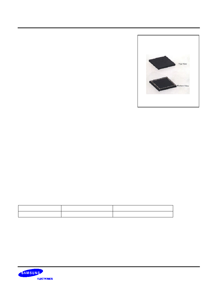
32BCC++(5mm * 5mm * 0.8mm) Package
ORDERING INFORMATION
Device
Package
Operating Temperature
++ S1M8662AX01-F0T0
32-BCC++-5.0
◊
5.0
-30 to +85
∞
C
++ : Under Development
32-BCC++-5.0
◊
5.0

S1M8662A (Preliminary)
RX IF/BBA WITH GPS
2
BLOCK DIAGRAM
SW
CRX_IF1
CRX_IF2
RAGC_CONT
GRX_IF1
GRX_IF2
RXVCO_OUT1,2
Q_OFS
CHIPX8
RXQD[0] - [3]
RXID[0] - [3]
I_OFS
RXVCO_T1
RXVCO_T2
TCXO_in
CLOCK
DATA
STROBE
N=2,3,4,6
TCXO_out
VCO
0
Div. N
90
CDMA
LPF
GPS
LPF
CDMA
LPF
GPS
LPF
Offset
Control
SPI
Control
4-Bit
ADC
X1
4-Bit
ADC

RX IF/BBA WITH GPS
S1M8662A (Preliminary)
3
PIN CONFIGURATION
CRX_IF2
TCXO_out
SPI_DATA
SPI_STB
RXVCO_OUT1
RXID[0]
VDDD
VDDA
RXID[1]
RAGC_CONT
GRX_IF1
GRX_IF2
CRX_IF1
VDDA
VDDA
VDDA
Q_OFS
I_OFS
RXVCO_T1
RXVCO_T2
RXVCO_OUT2
SPI_CLK
TCXO_in
CHIPX8
RXQD[3]
RXQD[2]
RXQD[1]
RXQD[0]
VDDM
RXID[3]
RXID[2]
VDDA
S1M8662A
(Top View)
GND SLUG
25
26
27
28
29
30
31
32
1
2
3
4
5
6
7
8
9
16
15
14
13
12
11
10
24
23
22
21
20
19
17
18

S1M8662A (Preliminary)
RX IF/BBA WITH GPS
4
PIN DESCRIPTION
Pin No
Symbol
I/O
Description
1
VDDD
P
Power for the digital logic.
2
VDDA
P
Power input terminal for the analog circuit.
3
RAGC_CONT
AI
AGC gain control input. The input voltage is allowed up to VDDA.
It remains at High impedance during SLEEP.
4
5
GRX_IF1
GRX_IF2
AI
GPS IF input terminals, which have an input impedance of about
865W; generally, the GPS IF SAW filter is connected to them. When
these terminals are not used, they remain at High impedance.
6
7
CRX_IF1
CRX_IF2
AI
CDMA IF input terminals, which have an input impedance of about
865
; generally, the CDMA IF SAW filter is connected to them. When
these terminals are not used, they remain at High impedance.
8
VDDA
P
Power input terminal for the analog circuit.
9
TCXO_out
DO
TCXO Clock output. division ratio : 1
10
VDDA
P
Power input terminal for the analog circuit.
11
VDDA
P
Power input terminal for the analog circuit.
12
13
Q_OFS
I_OFS
AI
Control DC input for removing the DC offset generated in the
S1M8662A and system during CDMA and GPS Mode. The control DC
is generated in the modem in PDM form, passes through the R-C filter
and is converted to DC, which is sent to this input terminal.
14
15
RXVCO_T1
RXVCO_T2
AI
Very sensitive terminal, which is connected to the oscillation L-C
resonance circuit.
Their impedance are about 2k
16
VDDA
P
Power input terminal for the analog circuit.
17
18
RXVCO_OUT1
RXVCO_OUT2
AO
Output for the PLL, able to output about -12dBm.
When this is not used, it remains at high impedance.
19
SPI_STB
DI
3-Line serial control. Strobe input port.
If this pin is opened, it remains at Low.
20
SPI_DATA
BI
3-Line serial control. DATA input/output port.
If this pin is opened, it remains at Low.
21
SPI_CLK
DI
3-Line serial control. CLOCK input/output port.
If this pin is opened, it remains at Low.
22
TCXO_in
AI/DI
Reference frequency input terminal connected to the VCTCXO output.
When this pin stops, only DC bias is delivered to maintain the DC
charge value of the capacitor connected externally
23
CHIPx8
DI
CHIPx8 Clock input port. CDMA/GPS ADC sampling clock from the
MSM.

RX IF/BBA WITH GPS
S1M8662A (Preliminary)
5
PIN DESCRIPTION (Continued)
Pin No
Symbol
I/O
Description
24
25
26
27
RXQD3
RXQD2
RXQD1
RXQD0
DO
Q Channel 4-bit A-D Converter's digital outputs, which are connected
to the modem data input pins. These data are synchronized at
CHIP
◊
8's rising edge and output. Because they are valid at the falling
edge, the data are latched at the falling edge in the modem.
28
VDDM
DI
Power source for a logic circuit ,related to the digital input /output,
connected to an external digital logic such as the modem.
29
30
31
32
RXQD3
RXQD2
RXQD1
RXQD0
DO
I Channel 4-bit A-D Converter's digital outputs, which are connected to
the modem data input pins. These data are synchronized at CHIP
◊
8's
rising edge and output. Because they are valid at the falling edge, the
data are latched at the falling edge in the modem.
Table 1. S1M8660A and S1M8662A Function & Control Content Comparison
Function / Mode Control
S1M8660A
S1M8662A
Operation Modes
CDMA (Cellular CDMA, PCS)
∑
∑
AMPS (FM)
∑
Global Positioning System (GPS)
∑
∑
IF AGC 90dB Range
CDMA (Cellular CDMA, PCS)
∑
∑
AMPS (FM)
∑
Global Positioning System (GPS)
∑
∑
IF to Analog Baseband Quadrature Down-Conversion
CDMA (Cellular CDMA, PCS)
∑
∑
AMPS (FM)
∑
Global Positioning System (GPS)
∑
∑
Low Pass Baseband I/Q Filtering with Mode Specific Performance
CDMA (Cellular CDMA, PCS)
∑
∑
AMPS (FM)
∑
Global Positioning System (GPS)
∑
∑
4-bit I/Q Analog to Digital Converters, Parallel Outputs
CDMA (Cellular CDMA, PCS)
∑
∑
Global Positioning System (GPS)
∑
∑
8-bit I/Q Analog to Digital Converters, Serial Outputs
AMPS (FM)
∑
Rx Slotting Operation for Saving Current Consumption
∑
∑
Clock Generation
TCXO/N Output
∑
(N=1)
Configurable CHIPx8 as Input or Output
∑
(Input)
VCO for Generation the Rx IF LO
∑
∑
Analog Baseband Amplifiers with I/Q Offset Controls
∑
∑