 | –≠–ª–µ–∫—Ç—Ä–æ–Ω–Ω—ã–π –∫–æ–º–ø–æ–Ω–µ–Ω—Ç: S1M8673 | –°–∫–∞—á–∞—Ç—å:  PDF PDF  ZIP ZIP |

RX RF FRONT-ENDS IC
S1M8673
1
INTRODUCTION
S1M8673 is an integrated receiver chip intended for use in cellular phones
operating in IS-95 AMPS/CDMA applications.
This device incorporates all the components required to implement the
receiver RF front-end except the filter blocks. It has a Low Noise Amplifier
(LNA) and a Mixer.
LNA has a single-ended input and a single-ended output for the RF Surface
Acoustic Wave (SAW) filter. RF Mixer, of which output is balanced, is followed
by an IF SAW filter.
The noise figure, gain, and IP3 of each stage in the receiver chip are
optimized to meet the system requirements for AMPS/CDMA mode as per IS-
98A. Using 0.5um silicon BiCMOS technology, the S1M8673 has been
designed for high performance and low cost applications.
The device package and pins are shown in Figure 1. A block diagram of the
S1M8673 is shown in Figure 2.
FEATURES
∑
Supports cellular CDMA/AMPS mode.
∑
On-chip High IIP3 (+4dBm) Low Noise Amplifier.
∑
Low noise, High IIP3 mixer (+4dBm).
∑
3V operation.
∑
20-eTSSOP, or 24-QFN package with exposed paddle.
APPLICATIONS
∑
Cellular CDMA/AMPS Hand Held Phone
ORDERING INFORMATION
Device
Package
Operating Temperature
+ S1M8673X01-V0T0
20-eTSSOP-BD44
-30 to +80
∞
C
+ S1M8673X01-G0T0
24-QFN-3.5
◊
4.5
-30 to +80
∞
C
+: New product
24-QFN-3.5
◊
4.5
20-eTSSOP-BD44
S1M8673
RX RF FRONT-ENDS IC
2
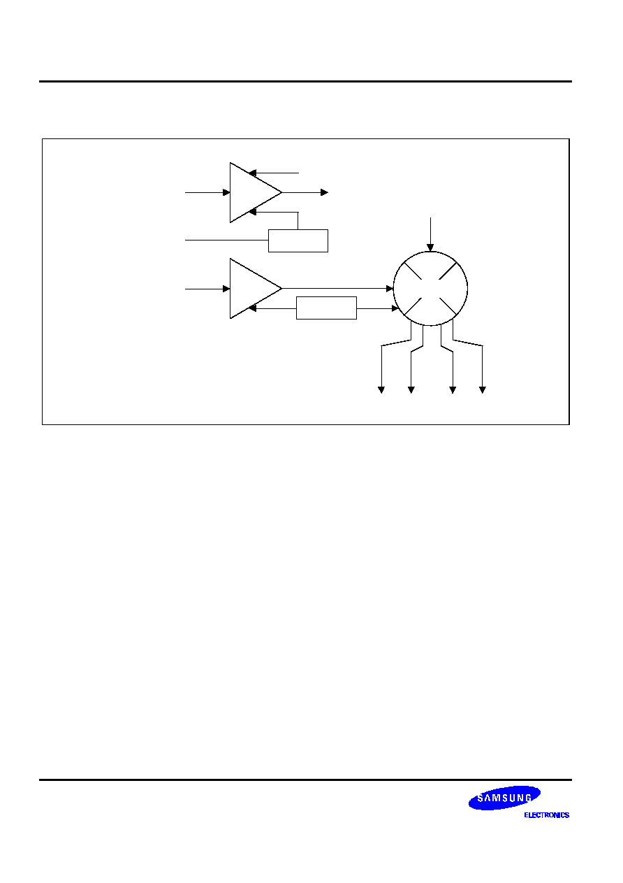
BLOCK DIAGRAM
LNA
LO
Buffer
LNA Bias
Mixer Bias
Mixer
LNA OUT
LNA CNTL
MIX IN
LNA IN
LNA EXT IND
LO IN
IF CDMA P
IF CDMA N
IF AMPS P
IF AMPS N
Figure 1. S1M8673 Block Diagram
RX RF FRONT-ENDS IC
S1M8673
3
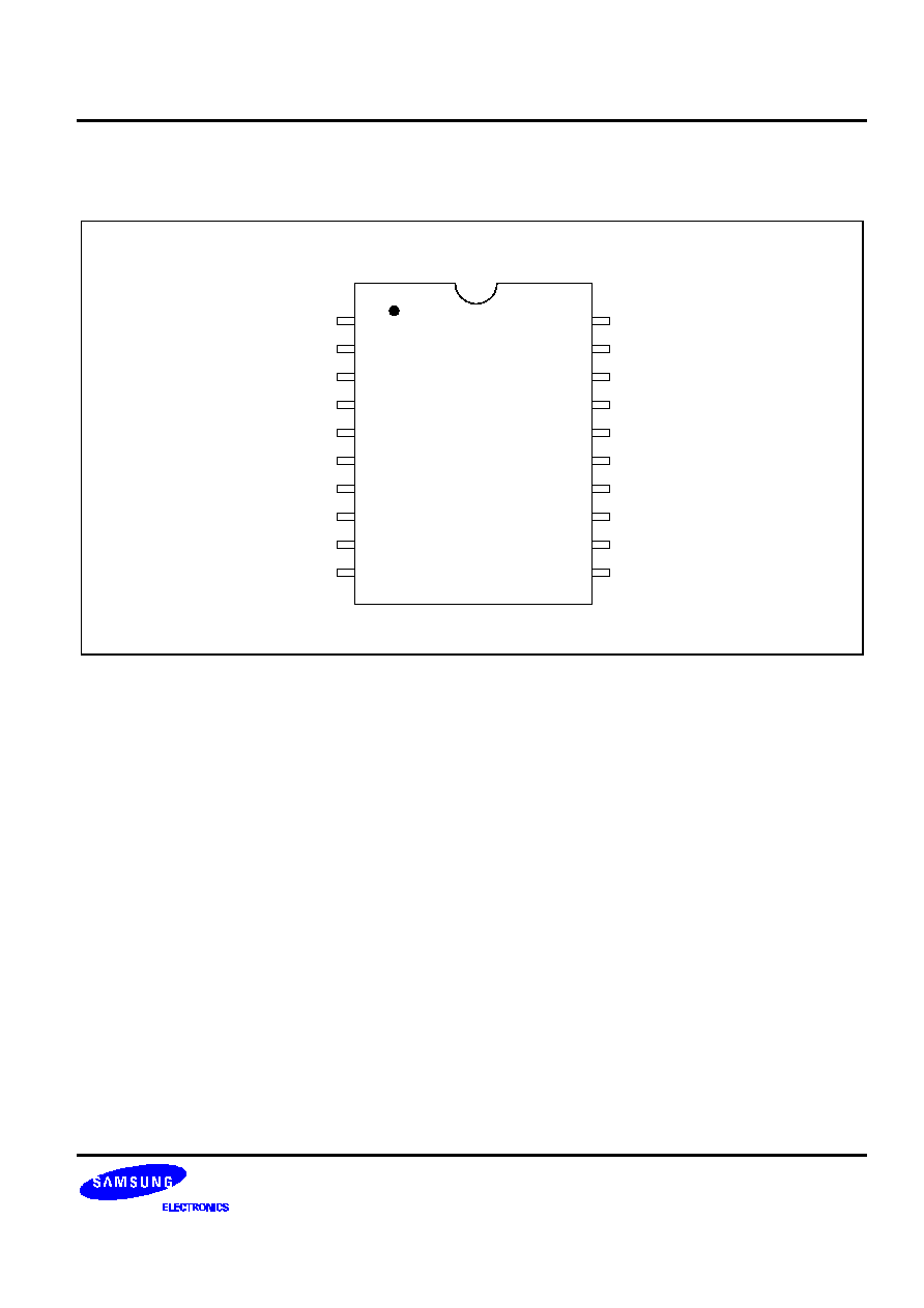
PIN DESCRIPTION
S1M8673
LNA V
CC
LNA CNTL
LNA OUT
LNA Bias R
MIX V
CC
MIX Bias R
MIX EXT IND
MIX IN
SLEEP
LO IN
20
19
18
17
16
15
14
13
12
11
1
2
3
4
5
6
7
8
9
10
LNA RF V
CC
EXT GND
LNA IN
LNA GND
LNA EXT IND
MOD SEL
IF CDMA N
IF CDMA P
IF AMPS N
IF AMPS P
Figure 2. S1M8673 Pin Description (20-eTSSOP)

S1M8673
RX RF FRONT-ENDS IC
4
PIN DESCRIPTION
Pin No.
Pin Name
Type
Descriptions
1
LNA_RF_VCC
Power supply voltage for LNA amplifier core
2
EXT_GND
Ground
3
LNA_IN
Input
RF signal input of LNA
4
LNA_GND
Ground
5
LNA_EXT_IND
LNA Bias pin
6
MOD_SEL
Input
AMPS/CDMA mode selection
7
IF_CDMA_N
Output
Mixer IF Output (CDMA)
8
IF_CDMA_P
Output
Mixer IF Output (CDMA)
9
IF_AMPS_N
Output
Mixer IF Output (AMPS)
10
IF_AMPS_P
Output
Mixer IF Output (AMPS)
11
LO_IN
Input
Local oscillator power input
12
SLEEP
Power down
13
MIX_IN
Input
Mixer RF signal input
14
MIX_EXT_IND
Attach external Inductor
15
MIX_Bias_R
Current control resistor for mixer
16
MIX_VCC
Power supply voltage for MIXER
17
LNA_Bias_R
LNA current control resistor
18
LNA_OUT
Output
LNA Output
19
LNA_CNTL
LNA Gain Control
20
LNA_VCC
Power supply voltage for LNA bias circuit

RX RF FRONT-ENDS IC
S1M8673
5
ABSOLUTE MAXIMUM RATINGS
Characteristic
Symbol
Value
Unit
Power supply voltage
V
CC
-0.3 to 5.0
V
Input voltage range
V
I
-0.3 to 5.0
V
LNA input power
P
I(LNA)
+ 5.0
dBm
Power dissipation
P
D
600
mW
Operating temperature
T
OPR
-30 to +80
∞
C
Storage temperature
T
STG
-65 to +125
∞
C
RECOMMENDED OPERATING CONDITIONS
Characteristic
Symbol
Value
Unit
Supply voltage
V
CC
2.5 to 3.3
V
Operating temperature
Ta
-30 to +80
∞
C
Logic 0
0.2
◊
V
CC
V
Logic 1
V
CC
V

S1M8673
RX RF FRONT-ENDS IC
6
ELECTRICAL CHARACTERISTICS
(T
a
= 25
∞
C,
V
CC
= 3.0V, PLO = -10dBm, input/output externally matched)
Characteristic
Test Conditions
Min
Typ
Max
Unit
LNA
Frequency Range
869 - 894
MHz
Gain
High gain state
Low gain state
@ 885 MHz
(Vcntl=3V)
(Vcntl=0V)
14
2
16
4
18
6
dB
Noise Figure
High gain state
Low gain state
@ 885 MHz
(Vcntl=3V)
(Vcntl=0V)
1.8
8
2.2
9
dB
Input Return Loss
- 15
- 10
dB
Output Return Loss
- 15
- 10
dB
Reverse Isolation
- 35
- 30
dB
P1dB
High gain state
Low gain state
@ Input
(Vcntl=3V)
(Vcntl=0V)
- 8
- 8
- 6
- 6
dBm
IP3
High gain state
Low gain state
@ Input
(Vcntl=3V)
(Vcntl=0V)
2
2
4
4
dBm
Current Consumption
8
mA
Mixer
RF Frequency Range
869 - 894
MHz
IF Frequency
50 - 200
MHz
Conversion Gain
CDMA mode
AMPS mode
6.5
4.0
7.5
5.0
8.5
6.0
dB
Output Impedance
CDMA
AMPS
(Differential)
(Single-ended)
2
1.5
K
Noise Figure (SSB)
CDMA mode
AMPS mode
8.0
9.2
9.0
9.5
dB
LO Power
- 15
- 10
- 5
dB
RF Input Return Loss
- 15
- 10
dB
LO Input Return Loss
- 15
- 10
IIP3
CDMA mode
AMPS mode
@ Input
2
2
4
4
dBm
LO to RF Isolation
- 20
- 15
dB
Current Consumption
14
mA

RX RF FRONT-ENDS IC
S1M8673
7
TECHNICAL DESCRIPTION
LOW NOISE AMPLIFIER (LNA)
The LNA is designed to provide low noise figure and high linearity to achieve maximum dynamic range. Pin 17,
LNA bias control pin, is required to connect grounded resistor to decide the LNA current. The input and output are
logic 0, mathod externally. For handling high level signals, LNA provides the low gain state by setting Pin 19 to
ground.
MIXER
The mixer is designed to operate with very low LO power of -10dBm. The LO port is matched externally to the
chip. Bias control resistors have to be connected to the Pin 15 to adjust the mixer current.
The sleep mode is controlled by a signal at Pin 12. The supply voltage should be present at all the VCC pins for
normal operation.
The signal pin assignments and functional pin descriptions are found in Table 1. The absolute maximum ratings
of the S1M8673 are provided in Table 2, the recommended operating conditions are specified in Table 3, and
electrical specifications are provided in Table 4.
ESD SENSITIVITY
The S1M8673 is a Class 1 device. The following extreme Electrostatic Discharge (ESD) precautions are required
according to the TBD Human Body Model (HBM) or Charged Device Model (CDM)
∑
Complete ESD training program required.
∑
Protective outer garments.
∑
Handle device in ESD safeguard work area.
∑
Transport device in ESD shielded containers.
∑
Monitor and test all ESD protection equipment.
Treat the S1M8673 as extremely sensitive to ESD since ESD sensitivity has not yet been determined for this
device.

S1M8673
RX RF FRONT-ENDS IC
8
PASSIVE
ELEMENT
VALUE
OF
TEST
CIRCUIT
Element
Value
Element
Value
R1
16 k
C64
39 pF
R2
11 k
C65
1000 pF
R3
1 k
C66
1.8 pF
R4
1 k
C67
1000 pF
R5
560
C68
9 pF
R6
1.5 k
C81
1000 pF
C2
1000 pF
C82
1000 pF
C4
1000 pF
L1
10 nH
C6
1000 pF
L2
47 nH
C8
1000 pF
L3
390 nH
C10
1000 pF
L4
390 nH
C14
1000 pF
L5
1.8 uH
C51
39 pF
L6
1.8 uH
C52
5.7 pF
L7
4.7 nH
C54
8 pF
L8
8.2 nH
C55
8 pF
L9
82 nH
C56
1000 pF
L10
18 nH
C57
1000 pF
L11
1.8 uH
C58
3.3 pF
L12
1.8 uH
C60
39 pF
L13
330 nH
C61
1.5 pF
T1
1:8 Transformer
C63
39 pF
T2
1:8 Transformer
NOTES:
1.
Transformer: TC8-1 by Mini-Circuits (See the data book of Mini-Circuits for more detailed information)
2. High Q components are recommended for C51, C52, L1, and L2 to reduce the noise figure.
3. For cascade measurement, RF filter with input and output impedance of 50
can be inserted between SC2 and SC3.

RX RF FRONT-ENDS IC
S1M8673
9
BLOCK TEST CIRCUIT (20TSSOP)
A
A
v
cc
v
cc
Gain Cntl V
v
cc
A
v
cc
v
cc
v
cc
SW1
SW7
C14
C2
L2
L1
C52
C51
SC1
C54
L4
L3
C55
C57
C56
R3
L6
R4
L5
SC5
T1
N2 N1
SC6
T2
N1 N2
C68
C4
C67
L12
R6
R5
L11
L7
C60
C63
L8
C61
L13
C58
C6
SW2
SC3
SW3
C82
R1
L9
C8
R2
C81
C10
C65
C12
SW4
SW5
C64
L10
C66
SC2
SC4
1.6uH
33uF
33uF
1uF
(Tantalum)
A
Current Meter
SMA Type Connector
50
Transmission Line
1
3
5
7
9
19
17
15
13
11
2
4
6
8
10
20
18
16
14
12
S1M8673
Figure 3. Package Block Test Circuit (B-Type)

S1M8673
RX RF FRONT-ENDS IC
10
NOTES