 | –≠–ª–µ–∫—Ç—Ä–æ–Ω–Ω—ã–π –∫–æ–º–ø–æ–Ω–µ–Ω—Ç: S1M8674 | –°–∫–∞—á–∞—Ç—å:  PDF PDF  ZIP ZIP |

TX RF FRONTS-ENDS IC
S1M8674
1
INTRODUCTION
S1M8674 is a fully integrated RF transmit IC for CDMA handsets. It includes
an upconverter, a two-stage driver amplifier, and an LO buffer in
20TSSOP/24QFN (with exposed paddle) package. The driver amplifier
delivers over 4dBm output power with -65 dBc/30kHz ACPR while drawing
total current of under 40mA from 3.0V supply. The maximum output power is
larger than 10dBm for AMPS application. The gain of the driver amplifier can
be changed by an amount in 30dB to compensate for the gain variation of on-
chip & off-chip component ICs. The driver amplifier saves current at typical
condition due to the class AB operation.
The S1M8674 is ideally suited for CDMA/AMPS handset applications for low
power consumption.
The S1M8674 is fabricated using Samsung's 0.5
µ
m BiCMOS process with low
cost and high yield.
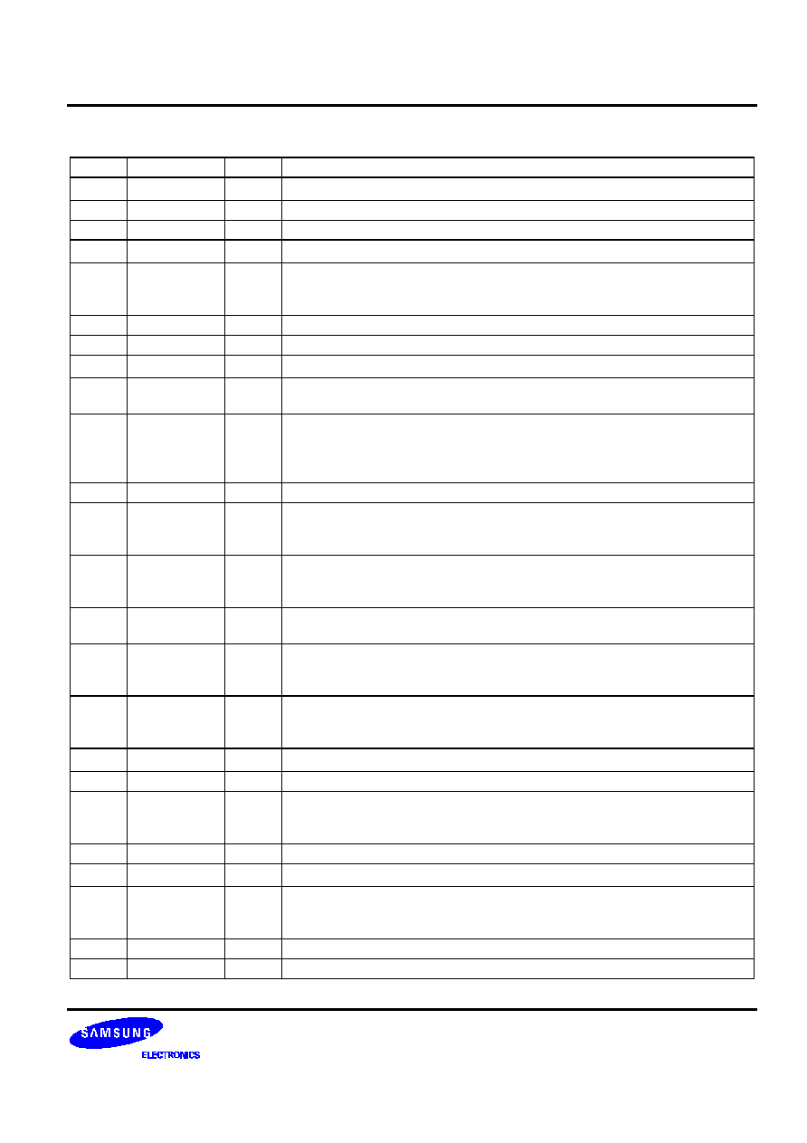
The device package is shown in Figure 1. The block diagram and pin out of
the S1M8674 on 20TSSOP/24QFN PKG are shown in Figure 2a and 2b,
respectively. The pin description is found in table 1a and 1b, respectively. The
absolute maximum ratings of the S1M8674 are provided in Table 2, the
recommended operating conditions are specified in Table 3, and electrical
specifications are provided in Table 4.
FEATURES
∑
Supports CDMA/AMPS application (824 to 849 MHz)
∑
30 dB gain control range of the driver amplifier to compensate for the gain variation of on-chip & off-chip
components
∑
Power amplifier driver which has high linearity
∑
Power down control of the entire chip
∑
20-Pin TSSOP/24-Pin QFN w/exposed paddle package
∑
13 dB Attenuator is included for wide dynamic range.
ORDERING INFORMATION
Device
Package
Operating Temperature
+ S1M8674X01-V0T0
20-eTSSOP-BD44
-30 to +80
∞
C
+ S1M8674X01-G0T0
24-QFN-3.5
◊
4.5
-30 to +80
∞
C
+ : New product
APPLICATIONS
∑
Cellular CDMA/AMPS Hand-Held Phone
20-eTSSOP-BD44
24-QFN-3.5
◊
4.5

S1M8674
TX RF FRONTS-ENDS IC
2
BLOCK DIAGRAM & PIN CONNECTIONS (20-eTSSOP TYPE)
IF_inp
Driver Amplifier
Upconverter
Attenuator
1
2
3
4
5
6
7
8
9
10
20
19
18
17
16
15
14
13
12
11
V
CC
_lo
LO_in
V
CC
_bias_m
GND_bias
Drv_out
GND_rf2
V
CC
_bias_rf
V
CC
_drv1
Gain_cntl
IF_inn
V
CC
_mix
RF_outn
V
CC
_bias_d
Ref_m
Drv_in
GND_rf1
Enable
Ref_d
Gain_Control
RF_outp
Figure 1. S1M8674 RF transmit IC Block Diagram and Pinout (20TSSOP-ePAD)

TX RF FRONTS-ENDS IC
S1M8674
3
BLOCK DIAGRAM & PIN CONNECTIONS (24QFN-TYPE )
V
CC
_lo
Driver Amplifier
Upconverter
Attenuator
1
2
3
4
5
6
7
8
9
21
20
19
18
17
16
15
14
13
LO_in
GND
V
CC
_bias_m
Drv_out
GND_rf2
GND
V
CC
_bias_rf
V
CC
_drv1
V
CC
_mix
RF_outp
RF_outn
V
CC
_bias_d
Ref_m
Drv_in
GND_rf1
Enable
Ref_d
Gain_Control
GND
10
11
12
24
23
22
GND
Gain_cntl1
IF_inn
GND
IF_inp
Figure 2. S1M8674 RF transmit IC Block Diagram and Pinout (24QFN)

S1M8674
TX RF FRONTS-ENDS IC
4
PIN FUNCTION DESCRIPTION (20TSSOP-ePAD)
Pin no.
Pin Name
Type
Descriptions
1
IF_inp
Input
The input IF pin for 130.38MHz IF frequency. This pin is connected to a
internal attenuator input. The output of the attenuator is connected to the
IF input of the CDMA/AMPS upconverter. This is a balanced input with Pin
20.
2
V
CC_lo
Supply voltage for the LO buffer.
3
LO_in
Input
This is the input pin for the local oscillator. DC blocking cap is required.
4
V
CC_bias_m
Supply voltage for the bias of the Upconverter.
5
GND_bias
GND
The common ground. It is connected to exposed paddle GND.
6
Drv_out
Output
This is the output pin for the CDMA/AMPS RF signal. The pin is
connected to the output of the Driver amplifier. Power supply and
Impedance matching are required.
7
GND_rf2
GND
The ground of the second stage in the Driver amplifier.
8
V
CC_bias_rf
Supply voltage for the bias of Driver amplifier.
9
V
CC_drv1
Supply voltage for the first stage of the Driver amplifier.
External load inductor is required.
10
Gain_cntl
Input
The gain control pin for the Driver amplifier. A DC voltage of 0.4 to 2.2V is
needed to cover the RF gain range of Driver amplifier. The gain slope is
controlled by a external series resistor. 18K ohm is suitable for 25 dB
dynamic range.
11
Ref_d
This pin is connected to an internal bias resistor of the Driver amplifier. An
external resistor can be connected to this pin in order to control the bias
current of the driver amplifier. The external R is not required at normal
bias.
12
Enable
Input
This is a control signal input pin. When the input is low, the chip will be
disabled. When the input is high, the chip will be enabled. This pin can be
used for puncturing.
13
GND_rf1
GND
The ground of the first stage in the Driver amplifier. This pin is connected
to an external degeneration inductor. Signal pass should be short.
14
Drv_in
Input
This pin is connected to the RF input of the driver amplifier. The input
signal should pass through a SAW filter before being connected to the
driver amplifier. Impedance matching is required.
15
Ref_m
This pin is connected to an internal bias resistor of the Upconverter. An
external resistor can be connected to this pin in order to control the bias
current of the mixer amplifier. The external R is not required at normal
bias.
16
V
CC_bias_d
Supply voltage for the bias of control block in the Driver amplifier.
17
RF_outp
Output
This pin is connected to the RF Output of the Upconverter. The input
signal should pass through a SAW filter before being connected to the
driver amplifier. Power supply and Impedance matching are required.
18
RF_outn
Output
The same as pin 17 , except complementary Output
19
V
CC_mix
Supply voltage for the mixer core in the upconverter.
20
IF_inn
Input
The same as pin 1, except complementary input
TX RF FRONTS-ENDS IC
S1M8674
5
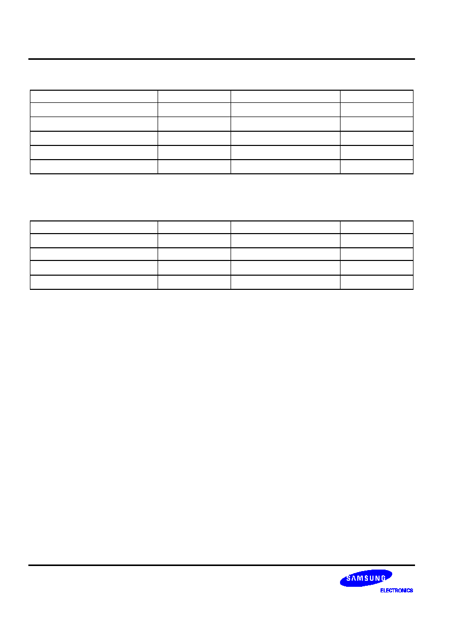
PIN FUNCTION DESCRIPTION (24QFN)
Pin no.
Pin Name
Type
Descriptions
1
V
CC_lo
Supply voltage for the LO buffer.
2
LO_in
Input
This is the input pin for the local oscillator. DC blocking cap is required
3
GND
GND
The common GND. It is connected to exposed paddle GND.
4
V
CC_bias_m
Supply voltage for the bias of the Upconverter.
5
Drv_out
Output
This is the output pin for the CDMA/AMPS RF signal. The pin is connected
to the output of the Driver amplifier. Power supply and Impedance matching
are required.
6
GND_rf2
GND
The ground of the second stage in the Driver amplifier.
7
GND
GND
The common GND. It is connected to exposed paddle GND.
8
V
CC_bias_rf
Supply voltage for the bias of Driver amplifier.
9
V
CC_drv1
Supply voltage for the first stage of the Driver amplifier.
External load inductor is required.
10
Gain_cntl
Input
The gain control pin for the Driver amplifier. A DC voltage of 0.4 to 2.2V is
needed to cover the RF gain range of Driver amplifier. The gain slope is
controlled by a external series resistor. 18K ohm is suitable for 25 dB
dynamic range.
11
GND
GND
The common GND. It is connected to exposed paddle GND.
12
Ref_d
This pin is connected to an internal bias resistor of the Driver amplifier. An
external resistor can be connected to this pin in order to control the bias
current of the driver amplifier. The external R is not required at normal bias.
13
Enable
Input
This is a control signal input pin. When the input is low, the chip will be
disabled. When the input is high, the chip will be enabled. This pin can be
used for puncturing.
14
GND_rf1
GND
The ground of the first stage in the Driver amplifier. This pin is connected to
an external degeneration inductor. Signal pass should be short.
15
Drv_in
Input
This pin is connected to the RF input of the driver amplifier. The input
signal should pass through a SAW filter before being connected to the
driver amplifier. Impedance matching is required.
16
Ref_m
This pin is connected to an internal bias resistor of the Upconverter. An
external resistor can be connected to this pin in order to control the bias
current of the mixer amplifier. The external R is not required at normal bias.
17
V
CC_bias_d
Supply voltage for the bias of control block in the Driver amplifier.
18
GND
GND
The common GND. It is connected to exposed paddle GND.
19
RF_outp
Output
This pin is connected to the RF Output of the Upconverter. The input signal
should pass through a SAW filter before being connected to the driver
amplifier. Power supply and Impedance matching are required.
20
RF_outn
Output
The same as pin 17 , except complementary Output
21
V
CC_mix
Supply voltage for the mixer core of the upconverter.
22
IF_inn
Input
The input IF pin for 130.38MHz IF frequency. This pin is connected to a
internal attenuator input. The output of the attenuator is connected to the IF
input of the CDMA/AMPS upconverter. This is a balanced input with Pin 24.
23
GND
GND
The common GND. It is connected to exposed paddle GND.
24
IF_inp
Input
The same as pin 22, except complementary input
S1M8674
TX RF FRONTS-ENDS IC
6
ABSOLUTE MAXIMUM RATINGS
Characteristic
Symbol
Value
Unit
Power supply voltage
V
CC
-0.3 to 5.0
V
Input voltage range
V
I
-0.3 to 5.0
V
Power dissipation
P
D
600
mW
Operating temperature
T
OPR
-40 to +85
∞
C
Storage temperature
T
STG
-65 to +125
∞
C
RECOMMENDED OPERATING CONDITIONS
Characteristic
Symbol
Value
Unit
Supply voltage
V
CC
2.5 to 3.3
V
Operating temperature
Ta
-30 to +80
∞
C
Logic 0
0.2
◊
V
CC
V
Logic 1
V
CC
V
ESD SENSITIVITY
The S1M8674 meets Human Body Model (HBM) < 150V and Machine Model (MM) < 75V. ESD data available
upon request. Moisture Sensitivity Level (MSL) will be determined.

TX RF FRONTS-ENDS IC
S1M8674
7
ELECTRICAL CHARACTERISTICS
(T
a
= 25
∞
C, V
CC
= 3.0V, Plo = -10dBm, input/output externally matched, unless otherwise specified)
Variable-Gain Driver Amplifier
Characteristic
Test Conditions
Min
Typ
Max
Unit
Frequency
824
≠
849
MHz
Gain
-4
26
dB
Output power level
maximum gain
4
dBm
ACPR
in 30kHz band at 885kHz
offset @maximum gain
-65
-62
dBc
dBc
Total supply current
@ Po, max
25
29
33
mA
Sleep mode current
0.01
mA
Noise Figure
≠
4.3
5.5
dB
In/Out Return Loss
15
dB
Upconverter
Characteristic
Test Conditions
Min.
Typ.
Max.
Units
LO frequency range
700
1000
MHz
LO input return loss
reference to 50
10
dB
Terminating resistor across IF
inputs
800
1000
1200
Output frequency
824
925
MHz
Conversion gain
13dB attenuator
-9
-8
-7
dB
Without 13dB attenuator
4
5
6
dB
Output power
maximum gain
-16
dBm
ACPR
30kHz band at 885kHz
offset @ -16dBm output
-64
dBc
Noise figure
13dB attenuator
26
dB
Noise figure
12
dB
LO to RF leakage
LO=- 10 dBm
-40
dBm
Total supply current:
10
mA
Sleep mode current
0.01
mA

S1M8674
TX RF FRONTS-ENDS IC
8
APPLICATION CIRCUIT (20TSSOP-EPAD)
R1 = 18k
C1 = 1pF
C2,C13,C16 = 20pF
C11 = 2pF,C12 = 3pF
C9 = 2.2pF
C3,C6 = 10nF
C4,C5,C7,C10 = 120pF
C14,C15 = 1nF
L7, L8 = 15nH
L7,L8 = 15nH
L9,L10 = 18nH
L3 = 12nH
L4 = 4.4nH
L1,L5 = 8.2nH
L6 = 2.2nH
Driver Amplifier
Mixer
Attenuator
2
4
5
7
8
19
18
17
16
15
14
13
12
11
Gain_Control
20
1
LO Buffer
C14
C15
IF_in
3
6
9
10
Gain_ctrl
V
CC
_LO
L1
LO_in
C1
V
CC
_bias_M
C2
V
CC
_drv2
L3
C4
C3
L4
C5
C7
C6
V
CC
_drv1
L5
R1
PWR
AMP
SAW
SAW
V
CC
_mix
C13
L9 L10
C11
C12
L8
C10
L7
C9
L6
Enable
AGC
V
CC
_bias_D

TX RF FRONTS-ENDS IC
S1M8674
9
APPLICATION CIRCUIT (24QFN)
R1 = 18k
C1 = 1pF
C2,C13,C16 = 20pF
C11 = 2pF,C12 = 3pF
C9 = 2.2pF
C3,C6 = 10nF
C4,C5,C7,C10 = 120pF
C14,C15 = 1nF
L7, L8 = 15nH
L7,L8 = 15nH
L9,L10 = 18nH
L3 = 12nH
L4 = 4.4nH
L1,L5 = 8.2nH
L6 = 2.2nH
C14
C15
IF_in
L1
LO_in
C0
V
CC
_bias_M
C2
V
CC
_drv2
L3
C4
C3
L4
C5
C7
V
CC
_drv1
L5
R1
V
CC
_mix
C13
L9 L10
C11
C12
L8
C10
L7
C9
L6
Enable
Driver Amplifier
Upconverter
Attenuator
1
2
3
4
5
6
7
8
9
21
20
19
18
17
16
15
14
13
Gain_Control
10
11
12
24
23
22
AGC
V
CC
_LO
C13
(C)
Drv_out
C6
Gain_ctrl
V
CC
_bias_D
Mixer
RF_out
Drv_in

S1M8674
TX RF FRONTS-ENDS IC
10
NOTES