
INTERGER RF/IF DUAL PLL
S1M8821/22/23
1
INTRODUCTION
The S1M8821/22/23 is a high performance dual frequency
synthesizer with integrated prescalers designed for RF operation up
to 1.2GHz/2.0GHz/2.5GHz and IF operation up to 520MHz.
The S1M8821/22/23 contains dual-modulus prescalers. The RF
synthesizer adopts a 64/65 or a 128/129 prescaler(32/33 or 64/65 for
the S1M8823) and the IF synthesizer adopts an 8/9 or a 16/17
prescaler.
Using a proprietary digital phase-locked-loop technique, the
S1M8821/22/23 has linear phase detector characteristic and can be
used for very stable, low noise local oscillator signal. Supply voltage
can range from 2.7V to 4.0V. The S1M8821/22/23 is now available
in
a
20-TSSOP/24-QFN package.
FEATURES
∑
High operating frequency dual synthesizer
-- S1M8821 : 0.1 to 1.2GHz (RF)/ 45 to 520MHz (IF)
-- S1M8822 : 0.2 to 2.0GHz (RF)/ 45 to 520MHz (IF)
-- S1M8823 : 0.5 to 2.5GHz (RF)/ 45 to 520MHz (IF)
∑
Very low current consumption(8821:3.5mA, 22:4.5mA, 23:5.5mA)
∑
Operating voltage range : 2.7 to 4.0V
∑
Selectable power saving mode(Icc=1uA typical @3V)
∑
Dual modulus prescaler :
S1M8821/22 (RF) 64/65 or 128/129
S1M8823 (RF) 32/33 or 64/65
S1M8821/22/23 (IF) 8/9 or 16/17
∑
Programmability via serial bus interface
∑
No dead-zone PFD
∑
Variable charge pump output current
∑
High speed lock mode
APPLICATIONS
∑
Cellular telephone systems : S1M8821
∑
Portable wireless communications : S1M8822 (PCS/PCN, cordless)
∑
Wireless Local Area Networks (W-LANs) : S1M8823
∑
Other wireless communication systems
20-TSSOP-BD44
24-QFN-3.5
◊
4.5

S1M8821/22/23
INTERGER RF/IF DUAL PLL
2
ORDERING INFORMATION
Device
Package
Operating Temperature
S1M8821X01-R0T0
S1M8822X01-R0T0
S1M8823X01-R0T0
20-TSSOP-BD44
-40 to +85
∞
C
S1M8821X01-R0T0
S1M8822X01-R0T0
S1M8823X01-R0T0
24-QFN-3.5
◊
4.5
-40 to +85
∞
C

INTERGER RF/IF DUAL PLL
S1M8821/22/23
3
BLOCK DIAGRAM
NOTE: The pin numbers above are for 20-TSSOP package.
1
2
3
4
5
6
7
8
9
10
20
19
18
17
16
15
14
13
12
11
foLD
Data Out
Multiplexer
RF
LD
RF
Phase
Detector
RF
Charge
Pump
IF
LD
IF
Phase
Detector
IF
Charge
Pump
+ ≠
RF Prescaler
Prescaler
Control
RF
Programmable
Counter
RF N-Latch
RF R-Latch
RF Reference
Counter
IF Reference
Counter
20-bit Shift Register
IF R-Latch
IF N-Latch
2-bit
Control
≠ +
IF Prescaler
Prescaler
Control
IF
Counter
Programmable
V
DD
1
V
P
1
CPoRF
GND
f
in
RF
f
in
RF
GND
OSCin
GND
foLD
V
DD
2
V
P
2
CPoIF
GND
f
in
IF
f
in
IF
GND
LE
DATA
CLOCK

S1M8821/22/23
INTERGER RF/IF DUAL PLL
4
PIN CONFIGURATION
NOTES:
1. pin #9 = pin #17(internally connected).
2.
Do not tie up Vp and VDD
: Vp is the source of digital noises. The power for analog part is supplied by VDD.
If Vp and VDD are tied together, noisy Vp corrupts the power source for the analog part.
V
DD
1
Vp1
CPoRF
GND
finRF
finRF
GND
OSCin
GND
foLD
V
DD
2
Vp2
CPoIF
GND
finIF
finIF
GND
LE
DATA
CLOCK
1
20
2
3
4
5
6
7
8
20-Lead(0.173 Wide) Thin Shrink Small
9
10
19
18
17
16
15
14
13
12
11
Outline Package(20-TSSOP)
S1M8821
S1M8822
S1M8823
20-TSSOP
(Digital)
(Analog)
(Digital)
(Digital)
(Analog)
INTERGER RF/IF DUAL PLL
S1M8821/22/23
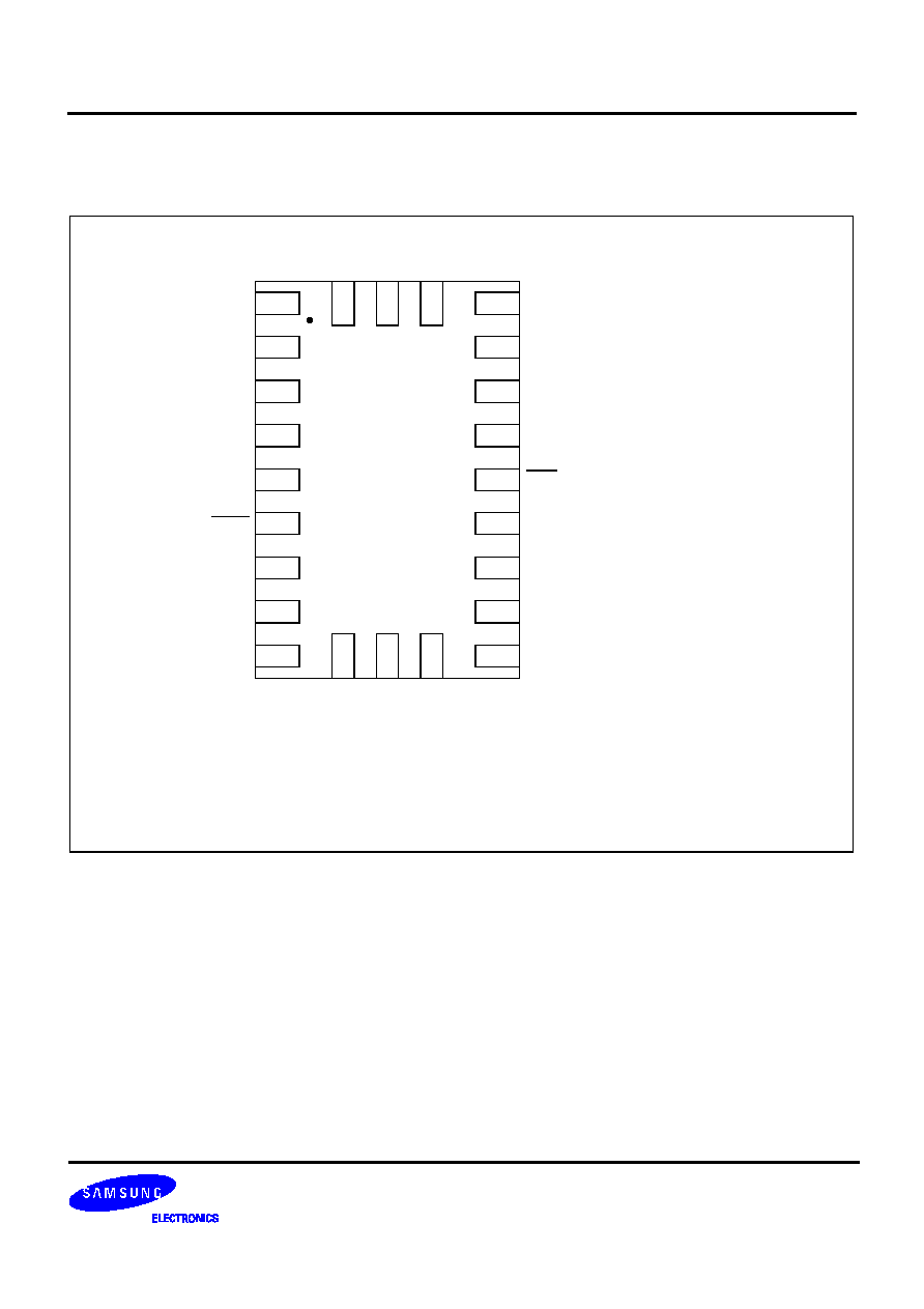
5
PIN CONFIGURATION(24-QFN, NOT TO SCALE)
NOTES:
1
pin #10 = pin #19(internally connected).
2.
Do not tie up Vp and V
DD
:
Vp is the source of digital noises. The power for analog part is supplied by V
DD.
If Vp and V
DD
are tied together,
noisy Vp corrupts the power source for the analog part.
V
DD
1
Vp1
CPoRF
GND
finRF
finRF
GND
OSCin
GND
foLD
V
DD
2 Vp2
CPoIF
GND
finIF
finIF
GND
LE
DATA
CLOCK
1
8
24
7
6
5
4
3
2
23
9
22
21
20
19
18
17
16
15
14
13
12
10
11
N/C
N/C
N/C
N/C
S1M8822
S1M8823
S1M8821
(24-QFN) Package
24-QFN
24 PIN Quad Flat Non-leaded
(Digital)
(Digital)
(Digital)
(Analog)
(Analog)
* N/C pins must be connected
to GND(to Analog GND if
possible).

S1M8821/22/23
INTERGER RF/IF DUAL PLL
6
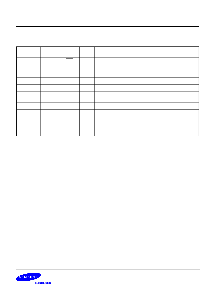
PIN DESCRIPTION
Pin No
(20TSSOP)
Pin No
(24QFN)
Symbol
I / O
Description
1
24
V
DD
1
-
Power supply voltage input for the RF PLL part. V
DD
1 must
equal V
DD
2. In order to reject supply noise, bypass capacitors
must be placed as close as possible to this pin and be
connected directly to the ground plane.
-
1
-
N/C
No connection.
2
2
Vp1
-
Power supply voltage input for RF charge pump(
V
DD
1).
3
3
CPoRF
O
Internal RF charge pump output for connection to an external
loop filter whose filtered output drives an external VCO.
4
4
GND
-
Ground for RF digital blocks.
5
5
finRF
I
RF prescaler input. The signal comes from the external VCO.
6
6
finRF
I
The complementary input of the RF prescaler. A bypass
capacitor must be placed as close as possible to this pin and
be connected directly to the ground plane. The bypass
capacitor is optional with some loss of sensitivity.
7
7
GND
-
Ground for RF analog blocks.
8
8
OSCin
I
Reference counter input. TCXO is connected via a coupling
capacitor.
-
9
-
N/C
No connection.
9
10
GND
-
Ground for IF digital blocks.
10
11
f
oLD
O
Multiplexed output of the RF/IF programmable counters, the
reference counters, the lock detect signals and the shift
registers. The output level is CMOS level. (see f
out
Programmable Truth Table)
11
12
CLOCK
I
CMOS clock input. Serial data for the various counters is
transferred into the 22-bit shift register on the rising edge of
the clock signal.
-
13
-
N/C
No connection.
12
14
DATA
I
Binary serial data input. The MSB of CMOS input data is
entered first. The control bits are on the last two bits. CMOS
input.
13
15
LE
I
Load enable CMOS input. When LE becomes high, the data
in the shift register is loaded into one of the four latches (by
the control bits).
14
16
GND
-
Ground for IF analog blocks.
INTERGER RF/IF DUAL PLL
S1M8821/22/23
7
PIN DESCRIPTION (Continued)
Pin No
(20TSSOP)
Pin No
(24QFN)
Symbol
I / O
Description
15
17
finIF
I
The complementary input of the IF prescaler. A bypass
capacitor must be placed as close as possible to this pin and
be connected directly to the ground plane. The bypass
capacitor is optional with some loss of sensitivity.
16
18
finIF
I
IF prescaler input. The signal comes from the external VCO.
17
19
GND
-
Ground for IF digital blocks.
18
20
CPoIF
O
Internal IF charge pump output for connection to an external
loop filter whose filtered output drives an external VCO.
-
21
-
N/C
No connection.
19
22
Vp2
-
Power supply voltage input for IF charge pump(
V
DD
2)
20
23
V
DD
2
-
Power supply voltage input for the IF PLL part. V
DD
1 must
equal V
DD
2. In order to reject supply noise, bypass capacitors
must be placed as close as possible to this pin and be
connected directly to the ground plane.
S1M8821/22/23
INTERGER RF/IF DUAL PLL
8
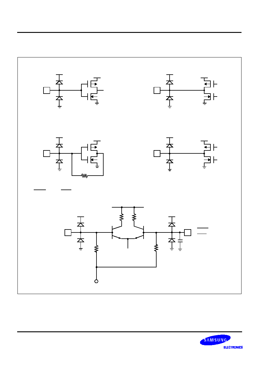
EQUIVALENT CIRCUIT DIAGRAM
CLOCK, DATA, LE
foLD
OSCin
CPoRF, CPoIF
finRF, finRF, finIF, finIF
finRF,
finIF
finRF,
finIF
V
bias
INTERGER RF/IF DUAL PLL
S1M8821/22/23
9
ABSOLUTE MAXIMUM RATINGS
ELECTROSTATIC CHARACTERISTICS
These devices are ESD sensitive. These devices must be handled in the ESD protected environment.
Characteristic
Symbol
Value
Unit
Power Supply Voltage
V
DD
0 to 4.0
V
Power Dissipation
P
D
600
mW
Operating Temperature
Ta
-40 to +85
o
C
∞
C
Storage Temperature
T
STG
-65 to +150
o
C
∞
C
Characteristic
Pin No.
ESD level
Unit
Human Body Model
All
< ±
2000
V
Machine Model
All
< ±
300
V
Charged Device Model
All
< ±
800
V
S1M8821/22/23
INTERGER RF/IF DUAL PLL
10
ELECTRICAL CHARACTERISTICS
(V
DD
=3.0V, V
P
=3.0V, Ta
=
=
=
=
25
∞
C, Unless otherwise specified)
Characteristic
Symbol
Test Conditions
Min.
Typ.
Max.
Unit
Power Supply Voltage
V
DD
2.7
3.0
4.0
V
V
P
V
DD
3.0
4.0
Power
Supply
Current
S1M8823 RF + IF
I
DD
V
DD
=2.7V to 4.0V
5.5
mA
S1M8823 RF Only
4.0
S1M8822 RF + IF
4.5
S1M8822 RF Only
3.0
S1M8821 RF + IF
3.5
S1M8821 RF Only
2.0
S1M882x IF Only
1.5
Power down Current
I
PWDN
V
DD
=3.0V
1.0
10
µ
A
Digital inputs : CLOCK, DATA and LE
High-Level Input Voltage
V
IH
V
DD
=2.7V to 4.0V
0.7V
DD
V
Low-Level Input Voltage
V
IL
V
DD
=2.7V to 4.0V
0.3V
DD
V
High-Level Input Current
I
IH
V
IH
= V
DD
=4.0V
-1.0
+1.0
µ
A
Low-Level Input Current
I
IL
V
IL
=0V, V
DD
=4.0V
-1.0
+1.0
µ
A
Reference Oscillator Input : OSCin
Input Current
I
IHR
V
IH
= V
DD
=4.0V
+100
µ
A
I
ILR
V
IL
=0V, V
DD
=4.0V
-100
µ
A
Digital Output : foLD
High Level Output Voltage
V
OH
Iout = -500
µ
A
V
DD
-0.4
V
Low Level Output Voltage
V
OL
Iout = +500
µ
A
0.4
V

INTERGER RF/IF DUAL PLL
S1M8821/22/23
11
ELECTRICAL CHARACTERISTICS (Continued)
(V
DD
=3.0V, V
P
=3.0V, Ta
=
=
=
=
25
∞
C, Unless otherwise specified)
Characteristic
Symbol
Test Conditions
Min.
Typ.
Max.
Unit
Charge Pump Outputs : CPoRF, CPoIF
Charge Pump Output
Current
I
CP-SRC
V
CP
=V
P
/2, I
CPo
=Low
-1.0
mA
I
CP-SINK
V
CP
=V
P
/2, I
CPo
=Low
+1.0
I
CP-SRC
V
CP
=V
P
/2, I
CPo
=High
-4.0
I
CP-SINK
V
CP
=V
P
/2, I
CPo
=High
+4.0
Charge Pump Leakage
Current
I
CPL
0.5V
V
CP
V
P
-0.5V
-2.5
+2.5
nA
Output Current Sink vs.
Source Mismatch*
I
CP-SINK
vs I
CP-SRC
V
CP
=V
P
/2
3
10
%
Output Current Magnitude
Variation vs. Temperature**
I
CP
vs T
V
CP
=V
P
/2
10
%
Output Current Magnitude
Variation vs. Voltage***
I
CP
vs V
CP
0.5V
V
CP
V
P
-0.5V
10
15
%
Programmable Divider
Operating
Frequency
S1M8823
finRF
V
DD
=2.7V to 4.0V
0.5
2.5
GHz
S1M8822
0.2
2.0
S1M8821
0.1
1.2
Operating Frequency
finIF
V
DD
=3.0V
45
520
MHz
RF Input Sensitivity
P
fin
RF
V
DD
=3.0V
-15
0
dBm
V
DD
=4.0V
-10
0
IF Input Sensitivity
P
fin
IF
V
DD
=2.7V to 4.0V
-10
0
dBm
Phase Detector Frequency
f
PD
10
MHz
Reference Divider
Operating Frequency
OSCin
5
40
MHz
Input Sensitivity
V
OSCin
0.5
V
PP

S1M8821/22/23
INTERGER RF/IF DUAL PLL
12
ELECTRICAL CHARACTERISTICS (Continued)
(V
DD
=3.0V, V
P
=3.0V, Ta
=
=
=
=
25
∞
C, Unless otherwise specified )
<For Charge Pump items>
Ia=Charge pump sink current at Vcp=Vp-
V, Ib=Charge pump sink current at Vcp=Vp/2,
Ic=Charge pump sink current at Vcp=
V
Id=Charge pump source current at Vcp=Vp-
V, Ie=Charge pump source current at Vcp=Vp/2,
If=Charge pump source current at Vcp=
V
V=Voltage offset from positive(for sink current) and negative(for source current) points from which the charge pump currents
become flat.
* Output Current Sink vs. Source Mismatch = [| Ib|-|Ie|] / [0.5 * {| Ib|+|Ie|}] * 100 (%)
** Output Current Magnitude Variation vs. Temperature =
[| Ib @any temp.| - |Ib @ 25
C|] / | Ib @ 25
C| * 100 (%) and [|Ie @any temp.| - |Ie @ 25
C|] / |Ie @ 25
C| * 100 (%)
*** Output Current Magnitude Variation vs. Voltage =
[0.5 * {|Ia|-|Ic|}] / [0.5 * {|Ia|+|Ic|}] * 100 (%) and [0.5 * {|Id|-|If|}] / [0.5 * {|Id|+|If|}] * 100 (%)
Characteristic
Symbol
Test Conditions
Min.
Typ.
Max.
Unit
Serial Data Control
CLOCK Frequency
f
CLOCK
10
MHz
CLOCK Pulse Width High
t
CWH
50
ns
CLOCK Pulse Width Low
t
CWL
50
ns
DATA Set Up Time to CLOCK
Risng Edge
t
DS
50
ns
DATA Hold Time after CLOCK
Rising Edge
t
DH
10
ns
LE Pulse Width
t
LEW
50
ns
CLOCK Rising Edge to LE Rising
Edge
t
CLE
50
ns

INTERGER RF/IF DUAL PLL
S1M8821/22/23
13
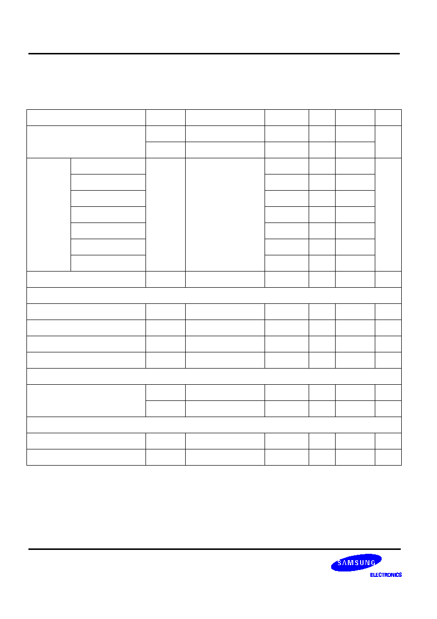
FUNCTIONAL DESCRIPTION
The Samsung S1M8821/22/23 are dual PLL frequency synthesizer ICs. S1M8821/22/23 combined with external
LPFs and external VCOs form PLL frequency synthesizers. They include serial data control, R counter, N counter,
prescaler, phase detector, charge pump, and etc.
Serial data is moved into 20-bit shift register on the rising edge of the clock. These data enters MSB first. When LE
becomes HIGH, data in the shift register is moved into one of the 4 latches(by the 2-bit control). The divide ratios of
the prescaler and the counters are determined by the data stored in the latches. The external VCO output signal is
divided by the prescaler and the N counter. External reference signal is divided by the R counter. These two signals
are the two input signals to the phase detector. The phase detector drives the charge pump by comparing
frequencies and phases of the above two signals. The charge pump and the external LPF make the control voltage
for the external VCO and finally the VCO generates the appropriate frequency signal.
Serial Data Input Timing
MSB
LSB
N20(R20)
N19(R19)
N10(R10)
N9(R9)
C2
C1
t
DS
t
CWL
t
CWH
t
LEW
t
DH
DATA
CLOCK
LE
t
CLE

S1M8821/22/23
INTERGER RF/IF DUAL PLL
14
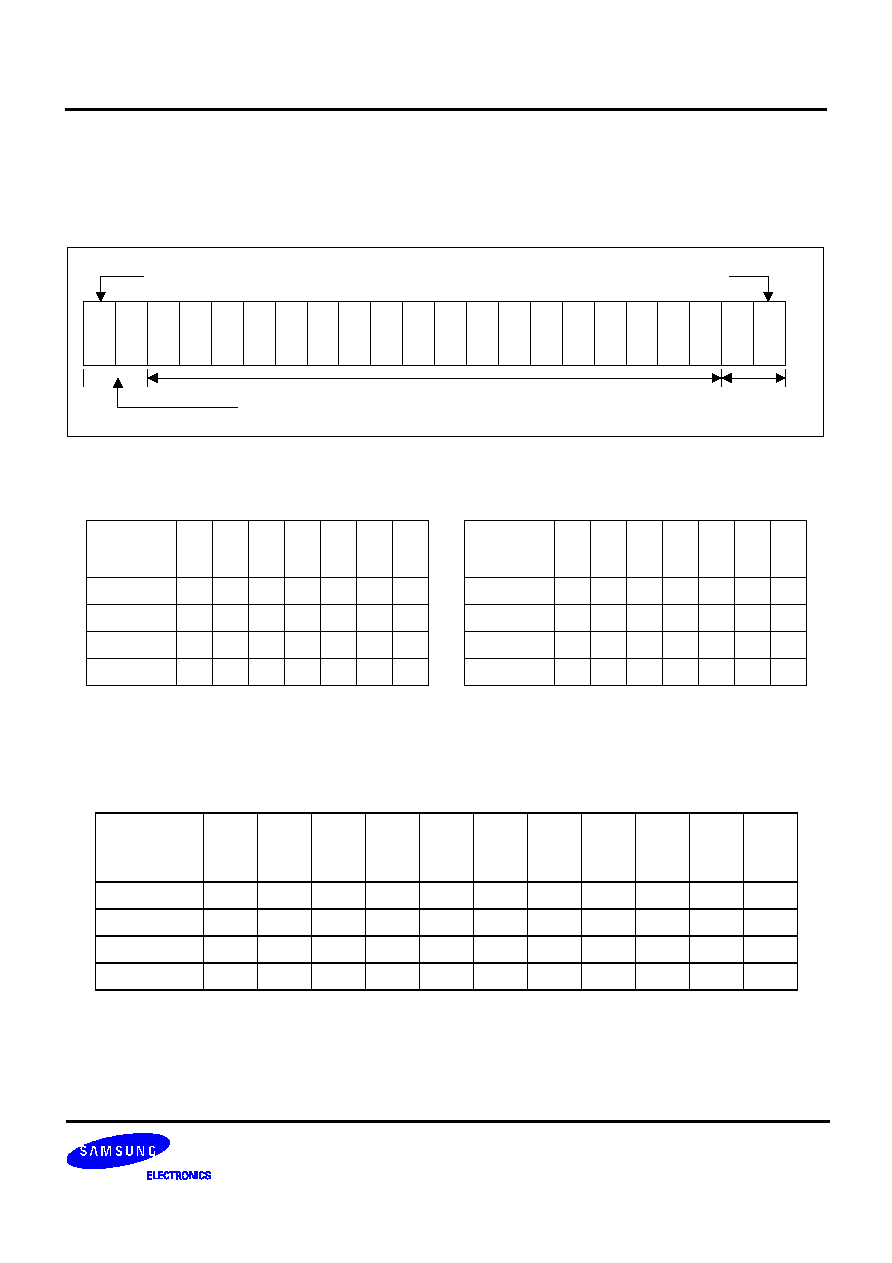
PROGRAMMING DESCRIPTION
Control Bits
Programmable Reference Counter(IF / RF R Counter)
If the Control Bits are 00(IF) or 01(RF), data is moved from the 20-bit shift register into the R-latch which sets the
reference counter. Serial data format is shown in the table below.
∑
15-Bit Programmable Reference Counter Ratio
Division ratio : 3 to 32767
Data are shifted in MSB first
Control Bits
DATA Location
C1
C2
0
0
IF R Counter
0
1
RF R Counter
1
0
IF N Counter
1
1
RF N Counter
Division
Ratio
R
15
R
14
R
13
R
12
R
11
R
10
R
9
R
8
R
7
R
6
R
5
R
4
R
3
R
2
R
1
3
0
0
0
0
0
0
0
0
0
0
0
0
0
1
1
4
0
0
0
0
0
0
0
0
0
0
0
0
1
0
0
≤
≤
≤
≤
≤
≤
≤
≤
≤
≤
≤
≤
≤
≤
≤
≤
32767
1
1
1
1
1
1
1
1
1
1
1
1
1
1
1
C1 C2
R
1
R
2
R
3
R
4
R
5
R
6
R
7
R
8
R
9
R
10
R
11
R
12
R
13
R
14
R
15
R
16
R
17
R
18
R
19
R
20
LSB
MSB
Program Modes
Division Ratio of the R Counter, R
Control Bits
INTERGER RF/IF DUAL PLL
S1M8821/22/23
15
Programmable Counter(N Counter)
If the Control Bits are 10(IF) or 11(RF), data is transferred from the 20-bit shift register into the N-latch. N Counter
consists of 7-bit swallow counter(A counter) and 11-bit main counter(B counter). Serial data format is shown below.
∑
7-Bit Swallow Counter Division Ratio(A Counter)
∑
11-Bit Main Counter Division Ratio(B Counter)
Division ratio : 3 to 2047
RF
IF
Division
Ratio(A)
N
7
N
6
N
5
N
4
N
3
N
2
N
1
Division
Ratio(A)
N
7
N
6
N
5
N
4
N
3
N
2
N
1
0
0
0
0
0
0
0
0
0
X
X
X
0
0
0
0
1
0
0
0
0
0
0
1
1
X
X
X
0
0
0
1
∑
∑
∑
∑
∑
∑
∑
∑
∑
∑
∑
∑
∑
∑
∑
∑
127
1
1
1
1
1
1
1
15
X
X
X
1
1
1
1
Division ratio : 0 to 127
B
>
A
Division ratio : 0 to 15
B > A
X = DON'T CARE condition
Division
Ratio
N
18
N
17
N
16
N
15
N
14
N
13
N
12
N
11
N
10
N
9
N
8
3
0
0
0
0
0
0
0
0
0
1
1
4
0
0
0
0
0
0
0
0
1
0
0
∑
∑
∑
∑
∑
∑
∑
∑
∑
∑
∑
∑
2047
1
1
1
1
1
1
1
1
1
1
1
C1 C2
N
1
N
2
N
3
N
4
N
5
N
6
N
7
N
8
N
9
N
10
N
11
N
12
N
13
N
14
N
15
N
16
N
17
N
18
N
19
N
20
LSB
MSB
Program Modes
Division Ratio of the N Counter, N
Control Bits

S1M8821/22/23
INTERGER RF/IF DUAL PLL
16
Pulse Swallow Function
f
VCO
=[ ( P X B ) + A ] x f
OSCin
/ R
f
VCO
: External VCO output frequency
P : Preset modulus of dual modulus prescaler
(for S1M8821/22 RF:P=64 or 128, for S1M8823 RF:P=32 or 64, for IF: P=8 or 16)
B : 11-bit main counter division ratio (3
B
2047)
A : 7-bit swallow counter division ratio
(for RF: 0
A
127, for IF: 0
A
15, A
B)
f
OSCin
: External reference frequency(from external oscillator)
R : 15-bit reference counter division ratio (3
R
32767)
Program Mode
∑
Mode Select Truth Table
* The charge pump output current of I
CPo
LOW = 1/4
◊
I
CPo
HIGH.
C1
C2
R16
R17
R18
R19
R20
0
0
IF Phase
Detector Polarity
IF I
CPo
IF CPoIF
High Impedance
IF
LD
IF
Fo
0
1
RF Phase
Detector Polarity
RF I
CPo
RF CPoIF
High Impedance
RF
LD
RF
Fo
C1
C2
N19
N20
1
0
IF Prescaler
Pwdn IF
1
1
RF Prescaler
Pwdn RF
Phase Detector Polarity
CPoIF High Impedance
I
CPo
IF Prescaler
RF Prescaler
S1M8821/22
(S1M8823)
Pwdn
0
Negative
Normal Operation
Low
8/9
64/65 (32/33)
Pwr Up
1
Positive
High Impedance
High
16/17
128/129 (64/65)
Pwr Dn
INTERGER RF/IF DUAL PLL
S1M8821/22/23
17
∑
Phase Detector Polarity
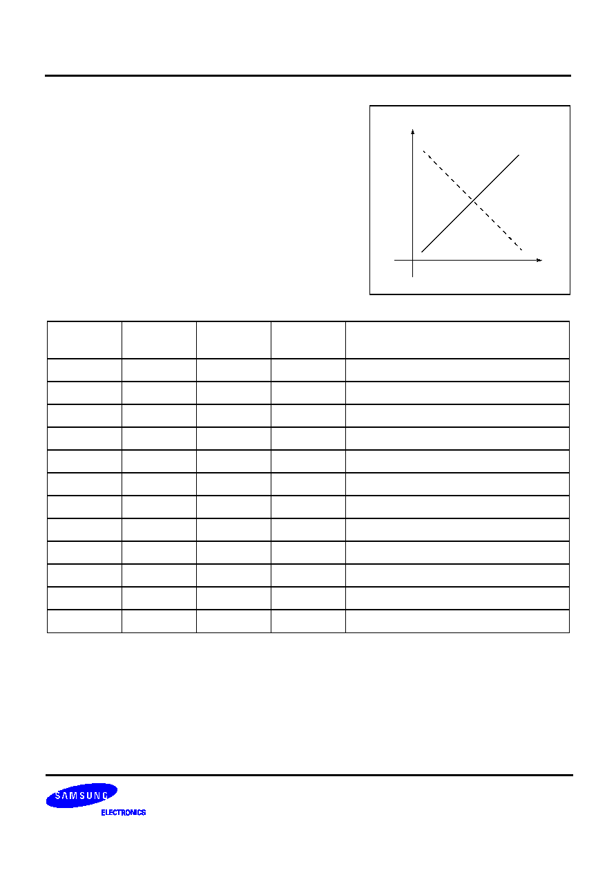
Depending on VCO characteristics, R16 bit should be set as follows :
VCO characteristics are positive like (1) : R16 HIGH
VCO characteristics are negative like (2) : R16 LOW
∑
foLD (Pin10) Output Truth Table
-- When the PLL is locked and a lock detect mode is selected, the foLD output is HIGH, with narrow pulses
LOW.
-- Counter Reset mode resets R & N counters.
-- The high speed lock mode sets the foLD output pin to be connected to ground with a low impedance
(
110
).
RF R19
(RF LD)
IF R19
(IF LD)
RF R20
(RF fo)
IF R20
(IF fo)
foLD Output State
0
0
0
0
Disabled (default LOW)
0
1
0
0
IF Lock Detect
1
0
0
0
RF Lock Detect
1
1
0
0
RF and IF Lock Detect
0
0
0
1
IF Reference Divider Output
0
0
1
0
RF Reference Divider Output
0
1
0
1
IF Programmable Divider Output
0
1
1
0
RF Programmable Divider Output
0
0
1
1
High Speed Lock mode
0
1
1
1
IF Counter Reset
1
0
1
1
RF Counter Reset
1
1
1
1
RF and IF Counter Reset
(1)
(2)
VCO Input Voltage
VC
O
O
u
t
put
Freq
uen
c
y
VCO Characteristics
S1M8821/22/23
INTERGER RF/IF DUAL PLL
18
FUNCTIONAL DESCRIPTION
(Continued)
∑
Powerdown mode operation
There are synchronous and asynchronous powerdown modes for S1M8821/22/23.
Synchronous powerdown mode occurs if R18 bit is LOW, N20 bit is HIGH and charge pump output is in high
impedance state. In the synchronous power down mode, the powerdown function is activated by the charge pump
to diminish unwanted frequency jumps. Asynchronous powerdown mode occurs if R18 bit is HIGH and N20 bit is
HIGH.
When the PLL goes to either synchronous or asynchronous powerdown mode, preamp becomes debiased, R & N
counters keeps their load conditions and the charge pump becomes high impedance state. The oscillator circuitry
function becomes disabled only when both IF and RF powerdown bits are activated, i.e. N20 HIGH.
The PLL returns to an active powerup mode when N20 bit becomes LOW(either in synchronous or asynchronous
modes).
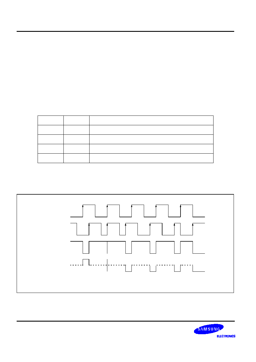
Phase Detector and Charge pump Characteristics
Phase difference detection range : -2
to +2
When R16 = HIGH
R18
N20
Powerdown mode status
0
0
PLL active
1
0
PLL active, only charge pump high impedance
0
1
Synchronous powerdown
1
1
Asynchronous powerdown
fr
fp
LD
fr>fp
fr=fp
fr<fp
fr<fp
fr<fp
CPo

INTERGER RF/IF DUAL PLL
S1M8821/22/23
19
RF SENSITIVITY MEASUREMENT CIRCUIT
RF
Signal
Generator
Frequency
Counter
PC
Parallel
Port
50
Microstrip
100pF
51
100pF
12k
39k
f
in
f
in
OSC
in
foLD
2.7V to 4.0V
V
DD
V
P
LE
DATA
CLOCK
100pF
100pF
2.2
µ
F
2.2
µ
F
** N=10,000 R=50 P=64
** Sensitivity limit is determined when the error of the divided RF output( foLD) becomes
1 Hz.
10dB ATTN
S1M8821/22/23
INTERGER RF/IF DUAL PLL
20
TYPICAL APPLICATION CIRCUIT
** The role of Rin : Rin makes VCO output power go to the load rather than the PLL.
The value of Rin depends on the VCO power level.
10
9
8
7
6
5
4
3
2
1
11
12
13
14
15
16
17
18
19
20
foLD
GND
OSCin
GND
finRF
f
in
RF
GND
CPoRF
V
P
1
V
DD
1
CLOCK DATA
LE
GND
f
in
IF
f
in
IF
GND
CPoIF
V
P
2
V
DD
2
VCO
VCO
From
Controller
IF out
100pF
100pF
10pF
R
in
R2
C3
C4
100pF
Vp
0.01
µ
F
18
V
DD
100pF
0.01
µ
F
0.01
µ
F
0.01
µ
F
100pF
0.01
µ
F
V
DD
V
P
100pF
0.01
µ
F
R1
C1
C2
10pF
100pF
100pF
RF out
1000pF
foLD
Reference
Input
51
R
in
18
S1M8821/22/23
<RF VCO Module: ALPS Part No>
. CDMA : UCVA4X103A
. K-PCS : UCVW4X102A
. US-PCS : UCVA3X120A
INTERGER RF/IF DUAL PLL
S1M8821/22/23
21
PACKAGE DIMENSIONS
#20
#11
#1
#10
6.4
0
±
0.
3
0
0.2
52
±
0.0
1
2
6.40 °æ 0.20
0.252 °æ 0.008
6.90
0.272 MAX
0.
90
±
0.2
0
0.0
59
±
0.0
0
8
1.
1
0
0.
0
7
3
MA
X
0.30
0.012
0.22 °æ 0.10
0.009 °æ 0.004
0.65
0.026
0.
0
5
0.
0
0
2
MI
N
0.10MAX
0.004MAX
4.40 °æ 0.20
0.173 °æ 0.008
5.72
0.225
0.50 °æ 0.20
0.020 °æ 0.008
0.
15 x
-0
.
0
5
0.
006
x
-
0
.
002
+0
.
1
0
+0
.0
0
4
0 ~
8
o
20-Lead TSSOP Package
(Samsung 20-TSSOP-BD44)

S1M8821/22/23
INTERGER RF/IF DUAL PLL
22
PACKAGE DIMENSIONS (24-QFN)
0.27
+ 0.05
0.70
+ 0.05
1.00MAX
3.50
+ 0.10
4.50
+
0.10
B
A
#1 INDEX AREA
C
0.08
C
(0.05)
0.10
2X4.00
0.10
C
2X
(0.05)
#24
4X0.50
+ 0.10
#1
#1 ID MARK
0.10
C
2X
20X0.50
2X1.00
24X0.30
+ 0.05
M
C
B
C
S