LINEAR INTEGRATED CIRCUIT
S1P2655A01/02/03/04/05
1
INTRODUCTION
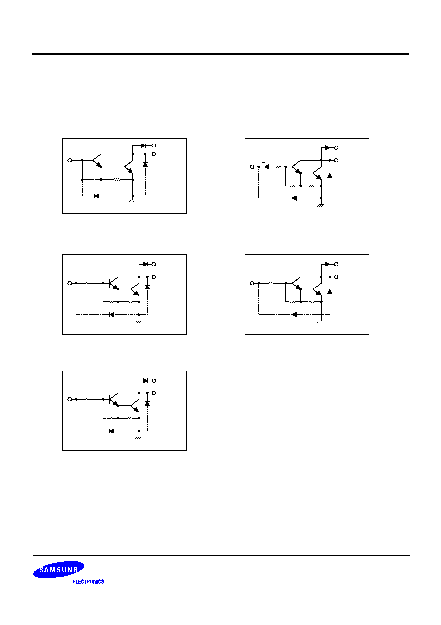
HIGH VOLTAGE, HIGH CURRENT DARINGTON ARRAYS
The S1P2655A01, S1P2655A02, S1P2655A03, S1P2655A04
and S1P2655A05 are comprised of saven high voltage, high
current NPN darlington transistors arrays with common emitter,
open collector outputs. Suppression diodes are included for
inductive load driving and the inputs are pinned opposite the
outputs to simplify board layout. Peak inrush currents to 600mA
permit them to drive incandescent lamps.
The S1P2655A01 is a general purpose array for use with DTL,
TTL, PMOS or CMOS logic directly.
The S1P2655A02 version does away with the need for any
external discrete resistors, since each usit has a resistor and a
zener diode in series with the input. The S1P2655A02 is
designed for use with 14 to 25V PMOS devices. The zener
diode also gives these devices excellent noise immunity.
The S1P2655A03 has a series base resistor to each darlington
pair, and thus allows operation directly with TTL or CMOS oper-
ating at supply voltages of 5V. The S1P2655A03 will handle
numberous interfaces needs-particularly those beyond the
capailities of standard logic buffers.
The S1P2655A04 has an appropriate input resistor to allow direct operation from CMOS or PMOS outputs operat-
ing supply voltage of 6V to 15V.
The S1P2655A05 is designed for use with standard TTL and Schottky TTL, with which hinger output currents are
required and loading of the logic output is not a concern.
These devices will sink a minimum of 350mA when driven from a
"
totempole
"
logic output.
These versatile devices are useful for driving a wide range of loads including Solenoids, Relays, DC motors, LED
displays, Filament lamps, thermal printheads and high power buffer. Applications requiriing sink currents beyonds
the capability of a single output may be accomodated by paralleling the outputs.
APPLICATIONS
∑
Relay driver
∑
DC motor driver
∑
Solenoids driver
∑
LED display driver
∑
Filament lamp driver
∑
High power buffer
∑
Thermal print head driver
16
-
DIP
16
-
SOP
LINEAR INTEGRATED CIRCUIT
S1P2655A01/02/03/04/05
3
ELECTRICAL CHARACTERISTICS
(Ta = 25
∞
C, unless otherwise noted)
Characteristic
Symbol
Test Condition
Min.
Typ.
Max.
Unit
Output Leakage Current
I
LK
V
CE
= 50V, Ta = 25
∞
C, V
IN
= open
-
-
50
µ
A
V
CE
= 50V, Ta = 70
∞
C, V
IN
= open
-
100
V
CE
= 50V, Ta = 70
∞
C,
V
IN
= 6.0V (S1P2655A02)
-
-
500
V
CE
= 50V, Ta = 70
∞
C,
V
IN
= 1.0V (S1P2655A04)
-
-
500
Output Saturation Voltage
Vsat
I
C
= 100mA, I
IN
= 250
µ
A
-
0.9
1.1
V
I
C
= 200mA, I
IN
= 350
µ
A
--
1.1
1.3
I
C
= 350mA, I
IN
= 500
µ
A
1.25
1.6
Input Current 1 (Off Condition)
I
IN 1
I
C
= 500mA, Ta = 70
∞
C
50
65
-
µ
A
Input Current 2 (On Condition)
I
IN 2
V
IN
= 17V (S1P2655A02), Vo = open
-
0.85
1.3
mA
V
IN
= 3.85V (S1P2655A03), Vo = open
-
0.93
1.35
V
IN
= 5V (S1P2655A04), Vo = open
-
0.35
0.5
V
IN
= 12V (S1P2655A04), Vo = open
-
1.0
1.45
V
IN
= 3.0V (S1P2655A05), Vo = open
-
1.5
2.4
Input Voltage
V
IN
V
CE
= 2.0V, Ic = 300mA (S1P2655A02)
-
-
13
V
V
CE
= 2.0V, Ic = 200mA (S1P2655A03)
-
-
2.4
V
CE
= 2.0V, Ic = 250mA (S1P2655A03)
-
-
2.7
V
CE
= 2.0V, Ic = 300mA (S1P2655A03)
-
-
3.0
V
CE
= 2.0V, Ic = 125mA (S1P2655A04)
-
-
5.0
V
CE
= 2.0V, Ic = 200mA (S1P2655A04)
-
-
6.0
V
CE
= 2.0V, Ic = 275mA (S1P2655A04)
-
-
7.0
V
CE
= 2.0V, Ic = 350mA (S1P2655A04)
-
-
8.0
V
CE
= 2.0V, Ic = 350mA (S1P2655A05)
-
-
2.4
DC Current Gain
h
FE
V
CE
= 2.0V, Ic = 350mA (S1P2655A05)
1000
-
-
-
Input Capacitance
C
IN
-
-
15
30
pF
Proparation Delay Time
t
ON
0.5 V
IN
to 0.5 Vo
-
0.25
1.0
µ
s
t
OFF
0.5 V
IN
to 0.5 Vo
-
0.25
1.0
µ
s
Clamp Diode Leakage Current
I
R
V
IN
= open, Vo = GND, V
R
= 50V, Ta =
25
∞
C
-
-
50
µ
A
V
IN
= open, Vo = GND, V
R
= 50V, Ta =
70
∞
C
-
-
100
µ
A
Clamp Diode Forward Voltage
V
F
I
F
= 350mA
-
1.7
2.0
V