TONE RINGER
S1T2410B01/B02
1
INTRODUCTION
The S1T2410B01/B02 is a bipolar integrated circuit designed as a
telephone bell replacement.
FUNCTIONS
∑
Two oscillators
∑
Output amplifier
∑
Power supply control circuit
FEATURES
∑
Designed for telephone bell replacement
∑
Low drain current
∑
Small size MINIDIP package
∑
Adjustable 2-frequency tone
∑
Adjustable warbling rate
∑
Built-in hysteresis prevents false triggering and rotary dial `CHIRPS'
∑
Extension tone ringer modules
∑
Alarms or other alerting devices
∑
External triggering or ringer disable (S1T2410B01)
∑
Adjustable for reduced initial supply current (S1T2410B02)
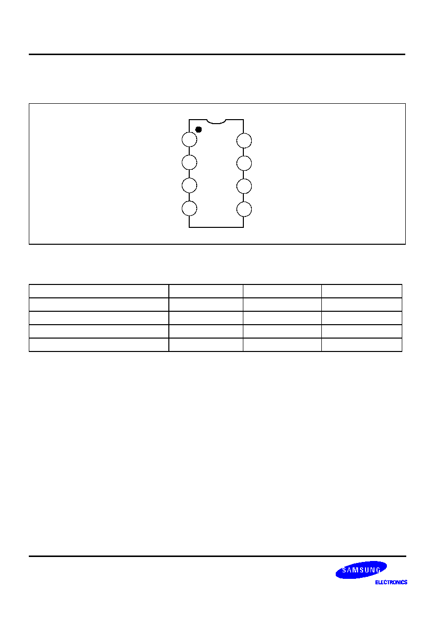
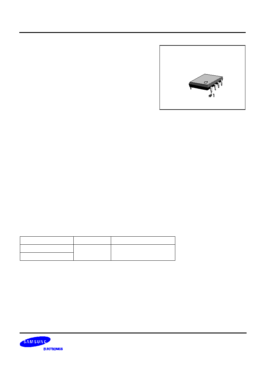
ORDERING INFORMATION
Device
Package
Operating Temperature
S1T2410B01-D0B0
8-DIP-300
-
45
∞
C to +65
∞
C
S1T2410B02-D0B0
8
-
DIP
-
300

TONE RINGER
S1T2410B01/B02
3
ELECTRICAL CHARACTERISTICS (Ta = 25
∞
∞
∞
∞
C)
(All voltage referenced to GND unless otherwise specified)
NOTES: (see electrical characteristics sheet)
1.
Initial supply voltage (V
SI
) is the supply voltage required to start tone ringer oscillation
2.
Sustaining voltage (V
SUS
) is the supply voltage required to maintain oscillation.
3.
V
TR
and I
TR
are the conditions applied to trigger to start oscillation for V
SUS
V
CC
V
SI
4.
V
DIS
and l
DIS
are the conditions applied to trigger to inhibit oscillation for V
SI
V
CC
5.
Trigger current must be limited to this value externally.
Characteristic
Symbol
Test Conditions
Min.
Typ.
Max.
Unit
Operating Voltage
V
CC
-
-
-
29.0
V
Initiation Voltage
1
V
SI
See Fig. 1
17
19
21
V
Initiation Current
1
I
SI
S1T2410B02 -6.8K-Pin 2 to GND
1.4
2.5
4.2
mA
Sustaining Voltage
2
V
SUS
See Fig. 1
9.7
11.0
12.0
V
Sustaining Current
2
I
SUS
No Load V
CC
= V
SUS
, See Fig. 1
0.7
1.4
2.5
mA
Trigger Voltage
3
V
TRG
S1T2410B01 Only V
CC
= 15V
9.0
10.5
12.0
V
Trigger Current
3
I
TRG
S1T2410B01 Only
10.0
20.0
1000
5
µ
A
Disable Voltage
4
V
DIS
S1T2410B01 Only
-
-
0.8
V
Disable Current
4
I
DIS
S1T2410B01 Only
-
40
-
50
-
µ
A
Output Voltage High
V
OH
V
CC
= 21V, I
8
=
-
15mA
Pin 6 = 6V, Pin 7 = GND
17.0
19.0
21.0
V
Output Voltage Low
V
OL
V
CC
= 21V, I
8
= 15mA
Pin 6 = GND, Pin 7 = 6V
-
-
1.6
V
Input Current 1 (Pin 3)
I
I (PIN 3)
Pin 3 = 6V, Pin 4 = GND
-
-
500
nA
Input Current 2 (Pin 7)
I
I (PIN 7)
Pin 7 = 6V, Pin 6 = GND
-
-
500
nA
High Frequency 1
f
H1
R
3
= 191K, C
3
= 6800pF
461
512
563
Hz
High Frequency 2
f
H2
R
3
= 191K, C
3
= 6800pF
576
640
704
Hz
Low Frequency
f
L
R
2
= 165K, C
2
= 0.47
µ
F
9.0
10
11.0
Hz

TONE RINGER
S1T2410B01/B02
5
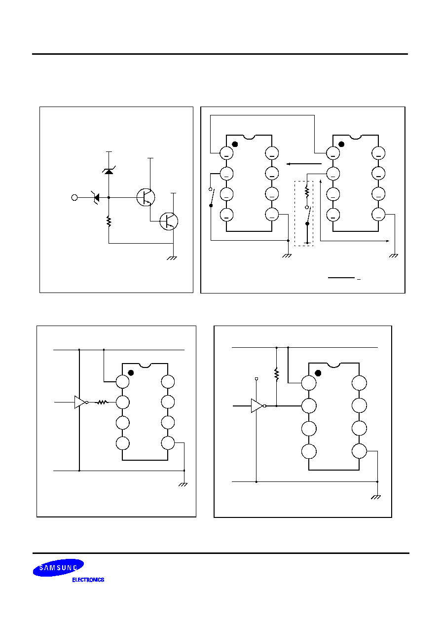
APPLICATION INFORMATION
The application circuit illustrates the use of the S1T2410B01/B02 devices in typical telephone or extensive tone
ringer applications.
The AC ringer signal voltage appears across the TIP and RING inputs of the circuit, and is attenuated by capacitor
C
1
and resistor R
1
.
(C
1
also provides isolation from DC voltages (48V) on the exchange line).
After full wave rectification by the bridge diode, the wave form is filtered by capacitor C
4
to provide a DC supply for
the tone ringer chip.
When this voltage exceeds the initiation (V
SI
), oscillation starts.
With the components shown, the output frequency chops between 512 Hz (f
H1
) and 640Hz (f
H2
) at a 10Hz (f
L
) rate.
The loudspeaker load is coupled through a 1300
to 8
transformer.
The output coupling capacitor C
5
with transformer coupled loads is required.
When driving a piezo-ceramic transducer type load, the coupling C
5
and transformer (1300
:8
) are not required.
However, a current limiting resistor is required.
The low frequency oscillator oscillates at a rate (f
L
) controlled by an external resistor (R
2
) and capacitor (C
2
). The
frequency can be determined using the function f
L
= 1/(1.289 R
2
∑
C
2
). The high frequency oscillates at a f
H1
, f
H2
controlled by an external resistor (R
3
) and capacitor (C
3
). The frequency can be determined using the function t
HI
= 1/(1.504 R
3
∑
C
3
). Voltage remains constant independent of R
SL
.
Pin 2 of the S1T2410B02 allows connection of an external resistor R
SL
, which is used to program the slope of the
supply current vs supply voltage characteristics (see Fig. 2) and hence the supply current up to the initial voltage
(V
SI
). This initial voltage remains constant independent of R
SL
.
The supply current drawn prior to triggering is inversely proportional with R
SL
, decreasing for an increasing value of
resistance.
Thus, increasing the value of R
SL
, will decrease the amount of AC ringing current required to trigger the device.
Longer subscriber loops are possible since less voltage is dropped per unit length of loop wire due to the lower
current level. R
SL
can also be used to compensate for smaller AC coupling capacitors (C
5
on Fig. 3) (higher
impedance) to the line which is used to alter the ringer equivalence number of a tone ringer circuit.
The graph in Fig. 2 illustrates the variation of supply current with supply voltage of the S1T2410B02. Three curves
are drawn to show the variation of the initiation current with R
SL
. Curve B (R
SL
= 6.8k
) shows the I-V
characteristic for the S1T2410B02 tone ringer. Curve A is a plot with R
SL
< 6.8k
and shows an increase in the
current drawn up to the initiation voltage V
SI
. After initiation, the I-V characteristic remain unchanged. Curve C
illustrates the effect of increasing R
SL
above 6.8k
initiation current decreases, but is unchanged after triggering.