LOW VOLTAGE/POWER NARROW BAND FM IF
S1T3361D
1
INTRODUCTION
The S1T3361D is designed for use in FM dual conversion
communication. It contains a complete narrow band FM demodulation
system operable to less than 2.5V supply voltage. This low-power
narrow-band FM IF system provides the second converter, second IF,
demodulator. Filter Amp and squelch circuitry for communications and
scanning receivers.
FEATURES
∑
Low power consumption (4.0mA typ. at V
CC
= 4.0V)
∑
Excellent input sensitivity
(-3dB limiting, 2.0
µ
V
rms
typ.)
∑
Minimum number of external components required.
∑
Operating Voltage: 2.5 to 7.0V
APPLICATIONS
∑
Cordless phone (for home usage)
∑
FM dual conversion communications equipment
ORDERING INFORMATION
Device
Package
Operating Temperature
S1T3361D01-D0B0
16
-
DIP
-
300A
-
20
∞
C to +70
∞
C
S1T3361D01-S0B0
16
-
SOP
-
225A
16
-
DIP
-
300A
16
-
SOP
-
225A
S1T3361D
LOW VOLTAGE/POWER NARROW BAND FM IF
2
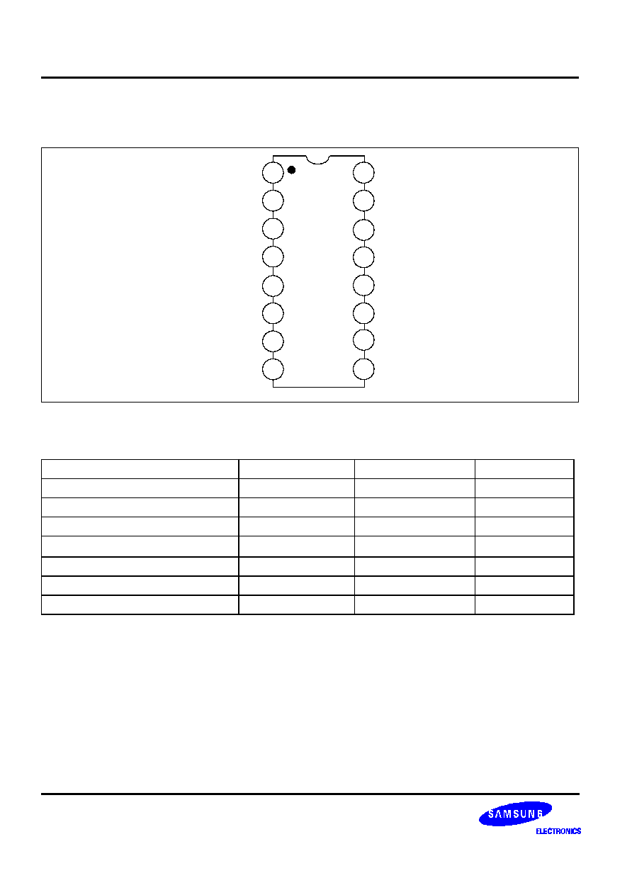
PIN CONFIGURATION
ABSOLUTE MAXIMUM RATINGS
NOTE:
Absolute maximum ratings are those values beyond which permanent damage to the device may occur. These are stress
ratings only and functional operation of the device at or beyond them is not implied. Long exposure to these conditions may
affect device reliability.
Characteristic
Symbol
Value
Unit
Max. Supply Voltage
V
CC (MAX)
10
V
Supply Voltage Range
V
CC
2.5 to 7.0
V
Detector Input Voltage
V
I (DET)
1.0
V
P-P
RF Input Voltage (V
CC
4.0V)
V
I (RF)
1.0
V
rms
Mute Function
V
MUTE
-
0.5 to + 0.5
V
peak
Operating Temperature
T
OPR
-
20 to + 70
∞
C
Storage Temperature
T
STG
-
65 to + 150
∞
C
1
2
3
4
5
6
7
8
9
10
11
12
13
14
15
16
S1T3361D
OSC
OSC
MIXER
V
CC
LIMITER
DECOUPLING
DECOUPLING
QUADRATURE
MUTE
SCAN
SQUELCH
FILTER
FILTER
AUDIO
OUTPUT
INPUT
INPUT
CONTROL
INPUT
OUTPUT
INPUT
OUTPUT
RF
INPUT
GND
LOW VOLTAGE/POWER NARROW BAND FM IF
S1T3361D
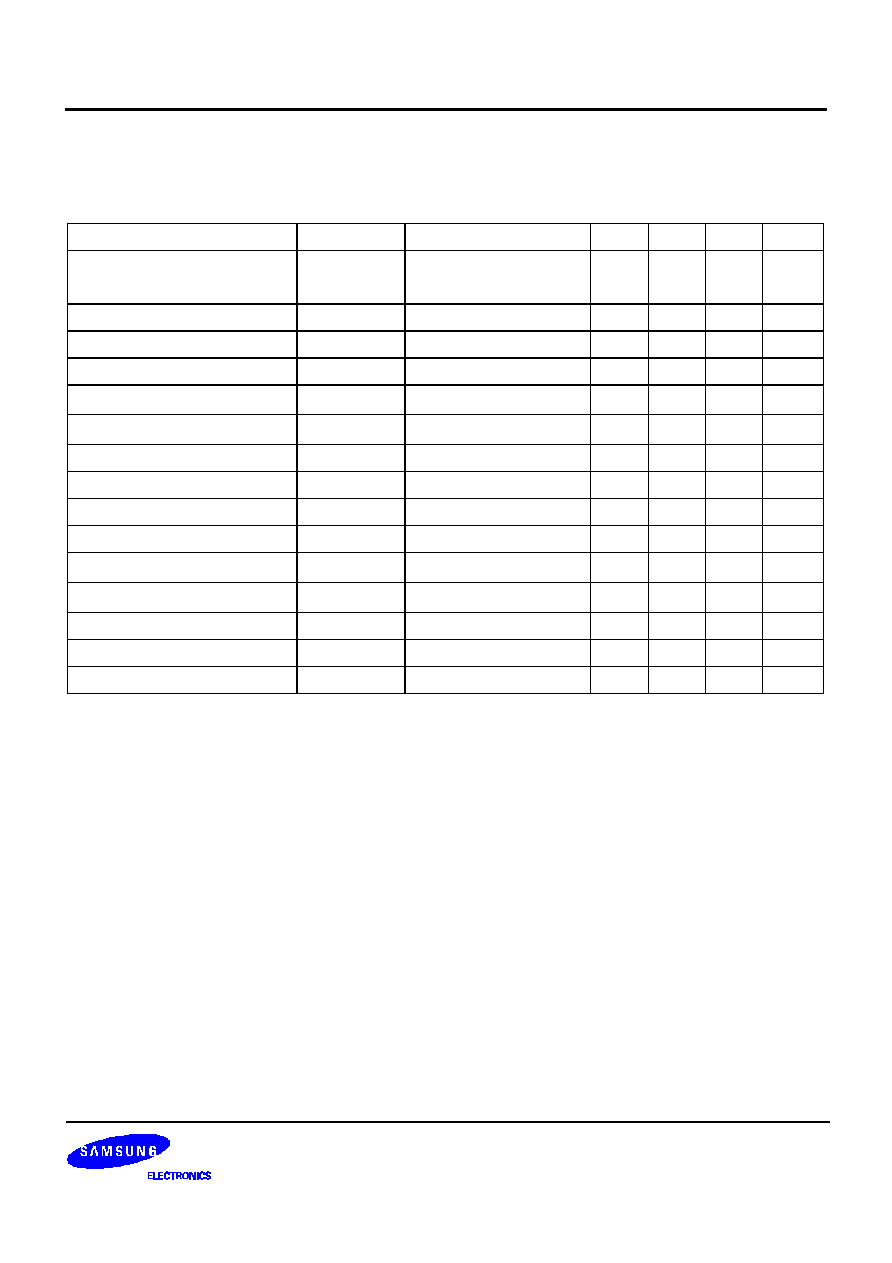
3
ELECTRICAL CHARACTERISTICS
(V
CC
= 4.0V, fo = 10.7MHz,
f =
±
3kHz, f
MOD
= 1kHz, Ta = 25
∞
C, unless otherwise specified)
Characteristic
Symbol
Test Conditions
Min.
Typ.
Max.
Unit
Operating Current
I
CC
Squelch off (V
12
= 2V)
Squelch on (V
12
= GND)
2.0
3.0
4.0
6.0
8.0
10
mA
mA
Input Limiting Voltage
V
I (LIM)
-3.0dB limiting
-
2.0
6.0
µ
V
Detector Output Voltage
V
O (DET)
-
-
2.0
-
V
dc
Detector Output Impedance
Z
O (DET)
-
-
400
-
W
Recoverd audio output voltage
V
O
V
in
= 10mV
134
150
168
mV
rms
Filter Gain
G
V
f = 10kHz, V
in
= 5mV
40
48
52
dB
Filter Output DC Voltage
V
O (DC)
-
1.0
1.5
2.0
V
dc
Trigger Hysteresis of Filter
V
TH
-
-
50
-
mV
Mute Switch-on Resistance
R
ON (MUTE)
Mute Low
-
10
40
Mute Switch-off Resistance
R
OFF(MUTE)
Mute High
1
-
10
M
Scan Control Low Output
V
L (SCAN)
Mute off (V
12
= 2V)
-
-
0.5
V
dc
Scan Control High Output
V
H (SCAN)
Mute on (V
12
= GND)
3.0
-
-
V
dc
Mixer Conversion Gain
G
V (MIXER)
-
30
36
-
dB
Mixer Input Resistance
R
I (MIXER)
-
-
3.3
-
k
Mixer Input Capacitance
C
I (MIXER)
-
-
2.2
-
pF

S1T3361D
LOW VOLTAGE/POWER NARROW BAND FM IF
4
CHARACTERISTIC GRAPH
LOW VOLTAGE/POWER NARROW BAND FM IF
S1T3361D
5
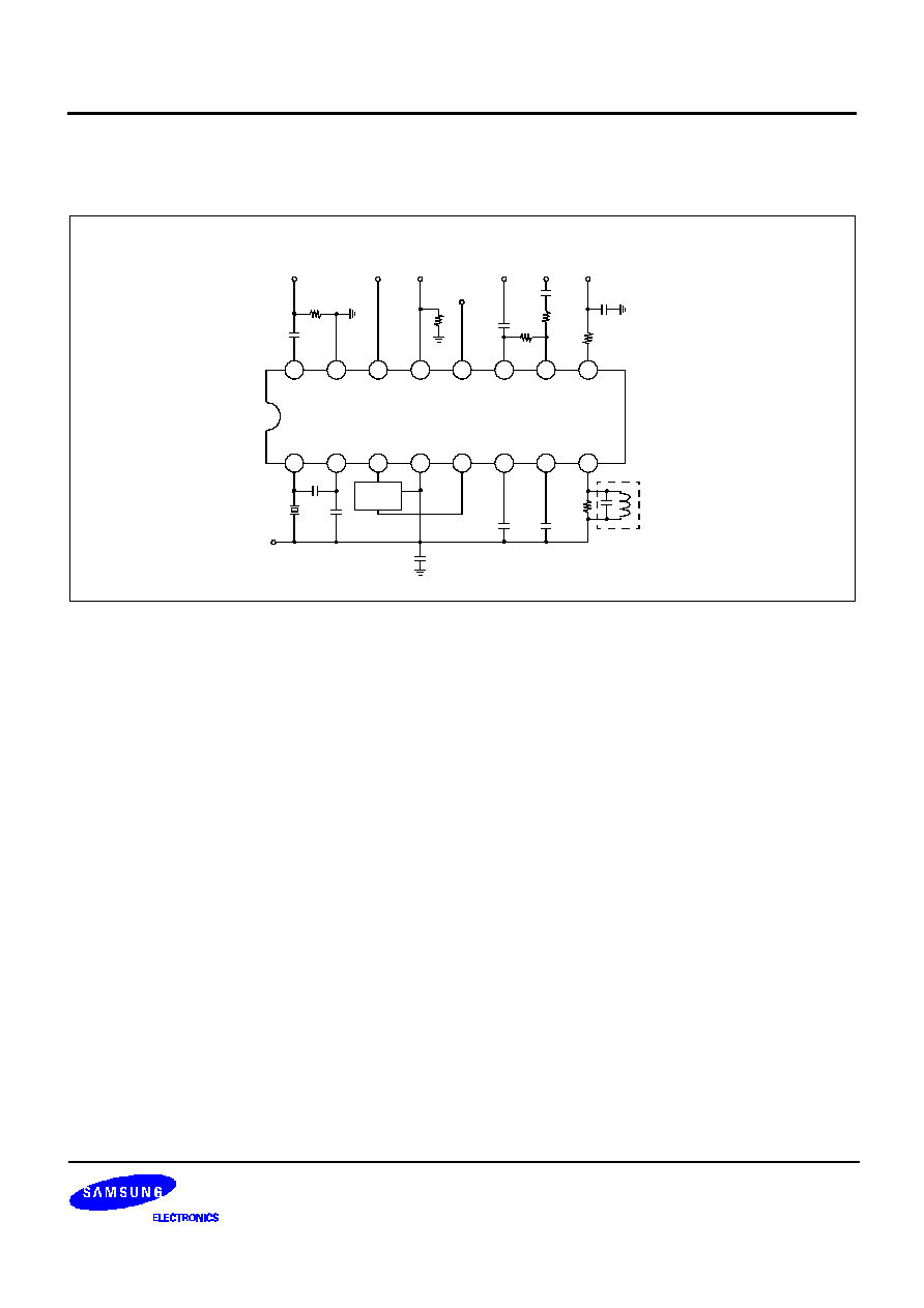
APPLICATION CIRCUIT
In the above application circuit, the audio signal is recovered using a conventional quadrature FM detector.
The absence of an input signal is indicated by the presence of noise above the desired audio frequencies. This
"
noise band
"
is monitored by an active filter and a detector. A squelch trigger circuit indicates the presence of
noise (or a tone) by an output which can be used to control scanning. At the same time, an internal switch is
operated which can be used to mute the audio.
1
2
3
4
5
6
7
8
16
15
14
13
12
11
10
9
Mixer input
10.7MHz
10nF
51
Audio
Mute
Scan
Control
10k
Squelch
SW input
1.0uF
Filter
Amp out
470k
510k
1.0uF
Filter
Amp in
Audio
output
10nF
8.2k
20k
Quad coil
0.1uF
0.1uF
0.1uF
455MHz
Filter
68pF
220pF
Vcc
10.24MHz
OSC
OSC MIXOUT VCC
LIMIN DECOLP LING
QUAD
S1T3361D
AUDIO
FIN
FOUT
SQ
SCAN
MUTE
GND
MIXIN

S1T3361D
LOW VOLTAGE/POWER NARROW BAND FM IF
6
NOTES