LOW VOLTAGE SPEECH NETWORK
S1T8503
1
INTRODUCTION
The S1T8503 is a low voltage speech network which includes Mic amp.
transmit amp, side-tone amp, and receive amp. It handles the voice
signal performing the 2/4 wire interface and changing the gain on both
sending and receiving amplifiers to compensate for line attenuation by
sensing the line length through the line current.
Application dependent parameters such as amplitude of each amp,
sidetone level, line balance and frequency response are controlled by
external components. Each gain can be controlled by external
component exchange. The receiver output driving capability is
adjustable.
FEATURES
∑
Adjust Sending and Receiving Attenuation Length
∑
Mute Function
∑
Side Tone Balance Network Constitution
∑
Low Voltage Operating
∑
AC Impedance Matching
∑
Uses Inexpensive Components
∑
Uses a minimum of external components (5 Capacitors & 10 Resistors)
ORDERING INFORMATION
Device
Package
Operating Temperature
S1T8503X01-D0B0
18
-
DIP
-
300A
-
40
∞
C to + 70
∞
C
18
-
DIP
-
300A
S1T8503
LOW VOLTAGE SPEECH NETWORK
2
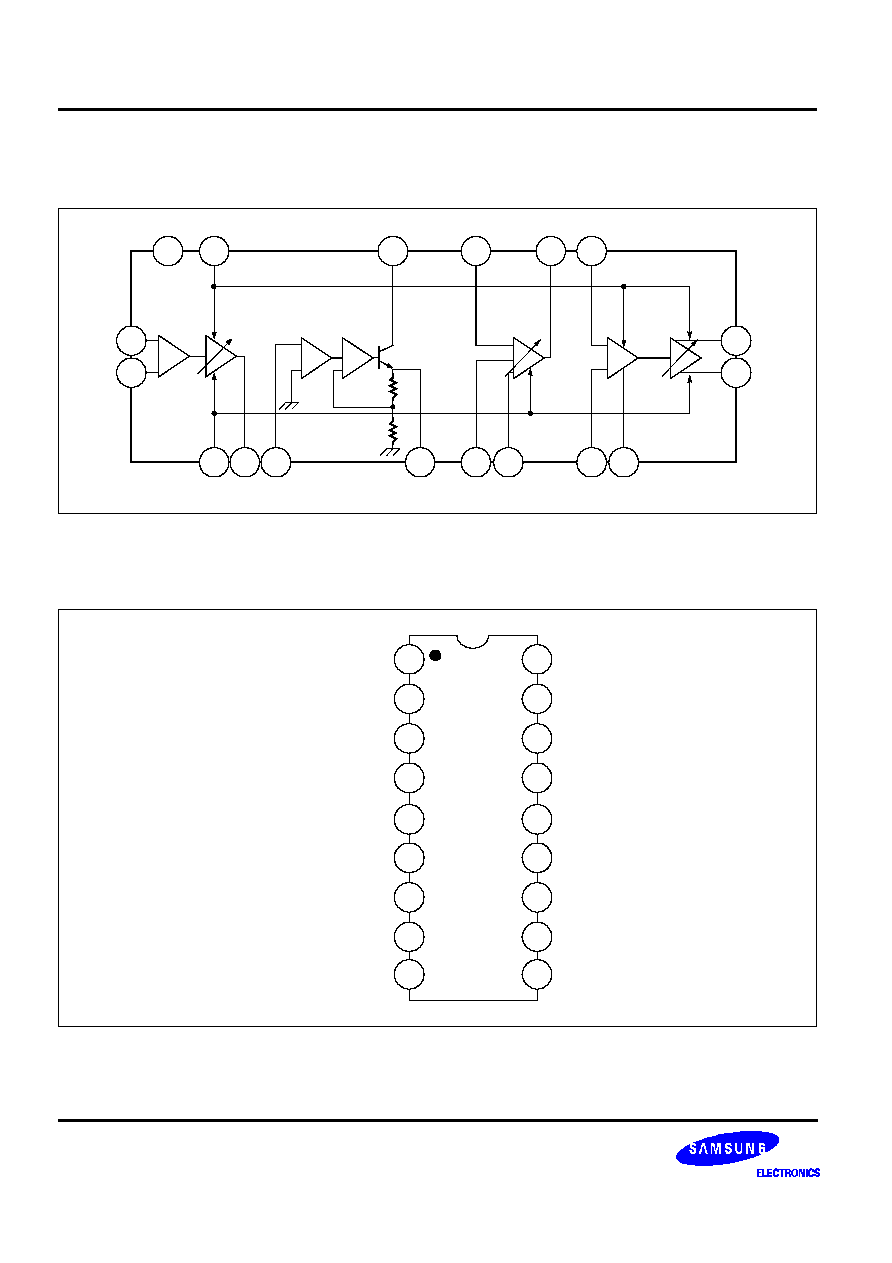
BLOCK DIAGRAM
PIN CONFIGURATION
1
2
3
4
5
6
7
8
9
10
11
12
13
14
15
16
17
18
V
DD
MUTE
V +
ST3
STO
RXI
RXO2
RXO3
RXO1
V -
ST1
ST2
TXO
TXI
MICO
GR
MIC1
MIC2
1
2
3
4
5
6
7
8
9
10
11
12
13
14
15
16
17
18
S1T8503
V +
TXO
TXI
V
DD
MUTE
GR
ST1
ST2
ST3
RXO3
RXO2
RXO1
RXI
V -
MIC2
MIC1
MIC0
ST0

LOW VOLTAGE SPEECH NETWORK
S1T8503
3
PIN DESCRIPTION
ABSOLUTE MAXIMUM RATINGS
Pin No
Symbol
Description
1
V +
Positive power line and transmit amplifier output.
2
TXO
Transmit amplifier output. The resistor which is connected this pin to V
-
sets the
DC resistance of circuit. The value of resistor is suitable for 47 to 100
.
3
TXI
Transmit amplifier input. Input impedance is 17k
±
20%
4
V
DD
DC power supply pin.
This pin will be connected to a decoupling capacitor 47
µ
F - 100
µ
F.
5
MUTE
Mute input : Active high .
6
GR
Gain regulation control input. Input impedance is 5.5k
±
20%.
7, 8, 9
ST1, ST2, ST3
Separate amplifier control inputs.
10
STO
Separate amplifier output.
11
MIC0
Microphone amplifier output.
12, 13
MIC1, MIC2
Microphone amplifier inputs. Input impedance is 1.7k
±
20%
14
V
-
Negative power line.
15
RXI
Receive amplifier input.
16
RXO1
Receive amplifier output.
17, 18
RXO2, ROX3
Receive amplifier output. Output impedance is 3
(Typ)
Characteristic
Symbol
Value
Unit
Line Voltage (3ms max)
V
L
22
V
Forward Line Current
I
LF
150
mA
Reverse Line Current
I
LR
-
150
mA
Power Dissipation (Ta = 70
∞
C)
P
D
1
W
Operating Temperature
T
OPR
-
40 to + 70
∞
C
Storage Temperature
T
STG
-
55 to + 125
∞
C

S1T8503
LOW VOLTAGE SPEECH NETWORK
4
ELECTRICAL CHARACTERISTICS
(Refer to the test circuits, I
L
= 15 to 100mA, f = 200 to 3.4kHz, Ta = 25
∞
C, unless otherwise specified)
Characteristic
Symbol
Test Conditions
Test Fig
Min.
Typ.
Max.
Unit
Line Voltage
V
L
I
L
= 15mA
I
L
= 15mA
3.3
3.7
4.1
V
I
L
= 100mA
I
L
= 100mA
11
13
15
V
MI
= 5V
f = 1kHz
I
L
= 20mA
46
48
50
T
X
Gain
G
V (TX)
I
L
= 38.5mA
1
43.5
45.5
47.5
dB
I
L
= 55mA
41
43
45
TX Range of Regulation
G
TX
G
TX
= G
TX1
- G
TX3
3
5
7
dB
TX Frequency Response
G
TX(RES)
V
MI
= 5mV
f = 200Hz
1
-
-
±
1
dB
I
L
= 20mA
f = 3.4kHz
-
-
±
1
V
MI
= 5mV
f = 200Hz
1
-
-
±
1
I
L
= 80mA
f = 3.4kHz
-
-
±
1
TX Dynamic Output
Voltage
V
O(TX)
I
L
= 20mA, f = 200Hz to 3.4kHz
1
-
1.5
-
Vp-p
I
L
= 100mA, f = 200Hz to 3.4kHz
-
1.5
-
TX Max Output Voltage
V
OTX(MAX)
I
L
= 20mA, f = 200Hz to 3.4kHz
1
-
1.5
-
Vp-p
I
L
= 100mA, f = 200Hz to 3.4kHz
-
1.5
-
TX Input Impedance
Z
I (TX)
I
L
= 20mA,
f = 200Hz to 3.4kHz
-
1.7
-
k
Mute Input Current
I
I (MUTE)
I
L
= 20mA
I
M
= 0.1mA
0.1
-
-
mA
V
RI
= 0.5V
f = 1kHz
I
L
= 20mA
-
13.5
-
11.5
-
9.5
RX Gain
G
V (RX)
I
L
= 38.5mA
2
-
16
-
14
-
12
dB
I
L
= 55mA
-
18.5
-
16.5
-
14.5
RX Range of Regulation
G
RX
G
RX
= G
RX1
- G
RX3
3
5
7
dB
RX Frequency Response
G
RX(RES)
V
RI
= 0.5V
f = 200Hz
2
-
-
±
1
dB
I
L
= 20mA
f = 3.4kHz
-
-
±
1
V
RI
= 0.5V
f = 200Hz
-
-
±
1
I
L
= 80mA
f = 3.4kHz
-
-
±
1
RX Dynamic Output
Voltage
V
O(RX)
I
L
= 20mA
f = 200Hz
0.3
0.5
-
Vp-p
f = 3.4kHz
2
0.3
0.5
-
I
L
= 100mA
f = 200Hz
0.3
0.5
-
f = 3.4kHz
0.3
0.5
-
RX Max Output Voltage
V
ORX(MAX)
I
L
= 20mA
f = 200Hz
2
-
0.9
-
Vp-p
V
RI
= 10V
f = 3.4kHz
-
0.9
-

LOW VOLTAGE SPEECH NETWORK
S1T8503
5
TEST CIRCUIT
]
Figure 1.
Figure 2.
1
2
3
4
5
6
7
8
9
10
11
12
13
14
15
16
17
18
S1T8503
A
I
L
+ Line
910
470uF
1.5M
12K
62K
47uF
6.2K
Mute
300
20uF
1.7K
SW1
V
M1
D
47uF
1.5M
1.5M
18K
27K
104
75
3.6K
820
9.1K
22uF
10
560
310
SW3
V
RI
600
62K
C
350
SW2
- Line
470uF
A
B
C
D
E
F
G
V
MI
470uF
V
RO
V
SO
560
S1T8503
* side tone = 20 log
V
MI
V
RO
* G
V(TX)
= 20 log
V
SO
V
RO
A
B
C
D
E
F
G
470uF
V
RO
V
RI
560
S1T8503
* G
V(TX)
= 20 log
V
RO
V
RI

S1T8503
LOW VOLTAGE SPEECH NETWORK
6
NOTES