FM IF RECEIVER FOR FLEX PAGER
S1T8515A
1
INTRODUCTION
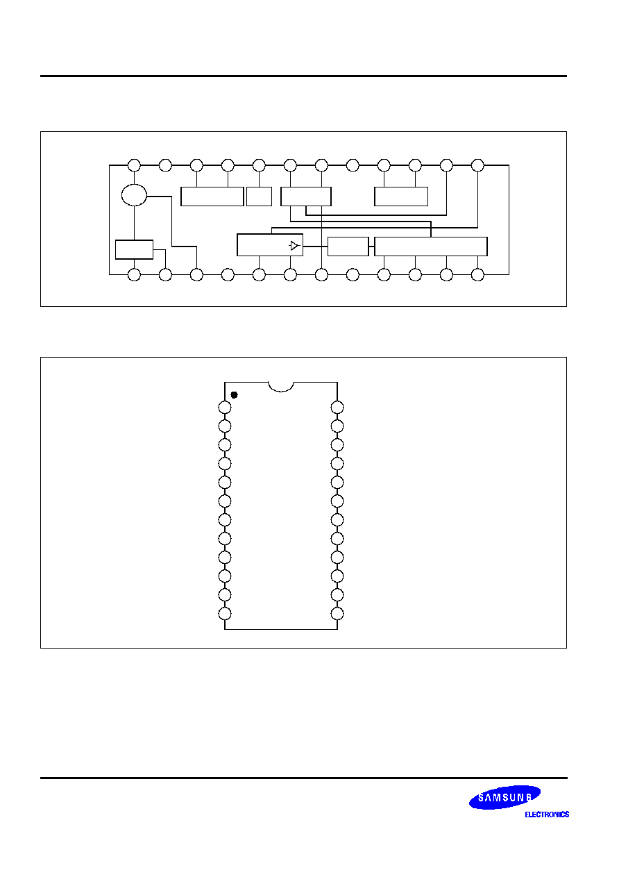
The S1T8515A is a designed for FM detection on the FLEX pager set.
It consists of an Oscillator, Mixer, Limiting IF Amp. Quadrature
Detector, Regulator, RSSI (Received Signal Strength Indicator), Bit
Rate Filter, and a 2-level / 4-level FSK comparator.
It has a 24-SSOP (0.65mm)Surface Mount Package.
FEATURES
∑
Internal A/D converter for 4 level FSK (2-bit ADC)
∑
High transmission rate: 6400bps (Max.)
∑
Operating voltage range: V
CC1
= 1.1 ~ 4.0V
∑
Typical supply current: 1.5mA at 1.4V
∑
Low battery detection circuit (alarm function): 1.05V
∑
Mixer operating frequency: 10 ~ 50MHz
∑
Package type: 24-SSOP (0.65mm)
ORDERING INFORMATION
Device
Package
Operating Temperature
S1T8515A01-U0B0
24
-
SSOP
-
BD209
-
20
∞
C ~ +70
∞
C
24
-
SSOP
-
BD209

FM IF RECEIVER FOR FLEX PAGER
S1T8515A
3
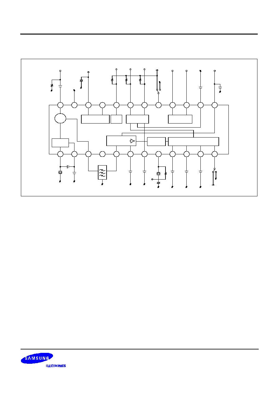
PIN DESCRIPTION
Pin No
Symbol
Description
1
OSCI
Oscillator input (Base). The oscillator is an internally biased colpitts type.
2
OSCO
Oscillator output (Emitter).
3
MO
Mixer output (Output impedance
1.5k
) Connect a 455kHz filter between this pin
and the LI.
4
V
CC
Power supply voltage.
5
LI
IF limiter amplifier input (Input impedance
1.5k
).
6
LD
Bypass capacitor connect pin for the IF limiter amp.
7
FSKR1
Differential Amp Reference input on the FSK comparator.
8
QD
Quadrature detection, phase shiftier input.
9
10
11
C1
C2
C3
Capacitors for bit-rate filter.
12
FIL VAR
Bit-rate filter selection.
High: Internal cut-off frequency will be set to Low.
Low: Internal cut- off frequency will be set to High.
13
RSSI
RSSI output.
The power of received RF signal can be detected by monitoring the limiter amplifier.
14
FSKR2
Differential Amp Reference input on the FSK comparator for 4-Level FSK Detection.
15, 16
QC2, QC1
Quick charge control 2 & 1.
High: Quick charge-discharge on. Low: Quick charge-discharge off.
17
BSC
Battery saving control.
High: Battery saving off-normal mode operation.
Low: Battery saving on-battery save mode operation.
18
FSKO2
The output signal from the Bit-rate filter is compared with FSK Reference signal, and
the final output signal will be output to the LSB after 4-Level FSK detection.
19
FSKO1
The final output signal will be output to the MSB after 4-Level FSK detection.
20
AO
Alarm output.
This pin becomes high, when V
CC
drops below 1.05V.
21
REGC
S1T8515A has an internal PNP transistor.
But, it also can support an external PNP transistor to control the power.
22
REGO
Regulated voltage output.
23
GND
Ground.
24
MI
Mixer input (Input impedance
1.5k
).

S1T8515A
FM IF RECEIVER FOR FLEX PAGER
4
ABSOLUTE MAXIMUM RATINGS
ELECTRICAL CHARACTERISTICS
(V
CC
= 1.4V
±
5%, f
IN
(2MIX) = 21.4MHz, f
DEV
=
±
4.8kHz, f
MOD
= 800Hz, Ta = 25
∞
C, FIL_VAR = "H", unless
otherwise specified)
Characteristic
Symbol
Value
Unit
Supply Voltage
V
CC (MAX)
4
V
Power Dissipation
P
D
760
mW
Operating Temperature
T
OPR
-
20 -- +70
∞
C
Storage Temperature
T
STG
-
55 -- +125
∞
C
Characteristic
Symbol
Test Conditions
Min.
Typ.
Max.
Unit
Operating current
I
CCN
No Input Signal
-
1.5
1.75
mA
I
CCS
Battery Saving
-
0
10
µ
A
Alarm detection voltage
V
AD
-
1.0
1.05
1.1
V
Alarm low level output voltage
V
O (AL)
I = 100
µ
A
-
-
0.4
V
Alarm high level leakage current I
LKG (AL)
-
-
-
2
µ
A
FSK low level output voltage
V
L (FSK)
I = 100
µ
A
-
-
0.4
V
FSK high level leakage current
I
LKG (FSK)
-
-
-
2
µ
A
Regulator output voltage
V
OREG
-
0.95
1.0
1.05
V
Quick charge current
I
C
-
50
70
-
µ
A
Input for
-
3dB sensitivity
V
LIM
Mixer Input
-
2.5
7.5
µ
Vrms
Recovered audio output voltage
V
O (RAO)
V
IN (2MIX)
= 500
µ
Vrms
36
54
78
mVrms
Mixer conversion gain
G
V (M)
Ceramic Filter loss =
-
1dB
8
12
16
dB
Signal to noise ratio
S/N
V
IN (MIX1N)
= 500
µ
Vrms
38
55
-
dB
Total Harmonic Distortion
THD
V
IN (MIX1N)
= 500
µ
Vrms
-
2.0
3.5
%
Mixer 3rd order intercept point
3RD
-
-
-
10
-
dBm
Mixer input resistance
R
I (MIX)
-
3.5
5
6.5
k
Limiting amp input resistance
R
I (LA)
-
0.9
1.5
2.1
k
AM rejection ratio
AMR
V
IN (2MIX)
= 500
µ
Vrms
(AM = 300%)
25
40
-
dB
Data shaping output duty
DR
V
IN (2MIX)
= 500
µ
Vrms
40
50
60
%
RSSI output voltage
V
RSSI
V
IN (2MIX)
= 1mVrms
0.49
0.7
0.91
V
RSSI output resistance
R
RSSI
-
90
100
110
k