
ENHANCED-1 CHIP CT0 RF IC
S1T8528
1
INTRODUCTION
S1T8528 is a 1 CHIP RF IC which can be used in high performance
CTO CLP systems at max. 60MHz. S1T8528 is designed to include a
receiver, PLL and COMPANDER to minimize PCB space
requirements. Improved RX characteristics such as inter-modulation,
spurious response and adjacent channel interface have been
included to satisfy the universal standards.
The 1 CHIP RF IC has considerably reduced the cost by including a
build-in 1
'
st mixer, low battery detector, f
MCU
, RSSI, RF regulator and
speaker amp. Also, it fulfills carrier detector threshold control, speaker
volume control, operating mode selection and MUTE function using S/
W, thus making external application easier.
FEATURES
∑
Operating voltage range: 2.0V to 5.5V
∑
Typical supply current: 8.9mA at 3.6V
∑
Built-in low battery detection function ( selectable 3.45V, 3.3V, 3.0V, 2.2V, 2.1V )
∑
Built-in speaker volume control and speaker amplifier
∑
Built-in splatter filter
∑
Support mode selection ( Active, Rx, Standby and Inactive mode )
∑
FM Receiver
-- Excellent Receiver characteristics
-- RSSI ( Linear ) and Carrier detector output ( Digital ) function
∑
Compander
-- Easy gain control and application using external component
-- Included ALC (Automatic Level Control) circuit
∑
Universal PLL
-- RX (TX) divided counter range : 1/16 to 1/16383
-- Reference frequency divided counter range : 1/16 to 1/4095
-- Lock detector signal output
-- Serial interface with MICOM for controlling each block
-- Clock Output for MICOM oscillator substitution. ( X-tal divided clock by 2, 3, 4 and 5 )
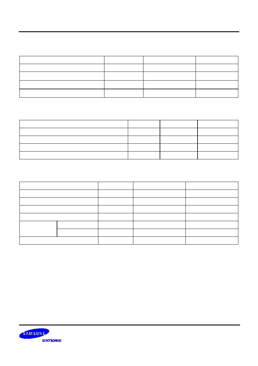
ORDERING INFORMATION
< 10.7MHz crystal filter used >
Input sensitivity
Adjacent channel
rejection
Spurious rejection
(image of the second IF)
Intermodulation
rejection
0.7
µ
µ
µ
µ
Vrms at 12dB
SINAD
> 55dB
> 60dB
> 50dB
Device
Package
Operating Temperature
S1T8528X01-Q0R0
48
-
QFP
-
1010E
-
20
∞
C to + 70
∞
C
48
-
QFP
-
1010E

S1T8528
ENHANCED-1 CHIP CT0 RF IC
2
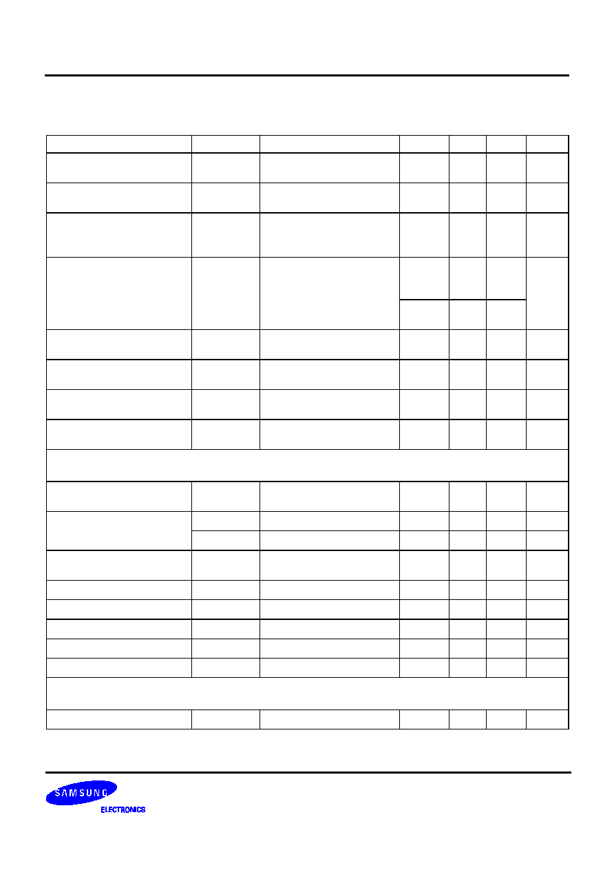
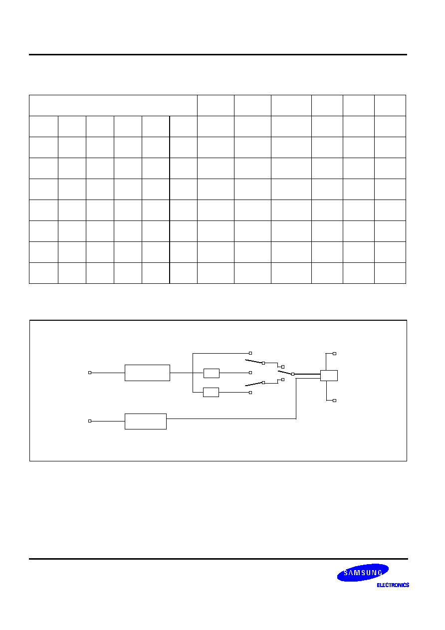
BLOCK DIAGRAM
Limiting
IF AMP
RSSI
Carrier
Detector
Rectifier
Gain Cell
Regulator
(Vcc/2)
Limiter
Gain Cell
Rectifier
IF AMP
(455KHz)
13
14
15
16
17
18
19
21
22
23
Quadrature
Detector
FSK
COMP
ALC
35
38
39
40
41
42
43
44
45
46
47
48
RX
VCO
IF AMP
(10.7MHz)
1st
MIX
PLL Regulator
( 2.05 V )
Programmable Counter ( REF )
RX Phase
Detector
TX Phase
Detector
fMCU
4_25 CNT
CONTROL
Buffer
SUM
AMP
MIC
AMP
SPK
AMP2
SUM
AMP
PRE AMP
AMP
Compander
mute
X-tal
OSC
Low
Battery
Detector
2nd
MIX
36
34
33
32
31
30
29
28
27
26
25
12
11
10
9
8
7
5
4
3
1
2
-
+
VREF
CRC
CO
SF
I
SF
O
CDO
/L
DT
CL
K
O
CL
K
DATA
LBD
EN
AGI
C
PDT
EPI
ERC
SAI
SAO1
SAO2
VCC
(COMP)
GND
(COMP)
CPI
CPO
ALC
24
V
REF
(COMP)
2M
O
VCC
(R
X
)
LI
LD
GND
(R
X
)
QCI
RAO
DSCI
DSCO
RSSI
2LO
I
6
37
2LOI
GND
(PLL)
V
REF
(RF)
2M
I
1LOI
1LOI
1MI
TIF
1MI
1MO
V
REF
(PLL)
VCO
RX
PDR
20 EO
Splatter
Filter
VREF
+
-
Programmable Counter ( RX )
Programmable Counter ( TX )
Internal
cap.
SPK
AMP1
Volume control
VCC
(RX)

ENHANCED-1 CHIP CT0 RF IC
S1T8528
3
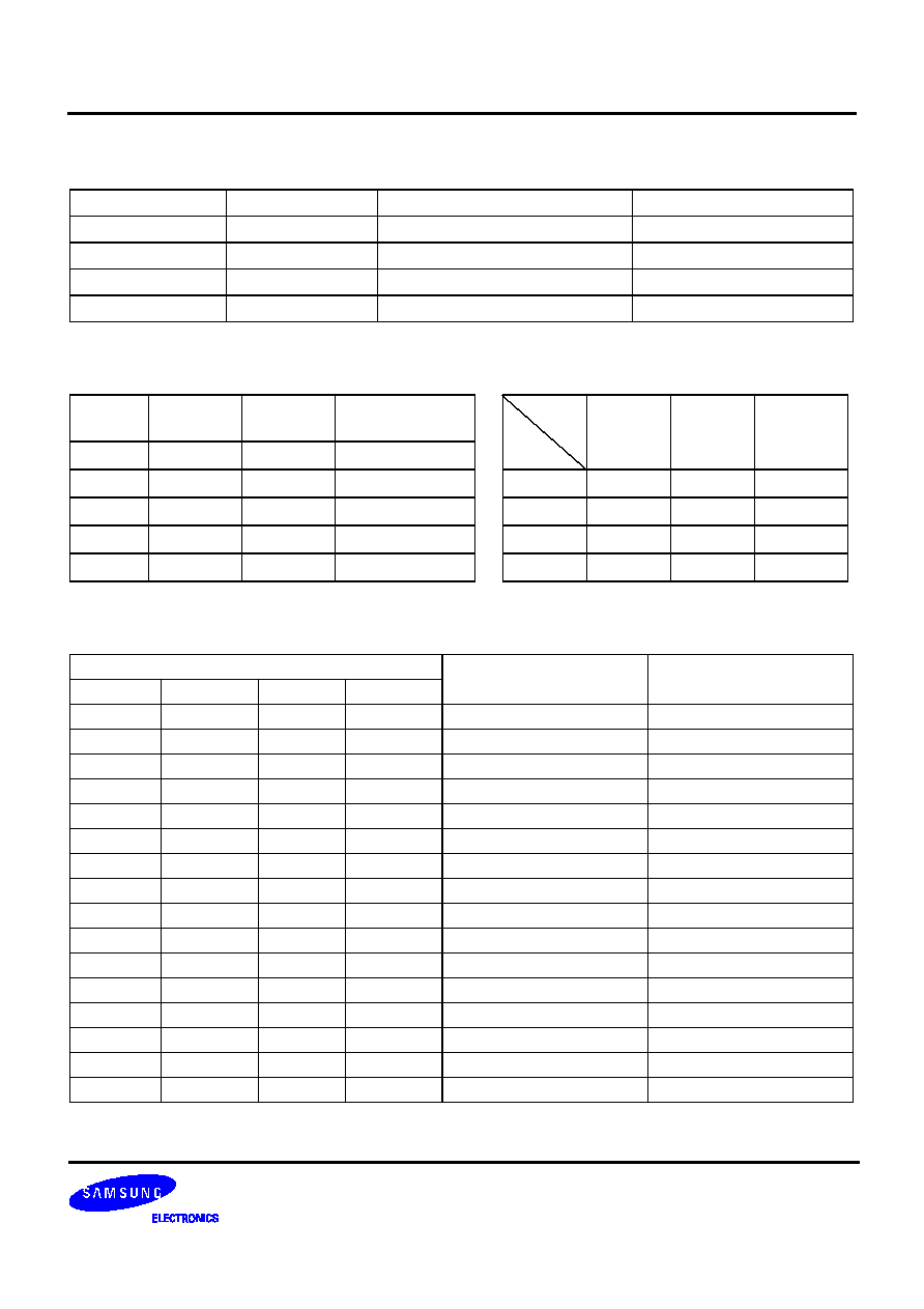
PIN CONFIGURATION
1
2
3
4
5
6
7
8
9
10 11 12
EPI
ERC
EO
SAI
SAO1
SAO2
VCC
(COMP)
GND
(COMP)
CPI
CPO
CR
C
2MI
VCC
(R
X
)
LI
LD
GN
D
(R
X
)
QC
I
RAO
DSC
I
DSC
O
RSS
I
V
REF(COMP)
ALC
KB8528
14
15
16
17
18
19
20
21
22
23
24
13
47
46
45
44
43
42
41
40
39
38
37
48
36 35 34 33 32 31 30 29 28 27 26 25
CO
SF
I
SF
O
CD
O
/
LDT
CLK
O
CLK
DATA
LB
D
EN
AG
I
C
GND
(PLL)
V
REF(RF)
2MO
2LO
I
2LOI
1LOI
1LOI
1MI
TIF
1MI
1MO
V
REF(PLL)
PDT
VCO
RX
PDR
S1T8528

S1T8528
ENHANCED-1 CHIP CT0 RF IC
4
PIN DESCRIPTION
Pin No
Symbol
Description
1
PDT
Phase detector output terminal of the transmitter at PLL.
If f
TX
> f
REF
or f
TX
is leading
the output is negative pulse
If f
TX
< f
REF
or f
TX
is lagging
the output is positive pulse
If f
TX
= f
REF
and the same phase
the output is High Impedance
2
CO
Compressor output terminal of compander: connected to the splatter filter amp input
terminal.
3
SFI
Input terminal of Splatter filter amp.
4
SFO
Output terminal of Splatter filter amp.
5
LDT/CDO
LDT: Output terminal of transmitter lock detector in PLL block. Output is low if PLL is in
lock state and is high if PLL is in unlock state.
CDO: As an output terminal of the carrier detector buffer, connected to (RSSI ) terminal
of MICOM. This pin outputs the contents of Meter Driver buffer which is turned
on/off, according to the signal level detected by Meter Driver.
6
f
MCU
Clock output terminal for MCU crystal.
This pin provides the clock source for MCU or other system as an output of
X-tal osc.
˜
2/
˜
3/
˜
4/
˜
5. Which can be controlled by the bit of the control register.
Clock ON/OFF control is possible by MCU
7
8
9
CLK
DATA
EN
These pins are serial interface terminals for programming reference counter, auxiliary
reference counter, TX channel counter, RX channel counter and control block that
controls internal each block with 4 mode selection.
10
LBD
Low Battery Detecting output. ( Selectable 3.45V, 3.3V, 3.0V, 2.2V, 2.0V ).
During the normal operation, output level is low, but it is high at low battery detection. As
this pin is an open collector type, it requires a pull-up resister.
11
AGIC
This pin bypasses AC elements at the feedback loop which come from the SUM amp
block of COMPRESSOR. A capacitor should be connected between this terminal and
GND. ( C = 2.2uF )
12
CRC
Converts waveform from the full wave rectifier to DC element at the rectifier block of
Compressor. ( RC = 33 msec at C = 3.3uF)
13
CPO-
Pre-amp output terminal of Compressor.
Used as an input terminal for voice signals.
14
CPI
Inverting type Pre-amp input terminal of Compressor.
15
GND
(COMP
)
Ground.
Ground of Compander.
16
Vcc
(COMP)
Supply voltage.
Power supply terminal of Compander.
17
SAO 2
Output terminal of speaker amp 2.
This signal is the same as SAO1 output, but phase difference is 180
∞
for SAO1 DC
voltage level is Vcc / 2.

ENHANCED-1 CHIP CT0 RF IC
S1T8528
5
18
SAO 1
Output terminal of Speaker amp 1.
DC voltage level is Vcc/ 2.
19
SAI
Speaker Amp 1 input terminal.
Between this terminal and Expander output terminal, apply DC coupled capacitor.
20
EO
Output terminal of Expander
21
ERC
Converts waveform from the full wave rectifier to DC element at the rectifier block of
Expander. ( RC = 33 msec at C = 3.3uF )
22
EPI
Pre-amp inverting input terminal of Expander.
Adjusts the negative feedback loop gain. ( in application, gain is 5 )
23
ALC
Reference current input terminal of Automatic Level Control ( ALC); Adjusts THD of
compressor output voltage to less than 3% or limits the frequency deviation of TX if the
input is higher than a certain level. The ALC circuit may be turned off depending on the
ALC reference current or the magnitude of output voltage may be limited if it is higher
than a certain level.
24
V
REF(COMP)
Reference voltage ( VREF= 1/2 V
CC
). Supplies a regulator voltage to the Compressor
and Expander of COMPANDER.
25
RSSI
Received Signal Strength Indicator terminal ( Analog type )
26
DSCO
Output terminal of Data Slicing comparator.
Separates Frequency Shift Keying ( FSK ) serial data and executes data shaping and
limiting.
27
DSCI
Input terminal of Data slicing comparator.
Non-inverting type with the negative input terminal biased to 1/2 Vcc.
28
RAO
Recovered Audio Output terminal. Voice signals detected by the Quadrature Detector
are amplified and then output through this terminal.
29
QCI
Quadrature coil input terminal.
The 455kHz oscillator circuit is an Lp = 680uH, Cp = 180pF valued LC tank circuit.
Voice signals are detected by mixture of 455kHz ( by phase difference ) which is
converted from mixer 2.
30
GND
RX
Ground .
Ground for Receiver.
31
32
LD
LI
Limiter input and decoupling terminal.
Limiter block removes amplitude modulation elements caused by fading or FM signal
noise. Limiting IF stage makes the second intermediate frequency amplify and limit.
The input impedance of the limiting IF amplifier is set to 1.5k
.
While FM waves are transmitted with constant magnitude, their magnitudes are slightly
modulated due to reflection from obstacles, fading phenomenon, noise wave and
mixing with AM wave elements before entering the receiver
'
s antenna.
The limiter makes amplitude uniform by removing these AM wave elements.
33
V
CC(RX)
Supply voltage.
Supplies power to the Receiver.
PIN DESCRIPTION (Continued)
Pin No
Symbol
Description

S1T8528
ENHANCED-1 CHIP CT0 RF IC
6
34
2MI
Input terminal of mixer 2. Output from mixer 1 is entered to mixer 2 input terminal via
10.7MHz ceramic filter. Second mixer converts frequency to second intermediate
frequency ( 455kHz: AM IF ).
35
2MO
Output terminal of Mixer 2. Second intermediate frequency ( 455kHz ), generated by
mixing first intermediate frequency ( 10.7MHz ) and Second Local Oscillator is output.
36
37
2LOI
2LOI
Input terminal of second local oscillator. These pins generate 2
'
nd local oscillation
frequency and are designed as colpitt type oscillator.
10.24MHz or 10.245MHz can be applied as for 2
'
nd local oscillator.
38
1MO
Output terminal of mixer 1.
The signal from mixer 1 and the frequency of the first local oscillator are mixed to
produce the first intermediate frequency, which is the output through this terminal. The
output terminal is an emitter follower with an output impedance of 330
to match the
330
input / output impedance of the 10.7MHz ceramic filter.
39
40
1LOI
1LOI
Input terminal of the first local oscillator.
The local oscillator is a voltage controlled oscillator. Local oscillation frequency and
received frequency are mixed at mixer 1 and then converted to the first intermediate
frequency of 10.7MHz or 10.695MHz.
41
VCO
RX
The terminal which variable capacitor is included in the chip. Used as an input terminal
where 1st local oscillation frequency is changed by varying the capacitor connected
between 1st local oscillator terminals.
The internal variable capacitor has the value of 18.73 to 15.86 pF depending on the
applied voltage. ( 1.0 to 2.0V )
42
43
1MI
1MI
Input terminal of Mixer1. This mixer is made of doubly balanced multiplier.
The received signal amplified at RF AMP is input to this terminal.
44
GND
(PLL)
Ground.
Ground for analog at PLL.
45
PDR
Phase detector output terminal of the receiver at PLL.
If f
RX
> f
REF
or f
RX
is Leading
The output is negative pulse
If f
RX
< f
REF
or f
RX
is Lagging
The output is positive pulse
If f
RX
= f
REF
and the same phase
The output is high impedance
46
V
REF(RF)
An internal PMOS pass transistor provides power supplier for the RF pre amplifier.
PMOS pass transistor is on in Active/Rx mode and off in Standby/Inactive mode.
47
V
REF(PLL)
PLL voltage reference output pin.
An internal voltage regulator provides a stable power supply voltage for the RX and TX
PLLs. (2.05V)
48
TIF
Input terminal of TX channel counter.
AC coupling with TX VCO.
Minimum input level is 300 mVp-p ( at 60MHz ).
PIN DESCRIPTION (Continued)
Pin No
Symbol
Description
ENHANCED-1 CHIP CT0 RF IC
S1T8528
7
ABSOLUTE MAXIMUM RATINGS
CURRENT CONSUMPTION AT EACH MODE ( V
CC
= 3.6V )
CURRENT CONSUMPTION IN EACH BLOCK ( V
CC
= 3.6V )
Characteristic
Symbol
Value
Unit
Maximum Supply Voltage
Vcc
5.5
V
Power Dissipation
P
D
600
mW
Operating Temperature
T
OPR
-
20 to + 70
∞
C
Storage Temperature
T
SCG
-
55 to + 150
∞
C
Modes
Min.
Typ.
Max.
Active mode (Communication mode )
-
8.9mA
-
RX mode
-
4.8mA
-
Stand-by mode
-
700uA
-
Inactive mode (Battery Saving Mode)
-
50uA
70uA
Modes
Min.
Typ.
Max.
Receiver part
-
3.5mA
4.6mA
Expander part
-
0.8mA
1.1mA
Speaker part
-
1.0mA
1.4mA
compressor part
-
1.7mA
2.1mA
PLL
RX part
-
1.2mA
1.6mA
TX part
-
0.7mA
1.1mA
Total
-
8.9mA
11.9mA

S1T8528
ENHANCED-1 CHIP CT0 RF IC
8
ELECTRICAL CHARACTERISTICS
Characteristic
Symbol
Test Conditions
Min.
Typ.
Max.
Unit
Operating Voltage
Vcc
-
2.0
-
5.5
V
RECEIVER
( V
CC
= 3.6V, f
C
= 49.7MHz, f
DEV
=
±
3kHz, f
MOD
= 1kHz,Ta = 25∞C, unless otherwise specified )
Sensitivity
(input for 12dB SINAD)
V
SEN
MIX1 Matched Impedance
Input
-
0.7
2.0
µ
Vrms
Input for -3dB Limiting
V
LIM
MIX1 Matched Impedance
Input
-
0.7
2.0
µ
Vrms
S/N Ratio
S/N
RFin = 1mVrms
48
55
-
dB
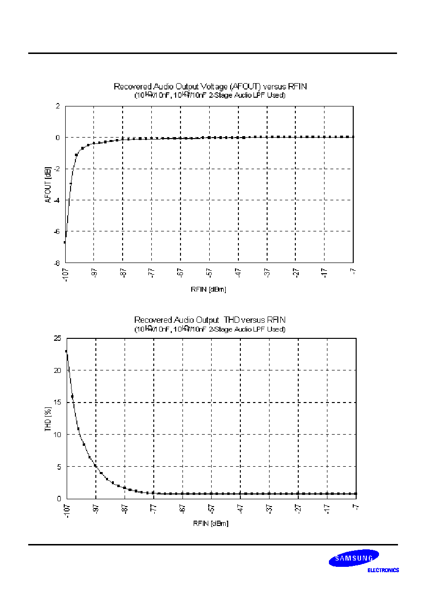
Recovered Audio Output
V
O(RA)
RFin = 1mVrms,
After 2nd stage LPF
147
177
207
mVrms
Recovered Audio Output
Voltage Drop
V
O(RAD
)
Vcc = 5.5V
2.0V
RFin = 1mVrms
-
3.0
-
1.5
-
dB
Detector Output Resistance
R
O(DET)
RFin = 1mVrms
-
1.2
-
K
Detect Output Voltage
V
O(DET)
RFin = 1mVrms
1.0
1.5
2.0
V
Detector Output Distortion
THD
DET
RFin = 1mVrms
(with CCITT Filter)
-
1.0
2.5
%
Comparator Threshold
Voltage Difference
V
TH
V
COMP
= 360mVp-p
R
HYS
= 180K
70
110
150
mV
Comparator Output Voltage 1 V
OH
V
COMP
=360mVp-p
R
HYS
= 180k
Vcc-0.4
-
-
V
Comparator Output Voltage 2 V
OL
V
COMP
= 360mVp-p
R
HYS
= 180k
-
0.1
0.4
V
First Mixer Conversion
Voltage Gain
G
V(1M)
V
MIX1 1/2
= 1mVrms
R
L
= 330k
12
15
18
dB
Second Mixer Conversion
Voltage Gain
G
V(2M)
V
MIX2
= 1mVrms
R
L
= 1.5k
18
22
26
dB
Demodulator Bandwidth
DBW
RFin = 1mVrms
-
10
-
kHz
Limiter Input Sensitivity
V
I(LIM)
Fc = 455kHz ,
-
3dB Limiting
-
20
40
uVrms
AM Rejection Ratio
AMRR
RFin = 1mVrms
AM MOD = 30% @1kHz
-
40
-
dB
First Mixer 3rd Order
Intercept Point
IMD3
MIX1 Input 50
Termination
-
-
15
-
dBm
First Mixer Input Impedance
R
I(1M)
/
C
I(1M)
Fc = 50MHz
-
690
7.2
-
pF
First Mixer output Impedance Ro
(1M)
Fc = 10.7MHz
-
330
-
ENHANCED-1 CHIP CT0 RF IC
S1T8528
9
Second Mixer input
Impedance
R
I(2M)
Fc = 10.7MHz
-
4
-
k
Second Mixer output
Impedance
Ro
(2M)
Fc = 455kHz
-
1.5
-
k
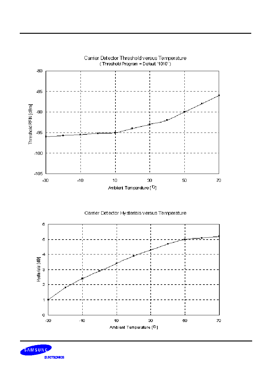
Carrier Detector Threshold
CD
TH
MIX1 Single-Ended
Matching,
Default Threshold=1010
-
-
95
-
dBm
Low Battery Detector
LBD
LBD0 ≠ LBD3 = 0 ( Default )
Only LBD2 = 0
Only LBD1 = 0
Only LBD3 = 0
LBD0 ≠ LBD3 = 1
-
0.15
3.45
3.3
3.0
0.1
V
-
0.1
2.2
2.1
0.075
RSSI Slope
V
RSSI
MIX1 Single-Ended
Matching
-
30
-
mV/dB
RSSI Output Voltage
Dynamic Range
RSSI
MIX1 Single-Ended
Matching
-
60
-
dB
Carrier Detect
Output High Voltage
V
OH
RFin = 1
µ
Vrms
Default Threshold = 1010
Vcc-0.4
-
-
V
Carrier Detect
Output Low Voltage
V
OL
RFin = 10
µ
Vrms
Default Threshold = 1010
-
-
0.4
V
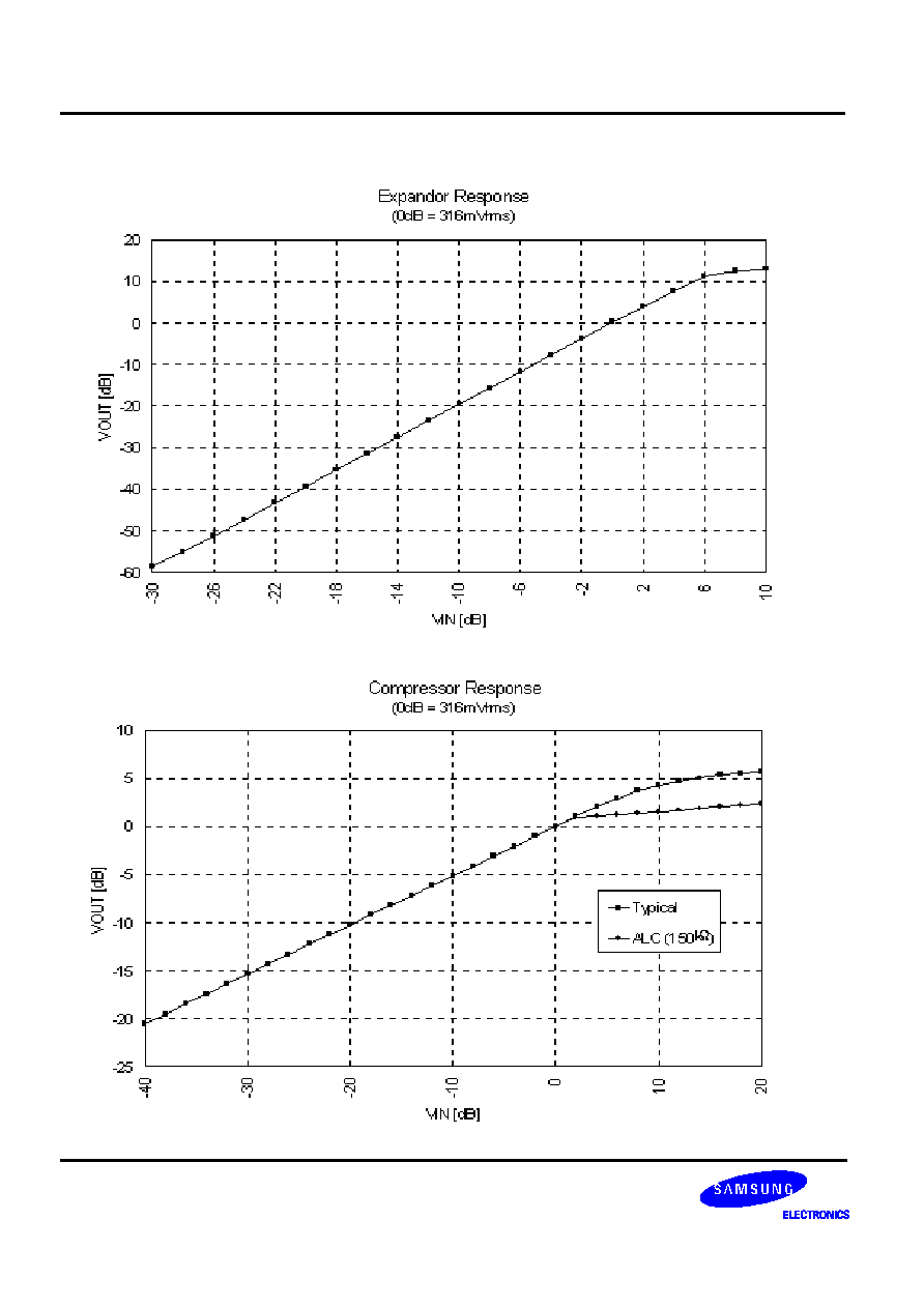
COMPRESSOR
( Vcc = 3.6V, fc = 1kHz, Ta = 25∞C, unless otherwise specified )
Standard Output Voltage
Vo(com)
Vinc = 63.2mVrms
0dB
ALC disabled (pin 13)
269
316
363
mVrms
Compressor Gain
Difference
G
V1(COM)
Vinc =
-
20dB
-
10
0
1.0
dB
G
V2(COM)
Vinc =
-
40dB
-
1.5
0
1.5
dB
Compressor Output
Distortion
THD
COM
Vinc = 63.2mVrms
0dB
-
0.5
1.0
%
Mute Attenuation Ratio
ATT
MUTE
Vinc = 0dB
60
80
-
dB
Compressor Limiting Voltage
V
LIM(COM)
Vinc = Variable
1.05
1.35
1.65
Vp-p
ALC
VALC
R
ALC
= 150k
,
Vinc = 10dB
310
390
450
mVrms
Splatter filter
Vo(SF)
V
INC
= 63.2mVrms
0 dB
269
316
363
mVrms
Maximum Output Voltage
V
OMIC(MAX)
RL = 10K
-
2.8
-
Vp-p
EXPANDER
(Vcc = 3.6V, fc = 1kHz, Ta = 25∞C, unless otherwise specified)
Standard Output Voltage
V
O(EXP)
Vin
E
= 63.2mVrms
0dB
309
356
403
mVrms
ELECTRICAL CHARACTERISTICS (Continued)
Characteristic
Symbol
Test Conditions
Min.
Typ.
Max.
Unit

S1T8528
ENHANCED-1 CHIP CT0 RF IC
10
Expander Gain Difference
G
V1(EXP)
Vin
E
=
-
10dB
-
1.0
0
1.0
dB
G
V2(EXP)
Vin
E
=
-
20dB
-
1.5
0
1.5
dB
G
V3(EXP)
Vin
E
=
-
30dB
-
2.0
0
2.0
dB
Expander Output Distortion
THD
EXP
Vin
E
= 63.2mVrms
0dB
-
0.5
1.0
%
Mute Attenuation Ratio
ATT
MUTE
Vin
E
= 63.2mVrms
0dB
60
80
-
dB
Expander Maximum Output
Voltage
V
OEXP(MAX)
Vin
E
= Variable
THD = 10%
800
-
-
mVrms
Maximum Output Voltage
V
OSPK(MAX)
R
L
= 150
-
2.2
-
Vp-p
RL = 600
-
3.0
-
Vp-p
Input Current
I
IH
Vin = Vcc
-
-
5
µ
A
I
IL
Vin = 0V
-
5
-
-
µ
A
Input Voltage
V
IH
-
Vcc-0.3
-
-
V
V
IL
-
-
-
0.3
V
Output Current
I
OH
Vout = Vcc
0.3
-
-
mA
I
OL
Vout = 0V
0.3
-
-
mA
Output Voltage
V
OH1
PDT,PDR: Io = -0.3mA
( Sourcing )
Vcc-0.4
-
-
V
V
OL1
PDT,PDR: Io = 0.3mA
( Sinking )
-
-
0.4
V
V
OH2
LD,f
MCU
: Io =
-
0.1mA
( Sourcing )
Vcc-0.5
-
-
V
V
OL2
LD,f
MCU
: Io = 0.1mA
( Sinking )
-
-
0.5
V
PLL regulator voltage
V
PLLREG
-
1.90
2.05
2.20
V
Regulator Load Current
I
REG
Vout = V
REG
(OPEN)-0.05V
-
3.0
-
mA
ELECTRICAL CHARACTERISTICS (Continued)
Characteristic
Symbol
Test Conditions
Min.
Typ.
Max.
Unit

ENHANCED-1 CHIP CT0 RF IC
S1T8528
11
PLL PROGRAM SUMMARY
∑
MCU ( MICOM ) Serial Interface ( MSB : 1st INPUT )
Use CLK (Pin 7 ), DATA (Pin 8 ) , and EN (Pin 9 ) terminals for program.
DATA and CLK terminals are used for loading data to internal Shift - Register. When EN terminal is
`
Low
'
, It is possible to program TX-Channel Counter, RX - Channel Counter and various control
functions of PLL. When EN terminal is
`
High
'
, Program 1st Local Oscillator Capacitor Selection in
receiver for U.S.A - 25 CH function
.
-- TX - Register, RX-Register, Control Register
Figure 1.
-- Reference - Register
Figure 2.
DATA
EN
CLK
MSB
LSB
PMC0 PMC1
14Bit DATA
DATA
EN
CLK
MSB
LSB
PMC
0
PMC
1
UK_
S1
12Bit DATA
UK_
S0

S1T8528
ENHANCED-1 CHIP CT0 RF IC
12
-- Auxiliary - Register(16bits)
Figure 3.
∑
Programmable Counter
-- RX - counter: Setting frequency for RX.VCO ( 14 Bits --> 1/16 to 1/16383 )
[ Default_CH. = USA_#21 ( REMOTE ) : 36.075MHz ( Div._NO = 7215 )]
< RX. Register (16bits) >
-- TX - counter: Setting frequency for TX.VCO ( 14 Bits --> 1/16 to 1/16383 )
[ Default_CH. = USA_#21 ( REMOTE ) : 49.830MHz ( Div._NO = 9966 )]
< TX. Register (16 bits) >
Bit
Bit 15
Bit 14
Bit 13
Bit 12
Bit 11
Bit 10
Bit 9
Bit 8
Name
PMC0
PMC1
D13
D12
D11
D10
D9
D8
Default value
7215
*
0
1
1
1
0
0
Bit
Bit 7
Bit 6
Bit 5
Bit 4
Bit 3
Bit 2
Bit 1
Bit 0
Name
D7
D6
D5
D4
D3
D2
D1
D0
Default value
7215
0
0
1
0
1
1
1
1
Bit
Bit 15
Bit 14
Bit 13
Bit 12
Bit 11
Bit 10
Bit 9
Bit 8
Name
PMC0
PMC1
D13
D12
D11
D10
D9
D8
Default value
9966
*
1
0
0
1
1
0
DATA
EN
CLK
MSB
LSB
PMC
CD_TH(4bits)
LBD(3bits)
TEST(2bits)
CLO(6bits)

ENHANCED-1 CHIP CT0 RF IC
S1T8528
13
* Program Latch Assign
-- Ref - counter: Setting reference frequency for phase detector ( 12 Bits --> 1/16 to 1/4095 )
[ Default_Divider = 2048, X-tal_OSC = 10.240 MHz -->Fref = 5KHz ]< Ref. Register (16bits) >
< Ref. Register (16bits) >
-- UK_Selection
Bit
Bit 7
Bit 6
Bit 5
Bit 4
Bit 3
Bit 2
Bit 1
Bit 0
Name
D7
D6
D5
D4
D3
D2
D1
D0
Default value
9966
1
1
1
0
1
1
1
0
PMC0 (Bit15)
PMC1 (Bit14)
Register Assign
0
0
Control
0
1
UPLL_Rx
1
0
UPLL_Ref
1
1
UPLL_Tx
Bit
Bit 15
Bit 14
Bit 13
Bit 12
Bit 11
Bit 10
Bit 9
Bit 8
Name
PMC0
PMC1
UK_S1
UK_S0
D11
D10
D9
D8
Default value
2048
*
Ref.freq. selection
for United Kingdom
1
0
0
0
Bit
Bit 7
Bit 6
Bit 5
Bit 4
Bit 3
Bit 2
Bit 1
Bit 0
Name
D7
D6
D5
D4
D3
f
MCU_M
f
MCUS1
f
MCUS0
Default value
2048
0
0
0
0
0
MCU CLK
Mute
MCU CLK
CNTl_1
MCU CLK
CNTL_0
UK_S0
UK_S1
FR1
FR2
FrefTX
FrefRX
0
0
fREF (A)
-
fREF (A)
fREF (A)
1
0
fREF (A)
fREF/4 (B)
fREF/4 (B)
fREF/4 (B)
0
1
fREF/4 (B)
fREF/25 (C)
fREF/4 (B)
fREF/25 (C)
1
1
fREF/4 (B)
fREF/25 (C)
fREF/25 (C)
fREF/4 (B)

S1T8528
ENHANCED-1 CHIP CT0 RF IC
14
Figure 4. Reference frequency selection
∑
Control program
Control register (16 Bits)
Bit
Bit 15
Bit 14
Bit 13
Bit 12
Bit 11
Bit 10
Bit 9
Bit 8
Name
PMC0
PMC1
BS1
BS0
LBD_BS
CO_M
EX_M
SPK_M
Description Program
Mode
Control_0
Program
Mode
Control_1
Power
Save
Control_1
Power
Save
Control_0
Low
Battery
Detector
Battery
Save
Compressor
Mute
Expander
Mute
Speaker
Mute
Function
*
Program Latch
Assign
**
Power Save Mode
0:Normal
(LBD-On)
1:LBD-Part
Power-Off
0: Normal
1: Mute
0:Normal
1:Mute
0:Nomal
1:Mute
Bit
Bit 7
Bit 6
Bit 5
Bit 4
Bit 3
Bit 2
Bit 1
Bit 0
Name
SPK3
SPK2
SPK1
SPK0
LDT/CDO
f
MCU_M
f
MCUS1
f
MCUS0
Description
SPK
Control_3
SPK
Control_2
SPK
Control_1
SPK
Conrol_
0
LDT/CDO
Select
MCU
Clock
Mute
MCU
Clock
Control_1
MCU
Clock
Control_0
Function
Speaker Volume Control
0: CDO
1: LDT
0: Normal
1: Mute
***
MCU Clock Output
12 Bits Reference
program divider.
˜
4
˜
25
PD_TX
PD_RX
LD
PDT
PDR
fREF
(A)
fREF
˜
4
(B)
fREF
˜
25
(C)
FR1
FR2
ENHANCED-1 CHIP CT0 RF IC
S1T8528
15
** Power Save Mode Assign
*** MCU Clock Output Control & Frequency
*** Speaker Amplifier Volume Control
BS1 (Bit13)
BS0 (Bit12)
Power Save Mode
0
0
Rx
Default
0
1
Active
1
0
STD_By
1
1
Inactive
fMCU_M
fMCUS1
fMCUS0
Clock Output
Divider
X-tal 10.24MHz 11.15MHz
12.0MHz
1
Don
'
t Care
Don
'
t Care
Low
Divider
0
0
0
2
2
5.120MHz 5.575MHz
6.0MHz
0
0
1
3
3
3.413MHz 3.717MHz
4.0MHz
0
1
0
4
4
2.560MHz 2.788MHz
3.0MHz
0
1
1
5 (Default)
5
2.048MHz 2.230MHz
2.4MHz
DATA
Gain/Attenuation
Output Level [SAO1-SAO2]
SPK3
SPK2
SPK1
SPK0
0
0
0
0
-
18dB
25mVrms
0
0
0
1
-
16dB
-
0
0
1
0
-
14dB
-
0
0
1
1
-
12dB
50mVrms
0
1
0
0
-
10dB
-
0
1
0
1
-
8dB
-
0
1
1
0
-
6dB
100mVrms
0
1
1
1
-
4dB
-
1
0
0
0
-
2dB
-
1
0
0
1
0dB
200mVrms
1
0
1
0
+2dB
-
1
0
1
1
+4dB
-
1
1
0
0
+6dB
400mVrms
1
1
0
1
+8dB
-
1
1
1
0
+10dB
-
1
1
1
1
+12dB
800mVrms

S1T8528
ENHANCED-1 CHIP CT0 RF IC
16
∑
Auxiliary Register (16 Bits)
Auxiliary Register Function
**** TEST Mode & LDT-CDO Mode
Bit
Bit 15
Bit 14
Bit 13
Bit 12
Bit 11
Bit 10
Bit 9
Bit 8
Name
PMC
CLO5
CLO4
CLO3
CLO2
CLO1
CLO0
CD_TH3
Description Auxiliary
register
Selection
Cap=5.9p Cap=4.8p Cap=3.2p Cap=1.6p Cap=1.3p Cap=0.8p
CD_TH
Control_3
Function
*****
Program
Mode
Control
1
'
st LO Cap Select
CD
Control_3
Bit
Bit 7
Bit 6
Bit 5
Bit 4
Bit 3
Bit 2
Bit 1
Bit 0
Name
CD_TH2
CD_TH1
CD_TH0
LBD3
LBD2
LBD1
TEST2
TEST1
Description CD_TH
Control_2
CD_TH
Control_1
CD_TH
Control_0
LBD
Control_3
LBD
Control_2
LBD
Control_1
TEST
Mode2
TEST
Mode1
Function
Carrier Detector
Threshold Control
Low Battery Detector
Voltage Control
**** TEST Mode &
LDT-CDO Mode
LDT/CDO
TEST1
TEST2
LDT / CDO
Remark
0
0
0
Rx block CDO
Default
1
0
Rx block CDO
-
0
1
4_25cnt block FR2
-
1
1
4_25cnt block FR2
-
1
0
0
PLL block LDT
-
1
0
PLL block LDT
-
0
1
Test PLL_RX
-
1
0
Test PLL_TX
-
ENHANCED-1 CHIP CT0 RF IC
S1T8528
17
**** Carrier Detector Threshold Control
DATA
Carrier Detector Threshold
CD_TH3
CD_TH2
CD_TH1
CD_TH0
0
0
0
0
-
20dB
0
0
0
1
-
18dB
0
0
1
0
-
16dB
0
0
1
1
-
14dB
0
1
0
0
-
12dB
0
1
0
1
-
10dB
0
1
1
0
-
8dB
0
1
1
1
-
6dB
1
0
0
0
-
4dB
1
0
0
1
-
2dB
1
0
1
0
0dB (Default)
1
0
1
1
+2dB
1
1
0
0
+4dB
1
1
0
1
+6dB
1
1
1
0
+8dB
1
1
1
1
+10dB
S1T8528
ENHANCED-1 CHIP CT0 RF IC
18
∑
Operating internal circuit blocks in each mode
∑
Auxiliary Register(CLO_LBD Program)
[ Rx - 1'st local oscillation internal cap. for U.S.A - 25CH & low battery detecting voltage ]
-- CLO register ( 6 bits ) : Receiver 1'st local oscillator internal capacitor selection
Mode ( state )
Operating circuit blocks
Active state
( Communication mode )
PLL regulator / MICOM I/F ( Data, CLK, EN ) / 2'nd local oscillator / Receiver/ 1'st
local oscillator/ RX PLL/ Carrier detector / FSK comparator / Low battery detector
/ TX PLL / Expander & speaker amp / Compressor /Splatter filter amp, Clock
Output
Receiving mode
PLL regulator / MICOM I/F( Data, CLK, EN ) / 2'nd local oscillator / Receiver/ 1'st
local oscillator/ RX PLL/ Carrier detector / FSK comparator / Low battery
detector, Clock Output
Stand-by mode
(Battery Save Mode#2)
PLL regulator, MICOM I/F ( Data, CLK, EN ), 2'nd local oscillator, Clock Output
Inactive state
(Battery Saving Mode#1)
Interrupt
Bit
Bit 15
Bit 14
Bit 13
Bit 12
Bit 11
Bit 10
Bit 9
Name
PMC
CLO5
CLO4
CLO3
CLO2
CLO1
CLO0
Default
Value 0
1
*****
0
0
0
0
0
0
Function
-
0:Normal
1:Internal
Cap. for
USA 25
Channel
=
5.9pF
0:Normal
1:Internal
Cap. for
USA 25
Channel
=
4.8pF
0:Normal
1:Internal
Cap. for
USA 25
Channel
=
3.2pF
0:Normal
1:Internal
Cap. for
USA 25
Channel
=
1.6pF
0:Normal
1:Internal
Cap. for
USA 25
Channel
=
1.3p F
0:Normal
1:Internal
Cap. for
USA 25
Channel
=
0.8pF

ENHANCED-1 CHIP CT0 RF IC
S1T8528
19
***** PMC ( Program Mode Control )
PMC =
`
HIGH
'
& EN =
`
HIGH
'
---> Auxiliary Register Program Mode
-- Rx-Low Battery Detect Voltage
***** PMC ( Program Mode Control )
PMC =
`
HIGH
'
& EN =
`
HIGH
'
---> Auxiliary Register Program Mode
< Example 1 >
Low battery detector voltage : 2.1V
U.S.A _CH-#1 ( REMOTE ) ---> 1'st local osc. varicap. value =15.86pF,
Internal cap. = 9.3pF
( Ext_L = 0.45uH, EXT_C = 47pF )
-- 16 bit data format
Figure 5.
Bit
Bit15 (MSB)
Bit 4
Bit 3
Bit 2
Low Battery Detector
Voltage
Remark
Name
PMC
LBD3
LBD2
LBD1
Default
Value
1
*****
0
0
0
3.45V
Default
Function
1
1
0
1
3.3V
-
1
1
1
0
3.0V
-
0
0
1
1
2.2V
-
1
1
1
1
2.1V
-
DATA
EN
CLK
MSB
LSB
PMC
LBD3 LBD2 LBD1
1
1
1
1
CLO5 CLO4 CLO3 CLO2 CLO1 CLO0
0
1
1
0
1
0
1( 0 ) 1( 0 ) 1( 0 )
1( 0 ) 1( 0 )
1( 0 )
S1T8528
ENHANCED-1 CHIP CT0 RF IC
20
∑
Example data for U.S.A 25_channel selection
Phase detector / Lock Detector Output Waveforms
Figure 6.
1st Local Osc. Internal Capacitor Select
Base
Channels
Hand
Channels
Varicap
Value
External
C
External
L
Internal
C
Bit5
(CLO5)
Bit4
(CLO4)
Bit3
(CLO3)
Bit2
(CLO2)
Bit1
(CLO1)
Bit0
(CLO0)
1 ~ 25CH. 1 ~ 25CH.
1.0V~2.0V
TYP 1.5V
27pF
(30pF)
0.45uH
pF
0
0
0
0
0
0
16~25CH.
18.73
~15.86pF
27pF
0.44uH
-
0
0
0
0
0
1
-
16~25CH.
18.73
~15.86pF
47pF
0.20uH
0.8
0
0
0
0
1
1
01~04CH.
18.73
~15.86pF
27pF
0.44uH
2.1
0
0
0
1
0
0
05~10CH.
18.73
~15.86pF
27pF
0.44uH
1.6
0
0
0
0
0
1
11~15CH.
18.73
~15.86pF
27pF
0.44uH
0.8
0
1
1
0
1
0
-
01~06CH.
18.73
~15.86pF
47pF
0.20uH
9.3
0
1
0
1
1
0
-
07~15CH.
18.73
~15.86pF
47pF
0.20uH
7.8
12 Bits Reference
program divider.
˜
4
˜
25
PD_TX
LD
PDT
fREF
(A)
fREF
˜
4
(B)
fREF
˜
25
(C)
FR1
FR2
14 Bits TX.
program divider.
2LOI
TIF
REF.Freq
TIF
˜
N

ENHANCED-1 CHIP CT0 RF IC
S1T8528
21
Figure 7. Phase Detector / Lock Detector Output Waveform
REF.Freq.
TIF
˜
N
PDT
LD

S1T8528
ENHANCED-1 CHIP CT0 RF IC
22
APPLICATION CIRCUIT ( BASE SET )
4.
7
k
1
2
3
4
5
6
7
8
9
10
11
12
13
14
15
16
17
18
19
20
21
22
23
24
36
35
34
33
32
31
30
29
28
27
26
25
48
47
46
45
44
43
42
41
40
39
38
37
S1
T85
2
8
+
+
+
+
+
+
+
+
R1
0
20
K
R1
1
10K
C17
IN
TX
V
C
O
C24
2.
2u
C25
3.
3uF
To
M
I
C
O
M
(
M
C
U
)
Da
t
a
f
r
om
M
I
CO
M
(M
CU)
MI
C
O
M
C
L
K
To
M
I
C
O
M
(
M
C
U
)
C30
2P
R15
240K
C20
4.
7n
R16
2.
2M
R23
30K
C26
47uF
C32
100N
C33
3.
3uF
C34
10
0N
R26
120
K
C35
4.
7u
F
C3
6
1
00N
R27
33K
C30
220uF
C37
10N
R28
10k
C39
10N
R2
9
10k
R31
27k
C40
10N
R33
22k
C41
33N
R3
2
470K
R34
47K
T5
C42
68
N
C4
3
10
N
FL
T
3
45
5M
Hz
Y1
10.
24M
Hz
R38
C45
20P
C44
68
P
CV
1
20
P
S2
39
0
FL
T2
10M
Hz
C4
6
10
N
R35
22
C48
10N
T4
AW
I
C4
7
30
P
C49
10
0N
R35
56K
T2
AY
R39
3.
9K
R4
0
1.
0K
C57
4.
7N
C52
0
.
47u
F
C59
10N
C5
4
10uF
C51
10N
R3
7
10
0
RX
AN
T
TX
DU
P
L
E
X
FL
T
1
25k
544
L1
1.
8
µ
H
AN
T
Co
m
p
re
sso
r
Ma
i
n
p
o
w
e
r
RX
out
RX
dat
a
out
i
nput
P
D
T
C
O
S
F
I
S
F
O
L
T
D
/
CDO
1M
CU
CLK
D
A
T
A
E
N
L
B
D
A
G
I
C
CRC
CP
O
CP
I
GN
D
VC
C
SA
O
2
SA
O
1
SA
I
EO
ER
C
ER
I
AL
C
V
RE
F
(
COM
P
)
2LOI
2
M
O
2M
I
V
CC
(RX)
LI
LD
G
N
D
(RX)
Q
C
I
R
A
O
DS
CI
DS
CO
RS
S
I
TI
F
V
RE
F
(
P
L
L
)
V
RE
F
(
R
F
)
PD
R
GN
D
(PL
L
)
1M
I
1M
I
VC
O
RX
1LOI
1LOI
1M
O
2LOI
R38
4.
7k
C53
6P
R4
4
10
K

ENHANCED-1 CHIP CT0 RF IC
S1T8528
23
APPLICATION CIRCUIT ( HAND SET )
1
2
3
4
5
6
7
8
9
10
11
12
13
14
15
16
17
18
19
20
21
22
23
24
36
35
34
33
32
31
30
29
28
27
26
25
48
47
46
45
44
43
42
41
40
39
38
37
S1
T85
2
8
+
+
+
+
+
+
+
+
R10
10
K
R1
1
10K
C17
12N
TX
V
C
O
C24
2.
2u
C25
3.
3uF
T
o
MI
C
O
M (
M
C
U
)
Dat
a
f
r
om
M
I
CO
M
(M
CU)
MI
C
O
M C
L
K
T
o
MI
C
O
M (
M
C
U
)
R15
240
K
C20 4.
7N
R23 30K
C27
47uF
C32
100N
C33
3.
3uF
C34
100
N
R26
120K
C3
5
4.
7uF
C36
100
N
R27
33K
C30
220uF
C37
10N
R28
10
k
C39
10N
R29
10k
R31
27k
C40
10N
R3
3
1k
C41
33N
R32
470K
R34
47K
T5
C42
68N
C43
10
N
FL
T
3
455M
Hz
Y1
10.
245M
Hz
C45
20P
C44
68P
CV
1
20P
S2
390
FL
T
2
10
7M
Hz
C46
10
N
R35
22
C48
10N
T4
AW
I
C47
47P
C49
100N
R35
56K
T2
AY
R39
3.
9K
R40
1.
0K
C57
47N
C5
2
0.
47uF
C59
10N
C54
10uF
C51
10
N
R37
220
RX
AN
T
TX
DUP
LE
X
FE
T1
25k
544
L1
1.
8
µ
H
AN
T
P
D
T
C
O
S
F
I
S
F
O
L
T
D
/
CDO
1
M
CU
CLK
D
A
T
A
E
N
L
B
D
A
G
I
C
CRC
CP
O
CP
I
GN
D
VC
C
SAO
2
SAO
1
SAI
EO
ER
C
ER
I
AL
C
V
RE
F
(
COM
P
)
2LOI
2
M
O
2M
I
V
CC
(RX)
LI
L
D
G
N
D
(R
X
)
Q
C
I
R
A
O
DS
CI
DS
CO
RS
S
I
TI
F
V
RE
F
(
P
L
L
)
V
RE
F
(
RF
)
PD
R
GN
D
(PL
L
)
1M
I
1M
I
VC
O
RX
1L
O
I
1L
O
I
1M
O
2L
O
I
C18
12N
R2
2
2.
2
M
MI
C
+
R16
22K
R17
22K
C26
10uF
1
2
RX
DA
T
A
out
C50
2P
T3
AY
C53
2P
SPK
R38
4.
7k

S1T8528
ENHANCED-1 CHIP CT0 RF IC
24
TEST CIRCUIT
+
+
+
VREFCOM
P
4.7uF
+
+
Vin22
1uF
2.2uF
Voe
10k
+
Vine1
1uF
150
SAo1
SAo2
+
10uF
10nF
Vinc
2.2uF
+
2.2uF
100k
CLK
DATA EN
LBD
LD
CDo
100k
S5
SFout
1k
1nF
10nF
15k
Vinc1
+
1nF
+
2.2uF
10k
PDT
Vc
10uF
10nF
S48
+
+
100k
100k
10nF
10uF
1uF
4.3k
1k
S45
PDR
~
1nF
18pF
56k
100nF
S41
~
47pF
0.1uF
68k
680uH
180pF
S25
10k
0.01uF
10k
0.01uF
0.01uF
1k
0.1uF
15k
180k
DSCO
RSSI
Vin27
RAo
DSCI
Vcccom
Vin40
Vin43
S1T8528
150k
S23
+
2.2uF
V28
10nF
10nF
1uF
S40
S1
10K
S7
10K
S8
10K
S9
500k
-1000k
+
10uF
10nF
VREFRF
VREFPLL
48
2
47
46
45
44
43
42
41
40
39
38
37
24
23
22
21
20
19
18
17
16
15
14
13
10
1
3
4
5
6
7
8
9
11
12
36
35
34
33
32
31
30
29
28
27
26
25
PDT
CO
SFI
SFO
CDO
LDT CLKO
LBD
EN
DATA
AGIC
CLK
CRC
CPO
CPI
VCC(COMP)
GND(COMP)
SAO2
SAO1
SAI
EO
ERC
EPI
ALC
VREF(COMP)
RSSI
DSCO
DSCI
RAO
QCI
GND
(RX)
VCC
(RX)
LI
LD
2MI
2MO
2LOI
2LOI
1MO
1LOI
1LOI
VCO(RX)
1MI
1MI
GND(PLL)
PDR
VREF(RF)
VREF(PLL)
TIF
0.47uH
CLKO
150k
100pF
30k
+
Vmico
1uF
68pF
1k
100
82k
33pF
+
0.47uF
+
6.8k
1uF
56k
KDS2236
47pF
T1(AW)
2.7k
0.41uH
100k
100k
15k
25pF
0.47uH
~
Vin48
68pF
VCOR
VCOT
TIF
10.7MHz
1Mo
2Lo
47pF
10nF
20pF
10.240MHz
455kHz
Vccrx
+
10uF
S34
390
2Mo
Varicap
47pF
5.1k
S1T8528

ENHANCED-1 CHIP CT0 RF IC
S1T8528
25
S1T8528
ENHANCED-1 CHIP CT0 RF IC
26

ENHANCED-1 CHIP CT0 RF IC
S1T8528
27

S1T8528
ENHANCED-1 CHIP CT0 RF IC
28

ENHANCED-1 CHIP CT0 RF IC
S1T8528
29

S1T8528
ENHANCED-1 CHIP CT0 RF IC
30
ENHANCED-1 CHIP CT0 RF IC
S1T8528
31
S1T8528
ENHANCED-1 CHIP CT0 RF IC
32

ENHANCED-1 CHIP CT0 RF IC
S1T8528
33

S1T8528
ENHANCED-1 CHIP CT0 RF IC
34