WIDEBAND FM/FSK IF RECEIVER
S1T8531
1
INTRODUCTION
The S1T8531 is a wideband FM / FSK receiver designed for
wideband FSK data and analog FM applications.
It is fabricated using Samsung's ASP5HB 0.5um advanced BiCMOS
process. The S1T8531 contains high gain IF amplifier with received
signal strength indicator (RSSI), a wideband FM quadrature
demodulator, a baseband filter amplifier and a high speed data slicer
with sample & hold function.
The IF amplifier has 100dB small signal gain and 2MHz through
40MHz bandwidth. The wideband FM quadrature demodulator has
demodulation bandwidth greater than 1MHz.
The baseband filter amplifier is a wideband buffer and it can be
configured as a second-order sallen-key low pass filter. The data slicer is a comparator that is designed to square
up the data signal with data rates up to 2Mbps.
FEATURES
∑
Operating voltage range : 2.2 to 5.5V
∑
Typical supply current : 5.5mA at 3.6V
∑
Operating frequency range : 2MHz to 40MHz
∑
High Gain (100dB) and Wideband (2MHz to 40MHz) IF Amplifier
∑
Quadrature Demodulator with Greater than 1MHz Bandwidth
∑
High Speed Data Slicer Operating Upto 2Mbps with Sample & Hold
∑
RSSI Dynmic range : Typ : 60dB
APPLICATION
∑
Wideband FM / FSK Wireless Communication Systems
ORDERING INFORMATION
+ : New Product
Device
Package
Operating Temperature
+S1T8531X01-S0B0
16-SOP-225
- 10
∞
C to + 70
∞
C
16-SOP-225
S1T8531
WIDEBAND FM/FSK IF RECEIVER
2
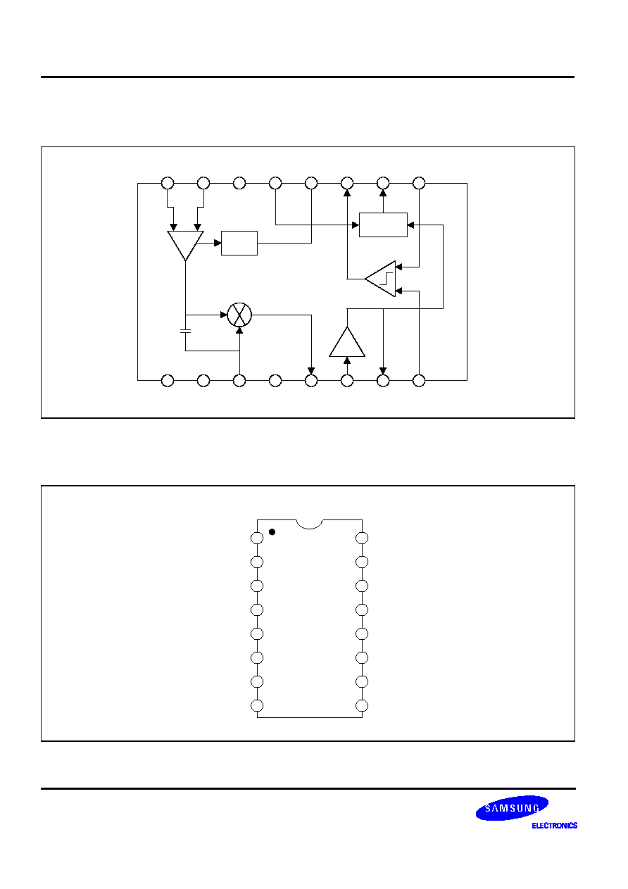
BLOCK DIAGRAM
PIN CONFIGURATION
VCC2
BOUT
BIN
QOUT
GND1
IFIP
QIN
IFIN
GND2
RSSI
DSO
SHEN
DSIN
DSIP
5pF
SHO
VCC1
16
15
14
13
12
11
10
9
1
2
3
4
5
6
7
8
A
RSSI
Sample
Hold
1
GND1
QIN
VCC1
VCC2
QOUT
BOUT
BIN
DSIP
IFIN
GND2
IFIP
SHEN
RSSI
SHO
DSO
DSIN
S1T8531
1
2
3
4
5
6
7
8
16
15
14
13
12
11
10
9

WIDEBAND FM/FSK IF RECEIVER
S1T8531
3
PIN DESCRIPTION
Pin
Name
Schematic
Description
1
GND1
Ground. (Pin1 and Pin14 are connected internally)
2
VCC1
Supply. (Pin2 and Pin4 are connected internally)
3
QIN
Quadrature demodulator tank input.
4
VCC2
Supply. (Pin2 and Pin4 are connected internally)
5
QOUT
Quadrature demodulator output.
6
7
BIN
BOUT
Baseband filter buffer amplifier input.
Baseband filter buffer amplifier output.
8
9
DSIP
DSIN
Data slicer positive input.
Data slicer negative input.
VCC
3
VCC
5
VCC
7
6
VCC
9
8

S1T8531
WIDEBAND FM/FSK IF RECEIVER
4
PIN DESCRIPTION (Continued)
Pin
Name
Schematic
Description
10
SHO
Sample and hold output.
11
DSO
Data slicer output.
12
RSSI
RSSI output.
13
SHEN
Sample and hold enable input.
High signal input enable sample and hold function
and low signal input disable sample and hold
function .
14
GND2
Ground. (Pin1 and Pin14 are connected internally)
15
16
IFIP
IFIN
IF amplifier differential inputs.
DC blocking is required.
7
VCC
11
VCC
12
VCC
13
VCC
15
16

WIDEBAND FM/FSK IF RECEIVER
S1T8531
5
ABSOLUTE MAXIMUM RATINGS
RECOMMENDED OPERATING CONDITIONS
Characteristic
Symbol
Value
Unit
Maximum Supply Voltage
V
CC
6
V
Operating temperature
T
a
-10 to + 70
∞
C
Storage Temperature
T
STG
-55 to + 150
∞
C
Parameter
Symbol
Value
Unit
Power Supply Voltage
V
CC
2.2 to 5.5
V
Voltage applied to any pin
V
IN
- 0.3 to Vcc + 5.5
V

S1T8531
WIDEBAND FM/FSK IF RECEIVER
6
ELECTRICAL CHARACTERISTICS
( Vcc = 3.6V, IF = 10.7MHz, fdev = ± 75kHz, fmod = 10kHz,Ta = 25
∞
C, IFin = -47dBm unless otherwise noted. )
NOTES:
1.
Not 100% AC tested but guaranteed by design and characterization.
2.
Measured result on evaluation board with proper impedance matching.
Characteristic
Symbol
Test Condition
Min
Typ
Max
Unit
Current consumption
Icc
-
-
5.5
7.0
mA
IF Input Frequency
IFfreq
-
2
10.7
40
MHz
20dB SINAD Sensitivity (Note 2)
VSEN
-
-
-95
-81
dBm
IF Amplifire Bandwidth (Note 1)
BWIF
-
2
-
40
MHz
IF Amplifier Voltage Gain (Note 1)
G IF
-
95
101
-
dB
IF Amplifier Input Impedance (Note 1)
RII
IF
-
-
1.5
-
k
Quadrature Demodulator Output Voltage
Vo(DEM)
-
100
150
200
mVrms
Demodulator Bandwidth (Notes 1 and 2)
BWDEM
-
0.6
1
-
MHz
Baseband Filter Buffer Amplifier Bandwidth
BWAMP
-
1
2
-
MHz
Baseband Filter Buffer Amplifier Voltage
Gain
DG AMP
-
-3
0
+3
dB
Data Slicer Maximum Operating Frequency
(Notes 1 and 2)
BWDS
-
1
2
-
Mbps
RSSI Dynamic Range
RSSI
-
50
60
-
dB
RSSI Output Level
Vo(RSSI)
-
0.5
-
2.0
V

WIDEBAND FM/FSK IF RECEIVER
S1T8531
7
FUNCTIONAL DESCRIPTION
General
The S1T8531 is a wideband FM / FSK receiver designed for use in analog FM and digital FSK systems such as
900MHz / 2.4GHz ISM band analog / digital cordless phones and wideband data links with data rates up to 2Mbps.
It contains IF amplifier, quadrature detector, baseband filter amplifier and data slicer with sample and hold function.
IF Amplifier
The IF amplifier section is composed of seven differential stage with total gain of 100dB at 10.7MHz. The input
impedance at 10.7MHz is 1.5k
. For 10.7MHz ceramic filter applications, an external 430
resistor must be placed
between IFP(Pin15) and IFN(pin16) to provide the equivalent load impedance of 330
that is required by the filter.
Quadrature Demodulator
The quadrature demodulator requires tank circuit with loaded Q depending on detection bandwidth. Following
figure shows external components required for 10.7MHz operation.
Baseband Filter Buffer Amplifier3
Baseband filter amplifier is a wideband buffer and it can be configured as a second-order sallen-key low pass filter.
Following figure shows the external components required.
Cutoff frequency = 1 / [2
*SQRT(R1R2C1C2)]
Quality factor = SQRT(R1R2C1C2) / (R1C2 + R2C2)
The component value of R1 should contain the quadrature detector output resistance.
VCC
QUAD OUT
47pF 4.255uH
Rdamp
3
5
QUAD IN
BUF IN
BUF OUT
R1
R2
C2
C1
Vin
Vout
7
6

S1T8531
WIDEBAND FM/FSK IF RECEIVER
8
Data Slicer with Sample and Hold
The data slicer is a comparator that is designed to square up the data signal. The recovered data signal from the
baseband filter output can be DC coupled to the data slicer DS-INP(Pin 9). The S1T8531's data slicer incorporates
an sample and hold used to derive the data slicer reference voltage by means of an external integration circuit. The
sample and hold is "ON" during reception of the preamble data pattern, and is otherwise "OFF" in TDD (Time
Division Duplex) system. The external integration circuit is formed by an RC low pass circuit placed between SHO
(Pin 10) and ground.
The size of this resistor and capacitor and the nature of the data signal determine how faithfully the data slicer
shapes up the recovered signal. The time constant is short for large peak to peak voltage swings or when there is a
change in DC level at the detector output. For small signal or for continuous bits of the same polarity which drift
close to the threshold voltage, the time constant is longer.
`The sample and hold is able to sink/source 3mA to/from the external integration circuit in order to minimize the
settling time. When the sample and hold is "OFF" the output (SHO) is in high impedance state with extremely low
leakage current.
`Following figure shows the internal block diagram.
The output of the data slicer (DS-OUT) is a CMOS compatible bitstream. However, it is recommeded that an
external NPN amplifier stage be used to drive the CMOS baseband processor, in order to minimize the amount of
ground and supply currents in the S1T8531 which might desensitize the chip.
The data slicer can be used as a carrier detector also. Following figure shows application example. In this case,
sample and hold should be off.
DS INP
DS INN
SHEN
DS OUT
SHO
8
9
10
13
11
+1
Carrier
Detect
RSSI
Reference
Voltage
11
12
9
8

WIDEBAND FM/FSK IF RECEIVER
S1T8531
9
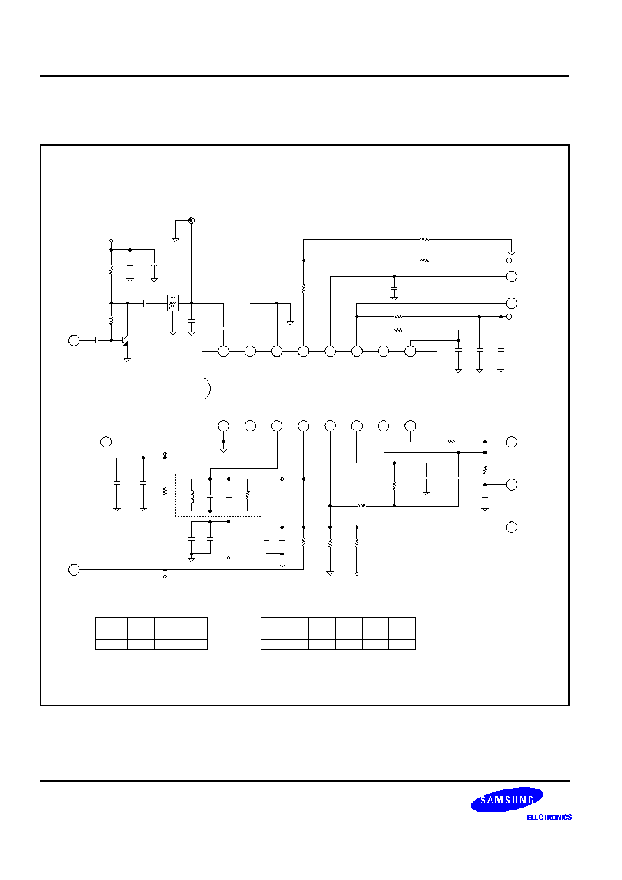
TEST CIRCUIT
50
10n
IF Input
IFN
IFP
GND
Data
Output
VCC
SHEN RSSI DSO SHO DSIN
VCC
Audio
Output
RSSI
GND VCC
QIN
VCC QOUT BIN BOUT DSIP
1n
S1T8531
1
2
3
4
5
6
7
8
16
15
14
13
12
11
10
9
10n
100n
1n
100n
100n
1.8k
1u
20k
20k
15k
39k
68p
100p
S1T8531
WIDEBAND FM/FSK IF RECEIVER
10
APPLICATION CIRCOUT
IFN
IFIP GND2 SHEN RSSI DSO SHO DSIN
GND1 VCC1 QIN VCC2 QOUT BIN BOUT DSIP
S1T8531
1
2
3
4
5
6
7
8
16
15
14
13
12
11
10
9
1
1
1
1
1
1
1
1
VCC
R15
330
C19
56p
C18
100n
C17
10nF
T2
10.7MHz
IF2
BNC
C16
120p
C15
10nF
C14
10nF
R12
56K
R14
R13
Sample &hold enable
Sample &hold diable
VCC2
TP5
RSSI
TP4
DSOUT
VCC2
C13
100n
R11 10K
R10 1.8K
C10
1u
C11
3.3n
C12
56p
R8
51
R9
5.6K
TP2
BUFOUT
AUDIOOUT
TP3
TP1
QUADOUT
*C9
4.7n
*C8
100p
*C7
68p
R7
39K
R6
15K
R4
20K
R5
20K
VCC2
R3
51
C6
56p
C5
100n
C4
56p
C3
3.3nF
VCC
VCC1
VCC
POWER
VCC2
Quad.
coil
L1
CX1 CX1 R2
R1
51
C2
56p
C1
3.3n
VCC1
GND
POWER
* Changable value for each application
C7
Analog
Digital
68p
100p
C8
100p
220p
C9
4.7n
820p
* Quadrature Coil
L1
Quad. coil
Ext. coil
360u
2.7u
CX1
120p
56p
CV1
N/A
1-3p
R2
7.5K
2.4K
R16
10K
C20
10n
0
0