LOW VOLTAGE AUDIO AMPLIFIER
S1T8602B
1
INTRODUCTION
The S1T8602B is the audio power amplifier available for low voltages.
S1T8602B supplies differential outputs for maximizing output swing at
low voltages. S1T8602B doesn
'
t need coupling capacitors to the
speaker. The gain of this amp is controlled easily by two external
resistors.
FEATURES
∑
Wide Supply Voltage (2 to 16V)
∑
Low Quiescent Supply Current (I
CC
= 2.7mA : Typ)
∑
Easy Gain Control
∑
Medium Output Power
P
O
= 250mW at V
CC
= 6V, R
L
= 32
, THD = 10%
∑
Minimum External Parts
∑
Various Load Impedance Range (8
to 100
)
∑
Low Distortion
∑
Mute Function (l
CC
= 65
µ
A: Typ)
ORDERING INFORMATION
Device
Package
Operating Temperature
S1T8602B01-D0B0
8
-
DIP
-
300
-
20
∞
C to +70
∞
C
S1T8602B01-S0B0
8
-
SOP
-
225
8
-
DIP
-
300
8
-
SOP
-
225

LOW VOLTAGE AUDIO AMPLIFIER
S1T8602B
3
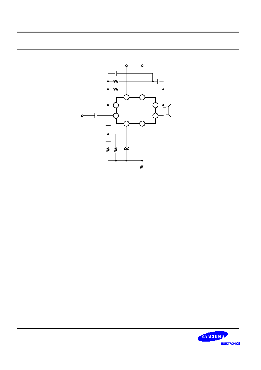
PIN DESCRIPTION
ABSOLUTE MAXIMUM RATINGS
Pin No
Symbol
Description
1
Input (+)
Analog Ground for the amplifiers. A 1.0
µ
F capacitor at this pin (with a 5.0
µ
F capacitor at
pin 8) provides 52dB (Typ) of power supply rejection. Turn-on time of the circuit is affected
by the capacitor on this pin. This pin can be used as an alternative input.
2
Input (
-
)
Amplifier input. The input capacitor and resistor set low frequency roll-off and input
impedance. The feedback resistor is connected between this pin and output1.
3
Output 1
The output of Amplifier 1. DC Level is (V
CC
- 0.7V)/2.
4
V
CC
DC supply voltage (+2.0 to + 16V) is applied to this pin.
5
GND
Ground pin.
6
Output 2
The output of Amplifier 2. This signal is equal in amplitude, but 180
∞
out of phase with that
at output1. The DC level is (V
CC
- 0.7V)/2.
7
Mute
This pin can be used to power down the IC to conserve power or for muting, or both.
When at a logic Low (0 to 0.8 volts), the S1T8602B is enabled for normal operation. When
at a logic High (2.0 to V
CC
volts), the IC is disabled. If Mute is open, that is equivalent to a
logic Low.
8
Ripple Rejection
A capacitor at this pin increases power supply rejection, and affects turn-on time. This pin
can be left open if the capacitor at pin 1 is sufficient.
Characteristic
Symbol
Value
Unit
Supply Voltage
V
CC
-
1.0 to + 18
V
Output Current (output pin)
I
O
±
250
mA
Maximum Voltage (input, Ripple rejection, Mute pin)
V
I (MAX)
-
1.0 to V
CC
+ 1.0
V
Applied Output Voltage (output pin) when disabled
V
O
-
1.0 to V
CC
+ 1.0
V
Junction Temperature
T
J
-
55 to + 140
∞
C

S1T8602B
LOW VOLTAGE AUDIO AMPLIFIER
4
RECOMMENDED OPERATING CONDITIONS
Characteristic
Symbol
Min.
Typ.
Max.
Unit
Supply Voltage
V
CC
+2.0
-
+16
V
Load Impedance
Z
L
8
-
100
W
Peak Load Current
I
L (PK)
-
200
-
±
200
mA
Differential Gain (5KHz Bandwidth)
G
V
0
-
46
dB
Voltage at Mute (Pin 7)
V
I (MUTE)
0
-
V
CC
V
Ambient Temperature
Ta
-
20
-
470
∞
C
ELECTRICAL CHARACTERISTIC
(V
CC
= 6V, Ta = 25
∞
C, unless otherwise noted)
Characteristic
Symbol
Test Conditions
Min.
Typ.
Max.
Unit
DC ELECTRICAL CHARACTERISTICS
Operating Current (RL = 0)
I
CC
V
CC
= 3.0V, Mute = 0.8V
V
CC
= 16.0V, Mute = 0.8V
-
2.7
3.3
4.0
5.0
mA
V
CC
= 3.0V, Mute = 2.0V
-
65
100
µ
A
Output Voltage (output pin)
V
O
RL = 16
R1 = 75k
V
CC
= 3.0V
V
CC
= 6.0V
V
CC
= 12.0V
1.0
1.15
2.65
5.65
1.25
V
Output Offset Voltage
V
OO
V
CC
= 6.0V, R
f
= 75k
, R
L
= 32
-
30
0
+30
mV
Output High Level
V
OH
2.0V
V
CC
16V, I
out
= -75mA
-
V
CC
-
1.0
-
V
Output Low Level
V
OL
2.0V
V
CC
16V, I
out
= 75mA
-
0.16
-
V
Input Bias Current (pin 2)
I
BIAS
-
-
-
100
-200
nA
Equivalent Resistance
R
EQ
pin 1
pin 8
100
18
150
25
220
40
k
Input Low Voltage
V
IL (MUTE)
-
-
-
0.8
V
Mute
Input High Voltage
V
IH (MUTE)
-
2.0
-
-
V
Input Resistance
R
I (MUTE)
V
CC
= Mute = 16V
50
90
175
k
AC ELECTRICAL CHARACTERISTICS
Open Loop Gain (Amp 1)
G
V (AMP1)
-
80
-
-
dB
Close Loop Gain (Amp 2)
G
V (AMP2)
f = 1.0kHz, R
L
= 32
-
0.35
0
+0.35
dB
Output Power
P
O
V
CC
= 3.0V, R
L
= 6
, THD
10%
V
CC
= 6.0V, R
L
= 32
, THD
10%
V
CC
= 12V, R
L
= 100
, THD
10%
55
250
400
-
-
mW

LOW VOLTAGE AUDIO AMPLIFIER
S1T8602B
5
Total Harmonic Distortion
(f = 1.0kHz)
THD
V
CC
= 6.0V, R
L
= 32
, P
O
=125mW
V
CC
3.0V, R
L
= 8
, P
O
= 20mW
V
CC
12V, R
L
= 32
, P
O
= 200mW
-
0.5
0.5
0.6
1.0
%
Gain Bandwidth Product
GBW
-
-
1.5
-
MHz
Power Supply Rejection
(V
CC
= 6.0V,
V
CC
= 3.0V)
PSRR
C
1
=
, C
2
= 0.01
µ
F
C
1
=0.1
µ
F, C
2
=0, f=1.0kHz
C
1
= 1.0
µ
F, C
2
= 5.0
µ
F, f = 1.0kHz
50
12
52
-
dB
Muting
G
V (MUTE)
Mute = 2.0V, 1.0Khz
f
20kHz
-
> 70
-
dB
ELECTRICAL CHARACTERISTIC (Continued)
(V
CC
= 6V, Ta = 25
∞
C, unless otherwise noted)
Characteristic
Symbol
Test Conditions
Min.
Typ.
Max.
Unit