 | –≠–ª–µ–∫—Ç—Ä–æ–Ω–Ω—ã–π –∫–æ–º–ø–æ–Ω–µ–Ω—Ç: S3C1850 | –°–∫–∞—á–∞—Ç—å:  PDF PDF  ZIP ZIP |

1. S3C1840

S3C1840
1-1
DESCRIPTION
S3C1840, a 4-bit single-chip CMOS microcontroller, consists of the reliable SMCS-51 CPU core with on-chip
ROM and RAM. Eight input pins and 11 output pins provide the flexibility for various I/O requirements. Auto reset
circuit generates reset pulse every certain period, and every halt mode termination time. The S3C1840
microcontroller has been designed for use in small system control applications that require a low-power, cost -
sensitive design solution. In addition, the S3C1840 has been optimized for remote control transmitter.
FEATURES
ROM Size
∑
1,024 bytes
RAM Size
∑
∑
32 nibbles
Instruction Set
∑
∑
39 instructions
Instruction Cycle Time
∑
∑
13.2
µ
sec at fxx = 455 kHz
Input Ports
∑
∑
Two 4-bit ports (24 pins)/one 4-bit port, one 2-bit
ports (20 pins)
Output Ports
∑
∑
One 4-bit port, seven 1-bit ports (24 pins)/one 4-
bit port, five1-bit ports (20 pins)
Built-in Oscillator
∑
∑
Crystal/ceramic resonator
Built-in Reset Circuit
∑
Built-in Power-on reset and auto reset circuit for
generating reset pulse every 131072/fxx
(288
ms at fxx = 455 kHz)
Four Transmission Frequencies
∑
∑
fxx/12 (1/4 duty), fxx/12 (1/3 duty), fxx/8 (1/2
duty), and no-carrier frequency
Supply Voltage
∑
∑
1.8 V-3.6 V (250 kHz
f
OSC
3.9 MHz)
2.2 V-3.6 V (3.9 MHz < f
OSC
6 MHz)
Power Consumption
∑
∑
Halt mode: 1
µ
A (maxium)
∑
∑
Normal mode: 0.5 mA (typical)
Operating temperature
∑
∑
≠ 20
∞
C to 85
∞
C
Package Type
∑
∑
24 SOP, 20 DIP, 20 SOP
Oscillator Frequency divide select
∑
∑
Mask Option: fxx = f
OSC
or f
OSC
/8

S3C1840
1-2
BLOCK DIAGRAM
P1.0 - P1.3
P0.0 - P0.3
P3.0 - P3.3
6
P3 Output Register
(PR)
ALU & A
H
2
4
4
RAM
16 x 2 x 4-bits
L Decoder
5
16
8
4
6
3-Level Stack
4
4
4
L
4
1
Internal P2.9 and P2.10
4
Internal P2.13
Internal
P2.0
P2.1 - P2.6
4
4
f
XX
/8 (1/2)
f
XX
/12 (1/3)
f
XX
/12 (1/4)
No Carrier
Internal P2.12
P2.0/REM
HALT
DIV
OSC
X
I
X
O
4
Auto Reset
MUX
PB
SF
PA
PC
64 x 16 x 8-bits
ROM
P2-Output Latch
4
Figure 1-1. Block diagram

S3C1840
1-3
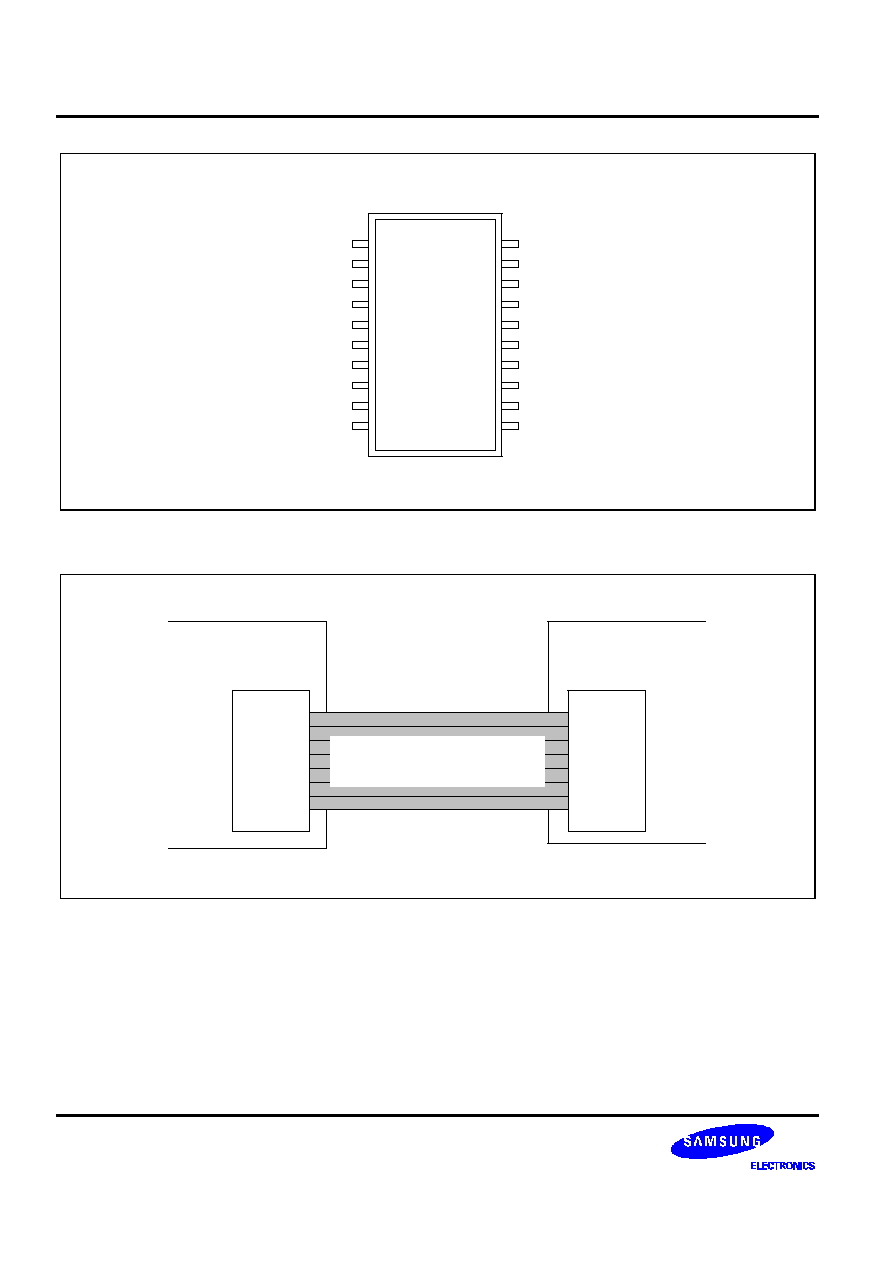
PIN CONFIGURATION (24 SOP)
S3C1840
1
2
3
4
5
6
7
8
9
10
11
12
24
23
22
21
20
19
18
17
16
15
14
13
V
SS
X
I
X
O
P2.6
P0.0
P0.1
P0.2
P0.3
P1.0
P1.1
P1.2
P1.3
V
DD
P2.0/REM
TEST
P2.1
P2.2
P2.3
P2.4
P2.5
P3.0
P3.1
P3.2
P3.3
Figure 1-2. Pin Configuration (24 SOP)
Table 1-1. PIN Description for 24 PINS
Pin
Name
Pin
Number
Pin
Type
Description
I/O Circuit
Type
P0.0-P0.3
5, 6, 7, 8
Input
4-bit input port when P2.13 is low
A
P1.0-P1.3
9, 10, 11, 12
Input
4-bit input port when P2.13 is high
A
P2.0 REM
23
Output
1-bit individual output for remote carrier
frequency
(1)
B
P2.2-P2.5
20, 19, 18, 17
Output
1-bit individual output port
C
P2.1, P2.6
21, 4
D
P3.0-P3.3
16, 15, 14, 13
Output
4-bit parallel output port
C
TEST
22
Input
Input pin for test (Normally connected to V
SS
)
≠
X
I
2
Input
Oscillation clock input
≠
X
O
3
Output
Oscillation clock output
≠
V
DD
24
≠
Power supply
≠
V
SS
1
≠
Ground
≠
NOTES:
1.
The carrier can be selected by software as fxx/12 (1/3 duty), fxx/12 (1/4 duty), fxx/8 (1/2 duty), or no-carrier
frequency.
2.
Package type can be selected as 24 SOP in the ordering sheet.

S3C1840
1-4
PIN CONFIGURATION (20 DIP, 20 SOP)
V
SS
X
I
X
O
P0.0
P0.1
P0.2
P0.3
P1.0
P1.1
P3.3
S3C1840
1
2
3
4
5
6
7
8
9
10
20
19
18
17
16
15
14
13
12
11
V
DD
P2.0/REM
TEST
P2.1
P2.2
P2.3
P2.4
P3.0
P3.1
P3.2
Figure 1-3. Pin Configuration (20 DIP, 20 SOP)
Table 1-2. Pin Description for 20 Pins
Pin
Name
Pin
Number
Pin
Type
Description
I/O Circuit
Type
P0.0-P0.3
4, 5, 6, 7
Input
4-bit input port when P2.13 is low
A
P1.0-P1.1
8, 9
Input
2-bit input port when P2.13 is high
A
P2.0/REM
19
Output
1-bit individual output for remote carrier
frequency
(1)
B
P2.2-P2.4
16, 15, 14
Output
1-bit individual output port
C
P2.1
17
D
P3.0-P3.3
13, 12, 11, 10
Output
4-bit parallel output port
C
TEST
18
Input
Input pin for test (Normally connected to V
SS
)
≠
X
I
2
Input
Oscillation clock input
≠
X
O
3
Output
Oscillation clock output
≠
V
DD
20
≠
Power supply
≠
V
SS
1
≠
Ground
≠
NOTES:
1.
The carrier can be selected by software as fxx/12 (1/3 duty), fxx/12 (1/4 duty), fxx/8 (1/2 duty), or no-carrier
frequency.
2
Package type can be selected as 20 DIP, or 20 SOP in the ordering sheet.

S3C1840
1-5
I/O CIRCUIT SCHEMATICS
Input
V
DD
30 -150 k
V
SS
Figure 1-4. I/O Circuit Type A
V
DD
N-CH
Output
Data
NOTE:
If data disable signal is active, halt mode,
the output becomes low state.
V
SS
Data
Disable
(note)
Figure 1-6. I/O Circuit Type C
V
DD
Output
Data
Disable
(note)
Data
NOTE:
If data disable signal is active, halt mode,
the output becomes low state.
V
SS
P-CH
N-CH
Figure 1-5. I/O Circuit Type B
V
DD
V
SS
N-CH
Data
Output
Figure 1-7. I/O Circuit Type D

S3C1840
1-6
Table 1-3. Absolute Maximum Ratings
Parameters
Symbols
Ratings
Units
Supply Voltage
V
DD
≠ 0.3 to 6
V
Input Voltage
V
I
≠ 0.3 to V
DD
+ 0.3
V
Output Voltage
V
O
≠ 0.3 to V
DD
+ 0.3
V
Soldering Temperature
T
SLD
260 (10 sec)
∞
C
Storage Temperature
T
STG
≠ 55 to 125
∞
C
Table 1-4. DC Characteristics
(V
DD
= 3 V, T
A
= 25
∞
C)
Parameters
Symbols
Test Conditions
Min
Typ
Max
Units
Supply Voltage
V
DD
250kHz
f
OSC
3.9MHz
1.8
3.0
3.6
V
3.9MHz< f
OSC
6MHz
2.2
3.0
3.6
Operating Temperature
T
A
≠
≠ 20
≠
85
∞
C
High-Level Input Voltage
V
IH1
All input pins except
X
IN
0.7 V
DD
≠
V
DD
V
V
IH2
X
IN
V
DD
-0.3
≠
V
DD
V
Low-Level Input Voltage
V
IL1
All input pins except
X
IN
0
≠
0.3 V
DD
V
V
IL2
X
IN
0
≠
0.3
V
High-Level Output Current P2.0
I
OH1
V
O
= 2.0 V
≠ 6.0
≠ 9
≠ 14
mA
Low-Level Output Current P2.0
I
OL1
V
O
= 0.4 V
1.5
3.0
4.5
mA
Low-Level
P3 Output
I
OL2
V
O
= 0.4 V
0.5
1.0
2.0
mA
Output
P2.1-P2.3
1.5
3.0
4.5
Current
P2.4-P2.6
0.5
1.0
2.0

S3C1840
1-7
Table 1-4. DC Characteristics (Continued)
(V
DD
= 3 V, T
A
= 25
∞
C)
Parameters
Symbols
Test Conditions
Min
Typ
Max
Units
High-Level Input Leakage Current
I
LIH1
V
I
= V
DD
≠
≠
3
uA
All input pins
except X
IN
I
LIH2
X
IN
≠
3
10
Low-level Input Leakage Current
I
LIL1
X
IN
≠ 0.6
≠ 3
≠ 10
High-level Output Leakage
Current
I
LOH
V
O
= V
DD
≠
≠
3
uA
All output pins
except P2.0
Pull-up Resistance of Input Port
R
V
DD
= 3 V
30
70
150
K
V
I
= 0 V
Average Supply Current
I
DD
V
DD
= 3 V
≠
0.5
1.0
mA
Crystal/resonator
Non-divide option
f
OSC
= 1 MHz
Dvide-8 option
f
OSC
= 6 MHz
HALT Current
I
DDH
f
OSC
= 0
≠
≠
1.0
uA
Clock Frequency
fxx
Crystal/ceramic
250
≠
1000
kHz
Oscillator Frequency
f
OSC
Crystal/ceramic
250
≠
1000
Non-divide option
Crystal/ceramic
2000
6000
Divide-8 option

S3C1840
1-8
FUCTIONAL DESCRIPTION
Program Memory (ROM)
The S3C1840's program memory consists of a 1024-byte ROM, organized in 16 pages. Each page is 64 bytes
long. (See Figure 1-10).
ROM addressing is supported by a 10-bit register made up of two sub-registers: a 4-bit Page Address register
(PA), and a 6-bit Program Counter (PC).
Pages 0 through 15 (FH) can each access 64 (3FH) bytes.
ROM addressing occurs as follows: The 10-bit register selects one of the ROM's 1024-bytes. A new address is
then loaded into the PC register during each instruction cycle.
Unless a transfer-of -control instruction such as JP,CALL, or RET is encountered, the PC is loaded with the next
sequential 6-bit address in the page, PC + 1. In this case, the next address of 3FH would be 00H.
Only the PAGE instruction can change the Page Buffer (PB) to a specified value.
When a JP or CALL instruction is executed, and if the Status Flag is set to "1", the contents of the PB are loaded
into the PA register. If the Status Flag is "0", however, the JP or CALL is executed like NOP instruction in an
instruction cycle and the Status Flag is set to "1". After that, program execution proceeds.
Page-In Addressing
All instructions, including, JP and CALL, can be executed by page. (See Figure 1-8). When the Status Flag is
"1", a JP or CALL causes a program to branch to its address (operand) in a page.
PB
PA
PC
PC address to be jumped ; if SF = 1
4
Figure 1-8. Page-In Addressing
Page-To-Page Addressing
When a PAGE instruction occurs, and if the Status Flag is "1", a JP or CALL instruction will cause a program to
branch to its address (operand) across the page (See Figure 1-9).
PB
PA
PC
PB #n ; PAGE #n
PC address to be jumped ; if SF = 1
PA PB
4
NOTE: If SF = 0 then PC PC + 1
Figure 1-9. Page-to-Page Addressing

S3C1840
1-9
6-bit
PC
0
0
4-bit
PA
The 10-bit register points one of 1024 bytes at addresses 0000H to 0F3FH.
After reset, it points to 0FXXH for execution in the first instruction cycle. it then becomes 0F00H in the
next instruction cycle.
ROM Address
000
03F
100
13F
200
300
23F
33F
400
43F
500
53F
600
0F00
0F3F
0FFF
RESET Address
: Not built-in chip
Page 0
Page 1
Page 4
Page 3
Page 2
Page 15
Page 5
Figure 1-10. S3C1840 Program Memory Map

S3C1840
1-10
DATA MEMORY (RAM)
The S3C1840's data memory consists of a 32-nibble RAM which is organized into two files of 16 nibbles each
(See Figure 1-11).
RAM addressing is implemented by a 7-bit register, HL.
It's upper 3-bit register (H) selects one of two files and its lower 4-bit register (L) selects one of 16 nibbles in the
selected file.
Instructions which manipulate the H and L registers are as follow:
Select a file :
MOV
H,#n
; H
#n, where n must be 0,4
NOT
H
; Complement MSB of H register
Select a nibble in a selected file :
MOV
L,A
; L
A
MOV
L,A,@HL
; L
M (H,L)
MOV
L,#N
; L
#n, where 0
n
0FH
INCS
L
; L
L + 1
DECS
L
; L
L - 1
RAM Address
00
0F
40
4F
7F
File 4
File 0
: Not built-in chip
3-bit
4-bit
L
The 7-bit HL register pair points to one of the 32 nibbles.
H register selects one of two files; 0, 4
L register selects one of 16 nibbles; 0 to 0FH
After reset, the HL register pair becomes to unknown state.
H
Figure 1-11. S3C1840 Data Memory Map

S3C1840
1-11
REGISTER DESCRIPTIONS
Stack Register (SR)
Three levels of subroutine nesting are supported by a three-level stack as shown in Figure 1-12.
Each subroutine call (CALL) pushes the next PA and PC address into the stack. The latest stack to be stored will
be overwritten and lost. Each return instruction (RET) pops the stack back into the PA and PC registers.
PA
PC
SR
: Push Operation (CALL)
: Pop Operation (RET)
Figure 1-12. Stack Operations
Page Address Register (PA), Page Buffer Register (PB)
The Page Address Register (PA) and Page Buffer Register (PB) are 4-bit registers. The PA always specifies the
current page.
A page select instruction (PAGE #n) loads the value "n" into the PB. When JP or CALL instruction is executed,
and if the Status Flag (SF) is set to 1, the contents of PB are loaded into PA. If SF is "0", however, the JP or
CALL is executed like NOP instruction and SF is set to "1". The contents of PB don't be loaded. Figure 1-13
illustrates this concept.
PAGE #n
; PB n
PB
PA
4
4
JP xxx (CALL xxx)
; PA PB
Common Bus
if SF = 1
Figure 1-13. PA, PB Operations

S3C1840
1-12
Arithmetic Logic Unit (ALU), Accumulator (A)
The SMCS-51 CPU contains an ALU and its own 4-bit register (accumulator) which is the source and destination
register for most I/O, arithmetic, logic, and data memory access operations.
Arithmetic functions and logical operations will set the status flag (SF) to "0" or "1".
Status Latch (SL)
The Status latch (SL) flag is an 1-bit flip-flop register. Only the "CPNE L,A" instruction can change the value of
SL.
If the result of a "CPNE L,A" instruction is true, the SL is set to "1"; If not true, to "0".
Status Flag : SF
The Status Flag (SF) is a 1-bit flip-flop register which enables programs to conditionally skip an instruction. All
instructions, including JP and CALL, are executed when SF is "1".
But if SF is "0", the program executes NOP instruction instead of JP or CALL and resets SF to "1". Then,
program execution proceeds. The following instructions set the SF to "0":
∑
∑
Arithmetic Instructions
ADDS
A, #n
; if no carry
ADDS
A,@HL
; if no carry
INCS
A,2HL
; if no carry
INCS
A
; if no carry
INCS
L
; if no carry
SUBS
A,@HL
; if no carry
DECS
A,@HL
; if no carry
DECS
A
; if no carry
DECS
L
; if no carry
∑
Compare Instructions
CPNE
@HL,A
; if M(H,L) = (A)
CPNZ
@HL
; if M(H,L) = 0
CPNE
L,#n
; if (L) = #
CPNE
L,A
; if (L) = (A)
CPNE
A,@HL
; if (A) > M(H,L)
CPNZ
P0
; if (P0) = 0
CPBT
@HL,b
; if M (H,L,b)
1
∑
∑
Data Transfer Instructions
MOV
@HL+,A
; if no carry
MOV
@HL_,A
; if borrow
∑
∑
Logical Instructions
NOTI
A
; if (A)
0 after operation

S3C1840
1-13
INPUT PORTS : P0, P1
The P0 and P1 input ports have internal pull-up 30-150 k
resistors, (See I/O circuit type A), each multiplexed to
a common bus (See Figure 1-14). If the P2.13 pin is programmed to low, then port 0 is selected as the input port.
Otherwise, if the P2.13 pin high, port 1 is selected.
Common Bus
MUX
P0.0-P0.3
4
P2.13 (Internal)
P1.0-P1.3
4
Figure 1-14. S3C1840 Input Port
OUTPUT PORTS : P2, P3
The P2 and P3 output ports can be configured as push-pull (P2.0/REM only) and open drain (P2.1-P2.6, P3.0-
P3.3) as follows:
∑
∑
Standard push-pull : A CMOS push-pull buffer with N-channel transistor to ground in conjunction with a P-
channel transistor to V
DD
, compatible with CMOS and TTL. (See I/O Circuit Type B).
∑
∑
N-channel open drain : An N-channel transistor to ground, compatible with CMOS and TTL.
(see I/O Circuit Type C and D).
P2.0, P2.2-P2.5 and P3.0-P3.3 pins become low state in halt mode.
The L register specifies P2 output pins (P2.0/REM-P2.6, P2.9-P2.10, P2.12, and P2.13) individually as follows:
∑
∑
SETB P2.(L) : Set port 2 bits to correspond to L-register contents.
∑
CLRB P2.(L) : Clear port 2 bits to correspond to L-register contents.
P3 output pins P3.0-P3.3 are parallel output pins.
For the S3C1840, only the 4-bit accumulator outputs its value to the P3 port by the output instruction "OUT P3,
@SL+ A" (the value of the Status Latch (SL) does not matter).

S3C1840
1-14
TRANSMISSION CARRIER FREQUENCY
One of four carrier frequencies can be selected and transmitted through the P2.0/REM pin by programming the
internal P2.9, P2.10 and P2.0 pins (See Table 1-5). Figure 1-16 shows a simplified diagram of the various
transmission circuits.
Table 1-5. Carrier Frequency Selection Table
P2.10
P2.9
Carrier Frequency of P2.0/REM Pin
0
0
fxx/12, 1/3 duty
0
1
fxx/8, 1/2 duty
1
0
fxx/12, 1/4 duty
1
1
No carrier

S3C1840
1-15
4 x 1
MUX
Internal P2.9
f
XX
/8, 1/2 Duty
f
XX
/12, 1/3 Duty
f
XX
/12, 1/4 Duty
V
DD
(No Carry)
Internal P2.10
Internal P2.0
P2.0/REM
System Clock
Frequency
Internal P2.0
P2.0/REM
(f
XX
/12, 1/3 duty)
P2.0/REM
(f
XX
/8, 1/2 duty)
P2.0/REM
(No carry)
P2.0/REM
(f
XX
/12, 1/4 duty)
Figure 1-15. Diagram of Transmission Circuits

S3C1840
1-16
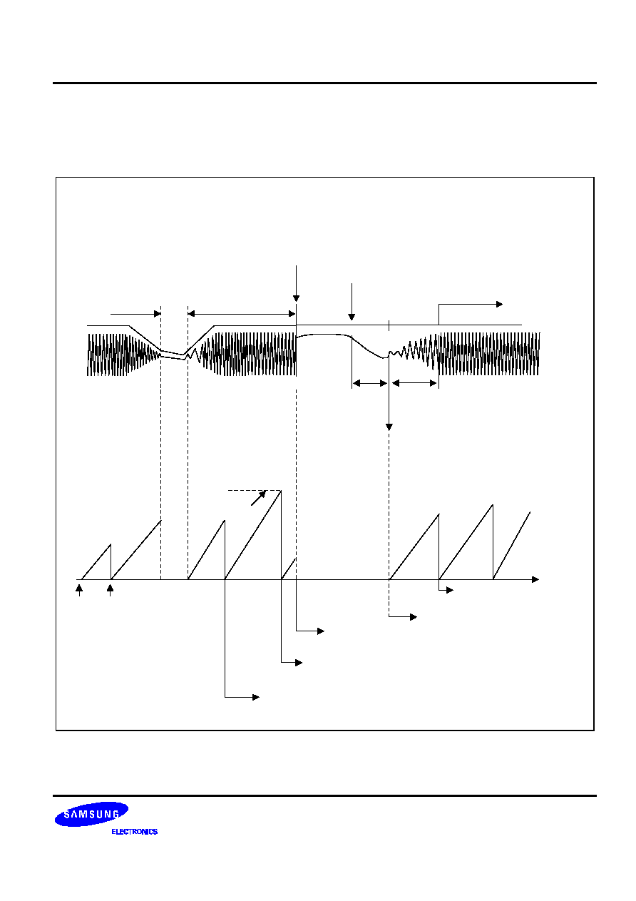
HALT MODE
The HALT mode is used to reduce power consumption by stopping the clock and holding the states of all internal
operations fixed. This mode is very useful in battery-powered instruments. It also holds the controller in wait
status for external stimulus to start some event. The S3C1840 can be halted by programming the P2.12 pin high,
and by forcing P0 input pins (P0.0-P0.3) to high and P1 input pins (P1.0-P1.3) to high, concurrently (See Figure
1-16). When in HALT mode, the internal circuitry does not receive any clock signal, and all P2, P3 output pins
become low states. However, P2.1 and P2.6 pins retain their programmed values until the device is re-started as
follows:
∑
∑
Forcing any P0 and P1 input pins to low : system reset occurs and it continues to operate from the reset
address.
An oscillation stabilization time of 13 msec in fxx = 455 kHz crystal oscillation is needed for stability (See Figure
1-17).
P0.3-P0.0
P1.3-P1.0
V
DD
4
Internal P2.12
Internal
HALT
System reset
4
Figure 1-16. Block Diagram of HALT Logic
Normal Mode
HALT mode
HALT mode
X'tal
13 msec (Minimum)
120
µ
sec (Typical)
HALT
Figure 1-17. Release Timing for HALT or RESET to Normal Mode in Crystal Oscillation

S3C1840
1-17
RESET
All reset operations are internal in the S3C1840. It has an internal power-on reset circuit consisting of a 7 pF
capacitor and a 1 M
resistor (See Figure 1-18). The controller also contains an auto-reset circuit that resets the
chip every 131,072 oscillator clock cycles (288 ms at a fxx = 455 kHz clock frequency). The auto-reset counter is
cleared by the rising edge of a internal P2.0 pin, by HALT, or by the power-on reset pulse (See Figure 1-19).
Therefore, no clocks are sent to the counter and the time-out is suspended in HALT mode. When a reset occurs
during program execution, a transient condition occurs. The PA register is immediately initialized to 0FH. The
PC, however, is not reset to 0H until one instruction cycle later. For example, if PC is 1AH when a reset pulse is
generated, the instruction at 0F1AH is executed, followed by the instruction at 0F00H.
After a reset, approximately 13 msec is needed before program execution proceeds (assuming fxx = 455 kHz
ceramic oscillation).
Upon initialization, registers are set as follows:
∑
∑
PC register to 0 in next instruction cycle
∑
∑
PA and PB registers to 0FH (15th page)
∑
∑
SF and SL registers to 1
∑
∑
HL registers to unknown state
∑
∑
All internal/external output pins (P3.0-P3.3, P2.0/REM-P2.6, P2.9, P2.10, P2.12 and P2.13) to low.
1 M
V
DD
V
SS
S3C1840
7 pF
Figure 1-18. S3C1840's Power-on Reset Circuit

S3C1840
1-18
System Reset
Internal
HALT
The Auto-Reset Counter is cleared every 131,072/fxx (288 msec if fxx is 455 KHz).
Power-on Reset
Auto-Reset Counter
Internal
HALT
Internal P2.0
fxx
CLK
CLR
Figure 1-19. Auto Reset Block Diagram
OSC DIVIDE OPTION CIRCUIT
The OSC Divide Option Circuit provides a maximum 1MHz fxx system clock. f
OSC
which is generated in
oscillation circuit is divided eight or non-divide in this circuit to produce fxx. This dividing ratio will be chosen by
mask option. (See Figure 1-20)
f
OSC
: Oscillator clock
fxx : System clock (f
OSC
or f
OSC
/8)
f
CPU
: CPU clock (f
CPU
= fxx/6)
1 instruction cycle clock
X
I
X
O
f
OSC
Mask Option
OSC
DIVIDE-8
f
XX
Figure 1-20. S3C1840 OSC Divide Option Circuit

S3C1840
1-19
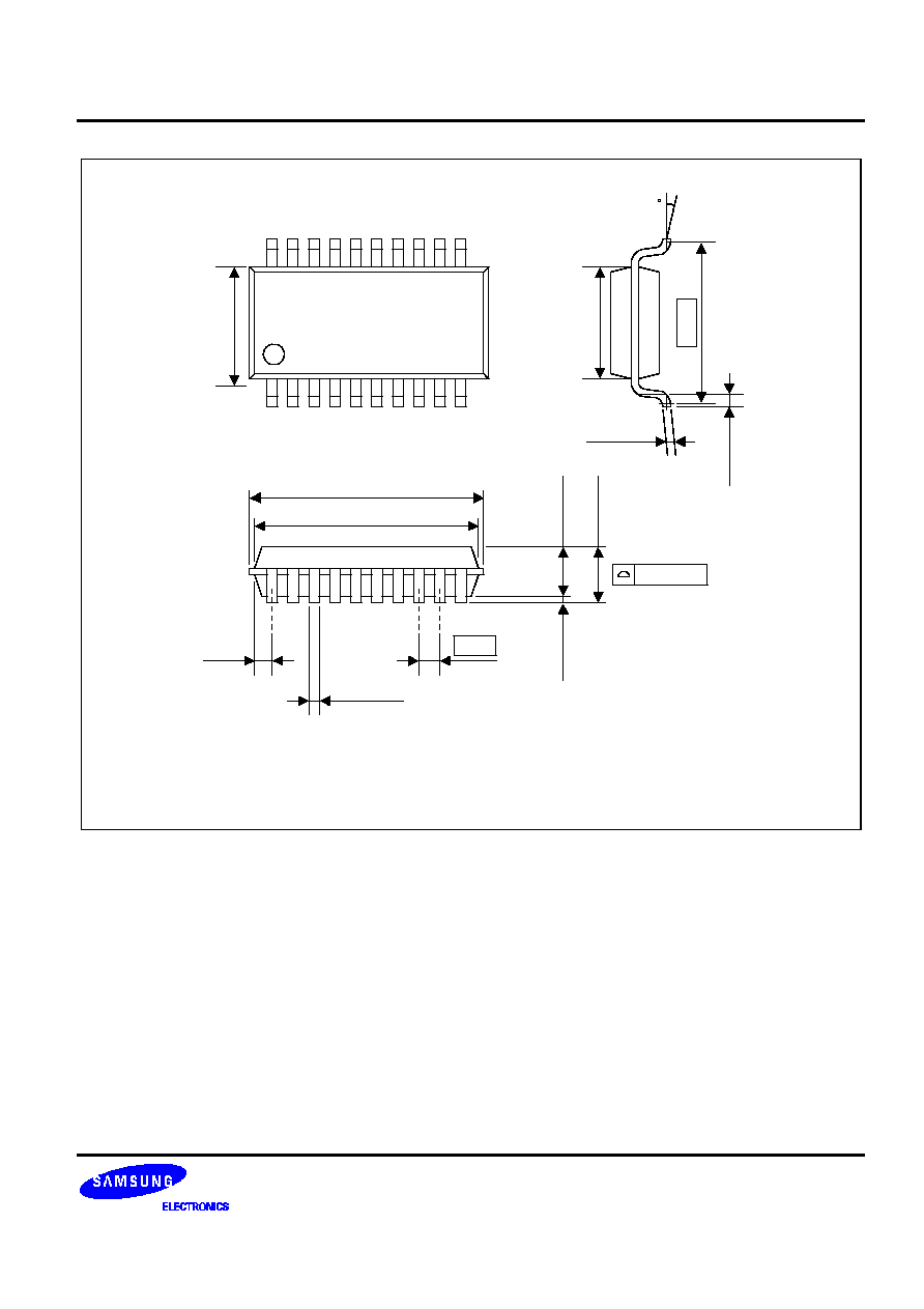
PACKAGE DIMENSIONS
NOTE: Dimensions are in millimeters.
24-SOP-375
10.30
±
0
.30
#13
#24
#1
#12
15.74 MAX
15.34
± 0.20
(0.69)
0-8
0.15
+ 0.10
- 0.05
9.53
7.50
±
0.20
0.85
±
0.20
0.05 MIN
2.30
±
0.10
2.50 MAX
0.38
0.10 MAX
+ 0.10
- 0.05
1.27
Figure 1-21. 24-SOP-375

S3C1840
1-20
NOTE: Dimensions are in millimeters.
20-SOP-375
10.30
±
0
.30
#11
#20
#1
#10
13.14 MAX
12.74
±
0.20
(0.66)
0-8
0.203
+ 0.10
- 0.05
9.53
7.50
±
0.20
0.85
±
0.20
0.05 MIN
2.30
±
0.10
2.50 MAX
0.40
0.10 MAX
+ 0.10
- 0.05
1.27
Figure 1-22. 20-SOP-375
S3C1840
1-21
NOTE: Dimensions are in millimeters.
20-SOP-300
7.80
±
0
.30
#11
#20
#1
#10
14.10 MAX
13.70
± 0.20
(1.14)
0-8
0.20
+ 0.10
- 0.05
7.62
5.40
±
0.20
0.60
±
0.20
0.05 MIN
1.70
±
0.10
2.00 MAX
0.40
0.10 MAX
+ 0.10
- 0.05
1.27
Figure 1-23. 20-SOP-300

S3C1840
1-22
NOTE: Dimensions are in millimeters.
26.80 MAX
26.40
± 0.20
(1.77)
20-DIP-300A
6.40
±
0
.20
#20
#1
0.46 ±
0.10
1.52 ±
0.10
#11
#10
0-15
0.25
+ 0.10- 0.05
7.62
2.54
0.51 MIN
3.30
±
0.30
3.25
±
0.20
5.08 MAX
Figure 1-24. 20-DIP-300A

5. INSTRUCTION SET

S3C1840/C1850/C1860/P1860
INSTRUCTION SET
5-1
INSTRUCTION SET DESCRIPTION
Abbreviations and symbols table specifies internal architecture, instruction operand and operational symbols.
As mentioned before, JP and CALL instructions are executed normally only when SF is high. If SF is low, the
program executes NOP instruction instead of them and sets SF to high. And then, the program executes a next
instruction. In addition, JPL and CALL are long jump and long call instructions which consists of PAGE and
JP/CALL instructions.
Table 5-1. Abbreviations and Symbols
Symbol
Description
Symbol
Description
L
L register (4 bits)
SF
Status Flag
A
Accumulator (4 bits)
P3
P4-output
(L)
The contents of the L register
P0
P0 input (4 bits)
(A)
The contents of the accumulator
D
Any binary number
SL
Status latch (1 bit)
DST
Destination operand
PB
Page buffer register (4 bits)
C
Carry Flag
PA
Page address register (4bits)
SRC
Source operand
P2
P2-output
REG
Register
PC
Program counter
Transfer
SR
Stack register
+
Addition or increment by 1
H
H register
Equal or less than
M
RAM addressed by H and L registers
( )
The complement of the contents
(H)
The contents of the H register
@
Indirect register address prefix
M (H,L)
The contents of the RAM addressed by H,L
#n
Constant n (immediate 3or 4-bit data)
b
Bit address of the RAM [(H,L)] addressed
by H,L
Is exchanged with
Not equal to
-
Subtract or decrement by 1

INSTRUCTION SET
S3C1840/C1850/C1860/P1860
5-2
Table 5-2. Instruction Set Summary
Mnemonic
Operand
Description
MOV Instructions
MOV
MOV
MOV
MOV
MOV
MOV
MOV
MOV
MOV
MOV
MOVZ
XCH
PAGE
L,A
A,L
@HL,A
A,@HL
L,@HL
@HL+,A
@HL-,A
L,#n
H,#n
@HL+,#n
@HL,A
@HL,A
#n
Move A to register L
Move L register to A
Move A to indirect data memory
Move indirect data memory to A
Move indirect data memory to register L
Move A to indirect data memory and increment register L
Move A to indirect data memory and decrement register L
Move immediate data to register L
Move immediate data to register H
Move immediate data to indirect data memory and increment register L
Move A to indirect data memory and clear A
Exchange A with indirect data memory
Set PB register to n
Program Control Instructions
CPNE
CPNZ
CPNE
CPNE
CPLE
CPNZ
CPBT
JP
CALL
RET
@HL,A
@HL
L,A
L,#n
A,@HL
P0
@HL,b
dst
dst
Compare A to indirect data memory and set SF if not equal
Set SF if indirect data memory
Compare A to register L, set SF and SL if not equal
Compare immediate data to register L and set SF if not equal
Set SF if A is less than or equal to indirect data memory
Set SF if A is less than or equal to indirect data memory
Test indirect data memory bit and set SF if indirect bit is one
Jump if SF flag is set
Call subroutine if SF is set
Return from subroutine
I/O Instructions
SETB
CLRB
IN
OUT
P2.(L)
P2.(L)
A,P0
P3,@SL+A
Set bit
Clear bit
Input P0 to A
Output A to P4-PLA output port
Logical Instructions
NOTI
NOT
CLR
A
H
A
Complement A and increment A
Complement MSB of H register
Clear
Arithmetic Instructions
ADDS
ADDS
SUBS
INCS
INCS
INCS
DECS
DECS
DECS
A,@HL
A,#n
A,@HL
A,@HL
L
A
A
A,@HL
L
Add indirect data memory to A
Add immediate data to A
Subtract A from indirect data memory
Increment indirect data memory and load the result in A
Increment register L
Increment A
Decrement A
Decrement indirect data memory and load the result in A
Decrement register L
Bit Manipulation Instruction
SETB
CLRB
@HL.b
@HL.b
Set indirect data memory bit
Clear indirect data memory bit

S3C1840/C1850/C1860/P1860
INSTRUCTION SET
5-3
Lower Nibble (Hex)
Upper Nibble (Hex)
CPNE
@HL,A
CPLE
A,@HL
CPNE
L,A
XCH
@HL,A
DECS
L
INCS
L
ADDS
A,@HL
DECS
A,@HL
IN
A,P0
NOT
H
OUT
P3,@SL+A
CLRB
P2.(L)
SETB
P2.(L)
CPNZ
P0
RET
PAGE
#n
MOV
L,A
MOV
A,@HL
MOV
L,@HL
MOV
A,L
MOV
@HL-,A
MOV
@HL+,A
MOVZ
@HL,A
MOV
@HL,A
MOV
H,#n
SETB
@HL.b
CLRB
@HL.b
CPBT
@HL.b
MOV
L,#n
MOV
@HL+#N
INCS
A
JP
JP
JP
JP
CALL
CALL
CALL
CALL
CPNE
L,#n
SUBS
A,@HL
NOTI
A
INCS
A,@HL
CPNZ
@HL
ADDS
A,#n
DECS
A
ADDS
A,#n
CLR
A
0
1
3
4
5
6
2
8
9
A
B
C
D
E
F
7
0
1
3
4
5
6
2
8
9
A
B
C
D
E
F
7
Figure5-1. KS51 Opcode Map
INSTRUCTION SET
S3C1840/C1850/C1860/P1860
5-4
MOV
L,A
Binary Code:
0 0 1 0
0 0 0 0
Description:
The contents of the accumulator are moved to register L.
The contents of the source operand are not affected.
Operation:
(L)
(A)
Flags:
SF : Set to one
SL : Unaffected
Example:
CLR
A
; Clear the contents of A
MOV
L,A
; Move 0H to REG L
MOV A,L
Binary Code:
0 0 1 0
0 0 1 1
Description:
The contents of register L are moved to the accumulator.
The contents of the source operand are not affected.
Operation:
(A)
(L)
Flags:
SF : Set to one
SL : Unaffected
Example:
MOV
L,#3H
; Move 3H to REG L
MOV
A,L
; Move 0H to A
MOV @HL,A
Binary Code:
0 0 1 0
0 1 1 1
Description:
The contents of the accumulator are moved to the data memory whose address is
specified by registers H and L.
The contents of the source operand are not affected.
Operation:
M [(H,L)]
(A)
Flags:
SF : Set to one
SL : Unaffected
Example:
CLR
A
; Clear the contents of A
MOV
H,#0H
; Move 0H to REG H
MOV
L,#3H
; Move 3H to REG L
MOV
@HL,A
; Move 0H to RAM address 03H

S3C1840/C1850/C1860/P1860
INSTRUCTION SET
5-5
MOV A,@HL
Binary Code:
0 0 1 0
0 0 0 1
Description:
The contents of the data memory addressed by registers H and L are moved to
accumulator.
The contents of the source operand are not affected.
Operation:
(A)
M [(H,L)]
Flags:
SF : Set to one
SL : Unaffected
Example:
Assume HL contains 04H
MOV
A,@HL
; Move contents of RAM addressed 04H to A
MOV L,@HL
Binary Code:
0 0 1 0
0 0 1 0
Description:
The contents of the data memory addressed by registers H and L are moved to register L.
The contents of the source operand are not affected.
Operation:
(L)
M [(H,L)]
Flags:
SF : Set to one
SL : Unaffected
Example:
Assume Hl contains 04H
MOV
L,@HL
; Move contents of RAM address 4H to REG L
CPNE
L,#5H
; Compare 5H to REG L values
JP
XX
; jump to XX if REG L value is not 5H
JP
YY
; Jump to YY if REG L value is 5H
MOV @HL+,A
Binary Code:
0 0 1 0
0 1 0 1
Description:
The contents of the accumulator are moved to the data memory addressed by registers
H,L;
L register contents are incremented by one.
The contents of the source operand are not affected.
Operation:
M [(H,L)]
(A), L
L + 1
Flags:
SF : Set if carry occurs; cleared otherwise
SL : Unaffected
Example:
MOV
H,#0H
MOV
L,#0FH
CLR
A
MOV
@HL+A
; Move 0H to RAM address 0FH and increment REG L value
by one
JP
PRT
; jump to PRT, since there is a carry from increment

INSTRUCTION SET
S3C1840/C1850/C1860/P1860
5-6
MOV @HL-A
Binary Code:
0 0 1 0
0 1 0 0
Description:
The contents of accumulator are moved to the data memory addressed by registers H,L;
L register contents are decremented by one.
The contents of the source operand are not affected.
Operation:
M [(H,L)]
(A), L
L - 1
Flags:
SF : Set if no borrow; cleared otherwise
SL : Unaffected
Example:
MOV
H,#0H
MOV
L,#3H
CLR
A
MOV
@HL-,A
JP
ABC
MOV L,#N
Binary Code:
0 1 0 0
d d d d
Description:
The 4-bit value specified by n (data) is loaded into register L.
The contents of the source operand are not affected.
Operation:
(L)
#n
Flags:
SF : Set to one
SL : Unaffected
Example:
MOV
L,#8H
; 8H is moved to REG L
MOV H,#n
Binary Code:
0 0 1 0
1 d d d
Description:
The 3-bit value specified by n (data) is moved to register H.
The contents of the source operand are not affected.
Operation:
(H)
#n
Flags:
SF : Set to one
SL : Unaffected
Example:
MOV
H,#4H
; 4H is moved into REG H

S3C1840/C1850/C1860/P1860
INSTRUCTION SET
5-7
MOV @HL+,#n
Binary Code:
0 1 1 0
d d d d
Description:
The 4-bit value specified by n (data) is moved to data memory addressed by registers H,L;
L register contents are incremented by one.
The contents of the source operand are not affected.
Operation:
M [(H,L)]
#n, L
L + 1
Flags:
SF : Set to one
SL : Unaffected
Example:
MOV
H,#0H
MOV
L,#7H
MOV
@HL+,#9H
; Move 9H to RAM address 07H and increment REG L value
by one, then REG L contains 8H
MOVZ @HL,A
Binary Code:
0 0 1 0
0 1 1 0
Description:
The contents of the accumulator are moved to the data memory addressed by registers
H,L;
accumulator contents are cleared to zero.
Operation:
M [(H,L)]
(A), (A)
0
Flags:
SF : Set to one
SL : Unaffected
Example:
MOV
L,#3H
MOV
A,L
MOVZ
@HL,A
; Move 3H to indirect RAM and clear A to zero
MOV
L,A
; Move 0H to REG L
SETB
P2.(L)
; Set P2.0 to 1
XCH @HL,A
Binary Code:
0 0 0 0
0 0 1 1
Description:
This instruction exchanges the contents of the data memory addressed by registers H and
L with the accumulator contents.
Operation:
M [(H,L)]
(A)
Flags:
SF : Set to one
SL : Unaffected
Example:
MOV
H,#0H
MOV
L,#6H
CLR
A
; Clear A to zero
ADDS
A,#5H
; Add 5H to A
XCH
@HL,A
; Exchange 5H with contents of RAM address 06H

INSTRUCTION SET
S3C1840/C1850/C1860/P1860
5-8
PAGE #n
Binary Code:
0 0 0 1
d d d d
Description:
The immediate 4-bit value specified by n (data) is loaded into the PB register.
Operation:
(PB)
#n
Flags:
SF : Set to one
SL : Unaffected
Example:
PAGE
#3H
; Move 3H to page buffer
JP
AN
; Jump to label AN located at page 3 if SF is one;
otherwise, it is skipped
CPNE @HL,A
Binary Code:
0 0 0 0
0 0 0 0
Description:
The contents of accumulator are compared to the contents of indirect data memory; an
appropriate flag is set if their values are not equal.
The contents of both operands are unaffected by the comparison.
Operation:
M [(H,L)]
(A)
Flags:
SF : Set if not equal, cleared otherwise
SL : Unaffected
Example:
CLR
A
ADDS
A,#3H
MOV
H,#0H
MOV
L,#6H
CPNE
@HL,A
; Acc value 3H is compared to contents of RAM address 06H
JP
OA
; Jump to OA if values of RAM address 06H are not 3h
JP
OB
; Jump to OB if values of RAM address 06H are 3H
S3C1840/C1850/C1860/P1860
INSTRUCTION SET
5-9
CPNZ @HL
Binary Code:
0 0 1 1
1 1 1 1
Description:
This instruction compares the magnitude of indirect data memory with zero, and the
appropriate flag is set if their values are not equal, i.e., if the contents of indirect data
memory are not zero.
The contents of operand are unaffected by the comparison.
Operation:
M [(H,L)]
0
Flags:
SF : Set if not zero, cleared otherwise
SL : Unaffected
Example:
Assume the contents of RAM address are 4H
CPNZ
@HL
; Compare 4H with zero
JP
EQ
; Jump to EQ because the result is not equal
JP
WAIT
CPNE L,A
Binary Code:
0 0 0 0
0 0 1 0
Description:
The contents of the accumulator are compared to the contents of register L; the
appropriate flags are set if their values are not equal.
The contents of both operands are unaffected by the comparison.
Operation:
(L)
(A)
Flags:
SF : Set if not equal, cleared otherwise
SL : Set if not equal, cleared otherwise
Example:
Assume REG L contains 5H, A contains 4H
CPNE
L,A
; Compare A to REG L values
JP
K1
; Jump to K1 because the result is not equal
JP
K2

INSTRUCTION SET
S3C1840/C1850/C1860/P1860
5-10
CPNE L,#n
Binary Code:
0 1 0 1
d d d d
Description:
This instruction compare the immediate 4 bit data n with the contents of register L, and
sets an appropriate flag if their values are not equal.
The contents of both operands are unaffected by the comparison.
Operation:
(L)
#n
Flags:
SF : Set if not equal, cleared otherwise
SL : Unaffected
Example:
CLR
A
ADDS
A,#4H
MOV
L,A
CPNE
L,#5H
; Compare immediate data 5H to REG L values
JP
K3
; Jump to K3 because the result is not equal
CPNE A,@HL
Binary Code:
0 0 0 0
0 0 0 1
Description:
The contents of indirect data memory are compared to the contents of the accumulator.
Appropriate flags are set if the contents of the accumulator are less than or equal to the
contents of indirect data memory.
The contents of both operands are unaffected by the comparison.
Operation:
(A)
M [(H,L)]
Flags:
SF : Set if less than or equal to, cleared otherwise
SL : Unaffected
Example:
Assume RAM address holds 8H
CPLE
A,@HL
; Compare 8H to A values
JP
MAR
; Jump to MAR if 0H
A
8H
JP
BPR
; Jump to BPR if 9H
A
0FH

S3C1840/C1850/C1860/P1860
INSTRUCTION SET
5-11
CPNZ P0
Binary Code:
0 0 0 0
1 1 1 0
Description:
The instruction compares the contents of Port 0 with zero. Appropriate flags are set if their
values are not equal, i.e., if the contents of Port 0 are not zero.
The contents of the operand are unaffected by the comparison.
Operation:
(P0)
0
Flags:
SF : Set if not zero, cleared otherwise
SL : Unaffected
Example:
MOV
L,#0DH
CLRB
P2.(L)
; Clear P2.13, i.e., select P0 input
CPNZ
P0
; Compare P0 to zero
JP
KEYIN
; Jump to KEYIN if P0
0
JP
NOKEY
; Jump to NOKEY if P0 = 0
CPBT @HL,b
Binary Code:
0 0 1 1
1 0 d d
Description:
CPBT tests indirect data memory bit and sets appropriate flags if the bit value is one.
The contents of operand are unaffected by the test.
Operation:
M [(H,L)] = 1
Flags:
SF : Set if one, cleared otherwise
SL : Unaffected
Example:
MOV
H,#0H
MOV
L,#0BH
CPBT
@HL,3
; Test RAM address 0BH bit 3
JP
Q1
; Jump to Q1 if RAM address bit 3 is 1
JP
Q2
; Jump to Q2 if RAM address bit 3 is 0

INSTRUCTION SET
S3C1840/C1850/C1860/P1860
5-12
JP dst
Binary Code:
1 0 d d
d d d d
Description:
The JP transfers program control to the destination address if the SF is one.
The conditional jump replaces the contents of the program counter with the address
indicated and transfers control to that location.
Had the SF flag not been set, control would have proceeded with the next instruction.
Operation:
If SF = 1 ; PC
(W), PA
PB
Flags:
SF : Set to one
SL : Unaffected
Example:
JP
SUTIN1
; This instruction will cause program execution to branch to the
instruction at label SUTIN; SUTIN1 must be within the current
page
CALL dst
Binary Code:
1 1 d d
d d d d
Description:
If the SF flag is set to 1, this instruction calls a subroutine located at the indicated address,
and then pushes the current contents of the program counter to the top of the stack. The
program counter value used is the address of the first instruction following the CALL ins.
The specified destination address is then loaded into the program counter and points to the
first instruction of a procedure. At the end of the procedure, the return (RET) instruction
can be used to return to the original program flow.
Operation:
If SF = 1 ; SRi
PC + 1, PSRi
PA
PC
I (W), PA
PB
Flags:
SF : Set to one
SL : Unaffected
Example:
CALL
ACD1
; CALL subroutine located at the label ACD1 where ACD1
must be within the current page
RET
Binary Code:
0 0 0 0
1 1 1 1
Description:
This instruction is normally used to return to the previously executing procedure at the end
of a procedure entered by a CALL instruction. The contents of the location addressed by
the stack pointer are popped into the program counter. The next statement executed is that
addressed by the new contents of the program counter.
Operation:
PC
Sri, PB
PSRi
PA
PB
Flags:
SF : Set to one
SL : Unaffected
Example:
RET
; Return from subroutine

S3C1840/C1850/C1860/P1860
INSTRUCTION SET
5-13
SETB P2.(L)
Binary Code:
0 0 0 0
1 1 0 1
Description:
This instruction sets the Port 2 bit addressed by register L without affecting any other bits in
the destination.
Operation:
P2.(L)
1
Flags:
SF : Set to one
SL : Unaffected
Example:
MOV
L,#0H
SETB
P2.(L)
; Set P2.0 to 1
CLRB P2.(L)
Binary Code:
0 0 0 0
1 1 0 0
Description:
This instruction clears the Port 2 bit addressed by register L without affecting any other bits
in the destination.
Operation:
P2.(L)
0
Flags:
SF : Set to one
SL : Unaffected
Example:
MOV
L,#0H
CLRB
P2.(L)
; Clear P2.0 to 0
IN A,P0
Binary Code:
0 0 0 0
1 0 0 0
Description:
Data present on Port n is transferred (read) to the accumulator.
Operation:
(A)
(Pn) (n = 0,1)
Flags:
SF : Set to one
SL : Unaffected
Example:
IN
A,P0
; Input port 0 data to Acc
MOV
L,A
CPNE
L,#3H
JP
OX
; Jump to OX if port 0 data
3H
JP
QP
; Jump to QP if port 0 data = 3H

INSTRUCTION SET
S3C1840/C1850/C1860/P1860
5-14
OUT P3,@SL+A
Binary Code:
0 0 0 0
1 0 1 0
Description:
The contents of the accumulator and SL are transferred to the P3 Output register.
Operation:
(P3 Output register)
(A) + (SL)
Flags:
SF : Set to one
SL : Unaffected
Example:
CLR
A
OUT
P3,@SL+A
; Zero output on port 3
NOTI A
Binary Code:
0 0 1 1
1 1 0 1
Description:
The contents of the accumulator are complemented; all 1 bits are changed to 0, and vice-
versa, and then incremented by one.
Operation:
(A)
(A),
(A)
(A) +1
Flags:
SF : Set if the result is zero, cleared otherwise
SL : Unaffected
Example:
CLR
A
ADDS
A,#7H
NOTI
A
; Complement 7H (0111B) and increment the result by one;
the instruction NOTI A then leaves 9H (1001B) in A

S3C1840/C1850/C1860/P1860
INSTRUCTION SET
5-15
NOT H
Binary Code:
0 0 0 0
1 0 0 1
Description:
The MSB of register H is complemented,
Operation:
(H)
(H)
Flags:
SF : Set to one
SL : Unaffected
Example:
MOV
H,#4H
NOT
H
; Complement 4H (100B), then it leaves 00H (000B) in REG H
CLR A
Binary Code:
0 1 1 1
1 1 1 1
Description:
The contents of the accumulator are cleared to zero (all bits set on zero).
Operation:
(A)
0
Flags:
SF : Set to one
SL : Unaffected
Example:
CLR
A
; A value are cleared to zero
ADDS A,@HL
Binary Code:
0 0 0 0
0 1 1 0
Description:
ADDS adds the contents of indirect data memory to accumulator, leaving the result in the
accumulator.
The contents of the source operand are unaffected.
Operation:
(A)
M [(H,L)] + (A)
Flags:
SF : Set if a carry occurred, cleared otherwise
SL : Unaffected
Example:
Assume RAM address holds 5H
CLR
A
; Clear A to zero
ADDS
A,@HL
; This instruction will leaves 5H in A

INSTRUCTION SET
S3C1840/C1850/C1860/P1860
5-16
ADDS A,#n
Binary Code:
0 1 1 1
d d d d
Description:
The specified 4-bit data n is added to the accumulator and the sum is stored in the
accumulator.
Operation:
(A)
(A) + #n
Flags:
SF : Set if a carry occurred, cleared otherwise
SL : Unaffected
Example:
CLR
A
; Clear A to zero
ADDS
A,#4H
; Add 4H to A, it leaves 4H in A
SUBS A,@HL
Binary Code:
0 0 1 1
1 1 0 0
Description:
SUBS subtracts the contents of accumulator from the contents of indirect data memory,
leaving the result in the accumulator.
The contents of source operand are unaffected.
Operation:
(A)
M [(H,L)] - (A)
Flags:
SF : Set if no borrow occurred, cleared otherwise
SL : Unaffected
Example:
Assume RAM address holds 0CH
MOV
L,#8H
MOV
A,L
SUBS
A,@HL
; Subtract A from 0CH; it will leave 4H in A
INCS A,@HL
Binary Code:
0 0 1 1
1 1 1 0
Description:
The contents of indirect data memory are incremented by one and the result is loaded into
the accumulator.
The contents of indirect data memory are unaffected.
Operation:
(A)
M [(H,L)] + 1
Flags:
SF : Set if a carry occurred, cleared otherwise
SL : Unaffected
Example:
Assume RAM address holds 6H
CLR
A
; Clear A to zero
INCS
A,@HL
; Increment 6H by one and leave 7H in A

S3C1840/C1850/C1860/P1860
INSTRUCTION SET
5-17
INCS L
Binary Code:
0 0 0 0
0 1 0 1
Description:
The contents of the L register are incremented by one.
Operation:
(L)
(L) + 1
Flags:
SF : Set if a carry occurred, cleared otherwise
SL : Unaffected
Example:
MOV
L,#5H
INCS
L
; Increment REG L value 5H by one
INCS A
Binary Code:
0 1 1 1
0 0 0 0
Description:
The contents of the accumulator are incremented by one.
Operation:
(A)
(A) + 1
Flags:
SF : Set if no borrow occurred, cleared otherwise
SL : Unaffected
Example:
MOV
L,#5H
MOV
A,L
INCS
A
; Increment 5H by one
DECS A
Binary Code:
0 1 1 1
0 1 1 1
Description:
The contents of the accumulator are decremented by one.
Operation:
(A)
(A) - 1
Flags:
SF : Set if a carry occurred, cleared otherwise
SL : Unaffected
Example:
MOV
L,#0BH
MOV
A,L
DECS
A
; The instruction leaves the value 0AH in A
INSTRUCTION SET
S3C1840/C1850/C1860/P1860
5-18
DECS A,@HL
Binary Code:
0 0 0 0
0 1 1 1
Description:
The contents of the data memory addressed by the H and L registers are decremented by
one and the result is loaded in the accumulator.
But the contents of data memory are not affected.
Operation:
(A)
M [(H,L)] - 1
Flags:
SF : Set if a carry occurred, cleared otherwise
SL : Unaffected
Example:
Assume RAM address holds 5h
MOV
L,#0AH
MOV
A,L
DECS
A,@HL
; Decrement the value 5H by one, and the result value 4H is
loaded in A
DECS L
Binary Code:
0 0 0 0
0 1 0 0
Description:
The contents of the L register are decremented by one.
Operation:
(L)
(L) - 1
Flags:
SF : Set if no borrow occurred, cleared otherwise
SL : Unaffected
Example:
MOV
L,#3H
DECS
L
; This instruction leaves the value 2H in REG L
SETB @HL,b
Binary Code:
0 0 1 1
0 0 d d
Description:
This instruction sets indirect data memory bit addressed by registers H and L without
affecting any other bits in the destination.
Operation:
b
1 (b = 0,1,2,3)
Flags:
SF : Set to one
SL : Unaffected
Example:
MOV
H,#0H
MOV
L,#5H
SETB
@HL.2
; Set RAM address 05H bit 2 to 1

S3C1840/C1850/C1860/P1860
INSTRUCTION SET
5-19
DECS A,@HL
Binary Code:
0 0 1 1
0 1 d d
Description:
This instruction clears the indirect data memory bit addressed by registers H and L without
affecting any other bits in the destination.
Operation:
b
1 (b = 0,1,2,3)
Flags:
SF : Set to one
SL : Unaffected
Example:
MOV
H,#0H
MOV
L,#5H
CLRB
@HL.3
; Clear RAM address 05H bit 3 to zero

6. DEVELOPMENT TOOLS


S3C1840/C1850/C1860/P1860
DEVELOPMENT TOOLS
6-1
SMDS
The Samsung Microcontroller Development System, SMDS is a complete PC-based development environment
for S3C1840/C1850/C1860 microcontroller. The SMDS is powerful, reliable, and portable. The SMDS tool set
includes a versatile debugging utility, trace with built-in logic analyzer, and performance measurement
applications.
Its window-oriented program development structure makes SMDS easy to use. SMDS has three components:
-- IBM PC- compatible SMDS software, all device-specific development files, and the SAMA assembler.
-- Development system kit including main board, personality board, SMDS manual, and target board adapter,
if required.
-- Device-specific target board.
SMDS PRODUCT VERSIONS
As of the date of this publication, two versions of the SMDS are being supported:
-- SMDS Version 4.8 (S/W) and SMDS Version 3.6 (H/W); last release: January, 1994.
-- SMDS2 Version 5.3 (S/W) and SMDS2 Version 1.3 (H/W); last release: November, 1995.
The new SMDS2 Version 1.3 is intended to replace the older Version 3.6 SMDS. The SMDS2 contains many
enhancements to both hardware and software. These development systems are also supported by the personality
boards of Samsung's microcontroller series: S3C1, S3C7, and S3C8.
SAMA ASSEMBLER
The Samsung Arrangeable Microcontroller (SAM) Assembler, SAMA, is a universal assembler, and generates
object code in standard hexadecimal format.
Compiled program code includes the object code that is used for ROM data and required SMDS program control
data. To compile programs, SAMA requires a source file and an auxiliary definition (DEF) file with device-specific
information.
TARGET BOARDS AND PIGGYBACKS
Target boards are available for S3C1840/C1850/C1860 microcontroller. All required target system cables and
adapters are included with the device-specific target board.
Piggyback chips are provided to customers in limited quantities for S3C1840/C1850 microcontroller. The
S3C1840/C1850 piggyback chips, PB51840-20 and PB51840/51850-24 are now available.

DEVELOPMENT TOOLS
S3C1840/C1850/C1860/P1860
6-2
PB51840-20 is 20 DIP piggyback chip for 20 DIP, 20 SOP package device of S3C1840 microcontroller.
PB51840/51850-24 is 24DIP piggyback chip for 24 SOP package device of S3C1840/C1850 microcontroller.
IBM-PC
or
Compatiable
Internal Bus
5-Volt
Power
Supply
Main Board
Personality
Board
Front
Panel
Board
RS-232C
SMDS2
POD
Target Board
Target
Application
System
Target Cable
Figure 6-1. SMDS Product Configuration (SMDS2)

S3C1840/C1850/C1860/P1860
DEVELOPMENT TOOLS
6-3
TB51840/51850A TARGET BOARD
The TB51840/51850A target board is used for the S3C1840/C1850/C1860 microcontroller. It is supported by the
SMDS2 development system only.
25
TB51840/51850A/51860
SM1243A
1
CN1
To User_Vcc
Off
On
Reset 1
U5
U4
GND
V
CC
U5
U6
1
64
64 SDIP
KS51899
EVA CHIP
U1
32
33
J102
J101
P2
OFF
ON
RA3
RA1
RA2
+
+
+
P2.6
P2.5
P2.4
+
+
+
+
P2.3
P2.2
P2.1
P2.0
Figure 6-2. TB51840/51850A Target Board Configuration

DEVELOPMENT TOOLS
S3C1840/C1850/C1860/P1860
6-4
Table 6-1. Power Selection Settings for TB51840/51950A
'To User_Vcc' Settings
Operating Mode
Comments
To User_Vcc
ON
OFF
Target
System
SMDS2
TB51840/
51850A
V
CC
V
SS
V
CC
The SMDS2 supplies V
CC
to
the target board (evaluation
chip) and the target system.
To User_Vcc
ON
OFF
Target
System
SMDS2
TB51840/
51850A
V
CC
V
SS
V
CC
External
The SMDS2 supplies V
CC
only
to the target board (evaluation
chip). The target system must
have its own power supply.
LED 2.0-LED 2.6:
These LEDs are used to display value of the P2.0-P2.6. It will be turn on, if the value is Low.
P2 Option Switch:
Switch ON: You can see the port value using the LED display.
Switch OFF: You can't see the port value. That is, the LED won't be turn ON by the port value.

S3C1840/C1850/C1860/P1860
DEVELOPMENT TOOLS
6-5
24
23
22
21
20
19
18
17
16
15
J101
24-DIP SOCKET
2
3
4
5
6
7
8
9
1
14
13
10
11
12
V
SS
X
IN
X
OUT
P2.6
P0.0
P0.1
P0.2
P0.3
P1.0
P1.2
P1.3
P1.1
V
SS
X
IN
X
OUT
P0.0
P0.1
P0.2
P0.3
P1.0
P1.2
P1.3
P1.1
P2.6
Figure 6-3. 24 DIP Socket for TB51840/51850A (S3C1840/C1850, 24 SOP)
Target Board
24-DIP SOCKET
Target System
J101
Target Cable for 24 DIP Package
Part Name: AS24D
Order Code: SM6303
1
24
12
13
1
24
12
13
Figure 6-4. TB51840/51850A Cable for 24 DIP Package
DEVELOPMENT TOOLS
S3C1840/C1850/C1860/P1860
6-6
J102
P0.0
P0.1
P0.2
P0.3
P1.0
P1.1
P3.3
P2.2
P2.3
P2.4
P3.0
P3.1
P3.2
P2.1
20-DIP SOCKET
V
SS
X
IN
X
OUT
V
DD
P2.0/REM
TEST
1
2
3
4
5
6
7
8
9
10
11
12
13
14
15
16
17
18
19
20
Figure 6-5. 20 DIP Socket for TB51840A (S3C1840/C1860, 20 DIP, 20 SOP)
Target Board
20-DIP SOCKET
Target System
J101
Target Cable for 20 DIP Package
Part Name: AS20D
Order Code: SM6304
1
20
10
11
1
20
10
11
Figure 6-6. TB51840A Cable for 20 DIP Package

7. REMOTE CONTROL Tx. APPLICATION NOTE


S3C1840/C1850/C1860/P1860
REMOTE CONTROL TX. APPLICATION NOTE
7-1
DESCRIPTION OF THE S3C1840/C1850/C1860 MCUS
The S3C1840/C1850/C1860 4-bit single-chip CMOS microcontroller is designed using the reliable SMCS-51 CPU
core with on-chip ROM and RAM. An auto-reset circuit generates a
RESET
pulse in regular intervals, and can be
used to initiate a Halt mode release. The S3C1840/C1850/C1860 microcontroller is intended for use in small
system control applications that require a low-power and cost-sensitive design solution. In addition, the
S3C1840/C1850/C1860 has been optimized for remote control transmitters.
FEATURES
Table 7-1. S3C1840/C1850/C1860 Features
Feature
S3C1840
S3C1850
S3C1860
ROM
1024 bytes
1024 bytes
1024 bytes
RAM
32 x 4 bits
32 x 4 bits
32 x 4 bits
Carrier frequency
fxx/12, fxx/8, no carrier
fxx/12, fxx/8, no carrier
fxx/12, fxx/8, no carrier
Operating voltage
250 kHz
f
OSC
3.9 MHz
1.8 V to 3.6 V,
3.9 MHz < f
OSC
< 6 MHz
2.2 V to 3.6 V
250 kHz
f
OSC
3.9MHz
1.8 V to 3.6 V,
3.9 MHz < f
OSC
< 6 MHz
2.2 V to 3.6 V
250 kHz
f
OSC
3.9 MHz
1.8 V to 3.6 V,
3.9 MHz < f
OSC
< 6 MHz
2.2 V to 3.6 V
Low-Level Output
Current P2.0 (IOL1)
Typ. 3.0mA (at VO=0.4V)
Typ. 210mA (at VO=0.4V)
Typ. 280mA (at VO=0.4V)
Typ. 260mA (at VO=0.5V)
Typ. 320mA (at VO=0.5V)
Package
24 SOP, 20 SOP/DIP
24 SOP
20 SOP/DIP
Piggyback
O
O
x
OTP
x
x
O
(S3P1860:divide-8 only)
Tr. for I.R.LED drive
x
Built-in
Built-in
Power on reset circuit
Built-in
Built-in
x
Oscillation Start and
reset circuit (OSR)
x
x
Built-in
Table 7-2. S3C1840/C1850/C1860 Package Types
(note)
Item
24 pins
20 pins
Package
24 SOP-375
20 DIP-300A
20 SOP-300
20 SOP-375
NOTE : The S3C1850 has 24 pin package type only and S3C1860/S3P1860 has 20 pin package type only.

REMOTE CONTROL TX. APPLICATION NOTE
S3C1840/C1850/C1860/P1860
7-2
Table 7-3. S3C1840/C1850/C1860 Functions
Description
Automatic reset by Halt mode
release
When Halt mode is released, the chip is reset after an oscillator stabilization
interval of 9 ms. (fxx = 455 kHz)
Output pin state retention
function
When the system enters Halt Mode,
P3.0-P3.3, P2.0, and P2.2-P2.5 go low level in 24 pins.
P3.0-P3.3, P2.0, and P2.2-P2.4 go low level in 20 pins.
But the P2.0 is floating state in S3C1850/C1860. (NOTE)
Auto-reset
With oscillation on and with no change to the IP2.0 output pin, a reset is
activated every 288 ms at fxx = 455 kHz.
Osc. Stabilization time
CPU instructions are executed after oscillation stabilization time has elapsed.
Other functions
Carrier frequency generator. Halt wake-up function.
NOTE : The S3C1850 has 24 pin package type only and S3C1860 has 20 pin package type only.
RESET
The S3C1840/C1850 has three kinds of reset operations:
-- POR (Power-On Reset)
-- Auto-reset
-- Automatic reset by Halt release
The S3C1860 has three kinds of reset operations;
-- OSR (Oscillation Start and Reset)
-- Auto-reset
-- Automatic reset by Halt release
Power-On Reset Circuits
7 pF
1 M
0.3 V
DD
2.2 V
V
DD
RESET
Reset Time
Figure 7-1. Power-On Reset Circuits
S3C1840/C1850/C1860/P1860
REMOTE CONTROL TX. APPLICATION NOTE
7-3
Auto-Reset
The auto-reset function resets the CPU every 131,072 oscillator cycles (288 ms at fxx = 455 kHz). The auto-reset
counter is cleared when a rising edge is detected at IP2.0, or by a
HALT
or
RESET
pulse.
Normal Mode
Halt
Halt Release Signal
IP2.12 = 1, Non-Active Input Pin
f
XX
= 455 kHz
Osc. Stabilization Time
(9 ms)
Osc. Circuit
Wait Time
(3-4 ms)
X
O
Osc. Stabilization counter starts
Auto-reset
counter
Chip restarts and auto-reset
counter is incremented.
Chip holds it's internal status.
Upon entering Halt mode, the auto-reset counter is
cleared to zero.
Systerm reset occurs when the auto-reset counter
overflows. The program restarts from 0F00hH
Overflow
IP2.0
IP2.0
Normal Mode:
After a reset, the program restart
from 0F00H after one instruction in
0FxxH is executed.('F' is page
number and 'xx' is the next
instruction of HALT instruction)
Chip restarts and the auto-reset counter is incremented
(Reset by internal POR or OSR)
Abnormal
status
V
DD
Figure 7-2. Auto-Reset Counter Function
NOTE : The OSR(Oscillation Start and reset) is not implemented for the S3C1840/C1850.

REMOTE CONTROL TX. APPLICATION NOTE
S3C1840/C1850/C1860/P1860
7-4
Automatic Reset by Halt Mode Release
This function resets the CPU by releasing Halt mode. The CPU is reset to its initial operating status and program
execution starts from the reset address.
Halt Mode and Automatic Reset by Halt Release
Halt mode is used to reduce power consumption by stopping the oscillation and holding the internal state. Halt
mode can be entered by forcing IP2.12 to high level (remaining input pins are non-active).
Before entering Halt mode, programmer should pre-set all key strobe output pins to active state even though Halt
mode causes some pins to remain active.
For the 24 pins, P3.0-P3.3, P2.0, P2.2- P2.4, and P2.5 are sent low and for 20 pins, P3.0-P3.3, P2.0, P2.2-P2.4
are sent low, but the P2.0 is floating state in S3C1850/C1860.. Forcing any key input port to active state causes
the clock oscillation logic to start system initialization.
At this time, the system is reset after the oscillation stabilization time elapses. A system reset causes program
execution to start from address 0F00H.
Normal Mode:
After a reset, the program
restarts from 0F00H after one
instruction in 0FxxH is
executed.('F' is page number
and 'xx' is the instruction
immediately following the
HALT instruction.)
Halt Release Signal
IP2.12 = 1, Non-Active Input Pin
Normal Mode
Halt
X
O
Osc. Circuit
Wait Time
(3-4 ms)
Osc. Stabilization Timer Start
Osc. Stabilization Timer
(9 ms)
fxx = 455 kHz)
Figure 7-3. Reset Timing Diagram

S3C1840/C1850/C1860/P1860
REMOTE CONTROL TX. APPLICATION NOTE
7-5
HALT mode programming
The S3C1840/C1850/C1860 can enter Halt mode by setting the IP2.12 pin to high level and forcing P0 and P1
input to a normal state. If IP 2.12 is high and any input is active, the chip cannot enter Halt mode. Therefore, the
next instruction is executed, which must be a clear command for IP2.12.
MOV
L,#5
KEYOLO
CLRB P2.(L)
; P2.5,4,3,2,
Low
DECS L
CPNE L,#1
JP
KEYOLO
CLR
A
; A
CC
.
#0h
OUT
P3,@SL+A
; P3.0,1,2,3,
Low
MOV
L,#0DH
CLRB P2.(L)
; Select the P0 input
IN
A,P0
INCS
A
; P0 input check
JP
.+2
JP
KEYCHK
; If any key pressed in P0, jump to KEYCHK routine
SETB P2.(L)
; Select the P1 input
timea IN
A,P0
INCS
A
; P1 input check
JP
+ 2
timeb JP
KEYCHK
; If any key pressed in P1, jump to KEYCHK routine
MOV
L,#0CH
; No key pressed
SETB P2.(L)
; Halt mode
; When no key is pressed, the chip enters Halt mode. Pressing any key while in Halt mode causes the chip to be
initialized and restarted from the reset address.
; If any key is pressed between time A and time B, the following instruction is executed.
MOV
L,#0CH
; These two instructions remove the condition of re-entering
CLRB P2,(L)
; Halt mode.

REMOTE CONTROL TX. APPLICATION NOTE
S3C1840/C1850/C1860/P1860
7-6
RESET
RESET
and
HALT
HALT
Logic Diagram
IP2.12
4
Internal
HALT
4
P0
P1
System
RESET
Internal POR or
OSR
(note)
Auto-Reset
Counter
Internal
HALT
IP 2.0
f
OSC
CLK
4
4
NOTE:
Internal POR is implemented for S3C1840/C1850 and OSR is implemented for S3C1860.
Figure 7-4.
RESET
RESET
and
HALT
HALT
Logic Diagram

S3C1840/C1850/C1860/P1860
REMOTE CONTROL TX. APPLICATION NOTE
7-7
OUTPUT PIN DESCRIPTION
Indicator LED Drive Output
To drive the indicator LED, the programmer should use P2.1 of the S3C1840/C1850/C1860 (which have higher
current drive capability than other pins) in order to retain the pre-programmed status during Halt mode. Be careful
to turn on the LED when a reset signal is generated. Because a reset signal sends all of the internal and external
output pins to low level, the programmer must set LED output P2.1 to high state using a reset subroutine.
P2.1
Figure 7-5. LED Drive Output Circuit
Strobe Output Option
To active the optional strobe output function for TV and VCR remocon applications, the programmer must use
the option selection strobe output pin (P2.6).
This pin has lower current drive capability than other pins and retain the pre-programmed status while in Halt
mode. Be careful to turn on the option strobe output pin when a reset signal is generated. Because the reset
sends all internal and external output pins to low level, the option strobe output pin should always be non-active
state (H-Z). The pin should be active only when you are checking option status to reduce current consumption.
Table 7-4. Strobe Output Option
Pin usage
Key Output
LED Drive
Option Selection
P3.0-P3.3, P2.2-P2.5
00
X
X
P2.1
0
00
0
P2.6
0
0
00
NOTE: X = not allowed
0 = good
00 = better

REMOTE CONTROL TX. APPLICATION NOTE
S3C1840/C1850/C1860/P1860
7-8
Output Pin Circuit Type
P2.1, P2.6
P2.6: For option pin or key-out
P2.1: For LED drive pin or key-out
DATA
X
0
0
X
1
H-Z
Halt
Data
Port
DATA
HALT
P3.0-P3.3, P2.2-P2.5
Low output retention function in Halt mode is
used for key strobe output only
0
0
0
0
1
H-Z
0
X
0
Halt
Data
Port
Figure 7-6. Output Pin Circuits

S3C1840/C1850/C1860/P1860
REMOTE CONTROL TX. APPLICATION NOTE
7-9
Soft Ware Delay Routine
To obtain a constant time value, the S3C1840/C1850/C1860 use a software delay routine (there is not an internal
timer interrupt). One instruction cycle is six oscillator clocks. Using a ceramic resonator with a constant
frequency, you can calculate the time delay as follows:
t = 6/fxx Number of Instructions
Where t: Elapsed time and fxx: System clock.
Programming Tip
To program a 1-ms delay: 1 ms = 6/455 kHz x n, where fxx = 455 kHz
Therefore, n = 75.8 = 76 instructions
DLY1MS
CLR
A
ADDS
A,#0BH
; Two instructions
DLY
MOV
H,#0
; Dummy instruction
MOV
H,#0
; Dummy instruction
MOV
H,#0
; Dummy instruction
MOV
H,#0
; Dummy instruction
DECS
A
JP
DLY
; DLY loop: 6 instructions
;2 + (ACC + 1) x instructions in loop = 2 + (11 + 1) x 6 = 74
CLR
A
CLR
A
; Two instructions.
; Total number of instructions for DLY1MS is 76.
NOTE
In order to lengthen the delay time, you can use an arithmetic instruction combination of L register and
Accumulator. The L register causes the address lower pointer to access RAM space and the output port pointer to
control the P2 (individual/serial output) port status.
-- RAM manipulation instruction: RAM address pointer.
MOV
A,@HL
CPNE @HL,A
ADDS
A,@HL
SETB @HL.b
-- P2 output control instruction: P2 pointer.
SETB P2.(L)
CLRB P2.(L)

REMOTE CONTROL TX. APPLICATION NOTE
S3C1840/C1850/C1860/P1860
7-10
PROGRAMMING GUIDELINES
When programming S3C1840/C1850/C1860 microcontroller, please follow the guidelines presented in this
subsection.
PCB Artwork
For remote control applications, turning the I.R.LED on and off may cause variations in transmission current
ranging from a few hundred
µ
A to a few hundred mA. This current variation generates overshoot and undershoot
noise on the power line, causing a system malfunction.
Remocon
Signal
V
DD
To reduce noise and to stabilize the chip's operation, we recommend that the application designer reduce
overshooting of the I.R.LED drive current and design PCB for the remote controller as follows: (The noise level
should be limited to around 0.5 V
P-P
, where V
P-P
is the peak-to-peak voltage)
-- Oscillation circuit should be located as near as possible to the chip.
-- PCB pattern for V
DD
/V
SS
should be as wide and short as possible.
-- I.R.LED drive TR and I.R.LED should be located as far as possible from the chip.
-- Power supply battery and power capacitor should be located as near as possible to the chip.
-- The ground pattern of the TEST pin (Ground of I.R.LED drive TR) and V
SS
pin should be separated and
connected directly with the battery terminal.
-- The ceramic capacitor (0.1uF or 0.01uF) and power capacitor(over 47uF) is recommended to use noise filter.

S3C1840/C1850/C1860/P1860
REMOTE CONTROL TX. APPLICATION NOTE
7-11
C2
C3
C1=47uF
GND
V
DD
V
SS
X
IN
X
OUT
V
DD
P2.0
Test
GND
V
DD
C1=47uF
C4=0.1uF
C2
C3
V
SS
X
IN
X
OUT
V
DD
P2.0
Test
Recommended Artwork for S3C1850/C1860 Unacceptable Artwork for S3C1850/C1860

REMOTE CONTROL TX. APPLICATION NOTE
S3C1840/C1850/C1860/P1860
7-12
SMDS
When a breakpoint or single-step instruction is executed in area of PAGE and JP or CALL instruction, the JP or
CALL may jump to the wrong address, We therefore recommend using a JPL or CALL instruction (instead of
PAGE and JP or PAGE and CALL) to avoid this problems. Note that JP and CALL are 2-byte instructions.
Programming Guidelines for Reset Subroutine
1. We recommend that you initialize a H register to either "0" or "4"
2. Do not write the instructions CALLL (PAGE + CALL) or JPL (PAGE + JP) to the reset address 0F00H. In
other words, do not use a PAGE instruction at 0F00H.
3. Turn off the LED output pin.
4. To reduce current consumption, do not set the option output pin to active state.
5. Pre-set the remocon carrier frequency (to fxx/12, fxx/8, and so on) before remocon signal transmission.
6. Because the program is initialized by an auto-reset or Halt mode release, even in normal operating state, do
not pre-set all RAM data. If necessary, pre-set only the RAM area you need.
7. Be careful to control output pin status because some pins are automatically changed to active state.
8. To enter Halt mode, the internal port, IP2.12, should be set to high level and all of the input pins should be
set to normal state.
9. To release Halt mode, an active level signal is supplied to input pins. If pulse width is less than 9 ms at
fxx = 455 kHz, nothing happens and program re-enters Halt mode. That is, the external circuit should
maintain the input pulse over a 9-ms interval in order to release Halt mode. After Halt mode is released, the
hardware is reset. The hardware reset sends all internal and external output pins low (except P2.0 in
S3C1850/C1860) and clears the stack to zero. However, H,L and A registers retain their previous status.
10. If a rising edge is not generated at IP2.0, reset signal occurs every 288 ms at fxx = 455 kHz. To prevent an
auto-reset, IP2.0 should be forced low and then high at regular intervals (within 288 ms at fxx = 455 kHz).

S3C1840/C1850/C1860/P1860
REMOTE CONTROL TX. APPLICATION NOTE
7-13
S3C1840 Application Circuit Example
D1
V
DD
P2.0/
REM
TEST P2.1 P2.2 P2.3 P2.4 P2.5 P3.0 P3.1 P3.2 P3.3
V
SS
XI
XO
P2.6 P0.0 P0.1 P0.2 P0.3 P1.0 P1.1 P1.2 P1.3
SAMSUNG
S3C1840-xx
C2
C1
C4
C3
C6
C5
C8
C7
C2
C3
K8
K24
K16
K40
K32
K56
K48
K9
K1
K25
K17
K41
K33
K57
K49
K10
K2
K26
K18
K42
K34
K58
K50
K11
K3
K27
K19
K43
K35
K59
K51
K12
K4
K28
K20
K44
K36
K60
K52
K13
K5
K29
K21
K45
K37
K61
K53
K14
K6
K30
K22
K46
K38
K62
K54
K15
K7
K31
K23
K47
K39
K63
K55
K0
R2
D2
R1
+
-
C4
C1
+3 V
V
DD
R1: 1-0.45
R2: 100
C1: 4.7
µ
F/6.3 V
C2, C3: 100 pF
C4: 0.1
µ
F
D1: I.R.LED
D2: INDICATOR LED
Resonator: 455 kHz
K
C
OR
Figure 7-7. S3C1840 Applicatrion Circuit Example
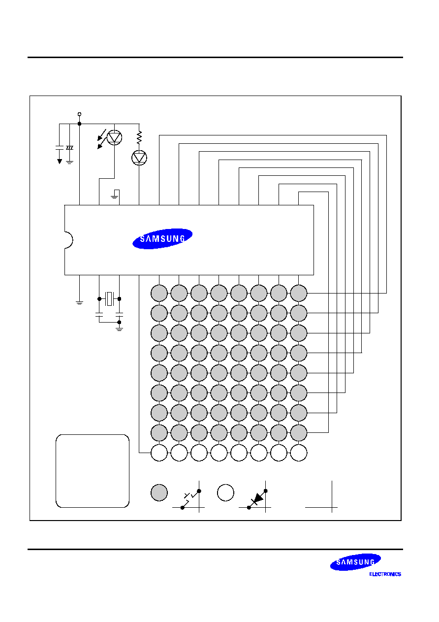
REMOTE CONTROL TX. APPLICATION NOTE
S3C1840/C1850/C1860/P1860
7-14
S3C1850 Application Circuit Example
D1
V
DD
P2.0/
REM
TEST P2.1 P2.2 P2.3 P2.4 P2.5 P3.0 P3.1 P3.2 P3.3
V
SS
XI
XO
P2.6 P0.0 P0.1 P0.2 P0.3 P1.0 P1.1 P1.2 P1.3
SAMSUNG
S3C1850-xx
C2
C1
C4
C3
C6
C5
C8
C7
C2
C3
K8
K24
K16
K40
K32
K56
K48
K9
K1
K25
K17
K41
K33
K57
K49
K10
K2
K26
K18
K42
K34
K58
K50
K11
K3
K27
K19
K43
K35
K59
K51
K12
K4
K28
K20
K44
K36
K60
K52
K13
K5
K29
K21
K45
K37
K61
K53
K14
K6
K30
K22
K46
K38
K62
K54
K15
K7
K31
K23
K47
K39
K63
K55
K0
R
D2
+
-
C4
C1
+3 V
V
DD
R: 100
C1: 4.7
µ
F/6.3 V
C2,C3: 100 pF
C4: 0.1
µ
F
D1: I.R.LED
D2: INDICATOR LED
Resonator: 455 kHz
K
C
OR
Figure 7-8. S3C1850 Application Circuit Example
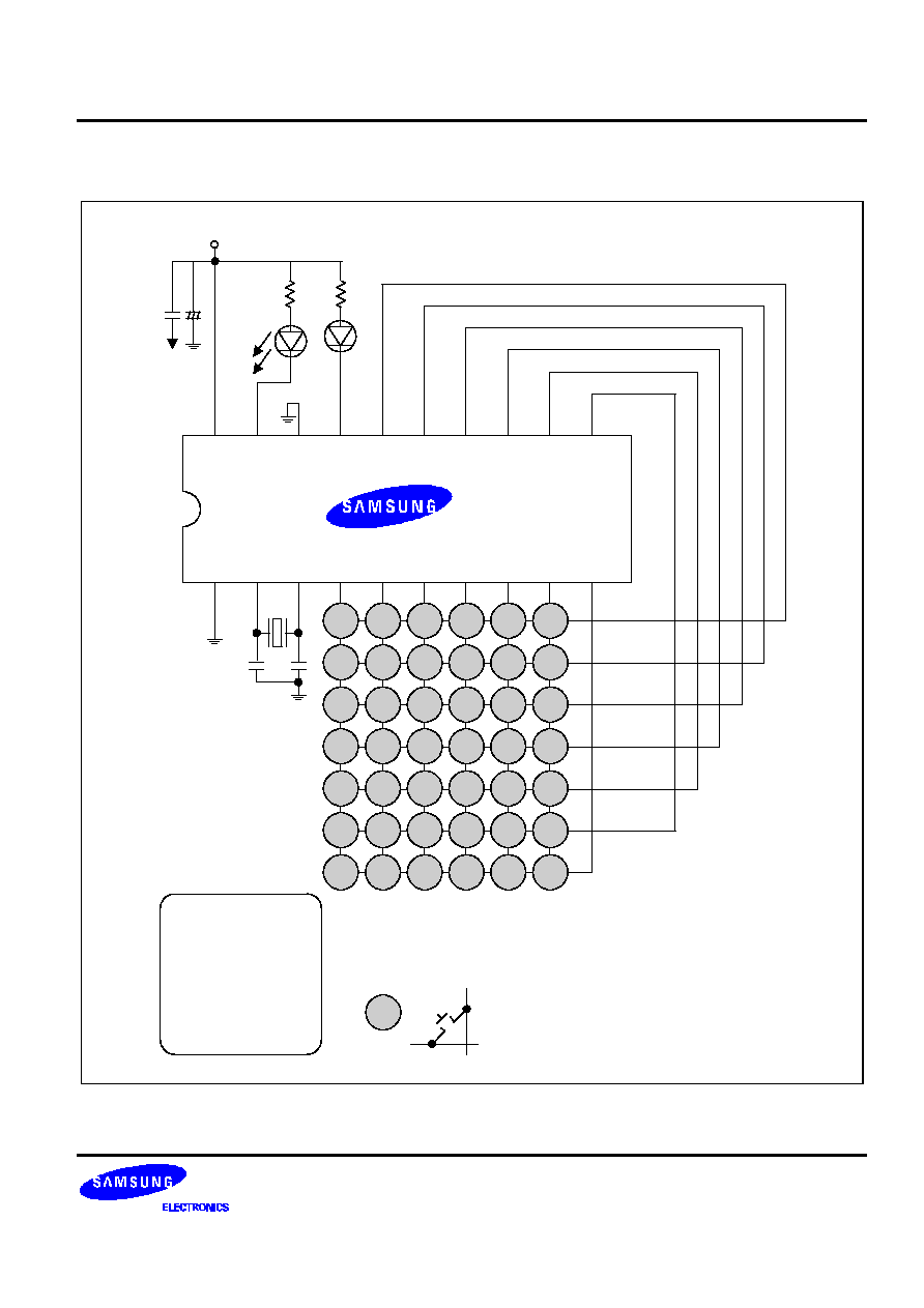
S3C1840/C1850/C1860/P1860
REMOTE CONTROL TX. APPLICATION NOTE
7-15
S3C1860 Application Circuit Example
D1
V
DD
P2.0/
REM
TEST P2.1 P2.2 P2.3 P2.4 P3.0 P3.1 P3.2
V
SS
XI
XO
P0.0 P0.1 P0.2 P0.3 P1.0 P1.1 P3.3
SAMSUNG
S3C1860-xx
C2
C3
K7
K21
K14
K35
K28
K8
K1
K22
K15
K36
K28
K9
K2
K23
K16
K37
K30
K10
K3
K24
K17
K38
K31
K11
K4
K25
K18
K39
K32
K12
K5
K26
K19
K40
K33
K13
K6
K27
K20
K41
K34
K0
R2
D2
+
-
C4
C1
+3 V
V
DD
R1: 1-5
R2: 100
C1: 47
µ
F/6.3 V
C2,C3: 100 pF
C4: 0.1
µ
F
D1: I.R.LED
D2: INDICATOR LED
R1
K
Figure 7-9. S3C1860 Application Circuit Example

REMOTE CONTROL TX. APPLICATION NOTE
S3C1840/C1850/C1860/P1860
7-16
Program Flowchart (This program is only apply to S3C1840)
One key input?
Reset Debounce Time
All key strobe output pins
are non-active
Transmit Two
Waveforms
Transmit Repeat
Waveforms
Only one key strobe pin is active
Debounce Time = 0?
Data & Custom Code Generator
Continous key?
MAIN
Yes
No
Yes
No
No
Yes
Double Key & No Key
RESET
MAIN
KEYSCAN
DATCUS
SIGNAL Tx.
No
Yes
Any key input?
All key strobe output pins
are active
HALT
START
Figure 7-10. Program Flowchart 1

S3C1840/C1850/C1860/P1860
REMOTE CONTROL TX. APPLICATION NOTE
7-17
S3C1840/C1850 KEYSCAN FUNCTION
Description
This program has an 8 x 9 key matrix, which consists of input P0 and P1 and output P2 and P3. Because pull-up
resistors are connected, the normal state for all input pins is high level. The operating method for the keyscan
function is as follows:
-- All output pins remain active state ( = low).
-- If key is pressed, set all output pins to non-active state and rotate the pins to set only a pin to active state
during debounce time.
-- If key is pressed more than one or if no key is pressed, go to reset label.
-- If a new key is pressed, reset debounce time, continuous flag, and key-in flag.
RAM Assignment
O_INP0
N_INP0
O_INP1
N_INP1
O_OUTP
I_TWICE
N_OUTP
DEBOCNT CONKEY
KFLG
05H
09H
H register selects #0
01H
HL 00H
O_INP0:
The old value of P0
N_INP0:
The new value of P0
O_INP1:
The old value of P1
N_INP1:
The new value of P1
O_OUTP:
The old value of output port
N_OUTP:
The new value of output port
I_TWICE:
Double number increment
DEBOCNT: Debounce time
CONKEY:
Continuous key flag
KFLG:
key input flag

REMOTE CONTROL TX. APPLICATION NOTE
S3C1840/C1850/C1860/P1860
7-18
Program Flowchart (This program is only apply to S3C1840)
518KSCAN
O_INP0, O_INP1, O_OUTP #0FH
DEBOCNT, CONKEY #0
P2.1 & 2.6 High
PORT3, P2.2-P2.5 Low
Port 0 = #0FH
Port 1 = #0FH
N_OUTP.2 = #1
A
RESET
; Close indicator LED & option pin
; Active strobe output pins
; Initial variable
; Check port 0 input
No
No
; Check port1 input
; Halt mode & Halt mode release
; H register selects #0
; Non-active strobe output pins
; Only one output pin is low level
; PARALL
MAIN
STROBE:
SERIAL:
No
Yes
P2.5 High
Port 3 Low
H #0
P2.2-P2.5 Low
PORT3, P2.2-P2.5 High
P2.12 High
P2.12 Low
N_OUTP, KFLG #0, I_TWICE #1
Yes
Yes
Figure 7-11. Program Flowchart 2

S3C1840/C1850/C1860/P1860
REMOTE CONTROL TX. APPLICATION NOTE
7-19
A
RESET
Port 0 = #0FH
N_INP0 Port 0
N_INP1 #0FH
L N_INP0
Port 1 = #0FH
A A + #1
Overflow?
A A - #1
N_INP0 A
N_OUTP O_OUTP
N_OUTP = O_INP0
N_INP0 O_INP0
N_INP0 = O_INP0
N_INP1 O_INP1
N_INP1 = O_INP1
DEBOCNT #2
CONKEY #0
KFLG #1
Port 1 = #0FH
N_INP0 #0FH
N_INP1 Port 1
L N_INP1
A A + #1
Overflow?
A A - #1
N_INP1 A
a
NORMAL
RESET
Key In:
Port 0:
; Double Key
DBCOMP:
;Key input setting
SETKEY:
;New key &
debounce time
setting
;Compare old data to new data
; Double Key
; NO KEY
Port 1:
; Check the end
of debounce time
INCS N_OUTP
a
N_OUTP = #8
KFLG = #1
P3.3 High
DECS DEBOCNT
DEBOCNT = #0
RET
RESET
MAIN
STROBE
Normal:
No Key
Yes
Yes
No
Yes
No
Yes
No
No
No
Yes
No
Yes
No
No
Yes
No
Yes
No
No
Yes
Keycheck
Keycheck
Yes
Yes
FSTKEY:
Figure 7-12. Program Flowchart 3

REMOTE CONTROL TX. APPLICATION NOTE
S3C1840/C1850/C1860/P1860
7-20
S3C1840/C1850 Keycheck Subroutine
L= #07H
No
No
No
L = #0DH
KEYCHEK
A #0FH
L = #0EH
A A + #1
L = #0BH
A A + #2
A A + #3
A A + #4
RET
No
Yes
Yes
Yes
Figure 7-13. S3C1840/C1850 Keycheck Subroutine

S3C1840/C1850/C1860/P1860
REMOTE CONTROL TX. APPLICATION NOTE
7-21
;*********************************************
ORG
0F00H
;*********************************************
; If reset occurs, PA register is immediately initialized to #0FH
RESET
MOV
L,#1
; close indicator LED
SETB
P2.(L)
;
MOV
L,#6
; non-select P2.6
SETB
P2.(L)
;
PRTCLR
CLR
A
;
OUT
P3,@SL + A
; low all the output ports
MOV
L,#5
; (except P2.0, P2.1, P2.6)
CLRB
P2.(L)
;
DECS
L
;
CPNE
L,#1
;
JP
.-3
;
;;; initial all of the variables --------------------------------------------------
;;;
input ports are connected with pull-up resistor
;;;
Therefore, normal state
high
MOV
H,#0
; H register selects file #0
MOV
L,#O_INP0
; port0 is #0fh
MOV
@HL+,#0FH
MOV
L, #O_INP1
; port1 is #0fh
MOV
@HL +,#0FH
MOV
L, #O_OUTP
; the strobe out is #0fh
MOV
@HL+,#0FH
MOV
L,#DEBOCNT
; debounce count is #0
MOV
@HL+,#0
MOV
L,#CONKEY
; continuous key is #0
MOV
@HL+,#0
;;; check each input port (=key input) ------------------------------------
MOV
L,#0DH
; check port0
CLRB
P2.(L)
;
IN
A,P0
;
MOV
L,A
;
CPNE
L,#0FH
;
JP
DELAYP0
;
MOV
L,#0DH
; check port1
SETB
P2.(L)
;
IN
A,P0
;
MOV
L,A
;
CPNE
L,#0FH
;
JP
J_MAIN
;
;;; halt mode, after halt mode release, go to reset ------------------
MOV
L,#0CH
SETB
P2.(L)
; halt mode
CLRB
P2.(L)
; halt mode release
JP
RESET

REMOTE CONTROL TX. APPLICATION NOTE
S3C1840/C1850/C1860/P1860
7-22
PRTSET CLR
A
;
ADDS
A,#0FH
; high all the output ports
OUT
P3,@SL+A
; (P3, P2.2-P2.5)
MOV
L,#5
;
SETB
P2.(L)
;
DECS
L
;
CPNE
L,#1
; If P2.0 is high, data Tx.
JP
.- 3
; and auto reset counter clear
RET
DELAYP0
MOV
H #0
; for the match of delay time
MOV
H #0
;
MOV
H #0
;
MOV
H #0
;
MOV
H #0
;
MOV
H #0
;
J_MAIN
JPL
MAIN
;
;
;*********************************************
ORG
0000H
JPL
RESET
;*********************************************
MAIN
MOV
H,#0
; H regisster selects file #0
; useful when continous pulse Tx.
;
CALLL
PRTSET
; high all the output ports
;;; initial useful variable in main routine ------------------------------------
MOV
L,#N_OUTP
; N_OUTP
#0
MOV
@HL+,#0
;
MOV
L,#1_TWICE
; I_TWICE (double increment)
#1
MOV
@HL+,#1
;
MOV
L,#KFLG
; KFLG
#0 (input key flag)
MOV
@HL+,#0
;
;; select output pin by one and one ---------------------------------
STROBE
MOV
L,#N_OUTP
CPBT
@HL.2
; If N_OUTP.2 is set, go to parall (parallel port)
JP
PARALL
; otherwise, go to serial (serial port)
SERIAL
MOV
L,@HL
;
INCS
L
;
SETB
P2.(L)
; low P2.2-P2.5
INCS
L
;
CLRB
P2.(L)
;
JPL
KEYIN
PARALL
MOV
L,#5
; high P2.5
SETB
P2.(L)
;

S3C1840/C1850/C1860/P1860
REMOTE CONTROL TX. APPLICATION NOTE
7-23
;;;*********************************************
;;; A
#0h
;;; A
A-1_TWICE
;;; output P3
;;; I_TWICE
I_TWICE + I_TWICE
;;; ;*********************************************
CLR
A
; A
#0FH
ADDS
A, #0FH
;
MOV
L, #1_TWICE
;
XCH
@HL,A
; A
A-I_TWICE
SUBS
A,@HL
;
OUT
P3,@SL+A
; low port3
SUBS
A,@HL
;
MOV
@HL,A
; recover I_TWICE
ADDS
A,@HL
;
MOVZ
@HL,A
; I_TWICE
I_TWICE + I_TWICE
JPL
KEYIN
;;;*********************************************
;; check double key at each port
;; if a key pressed, do adds instruction
;; otherwise, induce overflow occurrence
;;;*********************************************
KEYCHEK
CLR
A
ADDS
A,#0FH
; A
#0fh
CPNE
L,#0EH
JP
.+2
ADDS
A,#1
; A
#0
CPNE
L,#0DH
JP
.+2
ADDS
A,#2
; A
#1
CPNE
L,#0BH
JP
.+2
ADDS
A,#3
; A
#2
CPNE
L,#7
JP
.+2
ADDS
A,#4
; A
#3
RET
;
;
; *********************************************
ORG
0100H
JPL
RESET
; *********************************************
KEYIN
MOV
L,#0DH
CLRB
P2.(L)
;;; select port0 ---------------------------------
IN
A, P0
MOV
L,A
CPNE
L,#0FH
; is key pressed in port0 ?
JP
PORT0
JP
PORT1

REMOTE CONTROL TX. APPLICATION NOTE
S3C1840/C1850/C1860/P1860
7-24
PORT0
MOV
L,#N_INP0
; setting at N_INP0
MOV
@HL,A
;
MOV
L,#ODH
;
SETB
P2.(L)
;
IN
A,P0
;
MOV
L,A
;
CPNE
L,#0FH
;
JP
DBKEY
; If also port1 input a key,
; it is double key
MOV
L,#N_INP1
; Only N_INP0 input
MOV
@HL+,#0FH
; but N_INP1 is set to #0fh
MOV
L,#N_INP0
;
MOV
L,@HL
;
CALLL
KEYCHEK
;
ADDS
A,#1
;
JP
DBKEY
; if overflow occurs, it is double key
DECS
A
; because input value ranges
MOV
L,#N_INP0
; from #0 to #3
MOVZ
@HL,A
; N_INP0
A
JPL
DBCOMP
;;; select port1 ---------------------------------
PORT1
MOV
L,#0DH
SETB
P2.(L)
IN
A,P0
MOV
L,A
CPNE
L,#0FH
; is key pressed in port 1?
JP
.+3
JPL
NORMAL
; no key, go to NORMAL
MOV
L,#N_INP0
; setting N_INP0 to #0fh
MOV
@HL+,#0FH
; Only N_INP1 input
MOV
L,#N_INP1
;
MOV
@HL,A
;
MOV
L,A
; L
N_INP1
CALLL
KEYCHEK
ADDS
A,#1
; if overflow occurs, go to double key
JP
DBKEY
;
DECS
A
; because input value ranges from
#0 to #3
MOV
L,#N_INP1
; N_INP1
A
MOVZ
@HL,A
JPL
DBCOMP
;;; if double key occurs, go to reset ---------------------------------
DBKEY
JPL
RESET
;
;

S3C1840/C1850/C1860/P1860
REMOTE CONTROL TX. APPLICATION NOTE
7-25
; *********************************************
ORG
0200H
JPL
RESET
; *********************************************
;;; compare for the recognition of a new key----------------------
DBCOMP
MOV
H,#N_OUTP
; compare N_OUTP to
O_OUTP
MOV
A,@HL
MOV
L,#O_OUTP
XCH
@HL,A
CPNE
@HL,A
JP
FSTKEY
MOV
L,#N_INP0
; compare N_INP0 to O_INP0
MOV
A,@HL
MOV
L,#O_INP0
XCH
@HL,A
CPNE
@HL,A
JP
FSTDLY
MOV
L,#N_INP1
; compare N_INP1 to O_INP1
MOV
A,@HL
MOV
L,#O_INP1
XCH
@HL,A
CPNE
@HL,A
JP
FSTKEY
JP
SETKEY
FSTDLY
MOV
H,#0
; for match of delay time
MOV
H,#0
MOV
H,#0
MOV
H,#0
MOV
H,#0
;;; when new key input ----------------------------
FSTKEY
MOV
L,#DEBOCNT
; DEBOCNT
#2
MOV
@HL+,#2
MOV
L,#CONKEY
; CONKEY
#0
MOV
@HL+,#0
SETKEY
MOV
L,#KFLG
; KFLG
#1
MOV
@HL+,#1

REMOTE CONTROL TX. APPLICATION NOTE
S3C1840/C1850/C1860/P1860
7-26
; *********************************************
;;; increase N_OUTP
;;; check N_OUTP is equal to #8
;;; check no key (= DEBOCNT)
; *********************************************
NORMAL
MOV
L,#N_OUTP
; increase N_OUTP
INCS
A,@HL
MOVZ
@HL,A
ADDS
A,#8
; A
#8
CPNE
@HL,A
; compare N_OUTP to A
JP
J_STRO
; go to stroble label
MOV
L,#KFLG
;
CPBT
@HL.0
; check key flag
JP
ONKEY
JPL
RESET
; no key
ONKEY
CLR
A
ADDS
A,#0FH
OUT
P3,@SL + A
; set port3 to `1'
MOV
L,#DEBOCNT
; decrease DEBOCNT
DECS
A,@HL
XCH
@HL,A
CPNZ
@HL
; compare DEBOCNT TO #0
JP
J1_MAIN
JPL
KEYSCAN
J1_MAIN
JPL
MAIN
J_STRO
JPL
STROBE

S3C1840/C1850/C1860/P1860
REMOTE CONTROL TX. APPLICATION NOTE
7-27
S3C1840/C1850 CODE GENERATION
Description
This program generates data code and custom code. The custom code is determined according to diodes
between input ports and output pin (P2.6). The data code is as follows:
D0 D1 D2
D4 D5
D3
D6 D7
KEY1
KEY0
KEY33
KEY32
KEY31
KEY63
0
0
0
0
0
0
0
0
0
0
0
0
0
0
0
1
1
1
1
1
1
1
1
1
0
0
0
0
0
0
0
0
0
0
0
0
0
0
0
0
1
1
1
1
1
0
0
1
.
.
.
.
.
.
.
.
D0 D1 D2
D4 D5
D3
D6 D7
KEY1
KEY0
KEY33
KEY32
KEY31
KEY63
0
0
0
0
0
0
0
0
0
0
0
0
0
0
0
1
1
1
1
1
1
1
0
0
0
0
0
0
0
1
1
0
0
0
0
0
0
0
0
0
1
1
1
1
0
1
0
1
.
.
.
.
.
.
.
.
RAM DAT0 (D0-D3), DAT1_0 (D4-D7)
RAM DAT0 (D0-D3), DAT1 (D4-D7)
RAM Assignment
CUS0
CUS1
CUS2
CUS3
DAT0
DAT2
DAT1
DAT3
DAT1_0
DAT3_0
45H
49H
H register selects #4
41H
HL 40H
CUS0;
Custom code (c0-c3)
CUS1:
Custom code (c4-c7)
CUS2:
The complement of CUS0
CUS3:
The complement of CUS1
DAT0:
Data code (d0-d3)]
DAT1:
Data code (d4-d7)
:
32 key: 00000010, 63 key: 1111010
DAT2:
The complement of DAT0
DAT3:
The complement of DAT1
DAT1_0
Data code (d4-d7)
:
32 key: 00000100, 63 key: 1111100
DAT3_0
The complement of DAT1_0

REMOTE CONTROL TX. APPLICATION NOTE
S3C1840/C1850/C1860/P1860
7-28
Program Flowchart
518CODE
; Select option pin
; Custom code production
; Close option pin
; Indicator LED
DAT0 = #0FH
DAT1 <- #0
DAT1_0 <- #0
DAT_P0:
CARRY ?
DAT_P1:
R_SHIFT:
S_CARRY:
A_OUTP:
; Check the end of
debounce time
RET
N
Y
N
Y
Y
H <- #4
P2.6 <- LOW
P2.13 <- LOW
produce CUS0 & CUS2
P2.6 <- HIGH
P2.13 <- HIGH
produce CUS1 & CUS3
P2.1 <- LOW
DAT0 <- O_INP0
DAT1 <- #4
DAT1_0 <- #2
DAT0 <- O_INP1
L <- DAT0
DAT0 shifts three times to left
INCS DAT1 & DAT1_0
DAT0 <- DAT0+O_OUTP
DAT2 <- the complement of
DAT0
DAT3 <- the complement of
DAT1
DAT1_0 <- the complement of
DAT3_0
Figure 7-14. Program Flowchart 4

S3C1840/C1850/C1860/P1860
REMOTE CONTROL TX. APPLICATION NOTE
7-29
;*********************************************
ORG
0300H
JPL
RESET
;*********************************************
;;; select only a key ------------------------------------------------
KEYSCAN MOV
H,#4
;;; product custom code -------------------------------------------
MOV
L,#6
; P2.6
low
CLRB
P2.(L)
; check custom code
MOV
L,#0DH
;
CLRB
P2.(L)
;
IN
A,P0
;
MOV
L,#CUS2
; CUS2 is the complement of CUS0
MOV
@HL,A
;
NOTI
A
;
DECS
A
;
MOV
L,#CUS0
;
MOV
@HL,A
;
MOV
L,#0DH
SETB
P2.(L)
; CUS3 is the complement of CUS1
IN
A,P0
;
MOV
L,#CUS3
;
MOV
@HL,A
;
ADDS
A,@HL
;
NOTI
A
;
DECS
A
;
MOV
L,#CUS1
;
MOVZ
@HL,A
;
MOV
L,#6
; high P2.6
SETB
P2.(L)
MOV
L,#1
; the indicator LED of a key input
CLRB
P2.(L)
;;; product data code -------------------------------------------------
MOV
H,#0
MOV
L,#O_INP0
; DAT0
O_INP0
MOV
A,@HL
MOV
H,#4
MOV
L,#DAT0
MOVZ
@HL,A
ADDS
A,#0FH
; A
#0fh
CPNE
@HL,A
; does input key exist in port0?
JP
DAT_P0

REMOTE CONTROL TX. APPLICATION NOTE
S3C1840/C1850/C1860/P1860
7-30
DAT_P1
MOV
L,#DAT1
; input key exists in port1
MOV
@HL+,#04H
; DAT1
DAT1 + #4
MOV
L,#DAT1_0
MOV
@HL+,#02H
; DAT1_0
DAT1_0 + #2
MOV
H,#0
; DAT0
O_INP1
MOV
L,#O_INP1
;
MOV
A,@HL
;
MOV
H,#4
;
MOV
L,#DAT0
;
MOVZ
@HL,A
;
JPL
R_SHIFT
;
DAT_P0
MOV
L,#DAT1
; clear DAT1 & DAT1_0
MOV
@HL+,#0
MOV
L,#DAT1_0
MOV
@HL+,#0
MOV
L,#DAT0
MOV
H,#4
; delay time
MOV
H,#4
;
MOV
H,#4
;
MOV
H,#4
;
MOV
H,#4
;
JPL
R_SHIFT
;
;
;*********************************************
ORG
0400H
JPL
RESET
;*********************************************
R_SHIFT
MOV
A,@HL
; DAT0 shifts three times to the left
ADDS
A,@HL
;
MOV
@HL,A
;
ADDS
A,@HL
;
MOV
@HL,A
;
ADDS
A,@HL
;
JP
S_CARRY
JP
N_CARRY
S_CARRY
MOV
L,#DAT1
;if carry occurs, increase DAT1 & DAT1_0
XCH
@HL,A
;
INCS
A
;
XCH
@HL,A
;
MOV
L,#DAT1_0
;
XCH
@HL,A
;
INCS
A
;
XCH
@HL,A
;
JP
A_OUTP

S3C1840/C1850/C1860/P1860
REMOTE CONTROL TX. APPLICATION NOTE
7-31
N_CARRY
MOV
H,#0
; if carry doesn't occur, delay time
MOV
H,#0
;
MOV
H,#0
;
MOV
H,#0
;
MOV
H,#0
;
MOV
H,#0
;
MOV
H,#0
;
MOV
H,#0
;
A_OUTP
MOV
H,#0
MOV
L,#O_OUTP
; DAT0
DAT0 + O_OUTP
ADDS
A,@HL
;
MOV
H,#4
;
MOV
L,#DAT0
MOV
@HL,A
;
NOTI
A
DECS
A
; DAT2
complement of DAT0
MOV
L,#DAT2
MOVz
@HL,A
MOV
L,#DAT1
MOV
A,@HL
NOTI
A
; DAT3
complement of DAT1
DECS
A
MOV
L,#DAT3
MOVZ
@HL,A
MOV
L,#DAT1_0
MOV
A,@HL
NOTI
A
DECS
A
MOV
L,#DAT3_0
; DAT3_0
complement of DAT 1_0
MOV
@HL,A
JPL
TX

REMOTE CONTROL TX. APPLICATION NOTE
S3C1840/C1850/C1860/P1860
7-32
S3C1840/C1850 SIGNAL TRANSMISSION
Description
This program is for signal transmissions in SAMSUNG standard format. If one key is pressed, two frames are
transmitted consecutively. The repeat pulse is transmitted until key-off. The frame interval is 60 ms.
Each frame consists of leader code, custom code, and data code:
-- Leader code (high level for 4.5 ms and low level for 4.5 ms)
-- 12-bit custom code
-- 8-bit data code
Transmission Waveform
60 ms
Frame Waveform
Leader code
4.5 ms 4.5 ms
60 ms
60 ms
custom code (c0-c11)
data code (d0-d7)
Data Pulse
0.56 ms
1.125 ms
data '0'
2.25 ms
0.56 ms
data '1'
Figure 7-15. Transmission Waveforms
RAM Assignment
This part is the same as for keyscan and code generation.

S3C1840/C1850/C1860/P1860
REMOTE CONTROL TX. APPLICATION NOTE
7-33
S3C1840 Program Flowchart (This program is only apply to S3C1840)
P2.9 & 2.10 LOW
CONKEY + #0
518SAMTX
CUS4 #0
P2.0 HIGH for 4.5 msec
P2.0 LOW for 4.5 msec
P2.0 HIGH for .56 msec
P2.0 LOW delay as many as
low number
Output Custom & Data Code
DEBOCNT #1
CONKEY #1
Delay for 60 msec
; select carrier frequency
; c8 #0
MAIN
Delay for 60 msec
; Repeat waveform transmission
; Until key off
Yes
; Repeat one more time
No
Figure 7-16. S3C1840 Program Flowchart 5

REMOTE CONTROL TX. APPLICATION NOTE
S3C1840/C1850/C1860/P1860
7-34
;*********************************************
ORG
0500H
JPL
RESET
;*********************************************
TX
MOV
L,#9
; select farrier frequency
CLRB
P2.(L)
; 37.9 kHz, 1/3 duty
MOV
L,#0AH
; clear P2.9 & 2.10
CLRB
P2.(L)
SIGOUT
MOV
L,#CUS4
; custom code (c8-c11)
#0
MOB
@HL+,#0
; if device is KS51910, c8
#1
;;; output head pulse --------------------------------------------------
MOV
L,#0
; high for delay time 4.5 msec
SETB
P2.(L)
CALLL
D4_5
MOV
L,#0
CLRB
P2.(L)
; low for delay time 4.5 msec
CALLL
D4_5D
;;; output custom code (c0-c11) & data code (d0-d7)
MOV
L,#CUS0
; custom code (c0-c3)
CALLL
DATGEN
MOV
L,#CUS1
; custom code (c4-c7)
CALLL
DATGEN
MOV
L,#CUS4
; custom code (c8-c11)
CALLL
DATGEN
MOV
L,#DAT0
; data code (d0-d3)
CALLL
DATGEN
MOV
L,#DAT1_0
; data code (d4-d7)
CALLL
DATGEN
MOV
L,#1
DECS
L
JP
.-1
MOV
L,#0
; EOB (end of bit)
SETB
P2.(L)
; high for .56msec
CALLL
D_560F
MOV
L,#0
CLRB
P2.(L)
JPL
LOWCHEK

S3C1840/C1850/C1860/P1860
REMOTE CONTROL TX. APPLICATION NOTE
7-35
;*********************************************
ORG
0600H
JPL
RESET
;*********************************************
;;; check low code of custom code & data code --------------------------------
LOWCHEK MOV
L,#CUS0
; custom code (c0-c3)
CALL
LCHEK
MOV
L,#CUS1
; custom code (c4-c7)
CALL
LCHEK
MOV
L,#CUS4
; custom code (c8-c11)
CALL
LCHEK
MOV
L,#DAT0
; data code (d0-d3)
CALL
LCHEK
MOV
L,#DAT1_01
; the maximum value of upper bit is #3
MOV
A,L
; data code (d4-d7)
CALL
LCHEK_1
; check from the second bit
;== notice ===========================================================
; If value of DAT1_0 is greater than #3, programmer must change instruction
; CALLLCHEK_1 to other instruction such as CALLCHECK_2 or CALL
; LCHEK. And you must check the fram interval (= 60 msec)
;===================================================================
;;; re-setting debounce count to #1-------------------------------------
SETDBT
MOV
H,#0
MOV
L,#DEBOCNT
; DEBOCNT
#1
MOV
@HL+,#1
;---------------------------------------------------------------------------------
;;; If conkey flag isn't `0', transmit repeat pulse
;;; otherwise, after setting, transmit again (two frames)
;---------------------------------------------------------------------------------
CONCHEK
MOV
H,#0
MOV
L,#CONKEY
; CONKEY == #0?
CPNZ
@HL
; If CONKEY is #0, CONKEY
#1
JP
LJ_MAIN
; transmit frame again
MOV
@HL+,#1
CALLL
D4_5D
; time is 60 msec per frame
CALLL
D2_25
CALLL
D1_125
MOV
L,#0CH
MOV
H,#4
MOV
H,#4
DECS
L
JP
.-3
JPL
SIGOUT

REMOTE CONTROL TX. APPLICATION NOTE
S3C1840/C1850/C1860/P1860
7-36
;;; output repeat pulse ----------------------------------------------------------
LJ_MAIN
CALL
D1_125
JPL
MAIN
;;; output delay time as many as low numbers ----------------------------
LCHEK
MOV
A,L
CPBT
@HL,3
; if @hl.3 is low, call d2_25d.
JP
LCHEK_2
CALLL
D2_25D
LCHEK_2
MOV
L,A
CPBT
@HL.2
; if @hl.2 is low, call d2_25d.
JP
LCHEK_1
CALLL
D2_25D
LCHEK_1
MOV
L,A
CPBT
@HL.1
; if @hl.1 is low, call d2_25d.
JP
LCHEK_0
CALLL
D2_25D
LCHEK_0
MOV
L,A
CPBT
@HL.0
; if @hl. 0 is low, call d2_25d.
JP
LCHEK_R
CALLL
D2_25D
LCHEK_R RET
;
;
;
;
;
;*********************************************
ORG
0700H
JPL
RESET
;*********************************************
;; custom code & data code generation -------------------------------------
DATGEN
MOV
A,L
CALL
D_560
; high for .56 msec
CPBT
@HL.0
; if @hl.0 is high, low for 2.25 msec.
CALL
D2_25
; otherwise, low for 1.125 msec.
CALL
D1_125

S3C1840/C1850/C1860/P1860
REMOTE CONTROL TX. APPLICATION NOTE
7-37
CALL
D_560
; high for .56 msec
CPBT
@HL.1
; if @hl.1 is high, low for 2.25 msec.
CALL
D2_25
; otherwise, low for 1.125 msec.
CALL
D1_125
CALL
D_560
; high for .56 msec
CPBT
@HL.2
; if @hl.2 is high, low for 2.25 msec.
CALL
D2_25
; otherwise, low for 1.125 msec.
CALL
D1_125
CALL
D_560
; high for .56 msec
CPBT
@HL.3
; if @hl.3 is high, low for 2.25 msec.
CALL
D2_25
; otherwise, low for 1.125 msec.
CALL
D1_125D
RET
;;; delay time subroutine by programming -----------------------------------
D_560
MOV
L,#0
SETB
P2,(L)
;
MOV
L,#0CH
MOV
H,#4
DECS
L
JP
.-2
MOV
H,#4
;
MOV
L,#0
CLRB
P2.(L)
MOV
L,A
RET
D4_5D
MOV
L,#02H
; delay time 4.5 msec
JP
.+2
D4_5
MOV
L,#06H
DECS
L
JP
-1
MOV
L,#05H
CLR
A
ADDS
A,#0BH
MOV
H,#4
D_A
DECS
A
JP
.-2
DECS
L
JP
.-6

REMOTE CONTROL TX. APPLICATION NOTE
S3C1840/C1850/C1860/P1860
7-38
D2_25D
MOV
L,#0EH
JP
.+2
D2_25
MOV
L,#0FH
MOV
H,#4
DECS
L
JP
.-2
D1_125
MOV
L,#0AH
JP
.+6
D1_125D
MOV
L,#08H
JP
.+4
D_560F
MOV
L,#0BH
; delay time .56 msec (for EOB)
MOV
H,#4
MOV
H,#4
DECS
L
JP
.-2
RET
;
;
org
0800h
jpl
reset
org
0900h
jpl
reset
org
oaooh
jpl
reset
org
obooh
jpl
reset
org
ocooh
jpl
reset
org
odooh
jpl
reset
org
oeooh
jpl
reset
;
;******************* The END of S3C1840 SAMSUNG FORMAT TX. **************************