 | –≠–ª–µ–∫—Ç—Ä–æ–Ω–Ω—ã–π –∫–æ–º–ø–æ–Ω–µ–Ω—Ç: S3C2440A | –°–∫–∞—á–∞—Ç—å:  PDF PDF  ZIP ZIP |
Document Outline
- ˛ˇ
- ˛ˇ
- ˛ˇ
- ˛ˇ
- ˛ˇ
- ˛ˇ
- ˛ˇ
- ˛ˇ
- ˛ˇ
- ˛ˇ
- ˛ˇ
- ˛ˇ
- ˛ˇ
- ˛ˇ
- ˛ˇ
- ˛ˇ
- ˛ˇ
- ˛ˇ
- ˛ˇ
- ˛ˇ
- ˛ˇ
- ˛ˇ
- ˛ˇ
- ˛ˇ
- ˛ˇ
- ˛ˇ
- ˛ˇ
- ˛ˇ
- ˛ˇ
- ˛ˇ

S3C2440A
32-BIT CMOS
MICROCONTROLLER
USER'S MANUAL
Revision 1

Important Notice
The information in this publication has been carefully
checked and is believed to be entirely accurate at the
time of publication. Samsung assumes no
responsibility, however, for possible errors or
omissions, or for any consequences resulting from
the use of the information contained herein.
Samsung reserves the right to make changes in its
products or product specifications with the intent to
improve function or design at any time and without
notice and is not required to update this
documentation to reflect such changes.
This publication does not convey to a purchaser of
semiconductor devices described herein any license
under the patent rights of Samsung or others.
Samsung makes no warranty, representation, or
guarantee regarding the suitability of its products for
any particular purpose, nor does Samsung assume
any liability arising out of the application or use of any
product or circuit and specifically disclaims any and
all liability, including without limitation any
consequential or incidental damages.
"Typical" parameters can and do vary in different
applications. All operating parameters, including
"Typicals" must be validated for each customer
application by the customer's technical experts.
Samsung products are not designed, intended, or
authorized for use as components in systems
intended for surgical implant into the body, for other
applications intended to support or sustain life, or for
any other application in which the failure of the
Samsung product could create a situation where
personal injury or death may occur.
Should the Buyer purchase or use a Samsung
product for any such unintended or unauthorized
application, the Buyer shall indemnify and hold
Samsung and its officers, employees, subsidiaries,
affiliates, and distributors harmless against all claims,
costs, damages, expenses, and reasonable attorney
fees arising out of, either directly or indirectly, any
claim of personal injury or death that may be
associated with such unintended or unauthorized use,
even if such claim alleges that Samsung was
negligent regarding the design or manufacture of said
product.
S3C2440A 32-Bit CMOS Microcontroller
User's Manual, Revision 1
Publication Number: 21-S3-C2440A-072004
© 2004 Samsung Electronics
All rights reserved. No part of this publication may be reproduced, stored in a retrieval system, or transmitted in any
form or by any means, electric or mechanical, by photocopying, recording, or otherwise, without the prior written
consent of Samsung Electronics.
Samsung Electronics' microcontroller business has been awarded full ISO-14001
certification (BVQ1 Certificate No. 9330). All semiconductor products are designed and
manufactured in accordance with the highest quality standards and objectives.
Samsung Electronics Co., Ltd.
San #24 Nongseo-Ri, Giheung- Eup
Yongin-City, Gyeonggi-Do, Korea
C.P.O. Box #37, Suwon 449-900
TEL:
(82)-(031)-209-1490
FAX:
(82) (331) 209-1909
Home-Page URL: Http://www.samsungsemi.com/
Printed in the Republic of Korea

S3C2440A MICROCONTROLLER
iii
Table of Contents
Chapter 1
Product Overview
Introduction.........................................................................................................................................1-1
Features .............................................................................................................................................1-2
Block Diagram ....................................................................................................................................1-5
Pin Assignments.................................................................................................................................1-6
Signal Descriptions..............................................................................................................................1-20
S3C2440A Special Registers................................................................................................................1-26
Chapter 2
Programmer's Model
Overview .............................................................................................................................................2-1
Processor Operating States .........................................................................................................2-1
Switching State...........................................................................................................................2-1
Memory Formats.........................................................................................................................2-1
Big-Endian Format.......................................................................................................................2-2
Little-Endian Format ....................................................................................................................2-2
Instruction Length........................................................................................................................2-2
Operating Modes .........................................................................................................................2-3
Registers ....................................................................................................................................2-3
The Program Status Registers ......................................................................................................2-7
Exceptions .................................................................................................................................2-10
Interrupt Latencies .......................................................................................................................2-15
Reset .........................................................................................................................................2-15

iv
S3C2440A MICROCONTROLLER
Table of Contents
(Continued)
Chapter 3
ARM Instruction Set
Instruction Set Summay.......................................................................................................................3-1
Format Summary ........................................................................................................................3-1
Instruction Summary....................................................................................................................3-2
The Condition Field..............................................................................................................................3-4
Branch and Exchange (Bx)...................................................................................................................3-5
Instruction Cycle Times................................................................................................................3-5
Assembler Syntax .......................................................................................................................3-5
Using R15 as an Operand ............................................................................................................3-5
Branch and Branch with Link (B, Bl)......................................................................................................3-7
The Link Bit ................................................................................................................................3-7
Instruction Cycle Times................................................................................................................3-7
Assembler Syntax .......................................................................................................................3-8
Data Processing..................................................................................................................................3-9
Cpsr Flags ..................................................................................................................................3-11
Shifts .........................................................................................................................................3-12
Immediate Operand Rotates .........................................................................................................3-16
Writing to R15.............................................................................................................................3-16
Using R15 as an Operandy...........................................................................................................3-16
TEQ, TST, Cmp and Cmn Opcodes...............................................................................................3-16
Instruction Cycle Times................................................................................................................3-16
Assembler Syntax .......................................................................................................................3-17
Examples ...................................................................................................................................3-17
Psr Transfer (MRS, MSR).....................................................................................................................3-18
Operand Restrictions ...................................................................................................................3-18
Reserved Bits..............................................................................................................................3-20
Examples ...................................................................................................................................3-20
Instruction Cycle Times................................................................................................................3-20
Assembly Syntax ........................................................................................................................3-21
Examples ...................................................................................................................................3-21
Multiply And Multiply-Accumulate (MUL, MLA).......................................................................................3-22
Cpsr Flags ..................................................................................................................................3-24
Instruction Cycle Times................................................................................................................3-24
Assembler Syntax .......................................................................................................................3-24
Examples ...................................................................................................................................3-24
Multiply Long And Multiply-Accumulate Long (MULL, MLAL) ...................................................................3-25
Operand Restrictions ...................................................................................................................3-26
Cpsr Flags ..................................................................................................................................3-26
Instruction Cycle Times................................................................................................................3-26
Assembler Syntax .......................................................................................................................3-27
Examples ...................................................................................................................................3-27

S3C2440A MICROCONTROLLER
v
Table of Contents
(Continued)
Chapter 3
ARM Instruction Set
(Continued)
Single Data Transfer (LDR, STR)...........................................................................................................3-28
Offsets and Auto-Indexing ............................................................................................................3-29
Shifted Register Offset .................................................................................................................3-29
Bytes and Words ........................................................................................................................3-29
Use of R15..................................................................................................................................3-31
Example.....................................................................................................................................3-31
Data Aborts ................................................................................................................................3-31
Instruction Cycle Times................................................................................................................3-31
Assembler Syntax .......................................................................................................................3-32
Examples ...................................................................................................................................3-33
Halfword and Signed Data Transfer (LDRH/STRH/LDRSB/LDRSH) ...........................................................3-34
Offsets and Auto-Indexing ............................................................................................................3-35
Halfword Load and Stores.............................................................................................................3-36
Use of R15..................................................................................................................................3-37
Data Aborts ................................................................................................................................3-37
Instruction Cycle Times................................................................................................................3-37
Assembler Syntax .......................................................................................................................3-38
Examples ...................................................................................................................................3-39
Block Data Transfer (LDM, STM)...........................................................................................................3-40
The Register List .........................................................................................................................3-40
Addressing Modes.......................................................................................................................3-41
Address Alignment ......................................................................................................................3-41
Use of the S Bit...........................................................................................................................3-43
Use of R15 as The Base ..............................................................................................................3-43
Inclusion of the Base in the Register List .......................................................................................3-44
Data Aborts ................................................................................................................................3-44
Instruction Cycle Times................................................................................................................3-44
Assembler Syntax .......................................................................................................................3-45
Examples ...................................................................................................................................3-46
Single Data Swap (SWP).....................................................................................................................3-47
Bytes and Words ........................................................................................................................3-47
Use of R15..................................................................................................................................3-48
Data Aborts ................................................................................................................................3-48
Instruction Cycle Times................................................................................................................3-48
Assembler Syntax .......................................................................................................................3-48
Software Interrupt (SWI) .......................................................................................................................3-49
Return from the Supervisor ...........................................................................................................3-49
Comment Field............................................................................................................................3-49
Instruction Cycle Times................................................................................................................3-49
Assembler Syntax .......................................................................................................................3-50
Coprocessor Data Operations (CDP).....................................................................................................3-51
Coprocessor Instructions..............................................................................................................3-51
Instruction Cycle Times................................................................................................................3-52
Examples ...................................................................................................................................3-52

vi
S3C2440A MICROCONTROLLER
Table of Contents
(Continued)
Chapter 3
ARM Instruction Set
(Continued)
Coprocessor Data Transfers (LDC, STC)................................................................................................3-53
The Coprocessor Fields ...............................................................................................................3-54
Addressing Modes.......................................................................................................................3-54
Address Alignment ......................................................................................................................3-54
Data Aborts ................................................................................................................................3-54
Assembler Syntax .......................................................................................................................3-55
Examples ...................................................................................................................................3-55
Coprocessor Register Transfers (MRC, MCR).................................................................................3-56
The Coprocessor Fields ...............................................................................................................3-56
Transfers to R15..........................................................................................................................3-57
Transfers from R15 ......................................................................................................................3-57
Instruction Cycle Times................................................................................................................3-57
Assembler Syntax .......................................................................................................................3-57
Examples ...................................................................................................................................3-57
Undefined Instruction ...................................................................................................................3-58
Instruction Cycle Times................................................................................................................3-58
Assembler Syntax .......................................................................................................................3-58
Instruction Set Examples .............................................................................................................3-59
Using the Conditional Instructions .................................................................................................3-59
Pseudo-Random Binary Sequence Generator.................................................................................3-61
Multiplication by Constant Using the Barrel Shifter..........................................................................3-61
Loading a Word from an Unknown Alignment .................................................................................3-63
Chapter 4
Thumb Instruction Set
Thumb Instruction Set Format...............................................................................................................4-1
Format Summary ........................................................................................................................4-2
Opcode Summary .......................................................................................................................4-3
Format 1: Move Shifted Register ...........................................................................................................4-5
Operation....................................................................................................................................4-5
Instruction Cycle Times................................................................................................................4-6
Examples ...................................................................................................................................4-6
Format 2: Add/Subtract........................................................................................................................4-7
Operation....................................................................................................................................4-7
Instruction Cycle Times................................................................................................................4-8
Examples ...................................................................................................................................4-8
Format 3: Move/Compare/Add/Subtract Immediate.................................................................................4-9
Operations ..................................................................................................................................4-9
Instruction Cycle Times................................................................................................................4-10
Examples ...................................................................................................................................4-10

S3C2440A MICROCONTROLLER
vii
Table of Contents
(Continued)
Chapter 4
Thumb Instruction Set
(Continued)
Format 4: ALU Operations....................................................................................................................4-11
Operation....................................................................................................................................4-11
Instruction Cycle Times................................................................................................................4-12
Examples ...................................................................................................................................4-12
Format 5: Hi-Register Operations/Branch Exchange ...............................................................................4-13
Operation....................................................................................................................................4-13
Instruction Cycle Times................................................................................................................4-14
The BX Instruction .......................................................................................................................4-14
Examples ...................................................................................................................................4-15
Using R15 As an Operand............................................................................................................4-15
Format 6: PC-Relative Load..................................................................................................................4-16
Operation....................................................................................................................................4-16
Instruction Cycle Times................................................................................................................4-17
Examples ...................................................................................................................................4-17
Format 7: Load/Store With Register Offset.............................................................................................4-18
Operation....................................................................................................................................4-19
Instruction Cycle Times................................................................................................................4-19
Examples ...................................................................................................................................4-19
Format 8: Load/Store Sign-Extended Byte/Halfword................................................................................4-20
Operation....................................................................................................................................4-20
Instruction Cycle Times................................................................................................................4-21
Examples ...................................................................................................................................4-21
Format 9: Load/Store With Immediate Offset..........................................................................................4-22
Operation....................................................................................................................................4-23
Instruction Cycle Times................................................................................................................4-23
Examples ...................................................................................................................................4-23
Format 10: Load/Store Halfword............................................................................................................4-24
Operation....................................................................................................................................4-24
Examples ...................................................................................................................................4-25
Format 11: SP-Relative Load/Store .......................................................................................................4-26
Operation....................................................................................................................................4-26
Instruction Cycle Times................................................................................................................4-27
Examples ...................................................................................................................................4-27
Format 12: Load Address.....................................................................................................................4-28
Operation....................................................................................................................................4-28
Instruction Cycle Times................................................................................................................4-29
Examples ...................................................................................................................................4-29
Format 13: Add Offset to Stack Pointer .................................................................................................4-30
Operation....................................................................................................................................4-30
Instruction Cycle Times................................................................................................................4-30
Examples ...................................................................................................................................4-30

viii
S3C2440A MICROCONTROLLER
Table of Contents
(Continued)
Chapter 4
Thumb Instruction Set
(Continued)
Format 14: Push/Pop Registers ............................................................................................................4-31
Operation....................................................................................................................................4-31
Instruction Cycle Times................................................................................................................4-32
Examples ...................................................................................................................................4-32
Format 15: Multiple Load/Store.............................................................................................................4-33
Operation....................................................................................................................................4-33
Instruction Cycle Times................................................................................................................4-33
Examples ...................................................................................................................................4-33
Format 16: Conditional Branch..............................................................................................................4-34
Operation....................................................................................................................................4-34
Instruction Cycle Times................................................................................................................4-35
Examples ...................................................................................................................................4-35
Format 17: Software Interrupt................................................................................................................4-36
Operation....................................................................................................................................4-36
Instruction Cycle Times................................................................................................................4-36
Examples ...................................................................................................................................4-36
Format 18: Unconditional Branch..........................................................................................................4-37
Operation....................................................................................................................................4-37
Examples ...................................................................................................................................4-37
Format 19: long branch with link ...........................................................................................................4-38
Operation....................................................................................................................................4-38
Instruction Cycle Times................................................................................................................4-39
Examples ...................................................................................................................................4-39
Instruction Set Examples .....................................................................................................................4-40
Multiplication by A Constant Using Shifts and Adds........................................................................4-40
General Purpose Signed Divide.....................................................................................................4-41
Division by a Constant .................................................................................................................4-43

S3C2440A MICROCONTROLLER
ix
Table of Contents
(Continued)
Chapter 5
Memory Controller
Overview .............................................................................................................................................5-1
Function Description............................................................................................................................5-4
Bank0 Bus Width........................................................................................................................5-4
Memory (SROM/SDRAM) Address Pin Connections.......................................................................5-4
Sdram Bank Address Pin Connection Example..............................................................................5-5
nWAIT Pin Operation ...................................................................................................................5-6
nXBREQ/nXBACK Pin Operation...................................................................................................5-7
Programmable Access Cycle .......................................................................................................5-12
Bus Width & Wait Control Register (Bwscon).................................................................................5-14
Bank Control Register (Bankconn: NGCS0-NGCS5) .......................................................................5-16
Bank Control Register (Bankconn: NGCS6-NGCS7) .......................................................................5-17
Refresh Control Register ..............................................................................................................5-18
Banksize Register .......................................................................................................................5-19
Sdram Mode Register Set Register (MRSR)...................................................................................5-20
Chapter 6
Nand Flash Contorller
Overview .............................................................................................................................................6-1
Features .....................................................................................................................................6-1
Block Diagram ............................................................................................................................6-2
Boot Loader Function...................................................................................................................6-2
Pin Configuration .........................................................................................................................6-3
Nand Flash Memory Configuration Table........................................................................................6-3
Nand Flash Memory Timing..........................................................................................................6-4
Software Mode ....................................................................................................................................6-5
Steppingstone (4K-Byte SRAM)....................................................................................................6-6
Ecc (Error Correction Code)..................................................................................................................6-7
2048 Byte ECC Parity Code Assignment Table ..............................................................................6-7
16 Byte ECC Parity Code Assignment Table..................................................................................6-7
ECC Module Features..................................................................................................................6-8
ECC Programming Guide .............................................................................................................6-8
Nand Flash Memory Mapping .......................................................................................................6-9
Nand Flash Memory Configuration.................................................................................................6-10
Nand Flash Configuration Register ................................................................................................6-12
Control Register ..........................................................................................................................6-13
Command Register......................................................................................................................6-15
Address Register.........................................................................................................................6-15
Data Register..............................................................................................................................6-15
Main Data Area Register ..............................................................................................................6-16
Spare Area Ecc Register.............................................................................................................6-17
NFCON Status Register...............................................................................................................6-18
ECC0/1 Status Register...............................................................................................................6-19
Main Data Area ECC0 Status Register ..........................................................................................6-20
Spare Area ECC Status Register ..................................................................................................6-20
Block Address Register ...............................................................................................................6-21

x
S3C2440A MICROCONTROLLER
Table of Contents
(Continued)
Chapter 7
Clock & Power Management
Overview .............................................................................................................................................7-1
Functional Description .........................................................................................................................7-2
Clock Architecture.......................................................................................................................7-2
Clock Source Selection................................................................................................................7-2
Phase Locked Loop (PLL) ............................................................................................................7-4
Clock Control Logic .....................................................................................................................7-6
Power Management .....................................................................................................................7-10
Clock Generator & Power Management Special Register ........................................................................7-20
Lock Time Count Register (LOCKTIME).........................................................................................7-20
PLL Control Register (MPLLCON & UPLLCON)..............................................................................7-21
PLL Value Selection Table ...........................................................................................................7-21
Clock Control Register (CLKCON).................................................................................................7-22
Clock Slow Control (CLKSLOW) Register ......................................................................................7-23
Clock Divider Control (CLKDIVN) Register......................................................................................7-24
Camera Clock Divider (CAMDIVN) Register....................................................................................7-25
Chapter 8
DMA
Overview .............................................................................................................................................8-1
DMA Request Sources ........................................................................................................................8-2
DMA Operation ...................................................................................................................................8-2
External DMA DREQ/DACK Protocol ............................................................................................8-3
Examples ...........................................................................................................................................8-6
DMA Special Registers ........................................................................................................................8-7
DMA Initial Source (DISRC) Register.............................................................................................8-7
DMA Initial Source Control (DISRCC) Register ...............................................................................8-7
DMA Initial Destination (DIDST) Register .......................................................................................8-8
DMA Initial Destination Control (DIDSTC) Register..........................................................................8-8
DMA Control (DCON) Register......................................................................................................8-9
DMA Status (DSTAT) Register......................................................................................................8-12
DMA Current Source (DCSRC) Register ........................................................................................8-13
Current Destination (DCDST) Register ...........................................................................................8-13
DMA Mask Trigger (DMASKTRIG) Register....................................................................................8-14

S3C2440A MICROCONTROLLER
xi
Table of Contents
(Continued)
Chapter 9
I/O PORTS
Overview .............................................................................................................................................9-1
Port Control Descriptions .....................................................................................................................9-7
Port Configuration Register (GPACON-GPJCON)............................................................................9-7
Port Data Register (GPADAT-GPJDAT) .........................................................................................9-7
Port Pull-Up Register (GPBUP-GPJUP).........................................................................................9-7
Miscellaneous Control Register.....................................................................................................9-7
External Interrupt Control Register.................................................................................................9-7
I/O Port Control Register ......................................................................................................................9-8
Port A Control Registers (GPACON, GPADAT) ..............................................................................9-8
Port B Control Registers (GPBCON, GPBDAT, GPBUP).................................................................9-10
Port C Control Registers (GPCCON, GPCDAT, GPCUP).................................................................9-11
Port D Control Registers (GPDCON, GPDDAT, GPDUP).................................................................9-13
Port E Control Registers (GPECON, GPEDAT, GPEUP).................................................................9-15
Port F Control Registers (GPFCON, GPFDAT) ...............................................................................9-17
Port G Control Registers (GPGCON, GPGDAT) .............................................................................9-18
Port H Control Registers (GPHCON, GPHDAT) ..............................................................................9-20
Port J Control Registers (GPJCON, GPJDAT) ................................................................................9-21
Miscellaneous Control Register (MISCCR) .....................................................................................9-23
DCLK Control Registers (DCLKCON).............................................................................................9-25
EXTINTn (External Interrupt Control Register n)...............................................................................9-26
EINTFLTn (External Interrupt Filter Register n)................................................................................9-30
EINTMASK (External Interrupt Mask Register) ...............................................................................9-31
EINTPEND (External Interrupt Pending Register) ............................................................................9-32
GSTATUSn (General Status Registers) .........................................................................................9-33
DSCn (Drive Strength Control).......................................................................................................9-34
DSCn (Drive Strength Control).......................................................................................................9-35
MSLCON (Memory Sleep Control Register)....................................................................................9-36

xii
S3C2440A MICROCONTROLLER
Table of Contents
(Continued)
Chapter 10
Basic Timer
Overview .............................................................................................................................................10-1
Feature.......................................................................................................................................10-1
PWM Timer Operation .........................................................................................................................10-3
Prescaler & Divider ......................................................................................................................10-3
Basic Timer Operation .................................................................................................................10-3
Auto Reload & Double Buffering ....................................................................................................10-4
Timer Initialization Using Manual Update Bit and Inverter Bit ............................................................10-5
Timer Operation...........................................................................................................................10-6
Pulse Width Modulation (PWM)....................................................................................................10-7
Output Level Control ....................................................................................................................10-8
Dead Zone Generator...................................................................................................................10-9
DMA Request Mode ....................................................................................................................10-10
PWM Timer Control Registers ..............................................................................................................10-11
Timer Configuration Register0 (TCFG0)..........................................................................................10-11
Timer Configuration Register1 (TCFG1)..........................................................................................10-12
Timer Control (TCON) Register......................................................................................................10-13
Timer 0 Count Buffer Register & Compare Buffer Register (TCNTB0/TCMPB0)...................................10-15
Timer 0 Count Observation Register (TCNTO0) ...............................................................................10-15
Timer 1 Count Buffer Register & Compare Buffer Register (TCNTB1/TCMPB1)...................................10-16
Timer 1 Count Observation Register (TCNTO1) ...............................................................................10-16
Timer 2 Count Buffer Register & Compare Buffer Register (TCNTB2/TCMPB2)...................................10-17
Timer 2 Count Observation Register (TCNTO2) ...............................................................................10-17
Timer 3 Count Buffer Register & Compare Buffer Register (TCNTB3/TCMPB3)...................................10-18
Timer 3 Count Observation Register (TCNTO3) ...............................................................................10-18
Timer 4 Count Buffer Register (TCNTB4) ........................................................................................10-19
Timer 4 Count Observation Register (TCNTO4) ...............................................................................10-19

S3C2440A MICROCONTROLLER
xiii
Table of Contents
(Continued)
Chapter 11
UART
Overview .............................................................................................................................................11-1
Features .....................................................................................................................................11-1
Block Diagram ....................................................................................................................................11-2
Uart Operation.............................................................................................................................11-3
Uart Special Registers .........................................................................................................................11-10
Uart Line Control Register ............................................................................................................11-10
Uart Control Register ...................................................................................................................11-11
Uart FIFO Control Register ...........................................................................................................11-14
Uart Modem Control Register........................................................................................................11-15
Uart Tx/Rx Status Register...........................................................................................................11-16
Uart Error Status Register ............................................................................................................11-17
Uart FIFO Status Register............................................................................................................11-18
Uart Modem Status Register ........................................................................................................11-19
Uart Transmit Buffer Register (HOLDING Register & FIFO Register) .................................................11-20
Uart Receive Buffer Register (HOLDING Register & FIFO Register) ..................................................11-20
Uart Baud Rate Divisor Register....................................................................................................11-21
Chapter 12
USB HOST Controller
Overview .............................................................................................................................................12-1
Usb Host Controller Special Registers ...................................................................................................12-2
OHCI Registers for Usb Host Controller .........................................................................................12-2

xiv
S3C2440A MICROCONTROLLER
Table of Contents
(Continued)
Chapter 13
USB Device Controller
Overview .............................................................................................................................................13-1
Feature.......................................................................................................................................13-1
Usb Device Controller Special Registers ................................................................................................13-3
Function Address Register (FUNC_ADDR_REG)............................................................................13-5
Power Management Register (PWR_REG) ....................................................................................13-6
Interrupt Register (EP_INT_REG/USB_INT_REG) ...........................................................................13-7
Interrupt Enable Register (EP_INT_EN_REG/USB_INT_EN_REG)....................................................13-9
Frame Number Register (FPAME_NUM1_REG/FRAME_NUM2_REG) .............................................13-10
Index Register (INDEX_REG)........................................................................................................13-11
MAX Packet Register (MAXP_REG)..............................................................................................13-11
END Point0 Control Status Register (EP0_CSR) ............................................................................13-12
END Point In Control Status Register (IN_CSR1_REG/IN_CSR2_REG) ............................................13-13
END Point Out Control Status Register (OUT_CSR1_REG/OUT_CSR2_REG) ..................................13-15
END Point Out Write Count Register (OUT_FIFO_CNT1_REG/OUT_FIFO_CNT2_REG).....................13-17
END Point FIFO Register (EPN_FIFO_REG)..................................................................................13-17
DMA Interface Control Register (EPN_DMA_CON) .........................................................................13-18
DMA Unit Counter Register (EPN_DMA_UNIT) ...............................................................................13-19
DMA FIFO Counter Register (EPN_DMA_FIFO) .............................................................................13-20
DMA Total Transfer Counter Register (EPn_DMA_TTC_L, M, H) ......................................................13-21
Chapter 14
Interrupt Controller
Overview .............................................................................................................................................14-1
Interrupt Controller Operation ........................................................................................................14-2
Interrupt Sources .........................................................................................................................14-3
Interrupt Sub Sources ..................................................................................................................14-4
Interrupt Priority Generating Block.................................................................................................14-5
Interrupt Priority...........................................................................................................................14-6
Interrupt Controller Special Registers.....................................................................................................14-7
Source Pending (SRCPND) Register .............................................................................................14-7
Interrupt Mode (INTMOD) Register.................................................................................................14-9
Interrupt Mask (INTMSK) Register.................................................................................................14-11
Priority Register (PRIORITY).........................................................................................................14-13
Interrupt Pending (INTPND) Register..............................................................................................14-14
Interrupt Offset (INTOFFSET) Register...........................................................................................14-16
Sub Source Pending (SUBSRCPND) Register................................................................................14-17
Interrupt Sub Mask (INTSUBMSK) Register ...................................................................................14-18

S3C2440A MICROCONTROLLER
xv
Table of Contents
(Continued)
Chapter 15
LCD Controller
Overview .............................................................................................................................................15-1
Features .....................................................................................................................................15-1
Common Features .......................................................................................................................15-2
External Interface Signal ..............................................................................................................15-2
Block Diagram ............................................................................................................................15-3
STN LCD Controller Operation ..............................................................................................................15-4
Timing Generator (TIMEGEN) .......................................................................................................15-4
Video Operation ..........................................................................................................................15-5
Dithering and Frame Rate Control .................................................................................................15-7
Memory Data Format (STN, BSWP = 0)........................................................................................15-9
TFT LCD Controller Operation ...............................................................................................................15-16
Video Operation ..........................................................................................................................15-16
Memory Data Format (TFT) ..........................................................................................................15-17
256 Palette Usage (TFT) ..............................................................................................................15-21
Samsung TFT LCD Panel
(3.5" PORTRAIT/256K COLOR/REFLECTIVE A-SI/TRANSFLECTIVE A-SI TFT LCD).........................15-24
Virtual Display (TFT/STN).............................................................................................................15-25
LCD Power Enable (STN/TFT).......................................................................................................15-26
LCD Controller Special Registers ..................................................................................................15-27
Frame Buffer Start Address 1 Register ..........................................................................................15-33
Chapter 16
ADC & Touch Screen Interface
Overview .............................................................................................................................................16-1
Features .....................................................................................................................................16-1
ADC & Touch Screen Interface Operation ..............................................................................................16-2
Block Diagram ............................................................................................................................16-2
Function Descriptions ..................................................................................................................16-3
ADC AND Touch Screen Interface Special Registers ..............................................................................16-5
ADC Control Register (ADCCON)..................................................................................................16-5
ADC Touch Screen Control Register (ADCTSC)..............................................................................16-6
ADC Start Delay Register (ADCDLY).............................................................................................16-7
ADC Conversion Data Register (ADCDAT0)....................................................................................16-8
ADC Conversion Data Register (ADCDAT1)....................................................................................16-9
ADC Touch Screen Up-Down INT Check Register (ADCUPDN) ........................................................16-9

xvi
S3C2440A MICROCONTROLLER
Table of Contents
(Continued)
Chapter 17
Real Time Clock
Overview .............................................................................................................................................17-1
Features .....................................................................................................................................17-1
Real Time Clock Operation...........................................................................................................17-2
Leap Year Generator....................................................................................................................17-2
Read/Write Registers...................................................................................................................17-2
Backup Battery Operation ............................................................................................................17-2
Alarm Function............................................................................................................................17-3
TICK Time Interrupt ......................................................................................................................17-3
32.768kHz X-Tal Connection Example ..........................................................................................17-3
Real Time Clock Special Registers .......................................................................................................17-4
Real Time Clock Control (RTCCON) Register .................................................................................17-4
TICK Time Count (TICNT) Register ................................................................................................17-4
RTC Alarm Control (RTCALM) Register..........................................................................................17-5
ALARM Second Data (ALMSEC) Register .....................................................................................17-6
ALARM Min Data (ALMMIN) Register............................................................................................17-6
ALARM Hour Data (ALMHOUR) Register.......................................................................................17-6
ALARM Date Data (ALMDATE) Register........................................................................................17-7
ALARM Mon Data (ALMMON) Register .........................................................................................17-7
ALARM Year Data (ALMYEAR) Register .......................................................................................17-7
BCD Second (BCDSEC) Register .................................................................................................17-8
BCD Minute (BCDMIN) Register....................................................................................................17-8
BCD Hour (BCDHOUR) Register ...................................................................................................17-8
BCD Date (BCDDATE) Register....................................................................................................17-9
BCD Day (BCDDAY) Register.......................................................................................................17-9
BCD Month (BCDMON) Register...................................................................................................17-9
BCD Year (BCDYEAR) Register ...................................................................................................17-10
Chapter 18
Watchdog Timer
Overview .............................................................................................................................................18-1
Features .....................................................................................................................................18-1
Watchdog Timer Operation...........................................................................................................18-2
Wtdat & Wtcnt ............................................................................................................................18-2
Consideration of Debugging Environment .......................................................................................18-2
Watchdog Timer Special Registers .......................................................................................................18-3
Watchdog Timer Control (WTCON) Register...................................................................................18-3
Watchdog Timer Data (WTDAT) Register.......................................................................................18-4
Watchdog Timer Count (WTCNT) Register .....................................................................................18-4

S3C2440A MICROCONTROLLER
xvii
Table of Contents
(Continued)
Chapter 19
MMC/SD/SDIO Controller
Features .............................................................................................................................................19-1
Block Diagram ....................................................................................................................................19-1
SD Operation ......................................................................................................................................19-2
SDIO Operation...................................................................................................................................19-3
SDI Special Registers ..........................................................................................................................19-4
SDI Control Register (SDICON).....................................................................................................19-4
SDI Baud Rate Prescaler Register (SDIPRE) .................................................................................19-4
SDI Command Argument Register (SDICmdArg).............................................................................19-5
SDI Command Control Register (SDICmdCon)................................................................................19-5
SDI Command Status Register (SDICmdSta) .................................................................................19-6
SDI Response Register 0 (SDIRSP0) ............................................................................................19-6
SDI Response Register 1 (SDIRSP1) ............................................................................................19-6
SDI Response Register 2 (SDIRSP2) ............................................................................................19-7
SDI Response Register 3 (SDIRSP3) ............................................................................................19-7
SDI Data / Busy Timer Register (SDIDTimer)..................................................................................19-7
SDI Block Size Register (SDIBSize)..............................................................................................19-7
SDI Data Control Register (SDIDatCon) .........................................................................................19-8
SDI Data Remain Counter Register (ADIDatCnt).............................................................................19-9
SDI Data Status Register (ADIDatSta)...........................................................................................19-9
SDI FIFO Status Register (SDIFSTA)............................................................................................19-10
SDI Interrupt Mask Register (SDIIntMsk)........................................................................................19-11
SDI Data Register (SDIDAT) .........................................................................................................19-12
Chapter 20
IIC-Bus Interface
Overview .............................................................................................................................................20-1
IIC-Bus Interface..........................................................................................................................20-3
Start and Stop Conditions ............................................................................................................20-3
Data Transfer Format ...................................................................................................................20-4
ACK Signal Transmission.............................................................................................................20-5
Read-Write Operation ..................................................................................................................20-6
Bus Arbitration Procedures...........................................................................................................20-6
Abort Conditions..........................................................................................................................20-6
Configuring IIC-Bus ......................................................................................................................20-6
Flowcharts of Operations in Each Mode.........................................................................................20-7
IIC-Bus Interface Special Registers .......................................................................................................20-11
Multi-Master IIC-Bus Control (IICCON) Register ..............................................................................20-11
Multi-Master IIC-Bus Control/Status (IICSTAT) Register...................................................................20-12
Multi-Master IIC-Bus Address (IICADD) Register.............................................................................20-13
Multi-Master IIC-Bus Transmit/Receive Data Shift (IICDS) Register...................................................20-13
Multi-Master IIC-Bus Line Contro l(IICLC) Register ..........................................................................20-14

xviii
S3C2440A MICROCONTROLLER
Table of Contents
(Continued)
Chapter 21
IIS-Bus Interface
Overview .............................................................................................................................................21-1
Block Diagram ....................................................................................................................................21-2
Functional Descriptions........................................................................................................................21-2
Transmit or Receive Only Mode ....................................................................................................21-2
Dma Transfer ..............................................................................................................................21-3
Transmit and Receive Mode..........................................................................................................21-3
Audio Serial Interface Format................................................................................................................21-3
IIS-Bus Format ............................................................................................................................21-3
MSB (Left) Justified .....................................................................................................................21-3
Sampling Frequency and Master Clock .........................................................................................21-4
IIS-Bus Interface Special Registers .......................................................................................................21-5
IIS Control (IISCON) Register........................................................................................................21-5
IIS Mode Register (IISMOD) Register.............................................................................................21-6
IIS Prescaler (IISPSR) Register.....................................................................................................21-7
IIS FIFO Control (IISFCON) Register..............................................................................................21-8
IIS FIFO (IISFIFO) Register...........................................................................................................21-8
Chapter 22
SPI
Overview .............................................................................................................................................22-1
Features .....................................................................................................................................22-1
Block Diagram ............................................................................................................................22-2
SPI Operation .....................................................................................................................................22-3
Programming Procedure...............................................................................................................22-3
SPI Transfer Format.....................................................................................................................22-4
Transmitting Procedure for DMA ...................................................................................................22-5
Receiving Procedure for DMA .......................................................................................................22-5
SPI Special Registers ..........................................................................................................................22-6
SPI Control Register ....................................................................................................................22-6
SPI Status Register.....................................................................................................................22-7
SPI Pin Control Register ..............................................................................................................22-8
SPI Baud Rate Prescaler Register ................................................................................................22-9
SPI Tx Data Register ...................................................................................................................22-9
SPI Rx Data Register...................................................................................................................22-9

S3C2440A MICROCONTROLLER
xix
Table of Contents
(Continued)
Chapter 23
Camera Interface
Overview .............................................................................................................................................23-1
Features .....................................................................................................................................23-1
Block Diagram ............................................................................................................................23-2
Timing Diagram ...........................................................................................................................23-3
Camera Interface Operation ..................................................................................................................23-5
Two DMA Paths ..........................................................................................................................23-5
Clock Domain .............................................................................................................................23-5
Frame Memory Hirerarchy ............................................................................................................23-6
Memory Storing Method...............................................................................................................23-8
Timing Diagram for Register Setting ..............................................................................................23-9
Timing Diagram for Last IRQ.........................................................................................................23-10
Camera Interface Special Registers.......................................................................................................23-11
Source Format Register ...............................................................................................................23-11
Window Option Register...............................................................................................................23-12
Global Control Register ................................................................................................................23-13
Y1 Start Address Register............................................................................................................23-13
Y2 Start Address Register............................................................................................................23-13
Y3 Start Address Register............................................................................................................23-14
Y4 Start Address Register............................................................................................................23-14
CB1 Start Address Register .........................................................................................................23-14
CB2 Start Address Register .........................................................................................................23-14
CB3 Start Address Register .........................................................................................................23-15
CB4 Start Address Register .........................................................................................................23-15
CR1 Start Address Register .........................................................................................................23-15
CR2 Start Address Register .........................................................................................................23-15
CR3 Start Address Register .........................................................................................................23-16
CR4 Start Address Register .........................................................................................................23-16
Codec Target Format Register ......................................................................................................23-17
Codec Dma Control Register ........................................................................................................23-19
Register Setting Guide for Codec Scaler and Preview Scaler ...........................................................23-20
Codec Pre-Scaler Control Register 1.............................................................................................23-21
Codec Pre-Scaler Control Register 2.............................................................................................23-21
Codec Main-Scaler Control Register..............................................................................................23-22
Codec Dma Target Area Register..................................................................................................23-22
Codec Status Register.................................................................................................................23-23
RGB1 Start Address Register.......................................................................................................23-23
RGB2 Start Address Register.......................................................................................................23-23
RGB3 Start Address Register.......................................................................................................23-24
RGB4 Start Address Register.......................................................................................................23-24
Preview Target Format Register ....................................................................................................23-24
Preview DMA Control Register ......................................................................................................23-25

xx
S3C2440A MICROCONTROLLER
Table of Contents
(Continued)
Chapter 23
Camera Interface
(Continued)
Preview Pre-Scaler Control Register 1 ...........................................................................................23-25
Preview Pre-Scaler Control Register 2 ...........................................................................................23-26
Preview Main-Scaler Control Register ............................................................................................23-26
Preview DMA Target Area Register................................................................................................23-26
Preview Status Register ...............................................................................................................23-27
Image Capture Enable Register.....................................................................................................23-27
Chapter 24
AC97 Controller
Overview .............................................................................................................................................24-1
Features .....................................................................................................................................24-1
AC97 Controller Operation....................................................................................................................24-2
Block Diagram ............................................................................................................................24-2
Internal Data Path........................................................................................................................24-3
Operation Flow Chart ...........................................................................................................................24-4
AC-Link Digital Interface Protocol..........................................................................................................24-5
AC-Link Output Frame (SDATA_OUT) ...........................................................................................24-6
AC-Link Input Frame (SDATA_IN) .................................................................................................24-6
AC97 Powerdown ................................................................................................................................24-7
AC97 Controller Special Registers ........................................................................................................24-9
AC97 Global Control Register (AC_GLBCTRL) ...............................................................................24-9
AC97 Global Status Register (AC_GLBSTAT) ................................................................................24-10
AC97 Codec Command Register (AC_CODEC_CMD).....................................................................24-10
AC97 Codec Status Register (AC_CODEC_STAT) .........................................................................24-11
AC97 PCM Out/In Channel FIFO Address Register (AC_PCMADDR) ...............................................24-11
AC97 MIC in Channel FIFO Address Register (AC_MICADDR) ........................................................24-12
AC97 PCM Out/In Channel FIFO Data Register (AC_PCMDATA).....................................................24-12
AC97 MIC in Channel FIFO Data Register (AC_MICDATA)..............................................................24-12

S3C2440A MICROCONTROLLER
xxi
Table of Contents
(Continued)
Chapter 25
Bus Priorities
Overview .............................................................................................................................................25-1
Bus Priority Map .........................................................................................................................25-1
Chapter 26
Mechanical Data
Package Dimensions ...........................................................................................................................26-1
Chapter 27
Electrical Data
Absolute Maximum Ratings..................................................................................................................27-1
Recommended Operating Conditions.....................................................................................................27-2
D.C. Electrical Characteristics..............................................................................................................27-3
A.C. Electrical Characteristics..............................................................................................................27-8

S3C2440A MICROCONTROLLER
xxiii
List of Figures
Figure
Title
Page
Number
Number
1-1
S3C2440A Block Diagram................................................................................................1-5
1-2
S3C2440A Pin Assignments (289-FBGA)..........................................................................1-6
2-1
Big-Endian Addresses of Bytes within Words.....................................................................2-2
2-2
Little-Endian Addresses of Bytes within Words ..................................................................2-2
2-3
Register Organization in ARM State..................................................................................2-4
2-4
Register Organization in THUMB state ..............................................................................2-5
2-5
Mapping of THUMB State Registers onto ARM State Registers ...........................................2-6
2-6
Program Status Register Format.......................................................................................2-7
3-1
ARM Instruction Set Format .............................................................................................3-1
3-2
Branch and Exchange Instructions ....................................................................................3-5
3-3
Branch Instructions..........................................................................................................3-7
3-4
Data Processing Instructions ............................................................................................3-9
3-5
ARM Shift Operations ......................................................................................................3-12
3-6
Logical Shift Left..............................................................................................................3-12
3-7
Logical Shift Right ...........................................................................................................3-13
3-8
Arithmetic Shift Right .......................................................................................................3-13
3-9
Rotate Right....................................................................................................................3-14
3-10
Rotate Right Extended.....................................................................................................3-14
3-11
PSR Transfer ..................................................................................................................3-19
3-12
Multiply Instructions.........................................................................................................3-22
3-13
Multiply Long Instructions.................................................................................................3-25
3-14
Single Data Transfer Instructions.......................................................................................3-28
3-15
Little-Endian Offset Addressing.........................................................................................3-30
3-16
Halfword and Signed Data Transfer with Register Offset.......................................................3-34
3-17
Halfword and Signed Data Transfer with Immediate Offset and Auto-Indexing.........................3-35
3-18
Block Data Transfer Instructions .......................................................................................3-40
3-19
Post-Increment Addressing ..............................................................................................3-41
3-20
Pre-Increment Addressing ................................................................................................3-42
3-21
Post-Decrement Addressing.............................................................................................3-42
3-22
Pre-Decrement Addressing...............................................................................................3-43
3-23
Swap Instruction..............................................................................................................3-47
3-24
Software Interrupt Instruction ............................................................................................3-49
3-25
Coprocessor Data Operation Instruction.............................................................................3-51
3-26
Coprocessor Data Transfer Instructions .............................................................................3-53
3-27
Coprocessor Register Transfer Instructions ........................................................................3-56
3-28
Undefined Instruction .......................................................................................................3-58

xxiv
S3C2440A MICROCONTROLLER
List of Figures
(Continued)
Figure
Title
Page
Number
Number
4-1
THUMB Instruction Set Formats .......................................................................................4-2
4-2
Format 1.........................................................................................................................4-5
4-3
Format 2.........................................................................................................................4-7
4-4
Format 3.........................................................................................................................4-9
4-5
Format 4.........................................................................................................................4-11
4-6
Format 5.........................................................................................................................4-13
4-7
Format 6.........................................................................................................................4-16
4-8
Format 7.........................................................................................................................4-18
4-9
Format 8.........................................................................................................................4-20
4-10
Format 9.........................................................................................................................4-22
4-11
Format 10.......................................................................................................................4-24
4-12
Format 11.......................................................................................................................4-26
4-13
Format 12.......................................................................................................................4-28
4-14
Format 13.......................................................................................................................4-30
4-15
Format 14.......................................................................................................................4-31
4-16
Format 15.......................................................................................................................4-33
4-17
Format 16.......................................................................................................................4-34
4-18
Format 17.......................................................................................................................4-36
4-19
Format 18.......................................................................................................................4-37
4-20
Format 19.......................................................................................................................4-38
5-1
S3C2440A Memory Map after Reset .................................................................................5-2
5-2
S3C2440A External nWAIT Timing Diagram (Tacc=4) .........................................................5-6
5-3
S3C2440A nXBREQ/nXBACK Timing Diagram ...................................................................5-7
5-4
Memory Interface with 8-bit ROM ......................................................................................5-8
5-5
Memory Interface with 8-bit ROM x 2.................................................................................5-8
5-6
Memory Interface with 8-bit ROM x 4.................................................................................5-9
5-7
Memory Interface with 16-bit ROM ....................................................................................5-9
5-8
Memory Interface with 16-bit SRAM ..................................................................................5-10
5-9
Memory Interface with 16-bit SRAM x 2.............................................................................5-10
5-10
Memory Interface with 16-bit SDRAM (4Mx16, 4banks).......................................................5-11
5-11
Memory Interface with 16-bit SDRAM (4Mx16x4Bank * 2ea)................................................5-11
5-12
S3C2440A nGCS Timing Diagram.....................................................................................5-12
5-13
S3C2440A SDRAM Timing Diagram..................................................................................5-13

S3C2440A MICROCONTROLLER
xxv
List of Figures
(Continued)
Figure
Title
Page
Number
Number
6-1
NAND Flash Controller Block Diagram...............................................................................6-2
6-2
NAND Flash Controller Boot Loader Block Diagram ............................................................6-2
6-3
CLE & ALE Timing (TACLS=1, TWRPH0=0, TWRPH1=0)...................................................6-4
6-4
nWE & nRE Timing (TWRPH0=0, TWRPH1=0)..................................................................6-4
6-5
NAND Flash Memory Mapping..........................................................................................6-9
6-6
A 8-bit NAND Flash Memory Interface...............................................................................6-10
6-7
Two 8-bit NAND Flash Memory Interface............................................................................6-10
6-8
A 16-bit NAND Flash Memory Interface .............................................................................6-11
7-1
Clock Generator Block Diagram........................................................................................7-3
7-2
PLL (Phase-Locked Loop) Block Diagram..........................................................................7-5
7-3
Main Oscillator Circuit Examples ......................................................................................7-5
7-4
Power-On Reset Sequence (when the external clock source is a crystal oscillator) ...............7-6
7-5
Changing Slow Clock by Setting PMS Value......................................................................7-7
7-6
Example of Internal Clock Change.....................................................................................7-8
7-7
The Clock Distribution Block Diagram................................................................................7-10
7-8
Power Management State Diagram ...................................................................................7-11
7-9
Issuing Exit_from_Slow_mode Command in PLL on State...................................................7-13
7-10
Issuing Exit_from_Slow_mode Command After Lock Time...................................................7-13
7-11
Issuing Exit_from_Slow_mode Command and the Instant PLL_on
Command Simultaneously................................................................................................7-14
7-12
SLEEP Mode..................................................................................................................7-17
8-1
Basic DMA Timing Diagram..............................................................................................8-3
8-2
Demand/Handshake Mode Comparison .............................................................................8-4
8-3
Burst 4 Transfer Size.......................................................................................................8-5
8-4
Single service in Demand Mode with Unit Transfer Size.......................................................8-6
8-5
Single service in Handshake Mode with Unit Transfer Size ..................................................8-6
8-6
Whole service in Handshake Mode with Unit Transfer Size..................................................8-6
10-1
16-bit PWM Timer Block Diagram .....................................................................................10-2
10-2
Timer Operations .............................................................................................................10-3
10-3
Example of Double Buffering Function ...............................................................................10-4
10-4
Example of a Timer Operation...........................................................................................10-6
10-5
Example of PWM............................................................................................................10-7
10-6
Inverter On/Off .................................................................................................................10-8
10-7
The Wave Form When a Dead Zone Feature is Enabled......................................................10-9
10-8
Timer4 DMA Mode Operation............................................................................................10-10

xxvi
S3C2440A MICROCONTROLLER
List of Figures
(Continued)
Figure
Title
Page
Number
Number
11-1
UART Block Diagram (with FIFO)......................................................................................11-2
11-2
UART AFC interface ........................................................................................................11-4
11-3
Example showing UART Receiving 5 Characters with 2 Errors .............................................11-6
11-4
IrDA Function Block Diagram............................................................................................11-8
11-5
Serial I/O Frame Timing Diagram (Normal UART)................................................................11-9
11-6
Infrared Transmit Mode Frame Timing Diagram...................................................................11-9
11-7
Infrared Receive Mode Frame Timing Diagram ....................................................................11-9
11-8
nCTS and Delta CTS Timing Diagram ................................................................................11-19
12-1
USB Host Controller Block Diagram ..................................................................................12-1
13-1
USB Device Controller Block Diagram ...............................................................................13-2
14-1
Interrupt Process Diagram................................................................................................14-1
14-2
Priority Generating Block .................................................................................................14-5
15-1
LCD Controller Block Diagram ..........................................................................................15-3
15-2
Monochrome Display Types (STN) ....................................................................................15-12
15-3
Color Display Types (STN) ...............................................................................................15-13
15-4
8-bit Single Scan Display Type STN LCD Timing ................................................................15-15
15-5
16BPP Display Types (TFT) .............................................................................................15-22
15-6
TFT LCD Timing Example.................................................................................................15-23
15-7
Example of Scrolling in Virtual Display (Single Scan)..........................................................15-25
15-8
Example of PWREN Function (PWREN=1, INVPWREN=0) ................................................15-26
16-1
ADC and Touch Screen Interface Functional Block Diagram ................................................16-2
16-2
ADC and Touch Screen Operation signal ...........................................................................16-4
17-1
Real Time Clock Block Diagram........................................................................................17-2
17-2
Main Oscillator Circuit Example........................................................................................17-3
18-1
Watchdog Timer Block Diagram........................................................................................18-2
19-1
SD Interface Block Diagram..............................................................................................19-1
20-1
IIC-Bus Block Diagram.....................................................................................................20-2
20-2
Start and Stop Condition ..................................................................................................20-3
20-3
IIC-Bus Interface Data Format ...........................................................................................20-4
20-4
Data Transfer on the IIC-Bus .............................................................................................20-5
20-5
Acknowledge on the IIC-Bus .............................................................................................20-5
20-6
Operations for Master/Transmitter Mode ............................................................................20-7
20-7
Operations for Master/Receiver Mode ................................................................................20-8
20-8
Operations for Slave/Transmitter Mode ..............................................................................20-9
20-9
Operations for Slave/Receiver Mode ..................................................................................20-10

S3C2440A MICROCONTROLLER
xxvii
List of Figures
(Continued)
Figure
Title
Page
Number
Number
21-1
IIS-Bus Block Diagram.....................................................................................................21-2
21-2
IIS-Bus and MSB (Left)-justified Data Interface Formats ......................................................21-4
22-1
SPI Block Diagram ..........................................................................................................22-2
22-2
SPI Transfer Format.........................................................................................................22-4
23-1
CAMIF Overview ..............................................................................................................23-2
23-2
ITU-R BT 601 Input Timing Diagram...................................................................................23-3
23-3
ITU-R BT 656 Input Timing Diagram...................................................................................23-3
23-4
Two DMA Paths ..............................................................................................................23-5
23-5
CAMIF Clock Generation..................................................................................................23-6
23-6
Ping-Pong Memory Hierarchy ...........................................................................................23-7
23-7
Memory Storing Style ......................................................................................................23-8
23-8
Timing Diagram for Register Setting ..................................................................................23-9
23-9
Timing diagram for last IRQ ..............................................................................................23-10
23-10
Window Offset Scheme....................................................................................................23-12
23-11
Image Mirror and Rotation ................................................................................................23-18
23-12
Scaling Scheme..............................................................................................................23-20
24-1
AC97 Block Diagram .......................................................................................................24-2
24-2
Internal Data Path............................................................................................................24-3
24-3
AC97 Operation Flow Chart ..............................................................................................24-4
24-4
Bi-directional AC-link Frame with Slot Assignments............................................................24-5
24-5
AC-link Output Frame ......................................................................................................24-6
24-6
AC-link Input Frame.........................................................................................................24-6
24-7
AC97 Powerdown Timing Diagram.....................................................................................24-7
24-8
AC97 Power down/Power up Flow.....................................................................................24-8
26-1
289-FBGA-1414 Package Dimension 1 (Top View) .............................................................26-1
26-2
289-FBGA-1414 Package Dimension 2 (Bottom View) ........................................................26-2
27-1
Power Consumption Example Comparison when Applied DVS Scheme................................27-7
27-2
XTIpll Clock Timing Diagram .............................................................................................27-8
27-3
EXTCLK Clock Input Timing Diagram.................................................................................27-8
27-4
EXTCLK/HCLK in case when EXTCLK is used Without the PLL ...........................................27-8
27-5
HCLK/CLKOUT/SCLK in case when EXTCLK is used .........................................................27-9
27-6
Manual Reset Input Timing Diagram ..................................................................................27-9
27-7
Power-On Oscillation Setting Timing Diagram ....................................................................27-10
27-8
Sleep Mode Return Oscillation Setting Timing Diagram.......................................................27-11
27-9
ROM/SRAM Burst READ Timing Diagram (I)
(Tacs=0, Tcos=0, Tacc=2, Toch=0, Tcah=0, PMC=0, ST=0, DW=16bit)...............................27-12
27-10
ROM/SRAM Burst READ Timing Diagram (II)
(Tacs=0, Tcos=0, Tacc=2, Toch=0, Tcah=0, PMC=0, ST=1, DW=16bit)...............................27-13

xxviii
S3C2440A MICROCONTROLLER
List of Figures
(Continued)
Figure
Title
Page
Number
Number
27-11
External Bus Request in ROM/SRAM Cycle
(Tacs=0, Tcos=0, Tacc=8, Toch=0, Tcah=0, PMC=0, ST=0) ...............................................27-14
27-12
ROM/SRAM READ Timing Diagram (I)
(Tacs=2, Tcos=2, Tacc=4, Toch=2, Tcah=2, PMC=0, ST=0) ...............................................27-15
27-13
ROM/SRAM READ Timing Diagram (II)
(Tacs=2, Tcos=2, Tacc=4, Toch=2, Tcah=2cycle, PMC=0, ST=1) .......................................27-16
27-14
ROM/SRAM WRITE Timing Diagram (I)
(Tacs=2,Tcos=2,Tacc=4,Toch=2, Tcah=2, PMC=0, ST=0...................................................27-17
27-15
ROM/SRAM WRITE Timing Diagram (II)
(Tacs=2, Tcos=2, Tacc=4, Toch=2, Tcah=2, PMC=0, ST=1) ...............................................27-18
27-16
External nWAIT READ Timing Diagram
(Tacs=0, Tcos=0, Tacc=6, Toch=0, Tcah=0, PMC=0, ST=0) ...............................................27-19
27-17
External nWAIT WRITE Timing Diagram
(Tacs=0, Tcos=0, Tacc=4, Toch=0, Tcah=0, PMC=0, ST=0) ...............................................27-19
27-18
Masked-ROM Single READ Timing Diagram (Tacs=2, Tcos=2, Tacc=8, PMC=01/10/11) .......27-20
27-19
Masked-ROM Consecutive READ Timing Diagram
(Tacs=0, Tcos=0, Tacc=3, Tpac=2, PMC=01/10/11)...........................................................27-20
27-20
SDRAM Single Burst READ Timing Diagram (Trp=2, Trcd=2, Tcl=2, DW=16bit)....................27-21
27-21
External Bus Request in SDRAM Timing Diagram (Trp=2, Trcd=2, Tcl=2).............................27-22
27-22
SDRAM MRS Timing Diagram ..........................................................................................27-23
27-23
SDRAM Single READ Timing Diagram (I) (Trp=2, Trcd=2, Tcl=2) .........................................27-24
27-24
SDRAM Single READ Timing Diagram (II) (Trp=2, Trcd=2, Tcl=3).........................................27-25
27-25
SDRAM Auto Refresh Timing Diagram (Trp=2, Trc=4) .........................................................27-26
27-26
SDRAM Page Hit-Miss READ Timing Diagram (Trp=2, Trcd=2, Tcl=2)..................................27-27
27-27
SDRAM Self Refresh Timing Diagram (Trp=2, Trc=4) ..........................................................27-28
27-28
SDRAM Single Write Timing Diagram (Trp=2, Trcd=2) ........................................................27-29
27-29
SDRAM Page Hit-Miss Write Timing Diagram (Trp=2, Trcd=2, Tcl=2)...................................27-30
27-30
External DMA Timing Diagram (Handshake, Single transfer)................................................27-31
27-31
TFT LCD Controller Timing Diagram...................................................................................27-31
27-32
IIS Interface Timing Diagram .............................................................................................27-32
27-33
IIC Interface Timing Diagram .............................................................................................27-32
27-34
SD/MMC Interface Timing Diagram....................................................................................27-33
27-35
SPI Interface Timing Diagram (CPHA=1, CPOL=1) .............................................................27-33
27-36
NAND Flash Address/Command Timing Diagram ...............................................................27-34
27-37
NAND Flash Timing Diagram ............................................................................................27-34

S3C2440A MICROCONTROLLER
xxix
List of Tables
Table
Title
Page
Number
Number
1-1
289-Pin FBGA Pin Assignments ≠ Pin Number Order (Sheet 1 of 3).....................................1-7
1-2
S3C2440A 289-Pin FBGA Pin Assignments (Sheet 1 of 9)..................................................1-10
1-3
S3C2440A Signal Descriptions (Sheet 1 of 6).....................................................................1-20
1-4
S3C2440A Special Registers (Sheet 1 of 14) .....................................................................1-26
2-1
PSR Mode Bit Values ......................................................................................................2-9
2-2
Exception Entry/Exit........................................................................................................2-11
2-3
Exception Vectors ...........................................................................................................2-13
3-1
The ARM Instruction Set ..................................................................................................3-2
3-2
Condition Code Summary.................................................................................................3-4
3-3
ARM Data Processing Instructions....................................................................................3-11
3-4
Incremental Cycle Times ..................................................................................................3-16
3-5
Assembler Syntax Descriptions ........................................................................................3-27
3-6
Addressing Mode Names .................................................................................................3-45
4-1
THUMB Instruction Set Opcodes ......................................................................................4-3
4-2
Summary of Format 1 Instructions ....................................................................................4-5
4-3
Summary of Format 2 Instructions ....................................................................................4-7
4-4
Summary of Format 3 Instructions ....................................................................................4-9
4-5
Summary of Format 4 Instructions ....................................................................................4-11
4-6
Summary of Format 5 Instructions ....................................................................................4-13
4-7
Summary of PC-Relative Load Instruction ..........................................................................4-16
4-8
Summary of Format 7 Instructions ....................................................................................4-19
4-9
Summary of Format 8 Instructions ....................................................................................4-20
4-10
Summary of Format 9 Instructions ....................................................................................4-23
4-11
Halfword Data Transfer Instructions ...................................................................................4-24
4-12
SP-Relative Load/Store Instructions ..................................................................................4-26
4-13
Load Address..................................................................................................................4-28
4-14
The ADD SP Instruction ...................................................................................................4-30
4-15
PUSH and POP Instructions.............................................................................................4-31
4-16
The Multiple Load/Store Instructions..................................................................................4-33
4-17
The Conditional Branch Instructions ..................................................................................4-34
4-18
The SWI Instruction .........................................................................................................4-36
4-19
Summary of Branch Instruction.........................................................................................4-37
4-20
The BL Instruction ...........................................................................................................4-39
5-1
Bank 6/7 Addresses ........................................................................................................5-3
5-2
SDRAM Bank Address Configuration Example...................................................................5-5
7-1
Clock Source Selection at Boot-Up ...................................................................................7-2
7-2
Clock and Power State in Each Power Mode .....................................................................7-11
7-3
CLKSLOW and CLKDIVN Register Settings for SLOW Clock example.................................7-12
7-4
Pin configuration table in Sleep mode................................................................................7-16

xxx
S3C2440A MICROCONTROLLER
List of Tables
(Continued)
Table
Title
Page
Number
Number
8-1
DMA Request Sources for Each Channel...........................................................................8-2
9-1
S3C2440A Port Configuration (Sheet 1 of 5).......................................................................9-2
11-1
Interrupts in Connection with FIFO ...................................................................................11-5
15-1
Relation Between VCLK and CLKVAL (STN, HCLK = 60MHz).............................................15-5
15-2
Dither Duty Cycle Examples.............................................................................................15-7
15-3
Relation between VCLK and CLKVAL (TFT, HCLK = 60MHz) ..............................................15-16
15-4
5:6:5 Format ...................................................................................................................15-21
15-5
5:5:5:1 Format ................................................................................................................15-21
15-6
MV Value for Each Display Mode......................................................................................15-41
21-1
CODEC clock (CODECLK = 256 or 384fs).........................................................................21-4
21-2
Usable Serial Bit Clock Frequency (IISCLK = 16 or 32 or 48fs) ............................................21-4
23-1
Camera Interface Signal Description..................................................................................23-1
23-2
Video Timing Reference Codes of ITU-656 Format ..............................................................23-4
27-1
Absolute Maximum Rating ...............................................................................................27-1
27-2
Recommended Operating Conditions.................................................................................27-2
27-3
Normal I/O PAD DC Electrical Characteristics....................................................................27-3
27-4
USB DC Electrical Characteristics ....................................................................................27-6
27-5
S3C2440 Power Supply Voltage and Current......................................................................27-6
27-6
Typical Current Decrease by CLKCON Register .................................................................27-7
27-7
Clock Timing Constants ...................................................................................................27-35
27-8
ROM/SRAM Bus Timing Constants...................................................................................27-36
27-9
Memory Interface Timing Constants ..................................................................................27-36
27-10
External Bus Request Timing Constants............................................................................27-37
27-11
DMA Controller Module Signal Timing Constants................................................................27-37
27-12
TFT LCD Controller Module Signal Timing Constants ..........................................................27-38
27-13
IIS Controller Module Signal Timing Constants ...................................................................27-38
27-14
IIC BUS Controller Module Signal Timing ...........................................................................27-39
27-15
SD/MMC Interface Transmit/Receive Timing Constants .......................................................27-39
27-16
SPI Interface Transmit/Receive Timing Constants ...............................................................27-40
27-17
USB Electrical Specifications ...........................................................................................27-40
27-18
USB Full Speed Output Buffer Electrical Characteristics .....................................................27-41
27-19
USB Low Speed Output Buffer Electrical Characteristics.....................................................27-41
27-20
NAND Flash Interface Timing Constants ............................................................................27-42

S3C2440A RISC MICROPROCESSOR
PRODUCT OVERVIEW
1-1
1
PRODUCT OVERVIEW
INTRODUCTION
This user's manual describes SAMSUNG's S3C2440A 16/32-bit RISC microprocessor. SAMSUNG's S3C2440A is
designed to provide hand-held devices and general applications with low-power, and high-performance micro-
controller solution in small die size. To reduce total system cost, the S3C2440A includes the following components.
The S3C2440A is developed with ARM920T core, 0.13um CMOS standard cells and a memory complier. Its low-
power, simple, elegant and fully static design is particularly suitable for cost- and power-sensitive applications. It
adopts a new bus architecture known as Advanced Micro controller Bus Architecture (AMBA).
The S3C2440A offers outstanding features with its CPU core, a 16/32-bit ARM920T RISC processor designed by
Advanced RISC Machines, Ltd. The ARM920T implements MMU, AMBA BUS, and Harvard cache architecture with
separate 16KB instruction and 16KB data caches, each with an 8-word line length.
By providing a complete set of common system peripherals, the S3C2440A minimizes overall system costs and
eliminates the need to configure additional components. The integrated on-chip functions that are described in this
document include:
∑
Around 1.2V internal, 1.8V/2.5V/3.3V memory, 3.3V external I/O microprocessor with 16KB I-Cache/16KB D-
Cache/MMU
∑
External memory controller (SDRAM Control and Chip Select logic)
∑
LCD controller (up to 4K color STN and 256K color TFT) with LCD-dedicated DMA
∑
4-ch DMA controllers with external request pins
∑
3-ch UARTs (IrDA1.0, 64-Byte Tx FIFO, and 64-Byte Rx FIFO)
∑
2-ch SPls
∑
IIC bus interface (multi-master support)
∑
IIS Audio CODEC interface
∑
AC'97 CODEC interface
∑
SD Host interface version 1.0 & MMC Protocol version 2.11 compatible
∑
2-ch USB Host controller / 1-ch USB Device controller (ver 1.1)
∑
4-ch PWM timers / 1-ch Internal timer / Watch Dog Timer
∑
8-ch 10-bit ADC and Touch screen interface
∑
RTC with calendar function
∑
Camera interface (Max. 4096 x 4096 pixels input support. 2048 x 2048 pixel input support for scaling)
∑
130 General Purpose I/O ports / 24-ch external interrupt source
∑
Power control: Normal, Slow, Idle and Sleep mode
∑
On-chip clock generator with PLL

PRODUCT OVERVIEW
S3C2440A RISC MICROPROCESSOR
1-2
FEATURES
Architecture
∑
Integrated system for hand-held devices and
general embedded applications.
∑
16/32-Bit RISC architecture and powerful
instruction set with ARM920T CPU core.
∑
Enhanced ARM architecture MMU to support
WinCE, EPOC 32 and Linux.
∑
Instruction cache, data cache, write buffer and
Physical address TAG RAM to reduce the effect of
main memory bandwidth and latency on
performance.
∑
ARM920T CPU core supports the ARM debug
architecture.
∑
Internal Advanced Microcontroller Bus Architecture
(AMBA) (AMBA2.0, AHB/APB).
System Manager
∑
Little/Big Endian support.
∑
Support Fast bus mode and Asynchronous bus
mode.
∑
Address space: 128M bytes for each bank (total
1G bytes).
∑
Supports programmable 8/16/32-bit data bus width
for each bank.
∑
Fixed bank start address from bank 0 to bank 6.
∑
Programmable bank start address and bank size
for bank 7.
∑
Eight memory banks:
≠ Six memory banks for ROM, SRAM, and others.
≠ Two memory banks for ROM/SRAM/
Synchronous DRAM.
∑
Complete Programmable access cycles for all
memory banks.
∑
Supports external wait signals to expand the bus
cycle.
∑
Supports self-refresh mode in SDRAM for power-
down.
∑
Supports various types of ROM for booting
(NOR/NAND Flash, EEPROM, and others).
NAND Flash Boot Loader
∑
Supports booting from NAND flash memory.
∑
4KB internal buffer for booting.
∑
Supports storage memory for NAND flash memory
after booting.
∑
Supports Advanced NAND flash
Cache Memory
∑
64-way set-associative cache with I-Cache (16KB)
and D-Cache (16KB).
∑
8words length per line with one valid bit and two
dirty bits per line.
∑
Pseudo random or round robin replacement
algorithm.
∑
Write-through or write-back cache operation to
update the main memory.
∑
The write buffer can hold 16 words of data and four
addresses.
Clock & Power Manager
∑
On-chip MPLL and UPLL:
UPLL generates the clock to operate USB
Host/Device.
MPLL generates the clock to operate MCU at
maximum 400Mhz @ 1.3V.
∑
Clock can be fed selectively to each function block
by software.
∑
Power mode: Normal, Slow, Idle, and Sleep
mode
Normal mode: Normal operating mode
Slow mode: Low frequency clock without PLL
Idle mode: The clock for only CPU is stopped.
Sleep mode: The Core power including all
peripherals is shut down.
∑
Woken up by EINT[15:0] or RTC alarm interrupt
from Sleep mode

S3C2440A RISC MICROPROCESSOR
PRODUCT OVERVIEW
1-3
FEATURES
(Continued)
Interrupt Controller
∑
60 Interrupt sources
(One Watch dog timer, 5 timers, 9 UARTs, 24
external interrupts, 4 DMA, 2 RTC, 2 ADC, 1 IIC, 2
SPI, 1 SDI, 2 USB, 1 LCD, 1 Battery Fault, 1
NAND and 2 Camera), 1 AC97
∑
Level/Edge mode on external interrupt source
∑
Programmable polarity of edge and level
∑
Supports Fast Interrupt request (FIQ) for very
urgent interrupt request
Timer with Pulse Width Modulation (PWM)
∑
4-ch 16-bit Timer with PWM / 1-ch 16-bit internal
timer with DMA-based or interrupt-based operation
∑
Programmable duty cycle, frequency, and polarity
∑
Dead-zone generation
∑
Supports external clock sources
RTC (Real Time Clock)
∑
Full clock feature: msec, second, minute, hour,
date, day, month, and year
∑
32.768 KHz operation
∑
Alarm interrupt
∑
Time tick interrupt
General Purpose Input/Output Ports
∑
24 external interrupt ports
∑
130 Multiplexed input/output ports
DMA Controller
∑
4-ch DMA controller
∑
Supports memory to memory, IO to memory,
memory to IO, and IO to IO transfers
∑
Burst transfer mode to enhance the transfer rate
LCD Controller STN LCD Displays Feature
∑
Supports 3 types of STN LCD panels: 4-bit dual
scan, 4-bit single scan, 8-bit single scan display
type
∑
Supports monochrome mode, 4 gray levels, 16
gray levels, 256 colors and 4096 colors for STN
LCD
∑
Supports multiple screen size
≠ Typical actual screen size: 640x480, 320x240,
160x160, and others.
≠ Maximum frame buffer size is 4 Mbytes.
≠ Maximum virtual screen size in 256 color
mode: 4096x1024, 2048x2048, 1024x4096
and others
TFT(Thin Film Transistor) Color Displays Feature
∑
Supports 1, 2, 4 or 8 bpp (bit-per-pixel) palette
color displays for color TFT
∑
Supports 16, 24 bpp non-palette true-color
displays for color TFT
∑
Supports maximum 16M color TFT at 24 bpp mode
∑
LPC3600 Timing controller embedded for
LTS350Q1-PD1/2(SAMSUNG 3.5" Portrait / 256K-
color/ Reflective a-Si TFT LCD)
∑
LCC3600 Timing controller embedded for
LTS350Q1-PE1/2(SAMSUNG 3.5" Portrait / 256K-
color/ Transflective a-Si TFT LCD)
∑
Supports multiple screen size
≠ Typical actual screen size: 640x480, 320x240,
160x160, and others.
≠ Maximum frame buffer size is 4Mbytes.
≠ Maximum virtual screen size in 64K color
mode: 2048x1024, and others
UART
∑
3-channel UART with DMA-based or interrupt-
based operation
∑
Supports 5-bit, 6-bit, 7-bit, or 8-bit serial data
transmit/receive (Tx/Rx)
∑
Supports external clocks for the UART operation
(UEXTCLK)
∑
Programmable baud rate
∑
Supports IrDA 1.0
∑
Loopback mode for testing
∑
Each channel has internal 64-byte Tx FIFO and
64-byte Rx FIFO.

PRODUCT OVERVIEW
S3C2440A RISC MICROPROCESSOR
1-4
FEATURES
(Continued)
A/D Converter & Touch Screen Interface
∑
8-ch multiplexed ADC
∑
Max. 500KSPS and 10-bit Resolution
∑
Internal FET for direct Touch screen interface
Watchdog Timer
∑
16-bit Watchdog Timer
∑
Interrupt request or system reset at time-out
IIC-Bus Interface
∑
1-ch Multi-Master IIC-Bus
∑
Serial, 8-bit oriented and bi-directional data
transfers can be made at up to 100 Kbit/s in
Standard mode or up to 400 Kbit/s in Fast mode.
IIS-Bus Interface
∑
1-ch IIS-bus for audio interface with DMA-based
operation
∑
Serial, 8-/16-bit per channel data transfers
∑
128 Bytes (64-Byte + 64-Byte) FIFO for Tx/Rx
∑
Supports IIS format and MSB-justified data format
AC97 Audio-CODEC Interface
∑
Support 16-bit samples
∑
1-ch stereo PCM inputs/ 1-ch stereo PCM outputs
1-ch MIC input
USB Host
∑
2-port USB Host
∑
Complies with OHCI Rev. 1.0
∑
Compatible with USB Specification version 1.1
USB Device
∑
1-port USB Device
∑
5 Endpoints for USB Device
∑
Compatible with USB Specification version 1.1
SD Host Interface
∑
Normal, Interrupt and DMA data transfer mode
(byte, halfword, word transfer)
∑
DMA burst4 access support (only word transfer)
∑
Compatible with SD Memory Card Protocol version
1.0
∑
Compatible with SDIO Card Protocol version 1.0
∑
64 Bytes FIFO for Tx/Rx
∑
Compatible with Multimedia Card Protocol version
2.11
SPI Interface
∑
Compatible with 2-ch Serial Peripheral Interface
Protocol version 2.11
∑
2x8 bits Shift register for Tx/Rx
∑
DMA-based or interrupt-based operation
Camera Interface
∑
ITU-R BT 601/656 8-bit mode support
∑
DZI (Digital Zoom In) capability
∑
Programmable polarity of video sync signals
∑
Max. 4096 x 4096 pixels input support (2048 x
2048 pixel input support for scaling)
∑
Image mirror and rotation (X-axis mirror, Y-axis
mirror, and 180∞ rotation)
∑
Camera output format (RGB 16/24-bit and YCbCr
4:2:0/4:2:2 format)
Operating Voltage Range
∑
Core: 1.20V for 300MHz
1.30V for 400MHz
Memory: 1.8V/ 2.5V/3.0V/3.3V
∑
I/O: 3.3V
Operating Frequency
∑
Fclk Up to 400MHz
∑
Hclk Up to 136MHz
∑
Pclk Up to 68MHz
Package
∑
289-FBGA
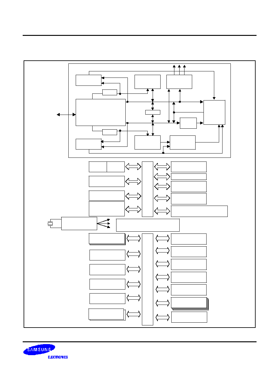
S3C2440A RISC MICROPROCESSOR
PRODUCT OVERVIEW
1-5
BLOCK DIAGRAM
ARM920T
ARM9TDMI
Processor core
(Internal Embedded ICE)
DD[31:0]
WriteBack
PA Tag
RAM
Data
MMU
C13
DVA[31:0]
DVA[31:0]
InstructionC
ACHE
(16KB)
Instruction
MMU
External
Coproc
Interface
C13
ID[31:0]
IPA[31:0]
IVA[31:0]
CP15
Write
Buffer
AMBA
Bus
I/F
JTAG
Data
CACHE
(16KB)
WBPA[31:0]
DPA[31:0]
Bridge & DMA (4Ch)
Clock Generator
(MPLL)
A
H
B
B
U
S
Memory CONT.
SRAM/NOR/SDRAM
BUS CONT.
Arbitor/Decode
Power
Management
Interrupt CONT.
USB Host CONT.
ExtMaster
LCD
DMA
LCD
CONT.
A
P
B
B
U
S
I2C
GPIO
I2S
RTC
SPI
ADC
SDI/MMC
USB Device
Watchdog
Timer
BUS CONT.
Arbitor/Decode
Timer/PWM
0 ~ 3, 4(Internal)
SPI 0, 1
UART 0, 1, 2
NAND Ctrl.
NAND Flash Boot
Loader
Camera
Interface
AC97
Figure 1-1. S3C2440A Block Diagram
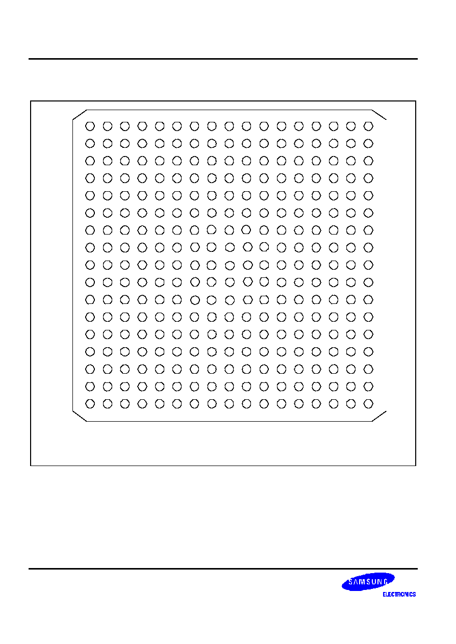
PRODUCT OVERVIEW
S3C2440A RISC MICROPROCESSOR
1-6
PIN ASSIGNMENTS
BOTTOM VIEW
U
T
R
P
N
M
L
K
J
H
G
F
E
D
C
B
A
1
2
3
4
5
6
7
8
9
10
11
12
13
14
15
16
17
Figure 1-2. S3C2440A Pin Assignments (289-FBGA)

S3C2440A RISC MICROPROCESSOR
PRODUCT OVERVIEW
1-7
Table 1-1. 289-Pin FBGA Pin Assignments ≠ Pin Number Order (Sheet 1 of 3)
Pin
Number
Pin Name
Pin
Number
Pin Name
Pin
Number
Pin Name
A1
VDDi
C1
VDDMOP
E1
nFRE/GPA20
A2
SCKE
C2
nGCS5/GPA16
E2
VSSMOP
A3
VSSi
C3
nGCS2/GPA13
E3
nGCS7
A4
VSSi
C4
nGCS3/GPA14
E4
nWAIT
A5
VSSMOP
C5
nOE
E5
nBE3
A6
VDDi
C6
nSRAS
E6
nWE
A7
VSSMOP
C7
ADDR4
E7
ADDR1
A8
ADDR10
C8
ADDR11
E8
ADDR6
A9
VDDMOP
C9
ADDR15
E9
ADDR14
A10
VDDi
C10
ADDR21/GPA6
E10
ADDR23/GPA8
A11
VSSMOP
C11
ADDR24/GPA9
E11
DATA2
A12
VSSi
C12
DATA1
E12
DATA20
A13
DATA3
C13
DATA6
E13
DATA19
A14
DATA7
C14
DATA11
E14
DATA18
A15
VSSMOP
C15
DATA13
E15
DATA17
A16
VDDi
C16
DATA16
E16
DATA21
A17
DATA10
C17
VSSi
E17
DATA24
B1
VSSMOP
D1
ALE/GPA18
F1
VDDi
B2
nGCS1/GPA12
D2
nGCS6
F2
VSSi
B3
SCLK1
D3
nGCS4/GPA15
F3
nFWE/GPA19
B4
SCLK0
D4
nBE0
F4
nFCE/GPA22
B5
nBE1
D5
nBE2
F5
CLE/GPA17
B6
VDDMOP
D6
nSCAS
F6
nGCS0
B7
ADDR2
D7
ADDR7
F7
ADDR0/GPA0
B8
ADDR9
D8
ADDR5
F8
ADDR3
B9
ADDR12
D9
ADDR16/GPA1
F9
ADDR18/GPA3
B10
VSSi
D10
ADDR20/GPA5
F10
DATA4
B11
VDDi
D11
ADDR26/GPA11
F11
DATA5
B12
VDDMOP
D12
DATA0
F12
DATA27
B13
VSSMOP
D13
DATA8
F13
DATA31
B14
VDDMOP
D14
DATA14
F14
DATA26
B15
DATA9
D15
DATA12
F15
DATA22
B16
VDDMOP
D16
VSSMOP
F16
VDDi
B17
DATA15
D17
VSSMOP
F17
VDDMOP

PRODUCT OVERVIEW
S3C2440A RISC MICROPROCESSOR
1-8
Table 1-1. 289-Pin FBGA Pin Assignments ≠ Pin Number Order (Sheet 2 of 3) (Continued)
Pin
Number
Pin Name
Pin
Number
Pin Name
Pin
Number
Pin Name
G1
VSSOP
J1
VDDOP
L1
LEND/GPC0
G2
CAMHREF/GPJ10
J2
VDDiarm
L2
VDDiarm
G3
CAMDATA1/GPJ1
J3
CAMCLKOUT/GPJ11
L3
nXDACK0/GPB9
G4
VDDalive
J4
CAMRESET/GPJ12
L4
VCLK/GPC1
G5
CAMPCLK/GPJ8
J5
TOUT1/GPB1
L5
nXBREQ/GPB6
G6
FRnB
J6
TOUT0/GPB0
L6
VD1/GPC9
G7
CAMVSYNC/GPJ9
J7
TOUT2/GPB2
L7
VFRAME/GPC3
G8
ADDR8
J8
CAMDATA6/GPJ6
L8
I2SSDI/AC_SDATA_IN
G9
ADDR17/GPA2
J9
SDDAT3/GPE10
L9
SPICLK0/GPE13
G10
ADDR25/GPA10
J10
EINT10/nSS0/GPG2
L10
EINT15/SPICLK1/GPG7
G11
DATA28
J11
TXD2/nRTS1/GPH6
L11
EINT22/GPG14
G12
DATA25
J12
PWREN
L12
Xtortc
G13
DATA23
J13
TCK
L13
EINT2/GPF2
G14
XTIpll
J14
TMS
L14
EINT5/GPF5
G15
XTOpll
J15
RXD2/nCTS1/GPH7
L15
EINT6/GPF6
G16
DATA29
J16
TDO
L16
EINT7/GPF7
G17
VSSi
J17
VDDalive
L17
nRTS0/GPH1
H1
VSSiarm
K1
VSSiarm
M1
VLINE/GPC2
H2
CAMDATA7/GPJ7
K2
nXBACK/GPB5
M2
LCD_LPCREV/GPC6
H3
CAMDATA4/GPJ4
K3
TOUT3/GPB3
M3
LCD_LPCOE/GPC5
H4
CAMDATA3/GPJ3
K4
TCLK0/GPB4
M4
VM/GPC4
H5
CAMDATA2/GPJ2
K5
nXDREQ1/GPB8
M5
VD9/GPD1
H6
CAMDATA0/GPJ0
K6
nXDREQ0/GPB10
M6
VD6/GPC14
H7
CAMDATA5/GPJ5
K7
nXDACK1/GPB7
M7
VD16/SPIMISO1/GPD8
H8
ADDR13
K8
SDCMD/GPE6
M8
SDDAT1/GPE8
H9
ADDR19/GPA4
K9
SPIMISO0/GPE11
M9
IICSDA/GPE15
H10
ADDR22/GPA7
K10
EINT13/SPIMISO1/GPG5
M10
EINT20/GPG12
H11
VSSOP
K11
nCTS0/GPH0
M11
EINT17/nRTS1/GPG9
H12
EXTCLK
K12
VDDOP
M12
VSSA_UPLL
H13
DATA30
K13
TXD0/GPH2
M13
VDDA_UPLL
H14
nBATT_FLT
K14
RXD0/GPH3
M14
Xtirtc
H15
nTRST
K15
UEXTCLK/GPH8
M15
EINT3/GPF3
H16
nRESET
K16
TXD1/GPH4
M16
EINT1/GPF1
H17
TDI
K17
RXD1/GPH5
M17
EINT4/GPF4
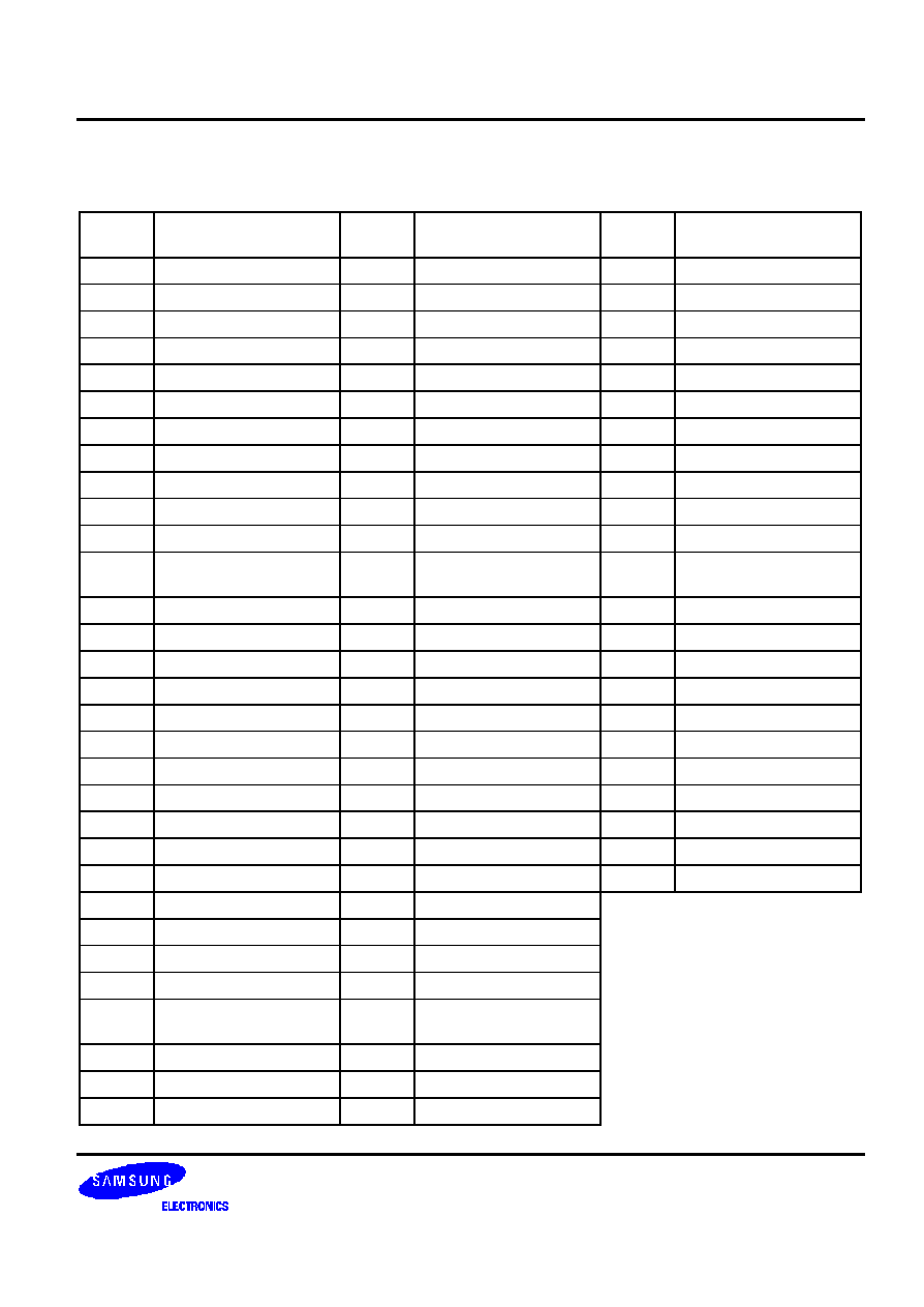
S3C2440A RISC MICROPROCESSOR
PRODUCT OVERVIEW
1-9
Table 1-1. 289-Pin FBGA Pin Assignments ≠ Pin Number Order (Sheet 3 of 3) (Continued)
Pin
Number
Pin Name
Pin
Number
Pin Name
Pin
Number
Pin Name
N1
VSSOP
P15
AIN3
T12
VDDOP
N2
VD0/GPC8
P16
XP/AIN7
T13
OM3
N3
VD4/GPC12
P17
UPLLCAP
T14
VSSA_ADC
N4
VD2/GPC10
R1
VD3/GPC11
T15
OM0
N5
VD10/GPD2
R2
VD8/GPD0
T16
YM/AIN4
N6
VD15/GPD7
R3
VD11/GPD3
T17
YP/AIN5
N7
VD22/nSS1/GPD14
R4
VD13/GPD5
U1
VDDiarm
N8
SDCLK/GPE5
R5
VD18/SPICLK1/GPD10
U2
VDDiarm
N9
EINT8/GPG0
R6
VD21 /GPD13
U3
VSSOP
N10
EINT18/nCTS1/GPG10
R7
I2SSCLK/AC_BIT_CLK
U4
VSSiarm
N11
DP0
R8
SDDAT0/GPE7
U5
VD23/nSS0/GPD15
N12
DN1/PDN0
R9
CLKOUT0/GPH9
U6
I2SSDO/AC_SDATA_
OUT
N13
nRSTOUT/GPA21
R10
EINT11/nSS1/GPG3
U7
VSSiarm
N14
MPLLCAP
R11
EINT14/SPIMOSI1/GPG6
U8
IICSCL/GPE14
N15
VDD_RTC
R12
NCON
U9
VSSOP
N16
VDDA_MPLL
R13
OM1
U10
VSSiarm
N17
EINT0/GPF0
R14
AIN0
U11
VDDi
P1
LCD_LPCREVB/GPC7
R15
AIN2
U12
EINT19/TCLK1/GPG11
P2
VD5/GPC13
R16
XM/AIN6
U13
EINT23/GPG15
P3
VD7/GPC15
R17
VSSA_MPLL
U14
DP1/PDP0
P4
VD12/GPD4
T1
VSSiarm
U15
VSSOP
P5
VD14/GPD6
T2
VSSiarm
U16
Vref
P6
VD20/GPD12
T3
VDDOP
U17
AIN1
P7
I2SLRCK/AC_SYNC
T4
VD17/SPIMOSI1/GPD9
P8
SDDAT2/GPE9
T5
VD19/GPD11
P9
SPIMOSI0/GPE12
T6
VDDiarm
P10
CLKOUT1/GPH10
T7
CDCLK/AC_nRESET
P11
EINT12/LCD_PWREN/
GPG4
T8
VDDiarm
P12
DN0
T9
EINT9/GPG1
P13
OM2
T10
EINT16/GPG8
P14
VDDA_ADC
T11
EINT21/GPG13
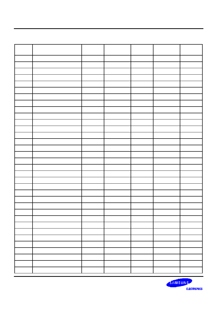
PRODUCT OVERVIEW
S3C2440A RISC MICROPROCESSOR
1-10
Table 1-2. S3C2440A 289-Pin FBGA Pin Assignments (Sheet 1 of 9)
Pin
Number
Pin
Name
Default
Function
I/O State
@BUS REQ
I/O State
@Sleep
I/O State
@nRESET
I/O
Type
F7
ADDR0/GPA0
ADDR0
Hi-z/≠
O(L)/≠
O(L)
t10s
E7
ADDR1
ADDR1
Hi-z
O(L)
O(L)
t10s
B7
ADDR2
ADDR2
Hi-z
O(L)
O(L)
t10s
F8
ADDR3
ADDR3
Hi-z
O(L)
O(L)
t10s
C7
ADDR4
ADDR4
Hi-z
O(L)
O(L)
t10s
D8
ADDR5
ADDR5
Hi-z
O(L)
O(L)
t10s
E8
ADDR6
ADDR6
Hi-z
O(L)
O(L)
t10s
D7
ADDR7
ADDR7
Hi-z
O(L)
O(L)
t10s
G8
ADDR8
ADDR8
Hi-z
O(L)
O(L)
t10s
B8
ADDR9
ADDR9
Hi-z
O(L)
O(L)
t10s
A8
ADDR10
ADDR10
Hi-z
O(L)
O(L)
t10s
C8
ADDR11
ADDR11
Hi-z
O(L)
O(L)
t10s
B9
ADDR12
ADDR12
Hi-z
O(L)
O(L)
t10s
H8
ADDR13
ADDR13
Hi-z
O(L)
O(L)
t10s
E9
ADDR14
ADDR14
Hi-z
O(L)
O(L)
t10s
C9
ADDR15
ADDR15
Hi-z
O(L)
O(L)
t10s
D9
ADDR16/GPA1
ADDR16
Hi-z/≠
O(L)/≠
O(L)
t10s
G9
ADDR17/GPA2
ADDR17
Hi-z/≠
O(L)/≠
O(L)
t10s
F9
ADDR18/GPA3
ADDR18
Hi-z/≠
O(L)/≠
O(L)
t10s
H9
ADDR19/GPA4
ADDR19
Hi-z/≠
O(L)/≠
O(L)
t10s
D10
ADDR20/GPA5
ADDR20
Hi-z/≠
O(L)/≠
O(L)
t10s
C10
ADDR21/GPA6
ADDR21
Hi-z/≠
O(L)/≠
O(L)
t10s
H10
ADDR22/GPA7
ADDR22
Hi-z/≠
O(L)/≠
O(L)
t10s
E10
ADDR23/GPA8
ADDR23
Hi-z/≠
O(L)/≠
O(L)
t10s
C11
ADDR24/GPA9
ADDR24
Hi-z/≠
O(L)/≠
O(L)
t10s
G10
ADDR25/GPA10
ADDR25
Hi-z/≠
O(L)/≠
O(L)
t10s
D11
ADDR26/GPA11
ADDR26
Hi-z/≠
O(L)/≠
O(L)
t10s
R14
AIN0
AIN0
≠
≠
AI
r10
U17
AIN1
AIN1
≠
≠
AI
r10
R15
AIN2
AIN2
≠
≠
AI
r10
P15
AIN3
AIN3
≠
≠
AI
r10
T16
YM/AIN4
AIN4
≠/≠
≠/≠
AI
r10
T17
YP/AIN5
YP
≠/≠
≠/≠
AI
r10
R16
XM/AIN6
AIN6
≠/≠
≠/≠
AI
r10

S3C2440A RISC MICROPROCESSOR
PRODUCT OVERVIEW
1-11
Table 1-2. S3C2440A 289-Pin FBGA Pin Assignments (Sheet 2 of 9) (Continued)
Pin
Number
Pin
Name
Default
Function
I/O State
@BUS REQ
I/O State
@Sleep
I/O State
@nRESET
I/O
Type
P16
XP/AIN7
XP
≠/≠
≠/≠
AI
r10
H6
CAMDATA0/GPJ0
GPJ0
≠/≠
Hi-z/≠
I
t8
G3
CAMDATA1/GPJ1
GPJ1
≠/≠
Hi-z/≠
I
t8
H5
CAMDATA2/GPJ2
GPJ2
≠/≠
Hi-z/≠
I
t8
H4
CAMDATA3/GPJ3
GPJ3
≠/≠
Hi-z/≠
I
t8
H3
CAMDATA4/GPJ4
GPJ4
≠/≠
Hi-z/≠
I
t8
H7
CAMDATA5/GPJ5
GPJ5
≠/≠
Hi-z/≠
I
t8
J8
CAMDATA6/GPJ6
GPJ6
≠/≠
Hi-z/≠
I
t8
H2
CAMDATA7/GPJ7
GPJ7
≠/≠
Hi-z/≠
I
t8
G5
CAMPCLK/GPJ8
GPJ8
≠/≠
Hi-z/≠
I
t8
G7
CAMVSYNC/GPJ9
GPJ9
≠/≠
Hi-z/≠
I
t8
G2
CAMHREF/GPJ10
GPJ10
≠/≠
Hi-z/≠
I
t8
J3
CAMCLKOUT/GPJ11
GPJ11
≠/≠
O(L)/≠
I
t8
J4
CAMRESET/GPJ12
GPJ12
≠/≠
O(L)/≠
I
t8
D12
DATA0
DATA0
Hi-z
Hi-z,O(L)
I
b12s
C12
DATA1
DATA1
Hi-z
Hi-z,O(L)
I
b12s
E11
DATA2
DATA2
Hi-z
Hi-z,O(L)
I
b12s
A13
DATA3
DATA3
Hi-z
Hi-z,O(L)
I
b12s
F10
DATA4
DATA4
Hi-z
Hi-z,O(L)
I
b12s
F11
DATA5
DATA5
Hi-z
Hi-z,O(L)
I
b12s
C13
DATA6
DATA6
Hi-z
Hi-z,O(L)
I
b12s
A14
DATA7
DATA7
Hi-z
Hi-z,O(L)
I
b12s
D13
DATA8
DATA8
Hi-z
Hi-z,O(L)
I
b12s
B15
DATA9
DATA9
Hi-z
Hi-z,O(L)
I
b12s
A17
DATA10
DATA10
Hi-z
Hi-z,O(L)
I
b12s
C14
DATA11
DATA11
Hi-z
Hi-z,O(L)
I
b12s
D15
DATA12
DATA12
Hi-z
Hi-z,O(L)
I
b12s
C15
DATA13
DATA13
Hi-z
Hi-z,O(L)
I
b12s
D14
DATA14
DATA14
Hi-z
Hi-z,O(L)
I
b12s
B17
DATA15
DATA15
Hi-z
Hi-z,O(L)
I
b12s
C16
DATA16
DATA16
Hi-z
Hi-z,O(L)
I
b12s
E15
DATA17
DATA17
Hi-z
Hi-z,O(L)
I
b12s
E14
DATA18
DATA18
Hi-z
Hi-z,O(L)
I
b12s
PRODUCT OVERVIEW
S3C2440A RISC MICROPROCESSOR
1-12
Table 1-2. S3C2440A 289-Pin FBGA Pin Assignments (Sheet 3 of 9) (Continued)
Pin
Number
Pin
Name
Default
Function
I/O State
@BUS REQ
I/O State
@Sleep
I/O State
@nRESET
I/O
Type
E13
DATA19
DATA19
Hi-z
Hi-z,O(L)
I
b12s
E12
DATA20
DATA20
Hi-z
Hi-z,O(L)
I
b12s
E16
DATA21
DATA21
Hi-z
Hi-z,O(L)
I
b12s
F15
DATA22
DATA22
Hi-z
Hi-z,O(L)
I
b12s
G13
DATA23
DATA23
Hi-z
Hi-z,O(L)
I
b12s
E17
DATA24
DATA24
Hi-z
Hi-z,O(L)
I
b12s
G12
DATA25
DATA25
Hi-z
Hi-z,O(L)
I
b12s
F14
DATA26
DATA26
Hi-z
Hi-z,O(L)
I
b12s
F12
DATA27
DATA27
Hi-z
Hi-z,O(L)
I
b12s
G11
DATA28
DATA28
Hi-z
Hi-z,O(L)
I
b12s
G16
DATA29
DATA29
Hi-z
Hi-z,O(L)
I
b12s
H13
DATA30
DATA30
Hi-z
Hi-z,O(L)
I
b12s
F13
DATA31
DATA31
Hi-z
Hi-z,O(L)
I
b12s
P12
DN0
DN0
≠
≠
AI
us
N11
DP0
DP0
≠
≠
AI
us
N12
DN1/PDN0
DN1
≠/≠
≠
AI
us
U14
DP1/PDP0
DP1
≠/≠
≠
AI
us
N17
EINT0/GPF0
GPF0
≠/≠
Hi-z/≠
I
t8
M16
EINT1/GPF1
GPF1
≠/≠
Hi-z/≠
I
t8
L13
EINT2/GPF2
GPF2
≠/≠
Hi-z/≠
I
t8
M15
EINT3/GPF3
GPF3
≠/≠
Hi-z/≠
I
t8
M17
EINT4/GPF4
GPF4
≠/≠
Hi-z/≠
I
t8
L14
EINT5/GPF5
GPF5
≠/≠
Hi-z/≠
I
t8
L15
EINT6/GPF6
GPF6
≠/≠
Hi-z/≠
I
t8
L16
EINT7/GPF7
GPF7
≠/≠
Hi-z/≠
I
t8
N9
EINT8/GPG0
GPG0
≠/≠
Hi-z/≠
I
t8
T9
EINT9/GPG1
GPG1
≠/≠
Hi-z/≠
I
t8
J10
EINT10/nSS0/GPG2
GPG2
≠/≠/≠
Hi-z/Hi-z/≠
I
t8
R10
EINT11/nSS1/GPG3
GPG3
≠/≠/≠
Hi-z/Hi-z/≠
I
t8
P11
EINT12/LCD_PWREN/GPG
4
GPG4
≠/≠/≠
Hi-z/O(L)/≠
I
t8
K10
EINT13/SPIMISO1/GPG5
GPG5
≠/≠/≠
Hi-z/Hi-z/≠
I
t8
R11
EINT14/SPIMOSI1/GPG6
GPG6
≠/≠/≠
Hi-z/Hi-z/≠
I
t8
L10
EINT15/SPICLK1/GPG7
GPG7
≠/≠/≠
Hi-z/Hi-z/≠
I
t8

S3C2440A RISC MICROPROCESSOR
PRODUCT OVERVIEW
1-13
Table 1-2. S3C2440A 289-Pin FBGA Pin Assignments (Sheet 4 of 9) (Continued)
Pin
Number
Pin
Name
Default
Function
I/O State
@BUS REQ
I/O State
@Sleep
I/O State
@nRESET
I/O
Type
T10
EINT16/GPG8
GPG8
≠/≠
Hi-z/≠
I
t8
M11
EINT17/nRTS1/GPG9
GPG9
≠/≠/≠
Hi-z/O(H)/≠
I
t8
N10
EINT18/nCTS1/GPG10
GPG10
≠/≠/≠
Hi-z/Hi-z/≠
I
t8
U12
EINT19/TCLK1/GPG11
GPG11
≠/≠/≠
Hi-z/Hi-z/≠
I
t12
M10
EINT20/GPG12
GPG12
≠/≠
Hi-z/≠
I
t12
T11
EINT21/GPG13
GPG13
≠/≠
Hi-z/≠
I
t12
L11
EINT22/GPG14
GPG14
≠/≠
Hi-z/≠
I
t12
U13
EINT23/GPG15
GPG15
≠/≠
Hi-z/≠
I
t12
H12
EXTCLK
EXTCLK
≠
≠
AI
is
P17
UPLLCAP
UPLLCAP
≠
≠
AI
r50
N14
MPLLCAP
MPLLCAP
≠
≠
AI
r50
H14
nBATT_FLT
nBATT_FLT
≠
≠
I
is
D4
nBE0
nBE0
Hi-z
Hi-z,O(H)
O(H)
t10s
B5
nBE1
nBE1
Hi-z
Hi-z,O(H)
O(H)
t10s
D5
nBE2
nBE2
Hi-z
Hi-z,O(H)
O(H)
t10s
E5
nBE3
nBE3
Hi-z
Hi-z,O(H)
O(H)
t10s
R12
NCON
NCON
≠
≠
I
is
G6
FRnB
FRnB
≠
Hi-z,O(L)
I
d2s
F3
nFWE/GPA19
GPA19
O(H)/≠
Hi-z,O(H)/≠
O(H)
t10s
E1
nFRE/GPA20
GPA20
O(H)/≠
Hi-z,O(H)/≠
O(H)
t10s
F4
nFCE/GPA22
GPA21
O(H)/≠
Hi-z,O(H)/≠
O(H)
t10s
F5
CLE/GPA17
GPA17
O(L)/≠
Hi-z,O(L)/≠
O(L)
t10s
D1
ALE/GPA18
GPA18
O(L)/≠
Hi-z,O(L)/≠
O(L)
t10s
N13
nRSTOUT/GPA21
GPA21
≠/≠
O(L)/≠
O(L)
b8
C5
nOE
nOE
Hi-z
Hi-z,O(H)
O(H)
t10s
H16
nRESET
nRESET
≠
≠
I
is
F6
nGCS0
nGCS0
Hi-z
Hi-z,O(H)
O(H)
t10s
B2
nGCS1/GPA12
GPA12
Hi-z/≠
Hi-z,O(H)/≠
O(H)
t10s
C3
nGCS2/GPA13
GPA13
Hi-z/≠
Hi-z,O(H)/≠
O(H)
t10s
C4
nGCS3/GPA14
GPA14
Hi-z/≠
Hi-z,O(H)/≠
O(H)
t10s
D3
nGCS4/GPA15
GPA15
Hi-z/≠
Hi-z,O(H)/≠
O(H)
t10s
C2
nGCS5/GPA16
GPA16
Hi-z/≠
Hi-z,O(H)/≠
O(H)
t10s
D2
nGCS6
nGCS6
Hi-z
Hi-z,O(H)
O(H)
t10s

PRODUCT OVERVIEW
S3C2440A RISC MICROPROCESSOR
1-14
Table 1-2. S3C2440A 289-Pin FBGA Pin Assignments (Sheet 5 of 9) (Continued)
Pin
Number
Pin
Name
Default
Function
I/O State
@BUS REQ
I/O State
@Sleep
I/O State
@nRESET
I/O
Type
E3
nGCS7
nGCS7
Hi-z
Hi-z,O(H)
O(H)
t10s
D6
nSCAS
nSCAS
Hi-z
Hi-z,O(H)
O(H)
t10s
C6
nSRAS
nSRAS
Hi-z
Hi-z,O(H)
O(H)
t10s
H15
nTRST
nTRST
I
≠
I
is
E4
nWAIT
nWAIT
≠
Hi-z,O(L)
I
d2s
E6
nWE
nWE
Hi-z
Hi-z,O(H)
O(H)
t10s
J6
TOUT0/GPB0
GPB0
≠/≠
O(L)/≠
I
t8
J5
TOUT1/GPB1
GPB1
≠/≠
O(L)/≠
I
t8
J7
TOUT2/GPB2
GPB2
≠/≠
O(L)/≠
I
t8
K3
TOUT3/GPB3
GPB3
≠/≠
O(L)/≠
I
t8
K4
TCLK0/GPB4
GPB4
≠/≠
≠/≠
I
t8
K2
nXBACK/GPB5
GPB5
≠/≠
O(H)/≠
I
t8
L5
nXBREQ/GPB6
GPB6
≠/≠
≠/≠
I
t8
K7
nXDACK1/GPB7
GPB7
≠/≠
O(H)/≠
I
t8
K5
nXDREQ1/GPB8
GPB8
≠/≠
≠/≠
I
t8
L3
nXDACK0/GPB9
GPB9
≠/≠
O(H)/≠
I
t8
K6
nXDREQ0/GPB10
GPB10
≠/≠
≠/≠
I
t8
T15
OM0
OM0
≠
≠
I
is
R13
OM1
OM1
≠
≠
I
is
P13
OM2
OM2
≠
≠
I
is
T13
OM3
OM3
≠
≠
I
is
J12
PWREN
PWREN
O(H)
O(L)
O(H)
b8
K11
nCTS0/GPH0
GPH0
≠/≠
≠/≠
I
t8
L17
nRTS0/GPH1
GPH1
≠/≠
O(H)/≠
I
t8
K13
TXD0/GPH2
GPH2
≠/≠
O(H)/≠
I
t8
K14
RXD0/GPH3
GPH3
≠/≠
≠/≠
I
t8
K16
TXD1/GPH4
GPH4
≠/≠
O(H)/≠
I
t8
K17
RXD1/GPH5
GPH5
≠/≠
≠/≠
I
t8
J11
TXD2/nRTS1/GPH6
GPH6
≠/≠/≠
O(H)/O(H)/≠
I
t8
J15
RXD2/nCTS1/GPH7
GPH7
≠/≠/≠
Hi-z/Hi-z/≠
I
t8
K15
UEXTCLK/GPH8
GPH8
≠/≠
Hi-z/≠
I
t8
R9
CLKOUT0/GPH9
GPH9
≠/≠
O(L)/≠
I
t12
P10
CLKOUT1/GPH10
GPH10
≠/≠
O(L)/≠
I
t12
S3C2440A RISC MICROPROCESSOR
PRODUCT OVERVIEW
1-15
Table 1-2. S3C2440A 289-Pin FBGA Pin Assignments (Sheet 6 of 9) (Continued)
Pin
Number
Pin
Name
Default
Function
I/O State
@BUS REQ
I/O State
@Sleep
I/O State
@nRESET
I/O
Type
A2
SCKE
SCKE
Hi-z
O(L)
O(H)
t10s
B4
SCLK0
SCLK0
Hi-z
O(L)
O(SCLK)
t12s
B3
SCLK1
SCLK1
Hi-z
O(L)
O(SCLK)
t12s
P7
I2SLRCK/AC_SYNC
GPE0
≠/≠
Hi-z/≠
I
t8
R7
I2SSCLK/AC_BIT_CLK
GPE1
≠/≠
Hi-z/≠
I
t8
T7
CDCLK/AC_nRESET
GPE2
≠/≠
Hi-z/≠
I
t8
L8
I2SSDI/AC_SDATA_IN
GPE3
≠/≠/≠
Hi-z/Hi-z/≠
I
t8
U6
I2SSDO/AC_SDATA_OUT
GPE4
≠/≠/≠
O(L)/Hi-z/≠
I
t8
N8
SDCLK/GPE5
GPE5
≠/≠
O(L)/≠
I
t8
K8
SDCMD/GPE6
GPE6
≠/≠
Hi-z/≠
I
t8
R8
SDDAT0/GPE7
GPE7
≠/≠
Hi-z/≠
I
t8
M8
SDDAT1/GPE8
GPE8
≠/≠
Hi-z/≠
I
t8
P8
SDDAT2/GPE9
GPE9
≠/≠
Hi-z/≠
I
t8
J9
SDDAT3/GPE10
GPE10
≠/≠
Hi-z/≠
I
t8
K9
SPIMISO0/GPE11
GPE11
≠/≠
Hi-z/≠
I
t8
P9
SPIMOSI0/GPE12
GPE12
≠/≠
Hi-z/≠
I
t8
L9
SPICLK0/GPE13
GPE13
≠/≠
Hi-z/≠
I
t8
U8
IICSCL/GPE14
GPE14
≠/≠
Hi-z/≠
I
d8
M9
IICSDA/GPE15
GPE15
≠/≠
Hi-z/≠
I
d8
J13
TCK
TCK
I
≠
I
is
H17
TDI
TDI
I
≠
I
is
J16
TDO
TDO
O
O
O
ot
J14
TMS
TMS
I
≠
I
is
L1
LEND/GPC0
GPC0
≠/≠
O(L)/≠
I
t8
L4
VCLK/GPC1
GPC1
≠/≠
O(L)/≠
I
t8
M1
VLINE/GPC2
GPC2
≠/≠
O(L)/≠
I
t8
L7
VFRAME/GPC3
GPC3
≠/≠
O(L)/≠
I
t8
M4
VM/GPC4
GPC4
≠/≠
O(L)/≠
I
t8
M3
LCD_LPCOE/GPC5
GPC5
≠/≠
O(L)/≠
I
t8
M2
LCD_LPCREV/GPC6
GPC6
≠/≠
O(L)/≠
I
t8
P1
LCD_LPCREVB/GPC7
GPC7
≠/≠
O(L)/≠
I
t8
N2
VD0/GPC8
GPC8
≠/≠
O(L)/≠
I
t8
L6
VD1/GPC9
GPC9
≠/≠
O(L)/≠
I
t8
PRODUCT OVERVIEW
S3C2440A RISC MICROPROCESSOR
1-16
Table 1-2. S3C2440A 289-Pin FBGA Pin Assignments (Sheet 7 of 9) (Continued)
Pin
Number
Pin
Name
Default
Function
I/O State
@BUS REQ
I/O State
@Sleep
I/O State
@nRESET
I/O
Type
N4
VD2/GPC10
GPC10
≠/≠
O(L)/≠
I
t8
R1
VD3/GPC11
GPC11
≠/≠
O(L)/≠
I
t8
N3
VD4/GPC12
GPC12
≠/≠
O(L)/≠
I
t8
P2
VD5/GPC13
GPC13
≠/≠
O(L)/≠
I
t8
M6
VD6/GPC14
GPC14
≠/≠
O(L)/≠
I
t8
P3
VD7/GPC15
GPC15
≠/≠
O(L)/≠
I
t8
R2
VD8/GPD0
GPD0
≠/≠
O(L)/≠
I
t8
M5
VD9/GPD1
GPD1
≠/≠
O(L)/≠
I
t8
N5
VD10/GPD2
GPD2
≠/≠
O(L)/≠
I
t8
R3
VD11/GPD3
GPD3
≠/≠
O(L)/≠
I
t8
P4
VD12/GPD4
GPD4
≠/≠
O(L)/≠
I
t8
R4
VD13/ GPD5
GPD5
≠/≠/≠
O(L)/O/≠
I
t8
P5
VD14/GPD6
GPD6
≠/≠/≠
O(L)/O/≠
I
t8
N6
VD15/GPD7
GPD7
≠/≠/≠
O(L)/O/≠
I
t8
M7
VD16/SPIMISO1/GPD8
GPD8
≠/≠/≠
O(L)/Hi-z/≠
I
t8
T4
VD17/SPIMOSI1/GPD9
GPD9
≠/≠/≠
O(L)/Hi-z/≠
I
t8
R5
VD18/SPICLK1/GPD10
GPD10
≠/≠/≠
O(L)/Hi-z/≠
I
t8
T5
VD19//GPD11
GPD11
≠/≠/≠
O(L)/Hi-z/≠
I
t8
P6
VD20/ GPD12
GPD12
≠/≠/≠
O(L)/Hi-z/≠
I
t8
R6
VD21/ GPD13
GPD13
≠/≠/≠
O(L)/Hi-z/≠
I
t8
N7
VD22/nSS1/GPD14
GPD14
≠/≠/≠
O(L)/Hi-z/≠
I
t8
U5
VD23/nSS0/GPD15
GPD15
≠/≠/≠
O(L)/Hi-z/≠
I
t8
U16
Vref
Vref
≠
≠
AI
ia
G14
XTIpll
XTIpll
≠
≠
AI
m26
M14
Xtirtc
Xtirtc
≠
≠
AI
nc
G15
XTOpll
XTOpll
≠
≠
AO
m26
L12
Xtortc
Xtortc
≠
≠
AO
nc
N15
VDD_RTC
VDD_RTC
P
P
P
drtc
P14
VDDA_ADC
VDDA_ADC
P
P
P
d33th
N16
VDDA_MPLL
VDDA_MPLL
P
P
P
d12t
M13
VDDA_UPLL
VDDA_UPLL
P
P
P
d12t
G4
VDDalive
VDDalive
P
P
P
d12i
J17
VDDalive
VDDalive
P
P
P
d12i

S3C2440A RISC MICROPROCESSOR
PRODUCT OVERVIEW
1-17
Table 1-2. S3C2440A 289-Pin FBGA Pin Assignments (Sheet 8 of 9) (Continued)
Pin
Number
Pin
Name
Default
Function
I/O State
@BUS REQ
I/O State
@Sleep
I/O State
@nRESET
I/O
Type
A1
VDDi
VDDi
P
P
P
d12c
A10
VDDi
VDDi
P
P
P
d12c
A16
VDDi
VDDi
P
P
P
d12c
A6
VDDi
VDDi
P
P
P
d12c
B11
VDDi
VDDi
P
P
P
d12c
F1
VDDi
VDDi
P
P
P
d12c
F16
VDDi
VDDi
P
P
P
d12c
U11
VDDi
VDDi
P
P
P
d12c
L2
VDDiarm
VDDiarm
P
P
P
d12c
T6
VDDiarm
VDDiarm
P
P
P
d12c
T8
VDDiarm
VDDiarm
P
P
P
d12c
U1
VDDiarm
VDDiarm
P
P
P
d12c
J2
VDDiarm
VDDiarm
P
P
P
d12c
U2
VDDiarm
VDDiarm
P
P
P
d12c
A9
VDDMOP
VDDMOP
P
P
P
d33o
B12
VDDMOP
VDDMOP
P
P
P
d33o
B14
VDDMOP
VDDMOP
P
P
P
d33o
B16
VDDMOP
VDDMOP
P
P
P
d33o
B6
VDDMOP
VDDMOP
P
P
P
d33o
C1
VDDMOP
VDDMOP
P
P
P
d33o
F17
VDDMOP
VDDMOP
P
P
P
d33o
J1
VDDOP
VDDOP
P
P
P
d33o
T12
VDDOP
VDDOP
P
P
P
d33o
T3
VDDOP
VDDOP
P
P
P
d33o
K12
VDDOP
VDDOP
P
P
P
d33o
T14
VSSA_ADC
VSSA_ADC
P
P
P
sth
R17
VSSA_MPLL
VSSA_MPLL
P
P
P
st
M12
VSSA_UPLL
VSSA_UPLL
P
P
P
st
A12
VSSi
VSSi
P
P
P
si
A3
VSSi
VSSi
P
P
P
si
A4
VSSi
VSSi
P
P
P
si
B10
VSSi
VSSi
P
P
P
si
C17
VSSi
VSSi
P
P
P
si
PRODUCT OVERVIEW
S3C2440A RISC MICROPROCESSOR
1-18
Table 1-2. S3C2440A 289-Pin FBGA Pin Assignments (Sheet 9 of 9) (Continued)
Pin
Number
Pin
Name
Default
Function
I/O State
@BUS REQ
I/O State
@Sleep
I/O State
@nRESET
I/O
Type
F2
VSSi
VSSi
P
P
P
si
G17
VSSi
VSSi
P
P
P
si
H1
VSSiarm
VSSiarm
P
P
P
si
K1
VSSiarm
VSSiarm
P
P
P
si
T1
VSSiarm
VSSiarm
P
P
P
si
T2
VSSiarm
VSSiarm
P
P
P
si
U10
VSSiarm
VSSiarm
P
P
P
si
U4
VSSiarm
VSSiarm
P
P
P
si
U7
VSSiarm
VSSiarm
P
P
P
si
A11
VSSMOP
VSSMOP
P
P
P
so
A15
VSSMOP
VSSMOP
P
P
P
so
A5
VSSMOP
VSSMOP
P
P
P
so
A7
VSSMOP
VSSMOP
P
P
P
so
B1
VSSMOP
VSSMOP
P
P
P
so
B13
VSSMOP
VSSMOP
P
P
P
so
D16
VSSMOP
VSSMOP
P
P
P
so
D17
VSSMOP
VSSMOP
P
P
P
so
E2
VSSMOP
VSSMOP
P
P
P
so
G1
VSSOP
VSSOP
P
P
P
so
N1
VSSOP
VSSOP
P
P
P
so
U15
VSSOP
VSSOP
P
P
P
so
U3
VSSOP
VSSOP
P
P
P
so
U9
VSSOP
VSSOP
P
P
P
so
H11
VSSOP
VSSOP
P
P
P
so
NOTES:
1.
The @BUS REQ. shows the pin state at the external bus, which is used by the other bus master.
2.
' ≠ ` mark indicates the unchanged pin state at Bus Request mode.
3. Hi-z or Pre means Hi-z or early state and it is determined by the setting of MISCCR register.
4. AI/AO means analog input/analog output.
5. P, I, and O mean power, input and output respectively.
6. The I/O state @nRESET shows the pin status in the @nRESET duration below.
nRESET
FCLK
@nRESET
4 OSCin

S3C2440A RISC MICROPROCESSOR
PRODUCT OVERVIEW
1-19
The table below shows I/O types and descriptions.
Input (I)/Output (O) Type
Descriptions
d12i(vdd12ih)
1.2V V
DD
for alive power
d12c(vdd12ih_core), si(vssih)
1.2V V
DD
/V
SS
for internal logic
d33o(vdd33oph), so(vssoph)
3.3V V
DD
/V
SS
for external logic
d33th(vdd33th_abb),sth(vssbbh_abb)
3.3V V
DD
/V
SS
for analog circuitry
d12t(vdd12t_abb), st(vssbb_abb)
1.2V V
DD
/V
SS
for analog circuitry
drtc(vdd30th_rtc)
3.0V V
DD
for RTC power
t8(phbsu100ct8sm)
Bi-directional pad, LVCMOS schmitt-trigger, 100k
pull-up resistor with
control, tri-state, Io = 8mA
is(phis)
Input pad, LVCMOS schmitt-trigger level
us(pbusb0)
USB pad
t10(phtot10cd)
5V tolerant output pad, tri-state.
ot(phot8)
Output pad, tri-state, Io = 8mA
b8(phob8)
Output pad, Io = 8mA
t16(phot16sm)
Output pad, tri-state, medium slew rate, Io = 16mA
r10(phiar10_abb)
Analog input pad with 10
resistor
ia(phia_abb)
Analog input pad
gp(phgpad_option)
Pad for analog pin
m26(phsoscm26_2440a)
Oscillator cell with enable and feedback resistor
t12(phbsu100ct12sm)
Bi-directional pad, LVCMOS schmitt-trigger, 100k
pull-up resistor with
control, tri-state, Io = 12mA
d8(phbsd8sm)
Bi-directional pad, LVCMOS schmitt-trigger, open drain, Io = 8mA
t10s(phtot10cd_10_2440a)
output pad, LVCMOS, tri -state, output drive strenth control, Io = 4, 6, 8,
10mA
b12s(phtbsu100ct12cd_12_2440a)
Bi-directional pad, LVCMOS schmitt-trigger, 100k
pull-up resistor with
control, tri -state,output drive strenth control, Io = 6, 8, 10, 12mA
d2s(phtbsd2_2440a)
Bi-directional pad, LVCMOS schmitt-trigger, open-drain, output drive
strenth ignore,
r50(phoar50_abb)
Analog output pad, 50k
resistor, separated bulk-bias
t12s(phtot12cd_12_2440a)
output pad, LVCMOS, tri -state, output drive strenth control, Io = 6, 8,
10, 12mA
nc(phnc)
No connection pad
PRODUCT OVERVIEW
S3C2440A RISC MICROPROCESSOR
1-20
SIGNAL DESCRIPTIONS
Table 1-3. S3C2440A Signal Descriptions (Sheet 1 of 6)
Signal
Input/Output
Descriptions
Bus Controller
OM[1:0]
I
OM[1:0] sets S3C2440A in the TEST mode, which is used only at fabrication.
Also, it determines the bus width of nGCS0. The pull-up/down resistor
determines the logic level during RESET cycle.
00: Nand-boot
01: 16-bit 10: 32-bit
11: Test mode
ADDR[26:0]
O
ADDR[26:0] (Address Bus) outputs the memory address of the corresponding
bank .
DATA[31:0]
IO
DATA[31:0] (Data Bus) inputs data during memory read and outputs data during
memory write. The bus width is programmable among 8/16/32-bit.
nGCS[7:0]
O
nGCS[7:0] (General Chip Select) are activated when the address of a memory is
within the address region of each bank. The number of access cycles and the
bank size can be programmed.
nWE
O
nWE (Write Enable) indicates that the current bus cycle is a write cycle.
nOE
O
nOE (Output Enable) indicates that the current bus cycle is a read cycle.
nXBREQ
I
nXBREQ (Bus Hold Request) allows another bus master to request control of the
local bus. BACK active indicates that bus control has been granted.
nXBACK
O
nXBACK (Bus Hold Acknowledge) indicates that the S3C2440A has surrendered
control of the local bus to another bus master.
nWAIT
I
nWAIT requests to prolong a current bus cycle. As long as nWAIT is L, the
current bus cycle cannot be completed.
SDRAM/SRAM
nSRAS
O
SDRAM row address strobe
nSCAS
O
SDRAM column address strobe
nSCS[1:0]
O
SDRAM chip select
DQM[3:0]
O
SDRAM data mask
SCLK[1:0]
O
SDRAM clock
SCKE
O
SDRAM clock enable
nBE[3:0]
O
Upper byte/lower byte enable (In case of 16-bit SRAM)
nWBE[3:0]
O
Write byte enable
NAND Flash
CLE
O
Command latch enable
ALE
O
Address latch enable
nFCE
O
Nand flash chip enable
nFRE
O
Nand flash read enable
nFWE
O
Nand flash write enable
NCON
I
Nand flash configuration
* If NAND flash controller isn't used, it
has to be pull-up. (VDDMOP)
FRnB
I
Nand flash ready/busy
S3C2440A RISC MICROPROCESSOR
PRODUCT OVERVIEW
1-21
Table 1-3. S3C2440A Signal Descriptions (Sheet 2 of 6) (Continued)
Signal
Input/
Output
Descriptions
LCD Control Unit
VD[23:0]
O
STN/TFT/SEC TFT: LCD data bus
LCD_PWREN
O
STN/TFT/SEC TFT: LCD panel power enable control signal
VCLK
O
STN/TFT: LCD clock signal
VFRAME
O
STN: LCD frame signal
VLINE
O
STN: LCD line signal
VM
O
STN: VM alternates the polarity of the row and column voltage
VSYNC
O
TFT: Vertical synchronous signal
HSYNC
O
TFT: Horizontal synchronous signal
VDEN
O
TFT: Data enable signal
LEND
O
TFT: Line end signal
STV
O
SEC TFT: SEC(Samsung Electronics Company) TFT LCD panel control signal
CPV
O
SEC TFT: SEC(Samsung Electronics Company) TFT LCD panel control signal
LCD_HCLK
O
SEC TFT: SEC(Samsung Electronics Company) TFT LCD panel control signal
TP
O
SEC TFT: SEC(Samsung Electronics Company) TFT LCD panel control signal
STH
O
SEC TFT: SEC(Samsung Electronics Company) TFT LCD panel control signal
LCD_LPCOE
O
SEC TFT: Timing control signal for specific TFT LCD
LCD_LPCREV
O
SEC TFT: Timing control signal for specific TFT LCD
LCD_LPCREVB
O
SEC TFT: Timing control signal for specific TFT LCD
CAMERA Interface
CAMRESET
O
Software reset to the camera
CAMCLKOUT
O
Master clock to the camera
CAMPCLK
I
Pixel clock from camera
CAMHREF
I
Horizontal sync signal from camera
CAMVSYNC
I
Vertical sync signal from camera
CAMDATA[7:0]
I
Pixel data for YCbCr
Interrupt Control Unit
EINT[23:0]
I
External interrupt request
DMA
nXDREQ[1:0]
I
External DMA request
nXDACK[1:0]
O
External DMA acknowledge
PRODUCT OVERVIEW
S3C2440A RISC MICROPROCESSOR
1-22
Table 1-3. S3C2440A Signal Descriptions (Sheet 3 of 6) (Continued)
Signal
Input/Output
Descriptions
UART
RxD[2:0]
I
UART receives data input
TxD[2:0]
O
UART transmits data output
nCTS[1:0]
I
UART clear to send input signal
nRTS[1:0]
O
UART request to send output signal
UEXTCLK
I
External clock input for UART
ADC
AIN[7:0]
AI
ADC input[7:0]. If it isn't used pin, it has to be low (ground).
Vref
AI
ADC Vref
IIC-Bus
IICSDA
IO
IIC-bus data
IICSCL
IO
IIC-bus clock
IIS-Bus
I2SLRCK
IO
IIS-bus channel select clock
I2SSDO
O
IIS-bus serial data output
I2SSDI
I
IIS-bus serial data input
I2SSCLK
IO
IIS-bus serial clock
CDCLK
O
CODEC system clock
AC'97
AC_SYNC
48kHz fixed rate sample sync
AC_BIT_CLK
IO
12.288MHz serial data clock
AC_nRESET
O
AC'97 Master H/W Reset
AC_SDATA_IN
I
Serial, time division multiplexed, AC'97 input stream
AC_SDATA_OUT
O
Serial, time division multiplexed, AC'97 output stream
Touch Screen
nXPON
O
Plus X-axis on-off control signal
XMON
O
Minus X-axis on-off control signal
nYPON
O
Plus Y-axis on-off control signal
YMON
O
Minus Y-axis on-off control signal
USB Host
DN[1:0]
IO
DATA(≠) from USB host. (Need to 15k
pull-down)
DP[1:0]
IO
DATA(+) from USB host. (Need to 15k
pull-down)
USB Device
PDN0
IO
DATA(≠) for USB peripheral.
(Need to 470k
pull-down for power consumption in sleep mode)
PDP0
IO
DATA(+) for USB peripheral. (Need to 1.5k
pull-up)
S3C2440A RISC MICROPROCESSOR
PRODUCT OVERVIEW
1-23
Table 1-3. S3C2440A Signal Descriptions (Sheet 4 of 6) (Continued)
Signal
Input/Output
Description
SPI
SPIMISO[1:0]
IO
SPIMISO is the master data input line, when SPI is configured as a master.
When SPI is configured as a slave, these pins reverse its role.
SPIMOSI[1:0]
IO
SPIMOSI is the master data output line, when SPI is configured as a master.
When SPI is configured as a slave, these pins reverse its role.
SPICLK[1:0]
IO
SPI clock
nSS[1:0]
I
SPI chip select(only for slave mode)
SD
SDDAT[3:0]
IO
SD receive/transmit data
SDCMD
IO
SD receive response/ transmit command
SDCLK
O
SD clock
General Port
GPn[129:0]
IO
General input/output ports (some ports are output only)
TIMMER/PWM
TOUT[3:0]
O
Timer output[3:0]
TCLK[1:0]
I
External timer clock input
JTAG TEST LOGIC
nTRST
I
nTRST (TAP Controller Reset) resets the TAP controller at start.
If debugger is used, A 10K pull-up resistor has to be connected.
If debugger (black ICE) is not used, nTRST pin must be issued by a low active
pulse (Typically connected to nRESET).
TMS
I
TMS (TAP Controller Mode Select) controls the sequence of the TAP controller's
states. A 10K pull-up resistor has to be connected to TMS pin.
TCK
I
TCK (TAP Controller Clock) provides the clock input for the JTAG logic.
A 10K pull-up resistor must be connected to TCK pin.
TDI
I
TDI (TAP Controller Data Input) is the serial input for test instructions and data.
A 10K pull-up resistor must be connected to TDI pin.
TDO
O
TDO (TAP Controller Data Output) is the serial output for test instructions and
data.
PRODUCT OVERVIEW
S3C2440A RISC MICROPROCESSOR
1-24
Table 1-3. S3C2440A Signal Descriptions (Sheet 5 of 6) (Continued)
Signal
Input/Output
Description
Reset, Clock & Power
XTOpll
AO
Crystal Output for internal osc circuit.
When OM[3:2] = 00b, XTIpll is used for MPLL CLK source and UPLL CLK
source.
When OM[3:2] = 01b, XTIpll is used for MPLL CLK source only.
When OM[3:2] = 10b, XTIpll is used for UPLL CLK source only.
If it isn't used, it has to be a floating pin.
MPLLCAP
AI
Loop filter capacitor for main clock.
UPLLCAP
AI
Loop filter capacitor for USB clock.
XTIrtc
AI
32 kHz crystal input for RTC. If it isn't used, it has to be High (VDDRTC).
XTOrtc
AO
32 kHz crystal output for RTC. If it isn't used, it has to be Float.
CLKOUT[1:0]
O
Clock output signal. The CLKSEL of MISCCR register configures the clock output
mode among the MPLL CLK, UPLL CLK, FCLK, HCLK, PCLK.
nRESET
ST
nRESET suspends any operation in progress and places S3C2440A into a
known reset state. For a reset, nRESET must be held to L level for at least 4
OSCin after the processor power has been stabilized.
nRSTOUT
O
For external device reset control (nRSTOUT = nRESET & nWDTRST &
SW_RESET)
PWREN
O
1.2V/1.3V core power on-off control signal
nBATT_FLT
I
Probe for battery state(Does not wake up at Sleep mode in case of low battery
state). If it isn't used, it has to be High (VDDOP).
OM[3:2]
I
OM[3:2] determines how the clock is made.
OM[3:2] = 00b, Crystal is used for MPLL CLK source and UPLL CLK source.
OM[3:2] = 01b, Crystal is used for MPLL CLK source and EXTCLK is used for
UPLL CLK source.
OM[3:2] = 10b, EXTCLK is used for MPLL CLK source and Crystal is used for
UPLL CLK source.
OM[3:2] = 11b, EXTCLK is used for MPLL CLK source and UPLL CLK source.
EXTCLK
I
External clock source.
When OM[3:2] = 11b, EXTCLK is used for MPLL CLK source and UPLL CLK
source.
When OM[3:2] = 10b, EXTCLK is used for MPLL CLK source only.
When OM[3:2] = 01b, EXTCLK is used for UPLL CLK source only.
If it isn't used, it has to be High (VDDOP).
XTIpll
AI
Crystal Input for internal osc circuit.
When OM[3:2] = 00b, XTIpll is used for MPLL CLK source and UPLL CLK
source.
When OM[3:2] = 01b, XTIpll is used for MPLL CLK source only.
When OM[3:2] = 10b, XTIpll is used for UPLL CLK source only.
If it isn't used, XTIpll has to be High (VDDOP).
S3C2440A RISC MICROPROCESSOR
PRODUCT OVERVIEW
1-25
Table 1-3. S3C2440A Signal Descriptions (Sheet 6 of 6) (Continued)
Signal
Input/Output
Description
Power
VDDalive
P
S3C2440A reset block and port status register V
DD
.
It should be always supplied whether in normal mode or in Sleep mode.
VDDiarm
P
S3C2440A core logic V
DD
for ARM core.
VDDi
P
S3C2440A core logic V
DD
for Internal block.
VSSi/VSSiarm
P
S3C2440A core logic V
SS
VDDi_MPLL
P
S3C2440A MPLL analog and digital V
DD
.
VSSi_MPLL
P
S3C2440A MPLL analog and digital V
SS
.
VDDOP
P
S3C2440A I/O port VDD (3.3V)
VDDMOP
P
S3C2440A memory I/O V
DD
3.3V: SCLK up to 135 MHz
2.5V: SCLK up to 135 MHz
1.8V: SCLK up to 93 MHz
VSSOP
P
S3C2440A I/O port VSS
RTCVDD
P
RTC V
DD
(3.0V, Input range: 1.8 ~ 3.6V)
This pin must be connected to power properly if RTC isn't used.
VDDi_UPLL
P
S3C2440A UPLL analog and digital V
DD
VSSi_UPLL
P
S3C2440A UPLL analog and digital V
SS
VDDA_ADC
P
S3C2440A ADC V
DD
(3.3V)
VSSA_ADC
P
S3C2440A ADC V
SS
NOTES:
1.
I/O means Input/Output.
2. AI/AO means analog input/analog output.
3. ST means schmitt-trigger.
4. P means power.
PRODUCT OVERVIEW
S3C2440A RISC MICROPROCESSOR
1-26
S3C2440A SPECIAL REGISTERS
Table 1-4. S3C2440A Special Registers (Sheet 1 of 14)
Register
Name
Address
(B. Endian)
Address
(L. Endian)
Acc.
Unit
Read/
Write
Function
Memory Controllers
BWSCON
0x48000000
W
R/W
Bus width & wait status control
BANKCON0
0x48000004
Boot ROM control
BANKCON1
0x48000008
BANK1 control
BANKCON2
0x4800000C
BANK2 control
BANKCON3
0x48000010
BANK3 control
BANKCON4
0x48000014
BANK4 control
BANKCON5
0x48000018
BANK5 control
BANKCON6
0x4800001C
BANK6 control
BANKCON7
0x48000020
BANK7 control
REFRESH
0x48000024
DRAM/SDRAM refresh control
BANKSIZE
0x48000028
Flexible bank size
MRSRB6
0x4800002C
Mode register set for SDRAM BANK6
MRSRB7
0x48000030
Mode register set for SDRAM BANK7
S3C2440A RISC MICROPROCESSOR
PRODUCT OVERVIEW
1-27
Table 1-4. S3C2440A Special Registers (Sheet 2 of 14) (Continued)
Register Name
Address
(B. Endian)
Address
(L. Endian)
Acc.
Unit
Read/
Write
Function
USB Host Controller
HcRevision
0x49000000
W
Control and status group
HcControl
0x49000004
HcCommonStatus
0x49000008
HcInterruptStatus
0x4900000C
HcInterruptEnable
0x49000010
HcInterruptDisable
0x49000014
HcHCCA
0x49000018
Memory pointer group
HcPeriodCuttentED
0x4900001C
HcControlHeadED
0x49000020
HcControlCurrentED
0x49000024
HcBulkHeadED
0x49000028
HcBulkCurrentED
0x4900002C
HcDoneHead
0x49000030
Frame counter group
HcRmInterval
0x49000034
HcFmRemaining
0x49000038
HcFmNumber
0x4900003C
HcPeriodicStart
0x49000040
HcLSThreshold
0x49000044
HcRhDescriptorA
0x49000048
Root hub group
HcRhDescriptorB
0x4900004C
HcRhStatus
0x49000050
HcRhPortStatus1
0x49000054
HcRhPortStatus2
0x49000058
Interrupt Controller
SRCPND
0X4A000000
W
R/W
Interrupt request status
INTMOD
0X4A000004
W
Interrupt mode control
INTMSK
0X4A000008
R/W
Interrupt mask control
PRIORITY
0X4A00000C
W
IRQ priority control
INTPND
0X4A000010
R/W
Interrupt request status
INTOFFSET
0X4A000014
R
Interrupt request source offset
SUBSRCPND
0X4A000018
R/W
Sub source pending
INTSUBMSK
0X4A00001C
R/W
Interrupt sub mask

PRODUCT OVERVIEW
S3C2440A RISC MICROPROCESSOR
1-28
Table 1-4. S3C2440A Special Registers (Sheet 3 of 14) (Continued)
Register
Name
Address
(B. Endian)
Address
(L. Endian)
Acc.
Unit
Read/
Write
Function
DMA
DISRC0
0x4B000000
W
R/W
DMA 0 initial source
DISRCC0
0x4B000004
DMA 0 initial source control
DIDST0
0x4B000008
DMA 0 initial destination
DIDSTC0
0x4B00000C
DMA 0 initial destination control
DCON0
0x4B000010
DMA 0 control
DSTAT0
0x4B000014
R
DMA 0 count
DCSRC0
0x4B000018
DMA 0 current source
DCDST0
0x4B00001C
DMA 0 current destination
DMASKTRIG0
0x4B000020
R/W
DMA 0 mask trigger
DISRC1
0x4B000040
DMA 1 initial source
DISRCC1
0x4B000044
DMA 1 initial source control
DIDST1
0x4B000048
DMA 1 initial destination
DIDSTC1
0x4B00004C
DMA 1 initial destination control
DCON1
0x4B000050
DMA 1 control
DSTAT1
0x4B000054
R
DMA 1 count
DCSRC1
0x4B000058
DMA 1 current source
DCDST1
0x4B00005C
DMA 1 current destination
DMASKTRIG1
0x4B000060
R/W
DMA 1 mask trigger
DISRC2
0x4B000080
DMA 2 initial source
DISRCC2
0x4B000084
DMA 2 initial source control
DIDST2
0x4B000088
DMA 2 initial destination
DIDSTC2
0x4B00008C
DMA 2 initial destination control
DCON2
0x4B000090
DMA 2 control
DSTAT2
0x4B000094
R
DMA 2 count
DCSRC2
0x4B000098
DMA 2 current source
DCDST2
0x4B00009C
DMA 2 current destination
DMASKTRIG2
0x4B0000A0
R/W
DMA 2 mask trigger
DISRC3
0x4B0000C0
W
R/W
DMA 3 initial source
DISRCC3
0x4B0000C4
DMA 3 initial source control
DIDST3
0x4B0000C8
DMA 3 initial destination
DIDSTC3
0x4B0000CC
DMA 3 initial destination control
DCON3
0x4B0000D0
DMA 3 control
DSTAT3
0x4B0000D4
R
DMA 3 count
DCSRC3
0x4B0000D8
DMA 3 current source
DCDST3
0x4B0000DC
DMA 3 current destination
DMASKTRIG3
0x4B0000E0
R/W
DMA 3 mask trigger
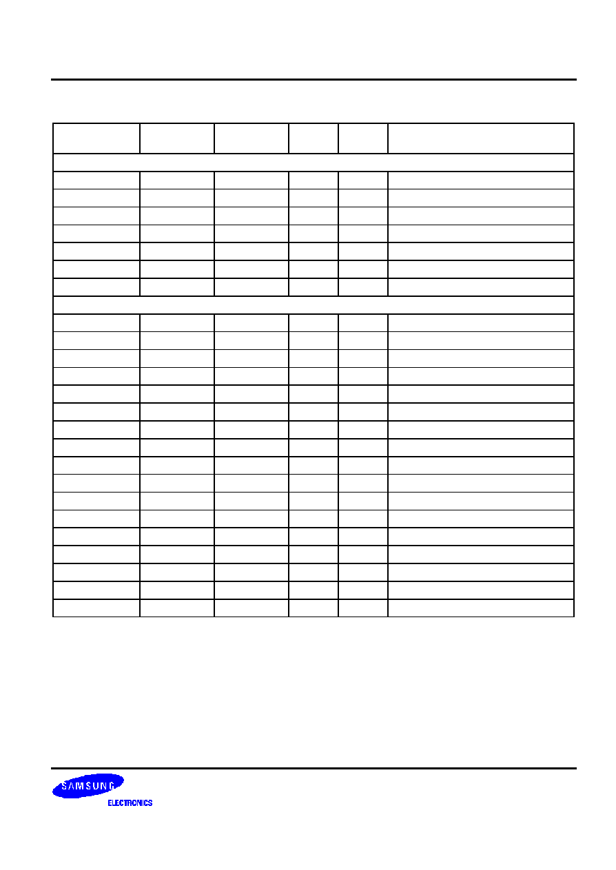
S3C2440A RISC MICROPROCESSOR
PRODUCT OVERVIEW
1-29
Table 1-4. S3C2440A Special Registers (Sheet 4 of 14) (Continued)
Register
Name
Address
(B. Endian)
Address
(L. Endian)
Acc.
Unit
Read/
Write
Function
Clock & Power Management
LOCKTIME
0x4C000000
W
R/W
PLL lock time counter
MPLLCON
0x4C000004
MPLL control
UPLLCON
0x4C000008
UPLL control
CLKCON
0x4C00000C
Clock generator control
CLKSLOW
0x4C000010
Slow clock control
CLKDIVN
0x4C000014
Clock divider control
CAMDIVN
0x4C000018
Camera clock divider control
LCD Controller
LCDCON1
0X4D000000
W
R/W
LCD control 1
LCDCON2
0X4D000004
LCD control 2
LCDCON3
0X4D000008
LCD control 3
LCDCON4
0X4D00000C
LCD control 4
LCDCON5
0X4D000010
LCD control 5
LCDSADDR1
0X4D000014
STN/TFT: frame buffer start address 1
LCDSADDR2
0X4D000018
STN/TFT: frame buffer start address 2
LCDSADDR3
0X4D00001C
STN/TFT: virtual screen address set
REDLUT
0X4D000020
STN: red lookup table
GREENLUT
0X4D000024
STN: green lookup table
BLUELUT
0X4D000028
STN: blue lookup table
DITHMODE
0X4D00004C
STN: dithering mode
TPAL
0X4D000050
TFT: temporary palette
LCDINTPND
0X4D000054
LCD interrupt pending
LCDSRCPND
0X4D000058
LCD interrupt source
LCDINTMSK
0X4D00005C
LCD interrupt mask
TCONSEL
0X4D000060
TCON(LPC3600/LCC3600) control
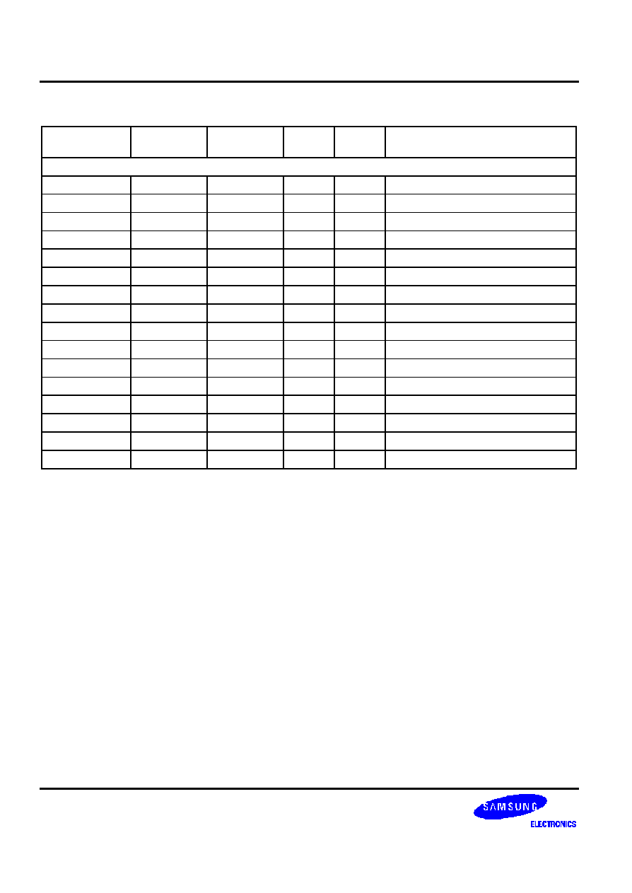
PRODUCT OVERVIEW
S3C2440A RISC MICROPROCESSOR
1-30
Table 1-4. S3C2440A Special Registers (Sheet 5 of 14) (Continued)
Register
Name
Address
(B. Endian)
Address
(L. Endian)
Acc.
Unit
Read/
Write
Function
NAND Flash
NFCONF
0x4E000000
W
R/W
NAND flash configuration
NFCONT
0x4E000004
NAND flash control
NFCMD
0x4E000008
NAND flash command
NFADDR
0x4E00000C
NAND flash address
NFDATA
0x4E000010
NAND flash data
NFMECC0
0x4E000014
NAND flash main area ECC0/1
NFMECC1
0x4E000018
NAND flash main area ECC2/3
NFSECC
0x4E00001C
NAND flash spare area ECC
NFSTAT
0x4E000020
NAND flash operation status
NFESTAT0
0x4E000024
NAND flash ECC status for I/O[7:0]
NFESTAT1
0x4E000028
NAND flash ECC status for I/O[15:8]
NFMECC0
0x4E00002C
R
NAND flash main area ECC0 status
NFMECC1
0x4E000030
NAND flash main area ECC1 status
NFSECC
0x4E000034
NAND flash spare area ECC status
NFSBLK
0x4E000038
R/W
NAND flash start block address
NFEBLK
0x4E00003C
NAND flash end block address
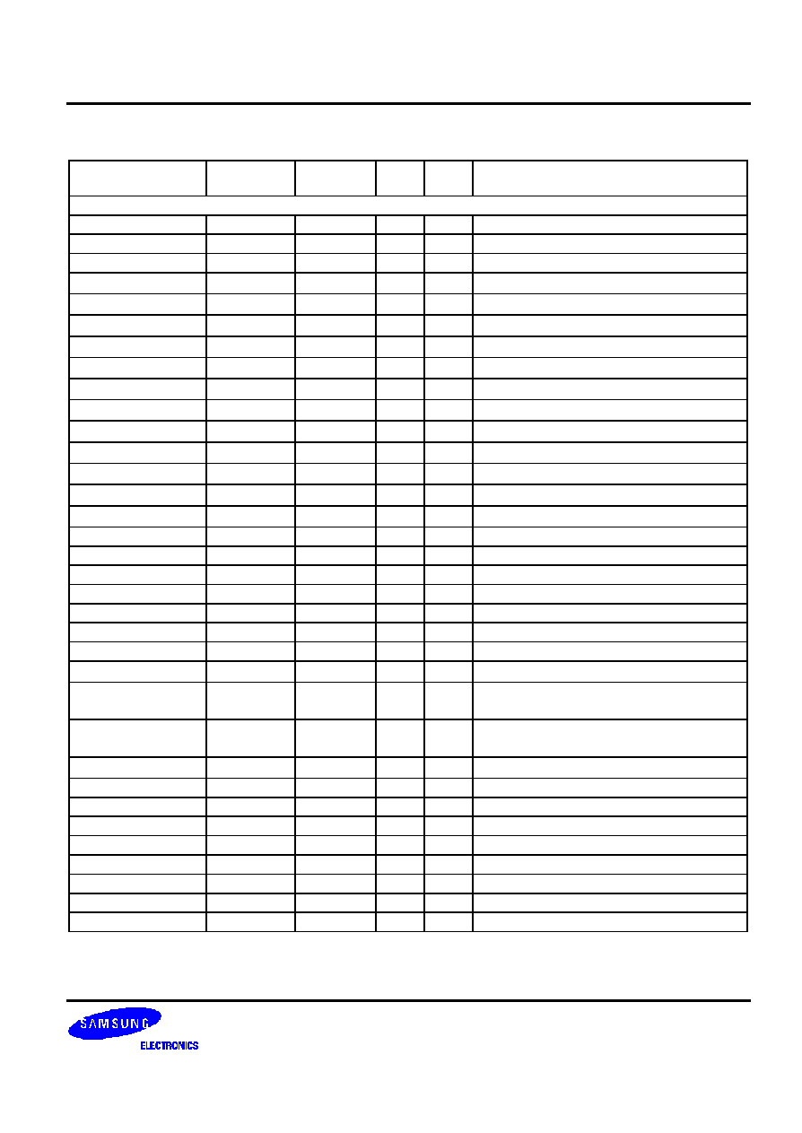
S3C2440A RISC MICROPROCESSOR
PRODUCT OVERVIEW
1-31
Table 1-4. S3C2440A Special Registers (Sheet 6 of 14) (Continued)
Register
Name
Address
(B. Endian)
Address
(L. Endian)
Acc.
Unit
Read/
Write
Function
Camera Interface
CISRCFMT
0x4F000000
W
RW
Input source format
CIWDOFST
0x4F000004
Window offset register
CIGCTRL
0x4F000008
Global control register
CICOYSA1
0x4F000018
Y 1
st
frame start address for codec DMA
CICOYSA2
0x4F00001C
Y 2
nd
frame start address for codec DMA
CICOYSA3
0x4F000020
Y 3
nd
frame start address for codec DMA
CICOYSA4
0x4F000024
Y 4
th
frame start address for codec DMA
CICOCBSA1
0x4F000028
Cb 1
st
frame start address for codec DMA
CICOCBSA2
0x4F00002C
Cb 2
nd
frame start address for codec DMA
CICOCBSA3
0x4F000030
Cb 3
nd
frame start address for codec DMA
CICOCBSA4
0x4F000034
Cb 4
th
frame start address for codec DMA
CICOCRSA1
0x4F000038
Cr 1
st
frame start address for codec DMA
CICOCRSA2
0x4F00003C
Cr 2
nd
frame start address for codec DMA
CICOCRSA3
0x4F000040
Cr 3
nd
frame start address for codec DMA
CICOCRSA4
0x4F000044
Cr 4
th
frame start address for codec DMA
CICOTRGFMT
0x4F000048
Target image format of codec DMA
CICOCTRL
0x4F00004C
Codec DMA control related
CICOSCPRERATIO
0x4F000050
Codec pre-scaler ratio control
CICOSCPREDST
0x4F000054
Codec pre-scaler destination format
CICOSCCTRL
0x4F000058
Codec main-scaler control
CICOTAREA
0x4F00005C
Codec scaler target area
CICOSTATUS
0x4F000064
Codec path status
CIPRCLRSA1
0x4F00006C
RGB 1
st
frame start address for preview DMA
CIPRCLRSA2
0x4F000070
RGB 2
nd
frame start address for preview
DMA
CIPRCLRSA3
0x4F000074
RGB 3
nd
frame start address for preview
DMA
CIPRCLRSA4
0x4F000078
RGB 4
th
frame start address for preview DMA
CIPRTRGFMT
0x4F00007C
Target image format of preview DMA
CIPRCTRL
0x4F000080
Preview DMA control related
CIPRSCPRERATIO
0x4F000084
Preview pre-scaler ratio control
CIPRSCPREDST
0x4F000088
Preview pre-scaler destination format
CIPRSCCTRL
0x4F00008C
Preview main-scaler control
CIPRTAREA
0x4F000090
Preview scaler target area
CIPRSTATUS
0x4F000098
Preview path status
CIIMGCPT
0x4F0000A0
Image capture enable command
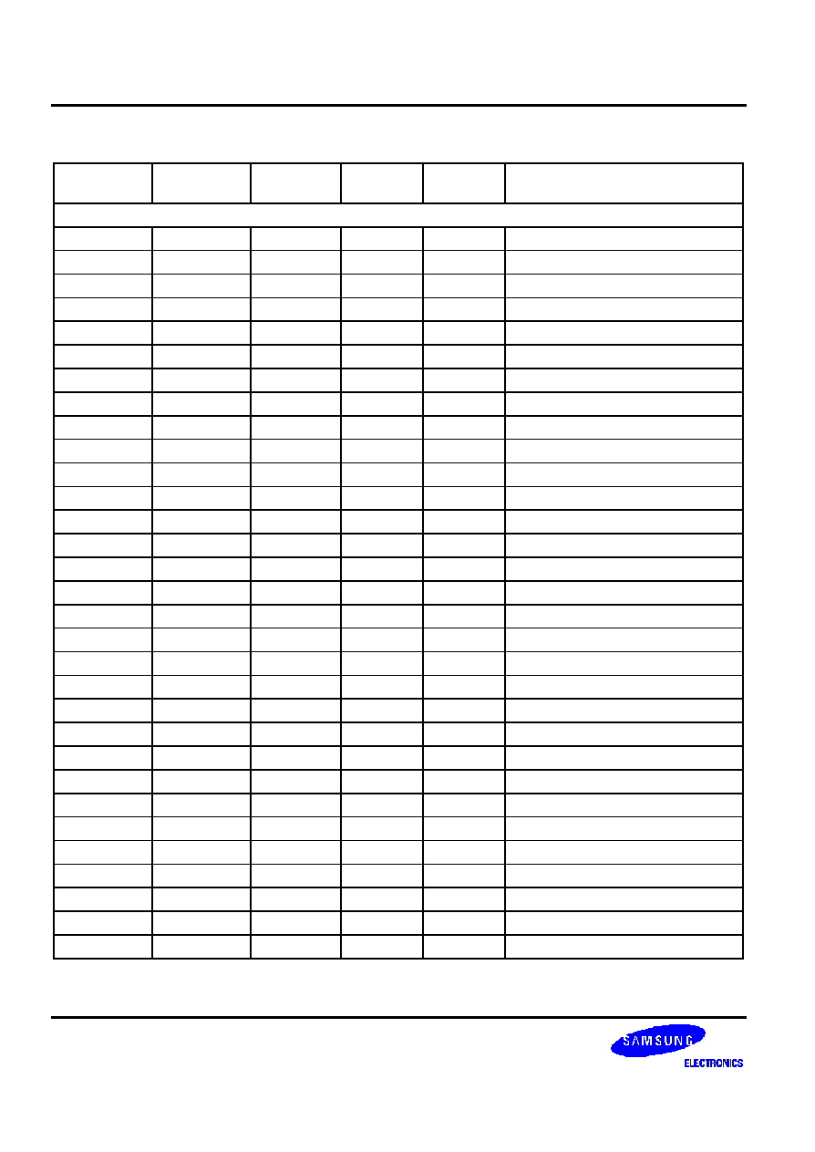
PRODUCT OVERVIEW
S3C2440A RISC MICROPROCESSOR
1-32
Table 1-4. S3C2440A Special Registers (Sheet 7 of 14) (Continued)
Register
Name
Address
(B. Endian)
Address
(L. Endian)
Acc. Unit
Read/
Write
Function
UART
ULCON0
0x50000000
W
R/W
UART 0 line control
UCON0
0x50000004
UART 0 control
UFCON0
0x50000008
UART 0 FIFO control
UMCON0
0x5000000C
UART 0 modem control
UTRSTAT0
0x50000010
R
UART 0 Tx/Rx status
UERSTAT0
0x50000014
UART 0 Rx error status
UFSTAT0
0x50000018
UART 0 FIFO status
UMSTAT0
0x5000001C
UART 0 modem status
UTXH0
0x50000023
0x50000020
B
W
UART 0 transmission hold
URXH0
0x50000027
0x50000024
R
UART 0 receive buffer
UBRDIV0
0x50000028
W
R/W
UART 0 baud rate divisor
ULCON1
0x50004000
UART 1 line control
UCON1
0x50004004
UART 1 control
UFCON1
0x50004008
UART 1 FIFO control
UMCON1
0x5000400C
UART 1 modem control
UTRSTAT1
0x50004010
R
UART 1 Tx/Rx status
UERSTAT1
0x50004014
UART 1 Rx error status
UFSTAT1
0x50004018
UART 1 FIFO status
UMSTAT1
0x5000401C
UART 1 modem status
UTXH1
0x50004023
0x50004020
B
W
UART 1 transmission hold
URXH1
0x50004027
0x50004024
R
UART 1 receive buffer
UBRDIV1
0x50004028
W
R/W
UART 1 baud rate divisor
ULCON2
0x50008000
UART 2 line control
UCON2
0x50008004
UART 2 control
UFCON2
0x50008008
UART 2 FIFO control
UTRSTAT2
0x50008010
R
UART 2 Tx/Rx status
UERSTAT2
0x50008014
UART 2 Rx error status
UFSTAT2
0x50008018
UART 2 FIFO status
UTXH2
0x50008023
0x50008020
B
W
UART 2 transmission hold
URXH2
0x50008027
0x50008024
R
UART 2 receive buffer
UBRDIV2
0x50008028
W
R/W
UART 2 baud rate divisor
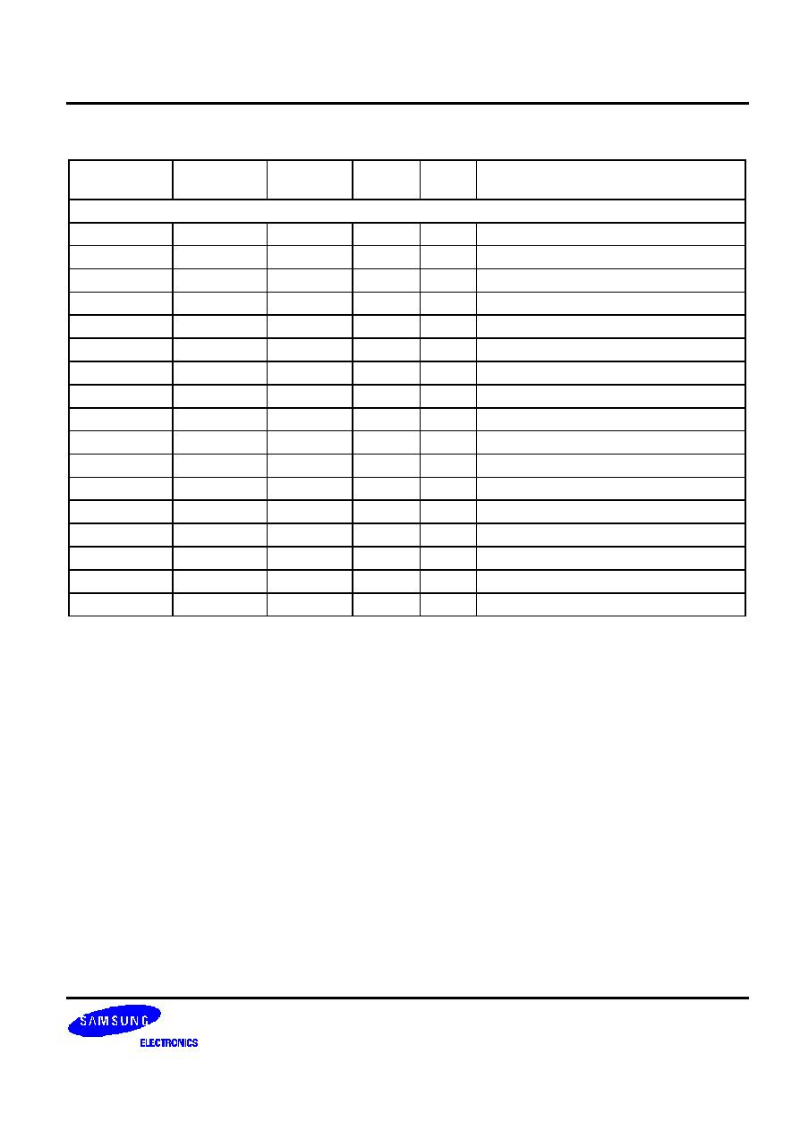
S3C2440A RISC MICROPROCESSOR
PRODUCT OVERVIEW
1-33
Table 1-4. S3C2440A Special Registers (Sheet 8 of 14) (Continued)
Register Name
Address
(B. Endian)
Address
(L. Endian)
Acc.
Unit
Read/
Write
Function
PWM Timer
TCFG0
0x51000000
W
R/W
Timer configuration
TCFG1
0x51000004
Timer configuration
TCON
0x51000008
Timer control
TCNTB0
0x5100000C
Timer count buffer 0
TCMPB0
0x51000010
Timer compare buffer 0
TCNTO0
0x51000014
R
Timer count observation 0
TCNTB1
0x51000018
R/W
Timer count buffer 1
TCMPB1
0x5100001C
Timer compare buffer 1
TCNTO1
0x51000020
R
Timer count observation 1
TCNTB2
0x51000024
R/W
Timer count buffer 2
TCMPB2
0x51000028
Timer compare buffer 2
TCNTO2
0x5100002C
R
Timer count observation 2
TCNTB3
0x51000030
R/W
Timer count buffer 3
TCMPB3
0x51000034
Timer compare buffer 3
TCNTO3
0x51000038
R
Timer count observation 3
TCNTB4
0x5100003C
R/W
Timer count buffer 4
TCNTO4
0x51000040
R
Timer count observation 4
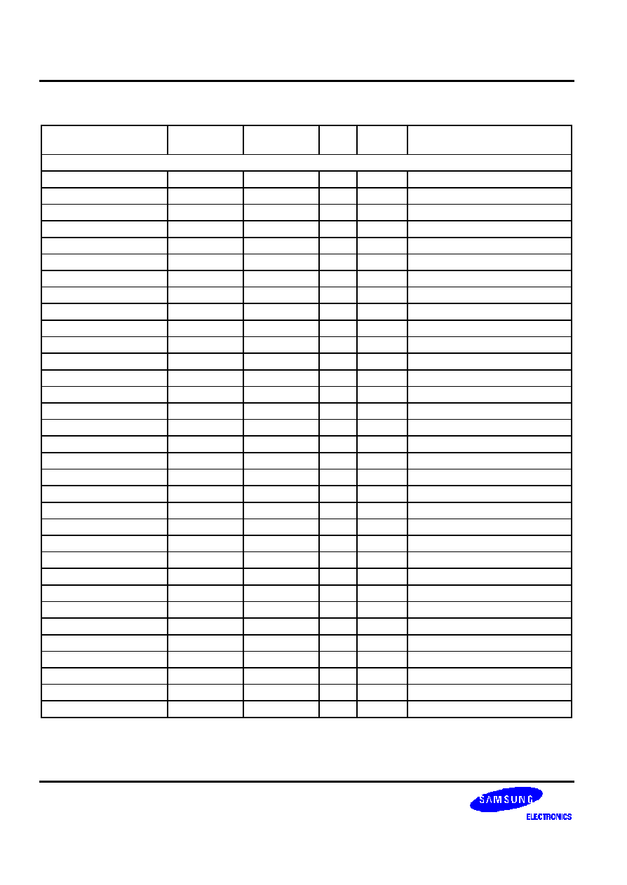
PRODUCT OVERVIEW
S3C2440A RISC MICROPROCESSOR
1-34
Table 1-4. S3C2440A Special Registers (Sheet 9 of 14) (Continued)
Register Name
Address
(B. Endian)
Address
(L. Endian)
Acc.
Unit
Read/
Write
Function
USB Device
FUNC_ADDR_REG
0x52000143
0x52000140
B
R/W
Function address
PWR_REG
0x52000147
0x52000144
Power management
EP_INT_REG
0x5200014B
0x52000148
EP interrupt pending and clear
USB_INT_REG
0x5200015B
0x52000158
USB interrupt pending and clear
EP_INT_EN_REG
0x5200015F
0x5200015C
Interrupt enable
USB_INT_EN_REG
0x5200016F
0x5200016C
Interrupt enable
FRAME_NUM1_REG
0x52000173
0x52000170
R
Frame number lower byte
FRAME_NUM2_REG
0x52000177
0x52000174
Frame number higher byte
INDEX_REG
0x5200017B
0x52000178
R/W
Register index
EP0_CSR
0x52000187
0x52000184
Endpoint 0 status
IN_CSR1_REG
0x52000187
0x52000184
In endpoint control status
IN_CSR2_REG
0x5200018B
0x52000188
In endpoint control status
MAXP_REG
0x52000183
0x52000180
Endpoint max packet
OUT_CSR1_REG
0x52000193
0x52000190
Out endpoint control status
OUT_CSR2_REG
0x52000197
0x52000194
Out endpoint control status
OUT_FIFO_CNT1_REG
0x5200019B
0x52000198
R
Endpoint out write count
OUT_FIFO_CNT2_REG
0x5200019F
0x5200019C
Endpoint out write count
EP0_FIFO
0x520001C3
0x520001C0
R/W
Endpoint 0 FIFO
EP1_FIFO
0x520001C7
0x520001C4
Endpoint 1 FIFO
EP2_FIFO
0x520001CB
0x520001C8
Endpoint 2 FIFO
EP3_FIFO
0x520001CF
0x520001CC
Endpoint 3 FIFO
EP4_FIFO
0x520001D3
0x520001D0
Endpoint 4 FIFO
EP1_DMA_CON
0x52000203
0x52000200
EP1 DMA Interface control
EP1_DMA_UNIT
0x52000207
0x52000204
EP1 DMA Tx unit counter
EP1_DMA_FIFO
0x5200020B
0x52000208
EP1 DMA Tx FIFO counter
EP1_DMA_TTC_L
0x5200020F
0x5200020C
EP1 DMA Total Tx counter
EP1_DMA_TTC_M
0x52000213
0x52000210
EP1 DMA Total Tx counter
EP1_DMA_TTC_H
0x52000217
0x52000214
EP1 DMA Total Tx counter
EP2_DMA_CON
0x5200021B
0x52000218
B
R/W
EP2 DMA interface control
EP2_DMA_UNIT
0x5200021F
0x5200021C
EP2 DMA Tx Unit counter
EP2_DMA_FIFO
0x52000223
0x52000220
EP2 DMA Tx FIFO counter
EP2_DMA_TTC_L
0x52000227
0x52000224
EP2 DMA total Tx counter
EP2_DMA_TTC_M
0x5200022B
0x52000228
EP2 DMA total Tx counter
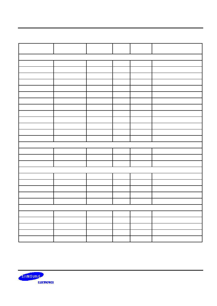
S3C2440A RISC MICROPROCESSOR
PRODUCT OVERVIEW
1-35
Table 1-4. S3C2440A Special Registers (Sheet 10 of 14) (Continued)
Register Name
Address
(B. Endian)
Address
(L. Endian)
Acc.
Unit
Read/
Write
Function
USB Device (Continued)
EP2_DMA_TTC_H
0x5200022F
0x5200022C
EP2 DMA Total Tx counter
EP3_DMA_CON
0x52000243
0x52000240
EP3 DMA Interface control
EP3_DMA_UNIT
0x52000247
0x52000244
EP3 DMA Tx Unit counter
EP3_DMA_FIFO
0x5200024B
0x52000248
EP3 DMA Tx FIFO counter
EP3_DMA_TTC_L
0x5200024F
0x5200024C
EP3 DMA Total Tx counter
EP3_DMA_TTC_M
0x52000253
0x52000250
EP3 DMA Total Tx counter
EP3_DMA_TTC_H
0x52000257
0x52000254
EP3 DMA Total Tx counter
EP4_DMA_CON
0x5200025B
0x52000258
EP4 DMA Interface control
EP4_DMA_UNIT
0x5200025F
0x5200025C
EP4 DMA Tx Unit counter
EP4_DMA_FIFO
0x52000263
0x52000260
EP4 DMA Tx FIFO counter
EP4_DMA_TTC_L
0x52000267
0x52000264
EP4 DMA Total Tx counter
EP4_DMA_TTC_M
0x5200026B
0x52000268
EP4 DMA Total Tx counter
EP4_DMA_TTC_H
0x5200026F
0x5200026C
EP4 DMA Total Tx counter
Watchdog Timer
WTCON
0x53000000
W
R/W
Watchdog timer mode
WTDAT
0x53000004
Watchdog timer data
WTCNT
0x53000008
Watchdog timer count
IIC
IICCON
0x54000000
W
R/W
IIC control
IICSTAT
0x54000004
IIC status
IICADD
0x54000008
IIC address
IICDS
0x5400000C
IIC data shift
IICLC
0x54000010
IIC multi-master line control
IIS
IISCON
0x55000000,02
0x55000000
HW,W
R/W
IIS control
IISMOD
0x55000004,06
0x55000004
IIS mode
IISPSR
0x55000008,0A
0x55000008
IIS prescaler
IISFCON
0x5500000C,0E
0x5500000C
IIS FIFO control
IISFIFO
0x55000012
0x55000010
HW
IIS FIFO entry
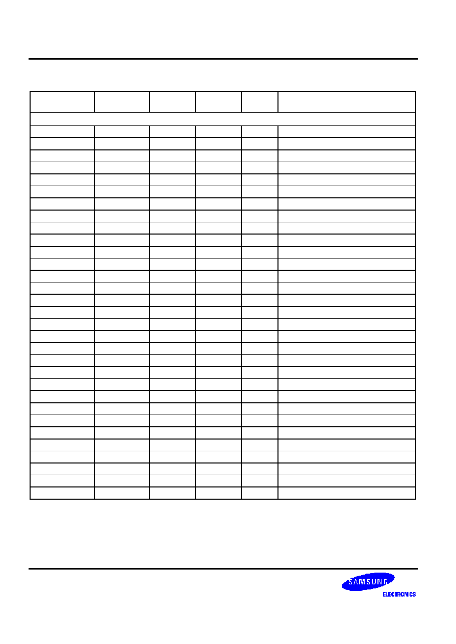
PRODUCT OVERVIEW
S3C2440A RISC MICROPROCESSOR
1-36
Table 1-4. S3C2440A Special Registers (Sheet 11 of 14) (Continued)
Register
Name
Address
(B. Endian)
Address
(L. Endian)
Acc. Unit
Read/
Write
Function
I/O port
GPACON
0x56000000
W
R/W
Port A control
GPADAT
0x56000004
Port A data
GPBCON
0x56000010
Port B control
GPBDAT
0x56000014
Port B data
GPBUP
0x56000018
Pull-up control B
GPCCON
0x56000020
Port C control
GPCDAT
0x56000024
Port C data
GPCUP
0x56000028
Pull-up control C
GPDCON
0x56000030
Port D control
GPDDA1T
0x56000034
Port D data
GPDUP
0x56000038
Pull-up control D
GPECON
0x56000040
Port E control
GPEDAT
0x56000044
Port E data
GPEUP
0x56000048
Pull-up control E
GPFCON
0x56000050
Port F control
GPFDAT
0x56000054
Port F data
GPFUP
0x56000058
Pull-up control F
GPGCON
0x56000060
Port G control
GPGDAT
0x56000064
Port G data
GPGUP
0x56000068
Pull-up control G
GPHCON
0x56000070
Port H control
GPHDAT
0x56000074
Port H data
GPHUP
0x56000078
Pull-up control H
GPJCON
0x560000D0
Port J control
GPJDAT
0x560000D4
Port J data
GPJUP
0x560000D8
Pull-up control J
MISCCR
0x56000080
Miscellaneous control
DCLKCON
0x56000084
DCLK0/1 control
EXTINT0
0x56000088
External interrupt control register 0
EXTINT1
0x5600008C
External interrupt control register 1
EXTINT2
0x56000090
External interrupt control register 2
S3C2440A RISC MICROPROCESSOR
PRODUCT OVERVIEW
1-37
Table 1-4. S3C2440A Special Registers (Sheet 12 of 14) (Continued)
Register
Name
Address
(B. Endian)
Address
(L. Endian)
Acc.
Unit
Read/
Write
Function
i/o port (continued)
EINTFLT0
0x56000094
W
R/W
Reserved
EINTFLT1
0x56000098
Reserved
EINTFLT2
0x5600009C
External interrupt filter control register 2
EINTFLT3
0x560000A0
External interrupt filter control register 3
EINTMASK
0x560000A4
External interrupt mask
EINTPEND
0x560000A8
External interrupt pending
GSTATUS0
0x560000AC
R
External pin status
GSTATUS1
0x560000B0
R/W
Chip ID
GSTATUS2
0x560000B4
Reset status
GSTATUS3
0x560000B8
Inform register
GSTATUS4
0x560000BC
Inform register
MSLCON
0x560000CC
Memory sleep control register
RTC
RTCCON
0x57000043
0x57000040
B
R/W
RTC control
TICNT
0x57000047
0x57000044
Tick time count
RTCALM
0x57000053
0x57000050
RTC alarm control
ALMSEC
0x57000057
0x57000054
Alarm second
ALMMIN
0x5700005B
0x57000058
Alarm minute
ALMHOUR
0x5700005F
0x5700005C
Alarm hour
ALMDATE
0x57000063
0x57000060
alarm day
ALMMON
0x57000067
0x57000064
Alarm month
ALMYEAR
0x5700006B
0x57000068
Alarm year
BCDSEC
0x57000073
0x57000070
BCD second
BCDMIN
0x57000077
0x57000074
BCD minute
BCDHOUR
0x5700007B
0x57000078
BCD hour
BCDDATE
0x5700007F
0x5700007C
BCD day
BCDDAY
0x57000083
0x57000080
BCD date
BCDMON
0x57000087
0x57000084
BCD month
BCDYEAR
0x5700008B
0x57000088
BCD year
PRODUCT OVERVIEW
S3C2440A RISC MICROPROCESSOR
1-38
Table 1-4. S3C2440A Special Registers (Sheet 13 of 14) (Continued)
Register
Name
Address
(B. Endian)
Address
(L. Endian)
Acc. Unit
Read/
Write
Function
A/D Converter
ADCCON
0x58000000
W
R/W
ADC control
ADCTSC
0x58000004
ADC touch screen control
ADCDLY
0x58000008
ADC start or interval delay
ADCDAT0
0x5800000C
R
ADC conversion data
ADCDAT1
0x58000010
ADC conversion data
ADCUPDN
0x58000014
R/W
Stylus up or down interrupt status
SPI
SPCON0,1
0x59000000,20
W
R/W
SPI control
SPSTA0,1
0x59000004,24
R
SPI status
SPPIN0,1
0x59000008,28
R/W
SPI pin control
SPPRE0,1
0x5900000C,2C
SPI baud rate prescaler
SPTDAT0,1
0x59000010,30
SPI Tx data
SPRDAT0,1
0x59000014,34
R
SPI Rx data
SD Interface
SDICON
0x5A000000
W
R/W
SDI control
SDIPRE
0x5A000004
SDI baud rate prescaler
SDICARG
0x5A000008
SDI command argument
SDICCON
0x5A00000C
SDI command control
SDICSTA
0x5A000010
R/(C)
SDI command status
SDIRSP0
0x5A000014
R
SDI response
SDIRSP1
0x5A000018
SDI response
SDIRSP2
0x5A00001C
SDI response
SDIRSP3
0x5A000020
SDI response
SDIDTIMER
0x5A000024
R/W
SDI data / busy timer
SDIBSIZE
0x5A000028
SDI block size
SDIDCON
0x5A00002C
SDI data control
SDIDCNT
0x5A000030
R
SDI data remain counter
SDIDSTA
0x5A000034
R/(C)
SDI data status
SDIFSTA
0x5A000038
R
SDI FIFO status
SDIIMSK
0x5A00003C
W
SDI interrupt mask
SDIDAT
0x5A000043
0x5A000040
B
R/W
SDI data
S3C2440A RISC MICROPROCESSOR
PRODUCT OVERVIEW
1-39
Table 1-4. S3C2440A Special Registers (Sheet 14 of 14) (Continued)
Register
Name
Address
(B. Endian)
Address
(L. Endian)
Acc. Unit
Read/
Write
Function
AC97 Audio-CODEC Interface
AC_GLBCTRL
0x5B000000
W
R/W
AC97 global control register
AC_GLBSTAT
0x5B000004
R
AC97 global status register
AC_CODEC_CMD
0x5B000008
R/W
AC97 codec command register
AC_CODEC_STAT
0x5B00000C
R
AC97 codec status register
AC_PCMADDR
0x5B000010
AC97 PCM out/in channel FIFO
address register
AC_MICADDR
0x5B000014
AC97 mic in channel FIFO address
register
AC_PCMDATA
0x5B000018
R/W
AC97 PCM out/in channel FIFO data
register
AC_MICDATA
0x5B00001C
AC97 MIC in channel FIFO data
register
Cautions on S3C2440A Special Registers
1. In the little endian mode `L', endian address must be used. In the big endian mode `B' endian address must be
used.
2. The special registers have to be accessed for each recommended access unit.
3. All registers except ADC registers, RTC registers and UART registers must be read/write in word unit (32-bit) in
little/big endian.
4. Make sure that the ADC registers, RTC registers and UART registers be read/write by the specified access unit
and the specified address. Moreover, one must carefully consider which endian mode is used.
5. W : 32-bit register, which must be accessed by LDR/STR or int type pointer (int *).
HW : 16-bit register, which must be accessed by LDRH/STRH or short int type pointer (short int *).
B : 8-bit register, which must be accessed by LDRB/STRB or char type pointer (char int *).

S3C2440A RISC MICROPROCESSOR
PROGRAMMER'S MODEL
2-1
2
PROGRAMMER'S MODEL
OVERVIEW
S3C2440A is developed using the advanced ARM920T core, which has been designed by Advanced RISC Machines,
Ltd.
PROCESSOR OPERATING STATES
From the programmer's point of view, the ARM920T can be in one of the two states:
∑
ARM state which executes 32-bit, word-aligned ARM instructions
∑
THUMB state is a state which can execute 16-bit, halfword-aligned THUMB instructions. In this state, the PC
uses bit 1 to select between alternate halfwords
NOTE
Transition between these two states does not affect the processor mode or the contents of the registers.
SWITCHING STATE
Entering THUMB State
Entry into THUMB state can be achieved by executing a BX instruction with the state bit (bit 0) set in the operand
register.
Transition to THUMB state will also occur automatically on return from an exception (IRQ, FIQ, UNDEF, ABORT,
SWI etc.), if the exception is entered with the processor in THUMB state.
Entering ARM State
Entry into ARM state can be done by the following methods:-
∑
On execution of the BX instruction with the state bit clear in the operand register.
∑
On the processor taking an exception (IRQ, FIQ, RESET, UNDEF, ABORT, SWI etc.). In this case, the PC is
placed in the exception mode's link register, and execution commences at the exception's vector address.
MEMORY FORMATS
ARM920T views memory as a linear collection of bytes numbered upwards from zero. Bytes 0 to 3 hold the first
stored word, bytes 4 to 7 the second and so on. ARM920T can treat words in memory as being stored either in Big-
Endian or Little-Endian format.
PROGRAMMER'S MODEL
S3C2440A RISC MICROPROCESSOR
2-2
BIG-ENDIAN FORMAT
In Big-Endian format, the most significant byte of a word is stored at the lowest numbered byte and the least
significant byte at the highest numbered byte. Byte 0 of the memory system is therefore connected to data lines 31
through 24.
31
24
8
4
0
23
16
9
5
1
10
6
2
11
7
3
15
8 7
0
4
0
8
Higher Address
Lower Address
Word Address
Most significant byte is at lowest address
Word is addressed by byte address of most significant byte
Figure 2-1. Big-Endian Addresses of Bytes within Words
LITTLE-ENDIAN FORMAT
In Little-Endian format, the lowest numbered byte in a word is considered the word's least significant byte, and the
highest numbered byte the most significant. Byte 0 of the memory system is therefore connected to data lines 7
through 0.
31
24
11
7
3
23
16
10
6
2
9
5
1
8
4
0
15
8 7
0
4
0
8
Higher Address
Lower Address
Word Address
Least significant byte is at lowest address
Word is addressed by byte address of least significant byte
Figure 2-2. Little-Endian Addresses of Bytes within Words
INSTRUCTION LENGTH
Instructions are either 32 bits long (in ARM state) or 16 bits long (in THUMB state).
Data Types
ARM920T supports byte (8-bit), halfword (16-bit) and word (32-bit) data types. Words must be aligned to four-byte
boundaries and half words to two-byte boundaries.

S3C2440A RISC MICROPROCESSOR
PROGRAMMER'S MODEL
2-3
OPERATING MODES
ARM920T supports seven modes of operation:
∑
User (usr): The normal ARM program execution state
∑
FIQ (fiq): Designed to support a data transfer or channel process
∑
IRQ (irq): Used for general-purpose interrupt handling
∑
Supervisor (svc): Protected mode for the operating system
∑
Abort mode (abt): Entered after a data or instruction prefetch abort
∑
System (sys): A privileged user mode for the operating system
∑
Undefined (und): Entered when an undefined instruction is executed
Mode changes can be made using the control of software, or may be brought about by external interrupts or
exception processing. Most application programs will execute in User mode. The non-user modes' known as
privileged modes-are entered in order to service interrupts or exceptions, or to access protected resources.
REGISTERS
ARM920T has a total of 37 registers - 31 general-purpose 32-bit registers and six status registers - but these cannot
all be seen at once. The processor state and operating mode decides which registers are available to the
programmer.
The ARM State Register Set
In ARM state, 16 general registers and one or two status registers are visible at any one time. In privileged (non-
User) modes, mode-specific banked registers are switched in. Figure 2-3 shows which register is available in each
mode: the banked registers are marked with a shaded triangle.
The ARM state register set contains 16 directly accessible registers: R0 to R15. All of these except R15 are general-
purpose, and may be used to hold either data or address values. In addition to these, there is a seventeenth register
used to store status information.
Register 14
This register is used as the subroutine link register. This receives a copy of R15 when
a Branch and Link (BL) instruction is executed. Rest of the time it may be treated as a
general-purpose register. The corresponding banked registers R14_svc, R14_irq,
R14_fiq, R14_abt and R14_und are similarly used to hold the return values of R15
when interrupts and exceptions arise, or when Branch and Link instructions are
executed within interrupt or exception routines.
Register 15
This register holds the Program Counter (PC). In ARM state, bits [1:0] of R15 are zero
and bits [31:2] contain the PC. In THUMB state, bit [0] is zero and bits [31:1] contain
the PC.
Register 16
This register is the CPSR (Current Program Status Register). This contains condition
code flags and the current mode bits.
FIQ mode has seven banked registers mapped to R8-14 (R8_fiq-R14_fiq). In ARM state there are many FIQ handlers
which don't require saving registers. User, IRQ, Supervisor, Abort and Undefined, each have two banked registers
mapped to R13 and R14, allowing each of these modes to have a private stack pointer and link registers.
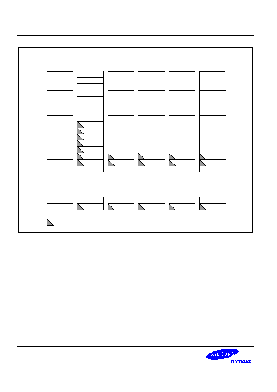
PROGRAMMER'S MODEL
S3C2440A RISC MICROPROCESSOR
2-4
r0
r1
r2
r3
r4
r5
r6
r7
r9
r8
r10
r11
r12
r13
r14
r15 (PC)
r0
r1
r2
r3
r4
r5
r6
r7
r9
r8
r10
r11
r12
r13_
svc
r14_
svc
r15 (PC)
r0
r1
r2
r3
r4
r5
r6
r7
r9_
fiq
r10_
fiq
r11_
fiq
r12_
fiq
r13_
fiq
r14_
fiq
r15 (PC)
r8_
fiq
r0
r1
r2
r3
r4
r5
r6
r7
r9
r8
r10
r11
r12
r13_
abt
r14_
abt
r15 (PC)
r0
r1
r2
r3
r4
r5
r6
r7
r9
r8
r10
r11
r12
r13_
irq
r14_
irq
r15 (PC)
r0
r1
r2
r3
r4
r5
r6
r7
r9
r8
r10
r11
r12
r13_
und
r14_
und
r15 (PC)
System & User
FIQ
Supervisor
IRQ
Abort
Undefined
ARM State General Registers and Program Counter
ARM State Program Status Registers
CPSR
CPSR
SPSR_
fiq
CPSR
SPSR_
svc
CPSR
SPSR_
abt
CPSR
SPSR_
irq
CPSR
SPSR_
und
= banked register
Figure 2-3. Register Organization in ARM State
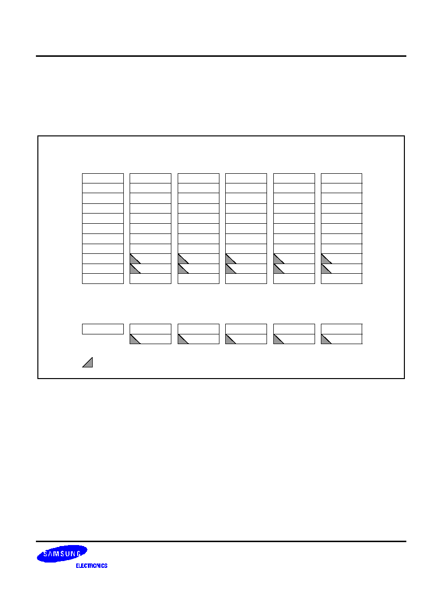
S3C2440A RISC MICROPROCESSOR
PROGRAMMER'S MODEL
2-5
The THUMB State Register Set
The THUMB state register set is a subset of the ARM state set. The programmer has direct access to eight general
registers, R0-R7, as well as the Program Counter (PC), a stack pointer register (SP), a link register (LR), and the
CPSR. There are banked Stack Pointers, Link Registers and Saved Process Status Registers (SPSRs) for each
privileged mode. This is shown in Figure 2-4.
r0
r1
r2
r3
r4
r5
r6
r7
LR
SP
PC
System & User
FIQ
Supervisor
IRQ
Abort
Undefined
THUMB State General Registers and Program Counter
THUMB State Program Status Registers
CPSR
CPSR
SPSR_
fiq
CPSR
SPSR_
svc
CPSR
SPSR_
abt
CPSR
SPSR_
irq
CPSR
SPSR_
und
= banked register
LR_
fiq
r0
r1
r2
r3
r4
r5
r6
r7
SP_
fiq
PC
LR_
svc
r0
r1
r2
r3
r4
r5
r6
r7
SP_
svc
PC
LR_
und
r0
r1
r2
r3
r4
r5
r6
r7
SP_
und
PC
LR_
fiq
r0
r1
r2
r3
r4
r5
r6
r7
SP_
fiq
PC
LR_
abt
r0
r1
r2
r3
r4
r5
r6
r7
SP_
abt
PC
Figure 2-4. Register Organization in THUMB state
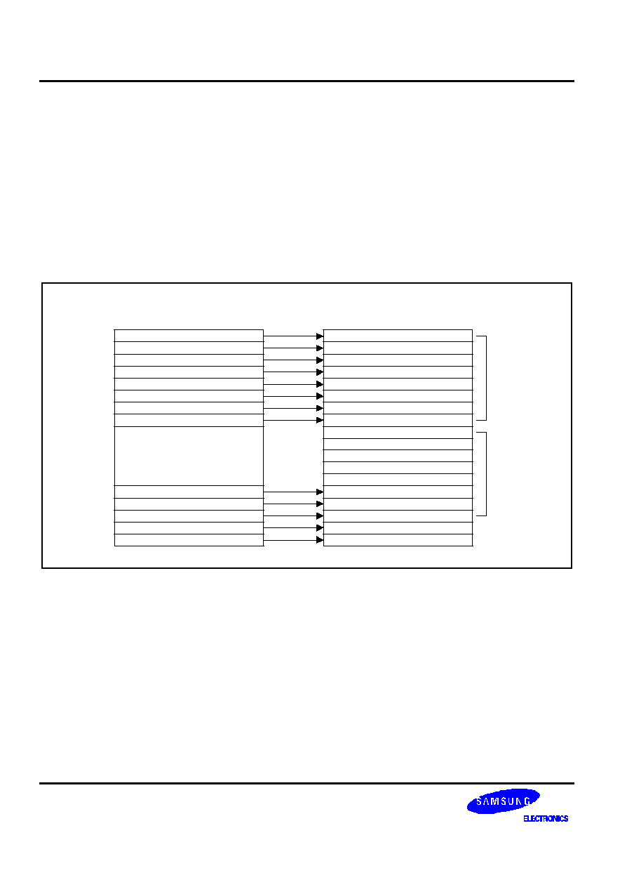
PROGRAMMER'S MODEL
S3C2440A RISC MICROPROCESSOR
2-6
The relationship between ARM and THUMB state registers
The relationship between ARM and THUMB state registers are as below:-
∑
THUMB state R0-R7 and ARM state R0-R7 are identical
∑
THUMB state CPSR and SPSRs and ARM state CPSR and SPSRs are identical
∑
THUMB state SP maps onto ARM state R13
∑
THUMB state LR maps onto ARM state R14
∑
The THUMB state Program Counter maps onto the ARM state Program Counter (R15)
This relationship is shown in Figure 2-5.
THUMB State
(CPSR)
(SPSR)
Stack Pointer (r13)
Link Register (r14)
Program Counter (r15)
r0
r1
r2
r3
r4
r5
r6
r7
r8
r9
r10
r11
r12
(CPSR)
(SPSR)
Stack Pointer (SP)
Link Register (LR)
Program Counter (PC)
r0
r1
r2
r3
r4
r5
r6
r7
ARM State
Lo-Registers
Hi-Registers
Figure 2-5. Mapping of THUMB State Registers onto ARM State Registers
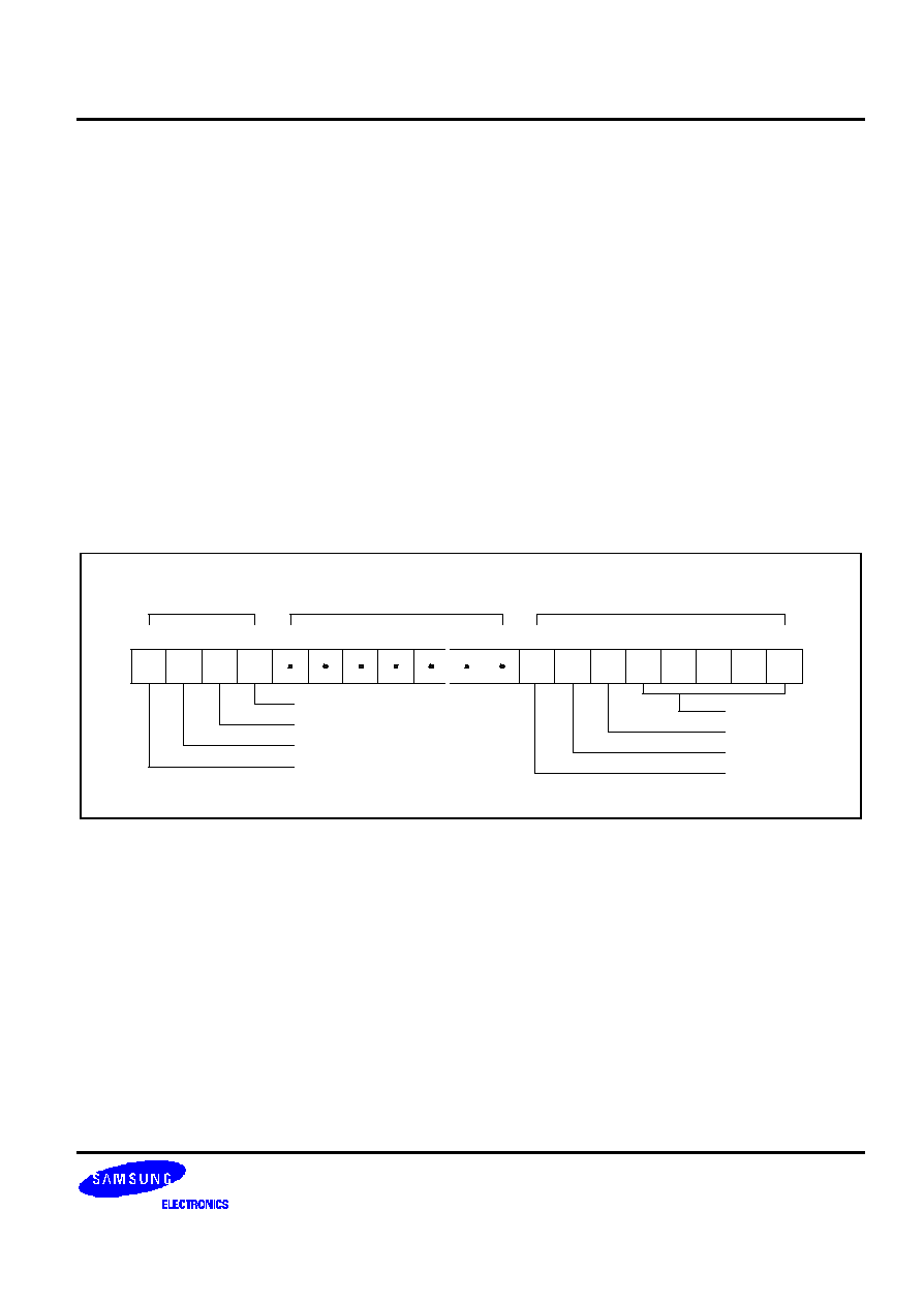
S3C2440A RISC MICROPROCESSOR
PROGRAMMER'S MODEL
2-7
Accessing Hi-Registers in THUMB State
In THUMB state, registers R8-R15 ("Hi registers") are not part of the standard register set. However, the assembly
language programmer has limited access to them, and can use them for fast temporary storage.
A value may be transferred from a register in the range R0-R7 (a Lo register) to a Hi register and from a Hi register to
a Lo register, using special variants of the MOV instruction. Hi register values can also be compared against or
added to Lo register values with the CMP and ADD instructions. For more information, Please refer to Figure 3-34.
THE PROGRAM STATUS REGISTERS
The ARM920T contains a Current Program Status Register (CPSR), plus five Saved Program Status Registers
(SPSRs) for use by exception handlers. These register's functions are:
∑
Hold information about the most recently performed ALU operation
∑
Control the enabling and disabling of interrupts
∑
Set the processor operating mode
The arrangement of bits is shown in Figure 2-6.
31
Condition Code Flags
Overflow
N
Z
C
V
I
F
T
M4 M3
M2 M1 M0
30
29
27
28
26
25
24
23
8
7
6
5
4
3
2
1
0
(Resverved)
Control Bits
Carry/Borrow/Extend
Zero
Negative/Less Than
Mode bits
State bits
FIQ disable
IRQ disable
~ ~
~ ~
Figure 2-6. Program Status Register Format

PROGRAMMER'S MODEL
S3C2440A RISC MICROPROCESSOR
2-8
The Condition Code Flags
The N, Z, C and V bits are the condition code flags. These may be changed as a result of arithmetic and logical
operations, and may be tested to determine whether an instruction should be executed.
In ARM state, all instructions may be executed conditionally: see Table 3-2 for details.
In THUMB state, only the Branch instruction is capable of conditional execution: see Figure 3-46 for details.
The Control Bits
The bottom 8 bits of a PSR (incorporating I, F, T and M[4:0]) are known collectively as the control bits. These will be
changed when an exception arises. If the processor is operating in a privileged mode, they can also be manipulated
by software.
The T bit
This reflects the operating state. When this bit is set, the processor is executed in
THUMB state, or otherwise it is executing in ARM state. This is reflected on the TBIT
external signal.
Note: That the software must never change the state of the TBIT in the CPSR. If this happens,
the processor will enter an unpredictable state.
Interrupt disable bits I and F bits are the interrupt disable bits. When set, these disable the IRQ and FIQ
interrupts respectively.
The mode bits
The M4, M3, M2, M1 and M0 bits (M[4:0]) are the mode bits. These determine the
processor's operating mode, as shown in Table 2-1. Not all combinations of the mode
bits define a valid processor mode. Only those explicitly described shall be used. The
user should be aware that if any illegal value is programmed into the mode bits, M[4:0],
then the processor will enter an unrecoverable state. If this occurs, reset should be
applied.
Reserved bits
The remaining bits in the PSRs are reserved. When changing a PSR's flag or control bits,
you must ensure that these unused bits are not altered. Also, your program should not
rely on them containing specific values, since in future processors they may read as one
or zero.

S3C2440A RISC MICROPROCESSOR
PROGRAMMER'S MODEL
2-9
Table 2-1. PSR Mode Bit Values
M[4:0]
Mode
Visible THUMB state registers
Visible ARM state registers
10000
User
R7..R0,
LR, SP
PC, CPSR
R14..R0,
PC, CPSR
10001
FIQ
R7..R0,
LR_fiq, SP_fiq
PC, CPSR, SPSR_fiq
R7..R0,
R14_fiq..R8_fiq,
PC, CPSR, SPSR_fiq
10010
IRQ
R7..R0,
LR_irq, SP_irq
PC, CPSR, SPSR_irq
R12..R0,
R14_irq, R13_irq,
PC, CPSR, SPSR_irq
10011
Supervisor
R7..R0,
LR_svc, SP_svc,
PC, CPSR, SPSR_svc
R12..R0,
R14_svc, R13_svc,
PC, CPSR, SPSR_svc
10111
Abort
R7..R0,
LR_abt, SP_abt,
PC, CPSR, SPSR_abt
R12..R0,
R14_abt, R13_abt,
PC, CPSR, SPSR_abt
11011
Undefined
R7..R0
LR_und, SP_und,
PC, CPSR, SPSR_und
R12..R0,
R14_und, R13_und,
PC, CPSR
11111
System
R7..R0,
LR, SP
PC, CPSR
R14..R0,
PC, CPSR
Reserved bits
The remaining bits in the PSR's are reserved. While changing a PSR's flag or control
bits, you must ensure that these unused bits are not altered. Also, your program should
not rely on them containing specific values, since in future processors they may read as
one or zero.

PROGRAMMER'S MODEL
S3C2440A RISC MICROPROCESSOR
2-10
EXCEPTIONS
Exceptions arise whenever the normal flow of a program has to be halted temporarily, for example to service an
interrupt from a peripheral. Before an exception can be handled, the current processor state must be preserved so
that the original program can resume when the handler routine has finished.
It is possible for several exceptions to arise at the same time. If this happens, they are dealt with in a fixed order.
See Exception Priorities on page 2-14.
Action on Entering an Exception
While handling an exception, the ARM920T does following activities:
1. Preserves the address of the next instruction in the appropriate Link Register. If the exception has been entered
from ARM state, then the address of the next instruction is copied into the Link Register (that is, current PC + 4
or PC + 8 depending on the exception. See Table 2-2 on for details). If the exception has been entered from
THUMB state, then the value written into the Link Register is the current PC offset by a value such that the
program resumes from the correct place on return from the exception. This means that the exception handler
need not determine which state the exception was entered from. For example, in the case of SWI, MOVS PC,
R14_svc will always return to the next instruction regardless of whether the SWI was executed in ARM or
THUMB state.
2. Copies the CPSR into the appropriate SPSR
3. Forces the CPSR mode bits to a value which depends on the exception
4. Forces the PC to fetch the next instruction from the relevant exception vector
It may also set the interrupt disable flags to prevent otherwise unmanageable nestings of exceptions.
If the processor is in THUMB state when an exception occurs, it will automatically switch into ARM state when the
PC is loaded with the exception vector address.
Action on Leaving an Exception
On completion, the exception handler:
1. Moves the Link Register, minus an offset where appropriate, to the PC. (The offset will vary depending on the
type of exception.)
2. Copies the SPSR back to the CPSR
3. Clears the interrupt disable flags, if they were set on entry
NOTE
An explicit switch back to THUMB state is never needed, since restoring the CPSR from the SPSR
automatically sets the T bit to the value it held immediately prior to the exception.
S3C2440A RISC MICROPROCESSOR
PROGRAMMER'S MODEL
2-11
Exception Entry/Exit Summary
Table 2-2 summarizes the PC value preserved in the relevant R14 on exception entry, and the recommended
instruction for exiting the exception handler.
Table 2-2. Exception Entry/Exit
Return Instruction
Previous State
Notes
ARM R14_x
THUMB R14_x
BL
MOV PC, R14
PC + 4
PC + 2
(1)
SWI
MOVS PC, R14_svc
PC + 4
PC + 2
(1)
UDEF
MOVS PC, R14_und
PC + 4
PC + 2
(1)
FIQ
SUBS PC, R14_fiq, #4
PC + 4
PC + 4
(2)
IRQ
SUBS PC, R14_irq, #4
PC + 4
PC + 4
(2)
PABT
SUBS PC, R14_abt, #4
PC + 4
PC + 4
(1)
DABT
SUBS PC, R14_abt, #8
PC + 8
PC + 8
(3)
RESET
NA
≠
≠
(4)
NOTES:
1. Where PC is the address of the BL/SWI/Undefined Instruction fetch which had the prefetch abort.
2. Where PC is the address of the instruction which did not get executed since the FIQ or IRQ took priority.
3. Where PC is the address of the Load or Store instruction which generated the data abort.
4. The value saved in R14_svc upon reset is unpredictable.
FIQ
The FIQ (Fast Interrupt Request) exception is designed to support a data transfer or channel process, and in ARM
state has sufficient private registers to remove the need for register saving (thus minimizing the overhead of context
switching).
FIQ is externally generated by taking the nFIQ input LOW. This input can except either synchronous or
asynchronous transitions, depending on the state of the ISYNC input signal. When ISYNC is LOW, nFIQ and nIRQ
are considered asynchronous, and a cycle delay for synchronization is incurred before the interrupt can affect the
processor flow.
Irrespective of whether the exception was entered from ARM or Thumb state, a FIQ handler should leave the interrupt
by executing
SUBS
PC,R14_fiq,#4
FIQ may be disabled by setting the CPSR's F flag (but note that this is not possible from User mode). If the F flag is
clear, ARM920T checks for a LOW level on the output of the FIQ synchronizer at the end of each instruction.

PROGRAMMER'S MODEL
S3C2440A RISC MICROPROCESSOR
2-12
IRQ
The IRQ (Interrupt Request) exception is a normal interrupt caused by a LOW level on the nIRQ input. IRQ has a
lower priority than FIQ and is masked out when a FIQ sequence is entered. It may be disabled at any time by setting
I bit in the CPSR, though this can only be done from a privileged (non-User) mode.
Irrespective of whether the exception was entered from ARM or Thumb state, an IRQ handler should return from the
interrupt by executing
SUBS
PC,R14_irq,#4
Abort
An abort indicates that the current memory access cannot be completed. It can be signaled by the external ABORT
input. ARM920T checks for the abort exception during memory access cycles.
There are two types of abort:
∑
Prefetch Abort: occurs during an instruction prefetch.
∑
Data Abort: occurs during a data access.
If a prefetch abort occurs, the prefetched instruction is marked as invalid, but the exception will not be taken until the
instruction reaches the head of the pipeline. If the instruction is not executed ≠ the abort doesn't take place because
a branch occurs while it is in the pipeline -.
If a data abort occurs, the action taken depends on the instruction type:
∑
Single data transfer instructions (LDR, STR) write back modified base registers: the Abort handler must be aware
of this.
∑
The swap instruction (SWP) is aborted as though it had not been executed.
∑
Block data transfer instructions (LDM, STM) complete. If write-back is set, the base is updated. If the instruction
would have overwritten the base with data (ie it has the base in the transfer list), the overwriting is prevented. All
register overwriting is prevented after an abort is indicated, which means in particular that R15 (always the last
register to be transferred) is preserved in an aborted LDM instruction.
The abort mechanism allows the implementation of a demand paged virtual memory system. In such a system the
processor is allowed to generate arbitrary addresses. When the data at an address is unavailable, the Memory
Management Unit (MMU) signals an abort. The abort handler must then work out the cause of the abort, make the
requested data available, and retry the aborted instruction. The application program needs no knowledge of the
amount of memory available to it, nor is its state in any way affected by the abort.
After fixing the reason for the abort, the handler should execute the following irrespective of the state (ARM or
Thumb):
SUBS
PC,R14_abt,#4
; for a prefetch abort, or
SUBS
PC,R14_abt,#8
; for a data abort
This restores both the PC and the CPSR, and retries the aborted instruction.
S3C2440A RISC MICROPROCESSOR
PROGRAMMER'S MODEL
2-13
Software Interrupt
The Software Interrupt Instruction (SWI) is used for entering Supervisor mode, usually to request a particular
supervisor function. A SWI handler should return by executing the following irrespective of the state (ARM or Thumb):
MOV
PC,R14_svc
This restores the PC and CPSR, and returns to the instruction following the SWI.
NOTE
nFIQ, nIRQ, ISYNC, LOCK, BIGEND, and ABORT pins exist only in the ARM920T CPU core.
Undefined Instruction
When ARM920T comes across an instruction which cannot be handled, it takes the undefined instruction trap. This
mechanism may be used to extend either the THUMB or ARM instruction set by software emulation.
After emulating the failed instruction, the trap handler should execute the following irrespective of the state (ARM or
Thumb):
MOVS
PC,R14_und
This restores the CPSR and returns to the instruction following the undefined instruction.
Exception Vectors
The following table shows the exception vector addresses.
Table 2-3. Exception Vectors
Address
Exception
Mode in Entry
0x00000000
Reset
Supervisor
0x00000004
Undefined instruction
Undefined
0x00000008
Software Interrupt
Supervisor
0x0000000C
Abort (prefetch)
Abort
0x00000010
Abort (data)
Abort
0x00000014
Reserved
Reserved
0x00000018
IRQ
IRQ
0x0000001C
FIQ
FIQ

PROGRAMMER'S MODEL
S3C2440A RISC MICROPROCESSOR
2-14
Exception Priorities
When multiple exceptions arise at the same time, a fixed priority system determines the order in which they are
handled:
Highest priority:
1. Reset
2. Data abort
3. FIQ
4. IRQ
5. Prefetch abort
Lowest priority:
6. Undefined Instruction, Software interrupt.
Not All Exceptions Can Occur at Once:
Undefined Instruction and Software Interrupt are mutually exclusive, since they each correspond to particular (non-
overlapping) decodings of the current instruction.
If a data abort occurs at the same time as a FIQ, and FIQs are enabled (ie the CPSR's F flag is clear), ARM920T
enters the data abort handler and then immediately proceeds to the FIQ vector. A normal return from FIQ will cause
the data abort handler to resume execution. Placing data abort at a higher priority than FIQ is necessary to ensure
that the transfer error does not escape detection. The time for this exception entry should be added to worst-case
FIQ latency calculations.

S3C2440A RISC MICROPROCESSOR
PROGRAMMER'S MODEL
2-15
INTERRUPT LATENCIES
The worst case latency for FIQ, assuming that it is enabled, consists of the longest time the request can take to
pass through the synchronizer (Tsyncmax if asynchronous), plus the time for the longest instruction to complete
(Tldm, the longest instruction is an LDM which loads all the registers including the PC), plus the time for the data
abort entry (Texc), plus the time for FIQ entry (Tfiq). At the end of this time ARM920T will be executing the
instruction at 0x1C.
Tsyncmax is 3 processor cycles, Tldm is 20 cycles, Texc is 3 cycles, and Tfiq is 2 cycles. The total time is
therefore 28 processor cycles. This is just over 1.4 microseconds in a system which uses a continuous 20 MHz
processor clock. The maximum IRQ latency calculation is similar, but must allow for the fact that FIQ has higher
priority and could delay entry into the IRQ handling routine for an arbitrary length of time. The minimum latency for
FIQ or IRQ consists of the shortest time the request can take through the synchronizer (Tsyncmin) plus Tfiq. This is
4 processor cycles.
RESET
When the nRESET signal goes LOW, ARM920T abandons the executing instruction and then continues to fetch
instructions from incrementing word addresses.
When nRESET goes HIGH again, ARM920T:
1. Overwrites R14_svc and SPSR_svc by copying the current values of the PC and CPSR into them. The value of
the saved PC and SPSR is not defined.
2. Forces M[4:0] to 10011 (Supervisor mode), sets the I and F bits in the CPSR, and clears the CPSR's T bit.
3. Forces the PC to fetch the next instruction from address 0x00.
4. Execution resumes in ARM state.

PROGRAMMER'S MODEL
S3C2440A RISC MICROPROCESSOR
2-16
NOTES
S3C2440A RISC MICROPROCESSOR
ARM INSTRUCTION SET
3-1
3
ARM INSTRUCTION SET
INSTRUCTION SET SUMMAY
This chapter describes the ARM instruction set in the ARM920T core.
FORMAT SUMMARY
The following figure shows the ARM instruction set.
Cond
Rn
Data/Processing/
PSR Transfer
0 0 I
S
Opcode
0 0 0 P U 0 W L
0 0 0 P U 1 W L
0 1 I P U B W L
0 1 I
1 0 0 P U B W L
1
1
1
1
1
1
1
1
1 0
L
1
1 1 0 P U B W L
1 1
1
1
1 1
0
1
1 1
0
1
L
Rd
Rd
Rn
RdHi
RdLo
Rn
Rn
Rn
Rn
Rd
Rd
Rd
Rn
Register List
Rn
CRn
CRn
CRd
Rd
CP Opc
CP
Opc
Operand2
Rs
Rm
Rm
Rm
Rm
Rn
Rn
Rd
Offset
Offset
CRd
Offset
CP#
CP#
CP#
CP
CP
CRm
CRm
Ignored by processor
0
1
Offset
Cond
Cond
Cond
Cond
Cond
Cond
Cond
Cond
Cond
Cond
Cond
Cond
Cond
Cond
0 0 0 0
0
0
A S
A S
U
1
0 0
0
0
0 0 0
0
0 0
1
B
1
0
0
0
1
0 0 0
1
1
1
1
1
1
0
0
0
0
H
H
0
0
0
0
S
S
1
1
1
0
1
1
1
0
0
1
0
0
1
0
0
1
0
0
1
Multiply
Multiply Long
Single Data Swap
Branch and Exchange
Halfword Data Transfer:
register offset
Halfword Data Transfer:
immendiate offset
Single Data Transfer
Undefined
Block Data Transfer
Branch
Coprocessor Register Transfer
Coprocessor Data Operation
Coprocessor Data Transfer
Software Interrupt
Offset
27
26
25
24
23
22
21
20
19
18
17
16
15
13 14
12
11
10
31
30
29
28
9
8
7
6
5
4
3
2
1
0
27
26
25
24
23
22
21
20
19
18
17
16
15
13 14
12
11
10
31
30
29
28
9
8
7
6
5
4
3
2
1
0
Figure 3-1. ARM Instruction Set Format

ARM INSTRUCTION SET
S3C2440A RISC MICROPROCESSOR
3-2
NOTES
Some instruction codes are not defined but does not cause Undefined instruction trap to be taken, for
instance a multiply instruction with bit 6 changed to a 1. These instructions should not be used, as their
action may change in future ARM implementations.
INSTRUCTION SUMMARY
Table 3-1. The ARM Instruction Set
Mnemonic
Instruction
Action
ADC
Add with carry
Rd: = Rn + Op2 + Carry
ADD
Add
Rd: = Rn + Op2
AND
AND
Rd: = Rn AND Op2
B
Branch
R15: = address
BIC
Bit clear
Rd: = Rn AND NOT Op2
BL
Branch with link
R14: = R15, R15: = address
BX
Branch and exchange
R15: = Rn, T bit: = Rn[0]
CDP
Coprocessor data processing
(Coprocessor-specific)
CMN
Compare Negative
CPSR flags: = Rn + Op2
CMP
Compare
CPSR flags: = Rn - Op2
EOR
Exclusive OR
Rd: = (Rn AND NOT Op2)
OR (Op2 AND NOT Rn)
LDC
Load coprocessor from memory
Coprocessor load
LDM
Load multiple registers
Stack manipulation (Pop)
LDR
Load register from memory
Rd: = (address)
MCR
Move CPU register to coprocessor
register
cRn: = rRn {<op>cRm}
MLA
Multiply accumulate
Rd: = (Rm
◊
Rs) + Rn
MOV
Move register or constant
Rd: = Op2

S3C2440A RISC MICROPROCESSOR
ARM INSTRUCTION SET
3-3
Table 3-1. The ARM Instruction Set (Continued)
Mnemonic
Instruction
Action
MRC
Move from coprocessor register to
CPU register
Rn: = cRn {<op>cRm}
MRS
Move PSR status/flags to register
Rn: = PSR
MSR
Move register to PSR status/flags
PSR: = Rm
MUL
Multiply
Rd: = Rm
◊
Rs
MVN
Move negative register
Rd: = 0
◊
FFFFFFFF EOR Op2
ORR
OR
Rd: = Rn OR Op2
RSB
Reverse subtract
Rd: = Op2 - Rn
RSC
Reverse subtract with Carry
Rd: = Op2 - Rn - 1 + Carry
SBC
Subtract with Carry
Rd: = Rn - Op2 - 1 + Carry
STC
Store coprocessor register to memory
address: = CRn
STM
Store Multiple
Stack manipulation (Push)
STR
Store register to memory
<address>: = Rd
SUB
Subtract
Rd: = Rn - Op2
SWI
Software Interrupt
OS call
SWP
Swap register with memory
Rd: = [Rn], [Rn] := Rm
TEQ
Test bitwise equality
CPSR flags: = Rn EOR Op2
TST
Test bits
CPSR flags: = Rn AND Op2
ARM INSTRUCTION SET
S3C2440A RISC MICROPROCESSOR
3-4
THE CONDITION FIELD
In ARM state, all instructions are conditionally executed according to the state of the CPSR condition codes and the
instruction's condition field. This field (bits 31:28) determines the circumstances under which an instruction is to be
executed. If the state of the C, N, Z and V flags fulfils the conditions encoded by the field, the instruction is
executed, otherwise it is ignored.
There are sixteen possible conditions, each represented by a two-character suffix that can be appended to the
instruction's mnemonic. For example, a Branch (B in assembly language) becomes BEQ for "Branch if Equal", which
means the Branch will only be taken if the Z flag is set.
In practice, fifteen different conditions may be used: these are listed in Table 3-2. The sixteenth (1111) is reserved,
and must not be used.
In the absence of a suffix, the condition field for most instructions is set to "Always" (suffix AL). This means the
instruction will always be executed regardless of the CPSR condition codes.
Table 3-2. Condition Code Summary
Code
Suffix
Flags
Meaning
0000
EQ
Z set
equal
0001
NE
Z clear
not equal
0010
CS
C set
unsigned higher or same
0011
CC
C clear
unsigned lower
0100
MI
N set
negative
0101
PL
N clear
positive or zero
0110
VS
V set
overflow
0111
VC
V clear
no overflow
1000
HI
C set and Z clear
unsigned higher
1001
LS
C clear or Z set
unsigned lower or same
1010
GE
N equals V
greater or equal
1011
LT
N not equal to V
less than
1100
GT
Z clear AND (N equals V)
greater than
1101
LE
Z set OR (N not equal to V)
less than or equal
1110
AL
(ignored)
always

S3C2440A RISC MICROPROCESSOR
ARM INSTRUCTION SET
3-5
BRANCH AND EXCHANGE (BX)
This instruction is only executed if the condition is true. The various conditions are defined in Table 3-2.
This instruction performs a branch by copying the contents of a general register, Rn, into the Program Counter, PC.
The branch causes a pipeline flush and refill from the address specified by Rn. This instruction also permits the
instruction set to be exchanged. When the instruction is executed, the value of Rn[0] determines whether the
instruction stream will be decoded as ARM or THUMB instructions.
31
24
27
19
15
8 7
0
0
0 0
1
1
0 0
0
1
1 1
1
1
1 1
1
1
1 1
1
0
0 0
1
Cond
Rn
28
16
11
12
23
20
4 3
[3:0] Operand Register
If bit0 of Rn = 1, subsequent instructions decoded as THUMB instructions
If bit0 of Rn =0, subsequent instructions decoded as ARM instructions
[31:28] Condition Field
Figure 3-2. Branch and Exchange Instructions
INSTRUCTION CYCLE TIMES
The BX instruction takes 2S + 1N cycles to execute, where S and N are defined as sequential (S-cycle) and non-
sequential (N-cycle), respectively.
ASSEMBLER SYNTAX
BX - branch and exchange.
BX {cond} Rn
{cond}
Two character condition mnemonic. See Table 3-2.
Rn
is an expression evaluating to a valid register number.
USING R15 AS AN OPERAND
If R15 is used as an operand, the behavior is undefined.
ARM INSTRUCTION SET
S3C2440A RISC MICROPROCESSOR
3-6
Examples
ADR
R0, Into_THUMB + 1
Generate branch target address and set bit 0 high ≠ hence it comes in
THUMB state
BX
R0
Branch and change to THUMB state.
CODE16
Assemble subsequent code as
Into_THUMB
THUMB instructions
ADR R5, Back_to_ARM
Generate branch target to word aligned address
hence bit 0 is low and so change back to ARM state.
BX R5
Branch and change back to ARM state.
ALIGN
Word alignment
CODE32
Assemble subsequent code as ARM instructions
Back_to_ARM
≠

S3C2440A RISC MICROPROCESSOR
ARM INSTRUCTION SET
3-7
BRANCH AND BRANCH WITH LINK (B, BL)
The instruction is only executed if the condition is true. The various conditions are defined Table 3-2. The instruction
encoding is shown in Figure 3-3, below.
31
24
27
Cond
Offset
28
23
[24] Link bit
0 = Branch
1 = Branch with link
[31:28] Condition Field
25
101
L
0
Figure 3-3. Branch Instructions
Branch instruction contains a signed 2's complement 24 bit offset. This is shifted left two bits, sign extended to 32
bits, and added to the PC. The instruction can therefore specify a branch of +/- 32Mbytes. The branch offset must
take account of the prefetch operation, which causes the PC to be 2 words (8 bytes) ahead of the current instruction.
Branches beyond +/- 32Mbytes must use an offset or absolute destination which has been previously loaded into a
register. In this case the PC should be manually saved in R14 if a Branch with Link type operation is required.
THE LINK BIT
Branch with Link (BL) writes the old PC into the link register (R14) of the current bank. The PC value written into R14
is adjusted to allow for the prefetch, and contains the address of the instruction following the branch and link
instruction. Note that the CPSR is not saved with the PC and R14[1:0] are always cleared.
To return from a routine called by Branch with Link use MOV PC,R14 if the link register is still valid or LDM
Rn!,{..PC} if the link register has been saved onto a stack pointed to by Rn.
INSTRUCTION CYCLE TIMES
Branch and Branch with Link instructions take 2S + 1N incremental cycles, where S and N are defined as sequential
(S-cycle) and internal (I-cycle).

ARM INSTRUCTION SET
S3C2440A RISC MICROPROCESSOR
3-8
ASSEMBLER SYNTAX
Items in "{}" are optional. Items in "<>" must be present.
B{L}{cond} <expression>
{L}
Used to request the Branch with Link form of the instruction.
If absent, R14 will not be affected by the instruction.
{cond}
A two-character mnemonic as shown in Table 3-2.
If absent then AL (ALways) will be used.
<expression>
The destination. The assembler calculates the offset
Examples
here
BAL
here
; Assembles to 0xEAFFFFFE (note effect of PC offset).
B
there
; Always condition used as default.
CMP
R1,#0
; Compare R1 with zero and branch to fred
if R1 was zero, otherwise continue.
BEQ
fred
; Continue to next instruction.
BL
sub+ROM
; Call subroutine at computed address.
ADDS
R1,#1
; Add 1 to register 1, setting CPSR flags
on the result then call subroutine if
BLCC
sub
; the C flag is clear, which will be the
case unless R1 held 0xFFFFFFFF.
S3C2440A RISC MICROPROCESSOR
ARM INSTRUCTION SET
3-9
DATA PROCESSING
The data processing instruction is only executed if the condition is true. The conditions are defined in Table 3-2. The
instruction encoding is shown in Figure 3-4.
31
24
27
19
15
Cond
Operand2
28
16
11
12
21
[15:12] Destination register
0 = Branch
1 = Branch with link
[19:16] 1st operand register
0 = Branch
1 = Branch with link
[20] Set condition codes
0 = Do not after condition codes
1 = Set condition codes
[24:21] Operation codes
0000 = AND-Rd: = Op1 AND Op2
0001 = EOR-Rd: = Op1 EOR Op2
0010 = SUB-Rd: = Op1-Op2
0011 = RSB-Rd: = Op2-Op1
0100 = ADD-Rd: = Op1+Op2
0101 = ADC-Rd: = Op1+Op2+C
0110 = SBC-Rd: = OP1-Op2+C-1
0111 = RSC-Rd: = Op2-Op1+C-1
1000 = TST-set condition codes on Op1 AND Op2
1001 = TEO-set condition codes on OP1 EOR Op2
1010 = CMP-set condition codes on Op1-Op2
1011 = SMN-set condition codes on Op1+Op2
1100 = ORR-Rd: = Op1 OR Op2
1101 = MOV-Rd: =Op2
1110 = BIC-Rd: = Op1 AND NOT Op2
1111 = MVN-Rd: = NOT Op2
[25] Immediate operand
0 = Operand 2 is a register
1 = Operand 2 is an immediate value
[11:0] Operand 2 type selection
26 25
00
L
20
OpCode
S
Rn
Rd
0
Rotate
Shift
Rm
[3:0] 2nd operand register
[11:4] Shift applied to Rm
3
11
0
4
8
11
0
7
Imm
[7:0] Unsigned 8 bit immediate value
[11:8] Shift applied to Imm
[31:28] Condition field
Figure 3-4. Data Processing Instructions

ARM INSTRUCTION SET
S3C2440A RISC MICROPROCESSOR
3-10
The instruction produces a result by performing a specified arithmetic or logical operation on one or two operands.
The first operand is always a register (Rn).
The second operand may be a shifted register (Rm) or a rotated 8 bit immediate value (Imm) according to the value of
the I bit in the instruction. The condition codes in the CPSR may be preserved or updated as a result of this
instruction, according to the value of the S bit in the instruction.
Certain operations (TST, TEQ, CMP, CMN) do not write the result to Rd. They are used only to perform tests and to
set the condition codes on the result and always have the S bit set. The instructions and their effects are listed in
Table 3-3.
S3C2440A RISC MICROPROCESSOR
ARM INSTRUCTION SET
3-11
CPSR FLAGS
The data processing operations can be classified as logical or arithmetic. The logical operations (AND, EOR, TST,
TEQ, ORR, MOV, BIC, MVN) perform the logical action on all corresponding bits of the operand or operands to
produce the result. If the S bit is set (and Rd is not R15, see below) the V flag in the CPSR will be unaffected. The C
flag will be set to the carry out from the barrel shifter (or preserved when the shift operation is LSL #0), the Z flag will
be set if and only if the result is all zeros, and the N flag will be set to the logical value of bit 31 of the result.
Table 3-3. ARM Data Processing Instructions
Assembler Mnemonic
OP Code
Action
AND
0000
Operand1 AND operand2
EOR
0001
Operand1 EOR operand2
WUB
0010
Operand1 - operand2
RSB
0011
Operand2 operand1
ADD
0100
Operand1 + operand2
ADC
0101
Operand1 + operand2 + carry
SBC
0110
Operand1 - operand2 + carry - 1
RSC
0111
Operand2 - operand1 + carry - 1
TST
1000
As AND, but result is not written
TEQ
1001
As EOR, but result is not written
CMP
1010
As SUB, but result is not written
CMN
1011
As ADD, but result is not written
ORR
1100
Operand1 OR operand2
MOV
1101
Operand2 (operand1 is ignored)
BIC
1110
Operand1 AND NOT operand2 (Bit clear)
MVN
1111
NOT operand2 (operand1 is ignored)
The arithmetic operations (SUB, RSB, ADD, ADC, SBC, RSC, CMP, CMN) treat each operand as a 32 bit integer
(either unsigned or 2's complement signed, the two are equivalent). If the S bit is set (and Rd is not R15) the V flag in
the CPSR will be set if an overflow occurs into bit 31 of the result; this may be ignored if the operands were
considered unsigned, but warns of a possible error if the operands were 2's complement signed. The C flag will be
set to the carry out of bit 31 of the ALU, the Z flag will be set if and only if the result was zero, and the N flag will be
set to the value of bit 31 of the result (indicating a negative result if the operands are considered to be 2's
complement signed).
ARM INSTRUCTION SET
S3C2440A RISC MICROPROCESSOR
3-12
SHIFTS
When the second operand is specified to be a shifted register, the operation of the barrel shifter is controlled by the
Shift field in the instruction. This field indicates the type of shift to be performed (logical left or right, arithmetic right or
rotate right). The amount by which the register should be shifted may contain an immediate field in the instruction, or
in the bottom byte of another register (other than R15). The encoding for the different shift types is shown in Figure 3-
5.
0
[6:5] Shift type
00 = logical left
01 = logical right
10 = arithmetic right 11 = rotate right
[11:7] Shift amount
5 bit unsigned integer
[6:5] Shift type
00 = logical left
01 = logical right
10 = arithmetic right 11 = rotate right
[11:8] Shift register
Shift amount specified in bottom-byte of Rs
4
5
6
7
11
1
4
5
6
7
11
8
0
RS
Figure 3-5. ARM Shift Operations
Instruction specified shift amount
When the shift amount is specified in the instruction, it is contained in a 5 bit field which can take any value from 0 to
31. A Logical Shift Left (LSL) takes the contents of Rm and moves each bit by the specified amount to a more
significant position. The least significant bits of the result are filled with zeros, and the high bits of Rm which do not
map into the result are discarded, except that the least significant discarded bit becomes the shifter carry output
which may be latched into the C bit of the CPSR when the ALU operation is in the logical class (see above). For
example, the effect of LSL #5 is shown in Figure 3-6.
31
27 26
Contents of Rm
Value of Operand 2
carry out
0
0
0
0
0
0
Figure 3-6. Logical Shift Left
NOTE
LSL #0 is a special case, where the shifter carries out is the old value of the CPSR C flag. The contents of
Rm are used directly as the second operand. A Logical Shift Right (LSR) is similar, but the contents of
Rm are moved to less significant positions in the result. LSR #5 has the effect shown in Figure 3-7.
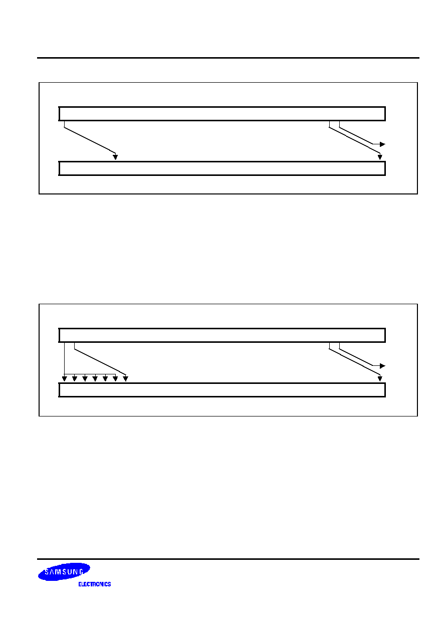
S3C2440A RISC MICROPROCESSOR
ARM INSTRUCTION SET
3-13
31
Contents of Rm
Value of Operand 2
0
carry out
4
5
0
0
0
0
0
Figure 3-7. Logical Shift Right
The form of the shift field which might be expected to correspond to LSR #0 is used to encode LSR #32, which has a
zero result with bit 31 of Rm as the carry output. Logical shift right zero is redundant as it is the same as logical shift
left zero, so the assembler will convert LSR #0 (and ASR #0 and ROR #0) into LSL #0, and allow LSR #32 to be
specified.
An Arithmetic Shift Right (ASR) is similar to logical shift right, except that the high bits are filled with bit 31 of Rm
instead of zeros. This preserves the sign in 2's complement notation. For example, ASR #5 is shown in Figure
3-8.
31
Contents of Rm
Value of Operand 2
0
carry out
4
5
30
Figure 3-8. Arithmetic Shift Right
The form of the shift field which might be expected to give ASR #0 is used to encode ASR #32. Bit 31 of Rm is again
used as the carry output, and each bit of operand 2 is also equal to bit 31 of Rm. The result is therefore all ones or
all zeros, according to the value of bit 31 of Rm.
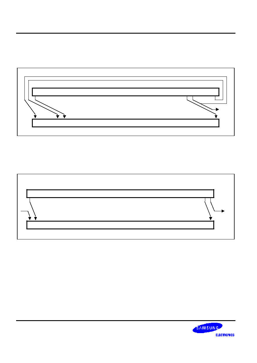
ARM INSTRUCTION SET
S3C2440A RISC MICROPROCESSOR
3-14
Rotate right (ROR) operations reuse the bits which "overshoot" in a logical shift right operation by reintroducing them
at the high end of the result, in place of the zeros used to fill the high end in logical right operations. For example,
ROR #5 is shown in Figure 3-9.
31
Contents of Rm
Value of Operand 2
0
carry out
4
5
Figure 3-9. Rotate Right
The form of the shift field which might be expected to give ROR #0 is used to encode a special function of the barrel
shifter, rotate right extended (RRX). This is a rotate right by one bit position of the 33 bit quantity formed by
appending the CPSR C flag to the most significant end of the contents of Rm as shown in Figure 3-10.
31
Contents of Rm
Value of Operand 2
0
1
carry out
C
in
Figure 3-10. Rotate Right Extended

S3C2440A RISC MICROPROCESSOR
ARM INSTRUCTION SET
3-15
Register Specified Shift Amount
Only the least significant byte of the contents of Rs is used to determine the shift amount. Rs can be any general
register other than R15.
If this byte is zero, the unchanged contents of Rm will be used as the second operand, and the old value of the
CPSR C flag will be passed on as the shifter carry output.
If the byte has a value between 1 and 31, the shifted result will exactly match that of an instruction specified shift
with the same value and shift operation.
If the value in the byte is 32 or more, the result will be a logical extension of the shift described above:
1. LSL by 32 has result zero, carry out equal to bit 0 of Rm.
2. LSL by more than 32 has result zero, carry out zero.
3. LSR by 32 has result zero, carry out equal to bit 31 of Rm.
4. LSR by more than 32 has result zero, carry out zero.
5. ASR by 32 or more has result filled with and carry out equal to bit 31 of Rm.
6. ROR by 32 has result equal to Rm, carry out equal to bit 31 of Rm.
7. ROR by n where n is greater than 32 will give the same result and carry out as ROR by n-32; therefore
repeatedly subtract 32 from n until the amount is in the range 1 to 32 and see above.
NOTE
The zero in bit 7 of an instruction with a register controlled shift is compulsory; a one in this bit will cause
the instruction to be a multiply or undefined instruction.

ARM INSTRUCTION SET
S3C2440A RISC MICROPROCESSOR
3-16
IMMEDIATE OPERAND ROTATES
The immediate operand rotate field is a 4 bit unsigned integer which specifies a shift operation on the 8 bit immediate
value. This value is zero extended to 32 bits, and then subject to a rotate right by twice the value in the rotate field.
This enables many common constants to be generated, for example all powers of 2.
WRITING TO R15
When Rd is a register other than R15, the condition code flags in the CPSR may be updated from the ALU flags as
described above.
When Rd is R15 and the S flag in the instruction is not set the result of the operation is placed in R15 and the CPSR
is unaffected.
When Rd is R15 and the S flag is set the result of the operation is placed in R15 and the SPSR corresponding to the
current mode is moved to the CPSR. This allows state changes which automatically restore both PC and CPSR.
This form of instruction should not be used in User mode.
USING R15 AS AN OPERANDY
If R15 (the PC) is used as an operand in a data processing instruction the register is used directly.
The PC value will be the address of the instruction, plus 8 or 12 bytes due to instruction prefetching. If the shift
amount is specified in the instruction, the PC will be 8 bytes ahead. If a register is used to specify the shift amount
the PC will be 12 bytes ahead.
TEQ, TST, CMP AND CMN OPCODES
NOTE
TEQ, TST, CMP and CMN do not write the result of their operation but do set flags in the CPSR. An
assembler should always set the S flag for these instructions even if this is not specified in the mnemonic.
The TEQP form of the TEQ instruction used in earlier ARM processors must not be used: the PSR transfer
operations should be used instead.
The action of TEQP in the ARM920T is to move SPSR_<mode> to the CPSR if the processor is in a privileged mode
and to do nothing if in User mode.
INSTRUCTION CYCLE TIMES
Data Processing instructions vary in the number of incremental cycles taken as follows:
Table 3-4. Incremental Cycle Times
Processing Type
Cycles
Normal data processing
1S
Data processing with register specified shift
1S + 1I
Data processing with PC written
2S + 1N
Data processing with register specified shift and PC written
2S + 1N +1I
NOTE: S, N and I are as defined sequential (S-cycle), non-sequential (N-cycle), and internal (I-cycle) respectively.

S3C2440A RISC MICROPROCESSOR
ARM INSTRUCTION SET
3-17
ASSEMBLER SYNTAX
∑
MOV,MVN (single operand instructions).
<opcode>{cond}{S} Rd,<Op2>
∑
CMP,CMN,TEQ,TST (instructions which do not produce a result).
<opcode>{cond} Rn,<Op2>
∑
AND,EOR,SUB,RSB,ADD,ADC,SBC,RSC,ORR,BIC
<opcode>{cond}{S} Rd,Rn,<Op2>
where:
<Op2>
Rm{,<shift>} or,<#expression>
{cond}
A two-character condition mnemonic. See Table 3-2.
{S}
Set condition codes if S present (implied for CMP, CMN, TEQ, TST).
Rd, Rn and Rm Expressions evaluating to a register number.
<#expression>
If this is used, the assembler will attempt to generate a shifted immediate 8-bit field to
match the expression. If this is impossible, it will give an error.
<shift>
<Shiftname> <register> or <shiftname> #expression, or RRX (rotate right one bit with
extend).
<shiftname>s
ASL, LSL, LSR, ASR, ROR. (ASL is a synonym for LSL, they assemble to the same
code.)
EXAMPLES
ADDEQ
R2,R4,R5
; If the Z flag is set make R2:=R4+R5
TEQS
R4,#3
; Test R4 for equality with 3.
; (The S is in fact redundant as the
; assembler inserts it automatically.)
SUB
R4,R5,R7,LSR R2
; Logical right shift R7 by the number in
; the bottom byte of R2, subtract result
; from R5, and put the answer into R4.
MOV
PC,R14
; Return from subroutine.
MOVS
PC,R14
; Return from exception and restore CPSR
; from SPSR_mode.

ARM INSTRUCTION SET
S3C2440A RISC MICROPROCESSOR
3-18
PSR TRANSFER (MRS, MSR)
The instruction is only executed if the condition is true. The various conditions are defined in Table 3-2.
The MRS and MSR instructions are formed from a subset of the Data Processing operations and are implemented
using the TEQ, TST, CMN and CMP instructions without the S flag set. The encoding is shown in Figure 3-11.
These instructions allow access to the CPSR and SPSR registers. The MRS instruction allows the contents of the
CPSR or SPSR_<mode> to be moved to a general register. The MSR instruction allows the contents of a general
register to be moved to the CPSR or SPSR_<mode> register.
The MSR instruction also allows an immediate value or register contents to be transferred to the condition code flags
(N,Z,C and V) of CPSR or SPSR_<mode> without affecting the control bits. In this case, the top four bits of the
specified register contents or 32 bit immediate value are written to the top four bits of the relevant PSR.
OPERAND RESTRICTIONS
∑
In user mode, the control bits of the CPSR are protected from change, so only the condition code flags of the
CPSR can be changed. In other (privileged) modes the entire CPSR can be changed.
∑
Note that the software must never change the state of the T bit in the CPSR. If this happens, the processor will
enter an unpredictable state.
∑
The SPSR register which is accessed depends on the mode at the time of execution. For example, only
SPSR_fiq is accessible when the processor is in FIQ mode.
∑
You must not specify R15 as the source or destination register.
∑
Also, do not attempt to access an SPSR in User mode, since no such register exists.
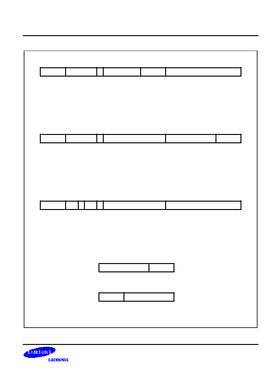
S3C2440A RISC MICROPROCESSOR
ARM INSTRUCTION SET
3-19
MSR (transfer register contents or immediate value to PSR flag bits only)
Cond
Source operand
Pd
101001111
31
22
27
28
11
12
21
23
I
10
00
26 25 24
0
Cond
00000000
00010
Pd
101001111
31
22
27
28
11
12
21
23
Rm
MSR
(transfer register contents to PSR)
4 3
0
Cond
000000000000
00010
Rd
Ps
001111
31
22
27
15
28
16
11
12
21
23
MRS (transfer PSR contents to a register)
0
[3:0] Source Register
[22] Destination PSR
0 = CPSR
1 = SPSR_<current mode>
[31:28] Condition Field
[15:12] Destination Register
[22] Source PSR
0 = CPSR
1 = SPSR_<current mode>
[31:28] Condition Field
[3:0] Source Register
[11:4] Source operand is an immediate value
[7:0] Unsigned 8 bit immediate value
[11:8] Shift applied to Imm
[22] Destination PSR
0 = CPSR
1 = SPSR_<current mode>
[25] Immediate Operand
0 = Source operand is a register
1 = SPSR_<current mode>
[11:0] Source Operand
[31:28] Condition Field
00000000
Rm
11
4 3
0
Rotate
Imm
11
0
8 7
Figure 3-11. PSR Transfer

ARM INSTRUCTION SET
S3C2440A RISC MICROPROCESSOR
3-20
RESERVED BITS
Only twelve bits of the PSR are defined in ARM920T (N,Z,C,V,I,F, T & M[4:0]); the remaining bits are reserved for use
in future versions of the processor. Refer to Figure 2-6 for a full description of the PSR bits.
To ensure the maximum compatibility between ARM920T programs and future processors, the following rules should
be observed:
∑
The reserved bits should be preserved while changing the value in a PSR.
∑
Programs should not rely on specific values from the reserved bits while checking the PSR status, since they
may read as one or zero in future processors.
A read-modify-write strategy should therefore be used when altering the control bits of any PSR register; this involves
transferring the appropriate PSR register to a general register using the MRS instruction, changing only the relevant
bits and then transferring the modified value back to the PSR register using the MSR instruction.
EXAMPLES
The following sequence performs a mode change:
MRS
R0,CPSR
; Take a copy of the CPSR.
BIC
R0,R0,#0x1F
; Clear the mode bits.
ORR
R0,R0,#new_mode
; Select new mode
MSR
CPSR,R0
; Write back the modified CPSR.
When the aim is simply to change the condition code flags in a PSR, a value can be written directly to the flag bits
without disturbing the control bits. The following instruction sets the N,Z,C and V flags:
MSR
CPSR_flg,#0xF0000000
; Set all the flags regardless of their previous state
; (does not affect any control bits).
No attempt should be made to write an 8 bit immediate value into the whole PSR since such an operation cannot
preserve the reserved bits.
INSTRUCTION CYCLE TIMES
PSR transfers take 1S incremental cycles, where S is defined as Sequential (S-cycle).

S3C2440A RISC MICROPROCESSOR
ARM INSTRUCTION SET
3-21
ASSEMBLY SYNTAX
∑
MRS - transfer PSR contents to a register
MRS{cond} Rd,<psr>
∑
MSR - transfer register contents to PSR
MSR{cond} <psr>,Rm
∑
MSR - transfer register contents to PSR flag bits only
MSR{cond} <psrf>,Rm
The most significant four bits of the register contents are written to the N,Z,C & V flags respectively.
∑
MSR - transfer immediate value to PSR flag bits only
MSR{cond} <psrf>,<#expression>
The expression should symbolise a 32 bit value of which the most significant four bits are written to the N,Z,C and V
flags respectively.
Key:
{cond}
Two-character condition mnemonic. See Table 3-2..
Rd and Rm
Expressions evaluating to a register number other than R15
<psr>
CPSR, CPSR_all, SPSR or SPSR_all. (CPSR and CPSR_all are synonyms as are SPSR
and SPSR_all)
<psrf>
CPSR_flg or SPSR_flg
<#expression>
Where this is used, the assembler will attempt to generate a shifted immediate 8-bit field
to match the expression. If this is impossible, it will give an error.
EXAMPLES
In User mode the instructions behave as follows:
MSR
CPSR_all,Rm
; CPSR[31:28] <- Rm[31:28]
MSR
CPSR_flg,Rm
; CPSR[31:28] <- Rm[31:28]
MSR
CPSR_flg,#0xA0000000
; CPSR[31:28] <- 0xA (set N,C; clear Z,V)
MRS
Rd,CPSR
; Rd[31:0] <- CPSR[31:0]
In privileged modes the instructions behave as follows:
MSR
CPSR_all,Rm
; CPSR[31:0] <- Rm[31:0]
MSR
CPSR_flg,Rm
; CPSR[31:28] <- Rm[31:28]
MSR
CPSR_flg,#0x50000000
; CPSR[31:28] <- 0x5 (set Z,V; clear N,C)
MSR
SPSR_all,Rm
; SPSR_<mode>[31:0]<- Rm[31:0]
MSR
SPSR_flg,Rm
; SPSR_<mode>[31:28] <- Rm[31:28]
MSR
SPSR_flg,#0xC0000000
; SPSR_<mode>[31:28] <- 0xC (set N,Z; clear C,V)
MRS
Rd,SPSR
; Rd[31:0] <- SPSR_<mode>[31:0]

ARM INSTRUCTION SET
S3C2440A RISC MICROPROCESSOR
3-22
MULTIPLY AND MULTIPLY-ACCUMULATE (MUL, MLA)
The instruction is only executed if the condition is true. The various conditions are defined in Table 3-2. The
instruction encoding is shown in Figure 3-12.
The multiply and multiply-accumulate instructions use an 8 bit Booth's algorithm to perform integer multiplication.
31
27
19
15
Cond
28
16
11
12
21 20
S
Rd
Rn
[15:12][11:8][3:0] Operand Registers
[19:16] Destination Register
[20] Set Condition Code
0 = Do not after condition codes
1 = Set condition codes
[21] Accumulate
0 = Multiply only
1 = Multiply and accumulate
[31:28] Condition Field
22
1 0 0 1
Rs
Rm
A
0
0
0 0 0 0
8 7
4 3
0
Figure 3-12. Multiply Instructions
The multiply form of the instruction gives Rd:=Rm*Rs. Rn is ignored, and should be set to zero for compatibility with
possible future upgrades to the instruction set. The multiply-accumulate form gives Rd:=Rm*Rs+Rn, which can save
an explicit ADD instruction in some circumstances. Both forms of the instruction work on operands which may be
considered as signed (2's complement) or unsigned integers.
The results of a signed multiply and of an unsigned multiply of 32 bit operands differ only in the upper 32 bits - the
low 32 bits of the signed and unsigned results are identical. As these instructions only produce the low 32 bits of a
multiply, they can be used for both signed and unsigned multiplies.
For example consider the multiplication of the operands:
Operand A
Operand B
Result
0xFFFFFFF6
0x0000001
0xFFFFFF38

S3C2440A RISC MICROPROCESSOR
ARM INSTRUCTION SET
3-23
If the Operands Are Interpreted as Signed
Operand A has the value -10, operand B has the value 20, and the result is -200 which is correctly represented as
0xFFFFFF38.
If the Operands Are Interpreted as Unsigned
Operand A has the value 4294967286, operand B has the value 20 and the result is 85899345720, which is
represented as 0x13FFFFFF38, so the least significant 32 bits are 0xFFFFFF38.
Operand Restrictions
The destination register Rd must not be the same as the operand register Rm. R15 must not be used as an operand
or as the destination register.
All other register combinations will give correct results, and Rd, Rn and Rs may use the same register when
required.

ARM INSTRUCTION SET
S3C2440A RISC MICROPROCESSOR
3-24
CPSR FLAGS
Setting the CPSR flags is optional, and is controlled by the S bit in the instruction. The N (Negative) and Z (Zero)
flags are set correctly on the result (N is made equal to bit 31 of the result, and Z is set if and only if the result is
zero). The C (Carry) flag is set to a meaningless value and the V (oVerflow) flag is unaffected.
INSTRUCTION CYCLE TIMES
MUL takes 1S + mI and MLA 1S + (m+1)I cycles to execute, where S and I are defined as sequential (S-cycle) and
internal (I-cycle), respectively.
m
The number of 8 bit multiplier array cycles is required to complete the multiply, which is
controlled by the value of the multiplier operand specified by Rs. Its possible values are
as follows
1
If bits [32:8] of the multiplier operand are all zero or all one.
2
If bits [32:16] of the multiplier operand are all zero or all one.
3
If bits [32:24] of the multiplier operand are all zero or all one.
4
In all other cases.
ASSEMBLER SYNTAX
MUL{cond}{S} Rd,Rm,Rs
MLA{cond}{S} Rd,Rm,Rs,Rn
{cond}
Two-character condition mnemonic. See Table 3-2..
{S}
Set condition codes if S present
Rd, Rm, Rs and Rn
Expressions evaluating to a register number other than R15.
EXAMPLES
MUL
R1,R2,R3
; R1:=R2*R3
MLAEQS
R1,R2,R3,R4
; Conditionally R1:=R2*R3+R4, Setting condition codes.
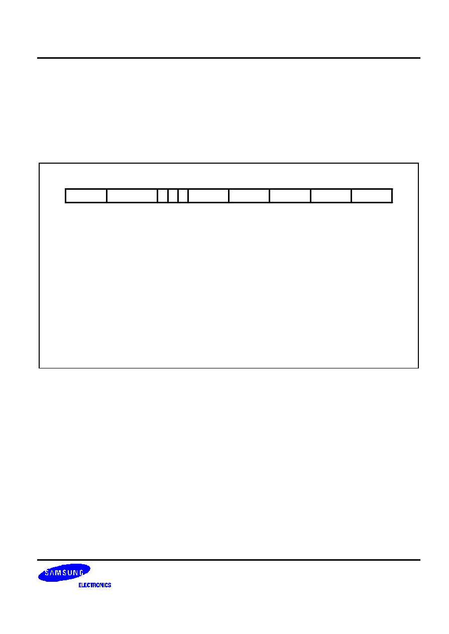
S3C2440A RISC MICROPROCESSOR
ARM INSTRUCTION SET
3-25
MULTIPLY LONG AND MULTIPLY-ACCUMULATE LONG (MULL, MLAL)
The instruction is only executed if the condition is true. The various conditions are defined in Table 3-2. The
instruction encoding is shown in Figure 3-13.
The multiply long instructions perform integer multiplication on two 32 bit operands and produce 64 bit results.
Signed and unsigned multiplication each with optional accumulate give rise to four variations.
31
27
19
15
Cond
28
16
11
12
21
23
U
20
S
RdHi
RdLo
[11:8][3:0] Operand Registers
[19:16][15:12] Source Destination Registers
[20] Set Condition Code
0 = Do not alter condition codes
1 = Set condition codes
[21] Accumulate
0 = Multiply only
1 = Multiply and accumulate
[22] Unsigned
0 = Unsigned
1 = Signed
[31:28] Condition Field
22
0
0
0 0 1
1 0 0 1
Rs
Rm
A
8 7
4 3
0
Figure 3-13. Multiply Long Instructions
The multiply forms (UMULL and SMULL) take two 32 bit numbers and multiply them to produce a 64 bit result of the
form RdHi,RdLo := Rm * Rs. The lower 32 bits of the 64 bit result are written to RdLo, the upper 32 bits of the result
are written to RdHi.
The multiply-accumulate forms (UMLAL and SMLAL) take two 32 bit numbers, multiply them and add a 64 bit
number to produce a 64 bit result of the form RdHi,RdLo := Rm * Rs + RdHi,RdLo. The lower 32 bits of the 64 bit
number to add is read from RdLo. The upper 32 bits of the 64 bit number to add is read from RdHi. The lower 32 bits
of the 64 bit result are written to RdLo. The upper 32 bits of the 64 bit result are written to RdHi.
The UMULL and UMLAL instructions treat all of their operands as unsigned binary numbers and write an unsigned 64
bit result. The SMULL and SMLAL instructions treat all of their operands as two's-complement signed numbers and
write a two's-complement signed 64 bit result.

ARM INSTRUCTION SET
S3C2440A RISC MICROPROCESSOR
3-26
OPERAND RESTRICTIONS
∑
R15 must not be used as an operand or as a destination register.
∑
RdHi, RdLo, and Rm must all specify different registers.
CPSR FLAGS
Setting the CPSR flags is optional, and is controlled by the S bit in the instruction. The N and Z flags are set
correctly on the result (N is equal to bit 63 of the result, Z is set if and only if all 64 bits of the result are zero). Both
the C and V flags are set to meaningless values.
INSTRUCTION CYCLE TIMES
MULL takes 1S + (m+1)I and MLAL 1S + (m+2)I cycles to execute, where m is the number of 8 bit multiplier array
cycles required to complete the multiply, which is controlled by the value of the multiplier operand specified by Rs.
Its possible values are as follows:
For Signed INSTRUCTIONS SMULL, SMLAL:
∑
If bits [31:8] of the multiplier operand are all zero or all one.
∑
If bits [31:16] of the multiplier operand are all zero or all one.
∑
If bits [31:24] of the multiplier operand are all zero or all one.
∑
In all other cases.
For Unsigned Instructions UMULL, UMLAL:
∑
If bits [31:8] of the multiplier operand are all zero.
∑
If bits [31:16] of the multiplier operand are all zero.
∑
If bits [31:24] of the multiplier operand are all zero.
∑
In all other cases.
S and I are defined as sequential (S-cycle) and internal (I-cycle), respectively.

S3C2440A RISC MICROPROCESSOR
ARM INSTRUCTION SET
3-27
ASSEMBLER SYNTAX
Table 3-5. Assembler Syntax Descriptions
Mnemonic
Description
Purpose
UMULL{cond}{S} RdLo,RdHi,Rm,Rs
Unsigned Multiply Long
32 x 32 = 64
UMLAL{cond}{S} RdLo,RdHi,Rm,Rs
Unsigned Multiply & Accumulate Long
32 x 32 + 64 = 64
SMULL{cond}{S} RdLo,RdHi,Rm,Rs
Signed Multiply Long
32 x 32 = 64
SMLAL{cond}{S} RdLo,RdHi,Rm,Rs
Signed Multiply & Accumulate Long
32 x 32 + 64 = 64
where:
{cond}
Two-character condition mnemonic. See Table 3-2.
{S}
Set condition codes if S present
RdLo, RdHi, Rm, Rs
Expressions evaluating to a register number other than R15.
EXAMPLES
UMULL
R1,R4,R2,R3
; R4,R1:=R2*R3
UMLALS
R1,R5,R2,R3
; R5,R1:=R2*R3+R5,R1 also setting condition codes
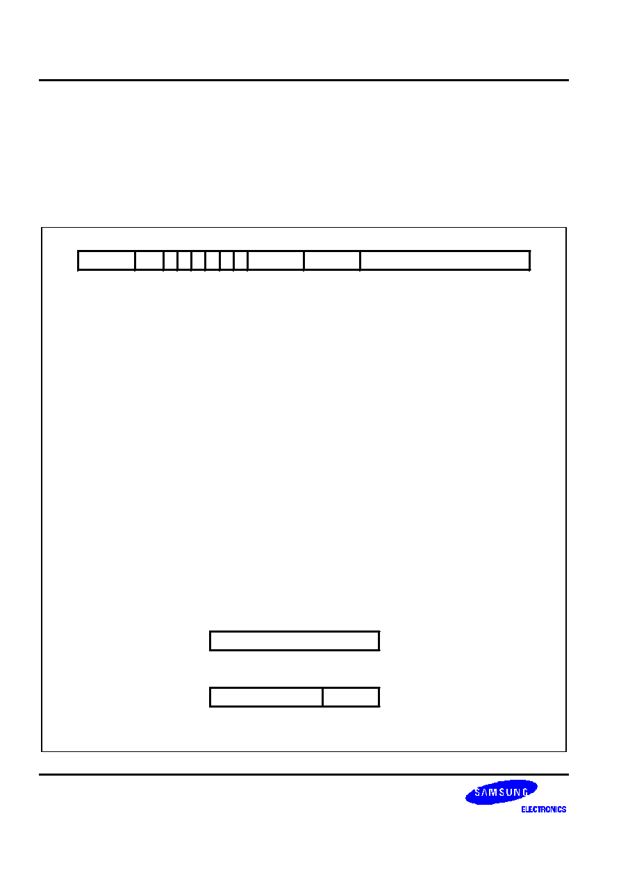
ARM INSTRUCTION SET
S3C2440A RISC MICROPROCESSOR
3-28
SINGLE DATA TRANSFER (LDR, STR)
The instruction is only executed if the condition is true. The various conditions are defined in Table 3-2. The
instruction encoding is shown in Figure 3-14.
The single data transfer instructions are used to load or store single bytes or words of data. The memory address
used in the transfer is calculated by adding an offset to or subtracting an offset from a base register.
The result of this calculation may be written back into the base register if auto-indexing is required.
31
27
19
15
0
Cond
28
16
11
12
21
23
B
20
L
Rn
Rd
22
01
I P U
Offset
W
26
24
25
[15:12] Source/Destination Registers
[19:16] Base Register
[20] Load/Store Bit
0 = Store to memory
1 = Load from memory
[21] Write-back Bit
0 = No write-back
1 = Write address into base
[22] Byte/Word Bit
0 = Transfer word quantity
1 = Transfer byte quantity
[23] Up/Down Bit
0 = Down: subtract offset from base
1 = Up: add offset to base
[24] Pre/Post Indexing Bit
0 = Post: add offset after transfer
1 = Pre: add offset before transfer
[25] Immediate Offset
0 = Offset is an immediate value
[11:0] Offset
Shift
Immediate
[11:0] Unsigned 12-bit immediate offset
11
11
Rm
[3:0] Offset register [11:4] Shift applied to Rm
[31:28] Condition Field
0
4 3
0
Figure 3-14. Single Data Transfer Instructions

S3C2440A RISC MICROPROCESSOR
ARM INSTRUCTION SET
3-29
OFFSETS AND AUTO-INDEXING
The offset from the base may be either a 12 bit unsigned binary immediate value in the instruction, or a second
register (possibly shifted in some way). The offset may be added to (U=1) or subtracted from (U=0) the base register
Rn. The offset modification may be performed either before (pre-indexed, P=1) or after (post-indexed, P=0) the base
is used as the transfer address.
The W bit gives optional auto increment and decrement addressing modes. The modified base value may be written
back into the base (W=1), or the old base value may be kept (W=0). In the case of post-indexed addressing, the
write back bit is redundant and is always set to zero, since the old base value can be retained by setting the offset to
zero. Therefore post-indexed data transfers always write back the modified base. The only use of the W bit in a post-
indexed data transfer is in privileged mode code, where setting the W bit forces non-privileged mode for the transfer,
allowing the operating system to generate a user address in a system where the memory management hardware
makes suitable use of this hardware.
SHIFTED REGISTER OFFSET
The 8 shift control bits are described in the data processing instructions section. However, the register specified shift
amounts are not available in this instruction class. See Figure 3-5.
BYTES AND WORDS
This instruction class may be used to transfer a byte (B=1) or a word (B=0) between an ARM920T register and
memory.
The action of LDR(B) and STR(B) instructions is influenced by the BIGEND control signal of ARM920T core. The two
possible configurations are described below.
Little-Endian Configuration
A byte load (LDRB) expects the data on data bus inputs 7 through 0 if the supplied address is on a word boundary,
on data bus inputs 15 through 8, if it is a word address plus one byte, and so on. The selected byte is placed in the
bottom 8 bits of the destination register, and the remaining bits of the register are filled with zeros. Please see Figure
2-2.
A byte store (STRB) repeats the bottom 8 bits of the source register four times across data bus outputs 31 through
0. The external memory system should activate the appropriate byte subsystem to store the data.
A word load (LDR) will normally use a word aligned address. However, an address offset from a word boundary will
cause the data to be rotated into the register so that the addressed byte occupies bits 0 to 7. This means that half-
words accessed at offsets 0 and 2 from the word boundary will be correctly loaded into bits 0 through 15 of the
register. Two shift operations are then required to clear or to sign extend the upper 16 bits.
A word store (STR) should generate a word aligned address. The word presented to the data bus is not affected if the
address is not word aligned. That is, bit 31 of the register being stored always appears on data bus output 31.
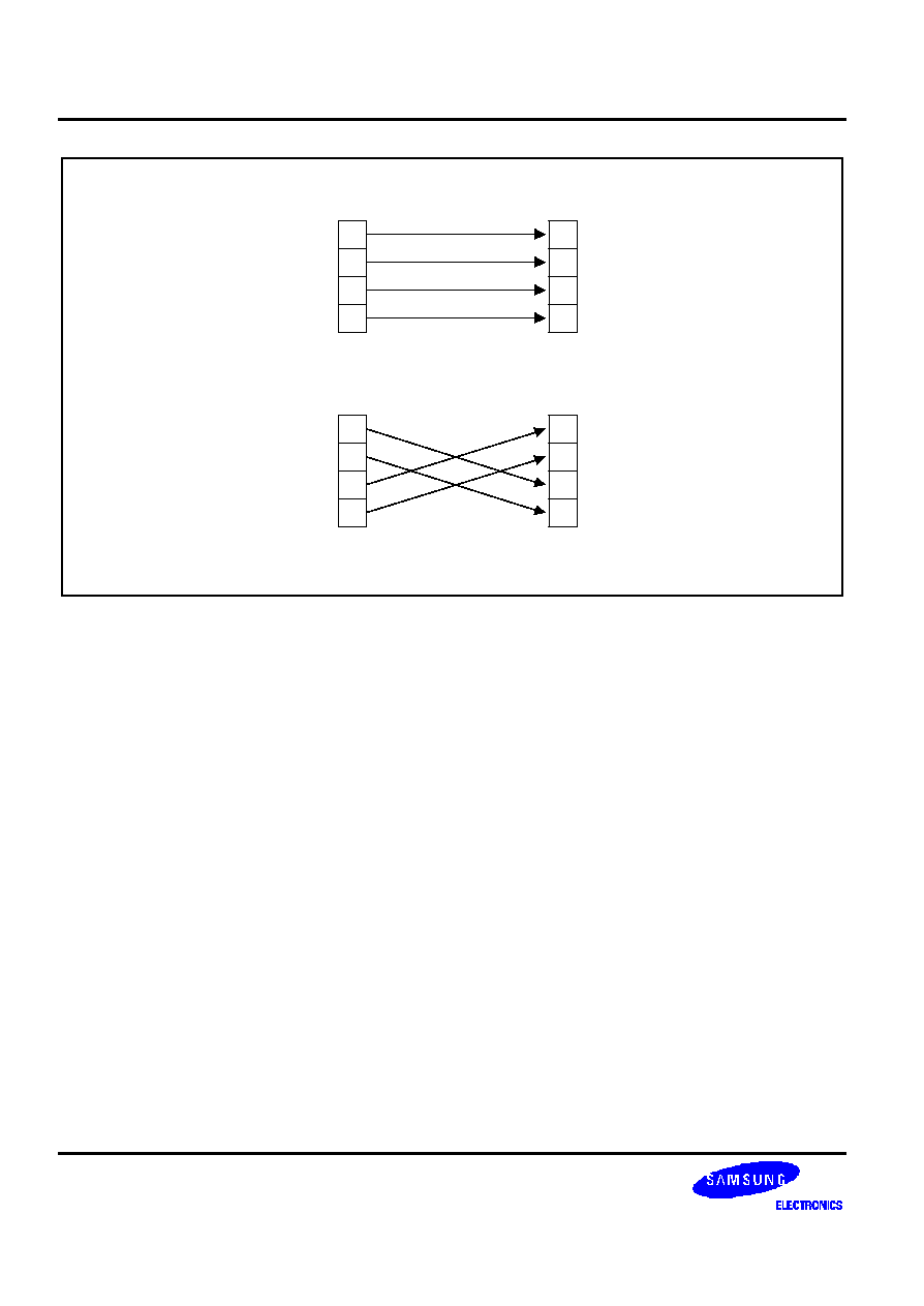
ARM INSTRUCTION SET
S3C2440A RISC MICROPROCESSOR
3-30
LDR from word aligned address
A+3
A
A+2
A+1
memory
24
16
8
0
A
B
C
D
register
24
16
8
0
A
B
C
D
LDR from address offset by 2
A+3
A
A+2
A+1
memory
24
16
8
0
A
B
C
D
register
24
16
8
0
A
B
C
D
Figure 3-15. Little-Endian Offset Addressing
Big-Endian Configuration
A byte load (LDRB) expects the data on data bus inputs 31 through 24 if the supplied address is on a word
boundary, on data bus inputs 23 through 16 if it is a word address plus one byte, and so on. The selected byte is
placed in the bottom 8 bits of the destination register and the remaining bits of the register are filled with zeros.
Please see Figure 2-1.
A byte store (STRB) repeats the bottom 8 bits of the source register four times across data bus outputs 31 through
0. The external memory system should activate the appropriate byte subsystem to store the data.
A word load (LDR) should generate a word aligned address. An address offset of 0 or 2 from a word boundary will
cause the data to be rotated into the register so that the addressed byte occupies bits 31 through 24. This means
that half-words accessed at these offsets will be correctly loaded into bits 16 through 31 of the register. A shift
operation is then required to move (and optionally sign extend) the data into the bottom 16 bits. An address offset of
1 or 3 from a word boundary will cause the data to be rotated into the register so that the addressed byte occupies
bits 15 through 8.
A word store (STR) should generate a word aligned address. The word presented to the data bus is not affected if the
address is not word aligned. That is, bit 31 of the register being stored always appears on data bus output 31.

S3C2440A RISC MICROPROCESSOR
ARM INSTRUCTION SET
3-31
USE OF R15
Write-back must not be specified if R15 is specified as the base register (Rn). While using R15 as the base register,
you must remember it contains an address of 8 bytes on from the address of the current instruction.
R15 must not be specified as the register offset (Rm).
When R15 is the source register (Rd) of a register store (STR) instruction, the stored value will be address of the
instruction plus 12.
Restriction are made depending on the use of base register
When configured for late aborts, the following example code is difficult to unwind as the base register, Rn, gets
updated before the abort handler starts. Sometimes it may be impossible to calculate the initial value.
After an abort, the following example code is difficult to unwind as the base register, Rn, gets updated before the
abort handler starts. Sometimes it may be impossible to calculate the initial value.
EXAMPLE:
LDR
R0,[R1],R1
Therefore a post-indexed LDR or STR where Rm is the same register as Rn should not be used.
DATA ABORTS
A transfer to or from a legal address may cause problems for a memory management system. For instance, in a
system which uses virtual memory the required data may be absent from main memory. The memory manager can
signal a problem by taking the processor ABORT input HIGH whereupon the Data Abort trap will be taken. It is up to
the system software to resolve the cause of the problem, then the instruction can be restarted and the original
program continued.
INSTRUCTION CYCLE TIMES
Normal LDR instructions take 1S + 1N + 1I and LDR PC take 2S + 2N +1I incremental cycles, where S,N and I are
defined as sequential (S-cycle), non-sequential (N-cycle), and internal (I-cycle), respectively. STR instructions take
2N incremental cycles to execute.

ARM INSTRUCTION SET
S3C2440A RISC MICROPROCESSOR
3-32
ASSEMBLER SYNTAX
<LDR|STR>{cond}{B}{T} Rd,<Address>
where:
LDR
Load from memory into a register
STR
Store from a register into memory
{cond}
Two-character condition mnemonic. See Table 3-2.
{B}
If B is present then byte transfer, otherwise word transfer
{T}
If T is present the W bit will be set in a post-indexed instruction, forcing non-privileged
mode for the transfer cycle. T is not allowed when a pre-indexed addressing mode is
specified or implied.
Rd
An expression evaluating to a valid register number.
Rn and Rm
Expressions evaluating to a register number. If Rn is R15 then the assembler will
subtract 8 from the offset value to allow for ARM920T pipelining.
In this case base write-back should not be specified.
<Address>can be:
1
An expression which generates an address:
The assembler will attempt to generate an instruction using the PC as a base and a
corrected immediate offset to address the location given by evaluating the expression.
This will be a PC relative, pre-indexed address. If the address is out of range, an error
will be generated.
2
A pre-indexed addressing specification:
[Rn]
offset of zero
[Rn,<#expression>]{!}
offset of <expression> bytes
[Rn,{+/-}Rm{,<shift>}]{!}
offset of +/- contents of index register, shifted
by <shift>
3
A post-indexed addressing specification:
[Rn],<#expression>
offset of <expression> bytes
[Rn],{+/-}Rm{,<shift>}
offset of +/- contents of index register, shifted as
by <shift>.
<shift>
General shift operation (see data processing instructions) but you cannot specify the shift
amount by a register.
{!}
Writes back the base register (set the W bit) if! is present.

S3C2440A RISC MICROPROCESSOR
ARM INSTRUCTION SET
3-33
EXAMPLES
STR
R1,[R2,R4]!
; Store R1 at R2+R4 (both of which are registers)
; and write back address to R2.
STR
R1,[R2],R4
; Store R1 at R2 and write back R2+R4 to R2.
LDR
R1,[R2,#16]
; Load R1 from contents of R2+16, but don't write back.
LDR
R1,[R2,R3,LSL#2]
; Load R1 from contents of R2+R3*4.
LDREQB
R1,[R6,#5]
; Conditionally load byte at R6+5 into
; R1 bits 0 to 7, filling bits 8 to 31 with zeros.
STR
R1,PLACE
; Generate PC relative offset to address PLACE.
PLACE
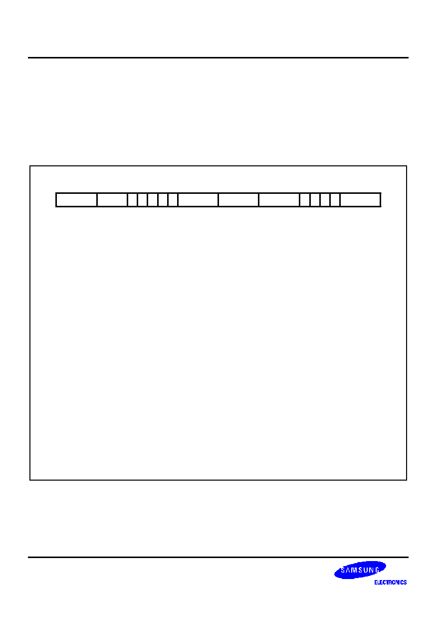
ARM INSTRUCTION SET
S3C2440A RISC MICROPROCESSOR
3-34
HALFWORD AND SIGNED DATA TRANSFER (LDRH/STRH/LDRSB/LDRSH)
The instruction is only executed if the condition is true. The various conditions are defined in Table 3-2. The
instruction encoding is shown in Figure 3-16.
These instructions are used to load or store half-words of data and also load sign-extended bytes or half-words of
data. The memory address used in the transfer is calculated by adding an offset to or subtracting an offset from a
base register. The result of this calculation may be written back into the base register if auto-indexing is required.
31
27
19
15
Cond
28
16
11
12
21
23
0
20
L
Rn
Rd
[3:0] Offset Register
[6][5] S H
0 0 = SWP instruction
0 1 = Unsigned halfword
1 1 = Signed byte
1 1 = Signed halfword
[15:12] Source/Destination Register
[19:16] Base Register
[20] Load/Store
0 = Store to memory
1 = Load from memory
[21] Write-back
0 = No write-back
1 = Write address into base
[23] Up/Down
0 = Down: subtract offset from base
1 = Up: add offset to base
[24] Pre/Post Indexing
0 = Post: add/subtract offset after transfer
1 = Pre: add/subtract offset bofore transfer
[31:28] Condition Field
22
000
P U
0000
W
24
25
1
Rm
S H 1
8 7 6 5 4 3
0
Figure 3-16. Halfword and Signed Data Transfer with Register Offset

S3C2440A RISC MICROPROCESSOR
ARM INSTRUCTION SET
3-35
31
27
19
15
Cond
28
16
11
12
21
23
1
20
L
Rn
Rd
[3:0] Immediate Offset (Low Nibble)
[6][5] S H
0 0 = SWP instruction
0 1 = Unsigned halfword
1 1 = Signed byte
1 1 = Signed halfword
[11:8] Immediate Offset (High Nibble)
[15:12] Source/Destination Register
[19:16] Base Register
[20] Load/Store
0 = Store to memory
1 = Load from memory
[21] Write-back
0 = No write-back
1 = Write address into base
[23] Up/Down
0 = Down: subtract offset from base
1 = Up: add offset to base
[24] Pre/Post Indexing
0 = Post: add/subtract offset after transfer
1 = Pre: add/subtract offset bofore transfer
[31:28] Condition Field
22
000
P U
Offset
W
24
25
1
Offset
S H 1
8 7 6 5 4 3
0
Figure 3-17. Halfword and Signed Data Transfer with Immediate Offset and Auto-Indexing
OFFSETS AND AUTO-INDEXING
The offset from the base may be either a 8-bit unsigned binary immediate value in the instruction, or a second
register. The 8-bit offset is formed by concatenating bits 11 to 8 and bits 3 to 0 of the instruction word, such that bit
11 becomes the MSB and bit 0 becomes the LSB. The offset may be added to (U=1) or subtracted from (U=0) the
base register Rn. The offset modification may be performed either before (pre-indexed, P=1) or after (post-indexed,
P=0) the base register is used as the transfer address.
The W bit gives optional auto-increment and decrement addressing modes. The modified base value may be written
back into the base (W=1), or the old base may be kept (W=0). In the case of post-indexed addressing, the write
back bit is redundant and is always set to zero, since the old base value can be retained if necessary by setting the
offset to zero. Therefore post-indexed data transfers always write back the modified base.
The Write-back bit should not be set high (W=1) when post-indexed addressing is selected.

ARM INSTRUCTION SET
S3C2440A RISC MICROPROCESSOR
3-36
HALFWORD LOAD AND STORES
Setting S=0 and H=1 may be used to transfer unsigned Half-words between an ARM920T register and memory.
The action of LDRH and STRH instructions is influenced by the BIGEND control signal. The two possible
configurations are described in the section below.
Signed byte and halfword loads
The S bit controls the loading of sign-extended data. When S=1 the H bit selects between Bytes (H=0) and Half-
words (H=1). The L bit should not be set low (Store) when Signed (S=1) operations have been selected.
The LDRSB instruction loads the selected Byte into bits 7 to 0 of the destination register and bits 31 to 8 of the
destination register are set to the value of bit 7, the sign bit.
The LDRSH instruction loads the selected Half-word into bits 15 to 0 of the destination register and bits 31 to 16 of
the destination register are set to the value of bit 15, the sign bit.
The action of the LDRSB and LDRSH instructions is influenced by the BIGEND control signal. The two possible
configurations are described in the following section.
Endianness and byte/halfword selection
Little-Endian Configuration
A signed byte load (LDRSB) expects data on data bus inputs 7 through to 0 if the supplied address is on a word
boundary, on data bus inputs 15 through to 8 if it is a word address plus one byte, and so on. The selected byte is
placed in the bottom 8 bit of the destination register, and the remaining bits of the register are filled with the sign bit,
bit 7 of the byte. Please see Figure 2-2.
A halfword load (LDRSH or LDRH) expects data on data bus inputs 15 through to 0 if the supplied address is on a
word boundary and on data bus inputs 31 through to 16 if it is a halfword boundary, (A[1]=1).The supplied address
should always be on a halfword boundary. If bit 0 of the supplied address is HIGH then the ARM920T will load an
unpredictable value. The selected halfword is placed in the bottom 16 bits of the destination register. For unsigned
half-words (LDRH), the top 16 bits of the register are filled with zeros and for signed half-words (LDRSH) the top 16
bits are filled with the sign bit, bit 15 of the halfword.
A halfword store (STRH) repeats the bottom 16 bits of the source register twice across the data bus outputs 31
through to 0. The external memory system should activate the appropriate halfword subsystem to store the data.
Note that the address must be halfword aligned, if bit 0 of the address is HIGH this will cause unpredictable
behaviour.

S3C2440A RISC MICROPROCESSOR
ARM INSTRUCTION SET
3-37
Big-Endian Configuration
A signed byte load (LDRSB) expects data on data bus inputs 31 through to 24 if the supplied address is on a word
boundary, on data bus inputs 23 through to 16 if it is a word address plus one byte, and so on. The selected byte is
placed in the bottom 8 bit of the destination register, and the remaining bits of the register are filled with the sign bit,
bit 7 of the byte. Please see Figure 2-1.
A halfword load (LDRSH or LDRH) expects data on data bus inputs 31 through to 16 if the supplied address is on a
word boundary and on data bus inputs 15 through to 0 if it is a halfword boundary, (A[1]=1). The supplied address
should always be on a halfword boundary. If bit 0 of the supplied address is HIGH then the ARM920T will load an
unpredictable value. The selected halfword is placed in the bottom 16 bits of the destination register. For unsigned
half-words (LDRH), the top 16 bits of the register are filled with zeros and for signed half-words (LDRSH) the top 16
bits are filled with the sign bit, bit 15 of the halfword.
A halfword store (STRH) repeats the bottom 16 bits of the source register twice across the data bus outputs 31
through to 0. The external memory system should activate the appropriate halfword subsystem to store the data.
NOTE
Please note that the address must be halfword aligned, if bit 0 of the address is HIGH this will cause
unpredictable behavior.
USE OF R15
Write-back should not be specified if R15 is specified as the base register (Rn). While using R15 as the base
register you must remember it contains address 8 bytes on from the address of the current instruction.
R15 should not be specified as the register offset (Rm).
When R15 is the source register (Rd) of a Half-word store (STRH) instruction, the stored address will be address of
the instruction plus 12.
DATA ABORTS
A transfer to or from a legal address may cause problems for a memory management system. For instance, in a
system which uses virtual memory the required data may be absent from the main memory. The memory manager
can signal a problem by taking the processor ABORT input HIGH whereupon the Data Abort trap will be taken. It is
up to the system software to resolve the cause of the problem, then the instruction can be restarted and the original
program continued.
INSTRUCTION CYCLE TIMES
Normal LDR(H,SH,SB) instructions take 1S + 1N + 1I. LDR(H,SH,SB) PC take 2S + 2N + 1I incremental cycles.
S,N and I are defined as sequential (S-cycle), non-sequential (N-cycle), and internal (I-cycle), respectively. STRH
instructions take 2N incremental cycles to execute.

ARM INSTRUCTION SET
S3C2440A RISC MICROPROCESSOR
3-38
ASSEMBLER SYNTAX
<LDR|STR>{cond}<H|SH|SB> Rd,<address>
LDR
Load from memory into a register
STR
Store from a register into memory
{cond}
Two-character condition mnemonic. See Table 3-2.
H
Transfer halfword quantity
SB
Load sign extended byte (Only valid for LDR)
SH
Load sign extended halfword (Only valid for LDR)
Rd
An expression evaluating to a valid register number.
<address> can be:
1
An expression which generates an address:
The assembler will attempt to generate an instruction using the PC as a base and a
corrected immediate offset to address the location given by evaluating the expression. This will
be a PC relative, pre-indexed address. If the address is out of range, an error will be
generated.
2
A pre-indexed addressing specification:
[Rn]
offset of zero
[Rn,<#expression>]{!}
offset of <expression> bytes
[Rn,{+/-}Rm]{!}
offset of +/- contents of index register
3
A post-indexed addressing specification:
[Rn],<#expression>
offset of <expression> bytes
[Rn],{+/-}Rm
offset of +/- contents of index register.
4
Rn and Rm are expressions evaluating to a register number. If Rn is R15 then the
assembler will subtract 8 from the offset value to allow for ARM920T pipelining. In this case
base write-back should not be specified.
{!}
Writes back the base register (set the W bit) if ! is present.

S3C2440A RISC MICROPROCESSOR
ARM INSTRUCTION SET
3-39
EXAMPLES
LDRH
R1,[R2,-R3]!
; Load R1 from the contents of the halfword address
; contained in R2-R3 (both of which are registers)
; and write back address to R2
STRH
R3,[R4,#14]
; Store the halfword in R3 at R14+14 but don't write back.
LDRSB
R8,[R2],#-223
; Load R8 with the sign extended contents of the byte
; address contained in R2 and write back R2-223 to R2.
LDRNESH
R11,[R0]
; Conditionally load R11 with the sign extended contents
; of the halfword address contained in R0.
HERE
; Generate PC relative offset to address FRED.
STRH
R5, [PC,#(FRED-HERE-8)];
Store the halfword in R5 at address FRED
FRED

ARM INSTRUCTION SET
S3C2440A RISC MICROPROCESSOR
3-40
BLOCK DATA TRANSFER (LDM, STM)
The instruction is only executed if the condition is true. The various conditions are defined in Table 3-2. The
instruction encoding is shown in Figure 3-18.
Block data transfer instructions are used to load (LDM) or store (STM) any subset of the currently visible registers.
They support all possible stacking modes, maintaining full or empty stacks which can grow up or down memory, and
are very efficient instructions for saving or restoring context, or for moving large blocks of data around main memory.
THE REGISTER LIST
The instruction can cause the transfer of any registers in the current bank (and non-user mode programs can also
transfer to and from the user bank, see below). The register list is a 16 bit field in the instruction, with each bit
corresponding to a register. A 1 in bit 0 of the register field will cause R0 to be transferred, a 0 will cause it not to be
transferred; similarly bit 1 controls the transfer of R1, and so on.
Any subset of the registers, or all the registers, may be specified. The only restriction is that the register list should
not be empty.
Whenever R15 is stored to memory the stored value is the address of the STM instruction plus 12.
31
27
19
15
Cond
28
16
21
23
S
20
L
Rn
[19:16] Base Register
[20] Load/Store Bit
0 = Store to memory
1 = Load from memory
[21] Write-back Bit
0 = No write-back
1 = Write address into base
[22] PSR & Force User Bit
0 = Do not load PSR or user mode
1 = Load PSR or force user mode
[23] Up/Down Bit
0 = Down: subtract offset from base
1 = Up: add offset to base
[24] Pre/Post Indexing Bit
0 = Post: add offset after transfer
1 = Pre: add offset bofore transfer
[31:28] Condition Field
22
100
P U
W
24
25
Register list
24
0
Figure 3-18. Block Data Transfer Instructions
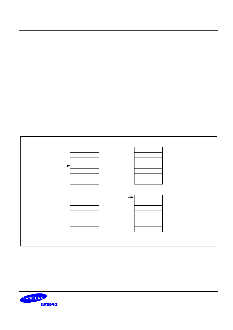
S3C2440A RISC MICROPROCESSOR
ARM INSTRUCTION SET
3-41
ADDRESSING MODES
The transfer addresses are determined by the contents of the base register (Rn), the pre/post bit (P) and the up/
down bit (U). The registers are transferred in the order lowest to highest, so R15 (if in the list) will always be
transferred last. The lowest register also gets transferred to/from the lowest memory address. By way of illustration,
consider the transfer of R1, R5 and R7 in the case where Rn=0x1000 and write back of the modified base is required
(W=1). Figure 3.19-22 show the sequence of register transfers, the addresses used, and the value of Rn after the
instruction has completed.
In all cases, had write back of the modified base not been required (W=0), Rn would have retained its initial value of
0x1000 unless it was also in the transfer list of a load multiple register instruction, when it would have been
overwritten with the loaded value. (Please check the meaning again)*****
ADDRESS ALIGNMENT
The address should normally be a word aligned quantity and non-word aligned addresses should not affect the
instruction. However, the bottom 2 bits of the address will appear on A[1:0] and might be interpreted by the memory
system.
1
2
3
4
Rn
R1
R1
R5
R1
R5
R7
Rn
0x100C
0x1000
0x0FF4
0x100C
0x1000
0x0FF4
0x100C
0x1000
0x0FF4
0x100C
0x1000
0x0FF4
Figure 3-19. Post-Increment Addressing
ARM INSTRUCTION SET
S3C2440A RISC MICROPROCESSOR
3-42
Rn
1
R1
R1
2
R5
3
R1
R5
4
R7
Rn
0x100C
0x1000
0x0FF4
0x100C
0x1000
0x0FF4
0x100C
0x1000
0x0FF4
0x100C
0x1000
0x0FF4
Figure 3-20. Pre-Increment Addressing
Rn
1
R1
R1
2
R5
3
R1
R5
4
R7
Rn
0x100C
0x1000
0x0FF4
0x100C
0x1000
0x0FF4
0x100C
0x1000
0x0FF4
0x100C
0x1000
0x0FF4
Figure 3-21. Post-Decrement Addressing
S3C2440A RISC MICROPROCESSOR
ARM INSTRUCTION SET
3-43
Rn
1
R1
R1
2
R5
3
R1
R5
4
R7
Rn
0x100C
0x1000
0x0FF4
0x100C
0x1000
0x0FF4
0x100C
0x1000
0x0FF4
0x100C
0x1000
0x0FF4
Figure 3-22. Pre-Decrement Addressing
USE OF THE S BIT
When the S bit is set in a LDM/STM instruction it depends on R15 is available in the transfer list and on the type of
instruction. The S bit should only be set if the instruction is to execute in a privileged mode.
LDM with R15 in Transfer List and S Bit Set (Mode Changes)
If the instruction is a LDM then SPSR_<mode> is transferred to CPSR at the same time as R15 is loaded.
STM with R15 in Transfer List and S Bit Set (User Bank Transfer)
The registers transferred are taken from the User bank rather than the bank corresponding to the current mode. This
is useful for saving the user state on process switches. Base write-back should not be used when this mechanism is
employed.
R15 not in List and S Bit Set (User Bank Transfer)
For both LDM and STM instructions, the User bank registers are transferred rather than the register bank
corresponding to the current mode. This is useful for saving the user state on process switches. Base write-back
should not be used when this mechanism is employed.
When the instruction is LDM, care must be taken not to read from a banked register during the following cycle
(inserting a dummy instruction such as MOV R0, R0 after the LDM will ensure safety).
USE OF R15 AS THE BASE
R15 should not be used as the base register in any LDM or STM instruction.

ARM INSTRUCTION SET
S3C2440A RISC MICROPROCESSOR
3-44
INCLUSION OF THE BASE IN THE REGISTER LIST
When write-back is specified, the base is written back at the end of the second cycle of the instruction. During a
STM, the first register is written out at the start of the second cycle. A STM which includes storing the base, with the
base as the first register to be stored, will therefore store the unchanged value, whereas with the base second or
later in the transfer order, will store the modified value. A LDM will always overwrite the updated base if the base is in
the list.
DATA ABORTS
Some legal addresses may be unacceptable to a memory management system, and the memory manager can
indicate a problem with an address by taking the ABORT signal HIGH. This can happen on any transfer during a
multiple register load or store, and must be recoverable if ARM920T is to be used in a virtual memory system.
Abort during STM Instructions
If the abort occurs during a store multiple instruction, ARM920T takes little action until the instruction completes,
whereupon it enters the data abort trap. The memory manager is responsible for preventing erroneous writes to the
memory. The only change to the internal state of the processor will be the modification of the base register if write-
back was specified, and this must be reversed by software (and the cause of the abort resolved) before the
instruction may be retried.
Aborts during LDM Instructions
When ARM920T detects a data abort during a load multiple instruction, it modifies the operation of the instruction to
ensure that recovery is possible.
∑
Overwriting of registers stops when the abort happens. The aborting load will not take place but earlier ones may
have overwritten registers. The PC is always the last register to be written and so will always be preserved.
∑
The base register is restored, to its modified value if write-back was requested. This ensures recoverability in the
case where the base register is also in the transfer list, and may have been overwritten before the abort occurred.
The data abort trap is taken when the load multiple has completed, and the system software must undo any base
modification (and resolve the cause of the abort) before restarting the instruction.
INSTRUCTION CYCLE TIMES
Normal LDM instructions take nS + 1N + 1I and LDM PC takes (n+1)S + 2N + 1I incremental cycles, where S,N and
I are defined as sequential (S-cycle), non-sequential (N-cycle), and internal (I-cycle), respectively. STM instructions
take (n-1)S + 2N incremental cycles to execute, where n is the number of words transferred.
S3C2440A RISC MICROPROCESSOR
ARM INSTRUCTION SET
3-45
ASSEMBLER SYNTAX
<LDM|STM>{cond}<FD|ED|FA|EA|IA|IB|DA|DB> Rn{!},<Rlist>{^}
where:
{cond}
Two character condition mnemonic. See Table 3-2.
Rn
An expression evaluating to a valid register number
<Rlist>
A list of registers and register ranges enclosed in {} (e.g. {R0,R2-R7,R10}).
{!}
If present requests write-back (W=1), otherwise W=0.
{^}
If present set S bit to load the CPSR along with the PC, or force transfer of user bank
when in privileged mode.
Addressing Mode Names
There are different assembler mnemonics for each of the addressing modes, depending on whether the instruction is
being used to support stacks or for other purposes. The equivalence between the names and the values of the bits in
the instruction are shown in the following table 3-6.
Table 3-6. Addressing Mode Names
Name
Stack
Other
L Bit
P Bit
U Bit
Pre-Increment Load
LDMED
LDMIB
1
1
1
Post-Increment Load
LDMFD
LDMIA
1
0
1
Pre-Decrement Load
LDMEA
LDMDB
1
1
0
Post-Decrement Load
LDMFA
LDMDA
1
0
0
Pre-Increment Store
STMFA
STMIB
0
1
1
Post-Increment Store
STMEA
STMIA
0
0
1
Pre-Decrement Store
STMFD
STMDB
0
1
0
Post-Decrement Store
STMED
STMDA
0
0
0
FD, ED, FA, EA define pre/post indexing and the up/down bit by reference to the form of stack required. The F and E
refer to a "full" or "empty" stack, i.e. whether a pre-index has to be done (full) before storing to the stack. The A and
D refer to whether the stack is ascending or descending. If ascending, a STM will go up and LDM down, if
descending, vice-versa.
IA, IB, DA, DB allow control when LDM/STM are not being used for stacks and simply mean Increment After,
Increment Before, Decrement After, Decrement Before.

ARM INSTRUCTION SET
S3C2440A RISC MICROPROCESSOR
3-46
EXAMPLES
LDMFD
SP!,{R0,R1,R2}
; Unstack 3 registers.
STMIA
R0,{R0-R15}
; Save all registers.
LDMFD
SP!,{R15}
; R15
(SP), CPSR unchanged.
LDMFD
SP!,{R15}^
; R15
(SP), CPSR <- SPSR_mode
; (allowed only in privileged modes).
STMFD
R13,{R0-R14}^
; Save user mode regs on stack
; (allowed only in privileged modes).
These instructions may be used to save state on subroutine entry, and restore it efficiently on return to the calling
routine:
STMED
SP!,{R0-R3,R14}
; Save R0 to R3 to use as workspace
; and R14 for returning.
BL
somewhere
; This nested call will overwrite R14
LDMED
SP!,{R0-R3,R15}
; Restore workspace and return.

S3C2440A RISC MICROPROCESSOR
ARM INSTRUCTION SET
3-47
SINGLE DATA SWAP (SWP)
31
19
15
Cond
28
16
11
12
21
23
B
20
00
Rn
Rd
[3:0] Source Register
[15:12] Destination Register
[19:16] Base Register
[22] Byte/Word Bit
0 = Swap word quantity
1 = Swap word quantity
[31:28] Condition Field
22
00010
0000
Rm
1001
27
8 7
4 3
0
Figure 3-23. Swap Instruction
The instruction is only executed if the condition is true. The various conditions are defined in Table 3-2. The
instruction encoding is shown in Figure 3-23.
The data swap instruction is used to swap a byte or word quantity between a register and external memory. This
instruction is implemented as a memory read followed by a memory write which are "locked" together (the processor
cannot be interrupted until both operations have completed, and the memory manager is warned to treat them as
inseparable). This class of instruction is particularly useful for implementing software semaphores.
The swap address is determined by the contents of the base register (Rn). The processor first reads the contents of
the swap address. Then it writes the contents of the source register (Rm) to the swap address, and stores the old
memory contents in the destination register (Rd). The same register may be specified as both the source and
destination.
The LOCK output goes HIGH for the duration of the read and write operations to signal to the external memory
manager that they are locked together, and should be allowed to complete without interruption. This is important in
multi-processor systems where the swap instruction is the only indivisible instruction which may be used to
implement semaphores; control of the memory must not be removed from a processor while it is performing a locked
operation.
BYTES AND WORDS
This instruction class may be used to swap a byte (B=1) or a word (B=0) between an ARM920T register and
memory. The SWP instruction is implemented as a LDR followed by a STR and the action of these is as described
in the section on single data transfers. In particular, the description of Big and Little Endian configuration applies to
the SWP instruction.

ARM INSTRUCTION SET
S3C2440A RISC MICROPROCESSOR
3-48
USE OF R15
Do not use R15 as an operand (Rd, Rn or Rs) in a SWP instruction.
DATA ABORTS
If the address used for the swap is unacceptable to a memory management system, the memory manager can flag
the problem by driving ABORT HIGH. This can happen on either the read or the write cycle (or both), and in either
case, the Data Abort trap will be taken. It is up to the system software to resolve the cause of the problem, then the
instruction can be restarted and the original program continued.
INSTRUCTION CYCLE TIMES
Swap instructions take 1S + 2N +1I incremental cycles to execute, where S,N and I are defined as sequential
(S-cycle), non-sequential, and internal (I-cycle), respectively.
ASSEMBLER SYNTAX
<SWP>{cond}{B} Rd,Rm,[Rn]
{cond}
Two-character condition mnemonic. See Table 3-2.
{B}
If B is present then byte transfer, otherwise word transfer
Rd,Rm,Rn
Expressions evaluating to valid register numbers
Examples
SWP
R0,R1,[R2]
; Load R0 with the word addressed by R2, and
; store R1 at R2.
SWPB
R2,R3,[R4]
; Load R2 with the byte addressed by R4, and
; store bits 0 to 7 of R3 at R4.
SWPEQ
R0,R0,[R1]
; Conditionally swap the contents of the
; word addressed by R1 with R0.

S3C2440A RISC MICROPROCESSOR
ARM INSTRUCTION SET
3-49
SOFTWARE INTERRUPT (SWI)
The instruction is only executed if the condition is true. The various conditions are defined in Table 3-2. The
instruction encoding is shown in Figure 3-24, below.
31
24
27
1111
Cond
Comment Field (Ignored by Processor)
28
23
[31:28] Condition Field
0
Figure 3-24. Software Interrupt Instruction
The software interrupt instruction is used to enter Supervisor mode in a controlled manner. The instruction causes
the software interrupt trap to be taken, which effects the mode change. The PC is then forced to a fixed value (0x08)
and the CPSR is saved in SPSR_svc. If the SWI vector address is suitably protected (by external memory
management hardware) from modification by the user, a fully protected operating system may be constructed.
RETURN FROM THE SUPERVISOR
The PC is saved in R14_svc upon entering the software interrupt trap, with the PC adjusted to point to the word after
the SWI instruction. MOVS PC,R14_svc will return to the calling program and restore the CPSR.
Note that the link mechanism is not re-entrant, so if the supervisor code wishes to use software interrupts within
itself it must first save a copy of the return address and SPSR.
COMMENT FIELD
The bottom 24 bits of the instruction are ignored by the processor, and may be used to communicate information to
the supervisor code. For instance, the supervisor may look at this field and use it to index into an array of entry
points for routines which perform the various supervisor functions.
INSTRUCTION CYCLE TIMES
Software interrupt instructions take 2S + 1N incremental cycles to execute, where S and N are defined as sequential
(S-cycle) and non-sequential (N-cycle).

ARM INSTRUCTION SET
S3C2440A RISC MICROPROCESSOR
3-50
ASSEMBLER SYNTAX
SWI{cond} <expression>
{cond}
Two character condition mnemonic, Table 3-2.
<expression>
Evaluated and placed in the comment field (which is ignored by ARM920T).
Examples
SWI
ReadC
; Get next character from read stream.
SWI
WriteI+"k"
; Output a "k" to the write stream.
SWINE
0
; Conditionally call supervisor with 0 in comment field.
Supervisor code
The previous examples assume that suitable supervisor code exists, for instance:
0x08 B Supervisor
; SWI entry point
EntryTable
; Addresses of supervisor routines
DCD ZeroRtn
DCD ReadCRtn
DCD WriteIRtn
∑
∑
∑
Zero
EQU 0
ReadC
EQU 256
WriteI
EQU 512
Supervisor
; SWI has routine required in bits 8-23 and data (if any) in
; bits 0-7. Assumes R13_svc points to a suitable stack
STMFD
R13,{R0-R2,R14}
; Save work registers and return address.
LDR
R0,[R14,#-4]
; Get SWI instruction.
BIC
R0,R0,#0xFF000000
; Clear top 8 bits.
MOV
R1,R0,LSR#8
; Get routine offset.
ADR
R2,EntryTable
; Get start address of entry table.
LDR
R15,[R2,R1,LSL#2]
; Branch to appropriate routine.
WriteIRtn
; Enter with character in R0 bits 0-7.
∑
∑
∑
LDMFD
R13,{R0-R2,R15}^
; Restore workspace and return,
; restoring processor mode and flags.

S3C2440A RISC MICROPROCESSOR
ARM INSTRUCTION SET
3-51
COPROCESSOR DATA OPERATIONS (CDP)
The instruction is only executed if the condition is true. The various conditions are defined in Table 3-2. The
instruction encoding is shown in Figure 3-25.
This class of instruction is used to tell a coprocessor to perform some internal operation. No result is communicated
back to ARM920T, and it will not wait for the operation to complete. The coprocessor could contain a queue of such
instructions awaiting execution, and their execution can overlap other activity, allowing the coprocessor and
ARM920T to perform independent tasks in parallel.
COPROCESSOR INSTRUCTIONS
The S3C2440A, unlike some other ARM-based processors, does not have an external coprocessor interface. It does
not have a on-chip coprocessor also.
So then all coprocessor instructions will cause the undefined instruction trap to be taken on the S3C2440A. These
coprocessor instructions can be emulated by the undefined trap handler. Even though external coprocessor can not
be connected to the S3C2440A, the coprocessor instructions are still described here in full for completeness.
(Remember that any external coprocessor described in this section is a software emulation.)
31
24
27
19
15
Cond
CRm
28
16
11
12
23
20
[3:0] Coprocessor operand register
[7:5] Coprocessor information
[11:8] Coprocessor number
[15:12] Coprocessor destination register
[19:16] Coprocessor operand register
[23:20] Coprocessor operation code
[31:28] Condition Field
0
Cp
Cp#
CRd
CRn
1110
CP Opc
8 7
5 4 3
0
Figure 3-25. Coprocessor Data Operation Instruction
Only bit 4 and bits 24 to 31 The coprocessor fields are significant to ARM920T. The remaining bits are used by
coprocessors. The above field names are used by convention, and particular coprocessors may redefine the use of
all fields except CP# as appropriate. The CP# field is used to contain an identifying number (in the range 0 to 15) for
each coprocessor, and a coprocessor will ignore any instruction which does not contain its number in the CP# field.
The conventional interpretation of the instruction is that the coprocessor should perform an operation specified in the
CP Opc field (and possibly in the CP field) on the contents of CRn and CRm, and place the result in CRd.

ARM INSTRUCTION SET
S3C2440A RISC MICROPROCESSOR
3-52
INSTRUCTION CYCLE TIMES
Coprocessor data operations take 1S + bI incremental cycles to execute, where b is the number of cycles spent in
the coprocessor busy-wait loop.
S and I are defined as sequential (S-cycle) and internal (I-cycle).
Assembler syntax
CDP{cond} p#,<expression1>,cd,cn,cm{,<expression2>}
{cond}
Two character condition mnemonic. See Table 3-2.
p#
The unique number of the required coprocessor
<expression1>
Evaluated to a constant and placed in the CP Opc field
cd, cn and cm
Evaluate to the valid coprocessor register numbers CRd, CRn and CRm respectively
<expression2>
Where present is evaluated to a constant and placed in the CP field
EXAMPLES
CDP
p1,10,c1,c2,c3
; Request coproc 1 to do operation 10
; on CR2 and CR3, and put the result in CR1.
CDPEQ
p2,5,c1,c2,c3,2
; If Z flag is set request coproc 2 to do operation 5 (type 2)
; on CR2 and CR3, and put the result in CR1.
S3C2440A RISC MICROPROCESSOR
ARM INSTRUCTION SET
3-53
COPROCESSOR DATA TRANSFERS (LDC, STC)
The instruction is only executed if the condition is true. The various conditions are defined in Table 3-2. The
instruction encoding is shown in Figure 3-26.
This class of instruction is used to load (LDC) or store (STC) a subset of a coprocessors's registers directly to
memory. ARM920T is responsible for supplying the memory address and the coprocessor supplies or accepts the
data and controls the number of words transferred.
[7:0] Unsigned 8 Bit Immediate Offset
[11:8] Coprocessor Number
[15:12] Coprocessor Source/Destination Register
[19:16] Base Register
[20] Load/Store Bit
0 = Store to memory
1 = Load from memory
[21] Write-back Bit
0 = No write-back
1 = Write address into base
[22] Transfer Length
[23] Up/Down Bit
0 = Down: subtract offset from base
1 = Up: add offset to base
[24] Pre/Post Indexing Bit
0 = Post: add offset after transfer
1 = Pre: add offset before transfer
[31:28] Condition Field
31
27
19
15
Cond
28
16
11
12
21
23
N
20
L
Rn
CRd
22
110
P U
CP#
W
24
25
Offset
8 7
0
Figure 3-26. Coprocessor Data Transfer Instructions

ARM INSTRUCTION SET
S3C2440A RISC MICROPROCESSOR
3-54
THE COPROCESSOR FIELDS
The CP# field is used to identify the coprocessor which is required to supply or accept the data, and a coprocessor
will only respond if its number matches the contents of this field.
The CRd field and the N bit contain information for the coprocessor which may be interpreted in different ways by
different coprocessors, but by convention CRd is the register to be transferred (or the first register where more than
one is to be transferred), and the N bit is used to choose one of two transfer length options. For instance N=0 could
select the transfer of a single register, and N=1 could select the transfer of all the registers for context switching.
ADDRESSING MODES
ARM920T is responsible for providing the address used by the memory system for the transfer, and the addressing
modes available are a subset of those used in single data transfer instructions. Note, however, that the immediate
offsets are 8 bits wide and specify word offsets for coprocessor data transfers, whereas they are 12 bits wide and
specify byte offsets for single data transfers.
The 8 bit unsigned immediate offset is shifted left 2 bits and either added to (U=1) or subtracted from (U=0) the base
register (Rn); this calculation may be performed either before (P=1) or after (P=0) the base is used as the transfer
address. The modified base value may be overwritten back into the base register (if W=1), or the old value of the
base may be preserved (W=0). Note that post-indexed addressing modes require explicit setting of the W bit, unlike
LDR and STR which always write-back when post-indexed.
The value of the base register, modified by the offset in a pre-indexed instruction, is used as the address for the
transfer of the first word. The second word (if more than one is transferred) will go to or come from an address one
word (4 bytes) higher than the first transfer, and the address will be incremented by one word for each subsequent
transfer.
ADDRESS ALIGNMENT
The base address should normally be a word aligned quantity. The bottom 2 bits of the address will appear on A[1:0]
and might be interpreted by the memory system.
Use of R15
If Rn is R15, the value used will be the address of the instruction plus 8 bytes. Base write-back to R15 must not be
specified.
DATA ABORTS
If the address is legal but the memory manager generates an abort, the data trap will be taken. The write-back of the
modified base will take place, but all other processor state will be preserved. The coprocessor is partly responsible
for ensuring that the data transfer can be restarted after the cause of the abort has been resolved, and must ensure
that any subsequent actions it undertakes can be repeated when the instruction is retried.
Instruction cycle times
Coprocessor data transfer instructions take (n-1)S + 2N + bI incremental cycles to execute, where:
n
The number of words transferred.
b
The number of cycles spent in the coprocessor busy-wait loop.
S, N and I are defined as sequential (S-cycle), non-sequential (N-cycle), and internal (I-cycle), respectively.

S3C2440A RISC MICROPROCESSOR
ARM INSTRUCTION SET
3-55
ASSEMBLER SYNTAX
<LDC|STC>{cond}{L} p#,cd,<Address>
LDC
Load from memory to coprocessor
STC
Store from coprocessor to memory
{L}
When present perform long transfer (N=1), otherwise perform short transfer (N=0)
{cond}
Two character condition mnemonic. See Table 3-2..
p#
The unique number of the required coprocessor
cd
An expression evaluating to a valid coprocessor register number that is placed in the
CRd field
<Address>
can be:
1
An expression which generates an address:
The assembler will attempt to generate an instruction using the PC as a base and a
corrected immediate offset to address the location given by evaluating the expression.
This will be a PC relative, pre-indexed address. If the address is out of range, an error
will be generated
2
A pre-indexed addressing specification:
[Rn]
offset of zero
[Rn,<#expression>]{!}
offset of <expression> bytes
3
A post-indexed addressing specification:
[Rn],<#expression
offset of <expression> bytes
{!}
write back the base register (set the W bit) if! is present
Rn
is an expression evaluating to a valid
ARM920T register number.
NOTE
If Rn is R15, the assembler will subtract 8 from the offset value to allow for ARM920T pipelining.
EXAMPLES
LDC
p1,c2,table
; Load c2 of coproc 1 from address
; table, using a PC relative address.
STCEQL
p2,c3,[R5,#24]!
; Conditionally store c3 of coproc 2
; into an address 24 bytes up from R5,
; write this address back to R5, and use
; long transfer option (probably to store multiple words).
NOTE
Although the address offset is expressed in bytes, the instruction offset field is in words. The assembler will
adjust the offset appropriately.
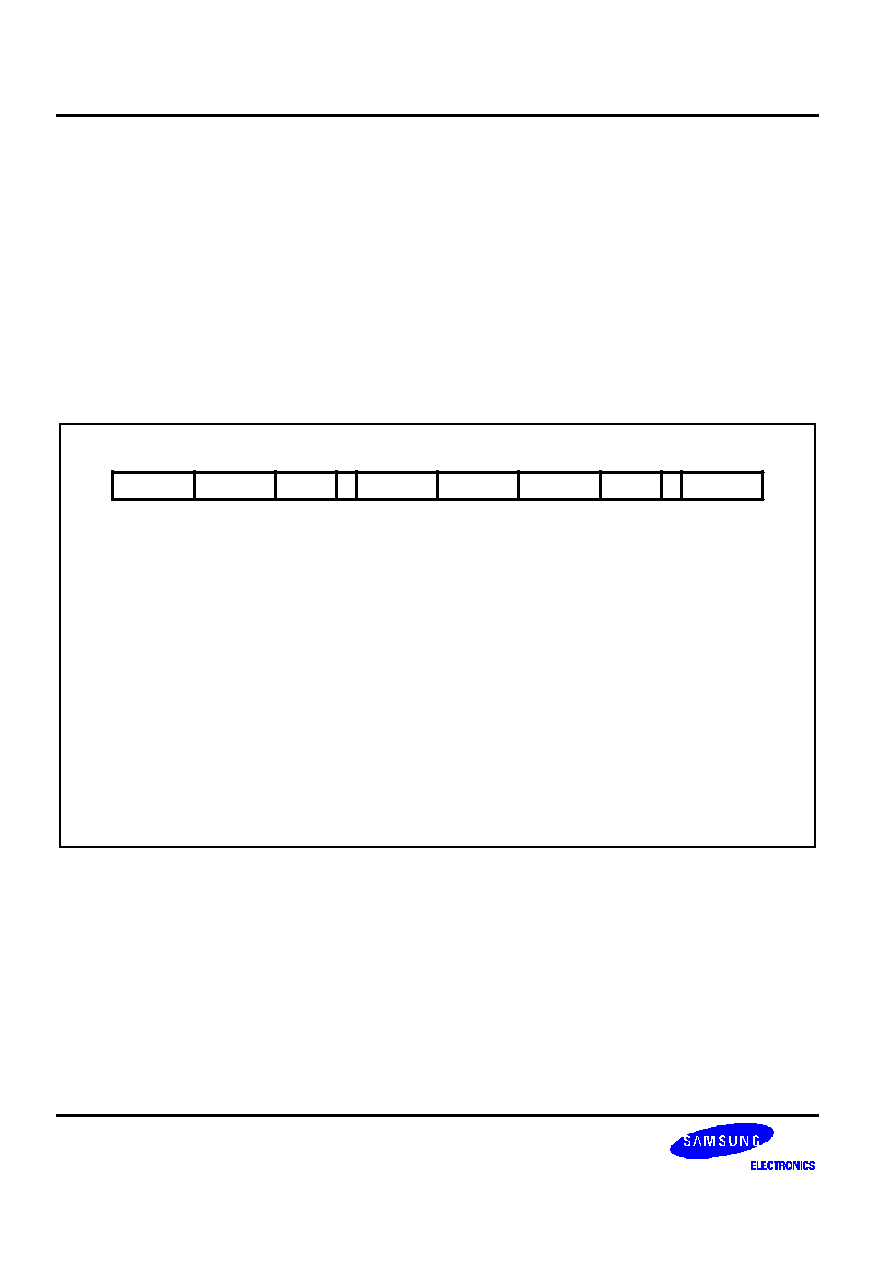
ARM INSTRUCTION SET
S3C2440A RISC MICROPROCESSOR
3-56
COPROCESSOR REGISTER TRANSFERS (MRC, MCR)
The instruction is only executed if the condition is true. The various conditions are defined in Table 3-2. The
instruction encoding is shown in Figure 3-27.
This class of instruction is used to communicate information directly between ARM920T and a coprocessor. An
example of a coprocessor to ARM920T register transfer (MRC) instruction would be a FIX of a floating point value
held in a coprocessor, where the floating point number is converted into a 32 bit integer within the coprocessor, and
the result is then transferred to ARM920T register. A FLOAT of a 32 bit value in ARM920T register into a floating
point value within the coprocessor illustrates the use of ARM920T register to coprocessor transfer (MCR).
An important use of this instruction is to communicate control information directly from the coprocessor into the
ARM920T CPSR flags. As an example, the result of a comparison of two floating point values within a coprocessor
can be moved to the CPSR to control the subsequent flow of execution.
31
27
19
15
Cond
28
16
11
12
21
23
20
L
CRn
Rd
[3:0] Coprocessor Operand Register
[7:5] Coprocessor Information
[11:8] Coprocessor Number
[15:12] ARM Source/Destination Register
[19:16] Coprocessor Source/Destination Register
[20] Load/Store Bit
0 = Store to coprocessor
1 = Load from coprocessor
[21] Coprocessor Operation Mode
[31:28] Condition Field
1110
CP Opc
CP#
24
CRm
1
CP
8 7
5 4 3
0
Figure 3-27. Coprocessor Register Transfer Instructions
THE COPROCESSOR FIELDS
The CP# field is used, as for all coprocessor instructions, to specify which coprocessor is being called upon.
The CP Opc, CRn, CP and CRm fields are used only by the coprocessor, and the interpretation presented here is
derived from convention only. Other interpretations are allowed where the coprocessor functionality is incompatible
with this one. The conventional interpretation is that the CP Opc and CP fields specify the operation the coprocessor
is required to perform, CRn is the coprocessor register which is the source or destination of the transferred
information, and CRm is a second coprocessor register which may be involved in some way which depends on the
particular operation specified.

S3C2440A RISC MICROPROCESSOR
ARM INSTRUCTION SET
3-57
TRANSFERS TO R15
When a coprocessor register transfer to ARM920T has R15 as the destination, bits 31, 30, 29 and 28 of the
transferred word are copied into the N, Z, C and V flags respectively. The other bits of the transferred word are
ignored, and the PC and other CPSR bits are unaffected by the transfer.
TRANSFERS FROM R15
A coprocessor register transfer from ARM920T with R15 as the source register will store the PC+12.
INSTRUCTION CYCLE TIMES
MRC instructions take 1S + (b+1)I +1C incremental cycles to execute, where S, I and C are defined as sequential
(S-cycle), internal (I-cycle), and coprocessor register transfer (C-cycle), respectively. MCR instructions take 1S + bI
+1C incremental cycles to execute, where b is the number of cycles spent in the coprocessor busy-wait loop.
ASSEMBLER SYNTAX
<MCR|MRC>{cond} p#,<expression1>,Rd,cn,cm{,<expression2>}
MRC
Move from coprocessor to ARM920T register (L=1)
MCR
Move from ARM920T register to coprocessor (L=0)
{cond}
Two character condition mnemonic. See Table 3-2
p#
The unique number of the required coprocessor
<expression1>
Evaluated to a constant and placed in the CP Opc field
Rd
An expression evaluating to a valid ARM920T register number
cn and cm
Expressions evaluating to the valid coprocessor register numbers CRn and CRm
respectively
<expression2>
Where present is evaluated to a constant and placed in the CP field
EXAMPLES
MRC
p2,5,R3,c5,c6
; Request coproc 2 to perform operation 5
; on c5 and c6, and transfer the (single
; 32-bit word) result back to R3.
MCR
p6,0,R4,c5,c6
; Request coproc 6 to perform operation 0
; on R4 and place the result in c6.
MRCEQ
p3,9,R3,c5,c6,2
; Conditionally request coproc 3 to
; perform operation 9 (type 2) on c5 and
; c6, and transfer the result back to R3.

ARM INSTRUCTION SET
S3C2440A RISC MICROPROCESSOR
3-58
UNDEFINED INSTRUCTION
The instruction is only executed if the condition is true. The various conditions are defined in Table 3-2. The
instruction format is shown in Figure 3-28.
31
27
Cond
28
25 24
011
xxxxxxxxxxxxxxxxxxxx
1
xxxx
5 4 3
0
Figure 3-28. Undefined Instruction
If the condition is true, the undefined instruction trap will be taken.
Note that the undefined instruction mechanism involves offering this instruction to any coprocessors which may be
present, and all coprocessors must refuse to accept it by driving CPA and CPB HIGH.
INSTRUCTION CYCLE TIMES
This instruction takes 2S + 1I + 1N cycles, where S, N and I are defined as sequential (S-cycle), non-sequential (N-
cycle), and internal (I-cycle).
ASSEMBLER SYNTAX
The assembler has no mnemonics for generating this instruction. If it is adopted in the future for some specified use,
suitable mnemonics will be added to the assembler. Until such time, this instruction must not be used.

S3C2440A RISC MICROPROCESSOR
ARM INSTRUCTION SET
3-59
INSTRUCTION SET EXAMPLES
The following examples show ways in which the basic ARM920T instructions can combine to give efficient code.
None of these methods saves a great deal of execution time (although they may save some), mostly they just save
code.
USING THE CONDITIONAL INSTRUCTIONS
Using Conditionals for Logical OR
CMP
Rn,#p
; If Rn=p OR Rm=q THEN GOTO Label.
BEQ
Label
CMP
Rm,#q
BEQ
Label
This can be replaced by
CMP
Rn,#p
CMPNE
Rm,#q
; If condition not satisfied try other test.
BEQ
Label
Absolute Value
TEQ
Rn,#0
; Test sign
RSBMI
Rn,Rn,#0
; and 2's complement if necessary.
Multiplication by 4, 5 or 6 (Run Time)
MOV
Rc,Ra,LSL#2
; Multiply by 4,
CMP
Rb,#5
; Test value,
ADDCS
Rc,Rc,Ra
; Complete multiply by 5,
ADDHI
Rc,Rc,Ra
; Complete multiply by 6.
Combining Discrete and Range Tests
TEQ
Rc,#127
; Discrete test,
CMPNE
Rc,# " "-1
; Range test
MOVLS
Rc,# ""
; IF Rc<= "" OR Rc=ASCII(127)
; THEN Rc:= "."

ARM INSTRUCTION SET
S3C2440A RISC MICROPROCESSOR
3-60
Division and Remainder
A number of divide routines for specific applications are provided in source form as part of the ANSI C library provided
with the ARM Cross Development Toolkit, available from your supplier. A short general purpose divide routine follows.
; Enter with numbers in Ra and Rb.
MOV
Rcnt,#1
; Bit to control the division.
Div1
CMP
Rb,#0x80000000
; Move Rb until greater than Ra.
CMPCC
Rb,Ra
MOVCC
Rb,Rb,ASL#1
MOVCC
Rcnt,Rcnt,ASL#1
BCC
Div1
MOV
Rc,#0
Div2
CMP
Ra,Rb
; Test for possible subtraction.
SUBCS
Ra,Ra,Rb
; Subtract if ok,
ADDCS
Rc,Rc,Rcnt
; Put relevant bit into result
MOVS
Rcnt,Rcnt,LSR#1
; Shift control bit
MOVNE
Rb,Rb,LSR#1
; Halve unless finished.
BNE
Div2
; Divide result in Rc, remainder in Ra.
Overflow Detection in the ARM920T
1. Overflow in unsigned multiply with a 32-bit result
UMULL
Rd,Rt,Rm,Rn
; 3 to 6 cycles
TEQ
Rt,#0
; +1 cycle and a register
BNE
overflow
2. Overflow in signed multiply with a 32-bit result
SMULL
Rd,Rt,Rm,Rn
; 3 to 6 cycles
TEQ
Rt,Rd ASR#31
; +1 cycle and a register
BNE
overflow
3. Overflow in unsigned multiply accumulate with a 32 bit result
UMLAL
Rd,Rt,Rm,Rn
; 4 to 7 cycles
TEQ
Rt,#0
; +1 cycle and a register
BNE
overflow
4. Overflow in signed multiply accumulate with a 32 bit result
SMLAL
Rd,Rt,Rm,Rn
; 4 to 7 cycles
TEQ
Rt,Rd, ASR#31
; +1 cycle and a register
BNE
overflow

S3C2440A RISC MICROPROCESSOR
ARM INSTRUCTION SET
3-61
5. Overflow in unsigned multiply accumulate with a 64 bit result
UMULL
Rl,Rh,Rm,Rn
; 3 to 6 cycles
ADDS
Rl,Rl,Ra1
; Lower accumulate
ADC
Rh,Rh,Ra2
; Upper accumulate
BCS
overflow
; 1 cycle and 2 registers
6. Overflow in signed multiply accumulate with a 64 bit result
SMULL
Rl,Rh,Rm,Rn
; 3 to 6 cycles
ADDS
Rl,Rl,Ra1
; Lower accumulate
ADC
Rh,Rh,Ra2
; Upper accumulate
BVS
overflow
; 1 cycle and 2 registers
NOTE
Overflow checking is not applicable to unsigned and signed multiplies with a 64-bit result, since overflow
does not occur in such calculations.
PSEUDO-RANDOM BINARY SEQUENCE GENERATOR
It is often necessary to generate (pseudo-) random numbers and the most efficient algorithms are based on shift
generators with exclusive-OR feedback rather like a cyclic redundancy check generator. Unfortunately the sequence
of a 32 bit generator needs more than one feedback tap to be maximal length (i.e. 2^32-1 cycles before repetition),
so this example uses a 33 bit register with taps at bits 33 and 20. The basic algorithm is newbit:=bit 33 eor bit 20,
shift left the 33 bit number and put in newbit at the bottom; this operation is performed for all the newbits needed (i.e.
32 bits). The entire operation can be done in 5 S cycles:
; Enter with seed in Ra (32 bits),
; Rb (1 bit in Rb lsb), uses Rc.
TST
Rb,Rb,LSR#1
; Top bit into carry
MOVS
Rc,Ra,RRX
; 33 bit rotate right
ADC
Rb,Rb,Rb
; Carry into lsb of Rb
EOR
Rc,Rc,Ra,LSL#12
; (involved!)
EOR
Ra,Rc,Rc,LSR#20
; (similarly involved!) new seed in Ra, Rb as before
MULTIPLICATION BY CONSTANT USING THE BARREL SHIFTER
Multiplication by 2^n (1,2,4,8,16,32..)
MOV
Ra, Rb, LSL #n
Multiplication by 2^n+1 (3,5,9,17..)
ADD
Ra,Ra,Ra,LSL #n
Multiplication by 2^n-1 (3,7,15..)
RSB
Ra,Ra,Ra,LSL #n

ARM INSTRUCTION SET
S3C2440A RISC MICROPROCESSOR
3-62
Multiplication by 6
ADD
Ra,Ra,Ra,LSL #1
; Multiply by 3
MOV
Ra,Ra,LSL#1
; and then by 2
Multiply by 10 and add in extra number
ADD
Ra,Ra,Ra,LSL#2
; Multiply by 5
ADD
Ra,Rc,Ra,LSL#1
; Multiply by 2 and add in next digit
General recursive method for Rb := Ra*C, C a constant:
1. If C even, say C = 2^n*D, D odd:
D=1:
MOV Rb,Ra,LSL #n
D<>1:
{Rb := Ra*D}
MOV
Rb,Rb,LSL #n
2. If C MOD 4 = 1, say C = 2^n*D+1, D odd, n>1:
D=1:
ADD Rb,Ra,Ra,LSL #n
D<>1:
{Rb := Ra*D}
ADD
Rb,Ra,Rb,LSL #n
3. If C MOD 4 = 3, say C = 2^n*D-1, D odd, n>1:
D=1:
RSB Rb,Ra,Ra,LSL #n
D<>1:
{Rb := Ra*D}
RSB
Rb,Ra,Rb,LSL #n
This is not quite optimal, but close. An example of its non-optimality is multiply by 45 which is done by:
RSB
Rb,Ra,Ra,LSL#2
; Multiply by 3
RSB
Rb,Ra,Rb,LSL#2
; Multiply by 4*3-1 = 11
ADD
Rb,Ra,Rb,LSL# 2
; Multiply by 4*11+1 = 45
rather than by:
ADD
Rb,Ra,Ra,LSL#3
; Multiply by 9
ADD
Rb,Rb,Rb,LSL#2
; Multiply by 5*9 = 45

S3C2440A RISC MICROPROCESSOR
ARM INSTRUCTION SET
3-63
LOADING A WORD FROM AN UNKNOWN ALIGNMENT
; Enter with address in Ra (32 bits) uses
; Rb, Rc result in Rd. Note d must be less than c e.g. 0,1
BIC
Rb,Ra,#3
; Get word aligned address
LDMIA
Rb,{Rd,Rc}
; Get 64 bits containing answer
AND
Rb,Ra,#3
; Correction factor in bytes
MOVS
Rb,Rb,LSL#3
; ...now in bits and test if aligned
MOVNE
Rd,Rd,LSR Rb
; Produce bottom of result word (if not aligned)
RSBNE
Rb,Rb,#32
; Get other shift amount
ORRNE
Rd,Rd,Rc,LSL Rb
; Combine two halves to get result

ARM INSTRUCTION SET
S3C2440A RISC MICROPROCESSOR
3-64
NOTES

S3C2440A RISC MICROPROCESSOR
THUMB INSTRUCTION SET
4-1
4
THUMB INSTRUCTION SET
THUMB INSTRUCTION SET FORMAT
The thumb instruction sets are 16-bit versions of ARM instruction sets (32-bit format). The ARM instructions are
reduced to 16-bit versions.Thumb instructions, at the cost of versatile functions of the ARM instruction sets. The
thumb instructions are decompressed to the ARM instructions by the Thumb decompressor inside the ARM920T
core.
As the Thumb instructions are compressed ARM instructions, the Thumb instructions have the 16-bit format
instructions and have some restrictions. The restriction by 16-bit format is fully notified for using the Thumb
instructions.
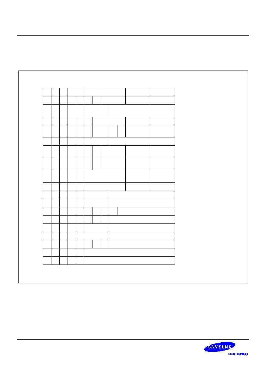
THUMB INSTRUCTION SET
S3C2440A RISC MICROPROCESSOR
4-2
FORMAT SUMMARY
The THUMB instruction set formats are shown in the following figure.
Move Shifted register
0
0
0
0
0
0
0
0
0
0
0
0
1
0
0
0
1
0
0
0
0
0
0
1
1
1
1
1
1
1
0
0
0
0
0
1
1
1
1
1
1
1
1
0
L
0
1
1
1
1
1
1
1
1
1
1
1
1
1
1
1
1
0
0
0
0
1
1
1
1
0
0
1
0
0
L
1
0
R
1
1
0
1
0 SP
1
L
L
S
H
0
0
1
B
L
0
1
H
0
1
B
0
0
1
1
1
I
Op
Op
Op
Op
Op
L
0
S
1
Offset5
Rs
Rd
Rn/offset3
Rd
Rs
Rd
Offset8
Rs
Rd/Hd
Rd
H1 H2
Rs/Hs
Rd
Word8
Rd
Rb
Ro
Ro
Rb
Rd
Offset5
Rb
Rd
Rb
Rd
Offset5
Rd
Rd
Word8
Word8
SWord7
Rb
Cond
Rlist
Rlist
Softset8
Value8
Offset11
Offset
Add/subtract
Move/compare/add/
subtract immediate
ALU operations
Hi register operations
/branch exchange
PC-relative load
Load/store with register
offset
Load/store with immediate
offset
Load/store sign-extended
byte/halfword
Load/store halfword
SP-relative load/store
Load address
Add offset to stack pointer
Push/pop register
Multiple load/store
Conditional branch
Software interrupt
Unconditional branch
Long branch with link
15 14 13 12 11 10
9
8
7
6
5
4
2
3
1
0
15 14 13 12 11 10
9
8
7
6
5
4
2
3
1
0
1
2
3
4
5
6
7
8
9
10
11
12
13
14
15
16
17
18
19
Figure 4-1. THUMB Instruction Set Formats
S3C2440A RISC MICROPROCESSOR
THUMB INSTRUCTION SET
4-3
OPCODE SUMMARY
The following table summarizes the THUMB instruction set. For further information about a particular instruction
please refer to the sections listed in the right-most column.
Table 4-1. THUMB Instruction Set Opcodes
Mnemonic
Instruction
Lo-Register
Operand
Hi-Register
Operand
Condition
Codes Set
ADC
Add with Carry
Y
≠
Y
ADD
Add
Y
≠
Y
(1)
AND
AND
Y
≠
Y
ASR
Arithmetic Shift Right
Y
≠
Y
B
Unconditional branch
Y
≠
≠
Bxx
Conditional branch
Y
≠
≠
BIC
Bit Clear
Y
≠
Y
BL
Branch and Link
≠
≠
≠
BX
Branch and Exchange
Y
Y
≠
CMN
Compare Negative
Y
≠
Y
CMP
Compare
Y
Y
Y
EOR
EOR
Y
≠
Y
LDMIA
Load multiple
Y
≠
≠
LDR
Load word
Y
≠
≠
LDRB
Load byte
Y
≠
≠
LDRH
Load halfword
Y
≠
≠
LSL
Logical Shift Left
Y
≠
Y
LDSB
Load sign-extended byte
Y
≠
≠
LDSH
Load sign-extended halfword
Y
≠
≠
LSR
Logical Shift Right
Y
≠
Y
MOV
Move register
Y
Y
Y
(2)
MUL
Multiply
Y
≠
Y
MVN
Move Negative register
Y
≠
Y
THUMB INSTRUCTION SET
S3C2440A RISC MICROPROCESSOR
4-4
Table 4-1. THUMB Instruction Set Opcodes (Continued)
Mnemonic
Instruction
Lo-Register
Operand
Hi-Register
Operand
Condition
Codes Set
NEG
Negate
Y
≠
Y
ORR
OR
Y
≠
Y
POP
Pop register
Y
≠
≠
PUSH
Push register
Y
≠
≠
ROR
Rotate Right
Y
≠
Y
SBC
Subtract with Carry
Y
≠
Y
STMIA
Store Multiple
Y
≠
≠
STR
Store word
Y
≠
≠
STRB
Store byte
Y
≠
≠
STRH
Store halfword
Y
≠
≠
SWI
Software Interrupt
≠
≠
≠
SUB
Subtract
Y
≠
Y
TST
Test bits
Y
≠
Y
NOTES:
1.
The condition codes are unaffected by the format 5, 12 and 13 versions of this instruction.
2.
The condition codes are unaffected by the format 5 version of this instruction.
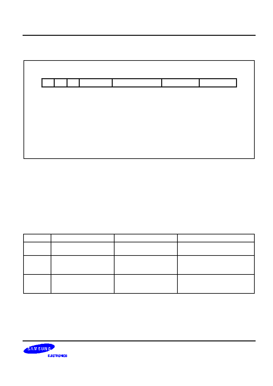
S3C2440A RISC MICROPROCESSOR
THUMB INSTRUCTION SET
4-5
FORMAT 1: MOVE SHIFTED REGISTER
15
0
0
14
10
[2:0] Destination Register
[5:3] Source Register
[10:6] Immediate Vale
[12:11] Opcode
0 = LSL
1 = LSR
2 = ASR
Offset5
6
5
3
2
Rd
0
0
13
12
11
Op
Rs
Figure 4-2. Format 1
OPERATION
These instructions move a shifted value between Lo registers. The THUMB assembler syntax is shown in
Table 4-2.
NOTE
All instructions in this group set the CPSR condition codes.
Table 4-2. Summary of Format 1 Instructions
OP
THUMB Assembler
ARM Equipment
Action
00
LSL Rd, Rs, #Offset5
MOVS Rd, Rs, LSL #Offset5
Shift Rs left by a 5-bit immediate
value and store the result in Rd.
01
LSR Rd, Rs, #Offset5
MOVS Rd, Rs, LSR #Offset5
Perform logical shift right on Rs by a
5-bit immediate value and store the
result in Rd.
10
ASR Rd, Rs, #Offset5
MOVS Rd, Rs, ASR #Offset5 Perform arithmetic shift right on Rs
by a 5-bit immediate value and store
the result in Rd.

THUMB INSTRUCTION SET
S3C2440A RISC MICROPROCESSOR
4-6
INSTRUCTION CYCLE TIMES
All instructions in this format have an equivalent ARM instruction as shown in Table 4-2. The instruction cycle times
for the THUMB instruction are identical to that of the equivalent ARM instruction.
EXAMPLES
LSR R2, R5, #27
; Logical shift right the contents of R5 by 27 and store the
result in R2.Set condition codes on the result.
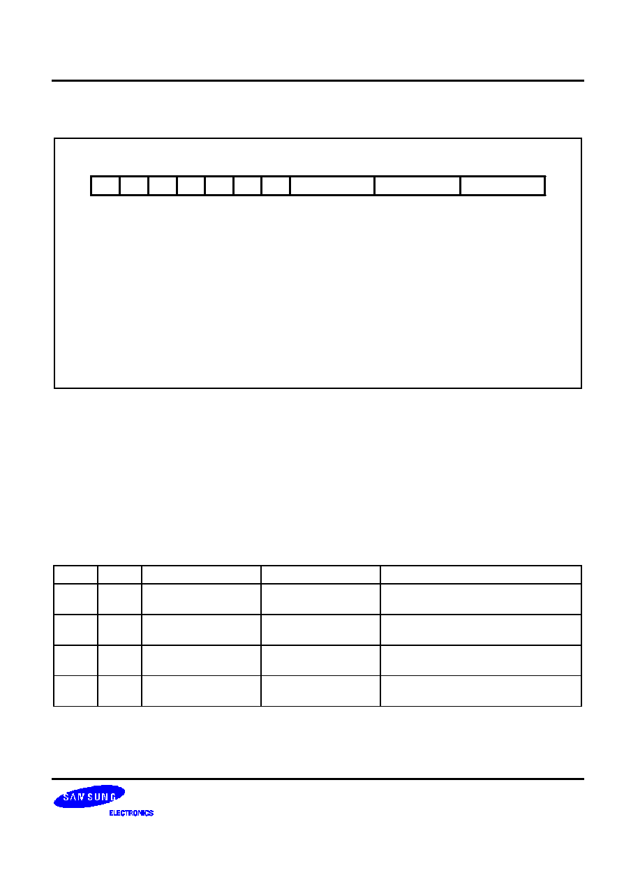
S3C2440A RISC MICROPROCESSOR
THUMB INSTRUCTION SET
4-7
FORMAT 2: ADD/SUBTRACT
15
0
14
10
[2:0] Destination Register
[5:3] Source Register
[8:6] Register/Immediate Vale
[9] Opcode
0 = ADD
1 = SUB
[10] Immediate Flag
0 = Register operand
1 = Immediate oerand
Rn/Offset3
Rd
0
0
13
12
11
Op
Rs
9
8
1
1
1
6
5
3
2
0
Figure 4-3. Format 2
OPERATION
These instructions allow the contents of a Lo register or a 3-bit immediate value to be added to or subtracted from a
Lo register. The THUMB assembler syntax is shown in Table 4-3.
NOTE
All instructions in this group set the CPSR condition codes.
Table 4-3. Summary of Format 2 Instructions
OP
I
THUMB Assembler
ARM Equipment
Description
0
0
ADD Rd, Rs, Rn
ADDS Rd, Rs, Rn
Add contents of Rn to contents of Rs.
Place result in Rd.
0
1
ADD Rd, Rs, #Offset3
ADDS Rd, Rs, #Offset3
Add 3-bit immediate value to contents of
Rs. Place result in Rd.
1
0
SUB Rd, Rs, Rn
SUBS Rd, Rs, Rn
Subtract contents of Rn from contents of
Rs. Place result in Rd.
1
1
SUB Rd, Rs, #Offset3
SUBS Rd, Rs, #Offset3
Subtract 3-bit immediate value from
contents of Rs. Place result in Rd.

THUMB INSTRUCTION SET
S3C2440A RISC MICROPROCESSOR
4-8
INSTRUCTION CYCLE TIMES
All instructions in this format have an equivalent ARM instruction as shown in Table 4-3. The instruction cycle times
for the THUMB instruction are identical to that of the equivalent ARM instruction.
EXAMPLES
ADD
R0, R3, R4
; R0 := R3 + R4 and set condition codes on the result.
SUB
R6, R2, #6
; R6 := R2 - 6 and set condition codes.
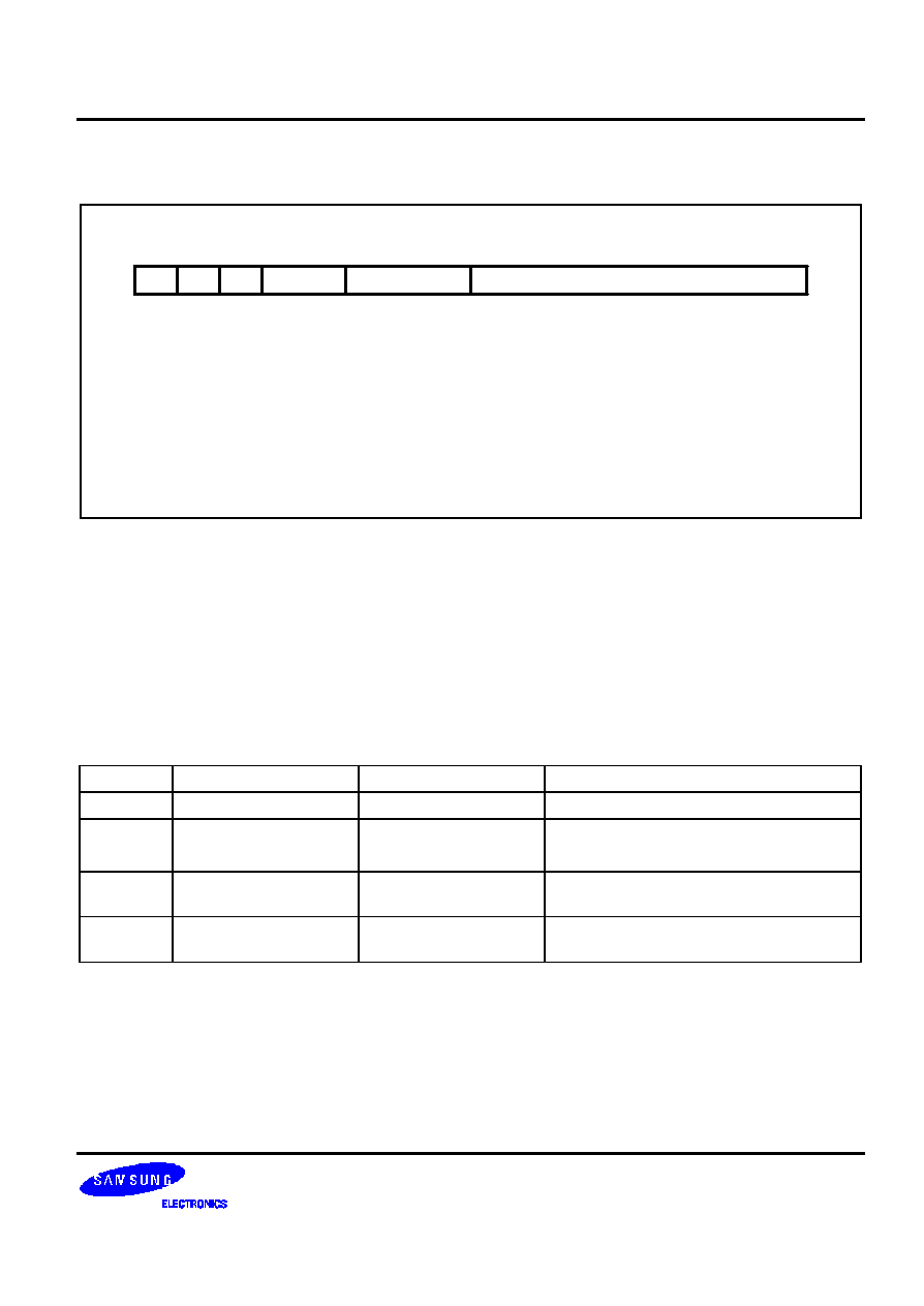
S3C2440A RISC MICROPROCESSOR
THUMB INSTRUCTION SET
4-9
FORMAT 3: MOVE/COMPARE/ADD/SUBTRACT IMMEDIATE
15
0
0
14
10
[7:0] Immediate Vale
[10:8] Source/Destination Register
[12:11] Opcode
0 = MOV
1 = CMP
2 = ADD
3 = SUB
Offset8
Rd
0
0
13
12
11
Op
7
8
Figure 4-4. Format 3
OPERATIONS
The instructions in this group perform operations between a Lo register and an 8-bit immediate value. The THUMB
assembler syntax is shown in Table 4-4.
NOTE
All instructions in this group set the CPSR condition codes.
Table 4-4. Summary of Format 3 Instructions
OP
THUMB Assembler
ARM Equipment
Description
00
MOV Rd, #Offset8
MOVS Rd, #Offset8
Move 8-bit immediate value into Rd.
01
CMP Rd, #Offset8
CMP Rd, #Offset8
Compare contents of Rd with 8-bit immediate
value.
10
ADD Rd, #Offset8
ADDS Rd, Rd, #Offset8
Add 8-bit immediate value to contents of Rd
and place the result in Rd.
11
SUB Rd, #Offset8
SUBS Rd, Rd, #Offset8
Subtract 8-bit immediate value from contents
of Rd and place the result in Rd.

THUMB INSTRUCTION SET
S3C2440A RISC MICROPROCESSOR
4-10
INSTRUCTION CYCLE TIMES
All instructions in this format have an equivalent ARM instruction as shown in Table 4-4. The instruction cycle times
for the THUMB instruction are identical to that of the equivalent ARM instruction.
EXAMPLES
MOV
R0, #128
; R0 := 128 and set condition codes
CMP
R2, #62
; Set condition codes on R2 - 62
ADD
R1, #255
; R1 := R1 + 255 and set condition codes
SUB
R6, #145
; R6 := R6 - 145 and set condition codes
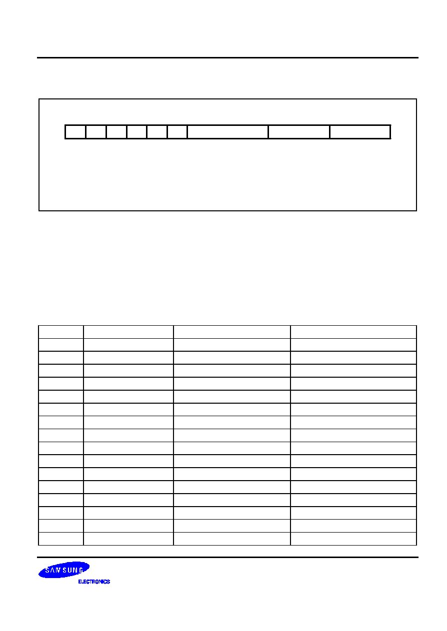
S3C2440A RISC MICROPROCESSOR
THUMB INSTRUCTION SET
4-11
FORMAT 4: ALU OPERATIONS
15
0
0
14
10
[2:0] Source/Destination Register
[5:3] Source Register 2
[9:6] Opcode
5
6
3
Rd
0
0
13
12
11
Op
Rs
0
0
0
9
2
Figure 4-5. Format 4
OPERATION
The following instructions perform ALU operations on a Lo register pair.
NOTE
All instructions in this group set the CPSR condition codes.
Table 4-5. Summary of Format 4 Instructions
OP
THUMB Assembler
ARM Equipment
Description
0000
AND Rd, Rs
ANDS Rd, Rd, Rs
Rd := Rd AND Rs
0001
EOR Rd, Rs
EORS Rd, Rd, Rs
Rd := Rd EOR Rs
0010
LSL Rd, Rs
MOVS Rd, Rd, LSL Rs
Rd := Rd << Rs
0011
LSR Rd, Rs
MOVS Rd, Rd, LSR Rs
Rd := Rd >> Rs
0100
ASR Rd, Rs
MOVS Rd, Rd, ASR Rs
Rd := Rd ASR Rs
0101
ADC Rd, Rs
ADCS Rd, Rd, Rs
Rd := Rd + Rs + C-bit
0110
SBC Rd, Rs
SBCS Rd, Rd, Rs
Rd := Rd - Rs - NOT C-bit
0111
ROR Rd, Rs
MOVS Rd, Rd, ROR Rs
Rd := Rd ROR Rs
1000
TST Rd, Rs
TST Rd, Rs
Set condition codes on Rd AND Rs
1001
NEG Rd, Rs
RSBS Rd, Rs, #0
Rd = ≠ Rs
1010
CMP Rd, Rs
CMP Rd, Rs
Set condition codes on Rd ≠ Rs
1011
CMN Rd, Rs
CMN Rd, Rs
Set condition codes on Rd + Rs
1100
ORR Rd, Rs
ORRS Rd, Rd, Rs
Rd := Rd OR Rs
1101
MUL Rd, Rs
MULS Rd, Rs, Rd
Rd := Rs * Rd
1110
BIC Rd, Rs
BICS Rd, Rd, Rs
Rd := Rd AND NOT Rs
1111
MVN Rd, Rs
MVNS Rd, Rs
Rd := NOT Rs

THUMB INSTRUCTION SET
S3C2440A RISC MICROPROCESSOR
4-12
INSTRUCTION CYCLE TIMES
All instructions in this format have an equivalent ARM instruction as shown in Table 4-5. The instruction cycle times
for the THUMB instruction are identical to that of the equivalent ARM instruction.
EXAMPLES
EOR
R3, R4
; R3 := R3 EOR R4 and set condition codes
ROR
R1, R0
; Rotate Right R1 by the value in R0, store
; the result in R1 and set condition codes
NEG
R5, R3
; Subtract the contents of R3 from zero,
; Store the result in R5. Set condition codes ie R5 = ≠ R3
CMP
R2, R6
; Set the condition codes on the result of R2 - R6
MUL
R0, R7
; R0 := R7
◊
R0 and set condition codes
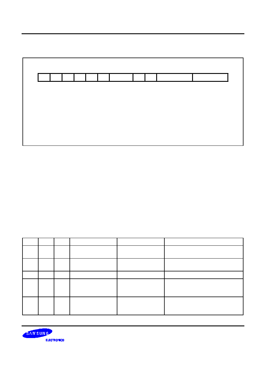
S3C2440A RISC MICROPROCESSOR
THUMB INSTRUCTION SET
4-13
FORMAT 5: HI-REGISTER OPERATIONS/BRANCH EXCHANGE
15
0
0
14
10
[2:0] Destination Register
[5:3] Source Register
[6] Hi Operand Flag 2
[7] Hi Operand Flag 1
[9:8] Opcode
6
5
3
2
Rd/Hd
0
0
13
12
11
Op
Rs/Hs
0
0
0
9
8
7
H1
H2
Figure 4-6. Format 5
OPERATION
There are four sets of instructions in this group. The first three allow ADD, CMP and MOV operations to be performed
between Lo and Hi registers, or a pair of Hi registers. The fourth, BX, allows a Branch to be performed which may
also be used to switch processor state. The THUMB assembler syntax is shown in Table 4-6.
NOTE
In this group only CMP (Op = 01) sets the CPSR condition codes.
The action of H1= 0, H2 = 0 for Op = 00 (ADD), Op =01 (CMP) and Op = 10 (MOV) is undefined, and should not be
used.
Table 4-6. Summary of Format 5 Instructions
Op
H1
H2
THUMB assembler
ARM equivalent
Description
00
0
1
ADD Rd, Hs
ADD Rd, Rd, Hs
Add a register in the range 8-15 to a
register in the range 0-7.
00
1
0
ADD Hd, Rs
ADD Hd, Hd, Rs
Add a register in the range 0-7 to a
register in the range 8-15.
00
1
1
ADD Hd, Hs
ADD Hd, Hd, Hs
Add two registers in the range 8-15
01
0
1
CMP Rd, Hs
CMP Rd, Hs
Compare a register in the range 0-7
with a register in the range 8-15. Set
the condition code flags on the result.
01
1
0
CMP Hd, Rs
CMP Hd, Rs
Compare a register in the range 8-15
with a register in the range 0-7. Set the
condition code flags on the result.

THUMB INSTRUCTION SET
S3C2440A RISC MICROPROCESSOR
4-14
Table 4-6. Summary of Format 5 Instructions (Continued)
Op
H1
H2
THUMB assembler
ARM equivalent
Description
01
1
1
CMP Hd, Hs
CMP Hd, Hs
Compare two registers in the range
8-15. Set the condition code flags on
the result.
10
0
1
MOV Rd, Hs
MOV Rd, Hs
Move a value from a register in the
range 8-15 to a register in the range 0-
7.
10
1
0
MOV Hd, Rs
MOV Hd, Rs
Move a value from a register in the
range 0-7 to a register in the range
8-15.
10
1
1
MOV Hd, Hs
MOV Hd, Hs
Move a value between two registers in
the range 8-15.
11
0
0
BX Rs
BX Rs
Perform branch (plus optional state
change) to address in a register in the
range 0-7.
11
0
1
BX Hs
BX Hs
Perform branch (plus optional state
change) to address in a register in the
range 8-15.
INSTRUCTION CYCLE TIMES
All instructions in this format have an equivalent ARM instruction as shown in Table 4-6. The instruction cycle times
for the THUMB instruction are identical to that of the equivalent ARM instruction.
THE BX INSTRUCTION
BX performs a Branch to a routine whose start address is specified in a Lo or Hi register.
Bit 0 of the address determines the processor state on entry to the routine:
Bit 0 = 0
Causes the processor to enter ARM state.
Bit 0 = 1
Causes the processor to enter THUMB state.
NOTE
The action of H1 = 1 for this instruction is undefined, and should not be used.

S3C2440A RISC MICROPROCESSOR
THUMB INSTRUCTION SET
4-15
EXAMPLES
Hi-Register Operations
ADD
PC, R5
; PC := PC + R5 but don't set the condition codes.
CMP
R4, R12
; Set the condition codes on the result of R4 - R12.
MOV
R15, R14
; Move R14 (LR) into R15 (PC) but don't set the condition
codes, eg. return from subroutine.
Branch and Exchange
; Switch from THUMB to ARM state.
ADR
R1,outofTHUMB
; Load address of outofTHUMB into R1.
MOV
R11,R1
BX
R11
; Transfer the contents of R11 into the PC.
; Bit 0 of R11 determines whether
; ARM or THUMB state is entered, ie. In this case the
state is ARM.
ALIGN
CODE32
outofTHUMB
; Now processing ARM instructions...
USING R15 AS AN OPERAND
If R15 is used as an operand, the value will be the address of the instruction + 4 with bit 0 cleared. Executing a BX
PC in THUMB state from a non-word aligned address will result in unpredictable execution.

THUMB INSTRUCTION SET
S3C2440A RISC MICROPROCESSOR
4-16
FORMAT 6: PC-RELATIVE LOAD
15
0
0
14
10
[7:0] Immediate Value
[10:8] Destination Register
Word 8
0
0
13
12
11
Rd
0
0
8
7
Figure 4-7. Format 6
OPERATION
This instruction loads a word from an address specified as a 10-bit immediate offset from the PC. The THUMB
assembler syntax is shown below.
Table 4-7. Summary of PC-Relative Load Instruction
THUMB assembler
ARM equivalent
Description
LDR Rd, [PC, #Imm]
LDR Rd, [R15, #Imm]
Add unsigned offset (255 words, 1020 bytes) in
Imm to the current value of the PC. Load the
word from the resulting address into Rd.
NOTE: The value specified by #Imm is a full 10-bit address, but must always be word-aligned (ie with bits 1:0 set to 0),
since the assembler places #Imm >> 2 in field Word 8. The value of the PC will be 4 bytes greater than the address
of this instruction, but bit 1 of the PC is forced to 0 to ensure it is word aligned.

S3C2440A RISC MICROPROCESSOR
THUMB INSTRUCTION SET
4-17
INSTRUCTION CYCLE TIMES
All instructions in this format have an equivalent ARM instruction. The instruction cycle times for the THUMB
instruction are identical to that of the equivalent ARM instruction.
EXAMPLES
LDR R3,[PC,#844]
; Load into R3 the word found at the address
formed by adding 844 to PC.bit[1] of PC is forced to zero.
Note that the THUMB opcode will contain 211 as the
Word8 value.

THUMB INSTRUCTION SET
S3C2440A RISC MICROPROCESSOR
4-18
FORMAT 7: LOAD/STORE WITH REGISTER OFFSET
[2:0] Source/Destination Register
[5:3] Base Register
[8:6] Offset Register
[10] Byte/Word Flag
0 = Transfer word quantity
1 = Transfer byte quantity
[11] Load/Store Flag
0 = Store to memory
1 = Load from memory
15
0
0
14
10
6
5
3
2
Rd
1
0
13
12
11
Rb
1
L
B
9
8
Ro
0
Figure 4-8. Format 7

S3C2440A RISC MICROPROCESSOR
THUMB INSTRUCTION SET
4-19
OPERATION
These instructions transfer byte or word values between registers and memory. Memory addresses are pre-indexed
using an offset register in the range 0-7. The THUMB assembler syntax is shown in Table 4-8.
Table 4-8. Summary of Format 7 Instructions
L
B
THUMB assembler
ARM equivalent
Description
0
0
STR Rd, [Rb, Ro]
STR Rd, [Rb, Ro]
Pre-indexed word store:
Calculate the target address by adding
together the value in Rb and the value in
Ro. Store the contents of Rd at the
address.
0
1
STRB Rd, [Rb, Ro]
STRB Rd, [Rb, Ro]
Pre-indexed byte store:
Calculate the target address by adding
together the value in Rb and the value in
Ro. Store the byte value in Rd at the
resulting address.
1
0
LDR Rd, [Rb, Ro]
LDR Rd, [Rb, Ro]
Pre-indexed word load:
Calculate the source address by adding
together the value in Rb and the value in
Ro. Load the contents of the address into
Rd.
1
1
LDRB Rd, [Rb, Ro]
LDRB Rd, [Rb, Ro]
Pre-indexed byte load:
Calculate the source address by adding
together the value in Rb and the value in
Ro. Load the byte value at the resulting
address.
INSTRUCTION CYCLE TIMES
All instructions in this format have an equivalent ARM instruction as shown in Table 4-8. The instruction cycle times
for the THUMB instruction are identical to that of the equivalent ARM instruction.
EXAMPLES
STR
R3, [R2,R6]
; Store word in R3 at the address formed by adding R6 to
R2.
LDRB
R2, [R0,R7]
; Load into R2 the byte found at the address formed by
adding R7 to R0.
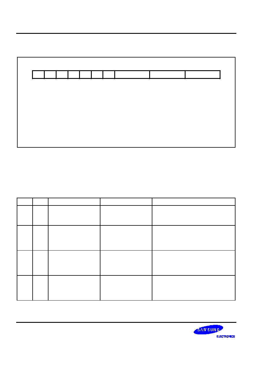
THUMB INSTRUCTION SET
S3C2440A RISC MICROPROCESSOR
4-20
FORMAT 8: LOAD/STORE SIGN-EXTENDED BYTE/HALFWORD
[2:0] Destination Register
[5:3] Base Register
[8:6] Offset Register
[10] Sign-Extended Flag
0 = Operand not sing-extended
1 = Operand sing-extended
[11] H Flag
15
0
0
14
10
6
5
3
2
Rd
1
0
13
12
11
Rb
1
H
S
9
8
Ro
1
Figure 4-9. Format 8
OPERATION
These instructions load optionally sign-extended bytes or halfwords, and store halfwords. The THUMB assembler
syntax is shown below.
Table 4-9. Summary of Format 8 Instructions
L
B
THUMB assembler
ARM equivalent
Description
0
0
STRH Rd, [Rb, Ro]
STRH Rd, [Rb, Ro]
Store halfword:
Add Ro to base address in Rb. Store bits
0-15 of Rd at the resulting address.
0
1
LDRH Rd, [Rb, Ro]
LDRH Rd, [Rb, Ro]
Load halfword:
Add Ro to base address in Rb. Load bits
0-15 of Rd from the resulting address, and
set bits 16-31 of Rd to 0.
1
0
LDSB Rd, [Rb, Ro]
LDRSB Rd, [Rb, Ro]
Load sign-extended byte:
Add Ro to base address in Rb. Load bits
0-7 of Rd from the resulting address, and
set bits 8-31 of Rd to bit 7.
1
1
LDSH Rd, [Rb, Ro]
LDRSH Rd, [Rb, Ro]
Load sign-extended halfword:
Add Ro to base address in Rb. Load bits
0-15 of Rd from the resulting address, and
set bits 16-31 of Rd to bit 15.

S3C2440A RISC MICROPROCESSOR
THUMB INSTRUCTION SET
4-21
INSTRUCTION CYCLE TIMES
All instructions in this format have an equivalent ARM instruction as shown in Table 4-9. The instruction cycle times
for the THUMB instruction are identical to that of the equivalent ARM instruction.
EXAMPLES
STRH
R4, [R3, R0]
; Store the lower 16 bits of R4 at the address formed by
adding R0 to R3.
LDSB
R2, [R7, R1]
; Load into R2 the sign extended byte found at the address
formed by adding R1 to R7.
LDSH
R3, [R4, R2]
; Load into R3 the sign extended halfword found at the
address formed by adding R2 to R4.

THUMB INSTRUCTION SET
S3C2440A RISC MICROPROCESSOR
4-22
FORMAT 9: LOAD/STORE WITH IMMEDIATE OFFSET
[2:0] Source/Destination Register
[5:3] Base Register
[10:6] Offset Register
[11] Load/Store Flag
0 = Store to memory
1 = Load from memory
[12] Byte/Word Flad
0 = Transfer word quantity
1 = Transfer byte quantity
15
0
0
14
10
6
5
3
2
Rd
1
1
13
12
11
Rb
B
L
Offset5
Figure 4-10. Format 9

S3C2440A RISC MICROPROCESSOR
THUMB INSTRUCTION SET
4-23
OPERATION
These instructions transfer byte or word values between registers and memory using an immediate 5 or 7-bit offset.
The THUMB assembler syntax is shown in Table 4-10.
Table 4-10. Summary of Format 9 Instructions
L
B
THUMB assembler
ARM equivalent
Description
0
0
STR Rd, [Rb, #Imm]
STR Rd, [Rb, #Imm]
Calculate the target address by adding
together the value in Rb and Imm. Store
the contents of Rd at the address.
1
0
LDR Rd, [Rb, #Imm]
LDR Rd, [Rb, #Imm]
Calculate the source address by adding
together the value in Rb and Imm. Load
Rd from the address.
0
1
STRB Rd, [Rb, #Imm]
STRB Rd, [Rb, #Imm]
Calculate the target address by adding
together the value in Rb and Imm. Store
the byte value in Rd at the address.
1
1
LDRB Rd, [Rb, #Imm]
LDRB Rd, [Rb, #Imm]
Calculate source address by adding
together the value in Rb and Imm. Load
the byte value at the address into Rd.
NOTE: For word accesses (B = 0), the value specified by #Imm is a full 7-bit address, but must be word-aligned
(ie with bits 1:0 set to 0), since the assembler places #Imm >> 2 in the Offset5 field.
INSTRUCTION CYCLE TIMES
All instructions in this format have an equivalent ARM instruction as shown in Table 4-10. The instruction cycle times
for the THUMB instruction are identical to that of the equivalent ARM instruction.
EXAMPLES
LDR
R2, [R5,#116]
; Load into R2 the word found at the address formed by
adding 116 to R5.Note that the THUMB opcode will
contain 29 as the Offset5 value.
STRB
R1, [R0,#13]
; Store the lower 8 bits of R1 at the address formed by
adding 13 to R0.Note that the THUMB opcode will
contain 13 as the Offset5 value.
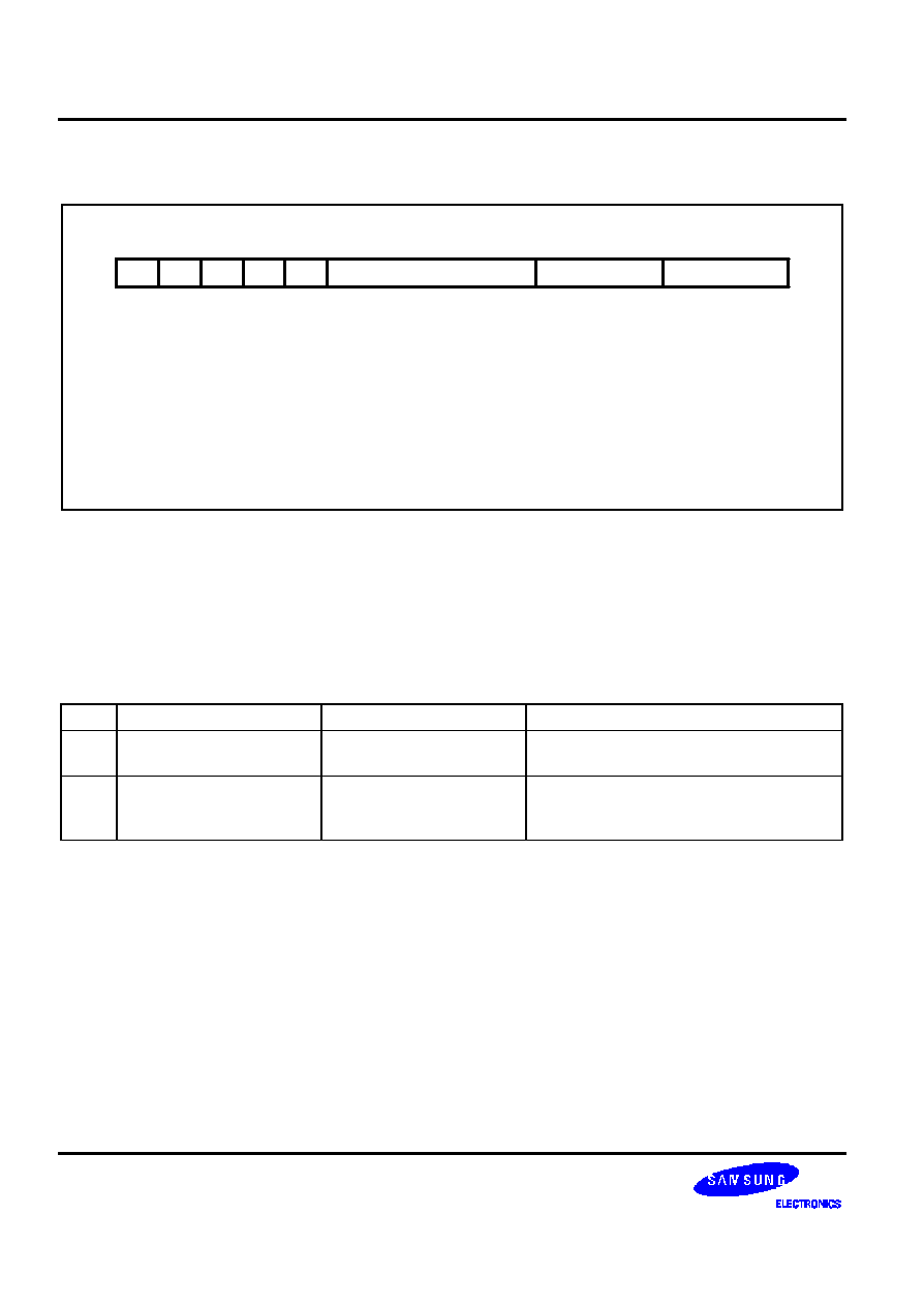
THUMB INSTRUCTION SET
S3C2440A RISC MICROPROCESSOR
4-24
FORMAT 10: LOAD/STORE HALFWORD
[2:0] Source/Destination Register
[5:3] Base Register
[10:6] Immediate Value
[11] Load/Store Flag
0 = Store to memory
1 = Load from memory
15
0
0
14
10
6
5
3
2
Rd
1
0
13
12
11
Rb
0
L
Offset5
Figure 4-11. Format 10
OPERATION
These instructions transfer halfword values between a Lo register and memory. Addresses are pre-indexed, using a
6-bit immediate value. The THUMB assembler syntax is shown in Table 4-11.
Table 4-11. Halfword Data Transfer Instructions
L
THUMB assembler
ARM equivalent
Description
0
STRH Rd, [Rb, #Imm]
STRH Rd, [Rb, #Imm]
Add #Imm to base address in Rb and store
bits 0 - 15 of Rd at the resulting address.
1
LDRH Rd, [Rb, #Imm]
LDRH Rd, [Rb, #Imm]
Add #Imm to base address in Rb. Load bits
0-15 from the resulting address into Rd and
set bits 16-31 to zero.
NOTE: #Imm is a full 6-bit address but must be halfword-aligned (ie with bit 0 set to 0) since the assembler places
#Imm >> 1 in the Offset5 field.

S3C2440A RISC MICROPROCESSOR
THUMB INSTRUCTION SET
4-25
INSTRUCTION CYCLE TIMES
All instructions in this format have an equivalent ARM instruction as shown in Table 4-11. The instruction cycle times
for the THUMB instruction are identical to that of the equivalent ARM instruction.
EXAMPLES
STRH
R6, [R1, #56]
; Store the lower 16 bits of R4 at the address formed by
adding 56 R1. Note that the THUMB opcode will contain
28 as the Offset5 value.
LDRH
R4, [R7, #4]
; Load into R4 the halfword found at the address formed by
adding 4 to R7. Note that the THUMB opcode will contain
2 as the Offset5 value.

THUMB INSTRUCTION SET
S3C2440A RISC MICROPROCESSOR
4-26
FORMAT 11: SP-RELATIVE LOAD/STORE
[7:0] Immediate Value
[10:8] Destination Register
[11] Load/Store Bit
0 = Store to memory
1 = Load from memory
15
0
1
14
10
0
0
13
12
11
Word 8
1
L
Rd
7
8
Figure 4-12. Format 11
OPERATION
The instructions in this group perform an SP-relative load or store. The THUMB assembler syntax is shown in the
following table.
Table 4-12. SP-Relative Load/Store Instructions
L
THUMB assembler
ARM equivalent
Description
0
STR Rd, [SP, #Imm]
STR Rd, [R13 #Imm]
Add unsigned offset (255 words, 1020 bytes)
in Imm to the current value of the SP (R7).
Store the contents of Rd at the resulting
address.
1
LDR Rd, [SP, #Imm]
LDR Rd, [R13 #Imm]
Add unsigned offset (255 words, 1020 bytes)
in Imm to the current value of the SP (R7).
Load the word from the resulting address into
Rd.
NOTE: The offset supplied in #Imm is a full 10-bit address, but must always be word-aligned (ie bits 1:0 set to 0),
since the assembler places #Imm >> 2 in the Word8 field.

S3C2440A RISC MICROPROCESSOR
THUMB INSTRUCTION SET
4-27
INSTRUCTION CYCLE TIMES
All instructions in this format have an equivalent ARM instruction as shown in Table 4-12. The instruction cycle times
for the THUMB instruction are identical to that of the equivalent ARM instruction.
EXAMPLES
STR
R4, [SP,#492]
; Store the contents of R4 at the address formed by adding
492 to SP (R13).Note that the THUMB opcode will
contain 123 as the Word8 value.

THUMB INSTRUCTION SET
S3C2440A RISC MICROPROCESSOR
4-28
FORMAT 12: LOAD ADDRESS
[7:0] 8-bit Unsigned Constant
[10:8] Destination Register
[11] Source
0 = PC
1 = SP
15
0
1
14
10
0
1
13
12
11
Word 8
0
SP
Rd
7
8
Figure 4-13. Format 12
OPERATION
These instructions calculate an address by adding a 10-bit constant to either the PC or the SP, and load the
resulting address into a register. The THUMB assembler syntax is shown in the following table.
Table 4-13. Load Address
L
THUMB assembler
ARM equivalent
Description
0
ADD Rd, PC, #Imm
ADD Rd, R15, #Imm
Add #Imm to the current value of the program
counter (PC) and load the result into Rd.
1
ADD Rd, SP, #Imm
ADD Rd, R13, #Imm
Add #Imm to the current value of the stack
pointer (SP) and load the result into Rd.
NOTE: The value specified by #Imm is a full 10-bit value, but this must be word-aligned (ie with bits 1:0 set to 0)
since the assembler places #Imm >> 2 in field Word 8.
Where the PC is used as the source register (SP = 0), bit 1 of the PC is always read as 0. The value of the PC will
be 4 bytes greater than the address of the instruction before bit 1 is forced to 0.
The CPSR condition codes are unaffected by these instructions.

S3C2440A RISC MICROPROCESSOR
THUMB INSTRUCTION SET
4-29
INSTRUCTION CYCLE TIMES
All instructions in this format have an equivalent ARM instruction as shown in Table 4-13. The instruction cycle times
for the THUMB instruction are identical to that of the equivalent ARM instruction.
EXAMPLES
ADD
R2, PC, #572
; R2 := PC + 572, but don't set thecondition codes.
bit[1] of PC is forced to zero.Note that the THUMB
opcode willcontain 143 as the Word8 value.
ADD
R6, SP, #212
; R6 := SP (R13) + 212, but don'tset the condition codes.
Note that the THUMB opcode will contain 53 as the
Word 8 value.

THUMB INSTRUCTION SET
S3C2440A RISC MICROPROCESSOR
4-30
FORMAT 13: ADD OFFSET TO STACK POINTER
[6:0] 7-bit Immediate Value
[7] Sign Flag
0 = Offset is positive
1 = Offset is negative
15
0
1
14
10
0
1
13
12
11
SWord 7
1
0
0
7
8
9
6
0
0
S
Figure 4-14. Format 13
OPERATION
This instruction adds a 9-bit signed constant to the stack pointer. The following table shows the THUMB assembler
syntax.
Table 4-14. The ADD SP Instruction
L
THUMB assembler
ARM equivalent
Description
0
ADD SP, #Imm
ADD R13, R13, #Imm
Add #Imm to the stack pointer (SP).
1
ADD SP, # -Imm
SUB R13, R13, #Imm
Add #-Imm to the stack pointer (SP).
NOTE: The offset specified by #Imm can be up to -/+ 508, but must be word-aligned (ie with bits 1:0 set to 0) since the
assembler converts #Imm to an 8-bit sign + magnitude number before placing it in field SWord7.
The condition codes are not set by this instruction.
INSTRUCTION CYCLE TIMES
All instructions in this format have an equivalent ARM instruction as shown in Table 4-14. The instruction cycle times
for the THUMB instruction are identical to that of the equivalent ARM instruction.
EXAMPLES
ADD
SP, #268
; SP (R13) := SP + 268, but don't set the condition codes.
Note that the THUMB opcode will contain 67 as the
Word7 value and S=0.
ADD
SP, #-104
; SP (R13) := SP - 104, but don't set the condition codes.
; Note that the THUMB opcode will contain 26 as the
Word7 value and S=1.
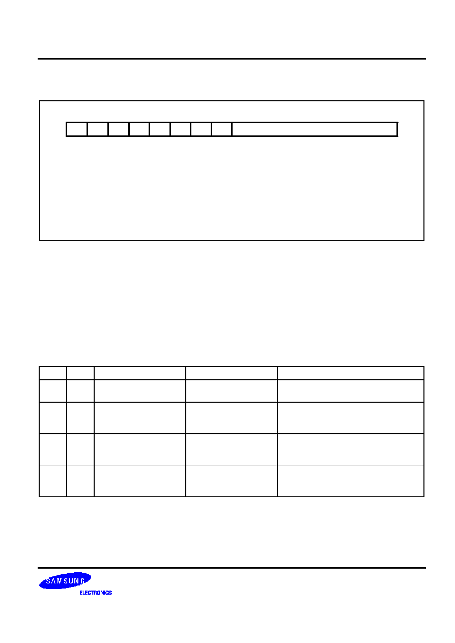
S3C2440A RISC MICROPROCESSOR
THUMB INSTRUCTION SET
4-31
FORMAT 14: PUSH/POP REGISTERS
[7:0] Register List
[8] PC/LR Bit
0 = Do not store LR/Load PC
1 = Store LR/Load PC
[11] Load/Store Bit
0 = Store to memory
1 = Load from memory
15
0
1
14
10
0
1
13
12
11
Rlist
1
L
0
7
8
9
1
R
Figure 4-15. Format 14
OPERATION
The instructions in this group allow registers 0-7 and optionally LR to be pushed onto the stack, and registers 0-7
and optionally PC to be popped off the stack. The THUMB assembler syntax is shown in Table 4-15.
NOTE
The stack is always assumed to be Full Descending.
Table 4-15. PUSH and POP Instructions
L
B
THUMB assembler
ARM equivalent
Description
0
0
PUSH { Rlist }
STMDB R13!, { Rlist }
Push the registers specified by Rlist onto
the stack. Update the stack pointer.
0
1
PUSH { Rlist, LR }
STMDB R13!,
{ Rlist, R14 }
Push the Link Register and the registers
specified by Rlist (if any) onto the stack.
Update the stack pointer.
1
0
POP { Rlist }
LDMIA R13!, { Rlist }
Pop values off the stack into the registers
specified by Rlist. Update the stack
pointer.
1
1
POP { Rlist, PC }
LDMIA R13!, {Rlist, R15}
Pop values off the stack and load into the
registers specified by Rlist. Pop the PC off
the stack. Update the stack pointer.

THUMB INSTRUCTION SET
S3C2440A RISC MICROPROCESSOR
4-32
INSTRUCTION CYCLE TIMES
All instructions in this format have an equivalent ARM instruction as shown in Table 4-15. The instruction cycle times
for the THUMB instruction are identical to that of the equivalent ARM instruction.
EXAMPLES
PUSH
{R0-R4,LR}
; Store R0,R1,R2,R3,R4 and R14 (LR) at the stack pointed
to by R13 (SP) and update R13.
Useful at start of a sub-routine to save workspace and
return address.
POP
{R2,R6,PC}
; Load R2,R6 and R15 (PC) from the stack pointed to by
R13 (SP) and update R13.Useful to restore workspace
and return from sub-routine.

S3C2440A RISC MICROPROCESSOR
THUMB INSTRUCTION SET
4-33
FORMAT 15: MULTIPLE LOAD/STORE
[7:0] Register List
[10:8] Base Register
[11] Load/Store Bit
0 = Store to memory
1 = Load from memory
15
0
1
14
10
1
0
13
12
11
Rlist
0
L
7
8
Rb
Figure 4-16. Format 15
OPERATION
These instructions allow multiple loading and storing of Lo registers. The THUMB assembler syntax is shown in the
following table.
Table 4-16. The Multiple Load/Store Instructions
L
THUMB assembler
ARM equivalent
Description
0
STMIA Rb!, { Rlist }
STMIA Rb!, { Rlist }
Store the registers specified by Rlist, starting
at the base address in Rb. Write back the
new base address.
1
LDMIA Rb!, { Rlist }
LDMIA Rb!, { Rlist }
Load the registers specified by Rlist, starting
at the base address in Rb. Write back the
new base address.
INSTRUCTION CYCLE TIMES
All instructions in this format have an equivalent ARM instruction as shown in Table 4-16. The instruction cycle times
for the THUMB instruction are identical to that of the equivalent ARM instruction.
EXAMPLES
STMIA
R0!, {R3-R7}
; Store the contents of registers R3-R7 starting at the
address specified in R0, incrementing the addresses for
each word. Write back the updated value of R0.
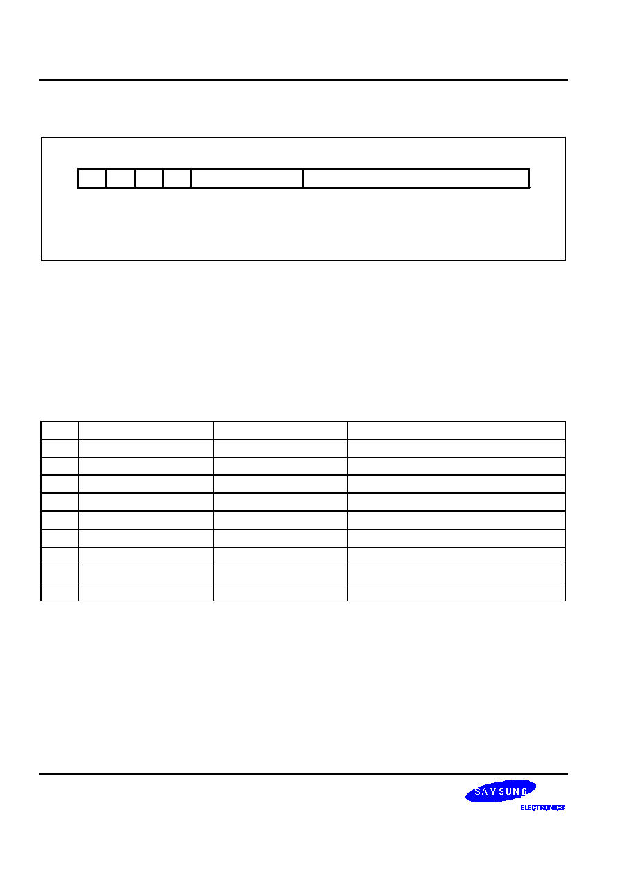
THUMB INSTRUCTION SET
S3C2440A RISC MICROPROCESSOR
4-34
FORMAT 16: CONDITIONAL BRANCH
[7:0] 8-bit Signed Immediate
[11:8] Condition
15
0
1
14
1
0
13
12
11
SOffset 8
1
7
8
Cond
Figure 4-17. Format 16
OPERATION
The instructions in this group all perform a conditional Branch depending on the state of the CPSR condition codes.
The branch offset must take account of the prefetch operation, which causes the PC to be 1 word (4 bytes) ahead of
the current instruction.
The THUMB assembler syntax is shown in the following table.
Table 4-17. The Conditional Branch Instructions
L
THUMB assembler
ARM equivalent
Description
0000
BEQ label
BEQ label
Branch if Z set (equal)
0001
BNE label
BNE label
Branch if Z clear (not equal)
0010
BCS label
BCS label
Branch if C set (unsigned higher or same)
0011
BCC label
BCC label
Branch if C clear (unsigned lower)
0100
BMI label
BMI label
Branch if N set (negative)
0101
BPL label
BPL label
Branch if N clear (positive or zero)
0110
BVS label
BVS label
Branch if V set (overflow)
0111
BVC label
BVC label
Branch if V clear (no overflow)
1000
BHI label
BHI label
Branch if C set and Z clear (unsigned higher)

S3C2440A RISC MICROPROCESSOR
THUMB INSTRUCTION SET
4-35
Table 4-17. The Conditional Branch Instructions (Continued)
L
THUMB assembler
ARM equivalent
Description
1001
BLS label
BLS label
Branch if C clear or Z set (unsigned lower or
same)
1010
BGE label
BGE label
Branch if N set and V set, or N clear and V
clear (greater or equal)
1011
BLT label
BLT label
Branch if N set and V clear, or N clear and V
set (less than)
1100
BGT label
BGT label
Branch if Z clear, and either N set and V set
or N clear and V clear (greater than)
1101
BLE label
BLE label
Branch if Z set, or N set and V clear, or N
clear and V set (less than or equal)
NOTES:
1.
While label specifies a full 9-bit two's complement address, this must always be halfword-aligned (ie with bit 0 set to 0)
since the assembler actually places label >> 1 in field SOffset8.
2.
Cond = 1110 is undefined, and should not be used.
Cond = 1111 creates the SWI instruction: see.
INSTRUCTION CYCLE TIMES
All instructions in this format have an equivalent ARM instruction as shown in Table 3-1. The instruction cycle times
for the THUMB instruction are identical to that of the equivalent ARM instruction.
EXAMPLES
CMP R0, #45
; Branch to over-if R0 > 45.
BGT over
; Note that the THUMB opcode will contain the number of
halfwords to offset.
over
; Must be halfword aligned.

THUMB INSTRUCTION SET
S3C2440A RISC MICROPROCESSOR
4-36
FORMAT 17: SOFTWARE INTERRUPT
[7:0] Comment Field
15
0
1
14
1
0
13
12
11
Value 8
1
7
8
10
9
1
1
1
1
Figure 4-18. Format 17
OPERATION
The SWI instruction performs a software interrupt. On taking the SWI, the processor switches into ARM state and
enters Supervisor (SVC) mode.
The THUMB assembler syntax for this instruction is shown below.
Table 4-18. The SWI Instruction
THUMB assembler
ARM equivalent
Description
SWI Value 8
SWI Value 8
Perform Software Interrupt:
Move the address of the next instruction into LR,
move CPSR to SPSR, load the SWI vector address
(0x8) into the PC. Switch to ARM state and enter
SVC mode.
NOTE: Value8 is used solely by the SWI handler; it is ignored by the processor.
INSTRUCTION CYCLE TIMES
All instructions in this format have an equivalent ARM instruction as shown in Table 4-18. The instruction cycle times
for the THUMB instruction are identical to that of the equivalent ARM instruction.
EXAMPLES
SWI 18
; Take the software interrupt exception. Enter Supervisor
mode with 18 as the requested SWI number.
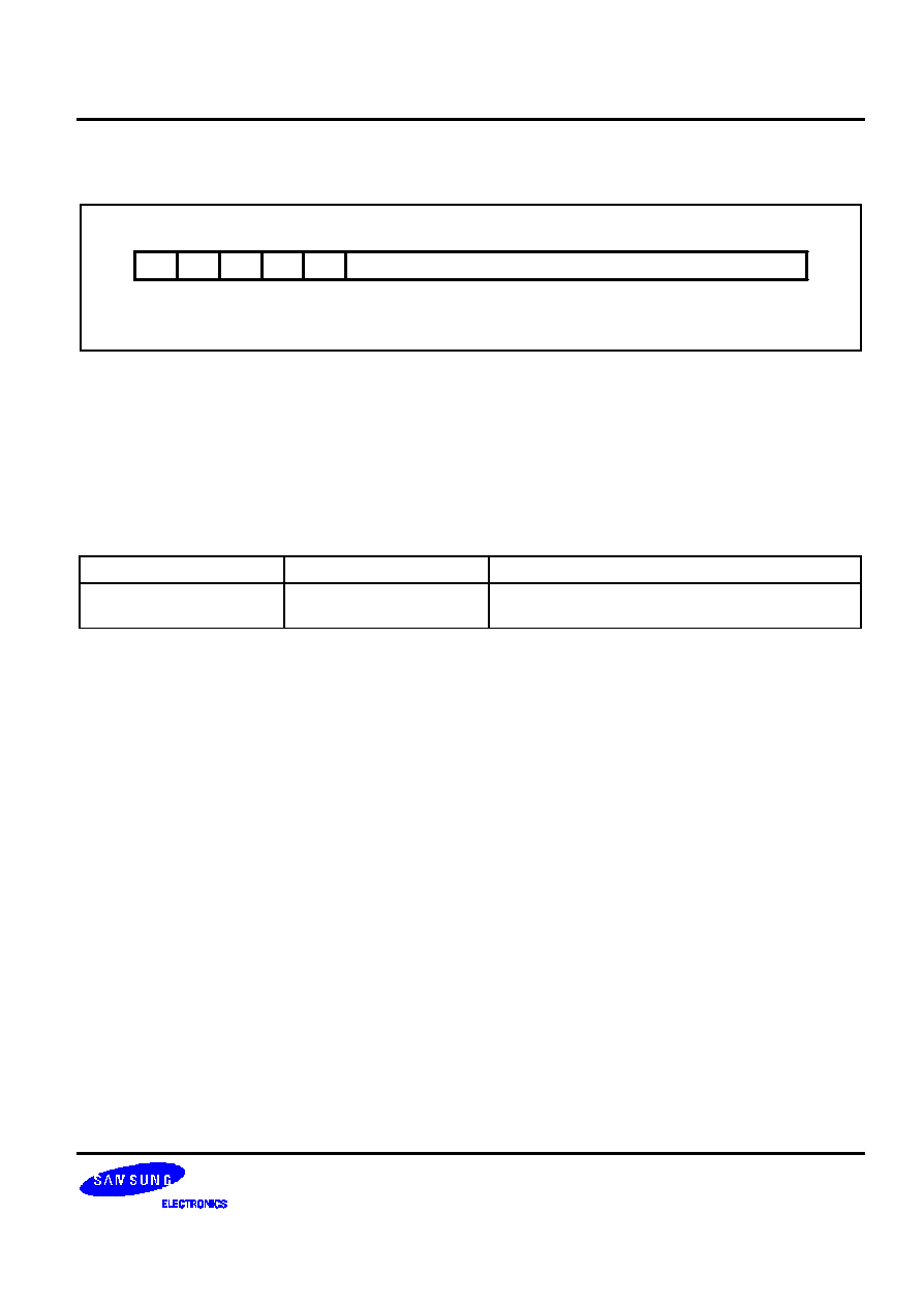
S3C2440A RISC MICROPROCESSOR
THUMB INSTRUCTION SET
4-37
FORMAT 18: UNCONDITIONAL BRANCH
[10:0] Immediate Value
15
0
1
14
1
1
13
12
11
Offset11
0
10
0
Figure 4-19. Format 18
OPERATION
This instruction performs a PC-relative Branch. The THUMB assembler syntax is shown below. The branch offset
must take account of the prefetch operation, which causes the PC to be 1 word (4 bytes) ahead of the current
instruction.
Table 4-19. Summary of Branch Instruction
THUMB assembler
ARM equivalent
Description
B label
BAL label (halfword offset)
Branch PC relative
±
Offset11 << 1, where label is
PC
±
2048 bytes.
NOTE: The address specified by label is a full 12-bit two's complement address,
but must always be halfword aligned (ie bit 0 set to 0), since the assembler places label >> 1 in the Offset11 field.
EXAMPLES
here
B here
; Branch onto itself. Assembles to 0xE7FE.
(Note effect of PC offset).
B jimmy
; Branch to 'jimmy'.
∑
Note that the THUMB opcode will contain the number of
∑
∑
; halfwords to offset.
jimmy
∑
Must be halfword aligned.

THUMB INSTRUCTION SET
S3C2440A RISC MICROPROCESSOR
4-38
FORMAT 19: LONG BRANCH WITH LINK
[10:0] Long Branch and Link Offset High/Low
[11] Low/High Offset Bit
0 = Offset high
1 = Offset low
15
0
1
14
1
1
13
12
11
Offset
1
10
H
Figure 4-20. Format 19
OPERATION
This format specifies a long branch with link.
The assembler splits the 23-bit two's complement half-word offset specified by the label into two 11-bit halves,
ignoring bit 0 (which must be 0), and creates two THUMB instructions.
Instruction 1 (H = 0)
In the first instruction the Offset field contains the upper 11 bits of the target address. This is shifted left by 12 bits
and added to the current PC address. The resulting address is placed in LR.
Instruction 2 (H =1)
In the second instruction the Offset field contains an 11-bit representation lower half of the target address. This is
shifted left by 1 bit and added to LR. LR, which now contains the full 23-bit address, is placed in PC, the address of
the instruction following the BL is placed in LR and bit 0 of LR is set.
The branch offset must take account of the prefetch operation, which causes the PC to be 1 word (4 bytes) ahead of
the current instruction
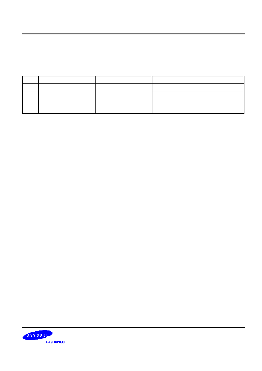
S3C2440A RISC MICROPROCESSOR
THUMB INSTRUCTION SET
4-39
INSTRUCTION CYCLE TIMES
This instruction format does not have an equivalent ARM instruction.
Table 4-20. The BL Instruction
L
THUMB assembler
ARM equivalent
Description
0
BL label
none
LR := PC + OffsetHigh << 12
1
temp := next instruction address
PC := LR + OffsetLow << 1
LR := temp | 1
EXAMPLES
BL faraway
; Unconditionally Branch to 'faraway'
next
∑
and place following instruction
∑
address, ie "next", in R14,the Link register and set bit 0 of
LR high.
Note that the THUMB opcodes will contain the number of
halfwords to offset.
faraway
∑
; Must be Half-word aligned.
∑

THUMB INSTRUCTION SET
S3C2440A RISC MICROPROCESSOR
4-40
INSTRUCTION SET EXAMPLES
The following examples show ways in which the THUMB instructions may be used to generate small and efficient
code. Each example also shows the ARM equivalent so these may be compared.
MULTIPLICATION BY A CONSTANT USING SHIFTS AND ADDS
The following instructions are the code to multiply by various constants using 1, 2 or 3 Thumb instructions alongside
the ARM equivalents. For other constants it is generally better to use the built-in MUL instruction rather than using a
sequence of 4 or more instructions.
Thumb
ARM
1. Multiplication by 2^n (1,2,4,8,...)
LSL
Ra, Rb, LSL #n
; MOV Ra, Rb, LSL #n
2. Multiplication by 2^n+1 (3,5,9,17,...)
LSL
Rt, Rb, #n
; ADD Ra, Rb, Rb, LSL #n
ADD
Ra, Rt, Rb
3. Multiplication by 2^n-1 (3,7,15,...)
LSL
Rt, Rb, #n
; RSB Ra, Rb, Rb, LSL #n
SUB
Ra, Rt, Rb
4. Multiplication by -2^n (-2, -4, -8, ...)
LSL
Ra, Rb, #n
; MOV Ra, Rb, LSL #n
MVN
Ra, Ra
; RSB Ra, Ra, #0
5. Multiplication by -2^n-1 (-3, -7, -15, ...)
LSL
Rt, Rb, #n
; SUB Ra, Rb, Rb, LSL #n
SUB
Ra, Rb, Rt
Multiplication by any C = {2^n+1, 2^n-1, -2^n or -2^n-1} * 2^n
Effectively this is any of the multiplications in 2 to 5 followed by a final shift. This allows the following additional
constants to be multiplied. 6, 10, 12, 14, 18, 20, 24, 28, 30, 34, 36, 40, 48, 56, 60, 62 .....
(2..5)
; (2..5)
LSL
Ra, Ra, #n
; MOV Ra, Ra, LSL #n

S3C2440A RISC MICROPROCESSOR
THUMB INSTRUCTION SET
4-41
GENERAL PURPOSE SIGNED DIVIDE
This example shows a general purpose signed divide and remainder routine in both Thumb and ARM code.
Thumb code
;signed_divide
; Signed divide of R1 by R0: returns quotient in R0,
; remainder in R1
;Get abs value of R0 into R3
ASR
R2, R0, #31
; Get 0 or -1 in R2 depending on sign of R0
EOR
R0, R2
; EOR with -1 (0
◊
FFFFFFFF) if negative
SUB
R3, R0, R2
; and ADD 1 (SUB -1) to get abs value
;SUB always sets flag so go & report division by 0 if necessary
BEQ
divide_by_zero
;Get abs value of R1 by xoring with 0xFFFFFFFF and adding 1 if negative
ASR
R0, R1, #31
; Get 0 or -1 in R3 depending on sign of R1
EOR
R1, R0
; EOR with -1 (0
◊
FFFFFFFF) if negative
SUB
R1, R0
; and ADD 1 (SUB -1) to get abs value
;Save signs (0 or -1 in R0 & R2) for later use in determining ; sign of quotient & remainder.
PUSH
{R0, R2}
;Justification, shift 1 bit at a time until divisor (R0 value) ; is just <= than dividend (R1 value). To do this shift dividend
; right by 1 and stop as soon as shifted value becomes >.
LSR
R0, R1, #1
MOV
R2, R3
B
%FT0
just_l
LSL
R2, #1
0
CMP
R2, R0
BLS
just_l
MOV
R0, #0
; Set accumulator to 0
B
%FT0
; Branch into division loop
div_l
LSR
R2, #1
0
CMP
R1, R2
; Test subtract
BCC
%FT0
SUB
R1, R2
; If successful do a real subtract
0
ADC
R0, R0
; Shift result and add 1 if subtract succeeded
CMP
R2, R3
; Terminate when R2 == R3 (ie we have just
BNE
div_l
; tested subtracting the 'ones' value).

THUMB INSTRUCTION SET
S3C2440A RISC MICROPROCESSOR
4-42
Now fix up the signs of the quotient (R0) and remainder (R1)
POP
{R2, R3}
; Get dividend/divisor signs back
EOR
R3, R2
; Result sign
EOR
R0, R3
; Negate if result sign = - 1
SUB
R0, R3
EOR
R1, R2
; Negate remainder if dividend sign = - 1
SUB
R1, R2
MOV
pc, lr
ARM Code
signed_divide
;
Effectively zero a4 as top bit will be shifted out later
ANDS
a4, a1, #&80000000
RSBMI
a1, a1, #0
EORS
ip, a4, a2, ASR #32
;ip bit 31 = sign of result
;ip bit 30 = sign of a2
RSBCS
a2, a2, #0
;Central part is identical code to udiv (without MOV a4, #0 which comes for free as part of signed entry sequence)
MOVS
a3, a1
BEQ
divide_by_zero
just_l
; Justification stage shifts 1 bit at a time
CMP
a3, a2, LSR #1
MOVLS
a3, a3, LSL #1
; NB: LSL #1 is always OK if LS succeeds
BLO
s_loop
div_l
CMP
a2, a3
ADC
a4, a4, a4
SUBCS
a2, a2, a3
TEQ
a3, a1
MOVNE
a3, a3, LSR #1
BNE
s_loop2
MOV
a1, a4
MOVS
ip, ip, ASL #1
RSBCS
a1, a1, #0
RSBMI
a2, a2, #0
ce
MOV
pc, lr

S3C2440A RISC MICROPROCESSOR
THUMB INSTRUCTION SET
4-43
DIVISION BY A CONSTANT
Division by a constant can often be performed by a short fixed sequence of shifts, adds and subtracts.
Here is an example of a divide by 10 routine based on the algorithm in the ARM Cookbook in both Thumb and ARM
code.
Thumb Code
udiv10
; Take argument in a1 returns quotient in a1,
; remainder in a2
MOV
a2, a1
LSR
a3, a1, #2
SUB
a1, a3
LSR
a3, a1, #4
ADD
a1, a3
LSR
a3, a1, #8
ADD
a1, a3
LSR
a3, a1, #16
ADD
a1, a3
LSR
a1, #3
ASL
a3, a1, #2
ADD
a3, a1
ASL
a3, #1
SUB
a2, a3
CMP
a2, #10
BLT
%FT0
ADD
a1, #1
SUB
a2, #10
0
MOV
pc, lr
ARM Code
udiv10
; Take argument in a1 returns quotient in a1,
; remainder in a2
SUB
a2, a1, #10
SUB
a1, a1, a1, lsr #2
ADD
a1, a1, a1, lsr #4
ADD
a1, a1, a1, lsr #8
ADD
a1, a1, a1, lsr #16
MOV
a1, a1, lsr #3
ADD
a3, a1, a1, asl #2
SUBS
a2, a2, a3, asl #1
ADDPL
a1, a1, #1
ADDMI
a2, a2, #10
MOV
pc, lr

THUMB INSTRUCTION SET
S3C2440A RISC MICROPROCESSOR
4-44
NOTES

S3C2440A RISC MICROPROCESSOR
MEMORY CONTROLLER
5-1
5
MEMORY CONTROLLER
OVERVIEW
The S3C2440A memory controller provides memory control signals that are required for external memory access.
The S3C2440A has the following features:
-- Little/Big endian (selectable by a software)
-- Address space: 128Mbytes per bank (total 1GB/8 banks)
-- Programmable access size (8/16/32-bit) for all banks except bank0 (16/32-bit)
-- Total 8 memory banks
Six memory banks for ROM, SRAM, etc.
Remaining two memory banks for ROM, SRAM, SDRAM, etc .
-- Seven fixed memory bank start address
-- One flexible memory bank start address and programmable bank size
-- Programmable access cycles for all memory banks
-- External wait to extend the bus cycles
-- Supporting self-refresh and power down mode in SDRAM
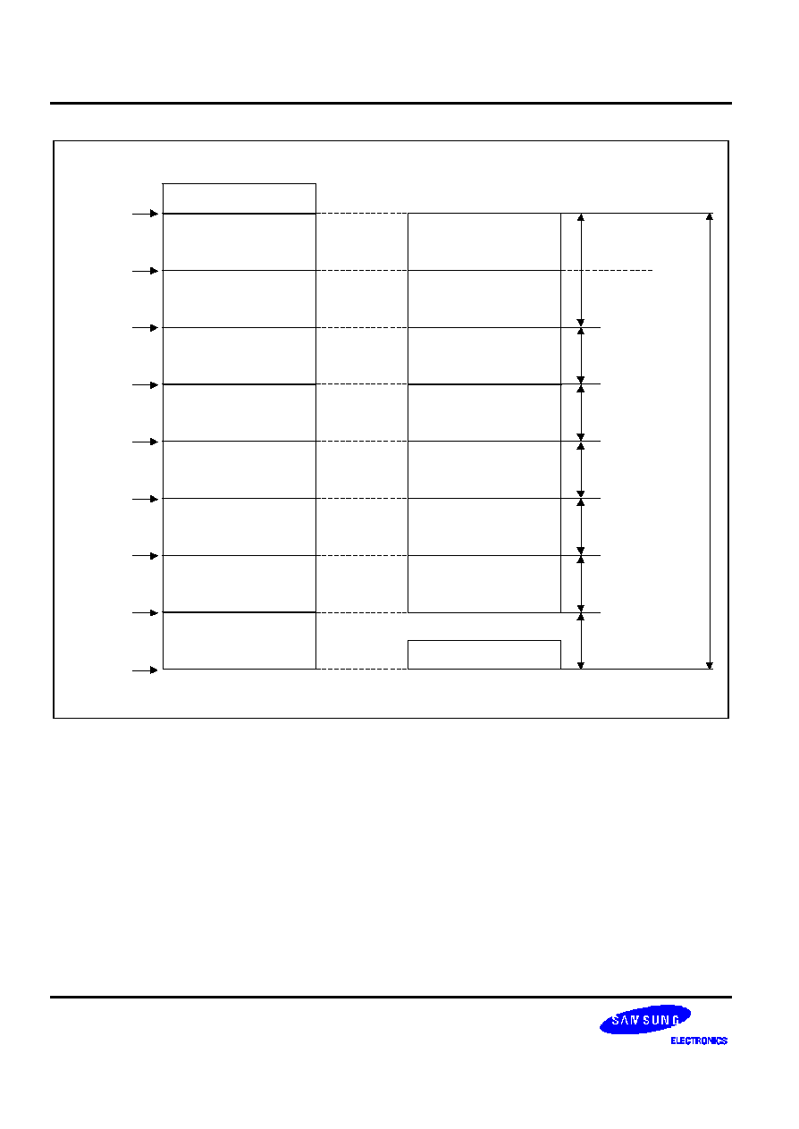
MEMORY CONTROLLER
S3C2440A RISC MICROPROCESSOR
5-2
0x0000_0000
0x0800_0000
0x1000_0000
0x1800_0000
0x2000_0000
0x2800_0000
0x3000_0000
0x3800_0000
0x4000_0000
SROM/SDRAM
(nGCS7)
SROM/SDRAM
(nGCS6)
SROM
(nGCS5)
SROM
(nGCS4)
SROM
(nGCS3)
SROM
(nGCS2)
SROM
(nGCS1)
Boot Internal
SRAM (4KB)
128 MB
128MB
128MB
128MB
128MB
128MB
2MB/4MB/8MB/16MB
/32MB/64MB/128MB
2MB/4MB/8MB/16MB
/32MB/64MB/128MB
Refer to
Table 5
1GB
HADDR[29:0]
Accessible
Region
SROM/SDRAM
(nGCS7)
SROM/SDRAM
(nGCS6)
SROM
(nGCS5)
SROM
(nGCS4)
SROM
(nGCS3)
SROM
(nGCS2)
SROM
(nGCS1)
SROM
(nGCS0)
OM[1:0] = 01,10
OM[1:0] = 00
[ Not using NAND flash for boot ROM ]
[ Using NAND flash for boot ROM ]
Boot Internal
SRAM (4KB)
Figure 5-1. S3C2440A Memory Map after Reset
NOTE
SROM means ROM or SRAM type memory

S3C2440A RISC MICROPROCESSOR
MEMORY CONTROLLER
5-3
Table 5-1. Bank 6/7 Addresses
Address
2MB
4MB
8MB
16MB
32MB
64MB
128MB
Bank 6
Start address
0x3000_0000
0x3000_0000
0x3000_0000
0x3000_0000
0x3000_0000
0x3000_0000
0x3000_0000
End address
0x301F_FFFF
0X303F_FFFF
0X307F_FFFF
0X30FF_FFFF
0X31FF_FFFF
0X33FF_FFFF
0X37FF_FFFF
Bank 7
Start address
0x3020_0000
0x3040_0000
0x3080_0000
0x3100_0000
0x3200_0000
0x3400_0000
0x3800_0000
End address
0X303F_FFFF
0X307F_FFFF
0X30FF_FFFF
0X31FF_FFFF
0X33FF_FFFF
0X37FF_FFFF
0X3FFF_FFFF
NOTE: Bank 6 and 7 must have the same memory size.
MEMORY CONTROLLER
S3C2440A RISC MICROPROCESSOR
5-4
FUNCTION DESCRIPTION
BANK0 BUS WIDTH
The data bus of BANK0 (nGCS0) should be configured with a width as one of 16-bit and 32-bit ones. Because the
BANK0 works as the booting ROM bank (map to 0x0000_0000), the bus width of BANK0 should be determined
before the first ROM access, which will depend on the logic level of OM[1:0] at Reset.
OM1 (Operating Mode 1)
OM0 (Operating Mode 0)
Booting ROM Data width
0
0
Nand Flash Mode
0
1
16-bit
1
0
32-bit
1
1
Test Mode
MEMORY (SROM/SDRAM) ADDRESS PIN CONNECTIONS
MEMORY ADDR. PIN
S3C2440A ADDR.
@ 8-bit DATA BUS
S3C2440A ADDR.
@ 16-bit DATA BUS
S3C2440A ADDR.
@ 32-bit DATA BUS
A0
A0
A1
A2
A1
A1
A2
A3
. . .
. . .
. . .
. . .
S3C2440A RISC MICROPROCESSOR
MEMORY CONTROLLER
5-5
SDRAM BANK ADDRESS PIN CONNECTION EXAMPLE
Table 5-2. SDRAM Bank Address Configuration Example
Bank Size
Bus Width
Base Component
Memory Configuration
Bank Address
2MByte
x8
16Mbit
(1M x 8 x 2Bank) x 1
A20
x16
(512K x 16 x 2B) x 1
4MB
x16
(1M x 8 x 2B) x 2
A21
x16
(1M x 8 x 2B) x 2
8MB
x16
16Mb
(2M x 4 x 2B) x 4
A22
x32
(1M x 8x 2B) x 4
x8
64Mb
(4M x 8 x 2B) x 1
x8
(2M x 8 x 4B) x 1
A[22:21]
x16
(2M x 16 x 2B) x 1
A22
x16
(1M x 16 x 4B) x 1
A[22:21]
x32
(512K x 32 x 4B) x 1
16MB
x32
16Mb
(2M x 4 x 2B) x 8
A23
x8
64Mb
(8M x 4 x 2B) x 2
x8
(4M x 4 x 4B) x 2
A[23:22]
x16
(4M x 8 x 2B) x 2
A23
x16
(2M x 8 x 4B) x 2
A[23:22]
x32
(2M x 16 x 2B) x 2
A23
x32
(1M x 16 x 4B) x 2
A[23:22]
x8
128Mb
(4M x 8 x 4B) x 1
x16
(2M x 16 x 4B) x 1
32MB
x16
64Mb
(8M x 4 x 2B) x 4
A24
x16
(4M x 4 x 4B) x 4
A[24:23]
x32
(4M x 8 x 2B) x 4
A24
x32
(2M x 8 x 4B) x 4
A[24:23]
x16
128Mb
(4M x 8 x 4B) x 2
x32
(2M x 16 x 4B) x 2
x8
256Mb
(8M x 8 x 4B) x 1
x16
(4M x 16 x 4B) x 1
64MB
x32
128Mb
(4M x 8 x 4B) x 4
A[25:24]
x16
256Mb
(8M x 8 x 4B) x 2
x32
(4M x 16 x 4B) x 2
x8
512Mb
(16M x 8 x 4B) x 1
128MB
x32
256Mb
(8M x 8 x 4Bank) x 4
A[26:25]
x8
512Mb
(32M x 4 x 4B) x 2
x16
(16M x 8 x 4B) x 2
x32
(8M x 16 x 4B) x 2
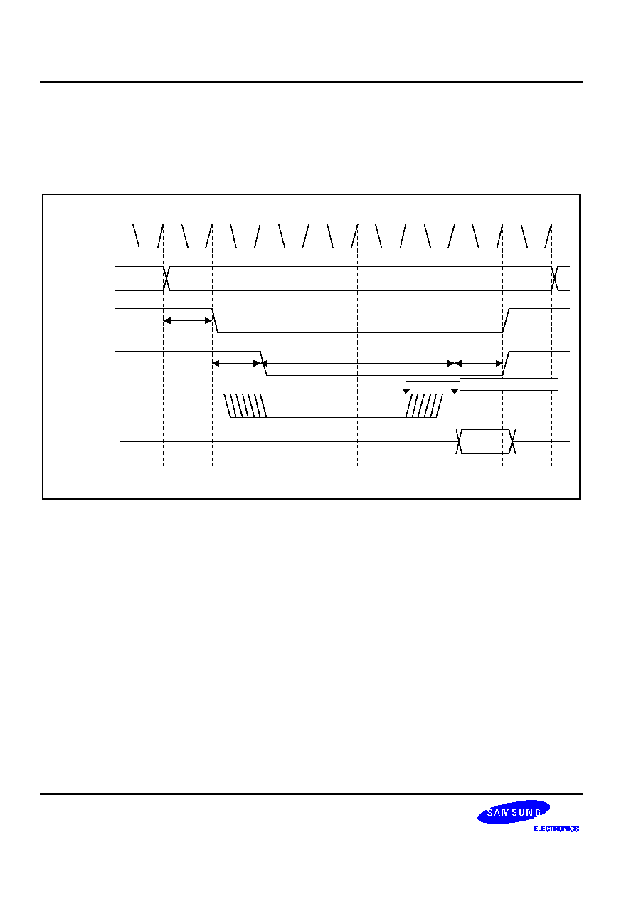
MEMORY CONTROLLER
S3C2440A RISC MICROPROCESSOR
5-6
nWAIT PIN OPERATION
If the WAIT bit(WSn bit in BWSCON) corresponding to each memory bank is enabled, the nOE duration should be
prolonged by the external nWAIT pin while the memory bank is active. nWAIT is checked from tacc-1. nOE will be
de-asserted at the next clock after sampling nWAIT is high. The nWE signal have the same relation with nOE.
Tacs
Tcos
Tacc=4
HCLK
ADDR
nGCS
nOE
nWAIT
DATA(R)
Delayed
Sampling nWAIT
Figure 5-2. S3C2440A External nWAIT Timing Diagram (Tacc=4)
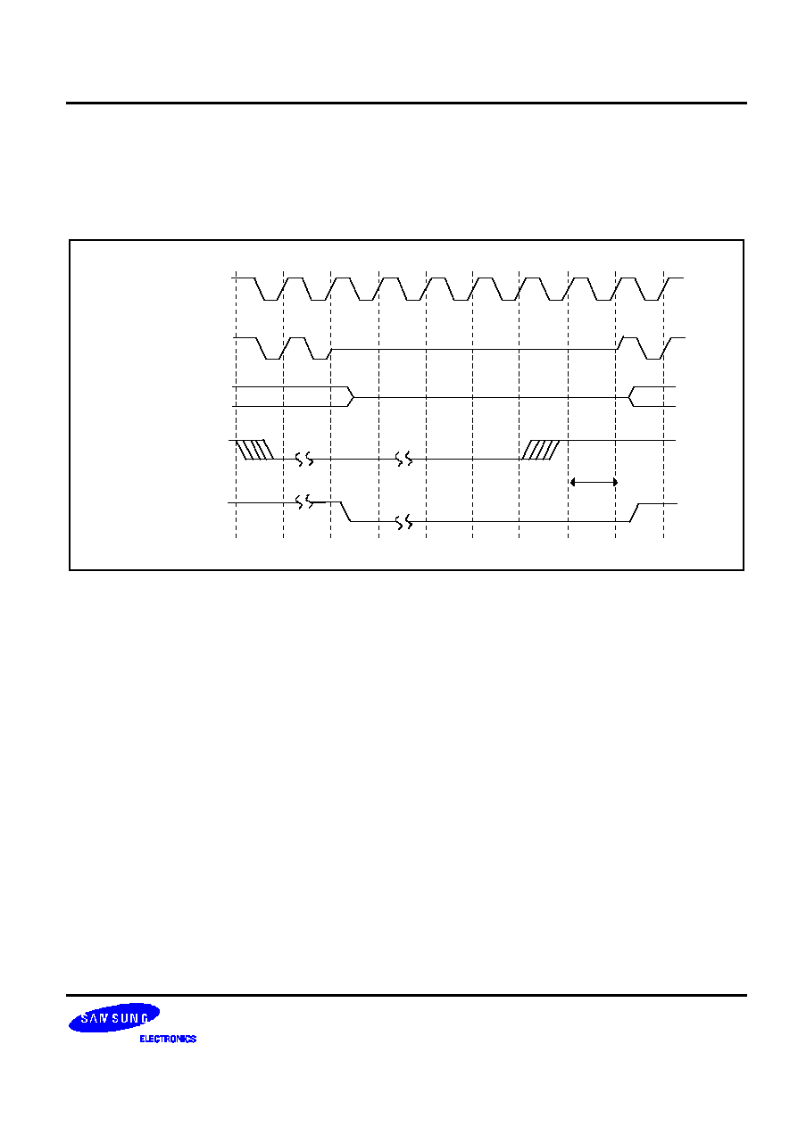
S3C2440A RISC MICROPROCESSOR
MEMORY CONTROLLER
5-7
nXBREQ/nXBACK Pin Operation
If nXBREQ is asserted, the S3C2440A will respond by lowering nXBACK. If nXBACK=L, the address/data bus and
memory control signals are in Hi-Z state as shown in Table 1-1. After nXBREQ is de-asserted, the nXBACK will also
be de-asserted.
HCLK
SCKE, A[24:0]
D[31:0], nGCS
nOE,nWE
nWBE
nXBREQ
nXBACK
SCLK
1clk
Figure 5-3. S3C2440A nXBREQ/nXBACK Timing Diagram
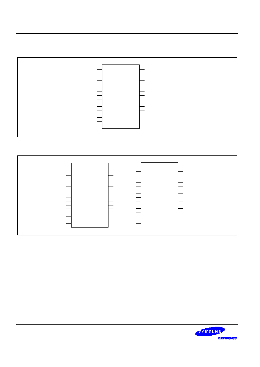
MEMORY CONTROLLER
S3C2440A RISC MICROPROCESSOR
5-8
ROM Memory Interface Examples
A0
A1
A2
A3
A4
A5
A6
A7
A8
A9
A10
A11
A12
A13
A14
A15
D0
D1
D2
D3
D4
D5
D6
D7
nWE
nOE
nGCSn
A0
A1
A2
A3
A4
A5
A6
A7
A8
A9
A10
A11
A12
A13
A14
A15
DQ0
DQ1
DQ2
DQ3
DQ4
DQ5
DQ6
DQ7
nWE
nOE
nCE
Figure 5-4. Memory Interface with 8-bit ROM
A1
A2
A3
A4
A5
A6
A7
A8
A9
A10
A11
A12
A13
A14
A15
A16
D0
D1
D2
D3
D4
D5
D6
D7
nWBE0
nOE
nGCSn
A0
A1
A2
A3
A4
A5
A6
A7
A8
A9
A10
A11
A12
A13
A14
A15
DQ0
DQ1
DQ2
DQ3
DQ4
DQ5
DQ6
DQ7
nWE
nOE
nCE
A1
A2
A3
A4
A5
A6
A7
A8
A9
A10
A11
A12
A13
A14
A15
A16
D8
D9
D10
D11
D12
D13
D14
D15
nWBE1
nOE
nGCSn
A0
A1
A2
A3
A4
A5
A6
A7
A8
A9
A10
A11
A12
A13
A14
A15
DQ0
DQ1
DQ2
DQ3
DQ4
DQ5
DQ6
DQ7
nWE
nOE
nCE
Figure 5-5. Memory Interface with 8-bit ROM x 2
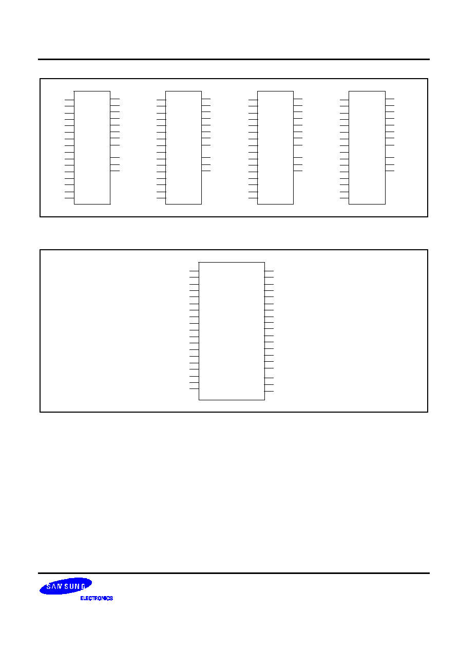
S3C2440A RISC MICROPROCESSOR
MEMORY CONTROLLER
5-9
A2
A3
A4
A5
A6
A7
A8
A9
A10
A11
A12
A13
A14
A15
A16
A17
A0
A1
A2
A3
A4
A5
A6
A7
A8
A9
A10
A11
A12
A13
A14
A15
DQ0
DQ1
DQ2
DQ3
DQ4
DQ5
DQ6
DQ7
nWE
nOE
nCE
D0
D1
D2
D3
D4
D5
D6
D7
nWBE0
nOE
nGCSn
A2
A3
A4
A5
A6
A7
A8
A9
A10
A11
A12
A13
A14
A15
A16
A17
A0
A1
A2
A3
A4
A5
A6
A7
A8
A9
A10
A11
A12
A13
A14
A15
DQ0
DQ1
DQ2
DQ3
DQ4
DQ5
DQ6
DQ7
nWE
nOE
nCE
D8
D9
D10
D11
D12
D13
D14
D15
nWBE1
nOE
nGCSn
A2
A3
A4
A5
A6
A7
A8
A9
A10
A11
A12
A13
A14
A15
A16
A17
A0
A1
A2
A3
A4
A5
A6
A7
A8
A9
A10
A11
A12
A13
A14
A15
DQ0
DQ1
DQ2
DQ3
DQ4
DQ5
DQ6
DQ7
nWE
nOE
nCE
D16
D17
D18
D19
D20
D21
D22
D23
nWBE2
nOE
nGCSn
A2
A3
A4
A5
A6
A7
A8
A9
A10
A11
A12
A13
A14
A15
A16
A17
A0
A1
A2
A3
A4
A5
A6
A7
A8
A9
A10
A11
A12
A13
A14
A15
DQ0
DQ1
DQ2
DQ3
DQ4
DQ5
DQ6
DQ7
nWE
nOE
nCE
D24
D25
D26
D27
D28
D29
D30
D31
nWBE3
nOE
nGCSn
Figure 5-6. Memory Interface with 8-bit ROM x 4
A1
A2
A3
A4
A5
A6
A7
A8
A9
A10
A11
A12
A13
A14
A15
A16
A17
A18
A19
D0
D1
D2
D3
D4
D5
D6
D7
D8
D9
D10
D11
D12
D13
D14
D15
A0
A1
A2
A3
A4
A5
A6
A7
A8
A9
A10
A11
A12
A13
A14
A15
A16
A17
A18
DQ0
DQ1
DQ2
DQ3
DQ4
DQ5
DQ6
DQ7
DQ8
DQ9
DQ10
DQ11
DQ12
DQ13
DQ14
DQ15
nWE
nOE
nCE
nWE
nOE
nGCSn
Figure 5-7. Memory Interface with 16-bit ROM
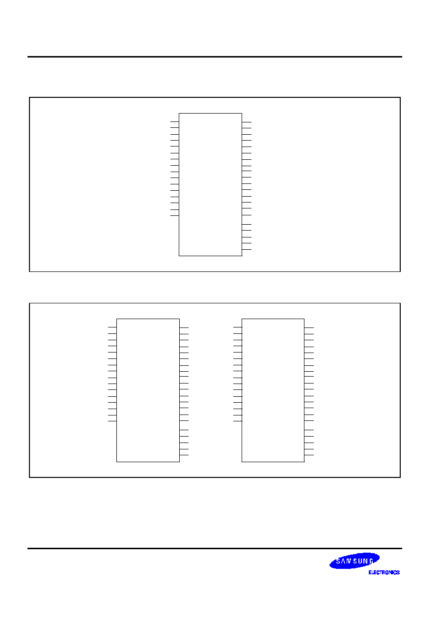
MEMORY CONTROLLER
S3C2440A RISC MICROPROCESSOR
5-10
SRAM Memory Interface Examples
A1
A2
A3
A4
A5
A6
A7
A8
A9
A10
A11
A12
A13
A14
A15
A16
D0
D1
D2
D3
D4
D5
D6
D7
D8
D9
D10
D11
D12
D13
D14
D15
A0
A1
A2
A3
A4
A5
A6
A7
A8
A9
A10
A11
A12
A13
A14
A15
DQ0
DQ1
DQ2
DQ3
DQ4
DQ5
DQ6
DQ7
DQ8
DQ9
DQ10
DQ11
DQ12
DQ13
DQ14
DQ15
nWE
nOE
nCS
nWE
nOE
nGCSn
nUB
nLB
nBE1
nBE0
Figure 5-8. Memory Interface with 16-bit SRAM
A2
A3
A4
A5
A6
A7
A8
A9
A10
A11
A12
A13
A14
A15
A16
A17
D0
D1
D2
D3
D4
D5
D6
D7
D8
D9
D10
D11
D12
D13
D14
D15
A0
A1
A2
A3
A4
A5
A6
A7
A8
A9
A10
A11
A12
A13
A14
A15
DQ0
DQ1
DQ2
DQ3
DQ4
DQ5
DQ6
DQ7
DQ8
DQ9
DQ10
DQ11
DQ12
DQ13
DQ14
DQ15
nWE
nOE
nCS
nWE
nOE
nGCSn
nUB
nLB
nBE1
nBE0
A2
A3
A4
A5
A6
A7
A8
A9
A10
A11
A12
A13
A14
A15
A16
A17
D16
D17
D18
D19
D20
D21
D22
D13
D24
D25
D26
D27
D28
D29
D30
D31
A0
A1
A2
A3
A4
A5
A6
A7
A8
A9
A10
A11
A12
A13
A14
A15
DQ0
DQ1
DQ2
DQ3
DQ4
DQ5
DQ6
DQ7
DQ8
DQ9
DQ10
DQ11
DQ12
DQ13
DQ14
DQ15
nWE
nOE
nCS
nWE
nOE
nGCSn
nUB
nLB
nBE3
nBE2
Figure 5-9. Memory Interface with 16-bit SRAM x 2
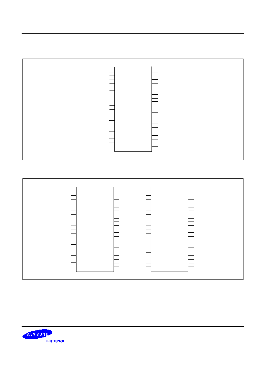
S3C2440A RISC MICROPROCESSOR
MEMORY CONTROLLER
5-11
SDRAM Memory Interface Examples
A1
A2
A3
A4
A5
A6
A7
A8
A9
A10
A11
A12
D0
D1
D2
D3
D4
D5
D6
D7
D8
D9
D10
D11
D12
D13
D14
D15
A0
A1
A2
A3
A4
A5
A6
A7
A8
A9
A10
A11
DQ0
DQ1
DQ2
DQ3
DQ4
DQ5
DQ6
DQ7
DQ8
DQ9
DQ10
DQ11
DQ12
DQ13
DQ14
DQ15
BA0
BA1
LDQM
UDQM
A21
A22
DQM0
DQM1
SCKE
SCLK
SCKE
SCLK
nSCS0
nSRAS
nSCAS
nWE
nSCS
nSRAS
nSCAS
nWE
Figure 5-10. Memory Interface with 16-bit SDRAM (4Mx16, 4banks)
A2
A3
A4
A5
A6
A7
A8
A9
A10
A11
A12
A13
A14
D0
D1
D2
D3
D4
D5
D6
D7
D8
D9
D10
D11
D12
D13
D14
D15
A0
A1
A2
A3
A4
A5
A6
A7
A8
A9
A10
A11
A12
DQ0
DQ1
DQ2
DQ3
DQ4
DQ5
DQ6
DQ7
DQ8
DQ9
DQ10
DQ11
DQ12
DQ13
DQ14
DQ15
BA0
BA1
LDQM
UDQM
A24
A25
DQM0
DQM1
SCKE
SCLK
SCKE
SCLK
nSCS0
nSRAS
nSCAS
nWE
nSCS
nSRAS
nSCAS
nWE
A2
A3
A4
A5
A6
A7
A8
A9
A10
A11
A12
A13
A14
A0
A1
A2
A3
A4
A5
A6
A7
A8
A9
A10
A11
A12
DQ0
DQ1
DQ2
DQ3
DQ4
DQ5
DQ6
DQ7
DQ8
DQ9
DQ10
DQ11
DQ12
DQ13
DQ14
DQ15
BA0
BA1
LDQM
UDQM
A24
A25
DQM2
DQM3
SCKE
SCLK
SCKE
SCLK
nSCS0
nSRAS
nSCAS
nWE
nSCS
nSRAS
nSCAS
nWE
D16
D17
D18
D19
D20
D21
D22
D23
D24
D25
D26
D27
D28
D29
D30
D31
Figure 5-11. Memory Interface with 16-bit SDRAM (4Mx16x4Bank * 2ea)
NOTE
Refer to Table 5-2 for the Bank Address configurations of SDRAM.
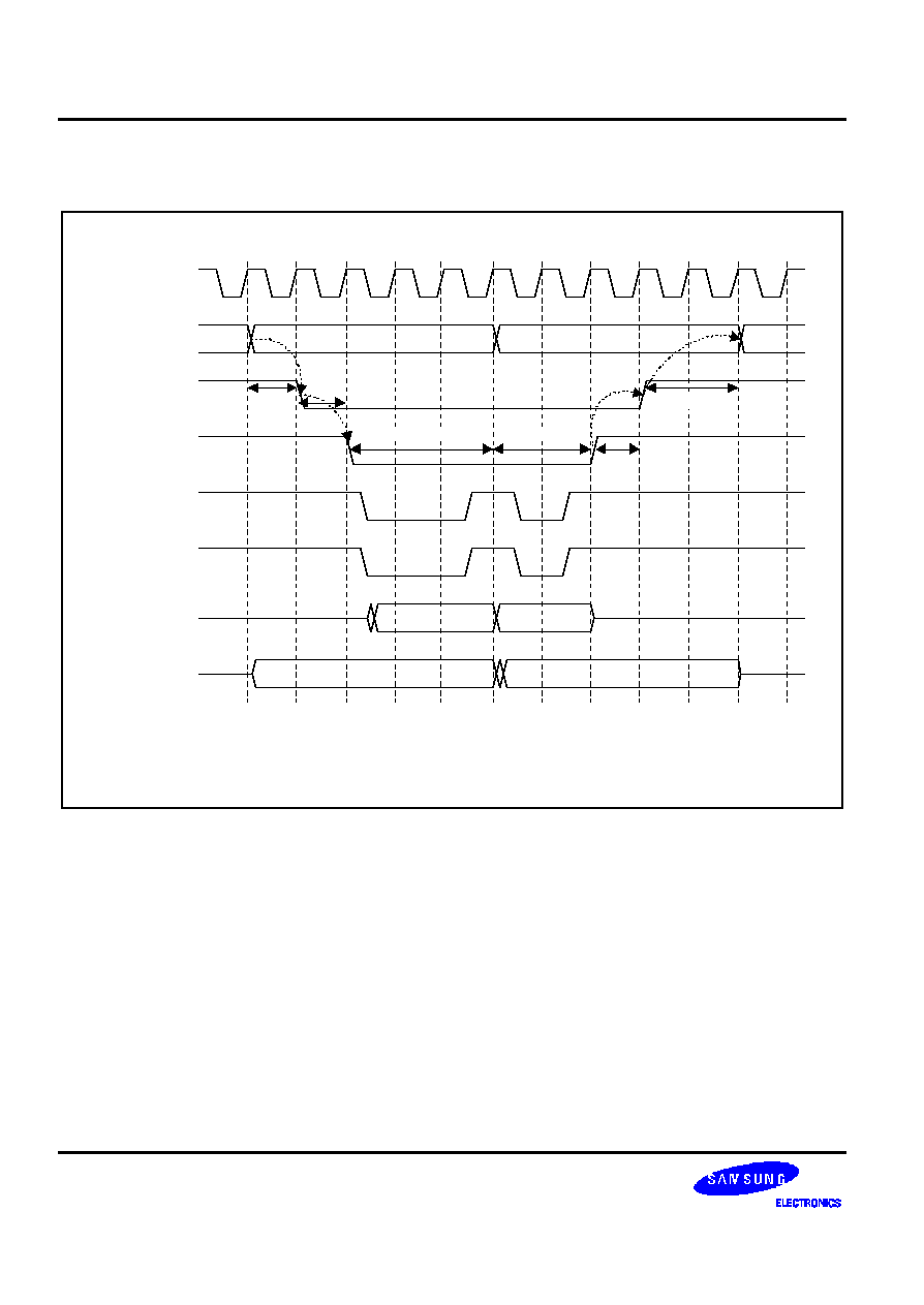
MEMORY CONTROLLER
S3C2440A RISC MICROPROCESSOR
5-12
PROGRAMMABLE ACCESS CYCLE
Tcoh
Tcos
Tacs
HCLK
A[24:0]
nGCS
nOE
nWE
nWBE
D[31:0](R)
D[31:0] (W)
Tacc
Tacp
Tcah
Tacs = 1 cycle
Tcos = 1 cycle
Tacc = 3 cycles
Tacp = 2 cycles
Tcoh = 1 cycle
Tcah = 2 cycles
Figure 5-12. S3C2440A nGCS Timing Diagram
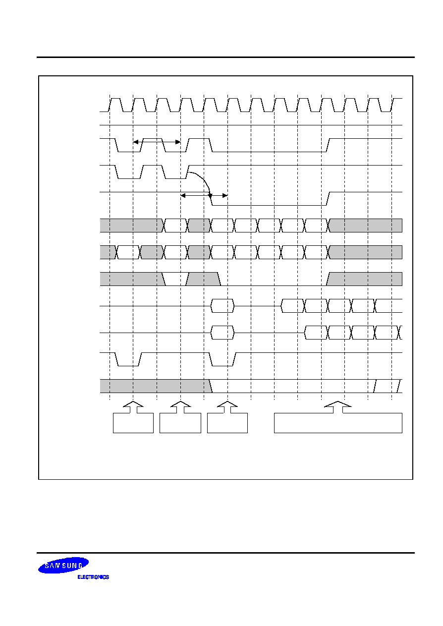
S3C2440A RISC MICROPROCESSOR
MEMORY CONTROLLER
5-13
MCLK
SCKE
nSCS
nSCAS
ADDR
A10/AP
RA
nSRAS
BA
DATA (CL2)
DATA (CL3)
nWE
DQM
Trp
Trcd
RA
Ca
Da
Da
BA
BA
Cb
Cc
Cd
Ce
Db
Dc
Dd
De
Db
Dc
Dd
De
BA
BA
BA
BA
BA
Bank
Precharge
Row
Active
Write
Read (CL = 2, CL = 3, BL = 1)
Trp = 2 cycle
Tcas = 2 cycle
Trcd = 2 cycle
Tcp = 2 cycle
Figure 5-13. S3C2440A SDRAM Timing Diagram

MEMORY CONTROLLER
S3C2440A RISC MICROPROCESSOR
5-14
BUS WIDTH & WAIT CONTROL REGISTER (BWSCON)
Register
Address
R/W
Description
Reset Value
BWSCON
0x48000000
R/W
Bus width & wait status control register
0x000000
BWSCON
Bit
Description
Initial state
ST7
[31]
Determines SRAM for using UB/LB for bank 7.
0 = Not using UB/LB (The pins are dedicated nWBE[3:0])
1 = Using UB/LB (The pins are dedicated nBE[3:0])
0
WS7
[30]
Determines WAIT status for bank 7.
0 = WAIT disable 1 = WAIT enable
0
DW7
[29:28]
Determines data bus width for bank 7.
00 = 8-bit 01 = 16-bit, 10 = 32-bit 11 = reserved
0
ST6
[27]
Determines SRAM for using UB/LB for bank 6.
0 = Not using UB/LB (The pins are dedicated nWBE[3:0 )
1 = Using UB/LB (The pins are dedicated nBE[3:0])
0
WS6
[26]
Determines WAIT status for bank 6.
0 = WAIT disable, 1 = WAIT enable
0
DW6
[25:24]
Determines data bus width for bank 6.
00 = 8-bit 01 = 16-bit, 10 = 32-bit 11 = reserved
0
ST5
[23]
Determines SRAM for using UB/LB for bank 5.
0 = Not using UB/LB (The pins are dedicated nWBE[3:0])
1 = Using UB/LB (The pins are dedicated nBE[3:0])
0
WS5
[22]
Determines WAIT status for bank 5.
0 = WAIT disable, 1 = WAIT enable
0
DW5
[21:20]
Determines data bus width for bank 5.
00 = 8-bit 01 = 16-bit, 10 = 32-bit 11 = reserved
0
ST4
[19]
Determines SRAM for using UB/LB for bank 4.
0 = Not using UB/LB (The pins are dedicated nWBE[3:0])
1 = Using UB/LB (The pins are dedicated nBE[3:0])
0
WS4
[18]
Determines WAIT status for bank 4.
0 = WAIT disable 1 = WAIT enable
0
DW4
[17:16]
Determine data bus width for bank 4.
00 = 8-bit 01 = 16-bit, 10 = 32-bit 11 = reserved
0
ST3
[15]
Determines SRAM for using UB/LB for bank 3.
0 = Not using UB/LB (The pins are dedicated nWBE[3:0])
1 = Using UB/LB (The pins are dedicated nBE[3:0])
0
WS3
[14]
Determines WAIT status for bank 3.
0 = WAIT disable 1 = WAIT enable
0
DW3
[13:12]
Determines data bus width for bank 3.
00 = 8-bit 01 = 16-bit, 10 = 32-bit 11 = reserved
0
ST2
[11]
Determines SRAM for using UB/LB for bank 2.
0 = Not using UB/LB (The pins are dedicated nWBE[3:0])
1 = Using UB/LB (The pins are dedicated nBE[3:0].)
0
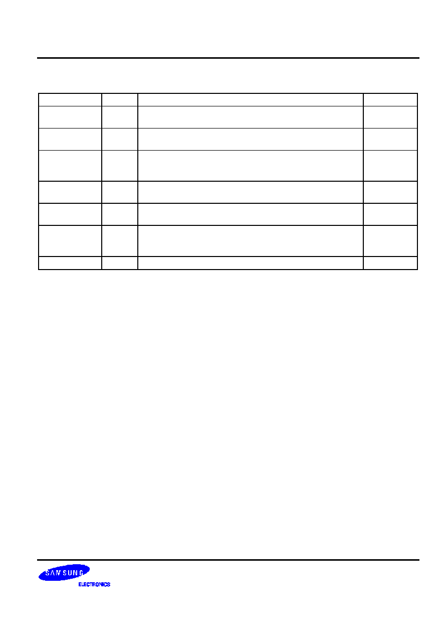
S3C2440A RISC MICROPROCESSOR
MEMORY CONTROLLER
5-15
BUS WIDTH & WAIT CONTROL REGISTER (BWSCON) (Continued)
BWSCON
Bit
Description
Initial state
WS2
[10]
Determines WAIT status for bank 2.
0 = WAIT disable 1 = WAIT enable
0
DW2
[9:8]
Determines data bus width for bank 2.
00 = 8-bit 01 = 16-bit, 10 = 32-bit 11 = reserved
0
ST1
[7]
Determines SRAM for using UB/LB for bank 1.
0 = Not using UB/LB (The pins are dedicated nWBE[3:0])
1 = Using UB/LB (The pins are dedicated nBE[3:0])
0
WS1
[6]
Determines WAIT status for bank 1.
0 = WAIT disable, 1 = WAIT enable
0
DW1
[5:4]
Determines data bus width for bank 1.
00 = 8-bit 01 = 16-bit, 10 = 32-bit 11 = reserved
0
DW0
[2:1]
Indicate data bus width for bank 0 (read only).
01 = 16-bit, 10 = 32-bit
The states are selected by OM[1:0] pins
≠
Reserved
[0]
Reserve to 0
0
NOTES:
1.
All types of master clock in this memory controller correspond to the bus clock.
For example, HCLK in SRAM is the same as the bus clock, and SCLK in SDRAM is also the same as the bus clock.
In this chapter (Memory Controller), one clock means one bus clock.
2.
nBE[3:0] is the 'AND' signal nWBE[3:0] and nOE.
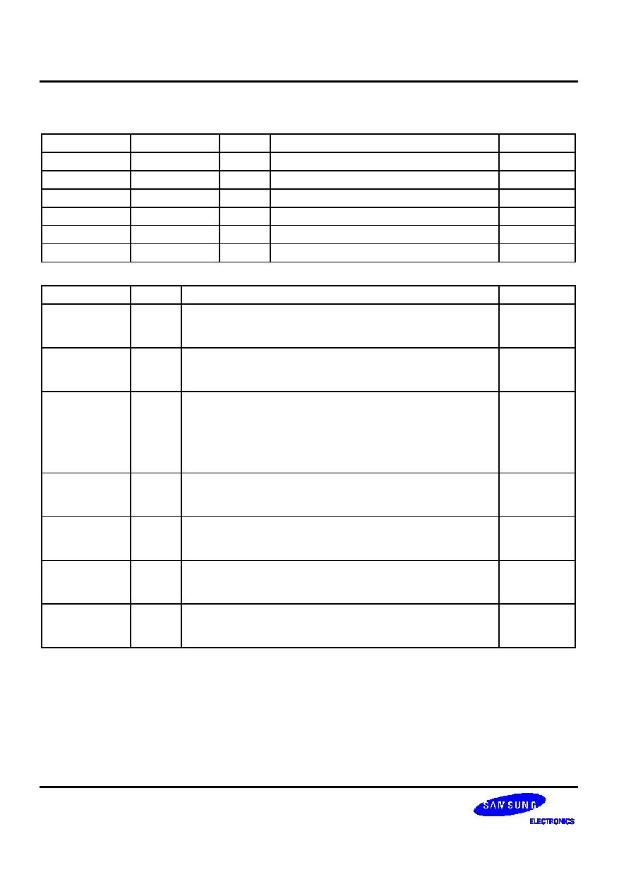
MEMORY CONTROLLER
S3C2440A RISC MICROPROCESSOR
5-16
BANK CONTROL REGISTER (BANKCONN: NGCS0-NGCS5)
Register
Address
R/W
Description
Reset Value
BANKCON0
0x48000004
R/W
Bank 0 control register
0x0700
BANKCON1
0x48000008
R/W
Bank 1 control register
0x0700
BANKCON2
0x4800000C
R/W
Bank 2 control register
0x0700
BANKCON3
0x48000010
R/W
Bank 3 control register
0x0700
BANKCON4
0x48000014
R/W
Bank 4 control register
0x0700
BANKCON5
0x48000018
R/W
Bank 5 control register
0x0700
BANKCONn
Bit
Description
Initial State
Tacs
[14:13]
Address set-up time before nGCSn
00 = 0 clock 01 = 1 clock
10 = 2 clocks 11 = 4 clocks
00
Tcos
[12:11]
Chip selection set-up time before nOE
00 = 0 clock 01 = 1 clock
10 = 2 clocks 11 = 4 clocks
00
Tacc
[10:8]
Access cycle
000 = 1 clock
001 = 2 clocks
010 = 3 clocks
011 = 4 clocks
100 = 6 clocks
101 = 8 clocks
110 = 10 clocks
111 = 14 clocks
Note: When nWAIT signal is used, Tacc
4 clocks.
111
Tcoh
[7:6]
Chip selection hold time after nOE
00 = 0 clock 01 = 1 clock
10 = 2 clocks 11 = 4 clocks
000
Tcah
[5:4]
Address hold time after nGCSn
00 = 0 clock 01 = 1 clock
10 = 2 clocks 11 = 4 clocks
00
Tacp
[3:2]
Page mode access cycle @ Page mode
00 = 2 clocks 01 = 3 clocks
10 = 4 clocks 11 = 6 clocks
00
PMC
[1:0]
Page mode configuration
00 = normal (1 data) 01 = 4 data
10 = 8 data 11 = 16 data
00
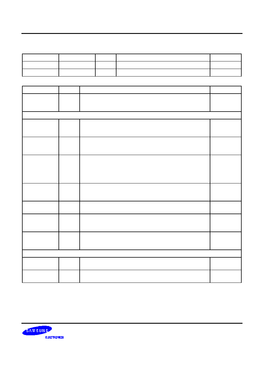
S3C2440A RISC MICROPROCESSOR
MEMORY CONTROLLER
5-17
BANK CONTROL REGISTER (BANKCONn: nGCS6-nGCS7)
Register
Address
R/W
Description
Reset Value
BANKCON6
0x4800001C
R/W
Bank 6 control register
0x18008
BANKCON7
0x48000020
R/W
Bank 7 control register
0x18008
BANKCONn
Bit
Description
Initial State
MT
[16:15]
Determine the memory type for bank6 and bank7.
00 = ROM or SRAM
01 = Reserved (Do not use)
10 = Reserved (Do not use)
11 = Sync. DRAM
11
Memory Type = ROM or SRAM [MT=00] (15-bit)
Tacs
[14:13]
Address set-up time before nGCS
00 = 0 clock 01 = 1 clock 10 = 2 clocks
11 = 4
clocks
00
Tcos
[12:11]
Chip selection set-up time before nOE
00 = 0 clock 01 = 1 clock 10 = 2 clocks
11 = 4
clocks
00
Tacc
[10:8]
Access cycle
000 = 1 clock 001 = 2 clocks
010 = 3 clocks 011 = 4 clocks
100 = 6 clocks 101 = 8 clocks
110 = 10 clocks 111 = 14 clocks
111
Tcoh
[7:6]
Chip selection hold time after nOE
00 = 0 clock 01 = 1 clock
10 = 2 clocks
11 = 4 clocks
00
Tcah
[5:4]
Address hold time after nGCSn
00 = 0 clock 01 = 1clock 10 = 2 clocks 11 = 4 clocks
00
Tacp
[3:2]
Page mode access cycle @ Page mode
00 = 2 clocks 01 = 3 clocks
10 = 4 clocks 11 = 6 clocks
00
PMC
[1:0]
Page mode configuration
00 = normal (1 data)
01 = 4 consecutive accesses
10 = 8 consecutive accesses
11 = 16 consecutive accesses
00
Memory Type = SDRAM [MT=11] (4-bit)
Trcd
[3:2]
RAS to CAS delay
00 = 2 clocks 01 = 3 clocks 10 = 4 clocks
10
SCAN
[1:0]
Column address number
00 = 8-bit 01 = 9-bit 10= 10-bit
00

MEMORY CONTROLLER
S3C2440A RISC MICROPROCESSOR
5-18
REFRESH CONTROL REGISTER
Register
Address
R/W
Description
Reset Value
REFRESH
0x48000024
R/W
SDRAM refresh control register
0xac0000
REFRESH
Bit
Description
Initial State
REFEN
[23]
SDRAM Refresh Enable
0 = Disable 1 = Enable (self or CBR/auto refresh)
1
TREFMD
[22]
SDRAM Refresh Mode
0 = CBR/Auto Refresh 1 = Self Refresh
In self-refresh time, the SDRAM control signals are driven to the
appropriate level.
0
Trp
[21:20]
SDRAM RAS pre-charge Time
00 = 2 clocks 01 = 3 clocks 10 = 4 clocks 11 = Not
support
10
Tsrc
[19:18]
SDRAM Semi Row cycle time
00 = 4 clocks 01 = 5 clocks 10 = 6 clocks 11 = 7 clocks
SDRAM Row cycle time: Trc=Tsrc+Trp
If Trp = 3clocks & Tsrc = 7clocks, Trc = 3+7=10clocks.
11
Reserved
[17:16]
Not used
00
Reserved
[15:11]
Not used
0000
Refresh Counter
[10:0]
SDRAM refresh count value. Refer to chapter 6 SDRAM refresh
controller bus priority section.
Refresh period = (2
11
-refresh_count+1)/HCLK
Ex) If refresh period is 7.8 us and HCLK is 100MHz,
the refresh count is as follows:
Refresh count = 2
11
+ 1 - 100x7.8 = 1269
0
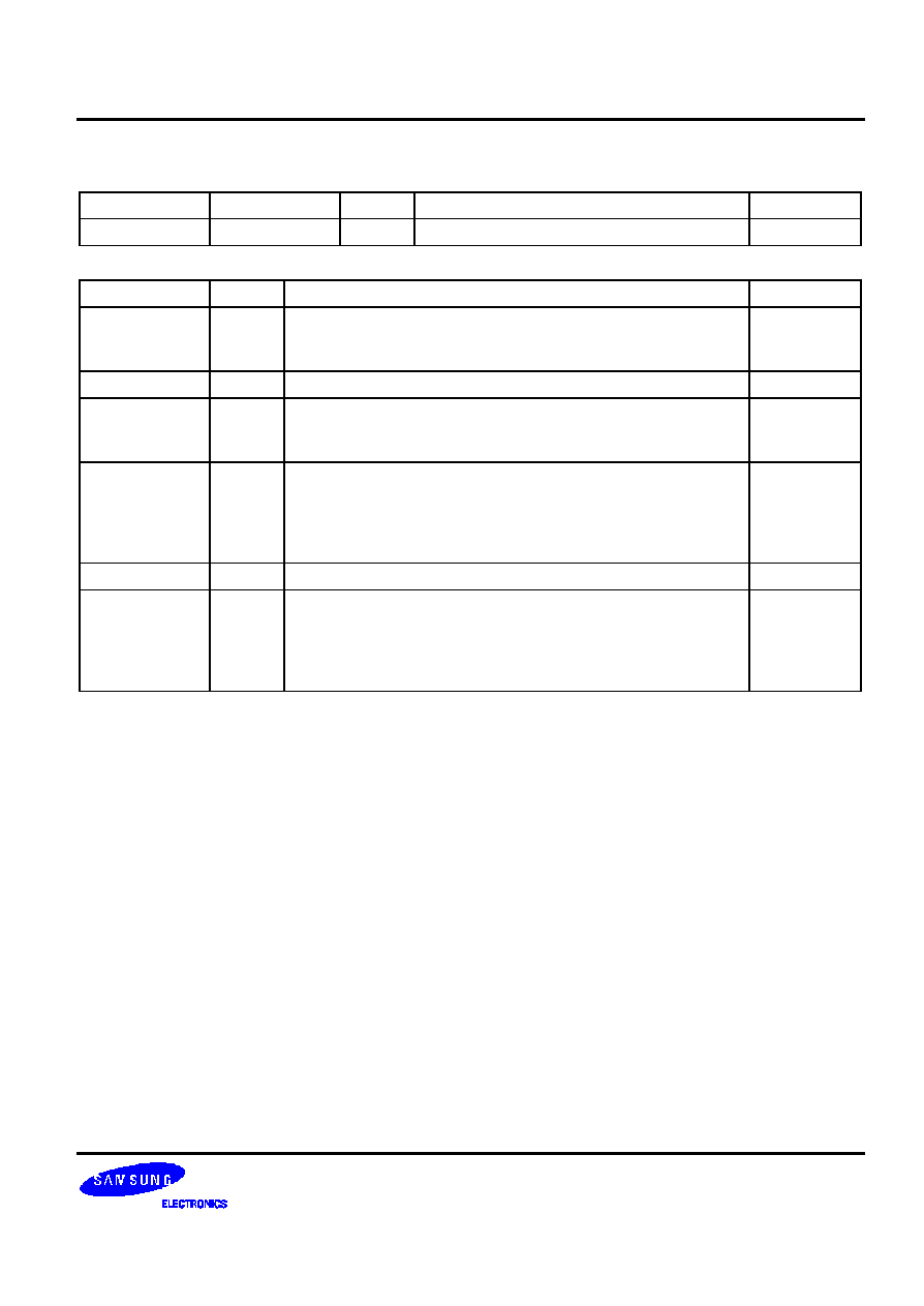
S3C2440A RISC MICROPROCESSOR
MEMORY CONTROLLER
5-19
BANKSIZE REGISTER
Register
Address
R/W
Description
Reset Value
BANKSIZE
0x48000028
R/W
Flexible bank size register
0x0
BANKSIZE
Bit
Description
Initial State
BURST_EN
[7]
ARM core burst operation enable.
0 = Disable burst operation.
1 = Enable burst operation.
0
Reserved
[6]
Not used
0
SCKE_EN
[5]
SDRAM power down mode enable control by SCKE
0 = SDRAM power down mode disable
1 = SDRAM power down mode enable
0
SCLK_EN
[4]
SCLK is enabled only during SDRAM access cycle for reducing
power consumption. When SDRAM is not accessed, SCLK
becomes 'L' level.
0 = SCLK is always active.
1 = SCLK is active only during the access (recommended).
0
Reserved
[3]
Not used
0
BK76MAP
[2:0]
BANK6/7 memory map
010 = 128MB/128MB
001 = 64MB/64MB
000 = 32M/32M
111 = 16M/16M
110 = 8M/8M
101 = 4M/4M
100 = 2M/2M
010

MEMORY CONTROLLER
S3C2440A RISC MICROPROCESSOR
5-20
SDRAM MODE REGISTER SET REGISTER (MRSR)
Register
Address
R/W
Description
Reset Value
MRSRB6
0x4800002C
R/W
Mode register set register bank6
xxx
MRSRB7
0x48000030
R/W
Mode register set register bank7
xxx
MRSR
Bit
Description
Initial State
Reserved
[11:10]
Not used
≠
WBL
[9]
Write burst length
0: Burst (Fixed)
1: Reserved
x
TM
[8:7]
Test mode
00: Mode register set (Fixed)
01, 10 and 11: Reserved
xx
CL
[6:4]
CAS latency
000 = 1 clock, 010 = 2 clocks, 011=3 clocks
Others: reserved
xxx
BT
[3]
Burst type
0: Sequential (Fixed)
1: Reserved
x
BL
[2:0]
Burst length
000: 1 (Fixed)
Others: Reserved
xxx
NOTE: MRSR register must not be reconfigured while the code is running on SDRAM.
IMPORTANT NOTE: In sleep mode, sdram has to enter sdram self-refresh mode.

S3C2440A RISC MICROPROCESSOR NAND FLASH CONTROLLER
6-1
6
NAND FLASH CONTORLLER
OVERVIEW
In recent times, NOR flash memory gets high in price while an SDRAM and a NAND flash memory is comparatively
economical , motivating some users to execute the boot code on a NAND flash and execute the main code on an
SDRAM.
S3C2440A boot code can be executed on an external NAND flash memory. In order to support NAND flash boot
loader, the S3C2440A is equipped with an internal SRAM buffer called `Steppingstone'. When booting, the first 4
KBytes of the NAND flash memory will be loaded into Steppingstone and the boot code loaded into Steppingstone
will be executed.
Generally, the boot code will copy NAND flash content to SDRAM. Using hardware ECC, the NAND flash data
validity will be checked. Upon the completion of the copy, the main program will be executed on the SDRAM.
FEATURES
1. Auto boot: The boot code is transferred into 4-kbytes Steppingstone during reset. After the transfer, the boot
code will be executed on the Steppingstone.
2. NAND Flash memory I/F: Support 256Words, 512Bytes, 1KWords and 2KBytes Page.
3. Software mode: User can directly access NAND flash memory, for example this feature can be used in
read/erase/program NAND flash memory.
4. Interface: 8 / 16-bit NAND flash memory interface bus.
5. Hardware ECC generation, detection and indication (Software correction).
6. SFR I/F: Support Little Endian Mode, Byte/half word/word access to Data and ECC Data register, and Word
access to other registers
7. SteppingStone I/F: Support Little/Big Endian, Byte/half word/word access.
8. The Steppingstone 4-KB internal SRAM buffer can be used for another purpose after NAND flash booting.
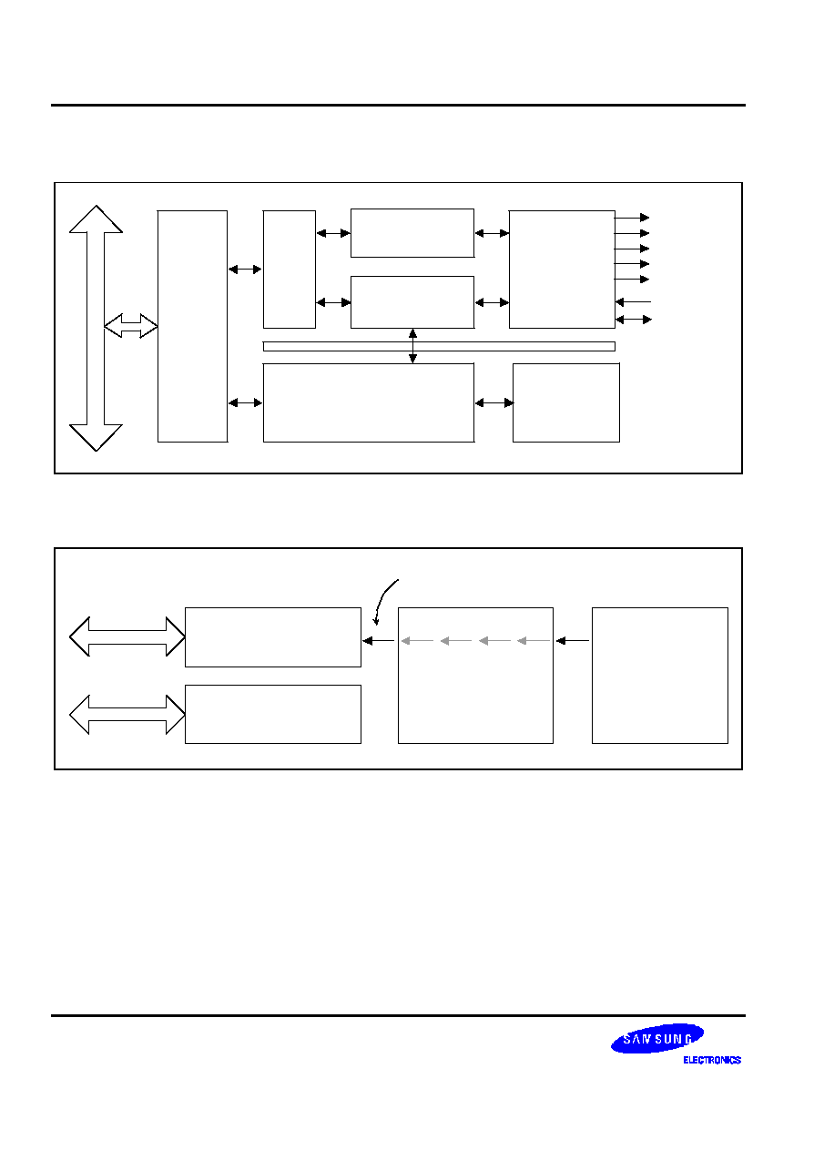
NAND FLASH CONTROLLER
S3C2440A RISC MICROPROCESSOR
6-2
BLOCK DIAGRAM
SFR
ECC
Gen.
Stepping Stone
(4KB SRAM)
Stepping Stone Controller
S
Y
S
T
E
M
B
U
S
NAND FLASH
Interface
CLE
ALE
nFCE
nFRE
nFWE
FRnB
I/O0 - I/O15
AHB
Slave I/F
Control &
State Machine
Figure 6-1. NAND Flash Controller Block Diagram
BOOT LOADER FUNCTION
Stepping Stone
(4KB Buffer)
NAND FLASH
Controller
NAND FLASH
Memory
Special Function
Registers
REGISTERS
AUTO BOOT
CORE ACCESS
(Boot Code)
USER ACCESS
Figure 6-2. NAND Flash Controller Boot Loader Block Diagram
During reset, Nand flash controller will get information about the connected NAND flash through Pin status
(NCON(Adv flash), GPG13(Page size), GPG14(Address cycle), GPG15(Bus width) ≠ refer to PIN
CONFIGURATION), After power-on or system reset is occurred, the NAND Flash controller load automatically the 4-
KBytes boot loader codes. After loading the boot loader codes, the boot loader code in steppingstone is executed.
NOTE
During the auto boot, the ECC is not checked. So, the first 4-KB of NAND flash should have no bit error.
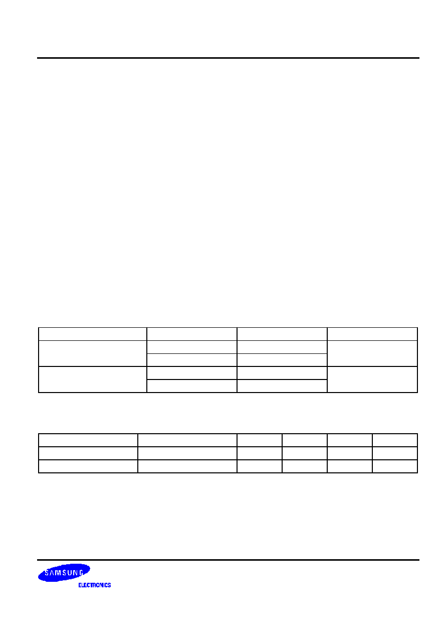
S3C2440A RISC MICROPROCESSOR NAND FLASH CONTROLLER
6-3
PIN CONFIGURATION
OM[1:0] = 00: Enable NAND flash memory boot
NCON: NAND flash memory selection(Normal / Advance)
0: Normal NAND flash(256Words/512Bytes page size, 3/4 address cycle)
1: Advance NAND flash(1KWords/2KBytes page size, 4/5 address cycle)
GPG13: NAND flash memory page capacitance selection
0: Page=256Words(NCON = 0) or Page=1KWords(NCON = 1)
1: Page=512Bytes(NCON = 0) or Page=2KBytes(NCON = 1)
GPG14: NAND flash memory address cycle selection
0: 3 address cycle(NCON = 0) or 4 address cycle(NCON = 1)
1: 4 address cycle(NCON = 0) or 5 address cycle(NCON = 1)
GPG15: NAND flash memory bus width selection
0: 8-bit bus width
1: 16-bit bus width
NOTE
The configuration pin ≠ NCON, GPG[15:13] ≠ will be fetched during reset.
In normal status, these pins must be set as input so that the pin status is not to be changed, when enters
Sleep mode by software or unexpected cause.
NAND FLASH MEMORY CONFIGURATION TABLE
NCON0
GPG13
GPG14
GPG15
0: Normal NAND
0: 256Words
0: 3-Addr
0: 8-bit bus width
1: 512Bytes
1: 4-Addr
1: Advance NAND
0: 1Kwords
0: 4-Addr
1: 16-bit bus width
1: 2Kbytes
1: 5-Addr
NOTE: With above 4-bit, Possible total combinations are 16, but not all the value can be used.
Example) Nand flash configuration setting.
Parts
Page size/Total size
NCON0
GPG13
GPG14]
GPG15
K9S1208V0M-xxxx
512Byte / 512Mbit
0
1
1
0
K9K2G16U0M-xxxx
1KW / 2Gbit
1
0
1
1
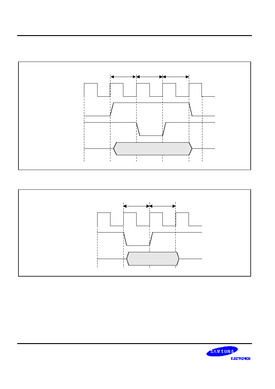
NAND FLASH CONTROLLER
S3C2440A RISC MICROPROCESSOR
6-4
NAND FLASH MEMORY TIMING
HCLK
CLE / ALE
nWE
TACLS
TWRPH0
TWRPH1
DATA
COMMAND / ADDRESS
Figure 6-3. CLE & ALE Timing (TACLS=1, TWRPH0=0, TWRPH1=0)
HCLK
nWE / nRE
DATA
DATA
TWRPH0
TWRPH1
Figure 6-4. nWE & nRE Timing (TWRPH0=0, TWRPH1=0)

S3C2440A RISC MICROPROCESSOR NAND FLASH CONTROLLER
6-5
SOFTWARE MODE
S3C2440A supports only software mode access. Using this mode, you can completely access the NAND flash
memory. The NAND Flash Controller supports direct access interface with the NAND flash memory.
1. Writing to the command register = the NAND Flash Memory command cycle
2. Writing to the address register = the NAND Flash Memory address cycle
3. Writing to the data register = write data to the NAND Flash Memory (write cycle)
4. Reading from the data register = read data from the NAND Flash Memory (read cycle)
5. Reading main ECC registers and Spare ECC registers = read data from the NAND Flash Memory
NOTE
In the software mode, you have to check the RnB status input pin by using polling or interrupt.
NAND FLASH CONTROLLER
S3C2440A RISC MICROPROCESSOR
6-6
Data Register Configuration
1. 16-bit NAND Flash Memory Interface
A. Word Access
Register
Endian
Bit [31:24]
Bit [23:16]
Bit [15:8]
Bit [7:0]
NFDATA
Little
2
nd
I/O[15:8]
2
nd
I/O[ 7:0]
1
st
I/O[15:8]
1
st
I/O[ 7:0]
NFDATA
Big
1
st
I/O[15:8]
1
st
I/O[ 7:0]
2
nd
I/O[15:8]
2
nd
I/O[ 7:0]
A. Half-word Access
Register
Endian
Bit [31:24]
Bit [23:16]
Bit [15:8]
Bit [7:0]
NFDATA
Little/Big
Invalid value
Invalid value
1
st
I/O[15:8]
1
st
I/O[ 7:0]
1. 8-bit NAND Flash Memory Interface
A. Word Access
Register
Endian
Bit [31:24]
Bit [23:16]
Bit [15:8]
Bit [7:0]
NFDATA
Little
4
th
I/O[ 7:0]
3
rd
I/O[ 7:0]
2
nd
I/O[ 7:0]
1
st
I/O[ 7:0]
NFDATA
Big
1
st
I/O[ 7:0]
2
nd
I/O[ 7:0]
3
nd
I/O[ 7:0]
4
th
I/O[ 7:0]
A. Half-word Access
Register
Endian
Bit [31:24]
Bit [23:16]
Bit [15:8]
Bit [7:0]
NFDATA
Little
Invalid value
Invalid value
2
nd
I/O[ 7:0]
1
st
I/O[ 7:0]
NFDATA
Big
Invalid value
Invalid value
1
st
I/O[ 7:0]
2
nd
I/O[ 7:0]
A. Byte Access
Register
Endian
Bit [31:24]
Bit [23:16]
Bit [15:8]
Bit [7:0]
NFDATA
Little/Big
Invalid value
Invalid value
Invalid value
1
st
I/O[ 7:0]
STEPPINGSTONE (4K-BYTE SRAM)
The NAND Flash controller uses Steppingstone as the buffer on booting and also you can use this area for another
purpose.
S3C2440A RISC MICROPROCESSOR NAND FLASH CONTROLLER
6-7
ECC (ERROR CORRECTION CODE)
NAND Flash controller consists of four ECC (Error Correction Code) modules. The two ECC modules (one for
data[7:0] and the other for data[15:8]) can be used for (up to) 2048 bytes ECC Parity code generation, and the
others(one for data[7:0] and the other for data[15:8]) can be used for (up to) 16 bytes ECC Parity code generation.
-- 28-bit ECC Parity Code = 22-bit Line parity + 6bit Column Parity
--
14-bit ECC Parity Code = 8-bit Line parity + 6bit Column Parity
2048 BYTE ECC PARITY CODE ASSIGNMENT TABLE
DATA7
DATA6
DATA5
DATA4
DATA3
DATA2
DATA1
DATA0
MECCn_0
P64
P64'
P32
P32'
P16
P16'
P8
P8'
MECCn_1
P1024
P1024'
P512
P512'
P256
P256'
P128
P128'
MECCn_2
P4
P4'
P2
P2'
P1
P1'
P2048
P2048'
MECCn_3
P8192
P8192'
P4096
P4096'
≠
≠
≠
≠
16 BYTE ECC PARITY CODE ASSIGNMENT TABLE
DATA7
DATA6
DATA5
DATA4
DATA3
DATA2
DATA1
DATA0
SECCn_0
P16
P16'
P8
P8'
P4
P4'
P2
P2'
SECCn_1
P1
P1'
P64
P64'
P32
P32'
≠
≠
NAND FLASH CONTROLLER
S3C2440A RISC MICROPROCESSOR
6-8
ECC MODULE FEATURES
ECC generation is controlled by the ECC Lock (MainECCLock, SpareECCLock) bit of the Control register.
ECC Register Configuration (Little / Big Endian)
1. 16-bit NAND Flash Memory Interface
Register
Bit [31:24]
Bit [23:16]
Bit [15:8]
Bit [7:0]
NFMECCD0
2
nd
ECC for I/O[15:8]
2
nd
ECC for I/O[7:0]
1
st
ECC for I/O[15:8]
1
st
ECC for I/O[7:0]
NFMECCD1
4
th
ECC for I/O[15:8]
4
th
ECC for I/O[7:0]
3
nd
ECC for I/O[15:8]
3
nd
ECC for I/O[7:0]
Register
Bit [31:24]
Bit [23:16]
Bit [15:8]
Bit [7:0]
NFSECCD
2
nd
ECC for I/O[15:8]
2
nd
ECC for I/O[7:0]
1
st
ECC for I/O[15:8]
1
st
ECC for I/O[7:0]
1. 8-bit NAND Flash Memory Interface
Register
Bit [31:24]
Bit [23:16]
Bit [15:8]
Bit [7:0]
NFMECCD0
≠
2
nd
ECC for I/O[7:0]
≠
1
st
ECC for I/O[7:0]
NFMECCD1
≠
4
th
ECC for I/O[7:0]
≠
3
nd
ECC for I/O[7:0]
Register
Bit [31:24]
Bit [23:16]
Bit [15:8]
Bit [7:0]
NFSECCD
≠
2
nd
ECC for I/O[7:0]
≠
1
st
ECC for I/O[7:0]
ECC PROGRAMMING GUIDE
1. In software mode, ECC module generates ECC parity code for all read / write data. So you have to reset ECC
value by writing the InitECC(NFCONT[4]) bit as `1' and have to clear theMainECCLock(NFCONT[5]) bit to
`0'(Unlock) before read or write data.
MainECCLock(NFCONT[5]) and SpareECCLock(NFCONT[6]) control whether ECC Parity code is generated or
not.
2. Whenever data is read or written, the ECC module generates ECC parity code on register NFMECC0/1.
3. After you completely read or write one page (not include spare area data), Set the MainECCLock bit to `1'(Lock).
ECC Parity code is locked and the value of the ECC status register will not be changed.
4. To generate spare area ECC parity code, Clear as `0'(Unlock) SpareECCLock(NFCONT[6]) bit.
5. Whenever data is read or written, the spare area ECC module generates ECC parity code on register NFSECC.
6. After you completely read or write spare area, Set the SpareECCLock bit to `1'(Lock). ECC Parity code is locked
and the value of the ECC status register will not be changed.
7. Once completed you can use these values to record to the spare area or check the bit error.
NOTE
NFSECCD is for ECC in the spare area (Usually, the user will write the ECC value of main data area to
Spare area, which value will be the same as NFMECC0/1) and which is generated from the main data area.
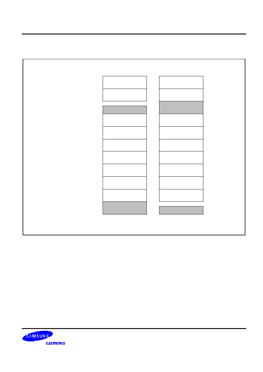
S3C2440A RISC MICROPROCESSOR NAND FLASH CONTROLLER
6-9
NAND FLASH MEMORY MAPPING
Not Used
SFR Area
Not Used
BootSRAM (4KB)
0xFFFF_FFFF
0x6000_0000
0x4800_0000
0x4000_0000
SFR Area
Not Used
SDRAM
(BANK7, nGCS7)
0x3800_0000
SDRAM
(BANK7, nGCS7)
SDRAM
(BANK6, nGCS6)
0x3000_0000
SDRAM
(BANK6, nGCS6)
SROM
(BANK5, nGCS5)
SROM
(BANK5, nGCS5)
0x2000_0000
0x2800_0000
SROM
(BANK4, nGCS4)
SROM
(BANK3, nGCS3)
SROM
(BANK2, nGCS2)
0x1000_0000
0x1800_0000
0x0800_0000
SROM
(BANK1, nGCS1)
SROM
(BANK4, nGCS4)
SROM
(BANK3, nGCS3)
SROM
(BANK2, nGCS2)
SROM
(BANK1, nGCS1)
SROM
(BANK0, nGCS0)
BootSRAM (4KB)
0x0000_0000
OM[1:0] = 01, 10
OM[1:0] = 00
0x4000_0FFF
Figure 6-5. NAND Flash Memory Mapping
NOTE
SROM means ROM or SRAM type memory
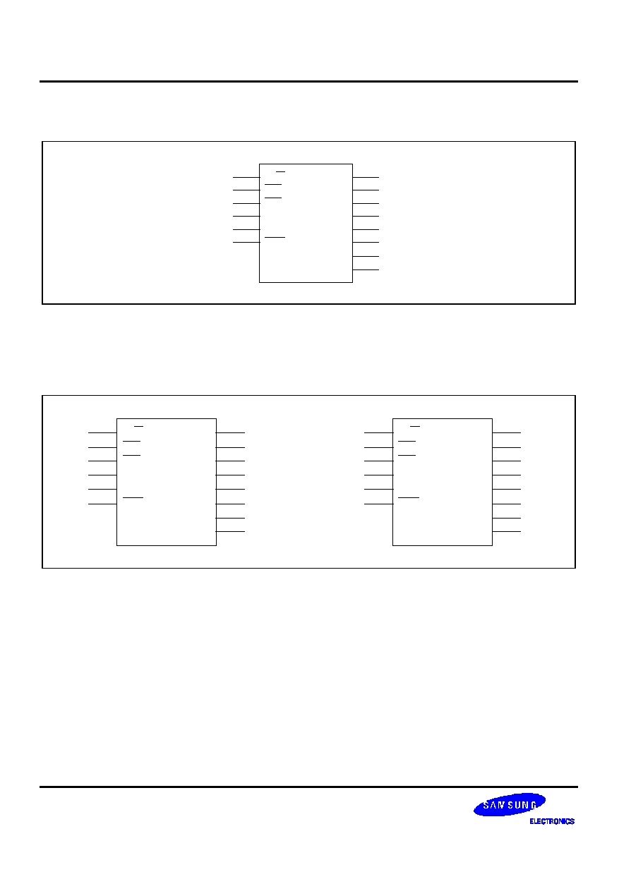
NAND FLASH CONTROLLER
S3C2440A RISC MICROPROCESSOR
6-10
NAND FLASH MEMORY CONFIGURATION
I/O7
I/O6
I/O5
I/O4
I/O3
I/O2
I/O1
I/O0
R/ B
WE
ALE
CLE
CE
RE
RnB
nFWE
ALE
CLE
nFCE
nFRE
DATA[7]
DATA[6]
DATA[5]
DATA[4]
DATA[3]
DATA[2]
DATA[1]
DATA[0]
Figure 6-6. A 8-bit NAND Flash Memory Interface
When you write the address, the same address is issued from data[7:0] and data[15:8]
I/O7
I/O6
I/O5
I/O4
I/O3
I/O2
I/O1
I/O0
R/ B
WE
ALE
CLE
CE
RE
Rn B
nFWE
ALE
CLE
nFCE
nFRE
DATA[7]
DATA[6]
DATA[5]
DATA[4]
DATA[3]
DATA[2]
DATA[1]
DATA[0]
I/O7
I/O6
I/O5
I/O4
I/O3
I/O2
I/O1
I/O0
R/ B
WE
ALE
CLE
CE
RE
Rn B
nFWE
ALE
CLE
nFCE
nFRE
DATA[15]
DATA[14]
DATA[13]
DATA[12]
DATA[11]
DATA[10]
DATA[9]
DATA[8]
Figure 6-7. Two 8-bit NAND Flash Memory Interface
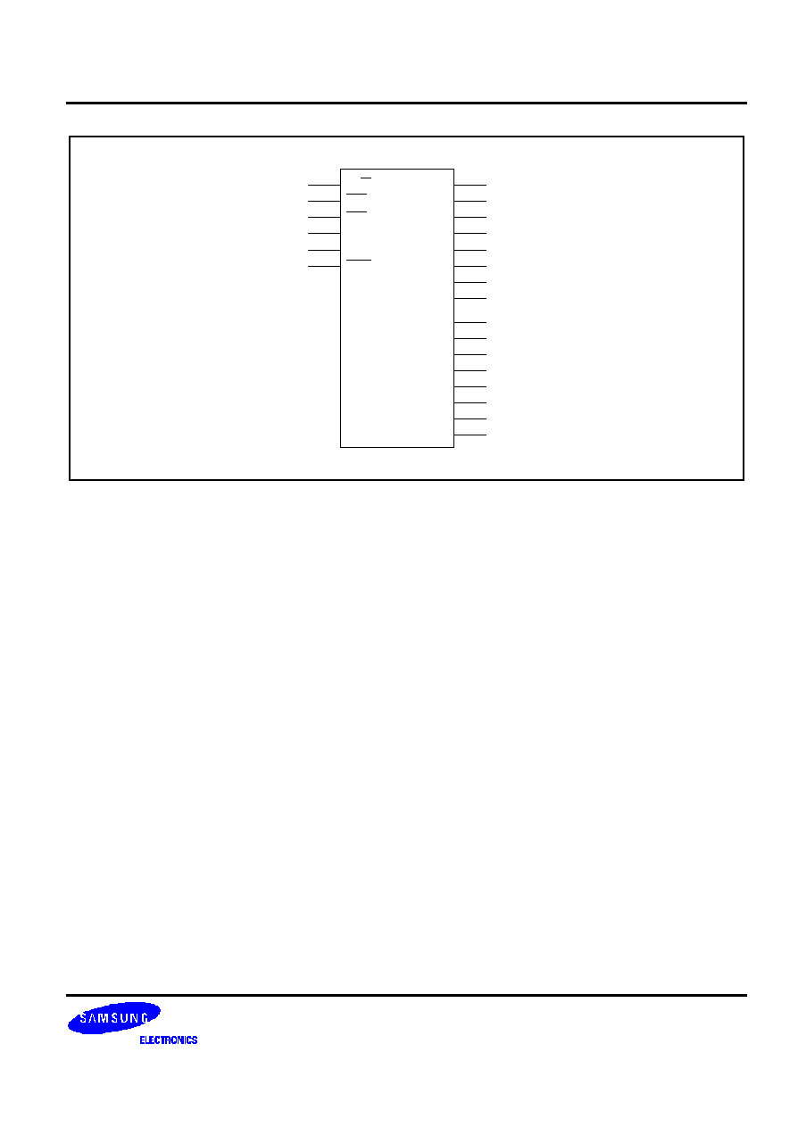
S3C2440A RISC MICROPROCESSOR NAND FLASH CONTROLLER
6-11
I/O15
I/O14
I/O13
I/O12
I/O11
I/O10
I/O9
I/O8
R/ B
WE
ALE
CLE
CE
RE
I/O7
I/O6
I/O5
I/O4
I/O3
I/O2
I/O1
I/O0
RnB
nFWE
ALE
CLE
nFCE
nFRE
DATA[7]
DATA[6]
DATA[5]
DATA[4]
DATA[3]
DATA[2]
DATA[1]
DATA[0]
DATA[15]
DATA[14]
DATA[13]
DATA[12]
DATA[11]
DATA[10]
DATA[9]
DATA[8]
Figure 6-8. A 16-bit NAND Flash Memory Interface
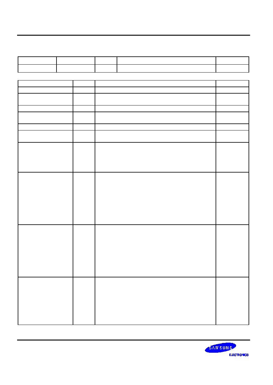
NAND FLASH CONTROLLER
S3C2440A RISC MICROPROCESSOR
6-12
NAND FLASH CONFIGURATION REGISTER
Register
Address
R/W
Description
Reset Value
NFCONF
0x4E000000
R/W
NAND flash configuration register
0x0000100X
NFCONF
Bit
Description
Initial State
Reserved
[15:14]
Reserved
≠
TACLS
[13:12]
CLE & ALE duration setting value (0~3)
Duration = HCLK x TACLS
01
Reserved
[11]
Reserved
0
TWRPH0
[10:8]
TWRPH0 duration setting value (0~7)
Duration = HCLK x ( TWRPH0 + 1 )
000
Reserved
[7]
Reserved
0
TWRPH1
[6:4]
TWRPH1 duration setting value (0~7)
Duration = HCLK x ( TWRPH1 + 1 )
000
AdvFlash (Read only)
[3]
Advance NAND flash memory for auto-booting
0: Support 256 or 512 byte/page NAND flash memory
1: Support 1024 or 2048 byte/page NAND flash memory
This bit is determined by NCON0 pin status during reset
and wake-up from sleep mode.
H/W Set
(NCON0)
PageSize (Read only)
[2]
NAND flash memory page size for auto-booting AdvFlash
PageSize
When AdvFlash is 0,
0: 256 Word/page,
1: 512 Bytes/page
When AdvFlash is 1,
0: 1024 Word/page,
1: 2048 Bytes/page
This bit is determined by GPG13 pin status during reset
and wake-up from sleep mode. After reset, the GPG13 can
be used as general I/O port or External interrupt.
H/W Set
(GPG13)
AddrCycle (Read only)
[1]
NAND flash memory Address cycle for auto-booting
AdvFlash AddrCycle
When AdvFlash is 0,
0: 3 address cycle
1: 4 address cycle
When AdvFlash is 1,
0: 4 address cycle
1: 5 address cycle
This bit is determined by GPG14pin status during reset
and wake-up from sleep mode. After reset, the GPG14can
be used as general I/O port or External interrupt.
H/W Set
(GPG14)
BusWidth (R/W)
[0]
NAND Flash Memory I/O bus width for auto-booting and
general access.
0: 8-bit bus
1: 16-bit bus
This bit is determined by GPG15 pin status during reset
and wake-up from sleep mode.
After reset, the GPG15 can be used as general I/O port or
External interrupt.
This bit can be changed by software.
H/W Set
(GPG15)

S3C2440A RISC MICROPROCESSOR NAND FLASH CONTROLLER
6-13
CONTROL REGISTER
Register
Address
R/W
Description
Reset Value
NFCONT
0x4E000004
R/W
NAND flash control register
0x0384
NFCONT
Bit
Description
Initial State
Reserved
[14:15]
Reserved
0
Lock-tight
[13]
Lock-tight configuration
0: Disable lock-tight
1: Enable lock-tight,
Once this bit is set to 1, you cannot clear. Only reset or
wake up from sleep mode can make this bit disable(can
not cleared by software).
When it is set to 1, the area setting in
NFSBLK(0x4E000038) to NFEBLK(0x4E00003C)-1 is
unlocked, and except this area, write or erase command
will be invalid and only read command is valid.
When you try to write or erase locked area, the illegal
access will be occur (NFSTAT[3] bit will be set).
If the NFSBLK and NFEBLK are same, entire area will be
locked.
0
Soft Lock
[12]
Soft Lock configuration
0: Disable lock
1: Enable lock
Soft lock area can be modified at any time by software.
When it is set to 1, the area setting in
NFSBLK(0x4E000038) to NFEBLK(0x4E00003C)-1 is
unlocked, and except this area, write or erase command
will be invalid and only read command is valid.
When you try to write or erase locked area, the illegal
access will be occur (NFSTAT[3] bit will be set).
If the NFSBLK and NFEBLK are same, entire area will be
locked.
1
Reserved
[11]
Reserved
0
EnbIllegalAccINT
[10]
Illegal access interrupt control
0: Disable interrupt
1: Enable interrupt
Illegal access interrupt is occurred when CPU tries to
program or erase locking area (the area setting in
NFSBLK(0x4E000038) to NFEBLK(0x4E00003C)-1).
0
EnbRnBINT
[9]
RnB status input signal transition interrupt control
0: Disable RnB interrupt 1: Enable RnB interrupt
0
RnB_TransMode
[8]
RnB transition detection configuration
0: Detect rising edge
1: Detect falling edge
0
Reserved
[7]
Reserved
0

NAND FLASH CONTROLLER
S3C2440A RISC MICROPROCESSOR
6-14
CONTROL REGISTER (Continued)
NFCONT
Bit
Description
Initial State
SpareECCLock
[6]
Lock spare area ECC generation.
0: Unlock spare ECC
1: Lock spare ECC
Spare area ECC status register is FSECC(0x4E000034)
1
MainECCLock
[5]
Lock Main data area ECC generation
0: Unlock main data area ECC generation
1: Lock main data area ECC generation
Main area ECC status register is NFMECC0/1
(0x4E00002C/30)
1
InitECC
[4]
Initialize ECC decoder/encoder(Write-only)
1: Initialize ECC decoder/encoder
0
Reserved
[2:3]
Reserved
00
Reg_nCE
[1]
NAND Flash Memory nFCE signal control
0: Force nFCE to low (Enable chip select)
1: Force nFCE to high (Disable chip select)
Note: During boot time, it is controlled automatically.
This value is only valid while MODE bit is 1
1
MODE
[0]
NAND flash controller operating mode
0: NAND flash controller disable (Don't work)
1: NAND flash controller enable
0
S3C2440A RISC MICROPROCESSOR NAND FLASH CONTROLLER
6-15
COMMAND REGISTER
Register
Address
R/W
Description
Reset Value
NFCMMD
0x4E000008
R/W
NAND flash command set register
0x00
NFCMMD
Bit
Description
Initial State
Reserved
[15:8]
Reserved
0x00
NFCMMD
[7:0]
NAND flash memory command value
0x00
ADDRESS REGISTER
Register
Address
R/W
Description
Reset Value
NFADDR
0x4E00000C
R/W
NAND flash address set register
0x0000XX00
REG_ADDR
Bit
Description
Initial State
Reserved
[15:8]
Reserved
0x00
NFADDR
[7:0]
NAND flash memory address value
0x00
DATA REGISTER
Register
Address
R/W
Description
Reset Value
NFDATA
0x4E000010
R/W
NAND flash data register
0xXXXX
NFDATA
Bit
Description
Initial State
NFDATA
[31:0]
NAND flash read/program data value for I/O
Note: Refer to data register configuration in Page 6-5.
0xXXXX
NAND FLASH CONTROLLER
S3C2440A RISC MICROPROCESSOR
6-16
MAIN DATA AREA REGISTER
Register
Address
R/W
Description
Reset Value
NFMECCD0
0x4E000014
R/W
NAND Flash ECC 1
st
and 2
nd
register for main
data read
Note: Refer to ECC module features in Page 6-8.
0x00000000
NFMECCD1
0x4E000018
R/W
NAND Flash ECC 3
nd
4
th
register for main data
read
Note: Refer to ECC module features in Page 6-8.
0x00000000
NFMECCD0
Bit
Description
Initial State
ECCData1_1
[31:24]
2
nd
ECC for I/O[15:8]
0x00
ECCData1_0
[23:16]
2
nd
ECC for I/O[ 7:0]
Note : In Software mode, Read this register when you need to
read 2
nd
ECC value from NAND flash memory
0x00
ECCData0_1
[15:8]
1
st
ECC for I/O[15:8]
0x00
ECCData0_0
[7:0]
1
st
ECC for I/O[ 7:0]
Note: In Software mode, Read this register when you need to
read 1
st
ECC value from NAND flash memory.
This register has same read function of NFDATA.
0x00
NOTE: Only word access is valid.
NFMECCD1
Bit
Description
Initial State
ECCData3_1
[31:24]
4
th
ECC for I/O[15:8]
0x00
ECCData3_0
[23:16]
4
th
ECC for I/O[ 7:0]
Note: In Software mode, Read this register when you need to
read 4
th
ECC value from NAND flash memory.
0x00
ECCData2_1
[15:8]
3
nd
ECC for I/O[15:8]
0x00
ECCData2_0
[7:0]
3
nd
ECC for I/O[ 7:0]
Note: In Software mode, Read this register when you need to
read 3
nd
ECC value from NAND flash memory. This
register has same read function of NFDATA.
0x00
NOTE: Only word access is valid.

S3C2440A RISC MICROPROCESSOR NAND FLASH CONTROLLER
6-17
SPARE AREA ECC REGISTER
Register
Address
R/W
Description
Reset Value
NFSECCD
0x4E00001C
R/W
NAND flash ECC (Error Correction Code)
register for spare area data read
0x00000000
NFSECCD
Bit
Description
Initial State
ECCData1_1
[31:24]
2
nd
ECC for I/O[15:8]
0x00
ECCData1_0
[23:16]
2
nd
ECC for I/O[ 7:0]
Note: In Software mode, Read this register when you need to
read 2
nd
ECC value from NAND flash memory.
0x00
ECCData0_1
[15:8]
1
st
ECC for I/O[15:8]
0x00
ECCData0_0
[7:0]
1
st
ECC for I/O[ 7:0]
Note: In Software mode, Read this register when you need to
read 1
st
ECC value from NAND flash memory. This
register has same read function of NFDATA.
0x00
NOTE: Only word access is valid.

NAND FLASH CONTROLLER
S3C2440A RISC MICROPROCESSOR
6-18
NFCON STATUS REGISTER
Register
Address
R/W
Description
Reset Value
NFSTAT
0x4E000020
R/W
NAND flash operation status register
0xXX00
NFSTAT
Bit
Description
Initial State
Reserved
[7]
Reserved
X
Reserved
[4:6]
Reserved
0
IllegalAccess
[3]
Once Soft Lock or Lock-tight is enabled, The illegal access
(program, erase) to the memory makes this bit set.
0: illegal access is not detected
1: illegal access is detected
0
RnB_TransDetect
[2]
When RnB low to high transition is occurred, this value set
and issue interrupt if enabled. To clear this value write `1'.
0: RnB transition is not detected
1: RnB transition is detected
Transition configuration is set in RnB_TransMode
(NFCONT[8]).
0
nCE (Read-only)
[1]
The status of nCE output pin
1
RnB (Read-only)
[0]
The status of RnB input pin.
0: NAND Flash memory busy
1: NAND Flash memory ready to operate
1
S3C2440A RISC MICROPROCESSOR NAND FLASH CONTROLLER
6-19
ECC0/1 STATUS REGISTER
Register
Address
R/W
Description
Reset Value
NFESTAT0
0x4E000024
R/W
NAND flash ECC Status register for I/O [7:0]
0x00000000
NFESTAT1
0x4E000028
R/W
NAND flash ECC status register for I/O [15:8]
0x00000000
NFESTAT0
Bit
Description
Initial State
SErrorDataNo
[24:21]
In spare area, Indicates which number data is error
00
SErrorBitNo
[20:18]
In spare area, Indicates which bit is error
000
MErrorDataNo
[17:7]
In main data area, Indicates which number data is error
0x00
MErrorBitNo
[6:4]
In main data area, Indicates which bit is error
000
SpareError
[3:2]
Indicates whether spare area bit fail error occurred
00: No Error
01: 1-bit error(correctable)
10: Multiple error
11: ECC area error
00
MainError
[1:0]
Indicates whether main data area bit fail error occurred
00: No Error
01: 1-bit error(correctable)
10: Multiple error
11: ECC area error
00
NOTE: The above values are only valid when both ECC register and ECC status register have valid value.
NFESTAT1
Bit
Description
Initial State
SErrorDataNo
[24:21]
In spare area, Indicates which number data is error
00
SErrorBitNo
[20:18]
In spare area, Indicates which bit is error
000
MErrorDataNo
[17:7]
In main data area, Indicates which number data is error
0x00
MErrorBitNo
[6:4]
In main data area, Indicates which bit is error
000
SpareError
[3:2]
Indicates whether spare area bit fail error occurred
00: No Error
01: 1-bit error(correctable)
10: Multiple error
11: ECC area error
00
MainError
[1:0]
Indicates whether main data area bit fail error occurred
00: No Error
01: 1-bit error(correctable)
10: Multiple error
11: ECC area error
00
NOTE: The above values are only valid when both ECC register and ECC status register have valid value.
NAND FLASH CONTROLLER
S3C2440A RISC MICROPROCESSOR
6-20
MAIN DATA AREA ECC0 STATUS REGISTER
Register
Address
R/W
Description
Reset Value
NFMECC0
0x4E00002C
R
NAND flash ECC register for data[7:0]
0xXXXXXX
NFMECC1
0x4E000030
R
NAND flash ECC register for data[15:8]
0xXXXXXX
NFMECC0
Bit
Description
Initial State
MECC0_3
[31:24]
ECC3 for data[7:0]
0xXX
MECC0_2
[23:16]
ECC2 for data[7:0]
0xXX
MECC0_1
[15:8]
ECC1 for data[7:0]
0xXX
MECC0_0
[7:0]
ECC0 for data[7:0]
0xXX
NFMECC1
Bit
Description
Initial State
MECC1_3
[31:24]
ECC3 data[15:8]
0xXX
MECC1_2
[23:16]
ECC2 data[15:8]
0xXX
MECC1_1
[15:8]
ECC1 data[15:8]
0xXX
MECC1_0
[7:0]
ECC0 data[15:8]
0xXX
NOTE: The NAND flash controller generate NFMECC0/1 when read or write main area data while the
MainECCLock(NFCONT[5]) bit is `0'(Unlock).
SPARE AREA ECC STATUS REGISTER
Register
Address
R/W
Description
Reset Value
NFSECC
0x4E000034
R
NAND flash ECC register for I/O [15:0]
0xXXXXXX
NFSECC
Bit
Description
Initial State
SECC1_1
[31:24]
Spare area ECC1 status for I/O[15:8]
0xXX
SECC1_0
[23:16]
Spare area ECC0 status for I/O[15:8]
0xXX
SECC0_1
[15:8]
Spare area ECC1 status for I/O[7:0]
0xXX
SECC0_0
[7:0]
Spare area ECC0 status for I/O[7:0]
0xXX
NOTE: The NAND flash controller generate NFSECC when read or write spare area data while the
SpareECCLock(NFCONT[6]) bit is `0'(Unlock).
S3C2440A RISC MICROPROCESSOR NAND FLASH CONTROLLER
6-21
BLOCK ADDRESS REGISTER
Register
Address
R/W
Description
Reset Value
NFSBLK
0x4E000038
R/W
NAND flash programmable start block address
0x000000
NFEBLK
0x4E00003C
R/W
NAND flash programmable end block address
Nand Flash can be programmed between start
and end address.
When the soft lock or lock-tight is enabled and
the start and end address has same value,
Entire area of NAND flash will be locked.
0x000000
NFSBLK
Bit
Description
Initial State
SBLK_ADDR2
[23:16]
The 3
nd
block address of the block erase operation
0x00
SBLK_ADDR1
[15:8]
The 2
nd
block address of the block erase operation
0x00
SBLK_ADDR0
[7:0]
The 1
st
block address of the block erase operation
(Only bit [7:5] are valid)
0x00
NOTE: Advance Flash's block Address start from 3-address cycle. So block address register only needs 3-bytes.
NFEBLK
Bit
Description
Initial State
EBLK_ADDR2
[23:16]
The 3
rd
block address of the block erase operation
0x00
EBLK_ADDR1
[15:8]
The 2
nd
block address of the block erase operation
0x00
EBLK_ADDR0
[7:0]
The 1
st
block address of the block erase operation
(Only bit [7:5] are valid)
0x00
NOTE: Advance Flash's block Address start from 3-address cycle. So block address register only needs 3-bytes.
NAND FLASH CONTROLLER
S3C2440A RISC MICROPROCESSOR
6-22
The NFSLK and NFEBLK can be changed while Soft lock bit(NFCONT[12]) is enabled. But cannot be changed when
Lock-tight bit(NFCONT[13]) is set.
when Lock-tight =1
or SoftLock =1
NAND Flash Memory
Locked area
(Read only)
Prorammable/
Readable
Area
Locked area
(Read only)
NFSBLK
Address
High
Low
NFEBLK
NFEBLK-1
NFSBLK
NFEBLK
Locked Area
(Read only)
When NFSBLK=NFEBLK

S3C2440A RISC MICROPROCESSOR
CLOCK & POWER MANAGEMENT
7-1
7
CLOCK & POWER MANAGEMENT
OVERVIEW
The Clock & Power management block consists of three parts: Clock control, USB control, and Power control.
The Clock control logic in S3C2440A can generate the required clock signals including FCLK for CPU, HCLK for the
AHB bus peripherals, and PCLK for the APB bus peripherals. The S3C2440A has two Phase Locked Loops (PLLs):
one for FCLK, HCLK, and PCLK, and the other dedicated for USB block (48Mhz). The clock control logic can make
slow clocks without PLL and connect/disconnect the clock to each peripheral block by software, which will reduce
the power consumption.
For the power control logic, the S3C2440A has various power management schemes to keep optimal power
consumption for a given task. The power management block in the S3C2440A can activate four modes: NORMAL
mode, SLOW mode, IDLE mode, and SLEEP mode.
NORMAL mode: The block supplies clocks to CPU as well as all peripherals in the S3C2440A. In this mode, the
power consumption will be maximized when all peripherals are turned on. It allows the user to control the operation of
peripherals by software. For example, if a timer is not needed, the user can disconnect the clock(CLKCON register)
to the timer to reduce power consumption.
SLOW mode: Non-PLL mode. Unlike the Normal mode, the Slow mode uses an external clock (XTIpll or EXTCLK)
directly as FCLK in the S3C2440A without PLL. In this mode, the power consumption depends on the frequency of
the external clock only. The power consumption due to PLL is excluded.
IDLE mode: The block disconnects clocks (FCLK) only to the CPU core while it supplies clocks to all other
peripherals. The IDLE mode results in reduced power consumption due to CPU core. Any interrupt request to CPU
can be woken up from the Idle mode.
SLEEP mode: The block disconnects the internal power. So, there occurs no power consumption due to CPU and
the internal logic except the wake-up logic in this mode. Activating the SLEEP mode requires two independent power
sources. One of the two power sources supplies the power for the wake-up logic. The other one supplies other
internal logics including CPU, and should be controlled for power on/off. In the SLEEP mode, the second power
supply source for the CPU and internal logics will be turned off. The wakeup from SLEEP mode can be issued by the
EINT[15:0] or by RTC alarm interrupt.

CLOCK & POWER MANAGEMENT
S3C2440A RISC MICROPROCESSOR
7-2
FUNCTIONAL DESCRIPTION
CLOCK ARCHITECTURE
Figure 7-1 shows a block diagram of the clock architecture. The main clock source comes from an external crystal
(XTIpll) or an external clock (EXTCLK). The clock generator includes an oscillator (Oscillation Amplifier), which is
connected to an external crystal, and also has two PLLs (Phase-Locked-Loop), which generate the high frequency
clock required in the S3C2440A.
CLOCK SOURCE SELECTION
Table 7-1 shows the relationship between the combination of mode control pins (OM3 and OM2) and the selection of
source clock for the S3C2440A. The OM[3:2] status is latched internally by referring the OM3 and OM2 pins at the
rising edge of nRESET.
Table 7-1. Clock Source Selection at Boot-Up
Mode OM[3:2]
MPLL State
UPLL State
Main Clock source
USB Clock Source
00
On
On
Crystal
Crystal
01
On
On
Crystal
EXTCLK
10
On
On
EXTCLK
Crystal
11
On
On
EXTCLK
EXTCLK
NOTES:
1.
Although the MPLL starts just after a reset, the MPLL output (Mpll) is not used as the system clock until the software
writes valid settings to the MPLLCON register. Before this valid setting, the clock from external crystal or EXTCLK source
will be used as the system clock directly. Even if the user does not want to change the default value of MPLLCON
register, the user should write the same value into MPLLCON register.
2.
OM[3:2] is used to determine a test mode when OM[1:0] is 11.
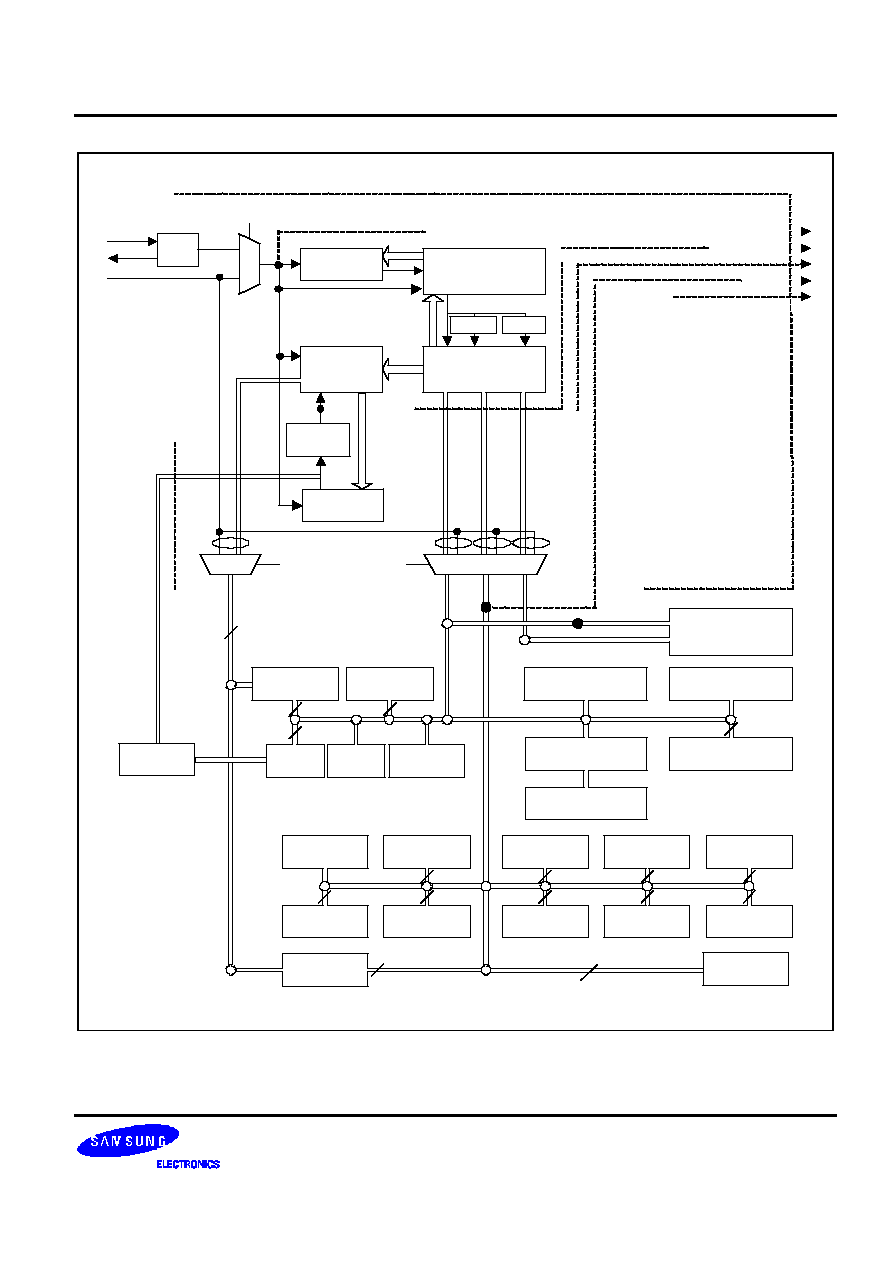
S3C2440A RISC MICROPROCESSOR
CLOCK & POWER MANAGEMENT
7-3
Nand Flash
Controller
OSC
MPLL
UPLL
CLKCNTL
FCLK
HDIVN
PDIVN
Mpll
Control
Signal
Upll
POWCNTL
F
H
P
USBCNTL
Test mode OM[1:0]
Bus
Controller
Memory
Controller
Arbitration
DMA 4ch
WDT
I
2
S
SDI
ADC
UART(0,1,2)
PWM
I
2
C
GPIO
RTC
SPI(0,1)
USB
Device
ARM920T
Interrupt
Controller
LCD
Controller
H_LCD
P_SDI
P_GPIO
P_ADC
P_RTC
P_UART
P_SPI
P_I
2
S
P_I
2
C
P_PWM
P_USB
H_Nand
FCLK
PCLK
HCLK
UCLK
Power
Management
Block
MPLLin CLK
UPLL CLK
HCLK
PCLK
RTC XTAL CLK
CLKOUT
XTIpll
XTOpll
EXTCLK
P[5:0]
M[7:0]
S[1:0]
OM[3:2]
P[5:0]
M[7:0]
S[1:0]
USB Host I/F
H_USB
TIC
H_CAM
CAM
ExtMater
DIVN_UPLL
1/1 or 1/2
CAMDIVN
P_A97
AC97
MPLLin
Figure 7-1. Clock Generator Block Diagram

CLOCK & POWER MANAGEMENT
S3C2440A RISC MICROPROCESSOR
7-4
PHASE LOCKED LOOP (PLL)
The MPLL within the clock generator, as a circuit, synchronizes an output signal with a reference input signal in
frequency and phase. In this application, it includes the following basic blocks as shown in Figure 7-2: the Voltage
Controlled Oscillator (VCO) to generate the output frequency proportional to input DC voltage, the divider P to divide
the input frequency (Fin) by p, the divider M to divide the VCO output frequency by m which is input to Phase
Frequency Detector (PFD), the divider S to divide the VCO output frequency by "s" which is Mpll (the output
frequency from MPLL block), the phase difference detector, the charge pump, and the loop filter. The output clock
frequency Mpll is related to the reference input clock frequency Fin by the following equation:
Mpll = (2*m * Fin) / (p * 2
s
)
m = M (the value for divider M)+ 8, p = P (the value for divider P) + 2
The UPLL within the clock generator is similar to the MPLL in every aspect.
The following sections describes the operation of the PLL, including the phase difference detector, the charge pump,
the Voltage controlled oscillator (VCO), and the loop filter.
Phase Frequency Detector (PFD)
The PFD monitors the phase difference between Fref and Fvco, and generates a control signal (tracking signal) when
the difference is detected. The Fref means the reference frequency as shown in the Figure 7-2.
Charge Pump (PUMP)
The charge pump converts PFD control signals into a proportional change in voltage across the external filter that
drives the VCO.
Loop Filter
The control signal, which the PFD generates for the charge pump, may generate large excursions (ripples) each time
the Fvco is compared to the Fref. To avoid overloading the VCO, a low pass filter samples and filters the high-
frequency components out of the control signal. The filter is typically a single-pole RC filter with a resistor and a
capacitor.
Voltage Controlled Oscillator (VCO)
The output voltage from the loop filter drives the VCO, causing its oscillation frequency to increase or decrease
linearly as a function of variations in average voltage. When the Fvco matches Fref in terms of frequency as well as
phase, the PFD stops sending control signals to the charge pump, which in turn stabilizes the input voltage to the
loop filter. The VCO frequency then remains constant, and the PLL remains fixed onto the system clock.
Usual Conditions for PLL & Clock Generator
PLL & Clock Generator generally uses the following conditions.
Loop filter capacitance
C
LF
MPLLCAP: 1.3 nF ± 5%
UPLLCAP: 700 pF ± 5%
External X-tal frequency
≠
12 ≠ 20 MHz
(note)
External capacitance used for X-tal
C
EXT
15 ≠ 22 pF
NOTES:
1. The value could be changed.
2.
FCLK
OUT
must be bigger than 200MHz (It does not mean that the ARM core has to run more than 200MHz).
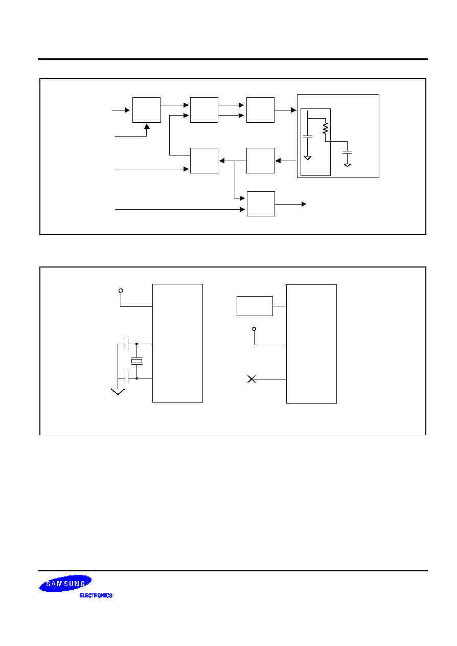
S3C2440A RISC MICROPROCESSOR
CLOCK & POWER MANAGEMENT
7-5
Divider
P
Loop Filter
Fin
M[7:0]
S[1:0]
PFD
Divider
M
P[5:0]
F
vco
PUMP
VCO
Divider
S
F
ref
MPLL,UPLL
R
C
Internal
CLF
External
MPLLCAP,
UPLLCAP
Figure 7-2. PLL (Phase-Locked Loop) Block Diagram
EXTCLK
XTIpll
XTOpll
EXTCLK
XTIpll
XTOpll
External
OSC
a) X-TAL Oscillation (OM[3:2]=00)
b) External Clock Source (OM[3:2]=11)
V
DD
V
DD
Figure 7-3. Main Oscillator Circuit Examples
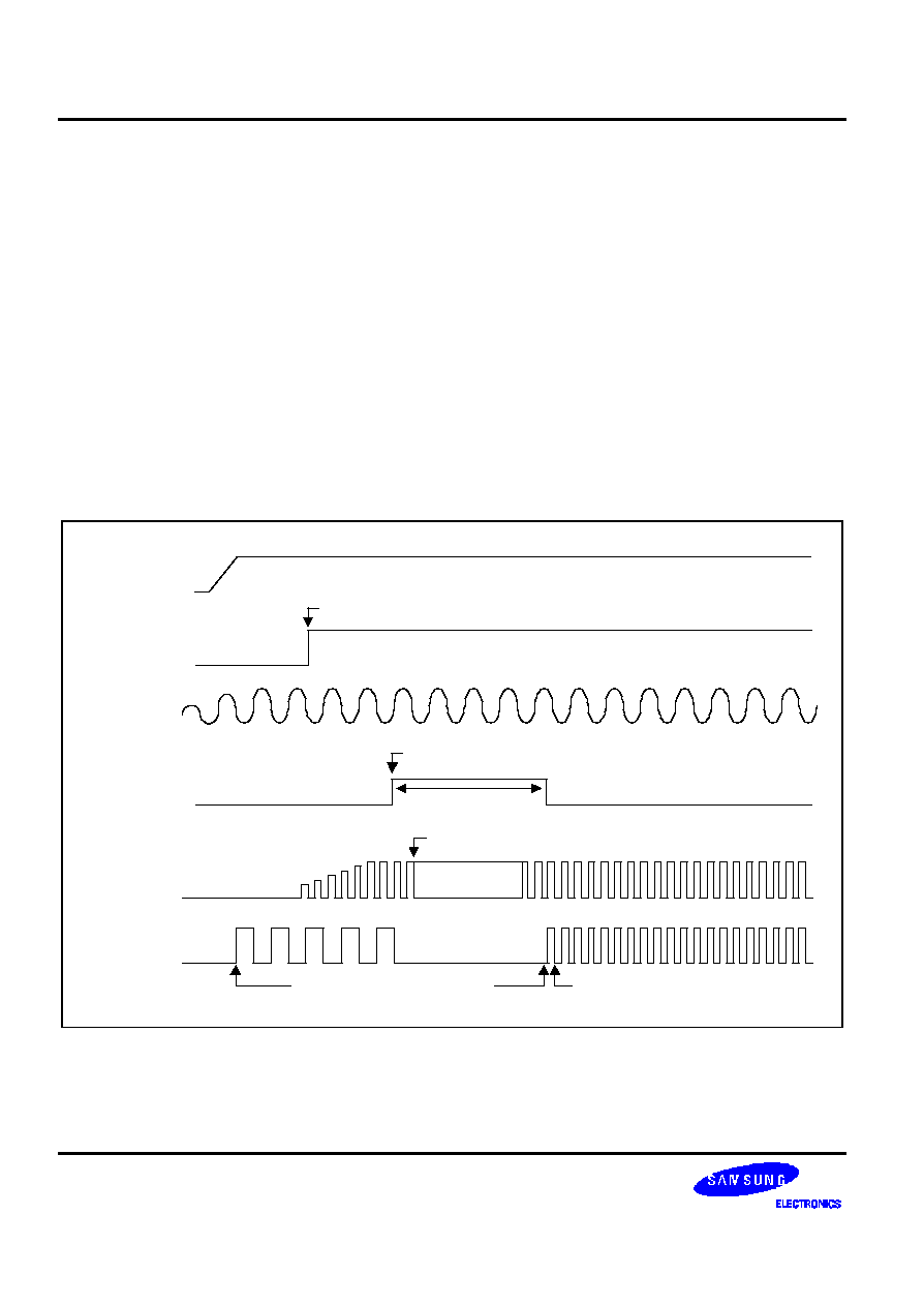
CLOCK & POWER MANAGEMENT
S3C2440A RISC MICROPROCESSOR
7-6
CLOCK CONTROL LOGIC
The Clock Control Logic determines the clock source to be used, i.e., the PLL clock (Mpll) or the direct external
clock (XTIpll or EXTCLK). When PLL is configured to a new frequency value, the clock control logic disables the
FCLK until the PLL output is stabilized using the PLL locking time. The clock control logic is also activated at power-
on reset and wakeup from power-down mode.
Power-On Reset (XTIpll)
Figure 7-4 shows the clock behavior during the power-on reset sequence. The crystal oscillator begins oscillation
within several milliseconds. When nRESET is released after the stabilization of OSC (XTIpll) clock, the PLL starts to
operate according to the default PLL configuration. However, PLL is commonly known to be unstable after power-on
reset, so Fin is fed directly to FCLK instead of the Mpll (PLL output) before the software newly configures the
PLLCON. Even if the user does not want to change the default value of PLLCON register after reset, the user should
write the same value into PLLCON register by software.
The PLL restarts the lockup sequence toward the new frequency only after the software configures the PLL with a
new frequency. FCLK can be configured as PLL output (Mpll) immediately after lock time.
The logic operates by XTIpll
nRESET
OSC
(XTIpll)
VCO
output
Power
Clock
Disable
Lock Time
PLL is configured by S/W first time.
VCO is adapted to new clock frequency.
FCLK
FCLK is new frequency
PLL can operate after OM[3:2] is latched.
Figure 7-4. Power-On Reset Sequence (when the external clock source is a crystal oscillator)
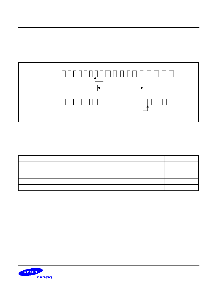
S3C2440A RISC MICROPROCESSOR
CLOCK & POWER MANAGEMENT
7-7
Change PLL Settings In Normal Operation Mode
During the operation of the S3C2440A in NORMAL mode, the user can change the frequency by writing the PMS
value and the PLL lock time will be automatically inserted. During the lock time, the clock is not supplied to the
internal blocks in the S3C2440A. Figure 7-5 shows the timing diagram.
Mpll
PMS setting
PLL Lock-time
FCLK
It changes to new PLL clock
after automatic lock time.
Figure 7-5. Changing Slow Clock by Setting PMS Value
USB Clock Control
USB host interface and USB device interface needs 48Mhz clock. In the S3C2440A, the USB dedicated PLL (UPLL)
generates 48Mhz for USB. UCLK does not fed until the PLL (UPLL) is configured.
Condition
UCLK State
UPLL State
After reset
XTlpll or EXTCLK
On
After UPLL configuration
L: During PLL lock time
48MHz: After PLL lock time
On
UPLL is turned off by CLKSLOW register
XTlpll or EXTCLK
Off
UPLL is turned on by CLKSLOW register
48MHz
On
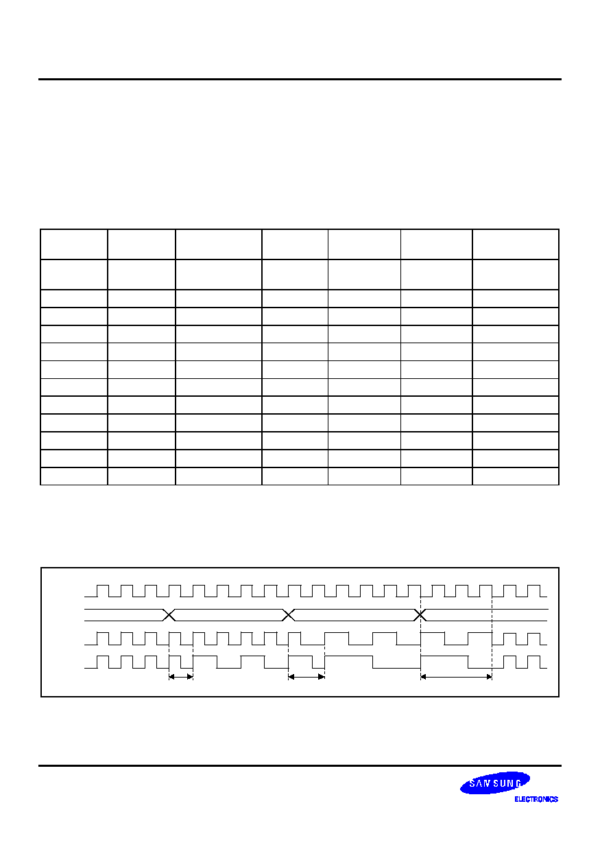
CLOCK & POWER MANAGEMENT
S3C2440A RISC MICROPROCESSOR
7-8
FCLK, HCLK, and PCLK
FCLK is used by ARM920T.
HCLK is used for AHB bus, which is used by the ARM920T, the memory controller, the interrupt controller, the LCD
controller, the DMA and USB host block.
PCLK is used for APB bus, which is used by the peripherals such as WDT, IIS, I2C, PWM timer, MMC interface,
ADC, UART, GPIO, RTC and SPI.
The S3C2440A supports selection of Dividing Ratio between FCLK, HLCK and PCLK. This ratio is determined by
HDIVN and PDIVN of CLKDIVN control register.
HDIVN
PDIVN
HCLK3_HALF/
HCLK4_HALF
FCLK
HCLK
PCLK
Divide Ratio
0
0
≠
FCLK
FCLK
FCLK
1 : 1 : 1
(Default)
0
1
≠
FCLK
FCLK
FCLK / 2
1 : 1 : 2
1
0
≠
FCLK
FCLK / 2
FCLK / 2
1 : 2 : 2
1
1
≠
FCLK
FCLK / 2
FCLK / 4
1 : 2 : 4
3
0
0 / 0
FCLK
FCLK / 3
FCLK / 3
1 : 3 : 3
3
1
0 / 0
FCLK
FCLK / 3
FCLK / 6
1 : 3 : 6
3
0
1 / 0
FCLK
FCLK / 6
FCLK / 6
1 : 6 : 6
3
1
1 / 0
FCLK
FCLK / 6
FCLK / 12
1 : 6 : 12
2
0
0 / 0
FCLK
FCLK / 4
FCLK / 4
1 : 4 : 4
2
1
0 / 0
FCLK
FCLK / 4
FCLK / 8
1 : 4 : 8
2
0
0 / 1
FCLK
FCLK / 8
FCLK / 8
1 : 8 : 8
2
1
0 / 1
FCLK
FCLK / 8
FCLK / 16
1 : 8 : 16
After setting PMS value, it is required to set CLKDIVN register. The value set for CLKDIVN will be valid after PLL lock
time. The value is also available for reset and changing Power Management Mode.
The setting value can also be valid after 1.5 HCLK. Only, 1HCLK can validate the value of CLKDIVN register changed
from Default (1:1:1) to other Divide Ratio (1:1:2, 1:2:2, 1:2:4).
1 HCLK
1.5 HCLK
1.5 HCLK
0x00000000
0x00000001(1:1:2)
0x00000003 (1:2:4)
0x00000000 (1:1:1)
CLKDIVN
FCLK
HCLK
PCLK
Figure 7-6. Example of Internal Clock Change

S3C2440A RISC MICROPROCESSOR
CLOCK & POWER MANAGEMENT
7-9
NOTES
1. CLKDIVN should be set carefully not to exceed the limit of HCLK and PCLK.
2. If HDIVN is not 0, the CPU bus mode has to be changed from the fast bus mode to the asynchronous
bus mode using following instructions(S3C2440 does not support synchronous bus mode).
MMU_SetAsyncBusMode
mrc p15,0,r0,c1,c0,0
orr r0,r0,#R1_nF:OR:R1_iA
mcr p15,0,r0,c1,c0,0
If HDIVN is not 0 and the CPU bus mode is the fast bus mode, the CPU will operate by the HCLK.
This feature can be used to change the CPU frequency as a half or more without affecting the HCLK
and PCLK.
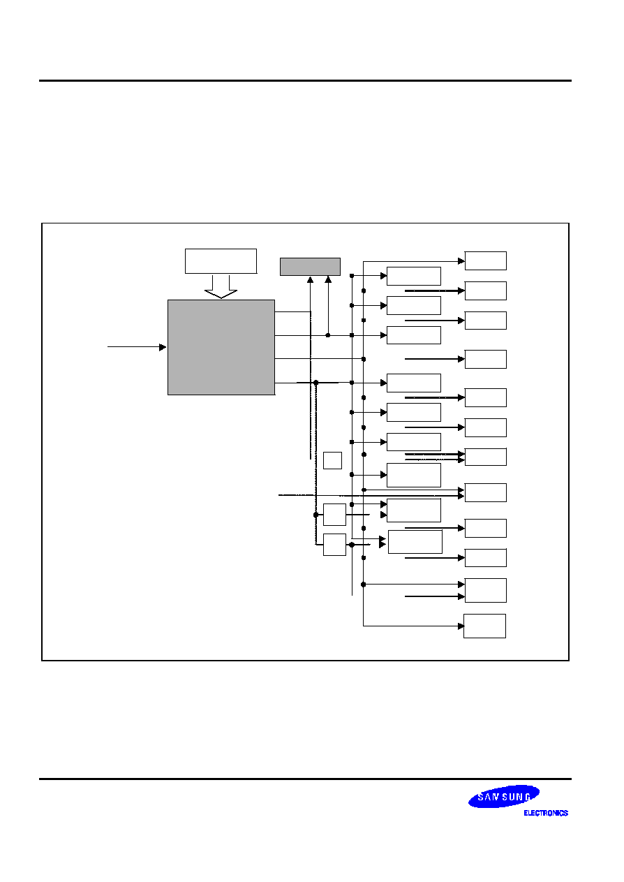
CLOCK & POWER MANAGEMENT
S3C2440A RISC MICROPROCESSOR
7-10
POWER MANAGEMENT
The Power Management block controls the system clocks by software for the reduction of power consumption in the
S3C2440A. These schemes are related to PLL, clock control logics (FCLK, HCLK, and PCLK) and wakeup signals.
Figure 7-7 shows the clock distribution of the S3C2440A.
The S3C2440A has four power modes. The following section describes each power management mode. The
transition between the modes is not allowed freely. Please see Figure 7-8 for available transitions among the modes.
INTCNTL
Power
Management
FCLK
Input Clock
FCLK defination
If SLOW mode
FCLK = input clock/divider ratio
If Normal mode (P, M & S value)
FCLK = MPLL clock (Mpll)
ARM920T
HCLK
PCLK
UPLL(96/48 MHz)
BUSCNTL
MEMCNTL
ARB/DMA
ExtMaster
LCDCNTL
Nand Flash
Controller
Camera
WDT
SPI
PWM
I2C
SDI
ADC
UART
I2S
GPIO
RTC
USB
Device
Clock Control
Register
USB
Host I/F
1/d
1/2
1/1
AC97
1/n
MPLLin
Figure 7-7. The Clock Distribution Block Diagram
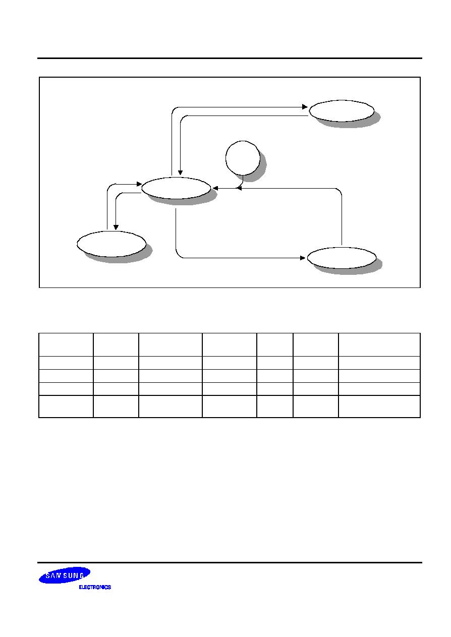
S3C2440A RISC MICROPROCESSOR
CLOCK & POWER MANAGEMENT
7-11
IDLE
SLEEP
NORMAL
(SLOW_BIT=0)
SLOW
(SLOW_BIT=1)
IDLE_BIT=1
Interrupts, EINT[0:23], RTC alarm
SLEEP BIT=1
EINT[15:0],
RTC alarm
RESET
Figure 7-8. Power Management State Diagram
Table 7-2. Clock and Power State in Each Power Mode
Mode
ARM920T
AHB Modules
(1)
/WDT
Power
Management
GPIO
32.768kHz
RTC clock
APB Modules
(2)
& USBH/LCD/NAND
NORMAL
O
O
O
SEL
O
SEL
IDLE
X
O
O
SEL
O
SEL
SLOW
O
O
O
SEL
O
SEL
SLEEP
OFF
OFF
Wait for wake-
up event
Previous
state
O
OFF
NOTES:
1. USB host,LCD, and NAND are excluded.
2.
WDT is excluded. RTC interface for CPU access is included.
3. SEL : selectable(O,X), O : enable , X : disable OFF: power is turned off

CLOCK & POWER MANAGEMENT
S3C2440A RISC MICROPROCESSOR
7-12
NORMAL Mode
In Normal mode, all peripherals and the basic blocks including power management block, the CPU core, the bus
controller, the memory controller, the interrupt controller, DMA, and the external master may operate completely.
But, the clock to each peripheral, except the basic blocks, can be stopped selectively by software to reduce the
power consumption.
IDLE Mode
In IDLE mode, the clock to the CPU core is stopped except the bus controller, the memory controller, the interrupt
controller, and the power management block. To exit the IDLE mode, EINT[23:0], or RTC alarm interrupt, or the other
interrupts should be activated. (EINT is not available until GPIO block is turned on).
SLOW Mode (Non-PLL Mode)
Power consumption can be reduced in the SLOW mode by applying a slow clock and excluding the power
consumption from the PLL. The FCLK is the frequency of divide_by_n of the input clock (XTIpll or EXTCLK) without
PLL. The divider ratio is determined by SLOW_VAL in the CLKSLOW control register and CLKDIVN control register.
Table 7-3. CLKSLOW and CLKDIVN Register Settings for SLOW Clock example
SLOW_VAL
FCLK
HCLK
PCLK
UCLK
1/1 Option
(HDIVN=0)
1/2 Option
(HDIVN=1)
1/1 Option
(PDIVN=0)
1/2 Option
(PDIVN=1)
0 0 0
EXTCLK or
XTIpll / 1
EXTCLK or
XTIpll / 1
EXTCLK or
XTIpll / 2
HCLK
HCLK / 2
48 MHz
0 0 1
EXTCLK or
XTIpll / 2
EXTCLK or
XTIpll / 2
EXTCLK or
XTIpll / 4
HCLK
HCLK / 2
48 MHz
0 1 0
EXTCLK or
XTIpll / 4
EXTCLK or
XTIpll / 4
EXTCLK or
XTIpll / 8
HCLK
HCLK / 2
48 MHz
0 1 1
EXTCLK or
XTIpll / 6
EXTCLK or
XTIpll / 6
EXTCLK or
XTIpll / 12
HCLK
HCLK / 2
48 MHz
1 0 0
EXTCLK or
XTIpll / 8
EXTCLK or
XTIpll / 8
EXTCLK or
XTIpll / 16
HCLK
HCLK / 2
48 MHz
1 0 1
EXTCLK or
XTIpll / 10
EXTCLK or
XTIpll / 10
EXTCLK or
XTIpll / 20
HCLK
HCLK / 2
48 MHz
1 1 0
EXTCLK or
XTIpll / 12
EXTCLK or
XTIpll / 12
EXTCLK or
XTIpll / 24
HCLK
HCLK / 2
48 MHz
1 1 1
EXTCLK or
XTIpll / 14
EXTCLK or
XTIpll / 14
EXTCLK or
XTIpll / 28
HCLK
HCLK / 2
48 MHz
In SLOW mode, PLL will be turned off to reduce the PLL power consumption. When the PLL is turned off in the
SLOW mode and the user changes power mode from SLOW mode to NORMAL mode, then the PLL needs clock
stabilization time (PLL lock time). This PLL stabilization time is automatically inserted by the internal logic with lock
time count register. The PLL stability time will take 300us after the PLL is turned on. During PLL lock time, the FCLK
becomes SLOW clock.
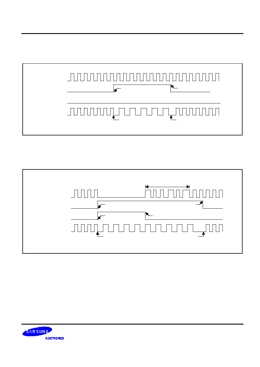
S3C2440A RISC MICROPROCESSOR
CLOCK & POWER MANAGEMENT
7-13
Users can change the frequency by enabling SLOW mode bit in CLKSLOW register in PLL on state. The SLOW
clock is generated during the SLOW mode. Figure 7-11(Please check the figure correctly) shows the timing diagram.
Mpll
Slow mode disable
FCLK
Slow mode enable
SLOW_BIT
Divided external clock
MPLL_OFF
It changes to PLL clock
after slow mode off
Figure 7-9. Issuing Exit_from_Slow_mode Command in PLL on State
If the user switches from SLOW mode to Normal mode by disabling the SLOW_BIT in the CLKSLOW register after
PLL lock time, the frequency is changed just after SLOW mode is disabled. Figure 7-12 (Please check for the figure
number correctly) shows the timing diagram.
Mpll
FCLK
SLOW_BIT
Divided OSC clock
MPLL_OFF
Software lock time
Slow mode disable
PLL off
PLL on
Slow mode enable
It changes to PLL clock
after slow mode off
Figure 7-10. Issuing Exit_from_Slow_mode Command After Lock Time
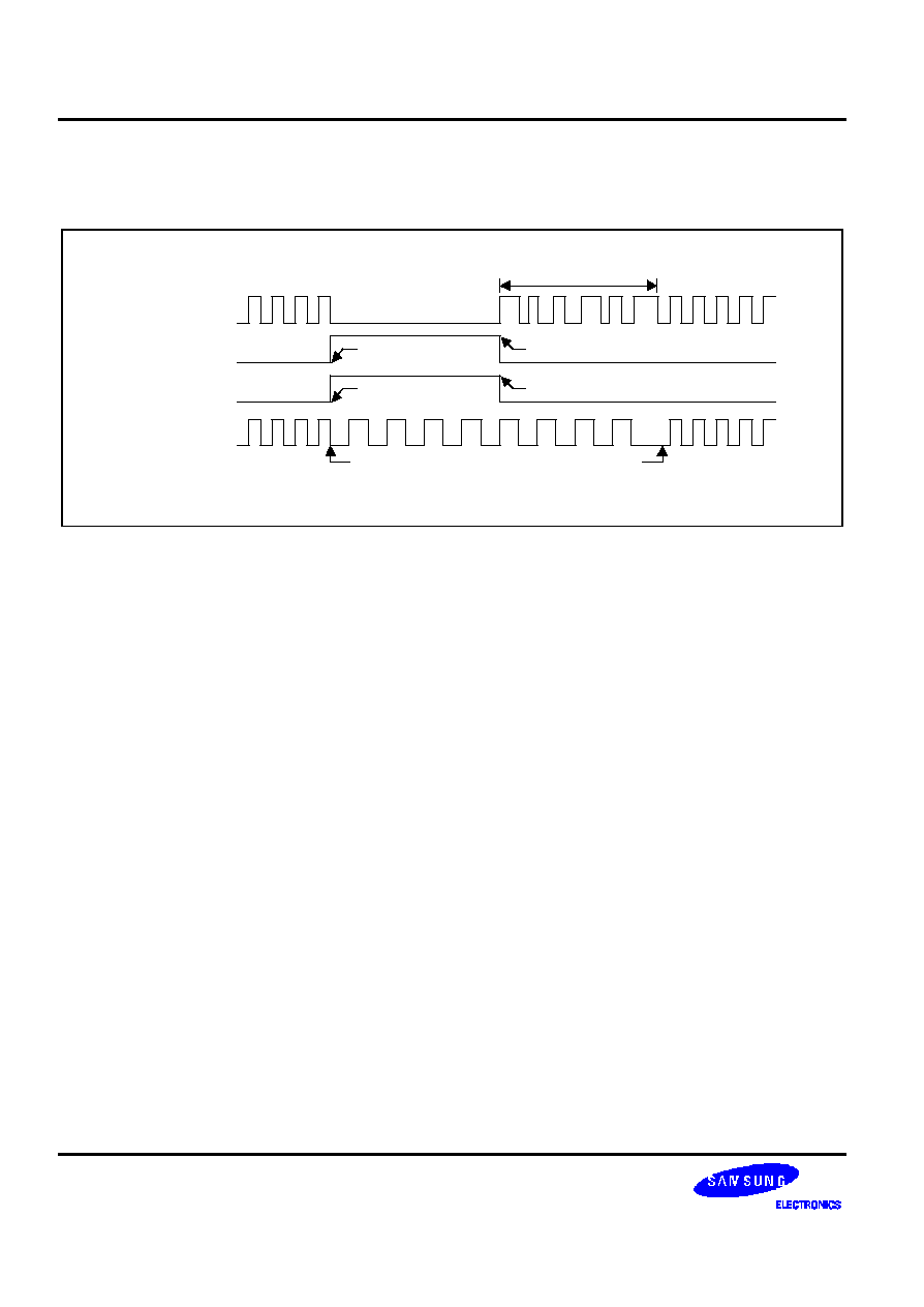
CLOCK & POWER MANAGEMENT
S3C2440A RISC MICROPROCESSOR
7-14
If the user switches from SLOW mode to Normal mode by disabling SLOW_BIT and MPLL_OFF bit simultaneously
in the CLKSLOW register, the frequency is changed just after the PLL lock time. Figure 7-13 (Please check for the
figure number correctly) shows the timing diagram.
Mpll
FCLK
SLOW_BIT
Divided
OSC clock
MPLL_OFF
Hardware lock time
PLL off
PLL on
Slow mode enable
It changes to PLL clock
after lock time automatically
Slow mode disable
Figure 7-11. Issuing Exit_from_Slow_mode Command and the Instant PLL_on Command Simultaneously

S3C2440A RISC MICROPROCESSOR
CLOCK & POWER MANAGEMENT
7-15
SLEEP Mode
The block disconnects the internal power. So, there occurs no power consumption due to CPU and the internal logic
except the wake-up logic in this mode. Activating the SLEEP mode requires two independent power sources. One of
the two power sources supplies the power for the wake-up logic. The other one supplies other internal logics
including CPU, and should be controlled for power on/off. In the SLEEP mode, the second power supply source for
the CPU and internal logics will be turned off. The wakeup from SLEEP mode can be issued by the EINT[15:0] or by
RTC alarm interrupt.
Follow the Procedure to Enter SLEEP mode
1. Set the GPIO configuration adequate for SLEEP mode.
2. Mask all interrupts in the INTMSK register.
3. Configure the wake-up sources properly including RTC alarm. (The bit of EINTMASK corresponding to the wake-
up source has not to be masked in order to let the corresponding bit of SRCPND or EINTPEND set. Although a
wake-up source is issued and the corresponding bit of EINTMASK is masked, the wake-up will occur and the
corresponding bit of SRCPND or EINTPEND will not be set.)
4. Set USB pads as suspend mode. (MISCCR[13:12]=11b)
5. Save some meaning values into GSTATUS[4:3] register. These register are preserved during SLEEP mode.
6. Configure MISCCR[1:0] for the pull-up resisters on the data bus,D[31:0]. If there is an external BUS holder, such
as 74LVCH162245, turn off the pull-up resistors. If not, turn on the pull-up resistors.
Additionally, The Memory concerning pins is set to two types, one is Hi-z, and the other is Inactive state.
7. Stop LCD by clearing LCDCON1.ENVID bit.
8. Read rREFRESH and rCLKCON registers in order to fill the TLB.
9. Let SDRAM enter the self-refresh mode by setting the REFRESH[22]=1b.
10. Wait until SDRAM self-refresh is effective.
11. Set MISCCR[19:17]=111b to make SDRAM signals(SCLK0,SCLK1 and SCKE) protected during SLEEP mode
12. Set the SLEEP mode bit in the CLKCON register.
Caution:
When the system is operating in NAND boot mode, The hardware pin configuration - EINT[23:21]
≠ must be set as input for starting up after wakeup from sleep mode.
CLOCK & POWER MANAGEMENT
S3C2440A RISC MICROPROCESSOR
7-16
Follow the Procedure to Wake-up from SLEEP mode
1. The internal reset signal will be asserted if one of the wake-up sources is issued. It's exactly same with the case
of the assertion of the external nRESET pin. This reset duration is determined by the internal 16-bit counter logic
and the reset assertion time is calculated as tRST = (65535 / XTAL_frequency).
2. Check GSTATUS2[2] in order to know whether or not the power-up is caused by the wake-up from SLEEP
mode.
3. Release the SDRAM signal protection by setting MISCCR[19:17]=000b.
4. Configure the SDRAM memory controller.
5. Wait until the SDRAM self-refresh is released. Mostly SDRAM needs the refresh cycle of all SDRAM row.
6. The information in GSTATUS[3:4] can be used for user's own purpose because the value in GSTATUS[3:4] has
been preserved during SLEEP mode.
7. ≠ For EINT[3:0], check the SRCPND register.
≠ For EINT[15:4], check the EINTPEND instead of SRCPND (SRCPND will not be set although some bits of
EINTPEND are set.).
Table 7-4. Pin configuration table in Sleep mode
Pin Condition
Guid of Pin Configuration
GPIO Pin
which are configured as input
Pull-up enable
which are configured as ouput
Pull-up disable and output low
Input pin, which doesn't have
internal pull-up control.
If external device doesn't always
drive pin's level.
Pull-up enable by external pull-up resistor
Output pin, which are
connected to external device
If external device's power is off
Output low
If external device's power is on
High or low
(It depends on External device's status)
Data
Bus
If memory power is off
Output low
If memory power is on
and external buffer does exist
If buffer can hold bus level, pull-up disable.
and no external buffer
Output low
NOTE:
1. ADC should be set to Standby mode.
2. USB pads should be Suspend mode.
* This table is just for informational use only. User should consider his own board condition and application.
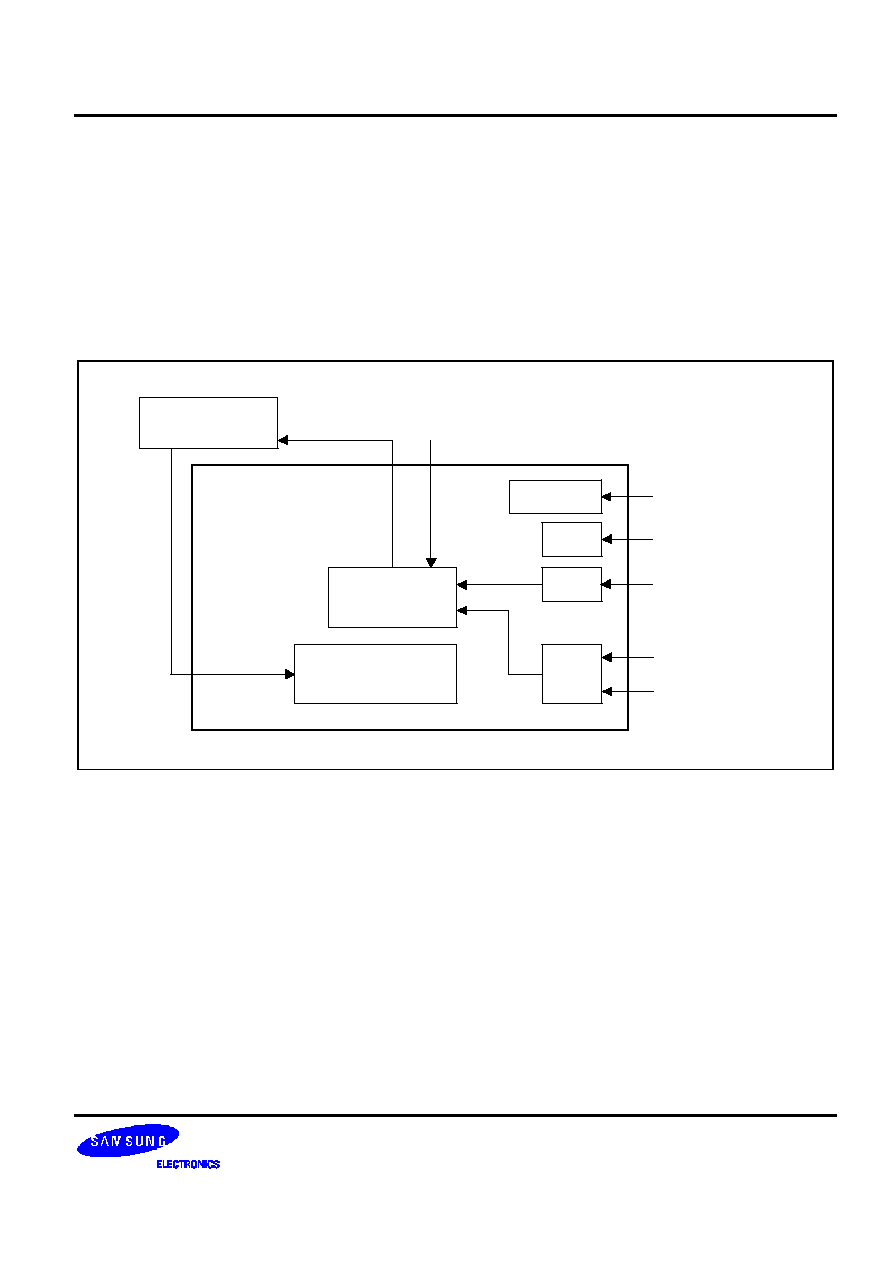
S3C2440A RISC MICROPROCESSOR
CLOCK & POWER MANAGEMENT
7-17
Power Control of VDDi and VDDiarm
In SLEEP mode, VDDi, VDDiarm, VDDMPLL and VDDUPLL will be turned off, which is controlled by PWREN pin.
If PWREN signal is activated(H), VDDi and VDDiarm are supplied by an external voltage regulator. If PWREN pin is
inactive (L), the VDDi and VDDiarm are turned off.
NOTE
Although VDDi, VDDiarm, VDDMPLL and VDDUPLL may be turned off, the other power pins have to be
supplied.
S3C2440A
Power CTRL
(Alive Block)
RTC Alarm
EINT
External Interrupt
3.3V Power
PWREN
VDDi
VDDiarm
VDDMPLL
VDDUPLL
Core & Peripherals
RTC
I/O
Regulator
1.2V/1.3V
EN
1.2V/1.3V
Power
VDDalive
ADC
1.8V~3.6V
Memory
Interface
1.8V/2.5V/3.3V
3.3V
Figure 7-12. SLEEP Mode
NOTE
During sleep mode, if you don't use Touch Screen panel, Touch ports (XP, XM, YP, and YM) must be
floating. That is, Touch ports (XP, XM, YP, and YM) shouldn't be connected to GND sources. Because
XP,YP will be maintained H during sleep mode.

CLOCK & POWER MANAGEMENT
S3C2440A RISC MICROPROCESSOR
7-18
Signaling EINT[15:0] for Wakeup
The S3C2440A can be woken up from SLEEP mode only if the following conditions are met.
a) Level signals (H or L) or edge signals (rising, falling or both) are asserted on EINTn input pin.
b) The EINTn pin has to be configured as EINT in the GPIO control register.
c) nBATT_FLT pin has to be H level. It is important to configure the EINTn in the GPIO control register as an
external interrupt pins, considering the condition a) above.
Just after the wake-up, the corresponding EINTn pin will not be used for wakeup. This means that the pin can be
used as an external interrupt request pin again.
Entering IDLE Mode
If CLKCON[2] is set to 1 to enter the IDLE mode, the S3C2440A will enter IDLE mode after some delay (until the
power control logic receives ACK signal from the CPU wrapper).
PLL On/Off
The PLL can only be turned off for low power consumption in slow mode. If the PLL is turned off in any other mode,
MCU operation is not guaranteed.
When the processor is in SLOW mode and tries to change its state into other state with the PLL turned on, then
SLOW_BIT should be clear to move to another state after PLL stabilization
Pull-up Resistors on the Data Bus and SLEEP Mode
In SLEEP mode, the data bus (D[31:0] or D[15:0] ) can be selected as Hi-z state and Output Low state.
The data bus can be set as Hi-z status with turning on pull-up register or can be set as output low with turning off
pull-up register for low power consumption in SLEEP mode. D[31:0] pin pull-up resistors can be controlled by the
GPIO control register (MISCCR). However, if there is an external bus holder, such as 74LVCH162245, on the data
bus, User can select one of two status ≠ one is output low with pull-up off, the other is Hi-z with pull-up off - , which
consumes less power.

S3C2440A RISC MICROPROCESSOR
CLOCK & POWER MANAGEMENT
7-19
Output Port State and SLEEP Mode
The output port should have a proper logic level in power off mode, which makes the current consumption minimized.
If there is no load on an output port pin, H level is preferred. If output is L, the current will be consumed through the
internal parasitic resistance; if the output is H, the current will not be consumed. For an output port, the current
consumption can be reduced if the output state is H.
It is recommended that the output ports be in H state to reduce current consumption in SLEEP mode.
Battery Fault Signal (nBATT_FLT)
There are two functions in nBATT_FLT pin, they are as follows;
-- When CPU is not in SLEEP mode, nBATT_FLT pin will cause the interrupt request by setting
BATT_FUNC(MISCCR[22:20]) as 10x'b. The interrupt attribute of the nBATT_FLT is L-level triggered.
-- While CPU is in SLEEP mode, assertion of the nBATT_FLT will prohibit the wake up from the sleep mode, which
is achieved by setting BATT_FUNC(MISCCR[22:20]) as 11x'b. So, Any wake-up source will be masked if
nBATT_FLT is asserted, which is protecting the system malfunction of the low battery capacity
ADC Power Down
The ADC has an additional power-down bit in ADCCON. If the S3C2440A enters the SLEEP mode, the ADC should
enter its own power-down mode.
CLOCK & POWER MANAGEMENT
S3C2440A RISC MICROPROCESSOR
7-20
CLOCK GENERATOR & POWER MANAGEMENT SPECIAL REGISTER
LOCK TIME COUNT REGISTER (LOCKTIME)
Register
Address
R/W
Description
Reset Value
LOCKTIME
0x4C000000
R/W
PLL lock time count register
0xFFFFFFFF
LOCKTIME
Bit
Description
Initial State
U_LTIME
[31:16]
UPLL lock time count value for UCLK.
(U_LTIME > 300uS)
0xFFFF
M_LTIME
[15:0]
MPLL lock time count value for FCLK, HCLK, and PCLK
(M_LTIME > 300uS)
0xFFFF
MPLL Control Register
Mpll = (2 * m * Fin) / (p * 2
S
)
m = (MDIV + 8), p = (PDIV + 2), s = SDIV
UPLL Control Register
Upll = (m * Fin) / (p * 2
S
)
m = (MDIV + 8), p = (PDIV + 2), s = SDIV
PLL Value Selection Guide (MPLLCON)
1. F
OUT
= 2 * m * Fin / (p*2
S
), F
VCO
= 2 * m * Fin / p where: m=MDIV+8, p=PDIV+2, s=SDIV
2. 600MHz
F
VCO
1.2GHz
3. 200MHz
FCLK
OUT
600MHz
4. Don't set the P or M value as zero, that is, setting the P=000000, M=00000000 can cause malfunction of
the PLL.
5. The proper range of P and M: 1
P
62, 1
M
248
NOTE
Although there is the rule for choosing PLL value, we recommend only the values in the PLL value
recommendation
table. If you have to use another value, please contact us.
S3C2440A RISC MICROPROCESSOR
CLOCK & POWER MANAGEMENT
7-21
PLL CONTROL REGISTER (MPLLCON & UPLLCON)
Register
Address
R/W
Description
Reset Value
MPLLCON
0x4C000004
R/W
MPLL configuration register
0x00096030
UPLLCON
0x4C000008
R/W
UPLL configuration register
0x0004d030
PLLCON
Bit
Description
Initial State
MDIV
[19:12]
Main divider control
0x96 / 0x4d
PDIV
[9:4]
Pre-divider control
0x03 / 0x03
SDIV
[1:0]
Post divider control
0x0 / 0x0
NOTE: When you set MPLL&UPLL values, you have to set the UPLL value first and then the MPLL value. (Needs intervals
approximately 7 NOP)
PLL VALUE SELECTION TABLE
It is not easy to find a proper PLL value. So, we recommend referring to the following PLL value recommendation
table.
Input Frequency
Output Frequency
MDIV
PDIV
SDIV
12.0000MHz
48.00 MHz
(Note)
56(0x38)
2
2
12.0000MHz
96.00 MHz
(Note)
56(0x38)
2
1
12.0000MHz
271.50 MHz
173(0xad)
2
2
12.0000MHz
304.00 MHz
68(0x44)
1
1
12.0000MHz
405.00 MHz
127(0x7f)
2
1
12.0000MHz
532.00 MHz
125(0x7d)
1
1
16.9344MHz
47.98 MHz
(Note)
60(0x3c)
4
2
16.9344MHz
95.96 MHz
(Note)
60(0x3c)
4
1
16.9344MHz
266.72 MHz
118(0x76)
2
2
16.9344MHz
296.35 MHz
97(0x61)
1
2
16.9344MHz
399.65 MHz
110(0x6e)
3
1
16.9344MHz
530.61 MHz
86(0x56)
1
1
16.9344MHz
533.43 MHz
118(0x76)
1
1
NOTE: The 48.00MHz and 96MHz output is used for UPLLCON register.

CLOCK & POWER MANAGEMENT
S3C2440A RISC MICROPROCESSOR
7-22
CLOCK CONTROL REGISTER (CLKCON)
Register
Address
R/W
Description
Reset Value
CLKCON
0x4C00000C
R/W
Clock generator control register
0xFFFFF0
CLKCON
Bit
Description
Initial State
AC97
[20]
Control PCLK into AC97 block.
0 = Disable, 1 = Enable
1
Camera
[19]
Control HCLK into Camera block.
0 = Disable, 1 = Enable
1
SPI
[18]
Control PCLK into SPI block.
0 = Disable, 1 = Enable
1
IIS
[17]
Control PCLK into IIS block.
0 = Disable, 1 = Enable
1
IIC
[16]
Control PCLK into IIC block.
0 = Disable, 1 = Enable
1
ADC(&Touch Screen)
[15]
Control PCLK into ADC block.
0 = Disable, 1 = Enable
1
RTC
[14]
Control PCLK into RTC control block.
Even if this bit is cleared to 0, RTC timer is alive.
0 = Disable, 1 = Enable
1
GPIO
[13]
Control PCLK into GPIO block.
0 = Disable, 1 = Enable
1
UART2
[12]
Control PCLK into UART2 block.
0 = Disable, 1 = Enable
1
UART1
[11]
Control PCLK into UART1 block.
0 = Disable, 1 = Enable
1
UART0
[10]
Control PCLK into UART0 block.
0 = Disable, 1 = Enable
1
SDI
[9]
Control PCLK into SDI interface block.
0 = Disable, 1 = Enable
1
PWMTIMER
[8]
Control PCLK into PWMTIMER block.
0 = Disable, 1 = Enable
1
USB device
[7]
Control PCLK into USB device block.
0 = Disable, 1 = Enable
1
USB host
[6]
Control HCLK into USB host block.
0 = Disable, 1 = Enable
1
LCDC
[5]
Control HCLK into LCDC block.
0 = Disable, 1 = Enable
1
NAND Flash Controller
[4]
Control HCLK into NAND Flash Controller block.
0 = Disable, 1 = Enable
1
SLEEP
[3]
Control SLEEP mode of S3C2440A.
0 = Disable, 1 = Transition to SLEEP mode
0
IDLE BIT
[2]
Enter IDLE mode. This bit is not cleared automatically.
0 = Disable, 1 = Transition to IDLE mode
0
Reserved
[1:0]
Reserved
0

S3C2440A RISC MICROPROCESSOR
CLOCK & POWER MANAGEMENT
7-23
CLOCK SLOW CONTROL (CLKSLOW) REGISTER
Register
Address
R/W
Description
Reset Value
CLKSLOW
0x4C000010
R/W
Slow clock control register
0x00000004
CLKSLOW
Bit
Description
Initial State
UCLK_ON
[7]
0: UCLK ON (UPLL is also turned on and the UPLL lock time is
inserted automatically.)
1: UCLK OFF (UPLL is also turned off.)
0
Reserved
[6]
Reserved
≠
MPLL_OFF
[5]
0: Turn on PLL.
After PLL stabilization time (minimum 300us), SLOW_BIT
can be cleared to 0.
1: Turn off PLL.
PLL is turned off only when SLOW_BIT is 1.
0
SLOW_BIT
[4]
0 : FCLK = Mpll (MPLL output)
1: SLOW mode
FCLK = input clock/(2xSLOW_VAL), when SLOW_VAL>0
FCLK = input clock, when SLOW_VAL=0.
Input clock = XTIpll or EXTCLK
0
Reserved
[3]
≠
≠
SLOW_VAL
[2:0]
The divider value for the slow clock when SLOW_BIT is on.
0x4

CLOCK & POWER MANAGEMENT
S3C2440A RISC MICROPROCESSOR
7-24
CLOCK DIVIDER CONTROL (CLKDIVN) REGISTER
Register
Address
R/W
Description
Reset Value
CLKDIVN
0x4C000014
R/W
Clock divider control register
0x00000000
CLKDIVN
Bit
Description
Initial State
DIVN_UPLL
[3]
UCLK select register(UCLK must be 48MHz for USB)
0: UCLK = UPLL clock
1: UCLK = UPLL clock / 2
Set to 0, when UPLL clock is set as 48MHz
Set to 1. when UPLL clock is set as 96MHz.
0
HDIVN
[2:1]
00 : HCLK = FCLK/1.
01 : HCLK = FCLK/2.
10 : HCLK = FCLK/4 when CAMDIVN[9] = 0.
HCLK= FCLK/8 when CAMDIVN[9] = 1.
11 : HCLK = FCLK/3 when CAMDIVN[8] = 0.
HCLK = FCLK/6 when CAMDIVN[8] = 1.
00
PDIVN
[0]
0: PCLK has the clock same as the HCLK/1.
1: PCLK has the clock same as the HCLK/2.
0
S3C2440A RISC MICROPROCESSOR
CLOCK & POWER MANAGEMENT
7-25
CAMERA CLOCK DIVIDER (CAMDIVN) REGISTER
Register
Address
R/W
Description
Reset Value
CAMDIVN
0x4C000018
R/W
Camera clock divider register
0x00000000
CAMDIVN
Bit
Description
Initial State
DVS_EN
[12]
0:DVS OFF
ARM core will run normally with FCLK (MPLLout).
1:DVS ON
ARM core will run at the same clock as system clock (HCLK).
0
Reserved
[11]
≠
0
Reserved
[10]
≠
0
HCLK4_HALF
[9]
HDIVN division rate change bit, when CLKDIVN[2:1]=10b.
0: HCLK = FCLK/4
1: HCLK= FCLK/8
Refer the CLKDIV register.
0
HCLK3_HALF
[8]
HDIVN division rate change bit, when CLKDIVN[2:1]=11b.
0: HCLK = FCLK/3
1: HCLK= FCLK/6
Refer the CLKDIV register.
0
CAMCLK_SEL
[4]
0:Use CAMCLK with UPLL output (CAMCLK=UPLL output).
1:CAMCLK is divided by CAMCLK_DIV value.
0
CAMCLK_DIV
[3:0]
CAMCLK divide factor setting register(0 ≠ 15).
Camera clock = UPLL / [(CAMCLK_DIV +1)x2].
This bit is valid when CAMCLK_SEL=1.
0

S3C2440A RISC MICROPROCESSOR DMA
8-1
8
DMA
OVERVIEW
The S3C2440A supports four-channel DMA controller located between the system bus and the peripheral bus. Each
channel of DMA controller can perform data movements between devices in the system bus and/or peripheral bus
with no restrictions. In other words, each channel can handle the following four cases:
1. Both source and destination are in the system bus
2. The source is in the system bus while the destination is in the peripheral bus
3. The source is in the peripheral bus while the destination is in the system bus
4. Both source and destination are in the peripheral bus
The main advantage of the DMA is that it can transfer the data without CPU intervention. The operation of DMA can
be initiated by software, or requests from internal peripherals or external request pins.
DMA
S3C2440A RISC MICROPROCESSOR
8-2
DMA REQUEST SOURCES
Each channel of the DMA controller can select one of the DMA request source among four DMA sources, if H/W
DMA request mode is selected by DCON register. (Note that if S/W request mode is selected, this DMA request
sources have no meaning at all.) Table 8-1 shows four DMA sources for each channel.
Table 8-1. DMA Request Sources for Each Channel
Source0
Source1
Source2
Source3
Source4
Source5
Source6
Ch-0
nXDREQ0
UART0
SDI
Timer
USB device EP1
I2SSDO
PCMIN
Ch-1
nXDREQ1
UART1
I2SSDI
SPI0
USB device EP2
PCMOUT
SDI
Ch-2
I2SSDO
I2SSDI
SDI
Timer
USB device EP3
PCMIN
MICIN
Ch-3
UART2
SDI
SPI1
Timer
USB device EP4
MICIN
PCMOUT
Here, nXDREQ0 and nXDREQ1 represent two external sources (External Devices), and I2SSDO and I2SSDI
represent IIS transmitting and receiving, respectively.
DMA OPERATION
DMA uses three-state FSM (Finite State Machine) for its operation, which is described in the three following steps:
State-1.
As an initial state, the DMA waits for a DMA request. Once the request is reached it goes to state-
2. At this state, DMA ACK and INT REQ are 0.
State-2.
In this state, DMA ACK becomes 1 and the counter (CURR_TC) is loaded from DCON[19:0]
register. Note that the DMA ACK remains 1 until it is cleared later.
State-3.
In this state, sub-FSM which handles the atomic operation of DMA is initiated. The sub-FSM reads
the data from the source address and then writes it to destination address. In this operation, data
size and transfer size (single or burst) are considered. This operation is repeated until the counter
(CURR_TC) becomes 0 in Whole service mode, while performed only once in Single service
mode. The main FSM (this FSM) counts down the CURR_TC when the sub-FSM finishes each of
atomic operation. In addition, this main FSM asserts the INT REQ signal when CURR_TC
becomes 0 and the interrupt setting of DCON[29] register is set to 1. In addition, it clears DMA
ACK .if one of the following conditions is met.
1) CURR_TC becomes 0 in the Whole service mode
2) Atomic operation finishes in the Single service mode.
Note that in the Single service mode, these three states of main FSM are performed and then stops, and wait for
another DMA REQ. And if DMA REQ comes in, all three states are repeated. Therefore, DMA ACK is asserted and
then de-asserted for each atomic transfer. In contrast, in the Whole service mode, main FSM waits at state-3 until
CURR_TC becomes 0. Therefore, DMA ACK is asserted during all the transfers and then de-asserted when TC
reaches 0.
However, INT REQ is asserted only if CURR_TC becomes 0 regardless of the service mode (Single service mode or
Whole service mode).
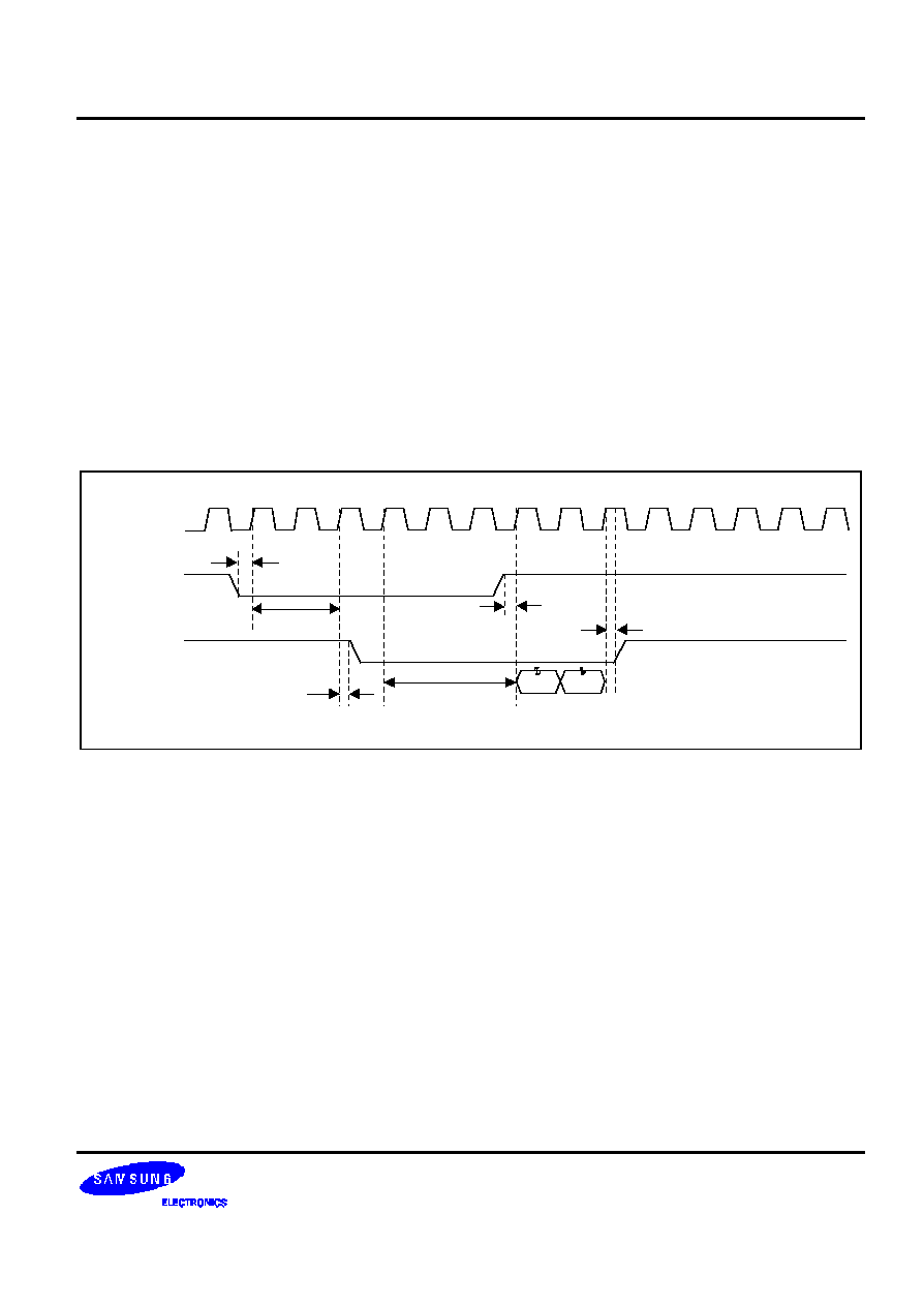
S3C2440A RISC MICROPROCESSOR DMA
8-3
EXTERNAL DMA DREQ/DACK PROTOCOL
There are three types of external DMA request/acknowledge protocols (Single service Demand, Single service
Handshake and Whole service Handshake mode). Each type defines how the signals like DMA request and
acknowledge are related to these protocols.
Basic DMA Timing
The DMA service means performing paired Reads and Writes cycles during DMA operation, which can make one
DMA operation. Figure 8-1 shows the basic Timing in the DMA operation of the S3C2440A.
-- The setup time and the delay time of XnXDREQ and XnXDACK are the same in all the modes.
-- If the completion of XnXDREQ meets its setup time, it is synchronized twice and then XnXDACK is asserted.
-- After assertion of XnXDACK, DMA requests the bus and if it gets the bus it performs its operations. XnXDACK is
de-asserted when DMA operation is completed.
XSCLK
9.3ns Setup
9.3ns Setup
6.8ns Delay
6.6ns Delay
Read
Write
Min. 2XSCLK
XnXDREQ
XnXDACK
Min. 3XSCLK
Figure 8-1. Basic DMA Timing Diagram
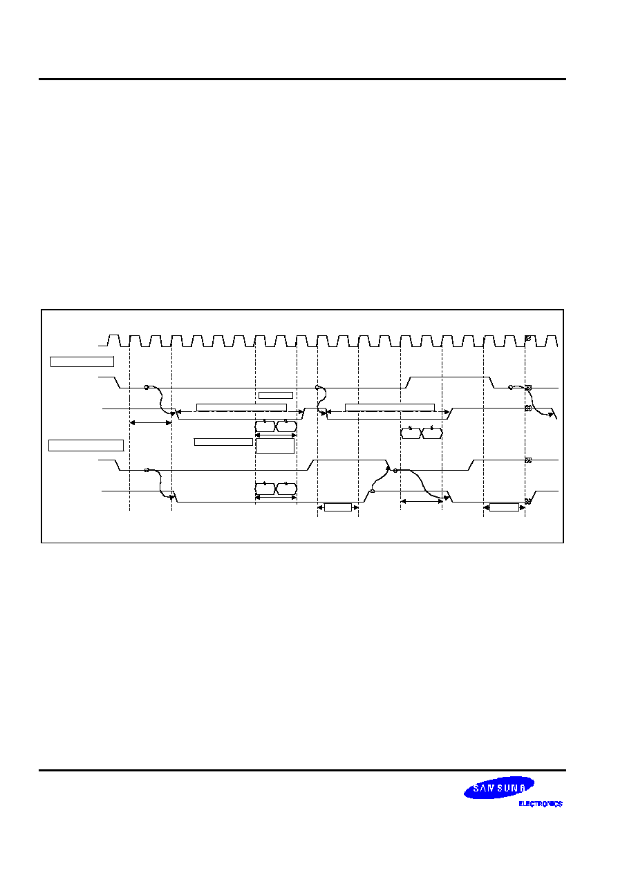
DMA
S3C2440A RISC MICROPROCESSOR
8-4
Demand/Handshake Mode Comparison
Demand and Handshake modes are related to the protocol between XnXDREQ and XnXDACK. Figure 8-2 shows the
differences between the two modes.
At the end of one transfer (Single/Burst transfer), DMA checks the state of double-synched XnXDREQ.
Demand Mode
-- If XnXDREQ remains asserted, the next transfer starts immediately. Otherwise it waits for XnXDREQ to
be asserted.
Handshake Mode
-- If XnXDREQ is de-asserted, DMA de-asserts XnXDACK in 2cycles. Otherwise it waits until XnXDREQ is
de-asserted.
Caution: XnXDREQ has to be asserted (low) only after the de-assertion (high) of XnXDACK.
Demand Mode
XSCLK
XnXDACK
XnXDACK
XnXDREQ
XnXDREQ
2cycles
Double Synch
Read
Write
Read Write
Handshake Mode
BUS Acquisiton
Actual
Transfer
1st Transfer
2nd Transfer
2cycles
Read
Write
Double Synch
2cycles
Figure 8-2. Demand/Handshake Mode Comparison
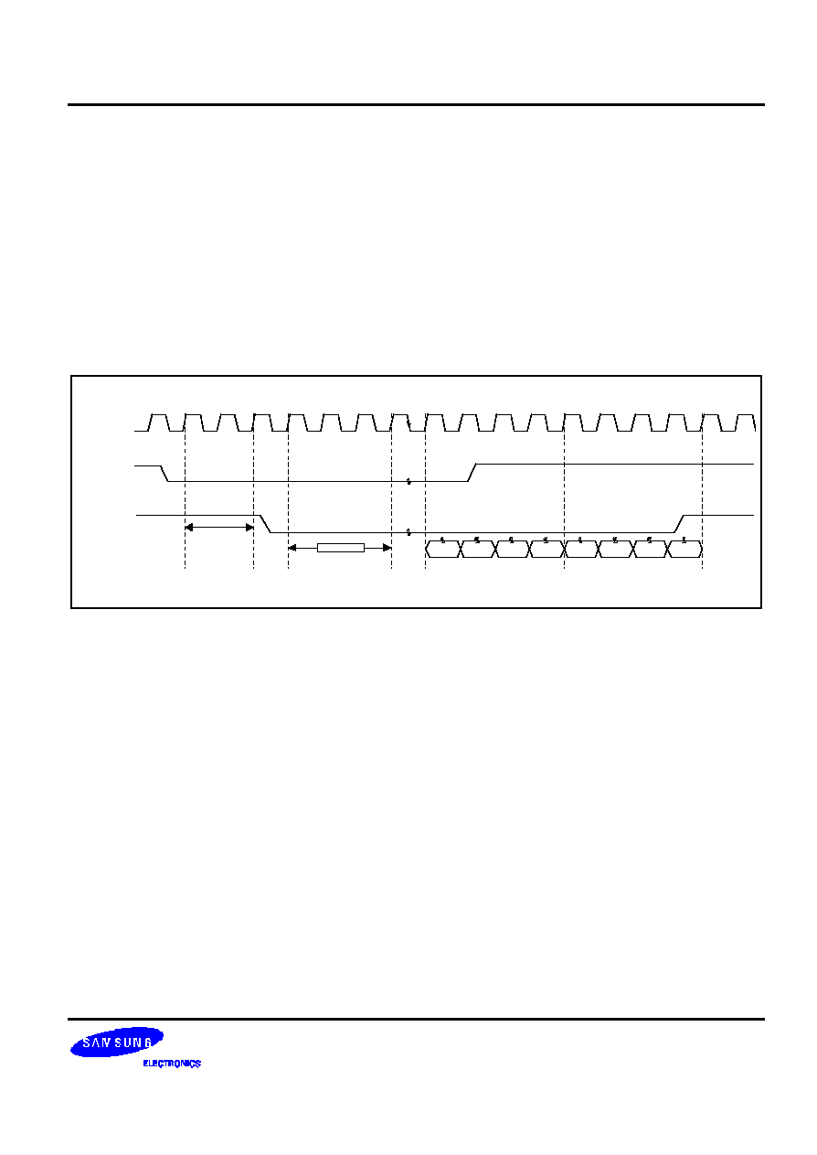
S3C2440A RISC MICROPROCESSOR DMA
8-5
Transfer Size
-- There are two different transfer sizes; unit and Burst 4.
-- DMA holds the bus firmly during the transfer of the chunk of data. Thus, other bus masters cannot get the bus.
Burst 4 Transfer Size
There will be four sequential Reads and Writes performed in the Burst 4 Transfer respectively.
NOTE
Unit Transfer size: One read and one write is performed.
XSCLK
XnXDREQ
XnXDACK
Read
Read Read
Write Write
Write
Read
Write
3 cycles
Double Synch
Figure 8-3. Burst 4 Transfer Size
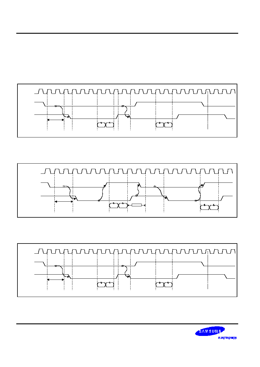
DMA
S3C2440A RISC MICROPROCESSOR
8-6
EXAMPLES
Single service in Demand Mode with Unit Transfer Size
The assertion of XnXDREQ will be a need for every unit transfer (Single service mode). The operation continues while
the XnXDREQ is asserted (Demand mode), and one pair of Read and Write (Single transfer size) is performed.
XnXDREQ
XnXDACK
XSCLK
Read Write
Read
Write
Double Synch
Figure 8-4. Single service in Demand Mode with Unit Transfer Size
Single service in Handshake Mode with Unit Transfer Size
XnXDREQ
XnXDACK
XSCLK
Read Write
Read
Write
2cycles
Double Synch
Figure 8-5. Single service in Handshake Mode with Unit Transfer Size
Whole service in Handshake Mode with Unit Transfer Size
XnXDREQ
XnXDACK
XSCLK
Read Write
Read
Write
Double Synch
Figure 8-6. Whole service in Handshake Mode with Unit Transfer Size
S3C2440A RISC MICROPROCESSOR DMA
8-7
DMA SPECIAL REGISTERS
Each DMA channel has nine control registers (36 in total since there are four channels for DMA controller). Six of the
control registers control the DMA transfer, and other three ones monitor the status of DMA controller. The details of
those registers are as follows.
DMA INITIAL SOURCE (DISRC) REGISTER
Register
Address
R/W
Description
Reset Value
DISRC0
0x4B000000
R/W
DMA 0 initial source register
0x00000000
DISRC1
0x4B000040
R/W
DMA 1 initial source register
0x00000000
DISRC2
0x4B000080
R/W
DMA 2 initial source register
0x00000000
DISRC3
0x4B0000C0
R/W
DMA 3 initial source register
0x00000000
DISRCn
Bit
Description
Initial State
S_ADDR
[30:0]
Base address (start address) of source data to transfer. This bit
value will be loaded into CURR_SRC only if the CURR_SRC is 0
and the DMA ACK is 1.
0x00000000
DMA INITIAL SOURCE CONTROL (DISRCC) REGISTER
Register
Address
R/W
Description
Reset Value
DISRCC0
0x4B000004
R/W
DMA 0 initial source control register
0x00000000
DISRCC1
0x4B000044
R/W
DMA 1 initial source control register
0x00000000
DISRCC2
0x4B000084
R/W
DMA 2 initial source control register
0x00000000
DISRCC3
0x4B0000C4
R/W
DMA 3 initial source control register
0x00000000
DISRCCn
Bit
Description
Initial State
LOC
[1]
Bit 1 is used to select the location of source.
0: the source is in the system bus (AHB).
1: the source is in the peripheral bus (APB).
0
INC
[0]
Bit 0 is used to select the address increment.
0 = Increment
1= Fixed
If it is 0, the address is increased by its data size after each
transfer in burst and single transfer mode.
If it is 1, the address is not changed after the transfer. (In the burst
mode, address is increased during the burst transfer, but the
address is recovered to its first value after the transfer.)
0
DMA
S3C2440A RISC MICROPROCESSOR
8-8
DMA INITIAL DESTINATION (DIDST) REGISTER
Register
Address
R/W
Description
Reset Value
DIDST0
0x4B000008
R/W
DMA 0 initial destination register
0x00000000
DIDST1
0x4B000048
R/W
DMA 1 initial destination register
0x00000000
DIDST2
0x4B000088
R/W
DMA 2 initial destination register
0x00000000
DIDST3
0x4B0000B8
R/W
DMA 3 initial destination register
0x00000000
DIDSTn
Bit
Description
Initial State
D_ADDR
[30:0]
Base address (start address) of destination for the transfer. This bit
value will be loaded into CURR_SRC only if the CURR_DST is 0
and the DMA ACK is 1.
0x00000000
DMA INITIAL DESTINATION CONTROL (DIDSTC) REGISTER
Register
Address
R/W
Description
Reset Value
DIDSTC0
0x4B00000C
R/W
DMA 0 initial destination control register
0x00000000
DIDSTC1
0x4B00004C
R/W
DMA 1 initial destination control register
0x00000000
DIDSTC2
0x4B00008C
R/W
DMA 2 initial destination control register
0x00000000
DIDSTC3
0x4B0000CC
R/W
DMA 3 initial destination control register
0x00000000
DIDSTCn
Bit
Description
Initial State
CHK_INT
[2]
Select interrupt occurrence time when auto reload is setting.
0: Interrupt will occur when TC reaches 0.
1: Interrupt will occur after auto-reload is performed.
0
LOC
[1]
Bit 1 is used to select the location of destination.
0: the destination is in the system bus (AHB).
1: the destination is in the peripheral bus (APB).
0
INC
[0]
Bit 0 is used to select the address increment.
0 = Increment
1 = Fixed
If it is 0, the address is increased by its data size after each transfer in
burst and single transfer mode.
If it is 1, the address is not changed after the transfer. (In the burst mode,
address is increased during the burst transfer, but the address is
recovered to its first value after the transfer.)
0

S3C2440A RISC MICROPROCESSOR DMA
8-9
DMA CONTROL (DCON) REGISTER
Register
Address
R/W
Description
Reset Value
DCON0
0x4B000010
R/W
DMA 0 control register
0x00000000
DCON1
0x4B000050
R/W
DMA 1 control register
0x00000000
DCON2
0x4B000090
R/W
DMA 2 control register
0x00000000
DCON3
0x4B0000D0
R/W
DMA 3 control register
0x00000000
DCONn
Bit
Description
Initial State
DMD_HS
[31]
Select one between Demand mode and Handshake mode.
0: Demand mode will be selected.
1: Handshake mode will be selected.
In both modes, DMA controller starts its transfer and asserts
DACK for a given asserted DREQ. The difference between the two
modes is whether it waits for the de-asserted DACK or not.
In the Handshake mode, DMA controller waits for the de-asserted
DREQ before starting a new transfer. If it finds the de-asserted
DREQ, it de-asserts DACK and waits for another asserted DREQ.
In contrast, in the Demand mode, DMA controller does not wait
until the DREQ is de-asserted. It just de-asserts DACK and then
starts another transfer if DREQ is asserted.
We recommend using Handshake mode for external DMA request
sources to prevent unintended starts of new transfers.
0
SYNC
[30]
Select DREQ/DACK synchronization.
0: DREQ and DACK are synchronized to PCLK (APB clock).
1: DREQ and DACK are synchronized to HCLK (AHB clock).
Therefore, for devices attached to AHB system bus, this bit has to
be set to 1, while for those attached to APB system, it should be
set to 0. For the devices attached to external systems, the user
should select this bit depending on which the external system is
synchronized with between AHB system and APB system.
0
INT
[29]
Enable/Disable the interrupt setting for CURR_TC (terminal count)
0: CURR_TC interrupt is disabled. The user has to view the transfer
count in the status register (i.e. polling).
1: Interrupt request is generated when all the transfer is done
(i.e. CURR_TC becomes 0).
0
TSZ
[28]
Select the transfer size of an atomic transfer (i.e. transfer
performed each time DMA owns the bus before releasing the bus).
0: A unit transfer is performed.
1: A burst transfer of length four is performed.
0

DMA
S3C2440A RISC MICROPROCESSOR
8-10
DMA CONTROL (DCON) REGISTER (Continued)
DCONn
Bit
Description
Initial State
SERVMODE
[27]
Select the service mode between Single service mode and Whole
service mode.
0: Single service mode is selected in which after each atomic
transfer (single or burst of length four) DMA stops and waits for
another DMA request.
1: Whole service mode is selected in which one request gets
atomic transfers to be repeated until the transfer count reaches to
0. In this mode, additional request are not required.
Note that even in the Whole service mode, DMA releases the bus
after each atomic transfer and then tries to re-get the bus to prevent
starving of other bus masters.
0
HWSRCSEL
[26:24]
Select DMA request source for each DMA.
DCON0: 000:nXDREQ0 001:UART0 010:SDI 011:Timer
100:USB device EP1
DCON1: 000:nXDREQ1 001:UART1 010:I2SSDI 011:SPI
100:USB device EP2
DCON2: 000:I2SSDO 001:I2SSDI 010:SDI 011:Timer
100:USB device EP3
DCON3: 000:UART2 001:SDI 010:SPI 011:Timer
100:USB device EP4
DCON0: 101:I2SSDO 110:PCMIN
DCON1: 101:PCMOUT 110:SDI
DCON2: 101:PCMIN 110:MICIN
DCON3: 101:MICIN 110:PCMOUT
These bits control the 4-1 MUX to select the DMA request source
of each DMA. These bits have meanings only if H/W request mode
is selected by DCONn[23].
00
SWHW_SEL
[23]
Select the DMA source between software (S/W request mode) and
hardware (H/W request mode).
0: S/W request mode is selected and DMA is triggered by setting
SW_TRIG bit of DMASKTRIG control register.
1: DMA source selected by bit[26:24] triggers the DMA operation.
0
RELOAD
[22]
Set the reload on/off option.
0: auto reload is performed when a current value of transfer count
becomes 0 (i.e. all the required transfers are performed).
1: DMA channel (DMA REQ) is turned off when a current value of
transfer count becomes 0. The channel on/off bit (DMASKTRIGn[1])
is set to 0 (DREQ off) to prevent unintended further start of new
DMA operation.
0

S3C2440A RISC MICROPROCESSOR DMA
8-11
DMA CONTROL (DCON) REGISTER (Continued)
DCONn
Bit
Description
Initial State
DSZ
[21:20]
Data size to be transferred.
00 = Byte 01 = Half word
10 = Word 11 = reserved
00
TC
[19:0]
Initial transfer count (or transfer beat).
Note that the actual number of bytes that are transferred is
computed by the following equation: DSZ x TSZ x TC. Where, DSZ,
TSZ (1 or 4), and TC represent data size DCONn[21:20], transfer
size DCONn[28], and initial transfer count, respectively. This value
will be loaded into CURR_TC only if the CURR_TC is 0 and the
DMA ACK is 1.
00000

DMA
S3C2440A RISC MICROPROCESSOR
8-12
DMA STATUS (DSTAT) REGISTER
Register
Address
R/W
Description
Reset Value
DSTAT0
0x4B000014
R
DMA 0 count register
000000h
DSTAT1
0x4B000054
R
DMA 1 count register
000000h
DSTAT2
0x4B000094
R
DMA 2 count register
000000h
DSTAT3
0x4B0000D4
R
DMA 3 count register
000000h
DSTATn
Bit
Description
Initial State
STAT
[21:20]
Status of this DMA controller.
00: Indicates that DMA controller is ready for another DMA request.
01: Indicates that DMA controller is busy for transfers.
00b
CURR_TC
[19:0]
Current value of transfer count.
Note that transfer count is initially set to the value of DCONn[19:0]
register and decreased by one at the end of every atomic transfer.
00000h
S3C2440A RISC MICROPROCESSOR DMA
8-13
DMA CURRENT SOURCE (DCSRC) REGISTER
Register
Address
R/W
Description
Reset Value
DCSRC0
0x4B000018
R
DMA 0 current source register
0x00000000
DCSRC1
0x4B000058
R
DMA 1 current source register
0x00000000
DCSRC2
0x4B000098
R
DMA 2 current source register
0x00000000
DCSRC3
0x4B0000D8
R
DMA 3 current source register
0x00000000
DCSRCn
Bit
Description
Initial State
CURR_SRC
[30:0]
Current source address for DMAn
0x00000000
CURRENT DESTINATION (DCDST) REGISTER
Register
Address
R/W
Description
Reset Value
DCDST0
0x4B00001C
R
DMA 0 current destination register
0x00000000
DCDST1
0x4B00005C
R
DMA 1 current destination register
0x00000000
DCDST2
0x4B00009C
R
DMA 2 current destination register
0x00000000
DCDST3
0x4B0000DC
R
DMA 3 current destination register
0x00000000
DCDSTn
Bit
Description
Initial State
CURR_DST
[30:0]
Current destination address for DMAn
0x00000000

DMA
S3C2440A RISC MICROPROCESSOR
8-14
DMA MASK TRIGGER (DMASKTRIG) REGISTER
Register
Address
R/W
Description
Reset Value
DMASKTRIG0
0x4B000020
R/W
DMA 0 mask trigger register
000
DMASKTRIG1
0x4B000060
R/W
DMA 1 mask trigger register
000
DMASKTRIG2
0x4B0000A0
R/W
DMA 2 mask trigger register
000
DMASKTRIG3
0x4B0000E0
R/W
DMA 3 mask trigger register
000
DMASKTRIGn
Bit
Description
Initial State
STOP
[2]
Stop the DMA operation.
1: DMA stops as soon as the current atomic transfer ends. If there
is no current running atomic transfer, DMA stops immediately. The
CURR_TC, CURR_SRC, and CURR_DST will be 0.
Note: Due to possible current atomic transfer, "stop" operation may
take
several cycles. The finish of the operation (i.e. actual stop time)
can be detected as soon as the channel on/off bit
(DMASKTRIGn[1]) is set to off. This stop is "actual stop".
0
ON_OFF
[1]
DMA channel on/off bit.
0: DMA channel is turned off.
(DMA request to this channel is ignored.)
1: DMA channel is turned on and the DMA request is handled. This
bit is automatically set to off if we set the DCONn[22] bit to "no
auto reload" and/or STOP bit of DMASKTRIGn to "stop".
Note that when DCON[22] bit is "no auto reload", this bit becomes
0 when CURR_TC reaches 0. If the STOP bit is 1, this bit becomes
0 as soon as the current atomic transfer is completed.
Note: This bit should not be changed manually during DMA operations
(i.e. this has to be changed only by using DCON[22] or STOP bit).
0
SW_TRIG
[0]
Trigger the DMA channel in S/W request mode.
1: it requests a DMA operation to this controller.
Note that this trigger gets effective after S/W request mode has to
be selected (DCONn[23]) and channel ON_OFF bit has to be set to
1 (channel on). When DMA operation starts, this bit is cleared
automatically.
0
NOTE: You are allowed to change the values of DISRC register, DIDST registers, and TC field of DCON register. Those
changes take effect only after the finish of current transfer (i.e. when CURR_TC becomes 0). On the other hand, any
change made to other registers and/or fields takes immediate effect. Therefore, be careful in changing those
registers and fields.

S3C2440A RISC MICROPROCESSOR
I/O PORTS
9-1
9
I/O PORTS
OVERVIEW
S3C2440A has 130 multi-functional input/output port pins and there are eight ports as shown below:
-- Port A(GPA): 25-output port
-- Port B(GPB): 11-input/out port
-- Port C(GPC): 16-input/output port
-- Port D(GPD): 16-input/output port
-- Port E(GPE): 16-input/output port
-- Port F(GPF): 8-input/output port
-- Port G(GPG): 16-input/output port
-- Port H(GPH): 9-input/output port
-- Port J(GPJ): 13-input/output port
Each port can be easily configured by software to meet various system configurations and design requirements. You
have to define which function of each pin is used before starting the main program. If a pin is not used for multiplexed
functions, the pin can be configured as I/O ports.
Initial pin states are configured seamlessly to avoid problems.

I/O PORTS
S3C2440A RISC MICROPROCESSOR
9-2
Table 9-1. S3C2440A Port Configuration (Sheet 1 of 5)
Port A
Selectable Pin Functions
GPA22
Output only
nFCE
≠
≠
GPA21
Output only
nRSTOUT
≠
≠
GPA20
Output only
nFRE
≠
≠
GPA19
Output only
nFWE
≠
≠
GPA18
Output only
ALE
≠
≠
GPA17
Output only
CLE
≠
≠
GPA16
Output only
nGCS5
≠
≠
GPA15
Output only
nGCS4
≠
≠
GPA14
Output only
nGCS3
≠
≠
GPA13
Output only
nGCS2
≠
≠
GPA12
Output only
nGCS1
≠
≠
GPA11
Output only
ADDR26
≠
≠
GPA10
Output only
ADDR25
≠
≠
GPA9
Output only
ADDR24
≠
≠
GPA8
Output only
ADDR23
≠
≠
GPA7
Output only
ADDR22
≠
≠
GPA6
Output only
ADDR21
≠
≠
GPA5
Output only
ADDR20
≠
≠
GPA4
Output only
ADDR19
≠
≠
GPA3
Output only
ADDR18
≠
≠
GPA2
Output only
ADDR17
≠
≠
GPA1
Output only
ADDR16
≠
≠
GPA0
Output only
ADDR0
≠
≠
S3C2440A RISC MICROPROCESSOR
I/O PORTS
9-3
Table 9-1. S3C2440A Port Configuration (Sheet 2 of 5) (Continued)
Port B
Selectable Pin Functions
GPB10
Input/output
nXDREQ0
≠
≠
GPB9
Input/output
nXDACK0
≠
≠
GPB8
Input/output
nXDREQ1
≠
≠
GPB7
Input/output
nXDACK1
≠
≠
GPB6
Input/output
nXBREQ
≠
≠
GPB5
Input/output
nXBACK
≠
≠
GPB4
Input/output
TCLK0
≠
≠
GPB3
Input/output
TOUT3
≠
≠
GPB2
Input/output
TOUT2
≠
≠
GPB1
Input/output
TOUT1
≠
≠
GPB0
Input/output
TOUT0
≠
≠
Port C
Selectable Pin Functions
GPC15
Input/output
VD7
≠
≠
GPC14
Input/output
VD6
≠
≠
GPC13
Input/output
VD5
≠
≠
GPC12
Input/output
VD4
≠
≠
GPC11
Input/output
VD3
≠
≠
GPC10
Input/output
VD2
≠
≠
GPC9
Input/output
VD1
≠
≠
GPC8
Input/output
VD0
≠
≠
GPC7
Input/output
LCD_LPCREVB
≠
≠
GPC6
Input/output
LCD_LPCREV
≠
≠
GPC5
Input/output
LCD_LPCOE
≠
≠
GPC4
Input/output
VM
≠
≠
GPC3
Input/output
VFRAME
≠
≠
GPC2
Input/output
VLINE
≠
≠
GPC1
Input/output
VCLK
≠
≠
GPC0
Input/output
LEND
≠
≠
I/O PORTS
S3C2440A RISC MICROPROCESSOR
9-4
Table 9-1. S3C2440A Port Configuration (Sheet 3 of 5) (Continued)
Port D
Selectable Pin Functions
GPD15
Input/output
VD23
nSS0
≠
GPD14
Input/output
VD22
nSS1
≠
GPD13
Input/output
VD21
≠
≠
GPD12
Input/output
VD20
≠
≠
GPD11
Input/output
VD19
≠
≠
GPD10
Input/output
VD18
SPICLK1
≠
GPD9
Input/output
VD17
SPIMOSI1
≠
GPD8
Input/output
VD16
SPIMISO1
≠
GPD7
Input/output
VD15
≠
≠
GPD6
Input/output
VD14
≠
≠
GPD5
Input/output
VD13
≠
≠
GPD4
Input/output
VD12
≠
≠
GPD3
Input/output
VD11
≠
≠
GPD2
Input/output
VD10
≠
≠
GPD1
Input/output
VD9
≠
≠
GPD0
Input/output
VD8
≠
≠
Port E
Selectable Pin Functions
GPE15
Input/output
IICSDA
≠
≠
GPE14
Input/output
IICSCL
≠
≠
GPE13
Input/output
SPICLK0
≠
≠
GPE12
Input/output
SPIMOSI0
≠
≠
GPE11
Input/output
SPIMISO0
≠
≠
GPE10
Input/output
SDDAT3
≠
≠
GPE9
Input/output
SDDAT2
≠
≠
GPE8
Input/output
SDDAT1
≠
≠
GPE7
Input/output
SDDAT0
≠
≠
GPE6
Input/output
SDCMD
≠
≠
GPE5
Input/output
SDCLK
≠
≠
GPE4
Input/output
I2SSDO
AC_SDATA_OUT
≠
GPE3
Input/output
I2SSDI
AC_SDATA_IN
≠
GPE2
Input/output
CDCLK
AC_nRESET
≠
GPE1
Input/output
I2SSCLK
AC_BIT_CLK
≠
GPE0
Input/output
I2SLRCK
AC_SYNC
≠
S3C2440A RISC MICROPROCESSOR
I/O PORTS
9-5
Table 9-1. S3C2440A Port Configuration (Sheet 4 of 5) (Continued)
Port F
Selectable Pin Functions
GPF7
Input/output
EINT7
≠
≠
GPF6
Input/output
EINT6
≠
≠
GPF5
Input/output
EINT5
≠
≠
GPF4
Input/output
EINT4
≠
≠
GPF3
Input/output
EINT3
≠
≠
GPF2
Input/output
EINT2
GPF1
Input/output
EINT1
GPF0
Input/output
EINT0
Port G
Selectable Pin Functions
GPG15
Input/output
EINT23
≠
≠
GPG14
Input/output
EINT22
≠
≠
GPG13
Input/output
EINT21
≠
≠
GPG12
Input/output
EINT20
≠
≠
GPG11
Input/output
EINT19
TCLK1
≠
GPG10
Input/output
EINT18
nCTS1
≠
GPG9
Input/output
EINT17
nRTS1
≠
GPG8
Input/output
EINT16
≠
≠
GPG7
Input/output
EINT15
SPICLK1
≠
GPG6
Input/output
EINT14
SPIMOSI1
≠
GPG5
Input/output
EINT13
SPIMISO1
≠
GPG4
Input/output
EINT12
LCD_PWREN
≠
GPG3
Input/output
EINT11
nSS1
≠
GPG2
Input/output
EINT10
nSS0
≠
GPG1
Input/output
EINT9
≠
≠
GPG0
Input/output
EINT8
≠
≠
I/O PORTS
S3C2440A RISC MICROPROCESSOR
9-6
Table 9-1. S3C2440A Port Configuration (Sheet 5 of 5) (Continued)
Port H
Selectable Pin Functions
GPH10
Input/output
CLKOUT1
≠
≠
GPH9
Input/output
CLKOUT0
≠
≠
GPH8
Input/output
UEXTCLK
≠
≠
GPH7
Input/output
RXD2
nCTS1
≠
GPH6
Input/output
TXD2
nRTS1
≠
GPH5
Input/output
RXD1
≠
≠
GPH4
Input/output
TXD1
≠
≠
GPH3
Input/output
RXD0
≠
≠
GPH2
Input/output
TXD0
≠
≠
GPH1
Input/output
nRTS0
≠
≠
GPH0
Input/output
nCTS0
≠
≠
Port J
Selectable Pin Functions
GPJ12
Input/output
CAMRESET
≠
≠
GPJ11
Input/output
CAMCLKOUT
≠
≠
GPJ10
Input/output
CAMHREF
≠
≠
GPJ9
Input/output
CAMVSYNC
≠
≠
GPJ8
Input/output
CAMPCLK
≠
≠
GPJ7
Input/output
CAMDATA7
≠
≠
GPJ6
Input/output
CAMDATA6
≠
≠
GPJ5
Input/output
CAMDATA5
≠
≠
GPJ4
Input/output
CAMDATA4
≠
≠
GPJ3
Input/output
CAMDATA3
≠
≠
GPJ2
Input/output
CAMDATA2
≠
≠
GPJ1
Input/output
CAMDATA1
≠
≠
GPJ0
Input/output
CAMDATA0
≠
≠

S3C2440A RISC MICROPROCESSOR
I/O PORTS
9-7
PORT CONTROL DESCRIPTIONS
PORT CONFIGURATION REGISTER (GPACON-GPJCON)
In S3C2440A, most of the pins are multiplexed pins. So, It is determined which function is selected for each pins.
The PnCON(port control register) determines which function is used for each pin.
If PE0 ≠ PE7 is used for the wakeup signal in power down mode, these ports must be configured in interrupt mode.
PORT DATA REGISTER (GPADAT-GPJDAT)
If Ports are configured as output ports, data can be written to the corresponding bit of PnDAT. If Ports are configured
as input ports, the data can be read from the corresponding bit of PnDAT.
PORT PULL-UP REGISTER (GPBUP-GPJUP)
The port pull-up register controls the pull-up resister enable/disable of each port group. When the corresponding bit is
0, the pull-up resister of the pin is enabled. When 1, the pull-up resister is disabled.
If the port pull-up register is enabled then the pull-up resisters work without pin's functional setting(input, output,
DATAn, EINTn and etc)
MISCELLANEOUS CONTROL REGISTER
This register controls DATA port pull-up resister in Sleep mode, USB pad, and CLKOUT selection.
EXTERNAL INTERRUPT CONTROL REGISTER
The 24 external interrupts are requested by various signaling methods. The EXTINT register configures the signaling
method among the low level trigger, high level trigger, falling edge trigger, rising edge trigger, and both edge trigger
for the external interrupt request
Because each external interrupt pin has a digital filter, the interrupt controller can recognize the request signal that is
longer than 3 clocks.
EINT[15:0] are used for wakeup sources.

I/O PORTS
S3C2440A RISC MICROPROCESSOR
9-8
I/O PORT CONTROL REGISTER
PORT A CONTROL REGISTERS (GPACON, GPADAT)
Register
Address
R/W
Description
Reset Value
GPACON
0x56000000
R/W
Configures the pins of port A
0xffffff
GPADAT
0x56000004
R/W
The data register for port A
Undef.
Reserved
0x56000008
≠
Reserved
Undef
Reserved
0x5600000c
≠
Reserved
Undef
GPACON
Bit
Description
GPA24
[24]
Reserved
GPA23
[23]
Reserved
GPA22
[22]
0 = Output
1 = nFCE
GPA21
[21]
0 = Output
1 = nRSTOUT
GPA20
[20]
0 = Output
1 = nFRE
GPA19
[19]
0 = Output
1 = nFWE
GPA18
[18]
0 = Output
1 = ALE
GPA17
[17]
0 = Output
1 = CLE
GPA16
[16]
0 = Output
1 = nGCS[5]
GPA15
[15]
0 = Output
1 = nGCS[4]
GPA14
[14]
0 = Output
1 = nGCS[3]
GPA13
[13]
0 = Output
1 = nGCS[2]
GPA12
[12]
0 = Output
1 = nGCS[1]
GPA11
[11]
0 = Output
1 = ADDR26
GPA10
[10]
0 = Output
1 = ADDR25
GPA9
[9]
0 = Output
1 = ADDR24
GPA8
[8]
0 = Output
1 = ADDR23
GPA7
[7]
0 = Output
1 = ADDR22
GPA6
[6]
0 = Output
1 = ADDR21
GPA5
[5]
0 = Output
1 = ADDR20
GPA4
[4]
0 = Output
1 = ADDR19
GPA3
[3]
0 = Output
1 = ADDR18
GPA2
[2]
0 = Output
1 = ADDR17
GPA1
[1]
0 = Output
1 = ADDR16
GPA0
[0]
0 = Output
1 = ADDR0
NOTE: The GPA21 signal level depends on VDDOP, the other pads (GPA0~20, GPA22~24) are all on VDDMOP.

S3C2440A RISC MICROPROCESSOR
I/O PORTS
9-9

I/O PORTS
S3C2440A RISC MICROPROCESSOR
9-10
PORT A CONTROL REGISTERS (GPACON, GPADAT) (Continued)
GPADAT
Bit
Description
GPA[24:0]
[24:0]
When the port is configured as output port, the pin state is the same as the
corresponding bit.
When the port is configured as functional pin, the undefined value will be
read.
NOTE: nRSTOUT = nRESET & nWDTRST & SW_RESET
S3C2440A RISC MICROPROCESSOR
I/O PORTS
9-11
PORT B CONTROL REGISTERS (GPBCON, GPBDAT, GPBUP)
Register
Address
R/W
Description
Reset Value
GPBCON
0x56000010
R/W
Configures the pins of port B
0x0
GPBDAT
0x56000014
R/W
The data register for port B
Undef.
GPBUP
0x56000018
R/W
Pull-up disable register for port B
0x0
Reserved
0x5600001c
PBCON
Bit
Description
GPB10
[21:20]
00 = Input
01 = Output
10 = nXDREQ0 11 = reserved
GPB9
[19:18]
00 = Input
01 = Output
10 = nXDACK0 11 = reserved
GPB8
[17:16]
00 = Input
01 = Output
10 = nXDREQ1 11 = Reserved
GPB7
[15:14]
00 = Input
01 = Output
10 = nXDACK1 11 = Reserved
GPB6
[13:12]
00 = Input
01 = Output
10 = nXBREQ 11 = reserved
GPB5
[11:10]
00 = Input
01 = Output
10 = nXBACK 11 = reserved
GPB4
[9:8]
00 = Input
01 = Output
10 = TCLK [0] 11 = reserved
GPB3
[7:6]
00 = Input
01 = Output
10 = TOUT3 11 = reserved
GPB2
[5:4]
00 = Input
01 = Output
10 = TOUT2 11 = reserved]
GPB1
[3:2]
00 = Input
01 = Output
10 = TOUT1 11 = reserved
GPB0
[1:0]
00 = Input
01 = Output
10 = TOUT0 11 = reserved
GPBDAT
Bit
Description
GPB[10:0]
[10:0]
When the port is configured as input port, the corresponding bit is the pin
state. When the port is configured as output port, the pin state is the same
as the corresponding bit. When the port is configured as functional pin, the
undefined value will be read.
GPBUP
Bit
Description
GPB[10:0]
[10:0]
0: The pull up function attached to the corresponding port pin is enabled.
1: The pull up function is disabled.

I/O PORTS
S3C2440A RISC MICROPROCESSOR
9-12
PORT C CONTROL REGISTERS (GPCCON, GPCDAT, GPCUP)
Register
Address
R/W
Description
Reset Value
GPCCON
0x56000020
R/W
Configures the pins of port C
0x0
GPCDAT
0x56000024
R/W
The data register for port C
Undef.
GPCUP
0x56000028
R/W
Pull-up disable register for port C
0x0
Reserved
0x5600002c
≠
≠
≠
GPCCON
Bit
Description
GPC15
[31:30]
00 = Input
01 = Output
10 = VD[7]
11 = Reserved
GPC14
[29:28]
00 = Input
01 = Output
10 = VD[6]
11 = Reserved
GPC13
[27:26]
00 = Input
01 = Output
10 = VD[5]
11 = Reserved
GPC12
[25:24]
00 = Input
01 = Output
10 = VD[4]
11 = Reserved
GPC11
[23:22]
00 = Input
01 = Output
10 = VD[3]
11 = Reserved
GPC10
[21:20]
00 = Input
01 = Output
10 = VD[2]
11 = Reserved
GPC9
[19:18]
00 = Input
01 = Output
10 = VD[1]
11 = Reserved
GPC8
[17:16]
00 = Input
01 = Output
10 = VD[0] 11 = Reserved
GPC7
[15:14]
00 = Input
01 = Output
10 = LCD_LPCREVB
11 = Reserved
GPC6
[13:12]
00 = Input
01 = Output
10 = LCD_LPCREV
11 = Reserved
GPC5
[11:10]
00 = Input
01 = Output
10 = LCD_LPCOE
11 = Reserved
GPC4
[9:8]
00 = Input
01 = Output
10 = VM 11 = I2SSDI
GPC3
[7:6]
00 = Input
01 = Output
10 = VFRAME 11 = Reserved
GPC2
[5:4]
00 = Input
01 = Output
10 = VLINE 11 = Reserved
GPC1
[3:2]
00 = Input
01 = Output
10 = VCLK
11 = Reserved
GPC0
[1:0]
00 = Input
01 = Output
10 = LEND
11 = Reserved
S3C2440A RISC MICROPROCESSOR
I/O PORTS
9-13
PORT C CONTROL REGISTERS (GPCCON, GPCDAT, GPCUP) (Continued)
GPCDAT
Bit
Description
GPC[15:0]
[15:0]
When the port is configured as input port, the corresponding bit is the pin
state. When the port is configured as output port, the pin state is the same
as the corresponding bit.
When the port is configured as functional pin, the undefined value will be
read.
GPCUP
Bit
Description
GPC[15:0]
[15:0]
0: The pull up function attached to the corresponding port pin is enabled.
1: The pull up function is disabled.

I/O PORTS
S3C2440A RISC MICROPROCESSOR
9-14
PORT D CONTROL REGISTERS (GPDCON, GPDDAT, GPDUP)
Register
Address
R/W
Description
Reset Value
GPDCON
0x56000030
R/W
Configures the pins of port D
0x0
GPDDAT
0x56000034
R/W
The data register for port D
Undef.
GPDUP
0x56000038
R/W
Pull-up disable register for port D
0xf000
Reserved
0x5600003c
≠
≠
≠
GPDCON
Bit
Description
GPD15
[31:30]
00 = Input
01 = Output
10 = VD[23]
11 = nSS0
GPD14
[29:28]
00 = Input
01 = Output
10 = VD[22]
11 = nSS1
GPD13
[27:26]
00 = Input
01 = Output
10 = VD[21]
11 = Reserved
GPD12
[25:24]
00 = Input
01 = Output
10 = VD[20]
11 = Reserved
GPD11
[23:22]
00 = Input
01 = Output
10 = VD[19]
11 = Reserved
GPD10
[21:20]
00 = Input
01 = Output
10 = VD[18]
11 = SPICLK1
GPD9
[19:18]
00 = Input
01 = Output
10 = VD[17]
11 = SPIMOSI1
GPD8
[17:16]
00 = Input
01 = Output
10 = VD[16]
11 = SPIMISO1
GPD7
[15:14]
00 = Input
01 = Output
10 = VD[15]
11 = Reserved
GPD6
[13:12]
00 = Input
01 = Output
10 = VD[14]
11 = Reserved
GPD5
[11:10]
00 = Input
01 = Output
10 = VD[13]
11 = Reserved
GPD4
[9:8]
00 = Input
01 = Output
10 = VD[12]
11 = Reserved
GPD3
[7:6]
00 = Input
01 = Output
10 = VD[11]
11 = Reserved
GPD2
[5:4]
00 = Input
01 = Output
10 = VD[10]
11 = Reserved
GPD1
[3:2]
00 = Input
01 = Output
10 = VD[9]
11 = Reserved
GPD0
[1:0]
00 = Input
01 = Output
10 = VD[8]
11 = Reserved

S3C2440A RISC MICROPROCESSOR
I/O PORTS
9-15
PORT D CONTROL REGISTERS (GPDCON, GPDDAT, GPDUP) (Continued)
GPDDAT
Bit
Description
GPD[15:0]
[15:0]
When the port is configured as input port, the corresponding bit is the pin
state. When the port is configured as output port, the pin state is the same
as the corresponding bit.
When the port is configured as functional pin, the undefined value will be
read.
GPDUP
Bit
Description
GPD[15:0]
[15:0]
0: The pull up function attached to the corresponding port pin is enabled.
1: The pull up function is disabled.

I/O PORTS
S3C2440A RISC MICROPROCESSOR
9-16
PORT E CONTROL REGISTERS (GPECON, GPEDAT, GPEUP)
Register
Address
R/W
Description
Reset Value
GPECON
0x56000040
R/W
Configures the pins of port E
0x0
GPEDAT
0x56000044
R/W
The data register for port E
Undef.
GPEUP
0x56000048
R/W
Pull-up disable register for port E
0x0000
Reserved
0x5600004c
≠
≠
≠
GPECON
Bit
Description
GPE15
[31:30]
00 = Input
01 = Output
10 = IICSDA
11 = Reserved
This pad is open-drain, There is no Pull-up option.
GPE14
[29:28]
00 = Input
01 = Output
10 = IICSCL
11 = Reserved
This pad is open-drain, There is no Pull-up option.
GPE13
[27:26]
00 = Input
01 = Output
10 = SPICLK0
11 = Reserved
GPE12
[25:24]
00 = Input
01 = Output
10 = SPIMOSI0
11 = Reserved
GPE11
[23:22]
00 = Input
01 = Output
10 = SPIMISO0
11 = Reserved
GPE10
[21:20]
00 = Input
01 = Output
10 = SDDAT3
11 = Reserved
GPE9
[19:18]
00 = Input
01 = Output
10 = SDDAT2
11 = Reserved
GPE8
[17:16]
00 = Input
01 = Output
10 = SDDAT1
11 = Reserved
GPE7
[15:14]
00 = Input
01 = Output
10 = SDDAT0
11 = Reserved
GPE6
[13:12]
00 = Input
01 = Output
10 = SDCMD 11 = Reserved
GPE5
[11:10]
00 = Input 01 = Output
10 = SDCLK
11 = Reserved
GPE4
[9:8]
00 = Input
01 = Output
10 = I2SDO 11 = AC_SDATA_OUT
GPE3
[7:6]
00 = Input
01 = Output
10 = I2SDI 11 = AC_SDATA_IN
GPE2
[5:4]
00 = Input
01 = Output
10 = CDCLK
11 = AC_nRESET
GPE1
[3:2]
00 = Input
01 = Output
10 = I2SSCLK
11 = AC_BIT_CLK
GPE0
[1:0]
00 = Input
01 = Output
10 = I2SLRCK
11 = AC_SYNC

S3C2440A RISC MICROPROCESSOR
I/O PORTS
9-17
PORT E CONTROL REGISTERS (GPECON, GPEDAT, GPEUP) (Continued)
GPEDAT
Bit
Description
GPE[15:0]
[15:0]
When the port is configured as an input port, the corresponding bit is the
pin state. When the port is configured as an output port, the pin state is the
same as the corresponding bit.
When the port is configured as a functional pin, the undefined value will be
read.
GPEUP
Bit
Description
GPE[13:0]
[13:0]
0: The pull up function attached to the corresponding port pin is enabled.
1: The pull up function is disabled.
I/O PORTS
S3C2440A RISC MICROPROCESSOR
9-18
PORT F CONTROL REGISTERS (GPFCON, GPFDAT)
If GPF0≠GPF7 will be used for wake-up signals at power down mode, the ports will be set in interrupt mode.
Register
Address
R/W
Description
Reset Value
GPFCON
0x56000050
R/W
Configures the pins of port F
0x0
GPFDAT
0x56000054
R/W
The data register for port F
Undef.
GPFUP
0x56000058
R/W
Pull-up disable register for port F
0x000
Reserved
0x5600005c
≠
≠
≠
GPFCON
Bit
Description
GPF7
[15:14]
00 = Input
01 = Output
10 = EINT[7]
11 = Reserved
GPF6
[13:12]
00 = Input
01 = Output
10 = EINT[6]
11 = Reserved
GPF5
[11:10]
00 = Input
01 = Output
10 = EINT[5]
11 = Reserved
GPF4
[9:8]
00 = Input
01 = Output
10 = EINT[4]
11 = Reserved
GPF3
[7:6]
00 = Input
01 = Output
10 = EINT[3]
11 = Reserved
GPF2
[5:4]
00 = Input
01 = Output
10 = EINT2]
11 = Reserved
GPF1
[3:2]
00 = Input
01 = Output
10 = EINT[1]
11 = Reserved
GPF0
[1:0]
00 = Input
01 = Output
10 = EINT[0]
11 = Reserved
GPFDAT
Bit
Description
GPF[7:0]
[7:0]
When the port is configured as an input port, the corresponding bit is the
pin state. When the port is configured as an output port, the pin state is the
same as the corresponding bit.
When the port is configured as functional pin, the undefined value will be
read.
GPFUP
Bit
Description
GPF[7:0]
[7:0]
0: The pull up function attached to the corresponding port pin is enabled.
1: The pull up function is disabled.
S3C2440A RISC MICROPROCESSOR
I/O PORTS
9-19
PORT G CONTROL REGISTERS (GPGCON, GPGDAT)
If GPG0≠GPG7 will be used for wake-up signals at Sleep mode, the ports will be set in interrupt mode.
Register
Address
R/W
Description
Reset Value
GPGCON
0x56000060
R/W
Configures the pins of port G
0x0
GPGDAT
0x56000064
R/W
The data register for port G
Undef.
GPGUP
0x56000068
R/W
Pull-up disable register for port G
0xfc00
GPGCON
Bit
Description
GPG15*
[31:30]
00 = Input
01 = Output
10 = EINT[23]
11 = Reserved
GPG14*
[29:28]
00 = Input
01 = Output
10 = EINT[22]
11 = Reserved
GPG13*
[27:26]
00 = Input
01 = Output
10 = EINT[21]
11 = Reserved
GPG12
[25:24]
00 = Input
01 = Output
10 = EINT[20]
11 = Reserved
GPG11
[23:22]
00 = Input
01 = Output
10 = EINT[19]
11 = TCLK[1]
GPG10
[21:20]
00 = Input
01 = Output
10 = EINT[18]
11 = nCTS1
GPG9
[19:18]
00 = Input
01 = Output
10 = EINT[17]
11 = nRTS1
GPG8
[17:16]
00 = Input
01 = Output
10 = EINT[16]
11 = Reserved
GPG7
[15:14]
00 = Input
01 = Output
10 = EINT[15]
11 = SPICLK1
GPG6
[13:12]
00 = Input
01 = Output
10 = EINT[14]
11 = SPIMOSI1
GPG5
[11:10]
00 = Input
01 = Output
10 = EINT[13]
11 = SPIMISO1
GPG4
[9:8]
00 = Input
01 = Output
10 = EINT[12]
11 = LCD_PWRDN
GPG3
[7:6]
00 = Input
01 = Output
10 = EINT[11]
11 = nSS1
GPG2
[5:4]
00 = Input
01 = Output
10 = EINT[10]
11 = nSS0
GPG1
[3:2]
00 = Input
01 = Output
10 = EINT[9]
11 = Reserved
GPG0
[1:0]
00 = Input
01 = Output
10 = EINT[8]
11 = Reserved
NOTE: GPG[15:13] must be selected as Input in NAND boot mode.

I/O PORTS
S3C2440A RISC MICROPROCESSOR
9-20
PORT G CONTROL REGISTERS (GPGCON, GPGDAT) (Continued)
GPGDAT
Bit
Description
GPG[15:0]
[15:0]
When the port is configured as an input port, the corresponding bit is the
pin state. When the port is configured as an output port, the pin state is the
same as the corresponding bit.
When the port is configured as functional pin, the undefined value will be
read.
GPGUP
Bit
Description
GPG[15:0]
[15:0]
0: The pull up function attached to the corresponding port pin is enabled.
1: The pull up function is disabled.

S3C2440A RISC MICROPROCESSOR
I/O PORTS
9-21
PORT H CONTROL REGISTERS (GPHCON, GPHDAT)
Register
Address
R/W
Description
Reset Value
GPHCON
0x56000070
R/W
Configures the pins of port H
0x0
GPHDAT
0x56000074
R/W
The data register for port H
Undef.
GPHUP
0x56000078
R/W
pull-up disable register for port H
0x000
Reserved
0x5600007c
≠
≠
≠
GPHCON
Bit
Description
GPH10
[21:20]
00 = Input
01 = Output
10 = CLKOUT1
11 = Reserved
GPH9
[19:18]
00 = Input
01 = Output
10 = CLKOUT0
11 = Reserved
GPH8
[17:16]
00 = Input
01 = Output
10 = UEXTCLK
11 = Reserved
GPH7
[15:14]
00 = Input
01 = Output
10 = RXD[2]
11 = nCTS1
GPH6
[13:12]
00 = Input
01 = Output
10 = TXD[2]
11 = nRTS1
GPH5
[11:10]
00 = Input
01 = Output
10 = RXD[1]
11 = Reserved
GPH4
[9:8]
00 = Input
01 = Output
10 = TXD[1]
11 = Reserved
GPH3
[7:6]
00 = Input
01 = Output
10 = RXD[0]
11 = reserved
GPH2
[5:4]
00 = Input
01 = Output
10 = TXD[0]
11 = Reserved
GPH1
[3:2]
00 = Input
01 = Output
10 = nRTS0
11 = Reserved
GPH0
[1:0]
00 = Input
01 = Output
10 = nCTS0
11 = Reserved
GPHDAT
Bit
Description
GPH[10:0]
[10:0]
When the port is configured as an input port, the corresponding bit is the
pin state. When the port is configured as an output port, the pin state is the
same as the corresponding bit.
When the port is configured as functional pin, the undefined value will be
read.
GPHUP
Bit
Description
GPH[10:0]
[10:0]
0: The pull up function attached to the corresponding port pin is enabled.
1: The pull up function is disabled.
I/O PORTS
S3C2440A RISC MICROPROCESSOR
9-22
PORT J CONTROL REGISTERS (GPJCON, GPJDAT)
Register
Address
R/W
Description
Reset Value
GPJCON
0x560000d0
R/W
Configures the pins of port J
0x0
GPJDAT
0x560000d4
R/W
The data register for port J
Undef.
GPJUP
0x560000d8
R/W
pull-up disable register for port J
0x0000
Reserved
0x560000dc
≠
≠
≠
GPJCON
Bit
Description
GPJ12
[25:24]
00 = Input
01 = Output
10 = CAMRESET
11 = Reserved
GPJ11
[23:22]
00 = Input
01 = Output
10 = CAMCLKOUT
11 = Reserved
GPJ10
[21:20]
00 = Input
01 = Output
10 = CAMHREF
11 = Reserved
GPJ9
[19:18]
00 = Input
01 = Output
10 = CAMVSYNC
11 = Reserved
GPJ8
[17:16]
00 = Input
01 = Output
10 = CAMPCLK
11 = Reserved
GPJ7
[15:14]
00 = Input
01 = Output
10 = CAMDATA[7]
11 = Reserved
GPJ6
[13:12]
00 = Input
01 = Output
10 = CAMDATA[6]
11 = Reserved
GPJ5
[11:10]
00 = Input
01 = Output
10 = CAMDATA[5]
11 = Reserved
GPJ4
[9:8]
00 = Input
01 = Output
10 = CAMDATA[4]
11 = Reserved
GPJ3
[7:6]
00 = Input
01 = Output
10 = CAMDATA[3]
11 = Reserved
GPJ2
[5:4]
00 = Input
01 = Output
10 = CAMDATA[2]
11 = Reserved
GPJ1
[3:2]
00 = Input
01 = Output
10 = CAMDATA[1]
11 = Reserved
GPJ0
[1:0]
00 = Input
01 = Output
10 = CAMDATA[0]
11 = Reserved

S3C2440A RISC MICROPROCESSOR
I/O PORTS
9-23
PORT J CONTROL REGISTERS (GPJCON, GPJDAT) (Continued)
GPJDAT
Bit
Description
GPJ15:0]
[12:0]
When the port is configured as an input port, the corresponding bit is the
pin state. When the port is configured as an output port, the pin state is
the same as the corresponding bit.
When the port is configured as functional pin, the undefined value will be
read.
GPJUP
Bit
Description
GPJ[12:0]
[12:0]
0: The pull up function attached to the corresponding port pin is enabled.
1: The pull up function is disabled.
I/O PORTS
S3C2440A RISC MICROPROCESSOR
9-24
MISCELLANEOUS CONTROL REGISTER (MISCCR)
In Sleep mode, the data bus(D[31:0] or D[15:0] can be set as Hi-Z and Output `0' state. But, because of the
characteristics of IO pad, the data bus pull-up resisters have to be turned on or off to reduce the power consumption.
D[31:0] pin pull-up resisters can be controlled by MISCCR register.
Pads related USB are controlled by this register for USB host, or for USB device.
Register
Address
R/W
Description
Reset Value
MISCCR
0x56000080
R/W
Miscellaneous control register
0x10020
MISCCR
Bit
Description
Reset Value
Reserved
[24]
Reserve to 0.
0
Reserved
[23]
Reserve to 0.
0
BATT_FUNC
[22:20]
Battery fault function selection.
0XX: In nBATT_FLT=0, The system will be in reset status.
After reset, Change this bit to other values, this bit is only
for preventing from booting in Battery fault status.
10X: In sleep mode status, when nBATT_FLT=0, the
system will wake-up. In normal mode, when
nBATT_FLT=0, the Battery fault interrupt will occur.
110: In sleep mode status, during nBATT_FLT=0, the
system will ignore all the wake-up events(the system will
not wake-up by wake-up source).
In normal mode, nBATT_FLT signal cannot affect the
system.
111: nBATT_FLT function disable.
000
OFFREFRESH
[19]
0: Self refresh retain disable
1: Self refresh retain enable
When 1, After wake-up from sleep, The self-refresh will be
retained.
0
nEN_SCLK1
[18]
SCLK1 output enable
0: SCLK1 = SCLK
1: SCLK1 = 0
0
nEN_SCLK0
[17]
SCLK0 output enable
0: SCLK0 = SCLK
1: SCLK 0 = 0
0
nRSTCON
[16]
nRSTOUT signal manual control
0: nRSTOUT signal level will be low (`0')
1: nRSTOUT signal level will be high (`1')
1
Reserved
[15:14]
≠
00
SEL_SUSPND1
[13]
USB Port 1 Suspend mode
0 = Normal mode
1 = Suspend mode
0
SEL_SUSPND0
[12]
USB Port 0 Suspend mode
0 = Normal mode
1 = Suspend mode
0

S3C2440A RISC MICROPROCESSOR
I/O PORTS
9-25
MISCELLANEOUS CONTROL REGISTER (MISCCR) (Continued)
MISCCR
Bit
Description
Reset Value
CLKSEL1
(Note)
[10:8]
Select source clock with CLKOUT1 pad
000 = MPLL output
001 = UPLL output
010 = RTC clock output
011 = HCLK
100 = PCLK
101 = DCLK1
11x = reserved
000
Reserved
[7]
≠
0
CLKSEL0
(Note)
[6:4]
Select source clock with CLKOUT0 pad
000 = MPLL INPUT Clock(XTAL)
001 = UPLL output
010 = FCLK
011 = HCLK
100 = PCLK
101 = DCLK0
11x = reserved
010
SEL_USBPAD
[3]
USB1 Host/Device select register.
0 = Use USB1 as device
1 = Use USB1 as host
0
Reserved
[2]
Reserved
0
SPUCR1
[1]
0 = DATA[31:16] port pull-up resister is enabled
1 = DATA[31:16] port pull-up resister is disabled
0
SPUCR0
[0]
0 = DATA[15:0] port pull-up resister is enabled
1 = DATA[15:0] port pull-up resister is disabled
0
NOTE: We recommend not to use this ouput pad to other device's pll clock source.

I/O PORTS
S3C2440A RISC MICROPROCESSOR
9-26
DCLK CONTROL REGISTERS (DCLKCON)
Register
Address
R/W
Description
Reset Value
DCLKCON
0x56000084
R/W
DCLK0/1 control register
0x0
DCLKCON
Bit
Description
DCLK1CMP
[27:24]
DCLK1 compare value clock toggle value. ( < DCLK1DIV)
If the DCLK1CMP is n, Low level duration is( n + 1),
High level duration is((DCLK1DIV + 1) ≠( n +1))
DCLK1DIV
[23:20]
DCLK1 divide value
DCLK1 frequency = source clock /( DCLK1DIV + 1)
DCLK1SelCK
[17]
Select DCLK1 source clock
0 = PCLK
1 = UCLK( USB)
DCLK1EN
[16]
DCLK1 enable
0 = DCLK1 disable
1 = DCLK1 enable
DCLK0CMP
[11:8]
DCLK0 compare value clock toggle value.( < DCLK0DIV)
If the DCLK0CMP is n, Low level duration is( n + 1),
High level duration is((DCLK0DIV + 1) ≠( n +1))
DCLK0DIV
[7:4]
DCLK0 divide value.
DCLK0 frequency = source clock /( DCLK0DIV + 1)
DCLK0SelCK
[1]
Select DCLK0 source clock
0 = PCLK
1 = UCLK( USB)
DCLK0EN
[0]
DCLK0 enable
0 = DCLK0 disable
1 = DCLK0 enable
DCLKnDIV + 1
DCLKnCMP + 1
S3C2440A RISC MICROPROCESSOR
I/O PORTS
9-27
EXTINTn (External Interrupt Control Register n)
The 8 external interrupts can be requested by various signaling methods. The EXTINT register configures the
signaling method between the level trigger and edge trigger for the external interrupt request, and also configures the
signal polarity.
To recognize the level interrupt, the valid logic level on EXTINTn pin must be retained for 40ns at least because of the
noise filter.
Register
Address
R/W
Description
Reset Value
EXTINT0
0x56000088
R/W
External interrupt control register 0
0x000000
EXTINT1
0x5600008c
R/W
External interrupt control register 1
0x000000
EXTINT2
0x56000090
R/W
External interrupt control register 2
0x000000
EXTINT0
Bit
Description
EINT7
[30:28]
Setting the signaling method of the EINT7.
000 = Low level 001 = High level 01x = Falling edge triggered
10x = Rising edge triggered 11x = Both edge triggered
EINT6
[26:24]
Setting the signaling method of the EINT6.
000 = Low level 001 = High level 01x = Falling edge triggered
10x = Rising edge triggered 11x = Both edge triggered
EINT5
[22:20]
Setting the signaling method of the EINT5.
000 = Low level 001 = High level 01x = Falling edge triggered
10x = Rising edge triggered 11x = Both edge triggered
EINT4
[18:16]
Setting the signaling method of the EINT4.
000 = Low level 001 = High level 01x = Falling edge triggered
10x = Rising edge triggered 11x = Both edge triggered
EINT3
[14:12]
Setting the signaling method of the EINT3.
000 = Low level 001 = High level 01x = Falling edge triggered
10x = Rising edge triggered 11x = Both edge triggered
EINT2
[10:8]
Setting the signaling method of the EINT2.
000 = Low level 001 = High level 01x = Falling edge triggered
10x = Rising edge triggered 11x = Both edge triggered
EINT1
[6:4]
Setting the signaling method of the EINT1.
000 = Low level 001 = High level 01x = Falling edge triggered
10x = Rising edge triggered 11x = Both edge triggered
EINT0
[2:0]
Setting the signaling method of the EINT0.
000 = Low level 001 = High level 01x = Falling edge triggered
10x = Rising edge triggered 11x = Both edge triggered

I/O PORTS
S3C2440A RISC MICROPROCESSOR
9-28
EXTINTn (External Interrupt Control Register n) (Continued)
EXTINT1
Bit
Description
FLTEN15
[31]
Filter enable for EINT15
0 = Filter Disable
1 = Filter Enable
EINT15
[30:28]
Setting the signaling method of the EINT15.
000 = Low level 001 = High level 01x = Falling edge triggered
10x = Rising edge triggered 11x = Both edge triggered
FLTEN14
[27]
Filter enable for EINT14
0 = Filter Disable
1 = Filter Enable
EINT14
[26:24]
Setting the signaling method of the EINT14.
000 = Low level 001 = High level 01x = Falling edge triggered
10x = Rising edge triggered 11x = Both edge triggered
FLTEN13
[23]
Filter enable for EINT13
0 = Filter Disable
1 = Filter Enable
EINT13
[22:20]
Setting the signaling method of the EINT13.
000 = Low level 001 = High level 01x = Falling edge triggered
10x = Rising edge triggered 11x = Both edge triggered
FLTEN12
[19]
Filter enable for EINT12
0 = Filter Disable
1 = Filter Enable
EINT12
[18:16]
Setting the signaling method of the EINT12.
000 = Low level 001 = High level 01x = Falling edge triggered
10x = Rising edge triggered 11x = Both edge triggered
FLTEN11
[15]
Filter enable for EINT11
0 = Filter Disable
1 = Filter Enable
EINT11
[14:12]
Setting the signaling method of the EINT11.
000 = Low level 001 = High level 01x = Falling edge triggered
10x = Rising edge triggered 11x = Both edge triggered
FLTEN10
[11]
Filter enable for EINT10
0 = Filter Disable
1 = Filter Enable
EINT10
[10:8]
Setting the signaling method of the EINT10.
000 = Low level 001 = High level 01x = Falling edge triggered
10x = Rising edge triggered 11x = Both edge triggered
FLTEN9
[7]
Filter enable for EINT9
0 = Filter Disable
1 = Filter Enable
EINT9
[6:4]
Setting the signaling method of the EINT9.
000 = Low level 001 = High level 01x = Falling edge triggered
10x = Rising edge triggered 11x = Both edge triggered
FLTEN8
[3]
Filter enable for EINT8
0 = Filter Disable
1 = Filter Enable
EINT8
[2:0]
Setting the signaling method of the EINT8.
000 = Low level 001 = High level 01x = Falling edge triggered
10x = Rising edge triggered 11x = Both edge triggered

S3C2440A RISC MICROPROCESSOR
I/O PORTS
9-29
EXTINTn (External Interrupt Control Register n) (Continued)
EXTINT2
Bit
Description
Reset Value
FLTEN23
[31]
Filter enable for EINT23
0 = Filter Disable
1= Filter Enable
0
EINT23
[30:28]
Setting the signaling method of the EINT23.
000 = Low level
001 = High level
01x = Falling edge triggered
10x = Rising edge triggered
11x = Both edge triggered
000
FLTEN22
[27]
Filter Enable for EINT22
0 = Filter Disable
1= Filter Enable
0
EINT22
[26:24]
Setting the signaling method of the EINT22.
000 = Low level
001 = High level
01x = Falling edge triggered
10x = Rising edge triggered
11x = Both edge triggered
000
FLTEN21
[23]
Filter Enable for EINT21
0 = Filter Disable
1= Filter Enable
0
EINT21
[22:20]
Setting the signaling method of the EINT21.
000 = Low level
001 = High level
01x = Falling edge triggered
10x = Rising edge triggered
11x = Both edge triggered
000
FLTEN20
[19]
Filter Enable for EINT20
0 = Filter Disable
1= Filter Enable
0
EINT20
[18:16]
Setting the signaling method of the EINT20.
000 = Low level
001 = High level
01x = Falling edge triggered
10x = Rising edge triggered
11x = Both edge triggered
000
FLTEN19
[15]
Filter enable for EINT19
0 = Filter Disable
1= Filter Enable
0
EINT19
[14:12]
Setting the signaling method of the EINT19.
000 = Low level
001 = High level
01x = Falling edge triggered
10x = Rising edge triggered
11x = Both edge triggered
000
FLTEN18
[11]
Filter enable for EINT18
0 = Filter Disable
1= Filter Enable
0
EINT18
[10:8]
Setting the signaling method of the EINT18.
000 = Low level
001 = High level
01x = Falling edge triggered
10x = Rising edge triggered
11x = Both edge triggered
000

I/O PORTS
S3C2440A RISC MICROPROCESSOR
9-30
EXTINTn (External Interrupt Control Register n) (Continued)
EXTINT2
Bit
Description
Reset Value
FLTEN17
[7]
Filter enable for EINT17
0 = Filter Disable
1= Filter Enable
0
EINT17
[6:4]
Setting the signaling method of the EINT17.
000 = Low level
001 = High level
01x = Falling edge triggered
10x = Rising edge triggered
11x = Both edge triggered
000
FLTEN16
[3]
Filter enable for EINT16
0 = Filter Disable
1= Filter Enable
0
EINT16
[2:0]
Setting the signaling method of the EINT16.
000 = Low level
001 = High level
01x = Falling edge triggered
10x = Rising edge triggered
11x = Both edge triggered
000
S3C2440A RISC MICROPROCESSOR
I/O PORTS
9-31
EINTFLTn (External Interrupt Filter Register n)
To recognize the level interrupt, the valid logic level on EXTINTn pin must be retained for 40ns at least because of the
noise filter.
Register
Address
R/W
Description
Reset Value
EINTFLT0
0x56000094
R/W
Reserved
0x000000
EINTFLT1
0x56000098
R/W
Reserved
0x000000
EINTFLT2
0x5600009c
R/W
External interrupt control register 2
0x000000
EINTFLT3
0x4c6000a0
R/W
External interrupt control register 3
0x000000
EINTFLT2
Bit
Description
EINTFLT19
[30:24]
Filtering width of EINT19
FLTCLK18
[23]
Filter clock of EINT18 (configured by OM)
0 = PCLK
1= EXTCLK/OSC_CLK
EINTFLT18
[22:16]
Filtering width of EINT18
FLTCLK17
[15]
Filter clock of EINT17 (configured by OM)
0 = PCLK
1= EXTCLK/OSC_CLK
EINTFLT17
[14:8]
Filtering width of EINT17
FLTCLK16
[7]
Filter clock of EINT16 (configured by OM)
0 = PCLK
1= EXTCLK/OSC_CLK
EINTFLT16
[6:0]
Filtering width of EINT16
EINTFLT3
Bit
Description
FLTCLK23
[31]
Filter clock of EINT23 (configured by OM)
0 = PCLK
1= EXTCLK/OSC_CLK
EINTFLT23
[30:24]
Filtering width of EINT23
FLTCLK22
[23]
Filter clock of EINT22 (configured by OM)
0 = PCLK
1= EXTCLK/OSC_CLK
EINTFLT22
[22:16]
Filtering width of EINT22
FLTCLK21
[15]
Filter clock of EINT21(configured by OM)
0 = PCLK
1= EXTCLK/OSC_CLK
EINTFLT21
[14:8]
Filtering width of EINT21
FLTCLK20
[7]
Filter clock of EINT20 (configured by OM)
0 = PCLK
1= EXTCLK/OSC_CLK
EINTFLT20
[6:0]
Filtering width of EINT20

I/O PORTS
S3C2440A RISC MICROPROCESSOR
9-32
EINTMASK (External Interrupt Mask Register)
Register
Address
R/W
Description
Reset Value
EINTMASK
0x560000a4
R/W
External interrupt mask register
0x000fffff
EINTMASK
Bit
Description
EINT23
[23]
0 = enable interrupt 1= masked
EINT22
[22]
0 = enable interrupt 1= masked
EINT21
[21]
0 = enable interrupt 1= masked
EINT20
[20]
0 = enable interrupt 1= masked
EINT19
[19]
0 = enable interrupt 1= masked
EINT18
[18]
0 = enable interrupt 1= masked
EINT17
[17]
0 = enable interrupt 1= masked
EINT16
[16]
0 = enable interrupt 1= masked
EINT15
[15]
0 = enable interrupt 1= masked
EINT14
[14]
0 = enable interrupt 1= masked
EINT13
[13]
0 = enable interrupt 1= masked
EINT12
[12]
0 = enable interrupt 1= masked
EINT11
[11]
0 = enable interrupt 1= masked
EINT10
[10]
0 = enable interrupt 1= masked
EINT9
[9]
0 = enable interrupt 1= masked
EINT8
[8]
0 = enable interrupt 1= masked
EINT7
[7]
0 = enable interrupt 1= masked
EINT6
[6]
0 = enable interrupt 1= masked
EINT5
[5]
0 = enable interrupt 1= masked
EINT4
[4]
0 = enable interrupt 1= masked
Reserved
[3:0]
Reserved

S3C2440A RISC MICROPROCESSOR
I/O PORTS
9-33
EINTPEND (External Interrupt Pending Register)
Register
Address
R/W
Description
Reset Value
EINTPEND
0x560000a8
R/W
External interrupt pending register
0x00
EINTPEND
Bit
Description
Reset Value
EINT23
[23]
It is cleard by writing "1"
0 = Not occur 1 = Occur interrupt
0
EINT22
[22]
It is cleard by writing "1"
0 = Not occur 1 = Occur interrupt
0
EINT21
[21]
It is cleard by writing "1"
0 = Not occur 1 = Occur interrupt
0
EINT20
[20]
It is cleard by writing "1"
0 = Not occur 1 = Occur interrupt
0
EINT19
[19]
It is cleard by writing "1"
0 = Not occur 1 = Occur interrupt
0
EINT18
[18]
It is cleard by writing "1"
0 = Not occur 1 = Occur interrupt
0
EINT17
[17]
It is cleard by writing "1"
0 = Not occur 1 = Occur interrupt
0
EINT16
[16]
It is cleard by writing "1"
0 = Not occur 1 = Occur interrupt
0
EINT15
[15]
It is cleard by writing "1"
0 = Not occur 1 = Occur interrupt
0
EINT14
[14]
It is cleard by writing "1"
0 = Not occur 1 = Occur interrupt
0
EINT13
[13]
It is cleard by writing "1"
0 = Not occur 1 = Occur interrupt
0
EINT12
[12]
It is cleard by writing "1"
0 = Not occur 1 = Occur interrupt
0
EINT11
[11]
It is cleard by writing "1"
0 = Not occur 1 = Occur interrupt
0
EINT10
[10]
It is cleard by writing "1"
0 = Not occur 1 = Occur interrupt
0
EINT9
[9]
It is cleard by writing "1"
0 = Not occur 1 = Occur interrupt
0
EINT8
[8]
It is cleard by writing "1"
0 = Not occur 1 = Occur interrupt
0
EINT7
[7]
It is cleard by writing "1"
0 = Not occur 1 = Occur interrupt
0
EINT6
[6]
It is cleard by writing "1"
0 = Not occur 1 = Occur interrupt
0
EINT5
[5]
It is cleard by writing "1"
0 = Not occur 1 = Occur interrupt
0
EINT4
[4]
It is cleard by writing "1"
0 = Not occur 1 = Occur interrupt
0
Reserved
[3:0]
Reserved
0000

I/O PORTS
S3C2440A RISC MICROPROCESSOR
9-34
S3C2440A RISC MICROPROCESSOR
I/O PORTS
9-35
GSTATUSn (General Status Registers)
Register
Address
R/W
Description
Reset Value
GSTATUS0
0x560000ac
R
External pin status
Not define
GSTATUS1
0x560000b0
R
Chip ID
0x32440001
GSTATUS2
0x560000b4
R/W
Reset status
0x1
GSTATUS3
0x560000b8
R/W
Inform register
0x0
GSTATUS4
0x560000bc
R/W
Inform register
0x0
GSTATUS0
Bit
Description
nWAIT
[3]
Status of nWAIT pin
NCON
[2]
Status of NCON pin
RnB
[1]
Status of RnB pin
BATT_FLT
[0]
Status of BATT_FLT pin
GSTATUS1
Bit
Description
CHIP ID
[0]
ID register = 0x32440001
GSTATUS2
Bit
Description
Reserved
[3]
Reserved
WDTRST
[2]
Boot is caused by Watch Dog Reset
cleared by writing "1"
SLEEPRST
[1]
Boot is caused by wakeup reset in sleep mode
cleared by writing "1".
PWRST
[0]
Boot is caused by power on reset
cleared by writing "1"
GSTATUS3
Bit
Description
inform
[31:0]
Inform register. This register is cleard by power on reset. Otherwise,
preserve data value.
GSTATUS4
Bit
Description
inform
[31:0]
Inform register. This register is cleard by power on reset. Otherwise,
preserve data value.
I/O PORTS
S3C2440A RISC MICROPROCESSOR
9-36
DSCn (Drive Strength Control)
Control the Memory I/O drive strength
Register
Address
R/W
Description
Reset Value
DSC0
0x560000c4
R/W
Strength control register 0
0x0
DSC1
0x560000c8
R/W
Strength control register 1
0x0
DSC0
Bit
Description
Reset Value
nEN_DSC
[31]
Enable Drive Strength Control
0: enable
1: Disable
0
Reserved
[30:10]
≠
0
DSC_ADR
[9:8]
Address Bus Drive strength.
00: 12mA
10: 10mA
01: 8mA
11: 6mA
00
DSC_DATA3
[7:6]
DATA[31:24] I/O Drive strength.
00: 12mA
10: 10mA
01: 8mA
11: 6mA
00
DSC_DATA2
[5:4]
DATA[23:16] I/O Drive strength.
00: 12mA
10: 10mA
01: 8mA
11: 6mA
00
DSC_DATA1
[3:2]
DATA[15:8] I/O Drive strength.
00: 12mA
10: 10mA
01: 8mA
11: 6mA
00
DSC_DATA0
[1:0]
DATA[7:0] I/O Drive strength.
00: 12mA
10: 10mA
01: 8mA
11: 6mA
00
S3C2440A RISC MICROPROCESSOR
I/O PORTS
9-37
DSCn (Drive Strength Control)
DSC1
Bit
Description
Reset Value
DSC_SCK1
[29:28]
SCLK1 drive strength.
00: 12mA
10: 10mA
01: 8mA
11: 6mA
00
DSC_SCK0
[27:26]
SCLK0 drive strength.
00: 12mA
10: 10mA
01: 8mA
11: 6mA
00
DSC_SCKE
[25:24]
SCKE drive strength.
00: 10mA
10: 8mA
01: 6mA
11: 4mA
00
DSC_SDR
[23:22]
nSRAS/nSCAS Drive strength.
00: 10mA
10: 8mA
01: 6mA
11: 4mA
00
DSC_NFC
[21:20]
Nand flash control drive strength (nFCE, nFRE, nFWE,
CLE, ALE).
00: 10mA
10: 8mA
01: 6mA
11: 4mA
00
DSC_BE
[19:18]
nBE[3:0] drive strength.
00: 10mA
10: 8mA
01: 6mA
11: 4mA
00
DSC_WOE
[17:16]
nWE/nOE drive strength.
00: 10mA
10: 8mA
01: 6mA
11: 4mA
00
DSC_CS7
[15:14]
nGCS7 drive strength.
00: 10mA
10: 8mA
01: 6mA
11: 4mA
00
DSC_CS6
[13:12]
nGCS6 drive strength.
00: 10mA
10: 8mA
01: 6mA
11: 4mA
00
DSC_CS5
[11:10]
nGCS5 drive strength.
00: 10mA
10: 8mA
01: 6mA
11: 4mA
00
DSC_CS4
[9:8]
nGCS4 drive strength.
00: 10mA
10: 8mA
01: 6mA
11: 4mA
00
DSC_CS3
[7:6]
nGCS3 drive strength.
00: 10mA
10: 8mA
01: 6mA
11: 4mA
00
DSC_CS2
[5:4]
nGCS2 drive strength.
00: 10mA
10: 8mA
01: 6mA
11: 4mA
00
DSC_CS1
[3:2]
nGCS1 drive strength.
00: 10mA
10: 8mA
01: 6mA
11: 4mA
00
DSC_CS0
[1:0]
nGCS0 drive strength.
00: 10mA
10: 8mA
01: 6mA
11: 4mA
00
I/O PORTS
S3C2440A RISC MICROPROCESSOR
9-38
MSLCON (Memory Sleep Control Register)
Select memory interface status when in SLEEP mode.
Register
Address
R/W
Description
Reset Value
MSLCON
0x560000cc
R/W
Memory sleep control register
0x0
MSLCON
Bit
Description
Reset Value
PSC_DATA
[11]
DATA[31:0] pin status in sleep mode.
0: Hi-Z
1: Output "0".
0
PSC_WAIT
[10]
nWAIT pin status in sleep mode.
0: Input
1: Output "0"
0
PSC_RnB
[9]
RnB pin status in sleep mode.
0: Input
1: Output "0"
0
PSC_NF
[8]
NAND Flash I/F pin status in sleep mode(
nFCE,nFRE,nFWE,ALE,CLE).
0: Inactive(nFCE,nFRE,nFWE,ALE,CLE = 11100)
1: Hi-Z
0
PSC_SDR
[7]
nSRAS, nSCAS pin status in sleep mode.
0: Inactive("1")
1: Hi-Z
0
PSC_DQM
[6]
DQM[3:0]/nWE[3:0] pin status in sleep mode.
0: Inactive
1: Hi-Z
0
PSC_OE
[5]
nOE pin status in sleep mode.
0: Inactive("1")
1: Hi-Z
0
PSC_WE
[4]
nWE pin status in sleep mode.
0: Inactive("1")
1: Hi-Z
0
PSC_GCS0
[3]
nGCS[0] pin status in sleep mode.
0: Inactive("1")
1: Hi-Z
0
PSC_GCS51
[2]
nGCS[5:1] pin status in sleep mode.
0: Inactive("1")
1: Hi-Z
0
PSC_GCS6
[1]
nGCS[6] pin status in sleep mode.
0: Inactive("1")
1: Hi-Z
0
PSC_GCS7
[0]
nGCS[7] pin status in sleep mode.
0: Inactive("1")
1: Hi-Z
0

S3C2440A RISC MICROPROCESSOR
PWM TIMER
10-1
10
PWM TIMER
OVERVIEW
The S3C2440A has five 16-bit timers. Timer 0, 1, 2, and 3 have Pulse Width Modulation (PWM) function. Timer 4 has
an internal timer only with no output pins. The timer 0 has a dead-zone generator, which is used with a large current
device.
The timer 0 and 1 share an 8-bit prescaler, while the timer 2, 3 and 4 share other 8-bit prescaler. Each timer has a
clock divider, which generates 5 different divided signals (1/2, 1/4, 1/8, 1/16, and TCLK). Each timer block receives
its own clock signals from the clock divider, which receives the clock from the corresponding 8-bit prescaler. The 8-
bit prescaler is programmable and divides the PCLK according to the loading value, which is stored in TCFG0 and
TCFG1 registers.
The timer count buffer register (TCNTBn) has an initial value which is loaded into the down-counter when the timer is
enabled. The timer compare buffer register (TCMPBn) has an initial value which is loaded into the compare register to
be compared with the down-counter value. This double buffering feature of TCNTBn and TCMPBn makes the timer
generate a stable output when the frequency and duty ratio are changed.
Each timer has its own 16-bit down counter, which is driven by the timer clock. When the down counter reaches
zero, the timer interrupt request is generated to inform the CPU that the timer operation has been completed. When
the timer counter reaches zero, the value of corresponding TCNTBn is automatically loaded into the down counter to
continue the next operation. However, if the timer stops, for example, by clearing the timer enable bit of TCONn
during the timer running mode, the value of TCNTBn will not be reloaded into the counter.
The value of TCMPBn is used for pulse width modulation (PWM). The timer control logic changes the output level
when the down-counter value matches the value of the compare register in the timer control logic. Therefore, the
compare register determines the turn-on time (or turn-off time) of a PWM output.
FEATURE
-- Five 16-bit timers
-- Two 8-bit prescalers & Two 4-bit divider
-- Programmable duty control of output waveform (PWM)
-- Auto reload mode or one-shot pulse mode
-- Dead-zone generator
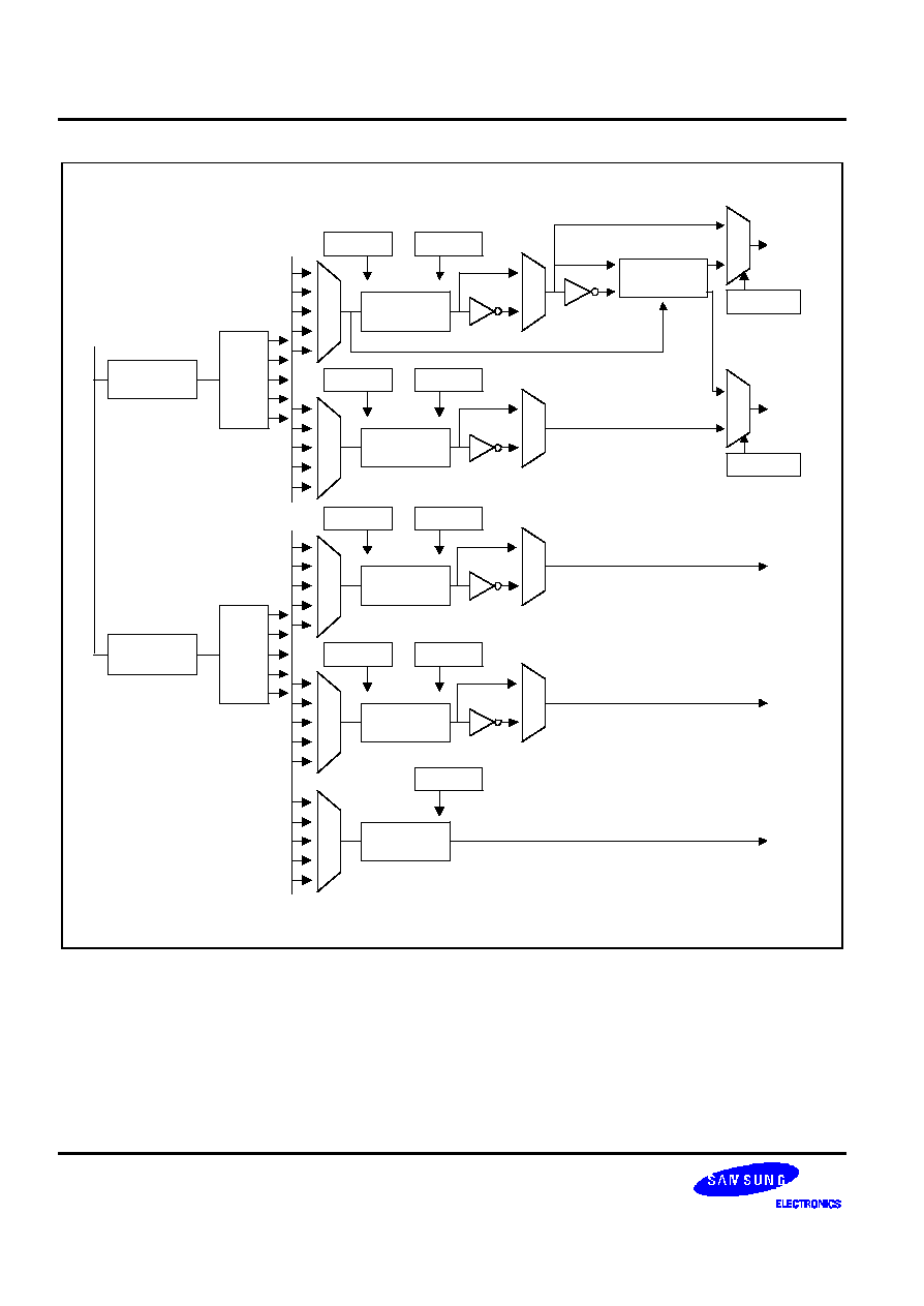
PWM TIMER
S3C2440A RISC MICROPROCESSOR
10-2
Clock
Divider
5:1 MUX
Dead Zone
Generator
TOUT0
TOUT1
TOUT2
Control
Logic0
TCMPB0
TCNTB0
Control
Logic1
TCMPB1
TCNTB1
5:1 MUX
Clock
Divider
5:1 MUX
5:1 MUX
Control
Logic2
TCMPB2
TCNTB2
TOUT3
Control
Logic3
TCMPB3
TCNTB3
No Pin
PCLK
8-Bit
Prescaler
8-Bit
Prescaler
Dead Zone
Dead Zone
TCLK0
1/8
1/4
1/16
1/2
TCLK1
1/8
1/4
1/16
1/2
5:1 MUX
Control
Logic4
TCNTB4
Figure 10-1. 16-bit PWM Timer Block Diagram
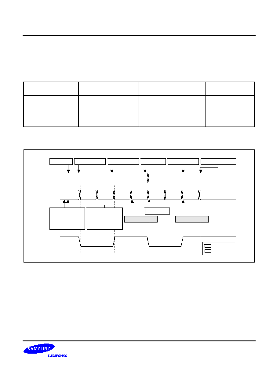
S3C2440A RISC MICROPROCESSOR
PWM TIMER
10-3
PWM TIMER OPERATION
PRESCALER & DIVIDER
An 8-bit prescaler and a 4-bit divider make the following output frequencies:
4-bit Divider Settings
Minimum Resolution
(prescaler = 0)
Maximum Resolution
(prescaler = 255)
Maximum Interval
(TCNTBn = 65535)
1/2 (PCLK = 50 MHz)
0.0400 us (25.0000 MHz)
10.2400 us (97.6562 kHz)
0.6710 sec
1/4 (PCLK = 50 MHz)
0.0800 us (12.5000 MHz)
20.4800 us (48.8281 kHz)
1.3421 sec
1/8 (PCLK = 50 MHz)
0.1600 us ( 6.2500 MHz)
40.9601 us (24.4140 kHz)
2.6843 sec
1/16 (PCLK = 50 MHz)
0.3200 us ( 3.1250 MHz)
81.9188 us (12.2070 kHz)
5.3686 sec
BASIC TIMER OPERATION
TCMPn
1
0
TCNTn
3
3
2
1
0
2
1
0
0
Start bit=1
Timer is started TCNTn=TCMPn Auto-reload TCNTn=TCMPn
Timer is stopped
TOUTn
Command
Status
TCNTBn=3
TCMPBn=1
Manual update=1
Auto-reload=1
TCNTBn=2
TCMPBn=0
Manual update=0
Auto-reload=1
Interrupt request
Auto-reload
Interrupt request
Figure 10-2. Timer Operations
A timer (except the timer ch-5) has TCNTBn, TCNTn, TCMPBn and TCMPn. (TCNTn and TCMPn are the names of
the internal registers. The TCNTn register can be read from the TCNTOn register) The TCNTBn and the TCMPBn are
loaded into the TCNTn and the TCMPn when the timer reaches 0. When the TCNTn reaches 0, an interrupt request
will occur if the interrupt is enabled.
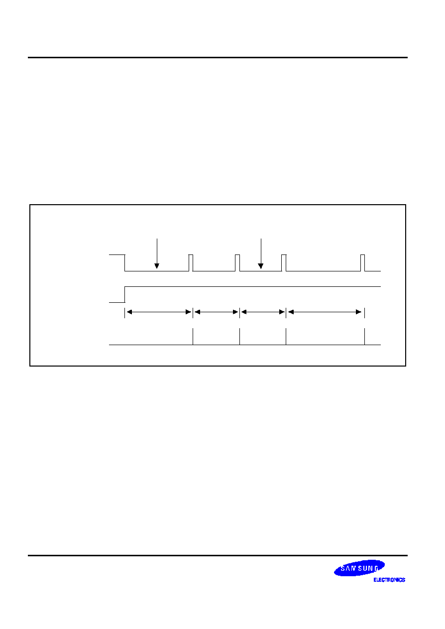
PWM TIMER
S3C2440A RISC MICROPROCESSOR
10-4
AUTO RELOAD & DOUBLE BUFFERING
S3C2440A PWM Timers have a double buffering function, enabling the reload value changed for the next timer
operation without stopping the current timer operation. So, although the new timer value is set, a current timer
operation is completed successfully.
The timer value can be written into Timer Count Buffer register (TCNTBn) and the current counter value of the timer
can be read from Timer Count Observation register (TCNTOn). If the TCNTBn is read, the read value does not indicate
the current state of the counter but the reload value for the next timer duration.
The auto-reload operation copies the TCNTBn into TCNTn when the TCNTn reaches 0. The value, written into the
TCNTBn, is loaded to the TCNTn only when the TCNTn reaches 0 and auto reload is enabled. If the TCNTn becomes
0 and the auto reload bit is 0, the TCNTn does not operate any further.
Write
TCNTBn = 100
Write
TCNTBn = 200
Start
TCNTBn = 150
Auto-reload
150
100
100
200
Interrupt
Write
TCNTBn = 100
Write
TCNTBn = 200
Start
TCNTBn = 150
Auto-reload
150
100
100
200
Interrupt
Figure 10-3. Example of Double Buffering Function

S3C2440A RISC MICROPROCESSOR
PWM TIMER
10-5
TIMER INITIALIZATION USING MANUAL UPDATE BIT AND INVERTER BIT
An auto reload operation of the timer occurs when the down counter reaches 0. So, a starting value of the TCNTn has
to be defined by the user in advance. In this case, the starting value has to be loaded by the manual update bit. The
following steps describe how to start a timer:
1) Write the initial value into TCNTBn and TCMPBn.
2) Set the manual update bit of the corresponding timer. It is recommended that you configure the inverter on/off bit.
(Whether use inverter or not).
3) Set start bit of the corresponding timer to start the timer (and clear the manual update bit).
If the timer is stopped by force, the TCNTn retains the counter value and is not reloaded from TCNTBn. If a new value
has to be set, perform manual update.
NOTE
Whenever TOUT inverter on/off bit is changed, the TOUTn logic value will also be changed whether the timer
runs. Therefore, it is desirable that the inverter on/off bit is configured with the manual update bit.

PWM TIMER
S3C2440A RISC MICROPROCESSOR
10-6
TIMER OPERATION
TOUTn
1
2
4
6
50
110
40
40
60
20
3
7 9
10
5
8
11
Figure 10-4. Example of a Timer Operation
The above Figure 10-4 shows the result of the following procedure:
1. Enable the auto re-load function. Set the TCNTBn to 160 (50+110) and the TCMPBn to 110. Set the manual
update bit and configure the inverter bit (on/off). The manual update bit sets TCNTn and TCMPn to the values of
TCNTBn and TCMPBn, respectively.
And then, set the TCNTBn and the TCMPBn to 80 (40+40) and 40, respectively, to determine the next reload
value.
2. Set the start bit, provided that manual_update is 0 and the inverter is off and auto reload is on. The timer starts
counting down after latency time within the timer resolution.
3. When the TCNTn has the same value as that of the TCMPn, the logic level of the TOUTn is changed from low to
high.
4. When the TCNTn reaches 0, the interrupt request is generated and TCNTBn value is loaded into a temporary
register. At the next timer tick, the TCNTn is reloaded with the temporary register value (TCNTBn).
5. In Interrupt Service Routine (ISR), the TCNTBn and the TCMPBn are set to 80 (20+60) and 60, respectively, for
the next duration.
6. When the TCNTn has the same value as the TCMPn, the logic level of TOUTn is changed from low to high.
7. When the TCNTn reaches 0, the TCNTn is reloaded automatically with the TCNTBn, triggering an interrupt
request.
8. In Interrupt Service Routine (ISR), auto reload and interrupt request are disabled to stop the timer.
9. When the value of the TCNTn is same as the TCMPn, the logic level of the TOUTn is changed from low to high.
10. Even when the TCNTn reaches 0, the TCNTn is not any more reloaded and the timer is stopped because auto
reload has been disabled.
11. No more interrupt requests are generated.
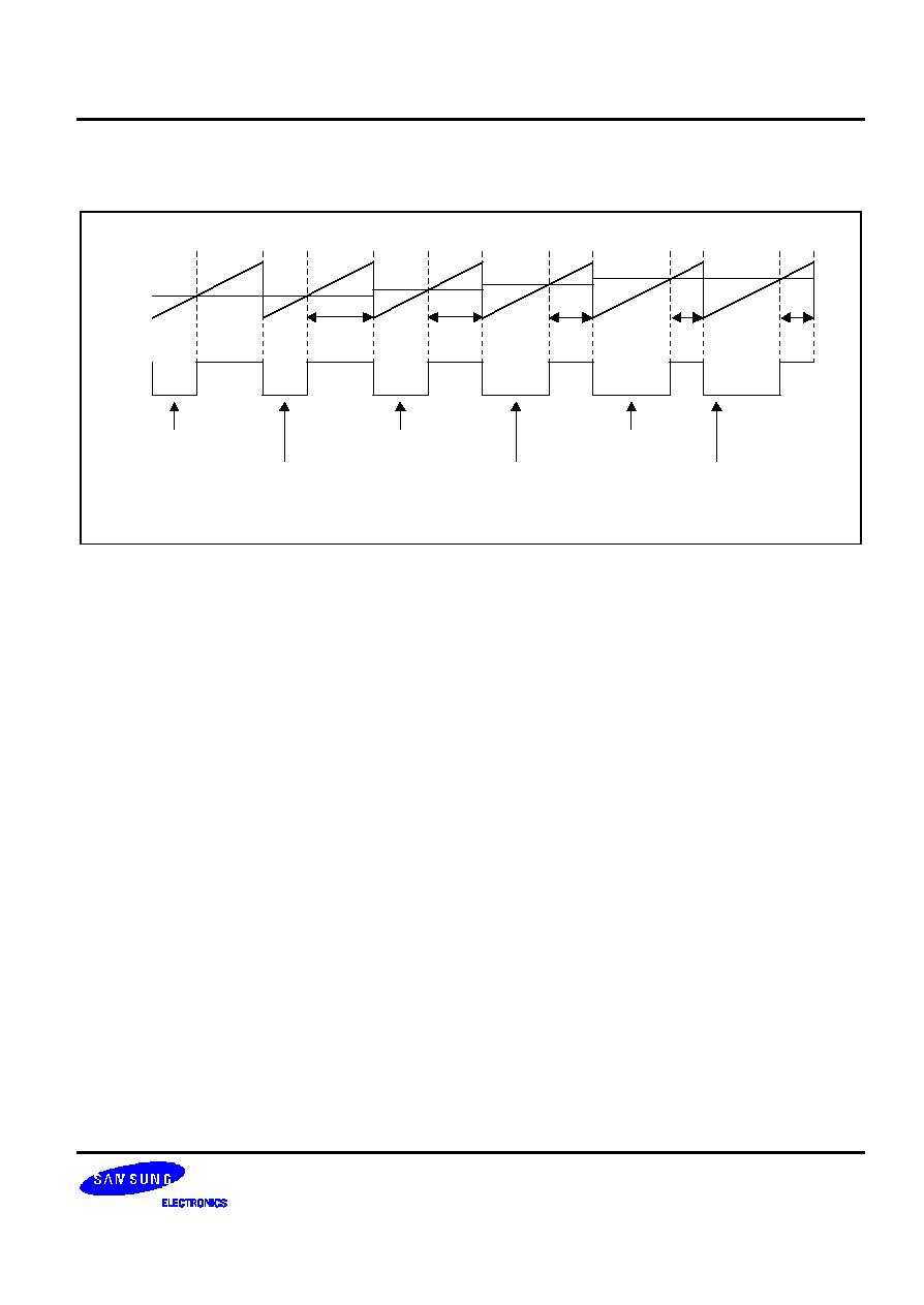
S3C2440A RISC MICROPROCESSOR
PWM TIMER
10-7
PULSE WIDTH MODULATION (PWM)
Write
TCMPBn = 60
Write
TCMPBn = 50
Write
TCMPBn = 40
Write
TCMPBn = 30
Write
TCMPBn = 30
Write
TCMPBn = Next PWM Value
60
50
40
30
30
Figure 10-5. Example of PWM
PWM function can be implemented by using the TCMPBn. PWM frequency is determined by TCNTBn. Figure 10-5
shows a PWM value determined by TCMPBn.
For a higher PWM value, decrease the TCMPBn value. For a lower PWM value, increase the TCMPBn value. If an
output inverter is enabled, the increment/decrement may be reversed.
The double buffering function allows the TCMPBn, for the next PWM cycle, written at any point in the current PWM
cycle by ISR or other routine.
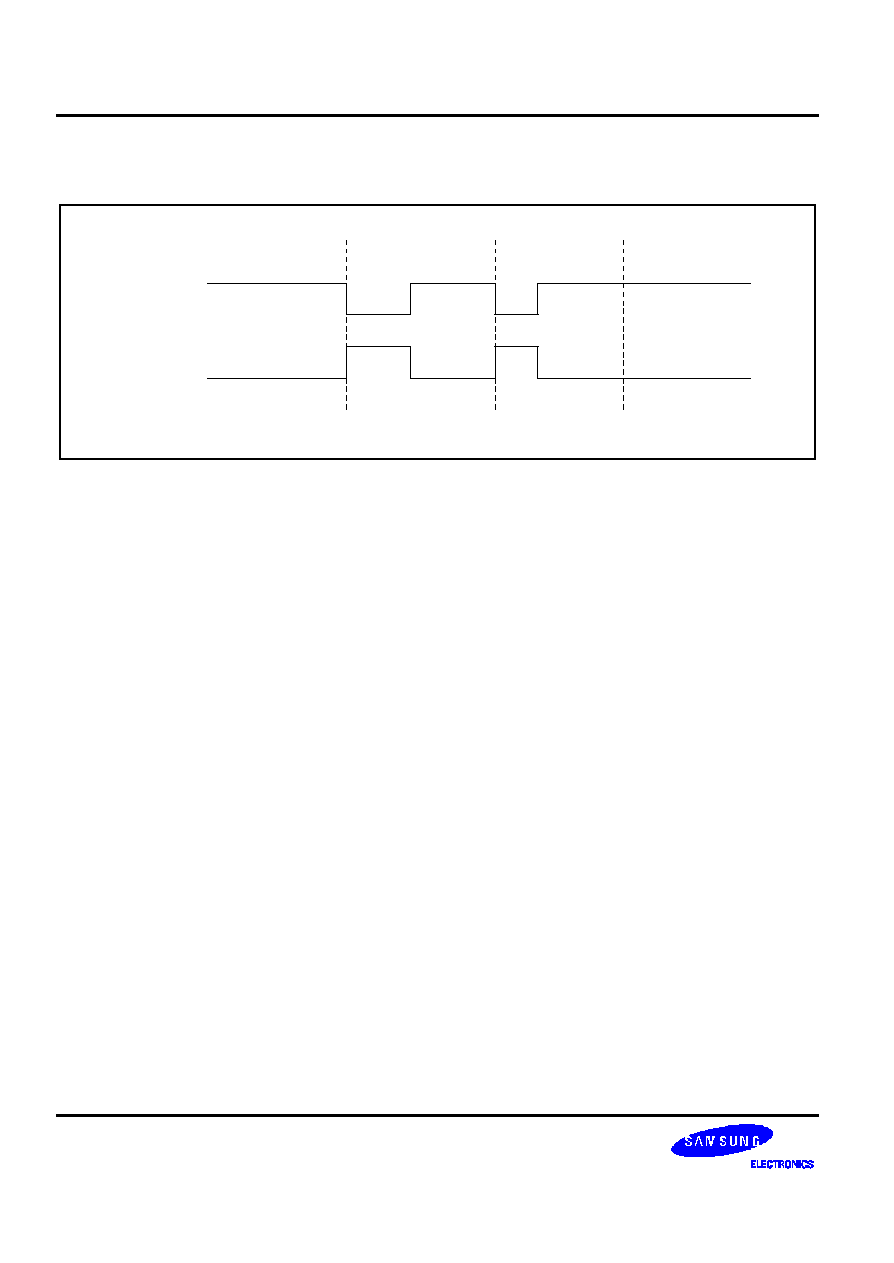
PWM TIMER
S3C2440A RISC MICROPROCESSOR
10-8
OUTPUT LEVEL CONTROL
Inverter off
Initial State
Period 1
Period 2
Timer Stop
Inverter on
Figure 10-6. Inverter On/Off
The following procedure describes how to maintain TOUT as high or low (assume the inverter is off):
1. Turn off the auto reload bit. And then, TOUTn goes to high level and the timer is stopped after the TCNTn reaches
0 (recommended).
2. Stop the timer by clearing the timer start/stop bit to 0. If TCNTn ° TCMPn, the output level is high. If TCNTn
>TCMPn, the output level is low.
3. The TOUTn can be inverted by the inverter on/off bit in TCON. The inverter removes the additional circuit to
adjust the output level.
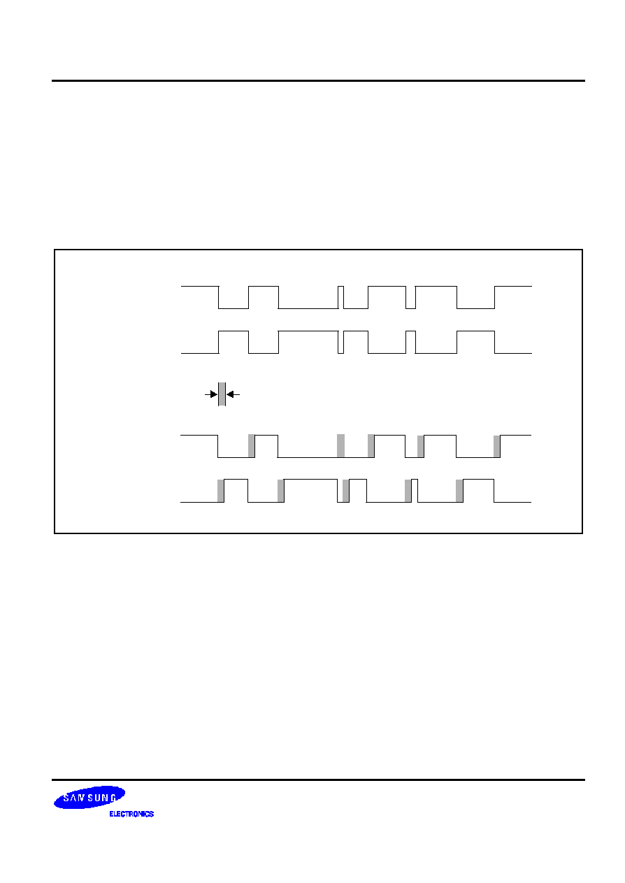
S3C2440A RISC MICROPROCESSOR
PWM TIMER
10-9
DEAD ZONE GENERATOR
The Dead Zone is for the PWM control in a power device. This function enables the insertion of the time gap between
a turn-off of a switching device and a turn on of another switching device. This time gap prohibits the two switching
devices from being turned on simultaneously, even for a very short time.
TOUT0 is the PWM output. nTOUT0 is the inversion of the TOUT0. If the dead zone is enabled, the output wave form
of TOUT0 and nTOUT0 will be TOUT0_DZ and nTOUT0_DZ, respectively. nTOUT0_DZ is routed to the TOUT1 pin.
In the dead zone interval, TOUT0_DZ and nTOUT0_DZ can never be turned on simultaneously.
TOUT0
nTOUT0
TOUT0_DZ
nTOUT0_DZ
Deadzone
Interval
Figure 10-7. The Wave Form When a Dead Zone Feature is Enabled
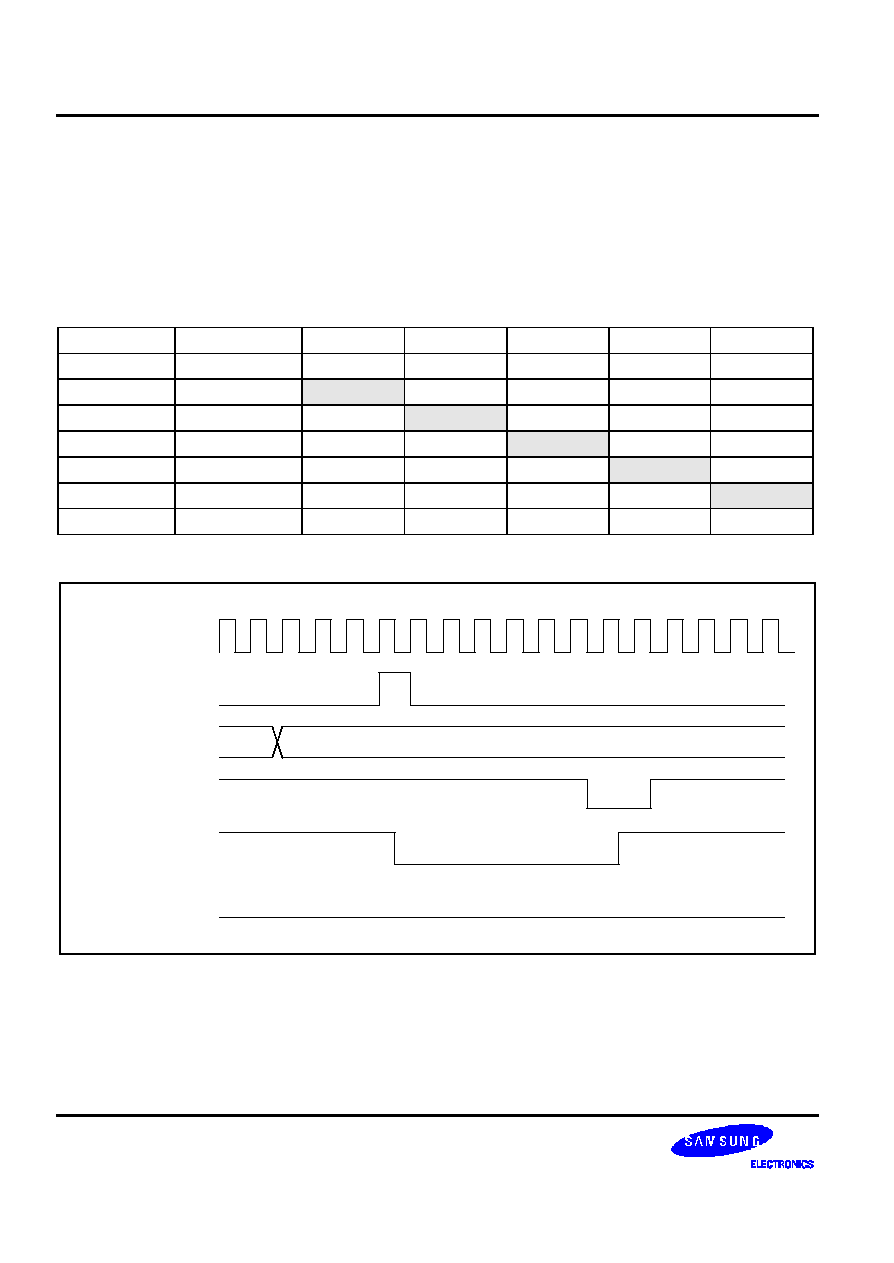
PWM TIMER
S3C2440A RISC MICROPROCESSOR
10-10
DMA REQUEST MODE
The PWM timer can generate a DMA request at every specific time. The timer keeps DMA request signals
(nDMA_REQ) low until the timer receives an ACK signal. When the timer receives the ACK signal, it makes the
request signal inactive. The timer, which generates the DMA request, is determined by setting DMA mode bits (in
TCFG1 register). If one of timers is configured as DMA request mode, that timer does not generate an interrupt
request. The others can generate interrupt normally.
DMA mode configuration and DMA / interrupt operation
DMA Mode
DMA Request
Timer0 INT
Timer1 INT
Timer2 INT
Timer3 INT
Timer4 INT
0000
No select
ON
ON
ON
ON
ON
0001
Timer0
OFF
ON
ON
ON
ON
0010
Timer1
ON
OFF
ON
ON
ON
0011
Timer2
ON
ON
OFF
ON
ON
0100
Timer3
ON
ON
ON
OFF
ON
0101
Timer4
ON
ON
ON
ON
OFF
0110
No select
ON
ON
ON
ON
ON
PCLK
INT4tmp
DMAreq_en
nDMA_ACK
nDMA_REQ
INT4
1 0 1
Figure 10-8. Timer4 DMA Mode Operation
S3C2440A RISC MICROPROCESSOR
PWM TIMER
10-11
PWM TIMER CONTROL REGISTERS
TIMER CONFIGURATION REGISTER0 (TCFG0)
Timer input clock Frequency = PCLK / {prescaler value+1} / {divider value}
{prescaler value} = 0~255
{divider value} = 2, 4, 8, 16
Register
Address
R/W
Description
Reset Value
TCFG0
0x51000000
R/W
Configures the two 8-bit prescalers
0x00000000
TCFG0
Bit
Description
Initial State
Reserved
[31:24]
0x00
Dead zone length
[23:16]
These 8 bits determine the dead zone length. The 1 unit time
of the dead zone length is equal to that of timer 0.
0x00
Prescaler 1
[15:8]
These 8 bits determine prescaler value for Timer 2, 3 and 4.
0x00
Prescaler 0
[7:0]
These 8 bits determine prescaler value for Timer 0 and 1.
0x00

PWM TIMER
S3C2440A RISC MICROPROCESSOR
10-12
TIMER CONFIGURATION REGISTER1 (TCFG1)
Register
Address
R/W
Description
Reset Value
TCFG1
0x51000004
R/W
5-MUX & DMA mode selection register
0x00000000
TCFG1
Bit
Description
Initial State
Reserved
[31:24]
00000000
DMA mode
[23:20]
Select DMA request channel
0000 = No select (all interrupt) 0001 = Timer0
0010 = Timer1 0011 = Timer2
0100 = Timer3 0101 = Timer4
0110 = Reserved
0000
MUX 4
[19:16]
Select MUX input for PWM Timer4.
0000 = 1/2 0001 = 1/4 0010 = 1/8
0011 = 1/16 01xx = External TCLK1
0000
MUX 3
[15:12]
Select MUX input for PWM Timer3.
0000 = 1/2 0001 = 1/4 0010 = 1/8
0011 = 1/16 01xx = External TCLK1
0000
MUX 2
[11:8]
Select MUX input for PWM Timer2.
0000 = 1/2 0001 = 1/4 0010 = 1/8
0011 = 1/16 01xx = External TCLK1
0000
MUX 1
[7:4]
Select MUX input for PWM Timer1.
0000 = 1/2 0001 = 1/4 0010 = 1/8
0011 = 1/16 01xx = External TCLK0
0000
MUX 0
[3:0]
Select MUX input for PWM Timer0.
0000 = 1/2 0001 = 1/4 0010 = 1/8
0011 = 1/16 01xx = External TCLK0
0000
S3C2440A RISC MICROPROCESSOR
PWM TIMER
10-13
TIMER CONTROL (TCON) REGISTER
Register
Address
R/W
Description
Reset Value
TCON
0x51000008
R/W
Timer control register
0x00000000
TCON
Bit
Description
Initial state
Timer 4 auto reload on/off
[22]
Determine auto reload on/off for Timer 4.
0 = One-shot 1 = Interval mode (auto reload)
0
Timer 4 manual update
(note)
[21]
Determine the manual update for Timer 4.
0 = No operation 1 = Update TCNTB4
0
Timer 4 start/stop
[20]
Determine start/stop for Timer 4.
0 = Stop 1 = Start for Timer 4
0
Timer 3 auto reload on/off
[19]
Determine auto reload on/off for Timer 3.
0 = One-shot 1 = Interval mode (auto reload)
0
Timer 3 output inverter on/off
[18]
Determine output inverter on/off for Timer 3.
0 = Inverter off 1 = Inverter on for TOUT3
0
Timer 3 manual update
(note)
[17]
Determine manual update for Timer 3.
0 = No operation 1 = Update TCNTB3 & TCMPB3
0
Timer 3 start/stop
[16]
Determine start/stop for Timer 3.
0 = Stop 1 = Start for Timer 3
0
Timer 2 auto reload on/off
[15]
Determine auto reload on/off for Timer 2.
0 = One-shot 1 = Interval mode (auto reload)
0
Timer 2 output inverter on/off
[14]
Determine output inverter on/off for Timer 2.
0 = Inverter off 1 = Inverter on for TOUT2
0
Timer 2 manual update
(note)
[13]
Determine the manual update for Timer 2.
0 = No operation 1 = Update TCNTB2 & TCMPB2
0
Timer 2 start/stop
[12]
Determine start/stop for Timer 2.
0 = Stop 1 = Start for Timer 2
0
Timer 1 auto reload on/off
[11]
Determine the auto reload on/off for Timer1.
0 = One-shot 1 = Interval mode (auto reload)
0
Timer 1 output inverter on/off
[10]
Determine the output inverter on/off for Timer1.
0 = Inverter off 1 = Inverter on for TOUT1
0
Timer 1 manual update
(note)
[9]
Determine the manual update for Timer 1.
0 = No operation 1 = Update TCNTB1 & TCMPB1
0
Timer 1 start/stop
[8]
Determine start/stop for Timer 1.
0 = Stop 1 = Start for Timer 1
0
NOTE: The bits have to be cleared at next writing.
PWM TIMER
S3C2440A RISC MICROPROCESSOR
10-14
TIMER CONTROL (TCON) REGISTER (Continued)
TCON
Bit
Description
Initial state
Reserved
[7:5]
Reserved
Dead zone enable
[4]
Determine the dead zone operation.
0 = Disable 1 = Enable
0
Timer 0 auto reload on/off
[3]
Determine auto reload on/off for Timer 0.
0 = One-shot 1 = Interval mode(auto reload)
0
Timer 0 output inverter on/off
[2]
Determine the output inverter on/off for Timer 0.
0 = Inverter off 1 = Inverter on for TOUT0
0
Timer 0 manual update
(note)
[1]
Determine the manual update for Timer 0.
0 = No operation 1 = Update TCNTB0 & TCMPB0
0
Timer 0 start/stop
[0]
Determine start/stop for Timer 0.
0 = Stop 1 = Start for Timer 0
0
NOTE: The bit has to be cleared at next writing.
S3C2440A RISC MICROPROCESSOR
PWM TIMER
10-15
TIMER 0 COUNT BUFFER REGISTER & COMPARE BUFFER REGISTER (TCNTB0/TCMPB0)
Register
Address
R/W
Description
Reset Value
TCNTB0
0x5100000C
R/W
Timer 0 count buffer register
0x00000000
TCMPB0
0x51000010
R/W
Timer 0 compare buffer register
0x00000000
TCMPB0
Bit
Description
Initial State
Timer 0 compare buffer register
[15:0]
Set compare buffer value for Timer 0
0x00000000
TCNTB0
Bit
Description
Initial State
Timer 0 count buffer register
[15:0]
Set count buffer value for Timer 0
0x00000000
TIMER 0 COUNT OBSERVATION REGISTER (TCNTO0)
Register
Address
R/W
Description
Reset Value
TCNTO0
0x51000014
R
Timer 0 count observation register
0x00000000
TCNTO0
Bit
Description
Initial State
Timer 0 observation register
[15:0]
Set count observation value for Timer 0
0x00000000
PWM TIMER
S3C2440A RISC MICROPROCESSOR
10-16
TIMER 1 COUNT BUFFER REGISTER & COMPARE BUFFER REGISTER (TCNTB1/TCMPB1)
Register
Address
R/W
Description
Reset Value
TCNTB1
0x51000018
R/W
Timer 1 count buffer register
0x00000000
TCMPB1
0x5100001C
R/W
Timer 1 compare buffer register
0x00000000
TCMPB1
Bit
Description
Initial State
Timer 1 compare buffer register
[15:0]
Set compare buffer value for Timer 1
0x00000000
TCNTB1
Bit
Description
Initial State
Timer 1 count buffer register
[15:0]
Set count buffer value for Timer 1
0x00000000
TIMER 1 COUNT OBSERVATION REGISTER (TCNTO1)
Register
Address
R/W
Description
Reset Value
TCNTO1
0x51000020
R
Timer 1 count observation register
0x00000000
TCNTO1
Bit
Description
initial state
Timer 1 observation register
[15:0]
Set count observation value for Timer 1
0x00000000
S3C2440A RISC MICROPROCESSOR
PWM TIMER
10-17
TIMER 2 COUNT BUFFER REGISTER & COMPARE BUFFER REGISTER (TCNTB2/TCMPB2)
Register
Address
R/W
Description
Reset Value
TCNTB2
0x51000024
R/W
Timer 2 count buffer register
0x00000000
TCMPB2
0x51000028
R/W
Timer 2 compare buffer register
0x00000000
TCMPB2
Bit
Description
Initial State
Timer 2 compare buffer register
[15:0]
Set compare buffer value for Timer 2
0x00000000
TCNTB2
Bit
Description
Initial State
Timer 2 count buffer register
[15:0]
Set count buffer value for Timer 2
0x00000000
TIMER 2 COUNT OBSERVATION REGISTER (TCNTO2)
Register
Address
R/W
Description
Reset Value
TCNTO2
0x5100002C
R
Timer 2 count observation register
0x00000000
TCNTO2
Bit
Description
Initial State
Timer 2 observation register
[15:0]
Set count observation value for Timer 2
0x00000000
PWM TIMER
S3C2440A RISC MICROPROCESSOR
10-18
TIMER 3 COUNT BUFFER REGISTER & COMPARE BUFFER REGISTER (TCNTB3/TCMPB3)
Register
Address
R/W
Description
Reset Value
TCNTB3
0x51000030
R/W
Timer 3 count buffer register
0x00000000
TCMPB3
0x51000034
R/W
Timer 3 compare buffer register
0x00000000
TCMPB3
Bit
Description
Initial State
Timer 3 compare buffer register
[15:0]
Set compare buffer value for Timer 3
0x00000000
TCNTB3
Bit
Description
Initial State
Timer 3 count buffer register
[15:0]
Set count buffer value for Timer 3
0x00000000
TIMER 3 COUNT OBSERVATION REGISTER (TCNTO3)
Register
Address
R/W
Description
Reset Value
TCNTO3
0x51000038
R
Timer 3 count observation register
0x00000000
TCNTO3
Bit
Description
Initial State
Timer 3 observation register
[15:0]
Set count observation value for Timer 3
0x00000000
S3C2440A RISC MICROPROCESSOR
PWM TIMER
10-19
TIMER 4 COUNT BUFFER REGISTER (TCNTB4)
Register
Address
R/W
Description
Reset Value
TCNTB4
0x5100003C
R/W
Timer 4 count buffer register
0x00000000
TCNTB4
Bit
Description
Initial State
Timer 4 count buffer register
[15:0]
Set count buffer value for Timer 4
0x00000000
TIMER 4 COUNT OBSERVATION REGISTER (TCNTO4)
Register
Address
R/W
Description
Reset Value
TCNTO4
0x51000040
R
Timer 4 count observation register
0x00000000
TCNTO4
Bit
Description
Initial State
Timer 4 observation register
[15:0]
Set count observation value for Timer 4
0x00000000

PWM TIMER
S3C2440A RISC MICROPROCESSOR
10-20
NOTES

S3C2440A RISC MICROPROCESSOR
UART
11-1
11
UART
OVERVIEW
The S3C2440A Universal Asynchronous Receiver and Transmitter (UART) provide three independent asynchronous
serial I/O (SIO) ports, each of which can operate in Interrupt-based or DMA-based mode. In other words, the UART
can generate an interrupt or a DMA request to transfer data between CPU and the UART. The UART can support bit
rates up to 115.2K bps using system clock. If an external device provides the UART with UEXTCLK, then the UART
can operate at higher speed. Each UART channel contains two 64-byte FIFOs for receiver and transmitter.
The S3C2440A UART includes programmable baud rates, infrared (IR) transmit/receive, one or two stop bit insertion,
5-bit, 6-bit, 7-bit or 8-bit data width and parity checking.
Each UART contains a baud-rate generator, transmitter, receiver and a control unit, as shown in Figure 11-1. The
baud-rate generator can be clocked by PCLK, FCLK/n or UEXTCLK (external input clock). The transmitter and the
receiver contain 64-byte FIFOs and data shifters. Data is written to FIFO and then copied to the transmit shifter
before being transmitted. The data is then shifted out by the transmit data pin (TxDn). Meanwhile, received data is
shifted from the receive data pin (RxDn), and then copied to FIFO from the shifter.
FEATURES
-- RxD0, TxD0, RxD1, TxD1, RxD2, and TxD2 with DMA-based or interrupt-based operation
-- UART Ch 0, 1, and 2 with IrDA 1.0 & 64-byte FIFO
-- UART Ch 0 and 1 with nRTS0, nCTS0, nRTS1, and nCTS1
-- Supports handshake transmit/receive
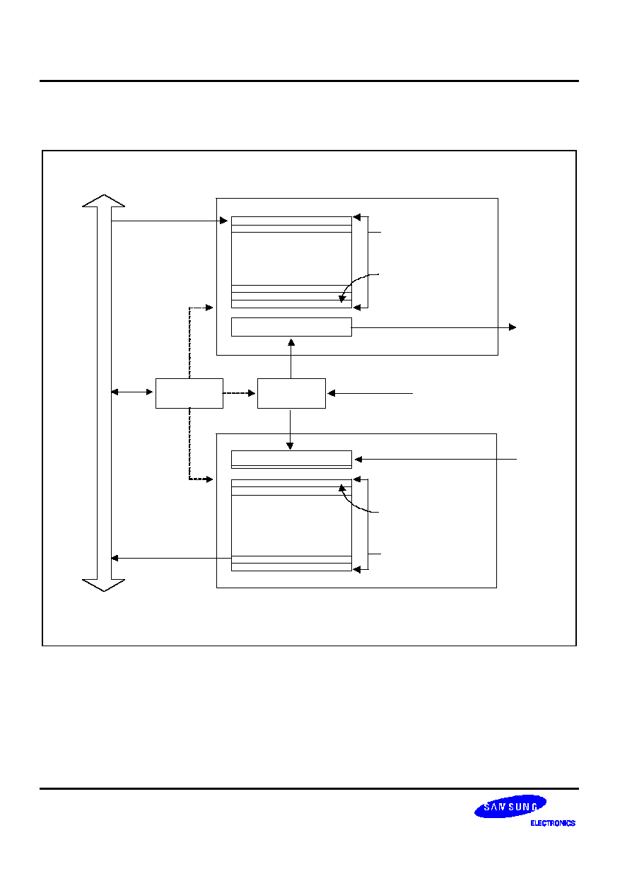
UART
S3C2440A RISC MICROPROCESSOR
11-2
BLOCK DIAGRAM
Buad-rate
Generator
Control
Unit
Transmitter
Receiver
Peripheral BUS
TXDn
Clock Source
(PCLK, FCLK/n,UEXTCLK)
RXDn
Transmit FIFO Register
(FIFO mode)
Transmit Holding Register
(Non-FIFO mode)
Receive FIFO Register
(FIFO mode)
Receive Holding Register
(Non-FIFO mode only)
In FIFO mode, all 64 Byte of Buffer register are used as FIFO register.
In non-FIFO mode, only 1 Byte of Buffer register is used as Holding register.
Transmit Shifter
Transmit Buffer
Register(64 Byte)
Receive Shifter
Receive Buffer
Register(64 Byte)
Figure 11-1. UART Block Diagram (with FIFO)

S3C2440A RISC MICROPROCESSOR
UART
11-3
UART OPERATION
The following sections describe the UART operations that include data transmission, data reception, interrupt
generation, baud-rate generation, Loopback mode, Infrared mode, and auto flow control.
Data Transmission
The data frame for transmission is programmable. It consists of a start bit, 5 to 8 data bits, an optional parity bit and
1 to 2 stop bits, which can be specified by the line control register (ULCONn). The transmitter can also produce the
break condition, which forces the serial output to logic 0 state for one frame transmission time. This block transmits
break signals after the present transmission word is transmitted completely. After the break signal transmission, it
continuously transmits data into the Tx FIFO (Tx holding register in the case of Non-FIFO mode).
Data Reception
Like the transmission, the data frame for reception is also programmable. It consists of a start bit, 5 to 8 data bits,
an optional parity bit and 1 to 2 stop bits in the line control register (ULCONn). The receiver can detect overrun error,
parity error, frame error and break condition, each of which can set an error flag.
-- The overrun error indicates that new data has overwritten the old data before the old data has been read.
-- The parity error indicates that the receiver has detected an unexpected parity condition.
-- The frame error indicates that the received data does not have a valid stop bit.
-- The break condition indicates that the RxDn input is held in the logic 0 state for a duration longer than one
frame transmission time.
Receive time-out condition occurs when it does not receive any data during the 3 word time (this interval follows the
setting of Word Length bit) and the Rx FIFO is not empty in the FIFO mode.
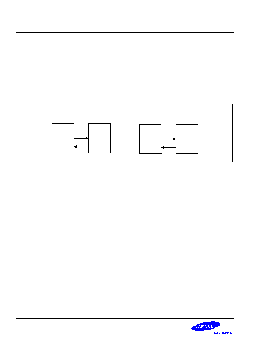
UART
S3C2440A RISC MICROPROCESSOR
11-4
Auto Flow Control (AFC)
The S3C2440A's UART 0 and UART 1 support auto flow control with nRTS and nCTS signals. In case, it can be
connected to external UARTs. If users want to connect a UART to a Modem, disable auto flow control bit in
UMCONn register and control the signal of nRTS by software.
In AFC, nRTS depends on the condition of the receiver and nCTS signals control the operation of the transmitter. The
UART's transmitter transfers the data in FIFO only when nCTS signals are activated (in AFC, nCTS means that other
UART's FIFO is ready to receive data). Before the UART receives data, nRTS has to be activated when its receive
FIFO has a spare more than 32-byte and has to be inactivated when its receive FIFO has a spare under 32-byte (in
AFC, nRTS means that its own receive FIFO is ready to receive data).
UART A
TxD
nCTS
UART B
RxD
nRTS
Transmission Case in UART A
UART A
RxD
nRTS
UART B
TxD
nCTS
Reception Case in UART A
Figure 11-2. UART AFC interface
NOTE
UART 2 does not support AFC function, because the S3C2440A has no nRTS2 and nCTS2.
Example of Non Auto-Flow Control (Controlling nRTS and nCTS by Software)
Rx Operation with FIFO
1. Select receive mode (Interrupt or DMA mode).
2. Check the value of Rx FIFO count in UFSTATn register. If the value is less than 32, users have to set the value of
UMCONn[0] to '1' (activating nRTS), and if it is equal or larger than 32 users have to set the value to '0'
(inactivating nRTS).
3. Repeat the Step 2.
Tx Operation with FIFO
1. Select transmit mode (Interrupt or DMA mode).
2. Check the value of UMSTATn[0]. If the value is '1' (activating nCTS), users write the data to Tx FIFO register.

S3C2440A RISC MICROPROCESSOR
UART
11-5
RS-232C interface
If the user wants to connect the UART to modem interface (instead of null modem), nRTS, nCTS, nDSR, nDTR, DCD
and nRI signals are needed. In this case, the users can control these signals with general I/O ports by software
because the AFC does not support the RS-232C interface.
Interrupt/DMA Request Generation
Each UART of the S3C2440A has seven status (Tx/Rx/Error) signals: Overrun error, Parity error, Frame error, Break,
Receive buffer data ready, Transmit buffer empty, and Transmit shifter empty, all of which are indicated by the
corresponding UART status register (UTRSTATn/UERSTATn).
The overrun error, parity error, frame error and break condition are referred to as the receive error status. Each of
which can cause the receive error status interrupt request, if the receive-error-status-interrupt-enable bit is set to one
in the control register, UCONn. When a receive-error-status-interrupt-request is detected, the signal causing the
request can be identified by reading the value of UERSTSTn.
When the receiver transfers the data of the receive shifter to the receive FIFO register in FIFO mode and the number
of received data reaches Rx FIFO Trigger Level, Rx interrupt is generated. If the Receive mode is in control register
(UCONn) and is selected as 1 (Interrupt request or polling mode). In the Non-FIFO mode, transferring the data of the
receive shifter to receive holding register will cause Rx interrupt under the Interrupt request and polling mode.
When the transmitter transfers data from its transmit FIFO register to its transmit shifter and the number of data left
in transmit FIFO reaches Tx FIFO Trigger Level, Tx interrupt is generated, if Transmit mode in control register is
selected as Interrupt request or polling mode. In the Non-FIFO mode, transferring data from the transmit holding
register to the transmit shifter will cause Tx interrupt under the Interrupt request and polling mode.
If the Receive mode and Transmit mode in control register are selected as the DMAn request mode then DMAn
request occurs instead of Rx or Tx interrupt in the situation mentioned above.
Table 11-1. Interrupts in Connection with FIFO
Type
FIFO Mode
Non-FIFO Mode
Rx Interrupt
Generated whenever receive data reaches the
trigger level of receive FIFO.
Generated when the number of data in FIFO does
not reaches Rx FIFO trigger Level and does not
receive any data during 3 word time (receive time
out). This interval follows the setting of Word Length
bit.
Generated by the receiving holding
register whenever receive buffer becomes
full.
Tx Interrupt
Generated whenever transmit data reaches the
trigger level of transmit FIFO (Tx FIFO trigger Level).
Generated by the transmitting holding
register whenever transmit buffer becomes
empty.
Error Interrupt
Generated when frame error, parity error, or break
signal are detected.
Generated when it gets to the top of the receive
FIFO without reading out data in it (overrun error).
Generated by all errors. However if another
error occurs at the same time, only one
interrupt is generated.
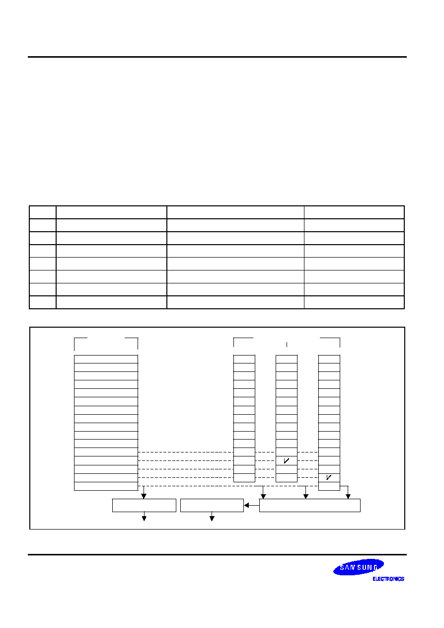
UART
S3C2440A RISC MICROPROCESSOR
11-6
UART Error Status FIFO
UART has the error status FIFO besides the Rx FIFO register. The error status FIFO indicates which data, among
FIFO registers, is received with an error. The error interrupt will be issued only when the data, which has an error, is
ready to read out. To clear the error status FIFO, the URXHn with an error and UERSTATn must be read out.
For example,
It is assumed that the UART Rx FIFO receives A, B, C, D and E characters sequentially and the frame error occurs
while receiving 'B', and the parity error occurs while receiving 'D'.
The actual UART receive error will not generate any error interrupt because the character which is received with an
error would have not been read. The error interrupt will occur once the character is read.
Figure 11-3 shows the UART receiving the five characters including the two errors.
Time
Sequence Flow
Error Interrupt
Note
#0
When no character is read out
≠
#1
A, B, C, D, and E is received
≠
#2
After A is read out
The frame error (in B) interrupt occurs.
The 'B' has to be read out.
#3
After B is read out
≠
#4
After C is read out
The parity error (in D) interrupt occurs.
The 'D' has to be read out.
#5
After D is read out
≠
#6
After E is read out
≠
-
-
-
-
-
-
-
-
-
-
-
'E'
'D'
'C'
'B'
'A'
Rx FIFO
URXHn
UERSTATn
break error
parity error
frame error
Error Status Generator Unit
Error Status FIFO
Figure 11-3. Example showing UART Receiving 5 Characters with 2 Errors

S3C2440A RISC MICROPROCESSOR
UART
11-7
Baud-rate Generation
Each UART's baud-rate generator provides the serial clock for the transmitter and the receiver. The source clock for
the baud-rate generator can be selected with the S3C2440A's internal system clock or UEXTCLK. In other words,
dividend is selectable by setting Clock Selection of UCONn. The baud-rate clock is generated by dividing the source
clock (PCLK, FCLK/n or UEXTCLK) by 16 and a 16-bit divisor specified in the UART baud-rate divisor register
(UBRDIVn). The UBRDIVn can be determined by the following expression:
UBRDIVn
= (int)( UART clock / ( buad rate x 16) ) ≠1
( UART clock: PCLK, FCLK/n or UEXTCLK )
Where, UBRDIVn should be from 1 to (2
16
-1), but can be set 0 (bypass mode) only using the UEXTCLK which
should be smaller than PCLK.
For example, if the baud-rate is 115200 bps and UART clock is 40 MHz, UBRDIVn is:
UBRDIVn
= (int)(40000000 / (115200 x 16) ) -1
= (int)(21.7) -1 [round to the nearest whole number]
= 22 -1 = 21
Baud-Rate Error Tolerance
UART Frame error should be less than 1.87%(3/160).
tUPCLK = (UBRDIVn + 1) x 16 x 1Frame / PCLK tUPCLK: Real UART Clock
tUEXACT = 1Frame / baud-rate tUEXACT: Ideal UART Clock
UART error = (tUPCLK ≠ tUEXACT) / tUEXACT x 100%
NOTES
1. 1Frame = start bit + data bit + parity bit + stop bit.
2. In specific condition, we can support the UART baud rate up to 921.6K bps. For example, when PCLK
is 60MHz, you can use 921.6K bps under UART error of 1.69%.
Loopback Mode
The S3C2440A UART provides a test mode referred to as the Loopback mode, to aid in isolating faults in the
communication link. This mode structurally enables the connection of RXD and TXD in the UART. In this mode,
therefore, transmitted data is received to the receiver, via RXD. This feature allows the processor to verify the internal
transmit and to receive the data path of each SIO channel. This mode can be selected by setting the loopback bit in
the UART control register (UCONn).
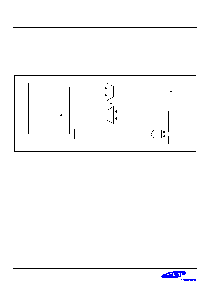
UART
S3C2440A RISC MICROPROCESSOR
11-8
Infrared (IR) Mode
The S3C2440A UART block supports infrared (IR) transmission and reception, which can be selected by setting the
Infrared-mode bit in the UART line control register (ULCONn). Figure 11-4 illustrates how to implement the IR mode.
In IR transmit mode, the transmit pulse comes out at a rate of 3/16, the normal serial transmit rate (when the
transmit data bit is zero); In IR receive mode, the receiver must detect the 3/16 pulsed period to recognize a zero
value (see the frame timing diagrams shown in Figure 11-6 and 11-7).
IrDA Tx
Encoder
0
1
0
1
IrDA Rx
Decoder
TxD
RxD
TxD
IRS
RxD
RE
UART
Block
Figure 11-4. IrDA Function Block Diagram
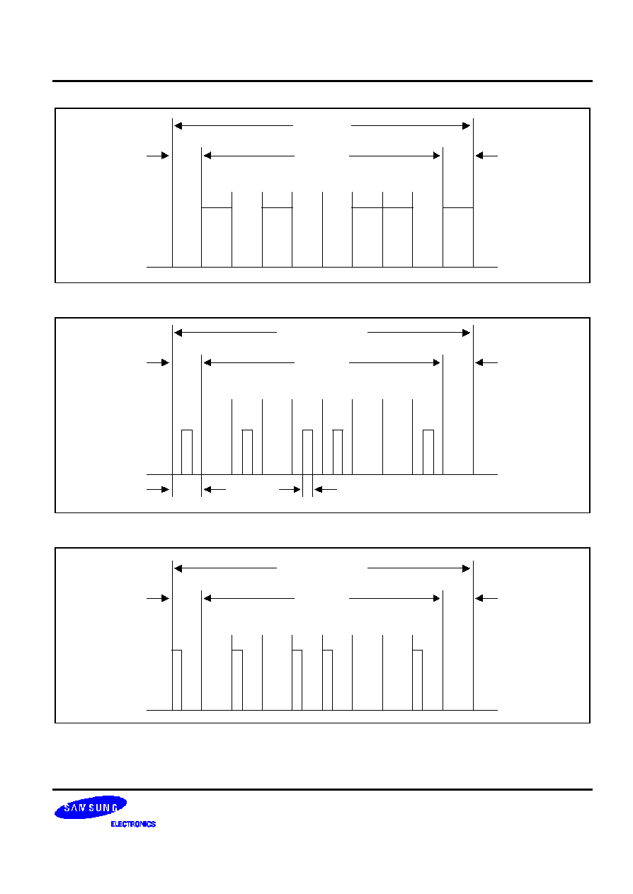
S3C2440A RISC MICROPROCESSOR
UART
11-9
Start
Bit
Stop
Bit
Data Bits
SIO Frame
0
1
0
1
0
0
1
1
0
1
Figure 11-5. Serial I/O Frame Timing Diagram (Normal UART)
0
Start
Bit
Stop
Bit
Data Bits
IR Transmit Frame
Bit
Time
Pulse Width = 3/16 Bit Frame
0
0
0
0
1
1
1
1
1
Figure 11-6. Infrared Transmit Mode Frame Timing Diagram
0
Start
Bit
Stop
Bit
Data Bits
IR Receive Frame
0
0
0
0
1
1
1
1
1
Figure 11-7. Infrared Receive Mode Frame Timing Diagram

UART
S3C2440A RISC MICROPROCESSOR
11-10
UART SPECIAL REGISTERS
UART LINE CONTROL REGISTER
There are three UART line control registers including ULCON0, ULCON1, and ULCON2 in the UART block.
Register
Address
R/W
Description
Reset Value
ULCON0
0x50000000
R/W
UART channel 0 line control register
0x00
ULCON1
0x50004000
R/W
UART channel 1 line control register
0x00
ULCON2
0x50008000
R/W
UART channel 2 line control register
0x00
ULCONn
Bit
Description
Initial State
Reserved
[7]
≠
0
Infrared Mode
[6]
Determine whether or not to use the Infrared mode.
0 = Normal mode operation
1 = Infrared Tx/Rx mode
0
Parity Mode
[5:3]
Specify the type of parity generation and checking during UART
transmit and receive operation.
0xx = No parity
100 = Odd parity
101 = Even parity
110 = Parity forced/checked as 1
111 = Parity forced/checked as 0
000
Number of Stop
Bit
[2]
Specify how many stop bits are to be used for end-of-frame signal.
0 = One stop bit per frame
1 = Two stop bit per frame
0
Word Length
[1:0]
Indicate the number of data bits to be transmitted or received per
frame.
00 = 5-bits 01 = 6-bits
10 = 7-bits 11 = 8-bits
00
S3C2440A RISC MICROPROCESSOR
UART
11-11
UART CONTROL REGISTER
There are three UART control registers including UCON0, UCON1 and UCON2 in the UART block.
Register
Address
R/W
Description
Reset Value
UCON0
0x50000004
R/W
UART channel 0 control register
0x00
UCON1
0x50004004
R/W
UART channel 1 control register
0x00
UCON2
0x50008004
R/W
UART channel 2 control register
0x00
UCONn
Bit
Description
Initial State
FCLK Divider
[15:12]
Divider value when the Uart clock source is selected as FCLK/n.
'n' is determined by UCON0[15:12], UCON1[15:12], UCON2[14:12].
UCON2[15] is FCLK/n Clock Enable/Disable bit.
For setting `n' from 7 to 21, use UCON0[15:12],
For setting `n' from 22 to 36, use UCON1[15:12],
For setting `n' from 37 to 43, use UCON2[14:12],
UCON2[15]: 0 = Disable FCLK/n clock. 1 = Enable FCLK/n
clock.
In case of UCON0,
UART clock = FCLK / (divider+6), where divider>0.
UCON1, UCON2 must be zero.
ex) 1: UART clock = FCLK/7, 2: UART clock = FCLK/8
3: UART clock = FCLK/9, ... , 15: UART clock = FCLK/21
In case of UCON1,
UART clock = FCLK / (divider+21), where divider>0.
UCON0, UCON2 must be zero.
ex) 1: UART clock = FCLK/22, 2: UART clock = FCLK/23
3: UART clock = FCLK/24, ... , 15: UART clock = FCLK/36
In case of UCON2,
UART clock = FCLK / (divider+36), where divider>0.
UCON0, UCON1 must be zero.
ex) 1: UART clock = FCLK/37, 2: UART clock = FCLK/38
3: UART clock = FCLK/39, ... , 7: UART clock = FCLK/43
If UCON00/1[15:12] and UCON2[14:12] are all `0', the divider will be
44, that is UART clock = FCLK/44
Total division range is from 7 to 44.
0000
Clock Selection
[11:10]
Select PCLK, UEXTCLK or FCLK/n for the UART baud rate.
UBRDIVn = (int)(selected clock / (baudrate x 16) ) ≠1
00, 10 = PCLK 01 = UEXTCLK 11 = FCLK/n
(If you would select FCLK/n, you should add the code of "NOTE"
after selecting or deselecting the FCLK/n.)
0

UART
S3C2440A RISC MICROPROCESSOR
11-12
UART CONTROL REGISTER (Continued)
UCONn
Bit
Description
Initial State
Tx Interrupt Type
[9]
Interrupt request type.
0 = Pulse (Interrupt is requested as soon as the Tx buffer becomes
empty in Non-FIFO mode or reaches Tx FIFO Trigger Level in FIFO
mode.)
1 = Level (Interrupt is requested while Tx buffer is empty in Non-
FIFO mode or reaches Tx FIFO Trigger Level in FIFO mode.)
0
Rx Interrupt Type
[8]
Interrupt request type.
0 = Pulse (Interrupt is requested the instant Rx buffer receives the
data in Non-FIFO mode or reaches Rx FIFO Trigger Level in FIFO
mode.)
1 = Level (Interrupt is requested while Rx buffer is receiving data in
Non-FIFO mode or reaches Rx FIFO Trigger Level in FIFO mode.)
0
Rx Time Out
Enable
[7]
Enable/Disable Rx time out interrupt when UART FIFO is enabled.
The interrupt is a receive interrupt.
0 = Disable 1 = Enable
0
Rx Error Status
Interrupt Enable
[6]
Enable the UART to generate an interrupt upon an exception, such
as a break, frame error, parity error, or overrun error during a receive
operation.
0 = Do not generate receive error status interrupt.
1 = Generate receive error status interrupt.
0
Loopback Mode
[5]
Setting loopback bit to 1 causes the UART to enter the loopback
mode. This mode is provided for test purposes only.
0 = Normal operation 1 = Loopback mode
0
Send Break
Signal
[4]
Setting this bit causes the UART to send a break during 1 frame
time. This bit is automatically cleared after sending the break
signal.
0 = Normal transmit 1 = Send break signal
0
NOTE: You should add following codes after selecting or deselecting the FCLK/n.
rGPHCON = rGPHCON & ~(3<<16); //GPH8(UEXTCLK) input
Delay(1); // about 100us
rGPHCON = rGPHCON & ~(3<<16) | (1<<17); //GPH8(UEXTCLK) UEXTCLK

S3C2440A RISC MICROPROCESSOR
UART
11-13
UART CONTROL REGISTER (Continued)
UCONn
Bit
Description
Initial State
Transmit Mode
[3:2]
Determine which function is currently able to write Tx data to the
UART transmit buffer register. (UART Tx Enable/Disable)
00 = Disable
01 = Interrupt request or polling mode
10 = DMA0 request (Only for UART0),
DMA3 request (Only for UART2)
11 = DMA1 request (Only for UART1)
00
Receive Mode
[1:0]
Determine which function is currently able to read data from UART
receive buffer register. (UART Rx Enable/Disable)
00 = Disable
01 = Interrupt request or polling mode
10 = DMA0 request (Only for UART0),
DMA3 request (Only for UART2)
11 = DMA1 request (Only for UART1)
00
NOTE: When the UART does not reach the FIFO trigger level and does not receive data during 3 word time in DMA receive
mode with FIFO, the Rx interrupt will be generated (receive time out), and the users should check the FIFO status
and read out the rest.
UART
S3C2440A RISC MICROPROCESSOR
11-14
UART FIFO CONTROL REGISTER
There are three UART FIFO control registers including UFCON0, UFCON1 and UFCON2 in the UART block.
Register
Address
R/W
Description
Reset Value
UFCON0
0x50000008
R/W
UART channel 0 FIFO control register
0x0
UFCON1
0x50004008
R/W
UART channel 1 FIFO control register
0x0
UFCON2
0x50008008
R/W
UART channel 2 FIFO control register
0x0
UFCONn
Bit
Description
Initial State
Tx FIFO Trigger Level
[7:6]
Determine the trigger level of transmit FIFO.
00 = Empty 01 = 16-byte
10 = 32-byte 11 = 48-byte
00
Rx FIFO Trigger Level
[5:4]
Determine the trigger level of receive FIFO.
00 = 1-byte 01 = 8-byte
10 = 16-byte 11 = 32-byte
00
Reserved
[3]
≠
0
Tx FIFO Reset
[2]
Auto-cleared after resetting FIFO
0 = Normal 1 = Tx FIFO reset
0
Rx FIFO Reset
[1]
Auto-cleared after resetting FIFO
0 = Normal 1 = Rx FIFO reset
0
FIFO Enable
[0]
0 = Disable 1 = Enable
0
NOTE: When the UART does not reach the FIFO trigger level and does not receive data during 3 word time in DMA receive
mode with FIFO, the Rx interrupt will be generated (receive time out), and the users should check the FIFO status
and read out the rest.
S3C2440A RISC MICROPROCESSOR
UART
11-15
UART MODEM CONTROL REGISTER
There are two UART MODEM control registers including UMCON0 and UMCON1 in the UART block.
Register
Address
R/W
Description
Reset Value
UMCON0
0x5000000C
R/W
UART channel 0 Modem control register
0x0
UMCON1
0x5000400C
R/W
UART channel 1 Modem control register
0x0
Reserved
0x5000800C
≠
Reserved
Undef
UMCONn
Bit
Description
Initial State
Reserved
[7:5]
These bits must be 0's
00
Auto Flow Control
(AFC)
[4]
0 = Disable 1 = Enable
0
Reserved
[3:1]
These bits must be 0's
00
Request to Send
[0]
If AFC bit is enabled, this value will be ignored. In this case the
S3C2440A will control nRTS automatically.
If AFC bit is disabled, nRTS must be controlled by software.
0 = 'H' level (Inactivate nRTS) 1 = 'L' level (Activate nRTS)
0
NOTE: UART 2 does not support AFC function, because the S3C2440A has no nRTS2 and nCTS2.
UART
S3C2440A RISC MICROPROCESSOR
11-16
UART TX/RX STATUS REGISTER
There are three UART Tx/Rx status registers including UTRSTAT0, UTRSTAT1 and UTRSTAT2 in the UART block.
Register
Address
R/W
Description
Reset Value
UTRSTAT0
0x50000010
R
UART channel 0 Tx/Rx status register
0x6
UTRSTAT1
0x50004010
R
UART channel 1 Tx/Rx status register
0x6
UTRSTAT2
0x50008010
R
UART channel 2 Tx/Rx status register
0x6
UTRSTATn
Bit
Description
Initial State
Transmitter empty
[2]
Set to 1 automatically when the transmit buffer register has
no valid data to transmit and the transmit shift register is
empty.
0 = Not empty
1 = Transmitter (transmit buffer & shifter register) empty
1
Transmit buffer empty
[1]
Set to 1 automatically when transmit buffer register is empty.
0 =The buffer register is not empty
1 = Empty
(In Non-FIFO mode, Interrupt or DMA is requested.
In FIFO mode, Interrupt or DMA is requested, when Tx
FIFO Trigger Level is set to 00 (Empty))
If the UART uses the FIFO, users should check Tx FIFO
Count bits and Tx FIFO Full bit in the UFSTAT register
instead of this bit.
1
Receive buffer data
ready
[0]
Set to 1 automatically whenever receive buffer register
contains valid data, received over the RXDn port.
0 = Empty
1 = The buffer register has a received data
(In Non-FIFO mode, Interrupt or DMA is requested)
If the UART uses the FIFO, users should check Rx FIFO
Count bits and Rx FIFO Full bit in the UFSTAT register
instead of this bit.
0
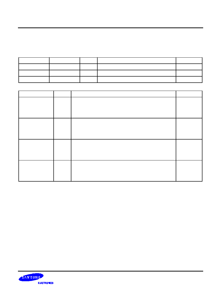
S3C2440A RISC MICROPROCESSOR
UART
11-17
UART ERROR STATUS REGISTER
There are three UART Rx error status registers including UERSTAT0, UERSTAT1 and UERSTAT2 in the UART
block.
Register
Address
R/W
Description
Reset Value
UERSTAT0
0x50000014
R
UART channel 0 Rx error status register
0x0
UERSTAT1
0x50004014
R
UART channel 1 Rx error status register
0x0
UERSTAT2
0x50008014
R
UART channel 2 Rx error status register
0x0
UERSTATn
Bit
Description
Initial State
Break Detect
[3]
Set to 1 automatically to indicate that a break signal has been
received.
0 = No break receive
1 = Break receive (Interrupt is requested.)
0
Frame Error
[2]
Set to 1 automatically whenever a frame error occurs during
receive operation.
0 = No frame error during receive
1 = Frame error (Interrupt is requested.)
0
Parity Error
[1]
Set to 1 automatically whenever a parity error occurs during
receive operation.
0 = No parity error during receive
1 = Parity error (Interrupt is requested.)
0
Overrun Error
[0]
Set to 1 automatically whenever an overrun error occurs during
receive operation.
0 = No overrun error during receive
1 = Overrun error (Interrupt is requested.)
0
NOTE: These bits (UERSATn[3:0]) are automatically cleared to 0 when the UART error status register is read.

UART
S3C2440A RISC MICROPROCESSOR
11-18
UART FIFO STATUS REGISTER
There are three UART FIFO status registers including UFSTAT0, UFSTAT1 and UFSTAT2 in the UART block.
Register
Address
R/W
Description
Reset Value
UFSTAT0
0x50000018
R
UART channel 0 FIFO status register
0x00
UFSTAT1
0x50004018
R
UART channel 1 FIFO status register
0x00
UFSTAT2
0x50008018
R
UART channel 2 FIFO status register
0x00
UFSTATn
Bit
Description
Initial State
Reserved
[15]
0
Tx FIFO Full
[14]
Set to 1 automatically whenever transmit FIFO is full during
transmit operation
0 = 0-byte
Tx FIFO data
63-byte
1 = Full
0
Tx FIFO Count
[13:8]
Number of data in Tx FIFO
0
Reserved
[7]
≠
0
Rx FIFO Full
[6]
Set to 1 automatically whenever receive FIFO is full during
receive operation
0 = 0-byte
Rx FIFO data
63-byte
1 = Full
0
Rx FIFO Count
[5:0]
Number of data in Rx FIFO
0
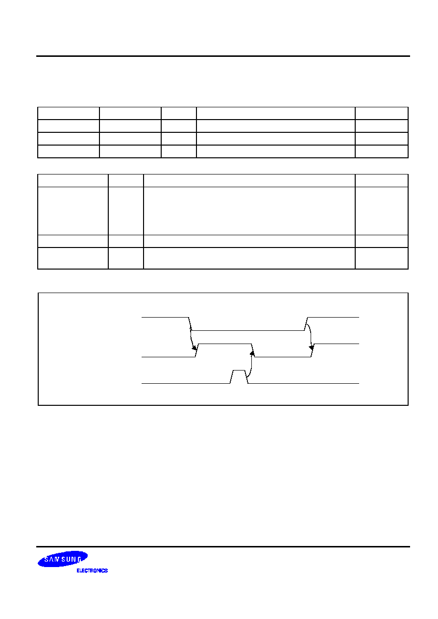
S3C2440A RISC MICROPROCESSOR
UART
11-19
UART MODEM STATUS REGISTER
There are two UART modem status registers including UMSTAT0, UMSTAT1 in the UART block.
Register
Address
R/W
Description
Reset Value
UMSTAT0
0x5000001C
R
UART channel 0 modem status register
0x0
UMSTAT1
0x5000401C
R
UART channel 1 modem status register
0x0
Reserved
0x5000801C
≠
Reserved
Undef
UMSTAT0
Bit
Description
Initial State
Delta CTS
[4]
Indicate that the nCTS input to the S3C2440A has changed
state since the last time it was read by CPU.
(Refer to Figure 11-8.)
0 = Has not changed
1 = Has changed
0
Reserved
[3:1]
≠
0
Clear to Send
[0]
0 = CTS signal is not activated (nCTS pin is high)
1 = CTS signal is activated (nCTS pin is low)
0
nCTS
Delta CTS
Read_UMSTAT
Figure 11-8. nCTS and Delta CTS Timing Diagram
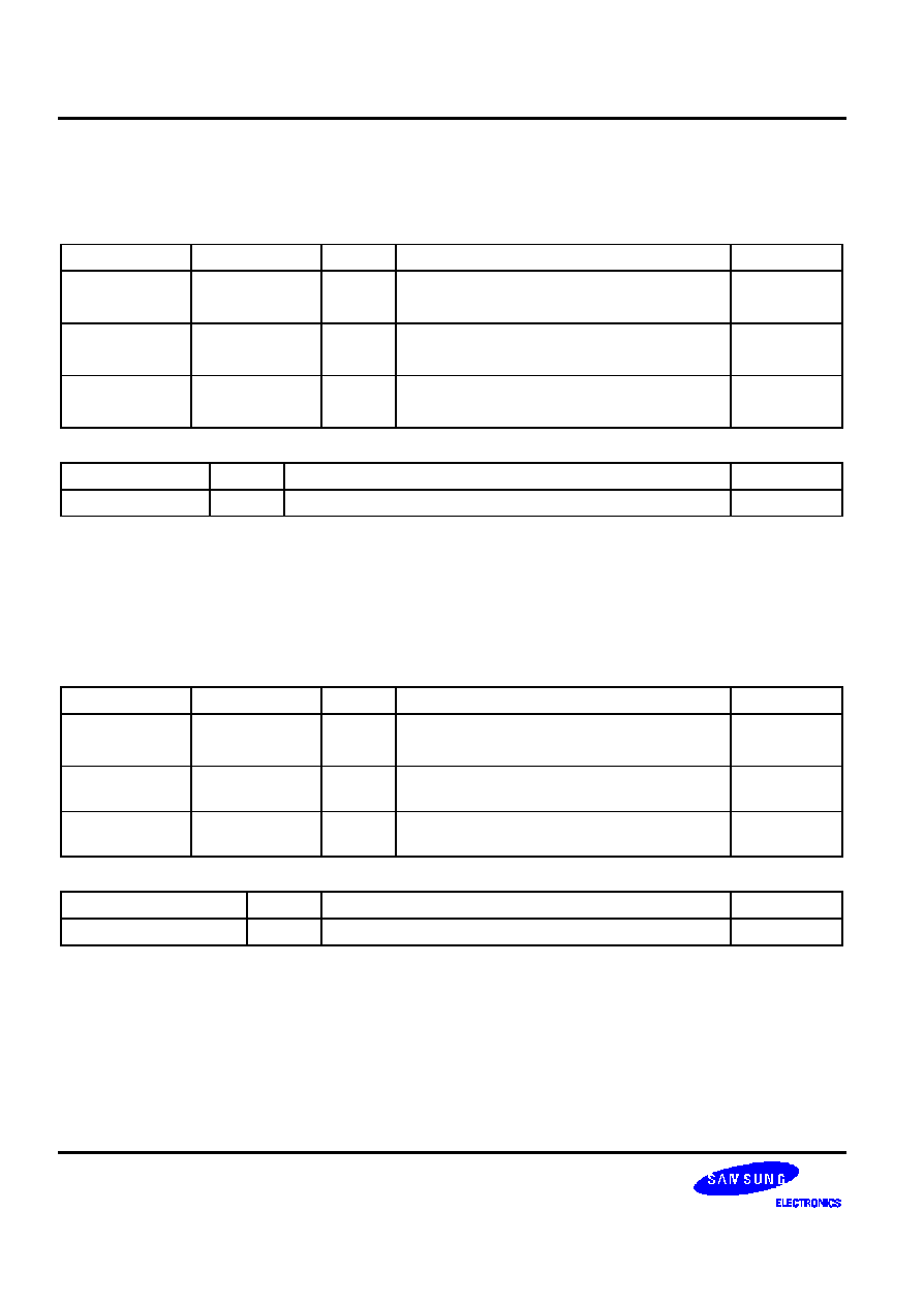
UART
S3C2440A RISC MICROPROCESSOR
11-20
UART TRANSMIT BUFFER REGISTER (HOLDING REGISTER & FIFO REGISTER)
There are three UART transmit buffer registers including UTXH0, UTXH1 and UTXH2 in the UART block.
UTXHn has an 8-bit data for transmission data.
Register
Address
R/W
Description
Reset Value
UTXH0
0x50000020(L)
0x50000023(B)
W
(by byte)
UART channel 0 transmit buffer register
≠
UTXH1
0x50004020(L)
0x50004023(B)
W
(by byte)
UART channel 1 transmit buffer register
≠
UTXH2
0x50008020(L)
0x50008023(B)
W
(by byte)
UART channel 2 transmit buffer register
≠
UTXHn
Bit
Description
Initial State
TXDATAn
[7:0]
Transmit data for UARTn
≠
NOTE: (L): The endian mode is Little endian.
(B): The endian mode is Big endian.
UART RECEIVE BUFFER REGISTER (HOLDING REGISTER & FIFO REGISTER)
There are three UART receive buffer registers including URXH0, URXH1 and URXH2 in the UART block.
URXHn has an 8-bit data for received data.
Register
Address
R/W
Description
Reset Value
URXH0
0x50000024(L)
0x50000027(B)
R
(by byte)
UART channel 0 receive buffer register
≠
URXH1
0x50004024(L)
0x50004027(B)
R
(by byte)
UART channel 1 receive buffer register
≠
URXH2
0x50008024(L)
0x50008027(B)
R
(by byte)
UART channel 2 receive buffer register
≠
URXHn
Bit
Description
Initial State
RXDATAn
[7:0]
Receive data for UARTn
≠
NOTE: When an overrun error occurs, the URXHn must be read. If not, the next received data will also make an overrun
error, even though the overrun bit of UERSTATn had been cleared.
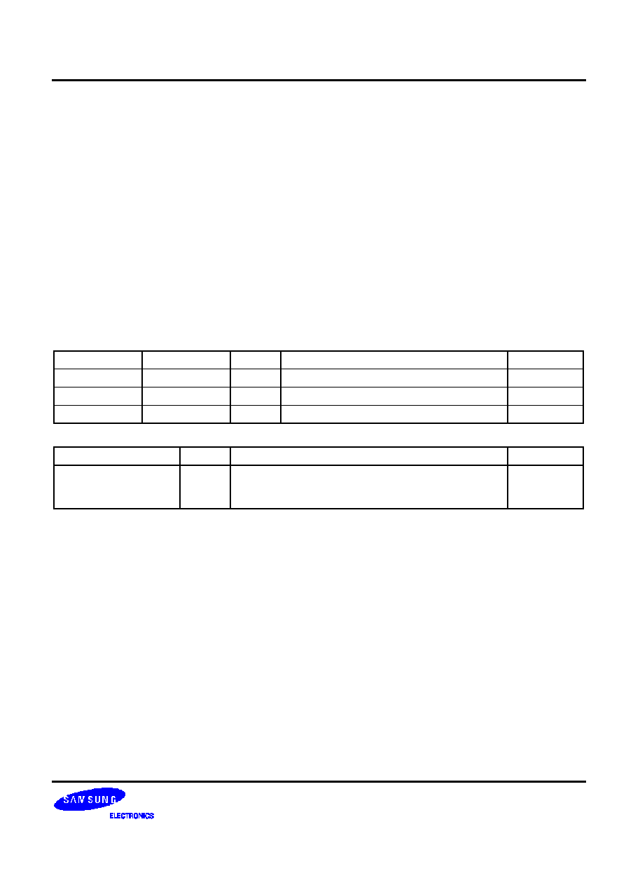
S3C2440A RISC MICROPROCESSOR
UART
11-21
UART BAUD RATE DIVISOR REGISTER
There are three UART baud rate divisor registers including UBRDIV0, UBRDIV1 and UBRDIV2 in the UART block.
The value stored in the baud rate divisor register (UBRDIVn), is used to determine the serial Tx/Rx clock rate (baud
rate) as follows:
UBRDIVn
= (int)( UART clock / ( buad rate x 16) ) ≠1
( UART clock: PCLK, FCLK/n or UEXTCLK )
Where, UBRDIVn should be from 1 to (2
16
-1), but can be set zero only using the UEXTCLK which should be smaller
than PCLK.
For example, if the baud-rate is 115200 bps and UART clock is 40 MHz, UBRDIVn is:
UBRDIVn
= (int)(40000000 / (115200 x 16) ) -1
= (int)(21.7) -1 [round to the nearest whole number]
= 22 -1 = 21
Register
Address
R/W
Description
Reset Value
UBRDIV0
0x50000028
R/W
Baud rate divisior register 0
≠
UBRDIV1
0x50004028
R/W
Baud rate divisior register 1
≠
UBRDIV2
0x50008028
R/W
Baud rate divisior register 2
≠
UBRDIVn
Bit
Description
Initial State
UBRDIV
[15:0]
Baud rate division value UBRDIVn > 0
Using the UEXTCLK as input clock, UBRDIVn can be set
`0'.
≠

UART
S3C2440A RISC MICROPROCESSOR
11-22
NOTES
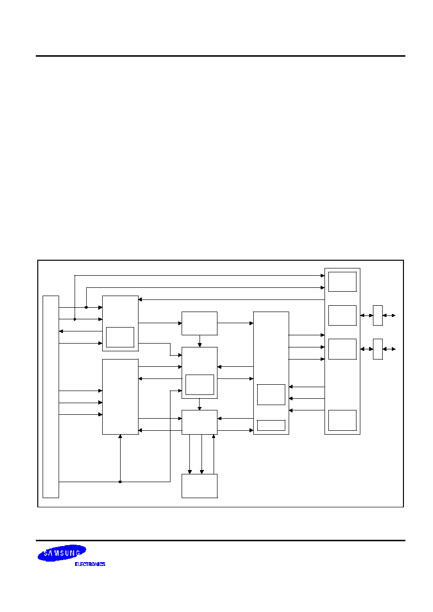
S3C2440A RISC MICROPROCESSOR
USB HOST
12-1
12
USB HOST CONTROLLER
OVERVIEW
S3C2440A supports 2-port USB host interface as follows:
-- OHCI Rev 1.0 compatible
-- USB Rev1.1 compatible
-- Two down stream ports
-- Support for both LowSpeed and FullSpeed USB devices
HCI
SLAVE
BLOCK
APP_SADR(8)
APP_SDATA(32)
HCI_DATA(32)
CONTROL
CONTROL
OHCI
REGS
USB
STATE
CONTROL
LIST
PROCESSOR
BLOCK
ED&TD
REGS
Cntl
HCI
MASTER
BLOCK
CONTROL
ED/TD_DATA(32)
ED/TD
STATUS(32)
64x8
FIFO
Cntl
HC_DATA(8)
DF_DATA(8)
APP_MDATA(32)
HCM_ADR/
DATA(32)
CONTROL
STATUS
CONTROL
CTRL
CTRL
RH_DATA(8)
DF_DATA(8)
HCF_DATA(8)
Addr(6)
FIFO_DATA(8)
64x8
FIFO
ROOT
HUB
&
HOST
SIE
HSIE
S/M
DPLL
ROOT
HUB
&
HOST
SIE
OHCI
ROOT HUB
REGS
PORT
S/M
PORT
S/M
PORT
S/M
X
V
R
USB
1
X
V
R
USB
2
HCI
BUS
EXT.FIFO STATUS
RCF0_RegData(32)
TxEnl
TxDpls
TxDmns
RcvData
RcvDpls
RcvDmns
Figure 12-1. USB Host Controller Block Diagram
USB HOST
S3C2440A RISC MICROPROCESSOR
12-2
USB HOST CONTROLLER SPECIAL REGISTERS
The S3C2440A USB host controller complies with OHCI Rev 1.0. Refer to Open Host Controller Interface Rev 1.0
specification for detailed information.
OHCI REGISTERS FOR USB HOST CONTROLLER
Register
Base Address
R/W
Description
Reset Value
HcRevision
0x49000000
≠
Control and status group
≠
HcControl
0x49000004
≠
≠
HcCommonStatus
0x49000008
≠
≠
HcInterruptStatus
0x4900000C
≠
≠
HcInterruptEnable
0x49000010
≠
≠
HcInterruptDisable
0x49000014
≠
≠
HcHCCA
0x49000018
≠
Memory pointer group
≠
HcPeriodCuttentED
0x4900001C
≠
≠
HcControlHeadED
0x49000020
≠
≠
HcControlCurrentED
0x49000024
≠
≠
HcBulkHeadED
0x49000028
≠
≠
HcBulkCurrentED
0x4900002C
≠
≠
HcDoneHead
0x49000030
≠
≠
HcRmInterval
0x49000034
≠
Frame counter group
≠
HcFmRemaining
0x49000038
≠
≠
HcFmNumber
0x4900003C
≠
≠
HcPeriodicStart
0x49000040
≠
≠
HcLSThreshold
0x49000044
≠
≠
HcRhDescriptorA
0x49000048
≠
Root hub group
≠
HcRhDescriptorB
0x4900004C
≠
≠
HcRhStatus
0x49000050
≠
≠
HcRhPortStatus1
0x49000054
≠
≠
HcRhPortStatus2
0x49000058
≠
≠

S3C2440A RISC MICROPROCESSOR
USB DEVICE
13-1
13
USB DEVICE CONTROLLER
OVERVIEW
Universal Serial Bus (USB) device controller is designed to provide a high performance full speed function controller
solution with DMA interface. USB device controller allows bulk transfer with DMA, interrupt transfer and control
transfer.
USB Device Controller Supports:
-- Full speed USB device controller compatible with the USB specification version 1.1
-- DMA interface for bulk transfer
-- Five endpoints with FIFO
EP0: 16byte (Register)
EP1: 128byte IN/OUT FIFO (dual port asynchronous RAM): interrupt or DMA
EP2: 128byte IN/OUT FIFO (dual port asynchronous RAM): interrupt or DMA
EP3: 128byte IN/OUT FIFO (dual port asynchronous RAM): interrupt or DMA
EP4: 128byte IN/OUT FIFO (dual port asynchronous RAM): interrupt or DMA
-- Integrated USB Transceiver
FEATURE
-- Fully compliant with USB Specification Version 1.1
-- Full speed (12Mbps) device
-- Integrated USB Transceiver
-- Supports control, interrupt and bulk transfer
-- Five endpoints with FIFO:
One bi-directional control endpoint with 16-byte FIFO (EP0)
Four bi-directional bulk endpoints with 128-byte FIFO (EP1, EP2, EP3, and EP4)
-- Supports DMA interface for receive and transmit bulk endpoints. (EP1, EP2, EP3, and EP4)
-- Independent 128-byte receive and transmit FIFO to maximize throughput
-- Supports suspend and remote wakeup function
NOTE
PCLK should be more than 20MHz to use USB Controller in stable condition.
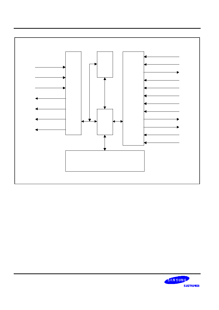
USB DEVICE
S3C2440A RISC MICROPROCESSOR
13-2
SIE
RT_VP_OUT
RT_VM_IN
RT_VP_IN
RXD
RT_UXSUSPEND
RT_UX_OEN
RT_VM_OUT
MC_ADDR[13:0]
SIU
GFI
FIFOs
MCU
&
DMA
I/F
MC_DATA_IN[31:0]
MC_DATA_OUT[31:0]
USB_CLK
SYS_CLK
SYS_RESETN
MC_WR
WR_RDN
MC_CSN
MC_INTR
DREQN[3:0]
DACKN[3:0]
Figure 13-1. USB Device Controller Block Diagram

S3C2440A RISC MICROPROCESSOR
USB DEVICE
13-3
USB DEVICE CONTROLLER SPECIAL REGISTERS
This section describes detailed functionalities about register sets of USB device controller.
All special function register is byte-accessible or word-accessible. If you access byte mode offset-address is
different in little endian and big endian. All reserved bit is zero.
Common indexed registers depend on INDEX register (INDEX_REG) (offset address: 0X178) value. For example if
you want to write EP0 CSR register, you must write `0x00' on the INDEX_REG before writing IN_CSR1 register.
NOTE
All register must be resettled after performing host reset signaling.
Register Name
Description
Offset Address
Non Indexed Registers
FUNC_ADDR_REG
Function address register
0x140(L) / 0x143(B)
PWR_REG
Power management register
0x144(L) / 0x147(B)
EP_INT_REG (EP0≠EP4)
Endpoint interrupt register
0x148(L) / 0x14B(B)
USB_INT_REG
USB interrupt register
0x158(L) / 0x15B(B)
EP_INT_EN_REG (EP0≠EP4)
Endpoint interrupt enable register
0x15C(L) / 0x15F(B)
USB_INT_EN_REG
USB Interrupt enable register
0x16C(L) / 0x16F(B)
FRAME_NUM1_REG
Frame number 1 register
0x170(L) / 0x173(B)
FRAME_NUM2_REG
Frame number 2 register
0x174(L) / 0x177(B)
INDEX_REG
Index register
0x178(L) / 0x17B(B)
EP0_FIFO_REG
Endpoint0 FIFO register
0x1C0(L) / 0x1C3(B)
EP1_FIFO_REG
Endpoint1 FIFO register
0x1C4(L) / 0x1C7(B)
EP2_FIFO_REG
Endpoint2 FIFO register
0x1C8(L) / 0x1CB(B)
EP3_FIFO_REG
Endpoint3 FIFO register
0x1CC(L) / 0x1CF(B)
EP4_FIFO_REG
Endpoint4 FIFO register
0x1D0(L) / 0x1D3(B)
EP1_DMA_CON
Endpoint1 DMA control register
0x200(L) / 0x203(B)
EP1_DMA_UNIT
Endpoint1 DMA unit counter register
0x204(L) / 0x207(B)
EP1_DMA_FIFO
Endpoint1 DMA FIFO counter register
0x208(L) / 0x20B(B)
EP1_DMA_TTC_L
Endpoint1 DMA transfer counter low-
byte register
0x20C(L) / 0x20F(B)
EP1_DMA_TTC_M
Endpoint1 DMA transfer counter
middle-byte register
0x210(L) / 0x213(B)
EP1_DMA_TTC_H
Endpoint1 DMA transfer counter high-
byte register
0x214(L) / 0x217(B)
EP2_DMA_CON
Endpoint2 DMA control register
0x218(L) / 0x21B(B)
USB DEVICE
S3C2440A RISC MICROPROCESSOR
13-4
USB DEVICE CONTROLLER SPECIAL REGISTERS (Continued)
Register Name
Description
Offset Address
EP2_DMA_UNIT
Endpoint2 DMA unit counter register
0x21C(L) / 0x21F(B)
EP2_DMA_FIFO
Endpoint2 DMA FIFO counter register
0x220(L) / 0x223(B)
EP2_DMA_TTC_L
Endpoint2 DMA transfer counter low-
byte register
0x224(L) / 0x227(B)
EP2_DMA_TTC_M
Endpoint2 DMA transfer counter
middle-byte register
0x228(L) / 0x22B(B)
EP2_DMA_TTC_H
Endpoint2 DMA transfer counter high-
byte register
0x22C(L) / 0x22F(B)
EP3_DMA_CON
Endpoint3 DMA control register
0x240(L) / 0x243(B)
EP3_DMA_UNIT
Endpoint3 DMA unit counter register
0x244(L) / 0x247(B)
EP3_DMA_FIFO
Endpoint3 DMA FIFO counter register
0x248(L) / 0x24B(B)
EP3_DMA_TTC_L
Endpoint3 DMA transfer counter low-
byte register
0x24C(L) / 0x24F(B)
EP3_DMA_TTC_M
Endpoint3 DMA transfer counter
middle-byte register
0x250(L) / 0x253(B)
EP3_DMA_TTC_H
Endpoint3 DMA transfer counter high-
byte register
0x254(L) / 0x247(B)
EP4_DMA_CON
Endpoint4 DMA control register
0x258(L) / 0x25B(B)
EP4_DMA_UNIT
Endpoint4 DMA unit counter register
0x25C(L) / 0x25F(B)
EP4_DMA_FIFO
Endpoint4 DMA FIFO counter register
0x260(L) / 0x263(B)
EP4_DMA_TTC_L
Endpoint4 DMA transfer counter low-
byte register
0x264(L) / 0x267(B)
EP4_DMA_TTC_M
Endpoint4 DMA transfer counter
middle-byte register
0x268(L) / 0x26B(B)
EP4_DMA_TTC_H
Endpoint4 DMA transfer counter high-
byte register
0x26C(L) / 0x26F(B)
Common Indexed Registers
MAXP_REG
Endpoint MAX packet register
0x180(L) / 0x183(B)
In Indexed Registers
IN_CSR1_REG/EP0_CSR
EP In control status register 1/EP0
control status register
0x184(L) / 0x187(B)
IN_CSR2_REG
EP In control status register 2
0x188(L) / 0x18B(B)
Out Indexed Registers
OUT_CSR1_REG
EP out control status register 1
0x190(L) / 0x193(B)
OUT_CSR2_REG
EP out control status register 2
0x194(L) / 0x197(B)
OUT_FIFO_CNT1_REG
EP out write count register 1
0x198(L) / 0x19B(B)
OUT_FIFO_CNT2_REG
EP out write count register 2
0x19C(L) / 0x19F(B)
S3C2440A RISC MICROPROCESSOR
USB DEVICE
13-5
FUNCTION ADDRESS REGISTER (FUNC_ADDR_REG)
This register maintains the USB device controller address assigned by the host. The Micro Controller Unit (MCU)
writes the value received through a SET_ADDRESS descriptor to this register. This address is used for the next
token.
Register
Address
R/W
Description
Reset Value
FUNC_ADDR_REG
0x52000140(L)
0x52000143(B)
R/W
(byte)
Function address register
0x00
FUNC_ADDR_REG
Bit
MCU
USB
Description
Initial State
ADDR_UPDATE
[7]
R
/SET
R
/CLEAR
Set by the MCU whenever it updates the
FUNCTION_ADDR field in this register.
This bit will be cleared by USB when
DATA_END bit in EP0_CSR register.
0
FUNCTION_ADDR
[6:0]
R/W
R
The MCU write the unique address,
assigned by host, to this field.
00

USB DEVICE
S3C2440A RISC MICROPROCESSOR
13-6
POWER MANAGEMENT REGISTER (PWR_REG)
This register acts as a power control register in the USB block.
Register
Address
R/W
Description
Reset Value
PWR_REG
0x52000144(L)
0x52000147(B)
R/W
(byte)
Power management register
0x00
PWR_ADDR
Bit
MCU
USB
Description
Initial State
Reserved
[7:4]
≠
≠
≠
≠
USB_RESET
[3]
R
SET
Set by the USB if reset signaling is received
from the host. This bit remains set as long as
reset signaling persists on the bus
0
MCU_RESUME
[2]
R/W
R
/CLEAR
Set by the MCU for MCU Resume.
The USB generates the resume signaling during
10ms, if this bit is set in suspend mode.
SUSPEND_MODE
[1]
R
SET
/CLEAR
Set by USB automatically when the device
enter into suspend mode.
It is cleared under the following conditions:
1) The MCU clears the MCU_RESUME bit by
writing `0', in order to end remote resume
signaling.
2) The resume signal from host is received.
0
SUSPEND_EN
[0]
R/W
R
Suspend mode enable control bit
0 = Disable (default).
The device will not enter suspend mode.
1 = Enable suspend mode
0

S3C2440A RISC MICROPROCESSOR
USB DEVICE
13-7
INTERRUPT REGISTER (EP_INT_REG/USB_INT_REG)
The USB core has two interrupt registers. These registers act as status registers for the MCU when it is interrupted.
The bits are cleared by writing a `1' (not `0') to each bit that was set.
Once the MCU is interrupted, MCU should read the contents of interrupt-related registers and write back to clear the
contents if it is necessary.
Register
Address
R/W
Description
Reset Value
EP_INT_REG
0x52000148(L)
0x5200014B(B)
R/W
(byte)
EP interrupt pending/clear register
0x00
EP_INT_REG
Bit
MCU
USB
Description
Initial State
EP1~EP4 Interrupt
[4:1]
R
/CLEAR
SET
For BULK/INTERRUPT IN endpoints:
Set by the USB under the following conditions:
1. IN_PKT_RDY bit is cleared.
2. FIFO is flushed
3. SENT_STALL set.
For BULK/INTERRUPT OUT endpoints:
Set by the USB under the following conditions:
1. Sets OUT_PKT_RDY bit
2. Sets SENT_STALL bit
0
EP0 Interrupt
[0]
R
/CLEAR
SET
Correspond to endpoint 0 interrupt.
Set by the USB under the following conditions:
1. OUT_PKT_RDY bit is set.
2. IN_PKT_RDY bit is cleared.
3. SENT_STALL bit is set
4. SETUP_END bit is set
5. DATA_END bit is cleared
(it indicates the end of control transfer).
0

USB DEVICE
S3C2440A RISC MICROPROCESSOR
13-8
INTERRUPT REGISTER (EP_INT_REG/USB_INT_REG) (Continued)
Register
Address
R/W
Description
Reset Value
USB_INT_REG
0x52000158(L)
0x5200015B(B)
R/W
(byte)
USB interrupt pending/clear register
0x00
USB_INT_REG
Bit
MCU
USB
Description
Initial State
RESET
Interrupt
[2]
R
/CLEAR
SET
Set by the USB when it receives reset
signaling.
0
RESUME
Interrupt
[1]
R
/CLEAR
SET
Set by the USB when it receives resume
signaling, while in Suspend mode.
If the resume occurs due to a USB reset, then
the MCU is first interrupted with a RESUME
interrupt. Once the clocks resume and the SE0
condition persists for 3ms, USB RESET
interrupt will be asserted.
0
SUSPEND
Interrupt
[0]
R
/CLEAR
SET
Set by the USB when it receives suspend
signalizing.
This bit is set whenever there is no activity for
3ms on the bus. Thus, if the MCU does not
stop the clock after the first suspend interrupt, it
will continue to be interrupted every 3ms as
long as there is no activity on the USB bus.
By default, this interrupt is disabled.
0
S3C2440A RISC MICROPROCESSOR
USB DEVICE
13-9
INTERRUPT ENABLE REGISTER (EP_INT_EN_REG/USB_INT_EN_REG)
Corresponding to each interrupt register, The USB device controller also has two interrupt enable registers (except
resume interrupt enable). By default, usb reset interrupt is enabled.
If bit = 0, the interrupt is disabled.
If bit = 1, the interrupt is enabled.
Register
Address
R/W
Description
Reset Value
EP_INT_EN_REG
0x5200015C(L)
0x5200015F(B)
R/W
(byte)
Determine which interrupt is enabled
0xFF
EP_INT_EN_REG
Bit
MCU
USB
Description
Initial State
EP4_INT_EN
[4]
R/W
R
EP4 Interrupt Enable bit
0 = Interrupt disable 1 = Enable
1
EP3_INT_EN
[3]
R/W
R
EP3 Interrupt Enable bit
0 = Interrupt disable 1 = Enable
1
EP2_INT_EN
[2]
R/W
R
EP2 Interrupt Enable bit
0 = Interrupt disable 1 = Enable
1
EP1_INT_EN
[1]
R/W
R
EP1 Interrupt Enable bit
0 = Interrupt disable 1 = Enable
1
EP0_INT_EN
[0]
R/W
R
EP0 Interrupt Enable bit
0 = Interrupt disable 1 = Enable
1
Register
Address
R/W
Description
Reset Value
USB_INT_EN_REG
0x520016C(L)
0x5200016F(B)
R/W
(byte)
Determine which interrupt is enabled
0x04
INT_MASK_REG
Bit
MCU
USB
Description
Initial State
RESET_INT_EN
[2]
R/W
R
Reset interrupt enable bit
0 = Interrupt disable 1 = Enable
1
Reserved
[1]
≠
≠
≠
0
SUSPEND_INT_EN
[0]
R/W
R
Suspend interrupt enable bit
0 = Interrupt disable 1 = Enable
0
USB DEVICE
S3C2440A RISC MICROPROCESSOR
13-10
FRAME NUMBER REGISTER (FPAME_NUM1_REG/FRAME_NUM2_REG)
When the host transfers USB packets, each Start Of Frame (SOF) packet includes a frame number. The USB
device controller catches this frame number and loads it into this register automatically.
Register
Address
R/W
Description
Reset Value
FRAME_NUM1_REG
0x52000170(L)
0x52000173(B)
R
(byte)
Frame number lower byte register
0x00
FRAME_NUM_REG
Bit
MCU
USB
Description
Initial State
FRAME_NUM1
[7:0]
R
W
Frame number lower byte value
00
Register
Address
R/W
Description
Reset Value
FRAME_NUM2_REG
0x52000174(L)
0x52000177(B)
R
(byte)
Frame number higher byte register
0x00
FRAME_NUM_REG
Bit
MCU
USB
Description
Initial State
FRAME_NUM2
[7:0]
R
W
Frame number higher byte value
00
S3C2440A RISC MICROPROCESSOR
USB DEVICE
13-11
INDEX REGISTER (INDEX_REG)
The INDEX register is used to indicate certain endpoint registers effectively. The MCU can access the endpoint
registers (MAXP_REG, IN_CSR1_REG, IN_CSR2_REG, OUT_CSR1_REG, OUT_CSR2_REG,
OUT_FIFO_CNT1_REG, and OUT_FIFO_CNT2_REG) for an endpoint inside the core using the INDEX register.
Register
Address
R/W
Description
Reset Value
INDEX_REG
0x52000178(L)
0x5200017B(B)
R/W
(byte)
Register index register
0x00
INDEX_REG
Bit
MCU
USB
Description
Initial State
INDEX
[7:0]
R/W
R
Indicate a certain endpoint
00
MAX PACKET REGISTER (MAXP_REG)
Register
Address
R/W
Description
Reset Value
MAXP_REG
0x52000180(L)
0x52000183(B)
R/W
(byte)
End Point MAX packet register
0x01
MAXP_REG
Bit
MCU
USB
Description
Initial State
MAXP
[3:0]
R/W
R
0000: Reserved
0001: MAXP = 8 Byte 0010: MAXP = 16 Byte
0100: MAXP = 32 Byte 1000: MAXP = 64 Byte
For EP0, MAXP=8 is recommended.
For EP1~4, MAXP=64 is recommended. And, if
MAXP=64, the dual packet mode will be
enabled automatically.
0001

USB DEVICE
S3C2440A RISC MICROPROCESSOR
13-12
END POINT0 CONTROL STATUS REGISTER (EP0_CSR)
This register has the control and status bits for Endpoint 0. Since a control transaction is involved with both IN and
OUT tokens, there is only one CSR register, mapped to the IN CSR1 register. (Share IN1_CSR and can access by
writing index register "0" and read/write IN1_CSR)
Register
Address
R/W
Description
Reset Value
EP0_CSR
0x52000184(L)
0x52000187(B)
R/W
(byte)
Endpoint 0 status register
0x00
EP0_CSR
Bit
MCU
USB
Description
Initial State
SERVICED_SET
UP_END
[7]
W
CLEAR
The MCU should write a "1" to this bit to clear
SETUP_END.
0
SERVICED_OUT
_PKT_RDY
[6]
W
CLEAR
The MCU should write a "1" to this bit to clear
OUT_PKT_RDY.
0
SEND_STALL
[5]
R/W
CLEAR
MCU should write a "1" to this bit at the same
time it clears OUT_PKT_RDY, if it decodes an
invalid token.
0 = Finish the STALL condition
1 = The USB issues a STALL and shake to the
current control transfer.
0
SETUP_END
[4]
R
SET
Set by the USB when a control transfer ends
before DATA_END is set.
When the USB sets this bit, an interrupt is
generated to the MCU.
When such a condition occurs, the USB
flushes the FIFO and invalidates MCU access
to the FIFO.
0
DATA_END
[3]
SET
CLEAR
Set by the MCU on the conditions below:
1. After loading the last packet of data into the
FIFO, at the same time IN_PKT_RDY is set.
2. While it clears OUT_PKT_RDY after
unloading the last packet of data.
3. For a zero length data phase.
0
SENT_STALL
[2]
CLEAR
SET
Set by the USB if a control transaction is
stopped due to a protocol violation. An interrupt
is generated when this bit is set. The MCU
should write "0" to clear this bit.
0
IN_PKT_RDY
[1]
SET
CLEAR
Set by the MCU after writing a packet of data
into EP0 FIFO. The USB clears this bit once
the packet has been successfully sent to the
host. An interrupt is generated when the USB
clears this bit, so as the MCU to load the next
packet. For a zero length data phase, the MCU
sets DATA_END at the same time.
0
OUT_PKT_RDY
[0]
R
SET
Set by the USB once a valid token is written to
the FIFO. An interrupt is generated when the
USB sets this bit. The MCU clears this bit by
writing a "1" to the SERVICED_OUT_PKT_RDY
bit.
0

S3C2440A RISC MICROPROCESSOR
USB DEVICE
13-13
END POINT IN CONTROL STATUS REGISTER (IN_CSR1_REG/IN_CSR2_REG)
Register
Address
R/W
Description
Reset Value
IN_CSR1_REG
0x52000184(L)
0x52000187(B)
R/W
(byte)
IN END POINT control status register1
0x00
IN_CSR1_REG
Bit
MCU
USB
Description
Initial State
Reserved
[7]
≠
≠
≠
≠
CLR_DATA_
TOGGLE
[6]
R/W
R/
CLEAR
Used in set-up procedure.
0: There are alternation of DATA0 and DATA1
1: The data toggle bit is cleared and PID in
packet will maintain DATA0
0
SENT_STALL
[5]
R/
CLEAR
SET
Set by the USB when an IN token issues a
STALL handshake, after the MCU sets
SEND_STALL bit to start STALL handshaking.
When the USB issues a STALL handshake,
IN_PKT_RDY is cleared
0
SEND_STALL
[4]
W/R
R
0: The MCU clears this bit to finish the STALL
condition.
1: The MCU issues a STALL handshake to the
USB.
0
FIFO_FLUSH
[3]
R/W
CLEAR
Set by the MCU if it intends to flush the packet
in Input-related FIFO. This bit is cleared by the
USB when the FIFO is flushed. The MCU is
interrupted when this happens. If a token is in
process, the USB waits until the transmission
is complete before FIFO flushing. If two packets
are loaded into the FIFO, only first packet (The
packet is intended to be sent to the host) is
flushed, and the corresponding IN_PKT_RDY bit
is cleared
0
Reserved
[2:1]
≠
≠
≠
≠
IN_PKT_RDY
[0
R/SET
CLEAR
Set by the MCU after writing a packet of data
into the FIFO.
The USB clears this bit once the packet has
been successfully sent to the host.
An interrupt is generated when the USB clears
this bit, so the MCU can load the next packet.
While this bit is set, the MCU will not be able to
write to the FIFO.
If the MCU sets SEND STALL bit, this bit
cannot be set.
0
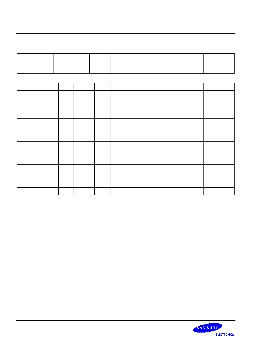
USB DEVICE
S3C2440A RISC MICROPROCESSOR
13-14
END POINT IN CONTROL STATUS REGISTER (IN_CSR1_REG/IN_CSR2_REG) (Continued)
Register
Address
R/W
Description
Reset Value
IN_CSR2_REG
0x52000188(L)
0x5200018B(B)
R/W
(byte)
IN END POINT control status register2
0x20
IN_CSR2_REG
Bit
MCU
USB
Description
Initial State
AUTO_SET
[7]
R/W
R
If set, whenever the MCU writes MAXP data,
IN_PKT_RDY will automatically be set by the
core without any intervention from MCU.
If the MCU writes less than MAXP data,
IN_PKT_RDY bit has to be set by the MCU.
0
ISO
[6]
R/W
R
Used only for endpoints whose transfer type is
programmable.
1: Reserved
0: Configures endpoint to Bulk mode
0
MODE_IN
[5]
R/W
R
Used only for endpoints whose direction is
programmable.
1: Configures Endpoint Direction as IN
0: Configures Endpoint Direction as OUT
1
IN_DMA_INT_EN
[4]
R/W
R
Determine whether the interrupt should be
issued or not, when the IN_PKT_RDY condition
happens. This is only useful for DMA mode.
0 = Interrupt enable, 1 = Interrupt Disable
0
Reserved
[3:0]
≠
≠
≠
≠

S3C2440A RISC MICROPROCESSOR
USB DEVICE
13-15
END POINT OUT CONTROL STATUS REGISTER (OUT_CSR1_REG/OUT_CSR2_REG)
Register
Address
R/W
Description
Reset Value
OUT_CSR1_REG
0x52000190(L)
0x52000193(B)
R/W
(byte)
End point out control status register1
0x00
OUT_CSR1_REG
Bit
MCU
USB
Description
Initial State
CLR_DATA_TOGGLE
[7]
R/W
CLEAR
When the MCU writes a 1 to this bit, the
data toggle sequence bit is reset to
DATA0.
0
SENT_STALL
[6]
CLEAR
/R
SET
Set by the USB when an OUT token is
ended with a STALL handshake. The USB
issues a stall handshake to the host if it
sends more than MAXP data for the OUT
TOKEN.
0
SEND_STALL
[5]
R/W
R
0: The MCU clears this bit to end the
STALL condition handshake, IN PKT
RDY is cleared.
1: The MCU issues a STALL handshake
to the USB. The MCU clears this bit to
end the STALL condition handshake,
IN PKT RDY is cleared.
0
FIFO_FLUSH
[4]
R/W
CLEAR
The MCU writes a 1 to flush the FIFO.
This bit can be set only when
OUT_PKT_RDY (D0) is set. The packet
due to be unloaded by the MCU will be
flushed.
0
Reserved
[3:1]
≠
≠
≠
0
OUT_PKT_RDY
[0]
R/
CLEAR
SET
Set by the USB after it has loaded a
packet of data into the FIFO. Once the
MCU reads the packet from FIFO, this bit
should be cleared by MCU (write a "0").
0
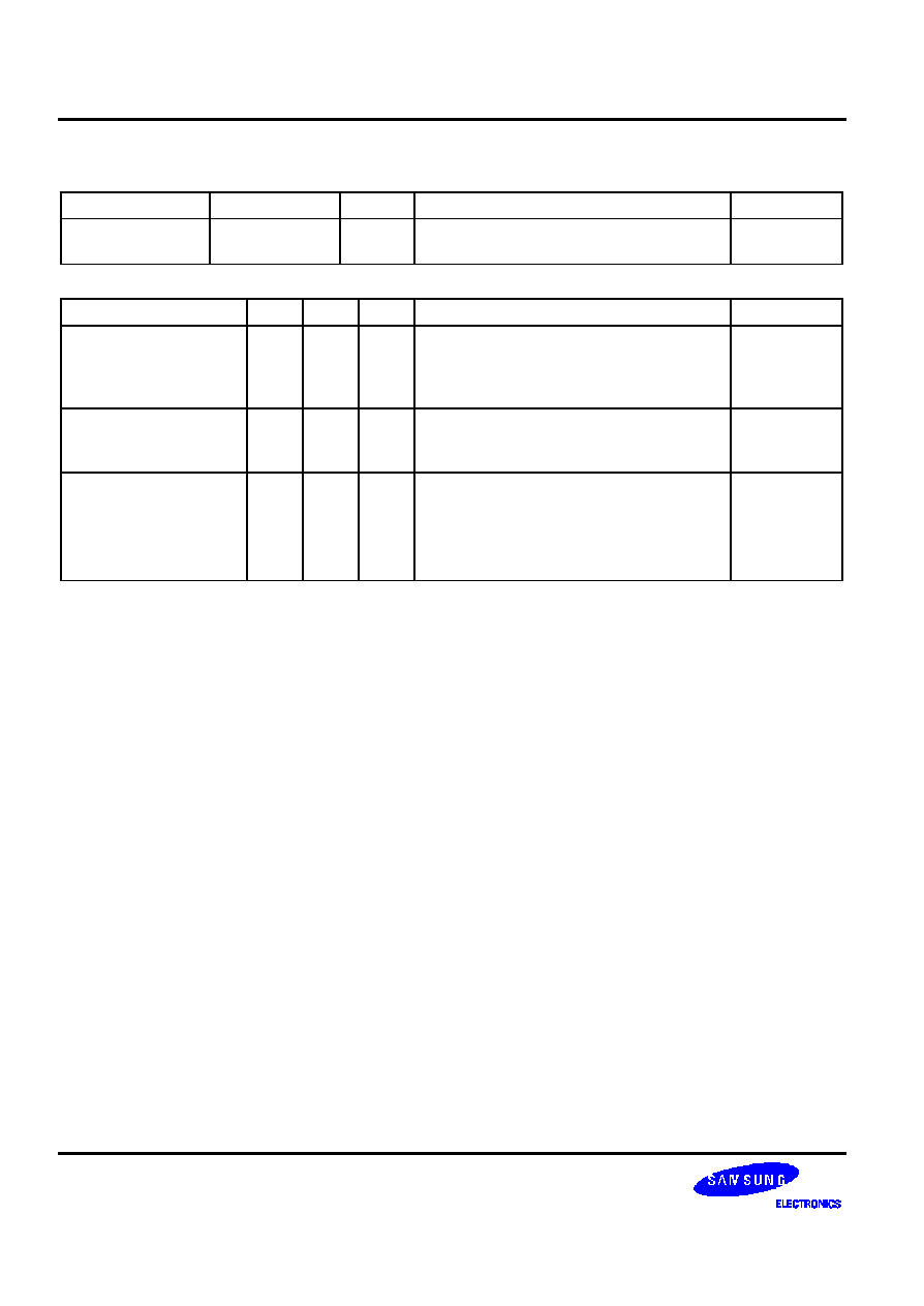
USB DEVICE
S3C2440A RISC MICROPROCESSOR
13-16
END POINT OUT CONTROL STATUS REGISTER (OUT_CSR1_REG/OUT_CSR2_REG) (Continued)
Register
Address
R/W
Description
Reset Value
OUT_CSR2_REG
0x52000194(L)
0x52000197(B)
R/W
(byte)
End point out control status register2
0x00
OUT_CSR2_REG
Bit
MCU
USB
Description
Initial State
AUTO_CLR
[7]
R/W
R
If the MCU is set, whenever the MCU reads
data from the OUT FIFO, OUT_PKT_RDY will
automatically be cleared by the logic without
any intervention from the MCU.
0
ISO
[6]
R/W
R
Determine endpoint transfer type.
0: Configures endpoint to Bulk mode.
1: Reserved.
0
OUT_DMA_INT_MASK
[5]
R/W
R
Determine whether the interrupt should be
issued or not.
OUT_PKT_RDY condition happens. This is
only useful for DMA mode
0 = Interrupt Enable 1 = Interrupt Disable
0
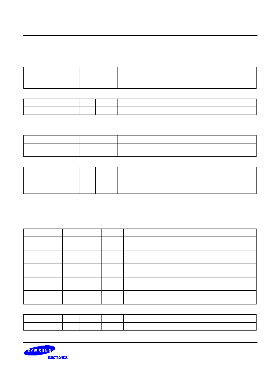
S3C2440A RISC MICROPROCESSOR
USB DEVICE
13-17
END POINT OUT WRITE COUNT REGISTER (OUT_FIFO_CNT1_REG/OUT_FIFO_CNT2_REG)
These registers maintain the number of bytes in the packet as the number is unloaded by the MCU.
Register
Address
R/W
Description
Reset Value
OUT_FIFO_CNT1_REG
0x52000198(L)
0x5200019B(B)
R
(byte)
End point out write count register1
0x00
OUT_FIFO_CNT1_REG
Bit
MCU
USB
Description
Initial State
OUT_CNT_LOW
[7:0]
R
W
Lower byte of write count
0x00
Register
Address
R/W
Description
Reset Value
OUT_FIFO_CNT2_REG
0x5200019C(L)
0x5200019F(B)
R
(byte)
End point out write count register2
0x00
OUT_FIFO_CNT2_REG
Bit
MCU
USB
Description
Initial State
OUT_CNT_HIGH
[7:0]
R
W
Higher byte of write count.
The OUT_CNT_HIGH may be always 0
normally.
0x00
END POINT FIFO REGISTER (EPN_FIFO_REG)
The EPn_FIFO_REG enables the MCU to access to the EPn FIFO.
Register
Address
R/W
Description
Reset Value
EP0_FIFO
0x520001C0(L)
0x520001C3 (B)
R/W
(byte)
End point0 FIFO register
0xXX
EP1_FIFO
0x520001C4(L)
0x520001C7(B)
R/W
(byte)
End point1 FIFO register
0xXX
EP2_FIFO
0x520001C8(L)
0x520001CB(B)
R/W
(byte)
End point2 FIFO register
0xXX
EP3_FIFO
0x520001CC(L)
0x520001CF(B)
R/W
(byte)
End point3 FIFO register
0xXX
EP4_FIFO
0x520001D0(L)
0x520001D3(B)
R/W
(byte)
End point4 FIFO register
0xXX
EPn_FIFO
Bit
MCU
USB
Description
Initial State
FIFO_DATA
[7:0]
R/W
R/W
FIFO data value
0xXX
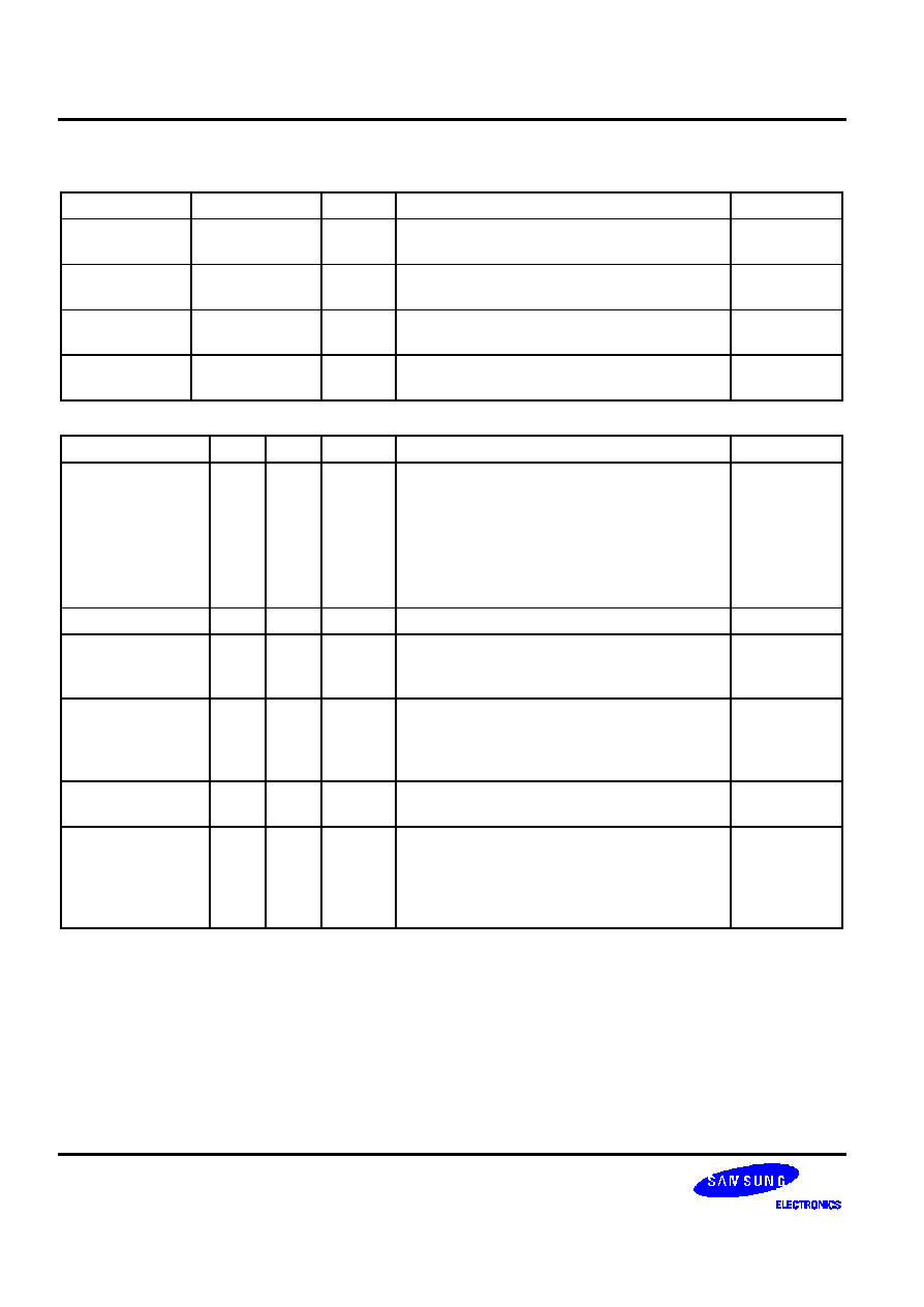
USB DEVICE
S3C2440A RISC MICROPROCESSOR
13-18
DMA INTERFACE CONTROL REGISTER (EPN_DMA_CON)
Register
Address
R/W
Description
Reset Value
EP1_DMA_CON
0x52000200(L)
0x52000203(B)
R/W
(byte)
EP1 DMA interface control register
0x00
EP2_DMA_CON
0x52000218(L)
0x5200021B(B)
R/W
(byte)
EP2 DMA interface control register
0x00
EP3_DMA_CON
0x52000240(L)
0x52000243(B)
R/W
(byte)
EP3 DMA interface control register
0x00
EP4_DMA_CON
0x52000258(L)
0x5200025B(B)
R/W
(byte)
EP4 DMA interface control register
0x00
EPn_DMA_CON
Bit
MCU
USB
Description
Initial State
RUN_OB
[7]
R/W
W
Read) DMA run observation
0: DMA is stopped 1:DMA is running
Write) Ignore EPn_DMA_TTC_n register
0: DMA requests will be stopped if
EPn_DMA_TTC_n reaches 0.
1: DMA requests will be continued although
EPn_DMA_TTC_n reaches 0.
0
STATE
[6:4]
R
W
DMA state monitoring
0
DEMAND_MODE
[3]
R/W
R
DMA demand mode enable bit
0: Demand mode disable
1: Demand mode enable
0
OUT_RUN_OB /
OUT_DMA_RUN
[2]
R/W
R/W
Functionally separated into write and read
operation.
Write operation: `0' = Stop `1' = Run
Read operation: OUT DMA Run Observation
0
IN_DMA_RUN
[1]
R/W
R
Start DMA operation.
0 = Stop 1 = Run
0
DMA_MODE_EN
[0]
R/W
R/Clear
Set DMA mode.If the RUN_OB has been wrtten
as 0 and EPn_DMA_TTC_n reaches 0,
DMA_MODE_EN bit will be cleared by USB.
0 = Interrupt Mode
1 = DMA Mode
0

S3C2440A RISC MICROPROCESSOR
USB DEVICE
13-19
DMA UNIT COUNTER REGISTER (EPN_DMA_UNIT)
This register is valid in Demand mode. In other modes, this register value must be set to `0x01'
Register
Address
R/W
Description
Reset Value
EP1_DMA_UNIT
0x52000204(L)
0x52000207(B)
R/W
(byte)
EP1 DMA transfer unit counter base register
0x00
EP2_DMA_UNIT
0x5200021C(L)
0x5200021F(B)
R/W
(byte)
EP2 DMA transfer unit counter base register
0x00
EP3_DMA_UNIT
0x52000244(L)
0x52000247(B)
R/W
(byte)
EP3 DMA transfer unit counter base register
0x00
EP4_DMA_UNIT
0x5200025C(L)
0x5200025F(B)
R/W
(byte)
EP4 DMA transfer unit counter base register
0x00
DMA_UNIT
Bit
MCU
USB
Description
Initial State
EPn_UNIT_CNT
[7:0]
R/W
R
EP DMA transfer unit counter value
0x00
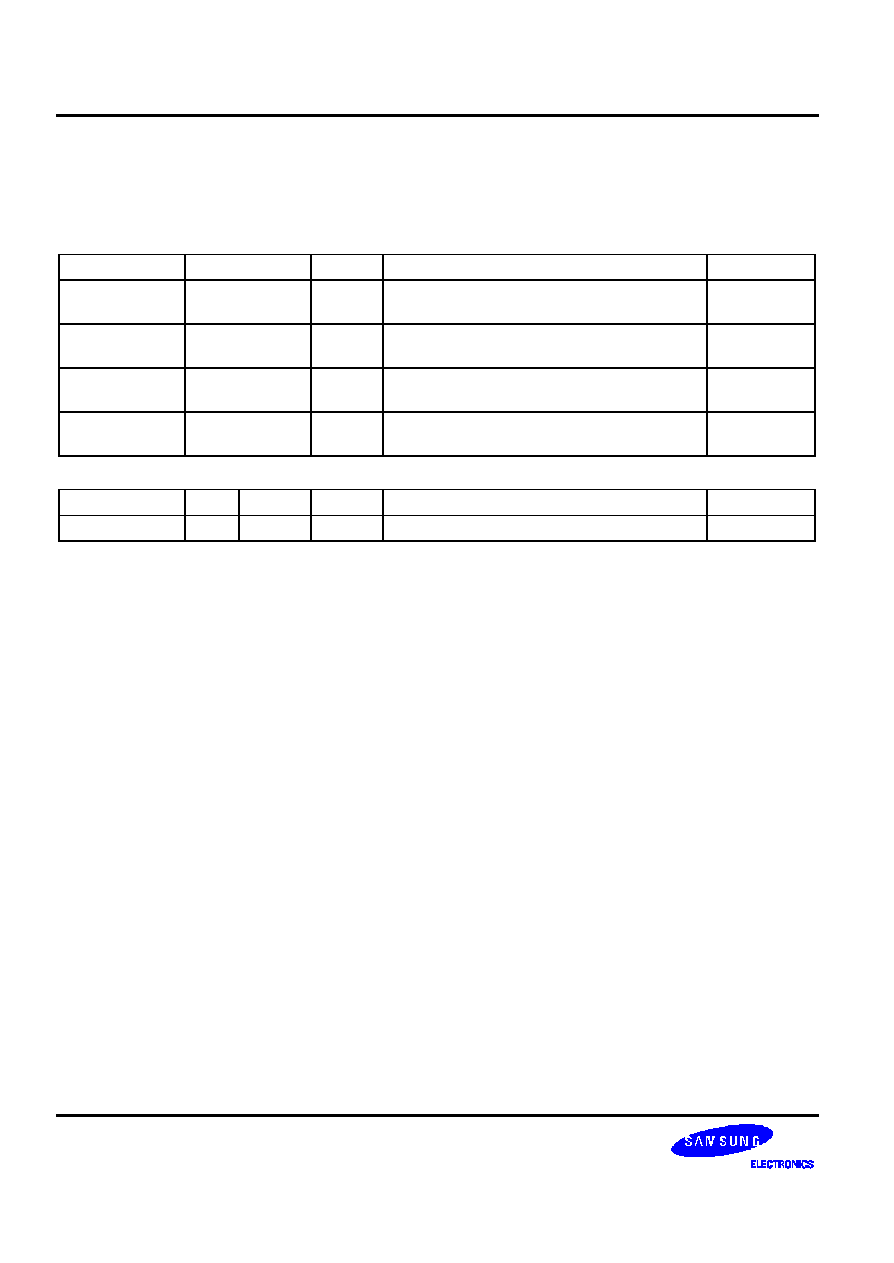
USB DEVICE
S3C2440A RISC MICROPROCESSOR
13-20
DMA FIFO COUNTER REGISTER (EPN_DMA_FIFO)
This register has values in byte size in FIFO to be transferred by DMA. In case of OUT_DMA_RUN enabled, the
value in OUT FIFO Write Count Register1 will be loaded in this register automatically. In case of IN DMA mode, the
MCU should set proper value by software.
Register
Address
R/W
Description
Reset Value
EP1_DMA_FIFO
0x52000208(L)
0x5200020B(B)
R/W
(byte)
EP1 DMA transfer FIFO counter base register
0x00
EP2_DMA_FIFO
0x52000220(L)
0x52000223(B)
R/W
(byte)
EP2 DMA transfer FIFO counter base register
0x00
EP3_DMA_FIFO
0x52000248(L)
0x5200024B(B)
R/W
(byte)
EP3 DMA transfer FIFO counter base register
0x00
EP4_DMA_FIFO
0x52000260(L)
0x52000263(B)
R/W
(byte)
EP4 DMA transfer FIFO counter base register
0x00
DMA_FIFO
Bit
MCU
USB
Description
Initial State
EPn_FIFO_CNT
[7:0]
R/W
R
EP DMA transfer FIFO counter value
0x00
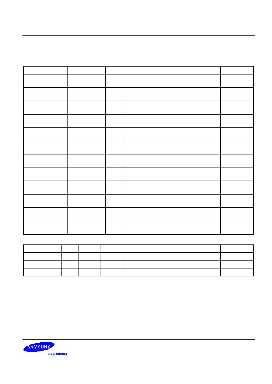
S3C2440A RISC MICROPROCESSOR
USB DEVICE
13-21
DMA TOTAL TRANSFER COUNTER REGISTER (EPn_DMA_TTC_L,M,H)
This register should have total number of bytes to be transferred using DMA (total 20-bit counter).
Register
Address
R/W
Description
Reset Value
EP1_DMA_TTC_L
0x5200020C(L)
0x5200020F(B)
R/W
(byte)
EP1 DMA total transfer counter (lower byte)
0x00
EP1_DMA_TTC_M
0x52000210(L)
0x52000213(B)
R/W
(byte)
EP1 DMA total transfer counter (middle byte)
0x00
EP1_DMA_TTC_H
0x52000214(L)
0x52000217(B)
R/W
(byte)
EP1 DMA total transfer counter (higher byte)
0x00
EP2_DMA_TTC_L
0x52000224(L)
0x52000227(B)
R/W
(byte)
EP2 DMA total transfer counter (lower byte)
0x00
EP2_DMA_TTC_M
0x52000228(L)
0x5200022B(B)
R/W
(byte)
EP2 DMA total transfer counter (middle byte)
0x00
EP2_DMA_TTC_H
0x5200022C(L)
0x5200022F(B)
R/W
(byte)
EP2 DMA total transfer counter (higher byte)
0x00
EP3_DMA_TTC_L
0x5200024C(L)
0x5200024F(B)
R/W
(byte)
EP3 DMA total transfer counter (lower byte)
0x00
EP3_DMA_TTC_M
0x52000250(L)
0x52000253(B)
R/W
(byte)
EP3 DMA total transfer counter (middle byte)
0x00
EP3_DMA_TTC_H
0x52000254(L)
0x52000257(B)
R/W
(byte)
EP3 DMA total transfer counter (higher byte)
0x00
EP4_DMA_TTC_L
0x52000264(L)
0x52000267(B)
R/W
(byte)
EP4 DMA total transfer counter (lower byte)
0x00
EP4_DMA_TTC_M
0x52000268(L)
0x5200026B(B)
R/W
(byte)
EP4 DMA total transfer counter (middle byte)
0x00
EP4_DMA_TTC_H
0x5200026C(L)
0x5200026F(B)
R/W
(byte)
EP4 DMA total transfer counter (higher byte)
0x00
DMA_TX
Bit
MCU
USB
Description
Initial State
EPn_TTC_L
[7:0]
R/W
R
DMA total transfer count value (lower byte)
0x00
EPn_TTC_M
[7:0]
R/W
R
DMA total transfer count value (middle byte)
0x00
EPn_TTC_H
[3:0]
R/W
R
DMA total transfer count value (higher byte)
0x00

USB DEVICE
S3C2440A RISC MICROPROCESSOR
13-22
NOTES
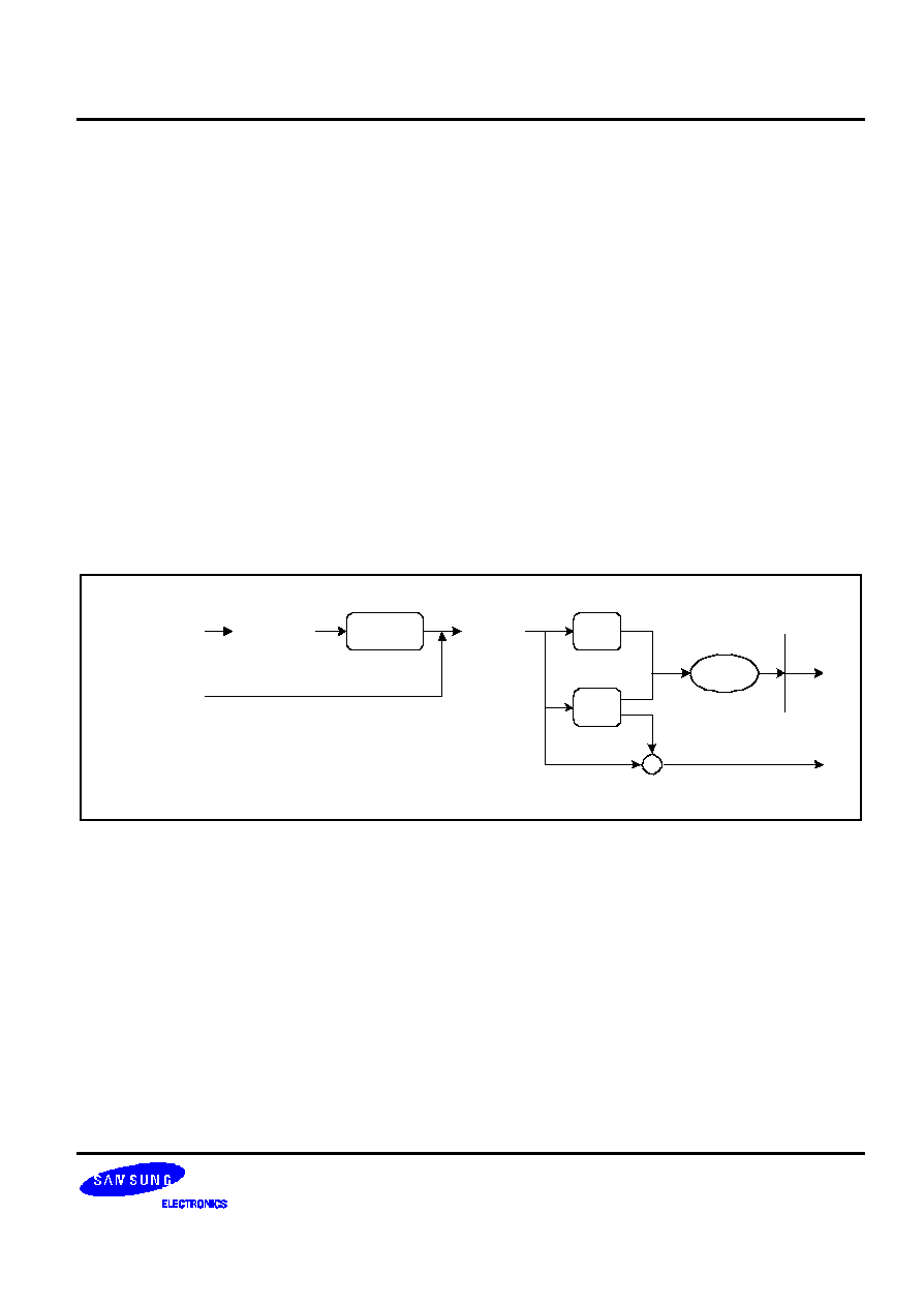
S3C2440A RISC MICROPROCESSOR
INTERRUPT CONTROLLER
14-1
14
INTERRUPT CONTROLLER
OVERVIEW
The interrupt controller in the S3C2440A receives the request from 60 interrupt sources. These interrupt sources are
provided by internal peripherals such as DMA controller, UART, IIC, and others. In these interrupt sources, the
UARTn, AC97 and EINTn interrupts are 'OR'ed to the interrupt controller.
When receiving multiple interrupt requests from internal peripherals and external interrupt request pins, the interrupt
controller requests FIQ or IRQ interrupt of the ARM920T core after the arbitration procedure.
The arbitration procedure depends on the hardware priority logic and the result is written to the interrupt pending
register, which helps users notify which interrupt is generated out of various interrupt sources.
Request sources
(with sub -register)
Request sources
(without sub -register)
SRCPND
MASK
MODE
Priority
INTPND
IRQ
FIQ
SUBSRCPND
SUBMASK
LCD interrupt has different features. Please see the chapter 15 LCD Controller
Figure 14-1. Interrupt Process Diagram

INTERRUPT CONTROLLER
S3C2440A RISC MICROPROCESSOR
14-2
INTERRUPT CONTROLLER OPERATION
F-bit and I-bit of Program Status Register (PSR)
If the F-bit of PSR in ARM920T CPU is set to 1, the CPU does not accept the Fast Interrupt Request (FIQ) from the
interrupt controller. Likewise, If I-bit of the PSR is set to 1, the CPU does not accept the Interrupt Request (IRQ) from
the interrupt controller. So, the interrupt controller can receive interrupts by clearing F-bit or I-bit of the PSR to 0 and
setting the corresponding bit of INTMSK to 0.
Interrupt Mode
The ARM920T has two types of Interrupt mode: FIQ or IRQ. All the interrupt sources determine which mode is used
at interrupt request.
Interrupt Pending Register
The S3C2440A has two interrupt pending registers: source pending register (SRCPND) and interrupt pending register
(INTPND). These pending registers indicate whether an interrupt request is pending or not. When the interrupt
sources request interrupt the service, the corresponding bits of SRCPND register are set to 1, and at the same time,
only one bit of the INTPND register is set to 1 automatically after arbitration procedure. If interrupts are masked, then
the corresponding bits of the SRCPND register are set to 1. This does not cause the bit of INTPND register changed.
When a pending bit of INTPND register is set, the interrupt service routine will start whenever the I-flag or F-flag is
cleared to 0. The SRCPND and INTPND registers can be read and written, so the service routine must clear the
pending condition by writing a 1 to the corresponding bit in the SRCPND register first and then clear the pending
condition in the INTPND registers by using the same method.
Interrupt Mask Register
This register indicates that an interrupt has been disabled if the corresponding mask bit is set to 1. If an interrupt
mask bit of INTMSK is 0, the interrupt will be serviced normally. If the corresponding mask bit is 1 and the interrupt is
generated, the source pending bit will be set.

S3C2440A RISC MICROPROCESSOR
INTERRUPT CONTROLLER
14-3
INTERRUPT SOURCES
The interrupt controller supports 60 interrupt sources as shown in the table below.
Sources
Descriptions
Arbiter Group
INT_ADC
ADC EOC and Touch interrupt (INT_ADC_S/INT_TC)
ARB5
INT_RTC
RTC alarm interrupt
ARB5
INT_SPI1
SPI1 interrupt
ARB5
INT_UART0
UART0 Interrupt (ERR, RXD, and TXD)
ARB5
INT_IIC
IIC interrupt
ARB4
INT_USBH
USB Host interrupt
ARB4
INT_USBD
USB Device interrupt
ARB4
INT_NFCON
Nand Flash Control Interrupt
ARB4
INT_UART1
UART1 Interrupt (ERR, RXD, and TXD)
ARB4
INT_SPI0
SPI0 interrupt
ARB4
INT_SDI
SDI interrupt
ARB 3
INT_DMA3
DMA channel 3 interrupt
ARB3
INT_DMA2
DMA channel 2 interrupt
ARB3
INT_DMA1
DMA channel 1 interrupt
ARB3
INT_DMA0
DMA channel 0 interrupt
ARB3
INT_LCD
LCD interrupt (INT_FrSyn and INT_FiCnt)
ARB3
INT_UART2
UART2 Interrupt (ERR, RXD, and TXD)
ARB2
INT_TIMER4
Timer4 interrupt
ARB2
INT_TIMER3
Timer3 interrupt
ARB2
INT_TIMER2
Timer2 interrupt
ARB2
INT_TIMER1
Timer1 interrupt
ARB 2
INT_TIMER0
Timer0 interrupt
ARB2
INT_WDT_AC97
Watch-Dog timer interrupt(INT_WDT, INT_AC97)
ARB1
INT_TICK
RTC Time tick interrupt
ARB1
nBATT_FLT
Battery Fault interrupt
ARB1
INT_CAM
Camera Interface (INT_CAM_C, INT_CAM_P)
ARB1
EINT8_23
External interrupt 8 ≠ 23
ARB1
EINT4_7
External interrupt 4 ≠ 7
ARB1
EINT3
External interrupt 3
ARB0
EINT2
External interrupt 2
ARB0
EINT1
External interrupt 1
ARB0
EINT0
External interrupt 0
ARB0
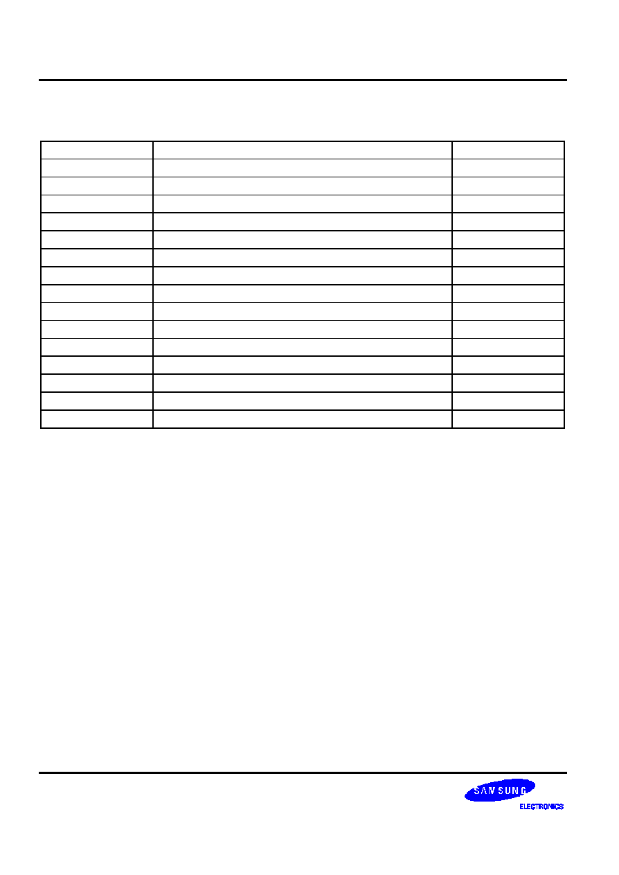
INTERRUPT CONTROLLER
S3C2440A RISC MICROPROCESSOR
14-4
INTERRUPT SUB SOURCES
Sub Sources
Descriptions
Source
INT_AC97
AC97 interrupt
INT_WDT_AC97
INT_WDT
Watchdoc interrupt
INT_WDT_AC97
INT_CAM_P
P-port capture interrupt in camera interface
INT_CAM
INT_CAM_C
C-port capture interrupt in camera interface
INT_CAM
INT_ADC_S
ADC interrupt
INT_ADC
INT_TC
Touch screen interrupt (pen up/down)
INT_ADC
INT_ERR2
UART2 error interrupt
INT_UART2
INT_TXD2
UART2 transmit interrupt
INT_UART2
INT_RXD2
UART2 receive interrupt
INT_UART2
INT_ERR1
UART1 error interrupt
INT_UART1
INT_TXD1
UART1 transmit interrupt
INT_UART1
INT_RXD1
UART1 receive interrupt
INT_UART1
INT_ERR0
UART0 error interrupt
INT_UART0
INT_TXD0
UART0 transmit interrupt
INT_UART0
INT_RXD0
UART0 receive interrupt
INT_UART0
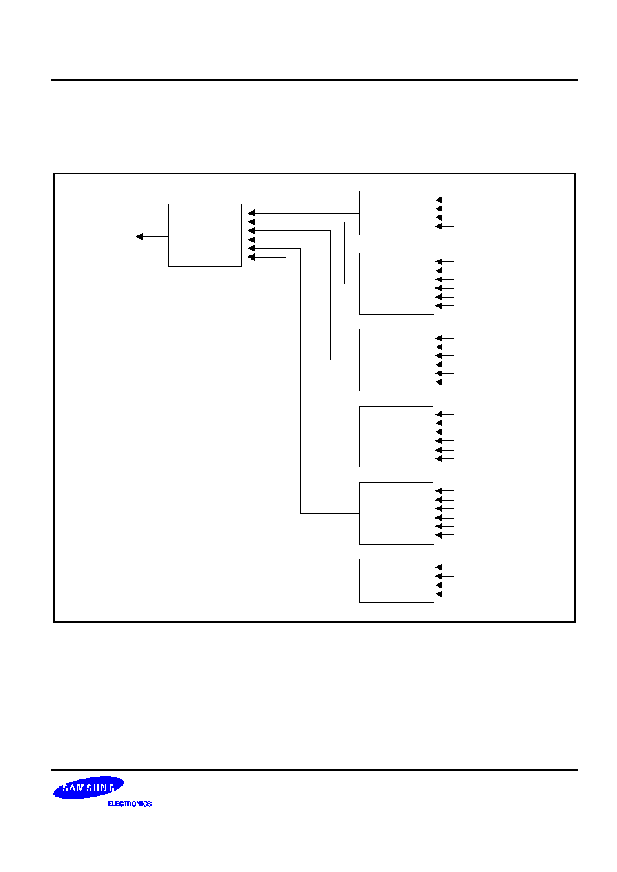
S3C2440A RISC MICROPROCESSOR
INTERRUPT CONTROLLER
14-5
INTERRUPT PRIORITY GENERATING BLOCK
The priority logic for 32 interrupt requests is composed of seven rotation based arbiters: six first-level arbiters and one
second-level arbiter as shown in Figure 14-1 below.
ARBITER6
ARBITER0
ARM IRQ
REQ1/EINT0
ARBITER1
ARBITER2
ARBITER3
ARBITER4
ARBITER5
REQ4/INT_TICK
REQ5/INT_WDT/AC97
REQ0/INT_TIMER0
REQ3/INT_TIMER3
REQ2/INT_TIMER2
REQ1/INT_TIMER1
REQ4/INT_TIMER4
REQ0/INT_LCD
REQ1/INT_DMA0
REQ3/INT_DMA2
REQ2/INT_DMA1
REQ5/INT_UART2
REQ4/INT_DMA3
REQ5/INT_SDI
REQ0/INT_SPI0
REQ1/INT_UART1
REQ2/INT_NFCON
REQ3/INT_USBD
REQ4/INT_USBH
REQ5/INT_IIC
REQ1/INT_UART0
REQ2/INT_SPI1
REQ3/INT_RTC
REQ4/INT_ADC
REQ0
REQ1
REQ2
REQ3
REQ4
REQ5
REQ2/EINT1
REQ3/EINT2
REQ4/EINT3
REQ0/EINT4_7
REQ1/EINT8_23
REQ2/INT_CAM
REQ3/nBATT_FLT
Figure 14-2. Priority Generating Block

INTERRUPT CONTROLLER
S3C2440A RISC MICROPROCESSOR
14-6
INTERRUPT PRIORITY
Each arbiter can handle six interrupt requests based on the one bit arbiter mode control (ARB_MODE) and two bits
of selection control signals (ARB_SEL) as follows:
-- If ARB_SEL bits are 00b, the priority order is REQ0, REQ1, REQ2, REQ3, REQ4, and REQ5.
-- If ARB_SEL bits are 01b, the priority order is REQ0, REQ2, REQ3, REQ4, REQ1, and REQ5.
-- If ARB_SEL bits are 10b, the priority order is REQ0, REQ3, REQ4, REQ1, REQ2, and REQ5.
-- If ARB_SEL bits are 11b, the priority order is REQ0, REQ4, REQ1, REQ2, REQ3, and REQ5.
Note that REQ0 of an arbiter always has the highest priority, and REQ5 has the lowest one. In addition, by changing
the ARB_SEL bits, we can rotate the priority of REQ1 to REQ4.
Here, if ARB_MODE bit is set to 0, ARB_SEL bits doesn't change automatically changed, making the arbiter to
operate in the fixed priority mode (note that even in this mode, we can reconfigure the priority by manually changing
the ARB_SEL bits). On the other hand, if ARB_MODE bit is 1, ARB_SEL bits are changed in rotation fashion, e.g., if
REQ1 is serviced, ARB_SEL bits are changed to 01b automatically so as to put REQ1 into the lowest priority. The
detailed rules of ARB_SEL change are as follows:
-- If REQ0 or REQ5 is serviced, ARB_SEL bits are not changed at all.
-- If REQ1 is serviced, ARB_SEL bits are changed to 01b.
-- If REQ2 is serviced, ARB_SEL bits are changed to 10b.
-- If REQ3 is serviced, ARB_SEL bits are changed to 11b.
-- If REQ4 is serviced, ARB_SEL bits are changed to 00b.

S3C2440A RISC MICROPROCESSOR
INTERRUPT CONTROLLER
14-7
INTERRUPT CONTROLLER SPECIAL REGISTERS
There are five control registers in the interrupt controller: source pending register, interrupt mode register, mask
register, priority register, and interrupt pending register.
All the interrupt requests from the interrupt sources are first registered in the source pending register. They are
divided into two groups including Fast Interrupt Request (FIQ) and Interrupt Request (IRQ), based on the interrupt
mode register. The arbitration procedure for multiple IRQs is based on the priority register.
SOURCE PENDING (SRCPND) REGISTER
The SRCPND register is composed of 32 bits each of which is related to an interrupt source. Each bit is set to 1 if
the corresponding interrupt source generates the interrupt request and waits for the interrupt to be serviced.
Accordingly, this register indicates which interrupt source is waiting for the request to be serviced. Note that each bit
of the SRCPND register is automatically set by the interrupt sources regardless of the masking bits in the INTMASK
register. In addition, the SRCPND register is not affected by the priority logic of interrupt controller.
In the interrupt service routine for a specific interrupt source, the corresponding bit of the SRCPND register has to be
cleared to get the interrupt request from the same source correctly. If you return from the ISR without clearing the bit,
the interrupt controller operates as if another interrupt request came in from the same source. In other words, if a
specific bit of the SRCPND register is set to 1, it is always considered as a valid interrupt request waiting to be
serviced.
The time to clear the corresponding bit depends on the user's requirement. If you want to receive another valid
request from the same source, you should clear the corresponding bit first, and then enable the interrupt.
You can clear a specific bit of the SRCPND register by writing a data to this register. It clears only the bit positions
of the SRCPND corresponding to those set to one in the data. The bit positions corresponding to those that are set
to 0 in the data remains as they are.
Register
Address
R/W
Description
Reset Value
SRCPND
0X4A000000
R/W
Indicate the interrupt request status.
0 = The interrupt has not been requested.
1 = The interrupt source has asserted the
interrupt request.
0x00000000

INTERRUPT CONTROLLER
S3C2440A RISC MICROPROCESSOR
14-8
SOURCE PENDING (SRCPND) REGISTER (Continued)
SRCPND
Bit
Description
Initial State
INT_ADC
[31]
0 = Not requested, 1 = Requested
0
INT_RTC
[30]
0 = Not requested, 1 = Requested
0
INT_SPI1
[29]
0 = Not requested, 1 = Requested
0
INT_UART0
[28]
0 = Not requested, 1 = Requested
0
INT_IIC
[27]
0 = Not requested, 1 = Requested
0
INT_USBH
[26]
0 = Not requested, 1 = Requested
0
INT_USBD
[25]
0 = Not requested, 1 = Requested
0
INT_NFCON
[24]
0 = Not requested, 1 = Requested
0
INT_UART1
[23]
0 = Not requested, 1 = Requested
0
INT_SPI0
[22]
0 = Not requested, 1 = Requested
0
INT_SDI
[21]
0 = Not requested, 1 = Requested
0
INT_DMA3
[20]
0 = Not requested, 1 = Requested
0
INT_DMA2
[19]
0 = Not requested, 1 = Requested
0
INT_DMA1
[18]
0 = Not requested, 1 = Requested
0
INT_DMA0
[17]
0 = Not requested, 1 = Requested
0
INT_LCD
[16]
0 = Not requested, 1 = Requested
0
INT_UART2
[15]
0 = Not requested, 1 = Requested
0
INT_TIMER4
[14]
0 = Not requested, 1 = Requested
0
INT_TIMER3
[13]
0 = Not requested, 1 = Requested
0
INT_TIMER2
[12]
0 = Not requested, 1 = Requested
0
INT_TIMER1
[11]
0 = Not requested, 1 = Requested
0
INT_TIMER0
[10]
0 = Not requested, 1 = Requested
0
INT_WDT_AC97
[9]
0 = Not requested, 1 = Requested
0
INT_TICK
[8]
0 = Not requested, 1 = Requested
0
nBATT_FLT
[7]
0 = Not requested, 1 = Requested
0
INT_CAM
[6]
0 = Not requested, 1 = Requested
0
EINT8_23
[5]
0 = Not requested, 1 = Requested
0
EINT4_7
[4]
0 = Not requested, 1 = Requested
0
EINT3
[3]
0 = Not requested, 1 = Requested
0
EINT2
[2]
0 = Not requested, 1 = Requested
0
EINT1
[1]
0 = Not requested, 1 = Requested
0
EINT0
[0]
0 = Not requested, 1 = Requested
0
.
S3C2440A RISC MICROPROCESSOR
INTERRUPT CONTROLLER
14-9
INTERRUPT MODE (INTMOD) REGISTER
This register is composed of 32 bits each of which is related to an interrupt source. If a specific bit is set to 1, the
corresponding interrupt is processed in the FIQ (fast interrupt) mode. Otherwise, it is processed in the IRQ mode
(normal interrupt).
Please note that only one interrupt source can be serviced in the FIQ mode in the interrupt controller (you should use
the FIQ mode only for the urgent interrupt). Thus, only one bit of INTMOD can be set to 1.
Register
Address
R/W
Description
Reset Value
INTMOD
0X4A000004
R/W
Interrupt mode register.
0 = IRQ mode 1 = FIQ mode
0x00000000
NOTE: If an interrupt mode is set to FIQ mode in the INTMOD register, FIQ interrupt will not affect both INTPND and
INTOFFSET registers. In this case, the two registers are valid only for IRQ mode interrupt source.

INTERRUPT CONTROLLER
S3C2440A RISC MICROPROCESSOR
14-10
INTERRUPT MODE (INTMOD) REGISTER (Continued)
INTMOD
Bit
Description
Initial State
INT_ADC
[31]
0 = IRQ, 1 = FIQ
0
INT_RTC
[30]
0 = IRQ, 1 = FIQ
0
INT_SPI1
[29]
0 = IRQ, 1 = FIQ
0
INT_UART0
[28]
0 = IRQ, 1 = FIQ
0
INT_IIC
[27]
0 = IRQ, 1 = FIQ
0
INT_USBH
[26]
0 = IRQ, 1 = FIQ
0
INT_USBD
[25]
0 = IRQ, 1 = FIQ
0
INT_NFCON
[24]
0 = IRQ, 1 = FIQ
0
INT_URRT1
[23]
0 = IRQ, 1 = FIQ
0
INT_SPI0
[22]
0 = IRQ, 1 = FIQ
0
INT_SDI
[21]
0 = IRQ, 1 = FIQ
0
INT_DMA3
[20]
0 = IRQ, 1 = FIQ
0
INT_DMA2
[19]
0 = IRQ, 1 = FIQ
0
INT_DMA1
[18]
0 = IRQ, 1 = FIQ
0
INT_DMA0
[17]
0 = IRQ, 1 = FIQ
0
INT_LCD
[16]
0 = IRQ, 1 = FIQ
0
INT_UART2
[15]
0 = IRQ, 1 = FIQ
0
INT_TIMER4
[14]
0 = IRQ, 1 = FIQ
0
INT_TIMER3
[13]
0 = IRQ, 1 = FIQ
0
INT_TIMER2
[12]
0 = IRQ, 1 = FIQ
0
INT_TIMER1
[11]
0 = IRQ, 1 = FIQ
0
INT_TIMER0
[10]
0 = IRQ, 1 = FIQ
0
INT_WDT_AC97
[9]
0 = IRQ, 1 = FIQ
0
INT_TICK
[8]
0 = IRQ, 1 = FIQ
0
nBATT_FLT
[7]
0 = IRQ, 1 = FIQ
0
INT_CAM
[6]
0 = IRQ, 1 = FIQ
0
EINT8_23
[5]
0 = IRQ, 1 = FIQ
0
EINT4_7
[4]
0 = IRQ, 1 = FIQ
0
EINT3
[3]
0 = IRQ, 1 = FIQ
0
EINT2
[2]
0 = IRQ, 1 = FIQ
0
EINT1
[1]
0 = IRQ, 1 = FIQ
0
EINT0
[0]
0 = IRQ, 1 = FIQ
0

S3C2440A RISC MICROPROCESSOR
INTERRUPT CONTROLLER
14-11
INTERRUPT MASK (INTMSK) REGISTER
This register also has 32 bits each of which is related to an interrupt source. If a specific bit is set to 1, the CPU
does not service the interrupt request from the corresponding interrupt source (note that even in such a case, the
corresponding bit of SRCPND register is set to 1). If the mask bit is 0, the interrupt request can be serviced.
Register
Address
R/W
Description
Reset Value
INTMSK
0X4A000008
R/W
Determine which interrupt source is masked.
The masked interrupt source will not be
serviced.
0 = Interrupt service is available.
1 = Interrupt service is masked.
0xFFFFFFFF

INTERRUPT CONTROLLER
S3C2440A RISC MICROPROCESSOR
14-12
INTERRUPT MASK (INTMSK) REGISTER (Continued)
INTMSK
Bit
Description
Initial State
INT_ADC
[31]
0 = Service available, 1 = Masked
1
INT_RTC
[30]
0 = Service available, 1 = Masked
1
INT_SPI1
[29]
0 = Service available, 1 = Masked
1
INT_UART0
[28]
0 = Service available, 1 = Masked
1
INT_IIC
[27]
0 = Service available, 1 = Masked
1
INT_USBH
[26]
0 = Service available, 1 = Masked
1
INT_USBD
[25]
0 = Service available, 1 = Masked
1
INT_NFCON
[24]
0 = Service available, 1 = Masked
1
INT_UART1
[23]
0 = Service available, 1 = Masked
1
INT_SPI0
[22]
0 = Service available, 1 = Masked
1
INT_SDI
[21]
0 = Service available, 1 = Masked
1
INT_DMA3
[20]
0 = Service available, 1 = Masked
1
INT_DMA2
[19]
0 = Service available, 1 = Masked
1
INT_DMA1
[18]
0 = Service available, 1 = Masked
1
INT_DMA0
[17]
0 = Service available, 1 = Masked
1
INT_LCD
[16]
0 = Service available, 1 = Masked
1
INT_UART2
[15]
0 = Service available, 1 = Masked
1
INT_TIMER4
[14]
0 = Service available, 1 = Masked
1
INT_TIMER3
[13]
0 = Service available, 1 = Masked
1
INT_TIMER2
[12]
0 = Service available, 1 = Masked
1
INT_TIMER1
[11]
0 = Service available, 1 = Masked
1
INT_TIMER0
[10]
0 = Service available, 1 = Masked
1
INT_WDT_AC97
[9]
0 = Service available, 1 = Masked
1
INT_TICK
[8]
0 = Service available, 1 = Masked
1
nBATT_FLT
[7]
0 = Service available, 1 = Masked
1
INT_CAM
[6]
0 = Service available, 1 = Masked
1
EINT8_23
[5]
0 = Service available, 1 = Masked
1
EINT4_7
[4]
0 = Service available, 1 = Masked
1
EINT3
[3]
0 = Service available, 1 = Masked
1
EINT2
[2]
0 = Service available, 1 = Masked
1
EINT1
[1]
0 = Service available, 1 = Masked
1
EINT0
[0]
0 = Service available, 1 = Masked
1
S3C2440A RISC MICROPROCESSOR
INTERRUPT CONTROLLER
14-13
PRIORITY REGISTER (PRIORITY)
Register
Address
R/W
Description
Reset Value
PRIORITY
0x4A00000C
R/W
IRQ priority control register
0x7F
PRIORITY
Bit
Description
Initial State
ARB_SEL6
[20:19]
Arbiter 6 group priority order set
00 = REQ 0-1-2-3-4-5
01 = REQ 0-2-3-4-1-5
10 = REQ 0-3-4-1-2-5
11 = REQ 0-4-1-2-3-5
00
ARB_SEL5
[18:17]
Arbiter 5 group priority order set
00 = REQ 1-2-3-4
01 = REQ 2-3-4-1
10 = REQ 3-4-1-2
11 = REQ 4-1-2-3
00
ARB_SEL4
[16:15]
Arbiter 4 group priority order set
00 = REQ 0-1-2-3-4-5
01 = REQ 0-2-3-4-1-5
10 = REQ 0-3-4-1-2-5
11 = REQ 0-4-1-2-3-5
00
ARB_SEL3
[14:13]
Arbiter 3 group priority order set
00 = REQ 0-1-2-3-4-5
01 = REQ 0-2-3-4-1-5
10 = REQ 0-3-4-1-2-5
11 = REQ 0-4-1-2-3-5
00
ARB_SEL2
[12:11]
Arbiter 2 group priority order set
00 = REQ 0-1-2-3-4-5
01 = REQ 0-2-3-4-1-5
10 = REQ 0-3-4-1-2-5
11 = REQ 0-4-1-2-3-5
00
ARB_SEL1
[10:9]
Arbiter 1 group priority order set
00 = REQ 0-1-2-3-4-5
01 = REQ 0-2-3-4-1-5
10 = REQ 0-3-4-1-2-5
11 = REQ 0-4-1-2-3-5
00
ARB_SEL0
[8:7]
Arbiter 0 group priority order set
00 = REQ 1-2-3-4
01 = REQ 2-3-4-1
10 = REQ 3-4-1-2
11 = REQ 4-1-2-3
00
ARB_MODE6
[6]
Arbiter 6 group priority rotate enable
0 = Priority does not rotate, 1 = Priority rotate enable
1
ARB_MODE5
[5]
Arbiter 5 group priority rotate enable
0 = Priority does not rotate, 1 = Priority rotate enable
1
ARB_MODE4
[4]
Arbiter 4 group priority rotate enable
0 = Priority does not rotate, 1 = Priority rotate enable
1
ARB_MODE3
[3]
Arbiter 3 group priority rotate enable
0 = Priority does not rotate, 1 = Priority rotate enable
1
ARB_MODE2
[2]
Arbiter 2 group priority rotate enable
0 = Priority does not rotate, 1 = Priority rotate enable
1
ARB_MODE1
[1]
Arbiter 1 group priority rotate enable
0 = Priority does not rotate, 1 = Priority rotate enable
1
ARB_MODE0
[0]
Arbiter 0 group priority rotate enable
0 = Priority does not rotate, 1 = Priority rotate enable
1

INTERRUPT CONTROLLER
S3C2440A RISC MICROPROCESSOR
14-14
INTERRUPT PENDING (INTPND) REGISTER
Each of the 32 bits in the interrupt pending register shows whether the corresponding interrupt request, which is
unmasked and waits for the interrupt to be serviced, has the highest priority . Since the INTPND register is located
after the priority logic, only one bit can be set to 1, and that interrupt request generates IRQ to CPU. In interrupt
service routine for IRQ, you can read this register to determine which interrupt source is serviced among the 32
sources.
Like the SRCPND register, this register has to be cleared in the interrupt service routine after clearing the SRCPND
register. We can clear a specific bit of the INTPND register by writing a data to this register. It clears only the bit
positions of the INTPND register corresponding to those set to one in the data. The bit positions corresponding to
those that are set to 0 in the data remains as they are.
Register
Address
R/W
Description
Reset Value
INTPND
0X4A000010
R/W
Indicate the interrupt request status.
0 = The interrupt has not been requested.
1 = The interrupt source has asserted the
interrupt request.
0x00000000
NOTE: If the FIQ mode interrupt occurs, the corresponding bit of INTPND will not be turned on as the INTPND register is
available only for IRQ mode interrupt.
S3C2440A RISC MICROPROCESSOR
INTERRUPT CONTROLLER
14-15
INTERRUPT PENDING (INTPND) REGISTER (Continued)
INTPND
Bit
Description
Initial State
INT_ADC
[31]
0 = Not requested, 1 = Requested
0
INT_RTC
[30]
0 = Not requested, 1 = Requested
0
INT_SPI1
[29]
0 = Not requested, 1 = Requested
0
INT_UART0
[28]
0 = Not requested, 1 = Requested
0
INT_IIC
[27]
0 = Not requested, 1 = Requested
0
INT_USBH
[26]
0 = Not requested, 1 = Requested
0
INT_USBD
[25]
0 = Not requested, 1 = Requested
0
INT_NFCON
[24]
0 = Not requested, 1 = Requested
0
INT_UART1
[23]
0 = Not requested, 1 = Requested
0
INT_SPI0
[22]
0 = Not requested, 1 = Requested
0
INT_SDI
[21]
0 = Not requested, 1 = Requested
0
INT_DMA3
[20]
0 = Not requested, 1 = Requested
0
INT_DMA2
[19]
0 = Not requested, 1 = Requested
0
INT_DMA1
[18]
0 = Not requested, 1 = Requested
0
INT_DMA0
[17]
0 = Not requested, 1 = Requested
0
INT_LCD
[16]
0 = Not requested, 1 = Requested
0
INT_UART2
[15]
0 = Not requested, 1 = Requested
0
INT_TIMER4
[14]
0 = Not requested, 1 = Requested
0
INT_TIMER3
[13]
0 = Not requested, 1 = Requested
0
INT_TIMER2
[12]
0 = Not requested, 1 = Requested
0
INT_TIMER1
[11]
0 = Not requested, 1 = Requested
0
INT_TIMER0
[10]
0 = Not requested, 1 = Requested
0
INT_WDT_AC97
[9]
0 = Not requested, 1 = Requested
0
INT_TICK
[8]
0 = Not requested, 1 = Requested
0
nBATT_FLT
[7]
0 = Not requested, 1 = Requested
0
INT_CAM
[6]
0 = Not requested, 1 = Requested
0
EINT8_23
[5]
0 = Not requested, 1 = Requested
0
EINT4_7
[4]
0 = Not requested, 1 = Requested
0
EINT3
[3]
0 = Not requested, 1 = Requested
0
EINT2
[2]
0 = Not requested, 1 = Requested
0
EINT1
[1]
0 = Not requested, 1 = Requested
0
EINT0
[0]
0 = Not requested, 1 = Requested
0

INTERRUPT CONTROLLER
S3C2440A RISC MICROPROCESSOR
14-16
INTERRUPT OFFSET (INTOFFSET) REGISTER
The value in the interrupt offset register shows which interrupt request of IRQ mode is in the INTPND register.
This bit can be cleared automatically by clearing SRCPND and INTPND.
Register
Address
R/W
Description
Reset Value
INTOFFSET
0x4A000014
R
Indicate the IRQ interrupt request source
0x00000000
INT Source
The OFFSET value
INT Source
The OFFSET value
INT_ADC
31
INT_UART2
15
INT_RTC
30
INT_TIMER4
14
INT_SPI1
29
INT_TIMER3
13
INT_UART0
28
INT_TIMER2
12
INT_IIC
27
INT_TIMER1
11
INT_USBH
26
INT_TIMER0
10
INT_USBD
25
INT_WDT_AC97
9
INT_NFCON
24
INT_TICK
8
INT_UART1
23
nBATT_FLT
7
INT_SPI0
22
INT_CAM
6
INT_SDI
21
EINT8_23
5
INT_DMA3
20
EINT4_7
4
INT_DMA2
19
EINT3
3
INT_DMA1
18
EINT2
2
INT_DMA0
17
EINT1
1
INT_LCD
16
EINT0
0
NOTE: FIQ mode interrupt does not affect the INTOFFSET register as the register is available only for IRQ mode interrupt.
S3C2440A RISC MICROPROCESSOR
INTERRUPT CONTROLLER
14-17
SUB SOURCE PENDING (SUBSRCPND) REGISTER
You can clear a specific bit of the SUBSRCPND register by writing a data to this register. It clears only the bit
positions of the SUBSRCPND register corresponding to those set to one in the data. The bit positions corresponding
to those that are set to 0 in the data remains as they are.
Register
Address
R/W
Description
Reset Value
SUBSRCPND
0X4A000018
R/W
Indicate the interrupt request status.
0 = The interrupt has not been requested.
1 = The interrupt source has asserted the
interrupt request.
0x00000000
SUBSRCPND
Bit
Description
Initial State
Reserved
[31:15]
Not used
0
INT_AC97
[14]
0 = Not requested, 1 = Requested
0
INT_WDT
[13]
0 = Not requested, 1 = Requested
0
INT_CAM_P
[12]
0 = Not requested, 1 = Requested
0
INT_CAM_C
[11]
0 = Not requested, 1 = Requested
0
INT_ADC_S
[10]
0 = Not requested, 1 = Requested
0
INT_TC
[9]
0 = Not requested, 1 = Requested
0
INT_ERR2
[8]
0 = Not requested, 1 = Requested
0
INT_TXD2
[7]
0 = Not requested, 1 = Requested
0
INT_RXD2
[6]
0 = Not requested, 1 = Requested
0
INT_ERR1
[5]
0 = Not requested, 1 = Requested
0
INT_TXD1
[4]
0 = Not requested, 1 = Requested
0
INT_RXD1
[3]
0 = Not requested, 1 = Requested
0
INT_ERR0
[2]
0 = Not requested, 1 = Requested
0
INT_TXD0
[1]
0 = Not requested, 1 = Requested
0
INT_RXD0
[0]
0 = Not requested, 1 = Requested
0
Map To SRCPND
SRCPND
SUBSRCPND
Remark
INT_UART0
INT_RXD0,INT_TXD0,INT_ERR0
INT_UART1
INT_RXD1,INT_TXD1,INT_ERR1
INT_UART2
INT_RXD2,INT_TXD2,INT_ERR2
INT_ADC
INT_ADC_S, INT_TC
INT_CAM
INT_CAM_C, INT_CAM_P
INT_WDT_AC97
INT_WDT, INT_AC97
INTERRUPT CONTROLLER
S3C2440A RISC MICROPROCESSOR
14-18
INTERRUPT SUB MASK (INTSUBMSK) REGISTER
This register has 11 bits each of which is related to an interrupt source. If a specific bit is set to 1, the interrupt
request from the corresponding interrupt source is not serviced by the CPU (note that even in such a case, the
corresponding bit of the SUBSRCPND register is set to 1). If the mask bit is 0, the interrupt request can be serviced.
Register
Address
R/W
Description
Reset Value
INTSUBMSK
0X4A00001C
R/W
Determine which interrupt source is masked.
The masked interrupt source will not be
serviced.
0 = Interrupt service is available.
1 = Interrupt service is masked.
0xFFFF
INTSUBMSK
Bit
Description
Initial State
Reserved
[31:15]
Not used
0
INT_AC97
[14]
0 = Service available, 1 = Masked
1
INT_WDT
[13]
0 = Service available, 1 = Masked
1
INT_CAM_P
[12]
0 = Service available, 1 = Masked
1
INT_CAM_C
[11]
0 = Service available, 1 = Masked
1
INT_ADC_S
[10]
0 = Service available, 1 = Masked
1
INT_TC
[9]
0 = Service available, 1 = Masked
1
INT_ERR2
[8]
0 = Service available, 1 = Masked
1
INT_TXD2
[7]
0 = Service available, 1 = Masked
1
INT_RXD2
[6]
0 = Service available, 1 = Masked
1
INT_ERR1
[5]
0 = Service available, 1 = Masked
1
INT_TXD1
[4]
0 = Service available, 1 = Masked
1
INT_RXD1
[3]
0 = Service available, 1 = Masked
1
INT_ERR0
[2]
0 = Service available, 1 = Masked
1
INT_TXD0
[1]
0 = Service available, 1 = Masked
1
INT_RXD0
[0]
0 = Service available, 1 = Masked
1

S3C2440A RISC MICROPROCESSOR
LCD CONTROLLER
15-1
15
LCD CONTROLLER
OVERVIEW
The LCD controller in the S3C2440A consists of the logic for transferring LCD image data from a video buffer located
in system memory to an external LCD driver.
The LCD controller supports monochrome, 2-bit per pixel (4-level gray scale) or 4-bit per pixel (16-level gray scale)
mode on a monochrome LCD, using a time-based dithering algorithm and Frame Rate Control (FRC) method and it
can be interfaced with a color LCD panel at 8-bit per pixel (256-level color) and 12-bit per pixel (4096-level color) for
interfacing with STN LCD.
It can support 1-bit per pixel, 2-bit per pixel, 4-bit per pixel, and 8-bit per pixel for interfacing with the palletized TFT
color LCD panel, and 16-bit per pixel and 24-bit per pixel for non-palletized true-color display.
The LCD controller can be programmed to support different requirements on the screen related to the number of
horizontal and vertical pixels, data line width for the data interface, interface timing, and refresh rate.
FEATURES
STN LCD Displays:
-- Supports 3 types of LCD panels: 4-bit dual scan, 4-bit single scan, and 8-bit single scan display type
-- Supports the monochrome, 4 gray levels, and 16 gray levels
-- Supports 256 colors and 4096 colors for color STN LCD panel
-- Supports multiple screen size
Typical actual screen size: 640 x 480, 320 x 240, 160 x 160, and others
Maximum virtual screen size is 4Mbytes.
Maximum virtual screen size in 256 color mode: 4096 x 1024, 2048 x 2048, 1024 x 4096, and others
TFT LCD Displays:
-- Supports 1, 2, 4 or 8-bpp (bit per pixel) palletized color displays for TFT
-- Supports 16, 24-bpp non-palletized true-color displays for color TFT
-- Supports maximum 16M color TFT at 24bit per pixel mode
-- Supports multiple screen size
Typical actual screen size: 640 x 480, 320 x 240, 160 x 160, and others
Maximum virtual screen size is 4Mbytes.
Maximum virtual screen size in 64K color mode: 2048 x 1024 and others
LCD CONTROLLER
S3C2440A RISC MICROPROCESSOR
15-2
COMMON FEATURES
The LCD controller has a dedicated DMA that supports to fetch the image data from video buffer located in system
memory. Its features also include:
-- Dedicated interrupt functions (INT_FrSyn and INT_FiCnt)
-- The system memory is used as the display memory.
-- Supports Multiple Virtual Display Screen (Supports Hardware Horizontal/Vertical Scrolling)
-- Programmable timing control for different display panels
-- Supports little and big-endian byte ordering, as well as WinCE data formats
-- Supports 2-type SEC TFT LCD panel
(SAMSUNG 3.5" Portrait / 256K Color /Reflective and Transflective a-Si TFT LCD)
LTS350Q1-PD1: TFT LCD panel with touch panel and front light unit (Reflective type)
LTS350Q1-PD2: TFT LCD panel only
LTS350Q1-PE1: TFT LCD panel with touch panel and front light unit (Transflective type)
LTS350Q1-PE2: TFT LCD panel only
NOTE
WinCE doesn't support the 12-bit packed data format.
Please check if WinCE can support the 12-bit color-mode.
EXTERNAL INTERFACE SIGNAL
STN
TFT
SEC TFT
(LTS350Q1-PD1/2)
SEC TFT
(LTS350Q1-PE1/2)
VFRAME
(Frame sync. Signal)
VSYNC
(Vertical sync. Signal)
STV
STV
VLINE
(Line sync pulse signal)
HSYNC
(Horizontal sync. Signal)
CPV
CPV
VCLK
(Pixel clock signal)
VCLK
(Pixel clock signal)
LCD_HCLK
LCD_HCLK
VD[23:0]
(LCD pixel data output ports)
VD[23:0]
(LCD pixel data output ports)
VD[23:0]
VD[23:0]
VM
(AC bias signal for LCD driver)
VDEN
(Data enable signal)
TP
TP
≠
LEND
(Line end signal)
STH
STH
LCD_PWREN
LCD_PWREN
LCD_PWREN
LCD_PWREN
≠
≠
LPC_OE
LCC_INV
≠
≠
LPC_REV
LCC_REV
≠
≠
LPC_REVB
LCC_REVB
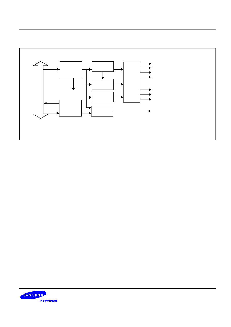
S3C2440A RISC MICROPROCESSOR
LCD CONTROLLER
15-3
BLOCK DIAGRAM
System Bus
LPC3600 is a timing control logic unit for LTS350Q1-PD1 or LTS350Q1-PD2.
LCC3600 is a timing control logic unit for LTS350Q1-PE1 or LTS350Q1-PE2.
REGBANK
LCDCDMA
VIDPRCS
LPC3600
TIMEGEN
VD[23:0]
VCLK /LCD_HCLK
VLINE / HSYNC / CPV
VFRAME / VSYNC / STV
VM / VDEN / TP
LCD_LPCOE / LCD_LCCINV
LCD_LPCREV / LCD_LCCREV
LCD_LPCREVB / LCD_LCCREVB
.
.
.
VIDEO
MUX
LCC3600
Figure 15-1. LCD Controller Block Diagram
The S3C2440A LCD controller is used to transfer the video data and to generate the necessary control signals, such
as VFRAME, VLINE, VCLK, VM, and so on. In addition to the control signals, the S3C2440A has the data ports for
video data, which are VD[23:0] as shown in Figure 15-1. The LCD controller consists of a REGBANK, LCDCDMA,
VIDPRCS, TIMEGEN, and LPC3600 (See the Figure 15-1 LCD Controller Block Diagram). The REGBANK has 17
programmable register sets and 256x16 palette memory which are used to configure the LCD controller. The
LCDCDMA is a dedicated DMA, which can transfer the video data in frame memory to LCD driver automatically. By
using this special DMA, the video data can be displayed on the screen without CPU intervention. The VIDPRCS
receives the video data from the LCDCDMA and sends the video data through the VD[23:0] data ports to the LCD
driver after changing them into a suitable data format, for example 4/8-bit single scan or 4-bit dual scan display
mode. The TIMEGEN consists of programmable logic to support the variable requirements of interface timing and
rates commonly found in different LCD drivers. The TIMEGEN block generates VFRAME, VLINE, VCLK, VM, and so
on.
The description of data flow is as follows:
FIFO memory is present in the LCDCDMA. When FIFO is empty or partially empty, the LCDCDMA requests data
fetching from the frame memory based on the burst memory transfer mode (consecutive memory fetching of 4 words
(16 bytes) per one burst request without allowing the bus mastership to another bus master during the bus transfer).
When the transfer request is accepted by bus arbitrator in the memory controller, there will be four successive word
data transfers from system memory to internal FIFO. The total size of FIFO is 28 words, which consists of 12 words
FIFOL and 16 words FIFOH, respectively. The S3C2440A has two FIFOs to support the dual scan display mode. In
case of single scan mode, one of the FIFOs (FIFOH) can only be used.

LCD CONTROLLER
S3C2440A RISC MICROPROCESSOR
15-4
STN LCD CONTROLLER OPERATION
TIMING GENERATOR (TIMEGEN)
The TIMEGEN generates the control signals for the LCD driver, such as VFRAME, VLINE, VCLK, and VM. These
control signals are closely related to the configuration on the LCDCON1/2/3/4/5 registers in the REGBANK. Based
on these programmable configurations on the LCD control registers in the REGBANK, the TIMEGEN can generate
the programmable control signals suitable to support many different types of LCD drivers.
The VFRAME pulse is asserted for the duration of the entire first line at a frequency of once per frame. The VFRAME
signal is asserted to bring the LCD's line pointer to the top of the display to start over.
The VM signal helps the LCD driver alternate the polarity of the row and column voltages, which are used to turn the
pixel on and off. The toggling rate of VM signals depends on the MMODE bit of the LCDCON1 register and MVAL
field of the LCDCON4 register. If the MMODE bit is 0, the VM signal is configured to toggle on every frame. If the
MMODE bit is 1, the VM signal is configured to toggle on the every event of the elapse of the specified number of
VLINE by the MVAL[7:0] value. Figure 15-4 shows an example for MMODE=0 and for MMODE=1 with the value of
MVAL[7:0]=0x2. When MMODE=1, the VM rate is related to MVAL[7:0], as shown below:
VM Rate = VLINE Rate / ( 2 x MVAL)
The VFRAME and VLINE pulse generation relies on the configurations of the HOZVAL field and the LINEVAL field in
the LCDCON2/3 registers. Each field is related to the LCD size and display mode. In other words, the HOZVAL and
LINEVAL can be determined by the size of the LCD panel and the display mode according to the following equation:
HOZVAL = (Horizontal display size / Number of the valid VD data line)-1
In color mode: Horizontal display size = 3 x Number of Horizontal Pixel
In the 4-bit single scan display mode, the Number of valid VD data line should be 4. In case of 4-bit dual scan
display, the Number of valid VD data lineshould also be 4 while in case of 8-bit single scan display mode, the
Number of valid VD data line should be 8.
LINEVAL = (Vertical display size) -1: In case of single scan display type
LINEVAL = (Vertical display size / 2) -1: In case of dual scan display type
The rate of VCLK signal depends on the configuration of the CLKVAL field in the LCDCON1 register. Table 15-1
defines the relationship of VCLK and CLKVAL. The minimum value of CLKVAL is 2.
VCLK(Hz)=HCLK/(CLKVAL x 2)
The frame rate is the VFRAM signal frequency. The frame rate is closely related to the field of WLH[1:0](VLINE pulse
width) WDLY[1:0] (the delay width of VCLK after VLINE pulse), HOZVAL, LINEBLANK, and LINEVAL in the
LCDCON1/2/3/4 registers as well as VCLK and HCLK. Most LCD drivers need their own adequate frame rate. The
frame rate is calculated as follows:
frame_rate(Hz) = 1 / [ { (1/VCLK) x (HOZVAL+1)+(1/HCLK) x (A+B+(LINEBLANK x 8) ) } x ( LINEVAL+1) ]
A = 2
(4+WLH)
, B = 2
(4+WDLY)

S3C2440A RISC MICROPROCESSOR
LCD CONTROLLER
15-5
Table 15-1. Relation Between VCLK and CLKVAL (STN, HCLK = 60MHz)
CLKVAL
60MHz/X
VCLK
2
60 MHz/4
15.0 MHz
3
60 MHz/6
10.0 MHz
:
:
:
1023
60 MHz/2046
29.3 kHz
VIDEO OPERATION
The S3C2440A LCD controller supports 8-bit color mode (256 color mode), 12-bit color mode (4096 color mode), 4
level gray scale mode, 16 level gray scale mode as well as the monochrome mode. For the gray or color mode, it is
required to implement the shades of gray level or color according to time-based dithering algorithm and Frame Rate
Control (FRC) method. The selection can be made following a programmable lockup table, which will be explained
later. The monochrome mode bypasses these modules (FRC and lookup table) and basically serializes the data in
FIFOH (and FIFOL if a dual scan display type is used) into 4-bit (or 8-bit if a 4-bit dual scan or 8-bit single scan
display type is used) streams by shifting the video data to the LCD driver.
The following sections describe the operation on the gray and color mode in terms of the lookup table and FRC.
Lookup Table
The S3C2440A can support the lookup table for various selection of color or gray level mapping, ensuring flexible
operation for users. The lookup table is the palette which allows the selection on the level of color or gray (Selection
on 4-gray levels among 16 gray levels in case of 4 gray mode, selection on 8 red levels among 16 levels, 8 green
levels among 16 levels and 4 blue levels among 16 levels in case of 256 color mode). In other words, users can
select 4 gray levels among 16 gray levels by using the lookup table in the 4 gray level mode. The gray levels cannot
be selected in the 16 gray level mode; all 16 gray levels must be chosen among the possible 16 gray levels. In case
of 256 color mode, 3 bits are allocated for red, 3 bits for green and 2 bits for blue. The 256 colors mean that the
colors are formed from the combination of 8 red, 8 green and 4 blue levels (8x8x4 = 256). In the color mode, the
lookup table can be used for suitable selections. Eight red levels can be selected among 16 possible red levels, 8
green levels among 16 green levels, and 4 blue levels among 16 blue levels. In case of 4096 color mode, there is no
selection as in the 256 color mode.
Gray Mode Operation
The S3C2440A LCD controller supports two gray modes: 2-bit per pixel gray (4 level gray scale) and 4-bit per pixel
gray (16 level gray scale). The 2-bit per pixel gray mode uses a lookup table (BLUELUT), which allows selection on 4
gray levels among 16 possible gray levels. The 2-bit per pixel gray lookup table uses the BULEVAL[15:0] in Blue
Lookup Table (BLUELUT) register as same as blue lookup table in color mode. The gray level 0 will be denoted by
BLUEVAL[3:0] value. If BLUEVAL[3:0] is 9, level 0 will be represented by gray level 9 among 16 gray levels. If
BLUEVAL[3:0] is 15, level 0 will be represented by gray level 15 among 16 gray levels, and so on. Following the
same method as above, level 1 will also be denoted by BLUEVAL[7:4], the level 2 by BLUEVAL[11:8], and the level 3
by BLUEVAL[15:12]. These four groups among BLUEVAL[15:0] will represent level 0, level 1, level 2, and level 3. In
16 gray levels, there is no selection as in the 16 gray levels.

LCD CONTROLLER
S3C2440A RISC MICROPROCESSOR
15-6
256 Level Color Mode Operation
The S3C2440A LCD controller can support an 8-bit per pixel 256 color display mode. The color display mode can
generate 256 levels of color using the dithering algorithm and FRC. The 8-bit per pixel are encoded into 3-bits for red,
3-bits for green, and 2-bits for blue. The color display mode uses separate lookup tables for red, green, and blue.
Each lookup table uses the REDVAL[31:0] of REDLUT register, GREENVAL[31:0] of GREENLUT register, and
BLUEVAL[15:0] of BLUELUT register as the programmable lookup table entries.
Similar to the gray level display, 8 group or field of 4 bits in the REDLUR register, i.e., REDVAL[31:28],
REDLUT[27:24], REDLUT[23:20], REDLUT[19:16], REDLUT[15:12], REDLUT[11:8], REDLUT[7:4], and REDLUT[3:0],
are assigned to each red level. The possible combination of 4 bits (each field) is 16, and each red level should be
assigned to one level among possible 16 cases. In other words, the user can select the suitable red level by using
this type of lookup table. For green color, the GREENVAL[31:0] of the GREENLUT register is assigned as the
lookup table, as was done in the case of red color. Similarly, the BLUEVAL[15:0] of the BLUELUT register is also
assigned as a lookup table. For blue color, 2 bits are allocated for 4 blue levels, different from the 8 red or green
levels.
4096 Level Color Mode Operation
The S3C2440A LCD controller can support a 12-bit per pixel 4096 color display mode. The color display mode can
generate 4096 levels of color using the dithering algorithm and FRC. The 12-bit per pixel are encoded into 4-bits for
red, 4-bits for green, and 4-bits for blue. The 4096 color display mode does not use lookup tables.
S3C2440A RISC MICROPROCESSOR
LCD CONTROLLER
15-7
DITHERING AND FRAME RATE CONTROL
In case of STN LCD display (except monochrome), video data must be processed by a dithering algorithm. The
DITHFRC block has two functions, such as Time-based Dithering Algorithm for reducing flicker and Frame Rate
Control (FRC) for displaying gray and color level on the STN panel. The main principle of gray and color level display
on the STN panel based on FRC is described. For example, to display the third gray (3/16) level from a total of 16
levels, the 3 times pixel should be on and 13 times pixel off. In other words, 3 frames should be selected among the
16 frames, of which 3 frames should have a pixel-on on a specific pixel while the remaining 13 frames should have a
pixel-off on a specific pixel. These 16 frames should be displayed periodically. This is basic principle on how to
display the gray level on the screen, so-called gray level display by FRC. The actual example is shown in Table 15-2.
To represent the 14
th
gray level in the table, we should have a 6/7 duty cycle, which mean that there are 6 times
pixel-on and one time pixel-off. The other cases for all gray levels are also shown in Table 15-2.
In the STN LCD display, we should be reminded of one item, i.e., Flicker Noise due to the simultaneous pixel-on and
-off on adjacent frames. For example, if all pixels on first frame are turned on and all pixels on next frame are turned
off, the Flicker Noise will be maximized. To reduce the Flicker Noise on the screen, the average probability of pixel-
on and -off between frames should be the same. In order to realize this, the Time-based Dithering Algorithm, which
varies the pattern of adjacent pixels on every frame, should be used. This is explained in detail. For the 16 gray level,
FRC should have the following relationship between gray level and FRC. The 15
th
gray level should always have pixel-
on, and the 14
th
gray level should have 6 times pixel-on and one times pixel-off, and the 13
th
gray level should have 4
times pixel-on and one times pixel-off, ,,,,,,,, , and the 0
th
gray level should always have pixel-off as shown in Table
15-2.
Table 15-2. Dither Duty Cycle Examples
Pre-Dithered Data
(gray level number)
Duty Cycle
Pre-Dithered Data
(gray level number)
Duty Cycle
15
1
7
1/2
14
6/7
6
3/7
13
4/5
5
2/5
12
3/4
4
1/3
11
5/7
3
1/4
10
2/3
2
1/5
9
3/5
1
1/7
8
4/7
0
0

LCD CONTROLLER
S3C2440A RISC MICROPROCESSOR
15-8
Display Types
The LCD controller supports 3 types of LCD drivers: 4-bit dual scan, 4-bit single scan, and 8-bit single scan display
mode. Figure 15-2 shows these 3 different display types for monochrome displays, and Figure 15-3 show these 3
different display types for color displays.
4-bit Dual Scan Display Type
A 4-bit dual scan display uses 8 parallel data lines to shift data to both the upper and lower halves of the display at
the same time. The 4 bits of data in the 8 parallel data lines are shifted to the upper half and 4 bits of data is shifted
to the lower half, as shown in Figure 15-2. The end of frame is reached when each half of the display has been
shifted and transferred. The 8 pins (VD[7:0]) for the LCD output from the LCD controller can be directly connected to
the LCD driver.
4-bit Single Scan Display Type
A 4-bit single scan display uses 4 parallel data lines to shift data to successive single horizontal lines of the display
at a time, until the entire frame has been shifted and transferred. The 4 pins (VD[3:0]) for the LCD output from the
LCD controller can be directly connected to the LCD driver, and the 4 pins (VD[7:4]) for the LCD output are not used.
8-bit Single Scan Display Type
An 8-bit single scan display uses 8 parallel data lines to shift data to successive single horizontal lines of the display
at a time, until the entire frame has been shifted and transferred. The 8 pins (VD[7:0]) for the LCD output from the
LCD controller can be directly connected to the LCD driver.
256 Color Displays
Color displays require 3 bits (Red, Green, and Blue) of image data per pixel, so the number of horizontal shift
registers for each horizontal line corresponds to three times the number of pixels of one horizontal line. These results
in a horizontal shift register of length 3 times the number of pixels per horizontal line. This RGB is shifted to the LCD
driver as consecutive bits via the parallel data lines. Figure 15-3 shows the RGB and order of the pixels in the parallel
data lines for the 3 types of color displays.
4096 Color Displays
Color displays require 3 bits (Red, Green, and Blue) of image data per pixel, and so the number of horizontal shift
registers for each horizontal line corresponds to three times the number of pixels of one horizontal line. This RGB is
shifted to the LCD driver as consecutive bits via the parallel data lines. This RGB order is determined by the
sequence of video data in video buffers.

S3C2440A RISC MICROPROCESSOR
LCD CONTROLLER
15-9
MEMORY DATA FORMAT (STN, BSWP = 0)
Mono 4-bit Dual Scan Display:
Video Buffer Memory:
Address
Data
0000H
A[31:0]
0004H
B[31:0]
∑
∑
∑
1000H
L[31:0]
1004H
M[31:0]
∑
∑
∑
Mono 4-bit Single Scan Display & 8-bit Single
Scan Display:
Video Buffer Memory:
Address
Data
0000H
A[31:0]
0004H
B[31:0]
0008H
C[31:0]
∑
∑
∑
LCD Panel
LCD Panel
A[31] A[30] ...... A[0] B[31] B[30] ...... B[0] ......
L[31] L[30] ...... L[0] M[31] M[30] ...... M[0] ......
A[31] A[30] A[29] ...... A[0] B[31] B[30] ...... B[0] C[31] ...... C[0] ......
LCD CONTROLLER
S3C2440A RISC MICROPROCESSOR
15-10
MEMORY DATA FORMAT ( STN, BSWP=0 ) (CONTINUED)
In 4-level gray mode, 2 bits of video data correspond to 1 pixel.
In 16-level gray mode, 4 bits of video data correspond to 1 pixel.
In 256 level color mode, 8 bits (3 bits of red, 3 bits of green, and 2 bits of blue) of video data correspond to 1 pixel.
The color data format in a byte is as follows:
Bit [ 7:5 ]
Bit [ 4:2 ]
Bit[1:0]
Red
Green
Blue
In 4096 level color mode :
Packed 12 BPP color mode
12 bits (4 bits of red, 4 bits of green, 4 bits of blue) of video data correspond to 1 pixel. The following table shows
color data format in words: (Video data must reside at 3 word boundaries (8 pixel), as follows)
RGB Order
DATA
[31:28]
[27:24]
[23:20]
[19:16]
[15:12]
[11:8]
[7:4]
[3:0]
Word #1
Red( 1)
Green(1)
Blue( 1)
Red( 2)
Green( 2)
Blue( 2)
Red(3)
Green(3)
Word #2
Blue(3)
Red(4)
Green(4)
Blue(4)
Red(5)
Green(5)
Blue(5)
Red(6)
Word #3
Green(6)
Blue(6)
Red(7)
Green(7)
Blue(7)
Red(8)
Green(8)
Blue(8)
Unpacked 12 BPP color mode
12 bits (4 bits of red, 4 bits of green, 4 bits of blue) of video data correspond to 1 pixel. The following table shows
color data format in words:
RGB Order
DATA
[31:28]
[27:24]
[23:20]
[19:16]
[15:12]
[11:8]
[7:4]
[3:0]
Word #1
≠
Red( 1)
Green(1)
Blue( 1)
≠
Red( 2)
Green( 2)
Blue( 2)
Word #2
≠
Red( 3)
Green(3)
Blue( 3)
≠
Red( 4)
Green( 4)
Blue( 4)
Word #3
≠
Red( 5)
Green(5)
Blue( 5)
≠
Red( 6)
Green( 6)
Blue( 6)

S3C2440A RISC MICROPROCESSOR
LCD CONTROLLER
15-11
16 BPP color mode
16 bits (5 bits of red, 6 bits of green, 5 bits of blue) of video data correspond to 1 pixel. But, stn controller will use
only 12 bit color data. It means that only upper 4bit each color data will be used as pixel data (R[15:12], G[10:7],
B[4:1]). The following table shows color data format in words:
RGB Order
DATA
[31:28]
[27:21]
[20:16]
[15:11]
[10:5]
[4:0]
Word #1
Red( 1)
Green(1)
Blue( 1)
Red( 2)
Green( 2)
Blue( 2)
Word #2
Red( 3)
Green(3)
Blue( 3)
Red( 4)
Green( 4)
Blue( 4)
Word #3
Red( 5)
Green(5)
Blue( 5)
Red( 6)
Green( 6)
Blue( 6)
LCD CONTROLLER
S3C2440A RISC MICROPROCESSOR
15-12
4-bit Dual Scan Display
4-bit Single Scan Display
8-bit Single Scan Display
. . . . . .
. . . . . .
VD3
VD2 VD1 VD0
VD3 VD2 VD1
VD0
VD3
VD2 VD1 VD0
VD3 VD2 VD1
VD0
VD3 VD2
VD1
VD0 VD3
VD2
VD1 VD0
. . . . . .
VD7
VD6 VD5 VD4
VD3 VD2 VD1
VD0
. . . . . .
Figure 15-2. Monochrome Display Types (STN)
S3C2440A RISC MICROPROCESSOR
LCD CONTROLLER
15-13
VD3
R1
VD2
G1
VD1
B1
VD0
R2
VD3
G2
VD2
B2
VD1
R3
VD0
G3
.
.
.
.
.
.
1 Pixel
.
.
.
.
.
.
4-bit Dual Scan Display
VD3
R1
VD2
G1
VD1
B1
VD0
R2
VD3
G2
VD2
B2
VD1
R3
VD0
G3
.
.
.
.
.
.
1 Pixel
4-bit Single Scan Display
VD7
R1
VD6
G1
VD5
B1
VD4
R2
VD7
G2
VD6
B2
VD5
R3
VD4
G3
.
.
.
.
.
.
1 Pixel
8-bit Single Scan Display
VD7
R1
VD6
G1
VD5
B1
VD4
R2
VD3
G2
VD2
B2
VD1
R3
VD0
G3
Figure 15-3. Color Display Types (STN)

LCD CONTROLLER
S3C2440A RISC MICROPROCESSOR
15-14
Timing Requirements
Image data should be transferred from the memory to the LCD driver using the VD[7:0] signal. VCLK signal is used
to clock the data into the LCD driver's shift register. After each horizontal line of data has been shifted into the LCD
driver's shift register, the VLINE signal is asserted to display the line on the panel.
The VM signal provides an AC signal for the display. The LCD uses the signal to alternate the polarity of the row and
column voltages, which are used to turn the pixels on and off, because the LCD plasma tends to deteriorate
whenever subjected to a DC voltage. It can be configured to toggle on every frame or to toggle every programmable
number of VLINE signals.
Figure 15-4 shows the timing requirements for the LCD driver interface.
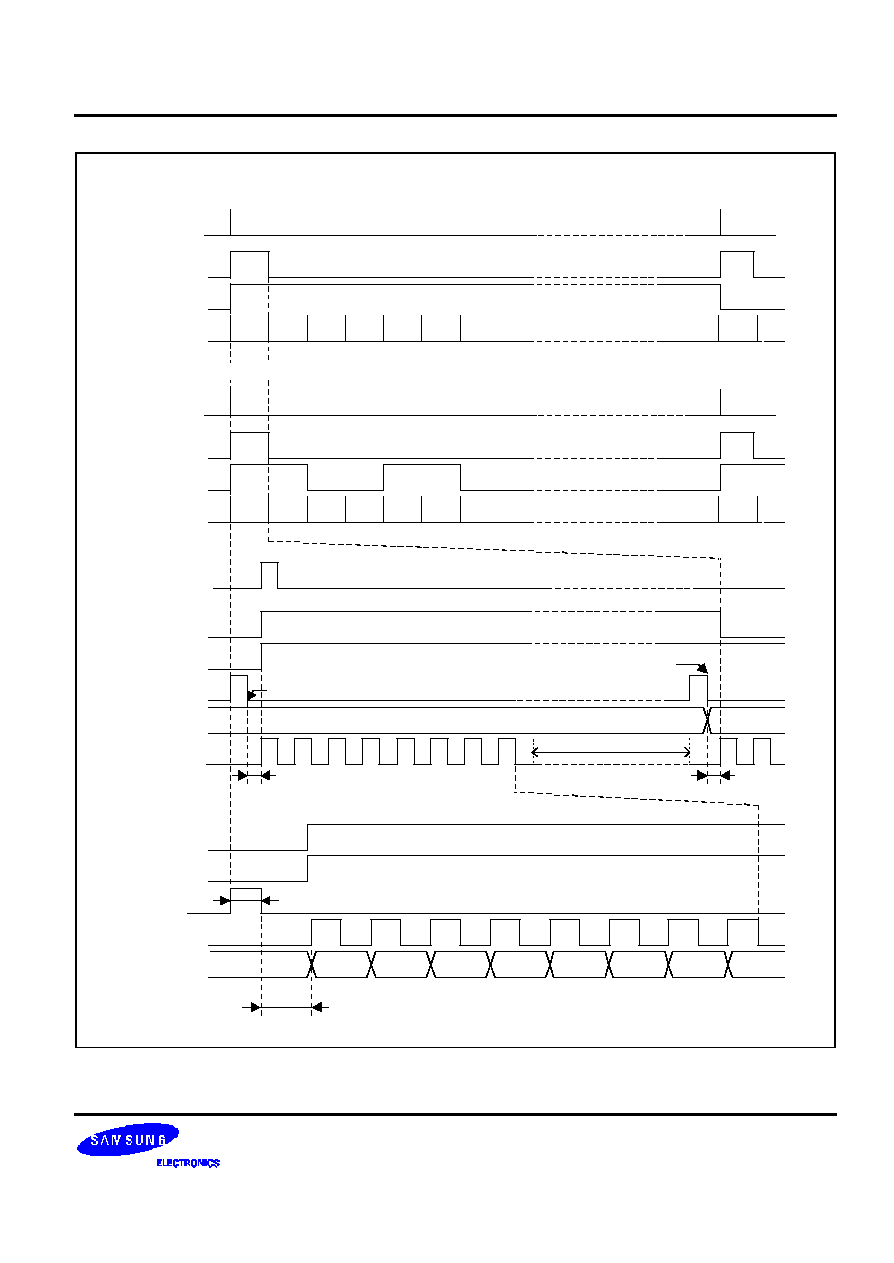
S3C2440A RISC MICROPROCESSOR
LCD CONTROLLER
15-15
WDLY
WLH
LINE1LINE2LINE3LINE4LINE5LINE6
LINE1
LINEn
First Line Timing
LINECNT decreases &
Display the 1st line
LINEBLANK
First Line Check & Data Timing
VFRAME
VM
VLINE
VFRAME
VM
VLINE
LINECNT
VCLK
VFRAME
VM
VLINE
VCLK
VD[7:0]
WDLY
WDLY
Display the last line of the previous frame
Full Frame Timing(MMODE = 1, MVAL=0x2)
INT_FrSyn
INT_FrSyn
VFRAME
VM
VLINE
Full Frame Timing(MMODE = 0)
LINE1LINE2LINE3LINE4LINE5LINE6
LINE1
LINEn
INT_FrSyn
Figure 15-4. 8-bit Single Scan Display Type STN LCD Timing
LCD CONTROLLER
S3C2440A RISC MICROPROCESSOR
15-16
TFT LCD CONTROLLER OPERATION
The TIMEGEN generates the control signals for LCD driver, such as VSYNC, HSYNC, VCLK, VDEN, and LEND
signal. These control signals are highly related with the configurations on the LCDCON1/2/3/4/5 registers in the
REGBANK. Base on these programmable configurations on the LCD control registers in the REGBANK, the
TIMEGEN can generate the programmable control signals suitable for the support of many different types of LCD
drivers.
The VSYNC signal is asserted to cause the LCD's line pointer to start over at the top of the display.
The VSYNC and HSYNC pulse generation depends on the configurations of both the HOZVAL field and the LINEVAL
field in the LCDCON2/3 registers. The HOZVAL and LINEVAL can be determined by the size of the LCD panel
according to the following equations:
-- HOZVAL = (Horizontal display size) -1
-- LINEVAL = (Vertical display size) -1
The rate of VCLK signal depends on the CLKVAL field in the LCDCON1 register. Table 15-3 defines the relationship
of VCLK and CLKVAL. The minimum value of CLKVAL is 0.
VCLK(Hz) = HCLK/[(CLKVAL+1)x2]
The frame rate is VSYNC signal frequency. The frame rate is related with the field of VSYNC, VBPD, VFPD,
LINEVAL, HSYNC, HBPD, HFPD, HOZVAL, and CLKVAL in LCDCON1 and LCDCON2/3/4 registers. Most LCD
drivers need their own adequate frame rate. The frame rate is calculated as follows:
Frame Rate = 1/ [ { (VSPW+1) + (VBPD+1) + (LIINEVAL + 1) + (VFPD+1) } x {(HSPW+1) + (HBPD +1)
+ (HFPD+1) + (HOZVAL + 1) } x { 2 x ( CLKVAL+1 ) / ( HCLK ) } ]
Table 15-3. Relation between VCLK and CLKVAL (TFT, HCLK = 60MHz)
CLKVAL
60MHz/X
VCLK
1
60 MHz/4
15.0 MHz
2
60 MHz/6
10.0 MHz
:
:
:
1023
60 MHz/2048
30.0 kHz
VIDEO OPERATION
The TFT LCD controller within the S3C2440A supports 1, 2, 4 or 8 bpp (bit per pixel) palettized color displays and 16
or 24 bpp non-palettized true-color displays.
256 Color Palette
The S3C2440A can support the 256 color palette for various selection of color mapping, providing flexible operation
for users.
S3C2440A RISC MICROPROCESSOR
LCD CONTROLLER
15-17
MEMORY DATA FORMAT (TFT)
This section includes some examples of each display mode.
24BPP Display
(BSWP = 0, HWSWP = 0, BPP24BL = 0)
D[31:24]
D[23:0]
000H
Dummy Bit
P1
004H
Dummy Bit
P2
008H
Dummy Bit
P3
...
(BSWP = 0, HWSWP = 0, BPP24BL = 1)
D[31:8]
D[7:0]
000H
P1
Dummy Bit
004H
P2
Dummy Bit
008H
P3
Dummy Bit
...
P1
P2 P3 P4
P5
......
LCD Panel
VD Pin Descriptions at 24BPP
VD
23 22 21 20 19 18 17 16 15 14 13 12 11 10
9
8
7
6
5
4
3
2
1
0
RED
7
6
5
4
3
2
1
0
GREEN
7
6
5
4
3
2
1
0
BLUE
7
6
5
4
3
2
1
0
LCD CONTROLLER
S3C2440A RISC MICROPROCESSOR
15-18
16BPP Display
(BSWP = 0, HWSWP = 0)
D[31:16]
D[15:0]
000H
P1
P2
004H
P3
P4
008H
P5
P6
...
(BSWP = 0, HWSWP = 1)
D[31:16]
D[15:0]
000H
P2
P1
004H
P4
P3
008H
P6
P5
...
P1
P2 P3 P4
P5
......
LCD Panel
VD Pin Descriptions at 16BPP
(5:6:5)
VD
23 22 21 20 19 18
17
16
15
14
13
12
11
10
9
8
7
6
5
4
3
2
1
0
RED
4
3
2
1
0
NC
NC
NC
GREEN
5
4
3
2
1
0
BLUE
4
3
2
1
0
(5:5:5:I)
VD
23 22 21 20 19 18 17
16
15
14
13
12
11
10
9
8
7
6
5
4
3
2
1
0
RED
4
3
2
1
0
I
NC
NC
NC
GREEN
4
3
2
1
0
I
BLUE
4
3
2
1
0
I
NOTE: The unused VD pins can be used as GPIO
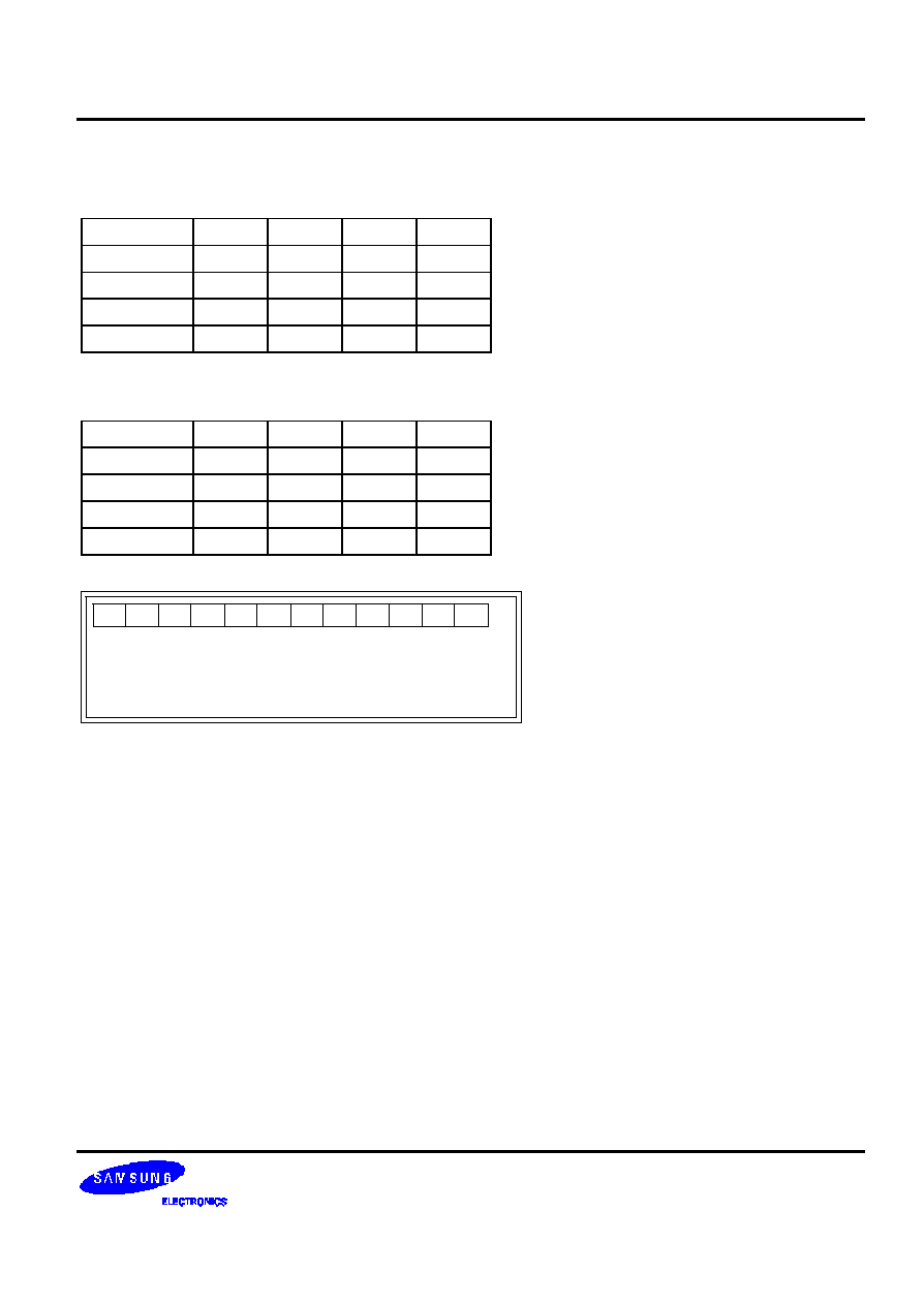
S3C2440A RISC MICROPROCESSOR
LCD CONTROLLER
15-19
8BPP Display
(BSWP = 0, HWSWP = 0)
D[31:24]
D[23:16]
D[15:8]
D[7:0]
000H
P1
P2
P3
P4
004H
P5
P6
P7
P8
008H
P9
P10
P11
P12
...
(BSWP = 1, HWSWP = 0)
D[31:24]
D[23:16]
D[15:8]
D[7:0]
000H
P4
P3
P2
P1
004H
P8
P7
P6
P5
008H
P12
P11
P10
P9
...
P1
P2 P3 P4
P5
......
LCD Panel
P6 P7
P8
P10 P11 P12
P9
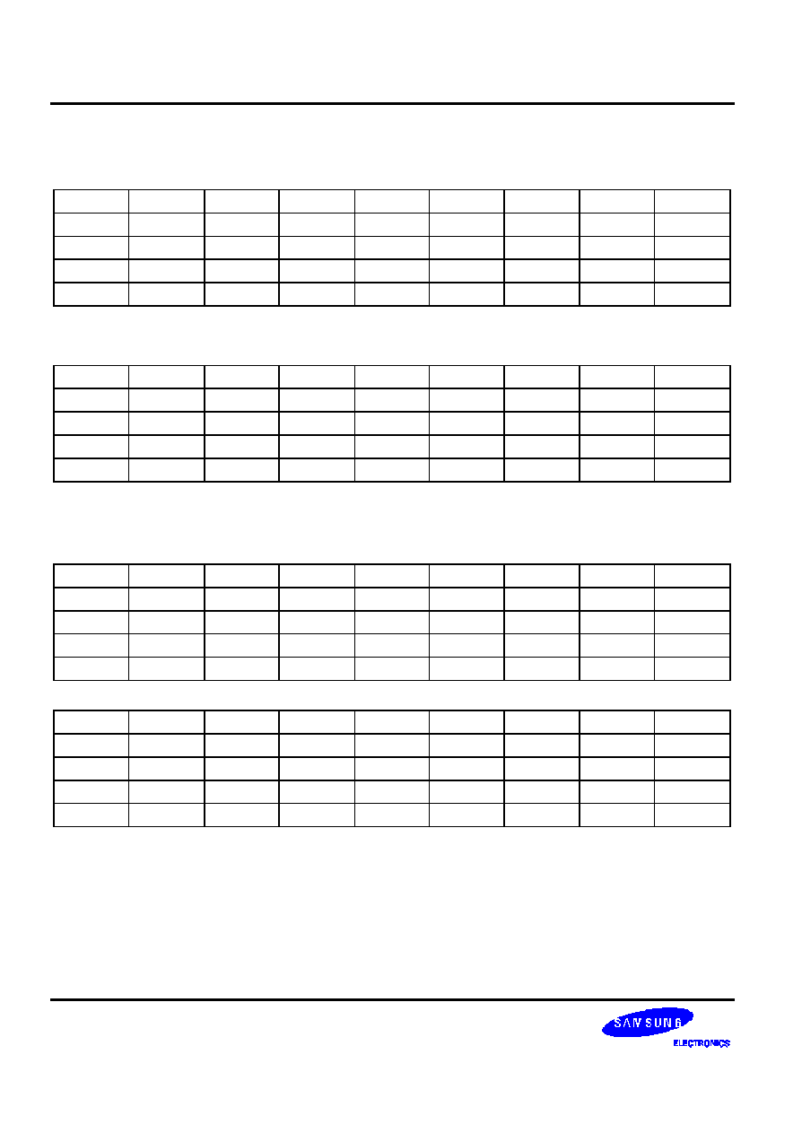
LCD CONTROLLER
S3C2440A RISC MICROPROCESSOR
15-20
4BPP Display
(BSWP = 0, HWSWP = 0)
D[31:28]
D[27:24]
D[23:20]
D[19:16]
D[15:12]
D[11:8]
D[7:4]
D[3:0]
000H
P1
P2
P3
P4
P5
P6
P7
P8
004H
P9
P10
P11
P12
P13
P14
P15
P16
008H
P17
P18
P19
P20
P21
P22
P23
P24
...
(BSWP = 1, HWSWP = 0)
D[31:28]
D[27:24]
D[23:20]
D[19:16]
D[15:12]
D[11:8]
D[7:4]
D[3:0]
000H
P7
P8
P5
P6
P3
P4
P1
P2
004H
P15
P16
P13
P14
P11
P12
P9
P10
008H
P23
P24
P21
P22
P19
P20
P17
P18
...
2BPP Display
(BSWP = 0, HWSWP = 0)
D
[31:30]
[29:28]
[27:26]
[25:24]
[23:22]
[21:20]
[19:18]
[17:16]
000H
P1
P2
P3
P4
P5
P6
P7
P8
004H
P17
P18
P19
P20
P21
P22
P23
P24
008H
P33
P34
P35
P36
P37
P38
P39
P40
...
D
[15:14]
[13:12]
[11:10]
[9:8]
[7:6]
[5:4]
[3:2]
[1:0]
000H
P9
P10
P11
P12
P13
P14
P15
P16
004H
P25
P26
P27
P28
P29
P30
P31
P32
008H
P41
P42
P43
P44
P45
P46
P47
P48
...
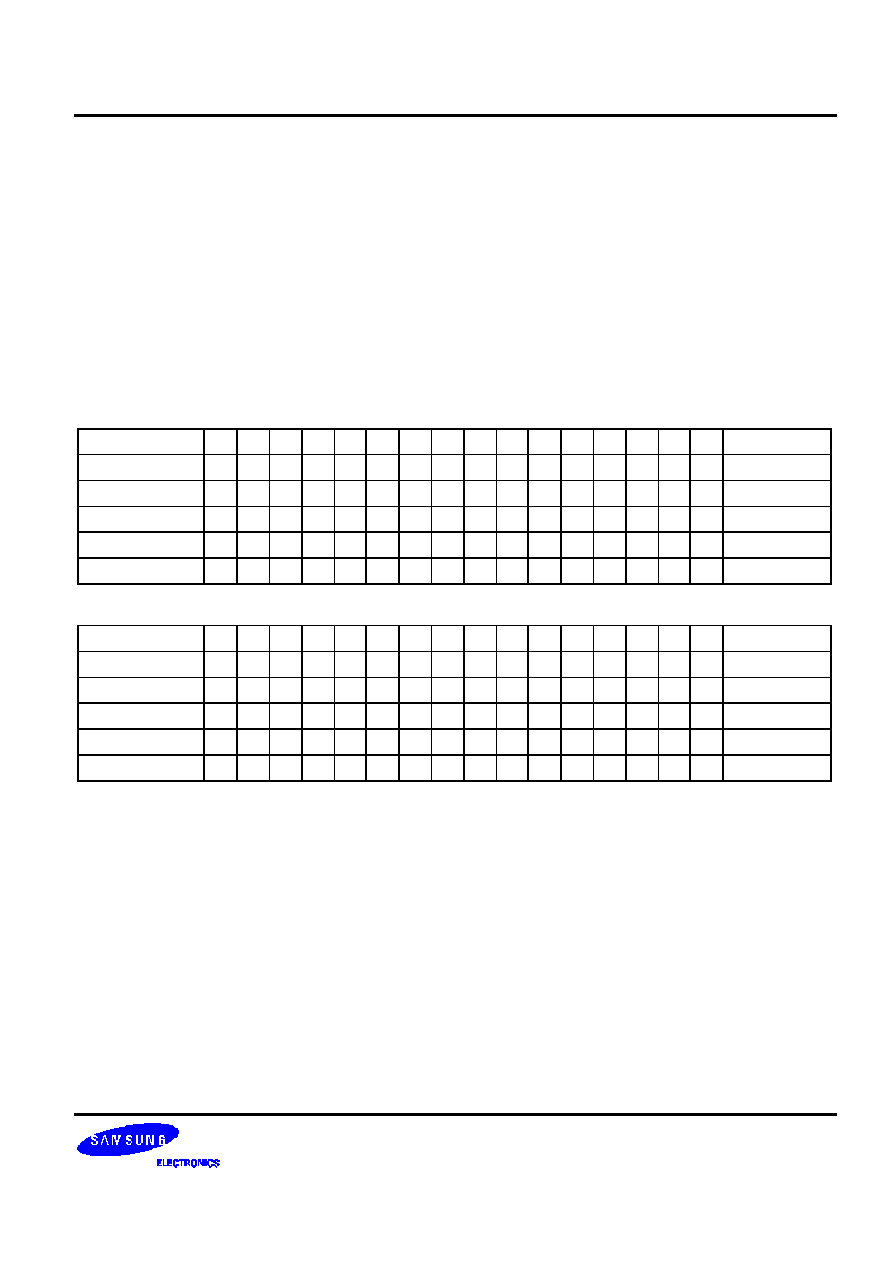
S3C2440A RISC MICROPROCESSOR
LCD CONTROLLER
15-21
256 PALETTE USAGE (TFT)
Palette Configuration and Format Control
The S3C2440A provides 256 color palette for TFT LCD Control.
The user can select 256 colors from the 64K colors in these two formats.
The 256 color palette consists of the 256 (depth) x 16-bit SPSRAM. The palette supports 5:6:5 (R:G:B) format and
5:5:5:1(R:G:B:I) format.
When the user uses 5:5:5:1 format, the intensity data(I) is used as a common LSB bit of each RGB data. So,
5:5:5:1 format is the same as R(5+I):G(5+I):B(5+I) format.
In 5:5:5:1 format, for example, the user can write the palette as in Table 15-5 and then connect VD pin to TFT LCD
panel(R(5+I)=VD[23:19]+VD[18], VD[10] or VD[2], G(5+I)=VD[15:11]+ VD[18], VD[10] or VD[2], B(5+I)=VD[7:3]+
VD[18], VD[10] or VD[2].), and set FRM565 of LCDCON5 register to 0.
Table 15-4. 5:6:5 Format
INDEX\Bit Pos.
15
14 13
12
11
10
9
8
7
6
5
4
3
2
1
0
Address
00H
R4 R3 R2 R1 R0 G5 G4 G3 G2 G1 G0 B4 B3 B2 B1 B0
1)
0X4D000400
01H
R4 R3 R2 R1 R0 G5 G4 G3 G2 G1 G0 B4 B3 B2 B1 B0
0X4D000404
.......
.......
FFH
R4 R3 R2 R1 R0 G5 G4 G3 G2 G1 G0 B4 B3 B2 B1 B0
0X4D0007FC
Number of VD
23
22 21
20
19
15
14 13
12
11
10
7
6
5
4
3
Table 15-5. 5:5:5:1 Format
INDEX\Bit Pos.
15
14 13
12
11
10
9
8
7
6
5
4
3
2
1
0
Address
00H
R4 R3 R2 R1 R0 G4 G3 G2 G1 G0 B4 B3 B2 B1 B0
I
0X4D000400
01H
R4 R3 R2 R1 R0 G4 G3 G2 G1 G0 B4 B3 B2 B1 B0
I
0X4D000404
.......
.......
FFH
R4 R3 R2 R1 R0 G4 G3 G2 G1 G0 B4 B3 B2 B1 B0
I
0X4D0007FC
Number of VD
23
22 21
20
19
15
14 13
12
11
7
6
5
4
3
2)
NOTES:
1.
0x4D000400 is Palette start address.
2.
VD18, VD10 and VD2 have the same output value, I.
3. DATA[31:16] is invalid.
Palette Read/Write
When the user performs Read/Write operation on the palette, HSTATUS and VSTATUS of LCDCON5 register must
be checked, for Read/Write operation is prohibited during the ACTIVE status of HSTATUS and VSTATUS.
Temporary Palette Configuration
The S3C2440A allows the user to fill a frame with one color without complex modification to fill the one color to the
frame buffer or palette. The one colored frame can be displayed by the writing a value of the color which is displayed
on LCD panel to TPALVAL of TPAL register and enable TPALEN.
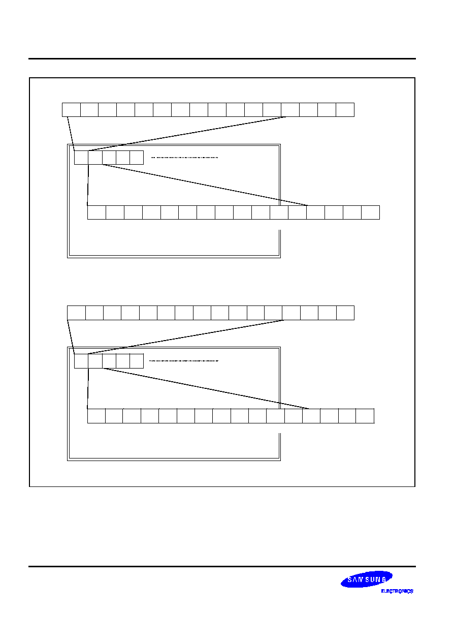
LCD CONTROLLER
S3C2440A RISC MICROPROCESSOR
15-22
1
2
3
4
5
LCD Panel
16BPP 5:5:5+1 Format(Non-Palette)
A[31] A[30] A[29] A[28] A[27] A[26]A[25] A[24] A[23] A[22] A[21] A[20] A[19]A[18] A[17] A[16]
R4
R3
R2
R1
R0
G4
G3
G2
G1
G0
R4
B3
B2
B1
B0
I
A[15] A[14] A[13] A[12] A[11] A[10] A[9] A[8] A[7] A[6] A[5] A[4] A[3] A[2] A[1] A[0]
R4
R3
R2
R1
R0
G4
G3
G2
G1
G0
R4
B3
B2
B1
B0
I
1
2
3
4
5
LCD Panel
16BPP 5:6:5 Format(Non-Palette)
A[31] A[30] A[29] A[28] A[27] A[26]A[25] A[24] A[23] A[22] A[21] A[20] A[19]A[18] A[17] A[16]
A[15] A[14] A[13] A[12]A[11] A[10] A[9] A[8] A[7] A[6] A[5] A[4] A[3] A[2] A[1] A[0]
R4
R3
R2
R1
R0
G5
G4
G3
G2
G1
G0
B4
B3
B2
B1
B0
R4
R3
R2
R1
R0
G5
G4
G3
G2
G1
G0
B4
B3
B2
B1
B0
Figure 15-5. 16BPP Display Types (TFT)
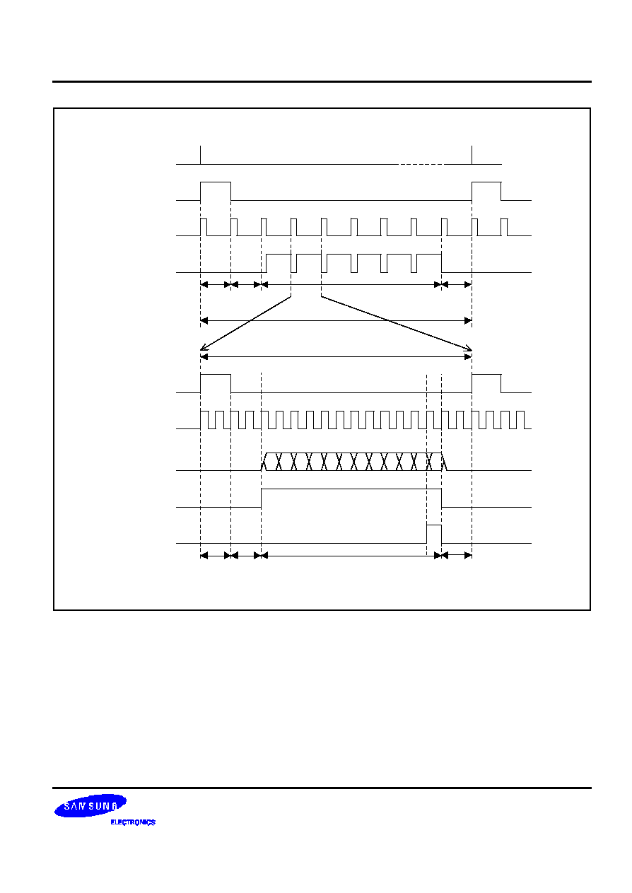
S3C2440A RISC MICROPROCESSOR
LCD CONTROLLER
15-23
INT_FrSyn
VSYNC
HSYNC
VDEN
HSYNC
VCLK
VD
LEND
VBPD+1
VSPW+1
VFPD+1
HBPD+1
HFPD+1
HSPW+1
VDEN
1 Frame
1 Line
LINEVAL +1
HOZVAL+1
Figure 15-6. TFT LCD Timing Example

LCD CONTROLLER
S3C2440A RISC MICROPROCESSOR
15-24
SAMSUNG TFT LCD PANEL (3.5" PORTRAIT / 256K COLOR / REFLECTIVE A-SI/TRANSFLECTIVE A-SI TFT
LCD)
The S3C2440A supports following SEC TFT LCD panels.
1. SAMSUNG 3.5" Portrait / 256K Color /Reflective a-Si TFT LCD.
LTS350Q1-PD1: TFT LCD panel with touch panel and front light unit
LTS350Q1-PD2: TFT LCD panel only
2. SAMSUNG 3.5" Portrait / 256K Color /Transflective a-Si TFT LCD.
LTS350Q1-PE1: TFT LCD panel with touch panel and front light unit
LTS350Q1-PE2: TFT LCD panel only
The S3C2440A provides timing signals as follows to use LTS350Q1-PD1 / PD2 and LTS350Q1-PE1 / PE2
LTS350Q1-PD1 / PD2
LTS350Q1-PE1 / PE2
STH: Horizontal Start Pulse
TP: Source Driver Data Load Pulse
INV: Digital Data Inversion
LCD_HCLK: Horizontal Sampling Clock
CPV: Vertical Shift Clock
STV: Vertical Start Pulse
OE: Gate On Enable
REV: Inversion Signal
REVB: Inversion Signal
STH: Horizontal Start Pulse
TP: Source Driver Data Load Pulse
INV: Digital Data Inversion
LCD_HCLK: Horizontal Sampling Clock
CPV: Vertical Shift Clock
STV: Vertical Start Pulse
LCCINV: Source drive IC sampling inversion signal
REV: VCOM modulation Signal
REVB: Inversion Signal
So, LTS350Q1-PD1/2 and PE1/2 can be connected with the S3C2440A without using the additional timing control
logic. But the user should additionally apply Vcom generator circuit, various voltages, INV signal and Gray scale
voltage generator circuit, which is recommended by PRODUCT INFORMATION (SPEC) of LTS350Q1-PD1/2 and
PE1/2. Detailed timing diagram is also described in PRODUCT INFORMATION (SPEC) of LTS350Q1-PD1/2 and
PE1/2.
Refer to the documentation (PRODUCT INFORMATION of LTS350Q1-PD1/2 and PE1/2), which is prepared by
AMLCD Technical Customer Center of Samsung Electronics Co., LTD.
Caution:
-- The S3C2440A has HCLK, working as the clock of AHB bus.
-- SEC TFT LCD panel (LTS350Q1-PD1/2 and PE1/2) has Horizontal Sampling Clock (HCLK).
-- These two HCLKs may cause a confusion. So, note that HCLK of the S3C2440A is HCLK and other HCLK
of the LTS350 is LCD_HCLK.
Check that the HCLK of SEC TFT LCD panel (LTS350Q1-PD1/2 and PE1/2) is changed to LCD_HCLK.
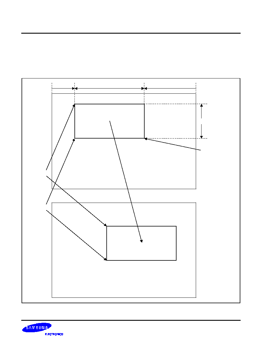
S3C2440A RISC MICROPROCESSOR
LCD CONTROLLER
15-25
VIRTUAL DISPLAY (TFT/STN)
The S3C2440A supports hardware horizontal or vertical scrolling. If the screen is scrolled, the fields of LCDBASEU
and LCDBASEL in LCDSADDR1/2 registers need to be changed (see Figure 15-8), except the values of
PAGEWIDTH and OFFSIZE.
The video buffer in which the image is stored should be larger than the LCD panel screen in size.
This is the data of line 1 of virtual screen. This is the data of line 1 of virtual screen.
This is the data of line 2 of virtual screen. This is the data of line 2 of virtual screen.
This is the data of line 3 of virtual screen. This is the data of line 3 of virtual screen.
This is the data of line 4 of virtual screen. This is the data of line 4 of virtual screen.
This is the data of line 5 of virtual screen. This is the data of line 5 of virtual screen.
This is the data of line 6 of virtual screen. This is the data of line 6 of virtual screen.
This is the data of line 7 of virtual screen. This is the data of line 7 of virtual screen.
This is the data of line 8 of virtual screen. This is the data of line 8 of virtual screen.
This is the data of line 9 of virtual screen. This is the data of line 9 of virtual screen.
This is the data of line 10 of virtual screen. This is the data of line 10 of virtual screen.
This is the data of line 11 of virtual screen. This is the data of line 11 of virtual screen.
.
.
.
Before Scrolling
View Port
(The same size
of LCD panel.)
LINEVAL + 1
OFFSIZE
PAGEWIDTH
This is the data of line 1 of virtual screen. This is the data of line 1 of virtual screen.
This is the data of line 2 of virtual screen. This is the data of line 2 of virtual screen.
This is the data of line 3 of virtual screen. This is the data of line 3 of virtual screen.
This is the data of line 4 of virtual screen. This is the data of line 4 of virtual screen.
This is the data of line 5 of virtual screen. This is the data of line 5 of virtual screen.
This is the data of line 6 of virtual screen. This is the data of line 6 of virtual screen.
This is the data of line 7 of virtual screen. This is the data of line 7 of virtual screen.
This is the data of line 8 of virtual screen. This is the data of line 8 of virtual screen.
This is the data of line 9 of virtual screen. This is the data of line 9 of virtual screen.
This is the data of line 10 of virtual screen. This is the data of line 10 of virtual screen.
This is the data of line 11 of virtual screen. This is the data of line 11 of virtual screen.
.
.
.
After Scrolling
LCDBASEU
LCDBASEL
OFFSIZE
Figure 15-7. Example of Scrolling in Virtual Display (Single Scan)
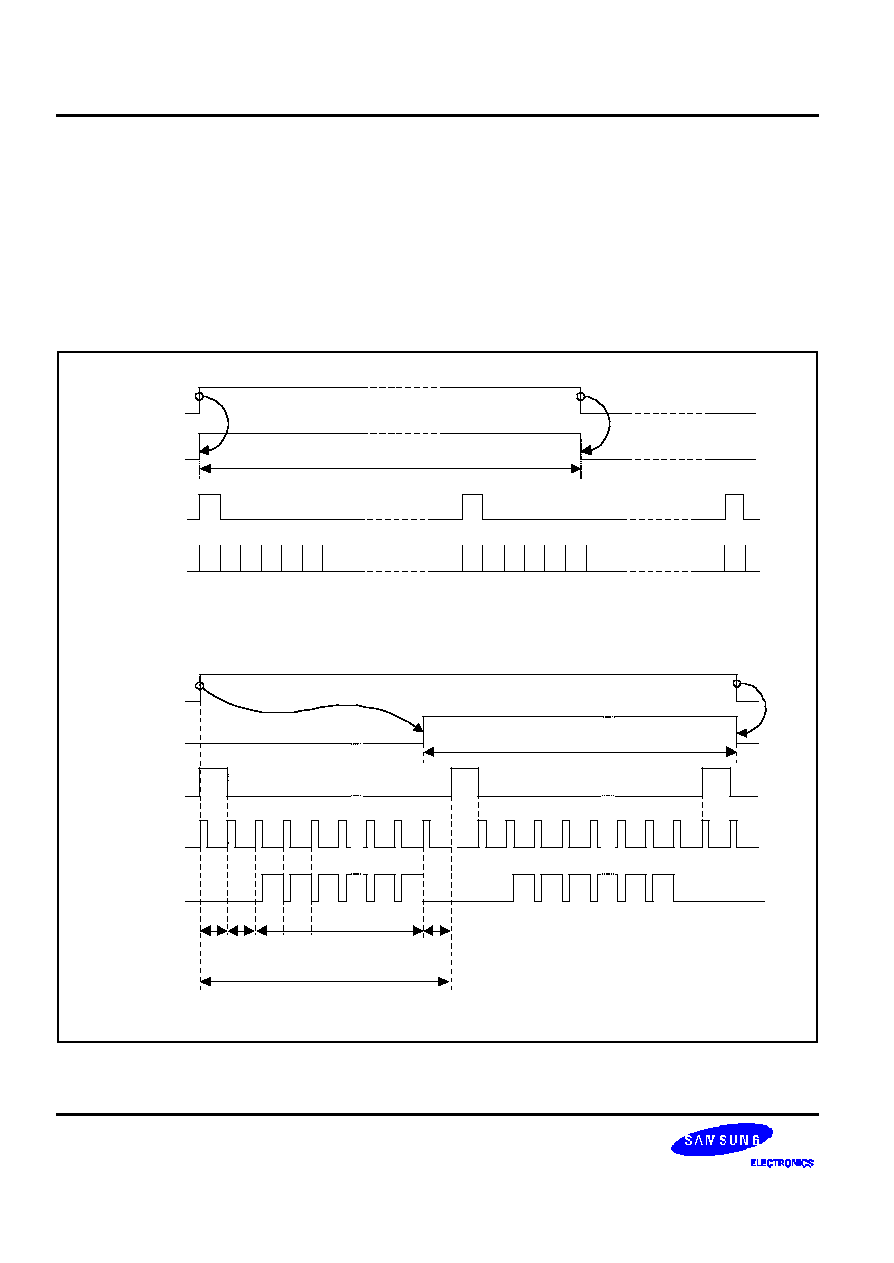
LCD CONTROLLER
S3C2440A RISC MICROPROCESSOR
15-26
LCD POWER ENABLE (STN/TFT)
The S3C2440A provides Power enable (PWREN) function. When PWREN is set to make PWREN signal enabled,
the output value of LCD_PWREN pin is controlled by ENVID. In other words, If LCD_PWREN pin is connected to the
power on/off control pin of the LCD panel, the power of LCD panel is controlled by the setting of ENVID automatically.
The S3C2440A also supports INVPWREN bit to invert polarity of the PWREN signal.
This function is available only when LCD panel has its own power on/off control port and when port is connected to
LCD_PWREN pin.
VSYNC
HSYNC
VDEN
LCD_PWREN
1 FRAME
ENVID
LCD Panel On
TFT LCD
VLINE
VFRAME
STN LCD
LCD_PWREN
LCD Panel On
ENVID
Figure 15-8. Example of PWREN Function (PWREN=1, INVPWREN=0)

S3C2440A RISC MICROPROCESSOR
LCD CONTROLLER
15-27
LCD CONTROLLER SPECIAL REGISTERS
LCD Control 1 Register
Register
Address
R/W
Description
Reset Value
LCDCON1
0X4D000000
R/W
LCD control 1 register
0x00000000
LCDCON1
Bit
Description
Initial State
LINECNT
(read only)
[27:18]
Provide the status of the line counter.
Down count from LINEVAL to 0
0000000000
CLKVAL
[17:8]
Determine the rates of VCLK and CLKVAL[9:0].
STN: VCLK = HCLK / (CLKVAL x 2) ( CLKVAL
2 )
TFT: VCLK = HCLK / [(CLKVAL+1) x 2] ( CLKVAL
0 )
0000000000
MMODE
[7]
Determine the toggle rate of the VM.
0 = Each Frame
1 = The rate defined by the MVAL
0
PNRMODE
[6:5]
Select the display mode.
00 = 4-bit dual scan display mode (STN)
01 = 4-bit single scan display mode (STN)
10 = 8-bit single scan display mode (STN)
11 = TFT LCD panel
00
BPPMODE
[4:1]
Select the BPP (Bits Per Pixel) mode.
0000 = 1 bpp for STN, Monochrome mode
0001 = 2 bpp for STN, 4-level gray mode
0010 = 4 bpp for STN, 16-level gray mode
0011 = 8 bpp for STN, color mode (256 color)
0100 = packed 12 bpp for STN, color mode (4096 color)
0101 = unpacked 12 bpp for STN, color mode (4096 color)
0110 = 16 bpp for STN, color mode (4096 color)
1000 = 1 bpp for TFT
1001 = 2 bpp for TFT
1010 = 4 bpp for TFT
1011 = 8 bpp for TFT
1100 = 16 bpp for TFT
1101 = 24 bpp for TFT
0000
ENVID
[0]
LCD video output and the logic enable/disable.
0 = Disable the video output and the LCD control signal.
1 = Enable the video output and the LCD control signal.
0

LCD CONTROLLER
S3C2440A RISC MICROPROCESSOR
15-28
LCD Control 2 Register
Register
Address
R/W
Description
Reset Value
LCDCON2
0X4D000004
R/W
LCD control 2 register
0x00000000
LCDCON2
Bit
Description
Initial State
VBPD
[31:24]
TFT: Vertical back porch is the number of inactive lines at the start of
a frame, after vertical synchronization period.
STN: These bits should be set to zero on STN LCD.
0x00
LINEVAL
[23:14]
TFT/STN: These bits determine the vertical size of LCD panel.
0000000000
VFPD
[13:6]
TFT: Vertical front porch is the number of inactive lines at the end of a
frame, before vertical synchronization period.
STN: These bits should be set to zero on STN LCD.
00000000
VSPW
[5:0]
TFT: Vertical sync pulse width determines the VSYNC pulse's high
level width by counting the number of inactive lines.
STN: These bits should be set to zero on STN LCD.
000000

S3C2440A RISC MICROPROCESSOR
LCD CONTROLLER
15-29
LCD Control 3 Register
Register
Address
R/W
Description
Reset Value
LCDCON3
0X4D000008
R/W
LCD control 3 register
0x00000000
LCDCON3
Bit
Description
Initial state
HBPD (TFT)
[25:19]
TFT: Horizontal back porch is the number of VCLK periods between
the falling edge of HSYNC and the start of active data.
0000000
WDLY (STN)
STN: WDLY[1:0] bits determine the delay between VLINE and VCLK
by counting the number of the HCLK. WDLY[7:2] are reserved.
00 = 16 HCLK, 01 = 32 HCLK, 10 = 48 HCLK, 11 = 64 HCLK
HOZVAL
[18:8]
TFT/STN: These bits determine the horizontal size of LCD panel.
HOZVAL has to be determined to meet the condition that total bytes
of 1 line are 4n bytes. If the x size of LCD is 120 dot in mono mode,
x=120 cannot be supported because 1 line consists of 15 bytes.
Instead, x=128 in mono mode can be supported because 1 line is
composed of 16 bytes (2n). LCD panel driver will discard the additional
8 dot.
00000000000
HFPD (TFT)
[7:0]
TFT: Horizontal front porch is the number of VCLK periods between
the end of active data and the rising edge of HSYNC.
0X00
LINEBLANK
(STN)
STN: These bits indicate the blank time in one horizontal line duration
time. These bits adjust the rate of the VLINE finely.
The unit of LINEBLANK is HCLK x 8.
Ex) If the value of LINEBLANK is 10, the blank time is inserted to
VCLK during 80 HCLK.
Programming NOTE
: In case of STN LCD, (LINEBLANK + WLH + WDLY) value should be bigger than (14+12Tmax).
(LINEBLANK + WLH + WDLY)
°
(14 + 8xT
max1
+ 4xT
max2
= 14 + 12T
max
)
LEGEND
:
(1) 14: SDRAM Auto refresh bus acquisition cycles
(2) 8x Tmax1 : Cache fill cycle X the Slowest Memory access time(Ex, ROM)
(3) 4x Tmax2 : 0xC~0xE address Frame memory Access time

LCD CONTROLLER
S3C2440A RISC MICROPROCESSOR
15-30
LCD Control 4 Register
Register
Address
R/W
Description
Reset Value
LCDCON4
0X4D00000C
R/W
LCD control 4 register
0x00000000
LCDCON4
Bit
Description
Initial state
MVAL
[15:8]
STN: These bit define the rate at which the VM signal will toggle if the
MMODE bit is set to logic '1'.
0X00
HSPW(TFT)
[7:0]
TFT: Horizontal sync pulse width determines the HSYNC pulse's high
level width by counting the number of the VCLK.
0X00
WLH(STN)
STN: WLH[1:0] bits determine the VLINE pulse's high level width by
counting the number of the HCLK.
WLH[7:2] are reserved.
00 = 16 HCLK, 01 = 32 HCLK, 10 = 48 HCLK, 11 = 64 HCLK
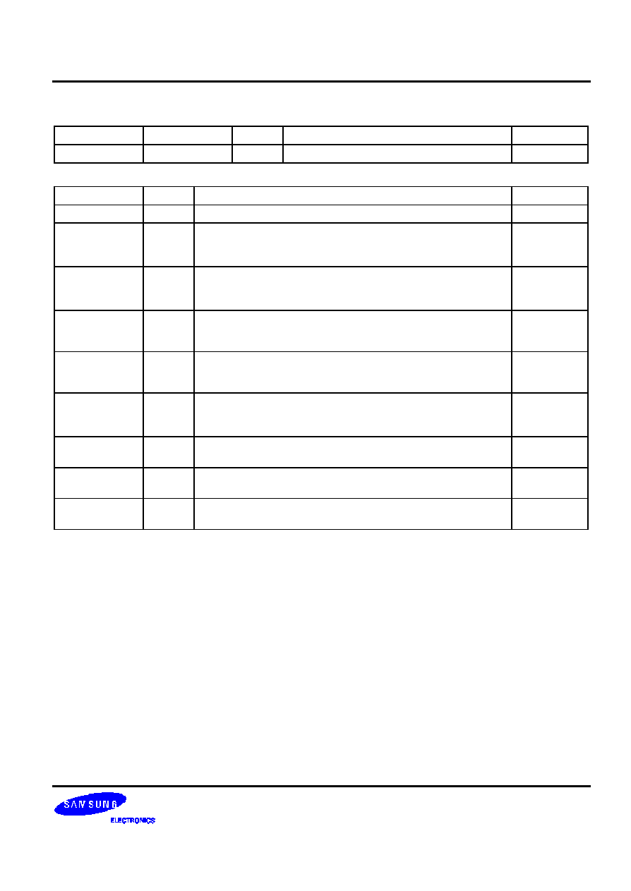
S3C2440A RISC MICROPROCESSOR
LCD CONTROLLER
15-31
LCD Control 5 Register
Register
Address
R/W
Description
Reset Value
LCDCON5
0X4D000010
R/W
LCD control 5 register
0x00000000
LCDCON5
Bit
Description
Initial state
Reserved
[31:17]
This bit is reserved and the value should be `0'.
0
VSTATUS
[16:15]
TFT: Vertical Status (read only).
00 = VSYNC 01 = BACK Porch
10 = ACTIVE 11 = FRONT Porch
00
HSTATUS
[14:13]
TFT: Horizontal Status (read only).
00 = HSYNC 01 = BACK Porch
10 = ACTIVE 11 = FRONT Porch
00
BPP24BL
[12]
TFT: This bit determines the order of 24 bpp video memory.
0 = LSB valid 1 = MSB Valid
0
FRM565
[11]
TFT: This bit selects the format of 16 bpp output video data.
0 = 5:5:5:1 Format 1 = 5:6:5 Format
0
INVVCLK
[10]
STN/TFT: This bit controls the polarity of the VCLK active edge.
0 = The video data is fetched at VCLK falling edge
1 = The video data is fetched at VCLK rising edge
0
INVVLINE
[9]
STN/TFT: This bit indicates the VLINE/HSYNC pulse polarity.
0 = Normal
1 = Inverted
0
INVVFRAME
[8]
STN/TFT: This bit indicates the VFRAME/VSYNC pulse polarity.
0 = Normal 1 = Inverted
0
INVVD
[7]
STN/TFT: This bit indicates the VD (video data) pulse polarity.
0 = Normal
1 = VD is inverted.
0
LCD CONTROLLER
S3C2440A RISC MICROPROCESSOR
15-32
LCD Control 5 Register (Continued)
LCDCON5
Bit
Description
Initial state
INVVDEN
[6]
TFT: This bit indicates the VDEN signal polarity.
0 = normal
1 = inverted
0
INVPWREN
[5]
STN/TFT: This bit indicates the PWREN signal polarity.
0 = normal
1 = inverted
0
INVLEND
[4]
TFT: This bit indicates the LEND signal polarity.
0 = normal
1 = inverted
0
PWREN
[3]
STN/TFT: LCD_PWREN output signal enable/disable.
0 = Disable PWREN signal
1 = Enable PWREN signal
0
ENLEND
[2]
TFT: LEND output signal enable/disable.
0 = Disable LEND signal 1 = Enable LEND signal
0
BSWP
[1]
STN/TFT: Byte swap control bit.
0 = Swap Disable
1 = Swap Enable
0
HWSWP
[0]
STN/TFT: Half-Word swap control bit.
0 = Swap Disable
1 = Swap Enable
0
S3C2440A RISC MICROPROCESSOR
LCD CONTROLLER
15-33
FRAME BUFFER START ADDRESS 1 REGISTER
Register
Address
R/W
Description
Reset Value
LCDSADDR1
0X4D000014
R/W
STN/TFT: Frame buffer start address 1 register
0x00000000
LCDSADDR1
Bit
Description
Initial State
LCDBANK
[29:21]
These bits indicate A[30:22] of the bank location for the video buffer in
the system memory. LCDBANK value cannot be changed even when
moving the view port. LCD frame buffer should be within aligned 4MB
region, which ensures that LCDBANK value will not be changed when
moving the view port. So, care should be taken to use the malloc()
function.
0x00
LCDBASEU
[20:0]
For dual-scan LCD : These bits indicate A[21:1] of the start address of
the upper address counter, which is for the upper frame memory of
dual scan LCD or the frame memory of single scan LCD.
For single-scan LCD : These bits indicate A[21:1] of the start address
of the LCD frame buffer.
0x000000
FRAME Buffer Start Address 2 Register
Register
Address
R/W
Description
Reset Value
LCDSADDR2
0X4D000018
R/W
STN/TFT: Frame buffer start address 2 register
0x00000000
LCDSADDR2
Bit
Description
Initial State
LCDBASEL
[20:0]
For dual-scan LCD: These bits indicate A[21:1] of the start address of
the lower address counter, which is used for the lower frame memory
of dual scan LCD.
For single scan LCD: These bits indicate A[21:1] of the end address
of the LCD frame buffer.
LCDBASEL = ((the frame end address) >>1) + 1
= LCDBASEU +
(PAGEWIDTH+OFFSIZE) x (LINEVAL+1)
0x0000
NOTE: Users can change the LCDBASEU and LCDBASEL values for scrolling while the LCD controller is turned on.
But, users must not change the value of the LCDBASEU and LCDBASEL registers at the end of FRAME by referring
to the LINECNT field in LCDCON1 register, for the LCD FIFO fetches the next frame data prior to the change in the
frame.
So, if you change the frame, the pre-fetched FIFO data will be obsolete and LCD controller will display an incorrect
screen. To check the LINECNT, interrupts should be masked. If any interrupt is executed just after reading
LINECNT,
the read LINECNT value may be obsolete because of the execution time of Interrupt Service
Routine (ISR).

LCD CONTROLLER
S3C2440A RISC MICROPROCESSOR
15-34
FRAME Buffer Start Address 3 Register
Register
Address
R/W
Description
Reset Value
LCDSADDR3
0X4D00001C
R/W
STN/TFT: Virtual screen address set
0x00000000
LCDSADDR3
Bit
Description
Initial State
OFFSIZE
[21:11]
Virtual screen offset size (the number of half words).
This value defines the difference between the address of the last half
word displayed on the previous LCD line and the address of the first
half word to be displayed in the new LCD line.
00000000000
PAGEWIDTH
[10:0]
Virtual screen page width (the number of half words).
This value defines the width of the view port in the frame.
000000000
NOTE: The values of PAGEWIDTH and OFFSIZE must be changed when ENVID bit is 0.
Example 1. LCD panel = 320 x 240, 16gray, single scan
Frame start address = 0x0c500000
Offset dot number = 2048 dots ( 512 half words )
LINEVAL = 240-1 = 0xef
PAGEWIDTH = 320 x 4 / 16 = 0x50
OFFSIZE = 512 = 0x200
LCDBANK = 0x0c500000 >> 22 = 0x31
LCDBASEU = 0x100000 >> 1 = 0x80000
LCDBASEL = 0x80000 + ( 0x50 + 0x200 ) x ( 0xef + 1 ) = 0xa2b00
Example 2. LCD panel = 320 x 240, 16gray, dual scan
Frame start address = 0x0c500000
Offset dot number = 2048 dots ( 512 half words )
LINEVAL = 120-1 = 0x77
PAGEWIDTH = 320 x 4 / 16 = 0x50
OFFSIZE = 512 = 0x200
LCDBANK = 0x0c500000 >> 22 = 0x31
LCDBASEU = 0x100000 >> 1 = 0x80000
LCDBASEL = 0x80000 + ( 0x50 + 0x200 ) x ( 0x77 + 1 ) = 0x91580
Example 3. LCD panel = 320*240, color, single scan
Frame start address = 0x0c500000
Offset dot number = 1024 dots ( 512 half words )
LINEVAL = 240-1 = 0xef
PAGEWIDTH = 320 x 8 / 16 = 0xa0
OFFSIZE = 512 = 0x200
LCDBANK = 0x0c500000 >> 22 = 0x31
LCDBASEU = 0x100000 >> 1 = 0x80000
LCDBASEL = 0x80000 + ( 0xa0 + 0x200 ) x ( 0xef + 1 ) = 0xa7600
S3C2440A RISC MICROPROCESSOR
LCD CONTROLLER
15-35
RED Lookup Table Register
Register
Address
R/W
Description
Reset Value
REDLUT
0X4D000020
R/W
STN: Red lookup table register
0x00000000
REDLUT
Bit
Description
Initial State
REDVAL
[31:0]
These bits define which of the 16 shades will be chosen by each of
the 8 possible red combinations.
000 = REDVAL[3:0],
001 = REDVAL[7:4]
010 = REDVAL[11:8],
011 = REDVAL[15:12]
100 = REDVAL[19:16],
101 = REDVAL[23:20]
110 = REDVAL[27:24],
111 = REDVAL[31:28]
0x00000000
GREEN Lookup Table Register
Register
Address
R/W
Description
Reset Value
GREENLUT
0X4D000024
R/W
STN: Green lookup table register
0x00000000
GREENLUT
Bit
Description
Initial State
GREENVAL
[31:0]
These bits define which of the 16 shades will be chosen by each of
the 8 possible green combinations.
000 = GREENVAL[3:0],
001 = GREENVAL[7:4]
010 = GREENVAL[11:8],
011 = GREENVAL[15:12]
100 = GREENVAL[19:16],
101 = GREENVAL[23:20]
110 = GREENVAL[27:24],
111 = GREENVAL[31:28]
0x00000000
BLUE Lookup Table Register
Register
Address
R/W
Description
Reset Value
BLUELUT
0X4D000028
R/W
STN: Blue lookup table register
0x0000
BULELUT
Bit
Description
Initial State
BLUEVAL
[15:0]
These bits define which of the 16 shades will be chosen by each of
the 4 possible blue combinations.
00 = BLUEVAL[3:0],
01 = BLUEVAL[7:4]
10 = BLUEVAL[11:8], 11 = BLUEVAL[15:12]
0x0000
NOTE: Address from 0x14A0002C to 0x14A00048 should not be used. This area is reserved for Test mode.

LCD CONTROLLER
S3C2440A RISC MICROPROCESSOR
15-36
Dithering Mode Register
Register
Address
R/W
Description
Reset Value
DITHMODE
0X4D00004C
R/W
STN: Dithering mode register.
This register reset value is 0x00000 But, user can
change this value to 0x12210.
(Refer to a sample program source for the latest
value of this register.)
0x00000
DITHMODE
Bit
Description
Initial state
DITHMODE
[18:0]
Use one of following value for your LCD:
0x00000 or 0x12210
0x00000

S3C2440A RISC MICROPROCESSOR
LCD CONTROLLER
15-37
Temp Palette Register
Register
Address
R/W
Description
Reset Value
TPAL
0X4D000050
R/W
TFT: Temporary palette register.
This register value will be video data at next frame.
0x00000000
TPAL
Bit
Description
Initial state
TPALEN
[24]
Temporary palette register enable bit.
0 = Disable
1 = Enable
0
TPALVAL
[23:0]
Temporary palette value register.
TPALVAL[23:16] : RED
TPALVAL[15:8] : GREEN
TPALVAL[7:0] : BLUE
0x000000
LCD CONTROLLER
S3C2440A RISC MICROPROCESSOR
15-38
LCD Interrupt Pending Register
Register
Address
R/W
Description
Reset Value
LCDINTPND
0X4D000054
R/W
Indicate the LCD interrupt pending register
0x0
LCDINTPND
Bit
Description
Initial state
INT_FrSyn
[1]
LCD frame synchronized interrupt pending bit.
0 = The interrupt has not been requested.
1 = The frame has asserted the interrupt request.
0
INT_FiCnt
[0]
LCD FIFO interrupt pending bit.
0 = The interrupt has not been requested.
1 = LCD FIFO interrupt is requested when LCD FIFO reaches trigger
level.
0
LCD Source Pending Register
Register
Address
R/W
Description
Reset Value
LCDSRCPND
0X4D000058
R/W
Indicate the LCD interrupt source pending register
0x0
LCDSRCPND
Bit
Description
Initial state
INT_FrSyn
[1]
LCD frame synchronized interrupt source pending bit.
0 = The interrupt has not been requested.
1 = The frame has asserted the interrupt request.
0
INT_FiCnt
[0]
LCD FIFO interrupt source pending bit.
0 = The interrupt has not been requested.
1 = LCD FIFO interrupt is requested when LCD FIFO reaches trigger
level.
0

S3C2440A RISC MICROPROCESSOR
LCD CONTROLLER
15-39
LCD Interrupt Mask Register
Register
Address
R/W
Description
Reset Value
LCDINTMSK
0X4D00005C
R/W
Determine which interrupt source is masked.
The masked interrupt source will not be serviced.
0x3
LCDINTMSK
Bit
Description
Initial state
FIWSEL
[2]
Determine the trigger level of LCD FIFO.
0 = 4 words 1 = 8 words
INT_FrSyn
[1]
Mask LCD frame synchronized interrupt.
0 = The interrupt service is available.
1 = The interrupt service is masked.
1
INT_FiCnt
[0]
Mask LCD FIFO interrupt.
0 = The interrupt service is available.
1 = The interrupt service is masked.
1
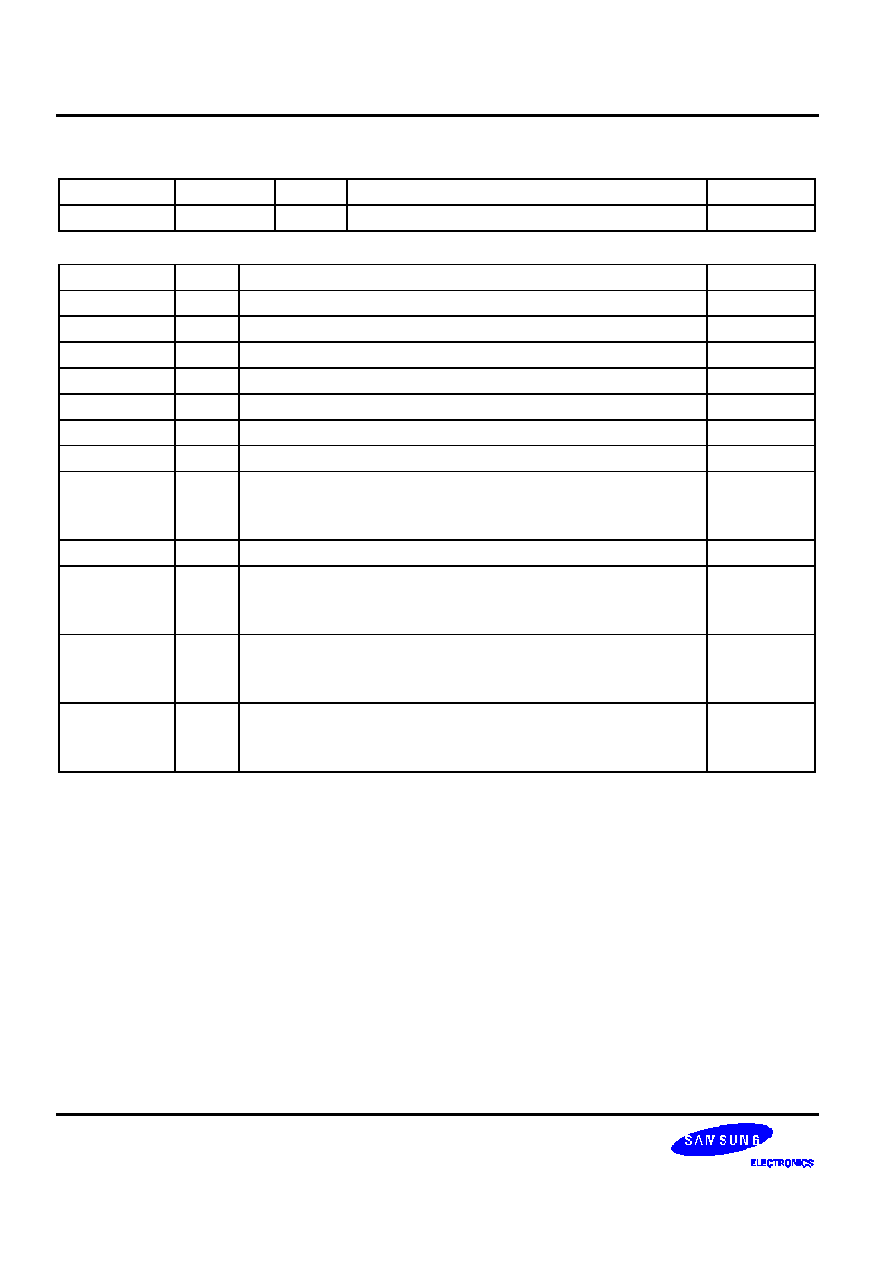
LCD CONTROLLER
S3C2440A RISC MICROPROCESSOR
15-40
TCON Control Register
Register
Address
R/W
Description
Reset Value
TCONSEL
0X4D000060
R/W
This register controls the LPC3600/LCC3600 modes.
0xF84
TCONSEL
Bit
Description
Initial state
LCC_TEST2
[11]
LCC3600 Test Mode 2 ( Read Only )
1
LCC_TEST1
[10]
LCC3600 Test Mode 1 ( Read Only )
1
LCC_SEL5
[9]
Select STV polarity
1
LCC_SEL4
[8]
Select CPV signal pin 0
1
LCC_SEL3
[7]
Select CPV signal pin 1
1
LCC_SEL2
[6]
Select Line/Dot inversion
0
LCC_SEL1
[5]
Select DG/Normal mode
0
LCC_EN
[4]
Determine LCC3600 Enable/Disable
0 = LCC3600 Disable
1 = LCC3600 Enable
0
CPV_SEL
[3]
Select CPV Pulse low width
0
MODE_SEL
[2]
Select DE/Sync mode
0 = Sync mode
1 = DE mode
1
RES_SEL
[1]
Select output resolution type
0 = 320 x 240
1 = 240 x 320
0
LPC_EN
[0]
Determine LPC3600 Enable/Disable
0 = LPC3600 Disable
1 = LPC3600 Enable
0
NOTE: Both LPC_EN and LCC_EN enable is not permitted. Only one TCON can be enabled at the same time.
S3C2440A RISC MICROPROCESSOR
LCD CONTROLLER
15-41
Register Setting Guide (STN)
The LCD controller supports multiple screen sizes by special register setting.
The CLKVAL value determines the frequency of VCLK. This value has to be determined such that the VCLK value is
greater than data transmission rate. The data transmission rate for the VD port of the LCD controller is used to
determine the value of CLKVAL register.
The data transmission rate is given by the following equation:
Data transmission rate = HS x VS x FR x MV
-- HS: Horizontal LCD size
-- VS: Vertical LCD size
-- FR: Frame rate
-- MV: Mode dependent value
Table 15-6. MV Value for Each Display Mode
Mode
MV Value
Mono, 4-bit single scan display
1/4
Mono, 8-bit single scan display or 4-bit dual scan display
1/8
4 level gray, 4-bit single scan display
1/4
4 level gray, 8-bit single scan display or 4-bit dual scan display
1/8
16 level gray, 4-bit single scan display
1/4
16 level gray, 8-bit single scan display or 4-bit dual scan display
1/8
Color, 4-bit single scan display
3/4
Color, 8-bit single scan display or 4-bit dual scan display
3/8
The LCDBASEU register value is the first address value of the frame buffer. The lowest 4 bits must be eliminated for
burst 4 word access. The LCDBASEL register value depends on LCD size and LCDBASEU. The LCDBASEL value is
given by the following equation:
-- LCDBASEL = LCDBASEU + LCDBASEL offset

LCD CONTROLLER
S3C2440A RISC MICROPROCESSOR
15-42
Example 1:
160 x 160, 4-level gray, 80 frame/sec, 4-bit single scan display, HCLK frequency is 60 MHz WLH = 1, WDLY = 1.
Data transmission rate = 160 x 160 x 80 x 1/4 = 512 kHz
CLKVAL = 58,
VCLK = 517KHz
HOZVAL = 39,
LINEVAL = 159
LINEBLANK =10
LCDBASEL = LCDBASEU + 3200
NOTE
The higher the system load is, the lower the CPU performance.
Example 2 (Virtual screen register):
4 -level gray, Virtual screen size = 1024 x 1024, LCD size = 320 x 240, LCDBASEU = 0x64, 4-bit dual scan.
1 halfword = 8 pixels (4-level gray),
Virtual screen 1 line = 128 halfword = 1024 pixels,
LCD 1 line = 320 pixels = 40 halfword,
OFFSIZE = 128 - 40 = 88 = 0x58,
PAGEWIDTH = 40 = 0x28
LCDBASEL = LCDBASEU + (PAGEWIDTH + OFFSIZE) x (LINEVAL +1) = 100 + (40 +88) x 120 = 0x3C64

S3C2440A RISC MICROPROCESSOR
LCD CONTROLLER
15-43
Gray Level Selection Guide
The S3C2440A LCD controller can generate 16 gray level using Frame Rate Control (FRC). The FRC characteristics
may cause unexpected patterns in gray level. These unwanted erroneous patterns may be shown in fast response
LCD or at lower frame rates.
Because the quality of LCD gray levels depends on LCD's own characteristics, the user has to select an appropriate
gray level after viewing all gray levels on user's own LCD.
Select the gray level quality through the following procedures:
1. Get the latest dithering pattern register value from SAMSUNG.
2. Display 16 gray bar in LCD.
3. Change the frame rate into an optimal value.
4. Change the VM alternating period to get the best quality.
5. As viewing 16 gray bars, select a good gray level, which is displayed well on your LCD.
6. Use only the good gray levels for quality.
LCD Refresh Bus Bandwidth Calculation Guide
The S3C2440A LCD controller can support various LCD display sizes. To select a suitable size (for the flicker free
LCD system application), the user have to consider the LCD refresh bus bandwidth determined by the LCD display
size, bit per pixel (bpp), frame rate, memory bus width, memory type, and so on.
LCD Data Rate (Byte/s) = bpp x (Horizontal display size) x (Vertical display size) x (Frame rate) /8
LCD DMA Burst Count (Times/s) = LCD Data Rate(Byte/s) /16(Byte) ; LCD DMA using 4words(16Byte) burst
Pdma means LCD DMA access period. In other words, the value of Pdma indicates the period of four-beat burst (4-
words burst) for video data fetch. So, Pdma depends on memory type and memory setting.
Eventually, LCD System Load is determined by LCD DMA Burst Count and Pdma.
-- LCD System Load = LCD DMA Burst Count x Pdma
Example 3:
640 x 480, 8bpp, 60 frame/sec, 16-bit data bus width, SDRAM (Trp=2HCLK / Trcd=2HCLK / CL=2HCLK) and HCLK
frequency is 60 MHz
LCD Data Rate = 8 x 640 x 480 x 60 / 8 = 18.432Mbyte/s
LCD DMA Burst Count = 18.432 / 16 = 1.152M/s
Pdma = (Trp+Trcd+CL+(2 x 4)+1) x (1/60MHz) = 0.250ms
LCD System Load = 1.152 x 250 = 0.288
System Bus Occupation Rate = (0.288/1) x 100 = 28.8%

LCD CONTROLLER
S3C2440A RISC MICROPROCESSOR
15-44
Register Setting Guide (TFT LCD)
The CLKVAL register value determines the frequency of VCLK and frame rate.
Frame Rate = 1/ [ { (VSPW+1) + (VBPD+1) + (LIINEVAL + 1) + (VFPD+1) } x {(HSPW+1) + (HBPD +1)
+ (HFPD+1) + (HOZVAL + 1) } x { 2 x ( CLKVAL+1 ) / ( HCLK ) } ]
For applications, the system timing must be considered to avoid under-run condition of the fifo of the lcd controller
caused by memory bandwidth contention.
Example 4:
TFT Resolution: 240 x 240,
VSPW =2, VBPD =14, LINEVAL = 239, VFPD =4
HSPW =25, HBPD =15, HOZVAL = 239, HFPD =1
CLKVAL = 5
HCLK = 60 M (hz)
The parameters below must be referenced by LCD size and driver specifications:
VSPW, VBPD, LINEVAL, VFPD, HSPW, HBPD, HOZVAL, and HFPD
If target frame rate is 60≠70Hz, then CLKVAL should be 5.
So, Frame Rate = 67Hz

S3C2440A RISC MICROPROCESSOR
ADC AND TOUCH SCREEN INTERFACE
16-1
16
ADC & TOUCH SCREEN INTERFACE
OVERVIEW
The 10-bit CMOS ADC (Analog to Digital Converter) is a recycling type device with 8-channel analog inputs. It
converts the analog input signal into 10-bit binary digital codes at a maximum conversion rate of 500KSPS with
2.5MHz A/D converter clock. A/D converter operates with on-chip sample-and-hold function and power down mode is
supported.
Touch Screen Interface can control/select pads (XP, XM, YP, YM) of the Touch Screen for X, Y position conversion.
Touch Screen Interface contains Touch Screen Pads control logic and ADC interface logic with an interrupt
generation logic.
FEATURES
-- Resolution: 10-bit
-- Differential Linearity Error:
±
1.0 LSB
-- Integral Linearity Error:
±
2.0 LSB
-- Maximum Conversion Rate: 500 KSPS
-- Low Power Consumption
-- Power Supply Voltage: 3.3V
-- Analog Input Range: 0 ~ 3.3V
-- On-chip sample-and-hold function
-- Normal Conversion Mode
-- Separate X/Y position conversion Mode
-- Auto(Sequential) X/Y Position Conversion Mode
-- Waiting for Interrupt Mode
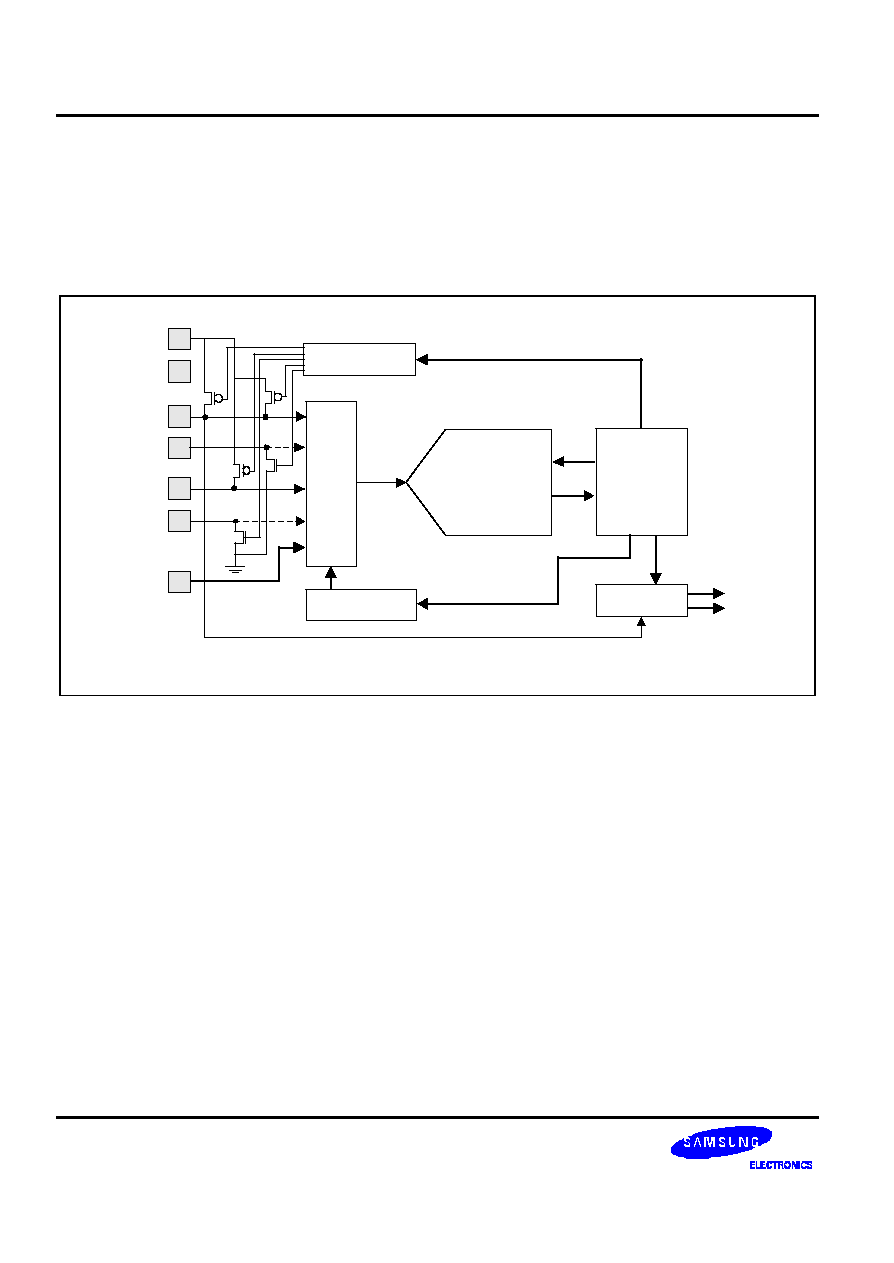
ADC AND TOUCH SCREEN INTERFACE
S3C2440A RISC MICROPROCESSOR
16-2
ADC & TOUCH SCREEN INTERFACE OPERATION
BLOCK DIAGRAM
Figure 16-1 shows the functional block diagram of A/D converter and Touch Screen Interface. Note that the A/D
converter device is a recycling type.
Pullup
Waiting for Interrupt Mode
INT_TC
INT_ADC
8:1
MUX
A/D Converter
ADC Input
Control
Interrupt
Generation
ADC
Interface
&Touch
Screen
AVDD
AGND
XP
XM
YP
YM
A[3:0]
(note)
(note)
Touch Screen
Figure 16-1. ADC and Touch Screen Interface Functional Block Diagram
NOTE: (symbol)
When Touch Screen device is used; XM or PM is only connected ground for Touch Screen I/F.
When Touch Screen device is not used, XM or PM is connecting Analog Input Signal for Normal ADC conversion.

S3C2440A RISC MICROPROCESSOR
ADC AND TOUCH SCREEN INTERFACE
16-3
FUNCTION DESCRIPTIONS
A/D Conversion Time
When the GCLK frequency is 50MHz and the prescaler value is 49, total 10-bit conversion time is as follows.
A/D converter freq. = 50MHz/(49+1) = 1MHz
Conversion time = 1/(1MHz / 5cycles) = 1/200KHz = 5 us
NOTE
This A/D converter was designed to operate at maximum 2.5MHz clock, so the conversion rate can go up to
500 KSPS.
Touch Screen Interface Mode
1. Normal Conversion Mode
Single Conversion Mode is the most likely used for General Purpose ADC Conversion. This mode can be
initialized by setting the ADCCON (ADC Control Register) and completed with a read and a write to the
ADCDAT0 (ADC Data Register 0).
2. Separate X/Y position conversion Mode
Touch Screen Controller can be operated by one of two Conversion Modes. Separate X/Y Position Conversion
Mode is operated as the following way. X-Position Mode writes X-Position Conversion Data to ADCDAT0, so
Touch Screen Interface generates the Interrupt source to Interrupt Controller. Y-Position Mode writes Y-Position
Conversion Data to ADCDAT1, so Touch Screen Interface generates the Interrupt source to Interrupt Controller.
3. Auto(Sequential) X/Y Position Conversion Mode
Auto (Sequential) X/Y Position Conversion Mode is operated as the following. Touch Screen Controller
sequentially converts X-Position and Y-Position that is touched. After Touch controller writes X-measurement
data to ADCDAT0 and writes Y-measurement data to ADCDAT1, Touch Screen Interface is generating Interrupt
source to Interrupt Controller in Auto Position Conversion Mode.
4. Waiting for Interrupt Mode
Touch Screen Controller generates interrupt (INT_TC) signal when the Stylus is down. Waiting for Interrupt Mode
setting value is rADCTSC=0xd3; // XP_PU, XP_Dis, XM_Dis, YP_Dis, YM_En.
After Touch Screen Controller generates interrupt signal (INT_TC), Waiting for interrupt Mode must be cleared.
(XY_PST sets to the No operation Mode)
Standby Mode
Standby mode is activated when ADCCON [2] is set to '1'. In this mode, A/D conversion operation is halted and
ADCDAT0, ADCDAT1 register contains the previous converted data.
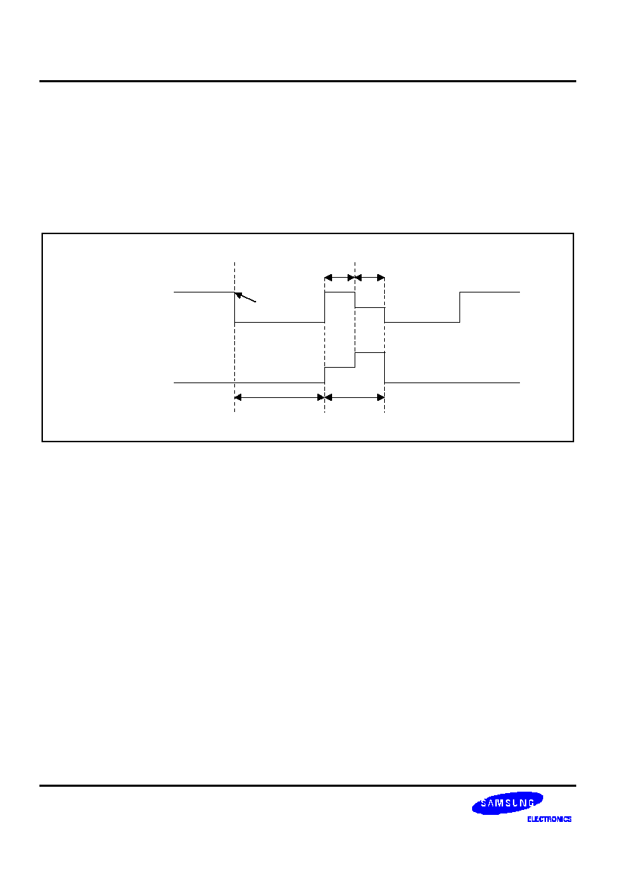
ADC AND TOUCH SCREEN INTERFACE
S3C2440A RISC MICROPROCESSOR
16-4
Programming Notes
1. The A/D converted data can be accessed by means of interrupt or polling method. With interrupt method
the overall conversion time - from A/D converter start to converted data read - may be delayed because of
the return time of interrupt service routine and data access time. With polling method, by checking the
ADCCON[15] - end of conversion flag-bit, the read time from ADCDAT register can be determined.
2. Another way for starting A/D conversion is provided. After ADCCON[1] - A/D conversion start-by-read
mode-is set to 1, A/D conversion starts simultaneously whenever converted data is read.
XP
X-Tal CLK is used
X-Conversion
YP
GCLK is used
Y-Conversion
Pen Touch
Figure 16-2. ADC and Touch Screen Operation signal
S3C2440A RISC MICROPROCESSOR
ADC AND TOUCH SCREEN INTERFACE
16-5
ADC AND TOUCH SCREEN INTERFACE SPECIAL REGISTERS
ADC CONTROL REGISTER (ADCCON)
Register
Address
R/W
Description
Reset Value
ADCCON
0x5800000
R/W
ADC control register
0x3FC4
ADCCON
Bit
Description
Initial State
ECFLG
[15]
End of conversion flag(Read only)
0 = A/D conversion in process
1 = End of A/D conversion
0
PRSCEN
[14]
A/D converter prescaler enable
0 = Disable
1 = Enable
0
PRSCVL
[13:6]
A/D converter prescaler value
Data value: 0 ~ 255
NOTE: ADC Freqeuncy should be set less than PCLK by
5times. (Ex. PCLK=10MHZ, ADC Freq.< 2MHz)
0xFF
SEL_MUX
[5:3]
Analog input channel select
000 = AIN 0
001 = AIN 1
010 = AIN 2
011 = AIN 3
100 = YM
101 = YP
110 = XM
111 = XP
0
STDBM
[2]
Standby mode select
0 = Normal operation mode
1 = Standby mode
1
READ_ START
[1]
A/D conversion start by read
0 = Disable start by read operation
1 = Enable start by read operation
0
ENABLE_START
[0]
A/D conversion starts by enable.
If READ_START is enabled, this value is not valid.
0 = No operation
1 = A/D conversion starts and this bit is cleared after the start-
up.
0
NOTE: When Touch Screen Pads(YM, YP, XM, XP) are disabled, these ports can be used as Analog input ports(AIN4,
AIN5, AIN6, AIN7) for ADC.
ADC AND TOUCH SCREEN INTERFACE
S3C2440A RISC MICROPROCESSOR
16-6
ADC TOUCH SCREEN CONTROL REGISTER (ADCTSC)
Register
Address
R/W
Description
Reset Value
ADCTSC
0x5800004
R/W
ADC Touch Screen Control Register
0x58
ADCTSC
Bit
Description
Initial State
UD_SEN
[8]
Detect Stylus Up or Down status.
0 = Detect Stylus Down Interrupt Signal.
1 = Detect Stylus Up Interrupt Signal.
0
YM_SEN
[7]
YM Switch Enable
0 = YM Output Driver Disable.
1 = YM Output Driver Enable.
0
YP_SEN
[6]
YP Switch Enable
0 = YP Output Driver Enable.
1 = YP Output Driver Disable.
1
XM_SEN
[5]
XM Switch Enable
0 = XM Output Driver Disable.
1 = XM Output Driver Enable.
0
XP_SEN
[4]
XP Switch Enable
0 = XP Output Driver Enable.
1 = XP Output Driver Disable.
1
PULL_UP
[3]
Pull-up Switch Enable
0 = XP Pull-up Enable.
1 = XP Pull-up Disable.
1
AUTO_PST
[2]
Automatically sequencing conversion of X-Position and Y-Position
0 = Normal ADC conversion.
1 = Auto Sequential measurement of X-position, Y-position.
0
XY_PST
[1:0]
Manually measurement of X-Position or Y-Position.
00 = No operation mode
01 = X-position measurement
10 = Y-position measurement
11 = Waiting for Interrupt Mode
0
NOTES:
1.
While waiting for Touch screen Interrupt, XP_SEN bit should be set to `1'(XP Output disable) and PULL_UP bit should
be set to `0'(XP Pull-up enable).
2.
AUTO_PST bit should be set `1' only in Automatic & Sequential X/Y Position conversion.
3.
XP, YP should be disconnected with GND source during sleep mode to avoid leakage current. Because XP, YP will be
maintained as 'H' states in sleep mode. Touch screen pin conditions in X/Y position conversion.
XP
XM
YP
YM
ADC ch. select
X Position
Vref
GND
Hi-Z
Hi-Z
YP
Y Position
Hi-Z
Hi-Z
Vref
GND
XP

S3C2440A RISC MICROPROCESSOR
ADC AND TOUCH SCREEN INTERFACE
16-7
ADC START DELAY REGISTER (ADCDLY)
Register
Address
R/W
Description
Reset Value
ADCDLY
0x5800008
R/W
ADC Start or interval delay register
0x00ff
ADCDLY
Bit
Description
Initial State
DELAY
[15:0]
1) Normal Conversion Mode, XY position mode, auto position
mode.
ADC conversion start delay value.
2) Waiting for Interrupt Mode.
When stylus down occurs at SLEEP MODE, generates Wake-Up
signal, having interval (several ms), for exiting SLEEP MODE.
Note: Don't use Zero value (0x0000)
00ff
NOTE: Before ADC conversion, Touch screen uses X-tal clock (3.68MHz). During ADC conversion GCLK ( Max. 50MHz) is
used.

ADC AND TOUCH SCREEN INTERFACE
S3C2440A RISC MICROPROCESSOR
16-8
ADC CONVERSION DATA REGISTER (ADCDAT0)
Register
Address
R/W
Description
Reset Value
ADCDAT0
0x580000C
R
ADC conversion data register
≠
ADCDAT0
Bit
Description
Initial State
UPDOWN
[15]
Up or Down state of stylus at waiting for interrupt mode.
0 = Stylus down state.
1 = Stylus up state.
≠
AUTO_PST
[14]
Automatic sequencing conversion of X-position and
Y-Position
0 = Normal ADC conversion.
1 = Sequencing measurement of X-position, Y-position.
≠
XY_PST
[13:12]
Manually measurement of X-position or Y-position.
00 = No operation mode
01 = X-position measurement
10 = Y-position measurement
11 = Waiting for Interrupt Mode
≠
Reserved
[11:10]
Reserved
≠
XPDATA
(Normal ADC)
[9:0]
X-Position conversion data value (include normal ADC conversion
data value)
Data value: 0 ~ 3FF
≠
S3C2440A RISC MICROPROCESSOR
ADC AND TOUCH SCREEN INTERFACE
16-9
ADC CONVERSION DATA REGISTER (ADCDAT1)
Register
Address
R/W
Description
Reset Value
ADCDAT1
0x5800010
R
ADC conversion data register
≠
ADCDAT1
Bit
Description
Initial State
UPDOWN
[15]
Up or down state of stylus at waiting for interrupt mode.
0 = Stylus down state.
1 = Stylus up state.
≠
AUTO_PST
[14]
Automatically sequencing conversion of X-position and Y-position
0 = Normal ADC conversion.
1 = Sequencing measurement of X-position, Y-position.
≠
XY_PST
[13:12]
Manually measurement of X-position or Y-position.
00 = No operation mode
01 = X-position measurement
10 = Y-position measurement
11 = Waiting for interrupt mode
≠
Reserved
[11:10]
Reserved
≠
YPDATA
[9:0]
Y-position conversion data value
Data value: 0 ~ 3FF
≠
ADC TOUCH SCREEN UP-DOWN INT CHECK REGISTER (ADCUPDN)
Register
Address
R/W
Description
Reset Value
ADCUPDN
0x5800014
R/W
Stylus up or down interrupt status register
0x0
ADCUPDN
Bit
Description
Initial State
TSC_UP
[1]
Stylus Up Interrupt.
0 = No stylus up status.
1 = Stylus up interrupt occurred.
0
TSC_DN
[0]
Stylus Down Interrupt.
0 = No stylus down status.
1 = Stylus down interrupt occurred.
0

ADC AND TOUCH SCREEN INTERFACE
S3C2440A RISC MICROPROCESSOR
16-10
NOTES

S3C2440A RISC MICROPROCESSOR
REAL TIME CLOCK
17-1
17
REAL TIME CLOCK
OVERVIEW
The Real Time Clock (RTC) unit can be operated by the backup battery while the system power is off. The RTC can
transmit 8-bit data to CPU as Binary Coded Decimal (BCD) values using the STRB/LDRB ARM operation. The data
include the time by second, minute, hour, date, day, month, and year. The RTC unit works with an external
32.768kHz crystal and also can perform the alarm function.
FEATURES
-- BCD number: second, minute, hour, date, day, month, and year
-- Leap year generator
-- Alarm function: alarm interrupt or wake-up from power-off mode
-- Year 2000 problem is removed.
-- Independent power pin (RTCVDD)
-- Supports millisecond tick time interrupt for RTOS kernel time tick.
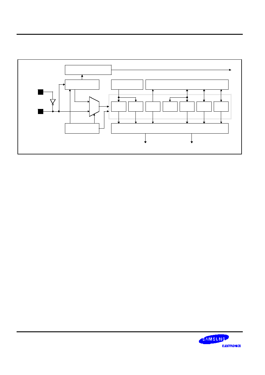
REAL TIME CLOCK
S3C2440A RISC MICROPROCESSOR
17-2
REAL TIME CLOCK OPERATION
2
15
Clock Divider
XTOrtc
XTIrtc
Control Register
SEC
MIN
HOUR
DAY
DATE
MON
YEAR
Leap Year Generator
Alarm Generator
Reset Register
1 Hz
INT_RTC
RTCCON
RTCALM
RTCRST
Time Tick Generator
TIME TICK
TICNT
128 Hz
PMWKUP
Figure 17-1. Real Time Clock Block Diagram
LEAP YEAR GENERATOR
The Leap Year Generator can determine the last date of each month out of 28, 29, 30, or 31, based on data from
BCDDATE, BCDMON, and BCDYEAR. This block considers leap year in deciding on the last date. An 8-bit counter
can only represent 2 BCD digits, so it cannot decide whether "00" year (the year with its last two digits zeros) is a
leap year or not. For example, it cannot discriminate between 1900 and 2000. To solve this problem, the RTC block
in S3C2440A has hard-wired logic to support the leap year in 2000. Note 1900 is not leap year while 2000 is leap
year. Therefore, two digits of 00 in S3C2440A denote 2000, not 1900.
READ/WRITE REGISTERS
Bit 0 of the RTCCON register must be set high in order to write the BCD register in RTC block. To display the
second, minute, hour, date, month, and year, the CPU should read the data in BCDSEC, BCDMIN, BCDHOUR,
BCDDAY, BCDDATE, BCDMON, and BCDYEAR registers, respectively, in the RTC block. However, a one second
deviation may exist because multiple registers are read. For example, when the user reads the registers from
BCDYEAR to BCDMIN, the result is assumed to be 2059 (Year), 12 (Month), 31 (Date), 23 (Hour) and 59 (Minute).
When the user read the BCDSEC register and the value ranges from 1 to 59 (Second), there is no problem, but, if the
value is 0 sec., the year, month, date, hour, and minute may be changed to 2060 (Year), 1 (Month), 1 (Date), 0
(Hour) and 0 (Minute) because of the one second deviation that was mentioned. In this case, the user should re-read
from BCDYEAR to BCDSEC if BCDSEC is zero.
BACKUP BATTERY OPERATION
The RTC logic can be driven by the backup battery, which supplies the power through the RTCVDD pin into the RTC
block, even if the system power is off. When the system is off, the interfaces of the CPU and RTC logic should be
blocked, and the backup battery only drives the oscillation circuit and the BCD counters to minimize power
dissipation.
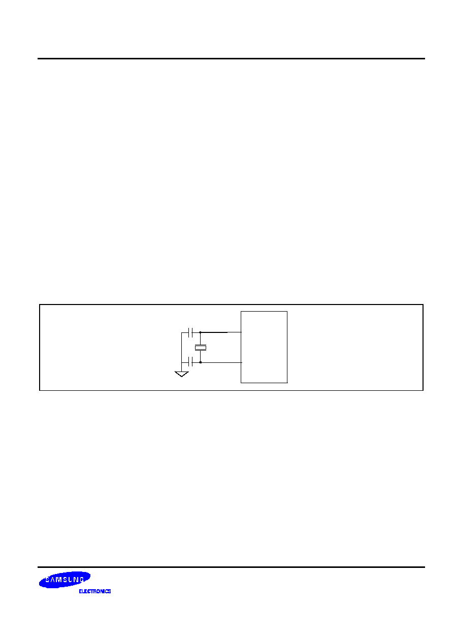
S3C2440A RISC MICROPROCESSOR
REAL TIME CLOCK
17-3
ALARM FUNCTION
The RTC generates an alarm signal at a specified time in the power-off mode or normal operation mode. In normal
operation mode, the alarm interrupt (INT_RTC) is activated. In the power-off mode, the power management wakeup
(PMWKUP) signal is activated as well as the INT_RTC. The RTC alarm register (RTCALM) determines the alarm
enable/disable status and the condition of the alarm time setting.
TICK TIME INTERRUPT
The RTC tick time is used for interrupt request. The TICNT register has an interrupt enable bit and the count value for
the interrupt. The count value reaches '0' when the tick time interrupt occurs. Then the period of interrupt is as
follows:
--
Period = ( n+1 ) / 128 second
-- n: Tick time count value (1~127)
This RTC time tick may be used for real time operating system (RTOS) kernel time tick. If time tick is generated by
the RTC time tick, the time related function of RTOS will always synchronized in real time.
32.768KHZ X-TAL CONNECTION EXAMPLE
The Figure 17-2 shows a circuit of the RTC unit oscillation at 32.768Khz.
XTIrtc
XTOrtc
32768Hz
15~ 22pF
Figure 17-2. Main Oscillator Circuit Example
REAL TIME CLOCK
S3C2440A RISC MICROPROCESSOR
17-4
REAL TIME CLOCK SPECIAL REGISTERS
REAL TIME CLOCK CONTROL (RTCCON) REGISTER
The RTCCON register consists of 4 bits such as the RTCEN, which controls the read/write enable of the BCD
registers, CLKSEL, CNTSEL, and CLKRST for testing.
RTCEN bit can control all interfaces between the CPU and the RTC, so it should be set to 1 in an RTC control
routine to enable data read/write after a system reset. Also before power off, the RTCEN bit should be cleared to 0 to
prevent inadvertent writing into RTC registers.
Register
Address
R/W
Description
Reset Value
RTCCON
0x57000040(L)
0x57000043(B)
R/W
(by byte)
RTC control register
0x0
RTCCON
Bit
Description
Initial State
CLKRST
[3]
RTC clock count reset.
0 = No reset, 1 = Reset
0
CNTSEL
[2]
BCD count select.
0 = Merge BCD counters
1 = Reserved (Separate BCD counters)
0
CLKSEL
[1]
BCD clock select.
0 = XTAL 1/215 divided clock
1 = Reserved (XTAL clock only for test)
0
RTCEN
[0]
RTC control enable.
0 = Disable 1 = Enable
Note: Only BCD time count and read operation can be performed.
0
NOTES:
1.
All RTC registers have to be accessed for each byte unit using STRB and LDRB instructions or char type pointer.
2.
(L): Little endian.
(B): Big endian.
TICK TIME COUNT (TICNT) REGISTER
Register
Address
R/W
Description
Reset Value
TICNT
0x57000044(L)
0x57000047(B)
R/W
(by byte)
Tick time count register
0x0
TICNT
Bit
Description
Initial State
TICK INT Enable
[7]
Tick time interrupt enable.
0 = Disable 1 = Enable
0
TICK Time Count
[6:0]
Tick time count value (1~127).
This counter value decreases internally, and users cannot read this
counter value in working.
000000
S3C2440A RISC MICROPROCESSOR
REAL TIME CLOCK
17-5
RTC ALARM CONTROL (RTCALM) REGISTER
The RTCALM register determines the alarm enable and the alarm time. Please note that the RTCALM register
generates the alarm signal through both INT_RTC and PMWKUP in power down mode, but only through INT_RTC in
the normal operation mode.
Register
Address
R/W
Description
Reset Value
RTCALM
0x57000050(L)
0x57000053(B)
R/W
(by byte)
RTC alarm control register
0x0
RTCALM
Bit
Description
Initial State
Reserved
[7]
≠
0
ALMEN
[6]
Alarm global enable.
0 = Disable, 1 = Enable
0
YEAREN
[5]
Year alarm enable.
0 = Disable, 1 = Enable
0
MONREN
[4]
Month alarm enable.
0 = Disable, 1 = Enable
0
DATEEN
[3]
Date alarm enable.
0 = Disable, 1 = Enable
0
HOUREN
[2]
Hour alarm enable.
0 = Disable, 1 = Enable
0
MINEN
[1]
Minute alarm enable.
0 = Disable, 1 = Enable
0
SECEN
[0]
Second alarm enable.
0 = Disable, 1 = Enable
0
REAL TIME CLOCK
S3C2440A RISC MICROPROCESSOR
17-6
ALARM SECOND DATA (ALMSEC) REGISTER
Register
Address
R/W
Description
Reset Value
ALMSEC
0x57000054(L)
0x57000057(B)
R/W
(by byte)
Alarm second data register
0x0
ALMSEC
Bit
Description
Initial State
Reserved
[7]
≠
0
SECDATA
[6:4]
BCD value for alarm second.
0 ~ 5
000
[3:0]
0 ~ 9
0000
ALARM MIN DATA (ALMMIN) REGISTER
Register
Address
R/W
Description
Reset Value
ALMMIN
0x57000058(L)
0x5700005B(B)
R/W
(by byte)
Alarm minute data register
0x00
ALMMIN
Bit
Description
Initial State
Reserved
[7]
≠
0
MINDATA
[6:4]
BCD value for alarm minute.
0 ~ 5
000
[3:0]
0 ~ 9
0000
ALARM HOUR DATA (ALMHOUR) REGISTER
Register
Address
R/W
Description
Reset Value
ALMHOUR
0x5700005C(L)
0x5700005F(B)
R/W
(by byte)
Alarm hour data register
0x0
ALMHOUR
Bit
Description
Initial State
Reserved
[7:6]
≠
00
HOURDATA
[5:4]
BCD value for alarm hour.
0 ~ 2
00
[3:0]
0 ~ 9
0000
S3C2440A RISC MICROPROCESSOR
REAL TIME CLOCK
17-7
ALARM DATE DATA (ALMDATE) REGISTER
Register
Address
R/W
Description
Reset Value
ALMDATE
0x57000060(L)
0x57000063(B)
R/W
(by byte)
Alarm date data register
0x01
ALMDATE
Bit
Description
Initial State
Reserved
[7:6]
≠
00
DATEDATA
[5:4]
BCD value for alarm date, from 0 to 28, 29, 30, 31.
0 ~ 3
00
[3:0]
0 ~ 9
0001
ALARM MON DATA (ALMMON) REGISTER
Register
Address
R/W
Description
Reset Value
ALMMON
0x57000064(L)
0x57000067(B)
R/W
(by byte)
Alarm month data register
0x01
ALMMON
Bit
Description
Initial State
Reserved
[7:5]
≠
00
MONDATA
[4]
BCD value for alarm month.
0 ~ 1
0
[3:0]
0 ~ 9
0001
ALARM YEAR DATA (ALMYEAR) REGISTER
Register
Address
R/W
Description
Reset Value
ALMYEAR
0x57000068(L)
0x5700006B(B)
R/W
(by byte)
Alarm year data register
0x0
ALMYEAR
Bit
Description
Initial State
YEARDATA
[7:0]
BCD value for year.
00 ~ 99
0x0
REAL TIME CLOCK
S3C2440A RISC MICROPROCESSOR
17-8
BCD SECOND (BCDSEC) REGISTER
Register
Address
R/W
Description
Reset Value
BCDSEC
0x57000070(L)
0x57000073(B)
R/W
(by byte)
BCD second register
Undefined
BCDSEC
Bit
Description
Initial State
SECDATA
[6:4]
BCD value for second.
0 ~ 5
≠
[3:0]
0 ~ 9
≠
BCD MINUTE (BCDMIN) REGISTER
Register
Address
R/W
Description
Reset Value
BCDMIN
0x57000074(L)
0x57000077(B)
R/W
(by byte)
BCD minute register
Undefined
BCDMIN
Bit
Description
Initial State
MINDATA
[6:4]
BCD value for minute.
0 ~ 5
≠
[3:0]
0 ~ 9
≠
BCD HOUR (BCDHOUR) REGISTER
Register
Address
R/W
Description
Reset Value
BCDHOUR
0x57000078(L)
0x5700007B(B)
R/W
(by byte)
BCD hour register
Undefined
BCDHOUR
Bit
Description
Initial State
Reserved
[7:6]
≠
≠
HOURDATA
[5:4]
BCD value for hour.
0 ~ 2
≠
[3:0]
0 ~ 9
≠
S3C2440A RISC MICROPROCESSOR
REAL TIME CLOCK
17-9
BCD DATE (BCDDATE) REGISTER
Register
Address
R/W
Description
Reset Value
BCDDATE
0x5700007C(L)
0x5700007F(B)
R/W
(by byte)
BCD date register
Undefined
BCDDATE
Bit
Description
Initial State
Reserved
[7:6]
≠
≠
DATEDATA
[5:4]
BCD value for date.
0 ~ 3
≠
[3:0]
0 ~ 9
≠
BCD DAY (BCDDAY) REGISTER
Register
Address
R/W
Description
Reset Value
BCDDAY
0x57000080(L)
0x57000083(B)
R/W
(by byte)
BCD a day of the week register
Undefined
BCDDAY
Bit
Description
Initial State
Reserved
[7:3]
≠
≠
DAYDATA
[2:0]
BCD value for a day of the week.
1 ~ 7
≠
BCD MONTH (BCDMON) REGISTER
Register
Address
R/W
Description
Reset Value
BCDMON
0x57000084(L)
0x57000087(B)
R/W
(by byte)
BCD month register
Undefined
BCDMON
Bit
Description
Initial State
Reserved
[7:5]
≠
≠
MONDATA
[4]
BCD value for month.
0 ~ 1
≠
[3:0]
0 ~ 9
≠

REAL TIME CLOCK
S3C2440A RISC MICROPROCESSOR
17-10
BCD YEAR (BCDYEAR) REGISTER
Register
Address
R/W
Description
Reset Value
BCDYEAR
0x57000088(L)
0x5700008B(B)
R/W
(by byte)
BCD year register
Undefined
BCDYEAR
Bit
Description
Initial State
YEARDATA
[7:0]
BCD value for year.
00 ~ 99
≠

S3C2440A RISC MICROPROCESSOR
WATCHDOG TIMER
18-1
18
WATCHDOG TIMER
OVERVIEW
The S3C2440A watchdog timer is used to resume the controller operation whenever it is disturbed by malfunctions
such as noise and system errors. It can be used as a normal 16-bit interval timer to request interrupt service. The
watchdog timer generates the reset signal for 128 PCLK cycles.
FEATURES
-- Normal interval timer mode with interrupt request
-- Internal reset signal is activated for 128 PCLK cycles when the timer count value reaches 0 (time-out).
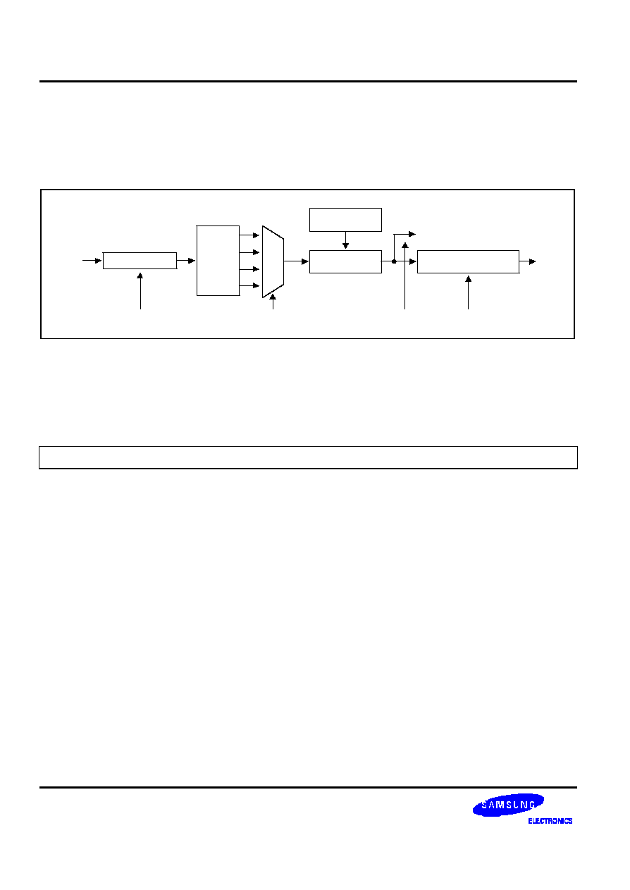
WATCHDOG TIMER
S3C2440A RISC MICROPROCESSOR
18-2
WATCHDOG TIMER OPERATION
Figure 18-1 shows the functional block diagram of the watchdog timer. The watchdog timer uses only PCLK as its
source clock. The PCLK frequency is prescaled to generate the corresponding watchdog timer clock, and the
resulting frequency is divided again.
Reset Signal Generator
WTCNT
(Down Counter)
PCLK
WTCON[4:3]
WTDAT
RESET
1/16
1/32
1/64
1/128
8-bit Prescaler
WTCON[15:8]
WTCON[2]
WTCON[0]
Interrupt
MUX
Figure 18-1. Watchdog Timer Block Diagram
The prescaler value and the frequency division factor are specified in the watchdog timer control (WTCON) register.
Valid prescaler values range from 0 to 2
8
-1. The frequency division factor can be selected as 16, 32, 64, or 128.
Use the following equation to calculate the watchdog timer clock frequency and the duration of each timer clock
cycle:
t_watchdog = 1/[ PCLK / (Prescaler value + 1) / Division_factor ]
WTDAT & WTCNT
Once the watchdog timer is enabled, the value of watchdog timer data (WTDAT) register cannot be automatically
reloaded into the timer counter (WTCNT). In this reason, an initial value must be written to the watchdog timer count
(WTCNT) register, before the watchdog timer starts.
CONSIDERATION OF DEBUGGING ENVIRONMENT
When the S3C2440A is in debug mode using Embedded ICE, the watchdog timer must not operate.
The watchdog timer can determine whether or not it is currently in the debug mode from the CPU core signal
(DBGACK signal). Once the DBGACK signal is asserted, the reset output of the watchdog timer is not activated as
the watchdog timer is expired.
S3C2440A RISC MICROPROCESSOR
WATCHDOG TIMER
18-3
WATCHDOG TIMER SPECIAL REGISTERS
WATCHDOG TIMER CONTROL (WTCON) REGISTER
The WTCON register allows the user to enable/disable the watchdog timer, select the clock signal from 4 different
sources, enable/disable interrupts, and enable/disable the watchdog timer output. The Watchdog timer is used to
resume the S3C2440A restart on mal-function after its power on; if controller restart is not desired, the Watchdog
timer should be disabled.
If the user wants to use the normal timer provided by the Watchdog timer, enable the interrupt and disable the
Watchdog timer.
Register
Address
R/W
Description
Reset Value
WTCON
0x53000000
R/W
Watchdog timer control register
0x8021
WTCON
Bit
Description
Initial State
Prescaler value
[15:8]
Prescaler value.
The valid range is from 0 to 255(2
8
-1).
0x80
Reserved
[7:6]
Reserved.
These two bits must be 00 in normal operation.
00
Watchdog timer
[5]
Enable or disable bit of Watchdog timer.
0 = Disable
1 = Enable
1
Clock select
[4:3]
Determine the clock division factor.
00: 16
01: 32
10: 64
11: 128
00
Interrupt generation
[2]
Enable or disable bit of the interrupt.
0 = Disable
1 = Enable
0
Reserved
[1]
Reserved.
This bit must be 0 in normal operation.
0
Reset enable/disable
[0]
Enable or disable bit of Watchdog timer output for reset
signal.
1: Assert reset signal of the S3C2440A at watchdog time-out
0: Disable the reset function of the watchdog timer.
1
WATCHDOG TIMER
S3C2440A RISC MICROPROCESSOR
18-4
WATCHDOG TIMER DATA (WTDAT) REGISTER
The WTDAT register is used to specify the time-out duration. The content of WTDAT cannot be automatically loaded
into the timer counter at initial watchdog timer operation. However, using 0x8000 (initial value) will drive the first time-
out. In this case, the value of WTDAT will be automatically reloaded into WTCNT.
Register
Address
R/W
Description
Reset Value
WTDAT
0x53000004
R/W
Watchdog timer data register
0x8000
WTDAT
Bit
Description
Initial State
Count reload value
[15:0]
Watchdog timer count value for reload.
0x8000
WATCHDOG TIMER COUNT (WTCNT) REGISTER
The WTCNT register contains the current count values for the watchdog timer during normal operation. Note that the
content of the WTDAT register cannot be automatically loaded into the timer count register when the watchdog timer
is enabled initially, so the WTCNT register must be set to an initial value before enabling it.
Register
Address
R/W
Description
Reset Value
WTCNT
0x53000008
R/W
Watchdog timer count register
0x8000
WTCNT
Bit
Description
Initial State
Count value
[15:0]
The current count value of the watchdog timer
0x8000
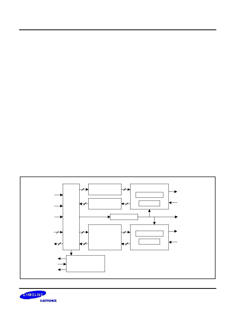
S3C2440A RISC MICROPROCESSOR
MMC/SD/SDIO CONTROLLER
19-1
19
MMC/SD/SDIO CONTROLLER
FEATURES
-- SD Memory Card Spec (ver 1.0) / MMC Spec(2.11) compatible
-- SDIO Card Spec (Ver 1.0) compatible
-- 16 words (64 bytes) FIFO for data Tx/Rx
-- 40-bit Command Register
-- 136-bit Response Register
-- 8-bit Prescaler logic (Freq = System Clock/(P + 1))
-- Normal, and DMA data transfer mode(byte, halfword, word transfer)
-- DMA burst4 access support(only word transfer)
-- 1-bit/4-bit (wide bus) mode & block/stream mode switch support
BLOCK DIAGRAM
CMD Reg
(5byte)
Resp Reg
(17byte)
CMD Control
8bit Shift Reg
CRC7
Prescaler
FIFO
(64byte)
DAT Control
8bit Shift Reg
CRC16*4
DMA
INT
APB
I/F
8
8
8
8
32
32
32
32
32
32
PADDR
PSEL
PCLK
PWDATA
[31:0]
PRDATA
[31:0]
DREQ
DACK
INT
TxCMD
RxCMD
SDCLK
TxDAT[3:0]
RxDAT[3:0]
Figure 19-1. SD Interface block diagram

MMC/SD/SDIO CONTROLLER
S3C2440A RISC MICROPROCESSOR
19-2
SD OPERATION
A serial clock line synchronizes shifting and sampling of the information on the five data lines. The transmission
frequency is controlled by making the appropriate bit settings to the SDIPRE register. You can modify its frequency
to adjust the baud rate data register value.
Programming Procedure (common)
To program the SDI modules, follow these basic steps:
1. Set SDICON to configure properly with clock & interrupt enable
2. Set SDIPRE to configure with a proper value.
3. Wait 74 SDCLK clock cycle in order to initialize the card.
CMD Path Programming
1. Write command argument 32bit to SDICmdArg.
2. Determine command types and start command transmit with setting SDICmdCon.
3. Confirm the end of SDI CMD path operation when the specific flag of SDICmdSta is set
4. The flag is CmdSent if command type is no response.
5. The flag is RspFin if command type is with response.
6. Clear the flags of SDICmdSta by writing '1' to the corresponding bit.
DAT Path Programming
1. Write data timeout period to SDIDTimer.
2. Write block size (block length) to SDIBSize(normally 0x80 word).
3. Determine the mode of block, wide bus, dma, etc and start data transfer with setting SDIDatCon.
4. Tx data
Write data to Data Register (SDIDAT) while Tx FIFO is available (TFDET is set), or half (TFHalf
is set), or empty(TFEmpty is set).
5. Rx data
Read data from Data Register (SDIDAT) while Rx FIFO is available (RFDET is set), or full
(RFFull is set), or half (RFHalf is set), or ready for last data(RFLast is set).
6. Confirm the end of SDI DAT path operation when DatFin flag of SDIDatSta is set
7. Clear the flags of SDIDatSta by writing '1' to the corresponding bit.

S3C2440A RISC MICROPROCESSOR
MMC/SD/SDIO CONTROLLER
19-3
SDIO OPERATION
There are two functions of SDIO operation: SDIO Interrupt receiving and Read Wait Request generation. These two
functions can operate when RcvIOInt bit and RwaitEn bit of SDICON register is activated respectively. And two
functions have the steps and conditions like below.
SDIO Interrupt
In SD 1-bit mode, Interrupt is received through all range from RxDAT[1] pin.
In SD 4-bit mode, RxDAT[1] pin is shared between data receiving and interrupt receiving.
When interrupt detection range(Interrupt Period) is:
1. Single Block: The time between A and B
≠ A: 2clocks after the completion of a data packet
≠ B: The completion of sending the end bit of the next withdata command
2. Multi Block, PrdType = 0: The time between A and B, restart at C
≠ A: 2clocks after the completion of a data packet
≠ B: 2clocks after A
≠ C: 2clocks after the end bit of the abort command response
3. Multi Block, PrdType = 1: The time between A and B, restart at A
≠ A: 2clocks after the completion of a data packet
≠ B: 2clocks after A
≠ In case of last block, interrupt period begins at A, but not ends at B (CMD53 case)
Read Wait Request
Regardless of 1bit or 4-bit mode, Read Wait Request signal transmits to TxDAT[2] pin in condition of below.
-- In read multiple operation, request signal transmission begins at 2clocks after the end of the data block
-- Transmission ends when user sets to one RwaitReq bit of SDIDatSta register
MMC/SD/SDIO CONTROLLER
S3C2440A RISC MICROPROCESSOR
19-4
SDI SPECIAL REGISTERS
SDI Control Register (SDICON)
Register
Address
R/W
Description
Reset Value
SDICON
0x5A000000
R/W
SDI control register
0x0
SDICON
Bit
Description
Initial Value
Reserved
[31:9]
≠
SDMMC Reset
(SDreset)
[8]
Reset whole sdmmc block. This bit is automatically cleared.
0 = Normal mode, 1 = SDMMC reset
0
Reserved
[7:6]
0
Clock Type (CTYP)
[5]
Determines which clock type is used as SDCLK.
0 = SD type, 1 = MMC type
0
Byte Order
Type(ByteOrder)
[4]
Determines byte order type when you read(write) data from(to)
sd host FIFO with word boundary.
0 = Type A, 1 = Type B
0
Receive SDIO
Interrupt from card
(RcvIOInt)
[3]
Determines whether sd host receives SDIO Interrupt from the
card or not(for SDIO).
0 = Ignore, 1 = Receive SDIO Interrupt
0
Read Wait
Enable(RWaitEn)
[2]
Determines read wait request signal generate when sd host
waits the next block in multiple block read mode. This bit needs
to delay the next block to be transmitted from the card(for
SDIO).
0 = Disable(no generate), 1 = Read wait enable(use SDIO)
0
Reserved
[1]
Clock Out Enable
(ENCLK)
[0]
Determines whether SDCLK Out enable or not
0 = Disable (prescaler off), 1 = Clock enable
0
NOTE: Byte Order Type
Type A: (Access by Word) D[7:0]
D[15:8]
D[23:16]
D[31:24]
(Access by Halfword) D[7:0]
D[15:8]
Type B: (Access by Word) D[31:24]
D[23:16]
D[15:8]
D[7:0]
(Access by Halfword) D[15:8]
D[7:0]
SDI Baud Rate Prescaler Register (SDIPRE)
Register
Address
R/W
Description
Reset Value
SDIPRE
0x5A000004
R/W
SDI buad rate prescaler register
0x01
SDIPRE
Bit
Description
Initial Value
Prescaler Value
[7:0]
Determines SDI clock(SDCLK) rate as above equation.
Baud rate = PCLK / (Prescaler value + 1)
0x01
NOTE: Prescaler Value should be greater than zero.
S3C2440A RISC MICROPROCESSOR
MMC/SD/SDIO CONTROLLER
19-5
SDI Command Argument Register (SDICmdArg)
Register
Address
R/W
Description
Reset Value
SDICmdArg
0x5A000008
R/W
SDI command argument register
0x0
SDICmdArg
Bit
Description
Initial Value
CmdArg
[31:0]
Command argument
0x00000000
SDI Command Control Register (SDICmdCon)
Register
Address
R/W
Description
Reset Value
SDICmdCon
0x5A00000C
R/W
SDI command control register
0x0
SDICommand
Bit
Description
Initial Value
Reserved
[31:13]
≠
Abort Command
(AbortCmd)
[12]
Determines whether command type is for abort (for SDIO).
0 = Normal command, 1 = Abort command (CMD12, CMD52)
0
Command with
Data (WithData)
[11]
Determines whether command type is with data(for SDIO).
0 = Without data, 1 = With data
0
LongRsp
[10]
Determines whether host receives a 136-bit long response or not
0 = Short response, 1 = Long response
0
WaitRsp
[9]
Determines whether host waits for a response or not
0 = No response, 1 = Wait response
0
Command
Start(CMST)
[8]
Determines whether command operation starts or not. . This bit is
automatically cleared.
0 = Command ready, 1 = Command start
0
CmdIndex
[7:0]
Command index with start 2-bit (8-bit)
0x00
MMC/SD/SDIO CONTROLLER
S3C2440A RISC MICROPROCESSOR
19-6
SDI Command Status Register (SDICmdSta)
Register
Address
R/W
Description
Reset Value
SDICmdSta
0x5A000010
R/(C)
SDI command status register
0x0
SDICmdSta
Bit
Description
Initial Value
Reserved
[31:13]
≠
≠
Response CRC
Fail(RspCrc)
[12]
R/C
CRC check failed when command response received. This flag is
cleared by setting to one this bit.
0 = Not detect, 1 = CRC fail
0
Command Sent
(CmdSent)
[11]
R/C
Command sent(not concerned with response). This flag is
cleared by setting to one this bit.
0 = Not detect, 1 = Command end
0
Command Time Out
(CmdTout)
[10]
R/C
Command response timeout (64CLK). This flag is cleared by
setting to one this bit.
0 = Not detect, 1 = Timeout
0
Response Receive
End (RspFin)
[9]
R/C
Command response received. This flag is cleared by setting to
one this bit.
0 = Not detect, 1 = Response end
0
CMD line progress
On (CmdOn)
[8]
Command transfer in progress
0 = Not detect, 1 = In progress
0
RspIndex
[7:0]
Response index 6-bit with start 2-bit (8-bit)
0x00
SDI Response Register 0 (SDIRSP0)
Register
Address
R/W
Description
Reset Value
SDIRSP0
0x5A000014
R
SDI response register 0
0x0
SDIRSP0
Bit
Description
Initial Value
Response0
[31:0]
Card status[31:0](short), card status[127:96](long)
0x00000000
SDI Response Register 1 (SDIRSP1)
Register
Address
R/W
Description
Reset Value
SDIRSP1
0x5A000018
R
SDI response register 1
0x0
SDIRSP1
Bit
Description
Initial Value
RCRC7
[31:24]
CRC7(with end bit, short), card status[95:88](long)
0x00
Response1
[23:0]
unused(short), card status[87:64](long)
0x000000

S3C2440A RISC MICROPROCESSOR
MMC/SD/SDIO CONTROLLER
19-7
MMC/SD/SDIO CONTROLLER
S3C2440A RISC MICROPROCESSOR
19-8
SDI Response Register 2 (SDIRSP2)
Register
Address
R/W
Description
Reset Value
SDIRSP2
0x5A00001C
R
SDI Response Register 2
0x0
SDIRSP2
Bit
Description
Initial Value
Response2
[31:0]
unused(short), card status[63:32](long)
0x00000000
SDI Response Register 3 (SDIRSP3)
Register
Address
R/W
Description
Reset Value
SDIRSP3
0x5A000020
R
SDI response register 3
0x0
SDIRSP3
Bit
Description
Initial Value
Response3
[31:0]
unused(short), card status[31:0](long)
0x00000000
SDI Data / Busy Timer Register (SDIDTimer)
Register
Address
R/W
Description
Reset Value
SDIDTimer
0x5A000024
R/W
SDI data / busy timer register
0x0
SDIDTimer
Bit
Description
Initial Value
Reserved
[31:23]
≠
≠
DataTimer
[22:0]
Data / busy timeout period
0x10000
SDI Block Size Register (SDIBSize)
Register
Address
R/W
Description
Reset Value
SDIBSize
0x5A000028
R/W
SDI block size register
0x0
SDIBSize
Bit
Description
Initial Value
Reserved
[31:12]
≠
≠
BlkSize
[11:0]
Block size value (0~4095 byte), don't care when stream mode
0x000
NOTE: In Case of multi block, BlkSize must be aligned to word(4byte) size.(BlkSize[1:0] = 00)

S3C2440A RISC MICROPROCESSOR
MMC/SD/SDIO CONTROLLER
19-9
SDI Data Control Register (SDIDatCon)
Register
Address
R/W
Description
Reset Value
SDIDatCon
0x5A00002C
R/W
SDI data control register
0x0
SDIDatCon
Bit
Description
Initial Value
Reserved
[31:25]
≠
≠
Burst4 enable
(Burst4)
[24]
Enable Burst4 mode in DMA mode. This bit should be set only
when Data Size is word.
0 = Disable, 1 = Burst4 enable
0
Data Size
(DataSize)
[23:22]
Indicates the size of the transfer with FIFO, which is typically
byte, halfword or word.
00 = Byte transfer, 01 = Halfword transfer
10 = Word transfer, 11 = Reserved
0
SDIO Interrupt
Period Type
(PrdType)
[21]
Determines whether SDIO Interrupt period is 2 cycle or extend
more cycle when data block last is transferred (for SDIO).
0 = Exactly 2 cycle, 1 = More cycle (likely single
block)
0
Transmit After
Response (TARSP)
[20]
Determines when data transmit start after response receive or
not
0 = Directly after DatMode set,
1 = After response receive (assume DatMode sets to 2'b11)
0
Receive After
Command
(RACMD)
[19]
Determines when data receive start after command sent or not
0 = Directly after DatMode set,
1 = After command sent (assume DatMode sets to 2'b10)
0
Busy After
Command
(BACMD)
[18]
Determines when busy receive start after command sent or not
0 = Directly after DatMode set,
1 = After command sent (assume DatMode sets to 2'b01)
0
Block mode
(BlkMode)
[17]
Data transfer mode
0 = Stream data transfer, 1 = Block data transfer
0
Wide bus enable
(WideBus)
[16]
Determines enable wide bus mode
0 = Standard bus mode(only SDIDAT[0] used),
1 = Wide bus mode(SDIDAT[3:0] used)
0
DMA Enable
(EnDMA)
[15]
Enable DMA
0 = Disable(polling), 1 = Dma enable
When DMA operation is completed, this bit should be disabled.
0
Data Transfer
Start(DTST)
[14]
Determines whether data transfer start or not. . This bit is auto-
matically cleared.
0 = Data ready, 1 = Data start
0
Data Transfer Mode
(DatMode)
[13:12]
Determines which direction of data transfer
00 = No operation, 01 = Only busy check mode
10 = Data receive mode, 11 = Data transmit mode
00
BlkNum
[11:0]
Block Number (0~4095), don't care when stream mode
0x000
NOTE: If you want one of TARSP, RACMD, BACMD bits(SDIDatCon[20:18]) to "1", you need to write on SDIDatCon register
ahead of on SDICmdCon register.(always need for SDIO)

MMC/SD/SDIO CONTROLLER
S3C2440A RISC MICROPROCESSOR
19-10
S3C2440A RISC MICROPROCESSOR
MMC/SD/SDIO CONTROLLER
19-11
SDI Data Remain Counter Register (ADIDatCnt)
Register
Address
R/W
Description
Reset Value
SDIDatCnt
0x5A000030
R
SDI data remain counter register
0x0
SDIDatCnt
Bit
Description
Initial Value
Reserved
[31:24]
≠
≠
BlkNumCnt
[23:12]
Remaining block number
0x000
BlkCnt
[11:0]
Remaining data byte of 1 block
0x000
SDI Data Status Register (ADIDatSta)
Register
Address
R/W
Description
Reset Value
SDIDatSta
0x5A000034
R/(C)
SDI data status register
0x0
SDIDatSta
Bit
Description
Initial Value
Reserved
[31:12]
≠
≠
No busy
(NoBusy)
[11]
R/C
Busy is not active during 16cycle after cmd packet transmitted in
only busy check mode. This flag is cleared by setting to 1 this bit.
0 = Not detect, 1 = No busy signal
0
Read wait
request occur
(RWaitReq)
[10]
R/C
Read wait request signal transmits to sd card. The request signal
is stopped and this flag is cleared by setting to one this bit.
0 = Not occur, 1 = Read wait request occur
0
SDIO interrupt
detect (IOIntDet)
[9]
R/C
SDIO interrupt detect. This flag is cleared by setting to one this bit.
0 = Not detect, 1 = SDIO interrupt detect
0
Reserved
[8]
≠
CRC status fail
(CrcSta)
[7]
R/C
CRC Status error when data block sent(CRC check failed). This
flag is cleared by setting to one this bit.
0 = Not detect, 1 = Crc status fail
0
Data receive
CRC fail (DatCrc)
[6]
R/C
Data block received error(CRC check failed). This flag is cleared by
setting to one this bit.
0 = Not detect, 1 = Receive crc fail
0
Data time out
(DatTout)
[5]
R/C
Data / Busy receive timeout. This flag is cleared by setting to one
this bit.
0 = Not detect, 1 = Timeout
0
Data transfer
finish (DatFin)
[4]
R/C
Data transfer completes(data counter is zero). This flag is cleared
by setting to one this bit.
0 = Not detect, 1 = Data finish detect
0
Busy finish
(BusyFin)
[3]
R/C
Only busy check finish. This flag is cleared by setting to one this
bit
0 = Not detect, 1 = Busy finish detect
0
Reserved
[2]
0
Tx data progress
on (TxDatOn)
[1]
Data transmit in progress
0 = Not active, 1 = Data Tx in progress
0
Rx data progress
on (RxDatOn)
[0]
Data receive in progress
0 = Not active, 1 = Data Rx in progress
0
MMC/SD/SDIO CONTROLLER
S3C2440A RISC MICROPROCESSOR
19-12
SDI Fifo Status Register (SDIFSTA)
Register
Address
R/W
Description
Reset Value
SDIFSTA
0x5A000038
R/(C)
SDI FIFO status register
0x0
SDIFSTA
Bit
Description
Initial State
Reserved
[31:16]
≠
≠
FIFO reset(FRST)
[16]
C
Reset FIFO value. This bit is automatically cleared.
0 = Normal mode, 1 = FIFO reset
0
FIFO fail error (FFfail)
[15:14]
R/C
FIFO fail error when FIFO occurs overrun / underrun data
saving. This flag is cleared by setting to one these bits.
00 = Not detect, 01 = FIFO fail
10 = FIFO fail in the last transfer (only FIFO reset need)
11 = Reserved
0
FIFO available detect
for Tx (TFDET)
[13]
This bit indicates that FIFO data is available for transmit when
DatMode is data transmit mode. If DMA mode is enable, sd
host requests DMA operation.
0 = Not detect(FIFO full), 1 = Detect (0
FIFO
63)
0
FIFO available detect
for Rx (RFDET)
[12]
This bit indicates that FIFO data is available for receive when
DatMode is data receive mode. If DMA mode is enable, sd
host requests DMA operation.
0 = Not detect(FIFO empty), 1 = Detect (1
FIFO
64)
0
Tx FIFO half full
(TFHalf)
[11]
This bit sets to 1 whenever Tx FIFO is less than 33byte.
0 = 33
Tx FIFO
64, 1 = 0
Tx FIFO
32
0
Tx FIFO empty
(TFEmpty)
[10]
This bit sets to 1 whenever Tx FIFO is empty.
0 = 1
Tx FIFO
64, 1 = Empty (0byte)
0
Rx FIFO last data
ready (RFLast)
[9]
R/C
This bit sets to 1 when Rx FIFO occurs to behave last data of
all block. This flag is cleared by setting to one this bit.
0 = Not received yet, 1 = Rx FIFO gets Last data
0
Rx FIFO full (RFFull)
[8]
This bit sets to 1 whenever Rx FIFO is full.
0 = 0
Rx FIFO
63, 1 = Full (64byte)
0
Rx FIFO half full
(RFHalf)
[7]
This bit sets to 1 whenever Rx FIFO is more than 31byte.
0 = 0
Rx FIFO
31, 1 = 32
Rx FIFO
64
0
FIFO count (FFCNT)
[6:0]
Number of data(byte) in FIFO
0000000
NOTE: Although the last Rx data size is lager than remained count of FIFO data, you could read this data. If this event
happens, you should clear FFfail field, and FIFO reset field

S3C2440A RISC MICROPROCESSOR
MMC/SD/SDIO CONTROLLER
19-13
SDI Interrupt Mask Register (SDIIntMsk)
Register
Address
R/W
Description
Reset Value
SDIIntMsk
0x5A00003C
R/W
SDI interrupt mask register
0x0
SDIIntMsk
Bit
Description
Initial Value
Reserved
[31:19]
≠
≠
NoBusy Interrupt
Enable (NoBusyInt)
[18]
Determines SDI generate an interrupt if busy signal is not active
0 = Disable, 1 = Interrupt enable
0
RspCrc Interrupt
Enable (RspCrcInt)
[17]
Determines SDI generate an interrupt if response CRC check
fails
0 = Disable, 1 = Interrupt enable
0
CmdSent Interrupt
Enable
(CmdSentInt)
[16]
Determines SDI generate an interrupt if command sent(no
response required)
0 = Disable, 1 = Interrupt enable
0
CmdTout Interrupt
Enable
(CmdToutInt)
[15]
Determines SDI generate an interrupt if command response
timeout occurs
0 = Disable, 1 = Interrupt enable
0
RspEnd Interrupt
Enable (RspEndInt)
[14]
Determines SDI generate an interrupt if command response
received
0 = Disable, 1 = Interrupt enable
0
RWaitReq Interrupt
Enable (RWReqInt)
[13]
Determines SDI generate an interrupt if read wait request occur.
0 = Disable, 1 = Interrupt enable
0
IOIntDet Interrupt
Enable (IntDetInt)
[12]
Determines SDI generate an interrupt if sd host receives SDIO
Interrupt from the card(for SDIO).
0 = Disable, 1 = Interrupt enable
0
FFfail Interrupt
Enable (FFfailInt)
[11]
Determines SDI generate an interrupt if FIFO fail error occurs
0 = Disable, 1 = Interrupt enable
0
CrcSta Interrupt
Enable (CrcStaInt)
[10]
Determines SDI generate an interrupt if CRC status error occurs
0 = Disable, 1 = Interrupt enable
0
DatCrc Interrupt
Enable (DatCrcInt)
[9]
Determines SDI generate an interrupt if data receive CRC failed
0 = Disable, 1 = Interrupt enable
0
DatTout Interrupt
Enable (DatToutInt)
[8]
Determines SDI generate an interrupt if data receive timeout
occurs
0 = Disable, 1 = Interrupt enable
0
DatFin Interrupt
Enable (DatFinInt)
[7]
Determines SDI generate an interrupt if data counter is zero
0 = Disable, 1 = Interrupt enable
0
MMC/SD/SDIO CONTROLLER
S3C2440A RISC MICROPROCESSOR
19-14
SDI Interrupt Mask Register (SDIIntMsk) (Continued)
SDIIntMsk
Bit
Description
Initial Value
BusyFin Interrupt
Enable (BusyFinInt)
[6]
Determines SDI generate an interrupt if only busy check
completes
0 = Disable, 1 = Interrupt enable
0
Reserved
[5]
≠
0
TFHalf Interrupt
Enable (TFHalfInt)
[4]
Determines SDI generate an interrupt if Tx FIFO fills half
0 = Disable, 1 = Interrupt enable
0
TFEmpty Interrupt
Enable (TFEmptInt)
[3]
Determines SDI generate an interrupt if Tx FIFO is empty
0 = Disable, 1 = Interrupt enable
0
RFLast Interrupt
Enable (RFLastInt)
[2]
Determines SDI generate an interrupt if Rx FIFO has last data
0 = Disable, 1 = Interrupt enable
0
RFFull Interrupt
Enable (RFFullInt)
[1]
Determines SDI generate an interrupt if Rx FIFO fills full
0 = Disable, 1 = Interrupt enable
0
RFHalf Interrupt
Enable (RFHalfInt)
[0]
Determines SDI generate an interrupt if Rx FIFO fills half
0 = Disable, 1 = Interrupt enable
0
SDI Data Register (SDIDAT)
Register
Address
R/W
Description
Reset Value
SDIDAT
0x5A000040, 44, 48,
4C(Li/W, Li/HW, Li/B, Bi/W)
0x5A000041(Bi/HW),
0x5A000043(Bi/B)
R/W
SDI data register
0x0
SDIDAT
Bit
Description
Initial State
Data Register
[31:0]
This field contains the data to be transmitted or received over the
SDI channel
0x00000000
NOTE:
-- (Li/W, Li/HW, Li/B): Access by Word/HalfWord//Byte unit when endian mode is Little
-- (Bi/W): Access by Word unit when endian mode is Big
-- (Bi/HW): Access by HalfWord unit when endian mode is Big
-- (Bi/B): Access by Byte unit when endian mode is Big

S3C2440A RISC MICROPROCESSOR
IIC-BUS INTERFACE
20-1
20
IIC-BUS INTERFACE
OVERVIEW
The S3C2440A RISC microprocessor can support a multi-master IIC-bus serial interface. A dedicated serial data line
(SDA) and a serial clock line (SCL) carry information between bus masters and peripheral devices which are
connected to the IIC-bus. The SDA and SCL lines are bi-directional.
In multi-master IIC-bus mode, multiple S3C2440A RISC microprocessors can receive or transmit serial data to or
from slave devices. The master S3C2440A can initiate and terminate a data transfer over the IIC-bus. The IIC-bus in
the S3C2440A uses Standard bus arbitration procedure.
To control multi-master IIC-bus operations, values must be written to the following registers:
-- Multi-master IIC-bus control register, IICCON
-- Multi-master IIC-bus control/status register, IICSTAT
-- Multi-master IIC-bus Tx/Rx data shift register, IICDS
-- Multi-master IIC-bus address register, IICADD
When the IIC-bus is free, the SDA and SCL lines should be both at High level. A High-to-Low transition of SDA can
initiate a Start condition. A Low-to-High transition of SDA can initiate a Stop condition while SCL remains steady at
High Level.
The Start and Stop conditions can always be generated by the master devices. A 7-bit address value in the first data
byte, which is put onto the bus after the Start condition has been initiated, can determine the slave device which the
bus master device has selected. The 8th bit determines the direction of the transfer (read or write).
Every data byte put onto the SDA line should be eight bits in total. The bytes can be unlimitedly sent or received
during the bus transfer operation. Data is always sent from most-significant bit (MSB) first, and every byte should be
immediately followed by acknowledge (ACK) bit.
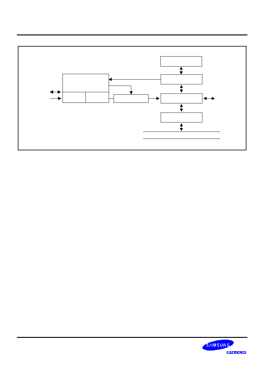
IIC-BUS INTERFACE
S3C2440A RISC MICROPROCESSOR
20-2
PCLK
Address Register
SDA
4-bit Prescaler
IIC-Bus Control Logic
IICSTAT
IICCON
Comparator
Shift Register
Shift Register
(IICDS)
Data Bus
SCL
Figure 20-1. IIC-Bus Block Diagram
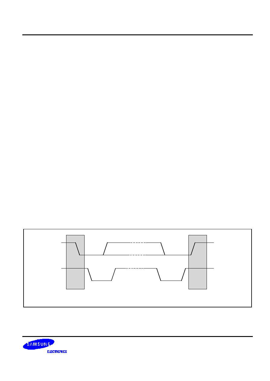
S3C2440A RISC MICROPROCESSOR
IIC-BUS INTERFACE
20-3
IIC-BUS INTERFACE
The S3C2440A IIC-bus interface has four operation modes:
-- Master transmitter mode
-- Master receive mode
-- Slave transmitter mode
-- Slave receive mode
Functional relationships among these operating modes are described below.
START AND STOP CONDITIONS
When the IIC-bus interface is inactive, it is usually in Slave mode. In other words, the interface should be in Slave
mode before detecting a Start condition on the SDA line (a Start condition can be initiated with a High-to-Low
transition of the SDA line while the clock signal of SCL is High). When the interface state is changed to Master
mode, a data transfer on the SDA line can be initiated and SCL signal generated.
A Start condition can transfer a one-byte serial data over the SDA line, and a Stop condition can terminate the data
transfer. A Stop condition is a Low-to-High transition of the SDA line while SCL is High. Start and Stop conditions
are always generated by the master. The IIC-bus gets busy when a Start condition is generated. A Stop condition
will make the IIC-bus free.
When a master initiates a Start condition, it should send a slave address to notify the slave device. One byte of
address field consists of a 7-bit address and a 1-bit transfer direction indicator (showing write or read).
If bit 8 is 0, it indicates a write operation (transmit operation); if bit 8 is 1, it indicates a request for data read (receive
operation).
The master will complete the transfer operation by transmitting a Stop condition. If the master wants to continue the
data transmission to the bus, it should generate another Start condition as well as a slave address. In this way, the
read-write operation can be performed in various formats.
SCL
SDA
SDA
SCL
Start
Condition
Stop
Condition
Figure 20-2. Start and Stop Condition
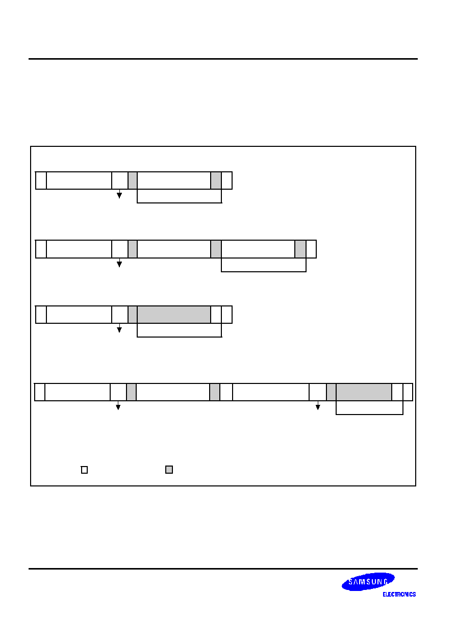
IIC-BUS INTERFACE
S3C2440A RISC MICROPROCESSOR
20-4
DATA TRANSFER FORMAT
Every byte placed on the SDA line should be eight bits in length. The bytes can be unlimitedly transmitted per
transfer. The first byte following a Start condition should have the address field. The address field can be transmitted
by the master when the IIC-bus is operating in Master mode. Each byte should be followed by an acknowledgement
(ACK) bit. The MSB bit of the serial data and addresses are always sent first.
NOTES:
1.
S: Start, rS: Repeat Start, P: Stop, A: Acknowledge
2. : From Master to Slave, : From Slave to Master
Write Mode Format with 7-bit Addresses
"0"
(Write)
Data Transferred
(Data + Acknowledge)
S Slave Address 7bits R/W A
P
DATA(1Byte)
A
Read Mode Format with 7-bit Addresses
"1"
(Read)
Data Transferred
(Data + Acknowledge)
S Slave Address 7 bits R/W A
P
DATA
A
Write Mode Format with 10-bit Addresses
"0"
(Write)
Data Transferred
(Data + Acknowledge)
P
DATA
A
S
Slave Address
1st 7 bits
R/W A
Slave Address
2nd Byte
A
11110XX
Read Mode Format with 10-bit Addresses
"1"
(Read)
S
Slave Address
1st 7 bits
11110XX
R/W A
Slave Address
2nd Byte
A rS
Slave Address
1st 7 Bits
A
Data Transferred
(Data + Acknowledge)
P
DATA
A
R/W
"1"
(Read)
Figure 20-3. IIC-Bus Interface Data Format
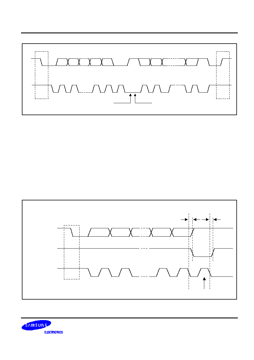
S3C2440A RISC MICROPROCESSOR
IIC-BUS INTERFACE
20-5
SDA
Acknowledgement
Signal from Receiver
SCL
S
1
2
7
8
9
1
2
9
Acknowledgement
Signal from Receiver
MSB
ACK
Byte Complete, Interrupt
within Receiver
Clock Line Held Low by
receiver and/or transmitter
Figure 20-4. Data Transfer on the IIC-Bus
ACK SIGNAL TRANSMISSION
To complete a one-byte transfer operation, the receiver should send an ACK bit to the transmitter. The ACK pulse
should occur at the ninth clock of the SCL line. Eight clocks are required for the one-byte data transfer. The master
should generate the clock pulse required to transmit the ACK bit.
The transmitter should release the SDA line by making the SDA line High when the ACK clock pulse is received. The
receiver should also drive the SDA line Low during the ACK clock pulse so that the SDA keeps Low during the High
period of the ninth SCL pulse.
The ACK bit transmit function can be enabled or disabled by software (IICSTAT). However, the ACK pulse on the
ninth clock of SCL is required to complete the one-byte data transfer operation.
Data Output by
Transmitter
Data Output by
Receiver
SCL from
Master
Start
Condition
Clock Pulse for Acknowledgment
Clock to Output
9
8
7
S
1
2
Figure 20-5. Acknowledge on the IIC-Bus

IIC-BUS INTERFACE
S3C2440A RISC MICROPROCESSOR
20-6
READ-WRITE OPERATION
In Transmitter mode, when the data is transferred, the IIC-bus interface will wait until IIC-bus Data Shift (IICDS)
register receives a new data. Before the new data is written into the register, the SCL line will be held low, and then
released after it is written. The S3C2440A should hold the interrupt to identify the completion of current data transfer.
After the CPU receives the interrupt request, it should write a new data into the IICDS register, again.
In Receive mode, when data is received, the IIC-bus interface will wait until IICDS register is read. Before the new
data is read out, the SCL line will be held low and then released after it is read. The S3C2440A should hold the
interrupt to identify the completion of the new data reception. After the CPU receives the interrupt request, it should
read the data from the IICDS register.
BUS ARBITRATION PROCEDURES
Arbitration takes place on the SDA line to prevent the contention on the bus between two masters. If a master with a
SDA High level detects the other master with a SDA active Low level, it will not initiate a data transfer because the
current level on the bus does not correspond to its own. The arbitration procedure will be extended until the SDA line
turns High.
However, when the masters simultaneously lower the SDA line, each master should evaluate whether the mastership
is allocated itself or not. For the purpose of evaluation is that each master should detect the address bits. While
each master generates the slaver address, it should also detect the address bit on the SDA line because the SDA
line is likely to get Low rather than to keep High. Assume that one master generates a Low as first address bit, while
the other master is maintaining High. In this case, both masters will detect Low on the bus because the Low status
is superior to the High status in power. When this happens, Low (as the first bit of address) generating master will
get the mastership while High (as the first bit of address) generating master should withdraw the mastership. If both
masters generate Low as the first bit of address, there should be arbitration for the second address bit, again. This
arbitration will continue to the end of last address bit.
ABORT CONDITIONS
If a slave receiver cannot acknowledge the confirmation of the slave address, it should hold the level of the SDA line
High. In this case, the master should generate a Stop condition and to abort the transfer.
If a master receiver is involved in the aborted transfer, it should signal the end of the slave transmit operation by
canceling the generation of an ACK after the last data byte received from the slave. The slave transmitter should then
release the SDA to allow a master to generate a Stop condition.
CONFIGURING IIC-BUS
To control the frequency of the serial clock (SCL), the 4-bit prescaler value can be programmed in the IICCON
register. The IIC-bus interface address is stored in the IIC-bus address (IICADD) register. (By default, the IIC-bus
interface address has an unknown value.)
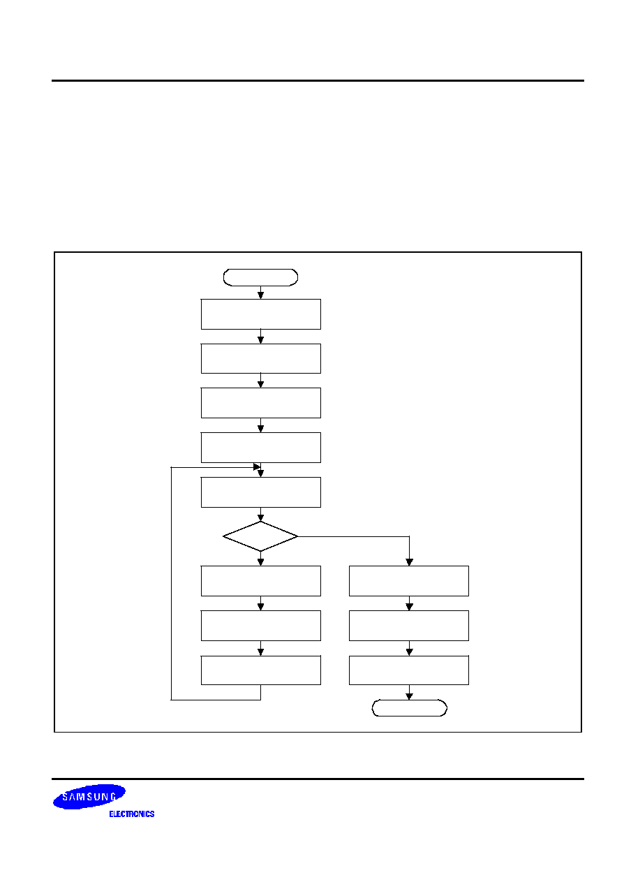
S3C2440A RISC MICROPROCESSOR
IIC-BUS INTERFACE
20-7
FLOWCHARTS OF OPERATIONS IN EACH MODE
The following steps must be executed before any IIC Tx/Rx operations.
1. Write own slave address on IICADD register, if needed.
2. Set IICCON register.
a) Enable interrupt
b) Define SCL period
3. Set IICSTAT to enable Serial Output
Write slave address to
IICDS.
Write 0xF0 (M/T
Start) to IICSTAT.
The data of the IICDS is
transmitted.
ACK period and then
interrupt is pending.
Write 0xD0 (M/T
Stop) to IICSTAT.
Write new data
transmitted to IICDS.
Stop?
Clear pending bit to
resume.
The data of the IICDS is
shifted to SDA.
START
Master Tx mode has
been configured.
Clear pending bit .
Wait until the stop
condition takes effect.
END
Y
N
Figure 20-6. Operations for Master/Transmitter Mode
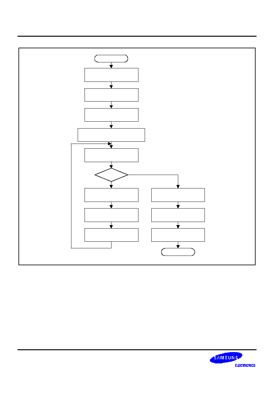
IIC-BUS INTERFACE
S3C2440A RISC MICROPROCESSOR
20-8
Write slave address to
IICDS.
Write 0xB0 (M/R
Start) to IICSTAT.
The data of the IICDS (slave
address) is transmitted.
ACK period and then
interrupt is pending.
Write 0x90 (M/R
Stop) to IICSTAT.
Read a new data from
IICDS.
Stop?
Clear pending bit to
resume.
SDA is shifted to IICDS.
START
Master Rx mode has
been configured.
Clear pending bit .
Wait until the stop
condition takes effect.
END
Y
N
Figure 20-7. Operations for Master/Receiver Mode
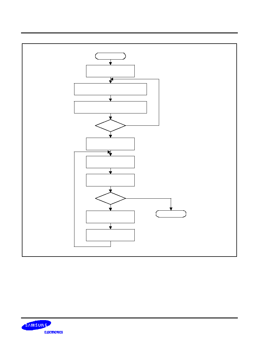
S3C2440A RISC MICROPROCESSOR
IIC-BUS INTERFACE
20-9
IIC detects start signal. and, IICDS
receives data.
IIC compares IICADD and IICDS (the
received slave address).
Write data to IICDS.
The IIC address match
interrupt is generated.
Clear pending bit to
resume.
The data of the IICDS is
shifted to SDA.
START
Slave Tx mode has
been configured.
END
Matched?
N
Y
Stop?
Interrupt is pending.
N
Y
Figure 20-8. Operations for Slave/Transmitter Mode
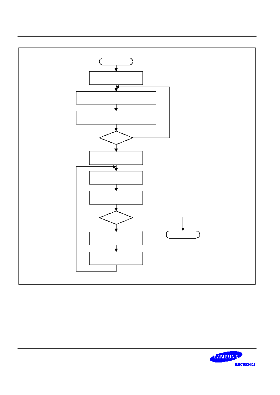
IIC-BUS INTERFACE
S3C2440A RISC MICROPROCESSOR
20-10
IIC detects start signal. and, IICDS
receives data.
IIC compares IICADD and IICDS (the
received slave address).
Read data from IICDS.
The IIC address match
interrupt is generated.
Clear pending bit to
resume.
SDA is shifted to IICDS.
START
Slave Rx mode has
been configured.
END
Matched?
N
Y
Stop?
Interrupt is pending.
N
Y
Figure 20-9. Operations for Slave/Receiver Mode

S3C2440A RISC MICROPROCESSOR
IIC-BUS INTERFACE
20-11
IIC-BUS INTERFACE SPECIAL REGISTERS
MULTI-MASTER IIC-BUS CONTROL (IICCON) REGISTER
Register
Address
R/W
Description
Reset Value
IICCON
0x54000000
R/W
IIC-Bus control register
0x0X
IICCON
Bit
Description
Initial State
Acknowledge generation
(1)
[7]
IIC-bus acknowledge enable bit.
0: Disable
1: Enable
In Tx mode, the IICSDA is free in the ack time.
In Rx mode, the IICSDA is L in the ack time.
0
Tx clock source selection
[6]
Source clock of IIC-bus transmit clock prescaler
selection bit.
0: IICCLK = fPCLK /16
1: IICCLK = fPCLK /512
0
Tx/Rx Interrupt
(5)
[5]
IIC-Bus Tx/Rx interrupt enable/disable bit.
0: Disable, 1: Enable
0
Interrupt pending flag
(2)
(3)
[4]
IIC-bus Tx/Rx interrupt pending flag. This bit cannot be
written to 1. When this bit is read as 1, the IICSCL is
tied to L and the IIC is stopped. To resume the
operation, clear this bit as 0.
0: 1) No interrupt pending (when read).
2) Clear pending condition &
Resume the operation (when write).
1: 1) Interrupt is pending (when read)
2) N/A (when write)
0
Transmit clock value
(4)
[3:0]
IIC-Bus transmit clock prescaler.
IIC-Bus transmit clock frequency is determined by this
4-bit prescaler value, according to the following formula:
Tx clock = IICCLK/(IICCON[3:0]+1).
Undefined
NOTES:
1. Interfacing with EEPROM, the ack generation may be disabled before reading the last data in order to generate the
STOP condition in Rx mode.
2.
An IIC-bus interrupt occurs 1) when a 1-byte transmits or receive operation is completed, 2) when a general call or a
slave
address match occurs, or 3) if bus arbitration fails.
3. To adjust the setup time of SDA before SCL rising edge, IICDS has to be written before clearing the IIC interrupt
pending bit.
4.
IICCLK is determined by IICCON[6].
Tx clock can vary by SCL transition time.
When IICCON[6]=0, IICCON[3:0]=0x0 or 0x1 is not available.
5.
If the IICCON[5]=0, IICCON[4] does not operate correctly.
So, It is recommended that you should set IICCON[5]=1, although you does not use the IIC interrupt.

IIC-BUS INTERFACE
S3C2440A RISC MICROPROCESSOR
20-12
MULTI-MASTER IIC-BUS CONTROL/STATUS (IICSTAT) REGISTER
Register
Address
R/W
Description
Reset Value
IICSTAT
0x54000004
R/W
IIC-Bus control/status register
0x0
IICSTAT
Bit
Description
Initial State
Mode selection
[7:6]
IIC-bus master/slave Tx/Rx mode select bits.
00: Slave receive mode
01: Slave transmit mode
10: Master receive mode
11: Master transmit mode
00
Busy signal status /
START STOP condition
[5]
IIC-Bus busy signal status bit.
0: read) Not busy (when read)
write) STOP signal generation
1: read) Busy (when read)
write) START signal generation.
The data in IICDS will be transferred
automatically just after the start signal.
0
Serial output
[4]
IIC-bus data output enable/disable bit.
0: Disable Rx/Tx, 1: Enable Rx/Tx
0
Arbitration status flag
[3]
IIC-bus arbitration procedure status flag bit.
0: Bus arbitration successful
1: Bus arbitration failed during serial I/O
0
Address-as-slave status flag
[2]
IIC-bus address-as-slave status flag bit.
0: Cleared when START/STOP condition was
detected
1: Received slave address matches the address
value in the IICADD
0
Address zero status flag
[1]
IIC-bus address zero status flag bit.
0: Cleared when START/STOP condition was
detected
1: Received slave address is 00000000b.
0
Last-received bit status flag
[0]
IIC-bus last-received bit status flag bit.
0: Last-received bit is 0 (ACK was received).
1: Last-received bit is 1 (ACK was not received).
0
S3C2440A RISC MICROPROCESSOR
IIC-BUS INTERFACE
20-13
MULTI-MASTER IIC-BUS ADDRESS (IICADD) REGISTER
Register
Address
R/W
Description
Reset Value
IICADD
0x54000008
R/W
IIC-Bus address register
0xXX
IICADD
Bit
Description
Initial State
Slave address
[7:0]
7-bit slave address, latched from the IIC-bus.
When serial output enable = 0 in the IICSTAT, IICADD is write-
enabled. The IICADD value can be read any time, regardless of the
current serial output enable bit (IICSTAT) setting.
Slave address : [7:1]
Not mapped : [0]
XXXXXXXX
MULTI-MASTER IIC-BUS TRANSMIT/RECEIVE DATA SHIFT (IICDS) REGISTER
Register
Address
R/W
Description
Reset Value
IICDS
0x5400000C
R/W
IIC-Bus transmit/receive data shift register
0xXX
IICDS
Bit
Description
Initial State
Data shift
[7:0]
8-bit data shift register for IIC-bus Tx/Rx operation.
When serial output enable = 1 in the IICSTAT, IICDS is write-
enabled. The IICDS value can be read any time, regardless of the
current serial output enable bit (IICSTAT) setting.
XXXXXXXX

IIC-BUS INTERFACE
S3C2440A RISC MICROPROCESSOR
20-14
MULTI-MASTER IIC-BUS LINE CONTROL(IICLC) REGISTER
Register
Address
R/W
Description
Reset Value
IICLC
0x54000010
R/W
IIC-Bus multi-master line control register
0x00
IICLC
Bit
Description
Initial State
Filter enable
[2]
IIC-bus filter enable bit.
When SDA port is operating as input, this bit should be High.
This filter can prevent from occurred error by a glitch during
double of PCLK time.
0: Filter disable
1: Filter enable
0
SDA output delay
[1:0]
IIC-Bus SDA line delay length selection bits.
SDA line is delayed as following clock time(PCLK)
00: 0 clocks 01: 5 clocks
10: 10 clocks 11: 15 clocks
00

S3C2440A RISC MICROPROCESSOR
IIS-BUS INTERFACE
21-1
21
IIS-BUS INTERFACE
OVERVIEW
Currently, many digital audio systems are attracting the consumers on the market, in the form of compact discs,
digital audio tapes, digital sound processors, and digital TV sound. The S3C2440A Inter-IC Sound (IIS) bus interface
can be used to implement a CODEC interface to an external 8/16-bit stereo audio CODEC IC for mini-disc and
portable applications. The IIS bus interface supports both IIS bus data format and MSB-justified data format. The
interface provides DMA transfer mode for FIFO access instead of an interrupt. It can transmit and receive data
simultaneously as well as transmit or receive data alternatively at a time.
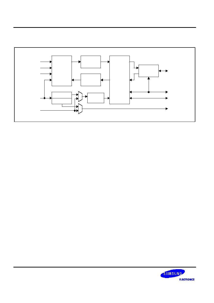
IIS-BUS INTERFACE
S3C2440A RISC MICROPROCESSOR
21-2
BLOCK DIAGRAM
ADDR
DATA
CNTL
PCLK
BRFC
IPSR_A
IPSR_B
TxFIFO
RxFIFO
SCLKG
CHNC
SFTR
LRCK
SCLK
SD
CDCLK
MPLLin
Figure 21-1. IIS-Bus Block Diagram
FUNCTIONAL DESCRIPTIONS
Bus interface, register bank, and state machine (BRFC): Bus interface logic and FIFO access are controlled by the
state machine.
5-bit dual prescaler (IPSR): One prescaler is used as the master clock generator of the IIS bus interface and the
other is used as the external CODEC clock generator.
64-byte FIFOs (TxFIFO and RxFIFO): In transmit data transfer, data are written to TxFIFO, and, in the receive data
transfer, data are read from RxFIFO.
Master IISCLK generator (SCLKG): In master mode, serial bit clock is generated from the master clock.
Channel generator and state machine (CHNC): IISCLK and IISLRCK are generated and controlled by the channel
state machine.
16-bit shift register (SFTR): Parallel data is shifted to serial data output in the transmit mode, and serial data input
is shifted to parallel data in the receive mode.
TRANSMIT OR RECEIVE ONLY MODE
Normal Transfer
IIS control register has FIFO ready flag bits for transmit and receive FIFOs. When FIFO is ready to transmit data, the
FIFO ready flag is set to '1' if transmit FIFO is not empty. If transmit FIFO is empty, FIFO ready flag is set to '0'.
While receiving FIFO is not full, the FIFO ready flag for receive FIFO is set to '1' ; it indicates that FIFO is ready to
receive data. If receive FIFO is full, FIFO ready flag is set to '0'. These flags can determine the time that CPU is to
write or read FIFOs. Serial data can be transmitted or received while the CPU is accessing transmit and receive
FIFOs in this way.

S3C2440A RISC MICROPROCESSOR
IIS-BUS INTERFACE
21-3
DMA TRANSFER
In this mode, transmit or receive FIFO is accessible by the DMA controller. DMA service request in transmit or
receive mode is made by the FIFO ready flag automatically.
TRANSMIT AND RECEIVE MODE
In this mode, IIS bus interface can transmit and receive data simultaneously.
AUDIO SERIAL INTERFACE FORMAT
IIS-BUS FORMAT
The IIS bus has four lines including serial data input (IISDI), serial data output (IISDO), left/right channel select
(IISLRCK), and serial bit clock (IISCLK); the device generating IISLRCK and IISCLK is the master.
Serial data is transmitted in 2's complement with the MSB first. The MSB is transmitted first because the transmitter
and receiver may have different word lengths. The transmitter does not have to know how many bits the receiver can
handle, nor does the receiver need to know how many bits are being transmitted.
When the system word length is greater than the transmitter word length, the word is truncated (least significant data
bits are set to '0') for data transmission. If the receiver gets more bits than its word length, the bits after the LSB are
ignored. On the other hand, if the receiver gets fewer bits than its word length, the missing bits are set to zero
internally. And therefore, the MSB has a fixed position, whereas the position of the LSB depends on the word length.
The transmitter sends the MSB of the next word at one clock period whenever the IISLRCK is changed.
Serial data sent by the transmitter may be synchronized with either the trailing (HIGH to LOW) or the leading (LOW
to HIGH) edge of the clock signal. However, the serial data must be latched into the receiver on the leading edge of
the serial clock signal, and so there are some restrictions when transmitting data that is synchronized with the
leading edge.
The LR channel select line indicates the channel being transmitted. IISLRCK may be changed either on a trailing or
leading edge of the serial clock, but it does not need to be symmetrical. In the slave, this signal is latched on the
leading edge of the clock signal. The IISLRCK line changes one clock period before the MSB is transmitted. This
allows the slave transmitter to derive synchronous timing of the serial data that will be set up for transmission.
Furthermore, it enables the receiver to store the previous word and clear the input for the next word.
MSB (LEFT) JUSTIFIED
MSB / left justified bus format is the same as IIS bus format architecturally. Only, different from the IIS bus format,
the MSB justified format realizes that the transmitter always sends the MSB of the next word whenever the IISLRCK
is changed.
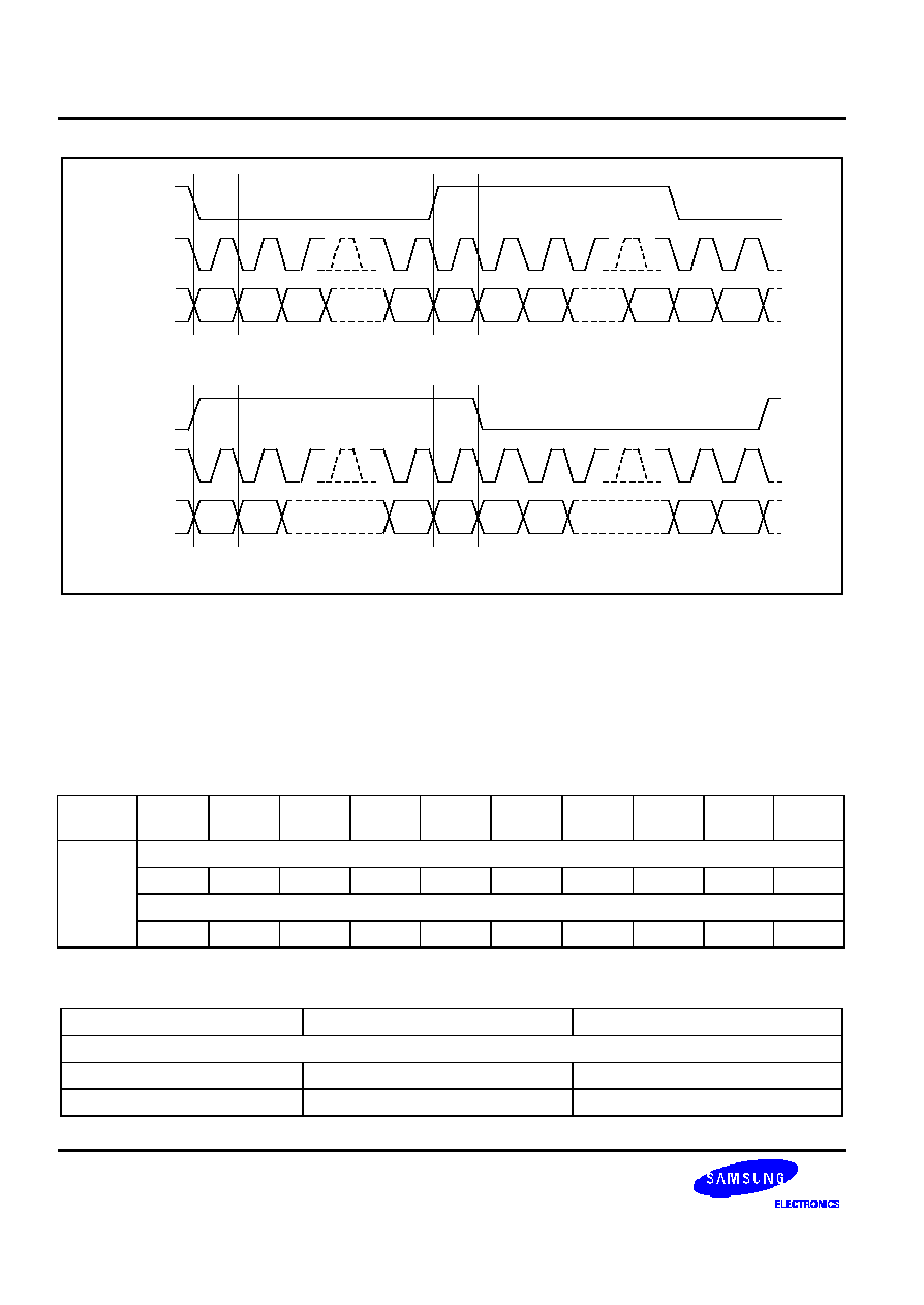
IIS-BUS INTERFACE
S3C2440A RISC MICROPROCESSOR
21-4
IIS-bus Format (N=8 or 16)
MSB
(1st)
2nd
Bit
N-1th
Bit
LSB
(last)
MSB
(1st)
2nd
Bit
N-1th
Bit
LSB
(last)
MSB
(1st)
LRCK
SCLK
SD
LEFT
RIGHT
LEFT
MSB-justified Format (N=8 or 16)
2nd
Bit
N-1th
Bit
LSB
(last)
MSB
(1st)
2nd
Bit
N-1th
Bit
LSB
(last)
LRCK
SCLK
SD
LEFT
RIGHT
MSB
(1st)
Figure 21-2. IIS-Bus and MSB (Left)-justified Data Interface Formats
SAMPLING FREQUENCY AND MASTER CLOCK
Master clock frequency (PCLK or MPLLin) can be selected by sampling frequency as shown in Table 21-1. Because
Master clock is made by IIS prescaler, the prescaler value and Master clock type (256 or 384fs) should be
determined properly. Serial bit clock frequency type (16/32/48fs) can be selected by the serial bit per channel and
Master clock as shown in Table 21-2.
Table 21-1. CODEC clock (CODECLK = 256 or 384fs)
IISLRCK
(fs)
8.000
kHz
11.025
kHz
16.000
kHz
22.050
kHz
32.000
kHz
44.100
kHz
48.000
kHz
64.000
kHz
88.200
kHz
96.000
kHz
256fs
CODECLK
2.0480
2.8224
4.0960
5.6448
8.1920
11.2896
12.2880
16.3840
22.5792
24.5760
(MHz)
384fs
3.0720
4.2336
6.1440
8.4672
12.2880
16.9344
18.4320
24.5760
33.8688
36.8640
Table 21-2. Usable Serial Bit Clock Frequency (IISCLK = 16 or 32 or 48fs)
Serial bit per channel
8-bit
16-bit
Serial clock frequency (IISCLK)
@CODECLK = 256fs
16fs, 32fs
32fs
@CODECLK = 384fs
16fs, 32fs, 48fs
32fs, 48fs
S3C2440A RISC MICROPROCESSOR
IIS-BUS INTERFACE
21-5
IIS-BUS INTERFACE SPECIAL REGISTERS
IIS CONTROL (IISCON) REGISTER
Register
Address
R/W
Description
Reset Value
IISCON
0x55000000 (Li/HW, Li/W, Bi/W)
0x55000002 (Bi/HW)
R/W
IIS control register
0x100
IISCON
Bit
Description
Initial State
Left/Right channel index
(Read only)
[8]
0 = Left
1 = Right
1
Transmit FIFO ready flag
(Read only)
[7]
0 = Empty
1 = Not empty
0
Receive FIFO ready flag
(Read only)
[6]
0 = Full
1 = Not full
0
Transmit DMA service request
[5]
0 = Disable
1 = Enable
0
Receive DMA service request
[4]
0 = Disable
1 = Enable
0
Transmit channel idle command
[3]
In Idle state the IISLRCK is inactive (Pause Tx).
0 = Not idle
1 = Idle
0
Receive channel idle command
[2]
In Idle state the IISLRCK is inactive (Pause Rx).
0 = Not idle
1 = Idle
0
IIS prescaler
[1]
0 = Disable
1 = Enable
0
IIS interface
[0]
0 = Disable (stop)
1 = Enable (start)
0
NOTES:
1.
The IISCON register is accessible for each byte, halfword and word unit using STRB/STRH/STR and LDRB/LDRH/LDR
instructions or char/short int/int type pointer in Little/Big endian mode.
2.
(Li/HW/W) : Little/HalfWord/Word
(Bi/HW/W) : Big/HalfWord/Word

IIS-BUS INTERFACE
S3C2440A RISC MICROPROCESSOR
21-6
IIS MODE REGISTER (IISMOD) REGISTER
Register
Address
R/W
Description
Reset Value
IISMOD
0x55000004 (Li/W, Li/HW, Bi/W)
0x55000006 (Bi/HW)
R/W
IIS mode register
0x0
IISMOD
Bit
Description
Initial State
Master clock select
[9]
Master clock select
0 = PCLK
1 = MPLLin
0
Master/slave mode select
[8]
0 = Master mode (IISLRCK and IISCLK are output mode).
1 = Slave mode (IISLRCK and IISCLK are input mode).
0
Transmit/receive mode
select
[7:6]
00 = No transfer 01 = Receive mode
10 = Transmit mode 11 = Transmit and receive mode
00
Active level of left/right
channel
[5]
0 = Low for left channel (High for right channel)
1 = High for left channel (Low for right channel)
0
Serial interface format
[4]
0 = IIS compatible format
1 = MSB (Left)-justified format
0
Serial data bit per
channel
[3]
0 = 8-bit 1 = 16-bit
0
Master clock frequency
select
[2]
0 = 256fs 1 = 384fs
(fs: sampling frequency)
0
Serial bit clock frequency
select
[1:0]
00 = 16fs 01 = 32fs
10 = 48fs 11 = N/A
00
NOTES:
1.
The IISMOD register is accessible for each halfword and wordunit using STRH/STR and LDRH/LDR instructions or
short
int/int type pointer in Little/Big endian mode.
2.
(Li/HW/W) : Little/HalfWord/Word.
(Bi/HW/W) : Big/HalfWord/Word.

S3C2440A RISC MICROPROCESSOR
IIS-BUS INTERFACE
21-7
IIS PRESCALER (IISPSR) REGISTER
Register
Address
R/W
Description
Reset Value
IISPSR
0x55000008 (Li/HW, Li/W, Bi/W)
0x5500000A (Bi/HW)
R/W
IIS prescaler register
0x0
IISPSR
Bit
Description
Initial State
Prescaler control A
[9:5]
Data value: 0 ~ 31
Note: Prescaler A makes the master clock that is used the internal
block and division factor is N+1.
00000
Prescaler control B
[4:0]
Data value: 0 ~ 31
Note: Prescaler B makes the master clock that is used the external
block and division factor is N+1.
00000
NOTES:
1.
The IISPSR register is accessible for each byte, halfword and word unit using STRB/STRH/STR and LDRB/LDRH/LDR
instructions or char/short int/int type pointer in Little/Big endian mode.
2.
(Li/HW/W): Little/HalfWord/Word.
(Bi/HW/W): Big/HalfWord/Word.
IIS-BUS INTERFACE
S3C2440A RISC MICROPROCESSOR
21-8
IIS FIFO CONTROL (IISFCON) REGISTER
Register
Address
R/W
Description
Reset Value
IISFCON
0x5500000C (Li/HW, Li/W, Bi/W)
0x5500000E (Bi/HW)
R/W
IIS FIFO interface register
0x0
IISFCON
Bit
Description
Initial State
Transmit FIFO access mode select
[15]
0 = Normal
1 = DMA
0
Receive FIFO access mode select
[14]
0 = Normal
1 = DMA
0
Transmit FIFO
[13]
0 = Disable 1 = Enable
0
Receive FIFO
[12]
0 = Disable 1 = Enable
0
Transmit FIFO data count
(Read only)
[11:6]
Data count value = 0 ~ 32
000000
Receive FIFO data count
(Read only)
[5:0]
Data count value = 0 ~ 32
000000
NOTES:
1.
The IISFCON register is accessible for each halfword and word unit using STRH/STR and LDRH/LDR instructions or
short int/int type pointer in Little/Big endian mode.
2.
(Li/HW/W): Little/HalfWord/Word.
(Bi/HW/W): Big/HalfWord/Word.
IIS FIFO (IISFIFO) REGISTER
IIS bus interface contains two 64-byte FIFO for the transmit and receive mode. Each FIFO has 16-width and 32-depth
form, which allows the FIFO to handles data for each halfword unit regardless of valid data size. Transmit and receive
FIFO access is performed through FIFO entry; the address of FENTRY is 0x55000010.
Register
Address
R/W
Description
Reset Value
IISFIFO
0x55000010(Li/HW)
0x55000012(Bi/HW)
R/W
IIS FIFO register
0x0
IISFIF
Bit
Description
Initial State
FENTRY
[15:0]
Transmit/Receive data for IIS
0x0
NOTES:
1.
The IISFIFO register is accessible for each halfword and word unit using STRH and LDRH instructions or short int type
pointer in Little/Big endian mode.
2.
(Li/HW): Little/HalfWord.
(Bi/HW): Big/HalfWord.

S3C2440A RISC MICROPROCESSOR
SPI
22-1
22
SPI
OVERVIEW
The S3C2440A Serial Peripheral Interface (SPI) can interface with the serial data transfer. The S3C2440A includes
two SPI, each of which has two 8-bit shift registers for transmission and receiving, respectively. During an SPI
transfer, data is simultaneously transmitted (shifted out serially) and received (shifted in serially). 8-bit serial data at
a frequency is determined by its corresponding control register settings. If you only want to transmit, receive data
can be kept dummy. Otherwise, if you only want to receive, you should transmit dummy '1' data.
There are 4 I/O pin signals associated with SPI transfers: SCK (SPICLK0,1), MISO (SPIMISO0,1) data line, MOSI
(SPIMOSI0,1) data line and active low /SS (nSS0,1) pin (input).
FEATURES
-- Support 2-ch SPI
-- SPI Protocol (ver. 2.11) compatible
-- 8-bit Shift Register for transmit
-- 8-bit Shift Register for receive
-- 8-bit Prescaler logic
-- Polling, Interrupt and DMA transfer mode
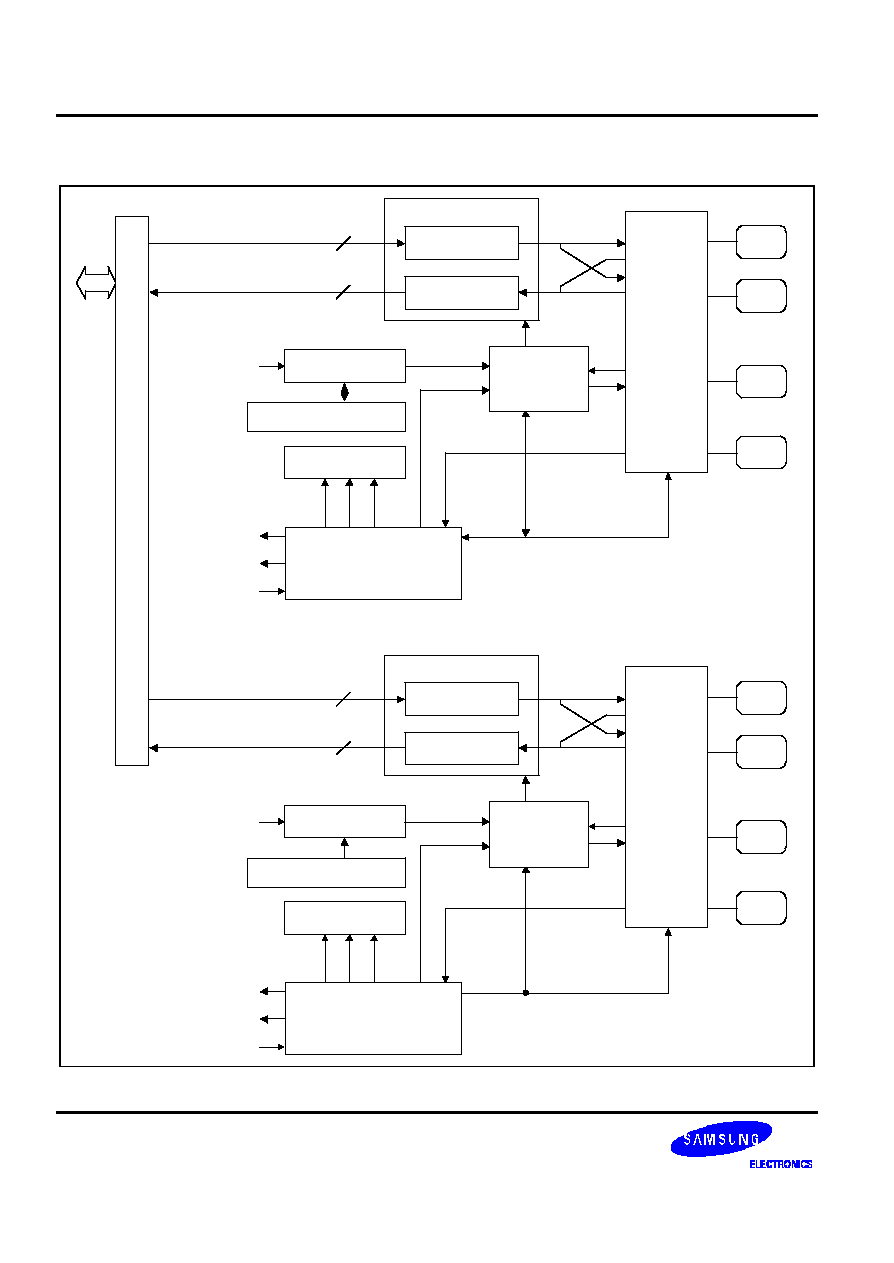
SPI
S3C2440A RISC MICROPROCESSOR
22-2
BLOCK DIAGRAM
8bit Prescaler 1
PCLK
Status Register 1
Prescaler Register 1
/SS
nSS 0
SCK
SPICLK 0
MOSI
SPIMOSI 0
MISO
SPIMISO 0
Pin Control Logic 0
MSTR
Tx 8bit Shift Reg 0
Rx 8bit Shift Reg 0
LSB
MSB
LSB
MSB
8
8
Clock
SPI Clock
(Master)
CPOL
CPHA
CLOCK Logic 0
MULF
DCOL
REDY
APB I/F 0
(INT DMA 0)
Master
Slave
Slave
Master
Slave
Slave
Master
Data
Bus
INT 0 / INT 1
REQ0 / REQ1
ACK0 / ACK1
/SS
nSS 1
SCK
SPICLK 1
MOSI
SPIMOSI 1
MISO
SPIMISO 1
Pin Control Logic 1
MSTR
Tx 8bit Shift Reg 1
Rx 8bit Shift Reg 1
LSB
MSB
LSB
MSB
8
8
Clock
SPI Clock
(Master)
CPOL
CPHA
CLOCK Logic 1
MULF
DCOL
REDY
APB I/F 1
(INT DMA 1)
Master
Slave
Slave
Master
Slave
Slave
Master
INT 0 / INT 1
REQ0 / REQ1
ACK0 / ACK1
8bit Prescaler 0
PCLK
Status Register 0
Prescaler Register 0
Figure 22-1. SPI Block Diagram

S3C2440A RISC MICROPROCESSOR
SPI
22-3
SPI OPERATION
Using the SPI interface, S3C2440A can send/receive 8-bit data simultaneously with an external device. A serial
clock line is synchronized with the two data lines for shifting and sampling of the information. When the SPI is the
master, transmission frequency can be controlled by setting the appropriate bit in SPPREn register. You can modify
its frequency to adjust the baud rate data register value. When the SPI is a slave, other master supplies the clock.
When the programmer writes byte data to SPTDATn register, SPI transmit/receive operation will start
simultaneously. In some cases, nSS should be activated before writing byte data to SPTDATn.
PROGRAMMING PROCEDURE
When a byte data is written into the SPTDATn register, SPI starts to transmit if ENSCK and MSTR of SPCONn
register are set. You can use a typical programming procedure to operate an SPI card.
To program the SPI modules, follow these basic steps:
1. Set Baud Rate Prescaler Register (SPPREn).
2. Set SPCONn to configure properly the SPI module.
3. Write data 0xFF to SPTDATn 10 times in order to initialize MMC or SD card.
4. Set a GPIO pin, which acts as nSS, low to activate the MMC or SD card.
5. Tx data ° Check the status of Transfer Ready flag (REDY=1), and then write data to SPTDATn.
6. Rx data(1): SPCONn's TAGD bit disable = normal mode
7. ° write 0xFF to SPTDATn, then confirm REDY to set, and then read data from Read Buffer.
8. Rx data(2): SPCONn's TAGD bit enable = Tx Auto Garbage Data mode
9. ° confirm REDY to set, and then read data from Read Buffer (then automatically start to transfer).
10. Set a GPIO pin, which acts as nSS, high to deactivate the MMC or SD card.
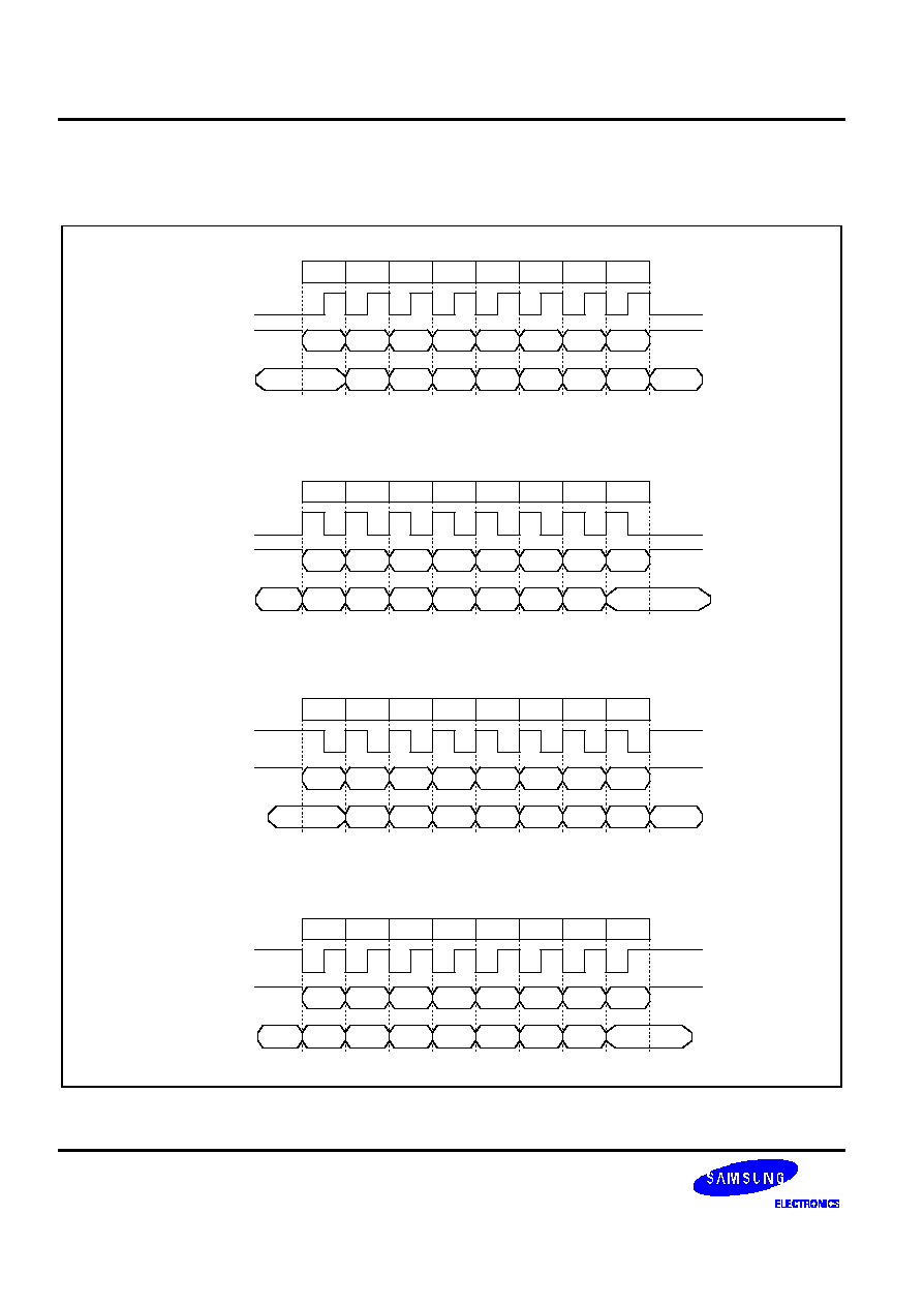
SPI
S3C2440A RISC MICROPROCESSOR
22-4
SPI TRANSFER FORMAT
The S3C2440A supports 4 different formats to transfer data. Figure 22-2 shows the four waveforms for SPICLK.
* LSB of previously transmitted character
Cycle
MOSI
1
2
3
4
5
6
7
8
MSB
6
5
4
3
2
1
LSB
6
5
4
3
2
1
LSB
SPICLK
MISO
MSB
CPOL = 1, CPHA = 1 (Format B)
* MSB of character just received
Cycle
MOSI
1
2
3
4
5
6
7
8
MSB
6
5
4
3
2
1
LSB
6
5
4
3
2
1
LSB
MSB*
SPICLK
MISO
MSB
CPOL = 1, CPHA = 0 (Format A)
Cycle
MOSI
1
2
3
4
5
6
7
8
6
5
4
3
2
1
LSB
6
5
4
3
2
1
LSB*
SPICLK
MISO
*LSB
CPOL = 0, CPHA = 1 (Format B)
* MSB of character just received
Cycle
MOSI
1
2
3
4
5
6
7
8
MSB
6
5
4
3
2
1
LSB
6
5
4
3
2
1
LSB
MSB*
SPICLK
MISO
MSB
CPOL = 0, CPHA = 0 (Format A)
* LSB of previously transmitted character
*LSB
MSB
MSB
Figure 22-2. SPI Transfer Format

S3C2440A RISC MICROPROCESSOR
SPI
22-5
TRANSMITTING PROCEDURE FOR DMA
1. SPI is configured as DMA mode.
2. DMA is configured properly.
3. SPI requests DMA service.
4. DMA transmits 1byte data to the SPI.
5. SPI transmits the data to card.
6. Return to Step 3 until DMA count becomes 0.
6. SPI is configured as interrupt or polling mode with SMOD bits.
RECEIVING PROCEDURE FOR DMA
1. SPI is configured as DMA start with SMOD bits and TAGD bit set.
2. DMA is configured properly.
3. SPI receives 1byte data from card.
4. SPI requests DMA service.
5. DMA receives the data from the SPI.
6. Write data 0xFF automatically to SPTDATn.
7. Return to Step 4 until DMA count becomes 0.
8. SPI is configured as polling mode with SMOD bits and clear TAGD bit.
9. If SPSTAn's READY flag is set, then read the last byte data.
NOTE
Total received data = DMA TC values + the last data in polling mode (Step 9).
The first DMA received data is dummy and the user can neglect it.

SPI
S3C2440A RISC MICROPROCESSOR
22-6
SPI SPECIAL REGISTERS
SPI CONTROL REGISTER
Register
Address
R/W
Description
Reset Value
SPCON0
0x59000000
R/W
SPI channel 0 control register
0x00
SPCON1
0x59000020
R/W
SPI channel 1 control register
0x00
SPCONn
Bit
Description
Initial State
SPI Mode Select
(SMOD)
[6:5]
Determine how SPTDAT is read/written
00 = polling mode
01 = interrupt mode
10 = DMA mode
11 = reserved
00
SCK Enable
(ENSCK)
[4]
Determine whether you want SCK enabled or not (master only).
0 = disable
1 = enable
0
Master/Slave
Select (MSTR)
[3]
Determine the desired mode (master or slave).
0 = slave
1 = master
Note: In slave mode, there should be set up time for master to initiate
Tx/Rx.
0
Clock Polarity
Select (CPOL)
[2]
Determine an active high or active low clock.
0 = active high
1 = active low
0
Clock Phase
Select (CPHA)
[1]
Select one of the two fundamentally different transfer format
0 = format A
1 = format B
0
Tx Auto Garbage
Data mode
enable (TAGD)
[0]
Decide whether the receiving data is required or not.
0 = normal mode
1 = Tx auto garbage data mode
Note: In normal mode, if you only want to receive data, you should
transmit dummy 0xFF data.
0
S3C2440A RISC MICROPROCESSOR
SPI
22-7
SPI STATUS REGISTER
Register
Address
R/W
Description
Reset Value
SPSTA0
0x59000004
R
SPI channel 0 status register
0x01
SPSTA1
0x59000024
R
SPI channel 1 status register
0x01
SPSTAn
Bit
Description
Initial State
Reserved
[7:3]
≠
≠
Data Collision
Error Flag
(DCOL)
[2]
This flag is set if the SPTDATn is written or SPRDATn is read while
a transfer is in progress and cleared by reading the SPSTAn.
0 = Not detect
1 = Collision error detect
0
Multi Master
Error Flag
(MULF)
[1]
This flag is set if the nSS signal goes to active low while the SPI is
configured as a master, and SPPINn's ENMUL bit is multi master
error detect mode. MULF is cleared by reading SPSTAn.
0 = Not detect
1 = Multi master error detect
0
Transfer Ready
Flag (REDY)
[0]
This bit indicates that SPTDATn or SPRDATn is ready to transmit
or receive. This flag is automatically cleared by writing data to
SPTDATn.
0 = Not ready
1 = Data Tx/Rx ready
1
SPI
S3C2440A RISC MICROPROCESSOR
22-8
SPI PIN CONTROL REGISTER
When the SPI system is enabled, the direction of pins except nSS pin is controlled by MSTR bit of SPCONn
register. The direction of nSS pin is always input.
When the SPI is a master, nSS pin is used to check multi-master error, provided that the SPPIN's ENMUL bit is
active, and another GPIO should be used to select a slave.
If the SPI is configured as a slave, the nSS pin is used to select SPI as a slave by one master.
Register
Address
R/W
Description
Reset Value
SPPIN0
0x59000008
R/W
SPI channel 0 pin control register
0x00
SPPIN1
0x59000028
R/W
SPI channel 1 pin control register
0x00
SPPINn
Bit
Description
Initial State
Reserved
[7:3]
Multi master
error detect
enable (ENMUL)
[2]
The nSS pin is used as an input to detect multi master error when
the SPI system is a master.
0 = Disable (general purpose) 1 = Multi master error detect enable
0
Reserved
[1]
Reserved
0
Master out keep
(KEEP)
[0]
Determine MOSI drive or release when 1byte transmit is completed
(master only).
0 = Release 1 = Drive the previous level
0
The SPIMISO (MISO) and SPIMOSI (MOSI) data pins are used for transmitting and receiving serial data. When SPI
is configured as a master, SPIMISO (MISO) is the master data input line, SPIMOSI (MOSI) is the master data
output line, and SPICLK (SCK) is the clock output line. When SPI becomes a slave, these pins perform reverse
roles. In a multiple-master system, SPICLK (SCK) pins, SPIMOSI (MOSI) pins, and SPIMISO (MISO) pins are tied
to configure a group respectively. A master SPI can experience a multi master error, when other SPI device working
as a master selects the S3C2440A SPI as a slave. When this error is detected, the following actions are taken
immediately. But you must previously set SPPINn's ENMUL bit if you want to detect this error.
1. The SPCONn's MSTR bit is forced to 0 to operate in slave mode.
2. The SPSTAn's MULF flag is set, and an SPI interrupt is generated.
S3C2440A RISC MICROPROCESSOR
SPI
22-9
SPI BAUD RATE PRESCALER REGISTER
Register
Address
R/W
Description
Reset Value
SPPRE0
0x5900000C
R/W
SPI cannel 0 baud rate prescaler register
0x00
SPPRE1
0x5900002C
R/W
SPI cannel 1 baud rate prescaler register
0x00
SPPREn
Bit
Description
Initial State
Prescaler Value
[7:0]
Determine SPI clock rate.
Baud rate = PCLK / 2 / (Prescaler value + 1)
0x00
NOTE: Baud rate should be less than 25 MHz.
SPI TX DATA REGISTER
Register
Address
R/W
Description
Reset Value
SPTDAT0
0x59000010
R/W
SPI channel 0 Tx data register
0x00
SPTDAT1
0x59000030
R/W
SPI channel 1 Tx data register
0x00
SPTDATn
Bit
Description
Initial State
Tx Data Register
[7:0]
This field contains the data to be transmitted over the SPI channel.
0x00
SPI RX DATA REGISTER
Register
Address
R/W
Description
Reset Value
SPRDAT0
0x59000014
R
SPI channel 0 Rx data register
0xFF
SPRDAT1
0x59000034
R
SPI channel 1 Rx data register
0xFF
SPRDATn
Bit
Description
Initial State
Rx Data Register
[7:0]
This field contains the data to be received over the SPI channel.
0xFF

SPI
S3C2440A RISC MICROPROCESSOR
22-10
NOTES

S3C2440A RISC MICROPROCESSOR
CAMERA INTERFACE
23-1
23
CAMERA INTERFACE
OVERVIEW
This chapter will explain the specification and defines the camera interface. CAMIF (CAMera InterFace) within the
S3C2440A consists of 7 parts ≠ pattern mux, capturing unit, preview scaler, codec scaler, preview DMA, codec
DMA, and SFR. The CAMIF supports ITU-R BT.601/656 YCbCr 8-bit standard. Maximum input size is 4096x4096
pixels (2048x2048 pixels for scaling) and two scalers exist. Preview scaler is dedicated to generate smaller size
image like PIP (Picture In Picture) and codec scaler is dedicated to generate codec useful image like plane type
YCbCr 4:2:0 or 4:2:2. Two master DMAs can do mirror and rotate the captured image for mobile environments. These
features are very useful in folder type cellular phones and the test pattern generated can be useful in calibration of
input sync signals as CAMHREF, CAMVSYNC. Also, video sync signals and pixel clock polarity can be inverted in
the CAMIF side by using register setting.
FEATURES
-- ITU-R BT. 601/656 8-bit mode external interface support
-- DZI (Digital Zoom In) capability
-- Programmable polarity of video sync signals
-- Max. 4096 x 4096 pixel input support without scaling (2048 x 2048 pixel input support with scaling)
-- Max. 4096 x 4096 pixel output support for CODEC path
-- Max. 640 x 480 pixel output support for PREVIEW path
-- Image mirror and rotation (X-axis mirror, Y-axis mirror, and 180
∞
rotation)
-- PIP and codec input image generation (RGB 16/24-bit format and YCbCr 4:2:0/4:2:2 format)
SIGNAL DESCRIPTION
Table 23-1. Camera Interface Signal Description
Name
I/O
Active
Description
CAMPCLK
I
≠
Pixel clock, driven by the camera processor
CAMVSYNC
I
H/L
Frame sync, driven by the camera processor
CAMHREF
I
H/L
Horizontal sync, driven by the camera processor
CAMDATA[7:0]
I
≠
Pixel data driven by the camera processor
CAMCLKOUT
O
≠
Master clock to the camera processor
CAMRESET
O
H/L
Software reset or power down to the camera processor
NOTE: I/O direction is on the AP side. I: input, O: output
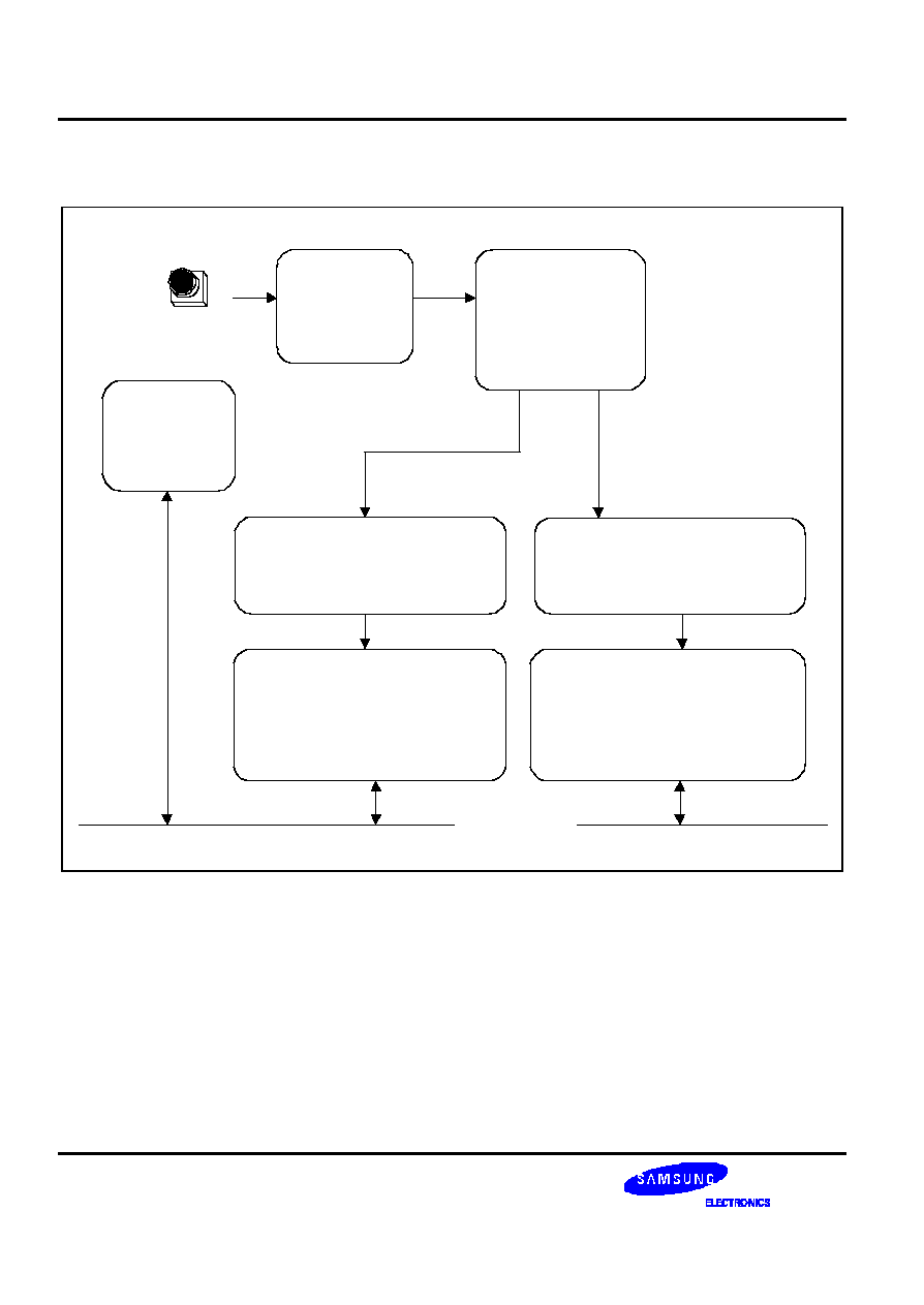
S3C2440A RISC MICROPROCESSOR
CAMERA INTERFACE
23-2
BLOCK DIAGRAM
YCbCr 4:2:2
T_patternMux
CatchCam
YCbCr 4:2:X
Preview Scaler &
RGB Formatter
Codec Scaler
Preview DMA
ITU-R BT 601/656
Codec DMA
CamI f
SFR
AHB bus
Figure 23-1. CAMIF Overview
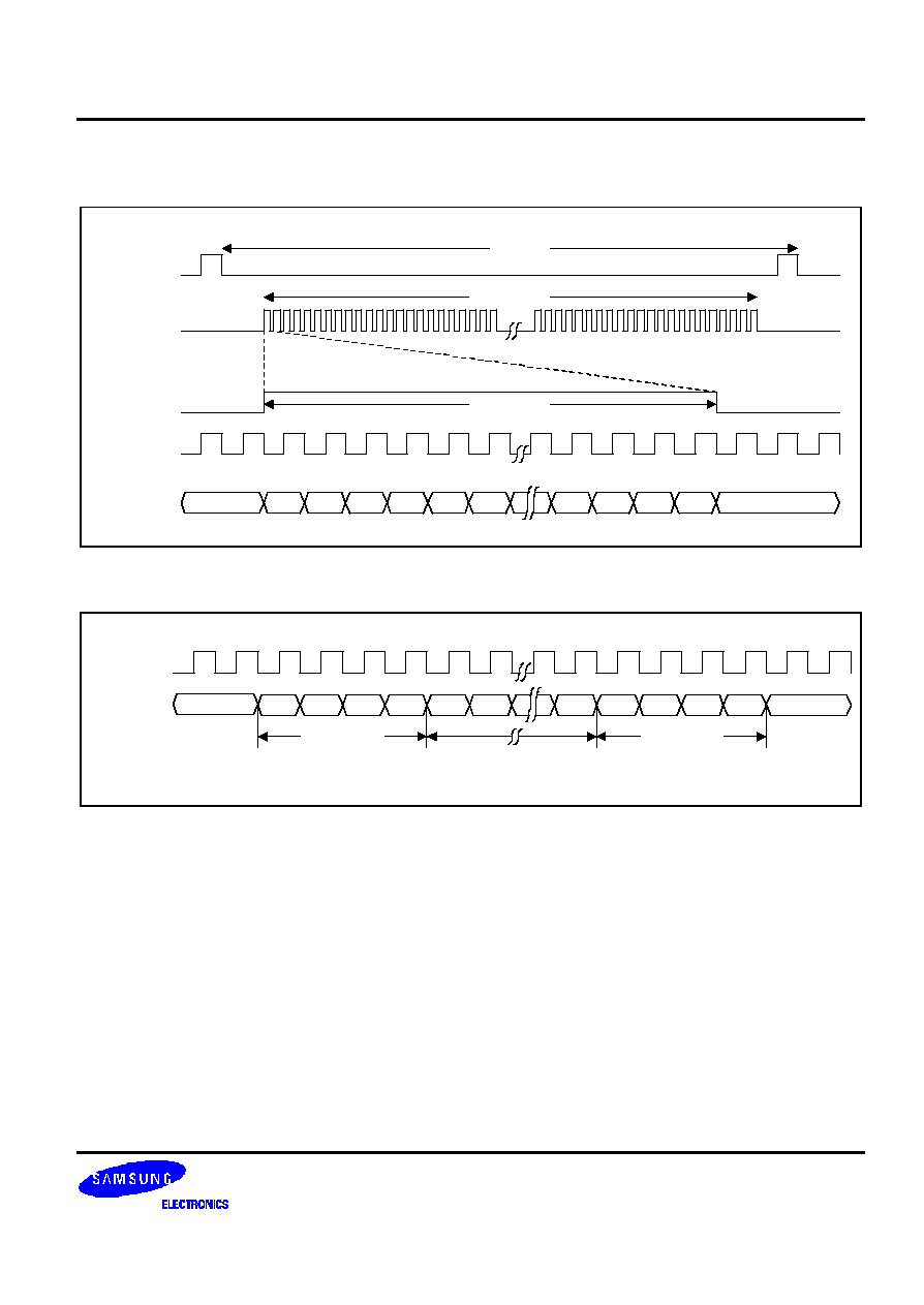
S3C2440A RISC MICROPROCESSOR
CAMERA INTERFACE
23-3
TIMING DIAGRAM
CAMVSYNC
Y
Cb
Y
Cr
Y
Cb
Y
Cb
Y
Cr
CAMHREF
CAMHREF
(1H)
CAMPCLK
CAMDATA
[7:0]
Vertical
lines
Horizontal
width
1 frame
8-bit mode
Figure 23-2. ITU-R BT 601 Input Timing Diagram
CAMPCLK
CAMDATA
[7:0]
Cr
FF
00
00
XY
Cb
Y
FF
00
00
XY
Video timing
reference
codes
Pixel
data
Video timing
reference
codes
Figure 23-3. ITU-R BT 656 Input Timing Diagram
There are two timing reference signals in ITU-R BT 656 format, one is at the beginning of each video data block (start
of active video, SAV) and other is at the end of each video data block (end of active video, EAV) as shown in Figure
23-3 and Table 23-2.
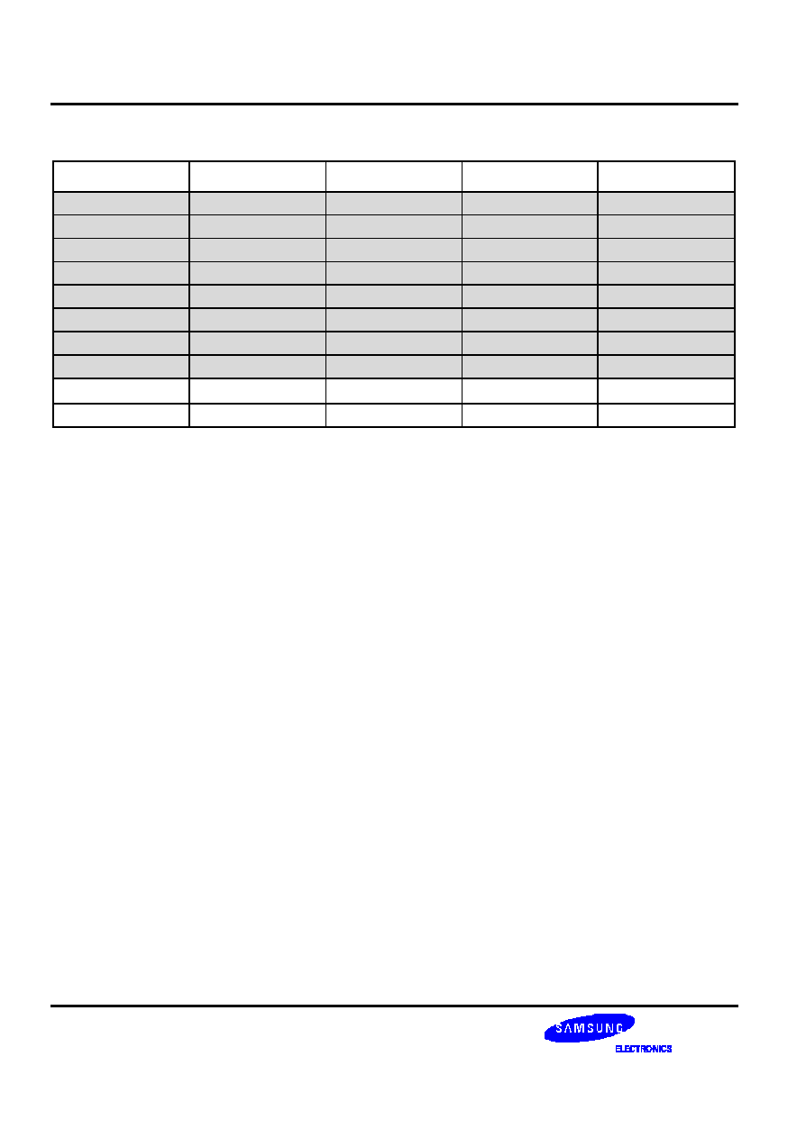
S3C2440A RISC MICROPROCESSOR
CAMERA INTERFACE
23-4
Table 23-2. Video Timing Reference Codes of ITU-656 Format
Data Bit Number
First Word
Second Word
Third Word
Fourth Word
9 (MSB)
1
0
0
1
8
1
0
0
F
7
1
0
0
V
6
1
0
0
H
5
1
0
0
P3
4
1
0
0
P2
3
1
0
0
P1
2
1
0
0
P0
1
(NOTE)
1
0
0
0
0
1
0
0
0
For compatibility with existing 8-bit interfaces, the values of bits D1 and D0 are not defined.
F = 0 (during field 1), 1 (during field 2)
V = 0 (elsewhere), 1 (during field blanking)
H = 0 (in SAV: Start of Active Video), 1 (in EAV: End of Active Video)
P0, P1, P2, P3 = protection bit
Camera interface logic can catch the video sync bits like H (SAV, EAV) and V (Frame Sync) after reserved data as
"FF-00-00".
NOTE: All external camera interface IOs are recommended to be Schmitt-trigger type IO for noise reduction.
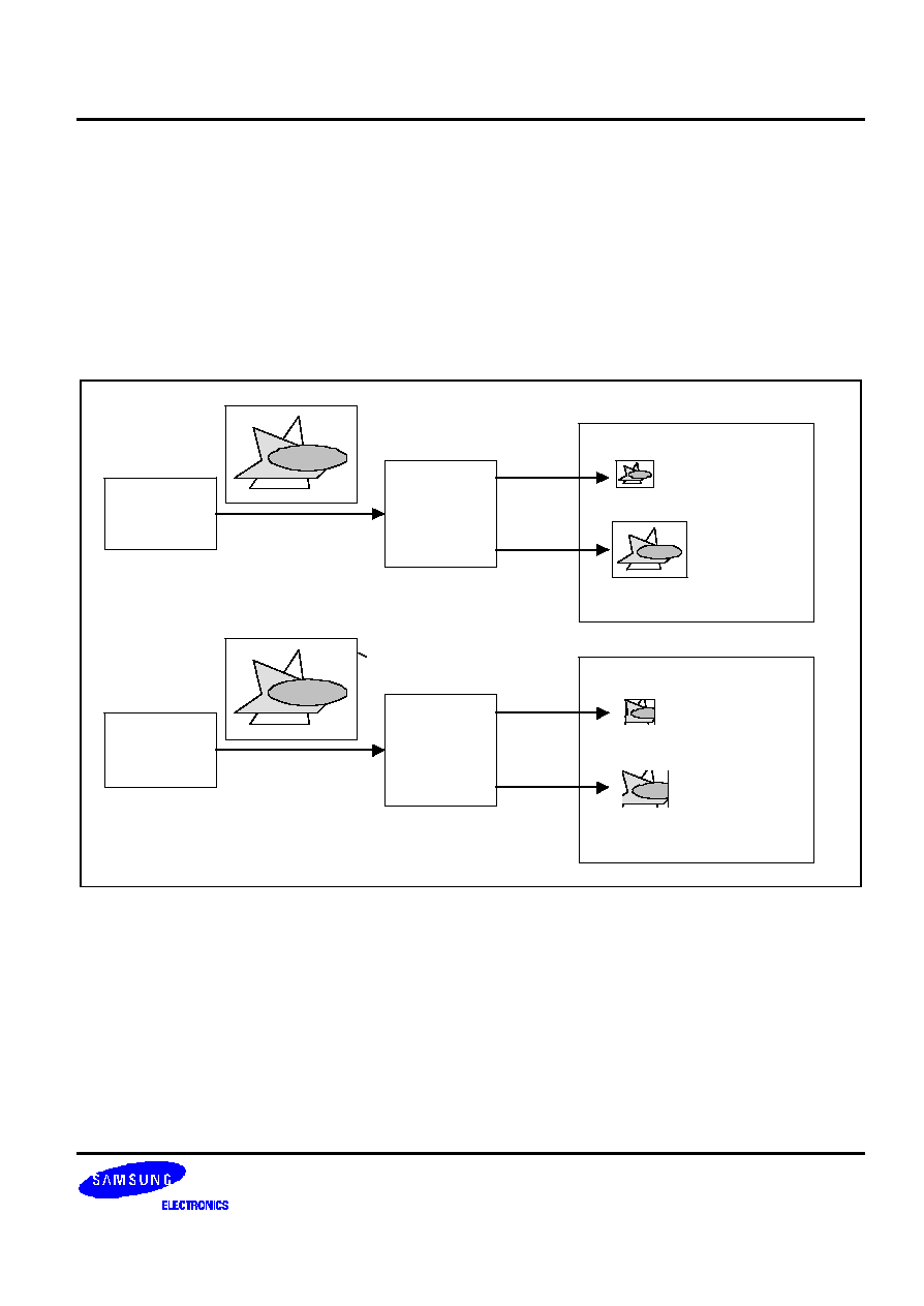
S3C2440A RISC MICROPROCESSOR
CAMERA INTERFACE
23-5
CAMERA INTERFACE OPERATION
TWO DMA PATHS
CAMIF has 2 DMA paths. P-path (Preview path) and C-path (Codec path) are separated from each other on the
AHB bus. In view of the system bus, both the paths are independent. The P-path stores the RGB image data into
memory for PIP. The C-path stores the YCbCr 4:2:0 or 4:2:2 image data into memory for Codec as MPEG-4, H.263,
etc. These two master paths support the variable applications like DSC (Digital Steel Camera), MPEG-4 video
conference, video recording, etc. For example, P-path image can be used as preview image, and C-path image can
be used as JPEG image in DSC application. Register setting can separately disable to P-path or C-path.
CAMIF
External
Camera
Processor
Frame Memory (SDRAM)
P-port
C-port
ITU format
PIP
RGB
Codec image
YCbCr 4:2:0
or
YCbCr 4:2:2
Window cut
CAMIF
External
Camera
Processor
Frame Memory (SDRAM)
P-port
C-port
ITU format
PIP
RGB
Codec image
YCbCr 4:2:0
or
YCbCr 4:2:2
Figure 23-4. Two DMA Paths
CLOCK DOMAIN
CAMIF has two clock domains. One is the system bus clock, which is HCLK. The other is the pixel clock, which is
CAMPCLK. The system clock must be faster than pixel clock. Figure 23-5 shows CAMCLKOUT must be divided
from the fixed frequency like USB PLL clock. If external clock oscillator is used, CAMCLKOUT should be floated.
Internal scaler clock is system clock. It is not necessary for two clock domains to synchronize each other. Other
signals such as CAMPCLK should be similarly connected to the Schmitt-triggered level shifter.
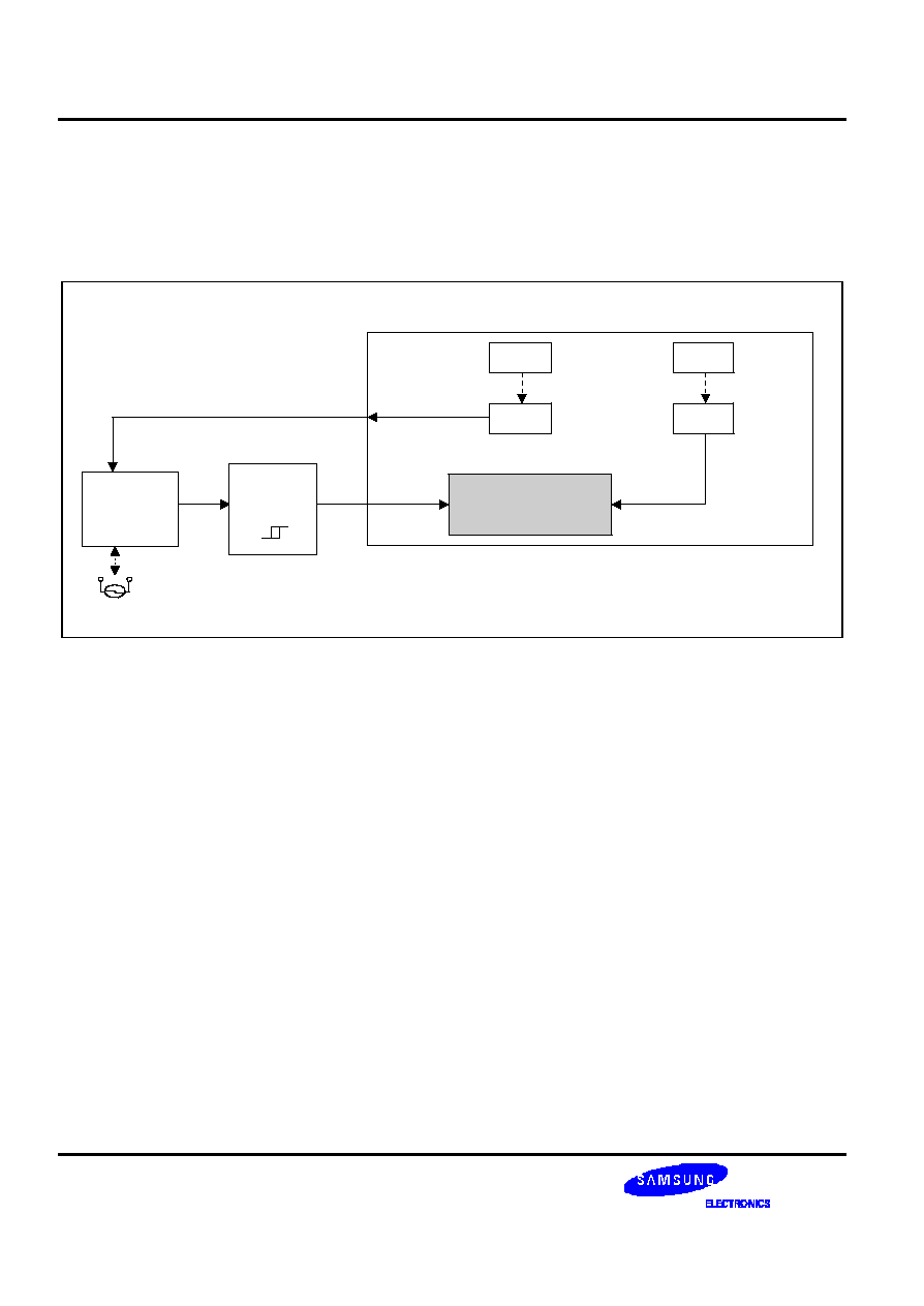
S3C2440A RISC MICROPROCESSOR
CAMERA INTERFACE
23-6
FRAME MEMORY HIRERARCHY
Frame memories consist of four ping-pong memories for each of P and C paths as shown in the Figure 23-6. C-
path ping-pong memories have three element memories ≠ luminance Y, chrominance Cb, and chrominance Cr. If
AHB-bus traffic is not enough for the DMA operation to complete during one horizontal line period, it may lead to mal-
functioning
CAMCLKOUT
Divide
Counter
1/1 ~ 1/16
UPLL
External
Camera
Processor
CAMPCLK
S3C2440A
CAMIF
USB PLL
96 MHz
f
USB
/d
f
USB
MPLL
Variable
Freq.
Divide
Counter
f
mpll
/d
f
mpll
HCLK
a
External MCLK
Normally use
Schmit-
triggered
Level-shifter
Figure 23-5. CAMIF Clock Generation
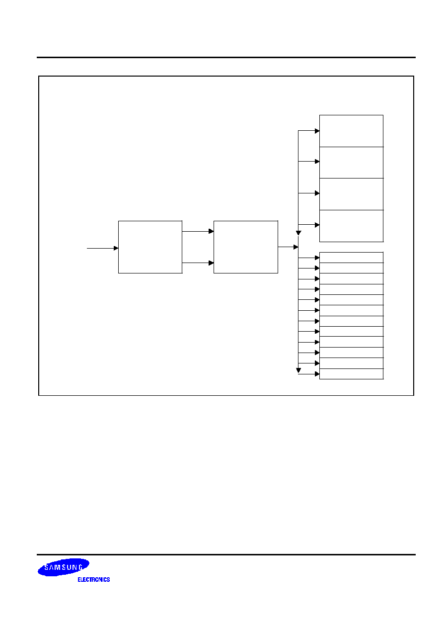
S3C2440A RISC MICROPROCESSOR
CAMERA INTERFACE
23-7
C-port Y 1
C-port Cb 1
C-port Cr 1
C-port Y 2
C-port Cb 2
C-port Cr 2
C-port Y 3
C-port Cb 3
C-port Cr 3
C-port Y 4
C-port Cb 4
C-port Cr 4
P-port RGB 1
P-port RGB 2
P-port RGB 3
P-port RGB 4
4-Pingpong
Frame Memory (SDRAM)
ITU-601/656
YCbCr
4:2:2
8-bits
Camera Interface
AHB bus &
Memorycontroller
P-port
RGB
4:4:4
C-port
4:2:0,2
Figure 23-6. Ping-Pong Memory Hierarchy
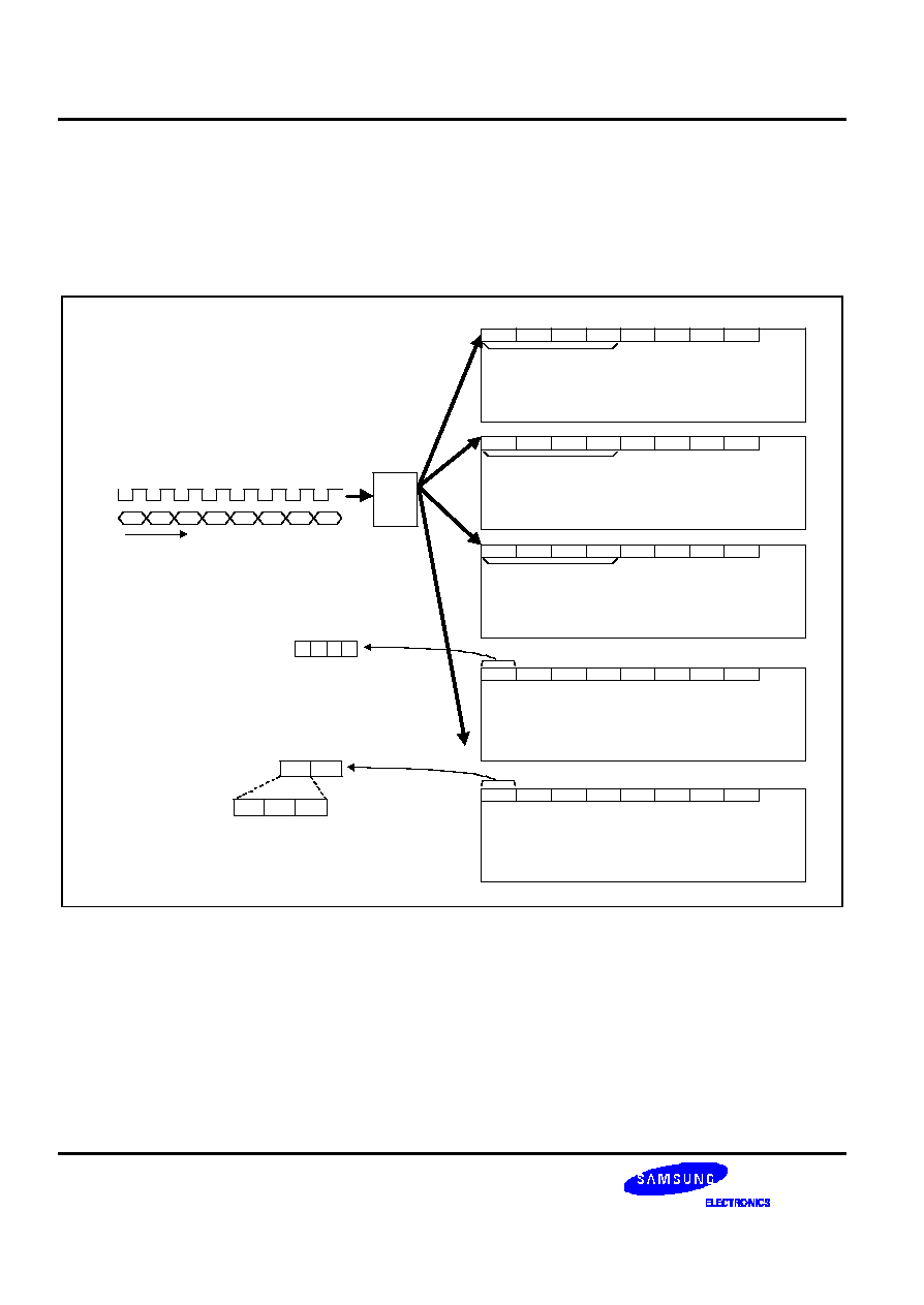
S3C2440A RISC MICROPROCESSOR
CAMERA INTERFACE
23-8
MEMORY STORING METHOD
The little-endian method in codec path is used to store in the frame memory. The pixels are stored from LSB to MSB
side. AHB bus carries 32-bit word data. So, CAMIF makes each of the Y-Cb-Cr words in little-endian style. For
preview path, two different formats exist. One pixel (Color 1 pixel) is one word for RGB 24-bit format. Otherwise, two
pixels are one word for RGB 16-bit format. Please refer the following figure.
Camera
Interface
Y Frame Memory
PCLK
DATA
ITU-601/656 YCbCr
4:2:2 8-bit input timing
Cb Frame Memory
Cr Frame Memory
Little endian method
time
Y1
Cb1
Y2
Cr1
Y3
Cb2
Y4
Cr2
Y4
Y3
Y2
Y1
Y8
Y7
Y6
Y5
Cb4
Cb3
Cb2
Cb1
Cb8
Cb7
Cb6
Cb5
Little endian method
Cr4
Cr3
Cr2
Cr1
Cr8
Cr7
Cr6
Cr5
Little endian method
RGB Frame Memory
(24-bit)
RGB1
RGB2
RGB3
RGB4 RGB5
RGB6
RGB7
RGB8
RGB Frame Memory
(16-bit)
RGB2/1 RGB4/3 RGB6/5 RGB8/7 RGB10/9
RGB12/11 RGB14/13 RGB16/15
32-bit
R G B
2
32-bit
1
R 5
G 6
B 5
16-bit
Figure 23-7. Memory Storing Style
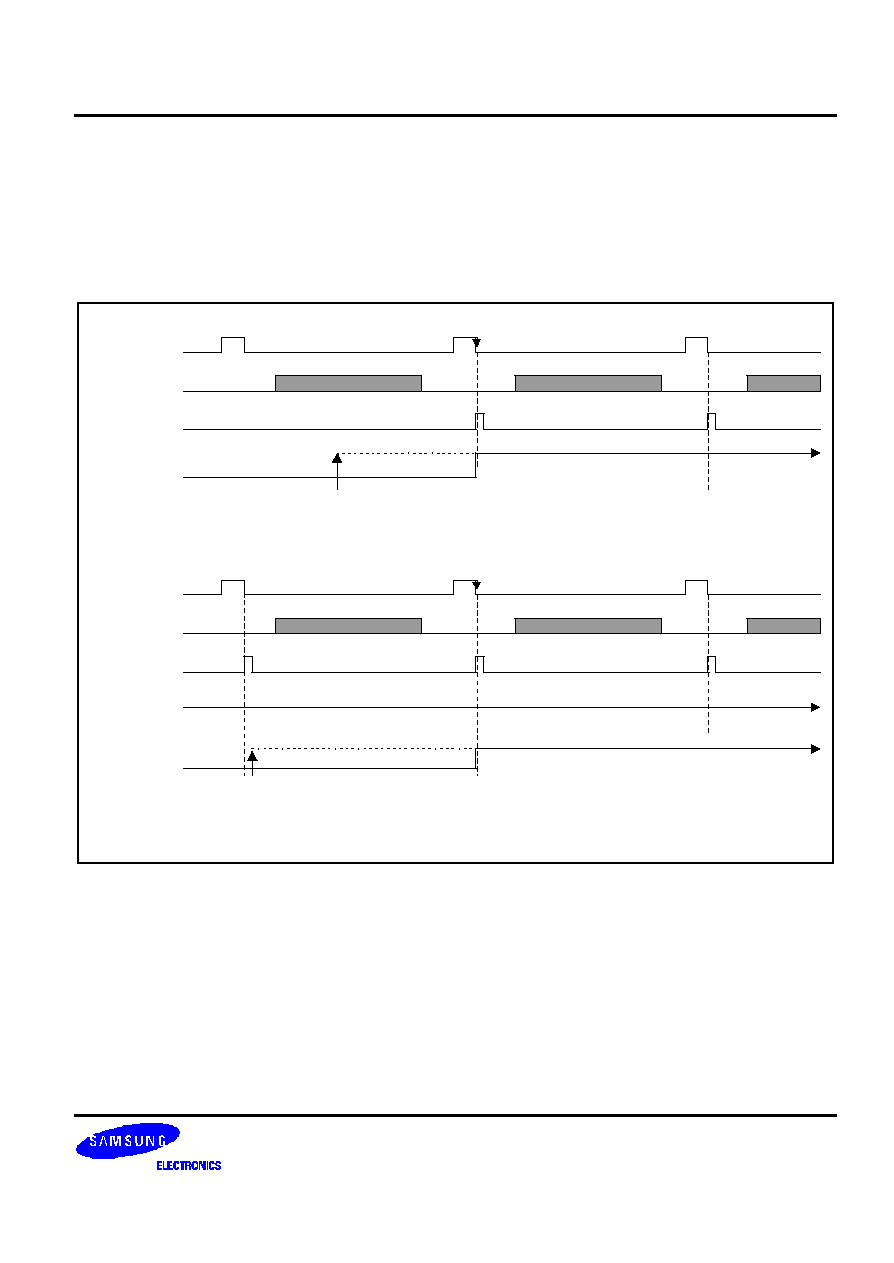
S3C2440A RISC MICROPROCESSOR
CAMERA INTERFACE
23-9
TIMING DIAGRAM FOR REGISTER SETTING
The first register setting for frame capture command can occur anywhere in the frame period. But, it is recommended
that you set it at the CAMVSYNC "L" state first and the CAMVSYNC information can be read from the status SFR
(Please see next page). All command include ImgCptEn, is valid at CAMVSYNC falling edge. But be careful that
except for first SFR setting, all command should be programmed in an ISR (Interrupt Service Routine). Especially,
capture operation should be disabled when related information for target size are changed.
CAMVSYNC
CAMHREF
INTERRUPT
SFR setting
(ImgCptEn)
Multi frame
capturing
Reserved
Image Capture
< Frame Capture Start >
CAMVSYNC
CAMHREF
INTERRUPT
New SFR
command in ISR
In Capturing
Reserved
Image Capture
< New Command Valid Timing Diagram >
New Command
Figure 23-8. Timing Diagram for Register Setting
NOTE: FIFO overflow of codec path will be occurred if codec path is not operating when preview path is operated. If you
want to use codec path under this case, you should stop preview path and reset CAMIF using SwRst bit of
CIGCTRL
register. Then clear overflow of codec path and set special function registers that you want.
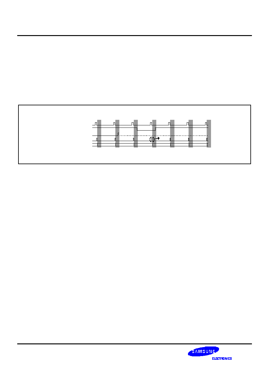
S3C2440A RISC MICROPROCESSOR
CAMERA INTERFACE
23-10
TIMING DIAGRAM FOR LAST IRQ
IRQ except LastIRQ is generated before image capturing. Last IRQ which means capture-end can be set by following
timing diagram. LastIRQEn is auto-cleared and ,as mentioned, SFR setting in ISR is for next frame command. So,
for adequate last IRQ, you should follow next sequence between LastIRQEn and ImgCptEn /ImgCptEn_CoSc
/ImgCptEnPrSC. It is recommended that ImgCptEn /ImgCptEn_CoSc /ImgCptEnPrSC are set at same time and at
last of SFR setting in ISR. FrameCnt which is read in ISR, means next frame count. On following diagram, last
captured frame count is "1". That is, Frame 1 is the last-captured frame among frame 0~3. FrameCnt is increased by
1 at IRQ rising.
ISR region
ISR region
ISR region
VSYNC
ISR region
ImgCptEn(cmd)
LastIRQEn
Capture O
Capture O
Capture O Capture X
IRQ
Auto cleared
Last IRQ
ISR region ISR region ISR region
FrameCnt
Capture O
Capture O
(Frame_3)
(Frame_0)
(Frame_1)
(Frame_3)
(Frame_0)
0
1
2
3
3
0
1
Figure 23-9. Timing diagram for last IRQ
S3C2440A RISC MICROPROCESSOR
CAMERA INTERFACE
23-11
CAMERA INTERFACE SPECIAL REGISTERS
SOURCE FORMAT REGISTER
Register
Address
R/W
Description
Reset Value
CISRCFMT
0x4F000000
RW
Input source format register
0
CISRCFMT
Bit
Description
Initial State
ITU601_656n
[31]
0 = ITU-R BT.656 YCbCr 8-bit mode enable
1 = ITU-R BT.601 YCbCr 8-bit mode enable
0
UVOffset
[30]
Cb,Cr Value Offset Control.
0 = +0 (normally used) - for YCbCr
1 = +128
- for YUV
0
Reserved
[29]
This bit is reserved and the value must be 0.
0
SourceHsize
[28:16]
Source Horizontal Pixel Number (must be multiple of 8)
0
Order422
[15:14]
Input YcbCr order inform for input 8-bit mode
00 = YCbYCr
01 = YCrYCb
10 = CbYCrY
11 = CrYCbY
0
SourceVsize
[12:0]
Source Vertical Pixel Number
0
NOTE: We recommend a following sequence for preventing FIFO overflow at first frame of capture operation in CODEC
path
<ITU 601 Format>
1. CISRCFMT[31] <- '1'
2. S/W reset
3. Initialize the Camera I/F
4. Start Capturing
<ITU 656 Format>
1. CISRCFMT[31] <- '1'
2. S/W reset
3. Initialize the Camera I/F
4. CISRCFMT[31] <- '0' //for ITU 656 format
6. Start Capturing
7. Clear Overflow of codec on First ISR
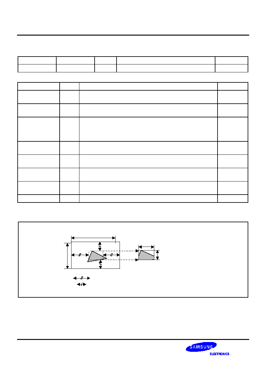
S3C2440A RISC MICROPROCESSOR
CAMERA INTERFACE
23-12
WINDOW OPTION REGISTER
Register
Address
R/W
Description
Reset Value
CIWDOFST
0x4F000004
RW
Window offset register
0
CIWDOFST
Bit
Description
Initial State
WinOfsEn
[31]
0 = No offset
1 = Window offset enable
0
ClrOvCoFiY
[30]
0 = Normal
1 = Clear the overflow indication flag of input CODEC FIFO Y
0
WinHorOfst
[26:16]
Window Horizontal Offset
(the number which is the horizontal pixels except WinHorOfst * 2,
must be multiple of 8)
* WinHorOfst >= (SourceHsize-640*PreHorRatio_Pr)/2
0
ClrOvCoFiCb
[15]
0 = Normal
1 = Clear the overflow indication flag of input CODEC FIFO Cb
0
ClrOvCoFiCr
[14]
0 = Normal
1 = Clear the overflow indication flag of input CODEC FIFO Cr
0
ClrOvPrFiCb
[13]
0 = Normal
1 = Clear the overflow indication flag of input PREVIEW FIFO Cb
0
ClrOvPrFiCr
[12]
0 = Normal
1 = Clear the overflow indication flag of input PREVIEW FIFO Cr
0
WinVerOfst
[10:0]
Window Vertical Offset
0
NOTE: We recommend you to clear all the overflow bits before starting the capture operation.
SourceHsize
SourceVsize
Original Input
Window Cut
: WinHorOfst
: WinVerOfst
TargetHsize_xx
TargetHsize_xx
= TargetHsize_Co or TargetHsize_Pr
TargetVsize_xx
Figure 23-10. Window Offset Scheme
S3C2440A RISC MICROPROCESSOR
CAMERA INTERFACE
23-13
GLOBAL CONTROL REGISTER
Register
Address
R/W
Description
Reset Value
CIGCTRL
0x4F000008
RW
Global control register
0
CIGCTRL
Bit
Description
Initial State
SwRst
[31]
Camera interface software reset
0
CamRst
[30]
External camera processor reset or power down
0
Reserved
[29]
This bit is reserved and the value must be 1.
1
TestPattern
[28:27]
This register should be set only at ITU-T 601 8-bit mode. It is not
allowed with ITU-T 656 mode. (max. 1280 X 1024)
00 = External camera processor input (normal)
01 = Color bar test pattern
10 = Horizontal increment test pattern
11 = Vertical increment test pattern
0
InvPolCAMPCLK
[26]
0 = Normal
1 = Inverse the polarity of CAMPCLK
0
InvPolCAMVSYNC
[25]
0 = Normal
1 = Inverse the polarity of CAMVSYNC
0
InvPolCAMHREF
[24]
0 = Normal
1 = Inverse the polarity of CAMHREF
0
Y1 START ADDRESS REGISTER
Register
Address
R/W
Description
Reset Value
CICOYSA1
0x4F000018
RW
Y 1
st
frame start address for codec DMA
0
CICOYSA1
Bit
Description
Initial State
CICOYSA1
[31:0]
Y 1
st
frame start address for codec DMA
0
NOTE: Address of buffers must be multiple of 1024.
Y2 START ADDRESS REGISTER
Register
Address
R/W
Description
Reset Value
CICOYSA2
0x4F00001C
RW
Y 2
nd
frame start address for codec DMA
0
CICOYSA2
Bit
Description
Initial State
CICOYSA2
[31:0]
Y 2
nd
frame start address for codec DMA
0
S3C2440A RISC MICROPROCESSOR
CAMERA INTERFACE
23-14
Y3 START ADDRESS REGISTER
Register
Address
R/W
Description
Reset Value
CICOYSA3
0x4F000020
RW
Y 3
nd
frame start address for codec DMA
0
CICOYSA3
Bit
Description
Initial State
CICOYSA3
[31:0]
Y 3
nd
frame start address for codec DMA
0
Y4 START ADDRESS REGISTER
Register
Address
R/W
Description
Reset Value
CICOYSA4
0x4F000024
RW
Y 4
th
frame start address for codec DMA
0
CICOYSA4
Bit
Description
Initial State
CICOYSA4
[31:0]
Y 4
th
frame start address for codec DMA
0
CB1 START ADDRESS REGISTER
Register
Address
R/W
Description
Reset Value
CICOCBSA1
0x4F000028
RW
Cb 1
st
frame start address for codec DMA
0
CICOCBSA1
Bit
Description
Initial State
CICOCBSA1
[31:0]
Cb 1
st
frame start address for codec DMA
0
CB2 START ADDRESS REGISTER
Register
Address
R/W
Description
Reset Value
CICOCBSA2
0x4F00002C
RW
Cb 2
nd
frame start address for codec DMA
0
CICOCBSA2
Bit
Description
Initial State
CICOCBSA2
[31:0]
Cb 2
nd
frame start address for codec DMA
0
S3C2440A RISC MICROPROCESSOR
CAMERA INTERFACE
23-15
CB3 START ADDRESS REGISTER
Register
Address
R/W
Description
Reset Value
CICOCBSA3
0x4F000030
RW
Cb 3
nd
frame start address for codec DMA
0
CICOCBSA3
Bit
Description
Initial State
CICOCBSA3
[31:0]
Cb 3
nd
frame start address for codec DMA
0
CB4 START ADDRESS REGISTER
Register
Address
R/W
Description
Reset Value
CICOCBSA4
0x4F000034
RW
Cb 4
th
frame start address for codec DMA
0
CICOCBSA4
Bit
Description
Initial State
CICOCBSA4
[31:0]
Cb 4
th
frame start address for codec DMA
0
CR1 START ADDRESS REGISTER
Register
Address
R/W
Description
Reset Value
CICOCRSA1
0x4F000038
RW
Cr 1
st
frame start address for codec DMA
0
CICOCRSA1
Bit
Description
Initial State
CICOCRSA1
[31:0]
Cr 1
st
frame start address for codec DMA
0
CR2 START ADDRESS REGISTER
Register
Address
R/W
Description
Reset Value
CICOCRSA2
0x4F00003C
RW
Cr 2
nd
frame start address for codec DMA
0
CICOCRSA2
Bit
Description
Initial State
CICOCRSA2
[31:0]
Cr 2
nd
frame start address for codec DMA
0
S3C2440A RISC MICROPROCESSOR
CAMERA INTERFACE
23-16
CR3 START ADDRESS REGISTER
Register
Address
R/W
Description
Reset Value
CICOCRSA3
0x4F000040
RW
Cr 3
nd
frame start address for codec DMA
0
CICOCRSA3
Bit
Description
Initial State
CICOCRSA3
[31:0]
Cr 3
nd
frame start address for codec DMA
0
CR4 START ADDRESS REGISTER
Register
Address
R/W
Description
Reset Value
CICOCRSA4
0x4F000044
RW
Cr 4
th
frame start address for codec DMA
0
CICOCRSA4
Bit
Description
Initial State
CICOCRSA4
[31:0]
Cr 4
th
frame start address for codec DMA
0

S3C2440A RISC MICROPROCESSOR
CAMERA INTERFACE
23-17
CODEC TARGET FORMAT REGISTER
Register
Address
R/W
Description
Reset Value
CICOTRGFMT
0x4F000048
RW
Target image format of codec DMA
0
CICOTRGFMT
Bit
Description
Initial State
In422_Co
[31]
0 = YCbCr 4:2:0 codec scaler input image format. In this case,
horizontal line decimation is performed before codec scaler.
(normally used)
1 = YCbCr 4:2:2 codec scaler input image format.
0
Out422_Co
[30]
0 = YCbCr 4:2:0 codec scaler output image format. This mode is
mainly for MPEG-4 codec & H/W JPEG DCT (normally used)
1 = YCbCr 4:2:2 codec scaler output image format. This mode is
mainly for S/W JPEG.
0
TargetHsize_Co
[28:16]
Horizontal pixel number of target image for codec DMA
(multiple of 16)
0
FlipMd_Co
[15:14]
Image mirror and rotation for codec DMA
00 = Normal
01 = X-axis mirror
10 = Y-axis mirror
11 = 180
∞
rotation
0
TargetVsize_Co
[12:0]
Vertical pixel number of target image for codec DMA
0
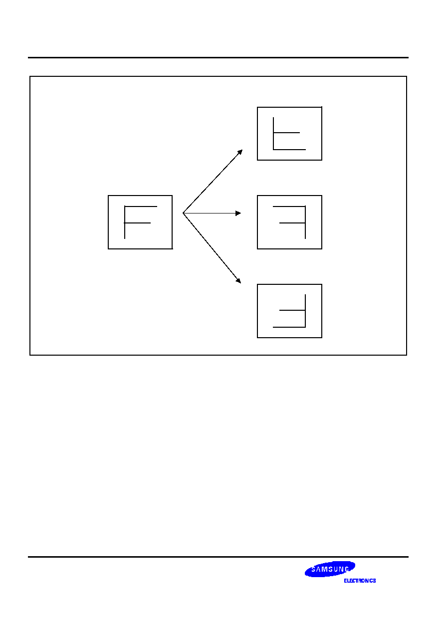
S3C2440A RISC MICROPROCESSOR
CAMERA INTERFACE
23-18
Original Image
X-Axis Flip
Y-Axis Flip
180
∞
Rotation
Figure 23-11. Image Mirror and Rotation
S3C2440A RISC MICROPROCESSOR
CAMERA INTERFACE
23-19
CODEC DMA CONTROL REGISTER
Register
Address
R/W
Description
Reset Value
CICOCTRL
0x4F00004C
RW
Codec DMA control related
0
CICOCTRL
Bit
Description
Initial State
Yburst1_Co
[23:19]
Main burst length for codec Y frames
0
Yburst2_Co
[18:14]
Remained burst length for codec Y frames
0
Cburst1_Co
[13:9]
Main burst length for codec Cb/Cr frames
0
Cburst2_Co
[8:4]
Remained burst length for codec Cb/Cr frames
0
LastIRQEn_Co
[2]
0 = normal
1 = enable last IRQ at the end of the frame capture
(This bit is cleared automatically)
0
NOTE: All burst lengths must be one of the 2, 4, 8, 16.
Example 1: Target image size: QCIF (horizontal Y width = 176 pixels. 1 pixel = 1 Byte. 1 word = 4 pixel)
176 / 4 = 44 word
44 % 8 = 4
main burst = 8, remained burst = 4
Example 2: Target image size: VGA (horizontal Y width = 640 pixels. 1 pixel = 1 Byte. 1 word = 4 pixel)
640 / 4 = 160 word
160 % 16 = 0
main burst = 16, remained burst = 16
Example 3: Target image size: QCIF (horizontal C width = 88 pixels. 1 pixel = 1 Byte. 1 word = 4 pixel)
88 / 4 = 22 word
22 % 4 = 2
main burst = 4, remained burst = 2 (HTRANS==INCR)
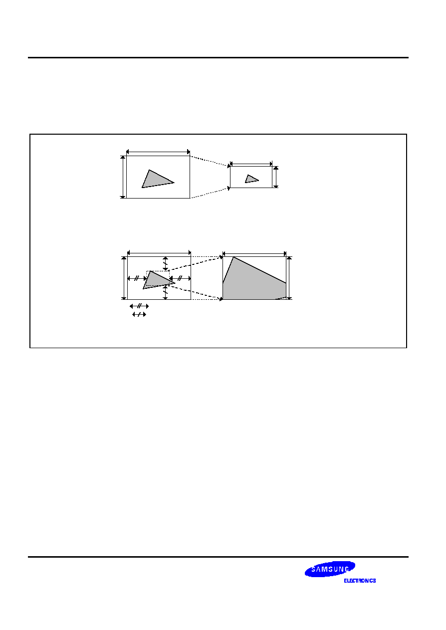
S3C2440A RISC MICROPROCESSOR
CAMERA INTERFACE
23-20
REGISTER SETTING GUIDE FOR CODEC SCALER AND PREVIEW SCALER
SRC_Width and DST_Width satisfy the word boundary constraints such that the number of horizontal pixel can be
represented to kn where n = 1,2,3, ... and k = 1 / 2 / 8 for 24bppRGB / 16bppRGB / YCbCr420 image, respectively.
TargetHsize should not be larger than SourceHsize. Similarly, TargetVsize should not be larger than SourceVsize.
SourceHsize
SourceVsize
TargetHsize_xx
TargetVsize_xx
Original Input
Scale Down
SourceHsize
SourceVsize
Original Input
Zoom In
: WinHorOfst
: WinVerOfst
TargetHsize_xx
TargetVsize_xx
SRC_Width = SourceHsize
SRC_Height = SourceVsize
TargetHsize_xx = TargetHsize_Co or TargetHsize_Pr
DST_Width = TargetHsize_xx
DST_Height = TargetVsize_xx
TargetHsize_xx = TargetHsize_Co or TargetHsize_Pr
DST_Width = TargetHsize_xx
DST_Height = TargetVsize_xx
SRC_Width = SourceHsize - (2 x WinHorOfst)
SRC_Height = SourceVsize - (2 x WinVerOfst)
Figure 23-12. Scaling Scheme
The other control registers of pre-scaled like image size, pre-scale ratio, pre-scale shift ratio and main scale ratio are
defined according to the following equations.
If ( SRC_Width >= 64 ◊ DST_Width ) { Exit(-1); /* Out Of Horizontal Scale Range */ }
else if (SRC_Width >= 32 ◊ DST_Width) { PreHorRatio_xx = 32; H_Shift = 5; }
else if (SRC_Width >= 16 ◊ DST_Width) { PreHorRatio_xx = 16; H_Shift = 4; }
else if (SRC_Width >= 8 ◊ DST_Width) { PreHorRatio_xx = 8; H_Shift = 3; }
else if (SRC_Width >= 4 ◊ DST_Width) { PreHorRatio_xx = 4; H_Shift = 2; }
else if (SRC_Width >= 2 ◊ DST_Width) { PreHorRatio_xx = 2; H_Shift = 1; }
else { PreHorRatio_xx = 1; H_Shift = 0; }
PreDstWidth_xx = SRC_Width / PreHorRatio_xx;
MainHorRatio_xx = ( SRC_Width << 8 ) / ( DST_Width << H_Shift);
S3C2440A RISC MICROPROCESSOR
CAMERA INTERFACE
23-21
If ( SRC_Height >= 64 ◊ DST_Height ) { Exit(-1); /* Out Of Vertical Scale Range */ }
else if (SRC_Height >= 32 ◊ DST_Height) { PreVerRatio_xx = 32; V_Shift = 5; }
else if (SRC_Height >= 16 ◊ DST_Height) { PreVerRatio_xx = 16; V_Shift = 4; }
else if (SRC_Height >= 8 ◊ DST_Height) { PreVerRatio_xx = 8; V_Shift = 3; }
else if (SRC_Height >= 4 ◊ DST_Height) { PreVerRatio_xx = 4; V_Shift = 2; }
else if (SRC_Height >= 2 ◊ DST_Height) { PreVerRatio_xx = 2; V_Shift = 1; }
else { PreVerRatio_xx = 1; V_Shift = 0; }
PreDstHeight_xx = SRC_Height / PreVerRatio_xx;
MainVerRatio_xx = ( SRC_Height << 8 ) / ( DST_Height << V_Shift);
SHfactor_xx = 10 ≠ ( H_Shit + V_Shift);
NOTE
Preview path contains 640 pixel line buffer. (Codec path contains 2048 pixel line buffer) So, upper 1280
pixels, input images must be pre-scaled by over 1/2 for capturing valid preview image. ((SourceHsize-
2*WinHorOfst)/PreHorRatio_Pr) <= 640
CODEC PRE-SCALER CONTROL REGISTER 1
Register
Address
R/W
Description
Reset Value
CICOSCPRERATIO
0x4F000050
RW
Codec pre-scaler ratio control
0
CICOSCPRERATIO
Bit
Description
Initial State
SHfactor_Co
[31:28]
Shift factor for codec pre-scaler
0
PreHorRatio_Co
[22:16]
Horizontal ratio of codec pre-scaler
0
PreVerRatio_Co
[6:0]
Vertical ratio of codec pre-scaler
0
CODEC PRE-SCALER CONTROL REGISTER 2
Register
Address
R/W
Description
Reset Value
CICOSCPREDST
0x4F000054
RW
Codec pre-scaler destination format
0
CICOSCPREDST
Bit
Description
Initial State
PreDstWidth_Co
[27:16]
Destination width for codec pre-scaler
0
PreDstHeight_Co
[11:0]
Destination height for codec pre-scaler
0
S3C2440A RISC MICROPROCESSOR
CAMERA INTERFACE
23-22
CODEC MAIN-SCALER CONTROL REGISTER
Register
Address
R/W
Description
Reset Value
CICOSCCTRL
0x4F000058
RW
Codec main-scaler control
0
CICOSCCTRL
Bit
Description
Initial State
ScalerBypass_Co
[31]
Codec scaler bypass for upper 2048 x 2048 size (In this case,
ImgCptEn_CoSC and ImgCptEn_PrSC should be 0, but
ImgCptEn should be 1. It is not allowed to capture preview
image. This mode is intended to capture JPEG input image for
DSC application) In this case, input pixel buffering depends on
only input FIFOs, so the system bus should be not busy in this
mode.
0
ScaleUpDown_Co
[30:29]
Scale up/down flag for codec scaler
(In 1:1 scale ratio, this bit should be "1")
00 = Down 11 = Up
00
MainHorRatio_Co
[24:16]
Horizontal scale ratio for codec main-scaler
0
CoScalerStart
[15]
Codec scaler start
0
MainVerRatio_Co
[8:0]
Vertical scale ratio for codec main-scaler
0
CODEC DMA TARGET AREA REGISTER
Register
Address
R/W
Description
Reset Value
CICOTAREA
0x4F00005C
RW
Codec scaler target area
0
CICOTAREA
Bit
Description
Initial State
CICOTAREA
[25:0]
Target area for codec DMA = Target H size x Target V size
0
S3C2440A RISC MICROPROCESSOR
CAMERA INTERFACE
23-23
CODEC STATUS REGISTER
Register
Address
R/W
Description
Reset Value
CICOSTATUS
0x4F000064
R
Codec path status
0
CICOSTATUS
Bit
Description
Initial State
OvFiY_Co
[31]
Overflow state of codec source FIFO Y
0
OvFiCb_Co
[30]
Overflow state of codec source FIFO Cb
0
OvFiCr_Co
[29]
Overflow state of codec source FIFO Cr
0
VSYNC
[28]
Camera VSYNC (This bit can be referred by CPU for first SFR
setting. And, it can be seen in the ITU-R BT 656 mode, too)
0
FrameCnt_Co
[27:26]
Frame count of codec DMA (This counter value indicates the
next frame number)
0
WinOfstEn_Co
[25]
Window offset enable status
0
FlipMd_Co
[24:23]
Flip mode of codec DMA
0
ImgCptEn_CamIf
[22]
Image capture enable of camera interface
0
ImgCptEn_CoSC
[21]
Image capture enable of codec path
0
RGB1 START ADDRESS REGISTER
Register
Address
R/W
Description
Reset Value
CIPRCLRSA1
0x4F00006C
RW
RGB 1
st
frame start address for preview DMA
0
CIPRCLRSA1
Bit
Description
Initial State
CIPRCLRSA1
[31:0]
RGB 1
st
frame start address for preview DMA
0
RGB2 START ADDRESS REGISTER
Register
Address
R/W
Description
Reset Value
CIPRCLRSA2
0x4F000070
RW
RGB 2
nd
frame start address for preview DMA
0
CIPRCLRSA2
Bit
Description
Initial State
CIPRCLRSA2
[31:0]
RGB 2
nd
frame start address for preview DMA
0
S3C2440A RISC MICROPROCESSOR
CAMERA INTERFACE
23-24
RGB3 START ADDRESS REGISTER
Register
Address
R/W
Description
Reset Value
CIPRCLRSA3
0x4F000074
RW
RGB 3
nd
frame start address for preview DMA
0
CIPRCLRSA3
Bit
Description
Initial State
CIPRCLRSA3
[31:0]
RGB 3
nd
frame start address for preview DMA
0
RGB4 START ADDRESS REGISTER
Register
Address
R/W
Description
Reset Value
CIPRCLRSA4
0x4F000078
RW
RGB 4
th
frame start address for preview DMA
0
CIPRCLRSA4
Bit
Description
Initial State
CIPRCLRSA4
[31:0]
RGB 4
th
frame start address for preview DMA
0
PREVIEW TARGET FORMAT REGISTER
Register
Address
R/W
Description
Reset Value
CIPRTRGFMT
0x4F00007C
RW
Target image format of preview DMA
0
CIPRTRGFMT
Bit
Description
Initial State
TargetHsize_Pr
[28:16]
Horizontal pixel number of target image for preview DMA (even)
0
FlipMd_Pr
[15:14]
Image mirror and rotation for preview DMA
00 = Normal
01 = X-axis mirror
10 = Y-axis mirror
11 = 180
∞
rotation
0
TargetVsize_Pr
[12:0]
Vertical pixel number of target image for preview DMA
0
S3C2440A RISC MICROPROCESSOR
CAMERA INTERFACE
23-25
PREVIEW DMA CONTROL REGISTER
Register
Address
R/W
Description
Reset Value
CIPRCTRL
0x4F000080
RW
Preview DMA control related
0
CIPRCTRL
Bit
Description
Initial State
RGBburst1_Pr
[23:19]
Main burst length for preview RGB frames
0
RGBburst2_Pr
[18:14]
Remained burst length for preview RGB frames
0
LastIRQEn_Pr
[2]
0 = Normal
1 = Enable last IRQ at the end of frame capture.
(This bit is cleared automatically.)
0
NOTE: All burst lengths must be one of the 2, 4, 8, 16.
Example 1: Target image size: QCIF for RGB 32-bit format (horizontal width = 176 pixels. 1 pixel = 1 word)
176 pixel = 176 word.
176 % 16 = 0
main burst = 16, remained burst = 16
Example 2: Target image size: VGA for RGB 16-bit format (horizontal width = 640 pixels. 2 pixel = 1 word)
640 / 2 = 320 word
160 % 16 = 0
main burst = 16, remained burst = 16
PREVIEW PRE-SCALER CONTROL REGISTER 1
Register
Address
R/W
Description
Reset Value
CIPRSCPRERATIO
0x4F000084
RW
Preview pre-scaler ratio control
0
CIPRSCPRERATIO
Bit
Description
Initial State
SHfactor_Pr
[31:28]
Shift factor for preview pre-scaler
0
PreHorRatio_Pr
[22:16]
Horizontal ratio of preview pre-scaler
0
PreVerRatio_Pr
[6:0]
Vertical ratio of preview pre-scaler
0
S3C2440A RISC MICROPROCESSOR
CAMERA INTERFACE
23-26
PREVIEW PRE-SCALER CONTROL REGISTER 2
Register
Address
R/W
Description
Reset Value
CIPRSCPREDST
0x4F000088
RW
Preview pre-scaler destination format
0
CIPRSCPREDST
Bit
Description
Initial State
PreDstWidth_Pr
[27:16]
Destination width for preview pre-scaler
0
PreDstHeight_Pr
[11:0]
Destination height for preview pre-scaler
0
PREVIEW MAIN-SCALER CONTROL REGISTER
Register
Address
R/W
Description
Reset Value
CIPRSCCTRL
0x4F00008C
RW
Preview main-scaler control
0
CICOSCCTRL
Bit
Description
Initial State
Sample_Pr
[31]
Sampling method for format conversion.
(This bit is recommended to fix 1)
0
RGBformat_Pr
[30]
0 = 16-bit RGB 1 = 24-bit RGB
0
ScaleUpDown_Pr
[29:28]
Scale up/down flag for preview scaler
(In 1:1 scale ratio, this bit should be "1")
00 = down
11 = up
00
MainHorRatio_Pr
[24:16]
Horizontal scale ratio for preview main-scaler
0
PrScalerStart
[15]
Preview scaler start
0
MainVerRatio_Pr
[8:0]
Vertical scale ratio for preview main-scaler
0
PREVIEW DMA TARGET AREA REGISTER
Register
Address
R/W
Description
Reset Value
CIPRTAREA
0x4F000090
RW
Preview scaler target area
0
CIPRTAREA
Bit
Description
Initial State
CIPRTAREA
[25:0]
Target area for preview DMA = Target H size x Target V size
0
S3C2440A RISC MICROPROCESSOR
CAMERA INTERFACE
23-27
PREVIEW STATUS REGISTER
Register
Address
R/W
Description
Reset Value
CIPRSTATUS
0x4F000098
R
Preview path status
0
CIPRSTATUS
Bit
Description
Initial State
OvFiCb_Pr
[31]
Overflow state of preview source FIFO Cb
0
OvFiCr_Pr
[30]
Overflow state of preview source FIFO Cr
0
FrameCnt_Pr
[27:26]
Frame count of preview DMA
0
FlipMd_Pr
[24:23]
Flip mode of preview DMA
0
ImgCptEn_PrSC
[21]
Image capture enable of preview path
0
IMAGE CAPTURE ENABLE REGISTER
This register must be set at last.
Register
Address
R/W
Description
Reset Value
CIIMGCPT
0x4F0000A0
RW
Image capture enable command
0
CIGCTRL
Bit
Description
Initial State
ImgCptEn
[31]
Camera interface global capture enable
0
ImgCptEn_CoSc
[30]
Capture enable for codec scaler.
This bit must be `0' in scaler bypass mode.
0
ImgCptEn_PrSc
[29]
Capture enable for preview scaler
This bit must be `0' in scaler bypass mode.
0

S3C2440A RISC MICROPROCESSOR
CAMERA INTERFACE
23-28
NOTES

S3C2440A RISC MICROPROCESSOR
AC97 CONTROLLER
24-1
24
AC97 CONTROLLER
OVERVIEW
The AC97 Controller Unit of the S3C2440A supports AC97 revision 2.0 features. AC97 Controller communicates with
AC97 Codec using an audio controller link (AC-link). Controller sends the stereo PCM data to Codec. The external
digital-to-analog converter (DAC) in the Codec then converts the audio sample to an analog audio waveform. Also, the
Controller receives the stereo PCM data and the mono Mic data from the Codec and then stores them in the
memories. This chapter describes the programming model for the AC97 Controller Unit. The information in this
chapter requires an understanding of the AC97 revision 2.0 specifications.
NOTE
The AC97 Controller and the I
2
S Controller must not be used at the same time.
FEATURES
-- Independent channels for stereo PCM In, stereo PCM Out, mono MIC In.
-- DMA-based operation and interrupt based operation.
-- All of the channels support only 16-bit samples.
-- Variable sampling rate AC97 Codec interface (48 KHz and below)
-- 16-bit, 16 entry FIFOs per channel
-- Only Primary CODEC support
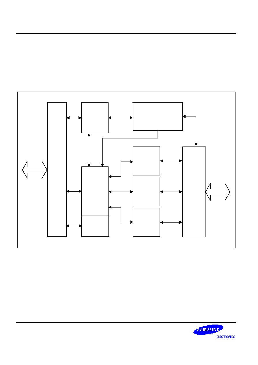
AC97 CONTROLLER
S3C2440A RISC MICROPROCESSOR
24-2
AC97 CONTROLLER OPERATION
BLOCK DIAGRAM
Figure 24-1 shows the functional block diagram of the S3C2440A AC97 Controller. The AC97 signals form the AC-
link, which is a point-to-point synchronous serial interconnect that supports full-duplex data transfers. All digital audio
streams and command/status information are communicated over the AC-link.
APB
I/F
DMA
Engine
Interrupt
Control
MIC in
FIFO
PCM
out FIFO
PCM in
FIFO
SFR
AC-link
I/F
FSM & Control
APB
AC-link
Figure 24-1. AC97 Block Diagram
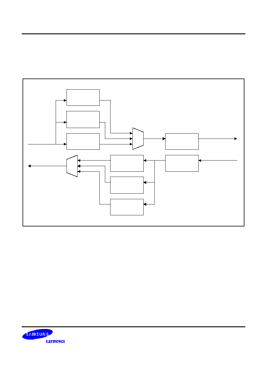
S3C2440A RISC MICROPROCESSOR
AC97 CONTROLLER
24-3
INTERNAL DATA PATH
Figure 24-2 shows the internal data path of the S3C2440A AC97 Controller. It has stereo Pulse Code Modulated
(PCM) In, Stereo PCM Out and mono Mic-in buffers, which consist of 16-bit, 16 entries buffer. Also it has a 20-bit I/O
shift register via AC-link.
Command Addr
Register
Command Data
Register
PCM Out Buffer
(Regfile 16 bit x 2
x 16 Entry)
PWDATA
Response Data
Register
Mic In Buffer
(RegFile 16 bit x16
Entry)
PCM In Buffer
(Regfile 16 bit x 2
x 16 Entry)
PRDATA
Input Shift
Register
(20 bit)
Output Shift
Register
(20 bit)
SDATA_IN
SDATA_OUT
Figure 24-2. Internal Data Path
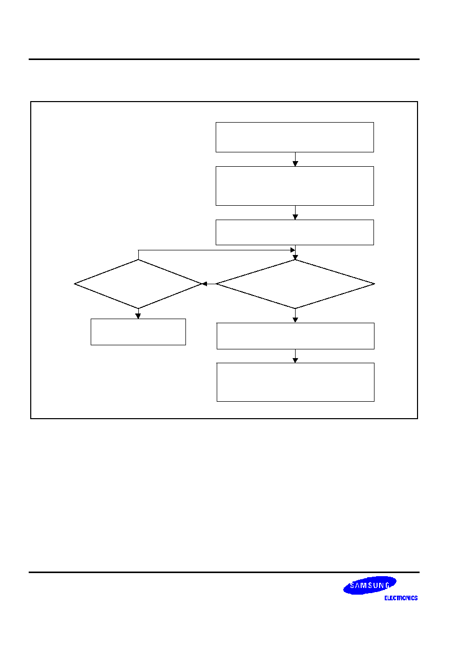
AC97 CONTROLLER
S3C2440A RISC MICROPROCESSOR
24-4
OPERATION FLOW CHART
System reset or Cold reset
Set GPIO and Release
INTMSK/SUBINTMSK bits
Enable Codec Ready interrupt
Disable Codec Ready interrupt
DMA operation or
PIO (Interrupt or Polling) operation
Controller off
Yes
No
No
Codec Ready interrupt ?
Time out condition ?
Figure 24-3. AC97 Operation Flow Chart
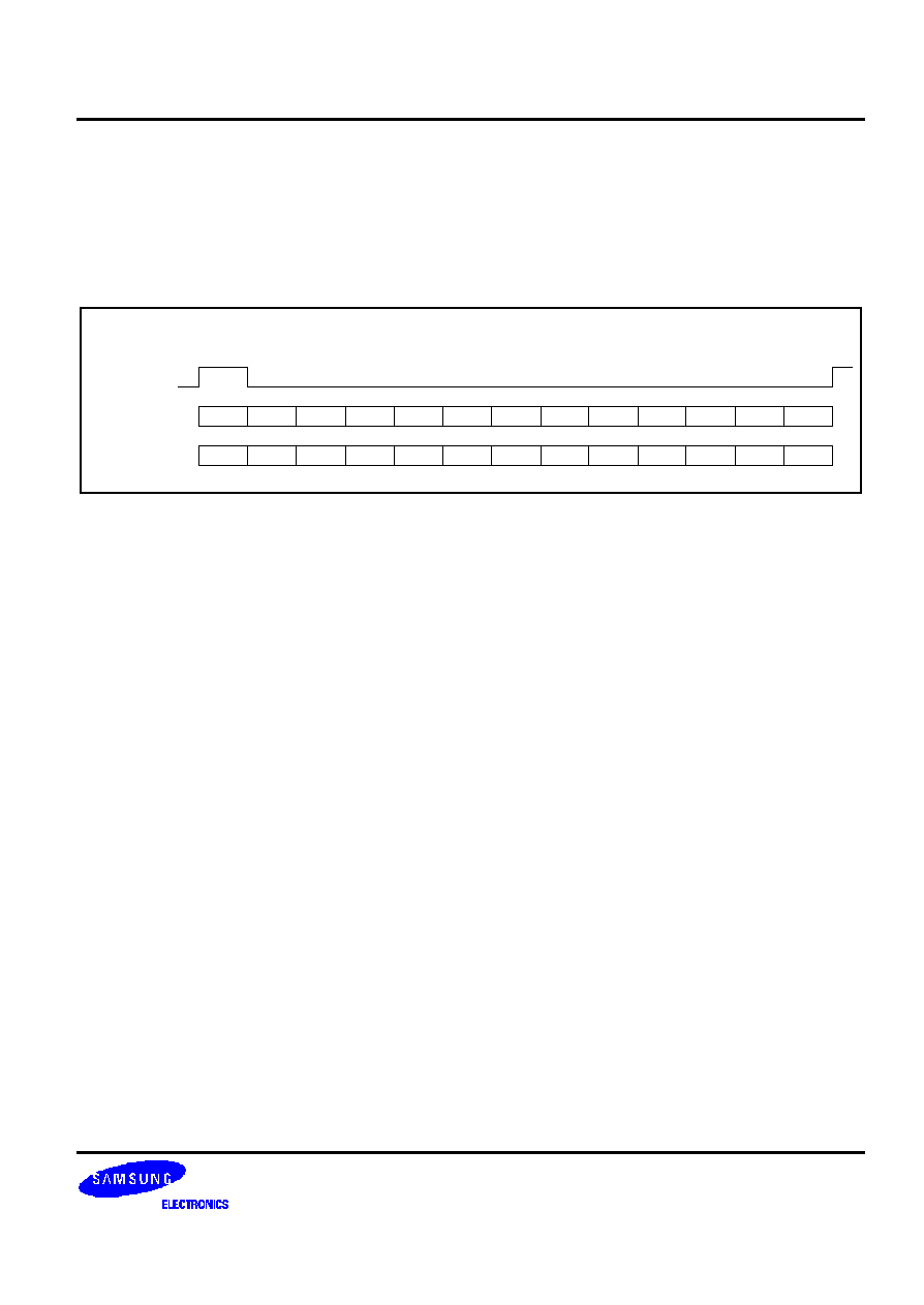
S3C2440A RISC MICROPROCESSOR
AC97 CONTROLLER
24-5
AC-LINK DIGITAL INTERFACE PROTOCOL
Each AC97 Codec incorporates a five-pin digital serial interface that links it to the S3C2440A AC97 Controller. The
AC-link is a full-duplex, fixed-clock, PCM digital stream. It employs a time division multiplexing (TDM) scheme to
handle control register access and multiple input and output audio streams. The AC-link architecture divides each
audio frame into 12 outgoing and 12 incoming data streams. Each stream has a 20-bit sample resolution and
requires a DAC and an analog-to-digital converter (ADC) with a minimum of 16-bit resolution.
SYNC
SDATA_OUT
SDATA_IN
Slot #
TAG
CMD
ADDR
CMD
DATA
PCM
PCM
RSRVD
TAG
STATUS
ADDR
STATUS
DATA
PCM
LEFT
PCM
RIGHT
0
1
2
3
4
5
6
7
8
9
10
11
12
RSRVD
RSRVD
RSRVD
RSRVD
RSRVD
RSRVD
RSRVD
RSRVD
RSRVD
RSRVD
RSRVD
RSRVD
RSRVD
RSRVD
PCM
MIC
LEFT
RIGHT
Figure 24-4. Bi-directional AC-link Frame with Slot Assignments
Figure 24-4 shows the slot definitions supported by the S3C2440A AC97 Controller. The S3C2440A AC97 Controller
provides synchronization for all data transaction on the AC-link.
A data transaction is made up of 256-bits of information broken up into groups of 13 time slots and is called a frame.
Time slot 0 is called as Tag Phase and it is 16-bits long. The remaining 12 time slots are called as Data Phase. The
Tag Phase contains a bit that identifies a valid frame and 12-bits that identify the time slots in the Data Phase that
contain a valid data. Each time slot in the Data Phase is 20-bits long. A frame begins when the SYNC goes high.
The amount of time the SYNC is high corresponds to the Tag Phase.
AC97 frames occur at fixed 48 kHz intervals and are synchronous to the 12.288 MHz bit rate clock, BITCLK. The
controller and the CODEC use the SYNC and BITCLK to determine when to send the transmit data and when to
sample the received data. A transmitter transitions the serial data stream on each rising edge of BITCLK and a
receiver samples the serial data stream on falling edges of BITCLK. The transmitter must tag the valid slots in its
serial data stream. The valid slots are tagged in slot 0. Serial data on the AC-link is from MSB to LSB. The Tag
Phase's first bit is bit 15 and the first bit of each slot in the Data Phase is bit 19. The last bit in any slot is bit 0.
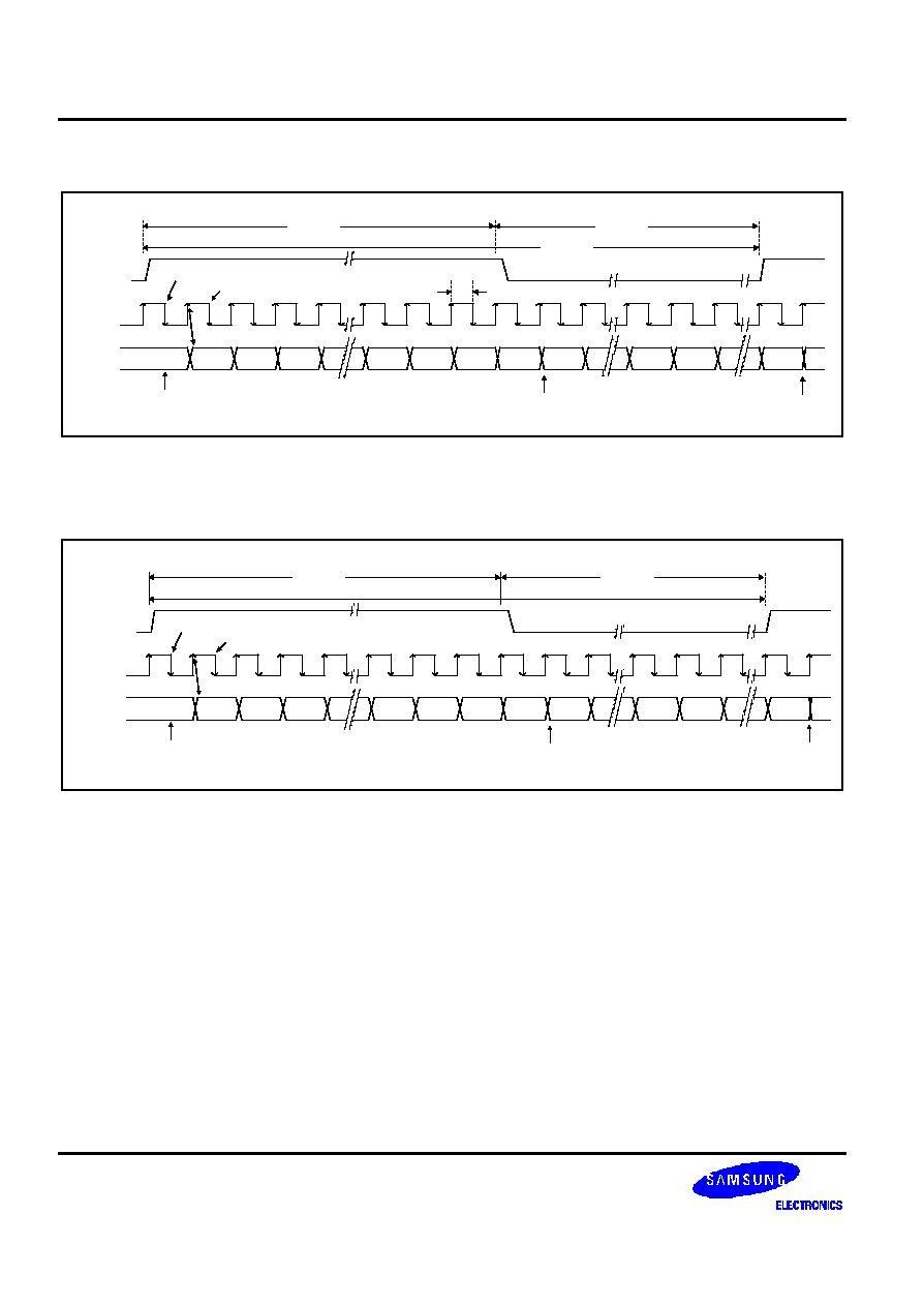
AC97 CONTROLLER
S3C2440A RISC MICROPROCESSOR
24-6
AC-LINK OUTPUT FRAME (SDATA_OUT)
SDATA_OUT
BIT_CLK
SYNC
AC '97 samples SYNC assertion here
AC '97 Controller samples first SDATA_OUT bit of frame here
END of previous Audio Frame
Valid
Frame
Slot(1)
Slot(2)
Slot(12)
"0"
ID1
ID0
19
0
Tag Phase
Data Phase
19
0
START of Data phase Slot# 1
END of Data Frame
Slot# 12
48kHz
12.288MHz
Figure 24-5. AC-link Output Frame
AC-LINK INPUT FRAME (SDATA_IN)
SDATA_OUT
BIT_CLK
SYNC
AC '97 samples SYNC assertion here
AC '97 Controller samples first SDATA_IN bit of frame here
END of previous Audio Frame
Codec
Ready
Slot(1)
Slot(2)
Slot(12)
"0"
"0"
"0"
19
0
Tag Phase
Data Phase
19
0
START of Data phase
Slot# 1
END of Data Frame
Slot# 12
Figure 24-6. AC-link Input Frame
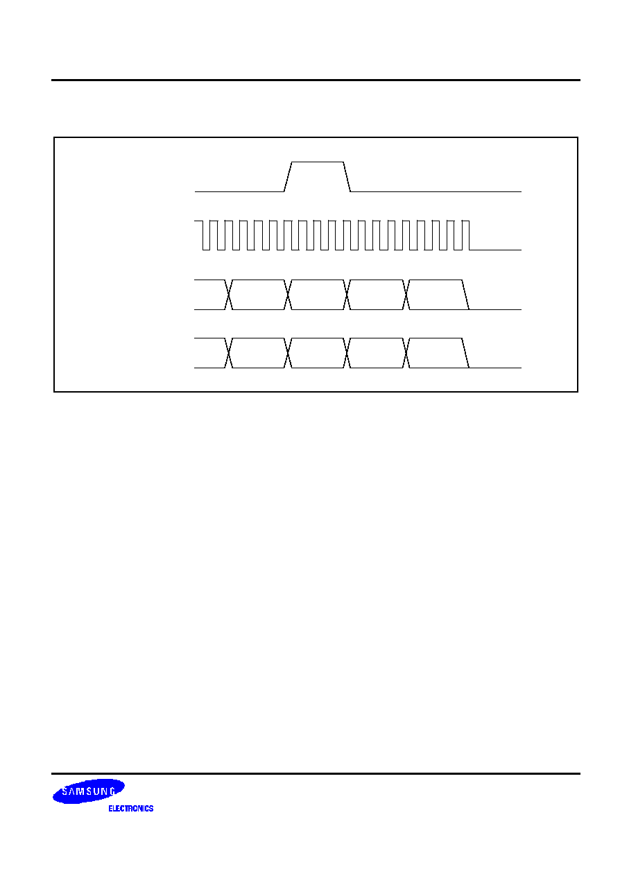
S3C2440A RISC MICROPROCESSOR
AC97 CONTROLLER
24-7
AC97 POWERDOWN
SDATA_OUT
SDATA_IN
BIT_CLK
SYNC
slot 12
prev.frame
Write to
0X26
slot 12
prev.frame
TAG
TAG
Data
PR4
Figure 24-7. AC97 Powerdown Timing Diagram
Powering Down the AC-link
The AC-link signals enter a low power mode when the AC97 CODEC Powerdown register (0x26) bit PR4 is set to 1
(i.e. by writing 0x1000). Then the Primary CODEC drives both the BITCLK and SDATA_IN to a logic low voltage level.
The sequence follows the timing diagram shown above in the Figure 24-7.
The AC97 Controller transmits the write to Powerdown register (0x26) over the AC-link. Set up the AC97 Controller
so that it does not transmit data to slots 3-12 when it writes to the Powerdown register bit PR4 (data 0x1000), and it
does not require the CODEC to process other data when it receives a power down request. When the CODEC
processes the request, it immediately transitions BITCLK and SDATA_IN to a logic low level. The AC97 Controller
drives the SYNC and SDATA_OUT to a logic low level after programming the AC_GLBCTRL register.
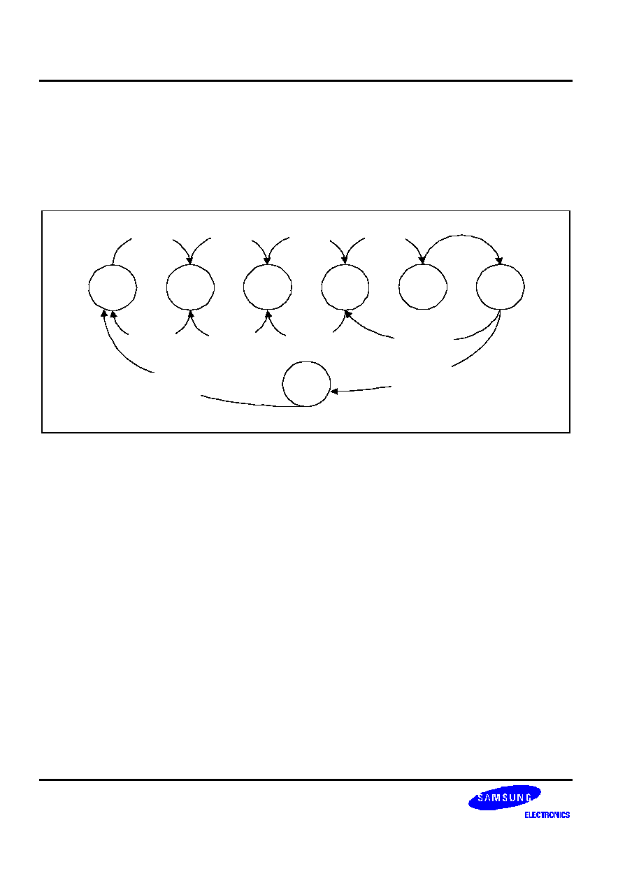
AC97 CONTROLLER
S3C2440A RISC MICROPROCESSOR
24-8
Waking up the AC-link - Wake Up Triggered by the AC97 Controller
AC-link protocol is provided for a cold AC97 reset and a warm AC97 reset. The current power-down state ultimately
dictates which AC97 reset is used. Registers must stay in the same state during all power-down modes unless a
cold AC97 reset is performed. In a cold AC97 reset, the AC97 registers are initialized to their default values. After a
power down, the AC-link must wait for a minimum of four audio frame time after the frame in which the power down
occurred before it can be reactivated by reasserting the SYNC signal. When AC-link powers up, it indicates
readiness through the Codec ready bit (input slot 0, bit 15).
Analog
off PR2
or PR3
Digital
I/F off
PR4
Shut off
AC-link
DACs off
PR1
ADCs off
PR0
Normal
Default
Ready = 1
PR0 = 0
&
ADC = 1
PR1 = 0
&
ADC = 1
PR2 = 0
&
ANL = 1
Warm Reset
Cold Reset
PR0 = 1
PR1 = 1
PR2 = 1
PR4 = 1
Figure 24-8. AC97 Power down/Power up Flow
Cold AC97 Reset
A cold reset is generated when an nRESET pin is asserted through the AC_GLBCTRL. Asserting and de-asserting
nRESET activates the BITCLK and SDATA_OUT. All the AC97 control registers are initialized to their default power
on reset values. nRESET is an asynchronous AC97 input.
Warm AC97 Reset
A warm AC97 reset reactivates the AC-link without altering the current AC97 register values. A warm reset is
generated when BITCLK is absent and SYNC is driven high. In normal audio frames, SYNC is a synchronous AC97
input. When BITCLK is absent, SYNC is treated as an asynchronous input used to generate a warm reset to
AC97.The AC97 Controller must not activate BITCLK until it samples the SYNC to low again. This prevents a new
audio frame from being falsely detected.
S3C2440A RISC MICROPROCESSOR
AC97 CONTROLLER
24-9
AC97 CONTROLLER SPECIAL REGISTERS
AC97 GLOBAL CONTROL REGISTER (AC_GLBCTRL)
Register
Address
R/W
Description
Reset Value
AC_GLBCTRL
0x5B000000
R/W
AC97 global control register
0x000000
AC_GLBCTRL
Bit
Description
Initial State
Reserved
[31:23]
≠
0x00
Codec ready interrupt enable
[22]
0: Disable
1: Enable
0
PCM out channel underrun
interrupt enable
[21]
0: Disable
1: Enable (FIFO is empty)
0
PCM in channel overrun interrupt
Enable
[20]
0 : Disable
1 : Enable (FIFO is full)
0
MIC in channel overrun interrupt
enable
[19]
0: Disable
1: Enable (FIFO is full)
0
PCM out channel threshold
interrupt enable
[18]
0: Disable
1: Enable (FIFO is half empty)
0
PCM in channel threshold
interrupt enable
[17]
0: Disable
1: Enable (FIFO is half full)
0
MIC in channel threshold interrupt
enable
[16]
0: Disable
1: Enable (FIFO is half full)
0
Reserved
[15:14]
≠
00
PCM out channel transfer mode
[13:12]
00: Off
01: PIO
10: DMA
11: Reserved
00
PCM in channel transfer mode
[11:10]
00: Off
01: PIO
10: DMA
11: Reserved
00
MIC in channel transfer mode
[9:8]
00: Off
01: PIO
10: DMA
11: Reserved
00
Reserved
[7:4]
≠
0000
Transfer data enable using AC-
link
[3]
0: Disable
1: Enable
0
AC-link on
[2]
0: Off
1: SYNC signal transfer to Codec
0
Warm reset
[1]
0: Normal
1: Wake up codec from power down
0
Cold reset
[0]
0: Normal
1: Reset Codec and Controller logic
0
AC97 CONTROLLER
S3C2440A RISC MICROPROCESSOR
24-10
AC97 GLOBAL STATUS REGISTER (AC_GLBSTAT)
Register
Address
R/W
Description
Reset Value
AC_GLBSTAT
0x5B000004
R
AC97 global status register
0x00000000
AC_GLBSTAT
Bit
Description
Initial State
Reserved
[31:23]
≠
0x00
Codec ready interrupt
[22]
0: Not requested 1: Requested
0
PCM out channel underrun interrupt
[21]
0: Not requested 1: Requested
0
PCM in channel overrun Interrupt
[20]
0: Not requested 1: Requested
0
MIC in channel overrun interrupt
[19]
0: Not requested 1: Requested
0
PCM out channel threshold interrupt
[18]
0: Not requested 1: Requested
0
PCM in channel threshold interrupt
[17]
0: Not requested 1: Requested
0
MIC in channel threshold interrupt
[16]
0: Not requested 1: Requested
0
Reserved
[15:3]
≠
0x000
Controller main state
[2:0]
000: Idle 001: Init 010: Ready
011: Active 100: LP 101: Warm
000
AC97 CODEC COMMAND REGISTER (AC_CODEC_CMD)
Register
Address
R/W
Description
Reset Value
AC_CODEC_CMD
0x5B000008
R/W
AC97 codec command register
0x00000000
AC_CODEC_CMD
Bit
Description
Initial State
Reserved
[31:24]
≠
0x00
Read enable
[23]
0: Command write
(NOTE)
1: Status read
0
Address
[22:16]
CODEC command address
0x00
Data
[15:0]
CODEC command data
0x0000
NOTE: When the commands are written on the AC_CODDEC_CMD register, it is recommended that the delay time
between
the command and the next command is more than 1/48 Hz.
S3C2440A RISC MICROPROCESSOR
AC97 CONTROLLER
24-11
AC97 CODEC STATUS REGISTER (AC_CODEC_STAT)
Register
Address
R/W
Description
Reset Value
AC_CODEC_STAT
0x5B00000C
R
AC97 codec status register
0x00000000
AC_CODEC_STAT
Bit
Description
Initial State
Reserved
[31:23]
≠
0x00
Address
[22:16]
CODEC status address
0x00
Data
[15:0]
CODEC status data
0x0000
NTOES:
If you want to read data from AC97 codec register via the AC_CODEC_STAT register, you should follow these steps.
1.
Write command address and data on the AC_CODEC_CMD register with Bit [23] =1.
2.
Have a delay time.
3.
Read command address and data from AC_CODEC_STAT register.
AC97 PCM OUT/IN CHANNEL FIFO ADDRESS REGISTER (AC_PCMADDR)
Register
Address
R/W
Description
Reset Value
AC_PCMADDR
0x5B000010
R
AC97 PCM out/in channel FIFO address
register
0x00000000
AC_PCMADDR
Bit
Description
Initial State
Reserved
[31:28]
≠
0000
Out read address
[27:24]
PCM out channel FIFO read address
0000
Reserved
[23:20]
≠
0000
In read address
[19:16]
PCM in channel FIFO read address
0000
Reserved
[15:12]
≠
0000
Out write address
[11:8]
PCM out channel FIFO write address
0000
Reserved
[7:4]
≠
0000
In write address
[3:0]
PCM in channel FIFO write address
0000
AC97 CONTROLLER
S3C2440A RISC MICROPROCESSOR
24-12
AC97 MIC IN CHANNEL FIFO ADDRESS REGISTER (AC_MICADDR)
Register
Address
R/W
Description
Reset Value
AC_MICADDR
0x5B000014
R
AC97 MIC in channel FIFO address register
0x00000000
AC_MICADDR
Bit
Description
Initial State
Reserved
[31:20]
≠
0000
Read Address
[19:16]
MIC in channel FIFO read address
0000
Reserved
[15:4]
≠
0x000
Write Address
[3:0]
MIC in channel FIFO write address
0000
AC97 PCM OUT/IN CHANNEL FIFO DATA REGISTER (AC_PCMDATA)
Register
Address
R/W
Description
Reset Value
AC_PCMDATA
0x5B000018
R/W
AC97 PCM out/in channel FIFO data register
0x00000000
AC_PCMDATA
Bit
Description
Initial State
Left Data
[31:16]
PCM out/in left channel FIFO data
Read: PCM in left channel
Write: PCM out left channel
0x0000
Right Data
[15:0]
PCM out/in right channel FIFO data
Read: PCM in right channel
Write: PCM out right channel
0x0000
AC97 MIC IN CHANNEL FIFO DATA REGISTER (AC_MICDATA)
Register
Address
R/W
Description
Reset Value
AC_MICDATA
0x5B00001C
R/W
AC97 MIC in channel FIFO data register
0x00000000
AC_MICDATA
Bit
Description
Initial State
Reserved
[31:16]
≠
0x0000
Mono Data
[15:0]
MIC in mono channel FIFO data
0x0000

S3C2440A RISC MICROPROCESSOR
BUS PRIORITIES
25-1
25
BUS PRIORITIES
OVERVIEW
The bus arbitration logic determines the priorities of bus masters. It supports a combination of rotation priority mode
and fixed priority mode.
BUS PRIORITY MAP
The S3C2440A holds 13 bus masters. They include DRAM refresh controller, LCD_DMA, CAMIF DMA, DMA0,
DMA1, DMA2, DMA3, USB_HOST_DMA, EXT_BUS_MASTER, Test interface controller (TIC) and ARM920T. The
following list shows the priorities among these bus masters after a reset:
1. DRAM refresh controller
2. LCD_DMA
3. CAMIF codec DMA
4. CAMIF preview DMA
5. DMA0
6. DMA1
7. DMA2
8. DMA3
9. USB host DMA
10. External bus master
11. TIC
12. ARM920T
13. Reserved
Among these bus masters, the four DMAs (DMA0, DMA1, DMA2 and DMA3) operate under rotation priority, while
the others run under fixed priority.

BUS PRIORITIES
S3C2440A RISC MICROPROCESSOR
25-2
NOTES
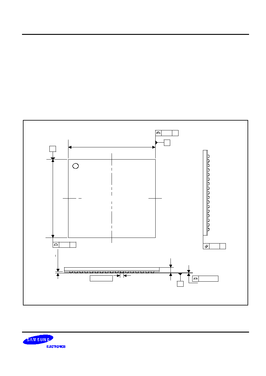
S3C2440A RISC MICROPROCESSOR
MECHANICAL DATA
26-1
26
MECHANICAL DATA
PACKAGE DIMENSIONS
14.00
14.00
0.35
+ 0.05
1.22
289-FBGA-1414
0.45
±0.05
C
0.12 MAX
0.10 C
A
B
0.15
TOLERANCE
±0.10
x 2
0.15
x 2
C
C
SAMSUNG
Figure 26-1. 289-FBGA-1414 Package Dimension 1 (Top View)
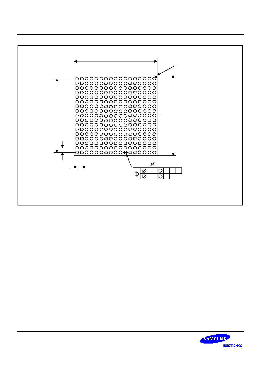
MECHANICAL DATA
S3C2440A RISC MICROPROCESSOR
26-2
A1 INDEX MARK
0.80 x 16 = 12.80
±
0.05
14.00
0.80
0.80
A
B
C
D
E
F
G
H
J
K
L
M
N
P
R
T
U
8
9
10
11
12
13
14
15
16
17
5
6
7
1
2
3
4
14.00
0.15
0.08
M
M
C
C
A B
289 - 0.45
±
0.05
TOLERANCE
±
0.10
Figure 26-2. 289-FBGA-1414 Package Dimension 2 (Bottom View)
The recommended land open size is 0.39 ≠ 0.41mm diameter.
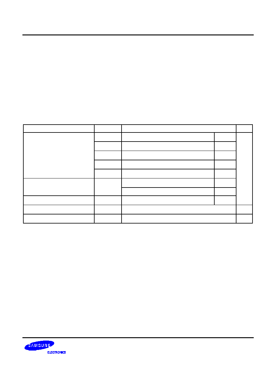
S3C2440A RISC MICROPROCESSOR
ELECTRICAL DATA
27-1
27
ELECTRICAL DATA
ABSOLUTE MAXIMUM RATINGS
Table 27-1. Absolute Maximum Rating
Parameter
Symbol
Rating
Unit
DC Supply Voltage
V
DDi
1.2V V
DD
1.8
V
V
DDOP
3.3V V
DD
4.8
V
DDMOP
1.8V/2.5V/3.0V/3.3V V
DD
4.8
V
DDRTC
1.8V/2.5V/3.0V/3.3V V
DD
4.5
V
DDADC
3.3V V
DD
4.8
DC Input Voltage
V
IN
3.3V Input buffer
4.8
3.3V Interface / 5V Tolerant input buffer
6.5
DC Output Voltage
V
OUT
3.3V Output buffer
4.8
DC Input (Latch-up) Current
I
IN
±
200
mA
Storage Temperature
T
STG
≠ 65 to 150
o
C
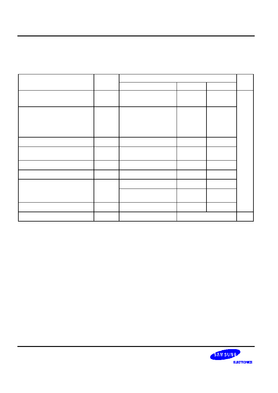
ELECTRICAL DATA
S3C2440A RISC MICROPROCESSOR
27-2
RECOMMENDED OPERATING CONDITIONS
Table 27-2. Recommended Operating Conditions
Parameter
Symbol
Rating
Unit
Typ.
Min
Max
DC supply voltage for alive block
V
DDalive
300MHz: 1.2V V
DD
400MHz: 1.3V V
DD
1.15
1.15
1.25
1.35
V
DC supply voltage for internal
V
DDi
(1)
V
DDiarm
(1)
V
DDMPLL
V
DDUPLL
300MHz: 1.2V V
DD
400MHz: 1.3V V
DD
1.15
1.25
1.25
1.35
DC supply voltage for I/O block
V
DDOP
3.3V V
DD
3.0
3.6
DC supply voltage for memory
interface
V
DDMOP
1.8V/2.5V/3.0V/3.3V V
DD
1.7
3.6
DC supply voltage for analog core
V
DD
3.3V V
DD
3.0
3.6
DC supply voltage for RTC
V
DDRTC
1.8V/2.5V/3.0V/3.3V V
DD
1.8
3.6
DC input voltage
V
IN
3.3V Input buffer
≠ 0.3
V
DDOP
+0.3
3.3V Interface / 5V
Tolerant input buffer
≠ 0.3
5.25
DC output voltage
V
OUT
3.3V Output buffer
≠ 0.3
V
DDOP
+0.3
Operating temperature
T
OPR
Industrial
≠40 to 85
o
C
NOTE: In the DVS(Dynamic Voltage Scaling) VDDi & VDDiarm can be supplied with 1.0V in Idle mode. Refer the
Application
Notes for detailed information.
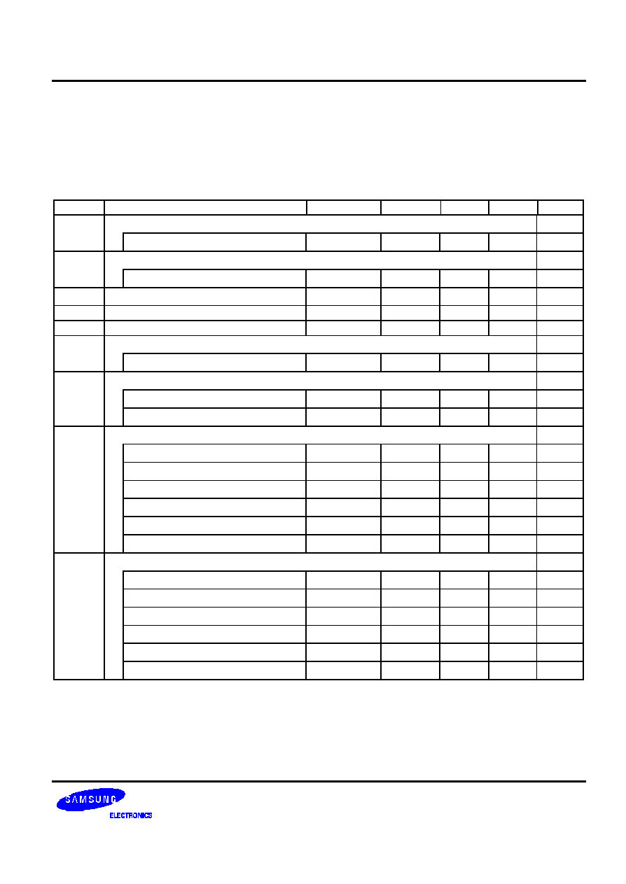
S3C2440A RISC MICROPROCESSOR
ELECTRICAL DATA
27-3
D.C. ELECTRICAL CHARACTERISTICS
Table 27-3 and 27-4 defines the DC electrical characteristics for the standard LVCMOS I/O buffers.
Table 27-3. Normal I/O PAD DC Electrical Characteristics
Normal I/O PAD DC Electrical Characteristics for Memory (VDDMOP = 2.5V
±
0.2V, T
A
= ≠40 to 85
∞
C)
Symbol
Parameters
Condition
Min
Typ.
Max
Unit
V
IH
High level input voltage
V
LVCMOS interface
1.7
V
IL
Low level input voltage
V
LVCMOS interface
0.7
VT
Switching threshold
0.5V
DD
V
VT+
Schmitt trigger, positive-going threshold
CMOS
2.0
V
VT≠
Schmitt trigger, negative-going threshold
CMOS
0.8
V
I
IH
High level input current
µA
Input buffer
V
IN
= V
DD
≠10
10
I
IL
Low level input current
µA
Input buffer
V
IN
= V
SS
≠10
10
Input buffer with pull-up
≠60
≠33
≠10
V
OH
High level output voltage
V
Type B4 to B12
I
OH
= ≠ 1 µA
V
DD
≠0.05
Type B4
I
OH
= ≠ 4 mA
2.0
Type B6
I
OH
= ≠ 6 mA
Type B8
I
OH
= ≠ 8 mA
Type B10
I
OH
= ≠ 10 mA
Type B12
I
OH
= ≠ 12mA
V
OL
Low level output voltage
V
Type B4 to B12
I
OL
= 1 µA
0.05
Type B4
I
OL
= 4 mA
0.4
Type B6
I
OL
= 6 mA
Type B8
I
OL
= 8 mA
Type B10
I
OL
= 10 mA
Type B12
I
OL
= 12 mA
NOTES:
1.
Type B6 means 6mA output driver cell.
2.
Type B8 means 8mA output driver cell.
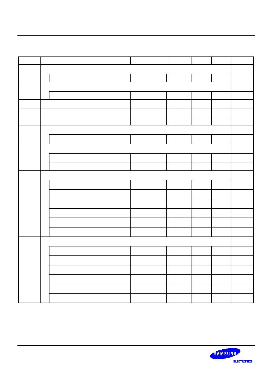
ELECTRICAL DATA
S3C2440A RISC MICROPROCESSOR
27-4
Normal I/O PAD DC Electrical Characteristics for Memory (V
DDMOP
=3.0V
±
0.3V, 3.3V
±
0.3V, T
A
= ≠40 to 85
∞
C)
Symbol
Parameters
Condition
Min
Typ.
Max
Unit
V
IH
High level input voltage
V
LVCMOS interface
2.0
V
IL
Low level input voltage
V
LVCMOS interface
0.8
VT
Switching threshold
0.5V
DD
V
VT+
Schmitt trigger, positive-going threshold
CMOS
2.0
V
VT≠
Schmitt trigger, negative-going threshold
CMOS
0.8
V
I
IH
High level input current
µA
Input buffer
V
IN
= V
DD
≠10
10
I
IL
Low level input current
µA
Input buffer
V
IN
= V
SS
≠10
10
Input buffer with pull-up
≠60
≠33
≠10
V
OH
High level output voltage
V
Type B4 to B12
I
OH
= ≠ 1 µA
V
DD
≠0.05
Type B4
I
OH
= ≠ 4 mA
2.4
Type B6
I
OH
= ≠ 6 mA
Type B8
I
OH
= ≠ 8 mA
Type B10
I
OH
= ≠10 mA
Type B12
I
OH
= ≠12 mA
V
OL
Low level output voltage
V
Type B4 to B12
I
OL
= 1 µA
0.05
Type B4
I
OL
= 4 mA
0.4
Type B6
I
OL
= 6 mA
Type B8
I
OL
= 8 mA
Type B10
I
OL
= 10 mA
Type B12
I
OL
= 12 mA
NOTES:
1.
Type B6 means 6mA output driver cell.
2.
Type B8 means 8mA output driver cell.
3.
Type B12 means 12mA output driver cells.
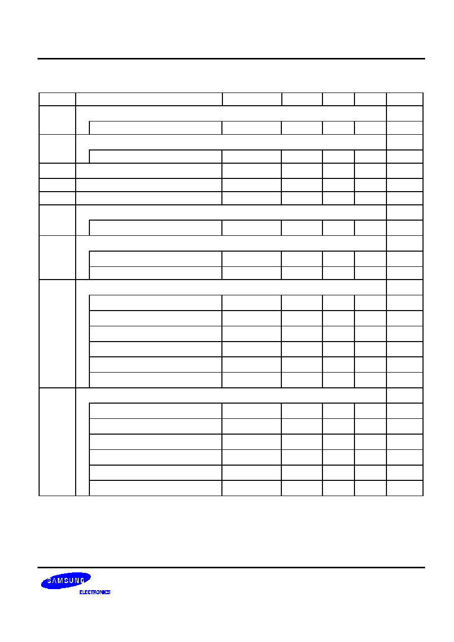
S3C2440A RISC MICROPROCESSOR
ELECTRICAL DATA
27-5
Normal I/O PAD DC Electrical Characteristics for I/O (V
DDOP
= 3.3V
±
0.3V, T
A
= ≠40 to 85
∞
C)
Symbol
Parameters
Condition
Min
Typ.
Max
Unit
V
IH
High level input voltage
V
LVCMOS interface
2.0
V
IL
Low level input voltage
V
LVCMOS interface
0.8
VT
Switching threshold
0.5V
DD
V
VT+
Schmitt trigger, positive-going threshold
CMOS
2.0
V
VT≠
Schmitt trigger, negative-going threshold
CMOS
0.8
V
I
IH
High level input current
µA
Input buffer
V
IN
= V
DD
≠10
10
I
IL
Low level input current
µA
Input buffer
V
IN
= V
SS
≠10
10
Input buffer with pull-up
≠60
≠33
≠10
V
OH
High level output voltage
V
Type B4 to B12
I
OH
= ≠ 1 µA
V
DD
≠0.05
Type B4
I
OH
= ≠ 4 mA
2.4
Type B6
I
OH
= ≠ 6 mA
Type B8
I
OH
= ≠ 8 mA
Type B10
I
OH
= ≠10 mA
Type B12
I
OH
= ≠12 mA
V
OL
Low level output voltage
V
Type B4 to B12
I
OL
= 1 µA
0.05
Type B4
I
OL
= 4 mA
0.4
Type B6
I
OL
= 6 mA
Type B8
I
OL
= 8 mA
Type B10
I
OL
= 10 mA
Type B12
I
OL
= 12 mA
NOTES:
1.
Type B6 means 6mA output driver cell.
2.
Type B8 means 8mA output driver cell.
3.
Type B12 means 12mA output driver cells.
ELECTRICAL DATA
S3C2440A RISC MICROPROCESSOR
27-6
Table 27-4. USB DC Electrical Characteristics
Symbol
Parameter
Condition
Min
Max
Unit
V
IH
High level input voltage
≠
2.5
≠
V
V
IL
Low level input voltage
≠
≠
0.8
V
I
IH
High level input current
Vin = 3.3V
≠10
10
µA
I
IL
Low level input current
Vin = 0.0V
≠10
10
µA
V
OH
Static output high
15K to GND
2.8
3.6
V
V
OL
Static output low
1.5K to 3.6V
0.3
V
Table 27-5. S3C2440 Power Supply Voltage and Current
Parameter
Value
Unit
Condition
Typical V
DDi
/ V
DDOP
1.3 / 3.3
V
Without DVS
Max. Operating frequency (FCLK)
400
MHz
≠
Max. Operating frequency (HCLK)
133
MHz
≠
Max. Operating frequency (PCLK)
67
MHz
≠
Typical normal mode power
(3)
(Total V
DDi
+ V
IO
)
368
mW
(1)
Typical normal mode power
(3)
(Total V
DDi
+ VIO)
310
mW
(2)
Typical idle mode power
(3)
(Total V
DDi
+ V
IO
)
213
mW
FCLK = 400MHz
(F:H:P = 1:3:6)
Typical slow mode power
(3)
(Total V
DDi
+ V
IO
)
97
mW
FCLK = 12MHz
(F:H:P = 1:1:1)
Typical Sleep mode power
(3)
380
µA
@1.2/3.3V, Room temperature
All other I/O static.
Typical RTC power
(3)
3
µA
@3.0V, Room temperature
X-tal = 32.768kHz for RTC
NOTES:
1.
I/D cache: ON, MMU: ON, Code on SRAM, FCLK:HCLK:PCLK = 400MHz:133MHz:66.7MHz
:LCD ON (320x240x16bppx60Hz, color TFT):13 kHz Timer internal mode (5 Channel run)
:Audio (IIS&DMA, CDCLK=16.9MHz, LRCK=44.1kHz):Integer data quick sort (65536 EA)
2. Pocket PC 2003 MPEG play
3.
The above power consumption data is measured in Room temperature with random sample (Lot #: KZZ1FS).
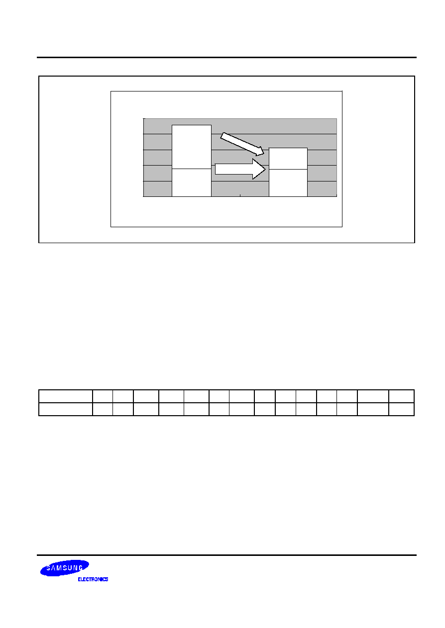
S3C2440A RISC MICROPROCESSOR
ELECTRICAL DATA
27-7
400Mhz Power consumption
87mW
88mW
139mW
68mW
0
50
100
150
200
250
Without DVS
With DVS
Item
[mW]
Core Power
51% Down
Total Power
32% Down
VDD_Core
VDD_IO
Figure 27-1. Power Consumption Example Comparison when Applied DVS Scheme
NOTE: (Condition) Current measure condition: Play Battlife.wma(bit rate=64kbps) on PPC2003 SMDK2440.
Core power:
Without DVS : VDDiarm/VDDi/VDDupll/VDDmpll/VDDalive = 1.3V
using DVS : VDDiarm/VDDi = 1.3V
Û
1.0V, VDDupll/VDDmpll/VDDalive = 1.3V
I/O Power : VDDOP/VDDMOP/VDDRTC/VDDADC=3.3V
Refer the Application notes for more information about DVS.
Table 27-6. Typical Current Decrease by CLKCON Register
FCLK:HCLK:PCLK = 300:100:50MHz, 1.2V (Random sample)
(Unit: mA)
Peripherals
NFC
LCD
USBH USBD Timer
SDI
UART
RTC ADC
IIC
IIS
SPI
Camera
Total
Current
1.7
2.8
0.37
0.79
0.32
1.0
2.7
0.45 0.26 0.32 0.78 0.16
14.25
26.26
NOTE: This table includes power consumption of each peripheral. For example, If you do not use Camera and have turned
off the Camera block by CLKCON register, then you can save the 14.25mA of internal block.
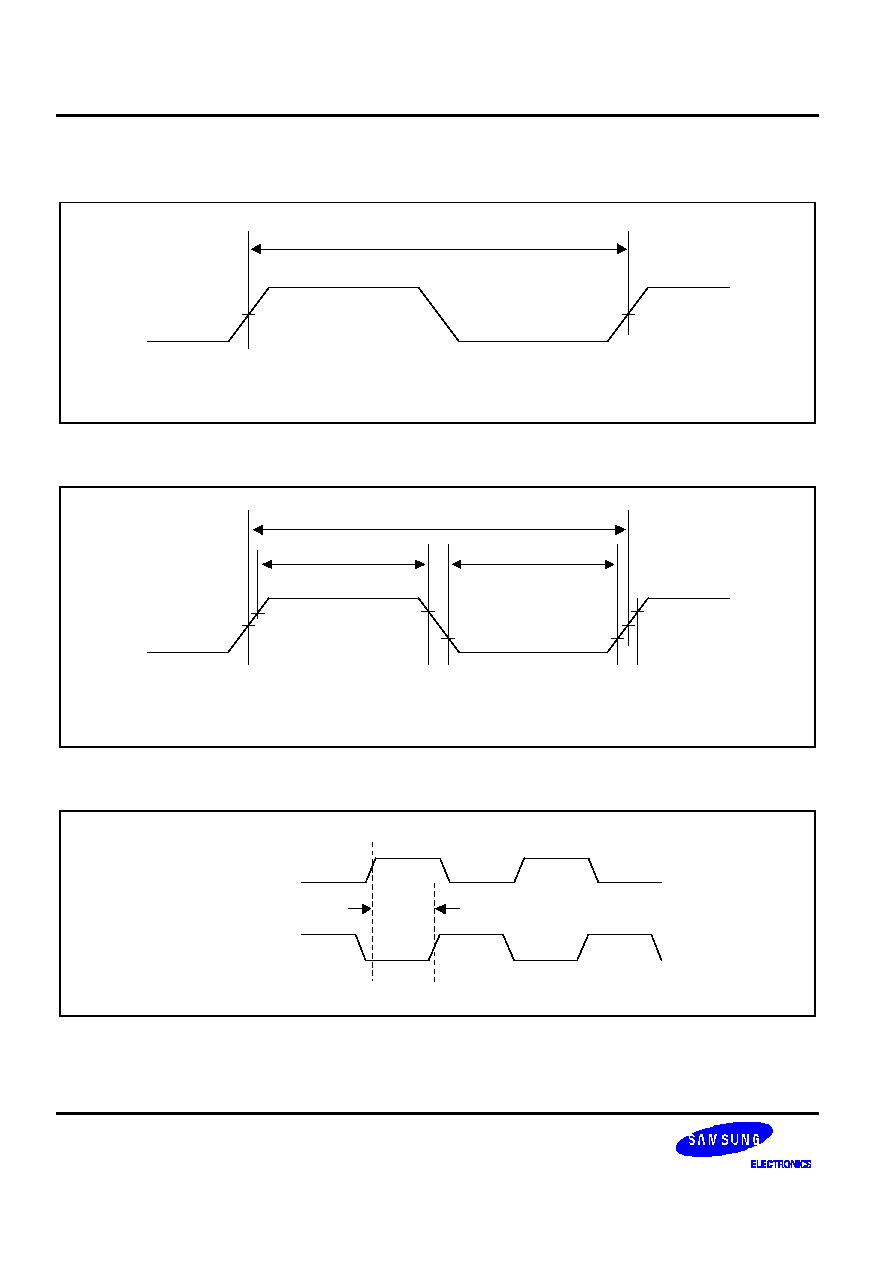
ELECTRICAL DATA
S3C2440A RISC MICROPROCESSOR
27-8
A.C. ELECTRICAL CHARACTERISTICS
1/2 V
DD
1/2 V
DD
t
XTALCYC
NOTE:
Clock input is from the XTIpll pin.
Figure 27-2. XTIpll Clock Timing Diagram
t
EXTHIGH
V
IH
1/2 V
DD
V
IL
V
IL
V
IH
V
IH
1/2 V
DD
t
EXTLOW
t
EXTCYC
NOTE:
Clock input is from the EXTCLK pin.
Figure 27-3. EXTCLK Clock Input Timing Diagram
HCLK
(internal)
EXTCLK
t
EX2HC
Figure 27-4. EXTCLK/HCLK in case when EXTCLK is used Without the PLL
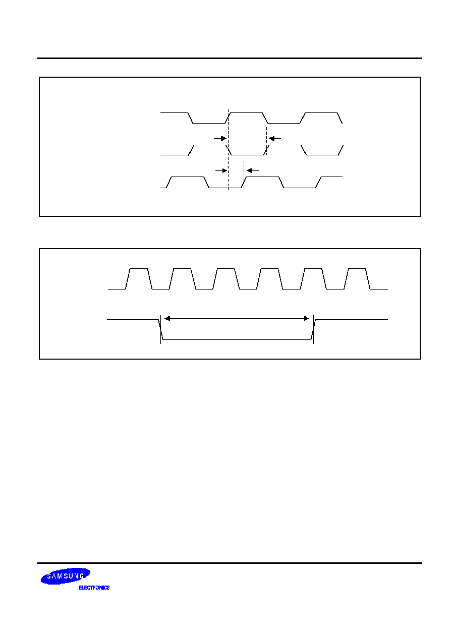
S3C2440A RISC MICROPROCESSOR
ELECTRICAL DATA
27-9
HCLK
(internal)
SCLK
CLKOUT
(HCLK)
t
HC2CK
t
HC2SCLK
Figure 27-5. HCLK/CLKOUT/SCLK in case when EXTCLK is used
EXTCLK
t
RESW
nRESET
Figure 27-6. Manual Reset Input Timing Diagram
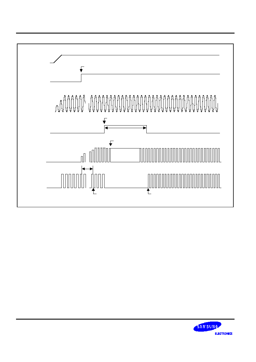
ELECTRICAL DATA
S3C2440A RISC MICROPROCESSOR
27-10
nRESET
XTIpll or
EXTCLK
VCO
output
MCU operates by XTIpll
or EXTCLK clcok.
Clock
Disable
tPLL
FCLK is new frequency.
Power
PLL can operate after OM[3:2] is latched.
PLL is configured by S/W first time.
VCO is adapted to new clock frequency.
FCLK
...
...
...
tRST2RUN
Figure 27-7. Power-On Oscillation Setting Timing Diagram
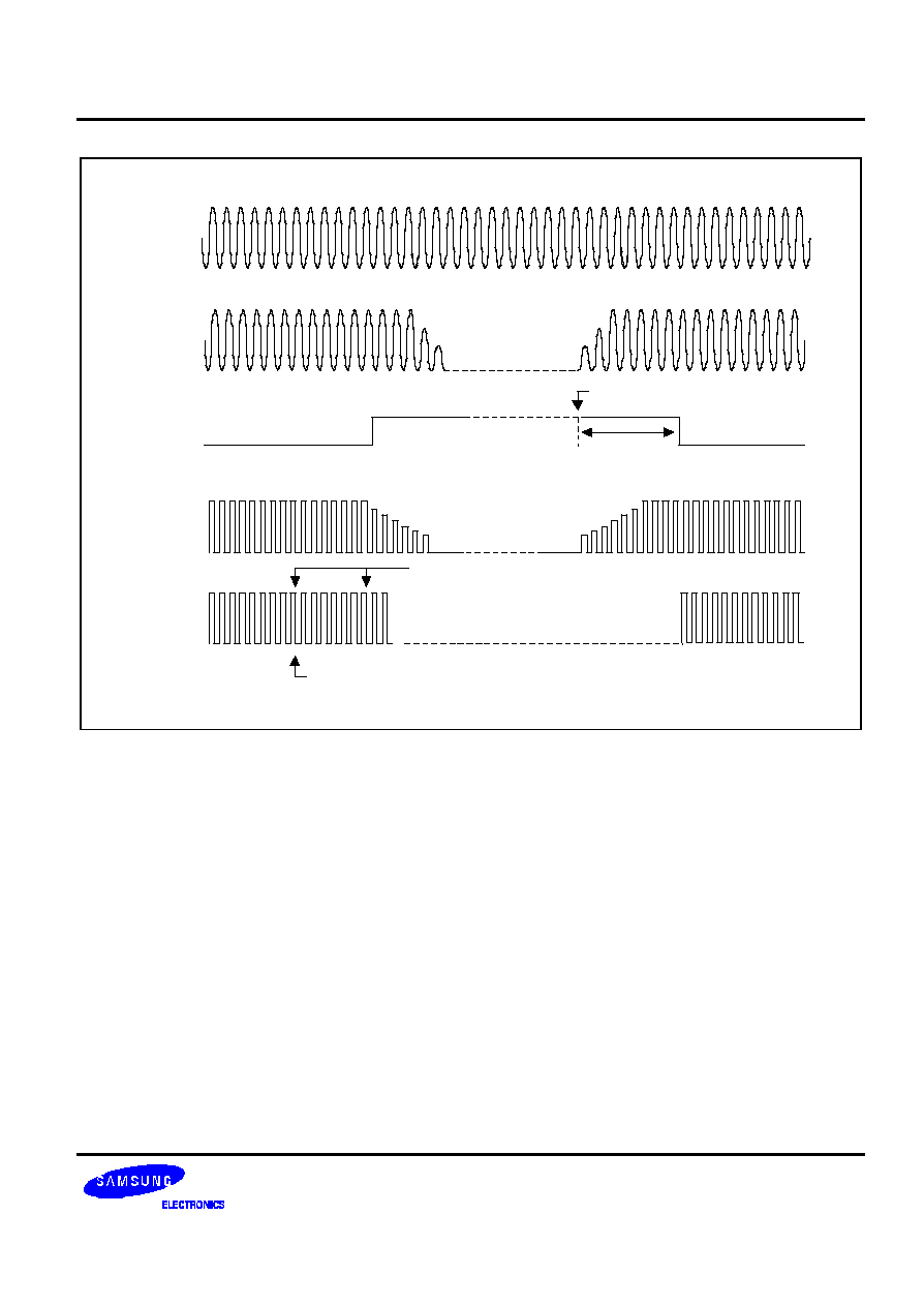
S3C2440A RISC MICROPROCESSOR
ELECTRICAL DATA
27-11
XTIpll
VCO
Output
Clock
Disable
FCLK
Several slow clocks (XTIpll or EXTCLK)
Power_OFF mode is initiated.
t
OSC2
EXTCLK
Figure 27-8. Sleep Mode Return Oscillation Setting Timing Diagram
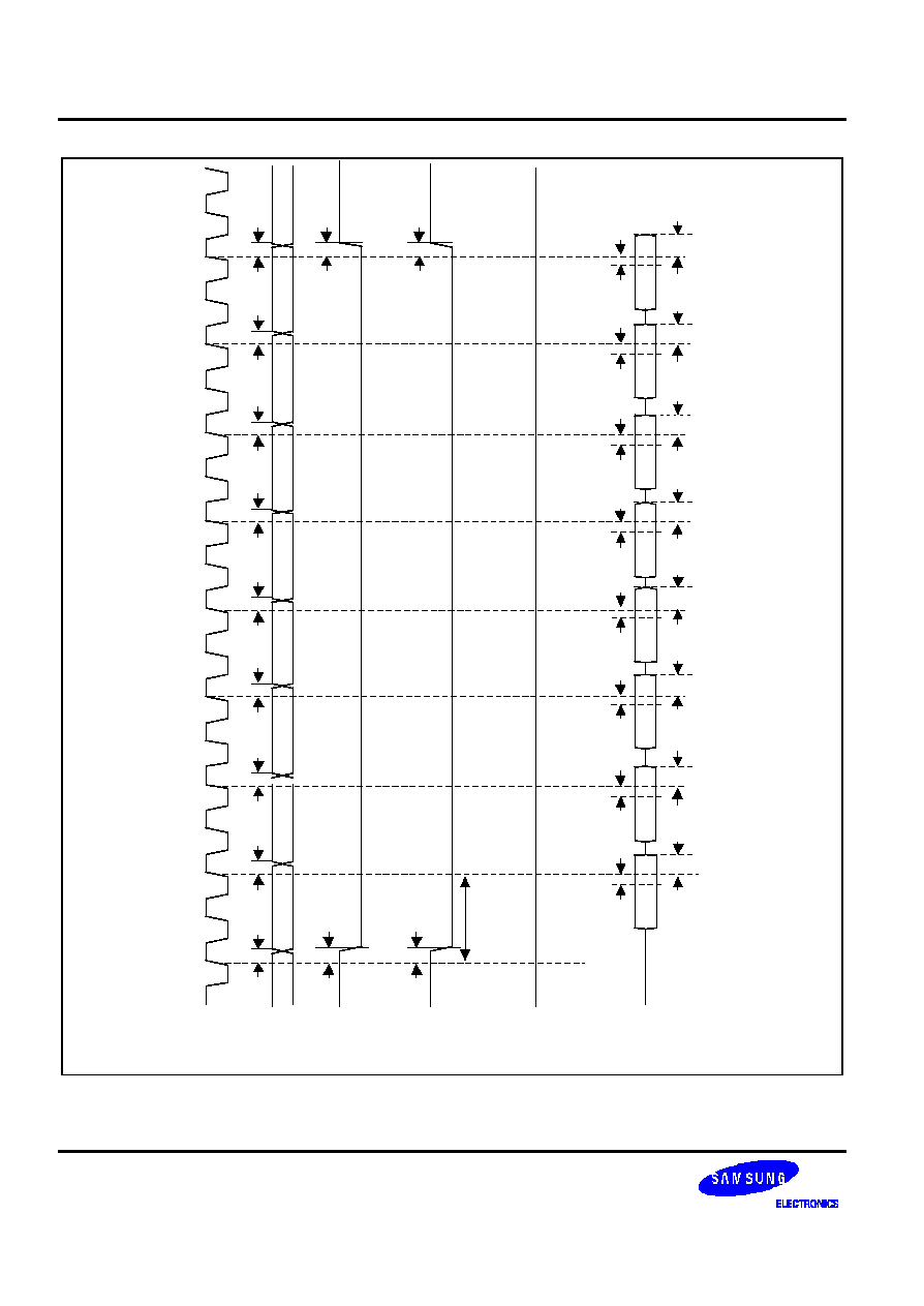
ELECTRICAL DATA
S3C2440A RISC MICROPROCESSOR
27-12
HCLK
nGCSx
t
RAD
nOE
DATA
ADDR
nBEx
t
RCD
t
ROD
t
ROD
t
RCD
Tacc
t
RAD
t
RAD
t
RAD
t
RAD
t
RAD
t
RAD
t
RAD
t
RAD
t
RDS
t
RDH
t
RDS
t
RDH
t
RDS
t
RDH
t
RDS
t
RDH
t
RDS
t
RDH
t
RDS
t
RDH
t
RDS
t
RDH
t
RDS
t
RDH
'1'
Figure 27-9. ROM/SRAM Burst READ Timing Diagram (I)
(Tacs=0, Tcos=0, Tacc=2, Toch=0, Tcah=0, PMC=0, ST=0, DW=16bit)
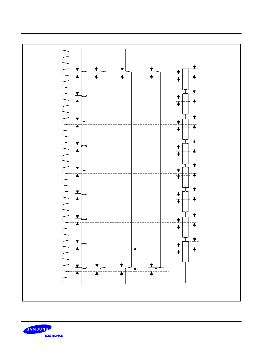
S3C2440A RISC MICROPROCESSOR
ELECTRICAL DATA
27-13
HCLK
nGCSx
t
RAD
nOE
DATA
ADDR
nBEx
t
RCD
t
ROD
t
ROD
t
RCD
t
RBED
t
RBED
Tacc
t
RAD
t
RAD
t
RAD
t
RAD
t
RAD
t
RAD
t
RAD
t
RAD
t
RDS
t
RDH
t
RDS
t
RDH
t
RDS
t
RDH
t
RDS
t
RDH
t
RDS
t
RDH
t
RDS
t
RDH
t
RDS
t
RDH
t
RDS
t
RDH
Figure 27-10. ROM/SRAM Burst READ Timing Diagram (II)
(Tacs=0, Tcos=0, Tacc=2, Toch=0, Tcah=0, PMC=0, ST=1, DW=16bit)
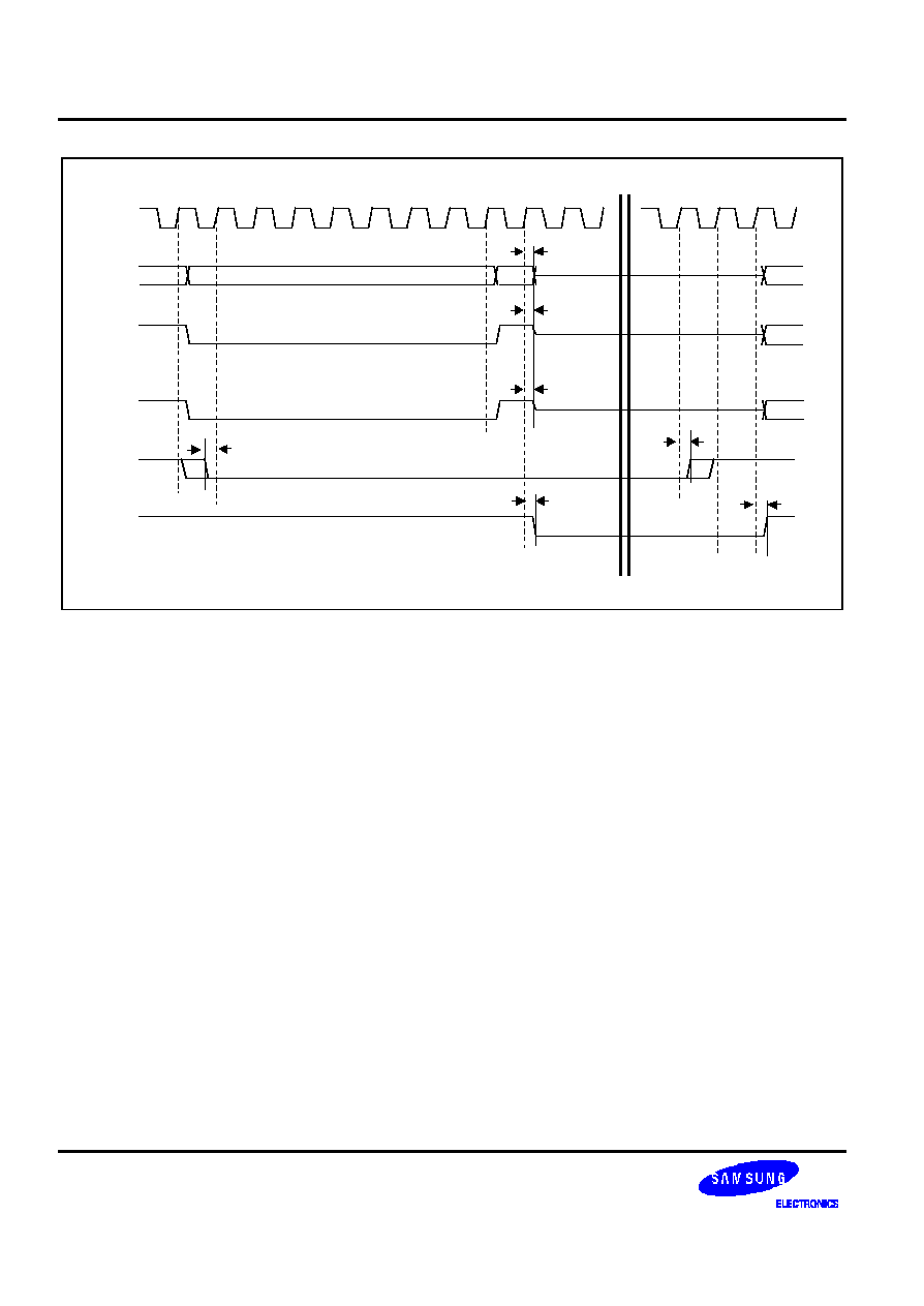
ELECTRICAL DATA
S3C2440A RISC MICROPROCESSOR
27-14
HCLK
nGS
nOE
ADDR
tXnBRQS
XnBREQ
tXnBRQH
XnBACK
'HZ'
'HZ'
'HZ'
tXnBACKD
tXnBACKD
tHZD
tHZD
tHZD
Figure 27-11. External Bus Request in ROM/SRAM Cycle
(Tacs=0, Tcos=0, Tacc=8, Toch=0, Tcah=0, PMC=0, ST=0)
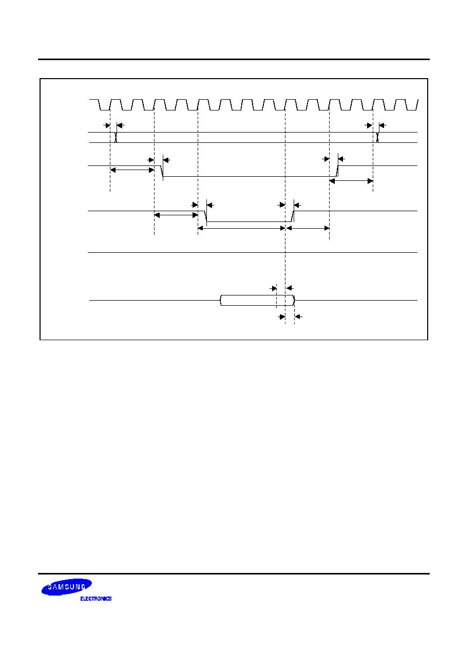
S3C2440A RISC MICROPROCESSOR
ELECTRICAL DATA
27-15
HCLK
nGCSx
t
RAD
Tacs
nOE
Tcos
DATA
ADDR
nWBEx
'1'
Toch
Tcah
t
RCD
t
ROD
t
RDS
t
RDH
t
ROD
t
RCD
t
RAD
Tacc
Figure 27-12. ROM/SRAM READ Timing Diagram (I)
(Tacs=2, Tcos=2, Tacc=4, Toch=2, Tcah=2, PMC=0, ST=0)
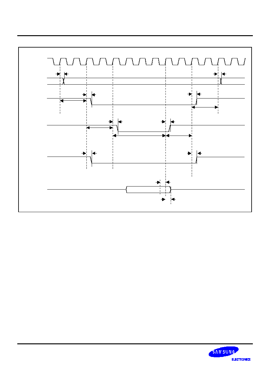
ELECTRICAL DATA
S3C2440A RISC MICROPROCESSOR
27-16
HCLK
nGCSx
t
RAD
Tacs
nOE
Tcos
DATA
ADDR
nBEx
Toch
Tcah
t
RCD
t
ROD
t
RDS
t
RDH
t
ROD
t
RCD
t
RAD
t
RBED
t
RBED
Tacc
Figure 27-13. ROM/SRAM READ Timing Diagram (II)
(Tacs=2, Tcos=2, Tacc=4, Toch=2, Tcah=2cycle, PMC=0, ST=1)
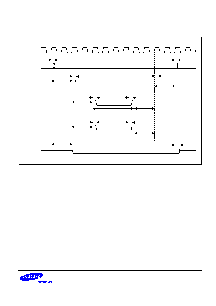
S3C2440A RISC MICROPROCESSOR
ELECTRICAL DATA
27-17
HCLK
nGCSx
t
RAD
Tacs
nWE
Tcos
DATA
ADDR
nWBEx
Toch
Tcah
t
RCD
t
RWD
t
RDD
t
RWD
t
RCD
t
RAD
Tcos
Toch
t
RWBED
t
RWBED
Tacc
t
RDD
Figure 27-14. ROM/SRAM WRITE Timing Diagram (I)
(Tacs=2,Tcos=2,Tacc=4,Toch=2, Tcah=2, PMC=0, ST=0
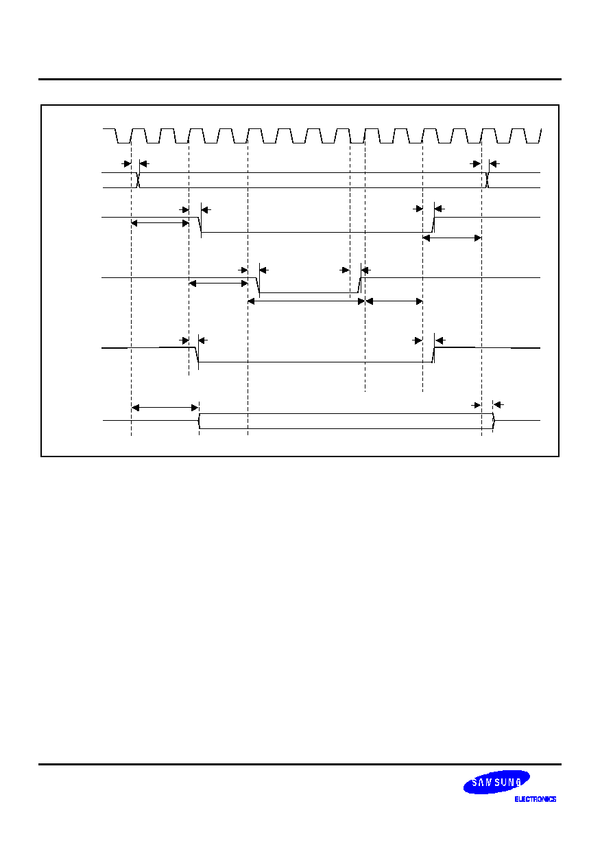
ELECTRICAL DATA
S3C2440A RISC MICROPROCESSOR
27-18
HCLK
nGCSx
t
RAD
Tacs
nWE
Tcos
DATA
ADDR
nBEx
Toch
Tcah
t
RCD
t
RWD
t
RDD
t
RWD
t
RCD
t
RAD
t
RBED
t
RBED
Tacc
t
RDD
Figure 27-15. ROM/SRAM WRITE Timing Diagram (II)
(Tacs=2, Tcos=2, Tacc=4, Toch=2, Tcah=2, PMC=0, ST=1)
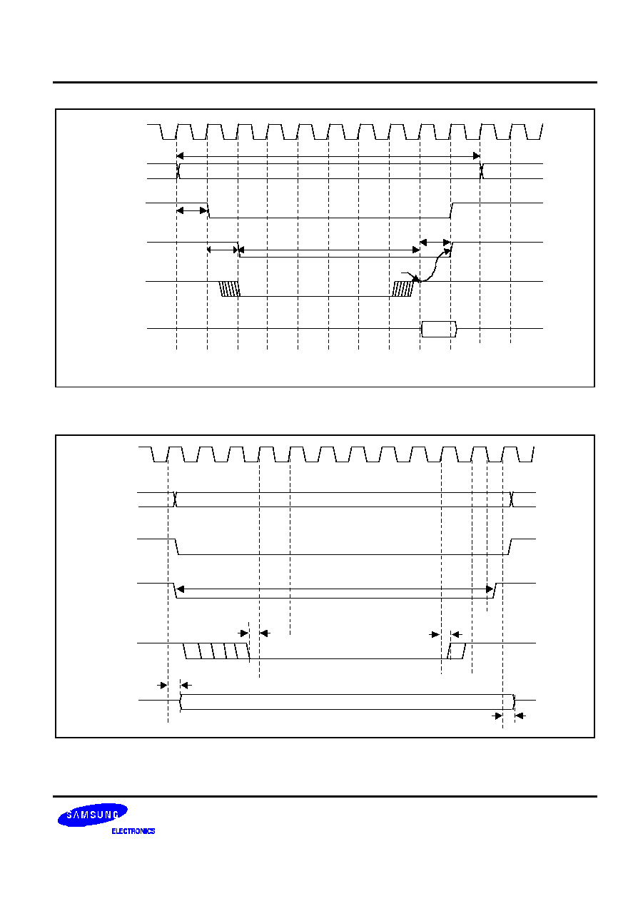
S3C2440A RISC MICROPROCESSOR
ELECTRICAL DATA
27-19
HCLK
nGCSx
nOE
Tacc = 6cycle
nWait
DATA
ADDR
Tacs
Tacs
delayed
t
RC
NOTE:
The status of nWait is checked at (Tacc-1) cycle.
sampling nWait
Figure 27-16. External nWAIT READ Timing Diagram
(Tacs=0, Tcos=0, Tacc=6, Toch=0, Tcah=0, PMC=0, ST=0)
HCLK
nGCSx
nWE
DATA
ADDR
t
RDD
t
RDD
Tacc >= 2cycle
nWait
t
WS
t
WH
Figure 27-17. External nWAIT WRITE Timing Diagram
(Tacs=0, Tcos=0, Tacc=4, Toch=0, Tcah=0, PMC=0, ST=0)
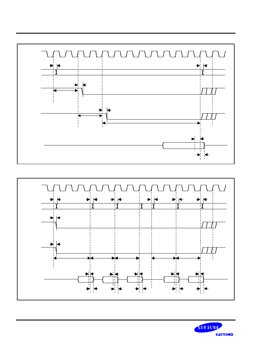
ELECTRICAL DATA
S3C2440A RISC MICROPROCESSOR
27-20
HCLK
nGCSx
t
RAD
Tacs
nOE
Tcos
DATA
ADDR
t
RCD
t
ROD
t
RDS
t
RDH
t
RAD
Tacc
Figure 27-18. Masked-ROM Single READ Timing Diagram (Tacs=2, Tcos=2, Tacc=8, PMC=01/10/11)
HCLK
nGCSx
t
RAD
nOE
DATA
ADDR
t
RCD
t
ROD
t
RDS
t
RDH
t
RAD
Tacc
Tpac
Tpac
Tpac
Tpac
t
RAD
t
RAD
t
RAD
t
RAD
t
RDS
t
RDH
t
RDS
t
RDH
t
RDS
t
RDH
t
RDS
t
RDH
Figure 27-19. Masked-ROM Consecutive READ Timing Diagram
(Tacs=0, Tcos=0, Tacc=3, Tpac=2, PMC=01/10/11)
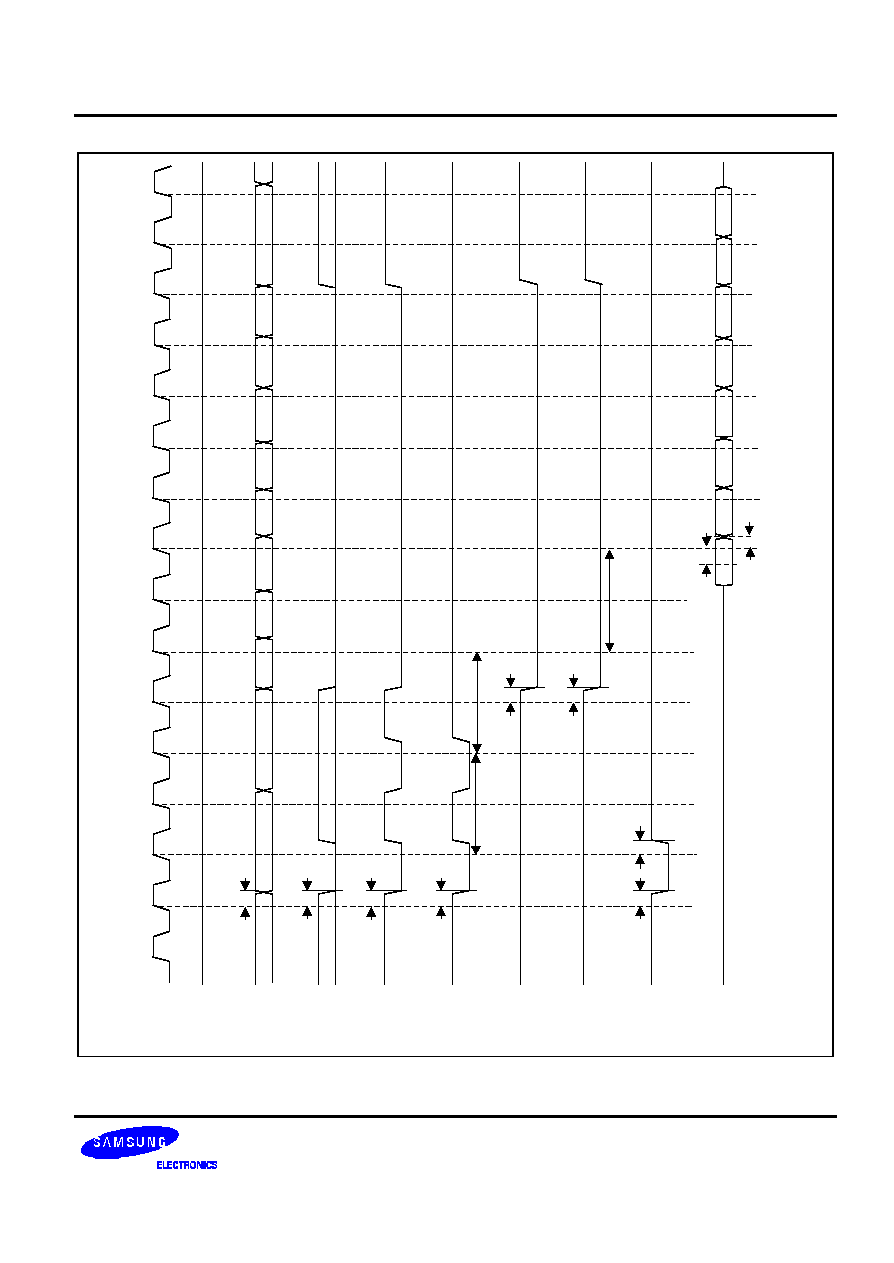
S3C2440A RISC MICROPROCESSOR
ELECTRICAL DATA
27-21
SCLK
nSRAS
t
SAD
Trp
nSCAS
DATA
ADDR/BA
nBEx
t
SRD
t
SDS
t
SDH
SCKE
A10/AP
nGCSx
t
SCSD
nWE
t
SAD
t
SCD
t
SWD
'1'
Trcd
t
SBED
Tcl
Figure 27-20. SDRAM Single Burst READ Timing Diagram (Trp=2, Trcd=2, Tcl=2, DW=16bit)
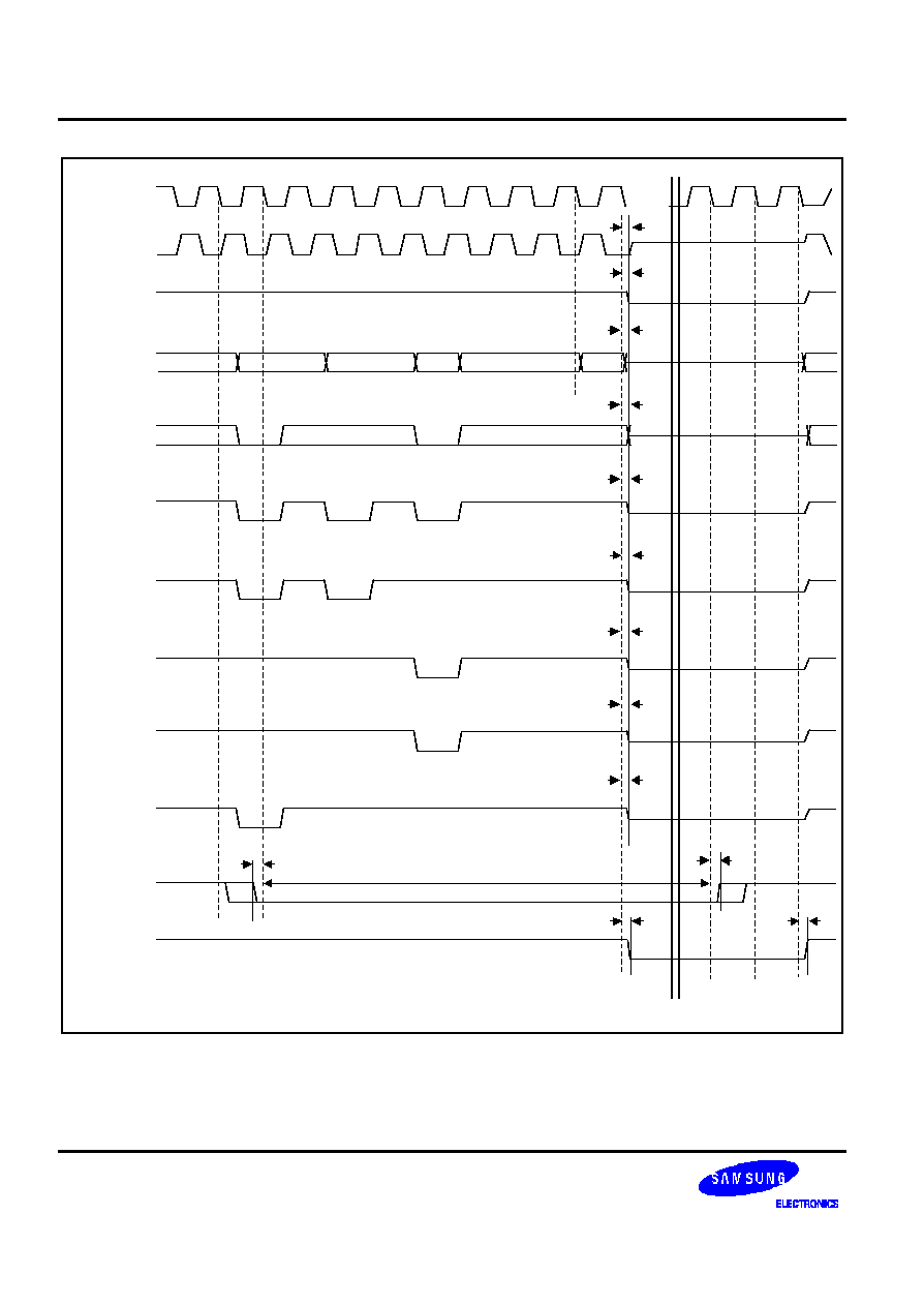
ELECTRICAL DATA
S3C2440A RISC MICROPROCESSOR
27-22
SCLK
nSRAS
nSCAS
ADDR/BA
nBEx
tXnBRQH
tXnBRQS
SCKE
A10/AP
nGCSx
nWE
'1'
XnBREQ
XnBACK
EXTCLK
tXnBACKD
tXnBACKD
'HZ'
'HZ'
'HZ'
'HZ'
'HZ'
'HZ'
'HZ'
'HZ'
'HZ'
tHZD
tHZD
tHZD
tHZD
tHZD
tHZD
tHZD
tHZD
tHZD
tXnBRQL
Figure 27-21. External Bus Request in SDRAM Timing Diagram (Trp=2, Trcd=2, Tcl=2)
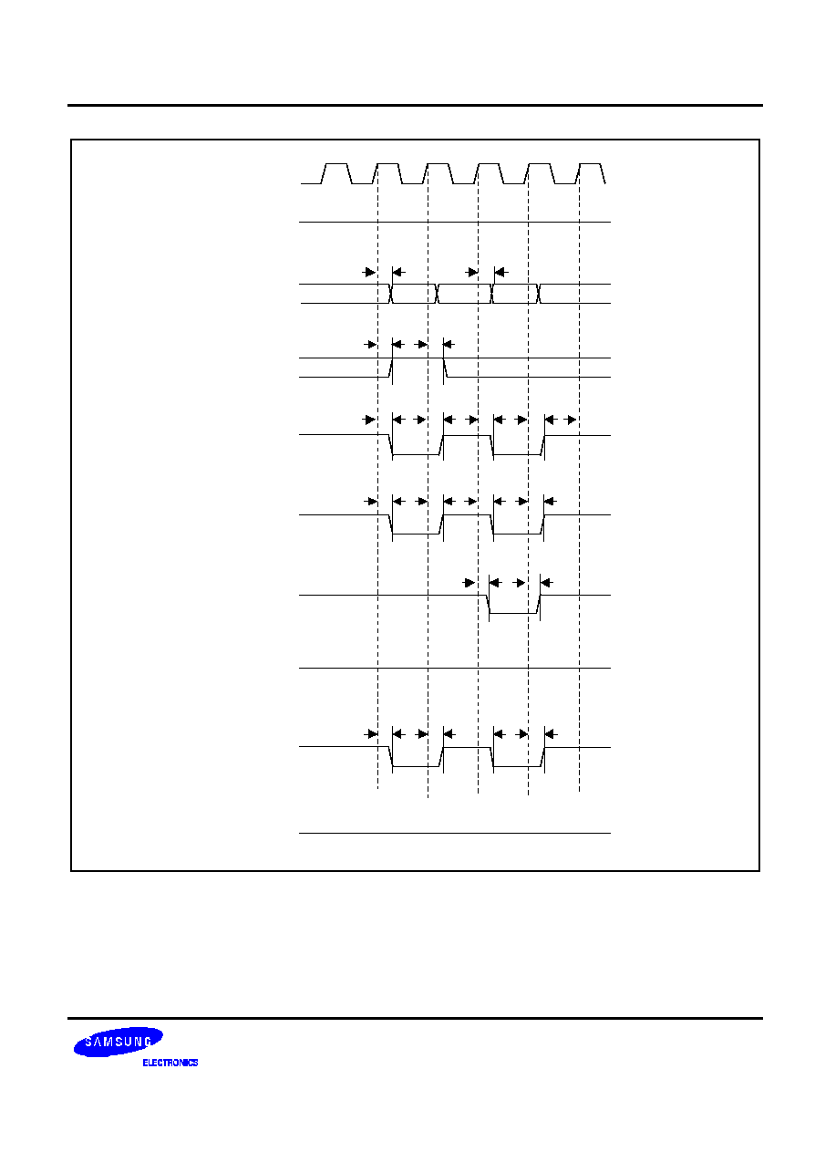
S3C2440A RISC MICROPROCESSOR
ELECTRICAL DATA
27-23
SCLK
nSRAS
t
SAD
nSCAS
DATA
ADDR/BA
nBEx
t
SRD
SCKE
A10/AP
nGCSx
t
SCSD
nWE
t
SAD
t
SCD
t
SWD
'1'
t
SAD
t
SCSD
t
SRD
'HZ'
'1'
t
SWD
Figure 27-22. SDRAM MRS Timing Diagram
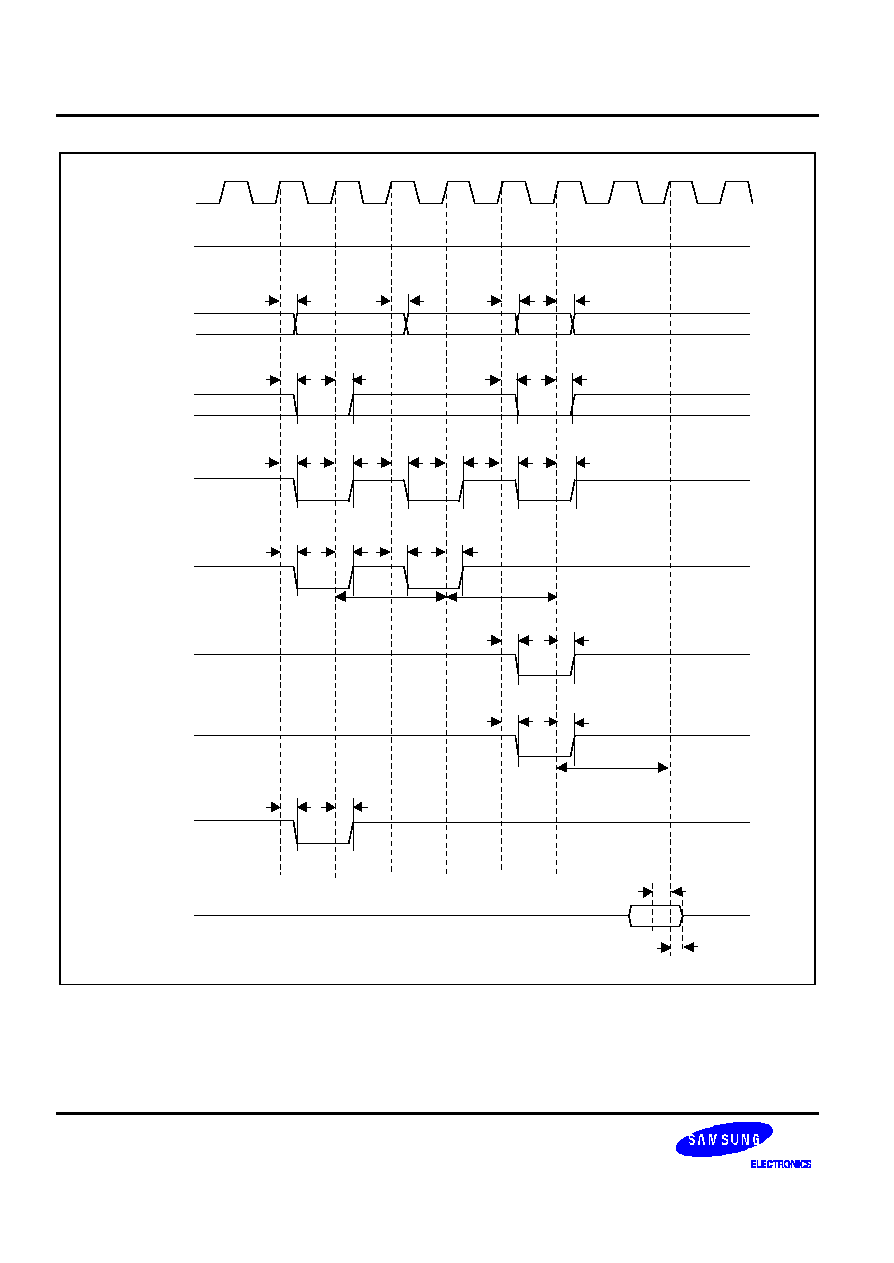
ELECTRICAL DATA
S3C2440A RISC MICROPROCESSOR
27-24
SCLK
nSRAS
t
SAD
Trp
nSCAS
DATA
ADDR/BA
nBEx
t
SRD
t
SDS
t
SDH
SCKE
A10/AP
nGCSx
t
SCSD
nWE
t
SAD
t
SCD
t
SWD
'1'
t
SAD
t
SAD
Trcd
t
SCSD
t
SRD
t
SCSD
t
SAD
t
SAD
t
SBED
Tcl
Figure 27-23. SDRAM Single READ Timing Diagram (I) (Trp=2, Trcd=2, Tcl=2)
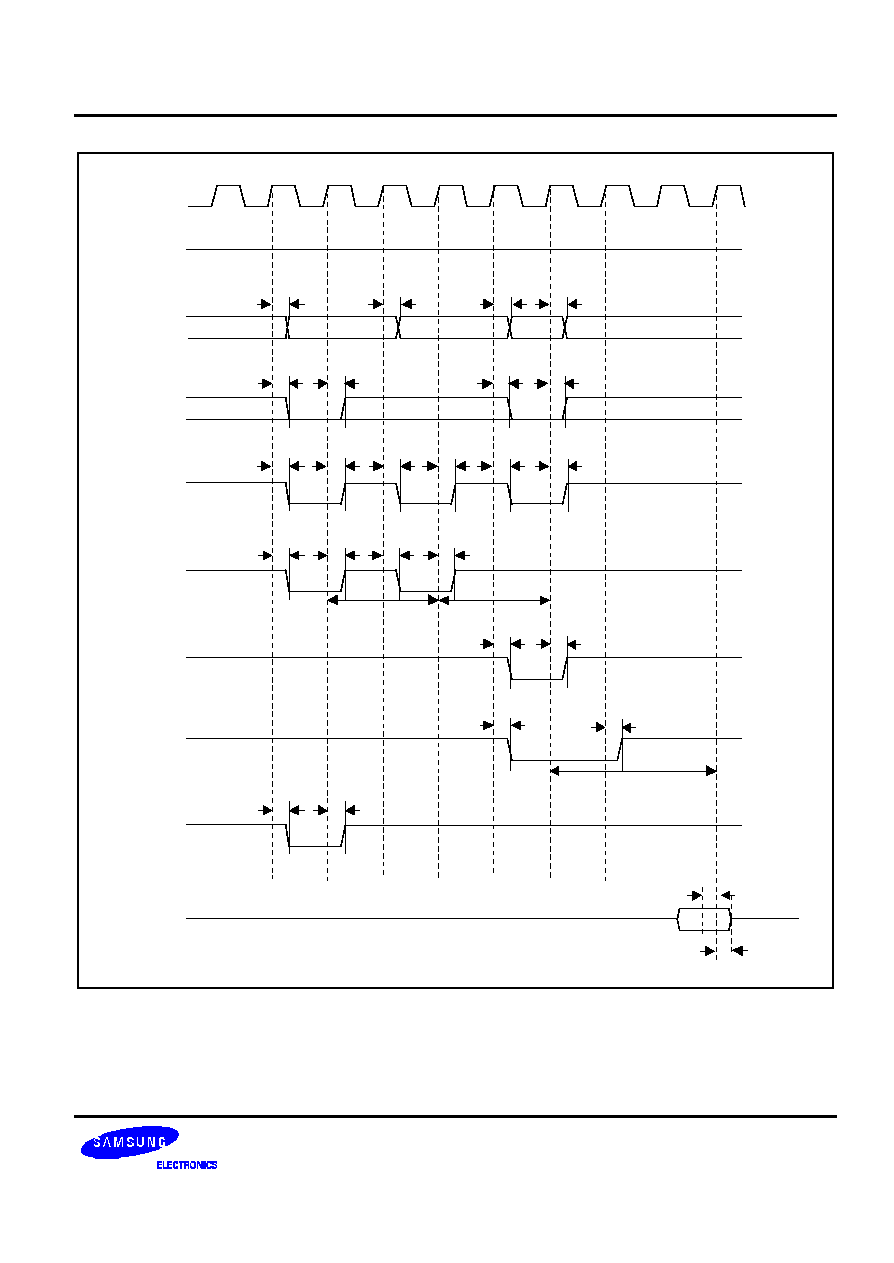
S3C2440A RISC MICROPROCESSOR
ELECTRICAL DATA
27-25
SCLK
nSRAS
t
SAD
Trp
nSCAS
DATA
ADDR/BA
nBEx
t
SRD
t
SDS
t
SDH
SCKE
A10/AP
nGCSx
t
SCSD
nWE
t
SAD
t
SCD
t
SWD
'1'
t
SAD
t
SAD
Trcd
t
SCSD
t
SRD
t
SCSD
t
SAD
t
SAD
t
SBED
Tcl
Figure 27-24. SDRAM Single READ Timing Diagram (II) (Trp=2, Trcd=2, Tcl=3)
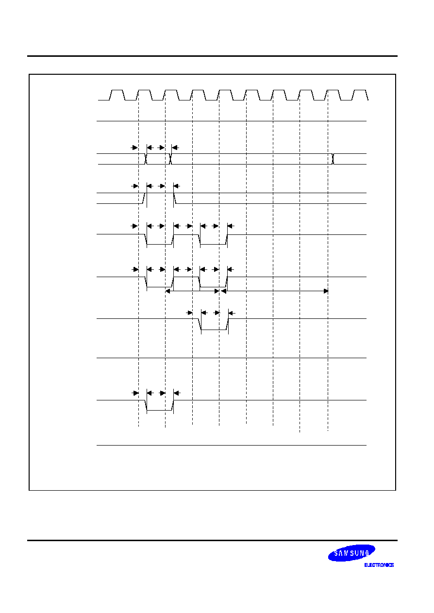
ELECTRICAL DATA
S3C2440A RISC MICROPROCESSOR
27-26
SCLK
nSRAS
t
SAD
Trp
nSCAS
DATA
ADDR/BA
nBEx
t
SRD
SCKE
A10/AP
nGCSx
t
SCSD
nWE
t
SAD
t
SCD
t
SWD
'1'
t
SAD
t
SCSD
t
SRD
'1'
'1'
'HZ'
Trc
NOTE: Before executing an auto/self refresh command, all the banks must be in idle state.
Figure 27-25. SDRAM Auto Refresh Timing Diagram (Trp=2, Trc=4)
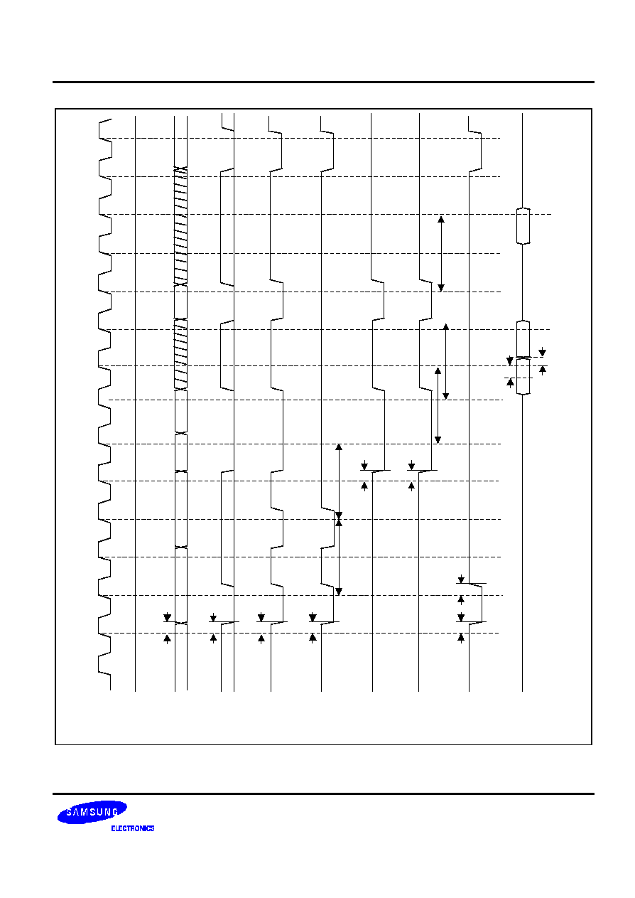
S3C2440A RISC MICROPROCESSOR
ELECTRICAL DATA
27-27
SCLK
nSRAS
t
SAD
Trp
nSCAS
DATA
ADDR/BA
nBEx
t
SRD
t
SDS
t
SDH
SCKE
A10/AP
nGCSx
t
SCSD
nWE
t
SAD
t
SCD
t
SWD
'1'
Trcd
t
SBED
Tcl
Tcl
Tcl
Figure 27-26. SDRAM Page Hit-Miss READ Timing Diagram (Trp=2, Trcd=2, Tcl=2)
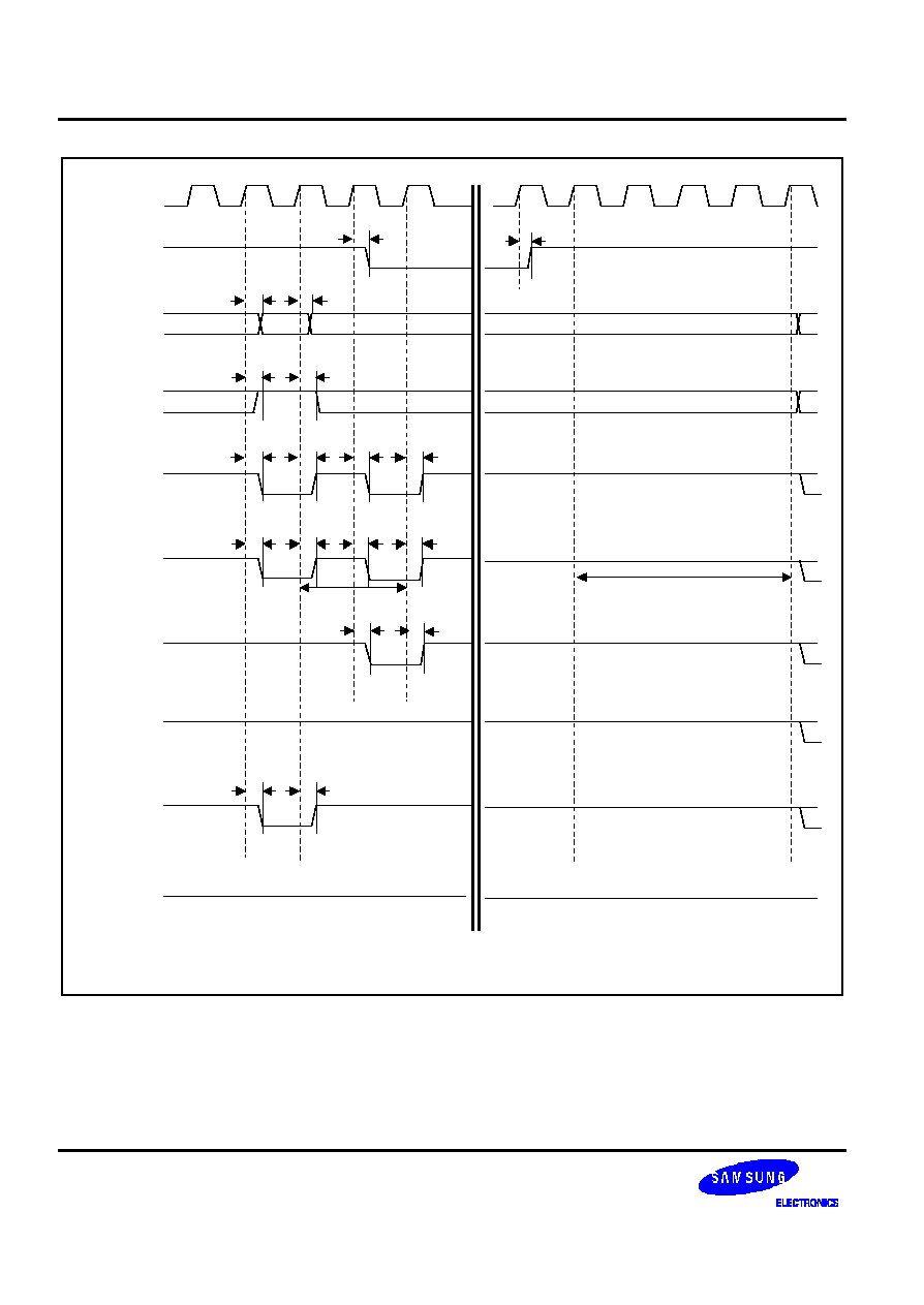
ELECTRICAL DATA
S3C2440A RISC MICROPROCESSOR
27-28
SCLK
nSRAS
t
SAD
Trp
nSCAS
DATA
ADDR/BA
nBEx
t
SRD
SCKE
A10/AP
nGCSx
t
SCSD
nWE
t
SAD
t
SCD
t
SWD
t
SAD
t
SCSD
t
SRD
'1'
'1'
'HZ'
Trc
t
CKED
'HZ'
'1'
'1'
'1'
'1'
'1'
t
CKED
NOTE: Before executing an auto/self refresh command, all the banks must be in idle state.
Figure 27-27. SDRAM Self Refresh Timing Diagram (Trp=2, Trc=4)
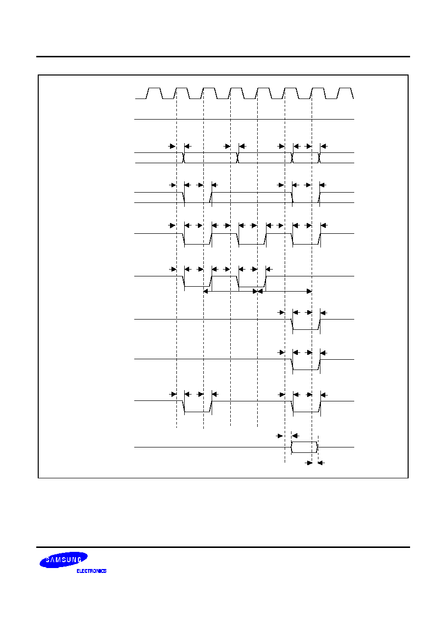
S3C2440A RISC MICROPROCESSOR
ELECTRICAL DATA
27-29
SCLK
nSRAS
t
SAD
Trp
nSCAS
DATA
ADDR/BA
nBEx
t
SRD
t
SDD
t
SDD
SCKE
A10/AP
nGCSx
t
SCSD
nWE
t
SAD
t
SCD
t
SWD
'1'
t
SAD
t
SAD
Trcd
t
SCSD
t
SRD
t
SCSD
t
SAD
t
SAD
t
SBED
t
SWD
Figure 27-28. SDRAM Single Write Timing Diagram (Trp=2, Trcd=2)
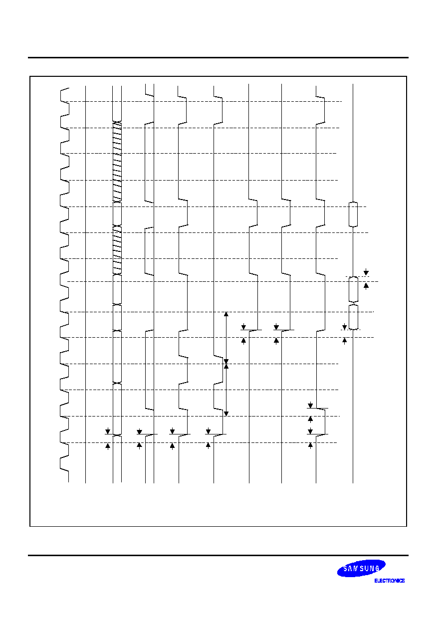
ELECTRICAL DATA
S3C2440A RISC MICROPROCESSOR
27-30
SCLK
nSRAS
t
SAD
Trp
nSCAS
DATA
ADDR/BA
nBEx
t
SRD
t
SDD
t
SDD
SCKE
A10/AP
nGCSx
t
SCSD
nWE
t
SAD
t
SCD
t
SWD
'1'
Trcd
t
SBED
Figure 27-29. SDRAM Page Hit-Miss Write Timing Diagram (Trp=2, Trcd=2, Tcl=2)
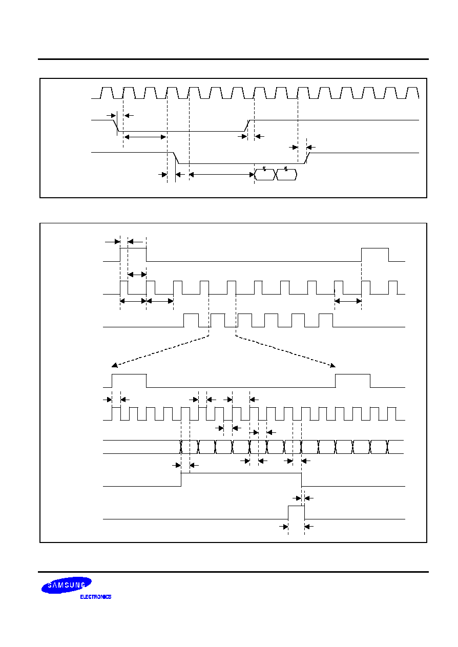
S3C2440A RISC MICROPROCESSOR
ELECTRICAL DATA
27-31
XSCLK
t
XRS
t
XRS
t
CADL
t
CADH
t
XAD
XnXDREQ
XnXDACK
Read Write
Min. 3SCLK
Figure 27-30. External DMA Timing Diagram (Handshake, Single transfer)
VSYNC
HSYNC
VDEN
Tf2hsetup
Tf2hhold
Tvspw
Tvbpd
Tvfpd
HSYNC
VCLK
VD
VDEN
LEND
Tl2csetup
Tvclkh
Tvclk
Tvclkl
Tvdhold
Tvdsetup
Tve2hold
Tle2chold
Tlewidth
Figure 27-31. TFT LCD Controller Timing Diagram
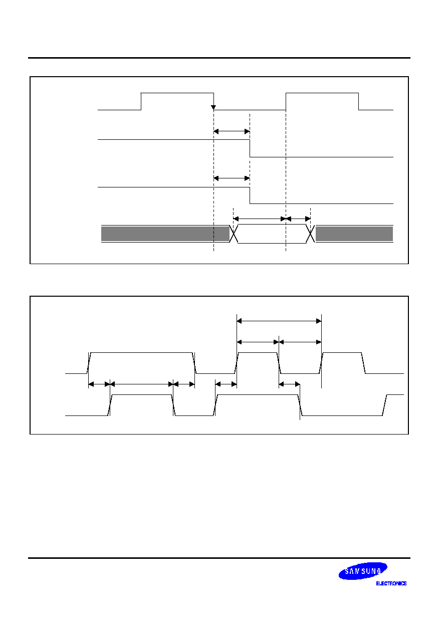
ELECTRICAL DATA
S3C2440A RISC MICROPROCESSOR
27-32
IISSCLK
t
LRCK
IISLRCK (out)
t
SDO
IISLRCK (out)
t
SDIH
t
SDIS
IISSDI (in)
Figure 27-32. IIS Interface Timing Diagram
t
STOPH
t
STARTS
t
SDAS
t
SDAH
t
BUF
t
SCLHIGH
t
SCLLOW
f
SCL
IICSCL
IICSDA
Figure 27-33. IIC Interface Timing Diagram
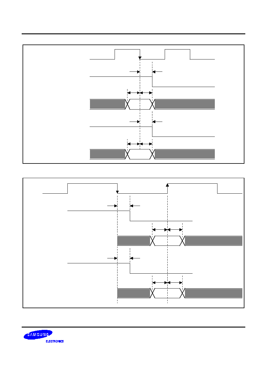
S3C2440A RISC MICROPROCESSOR
ELECTRICAL DATA
27-33
SDCLK
t
SDCD
SDCMD (out)
t
SDCH
t
SDCS
t
SDDD
SDCMD (in)
t
SDDH
t
SDDS
SDDATA[3:0] (in)
SDDATA[3:0] (out)
Figure 27-34. SD/MMC Interface Timing Diagram
SPICLK
t
SPIMOD
t
SPISIH
t
SPISIS
t
SPISOD
t
SPIMIH
t
SPIMIS
SPIMOSI (MO)
SPIMOSI (SI)
SPIMISO (SO)
SPIMISO (MI)
Figure 27-35. SPI Interface Timing Diagram (CPHA=1, CPOL=1)
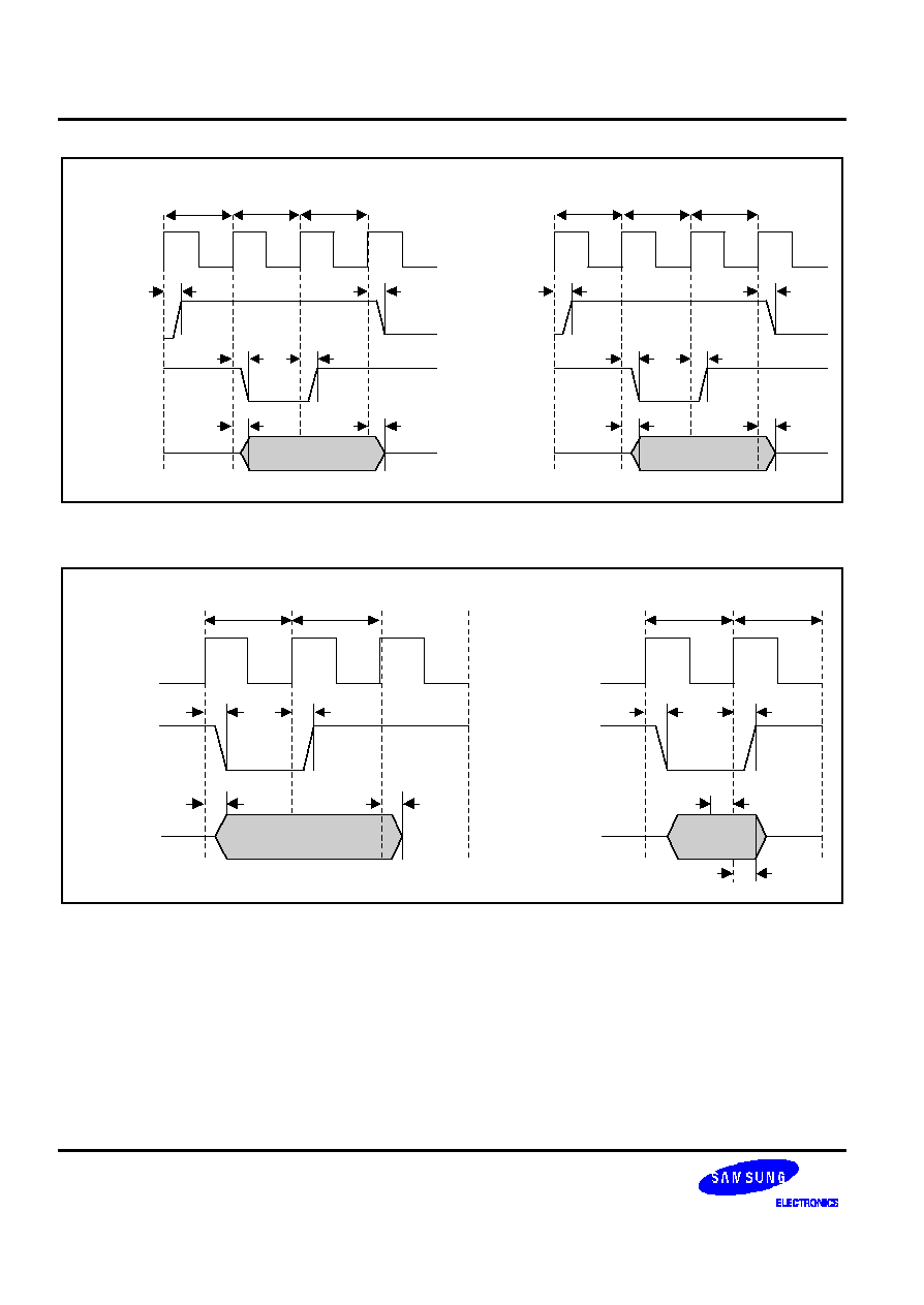
ELECTRICAL DATA
S3C2440A RISC MICROPROCESSOR
27-34
t
ACLS
t
WRPH0
t
WRPH1
Command
t
WRPH0
t
WRPH1
Address
HCLK
ALE
nFWE
DATA[7:0]
DATA[7:0]
HCLK
CLE
nFWE
t
CLED
t
CLED
t
WED
t
WED
t
WDS
t
WDH
t
ALED
t
WED
t
WDS
t
ALED
t
WED
t
WDH
t
ACLS
Figure 27-36. NAND Flash Address/Command Timing Diagram
HCLK
nFWE
t
WRPH0
t
WRPH1
DATA[7:0]
HCLK
nFRE
t
WRPH0
t
WRPH1
DATA[7:0]
t
WED
t
WED
t
WDH
t
WED
t
WED
t
RDS
t
RDH
t
WDS
WDATA
RDATA
Figure 27-37. NAND Flash Timing Diagram
S3C2440A RISC MICROPROCESSOR
ELECTRICAL DATA
27-35
Table 27-7. Clock Timing Constants
(V
DDi,
V
DDalive,
V
DDiarm
= 1.2 V
±
0.1 V, T
A
= ≠40 to 85
∞
C, V
DDMOP
= 3.3V
±
0.3V)
Parameter
Symbol
Min
Typ
Max
Unit
Crystal clock input frequency
f
XTAL
12
≠
20
MHz
Crystal clock input cycle time
t
XTALCYC
50
≠
83.3
ns
External clock input frequency
f
EXT
≠
≠
66
MHz
External clock input cycle time
t
EXTCYC
15.0
≠
≠
ns
External clock input low level pulse width
t
EXTLOW
7
≠
≠
ns
External clock to HCLK (without PLL)
t
EX2HC
3
≠
7
ns
HCLK (internal) to CLKOUT
t
HC2CK
3
≠
9
ns
HCLK (internal) to SCLK
t
HC2SCLK
1
≠
2
ns
External clock input high level pulse width
t
EXTHIGH
4
≠
≠
ns
Reset assert time after clock stabilization
t
RESW
4
≠
≠
XTIpll or
EXTCLK
PLL Lock Time
t
PLL
300
≠
µS
Sleep mode return oscillation setting time
t
OSC2
≠
≠
65536
XTIpll or
EXTCLK
Interval before CPU runs after nRESET is released
t
RST2RUN
≠
7
≠
XTIpll or
EXTCLK
ELECTRICAL DATA
S3C2440A RISC MICROPROCESSOR
27-36
Table 27-8. ROM/SRAM Bus Timing Constants
(V
DDi,
V
DDalive,
V
DDiarm
= 1.2 V
±
0.1 V, T
A
= ≠40 to 85
∞
C, V
DDMOP
= 3.3V
±
0.3V / 3.0V
±
0.3V / 2.5V
±
0.2V / 1.8V
±
0.1V)
Parameter
Symbol
Min
(V
DDMOP
=
3.3V/3.0V/2.5V/1.8V)
Typ
Max
(V
DDMOP
=
3.3V/3.0V/2.5V/1.8V)
Unit
ROM/SRAM address delay
t
RAD
2 / 2 / 2 / 3
≠
6 / 6 / 7 / 8
ns
ROM/SRAM chip select delay
t
RCD
2 / 2 / 3 / 3
≠
6 / 6 / 6 / 7
ns
ROM/SRAM output enable delay
t
ROD
2 / 2 / 2 / 3
≠
5 / 5 / 5 / 6
ns
ROM/SRAM read data setup time.
t
RDS
1 / 1 / 1 / 2
≠
≠ / ≠ / ≠ / ≠
ns
ROM/SRAM read data hold time.
t
RDH
0 / 0 / 0 / 0
≠
≠ / ≠ / ≠ / ≠
ns
ROM/SRAM byte enable delay
t
RBED
2 / 2 / 2 / 3
≠
5 / 5 / 5 / 7
ns
ROM/SRAM write byte enable delay
t
RWBED
2 / 2 / 2 / 3
≠
5 / 5 / 6 / 7
ns
ROM/SRAM output data delay
t
RDD
2 / 2 / 2 / 2
≠
6 / 6 / 6 / 7
ns
ROM/SRAM external wait setup time
t
WS
3 / 3 / 4 / 4
≠
≠ / ≠ / ≠ / ≠
ns
ROM/SRAM external wait hold time
t
WH
0 / 0 / 0 / 0
≠
≠ / ≠ / ≠ / ≠
ns
ROM/SRAM write enable delay
t
RWD
2 / 2 / 2 / 3
≠
5 / 5 / 6 / 7
ns
Table 27-9. Memory Interface Timing Constants
(V
DDi,
V
DDalive,
V
DDiarm
= 1.2 V
±
0.1 V, T
A
= ≠40 to 85
∞
C, V
DDMOP
= 3.3V
±
0.3V / 3.0V
±
0.3V / 2.5V
±
0.2V / 1.8V
±
0.1V)
Parameter
Symbol
Min
Typ
Max
Unit
SDRAM address delay
t
SAD
1
≠
4
ns
SDRAM chip select delay
t
SCSD
1
≠
3
ns
SDRAM row active delay
t
SRD
1
≠
3
ns
SDRAM column active delay
t
SCD
1
≠
3
ns
SDRAM byte enable delay
t
SBED
1
≠
3
ns
SDRAM write enable delay
t
SWD
1
≠
2
ns
SDRAM read data setup time
t
SDS
2 / 3 / 3 / 5 *
≠
≠
ns
SDRAM read data hold time
t
SDH
0
≠
≠
ns
SDRAM output data delay
t
SDD
1
≠
4
ns
SDRAM clock enable delay
T
cked
2
≠
3
ns
NOTE: Minimum t
SDS
= 2ns / 3ns / 3ns, when V
DDMOP
= 3.3V / 3.0V / 2.5V / 1.8V respectively.
S3C2440A RISC MICROPROCESSOR
ELECTRICAL DATA
27-37
Table 27-10. External Bus Request Timing Constants
(V
DD
= 1.2 V
±
0.1 V, T
A
= ≠40 to 85
∞
C, V
EXT
= 3.3V
±
0.3V)
Parameter
Symbol
Min
Typ.
Max
Unit
External bus request setup time
t
XnBRQS
4
≠
≠
ns
External bus request hold time
t
XnBRQH
1
≠
≠
ns
External bus ack delay
t
XnBACKD
4
≠
10
ns
HZ delay
t
HZD
2
≠
6
ns
Table 27-11. DMA Controller Module Signal Timing Constants
(V
DD
= 1.2 V
±
0.1 V, T
A
= ≠40 to 85
∞
C, V
EXT
= 3.3V
±
0.3V)
Parameter
Symbol
Min
Typ.
Max
Unit
External request setup
t
XRS
5
≠
≠
ns
Access to ack delay during low transition
t
CADL
3
≠
8
ns
Access to ack delay during high transition
t
CADH
3
≠
8
ns
External request delay
t
XAD
2
≠
≠
SCLK
ELECTRICAL DATA
S3C2440A RISC MICROPROCESSOR
27-38
Table 27-12. TFT LCD Controller Module Signal Timing Constants
(V
DD
= 1.2 V
±
0.05 V, T
A
= ≠40 to 85
∞
C, V
EXT
= 3.3V
±
0.3V)
Parameter
Symbol
Min
Typ
Max
Units
Vertical sync pulse width
Tvspw
VSPW + 1
≠
≠
Phclk
(1)
Vertical back porch delay
Tvbpd
VBPD+1
≠
≠
Phclk
Vertical front porch delay
Tvfpd
VFPD+1
≠
≠
Phclk
VCLK pulse width
Tvclk
1
≠
≠
Pvclk
(2)
VCLK pulse width high
Tvclkh
0.5
≠
≠
Pvclk
VCLK pulse width low
Tvclkl
0.5
≠
≠
Pvclk
Hsync setup to VCLK falling edge
Tl2csetup
0.5
≠
≠
Pvclk
VDEN setup to VCLK falling edge
Tde2csetup
0.5
≠
≠
Pvclk
VDEN hold from VCLK falling edge
Tde2chold
0.5
≠
≠
Pvclk
VD setup to VCLK falling edge
Tvd2csetup
0.5
≠
≠
Pvclk
VD hold from VCLK falling edge
Tvd2chold
0.5
≠
≠
Pvclk
VSYNC setup to HSYNC falling edge
Tf2hsetup
HSPW + 1
≠
≠
Pvclk
VSYNC hold from HSYNC falling edge
Tf2hhold
HBPD + HFPD +
HOZVAL + 3
≠
≠
Pvclk
NOTES:
1.
HSYNC period
2.
VCLK period
Table 27-13. IIS Controller Module Signal Timing Constants
(V
DD
= 1.2 V
±
0.1 V, T
A
= ≠40 to 85
∞
C, V
EXT
= 3.3V
±
0.3V)
Parameter
Symbol
Min
Typ.
Max
Unit
IISLRCK delay time
t
LRCK
0
≠
3
ns
IISDO delay time
t
SDO
1
≠
2
ns
IISDI input setup time
t
SDIS
13
≠
≠
ns
IISDI input hold time
t
SDIH
1
≠
≠
ns
CODEC clock frequency
f
CODEC
1/16
≠
1
f
IIS_BLOCK
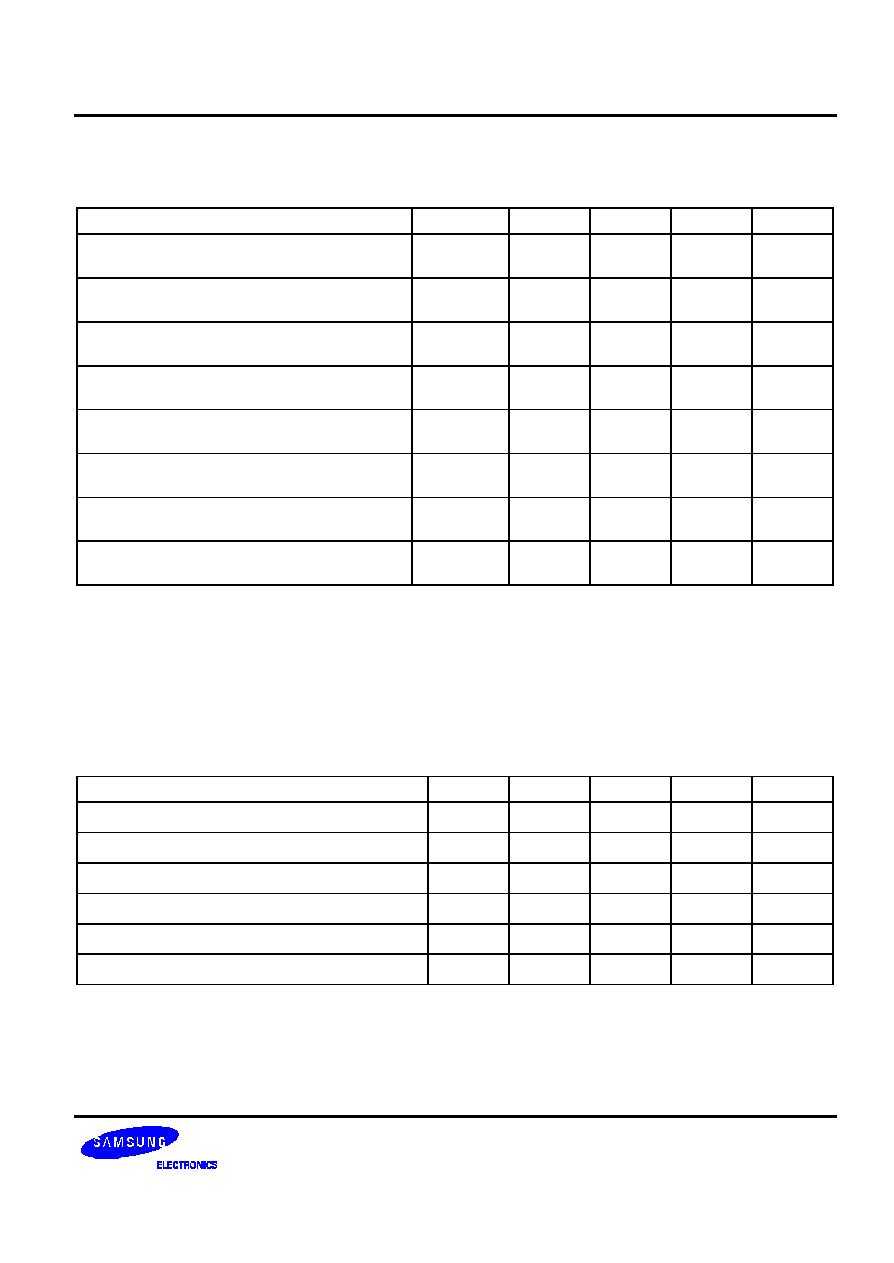
S3C2440A RISC MICROPROCESSOR
ELECTRICAL DATA
27-39
Table 27-14. IIC BUS Controller Module Signal Timing
(V
DD
= 1.2 V
±
0.05 V, T
A
= ≠40 to 85
∞
C, V
EXT
= 3.3V
±
0.3V)
Parameter
Symbol
Min
Typ.
Max
Unit
SCL clock frequency
f
SCL
≠
≠
std. 100
fast 400
kHz
SCL high level pulse width
t
SCLHIGH
std. 4.0
fast 0.6
≠
≠
µ
s
SCL low level pulse width
t
SCLLOW
std. 4.7
fast 1.3
≠
≠
µ
s
Bus free time between STOP and START
t
BUF
std. 4.7
fast 1.3
≠
≠
µ
s
START hold time
t
STARTS
std. 4.0
fast 0.6
≠
≠
µ
s
SDA hold time
t
SDAH
std. 0
fast 0
≠
std. ≠
fast 0.9
µ
s
SDA setup time
t
SDAS
std. 250
fast 100
≠
≠
ns
STOP setup time
t
STOPH
std. 4.0
fast 0.6
≠
≠
µ
s
NOTES: Std. means Standard Mode and fast means Fast Mode.
1.
The IIC data hold time (t
SDAH
) is minimum 0ns.
(IIC data hold time is minimum 0ns for standard/fast bus mode in IIC specification v2.1)
Please check whether the data hold time of your IIC device is 0 nS or not.
2.
The IIC controller supports only IIC bus device (standard/fast bus mode), and not C bus device.
Table 27-15. SD/MMC Interface Transmit/Receive Timing Constants
(V
DD
= 1.2 V
±
0.1 V, T
A
= ≠40 to 85
∞
C, V
EXT
= 3.3V
±
0.3V)
Parameter
Symbol
Min
Typ.
Max
Unit
SD command output delay time
t
SDCD
0
≠
1
ns
SD command input setup time
t
SDCS
14
≠
≠
ns
SD command input hold time
t
SDCH
1
≠
≠
ns
SD data output delay time
t
SDDD
0
≠
1
ns
SD data input setup time
t
SDDS
13
≠
≠
ns
SD data input hold time
t
SDDH
1
≠
≠
ns
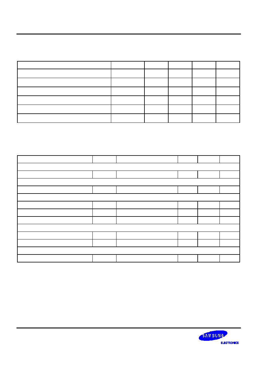
ELECTRICAL DATA
S3C2440A RISC MICROPROCESSOR
27-40
Table 27-16. SPI Interface Transmit/Receive Timing Constants
(V
DD
= 1.2 V
±
0.1 V, T
A
= ≠40 to 85
∞
C, V
EXT
= 3.3V
±
0.3V)
Parameter
Symbol
Min
Typ.
Max
Unit
SPI MOSI master output delay time
t
SPIMOD
0
≠
1
ns
SPI MOSI slave input setup time
t
SPISIS
1
≠
≠
ns
SPI MOSI slave input hold time
t
SPISIH
1
≠
≠
ns
SPI MISO slave output delay time
t
SPISOD
7
≠
17
ns
SPI MISO master input setup time
t
SPIMIS
15
≠
≠
ns
SPI MISO master input hold time
t
SPIMIH
1
≠
≠
ns
Table 27-17. USB Electrical Specifications
(V
DD
= 1.2 V
±
0.05 V, T
A
= ≠40 to 85
∞
C, V
EXT
= 3.3V
±
0.3V)
Parameter
Symbol
Condition
Min
Max
Unit
Supply Current
Suspend device
ICCS
10
µA
Leakage Current
Hi-Z state input leakage
ILO
0V < VIN < 3.3V
≠10
10
µA
Input Levels
Differential input sensitivity
VDI
| (D+) ≠ (D≠) |
0.2
V
Differential common mode range
VCM
Includes VDI range
0.8
2.5
Single ended receiver threshold
VSE
0.8
2.0
Output Levels
Static output low
VOL
RL of 1.5k
to 3.6V
0.2
V
Static output high
VOH
RL of 15 k
to GND
2.8
3.6
Capacitance
Transceiver capacitance
CIN
Pin to GND
20
pF
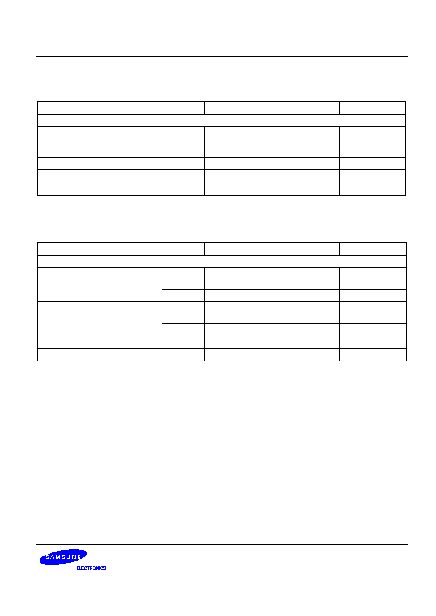
S3C2440A RISC MICROPROCESSOR
ELECTRICAL DATA
27-41
Table 27-18. USB Full Speed Output Buffer Electrical Characteristics
(V
DD
= 1.2 V
±
0.05 V, T
A
= ≠40 to 85
∞
C, V
EXT
= 3.3V
±
0.3V)
Parameter
Symbol
Condition
Min
Max
Unit
Driver Characteristics
Transition time
Rise time
Fall time
TR
TF
CL = 50pF
CL = 50pF
4.0
4.0
20
20
ns
Rise/Fall time matching
Trfm
(TR / TF )
90
111.1
%
Output signal crossover voltage
Vcrs
1.3
2.0
V
Drive output resistance
Zdrv
Steady state drive
28
44
Table 27-19. USB Low Speed Output Buffer Electrical Characteristics
(V
DD
= 1.2 V
±
0.05 V, T
A
= ≠40 to 85
∞
C, V
EXT
= 3.3V
±
0.3V)
Parameter
Symbol
Condition
Min
Max
Unit
Driver Characteristics
Rising time
TR
CL = 50pF
CL = 350pF
75
ns
300
Falling time
TF
CL = 50pF
CL = 350pF
75
300
Rise/Fall time matching
Trfm
(Tr / Tf )
80
125
%
Output signal crossover voltage
Vcrs
1.3
2.0
V
NOTE: All measurement conditions are in accordance with the Universal Serial Bus Specification 1.1 Final Draft Revision.
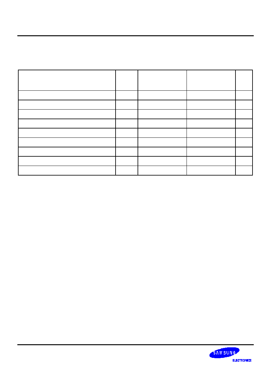
ELECTRICAL DATA
S3C2440A RISC MICROPROCESSOR
27-42
Table 27-20. NAND Flash Interface Timing Constants
(V
DDi,
V
DDalive,
V
DDiarm
= 1.2 V
±
0.1 V, T
A
= ≠40 to 85
∞
C, V
DDMOP
= 3.3V
±
0.3V / 3.0V
±
0.3V / 2.5V
±
0.2V / 1.8V
±
0.1V)
Parameter
Symbol
Min
(V
DDMOP
=
3.3V/3.0V/2.5V/1.8V)
Max
(V
DDMOP
=
3.3V/3.0V/2.5V/1.8V)
Unit
NFCON chip enable delay
t
CED
≠ / ≠ / ≠ / ≠
5.4/5.6/5.9/7.1
ns
NFCON CLE delay
t
CLED
≠ / ≠ / ≠ / ≠
5.3/5.5/5.8/7.0
ns
NFCON ALE delay
t
ALED
≠ / ≠ / ≠ / ≠
5.4/5.6/5.9/7.1
ns
NFCON write enable delay
t
WED
≠ / ≠ / ≠ / ≠
5.0/5.2/5.5/6.7
ns
NFCON read enable delay
t
RED
≠ / ≠ / ≠ / ≠
5.0/5.2/5.5/6.7
ns
NFCON write data setup time
t
WDS
5.8/6.0/6.3/7.5
≠ / ≠ / ≠ / ≠
ns
NFCON write data hold time
t
WDH
4.6/4.8/5.1/6.3
≠ / ≠ / ≠ / ≠
ns
NFCON read data setup requirement time
t
RDS
3/3.1/3.3/4
≠ / ≠ / ≠ / ≠
ns
NFCON read data hold requirement time
t
RDH
0.3/0.3/0.3/0.3
≠ / ≠ / ≠ / ≠
ns