Document Outline
- CH1. INTRODUCTION
- CH2. SROM
- CH3. SDRAM
- CH4. NAND
- CH5. BUX MATRIX
- CH6. INTERRUPT
- CH7. PWM TIMER
- CH8. WATCHDOG TIMER
- CH9. DMA
- CH10. RTC
- CH11. UART
- CH12. IRDA
- CH13. IIC
- CH14. IIS
- CH15. SPI
- CH16. AC97
- CH17. USB HOST
- CH18. USB DEVICE
- CH19. MODEM
- CH20. GPIO
- CH21. CAMERA
- CH22. MPEG4 OVERVIEW
- CH23. ME
- CH24. MC
- CH25. DCTQ
- CH26. VLX
- CH27. POST
- CH28. LCD
- CH29. KEYPAD
- CH30. ADC & TOUCH
- CH31. SDI
- CH32. MEMORY STICK
- CH33. CLOCK & POWER
- CH34. MECHANICAL DATA

BSW rv0.1-0417-N01
Preliminary product information describes products that are in development,
for which full characterization data and associated errata are not yet available.
Specifications and information herein are subject to change without notice.
S3C24A0 RISC MICROPROCESSOR
PRELIMINARY PRODUCT OVERVIEW
1-1
PRODUCT OVERVIEW
S3C24A0
AN APPLICATION PROCESSOR FOR
2.5G/3G MOBILE PHONES
SOC R&D CENTER
SAMSUNG ELECTRONICS CORP.

BSW rv0.1-0417-N01
Preliminary product information describes products that are in development,
for which full characterization data and associated errata are not yet available.
Specifications and information herein are subject to change without notice.
PRELIMINARY PRODUCT OVERVIEW
S3C24A0 RISC MICROPROCESSOR
1-2
CONTENTS
CH1. INTRODUCTION
CH2. SROM
CH3. SDRAM
CH4. NAND
CH5. BUS MATRIX
CH6. INTERRUPT
CH7. PWM TIMER
CH8. WATCH DOG TIMER
CH9. DMA
CH10. RTC
CH11. UART
CH12. IRDA
CH13. IIC
CH14. IIS
CH15. SPI
CH16. AC97
CH17. USB HOST
CH18. USB DEVICE
CH19. MODEM
CH20. GPIO
CH21. CAMERA
CH22. MPEG4-OVERVIEW
CH23. MOTION ESTIMATION
CH24. MOTION COMPENSATION
CH25. DCTQ
CH26. VLX
CH27. POST
CH28. LCD
CH29. KEYPAD
CH30. ADC & TOUCH
CH31. SD/MMC
CH32. MEMORY STICK
CH33. CLOCK & POWER
CH34. MECHANICAL DATA

BSW rv0.1-0417-N01
Preliminary product information describes products that are in development,
for which full characterization data and associated errata are not yet available.
Specifications and information herein are subject to change without notice.
S3C24A0 RISC MICROPROCESSOR
PRELIMINARY PRODUCT OVERVIEW
1-3
1
INTRODUCTION (PRELIMINARY)
1.1 ARCHITECTURAL OVERVIEW
The S3C24A0 is a 16/32-bit RISC microprocessor, which is designed to provide a cost-effective, low power, and
high performance micro-controller solution for mobile phones and general applications. To provide a sufficient H/W
performance for the 2.5G & 3G communication services, the S3C24A0 adopts dual-32-bit bus architecture and
includes many powerful hardware accelerators for the motion video processing, serial communications, and etc.
For the real time video conferencing, an optimized MPEG4 H/W Encoder/Decoder is integrated. To reduce total
system cost and enhance overall functionality, the S3C24A0 also includes following components: separate 16KB
Instruction and 16KB Data Cache, MMU to handle virtual memory management, LCD controller (TFT), Camera
Interface, MPEG-4 ME, MC, DCTQ, NAND Flash Boot loader, System Manager (power management & etc.),
SDRAM controller, 2-ch UART, 4-ch DMA, 4-ch Timers, General I/O Ports, IIC-BUS interface, USB Host, SD Host
& Multi-Media Card Interface, Memory Stick Interface, PLL for clock generation & etc. The S3C24A0 can be used
as a most powerful Application Processor for mobiles phones. For this application, the S3C24A0 has a Modem
Interface to communicate with various Modem Chips.
The S3C24A0 is developed using an ARM926EJ-S core, advanced 0.13um CMOS standard cells and memory
compliers. Its low-power, simple, elegant and fully static-design scheme is particularly suitable for cost-sensitive
and power-sensitive applications. Also, the S3C24A0 adopts a de-facto standard bus architecture � the AMBA
(Advanced Microcontroller Bus Architecture).
One of outstanding features of the S3C24A0 is its CPU core, a 16/32-bit ARM926EJ-S RISC processor designed
by ARM, Ltd. The ARM926EJ-S is a single chip MCU and Java enabled microprocessor. The ARM926EJ-S also
implements the MMU, the AMBA BUS, and the Harvard cache architecture with separate 16KB instruction and
16KB data caches, each cache with an 8-word line length.
By providing a complete set of common system peripherals, the S3C24A0 minimizes overall system costs and
eliminates the need to configure additional components.
1.2 FEATURES
This section summarizes the features of the S3C24A0. Figure 1-1 is an overall block diagram of the S3C24A0.
1.2.1 Microprocessor and Overall Architecture
�
SoC (System-on-Chip) for mobile phones and general embedded applications.
�
16/32-Bit RISC architecture and powerful instruction set with ARM926EJ-S CPU core.
�
ARM's Jazelle Java technology
�
Enhanced ARM architecture MMU to support WinCE, Symbian and Linux
�
Instruction cache, data cache, write buffer and Physical address TAG RAM to reduce the effect of main
memory bandwidth and latency on performance

BSW rv0.1-0417-N01
Preliminary product information describes products that are in development,
for which full characterization data and associated errata are not yet available.
Specifications and information herein are subject to change without notice.
PRELIMINARY PRODUCT OVERVIEW
S3C24A0 RISC MICROPROCESSOR
1-4
�
4 way set-associative cache with I-Cache (16KB) and D-Cache (16KB).
�
8-words per line with one valid bit and two dirty bits per line
�
Pseudo random or round robin replacement algorithm.
�
Write through or write back cache operation to update the main memory.
�
The write buffer can hold 16 words of data and four addresses.
�
ARM926EJ-S core supports the ARM debug architecture
�
Internal AMBA (Advanced Microcontroller Bus Architecture) (AMBA2.0, AHB/APB)
�
Dual AHB bus for high-performance processing (AHB-I & AHB-S)
1.2.2 Memory Subsystem
�
High bandwidth Memory subsystem with two access channels (accesses from two AHB buses) and three-
channel memory ports
�
Double the bandwidth with the simultaneous access capability
�
ROM/SRAM/NOR-Flash/NAND-Flash channel
�
One SDRAM channels
�
Up to 1GB Address space
�
Low-power SDRAM interface support : Mobile SDRAM function
-
DS : Driver Strength Control
-
TCSR : Temperature Compensated Self-Refresh Control
-
PASR : Partial Array Self-Refresh Control
�
NAND Flash Boot Loader with the ECC circuitry to support booting from NAND Flash
-
4KB Stepping Stone
-
Support 1G, 2G bit NAND Flash
1.2.3 General Peripherals
�
Interrupt Controller
-
61 Interrupt sources
(1 Watch Dog Timer, 5 Timer, 6 UART, 18 External Interrupts, 4 DMA, 2 RTC, 3 ADC, 1 I2C, 1 AC97, 1
NAND Flash, 1 IrDA, 1 Memory Stick, 2 SPI, 1 SDI, 2 USB (Host and Device), 1 Keypad, 1 Modem
Interface, 2 Camera Interface, 4 MPEG, 2 LCD, 1 Battery Fault, 1 Post)
-
Level/Edge mode on external interrupt source.
-
Programmable polarity of edge and level.
-
Supports FIQ (Fast Interrupt request) for very urgent interrupt request.
�
Timer with PWM (Pulse Width Modulation)
-
4-ch 16-bit Timer with PWM / 1-ch 16-bit internal timer with DMA-based or interrupt-based operation
-
Programmable duty cycle, frequency, and polarity
-
Dead-zone generation.
-
Support external clock source.

BSW rv0.1-0417-N01
Preliminary product information describes products that are in development,
for which full characterization data and associated errata are not yet available.
Specifications and information herein are subject to change without notice.
S3C24A0 RISC MICROPROCESSOR
PRELIMINARY PRODUCT OVERVIEW
1-5
�
16-bit Watchdog Timer.
-
Interrupt request or system reset at time-out.
�
4-ch DMA controller.
-
Support memory to memory, IO to memory, memory to IO, and IO to IO
-
Burst transfer mode to enhance the transfer rate.
�
RTC (Real Time Clock)
-
Full clock feature: msec, sec, min, hour, day, date, week, month, year.
-
32.768 KHz operation
-
Alarm interrupt
-
Time-tick interrupt
1.2.4 Serial Communication
�
UART
-
2-channel UART with DMA-based or interrupt-based operation
-
Supports 5-bit, 6-bit, 7-bit, or 8-bit serial data transmit/receive
-
Supports external clock for the UART operation (XuCLK)
-
Programmable baud rate
-
Supports IrDA 1.0
-
Loop back mode for testing
-
Each channel has internal 64-byte Tx FIFO and 64-byte Rx FIFO
�
IrDA
-
Support IrDA 1.1 (1.152Mbps and 4Mbps)
-
Support FIFO operation in the MIR and FIR mode
-
Configurable FIFO Size (16-byte or 64-byte)
-
Support Back-to-Back Transactions
-
Support Software Selection Temic-IBM or HP Transceiver
-
Support Little-endian access
�
IIC-Bus Interface
-
1-ch Multi-Master IIC-Bus
-
Serial, 8-bit oriented and bi-directional data transfers can be made at up to 100 Kbit/s in the standard
mode
�
IIS-Bus Interface
-
1-ch IIS-bus for the audio-codec interface with DMA-based operation
-
Serial, 8/16-bit per channel data transfers
-
128 Bytes (64-Byte + 64-Byte) FIFO for receive/transmit
-
Supports IIS format and MSB-justified data format

BSW rv0.1-0417-N01
Preliminary product information describes products that are in development,
for which full characterization data and associated errata are not yet available.
Specifications and information herein are subject to change without notice.
PRELIMINARY PRODUCT OVERVIEW
S3C24A0 RISC MICROPROCESSOR
1-6
�
SPI Interface
-
2-ch Serial Peripheral Interface Protocol version 2.11 compatible
-
2x8 bits Shift register for receive/transmit.
-
DMA-based or interrupt-based operation.
�
AC97 Audio-CODEC Interface
-
48KHz 16-bit sampling
-
1-ch stereo PCM inputs / 1-ch stereo PCM outputs / 1-ch MIC input
�
USB Host
-
2-port USB Host
-
Complies with OHCI Rev. 1.0
-
Compatible with the USB Specification version 1.1
�
USB Device
-
1-port USB Device
-
5 End-points for USB Device
-
Compatible with the USB Specification version 1.1
1.2.5 Parallel Communication
�
Modem Chip Interface
-
8-bit Asynchronous SRAM interface-style interface
-
On-chip 2KB dual-ported SRAM buffer
-
Interrupt Request for Data Exchange
-
Programmable Interrupt Port Address
�
32-bit GPIO
-
Fully configurable 32-bit GPIO
1.2.6 Image and Video Processing
�
Camera Inteface
-
ITU601/ITU656 YCbCr 4:2:2 8/16-bit mode
- Image down scaling capability for variable applications
-
Digital Zoom-In
- Image X, Y-flip, 180 rotation
- Input Image Window Cut
- Two master for dedicated DMA operation
- Programmable burst length for DMA operation
- Programmable polarity of video sync signals
- Wide horizontal line buffer (maximum 2048 pixel)

BSW rv0.1-0417-N01
Preliminary product information describes products that are in development,
for which full characterization data and associated errata are not yet available.
Specifications and information herein are subject to change without notice.
S3C24A0 RISC MICROPROCESSOR
PRELIMINARY PRODUCT OVERVIEW
1-7
- Up to 4M pixel resolution support for scaled image (image preview or motion video capturing) and 16M
pixel for unscaled image (JPEG)
-
Format conversion from YCrCb 4:2:2 to 4:2:0 for codec, and to RGB 4:4:4 for preview
�
Hardware Accelerated MPEG4 Video Encoding/Decoding
-
A AHB Interface
-
Realtime MPEG-4 Video Encoding & Decoding
-
Up to Simple Profile at Level 3 (352x288 at 30fps)
-
Supports H.263 Base Line
�
MPEG-4 ME (Motion Estimation)
-
Highly optimized hard-wired engine
-
Unrestricted Mode and Advanced Prediction Mode (4MV)
-
Use the advanced MRMCS algorithm
-
Half-pel search
-
Programmable Image size up to 2048x2048
-
Padding for Macro-block basis
-
Search Range : [-16, 15.5]
-
Intra/Inter Mode Decision MC (Motion Compensation)
�
MC (Motion Compensation)
-
Highly optimized hard-wired engine
-
Unrestricted Mode and Advanced Prediction Mode (4MV)
-
Half-pel search
-
Programmable Image size up to 2048x2048
-
Dedicated DMA
-
Macroblock-based Pading
-
Search Range : [-64, 63.5]
�
DCTQ
-
DCT/IDCT/Q/IQ operations
�
AMBA AHB Interface
-
Support MPEG-4 Simple Profile Level 3 / H.263 Base-Line
�
Support programmable image size up to
4096x4096
-
Macroblock-based processing
-
Rate Control by Qp Information
-
Local DMA
-
Support MPEG-4 Encoding / Decoding
-
Support JPEG DCT / IDCT Operation
-
Operation unit : 1MB(MacroBlock) ~ 1 Frame

BSW rv0.1-0417-N01
Preliminary product information describes products that are in development,
for which full characterization data and associated errata are not yet available.
Specifications and information herein are subject to change without notice.
PRELIMINARY PRODUCT OVERVIEW
S3C24A0 RISC MICROPROCESSOR
1-8
�
VLX
-
VLC/VLD operations
-
AMBA AHB Interface
-
Support MPEG4 Simple Profile Level 3/ H.263. Baseline
-
Macro block-based processing
-
Dedicated DMA
-
Only DCTQ coefficient VLC/VLD operation
-
Only DC prediction operation in VLC
�
Post Processor
-
Dedicate DMA with Offset Address
-
3 Channel Scaling Pipelines for Video/Graphis Signal
-
Input Format : YCbCr4:2:0, YCbCr4:2:2, or RGB 16b/24b
-
Output Format : RGB 16b/24b
-
Programmable Image Size (Source up to 4096x4096, Destination up to 2048x2048)
-
Programmable Scale Ratio (Up-scale: up to Max. Destination Size, Down-scale: ~>1/64 in X & Y)
-
Format Conversion for Video Signal (YCbCr4:2:0 or YCbCr4:2:2)
-
Color Space Conversion (YCbCr2RGB)
-
Separate Processing Clock from AHB Interface Clock
1.2.7 Display Control
�
TFT LCD Interface
-
18-bit Parallel or 6bit*3 Interface
-
1/2/4/8-bpp Palletized or 8/16/18-bpp Non-Palletized Color-TFF support
-
Supports 640x480, 320x240, 176x192 and others
-
Up to 16 Mbyte virtual screen size
-
Supports Multiple Virtual Display Screen (Supports Hardware Horizontal/Vertical Scrolling)
-
Programmable timing control for different display panels
-
Dual Buffer
�
OSD (On Screen Display)
-
Realtime overlay plane multiplexing
-
Programmable OSD window positioning
-
Per-pixel alpha blending for 18-bpp OSD images
-
Fixed alpha-value for 8-/16-/18-bpp OSD image
-
256-level alpha blending
-
24-bit color key support
-
Dual buffer

BSW rv0.1-0417-N01
Preliminary product information describes products that are in development,
for which full characterization data and associated errata are not yet available.
Specifications and information herein are subject to change without notice.
S3C24A0 RISC MICROPROCESSOR
PRELIMINARY PRODUCT OVERVIEW
1-9
1.2.8 Input Devices
�
Keypad Interface
-
Provides internal debouncing filter
-
5-input, 5-output pins for key scan in/out
�
A/D Converter and Touch Screen Interface
-
8-ch multiplexed ADC
-
Max. 500K samples/sec and 10-bit resolution
1.2.9 Storage Devices
�
SD Host
-
Compatible with SD Memory Card Protocol version 1.0
-
Compatible with SDIO Card Protocol version 1.0
-
64 Bytes FIFO for Tx/Rx
-
DMA based or Interrupt based operation
-
Compatible with Multimedia Card Protocol version 2.11
�
Memory Stick Host
-
Memory Stick version 1.3 compliant
1.2.10 System Management
�
Little Endian format support
�
System operating clock generation
-
Two on-chip PLLs, MPLL & UPLL
-
MPLL generates the system reference clock, 200MHz@1.2V
-
UPLL generates clocks for the USB Host/Device, IrDA and Camera
�
Power Management
-
Clock-off control for individual components
-
Various power-down modes are available such as IDLE, STOP and SLEEP
-
Wake-up by one of external interrupts or by the RTC alarm interrupt, etc.
1.2.11 Electrical Characteristics
�
Operating Conditions
-
- Supply Voltage for Logic Core: 1.25V +/- 0.05V
-
- External Memory Interface: 1.8V / 2.5V / 3.3V
-
- External I/O Interface: 3.3V
�
Operational Frequency
-
- Max. 200MHz@1.25V

BSW rv0.1-0417-N01
Preliminary product information describes products that are in development,
for which full characterization data and associated errata are not yet available.
Specifications and information herein are subject to change without notice.
PRELIMINARY PRODUCT OVERVIEW
S3C24A0 RISC MICROPROCESSOR
1-10
1.2.12 Package
�
337-pin FBGA (0.5mm pitch, 13mm x 13mm)

BSW rv0.1-0417-N01
Preliminary product information describes products that are in development,
for which full characterization data and associated errata are not yet available.
Specifications and information herein are subject to change without notice.
S3C24A0 RISC MICROPROCESSOR
PRELIMINARY PRODUCT OVERVIEW
1-11
M
P
EG4
H
/
W
Accel
erato
r
AH
B-
I
AH
B-
S
AH
B
t
o
A
H
B
Bri
d
ge
Memory
C
o
n
t
rol
l
er
SD
RA
M
Memory
C
ontroll
er
SRAM
/N
O
R
/N
AN
D
/RO
M
AHB to
APB Bridge
A
P
B
Cam
e
r
a
Int
e
rface
DCTQ
/V
L
X
ME/MC
Digi
tal
D
isplay
C
o
n
t
roller
TF
T
L
C
D
Interface
Modem
Interface
U
S
B
1.1
Ho
s
t
4-C
h
an
nel
DMA
NAN
D
B
o
o
t
Lo
ader
S
y
stem
/
P
ower
Down
C
o
nt
roller
Audio
Co
d
e
c
I
F
TI
ME
R
*
5
10-
bit
AD
C
/
Touc
h
Sc
re
e
n
Wat
c
h
Do
g
Timer
IrDA
1.1
In
st
.
D
a
t
a
AR
M926EJ
US
B
1.1
Dev
i
ce
KEY
P
AD
INTC
Po
stp
r
o
ces
so
r
SD
Ho
s
t
Memory
Stic
k
Hos
t
UA
RT*
2
G
P
I
O
*32
I2C
/
I
2
S
/
S
PI
Figure 1- 1 An Overall Block Diagram of the S3C24A0

BSW rv0.1-0417-N01
Preliminary product information describes products that are in development,
for which full characterization data and associated errata are not yet available.
Specifications and information herein are subject to change without notice.
PRELIMINARY PRODUCT OVERVIEW
S3C24A0 RISC MICROPROCESSOR
1-12
1.3.2 Pin Assignment
337-Pin FBGA Pin Assignment
#A1 INDEX MARK

BSW rv0.1-0417-N01
Preliminary product information describes products that are in development,
for which full characterization data and associated errata are not yet available.
Specifications and information herein are subject to change without notice.
S3C24A0 RISC MICROPROCESSOR
PRELIMINARY PRODUCT OVERVIEW
1-13
Table 1-1. 337-Pin FBGA Pin Assignments � Pin Number Order
Pin
Number
Pin Name
Pin
Number
Pin Name
Pin
Number
Pin Name
A01
XCIYDATA[4]
B11
XRDATA[1]
C21
XRADDR [21]
A02
VSS_B
B12
XRDATA[3]
C22
XFNFPS
A03
XCICDATA[0]
B13
XRDATA[7]
C23
XFNFADV
A04
XCIYDATA[7]
B14
XRADDR[5]
D01
XJTDO
A05
XCIPCLK
B15
XRNWBE[0]
D02
XJTDI
A06
XVVD[5]
B16
XRWEN
D03
XVVD[2]
A07
XVVD[7]
B17
XRCSN[2]
D04
XCIRSTN
A08
XVVCLK
B18
XRDATA[14]
D05
XCIYDATA[5]
A09
XVDEN
B19
XRADDR[11]
D06
XCIVSYNC
A10
XCICDATA[7]
B20
XRADDR[15]
D07
XVVD[13]
A11
XRDATA[0]
B21
XRADDR[22]
D08
XVVD[14]
A12
XRDATA[5]
B22
XFALE
D09
XCICDATA[5]
A13
XRADDR [3]
B23
XFNFACYC
D10
XJRTCK
A14
XRADDR [7]
C01
XJTMS
D11
XVVSYNC
A15
XRNWBE[1]
C02
XJTRSTN
D12
XVVD[19]
A16
XRDATA[8]
C03
XCICLK
D13
XVVD[22]
A17
XRDATA[13]
C04
XCICDATA[1]
D14
XRADDR [4]
A18
XRADDR [10]
C05
XVVD[4]
D15
XRADDR [2]
A19
XRADDR [16]
C06
XCIHREF
D16
XRADDR [0]
A20
XRADDR [17]
C07
XCICDATA[4]
D17
XRADDR [14]
A21
XRADDR[20]
C08
XCICDATA[6]
D18
XRADDR [19]
A22
XRADDR [23]
C09
XVHSYNC
D19
XFCLE
A23
XFRNB[0]
C10
XVVD[20]
D20
XRADDR [8]
B01
XJTCK
C11
XVVD[23]
D21
XRADDR [12]
B02
XCIYDATA[0]
C12
VDD_C
D22
XFNFBW
B03
XCIYDATA[2]
C13
XRDATA[6]
D23
XRADDR [25]
B04
XCIYDATA[6]
C14
XRADDR[1]
E01
XGPIO[31]
B05
XCICDATA[2]
C15
XRADDR [6]
E02
X2CSDA
B06
XCICDATA[3]
C16
XRWAITN
E03
X2CSCL
B07
XVVD[11]
C17
XRCSN[1]
E04
XCIYDATA[1]
B08
XVVD[15]
C18
XRDATA[10]
E20
XFRNB[1]
B09
XVVD[18]
C19
XRDATA[12]
E21
XRADDR [24]
B10
XVVD[21]
C20
XRADDR [9]
E22
XPDATA[2]

BSW rv0.1-0417-N01
Preliminary product information describes products that are in development,
for which full characterization data and associated errata are not yet available.
Specifications and information herein are subject to change without notice.
PRELIMINARY PRODUCT OVERVIEW
S3C24A0 RISC MICROPROCESSOR
1-14
Table 1-1. 337-Pin FBGA Pin Assignments � Pin Number Order
Pin
Number
Pin Name
Pin
Number
Pin Name
Pin
Number
Pin Name
E23
XPDATA[1]
J21
VDD_A
M09
VSS_B
F01
XGPIO[28]
J22
XPDQM[3]
M10
VDD_F
F02
XGPIO[29]
J23
XPDATA[8]
M11
VSS
F03
XGPIO[30]
K01
XGPIO[11]
M12
VSS
F04
XCIYDATA[3]
K02
XGPIO[14]
M13
VSS
F20
XRADDR [18]
K03
XGPIO[16]
M14
VDD_A
F21
XPDATA[0]
K04
XVVD[12]
M15
VSS_D
F22
XPDATA[6]
K11
VDD_B
M20
XPADDR[2]
F23
XPDATA[3]
K12
VSS
M21
XPDATA[15]
G01
XGPIO[24]
K13
VSS_E
M22
XPADDR[1]
G02
XGPIO[26]
K20
XRDATA[11]
M23
XPADDR[3]
G03
XGPIO[27]
K21
XPDATA[9]
N01
X97SYNC
G04
XVVD[3]
K22
XPDATA[10]
N02
X97RESETN
G20
XRADDR [13]
K23
XPDATA[11]
N03
XGPIO[4]
G21
XPDATA[5]
L01
XGPIO[7]
N04
XGPIO[8]
G22
XPDQM[0]
L02
XGPIO[10]
N09
VDD_A
G23
XPDATA[7]
L03
XGPIO[12]
N10
VDD_B
H01
XGPIO[20]
L04
XGPIO[21]
N11
VSS
H02
XGPIO[23]
L09
VDD_C
N12
VSS
H03
XGPIO[22]
L10
VDD_C
N13
VSS
H04
XVVD[6]
L11
VSS
N14
VSS_D
H20
XPDATA[4]
L12
VSS
N15
VDD_D
H21
VDD_D
L13
VSS
N20
XRDATA[9]
H22
XPDQM[1]
L14
VDD_E
N21
XPADDR[4]
H23
XPDQM[2]
L15
VSS_D
N22
XPADDR[5]
J01
XGPIO[17]
L20
XPDATA[14]
N23
XPADDR[6]
J02
XGPIO[18]
L21
XPDATA[12]
P01
XURTSN
J03
XGPIO[25]
L22
XPDATA[13]
P02
X97SDO
J04
XVVD[10]
L23
XPADDR[0]
P03
X97BITCLK
J11
VSS_B
M01
XGPIO[0]
P04
XGPIO[5]
J12
VSS_E
M02
XGPIO[6]
P11
VSS_B
J13
VDD_E
M03
VDD_B
P12
VDD_F
J20
XRDATA[15]
M04
XGPIO[19]
P13
VSS_D

BSW rv0.1-0417-N01
Preliminary product information describes products that are in development,
for which full characterization data and associated errata are not yet available.
Specifications and information herein are subject to change without notice.
S3C24A0 RISC MICROPROCESSOR
PRELIMINARY PRODUCT OVERVIEW
1-15
Table 1-1. 337-Pin FBGA Pin Assignments � Pin Number Order
Pin
Number
Pin Name
Pin
Number
Pin Name
Pin
Number
Pin Name
P20
XRCSN[0]
V03
XGTMODE[3]
Y20
VDD_D
P21
XPDATA[16]
V04
XUCLK
Y21
XPDATA[25]
P22
XPADDR[7]
V20
XRDATA[2]
Y22
XPDATA[27]
P23
XPDATA[18]
V21
XPDATA[29]
Y23
XPDATA[26]
R01
XGTMODE[2]
V22
XPWEN
AA01
XRTCXTI
R02
XURXD
V23
XPCASN
AA02
XGREFCLKSEL[0]
R03
XGPIO[2]
W01
XGTMODE[1]
AA03
XGPWROFFN
R04
XGPIO[15]
W02
XSPIMISO
AA04
XADCAIN[5]
R11
VDD_A
W03
XSPISSIN[0]
AA05
XADCAVREF
R12
VDD_B
W04
X2SCLK
AA06
XADCAIN[2]
R13
VSS_D
W20
VDD_D
AA07
GND10
R20
XROEN
W21
VDD_A
AA08
VDD13
R21
XPDATA[17]
W22
XPCSN[0]
AA09
XSRESETN
R22
XPDATA[19]
W23
XPCSN[1]
AA10
XSXTOUT
R23
XPSCLK
Y01
XSWRESETN
AA11
XUSDP[0]
T01
X2SCDCLK
Y02
XGTMODE[0]
AA12
XUSDN[0]
T02
XUCTSN
Y03
XSPICLK
AA13
XMSBS
T03
X97SDI
Y04
X2SDI
AA14
XMIWEN
T04
XGPIO[13]
Y05
XGBATFLTN
AA15
XMIADR[8]
T20
XPDATA[24]
Y06
XGPIO[1]
AA16
XMIADR[6]
T21
XPDATA[20]
Y07
XGPIO[3]
AA17
XMIDATA[6]
T22
XPDATA[21]
Y08
VDD15
AA18
VDD_A
T23
XPDATA[23]
Y09
XSRSTOUTN
AA19
XMIDATA[2]
U01
X2SDO
Y10
XUDDP
AA20
XMIADR[0]
U02
X2SLRCK
Y11
XSDDAT[3]
AA21
VDD_D
U03
XUTXD
Y12
VDD20(VDDpadUSB)
AA22
XPDATA[31]
U04
XGPIO[9]
Y13
XMSSDIO
AA23
XPDATA[28]
U20
XRDATA[4]
Y14
XMSPI
AB01
VDD10
U21
XPDATA[22]
Y15
XMICSN
AB02
XADCAIN[7]
U22
XPCKE
Y16
XMIADR[10]
AB03
XRTCXTO
U23
XPRASN
Y17
XPADDR[13]
AB04
XGREFCLKSEL[1]
V01
XSPIMOSI
Y18
XMIADR[4]
AB05
XADCAIN[0]
V02
XSPISSIN[1]
Y19
XMIADR[2]
AB06
VDD11

BSW rv0.1-0417-N01
Preliminary product information describes products that are in development,
for which full characterization data and associated errata are not yet available.
Specifications and information herein are subject to change without notice.
PRELIMINARY PRODUCT OVERVIEW
S3C24A0 RISC MICROPROCESSOR
1-16
Table 1-1. 337-Pin FBGA Pin Assignments � Pin Number Order
Pin
Number
Pin Name
Pin
Number
Pin Name
Pin
Number
Pin Name
AB07
GND12
AB21
XPADDR[11]
AC12
XSDDAT[2]
AB08
XSUPLLCAP
AB22
XPDATA[30]
AC13
XSDDAT[0]
AB09
XSEXTCLK
AB23
XPADDR[8]
AC14
XMIADR[9]
AB10
XUSDP[1]
AC01
GND9(VSSrtc)
AC15
XMIADR[5]
AB11
XUDDN
AC02
XADCAIN[6]
AC16
XMIDATA[5]
AB12
XSDDAT[1]
AC03
XADCAIN[4]
AC17
XMIDATA[3]
AB13
GND19(VSSpadUSB)
AC04
XADCAIN[3]
AC18
XMIDATA[1]
AB14
XMIOEN
AC05
XADCAIN[1]
AC19
XMIADR[3]
AB15
XMIADR[7]
AC06
XSMPLLCAP
AC20
XPADDR[14]
AB16
XMIDATA[7]
AC07
GND14
AC21
XPADDR[12]
AB17
XMIDATA[4]
AC08
XGMONHCLK
AC22
XPADDR[10]
AB18
XMIIRQN
AC09
XSXTIN
AC23
XPADDR[9]
AB19
XMIDATA[0]
AC10
XUSDN[1]
AB20
XMIADR[1]
AC11
XMSSCLKO

BSW rv0.1-0417-N01
Preliminary product information describes products that are in development,
for which full characterization data and associated errata are not yet available.
Specifications and information herein are subject to change without notice.
S3C24A0 RISC MICROPROCESSOR
PRELIMINARY PRODUCT OVERVIEW
1-17
Table 1-2. 337-Pin FBGA Pin Assignments
Pin
Number
Name
Default Function I/O
I/O state@ Reset mode
(Data/En/PullupEn)
En(L)=>output
PullupEn(L)=>PullUp
I/O
State@SLEEP
mode
I/O
State@STOP
mode
Cell Type
(24A0A)
AA7
VSSadc
VSSadc
P
P
P
P
P
AB7
VSSMpll
VSSMpll
P
P
P
P
P
AC7
VSSUpll
VSSUpll
P
P
P
P
P
AB13
VSSpadUSB
VSSpadUSB
P
P
P
P
P
AC1
VSSrtc
VSSrtc
P
P
P
P
P
AA18
VDDlogic
VDDlogic
P
P
P
P
P
J21
VDDlogic
VDDlogic
P
P
P
P
P
M14
VDDlogic
VDDlogic
P
P
P
P
P
N9
VDDlogic
VDDlogic
P
P
P
P
P
R11
VDDlogic
VDDlogic
P
P
P
P
P
W21
VDDlogic
VDDlogic
P
P
P
P
P
K11
VDDpadIO
VDDpadIO
P
P
P
P
P
M3
VDDpadIO
VDDpadIO
P
P
P
P
P
N10
VDDpadIO
VDDpadIO
P
P
P
P
P
R12
VDDpadIO
VDDpadIO
P
P
P
P
P
C12
VDDarm
VDDarm
P
P
P
P
P
L10
VDDarm
VDDarm
P
P
P
P
P
L9
VDDarm
VDDarm
P
P
P
P
P
AA21
VDDpadSDRAM VDDpadSDRAM
P
P
P
P
P
H21
VDDpadSDRAM VDDpadSDRAM
P
P
P
P
P
N14
VSS
VSS
P
P
P
P
P
N15
VDDpadSDRAM VDDpadSDRAM
P
P
P
P
P
W20
VDDpadSDRAM VDDpadSDRAM
P
P
P
P
P
Y20
VDDpadSDRAM VDDpadSDRAM
P
P
P
P
P
J13
VDDpadFlash
VDDpadFlash
P
P
P
P
P
L14
VDDpadFlash
VDDpadFlash
P
P
P
P
P
M10
VDDalive
VDDalive
P
P
P
P
P
P12
VDDalive
VDDalive
P
P
P
P
P
AB1
VDDrtc
VDDrtc
P
P
P
P
P
AB6
VDDadc
VDDadc
P
P
P
P
P
AA8
VDDMpll
VDDMpll
P
P
P
P
P
Y8
VDDupll
VDDupll
P
P
P
P
P
Y12
VDDpadUSB
VDDpadUSB
P
P
P
P
P
K12
VSS
VSS
P
P
P
P
P
L11
VSS
VSS
P
P
P
P
P
L12
VSS
VSS
P
P
P
P
P
L13
VSS
VSS
P
P
P
P
P

BSW rv0.1-0417-N01
Preliminary product information describes products that are in development,
for which full characterization data and associated errata are not yet available.
Specifications and information herein are subject to change without notice.
PRELIMINARY PRODUCT OVERVIEW
S3C24A0 RISC MICROPROCESSOR
1-18
Table 1-2. 337-Pin FBGA Pin Assignments
Pin
Number
Name
Default
Function
I/O
I/O state@ Reset mode
(Data/En/PullupEn)
En(L)=>output
PullupEn(L)=>PullUp
I/O
State@SLEEP
mode
I/O
State@STOP
mode
Cell Type
(24A0A)
M11
VSS
VSS
P
P
P
P
P
M12
VSS
VSS
P
P
P
P
P
M13
VSS
VSS
P
P
P
P
P
N11
VSS
VSS
P
P
P
P
P
N12
VSS
VSS
P
P
P
P
P
N13
VSS
VSS
P
P
P
P
P
A2
VSSpadIO
VSSpadIO
P
P
P
P
P
J11
VSSpadIO
VSSpadIO
P
P
P
P
P
M9
VSSpadIO
VSSpadIO
P
P
P
P
P
P11
VSSpadIO
VSSpadIO
P
P
P
P
P
L15
VSSpadSDRAM VSSpadSDRAM
P
P
P
P
P
M15
VSSpadSDRAM VSSpadSDRAM
P
P
P
P
P
P13
VSSpadSDRAM VSSpadSDRAM
P
P
P
P
P
R13
VSSpadSDRAM VSSpadSDRAM
P
P
P
P
P
J12
VSSpadFlash
VSSpadFlash
P
P
P
P
P
K13
VSSpadFlash
VSSpadFlash
P
P
P
P
P
E3
X2cSCL
X2cSCL
I/O
I/H
L or I
H
phbsud8sm
E2
X2cSDA
X2cSDA
I/O
I/H
L or I
H
phbsud8sm
T1
X2sCDCLK
X2sCDCLK
O
H or L/L
Hi-z or H or L
H
phot8
W4
X2sCLK
X2sCLK
I/O
L/L/L
H or L or I
L
phbsu100ct8sm
Y4
X2sDI
X2sDI
I
I
-
-
phisu
U1
X2sDO
X2sDO
O
L/L
Hi-z or H or L
L
phot8
U2
X2sLRCK
X2sLRCK
I/O
H/L/L
H or L or I
Pre
phbsu100ct8sm
P3
X97BITCLK
X97BITCLK
I
I
-
-
phis
N2
X97RESETn
X97RESETn
O
L/L
Hi-z or H or L
H
phot8
T3
X97SDI
X97SDI
I
I
-
-
phisu
P2
X97SDO
X97SDO
O
L/L
Hi-z or H or L
L
phot8
N1
X97SYNC
X97SYNC
O
L/L
Hi-z or H or L
L
phot8
AB5
XadcAIN[0]
XadcAIN[0]
Ain
I
-
-
phiar10_abb
AC5
XadcAIN[1]
XadcAIN[1]
Ain
I
-
-
phiar10_abb
AA6
XadcAIN[2]
XadcAIN[2]
Ain
I
-
-
phiar10_abb

BSW rv0.1-0417-N01
Preliminary product information describes products that are in development,
for which full characterization data and associated errata are not yet available.
Specifications and information herein are subject to change without notice.
S3C24A0 RISC MICROPROCESSOR
PRELIMINARY PRODUCT OVERVIEW
1-19
Table 1-2. 337-Pin FBGA Pin Assignments
Pin
Number
Name
Default
Function
I/O
I/O state@ Reset mode
(Data/En/PullupEn)
En(L)=>output
PullupEn(L)=>PullUp
I/O
State@SLEEP
mode
I/O
State@STOP
mode
Cell Type
(24A0A)
AC4
XadcAIN[3]
XadcAIN[3]
Ain
I
-
-
phiar10_abb
AC3
XadcAIN[4]
XadcAIN[4]
Ain
I
-
-
phiar10_abb
AA4
XadcAIN[5]
XadcAIN[5]
Ain
I
-
-
phiar10_abb
AC2
XadcAIN[6]
XadcAIN[6]
Ain
I
-
-
phiar10_abb
AB2
XadcAIN[7]
XadcAIN[7]
Ain
I
-
-
phiar10_abb
AA5
XadcAVREF
XadcAVREF
Ain
I
-
-
phia_abb
A3
XciCDATA[0]
XciCDATA[0]
I
I/H/L
-
-
phbsu100ct8sm
C4
XciCDATA[1]
XciCDATA[1]
I
I/H/L
-
-
phbsu100ct8sm
B5
XciCDATA[2]
XciCDATA[2]
I
I/H/L
-
-
phbsu100ct8sm
B6
XciCDATA[3]
XciCDATA[3]
I
I/H/L
-
-
phbsu100ct8sm
C7
XciCDATA[4]
XciCDATA[4]
I
I/H/L
-
-
phbsu100ct8sm
D9
XciCDATA[5]
XciCDATA[5]
I
I/H/L
-
-
phbsu100ct8sm
C8
XciCDATA[6]
XciCDATA[6]
I
I/H/L
-
-
phbsu100ct8sm
A10
XciCDATA[7]
XciCDATA[7]
I
I/H/L
-
-
phbsu100ct8sm
C3
XciCLK
XciCLK
O
L/L
Hi-z or H or L
L
phot12sm
C6
XciHREF
XciHREF
I
I
-
-
phis
A5
XciPCLK
XciPCLK
I
I
-
-
phis
D4
XciRSTn
XciRSTn
O
L/L
Hi-z or H or L
Pre
phot8
D6
XciVSYNC
XciVSYNC
I
I
-
-
phis
B2
XciYDATA[0]
XciYDATA[0]
I
I
-
-
phis
E4
XciYDATA[1]
XciYDATA[1]
I
I
-
-
phis
B3
XciYDATA[2]
XciYDATA[2]
I
I
-
-
phis
F4
XciYDATA[3]
XciYDATA[3]
I
I
-
-
phis
A1
XciYDATA[4]
XciYDATA[4]
I
I
-
-
phis
D5
XciYDATA[5]
XciYDATA[5]
I
I
-
-
phis
B4
XciYDATA[6]
XciYDATA[6]
I
I
-
-
phis
A4
XciYDATA[7]
XciYDATA[7]
I
I
-
-
phis
B22
XfALE
XfALE
O
L/L
Hi-z or H or L
L
phot8
D19
XfCLE
XfCLE
O
L/L
Hi-z or H or L
L
phot8

BSW rv0.1-0417-N01
Preliminary product information describes products that are in development,
for which full characterization data and associated errata are not yet available.
Specifications and information herein are subject to change without notice.
PRELIMINARY PRODUCT OVERVIEW
S3C24A0 RISC MICROPROCESSOR
1-20
Table 1-2. 337-Pin FBGA Pin Assignments
Pin
Number
Name
Default
Function
I/O
I/O state@ Reset
mode
(Data/En/PullupEn)
En(L)=>output
PullupEn(L)=>PullU
p
I/O
State@SLEEP
mode
I/O
State@STOP
mode
Cell Type
(24A0A)
B23
XfNFACYC
XfNFACYC
I
I
-
-
phis
C23
XfNFADV
XfNFADV
I
I
-
-
phis
D22
XfNFBW
XfNFBW
I
I
-
-
phis
C22
XfNFPS
XfNFPS
I
I
-
-
phis
A23
XfRnB[0]
XfRnB[0]
I
I
-
-
phisu
E20
XfRnB[1]
XfRnB[1]
I
I
-
-
phisu
Y5
XgBATFLT
XgBATFLT
I
H
-
-
phis
AC8
XgMONHCLK
XgMONHCLK O
L/L
Hi-z or H or L
L
phot8
M1
XgpIO[0]/EINT0
XgpIO[0]
I/O
I/H/L
H or L or I
-
phbsu100ct8s
m
Y6
XgpIO[1]/EINT1
XgpIO[1]
I/O
I/H/L
H or L or I
-
phbsu100ct8s
m
L2
XgpIO[10]/YMON
XgpIO[10] I/O
I/H/L
H or L or I
-
phbsu100ct8s
m
K1
XgpIO[11]/EINT11
XgpIO[11] I/O
I/H/L
H or L or I
-
phbsu100ct8s
m
L3
XgpIO[12]/EINT12/XMON
XgpIO[12] I/O
I/H/L
H or L or I
-
phbsu100ct8s
m
T4
XgpIO[13]/EINT13/XPON
XgpIO[13] I/O
I/H/L
H or L or I
-
phbsu100ct8s
m
K2
XgpIO[14]/EINT14/RTC_ALMINT
XgpIO[14] I/O
I/H/L
H or L or I
-
phbsu100ct8s
m
R4
XgpIO[15]/EINT15/XspiMOSI
XgpIO[15] I/O
I/H/L
H or L or I
-
phbsu100ct8s
m
K3
XgpIO[16]/EINT16/XspiMISO
XgpIO[16] I/O
I/H/L
H or L or I
-
phbsu100ct8s
m
J1
XgpIO[17]/EINT17/XspiCLK
XgpIO[17] I/O
I/H/L
H or L or I
-
phbsu100ct8s
m
J2
XgpIO[18]/EINT18/XkpROW0
XgpIO[18] I/O
I/H/L
H or L or I
-
phbsu100ct8s
m
M4
XgpIO[19]/PWM_ECLK/XkpROW
1
XgpIO[19] I/O
I/H/L
H or L or I
-
phbsu100ct8s
m
R3
XgpIO[2]/EINT2/PWM_TOUT0
XgpIO[2]
I/O
I/H/L
H or L or I
-
phbsu100ct8s
m
H1
XgpIO[20]/PWM_TOUT0/
XkpROW2
XgpIO[20] I/O
I/H/L
H or L or I
-
phbsu100ct8s
m
L4
XgpIO[21]/PWM_TOUT1/
XkpROW3
XgpIO[21] I/O
I/H/L
H or L or I
-
phbsu100ct8s
m

BSW rv0.1-0417-N01
Preliminary product information describes products that are in development,
for which full characterization data and associated errata are not yet available.
Specifications and information herein are subject to change without notice.
S3C24A0 RISC MICROPROCESSOR
PRELIMINARY PRODUCT OVERVIEW
1-21
Table 1-2. 337-Pin FBGA Pin Assignments
Pin
Number
Name
Default Function I/O
I/O state@ Reset
mode
(Data/En/PullupEn)
En(L)=>output
PullupEn(L)=>PullU
p
I/O
State@SLEEP
mode
I/O
State@STOP
mode
Cell Type
(24A0A)
H3
XgpIO[22]/PWM_TOUT2/XkpROW4
XgpIO[22]
I/O
I/H/L
H or L or I
-
phbsu100ct8s
m
H2
XgpIO[23]/PWM_TOUT3/XkpCOL0
XgpIO[23]
I/O
I/H/L
H or L or I
-
phbsu100ct8s
m
G1
XgpIO[24]/EXTDMA_REQ0/
XkpCOL1
XgpIO[24]
I/O
I/H/L
H or L or I
-
phbsu100ct8s
m
J3
XgpIO[25]/EXTDMA_REQ1/
XkpCOL2
XgpIO[25]
I/O
I/H/L
H or L or I
-
phbsu100ct8s
m
G2
XgpIO[26]/EXTDMA_ACK0/
XkpCOL3
XgpIO[26]
I/O
I/H/L
H or L or I
-
phbsu100ct8s
m
G3
XgpIO[27]/EXTDMA_ACK1/XkpCOL4
XgpIO[27]
I/O
I/H/L
H or L or I
-
phbsu100ct8s
m
F1
XgpIO[28]/XuCTSn1/RTC_ALMINT
XgpIO[28]
I/O
I/H/L
H or L or I
-
phbsu100ct8s
m
F2
XgpIO[29]/XuRTSn1/IrDA_SDBW
XgpIO[29]
I/O
I/H/L
H or L or I
-
phbsu100ct8s
m
Y7
XgpIO[3]/EINT3/PWM_TOUT1
XgpIO[3]
I/O
I/H/L
H or L or I
-
phbsu100ct8s
m
F3
XgpIO[30]/XuTXD1/IrDA_TXD
XgpIO[30]
I/O
I/H/L
H or L or I
-
phbsu100ct8s
m
E1
XgpIO[31]/XuRXD1/ IrDA_RXD
XgpIO[31]
I/O
I/H/L
H or L or I
-
phbsu100ct8s
m
N3
XgpIO[4]/EINT4/PWM_TOUT2
XgpIO[4]
I/O
I/H/L
H or L or I
-
phbsu100ct8s
m
P4
XgpIO[5]/EINT5/ PWM_TOUT3
XgpIO[5]
I/O
I/H/L
H or L or I
-
phbsu100ct8s
m
M2
XgpIO[6]/EINT6/EXTDMA_REQ0
XgpIO[6]
I/O
I/H/L
H or L or I
-
phbsu100ct8s
m
L1
XgpIO[7]/EINT7 EXTDMA_REQ1
XgpIO[7]
I/O
I/H/L
H or L or I
-
phbsu100ct8s
m
N4
XgpIO[8]/EINT8/ EXTDMA_ACK0
XgpIO[8]
I/O
I/H/L
H or L or I
-
phbsu100ct8s
m
U4
XgpIO[9]/EINT9 EXTDMA_ACK1
XgpIO[9]
I/O
I/H/L
H or L or I
-
phbsu100ct8s
m
AA3
XgPWROFFn
XgPWROFFn
O
H
L
H
phob8
AA2
XgREFCLKSEL[0]
XgREFCLKSEL[0] I
H
-
-
phis
AB4
XgREFCLKSEL[1]
XgREFCLKSEL[1] I
H
-
-
phis

BSW rv0.1-0417-N01
Preliminary product information describes products that are in development,
for which full characterization data and associated errata are not yet available.
Specifications and information herein are subject to change without notice.
PRELIMINARY PRODUCT OVERVIEW
S3C24A0 RISC MICROPROCESSOR
1-22
Table 1-2. 337-Pin FBGA Pin Assignments
Pin
Number
Name
Default
Function
I/O
I/O state@ Reset mode
(Data/En/PullupEn)
En(L)=>output
PullupEn(L)=>PullUp
I/O
State@SLEEP
mode
I/O
State@STOP
mode
Cell Type
(24A0A)
Y2
XgTMODE[0]
XgTMODE[0]
I
I
-
-
phis
W1
XgTMODE[1]
XgTMODE[1]
I
I
-
-
phis
R1
XgTMODE[2]
XgTMODE[2]
I
I
-
-
phis
V3
XgTMODE[3]
XgTMODE[3]
I
I
-
-
phis
D10
XjRTCK
XjRTCK
O
L
-
-
phob8
B1
XjTCK
XjTCK
I
I
-
-
phis
D2
XjTDI
XjTDI
I
I
-
-
phisu
D1
XjTDO
XjTDO
O
I/H
Hi-z or H or L
Hi-z
phot8
C1
XjTMS
XjTMS
I
I
-
-
phisu
C2
XjTRSTn
XjTRSTn
I
I
-
-
phisu
AA20
XmiADR[0]
XmiADR[0]
I
I/H/L
-
-
phbsu100ct8sm
AB20
XmiADR[1]
XmiADR[1]
I
I/H/L
-
-
phbsu100ct8sm
Y16
XmiADR[10]
XmiADR[10]
I
I/H/L
-
-
phbsu100ct8sm
Y19
XmiADR[2]
XmiADR[2]
I
I/H/L
-
-
phbsu100ct8sm
AC19
XmiADR[3]
XmiADR[3]
I
I/H/L
-
-
phbsu100ct8sm
Y18
XmiADR[4]
XmiADR[4]
I
I/H/L
-
-
phbsu100ct8sm
AC15
XmiADR[5]
XmiADR[5]
I
I/H/L
-
-
phbsu100ct8sm
AA16
XmiADR[6]
XmiADR[6]
I
I/H/L
-
-
phbsu100ct8sm
AB15
XmiADR[7]
XmiADR[7]
I
I/H/L
-
-
phbsu100ct8sm
AA15
XmiADR[8]
XmiADR[8]
I
I/H/L
-
-
phbsu100ct8sm
AC14
XmiADR[9]
XmiADR[9]
I
I/H/L
-
-
phbsu100ct8sm
Y15
XmiCSn
XmiCSn
I
I
-
-
phisu
AB19
XmiDATA[0]
XmiDATA[0]
I/O
I/H/L
H or L or I
-
phbsu100ct8sm
AC18
XmiDATA[1]
XmiDATA[1]
I/O
I/H/L
H or L or I
-
phbsu100ct8sm
AA19
XmiDATA[2]
XmiDATA[2]
I/O
I/H/L
H or L or I
-
phbsu100ct8sm
AC17
XmiDATA[3]
XmiDATA[3]
I/O
I/H/L
H or L or I
-
phbsu100ct8sm
AB17
XmiDATA[4]
XmiDATA[4]
I/O
I/H/L
H or L or I
-
phbsu100ct8sm
AC16
XmiDATA[5]
XmiDATA[5]
I/O
I/H/L
H or L or I
-
phbsu100ct8sm
AA17
XmiDATA[6]
XmiDATA[6]
I/O
I/H/L
H or L or I
-
phbsu100ct8sm
AB16
XmiDATA[7]
XmiDATA[7]
I/O
I/H/L
H or L or I
-
phbsu100ct8sm

BSW rv0.1-0417-N01
Preliminary product information describes products that are in development,
for which full characterization data and associated errata are not yet available.
Specifications and information herein are subject to change without notice.
S3C24A0 RISC MICROPROCESSOR
PRELIMINARY PRODUCT OVERVIEW
1-23
Table 1-2. 337-Pin FBGA Pin Assignments
Pin
Number
Name
Default
Function
I/O
I/O state@ Reset mode
(Data/En/PullupEn)
En(L)=>output
PullupEn(L)=>PullUp
I/O
State@SLEEP
mode
I/O
State@STOP
mode
Cell Type
(24A0A)
AB18
XmiIRQn
XmiIRQn
O
H/L
Hi-z or H or L
H
phot8
AB14
XmiOEn
XmiOEn
I
I
-
-
phisu
AA14
XmiWEn
XmiWEn
I
I
-
-
phisu
AA13
XmsBS
XmsBS
O
L/L
Hi-z or H or L
L
phot8
Y14
XmsPI
XmsPI
I
I
-
-
phis
AC11
XmsSCLKO
XmsSCLKO
O
H/L
Hi-z or H or L
H
phot8
Y13
XmsSDIO
XmsSDIO
I/O
I/H/L
H or L or I
-
phbsu100ct12s
m
L23
XpADDR[0]
XpADDR[0]
O
L/L
Hi-z or H or L
Pre
phot12sm
M22
XpADDR[1]
XpADDR[1]
O
L/L
Hi-z or H or L
Pre
phot12sm
AC22
XpADDR[10]
XpADDR[10]
O
L/L
Hi-z or H or L
Pre
phot12sm
AB21
XpADDR[11]
XpADDR[11]
O
L/L
Hi-z or H or L
Pre
phot12sm
AC21
XpADDR[12]
XpADDR[12]
O
L/L
Hi-z or H or L
Pre
phot12sm
Y17
XpADDR[13]
XpADDR[13]
O
L/L
Hi-z or H or L
Pre
phot12sm
AC20
XpADDR[14]
XpADDR[14]
O
L/L
Hi-z or H or L
Pre
phot12sm
M20
XpADDR[2]
XpADDR[2]
O
L/L
Hi-z or H or L
Pre
phot12sm
M23
XpADDR[3]
XpADDR[3]
O
L/L
Hi-z or H or L
Pre
phot12sm
N21
XpADDR[4]
XpADDR[4]
O
L/L
Hi-z or H or L
Pre
phot12sm
N22
XpADDR[5]
XpADDR[5]
O
L/L
Hi-z or H or L
Pre
phot12sm
N23
XpADDR[6]
XpADDR[6]
O
L/L
Hi-z or H or L
Pre
phot12sm
P22
XpADDR[7]
XpADDR[7]
O
L/L
Hi-z or H or L
Pre
phot12sm
AB23
XpADDR[8]
XpADDR[8]
O
L/L
Hi-z or H or L
Pre
phot12sm
AC23
XpADDR[9]
XpADDR[9]
O
L/L
Hi-z or H or L
Pre
phot12sm
V23
XpCASn
XpCASn
O
H/L
Hi-z or H or L
Pre
phot12sm
U22
XpCKE
XpCKE
O
L/L
Hi-z or H or L
L
phot12sm

BSW rv0.1-0417-N01
Preliminary product information describes products that are in development,
for which full characterization data and associated errata are not yet available.
Specifications and information herein are subject to change without notice.
PRELIMINARY PRODUCT OVERVIEW
S3C24A0 RISC MICROPROCESSOR
1-24
Table 1-2. 337-Pin FBGA Pin Assignments
Pin
Number
Name
Default
Function
I/O
I/O state@ Reset mode
(Data/En/PullupEn)
En(L)=>output
PullupEn(L)=>PullUp
I/O
State@SLEEP
mode
I/O
State@STOP
mode
Cell Type
(24A0A)
W22
XpCSN[0]
XpCSN[0]
O
H/L
Hi-z or H or L
H
phot12sm
W23
XpCSN[1]
XpCSN[1]
O
H/L
Hi-z or H or L
H
phot12sm
F21
XpDATA[0]
XpDATA[0]
I/O
I/H/L
H or L or I
-
phbsu100ct12s
m
E23
XpDATA[1]
XpDATA[1]
I/O
I/H/L
H or L or I
-
phbsu100ct12s
m
K22
XpDATA[10]
XpDATA[10]
I/O
I/H/L
H or L or I
-
phbsu100ct12s
m
K23
XpDATA[11]
XpDATA[11]
I/O
I/H/L
H or L or I
-
phbsu100ct12s
m
L21
XpDATA[12]
XpDATA[12]
I/O
I/H/L
H or L or I
-
phbsu100ct12s
m
L22
XpDATA[13]
XpDATA[13]
I/O
I/H/L
H or L or I
-
phbsu100ct12s
m
L20
XpDATA[14]
XpDATA[14]
I/O
I/H/L
H or L or I
-
phbsu100ct12s
m
M21
XpDATA[15]
XpDATA[15]
I/O
I/H/L
H or L or I
-
phbsu100ct12s
m
P21
XpDATA[16]
XpDATA[16]
I/O
I/H/L
H or L or I
-
phbsu100ct12s
m
R21
XpDATA[17]
XpDATA[17]
I/O
I/H/L
H or L or I
-
phbsu100ct12s
m
P23
XpDATA[18]
XpDATA[18]
I/O
I/H/L
H or L or I
-
phbsu100ct12s
m
R22
XpDATA[19]
XpDATA[19]
I/O
I/H/L
H or L or I
-
phbsu100ct12s
m
E22
XpDATA[2]
XpDATA[2]
I/O
I/H/L
H or L or I
-
phbsu100ct12s
m
T21
XpDATA[20]
XpDATA[20]
I/O
I/H/L
H or L or I
-
phbsu100ct12s
m
T22
XpDATA[21]
XpDATA[21]
I/O
I/H/L
H or L or I
-
phbsu100ct12s
m
U21
XpDATA[22]
XpDATA[22]
I/O
I/H/L
H or L or I
-
phbsu100ct12s
m
T23
XpDATA[23]
XpDATA[23]
I/O
I/H/L
H or L or I
-
phbsu100ct12s
m
T20
XpDATA[24]
XpDATA[24]
I/O
I/H/L
H or L or I
-
phbsu100ct12s
m
Y21
XpDATA[25]
XpDATA[25]
I/O
I/H/L
H or L or I
-
phbsu100ct12s
m
Y23
XpDATA[26]
XpDATA[26]
I/O
I/H/L
H or L or I
-
phbsu100ct12s
m
Y22
XpDATA[27]
XpDATA[27]
I/O
I/H/L
H or L or I
-
phbsu100ct12s
m

BSW rv0.1-0417-N01
Preliminary product information describes products that are in development,
for which full characterization data and associated errata are not yet available.
Specifications and information herein are subject to change without notice.
S3C24A0 RISC MICROPROCESSOR
PRELIMINARY PRODUCT OVERVIEW
1-25
Table 1-2. 337-Pin FBGA Pin Assignments
Pin
Number
Name
Default Function I/O
I/O state@ Reset mode
(Data/En/PullupEn)
En(L)=>output
PullupEn(L)=>PullUp
I/O
State@SLEEP
mode
I/O
State@STOP
mode
Cell Type
(24A0A)
AA23
XpDATA[28]
XpDATA[28]
I/O
I/H/L
H or L or I
-
phbsu100ct12s
m
V21
XpDATA[29]
XpDATA[29]
I/O
I/H/L
H or L or I
-
phbsu100ct12s
m
F23
XpDATA[3]
XpDATA[3]
I/O
I/H/L
H or L or I
-
phbsu100ct12s
m
AB22
XpDATA[30]
XpDATA[30]
I/O
I/H/L
H or L or I
-
phbsu100ct12s
m
AA22
XpDATA[31]
XpDATA[31]
I/O
I/H/L
H or L or I
-
phbsu100ct12s
m
H20
XpDATA[4]
XpDATA[4]
I/O
I/H/L
H or L or I
-
phbsu100ct12s
m
G21
XpDATA[5]
XpDATA[5]
I/O
I/H/L
H or L or I
-
phbsu100ct12s
m
F22
XpDATA[6]
XpDATA[6]
I/O
I/H/L
H or L or I
-
phbsu100ct12s
m
G23
XpDATA[7]
XpDATA[7]
I/O
I/H/L
H or L or I
-
phbsu100ct12s
m
J23
XpDATA[8]
XpDATA[8]
I/O
I/H/L
H or L or I
-
phbsu100ct12s
m
K21
XpDATA[9]
XpDATA[9]
I/O
I/H/L
H or L or I
-
phbsu100ct12s
m
G22
XpDQM[0]
XpDQM[0]
O
H/L
Hi-z or H or L
-
phot12sm
H22
XpDQM[1]
XpDQM[1]
O
H/L
Hi-z or H or L
-
phot12sm
H23
XpDQM[2]
XpDQM[2]
O
H/L
Hi-z or H or L
-
phot12sm
J22
XpDQM[3]
XpDQM[3]
O
H/L
Hi-z or H or L
-
phot12sm
U23
XpRASn
XpRASn
O
H/L
Hi-z or H or L
-
phot12sm
R23
XpSCLK
XpSCLK
I/O
H or L /L
H or L or I
L
phbst12
V22
XpWEn
XpWEn
O
H/L
Hi-z or H or L
H
phot12sm
D16
XrADDR[0]
XrADDR[0]
O
L/L
Hi-z or H or L
Pre
phot8
C14
XrADDR[1]
XrADDR[1]
O
L/L
Hi-z or H or L
Pre
phot8
A18
XrADDR[10]
XrADDR[10]
O
L/L
Hi-z or H or L
Pre
phot8
B19
XrADDR[11]
XrADDR[11]
O
L/L
Hi-z or H or L
Pre
phot8
D21
XrADDR[12]
XrADDR[12]
O
L/L
Hi-z or H or L
Pre
phot8

BSW rv0.1-0417-N01
Preliminary product information describes products that are in development,
for which full characterization data and associated errata are not yet available.
Specifications and information herein are subject to change without notice.
PRELIMINARY PRODUCT OVERVIEW
S3C24A0 RISC MICROPROCESSOR
1-26
Table 1-2. 337-Pin FBGA Pin Assignments
Pin
Number
Name
Default Function I/O
I/O state@ Reset
mode
(Data/En/PullupEn)
En(L)=>output
PullupEn(L)=>PullUp
I/O
State@SLEEP
mode
I/O
State@STOP
mode
Cell Type
(24A0A)
G20
XrADDR[13]
XrADDR[13]
O
L/L
Hi-z or H or L
Pre
phot8
D17
XrADDR[14]
XrADDR[14]
O
L/L
Hi-z or H or L
Pre
phot8
B20
XrADDR[15]
XrADDR[15]
O
L/L
Hi-z or H or L
Pre
phot8
A19
XrADDR[16]
XrADDR[16]
O
L/L
Hi-z or H or L
Pre
phot8
A20
XrADDR[17]
XrADDR[17]
O
L/L
Hi-z or H or L
Pre
phot8
D15
XrADDR[2]
XrADDR[2]
O
L/L
Hi-z or H or L
Pre
phot8
A13
XrADDR[3]
XrADDR[3]
O
L/L
Hi-z or H or L
Pre
phot8
D14
XrADDR[4]
XrADDR[4]
O
L/L
Hi-z or H or L
Pre
phot8
B14
XrADDR[5]
XrADDR[5]
O
L/L
Hi-z or H or L
Pre
phot8
C15
XrADDR[6]
XrADDR[6]
O
L/L
Hi-z or H or L
Pre
phot8
A14
XrADDR[7]
XrADDR[7]
O
L/L
Hi-z or H or L
Pre
phot8
D20
XrADDR[8]
XrADDR[8]
O
L/L
Hi-z or H or L
Pre
phot8
C20
XrADDR [9]
XrADDR [9]
O
L/L
Hi-z or H or L
Pre
phot8
F20
XrADDR[18]
XrADDR[18]
O
L/L/H
Hi-z or H or L
Pre
phbsu100ct8sm
D18
XrADDR[19]
XrADDR[19]
O
L/L/H
Hi-z or H or L
Pre
phbsu100ct8sm
A21
XrADDR[20]
XrADDR[20]
O
L/L/H
Hi-z or H or L
Pre
phbsu100ct8sm
C21
XrADDR[21]
XrADDR[21]
O
L/L/H
Hi-z or H or L
Pre
phbsu100ct8sm
B21
XrADDR[22]
XrADDR[22]
O
L/L/H
Hi-z or H or L
Pre
phbsu100ct8sm
A22
XrADDR[23]
XrADDR[23]
O
L/L/H
Hi-z or H or L
Pre
phbsu100ct8sm
E21
XrADDR[24]
XrADDR[24]
O
L/L/H
Hi-z or H or L
Pre
phbsu100ct8sm
D23
XrADDR[25]
XrADDR[25]
O
L/L/H
Hi-z or H or L
Pre
phbsu100ct8sm
P20
XrCSn[0]
XrCSn[0]
O
H/L
Hi-z or H or L
Pre
phot8

BSW rv0.1-0417-N01
Preliminary product information describes products that are in development,
for which full characterization data and associated errata are not yet available.
Specifications and information herein are subject to change without notice.
S3C24A0 RISC MICROPROCESSOR
PRELIMINARY PRODUCT OVERVIEW
1-27
Table 1-2. 337-Pin FBGA Pin Assignments
Pin
Number
Name
Default
Function
I/O
I/O state@ Reset mode
(Data/En/PullupEn)
En(L)=>output
PullupEn(L)=>PullUp
I/O
State@SLEEP
mode
I/O
State@STOP
mode
Cell Type
(24A0A)
C17
XrCSn[1]
XrCSn[1]
O
H/L
Hi-z or H or L
Pre
phot8
B17
XrCSn[2]
XrCSn[2]
O
H/L
Hi-z or H or L
Pre
phot8
A11
XrDATA[0]
XrDATA[0]
I/O
I/H/L
H or L or I
-
phbsu100ct8sm
B11
XrDATA[1]
XrDATA[1]
I/O
I/H/L
H or L or I
-
phbsu100ct8sm
C18
XrDATA[10]
XrDATA[10]
I/O
I/H/L
H or L or I
-
phbsu100ct8sm
K20
XrDATA[11]
XrDATA[11]
I/O
I/H/L
H or L or I
-
phbsu100ct8sm
C19
XrDATA[12]
XrDATA[12]
I/O
I/H/L
H or L or I
-
phbsu100ct8sm
A17
XrDATA[13]
XrDATA[13]
I/O
I/H/L
H or L or I
-
phbsu100ct8sm
B18
XrDATA[14]
XrDATA[14]
I/O
I/H/L
H or L or I
-
phbsu100ct8sm
J20
XrDATA[15]
XrDATA[15]
I/O
I/H/L
H or L or I
-
phbsu100ct8sm
V20
XrDATA[2]
XrDATA[2]
I/O
I/H/L
H or L or I
-
phbsu100ct8sm
B12
XrDATA[3]
XrDATA[3]
I/O
I/H/L
H or L or I
-
phbsu100ct8sm
U20
XrDATA[4]
XrDATA[4]
I/O
I/H/L
H or L or I
-
phbsu100ct8sm
A12
XrDATA[5]
XrDATA[5]
I/O
I/H/L
H or L or I
-
phbsu100ct8sm
C13
XrDATA[6]
XrDATA[6]
I/O
I/H/L
H or L or I
-
phbsu100ct8sm
B13
XrDATA[7]
XrDATA[7]
I/O
I/H/L
H or L or I
-
phbsu100ct8sm
A16
XrDATA[8]
XrDATA[8]
I/O
I/H/L
H or L or I
-
phbsu100ct8sm
N20
XrDATA[9]
XrDATA[9]
I/O
I/H/L
H or L or I
-
phbsu100ct8sm
B15
XrnWBE[0]
XrnWBE[0]
O
H/L
Hi-z or H or L
Pre
phot8
A15
XrnWBE[1]
XrnWBE[1]
O
H/L
Hi-z or H or L
Pre
phot8
R20
XrOEn
XrOEn
O
H/L
Hi-z or H or L
H
phot8

BSW rv0.1-0417-N01
Preliminary product information describes products that are in development,
for which full characterization data and associated errata are not yet available.
Specifications and information herein are subject to change without notice.
PRELIMINARY PRODUCT OVERVIEW
S3C24A0 RISC MICROPROCESSOR
1-28
Table 1-2. 337-Pin FBGA Pin Assignments
Pin
Number
Name
Default
Function
I/O
I/O state@ Reset mode
(Data/En/PullupEn)
En(L)=>output
PullupEn(L)=>PullUp
I/O
State@SLEEP
mode
I/O
State@STOP
mode
Cell Type
(24A0A)
AA1
XrtcXTI
XrtcXTI
Ain
L
-
-
rtc_osc
AB3
XrtcXTO
XrtcXTO
Aout
X
-
-
rtc_osc
C16
XrWAITn
XrWAITn
I
I
-
-
phis
B16
XrWEn
XrWEn
O
H/L
Hi-z or H or L
H
phot8
AC13
XsdDAT[0]
XsdDAT[0]
I/O
I/H/L
H or L or I
-
phbsu100ct12sm
AB12
XsdDAT[1]
XsdDAT[1]
I/O
I/H/L
H or L or I
-
phbsu100ct12sm
AC12
XsdDAT[2]
XsdDAT[2]
I/O
I/H/L
H or L or I
-
phbsu100ct12sm
Y11
XsdDAT[3]
XsdDAT[3]
I/O
I/H/L
H or L or I
-
phbsu100ct12sm
AB9
XsEXTCLK
XsEXTCLK
I
I
-
-
phis
AC6
XsMPLLCAP
XsMPLLCAP
Aout
X
-
-
phob1_abb
Y3
XspiCLK
XspiCLK
I/O
I/H/L
H or L or I
-
phtbsu100ct8sm
W2
XspiMISO
XspiMISO
I/O
H/L/L
H or L or I
H
phtbsu100ct8sm
V1
XspiMOSI
XspiMOSI
I/O
I/H/L
H or L or I
-
phtbsu100ct8sm
W3
XspiSSIn[0]
XspiSSIn[0]
I
I
-
-
phisu
V2
XspiSSIn[1]
XspiSSIn[1]
I
I
-
-
phisu
AA9
XsRESETn
XsRESETn
I
L
-
-
phisu
Y9
XsRSTOUTn
XsRSTOUTn
O
L
Hi-z or H or L
H
phot8
AB8
XsUPLLCAP
XsUPLLCAP
Aout
X
-
-
phob1_abb
Y1
XsWRESETn
XsWRESETn
I
L
-
-
phisu
AC9
XsXTIN
XsXTIN
I
H or L
-
-
phsoscm26_schmit
t
AA10
XsXTOUT
XsXTOUT
O
H or L
-
-
phsoscm26_schmit
t
V4
XuCLK
XuCLK
I
I
-
-
phis
T2
XuCTSn
XuCTSn
I
I
-
-
phis
AB11
XudDN
XudDN
I/O
I
H or L or I
-
pbusb1
Y10
XudDP
XudDP
I/O
I
H or L or I
-
pbusb1
P1
XuRTSn
XuRTSn
O
H/L
Hi-z or H or L
H
phot8
R2
XuRXD
XuRXD
I
I
-
-
phisu
AA12
XusDN[0]
XusDN[0]
I/O
X
H or L or I
-
pbusb1

BSW rv0.1-0417-N01
Preliminary product information describes products that are in development,
for which full characterization data and associated errata are not yet available.
Specifications and information herein are subject to change without notice.
S3C24A0 RISC MICROPROCESSOR
PRELIMINARY PRODUCT OVERVIEW
1-29
Table 1-2. 337-Pin FBGA Pin Assignments
Pin
Number
Name
Default
Function
I/O
I/O state@ Reset mode
(Data/En/PullupEn)
En(L)=>output
PullupEn(L)=>PullUp
I/O
State@SLEEP
mode
I/O
State@STOP
mode
Cell Type
(24A0A)
AC10
XusDN[1]
XusDN[1]
I/O
X
H or L or I
-
pbusb1
AA11
XusDP[0]
XusDP[0]
I/O
X
H or L or I
-
pbusb1
AB10
XusDP[1]
XusDP[1]
I/O
X
H or L or I
-
pbusb1
U3
XuTXD
XuTXD
O
H/L
Hi-z or H or L
H
phot8
A9
XvDEN
XvDEN
O
L/L
Hi-z or H or L
L
phot8
C9
XvHSYNC
XvHSYNC
O
L/L
Hi-z or H or L
Pre
phot8
A8
XvVCLK
XvVCLK
O
H or L /L
Hi-z or H or L
L
phot12sm
J4
XvVD[6]
XvVD[6]
O
L/L
H or L or I
Pre
phot12sm
B7
XvVD[7]
XvVD[7]
O
L/L
H or L or I
Pre
phot12sm
K4
XvVD[8]
XvVD[8]
O
L/L
H or L or I
Pre
phot12sm
D7
XvVD[9]
XvVD[9]
O
L/L
H or L or I
Pre
phot12sm
D8
XvVD[10]
XvVD[10]
O
L/L
H or L or I
Pre
phot12sm
B8
XvVD[11]
XvVD[11]
O
L/L
H or L or I
Pre
phot12sm
B9
XvVD[12]
XvVD[12]
O
L/L
H or L or I
Pre
phot12sm
D12
XvVD[13]
XvVD[13]
O
L/L
H or L or I
Pre
phot12sm
D3
XvVD[0]
XvVD[0]
O
L/L
H or L or I
Pre
phot12sm
C10
XvVD[14]
XvVD[14]
O
L/L
H or L or I
Pre
phot12sm
B10
XvVD[15]
XvVD[15]
O
L/L
H or L or I
Pre
phot12sm
D13
XvVD[16]
XvVD[16]
O
L/L
H or L or I
Pre
phot12sm
C11
XvVD[17]
XvVD[17]
O
L/L
H or L or I
Pre
phot12sm
G4
XvVD[1]
XvVD[1]
O
L/L
H or L or I
Pre
phot12sm

BSW rv0.1-0417-N01
Preliminary product information describes products that are in development,
for which full characterization data and associated errata are not yet available.
Specifications and information herein are subject to change without notice.
PRELIMINARY PRODUCT OVERVIEW
S3C24A0 RISC MICROPROCESSOR
1-30
Table 1-2. 337-Pin FBGA Pin Assignments
Pin
Number
Name
Default
Function
I/O
I/O state@ Reset mode
(Data/En/PullupEn)
En(L)=>output
PullupEn(L)=>PullUp
I/O
State@SLEEP
mode
I/O
State@STOP
mode
Cell Type
(24A0A)
C5
XvVD[2]
XvVD[2]
O
L/L
H or L or I
Pre
phot12sm
A6
XvVD[3]
XvVD[3]
O
L/L
H or L or I
Pre
phot12sm
H4
XvVD[4]
XvVD[4]
O
L/L
H or L or I
Pre
phot12sm
A7
XvVD[5]
XvVD[5]
O
L/L
H or L or I
Pre
phot12sm
D11
XvVSYNC
XvVSYNC
O
L/L
Hi-z or H or L
L
phot8
Notes:
1.`-` mark indicates the unchanged pin state
2. Hi-z or Pre means Hi-z or Previous value
3. P, I and O mean power, input and output respectively
4. AI/AO means analog input/output
The table below shows I/O types and the descriptions.
I/O Type
Descriptions
vdd12ih
1.2V Vdd for alive
vdd12ih_core
1.2V Vdd for internal logic
vdd33oph
3.3V Vdd for external logic
vdd33th_abb
3.3V Vdd for analog circuit
vdd30th_rtc
3.3V Vdd for rtc circuit
vdd33th_abb
3.3V Vdd for pll circuit
Vss
Vss
Phis
Input pad, LVCMOS schmitt-trigger level
Phisu
Input pad, schmitt-trigger level, pull-up
Phisd
Input pad, schmitt-trigger level, pull-down
Pbusb
USB pad
phot8
Output pad, tri-state, Io=8mA
phob8
Output pad, Io=8mA
phot12sm
Output pad, tri-state, medium slew rate, Io=12mA

BSW rv0.1-0417-N01
Preliminary product information describes products that are in development,
for which full characterization data and associated errata are not yet available.
Specifications and information herein are subject to change without notice.
S3C24A0 RISC MICROPROCESSOR
PRELIMINARY PRODUCT OVERVIEW
1-31
phbst12sm
Bi-directional pad, LVCMOS schmitt-trigger, pull-up resistor with
control, tri-state, Io=12mA
pbusb1
USB pad
Rtc-osc
rtc X-tal
phob1-abb
Analog pad
phiar10_abb
Analog input pad with 10-ohm resistor
phia_abb
Analog input pad
phsoscm26_shmitt
Oscillator cell with enable and feedback resistor
phbsu100ct8sm
Bi-directional pad, LVCMOS schmitt-trigger, 100Kohm pull-up resistor with
control, tri-state, Io=8mA
phbsu100ct12sm
Bi-directional pad, LVCMOS schmitt-trigger, 100Kohm pull-up resistor with
control, tri-state, Io=12mA
phbsud8sm
Bi-directional pad, schmitt-trigger, pull-up resistor with, open-drain
control, Io=8mA
Note) phbsu100ct8sm means a bi-directional pad, but this means input pad so long as phbsu100ct8sm is used for
XciCDATA[7:0]

BSW rv0.1-0417-N01
Preliminary product information describes products that are in development,
for which full characterization data and associated errata are not yet available.
Specifications and information herein are subject to change without notice.
PRELIMINARY PRODUCT OVERVIEW
S3C24A0 RISC MICROPROCESSOR
1-32
1.3 PIN DESCRIPTIONS
1.3.1 I/O Signal Descriptions
1.3.1.1 External Memory Interface
�
Shared Memory Bus (ROM/SRAM/NOR Flash/NAND Flash/External Bus)
Signal
I/O
Description
XrADDR[25:0]
O
XrADDR[25:0] (Address Bus for shared memory) outputs the memory address of the
corresponding bank .
XrDATA[15:0]
IO
XrDATA[15:0] (Data Bus) inputs data during memory read and outputs data during
memory write. The bus width is programmable among 8/16-bit.
XrCSn[2:0]
O
XrCSn[2:0] (Chip Select) are activated when the address of a memory is within the
address region of each bank. The number of access cycles and the bank size can be
programmed.
XrWEn
O
XrWEn (Write Enable) indicates that the current bus cycle is a write cycle.
XrOEn
O
XrOEn (Output Enable) indicates that the current bus cycle is a read cycle.
XrWAITn
I
XrWAITn requests to prolong a current bus cycle. As long as XrWAITn n is L, the
current bus cycle cannot be completed.
XrnWBE[1:0]
O
Write Byte Enable
XfCLE
O
Nand Flash Command Latch Enable
XfALE
O
Nand Flash Address Latch Enable
XfNFPS
I
Nand Flash Page Size (0:256HWord, 1:512Byte)
or Advanced Page size(0:1K Hword , 1:2K Byte)
XfNFBW
I
Nand Flash Bus Width (0:8-bit, 1:16-bit)
XfNFACYC
I
Nand Flash Address Step (0:3-step, 1:4-step)
or Advanced Address step(0:4-step, 1:5-step)
XfNFADV
I
To Support advanced 2G Nand Flash
XfRnB[1:0]
I
Nand Flash Ready and Busy
�
SDRAM Bank 0
Signal
I/O
Description
XpCSN[1:0]
O
SDRAM bank 0 Chip Select
XpCASn
O
SDRAM bank 0 Column Address Strobe
XpRASn
O
SDRAM bank 0 Row Address Strobe
XpWEn
O
SDRAM bank 0 Write Enable
XpCKE
O
SDRAM bank 0 Clock Enable
XpDQM[3:0]
O
SDRAM bank 0 Data Mask
XpSCLK
IO
SDRAM bank 0 Clock
XpADDR[14:0]
O
SDRAM bank 0 Address bus
XpDATA[31:0]
O
SDRAM bank 0 Data bus

BSW rv0.1-0417-N01
Preliminary product information describes products that are in development,
for which full characterization data and associated errata are not yet available.
Specifications and information herein are subject to change without notice.
S3C24A0 RISC MICROPROCESSOR
PRELIMINARY PRODUCT OVERVIEW
1-33
1.3.1.2 Serial Communication
�
UART
Signal
I/O
Description
XuCLK
I
UART 0 clock signal
XuRXD0
I
UART 0 receives data input
XuCTSn0
I
UART 0 clear to send input signal
XuTXD0
O
UART 0 transmits data output
XuRTSn0
O
UART 0 request to send output signal
�
IIC Bus
Signal
I/O
Description
X2cSDA
IO
IIC-bus data
X2cSCL
IO
IIC-bus clock
�
IIS Bus
Signal
I/O
Description
X2sLRCK
IO
IIS-bus channel select clock
X2sDO
O
IIS-bus serial data output
X2sDI
I
IIS-bus serial data input
X2sCLK
IO
IIS-bus serial clock
X2sCDCLK
O
CODEC system clock
�
SPI Bus
Signal
I/O
Description
XspiSSIn[1:0]
I
SPI chip select(only for slave mode)
XspiCLK
IO
SPI clock for channel 0
XspiMISO
IO
XspiMISO is the master data input line, when SPI is configured as a master.
When SPI is configured as a slave, these pins reverse its role. For channel 0
XspiMOSI
IO
XspiMOSI is the master data output line, when SPI is configured as a master.
When SPI is configured as a slave, these pins reverse its role. For channel 0
�
�
AC97
Signal
I/O
Description
X97BITCLK
I
AC-Link bit clock(12.288MHz) from AC97 Codec
X97SDI
I
AC-link Serial Data input from AC97 Codec
X97RESETn
O
AC-link Reset to Codec
X97SYNC
O
AC-link Frame Synchronization (Sampling Frequency 48Khz) from AC97 Controllor
X97SDO
O
AC-link Serial Data output to AC97 Codec

BSW rv0.1-0417-N01
Preliminary product information describes products that are in development,
for which full characterization data and associated errata are not yet available.
Specifications and information herein are subject to change without notice.
PRELIMINARY PRODUCT OVERVIEW
S3C24A0 RISC MICROPROCESSOR
1-34
�
USB Host
Signal
I/O
Description
XusDN[1:0]
IO
DATA(�) from USB host
XusDP[1:0]
IO
DATA(+) from USB host
�
USB Device
Signal
I/O
Description
XudDN
IO
DATA(�) for USB peripheral device
XudDP
IO
DATA(+) for USB peripheral device
1.3.1.3 Parallel Communication
�
GPIO
Signal
I/O
Description
XgpIO[31:0]
IO
General input/output ports
�
Modem Interface (8-bit Parallel)
Signal
I/O
Description
XmiCSn
I
Chip select, driven by the Modem chip
XmiWEn
I
Write enable, driven by the Modem chip
XmiOEn
I
Read enable, driven by the Modem chip
XmiADR[10:0]
I
Address bus, driven by the Modem chip
XmiDATA[7:0]
IO
Data bus, driven by the Modem chip
XmiIRQn
O
Interrupt request to the Modem chip
1.3.1.4 Image/Video Processing
�
Camera Interface
Signal
I/O
Description
XciPCLK
I
Pixel Clock, driven by the Camera processor
XciVSYNC
I
Vertical Sync, driven by the Camera processor
XciHREF
I
Horizontal Sync, driven by the Camera processor
XciCDATA[7:0]
I
Pixel Data for CbCr in 16-bit mode, driven by the Camera processor
XciYDATA[7:0]
I
Pixel Data for YCbCr in 8-bit mode or for Y in 16-bit mode, driven by the Camera
processor
XciCLK
O
Master Clock to the Camera processor
XciRSTn
O
Software Reset to the Camera processor
BSW rv0.1-0417-N01
Preliminary product information describes products that are in development,
for which full characterization data and associated errata are not yet available.
Specifications and information herein are subject to change without notice.
S3C24A0 RISC MICROPROCESSOR
PRELIMINARY PRODUCT OVERVIEW
1-35
1.3.1.5 Display Control
�
TFT LCD Display Interface
Signal
I/O
Description
XvVD[17:0]
O
LCD pixel data output ports
XvVCLK
O
Pixel clock signal
XvVSYNC
O
Vertical synchronous signal
XvHSYNC
O
Horizontal synchronous signal
XvDEN
O
Data enable signal
1.3.1.6 Input Devices
�
Analog-to-Digital Converter and Touch Screen Interface
Signal
I/O
Description
XadcAVREF
AI
ADC Reference top
XadcAIN[7:0]
AI
ADC Analog Input
1.3.1.7 Storage Devices
�
Secure Digital (SD) and Memory Stick Interface
Signal
I/O
Description
XsdDAT[3:0]
IO
SD/MMC card receive/transmit Data
XmsPI
I
Input port used for insertion/extraction detect of Memory stick
XmsSDIO
IO
SD/MMC card command signal port (default). If MemoryStick card enable, Memory
stick Serial data in/out port
XmsSCLKO
O
SD/MMC card Clock (default). If MemoryStick card enable, MemoryStick Clock
XmsBS
O
MemoryStick Serial bus control signal

BSW rv0.1-0417-N01
Preliminary product information describes products that are in development,
for which full characterization data and associated errata are not yet available.
Specifications and information herein are subject to change without notice.
PRELIMINARY PRODUCT OVERVIEW
S3C24A0 RISC MICROPROCESSOR
1-36
1.3.1.8 System Management
�
Reset
Signal
I/O
Description
XsRESETn
I
XsRESETn suspends any operation in progress and places S3C24A0 into a known
reset state. For a reset, XsRESETn must be held to L level for at least 4 External clock
after the processor power has been stabilized.
XsWRESETn
I
System Warm Reset. Reset the whole system while preserves the SDRAM contents
XsRSTOUTn
O
For external device reset control (XsRSTOUTn = XsRESETn & nWDTRST
& SW_RESET & XsWRESETn)
�
Clock
Signal
I/O
Description
XsMPLLCAP
AO
Loop filter capacitor for main clock.
XsUPLLCAP
AO
Loop filter capacitor for USB clock.
XrtcXTI
AI
32 KHz crystal input for RTC.
XrtcXTO
AO
32 KHz crystal output for RTC.
XsXTIN
I
Crystal Input for internal osc circuit.
XsXTOUT
O
Crystal Input for internal osc circuit.
XsEXTCLK
I
External clock source.
�
JTAG
Signal
I/O
Description
XjTRSTn
I
XjTRSTn (TAP Controller Reset) resets the TAP controller at start.
If debugger is used, A 10K pull-up resistor has to be connected.
If debugger(black ICE) is not used, TRSTn pin must be issued by a low active
pulse(Typically connected to XsRESETn)
XjTMS
I
XjTMS (TAP Controller Mode Select) controls the sequence of the TAP controller's
states. A 10K pull-up resistor has to be connected to TMS pin.
XjTCK
I
XjTCK (TAP Controller Clock) provides the clock input for the JTAG logic.
A 10K pull-up resistor must be connected to TCK pin.
XjRTCK
O
XjRTCK (TAP Controller Returned Clock) provides the clock output for the JTAG logic.
XjTDI
I
XjTDI (TAP Controller Data Input) is the serial input for test instructions and data.
A 10K pull-up resistor must be connected to TDI pin.
XjTDO
O
XjTDO (TAP Controller Data Output) is the serial output for test instructions and data.

BSW rv0.1-0417-N01
Preliminary product information describes products that are in development,
for which full characterization data and associated errata are not yet available.
Specifications and information herein are subject to change without notice.
S3C24A0 RISC MICROPROCESSOR
PRELIMINARY PRODUCT OVERVIEW
1-37
�
Misc
Signal
I/O
Description
XgREFCLKSEL[1:0]
I
Clock Source Selection
XgREFCLKSEL determines how the clock is made.
XgREFCLKSEL[0] - `0' : Main clock source is from XsXTIN,
`1' : Main clock source is from XsEXTCLK
XgREFCLKSEL[1] - `0' : USB clock source is from XsXTIN
`1' : USB clock source is from XsEXTCLK
XgTMODE[3]
I
`0' : PAD JTAG(Selection of ARM core boundary scan)
`1' : ARM JTAG(Selection of S3C24A0 boundary scan)
XgTMODE[2:1]
XgTMODE[0]
I
These signals must be reserved `00'
`0' : Normal Operation without NAND BOOT
`1' : Normal Operation with NAND BOOT
XgBATFLTn
I
Probe for battery state (Does not wake up at Stop and Sleep mode in case of low
battery state)
XgPWROFFn
O
1.2V core power on-off control signal
XgMONHCLK
O
HCLK clock monitoring. HCLK clock can be monitored through this pin when the
ClkMonOn bit in the CLKCON register is set.
1.3.1.9 Power -supply Groups
�
VDD
Signal
I/O
Description
XxVDDlogic
P
Core logic VDD (1.2V) for internal logic
XxVDDalive
P
S3C24A0 reset block and port status register VDD (1.2V).
It should be always supplied whether in normal mode or in Stop and Sleep mode.
XxVDDarm
P
Core logic VDD (1.2V) for CPU
XxVDDMpll
P
S3C24A0 MPLL analog and digital VDD (1.2 V).
XxVDDUpll
P
S3C24A0 UPLL analog and digital VDD (1.2V)
XxVDDpadIO
P
S3C24A0 I/O port VDD (3.3V)
XxVDDpadSDRAM
P
S3C24A0 SDRAM memory IO VDD (3.3V)
XxVDDpadFlash
P
S3C24A0 NFLASH memory IO VDD (3.3V)
XxVDDpadUSB
P
S3C24A0 USB IO VDD (3.3V)
XrtcVDD
P
RTC VDD (3.3V)
(Although RTC function is not used, this pin should be connected to power)
XadcVDD
P
S3C24A0 ADC VDD(3.3V)
BSW rv0.1-0417-N01
Preliminary product information describes products that are in development,
for which full characterization data and associated errata are not yet available.
Specifications and information herein are subject to change without notice.
PRELIMINARY PRODUCT OVERVIEW
S3C24A0 RISC MICROPROCESSOR
1-38
�
VSS
Signal
I/O
Description
Core logic VSS for internal logic
VSS for S3C24A0 reset block and port status register
Core logic VSS for CPU
VSS
P
S3C24A0 I/O port VSS
XxVSSpadSDRAM
P
S3C24A0 SDRAM memory IO VSS
XxVSSpadFlash
P
S3C24A0 Flash memory IO VSS
XxVSSpadUSB
P
S3C24A0 USB IO VSS
XxVSSMpll
P
S3C24A0 MPLL analog and digital VSS.
XxVSSUpll
P
S3C24A0 UPLL analog and digital VSS
XrtcVSS
P
RTC VSS
XadcVSS
P
S3C24A0 ADC VSS
Note:
1.
I/O means input/output.
2.
AI/AO means analog input/output.
3.
P means power.

BSW rv0.1-0417-N01
Preliminary product information describes products that are in development,
for which full characterization data and associated errata are not yet available.
Specifications and information herein are subject to change without notice.
S3C24A0 RISC MICROPROCESSOR
PRELIMINARY PRODUCT OVERVIEW
1-39
1.4 Address MAP
1.4.1 Address Space Assignment Overview
NOTES:
1. SROM means ROM or SRAM type memory.
2. SFR means Special Function Register.
[Not using NAND flash for boot ROM]
SROM
(XrCSn0)
Stepping stone
(4KB, No CS)
Stepping stone
(4KBytes)
Stepping stone
(4KBytes)
SDRAM
(XpCSn0)
SROM
(XrCSn0)
SROM
(XrCSn1)
SROM
(XrCSn2)
SROM
(XrCSn1)
SROM
(XrCSn2)
SROM
(XrCSn1)
[Using NAND flash for boot ROM]
0x0800_0000
0x0000_0000
0x0400_0000
0x0c00_0000
0x1000_0000
SDRAM
(XpCSn0)
SDRAM
(XpCSn0)
64MB
64MB
64MB
64MB
SDRAM
(XpCSn1)
SDRAM
(XpCSn1)
SDRAM
(XpCSn1)
128MB
128MB
0x1800_0000
AHB_S SFRs
0x2000_0000
0x4000_0000
APB SFRs
AHB_I SFRs
0x4400_0000
0x4800_0000
0x5000_0000
64MB
AHB_S SFRs
APB SFRs
AHB_I SFRs
AHB_S SFRs
APB SFRs
AHB_I SFRs
64MB
128MB
Reserved
0xFFFF_FFFF
Reserved
Reserved
Reserved
Reserved
TMODE[2:0] = 000
SROM_BW[9] = 0
TMODE[2:0] = 000
SROM_BW[9] = 1
TMODE[2:0] = 001
Reserved
Reserved
Reserved
Assigned
for
Special Function
Registers
Assigned
for
SDRAM Bank0/1
Accessible Region
Assigned
for
SROM Bank0/1/2
Accessible Region
Figure 1-2. Address map

BSW rv0.1-0417-N01
Preliminary product information describes products that are in development,
for which full characterization data and associated errata are not yet available.
Specifications and information herein are subject to change without notice.
PRELIMINARY PRODUCT OVERVIEW
S3C24A0 RISC MICROPROCESSOR
1-40
1.4.2 Device Specific Address Space
�
AHB_S (System-side AHB Bus) Devices: Base = 0x4000_0000 (just above 1GB), Size = 64MB
-
Physical Address = Base Address + Device Offset + Register Offset
Device Offset
Size (MB)
Group
Device
Note
0x00_0_0000
1
AHB_S
SystemCtrl
0x01_0_0000
1
AHB_S
Reserved
0x02_0_0000
1
AHB_S
INTC
0x03_0_0000
1
AHB_S
Reserved
0x04_0_0000
1
AHB_S
DMA 0
0x05_0_0000
1
AHB_S
DMA 1
0x06_0_0000
1
AHB_S
DMA 2
0x07_0_0000
1
AHB_S
DMA 3
0x08_0_0000
4
AHB_S
Reserved
0x0C_0_0000
1
AHB_S
MemCtrl
0x0D_0_0000
3
AHB_S
Reserved
0x10_0_0000
1
AHB_S
USB Host
0x11_0_0000
1
AHB_S
Modem IF0
0x12_0_0000
6
AHB_S
Reserved
0x18_0_0000
1
AHB_S
IrDA
0x19_0_0000
7
AHB_S
Reserved
0x20_0_0000
16
AHB_S
EXT AHB
0x30_0_0000
16
AHB_S
Reserved
0x40_0_0000
64
AHB_S
APB devices
Through AHB to APB Bridge
0x80_0_0000
128
AHB_S
AHB_I devices
Through AHB to AHB Bridge
�
APB Devices: Base = 0x4000_0000
Device Offset
Size (MB)
Group
Device
Note
0x40_0_0000
1
APB
PWM Timer
0x41_0_0000
1
APB
Watch Dog Timer
0x42_0_0000
1
APB
RTC
0x43_0_0000
1
APB
Reserved
0x44_0_0000
1
APB
UART
0x45_0_0000
1
APB
SPI
0x46_0_0000
1
APB
I2C
0x47_0_0000
1
APB
I2S
0x48_0_0000
1
APB
GPIO
0x49_0_0000
1
APB
KEYPAD Interface
0x4A_0_0000
1
APB
USB Device
0x4B_0_0000
5
APB
Reserved
0x50_0_0000
1
APB
AC97
0x51_0_0000
7
APB
Reserved
0x58_0_0000
1
APB
ADC/Touch Screen
0x59_0_0000
7
APB
Reserved
0x60_0_0000
1
APB
SD/MMC
0x61_0_0000
1
APB
Memory Stick
0x62_0_0000
14
APB
Reserved
0x70_0_0000
16
APB
Reserved

BSW rv0.1-0417-N01
Preliminary product information describes products that are in development,
for which full characterization data and associated errata are not yet available.
Specifications and information herein are subject to change without notice.
S3C24A0 RISC MICROPROCESSOR
PRELIMINARY PRODUCT OVERVIEW
1-41
�
AHB_I (the AHB Bus for the Image Subsystem) Devices: Base = 0x4000_0000
Offset (Hex)
Size (MB)
Group
Device
Note
0x80_0_0000
4
AHB_I
Camera Inteface
0x84_0_0000
4
AHB_I
Reserved
0x88_0_0000
4
AHB_I
ME
0x8C_0_0000
4
AHB_I
MC
0x90_0_0000
4
AHB_I
DCT/Q
0x94_0_0000
12
AHB_I
Reserved
0xA0_0_0000
1
AHB_I
Display Controller
0xA1_0_0000
1
AHB_I
Video POST Processor
0xA2_0_0000
4
AHB_I
Reserved
0xA4_0_0000
10
AHB_I
VLX
0xB0_0_0000
16
AHB_I
Reserved
0xC0_0_0000
16
AHB_I
Reserved
0xD0_0_0000
16
AHB_I
Reserved
0xE0_0_0000
16
AHB_I
Reserved
0xF0_0_0000
16
AHB_I
Reserved
1.4.3 Internal Registers
The base of all devices internal registers = 0x4000_0000
1.4.3.1 External Memory Interface
�
NAND Flash Controller
Register
Name
Offset
Acc.
Unit
Read/
Write
Function
NFCONF
0x0C0_0000
W
R/W
NAND Flash Configuration
NFCONT
0x0C0_0004
NAND Flash Control
NFCMMD
0x0C0_0008
NAND Flash Command
NFADDR
0x0C0_000C
NAND Flash Address
NFDATA
0x0C0_0010
NAND Flash Data
NFMECCDATA0
0x0C0_0014
NAND Flash Main area ECC Data
reg.0
NFMECCDATA1
0x0C0_0018
NAND Flash Main area ECC Data
reg.1
NFMECCDATA2
0x0C0_001C
NAND Flash Main area ECC Data
reg.2
NFMECCDATA3
0x0C0_0020
NAND Flash Main area ECC Data
reg.3
NFSECCDATA0
0x0C0_0024
NAND Flash Spare area ECC Data
reg.1
NFSECCDATA1
0x0C0_0028
NAND Flash Spare area ECC Data
reg.2
NFSTAT
0x0C0_002C
R
NAND Flash Status

BSW rv0.1-0417-N01
Preliminary product information describes products that are in development,
for which full characterization data and associated errata are not yet available.
Specifications and information herein are subject to change without notice.
PRELIMINARY PRODUCT OVERVIEW
S3C24A0 RISC MICROPROCESSOR
1-42
NFESTAT0
0x0C0_0030
NAND Flash ECC Status 0 for I/O[7:0]
NFESTAT1
0x0C0_0034
NAND Flash ECC Status 1 for
I/O[15:8]
NFMECC0
0x0C0_0038
NAND Flash Main Area ECC reg.0
NFMECC1
0x0C0_003C
NAND Flash Main Area ECC reg.1
NFSECC
0x0C0_0040
NAND Flash Spare area ECC reg.
NFSBLK
0x0C0_0044
R/W
NAND Flash Start Block Address
NFEBLK
0x0C0_0048
NAND Flash End Block Address
�
SROM Controller
Register
Name
Offset
Acc.
Unit
Read/
Write
Function
SROM_BW
0x0C2_0000
W
R/W
SROM Bus width & wait control
SROM_BC0
0x0C2_0004
SROM Bank0 Control register
SROM_BC1
0x0C2_0008
SROM Bank1 Control register
SROM_BC2
0x0C2_000C
SROM Bank2 Control register
�
SDRAM Controller
Register
Name
Offset
Acc.
Unit
Read/
Write
Function
SDRAM_BANKCFG
0x0C4_0000
W
R/W
SDRAM Configuration
SDRAM_BANKCON
0x0C4_0004
SDRAM Control
SDRAM_REFRESH
0x0C4_0008
SDRAM Refresh Control
�
BUS Matrix
Register
Name
Offset
Acc.
Unit
Read/
Write
Function
PRIORITY0
0x0CE_0000
W
R/W
Priority Control for SROMC/NFLASHC
PRIORITY1
0x0CE_0004
Priority Control for SDRAMC
1.4.3.2 General Peripherals
�
Interrupt Controller
Register
Name
Offset
Acc.
Unit
Read/
Write
Function
SRCPND
0x020_0000
W
R/W
Interrupt Request Status
INTMOD
0x020_0004
Interrupt Mode Control
INTMSK
0x020_0008
Interrupt Mask Control
PRIORITY
0x020_000C
IRQ Priority Control

BSW rv0.1-0417-N01
Preliminary product information describes products that are in development,
for which full characterization data and associated errata are not yet available.
Specifications and information herein are subject to change without notice.
S3C24A0 RISC MICROPROCESSOR
PRELIMINARY PRODUCT OVERVIEW
1-43
INTPND
0x020_0010
Interrupt Request Status
INTOFFSET
0x020_0014
R
Interrupt Request Source Offset
SUBSRCPND
0x020_0018
R/W
Sub Source Pending
INTSUBMSK
0x020_001C
Interrupt Sub Mask
VECINTMOD
0x020_0020
Vectored Interrupt Mode
VECADDR
0x020_0024
R
Vectored Mode Address
NVECADDR
0x020_0028
R/W
Non-Vectored Mode Address
VAR
0x020_002C
R
Vector Address Register
�
Timer with PWM (Pulse Width Modulation)
Register
Name
Offset
Acc.
Unit
Read/
Write
Function
TCFG0
0x400_0000
W
R/W
Timer Configuration
TCFG1
0x400_0004
Timer Configuration
TCON
0x400_0008
Timer Control
TCNTB0
0x400_000C
Timer Count Buffer 0
TCMPB0
0x400_0010
Timer Compare Buffer 0
TCNTO0
0x400_0014
R
Timer Count Observation 0
TCNTB1
0x400_0018
R/W
Timer Count Buffer 1
TCMPB1
0x400_001C
Timer Compare Buffer 1
TCNTO1
0x400_0020
R
Timer Count Observation 1
TCNTB2
0x400_0024
R/W
Timer Count Buffer 2
TCMPB2
0x400_0028
Timer Compare Buffer 2
TCNTO2
0x400_002C
R
Timer Count Observation 2
TCNTB3
0x400_0030
R/W
Timer Count Buffer 3
TCMPB3
0x400_0034
Timer Compare Buffer 3
TCNTO3
0x400_0038
R
Timer Count Observation 3
TCNTB4
0x400_003C
R/W
Timer Count Buffer 4
TCNTO4
0x400_0040
R
Timer Count Observation 4
�
16-bit Watchdog Timer.
Register Name
Offset
Acc.
Unit
Read/
Write
Function
WTCON
0x410_0000
W
R/W
Watch-Dog Timer Mode
WTDAT
0x410_0004
Watch-Dog Timer Data
WTCNT
0x410_0008
Watch-Dog Timer Count
4-ch DMA controller.

BSW rv0.1-0417-N01
Preliminary product information describes products that are in development,
for which full characterization data and associated errata are not yet available.
Specifications and information herein are subject to change without notice.
PRELIMINARY PRODUCT OVERVIEW
S3C24A0 RISC MICROPROCESSOR
1-44
Register
Name
Offset
Acc.
Unit
Read/
Write
Function
DISRC0
0x040_0000
W
R/W
DMA 0 Initial Source
DISRCC0
0x040_0004
DMA 0 Initial Source Control
DIDST0
0x040_0008
DMA 0 Initial Destination
DIDSTC0
0x040_000C
DMA 0 Initial Destination Control
DCON0
0x040_0010
DMA 0 Control
DSTAT0
0x040_0014
R
DMA 0 Count
DCSRC0
0x040_0018
DMA 0 Current Source
DCDST0
0x040_001C
DMA 0 Current Destination
DMASKTRIG0
0x040_0020
W
R/W
DMA 0 Mask Trigger
DISRC1
0x050_0000
DMA 1 Initial Source
DISRCC1
0x050_0004
DMA 1 Initial Source Control
DIDST1
0x050_0008
DMA 1 Initial Destination
DIDSTC1
0x050_000C
DMA 1 Initial Destination Control
DCON1
0x050_0010
DMA 1 Control
DSTAT1
0x050_0014
R
DMA 1 Count
DCSRC1
0x050_0018
DMA 1 Current Source
DCDST1
0x050_001C
W
DMA 1 Current Destination
DMASKTRIG1
0x050_0020
R/W
DMA 1 Mask Trigger
DISRC2
0x060_0000
DMA 2 Initial Source
DISRCC2
0x060_0004
DMA 2 Initial Source Control
DIDST2
0x060_0008
DMA 2 Initial Destination
DIDSTC2
0x060_000C
DMA 2 Initial Destination Control
DCON2
0x060_0010
DMA 2 Control
DSTAT2
0x060_0014
R
DMA 2 Count
DCSRC2
0x060_0018
W
DMA 2 Current Source
DCDST2
0x060_001C
DMA 2 Current Destination
DMASKTRIG2
0x060_0020
R/W
DMA 2 Mask Trigger
DISRC3
0x070_0000
W
R/W
DMA 3 Initial Source
DISRCC3
0x070_0004
DMA 3 Initial Source Control
DIDST3
0x070_0008
DMA 3 Initial Destination
DIDSTC3
0x070_000C
DMA 3 Initial Destination Control
DCON3
0x070_0010
DMA 3 Control
DSTAT3
0x070_0014
R
DMA 3 Count
DCSRC3
0x070_0018
DMA 3 Current Source
DCDST3
0x070_001C
DMA 3 Current Destination
DMASKTRIG3
0x070_0020
R/W
DMA 3 Mask Trigger

BSW rv0.1-0417-N01
Preliminary product information describes products that are in development,
for which full characterization data and associated errata are not yet available.
Specifications and information herein are subject to change without notice.
S3C24A0 RISC MICROPROCESSOR
PRELIMINARY PRODUCT OVERVIEW
1-45
�
RTC (Real Time Clock)
Register
Name
Offset
Acc.
Unit
Read/
Write
Function
RTCCON
0x420_0040
B
R/W
RTC Control
TICINT
0x420_0044
Tick time count
RTCALM
0x420_0050
RTC Alarm Control
ALMSEC
0x420_0054
Alarm Second
ALMMIN
0x420_0058
Alarm Minute
ALMHOUR
0x420_005C
Alarm Hour
ALMDATE
0x420_0060
Alarm Day
ALMMON
0x420_0064
Alarm Month
ALMYEAR
0x420_0068
Alarm Year
RTCRST
0x420_006C
RTC Round Reset
BCDSEC
0x420_0070
BCD Second
BCDMIN
0x420_0074
BCD Minute
BCDHOUR
0x420_0078
BCD Hour
BCDDATE
0x420_007C
BCD Day
BCDDAY
0x420_0080
BCD Date
BCDMON
0x420_0084
BCD Month
BCDYEAR
0x420_0088
BCD Year
1.4.3.3 Serial Communication
�
UART
Register
Name
Offset
Acc.
Unit
Read/
Write
Function
ULCON0
0x440_0000
W
R/W
UART 0 Line Control
UCON0
0x440_0004
UART 0 Control
UFCON0
0x440_0008
UART 0 FIFO Control
UMCON0
0x440_000C
UART 0 Modem Control
UTRSTAT0
0x440_0010
R
UART 0 Tx/Rx Status
UERSTAT0
0x440_0014
UART 0 Rx Error Status
UFSTAT0
0x440_0018
UART 0 FIFO Status
UMSTAT0
0x440_001C
UART 0 Modem Status
UTXH0
0x440_0020
B
W
UART 0 Transmission Hold
URXH0
0x440_0024
R
UART 0 Receive Buffer
UBRDIV0
0x440_0028
W
R/W
UART 0 Baud Rate Divisor
ULCON1
0x440_4000
W
R/W
UART 1 Line Control

BSW rv0.1-0417-N01
Preliminary product information describes products that are in development,
for which full characterization data and associated errata are not yet available.
Specifications and information herein are subject to change without notice.
PRELIMINARY PRODUCT OVERVIEW
S3C24A0 RISC MICROPROCESSOR
1-46
UCON1
0x440_4004
UART 1 Control
UFCON1
0x440_4008
UART 1 FIFO Control
UMCON1
0x440_400C
UART 1 Modem Control
UTRSTAT1
0x440_4010
R
UART 1 Tx/Rx Status
UERSTAT1
0x440_4014
UART 1 Rx Error Status
UFSTAT1
0x440_4018
UART 1 FIFO Status
UMSTAT1
0x440_401C
UART 1 Modem Status
UTXH1
0x440_4020
B
W
UART 1 Transmission Hold
URXH1
0x440_4024
R
UART 1 Receive Buffer
UBRDIV1
0x440_4028
W
R/W
UART 1 Baud Rate Divisor
�
IIC-Bus Interface
Register Name
Offset
Acc.
Unit
Read/
Write
Function
IICCON
0x460_0000
W
R/W
IIC Control
IICSTAT
0x460_0004
IIC Status
IICADD
0x460_0008
IIC Address
IICDS
0x460_000C
IIC Data Shift
IICSDADLY
0x460_0010
1-bit
SDA Output Delay
�
IIS-Bus Interface
Register Name
Offset
Acc.
Unit
Read/
Write
Function
IISCON
0x470_0000
W
R/W
IIS Control
IISMOD
0x470_0004
W
IIS Mode
IISPSR
0x470_0008
W
IIS Prescaler
IISFCON
0x470_000C
W
IIS FIFO Control
IISFIFO
0x470_0010
HW
IIS FIFO Entry
�
SPI Interface
Register
Name
Offset
Acc.
Unit
Read/
Write
Function
SPCON0
0x450_0000
W
R/W
SPI Channel 0 Control
SPSTA0
0x450_0004
R
SPI Channel 0 Status
SPPIN0
0x450_0008
R/W
SPI Channel 0 Pin Control
SPPRE0
0x450_000C
SPI Channel 0 Baud Rate Prescaler
SPTDAT0
0x450_0010
SPI Channel 0 Tx Data
SPRDAT0
0x450_0014
R
SPI Channel 0 Rx Data
BSW rv0.1-0417-N01
Preliminary product information describes products that are in development,
for which full characterization data and associated errata are not yet available.
Specifications and information herein are subject to change without notice.
S3C24A0 RISC MICROPROCESSOR
PRELIMINARY PRODUCT OVERVIEW
1-47
SPCON1
0x450_0020
R/W
SPI Channel 1 Control
SPSTA1
0x450_0024
R
SPI Channel 1 Status
SPPIN1
0x450_0028
R/W
SPI Channel 1 Pin Control
SPPRE1
0x450_002C
SPI Channel 1 Baud Rate Prescaler
SPTDAT1
0x450_0030
SPI Channel 1 Tx Data
SPRDAT1
0x450_0034
R
SPI Channel 1 Rx Data
�
AC97 Audio-CODEC Interface
Register
Name
Offset
Acc.
Unit
Read/
Write
Function
AC_GLBCTRL
0x500_0000
W
R/W
AC97 Global Control
AC_GLBSTAT
0x500_0004
R
AC97 Global Status
AC_CODEC_CMD
0x500_0008
R/W
AC97 Codec Command
AC_CODEC_STAT
0x500_000C
R
AC97 Codec Status
AC_PCM_ADDR
0x500_0010
R
AC97 PCM Out/In Channel FIFO Address
AC_MICADDR
0x500_0014
R
AC97 Mic In Channel FIFO Address
AC_PCMDATA
0x500_0018
R/W
AC97 PCM Out/In Channel FIFO Data
AC_MICDATA
0x500_001C
R/W
AC97 Mic In Channel FIFO Data
�
USB Host
Register Name
Offset
Acc.
Unit
Read/
Write
Function
HcRevision
0x100_0000
W
Control and Status Group
HcControl
0x100_0004
HcCommonStatus
0x100_0008
HcInterruptStatus
0x100_000C
HcInterruptEnable
0x100_0010
HcInterruptDisable
0x100_0014
HcHCCA
0x100_0018
Memory Pointer Group
HcPeriodCuttentED
0x100_001C
HcControlHeadED
0x100_0020
HcControlCurrentED
0x100_0024
HcBulkHeadED
0x100_0028
HcBulkCurrentED
0x100_002C
HcDoneHead
0x100_0030
HcRmInterval
0x100_0034
Frame Counter Group
HcFmRemaining
0x100_0038
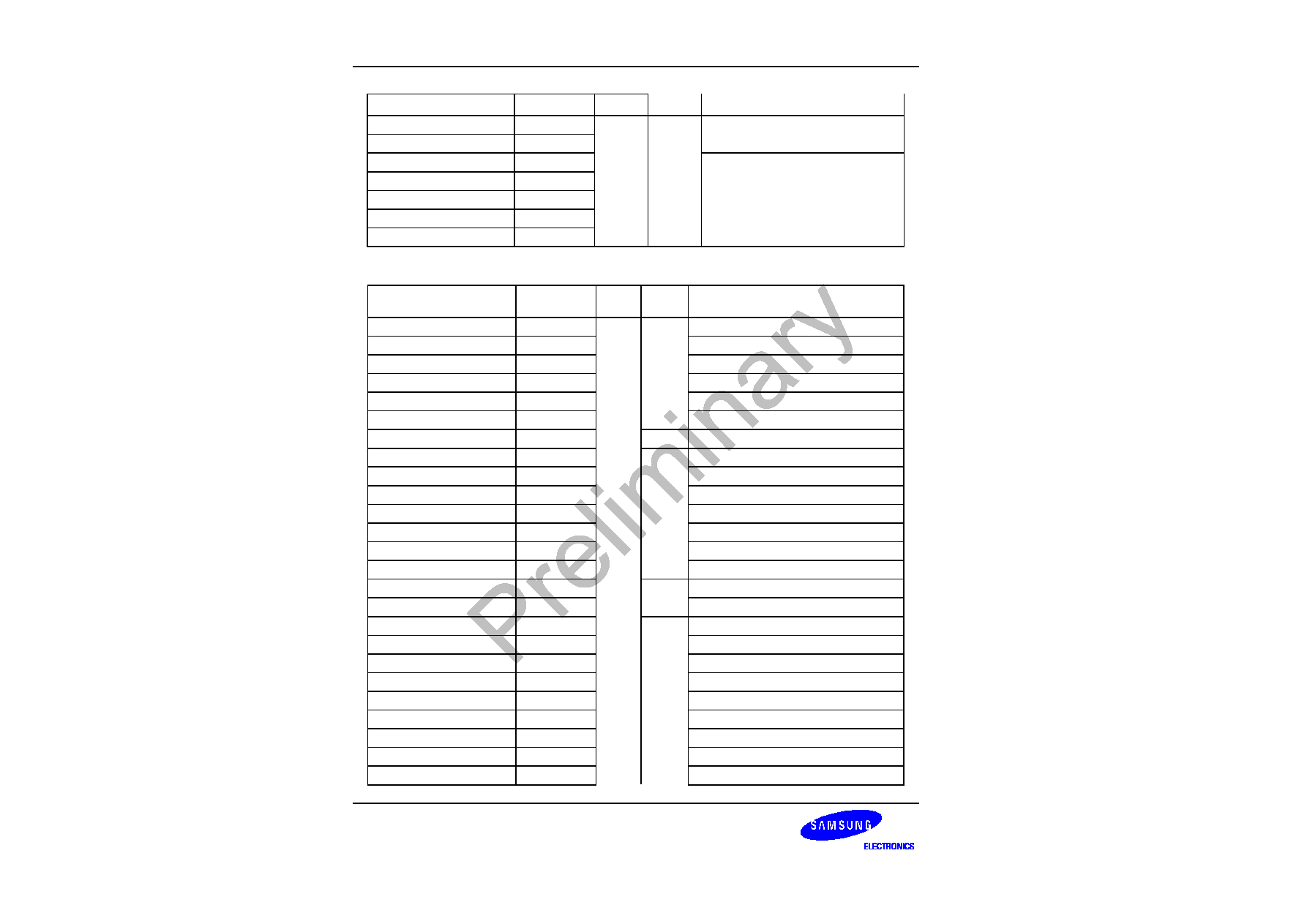
BSW rv0.1-0417-N01
Preliminary product information describes products that are in development,
for which full characterization data and associated errata are not yet available.
Specifications and information herein are subject to change without notice.
PRELIMINARY PRODUCT OVERVIEW
S3C24A0 RISC MICROPROCESSOR
1-48
HcFmNumber
0x100_003C
HcPeriodicStart
0x100_0040
HcLSThreshold
0x100_0044
HcRhDescriptorA
0x100_0048
Root Hub Group
HcRhDescriptorB
0x100_004C
HcRhStatus
0x100_0050
HcRhPortStatus1
0x100_0054
HcRhPortStatus2
0x100_0058
�
USB Device
Register Name
Offset
Acc.
Unit
Read/
Write
Function
FUNC_ADDR_REG
0x4A0_0140
B
R/W
Function Address
PWR_REG
0x4A0_0144
Power Management
EP_INT_REG
0x4A0_0148
EP Interrupt Pending and Clear
USB_INT_REG
0x4A0_0158
USB Interrupt Pending and Clear
EP_INT_EN_REG
0x4A0_015C
Interrupt Enable
USB_INT_EN_REG
0x4A0_016C
Interrupt Enbale
FRAME_NUM1_REG
0x4A0_0170
R
Frame Number Lower Byte
INDEX_REG
0x4A0_0178
R/W
Register Index
EP0_CSR
0x4A0_0184
Endpoint 0 Status
IN_CSR1_REG
0x4A0_0184
In Endpoint Control Status
IN_CSR2_REG
0x4A0_0188
In Endpoint Control Status
MAXP_REG
0x4A0_0180
Endpoint Max Packet
OUT_CSR1_REG
0x4A0_0190
Out Endpoint Control Status
OUT_CSR2_REG
0x4A0_0194
Out Endpoint Control Status
OUT_FIFO_CNT1_REG
0x4A0_0198
R
Endpoint Out Write Count
OUT_FIFO_CNT2_REG
0x4A0_019C
Endpoint Out Write Count
EP0_FIFO
0x4A0_01C0
R/W
Endpoint 0 FIFO
EP1_FIFO
0x4A0_01C4
Endpoint 1 FIFO
EP2_FIFO
0x4A0_01C8
Endpoint 2 FIFO
EP3_FIFO
0x4A0_01CC
Endpoint 3 FIFO
EP4_FIFO
0x4A0_01D0
Endpoint 4 FIFO
EP1_DMA_CON
0x4A0_0200
EP1 DMA Interface Control
EP1_DMA_UNIT
0x4A0_0204
EP1 DMA Tx Unit Counter
EP1_DMA_FIFO
0x4A0_0208
EP1 DMA Tx FIFO Counter
EP1_DMA_TTC_L
0x4A0_020C
EP1 DMA Total Tx Counter

BSW rv0.1-0417-N01
Preliminary product information describes products that are in development,
for which full characterization data and associated errata are not yet available.
Specifications and information herein are subject to change without notice.
S3C24A0 RISC MICROPROCESSOR
PRELIMINARY PRODUCT OVERVIEW
1-49
EP1_DMA_TTC_M
0x4A0_0210
EP1 DMA Total Tx Counter
EP1_DMA_TTC_H
0x4A0_0214
EP1 DMA Total Tx Counter
EP2_DMA_CON
0x4A0_0218
B
R/W
EP2 DMA Interface Control
EP2_DMA_UNIT
0x4A0_021C
EP2 DMA Tx Unit Counter
EP2_DMA_FIFO
0x4A0_0220
EP2 DMA Tx FIFO Counter
EP2_DMA_TTC_L
0x4A0_0224
EP2 DMA Total Tx Counter
EP2_DMA_TTC_M
0x4A0_0228
EP2 DMA Total Tx Counter
EP2_DMA_TTC_H
0x4A0_022C
EP2 DMA Total Tx Counter
EP3_DMA_CON
0x4A0_0240
EP3 DMA Interface Control
EP3_DMA_UNIT
0x4A0_0244
EP3 DMA Tx Unit Counter
EP3_DMA_FIFO
0x4A0_0248
EP3 DMA Tx FIFO Counter
EP3_DMA_TTC_L
0x4A0_024C
EP3 DMA Total Tx Counter
EP3_DMA_TTC_M
0x4A0_0250
EP3 DMA Total Tx Counter
EP3_DMA_TTC_H
0x4A0_0254
EP3 DMA Total Tx Counter
EP4_DMA_CON
0x4A0_0258
EP4 DMA Interface Control
EP4_DMA_UNIT
0x4A0_025C
EP4 DMA Tx Unit Counter
EP4_DMA_FIFO
0x4A0_0260
EP4 DMA Tx FIFO Counter
EP4_DMA_TTC_L
0x4A0_0264
EP4 DMA Total Tx Counter
EP4_DMA_TTC_M
0x4A0_0268
EP4 DMA Total Tx Counter
EP4_DMA_TTC_H
0x4A0_026C
EP4 DMA Total Tx Counter
�
IrDA
Register
Name
Offset
Acc.
Unit
Read/
Write
Function
IrDA _CNT
0x180_0000
W
R/W
IrDA Control r
IrDA_MDR
0x180_0004
IrDA Mode Definition
IrDA_CNF
0x180_0008
IrDA Interrupt / DMA Configuration
IrDA _IER
0x180_000C
IrDA Interrupt Enable
IrDA _IIR
0x180_0010
R
IrDA Interrupt Identification
IrDA _LSR
0x180_0014
IrDA Line Status
IrDA _FCR
0x180_0018
R/W
IrDA FIFO Control
IrDA _PLR
0x180_001C
IrDA Preamble Length
IrDA_RBR
0x180_0020
IrDA Receiver & Transmitter Buffer
IrDA_TXNO
0x180_0024
R
The total number of data bytes remained in Tx
FIFO
IrDA_RXNO
0x180_0028
The total number of data bytes remained in Rx
FIFO
IrDA _TXFLL
0x180_002C
R/W
IrDA Transmit Frame-Length Register Low

BSW rv0.1-0417-N01
Preliminary product information describes products that are in development,
for which full characterization data and associated errata are not yet available.
Specifications and information herein are subject to change without notice.
PRELIMINARY PRODUCT OVERVIEW
S3C24A0 RISC MICROPROCESSOR
1-50
IrDA _TXFLH
0x180_0030
IrDA Transmit Frame-Length Register High
IrDA _RXFLL
0x180_0034
IrDA Receive Frame-Length Register Low
IrDA _RXFLH
0x180_0038
IrDA Receive Frame-Length Register High
1.4.3.4 Parallel Communication
�
Modem Interface
Register
Name
Offset
Acc.
Unit
Read/
Write
Function
INT2AP
0x118_0000
W
R/W
Interrupt Request to AP Register
INT2MDM
0x118_0004
Interrupt request to MODEM Register
�
GPIO
Register
Name
Offset
Acc.
Unit
Read/
Write
Function
GPCON_U
0x480_0000
W
R/W
GPIO Ports Configuration Register
GPCON_M
0x480_0004
GPIO Ports Configuration Register
GPCON_L
0x480_0008
GPIO Ports Configuration Register
GPDAT
0x480_000C
GPIO Ports Data Register
GPPU
0x480_0010
GPIO Ports Pull-up Control Register
EXTINTC0
0x480_0018
External Interrupt Control Register 0
EXTINTC1
0x480_001C
External Interrupt Control Register 1
EXTINTC2
0x480_0020
External Interrupt Control Register 2
EINTFLT0
0x480_0024
External Interrupt Filter Control Register 0
EINTFLT1
0x480_0028
External Interrupt Filter Control Register 1
EINTMASK
0x480_0034
External interupt mask Register
EINTPEND
0x480_0038
External Interupt Pending Register
PERIPU
0x480_0040
Peri. Ports Pull-up Control Register
ALIVECON
0x480_0044
Alive Control Register
GPDAT_SLEEP
0x480_0048
GPIO Output Data for Sleep Mode
GPOEN_SLEEP
0x480_004C
GPIO Output Enable Control for Sleep Mode
GPPU_SLEEP
0x480_0050
GPIO Pull-up Control Register for Sleep Mode
PERIDAT_SLEEP0
0x480_0054
Peri. Ports Output Data Control Register 0 for
sleep mode
PERIDAT_SLEEP1
0x480_0058
Peri. Ports Output Data Control Register 1 for
sleep mode
PERIOEN_SLEEP0
0x480_005C
Peri. Ports Output Control Register 0 for sleep
mode
PERIOEN_SLEEP1
0x480_0060
Peri. Ports Output Control Register 1 for sleep
mode

BSW rv0.1-0417-N01
Preliminary product information describes products that are in development,
for which full characterization data and associated errata are not yet available.
Specifications and information herein are subject to change without notice.
S3C24A0 RISC MICROPROCESSOR
PRELIMINARY PRODUCT OVERVIEW
1-51
PERIPU_SLEEP
0x480_0064
Peri. Ports Pull-up Control Register for slee
mode
RSTCNT
0x480_0068
Reset Count Compare Register
GPRAM0~15
0x480_0080
~0x480_00BC
General purpose RAM array
1.4.3.5 Image/Video Processing
�
Camera Interface
Register
Name
Offset
Acc.
Unit
Read/
Write
Function
CISRCFMT
0x800_0000
W
R/W
Input Source Format
CIWDOFST
0x800_0004
Window offset register
CIGCTRL
0x800_0008
Global control register
CICOYSA1
0x800_0018
Y 1
st
frame start address for codec DMA
CICOYSA2
0x800_001C
Y 2
nd
frame start address for codec DMA
CICOYSA3
0x800_0020
Y 3
rd
frame start address for codec DMA
CICOYSA4
0x800_0024
Y 4
th
frame start address for codec DMA
CICOCBSA1
0x800_0028
Cb 1
st
frame start address for codec DMA
CICOCBSA2
0x800_002C
Cb 2
nd
frame start address for codec DMA
CICOCBSA3
0x800_0030
Cb 3
rd
frame start address for codec DMA
CICOCBSA4
0x800_0034
Cb 4
th
frame start address for codec DMA
CICOCRSA1
0x800_0038
Cr 1
st
frame start address for codec DMA
CICOCRSA2
0x800_003C
Cr 2
nd
frame start address for codec DMA
CICOCRSA3
0x800_0040
Cr 3
rd
frame start address for codec DMA
CICOCRSA4
0x800_0044
Cr 4
th
frame start address for codec DMA
CICOTRGFMT
0x800_0048
Target image format of codec DMA
CICOCTRL
0x800_004C
Codec DMA control related
CICOSCPRERATIO
0x800_0050
Codec pre-scaler ratio control
CICOSCPREDST
0x800_0054
Codec pre-scaler destination format
CICOSCCTRL
0x800_0058
Codec main-scaler control
CICOTAREA
0x800_005C
Codec pre-scaler destination format
CICOSTATUS
0x800_0064
R
Codec path status
CIPRCLRSA1
0x800_006C
R/W
RGB 1
st
frame start address for preview
DMA
CIPRCLRSA2
0x800_0070
RGB 2
nd
frame start address for preview
DMA
CIPRCLRSA3
0x800_0074
RGB 3
rd
frame start address for preview
DMA

BSW rv0.1-0417-N01
Preliminary product information describes products that are in development,
for which full characterization data and associated errata are not yet available.
Specifications and information herein are subject to change without notice.
PRELIMINARY PRODUCT OVERVIEW
S3C24A0 RISC MICROPROCESSOR
1-52
CIPRCLRSA4
0x800_0078
RGB 4
th
frame start address for preview
DMA
CIPRTRGFMT
0x800_007C
Target image format of preview DMA
CIPRCTRL
0x800_0080
Preview DMA control related
CIPRSCPRERATIO
0x800_0084
Preview pre-scaler ratio control
CIPRSCPREDST
0x800_0088
Preview pre-scaler destination format
CIPRSCCTRL
0x800_008C
Preview main-scaler control
CIPRTAREA
0x800_0090
Preview pre-scaler destination format
CIPRSTATUS
0x800_0098
R
Preview path status
CIIMGCPT
0x800_00A0
R/W
Image capture enable command
�
Video POST
Register
Name
Offset
Acc.
Unit
Read/
Write
Function
MODE
0xA10_0000
W
R/W
Mode Register [9:0]
PreScale_Ratio
0xA10_0004
Pre-Scale ratio for vertical and horizontal.
PreScaleImgSize
0xA10_0008
Pre-Scaled image size
SRCImgSize
0xA10_000C
Source image size
MainScale_H_Ratio
0xA10_0010
Main scale ratio along to horizontal direction
MainScale_V_Ratio
0xA10_0014
Main scale ratio along to vertical direction
DSTImgSize
0xA10_0018
Destination image size
PreScale_SHFactor
0xA10_001C
Pre-scale shift factor
ADDRStart_Y
0xA10_0020
DMA Start address for Y or RGB component
ADDRStart_Cb
0xA10_0024
DMA Start address for Cb component
ADDRStart_Cr
0xA10_0028
DMA Start address for Cr component
ADDRStart_RGB
0xA10_002C
DMA Start address for RGB component
ADDREnd_Y
0xA10_0030
DMA End address for Y or RGB component
ADDREnd_Cb
0xA10_0034
DMA End address for Cb component
ADDREnd_Cr
0xA10_0038
DMA End address for Cr component
ADDREnd_RGB
0xA10_003C
DMA End address for RGB component
Offset_Y
0xA10_0040
Offset of Y component for fetching source image
Offset_Cb
0xA10_0044
Offset of Cb component for fetching source image
Offset_Cr
0xA10_0048
Offset of Cr component for fetching source image
Offset_RGB
0xA10_004C
Offset of RGB component for restoring destination
image

BSW rv0.1-0417-N01
Preliminary product information describes products that are in development,
for which full characterization data and associated errata are not yet available.
Specifications and information herein are subject to change without notice.
S3C24A0 RISC MICROPROCESSOR
PRELIMINARY PRODUCT OVERVIEW
1-53
ME
Register
Name
Offset
Acc.
Unit
Read/
Write
Function
ME_CFSA
0x880_0000
Current Frame Start Address Register
ME_PFSA
0x880_0004
Previous Frame Start Address Register
ME_MVSA
0x880_0008
Motion Vector Start Address Register
ME_CMND
0x880_000C
Command Register
ME_STAT_SWR
0x880_0010
Status & S/W Reset Register
ME_CNFG
0x880_0014
Configuration Register
ME_IMGFMT
0x880_0018
W
R/W
Image Format Register
�
MC
Register
Name
Offset
Acc.
Unit
Read/
Write
Function
MC_PFYSA_ENC
0x8C0_0000
Previous Frame Y Start Address Register
for the Encoder
MC_CFYSA_ENC
0x8C0_0004
MCed Frame Y Start Address Register for
the Encoder
MC_PFYSA_DEC
0x8C0_0008
Previous Frame Y Start Address Register
for the Decoder
MC_CFYSA_DEC
0x8C0_000C
MCed Frame Y Start Address Register for
the Decoder
MC_PFCbSA_ENC
0x8C0_0010
Previous Frame Cb Start Address Register
for the Encoder
MC_PFCrSA_ENC
0x8C0_0014
Previous Frame Cr Start Address Register
for the Encoder
MC_CFCbSA_ENC
0x8C0_0018
MCed Frame Cb Start Address Register for
the Encoder
MC_CFCrSA_ENC
0x8C0_001C
MCed Frame Cr Start Address Register for
the Encoder
MC_PFCbSA_DEC
0x8C0_0020
Previous Frame Cb Start Address Register
for the Decoder
MC_PFCrSA_DEC
0x8C0_0024
Previous Frame Cr Start Address Register
for the Decoder
MC_CFCbSA_DEC
0x8C0_0028
MCed Frame Cb Start Address Register for
the Decoder
MC_CFCrSA_DEC
0x8C0_002C
MCed Frame Cr Start Address Register for
the Decoder
MC_MVSA_ENC
0x8C0_0030
W
R/W
Motion Vector Start Address Register for
the Encoder

BSW rv0.1-0417-N01
Preliminary product information describes products that are in development,
for which full characterization data and associated errata are not yet available.
Specifications and information herein are subject to change without notice.
PRELIMINARY PRODUCT OVERVIEW
S3C24A0 RISC MICROPROCESSOR
1-54
MC_MVSA_DEC
0x8C0_0034
Motion Vector Start Address Register for
the Decoder
MC_CMND
0x8C0_0038
Command Register
MC_STAT_SWR
0x8C0_003C
Status & S/W Reset Register
MC_CNFG
0x8C0_0040
Configuration Register
MC_IMGFMT
0x8C0_0044
Image Format Register
�
DCTQ
Register
Name
Offset
Acc.
Unit
Read/
Write
Function
SAYCF
0x900_0000
W
R/W
Current frame luminance start address
SACBCF
0x900_0004
Current frame Cb start address
SACRCF
0x900_0008
Current frame Cr start address
SAYRF
0x900_000C
Reconstruction frame luminance start
address
SACBRF
0x900_0010
Reconstruction frame Cb start address
SACRRF
0x900_0014
Reconstruction frame Cr start address
SAYDQF
0x900_0018
DCTQed frame luminance start address
SACBDQF
0x900_001C
DCTQed frame Cb start address
SACRDQF
0x900_0020
DCTQed frame Cr start address
SAQP
0x900_0024
Qp start address
IMGSIZE
0x900_0028
Image horizontal and vertical pixel number
SHQ
0x900_002C
Short header quantization mode
DCTQCTRL
0x900_0034
Control register
�
VLX
Register
Name
Offset
Acc.
Unit
Read/
Write
Function
VLX_COMMON1
0x940_0000
W
R/W
VLX common control register1
VLX_FRAMESTARTY
0x940_0004
Y coeff. start address
VLX_FRAMESTARTCB
0x940_0008
Cb coeff. frame start address
VLX_FRAMESTARTCR
0x940_000C
Cr coeff. frame start address
VLC_CON1
0x940_0010
Control register in VLC mode
VLC_CON2
0x940_0014
Reserved

BSW rv0.1-0417-N01
Preliminary product information describes products that are in development,
for which full characterization data and associated errata are not yet available.
Specifications and information herein are subject to change without notice.
S3C24A0 RISC MICROPROCESSOR
PRELIMINARY PRODUCT OVERVIEW
1-55
VLC_CON3
0x940_0018
VLC result external address
VLC_CON4
0x940_001C
Reserved
VLD_CON1
0x940_0020
Control register in VLD mode
VLD_CON2
0x940_0024
VLCed bit stream start address
VLD_CON3
0x940_0028
Reserved
VLX_OUT1
0x940_002C
R
VLX output information register 1
VLX_OUT2
0x940_0030
VLX output information register 2
1.4.3.6 Display Control
�
TFT LCD Controller
Register
Offset
Acc.
Unit
R/W
Function
LCDCON1
0xA00_0000
W
R/W
LCD Control 1
LCDCON2
0xA00_0004
R/W
LCD Control 2
LCDTCON1
0xA00_0008
R/W
LCD Time Control 1
LCDTCON2
0xA00_000C
R/W
LCD Time Control 2
LCDTCON3
0xA00_0010
R/W
LCD Time Control 3
LCDOSD1
0xA00_0014
R/W
LCD OSD Control Register
LCDOSD2
0xA00_0018
R/W
Foreground image(OSD Image) Left top position set
LCDOSD3
0xA00_001C
R/W
Foreground image(OSD Image) Right Bottom position
set
LCDSADDRB1
0xA00_0020
R/W
Frame Buffer Start Address 1 ( Background buffer 1)
LCDSADDRB2
0xA00_0024
R/W
Frame Buffer Start Address 2 ( Background buffer 2)
LCDSADDRF1
0xA00_0028
R/W
Frame Buffer Start Address 1 ( foreground buffer 1)
LCDSADDRF2
0xA00_002C
R/W
Frame Buffer Start Address 2 ( foreground buffer 2)
LCDEADDRB1
0xA00_0030
R/W
Frame Buffer End Address 1 ( Background buffer 1)
LCDEADDRB2
0xA00_0034
R/W
Frame Buffer End Address 2 ( Background buffer 2)
LCDEADDRF1
0xA00_0038
R/W
Frame Buffer End Address 1 ( foreground buffer 1)
LCDEADDRF2
0xA00_003C
R/W
Frame Buffer End Address 2 ( foreground buffer 2)
LCDVSCRB1
0xA00_0040
R/W
Virtual Screen Offsize and Pagewidth ( Background
buffer 1)
LCDVSCRB2
0xA00_0044
R/W
Virtual Screen Offsize and Pagewidth ( Background
buffer 2)
LCDVSCRF1
0xA00_0048
R/W
Virtual Screen Offsize and Pagewidth ( Foreground
buffer 1)
LCDVSCRF2
0xA00_004C
R/W
Virtual Screen Offsize and Pagewidth ( Foreground
buffer 2)
LCDINTCON
0xA00_0050
R/W
LCD Interrupt Control
LCDKEYCON
0xA00_0054
R/W
COLOR KEY Control 1

BSW rv0.1-0417-N01
Preliminary product information describes products that are in development,
for which full characterization data and associated errata are not yet available.
Specifications and information herein are subject to change without notice.
PRELIMINARY PRODUCT OVERVIEW
S3C24A0 RISC MICROPROCESSOR
1-56
LCDKEYVAL
0xA00_0058
R/W
COLOR KEY Control 2
LCDBGCON
0xA00_005C
R/W
Back-ground color Control
LCDFGCON
0xA00_0060
R/W
Fore-ground color Control
LCDDITHCON
0xA00_0064
R/W
LCD Dithering Control for Active Matrix
1.4.3.7 Input Devices
�
Keypad Interface
Register
Name
Offset
Acc.
Unit
Read/
Write
Function
KEYDAT
0x490_0000
W
R/W
The data register for KEYPAD input
KEYINTC
0x490_0004
KEYPAD input ports Interrupt Control
KEYFLT0
0x490_0008
KEY PAD Input Filter Control
KEYFLT1
0x490_000C
KEY PAD Input Filter Control
KEYMAN
0x490_0010
KEYPAD manual scan control
�
Analog-to-Digital Converter and Touch Screen Interface
Register
Name
Offset
Acc.
Unit
Read/
Write
Function
ADCCON
0x580_0000
W
R/W
ADC Control
ADCTSC
0x580_0004
ADC Touch Screen Control
ADCDLY
0x580_0008
ADC Start or Interval Delay
ADCDAX
0x580_000C
R
ADC Conversion Data Register X
ADCDAY
0x580_0010
ADC Conversion Data Register Y
1.4.3.8 Storage Devices
�
SD and SDIO / MMC
Register Name
Offset
Acc.
Unit
Read/
Write
Function
SDICON
0x600_0000
W
R/W
SDI Control
SDIPRE
0x600_0004
SDI Buad Rate Prescaler
SDICARG
0x600_0008
SDI Command Argument
SDICCON
0x600_000C
SDI Command Control
SDICSTA
0x600_0010
R/(C)
SDI Command Status
SDIRSP0
0x600_0014
R
SDI Response
SDIRSP1
0x600_0018
SDI Response
SDIRSP2
0x600_001C
SDI Response
SDIRSP3
0x600_0020
SDI Response
SDIDTIMER
0x600_0024
R/W
SDI Data / Busy Timer

BSW rv0.1-0417-N01
Preliminary product information describes products that are in development,
for which full characterization data and associated errata are not yet available.
Specifications and information herein are subject to change without notice.
S3C24A0 RISC MICROPROCESSOR
PRELIMINARY PRODUCT OVERVIEW
1-57
SDIBSIZE
0x600_0028
SDI Block Size
SDIDCON
0x600_002C
W
R/W
SDI Data control
SDIDCNT
0x600_0030
R
SDI Data Remain Counter
SDIDSTA
0x600_0034
R/(C)
SDI Data Status
SDIFSTA
0x600_0038
R/(C)
SDI FIFO Status
SDIIMSK
0x600_003C
R/W
SDI Interrupt Mask
SDIDAT0
0x600_0040
B,HW,W
SDI Data0
SDIDAT1
0x600_0044
W
SDI Data1
SDIDAT2
0x600_0048
SDI Data2
SDIDAT3
0x600_004C
SDI Data3
�
Memory Stick
Register Name
Offset
Acc.
Unit
Read/
Write
Function
MSPRE
0x610_0000
W
R/W
Prescaler Control
MSFINTCON
0x610_0004
FIFO Interrupt Control
TP_CMD
0x610_8000
Transfer Protocol Command
CTRL_STA
0x610_8004
Command and Status
DAT_FIFO
0x610_8008
Data FIFO
INTCTRL_STA
0x610_800C
Interrupt Control and Status
INS_CON
0x610_8010
INS Port Control
ACMD_CON
0x610_8014
Auto Command and Polarity Control
ATP_CMD
0x610_8018
Auto Transfer Protocol Command
1.4.3.8 System Management
�
PLL Clock Control and Power Management
Register
Name
Offset
Acc.
Unit
Read/
Write
Function
LOCKTIME
0x000_0000
W
R/W
PLL Lock Time Counter
OSCWSET
0x000_0004
OSC settle-down wait time setting
MPLLCON
0x000_0010
MPLL Configuration
UPLLCON
0x000_0014
UPLL Configuration
CLKCON
0x000_0020
Clock Generator Control
CLKSRC
0x000_0024
Slow Clock Control
CLKDIVN
0x000_0028
Clock divider Control
PWRMAN
0x000_0030
Power Management
SOFTRESET
0x000_0038
Software Reset

BSW rv0.1-0417-N01
Preliminary product information describes products that are in development,
for which full characterization data and associated errata are not yet available.
Specifications and information herein are subject to change without notice.
PRELIMINARY PRODUCT OVERVIEW
S3C24A0 RISC MICROPROCESSOR
1-58
IMPORTANT NOTES ABOUT S3C24A0 SPECIAL REGISTERS
1. The special registers have to be accessed by the recommended access unit.
2. All registers except ADC registers, RTC registers and UART registers must be read/written in word unit (32bit)
at little/big endian.
3. It is very important that the ADC registers, RTC registers and UART registers be read/written by the specified
access unit and the specified address. Moreover, one must carefully consider which endian mode is used.
4. W : 32-bit register, which must be accessed by LDR/STR or int type pointer(int *).
HW : 16-bit register, which must be accessed by LDRH/STRH or short int type pointer(short int *).
B : 8-bit register, which must be accessed by LDRB/STRB or char type pointer(char int *).
.

BSW rv0.1-0417-N01
Preliminary product information describes products that are in development,
for which full characterization data and associated errata are not yet available.
Specifications and information herein are subject to change without notice.
S3C24A0 RISC MICROPROCESSOR
SROM CONTROLLER
2-1
SROM CONTROLLER(Preliminary)
OVERVIEW
S3C24A0 support external 16-bit bus for NAND Flash/ NOR Flash/ PROM/ SRAM external memory. It's not
shared with SDRAM bus and support up to 3 Bank for one controller. From now on, we call this controller as
SROM Controller.
Below figure show the Address Map configuration of S3C24A0 SROM Controller. S3C24A0 SROM Controller
has 3 kinds of configuration. If user want to use NAND boot loader, it'll be selected the third configuration
which stepping stone (SRAM 4KB) is on the 0x00000000. And If user want to use ROM type boot, it'll be
selected the first or second configuration by selecting SFR (Special Function Register) of SROM Controller. In
this case user can use NAND Flash Memory for other usage. At the first configuration, Stepping Stone is used
just for buffer of any master.
NOTES:
1. SROM means ROM or SRAM type memory.
2. SFR means Special Function Register.
[Not using NAND flash for boot ROM]
SROM
(BANK0, XrCSn0)
SRAM Buffer
(4KB, No CS)
Stepping stone
(4KBytes)
Stepping stone
(4KBytes)
SDRAM
(BANK0/1)
SROM
SROM
(BANK1, XrCSn1)
SROM
(BANK2, XrCSn2)
SROM
SROM
SROM
[Using NAND flash for boot ROM]
0x0800_0000
0x0000_0000
0x0400_0000
0x0c00_0000
0x1000_0000
SDRAM
SDRAM
64MB
64MB
64MB
64MB
256MB
0x2000_0000
0x4000_0000
AHB/APB SFRs
0x5000_0000
256MB
Reserved
0xFFFF_FFFF
Reserved
Reserved
Reserved
Reserved
TMODE[2:0] = 000
SROM_BW[9] = 0
TMODE[2:0] = 000
SROM_BW[9] = 1
TMODE[2:0] = 001
Reserved
Reserved
Reserved
Assigned
for
Special Function
Registers
Assigned
for
SDRAM Bank0/1
Accessible Region
Assigned
for
SROM Bank0/1/2
Accessible Region
(BANK2, XrCSn2)
(BANK0, XrCSn0)
(BANK1, XrCSn1)
(BANK1, XrCSn1)
(BANK0/1)
(BANK0/1)
AHB/APB SFRs
AHB/APB SFRs
Figure 2-1. SROM Controller Address Mapping

BSW rv0.1-0417-N01
Preliminary product information describes products that are in development,
for which full characterization data and associated errata are not yet available.
Specifications and information herein are subject to change without notice.
SROM CONTROLLER
S3C24A0 RISC MICROPROCESSOR
2-2
FEATURE
-
Supports SRAM, various ROMs and NOR flash memory
-
Supports only 8 or 16-bit data bus
-
Address space : Up to 64MB per Bank
-
Supports 3 banks (XrCSn[2:0])
Boot by NAND Flash Memory : XrCSn0's owner is not SROM Controller but NAND Controller.
Boot by other Memory (Nor Flash or ROM): XrCSn2's owner is either SROM Controller or NAND
Controller (User can choose it by setting SFR).
-
Fixed memory bank start address
-
External wait to extend the bus cycle
-
Support byte, half-word and word access for external memory
BLOCK DIAGRAM
SROM
DECODER
SFR
CONTROL &
STATE MACHINE
SROM I/F
SINGAL
GENERATO
N
AHB I/F for SROM SFR
AHB I/F for SROM MEM
SROM MEM I/F
Figure 2-2 SROM Controller Block Diagram

BSW rv0.1-0417-N01
Preliminary product information describes products that are in development,
for which full characterization data and associated errata are not yet available.
Specifications and information herein are subject to change without notice.
S3C24A0 RISC MICROPROCESSOR
SROM CONTROLLER
2-3
FUNCTION DESCRIPTION
SROM Controller support SROM interface for Bank0 to Bank2. In case of NAND boot, SROM controller can't
control Bank0 because of its mastership is on NAND Flash Controller. In case of ROM boot, as it mentioned
before, it is possible that Bank2's master is NAND Flash Controller by setting of users.
SRAM/ROM/
NOR FLASH/
NAND FLASH
SRAM/ROM/
NOR FLASH
SRAM/ROM/
NOR FLASH
/NAND FLASH
BANK0
BANK2
BANK1
MEMORY
BU
S
#
1
SROM
CONTROLLER
Address-bus : 26-bit
Data-bus : 8/16
Figure 2-3 Memory Interface Block Diagram

BSW rv0.1-0417-N01
Preliminary product information describes products that are in development,
for which full characterization data and associated errata are not yet available.
Specifications and information herein are subject to change without notice.
SROM CONTROLLER
S3C24A0 RISC MICROPROCESSOR
2-4
XrWAITn PIN OPERATION
If the WAIT corresponding to each memory bank is enabled, the XrOEn duration should be prolonged by the
external XrWAITn pin while the memory bank is active. XrWAITn is checked from Tacc-1.
The XrOEn will be deasserted at the next clock after sampling XrWAITn is high. The XrWEn signal have the same
relation with XrOEn.
Tacs
Tcos
Tacc=4
HCLK
XrADDR
[25:0]
XrCSn
[2:0]
XrOEn
XrWAITn
XrDATA
[15:0]
(R)
Delayed
Sampling XrWAITn
Figure 2-4 XrWAITn pin operation

BSW rv0.1-0417-N01
Preliminary product information describes products that are in development,
for which full characterization data and associated errata are not yet available.
Specifications and information herein are subject to change without notice.
S3C24A0 RISC MICROPROCESSOR
SROM CONTROLLER
2-5
PROGRAMMABLE ACCESS CYCLE WRITE TO READ WAVEFORM
Tcoh
Tcos
Tacs
HCLK
XrADDR
[25:0]
XrCSn
[2:0]
XrOEn
XrWEn
XrnWBE
[1:0]
XrDATA
[15:0]
(R)
XrDATA
[15:0]
(W)
Tacc
Tcah
Tacs = 1 cycle
Tcos = 1 cycle
Tacc = 2 cycles
Tcoh = 1 cycle
Tcah = 2 cycles
Figure 2-4 Programmable access cycle

BSW rv0.1-0417-N01
Preliminary product information describes products that are in development,
for which full characterization data and associated errata are not yet available.
Specifications and information herein are subject to change without notice.
SROM CONTROLLER
S3C24A0 RISC MICROPROCESSOR
2-6
SPECIAL FUNCTION REGISTERS
SROM BUS WIDTH & WAIT CONTRL REGISTER(SROM_BW)
Register
Address
R/W
Description
Reset Value
SROM_BW 0x40C20000
R/W
SROM Bus width & wait control
0x000x
SROM_BW
Bit
Description
Initial State
Reserved
[15:9]
Reserved
0x00
BankNum
[9]
0 = XrCSn2's owner is SROM Controller (In this case Stepping
Stone is just used as 4KB SRAM buffer)
1 = XrCSn2's owner is NAND Flash Controller
0x00
ST2
[8]
This bit determines SRAM for using UB/LB for bank2
0 = Not using UB/LB (XrnWBE[1:0] is dedicated nWBE[1:0])
1 = Using UB/LB (XrnWBE[1:0] is dedicated nBE[1:0]
0
WS2
[7]
This bit determines WAIT status for bank2
0 = WAIT disable
1 : WAIT enable
0
DW2
[6]
Indicates data bus width for bank2
0 = 8-bit
1 : 16-bit
0
ST1
[5]
This bit determines SRAM for using UB/LB for bank1
0 = Not using UB/LB (XrnWBE[1:0] is dedicated nWBE[1:0])
1 = Using UB/LB (XrnWBE[1:0] is dedicated nBE[1:0]
0
WS1
[4]
This bit determines WAIT status for bank1
0 = WAIT disable
1 : WAIT enable
0
DW1
[3]
Indicates data bus width for bank1
0 = 8-bit
1 : 16-bit
0
ST0
[2]
This bit determines SRAM for using UB/LB for bank0
0 = Not using UB/LB (XrnWBE[1:0] is dedicated nWBE[1:0])
1 = Using UB/LB (XrnWBE[1:0] is dedicated nBE[1:0]
0
WS0
[1]
This bit determines WAIT status for bank0
0 = WAIT disable
1 : WAIT enable
0
DW0
[0]
Indicates data bus width for bank0 (read only)
0 : 8-bit
1 : 16-bit
H/W Set
*
DW0 is read only. The value is written by external configuration pin(XfNFBW)

BSW rv0.1-0417-N01
Preliminary product information describes products that are in development,
for which full characterization data and associated errata are not yet available.
Specifications and information herein are subject to change without notice.
S3C24A0 RISC MICROPROCESSOR
SROM CONTROLLER
2-7
SROM BANK CONTROL REGISTER (SROM_BC : XrCSn0 ~ XrCSn2)
Register
Address
R/W
Description
Reset Value
SROM_BC0
0x40C20004
R/W
SROM Bank0 control register
0x0700
SROM_BC1
0x40C20008
R/W
SROM Bank1 control register
0x0700
SROM_BC2
0x40C2000C
R/W
SROM Bank2 control register
0x0700
SROM_BCn
Bit
Description
Initial State
Tacs
[15:14]
Adress set-up before XrCSn[2:0]
00 = 0 clock
01 = 2 clock
10 = 4 clocks
11 = 8 clocks
00
Tcos
[13:12]
Chip selection set-up XrOEn
00 = 0 clock
01 = 2 clock
10 = 4 clocks
11 = 8 clocks
00
Reserved
[11]
Reserved
0
Tacc
[10:8]
Access cycle
000 = 2 clock
001 = 3 clocks
010 = 4 clocks
011 = 10 clocks
100 = 12 clocks
101 = 14 clocks
110 = 16 clock
111 = 20 clocks
111
Tcoh
[7:6]
Chip selection hold on XrOEn
00 = 0 clock
01 = 2 clock
10 = 4 clocks
11 = 8 clocks
00
Tcah
[5:4]
Address holding time after XrCSn[2:0]
00 = 0 clock
01 = 2 clock
10 = 4 clocks
11 = 8 clocks
00
Reserved
[3:0]
Reserved
0000

BSW rv0.1-0417-N01
Preliminary product information describes products that are in development,
for which full characterization data and associated errata are not yet available.
Specifications and information herein are subject to change without notice.
S3C24A0 RISC MICROPROCESSOR
SDRAM CONTROLLER
3-1
3
SDRAM CONTROLLER (Preliminary)
OVERVIEW
The S3C24A0 SDRAM Controller has the following features:
�
SDRAM
-
Supports 16-bit or 32-bit data bus
-
Supports 2 banks:
XpCSN[1:0]
-
16-bit Refresh Timer
-
Self Refresh Mode
-
Programmable CAS Latency
-
Provide Write buffer (4word size x2)
-
Provide long burst(INCR8,16 & WRAP8,16) transfer
-
Provide Power Down Mode
-
Support mobile SDRAM
-
Support extended MRS set (EMRS)
- DS , TSCR, PASR

BSW rv0.1-0417-N01
Preliminary product information describes products that are in development,
for which full characterization data and associated errata are not yet available.
Specifications and information herein are subject to change without notice.
SDRAM CONTROLLER
S3C24A0 RISC MICROPROCESSOR
3-2
SELECTION OF SDRAM
We recommanded select one of the SDRAM configurations in Table 3-1. And, each two banks should have same
bus width.
Table 3-1. Supported SDRAM configuration
Total Size
Bus Width
Base Component
Memory Configuration
Bank Address
4MB
x32
16Mb
(512Kbit x 16bit x 2Bank) x 2ea
A13
8MB
64Mb
(512K x 32 x 4) x 1
A[14:13]
16Mb
(1M x 8 x 2) x 4
A13
16MB
128Mb
(1M x 32 x 4) x 1
A[14:13]
64Mb
(1M x 16 x 4) x 2
A[14:13]
32MB
256Mb
(2M x 32 x 4) x 1
A[14:13]
128Mb
(2M x 16 x 4) x 2
A[14:13]
64Mb
(2M x 8 x 4) x 4
A[14:13]
64MB
256Mb
(4M x 16 x 4) x 2
A[14:13]
128Mb
(4M x 8 x 4) x 4
A[14:13]
512Mb
(4M x 32 x 4) x 1
A[14:13]
128MB
256Mb
(8M x 8 x 4) x 4
A[14:13]
512Mb
(8M x 16 x 4) x 2
A[14:13]
2MB
x16
16Mb
(512K x 16 x 2) x 1
A13
4MB
16Mb
(1M x 8 x 2) x 2
A13
8MB
64Mb
(1M x 16 x 4) x 1
A[14:13]
16MB
128Mb
(2M x 16 x 4) x 1
A[14:13]
64Mb
(2M x 8 x 4) x 2
A[14:13]
32MB
256Mb
(4M x 16 x 4) x 1
A[14:13]
128Mb
(4M x 8 x 4) x 2
A[14:13]
64MB
256Mb
(8M x 8 x 4) x 2
A[14:13]
512Mb
(8M x 16 x 4) x 1
A[14:13]
SELF REFRESH
The S3C24A0 provides the auto refresh and self refresh command to sustain the contents of SDRAM. The auto
refresh is issued to SDRAM periodically when refresh timer is expired. The self refresh is entered and exited by
request of on-chip power manager.

BSW rv0.1-0417-N01
Preliminary product information describes products that are in development,
for which full characterization data and associated errata are not yet available.
Specifications and information herein are subject to change without notice.
S3C24A0 RISC MICROPROCESSOR
SDRAM CONTROLLER
3
-3
SDRAM INITIALIZATION SEQUENCE
On power-on reset, software must initialize the memory controller and each of the SDRAM connected to the
controller. Refer to the SDRAM data sheet for the start up procedure, and examples sequence is given below:
1.
Wait 200us to allow SDRAM power and clock stabilize.
2.
Program the INIT[1:0] to `01b'. This automatically issues a PALL(pre-charge all) cammand to the
SDRAM.
3.
Write `
0x20
' into the refresh timer register. This provides a refresh cycle every
32
-clock cycles.
4.
Wait for a time period equivalent to
128
-clock cycles (
4
refresh cycles).
5.
Program the normal operational value into the refresh timer..
6.
Program the configuration registers to their normal operation values.
7.
Program the INIT[1:0] to `10b'. This automatically issues a MRS command to the SDRAM.
8.
Mobile only Program the INIT[1:0] to `11b'. This automatically issues a EMRS command to the SDRAM.
9.
Program the INIT[1:0] to `00b'. The controller enters the normal mode.
10. The SDRAM is now ready for normal operation.
Note : If you issue MRS after issuing EMRS, EMRS value will be reset . So you have to issue EMRS after
issuing MRS.

BSW rv0.1-0417-N01
Preliminary product information describes products that are in development,
for which full characterization data and associated errata are not yet available.
Specifications and information herein are subject to change without notice.
SDRAM CONTROLLER
S3C24A0 RISC MICROPROCESSOR
3-4
SDRAM Memory Interface Examples
XpADDR0
XpADDR1
XpADDR2
XpADDR3
XpADDR4
XpADDR5
XpADDR6
XpADDR7
XpADDR8
XpADDR9
XpADDR10
XpADDR11
XpDATA0
XpDATA1
XpDATA2
XpDATA3
XpDATA4
XpDATA5
XpDATA6
XpDATA7
XpDATA8
XpDATA9
XpDATA10
XpDATA11
XpDATA12
XpDATA13
XpDATA14
XpDATA15
A0
A1
A2
A3
A4
A5
A6
A7
A8
A9
A10
A11
DQ0
DQ1
DQ2
DQ3
DQ4
DQ5
DQ6
DQ7
DQ8
DQ9
DQ10
DQ11
DQ12
DQ13
DQ14
DQ15
BA0
BA1
LDQM
UDQM
XpADDR13
XpADDR14
XpDQM0
XpDQM1
XpCKE
XpSCLK
SCKE
SCLK
XpCSN0
XpRASn
XpCASn
XpWEn
nSCS
nSRAS
nSCAS
nWE
Figure 3-1. Memory Interface with 16-bit SDRAM (4Mx16, 4banks)
XpADDR0
XpADDR1
XpADDR2
XpADDR3
XpADDR4
XpADDR5
XpADDR6
XpADDR7
XpADDR8
XpADDR9
XpADDR10
XpADDR11
XpDATA0
XpDATA1
XpDATA2
XpDATA3
XpDATA4
XpDATA5
XpDATA6
XpDATA7
XpDATA8
XpDATA9
XpDATA10
XpDATA11
XpDATA12
XpDATA13
XpDATA14
XpDATA15
A0
A1
A2
A3
A4
A5
A6
A7
A8
A9
A10
A11
DQ0
DQ1
DQ2
DQ3
DQ4
DQ5
DQ6
DQ7
DQ8
DQ9
DQ10
DQ11
DQ12
DQ13
DQ14
DQ15
BA0
BA1
LDQM
UDQM
XpADDR13
XpADDR14
XpDQM0
XpDQM1
XpCKE
XpSCLK
SCKE
SCLK
XpCSN0
XpRASn
XpCASn
XpWEn
nSCS
nSRAS
nSCAS
nWE
XpADDR0
XpADDR1
XpADDR2
XpADDR3
XpADDR4
XpADDR5
XpADDR6
XpADDR7
XpADDR8
XpADDR9
XpADDR10
XpADDR11
XpDATA16
XpDATA17
XpDATA18
XpDATA19
XpDATA20
XpDATA21
XpDATA22
XpDATA23
XpDATA24
XpDATA25
XpDATA26
XpDATA27
XpDATA28
XpDATA29
XpDATA30
XpDATA31
A0
A1
A2
A3
A4
A5
A6
A7
A8
A9
A10
A11
DQ0
DQ1
DQ2
DQ3
DQ4
DQ5
DQ6
DQ7
DQ8
DQ9
DQ10
DQ11
DQ12
DQ13
DQ14
DQ15
BA0
BA1
LDQM
UDQM
XpADDR13
XpADDR14
XpDQM2
XpDQM3
XpCKE
XpSCLK
SCKE
SCLK
XpCSN0
XpRASn
XpCASn
XpWEn
nSCS
nSRAS
nSCAS
nWE
Figure 3-2. Memory Interface with 16-bit SDRAM (4Mx16 * 2ea, 4banks)

BSW rv0.1-0417-N01
Preliminary product information describes products that are in development,
for which full characterization data and associated errata are not yet available.
Specifications and information herein are subject to change without notice.
S3C24A0 RISC MICROPROCESSOR
SDRAM CONTROLLER
3
-5
ADDR
BA
DATA (CL2)
DATA (CL3)
SCLK
SCKE
nSCS
nCAS
A10/AP
nRAS
nWE
DQM
Ra
Trcd
Ra
Ba
Ca
Da
Db
Dc
Dd
Da
Db
Dc
Dd
Ba
Row
Active(A bank)
Read (A bank)
(CL = 2 or CL = 3, BL = 4)
Ba
Bank A
Precharge
Rb
Bb
Cb
Bb
Da
Db
Dc
Dd
Rb
Trc
Row
Active(B bank)
Write
(B bank)
Trp
Da
Db
Dc
Dd
Figure 3-3. SDRAM Timing Diagram

BSW rv0.1-0417-N01
Preliminary product information describes products that are in development,
for which full characterization data and associated errata are not yet available.
Specifications and information herein are subject to change without notice.
SDRAM CONTROLLER
S3C24A0 RISC MICROPROCESSOR
3-6
SDRAM CONFIGURATION REGISTER
Register
Address
R/W
Description
Reset Value
SDRAM_BANKCFG
0x40C40000
R/W
Port 1 SDRAM configuration register
0x9f0c
SDRAM_BANKCFG
Bit
Description
Initial State
DS
[30:29]
Driver Strength Control
00 = Full 01 = half
10 = weak 11 = RFU
Note :
DS bit fields are only for mobile SDRAM.
00 b
TCSR
[28:27]
Temperature compensated self refresh control
00 = 46 ~ 70
o
C
01 = 16 ~ 45
o
C
10 = -25 ~ 15
o
C
11 = 71 ~ 85
o
C
Note:
TCSR bit fields are only for mobile SDRAM.
00b
PASR
[26:24]
Partial array self refresh control
000 = 4banks
001 = 2banks
010 =
1banks
011 = Reserved
100 = Reserved
101 =
Reserved
110 = Reserved
111 = Reserved
Note:
PASR bit fields are only for mobile SDRAM.
00b
Reserved
[23:21]
Reserved
PWRDN
[20]
0 : not support sdram power down control
1 : support sdram power down control
0
Tras
[19:16]
Row active time
0000 = 1-clock 0001 = 2-clock 0010 = 3-clock 0011 = 4-
clock
0100 = 5-clock 0101 = 6-clock 0110 = 7-clock 0111 = 8-
clock
1000 = 9-clock 1001 = 10-clock 1010 = 11-clock 1011 = 12-
clock
1100 = 13-clock 1101 = 14-clock 1110 = 15-clock 1111 = 16-
clock
1001b
Trc
[15:12]
Row cycle time
0000 = 1-clock 0001 = 2-clock 0010 = 3-clock 0011 = 4-
clock
0100 = 5-clock 0101 = 6-clock 0110 = 7-clock 0111 = 8-
clock
1000 = 9-clock 1001 = 10-clock 1010 = 11-clock 1011 = 12-
clock
1100 = 13-clock 1101 = 14-clock 1110 = 15-clock 1111 = 16-
clock
1001b
Trcd
[11:10]
RAS to CAS delay
00 = 1-clock
01 = 2-clock
10 = 3-clock
11 = 4-clock
11b

BSW rv0.1-0417-N01
Preliminary product information describes products that are in development,
for which full characterization data and associated errata are not yet available.
Specifications and information herein are subject to change without notice.
S3C24A0 RISC MICROPROCESSOR
SDRAM CONTROLLER
3
-7
Trp
[9:8]
Row pre-charge time
00 = 1-clock
01 = 2-clock
10 = 3-clock
11 = 4-clock
11b
DENSITY1
[7:6]
SDRAM base component density of bank 1
00 = 16Mbit
01 = 64Mbit
10 = 128Mbit
11 = 256Mbit and 512Mbit
00b
DENSITY0
[5:4]
SDRAM base component density of bank 0
00 = 16Mbit
01 = 64Mbit
10 = 128Mbit
11 = 256Mbit and 512Mbit
00b
CL
[3:2]
CAS latency
00 = Reserved 01 = 1-clock
10 = 2-clock
11 = 3-clock
11b
AP
[1]
Auto pre-charge control
0 = enable auto pre-charge
1 = disable auto pre-charge
10b
DW
[0]
Determine data bus width
0 = 32-bit
1 = 16-bit
00b
Note: SDRAM_BANKCFG register should not be written when the SDRAM controller is busy. The controller status bit, BUSY
in SDRAM_BANKCON register, can be used to check if the controller is idle.
SDRAM CONTROL REGISTER
Register
Address
R/W
Description
Reset Value
SDRAM_BANKCON
0x40C40004
R/W
Port 1 SDRAM control register
0x00
SDRAM_BANKCON
Bit
Description
Initial State
Reserved
[31:4] Reserved
0b
BUSY
[3]
SDRAM controller status bit (read only)
0 = IDLE
1 = BUSY
0b
WBUF
[2]
Write buffer control
0 = Disable
1 = Enable
Note:
Write buffer mentioned above is in SDRAM controller. If write
buffer is disabled, data is written to the external SDRAM memory
immediately. If write buffer is enabled, data is flushed to the external
SDRAM memory when write buffer is full.
0b
INIT
[1:0]
SDRAM initialization control
00 = Normal operation
01 = Issue PALL command
10 = Issue MRS command
11 = Issue EMRS command
note:
EMRS command is only for mobile SDRAM.
00b
REFRESH CONTROL REGISTER
Register
Address
R/W
Description
Reset Value
SDRAM_REFRESH
0x40C40008
R/W
SDRAM refresh control register
0x0020

BSW rv0.1-0417-N01
Preliminary product information describes products that are in development,
for which full characterization data and associated errata are not yet available.
Specifications and information herein are subject to change without notice.
SDRAM CONTROLLER
S3C24A0 RISC MICROPROCESSOR
3-8
SDRAM_REFRESH
Bit
Description
Initial State
REFCYC
[15:0]
SDRAM refresh cycle.
Example: Refresh period is 15.6us, and HCLK is 66MHz. The
value of REFCYC is as follows:
REFCYC = 15.6 x 10
-6
x 66 x 10
6
= 1029
100000b
NOTES

BSW rv0.1-0417-N01
Preliminary product information describes products that are in development,
for which full characterization data and associated errata are not yet available.
Specifications and information herein are subject to change without notice.
S3C24A0 RISC MICROPROCESSOR
NAND FLASH CONTROLLER
4
-1
NAND FLASH CONTROLLER (PRELIMINARY)
OVERVIEW
Recently, a NOR flash memory gets high in price while an SDRAM and a NAND flash memory get moderate,
motivating some users to execute the boot code on a NAND flash and execute the main code on an SDRAM.
S3C24A0 boot code can be executed on an external NAND flash memory. In order to support NAND flash boot
loader, the S3C24A0 is equipped with an internal SRAM buffer called `Steppingstone'. When booting, the first 4
KBytes of the NAND flash memory will be loaded into Steppingstone and the boot code loaded into Steppingstone
will be executed.
Generally, the boot code will copy NAND flash content to SDRAM. Using hardware ECC, the NAND flash data
validity will be checked. Upon the completion of the copy, the main program will be executed on the SDRAM.
FEATURES
-- Support up to 2Gbit Nand Flash Memory.
-- Support 256/512/1K/2K byte page, 3,4 or 5 address cycle NAND Flash memory
-- Auto boot mode : The boot code is transferred into Steppingstone during reset. After the transfer, the boot
code will be executed on the Steppingstone.
-- Auto load mode : Support automatically one or more page load from Flash Memory to Steppingstone
-- Auto store mode : Support automatically one page store to Flash Memory from Steppingstone
-- Software mode : User can directly access NAND flash memory, for example this feature can be used in
read/erase/program NAND flash memory
-- Memory bus interface : 8 / 16-bit NAND flash memory interface bus
-- Hardware ECC generation, detection and indication (Software correction)
-- SFR I/F : Support Little Endian Mode, Byte/half word/word access
-- SteppingStone I/F : Support Little Endian, Byte/half word/word access
-- The Steppingstone 4-KB internal SRAM buffer can be used for another purpose after NAND flash booting

BSW rv0.1-0417-N01
Preliminary product information describes products that are in development,
for which full characterization data and associated errata are not yet available.
Specifications and information herein are subject to change without notice.
NAND FLASH CONTROLLER
S3C24A0 RISC MICROPROCESSOR
4-2
PIN CONFIGURATION
Here is a configuration of NAND Flash Controller of S3C24A0. Users can select configuration of NAND Flash
Memory according to the table below. There is some differences between conventional NAND Flash Memory and
New Advance Flash Memory. So users have to select the configuration properly.
Advance Flash
Page size
Bus width
Real page size
Organization
0
256Byte
-
0
1
256Word
16bitX1
0
512Byte
8bitX1
0
1
1
1KByte
8bitX2
0
1KByte
-
0
1
1KWord
16bitX1
0
2KByte
8bitX1
1
1
1
4KByte
8bitX2
Advance Flash
Address cycle
Real cycle
0
3CYCLE(256M)
0
1
4CYCLE(512M)
0
4CYCLE(1G)
1
1
5CYCLE(2G)
Table 4-1 Advance NAND Flash Controller Configuration (word means 16-bit in this table)

BSW rv0.1-0417-N01
Preliminary product information describes products that are in development,
for which full characterization data and associated errata are not yet available.
Specifications and information herein are subject to change without notice.
S3C24A0 RISC MICROPROCESSOR
NAND FLASH CONTROLLER
4
-3
BLOCK DIAGRAM
SFR
ECC Gen.
SteppingStone
(SRAM : 4KB)
SteppingStone
Controller
SYSTEM
BU
S
NAND FLASH
INTERFACE
CLE
ALE
nCE
nRE
nWE
R/nB0
I/O0~I/O15
R/nB1
AHB
Slave I/F
CONTROL &
STATE MACHINE
Figure 4-1 NAND Flash Controller Block Diagram
BOOT LOADER FUNCTION
When power-on or system reset is occurred, the NAND Flash controller loads automatically the 4-KBytes boot
loader codes. After loading the boot loader codes, the boot loader code is executed on the steppingstone.
STEPPINGSTONE
(4 KB BUFFER)
NAND FLASH
CONTROLLER
NAND
FLASH
MEMORY
SPECIAL FUNCTION
REGISTERS
AUTO BOOT
CORE ACCESS
(BOOT CODE)
USER ACCESS
Figure 4-2 NAND Flash Controller Boot Loader Block Diagram

BSW rv0.1-0417-N01
Preliminary product information describes products that are in development,
for which full characterization data and associated errata are not yet available.
Specifications and information herein are subject to change without notice.
NAND FLASH CONTROLLER
S3C24A0 RISC MICROPROCESSOR
4-4
OPERATION MODE
STEPPINGSTONE
(4 KB BUFFER)
NAND FLASH
CONTROLLER
NAND
FLASH
MEMORY
SPECIAL FUNCTION
REGISTERS
AUTO LOAD/STORE MODE
S/W MODE
CORE ACCESS
USER ACCESS
Figure 4-3 NAND Flash Controller Operation Mode Block Diagram
Figure 4-3 describes all operation modes of the NAND Flash controller. The NAND Flash controller controls the
Auto load and store page(s) by using the steppingstone automatically in auto load or store mode. In software
mode, you can access the NAND Flash Memory directly using the command, address and data register.
HCLK
Flash_CLE
Flash_nWE
TACLS
TWRPH0
TWRPH1
Flash_I/O
COMMAND
Flash_ALE
ADDRESS
TACLS
TWRPH0
TWRPH1
Figure 4-4 Auto Mode Timing Diagram (TACLS = 1, TWRPH0 = 0, TWRPH1 = 0)

BSW rv0.1-0417-N01
Preliminary product information describes products that are in development,
for which full characterization data and associated errata are not yet available.
Specifications and information herein are subject to change without notice.
S3C24A0 RISC MICROPROCESSOR
NAND FLASH CONTROLLER
4
-5
AUTO LOAD MODE
Auto load function supports automatically load the page(s) of the NAND Flash Memory to steppingstone up to
4KBytes. You can specify the load start address of the steppingstone and how many pages are loaded.
AUTO LOAD PROGRAMMING GUIDE
1) Set command (read command), address (of the page you read), and configuration and control value.
2) Set the MODE bit of the controller register to 0b01(auto load start)
3) Once you set the MODE bit to auto mode, the NAND Flash controller automatically load the page(s) you
specify from the NAND Flash Memory.
4) When auto loading is completed, the MODE is reset to 0b00 and the LoadDone bit of the status register
is set. Also you can know this event by using auto load done interrupt
NOTE: The NAND Flash Controller only load main area data (256 or 512 bytes), not the spare area data. So
you need to access the spare area, you have to use the software mode (refer to the Software mode).
HCLK
Flash_nRE
TWRPH0
TWRPH1
Flash_I/O
1st Data
2nd Data
N-1th Data
Nth Data
TWRPH0
TWRPH0
TWRPH1
TWRPH0
TWRPH1
Flash_RnB
Figure 4-5 NAND Flash Controller Auto Load Timing Diagram (TWRPH0 = 0, TWRPH1 = 0)
AUTO STORE MODE
Auto store function supports automatically store a page from the steppingstone to the NAND Flash Memory. You
can specify the store start address of the steppingstone. In auto store mode, only one page store is supported.
AUTO STORE PROGRAMMING GUIDE
1) Set command (1
st
program command), address (of the page you store), configuration and control value.
2) Set MODE bit of the controller register to 0b10(auto store start)
3) Once you set MODE bit to the auto store mode, the NAND Flash controller automatically store a page to
the NAND Flash Memory.

BSW rv0.1-0417-N01
Preliminary product information describes products that are in development,
for which full characterization data and associated errata are not yet available.
Specifications and information herein are subject to change without notice.
NAND FLASH CONTROLLER
S3C24A0 RISC MICROPROCESSOR
4-6
4) When auto storing is completed, the MODE is reset to 0b00 and the StoreDone bit of the status register
is set. Also you can know this event by using auto store done interrupt
NOTE: The NAND Flash Controller only store main area data (256 or 512 bytes), not the spare area data. So
you need to access the spare area, you have to use the software mode (refer to the Software mode).
HCLK
Flash_nWE
TWRPH0
TWRPH1
Flash_I/O
TWRPH0
TWRPH0
TWRPH1
TWRPH0
TWRPH1
Flash_RnB
1st DATA
2nd DATA
N-1th DATA
Nth DATA
Figure 4-6 NAND Flash Controller Auto Store Timing Diagram (TWRPH0 =0, TWRPH1 = 0)
SOFTWARE MODE
In the software mode, you can fully access the NAND Flash controller. The NAND Flash Controller supports
direct access interface with the NAND Flash Controller.
1) The writing to the command register = the NAND Flash Memory command cycle
2) The writing to the address register = the NAND Flash Memory the address cycle
3) The writing to the data register = write data to the NAND Flash Memory (write cycle)
4) The reading from the data register = read data from the NAND Flash Memory (read cycle)
5) The reading main ECC registers and Spare ECC registers = read data from the NAND Flash Memory
NOTE: In the software mode, you have check the Flash_RnB status input pin by using polling or interrupt.

BSW rv0.1-0417-N01
Preliminary product information describes products that are in development,
for which full characterization data and associated errata are not yet available.
Specifications and information herein are subject to change without notice.
S3C24A0 RISC MICROPROCESSOR
NAND FLASH CONTROLLER
4
-7
STEPPING STONE (4K-Byte SRAM)
The NAND Flash controller uses Steppingstone as the buffer in the auto load and store mode. Also you can use
this area for another purpose, if you don't use auto load and store function.
For the best performance, if you need to move the content of the NAND Flash Memory to SDRAM, We
recommend that you use DMA burst transfer(source address : Steppingstone, destination address : SDRAM).
The NAND Flash Controller supports that the NAND Flash controller and other masters can access the
steppingstone concurrently.
For example, 1K-byte of the steppingstone area have valid data, and the NAND Flash Controller is moving data
from the NAND Flash Memory to Steppingstone(Area : 1K ~ 4K-Byte). You can move 0 ~ 1K-Byte data to the
other memory area using DMA burst transfer(DMA burst tranfer is the best solution for the high speed).
ERROR CORRECTION CODE
NAND Flash controller has four ECC (Error Correction Code) modules. The two ECC modules (one for data[7:0]
and the other for data[15:8]) can be used for (up to) 2048 bytes ECC Parity code generation, and the others(one
for data[7:0] and the other for data[15:8]) can be used for (up to) 16 bytes ECC Parity code generation.
28bit ECC Parity Code = 22bit Line parity + 6bit Column Parity
14bit ECC Parity Code = 8bit Line parity + 6bit Column Parity
DATA7
DATA6
DATA5
DATA4
DATA3
DATA2
DATA1
DATA0
ECC0
P64
P64'
P32
P32'
P16
P16'
P8
P8'
ECC1
P1024
P1024'
P512
P512'
P256
P256'
P128
P128'
ECC2
P4
P4'
P2
P2'
P1
P1'
P2048
P2048'
ECC3
P8192
P8192'
P4096
P4096'
0
0
0
0
Table 4-2 2K Byte Main Area ECC Parity Code Assignment Table
DATA7
DATA6
DATA5
DATA4
DATA3
DATA2
DATA1
DATA0
ECC0
P16
P16'
P8
P8'
P4
P4'
P2
P2'
ECC1
P1
P1'
P64
P64'
P32
P32'
0
0
Table 4-3 16 Byte SPARE AREA ECC Parity Code Assignment Table
ECC MODULE FEATURES
1) In auto load & auto store mode, ECC module generates automatically ECC parity code.
2) In software mode, ECC generation is controlled by the ECC Lock (MainECCLock, SpareECCLock) bit of
the Control register.
ECC PROGRAMMING GUIDE
1) In auto store mode
In auto store mode, ECC module generates automatically ECC parity code for main data(256 or 512

BSW rv0.1-0417-N01
Preliminary product information describes products that are in development,
for which full characterization data and associated errata are not yet available.
Specifications and information herein are subject to change without notice.
NAND FLASH CONTROLLER
S3C24A0 RISC MICROPROCESSOR
4-8
bytes), not for spare area data. After auto store is completed, you may need to recode the ECC parity
code generated to the spare area of NAND Flash Memory. In this case, you just do read the first, second
and third ECC status registers and writes to the spare area.
2) In auto load mode
In auto load mode, ECC module also generates automatically ECC parity code for main data. After auto
load is completed, you may need to check that the content of NAND flash memory have no bit error. In
this case, you just do read the first, second and third ECC value from the spare area through the main
data area ecc0, ecc1 and ecc2 register.
3) In Software mode
A. In software mode, ECC module generates ECC parity code for all read / write data. So you have to
reset ECC value before read or write data using the InitECC bit of the Control register and have to
set the MainECCLock bit of the control register to `0'. MainECCLock and SpareECCLock bit control
whether ECC Parity code is generated or not.
B. After you reset ECC parity code. Whenever you read or write data, the ECC module generate ECC
parity code on this data.
C. After you finished read or write all page data. Set the MainECCLock bit to `1'. ECC Parity code is
locked and the value of the ECC status register isn't changed. From now as described in auto store
& load mode, you can use these values to record to the spare area or check the bit error.
NAND FLASH MEMORY CONFIGURATIONS
Figure 4-7 ~ Figure 4-9 discribe the configuration of NAND flash memory. If you use NAND flash memory as a
boot memroy, you can use one of the these memory configruration. But if you use NAND flash memory as a I/O
memory not a boot memory, you have to connect nGCS[0] signal to Boot ROM memory. In these case you can
use NF_RnB[1] signal which is used as a selection signal of NAND flash memory. Also the NF_RnB[1] is
internally fixed `H'.
I/O7
I/O6
I/O5
I/O4
I/O3
I/O2
I/O1
I/O0
R/ B
WE
ALE
CLE
CE
RE
RnB0
nFWE
ALE
CLE
nFCE
nFRE
DATA[7]
DATA[6]
DATA[5]
DATA[4]
DATA[3]
DATA[2]
DATA[1]
DATA[0]
Figure 4-7 8-bit NAND Flash Memory Interface

BSW rv0.1-0417-N01
Preliminary product information describes products that are in development,
for which full characterization data and associated errata are not yet available.
Specifications and information herein are subject to change without notice.
S3C24A0 RISC MICROPROCESSOR
NAND FLASH CONTROLLER
4
-9
I/O7
I/O6
I/O5
I/O4
I/O3
I/O2
I/O1
I/O0
R/ B
WE
ALE
CLE
CE
RE
RnB0
nFWE
ALE
CLE
nFCE
nFRE
DATA[7]
DATA[6]
DATA[5]
DATA[4]
DATA[3]
DATA[2]
DATA[1]
DATA[0]
I/O7
I/O6
I/O5
I/O4
I/O3
I/O2
I/O1
I/O0
R/ B
WE
ALE
CLE
CE
RE
DATA[15]
DATA[14]
DATA[13]
DATA[12]
DATA[11]
DATA[10]
DATA[9]
DATA[8]
RnB1
nFWE
ALE
CLE
nFCE
nFRE
Figure 4-8 Two 8-bit NAND Flash Memory Interface
I/O15
I/O14
I/O13
I/O12
I/O11
I/O10
I/O9
I/O8
R/ B
WE
ALE
CLE
CE
RE
I/O7
I/O6
I/O5
I/O4
I/O3
I/O2
I/O1
I/O0
RnB0
nFWE
ALE
CLE
nFCE
nFRE
DATA[7]
DATA[6]
DATA[5]
DATA[4]
DATA[3]
DATA[2]
DATA[1]
DATA[0]
DATA[15]
DATA[14]
DATA[13]
DATA[12]
DATA[11]
DATA[10]
DATA[9]
DATA[8]
Figure 4-9 16-bit NAND Flash Memory Interface

BSW rv0.1-0417-N01
Preliminary product information describes products that are in development,
for which full characterization data and associated errata are not yet available.
Specifications and information herein are subject to change without notice.
NAND FLASH CONTROLLER
S3C24A0 RISC MICROPROCESSOR
4-10
NAND FLASH CONTROLLER SPECIAL REGISTERS
CONFIGURATION REGISTER
Register
Address
R/W
Description
Reset Value
NFCONF
0x40C00000
R/W
NAND Flash Configuration register
0x00XF100X
NFCONF
Bit
Description
Initial State
Reserved
[23]
Reserved
00
Advance Flash
[22]
Supports 1G & 2G Advance Flash Memory
This bit indicates whether external memory is new version
or not
H/W Set
TCEH
[21:16]
nCE High Hold Time to break the sequential read cycle
Used only boot loader & auto load function
Duration = HCLK * (TCEH+1)
0x3F
Reserved
[15]
Reserved
0
TACLS
[14:12]
CLE & ALE duration Setting Value (0~7)
Duration = HCLK * TACLS
001
Reserved
[11]
Reserved
0
TWRPH0
[10:8]
TWRPH0 duration Setting Value (0~7)
Duration = HCLK * ( TWRPH0+1 )
110
X16 Device
[7]
0 : External Flash Memories are not X16 device
1 : External Flash Memory is X16 device (READ ONLY)
0
TWRPH1
[6:4]
TWRPH1 duration Setting Value (0~7)
Duration = HCLK * ( TWRPH1+1 )
110
Hardware nCE
[3]
Hardware Flash_nCE control
0 : Do not supports Flash_nCE control(Manual set)
1 : Supports Flash_nCE control
1
Bus Width
[2]
NAND Flash Memory I/O bus width
0 : 8-bit bus (RnB0)
1 : 16-bit bus(RnB0 and RnB1)
H/W Set
Page Size
[1]
Auto Load Page Size of NAND Flash Memory
0 : 256/1K Bytes,
1 : 512/2K Bytes,
H/W Set
Address Cycle
[0]
Address Cycle of NAND Flash Memory
0 : 3/4 address cycle
1 : 4/5 address cycle
H/W Set

BSW rv0.1-0417-N01
Preliminary product information describes products that are in development,
for which full characterization data and associated errata are not yet available.
Specifications and information herein are subject to change without notice.
S3C24A0 RISC MICROPROCESSOR
NAND FLASH CONTROLLER
4
-11
CONTROL REGISTER
Register
Address
R/W
Description
Reset Value
NFCONT
0x40C00004
R/W
NAND Flash control register
0x0384
NFCONT
Bit
Description
Initial State
LdStrAddr
[27:16]
The address of the steppingstone to read or write when
auto loading or storing
Note: the bit [17:16] are fixed to zero.
0x00
EnbIllegalAccINT
[15]
Illegal access interrupt control
0 : Disable interrupt
1 : Enable interrupt
0
EnbLoadINT
[14]
In Auto load, Data load completion interrupt control
0 : Disable interrupt
1 : Enable interrupt
0
EnbStoreINT
[13]
In Auto store, Data store completion interrupt control
0 : Disable interrupt
1 : Enable interrupt
0
EnbRnBINT
[12]
RnB status input signal transition interrupt control
0 : Disable RnB interrupt
1 : Enable RnB interrupt
0
RnB_TransMode
[11]
RnB transition detection configuration
0 : Detect low to high
1 : Detect high to low
0
SpareECCLock
[10]
Lock Spare area ECC generation
0 : Unlock
1 : Lock
1
MainECCLock
[9]
Lock Main data area ECC generation
0 : Unlock 1 : Lock
1
InitECC
[8]
Initialize ECC decoder/encoder(Write-only)
0 :
1 : Initialize ECC decoder/encoder
0
Reg_nCE
[7]
NAND Flash Memory Flash_nCE control
0 : NAND flash chip enable(Active LOW)
1 : NAND flash chip disable
(After AUTO Load / Store, nCE will be inactive)
Note: It is controlled automatically in Auto Load / Store
mode. You must control this value in Software mode. But
if HW_nCE is set to 1, also controlled by H/W.
1
LoadPageSize
[6:4]
Auto load page size configuration (0 ~ 7)
Size = Setting value + 1
000
Lock-tight
[3]
Lock-tight configuration
0: Disable
1 : Enable
Note: Once you set this bit to 1, you can't clear this.
In this state, you can only read.
0
Lock
[2]
Lock configuration
0: Disable
1: Enable
1
Mode
[1:0]
NAND Flash controller operating mode selection
00 = Disable all mode
01 = Auto load mode
10 = Auto store mode
11 = Software Mode
00

BSW rv0.1-0417-N01
Preliminary product information describes products that are in development,
for which full characterization data and associated errata are not yet available.
Specifications and information herein are subject to change without notice.
NAND FLASH CONTROLLER
S3C24A0 RISC MICROPROCESSOR
4-12
COMMAND REGISTER
Register
Address
R/W
Description
Reset Value
NFCMMD
0x40C00008
R/W
NAND Flash command set register
0x00
NFCMMD
Bit
Description
Initial State
NFCMMD1
[15:8]
NAND Flash memory 2
nd
command value
-
NFCMMD0
[7:0]
NAND Flash memory command value
0x00
NOTE: When you use Advance Flash memory, it has 2
nd
cycle read command (h30). So If you want to do auto
load you have to set the value at the REG_CMMD1.
ADDRESS REGISTER
Register
Address
R/W
Description
Reset Value
NFADDR
0x40C0000C R/W NAND Flash address set register
0x0000XX00
NFADDR
Bit
Description
Initial State
NFADDR3
[31:24]
NAND Flash memory address value3
(This value is only used at 4
th
or 5
th
address cycle)
0x00
NFADDR 2
[23:16]
NAND Flash memory address value2
0x00
NFADDR 1
[15:8]
NAND Flash memory address value1
0xXX
NFADDR 0
[7:0]
NAND Flash memory address value0
In Software mode, Only this value is used for Flash_IO
0x00
NOTE: Advance Flash's 1
st
and 2
nd
address is always column address. It means you don't need to care about 1
st
and 2
nd
address. So, When you want to do auto load or store, you can set the address from REG_ADDR1 to
REG_ADDR2 for 4 cycle address memory and from REG_ADDR1 to REG_ADDR3 for 5 cycle address memory.
DATA REGISTER
Register
Address
R/W
Description
Reset Value
NFDATA
0x40C00010
R/W
NAND Flash data register
0xXXXX
NF_DATA
Bit
Description
Initial State
NFDATA1
[15:8]
NAND Flash read/program data value for I/O[15:8]
0xXX
NFDATA0
[7:0]
NAND Flash read/program data value for I/O[7:0]
In case of write: Programming data
In case of read: Reading data.
These values are only used in Software mode.
0xXX

BSW rv0.1-0417-N01
Preliminary product information describes products that are in development,
for which full characterization data and associated errata are not yet available.
Specifications and information herein are subject to change without notice.
S3C24A0 RISC MICROPROCESSOR
NAND FLASH CONTROLLER
4
-13
MAIN DATA AREA ECC0 REGISTER
Register
Address
R/W
Description
Reset Value
NFMECCDATA0 0x40C00014
R/W
NAND Flash ECC register for main data read
0x00000000
NFMECCDATA0
Bit
Description
Initial State
ECCData0_1
[15:8]
1
st
ECC for I/O[15:8]
0x00
ECCData0_0
[7:0]
1
st
ECC for I/O[ 7:0]
NOTE: In Software mode, Read this register when you
need to read 1
st
ECC value from NAND flash memory
0x00
MAIN DATA AREA ECC1 REGISTER
Register
Address
R/W
Description
Reset Value
NFMECCDATA1
0x40C00018
R/W NAND Flash ECC register for main data read
0x00000000
NFMECCDATA1
Bit
Description
Initial State
ECCData1_1
[15:8]
2
nd
ECC for I/O[15:8]
0x00
ECCData1_0
[7:0]
2
nd
ECC for I/O[ 7:0]
NOTE: In Software mode, Read this register when you
need to read 2
nd
ECC value from NAND flash memory
0x00
MAIN DATA AREA ECC2 REGISTER
Register
Address
R/W
Description
Reset Value
NFMECCDATA2 0x40C0001C R/W NAND Flash ECC register for main data read
0x00000000
NFMECCDATA2
Bit
Description
Initial State
ECCData2_1
[15:8]
3
rd
ECC for I/O[15:8]
0x00
ECCData2_0
[7:0]
3
rd
ECC for I/O[ 7:0]
NOTE: In Software mode, Read this register when you
need to read 3
rd
ECC value from NAND flash memory
0x00
MAIN DATA AREA ECC3 REGISTER
Register
Address
R/W
Description
Reset Value
NFMECCDATA3 0x40C00020 R/W NAND Flash ECC register for main data read( Advance
Flash memory have 4byte ECC code )
0x00000000
NFMECCDATA3
Bit
Description
Initial State
ECCData3_1
[15:8]
4
th
ECC for I/O[15:8]
0x00
ECCData3_0
[7:0]
4
th
ECC for I/O[ 7:0]
NOTE: In Software mode, Read this register when you
need to read 4
th
ECC value from NAND flash memory
0x00

BSW rv0.1-0417-N01
Preliminary product information describes products that are in development,
for which full characterization data and associated errata are not yet available.
Specifications and information herein are subject to change without notice.
NAND FLASH CONTROLLER
S3C24A0 RISC MICROPROCESSOR
4-14
SPARE AREA ECC0 REGISTER
Register
Address
R/W
Description
Reset Value
NFSECCDATA0 0x40C00024 R/W NAND Flash ECC register for spare area data read
0x00000000
NFSECCDATA0
Bit
Description
Initial State
SPARE ECCData0_1
[15:8]
1
st
ECC for I/O[15:8]
0x00
SPARE ECCData0_0
[7:0]
1
st
ECC for I/O[ 7:0]
NOTE: In Software mode, Read this register when you
need to read 1
st
ECC value from NAND flash memory
0x00
SPARE AREA ECC1 REGISTER
Register
Address
R/W
Description
Reset Value
NFSECCDATA1 0x40000028 R/W NAND Flash ECC register for spare area data read
0x00000000
NFSECCDATA1
Bit
Description
Initial State
SPARE ECCData1_1
[15:8]
2
nd
ECC for I/O[15:8]
0x00
SPARE ECCData1_0
[7:0]
2
nd
ECC for I/O[ 7:0]
NOTE: In Software mode, Read this register when you
need to read 2
nd
ECC value from NAND flash memory
0x00
BSW rv0.1-0417-N01
Preliminary product information describes products that are in development,
for which full characterization data and associated errata are not yet available.
Specifications and information herein are subject to change without notice.
S3C24A0 RISC MICROPROCESSOR
NAND FLASH CONTROLLER
4
-15
NF_CONF STATUS REGISTER
Register
Address
R/W
Description
Reset Value
NFSTAT
0x40C0002C R/W NAND Flash operation status register
0xXX00
NFSTAT
Bit
Description
Initial State
IllegalAccess
[16]
Once Lock or Lock-tight is enabled, The illegal access
(program, erase ...) to the memory makes this bit set.
To clear this value write `1'
0 : Illegal access is not detected
1 : Illegal access is detected
0
AutoLoadDone
[15]
When Auto load operation is completed, this value set and
issue interrupt if enabled.
To clear this value write `1'
0 : Auto load completion is not detected
1 : Auto load completion is detected
0
AutoStoreDone
[14]
When Auto store operation is completed, this value set
and issue interrupt if enabled.
To clear this value write `1'
0 : Auto store completion is not detected
1 : Auto store completion is detected
0
RnB_TransDetect
[13]
When RnB transition is occurred, this value set and issue
interrupt if enabled.
To clear this value write `1'
0 : RnB transition is not detected
1 : RnB transition is detected
0
Flash_nCE
[12]
The status of Flash_nCE output pin (Read-only)
1
Flash_RnB1
[11]
The status of Flash_RnB1 input pin (Read-only)
0 : NAND Flash memory busy
1 : NAND Flash memory ready to operate
X
Flash_RnB0
[10]
The status of Flash_RnB0 input pin (Read-only)
0 : NAND Flash memory busy
1 : NAND Flash memory ready to operate
X
STON_A2
[9:0]
SteppingStone access address (Read-only)
This address indicates which part of the memory is
accessed by the NAND Flash controller and is valid in
auto load / store mode
0x00

BSW rv0.1-0417-N01
Preliminary product information describes products that are in development,
for which full characterization data and associated errata are not yet available.
Specifications and information herein are subject to change without notice.
NAND FLASH CONTROLLER
S3C24A0 RISC MICROPROCESSOR
4-16
ECC0 STATUS REGISTER
Register
Address
R/W
Description
Reset Value
NFESTAT0
0x40C00030
R/W
NAND Flash ECC Status register for I/O [7:0]
0x00000000
NFESTAT0
Bit
Description
Initial State
SErrorDataNo
[24:21]
In spare area, Indicates which number data is error
00
SErrorBitNo
[20:18]
In spare area, Indicates which bit is error
000
MErrorDataNo
[17:7]
In main data area, Indicates which number data is error
0x00
MErrorBitNo
[6:4]
In main data area, Indicates which bit is error
000
SpareError
[3:2]
Indicates whether spare area bit fail error occurred
00 : No Error
01 : 1-bit error(correctable)
10 : Multiple error
11 : ECC area error
00
MainError
[1:0]
Indicates whether main data area bit fail error occurred
00 : No Error
01 : 1-bit error(correctable)
10 : Multiple error
11 : ECC area error
00
NOTE: The above values are only valid when both NFMECCDATAn(NFSECCDATAn) and NFMECCn(NFSECC)
have valid value.
ECC1 STATUS REGISTER
Register
Address
R/W
Description
Reset Value
NFESTAT1
0x40C00034
R/W
NAND Flash ECC Status register for I/O [15:8]
0x00000000
NFESTAT1
Bit
Description
Initial State
SErrorDataNo
[24:21]
In spare area, Indicates which number data is error
00
SErrorBitNo
[20:18]
In spare area, Indicates which bit is error
000
MErrorDataNo
[17:7]
In main data area, Indicates which number data is error
0x00
MErrorBitNo
[6:4]
In main data area, Indicates which bit is error
000
SpareError
[3:2]
Indicates whether spare area bit fail error occurred
00 : No Error
01 : 1-bit error(correctable)
10 : Multiple error
11 : ECC area error
00
MainError
[1:0]
Indicates whether main data area bit fail error occurred
00 : No Error
01 : 1-bit error(correctable)
10 : Multiple error
11 : ECC area error
00
NOTE: The above values are only valid when both NFMECCDATAn(NFSECCDATAn) and NFMECCn(NFSECC)
have valid value.

BSW rv0.1-0417-N01
Preliminary product information describes products that are in development,
for which full characterization data and associated errata are not yet available.
Specifications and information herein are subject to change without notice.
S3C24A0 RISC MICROPROCESSOR
NAND FLASH CONTROLLER
4
-17
MAIN DATA AREA ECC0 STATUS REGISTER
Register
Address
R/W
Description
Reset Value
NFMECC0
0x40C00038
R
NAND Flash ECC register for I/O [7:0]
0xXXXXXX
NFMECC0
Bit
Description
Initial State
MECC0_3
[31:24]
ECC: Error Correction Code #3
0xXX
MECC0_2
[23:16]
ECC: Error Correction Code #2
0xXX
MECC0_1
[15:8]
ECC: Error Correction Code #1
0xXX
MECC0_0
[7:0]
ECC: Error Correction Code #0
0xXX
MAIN DATA AREA ECC1 STATUS REGISTER
Register
Address
R/W
Description
Reset Value
NFMECC1 0x40C0003C
R
NAND Flash ECC register for data[15:8]
0xXXXXXX
NFMECC1
Bit
Description
Initial State
MECC1_3
[31:24]
ECC: Error Correction Code #3
0xXX
MECC1_2
[23:16]
ECC: Error Correction Code #2
0xXX
MECC1_1
[15:8]
ECC: Error Correction Code #1
0xXX
MECC1_0
[7:0]
ECC: Error Correction Code #0
0xXX
SPARE AREA ECC STATUS REGISTER
Register
Address
R/W
Description
Reset Value
NFSECC
0x40C00040
R
NAND Flash ECC register for I/O [15:0]
0xXXXXXX
NFSECC
Bit
Description
Initial State
SECC1_1
[31:24]
Spare area ECC1 Status for I/O[15:8]
0xXX
SECC1_0
[23:16]
Spare area ECC0 Status for I/O[15:8]
0xXX
SECC0_1
[15:8]
Spare area ECC1 Status for I/O[7:0]
0xXX
SECC0_0
[7:0]
Spare area ECC0 Status for I/O[7:0]
0xXX

BSW rv0.1-0417-N01
Preliminary product information describes products that are in development,
for which full characterization data and associated errata are not yet available.
Specifications and information herein are subject to change without notice.
NAND FLASH CONTROLLER
S3C24A0 RISC MICROPROCESSOR
4-18
START BLOCK ADDRESS REGISTER
Register
Address
R/W
Description
Reset Value
NFSBLK
0x40C00044
R/W
NAND Flash programmable start block address
0x000000
NFSBLK
Bit
Description
Initial State
SBLK_ADDR2
[23:16] The 3
rd
block address of the block erase operation
0x00
SBLK_ADDR1
[15:8]
The 2
nd
block address of the block erase operation
0x00
SBLK_ADDR0
[7:0]
The 1
st
block address of the block erase operation
(Only bit [7:5] are valid when External Memory is old version and
Only bit [7:6] are valid when External Memory is new version)
0x00
NOTE: Advance Flash's block Address starts from 3 address cycle. So Block address register only need 3Byte
.
END BLOCK ADDRESS REGISTER
Register
Address
R/W
Description
Reset Value
NFEBLK
0x40C00048
R/W
NAND Flash programmable end block address
0x000000
NFEBLK
Bit
Description
Initial State
EBLK_ADDR2
[23:16] The 3
rd
block address of the block erase operation
0x00
EBLK_ADDR1
[15:8]
The 2
nd
block address of the block erase operation
0x00
EBLK_ADDR0
[7:0]
The 1
st
block address of the block erase operation
(Only bit [7:5] are valid when External Memory is old version and
Only bit [7:6] are valid when External Memory is new version)
0x00
NOTE: Advance Flash's block Address starts from 3 address cycle. So Block address register only need 3Byte
.

BSW rv0.1-0417-N01
Preliminary product information describes products that are in development,
for which full characterization data and associated errata are not yet available.
Specifications and information herein are subject to change without notice.
S3C24A0 RISC MICROPROCESSOR
NAND FLASH CONTROLLER
4
-19
NOTES

BSW rv0.1-0417-N01
Preliminary product information describes products that are in development,
for which full characterization data and associated errata are not yet available.
Specifications and information herein are subject to change without notice.
S3C24A0 RISC MICROPROCESSOR
BUS MATRIX
5-1
BUS MATRIX
OVERVIEW
S3C24A0 MATRIX provides the interface between dual AHB bus and Memory sub-system. It is used for achieving
high system performance by accessing various kinds of memory (SDRAM, SRAM, Flash Memory, ROM etc) from
different AHB bus (one is for system and the other is for image) at the same time. S3C24A0 have two MATRIX cores
because it has two memory ports, and each MATRIX can select the priority between rotation type and fixed type.
User can select which one is excellent for improving system performance.
Figure 5-1 shows the configuration of MATRIX and Memory sub-system of S3C24A0. It also shows the model of
external memory. Both AHB bus can access all MATRIX core and MATRIX core is dedicated each memory port
respectively. So it can operate separately at the same time. It's a key of MATRIX.
Figure 5-1 Configuration of MATRIX and Memory sub-system
SROM/
NFCON
SROM
SROM
SDRAM
SDRAM
SROMC/
NFLASHC
SDRAMC
External memory
interface
MATRIX
SFR
MATRIX
CORE1
AHB-S
AHB-I
External Memory
MATRIX
CORE0

BSW rv0.1-0417-N01
Preliminary product information describes products that are in development,
for which full characterization data and associated errata are not yet available.
Specifications and information herein are subject to change without notice.
BUS MATRIX
S3C24A0 RISC MICROPROCESSOR
5-2
SPECIAL FUNCTION REGISTERS
SROMC/NFLASHC ARBITER PRIORITY REGISTER (PRIORITY0)
Register
Address
R/W
Description
Reset Value
PRIORITY0
0X40CE0000 R/W priority control register
0x0000_0000
PRIORITY0
Bit
Description
Initial State
FIX_PRI_TYP
[1]
Priority type
0: Provide higher priority to S-Bus when user set fixed priority
1: Provide higher priority to I-Bus when user set fixed priority
0
PRI_TYP
[0]
Priority type
0: Fixed priority
1: Rotating priority
0
SDRAMC ARBITER PRIORITY REGISTER (PRIORITY1)
Register
Address
R/W
Description
Reset Value
PRIORITY1
0X40CE0004 R/W priority control register
0x0000_0000
PRIORITY1
Bit
Description
Initial State
FIX_PRI_TYP
[1]
Priority type
0: Provide higher priority to S-Bus when user set fixed priority
1: Provide higher priority to I-Bus when user set fixed priority
0
PRI_TYP
[0]
Priority type
0: Fixed priority
1: Rotating priority
0

BSW rv0.1-0417-N01
Preliminary product information describes products that are in development,
for which full characterization data and associated errata are not yet available.
Specifications and information herein are subject to change without notice.
S3C24A0 RISC MICROPROCESSOR
INTERRUPT CONTROLLER
6
-1
INTERRUPT CONTROLLER
OVERVIEW
The interrupt controller in S3C24A0 receives the requests for interrupt services from 61 interrupt sources.
These interrupt sources are provided by internal peripherals such as a DMA controller, UART and IIC, etc. Among
these interrupt sources, the UART0 and UART1 error interrupts are 'OR'ed to the interrupt controller. And, two
interrupts from a Display/Post processor , two interrupts from Timer3/Timer4, and four interrupts from DMA
controller are individually `OR'ed to the interrupt controller. Also, the IrDA/Memory stick interrupts, two interrupts
from ADC/PENUP/PENDN are individually `OR'ed to the interrupt controller.
The role of the interrupt controller is to ask for the FIQ or IRQ interrupt requests to the ARM926EJ core after the
arbitration process when there are multiple interrupt requests from internal peripherals and external interrupt
request pins.
The arbitration process is performed by the hardware priority logic and the result is written to the interrupt pending
register and users notice that register to know which interrupt has been requested.
FUNCTIONAL DESCRIPTION
F-BIT AND I-BIT OF PSR (PROGRAM STATUS REGISTER)
If the F-bit of PSR (program status register in ARM926EJ CPU) is set to 1, the CPU does not accept the FIQ
(fast interrupt request) from the interrupt controller. If I-bit of PSR (program status register in ARM926EJ CPU) is
set to 1, the CPU does not accept the IRQ (interrupt request) from the interrupt controller. So, to enable the
interrupt reception, the F-bit or I-bit of PSR has to be cleared to 0 and also the corresponding bit of INTMSK has
to be set to 0.
INTERRUPT MODE
ARM926EJ has 2 types of interrupt mode, FIQ or IRQ. All the interrupt sources determine the mode of interrupt
to be used at interrupt request.

BSW rv0.1-0417-N01
Preliminary product information describes products that are in development,
for which full characterization data and associated errata are not yet available.
Specifications and information herein are subject to change without notice.
INTERRUPT CONTROLLER
S3C24A0 RISC MICROPROCESSOR
6-2
INTERRUPT PENDING REGISTER
S3C24A0 has two interrupt pending resisters. The one is source pending register(SRCPND), the other is
interrupt pending register(INTPND). These pending registers indicate whether or not an interrupt request is
pending. When the interrupt sources request interrupt service the corresponding bits of SRCPND register are set
to 1, at the same time the only one bit of INTPND register is set to 1 automatically after arbitration process. If
interrupts are masked, the corresponding bits of SRCPND register are set to 1, but the bit of INTPND register is
not changed. When a pending bit of INTPND register is set, the interrupt service routine starts whenever the I-flag
or F-flag is cleared to 0. The SRCPND and INTPND registers can be read and written, so the service routine must
clear the pending condition by writing a 1 to the corresponding bit in SRCPND register first and then clear the
pending condition in INTPND registers same method.
INTERRUPT MASK REGISTER
Indicates that an interrupt has been disabled if the corresponding mask bit is 1. If an interrupt mask bit of INTMSK
is 0, the interrupt will be serviced normally. If the corresponding mask bit is 1 and the interrupt is generated, the
source pending bit will be set.

BSW rv0.1-0417-N01
Preliminary product information describes products that are in development,
for which full characterization data and associated errata are not yet available.
Specifications and information herein are subject to change without notice.
S3C24A0 RISC MICROPROCESSOR
INTERRUPT CONTROLLER
6
-3
INTERRUPT SOURCES
Interrupt controller supports 61 interrupt sources as shown in below table.
Among the 32 interrupt sources, each interrupt source corresponding to INT_ADC, INT_PCM_MSTICK,
INT_AC97_NFLASH, INT_DMA_PBUS, INT_DMA_GBUS, INT_DMA_MBUS, INT_UART0, INT_UART1, and
INT_CAMPRO is an `OR'ed interrupt which combines multiple subinterrupt sources connected to the
corresponding interrupt sources, and provides a single interrupt source to interrupt controller.
Sources
Descriptions
Arbiter Group
INT_ADC_ PENUP_DOWN
ADC EOC/Pen up/Pen down interrupt
ARB5
INT_RTC
RTC alarm interrupt
ARB5
INT_VLX_SPI1
SPI1 interrupt
ARB5
INT_IrDA_MSTICK
IrDA/MSTICK Interrupt
ARB5
INT_IIC
IIC interrupt
ARB4
INT_USBH
USB Host interrupt
ARB4
INT_USBD
USB Device interrupt
ARB4
INT_AC97_NFLASH
AC97/NFLASH interrupt
ARB4
INT_UART1
UART1 Interrupt ( ERR,RXD,TXD)
ARB4
INT_SPI0
SPI0 interrupt
ARB4
INT_SDI
SDI interrupt
ARB3
INT_DMA
DMA channels for S-bus interrupt
ARB3
INT_ MODEM
MODEM Interface interrupt
ARB3
INT_CAMIF_PREVIEW
Camera Interface interrupt
ARB3
INT_UART0
UART0 Interrupt ( ERR,RXD,TXD)
ARB3
INT_WDT_BATFLT
WDT/BATFLT interrupt
ARB3
INT_CAMIF_CODEC
Camera Interface interrupt
ARB2
INT_LCD_POST
LCD/POST interrupt
ARB2
INT_TIMER3,4
Timer3/4 interrupt
ARB2
INT_TIMER2
Timer2 interrupt
ARB2
INT_TIMER1
Timer1 interrupt
ARB2
INT_TIMER0
Timer0 interrupt
ARB2
INT_KEYPAD
Keypad interrupt
ARB1
INT_ME
ME interrupt
ARB1
INT_MC
MC interrupt
ARB1
INT_DCTQ
DCTQ interrupt
ARB1
INT_TIC
RTC Time tick interrupt
ARB1
EINT15_18
External interrupt 15-18
ARB1
EINT11_14
External interrupt 11-14
ARB0
EINT7_10
External interrupt 7-10
ARB0
EINT3_6
External interrupt 3-6
ARB0
EINT0_2
External interrupt 0-2
ARB0
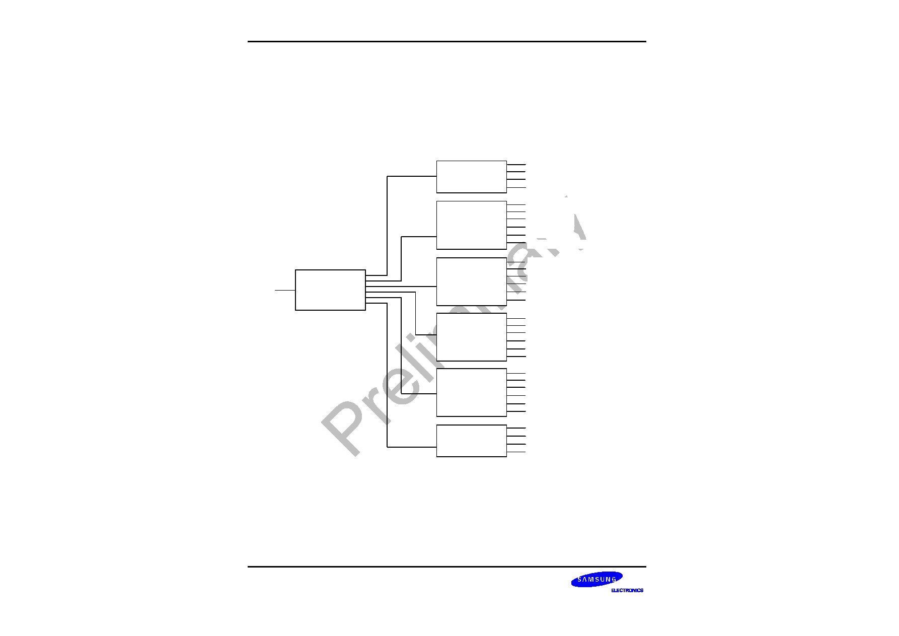
BSW rv0.1-0417-N01
Preliminary product information describes products that are in development,
for which full characterization data and associated errata are not yet available.
Specifications and information herein are subject to change without notice.
INTERRUPT CONTROLLER
S3C24A0 RISC MICROPROCESSOR
6-4
INTERRUPT PRIORITY GENERATING BLOCK
The priority logic for 32 interrupt requests is composed of seven rotation based arbiters: six first-level arbiters
and one second-level arbiter as shown in the following figure.
Figure 6-1. Priority Generating Block
ARM IRQ
ARBITER6
ARBITER0
REQ1/EINT0_2
REQ2/EINT3_6
REQ3/EINT7_10
REQ4/EINT11_14
ARBITER1
REQ1/EINT15_18
REQ2/INT_TIC
REQ3/DCTQ
REQ4/INT_MC
REQ5/INT_ME
REQ6/INT_Keypad
ARBITER2
REQ1/INT_TIMER0
REQ2/INT_TIMER1
REQ3/INT_TIMER2
REQ4/INT_TIMER3,4
REQ5/INT_LCD_POST
REQ6/INT_CAMIF_CODEC
ARBITER3
REQ1/INT_WDT_BATFLT
REQ2/INT_UART0
REQ3/INT_CAMIF_PREVIEW
REQ4/INT_MODEM
REQ5/INT_DMA
REQ6/INT_SDI
ARBITER4
REQ1/INT_SPI0
REQ2/INT_UART1
REQ3/INT_AC97_NFLASH
REQ4/INT_USBD
REQ5/INT_USBH
REQ6/INT_IIC
ARBITER5
REQ1/INT_IrDA_MSTICK
REQ2/INT_VLC_SPI1
REQ3/INT_RTC
REQ4/INT_ADC_PENUP_PENDN

BSW rv0.1-0417-N01
Preliminary product information describes products that are in development,
for which full characterization data and associated errata are not yet available.
Specifications and information herein are subject to change without notice.
S3C24A0 RISC MICROPROCESSOR
INTERRUPT CONTROLLER
6
-5
Interrupt Priority
Each arbiter can handle six interrupt requests based on the one bit arbiter mode control(ARB_MODE) and two
bits of selection control signals(ARB_SEL) as follows:
If ARB_SEL bits are 00b, the priority order is REQ0, REQ1, REQ2, REQ3, REQ4, and REQ5.
If ARB_SEL bits are 01b, the priority order is REQ0, REQ2, REQ3, REQ4, REQ1, and REQ5.
If ARB_SEL bits are 10b, the priority order is REQ0, REQ3, REQ4, REQ1, REQ2, and REQ5.
If ARB_SEL bits are 11b, the priority order is REQ0, REQ4, REQ1, REQ2, REQ3, and REQ5.
Note that REQ0 of an arbiter is always the highest priority, and REQ5 is the lowest one. In addition, by changing
the ARB_SEL bits, we can rotate the priority of REQ1 - REQ4.
Here, if ARB_MODE bit is set to 0, ARB_SEL bits are not automatically changed, thus the arbiter operates in the
fixed priority mode. (Note that even in this mode, we can change the priority by manually changing the ARB_SEL
bits.). On the other hand, if ARB_MODE bit is 1, ARB_SEL bits are changed in rotation fashion, e.g., if REQ1 is
serviced, ARB_SEL bits are changed to 01b automatically so as to make REQ1 the lowest priority one. The
detailed rule of ARB_SEL change is as follows.
If REQ0 or REQ5 is serviced, ARB_SEL bits are not changed at all.
If REQ1 is serviced, ARB_SEL bits are changed to 01b.
If REQ2 is serviced, ARB_SEL bits are changed to 10b.
If REQ3 is serviced, ARB_SEL bits are changed to 11b.
If REQ4 is serviced, ARB_SEL bits are changed to 00b.
VECTORED INTERRUPT MODE (ONLY FOR IRQ)
S3C24A0 has a vectored interrupt mode, to reduce the interrupt latency time.
If ARM926EJ receives the IRQ interrupt request from the interrupt controller, it executes an instruction at
0x00000018. The LDR instruction which loads to PC the address written in Vector Address Register, one of
special function registers in Interrupt controller, is located at 0x00000018. That is,
@0x0000_0018 : LDR PC, [VAR]
where, VAR is the special function register at 0x4020_002c of interrupt controller.

BSW rv0.1-0417-N01
Preliminary product information describes products that are in development,
for which full characterization data and associated errata are not yet available.
Specifications and information herein are subject to change without notice.
INTERRUPT CONTROLLER
S3C24A0 RISC MICROPROCESSOR
6-6
The LDR instruction lets the program counter be the vector table address corresponding to each interrupt source.
The user program code must locate the branch instruction, which branches to the corresponding ISR (interrupt
service routine) at each vector table address.
For example, If TIMER1 is IRQ, the LDR instruction at 0x00000018 which lets PC be 0x0000004c, is executed .
0x0000004c is automatically written to Vector Address Register by hardware logic.
And the branch instruction, which jumps to the ISR, is located at 0x0000004c.
Vector
number
Vector name
Interrupt vector address
0
EINT0_2
0x0000_0020
1
EINT3_6
0x0000_0024
2
EINT7_10
0x0000_0028
3
EINT11_14
0x0000_002c
4
EINT15_18
0x0000_0030
5
INT_TICK
0x0000_0034
6
INT_DCTQ
0x0000_0038
7
INT_MC
0x0000_003c
8
INT_ME
0x0000_0040
9
INT_KEYPAD
0x0000_0044
10
INT_TIMER0
0x0000_0048
11
INT_TIMER1
0x0000_004c
12
INT_TIMER2
0x0000_0050
13
INT_TIMER3,4
0x0000_0054
14
INT_LCD_POST
0x0000_0058
15
INT_CAMIF_CODEC
0x0000_005c
16
INT_WDT_BATFLT
0x0000_0060
17
INT_UART0
0x0000_0064
18
INT_CAMIF_PREVIEW
0x0000_0068
19
INT_MODEM
0x0000_006c
20
INT_DMA
0x0000_0070

BSW rv0.1-0417-N01
Preliminary product information describes products that are in development,
for which full characterization data and associated errata are not yet available.
Specifications and information herein are subject to change without notice.
S3C24A0 RISC MICROPROCESSOR
INTERRUPT CONTROLLER
6
-7
21
INT_SDI
0x0000_0074
22
INT_SPI0
0x0000_0078
23
INT_UART1
0x0000_007c
24
INT_AC97_NFLASH
0x0000_0080
25
INT_USBD
0x0000_0084
26
INT_USBH
0x0000_0088
27
INT_IIC
0x0000_008c
28
INT_IrDA_MSTICK
0x0000_0090
29
INT_VLX_SPI1
0x0000_0094
30
INT_RTC
0x0000_0098
31
INT_ADC_PENUP_DOWN
0x0000_009c
SPECIAL FUNCTION REGISTERS
There are five control registers in the interrupt controller: source pending register, interrupt mode register, mask
register, priority register, and interrupt pending register.
All the interrupt requests from the interrupt sources are first registered in the source pending register. They are
divided into two groups based on the interrupt mode register, i.e., one FIQ request and the remaining IRQ
requests. Arbitration process is performed for the multiple IRQ requests based on the priority register.
SOURCE PENDING REGISTER (SRCPND)
SRCPND register is composed of 32 bits each of which is related to an interrupt source. Each bit is set to 1 if the
corresponding interrupt source generates the interrupt request and waits for the interrupt to be serviced. By
reading this register, we can see the interrupt sources waiting for their requests to be serviced. Note that each bit
of SRCPND register is automatically set by the interrupt sources regardless of the masking bits in the INTMASK
register. In addition, it is not affected by the priority logic of interrupt controller.
In the interrupt service routine for a specific interrupt source, the corresponding bit of SRCPND register has to be
cleared to get the interrupt request from the same source correctly. If you return from the ISR without clearing the
bit, interrupt controller operates as if another interrupt request comes in from the same source. In other words, if a
specific bit of SRCPND register is set to 1, it is always considered as a valid interrupt request waiting to be
serviced.
BSW rv0.1-0417-N01
Preliminary product information describes products that are in development,
for which full characterization data and associated errata are not yet available.
Specifications and information herein are subject to change without notice.
INTERRUPT CONTROLLER
S3C24A0 RISC MICROPROCESSOR
6-8
The specific time to clear the corresponding bit depends on the user's requirement. The bottom line is that if you
want to receive another valid request from the same source you should clear the corresponding bit first, and then
enable the interrupt.
You can clear a specific bit of SRCPND register by writing a data to this register. It clears only the bit positions of
SRCPND corresponding to those set to one in the data. The bit positions corresponding to those that are set to 0
in the data remains as they are with no change.
Register
Address
R/W
Description
Reset Value
SRCPND
0X40200000
R/W
Indicates the interrupt request status.
0 = The interrupt has not been requested
1 = The interrupt source has asserted the interrupt request
0x00000000
NOTE : When the user clear a interrupt pending, specific bit of SRCPND and INTPND, has to clear the bit of
SRCPND

BSW rv0.1-0417-N01
Preliminary product information describes products that are in development,
for which full characterization data and associated errata are not yet available.
Specifications and information herein are subject to change without notice.
S3C24A0 RISC MICROPROCESSOR
INTERRUPT CONTROLLER
6
-9
SRCPND
Bit
Description
Initial State
INT_ADC_PENUP_DOW
N
[31]
0 = Not requested, 1 = Requested
(SUBSRCPND)
0
INT_RTC
[30]
0 = Not requested, 1 = Requested
0
INT_VLX_SPI1
[29]
0 = Not requested, 1 = Requested
(SUBSRCPND)
0
INT_IrDA_MSTICK
[28]
0 = Not requested, 1 = Requested
(SUBSRCPND)
0
INT_IIC
[27]
0 = Not requested, 1 = Requested
0
INT_USBH
[26]
0 = Not requested, 1 = Requested
0
INT_USBD
[25]
0 = Not requested, 1 = Requested
0
INT_AC97_NFLASH
[24]
0 = Not requested, 1 = Requested
(SUBSRCPND)
0
INT_UART1
[23]
0 = Not requested, 1 = Requested
(SUBSRCPND)
0
INT_SPI0
[22]
0 = Not requested, 1 = Requested
0
INT_SDI
[21]
0 = Not requested, 1 = Requested
0
INT_DMA
[20]
0 = Not requested, 1 = Requested
(SUBSRCPND)
0
INT_MODEM
[19]
0 = Not requested, 1 = Requested
0
INT_CAMIF_PREVIEW
[18]
0 = Not requested, 1 = Requested
0
INT_UART0
[17]
0 = Not requested, 1 = Requested
(SUBSRCPND)
0
INT_WDT_BATFLT
[16]
0 = Not requested, 1 = Requested
(SUBSRCPND)
0
INT_CAMIF_CODEC
[15]
0 = Not requested, 1 = Requested
0
INT_LCD_POST
[14]
0 = Not requested, 1 = Requested
(SUBSRCPND)
0
INT_TIMER3,4
[13]
0 = Not requested, 1 = Requested
(SUBSRCPND)
0
INT_TIMER2
[12]
0 = Not requested, 1 = Requested
0
BSW rv0.1-0417-N01
Preliminary product information describes products that are in development,
for which full characterization data and associated errata are not yet available.
Specifications and information herein are subject to change without notice.
INTERRUPT CONTROLLER
S3C24A0 RISC MICROPROCESSOR
6-10
INT_TIMER1
[11]
0 = Not requested, 1 = Requested
0
INT_TIMER0
[10]
0 = Not requested, 1 = Requested
0
INT_KEYPAD
[9]
0 = Not requested, 1 = Requested
0
INT_ME
[8]
0 = Not requested, 1 = Requested
0
INT_MC
[7]
0 = Not requested, 1 = Requested
0
INT_DCTQ
[6]
0 = Not requested, 1 = Requested
0
INT_TIC
[5]
0 = Not requested, 1 = Requested
0
EINT15_18
[4]
0 = Not requested, 1 = Requested
0
EINT11_14
[3]
0 = Not requested, 1 = Requested
0
EINT7_10
[2]
0 = Not requested, 1 = Requested
0
EINT3_6
[1]
0 = Not requested, 1 = Requested
0
EINT0_2
[0]
0 = Not requested, 1 = Requested
0

BSW rv0.1-0417-N01
Preliminary product information describes products that are in development,
for which full characterization data and associated errata are not yet available.
Specifications and information herein are subject to change without notice.
S3C24A0 RISC MICROPROCESSOR
INTERRUPT CONTROLLER
6
-11
INTERRUPT MODE REGISTER (INTMOD)
This register is composed of 32 bits each of which is related to an interrupt source. If a specific bit is set to 1, the
corresponding interrupt is processed in the FIQ (fast interrupt) mode. Otherwise, it is processed in the IRQ mode
(normal interrupt).
Note that at most only one interrupt source can be serviced in the FIQ mode in the interrupt controller. (You
should use the FIQ mode only for the urgent interrupt.) Thus, only one bit of INTMOD can be set to 1 at most.
This register is write-only one, thus it cannot be read out.
Register
Address
R/W
Description
Reset Value
INTMOD
0X40200004
R/W
Interrupt mode regiseter.
0 = IRQ mode 1 = FIQ mode
0x00000000
NOTE : If an interrupt mode is set to FIQ mode in INTMOD register, FIQ interrupt will not affect INTPND and
INTOFFSET registers. The INTPND and INTOFFSET registers are valid only for IRQ mode interrupt source.
INTMOD
Bit
Description
Initial State
INT_ADC_PENUP_DOWN [31]
0 = IRQ, 1 = FIQ
0
INT_RTC
[30]
0 = IRQ, 1 = FIQ
0
INT_VLX_SPI1
[29]
0 = IRQ, 1 = FIQ
0
INT_IrDA_MSTICK
[28]
0 = IRQ, 1 = FIQ
0
INT_IIC
[27]
0 = IRQ, 1 = FIQ
0
INT_USBH
[26]
0 = IRQ, 1 = FIQ
0
INT_USBD
[25]
0 = IRQ, 1 = FIQ
0
INT_AC97_NFLASH
[24]
0 = IRQ, 1 = FIQ
0
INT_UART1
[23]
0 = IRQ, 1 = FIQ
0
INT_SPI0
[22]
0 = IRQ, 1 = FIQ
0
INT_SDI
[21]
0 = IRQ, 1 = FIQ
0
INT_DMA
[20]
0 = IRQ, 1 = FIQ
0
INT_MODEM
[19]
0 = IRQ, 1 = FIQ
0

BSW rv0.1-0417-N01
Preliminary product information describes products that are in development,
for which full characterization data and associated errata are not yet available.
Specifications and information herein are subject to change without notice.
INTERRUPT CONTROLLER
S3C24A0 RISC MICROPROCESSOR
6-12
INT_CAMIF_PREVIEW
[18]
0 = IRQ, 1 = FIQ
0
INT_UART0
[17]
0 = IRQ, 1 = FIQ
0
INT_WDT_BATFLT
[16]
0 = IRQ, 1 = FIQ
0
INT_CAMIF_CODEC
[15]
0 = IRQ, 1 = FIQ
0
INT_LCD_POST
[14]
0 = IRQ, 1 = FIQ
0
INT_TIMER3,4
[13]
0 = IRQ, 1 = FIQ
0
INT_TIMER2
[12]
0 = IRQ, 1 = FIQ
0
INT_TIMER1
[11]
0 = IRQ, 1 = FIQ
0
INT_TIMER0
[10]
0 = IRQ, 1 = FIQ
0
INT_KEYPAD
[9]
0 = IRQ, 1 = FIQ
0
INT_ME
[8]
0 = IRQ, 1 = FIQ
0
INT_MC
[7]
0 = IRQ, 1 = FIQ
0
INT_DCTQ
[6]
0 = IRQ, 1 = FIQ
0
INT_TIC
[5]
0 = IRQ, 1 = FIQ
0
EINT15_18
[4]
0 = IRQ, 1 = FIQ
0
EINT11_14
[3]
0 = IRQ, 1 = FIQ
0
EINT7_10
[2]
0 = IRQ, 1 = FIQ
0
EINT3_6
[1]
0 = IRQ, 1 = FIQ
0
EINT0_2
[0]
0 = IRQ, 1 = FIQ
0

BSW rv0.1-0417-N01
Preliminary product information describes products that are in development,
for which full characterization data and associated errata are not yet available.
Specifications and information herein are subject to change without notice.
S3C24A0 RISC MICROPROCESSOR
INTERRUPT CONTROLLER
6
-13
INTERRUPT MASK REGISTER (INTMSK)
Each of the 32 bits in the interrupt mask register is related to an interrupt source. If you set a specific bit to 1, the
interrupt request from the corresponding interrupt source is not serviced by the CPU. (Note that even in such a
case, the corresponding bit of SRCPND register is set to 1). If the mask bit is 0, the interrupt request can be
serviced.
Register
Address
R/W
Description
Reset Value
INTMSK
0X40200008
R/W
Determines which interrupt source is masked. The
masked interrupt source will not be serviced.
0 = Interrupt service is available
1 = Interrupt service is masked
0xffffffff
INTMSK
Bit
Description
Initial State
INT_ADC_PENUP_DOW
N
[31]
0 = Service available, 1 = Masked
1
INT_RTC
[30]
0 = Service available, 1 = Masked
1
INT_VLX_SPI1
[29]
0 = Service available, 1 = Masked
1
INT_IrDA_MSTICK
[28]
0 = Service available, 1 = Masked
1
INT_IIC
[27]
0 = Service available, 1 = Masked
1
INT_USBH
[26]
0 = Service available, 1 = Masked
1
INT_USBD
[25]
0 = Service available, 1 = Masked
1
INT_AC97_NFLASH
[24]
0 = Service available, 1 = Masked
1
INT_UART1
[23]
0 = Service available, 1 = Masked
1
INT_SPI0
[22]
0 = Service available, 1 = Masked
1
INT_SDI
[21]
0 = Service available, 1 = Masked
1
INT_DMA
[20]
0 = Service available, 1 = Masked
1
INT_MODEM
[19]
0 = Service available, 1 = Masked
1
INT_CAMIF_PREVIEW
[18]
0 = Service available, 1 = Masked
1
INT_UART0
[17]
0 = Service available, 1 = Masked
1

BSW rv0.1-0417-N01
Preliminary product information describes products that are in development,
for which full characterization data and associated errata are not yet available.
Specifications and information herein are subject to change without notice.
INTERRUPT CONTROLLER
S3C24A0 RISC MICROPROCESSOR
6-14
INT_WDT_BATFLT
[16]
0 = Service available, 1 = Masked
1
INT_CAMIF_CODEC
[15]
0 = Service available, 1 = Masked
1
INT_LCD_POST
[14]
0 = Service available, 1 = Masked
1
INT_TIMER3,4
[13]
0 = Service available, 1 = Masked
1
INT_TIMER2
[12]
0 = Service available, 1 = Masked
1
INT_TIMER1
[11]
0 = Service available,
1 = Masked
1
INT_TIMER0
[10]
0 = Service available, 1 = Masked
1
INT_KEYPAD
[9]
0 = Service available, 1 = Masked
1
INT_ME
[8]
0 = Service available, 1 = Masked
1
INT_MC
[7]
0 = Service available, 1 = Masked
1
INT_DCTQ
[6]
0 = Service available, 1 = Masked
1
INT_TIC
[5]
0 = Service available, 1 = Masked
1
EINT15_18
[4]
0 = Service available, 1 = Masked
1
EINT11_14
[3]
0 = Service available, 1 = Masked
1
EINT7_10
[2]
0 = Service available, 1 = Masked
1
EINT3_6
[1]
0 = Service available, 1 = Masked
1
EINT0_2
[0]
0 = Service available, 1 = Masked
1

BSW rv0.1-0417-N01
Preliminary product information describes products that are in development,
for which full characterization data and associated errata are not yet available.
Specifications and information herein are subject to change without notice.
S3C24A0 RISC MICROPROCESSOR
INTERRUPT CONTROLLER
6
-15
PRIORITY REGISTER (PRIORITY)
Register
Address
R/W
Description
Reset Value
PRIORITY 0X4020000C R/W
IRQ priority control register
0x7f
PRIORITY
Bit
Description
Initial State
ARB_SEL6
[20:19]
Arbiter 6 group priority order set
00 = REQ 0-1-2-3-4-5
01 = REQ 0-2-3-4-1-5
10 = REQ 0-3-4-1-2-5
11 = REQ 0-4-1-2-3-5
0
ARB_SEL5
[18:17]
Arbiter 5 group priority order set
00 = REQ 1-2-3-4
01 = REQ 2-3-4-1
10 = REQ 3-4-1-2
11 = REQ 4-1-2-3
0
ARB_SEL4
[16:15]
Arbiter 4 group priority order set
00 = REQ 0-1-2-3-4-5
01 = REQ 0-2-3-4-1-5
10 = REQ 0-3-4-1-2-5
11 = REQ 0-4-1-2-3-5
0
ARB_SEL3
[14:13]
Arbiter 3 group priority order set
00 = REQ 0-1-2-3-4-5
01 = REQ 0-2-3-4-1-5
10 = REQ 0-3-4-1-2-5
11 = REQ 0-4-1-2-3-5
0
ARB_SEL2
[12:11]
Arbiter 2 group priority order set
00 = REQ 0-1-2-3-4-5
01 = REQ 0-2-3-4-1-5
10 = REQ 0-3-4-1-2-5
11 = REQ 0-4-1-2-3-5
0
ARB_SEL1
[10:9]
Arbiter 1 group priority order set
00 = REQ 0-1-2-3-4-5
01 = REQ 0-2-3-4-1-5
10 = REQ 0-3-4-1-2-5
11 = REQ 0-4-1-2-3-5
0
ARB_SEL0
[8:7]
Arbiter 0 group priority order set
00 = REQ 1-2-3-4
01 = REQ 2-3-4-1
10 = REQ 3-4-1-2
11 = REQ 4-1-2-3
0
ARB_MODE6
[6]
Arbiter 6 group priority rotate enable
0 = Priority does not rotate, 1 = Priority rotate enable
1
ARB_MODE5
[5]
Arbiter 5 group priority rotate enable
0 = Priority does not rotate, 1 = Priority rotate enable
1
ARB_MODE4
[4]
Arbiter 4 group priority rotate enable
0 = Priority does not rotate, 1 = Priority rotate enable
1
ARB_MODE3
[3]
Arbiter 3 group priority rotate enable
0 = Priority does not rotate, 1 = Priority rotate enable
1
ARB_MODE2
[2]
Arbiter 2 group priority rotate enable
0 = Priority does not rotate, 1 = Priority rotate enable
1
BSW rv0.1-0417-N01
Preliminary product information describes products that are in development,
for which full characterization data and associated errata are not yet available.
Specifications and information herein are subject to change without notice.
INTERRUPT CONTROLLER
S3C24A0 RISC MICROPROCESSOR
6-16
ARB_MODE1
[1]
Arbiter 1 group priority rotate enable
0 = Priority does not rotate, 1 = Priority rotate enable
1
ARB_MODE0
[0]
Arbiter 0 group priority rotate enable
0 = Priority does not rotate, 1 = Priority rotate enable
1

BSW rv0.1-0417-N01
Preliminary product information describes products that are in development,
for which full characterization data and associated errata are not yet available.
Specifications and information herein are subject to change without notice.
S3C24A0 RISC MICROPROCESSOR
INTERRUPT CONTROLLER
6
-17
INTERRUPT PENDING REGISTER (INTIPND)
Each of the 32 bits in the interrupt pending register shows whether the corresponding interrupt request is the
highest priority one that is unmasked and waits for the interrupt to be serviced. Since INTPND is located after the
priority logic, only one bit can be set to 1 at most, and that is the very interrupt request generating IRQ to CPU. In
interrupt service routine for IRQ, you can read this register to determine the interrupt source to be serviced among
32 sources.
Like the SRCPND, this register has to be cleared in the interrupt service routine after clearing SRCPND register.
We can clear a specific bit of INTPND register by writing a data to this register. It clears only the bit positions of
INTPND corresponding to those set to one in the data. The bit positions corresponding to those that are set to 0 in
the data remains as they are with no change.
Register
Address
R/W
Description
Reset Value
INTPND
0X40200010
R/W
Indicates the interrupt request status.
0 = The interrupt has not been requested
1 = The interrupt source has asserted the interrupt request
0x00000000
NOTE : If the FIQ mode interrupt is occurred, the corresponding bit of INTPND will not be turned on. Because the
INTPND register is available only for IRQ mode interrupt.
INTPND
Bit
Description
Initial State
INT_ADC_PENUP_DOWN [31]
0 = Not requested, 1 = Requested
0
INT_RTC
[30]
0 = Not requested, 1 = Requested
0
INT_VLX_SPI1
[29]
0 = Not requested, 1 = Requested
0
INT_IrDA_MSTICK
[28]
0 = Not requested, 1 = Requested
0
INT_IIC
[27]
0 = Not requested, 1 = Requested
0
INT_USBH
[26]
0 = Not requested, 1 = Requested
0
INT_USBD
[25]
0 = Not requested, 1 = Requested
0
INT_AC97_NFLASH
[24]
0 = Not requested, 1 = Requested
0
INT_UART1
[23]
0 = Not requested, 1 = Requested
0
INT_SPI0
[22]
0 = Not requested, 1 = Requested
0

BSW rv0.1-0417-N01
Preliminary product information describes products that are in development,
for which full characterization data and associated errata are not yet available.
Specifications and information herein are subject to change without notice.
INTERRUPT CONTROLLER
S3C24A0 RISC MICROPROCESSOR
6-18
INT_SDI
[21]
0 = Not requested, 1 = Requested
0
INT_DMA
[20]
0 = Not requested, 1 = Requested
0
INT_MODEM
[19]
0 = Not requested, 1 = Requested
0
INT_CAMIF_PREVIEW
[18]
0 = Not requested, 1 = Requested
0
INT_UART0
[17]
0 = Not requested, 1 = Requested
0
INT_WDT_BATFLT
[16]
0 = Not requested, 1 = Requested
0
INT_CAMIF_CODEC
[15]
0 = Not requested, 1 = Requested
0
INT_LCD_POST
[14]
0 = Not requested, 1 = Requested
0
INT_TIMER3,4
[13]
0 = Not requested, 1 = Requested
0
INT_TIMER2
[12]
0 = Not requested, 1 = Requested
0
INT_TIMER1
[11]
0 = Not requested, 1 = Requested
0
INT_TIMER0
[10]
0 = Not requested, 1 = Requested
0
INT_KEYPAD
[9]
0 = Not requested, 1 = Requested
0
INT_ME
[8]
0 = Not requested, 1 = Requested
0
INT_MC
[7]
0 = Not requested, 1 = Requested
0
INT_DCTQ
[6]
0 = Not requested, 1 = Requested
0
INT_TIC
[5]
0 = Not requested, 1 = Requested
0
EINT15_18
[4]
0 = Not requested, 1 = Requested
0
EINT11_14
[3]
0 = Not requested, 1 = Requested
0
EINT7_10
[2]
0 = Not requested, 1 = Requested
0
EINT3_6
[1]
0 = Not requested, 1 = Requested
0
EINT0_2
[0]
0 = Not requested, 1 = Requested
0

BSW rv0.1-0417-N01
Preliminary product information describes products that are in development,
for which full characterization data and associated errata are not yet available.
Specifications and information herein are subject to change without notice.
S3C24A0 RISC MICROPROCESSOR
INTERRUPT CONTROLLER
6
-19
INTERRUPT OFFSET REGISTER (INTOFFSET)
The number in the interrupt offset register shows which interrupt request of IRQ mode is in the INTPND register.
This bit can be cleared automatically by clearing SRCPND and INTPND.
Register
Address
R/W
Description
Reset Value
INTOFFSET
0X40200014
R
Indicates the IRQ interrupt request source
0x00000000
INT Source
The OFFSET value
INT Source
The OFFSET value
INT_ADC_PENUP_DOWN 31
INT_CAMIF_CODEC
15
INT_RTC
30
INT_LCD_POST
14
INT_VLX_SPI1
29
INT_TIMER3,4
13
INT_IrDA_MSTICK
28
INT_TIMER2
12
INT_IIC
27
INT_TIMER1
11
INT_USBH
26
INT_TIMER0
10
INT_USBD
25
INT_KEYPAD
9
INT_AC97_NFLASH
24
INT_ME
8
INT_UART1
23
INT_MC
7
INT_SPI0
22
INT_DCTQ
6
INT_SDI
21
INT_TIC
5
INT_DMA
20
EINT15_18
4
INT_MODEM
19
EINT11_14
3
INT_CAMIF_PREVIEW
18
EINT7_10
2
INT_UART0
17
EINT3_6
1
INT_WDT_BATFLT
16
EINT0_2
0
NOTE : If the FIQ mode interrupt is occurred, the INTOFFSET will not be affected. Because the INTOFFSET
register is available only for IRQ mode interrupt.

BSW rv0.1-0417-N01
Preliminary product information describes products that are in development,
for which full characterization data and associated errata are not yet available.
Specifications and information herein are subject to change without notice.
INTERRUPT CONTROLLER
S3C24A0 RISC MICROPROCESSOR
6-20
SUB SOURCE PENDING REGISTER (SUBSRCPND)
You can clear a specific bit of SUBSRCPND register by writing a data to this register. It clears only the bit
positions of the SUBSRCPND corresponding to those set to one in the data. The bit positions corresponding to
those that are set to 0 in the data remains as they are with no change.
Register
Address
R/W
Description
Reset Value
SUBSRCPND
0X402000018
R/W
Indicates the interrupt request status.
0 = The interrupt has not been requested
1 = The interrupt source has asserted the
interrupt request
0x00000000
SUBSRCPND
Bit
Description
Initial State
Reserved
[31:29]
-
-
INT_DMA3
[28]
0 = Not requested, 1 = Requested
0
INT_DMA2
[27]
0 = Not requested, 1 = Requested
0
INT_DMA1
[26]
0 = Not requested, 1 = Requested
0
INT_DMA0
[25]
0 = Not requested, 1 = Requested
0
INT_VLX
[24]
0 = Not requested, 1 = Requested
0
INT_SPI1
[23]
0 = Not requested, 1 = Requested
0
INT_AC97
[22]
0 = Not requested, 1 = Requested
0
INT_NFLASH
[21]
0 = Not requested, 1 = Requested
0
INT_DISP_FRAME
[20]
0 = Not requested, 1 = Requested
0
INT_ADC
[19]
0 = Not requested, 1 = Requested
0
INT_PENDN
[18]
0 = Not requested, 1 = Requested
0
INT_PENUP
[17]
0 = Not requested, 1 = Requested
0
INT_DISP_FIFO
[16]
0 = Not requested, 1 = Requested
0
INT_POST
[15]
0 = Not requested, 1 = Requested
0
INT_BATFLT
[14]
0 = Not requested, 1 = Requested
0
INT_WDT
[13]
0 = Not requested, 1 = Requested
0

BSW rv0.1-0417-N01
Preliminary product information describes products that are in development,
for which full characterization data and associated errata are not yet available.
Specifications and information herein are subject to change without notice.
S3C24A0 RISC MICROPROCESSOR
INTERRUPT CONTROLLER
6
-21
INT_TIMER4
[12]
0 = Not requested, 1 = Requested
0
INT_TIMER3
[11]
0 = Not requested, 1 = Requested
0
Reserved
[10:8]
-
-
INT_MSTICK
[7]
0 = Not requested, 1 = Requested
0
INT_IrDA
[6]
0 = Not requested, 1 = Requested
0
INT_ERR1
[5]
0 = Not requested, 1 = Requested
0
INT_TXD1
[4]
0 = Not requested, 1 = Requested
0
INT_RXD1
[3]
0 = Not requested, 1 = Requested
0
INT_ERR0
[2]
0 = Not requested, 1 = Requested
0
INT_TXD0
[1]
0 = Not requested, 1 = Requested
0
INT_RXD0
[0]
0 = Not requested, 1 = Requested
0

BSW rv0.1-0417-N01
Preliminary product information describes products that are in development,
for which full characterization data and associated errata are not yet available.
Specifications and information herein are subject to change without notice.
INTERRUPT CONTROLLER
S3C24A0 RISC MICROPROCESSOR
6-22
INTERRUPT SUB MASK REGISTER (INTSUBMSK)
Each of the 32 bits in the interrupt mask register is related to an interrupt source. If you set a specific bit to 1, the
interrupt request from the corresponding interrupt source is not serviced by the CPU. (Note that even in such a
case, the corresponding bit of SUBSRCPND register is set to 1). If the mask bit is 0, the interrupt request can be
serviced.
Register
Address
R/W
Description
Reset Value
INTSUBMSK
0X4020001C
R/W
Determines which interrupt source is masked. The
masked interrupt source will not be serviced.
0 = Interrupt service is available
1 = Interrupt service is masked
0x1fffffff
INTSUBMSK
Bit
Description
Initial State
reserved
[31:29]
-
-
INT_DMA3
[28]
0 = Service available, 1 = Masked
1
INT_DMA2
[27]
0 = Service available, 1 = Masked
1
INT_DMA1
[26]
0 = Service available, 1 = Masked
1
INT_DMA0
[25]
0 = Service available, 1 = Masked
1
INT_VLX
[24]
0 = Service available, 1 = Masked
1
INT_SPI1
[23]
0 = Service available, 1 = Masked
1
INT_AC97
[22]
0 = Service available, 1 = Masked
1
INT_NFLASH
[21]
0 = Service available, 1 = Masked
1
INT_DISP_FRAME
[20]
0 = Service available, 1 = Masked
1
INT_ADC
[19]
0 = Service available, 1 = Masked
1
INT_PENDN
[18]
0 = Service available, 1 = Masked
1
INT_PENUP
[17]
0 = Service available, 1 = Masked
1
INT_DISP_FIFO
[16]
0 = Service available, 1 = Masked
1
INT_POST
[15]
0 = Service available, 1 = Masked
1
INT_BATFLT
[14]
0 = Service available, 1 = Masked
1

BSW rv0.1-0417-N01
Preliminary product information describes products that are in development,
for which full characterization data and associated errata are not yet available.
Specifications and information herein are subject to change without notice.
S3C24A0 RISC MICROPROCESSOR
INTERRUPT CONTROLLER
6
-23
INT_WDT
[13]
0 = Service available, 1 = Masked
1
INT_TIMER4
[12]
0 = Service available, 1 = Masked
1
INT_TIMER3
[11]
0 = Service available, 1 = Masked
1
Reserved
[10:8]
-
-
INT_MSTICK
[7]
0 = Service available, 1 = Masked
-
INT_IrDA
[6]
0 = Service available, 1 = Masked
-
INT_ERR1
[5]
0 = Service available, 1 = Masked
1
INT_TXD1
[4]
0 = Service available, 1 = Masked
1
INT_RXD1
[3]
0 = Service available,
1 = Masked
1
INT_ERR0
[2]
0 = Service available, 1 = Masked
1
INT_TXD0
[1]
0 = Service available, 1 = Masked
1
INT_RXD0
[0]
0 = Service available, 1 = Masked
1

BSW rv0.1-0417-N01
Preliminary product information describes products that are in development,
for which full characterization data and associated errata are not yet available.
Specifications and information herein are subject to change without notice.
INTERRUPT CONTROLLER
S3C24A0 RISC MICROPROCESSOR
6-24
VECTORED INTERRUPT MODE REGISTER (VECT_INT_MODE)
This register is used to indicate if the vectored interrupt mode is enabled. If you set a bit[0] to 1, the vectored
interrupt mode will be enabled.
Register
Address
R/W Description
Reset Value
VECT_INT_MODE 0X40200020
R/W Indicates if the vectored interrupt mode is enabled.
0 = Nonvectored interrupt mode
1 = Vectored interrupt mode
0x00000000
VECT_INT_MODE
Bit
Description
Initial State
reserved
[31:1]
-
-
Vect_int_mode
[0]
0 = vectored interrupt mode disable
1 = vectored interrupt mode enable
0
VECTOR ADDRESS REGISTER (VAR)
This register is used to provide the interrupt vector address to which the program control branches. If IRQ occurs,
the LDR instruction at 0x0000_0018 let PC be the value written in this register.
If VECT_INT_MODE[0] is set to `0', the address in NONVECT_ADDR is passed to this register, and if
VECT_INT_MODE[0] is set to `1', the address in VECT_ADDR is passed to this register.
Register
Address
R/W Description
Reset Value
VAR
0X4020002C
R
Provides the interrupt vector address
-
VAR
Bit
Description
Initial State
Var
[31:0]
Provides the interrupt vector address
-

BSW rv0.1-0417-N01
Preliminary product information describes products that are in development,
for which full characterization data and associated errata are not yet available.
Specifications and information herein are subject to change without notice.
S3C24A0 RISC MOCROPROCESSOR
PWM TIMER
7-1
PWM TIMER(Preliminary)
OVERVIEW
The S3C24A0 has five 16-bit timers. The timer 0, 1, 2, 3 have PWM function(Pulse Width Modulation). Timer 4
has an internal timer only with no output pins. Timer 0 has a dead-zone generator, which is used with a large
current device.
Timer 0 and timer 1 share an 8-bit prescaler, timers 2, 3 and 4 share the other 8-bit prescaler. Each timer has a
clock-divider which has 4 different divided signals (1/2, 1/4, 1/8, 1/16). Each timer block receives its own clock
signals from the clock-divider, which receives the clock from the corresponding 8-bit prescaler. The 8-bit prescaler
is programmable and divides the PCLK according to the loading value, which is stored in TCFG0 and TCFG1
registers.
The timer count buffer register(TCNTBn) has an initial value which is loaded into the down-counter when the timer
is enabled. The timer compare buffer register(TCMPBn) has an initial value which is loaded into the compare
register to be compared with the down-counter value. This double buffering feature of TCNTBn and TCMPBn
makes the timer generate a stable output when the frequency and duty ratio are changed.
Each timer has its own 16-bit down counter, which is driven by the timer clock. When the down counter reaches
zero, the timer interrupt request is generated to inform the CPU that the timer operation has been completed.
When the timer counter reaches zero, the value of corresponding TCNTBn is automatically loaded into the down
counter to continue the next operation. However, if the timer stops, for example, by clearing the timer enable bit of
TCONn during the timer running mode, the value of TCNTBn will not be reloaded into the counter.
The value of TCMPBn is used for PWM (pulse width modulation). The timer control logic changes the output level
when the down-counter value matches the value of the compare register in the timer control logic. Therefore, the
compare register determines the turn-on time(or turn-off time) of an PWM output.
FEATURE
-- Five 16-bit timers
-- Two 8-bit prescalers & Two 4-bit divider
-- Programmable duty control of output waveform (PWM)
-- Auto-reload mode or one-shot pulse mode
-- Dead-zone generator

BSW rv0.1-0417-N01
Preliminary product information describes products that are in development,
for which full characterization data and associated errata are not yet available.
Specifications and information herein are subject to change without notice.
PWM TIMER
S3C24A0 RISC MICROPROCESSOR
7-2
Clock
Divider
4:
1
M
U
X
Dead Zone
Generator
TOUT0
TOUT1
TOUT2
Control
Logic0
TCMPB0
TCNTB0
Control
Logic1
TCMPB1
TCNTB1
4:
1
M
U
X
Clock
Divider
4:
1
M
U
X
4:
1
M
U
X
Control
Logic2
TCMPB2
TCNTB2
TOUT3
Control
Logic3
TCMPB3
TCNTB3
No Pin
PCLK
8-Bit
Prescaler
8-Bit
Prescaler
Dead Zone
Dead Zone
1/8
1/4
1/16
1/2
1/8
1/4
1/16
1/2
4:
1
M
UX
Control
Logic4
TCNTB4
Figure 7-1. 16-bit PWM Timer Block Diagram

BSW rv0.1-0417-N01
Preliminary product information describes products that are in development,
for which full characterization data and associated errata are not yet available.
Specifications and information herein are subject to change without notice.
S3C24A0 RISC MOCROPROCESSOR
PWM TIMER
7-3
PWM TIMER OPERATION
PRESCALER & DIVIDER
An 8-bit prescaler and 4-bit divider make the following output frequencies:
4-bit divider settings
minimum resolution
(prescaler = 0)
maximum resolution
(prescaler = 255)
maximum interval
(TCNTBn = 65535)
1/2 ( PCLK = 55 MHz )
0.0363 us (27.5000 MHz )
9.3090 us (107.4219 KHz )
0.6100 sec
1/4 ( PCLK = 55 MHz )
0.0727 us (13.7500 MHz )
18.6181 us (53.7109 KHz )
1.2201 sec
1/8 ( PCLK = 55 MHz )
0.1454us ( 6.8750 MHz )
37.2363 us (26.8554KHz )
2.4403 sec
1/16 ( PCLK = 55 MHz )
0.2909 us ( 3.4375MHz )
74.4729 us (13.4277 KHz )
4.8806 sec
BASIC TIMER OPERATION
3
3
2
0
1
1
0
2
1
0
0
TCNTBn=2
TCMPBn=0
manual update=0
auto-reload=1
interrupt request
interrupt request
TCNTBn=3
TCMPBn=1
manual update=1
auto-reload=1
TOUTn
TCMPn
TCNTn
auto-reload=0
command
status
timer is started
TCNTn=TCMPn
auto-reload
start bit=1
TCNTn=TCMPn
timer is stopped.
Figure 7-2. Timer operations
A timer (except the timer ch-5) has TCNTBn, TCNTn, TCMPBn and TCMPn. TCNTBn and TCMPBn are loaded
into TCNTn and TCMPn when the timer reaches 0. When TCNTn reaches 0, the interrupt request will occur if the
interrupt is enabled. (TCNTn and TCMPn are the names of the internal registers. The TCNTn register can be read
from the TCNTOn register)

BSW rv0.1-0417-N01
Preliminary product information describes products that are in development,
for which full characterization data and associated errata are not yet available.
Specifications and information herein are subject to change without notice.
PWM TIMER
S3C24A0 RISC MICROPROCESSOR
7-4
AUTO-RELOAD & DOUBLE BUFFERING
S3C24A0 PWM Timers have a double buffering feature, which can change the reload value for the next timer
operation without stopping the current timer operation. So, although the new timer value is set, a current timer
operation is completed successfully.
The timer value can be written into TCNTBn (Timer Count Buffer register) and the current counter value of the
timer can be read from TCNTOn (Timer Count Observation register). If TCNTBn is read, the read value is not the
current state of the counter but the reload value for the next timer duration.
The auto-reload is the operation, which copies the TCNTBn into TCNTn when TCNTn reaches 0. The value,
written into TCNTBn, is loaded to TCNTn only when the TCNTn reaches to 0 and auto-reload is enabled. If the
TCNTn is 0 and the auto-reload bit is 0, the TCNTn does not operate any further.
Write
TCNTBn = 100
Write
TCNTBn = 200
Start
TCNTBn = 150
Auto-reload
150
100
100
200
Interrupt
Figure 7-3. Example of Double Buffering Feature

BSW rv0.1-0417-N01
Preliminary product information describes products that are in development,
for which full characterization data and associated errata are not yet available.
Specifications and information herein are subject to change without notice.
S3C24A0 RISC MOCROPROCESSOR
PWM TIMER
7-5
TIMER INITIALIZation using Manual UpdatE BIT and Inverter BIt
Because an auto-reload operation of the timer occurs when the down counter reaches to 0, a starting value of the
TCNTn has to be defined by the user at first. In this case, the starting value has to be loaded by the manual
update bit. The sequence of starting a timer is as follows;
1) Write the initial value into TCNTBn and TCMPBn
2) Set the manual update bit of the corresponding timer. It is recommended to configure the inverter on/off bit.
(whether use inverter or not)
3) Set start bit of corresponding timer to start the timer(At the same time, clear the manual update bit).
Also, if the timer is stopped by force, the TCNTn retains the counter value and is not reloaded from TCNTBn. If
new value has to be set, manual update has to be done.
NOTE
Whenever TOUT inverter on/off bit is changed, the TOUTn logic value will be changed whether or not the
timer runs. Therefore, it is desirable that the inverter on/off bit is configured with the manual update bit.

BSW rv0.1-0417-N01
Preliminary product information describes products that are in development,
for which full characterization data and associated errata are not yet available.
Specifications and information herein are subject to change without notice.
PWM TIMER
S3C24A0 RISC MICROPROCESSOR
7-6
EXAMPLE OF a TIMER OPERATION
TOUTn
1
2
4
6
50
110
40
40
60
20
3
7 9
10
5
8
11
Figure 7-4. Example of a Timer Operation
The result of the following procedure is shown in Figure21-4;
1. Enable the auto-reload feature. Set the TCNTBn as 160 (50+110) and the TCMPBn as 110. Set the manual
update bit and configure the inverter bit(on/off). The manual update bit sets TCNTn and TCMPn to the values
of TCNTBn and TCMPBn, respectively.
And then, set TCNTBn and TCMPBn as 80 (40+40) and 40, respectively, to determine the next reload value.
2. Set the start bit, provided that manual_update is 0 and inverter is off and auto-reload is on. The timer starts
counting down after latency time within the timer resolution.
3. When TCNTn has the same value with TCMPn, the logic level of TOUTn is changed from low to high.
4. When TCNTn reaches 0, the interrupt request is generated and TCNTBn value is loaded into a temporary
register. At the next timer tick, TCNTn is reloaded with the temporary register value(TCNTBn).
5. In the ISR(Interrupt Service Routine), the TCNTBn and TCMPBn are set as 80 (20+60) and 60, respectively,
which is used for the next duration.
6. When TCNTn has the same value as TCMPn, the logic level of TOUTn is changed from low to high.
7. When TCNTn reaches 0, TCNTn is reloaded automatically with TCNTBn. At the same time, the interrupt
request is generated.
8. In the ISR (Interrupt Service Routine), auto-reload and interrupt request are disabled to stop the timer.
9. When the value of TCNTn is same as TCMPn, the logic level of TOUTn is changed from low to high.
10. Even when TCNTn reaches to 0, TCNTn is not any more reloaded and the timer is stopped because auto-
reload has been disabled.
11. No interrupt request is generated.

BSW rv0.1-0417-N01
Preliminary product information describes products that are in development,
for which full characterization data and associated errata are not yet available.
Specifications and information herein are subject to change without notice.
S3C24A0 RISC MOCROPROCESSOR
PWM TIMER
7-7
PWM (Pulse Width Modulation)
Write
TCMPBn = 60
Write
TCMPBn = 50
Write
TCMPBn = 40
Write
TCMPBn = 30
Write
TCMPBn = 30
Write
TCMPBn = Next PWM Value
60
50
40
30
30
Figure 7-5. Example of PWM
PWM feature can be implemented by using the TCMPBn. PWM frequency is determined by TCNTBn. A PWM
value is determined by TCMPBn in Figure 7-5.
For a higher PWM value, decrease the TCMPBn value. For a lower PWM value, increase the TCMPBn value. If
an output inverter is enabled, the increment/decrement may be reversed.
Because of the double buffering feature, TCMPBn, for a next PWM cycle, can be written at any point in the
current PWM cycle by ISR or something else

BSW rv0.1-0417-N01
Preliminary product information describes products that are in development,
for which full characterization data and associated errata are not yet available.
Specifications and information herein are subject to change without notice.
PWM TIMER
S3C24A0 RISC MICROPROCESSOR
7-8
Output Level Control
Inverter off
Initial State
Period 1
Period 2
Timer Stop
Inverter on
Figure 7-6. Inverter On/Off
The following methods can be used to maintain TOUT as high or low.(assume the inverter is off)
1. Turn off the auto-reload bit. And then, TOUTn goes to high level and the timer is stopped after TCNTn
reaches to 0. This method is recommended.
2. Stop the timer by clearing the timer start/stop bit to 0. If TCNTn
TCMPn, the output level is high. If TCNTn
>TCMPn, the output level is low.
3. TOUTn can be inverted by the inverter on/off bit in TCON. The inverter removes the additional circuit to
adjust the output level.

BSW rv0.1-0417-N01
Preliminary product information describes products that are in development,
for which full characterization data and associated errata are not yet available.
Specifications and information herein are subject to change without notice.
S3C24A0 RISC MOCROPROCESSOR
PWM TIMER
7-9
DEAD ZONE GENERATOR
The dead zone is for the PWM control in a power device. This feature is used to insert the time gap between a
turn-off of a switching device and a turn on of another switching device. This time gap prohibits the two switching
devices turning on simultaneously, even for a very short time.
TOUT0 is the PWM output. nTOUT0 is the inversion of the TOUT0. If the dead zone is enabled, the output wave
form of TOUT0 and nTOUT0 will be TOUT0_DZ and nTOUT0_DZ, respectively. nTOUT0_DZ is routed to the
TOUT1 pin.
In the dead zone interval, TOUT0_DZ and nTOUT0_DZ can never be turned on simultaneously.
TOUT0
nTOUT0
TOUT0_DZ
nTOUT0_DZ
Deadzone
Interval
Figure 7-7. The Wave Form When a Dead Zone Feature is Enabled

BSW rv0.1-0417-N01
Preliminary product information describes products that are in development,
for which full characterization data and associated errata are not yet available.
Specifications and information herein are subject to change without notice.
PWM TIMER
S3C24A0 RISC MICROPROCESSOR
7-10
Dma request mode
The PWM timer can generate a DMA request at every specific times. The timer keeps DMA request signal
(nDMA_REQ) low until the timer receives the ACK signal. When the timer receives the ACK signal, it makes the
request signal inactive. The timer, which generates the DMA request, is determined by setting DMA mode bits(in
TCFG1 register). If one of timers is configured as DMA request mode, that timer does not generate an interrupt
request. The others can generate interrupt normally.
DMA mode configuration and DMA / interrupt operation
DMA mode
DMA request
Timer0 INT
Timer1 INT
Timer2 INT
Timer3 INT
Timer4 INT
0000
No select
ON
ON
ON
ON
ON
0001
Timer0
OFF
ON
ON
ON
ON
0010
Timer1
ON
OFF
ON
ON
ON
0011
Timer2
ON
ON
OFF
ON
ON
0100
Timer3
ON
ON
ON
OFF
ON
0101
Timer4
ON
ON
ON
ON
OFF
0110
No select
ON
ON
ON
ON
ON
PCLK
INT4tmp
DMAreq_en
nDMA_ACK
nDMA_REQ
INT4
1 0 1
Figure 7-8. The Timer4 DMA mode operation

BSW rv0.1-0417-N01
Preliminary product information describes products that are in development,
for which full characterization data and associated errata are not yet available.
Specifications and information herein are subject to change without notice.
S3C24A0 RISC MOCROPROCESSOR
PWM TIMER
7-11
PWM TIMER CONTROL REGISTERS
TIMER CONFIGURATION REGISTER0 (TCFG0)
Timer input clock Frequency = PCLK / {prescaler value+1} / {divider value}
{prescaler value} = 0~255
{divider value} = 2, 4, 8, 16
Register
Address
R/W
Description
Reset Value
TCFG0
0x44000000
R/W
Configures the two 8-bit prescalers
0x00000000
TCFG0
Bit
Description
Initial State
Reserved
[31:24]
0x00
Dead zone length
[23:16]
These 8 bits determine the dead zone length. The 1 unit time
of the dead zone length is equal to the 1 unit time of timer 0.
0x00
Prescaler 1
[15:8]
These 8 bits determine prescaler value for Timer 2, 3 and 4
0x00
Prescaler 0
[7:0]
These 8 bits determine prescaler value for Timer 0 and 1
0x00
BSW rv0.1-0417-N01
Preliminary product information describes products that are in development,
for which full characterization data and associated errata are not yet available.
Specifications and information herein are subject to change without notice.
PWM TIMER
S3C24A0 RISC MICROPROCESSOR
7-12
TIMER CONFIGURATION REGISTER1 (TCFG1)
Register
Address
R/W
Description
Reset Value
TCFG1
0x44000004
R/W
5-MUX & DMA mode selecton register
0x00000000
TCFG1
Bit
Description
Initial State
Reserved
[31:24]
00000000
DMA mode
[23:20]
Select DMA request channel
0000 = No select(All interrupt) 0001 = Timer0
0010 = Timer1 0011 = Timer2
0100 = Timer3 0101 = Timer4
0110 = Reserved
0000
MUX 4
[19:16]
Select MUX input for PWM Timer4.
0000 = 1/2 0001 = 1/4 0010 = 1/8
0011 = 1/16
0000
MUX 3
[15:12]
Select MUX input for PWM Timer3.
0000 = 1/2 0001 = 1/4 0010 = 1/8
0011 = 1/16
0000
MUX 2
[11:8]
Select MUX input for PWM Timer2.
0000 = 1/2 0001 = 1/4 0010 = 1/8
0011 = 1/16
0000
MUX 1
[7:4]
Select MUX input for PWM Timer1.
0000 = 1/2 0001 = 1/4 0010 = 1/8
0011 = 1/16
0000
MUX 0
[3:0]
Select MUX input for PWM Timer0.
0000 = 1/2 0001 = 1/4 0010 = 1/8
0011 = 1/16
0000

BSW rv0.1-0417-N01
Preliminary product information describes products that are in development,
for which full characterization data and associated errata are not yet available.
Specifications and information herein are subject to change without notice.
S3C24A0 RISC MOCROPROCESSOR
PWM TIMER
7-13
TIMER CONTROL REGISTER (TCON)
Register
Address
R/W
Description
Reset Value
TCON
0x44000008
R/W
Timer control register
0x00000000
TCON
Bit
Description
initial state
Timer 4 auto reload on/off
[22] This bit determines auto reload on/off for Timer 4.
0 = One-shot 1 = Interval mode (auto reload)
0
Timer 4 manual update
(note)
[21] This bit determines the manual update for Timer 4.
0 = No operation 1 = Update TCNTB4
0
Timer 4 start/stop
[20] This bit determines start/stop for Timer 4.
0 = Stop 1 = Start for Timer 4
0
Timer 3 auto reload on/off
[19] This bit determines auto reload on/off for Timer 3.
0 = One-shot 1 = Interval mode (auto reload)
0
Timer 3 output inverter on/off
[18] This bit determines output inverter on/off for Timer 3.
0 = Inverter off 1 = Inverter on for TOUT3
0
Timer 3 manual update
(note)
[17] This bit determine manual update for Timer 3.
0 = No operation 1 = Update TCNTB3, TCMPB3
0
Timer 3 start/stop
[16] This bit determines start/stop for Timer 3.
0 = Stop 1 = Start for Timer 3
0
Timer 2 auto reload on/off
[15] This bit determines auto reload on/off for Timer 2.
0 = One-shot 1 = Interval mode (auto reload)
0
Timer 2 output inverter on/off
[14] This bit determines output inverter on/off for Timer 2.
0 = Inverter off 1 = Inverter on for TOUT2
0
Timer 2 manual update
(note)
[13] This bit determines the manual update for Timer 2.
0 = No operation 1 = Update TCNTB2, TCMPB2
0
Timer 2 start/stop
[12] This bit determines start/stop for Timer 2.
0 = Stop 1 = Start for Timer 2
0
Timer 1 auto reload on/off
[11] This bit determines the auto reload on/off for Timer1.
0 = One-shot 1 = Interval mode (auto reload)
0
Timer 1 output inverter on/off
[10] This bit determines the output inverter on/off for Timer1.
0 = Inverter off 1 = Inverter on for TOUT1
0
Timer 1 manual update
(note)
[9]
This bit determines the manual update for Timer 1.
0 = No operation 1 = Update TCNTB1, TCMPB1
0
Timer 1 start/stop
[8]
This bit determines start/stop for Timer 1.
0 = Stop 1 = Start for Timer 1
0
Reserved
[7:5]
-
-
NOTE: This bit has to be cleared at next writing.
BSW rv0.1-0417-N01
Preliminary product information describes products that are in development,
for which full characterization data and associated errata are not yet available.
Specifications and information herein are subject to change without notice.
PWM TIMER
S3C24A0 RISC MICROPROCESSOR
7-14
TCON(Continued)
TCON
Bit
Description
initial state
Dead zone enable
[4]
This bit determines the dead zone operation.
0 = Disable 1 = Enable
0
Timer 0 auto reload on/off
[3]
This bit determines auto reload on/off for Timer 0.
0 = One-shot 1 = Interval mode(auto reload)
0
Timer 0 output inverter on/off
[2]
This bit determines the output inverter on/off for Timer 0.
0 = Inverter off 1 = Inverter on for TOUT0
0
Timer 0 manual update
(note)
[1]
This bit determines the manual update for Timer 0.
0 = No operation 1 = Update TCNTB0, TCMPB0
0
Timer 0 start/stop
[0]
This bit determines start/stop for Timer 0.
0 = Stop 1 = Start for Timer 0
0
NOTE: This bit has to be cleared at next writing.

BSW rv0.1-0417-N01
Preliminary product information describes products that are in development,
for which full characterization data and associated errata are not yet available.
Specifications and information herein are subject to change without notice.
S3C24A0 RISC MOCROPROCESSOR
PWM TIMER
7-15
Timer 0 Count Buffer Register & Compare Buffer Register (TCNTB0, TCMPB0)
Register
Address
R/W
Description
Reset Value
TCNTB0
0x4400000C
R/W
Timer 0 count buffer register
0x00000000
TCMPB0
0x44000010
R/W
Timer 0 compare buffer register
0x00000000
TCMPB0
Bit
Description
Initial State
Timer 0 compare buffer register
[15:0]
Setting compare buffer value for Timer 0
0x00000000
TCNTB0
Bit
Description
Initial State
Timer 0 count buffer register
[15:0]
Setting count buffer value for Timer 0
0x00000000
TIMER 0 COUNT OBSERVATION REGISTER (TCNTO0)
Register
Address
R/W
Description
Reset Value
TCNTO0
0x44000014
R
Timer 0 count observation register
0x00000000
TCNTO0
Bit
Description
Initial State
Timer 0 observation register
[15:0]
Setting count observation value for Timer 0
0x00000000

BSW rv0.1-0417-N01
Preliminary product information describes products that are in development,
for which full characterization data and associated errata are not yet available.
Specifications and information herein are subject to change without notice.
PWM TIMER
S3C24A0 RISC MICROPROCESSOR
7-16
TIMER 1 COUNT BUFFER REGISTER & COMPARE BUFFER REGISTER (TCNTB1, TCMPB1)
Register
Address
R/W
Description
Reset Value
TCNTB1
0x44000018
R/W
Timer 1 count buffer register
0x00000000
TCMPB1
0x4400001C
R/W
Timer 1 campare buffer register
0x00000000
TCMPB1
Bit
Description
Initial State
Timer 1 compare buffer register
[15:0]
Setting compare buffer value for Timer 1
0x00000000
TCNTB1
Bit
Description
Initial State
Timer 1 count buffer register
[15:0]
Setting count buffer value for Timer 1
0x00000000
Timer 1 Count Observation Register(TCNTO1)
Register
Address
R/W
Description
Reset Value
TCNTO1
0x44000020
R
Timer 1 count observation register
0x00000000
TCNTO1
Bit
Description
initial state
Timer 1 observation register
[15:0]
Setting count observation value for Timer 1
0x00000000

BSW rv0.1-0417-N01
Preliminary product information describes products that are in development,
for which full characterization data and associated errata are not yet available.
Specifications and information herein are subject to change without notice.
S3C24A0 RISC MOCROPROCESSOR
PWM TIMER
7-17
TIMER 2 COUNT BUFFER REGISTER & COMPARE BUFFER REGISTER (TCNTB2, TCMPB2)
Register
Address
R/W
Description
Reset Value
TCNTB2
0x44000024
R/W
Timer 2 count buffer register
0x00000000
TCMPB2
0x44000028
R/W
Timer 2 campare buffer register
0x00000000
TCMPB2
Bit
Description
Initial State
Timer 2 compare buffer register
[15:0]
Setting compare buffer value for Timer 2
0x00000000
TCNTB2
Bit
Description
Initial State
Timer 2 count buffer register
[15:0]
Setting count buffer value for Timer 2
0x00000000
TIMER 2 COUNT OBSERVATION REGISTER (TCNTO2)
Register
Address
R/W
Description
Reset Value
TCNTO2
0x4400002C
R
Timer 2 count observation register
0x00000000
TCNTO2
Bit
Description
Initial State
Timer 2 observation register
[15:0]
Setting count observation value for Timer 2
0x00000000
BSW rv0.1-0417-N01
Preliminary product information describes products that are in development,
for which full characterization data and associated errata are not yet available.
Specifications and information herein are subject to change without notice.
PWM TIMER
S3C24A0 RISC MICROPROCESSOR
7-18
TIMER 3 COUNT BUFFER REGISTER & COMPARE BUFFER REGISTER (TCNTB3, TCMPB3)
Register
Address
R/W
Description
Reset Value
TCNTB3
0x44000030
R/W
Timer 3 count buffer register
0x00000000
TCMPB3
0x44000034
R/W
Timer 3 campare buffer register
0x00000000
TCMPB3
Bit
Description
Initial State
Timer 3 compare buffer register
[15:0]
Setting compare buffer value for Timer 3
0x00000000
TCNTB3
Bit
Description
Initial State
Timer 3 count buffer register
[15:0]
Setting count buffer value for Timer 3
0x00000000
TIMER 3 COUNT OBSERVATION REGISTER (TCNTO3)
Register
Address
R/W
Description
Reset Value
TCNTO3
0x44000038
R
Timer 3 count observation register
0x00000000
TCNTO3
Bit
Description
Initial State
Timer 3 observation register
[15:0]
Setting count observation value for Timer 3
0x00000000

BSW rv0.1-0417-N01
Preliminary product information describes products that are in development,
for which full characterization data and associated errata are not yet available.
Specifications and information herein are subject to change without notice.
S3C24A0 RISC MOCROPROCESSOR
PWM TIMER
7-19
TIMER 4 COUNT BUFFER REGISTER (TCNTB4)
Register
Address
R/W
Description
Reset Value
TCNTB4
0x4400003C
R/W
Timer 4 count buffer register
0x00000000
TCNTB4
Bit
Description
Initial State
Timer 4 count buffer register
[15:0]
Setting count buffer value for Timer 4
0x00000000
TIMER 4 COUNT OBSERVATION REGISTER (TCNTO4)
Register
Address
R/W
Description
Reset Value
TCNTO4
0x44000040
R
Timer 4 count observation register
0x00000000
TCNTO4
Bit
Description
Initial State
Timer 4 observation register
[15:0]
Setting count observation value for Timer 4
0x00000000

BSW rv0.1-0417-N01
Preliminary product information describes products that are in development,
for which full characterization data and associated errata are not yet available.
Specifications and information herein are subject to change without notice.
PWM TIMER
S3C24A0 RISC MICROPROCESSOR
7-20
NOTES

BSW rv0.1-0417-N01
Preliminary product information describes products that are in development,
for which full characterization data and associated errata are not yet available.
Specifications and information herein are subject to change without notice.
S3C24A0 RISC MICROPROCESSOR
WATCHDOG TIMER
8-1
WATCHDOG TIMER(Preliminary)
OVERVIEW
The S3C24A0 watchdog timer is used to resume the controller operation when it had been disturbed by
malfunctions such as noise and system errors. It can be used as a normal 16-bit interval timer to request interrupt
service. The watchdog timer generates the reset signal for 128 PCLK cycles.
FEATURES
-- Normal interval timer mode with interrupt request
-- Internal reset signal is activated for 128 PCLK cycles when the timer count value reaches 0(time-out).

BSW rv0.1-0417-N01
Preliminary product information describes products that are in development,
for which full characterization data and associated errata are not yet available.
Specifications and information herein are subject to change without notice.
WATCHDOG TIMER
S3C24A0 RISC MICROPROCESSOR
8-2
WATCHDOG TIMER OPERATION
The functional block diagram of the watchdog timer is shown in Figure 8-1. The watchdog timer uses PCLK as its
only source clock. To generate the corresponding watchdog timer clock, the PCLK frequency is prescaled first,
and the resulting frequency is divided again.
Reset Signal Generator
WTCNT
(Down Counter)
PCLK
WTCON[4:3]
WTDAT
RESET
1/16
1/32
1/64
1/128
8-bit Prescaler
WTCON[15:8]
WTCON[2]
WTCON[0]
Interrupt
MUX
Figure 8-1. Watchdog Timer Block Diagram
The prescaler value and the frequency division factor are specified in the watchdog timer control register,
WTCON. The valid prescaler values range from 0 to 2
8
-1. The frequency division factor can be selected as 16,
32, 64, or 128.
Use the following equation to calculate the watchdog timer clock frequency and the duration of each timer clock
cycle:
t_watchdog = 1/( PCLK / (Prescaler value + 1) / Division_factor )
WTDAT & WTCNT
When the watchdog timer is enabled first, the value of WTDAT (watchdog timer data register) cannot be
automatically reloaded into the WTCNT (timer counter). For this reason, an initial value must be written to the
watchdog timer count register, WTCNT, before the watchdog timer starts.
CONSIDERATION OF DEBUGGING ENVIRONMENT
When S3C24A0 is in debug mode using Embedded ICE, the watchdog timer must not operate.
The watchdog timer can determine whether or not the current mode is the debug mode from the CPU core signal
(DBGACK signal). Once the DBGACK signal is asserted, the reset output of the watchdog timer is not activated
when the watchdog timer is expired.

BSW rv0.1-0417-N01
Preliminary product information describes products that are in development,
for which full characterization data and associated errata are not yet available.
Specifications and information herein are subject to change without notice.
S3C24A0 RISC MICROPROCESSOR
WATCHDOG TIMER
8-3
WATCHDOG TIMER SPECIAL REGISTERS
WATCHDOG TIMER CONTROL REGISTER (WTCON)
Using the Watchdog Timer Control register, WTCON, you can enable/disable the watchdog timer, select the clock
signal from 4 different sources, enable/disable interrupts, and enable/disable the watchdog timer output.
The Watchdog timer is used to resume the S3C24A0 restart on mal-function after power-on; if controller restart is
not desired, the Watchdog timer should be disabled.
If the user wants to use the normal timer provided by the Watchdog timer, please enable the interrupt and disable
the Watchdog timer.
Register
Address
R/W
Description
Reset Value
WTCON
0x44100000
R/W
Watchdog timer control Register
0x8021
WTCON
Bit
Description
Initial State
Prescaler value
[15:8]
the prescaler value
The valid range is from 0 to (2
8
-1)
0x80
Reserved
[7:6]
Reserved.
These two bits must be 00 in normal operation.
00
Watchdog timer
[5]
Enable or disable bit of Watchdog timer.
0 = Disable
1 = Enable
1
Clock select
[4:3]
This two bits determines the clock division factor
00 : 16
01 : 32
10 : 64
11 : 128
00
Interrupt generation
[2]
Enable or disable bit of the interrupt.
0 = Disable
1 = Enable
0
Reserved
[1]
Reserved.
This bit must be 0 in normal operation
0
Reset enable/disable
[0]
Enable or disable bit of Watchdog timer output for reset
signal
1 : Asserts reset signal of the S3C24A0 at watchdog
time-out
0 : Disables the reset function of the watchdog timer.
1

BSW rv0.1-0417-N01
Preliminary product information describes products that are in development,
for which full characterization data and associated errata are not yet available.
Specifications and information herein are subject to change without notice.
WATCHDOG TIMER
S3C24A0 RISC MICROPROCESSOR
8-4
WATCHDOG TIMER DATA REGISTER (WTDAT)
The watchdog timer data register, WTDAT is used to specify the time-out duration. The content of WTDAT can
not be automatically loaded into the timer counter at initial watchdog timer operation. However, the first time-out
occurs by using 0x8000(initial value), after then the value of WTDAT will be automatically reloaded into WTCNT.
Register
Address
R/W
Description
Reset Value
WTDAT
0x44100004
R/W
Watchdog timer data Register
0x8000
WTDAT
Bit
Description
Initial State
count reload value
[15:0]
Watchdog timer count value for reload.
0x8000
WATCHDOG TIMER COUNT REGISTER (WTCNT)
The watchdog timer count register, WTCNT, contains the current count values for the watchdog timer during
normal operation. Note that the content of the watchdog timer data register cannot be automatically loaded into
the timer count register when the watchdog timer is enabled initially, so the watchdog timer count register must be
set to an initial value before enabling it.
Register
Address
R/W
Description
Reset Value
WTCNT
0x44100008
R/W
Watchdog timer count Register
0x8000
WTCNT
Bit
Description
Initial State
Count value
[15:0]
The current count value of the watchdog timer
0x8000

BSW rv0.1-0417-N01
Preliminary product information describes products that are in development,
for which full characterization data and associated errata are not yet available.
Specifications and information herein are subject to change without notice.
S3C24A0 RISC MICROPROCESSOR
DMA
9-1
DMA (Preliminary)
OVERVIEW
S3C24A0 supports four-channel DMA( Bridge DMA or peripheral DMA) controller that is located between the
system bus and the peripheral bus. Each channel of DMA controller can perform data movements between
devices in the system bus and/or peripheral bus with no restrictions. In other words, each channel can handle the
following four cases: 1) both source and destination are in the system bus, 2) source is in the system bus while
destination is in the peripheral bus, 3) source is in the peripheral bus while destination is in the system bus, 4)
both source and destination are in the peripheral bus.
The main advantage of DMA is that it can transfer the data without CPU intervention. The operation of DMA can
be initiated by S/W, the request from internal peripherals or the external request pins.

BSW rv0.1-0417-N01
Preliminary product information describes products that are in development,
for which full characterization data and associated errata are not yet available.
Specifications and information herein are subject to change without notice.
DMA
S3C24A0 RISC MICROPROCESSOR
9-2
DMA request sources
Each channel of DMA controller can select one of DMA request source among four DMA sources if H/W DMA
request mode is selected by DCON register. (Note that if S/W request mode is selected, this DMA request
sources have no meaning at all.) The four DMA sources for each channel are as follows.
Source0
Source1
Source2
Source3
Source4
Source5
Source6
Source7
Ch-0
nXDREQ0
UART0
I2SSDI
PWM Timer
USB device
EP1
AC97_PCMout
MSTICK
IrDA
Ch-1
nXDREQ1
UART1
I2SSDO
SPI
USB device
EP2
AC97_PCMin
AC97_PCMout
IrDA
Ch-2
UART0
I2SSDO
SDMMC
PWM Timer
USB device
EP3
AC97_MICin
AC97_PCMin
Reserved
Ch-3
UART1
SDMMC
SPI
Timer
USB device
EP4
MSTICK
AC97_MICin
Reserved
Table 9-1. DMA request sources for each channel
Here, nXDREQ0 and nXDREQ1 represent two external sources(External Devices), and I2SSDO and I2SSDI
represent IIS transmitting and receiving, respectively.
DMA OPERATION
The details of DMA operation can be explained using three-state FSM(finite state machine) as follows:
State-1.
As an initial state, it waits for the DMA request. If it comes, go to state-2. At this state, DMA ACK
and INT REQ are 0.
State-2.
In this state, DMA ACK becomes 1 and the counter(CURR_TC) is loaded from DCON[19:0]
register. Note that DMA ACK becomes 1 and remains 1 until it is cleared later.
State-3.
In this state, sub-FSM handling the atomic operation of DMA is initiated. The sub-FSM reads the
data from the source address and then writes it to destination address. In this operation, data size
and transfer size (single or burst) are considered. This operation is repeated until the
counter(CURR_TC) becomes 0 in the whole service mode, while performed only once in a single
service mode. The main FSM (this FSM) counts down the CURR_TC when the sub-FSM finishes
each of atomic operation. In addition, this main FSM asserts the INT REQ signal when CURR_TC
becomes 0 and the interrupt setting of DCON[28] register is set to 1. In addition, it clears DMA
ACK if one of the following conditions are met.
1) CURR_TC becomes 0 in the whole service mode
2) atomic operation finishes in the single service mode.
Note that in the single service mode, these three states of main FSM are performed and then stops, and waits for
another DMA REQ. And if DMA REQ comes in all three states are repeated. Therefore, DMA ACK is asserted
and then de-asserted for each atomic transfer. In contrast, in the whole service mode, main FSM waits at state-3
until CURR_TC becomes 0. Therefore, DMA ACK is asserted during all the transfers and then de-asserted when
TC reaches 0.
However, INT REQ is asserted only if CURR_TC becomes 0 regardless of the service mode (single service mode
or whole service mode).

BSW rv0.1-0417-N01
Preliminary product information describes products that are in development,
for which full characterization data and associated errata are not yet available.
Specifications and information herein are subject to change without notice.
S3C24A0 RISC MICROPROCESSOR
DMA
9-3
EXTERNAL DMA DREQ/DACK PROTOCOL
There are four types of external DMA request/acknowledge protocols. Each type defines how the signals like
DMA request and acknowledge are related to these protocols.
Basic DMA Timing
The DMA service means paired Reads and Writes cycles during DMA operation, which is one DMA operation.
The Fig. 9-1 shows the basic Timing in the DMA operation of the S3C24A0.
-
The setup time and the delay time of XnXDREQ and XnXDACK are same in all the modes.
-
If the completion of XnXDREQ meets its setup time, it is synchronized twice and then XnXDACK is
asserted.
-
After assertion of XnXDACK, DMA requests the bus and if it gets the bus it performs its operations.
XnXDACK is deasserted when DMA operation finishes.
XSCLK
9.3ns Setup
9.3ns Setup
6.8ns Delay
6.6ns Delay
Read
Write
Min. 2MCLK
XnXDREQ
XnXDACK
Min. 3MCLK
Figure 9-1. Basic DMA Timing Diagram

BSW rv0.1-0417-N01
Preliminary product information describes products that are in development,
for which full characterization data and associated errata are not yet available.
Specifications and information herein are subject to change without notice.
DMA
S3C24A0 RISC MICROPROCESSOR
9-4
Demand/Handshake Mode Comparison
�
Related to the Protocol between XnXDREQ and XnXDACK
These are two different modes related to the protocol between XnXDREQ and XnXDACK. Fig. 8-2 shows the
differences between these two modes i.e., Demand and Handshake modes.
At the end of one transfer(Single/Burst transfer), DMA checks the state of double-synched XnXDREQ.
Demand mode
-
If XnXDREQ remains asserted, the next transfer starts immediately. Otherwise it waits for XnXDREQ to
be asserted.
Handshake mode
-
If XnXDREQ is deasserted, DMA deasserts XnXDACK in 2cycles. Otherwise it waits until XnXDREQ is
deasserted.
Caution : XnXDREQ has to be asserted(low) only after the deassertion(high) of XnXDACK.
Demand Mode
XSCLK
XnXDACK
XnXDACK
XnXDREQ
XnXDREQ
2cycles
Double synch
Read
Write
Read
Write
Handshake Mode
BUS Acquisiton
Actual Transfer
1st Transfer
2nd Transfer
2cycles
Read
Write
Double synch
2cycles
Figure 9-2. Demand/Handshake Mode Comparison

BSW rv0.1-0417-N01
Preliminary product information describes products that are in development,
for which full characterization data and associated errata are not yet available.
Specifications and information herein are subject to change without notice.
S3C24A0 RISC MICROPROCESSOR
DMA
9-5
Transfer Size
-
There are two different transfer sizes; single and Burst 4.
-
DMA holds the bus firmly during the transfer of these chunk of data, thus other bus masters can not get
the bus.
Burst 4 Transfer Size
4 sequential Reads and 4 sequential Writes are performed in the Burst 4 Transfer.
* NOTE: Single Transfer size : One read and one write are performed.
XSCLK
XnXDREQ
XnXDACK
Read
Read
Read
Write
Write
Write
Read
Write
3 cycles
Double synch
Figure 9-3. Burst 4 Transfer size

BSW rv0.1-0417-N01
Preliminary product information describes products that are in development,
for which full characterization data and associated errata are not yet available.
Specifications and information herein are subject to change without notice.
DMA
S3C24A0 RISC MICROPROCESSOR
9-6
Examples of possible cases
Single service, Demand Mode, Single Transfer Size
The assertion of XnXDREQ is need for every unit transfer(Single service mode), the operation continues while the
XnXDREQ is asserted(Demand mode), and one pair of Read and Write(Single transfer size) is performed.
XSCLK
XnXDREQ
XnXDACK
XSCLK
XnXDREQ
XnXDACK
Read Write
Read Write
Double synch
Figure 9-4. Single service, Demand Mode, Single Transfer Size
Single service/Handshake Mode, Single Transfer Size
XnXDREQ
XnXDACK
XSCLK
Read
Write
Read
Write
2cycles
Double synch
Figure 9-5. Single service, Handshake Mode, Single Transfer Size
Whole service/Handshake Mode, Single Transfer Size
XSCLK
XnXDREQ
XnXDACK
Read Write
Read Write
Read Write
2cycles
2cycles
3 cycles
Double synch
Figure 9-6. Whole service, Handshake Mode, Single Transfer Size

BSW rv0.1-0417-N01
Preliminary product information describes products that are in development,
for which full characterization data and associated errata are not yet available.
Specifications and information herein are subject to change without notice.
S3C24A0 RISC MICROPROCESSOR
DMA
9-7
DMA SPECIAL REGISTERS
There are seven control registers for each DMA channel. (Since there are four channels, the total number of
control registers is 28.) Four of them are to control the DMA transfer, and other three are to see the status of DMA
controller. The details of those registers are as follows.
DMA INITIAL SOURCE REGISTER (DISRC)
Register
Address
R/W
Description
Reset Value
DISRC0
0x40400000
R/W
DMA0 Initial Source Register
0x00000000
DISRC1
0x40500000
R/W
DMA1 Initial Source Register
0x00000000
DISRC2
0x40600000
R/W
DMA2 Initial Source Register
0x00000000
DISRC3
0x40700000
R/W
DMA3 Initial Source Register
0x00000000
DISRCn
Bit
Description
Initial State
S_ADDR
[30:0]
These bits are the base address (start address) of source data to
transfer. This value will be loaded into CURR_SRC only if the
CURR_SRC is 0 and the DMA ACK is 1.
0x00000000
DMA INITIAL SOURCE CONTROL REGISTER (DISRCC)
Register
Address
R/W
Description
Reset Value
DISRCC0
0x40400004
R/W
DMA0 Initial Source Control Register
0x00000000
DISRCC1
0x40500004
R/W
DMA1 Initial Source Control Register
0x00000000
DISRCC2
0x40600004
R/W
DMA2 Initial Source Control Register
0x00000000
DISRCC3
0x40700004
R/W
DMA3 Initial Source Control Register
0x00000000
DISRCn
Bit
Description
Initial State
LOC
[1]
Bit 1 is used to select the location of source.
0: the source is in the system bus (AHB),
1: the source is in the peripheral bus (APB)
0
INC
[0]
Bit 0 is used to select the address increment.
0 = Increment
1= Fixed
If it is 0, the address is increased by its data size after each
transfer in burst and single transfer mode.
If it is 1, the address is not changed after the transfer (In the
burst mode, address is increased during the burst transfer, but
the address is recovered to its first value after the transfer).
0

BSW rv0.1-0417-N01
Preliminary product information describes products that are in development,
for which full characterization data and associated errata are not yet available.
Specifications and information herein are subject to change without notice.
DMA
S3C24A0 RISC MICROPROCESSOR
9-8
DMA INITIAL DESTINATION REGISTER (DIDST)
Register
Address
R/W
Description
Reset Value
DIDST0
0x40400008
R/W
DMA0 Initial Destination Register
0x00000000
DIDST1
0x40500008
R/W
DMA1 Initial Destination Register
0x00000000
DIDST2
0x40600008
R/W
DMA2 Initial Destination Register
0x00000000
DIDST3
0x40700008
R/W
DMA3 Initial Destination Register
0x00000000
DIDSTn
Bit
Description
Initial State
D_ADDR
[30:0]
These bits are the base address (start address) of destination for the
transfer. This value will be loaded into CURR_SRC only if the
CURR_SRC is 0 and the DMA ACK is 1.
0x00000000
DMA INITIAL DESTINATION CONTROL REGISTER (DIDSTC)
Register
Address
R/W
Description
Reset Value
DIDSTC0
0x4040000C
R/W
DMA0 Initial Destination Control Register
0x00000000
DIDSTC1
0x4050000C
R/W
DMA1 Initial Destination Control Register
0x00000000
DIDSTC2
0x4060000C
R/W
DMA2 Initial Destination Control Register
0x00000000
DIDSTC3
0x4070000C
R/W
DMA3 Initial Destination Control Register
0x00000000
DIDSTn
Bit
Description
Initial State
CHK_INT
[2]
Select interrupt occurrence time when auto reload is setting
0: Interrupt will occur when TC reaches 0
1: Interrupt will occur after auto reload is performed.
0
LOC
[1]
Bit 1 is used to select the location of destination.
0: the destination is in the system bus (AHB).
1: the destination is in the peripheral bus (APB).
0
INC
[0]
Bit 0 is used to select the address increment.
0 = Increment
1= Fixed
If it is 0, the address is increased by its data size after each transfer in
burst and single transfer mode.
If it is 1, the address is not changed after the transfer (In the burst mode,
address is increased during the burst transfer, but the address is
recovered to its first value after the transfer).
0

BSW rv0.1-0417-N01
Preliminary product information describes products that are in development,
for which full characterization data and associated errata are not yet available.
Specifications and information herein are subject to change without notice.
S3C24A0 RISC MICROPROCESSOR
DMA
9-9
DMA CONTROL REGISTER (DCON)
Register
Address
R/W
Description
Reset Value
DCON0
0x40400010
R/W
DMA0 Control Register
0x00000000
DCON1
0x40500010
R/W
DMA1 Control Register
0x00000000
DCON2
0x40600010
R/W
DMA2 Control Register
0x00000000
DCON3
0x40700010
R/W
DMA3 Control Register
0x00000000
DCONn
Bit
Description
Initial State
DMD_HS
[31]
Select one between demand mode and handshake mode.
0 : demand mode is selected
1 : handshake mode is selected.
In both modes, DMA controller starts its transfer and asserts DACK for
a given asserted DREQ. The difference between two modes is
whether it waits for the de-asserted DACK or not. In handshake mode,
DMA controller waits for the de-asserted DREQ before starting a new
transfer. If it sees the de-asserted DREQ, it de-asserts DACK and
waits for another asserted DREQ. In contrast, in the demand mode,
DMA controller does not wait until the DREQ is de-asserted. It just de-
asserts DACK and then starts another transfer if DREQ is asserted.
We recommend using handshake mode for external DMA request
sources to prevent unintended starts of new transfers.
0
SYNC
[30]
Select DREQ/DACK synchronization.
0: DREQ and DACK are synchronized to PCLK (APB clock).
1: DREQ and DACK are synchronized to HCLK (AHB clock).
Therefore, devices attached to AHB system bus, this bit has to be set
to 1, while those attached to APB system, it should be set to 0. For the
devices attached to external system, user should select this bit
depending on whether the external system is synchronized with AHB
system or APB system.
0
INT
[29]
Enable/Disable the interrupt setting for CURR_TC(terminal count)
0: CURR_TC interrupt is disabled. user has to look the transfer count
in the status register. (i.e., polling)
1: interrupt request is generated when all the transfer is done (i.e.,
CURR_TC becomes 0).
0
TSZ
[28]
Select the transfer size of an atomic transfer (i.e., transfer performed
at each time DMA owns the bus before releasing the bus).
0: a unit transfer is performed.
1: a burst transfer of length four is performed.
0

BSW rv0.1-0417-N01
Preliminary product information describes products that are in development,
for which full characterization data and associated errata are not yet available.
Specifications and information herein are subject to change without notice.
DMA
S3C24A0 RISC MICROPROCESSOR
9-10
DCONn
Bit
Description
Initia
l
Stat
e
SERVMODE
[27]
Select the service mode between single service mode and whole service
mode.
0: single service mode is selected in which after each atomic transfer (single
or burst of length four) DMA stops and waits for another DMA request.
1: whole service mode is selected in which one request gets atomic transfers
to be repeated until the transfer count reaches to 0. In this mode, additional
request is not required. Here, note that even in the whole service mode, DMA
releases the bus after each atomic transfer and then tries to re-get the bus to
prevent starving of other bus masters.
0
HWSRCSEL
[26:24] Select DMA request source for each DMA.
Source
0
Source1
Source 2
Sourc
e 3
Source
4
Source 5
Source
6
Source
7
Ch-
0
nXDRE
Q0
UART0
I2SSDI
PWM
Timer
USB
device
EP1
AC97_
PCMout
MSTICK
IrDA
Ch-
1
nXDRE
Q1
UART1
I2SSDO
SPI
USB
device
EP2
AC97_
PCMin
AC97_
PCMout
IrDA
Ch-
2
UART0
I2SSDO
SD MMC
PWM
Timer
USB
device
EP3
AC97_
MICin
AC97_
PCMin
Reserve
d
Ch-
3
UART1
SD
MMC
SPI
Timer
USB
device
EP4
MSTICK
AC97_
MICin
Reserve
d
This bits control the 8-1 MUX to select the DMA request source of each DMA.
These bits have meanings if and only if H/W request mode is selected by
DCONn[23].
000
SWHW_SEL
[23]
Select the DMA source between software (S/W request mode) and hardware
(H/W request mode).
0: S/W request mode is selected and DMA is triggered by setting SW_TRIG
bit of DMASKTRIG control register.
1: DMA source selected by bit[25:24] is used to trigger the DMA operation.
0
RELOAD
[22]
Set the reload on/off option.
0: auto reload is performed when a current value of transfer count
becomes 0 (i.e., all the required transfers are performed).
1: DMA channel(DMA REQ) is turned off when a current value of transfer
count becomes 0. The channel on/off bit(DMASKTRIGn[1]) is set to
0(DREQ off) to prevent unintended further start of new DMA operation
0

BSW rv0.1-0417-N01
Preliminary product information describes products that are in development,
for which full characterization data and associated errata are not yet available.
Specifications and information herein are subject to change without notice.
S3C24A0 RISC MICROPROCESSOR
DMA
9-11
DSZ
[21:20] Data size to be transferred.
00 = Byte 01 = Half word
10 = Word 11 = reserved
00
TC
[19:0]
Initial transfer count (or transfer beat).
Note that the actual number of bytes that are transferred is computed by the
following equation: DSZ x TSZ x TC, where DSZ, TSZ, and TC represent data
size (DCONn[21:20]), transfer size (DCONn[28]), and initial transfer count,
respectively.
This value will be loaded into CURR_TC only if the CURR_TC is 0 and the
DMA ACK is 1.
0000
0
DMA STATUS REGISTER (DSTAT)
Register
Address
R/W
Description
Reset Value
DSTAT0
0x40400014
R
DMA0 Count Register
000000h
DSTAT1
0x40500014
R
DMA1 Count Register
000000h
DSTAT2
0x40600014
R
DMA2 Count Register
000000h
DSTAT3
0x40700014
R
DMA3 Count Register
000000h
DSTATn
Bit
Description
Initial State
STAT
[21:20] Status of this DMA controller.
00: It indicates that DMA controller is ready for another DMA request.
01: It indicates that DMA controller is busy for transfers.
00b
CURR_TC
[19:0]
Current value of transfer count.
Note that transfer count is initially set to the value of DCONn[19:0]
register and decreased by one at the end of every atomic transfer.
00000h

BSW rv0.1-0417-N01
Preliminary product information describes products that are in development,
for which full characterization data and associated errata are not yet available.
Specifications and information herein are subject to change without notice.
DMA
S3C24A0 RISC MICROPROCESSOR
9-12
DMA CURRENT SOURCE REGISTER (DCSRC)
Register
Address
R/W
Description
Reset Value
DCSRC0
0x40400018
R
DMA0 Current Source Register
0x00000000
DCSRC1
0x40500018
R
DMA1 Current Source Register
0x00000000
DCSRC2
0x40600018
R
DMA2 Current Source Register
0x00000000
DCSRC3
0x40700018
R
DMA3 Current Source Register
0x00000000
DCSRCn
Bit
Description
Initial State
CURR_SRC
[30:0]
Current source address for DMAn.
0x00000000
CURRENT DESTINATION REGISTER (DCDST)
Register
Address
R/W
Description
Reset Value
DCDST0
0x4040001c
R
DMA0 Current Destination Register
0x00000000
DCDST1
0x4050001c
R
DMA1 Current Destination Register
0x00000000
DCDST2
0x4060001c
R
DMA2 Current Destination Register
0x00000000
DCDST3
0x4070001c
R
DMA3 Current Destination Register
0x00000000
DCDSTn
Bit
Description
Initial State
CURR_DST
[30:0]
Current destination address for DMAn.
0x00000000

BSW rv0.1-0417-N01
Preliminary product information describes products that are in development,
for which full characterization data and associated errata are not yet available.
Specifications and information herein are subject to change without notice.
S3C24A0 RISC MICROPROCESSOR
DMA
9-13
DMA MASK TRIGGER REGISTER (DMASKTRIG)
Register
Address
R/W
Description
Reset Value
DMASKTRIG0
0x40400020
R/W
DMA0 Mask Trigger Register
000
DMASKTRIG1
0x40500020
R/W
DMA1 Mask Trigger Register
000
DMASKTRIG2
0x40600020
R/W
DMA2 Mask Trigger Register
000
DMASKTRIG3
0x40700020
R/W
DMA3 Mask Trigger Register
000
DMASKTRIGn
Bit
Description
Initial State
STOP
[2]
Stop the DMA operation.
1: DMA stops as soon as the current atomic transfer ends. If
there is no current running atomic transfer, DMA stops
immediately. The CURR_TC, CURR_SRC, CURR_DST will
be 0.
NOTE: Due to possible current atomic transfer, "stop" may take
several cycles. The finish of "stopping" operation (i.e., actual stop
time) can be detected by waiting until the channel on/off
bit(DMASKTRIGn[1]) is set to off. This stop is "actual stop".
0
ON_OFF
[1]
DMA channel on/off bit.
0: DMA channel is turned off. (DMA request to this channel is
ignored.)
1: DMA channel is turned on and the DMA request is handled.
This bit is automatically set to off if we set the DCONn[22] bit
to "no auto reload" and/or STOP bit of DMASKTRIGn to "stop".
Note that when DCON[22] bit is "no auto reload", this bit
becomes 0 when CURR_TC reaches 0. If the STOP bit is 1,
this bit becomes 0 as soon as the current atomic transfer
finishes.
NOTE. This bit should not be changed manually during DMA
operations (i.e., this has to be changed only by using DCON[22]
or STOP bit.)
0
SW_TRIG
[0]
Trigger the DMA channel in S/W request mode.
1: it requests a DMA operation to this controller.
However, note that for this trigger to have effects S/W request
mode has to be selected (DCONn[23]) and channel ON_OFF bit
has to be set to 1 (channel on). When DMA operation starts, this
bit is cleared automatically.
0
NOTE. You can freely change the values of DISRC register, DIDST registers, and TC field of DCON register.
Those changes take effect only after the finish of current transfer (i.e., when CURR_TC becomes 0). On the other
hand, any change made to other registers and/or fields takes immediate effect. Therefore, be careful in changing
those registers and fields.

BSW rv0.1-0417-N01
Preliminary product information describes products that are in development,
for which full characterization data and associated errata are not yet available.
Specifications and information herein are subject to change without notice.
S3C24A0 RISC MICROPROCESSOR
REAL TIME CLOCK
10-1
RTC (REAL TIME CLOCK)(Preliminary)
OVERVIEW
The RTC (Real Time Clock) unit can be operated by the backup battery while the system power is off. The RTC
can transmit 8-bit data to CPU as BCD (Binary Coded Decimal) values using the STRB/LDRB ARM operation.
The data include second, minute, hour, date, day, month, and year. The RTC unit works with an external 32.768
KHz crystal and also can perform the alarm function.
FEATURE
-- BCD number : second, minute, hour, date, day, month, year
-- Leap year generator
-- Alarm function : alarm interrupt or wake-up from power down mode.
-- Year 2000 problem is removed.
-- Independent power pin (RTCVDD)
-- Supports millisecond tick time interrupt for RTOS kernel time tick.
-- Round reset function

BSW rv0.1-0417-N01
Preliminary product information describes products that are in development,
for which full characterization data and associated errata are not yet available.
Specifications and information herein are subject to change without notice.
REAL TIME CLOCK
S3C24A0 RISC MICROPROCESSOR
10-2
REAL TIME CLOCK OPERATION
215 Cl ock
Di vi der
XTOrtc
XTIrtc
Cont r ol
Regi st er
SEC
MI N
HOUR
DATE
DAY
MON
YEAR
Leap Year Gener at or
Al ar m Gener at or
Reset
Regi st er
1 Hz
ALMINT
RTCCON
RTCALM
RTCRST
Ti me Ti ck Gener at or
TIME TICK
TICNT
128 Hz
PMWKUP
PWDN
Figure 10-1. Real Time Clock Block Diagram
LEAP YEAR GENERATOR
This block can determine whether the last date of each month is 28, 29, 30, or 31, based on data from BCDDATE,
BCDMON, and BCDYEAR. This block considers the leap year in deciding on the last date. An 8-bit counter can
only represent 2 BCD digits, so it cannot decide whether 00 year is a leap year or not. For example, it can not
discriminate between 1900 and 2000. To solve this problem, the RTC block in S3C24A0 has hard-wired logic to
support the leap year in 2000. Please note 1900 is not leap year while 2000 is leap year. Therefore, two digits of
00 in S3C24A0 denote 2000, not 1900.
READ/WRITE REGISTERS
Bit 0 of the RTCCON register must be set to high in order to write the BCD register in RTC block. To display the
sec., min., hour, date, month, and year, the CPU should read the data in BCDSEC, BCDMIN, BCDHOUR,
BCDDAY, BCDDATE, BCDMON, and BCDYEAR registers, respectively, in the RTC block. However, a one
second deviation may exist because multiple registers are read. For example, when the user reads the registers
from BCDYEAR to BCDMIN, the result is assumed to be 2059(Year), 12(Month), 31(Date), 23(Hour) and
59(Minute). When the user read the BCDSEC register and the result is a value from 1 to 59(Second), there is no
problem, but, if the result is 0 sec., the year, month, date, hour, and minute may be changed to 2060(Year),
1(Month), 1(Date), 0(Hour) and 0(Minute) because of the one second deviation that was mentioned. In this case,
user should re-read from BCDYEAR to BCDSEC if BCDSEC is zero.
BACKUP BATTERY OPERATION
The RTC logic can be driven by the backup battery, which supplies the power through the RTCVDD pin into RTC
block, even if the system power is off. When the system off, the interfaces of the CPU and RTC logic should be
blocked, and the backup battery only drives the oscillation circuit and the BCD counters to minimize power
dissipation.
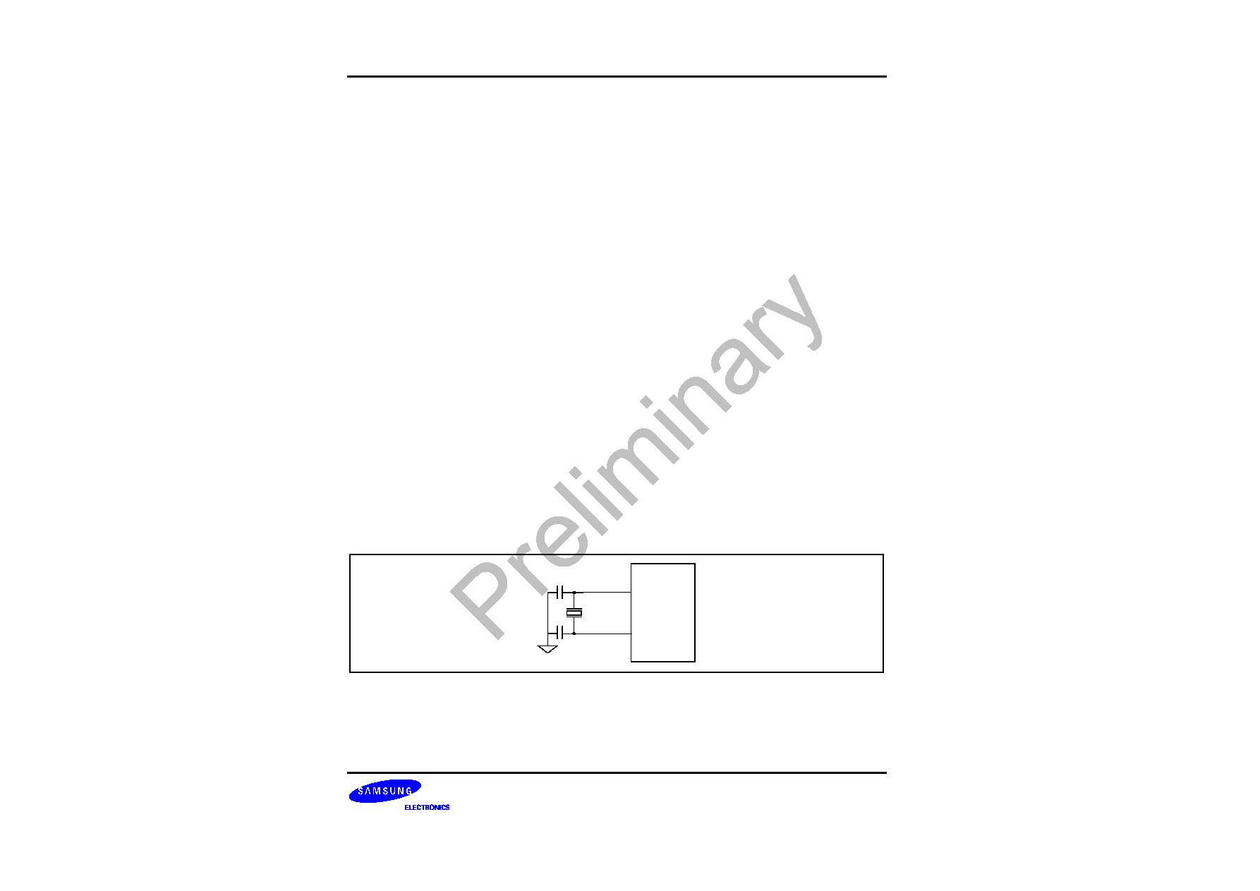
BSW rv0.1-0417-N01
Preliminary product information describes products that are in development,
for which full characterization data and associated errata are not yet available.
Specifications and information herein are subject to change without notice.
S3C24A0 RISC MICROPROCESSOR
REAL TIME CLOCK
10-3
2003-01-15
ALARM FUNCTION
The RTC generates an alarm signal at a specified time in the power down mode or normal operation mode. In
normal operation mode, the alarm interrupt (ALMINT) is activated. In the power down mode the power
management wakeup (PMWKUP) signal is activated as well as the ALMINT. The RTC alarm register, RTCALM,
determines the alarm enable/disable and the condition of the alarm time setting.
TICK TIME INTERRUPT
The RTC tick time is used for interrupt request. The TICNT register has an interrupt enable bit and the count value
for the interrupt. The count value reaches '0' when the tick time interrupt occurs. Then the period of interrupt is as
follow:
Period = ( n+1 ) / 128 second
n : Tick time count value (1~127)
This RTC time tick may be used for RTOS(real time operating system) kernel time tick. If time tick is generated by
RTC time tick, the time related function of RTOS will always synchronized with real time.
ROUND RESET FUNCTION
The round reset function can be performed by the RTC round reset register, RTCRST. The round boundary (30,
40, or 50 sec) of the second carry generation can be selected, and the second value is rounded to zero in the
round reset. For example, when the current time is 23:37:47 and the round boundary is selected to 40 sec, the
round reset changes the current time to 23:38:00.
NOTE
All RTC registers have to be accessed by the byte unit using the STRB,LDRB instructions or char type
pointer.
32.768KHZ X-TAL CONNECTION EXAMPLE
The Figure 10-2 is an example circuit of the RTC unit oscillation at 32.768Khz.
XTIrtc
XTOrtc
32768Hz
15~ 22pF
Figure 10-2. Main Oscillator Circuit Examples

BSW rv0.1-0417-N01
Preliminary product information describes products that are in development,
for which full characterization data and associated errata are not yet available.
Specifications and information herein are subject to change without notice.
REAL TIME CLOCK
S3C24A0 RISC MICROPROCESSOR
10-4
R E A L T IM E C L O C K S P E C IA L R E G IS T E R S
REAL TIME CLOCK CONTROL REGISTER (RTCCON)
The RTCCON register consists of 4 bits such as the RTCEN, which controls the read/write enable of the BCD
registers, CLKSEL, CNTSEL, and CLKRST for testing.
RTCEN bit can control all interfaces between the CPU and the RTC, so it should be set to 1 in an RTC control
routine to enable data read/write after a system reset. Also before power off, the RTCEN bit should be cleared to
0 to prevent inadvertent writing into RTC registers.
Register
Address
R/W
Description
Reset Value
RTCCON
0x44200040
R/W
(by byte)
RTC control Register
0x0
RTCCON
Bit
Description
Initial State
CLKRST
[3]
RTC clock count reset
0 = No reset, 1 = Reset
0
CNTSEL
[2]
BCD count select
0 = Merge BCD counters
1 = Reserved (Separate BCD counters)
0
CLKSEL
[1]
BCD clock select
0 = XTAL 1/215divided clock
1 = Reserved (XTAL clock only for test)
0
RTCEN
[0]
RTC control enable
0 = Disable
NOTE : Only BCD time count and read operation can be performed.
1 = Enable
0
NOTES:
1.
All RTC registers have to be accessed by byte unit using STRB and LDRB instructions or char type pointer.
TICK TIME COUNT REGISTER (TICNT)
Register
Address
R/W
Description
Reset Value
TICNT
0x44200044
R/W
(by byte)
Tick time count Register
0x0
TICNT
Bit
Description
Initial State
TICK INT ENABLE
[7]
Tick time interrupt enable
0 = Disable 1 = Enable
0
TICK TIME COUNT
[6:0]
Tick time count value. (1~127)
This counter value decreases internally, and users can not
read this real counter value in working.
000000

BSW rv0.1-0417-N01
Preliminary product information describes products that are in development,
for which full characterization data and associated errata are not yet available.
Specifications and information herein are subject to change without notice.
S3C24A0 RISC MICROPROCESSOR
REAL TIME CLOCK
10-5
2003-01-15
RTC ALARM CONTROL REGISTER (RTCALM)
RTCALM register determines the alarm enable and the alarm time. Note that the RTCALM register generates the
alarm signal through both ALMINT and PMWKUP in power down mode, but only through ALMINT in the normal
operation mode.
Register
Address
R/W
Description
Reset Value
RTCALM
0x44200050
R/W
(by byte)
RTC alarm control Register
0x0
RTCALM
Bit
Description
Initial State
Reserved
[7]
Reserved
0
ALMEN
[6]
Alarm global enable
0 = Disable, 1 = Enable
0
YEAREN
[5]
Year alarm enable
0 = Disable, 1 = Enable
0
MONREN
[4]
Month alarm enable
0 = Disable, 1 = Enable
0
DATEEN
[3]
Date alarm enable
0 = Disable, 1 = Enable
0
HOUREN
[2]
Hour alarm enable
0 = Disable, 1 = Enable
0
MINEN
[1]
Minute alarm enable
0 = Disable, 1 = Enable
0
SECEN
[0]
Second alarm enable
0 = Disable, 1 = Enable
0

BSW rv0.1-0417-N01
Preliminary product information describes products that are in development,
for which full characterization data and associated errata are not yet available.
Specifications and information herein are subject to change without notice.
REAL TIME CLOCK
S3C24A0 RISC MICROPROCESSOR
10-6
ALARM SECOND DATA REGISTER (ALMSEC)
Register
Address
R/W
Description
Reset Value
ALMSEC
0x44200054
R/W
(by byte)
Alarm second data Register
0x0
ALMSEC
Bit
Description
Initial State
Reserved
[7]
Reserved
0
SECDATA
[6:4]
BCD value for alarm second
from 0 to 5
000
[3:0]
from 0 to 9
0000
ALARM MIN DATA REGISTER (ALMMIN)
Register
Address
R/W
Description
Reset Value
ALMMIN
0x44200058
R/W
(by byte)
Alarm minute data Register
0x00
ALMMIN
Bit
Description
Initial State
Reserved
[7]
Reserved
0
MINDATA
[6:4]
BCD value for alarm minute
from 0 to 5
000
[3:0]
from 0 to 9
0000
ALARM HOUR DATA REGISTER (ALMHOUR)
Register
Address
R/W
Description
Reset Value
ALMHOUR
0x4420005C
R/W
(by byte)
Alarm hour data Register
0x0
ALMHOUR
Bit
Description
Initial State
Reserved
[7:6]
Reserved
00
HOURDATA
[5:4]
BCD value for alarm hour
from 0 to 2
00
[3:0]
from 0 to 9
0000

BSW rv0.1-0417-N01
Preliminary product information describes products that are in development,
for which full characterization data and associated errata are not yet available.
Specifications and information herein are subject to change without notice.
S3C24A0 RISC MICROPROCESSOR
REAL TIME CLOCK
10-7
2003-01-15
ALARM DATE DATA REGISTER (ALMDATE)
Register
Address
R/W
Description
Reset Value
ALMDATE
0x44200060
R/W
(by byte)
Alarm date data Register
0x01
ALMDATE
Bit
Description
Initial State
Reserved
[7:6]
Reserved
00
DATEDATA
[5:4]
BCD value for alarm date, from 0 to 28, 29, 30, 31
from 0 to 3
00
[3:0]
from 0 to 9
0001
ALARM MON DATA REGISTER (ALMMON)
Register
Address
R/W
Description
Reset Value
ALMMON
0x44200064
R/W
(by byte)
Alarm month data Register
0x01
ALMMON
Bit
Description
Initial State
Reserved
[7:5]
Reserved
00
MONDATA
[4]
BCD value for alarm month
from 0 to 1
0
[3:0]
from 0 to 9
0001
ALARM YEAR DATA REGISTER (ALMYEAR)
Register
Address
R/W
Description
Reset Value
ALMYEAR
0x44200068
R/W
(by byte)
Alarm year data Register
0x0
ALMYEAR
Bit
Description
Initial State
YEARDATA
[7:0]
BCD value for year
from 00 to 99
0x0

BSW rv0.1-0417-N01
Preliminary product information describes products that are in development,
for which full characterization data and associated errata are not yet available.
Specifications and information herein are subject to change without notice.
REAL TIME CLOCK
S3C24A0 RISC MICROPROCESSOR
10-8
RTC ROUND RESET REGISTER (RTCRST)
Register
Address
R/W
Description
Reset Value
RTCRST
0x4420006C
R/W
(by byte)
RTC round reset Register
0x0
RTCRST
Bit
Description
Initial State
SRSTEN
[3]
Round second reset enable
0 = Disable, 1 = Enable
0
SECCR
[2:0]
Round boundary for second carry generation.
011 = over than 30 sec
100 = over than 40 sec
101 = over than 50 sec
NOTE : If other values(0,1,2,6,7) are set, no second carry is
generated. But second value can be reset.
000
BCD SECOND REGISTER (BCDSEC)
Register
Address
R/W
Description
Reset Value
BCDSEC
0x44200070
R/W
(by byte)
BCD second Register
Undefined
BCDSEC
Bit
Description
Initial State
SECDATA
[6:4]
BCD value for second
from 0 to 5
-
[3:0]
from 0 to 9
-
BCD MINUTE REGISTER (BCDMIN)
Register
Address
R/W
Description
Reset Value
BCDMIN
0x44200074
R/W
(by byte)
BCD minute Register
Undefined
BCDMIN
Bit
Description
Initial State
MINDATA
[6:4]
BCD value for minute
from 0 to 5
-
[3:0]
from 0 to 9
-

BSW rv0.1-0417-N01
Preliminary product information describes products that are in development,
for which full characterization data and associated errata are not yet available.
Specifications and information herein are subject to change without notice.
S3C24A0 RISC MICROPROCESSOR
REAL TIME CLOCK
10-9
2003-01-15
BCD HOUR REGISTER (BCDHOUR)
Register
Address
R/W
Description
Reset Value
BCDHOUR
0x44200078
R/W
(by byte)
BCD hour Register
Undefined
BCDHOUR
Bit
Description
Initial State
Reserved
[7:6]
Reserved
-
HOURDATA
[5:4]
BCD value for hour
from 0 to 2
-
[3:0]
from 0 to 9
-
BCD DATE REGISTER (BCDDATE)
Register
Address
R/W
Description
Reset Value
BCDDATE
0x4420007C
R/W
(by byte)
BCD date Register
Undefined
BCDDATE
Bit
Description
Initial State
Reserved
[7:6]
Reserved
-
DATEDATA
[5:4]
BCD value for date
from 0 to 3
-
[3:0]
from 0 to 9
-
BCD DAY REGISTER (BCDDAY)
Register
Address
R/W
Description
Reset Value
BCDDAY
0x44200080
R/W
(by byte)
BCD day Register
Undefined
BCDDAY
Bit
Description
Initial State
Reserved
[7:3]
Reserved
-
DAYDATA
[2:0]
BCD value for day
from 1 to 7
-

BSW rv0.1-0417-N01
Preliminary product information describes products that are in development,
for which full characterization data and associated errata are not yet available.
Specifications and information herein are subject to change without notice.
REAL TIME CLOCK
S3C24A0 RISC MICROPROCESSOR
10-10
BCD MONTH REGISTER (BCDMON)
Register
Address
R/W
Description
Reset Value
BCDMON
0x44200084
R/W
(by byte)
BCD month Register
Undefined
BCDMON
Bit
Description
Initial State
Reserved
[7:5]
Reserved
-
MONDATA
[4]
BCD value for month
from 0 to 1
-
[3:0]
from 0 to 9
-
BCD YEAR REGISTER (BCDYEAR)
Register
Address
R/W
Description
Reset Value
BCDYEAR
0x44200088
R/W
(by byte)
BCD year Register
Undefined
BCDYEAR
Bit
Description
Initial State
YEARDATA
[7:0]
BCD value for year
from 00 to 99
-

BSW rv0.1-0417-N01
Preliminary product information describes products that are in development,
for which full characterization data and associated errata are not yet available.
Specifications and information herein are subject to change without notice.
S3C24A0 RISC MICROPROCESSOR
UART
11-1
UART(Preliminary)
OVERVIEW
The S3C24A0 UART (Universal Asynchronous Receiver and Transmitter) unit provides two independent
asynchronous serial I/O (SIO) ports, each of which can operate in interrupt-based or DMA-based mode. In other
words, UART can generate an interrupt or DMA request to transfer data between CPU and UART. It can support
bit rates of up to 115.2K bps, when UART use system clock. If external device provides UART with UCLK, then
UART can operates at more higher speed. Each UART channel contains two 64-byte FIFOs for receiver and
transmitter.
The S3C24A0 UART includes programmable baud-rates, infrared (IR) transmit/receive, one or two stop bit
insertion, 5-bit, 6-bit, 7-bit or 8-bit data width and parity checking.
Each UART contains a baud-rate generator, transmitter, receiver and control unit, as shown in Figure11-1. The
baud-rate generator can be clocked by PCLK. The transmitter and the receiver contain 64-byte FIFOs and data
shifters. Data, which is to be transmitted, is written to FIFO and then copied to the transmit shifter. It is then
shifted out by the transmit data pin (TxDn). The received data is shifted from the receive data pin (RxDn), and
then copied to FIFO from the shifter.
FEATURES
-- RxD0, TxD0, RxD1, TxD1 with DMA-based or interrupt-based operation
-- UART Ch 0, 1 with IrDA 1.0 & 64-byte FIFO
-- UART Ch 0, 1 with nRTS0, nCTS0, nRTS1, nCTS1
-- Supports handshake transmit / receive

BSW rv0.1-0417-N01
Preliminary product information describes products that are in development,
for which full characterization data and associated errata are not yet available.
Specifications and information herein are subject to change without notice.
UART
S3C24A0 RISC MICROPROCESSOR
11-2
BLOCK DIAGRAM
Buad-rate
Generator
Control
Unit
Transmitter
Receiver
Peripheral BUS
TXDn
Clock Source
RXDn
Transmit FIFO Register
(FIFO mode)
Transmit Holding Register
(Non-FIFO mode)
Receive FIFO Register
(FIFO mode)
Receive Holding Register
(Non-FIFO mode only)
In FIFO mode, all 64 Byte of Buffer register are used as FIFO register.
In non-FIFO mode, only 1 Byte of Buffer register is used as Holding register.
Transmit Shifter
Transmit Buffer
Register(64 Byte)
Receive Shifter
Receive Buffer
Register(64 Byte)
Figure 11-1. UART Block Diagram (with FIFO)

BSW rv0.1-0417-N01
Preliminary product information describes products that are in development,
for which full characterization data and associated errata are not yet available.
Specifications and information herein are subject to change without notice.
S3C24A0 RISC MICROPROCESSOR
UART
11-3
UART OPERATION
The following sections describe the UART operations that include data transmission, data reception, interrupt
generation, baud-rate generation, loopback mode, infrared mode, and auto flow control.
Data Transmission
The data frame for transmission is programmable. It consists of a start bit, 5 to 8 data bits, an optional parity bit
and 1 to 2 stop bits, which can be specified by the line control register (ULCONn). The transmitter can also
produce the break condition. The break condition forces the serial output to logic 0 state for one frame
transmission time. This block transmits break signal after the present transmission word transmits perfectly. After
the break signal transmission, it continously transmits data into the Tx FIFO (Tx holding register in the case of
Non-FIFO mode).
Data Reception
Like the transmission, the data frame for reception is also programmable. It consists of a start bit, 5 to 8 data bits,
an optional parity bit and 1 to 2 stop bits in the line control register (ULCONn).
The receiver can detect overrun
error. The overrun error indicates that new data has overwritten the old data before the old data has been read.
Receive time-out condition occurs when it does not receive data during the 3 word time (This interval follows the
setting of Word Length bit) and the Rx FIFO is not empty in the FIFO mode.
Auto Flow Control(AFC)
S3C24A0's UART 0 and UART 1 support auto flow control with nRTS and nCTS signals, in case, it would have to
connect UART to UART. If users connect UART to a Modem, disable auto flow control bit in UMCONn register
and control the signal of nRTS by software.
In AFC, nRTS is controlled by condition of the receiver and operation of transmitter is controlled by the nCTS
signal. The UART's transmitter transfers the data in FIFO only when nCTS signal active (In AFC, nCTS means
that the other UART's FIFO is ready to receive data). Before the UART receives data, nRTS has to be activated
when its receive FIFO has a spare more than
32-byte
and has to be inactivated when its receive FIFO has a
spare under
32-byte
(In AFC, nRTS means that its own receive FIFO is ready to receive data).
RxD
nRTS
UART A
TxD
nCTS
UART B
TxD
nCTS
UART A
RxD
nRTS
UART B
Transmission case in
UART A
Reception case in
UART A
Figure 11-2. UART AFC interface

BSW rv0.1-0417-N01
Preliminary product information describes products that are in development,
for which full characterization data and associated errata are not yet available.
Specifications and information herein are subject to change without notice.
UART
S3C24A0 RISC MICROPROCESSOR
11-4
Non Auto-Flow control (Controlling nRTS and nCTS by S/W) Example
Rx operation with FIFO
1. Select receive mode(Interrupt or DMA mode)
2. Check the value of Rx FIFO count in UFSTATn register. If the value is less than
32
, users have to set the
value of UMCONn[0] to '1'(activate nRTS), and if it is equal or larger than
32,
users have to set the value to
'0'(inactivate nRTS).
3. Repeat step 2.
Tx operation with FIFO
1. Select transmit mode (Interrupt or DMA mode)
2. Check the value of UMSTATn[0]. If the value is '1'(nCTS is activated), users write the data to Tx FIFO register.

BSW rv0.1-0417-N01
Preliminary product information describes products that are in development,
for which full characterization data and associated errata are not yet available.
Specifications and information herein are subject to change without notice.
S3C24A0 RISC MICROPROCESSOR
UART
11-5
RS-232C interface
If users connect to modem interface (not equal null modem), nRTS, nCTS, nDSR, nDTR, DCD and nRI signals
are need. In this case, users control these signals with general I/O ports by S/W because the AFC does not
support the RS-232C interface.
Interrupt/DMA Request Generation
Each UART of S3C24A0 has
four
status (Tx/Rx/Error) signals:
Overrun error, Receive buffer data ready,
Transmit
buffer empty, and Transmit shifter empty, all of which are indicated by the corresponding UART status register
(UTRSTATn/UERSTATn).
The overrun error can cause the receive error status interrupt request, if the receive-error-status-interrupt-enable
bit is set to one in the control register, UCONn.
When the receiver transfers the data of the receive shifter to the receive FIFO register in FIFO mode and the
number of received data reaches Rx FIFO Trigger Level, Rx interrupt is generated, if Receive mode in control
register(UCONn) is selected as 1(Interrupt request or polling mode).
In the Non-FIFO mode, transfering the data of the receive shifter to the receive holding register will cause Rx
interrupt under the Interrupt request and polling mode.
When the transmitter transfers data from its transmit FIFO register to its transmit shifter and the number of data
left in transmit FIFO reaches Tx FIFO Trigger Level, Tx interrupt is generated, if Transmit mode in control register
is selected as Interrupt request or polling mode.
In the Non-FIFO mode, transfering data from the transmit holding register to the transmit shifter will cause Tx
interrupt under the Interrupt request and polling mode.
If the Receive mode and Transmit mode in control register are selected as the DMAn request mode then DMAn
request is occurred instead of Rx or Tx interrupt in the situation mentioned above.
Table 11-1. Interrupts in Connection with FIFO
Type
FIFO Mode
Non-FIFO Mode
Rx interrupt
Each time receive data reaches the trigger level of
receive FIFO, the Rx interrupt will be generated.
When the number of data in FIFO does not
reaches Rx FIFO trigger Level and does not
receive data during 3 word time(This interval
follows the setting of Word Length bit), the Rx
interrupt will be generated(receive time out).
Each time receive data becomes full, the
receive holding register generates an
interrupt.
Tx interrupt
Each time transmit data reaches the trigger level of
transmit FIFO(Tx FIFO trigger Level), the Tx
interrupt will be generated.
Each time transmit data become empty,
the transmit holding register generates
an interrupt.
Error interrupt
Overrun error will be generated, when it gets to the
top of the receive FIFO without reading out data in
it.
Overrun error generates an error
interrupt immediately.

BSW rv0.1-0417-N01
Preliminary product information describes products that are in development,
for which full characterization data and associated errata are not yet available.
Specifications and information herein are subject to change without notice.
UART
S3C24A0 RISC MICROPROCESSOR
11-6
UART Error Status FIFO
UART has the error status FIFO besides the Rx FIFO register. The error status FIFO indicates which data, among
FIFO registers, is received with an error. The error interrupt will be issued only when the data, which has an error,
is ready to read out. To clear the error status FIFO, the URXHn with an error and UERSTATn must be read out.
For example,
It is assumed that the UART Rx FIFO receives A, B, C, D,and E characters sequentially and the frame error
occurs while receiving 'B', and the parity error occurs while receiving 'D'.
The actual UART receive error will not generate any error interrupt because the character, which was received
with an error, has not been read yet. The error interrupt will occur when the character is read out.
Figure 11-3 shows the UART receiving the five characters including the two errors.
Time
Sequence Flow
Error Interrupt
Note
#0
When no character is read out
-
#1
A, B, C, D, and E is received
-
#2
After A is read out
The frame error (in B) interrupt occurs.
The 'B' has to be read out.
#3
After B is read out
-
#4
After C is read out
The parity error (in D) interrupt occurs.
The 'D' has to be read out.
#5
After D is read out
-
#6
After E is read out
-
-
-
-
-
-
-
-
-
-
-
-
'E'
'D'
'C'
'B'
'A'
Rx FIFO
URXHn
UERSTATn
break error parity error frame error
Error Status Generator Unit
Error Status FIFO
Figure 11-3. Example showing UART Receiving 5 Characters with 2 Errors

BSW rv0.1-0417-N01
Preliminary product information describes products that are in development,
for which full characterization data and associated errata are not yet available.
Specifications and information herein are subject to change without notice.
S3C24A0 RISC MICROPROCESSOR
UART
11-7
Baud-Rate Generation
Each UART's baud-rate generator provides the serial clock for transmitter and receiver. The source clock for the
baud-rate generator can be selected with the S3C24A0's internal system clock or UCLK. In other words, dividend
can be selected by the setting of Clock Selection of UCONn. The baud-rate clock is generated by dividing the
source clock(PCLK or UCLK) by 16 and a 16-bit divisor specified in the UART baud-rate divisor register
(UBRDIVn). The UBRDIVn can be determined as follows:
UBRDIVn =
(int)(PCLK/(bps x 16) ) -1
where the UBRDIVn should be from 1 to (2
16
-1).
For the accurate UART operation, S3C24A0 also supports UARTCLK as a dividend.
If UARTCLK, supplied by external UART device or system, is used, then serial clock of UART is exactly
synchronized with UARTCLK. So, user can get the more precision UART operation. The UBRDIVn can be
determined as follows:
UBRDIVn
= (int)( UARTCLK / (bps x 16) ) �1
where the UBRDIVn should be from 1 to (2
16
-1) and UARTCLK should be smaller than PCLK.
For example, if the baud-rate is 115200 bps and PCLK or UARTCLK is 40 MHz , UBRDIVn is:
UBRDIVn = (int)(40000000/(115200 x 16) ) -1
= (int)(21.7) -1
= 22 -1 = 21
Baud-Rate Error Tolerance
UART Frame error should be less than 1.87%(3/160).
tUPCLK = (UBRDIVn + 1) x 16 x 10 / PCLK tUPCLK : Real UART clock time
tUEXACT = 10 / baud-rate tUEXACT : Ideal UART clock time
UART error = (tUPCLK � tUEXACT) / tUEXACT x 100%
NOTE.
1. 1Frame = 1start bit + 8 data bit + 1 stop bit.
2. In specific condition, we can support bit rates up to 921.6K bps. For example, when PCLK is 60MHz, you can
use bit rates of 921.6K bps under UART error of 1.69%.
Loop-back Mode
The S3C24A0 UART provides a test mode referred to as the loopback mode, to aid in isolating faults in the
communication link. In this mode, the transmitted data is immediately received. This feature allows the processor
to verify the internal transmit and to receive the data path of each SIO channel. This mode can be selected by
setting the loopback-bit in the UART control register (UCONn).
Break Condition
The break is defined as a continuous low level signal for one frame transmission time on the transmit data output.

BSW rv0.1-0417-N01
Preliminary product information describes products that are in development,
for which full characterization data and associated errata are not yet available.
Specifications and information herein are subject to change without notice.
UART
S3C24A0 RISC MICROPROCESSOR
11-8
IR (Infrared) Mode
The S3C24A0 UART block supports infrared (IR) transmission and reception, which can be selected by setting
the infrared-mode bit in the UART line control register (ULCONn). The implementation of the mode is shown in
Figure 11-3.
In IR transmit mode, the transmit period is pulsed at a rate of 3/16, the normal serial transmit rate (when the
transmit data bit is zero); In IR receive mode, the receiver must detect the 3/16 pulsed period to recognize a zero
value (refer to the frame timing diagrams shown in Figure 11-5 and 11-6 ).
IrDA Tx
Encoder
0
1
0
1
IrDA Rx
Decoder
TxD
RxD
TxD
IRS
RxD
RE
UART
Block
Figure 11-3. IrDA Function Block Diagram
BSW rv0.1-0417-N01
Preliminary product information describes products that are in development,
for which full characterization data and associated errata are not yet available.
Specifications and information herein are subject to change without notice.
S3C24A0 RISC MICROPROCESSOR
UART
11-9
Start
Bit
Stop
Bit
Data Bits
SIO Frame
0
1
0
1
0
0
1
1
0
1
Figure 11-4. Serial I/O Frame Timing Diagram (Normal UART)
0
Start
Bit
Stop
Bit
Data Bits
IR Transmit Frame
Bit
Time
Pulse Width = 3/16 Bit Frame
0
0
0
0
1
1
1
1
1
Figure 11-5. Infrared Transmit Mode Frame Timing Diagram
0
Start
Bit
Stop
Bit
Data Bits
IR Receive Frame
0
0
0
0
1
1
1
1
1
Figure 11-6. Infrared Receive Mode Frame Timing Diagram

BSW rv0.1-0417-N01
Preliminary product information describes products that are in development,
for which full characterization data and associated errata are not yet available.
Specifications and information herein are subject to change without notice.
UART
S3C24A0 RISC MICROPROCESSOR
11-10
UART SPECIAL REGISTERS
UART LINE CONTROL REGISTER
There are two UART line control registers, ULCON0 and ULCON1 in the UART block.
Register
Address
R/W
Description
Reset Value
ULCON0
0x44400000
R/W
UART channel 0 line control register
0x00
ULCON1
0x44404000
R/W
UART channel 1 line control register
0x00
ULCONn
Bit
Description
Initial State
Reserved
[7]
0
Infrared Mode
[6]
The Infrared mode determines whether or not to use the
Infrared mode.
0 = Normal mode operation
1 = Infrared Tx/Rx mode
0
Parity Mode
[5:3]
The parity mode specifies how parity generation and checking
are to be performed during UART transmit and receive
operation.
0xx = No parity
100 = Odd parity
101 = Even parity
110 = Parity forced/checked as 1
111 = Parity forced/checked as 0
000
Number of stop bit
[2]
The number of stop bits specifies how many stop bits are to
be used to signal end-of-frame.
0 = One stop bit per frame
1 = Two stop bit per frame
0
Word length
[1:0]
The word length indicates the number of data bits to be
transmitted or received per frame.
00 = 5-bits 01 = 6-bits
10 = 7-bits 11 = 8-bits
00

BSW rv0.1-0417-N01
Preliminary product information describes products that are in development,
for which full characterization data and associated errata are not yet available.
Specifications and information herein are subject to change without notice.
S3C24A0 RISC MICROPROCESSOR
UART
11-11
UART CONTROL REGISTER
There are two UART control registers, UCON0 and UCON1 in the UART block.
Register
Address
R/W
Description
Reset Value
UCON0
0x44400004
R/W
UART channel 0 control register
0x00
UCON1
0x44404004
R/W
UART channel 1 control register
0x00
UCONn
Bit
Description
Initial State
Clock selection
[10] Select PCLK or UARTCLK for the UART baud rate.
0=PCLK : UBRDIVn = (int)(PCLK / (bps x 16) ) -1
1= UARTCLK : UBRDIVn = (int)( UARTCLK / (bps x 16) ) -1
0
Tx interrupt type
[9]
Interrupt request type
0 = Pulse (Interrupt is requested as soon as the Tx buffer becomes
empty in Non-FIFO mode or reaches Tx FIFO Trigger Level in FIFO
mode)
1 = Level (Interrupt is requested while Tx buffer is empty in Non-FIFO
mode or reaches Tx FIFO Trigger Level in FIFO mode)
0
Rx interrupt type
[8]
Interrupt request type
0 = Pulse (Interrupt is requested the instant Rx buffer receives the data
in Non-FIFO mode or reaches Rx FIFO Trigger Level in FIFO mode)
1 = Level (Interrupt is requested while Rx buffer is receiving data in
Non-FIFO mode or reaches Rx FIFO Trigger Level in FIFO mode)
0
Rx time out
enable
[7]
Enable/Disable Rx time out interrupt when UART FIFO is enabled. The
interrupt is a receive interrupt.
0 = Disable 1 = Enable
0
Rx error status
interrupt enable
[6]
This bit enables the UART to generate an interrupt if overrun error
occurs during a receive operation.
0 = Do not generate receive error status interrupt
1 = Generate receive error status interrupt
0
Loop-back Mode
[5]
Setting loop-back bit to 1 causes the UART to enter the loop-back
mode. This mode is provided for test purposes only.
0 = Normal operation 1 = Loop-back mode
0
Send Break
Signal
[4]
Setting this bit causes the UART to send a break during 1 frame time.
This bit is auto-cleared after sending the break signal.
0 = Normal transmit 1 = Send break signal
0

BSW rv0.1-0417-N01
Preliminary product information describes products that are in development,
for which full characterization data and associated errata are not yet available.
Specifications and information herein are subject to change without notice.
UART
S3C24A0 RISC MICROPROCESSOR
11-12
UART CONTROL REGISTER (CONTINUED)
Transmit Mode
[3:2] These two bits determine which function is currently able to write Tx
data to the UART transmit buffer register.
00 = Disable
01 = Interrupt request or polling mode
10 = DMA0 or DMA2 request (Only for UART0),
11 = DMA1 or DMA3 request (Only for UART1)
00
Receive Mode
[1:0] These two bits determine which function is currently able to read data
from UART receive buffer register.
00 = Disable
01 = Interrupt request or polling mode
10 = DMA0 or DMA2 request (Only for UART0),
11 = DMA1 or DMA3 request (Only for UART1)
00
Note : When the UART does not reach the FIFO trigger level and does not receive data during 3 word time in DMA receive
mode with FIFO, the Rx interrupt will be generated (receive time out), and the users should check the FIFO status and read out
the rest.

BSW rv0.1-0417-N01
Preliminary product information describes products that are in development,
for which full characterization data and associated errata are not yet available.
Specifications and information herein are subject to change without notice.
S3C24A0 RISC MICROPROCESSOR
UART
11-13
UART FIFO CONTROL REGISTER
There are two UART FIFO control registers, UFCON0 and UFCON1 in the UART block.
Register
Address
R/W
Description
Reset Value
UFCON0
0x44400008
R/W
UART channel 0 FIFO control register
0x0
UFCON1
0x44404008
R/W
UART channel 1 FIFO control register
0x0
UFCONn
Bit
Description
Initial State
Tx FIFO Trigger Level
[7:6]
These two bits determine the trigger level of transmit FIFO.
00 = Empty 01 = 16-byte
10 = 32-byte 11 = 48-byte
00
Rx FIFO Trigger Level
[5:4]
These two bits determine the trigger level of receive FIFO.
00 = 1-byte 01 = 8-byte
10 = 16-byte 11 = 32-byte
00
Reserved
[3]
0
Tx FIFO Reset
[2]
This bit is auto-cleared after resetting FIFO
0 = Normal 1= Tx FIFO reset
0
Rx FIFO Reset
[1]
This bit is auto-cleared after resetting FIFO
0 = Normal 1= Rx FIFO reset
0
FIFO Enable
[0]
0 = FIFO disable 1 = FIFO mode
0
Note : When the UART does not reach the FIFO trigger level and does not receive data during 3 word time in DMA receive
mode with FIFO, the Rx interrupt will be generated(receive time out), and the users should check the FIFO status and read out
the rest.

BSW rv0.1-0417-N01
Preliminary product information describes products that are in development,
for which full characterization data and associated errata are not yet available.
Specifications and information herein are subject to change without notice.
UART
S3C24A0 RISC MICROPROCESSOR
11-14
UART MODEM CONTROL REGISTER
There are two UART MODEM control registers, UMCON0 and UMCON1, in the UART block.
Register
Address
R/W
Description
Reset Value
UMCON0
0x4440000C
R/W
UART channel 0 Modem control register
0x0
UMCON1
0x4440400C
R/W
UART channel 1 Modem control register
0x0
UMCONn
Bit
Description
Initial State
Reserved
[7:5]
These bits must be 0's
00
AFC(Auto Flow Control)
[4]
0 = Disable 1 = Enable
0
Reserved
[3:1]
These bits must be 0's
00
Request to Send
[0]
If AFC bit is enabled, this value will be ignored. In this case
the S3C24A0 will control nRTS automatically.
If AFC bit is disabled, nRTS must be controlled by S/W.
0 = 'H' level(Inactivate nRTS) 1 = 'L' level(Activate nRTS)
0

BSW rv0.1-0417-N01
Preliminary product information describes products that are in development,
for which full characterization data and associated errata are not yet available.
Specifications and information herein are subject to change without notice.
S3C24A0 RISC MICROPROCESSOR
UART
11-15
UART TX/RX STATUS REGISTER
There are two UART Tx/Rx status registers, UTRSTAT0 and UTRSTAT1 in the UART block.
Register
Address
R/W
Description
Reset Value
UTRSTAT0
0x44400010
R
UART channel 0 Tx/Rx status register
0x6
UTRSTAT1
0x44404010
R
UART channel 1 Tx/Rx status register
0x6
UTRSTATn
Bit
Description
Initial State
Transmitter empty
[2]
This bit is automatically set to 1 when the transmit buffer
register has no valid data to transmit and the transmit shift
register is empty.
0 = Not empty
1 = Transmitter(transmit buffer & shifter register) empty
1
Transmit buffer empty
[1]
This bit is automatically set to 1 when transmit buffer register
is empty.
0 =The buffer register is not empty
1 = Empty
(In Non-FIFO mode, Interrupt or DMA is requested.
In FIFO mode, Interrupt or DMA is requested, when Tx
FIFO Trigger Level is set to 00(Empty))
If the UART uses the FIFO, users should check Tx FIFO
Count bits and Tx FIFO Full bit in the UFSTAT register
instead of this bit.
1
Receive buffer data ready
[0]
This bit is automatically set to 1 whenever receive buffer
register contains valid data, received over the RXDn port.
0 = Empty
1 = The buffer register has a received data
(In Non-FIFO mode, Interrupt or DMA is requested)
If the UART uses the FIFO, users should check Rx FIFO
Count bits and Rx FIFO Full bit in the UFSTAT register
instead of this bit.
0

BSW rv0.1-0417-N01
Preliminary product information describes products that are in development,
for which full characterization data and associated errata are not yet available.
Specifications and information herein are subject to change without notice.
UART
S3C24A0 RISC MICROPROCESSOR
11-16
UART ERROR STATUS REGISTER
There are two UART Rx error status registers, UERSTAT0 and UERSTAT1 in the UART block.
Register
Address
R/W
Description
Reset Value
UERSTAT0
0x44400014
R
UART channel 0 Rx error status register
0x0
UERSTAT1
0x44404014
R
UART channel 1 Rx error status register
0x0
UERSTATn
Bit
Description
Initial State
Overrun Error
[0]
This bit is automatically set to 1 whenever an overrun error
occurs during receive operation.
0 = No overrun error during receive
1 = Overrun error(Interrupt is requested)
0
NOTE : This bit is automatically cleared to 0 when the UART error status register is read.

BSW rv0.1-0417-N01
Preliminary product information describes products that are in development,
for which full characterization data and associated errata are not yet available.
Specifications and information herein are subject to change without notice.
S3C24A0 RISC MICROPROCESSOR
UART
11-17
UART FIFO STATUS REGISTER
There are two UART FIFO status registers, UFSTAT0 and UFSTAT1 in the UART block.
Register
Address
R/W
Description
Reset Value
UFSTAT0
0x44400018
R
UART channel 0 FIFO status register
0x0000
UFSTAT1
0x44404018
R
UART channel 1 FIFO status register
0x0000
UFSTATn
Bit
Description
Initial State
Reserved
[15]
0
Tx FIFO Full
[14]
This bit is automatically set to 1 whenever transmit FIFO is
full during transmit operation
0 = 0-byte
Tx FIFO data
63-byte
1 = Full
0
Tx FIFO Count
[13:8]
Number of data in Tx FIFO
0
Reserved
[7]
0
Rx FIFO Full
[6]
This bit is automatically set to 1 whenever receive FIFO is
full during receive operation
0 = 0-byte
Rx FIFO data
63-byte
1 = Full
0
Rx FIFO Count
[5:0]
Number of data in Rx FIFO
0

BSW rv0.1-0417-N01
Preliminary product information describes products that are in development,
for which full characterization data and associated errata are not yet available.
Specifications and information herein are subject to change without notice.
UART
S3C24A0 RISC MICROPROCESSOR
11-18
UART MODEM STATUS REGISTER
There are two UART modem status registers, UMSTAT0 and UMSTAT1 in the UART block.
Register
Address
R/W
Description
Reset Value
UMSTAT0
0x4440001C
R
UART channel 0 Modem status register
0x00
UMSTAT1
0x4440401C
R
UART channel 1 Modem status register
0x00
UMSTAT0
Bit
Description
Initial State
Reserved
[7:5]
0
DCTS
[4]
Delta CTS
This bit indicates that the nCTS input to S3C24A0 has
changed state since the last time it was read by CPU.
(Refer to Figure 11-7)
0 = Has not changed
1 = Has changed
0
Reserved
[3:1]
0
Clear to Send
[0]
0 = CTS signal is not activated(nCTS pin is high)
1 = CTS signal is activated(nCTS pin is low)
0
nCTS
DCTS
Read_UMSTAT
Figure 11-7. nCTS and Delta CTS Timing Diagram

BSW rv0.1-0417-N01
Preliminary product information describes products that are in development,
for which full characterization data and associated errata are not yet available.
Specifications and information herein are subject to change without notice.
S3C24A0 RISC MICROPROCESSOR
UART
11-19
UART TRANSMIT BUFFER REGISTER(HOLDING REGISTER & FIFO REGISTER)
There are two UART transmit buffer registers, UTXH0 and UTXH1 in the UART block.
UTXHn has an 8-bit data for transmission data.
Register
Address
R/W
Description
Reset Value
UTXH0
0x44400020
W
(by byte)
UART channel 0 transmit buffer register
-
UTXH1
0x44404020
W
(by byte)
UART channel 1 transmit buffer register
-
UTXHn
Bit
Description
Initial State
TXDATAn
[7:0]
Transmit data for UARTn
-
UART RECEIVE BUFFER REGISTER (HOLDING REGISTER & FIFO REGISTER)
There are two UART receive buffer registers, URXH0 and URXH1 in the UART block.
URXHn has an 8-bit data for received data.
Register
Address
R/W
Description
Reset Value
URXH0
0x44400024
R
(by byte)
UART channel 0 receive buffer register
-
URXH1
0x44404024
R
(by byte)
UART channel 1 receive buffer register
-
URXHn
Bit
Description
Initial State
RXDATAn
[7:0]
Receive data for UARTn
-
NOTE:
When an overrun error occurs, the URXHn must be read. If not, the next received data will also make an
overrun error, even though the overrun bit of UERSTATn had been cleared.

BSW rv0.1-0417-N01
Preliminary product information describes products that are in development,
for which full characterization data and associated errata are not yet available.
Specifications and information herein are subject to change without notice.
UART
S3C24A0 RISC MICROPROCESSOR
11-20
UART BAUD RATE DIVISOR REGISTER
There are two UART baud rate divisor registers, UBRDIV0 and UBRDIV1 in the UART block.
The value stored in the baud rate divisor register (UBRDIVn), is used to determine the serial Tx/Rx clock rate
(baud rate) as follows:
UBRDIVn
= (int)(PCLK / (bps x 16) ) �1
or
UBRDIVn
= (int)( UARTCLK / (bps x 16) ) �1
where the UBRDIVn should be from 1 to (2
16
-1) and UARTCLK should be smaller than PCLK.
For example, if the baud-rate is 115200 bps and PCLK or UARTCLK is 40 MHz , UBRDIVn is:
UBRDIVn
= (int)(40000000 / (115200 x 16) ) -1
= (int)(21.7) -1
= 22 -1 = 21
Register
Address
R/W
Description
Reset Value
UBRDIV0
0x44400028
R/W
Baud rate divisior register 0
-
UBRDIV1
0x44404028
R/W
Baud rate divisior register 1
-
UBRDIV n
Bit
Description
Initial State
UBRDIV
[15:0]
Baud rate division value
UBRDIVn >0(if UARTCLK is used, UBRDIVn>=0)
-

BSW rv0.1-0417-N01
Preliminary product information describes products that are in development,
for which full characterization data and associated errata are not yet available.
Specifications and information herein are subject to change without notice.
S3C24A0 RISC MICROPROCESSOR
IRDA CONTROLLER
12-1
IRDA CONTROLLER(Preliminary)
OVERVIEW
The Samsung IrDA Core is a wireless serial communication controller. Supporting two different types of IrDA
speed(MIR, FIR), this core can transmit Ir(Infrared) pulses up to 4 Mbps speed. To lessen the CPU burden, it
has configurable FIFO feature. This makes it easy to adjust the internal FIFO sizes.
A user can program the core by accessing 16 internal registers. When receiving the Ir pulses, this core detects
three kinds of line errors such as CRC-error, PHY-error and payload length error.
FEATURE
1. IrDA specification compliant
- support IrDA 1.1 physical layer specification (4Mbps, 1.152Mpbs and 0.576Mbps)
2. Supports FIFO operation in the MIR and FIR mode
3. Configurable FIFO size (16-byte or 64-byte)
4. Supports Back-to-Back Transactions
5. Supports software in selecting Temic-IBM or HP transceiver

BSW rv0.1-0417-N01
Preliminary product information describes products that are in development,
for which full characterization data and associated errata are not yet available.
Specifications and information herein are subject to change without notice.
IRDA CONTROLLER
S3C24A0 RISC MICROPROCESSOR
12-2
BLOCK DIAGRAM
CLK_GEN
MASTER_Control
LSR
ACREG
MDR
FCR
Iinterrupt Control
and payload length
store
IER
ICR
RXFLH RXFLL
TXFLH TXFLL
TX FIFO Control
THR
PLR
RX FIFO Control
RBR
PLL
FIR Mod/Demodl
MIR Mod/Demodl
MUX
M
MCLK(48MHz)
INTERRUPT, DMA
IRRX
IRTX
HRESETn
TX FIFO
RAM
RX FIFO
RAM
IRSDBW
MOD
DEMOD
MOD
DEMOD
AHB BUS
Figure 12-1. Block Diagram
EXTERNAL INTERFACE SIGNALS
IrDA_Tx
: IrDA Tx signal (output)
IrDA_Rx
: IrDA Rx signal (input)
IrDA_SDBW
: IrDA Transceiver control (Shutdown, Bandwidth) (output)

BSW rv0.1-0417-N01
Preliminary product information describes products that are in development,
for which full characterization data and associated errata are not yet available.
Specifications and information herein are subject to change without notice.
S3C24A0 RISC MICROPROCESSOR
IRDA CONTROLLER
12-3
FUNCTION DESCRIPTION
Fast-Speed Infrared (
FIR
) Mode (IrDA 1.1)
In this FIR mode, data communicates at the baud rate speed of 4 Mbps. In the data transmission mode, the core encodes
the payload data into the 4PPM format and attaches the Preamble, Start Flag, CRC-32, and Stop flag on the encoded
payload and shifts them out serially. In data receive mode, the core works in reverse direction. First, when Ir pulse is
detected, the core recovers receiver clock from the incoming data and removes the Preamble and Start Flag, then it
extracts the payload from the received 4PPM data until it meets the Stop Flag. The core detects three different kinds of
errors which may occur in the middle of transmission. These are the Phy-Error, the Frame-Length Error and the CRC error.
The last one, CRC error is checked when the entire payload data is received. The micro-controller can monitor the error
status of the received frame by reading the Line Status Register(LSR) at the end of the frame receiving.
The below diagram shows the frame structure of the fir data frame. (The specific information of the each field can be found
in IrDA specification.)
Preamble
Start flag
Link layer frame(Payload)
CRC32
Stop flag
Preamble : 1000, 0000, 1010, 1000
Start Flag : 0000, 1100, 0000, 1100, 0110, 0000, 0110,0000
Stop Flag : 0000,1100, 0000, 1100, 0000, 0110, 0000, 0110
By programming the internal registers, the number of preambles can be selected from 4 to 32.
* Note : 4 PPM Coding
Data Bit Pair(DBP)
4PPM Data Symbol(DD)
00
1000
01
0100
10
0010
11
0001

BSW rv0.1-0417-N01
Preliminary product information describes products that are in development,
for which full characterization data and associated errata are not yet available.
Specifications and information herein are subject to change without notice.
IRDA CONTROLLER
S3C24A0 RISC MICROPROCESSOR
12-4
TX
Enable
Preamble
Transmit
Start
Flag
Transmit
Pay Load
Transmit
& CRC
CRC
Transmit
Stop
Flag
Transmit
~ena
ena
pre_end
str_end
pay_end
crc_end
stp_end & ena
apeend
Frame data
with error
crc
abort by
underrun
~abort
2u
Pulse
transmit
sip
pul_end & ena
0
1
2
3
4
5
6
7
stp_end & ~ena
pul_end & ~ena
Figure 12-2. Fir modulation process
Figure 12-2 shows the FIR modulation state machine. The FIR transmission mode can be selected by
programming ACR register. If an underrun condition occurs, the state machine appends the payload with
error crc data and terminate the transmission.

BSW rv0.1-0417-N01
Preliminary product information describes products that are in development,
for which full characterization data and associated errata are not yet available.
Specifications and information herein are subject to change without notice.
S3C24A0 RISC MICROPROCESSOR
IRDA CONTROLLER
12-5
Rx
Enable
Preamble
& start flag
Detect
Pay Load
Detect
& 4ppm decod
CRC
Decoding
for syndrom
ena & prebyte
pay_end = last_byte
stp_start
0
1
3
4
5
stp_end & ena
stp_end & ~ena
str_end
~(ena & prebyte)
Pay Load
Detect &
CRC check
2
phy_err
crc_decod_start
Stop
Flag
Detect
Figure 12-3. Fir demodulation process
Figure 12-3 shows FIR demodulation state machine. The state machine starts when ACR register bit 6 is
set to logic high. The incoming data will be depacketized by removing preamble and start flag and stop
flag .
Also, 4PPM decoding and CRC decoding is carried out.

BSW rv0.1-0417-N01
Preliminary product information describes products that are in development,
for which full characterization data and associated errata are not yet available.
Specifications and information herein are subject to change without notice.
IRDA CONTROLLER
S3C24A0 RISC MICROPROCESSOR
12-6
Medium-Speed Infrared (
MIR
) Mode (IrDA 1.1)
In MIR mode, data communicates at the speed of 1.152Mbps, and 0.576Mbps(half mode). The payload
data is wrapped around by Start Flags, CRC-16, and Stop Flags. The Start Flag should be at least two
bytes. Both in transmitting and receiving process, the basic wrapping and de-wrapping processes are
same as the FIR mode, but, the MIR mode needs the bit-stuffing procedure. Bit stuffing in MIR mode have
the core insert zero bit per every 5 consecutive ones in transmission mode. In receiving mode, the stuffed
bit should be removed. Like the fir mode case, three different kind of errors (crc, phy and frame length
error ) can be reported to the microcontroller in receiving mode by reading the LSR register.
The diagram below shows the data structure of MIR frame.
STA
STA
Link layer frame (Payload)
CRC16
STO
STA
: Beginning flag, 01111110 binary
CRC16 : CCITT 16 bit CRC
STO
: Ending flag, 01111110 binary
The MIR pulse is modulated by 1/4 pulse format. The below diagram shows how the pulse is generated.
1.152M
MIR Pulse
NRZ Data
Figure 12-4. Pulse modulation in MIR mode

BSW rv0.1-0417-N01
Preliminary product information describes products that are in development,
for which full characterization data and associated errata are not yet available.
Specifications and information herein are subject to change without notice.
S3C24A0 RISC MICROPROCESSOR
IRDA CONTROLLER
12-7
TX
Enable
ACREG[7]
1st Start
Flag
Transmit
Pay Load
Transmit
with stuff bit
CRC
Transmit
with stuff bit
Stop
Flag
Transmit
~ena
ena
pay_end
crc_end
stp_end & ena
append
Frame data
with error
crc & eflag
abort by
underrun
~abort
2u
Pulse
transmit
sip
pul_end & ena
0
stp_end & ~ena
pul_end & ~ena
1
2
3
4
5
6
str_end
Figure 12-5. Mir modulation process.
Figure 12-5 shows MIR modulation state machine. This machine works very similarly with FIR modulation
state machine. The major difference is that the MIR data transmission needs bit stuffing. After the every 5
consecutive ones, a zero data should be stuffed in MIR payload data. The state machine for this bit-stuffing
is not presented here.

BSW rv0.1-0417-N01
Preliminary product information describes products that are in development,
for which full characterization data and associated errata are not yet available.
Specifications and information herein are subject to change without notice.
IRDA CONTROLLER
S3C24A0 RISC MICROPROCESSOR
12-8
Rx
Enable
Str Flag
Detect
Pay Load
Detect
& De-Stuff
ena & flagbyte
0
1
3
str_end
~(ena&flagbyte)
CRC check
& Stp Det
2
pay_end
stp_end
Figure 12-6 mir demodulation process
Figure 12-6 shows the MIR demodulation state machine. Basically, it has similar structure with FIR
demodulation state machine. But, instead having 4 PPM demodulation phase, it has the stage of removing
stuffed bits from payload data stream. Since the MIR data stream doesn't have preamble data, the
preamble/start flag data detection stage in MIR demodulation is simplified to start flag detection state.

BSW rv0.1-0417-N01
Preliminary product information describes products that are in development,
for which full characterization data and associated errata are not yet available.
Specifications and information herein are subject to change without notice.
S3C24A0 RISC MICROPROCESSOR
IRDA CONTROLLER
12-9
CORE INITIALIZATION PROCEDURE
MIR/FIR Mode Initialization Operation
1)
Program the MDR register to select the MIR/FIR mode.
2)
Program the ACR register to select the transceiver type.
- For the Temic-IBM type transceiver, program twice in ACR[0] = 1'b0 and ACR[0] = 1'b1.
- For the HP type transceiver, program just once in ACR[0] = 1'b0 to FIR/MIR mode.
3)
Program the PLR register to select the number of preamble or start flag, and TX threshold level.
4)
Program the RXFLL and RXFLH register (maximum available receive bytes in frame).
5)
Program the TXFLL and TXFLH register (transmit bytes in transmission frame).
6)
Program the FCR register (FIFO size and RX threshold level).
7)
Program the IER register ( the types of interrupt).
8)
Program the ACR register (TX enable or RX enable).
9)
Program the ICR register (interrupt enable).
10)
Service Interrupt signal from the core.
Yes
START
Setup INT
Service Parameters
INT
Active ?
Initialize Core
Enable INT
ISR
No
Figure 12-8 General Program Flowchart

BSW rv0.1-0417-N01
Preliminary product information describes products that are in development,
for which full characterization data and associated errata are not yet available.
Specifications and information herein are subject to change without notice.
IRDA CONTROLLER
S3C24A0 RISC MICROPROCESSOR
12-10
SPECIAL FUNCTION REGISTERS
IrDA CONTROL REGISTER(IrDA_CNT)
Register
Address
R/W
Description
Reset Value
IrDA _CNT 0x41800000
R/W
IrDA Control Register
0x00
IrDA _CNT
Bit
Description
Initial State
TX enable
[7]
TX enable. Bit 7 must be set to `1' to enable data
transmission in MIR/FIR Ir modes.
0
RX enable
[6]
RX enable. Bit 6 must be set to `1' to enable data receive
in all MIR/FIR Ir modes.
0
Core loop
[5]
Core loop for software debugging. The IRRX port
connects directly to the IRTX internally.
0
MIR half mode
[4]
MIR half mode. When bit 4 is set to a `1', the operating
speed in the MIR mode changes from 1.152 Mbps to
0.576 Mbps.
0
Send IR pulse
[3]
Send 1.6-us IR pulse. When the IrDA_MDR[3] bit equals
to a `1' and the CPU writes a `1' to this bit, the transmitting
interface device sends a 1.6-us IR pulse at the end of the
frame. Bit 3 is cleared automatically by the transmitting
interface device at the end of 1.6-us IR pulse data
transmission.
0
Reserved
[2]
Reserved
0
Frame abort
[1]
Frame abort. The CPU can intentionally abort data
transmission of a frame by writing a `1' to bit 1. Neither the
end flag nor the CRC bits are appended to the frame. The
receiver will find the frame with the abort pattern in the
MIR mode and a PHY-error in the FIR mode. The CPU
must reset the TX FIFO and reset this bit by writing a `0' to
bit `1' before next frame can be transmitted.
0
SD/BW
[0]
This signal controls IrDA_SDBW output signal.
It is used for controlling mode (shutdown, band width) of
IrDA transceiver.
0

BSW rv0.1-0417-N01
Preliminary product information describes products that are in development,
for which full characterization data and associated errata are not yet available.
Specifications and information herein are subject to change without notice.
S3C24A0 RISC MICROPROCESSOR
IRDA CONTROLLER
12-11
IrDA MODE DEFINITION REGISTER(IrDA_MDR)
Register
Address
R/W
Description
Reset Value
IrDA_MDR 0x41800004
R/W
IrDA Mode Definition Register
0x00
IrDA _MDR
Bit
Description
Initial State
Reserved
[7:5]
Reserved
0
SIP Select
[4]
SIP select method. If this bit is set to `1' and the
IrDA_CNT[3] is set to `1', the SIP pulse is appended at the
end of FIR/MIR TX frame. Likewise, when this bit is set to
a `0', SIP is generated at the end of the every FIR/MIR
frames. If IrDA_CNT[3] is set to `0', setting this bit to `1'
doesn't help to generate SIP. Along with IrDA_CNT[3] bit,
the way of SIP generation can be controlled.
0
Temic select
[3]
Bit 3 is Temic transceiver select bit. When bit 3 is clear to
"0", core automatically selects in Temic transceiver mode.
0
Mode select
[2:0]
Bit 2, bit 1 and bit 0 select the mode of operation as
100 : FIR Mode
010 : MIR Mode
0
IrDA INTERRUPT / DMA CONFIGURATION REGISTER(IrDA_CNF)
Register
Address
R/W
Description
Reset Value
IrDA_CNF 0x41800008
R/W
IrDA Interrupt / DMA Configuration Register
0x00
IrDA _CNF
Bit
Description
Initial State
Reserved
[7:4]
Reserved
-
DMA Enable
[3]
1 : DMA Enable
0
DMA Mode
[2]
0 : Tx DMA
1 : Rx DMA
0
Reserved
[1]
Reserved
-
Interrupt Enable
[0]
The bit 0 enables Interrupt output signal.
0

BSW rv0.1-0417-N01
Preliminary product information describes products that are in development,
for which full characterization data and associated errata are not yet available.
Specifications and information herein are subject to change without notice.
IRDA CONTROLLER
S3C24A0 RISC MICROPROCESSOR
12-12
IrDA INTERUPT ENALBLE REGISTER(IrDA_IER)
Register
Address
R/W
Description
Reset Value
IrDA _IER 0x4180000C
R/W
IrDA Interrupt Enable Register
0x00
IrDA_IER
Bit
Description
Initial State
Last byte to Rx FIFO
[7]
Enables state indication interrupt when Last byte write to
RX FIFO.
0
Error indication
[6]
Enables error status indication interrupt in data receiving
mode.
0
Tx Underrun
[5]
Enables transmitter under-run interrupt.
0
Last byte detect
[4]
Detect stop-flag interrupt enable. If this bit is set to "1", an
interrupt signal will be activated when the last byte of the
received data frame comes into the demodulation block
and the CRC decoding is finished.
0
Rx overrun
[3]
Enables receiver over-run interrupt.
0
Last byte read from
Rx FIFO
[2]
Bit 2 enables last byte from RX FIFO interrupt which is
generated when the microcontroller reads the last byte of
the frame from the RX FIFO.
0
Tx FIFO below
threshold
[1]
Bit 1 enables an TX FIFO below threshold level interrupt
when the available empty space in TX FIFO is over the
threshold level.
0
Rx FIFO over
threshold
[0]
Bit 0 enables received data in RX FIFO over threshold
level interrupt when the RX FIFO is equal to or above the
threshold level.
0

BSW rv0.1-0417-N01
Preliminary product information describes products that are in development,
for which full characterization data and associated errata are not yet available.
Specifications and information herein are subject to change without notice.
S3C24A0 RISC MICROPROCESSOR
IRDA CONTROLLER
12-13
IrDA INTERUPT IDENTIFICATION REGISTER(IrDA_IIR)
Register
Address
R/W
Description
Reset Value
IrDA _IIR
0x41800010
R
IrDA Interrupt Identification Register
0x00
IrDA _IIR
Bit
Description
Initial State
Last byte to Rx FIFO
[7]
Last byte write to RX FIFO interrupt pending. When the
last payload byte of the frame is loaded into the RX FIFO,
bit 7 is set to `1'. Bit 7 is set prior to bit 2. Bit 7 is cleared
when it is read.
0
Error indication
[6]
Receiver line error Indication. Bit 6 is set to a `1' if one of
three possible errors occurs in the RX process. With the
corresponding interrupt enable bit active, one of PHY,
CRC and Frame length errors let this bit go active. Bit 6 is
cleared when the source of the error is cleared.
0
Tx Underrun
[5]
Transmit under-run interrupt pending. When
corresponding interrupt enable bit is active, bit 5 is set to
`1' if an under-run occurs in TX FIFO. Bit 5 is cleared by
serving the under-run.
0
Last byte detect
[4]
Detects last byte of a frame interrupt pending. If the
corresponding interrupt enable bit is active, bit 4 is set to
`1' when the demodulation block detects the last byte of a
received frame and the CRC decoding is finished. Bit 4 is
cleared when it is read.
0
Rx overrun
[3]
RX FIFO over-run interrupt. When corresponding interrupt
enable bit is set, bit3 is active, bit 3 is set to `1' when an
overrun occurs in the RX FIFO. Bit 3 is cleared by serving
the over-run.
0
Last byte read from
Rx FIFO
[2]
RX FIFO last byte read interrupt. When corresponding
interrupt enable bit is active, it is set to `1' when the CPU
reads the last byte of a frame from the RX FIFO. It is
cleared when it is read.
0
Tx FIFO below
threshold
[1]
TX FIFO below threshold interrupt pending. Bit 1 is set to
`1' when the transmitter FIFO level is below its threshold
level.
0
Rx FIFO over
threshold
[0]
RX FIFO over threshold interrupt pending. Bit 0 is set to `1'
when the receiver FIFO level is equal to or above its
threshold level.
0

BSW rv0.1-0417-N01
Preliminary product information describes products that are in development,
for which full characterization data and associated errata are not yet available.
Specifications and information herein are subject to change without notice.
IRDA CONTROLLER
S3C24A0 RISC MICROPROCESSOR
12-14
IrDA LINE STATUS REGISTER(IrDA_LSR)
Register
Address
R/W
Description
Reset Value
IrDA _LSR 0x41800014
R
IrDA Line Status Register
0x03
IrDA_LSR
Bit
Description
Initial State
Tx empty
[7]
Transmitter empty. This bit is set to `1' when TX FIFO is
empty and the transmitter front-end is idle.
1
Reserved
[6]
Reserved
0
Received last byte
from Rx FIFO
[5]
Last byte received from RX FIFO. It is set to a `1' when the
microcontroller reads the last byte of a frame from the RX
FIFO and cleared when the MCU reads the IrDA_LSR
register.
0
Frame length error
[4]
Frame length error. It is set to `1' when a frame exceeding
the maximum frame length predefined by IrDA_RXFLL
and IrDA_RXFLH register is received. This bit is cleared
when the microcontroller reads the IrDA_LSR register.
When this error is detected, current frame reception is
terminated. Data receiving is stopped until the next BOF is
detected. Bit 4 is cleared to `0' when the IrDA_LSR
register is read by the microcontroller.
0
PHY error
[3]
PHY error. In FIR mode, It is set to a `1' when an illegal
4PPM symbol is received. In IrDA_MIR mode, if an abort
pattern(more than 7 consecutive `1's) is received during
reception, this bit is set to `1'. It is cleared when
microcontroller reads the LSR register.
0
CRC error
[2]
CRC error. Bit 2 is set to `1' when a bad IrDA_CRC is
detected on data receive. It is cleared to `0' when
microcontroller reads the LSR register.
0
Reserved
[1]
Reserved
1
Rx FIFO empty
[0]
RX FIFO empty. It indicates that the RX FIFO is empty.
When the state of RX FIFO turns into empty, it is set to `1'.
When the RX FIFO is not empty, it is set to `0'.
1
BSW rv0.1-0417-N01
Preliminary product information describes products that are in development,
for which full characterization data and associated errata are not yet available.
Specifications and information herein are subject to change without notice.
S3C24A0 RISC MICROPROCESSOR
IRDA CONTROLLER
12-15
IrDA FIFO CONTROL REGISTER(IrDA_FCR)
Register
Address
R/W
Description
Reset Value
IrDA _FCR 0x41800018
R/W
IrDA FIFO Control Register
0x00
IrDA _FCR
Bit
Description
Initial State
Rx FIFO Trigger level
select
[7:6]
Receiver FIFO trigger level selection.
Bit 7
Bit 6
16-byte RX FIFO
64-byte RX FIFO
0
0
01
01
0
1
04
16
1
0
08
32
1
1
14
56
00
FIFO size select
[5]
When set to `1', 64 bytes TX and RX FIFO are selected.
When set to `0', 16 bytes TX and RX FIFO are selected.
0
TX FIFO Clear
Notification
[4]
This bit will be activated when the FIFO clear is over. This
bit is cleared by the CPU reads this register.
0
RX FIFO Clear
Notification
[3]
This bit will be activated when the FIFO clear is over. This
bit is cleared by the CPU reads this register.
0
Tx FIFO reset
[2]
TX FIFO reset. When set to `1', bit 2 clears all bytes in the
transmitter FIFO and reset its counter to `0'. A `1' written to
bit 2 is self-clearing.
0
Rx FIFO reset
[1]
RX FIFO reset. When set to `1', bit 1 clears all bytes in the
receiver FIFO and reset its counter to `0'. A `1' written to
bit 1 is self clearing.
0
FIFO enable
[0]
FIFO enable. When set to `1', bit 0 enables both the
transmitter and receiver FIFOs. Bit 0 must be a `1' when
setting other IrDA_FCR bits. Changing bit 0 clears the
FIFO.
0

BSW rv0.1-0417-N01
Preliminary product information describes products that are in development,
for which full characterization data and associated errata are not yet available.
Specifications and information herein are subject to change without notice.
IRDA CONTROLLER
S3C24A0 RISC MICROPROCESSOR
12-16
IrDA PREAMBLE LENGTH REGISTER(IrDA_PLR)
Register
Address
R/W
Description
Reset Value
IrDA _PLR 0x4180001C
R/W
IrDA Preamble Length Register
0x12
REG_PLR
Bit
Description
Initial State
Preamble length
in FIR mode
[7:6]
These two bits decide preamble length to be transmitted
at the beginning of each frame in FIR mode. The default
value of PLR[7:6] = `00' which is equal to 16 preambles.
00 : 16
01 : 4
01: 8
11: 32
00
TX FIFO trigger level
select
[5:4]
Transceiver FIFO trigger level selection.
Bit 5
Bit 4
16-byte FIFO
64-byte FIFO
0
0
Reserved
0
1
12
48
1
0
08
32
1
1
02
08
Note: Tx Trigger level value means how many data are empty.
01
Number of start flags
in MIR mode
[3:0]
Number of start flags in MIR mode. The number of start
flags to be transmitted at the beginning of a frame is equal
to the IrDA_PLR [3:0] value. The minimum value is
2
.
0010
IrDA RECEIVER & TRANSMITTER BUFFER REGISTER(IrDA_RBR)
Register
Address
R/W
Description
Reset Value
IrDA_RBR 0x41800020
R/W
IrDA Receiver & Transmitter Buffer Register
0x00
IrDA _RBR
Bit
Description
Initial State
Rx/Tx data
[7:0]
Received data (When read data)
Data to transmit (When write data)
0x00
IrDA TOTAL NUMBER OF DATA BYTES REMAINED IN Tx FIFO(IrDA_TxNO)
Register
Address
R/W
Description
Reset Value
IrDA
_TXNO
0x41800024
R
The total number of data bytes remained in Tx FIFO
0x00
IrDA _TxNO
Bit
Description
Initial State

BSW rv0.1-0417-N01
Preliminary product information describes products that are in development,
for which full characterization data and associated errata are not yet available.
Specifications and information herein are subject to change without notice.
S3C24A0 RISC MICROPROCESSOR
IRDA CONTROLLER
12-17
Tx data total number
[7:0]
The total number of data bytes remained in Tx FIFO
0x00
IrDA TOTAL NUMBER OF DATA BYTES REMAINED IN Rx FIFO(IrDA_RxNO)
Register
Address
R/W
Description
Reset Value
IrDA _RxNO
0x41800028
R
The total number of data bytes remained in Rx FIFO
0x00
IrDA _RxNO
Bit
Description
Initial State
Rx data total number
[7:0]
The total number of data bytes remained in Rx FIFO.
00
IrDA TRANSMIT FRAME-LENGTH REGISTER LOW(IrDA_TXFLL)
Register
Address
R/W
Description
Reset Value
IrDA _TXFLL 0x4180002C R/W IrDA Transmit Frame-Length Register Low
0x00
IrDA _TXFLL
Bit
Description
Initial State
Tx frame length low
[7:0]
TXFLL stores the lower 8 bits of the byte number of the
frame to be transmitted
.
00
IrDA TRANSMIT FRAME-LENGTH REGISTER HIGH(IrDA_TXFLH)
Register
Address
R/W
Description
Reset Value
IrDA _TXFLH 0x41800030 R/W IrDA Transmit Frame-Length Register High
0x00
IrDA _TXFLH
Bit
Description
Initial State
Tx frame length high
[7:0]
TXFLH stores the upper 8 bits of the byte number of the
frame to be transmitted.
00
IrDA RECEIVER FRAME-LENGTH REGISTER LOW(IrDA_RXFLL)
Register
Address
R/W
Description
Reset Value
IrDA _RXFLL 0x41800034 R/W IrDA Receive Frame-Length Register Low
0x00
IrDA _RXFLL
Bit
Description
Initial State
Rx frame length low
[7:0]
RXFLL stores the lower 8 bits of the maximum byte
number of the frame to be received.
00

BSW rv0.1-0417-N01
Preliminary product information describes products that are in development,
for which full characterization data and associated errata are not yet available.
Specifications and information herein are subject to change without notice.
IRDA CONTROLLER
S3C24A0 RISC MICROPROCESSOR
12-18
IrDA RECEIVER FRAME-LENGTH REGISTER HIGH(IrDA_RXFLH)
Register
Address
R/W
Description
Reset Value
IrDA _RXFLH 0x41800038 R/W IrDA Receive Frame-Length Register High
0x00
IrDA _RXFLH
Bit
Description
Initial State
Rx frame length high
[5:0]
TXFLL stores the upper 6 bits of the maximum byte
number of the frame to be received.
00

BSW rv0.1-0417-N01
Preliminary product information describes products that are in development,
for which full characterization data and associated errata are not yet available.
Specifications and information herein are subject to change without notice.
S3C24A0 RISC MICROPROCESSOR
IIC-BUS INTERFACE
13-1
IIC-BUS INTERFACE(Preliminary)
OVERVIEW
The S3C24A0 RISC microprocessor can support a multi-master IIC-bus serial interface. A dedicated serial data
line(SDA) and a serial clock line (SCL) carry information between bus masters and peripheral devices which are
connected to the IIC-bus. The SDA and SCL lines are bi-directional.
In multi-master IIC-bus mode, multiple S3C24A0 RISC microprocessors can receive or transmit serial data to or
from slave devices. The master S3C24A0, which can initiate a data transfer over the IIC-bus, is responsible for
terminating the transfer. Standard bus arbitration procedure is used in this IIC-bus in S3C24A0.
To control multi-master IIC-bus operations, values must be written to the following registers:
-- Multi-master IIC-bus control register, IICCON
-- Multi-master IIC-bus control/status register, IICSTAT
-- Multi-master IIC-bus Tx/Rx data shift register, IICDS
-- Multi-master IIC-bus address register, IICADD
-- Multi-master IIC-bus SDAOUT delay register, SDADLY
When the IIC-bus is free, the SDA and SCL lines should be both at High level. A High-to-Low transition of SDA
can initiate a Start condition. A Low-to-High transition of SDA can initiate a Stop condition while SCL remains
steady at High Level.
The Start and Stop conditions can always be generated by the master devices. A 7-bit address value in the first
data byte, which is put onto the bus after the Start condition has been initiated, can determine the
s
lave device
which the bus master device has selected. The 8
th
bit determines the direction of the transfer (read or write).
Every data byte put onto the SDA line should total eight bits. The number of bytes which can be sent or received
during the bus transfer operation is unlimited. Data is always sent from most-significant bit (MSB) first, and every
byte should be immediately followed by an acknowledge (ACK) bit.

BSW rv0.1-0417-N01
Preliminary product information describes products that are in development,
for which full characterization data and associated errata are not yet available.
Specifications and information herein are subject to change without notice.
IIC-BUS INTERFACE
S3C24A0 RISC MICROPROCESSOR
13-2
PCLK
Address Register
SDA
4-bit Prescaler
IIC-Bus Control Logic
IICSTAT
IICCON
Comparator
Shift Register
Shift Register
(IICDS)
Data Bus
SCL
Figure 13-1. IIC-Bus Block Diagram

BSW rv0.1-0417-N01
Preliminary product information describes products that are in development,
for which full characterization data and associated errata are not yet available.
Specifications and information herein are subject to change without notice.
S3C24A0 RISC MICROPROCESSOR
IIC-BUS INTERFACE
13-3
THE IIC-BUS INTERFACE
The S3C24A0 IIC-bus interface has four operation modes:
-- Master transmitter mode
-- Master receive mode
-- Slave transmitter mode
-- Slave receive mode
Functional relationships among these operating modes are described below.
START AND STOP CONDITIONS
When the IIC-bus interface is inactive, it is usually in slave mode. In other words, the interface should be in slave
mode before detecting a Start condition on the SDA line.(A Start condition can be initiated with a High-to-Low
transition of the SDA line while the clock signal of SCL is High) When the interface state is changed to the master
mode, a data transfer on the SDA line can be initiated and SCL signal generated.
A Start condition can transfer a one-byte serial data over the SDA line, and a stop condition can terminate the
data transfer. A stop condition is a Low-to-High transition of the SDA line while SCL is High. Start and Stop
conditions are always generated by the master. The IIC-bus is busy when a Start condition is generated. A few
clocks after a Stop condition, the IIC-bus will be free, again.
When a master initiates a Start condition, it should send a slave address to notify the slave device. The one byte
of address field consist of a 7-bit address and a 1-bit transfer direction indicator (that is, write or read).
If bit 8 is 0, it indicates a write operation(transmit operation); if bit 8 is 1, it indicates a request for data
read(receive operation).
The master will finish the transfer operation by transmitting a Stop condition. If the master wants to continue the
data transmission to the bus, it should generate another Start condition as well as a slave address. In this way,
the read-write operation can be performed in various formats.
SCL
SDA
SDA
SCL
Start
Condition
Stop
Condition
Figure 13-2. Start and Stop Condition

BSW rv0.1-0417-N01
Preliminary product information describes products that are in development,
for which full characterization data and associated errata are not yet available.
Specifications and information herein are subject to change without notice.
IIC-BUS INTERFACE
S3C24A0 RISC MICROPROCESSOR
13-4
DATA TRANSFER FORMAT
Every byte placed on the SDA line should be eight bits in length. The number of bytes which can be transmitted
per transfer is unlimited. The first byte following a Start condition should have the address field. The address field
can be transmitted by the master when the IIC-bus is operating in master mode. Each byte should be followed by
an acknowledgement (ACK) bit. The MSB bit of the serial data and addresses are always sent first.
NOTES:
1.
S: Start, rS: Repeat Start, P: Stop, A: Acknowledge
2. : From Master to Slave, : from Slave to Master
Write Mode Format with 7-bit Addresses
"0"
(Write)
Data Transferred
(Data + Acknowledge)
S Slave Address 7bits R/W A
P
DATA(1Byte)
A
Read Mode Format with 7-bit Addresses
"1"
(Read)
Data Transferred
(Data + Acknowledge)
S Slave Address 7 bits R/W A
P
DATA
A
Write Mode Format with 10-bit Addresses
"0"
(Write)
Data Transferred
(Data + Acknowledge)
P
DATA
A
S
Slave Address
1st 7 bits
R/W A
Slave Address
2nd Byte
A
11110XX
Read Mode Format with 10-bit Addresses
"1"
(Read)
S
Slave Address
1st 7 bits
11110XX
R/W A
Slave Address
2nd Byte
A rS
Slave Address
1st 7 Bits
A
Data Transferred
(Data + Acknowledge)
P
DATA
A
R/W
"1"
(Read)
Figure 13-3. IIC-Bus Interface Data Format

BSW rv0.1-0417-N01
Preliminary product information describes products that are in development,
for which full characterization data and associated errata are not yet available.
Specifications and information herein are subject to change without notice.
S3C24A0 RISC MICROPROCESSOR
IIC-BUS INTERFACE
13-5
SDA
Acknowledgement
Signal from Receiver
SCL
S
1
2
7
8
9
1
2
9
Acknowledgement
Signal from Receiver
MSB
ACK
Byte Complete, Interrupt
within Receiver
Clock Line Held Low While
Interrupts are Serviced
Figure 13-4. Data Transfer on the IIC-Bus
ACK SIGNAL TRANSMISSION
To finish a one-byte transfer operation completely, the receiver should send an ACK bit to the transmitter. The
ACK pulse should occur at the ninth clock of the SCL line. Eight clocks are required for the one-byte data transfer.
The master should generate the clock pulse required to transmit the ACK bit.
The transmitter should release the SDA line by making the SDA line High when the ACK clock pulse is received.
The receiver should also drive the SDA line Low during the ACK clock pulse so that the SDA is Low during the
High period of the ninth SCL pulse.
The ACK bit transmit function can be enabled or disabled by software (IICSTAT). However, the ACK pulse on the
ninth clock of SCL is required to complete a one-byte data transfer operation.
Data Output by
Transmitter
Data Output by
Receiver
SCL from
Master
Start
Condition
Clock Pulse for Acknowledgment
Clock to Output
9
8
7
S
1
2
Figure 13-5. Acknowledge on the IIC-Bus

BSW rv0.1-0417-N01
Preliminary product information describes products that are in development,
for which full characterization data and associated errata are not yet available.
Specifications and information herein are subject to change without notice.
IIC-BUS INTERFACE
S3C24A0 RISC MICROPROCESSOR
13-6
READ-WRITE OPERATION
In the transmitter mode, after the data is transferred, the IIC-bus interface will wait until IICDS(IIC-bus Data Shift
Register) is written by a new data. Until the new data is written, the SCL line will be held low. After the new data is
written to IICDS register, the SCL line will be released. The S3C24A0 should hold the interrupt to identify the
completion of current data transfer. After the CPU receives the interrupt request, it should write a new data into
IICDS, again.
In the receive mode, after a data is received, the IIC-bus interface will wait until IICDS register is read. Until the
new data is read out, the SCL line will be held low. After the new data is read out from IICDS register, the SCL
line will be released. The S3C24A0 should hold the interrupt to identify the completion of the new data reception.
After the CPU receives the interrupt request, it should read the data from IICDS.
BUS ARBITRATION PROCEDURES
Arbitration takes place on the SDA line to prevent the contention on the bus between two masters. If a master with
a SDA High level detects another master with a SDA active Low level, it will not initiate a data transfer because
the current level on the bus does not correspond to its own. The arbitration procedure will be extended until the
SDA line turns High.
However when the masters simultaneously lower the SDA line, each master should evaluate whether or not the
mastership is allocated to itself. For the purpose of evaluation, each master should detect the address bits. While
each master generates the slaver address, it should also detect the address bit on the SDA line because the
lowering of SDA line is stronger than maintaining High on the line. For example, one master generates a Low as
first address bit, while the other master is maintaining High. In this case, both masters will detect Low on the bus
because Low is stronger than High even if first master is trying to maintain High on the line. When this happens,
Low(as the first bit of address) -generating master will get the mastership and High(as the first bit of address) -
generating master should withdraw the mastership. If both masters generate Low as the first bit of address, there
should be an arbitration for second address bit, again. This arbitration will continue to the end of last address bit.
ABORT CONDITIONS
If a slave receiver can not acknowledge the confirmation of the slave address, it should hold the level of the SDA
line High. In this case, the master should generate a Stop condition and to abort the transfer.
If a master receiver is involved in the aborted transfer, it should signal the end of the slave transmit operation by
canceling the generation of an ACK after the last data byte received from the slave. The slave transmitter should
then release the SDA to allow a master to generate a Stop condition.
CONFIGURING THE IIC-BUS
To control the frequency of the serial clock (SCL), the 4-bit prescaler value can be programmed in the IICCON
register. The IIC-bus interface address is stored in the IIC-bus address register, IICADD. (By default, the IIC-bus
interface address is an unknown value.)

BSW rv0.1-0417-N01
Preliminary product information describes products that are in development,
for which full characterization data and associated errata are not yet available.
Specifications and information herein are subject to change without notice.
S3C24A0 RISC MICROPROCESSOR
IIC-BUS INTERFACE
13-7
FLOWCHARTS OF THE OPERATIONS IN EACH MODE
The following steps must be executed before any IIC Tx/Rx operations.
1) Write own slave address on IICADD register if needed.
2) Set IICCON Register.
a) Enable interrupt
b) Define SCL period
3) Set IICSTAT to enable Serial Output
Write slave address to
IICDS
Write 0xF0(M/T Start) to
IICSTAT
The data of the IICDS is
transmitted
ACK period and then
interrupt is pending
Write 0xD0(M/T Stop) to
IICSTAT
Write new data
transmitted to IICDS
Stop?
Clear pending bit to
resume
The data of the IICDS is
shifted to SDA
START
Master Tx mode has
been configured.
Clear pending bit
Wait until the stop
condition takes effect.
END
Y
N
Figure 13-6 Operations for Master / Transmitter Mode

BSW rv0.1-0417-N01
Preliminary product information describes products that are in development,
for which full characterization data and associated errata are not yet available.
Specifications and information herein are subject to change without notice.
IIC-BUS INTERFACE
S3C24A0 RISC MICROPROCESSOR
13-8
Write slave address to
IICDS
Write 0xB0(M/R Start) to
IICSTAT
The data of the IICDS(slave
address) is transmitted
ACK period and then
interrupt is pending
Write 0x90(M/R Stop) to
IICSTAT
Read a new data from
IICDS
Stop?
Clear pending bit to
resume
SDA is shifted to IICDS
START
Master Rx mode has
been configured.
Clear pending bit
Wait until the stop
condition takes effect.
END
Y
N
Figure 13-7 Operations for Master / Receiver Mode
BSW rv0.1-0417-N01
Preliminary product information describes products that are in development,
for which full characterization data and associated errata are not yet available.
Specifications and information herein are subject to change without notice.
S3C24A0 RISC MICROPROCESSOR
IIC-BUS INTERFACE
13-9
IIC detects start signal. and, IICDS
receives data.
IIC compares IICADD and IICDS(the
received slave address)
Write data to IICDS
The IIC address match
interrupt is generated
Clear pending bit to
resume.
The data of the IICDS is
shifted to SDA
START
Slave Tx mode has
been configured.
END
Matched?
N
Y
Stop?
Interrupt is pending
N
Y
Figure 13-8 Operations for Slave / Transmitter Mode

BSW rv0.1-0417-N01
Preliminary product information describes products that are in development,
for which full characterization data and associated errata are not yet available.
Specifications and information herein are subject to change without notice.
IIC-BUS INTERFACE
S3C24A0 RISC MICROPROCESSOR
13-10
IIC detects start signal. and, IICDS
receives data.
IIC compares IICADD and IICDS(the
received slave address)
Read data from IICDS
The IIC address match
interrupt is generated
Clear pending bit to
resume.
SDA is shifted to IICDS
START
Slave Rx mode has
been configured.
END
Matched?
N
Y
Stop?
Interrupt is pending
N
Y
Figure 13-9 Operations for Slave / Receiver Mode

BSW rv0.1-0417-N01
Preliminary product information describes products that are in development,
for which full characterization data and associated errata are not yet available.
Specifications and information herein are subject to change without notice.
S3C24A0 RISC MICROPROCESSOR
IIC-BUS INTERFACE
13-11
IIC-BUS INTERFACE SPECIAL REGISTERS
MULTI-MASTER IIC-BUS CONTROL REGISTER (IICCON)
Register
Address
R/W
Description
Reset Value
IICCON
0x44600000
R/W
IIC-Bus control register
0x0X
IICCON
Bit
Description
Initial State
Acknowledge generation
(1)
[7]
IIC-bus acknowledge enable bit
0 = Disable
1 = Enable
In Tx mode, the IICSDA is free in the ack time.
In Rx mode, the IICSDA is L in the ack time.
0
Tx clock source selection
[6]
Source clock of IIC-bus transmit clock prescaler
selection bit
0 = IICCLK = f
PCLK
/16
1 = IICCLK = f
PCLK
/512
0
Tx/Rx Interrupt
(5)
[5]
IIC-Bus Tx/Rx interrupt enable/disable bit
0 = Disable, 1 = Enable
0
Interrupt pending flag
(2) (3)
[4]
IIC-bus Tx/Rx interrupt pending flag. Writing 1 is
impossible. When this bit is read as 1, the IICSCL
is tied to L and the IIC is stopped. To resume the
operation, clear this bit as 0.
0 = 1) No interrupt pending(when read),
2) Clear pending condition &
Resume the operation (when write).
1 = 1) Interrupt is pending (when read)
2) N/A (when write)
0
Transmit clock value
(4)
[3:0]
IIC-Bus transmit clock prescaler
IIC-Bus transmit clock frequency is determined
by this 4-bit prescaler value, according to the
following formula:
Tx clock = IICCLK/(IICCON[3:0]+1)
Undefined
NOTES:
1. Interfacing with EEPROM, the ack generation may be disabled before reading the last data in order to generate the
STOP condition in Rx mode.
2.
A IIC-bus interrupt occurs 1)when a 1-byte transmit or receive operation is completed, 2)when a general call or a slave
address match occurs, or 3) if bus arbitration fails.
3. To time the setup time of IICSDA before IISSCL rising edge, IICDS has to be written before clearing the IIC interrupt
pending bit.
4.
IICCLK is determined by IICCON[6].
Tx clock can vary by SCL transition time.
When IICCON[6]=0, IICCON[3:0]=0x0 or 0x1 is not available.
5.
If the IICON[5]=0, IICON[4] does not operate correctly.
So, It is recommended to set IICCON[4]=1, although you does not use the IIC interrupt.

BSW rv0.1-0417-N01
Preliminary product information describes products that are in development,
for which full characterization data and associated errata are not yet available.
Specifications and information herein are subject to change without notice.
IIC-BUS INTERFACE
S3C24A0 RISC MICROPROCESSOR
13-12
MULTI-MASTER IIC-BUS CONTROL/STATUS REGISTER (IICSTAT)
Register
Address
R/W
Description
Reset Value
IICSTAT
0x44600004
R/W
IIC-Bus control/status register
0x0
IICSTAT
Bit
Description
Initial State
Mode selection
[7:6]
IIC-bus master/slave Tx/Rx mode select bits:
00: Slave receive mode
01: Slave transmit mode
10: Master receive mode
11: Master transmit mode
00
Busy signal status /
START STOP condition
[5]
IIC-Bus busy signal status bit:
0 = read) Not busy
write) STOP signal generate(only for master)
1 = read) Busy
write) START signal generate(only for master)
The data in IICDS will be transferred
automatically just after the start signal.
0
Serial output
[4]
IIC-bus data output enable/disable bit:
0 = Disable Rx/Tx
1 = Enable Rx/Tx
0
Arbitration status flag
[3]
IIC-bus arbitration procedure status flag bit:
0 = Bus arbitration successful
1 = Bus arbitration failed during serial I/O
0
Address-as-slave status
flag
[2]
IIC-bus address-as-slave status flag bit:
0 = Cleared when START/STOP condition was
detected
1 = Received slave address matches the address
value in the IICADD.
0
Address zero status flag
[1]
IIC-bus address zero status flag bit:
0 = Cleared when START/STOP condition was
detected.
1 = Received slave address is 00000000b
0
Last-received bit status
flag
[0]
IIC-bus last-received bit status flag bit
0 = Last-received bit is 0 (ACK was received)
1 = Last-received bit is 1 (ACK was not received)
0

BSW rv0.1-0417-N01
Preliminary product information describes products that are in development,
for which full characterization data and associated errata are not yet available.
Specifications and information herein are subject to change without notice.
S3C24A0 RISC MICROPROCESSOR
IIC-BUS INTERFACE
13-13
MULTI-MASTER IIC-BUS ADDRESS REGISTER (IICADD)
Register
Address
R/W
Description
Reset Value
IICADD
0x44600008
R/W
IIC-Bus address register
0xXX
IICADD
Bit
Description
Initial State
Slave address
[7:0]
7-bit slave address, latched from the IIC-bus :
When serial output enable = 0 in the IICSTAT, IICADD is
write-enabled. The IICADD value can be read any time,
regardless of the current serial output enable bit (IICSTAT)
setting.
Slave address = [7:1]
Not mapped = [0]
XXXXXXXX
MULTI-MASTER IIC-BUS TRANSMIT/RECEIVE DATA SHIFT REGISTER (IICDS)
Register
Address
R/W
Description
Reset Value
IICDS
0x4460000C
R/W
IIC-Bus transmit/receive data shift register
0xXX
IICDS
Bit
Description
Initial State
Data shift
[7:0]
8-bit data shift register for IIC-bus Tx/Rx operation :
When serial output enable = 1 in the IICSTAT, IICDS is
write-enabled. The IICDS value can be read any time,
regardless of the current serial output enable bit (IICSTAT)
setting
XXXXXXXX
MULTI-MASTER IIC-BUS SDAOUT DELAY REGISTER (SDADLY)
Register
Address
R/W
Description
Reset Value
SDADLY
0x44600010
R/W
IIC-Bus SDAOUT delay register
0x0
SDADLY
Bit
Description
Initial State
FLTEN
[2]
SCL & SDA line input filter enable
0= Disable
1= Enable
0
SDADLY
[1:0]
Delay setting for IIC-bus SDA output operation:
00= 0-cycle
01= 5-cycle
10= 10-cycle
11= 15-cycle
0

BSW rv0.1-0417-N01
Preliminary product information describes products that are in development,
for which full characterization data and associated errata are not yet available.
Specifications and information herein are subject to change without notice.
IIC-BUS INTERFACE
S3C24A0 RISC MICROPROCESSOR
13-14
NOTES

BSW rv0.1-0417-N01
Preliminary product information describes products that are in development,
for which full characterization data and associated errata are not yet available.
Specifications and information herein are subject to change without notice.
S3C24A0 RISC MICROPROCESSOR
IIS-BUS INTERFACE
14-1
IIS-BUS INTERFACE(PRELIMINARY)
OVERVIEW
Many digital audio systems are introduced into the consumer audio market, including compact disc, digital audio
tapes, digital sound processors, and digital TV sound. The S3C24A0 IIS(Inter-IC Sound) bus interface can be
used to implement a CODEC interface to an external 8/16-bit stereo audio CODEC IC for mini-disc and portable
applications. It supports the IIS bus data format and MSB-justified data format. IIS bus interface provides DMA
transfer mode for FIFO access instead of an interrupt. It can transmit or receive data simultaneously as well as
transmit or receive data only.
FEATURES
-- IIS, MSB-justified format compatible
-- 8/16-bit data per channel
-- 16, 32, 48fs(sampling frequency) serial bit clock per channel
-- 256, 384fs master clock
-- Programmable frequency divider for master clock and CODEC clock
-- 128 bytes(2 X 64) FIFO for transmit and receive
-- Normal and DMA transfer mode

BSW rv0.1-0417-N01
Preliminary product information describes products that are in development,
for which full characterization data and associated errata are not yet available.
Specifications and information herein are subject to change without notice.
IIS-BUS INTERFACE
S3C24A0 RISC MICROPROCESSOR
14-2
BLOCK DIAGRAM
ADDR
DATA
CNTL
PCLK
BRFC
IPSR_A
IPSR_B
TxFIFO
RxFIFO
SCLKG
CHNC
SFTR
LRCK
SCLK
SD
CDCLK
Figure 14-1. IIS-Bus Block Diagram
FUNCTIONAL DESCRIPTIONS
Bus interface, register bank, and state machine(BRFC) - Bus interface logic and FIFO access are controlled by
the state machine.
5-bit dual prescaler(IPSR) - One prescaler is used as the master clock generator of the IIS bus interface and the
other is used as the external CODEC clock generator.
64-byte FIFOs(TxFIFO, RxFIFO) - In transmit data transfer, data are written to TxFIFO, and, in the receive data
transfer, data are read from RxFIFO.
Master IISCLK generator(SCLKG) - In master mode, serial bit clock is generated from the master clock.
Channel generator and state machine(CHNC) - IISCLK and IISLRCK are generated and controlled by the
channel state machine.
16-bit shift register(SFTR) - Parallel data is shifted to serial data output in the transmit mode, and serial data input
is shifted to parallel data in the receive mode.
TRANSMIT OR RECEIVE ONLY MODE
Normal transfer
IIS control register has FIFO ready flag bits for transmit and receive FIFO. When FIFO is ready to transmit data,
the FIFO ready flag is set to '1' if transmit FIFO is not empty.
If transmit FIFO is empty, FIFO ready flag is set to '0'. When receive FIFO is not full, the FIFO ready flag for
receive FIFO is set to '1' ; it indicates that FIFO is ready to receive data. If receive FIFO is full, FIFO ready flag is
set to '0'. These flags can determine the time that CPU is to write or read FIFOs. Serial data can be transmitted or
received while CPU is accessing transmit and receive FIFOs in this way.

BSW rv0.1-0417-N01
Preliminary product information describes products that are in development,
for which full characterization data and associated errata are not yet available.
Specifications and information herein are subject to change without notice.
S3C24A0 RISC MICROPROCESSOR
IIS-BUS INTERFACE
14-3
DMA TRANSFER
In this mode, transmit or receive FIFO access is made by the DMA controller. DMA service request in transmit or
receive mode is made by the FIFO ready flag automatically.
TRANSMIT AND RECEIVE MODE
In this mode, IIS bus interface can transmit and receive data simultaneously.
AUDIO SERIAL INTERFACE FORMAT
IIS-BUS FORMAT
The IIS bus has four lines, serial data input(IISDI), serial data output(IISDO), left/right channel select(IISLRCK),
and serial bit clock(IISCLK); the device generating IISLRCK and IISCLK is the master.
Serial data is transmitted in 2's complement with the MSB first. The MSB is transmitted first because the
transmitter and receiver may have different word lengths. It is not necessary for the transmitter to know how many
bits the receiver can handle, nor does the receiver need to know how many bits are being transmitted.
When the system word length is greater than the transmitter word length, the word is truncated(least significant
data bits are set to '0') for data transmission. If the receiver is sent more bits than its word length, the bits after the
LSB are ignored. On the other hand, if the receiver is sent fewer bits than its word length, the missing bits are set
to zero internally. And so, the MSB has a fixed position, whereas the position of the LSB depends on the word
length. The transmitter always sends the MSB of the next word at one clock period after the IISLRCK change.
Serial data sent by the transmitter may be synchronized with either the trailing (HIGH to LOW) or the leading
(LOW to HIGH) edge of the clock signal. However, the serial data must be latched into the receiver on the leading
edge of the serial clock signal, and so there are some restrictions when transmitting data that is synchronized with
the leading edge.
The LR channel select line indicates the channel being transmitted. IISLRCK may change either on a trailing or
leading edge of the serial clock, but it does not need to be symmetrical. In the slave, this signal is latched on the
leading edge of the clock signal. The IISLRCK line changes one clock period before the MSB is transmitted. This
allows the slave transmitter to derive synchronous timing of the serial data that will be set up for transmission.
Furthermore, it enables the receiver to store the previous word and clear the input for the next word.
MSB(LEFT) JUSTIFIED
MSB / left justified bus has the same lines as the IIS format. It is only different with the IIS bus that transmitter
always sends the MSB of the next word when the IISLRCK change.

BSW rv0.1-0417-N01
Preliminary product information describes products that are in development,
for which full characterization data and associated errata are not yet available.
Specifications and information herein are subject to change without notice.
IIS-BUS INTERFACE
S3C24A0 RISC MICROPROCESSOR
14-4
IIS-BUS FORMAT (N=8 or 16)
MSB
(1st)
2nd
Bit
N-1th
Bit
LSB
(last)
MSB
(1st)
2nd
Bit
N-1th
Bit
LSB
(last)
MSB
(1st)
LRCK
SCLK
SD
LEFT
RIGHT
LEFT
MSB-JUSTIFIED FORMAT (N=8 or 16)
2nd
Bit
N-1th
Bit
LSB
(last)
MSB
(1st)
2nd
Bit
N-1th
Bit
LSB
(last)
LRCK
SCLK
SD
LEFT
RIGHT
MSB
(1st)
Figure 14-2. IIS-Bus and MSB(Left)-justified Data Interface Formats
SAMPLING FREQUENCY AND MASTER CLOCK
Master clock frequency(PCLK) can be selected by sampling frequency as shown in Table 21-1. Because PCLK is
made by IIS prescaler, the prescaler value and PCLK type(256 or 384fs) should be determined properly. Serial bit
clock frequency type(16/32/48fs) can be selected by the serial bit per channel and PCLK as shown in Table 21-2.
Table 14-1 CODEC clock (IISCDCLK = 256 or 384fs)
IISLRCK
(fs)
8.000
KHz
11.025
KHz
16.000
KHz
22.050
KHz
32.000
KHz
44.100
KHz
48.000
KHz
64.000
KHz
88.200
KHz
96.000
KHz
256fs
IISCDCLK
2.0480
2.8224
4.0960
5.6448
8.1920
11.2896
12.2880
16.3840
22.5792
24.5760
(MHz)
384fs
3.0720
4.2336
6.1440
8.4672
12.2880
16.9344
18.4320
24.5760
33.8688
36.8640
Table 14-2 Usable serial bit clock frequency (IISCLK = 16 or 32 or 48fs)
Serial bit per channel
8-bit
16-bit
Serial clock frequency (IISCLK)
@IISCDCLK = 256fs
16fs, 32fs
32fs
@IISCDCLK = 384fs
16fs, 32fs, 48fs
32fs, 48fs

BSW rv0.1-0417-N01
Preliminary product information describes products that are in development,
for which full characterization data and associated errata are not yet available.
Specifications and information herein are subject to change without notice.
S3C24A0 RISC MICROPROCESSOR
IIS-BUS INTERFACE
14-5
IIS-BUS INTERFACE SPECIAL REGISTERS
IIS CONTROL REGISTER (IISCON)
Register
Address
R/W
Description
Reset Value
IISCON
0x44700000
R/W
IIS control register
0x100
IISCON
Bit
Description
Initial State
Left/Right channel index
(Read only)
[8]
0 = Left
1 = Right
1
Transmit FIFO ready flag
(Read only)
[7]
0 = Empty
1 = Not empty
0
Receive FIFO ready flag
(Read only)
[6]
0 = Full
1 = Not full
0
Transmit DMA service request
[5]
0 = Disable
1 = Enable
0
Receive DMA service request
[4]
0 = Disable
1 = Enable
0
Transmit channel idle command
[3]
In Idle state the IISLRCK is inactive(Pause Tx)
0 = Not idle
1 = Idle
0
Receive channel idle command
[2]
In Idle state the IISLRCK is inactive(Pause Rx)
0 = Not idle
1 = Idle
0
IIS prescaler
[1]
0 = Disable
1 = Enable
0
IIS interface
[0]
0 = Disable (stop)
1 = Enable (start)
0

BSW rv0.1-0417-N01
Preliminary product information describes products that are in development,
for which full characterization data and associated errata are not yet available.
Specifications and information herein are subject to change without notice.
IIS-BUS INTERFACE
S3C24A0 RISC MICROPROCESSOR
14-6
IIS MODE REGISTER (IISMOD)
Register
Address
R/W
Description
Reset Value
IISMOD
0x44700004
R/W
IIS mode register
0x0
IISMOD
Bit
Description
Initial State
Master/slave mode select
[8]
0 = Master mode (IISLRCK and IISCLK are output mode)
1 = Slave mode (IISLRCK and IISCLK are input mode)
0
Transmit/receive mode
select
[7:6]
00 = No transfer 01 = Receive mode
10 = Transmit mode 11 = Transmit and receive mode
00
Active level of left/right
channel
[5]
0 = Low for left channel (High for right channel)
1 = High for left channel (Low for right channel)
0
Serial interface format
[4]
0 = IIS compatible format
1 = MSB(Left)-justified format
0
Serial data bit per channel
[3]
0 = 8-bit 1 = 16-bit
0
Master clock frequency
select
[2]
0 = 256fs 1 = 384fs
(fs : sampling frequency)
0
Serial bit clock frequency
select
[1:0]
00 = 16fs 01 = 32fs
10 = 48fs 11 = N/A
00

BSW rv0.1-0417-N01
Preliminary product information describes products that are in development,
for which full characterization data and associated errata are not yet available.
Specifications and information herein are subject to change without notice.
S3C24A0 RISC MICROPROCESSOR
IIS-BUS INTERFACE
14-7
IIS PRESCALER REGISTER (IISPSR)
Register
Address
R/W
Description
Reset Value
IISPSR
0x44700008
R/W
IIS prescaler register
0x0
IISPSR
Bit
Description
Initial State
Prescaler control A
[9:5]
Data value : 0 ~ 31
NOTE : Prescaler A makes the master clock that is used
the internal block and division factor is N+1.
00000
Prescaler control B
[4:0]
Data value : 0 ~ 31
NOTE : Prescaler B makes the master clock that is used
the external block and division factor is N+1.
00000
IIS FIFO CONTROL REGISTER (IISFCON)
Register
Address
R/W
Description
Reset Value
IISFCON
0x4470000C
R/W
IIS FIFO interface register
0x0
IISFCON
Bit
Description
Initial State
Transmit FIFO access mode select
[15]
0 = Normal
1 = DMA
0
Receive FIFO access mode select
[14]
0 = Normal
1 = DMA
0
Transmit FIFO
[13]
0 = Disable 1 = Enable
0
Receive FIFO
[12]
0 = Disable 1 = Enable
0
Transmit FIFO data count
(Read only)
[11:6]
Data count value = 0 ~ 32
000000
Receive FIFO data count
(Read only)
[5:0]
Data count value = 0 ~ 32
000000
IIS FIFO REGISTER (IISFIFO)
IIS bus interface contains two 64-byte FIFO for the transmit and receive mode. Each FIFO has 16-width and 32-
depth form, which allows the FIFO to handles data by halfword unit regardless of valid data size. Transmit and
receive FIFO access is performed through FIFO entry; the address of FENTRY is 0x44700010
Register
Address
R/W
Description
Reset Value
IISFIFO
0x44700010
R/W
IIS FIFO register
0x0
IISFIFO
Bit
Description
Initial State
FENTRY
[15:0]
Transmit/Receive data for IIS
0x0

BSW rv0.1-0417-N01
Preliminary product information describes products that are in development,
for which full characterization data and associated errata are not yet available.
Specifications and information herein are subject to change without notice.
IIS-BUS INTERFACE
S3C24A0 RISC MICROPROCESSOR
14-8

BSW rv0.1-0417-N01
Preliminary product information describes products that are in development,
for which full characterization data and associated errata are not yet available.
Specifications and information herein are subject to change without notice.
S3C24A0 RISC MICROPROCESSOR
SPI INTERFACE
15-1
SPI INTERFACE (PRELIMINARY)
OVERVIEW
The S3C24A0 Serial Peripheral Interface(SPI) can interface the serial data transfer. There are two SPI in S3C24A0
and each SPI has two 8bit shift register for transmission and receiving, respectively. During an SPI transfer, data is
simultaneously transmitted (shifted out serially) and received (shifted in serially) 8bit serial data at a frequency
determined by its corresponding control register settings. If you want only to transmit, you may treat the received
data as dummy. Otherwise, if you want only to receive, you should transmit dummy '1' data.
There are 4 I/O pin signals associated with SPI transfers: the SCK, the MISO data line, the MOSI data line, and the
active low /SS pin(input).
FEATURES
-- SPI Protocol(ver 2.11) compatible
-- 8-bit Shift Register for transmit
-- 8-bit Shift Register for receive
-- 8-bit Prescaler logic
-- Polling, Interrupt, and DMA transfer mode

BSW rv0.1-0417-N01
Preliminary product information describes products that are in development,
for which full characterization data and associated errata are not yet available.
Specifications and information herein are subject to change without notice.
SPI INTERFACE
S3C24A0 RISC MICROPROCESSOR
15-2
BLOCK DIAGRAM
8bit Prescaler 1
PCLK
Status Register 1
Prescaler Register 1
/SS
nSS 0
SCK
SPICLK 0
MOSI
SPIMOSI 0
MISO
SPIMISO 0
Pin
C
on
trol
Lo
gic
0
MSTR
Tx 8bit Shift Reg 0
Rx 8bit Shift Reg 0
LSB
MSB
LSB
MSB
8
8
Clock
SPI Clock
(Master)
CPOL
CPHA
CLOCK
Logic 0
MU
L
F
DC
OL
RE
DY
APB I/F 0
(INT DMA 0)
Master
Slave
Slave
Master
Slave
Slave
Master
Data
Bus
INT 0 / INT 1
REQ0 / REQ1
ACK0 / ACK1
/SS
nSS 1
SCK
SPICLK 1
MOSI
SPIMOSI 1
MISO
SPIMISO 1
Pin
C
o
n
t
r
ol
Lo
gic
1
MSTR
Tx 8bit Shift Reg 1
Rx 8bit Shift Reg 1
LSB
MSB
LSB
MSB
8
8
Clock
SPI Clock
(Master)
CPOL
CPHA
CLOCK
Logic 1
MU
LF
DC
OL
RE
DY
APB I/F 1
(INT DMA 1)
Master
Slave
Slave
Master
Slave
Slave
Master
INT 0 / INT 1
REQ0 / REQ1
ACK0 / ACK1
8bit Prescaler 0
PCLK
Status Register 0
Prescaler Register 0
Figure 15-1. SPI Block Diagram

BSW rv0.1-0417-N01
Preliminary product information describes products that are in development,
for which full characterization data and associated errata are not yet available.
Specifications and information herein are subject to change without notice.
S3C24A0 RISC MICROPROCESSOR
SPI INTERFACE
15-3
SPI OPERATION
Using the SPI interface, 8-bit data can be sending and receiving data simultaneously with an external device. A
serial clock line synchronizes shifting and sampling of the information on the two serial data lines. When SPI is the
master, transmission frequency can be controlled by setting the appropriate bit to SPPREn register. You can
modify its frequency to adjust the baud rate data register value. When SPI is a slave, other master supplies the
clock. When a programmer writes byte data to SPTDATn register, SPI transmit and receive operation will start
simultaneously. In some cases, nSS should be activated before writing byte data to SPTDATn.
Programming Procedure
When a byte data is written into the SPTDATn register, SPI starts to transmit if ENSCK and MSTR of SPCONn
register are set. There is a typical programming procedure to operate an SPI card.
To program the SPI modules, follow these basic steps :
1.
Set Baud Rate Prescaler Register(SPPREn)
2. Set SPCONn to configure properly the SPI module
3. Write data 0xFF to SPTDATn 10 times in order to initialize MMC or SD card
4. Set a GPIO pin, which acts as nSS, to low to activate the MMC or SD card.
5. Tx data
Check the status of Transfer Ready flag (REDY=1), and then write data to SPTDATn.
6. Rx data(1) : SPCONn's TAGD bit disable = normal mode
write 0xFF to SPTDATn, then confirm REDY to set, and then read data from Read Buffer
7. Rx data(2) : SPCONn's TAGD bit enable = Tx Auto Garbage Data mode
confirm REDY to set, and then read data from Read Buffer(then automatically start to transfer)
8. Set a GPIO pin, which acts as nSS, to high, to deactivate MMC or SD card.
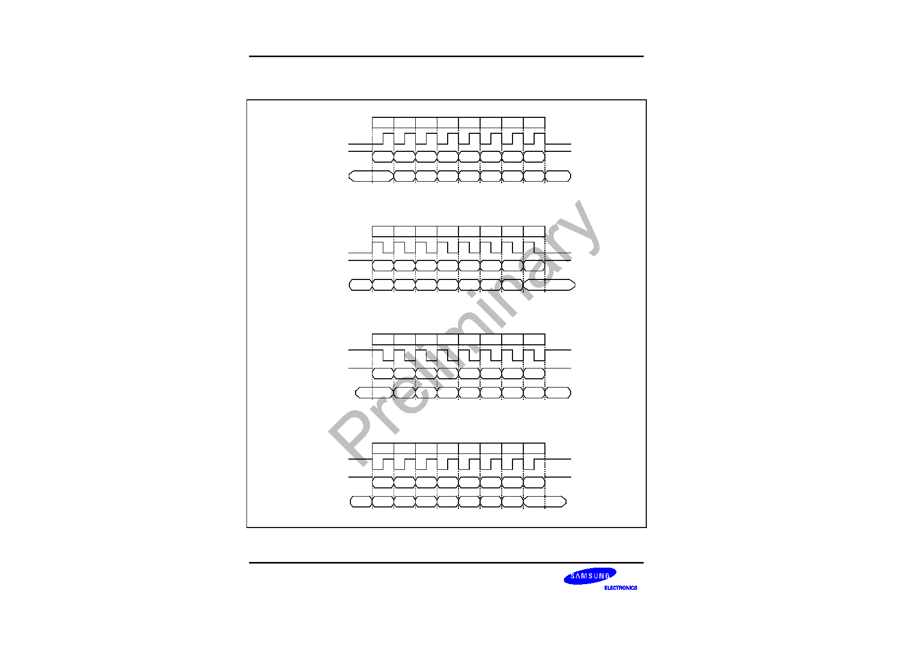
BSW rv0.1-0417-N01
Preliminary product information describes products that are in development,
for which full characterization data and associated errata are not yet available.
Specifications and information herein are subject to change without notice.
SPI INTERFACE
S3C24A0 RISC MICROPROCESSOR
15-4
SPI Transfer Format
S3C24A0 supports 4 different format to transfer the data. Four waveforms are shown for SPICLK.
* LSB of previously transmitted character
Cycle
MOSI
1
2
3
4
5
6
7
8
MSB
6
5
4
3
2
1
LSB
6
5
4
3
2
1
LSB
SPICLK
MISO
MSB
CPOL = 1, CPHA = 1 (Format B)
* MSB of character just received
Cycle
MOSI
1
2
3
4
5
6
7
8
MSB
6
5
4
3
2
1
LSB
6
5
4
3
2
1
LSB
MSB*
SPICLK
MISO
MSB
CPOL = 1, CPHA = 0 (Format A)
Cycle
MOSI
1
2
3
4
5
6
7
8
6
5
4
3
2
1
LSB
6
5
4
3
2
1
LSB*
SPICLK
MISO
*LSB
CPOL = 0, CPHA = 1 (Format B)
* MSB of character just received
Cycle
MOSI
1
2
3
4
5
6
7
8
MSB
6
5
4
3
2
1
LSB
6
5
4
3
2
1
LSB
MSB*
SPICLK
MISO
MSB
CPOL = 0, CPHA = 0 (Format A)
* LSB of previously transmitted character
*LSB
MSB
MSB
Figure 15-2. SPI Transfer Format

BSW rv0.1-0417-N01
Preliminary product information describes products that are in development,
for which full characterization data and associated errata are not yet available.
Specifications and information herein are subject to change without notice.
S3C24A0 RISC MICROPROCESSOR
SPI INTERFACE
15-5
Steps for Transmit by DMA
1.
The SPI is configured as DMA mode.
2. DMA is configured properly.
3. The SPI requests DMA service.
4. DMA transmits 1byte data to the SPI.
5. The SPI transmits the data to card.
6. Go to step 3 until DMA count is 0.
7. The SPI is configured as interrupt or polling mode with SMOD bits.
Steps for Receive by DMA
1. The SPI is configured as DMA start with SMOD bits and setting TAGD bit.
2.
DMA is configured properly.
3. The SPI receives 1byte data from card.
4. The SPI requests DMA service.
5. DMA receives the data from the SPI.
6. Write data 0xFF automatically to SPTDATn.
7.
Go to step 4 until DMA count is 0.
8.
The SPI is configured as polling mode with SMOD bits and clearing TAGD bit.
9.
If SPSTAn's REDY flag is set, then read the last byte data.
NOTE: Total received data = DMA TC values + The last data in polling mode(step 9).
First DMA received data is dummy, so user can neglect that.

BSW rv0.1-0417-N01
Preliminary product information describes products that are in development,
for which full characterization data and associated errata are not yet available.
Specifications and information herein are subject to change without notice.
SPI INTERFACE
S3C24A0 RISC MICROPROCESSOR
15-6
SPI SPECIAL REGISTERS
SPI CONTROL REGISTER
Register
Address
R/W
Description
Reset Value
SPCON0
0x44500000
R/W
SPI Channel 0 Control Register
0x00
SPCON1
0x44500020
R/W
SPI Channel 1 Control Register
0x00
SPCONn
Bit
Description
Initial State
SPI Mode Select
(SMOD)
[6:5]
Determines how and by what SPTDAT is read/written
00 = polling mode, 01 = interrupt mode
10 = DMA mode, 11 = reserved
00
SCK Enable
(ENSCK)
[4]
Determines what you want SCK enable or not(only master)
0 = disable, 1 = enable
0
Master/Slave
Select(MSTR)
[3]
Determines what mode you want master or slave
0 = slave, 1 = master
NOTE: In slave mode, there should be set up time for master to
initiate Tx / Rx.
0
Clock Polarity
Select(CPOL)
[2]
Determines an active high or active low clock.
0 = active high, 1 = active low
0
Clock Phase
Select(CPHA)
[1]
This bit selects one of two fundamentally different transfer formats.
0 = format A, 1 = format B
0
Tx Auto Garbage
Data mode enable
(TAGD)
[0]
This bit decides whether the receiving data only needs or not.
0 = normal mode, 1 = Tx auto garbage data mode
NOTE: In normal mode, you only want to receive data, you should
transmit dummy 0xFF data.
0

BSW rv0.1-0417-N01
Preliminary product information describes products that are in development,
for which full characterization data and associated errata are not yet available.
Specifications and information herein are subject to change without notice.
S3C24A0 RISC MICROPROCESSOR
SPI INTERFACE
15-7
SPI STATUS REGISTER
Register
Address
R/W
Description
Reset Value
SPSTA0
0x44500004
R
SPI Channel 0 Status Register
0x01
SPSTA1
0x44500024
R
SPI Channel 1 Status Register
0x01
SPSTAn
Bit
Description
Initial State
Reserved
[7:3]
Data Collision
Error Flag(DCOL)
[2]
This flag is set if the SPTDATn is written or the SPRDATn is read
while a transfer is in progress and cleared by reading the SPSTAn.
0 = not detect, 1 = collision error detect
0
Multi Master Error
Flag (MULF)
[1]
This flag is set if the nSS signal goes to active low while the SPI is
configured as a master, and SPPINn's ENMUL bit is multi master
errors detect mode. MULF is cleared by reading SPSTAn.
0 = not detect, 1 = multi master error detect
0
Transfer Ready
Flag (REDY)
[0]
This bit indicates that SPTDATn or SPRDATn is ready to transmit
or receive. This flag is automatically cleared by writing data to
SPTDATn.
0 = not ready, 1 = data Tx/Rx ready
1

BSW rv0.1-0417-N01
Preliminary product information describes products that are in development,
for which full characterization data and associated errata are not yet available.
Specifications and information herein are subject to change without notice.
SPI INTERFACE
S3C24A0 RISC MICROPROCESSOR
15-8
SPI PIN CONTROL REGISTER
When the SPI system is enabled, the direction of pins is controlled by MSTR bit of SPCONn register except nSS
pin. The direction of nSS pin is input always.
When the SPI is a master, nSS pin is used to check multi-master error, provided the SPPIN's ENMUL bit is active,
and another GPIO should be used to select a slave.
If the SPI is configured as a slave, nSS pin is used to select SPI as a slave by one master.
Register
Address
R/W
Description
Reset Value
SPPIN0
0x44500008
R/W
SPI Channel 0 Pin Control Register
0x02
SPPIN1
0x44500028
R/W
SPI Channel 1 Pin Control Register
0x02
SPPINn
Bit
Description
Initial State
Reserved
[7:3]
Multi Master
error detect
Enable
(ENMUL)
[2]
The /SS pin is used as an input to detect multi master error when the SPI
system is a master.
0 = disable(general purpose),
1 = multi master error detect enable
0
Reserved
[1]
This bit should be `1'.
1
Master Out
Keep(KEEP)
[0]
Determines MOSI drive or release when 1byte transmit finish(only master)
0 = release, 1 = drive the previous level
0
The SPIMISO(MISO) and SPIMOSI(MOSI) data pins are used for transmitting and receiving serial data. When the
SPI is configured as a master, SPIMISO(MISO) is the master data input line, SPIMOSI(MOSI) is the master data
output line, and SPICLK(SCK) is the clock output line. When as a slave, these pins reverse roles. In a multiple-
master system, all SPICLK(SCK) pins are tied together, all SPIMOSI(MOSI) pins are tied together, and all
SPIMISO(MISO) pins are tied together.
Only an SPI master can experience a multi master error, caused when a second SPI device becomes a master
and selects this device as if it were a slave. When this type error is detected, the following actions are taken
immediately. But you must previously set SPPINn's ENMUL bit if you want to detect this error.
1. The SPCONn's MSTR bit is forced to 0 to operate slave mode.
2. The SPSTAn's MULF flag is set, and an SPI interrupt is generated.

BSW rv0.1-0417-N01
Preliminary product information describes products that are in development,
for which full characterization data and associated errata are not yet available.
Specifications and information herein are subject to change without notice.
S3C24A0 RISC MICROPROCESSOR
SPI INTERFACE
15-9
SPI Baud Rate Prescaler Register
Register
Address
R/W
Description
Reset Value
SPPRE0
0x4450000C
R/W
SPI Cannel 0 Baud Rate Prescaler Register
0x00
SPPRE1
0x4450002C
R/W
SPI Cannel 1 Baud Rate Prescaler Register
0x00
SPPREn
Bit
Description
Initial State
Prescaler Value
[7:0]
Determines SPI clock rate as above equation.
Baud rate = PCLK / 2 / (Prescaler value + 1)
0x00
NOTE: Baud rate should be less than 25MHz.
SPI Tx Data Register
Register
Address
R/W
Description
Reset Value
SPTDAT0
0x44500010
R/W
SPI Channel 0 Tx Data Register
0x00
SPTDAT1
0x44500030
R/W
SPI Channel 1 Tx Data Register
0x00
SPTDATn
Bit
Description
Initial State
Tx Data Register
[7:0]
This field contains the data to be transmitted over the SPI channel
0x00
SPI Rx Data Register
Register
Address
R/W
Description
Reset Value
SPRDAT0
0x44500014
R
SPI Channel 0 Rx Data Register
0x00
SPRDAT1
0x44500034
R
SPI Channel 1 Rx Data Register
0x00
SPRDATn
Bit
Description
Initial State
Rx Data Register
[7:0]
This field contains the data to be received over the SPI channel
0x00

BSW rv0.1-0417-N01
Preliminary product information describes products that are in development,
for which full characterization data and associated errata are not yet available.
Specifications and information herein are subject to change without notice.
SPI INTERFACE
S3C24A0 RISC MICROPROCESSOR
15-10
NOTES

BSW rv0.1-0417-N01
Preliminary product information describes products that are in development,
for which full characterization data and associated errata are not yet available.
Specifications and information herein are subject to change without notice.
S3C24A0 RISC MICROPROCESSOR
AC97 CONTROLLER
16-1
AC97 CONTROLLER
OVERVIEW
The AC97 Controller Unit of S3C24A0 supports the AC97 revision 2.0 features. AC97 Controller communicates
with AC97 Codec using audio controller link (AC-link). Controller sends the stereo PCM data to Codec. The
external digital-to-analog converter (DAC) in the Codec then converts the audio sample to an analog audio
waveform. Also, Controller receives the stereo PCM data and the mono MIC data from Codec then store in
memories. This chapter describes the programming model for the AC97 Controller Unit. The information in this
chapter requires an understanding of the AC97 revision 2.0 specification.
FEATURE
_
Independent channels for stereo PCM In, stereo PCM Out, mono MIC In.
_
32bit (16-bit x 2), 16 entries for stereo PCM In, stereo PCM Out and 16bit, 16 entries for MIC In.
_
All of the channels support only 16-bit sample lengths.
_
Variable sampling rate AC97 Codec interface (48KHz and below)
_
DMA-based operation and interrupt based operation.
_
Only primary Codec support.

BSW rv0.1-0417-N01
Preliminary product information describes products that are in development,
for which full characterization data and associated errata are not yet available.
Specifications and information herein are subject to change without notice.
AC97 CONTROLLER
S3C24A0 RISC MICROPROCESSOR
16-2
AC97 CONTROLLER OPERATION
BLOCK DIAGRAM
Figure 16-1 shows the functional block diagram of S3C24A0 AC97 Controller. The AC97 signals form the AC-link,
which is a point-to-point synchronous serial interconnection that supports full-duplex data transfers. All digital
audio streams and command/status information are communicated over the AC-link.
APB
I/F
DMA
Engine
Interrupt
Control
MIC in
FIFO
PCM
out
FIFO
PCM
in
FIFO
SFR
AC-link
I/F
FSM &
Control
APB
AC-link
Figure 16-1 AC97 Block Diagram

BSW rv0.1-0417-N01
Preliminary product information describes products that are in development,
for which full characterization data and associated errata are not yet available.
Specifications and information herein are subject to change without notice.
S3C24A0 RISC MICROPROCESSOR
AC97 CONTROLLER
16-3
INTERNAL DATA PATH
Figure 16-2 shows the internal data path of S3C24A0 AC97 Controller. It has stereo Pulse Code Modulated
(PCM) In, Stereo PCM Out and mono MIC-in buffers, which consist of 16-bit, 16 entries buffer. Also it has 20-bit
I/O shift register via AC-link.
Command Addr
Register
Command Data
Register
PCM Out Buffer
(Regfile 16 bit x
2 x 16 Entry)
PWDATA
Response Data
Register
Mic In Buffer
(RegFile 16 bit
x16 Entry)
PCM In Buffer
(Regfile 16 bit x
2 x 16 Entry)
PRDATA
Input Shift
Register
(20 bit)
Output Shift
Register
(20 bit)
SDATA_IN
SDATA_OUT
Figure 16-2. Internal Data Path

BSW rv0.1-0417-N01
Preliminary product information describes products that are in development,
for which full characterization data and associated errata are not yet available.
Specifications and information herein are subject to change without notice.
AC97 CONTROLLER
S3C24A0 RISC MICROPROCESSOR
16-4
OPERATION FLOW CHART
System reset or Cold reset
Set GPIO and Release
INTMSK/SUBINTMSK bits
Enable Codec Ready interrupt
Codec Ready interrupt ?
Time out condition ?
Disable Codec Ready interrupt
DMA operation or
PIO (Interrupt or Polling) operation
Yes
No
Controller off
No
Figure 16-3. AC97 Operation Flow Chart

BSW rv0.1-0417-N01
Preliminary product information describes products that are in development,
for which full characterization data and associated errata are not yet available.
Specifications and information herein are subject to change without notice.
S3C24A0 RISC MICROPROCESSOR
AC97 CONTROLLER
16-5
AC-LINK DIGITAL INTERFACE PROTOCOL
Each AC97 Codec incorporates a five-pin digital serial interface that links it to the S3C24A0 AC97 Controller. AC-
link is a full-duplex, fixed-clock, PCM digital stream. It employs a time division multiplexed (TDM) scheme to
handle control register accesses and multiple input and output audio streams. The AC-link architecture divides
each audio frame into 12 outgoing and 12 incoming data streams. Each stream has 20-bit sample resolution and
requires a DAC and an analog-to-digital converter (ADC) with a minimum 16-bit resolution.
SYNC
SDATA_OUT
SDATA_IN
Slot #
(256-bit)
TAG
CMD
ADDR
CMD
DATA
PCM
L FRONT
PCM
R FRONT
TAG
STATUS
ADDR
PCM
MIC
STATUS
DATA
PCM
LEFT
PCM
RIGHT
RSRVD
RSRVD
RSRVD
0
1
2
3
4
5
6
7
8
9
10
11
12
16-bit
20-bit
20-bit
20-bit
20-bit
20-bit
20-bit
20-bit
20-bit
20-bit
20-bit
20-bit
20-bit
RSRVD
RSRVD
RSRVD
RSRVD
RSRVD
RSRVD
RSRVD
RSRVD
RSRVD
RSRVD
RSRVD
RSRVD
Figure 16-4. Bi-directional AC-link Frame with Slot Assignments
Figure 28-4 shows Tag and Data Phase organization for the controller and the Codec. The figure also lists the slot
definitions that the S3C24A0 AC97 Controller supports. The S3C24A0 AC97 Controller provides synchronization
for all data transaction on the AC-link.

BSW rv0.1-0417-N01
Preliminary product information describes products that are in development,
for which full characterization data and associated errata are not yet available.
Specifications and information herein are subject to change without notice.
AC97 CONTROLLER
S3C24A0 RISC MICROPROCESSOR
16-6
A data transaction is made up of 256 bits of information broken up into groups of 13 time slots and is called a
frame. Time slot 0 is called the Tag Phase and is 16 bits long. The other 12 time slots are called the Data Phase.
The Tag Phase contains one bit that identifies a valid frame and 12 bits that identify the time slots in the Data
Phase that contain valid data. Each time slot in the Data Phase is 20 bits long. A frame begins when SYNC goes
high. The amount of time that SYNC is high corresponds to the Tag Phase. AC97 frames occur at fixed 48 kHz
intervals and are synchronous to the 12.288 MHz bit rate clock, BITCLK. The controller and the Codec use the
SYNC and BITCLK to determine when to send transmit data and when to sample received data. A transmitter
transitions the serial data stream on each rising edge of BITCLK and a receiver samples the serial data stream on
falling edges of BITCLK. The transmitter must tag the valid slots in its serial data stream. The valid slots are
tagged in slot 0. Serial data on the AC-link is ordered most significant bit (MSB) to least significant bit (LSB). The
Tag Phase's first bit is bit 15 and the first bit of each slot in Data Phase is bit 19. The last bit in any slot is bit 0.
AC-LINK OUTPUT FRAME (SDATA_OUT)
SDATA_OUT
BIT_CLK
SYNC
AC '97 samples SYNC assertion here
AC '97 Controller samples first SDATA_OUT bit of frame here
END of previous Audio Frame
Valid
Frame
Slot(1)
Slot(2)
Slot(12)
"0"
ID1
ID0
19
0
Tag Phase
Data Phase
19
0
START of Data phase
Slot# 1
END of Data Frame
Slot# 12
48KHz
12.288MHz
Figure 16-5. AC-link Output Frame

BSW rv0.1-0417-N01
Preliminary product information describes products that are in development,
for which full characterization data and associated errata are not yet available.
Specifications and information herein are subject to change without notice.
S3C24A0 RISC MICROPROCESSOR
AC97 CONTROLLER
16-7
AC-LINK INPUT FRAME (SDATA_IN)
SDATA_OUT
BIT_CLK
SYNC
AC '97 samples SYNC assertion here
AC '97 Controller samples first SDATA_IN bit of frame here
END of previous Audio Frame
Codec
Ready
Slot(1)
Slot(2)
Slot(12)
"0"
"0"
"0"
19
0
Tag Phase
Data Phase
19
0
START of Data phase
Slot# 1
END of Data Frame
Slot# 12
Figure 16-6. AC-link Input Frame

BSW rv0.1-0417-N01
Preliminary product information describes products that are in development,
for which full characterization data and associated errata are not yet available.
Specifications and information herein are subject to change without notice.
AC97 CONTROLLER
S3C24A0 RISC MICROPROCESSOR
16-8
AC97 POWERDOWN
SDATA_OUT
SDATA_IN
BIT_CLK
SYNC
slot 12
prev.frame
Write to
0X26
slot 12
prev.frame
TAG
TAG
Data
PR4
Figure 16-7. AC97 Powerdown Timing
Powering Down the AC-link
The AC-link signals enter a low power mode when the AC97 Codec Powerdown register (0x26) bit PR4 is set to a
1 (by writing 0x1000). Then the Primary Codec drives both BITCLK and SDATA_IN to a logic low voltage level.
The sequence follows the timing diagram shown in Figure 16-7.
The AC97 Controller transmits the write to Powerdown register (0x26) over the AC-link. Set up the AC97
Controller so that it does not transmit data to slots 3-12 when it writes to the Powerdown register bit PR4 (data
0x1000), and it does not require the Codec to process other data when it receives a power down request. When
the Codec processes the request it immediately transitions BITCLK and SDATA_IN to a logic low level. The AC97
Controller drives SYNC and SDATA_OUT to a logic low level after programming the AC_GLBCTRL register.
Waking up the AC-link - Wake Up Triggered by the AC97 Controller
AC-link protocol provides for a cold AC97 reset and a warm AC97 reset. The current power-down state ultimately
dictates which AC97 reset is used. Registers must stay in the same state during all power-down modes unless a
cold AC97 reset is performed. In a cold AC97 reset, the AC97 registers are initialized to their default values. After
a power down, the AC-link must wait for a minimum of four audio frame times after the frame in which the power
down occurred before it can be reactivated by reasserting the SYNC signal. When AC-link powers up, it indicates
readiness through the Codec ready bit (input slot 0, bit 15).

BSW rv0.1-0417-N01
Preliminary product information describes products that are in development,
for which full characterization data and associated errata are not yet available.
Specifications and information herein are subject to change without notice.
S3C24A0 RISC MICROPROCESSOR
AC97 CONTROLLER
16-9
PR0=1
Normal
ADCs off
PR0
DACs off
PR1
Analog off
PR2 or
PR3
Digital I/F
off
PR4
Shut off
AC-link
Default
PR1=1
PR2=1
PR4=1
Warm Reset
PR0=0
&
ADC=1
PR1=0
&
DAC=1
PR2=0
&
ANL=1
Cold Reset
Ready=1
Figure 16-8 AC97 Power down/Power up Flow
Cold AC97 Reset
A cold reset is generated when the nRESET pin is asserted through the AC_GLBCTRL. Asserting and
deasserting nRESET activates BITCLK and SDATA_OUT. All AC97 control registers are initialized to their default
power on reset values. nRESET is an asynchronous AC97 input.
Warm AC97 Reset
A warm AC97 reset reactivates the AC-link without altering the current AC97 register values. A warm reset is
generated when BITCLK is absent and SYNC is driven high. In normal audio frames, SYNC is a synchronous
AC97 input. When BITCLK is absent, SYNC is treated as an asynchronous input used to generate a warm reset
to AC97.The AC97 Controller must not activate BITCLK until it samples SYNC low again. This prevents a new
audio frame from being falsely detected; When the AC97 Controller receives a wake-up from the Codec.

BSW rv0.1-0417-N01
Preliminary product information describes products that are in development,
for which full characterization data and associated errata are not yet available.
Specifications and information herein are subject to change without notice.
AC97 CONTROLLER
S3C24A0 RISC MICROPROCESSOR
16-10
AC97 CONTROLLER SPECIAL REGISTERS
AC97 GLOBAL CONTROL REGISTER (AC_GLBCTRL)
Register
Address
R/W
Description
Reset Value
AC_GLBCTRL
0x45000000
R/W
AC97 Global Control Register
0x000000
AC_GLBCTRL
Bit
Description
Initial State
Reserved
[31:23]
Reserved
0x00
Codec ready interrupt enable
[22]
0 : Disable 1 : Enable
0
PCM out channel underrun
interrupt enable
[21]
0 : Disable
1 : Enable ( FIFO is empty)
0
PCM in channel overrun
interrupt enable
[20]
0 : Disable
1 : Enable ( FIFO is full)
0
Mic in channel overrun
interrupt enable
[19]
0 : Disable
1 : Enable ( FIFO is full)
0
PCM out channel threshold
interrupt enable
[18]
0 : Disable
1 : Enable ( FIFO is half empty)
0
PCM in channel threshold
interrupt enable
[17]
0 : Disable
1 : Enable ( FIFO is half full)
0
MIC in channel threshold
interrupt enable
[16]
0 : Disable
1 : Enable ( FIFO is half full)
0
Reserved
[15:14]
Reserved
00
PCM out channel transfer
mode
[13:12]
00 : Off 01 : PIO 10 : DMA 11 : Reserved
00
PCM in channel transfer
mode
[11:10]
00 : Off 01 : PIO 10 : DMA 11 : Reserved
00
MIC in channel transfer mode
[9:8]
00 : Off 01 : PIO 10 : DMA 11 : Reserved
00
Reserved
[7:4]
Reserved
0000
Transfer data enable using
AC-link
[3]
0 : Disable 1 : Enable
0
AC-Link on
[2]
0 : Off
1 : SYNC signal transfer to Codec
0
Warm reset
[1]
0 : Normal
1 : Wake up codec from power down
0
Cold reset
[0]
0 : Normal
1 : Reset Codec and Controller logic
0

BSW rv0.1-0417-N01
Preliminary product information describes products that are in development,
for which full characterization data and associated errata are not yet available.
Specifications and information herein are subject to change without notice.
S3C24A0 RISC MICROPROCESSOR
AC97 CONTROLLER
16-11
AC97 GLOBAL STATUS REGISTER (AC_GLBSTAT)
Register
Address
R/W
Description
Reset Value
AC_GLBSTAT
0x45000004
R
AC97 Global Status Register
0x00000000
AC_GLBSTAT
Bit
Description
Initial State
Reserved
[31:23]
Reserved
0x00
Codec ready interrupt
[22]
0 : Not requested 1 : Requested
0
PCM out channel underrun
interrupt
[21]
0 : Not requested 1 : Requested
0
PCM in channel overrun
interrupt
[20]
0 : Not requested 1 : Requested
0
MIC in channel overrun interrupt
[19]
0 : Not requested 1 : Requested
0
PCM out channel threshold
interrupt
[18]
0 : Not requested 1 : Requested
0
PCM in channel threshold
interrupt
[17]
0 : Not requested 1 : Requested
0
MIC in channel threshold
interrupt
[16]
0 : Not requested 1 : Requested
0
Reserved
[15:3]
Reserved.
0x000
Controller main state
[2:0]
000 : Idle
001 : Init 010 : Ready
011 : Active 100 : LP 101 : Warm
000

BSW rv0.1-0417-N01
Preliminary product information describes products that are in development,
for which full characterization data and associated errata are not yet available.
Specifications and information herein are subject to change without notice.
AC97 CONTROLLER
S3C24A0 RISC MICROPROCESSOR
16-12
AC97 CODEC COMMAND REGISTER (AC_CODEC_CMD)
Register
Address
R/W
Description
Reset Value
AC_CODEC_CMD
0x45000008
R/W
AC97 Codec Command Register
0x00000000
AC_CODEC_CMD
Bit
Description
Initial State
Reserved
[31:24]
Reserved
0x00
Read enable
[23]
0 : Command write 1 : Status read
0
Address
[22:16]
Codec command address
0x00
Data
[15:0]
Codec command data
0x0000
AC97 CODEC STATUS REGISTER (AC_CODEC_STAT)
Register
Address
R/W
Description
Reset Value
AC_CODEC_STAT
0x4500000C
R
AC97 Codec Status Register
0x00000000
AC_CODEC_STAT
Bit
Description
Initial State
Reserved
[31:23]
Reserved.
0x00
Address
[22:16]
Codec status address
0x00
Data
[15:0]
Codec status data
0x0000
AC97 PCM OUT/IN CHANNEL FIFO ADDRESS REGISTER (AC_PCMADDR)
Register
Address
R/W
Description
Reset Value
AC_PCMADDR
0x45000010
R
AC97 PCM Out/In Channel FIFO Address Register
0x00000000
AC_PCMADDR
Bit
Description
Initial State
Reserved
[31:28]
Reserved.
0000
Out read address
[27:24]
PCM out channel FIFO read address
0000
Reserved
[23:20]
Reserved.
0000
In read address
[19:16]
PCM in channel FIFO read address
0000
Reserved
[15:12]
Reserved.
0000
Out write address
[11:8]
PCM out channel FIFO write address
0000
Reserved
[7:4]
Reserved.
0000
In write address
[3:0]
PCM in channel FIFO write address
0000

BSW rv0.1-0417-N01
Preliminary product information describes products that are in development,
for which full characterization data and associated errata are not yet available.
Specifications and information herein are subject to change without notice.
S3C24A0 RISC MICROPROCESSOR
AC97 CONTROLLER
16-13
AC97 MIC IN CHANNEL FIFO ADDRESS REGISTER (AC_MICADDR)
Register
Address
R/W
Description
Reset Value
AC_MICADDR
0x45000014
R
AC97 Mic In Channel FIFO Address Register
0x00000000
AC_MICADDR
Bit
Description
Initial State
Reserved
[31:20]
Reserved.
0000
Read address
[19:16]
MIC in channel FIFO read address
0000
Reserved
[15:4]
Reserved.
0x000
Write address
[3:0]
MIC in channel FIFO write address
0000
AC97 PCM OUT/IN CHANNEL FIFO DATA REGISTER (AC_PCMDATA)
Register
Address
R/W
Description
Reset Value
AC_PCMDATA
0x45000018
R/W
AC97 PCM Out/In Channel FIFO Data Register
0x00000000
AC_PCMDATA
Bit
Description
Initial State
Left data
[31:16]
PCM out/in left channel FIFO data
Read : PCM in left channel
Write : PCM out left channel
0x0000
Right data
[15:0]
PCM out/in right channel FIFO data
Read : PCM in right channel
Write : PCM out right channel
0x0000
AC97 MIC IN CHANNEL FIFO DATA REGISTER (AC_MICDATA)
Register
Address
R/W
Description
Reset Value
AC_MICDATA
0x4500001C
R/W
AC97 MIC In Channel FIFO Data Register
0x00000000
AC_MICDATA
Bit
Description
Initial State
Reserved
[31:16]
Reserved
0x0000
Mono data
[15:0]
MIC in mono channel FIFO data
0x0000

BSW rv0.1-0417-N01
Preliminary product information describes products that are in development,
for which full characterization data and associated errata are not yet available.
Specifications and information herein are subject to change without notice.
AC97 CONTROLLER
S3C24A0 RISC MICROPROCESSOR
16-14
NOTES

BSW rv0.1-0417-N01
Preliminary product information describes products that are in development,
for which full characterization data and associated errata are not yet available.
Specifications and information herein are subject to change without notice.
S3C24A0 RISC MICROPROCESSOR
USB HOST
17-1
USB HOST CONTROLLER (Preliminary)
OVERVIEW
S3C24A0 supports 2 port USB host interface as follows;
Open HCI Rev 1.0 compatible.
USB Rev1.1 compatible
2 down stream ports.
Support for both LowSpeed and HighSpeed USB devices
Figure 17-1. USB Host Controller Block Diagram
BSW rv0.1-0417-N01
Preliminary product information describes products that are in development,
for which full characterization data and associated errata are not yet available.
Specifications and information herein are subject to change without notice.
USB HOST
S3C24A0 RISC MICROPROCESSOR
17-2
USB HOST CONTROLLER SPECIAL REGISTERS
The S3C24A0 USB Host controller complies with OPEN HCI Rev 1.0. Please refer to Open Host Controller
Interface Rev 1.0 specification for detail information.
OHCI REGISTERS FOR USB HOST CONTROLLER
Register
Base Address
R/W
Description
Reset Value
HcRevision
0x41000000
-
-
HcControl
0x41000004
-
-
HcCommonStatus
0x41000008
-
-
HcInterruptStatus
0x4100000c
-
-
HcInterruptEnable
0x41000010
-
-
HcInterruptDisable
0x41000014
-
control and status group
-
HcHCCA
0x41000018
-
-
HcPeriodCuttentED
0x4100001C
-
-
HcControlHeadED
0x41000020
-
-
HcControlCurrentED
0x41000024
-
-
HcBulkHeadED
0x41000028
-
-
HcBulkCurrentED
0x4100002c
-
-
HcDoneHead
0x41000030
-
memory pointer group
-
HcRmInterval
0x41000034
-
-
HcFmRemaining
0x41000038
-
-
HcFmNumber
0x4100003c
-
-
HcPeriodicStart
0x41000040
-
-
HcLSThreshold
0x41000044
-
frame counter group
-
HcRhDescriptorA
0x41000048
-
-
HcRhDescriptorB
0x4100004C
-
-
HcRhStatus
0x41000050
-
-
HcRhPortStatus1
0x41000054
-
-
HcRhPortStatus2
0x41000058
-
root hub group
-

BSW rv0.1-0417-N01
Preliminary product information describes products that are in development,
for which full characterization data and associated errata are not yet available.
Specifications and information herein are subject to change without notice.
S3C24A0 RISC MICROPROCESSOR
USB DEVICE
18-1
USB DEVICE
OVERVIEW
USB device controller is designed to provide a high performance full speed function controller solution with DMA
I/F. USB device controller allows bulk transfer with DMA, interrupt transfer and control transfer.
The functions are as follows:
�
Full speed USB device controller compatible with the USB specification version 1.1
�
DMA interface for bulk transfer
�
5 endpoints with FIFO
EP0: 16byte (Register)
EP1: 128byte IN/OUT FIFO (dual port asynchronous RAM): interrupt or DMA
EP2: 128byte IN/OUT FIFO (dual port asynchronous RAM): interrupt or DMA
EP3: 128byte IN/OUT FIFO (dual port asynchronous RAM): interrupt or DMA
EP4: 128byte IN/OUT FIFO (dual port asynchronous RAM): interrupt or DMA
�
Integrated USB Transceiver
FEATURE
-- Fully compliant with USB Specification Version 1.1
-- Full speed (12Mbps) device
-- Integrated USB Transceiver
-- Supports control, interrupt and bulk transfer
-- 5 endpoints with FIFO:
One bi-directional control Endpoint with 16-byte FIFO (EP0)
Four bi-directional bulk endpoint with 128-byte FIFO (EP1, EP2, EP3, EP4)
-- Supports DMA interface for receive and transmit bulk endpoints. (EP1, EP2, EP3, EP4)
-- Independent 128byte receive and transmit FIFO to maximize throughput
-- Supports suspend and remote wake-up function
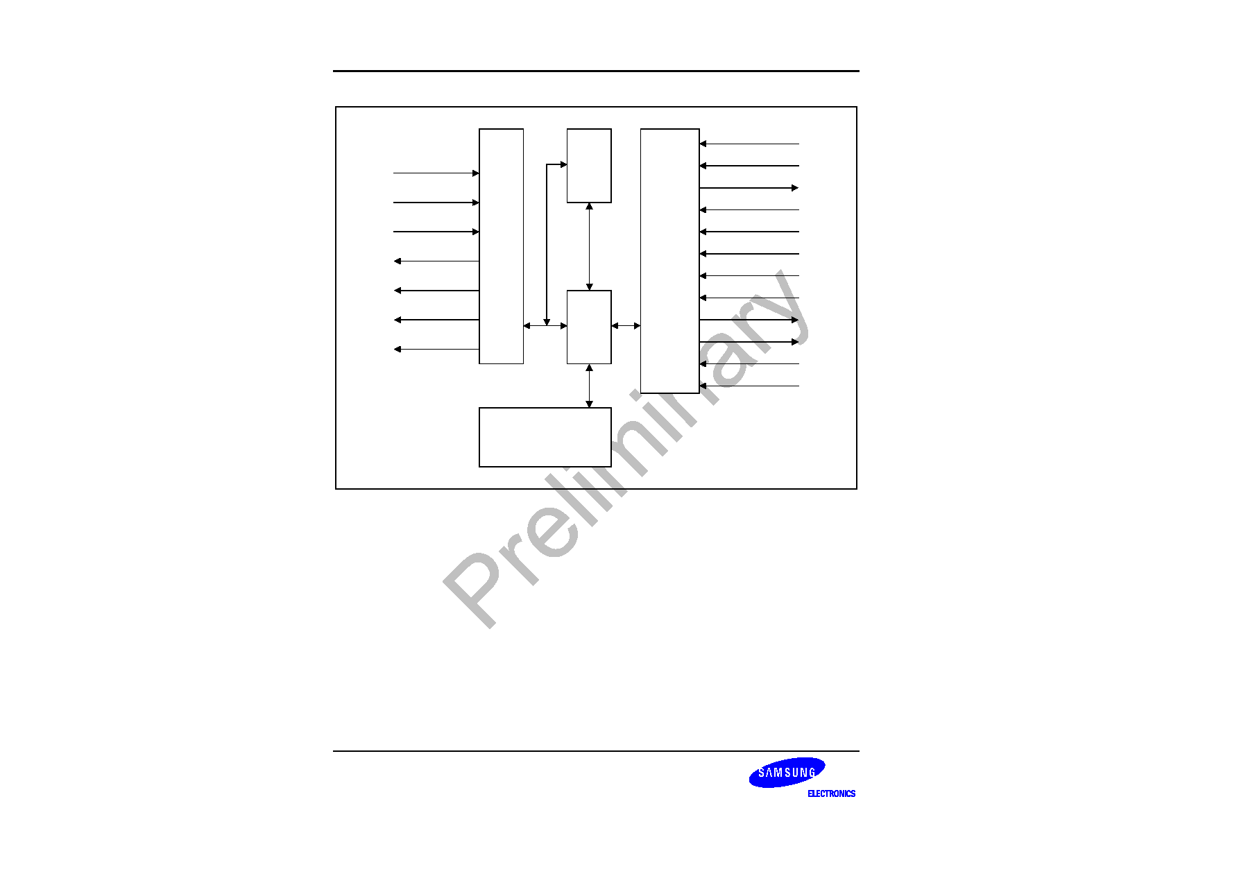
BSW rv0.1-0417-N01
Preliminary product information describes products that are in development,
for which full characterization data and associated errata are not yet available.
Specifications and information herein are subject to change without notice.
USB DEVICE
S3C24A0 RISC MICROPROCESSOR
18-2
SIE
RT_VP_OUT
RT_VM_IN
RT_VP_IN
RXD
RT_UXSUSPEND
RT_UX_OEN
RT_VM_OUT
MC_ADDR[13:0]
SIU
GFI
FIFOs
MCU
&
DMA
I/F
MC_DATA_IN[31:0]
MC_DATA_OUT[31:0]
USB_CLK
SYS_CLK
SYS_RESETN
MC_WR
WR_RDN
MC_CSN
MC_INTR
DREQN[3:0]
DACKN[3:0]
Figure 18-1. USB Device Block Diagram

BSW rv0.1-0417-N01
Preliminary product information describes products that are in development,
for which full characterization data and associated errata are not yet available.
Specifications and information herein are subject to change without notice.
S3C24A0 RISC MICROPROCESSOR
USB DEVICE
18-3
USB DEVICE SPECIAL REGISTERS
This section describes the detail functionality about register set USB Device..
All special function register is byte access or word access. All reserved bit is zero.
Common indexed registers depend on INDEX_REG(offset address : 0X178) value. For example if you want to
write EP0 CSR register, you must write `0x00' on INDEX_REG before writing IN CSR1 register.
All Register must be resettled after Host Reset Signaling.
Register Name
Description
Offset Address
NON INDEXED REGISTERS
FUNC_ADDR_REG
Function address register
0x140
PWR_REG
Power management register
0x144
EP_INT_REG (EP0�EP4)
Endpoint interrupt register
0x148
USB_INT_REG
USB interrupt register
0x158
EP_INT_EN_REG (EP0�EP4)
Endpoint interrupt enable register
0x15C
USB_INT_EN_REG
USB Interrupt enable register
0x16C
FRAME_NUM1_REG
Frame number 1 register
0x170
FRAME_NUM2_REG
Frame number 2 register
0x174
INDEX_REG
Index register
0x178
EP0_FIFO_REG
Endpoint0 FIFO register
0x1C0
EP1_FIFO_REG
Endpoint1 FIFO register
0x1C4
EP2_FIFO_REG
Endpoint2 FIFO register
0x1C8
EP3_FIFO_REG
Endpoint3 FIFO register
0x1CC
EP4_FIFO_REG
Endpoint4 FIFO register
0x1D0
EP1_DMA_CON
Endpoint1 DMA control register
0x200
EP1_DMA_UNIT
Endpoint1 DMA Unit counter register
0x204
EP1_DMA_FIFO
Endpoint1 DMA FIFO counter register
0x208
EP1_DMA_TTC_L
Endpoint1 DMA Transfer counter low-byte register
0x20C
EP1_DMA_TTC_M
Endpoint1 DMA Transfer counter middle-byte register
0x210
EP1_DMA_TTC_H
Endpoint1 DMA Transfer counter high-byte register
0x214

BSW rv0.1-0417-N01
Preliminary product information describes products that are in development,
for which full characterization data and associated errata are not yet available.
Specifications and information herein are subject to change without notice.
USB DEVICE
S3C24A0 RISC MICROPROCESSOR
18-4
EP2_DMA_CON
Endpoint2 DMA control register
0x218
EP2_DMA_UNIT
Endpoint2 DMA Unit counter register
0x21C
EP2_DMA_FIFO
Endpoint2 DMA FIFO counter register
0x220
EP2_DMA_TTC_L
Endpoint2 DMA Transfer counter low-byte register
0x224
EP2_DMA_TTC_M
Endpoint2 DMA Transfer counter middle-byte register
0x228
EP2_DMA_TTC_H
Endpoint2 DMA Transfer counter high-byte register
0x22C
EP3_DMA_CON
Endpoint3 DMA control register
0x240
EP3_DMA_UNIT
Endpoint3 DMA Unit counter register
0x244
EP3_DMA_FIFO
Endpoint3 DMA FIFO counter register
0x248
EP3_DMA_TTC_L
Endpoint3 DMA Transfer counter low-byte register
0x24C
EP3_DMA_TTC_M
Endpoint3 DMA Transfer counter middle-byte register
0x250
EP3_DMA_TTC_H
Endpoint3 DMA Transfer counter high-byte register
0x254
EP4_DMA_CON
Endpoint4 DMA control register
0x258
EP4_DMA_UNIT
Endpoint4 DMA Unit counter register
0x25C
EP4_DMA_FIFO
Endpoint4 DMA FIFO counter register
0x260
EP4_DMA_TTC_L
Endpoint4 DMA Transfer counter low-byte register
0x264
EP4_DMA_TTC_M
Endpoint4 DMA Transfer counter middle-byte register
0x268
EP4_DMA_TTC_H
Endpoint4 DMA Transfer counter high-byte register
0x26C
COMMON INDEXED REGISTERS
MAXP_REG
Endpoint MAX Packet register
0x180
IN INDEXED REGISTERS
IN_CSR1_REG
EP In Control status register 1
0x184
IN_CSR2_REG
EP In Control status register 2
0x188
OUT INDEXED REGISTERS
OUT_CSR1_REG
EP Out Control status register 1
0x190
OUT_CSR2_REG
EP Out Control status register 2
0x194
OUT_FIFO_CNT1_REG
EP Out Write count register 1
0x198
OUT_FIFO_CNT2_REG
EP Out Write count register 2
0x19C

BSW rv0.1-0417-N01
Preliminary product information describes products that are in development,
for which full characterization data and associated errata are not yet available.
Specifications and information herein are subject to change without notice.
S3C24A0 RISC MICROPROCESSOR
USB DEVICE
18-5
FUNC_ADDR_REG
This register maintains the USB Device Address assigned by the host. The MCU writes the value received
through a SET_ADDRESS descriptor to this register. This address is used for the next token.
Register
Address
R/W
Description
Reset Value
FUNC_ADDR_REG
0x44A00140
R/W
(byte)
Function address register
0x00
FUNC_ADDR_RE
G
Bit
MCU
USB
Description
Initial
State
ADDR_UPDATE
[7]
R/W
R
/CLEAR
The MCU sets this bit whenever it updates the
FUNCTION_ADDR field in this register. This
bit will be cleared by USB when DATA_END
bit in EP0_CSR register.
0
FUNCTION_ADDR
[6:0]
R/W
R
The MCU write the unique address, assigned
by host, to this field.
00

BSW rv0.1-0417-N01
Preliminary product information describes products that are in development,
for which full characterization data and associated errata are not yet available.
Specifications and information herein are subject to change without notice.
USB DEVICE
S3C24A0 RISC MICROPROCESSOR
18-6
POWER MANAGEMENT REGISTER (PWR_REG)
This register is power control register in USB block.
Register
Address
R/W
Description
Reset Value
PWR_REG
0x44A00144
R/W
(byte)
Power management register
0x00
FUNC_ADDR
Bit
MCU
USB
Description
Initial
State
Reserved
[31:9]
Reserved
0
ISO_UPDATE
[7]
R/W
R
Used for ISO mode only.
If set, GFI waits for a SOF token to set
IN_PKT_RDY even though a packet to send is
already loaded by MCU. If an IN token is
received before a SOF token, then a zero length
data packet will be sent.
0
Reserved
[6:4]
-
-
Reserved
-
USB_RESET
[3]
R
SET
The USB sets this bit if reset signaling is
received from the host. This bit remains set as
long as reset signaling persists on the bus
0
MCU_RESUME
[2]
R/W
R
/CLEAR
The MCU sets this bit for MCU resume.
The USB generates the resume signaling
depending RESUME CON Register, while this
bit is set in suspend mode.
SUSPEND_MODE
[1]
R
SET
/CLEAR
This bit can be set by USB, automatically when
the device enter into suspend mode.
It is cleared under the following conditions
1) The MCU clears the MCU_RESUME bit by
writing `0', to end remote resume signaling.
2) The resume signal form host is received.
0
SUSPEND_EN
[0]
R/W
R
Suspend mode enable control bit
0 = Disable(default). The device will not enter
suspend mode.
1 = Enable suspend mode
0

BSW rv0.1-0417-N01
Preliminary product information describes products that are in development,
for which full characterization data and associated errata are not yet available.
Specifications and information herein are subject to change without notice.
S3C24A0 RISC MICROPROCESSOR
USB DEVICE
18-7
INTERRUPT REGISTER (EP_INT_REG, USB_INT_REG)
The USB core has two interrupt registers.
These registers act as status registers for the MCU when it is interrupted. The bits are cleared by writing a `1'(not
`0') to each bit that was set.
Once the MCU is interrupted, MCU should read the contents of interrupt-related registers and write back to clear
the contents if it is necessary.
Register
Address
R/W
Description
Reset Value
EP_INT_REG
0x44A00148
R/W
(byte)
EP Interrupt pending/clear register
0x00
EP_INT_REG
Bit
MCU
USB
Description
Initial
State
EP1~EP4
Interrupt
[4:1]
R
/CLEAR
SET
For BULK/INTERRUPT IN endpoints:
The USB sets this bit under the following conditions:
1. IN_PKT_RDY bit is cleared.
2. FIFO is flushed
3. SENT_STALL set.
For BULK/INTERRUPT OUT endpoints:
USB sets this bit under the following conditions:
1. Sets OUT_PKT_RDY bit
2. Sets SENT_STALL bit
For ISO IN endpoints:
the USB sets this bit under the following conditions:
1. UNDER_RUN bit is set
2. IN_PKT_RDY bit is cleared.
3. FIFO is flushed
Note: conditions 1 and 2 are mutually exclusive
For ISO OUT endpoints:
USB sets this bit under the following conditions:
1. OUT_PKT_RDY bit is set
2. OVER RUN bit is set.
Note: Conditions 1 and 2 are mutually exclusive.
0
EP0 Interrupt
[0]
R
/CLEAR
SET
This bit corresponds to endpoint 0 interrupt
The USB sets this bit under the following conditions:
1. OUT_PKT_RDY bit is set.
2. IN_PKT_RDY bit is cleared.
3. SENT_STALL bit is set
4. SETUP_END bit is set
5. DATA_END bit is cleared(Indicates end of control
transfer)
0

BSW rv0.1-0417-N01
Preliminary product information describes products that are in development,
for which full characterization data and associated errata are not yet available.
Specifications and information herein are subject to change without notice.
USB DEVICE
S3C24A0 RISC MICROPROCESSOR
18-8
Register
Address
R/W
Description
Reset Value
USB_INT_REG
0x44A00158
R/W
(byte)
USB Interrupt pending/clear register
0x00
USB_INT_REG
Bit
MCU
USB
Description
Initial
State
RESET
Interrupt
[2]
R
/CLEAR
SET
The USB set this bit, when it receives reset signaling.
0
RESUME
Interrupt
[1]
R
/CLEAR
SET
The USB sets this bit, when it receives resume signaling,
while in suspend mode.
If the resume is due to a USB reset, then the MCU is first
interrupted with a RESUME interrupt. Once the clocks
resume and the SE0 condition persists for 3ms, USB
RESET interrupt will be asserted.
0
SUSPEND
Interrupt
[0]
R
/CLEAR
SET
The USB sets this bit when it receives suspend
signalizing.
This bit is set whenever there is no activity for 3ms on the
bus. Thus, if the MCU does not stop the clock after the
first suspend interrupt, it will be continue to be interrupted
every 3ms as long as there is no activity on the USB bus.
By default this interrupt is disabled.
0

BSW rv0.1-0417-N01
Preliminary product information describes products that are in development,
for which full characterization data and associated errata are not yet available.
Specifications and information herein are subject to change without notice.
S3C24A0 RISC MICROPROCESSOR
USB DEVICE
18-9
INTERRUPT ENABLE REGISTER (EP_INT_EN_REG, USB_INT_REG)
Corresponding to each interrupt register, there is an INTERRUPT ENABLE register (except resume interrupt
enable). By default usb reset interrupt is enabled.
If bit = 0, the interrupt is disabled
If bit = 1, the interrupt is enabled
Register
Address
R/W
Description
Reset Value
EP_INT_EN_REG
0x44A0015C
R/W
(byte)
Determines which interrupt is enabled.
0xFF
INT_MASK_REG
Bit
MCU
USB
Description
Initial
State
EP4_INT_EN
[4]
R/W
R
EP4 Interrupt Enable bit
0 = Interrupt disable 1 = Enable
1
EP3_INT_EN
[3]
R/W
R
EP3 Interrupt Enable bit
0 = Interrupt disable 1 = Enable
1
EP2_INT_EN
[2]
R/W
R
EP2 Interrupt Enable bit
0 = Interrupt disable 1 = Enable
1
EP1_INT_EN
[1]
R/W
R
EP1 Interrupt Enable bit
0 = Interrupt disable 1 = Enable
1
EP0_INT_EN
[0]
R/W
R
EP0 Interrupt Enable bit
0 = Interrupt disable 1 = Enable
1

BSW rv0.1-0417-N01
Preliminary product information describes products that are in development,
for which full characterization data and associated errata are not yet available.
Specifications and information herein are subject to change without notice.
USB DEVICE
S3C24A0 RISC MICROPROCESSOR
18-10
Register
Address
R/W
Description
Reset Value
USB_INT_EN_REG
0x44A0016C
R/W
(byte)
Determines which interrupt is enabled.
0x04
INT_MASK_REG
Bit
MCU
USB
Description
Initial
State
RESET_INT_EN
[2]
R/W
R
Reset interrupt enable bit
0 = Interrupt disable 1 = Enable
1
Reserved
[1]
-
-
-
0
SUSPEND_INT_EN
[0]
R/W
R
Suspend interrupt enable bit
0 = Interrupt disable 1 = Enable
0

BSW rv0.1-0417-N01
Preliminary product information describes products that are in development,
for which full characterization data and associated errata are not yet available.
Specifications and information herein are subject to change without notice.
S3C24A0 RISC MICROPROCESSOR
USB DEVICE
18-11
FRAME NUMBER REGISTER (FPAME_NUM1_REG, FRAME_NUM2_REG)
When host transfer USB packet, there is frame number in SOF(Start Of Frame). The USB catch this frame
number and load it into this register, automatically.
Register
Address
R/W
Description
Reset Value
FRAME_NUM1_REG
0x44A00170
R
(byte)
Frame number lower byte register
0x00
FRAME_NUM_REG
Bit
MCU
USB
Description
Initial State
FRAME_NUM1
[7:0]
R
W
Frame number lower byte value
00
Register
Address
R/W
Description
Reset Value
FRAME_NUM2_REG
0x44A00174
R
(byte)
Frame number higher byte register
0x00
FRAME_NUM_REG
Bit
MCU
USB
Description
Initial State
FRAME_NUM2
[7:0]
R
W
Frame number higher byte value
00

BSW rv0.1-0417-N01
Preliminary product information describes products that are in development,
for which full characterization data and associated errata are not yet available.
Specifications and information herein are subject to change without notice.
USB DEVICE
S3C24A0 RISC MICROPROCESSOR
18-12
INDEX REGISTER (INDEX_REG)
This INDEX register is used to indicate certain endpoint registers effectively. MCU can access the endpoint
registers(MAXP_REG,IN_CSR1_REG,IN_CSR2_REG,OUT_CSR1_REG,OUT_CSR2_REG,OUT_FIFO_CNT1_
REG,OUT_FIFO_CNT2_REG) for an endpoint inside the core using the INDEX register.
Register
Address
R/W
Description
Reset Value
INDEX_REG
0x44A00178
R/W
(byte)
Register index register
0x00
INDEX_REG
Bit
MCU
USB
Description
Initial State
INDEX
[7:0]
R/W
R
It indicates a certain endpoint.
00

BSW rv0.1-0417-N01
Preliminary product information describes products that are in development,
for which full characterization data and associated errata are not yet available.
Specifications and information herein are subject to change without notice.
S3C24A0 RISC MICROPROCESSOR
USB DEVICE
18-13
END POINT0 CONTROL STATUS REGISTER (EP0_CSR)
This register has the control and status bits for Endpoint 0. Since a control transaction involves both IN and OUT
tokens, there is only one CSR register, mapped to the IN CSR1 register.
(share IN1_CSR and can access by writing index register "0" and read/write IN1_CSR)
Register
Address
R/W
Description
Reset Value
EP0_CSR
0x44A00184
R/W
(byte)
Endpoint 0 status register
0x00
EP0_CSR
Bit
MCU
USB
Description
Initial
State
SERVICED_SE
TUP_END
[7]
W
CLEAR
The MCU should write a "1" to this bit to clear
SETUP_END
0
SERVICED_OU
T_PKT_RDY
[6]
W
CLEAR
The MCU should write a "1" to this bit to clear
OUT_PKT_RDY
0
SEND_STALL
[5]
R/W
CLEAR
MCU should writes a "1" to this bit at the same time it
clears OUT_PKT_RDY, if it decodes an invalid token.
0 = Finish the STALL condition
1 = The USB issues a STALL and shake to the
current control transfer.
0
SETUP_END
[4]
R
SET
The USB sets this bit when a control transfer ends before
DATA_END is set.
When the USB sets this bit, an interrupt is generated to
the MCU.
When such a condition occurs, the USB flushes the FIFO
and invalidates MCU access to the FIFO.
0
DATA_END
[3]
SET
CLEAR
The MCU sets this bit below conditions:
1. After loading the last packet of data into the FIFO, at
the same time IN_PKT_RDY is set.
2. While it clears OUT_PKT_RDY after unloading the last
packet of data.
3. For a zero length data phase.
0
SENT_STALL
[2]
CLE
AR
SET
The USB sets this bit if a control transaction is stopped
due to a protocol violation. An interrupt is generated when
this bit is set. The MCU should write "0" to clear this bit.
0
IN_PKT_RDY
[1]
SET
CLEAR
The MCU sets this bit after writing a packet of data into
EP0 FIFO. The USB clears this bit once the packet has
been successfully sent to the host. An interrupt is
generated when the USB clears this bit, so as the MCU to
load the next packet. For a zero length data phase, the
MCU sets DATA_END at the same time.
0
OUT_PKT_RDY
[0]
R
SET
The USB sets this bit once a valid token is written to the
FIFO. An interrupt is generated when the USB sets this
bit. The MCU clears this bit by writing a "1" to the
SERVICED_OUT_PKT_RDY bit.
0

BSW rv0.1-0417-N01
Preliminary product information describes products that are in development,
for which full characterization data and associated errata are not yet available.
Specifications and information herein are subject to change without notice.
USB DEVICE
S3C24A0 RISC MICROPROCESSOR
18-14
END POINT IN CONTROL STATUS REGISTER (IN_CSR1_REG, IN_CSR2_REG)
Register
Address
R/W
Description
Reset Value
IN_CSR1_REG
0x44A00184
R/W
(byte)
IN END POINT control status register1
0x00
IN_CSR1_REG
Bit
MCU
USB
Description
Initial
State
Reserved
[7]
-
-
-
0
CLR_DATA_
TOGGLE
[6]
R/W
R/
CLEAR
This bit can be used in Set-up procedure.
0 : There are alternation of DATA0 and DATA1
1 : The data toggle bit is cleared and PID in packet will
maintain DATA0
0
SENT_STALL
[5]
R/
CLEAR
SET
The USB sets this bit when an IN token issues a
STALL handshake, after the MCU sets SEND_STALL
bit to start STALL handshaking. When the USB issues
a STALL handshake, IN_PKT_RDY is cleared
0
SEND_STALL
[4]
W/R
R
0 : The MCU clears this bit to finish the STALL
condition.
1 : The MCU issues a STALL handshake to the USB.
0
FIFO_FLUSH
[3]
W/
CLEAR
CLEAR
The MCU sets this bit if it intends to flush the packet in
Input-related FIFO. This bit is cleared by the USB
when the FIFO is flushed. The MCU is interrupted
when this happens. If a token is in process, the USB
waits until the transmission is complete before FIFO
flushing. If two packets are loaded into the FIFO, only
first packet (The packet is intended to be sent to the
host) is flushed, and the corresponding IN_PKT_RDY
bit is cleared
0
UNDER_RUN
[2]
R/
CLEAR
Set
Valid For Iso Mode Only
The USB sets this bit when in ISO mode, an IN token
is received and the IN_PKT_RDY bit is not set.
The USB sends a zero length data packet for such
conditions, and the next packet that is loaded into the
FIFO is flushed.
This bit is cleared by writing 0.
0
Reserved
[1]
-
-
-
0
IN_PKT_RDY
[0
R/SET
CLEAR
The MCU sets this bit, after writing a packet of data
into the FIFO.
The USB clears this bit once the packet has been
successfully sent to the host.
An interrupt is generated when te USB clears this bit,
so the MCU can load the next packet. While this bit is
set, the MCU will not be able to write to the FIFO.
If the SEND STALL bit is set by the MCU, this bit
cannot be set.
0

BSW rv0.1-0417-N01
Preliminary product information describes products that are in development,
for which full characterization data and associated errata are not yet available.
Specifications and information herein are subject to change without notice.
S3C24A0 RISC MICROPROCESSOR
USB DEVICE
18-15
Register
Address
R/W
Description
Reset Value
IN_CSR2_REG
0x44A00188
R/W
(byte)
IN END POINT control status register2
0x20
IN_CSR1_REG
Bit
MCU
USB
Description
Initial
State
AUTO_SET
[7]
R/W
R
If set, whenever the MCU writes MAXP data,
IN_PKT_RDY will automatically be set by the core,
without any intervention from MCU.
If the MCU writes less than MAXP data, then
IN_PKT_RDY bit has to be set by the MCU.
0
ISO
[6]
R/W
R
This bit is used only for endpoints whose transfer type
is programmable.
'1' Configures endpoint to ISO mode
'0' Configures endpoint to Bulk mode
0
MODE_IN
[5]
R/W
R
This bit is used only for endpoints whose direction is
programmable.
'1' Configures Endpoint Direction as IN
'0' Configures Endpoint Direction as OUT
1
IN_DMA_INT_EN
[4]
R/W
R
This bit determines whether the interrupt should be
issued, or not, when the EP1 IN_PKT_RDY condition
happens. This is only useful for DMA mode.
0 = Interrupt enable, 1 = Interrupt Disable
0

BSW rv0.1-0417-N01
Preliminary product information describes products that are in development,
for which full characterization data and associated errata are not yet available.
Specifications and information herein are subject to change without notice.
USB DEVICE
S3C24A0 RISC MICROPROCESSOR
18-16
END POINT OUT CONTROL STATUS REGISTER(OUT_CSR1_REG, OUT_CSR2_REG)
Register
Address
R/W
Description
Reset Value
OUT_CSR1_REG
0x44A00190
R/W
(byte)
End Point out control status register1
0x00
OUT_CSR1_REG
Bit
MCU
USB
Description
Initial
State
CLR_DATA_TOGGLE
[7]
R/W
CLEAR
When the MCU writes a 1 to this bit, the data
toggle sequence bit is reset to DATA0.
0
SENT_STALL
[6]
CLEAR
/R
SET
The USB sets this bit when an OUT token is
ended with a STALL handshake. The USB
issues a stall handshake to the host if it sends
more than MAXP data for the OUT TOKEN.
0
SEND_STALL
[5]
R/W
R
0 : The MCU clears this bit to end the STALL
condition handshake, IN PKT RDY is
cleared.
1 : The MCU issues a STALL handshake to the
USB. The MCU clears this bit to end the
STALL condition handshake, IN PKT RDY
is cleared.
0
FIFO_FLUSH
[4]
R/W
CLEAR
The MCU write a 1 to flush the FIFO.
This bit can be set only when OUT_PKT_RDY
(D0) is set. The packet due to be unloaded by
the MCU will be flushed.
0
DATA_ERROR
[3]
R
R/W
This bit is valid only in ISO mode.
This bit should be sampled with
OUT_PKT_RDY .
When set, it indicates the data packet due to be
unloaded by the MCU has an error (either bit
stuffing or CRC). If two packets are loaded into
the FIFO, and the second packet has an error,
then this bit gets set only after the first packet is
unloaded. This bit is automatically cleared when
OUT_PKT_RDY gets cleared.
0
OVER_RUN
[2]
R/Clear
R/W
This bit is valid only in ISO mode.
This bit is set if the core is not able to load an
OUT ISO token into the FIFO.
MCU clears this bit by writing 0.
0
Reserved
[1]
-
-
-
0
OUT_PKT_RDY
[0]
R/
CLEAR
SET
The USB sets this bit after it has loaded a
packet of data into the FIFO. Once the MCU
reads the packet from FIFO, this bit should be
cleared by MCU. (Write a "0")
0

BSW rv0.1-0417-N01
Preliminary product information describes products that are in development,
for which full characterization data and associated errata are not yet available.
Specifications and information herein are subject to change without notice.
S3C24A0 RISC MICROPROCESSOR
USB DEVICE
18-17
Register
Address
R/W
Description
Reset Value
OUT_CSR2_REG
0x44A00194
R/W
(byte)
End Point out control status register2
0x00
OUT_CSR2_REG
Bit
MCU
USB
Description
Initial
State
AUTO_CLR
[7]
R/W
R
If MCU set, whenever the MCU reads data from
the OUT FIFO, OUT_PKT_RDY will
automatically be cleared by the logic, without
any intervention from MCU.
0
ISO
[6]
R/W
R
This bit determines endpoint transfer type.
'0' : Configures endpoint to Bulk mode.
'1' : Configures endpoint to ISO mode
0
OUT_DMA_INT_EN
[5]
R/W
R
This bit determines whether the interrupt should
be issued, or not.
OUT_PKT_RDY condition happens. This is only
useful for DMA mode
0 = Interrupt Enaebl 1 = Interrupt Disable
0

BSW rv0.1-0417-N01
Preliminary product information describes products that are in development,
for which full characterization data and associated errata are not yet available.
Specifications and information herein are subject to change without notice.
USB DEVICE
S3C24A0 RISC MICROPROCESSOR
18-18
END POINT FIFO REGISTER (EPN_FIFO_REG)
To access EPn FIFO, the MCU should access EPn_FIFO_REG.
Register
Address
R/W
Description
Reset Value
EP0_FIFO
0x44A001C0
R/W
(byte)
End Point0 FIFO register
0xXX
EP1_FIFO
0x44A001C4
R/W
(byte)
End Point1 FIFO register
0xXX
EP2_FIFO
0x44A001C8
R/W
(byte)
End Point2 FIFO register
0xXX
EP3_FIFO
0x44A001CC
R/W
(byte)
End Point3 FIFO register
0xXX
EP4_FIFO
0x44A001D0
R/W
(byte)
End Point4 FIFO register
0xXX
EPn_FIFO
Bit
MCU
USB
Description
Initial State
FIFO_DATA
[7:0]
R/W
R/W
FIFO data value
0xXX

BSW rv0.1-0417-N01
Preliminary product information describes products that are in development,
for which full characterization data and associated errata are not yet available.
Specifications and information herein are subject to change without notice.
S3C24A0 RISC MICROPROCESSOR
USB DEVICE
18-19
MAX PACKET REGISTER (MAXP_REG)
Register
Address
R/W
Description
Reset Value
MAXP_REG
0x44A00180
R/W
(byte)
End Point MAX packet register
0x01
MAXP_REG
Bit
MCU
USB
Description
Initial State
MAXP
[3:0]
R/W
R
0000 : Reserved
0001 : MAXP = 8 Byte
0010 : MAXP = 16 Byte
0100 : MAXP = 32 Byte
1000 : MAXP = 64 Byte
0001

BSW rv0.1-0417-N01
Preliminary product information describes products that are in development,
for which full characterization data and associated errata are not yet available.
Specifications and information herein are subject to change without notice.
USB DEVICE
S3C24A0 RISC MICROPROCESSOR
18-20
END POINT OUT WRITE COUNT REGISTER(OUT_FIFO_CNT1_REG, OUT_FIFO_CNT2_REG)
These registers maintain the number of bytes in the packet due to be unloaded by the MCU.
Register
Address
R/W
Description
Reset Value
OUT_FIFO_CNT1_REG
0x44A00198
R
(byte)
End Point out write count register1
0x00
OUT_FIFO_CNT1_REG
Bit
MCU
USB
Description
Initial State
OUT_CNT_LOW
[7:0]
R
W
Lower byte of write count
00
Register
Address
R/W
Description
Reset Value
OUT_FIFO_CNT2_REG
0x44A0019C
R
(byte)
End Point out write count register2
0x00
OUT_FIFO_CNT2_REG
Bit
MCU
USB
Description
Initial State
OUT_CNT_HIGH
[7:0]
R
W
Higher byte of write count
00

BSW rv0.1-0417-N01
Preliminary product information describes products that are in development,
for which full characterization data and associated errata are not yet available.
Specifications and information herein are subject to change without notice.
S3C24A0 RISC MICROPROCESSOR
USB DEVICE
18-21
DMA INTERFACE CONTROL REGISTER (EPN_DMA_CON)
Register
Address
R/W
Description
Reset Value
EP1_DMA_CON
0x44A00200
R/W
(byte)
EP1 DMA interface control register
0x00
EP2_DMA_CON
0x44A00218
R/W
(byte)
EP2 DMA interface control register
0x00
EP3_DMA_CON
0x44A00240
R/W
(byte)
EP3 DMA interface control register
0x00
EP4_DMA_CON
0x44A00258
R/W
(byte)
EP4 DMA interface control register
0x00
EPn_DMA_CON
Bit
MCU
USB
Description
Initial
State
IN_RUN_OB
[7]
R
W
IN DMA Run Observation
0
STATE
[6:4]
R
W
DMA State Monitoring
0
DEMAND_MODE
[3]
R/W
R
DMA Demand mode enable bit
'0' : Demand mode disable
'1' : Demand mode enable
0
OUT_RUN_OB /
OUT_DMA_RUN
[2]
R/W
R/W
This bit function is separated write and read
operation
Write operation: `0' = Stop `1' = Run
Read operation: OUT DMA Run Observation
0
IN_DMA_RUN
[1]
R/W
R
This bit is used to start DMA operation
0 = Stop 1 = Run
0
DMA_MODE_EN
[0]
R/W
R
This bit is used to set DMA mode
0 = Interrupt Mode
1 = DMA Mode
0

BSW rv0.1-0417-N01
Preliminary product information describes products that are in development,
for which full characterization data and associated errata are not yet available.
Specifications and information herein are subject to change without notice.
USB DEVICE
S3C24A0 RISC MICROPROCESSOR
18-22
DMA UNIT COUNTER REGISTER (EPN_DMA_UNIT)
This register is valid in demand mode. In case not demand mode, this register value must be set `0x01'
Register
Address
R/W
Description
Reset Value
EP1_DMA_UNIT
0x44A00204
R/W
(byte)
EP1 DMA transfer unit counter base register
0x00
EP2_DMA_UNIT
0x44A0021C
R/W
(byte)
EP2 DMA transfer unit counter base register
0x00
EP3_DMA_UNIT
0x44A00244
R/W
(byte)
EP3 DMA transfer unit counter base register
0x00
EP4_DMA_UNIT
0x44A0025C
R/W
(byte)
EP4 DMA transfer unit counter base register
0x00
DMA_UNIT
Bit
MCU
USB
Description
Initial State
EPn_UNIT_CNT
[7:0]
R/W
R
EP DMA transfer unit counter value
0x00

BSW rv0.1-0417-N01
Preliminary product information describes products that are in development,
for which full characterization data and associated errata are not yet available.
Specifications and information herein are subject to change without notice.
S3C24A0 RISC MICROPROCESSOR
USB DEVICE
18-23
DMA FIFO COUNTER REGISTER (EPN_DMA_FIFO)
This register has byte size in FIFO to be transferred by DMA. In case OUT_DMA_RUN enable, the value in OUT
FIFO Write Count Register1 will be loaded in this register automatically. In case of IN DMA Mode, the MCU
should set proper value by S/W.
Register
Address
R/W
Description
Reset Value
EP1_DMA_FIFO
0x44A00208
R/W
(byte)
EP1 DMA transfer FIFO counter base register
0x00
EP2_DMA_FIFO
0x44A00220
R/W
(byte)
EP2 DMA transfer FIFO counter base register
0x00
EP3_DMA_FIFO
0x44A00248
R/W
(byte)
EP3 DMA transfer FIFO counter base register
0x00
EP4_DMA_FIFO
0x44A00260
R/W
(byte)
EP4 DMA transfer FIFO counter base register
0x00
DMA_FIFO
Bit
MCU
USB
Description
Initial State
EPn_FIFO_CNT
[7:0]
R/W
R
EP DMA transfer FIFO counter value
0x00

BSW rv0.1-0417-N01
Preliminary product information describes products that are in development,
for which full characterization data and associated errata are not yet available.
Specifications and information herein are subject to change without notice.
USB DEVICE
S3C24A0 RISC MICROPROCESSOR
18-24
DMA TOTAL TRANSFER COUNTER REGISTER (EPN_DMA_TTC_L, EPN_DMA_TTC_M, EPN_DMA_TTC_H)
This register should have total number of bytes to be transferred using DMA.(Total 24bit Counter)
Register
Address
R/W
Description
Reset Value
EP1_DMA_TTC_L
0x44A0020C
R/W
(byte)
EP1 DMA total transfer counter(lower byte)
0x00
EP1_DMA_TTC_M
0x44A00210
R/W
(byte)
EP1 DMA total transfer counter(middle byte)
0x00
EP1_DMA_TTC_H
0x44A00214
R/W
(byte)
EP1 DMA total transfer counter(higher byte)
0x00
EP2_DMA_TTC_L
0x44A00224
R/W
(byte)
EP2 DMA total transfer counter(lower byte)
0x00
EP2_DMA_TTC_M
0x44A00228
R/W
(byte)
EP2 DMA total transfer counter(middle byte)
0x00
EP2_DMA_TTC_H
0x44A0022C
R/W
(byte)
EP2 DMA total transfer counter(higher byte)
0x00
EP3_DMA_TTC_L
0x44A0024C
R/W
(byte)
EP3 DMA total transfer counter(lower byte)
0x00
EP3_DMA_TTC_M
0x44A00250
R/W
(byte)
EP3 DMA total transfer counter(middle byte)
0x00
EP3_DMA_TTC_H
0x44A00254
R/W
(byte)
EP3 DMA total transfer counter(higher byte)
0x00
EP4_DMA_TTC_L
0x44A00264
R/W
(byte)
EP4 DMA total transfer counter(lower byte)
0x00
EP4_DMA_TTC_M
0x44A00268
R/W
(byte)
EP4 DMA total transfer counter(middle byte)
0x00
EP4_DMA_TTC_H
0x44A0026C
R/W
(byte)
EP4 DMA total transfer counter(higher byte)
0x00
DMA_TX
Bit
MCU
USB
Description
Initial State
EPn_TTC_L
[7:0]
R/W
R
DMA total transfer count value(lower byte)
0x00
EPn_TTC_M
[7:0]
R/W
R
DMA total transfer count value(middle byte)
0x00
EPn_TTC_H
[7:0]
R/W
R
DMA total transfer count value(higher byte)
0x00

BSW rv0.1-0417-N01
Preliminary product information describes products that are in development,
for which full characterization data and associated errata are not yet available.
Specifications and information herein are subject to change without notice.
S3C24A0 RISC MICROPROCESSOR
MODEM INTERFACE
19-1
MODEM INTERFACE (PRELIMINARY)
OVERVIEW
This specification defines the interface between the Base-band Modem and the Application Processor for the
data-exchange of these two devices (refer Figure 19-1). For the data-exchange, the AP (Application Processor,
S3C24A0) has a dual-ported SRAM buffer (on-chip) and the Modem chip can access that SRAM buffer using a
typical asynchronous-SRAM interface.
Typically, the size of the SRAM buffer is 2KB. For the buffer status and Interrupt Requests, this specification also
specifies a few of pre-defined special addresses.
The Modem chip can write data in the data buffer and write interrupt control-data to the interrupt-port address for
the interrupt request to the AP. The AP reads that data when an interrupt request is accepted and the interrupt is
cleared when the AP accesses the interrupt-port address. In the same manner, the AP can write data in the data
buffer and write interrupt control-data to the interrupt-port address for the interrupt request to the Modem chip.
Modem
chip
Application
Processor
(S3C24A0)
internal SRAM
buffer
Address & Control
signals
Data
Interrupt request
Interrupt request
to uP
embedded
uP
Figure 19-1 Modem interface overview

BSW rv0.1-0417-N01
Preliminary product information describes products that are in development,
for which full characterization data and associated errata are not yet available.
Specifications and information herein are subject to change without notice.
MODEM INTERFACE
S3C24A0 RISC MICROPROCESSOR
19-2
FEATURES
-- 8-bit parallel bus for data transfer
-- 2K bytes internal SRAM buffer
-- Interrupt request for data exchange
-- Programmable interrupt port address
BSW rv0.1-0417-N01
Preliminary product information describes products that are in development,
for which full characterization data and associated errata are not yet available.
Specifications and information herein are subject to change without notice.
S3C24A0 RISC MICROPROCESSOR
MODEM INTERFACE
19-3
HARDWARE INTERFACE
The Modem chip can access using an external memory interface (for example external SRAM). In this
specification, the Modem chip can access the internal SRAM and special address ports of the AP using the 8-bit
data-bus and the 2K-byte address-space (i.e. 8-bit data-bus and 11-bit address bus).
SIGNAL DESCRIPTION
Name
I/O
1)
Active
Description
XmiIRQn
O
L
Interrupt request to the Modem chip
XmiDATA [7:0]
B
-
Data bus, driven by the Modem chip
XmiADR[10:0]
I
-
Address bus, driven by the Modem chip
XmiCSn
I
L
Chip select, driven by the Modem chip
XmiWEn
I
L
Write enable, driven by the Modem chip
XmiOEn
I
L
Read enable, driven by the Modem chip
Note 1) I/O direction is on the AP side. I : input O : output B : bi-direction
Table 19-1 Modem interface signal description
INTERRUPT PORTS
Interrupts are requested or cleared if the Modem chip or the AP accesses the interrupt-port (predefined special
addresses). That special addresses can be configured by the AP and the default address-map is shown in the
Table19-2.
Address
1)
An Interrupt is requested, when
The Interrupt is cleared, when
0x7FE
the Modem chip writes
See note 2
2)
0x7FF
the AP writes
the Modem chip reads
Note 1) This address is default value. It can be set to the other value by the SFR.
Note 2) The interrupt is cleared by the interrupt controller of S3C24A0
Table 19-2 Interrupt ports and interrupt-request/clear conditions
Modem chip or AP(S3C24A0) can read the data that indicates what event happens � data transfer requested,
data transfer done, special command issued, etc. - from interrupt port address. That data format should be
defined for communication between the modem chip and AP.

BSW rv0.1-0417-N01
Preliminary product information describes products that are in development,
for which full characterization data and associated errata are not yet available.
Specifications and information herein are subject to change without notice.
MODEM INTERFACE
S3C24A0 RISC MICROPROCESSOR
19-4
ADDRESS MAPPING
0x000
0x001
0x002
0x7FF
0x000
0x004
0x008
0x7FC
0x7FE
0x7FD
0x7FC
0x003
0x00C
0x41100000
0x41100004
0x41100008
0x411007FC
0x4110000C
Modem
(byte)
Buffer
(word)
Address map
of 24A0
(word)
2K Bytes
buffer
area
0x41180000
0x41180004
SFR
modem
interface
area
Figure 19-2 Modem interface address mapping

BSW rv0.1-0417-N01
Preliminary product information describes products that are in development,
for which full characterization data and associated errata are not yet available.
Specifications and information herein are subject to change without notice.
S3C24A0 RISC MICROPROCESSOR
MODEM INTERFACE
19-5
TIMING DIAGRAM
XmiADR
XmiCSn
XmiWEn
XmiDATA
t
AVWR
t
CSVWR
t
DHWR
t
WR
t
DSUWR
t
AWR
Figure 19-3 Modem interface write timing diagram
Parameter
Description
Min (ns)
Max (ns)
Notes
t
AVWR
Address valid to address invalid
11 ns
-
t
CSVWR
Chip select active
11 ns
-
t
AWR
Address valid to write active
2 ns
-
t
WR
Write active
5 ns
-
t
DSUWR
Write data setup
3 ns
-
t
DHWR
Write data hold
4 ns
-
Table 19-3 Modem interface write timing

BSW rv0.1-0417-N01
Preliminary product information describes products that are in development,
for which full characterization data and associated errata are not yet available.
Specifications and information herein are subject to change without notice.
MODEM INTERFACE
S3C24A0 RISC MICROPROCESSOR
19-6
XmiADR
XmiCSn
XmiOEn
XmiDATA
t
AVRD
t
CSVRD
t
ACSDV
t
RD
t
RDH
t
RDDV
t
ADH
Figure 19-4 Modem interface read timing diagram
Parameter
Description
Min
Max
Notes
t
AVRD
Address valid to address invalid
20 ns
-
t
ADH
Address hold
2.5 ns
-
t
CSVRD
Chip select active
17.5 ns
-
t
RD
Read active
17 ns
-
t
RDDV
Read active to data valid
-
11.5 ns
t
RDH
Read data hold
4 ns
-
t
ACSDV
Address and chip select active to
data valid
-
12 ns
Note ) Output load is 30pF at room temperature (25�C)
Table 19-4 Modem interface read timing

BSW rv0.1-0417-N01
Preliminary product information describes products that are in development,
for which full characterization data and associated errata are not yet available.
Specifications and information herein are subject to change without notice.
S3C24A0 RISC MICROPROCESSOR
MODEM INTERFACE
19-7
SOFTWARE INTERFACE
This modem interface provides a generic data-exchange method. This interface does not implement any other
complex features except for the interrupt-request/clear such as automatic FIFO managements, etc. The software
should be responsible for all other required functionalities for the data exchange between the modem chip and the
AP such as the data exchange protocol, the data buffer managements, and etc.
MODEM INTERFACE SPECIAL REGISTERS
INTERRUPT REQUEST TO AP REGISTER (INT2AP)
Register
Address
R/W
Description
Reset Value
INT2AP
0x41180000
R/W
Interrupt request to AP Register
0x000007FE
INT2AP
Bit
Description
Initial State
Reserved
[31:11] Reserved
0
INT2AP_ADR
[10:0]
Modem interface requests the interrupt to AP when modem chip
writes this address. This interrupt is cleared by the interrupt
controller of AP.
7FE
INTERRUPT REQUEST TO MODEM REGISTER (INT2MDM)
Register
Address
R/W
Description
Reset Value
INT2MDM
0x41180004
R/W
Interrupt request to modem Register
0x000007FF
INT2MDM
Bit
Description
Initial State
Reserved
[31:11] Reserved
0
INT2MDM_ADR
[10:0]
Modem interface requests the interrupt to modem chip when AP
writes this address and clears the interrupt when modem chip
reads this address.
7FF
Note ) It is recommended that AP writes data with byte access on the interrupt port because AP can overwrite the
data in INT2AP if there are INT2AP and INT2MDM sharing the same word.

BSW rv0.1-0417-N01
Preliminary product information describes products that are in development,
for which full characterization data and associated errata are not yet available.
Specifications and information herein are subject to change without notice.
MODEM INTERFACE
S3C24A0 RISC MICROPROCESSOR
19-8
NOTES

BSW rv0.1-0417-N01
Preliminary product information describes products that are in development,
for which full characterization data and associated errata are not yet available.
Specifications and information herein are subject to change without notice.
S3C24A0 RISC MICROPROCESSOR
I/O PORTS
20-1
GENERAL PURPOSE I/O PORTS (Preliminary)
OVERVIEW
The S3C24A0 has 32 multi-functional general-purpose input/output port pins (GPIO).
Each port can be easily configured by software to meet various system configuration and design requirements.
You have to define which function of each pin is used before starting the main program. If the multiplexed
functions on a pin are not used, the pin can be configured as I/O ports.
The GPIO module in the S3C24A0 has control-registers to configure the power-saving features for the whole chip
interface. For example, it contains the control registers for the pin-status of the S3C24A0 that is in the SLEEP
state (the SLEEP state is the state that the power source for the whole chip is off except for the power-
management circuitry).
For the normal mode operation, the GPIO pins can be fully configured as an input port with or without pull-up
register, an output port, a specific functional pin or an External Interrupt source.

BSW rv0.1-0417-N01
Preliminary product information describes products that are in development,
for which full characterization data and associated errata are not yet available.
Specifications and information herein are subject to change without notice.
I/O PORTS
S3C24A0 RISC MICROPROCESSOR
20-2
Table 20-1. S3C24A0 Port Configuration Overview
Port
Selectable Pin Functions
(Refers the GPIO port configuration registers � GPCON_U, GPCON_M & GPCON_L.)
GP31
Input/output
XuRXD1
IrDA_RXD
GP30
Input/output
XuTXD1
IrDA_TXD
GP29
Input/output
XuRTSn1
IrDA_SDBW
GP28
Input/output
XuCTSn1
RTC_ALMINT
GP27
Input/output
EXTDMA_ACK1
XkpCOL4
GP26
Input/output
EXTDMA_ACK0
XkpCOL3
GP25
Input/output
EXTDMA_REQ1
XkpCOL2
GP24
Input/output
EXTDMA_REQ0
XkpCOL1
GP23
Input/output
PWM_TOUT3
XkpCOL0
GP22
Input/output
PWM_TOUT2
XkpROW4
GP21
Input/output
PWM_TOUT1
XkpROW3
GP20
Input/output
PWM_TOUT0
XkpROW2
GP19
Input/output
PWM_ECLK
XkpROW1
GP18
Input/output
EINT18
XkpROW0
GP17
Input/output
EINT17
XspiCLK
GP16
Input/output
EINT16
XspiMISO
GP15
Input/output
EINT15
XspiMOSI
GP14
Input/output
EINT14
RTC_ALMINT
GP13
Input/output
EINT13
Reserved
GP12
Input/output
EINT12
Reserved
GP11
Input/output
EINT11
Reserved
GP10
Input/output
Reserved
Reserved
GP9
Input/output
EINT9
EXTDMA_ACK1
GP8
Input/output
EINT8
EXTDMA_ACK0
GP7
Input/output
EINT7
EXTDMA_REQ1
GP6
Input/output
EINT6
EXTDMA_REQ0
GP5
Input/output
EINT5
PWM_TOUT3
GP4
Input/output
EINT4
PWM_TOUT2
GP3
Input/output
EINT3
PWM_TOUT1
GP2
Input/output
EINT2
PWM_TOUT0
GP1
Input/output
EINT1
PWM_ECLK
GP0
Input/output
EINT0
-

BSW rv0.1-0417-N01
Preliminary product information describes products that are in development,
for which full characterization data and associated errata are not yet available.
Specifications and information herein are subject to change without notice.
S3C24A0 RISC MICROPROCESSOR
I/O PORTS
20-3
PORT CONTROL DESCRIPTIONS
GPIO PORT CONFIGURATION REGISTER FOR NORMAL MODE (GPCON_U, GPCON_M, GPCON_L)
In the S3C24A0, 32 pins are multiplexed pins. So, It is determined which function is selected for each pins. The
PCON (port control register) determines which function is used for each pin.
If GP0 � GP9 are used for the wakeup signal in power down mode, these ports must be configured as an interrupt
mode. The wake-up events are generated when the individual GPIO pin is configured as an external interrupt
mode regardless of the interrupt mask bits.
GPIO PORT DATA REGISTER FOR NORMAL MODE (GPDAT)
If Ports are configured as output ports, data can be written to the corresponding bit of GPDAT. If Ports are
configured as input ports, the data can be read from the corresponding bit of GPDAT.
GPIO PORT PULL-PU CONTROL REGISTER FOR NORMAL MODE (GPPU)
The port pull-up register controls the pull-up resister enable/disable of each port group. When the corresponding
bit is 0, the pull-up resister of the pin is enabled. When 1, the pull-up resister is disabled.
If the port pull-up register is enabled then the pull-up resisters work without pin's functional setting (input, output,
EINTn and etc)
EXTERNAL INTERRUPT CONTROL REGISTER (EXTINTCn/ EINTFLTn/ EINTMASK/ EINTPEND)
The 18 EINT ports are requested by various signaling methods. The EXTINTC register configures the signaling
method among the low level trigger, high level trigger, falling edge trigger, rising edge trigger, and both edge
trigger for the external interrupt request
All 18 EINT ports generate an interrupt when each port is configured as the interrupt mode and the corresponding
interrupt is unmasked. However, even if the interrupt is masked to a corresponding interrupt port (EINTMASK), an
interrupt pending bit (EINTPEND) is set when the port is configured as the interrupt mode.
The 8 EINT ports have a digital filter. (Refer to EINTFLTn register)
Only 10 EINT ports (EINT [9:0]) are used for wake-up sources. In the SLEEP mode, all wake-up sources are
disabled when the nBATFLT signal is asserted to low (it will not generate a wake-up event nor a interrupt is
pending).
Wake-up source is updated in EINTPEND including RTC alarm wake-up bit.
PERIPHERAL PORT PULL-UP CONTROL REGISTER FOR NORMAL MODE (PERIPU)
The peripheral port pull-up control register controls internal pull-up resister attached to the corresponding port pin.
When the corresponding bit is 0, the pull-up resister of the pin is enabled. When 1, the pull-up resister is disabled.
ALIVE CONTROL REGISTER (ALIVECON)
These bits notify what kind of reset occurred and Battery fault has occurred or not.

BSW rv0.1-0417-N01
Preliminary product information describes products that are in development,
for which full characterization data and associated errata are not yet available.
Specifications and information herein are subject to change without notice.
I/O PORTS
S3C24A0 RISC MICROPROCESSOR
20-4
GPIO OUTPUT DATA REGISTER FOR SLEEP MODE (GPDAT_SLEEP)
GPIO port output data register in sleep mode. In sleep mode the value of GPDAT is meaningless.
GPIO OUTPUT CONTROL REGISTER FOR SLEEP MODE (GPOEN_SLEEP)
GPIO port output control register for each port in sleep mode. In sleep mode the value of GPCON is meaningless.
GPIO PULL-UP CONTROL REGISTER FOR SLEEP MODE (GPPU_SLEEP)
Control pull up resister attached to the corresponding GPIO port pin in sleep mode. In sleep mode the value of
GPPU is meaningless.
PERIPHERAL PORT OUTPUT DATA REGISTER FOR SLEEP MODE (PERIDAT_SLEEPn)
Peripheral port output data register in sleep mode.
PERIPHERAL PORT OUTPUT CONTROL REGISTER FOR SLEEP MODE (PERIOEN_SLEEPn)
Peripheral port output control register for each port in sleep mode.
PERIPHERAL PORT PULL-UP CONTROL REGISTER FOR SLEEP MODE (PERIPU_SLEEP)
Control pull up resister attached to the peripheral port in sleep mode. In sleep mode the value of PERIPU is
meaningless.
RESET COUNT COMPARE REGISTER (RSTCNT)
These value control the duration of reset when wake-up from sleep mode.
GENERAL PURPOSE RAM ARRAY (GPRAMn)
General purpose RAM array, 16 x 32 bit.

BSW rv0.1-0417-N01
Preliminary product information describes products that are in development,
for which full characterization data and associated errata are not yet available.
Specifications and information herein are subject to change without notice.
S3C24A0 RISC MICROPROCESSOR
I/O PORTS
20-5
I/O PORT CONTROL REGISTER
GPIO UPPER PORT CONTROL REGISTER (GPCON_U)
Register
Address
R/W
Description
Reset Value
GPCON_U
0x44800000
R/W
Configures the pins of upper ports[31:19]
0x0
GPCON_U
Bit
Description
GP31
[25:24]
00 = Input
01 = Output
10 = XuRXD1
11 = IrDA_RXD
GP30
[23:22]
00 = Input
01 = Output
10 = XuTXD1
11 = IrDA_TXD
GP29
[21:20]
00 = Input
01 = Output
10 = XuRTSn1
11 = IrDA_SDBW
GP28
[19:18]
00 = Input
01 = Output
10 = XuCTSn1
11 = RTC_ALMINT
GP27
[17:16]
00 = Input
01 = Output
10 = EXTDMA_ACK1 11 = XkpCOL4
GP26
[15:14]
00 = Input
01 = Output
10 = EXTDMA_ACK0 11 = XkpCOL3
GP25
[13:12]
00 = Input
01 = Output
10 = EXTDMA_REQ1 11 = XkpCOL2
GP24
[11:10]
00 = Input
01 = Output
10 = EXTDMA_REQ0 11 = XkpCOL1
GP23
[9:8]
00 = Input
01 = Output
10 = PWM_TOUT3 11 = XkpCOL0
GP22
[7:6]
00 = Input
01 = Output
10 = PWM_TOUT2 11 = XkpROW4
GP21
[5:4]
00 = Input
01 = Output
10 = PWM_TOUT1 11 = XkpROW3
GP20
[3:2]
00 = Input
01 = Output
10 = PWM_TOUT0 11 = XkpROW2
GP19
[1:0]
00 = Input
01 = Output
10 = PWM_ECLK 11 = XkpROW1

BSW rv0.1-0417-N01
Preliminary product information describes products that are in development,
for which full characterization data and associated errata are not yet available.
Specifications and information herein are subject to change without notice.
I/O PORTS
S3C24A0 RISC MICROPROCESSOR
20-6
GPIO MIDDLE PORT CONTROL REGISTER (GPCON_M)
If GP11 � GP18 will be used for wakeup signals at power down mode, the ports will be set in Interrupt mode.
Register
Address
R/W
Description
Reset Value
GPCON_M
0x44800004
R/W
Configures the pins of middle ports[18:11]
0x0
GPCON_M
Bit
Description
GP18
[15:14]
00 = Input
01 = Output
10 = EINT18
11 = XkpROW0
GP17
[13:12]
00 = Input
01 = Output
10 = EINT17
11 = XspiCLK
GP16
[11:10]
00 = Input
01 = Output
10 = EINT16
11 = XspiMISO
GP15
[9:8]
00 = Input
01 = Output
10 = EINT15
11 = XspiMOSI
GP14
[7:6]
00 = Input
01 = Output
10 = EINT14
11 = RTC_ALMINT
GP13
[5:4]
00 = Input
01 = Output
10 = EINT13
11 =
Reserved
GP12
[3:2]
00 = Input
01 = Output
10 = EINT12
11 =
Reserved
GP11
[1:0]
00 = Input
01 = Output
10 = EINT11
11 =
Reserved

BSW rv0.1-0417-N01
Preliminary product information describes products that are in development,
for which full characterization data and associated errata are not yet available.
Specifications and information herein are subject to change without notice.
S3C24A0 RISC MICROPROCESSOR
I/O PORTS
20-7
GPIO LOWER PORT CONTROL REGISTER (GPCON_L)
If GP8 � GP10 will be used for wakeup signals at power down mode, the ports will be set in Interrupt mode.
Register
Address
R/W
Description
Reset Value
GPCON_L
0x44800008
R/W
Configures the pins of lower ports[10:0]
0x0
GPCON_L
Bit
Description
GP10
[21:20]
00 = Input
01 = Output
10 = Reserved
11 =
Reserved
GP9
[19:18]
00 = Input
01 = Output
10 = EINT9
11 = EXTDMA_ACK1
GP8
[17:16]
00 = Input
01 = Output
10 = EINT8
11 = EXTDMA_ACK0
GP7
[15:14]
00 = Input
01 = Output
10 = EINT7
11 = EXTDMA_REQ1
GP6
[13:12]
00 = Input
01 = Output
10 = EINT6
11 = EXTDMA_REQ0
GP5
[11:10]
00 = Input
01 = Output
10 = EINT5
11 = PWM_TOUT3
GP4
[9:8]
00 = Input
01 = Output
10 = EINT4
11 = PWM_TOUT2
GP3
[7:6]
00 = Input
01 = Output
10 = EINT3
11 = PWM_TOUT1
GP2
[5:4]
00 = Input
01 = Output
10 = EINT2
11 = PWM_TOUT0
GP1
[3:2]
00 = Input
01 = Output
10 = EINT1
11 = PWM_ECLK
GP0
[1:0]
00 = Input
01 = Output
10 = EINT0
11 = Reserved

BSW rv0.1-0417-N01
Preliminary product information describes products that are in development,
for which full characterization data and associated errata are not yet available.
Specifications and information herein are subject to change without notice.
I/O PORTS
S3C24A0 RISC MICROPROCESSOR
20-8
GPIO PORT DATA REGISTER (GPDAT)
Register
Address
R/W
Description
Reset Value
GPDAT
0x4480000C
R/W
The data register for all ports[31:0]
Undefined
GPDAT
Bit
Description
GP[31:0]
[31:0]
When the port is configured as input port, data from external sources
can be read to the corresponding pin. When the port is configured as
output port, data written in this register can be sent to the
corresponding pin. When the port is configured as function pin,
undefined value will be read.
GPIO PORT PULL UP RESISTER CONTROL REGISTER (GPPU)
Register
Address
R/W
Description
Reset Value
GPPU
0x44800010
R/W
Pull-up disable register for all ports[31:0]
0x0
Reserved
0x44800014
-
Reserved
Undefined
GPPU
Bit
Description
GP[31:0]
[31:0]
0 : The pull up function attached to to the corresponding port pin is enabled.
1 : The pull up function is disabled.

BSW rv0.1-0417-N01
Preliminary product information describes products that are in development,
for which full characterization data and associated errata are not yet available.
Specifications and information herein are subject to change without notice.
S3C24A0 RISC MICROPROCESSOR
I/O PORTS
20-9
EXTERNAL INTERRUPT CONTROL REGISTER (EXTINTC0)
The 18 external interrupts can be requested by various signaling methods. The EXTINTC register configures the
signaling method between the level trigger and edge trigger for the external interrupt request, and also configures
the signal polarity.
To recognize the level interrupt, the valid logic level on EXTINTCn pin must be retained for 40ns at least because
of the noise filter. (EINT[9:0])
Register
Address
R/W
Description
Reset Value
EXTINTC0
0x44800018
R/W
External Interrupt control Register 0
0x0
EXTINTC0
Bit
Description
Reserved
[11]
This bit is reserved and the value should be `0'
EXTINT2
[10:8]
Setting the signaling method of the EINT2.
000 = Low level 001 = High level 01x = Falling edge triggered
10x = Rising edge triggered 11x = Both edge triggered
Reserved
[7]
This bit is reserved and the value should be `0'
EXTINT1
[6:4]
Setting the signaling method of the EINT1.
000 = Low level 001 = High level 01x = Falling edge triggered
10x = Rising edge triggered 11x = Both edge triggered
Reserved
[3]
This bit is reserved and the value should be `0'
EXTINT0
[2:0]
Setting the signaling method of the EINT0.
000 = Low level 001 = High level 01x = Falling edge triggered
10x = Rising edge triggered 11x = Both edge triggered

BSW rv0.1-0417-N01
Preliminary product information describes products that are in development,
for which full characterization data and associated errata are not yet available.
Specifications and information herein are subject to change without notice.
I/O PORTS
S3C24A0 RISC MICROPROCESSOR
20-10
EXTERNAL INTERRUPT CONTROL REGISTER (EXTINTC1)
Register
Address
R/W
Description
Reset Value
EXTINTC1
0x4480001C
R/W
External Interrupt control Register 1
0x0
EXTINTC1
Bit
Description
Reserved
[31:27]
This bit is reserved and the value should be `0'
EXTINT9
[26:24]
Setting the signaling method of the EINT9.
000 = Low level 001 = High level 01x = Falling edge triggered
10x = Rising edge triggered 11x = Both edge triggered
Reserved
[23]
This bit is reserved and the value should be `0'
EXTINT8
[22:20]
Setting the signaling method of the EINT8.
000 = Low level 001 = High level 01x = Falling edge triggered
10x = Rising edge triggered 11x = Both edge triggered
Reserved
[19]
This bit is reserved and the value should be `0'
EXTINT7
[18:16]
Setting the signaling method of the EINT7.
000 = Low level 001 = High level 01x = Falling edge triggered
10x = Rising edge triggered 11x = Both edge triggered
Reserved
[15]
This bit is reserved and the value should be `0'
EXTINT6
[14:12]
Setting the signaling method of the EINT6.
000 = Low level 001 = High level 01x = Falling edge triggered
10x = Rising edge triggered 11x = Both edge triggered
Reserved
[11]
This bit is reserved and the value should be `0'
EXTINT5
[10:8]
Setting the signaling method of the EINT5.
000 = Low level 001 = High level 01x = Falling edge triggered
10x = Rising edge triggered 11x = Both edge triggered
Reserved
[7]
This bit is reserved and the value should be `0'
EXTINT4
[6:4]
Setting the signaling method of the EINT4.
000 = Low level 001 = High level 01x = Falling edge triggered
10x = Rising edge triggered 11x = Both edge triggered
Reserved
[3]
This bit is reserved and the value should be `0'
EXTINT3
[2:0]
Setting the signaling method of the EINT3.
000 = Low level 001 = High level 01x = Falling edge triggered
10x = Rising edge triggered
11x = Both edge triggered

BSW rv0.1-0417-N01
Preliminary product information describes products that are in development,
for which full characterization data and associated errata are not yet available.
Specifications and information herein are subject to change without notice.
S3C24A0 RISC MICROPROCESSOR
I/O PORTS
20-11
EXTERNAL INTERRUPT CONTROL REGISTER (EXTINTC2)
Register
Address
R/W
Description
Reset Value
EXTINTC2
0x44800020
R/W
External Interrupt control Register 2
0x0
EXTINTC2
Bit
Description
FLTEN18
[31]
Filter Enable for EINT18 0 = Disable
1= Enable
EXTINT18
[30:28]
Setting the signaling method of the EINT18.
000 = Low level 001 = High level 01x = Falling edge triggered
10x = Rising edge triggered 11x = Both edge triggered
FLTEN17
[27]
Filter Enable for EINT17 0 = Disable
1= Enable
EXTINT17
[26:24]
Setting the signaling method of the EINT17.
000 = Low level 001 = High level 01x = Falling edge triggered
10x = Rising edge triggered 11x = Both edge triggered
FLTEN16
[23]
Filter Enable for EINT16 0 = Disable
1= Enable
EXTINT16
[22:20]
Setting the signaling method of the EINT16.
000 = Low level 001 = High level 01x = Falling edge triggered
10x = Rising edge triggered 11x = Both edge triggered
FLTEN15
[19]
Filter Enable for EINT15 0 = Disable
1= Enable
EXTINT15
[18:16]
Setting the signaling method of the EINT15.
000 = Low level 001 = High level 01x = Falling edge triggered
10x = Rising edge triggered 11x = Both edge triggered
FLTEN14
[15]
Filter Enable for EINT14 0 = Disable
1= Enable
EXTINT14
[14:12]
Setting the signaling method of the EINT14.
000 = Low level 001 = High level 01x = Falling edge triggered
10x = Rising edge triggered 11x = Both edge triggered
FLTEN13
[11]
Filter Enable for EINT13 0 = Disable
1= Enable
EXTINT13
[10:8]
Setting the signaling method of the EINT13.
000 = Low level 001 = High level 01x = Falling edge triggered
10x = Rising edge triggered 11x = Both edge triggered
FLTEN12
[7]
Filter Enable for EINT12 0 = Disable
1= Enable
EXTINT12
[6:4]
Setting the signaling method of the EXTINT12.
000 = Low level 001 = High level 01x = Falling edge triggered
10x = Rising edge triggered 11x = Both edge triggered
FLTEN11
[3]
Filter Enable for EINT11 0 = Disable
1= Enable
EXTINT11
[2:0]
Setting the signaling method of the EINT11.
000 = Low level 001 = High level 01x = Falling edge triggered
10x = Rising edge triggered 11x = Both edge triggered

BSW rv0.1-0417-N01
Preliminary product information describes products that are in development,
for which full characterization data and associated errata are not yet available.
Specifications and information herein are subject to change without notice.
I/O PORTS
S3C24A0 RISC MICROPROCESSOR
20-12
EXTERNAL INTERRUPT FILTER CONTROL REGISTER (EINTFLTn)
EINTFLTn control the length of filter for 8 external interrupts (EINT[18:11]).
Register
Address
R/W
Description
Reset Value
EINTFLT0
0x44800024
R/W
External Interrupt Control Register
0x0
EINTFLT1
0x44800028
R/W
External Interrupt Control Register
0x0
EINTFLT0
Bit
Description
FLTCLK14
[31]
Filter clock of EINT14
0 = PCLK 1= XsEXTCLK/XsXTIN/RTC_CLK
NOTE
EINTFLT14
[30:24]
Filtering width of EINT14
FLTCLK13
[23]
Filter clock of EINT13
0 = PCLK 1= XsEXTCLK/XsXTIN/RTC_CLK
NOTE
EINTFLT13
[22:16]
Filtering width of EINT13
FLTCLK12
[15]
Filter clock of EINT12
0 = PCLK 1= XsEXTCLK/XsXTIN/RTC_CLK
NOTE
EINTFLT12
[14:8]
Filtering width of EINT12
FLTCLK11
[7]
Filter clock of EINT11
0 = PCLK 1= XsEXTCLK/XsXTIN/RTC_CLK
NOTE
EINTFLT11
[6:0]
Filtering width of EINT11
EINTFLT1
Bit
Description
FLTCLK18
[31]
Filter clock of EINT18
0 = PCLK 1= XsEXTCLK/XsXTIN/RTC_CLK
NOTE
EINTFLT18
[30:24]
Filtering width of EINT18
FLTCLK17
[23]
Filter clock of EINT17
0 = PCLK 1= XsEXTCLK/XsXTIN/RTC_CLK
NOTE
EINTFLT17
[22:16]
Filtering width of EINT17
FLTCLK16
[15]
Filter clock of EINT16
0 = PCLK 1= XsEXTCLK/XsXTIN/RTC_CLK
NOTE
EINTFLT16
[14:8]
Filtering width of EINT16
FLTCLK15
[7]
Filter clock of EINT15
0 = PCLK 1= XsEXTCLK/XsXTIN/RTC_CLK
NOTE
EINTFLT15
[6:0]
Filtering width of EINT15
NOTE: When the filter clock bit is `1', the source clock for filter is determined by the value of XgREFCLKSEL[0]
pin and the value of ALIVECON[0].

BSW rv0.1-0417-N01
Preliminary product information describes products that are in development,
for which full characterization data and associated errata are not yet available.
Specifications and information herein are subject to change without notice.
S3C24A0 RISC MICROPROCESSOR
I/O PORTS
20-13
EXTERNAL INTERRUPT MASK REGISTER (EINTMASK))
Interrupt mask register for 18 external interrupts (EINT[18:11, 9:0]).
Register
Address
R/W
Description
Reset Value
EINTMASK
0x44800034
R/W
External interupt mask Register
0x0007FFFF
EINTMASK
Bit
Description
EINT18
[18]
0 = Enable Interrupt 1= Masked
EINT17
[17]
0 = Enable Interrupt 1= Masked
EINT16
[16]
0 = Enable Interrupt 1= Masked
EINT15
[15]
0 = Enable Interrupt 1= Masked
EINT14
[14]
0 = Enable Interrupt 1= Masked
EINT13
[13]
0 = Enable Interrupt 1= Masked
EINT12
[12]
0 = Enable Interrupt 1= Masked
EINT11
[11]
0 = Enable Interrupt 1= Masked
Reserved
[10]
Reserved
EINT9
[9]
0 = Enable Interrupt 1= Masked
EINT8
[8]
0 = Enable Interrupt 1= Masked
EINT7
[7]
0 = Enable Interrupt 1= Masked
EINT6
[6]
0 = Enable Interrupt 1= Masked
EINT5
[5]
0 = Enable Interrupt 1= Masked
EINT4
[4]
0 = Enable Interrupt 1= Masked
EINT3
[3]
0 = Enable Interrupt 1= Masked
EINT2
[2]
0 = Enable Interrupt 1= Masked
EINT1
[1]
0 = Enable Interrupt 1= Masked
EINT0
[0]
0 = Enable Interrupt 1= Masked

BSW rv0.1-0417-N01
Preliminary product information describes products that are in development,
for which full characterization data and associated errata are not yet available.
Specifications and information herein are subject to change without notice.
I/O PORTS
S3C24A0 RISC MICROPROCESSOR
20-14
EXTERNAL INTERRUPT PENDING REGISTER (EINTPEND)
Interrupt pending register for 18 external interrupts (EINT[18:11, 9:0]). If the S3C24A0 wake-up from sleep mode
by RTC alarm, the PMWKUP bit is set instead of INT_RTC bit in INTPND and INTSRCPND register. You can
clear a specific bit of EINTPEND register by writing a data (`1') to this register. It clears only the bit positions of
EINTPEND corresponding to those set to one in the data. The bit positions corresponding to those that are set to
0 in the data remains as they are with no change.
Register
Address
R/W
Description
Reset Value
EINTPEND
0x44800038
R/W
External Interupt Pending Register
0x0
EINTPEND
Bit
Description
PMWKUP
[19]
RTC Alarm Interrupt.
0 = Not occur
1= Occur interrupt
EINT18
[18]
0 = Not occur
1= Occur interrupt
EINT17
[17]
0 = Not occur
1= Occur interrupt
EINT16
[16]
0 = Not occur
1= Occur interrupt
EINT15
[15]
0 = Not occur
1= Occur interrupt
EINT14
[14]
0 = Not occur
1= Occur interrupt
EINT13
[13]
0 = Not occur
1= Occur interrupt
EINT12
[12]
0 = Not occur
1= Occur interrupt
EINT11
[11]
0 = Not occur
1= Occur interrupt
Reserved
[10]
Reserved
EINT9
[9]
0 = Not occur
1= Occur interrupt
EINT8
[8]
0 = Not occur
1= Occur interrupt
EINT7
[7]
0 = Not occur
1= Occur interrupt
EINT6
[6]
0 = Not occur
1= Occur interrupt
EINT5
[5]
0 = Not occur
1= Occur interrupt
EINT4
[4]
0 = Not occur
1= Occur interrupt
EINT3
[3]
0 = Not occur
1= Occur interrupt
EINT2
[2]
0 = Not occur
1= Occur interrupt
EINT1
[1]
0 = Not occur
1= Occur interrupt
EINT0
[0]
0 = Not occur
1= Occur interrupt

BSW rv0.1-0417-N01
Preliminary product information describes products that are in development,
for which full characterization data and associated errata are not yet available.
Specifications and information herein are subject to change without notice.
S3C24A0 RISC MICROPROCESSOR
I/O PORTS
20-15
PERIPHERAL PORT PULL UP CONTROL REGISTER (PERIPU)
Pull up control register for peripheral port in normal mode.
Register
Address
R/W
Description
Reset Value
PERIPU
0x44800040
R/W
Controlled Pull-up Register
0x00004000
PERIPU
Bit
Description
Reserved
[31:27]
Reserved
PERIPU26
[26]
Pull-up for XmsSDIO port
0 : Enabled
1 : Disabled
Reserved
[25]
Reserved
PERIPU24
[24]
Pull-up for XsdDAT[3:0] ports
0 : Enabled
1 : Disabled
Reserved
[23:15]
Reserved
PERIPU14
[14]
Pull-up for XrADDR[25:18] ports
0 : Enabled
1 : Disabled
PERIPU13
[13]
Pull-up for XciCDATA[7:0] ports
0 : Enabled
1 : Disabled
PERIPU12
[12]
Pull-up for XmiADR[10:0] ports
0 : Enabled
1 : Disabled
PERIPU11
[11]
Pull-up for XmiDATA[7:0] ports
0 : Enabled
1 : Disabled
PERIPU10
[10]
Pull-up for XspiCLK and XspiMOSI ports
0 : Enabled
1 : Disabled
PERIPU9
[9]
Pull-up for X2sLRCK and X2sCLK ports
0 : Enabled
1 : Disabled
PERIPU8
[8]
Pull-up for XspiMISO port
0 : Enabled
1 : Disabled
Reserved
[7:5]
Reserved
PERIPU4
[4]
Pull-up for XrDATA[15:0] ports
0 : Enabled
1 : Disabled
PERIPU3
[3]
Reserved
PERIPU2
[2]
Pull-up for XpDATA[31:0] ports
0 : Enabled
1 : Disabled
Reserved
[1:0]
Reserved

BSW rv0.1-0417-N01
Preliminary product information describes products that are in development,
for which full characterization data and associated errata are not yet available.
Specifications and information herein are subject to change without notice.
I/O PORTS
S3C24A0 RISC MICROPROCESSOR
20-16
ALIVE CONTROL REGISTER (ALIVECON)
ALIVECON register reports reset status and battery fault status. The clock for alive-block in sleep mode can be
selected.
Register
Address
R/W
Description
Reset Value
ALIVECON
0x44800044
R/W
Alive Control Register
0x0
ALIVECON
Bit
Description
BATFLT
[7]
0 � Battery fault has not been asserted
1 � Battery fault has been asserted
SOFTRST
[6]
0 � SW reset has not been asserted
1 � SW reset has been asserted
WDTRST
[5]
0 � Watch-Dog-Timer reset has not been asserted
1 � Watch-Dog-Timer reset has been asserted
WARMRST
[4]
0 � Warm reset has not been asserted
1 � Warm reset has been asserted
Reserved
[3:2]
Reserved
SLEEPRST
[1]
This bit does not set automatically. Users must set this bit before enter
sleep mode.
0 � Sleep mode wake-up operation has not been asserted
1 � Sleep mode wake-up operation has been asserted
AliveCLKsel
[0]
XsXTIN and XsEXTCLK is selected by XgREFCLKSEL[0] pin when the
XgREFCLKSEL[0] is high, the EXT_CLK is selected.
0 : XsXTIN / XsEXTCLK
1 : RTC_CLK
NOTE: The asserted value, which is set automatically by hardware, should be cleared by software after
checking the status.
BSW rv0.1-0417-N01
Preliminary product information describes products that are in development,
for which full characterization data and associated errata are not yet available.
Specifications and information herein are subject to change without notice.
S3C24A0 RISC MICROPROCESSOR
I/O PORTS
20-17
GPIO OUTPUT DATA REGISTER (GPDAT_SLEEP)
GPIO port output data register in sleep mode. In sleep mode the value of GPDAT is meaningless.
Register
Address
R/W
Description
Reset Value
GPDAT_SLEEP
0x44800048
R/W
Output Data for Sleep Mode
0x0
GPDAT_SLEEP
Bit
Description
GPDAT_SLEEP[31:0]
[31:0] these value are propagated to corresponding ports/pins, if GPOEN_SLEEP is
activated at sleep mode.
GPIO OUTPUT CONTROL REGISTER FOR SLEEP MODE (GPOEN_SLEEP)
GPOEN_SLEEP register controls GPIO port with output or Hi-z state.
Register
Address
R/W
Description
Reset Value
GPOEN_SLEEP
0x4480004C
R/W
GPIO output enable control for sleep mode
0xFFFF_FFFF
GPOEN_SLEEP
Bit
Description
GPOEN_SLEEP[31:0]
[31:0]
0 : Make GPIO output port in sleep mode.
1 : Make GPIO Hi-z state in sleep mode.
GPIO PULL UP CONTROL REGISTER FOR SLEEP MODE (GPPU_SLEEP)
Pull up control register for GPIO port in sleep mode.
Register
Address
R/W
Description
Reset Value
GPPU_SLEEP
0x44800050
R/W
GPIO Pull-up Control Register for sleep mode
0xFFFF_FFFF
GPPU_SLEEP
Bit
Description
GPPU_SLEEP[31:0]
[31:0]
0 : The pull up function attached to to the corresponding port pin is enabled in
sleep mode.
1 : The pull up function is disabled in sleep mode.

BSW rv0.1-0417-N01
Preliminary product information describes products that are in development,
for which full characterization data and associated errata are not yet available.
Specifications and information herein are subject to change without notice.
I/O PORTS
S3C24A0 RISC MICROPROCESSOR
20-18
PERIPHERAL PORT OUTPUT DATA REGISTER FOR SLEEP MODE (PERIDAT_SLEEP0)
Peripheral port output data register in sleep mode. These data is meaningful only when the PERIOEN_SLEEP is
enabled.
Register
Address
R/W
Description
Reset Value
PERIDAT_SLEEP0
0x44800054
R/W
Output data register for sleep mode
0x8095_A220
PERIDAT_SLEEP0
Bit
Description
Reset Value
PERIDAT031
[31]
XsRSTOUTn port output data
1
PERIDAT030
[30]
XmsSDIO and XsdDAT[3:0] ports output data
0
PERIDAT029
[29]
XmsSCLKO and XmsBS ports output data
0
Reserved
[28]
Reserved
0
PERIDAT027
[27]
XvVD[17:0] ports output data
0
PERIDAT026
[26]
XvVSYNC, XvHSYNC and XvVCLK ports output data
0
PERIDAT025
[25
XciRSTn port output data
0
PERIDAT024
[24]
XciCLK port output data
0
PERIDAT023
[23]
XmiIRQn port output data
1
PERIDAT022
[22]
XmiDATA[7:0] and XgMONHCLK ports output data
0
PERIDAT021
[21]
XudDN port output data
0
PERIDAT020
[20]
XudDP port output data
1
PERIDAT019
[19]
XusDN[1:0] ports output data
0
PERIDAT018
[18]
XusDP[1:0] ports output data
1
PERIDAT017
[17]
X97SYNC and X97SDO ports output data
0
PERIDAT016
[16]
X97RESETn port output data
1
PERIDAT015
[15]
XspiCLK and XspiMOSI ports output data
1
PERIDAT014
[14]
X2sCDCLK and X2sDO ports output data
0
PERIDAT013
[13]
X2sLRCK and X2sCLK ports output data
1
PERIDAT012
[12]
XuTXD0 and XuRTS0 ports output data
0
Reserved
[11:8]
Reserved
2
PERIDAT07
[7]
XpDATA[31:0] ports output data
0
PERIDAT06
[6]
XpDQM[3:0] and XpADDR[14:0] ports output data
0
PERIDAT05
[5]
XpCSN[1:0], XpCASn and XpRASn ports output data
1
PERIDAT04
[4]
XpCKE and XpSCLK ports output data
0
PERIDAT03
[3]
XrDATA[15:0] ports output data
0
PERIDAT02
[2]
XrADDR[25:18] ports output data
0
PERIDAT01
[1]
XrCSn[2:0], XrWEn, XrOEn and XrnWBE[1:0] ports output data
0
PERIDAT00
[0]
XfCLE and XfALE ports output data
0

BSW rv0.1-0417-N01
Preliminary product information describes products that are in development,
for which full characterization data and associated errata are not yet available.
Specifications and information herein are subject to change without notice.
S3C24A0 RISC MICROPROCESSOR
I/O PORTS
20-19
PERIPHERAL PORT OUTPUT DATA REGISTER FOR SLEEP MODE (PERIDAT_SLEEP1)
Peripheral port output data register in sleep mode. These data is meaningful only when the PERIOEN_SLEEP is
enabled.
Register
Address
R/W
Description
Reset Value
PERIDAT_SLEEP1
0x44800058
R/W
Output data register for sleep mode
0x8095_A220
PERIDAT_SLEEP1
Bit
Description
Reset Value
Reserved
[31:7]
Reserved
0
PERIDAT16
[6]
XpWEn port output data
1
PERIDAT15
[5]
XjRTCK port output data
1
PERIDAT14
[4]
X2cSCL, X2cSDA ports output data
1
Reserved
[3]
Reserved
1
PERIDAT12
[2]
XrADDR[17:0] ports output data
0
PERIDAT11
[1]
XspiMISO port output data
1
PERIDAT10
[0]
XjTDO port output data
0

BSW rv0.1-0417-N01
Preliminary product information describes products that are in development,
for which full characterization data and associated errata are not yet available.
Specifications and information herein are subject to change without notice.
I/O PORTS
S3C24A0 RISC MICROPROCESSOR
20-20
PERIPHERAL PORT OUTPUT CONTROL REGISTER FOR SLEEP MODE (PERIOEN_SLEEP0)
Peripheral port output control register for each port in sleep mode. PERIOEN_SLEEP[8, 6] bits are used for
suspend enabler also in stop mode.
Register
Address
R/W
Description
Reset Value
PERIOEN_SLEEP0
0x4480005C
R/W
Output control register0 for sleep mode
0x003F_03E3
PERIOEN_SLEEP0
Bit
Description
Reset Value
Reserved
[31:22] Reserved
0
PERIOEN021
[21]
Select XmiDATA[7:0] pins output or Hi-z
0: Enable(Output)
1: Disable(Hi-z)
1
Reserved
[20:16] Reserved
0x1f
PERIOEN015
[15]
Select XjTDO pin output or Hi-z
0: Enable(Output)
1: Disable(Hi-z)
0
PERIOEN014
[14]
Select XsXTOUT pin output or Hi-z
0: Enable(Output)
1: Disable(Hi-z)
0
PERIOEN013
[13]
Select XsdDAT[3:0] pins output or Hi-z
0: Enable(Output)
1: Disable(Hi-z)
0
PERIOEN012
[12]
Select XmsSDIO pin output or Hi-z
0: Enable(Output)
1: Disable(Hi-z)
0
Reserved
[11]
Reserved
0
PERIOEN010
[10]
Select XvVD[17:0] pins output or Hi-z
0: Enable(Output)
1: Disable(Hi-z)
0
Reserved
[9]
Reserved
1
PERIOEN08
[8]
Select XudDP and XudDN pins output or Hi-z
0: Enable(Output)
1: Disable(Hi-z)
1
Reserved
[7]
Reserved
1
PERIOEN06
[6]
Select XusDP[1:0] and XusDN[1:0] pins output or Hi-z
0: Enable(Output)
1: Disable(Hi-z)
1
PERIOEN05
[5]
Select XspiCLK and XspiMOSI pins output or Hi-z
0: Enable(Output)
1: Disable(Hi-z)
1
PERIOEN04
[4]
Select X2sLRCK and X2sCLK pins output or Hi-z
0: Enable(Output)
1: Disable(Hi-z)
0
PERIOEN03
[3]
Select XspiMISO pin output or Hi-z
0: Enable(Output)
1: Disable(Hi-z)
0
Reserved
[2]
Reserved
0
PERIOEN01
[1]
Select XpDATA[31:0] pins output or Hi-z
0: Enable(Output)
1: Disable(Hi-z)
1
PERIOEN00
[0]
Select XrDATA[15:0] pins output or Hi-z
0: Enable(Output)
1: Disable(Hi-z)
1

BSW rv0.1-0417-N01
Preliminary product information describes products that are in development,
for which full characterization data and associated errata are not yet available.
Specifications and information herein are subject to change without notice.
S3C24A0 RISC MICROPROCESSOR
I/O PORTS
20-21
PERIPHERAL PORT OUTPUT CONTROL REGISTER FOR SLEEP MODE (PERIOEN_SLEEP1)
Register
Address
R/W
Description
Reset Value
PERIOEN_SLEEP1
0x44800060
R/W
Output control register1 for sleep mode
0x0037_D802
PERIOEN_SLEEP1
Bit
Description
Reset Value
Reserved
[31:20] Reserved
0x3
PERIOEN119
[19]
Select XsRSTOUTn pin output or Hi-z
0: Enable(Output)
1: Disable(Hi-z)
0
PERIOEN118
[18]
Select XmsBS and XmsSCLKO pins output or Hi-z
0: Enable(Output)
1: Disable(Hi-z)
1
PERIOEN117
[17]
Select XvDEN pin output or Hi-z
0: Enable(Output)
1: Disable(Hi-z)
1
PERIOEN116
[16]
Select XvVSYNC, XvHSYNC and XvVCLK pins output or Hi-z
0: Enable(Output)
1: Disable(Hi-z)
1
PERIOEN115
[15]
Select XciRSTn pin output or Hi-z
0: Enable(Output)
1: Disable(Hi-z)
1
PERIOEN114
[14]
Select XciCLK pin output or Hi-z
0: Enable(Output)
1: Disable(Hi-z)
1
PERIOEN113
[13]
Select XmiIRQn and XgMONHCLK pins output or Hi-z
0: Enable(Output)
1: Disable(Hi-z)
0
PERIOEN112
[12]
Select X97SYNC and X97SDO pins output or Hi-z
0: Enable(Output)
1: Disable(Hi-z)
1
PERIOEN111
[11]
Select X97RESETn pin output or Hi-z
0: Enable(Output)
1: Disable(Hi-z)
1
PERIOEN110
[10]
Select X2sCDCLK and X2sDO pins output or Hi-z
0: Enable(Output)
1: Disable(Hi-z)
0
PERIOEN19
[9]
Select XuTXD0 and XuRTSn0 pins output or Hi-z
0: Enable(Output)
1: Disable(Hi-z)
0
Reserved
[8:6]
Reserved
0
PERIOEN15
[5]
Select XpDQM[3:0] and XpADDR[14:0] pins output or Hi-z
0: Enable(Output)
1: Disable(Hi-z)
0
PERIOEN14
[4]
Select XpWEn, XpCSn[1:0], XpCASn and XpRASn pins output or
Hi-z
0: Enable(Output)
1: Disable(Hi-z)
0
PERIOEN13
[3]
Select XpCKE and XpSCLK pins output or Hi-z
0: Enable(Output)
1: Disable(Hi-z)
0
PERIOEN12
[2]
Select XrADDR[17:0] pins output or Hi-z
0: Enable(Output)
1: Disable(Hi-z)
0
PERIOEN11
[1]
Select XrCSn[2:0], XrWEn, XrOEn and XrnWBE[1:0] pins output
or Hi-z
0: Enable(Output)
1: Disable(Hi-z)
1
PERIOEN10
[0]
Select XfCLE and XfALE pins output or Hi-z
0: Enable(Output)
1: Disable(Hi-z)
0

BSW rv0.1-0417-N01
Preliminary product information describes products that are in development,
for which full characterization data and associated errata are not yet available.
Specifications and information herein are subject to change without notice.
I/O PORTS
S3C24A0 RISC MICROPROCESSOR
20-22
PERIPHERAL PORT PULL UP CONTROL REGISTER FOR SLEEP MODE (PERIPU_SLEEP)
Control pull up resister attached to the corresponding peripheral port pin in sleep mode.
Register
Address
R/W
Description
Reset Value
PERIPU_SLEEP
0x44800064
R/W
Controlled Pull-up Register for slee mode
0x0
PERIPU_SLEEP
Bit
Description
Reserved
[32:27] Reserved
PERIPU26
[26]
Control internal pull-up resister for XmsSDIO in sleep mode
0 : Enabled 1 : Disabled
Reserved
[25]
Reserved
PERIPU24
[24]
Control internal pull-up resister for XsdDAT[3:0] in sleep mode
0 : Enabled 1 : Disabled
Reserved
[23:12] Reserved
PERIPU11
[11]
Control internal pull-up resister for XmiDATA[7:0] in sleep mode
0 : Enabled 1 : Disabled
PERIPU10
[10]
Control internal pull-up resister for XspiCLK and XspiMOSI in sleep mode
0 : Enabled 1 : Disabled
PERIPU9
[9]
Control internal pull-up resister for X2sLRCK and X2sCLK in sleep mode
0 : Enabled 1 : Disabled
PERIPU8
[8]
Control internal pull-up resister for XspiMISO in sleep mode
0 : Enabled 1 : Disabled
Reserved
[7:5]
Reserved in sleep mode
PERIPU4
[4]
Control internal pull-up resister for XrDATA[15:0] in sleep mode
0 : Enabled 1 : Disabled
Reserved
[3]
Reserved
PERIPU2
[2]
Control internal pull-up resister for XpDATA[31:0] in sleep mode
0 : Enabled
1 : Disabled
Reserved
[1:0]
Reserved

BSW rv0.1-0417-N01
Preliminary product information describes products that are in development,
for which full characterization data and associated errata are not yet available.
Specifications and information herein are subject to change without notice.
S3C24A0 RISC MICROPROCESSOR
I/O PORTS
20-23
RESET COUNT COMPARE REGISTER (RSTCNT)
Compared counter value for the Power Settle-down-time wait.
Register
Address
R/W
Description
Reset Value
RSTCNT
0x44800068
R/W
Reset Count Compare Register
0x0
RSTCNT
Bit
Description
RstCnt[7:0]
[7:0]
After wake-up from the SLEEP mode, the S3C24A0 power-management logic
adds an external power-source settle-down-wait time by holding the internal
reset signal to low (forces the internal reset is active).
The AliveCLK is the reference clock source for the power-management circuitry.
It can be selected from the external clock sources or the RTC clock.
Reset duration = (RstCnt[7] x 16384
RstCnt[6] X 3 X 2048
RstCnt[5] X 7 X 256
RstCnt[4] X 7 X 32
RstCnt[3] X 3 X 8
RstCnt[2:0]
) x 32 x 1/AliveCLK
BSW rv0.1-0417-N01
Preliminary product information describes products that are in development,
for which full characterization data and associated errata are not yet available.
Specifications and information herein are subject to change without notice.
I/O PORTS
S3C24A0 RISC MICROPROCESSOR
20-24
GENERAL PURPOSE RAM ARRAY (GPRAMn)
General purpose RAM array, 16x32-bit. These memory array connected alive-block, so their contents be
maintained in sleep mode.
Register
Address
R/W
Description
Reset Value
GPRAM0
0x44800080
R/W
General purpose RAM word 0
Undefined
GPRAM1
0x44800084
R/W
General purpose RAM word 1
Undefined
GPRAM2
0x44800088
R/W
General purpose RAM word 2
Undefined
GPRAM3
0x4480008C
R/W
General purpose RAM word 3
Undefined
GPRAM4
0x44800090
R/W
General purpose RAM word 4
Undefined
GPRAM5
0x44800094
R/W
General purpose RAM word 5
Undefined
GPRAM6
0x44800098
R/W
General purpose RAM word 6
Undefined
GPRAM7
0x4480009C
R/W
General purpose RAM word 7
Undefined
GPRAM8
0x448000A0
R/W
General purpose RAM word 8
Undefined
GPRAM9
0x448000A4
R/W
General purpose RAM word 9
Undefined
GPRAM10
0x448000A8
R/W
General purpose RAM word 10
Undefined
GPRAM11
0x448000AC
R/W
General purpose RAM word 11
Undefined
GPRAM12
0x448000B0
R/W
General purpose RAM word 12
Undefined
GPRAM13
0x448000B4
R/W
General purpose RAM word 13
Undefined
GPRAM14
0x448000B8
R/W
General purpose RAM word 14
Undefined
GPRAM15
0x448000BC
R/W
General purpose RAM word 15
Undefined

BSW rv0.1-0417-N01
Preliminary product information describes products that are in development,
for which full characterization data and associated errata are not yet available.
Specifications and information herein are subject to change without notice.
S3C24A0 RISC MICROPROCESSOR
I/O PORTS
20-25
NOTES

BSW rv0.1-0417-N01
Preliminary product information describes products that are in development,
for which full characterization data and associated errata are not yet available.
Specifications and information herein are subject to change without notice.
S3C24A0 RISC MICROPROCESSOR
CAMERA INTERFACE
2
1-1
CAMERA INTERFACE (PRELIMINARY)
OVERVIEW
This specification defines the interface of camera. The camera interface of S3C24A0 consists of seven parts.
They are the pattern mux, capturing unit, preview scaler, codec scaler, preview DMA, codec DMA, and SFR. The
camera interface supports ITU R BT-601/656 YCbCr 8/16-bit standard. Maximum input size is 4096x4096 pixels
(2048x2048 pixels for scaling). There are two scalers. The one is the preview scaler, which is dedicated to
generate small size image as PIP(Picture In Picture). The other one is the codec scaler, which is dedicated to
generate codec useful image like plane type YCbCr 4:2:0 or 4:2:2. Two master DMAs can do mirroring and
rotating the captured image for mobile environments. These features are very useful at folder type cellular phone.
And test pattern generation can be used to calibration of input sync signals as HREF,VSYNC. Also, video sync
signals and pixel clock polarity can be inverted in the camera interface side with using register setting.
YCbCr 4:2:2
T_patternMux
CatchCam
YC
bC
r
4
:2:
X
Preview Scaler &
RGB Formatter
Codec Scaler
Preview DMA
ITU-R BT
601/656
Codec DMA
CamIf
SFR
AHB bus
Figure 21-1. Camera interface overview

BSW rv0.1-0417-N01
Preliminary product information describes products that are in development,
for which full characterization data and associated errata are not yet available.
Specifications and information herein are subject to change without notice.
S3C24A0 RISC MICROPROCESSOR
CAMERA INTERFACE
21-2
Features
- ITU-R BT 601/656 8/16-bit mode
- DZI (Digital Zoom In) capability
- Programmable polarity of video sync signals
- Up to 4096 x 4096 pixel input (Up to 2048 x 2048 pixel input for scaling)
- Image mirror and rotation (X-axis mirror, Y-axis mirror, and 180�rotation)
- PIP and codec input image generation (RGB 16/24-bit format and YCbCr 4:2:0/4:2:2 format)
EXTERNAL INTERFACE
The camera interface of S3C24A0 can support the next video standards.
- ITU-R BT 601 YCbCr 8/16-bit mode
- ITU-R BT 656 YCbCr 8-bit mode
SIGNAL DESCRIPTION
Name
I/O
1)
Active
Description
XciPCLK
I
-
Pixel Clock, driven by the camera processor
XciVSYNC
I
H/L
Frame Sync, driven by the camera processor
XciHREF
I
H/L
Horizontal Sync, driven by the camera processor
XciYDATA [7:0]
I
-
Pixel Data for YcbCr in 8-bit mode or for Y in 16-bit mode,
driven by the camera processor
XciCDATA [7:0]
I
-
Pixel Data for CbCr in 16-bit mode, driven by the camera
processor
XciCLK
O
-
Master Clock to the Camera processor
XciRSTn
O
H/L
Software Reset or Power Down for the Camera processor
Note
1)
I/O direction is on the S3C24A0 side. I : input, O : output, B : bi-direction
Table 21-1. Camera interface signal description

BSW rv0.1-0417-N01
Preliminary product information describes products that are in development,
for which full characterization data and associated errata are not yet available.
Specifications and information herein are subject to change without notice.
S3C24A0 RISC MICROPROCESSOR
CAMERA INTERFACE
2
1-3
TIMING DIAGRAM
XciVSYNC
Y
Cb
Y
Cr
Y
Cb
Y
Cb
Y
Cr
XciHREF
XciHREF
XciPCLK
XciYDATA[7:0]
Vertical lines
Horizontal width
1 frame
XciYDATA[7:0]
XciCDATA[7:0]
8-bit mode
16-bit mode
Y
Y
Y
Y
Y
Y
Y
Y
Y
Y
Cb
Cr
Cb
Cr
Cb
Cr
Cb
Cr
Cb
Cr
Figure 21-2. ITU-R BT 601 Input timing diagram
Figure 21-3. ITU-R BT 656 Input timing diagram
There are two timing reference signals in ITU-R BT 656 format, one is at the beginning of each video data
block (start of active video, SAV) and the other is at the end of each video data block(end of active video, EAV) as
shown in Figure 21-3 and Table 21-2.
Data bit number
First word
Second word
Third word
Fourth word
9 (MSB)
1
0
0
1
8
1
0
0
F
7
1
0
0
V
XciPCLK
XciYDATA[7:0]
Cr
FF
00
00
XY
Cb
Y
FF
00
00
XY
Video timing
reference codes
Pixel data
Video timing
reference codes
BSW rv0.1-0417-N01
Preliminary product information describes products that are in development,
for which full characterization data and associated errata are not yet available.
Specifications and information herein are subject to change without notice.
S3C24A0 RISC MICROPROCESSOR
CAMERA INTERFACE
21-4
6
1
0
0
H
5
1
0
0
P3
4
1
0
0
P2
3
1
0
0
P1
2
1
0
0
P0
1 (Note 1)
1
0
0
0
0
1
0
0
0
Note 1) For compatibility with existing 8-bit interfaces, the values of bits D1 and D0 are not defined.
F = 0 (during field 1), 1 (during field 2)
V = 0 (elsewhere), 1 (during field blanking)
H = 0 (in SAV : Start of Active Video), 1 (in EAV : End of Active Video)
P0, P1, P2, P3 = protection bit
Table 21-2. Video timing reference codes of ITU-656 format
Camera interface logic can catch the video sync bits like H(SAV,EAV) and V(Frame Sync) after reserved data as
"FF-00-00".

BSW rv0.1-0417-N01
Preliminary product information describes products that are in development,
for which full characterization data and associated errata are not yet available.
Specifications and information herein are subject to change without notice.
S3C24A0 RISC MICROPROCESSOR
CAMERA INTERFACE
2
1-5
EXTERNAL CONNECTION GUIDE
All input signals of camera interface should not occur inter-skewing to pixel clock line. Recommend next pin
location and routing.
XciRSTn
XciCLK
XciVSYNC
XciHREF
XciPCLK
XciYDATA[7:0]
XciCDATA[7:0]
Chip IO
Camera I/F
Camera
No Skew
No Skew
No Skew
Figure 21-4. IO connection guide
8-BIT MODE
In this case, Camera data are fed into S3C24A0 through only XciYDATA[7:0]. Therefore, Signal levels of
XciCDATA[7:0] are determined in appropriate value to prevent leakage current. If you connect these signals to
ground, internal pull-up must be disabled at both normal and power saving mode.
16-BIT MODE
In this case, Camera data are fed into S3C24A0 through XciYDATA[7:0] for Y and XciCDATA[7:0] for CbCr.

BSW rv0.1-0417-N01
Preliminary product information describes products that are in development,
for which full characterization data and associated errata are not yet available.
Specifications and information herein are subject to change without notice.
S3C24A0 RISC MICROPROCESSOR
CAMERA INTERFACE
21-6
CAMERA INTERFACE OPERATION
TWO DMA PORTS
Camera interface has two DMA ports. P-port(Preview port) and C-port(Codec port) are separated from each other
on AHB bus. At the view of system bus, two ports are independent. The P-port stores the RGB image data into
memory for PIP. The C-port stores the YCbCr 4:2:0 or 4:2:2 image data into memory for Codec as MPEG-4,
H.263, etc. These two master ports support the variable applications like DSC (Digital Steel Camera), MPEG-4
video conference, video recording, etc. For example, P-port image can be used as preview image, and C-port
image can be used as JPEG image in DSC application. Also, the P-port or C-port can be disabled separately.
CAMIF
External
Camera
Processor
Frame Memory (SDRAM)
P-port
C-port
ITU format
PIP
RGB
Codec image
YCbCr 4:2:0
or
YCbCr 4:2:2
CAMIF
External
Camera
Processor
Frame Memory (SDRAM)
P-port
C-port
ITU format
PIP
RGB
Codec image
YCbCr 4:2:0
or
YCbCr 4:2:2
Window cut
Figure 21-7. Two DMA ports

BSW rv0.1-0417-N01
Preliminary product information describes products that are in development,
for which full characterization data and associated errata are not yet available.
Specifications and information herein are subject to change without notice.
S3C24A0 RISC MICROPROCESSOR
CAMERA INTERFACE
2
1-7
CLOCK DOMAIN
Camera interface has two clock domains. The one is the system bus clock, which is HCLK. The other is the pixel
clock, which is XciPCLK.
The system clock must be faster than pixel clock
. As shown in figure 21-8, XciCLK must
be divided from the fixed frequency like USB PLL clock. If external clock oscillator were used, XciCLK should be
floated. The clock for internal scaler is system clock. It is not necessary that two clock domains are synchronized
to each other. Other signals as XciPCLK should be connected similarly to schmitt-triggered level shifter.
XciCLK
Divide
Counter
1/1,1/2,1/
3...~1/16
UPLL
External
Camera
Processor
XciPCLK
S3C24A0
Camera Interface
USB PLL
96 MHz
f
USB
/d
f
USB
MPLL
Variable
Freq.
Divide
Counter
f
mpll
/d
f
mpll
HCLK
External MCLK
Normally use
Schmitt-triggered
Level-shifter
Figure 21-8. Clock generation

BSW rv0.1-0417-N01
Preliminary product information describes products that are in development,
for which full characterization data and associated errata are not yet available.
Specifications and information herein are subject to change without notice.
S3C24A0 RISC MICROPROCESSOR
CAMERA INTERFACE
21-8
FRAME MEMORY HIRERARCHY
Frame memories consist of four ping-pong memories for each P- and C-ports. C-port ping-pong memories have
three element memories that are luminance Y, chrominance Cb, and chrominance Cr.
C-port Y 1
C-port Cb 1
C-port Cr 1
C-port Y 2
C-port Cb 2
C-port Cr 2
C-port Y 3
C-port Cb 3
C-port Cr 3
C-port Y 4
C-port Cb 4
C-port Cr 4
P-port RGB 1
P-port RGB 2
P-port RGB 3
P-port RGB 4
4-pingpong
Frame memory
(SDRAM)
ITU-601/656
YCbCr
4:2:2
8-bits
Camera Interface
AHB bus &
Memorycontroller
P-port
RGB
4:4:4
C-port
4:2:0,2
Figure 21-9. Ping-pong memory hierarchy

BSW rv0.1-0417-N01
Preliminary product information describes products that are in development,
for which full characterization data and associated errata are not yet available.
Specifications and information herein are subject to change without notice.
S3C24A0 RISC MICROPROCESSOR
CAMERA INTERFACE
2
1-9
MEMORY STORING METHOD
The storing method to the frame memory is the little-endian method in codec path. The first entering pixels stored
into LSB sides, and the last entering pixels stored into MSB sides. The carried data by AHB bus is 32-bit word.
So, camera interface stores the each Y-Cb-Cr words by little endian style. For preview path, two different formats
exist. One pixel (Color 1 pixel) is in one word for RGB 24-bit format. Otherwise, two pixels are in one word for
RGB 16-bit format. Refer to Figure 21-10.
Camera
Interface
XciPCLK
XciYDATA[7:0]
ITU-601/656 YCbCr
4:2:2 8-bit input timing
time
Y1
Cb1
Y2
Cr1
Y3
Cb2
Y4
Cr2
Cb frame memory
Cb4
Cb3
Cb2
Cb1
Cb8
Cb7
Cb6
Cb5
Little endian method
Cr frame memory
Cr4
Cr3
Cr2
Cr1
Cr8
Cr7
Cr6
Cr5
Little endian method
RGB frame memory
(16-bit)
RGB2/1
RGB4/3
RGB6/5
RGB8/7
RGB10/9
RGB12/11
RGB14/13
RGB16/15
2
32-bit
1
R 5
G 6
B 5
16-bit
RGB frame memory
(24-bit)
RGB1
RGB2
RGB3
RGB4
RGB5
RGB6
RGB7
RGB8
32-bit
R G B
Y frame memory
Little endian method
Y4
Y3
Y2
Y1
Y8
Y7
Y6
Y5
Figure 21-10. Memory storing style

BSW rv0.1-0417-N01
Preliminary product information describes products that are in development,
for which full characterization data and associated errata are not yet available.
Specifications and information herein are subject to change without notice.
S3C24A0 RISC MICROPROCESSOR
CAMERA INTERFACE
21-10
TIMING DIAGRAM FOR REGISTER SETTING
The first register setting for frame capture command can be occurred in anywhere of frame period. But, it is
recommend to do first setting at the VSYNC "L" state. VSYNC information can be read from status SFR. All
command include ImgCptEn, is valid at VSYNC falling edge. Be sure that except first SFR setting, all command
should be programmed in ISR(Interrupt Service Routine). It is not allowed for target size information to be
changed during capturing operation. However, image mirror or rotation, windowing, and Zoom In settings are
allowed to change in capturing operation.
XciVSYNC
XciHREF
INTERRUPT
SFR setting
(ImgCptEn)
Multi frame
capturing
Reserved
Image Capture
< Frame Capture Start >
XciVSYNC
XciHREF
INTERRUPT
New SFR
command
In Capturing
Reserved
Image Capture
< New command valid timing diagram >
New Command
Figure 21-11. Timing diagram for register setting
NOTE :
FIFO overflow of codec port will be set if codec port is not operating when preview port is operated. If you want to
use codec port under this case, you should stop preview port and reset CAMIF using SwRst bit of CIGCTRL
register. Then clear overflow of codec port and set special function registers that you want.
Overflow that doesn't affect normal operation will be set when camera module is turned on and 31th bit of
CISRCFMT is `0'. We recommend that you set 31th bit of CISRCFMT to `1' before camera module is turned on if

BSW rv0.1-0417-N01
Preliminary product information describes products that are in development,
for which full characterization data and associated errata are not yet available.
Specifications and information herein are subject to change without notice.
S3C24A0 RISC MICROPROCESSOR
CAMERA INTERFACE
2
1-11
you use ITU-R 601 format. If overflow is set before starting capturing, please clear overflow using clearing bits of
CIWDOFST.
TIMING DIAGRAM FOR LAST IRQ
IRQ except LastIRQ is generated before image capturing. Last IRQ which means capture-end can be set by
following timing diagram. LastIRQEn is auto-cleared and ,as mentioned, SFR setting in ISR is for next frame
command. So, for adequate last IRQ, you should follow next sequence between LastIRQEn and
ImgCptEn/ImgCptEn_CoSc/ImgCptEnPrSC. It is recommended that ImgCptEn/ImgCptEn_CoSc/ImgCptEnPrSC
are set at same time and at last of SFR setting in ISR. FrameCnt which is read in ISR, means next frame count.
On following diagram, last captured frame count is "1". That is, Frame 1 is the last-captured frame among frame
0~3. FrameCnt is increased by 1 at IRQ rising.
VSYNC
ISR region
ImgCptEn
LastIRQEn
Capture O
Capture O
Capture O
Capture X
IRQ
Auto cleared
Last IRQ
ISR region
ISR region
ISR region
FrameCnt
0
1
2
3
3
Figure 21-12. Timing diagram for last IRQ

BSW rv0.1-0417-N01
Preliminary product information describes products that are in development,
for which full characterization data and associated errata are not yet available.
Specifications and information herein are subject to change without notice.
S3C24A0 RISC MICROPROCESSOR
CAMERA INTERFACE
21-12
SOFTWARE INTERFACE
Camera Interface SFR (Special Function Register)
CAMERA INTERFACE SPECIAL REGISTERS
SOURCE FORMAT REGISTER
Register
Address
R/W
Description
Reset Value
CISRCFMT
0x48000000
RW
Input Source Format
0
CISRCFMT
Bit
Description
Initial State
ITU601_656n
[31]
1 : ITU-R BT.601 YCbCr 8/16-bit mode enable
0 : ITU-R BT.656 YCbCr 8-bit mode enable
0
UVOffset
[30]
Cb,Cr value offset control.
1 : +128
0 : +0 (normally used)
0
In16bit
[29]
ITU-R BT 601 YCbCr 16-bit mode enable
0
SourceHsize
[28:16]
Source horizontal pixel number (must be 8's multiple)
0
Order422
[15:14]
Input YCbCr order inform for input 8/16-bit mode
8-bit mode (In16bit = 0)
16-bit mode (In16bit = 1)
00 : YCbYCr
01 : YCrYCb
10 : CbYCrY
11 : CrYCbY
00 : Y Y Y Y
CbCrCbCr
01 : Y Y Y Y
CrCbCrCb
Others : Forbidden
0
SourceVsize
[12:0]
Source vertical pixel number (must be 16's multiple for JPEG
DCT.)
0

BSW rv0.1-0417-N01
Preliminary product information describes products that are in development,
for which full characterization data and associated errata are not yet available.
Specifications and information herein are subject to change without notice.
S3C24A0 RISC MICROPROCESSOR
CAMERA INTERFACE
2
1-13
WINDOW OPTION REGISTER
Register
Address
R/W
Description
Reset Value
CIWDOFST
0x48000004
RW
Window offset register
0
SourceHsize
So
ur
ce
Vs
iz
e
Original Input
Window Cut
: WinHorOfst
: WinVerOfst
TargetHsize_xx Targ
et
V
s
i
z
e_
xx
TargetHsize_xx
= TargetHsize_Co or
TargetHsize_Pr
Figure 21-13 Window offset scheme
CIWDOFST
Bit
Description
Initial State
WinOfsEn
[31]
1 : window offset enable
0 : no offset
0
ClrOvCoFiY
[30]
1 : clear the overflow indication flag of input CODEC FIFO Y
0 : normal
0
WinHorOfst
[26:16]
Window horizontal offset by pixel unit. (The size of offset must be
multiple of 8)
0
ClrOvCoFiCb
[15]
1 : clear the overflow indication flag of input CODEC FIFO Cb
0 : normal
0
ClrOvCoFiCr
[14]
1 : clear the overflow indication flag of input CODEC FIFO Cr
0 : normal
0
ClrOvPrFiCb
[13]
1 : clear the overflow indication flag of input PREVIEW FIFO Cb
0 : normal
0
ClrOvPrFiCr
[12]
1 : clear the overflow indication flag of input PREVIEW FIFO Cr
0 : normal
0
WinVerOfst
[10:0]
Window vertical offset by pixel unit
0
Clear bits should be set by zero after clearing the flags.
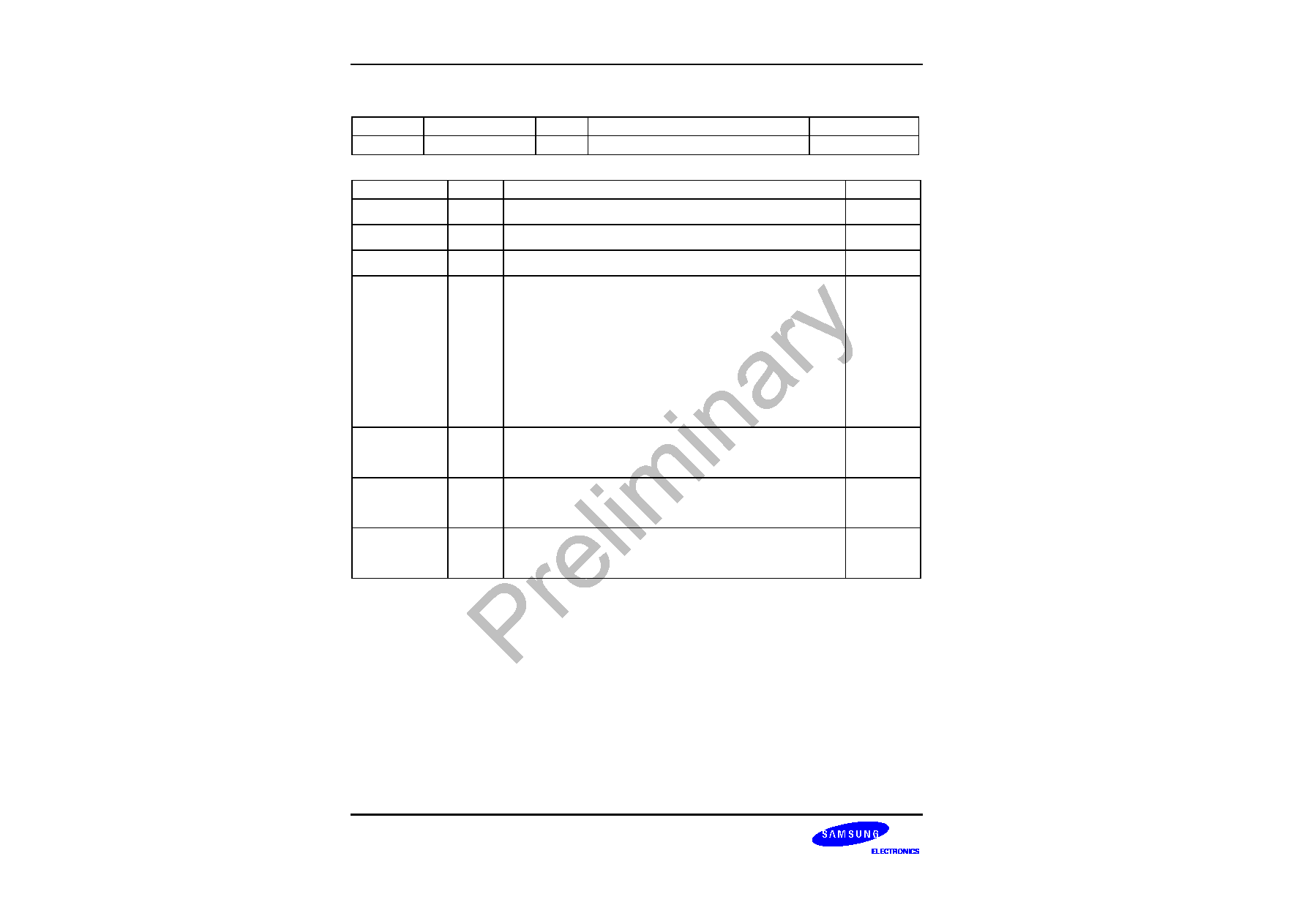
BSW rv0.1-0417-N01
Preliminary product information describes products that are in development,
for which full characterization data and associated errata are not yet available.
Specifications and information herein are subject to change without notice.
S3C24A0 RISC MICROPROCESSOR
CAMERA INTERFACE
21-14
GLOBAL CONTROL REGISTER
Register
Address
R/W
Description
Reset Value
CIGCTRL
0x48000008
RW
Global control register
0x20000000
CIGCTRL
Bit
Description
Initial State
SwRst
[31]
Camera interface software reset
0
CamRst
[30]
External camera processor Reset or Power Down control
0
Reserved
[29]
Should be `1'.
1
TestPattern
[28:27]
This register should be set at only ITU-T 601 8-bit mode. Not
allowed with input 16-bit mode or ITU-T 656 mode. (max. 1280 X
1024)
00 : external camera processor input (normal)
01 : color bar test pattern
10 : horizontal increment test pattern
11 . vertical increment test pattern
0
InvPolPCLK
[26]
1 : inverse the polarity of XciPCLK
0 : normal(Camera data is fetched at rising edge of XciPCLK)
0
InvPolVSYNC
[25]
1 : inverse the polarity of XciVSYNC
0 : normal
0
InvPolHREF
[24]
1 : inverse the polarity of XciHREF
0 : normal
0

BSW rv0.1-0417-N01
Preliminary product information describes products that are in development,
for which full characterization data and associated errata are not yet available.
Specifications and information herein are subject to change without notice.
S3C24A0 RISC MICROPROCESSOR
CAMERA INTERFACE
2
1-15
Y1 START ADDRESS REGISTER
Register
Address
R/W
Description
Reset Value
CICOYSA1
0x48000018
RW
1
st
Y frame start address for codec DMA
0
CICOYSA1
Bit
Description
Initial State
CICOYSA1
[31:0]
1
st
Y frame start address for codec DMA
0
Y2 START ADDRESS REGISTER
Register
Address
R/W
Description
Reset Value
CICOYSA2
0x4800001c
RW
2
nd
Y frame start address for codec DMA
0
CICOYSA2
Bit
Description
Initial State
CICOYSA2
[31:0]
2
nd
Y frame start address for codec DMA
0
Y3 START ADDRESS REGISTER
Register
Address
R/W
Description
Reset Value
CICOYSA3
0x48000020
RW
3
rd
Y frame start address for codec DMA
0
CICOYSA3
Bit
Description
Initial State
CICOYSA3
[31:0]
3
rd
Y frame start address for codec DMA
0
Y4 START ADDRESS REGISTER
Register
Address
R/W
Description
Reset Value
CICOYSA4
0x48000024
RW
4
th
Y frame start address for codec DMA
0
CICOYSA4
Bit
Description
Initial State
CICOYSA4
[31:0]
4
th
Y frame start address for codec DMA
0
CB1 START ADDRESS REGISTER
Register
Address
R/W
Description
Reset Value
CICOCBSA1
0x48000028
RW
1
st
Cb frame start address for codec DMA
0

BSW rv0.1-0417-N01
Preliminary product information describes products that are in development,
for which full characterization data and associated errata are not yet available.
Specifications and information herein are subject to change without notice.
S3C24A0 RISC MICROPROCESSOR
CAMERA INTERFACE
21-16
CICOCBSA1
Bit
Description
Initial State
CICOCBSA1
[31:0]
1
st
Cb frame start address for codec DMA
0
CB2 START ADDRESS REGISTER
Register
Address
R/W
Description
Reset Value
CICOCBSA2
0x4800002c
RW
2
nd
Cb frame start address for codec DMA
0
CICOCBSA2
Bit
Description
Initial State
CICOCBSA2
[31:0]
2
nd
Cb frame start address for codec DMA
0
CB3 START ADDRESS REGISTER
Register
Address
R/W
Description
Reset Value
CICOCBSA3
0x48000030
RW
3
rd
Cb frame start address for codec DMA
0
CICOCBSA3
Bit
Description
Initial State
CICOCBSA3
[31:0]
3
rd
Cb frame start address for codec DMA
0
CB4 START ADDRESS REGISTER
Register
Address
R/W
Description
Reset Value
CICOCBSA4
0x48000034
RW
4
th
Cb frame start address for codec DMA
0
CICOCBSA4
Bit
Description
Initial State
CICOCBSA4
[31:0]
4
th
Cb frame start address for codec DMA
0
CR1 START ADDRESS REGISTER
Register
Address
R/W
Description
Reset Value
CICOCRSA1
0x48000038
RW
1
st
Cr frame start address for codec DMA
0
CICOCRSA1
Bit
Description
Initial State
CICOCRSA1
[31:0]
1
st
Cr frame start address for codec DMA
0

BSW rv0.1-0417-N01
Preliminary product information describes products that are in development,
for which full characterization data and associated errata are not yet available.
Specifications and information herein are subject to change without notice.
S3C24A0 RISC MICROPROCESSOR
CAMERA INTERFACE
2
1-17
CR2 START ADDRESS REGISTER
Register
Address
R/W
Description
Reset Value
CICOCRSA2
0x4800003c
RW
2
nd
Cr frame start address for codec DMA
0
CICOCRSA2
Bit
Description
Initial State
CICOCRSA2
[31:0]
2
nd
Cr frame start address for codec DMA
0
CR3 START ADDRESS REGISTER
Register
Address
R/W
Description
Reset Value
CICOCRSA3
0x48000040
RW
3
rd
Cr frame start address for codec DMA
0
CICOCRSA3
Bit
Description
Initial State
CICOCRSA3
[31:0]
3
rd
Cr frame start address for codec DMA
0
CR4 START ADDRESS REGISTER
Register
Address
R/W
Description
Reset Value
CICOCRSA4
0x48000044
RW
4
th
Cr frame start address for codec DMA
0
CICOCRSA4
Bit
Description
Initial State
CICOCRSA4
[31:0]
4
th
Cr frame start address for codec DMA
0
CODEC TARGET FORMAT REGISTER
Register
Address
R/W
Description
Reset Value
CICOTRGFMT
0x48000048
RW
Target image format of codec DMA
0

BSW rv0.1-0417-N01
Preliminary product information describes products that are in development,
for which full characterization data and associated errata are not yet available.
Specifications and information herein are subject to change without notice.
S3C24A0 RISC MICROPROCESSOR
CAMERA INTERFACE
21-18
Original image
X-axis flip
Y-axis flip
180' rotation
Figure 21-14 Image mirror and rotation
CICOTRGFMT
Bit
Description
Initial State
In422_Co
[31]
1 : YCbCr 4:2:2 codec scaler input image format.
0 : YCbCr 4:2:0 codec scaler input image format. In this case,
horizontal line decimation is performed before codec scaler.
(normal)
0
Out422_Co
[30]
1 : YCbCr 4:2:2 codec scaler output image format. This mode is
mainly for S/W JPEG.
0 : YCbCr 4:2:0 codec scaler output image format. This mode is
mainly for MPEG-4 codec and H/W JPEG DCT.(normal)
0
TargetHsize_Co
[28:16]
Horizontal pixel number of target image for codec DMA (16's
multiple)
0
FlipMd_Co
[15:14]
Image mirror and rotation for codec DMA
00 : Normal
01 : X-axis mirror
10 : Y-axis mirror
11 : 180�rotation
0
TargetVsize_Co
[12:0]
Vertical pixel number of target image for codec DMA (must be 16's
multiple for JPEG DCT.)
0

BSW rv0.1-0417-N01
Preliminary product information describes products that are in development,
for which full characterization data and associated errata are not yet available.
Specifications and information herein are subject to change without notice.
S3C24A0 RISC MICROPROCESSOR
CAMERA INTERFACE
2
1-19
CODEC DMA CONTROL REGISTER
Register
Address
R/W
Description
Reset Value
CICOCTRL
0x4800004c
RW
Codec DMA control
0
CICOCTRL
Bit
Description
Initial State
Yburst1_Co
[23:19]
Main burst length for codec Y frames
0
Yburst2_Co
[18:14]
Remained burst length for codec Y frames
0
Cburst1_Co
[13:9]
Main burst length for codec Cb/Cr frames
0
Cburst2_Co
[8:4]
Remained burst length for codec Cb/Cr frames
0
LastIRQEn_Co
[2]
1 : enable last IRQ at the end of frame capture (It is recommended
to check the done signal of capturing image for JPEG.)
0 : normal
0
All burst lengthes should be one of the 2,4,8,16.
Example 1. Target image size : QCIF (horizontal Y width = 176)
176 / 4 = 44 word.
44 % 8 = 4 main burst = 8, remained burst = 4
Example 2. Target image size : VGA (horizontal Y width = 640)
640 / 4 = 160 word.
160 % 16 = 0 main burst = 16, remained burst = 16
Example 3. Target image size : QCIF (horizontal C width = 88)
88 / 4 = 22 word.
22 % 4 = 2 main burst = 4, remained burst = 2 (HTRANS==INCR)
REGISTER SETTING GUIDE FOR CODEC SCALER AND PREVIEW SCALER
SRC_Width and DST_Width satisfy the following constraints. In SRC_Width case, the number of horizontal
pixel can be represented to the power of 8. In DST_Width case, the number of horizontal pixel can be represented
kn where n = 1,2,3, ... and k = 2/4/16 for 24bpp RGB/16bpp RGB/YCbCr image, respectively.
TargetHsize should
not be larger than SourceHsize. Similarly, TargetVsize should not be larger than SourceVsize.
BSW rv0.1-0417-N01
Preliminary product information describes products that are in development,
for which full characterization data and associated errata are not yet available.
Specifications and information herein are subject to change without notice.
S3C24A0 RISC MICROPROCESSOR
CAMERA INTERFACE
21-20
SourceHsize
So
urce
V
s
iz
e
TargetHsize_xx
T
a
r
g
et
V
s
ize_
xx
Original Input
Scale Down
SourceHsize
So
urce
V
s
iz
e
Original Input
Zoom In
: WinHorOfst
: WinVerOfst
TargetHsize_xx
T
a
r
g
et
Vs
i
z
e_
x
x
SRC_Width = SourceHsize
SRC_Height = SourceVsize
TargetHsize_xx = TargetHsize_Co or TargetHsize_Pr
DST_Width = TargetHsize_xx
DST_Height = TargetVsize_xx
TargetHsize_xx = TargetHsize_Co or TargetHsize_Pr
DST_Width = TargetHsize_xx
DST_Height = TargetVsize_xx
SRC_Width = SourceHsize - (2 x WinHorOfst)
SRC_Height = SourceVsize - (2 x WinVerOfst)
Figure 21-15 Scaling scheme
The other control registers of pre-scaled image size, pre-scale ratio, pre-scale shift ratio and main scale ratio
are defined according to the following equations.
If ( SRC_Width >= 64 � DST_Width ) { Exit(-1); /* Out Of Horizontal Scale Range */ }
else if (SRC_Width >= 32 � DST_Width) { PreHorRatio_xx = 32; H_Shift = 5; }
else if (SRC_Width >= 16 � DST_Width) { PreHorRatio_xx = 16; H_Shift = 4; }
else if (SRC_Width >= 8 � DST_Width) { PreHorRatio_xx = 8; H_Shift = 3; }
else if (SRC_Width >= 4 � DST_Width) { PreHorRatio_xx = 4; H_Shift = 2; }
else if (SRC_Width >= 2 � DST_Width) { PreHorRatio_xx = 2; H_Shift = 1; }
else { PreHorRatio_xx = 1; H_Shift = 0; }
PreDstWidth_xx = SRC_Width / PreHorRatio_xx;
MainHorRatio_xx = ( SRC_Width << 8 ) / ( DST_Width << H_Shift);
If ( SRC_Height >= 64 � DST_Height ) { Exit(-1); /* Out Of Vertical Scale Range */ }
else if (SRC_Height >= 32 � DST_Height) { PreVerRatio_xx = 32; V_Shift = 5; }
else if (SRC_Height >= 16 � DST_Height) { PreVerRatio_xx = 16; V_Shift = 4; }

BSW rv0.1-0417-N01
Preliminary product information describes products that are in development,
for which full characterization data and associated errata are not yet available.
Specifications and information herein are subject to change without notice.
S3C24A0 RISC MICROPROCESSOR
CAMERA INTERFACE
2
1-21
else if (SRC_Height >= 8 � DST_Height) { PreVerRatio_xx = 8; V_Shift = 3; }
else if (SRC_Height >= 4 � DST_Height) { PreVerRatio_xx = 4; V_Shift = 2; }
else if (SRC_Height >= 2 � DST_Height) { PreVerRatio_xx = 2; V_Shift = 1; }
else { PreVerRatio_xx = 1; V_Shift = 0; }
PreDstHeight_xx = SRC_Height / PreVerRatio_xx;
MainVerRatio_xx = ( SRC_Height << 8 ) / ( DST_Height << V_Shift);
SHfactor_xx = 10 � ( H_Shit + V_Shift);
Note:
In preview path, Pre-scaled H_width must be the less than 640. (The maximum size of preview path
horizontal line buffer is 640.)

BSW rv0.1-0417-N01
Preliminary product information describes products that are in development,
for which full characterization data and associated errata are not yet available.
Specifications and information herein are subject to change without notice.
S3C24A0 RISC MICROPROCESSOR
CAMERA INTERFACE
21-22
CODEC PRE-SCALER CONTROL REGISTER 1
Register
Address
R/W
Description
Reset Value
CICOSCPRERATIO
0x48000050
RW
Codec pre-scaler ratio control
0
CICOSCPRERATIO
Bit
Description
Initial State
SHfactor_Co
[31:28]
Shift factor for codec pre-scaler
0
PreHorRatio_Co
[22:16]
Horizontal ratio of codec pre-scaler
0
PreVerRatio_Co
[6:0]
Vertical ratio of codec pre-scaler
0
CODEC PRE-SCALER CONTROL REGISTER 2
Register
Address
R/W
Description
Reset Value
CICOSCPREDST
0x48000054
RW
Codec pre-scaler destination format
0
CICOSCPREDST
Bit
Description
Initial State
PreDstWidth_Co
[27:16]
Destination width for codec pre-scaler
0
PreDstHeight_Co
[11:0]
Destination height for codec pre-scaler
0
CODEC MAIN-SCALER CONTROL REGISTER
Register
Address
R/W
Description
Reset Value
CICOSCCTRL
0x48000058
RW
Codec main-scaler control
0
CICOSCCTRL
Bit
Description
Initial State
ScalerBypass_Co
[31]
Codec scaler bypass for upper 2048 x 2048 size (In this case,
ImgCptEn_CoSC and ImgCptEn_PrSC should be 0, but
ImgCptEn should be 1. It is not allowed to capturing preview
image. This mode is intended to capture JPEG input image for
DSC application) In this case, input pixel buffering depends on
only input FIFOs, so system bus should be not busy in this
mode.
0
ScaleUpDown_Co
[30:29]
Scale up/down flag for codec scaler(In 1:1 scale ratio, this bit
should be "1")
00 = down 11 = up
00
MainHorRatio_Co
[24:16]
Horizontal scale ratio for codec main-scaler
0

BSW rv0.1-0417-N01
Preliminary product information describes products that are in development,
for which full characterization data and associated errata are not yet available.
Specifications and information herein are subject to change without notice.
S3C24A0 RISC MICROPROCESSOR
CAMERA INTERFACE
2
1-23
CoScalerStart
[15]
Codec scaler start
0
MainVerRatio_Co
[8:0]
Vertical scale ratio for codec main-scaler
0
CODEC DMA TARGET AREA REGISTER
Register
Address
R/W
Description
Reset Value
CICOTAREA
0x4800005c
RW
Codec pre-scaler destination format
0
CICOTAREA
Bit
Description
Initial State
CICOTAREA
[25:0]
Target area for codec DMA
= Target H size x Target V size
0
CODEC STATUS REGISTER
Register
Address
R/W
Description
Reset Value
CICOSTATUS
0x48000064
R
Codec path status
0
CICOSTATUS
Bit
Description
Initial State
OvFiY_Co
[31]
Overflow state of codec FIFO Y
0
OvFiCb_Co
[30]
Overflow state of codec FIFO Cb
0
OvFiCr_Co
[29]
Overflow state of codec FIFO Cr
0
VSYNC
[28]
Camera VSYNC (This bit can be referred by CPU for first SFR
setting after external camera muxing. And, it can be seen in the
ITU-R BT 656 mode) 1:blank, 0: field
0
FrameCnt_Co
[27:26]
Frame count of codec DMA (This counter value means the next
frame number)
0
WinOfstEn_Co
[25]
Window offset enable status
0
FlipMd_Co
[24:23]
Flip mode of codec DMA
0
ImgCptEn_CamIf
[22]
Image capture enable of camera interface
0
ImgCptEn_CoSC
[21]
Image capture enable of codec path
0
VSYNC_E
[20]
Status of signal level of XciVSYNC
x

BSW rv0.1-0417-N01
Preliminary product information describes products that are in development,
for which full characterization data and associated errata are not yet available.
Specifications and information herein are subject to change without notice.
S3C24A0 RISC MICROPROCESSOR
CAMERA INTERFACE
21-24
RGB1 START ADDRESS REGISTER
Register
Address
R/W
Description
Reset Value
CIPRCLRSA
1
0x4800006c
RW
1
st
RGB frame start address for preview
DMA
0
CIPRCLRSA1
Bit
Description
Initial State
CIPRCLRSA1
[31:0]
1
st
RGB frame start address for preview DMA
0
RGB2 START ADDRESS REGISTER
Register
Address
R/W
Description
Reset Value
CIPRCLRSA
2
0x48000070
RW
2
nd
RGB frame start address for preview DMA
0
CIPRCLRSA2
Bit
Description
Initial State
CIPRCLRSA2
[31:0]
2
nd
RGB frame start address for preview DMA
0
RGB3 START ADDRESS REGISTER
Register
Address
R/W
Description
Reset Value
CIPRCLRSA
3
0x48000074
RW
3
rd
RGB frame start address for preview DMA
0
CIPRCLRSA3
Bit
Description
Initial State
CIPRCLRSA3
[31:0]
3
rd
RGB frame start address for preview DMA
0
RGB4 START ADDRESS REGISTER
Register
Address
R/W
Description
Reset Value
CIPRCLRSA
4
0x48000078
RW
4
th
RGB frame start address for preview DMA
0
CIPRCLRSA4
Bit
Description
Initial State
CIPRCLRSA4
[31:0]
4
th
RGB frame start address for preview DMA
0

BSW rv0.1-0417-N01
Preliminary product information describes products that are in development,
for which full characterization data and associated errata are not yet available.
Specifications and information herein are subject to change without notice.
S3C24A0 RISC MICROPROCESSOR
CAMERA INTERFACE
2
1-25
PREVIEW TARGET FORMAT REGISTER
Register
Address
R/W
Description
Reset Value
CIPRTRGFMT
0x4800007c
RW
Target image format of preview DMA
0
CIPRTRGFMT
Bit
Description
Initial State
TargetHsize_Pr
[28:16]
Horizontal pixel number of target image for preview DMA .
16bpp RGB : 4n(n=1,2,3, ...)
24bpp RGB : 2n(n=1,2,3, ...)
0
FlipMd_Pr
[15:14]
Image mirror and rotation for preview DMA
00 : normal
01 : x-axis mirror
10 : y-axis mirror
11 : 180� rotation
0
TargetVsize_Pr
[12:0]
Vertical pixel number of target image for preview DMA
0
PREVIEW DMA CONTROL REGISTER
Register
Address
R/W
Description
Reset Value
CIPRCTRL
0x48000080
RW
Preview DMA control related
0
CIPRCTRL
Bit
Description
Initial State
RGBburst1_Pr
[23:19]
Main burst length for preview RGB frames
0
RGBburst2_Pr
[18:14]
Remained burst length for preview RGB frames
0
LastIRQEn_Pr
[2]
1 : enable last IRQ at the end of frame capture
0 : normal
0
All burst lengths must be one of the 2,4,8,16.
Example 1. Target image size : QCIF for RGB 32-bit format (horizontal width = 176 pixels. 1 pixel = 1 word)
176 pixel = 176 word.
176 % 16 = 0 main burst = 16, remained burst = 16
Example 2. Target image size : VGA for RGB 16-bit format (horizontal width = 640 pixels. 2 pixel = 1 word)
640 / 2 = 320 word.

BSW rv0.1-0417-N01
Preliminary product information describes products that are in development,
for which full characterization data and associated errata are not yet available.
Specifications and information herein are subject to change without notice.
S3C24A0 RISC MICROPROCESSOR
CAMERA INTERFACE
21-26
160 % 16 = 0 main burst = 16, remained burst = 16
Note:
Preview path contains 640 pixel line buffer.(Codec path contains 2048 pixel line buffer) So, upper 1280
pixels, input images must be pre-scaled by over 1/2 for capturing valid preview image.
PREVIEW PRE-SCALER CONTROL REGISTER 1
Register
Address
R/W
Description
Reset Value
CIPRSCPRERATIO
0x48000084
RW
Preview pre-scaler ratio control
0
CIPRSCPRERATIO
Bit
Description
Initial State
SHfactor_Pr
[31:28]
Shift factor for preview pre-scaler
0
PreHorRatio_Pr
[22:16]
Horizontal ratio of preview pre-scaler
0
PreVerRatio_Pr
[6:0]
Vertical ratio of preview pre-scaler
0
PREVIEW PRE-SCALER CONTROL REGISTER 2
Register
Address
R/W
Description
Reset Value
CIPRSCPREDST
0x48000088
RW
Preview pre-scaler destination format
0
CIPRSCPREDST
Bit
Description
Initial State
PreDstWidth_Pr
[27:16]
Destination width for preview pre-scaler
0
PreDstHeight_Pr
[11:0]
Destination height for preview pre-scaler
0
PREVIEW MAIN-SCALER CONTROL REGISTER
Register
Address
R/W
Description
Reset Value
CIPRSCCTRL
0x4800008c
RW
Preview main-scaler control
0
CIPRSCCTRL
Bit
Description
Initial State
Sample_Pr
[31]
Sampling method for format conversion. (normally 1)
0
RGBformat_Pr
[30]
1 : 24-bit RGB , 0 : 16-bit RGB
0

BSW rv0.1-0417-N01
Preliminary product information describes products that are in development,
for which full characterization data and associated errata are not yet available.
Specifications and information herein are subject to change without notice.
S3C24A0 RISC MICROPROCESSOR
CAMERA INTERFACE
2
1-27
ScaleUpDown_Pr
[29:28]
Scale up/down flag for preview scaler(In 1:1 scale ratio, this bit
should be "1")
00 = down 11 =
up
00
MainHorRatio_Pr
[24:16]
Horizontal scale ratio for preview main-scaler
0
PrScalerStart
[15]
Preview scaler start
0
MainVerRatio_Pr
[8:0]
Vertical scale ratio for preview main-scaler
0
PREVIEW DMA TARGET AREA REGISTER
Register
Address
R/W
Description
Reset Value
CIPRTAREA
0x48000090
RW
Preview pre-scaler destination format
0
CIPRTAREA
Bit
Description
Initial State
CIPRTAREA
[25:0]
Target area for preview DMA
= Target H size x Target V size
0
PREVIEW STATUS REGISTER
Register
Address
R/W
Description
Reset Value
CIPRSTATUS
0x48000098
R
Preview path status
0
CIPRSTATUS
Bit
Description
Initial State
OvFiCb_Pr
[31]
Overflow state of preview FIFO Cb
0
OvFiCr_Pr
[30]
Overflow state of preview FIFO Cr
0
FrameCnt_Pr
[27:26]
Frame count of preview DMA
0
FlipMd_Pr
[24:23]
Flip mode of preview DMA
0
ImgCptEn_PrSC
[21]
Image capture enable of preview path
0
IMAGE CAPTURE ENABLE REGISTER
Register
Address
R/W
Description
Reset Value
CIIMGCPT
0x480000a0
RW
Image capture enable command
0
CIIMGCPT
Bit
Description
Initial State
BSW rv0.1-0417-N01
Preliminary product information describes products that are in development,
for which full characterization data and associated errata are not yet available.
Specifications and information herein are subject to change without notice.
S3C24A0 RISC MICROPROCESSOR
CAMERA INTERFACE
21-28
ImgCptEn
[31]
camera interface global capture enable
0
ImgCptEn_CoSc
[30]
capture enable for codec scaler. This bit must be zero in scaler-
bypass mode.
0
ImgCptEn_PrSc
[29]
capture enable for preview scaler. This bit must be zero in scaler-
bypass mode.
0
Note:
This register must be set at last.
NOTES

BSW rv0.1-0417-N01
Preliminary product information describes products that are in development,
for which full characterization data and associated errata are not yet available.
Specifications and information herein are subject to change without notice.
S3C24A0 RISC MICROPROCESSOR
MPEG-4 VIDEO CODEC
22
-1
MPEG-4 VIDEO CODEC
OVERVIEW
MPEG-4 is an ISO/IEC standard developed by MPEG (Moving Picture Experts Group). MPEG-4 video aims at
providing standardized core technologies allowing efficient storage, transmission and manipulation of video data
in multimedia environments. MPEG-4 video codec of S3C24A0 provides high performance solution and lower the
processing load of embedded processor core. The processing clock for DCT/quantization and motion estimation
can be controlled by embedded processor core to reduce the power consumption.
FEATURE
-
ISO/IEC MPEG-4 Simple Profile @ Level 3 / ITU-T H.263 Base Line
-
AMBA AHB Interface
-
Real-time Encoding / Decoding
-
Scalable image size : M x N macro-blocks up to 2048x2048
-
Hardware Accelerator for Motion Estimation, Motion Compensation, DCT/Quantization and VLC/VLD
-
Unrestricted Mode & Advanced Prediction Mode (4MV)
-
Half-pel Search
-
Programmable Processing Clock in DCT/Quantization and Motion Estimation : HCLK ~ HCLK/30

BSW rv0.1-0417-N01
Preliminary product information describes products that are in development,
for which full characterization data and associated errata are not yet available.
Specifications and information herein are subject to change without notice.
MPEG-4 VIDEO CODEC
S3C24A0 RISC MICROPROCESSOR
22-2
BLOCK DIAGRAM
Figure 22-1 shows the functional block diagram of S3C24A0 MPEG-4 Video CODEC. This CODEC consists of
four parts, i.e., DCT/Quantization, Motion Compensation, Motion Estimation and VLX(VLC/VLD).
curr
mem
DCT
mced
mem
Q
IQ
IDCT
recon
mem
Qp
factor
COEF
mem
SDRAM
SDRAM
SDRAM
ME
prev
mem
curr
mem
MC
DCT/Q
VLX
Figure 22-1. MPEG-4 Video CODEC Block Diagram

BSW rv0.1-0417-N01
Preliminary product information describes products that are in development,
for which full characterization data and associated errata are not yet available.
Specifications and information herein are subject to change without notice.
S3C24A0 RISC MICROPROCESSOR
MPEG-4 MOTION ESTIMATION
23-1
MPEG-4 MOTION ESTIMATION
OVERVIEW
The MPEG-4 motion estimation block is a part of MPEG-4 Video CODEC. Motion estimation is an essential
part in standard video coder such as H.26x, MPEG-1, MPEG-2 and MPEG-4. By removing temporal
redundancies exiting in adjacent frames Advanced MRMCS (Multi-Resolution search using Multiple
Candidates and Spatial correlation of motion field) algorithm is applied and it is based on the hierarchical
search block-matching algorithm.
FEATURE
-
MPEG-4 Simple Profile @ Level 3 / H.263 Base Line
-
AMBA AHB Interface
-
Using Advanced MRMCS (Multi-Resolution search using Multiple Candidates and Spatial correlation
of motion field) Algorithm
-
Scalable image size : M x N macro-blocks up to 2048x2048
-
Unrestricted Mode & Advanced Prediction Mode (4MV)
-
INTRA / INTER Mode Decision
-
Macroblock-based Padding
-
Search Range : [-16, 15.5]
-
Half-pel Search
-
Double Buffering of frame Data
-
Re-use of Overlapped Search Range Data
-
Variable processing clock ( HCLK ~ HCLK / 30 )
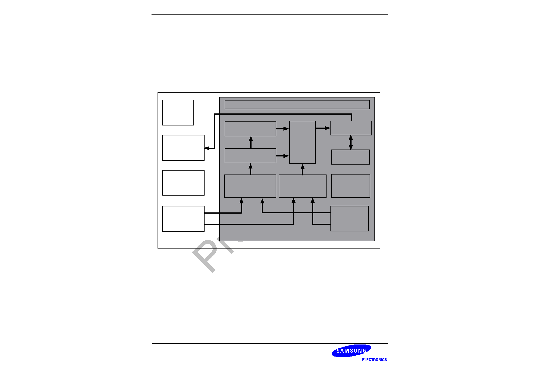
BSW rv0.1-0417-N01
Preliminary product information describes products that are in development,
for which full characterization data and associated errata are not yet available.
Specifications and information herein are subject to change without notice.
MPEG-4 MOTION ESTIMATION S3C24A0 RISC MICROPROCESSOR
23-2
MPEG-4 MOTION ESTIMATION OPERATION
BLOCK DIAGRAM
Figure 23-1 shows the functional block diagram of MPEG-4 Motion Estimation. This block includes two parts
with different clocks, i.e., system clock part and motion estimation clock part.
config
sdram_ctrl
sdram_read
sram_write
internal_ctrl
interpolation
data_arrange
prev_mem
(80x64x12)
curr_mem
(16x16x8x2)
bsu
candidate
shift_reg
sram_read
mode
decision
System Clock Part
ME Clock Part
Figure 23-1. MPEG-4 Motion Estimation Block Diagram

BSW rv0.1-0417-N01
Preliminary product information describes products that are in development,
for which full characterization data and associated errata are not yet available.
Specifications and information herein are subject to change without notice.
S3C24A0 RISC MICROPROCESSOR
MPEG-4 MOTION ESTIMATION
23-3
OPERATION FLOW
-
Firstly, set current, previous, and motion vector start address registers.
-
Start address of previous frame must be considered the padding area.
-
Set command register to operate motion estimation block.
-
Current image data and padded previous image data of a macro-block are stored into the internal
SRAM buffers from the external SDRAM.
-
Operations to find motion vector of each macro-block are started after data transfer.
-
After the completion of searches for each macro-block, the result data is written into the external
SDRAM and then operations for one macro-block are finished.
-
The operation unit in command register is set to decide the number of the macro-block to operate
motion estimation continuously.
Y Image
Current Frame
Start Address
Y Image
Previous Frame
Start Address
offset
(a) Current Frame (b) Previous Frame
Figure 23-2. Memory Map of Y (Luminance) Image for Current and Previous Frames
Table 1. Example of Sizes of Y Image and Offset for QCIF and CIF
Image Format
QCIF
CIF
Current Frame
176x144 = 25,344
352x288 = 101,376
Y
Image
Previous Frame
(176+16x2)x(144+16x2) = 36,608
(352+16x2)x(288+16x2) =122,880
Offset
(176+16x2)x16+16 = 3,344
(352+16x2)x16+16 = 6,160

BSW rv0.1-0417-N01
Preliminary product information describes products that are in development,
for which full characterization data and associated errata are not yet available.
Specifications and information herein are subject to change without notice.
MPEG-4 MOTION ESTIMATION S3C24A0 RISC MICROPROCESSOR
23-4
RESULT DATA
-
The result of the motion estimation for each macro-block is stored into the external SDRAM area
assigned in motion vector start address register.
-
The result data of each macro-block is as follows.
Address 0
1
2
3
4
(a) Location of 8x8 block in one macro-block (b) Result data of one macro-block
Figure 23-3. Motion Estimation Result Data
-
MVX0, 1, 2, 3 and MVY0, 1, 2, 3 are X and Y components for motion vector of block 0, 1, 2, 3,
respectively.
-
The value of bit 0 of MVX0, 1, 2, 3 and MVY0, 1, 2, 3 indicates the value of half-pel unit. If this bit is 1,
the value is 0.5. Otherwise, it indicates 0.0. Bit [7:1] is the signed number that is represented using 2's
complement system. For example, if values of MVX0 and MVY0 are 0xE2 and 0x1B, respectively, the
values of X and Y components of motion vector are �15.0 and 13.5, respectively.
-
In the case of 4MV mode, motion vectors of 4 blocks are generated and in other cases, 4 motion
vectors have the same value.
-
SAD0, 1, 2 and 3 are the SAD values for each block and they can be used for DCT/Q skipping.
-
The value of INTRA/INTER mode indicates that 0x0000 is INTER mode and 0xFFFF is INTRA mode.
This value is only valid in case of MPEG-4 mode and always is 0x0000, that is, INTER mode in H.263
mode.
-
SADinter is the result of min { SAD16, SAD8 } after half-pel operation and it is used for INTRA/INTER
mode decision.
Block 0
Block 1
Block 2
Block 3
MVY1
MVX1
MVY0
MVX0
MVY3
MVX3
MVY2
MVX2
SAD1
SAD0
SAD3
SAD2
SADinter
INTRA/INTER Mode

BSW rv0.1-0417-N01
Preliminary product information describes products that are in development,
for which full characterization data and associated errata are not yet available.
Specifications and information herein are subject to change without notice.
S3C24A0 RISC MICROPROCESSOR
MPEG-4 MOTION ESTIMATION
23-5
MPEG-4 MOTION ESTIMATION SPECIAL REGISTERS
Current Frame Start Address Register (ME_CFSA)
Register
Address
R/W
Description
Reset Value
ME_CFSA
0x4880_0000
R/W
Current frame start address register
0x0000_0000
ME_CFSA
Bit
Description
Initial State
Current frame start address
[31:0]
Set current frame start address
0x0000_0000
Note 1. Current Frame Start Address is the start address of current Y image. Motion estimation operates
only for Y (Luminance) image.
Previous Frame Start Address Register (ME_PFSA)
Register
Address
R/W
Description
Reset Value
ME_PFSA
0x4880_0004
R/W
Previous frame start address register
0x0000_0000
ME_PFSA
Bit
Description
Initial State
Previous frame start address
[31:0]
Set previous frame start address
0x0000_0000
Note 1. Previous Frame Start Address is the start address of previous Y image. Motion estimation operates
only for Y (Luminance) image.
2. Previous Frame Start Address must be considered the padding area and it is the start address of the
original previous image except the padding area.
Motion Vector Start Address Register (ME_MVSA)
Register
Address
R/W
Description
Reset Value
ME_MVSA
0x4880_0008
R/W
Motion vector start address register
0x0000_0000
ME_MVSA
Bit
Description
Initial State
Motion vector start address
[31:0]
Set motion vector start address
0x0000_0000
Note 1. Motion Vector Start Address is the start address to store the result data of motion estimation.
2. The number of the result data is determined according to the operation unit of command register.

BSW rv0.1-0417-N01
Preliminary product information describes products that are in development,
for which full characterization data and associated errata are not yet available.
Specifications and information herein are subject to change without notice.
MPEG-4 MOTION ESTIMATION S3C24A0 RISC MICROPROCESSOR
23-6
Command Register (ME_CMND)
Register
Address
R/W
Description
Reset Value
ME_CMND
0x4880_000C
R/W
Command register
0x0000_0001
ME_CMND
Bit
Description
Initial State
-
[31:18] Reserved
0x0
Round control bit
[17]
0 : round bit 0
1 : round bit 1
0
4MV mode enable
[16]
0 : 16x16 prediction mode
1 : advanced prediction mode (4MV)
0
-
[15:4]
Reserved
0x0
ME operation start bit
[3]
0 : not active
1 : enable
0
MPEG-4/H.263 mode select
[2]
0 : MPEG-4 mode
1 : H.263 mode
0
Frame start bit
[1]
0 : not active
1 : enable
0
Interrupt request clear bit
[0]
0 : not active
1 : clear
1
Note 1. Frame start bit is enabled only when the first start of the frame.
2. ME operation start bit is enable every operation unit in the frame.
3. Interrupt request clear bit is cleared when ME operation start bit is enable at the same time.

BSW rv0.1-0417-N01
Preliminary product information describes products that are in development,
for which full characterization data and associated errata are not yet available.
Specifications and information herein are subject to change without notice.
S3C24A0 RISC MICROPROCESSOR
MPEG-4 MOTION ESTIMATION
23-7
Status & S/W Reset Register (ME_STAT_SWR)
Register
Address
R/W
Description
Reset Value
ME_STAT_SWR 0x4880_0010
R/(W)
Status & S/W reset register
0x0000_0002
ME_STAT_SWR
Bit
Description
Initial State
Reserved
[31:20]
R
Reserved
0x0
BSU state buf FSM
[19:16]
R
BSU state buf FSM in candidate block
0x0
Data flow FSM
[15:12]
R
Data flow FSM in internal_ctrl block
0x0
BSU FSM
[11:8]
R
BSU FSM in internal_ctrl block
0x0
Reserved
[7]
R
Reserved
0
Control FSM
[6:4]
R
Control FSM in sdram_ctrl block
0x0
Reserved
[3:2]
R
Reserved
0x0
S/W reset bit
[1]
R/W
0 : set S/W reset
1 : clear S/W reset
1
Motion estimation status bit
[0]
R
0 : idle
1 : busy
0
Note 1. In case of not using interrupt, motion estimation operation must be started when motion estimation
status bit is "0".
2. S/W reset bit is used to reset motion estimation block. It reset special registers and internal finite
state machines.
3. Since S/W reset bit keeps the written value until written into "0" or hardware reset, be careful to use
S/W reset bit.

BSW rv0.1-0417-N01
Preliminary product information describes products that are in development,
for which full characterization data and associated errata are not yet available.
Specifications and information herein are subject to change without notice.
MPEG-4 MOTION ESTIMATION S3C24A0 RISC MICROPROCESSOR
23-8
Configuration Register (ME_CNFG)
Register
Address
R/W
Description
Reset Value
ME_CNFG
0x4880_0014
R/W
Configuration register
0x0010_0063
ME_CNFG
Bit
Description
Initial State
-
[31:25] Reserved
0x0
Fast mode enable bit
[24]
0 : disable
1 : enable
0
-
[23]
Reserved
0
Threshold value
[22:16]
Threshold value to be compared to the intensity
variation in the fast mode
0x10
-
[15:14] Reserved
0x0
Operation unit
[13:0]
The number of macro-blocks to operate motion
estimation continuously
0x0063
Note 1. The operation unit is variable only inside one frame.
2. In fast mode, the execution time is considerably reduced with less PSNR.
3. Fast mode enable bit is only valid in case of MPEG-4 mode. In H.263 mode, this bit always is not
enabled.
Image Format Register (ME_IMGFMT)
Register
Address
R/W
Description
Reset Value
ME_IMGFMT
0x4880_0018
R/W
Image format register
0x0000_080A
ME_IMGFMT
Bit
Description
Initial State
-
[31:15] Reserved
0x0
N value
[14:8] The number of vertical macro-blocks minus one
0x08
-
[7]
Reserved
0
M value
[6:0]
The number of horizontal macro-blocks minus one
0x0A

BSW rv0.1-0417-N01
Preliminary product information describes products that are in development,
for which full characterization data and associated errata are not yet available.
Specifications and information herein are subject to change without notice.
S3C24A0 RISC MICROPROCESSOR
MPEG-4 MOTION COMPENSATION
24-1
MPEG-4 MOTION COMPENSATION
OVERVIEW
The MPEG-4 motion compensation block is a part of MPEG-4 Video CODEC. Motion compensation is a key
element in the inter compression. In inter compression pixels in a region of a previous frame are used to
predict pixels in a region of the current frame. Differences between the previous frame and the mced frame
are then coded to whatever accuracy is affordable at the desired bit-rate.
FEATURE
-
MPEG-4 Simple Profile @ Level 3 / H.263 Base Line
-
AMBA AHB Interface
-
8x8 Block-based Motion Compensation
-
Scalable image size : M x N macro-blocks up to 2048x2048
-
Dedicated DMA
-
Unrestricted Mode & Advanced Prediction Mode (4MV)
-
Search Range : [-32, 31.5]
-
Half-pel Search
-
Error Concealment Support
-
Encoding / Decoding
BSW rv0.1-0417-N01
Preliminary product information describes products that are in development,
for which full characterization data and associated errata are not yet available.
Specifications and information herein are subject to change without notice.
MPEG-4 MOTION COMPENSATION
S3C24A0 RISC MICROPROCESSOR
24-2
MPEG-4 MOTION COMPENSATION OPERATION
BLOCK DIAGRAM
Figure 24-1 shows the functional block diagram of MPEG-4 Motion Compensation.
regs
addr_gen
motionvector
fifo
control
Figure 24-1. MPEG-4 Motion Compensation Block Diagram

BSW rv0.1-0417-N01
Preliminary product information describes products that are in development,
for which full characterization data and associated errata are not yet available.
Specifications and information herein are subject to change without notice.
S3C24A0 RISC MICROPROCESSOR
MPEG-4 MOTION COMPENSATION
24-3
OPERATION FLOW
-
Firstly, set Y/Cb/Cr start address registers of current and previous. Each start address of current and
previous frames must be considered the padding area.
-
Secondly, set motion vector start address register.
-
Set command register to operate motion compensation block.
-
The operation unit in command register is set to decide the number of the macro-block to motion
compensation continuously.
-
The operation of motion compensation is as follows.
Start -> Motion Vector Read -> Data Read -> Data Processing -> Data Write
-
Motion compensation is operated in 8x8 block unit.
-
Motion compensation cannot support the encoding and the decoding at the same time.
-
Current and previous frame are padded frames.
Y Image
Cb Image
Cr Image
Original Frame
Y Start Address
Original Frame
Cb Start Address
Original Frame
Cr Start Address
Y Image
Cb Image
Cr Image
Padded Frame
Y Start Address
Y offset
Cb offset
Cr offset
Padded Frame
Cb Start Address
Padded Frame
Cr Start Address
(a) Original Frame (b) Padded Frame
Figure 24-2. Y/Cb/Cr Image Memory Map of Original and Padded Frames
Table 1. Sizes of Y/Cb/Cr Image and Offset for QCIF and CIF
QCIF
CIF
Y
176x144 = 25,344
352x288 = 101,376
Original Frame
Cb/Cr
88x72 = 6,336
176x144 = 25,344
Y
(176+16x2)x(144+16x2) = 36,608
(352+16x2)x(288+16x2) = 122,880
Padded Frame
Cb/Cr
(88+8x2)x(72+8x2) = 9,152
(176+8x2)x(144+8x2) = 30,720
Y
(176+16x2)x16+16 = 3,344
(352+16x2)x16+16 = 6,160
Offset
Cb/Cr
(88+8x2)x8+8 = 840
(176+8x2)x8+8 = 1,544

BSW rv0.1-0417-N01
Preliminary product information describes products that are in development,
for which full characterization data and associated errata are not yet available.
Specifications and information herein are subject to change without notice.
MPEG-4 MOTION COMPENSATION
S3C24A0 RISC MICROPROCESSOR
24-4
CONFIGURATION OF QCIF / CIF FRAME
Figure 24-3. Y/Cb/Cr Configuration for QCIF/CIF Original Frame
Figure 24-4. Y/Cb/Cr Configuration for QCIF/CIF Padded Frame
QCIF
Y
176
144
176 + 32 = 208
144 + 32
= 176
QCIF
Cb/Cr
88
72
88 + 16 = 104
72 + 16
= 88
CIF
Y
352
288
352 + 32 = 384
288 + 32
= 320
CIF
Cb/Cr
176
144
176 + 16 = 192
144 + 16
= 160
QCIF
MV
32-bit
5 x 99
= 495
CIF
MV
32-bit
5 x 396
= 1980
QCIF
Y
144
QCIF
Cb/Cr
72
176
88
CIF
Y
288
CIF
Cb/Cr
144
352
176

BSW rv0.1-0417-N01
Preliminary product information describes products that are in development,
for which full characterization data and associated errata are not yet available.
Specifications and information herein are subject to change without notice.
S3C24A0 RISC MICROPROCESSOR
MPEG-4 MOTION COMPENSATION
24-5
Figure 24-5. Motion Vector Configuration for QCIF/CIF Image
MPEG-4 MOTION COMPENSATION SPECIAL REGISTERS
Previous Frame Y Start Address Register for the Encoder (MC_PFYSA_ENC)
Register
Address
R/W
Description
Reset Value
MC_PFYSA_ENC
0x48C0_0000
R/W
Previous frame Y start address register (ENC)
0x0000_0000
MC_PFYSA_ENC
Bit
Description
Initial State
Previous frame Y start address (ENC)
[31:0] Set previous frame Y start address (ENC)
0x0000_0000
MCed Frame Y Start Address Register for the Encoder (MC_MFYSA_ENC)
Register
Address
R/W
Description
Reset Value
MC_MFYSA_ENC
0x48C0_0004
R/W
MCed frame Y start address register (ENC)
0x0000_0000
MC_MFYSA_ENC
Bit
Description
Initial State
MCed frame Y start address (ENC)
[31:0] Set MCed frame Y start address (ENC)
0x0000_0000
Previous Frame Y Start Address Register for the Decoder (MC_PFYSA_DEC)
Register
Address
R/W
Description
Reset Value
MC_PFYSA_DEC
0x48C0_0008
R/W
Previous frame Y start address register (DEC)
0x0000_0000
MC_PFYSA_DEC
Bit
Description
Initial State
Previous frame Y start address (DEC)
[31:0] Set previous frame Y start address (DEC)
0x0000_0000
MCed Frame Y Start Address Register for the Decoder (MC_MFYSA_DEC)
Register
Address
R/W
Description
Reset Value
MC_MFYSA_DEC
0x48C0_000C
R/W
MCed frame Y start address register (DEC)
0x0000_0000
MC_MFYSA_DEC
Bit
Description
Initial State
MCed frame Y start address (DEC)
[31:0] Set MCed frame Y start address (DEC)
0x0000_0000

BSW rv0.1-0417-N01
Preliminary product information describes products that are in development,
for which full characterization data and associated errata are not yet available.
Specifications and information herein are subject to change without notice.
MPEG-4 MOTION COMPENSATION
S3C24A0 RISC MICROPROCESSOR
24-6
Previous Frame Cb Start Address Register for the Encoder (MC_PFCbSA_ENC)
Register
Address
R/W
Description
Reset Value
MC_PFCbSA_ENC
0x48C0_0010
R/W
Previous frame Cb start address register (ENC)
0x0000_0000
MC_PFCbSA_ENC
Bit
Description
Initial State
Previous frame Cb start address (ENC) [31:0] Set previous frame Cb start address (ENC)
0x0000_0000
Previous Frame Cr Start Address Register for the Encoder (MC_PFCrSA_ENC)
Register
Address
R/W
Description
Reset Value
MC_PFCrSA_ENC
0x48C0_0014
R/W
Previous frame Cr start address register (ENC)
0x0000_0000
MC_PFCrSA_ENC
Bit
Description
Initial State
Previous frame Cr start address (ENC)
[31:0] Set previous frame Cr start address (ENC)
0x0000_0000
MCed Frame Cb Start Address Register for the Encoder (MC_MFCbSA_ENC)
Register
Address
R/W
Description
Reset Value
MC_MFCbSA_ENC
0x48C0_0018
R/W
MCed frame Cb start address register (ENC)
0x0000_0000
MC_MFCbSA_ENC
Bit
Description
Initial State
MCed frame Cb start address (ENC)
[31:0] Set MCed frame Cb start address (ENC)
0x0000_0000
MCed Frame Cr Start Address Register for the Encoder (MC_MFCrSA_ENC)
Register
Address
R/W
Description
Reset Value
MC_MFCrSA_ENC
0x48C0_001C
R/W
MCed frame Cr start address register (ENC)
0x0000_0000
MC_MFCrSA_ENC
Bit
Description
Initial State
MCed frame Cr start address (ENC)
[31:0] Set MCed frame Cr start address (ENC)
0x0000_0000

BSW rv0.1-0417-N01
Preliminary product information describes products that are in development,
for which full characterization data and associated errata are not yet available.
Specifications and information herein are subject to change without notice.
S3C24A0 RISC MICROPROCESSOR
MPEG-4 MOTION COMPENSATION
24-7
Previous Frame Cb Start Address Register for the Decoder (MC_PFCbSA_DEC)
Register
Address
R/W
Description
Reset Value
MC_PFCbSA_DEC
0x48C0_0020
R/W
Previous frame Cb start address register (DEC)
0x0000_0000
MC_PFCbSA_DEC
Bit
Description
Initial State
Previous frame Cb start address (DEC) [31:0] Set previous frame Cb start address (DEC)
0x0000_0000
Previous Frame Cr Start Address Register for the Decoder (MC_PFCrSA_DEC)
Register
Address
R/W
Description
Reset Value
MC_PFCrSA_DEC
0x48C0_0024
R/W
Previous frame Cr start address register (DEC)
0x0000_0000
MC_PFCrSA_DEC
Bit
Description
Initial State
Previous frame Cr start address (DEC)
[31:0] Set previous frame Cr start address (DEC)
0x0000_0000
MCed Frame Cb Start Address Register for the Decoder (MC_MFCbSA_DEC)
Register
Address
R/W
Description
Reset Value
MC_MFCbSA_DEC
0x48C0_0028
R/W
MCed frame Cb start address register (DEC)
0x0000_0000
MC_MFCbSA_DEC
Bit
Description
Initial State
MCed frame Cb start address (DEC)
[31:0] Set MCed frame Cb start address (DEC)
0x0000_0000
MCed Frame Cr Start Address Register for the Decoder (MC_MFCrSA_DEC)
Register
Address
R/W
Description
Reset Value
MC_MFCrSA_DEC
0x48C0_002C
R/W
MCed frame Cr start address register (DEC)
0x0000_0000
MC_MFCrSA_DEC
Bit
Description
Initial State
MCed frame Cr start address (DEC)
[31:0] Set MCed frame Cr start address (DEC)
0x0000_0000

BSW rv0.1-0417-N01
Preliminary product information describes products that are in development,
for which full characterization data and associated errata are not yet available.
Specifications and information herein are subject to change without notice.
MPEG-4 MOTION COMPENSATION
S3C24A0 RISC MICROPROCESSOR
24-8
Motion Vector Start Address Register for the Encoder (MC_MVSA_ENC)
Register
Address
R/W
Description
Reset Value
MC_MVSA_ENC
0x48C0_0030
R/W
Motion vector start address register (ENC)
0x0000_0000
MC_MVSA_ENC
Bit
Description
Initial State
Motion vector start address (ENC)
[31:0] Set motion vector start address (ENC)
0x0000_0000
Motion Vector Start Address Register for the Decoder (MC_MVSA_DEC)
Register
Address
R/W
Description
Reset Value
MC_MVSA_DEC
0x48C0_0034
R/W
Motion vector start address register (DEC)
0x0000_0000
MC_MVSA_DEC
Bit
Description
Initial State
Motion vector start address (DEC)
[31:0] Set motion vector start address (DEC)
0x0000_0000
BSW rv0.1-0417-N01
Preliminary product information describes products that are in development,
for which full characterization data and associated errata are not yet available.
Specifications and information herein are subject to change without notice.
S3C24A0 RISC MICROPROCESSOR
MPEG-4 MOTION COMPENSATION
24-9
Command Register (MC_CMND)
Register
Address
R/W
Description
Reset Value
MC_CMND
0x48C0_0038
R/W
Command register
0x0000_0040
MC_CMND
Bit
Description
Initial State
-
[31:18] Reserved
0x0
Rounding control bit
[17]
0 : round bit 0
1 : round bit 1
0
-
[16:7] Reserved
0x0
Encoder / Decoder mode select
[6]
0 : Decoder
1 : Encoder
1
Interrupt request clear bit
[5]
0 : not active
1 : enable
0
MC operation start bit
[4]
0 : not active
1 : enable
0
-
[3:2]
Reserved
0x0
MC abort bit
[1]
0 : not active
1 : enable
0
-
[0]
Reserved
0
Note 1. MC operation start bit is enabled every operation unit in the frame.
2. Interrupt request clear bit is cleared when MC operation start bit is enabled at the same time.
3. MC abort bit has the same function as S/W reset bit of Status & S/W Reset Register and is cleared
automatically.

BSW rv0.1-0417-N01
Preliminary product information describes products that are in development,
for which full characterization data and associated errata are not yet available.
Specifications and information herein are subject to change without notice.
MPEG-4 MOTION COMPENSATION
S3C24A0 RISC MICROPROCESSOR
24-10
Status & S/W Reset Register (MC_STAT_SWR)
Register
Address
R/W
Description
Reset Value
MC_STAT_SWR
0x48C0_003C
R/(W)
Status & S/W reset register
0x0000_0002
MC_STAT_SWR
Bit
Description
Initial State
-
[31:9]
R
Reserved
0x0
Control FSM
[8:4]
R
Control FSM in control block
0x0
-
[3:2]
R
Reserved
0x0
S/W reset bit
[1]
R/W
0 : set S/W reset
1 : clear S/W reset
1
Motion compensation status bit
[0]
R
0 : idle
1 : busy
0
Note 1. In case of not using interrupt, motion compensation operation must be started when motion
compensation status bit is "0".
2. S/W reset bit is used to reset motion compensation block. It reset special registers and internal finite
state machines.
3. Since S/W reset bit keeps the written value until written into "0" or hardware reset, be careful to use
S/W reset bit.

BSW rv0.1-0417-N01
Preliminary product information describes products that are in development,
for which full characterization data and associated errata are not yet available.
Specifications and information herein are subject to change without notice.
S3C24A0 RISC MICROPROCESSOR
MPEG-4 MOTION COMPENSATION
24-11
Configuration Register (MC_CNFG)
Register
Address
R/W
Description
Reset Value
MC_CNFG
0x48C0_0040
R/W
Configuration register
0x0000_0063
MC_CNFG
Bit
Description
Initial State
MC X, Y count update enable bit
[31]
0 : disable
1 : enable
0
MC Y count update value
[30:24] Update value when bit 31 is set to "1"
0x0
-
[23]
Reserved
0
MC X count update value
[22:16] Update value when bit 31 is set to "1"
0x0
-
[15:14] Reserved
0x0
Operation unit
[13:0]
The number of the macro-block to operate motion
compensation continuously
0x0063
Note 1. The operation unit is variable only inside one frame.
2. MC X, Y count update enable bit and MC X, Y count update value should be written at the same time
to operate motion compensation for specific macro-blocks in the frame..

BSW rv0.1-0417-N01
Preliminary product information describes products that are in development,
for which full characterization data and associated errata are not yet available.
Specifications and information herein are subject to change without notice.
MPEG-4 MOTION COMPENSATION
S3C24A0 RISC MICROPROCESSOR
24-12
Image Format Register (MC_IMGFMT)
Register
Address
R/W
Description
Reset Value
MC_IMGFMT
0x48C0_0044
R/W
Image format register
0x0000_080A
ME_IMGFMT
Bit
Description
Initial State
-
[31:15] Reserved
0x0
N value
[14:8] The number of vertical macro-blocks minus one
0x08
-
[7]
Reserved
0
M value
[6:0]
The number of horizontal macro-blocks minus one
0x0A
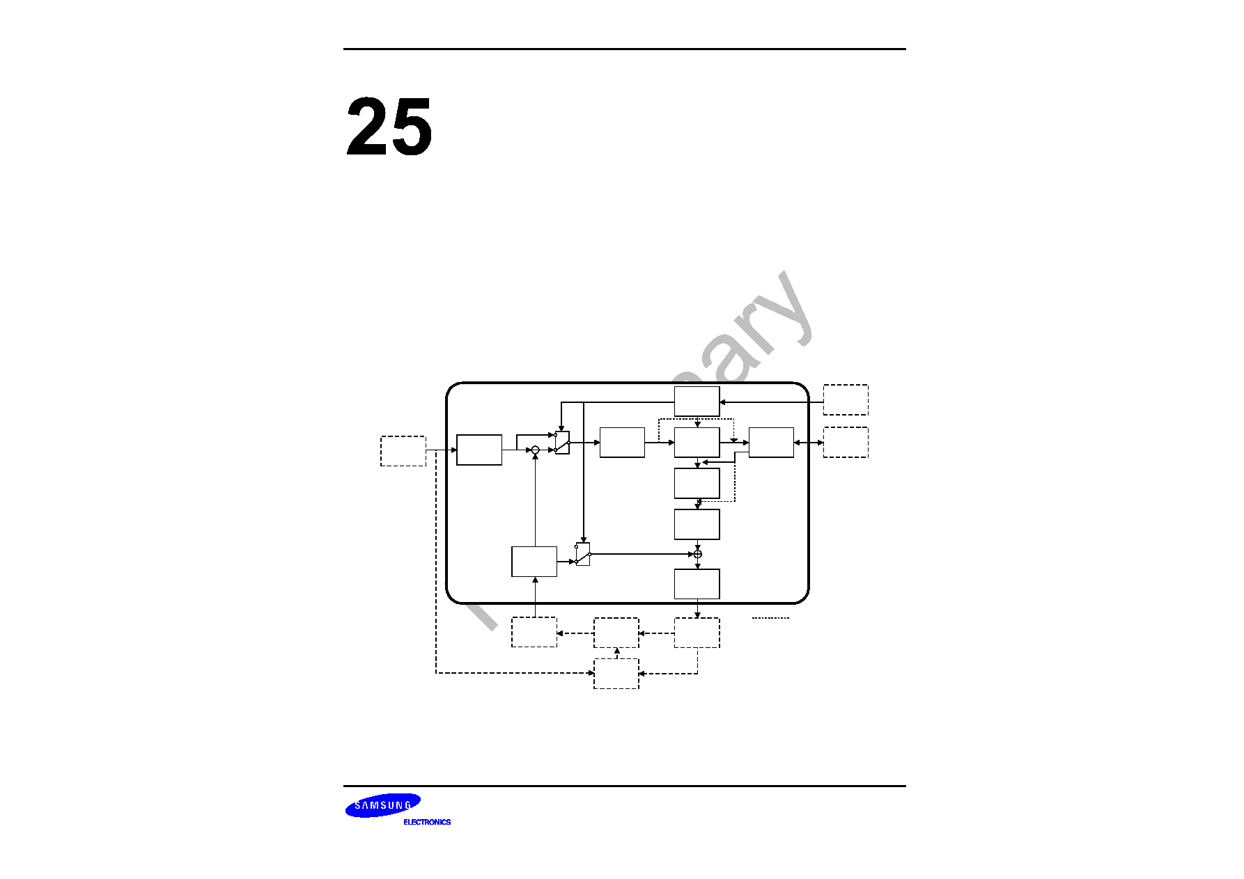
BSW rv0.1-0417-N01
Preliminary product information describes products that are in development,
for which full characterization data and associated errata are not yet available.
Specifications and information herein are subject to change without notice.
S3C24A0 RISC MICROPROCESSOR
MPEG-4 DCTQ
25
-1
MPEG-4 DCTQ (PRELIMINARY)
OVERVIEW
This specification defines the DCT, IDCT, Quantisation and Dequantisation engine for MPEG-4 codec (refer
Figure 25-1). MPEG-4 DCTQ engine gets current macroblock, previous macroblock and quantisation information
from main memory. After internal DCTQ operation, this engine writes quantized coefficients and reconstructed
macroblock to main memory. Using quantisation factor, it is possible to control bit-rate for video streams. Padding
operation for motion estimation supports on the writing reconstruction macroblock. Also, it is possible to setting
intra or inter mode and Qp value with accessing quantisation information in memory. This engine has own DMA
module. So, just by setting function attributes into DCTQ SFR (Special Function Register), this engine
automatically performs DCT, IDCT, Quantisation, Dequantisation, and memory access.
Current
MB
Local Mem.
DCT
Q
Level
Local Mem.
IQ
IDCT
Q-inform
Reconstruct
MB
Local Mem.
SDRAM
Reference
MB
Local Mem.
MC
ME
MPEG-4
DCTQ
SDRAM
SDRAM
SDRAM
SDRAM
Q/IQ skip mode
Figure 25-1. DCTQ overview

BSW rv0.1-0417-N01
Preliminary product information describes products that are in development,
for which full characterization data and associated errata are not yet available.
Specifications and information herein are subject to change without notice.
S3C24A0 RISC MICROPROCESSOR
MPEG-4 DCTQ
25-2
FEATURES
-- H.263, MPEG-4 simple profile level 0,1,2 3 supports.
--
DCT / IDCT / Q / IQ operations
--
Residual extraction / Image reconstruction
--
Padding operation for unrestricted motion compensation
--
Rate control by Q-inform
--
Intra refresh feasibility by Q-inform
--
Dedicated DMA
--
MPEG-4 encoder/decoder support
--
JPEG DCT/IDCT support
--
Variable aspect ratio and size (up to 4096 x 4096)
TIMING DIAGRAM
DCTQ IP operates by OPUNIT. OPUNIT is a macroblock-based, which is 16x16 pixel array. One macroblock
consists of six 8x8 block, which are 4 luminance blocks and, 2 chrominance blocks. DCTQ IP starts with
DCTQ_START signal by register setting. And, during operation, DCTQ_BUSY signal remains High. After dctq
operation, IRQ is generated. And then, DCTQ_BUSY signal go to Low. CPU can read the state of DCTQ by
referencing DCTQ_BUSY. In this document, for convenience, dctq operation means dct, quantisation,
dequantisation and, inverse dct operations.
HCLK
DCTQ_START
DCTQ_BUSY
IRQ
DCT/Q/IQ/IDCT operating period by OPUNIT MB
STATE
Figure 25-2. DCTQ operation timing diagram

BSW rv0.1-0417-N01
Preliminary product information describes products that are in development,
for which full characterization data and associated errata are not yet available.
Specifications and information herein are subject to change without notice.
S3C24A0 RISC MICROPROCESSOR
MPEG-4 DCTQ
25
-3
SEPARATED CLOCK DOMAIN
DCTQ IP has two clock domains. The one is a system bus clock domain. And, the other is a DCTQ core clock
domain. These two clock domains are independent. However, it is recommended to use integer number division
for DCTQ core clock. For low power consumption, if possible, lower DCTQ core clock is requested within codec
performance.
System
bus clock
DCTQ
core clock
DCT/Q
IQ/IDCT
Divide
Counter
1/1 ~ 1/30
PLL
Divide
Counter
Figure 25-3. DCTQ clock domain
DCT
A separable 2-dimensional Discrete Cosine Transform (DCT) is used.
F u v
N
C u C v
f x y
x
u
N
y
v
N
y
N
x
N
( , )
( ) ( )
( , ) cos
(
)
cos
(
)
=
+
+
=
-
=
-
2
2
1
2
2
1
2
0
1
0
1
C u C v
( ), ( )
=
1
2
for u,v = 0
= 1 otherwise
In this IP, N value is fixed to 8. Before quantisation, F(u,v) is rounded. For reducing multiplication and reducing
hardware size, row-column decomposition and Chen's algorithm is used.
IDCT
Inverse DCT module follows next equation.
f x y
N
C u C v F u v
x
u
N
y
v
N
v
N
u
N
( , )
( ) ( ) ( , ) cos
(
)
cos
(
)
=
+
+
=
-
=
-
2
2
1
2
2
1
2
0
1
0
1

BSW rv0.1-0417-N01
Preliminary product information describes products that are in development,
for which full characterization data and associated errata are not yet available.
Specifications and information herein are subject to change without notice.
S3C24A0 RISC MICROPROCESSOR
MPEG-4 DCTQ
25-4
QUANTISATION
The Quantisation parameter Qp takes integer values from 1 to 31. The quantisation stepsize is 2xQp.
COF
A transform coefficient to be quantized.
LEVEL
Absolute value of the quantized version of the transform coefficient.
COF'
Reconstructed transform coefficient.
INTRA DC (In MPEG-4 mode)
LEVEL = COF // dc_scaler
Others
For INTRA: LEVEL = |COF| / (2xQp)
For INTER: LEVEL = (|COF| - Qp/2) / (2xQp)
Clipping to [-127:127] is performed for all coefficients except intra DC.
The sign of COF is then added to obtain COF' : COF' = Sign(COF) x |COF|
DEQUANTISATION
INTRA DC (In MPEG-4 mode)
COF' = LEVEL x dc_scaler
Others
|COF'| = 0, if LEVEL = 0
|COF'| = 2 x Qp x LEVEL + Qp, if LEVEL
0, Qp is odd
|COF'| = 2 x Qp x LEVEL + Qp � 1, if LEVEL
0, Qp is even
Clipping is [-2048:2047] is performed before IDCT.

BSW rv0.1-0417-N01
Preliminary product information describes products that are in development,
for which full characterization data and associated errata are not yet available.
Specifications and information herein are subject to change without notice.
S3C24A0 RISC MICROPROCESSOR
MPEG-4 DCTQ
25
-5
FRAME MEMORY MAP
The frame memories for DCTQ are shown in figure 1-4. The padding area of reference frame fixed to 16 pixel
extensions from original image to outsides in any other image sizes. Because of DCTQed bits per pixel, the
DCTQed frame memory size is double compared to original frame size. Show the bit format in figure 1-6. Q-
information frame consists of the words of Q-information by macroblock units.
QCIF
Y
176
144
Reference frame
memory size
208
176
Start address
location of
register
Padding
area
QCIF
Cb
88
72
104
88
QCIF
Cr
88
72
104
88
QCIF
Y
176
144
QCIF
Cb
88
72
QCIF
Cr
88
72
Current frame
memory size
Start address
location of
register
Current frame memory size
= (176x144) + (88x72) + (88x72) = 38016 Bytes
Reference frame memory size
= (208x176) + (104x88) + (104x88) = 54912 Bytes
DCTQed frame memory size
= (352x144) + (176x72) + (176x72) = 76032 Bytes
Q-inform memory size
= 4 x 99 = 396 Bytes
QCIF
Y
352
144
QCIF
Cb
176
72
DCTQed frame
memory size
Start address
location of
register
QCIF
Cr
176
72
Q-
inform
word
99
Q-information frame
memory size
Start address
location of
register
Figure 25-4. DCTQ frame memory map in QCIF case

BSW rv0.1-0417-N01
Preliminary product information describes products that are in development,
for which full characterization data and associated errata are not yet available.
Specifications and information herein are subject to change without notice.
S3C24A0 RISC MICROPROCESSOR
MPEG-4 DCTQ
25-6
Q-INFORMATION
After DCTQ register setting, the first step of operations is the read of Q-information for macroblock. The DCTQ
engine observes the Q-information and then determines the intra- or inter-modes, MB skip mode and, pick up
Quantisation information. For CBP mode in the decoder, software has to write zero coefficients into the each
skipped 8x8 blocks. In MB-skip case that is not_coded(Inter, zero-MV), in the decoder, DCTQ operation can be
skipped for next MB operation. This MB-skip mode is not recommended with VLC in the encoder.
Reserved
Intra/
Inter
Qp step
MB skip inform
0
5
6
10
11
12
31
MSB
LSB
1 = Intra MB
0 = Inter MB
31 Quantization step size
(1 ~ 31)
6'b111111 = MB skip
6'b000000 = Normal
Figure 25-5. Q-information structure

BSW rv0.1-0417-N01
Preliminary product information describes products that are in development,
for which full characterization data and associated errata are not yet available.
Specifications and information herein are subject to change without notice.
S3C24A0 RISC MICROPROCESSOR
MPEG-4 DCTQ
25
-7
BIT FORMAT
The DMA operations are performed with word units. Internal memory accesses are mainly byte based. The dctq
operations use the 9, 12 bits. Only little endian is supported in the words.
CURLM
MCDLM
-
DCT
Q
IQ
IDCT
+
RECLM
DCTQ
LM
Q-info
Word
Word
Word
Word
8-bit
8-bit
8-bit
9-bit
12-bit
12-bit
12-bit
12-bit
5-bit
9-bit
8-bit
s
16-bits
s 11-bit
12-bits
32-bits
s
16-bits
s 11-bit
12-bits
1)
Word
32-bits
8-bit
8-bit
8-bit
8-bit
32-bits
8-bit
8-bit
8-bit
8-bit
32-bits
8-bit
8-bit
8-bit
8-bit
CURLM : Current MB local sram, MCDLM : MCed MB local sram, DCTQLM: DCTQed MB local sram, RECLM : Reconstructed MB local sram
1)
View the Q-inform structure in figure 1-5.
Figure 25-6. DCTQ bit-format
Output bit-format of coefficient is incompatible with 2's compliment for software. For getting sign, check
the MSB of output coefficient. And, lower 12-bits are levels for VLC.
For block skip mode in decoder, software can put the `0' coefficients into coefficient memory. In inter-mode, this
zero residuals add by MCed pixels for reconstruction image.

BSW rv0.1-0417-N01
Preliminary product information describes products that are in development,
for which full characterization data and associated errata are not yet available.
Specifications and information herein are subject to change without notice.
S3C24A0 RISC MICROPROCESSOR
MPEG-4 DCTQ
25-8
TRANSPOSED COEFFICEINT OUTPUT
The coefficient outputs of DCTQ are transposed in 8x8 block. One coefficient is stored into the half word. In
memory, the sequences of coefficient are 0-8-16-24- etc. In macroblock level, the output sequence of 6 blocks are
as shown in below diagram.
1
2
3
4
5
6
0
1
2
3
4
5
6
7
8
9
10
11
12
13
14
15
16
17
18
19
20
21
22
23
24
25
26
27
28
29
30
31
32
33
34
35
36
37
38
39
40
41
42
43
44
45
46
47
48
49
50
51
52
53
54
55
56
57
58
59
60
61
62
63
Y Blocks
C Blocks
Transposed block
0
8
16
24
32
40
48
56
0
31
16 15
.
.
.
1
9
17
25
33
41
49
57
.
.
.
.
.
.
32-bit
SDRAM
Memory Map
0x20000000
0x20000004
0x20000008
0x2000000C
address
offset
(1 line)
0x20000058
0x2000005C
0x20000060
0x20000064
Figure 25-7. Transposed coefficient output for MB

BSW rv0.1-0417-N01
Preliminary product information describes products that are in development,
for which full characterization data and associated errata are not yet available.
Specifications and information herein are subject to change without notice.
S3C24A0 RISC MICROPROCESSOR
MPEG-4 DCTQ
25
-9
SOFTWARE INTERFACE
This MPEG-4 DCTQ provides a generic data-exchange method. It is recommended that the CONTROL register
should be set at the last SFR setting sequence.
MPEG-4 DCTQ SPECIAL REGISTERS
CURRENT FRAME Y START ADDRESS REGISTER
Register
Address
R/W
Description
Reset Value
SAYCF
0x4900_0000
RW
Current frame luminance start address
0x00000000
SAYCF
Bit
Description
Initial State
SAYCF
[31:0]
These bits indicate the luminance start address of current frame.
0x00000000
CURRENT FRAME CB START ADDRESS REGISTER
Register
Address
R/W
Description
Reset Value
SACBCF
0x4900_0004
RW
Current frame Cb start address
0x00000000
SACBCF
Bit
Description
Initial State
SACBCF
[31:0]
These bits indicate the chrominance Cb start address of current
frame.
0x00000000
CURRENT FRAME CR START ADDRESS REGISTER
Register
Address
R/W
Description
Reset Value
SACRCF
0x4900_0008
RW
Current frame Cr start address
0x00000000
SACRCF
Bit
Description
Initial State
SACRCF
[31:0]
These bits indicate the chrominance Cr start address of current
frame.
0x00000000

BSW rv0.1-0417-N01
Preliminary product information describes products that are in development,
for which full characterization data and associated errata are not yet available.
Specifications and information herein are subject to change without notice.
S3C24A0 RISC MICROPROCESSOR
MPEG-4 DCTQ
25-10
REFERENCE FRAME Y START ADDRESS REGISTER
Register
Address
R/W
Description
Reset Value
SAYRF
0x4900_000C
RW
Reference frame luminance start address
0x00000000
SAYRF
Bit
Description
Initial State
SAYRF
[31:0]
These bits indicate the luminance start address of reference
frame.
0x00000000
REFERENCE FRAME CB START ADDRESS REGISTER
Register
Address
R/W
Description
Reset Value
SACBRF
0x4900_0010
RW
Reference frame Cb start address
0x00000000
SACBRF
Bit
Description
Initial State
SACBRF
[31:0]
These bits indicate the chrominance Cb start address of reference
frame.
0x00000000
REFERENCE FRAME CR START ADDRESS REGISTER
Register
Address
R/W
Description
Reset Value
SACRRF
0x4900_0014
RW
Reference frame Cr start address
0x00000000
SACRRF
Bit
Description
Initial State
SACRRF
[31:0]
These bits indicate the chrominance Cr start address of reference
frame.
0x00000000
DCTQED FRAME Y START ADDRESS REGISTER
Register
Address
R/W
Description
Reset Value
SAYDQF
0x4900_0018
RW
DCTQed frame luminance start address
0x00000000
SAYDQF
Bit
Description
Initial State
SAYDQF
[31:0]
These bits indicate the luminance start address for storing DCT
and Quantized outputs.
0x00000000

BSW rv0.1-0417-N01
Preliminary product information describes products that are in development,
for which full characterization data and associated errata are not yet available.
Specifications and information herein are subject to change without notice.
S3C24A0 RISC MICROPROCESSOR
MPEG-4 DCTQ
25
-11
DCTQED FRAME CB START ADDRESS REGISTER
Register
Address
R/W
Description
Reset Value
SACBDQF
0x4900_001C
RW
DCTQed frame Cb start address
0x00000000
SACBDQF
Bit
Description
Initial State
SACBDQF
[31:0]
These bits indicate the chrominance Cb start address for storing
DCT and Quantized outputs.
0x00000000
DCTQED FRAME CR START ADDRESS REGISTER
Register
Address
R/W
Description
Reset Value
SACRDQ
F
0x4900_0020
RW
DCTQed frame Cr start address
0x00000000
SACRDQF
Bit
Description
Initial State
SACRDQF
[31:0]
These bits indicate the chrominance Cr start address for storing
DCT and Quantized outputs.
0x00000000
QUANTISATION FACTOR START ADDRESS REGISTER
Register
Address
R/W
Description
Reset Value
SAQP
0x4900_0024
RW
Qp start address
0x00000000
SAQP
Bit
Description
Initial State
SAQP
[31:0]
These bits indicate the Qp start address for Quantisation
informations.
0x00000000

BSW rv0.1-0417-N01
Preliminary product information describes products that are in development,
for which full characterization data and associated errata are not yet available.
Specifications and information herein are subject to change without notice.
S3C24A0 RISC MICROPROCESSOR
MPEG-4 DCTQ
25-12
IMAGE SIZE REGISTER
Register
Address
R/W
Description
Reset Value
IMGSIZE
0x4900_0028
RW
Image horizontal and vertical pixel number
0x00000000
Because DCTQ engine operates by macroblock unit, the horizontal and vertical pixel numbers should be the
multiple of 16. For example, you can extract the exact SVGA image size after 800x608 dctq operation with dummy
pixels.
IMGSIZE
Bit
Description
Initial State
Image_X
[28:16] Image horizontal pixel number
0
Image_Y
[12:0]
Image vertical pixel number
0
SH Q REGISTER
Register
Address
R/W
Description
Reset Value
SHQ
0x4900_002C
RW
Short header quantization mode
0x00000000
SHQ
Bit
Description
Initial State
Is_SHQ
[
27
]
0 : MPEG-4 dc_scaler Q-mode for Intra-DC
1 : Short header Q-mode (/8,*8) for Intra-DC
0
Reserved
[
26
:0]
Must be zero
0
Reserved SFR 0x49000030
CONTROL REGISTER
Register
Address
R/W
Description
Reset Value
DCTQCTRL
0x4900_0034
RW
Control register
0x00000000
DCTQCTRL
Bit
Description
Initial State
Reserved
[31:30] Reserved
0
Coeff_not_write
[29]
Coefficients write operation to memory can be skipped with VLC
IP `On' state. In this case, DCTQ engine write the coefficient to the
internal memory of VLC directly.
0
With_VLC
[28]
DCTQ operates by MB-unit with watching VLC operation (BUSY).
In decoder mode, this bit must be zero. If only DCTQ is operating,
0

BSW rv0.1-0417-N01
Preliminary product information describes products that are in development,
for which full characterization data and associated errata are not yet available.
Specifications and information herein are subject to change without notice.
S3C24A0 RISC MICROPROCESSOR
MPEG-4 DCTQ
25
-13
this bit should be zero.
DCT_only
[27]
Quantization skip for JPEG mode
0
IDCT_only
[26]
De-quantization skip for JPEG mode
0
SWRST
[25]
This bit indicates the software reset of MPEG-4 DCTQ.
0
OPUNIT
[24:8]
These bits controls the number of DCTQ operations by
macroblock unit. If these bits are 14'd99 in QCIF size, DCTQ
operates during one frame without command.
0
DCTQBSY
[7]
This bit indicates the busy state of DCTQ.
1 = DCTQ is operating.
0 = DCTQ is not operating.
0
DCTQST
[6]
This bit indicates the start of DCTQ operation. This bit is auto-
cleared.
0
Reserved
[5]
Reserved
0
ISH263
[4]
This bit indicates that the format of current DCTQ operation is
H.263 or not.
1 = H.263 (without padding)
0 = MPEG-4 (with padding)
0
Reserved
[3]
Reserved
0
ISENC
[2]
This bit indicates that the current DCTQ operation is encoding or
not.
1 = encoding
0 = decoding
0
Reserved
[1]
Reserved
0
FRST
[0]
This bit indicates the frame start signal, which is active only first
OPUNIT.
1 = frame start
0 = normal
0
Reserved SFR 0x49000038
Reserved SFR 0x4900003c
NOTES
�
It is needed for software-reset to convert from encoder to decoder or from decoder to encoder.

BSW rv0.1-0417-N01
Preliminary product information describes products that are in development,
for which full characterization data and associated errata are not yet available.
Specifications and information herein are subject to change without notice.
S3C24A0 RISC MICROPROCESSOR
VLX
26-1
VLX (Preliminary)
OVERVIEW
VLX module consist of VLC( Variable Length Coding )and VLD( Variable Length Decoding ) module.
VLC block does the entropy coding in MPEG4 system. It assigns small bits to a symbol that occurs frequently in
the source data. On the other hand, it assigns large bits to a symbol that occurs rarely. As a result, the size of the
coded data is smaller than that of the original. MPEG4 used a predefined table that assigns a code to each
symbol (RUN, LEVEL, LAST ) and cannot be redefined by the user in MPEG4 simple profile.
VLC received coefficient data and control signal from DCTQ h/w module. So SFR control bits must be set same
value in DCTQ module SFR data in VLC mode.
VLD block does the entropy decoding in MPEG4 system. It reads the coded bit stream from the main memory,
extracts one code from the coded bit stream, and generates the symbol from the extracted code. As the length of
a code is variable, VLD block searches the coded bit stream step by step and compares the intermediate code
value with the code table to get a complete code value.
VLD module is only 1 macro block operation so that always need to control interface between CPU. S/w must to
be known the time of end of MB, so polling or interrupt signal generation in VLD h/w.
VLC and VLD operation are not supported operation simultaneous. If intra macro block in VLD mode need to DC
prediction decoding and inverse scanning to use in DCTQ H/W module. And inter block in VLD mode don't need
extra operation to use DCTQ module.
VLX module designed for AMBA2.0 and has two dedicated DMA, and 1 master and 1 slave AHB interface.
FEATURE
-
MPEG-4 Simple Profile
-
AMBA AHB Interface
-
Use Dedicated DMA
-
Programmable Image size QCIF, CIF, VGA, QVGA etc.
-
Include DC prediction in VLC mode..
-
Interrupt and polling mode supported
-
Support MPEG4 simple profile basic table excluding reversible VLC table

BSW rv0.1-0417-N01
Preliminary product information describes products that are in development,
for which full characterization data and associated errata are not yet available.
Specifications and information herein are subject to change without notice.
VLX
S3C24A0 RISC MICROPROCESSOR
26-2
MPEG-4 VLX( Variable Length Coding, Decoding ) OPERATION
Coeff Mem.
VLX
DCTQ
VLX Ctrl.
AH
B
External
MEM. I/F
coeff I/F
ctrl. I/F
AHB I/F
AHB master
I/F
AHB slave
I/F
VLC path
VLD path
Figure 26-1 VLX top interface block diagram
VLC
VLC block has 3 major blocks to code the input symbols. They are VLC coder, run-length coding (RLC), DC
prediction blcok.
Run-Length Coder(RLC).
The output of the zigzag address generator is the sequence of the DCT coefficients that read in zigzag order or
DCTQ zigzag order . These coefficients are coded to RLC. RLC coder result is LAST, RUN, LEVEL value.
In MPEG4 mode, the AC coefficients are coded to 3-D RLC code: (LAST, RUN,LEVEL). RUN is the zero number
before the non-zero value, LEVEL. The LAST indicates that the LEVEL is the last non-zero value in the DCT
block.
RLC coder searched the 8x8 blocks of transform coefficients are scanned with "zigzag" scanning.
Zigzag order is explained Figure. 26-2

BSW rv0.1-0417-N01
Preliminary product information describes products that are in development,
for which full characterization data and associated errata are not yet available.
Specifications and information herein are subject to change without notice.
S3C24A0 RISC MICROPROCESSOR
VLX
26-3
1
6
2
7
16
15
28
29
3
4
10
5
8
14
17
27
30
43
9
12
13
18
26
31
42
44
19
25
32
41
45
54
11
24
20
33
46
40
53
55
21
22
36
23
34
39
47
52
56
61
35
37
38
48
51
57
60
62
49
50
58
59
63
64
Figure 26-2 ZigZag scanning method
A three dimensional variable length coder is used to code transform coefficients. An EVENT is a combination of
three parameters
LAST 0 : There are more nonzero coefficients in the block.
1 : This is the last nonzero coefficient in the block.
RUN
Number of zero coefficients preceding the current nonzero coefficient.
LEVEL Magnitude of the coefficient.
The most commonly occurring combinations of LAST, RUN, LEVEL are coded with variable length codes given
standard table. The remaining combinations, no matched case in table use three ESCAPE mode coding. First,
Level vaule change Level minus Lmax( Lmax is defined by RUN . Second, RUN value change RUN minus Rmax
( Rmax is defined by Level ). Last, FLC, fixed length coding, are coded with a 22 bit word fixed length coding
consisting of ESCAPE( 7 bit ), LAST(1 bit ), RUN( 6 bit ),LEVEL(8 bit), coding used.
Entropy coder
Entropy coding is performed after the run-length coding. MPEG4 in simple profile uses a predefined table that
gives the code and the length of the code for each symbol. Entropy coder use many predefined table, DC table,
intra luminance table, intra chrominance table, various escape table. Etc.. . So, the table in MPEG4 can be fixed
in hardware to speed up the entropy coding using direct matching method. it supports only the MPEG4 simple
profile, the table is hardwired to speed up the VLC and to lower the power consumption.
DC prediction coder
VLC support DC prediction operation. but AC prediction is not supported VLX module. So scanning method is
always zigzag scanning. DC prediction value calculates below fomular. Assume, `X', `A', `B' and `C'
correspondingly refer to the current block, the previous block, the block above and to the left, and the block
immediately above as shown.

BSW rv0.1-0417-N01
Preliminary product information describes products that are in development,
for which full characterization data and associated errata are not yet available.
Specifications and information herein are subject to change without notice.
VLX
S3C24A0 RISC MICROPROCESSOR
26-4
A
B
C
D
X
Macroblock
Y
or
or
Figure 26-3 Previous neighboring blocks used in DC prediction
The differential DC is then obtained by subtracting the DC prediction, DCX' from DC of block `X'.
if (|DCA - DCB| < |DCB - DCC|)
DCX' = DCC
else
DCX' = DCA
DCX = DCX � DCX'
DC prediction h/w support Q-step Scaling method. Q-step scaling method is To compensate for differences in the
quantisation of previous horizontaly adjacent or vertically adjacent blocks used in AC prediction of the current
block, scaling of prediction coefficients becomes necessary. Thus the prediction is modified so that the predictor
is scaled by the ratio of the current quantisation stepsize and the quantisation stepsize of the predictor block.
VLC mode operations sequence.
-
Receiving the data and control signal from the DCTQ H/W module.
-
1 macro block data, zigzag ordered data receive form DCTQ module and data save COEF_MEM in the
VLX H/W module
.
-
SFR control bits already must be set.
-
The value, after run-length coding, is coded with intra, Inter, escape run, escape level , dc code table, and
then saved external memory.
-
VLC output save external memory on 1 word value. Not coded information, from MSB to LSB data. {word
count(16bit), bit count(16bit) }, VLC coeff. ordered save.VLX output in VLC mode are CBP information,
Word count, Bit count VLCed stream data. Figure 26-4 show the output format in VLC mode.
-
CBP information : Coded Block Pattern explain MB data exist or not . if Coded Block Patter value 1 , that
component has no DCTQ coefficient data.
-
One MB has six block so CBP information is six bit output. 0 bit is y0 block and 5 bit is Cr block. Figure 26-4
show the CBP bit information.
BSW rv0.1-0417-N01
Preliminary product information describes products that are in development,
for which full characterization data and associated errata are not yet available.
Specifications and information herein are subject to change without notice.
S3C24A0 RISC MICROPROCESSOR
VLX
26-5
External Memory
CBP
Word count
Bit count
VLC stream
VLCed Addr
.
.
.
.
.
.
CBP
Word count
Bit count
VLC stream
.
.
.
128word( offset )
First MB data
Second MB data
VLCed Addr + (128*4)
Word count
Bit count
.
.
.
CBP value
CR Cb
y3
y2
y1
y0
1MB = 6 block
Big-endian value
Figure 26-4 VLC output bit stream format
-
Output of encoder, saved data in memory, is big-endian data
-
Interrupt signal or busy signal generated by end of OP_UNIT processing. Interrupt signal generation
can be controlled by INT_ENABLE bit.
-
Busy signal put to DCTQ module and be set SFR bit.
HCLK
Write_start ( from DCTQ )
VLX_BUSY
VLX_IRQ
VLXoperating period by one MB
STATE
DCTQ coeff. writting period
Figure 26-5 VLC start, busy, and Interrupt signal timing diagram.
At the VOP layer, intra_dc_vlc_thr allows switching between DC Intra VLC and AC Intra VLC when coding DC
coefficients of Intra macroblocks. When the intra AC-VLC is turned on, INTRA-DC transform coefficients are not
handled separately any more, but treated the same as all AC coefficients.
That means a zero INTRA-DC will not be coded but will simply increase the run for the following AC-coefficients.
But this H/W set intra_dc_thr value fixed zero value, so always threated DC coefficients.

BSW rv0.1-0417-N01
Preliminary product information describes products that are in development,
for which full characterization data and associated errata are not yet available.
Specifications and information herein are subject to change without notice.
VLX
S3C24A0 RISC MICROPROCESSOR
26-6
VLD
VLD h/w support only coefficient bit stream variable length decoding. Except header decoding, intra DC/AC
inverse prediction. so VLD h/w need to communicate to S/W per macro block. This operation show Figure 26-
6 .
BIT_SADDR
0
31
16
START_BIT_CNT
0
31
Bit stream
VLC_EADDR
END_BIT_CNT
0
31
Big-endian data
Figure 26-6 VLD bit stream h/w and S/W interface format.
S/W must be set BIT_SADDR and START_BIT_CNT and bitstream data. BIT_SADDR is address of start
coefficient bit stream. And START_BIT_CNT is start bit of current macro block bit stream.
And bitstream
data must be big-endian data
. VLD h/w generate VLC_EADDR and END_BIT_CNT value after macro block
VLD operation. Before next macro block start s/w have to find BIT_SADDR and START_BIT_CNT after
header parsing and VLD.
Decoded coefficient data saved external memory Y image, Cb image, and Cr image. Figure 26-7 is example
external memory amount. So special function register Y_START_ADDR, CB_START_ADDR,
CR_START_ADDR must be set.
VLDed frame memory size
= (352x144) + (176x72) + (176x72) = 76032 Bytes
QCIF
Y
352
144
QCIF
Cb
176
72
VLX frame
memory size
Start address
location of
register
QCIF
Cr
176
72
Figure 26-.7 External memory amount in VLD mode.
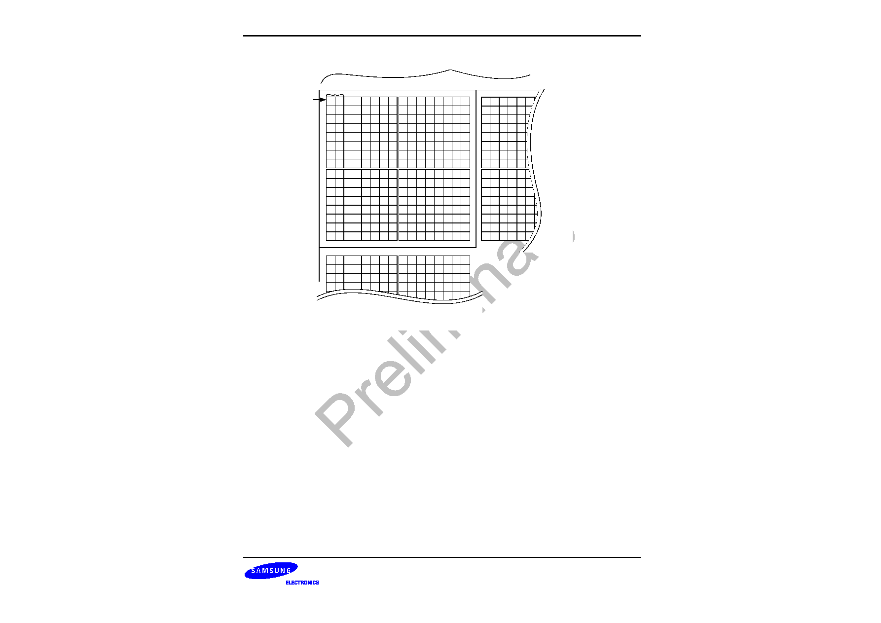
BSW rv0.1-0417-N01
Preliminary product information describes products that are in development,
for which full characterization data and associated errata are not yet available.
Specifications and information herein are subject to change without notice.
S3C24A0 RISC MICROPROCESSOR
VLX
26-7
1
6
2
7
16
15
28
29
3
4
10
5
8
14
17
27
30
43
9
12
13
18
26
31
42
44
19
25
32
41
45
54
11
24
20
33
46
40
53
55
21
22
36
23
34
39
47
52
56
61
35
37
38
48
51
57
60
62
49
50
58
59
63
0
1
6
2
7
16
15
28
29
3
4
10
5
8
14
17
27
30
43
9
12
13
18
26
31
42
44
19
25
32
41
45
54
11
24
20
33
46
40
53
55
21
22
36
23
34
39
47
52
56
61
35
37
38
48
51
57
60
62
49
50
58
59
63
0
1
6
2
7
16
15
28
29
3
4
10
5
8
14
17
27
30
43
9
12
13
18
26
31
42
44
19
25
32
41
45
54
11
24
20
33
46
40
53
55
21
22
36
23
34
39
47
52
56
61
35
37
38
48
51
57
60
62
49
50
58
59
63
0
1
6
2
7
16
15
28
29
3
4
10
5
8
14
17
27
30
43
9
12
13
18
26
31
42
44
19
25
32
41
45
54
11
24
20
33
46
40
53
55
21
22
36
23
34
39
47
52
56
61
35
37
38
48
51
57
60
62
49
50
58
59
63
0
32bit
1 MB Luminance
1
6
2
7
16
15
28
29
3
4
10
5
8
14
17
27
30
43
9
12
13
18
26
31
42
44
19
25
32
41
45
54
11
24
20
33
46
40
53
55
21
22
36
23
34
39
47
52
56
61
35
37
38
48
51
57
60
62
49
50
58
59
63
0
1
6
2
7
16
15
28
29
3
4
10
5
8
14
17
27
30
43
9
12
13
18
26
31
42
44
19
25
32
41
45
54
11
24
20
33
46
40
53
55
21
22
36
23
34
39
47
52
56
61
35
37
38
48
51
57
60
62
49
50
58
59
63
0
1 FRAME IMAGE
1
6
2
7
16
15
28
29
3
4
10
5
8
14
17
27
30
43
9
12
13
18
26
31
42
44
19
25
32
41
45
54
11
24
20
33
46
40
53
55
21
22
36
23
34
39
47
52
56
61
35
37
38
48
51
57
60
62
49
50
58
59
63
0
1
6
2
7
16
15
28
29
3
4
10
5
8
14
17
27
30
43
9
12
13
18
26
31
42
44
19
25
32
41
45
54
11
24
20
33
46
40
53
55
21
22
36
23
34
39
47
52
56
61
35
37
38
48
51
57
60
62
49
50
58
59
63
0
Figure 26-8 VLD output coefficient format
VLD block has 3 major blocks. They are shifter, entropy decoding, run length decoding (RLD), Shifter include
entropy coder. The operation and the sequence of the VLD operation are reverse to the VLC
.
Shifter
The shifter gives the coded bit stream to the entropy-decoding block and does the shifting operation
requested from the entropy-decoding block. The shifting operation is executed during the decoding
process to give the left aligned coded bit stream to the entropy-decoding block.
Entropy decoder
The entropy-decoding process has two steps. In first step, it extracts one code from the coded bit
stream from the shifter and in second, it finds the symbol address corresponding to that code. In
general case, during the process to extract one code the address for the symbol is calculated. The output of
Entropy decoder are Run, Level, Last value. These value is input of RLD module.

BSW rv0.1-0417-N01
Preliminary product information describes products that are in development,
for which full characterization data and associated errata are not yet available.
Specifications and information herein are subject to change without notice.
VLX
S3C24A0 RISC MICROPROCESSOR
26-8
Run length decoder
The output of the entropy decoding is (LAST,RUN, LEVEL) in MPEG mode. They are decoded to a sequence of
the coefficients. This operation is done in the run-length decoding block. It is the reverse operation of the RLC
block. And reads the sequence of coefficients from the run-length decoding block and writes the coefficients to the
DCT/Q memory in zigzag address order or DCTQ zigzag address order . This is the reverse operation in VLC
RLC.
VLD operation.
-
VLD is operated by 1 MB opunit.
-
Decoding start address and bit count are accepted on each MB by S/W processing.
31
0
(SFR : BIT_COUNT )
8
16
24
31
Figure 26-9 MSB is first bit value in output bit stream
-
VLD output is saved image format in external memory. Figure 26-7, 26-8 show the external memory
-
DC prediction inverse coding and scanning are need in S/W processing in Intra mode.
-
VLD processing explained Figure 26-10 VLD flow chart. VLD flow chart is partitioned S/W processing and
H/W processing.

BSW rv0.1-0417-N01
Preliminary product information describes products that are in development,
for which full characterization data and associated errata are not yet available.
Specifications and information herein are subject to change without notice.
S3C24A0 RISC MICROPROCESSOR
VLX
26-9
VOP header Dec.
get VOP information
MB Header Dec.
MB mode information
MB == OP_UNIT
No
Yes
ON
VLD SFR set and triggering.
CBP information
Bit_SADDR,
START_BIT_CNT
Coefficient VLD operation
polling sigal or
interrupt signal gen.
Get VLD_EADDR
END_BIT_CNT
Intra
Yes
INTRA DC/AC inverse
prediction
and scannig
Yes
DCTQ transter
No
MB == FRAME
ON
Yes
No
H/W operation
S/W operation
Figure 26-10 VLD flow chart and s/w and h/w processing partition.
-
Start signal and busy signal and interrupt relation is Fig.26-11
HCLK
VLX_CPU_START
or
Write_start ( from DCTQ )
VLX_BUSY
VLX_IRQ
VLXoperating period by OPUNIT MB
STATE
Figure 26-11 Start signal, busy signal and interrupt signal in VLD mode.

BSW rv0.1-0417-N01
Preliminary product information describes products that are in development,
for which full characterization data and associated errata are not yet available.
Specifications and information herein are subject to change without notice.
VLX
S3C24A0 RISC MICROPROCESSOR
26-10
VLX( VLC and VLD ) SPECIAL REGISTERS
VLX common SFR .
Register
Address
R/W
Description
Reset Value
COMMON1
0x4
9
40_0000
R/W
VLX common control register 1
0x0000_0000
COMMON1
Bit
Description
Initial State
VLX ON
[0]
VLX system on / off control bit, not start bit
0x0
-
[1]
reserved
0x0
FRAME_START
[2]
1 : Frame START 0 : not frame start
0x0
VLX_START
[3]
1 : Encoder or Decoder start 0 : disable
0x0
ENC_MODE
[4]
1 : Encoder 0 : Decoder
0x0
INT_ENABLE
[5]
1 : Interrupt mode enable 0 : disable
0x0
-
[8:6]
reserved
0x0
OP_UNIT_SFR
[20:9]
Operation MB count
0x000
-
[21]
reserved
0x0
Note
1.
VLX _ON bit is on / off control.
2.
FRAME START and CPU START must down before next COMMON1 set. Because of these signal is generated one
pulse signal in VLX internal module ( only detect rising edge this signal ).
3.
FRAME_START signal must be set 1 time per 1 frame. And it must be set 0 before next OP_UNIT processing start.
4.
ENC_MODE 1 : VLC operation , 0 : VLD operation.
5.
INT_ENABLE 0 : only polling mode ( busy signal is
VLX_BUSY value in VLX_OUT1 special function register .)
6.
OP_UNIT SFR count value of macro block operation in VLC mode. Interrupt signal generation on end of OP_UNIT.
OP_UNIT_SFR must be set 1 value in VLD mode.
7.
COMMON[1] and COMMON[8:6] must be set value `0'
8.
COMMON[21] must be set value `1'.
FRAME START ADDR
Register
Address
R/W
Description
Reset Value
FRAME_START_Y
0x4
9
40_0004
R/W
Y coeff. frame start address
0x0000_0000
FRAME_START_Y
Bit
Description
Initial State

BSW rv0.1-0417-N01
Preliminary product information describes products that are in development,
for which full characterization data and associated errata are not yet available.
Specifications and information herein are subject to change without notice.
S3C24A0 RISC MICROPROCESSOR
VLX
26-11
Y img frame start addr
[31:0]
Y coeff. frame start address in VLD mode
0x0000_0000
Register
Address
R/W
Description
Reset Value
FRAME_START_CB
0x4940_0008
R/W
CB coeff. frame start address
0x0000_0000
FRAME_START_CB
Bit
Description
Initial State
CB img frame start addr
[31:0]
CB coeff. frame start address in VLD mode
0x0000_0000
Register
Address
R/W
Description
Reset Value
FRAME_START_CR
0x4940_000c
R/W
CR coeff. frame start address
0x0000_0000
FRAME_START_CR
Bit
Description
Initial State
CR img frame start addr
[31:0]
CR coeff. frame start address in VLD mode
0x0000_0000
VLX CONTROL REGISTER( VLX_CON)
Register
Address
R/W
Description
Reset Value
VLC_CON1
0x4940_0010
R/W
Control register in VLC mode
0x0000_0000
VLC_CON1
Bit
Description
Initial State
IMG_XSIZE_SFR
[9:0]
Image x size set register
0x000
-
[10]
reserved
0x0
SEL_SCAN_SFR
[12:11]
Scanning method select control bits.
0x0
-
[13]
reserved
0x0
SW_RESET
[14]
S/w reset active high.
0x0
Note 1.IMG_XSIZE_SFR is pixel count value. Ex ) QCIF = 176, CIF = 352
2. 2'b00 : zigzag scan, 2'b11 : DCTQ zigzag format by dctq module format , others : ordered
format.
3. S/W reset active high. And need to be down after high.
4.
COMMON[10] must be set value `1'
5. COMMON[13] must be set value `0'

BSW rv0.1-0417-N01
Preliminary product information describes products that are in development,
for which full characterization data and associated errata are not yet available.
Specifications and information herein are subject to change without notice.
VLX
S3C24A0 RISC MICROPROCESSOR
26-12
Register
Address
R/W
Description
Reset Value
VLC_CON2
0x4940_0014
R/W
Reserved
-
Register
Address
R/W
Description
Reset Value
VLC_CON3
0x4940_0018
R/W
VLC bit stream start addr.
0x0000_0000
VLC_CON3
Bit
Description
Initial State
VLCED_ADDR
[31:0]
External address saved VLCed output stream.
0x0000_0000
Note. VLCED ADDR is bit stream base address output in VLC mode.
VLCED ADDR[8:0] bit must be set 0 value!!.
Register
Address
R/W
Description
Reset Value
VLC_CON4
0x4940_001c
R/W
reserved
0x0000_0000
BSW rv0.1-0417-N01
Preliminary product information describes products that are in development,
for which full characterization data and associated errata are not yet available.
Specifications and information herein are subject to change without notice.
S3C24A0 RISC MICROPROCESSOR
VLX
26-13
VLD CONTROL REGISTER( VLD_CON)
Register
Address
R/W
Description
Reset Value
VLD_CON1
0x4940_0020
R/W
VLD control value setting register
0x0000_0000
VLD_CON1
Bit
Description
Initial State
-
[11:0]
reserved
-
START_BIT_CNT
[17:12]
First bit count value when VLD start
0x00
IS_INTRA_VLD
[18]
1 : intra, 0 : inter mode in VLD
0x0
-
[19]
reserved
-
CBP_VLD_SFR
[25:20]
CBP value
0x00
QP_SFR
[30:26]
QP value
0x00
-
[31]
Reserved
-
Note
1. BIT_STUFF_SFR is bit count number of first start macro block bit streams.
2.
Bit[11:0], Bit[19] must be set value `0'.
3. Bit[31] must be set `0x1'
Register
Address
R/W
Description
Reset Value
VLD_CON2
0x4940_0024
R/W
VLD BIT_SADDR
0x0000_0000
VLD_CON2
Bit
Description
Initial State
BIT_SADDR
[31:0]
VLD Bit stream start bit in VLD mode.
0x0000_0000
Register
Address
R/W
Description
Reset Value
VLD_CON3
0x4940_0028
R/W
Reserved
-

BSW rv0.1-0417-N01
Preliminary product information describes products that are in development,
for which full characterization data and associated errata are not yet available.
Specifications and information herein are subject to change without notice.
VLX
S3C24A0 RISC MICROPROCESSOR
26-14
VLX OUTPUT REGISTER 1 ( VLX_CON 1 ) � read only
Register
Address
R/W
Description
Reset Value
VLX_OUT1
0x4940_002c
R
VLX output information register. 1
0x0000_0000
VLX_CON1
Bit
Description
Initial State
VLD_BUSY
[0]
VLX busy signal
0x0
N_ST_BIT_CNT
[6:1]
Next start bit count
0x00
VLX OUTPUT REGISTER 2 ( VLX_CON 2 ) � read only
Register
Address
R/W
Description
Reset Value
VLX_OUT2
0x4940_0030
R
VLX output information register. 2
0x0000_0000
VLX_CON2
Bit
Description
Initial State
N_START_ADDR
[31:0] Next start address.
0x0000_0000
Note
1. N_START_BIT_CNT is next start bit counter number for next MB decoding..
2. N_START_ADDR is next start address for next MB decoding.
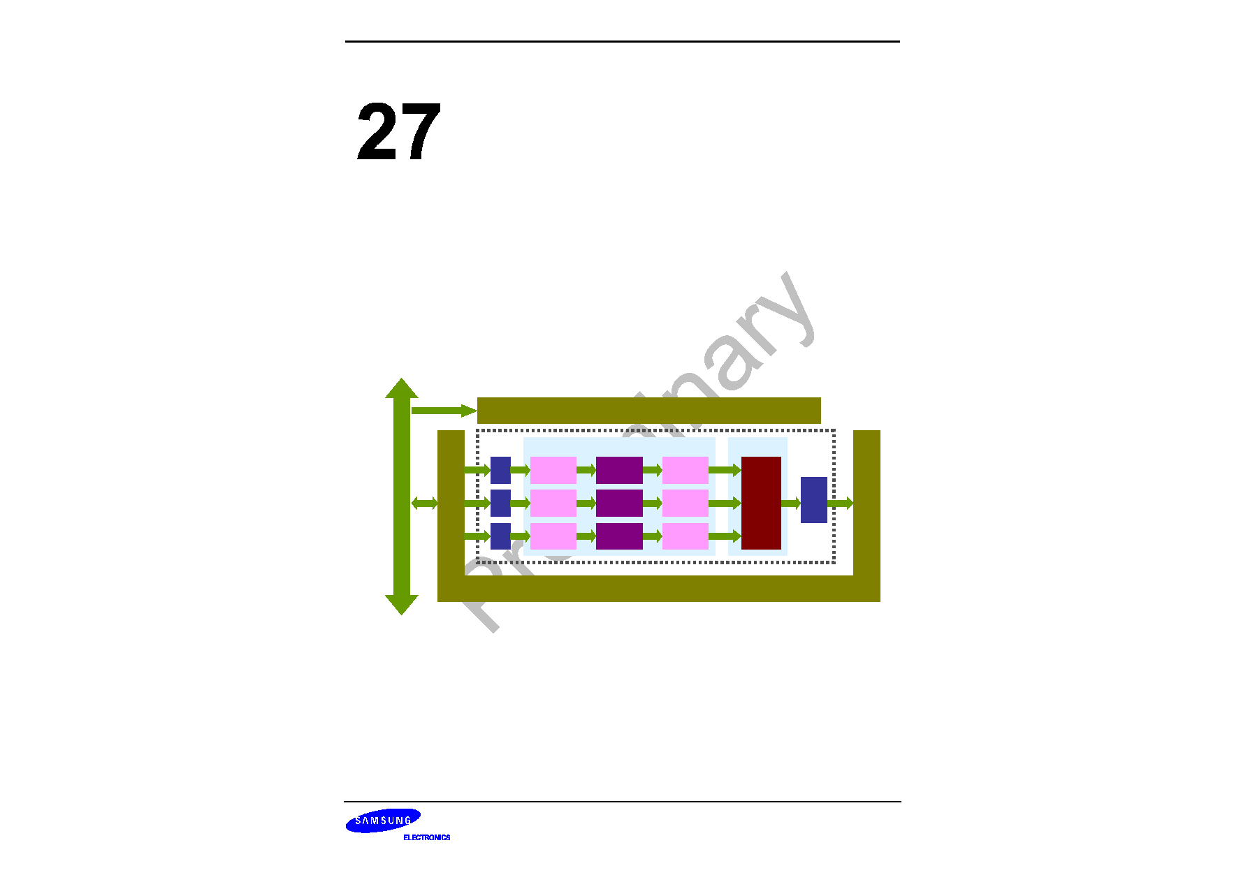
BSW rv0.1-0417-N01
Preliminary product information describes products that are in development,
for which full characterization data and associated errata are not yet available.
Specifications and information herein are subject to change without notice.
S3C24A0 RISC MICROPROCESSOR
POST PROCESSOR
27-1
POST Processor (Preliminary)
1. Overview
Post processor performs video/graphic scale, video format conversion and color space conversion. It is
composed of Data-Path, DMA controller and Register files as shown in the overall block diagram of Figure 27-1.
Overall features are summarized as follows.
Figure 27-1. Block Diagram of Post Processor
Overall Features
AMBA AHB v2.0 compatible interface
Dedicated DMA with offset address
3 Channel scaling pipelines for video/graphic scaling up/down or zooming in/out
Video input format: 420, 422 format
Graphic input format: 16-bit (565format) or 24-bit
Register Files
DMA Controller
Scale & Format Conversion
CSC
Pre
Scale
Main
Scale
Pre
Scale
Main
Scale
Pre
Scale
Main
Scale
Color
Space
Con.
Y
Cb
Cr
A
HB
BUS
RGB
Line
Memory
InFIFO
OutFIFO
Line
Memory
Line
Memory

BSW rv0.1-0417-N01
Preliminary product information describes products that are in development,
for which full characterization data and associated errata are not yet available.
Specifications and information herein are subject to change without notice.
POST PROCESSOR
S3C24A0 RISC MICROPROCESSOR
27-2
Output format: 16-bit (565 format) / 24-bit graphic data
Programmable source and destination image size up to 2048
� 2048 resolution
Programmable scaling ratio
Format conversion for video signals
Color space conversion
Separate processing clock with AHB interface clock

BSW rv0.1-0417-N01
Preliminary product information describes products that are in development,
for which full characterization data and associated errata are not yet available.
Specifications and information herein are subject to change without notice.
S3C24A0 RISC MICROPROCESSOR
POST PROCESSOR
27-3
2. A Source and Destination Image Data Format
Various source and destination image formats can be selected according to the mode configuration as
described in Table 27-1. Source image format is one of YCbCr420, YCbCr422, RGB16-bit (565format) and RGB
24-bit format. Destination image format is either RGB 16-bit (565format) or RGB 24-bit.
In the case of YCbCr420 source image format, each component of Y, Cb and Cr is stored in each own
separated address space without any interleaving as shown in Case A of Figure 27-2 (a) and Figure 27-3. In the
other cases, either byte or half-word interleaving is applied within unified address space as shown in Figure 27-2
(b). Byte interleaving order of YCbCr422 source image is selectable either YCbYCr or CbYCrY as shown in case
B and C of Figure 27-2 (b) and Figure 27-3. Byte order of RGB 24-bit and half-word order of RGB 16-bit are
shown in case D and E of Figure 27-2 (b) and Figure 27-3.
In both cases of YCbCr420 and YCbCr422 source image format, whether MPEG4 format or MPEG2/H.263
format needs to be selected according to the sampling position of the chroma information as shown in Figure 27-4.
All source and destination image data need to be stored in memory system aligned with word boundary. It
means that neither byte nor half-word size DMA operations are supported (see chapter 27-4 for DMA operation).
Therefore, the width of source and destination image should be selected to satisfy the word boundary condition
(see chapter 27-3 for image size).
Table 27-1. Mode configuration for video/graphic source format and the corresponding data format
Description
MODE[8]
SRC420
MODE[3]
InRGB
MODE[2]
INTER-
LEAVE
MODE[1]
InRGB
Format
MODE[0]
InYCbCr
Format
Video/Graphic Format
Data Format
in Fig27-2 and 3
1
0
0
1
�
420 YCbCr Format
A
0
0
1
1
0
422 YCbYCr Format
B
0
0
1
1
1
422 CbYCrY Format
C
0
1
1
1
�
RGB 24-bit true color
D
0
1
1
0
�
RGB 16-bit Format
E
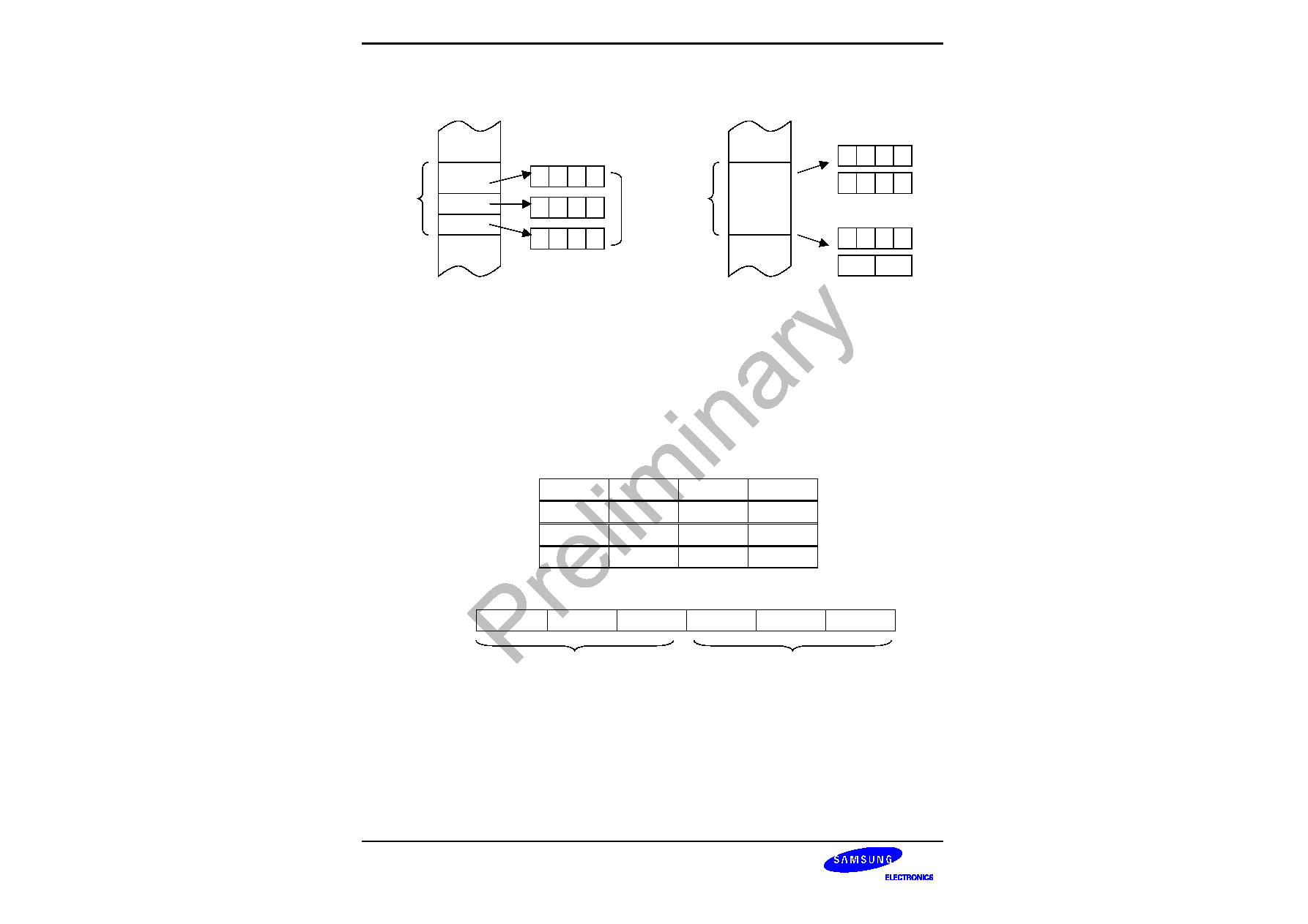
BSW rv0.1-0417-N01
Preliminary product information describes products that are in development,
for which full characterization data and associated errata are not yet available.
Specifications and information herein are subject to change without notice.
POST PROCESSOR
S3C24A0 RISC MICROPROCESSOR
27-4
WORD
WORD
MSB LSB
MSB LSB
B
C
A
D
E
Memory Space
Memory Space
(a) Non-Interleaving
(b) Interleaving
Figure 27-2 Data format stored in external memory
31 24 23 16 15 8 7 0
Case A
Y/Cb/Cr
N+3
Y/Cb/Cr
N+2
Y/Cb/Cr
N+1
Y/Cb/Cr
N
Case B
Y
N+1
Cb
N
Y
N
Cr
N
Case C
Cb
N
Y
N+1
Cr
N
Y
N
Case D
Don't Care
R
N
G
N
B
N
31 27 26 21 20 16 15 11 10 5 4 0
Case E
R[4:0]
G[5:0]
B[4:0]
R[4:0]
G[5:0]
B[4:0]
Pixel N+1
Pixel N
Figure 27-3 Byte and half-word organization
Y
Cb
Cr
1 Frame
Video Data
Or
Graphic Data
1 Frame
Y Y Y Y
Cb Cb
Cb Cb
Cr Cr
Cr Cr
Y Cb Y Cr
Cb Y
Cr
Y
Pixel
N+1
Pixel
N
x R G B

BSW rv0.1-0417-N01
Preliminary product information describes products that are in development,
for which full characterization data and associated errata are not yet available.
Specifications and information herein are subject to change without notice.
S3C24A0 RISC MICROPROCESSOR
POST PROCESSOR
27-5
(a) YCbCr420 (MPEG2/H.263)
(b) YCbCr420 (MPEG4)
(c) YCbCr422 (MPEG2/H.263)
(d) YCbCr422 (MPEG4)
Figure 27-4 Sampling position of YCbCr420 and YCbCr422 format
(�: Luma sample and : Chroma sample)
dx
dy
1/2dx 1/2dx
1/4dy
1/2dy
1/2dy
dx
dy
1/4dx
1/2dx 1/2dx
1/4dy
1/2dy
1/2dy
dx
dy
1/2dx 1/2dx
1/4dy
1/2dy
1/2dy
dx
dy
1/4dx
1/2dx 1/2dx
1/4dy
1/2dy
1/2dy

BSW rv0.1-0417-N01
Preliminary product information describes products that are in development,
for which full characterization data and associated errata are not yet available.
Specifications and information herein are subject to change without notice.
POST PROCESSOR
S3C24A0 RISC MICROPROCESSOR
27-6
3. Image Size and Scale Ratio
The RGB graphic source image size is determined by number of pixels along to horizontal and vertical
directions. YCbCr420 and YCbCr422 source image size is determined only by numbers of Y samples along to
horizontal and vertical directions. Destination image size is determined by dimension of final RGB graphic image,
after color space conversion if source image is YCbCr image.
As explained in the previous section, SRC_Width and DST_Width satisfy the word boundary constraints such
that the number of horizontal pixel can be represented to kn where n = 1,2,3, ... and k = 1 / 2 / 8 for 24bppRGB /
16bppRGB / YCbCr420 image, respectively.
Figure 27-5 Source destination image size
The other control registers of pre-scaled image size, pre-scale ratio, pre-scale shift ratio and main scale ratio
are defined according to the following equations.
If ( SRC_Width >= 64 � DST_Width ) { Exit(-1); /* Out Of Horizontal Scale Range */ }
else if (SRC_Width >= 32 � DST_Width) { PreScale_H_Ratio = 32; H_Shift = 5; }
else if (SRC_Width >= 16 � DST_Width) { PreScale_H_Ratio = 16; H_Shift = 4; }
else if (SRC_Width >= 8 � DST_Width) { PreScale_H_Ratio = 8; H_Shift = 3; }
else if (SRC_Width >= 4 � DST_Width) { PreScale_H_Ratio = 4; H_Shift = 2; }
else if (SRC_Width >= 2 � DST_Width) { PreScale_H_Ratio = 2; H_Shift = 1; }
else { PreScale_H_Ratio = 1; H_Shift = 0; }
PreScale_DSTWidth = SRC_Width / PreScale_H_Ratio;
dx = ( SRC_Width << 8 ) / ( DST_Width << H_Shift);
Source Image
Destination Image
SRC_Width
S
RC_He
ight
DST_Width
DST_Height

BSW rv0.1-0417-N01
Preliminary product information describes products that are in development,
for which full characterization data and associated errata are not yet available.
Specifications and information herein are subject to change without notice.
S3C24A0 RISC MICROPROCESSOR
POST PROCESSOR
27-7
If ( SRC_Height >= 64 � DST_Height ) { Exit(-1); /* Out Of Vertical Scale Range */ }
else if (SRC_Height >= 32 � DST_Height) { PreScale_V_Ratio = 32; V_Shift = 5; }
else if (SRC_Height >= 16 � DST_Height) { PreScale_V_Ratio = 16; V_Shift = 4; }
else if (SRC_Height >= 8 � DST_Height) { PreScale_V_Ratio = 8; V_Shift = 3; }
else if (SRC_Height >= 4 � DST_Height) { PreScale_V_Ratio = 4; V_Shift = 2; }
else if (SRC_Height >= 2 � DST_Height) { PreScale_V_Ratio = 2; V_Shift = 1; }
else { PreScale_V_Ratio = 1; V_Shift = 0; }
PreScale_DSTHeight = SRC_Height / PreScale_V_Ratio;
dy = ( SRC_Height << 8 ) / ( DST_Height << V_Shift);
PreScale_SHFactor = 10 � ( H_Shit + V_Shift);

BSW rv0.1-0417-N01
Preliminary product information describes products that are in development,
for which full characterization data and associated errata are not yet available.
Specifications and information herein are subject to change without notice.
POST PROCESSOR
S3C24A0 RISC MICROPROCESSOR
27-8
4. DMA operation of Source and Destination Image
There are three address categories such as start address, end address and offset address for DMA operation.
Each address category consists of three source address components of Y/Cb/Cr and one destination address
component of RGB. If a source image is stored by the non-interleaved format such as YCbCr420, all source
address components are valid as shown in Figure 27-6 (a). If a source image is stored by the interleaved format
such as a RGB graphic format or an YCbCr422 format, only Y component of three source components is valid
and two chroma address components are invalid as shown in Figure 27-6 (b). The details of start and end
address are define as follows.
(a) Non-Interleaving
(b) Interleaving
Figure 27-6 Start and end address set according to memory allocation type
Y
Cb
Cr
Video Data
Or
Graphic Data
Source Image
Destination Image
ADDRStart_Y
ADDREnd_Y
ADDRStart_Cb
ADDREnd_Cb
ADDRStart_Cr
ADDREnd_Cr
ADDRStart_RGB
ADDREnd_RGB
ADDRStart_Y
ADDREnd_Y
ADDRStart_RGB
ADDREnd_RGB
RGB
RGB

BSW rv0.1-0417-N01
Preliminary product information describes products that are in development,
for which full characterization data and associated errata are not yet available.
Specifications and information herein are subject to change without notice.
S3C24A0 RISC MICROPROCESSOR
POST PROCESSOR
27-9
Start address
Start address of ADDRStart_Y/Cb/Cr/RGB points the first word address where the corresponding component
of Y/Cb/Cr/RGB is read or written. Each one should be aligned with word boundary (i.e. ADDRStart_X[1:0] =
00). ADDRStart_Cb and ADDRStart_Cr are valid only for the YCbCr420 source image format.
End address
ADDREnd_Y
= ADDRStart_Y + Memory size for the component of Y
= ADDRStart_Y + (SRC_Width � SRC_Height) � ByteSize_Per_Pixel + Offset_Y � (SRC_Height-1)
ADDREnd_Cb (Valid for YCbCr420 source format)
= ADDRStart_Cb + Memory size for the component of Cb
= ADDRStart_Cb + (SRC_Width/2 � SRC_Height/2) � ByteSize_Per_Pixel + Offset_Cb � (SRC_Height/2-1)
ADDREnd_ Cr (Valid for YCbCr420 source format)
= ADDRStart_ Cr + Memory size for the component of Cr
= ADDRStart_Cr + (SRC_Width/2 � SRC_Height/2) � ByteSize_Per_Pixel + Offset_Cr � (SRC_Height/2-1)
ADDREnd_RGB
= ADDRStart_RGB + Memory size for the component of RGB data
= ADDRStart_RGB + (DST_Width � DST_Height) � ByteSize_Per_Pixel + Offset_RGB � (DST_Height-1)
Where,
Offset_Y/Cb/Cr/RGB
= Memory size for offset per a horizontal line
= Number of pixel (or sample) in horizontal offset � ByteSize_Per_Pixel (or Sample)
ByteSize_Per_Pixel = 1 for YCbCr420
2 for 16-bit RGB
and YCbCr422
4 for 24-bit RGB

BSW rv0.1-0417-N01
Preliminary product information describes products that are in development,
for which full characterization data and associated errata are not yet available.
Specifications and information herein are subject to change without notice.
POST PROCESSOR
S3C24A0 RISC MICROPROCESSOR
27-10
Offset is used for the following two situations. One is to fetch some parts of source image in order to zoom
in/out as shown in Figure 27-7 (a). The other is to restore destination image for PIP (picture-in-picture)
applications as shown in Figure 27-7 (b). Of course, the word boundary constraints should be satisfied in both
cases.
Original Image
Source Image
Src_Width
Sr
c_
He
igh
t
Offset
Destination Image
(Zoom In/Out)
Dst_Width
Ds
t
_
H
e
igh
t
a) Zoom In/Out
Source Image
Src_Width
Src
_
Hei
g
ht
Background Image
b) PIP
Destination
Image(PIP)
Dst_Width
Dst_
Hei
g
h
t
Offset
Figure 27-7 Offset for (a) source image for zoom in/out operation and
(b) destination image for PIP applications
5. Starting and Terminating of POST Processor
Starting and terminating the operation of POST-Processor are controlled by two control register such as
POSTENVID and POSTINT as shown in Figure 27-8. "POSTENVID" triggers the operation of POST
PROCESSOR. It is automatically de-asserted when all operations of the given frame are completed. Before
asserting "POSTENVID", all control registers should be set to the proper value as explained in the previous
chapters. When all operations are completed, interrupt pending register is asserted (POSTINT=1), if interrupt
enable signal is asserted (INTEN=1). The POSTINT signal, directing to the interrupt controller, should be cleared
by the interrupt service routine. Otherwise, polling POSTENVID is used to detect the end of the operation.
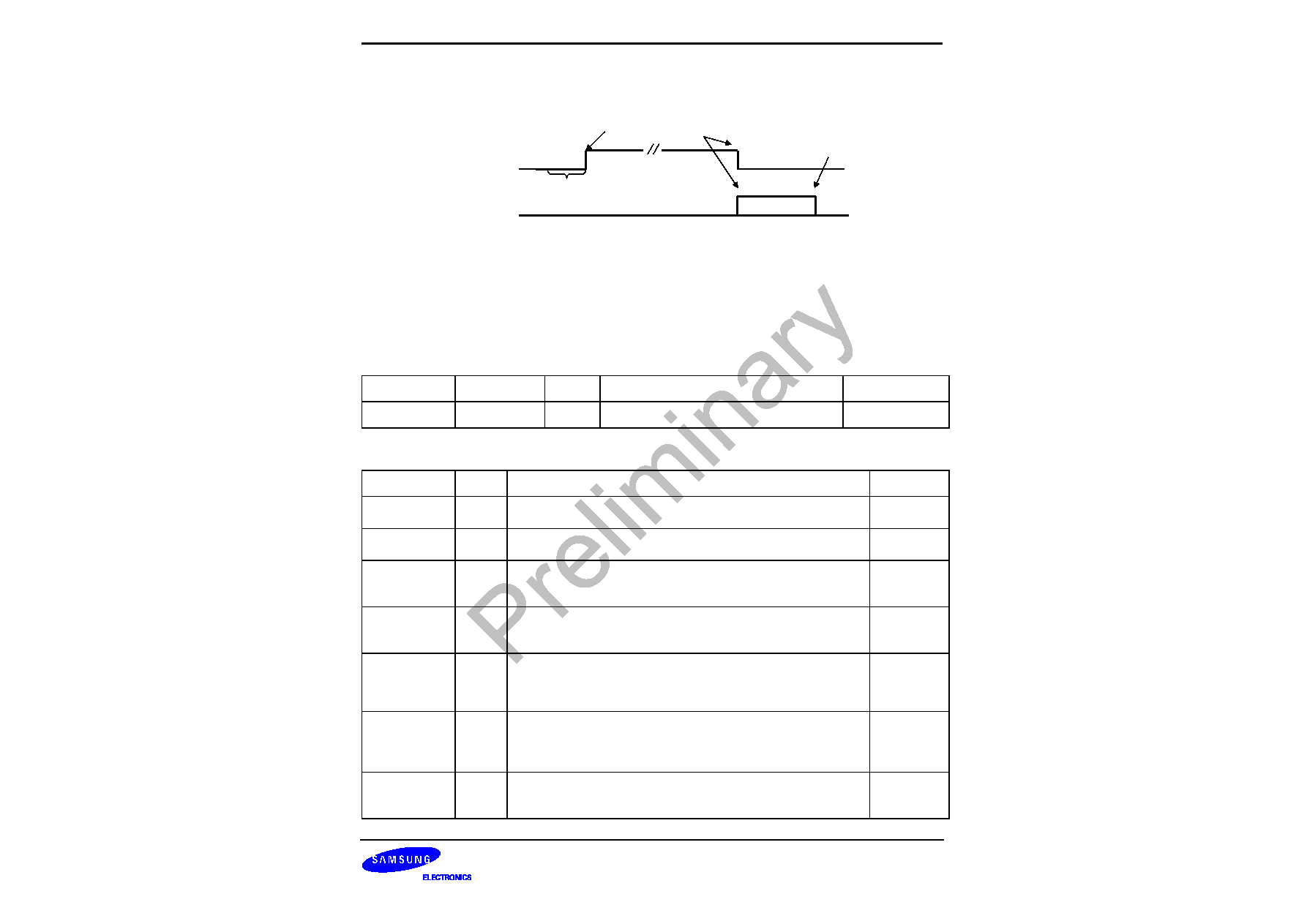
BSW rv0.1-0417-N01
Preliminary product information describes products that are in development,
for which full characterization data and associated errata are not yet available.
Specifications and information herein are subject to change without notice.
S3C24A0 RISC MICROPROCESSOR
POST PROCESSOR
27-11
Figure 27-8 Start and termination of the operation of POST PROCESSOR
6. Register File Lists
MODE Control Register
Register
Address
R/W
Description
Reset Value
MODE
0X4A100000
R/W
Mode Register [9:0]
0xB12
MODE
Bit
Description
Initial State
Reserved
11
This bit should be `1'.
1
Reserved
10
This bit should be `0'.
0
MPEG4
[9]
Sampling position of chroma information. 0 for H.263/MPEG2 and 1
for MPEG4. It is valid only for YCbCr source image (i.e. InRGB = 0)
1
SRC420
[8]
0 for YCbCr422 and 1 for YCbCr420 source format. It is valid only for
YCbCr source image (i.e. InRGB = 0)
1
INTEN
[7]
Interrupt Enable. It determines whether the POSTINT signal is
asserted or not, when the processing of the current frame is finished.
0: disable, 1 : enable.
0
POSTINT
[6]
Interrupt Pending Bit. If INTEN is enabled, it is automatically asserted
right after finishing operation of the current frame. It should be
cleared by interrupt service routine. 0 : disable, 1 : enable.
0
POSTENVID
[5]
Enable Video Processing. It turns on the operation of PostProcessor.
It is de-asserted automatically after operation of the current frame is
finished. It should be disabled (POSTENVID=0) during control
0
Users set
(Start operation)
Automatic clear/assertion
(Terminate operation)
User clear
if asserted
POSTENVID
POSTINT
(INTEN=1)
(INTEN=0)
Control Register Set
BSW rv0.1-0417-N01
Preliminary product information describes products that are in development,
for which full characterization data and associated errata are not yet available.
Specifications and information herein are subject to change without notice.
POST PROCESSOR
S3C24A0 RISC MICROPROCESSOR
27-12
register configuration state.
OutRGBFormat
[4]
It determines the output format of destination image. 0 for 16-bit (565
format) RGB and 1 for 24-bit RGB.
1
InRGB
[3]
It indicates the input color space of source image. 0 for YCbCr or 1
for RGB.
0
INTERLEAVE
[2]
It indicates the data format of YCbCr. 0 for Non-Interleaved format
(Each component of Y, Cb and Cr is access by the word). 1 for
Interleaved format (All components of Y, Cb and Cr are mixed inside
single word). It should be 1 when source image is RGB data (or
InRGB =1).
0
InRGBFormat
[1]
If the source image is in RGB color space (or InRGB=1), it indicates
the data format of graphic image. 0 for 16-bit (565 format) and 1 for
24-bit. Otherwise (or InRGB=0), it should be remains to 1.
1
InYCbCrFormat
[0]
It determines the byte organization of word data when the source
image is interleaved YCbCr format (InRGB=0 and INTERLEAVE=1).
0 for YCbYCr(type B in Fig. 27-2(b)) and 1 for CbYCrY (type C in
Fig.27-2(b) .
0
Pre-Scale Ratio Register
Register
Address
R/W
Description
Reset Value
PreScale_Ratio
0X4A100004
R/W
Pre-Scale ratio for vertical and horizontal.
0x0
PreScale_Ratio
Bit
Description
Initial State
PreScale_V_Ratio
[13:7]
Pre-scale ratio along to vertical direction (see chapter 27-3)
0x0
PreScale_H_Ratio
[6:0]
Pre-scale ratio along to horizontal direction (see chapter 27-3)
0x0
Pre-Scale Image Size Register
Register
Address
R/W
Description
Reset Value
PreScaleImgSize
0X4A100008
R/W
Pre-Scaled image size
0x0

BSW rv0.1-0417-N01
Preliminary product information describes products that are in development,
for which full characterization data and associated errata are not yet available.
Specifications and information herein are subject to change without notice.
S3C24A0 RISC MICROPROCESSOR
POST PROCESSOR
27-13
PreScaleImgSize
Bit
Description
Initial State
PreScale_DSTHeight
[23:12]
Pre-Scaled image height (see chapter 27-3)
0x0
PreScale_DSTWidth
[11:0]
Pre-Scaled image width (see chapter 27-3)
0x0
Source Image Size Register
Register
Address
R/W
Description
Reset Value
SRCImgSize
0X4A10000C
R/W
Source image size
0x0
SRCImgSize
Bit
Description
Initial State
SRCHeight
[23:12]
Source image height (see chapter 27-3)
0x0
SRCWidth
[11:0]
Source image width (see chapter 27-3)
0x0
Horizontal Main Scale Ratio Register
Register
Address
R/W
Description
Reset Value
MainScale_H_Ratio 0X4A100010
R/W
Main scale ratio along to horizontal direction
0x0
MainScale_H_Ratio
Bit
Description
Initial State
MainScale_H_Ratio
[8:0]
Main scale ratio along to horizontal direction (see chapter 27-3)
0x0
Vertical Main Scale Ratio Register
Register
Address
R/W
Description
Reset Value
MainScale_V_Ratio 0X4A100014
R/W
Main scale ratio along to vertical direction
0x0
MainScale_V_Ratio
Bit
Description
Initial State

BSW rv0.1-0417-N01
Preliminary product information describes products that are in development,
for which full characterization data and associated errata are not yet available.
Specifications and information herein are subject to change without notice.
POST PROCESSOR
S3C24A0 RISC MICROPROCESSOR
27-14
MainScale_V_Ratio
[8:0]
Main scale ratio along to vertical direction (see chapter 27-3)
0x0
Destination Image Size Register
Register
Address
R/W
Description
Reset Value
DSTImgSize
0X4A100018
R/W
Destination image size
0x0
SRCImgSize
Bit
Description
Initial State
DSTHeight
[23:12]
Destination image height (see chapter 27-3)
0x0
DSTWidth
[11:0]
Destination image width (see chapter 27-3)
0x0
Pre-Scale Shift Factor Register
Register
Address
R/W
Description
Reset Value
PreScale_SHFactor
0X4A10001C
R/W
Pre-scale shift factor
0x0
SRC_Width
Bit
Description
Initial State
PreScale_SHFactor
[3:0]
Pre-scale shift factor (see chapter 27-3)
0x0
DMA Start Address Register
Register
Address
R/W
Bit
Description
Reset Value
ADDRStart_Y
0X4A100020
R/W
[30:0]
DMA Start address for Y or RGB
component of source image
0x2000_0000
Register
Address
R/W
Bit
Description
Reset Value
ADDRStart_Cb
0X4A100024
R/W
[30:0]
DMA Start address for Cb component
of source image
0x2000_0000

BSW rv0.1-0417-N01
Preliminary product information describes products that are in development,
for which full characterization data and associated errata are not yet available.
Specifications and information herein are subject to change without notice.
S3C24A0 RISC MICROPROCESSOR
POST PROCESSOR
27-15
Register
Address
R/W
Bit
Description
Reset Value
ADDRStart_Cr
0X4A100028
R/W
[30:0]
DMA Start address for Cr component
of source image
0x2000_0000
Register
Address
R/W
Bit
Description
Reset Value
ADDRStart_RGB
0X4A10002C
R/W
[30:0]
DMA Start address for RGB
component of destination image
0x2000_0000
DMA End Address Register
Register
Address
R/W
Bit
Description
Reset Value
ADDREnd_Y
0X4A100030
R/W
[30:0]
DMA End address for Y or RGB
component of source image (see
chapter 27-4)
0x2000_62fc
Register
Address
R/W
Bit
Description
Reset Value
ADDREnd_Cb
0X4A100034
R/W
[30:0]
DMA End address for Cb component
of source image (see chapter 27-4)
0x2000_62fc
Register
Address
R/W
Bit
Description
Reset Value
ADDREnd_Cr
0X4A100038
R/W
[30:0]
DMA End address for Cr component of
source image (see chapter 27-4)
0x2000_62fc
Register
Address
R/W
Bit
Description
Reset Value
ADDREnd_RGB
0X4A10003C
R/W
[30:0]
DMA End address for RGB component
of destination image (see chapter 27-
4)
0x2000_62fc
Offset Register
Register
Address
R/W
Bit
Description
Reset Value

BSW rv0.1-0417-N01
Preliminary product information describes products that are in development,
for which full characterization data and associated errata are not yet available.
Specifications and information herein are subject to change without notice.
POST PROCESSOR
S3C24A0 RISC MICROPROCESSOR
27-16
Offset_Y
0X4A100040
R/W
[23:0]
Offset of Y component for fetching source
image (see chapter 27-4)
0
Register
Address
R/W
Bit
Description
Reset Value
Offset_Cb
0X4A100044
R/W
[23:0]
Offset of Cb component for fetching
source image (see chapter 27-4)
0
Register
Address
R/W
Bit
Description
Reset Value
Offset_Cr
0X4A100048
R/W
[23:0]
Offset of Cr component for fetching source
image (see chapter 27-4)
0
Register
Address
R/W
Bit
Description
Reset Value
Offset_RGB
0X4A10004C
R/W
[23:0]
Offset of RGB component for restoring
destination image (see chapter 27-4)
0

BSW rv0.1-0417-N01
Preliminary product information describes products that are in development,
for which full characterization data and associated errata are not yet available.
Specifications and information herein are subject to change without notice.
S3C24A0 RISC MICROPROCESSOR
LCD CONTROLLER
28-1
LCD CONTROLLER (PRELIMINARY)
OVERVIEW
The LCD controller within S3C24A0 consists of logic for transferring LCD image data from a video buffer located
in system memory to an external LCD driver.
The LCD controller supports 1-bit per pixel, 2-bit per pixel, 4-bit per pixel, 8-bit per pixel for interfacing with the
palettized TFT color LCD panel, 8-bit, 16-bit per pixel and 18-bit per pixel non-palettized color display.
The LCD controller can be programmed to support the different requirements on the screen related to the number
of horizontal and vertical pixels, data line width for the data interface, interface timing, and refresh rate.
FEATURES
Video Clock Source
HCLK
External Panel Interface
Supports up to 18 bit RGB I/F Panel(RGB Parallel mode)
Supports 6 bit RGB I/F Panel(RGB Serial mode)
Supports both RGB and BGR mode
OSD(Overlay)
Supports 8 BPP (bit per pixel) palettized or non-palettized color displays for TFT
Supports 16 and 18 BPP non-palettized color displays for color TFT
Supports X,Y indexed position
Supports 8 bit Alpha blending : per Plan or per Pixel(18 BPP only)
Support 18 bit Color Key function
Color Level of TFT
Supports 1, 2, 4 and 8 BPP(bit per pixel) palettized color displays for TFT
Supports 8, 16 and 18 BPP non-palettized color displays for TFT
Display Size
Supports 640x480, 320x240, 176x192 and others
Configurable Burst Length
Support programmable 4 / 8 / 16 Burst DMA operation
Dual Palette
256 x 24 bit palette (2ea for each Background and Foreground image)
Soft Scrolling
Horizontal : 1 Byte resloution
Vertical : 1 pixel resolution
Virtual Screen
Virtual image can has up to 16MB image size.
Double Buffering
Frame buffer alternating by one control bit
Dithering
Patented 4x4 dither matrix implemetation

BSW rv0.1-0417-N01
Preliminary product information describes products that are in development,
for which full characterization data and associated errata are not yet available.
Specifications and information herein are subject to change without notice.
LCD CONTROLLER
S3C24A0 RISC MICROPROCESSOR
28-2
EXTERNAL INTERFACE SIGNAL
Name
Type
Source/Destination
Description
XvVCLK
Output
Pad
Video Clock Signal
XvHSYNC
Output
Pad
Horizontal Sync. Signal
XvVSYNC
Output
Pad
Vertical Sync. Signal
XvVDEN
Output
Pad
Video Data Enable/Valid
XvVD[17:12]
Output
Pad
LCD pixel data output for Red in RGB Parallel Mode
LCD pixel data output in RGB Serial Mode
XvVD[11:6]
Output
Pad
LCD pixel data output for Green in RGB Parallel Mode
XvVD[5:0]
Output
Pad
LCD pixel data output for Blue in RGB Parallel Mode
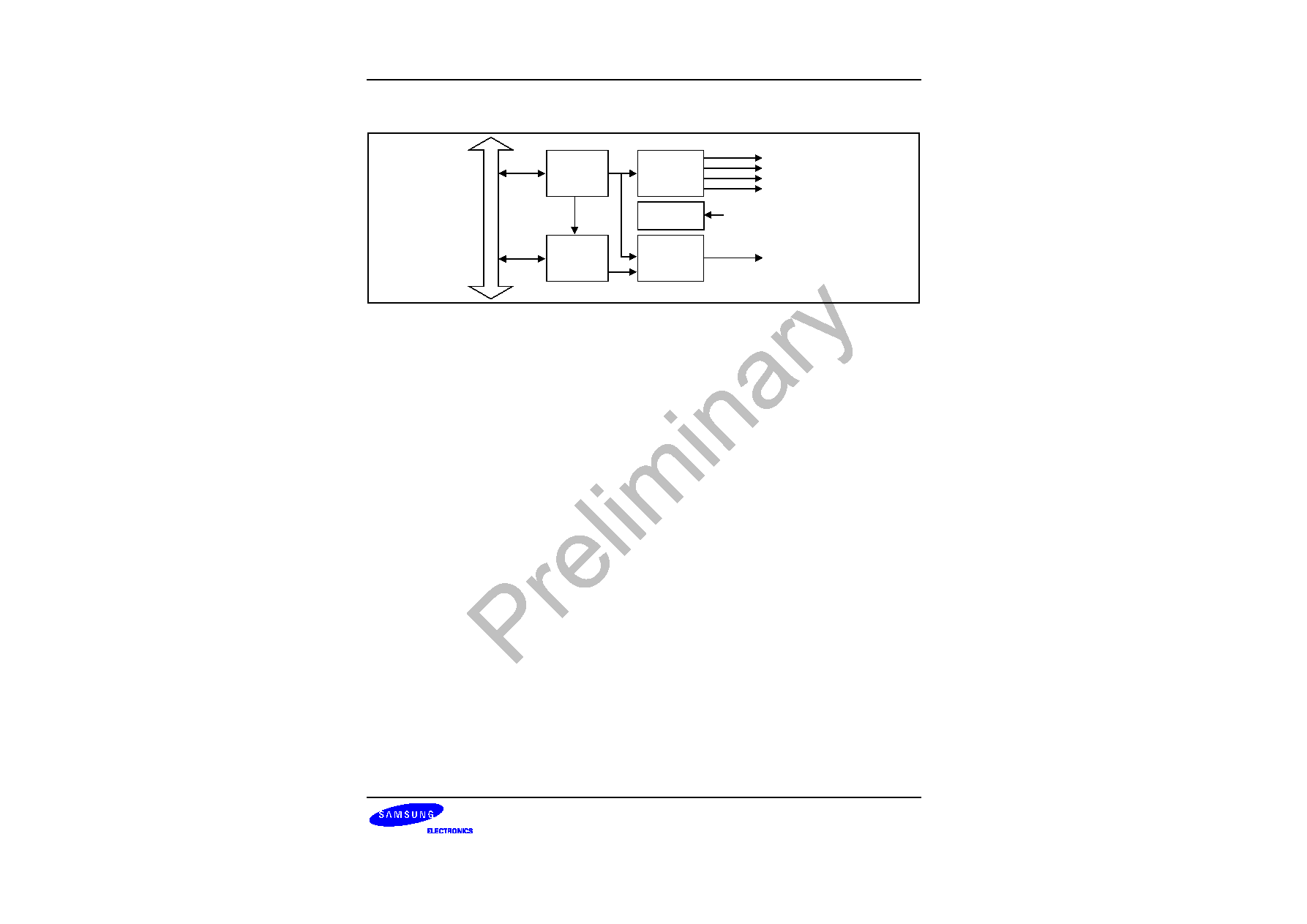
BSW rv0.1-0417-N01
Preliminary product information describes products that are in development,
for which full characterization data and associated errata are not yet available.
Specifications and information herein are subject to change without notice.
S3C24A0 RISC MICROPROCESSOR
LCD CONTROLLER
28-3
BLOCK DIAGRAM
REGBANK
LCDCDMA
XvVCLK
XvHSYNC
XvVSYNC
XvVDEN
TIMEGEN
VIDPRCS
XvVD[17:0]
VIDCLKGEN
HCLK
Figure 28-1. LCD Controller Block Diagram
The LCD controller within S3C24A0 is used to transfer the video data and to generate the necessary control
signals such as
, XvVSYNC, XvHSYNC, XvVCLK, and XvVDEN
. As well as the control signals, S3C24A0 has the
data ports for video data, which are
XvVD[17:0]
as shown in Figure 28-1. The LCD controller consists of a
REGBANK, LCDCDMA, VIDPRCS, TIMEGEN, and VIDCLKGEN (See Figure 28-1 LCD Controller Block
Diagram). The REGBANK has 26 programmable register sets and 256x24 palette memory which are used to
configure the LCD controller. The LCDCDMA is a dedicated DMA, which it can transfer the video data in frame
memory to LCD driver, automatically. By using this special DMA, the video data can be displayed on the screen
without CPU intervention. The VIDPRCS receives the video data from LCDCDMA and sends the video data
through the VD[17:0] data ports to the LCD driver after changing them into a suitable data format, for example 8-
bit per pixel mode(8 BPP Mode) or 16-bit per pixel mode(16 BPP Mode). The TIMEGEN consists of
programmable logic to support the variable requirement of interface timing and rates commonly found in different
LCD drivers. The TIMEGEN block generates
, XvVSYNC, XvHSYNC, XvVCLK, and XvVDEN
.
The description of data flow is as follows:
FIFO memory is present in the LCDCDMA. When FIFO is empty or partially empty, LCDCDMA requests data
fetching from the frame memory based on the burst memory transfer mode(Consecutive memory fetching of 4 / 8
/ 16 words per one burst request without allowing the bus mastership to another bus master during the bus
transfer). When this kind of transfer request is accepted by bus arbitrator in the memory controller, there will be 4
/8 /16 successive word data transfers from system memory to internal FIFO. The total sizes of FIFO are 128x2
words, which consist of 128 words for background FIFO and 128 words foreground FIFO, respectively. The
S3C24A0 has two FIFOs because it needs to support the OSD display mode. In case of one screen display
mode, the background FIFO could only be used.
LCD controller supports overlay function which enables overlaying any image (OSD, foreground image) which is
small or same size can be blended with background image with programmable alpha blending or color (chroma)
key function.

BSW rv0.1-0417-N01
Preliminary product information describes products that are in development,
for which full characterization data and associated errata are not yet available.
Specifications and information herein are subject to change without notice.
LCD CONTROLLER
S3C24A0 RISC MICROPROCESSOR
28-4
TIMING CONTROLLER OPERATION
The TIMEGEN generates the control signals for LCD driver such as,
, XvVSYNC, XvHSYNC, XvVCLK, and
XvVDEN
signal. These control signals are highly related with the configuration on the LCDTCON1/2/3 registers in
the REGBANK. Base on these programmable configurations on the LCD control registers in REGBANK, the
TIMEGEN can generate the programmable control signals suitable for the support of many different types of LCD
drivers.
The VSYNC signal is asserted to cause the LCD's line pointer to start over at the top of the display.
The generation of VSYNC and HSYNC pulse is controlled by the configuration of both the HOZVAL field and the
LINEVAL field in the LCDTCON3 register. The HOZVAL and LINEVAL can be determined by the size of the LCD
panel according to the following equations:
HOZVAL = (Horizontal display size) -1
LINEVAL = (Vertical display size) -1
Divider
1/[(CLKVAL+1)x2]
HCLK
MUX
0
1
VCLK
CLKDIR
Figure 28-2. Clock Selection
The rate of VCLK signal can be controlled by the CLKVAL field in the LCDCON1 register. The table below defines
the relationship of VCLK and CLKVAL. The minimum value of CLKVAL is 0.
XvVCLK (Hz)
=HCLK/ [(CLKVAL+1) x2]
The frame rate is VSYNC signal frequency. The frame rate is related with the field of VSYNC, VBPD, VFPD,
LINEVAL, HSYNC, HBPD, HFPD, HOZVAL, CLKVAL registers. Most LCD driver needs their own adequate frame
rate. The frame rate is calculated as follows;
Frame Rate = 1/ [ { (VSPW+1) + (VBPD+1) + (LIINEVAL + 1) + (VFPD+1) } x {(HSPW+1) + (HBPD +1)
+ (HFPD+1) + (HOZVAL + 1) } x { 2 x ( CLKVAL+1 ) / ( Frequency of Clock source ) } ]
Table 28-1. Relation between
XvVCLK
and CLKVAL (TFT, Freq. of Video Clock Source=60MHz)
CLKVAL
60MHz/X
XvVCLK
1
60 MHz/4
15.0 MHz
2
60 MHz/6
10.0 MHz

BSW rv0.1-0417-N01
Preliminary product information describes products that are in development,
for which full characterization data and associated errata are not yet available.
Specifications and information herein are subject to change without notice.
S3C24A0 RISC MICROPROCESSOR
LCD CONTROLLER
28-5
:
:
:
63
60 MHz/128
492 kHz

BSW rv0.1-0417-N01
Preliminary product information describes products that are in development,
for which full characterization data and associated errata are not yet available.
Specifications and information herein are subject to change without notice.
LCD CONTROLLER
S3C24A0 RISC MICROPROCESSOR
28-6
VIDEO OPERATION
The TFT LCD controller within S3C24A0 supports 1, 2, 4 or 8 BPP(bit per pixel) palettized color displays and 8,
16 non-palettized high-color or 18 BPP non-palettized true-color displays. The TFT LCD controller also supports
On-Screen Display with 256-level alpha blending and color (chroma) key functions. The background image and
foreground image (OSD image) should have a frame buffer of each image.
OSD (ON-SCREEN DISPLAY) : OVERLAY
OSD (On Screen Display) and blending operation as shown in Fig 28-3 are established for video overlay or other
graphics applications. Two blending schemes are provided according to the control bit of OSD_BLD_PIX. One is
per-pixel blending for 18 BPP mode display (OSD_BLD_PIX = 1) and the other is per-plane bending for 8/16/18
BPP mode display (OSD_BLD_PIX = 0). LCDB1ADDR1/2/3, LCDB2ADDR1/2/3 registers are defined to perform
DMA for OSD image. Four screen coordinates such as OSD_LEFT_TOP_X, OSD_LEFT_TOP_Y,
OSD_RIGHT_BOT_X and OSD_RIGHT_BOT_Y determines where the OSD image is located on the whole
background image. The level of blending is controller by OSD_ALPHA as following manner.
<Equation 28-1>
New Pixel = (1-Alpha) � Background Pixel + Alpha � Foreground Pixel
Where, Alpha = 0
, if OSD_ALPHA[7:0] = 0.
Alpha =
i=1,2,,...7
OSD_ALPHA[7-i]x2
-i � O SD_ALPHA[7-i]
, other.
Background
Frame Buffer
Foreground
Frame Buffer(OSD)
LCD Controller
System Memory
(OSD_LEFTTOP_X, OSD_LEFTTOP_Y)
(OSD_RIGHTBOT_X, OSD_RIGHTBOT_Y)
(a) Memory allocation
(b) Blending
Fig 28-3 OSD Procedure
BSW rv0.1-0417-N01
Preliminary product information describes products that are in development,
for which full characterization data and associated errata are not yet available.
Specifications and information herein are subject to change without notice.
S3C24A0 RISC MICROPROCESSOR
LCD CONTROLLER
28-7
COLOR-KEY FUNCTION
The S3C24A0 can support color-key function for the various effect of image mapping.
Color image, which is specified by COLOR-KEY register, of OSD layer will be substituted by background image
for special functionality, as cursor image or pre-view image of the camera.
Background Image
Foreground Image
Blending
Color Key
Fig 28-4 Blending and Color Key function of OSD

BSW rv0.1-0417-N01
Preliminary product information describes products that are in development,
for which full characterization data and associated errata are not yet available.
Specifications and information herein are subject to change without notice.
LCD CONTROLLER
S3C24A0 RISC MICROPROCESSOR
28-8
DUAL BUFFER
The S3C24A0 LCD controller supports easy and fast way for the dual buffering of frame image.
User can take two frame image buffer and select one for active frame buffer using the BDBCON (Background
double buffer control) and FDBCON (Foreground double buffer control) register. Pre-defined address sets of
frame buffer 1 and frame buffer2 are described at Frame Buffer Register 1,2,3. So, user can select which buffer
will be activated by setting of the BDBCON and FDBCON register. Maybe, some applications should need simple
changing method of frame buffer namely "ping-pong display" . Pre-view image of camera interface will be good
example of dual buffering method. One frame should be used as a display buffer, and the other frame as a
updating buffer by camera interface module.

BSW rv0.1-0417-N01
Preliminary product information describes products that are in development,
for which full characterization data and associated errata are not yet available.
Specifications and information herein are subject to change without notice.
S3C24A0 RISC MICROPROCESSOR
LCD CONTROLLER
28-9
Memory Data Format (TFT)
The LCD controller requests the specified memory format of frame buffer. The next table shows some examples
of each display mode.
18 BPP Display
[BSWP = 0, HWSWP = 0]
D[31:24]
D[23:0]
000H
Alpha1
P1
004H
Alpha2
P2
008H
Alpha3
P3
...
Note: D[31:24] are used to be the alpha value according to each pixel data when blending mode is per-pixel at 18
BPP. So, user must write appropriate value to this filed.
P1 P2 P3 P4 P5
......
LCD Panel
[Memory Storing Order at 18 BPP]
D[23:0] 23 22 21 20 19 18 17 16 15 14 13 12 11 10
9
8
7
6
5
4
3
2
1 0
Data
R5 R4 R3 R2 R1 R0 x
x
G5 G4 G3 G2 G1 G0 x
x
B5 B4 B3 B2 B1 B0 x
x
x: Don't care, We recommend that those bits are filled with `0'.
[XvVD Pin Connection at 18 BPP/Parallel Mode]
XvVD
17 16 15 14 13 12 11 10
9
8
7
6
5
4
3
2
1
0
Data
R5 R4 R3 R2 R1 R0 G5 G4 G3 G2 G1 G0 B5 B4 B3 B2 B1 B0
[XvVD Pin Connection at 18 BPP/Serial Mode]
XvVD
17 16 15 14 13 12
11 - 0
1
st
Data
R5 R4 R3 R2 R1 R0
NC
2
nd
Data
G5 G4 G3 G2 G1 G0
NC
3
rd
Data
B5 B4 B3 B2 B1 B0
NC

BSW rv0.1-0417-N01
Preliminary product information describes products that are in development,
for which full characterization data and associated errata are not yet available.
Specifications and information herein are subject to change without notice.
LCD CONTROLLER
S3C24A0 RISC MICROPROCESSOR
28-10
16BPP Display
[BSWP = 0, HWSWP = 0]
D[31:16]
D[15:0]
000H
P1
P2
004H
P3
P4
008H
P5
P6
...
[BSWP = 0, HWSWP = 1]
D[31:16]
D[15:0]
000H
P2
P1
004H
P4
P3
008H
P6
P5
...
P1 P2 P3 P4 P5
......
LCD Panel
[Memory Storing Method at 16 BPP]
(5:6:5)
D[15:0]
15 14 13 12 11 10
9
8
7
6
5
4
3
2
1
0
Data
R4 R3 R2 R1 R0 G5 G4 G3 G2 G1 G0 B4 B3 B2 B1 B0
(5:5:5:I)
D[15:0]
15 14 13 12 11 10
9
8
7
6
5
4
3
2
1
0
Data
R4 R3 R2 R1 R0 G4 G3 G2 G1 G0 B4 B3 B2 B1 B0
I
[XvVD Pin Connection at 16 BPP/Parallel Mode]
(5:6:5)
XvVD
17
16
15
14
13
12
11
10
9
8
7
6
5
4
3
2
1
0
Data
R4 R3 R2 R1 R0
N
C
G5 G4 G3 G2 G1 G0 B4 B3 B2 B1 B0
N
C
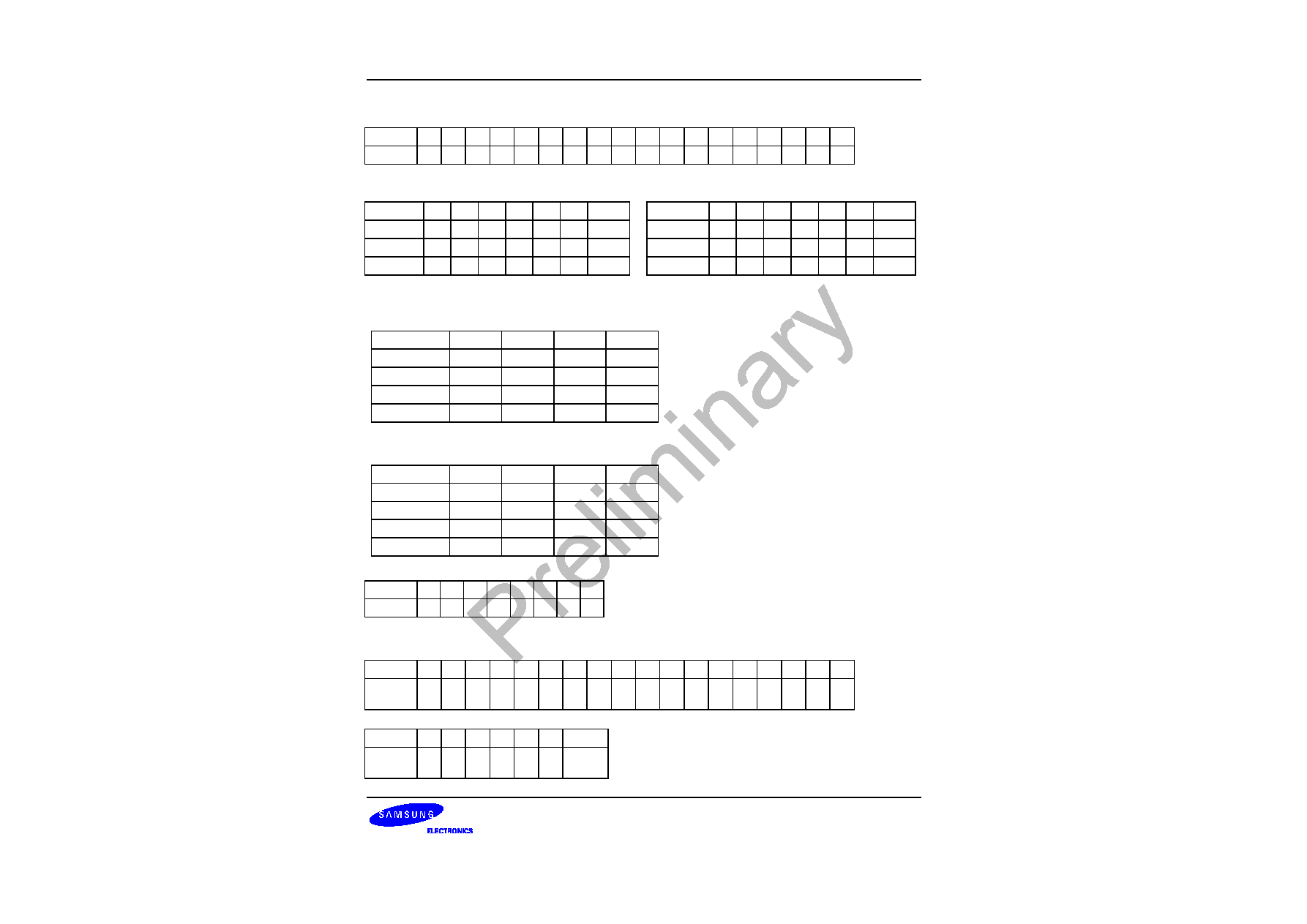
BSW rv0.1-0417-N01
Preliminary product information describes products that are in development,
for which full characterization data and associated errata are not yet available.
Specifications and information herein are subject to change without notice.
S3C24A0 RISC MICROPROCESSOR
LCD CONTROLLER
28-11
(5:5:5:I)
XvVD
17
16
15
14
13
12
11
10
9
8
7
6
5
4
3
2
1
0
Data
R4 R3 R2 R1 R0
I
G4 G3 G2 G1 G0
I
B4 B3 B2 B1 B0
I
[XvVD Pin Connection at 16 BPP/Serial Mode]
(5:6:5) (5:5:5:I)
XvVD
17
16
15
14
13
12
11 - 0
XvVD
17
16
15
14
13
12
11 - 0
1
st
Data
R4
R3
R2
R1
R0
NC
NC
1
st
Data
R4
R3
R2
R1
R0
I
NC
2
nd
Data
G5
G4
G3
G2
G1
G0
NC
2
nd
Data
G4
G3
G2
G1
G0
I
NC
3
rd
Data
B4
B3
B2
B1
B0
NC
NC
3
rd
Data
B4
B3
B2
B1
B0
I
NC
8BPP Display
[BSWP = 0, HWSWP = 0]
D[31:24] D[23:16] D[15:8]
D[7:0]
000H
P1
P2
P3
P4
004H
P5
P6
P7
P8
008H
P9
P10
P11
P12
...
[BSWP = 1, HWSWP = 0]
D[31:24] D[23:16] D[15:8]
D[7:0]
000H
P4
P3
P2
P1
004H
P8
P7
P6
P5
008H
P12
P11
P10
P9
...
[Memory Storing Method at Non-palettized 8 BPP]
D[7:0]
7
6
5
4
3
2
1
0
Data
R2 R1 R0 G2 G1 G0 B1 B0
[XvVD Pin Connection at Non-palettized 8BPP/Parallel Mode]
XvVD
17
16
15
14
13
12
11
10
9
8
7
6
5
4
3
2
1
0
Data
R2 R1 R0
N
C
N
C
N
C
G2 G1 G0
N
C
N
C
N
C
B1 B0
N
C
N
C
N
C
N
C
[XvVD Pin Connection at Non-palettized 8BPP/Serial Mode]
XvVD
17
16
15
14
13
12
11 - 0
1
st
Data
R2 R1 R0
N
C
N
C
N
C
NC

BSW rv0.1-0417-N01
Preliminary product information describes products that are in development,
for which full characterization data and associated errata are not yet available.
Specifications and information herein are subject to change without notice.
LCD CONTROLLER
S3C24A0 RISC MICROPROCESSOR
28-12
2
nd
Data
G2 G1 G0
N
C
N
C
N
C
NC
3
rd
Data
B1 B0
N
C
N
C
N
C
N
C
NC

BSW rv0.1-0417-N01
Preliminary product information describes products that are in development,
for which full characterization data and associated errata are not yet available.
Specifications and information herein are subject to change without notice.
S3C24A0 RISC MICROPROCESSOR
LCD CONTROLLER
28-13
4BPP Display
[BSWP = 0, HWSWP = 0]
D[31:28]
D[27:24]
D[23:20]
D[19:16]
D[15:12]
D[11:8]
D[7:4]
D[3:0]
000H
P1
P2
P3
P4
P5
P6
P7
P8
004H
P9
P10
P11
P12
P13
P14
P15
P16
008H
P17
P18
P19
P20
P21
P22
P23
P24
...
[BSWP = 1, HWSWP = 0]
D[31:28]
D[27:24]
D[23:20]
D[19:16]
D[15:12]
D[11:8]
D[7:4]
D[3:0]
000H
P7
P8
P5
P6
P3
P4
P1
P2
004H
P15
P16
P13
P14
P11
P12
P9
P10
008H
P23
P24
P21
P22
P19
P20
P17
P18
...
2BPP Display
[BSWP = 0, HWSWP = 0]
D
[31:30]
[29:28]
[27:26]
[25:24]
[23:22]
[21:20]
[19:18]
[17:16]
000H
P1
P2
P3
P4
P5
P6
P7
P8
004H
P17
P18
P19
P20
P21
P22
P23
P24
008H
P33
P34
P35
P36
P37
P38
P39
P40
...
D
[15:14]
[13:12]
[11:10]
[9:8]
[7:6]
[5:4]
[3:2]
[1:0]
000H
P9
P10
P11
P12
P13
P14
P15
P16
004H
P25
P26
P27
P28
P29
P30
P31
P32
008H
P41
P42
P43
P44
P45
P46
P47
P48
...

BSW rv0.1-0417-N01
Preliminary product information describes products that are in development,
for which full characterization data and associated errata are not yet available.
Specifications and information herein are subject to change without notice.
LCD CONTROLLER
S3C24A0 RISC MICROPROCESSOR
28-14
256 PALETTE USAGE (TFT)
Palette Configuration and Format Control
The S3C24A0 can support the 256 colors palette for various selection of color mapping. The user can select 256
colors from the 24-bit palette data through these three formats. 256 color palette consist of the 256(depth)
�
24-bit
SPSRAM. Palette supports 6:6:6, 5:6:5(R:G:B), and 5:5:5:1(R:G:B:I) format. When the user use 5:5:5:1 format,
the intensity data(I) is used as a common LSB bit of each RGB data. So, 5:5:5:1 format is same as
(5+I):G(5+I):B(5+I) format. For example of 5:5:5:1 format, write palette like Table 28-4 and then connect VD pin to
TFT LCD panel(R(5+I)=VD[17:13]+VD[12], VD[6] or VD[0], G(5+I)=VD[11:7]+ VD[12], VD[6] or VD[0],
B(5+I)=VD[5:1]+ VD[12], VD[6] or VD[0].) At the last, Set PALFRM register to 0x3.
Table 28-2. 6:6:6 Palette Data Format
INDEX\Bit Pos.
23-18
17
16
15
14
13
12
11
10
9
8
7
6
5
4
3
2
1
0
00H
-
R5
R4
R3
R2
R1
R0
G5
G4
G3
G2
G1
G0
B5
B4
B3
B2
B1
B0
01H
-
R5
R4
R3
R2
R1
R0
G5
G4
G3
G2
G1
G0
B5
B4
B3
B2
B1
B0
.......
-
...
...
...
...
...
...
...
...
...
...
...
...
...
...
...
...
...
...
FFH
-
R5
R4
R3
R2
R1
R0
G5
G4
G3
G2
G1
G0
B5
B4
B3
B2
B1
B0
Number of VD
-
17
16
15
14
13
12
11
10
9
8
7
6
5
4
3
2
1
0
Table 28-3. 5:6:5 Palette Data Format
INDEX\Bit Pos.
23-16
15
14
13
12
11
10
9
8
7
6
5
4
3
2
1
0
00H
-
R4
R3
R2
R1
R0
G5
G4
G3
G2
G1
G0
B4
B3
B2
B1
B0
01H
-
R4
R3
R2
R1
R0
G5
G4
G3
G2
G1
G0
B4
B3
B2
B1
B0
.......
-
...
...
...
...
...
...
...
...
...
...
...
...
...
...
...
...
FFH
-
R4
R3
R2
R1
R0
G5
G4
G3
G2
G1
G0
B4
B3
B2
B1
B0
Number of VD
-
17
16
15
14
13
11
10
9
8
7
6
5
4
3
2
1
Table 28-4. 5:5:5:1 Palette Data Format
INDEX\Bit Pos.
23-16
15
14
13
12
11
10
9
8
7
6
5
4
3
2
1
0
00H
-
R4
R3
R2
R1
R0
G4
G3
G2
G1
G0
B4
B3
B2
B1
B0
I
01H
-
R4
R3
R2
R1
R0
G4
G3
G2
G1
G0
B4
B3
B2
B1
B0
I
.......
-
...
...
...
...
...
...
...
...
...
...
...
...
...
...
...
...
FFH
-
R4
R3
R2
R1
R0
G4
G3
G2
G1
G0
B4
B3
B2
B1
B0
I
Number of VD
-
17
16
15
14
13
11
10
9
8
7
5
4
3
2
1
1)
NOTES:
1. VD12, VD6 and VD0 has same output value, I.
2. DATA[31:24] is invalid.
Palette Read/Write
It is prohibited to access Palette memory during the ACTIVE status of the VSTATUS (vertical status) of
LCDCON2 register. When the user going to do Read/Write operation on the palette, VSTATUS must be checked.

BSW rv0.1-0417-N01
Preliminary product information describes products that are in development,
for which full characterization data and associated errata are not yet available.
Specifications and information herein are subject to change without notice.
S3C24A0 RISC MICROPROCESSOR
LCD CONTROLLER
28-15
1
2
3
4
5
LCD Panel
16BPP 5:5:5+1 Format(Non-Palette)
A[31] A[30] A[29] A[28] A[27] A[26]A[25] A[24] A[23] A[22] A[21] A[20] A[19]A[18] A[17] A[16]
R4
R3
R2
R1
R0
G4
G3
G2
G1
G0
B4
B3
B2
B1
B0
I
A[15] A[14] A[13] A[12] A[11] A[10] A[9] A[8] A[7] A[6] A[5] A[4] A[3] A[2] A[1] A[0]
R4
R3
R2
R1
R0
G4
G3
G2
G1
G0
B4
B3
B2
B1
B0
I
1
2
3
4
5
LCD Panel
16BPP 5:6:5 Format(Non-Palette)
A[31] A[30] A[29] A[28] A[27] A[26]A[25] A[24] A[23] A[22] A[21] A[20] A[19]A[18] A[17] A[16]
A[15] A[14] A[13] A[12]A[11] A[10] A[9] A[8] A[7] A[6] A[5] A[4] A[3] A[2] A[1] A[0]
R4
R3
R2
R1
R0
G5
G4
G3
G2
G1
G0
B4
B3
B2
B1
B0
R4
R3
R2
R1
R0
G5
G4
G3
G2
G1
G0
B4
B3
B2
B1
B0
Figure 28-5. 16BPP Display Types

BSW rv0.1-0417-N01
Preliminary product information describes products that are in development,
for which full characterization data and associated errata are not yet available.
Specifications and information herein are subject to change without notice.
LCD CONTROLLER
S3C24A0 RISC MICROPROCESSOR
28-16
INT_FrSyn
VSYNC
HSYNC
VDEN
HSYNC
VCLK
VD[17:0]
(Parallel Mode)
VBPD+1
VSPW+1
VFPD+1
HBPD+1
VFPD+1
HSPW+1
VDEN
1 Frame
1 Line
LINEVAL +1
HOZVAL+1
VD[17:12]
(Serial Mode)
R
G
B
R
G
B
R
...
B
R
G
B
R
G
B
R
G
B
R
G
B
R
G
B
R
G
B
R
G
B
R
G
B
R
G
B
R
G
B
R
G
B
R
G
B
R
G
B
Figure 28-6. TFT LCD Timing Example

BSW rv0.1-0417-N01
Preliminary product information describes products that are in development,
for which full characterization data and associated errata are not yet available.
Specifications and information herein are subject to change without notice.
S3C24A0 RISC MICROPROCESSOR
LCD CONTROLLER
28-17
VIRTUAL DISPLAY
The S3C24A0 supports hardware horizontal or vertical scrolling. If the screen is scrolled, the fields of LCDBASEU
and LCDBASEL registers need to be changed(refer to Figure 28-7) but not the values of PAGEWIDTH and
OFFSIZE. The size of video buffer in which the image is stored should be larger than LCD panel screen size.
This is the data of line 1 of virtual screen. This is the data of line 1 of virtual screen.
This is the data of line 2 of virtual screen. This is the data of line 2 of virtual screen.
This is the data of line 3 of virtual screen. This is the data of line 3 of virtual screen.
This is the data of line 4 of virtual screen. This is the data of line 4 of virtual screen.
This is the data of line 5 of virtual screen. This is the data of line 5 of virtual screen.
This is the data of line 6 of virtual screen. This is the data of line 6 of virtual screen.
This is the data of line 7 of virtual screen. This is the data of line 7 of virtual screen.
This is the data of line 8 of virtual screen. This is the data of line 8 of virtual screen.
This is the data of line 9 of virtual screen. This is the data of line 9 of virtual screen.
This is the data of line 10 of virtual screen. This is the data of line 10 of virtual screen.
This is the data of line 11 of virtual screen. This is the data of line 11 of virtual screen.
.
.
.
Before Scrolling
View Port
(The same size
of LCD panel.)
LINEVAL + 1
OFFSIZE
PAGEWIDTH
This is the data of line 1 of virtual screen. This is the data of line 1 of virtual screen.
This is the data of line 2 of virtual screen. This is the data of line 2 of virtual screen.
This is the data of line 3 of virtual screen. This is the data of line 3 of virtual screen.
This is the data of line 4 of virtual screen. This is the data of line 4 of virtual screen.
This is the data of line 5 of virtual screen. This is the data of line 5 of virtual screen.
This is the data of line 6 of virtual screen. This is the data of line 6 of virtual screen.
This is the data of line 7 of virtual screen. This is the data of line 7 of virtual screen.
This is the data of line 8 of virtual screen. This is the data of line 8 of virtual screen.
This is the data of line 9 of virtual screen. This is the data of line 9 of virtual screen.
This is the data of line 10 of virtual screen. This is the data of line 10 of virtual screen.
This is the data of line 11 of virtual screen. This is the data of line 11 of virtual screen.
.
.
.
After Scrolling
LCDBASEU
LCDBASEL
OFFSIZE
Figure 28-7. Example of Scrolling in Virtual Display

BSW rv0.1-0417-N01
Preliminary product information describes products that are in development,
for which full characterization data and associated errata are not yet available.
Specifications and information herein are subject to change without notice.
LCD CONTROLLER
S3C24A0 RISC MICROPROCESSOR
28-18
REGISTER DESCRIPTION
MEMORY MAP
Table 28-5. Configuration registers
Register
Address
R/W
Description
Reset Value
LCDCON1
0X4A000000 R/W LCD Control 1
0x00000000
LCDCON2
0X4A000004 R/W LCD Control 2
0x00000000
LCDTCON1
0X4A000008 R/W LCD Time Control 1
0x00000000
LCDTCON2
0X4A00000C R/W LCD Time Control 2
0x00000000
LCDTCON3
0X4A000010 R/W LCD Time Control 3
0x00000000
LCDOSD1
0X4A000014 R/W LCD OSD Control Register
0x00000000
LCDOSD2
0X4A000018 R/W Foreground image(OSD Image) Left top position set
0x00000000
LCDOSD3
0X4A00001C R/W Foreground image(OSD Image) Right Bottom position set
0x00000000
LCDSADDRB1
0X4A000020 R/W Frame Buffer Start Address 1(Background buffer 1)
0x00000000
LCDSADDRB2
0X4A000024 R/W Frame Buffer Start Address 2(Background buffer 2)
0x00000000
LCDSADDRF1
0X4A000028 R/W Frame Buffer Start Address 1(Foreground buffer 1)
0x00000000
LCDSADDRF2
0X4A00002C R/W Frame Buffer Start Address 2(Foreground buffer 2)
0x00000000
LCDEADDRB1
0X4A000030 R/W Frame Buffer End Address 1(Background buffer 1)
0x00000000
LCDEADDRB2
0X4A000034 R/W Frame Buffer End Address 2(Background buffer 2)
0x00000000
LCDEADDRF1
0X4A000038 R/W Frame Buffer End Address 1(Foreground buffer 1)
0x00000000
LCDEADDRF2
0X4A00003C R/W Frame Buffer End Address 2(Foreground buffer 2)
0x00000000
LCDVSCRB1
0X4A000040 R/W Virtual Screen OFFSIZE and PAGEWIDTH(Background buffer 1)
0x00000000
LCDVSCRB2
0X4A000044 R/W Virtual Screen OFFSIZE and PAGEWIDTH (Background buffer 2)
0x00000000
LCDVSCRF1
0X4A000048 R/W Virtual Screen OFFSIZE and PAGEWIDTH (Foreground buffer 1)
0x00000000
LCDVSCRF2
0X4A00004C R/W Virtual Screen OFFSIZE and PAGEWIDTH (Foreground buffer 2)
0x00000000
LCDINTCON
0X4A000050 R/W LCD Interrupt Control
0x00000000
LCDKEYCON
0X4A000054 R/W COLOR KEY Control 1
0x00000000
LCDKEYVAL
0X4A000058 R/W COLOR KEY Control 2
0x00000000
LCDBGCON
0x4A00005C R/W Background color Control
0x00000000
LCDFGCON
0x4A000060
R/W Foreground color Control
0x00000000
LCDDITHCON
0X4A000064 R/W LCD Dithering Control for Active Matrix
0x00000000
Individual Register Descriptions
LCD Control 1 Register
Register
Address
R/W
Description
Reset Value
LCDCON1
0X4A000000
R/W
LCD control 1 register
0x00000000

BSW rv0.1-0417-N01
Preliminary product information describes products that are in development,
for which full characterization data and associated errata are not yet available.
Specifications and information herein are subject to change without notice.
S3C24A0 RISC MICROPROCESSOR
LCD CONTROLLER
28-19
LCDCON1
Bit
Description
Initial
State
BURSTLEN
[29:28] DMA's Burst Length selection :
00 : 16 word� burst
01 : 8 word� burst
10 : 4 word� burst
11 : reserved
0
Reserved
[27:22] Reserved
0
BDBCON
[21]
Active Frame Select control for background image.
It will be adopted from next frame data.
0 = Buffer1 1 = Buffer2
0
FDBCON
[20]
Active Frame Select control for foreground image(OSD image).
It will be adopted from next frame data.
0 = Buffer1 1 = Buffer2
0
DIVEN
[19]
VCLK Divider( CLKVAL ) counter enable control bit
0 = Disable ( for Power saving)
1 = Enable
0
CLKVAL
[18:13] Determine the rates of VCLK and CLKVAL[5:0].
VCLK = HCLK / [(CLKVAL+1) x 2] ( CLKVAL
0 )
0
CLKDIR
[12]
Select the clock source as direct or divide using CLKVAL register.
0 = Direct clock ( frequency of VCLK = frequency of Clock source)
1 = Divided using CLKVAL
0
Reserved
[11]
This bit should be `0'
0
PNRMODE
[10:9]
Select the display mode.
00 = RGB Parallel mode ( RGB )
01 = RGB Parallel mode ( BGR )
10 = RGB Serial mode ( R->G->B)
11 = RGB Serial mode ( B->G->R)
0
BPPMODEF
[8:6]
Select the BPP (Bits Per Pixel) mode for foreground image (OSD).
011 = 8 BPP ( palettized )
100 = 8 BPP ( non-palettized, R:3-G:3-B:2 )
101 = 16 BPP ( non-palettized, R:5-G:6-B:5)
110 = 16 BPP ( non-palettized, R:5-G:5-B:5-I:1)
111 = unpacked 18 BPP ( non-palettized )
0
BPPMODEB
[5:2]
Select the BPP (Bits Per Pixel) mode for background image.
0000 = 1 BPP
0001 = 2 BPP
0010 = 4 BPP
0

BSW rv0.1-0417-N01
Preliminary product information describes products that are in development,
for which full characterization data and associated errata are not yet available.
Specifications and information herein are subject to change without notice.
LCD CONTROLLER
S3C24A0 RISC MICROPROCESSOR
28-20
0011 = 8 BPP ( palettized )
0100 = 8 BPP ( non-palettized, R:3-G:3-B:2 )
0101 = 16 BPP ( non-palettized, R:5-G:6-B:5)
0110 = 16 BPP ( non-palettized, R:5-G:5-B:5-I:1)
0111 = unpacked 18 BPP ( non-palettized )
1xxx = Reserved
ENVID
[1]
LCD video output and the logic immediately enable/disable.
0 = Disable the video output and the LCD control signal.
1 = Enable the video output and the LCD control signal.
0
ENVID_F
[0]
LCD video output and the logic enable/disable at current frame end.
0 = Disable the video output and the LCD control signal.
1 = Enable the video output and the LCD control signal.
* If you on and off this bit, then you will read "H" and video controller is
enabled until the end of current frame.
0
Note) Per Frame video on-off : ENVID & ENVID_F on-off simultaneously.
Direct video on-off : ENVID on-off only. (where, ENVID_F = 0)
LCD Control 2 Register
Register
Address
R/W
Description
Reset Value
LCDCON2
0X4A000004
R/W
LCD control 2 register
0x00000000
LCDCON2
Bit
Description
Initial state
LINECNT (read
only)
[25:15]
Provide the status of the line counter (read only)
Up count from 0 to LINEVAL
0
VSTATUS
[14:13]
Vertical Status (read only).
00 = VSYNC 01 = BACK Porch
10 = ACTIVE 11 = FRONT Porch
0
HSTATUS
[12:11]
Horizontal Status (read only).
00 = HSYNC 01 = BACK Porch
10 = ACTIVE 11 = FRONT Porch
0
PALFRM
[10:9]
This bit determines the size of the palette data format
00 = Reserved 01 = 18 bit ( 6:6:6)
10 = 16 bit (5:6:5) 11 = 16 bit ( 5:5:5:1)
0
Reserved
[8]
This bit must be "0".
0
IVCLK
[7]
This bit controls the polarity of the VCLK active edge.
0 = The video data is fetched at VCLK falling edge
1 = The video data is fetched at VCLK rising edge
0
IHSYNC
[6]
This bit indicates the HSYNC pulse polarity.
0 = normal 1 = inverted
0
IVSYNC
[5]
This bit indicates the VSYNC pulse polarity.
0 = normal 1 = inverted
0

BSW rv0.1-0417-N01
Preliminary product information describes products that are in development,
for which full characterization data and associated errata are not yet available.
Specifications and information herein are subject to change without notice.
S3C24A0 RISC MICROPROCESSOR
LCD CONTROLLER
28-21
Reserved
[4]
Reserved
0
IVDEN
[3]
This bit indicates the VDEN signal polarity.
0 = normal 1 = inverted
0
BITSWP
[2]
Bit swap control bit.
0 = Swap Disable 1 = Swap Enable
0
BYTSWP
[1]
Byte swap control bit.
0 = Swap Disable 1 = Swap Enable
0
HAWSWP
[0]
Half-Word swap control bit.
0 = Swap Disable 1 = Swap Enable
0
LCD Time Control 1 Register
Register
Address
R/W
Description
Reset Value
LCDTCON1
0X4A000008
R/W
LCD control 2 register
0x00000000
LCDTCON1
Bit
Description
Initial State
VBPD
[23:16]
Vertical back porch is the number of inactive lines at the start of a
frame, after vertical synchronization period.
0
VFPD
[15:8]
Vertical front porch is the number of inactive lines at the end of a
frame, before vertical synchronization period.
0
VSPW
[7:0]
Vertical sync pulse width determines the VSYNC pulse's sync level
width by counting the number of inactive lines.
0
LCD Time Control 2 Register
Register
Address
R/W
Description
Reset Value
LCDTCON2
0X4A00000C
R/W
LCD time control 2 register
0x00000000
LCDTCON2
Bit
Description
Initial state
HBPD
[23:16]
Horizontal back porch is the number of VCLK periods between the
falling edge of HSYNC and the start of active data.
0000000
HFPD
[15:8]
Horizontal front porch is the number of VCLK periods between the
end of active data and the rising edge of HSYNC.
0X00
HSPW
[7:0]
Horizontal sync pulse width determines the HSYNC pulse's sync
level width by counting the number of the VCLK.
0X00
LCD Time Control 3 Register
Register
Address
R/W
Description
Reset Value
LCDTCON3
0X4A000010
R/W
LCD time control 3 register
0x00000000
LCDTCON3
Bit
Description
Initial state

BSW rv0.1-0417-N01
Preliminary product information describes products that are in development,
for which full characterization data and associated errata are not yet available.
Specifications and information herein are subject to change without notice.
LCD CONTROLLER
S3C24A0 RISC MICROPROCESSOR
28-22
LINEVAL
[21:11] These bits determine the vertical size of LCD panel.
0
HOZVAL
[10:0]
These bits determine the horizontal size of LCD panel.
0
LCD OSD Control 1 Register
Register
Address
R/W
Description
Reset Value
LCDOSD1
0X4A000014
R/W
LCD OSD control 1 register
0x00000000
LCDOSD1
Bit
Description
Initial state
OSDEN_F
[9]
OSD(On-screen display) control bit.
0 = OSD Disable 1 = OSD Enable
0
OSD_BLD_PIX
[8]
Select blending mode
0 = Per plane blending (8/16/18 BPP mode)
1 = Per pixel blending (18 BPP only)
0
OSD_ALPHA
[7:0]
8-bit Alpha value for Per plane defined by Equation 28-1.
0
Note) OSD_ALPHA when blending mode is Per pixel should be written in MSB 8 bits of D[31:0].
If color key is enabled, blending function is not performed.
LCD OSD Control 2 Register
Register
Address
R/W
Description
Reset Value
LCDOSD2
0X4A000018
R/W
LCD OSD control 2 register
0x0
LCDOSD2
Bit
Description
initial state
OSD_LEFTTOP_X
[21:11]
Horizontal screen coordinate for left top pixel of OSD image
0
OSD_LEFTTOP_Y
[10:0]
Vertical screen coordinate for left top pixel of OSD image
0
LCD OSD Control 3 Register
Register
Address
R/W
Description
Reset Value
LCDOSD3
0X4A00001C R/W
LCD OSD control 3 register
0x0
LCDOSD3
Bit
Description
initial state
OSD_RIGHTBOT_X
[21:11]
Horizontal screen coordinate for right bottom pixel of OSD
image.
OSD_RIGHTBOT_X <= LCD Panel size of X.
0
OSD_RIGHTBOT_Y
[10:0]
Vertical screen coordinate for right bottom pixel of OSD
image.
OSD_RIGHTBOT_X <= LCD Panel size of Y.
0
Note) Horizontal screen coordinate of LCDOSD2 and LCDOSD3 must be in word boundary.
So, 18 BPP mode can has X position by 1 pixel. ( ex, X = 0,1,2,3....)

BSW rv0.1-0417-N01
Preliminary product information describes products that are in development,
for which full characterization data and associated errata are not yet available.
Specifications and information herein are subject to change without notice.
S3C24A0 RISC MICROPROCESSOR
LCD CONTROLLER
28-23
16 BPP mode can has X position by 2 pixel. ( ex, X = 0,2,4,6....)
8 BPP mode can has X position by 4 pixel. ( ex, X = 0,4,8,12....)
FRAME Buffer Start Address Registers
Register
Address
R/W
Description
Reset
Value
LCDSADDRB1
0X4A000020
R/W Frame buffer start address register for Background buffer 1
0x0
LCDSADDRB2
0X4A000024
R/W Frame buffer start address register for Background buffer 2
0x0
LCDSADDRF1
0X4A000028
R/W Frame buffer start address register for Foreground(OSD) buffer
1
0x0
LCDSADDRF2
0X4A00002C
R/W Frame buffer start address register for Foreground(OSD) buffer
2
0x0
LCDSADDRxx
Bit
Description
Initial State
LCDBANK
[31:24] These bits indicate A[31:24] of the bank location for the video
buffer in the system memory.
0
LCDBASEU
[23:0]
These bits indicate A[23:0] of the start address of the LCD frame
buffer.
0
FRAME Buffer End Address Registers
Register
Address
R/W
Description
Reset
Value
LCDEADDRB1 0X4A000030
R/W
Frame buffer end address register for Background buffer 1
0x0
LCDEADDRB2 0X4A000034
R/W
Frame buffer end address register for Background buffer 2
0x0
LCDEADDRF1 0X4A000038
R/W
Frame buffer end address register for Foreground(OSD)
buffer 1
0x0
LCDEADDRF2 0X4A00003C
R/W
Frame buffer end address register for Foreground(OSD)
buffer 2
0x0
LCDEADDRxx
Bit
Description
Initial State
LCDBASEL
[23:0]
These bits indicate A[23:0] of the end address of the LCD frame
buffer.
LCDBASEL = LCDBASEU +
(PAGEWIDTH+OFFSIZE) x (LINEVAL+1)
0x0000
Virtual Screen OffSIZE and PAGEWIDTH Registers
Register
Address
R/W
Description
Reset Value

BSW rv0.1-0417-N01
Preliminary product information describes products that are in development,
for which full characterization data and associated errata are not yet available.
Specifications and information herein are subject to change without notice.
LCD CONTROLLER
S3C24A0 RISC MICROPROCESSOR
28-24
LCDVSCRB1
0X4A000040
R/W
Virtual screen OFFSIZE and PAGEWIDTH for
Background buffer 1
0x00000000
LCDVSCRB2
0X4A000044
R/W
Virtual screen OFFSIZE and PAGEWIDTH for
Background buffer 2
0x00000000
LCDVSCRF1
0X4A000048
R/W
Virtual screen OFFSIZE and PAGEWIDTH for
Foreground(OSD) buffer 1
0x00000000
LCDVSCRF2
0X4A00004C
R/W
Virtual screen OFFSIZE and PAGEWIDTH for
Foreground(OSD) buffer 2
0x00000000
LCDVSCRxx
Bit
Description
Initial State
OFFSIZE
[25:13] Virtual screen offset size (the number of byte).
This value defines the difference between the address of the last byte
displayed on the previous LCD line and the address of the first byte
to be displayed in the new LCD line.
OFFSIZE must has value more than burst length value or 0.
0
PAGEWIDTH
[12:0]
Virtual screen page width (the number of byte).
This value defines the width of the view port in the frame.
PAGEWIDTH must has value which is multiple of the burst length.
0
LCD Interrupt Control Register
Register
Address
R/W
Description
Reset Value
LCDINTCON
0X4A000050
R/W
Indicate the LCD interrupt control register
0x0
LCDINTCON
Bit
Description
Initial state
FRAMESEL0
[11:10]
LCD Frame Interrupt 2 at start of :
00 = BACK Porch 01 = VSYNC
10 = ACTIVE 11 = FRONT Porch
0
FRAMESEL1
[9:8]
LCD Frame Interrupt 1 at start of :
00 = None 01 = BACK Porch
10 = VSYNC
11 = FRONT Porch
0
INTFRMEN
[7]
LCD Frame interrupt Enable control bit.
0 = LCD Frame Interrupt Disable
1 = LCD Frame Interrupt Enable
0
Reserved
[6:5]
Reserved.
0
Reserved
[4:2]
Reserved.
0
Reserved
[1]
Reserved.
0
INTEN
[0]
LCD interrupt Enable control bit.
0 = LCD Interrupt Disable
1 = LCD Interrupt Enable
0

BSW rv0.1-0417-N01
Preliminary product information describes products that are in development,
for which full characterization data and associated errata are not yet available.
Specifications and information herein are subject to change without notice.
S3C24A0 RISC MICROPROCESSOR
LCD CONTROLLER
28-25
Color Key 1 Register
Register
Address
R/W
Description
Reset Value
LCDKEYCON
0X4A000054
R/W
Color key control register
0x00000
LCDKEYCON
Bit
Description
Initial state
KEYEN
[25]
Color Key (Chroma key ) Enable control
0 = color key disable, blending enable
1 = color key enable, blending disable
0
DIRCON
[24]
Color key (Chroma key)direction control
0 = If the pixel value match foreground image with COLVAL
according to COMPKEY, pixel from background image is displayed
(only in OSD area)
1 = If the pixel value match background with COLVAL according to
COMPKEY, pixel from foreground image is displayed (only in OSD
area)
0
COMPKEY
[23:0]
Each bit is correspond to the COLVAL[23:0].
If some bit position is set then that bit position of COLVAL and pixel
value will not be compared.
0
Color key 2 Register
Register
Address
R/W
Description
Reset Value
LCDCOLVAL
0X4A000058
R/W
Color key value ( transparent value) register
0x00000000
LCDCOLVAL
Bit
Description
Initial state
COLVAL
[23:0]
Color key value for the transparent pixel effect.
0
Note) COLVAL and COMPKEY use 24bit data at all BPP mode.
18 BPP mode : 18 bit color value is valid.
COLVAL 23 22 21 20 19 18 17-16 15 14 13 12 11 10 9-8
7
6
5
4
3
2
1-
0
Data
R5 R4 R3 R2 R1 R0
x
G5 G4 G3 G2 G1 G0
x
B5 B4 B3 B2 B1 B0
x
x: Don't care, We recommend that those bits are filled with `0'.
COMPKE
Y
23 22 21 20 19 18 17-16 15 14 13 12 11 10 9-8
7
6
5
4
3
2
1-0
Data
R5 R4 R3 R2 R1 R0
0x3
G5 G4 G3 G2 G1 G0 0x3 B5 B4 B3 B2 B1 B0 0x3
COMPKEY[17:16], COMPKEY[9: 8] and COMPKEY[1:0] must be 0x3.
16 BPP (5:6:5) mode : 16 bit color value is valid

BSW rv0.1-0417-N01
Preliminary product information describes products that are in development,
for which full characterization data and associated errata are not yet available.
Specifications and information herein are subject to change without notice.
LCD CONTROLLER
S3C24A0 RISC MICROPROCESSOR
28-26
COLVAL 23 22 21 20 19 18-16 15 14 13 12 11 10 9-8
7
6
5
4
3
2-
0
Data
R5 R4 R3 R2 R1
x
G5 G4 G3 G2 G1 G0
x
B5 B4 B3 B2 B1
x
x: Don't care, We recommend that those bits are filled with `0'.
COMPKE
Y
23 22 21 20 19 18-16 15 14 13 12 11 10 9-8
7
6
5
4
3
2-0
Data
R5 R4 R3 R2 R1
0x7
G5 G4 G3 G2 G1 G0 0x3 B5 B4 B3 B2 B1 0x7
COMPKEY[18:16] and COMPKEY[2:0] must be 0x7.
COMPKEY[ 9: 8] must be 0x3.
COMPKEY register must be set properly for the each BPP mode.
Background Color MAP
Register
Address
R/W
Description
Reset Value
LCDBGCON
0X4A00005C
R/W
Background color control
0x00000
LCDBGCON
Bit
Description
Initial state
BGCOLEN
[24]
Background color mapping control bit .
If this bit is enabled then lcd background DMA will stop, and
GBCOLOR will be appear on background image instead of original
image.
0 = disable
1 = enable
0
BGCOLOR
[23:0]
Color Value
0
Foreground Color MAP
Register
Address
R/W
Description
Reset Value
LCDFGCON
0X4A000060
R/W
Foreground color control
0x00000
LCDFGCON
Bit
Description
Initial state
FGCOLEN
[24]
Foreground color mapping control bit .
If this bit is enabled then lcd foreground DMA will stop, and
FGCOLOR will be appear on foreground image instead of original
image.
0 = disable
1 = enable
0
FGCOLOR
[23:0]
Color Value
0

BSW rv0.1-0417-N01
Preliminary product information describes products that are in development,
for which full characterization data and associated errata are not yet available.
Specifications and information herein are subject to change without notice.
S3C24A0 RISC MICROPROCESSOR
LCD CONTROLLER
28-27
Dithering Control 1 Register
Register
Address
R/W
Description
Reset Value
LCDDITHMODE
0X4A000064
R/W
Dithering mode register.
0x00000
LCDDITHMODE
Bit
Description
Initial state
RDithPos
[6:5]
Red Dither bit control
01 : 6bit
1x : 5bit
0
GDithPos
[4:3]
Green Dither bit control
01 : 6bit
1x : 5bit
0
BDithPos
[2:1]
Blue Dither bit control
01 : 6bit
1x : 5bit
0
DITHEN
[0]
Dithering Enable bit
0 = dithering disable
1 = dithering enable
0
Note ) Dithering function can reduce the "contouring" effect.
The "contouring" effect is a undesirable artifact which can be occurred at the following cases.
- Reduce quantization ( pre-view of camera image)
- Conversion of image data from YUV format to an RGB format
- Edge boosting ( rigid line of 3D image )
- Etc.
Notice: LCD controller use fixed dithering matrix, and it can occur the side artifact known as "graininess".
So, user must make decision by trade-off between contouring effect and graininess effect.

BSW rv0.1-0417-N01
Preliminary product information describes products that are in development,
for which full characterization data and associated errata are not yet available.
Specifications and information herein are subject to change without notice.
LCD CONTROLLER
S3C24A0 RISC MICROPROCESSOR
28-28
Background Palette Ram Access Address (not SFR)
Index
Address
R/W
Description
Reset Value
00
0X4A001000
R/W
Background Palette entry 0 address
undefined
01
0X4A001004
R/W
Background Palette entry 1 address
undefined
-
-
-
-
-
FF
0x4A0013FC
R/W
Background Palette entry 255 address
undefined
Foreground Palette Ram Access Address (not SFR)
Index
Address
R/W
Description
Reset Value
00
0X4A002000
R/W
Foreground Palette entry 0 address
undefined
01
0X4A002004
R/W
Foreground Palette entry 1 address
undefined
-
-
-
-
-
FF
0x4A0023FC
R/W
Foreground Palette entry 255 address
undefined

BSW rv0.1-0417-N01
Preliminary product information describes products that are in development,
for which full characterization data and associated errata are not yet available.
Specifications and information herein are subject to change without notice.
S3C24A0 RISC MICROPROCESSOR
KEY PAD
29-1
KEY PAD I/F (Preliminary)
OVERVIEW
The Key Pad I/F in S3C24A0 receives the key matrix inputs. An internal register remembers the last key pressed
even after the key is released. It provides interrupt source and status register at the moment of key pressed or key
released or both cases. The internal debouncing filter prevent the switching noises.
The KEYDAT register value is the number of the pressed key. The number of 25 key is same as Figure 29-1.
S3C24A0
KEYIF
SCAN_X[0]
SCAN_X[4]
SCAN_Y[0]
SCAN_Y[4]
0
1
2
3
4
5
6
7
8
9
10
11
12
13
14
15
16
17
18
19
20
21
22
23
24
Figure 29-1. Key Matrix Interface Guide

BSW rv0.1-0417-N01
Preliminary product information describes products that are in development,
for which full characterization data and associated errata are not yet available.
Specifications and information herein are subject to change without notice.
KEY PAD
S3C24A0 RISC MICROPROCESSOR
29-2
KEYPAD CONTROL REGISTER
KEYPAD CONTROL REGISTERS (KEYDAT, KEYPUP)
Register
address
R/W
Description
Reset Value
KEYDAT
0x44900000
R/W
The data register for KEYPAD input
0x20
KEYDAT
Bit
Description
KEYDAT[3:0]
[4:0]
KEYPAD input decoding data (Read Only)
KEYVAL
[5]
KEYDAT Valid Status (Read Only)
0 = Valid 1 = Invalid
KEYCLEAR
[6]
Key Clear (Write Only)
0 = No action 1 = Clear the KEYDAT
KEYEN
[7]
KEY Enable
0 = Disable 1= Enable
KEYPAD INTERRUPT CONTROL REGISTER
Register
address
R/W
Description
Reset Value
KEYINTC
0x44900004
R/W
KEYPAD input ports interrupt control
0x0
KEYINTC
Bit
Description
KEYINTLV
[2:0]
KEYPAD input ports interrupt level
000 = Low level (Key Pressing) 001=High level(Key Not Pressing)
010 = Rising edge(Key Released) 10x=Falling edge (Key Pressed)
11x = Both edge(Key Released or Key Pressed)
KEYINTEN
[3]
Interrupt enable of KEYPAD input ports.
0 = disable 1= enable
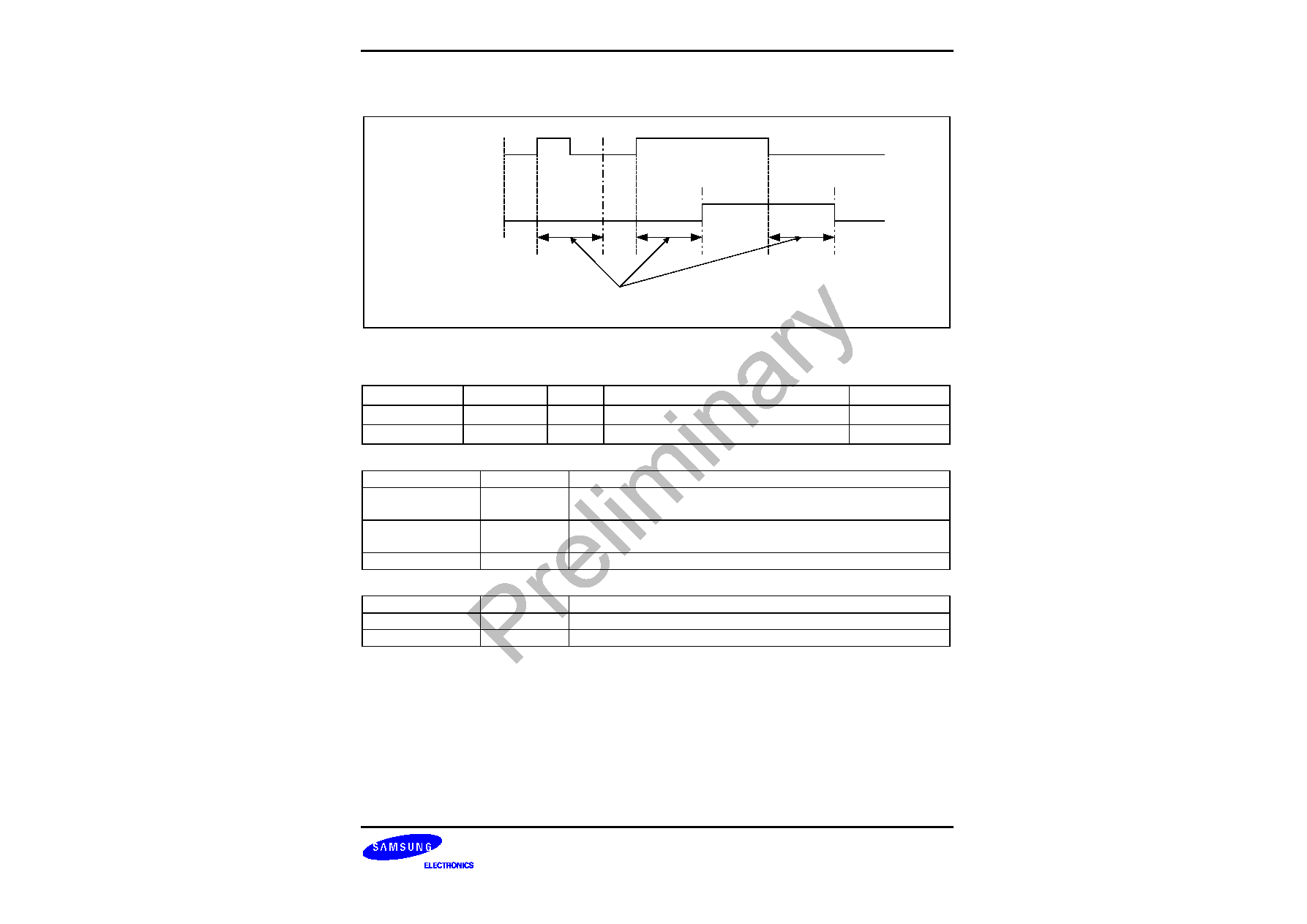
BSW rv0.1-0417-N01
Preliminary product information describes products that are in development,
for which full characterization data and associated errata are not yet available.
Specifications and information herein are subject to change without notice.
S3C24A0 RISC MICROPROCESSOR
KEY PAD
29-3
DEBOUNCING FILTER
FILTER_IN
FILTER_OUT
width = Filter_clk*(width_reg+1)
KEYPAD FILTER CONTROL REGISTER ( KEYFLT )
Register
Address
R/W
Description
Reset Value
KEYFLT0
0x44900008
R/W
KEY PAD Input Filter Control Register
0x0000
KEYFLT1
0x4490000C
R/W
KEY PAD Input Filter Control Register
0x0000
KEYFLT0
Bit
Description
SELCLK
[0]
Select Filter Clock
0 = RTC Clock 1 = GCLK
FILEN
[1]
Filter Enable
0 = Disable 1= Enable
Reserved
[15:2]
Must be "0"
KEYFLT1
Bit
Description
WIDTH_reg
[13:0]
Filtering width of KEYPAD input ports.
Reserved
[15:14]
Must be "0"
BSW rv0.1-0417-N01
Preliminary product information describes products that are in development,
for which full characterization data and associated errata are not yet available.
Specifications and information herein are subject to change without notice.
KEY PAD
S3C24A0 RISC MICROPROCESSOR
29-4
KEYPAD MANUAL SCAN CONTROL REGISTER ( YMAN )
Register
address
R/W
Description
Reset
Value
KEYMAN
0x44900010
R/W
KEYPAD manual scan control
0x1F
YMAN
Bit
Description
Y_VAL
[4:0]
KEYPAD manual column value. (Read only)
MAN_EN
[5]
KEYPAD manual scan control enable
0 = disable 1= enable

BSW rv0.1-0417-N01
Preliminary product information describes products that are in development,
for which full characterization data and associated errata are not yet available.
Specifications and information herein are subject to change without notice.
S3C24A0 RISC MICROPROCESSOR
A/D CONVERTER AND TOUCH SCREEN
30
-1
ADC & TOUCH SCREEN INTERFACE
(PRELIMINARY)
OVERVIEW
The 10-bit CMOS ADC (Analog to Digital Converter) of S3C24A0 is a recycling type device with 8-channel analog
inputs. It converts the analog input signal into 10-bit binary digital codes at a maximum conversion rate of
500KSPS with 2.5MHz A/D converter clock. A/D converter operates with on-chip sample-and-hold function and
power down mode is supported.
S3C24A0 supports Touch Screen Interface.
This function consists of touch screen panel, 4 internal switch, external voltage source, AIN[7] and AIN[5] (refer to
the example, Figure 30-2).
Touch Screen Interface is controlling and selecting control signal (nYPON, YMON, nXPON and XMON) and
analog pads (AIN[7] and AIN[5]) which are connected with pads of touch screen panel and the internal switch for
X-position conversion and Y-position conversion.
Touch Screen Interface contains switch control logic and ADC interface logic with interrupt generation logic.
FEATURES
-- Resolution : 10-bit
-- Differential Linearity Error :
�
1.0 LSB
-- Integral Linearity Error :
�
2.0 LSB
-- Maximum Conversion Rate : 500 KSPS
-- Low Power Consumption
-- Internal switch for X-position conversion and Y-position conversion
-- Power Supply Voltage : 3.3V
-- Analog Input Range : 0 ~ 3.3V
-- On-chip sample-and-hold function
-- Normal Conversion Mode
-- Separate X/Y position conversion Mode
-- Auto(Sequential) X/Y Position Conversion Mode
-- Waiting for Interrupt Mode (Stylus pen up or down interrupt)

BSW rv0.1-0417-N01
Preliminary product information describes products that are in development,
for which full characterization data and associated errata are not yet available.
Specifications and information herein are subject to change without notice.
A/D CONVERTER AND TOUCH SCREEN
S3C24A0 RISC MICROPROCESSOR
30-2
ADC & TOUCH SCREEN INTERFACE OPERATION
BLOCK DIAGRAM
Figure 30-1 shows the functional block diagram of S3C24A0 A/D converter and Touch Screen Interface. Note that
the A/D converter device is a recycling type.
A pull-up resister is attached to AIN[7] on VDDA_ADC. So, XP pad of touch screen panel should be connected
with AIN[7] of S3C24A0 and YP pad of touch screen panel should be connected with AIN[5].
8:1
MUX
A/D
Converter
ADC
interface
&Touch
Screen
Controller
VSSA_ADC
Waiting for Interrupt
INT_PENUP
INT_ADC
ADC input
control
Interrup
Generation
AIN[7]
AIN [6]
AIN [5]
AIN [4]
VDDA_ADC
XMON
nXPON
YMON
nYPON
AIN [3]
AIN [2]
AIN [1]
AIN [0]
Internal
Transister
Control
INT_PENDN
Switch
Matrix
Figure 30-1. ADC and Touch Screen Interface Functional Block Diagram

BSW rv0.1-0417-N01
Preliminary product information describes products that are in development,
for which full characterization data and associated errata are not yet available.
Specifications and information herein are subject to change without notice.
S3C24A0 RISC MICROPROCESSOR
A/D CONVERTER AND TOUCH SCREEN
30
-3
EXAMPLE for touch screen
In this example, AIN[7] is connected with XP and AIN[5] is connected with YP pad of touch screen panel.
To control pads of touch screen panel (XP, XM, YP and YM), 4 internal transistor are applied and control signals,
nYPON, YMON, nXPON and XMON are connected with 4 internal transistor.
Internal Transistor
Control
VDDA_ADC
XM
YP
YM
A[7]
A[5]
XMON
nXPON
YMON
nYPON
Touch Panel
S3C24A0
A[6]
A[4]
XP
Figure 30-2. Example of ADC and Touch Screen Interface
1. Select Separate X/Y Position Conversion Mode or Auto (Sequential) X/Y Position Conversion Mode to get X/Y
position.
2. Set Touch Screen Interface to Waiting Interrupt Mode,
3. If interrupt occurs, then appropriate conversion (Separate X/Y Position Conversion Mode or Auto (Sequential)
X/Y Position Conversion Mode) is activated.
4. After get the proper value about X/Y position, return to Waiting for Interrupt Mode.

BSW rv0.1-0417-N01
Preliminary product information describes products that are in development,
for which full characterization data and associated errata are not yet available.
Specifications and information herein are subject to change without notice.
A/D CONVERTER AND TOUCH SCREEN
S3C24A0 RISC MICROPROCESSOR
30-4
FUNCTION DESCRIPTIONS
A/D Conversion Time
When the PCLK frequency is 50MHz and the prescaler value is 49, total 10-bit conversion time is as follows.
A/D converter freq. = 50MHz/(49+1) = 1MHz
Conversion time = 1/(1MHz / 5cycles) = 1/200KHz = 5 us
NOTE:
This A/D converter was designed to operate at maximum 2.5MHz clock, so the conversion rate can go up to 500 KSPS.
Touch Screen Interface Mode
1. Normal Conversion Mode
Normal Conversion Mode (AUTO_PST = 0, XY_PST = 0) is the most likely used for General Purpose ADC
Conversion. This mode can be initialized by setting the ADCCON and ADCTSC and completed with a read the
XPDATA (Normal ADC) value of ADCDAX (ADC Data Register 0).
2. Separate X/Y Position Conversion Mode
Touch Screen Controller can be operated by one of two Conversion Modes. Separate X/Y Position Conversion
Mode is operated as the following way;
X-Position Mode (AUTO_PST = 0 and XY_PST = 1) writes X-Position Conversion Data to XPDATA of
ADCDAX register, After conversion, Touch Screen Interface generates the Interrupt source (INT_ADC) to
Interrupt Controller.
Y-Position Mode (AUTO_PST = 0 and XY_PST = 2) writes Y-Position Conversion Data to YPDATA of
ADCDAY, After conversion, Touch Screen Interface generates the Interrupt source (INT_ADC) to Interrupt
Controller also.
Table 30-1. Condition of touch screen panel pads in Separate X/Y Position Conversion Mode.
XP
XM
YP
YM
X Position Conversion
VDDA_ADC
GND
AIN[5]
Hi-Z
Y Position Conversion
AIN[7]
Hi-Z
VDDA_ADC
GND

BSW rv0.1-0417-N01
Preliminary product information describes products that are in development,
for which full characterization data and associated errata are not yet available.
Specifications and information herein are subject to change without notice.
S3C24A0 RISC MICROPROCESSOR
A/D CONVERTER AND TOUCH SCREEN
30
-5
1. Auto(Sequential) X/Y Position Conversion Mode
Auto (Sequential) X/Y Position Conversion Mode (AUTO_PST = 1 and XY_PST = 0) is operated as the
following;
Touch Screen Controller automatically converts X-Position and Y-Position. Touch Screen Controller writes X-
measurement data to XPDATA of ADCDAX, and then writes Y-measurement data to YPDATA of ADCDAY.
After Auto (Sequential) Position Conversion, Touch Screen Controller is generating Interrupt source(INT_ADC)
to Interrupt Controller.
Table 30-2. Condition of touch screen panel pads in Auto (Sequential) X/Y Position Conversion Mode.
XP
XM
YP
YM
X Position Conversion
VDDA_ADC
GND
AIN[5]
Hi-Z
Y Position Conversion
AIN[7]
Hi-Z
VDDA_ADC
GND
1. Waiting for Interrupt Mode
When Touch Screen Controller is in Waiting for Interrupt Mode (YM_SEN = 1, XP_SEN = 1 and XY_PST = 3),
Touch Screen Controller is waiting for Stylus down or up. Touch Screen Controller is generating Interrupt
(INT_PENDN or INT_PENUP) signal when the Stylus is down or up on Touch Screen Panel.
After interrupt occurs, X and Y position can be read by the proper conversion mode (Separate X/Y position
conversion Mode or Auto X/Y Position Conversion Mode).
Table 30-3. Condition of touch screen panel pads in Waiting for Interrupt Mode.
XP
XM
YP
YM
Waiting for Interrupt Mode
AIN[7](Pull-up enable)
Hi-Z
AIN[5]
GND
Standby Mode
Standby mode is activated when STDBM of ADCCON register is set to '1'. In this mode, A/D conversion operation
is halted and XPDATA (Normal ADC) of ADCDAX and YPDATA of ADCDAY contain the previous converted data.

BSW rv0.1-0417-N01
Preliminary product information describes products that are in development,
for which full characterization data and associated errata are not yet available.
Specifications and information herein are subject to change without notice.
A/D CONVERTER AND TOUCH SCREEN
S3C24A0 RISC MICROPROCESSOR
30-6
Programming Notes
1.
The A/D converted data can be accessed by means of interrupt or polling method. With interrupt method
the overall conversion time - from A/D converter start to converted data read - may be delayed because of
the return time of interrupt service routine and data access time. With polling method, by checking the
ADCCON[15] - end of conversion flag-bit, the read time from ADCDAT register can be determined.
2. Another way for starting A/D conversion is provided. After ADCCON[1] - A/D conversion start-by-read
mode-is set to 1, A/D conversion starts simultaneously whenever converted data is read.
XP
A
X-Conversion
YP
B
Y-Conversion
C
D = DELAY value of ADCDLY Register
A = D x (1/X-Tal Clock) or A = D x (1/External Clock)
B = D x (1/PCLK)
C = D x (1/PCLK)
Stylus Down
Stylus Up
Figure 30-3 Timing Diagram at Auto (Sequential) X/Y Position Conversion Mode

BSW rv0.1-0417-N01
Preliminary product information describes products that are in development,
for which full characterization data and associated errata are not yet available.
Specifications and information herein are subject to change without notice.
S3C24A0 RISC MICROPROCESSOR
A/D CONVERTER AND TOUCH SCREEN
30
-7
ADC AND TOUCH SCREEN INTERFACE SPECIAL REGISTERS
ADC CONTROL REGISTER (ADCCON)
Register
Address
R/W
Description
Reset Value
ADCCON
0x4580_0000
R/W
ADC Control Register
0x3FC4
ADCCON
Bit
Description
Initial State
ECFLG
[15]
End of conversion flag(Read only)
0 = A/D conversion in process
1 = End of A/D conversion
0
PRSCEN
[14]
A/D converter prescaler enable
0 = Disable
1 = Enable
0
PRSCVL
[13:6]
A/D converter prescaler value
Data value: 1 ~ 255
NOTE: ADC Freqeuncy should be set less than PCLK by 5times.
(Ex. PCLK=10MHZ, ADC Freq.
<
2MHz)
0xFF
SEL_MUX
[5:3]
Analog input channel select
000 = AIN 0
001 = AIN 1
010 = AIN 2
011 = AIN 3
100 = AIN 4
101 = AIN 5 (YP)
110 = AIN 6
111 = AIN 7 (XP)
0
STDBM
[2]
Standby mode select
0 = Normal operation mode
1 = Standby mode
1
READ_ START
[1]
A/D conversion start by read
0 = Disable start by read operation
1 = Enable start by read operation
0
ENABLE_START
[0]
A/D conversion starts by setting this bit.
If READ_START is enabled, this value is not valid.
0 = No operation
1 = A/D conversion starts and this bit is cleared after the start-up.
0

BSW rv0.1-0417-N01
Preliminary product information describes products that are in development,
for which full characterization data and associated errata are not yet available.
Specifications and information herein are subject to change without notice.
A/D CONVERTER AND TOUCH SCREEN
S3C24A0 RISC MICROPROCESSOR
30-8
ADC TOUCH SCREEN CONTROL REGISTER (ADCTSC)
Register
Address
R/W
Description
Reset Value
ADCTSC
0x4580_0004
R/W
ADC Touch Screen Control Register
0x058
ADCTSC
Bit
Description
Initial State
Reserved
[11:8]
Reserved. Should be set to 0.
0
YM_SEN
[7]
Select output value of YMON
0 = YMON output is 0. (YM = Hi-Z)
1 = YMON output is 1. (YM = GND)
0
YP_SEN
[6]
Select output value of nYPON
0 = nYPON output is 0. (YP = External voltage)
1 = nYPON output is 1. (YP is connected with AIN[5])
1
XM_SEN
[5]
Select output value of XMON
0 = XMON output is 0. (XM = Hi-Z)
1 = XMON output is 1. (XM = GND)
0
XP_SEN
[4]
Select output value of nXPON
0 = nXPON output is 0. (XP = External voltage)
1 = nXPON output is 1. (XP is connected with AIN[7])
1
PULL_UP
1)
[3]
Pull-up Switch Enable
0 = XP Pull-up Enable.
1 = XP Pull-up Disable.
1
AUTO_PST
2)
[2]
Automatically sequencing conversion of X-Position and Y-Position
0 = Normal ADC conversion.
1 = Auto (Sequential) X/Y Position Conversion Mode.
0
XY_PST
3)
[1:0]
Manually measurement of X-Position or Y-Position.
00 = No operation mode
01 = X-position measurement
10 = Y-position measurement
11 = Waiting for Interrupt Mode
0
NOTE:
1. Unexpected pen-up or pen-down interrupt may be occurred when pull-up switch is turn on. It is recommended
that pull-up enable switch is turn on before setting to the waiting for interrupt mode because some stabilization
time of pull-up switch is needed.
2. AUTO_PST bit should be set whenever the data conversion ends if the conversion start by read mode is
activated.
3. When all data conversions are finished at automatically sequencing conversion mode, the conversion pointer
remained at Y position conversion mode. It is recommended to set XY_PST register to "01" (X-position
measurement mode) every conversion time for getting right result.

BSW rv0.1-0417-N01
Preliminary product information describes products that are in development,
for which full characterization data and associated errata are not yet available.
Specifications and information herein are subject to change without notice.
S3C24A0 RISC MICROPROCESSOR
A/D CONVERTER AND TOUCH SCREEN
30
-9
ADC START DELAY REGISTER (ADCDLY)
Register
Address
R/W
Description
Reset Value
ADCDLY
0x4580_0008
R/W
ADC Start or Interval Delay Register
0x00ff
ADCDLY
Bit
Description
Initial State
DELAY
[15:0]
1)
Normal Conversion Mode, Separate X/Y Position Conversion
Mode, Auto (Sequential) X/Y Position Conversion Mode.
X/Y Position Conversion Delay Value.
2) Waiting for Interrupt Mode.
When Stylus down occurs at Waiting for Interrupt Mode, generates
Interrupt signal (INT_ADC), having interval (several ms), for Auto
X/Y Position conversion.
Note) Don't use Zero value(0x0000)
00ff
NOTE:
1. Before ADC conversion, Touch screen uses X-tal clock or EXTCLK (Waiting for Interrupt Mode).
2. During ADC conversion PCLK is used.

BSW rv0.1-0417-N01
Preliminary product information describes products that are in development,
for which full characterization data and associated errata are not yet available.
Specifications and information herein are subject to change without notice.
A/D CONVERTER AND TOUCH SCREEN
S3C24A0 RISC MICROPROCESSOR
30-10
ADC CONVERSION DATA REGISTER (ADCDAX)
Register
Address
R/W
Description
Reset Value
ADCDAX
0x4580_000C
R
ADC Conversion Data Register
X-Position conversion data at
Touch Screen mode
-
ADCDAX
Bit
Description
Initial State
UPDOWN
[15]
Up or Down state of Stylus at Waiting for Interrupt Mode.
0 = Stylus down state.
1 = Stylus up state.
-
AUTO_PST
[14]
Automatic sequencing conversion of X-Position and
Y-Position
0 = Normal ADC conversion.
1 = Sequencing measurement of X-position, Y-position.
-
XY_PST
[13:12]
Manually measurement of X-Position or Y-Position.
00 = No operation mode
01 = X-position measurement
10 = Y-position measurement
11 = Waiting for Interrupt Mode
-
Reserved
[11:10]
Reserved
XPDATA
(Normal ADC)
[9:0]
X-Position Conversion data value
(include Normal ADC Conversion data value)
Data value : 0 ~ 3FF
-

BSW rv0.1-0417-N01
Preliminary product information describes products that are in development,
for which full characterization data and associated errata are not yet available.
Specifications and information herein are subject to change without notice.
S3C24A0 RISC MICROPROCESSOR
A/D CONVERTER AND TOUCH SCREEN
30
-11
ADC CONVERSION DATA REGISTER (ADCDAY)
Register
Address
R/W
Description
Reset Value
ADCDAY
0x4580_0010
R
ADC Conversion Data Register
Y-Position conversion data at
Touch Screen mode
-
ADCDAY
Bit
Description
Initial State
UPDOWN
[15]
Up or Down state of Stylus at Waiting for Interrupt Mode.
0 = Stylus down state.
1 = Stylus up state.
-
AUTO_PST
[14]
Automatically sequencing conversion of X-Position and
Y-Position
0 = Normal ADC conversion.
1 = Sequencing measurement of X-position, Y-position.
-
XY_PST
[13:12]
Manually measurement of X-Position or Y-Position.
00 = No operation mode
01 = X-position measurement
10 = Y-position measurement
11 = Waiting for Interrupt Mode
-
Reserved
[11:10]
Reserved
YPDATA
[9:0]
Y-Position Conversion data value
Data value : 0 ~ 3FF
-

BSW rv0.1-0417-N01
Preliminary product information describes products that are in development,
for which full characterization data and associated errata are not yet available.
Specifications and information herein are subject to change without notice.
A/D CONVERTER AND TOUCH SCREEN
S3C24A0 RISC MICROPROCESSOR
30-12
NOTES

BSW rv0.1-0417-N01
Preliminary product information describes products that are in development,
for which full characterization data and associated errata are not yet available.
Specifications and information herein are subject to change without notice.
S3C24A0 RISC MICROPROCESSOR
SDI
31-1
SECURE DIGITAL INTERFACE
OVERVIEW
The S3C24A0 SDI(Secure Digital Interface) can interface for SD memory card, SDIO device and MMC(Multi-
Media Card).
FEATURE
SD Memory Card Spec(Ver 1.0) / MMC Spec(2.11) compatible
SDIO Card Spec(Ver 1.0) compatible
16 words(64 bytes) FIFO for data Tx/Rx
40-bit Command Register
136-bit Response Register
8-bit Prescaler logic(Freq = System Clock / (P + 1))
Normal, and DMA data transfer mode(byte,
halfword
, word transfer)
DMA burst4 access support(only word transfer)
1bit / 4bit(wide bus) mode & block / stream mode switch support

BSW rv0.1-0417-N01
Preliminary product information describes products that are in development,
for which full characterization data and associated errata are not yet available.
Specifications and information herein are subject to change without notice.
SDI
S3C24A0 RISC MICROPROCESSOR
31-2
BLOCK DIAGRAM
CMD Reg
(5byte)
Resp Reg
(17byte)
CMD Control
8bit Shift Reg
CRC7
Prescaler
FIFO
(64byte)
DAT Control
32bit Shift Reg
CRC16*4
DMA
INT
APB
I/F
8
8
8
8
32
32
32
32
32
32
PADDR
PSEL
PCLK
PWDATA
[31:0]
PRDATA
[31:0]
DREQ
DACK
INT
TxCMD
RxCMD
SDCLK
TxDAT[3:0]
RxDAT[3:0]
Figure 31-1. SDI Block Diagram

BSW rv0.1-0417-N01
Preliminary product information describes products that are in development,
for which full characterization data and associated errata are not yet available.
Specifications and information herein are subject to change without notice.
S3C24A0 RISC MICROPROCESSOR
SDI
31-3
SDI OPERATION
A serial clock line synchronizes shifting and sampling of the information on the five data lines. The transmission
frequency is controlled by making the appropriate bit settings to the SDIPRE register. You can modify its frequency
to adjust the baud rate data register value.
Programming Procedure (common)
To program the SDI modules, follow these basic steps:
1. Set SDICON to configure properly with clock & interrupt enable
2. Set SDIPRE to configure with a proper value.
3. Wait 74 SDCLK clock cycle in order to initialize the card.
CMD Path Programming
1. Write command argument 32bit to SDICARG.
2. Determine command types and start command transmit with setting SDICCON.
3. Confirm the end of SDI CMD path operation when the specific flag of SDICSTA is set
4. The flag is CmdSent if command type is no response.
5. The flag is RspFin if command type is with response.
6. Clear the corresponding flag of SDICSTA through writing one with this bit
DAT Path Programming
1. Write data timeout period to SDIDTIMER.
2. Write block size(block length) to SDIBSIZE(normally 0x80 word).
3. Determine the mode of block, wide bus, dma, etc and start data transfer with setting SDIDCON.
4. Tx data
Write data to Data Register(SDIDAT) while Tx FIFO is available(TFDET is set), or half(TFHalf is
set), or empty(TFEmpty is set).
5. Rx data
Read data from Data Register(SDIDAT) while Rx FIFO is available(RFDET is set), or full(RFFull
is set), or half(RFHalf is set), or ready for last data(RFLast is set).
6. Confirm the end of SDI DAT path operation when DatFin flag of SDIDSTA is set
7. Clear the corresponding flag of SDIDSTA through writing one with this bit

BSW rv0.1-0417-N01
Preliminary product information describes products that are in development,
for which full characterization data and associated errata are not yet available.
Specifications and information herein are subject to change without notice.
SDI
S3C24A0 RISC MICROPROCESSOR
31-4
SDIO OPERATION
There are two functions of SDIO operation: SDIO Interrupt receiving and Read Wait Request generation. These
two functions can operate when RcvIOInt bit and RwaitEn bit of SDICON register is activated respectively. And two
functions have the steps and conditions like below.
SDIO Interrupt
In SD 1bit mode, Interrupt is received through all range from RxDAT [1] pin.
In SD 4bit mode, RxDAT[1] pin is shared between data receiving and interrupt receiving.
When interrupt detection range (Interrupt Period) is:
1. Single Block : the time between A and B
-
A : 2clocks after the completion of a data packet
-
B : The completion of sending the end bit of the next withdata command
2. Multi Block, PrdType = 0 : the time between A and B, restart at C
-
A : 2clocks after the completion of a data packet
-
B : 2clocks after A
-
C : 2clocks after the end bit of the abort command response
3. Multi Block, PrdType = 1 : the time between A and B, restart at A
-
A : 2clocks after the completion of a data packet
-
B : 2clocks after A
-
In case of last block, interrupt period begins at A, but not ends at B(CMD53 case)
Read Wait Request
Regardless of 1bit or 4bit mode, Read Wait Request signal transmits to TxDAT[2] pin in condition of below.
-
In read multiple operation, request signal transmission begins at 2clocks after the end of the data
block
-
Transmission ends when user sets to one RwaitReq bit of SDIDSTA register

BSW rv0.1-0417-N01
Preliminary product information describes products that are in development,
for which full characterization data and associated errata are not yet available.
Specifications and information herein are subject to change without notice.
S3C24A0 RISC MICROPROCESSOR
SDI
31-5
SDI SPECIAL REGISTERS
SDI Control Register (SDICON)
Register
Address
R/W
Description
Reset Value
SDICON
0x4600_0000
R/W
SDI Control Register
0x0
SDICON
Bit
Description
Initial Value
Reserved
[31:9]
SDMMC Reset
(SDreset)
[8]
Reset whole sdmmc block. This bit is automatically clear.
0 = normal mode,
1 = SDMMC reset
0
Hold Margin
(HoldMgn)
[7:6]
Determines how much you delay CMD, DAT lines for hold margin
in MMC clock type
00 = 1/2 PCLK cycle,
01 = 1 PCLK cycle
10 = 3/2 PCLK cycles,
11 = 2 PCLK cycles
0
Clock Type
(CTYP)
[5]
Determines which clock type is used as SDCLK.
0 = SD type,
1 = MMC type
0
Byte Order
Type(ByteOrder)
[4]
Determines byte order type when you read(write) data from(to) sd
host FIFO with word boundary.
0 = Type A,
1 = Type B
0
Receive SDIO
Interrupt from card
(RcvIOInt)
[3]
Determines whether sd host receives SDIO Interrupt from the card
or not(for SDIO).
0 = ignore,
1 = receive SDIO Interrupt
0
Read Wait
Enable(RWaitEn)
[2]
Determines read wait request signal generate when sd host waits
the next block in multiple block read mode. This bit needs to delay
the next block to be transmitted from the card(for SDIO).
0 = disable(no generate),
1 = Read wait enable(use SDIO)
0
Reserved
[1]
Clock Out Enable
(ENCLK)
[0]
Determines whether SDCLK Out enable or not
0 = disable(prescaler off), 1 = clock enable
0
* Byte Order Type
- Type A: (Access by Word) D[7:0]
D[15:8]
D[23:16]
D[31:24]
(Access by Halfword) D[7:0]
D[15:8]
- Type B: (Access by Word) D[31:24]
D[23:16]
D[15:8]
D[7:0]
(Access by Halfword) D[15:8]
D[7:0]
SDI Baud Rate Prescaler Register (SDIPRE)
Register
Address
R/W
Description
Reset Value
SDIPRE
0x4600_0004
R/W
SDI Buad Rate Prescaler Register
0x01
SDIPRE
Bit
Description
Initial Value
Prescaler Value
[7:0]
Determines SDI clock (SDCLK) rate as above equation.
Baud rate = PCLK / (Prescaler value + 1)
0x01
* Prescaler Value should be greater than zero.

BSW rv0.1-0417-N01
Preliminary product information describes products that are in development,
for which full characterization data and associated errata are not yet available.
Specifications and information herein are subject to change without notice.
SDI
S3C24A0 RISC MICROPROCESSOR
31-6
SDI Command Argument Register (SDICARG)
Register
Address
R/W
Description
Reset Value
SDICARG
0x4600_0008
R/W
SDI Command Argument Register
0x0
SDICARG
Bit
Description
Initial Value
CmdArg
[31:0]
Command Argument
0x00000000
SDI Command Control Register (SDICCON)
Register
Address
R/W
Description
Reset Value
SDICCON
0x4600_000c
R/W
SDI Command Control Register
0x0
SDICCON
Bit
Description
Initial Value
Reserved
[31:13]
Abort Command
(AbortCmd)
[12]
Determines whether command type is for abort(for SDIO).
0 = normal command, 1 = abort command(CMD12, CMD52)
0
Command with
Data (WithData)
[11]
Determines whether command type is with data(for SDIO).
0 = without data, 1 = with data
0
LongRsp
[10]
Determines whether host receives a 136-bit long response or not
0 = short response, 1 = long response
0
WaitRsp
[9]
Determines whether host waits for a response or not
0 = no response,
1 = wait response
0
Command
Start(CMST)
[8]
Determines whether command operation starts or not.
. This bit is
automatically clear
0 = command ready, 1 = command start
0
CmdIndex
[7:0]
Command index with start 2bit(8bit)
0x00

BSW rv0.1-0417-N01
Preliminary product information describes products that are in development,
for which full characterization data and associated errata are not yet available.
Specifications and information herein are subject to change without notice.
S3C24A0 RISC MICROPROCESSOR
SDI
31-7
SDI Command Status Register (SDICSTA)
Register
Address
R/W
Description
Reset Value
SDICSTA
0x4600_0010
R/(C)
SDI Command Status Register
0x0
SDICSTA
Bit
Description
Initial Value
Reserved
[31:13]
Response CRC
Fail(RspCrc)
[12]
R/C
CRC check failed when command response received. This flag is
cleared by setting to one this bit.
0 = not detect, 1 = crc fail
0
Command Sent
(CmdSent)
[11]
R/C
Command sent(not concerned with response). This flag is cleared
by setting to one this bit.
0 = not detect, 1 = command end
0
Command Time
Out (CmdTout)
[10]
R/C
Command response timeout(64clk). This flag is cleared by setting
to one this bit.
0 = not detect, 1 = timeout
0
Response Receive
End (RspFin)
[9]
R/C
Command response received. This flag is cleared by setting to
one this bit.
0 = not detect, 1 = response end
0
CMD line progress
On (CmdOn)
[8]
Command transfer in progress
0 = not detect, 1 = in progress
0
RspIndex
[7:0]
Response index 6bit with start 2bit(8bit)
0x00
SDI Response Register0 (SDIRSP0)
Register
Address
R/W
Description
Reset Value
SDIRSP0
0x4600_0014
R
SDI Response Register 0
0x0
SDIRSP0
Bit
Description
Initial Value
Response0
[31:0]
Card status[31:0](short), card status[127:96](long)
0x00000000
SDI Response Register1 (SDIRSP1)
Register
Address
R/W
Description
Reset Value
SDIRSP1
0x4600_0018
R
SDI Response Register 1
0x0
SDIRSP1
Bit
Description
Initial Value
RCRC7
[31:24] CRC7(with end bit, short), card status[95:88](long)
0x00
Response1
[23:0]
unused(short), card status[87:64](long)
0x000000
SDI Response Register2 (SDIRSP2)
Register
Address
R/W
Description
Reset Value
SDIRSP2
0x4600_001c
R
SDI Response Register 2
0x0
SDIRSP2
Bit
Description
Initial Value
Response2
[31:0]
unused(short), card status[63:32](long)
0x00000000

BSW rv0.1-0417-N01
Preliminary product information describes products that are in development,
for which full characterization data and associated errata are not yet available.
Specifications and information herein are subject to change without notice.
SDI
S3C24A0 RISC MICROPROCESSOR
31-8
SDI Response Register3 (SDIRSP3)
Register
Address
R/W
Description
Reset Value
SDIRSP3
0x4600_0020
R
SDI Response Register 3
0x0
SDIRSP3
Bit
Description
Initial Value
Response3
[31:0]
unused(short), card status[31:0](long)
0x00000000
SDI Data / Busy Timer Register (SDIDTIMER)
Register
Address
R/W
Description
Reset Value
SDIDTIMER
0x4600_0024
R/W
SDI Data / Busy Timer Register
0x0
SDIDTIMER
Bit
Description
Initial Value
Reserved
[31:21]
DataTimer
[22:0]
Data / Busy timeout period(0~2M cycle)
0x10000
SDI Block Size Register (SDIBSIZE)
Register
Address
R/W
Description
Reset Value
SDIBSIZE
0x4600_0028
R/W
SDI Block Size Register
0x0
SDIBSIZE
Bit
Description
Initial Value
Reserved
[31:12]
BlkSize
[11:0]
Block Size value(0~4095 byte) , don't care when stream mode
0x000
* In Case of multi block, BlkSize must be aligned to word (4byte) size. (BlkSize[1:0] = 00)

BSW rv0.1-0417-N01
Preliminary product information describes products that are in development,
for which full characterization data and associated errata are not yet available.
Specifications and information herein are subject to change without notice.
S3C24A0 RISC MICROPROCESSOR
SDI
31-9
SDI Data Control Register (SDIDCON)
Register
Address
R/W
Description
Reset Value
SDIDCON
0x4600_002c
R/W
SDI Data control Register
0x0
SDIDCON
Bit
Description
Initial Value
Reserved
[31:25]
Burst4 enable
(Burst4)
[24]
Enable Burst4 mode in DMA mode. This bit should be set only
when Data Size is word.
0 = disable,
1 = Burst4 enable
0
Data Size
(DataSize)
[23:22] Indicates the size of the transfer with FIFO, which is typically byte,
halfword or word.
00 = Byte transfer,
01 = Halfword transfer
10 = Word transfer,
11 = reserved
0
SDIO Interrupt
Period Type
(PrdType)
[21]
Determines whether SDIO Interrupt period is 2 cycle or extend
more cycle when last data block is transferred(for SDIO).
0 = exactly 2 cycle,
1 = more cycle(likely single block)
0
Transmit After
Response
(TARSP)
[20]
Determines when data transmit start after response receive or not
0 = directly after DatMode set,
1 = after response receive(assume DatMode sets to 2'b11)
0
Receive After
Command
(RACMD)
[19]
Determines when data receive start after command sent or not
0 = directly after DatMode set,
1 = after command sent (assume DatMode sets to 2'b10)
0
Busy After
Command
(BACMD)
[18]
Determines when busy receive start after command sent or not
0 = directly after DatMode set,
1 = after command sent (assume DatMode sets to 2'b01)
0
Block mode
(BlkMode)
[17]
Data transfer mode
0 = stream data transfer, 1 = block data transfer
0
Wide bus enable
(WideBus)
[16]
Determines enable wide bus mode
0 = standard bus mode(only SDIDAT[0] used),
1 = wide bus mode(SDIDAT[3:0] used)
0
DMA Enable
(EnDMA)
[15]
Enable DMA
0 = disable(polling),
1 = dma enable
0
Data Transfer
Start(DTST)
[14]
Determines whether data transfer start or not. . This bit is auto-
matically clear
0 = data ready,
1 = data start
0
Data Transfer
Mode (DatMode)
[13:12] Determines which direction of data transfer
00 = no operation, 01 = only busy check start
10 = data receive start,
11 = data transmit start
00
BlkNum
[11:0]
Block Number(0~4095), don't care when stream mode
0x000
* If you want one of TARSP, RACMD, BACMD bits (SDIDCON [20:18]) to "1", you need to write on SDIDCON
register ahead of on SDICCON register. (Always need for SDIO)

BSW rv0.1-0417-N01
Preliminary product information describes products that are in development,
for which full characterization data and associated errata are not yet available.
Specifications and information herein are subject to change without notice.
SDI
S3C24A0 RISC MICROPROCESSOR
31-10
SDI Data Remain Counter Register (SDIDCNT)
Register
Address
R/W
Description
Reset Value
SDIDCNT
0x4600_0030
R
SDI Data Remain Counter Register
0x0
SDIDCNT
Bit
Description
Initial Value
Reserved
[31:24]
BlkNumCnt
[23:12] Remaining Block number
0x000
BlkCnt
[11:0]
Remaining data byte of 1 block
0x000
SDI Data Status Register (SDIDSTA)
Register
Address
R/W
Description
Reset Value
SDIDSTA
0x4600_0034
R/(C)
SDI Data Status Register
0x0
SDIDSTA
Bit
Description
Initial Value
Reserved
[31:12]
No Busy(NoBusy)
[11]
R/C
Busy is not active during 16cycle after cmd packet transmitted in
only busy check mode. This flag is cleared by setting to 1 this bit.
0 = not detect, 1 = no busy signal
0
Read Wait
Request Occur
(RWaitReq)
[10]
R/C
Read wait request signal transmits to sd card. The request signal
is stopped and this flag is cleared by setting to one this bit.
0 = not occur,
1 = Read wait request occur
0
SDIO Interrupt
Detect(IOIntDet)
[9]
R/C
SDIO interrupt detect. This flag is cleared by setting to one this bit.
0 = not detect, 1 = SDIO interrupt detect
0
Reserved
[8]
CRC Status
Fail(CrcSta)
[7]
R/C
CRC Status error when data block sent(CRC check failed). This
flag is cleared by setting to one this bit.
0 = not detect, 1 = crc status fail
0
Data Receive CRC
Fail(DatCrc)
[6]
R/C
Data block received error(CRC check failed). This flag is cleared
by setting to one this bit.
0 = not detect,
1 = receive crc fail
0
Data Time
Out(DatTout)
[5]
R/C
Data / Busy receive timeout. This flag is cleared by setting to one
this bit.
0 = not detect, 1 = timeout
0
Data Transfer
Finish(DatFin)
[4]
R/C
Data transfer completes (data counter is zero). This flag is cleared
by setting to one this bit.
0 = not detect, 1 = data finish detect
0
Busy Finish
(BusyFin)
[3]
R/C
Only busy check finish. This flag is cleared by setting to one this
bit
0 = not detect, 1 = busy finish detect
0
Reserved
[2]
0
Tx Data progress
On(TxDatOn)
[1]
Data transmit in progress
0 = not active, 1 = data Tx in progress
0
Rx Data Progress
On(RxDatOn)
[0]
Data receive in progress
0 = not active, 1 = data Rx in progress
0

BSW rv0.1-0417-N01
Preliminary product information describes products that are in development,
for which full characterization data and associated errata are not yet available.
Specifications and information herein are subject to change without notice.
S3C24A0 RISC MICROPROCESSOR
SDI
31-11
SDI FIFO Status Register (SDIFSTA)
Register
Address
R/W
Description
Reset Value
SDIFSTA
0x4600_0038
R
SDI FIFO Status Register
0x0
SDIFSTA
Bit
Description
Initial State
Reserved
[31:16]
FIFO Reset(FRST)
[16]
C
Reset FIFO value. This bit is automatically clear.
0 = normal mode,
1 = FIFO reset
0
FIFO Fail error
(FFfail)
[15:14]
R/C
FIFO fail error when FIFO occurs overrun / underrun data saving.
This flag is cleared by setting to one these bits.
00 = not detect,
01 = FIFO fail
10 = FIFO fail in the last transfer(only FIFO reset need)
11 = reserved
0
FIFO available
Detect for Tx
(TFDET)
[13]
This bit indicates that FIFO data is available for transmit when
DatMode is data transmit mode. If DMA mode is enable, SD host
requests DMA operation.
0 = not detect(FIFO full), 1 = detect(0
FIFO
63)
0
FIFO available
Detect for Rx
(RFDET)
[12]
This bit indicates that FIFO data is available for receive when
DatMode is data receive mode. If DMA mode is enable, sd host
requests DMA operation.
0 = not detect(FIFO empty), 1 = detect(1
FIFO
64)
0
Tx FIFO Half Full
(TFHalf)
[11]
This bit sets to 1 whenever Tx FIFO is less than 33byte.
0 = 33
Tx FIFO
64, 1 = 0
Tx FIFO
32
0
Tx FIFO Empty
(TFEmpty)
[10]
This bit sets to 1 whenever Tx FIFO is empty.
0 = 1
Tx FIFO
64, 1 = Empty(0byte)
0
Rx FIFO Last Data
Ready (RFLast)
[9]
R/C
This bit sets to 1 when Rx FIFO occurs to behave last data of all
block. This flag is cleared by setting to one this bit.
0 = not received yet,
1 = Rx FIFO gets Last data
0
Rx FIFO Full
(RFFull)
[8]
This bit sets to 1 whenever Rx FIFO is full.
0 = 0
Rx FIFO
63, 1 = Full(64byte)
0
Rx FIFO Half Full
(RFHalf)
[7]
This bit sets to 1 whenever Rx FIFO is more than 31byte.
0 = 0
Rx FIFO
31, 1 = 32
Rx FIFO
64
0
FIFO Count
(FFCNT)
[6:0]
Number of data(byte) in FIFO
0000000
* Although the last Rx data size is lager than remained count of FIFO data, you could read this data. If this event
happens, you should clear FFfail field, and FIFO reset field

BSW rv0.1-0417-N01
Preliminary product information describes products that are in development,
for which full characterization data and associated errata are not yet available.
Specifications and information herein are subject to change without notice.
SDI
S3C24A0 RISC MICROPROCESSOR
31-12
SDI Interrupt Mask Register (SDIIMSK)
Register
Address
R/W
Description
Reset Value
SDIIMSK
0x4600_003C
R/W
SDI Interrupt Mask Register
0x0
SDICON
Bit
Description
Initial Value
Reserved
[31:19]
NoBusy Interrupt
Enable (NoBusyInt)
[18]
Determines SDI generate an interrupt if busy signal is not active
0 = disable, 1 = interrupt enable
0
RspCrc Interrupt
Enable (RspCrcInt)
[17]
Determines SDI generate an interrupt if response CRC check fails
0 = disable, 1 = interrupt enable
0
CmdSent Interrupt
Enable
(CmdSentInt)
[16]
Determines SDI generate an interrupt if command sent(no
response required)
0 = disable, 1 = interrupt enable
0
CmdTout Interrupt
Enable
(CmdToutInt)
[15]
Determines SDI generate an interrupt if command response
timeout occurs
0 = disable, 1 = interrupt enable
0
RspEnd Interrupt
Enable (RspEndInt)
[14]
Determines SDI generate an interrupt if command response
received
0 = disable, 1 = interrupt enable
0
RWaitReq Interrupt
Enable (RWReqInt)
[13]
Determines SDI generate an interrupt if read wait request occur.
0 = disable, 1 = interrupt enable
0
IOIntDet Interrupt
Enable (IntDetInt)
[12]
Determines SDI generate an interrupt if sd host receives SDIO
Interrupt from the card(for SDIO).
0 = disable, 1 = interrupt enable
0
FFfail Interrupt
Enable (FFfailInt)
[11]
Determines SDI generate an interrupt if FIFO fail error occurs
0 = disable, 1 = interrupt enable
0
CrcSta Interrupt
Enable (CrcStaInt)
[10]
Determines SDI generate an interrupt if CRC status error occurs
0 = disable, 1 = interrupt enable
0
DatCrc Interrupt
Enable (DatCrcInt)
[9]
Determines SDI generate an interrupt if data receive CRC failed
0 = disable, 1 = interrupt enable
0
DatTout Interrupt
Enable (DatToutInt)
[8]
Determines SDI generate an interrupt if data receive timeout occurs
0 = disable, 1 = interrupt enable
0
DatFin Interrupt
Enable (DatFinInt)
[7]
Determines SDI generate an interrupt if data counter is zero
0 = disable, 1 = interrupt enable
0
BusyFin Interrupt
Enable(BusyFinInt)
[6]
Determines SDI generate an interrupt if only busy check completes
0 = disable, 1 = interrupt enable
0
Reserved
[5]
0
TFHalf Interrupt
Enable (TFHalfInt)
[4]
Determines SDI generate an interrupt if Tx FIFO fills half
0 = disable, 1 = interrupt enable
0
TFEmpty Interrupt
Enable(TFEmptInt)
[3]
Determines SDI generate an interrupt if Tx FIFO is empty
0 = disable, 1 = interrupt enable
0
RFLast Interrupt
Enable (RFLastInt)
[2]
Determines SDI generate an interrupt if Rx FIFO has last data
0 = disable, 1 = interrupt enable
0
RFFull Interrupt
Enable (RFFullInt)
[1]
Determines SDI generate an interrupt if Rx FIFO fills full
0 = disable, 1 = interrupt enable
0
RFHalf Interrupt
Enable (RFHalfInt)
[0]
Determines SDI generate an interrupt if Rx FIFO fills half
0 = disable, 1 = interrupt enable
0

BSW rv0.1-0417-N01
Preliminary product information describes products that are in development,
for which full characterization data and associated errata are not yet available.
Specifications and information herein are subject to change without notice.
S3C24A0 RISC MICROPROCESSOR
SDI
31-13
SDI Data Register (SDIDATn)
Register
Address
R/W
Description
Reset Value
SDIDAT0
0x4600_0040(W,HW,B)
R/W
SDI Data0 Register
0x0
SDIDAT1
0x4600_0044(Word)
R/W
SDI Data1 Register
0x0
SDIDAT2
0x4600_0048(Word)
R/W
SDI Data2 Register
0x0
SDIDAT3
0x4600_004C(Word)
R/W
SDI Data3 Register
0x0
SDIDATn
Bit
Description
Initial State
Data Register
[31:0]
This field contains the data to be transmitted or received over the
SDI channel
0x00000000
* In case that DMA Burst4 mode is enabled by setting SDIDCON [24], SDIDAT1 ~ SDIDAT3 are valid.

BSW rv0.1-0417-N01
Preliminary product information describes products that are in development,
for which full characterization data and associated errata are not yet available.
Specifications and information herein are subject to change without notice.
S3C24A0 RISC MICROPROCESSOR
MEMORY STICK
32-1
MEMORY STICK (Preliminary)
OVERVIEW
There are so many types of media for storing and transferring data. Memory Stick is one of the popular media.
The S3C24A0 supports Memory Stick specifications version 1.3. Four pins are dedicated for memory stick
interface, which are Bus State (MS_BS), Serial Data (MS_SDIO), Serial Clock (MS_SCLK) and Insertion Detect
(MS_INS).
FEATURES
_
Protocol is stared by writing to the command register (TP_CMD)
_
Supports DMA
_
BUSY timeout period can be controlled by setting the BSYCNT bit fields in control status register
(CTRL_STA)
_
16-bit access
_
The output from FIFO is only little endian
_
Built in 8-byte (2-word) FIFO buffers for Tx and Rx respectively
_
Built in CRC circuit (can be turned on/ off)
_
PCLK must be under 80MHz
_
Supports automatic command execution (can be turn on/ off)
_
Supports Memory Stick detection interrupt
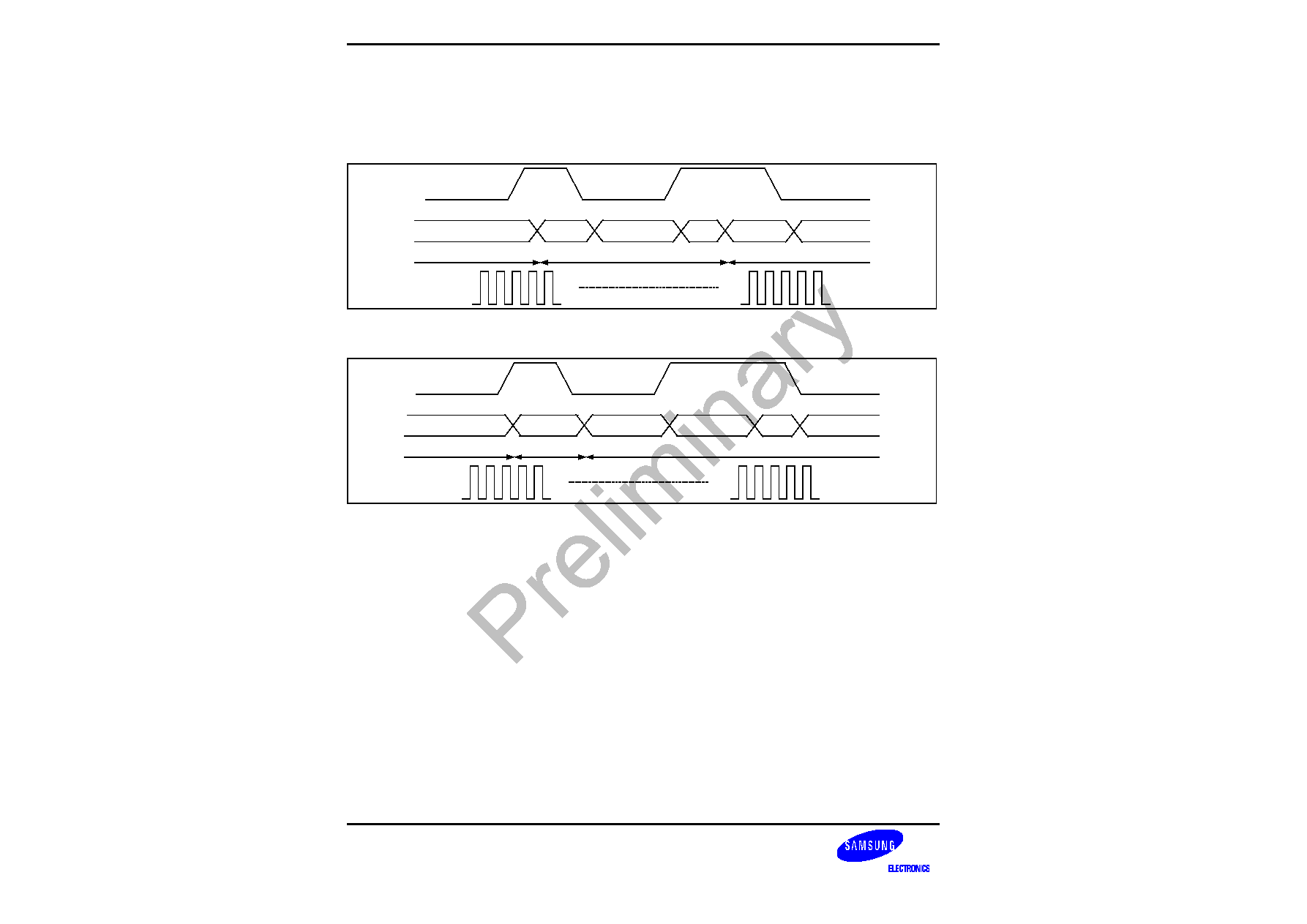
BSW rv0.1-0417-N01
Preliminary product information describes products that are in development,
for which full characterization data and associated errata are not yet available.
Specifications and information herein are subject to change without notice.
MEMORY STICK
S3C24A0 RISC MICROPROCESSOR
32-2
MEMORY STICK PROTOCOL
Figure 32-1and 2 shows the read/ write packet of Memory Stick. The memory stick host controller uses only PCLK
as its source clock. The MS_SCLK frequency is made by divided PCLK (1/1, 1/2, 1/4 or 1/8) and it is slower than
20MHz.
BS0
BS1
BS2
BS3
BS0
IN
T
TP
C
DATA
CR
C
RDY/BSY
IN
T
Memory StIck
Host
Memory Stick
Figure 32-1. Memory stick write packet
BS0
BS1
BS2
BS3
BS0
IN
T
TP
C
DATA
CR
C
RDY/BSY
IN
T
Memory StIck
Host
Memory Stick
Figure 32-2. Memory stick read packet
MANDATORY HARDWARE CONFIGURATION
The MS_SDIO pin should be configured pull down resistor and the MS_INS pin should be configured pull up
resistor.

BSW rv0.1-0417-N01
Preliminary product information describes products that are in development,
for which full characterization data and associated errata are not yet available.
Specifications and information herein are subject to change without notice.
S3C24A0 RISC MICROPROCESSOR
MEMORY STICK
32-3
HOST BLOCK PIN DESCRIPTION
Pin name
Function name
Dir
Active
Description
XINT
Interrupt request
Out
Low
Interrupt request signal line
Low level during interrupt request
High level at access to IntDataReg
PI
Input parallel Port
In
-
Parallel port for input only
(used for insertion/extraction detect of Memory stick)
Fixed in a High level when unused
RBE
Receive Buffer Empty
Out
High
High level when receive data buffer is empty Low
level when there is data in receive data buffer
RBF
Receive Buffer Full
Out
High
High level when receive data buffer is full.
Low level when there is space in receive data buffer
TBE
Transmit Buffer Empty
Out
High
High level when transmit data buffer is empty
Low level when there is data in transmit data buffer
TBF
Transmit Buffer Full
Out
High
High level when transmit data buffer is full
Low level when there is space in transmit data buffer
NOCRC
INT_P_END(RO)
SDIO
Interrupt control
INT_SIF(RO)
INT_TOE(RO)
INT_CRC(RO)
INS
INS_EN
INS_INTEN
XINT
RBF(RO)
RBE(RO)
TBF(RO)
TBE(RO)
FIFO Control
FIFO_INT
INT_INS(RO)
PI
SIEN
Host Controller
BS
SCLK
INT_STA
check
INT_EN

BSW rv0.1-0417-N01
Preliminary product information describes products that are in development,
for which full characterization data and associated errata are not yet available.
Specifications and information herein are subject to change without notice.
MEMORY STICK
S3C24A0 RISC MICROPROCESSOR
32-4
MEMORY STICK SPECIAL REGISTERS
PRESCALER CONTROL (MSPRE) REGISTER
Register
Address
R/W
Description
Reset Value
MSPRE
0x46100000
R/W
Pescaler control register
0x0
MSPRE
Bit
Description
Initial State
PRE_EN
[2]
Prescaler control
0 = Disable
1 = Enable
0
PRE_VAL
[1:0]
Prescaler value
00 = 1/1
01 = 1/2
10 = 1/4
11 = 1/8
Note: MS_SCLK must be less than 20MHz
00
FIFO INTERRUPT CONTROL (MSFINTCON) REGISTER
Register
Address
R/W
Description
Reset Value
MSFINTCON
0x46100004
R/W
FIFO interrupt control
0x0
MSINTCON
Bit
Description
Initial State
FIFO_INTEN
[0]
FIFO states, which are receive buffer full (RBF), receive
buffer empty (RBF), transmit buffer full (TBF) and
transmit buffer empty (TBF) request interrupt or do not.
0 = Only for XINT
1 = Enables interrupt request according to FIFO states
Note: XINT means internal conditions, which are detecting
protocol end interrupt (INT_P_END), serial interface interrupt
(INT_SIF), Tx/ Rx request interrupt (INT_TR), and insertion
interrupt (INT_INS).
0

BSW rv0.1-0417-N01
Preliminary product information describes products that are in development,
for which full characterization data and associated errata are not yet available.
Specifications and information herein are subject to change without notice.
S3C24A0 RISC MICROPROCESSOR
MEMORY STICK
32-5
TRANSFER PROTOCOL COMMAND (TP_CMD) REGISTER
Register
Address
R/W
Description
Reset Value
TP_CMD
0x46108000
R/W
Transfer protocol command register
0x0000
MSINTCON
Bit
Description
Initial State
TPC
[15:12]
Transfer protocol command
0x2 = Read page data
0xd = Write page data
0x8 = Set read/ write register address
0xe = Set command
0x7 = Get interrupt
0x4 = Read register
0xb = Write register
Others = Reserved
Note: These bit fields can not be written while the
INT_P_END bit in INTCON_STA register is `0'
.
0x0
Reserved
[11:10]
Reserved
00
DAT_SIZE
[9:0]
Transferred data size
0x200 = Read/ write page data command
0x4 = Set read/ write register address
0x1 = Set command/ Get interrupt
0xX = Any data size to read/ write register
0x00

BSW rv0.1-0417-N01
Preliminary product information describes products that are in development,
for which full characterization data and associated errata are not yet available.
Specifications and information herein are subject to change without notice.
MEMORY STICK
S3C24A0 RISC MICROPROCESSOR
32-6
CONTROL AND STATUS (CTRLSTA) REGISTER
Register
Address
R/W
Description
Reset Value
CTRL_STA
0x46108004
R/W
Control [15:8] and staus [7:0] register
0x050a
MSCTRLSTA
Bit
Description
Initial State
RST
[15]
Internal logic reset control
0 = Clear reset
1 = Reset
0
PWS
[14]
Power save mode control
0 = Normal mode
1 = Power save mode
0
SIEN
[13]
Serial interface enable/ disable control
0 = Disable
1 = Enable
0
Reserved
[12]
Should be 0 (SBZ)
0
NOCRC
[11]
CRC enable/ disable control
0 = Enable
1 = Disable
0
BSYCNT
[10:8]
Busy timeout counter
Timeout detecting time (MS_SCLK cycles)
= BSYCNT x 4 + 2
Example: BSYCNT = 0x5, MS_SCLK = 10MHz
Exceeding 2.2us (22 x 0.1) causes a RDY timeout error.
0x5
INT_STA
(Read only)
[7]
Interrupt status
0 = Not generated interrupt condition
1 = Generated interrupt condition
0
DRQ_STA
(Read only)
[6]
DMA request status
0 = Not requested DMA
1 = Requested DMA
0
Reserved
[5:4]
Reserved
00
RBE_STA
(Read only)
[3]
Receive buffer (FIFO) empty status
0 = Not empty
1 = Empty
1
RBF_STA
(Read only)
[2]
Receive buffer (FIFO) full status
0 = Not full
1 = Full
0
TBE_STA
(Read only)
[1]
Transmit buffer (FIFO) empty status
0 = Not empty
1 = Empty
1
TBF_STA
(Read only)
[0]
Transmit buffer (FIFO) full status
0 = Not full
1 = Full
0

BSW rv0.1-0417-N01
Preliminary product information describes products that are in development,
for which full characterization data and associated errata are not yet available.
Specifications and information herein are subject to change without notice.
S3C24A0 RISC MICROPROCESSOR
MEMORY STICK
32-7
DATA FIFO (DAT_FIFO) REGISTER
Memory stick host controller has two 16-byte FIFO for the Tx and Rx mode. Transmit and receive FIFO access is
performed through same FIFO entry: the address FIFOENTY is 0x46108008.
Register
Address
R/W
Description
Reset Value
DAT_FIFO
0x46108008
R/W
Tx/ Rx FIFO (buffer) register
0x0000
MSFIFO
Bit
Description
Initial State
FIFOENTRY
[15:0]
Transmit/ Receive data for Memory Stick
0x0000
BSW rv0.1-0417-N01
Preliminary product information describes products that are in development,
for which full characterization data and associated errata are not yet available.
Specifications and information herein are subject to change without notice.
MEMORY STICK
S3C24A0 RISC MICROPROCESSOR
32-8
INTERRUPT CONTROL AND STATUS (INTCTRLSTA) REGISTER
Register
Address
R/W
Description
Reset Value
INTCTRL_STA
0x4610800c
R/W
Interrupt control [15:8] and staus [7:0] register
0x0080
MSINTCTRLSTA
Bit
Description
Initial State
INT_EN
[15]
Internal enable/ disable control
0 = Disable
1 = Enable
0
Reseved
[14]
Reseved
0
INS_INTEN
[13]
Insertion interrupt enable/ disable control
0 = Disable
1 = Enable
0
Reserved
[12:8]
Reserved
0x00
INT_P_END
(Read only)
[7]
Protocol end interrupt status
0 = In progress
1 = Complete
1
INT_SIF
(Read only)
[6]
Serial interface receive interrupt status
(From Memory stick)
0 = No interrupt
1 = Receive interrupt
0
Reseved
[5]
Reseved
0
INT_INS
(Read only)
[4]
Insertion interrupt status
0 = No insertion
1 = Insertion
0
Reserved
[3:2]
Reserved
00
INT_CRC
(Read only)
[1]
CRC error interrupt status
0 = No CRC error
1 = Occurred CRC error
0
INT_TOE
(Read only)
[0]
Busy timeout error interrupt status
0 = No timeout error
1 = Occurred timeout error
0

BSW rv0.1-0417-N01
Preliminary product information describes products that are in development,
for which full characterization data and associated errata are not yet available.
Specifications and information herein are subject to change without notice.
S3C24A0 RISC MICROPROCESSOR
MEMORY STICK
32-9
INS PORT CONTROL (INSCON) REGISTER
Register
Address
R/W
Description
Reset Value
INS_CON
0x46108010
R/W
INS port control register
0x0000
MSINSCON
Bit
Description
Initial State
Reserved
[15:13]
Reserved
000
INS_EN
[12]
INS port enable/ disable control
0 = Disable
1 = Enable
0
Reserved
[11:5]
Reserved
0x00
INS_STA
[4]
INS port status
0 = High (no insertion) 1 = Low (insertion)
0
Reserved
[3:0]
Reserved
0x0
BSW rv0.1-0417-N01
Preliminary product information describes products that are in development,
for which full characterization data and associated errata are not yet available.
Specifications and information herein are subject to change without notice.
MEMORY STICK
S3C24A0 RISC MICROPROCESSOR
32-10
AUTO COMMAND/ POL CONTROL (ACMD_CON) REGISTER
Register
Address
R/W
Description
Reset Value
ACMD_CON
0x46108014
R/W
Auto command and polaity control register
0x0000
MSACMDCON
Bit
Description
Initial State
ATPC_EN
[15]
Auto command operation enable/ disable control
0 = Disable
1 = Enable
0
POL
[14]
Loading polarity control of the serial data input
0 = Rising edge
1 = Falling edge
0
Reserved
[13:0]
Reserved
0x00
AUTO TRANSFER PROTOCOL COMMAND (ATP_CMD) REGISTER
Register
Address
R/W
Description
Reset Value
ATP_CMD
0x46108018
R/W
Auto transfer protocol command register
0x7001
MSACMD
Bit
Description
Initial State
ATPC
[15:12]
Set transfer protocol command (TPC) to be automatically
executed.
0x7
Reserved
[11:10]
Reserved
0x0
ADAT_SIZE
[9:0]
Set the size of data which is transferred.
0x01

BSW rv0.1-0417-N01
Preliminary product information describes products that are in development,
for which full characterization data and associated errata are not yet available.
Specifications and information herein are subject to change without notice.
S3C24A0 RISC MICROPROCESSOR
CLOCK & POWER MANAGEMENT
33-1
CLOCK & POWER MANAGEMENT
OVERVIEW
The clock & power management unit consists of 3 parts; System Clock Control, USB Clock Control, and System
Power-management Control.
The System Clock Control logic in S3C24A0 can generate the required system clock signals, ARMCLK for CPU,
HCLK for the AHB-bus peripherals, and PCLK for the APB-bus peripherals. There are two PLLs in S3C24A0. One
is for ARMCLK, HCLK, and PCLK, and the other is for the USB, IrDA and Camera Interface. The clock control-
logic can make slow clock without PLL and connect/disconnect the clock to each peripheral block by software,
which will reduce the power consumption.
In the power control logic, S3C24A0 has various power management schemes to keep optimal power
consumption for a given task. The power management in S3C24A0 consists of four modes: General Clock Gating
(NORMAL) mode, IDLE mode, STOP mode, and SLEEP mode.
General Clock Gating mode is used to control the On/Off of clocks for internal peripherals in S3C24A0. The user
can optimize the power consumption of S3C24A0 using this General Clock Gating mode by supplying clocks for
peripherals that are necessary for a certain application. For example, if a timer is not needed, the user can
disconnect the clock to the timer to reduce power.
IDLE mode disconnects the ARMCLK only to CPU core while it supplies the clock to all peripherals. By using
IDLE mode, the power consumption due to CPU core can be reduced.
STOP mode freezes all clocks to the CPU as well as peripherals by disabling PLLs. The power consumption is
only due to the leakage current in S3C24A0.
SLEEP mode is intended to disconnect the internal power. So, the power consumption due to CPU and the
internal logic except the wake-up logic will be zero in the SLEEP mode. In order to use the SLEEP mode two
independent power sources are needed. One of the two power sources supplies the power for the wake-up logic.
The other one supplies the other internal logic including CPU, and should be controlled in order to be turned
on/off. In SLEEP mode, the second power supply source for the CPU and internal logic will be turned off.
A detailed description of the power-saving modes such as the entering sequence to the specific power-down
mode or the wake-up sequence from a power-down mode is given in the following Power Management section.

BSW rv0.1-0417-N01
Preliminary product information describes products that are in development,
for which full characterization data and associated errata are not yet available.
Specifications and information herein are subject to change without notice.
CLOCK & POWER MANAGEMENT
S3C24A0 RISC MICROPROCESSOR
33-2
FUNCTION DESCRIPTION
CLOCK Generation Overview
Figure 33-1 shows the block diagram of the clock generation module. The main clock source comes from an
external crystal (XsXTIN) or external clock (XsEXTCLK). The clock generator consists of two PLLs (Phase-
Locked-Loop) which generate the high-frequency clock signals required in S3C24A0.
XsXTIN
XsEXTCLK
XgREFCLKSEL[1]
MPLL
(M_M/ P/ S)
ExtclkDiv
0
CLKDIVN
(H/ P/ M)
ClockIdle
HCLK
PCLK
MPEGCLK
ARMCLK
XsXTIN
XsEXTCLK
XgREFCLKSEL[0]
UPLL
(U_M/ P/ S)
0
0
CLKDIVN
(C)
USBCLK
IrDACLK
CAMCLK
MPLL_clk
UPLL_clk
1/2
1/2
Figure 33-1. Clock Generator Block Diagram
CLOCK Source Selection
Table 33-1 shows the relationship between the combination of mode control pins XgREFCLKSEL[1:0] and the
selection of source clock for S3C24A0. (see the figure 33-1.)
Table33-1. Clock source selection for the internal PLLs and clock generation logic
XgREFCLKSEL[1:0]
(refer to Pin Description)
Main Clock source
(MPLL and External Clock)
USB Clock source
(UPLL and External Clock)
00
XsXTIN
XsXTIN
01
XsXTIN
XsEXTCLK
10
XsEXTCLK
XsXTIN
11
XsEXTCLK
XsEXTCLK
NOTES.
1.
Although the MPLL/UPLL starts just after a reset, the MPLL output (MPLL_clk) isn't used as the system clock until the
S/W writes valid settings to the MPLLCON / UPLLCON register. Before this valid setting, the clock from XsXTIN or
XsEXTCLK source will be used as the system clock directly. Even if the user wants to maintain the default value of
MPLLCON / UPLLCON register, the user should write the same value into MPLLCON / UPLLCON register.
2.
MPLL generates the clock source for ARMCLK, HCLK, PCLK and UPLL generates clock source for USBCLK,
IrDACLK and CAMCLK.

BSW rv0.1-0417-N01
Preliminary product information describes products that are in development,
for which full characterization data and associated errata are not yet available.
Specifications and information herein are subject to change without notice.
S3C24A0 RISC MICROPROCESSOR
CLOCK & POWER MANAGEMENT
33-3
PLL (Phase-Locked-Loop)
The PLL (Phase-Locked Loop) frequency synthesizer is constructed in CMOS on single monolithic structure. The
PLL provides frequency multiplication capabilities the output clock frequency MPLL_clk is related to the input
clock frequency Fin by the following equation:
Fout (MPLL_clk or UPLL_clk) = (m * Fin) / (p * 2
s
)
Where,
m = M (the value for Main Divider)+ 8, p = P(the value for Pre-Divider P) + 2
Where, Fout is the output clock frequency. Fin the input frequency. M, P and S are the values for programmable
dividers (see the register description). The PLL consists of a Phase/Frequency Detector (PFD), a Charge Pump,
an Off-chip Loop Filter, a Voltage Controlled Oscillator (VCO), a 6 bit pre-divider, an 8bit main divider and 2-bit
post scaler and shown in Fig.33-2
The UPLL within the clock generator is same as the MPLL in every aspect.
To ensure the proper operation of the internal PLLs, we recommend the following PLL value-sets(refer to table
33-7). If the user requires other range of PLL set-values, please contact one of SEC application engineers.
Pre-
Divider(P)
PFD
Charge
Pump
VCO
Main
Divider(M)
Post
Scaler(S)
Off-chip loop filter
Fin
Fout
Figure 33-2. PLL (Phase-Locked Loop) Block Diagram

BSW rv0.1-0417-N01
Preliminary product information describes products that are in development,
for which full characterization data and associated errata are not yet available.
Specifications and information herein are subject to change without notice.
CLOCK & POWER MANAGEMENT
S3C24A0 RISC MICROPROCESSOR
33-4
Usual Conditions for PLL & Clock Generator
Table 33-2. Recommended operation conditions
Characteristics
Min
Typ
Max
Unit
Supply voltage differential
-0.1
0.1
V
External loop filter capacitance
1.7
nF
Operating temperature
-40
85
�
C
Table 33-3. DC Electrical Characteristics
Characteristics
Symbol
Min
Typ
Max
Unit
Operating voltage
AVDD12D/AVDD12A
1.14
1.20
1.26
V
Dynamic current
L
DD
3
mA
Power down current
l
PD
TBD
�
A
Table 33-4. AC Electrical Characteristics
Characteristics
Symbol
Min
Typ
Max
Unit
Input frequency
F
IN
10
40
MHz
Output clock frequency
F
out
50
300
MHz
VCO output frequency
F
VCO
100
300
MHz
Input clock duty cycle
T
ID
40
50
60
%
Input glitch pulse width
T
IGP
1
ns
Jitter, cycle to cycle
T
JCC
200
200
ps
CLOCK Control Logic
The clock control logic determines the clock source to be used, i.e., the PLL clock(MPLL_clk) or the direct
external clock ( XsXTIN or XsEXTCLK ). When PLL is configured to a new frequency value, the clock control logic
disables the ARMCLK until the PLL output is stabilized during the PLL locking time. The clock control logic is also
activated at power-on reset and waked-up from power-down mode.
PLL Lock Time
The lock time is the minimum time required for PLL output stabilization. The lock time should be a minimum of
300us. After reset and wake-up from STOP and SLEEP mode, respectively, the lock-time is inserted automatically
by the internal logic with lock time count register. The automatically inserted lock time is calculated as follows;
t_lock (the PLL lock time by H/W logic) = (1/ Fin) x n
where, n = M_LTIME for MPLL,U_LTIME for UPLL, refer to the register description

BSW rv0.1-0417-N01
Preliminary product information describes products that are in development,
for which full characterization data and associated errata are not yet available.
Specifications and information herein are subject to change without notice.
S3C24A0 RISC MICROPROCESSOR
CLOCK & POWER MANAGEMENT
33-5
Power-On Reset (XsRESETn)
Figure 33-3 shows the clock behavior during the power-on reset sequence. The crystal oscillator begins
oscillation within several milliseconds after the power source supplies enough power-level to the S3C24A0.
Internal PLLs (MPLL and UPLL) also begins the frequency locking based on power-on-reset frequency-setting
value. XsRESETn signal should be released after the fully settle-down of the power-level. For the proper system
operation, the S3C24A0 requires a hazard-free system clock (ARMCLK, HCLK and PCLK) when the system reset
is released (XsRESETn). However, the PLL is commonly known to be unstable after power-on reset, so Fin (the
direct external clock source, XsXTIN or XsEXTCLK depending on the XgREFCLKSEL[1:0] pin status) is fed
directly to ARMCLK instead of the MPLL_clk (PLL output) before the S/W newly configures the MPLLCON
register. Even if the user wants to use the default value of MPLLCON register, user should write the same value
into MPLLCON register by S/W after the release of the system reset.
The PLL begins the lockup sequence toward the new frequency only after the S/W configures the PLL with a new
frequency-value. ARMCLK is configured to be PLL output (MPLL_clk) immediately after lock time.
The user should be aware that the crystal oscillator settle-down time is not explicitly added by the hardware during
the power-up sequence. The S3C24A0 assumes that the crystal oscillation is settled during the power-supply
settle-down period. However, to ensure the proper operation during wake-up from the STOP mode, the S3C24A0
explicitly adds the crystal oscillator settle-down time (the wait-time can be programmed using the XTALWSET
registers) after wake-up from the STOP mode.
For the USB, IrDA and Camera Interface device clocks, the output of UPLL clock is directly fed to those devices.
The logic operates by
XsEXTCLK or XsXTIN
XsRESETn
XsEXTCLK
or
XsXTIN
VCO
output
Power
Clock
Disable
lock time
PLL is configured by S/W first time.
VCO is adapted to new clock frequency.
ARMCLK
ARMCLK is new frequency
Figure 33-3. Power-On Reset Sequence
BSW rv0.1-0417-N01
Preliminary product information describes products that are in development,
for which full characterization data and associated errata are not yet available.
Specifications and information herein are subject to change without notice.
CLOCK & POWER MANAGEMENT
S3C24A0 RISC MICROPROCESSOR
33-6
Change PLL Settings In Normal Operation
During the operation of S3C24A0 in NORMAL mode, if the user wants to change the frequency by writing the
PMS value, the PLL lock time is automatically inserted. During the lock time, the clock is not supplied to the
internal blocks in S3C24A0. The timing diagram is as follow.
MPLL_clk
PMS setting
PLL Lock-time
ARMCLK
It changes to new PLL clock
after lock time automatically
Figure 33-4. The case that changes Slow clock by setting PMS value
NOTE : Changing PMS value can cause a problem in LCD display. In the S3C24A0, the LCD screen-refresh timing is
dependent on the HCLK (HCLK clock is also dependent on the MPLL clock output).
ARMCLK, HCLK, PCLK, MPEGCLK and CAMCLK Control
The ARMCLK is used for ARM926EJ-S core, the main CPU of the S3C24A0. The HCLK is the reference clock for
internal AHB bus and peripherals such as the memory controller, the interrupt controller, the Modem Interface,
LCD controller, the DMA, USB host block, System Controller, Power down controller and etc. The PCLK is used
for internal APB bus and peripherals such as WDT, IIS, I2C, PWM timer, and MMC interface, ADC, UART, GPIO,
RTC and SPI etc. MPEGCLK is used for MPEG4 H/W accelerator block such as DCT, ME, MC block. CAMCLK is
used for camera interface block.
The following table shows the clock division ratios between ARMCLK, HLCK and PCLK. This ratio is determined
by HDIV and PDIV bits of CLKDIVN control register.
HCLKdiv[1:0]
PCLKdiv
ARMCLK
HCLK
PCLK
Division Ratio
00
0
ARMCLK
ARMCLK
ARMCLK
1 : 1 : 1 (Default)
00
1
ARMCLK
ARMCLK
ARMCLK / 2
1 : 1 : 2
01
0
ARMCLK
ARMCLK / 2
ARMCLK / 2
1 : 2 : 2
01
1
ARMCLK
ARMCLK / 2
ARMCLK / 4
1 : 2 : 4
10
0
ARMCLK
ARMCLK / 4
ARMCLK / 4
1 : 4 : 4
10
1
ARMCLK
ARMCLK / 4
ARMCLK / 8
1 : 4 : 8

BSW rv0.1-0417-N01
Preliminary product information describes products that are in development,
for which full characterization data and associated errata are not yet available.
Specifications and information herein are subject to change without notice.
S3C24A0 RISC MICROPROCESSOR
CLOCK & POWER MANAGEMENT
33-7
MPEGCLK and CAMCLK frequency are determined by MPEGCLKdiv[3:0] and CAMCLKdiv[3:0] bits of CLKDIVN
control register.
MPEG or CAMCLKdiv[3:0]
MPEGCLK
CAMCLK
0
HCLK
UPLL_clk / 2
1~15
HCLK / ( 2 x MPEGCLKdiv )
UPLL_clk / (CAMCLKdiv + 1 ) * 2
The MPEGCLK and the CAMCLK frequency are changed whenever the source clock frequency is changed.
UCLK (USB Clock) Control
USB host interface and USB device interface needs 48Mhz fixed-frequency clock. In the S3C24A0, The USB
dedicated PLL (UPLL) generates 96Mhz and divided by two for USB block. UPLL will be turned off during STOP
and SLEEP mode automatically. Also, UPLL will be generated clock to USBCLK, IrDACLK, CAMCLK after exiting
STOP and SLEEP mode if USBon, IrDAclkOn and CAMclkOn bits are enabled in CLKCON register.
Condition
UCLK state
UPLL State
After reset
UPLL Output
on
After configuring UPLL
During PLL lock time: Low
After PLL lock time: UPLL Output
on
UPLL is turned off by U_PLLoff bit in CLKSRC register
No Clock
off
UPLL is turned on by U_PLLoff bit in CLKSRC register
UPLL Output
on
NOTE: UPLL_clk (UPLL output) is 98MHz. USBCLK is obtained by dividing by two of UPLL_clk, i.e. UPLL_clk/2.

BSW rv0.1-0417-N01
Preliminary product information describes products that are in development,
for which full characterization data and associated errata are not yet available.
Specifications and information herein are subject to change without notice.
CLOCK & POWER MANAGEMENT
S3C24A0 RISC MICROPROCESSOR
33-8
Power Management
The power management block controls the system clocks by software for the reduction of power consumption in
S3C24A0. These schemes are related to PLL, clock control logic(ARMCLK,HCLK,PCLK) and wake-up signal.
The Figure 33-5 depicts the clock distribution of S3C24A0.
S3C24A0 has four power-down modes. The following section describes each power management mode.
PLL
(Main & USB)
Fin
MPLL_out
UPLL_out
Clock Generation
(on/ off control)
System
Configuration
Registers
System
Configuration
Registers
VPOST
MPEG4ME
MPEG4DCTQ
VLX
MPEG4IF
LCD
CAMIF
VPOSTIF
USB Host
USB
IrDA
CAM
AC97
PWM TIMER
UART0
UART1
SPI
I2C
I2S
GPIO
USB Device
Memory Stick
SD
ADC
Key Pad
MPEGclk
HCLK
PCLK
UPLLclk
ARMclk
ARM926-EJ
Figure 33-5. The Clock Distribution Block Diagram

BSW rv0.1-0417-N01
Preliminary product information describes products that are in development,
for which full characterization data and associated errata are not yet available.
Specifications and information herein are subject to change without notice.
S3C24A0 RISC MICROPROCESSOR
CLOCK & POWER MANAGEMENT
33-9
POWER SAVING MODES
General Clock Gating Mode
In General Clock Gating mode, the On/Off clock gating of the individual clock source of each IP block is
performed by controlling of each corresponding clock source enable bit. The Clock Gating is applied instantly
whenever the corresponding bit (or bits) is changed. (In general, these bits are set or cleared by the main CPU.)
IDLE Mode
In IDLE mode, the clock to CPU core is stopped. The IDLE mode is activated just after the execution of the STR
instruction that enables the IDLE Mode bit. The IDLE Mode bit should be cleared by software after the wake-up
from the IDLE state because it is not cleared automatically, and the H/W logic only detects the low-to-high
triggering of the IDLE Mode bit.
STOP Mode
In STOP mode, all clocks are stopped for minimum power consumption. Therefore, the PLL and oscillator circuit
are also stopped. The STOP Mode is activated after the execution of the STR instruction that enables the STOP
Mode bit. The STOP Mode bit should be cleared by software after the wake-up from the STOP state because it is
not cleared automatically, and the H/W logic only detects the low-to-high triggering of the STOP Mode bit.
To exit from STOP mode, External interrupt, RTC alarm, Touch Screen Pen-down INT, Modem INT, XsRESETn
or XsWRESETn has to be activated. During the wake-up sequences, the crystal oscillator and PLL may begin to
operate. The crystal-oscillator settle-down-time and the PLL locking-time is required to provide stabilized
ARMCLK. Those time-waits are automatically inserted by the hardware of the S3C24A0. During these time-waits,
the clock is not supplied to the internal logic circuitry.
STOP mode Entering sequence is
1) Set the STOP Mode bit by software.
2) Set the SDRAM in self-refresh mode to preserve its contents (the Power-manager of S3C24A0 requests
the entering of the self-refresh state to the SDRAM controller of S3C24A0 and it issues the self-refresh
command.)
3) After receiving the self-refresh acknowledge, disables the X-tal and PLL oscillation.
STOP mode Exiting sequence is
1) Enable X-tal Oscillator if it is used, and wait the OSC settle down (around 1ms).
2) After the Oscillator settle-down, the System Clock is fed using the PLL input clock and also enable the
PLLs and waits the PLL locking time.
3) Switching the clock source, now the PLL is the clock source.
4) The SDRAM controller releases the self-refresh mode just before the S3C24A0 access the SDRAM.
NOTES:
1.
DRAM has to be in self-refresh mode during STOP and SLEEP mode to retain valid memory data.
2.
LCD must be stopped before STOP and SLEEP mode, because DRAM can't be accessed when it is in self-refresh
mode.

BSW rv0.1-0417-N01
Preliminary product information describes products that are in development,
for which full characterization data and associated errata are not yet available.
Specifications and information herein are subject to change without notice.
CLOCK & POWER MANAGEMENT
S3C24A0 RISC MICROPROCESSOR
33-10
XsXTIN
or
XsEXTCLK
Wake-up
VCO
Output
Clock
Disable
ARMCLK
STOP mode is initiated.
lock time
a
XTALWSET
Figure 33-6. Entering STOP Mode and Exiting STOP mode (Wake-up)
SLEEP Mode
In the SLEEP Mode, all the clock sources are off and also the internal logic-power is not supplied except for the
wake-up logic circuitry. In this mode, the static power-dissipation of internal logic can be minimized.
SLEEP Mode Entering sequence is as follows.
1) One of the SLEEP Mode entering events is triggered by the system software or by the hardware.
2) Set the SDRAM in self-refresh mode to preserve its contents (the Power-manager of S3C24A0 requests
the entering of the self-refresh state to the SDRAM controller of S3C24A0 and it issues the self-refresh
command.).
3) After receiving the self-refresh acknowledge, disables the X-tal and PLL oscillation and also disables the
external power source for the internal logic by asserting XgPWROFFn signal to low state. XgPWROFFn
signal is the regulator-disable control signal for the internal-logic power-source.
SLEEP Mode Exiting sequence is as follows.
1) Enable external power source by deactivation of the XgPWROFFn signal and wait power settle down time
(around 6ms, it is programmable by a register in the GPIO block).
2) Release the System Reset (synchronously, relatively to the system clock) after the power supply is
stabilized (see the GPIO descriptions).
3) The SDRAM controller releases the self-refresh mode just before the S3C24A0 access the SDRAM.
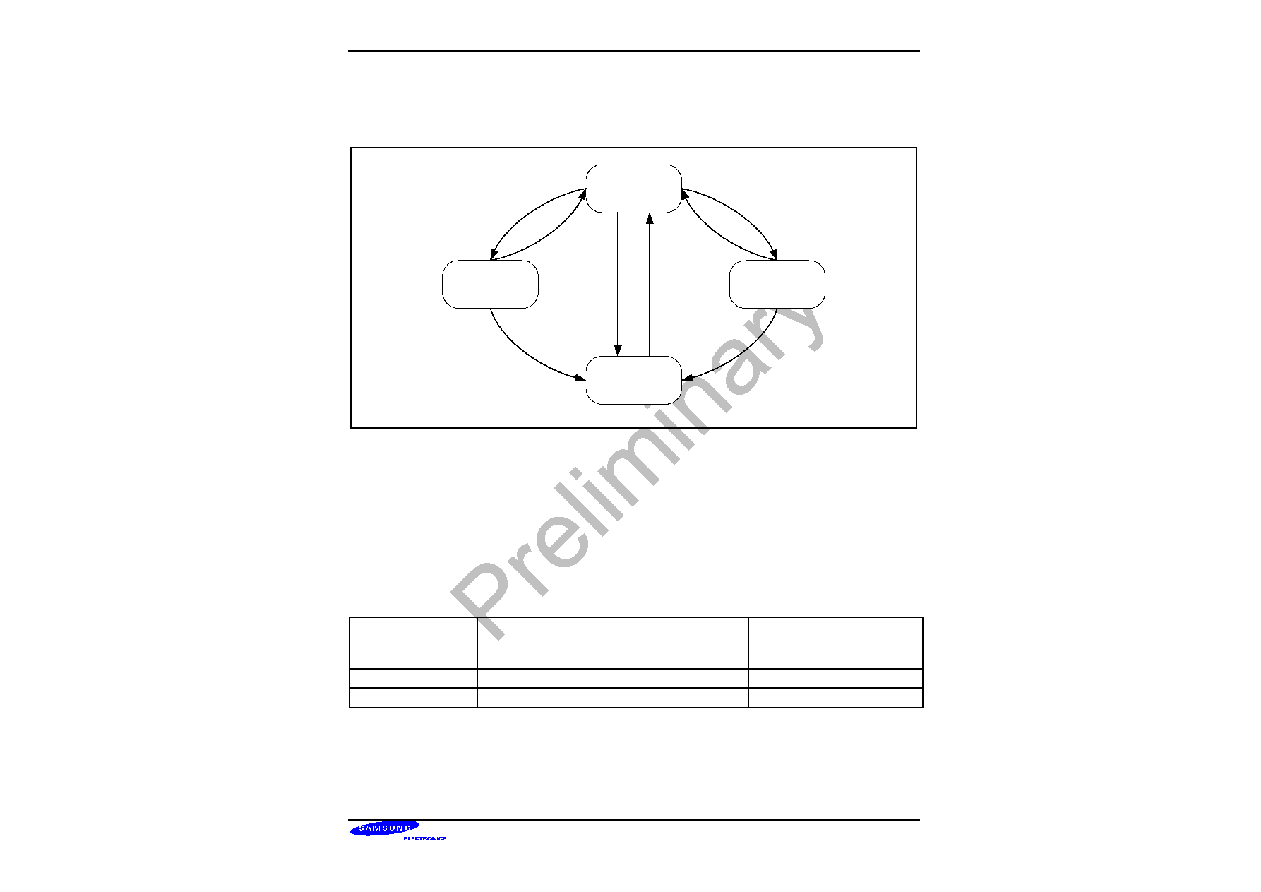
BSW rv0.1-0417-N01
Preliminary product information describes products that are in development,
for which full characterization data and associated errata are not yet available.
Specifications and information herein are subject to change without notice.
S3C24A0 RISC MICROPROCESSOR
CLOCK & POWER MANAGEMENT
33-11
Power Mode State Diagram
Figure 33-7 show that Power Saving mode state and Entering or Exiting condition. In general, the S3C24A0
issues the Entering conditions.
Normal
(General Clock
Gating Mode)
IDLE
SLEEP
STOP
CMD
CMD
nBATFLT
nBATFLT
CMD or
nBATFLT
One of
wakeup
source
Reset
or
restricted
wakeup
evants.
One of
wakeup
source
Figure 33-7. Power mode state diagram
Wake-Up Event
When the S3C24A0 wakes up from the STOP Mode or the SLEEP Mode by an External Interrupt, a RTC alarm
interrupt and other interrupts, the PLL is turned on automatically. However, the clock supply scheme is quite
different. The initial-state of the S3C24A0 after wake-up from the SLEEP Mode is almost the same as the Power-
On-Reset state except for the contents of the external DRAM is preserved. In contrast, the S3C24A0
automatically recovers the previous working state after wake-up from the STOP Mode.
The following table shows the states of PLLs and internal clocks after wake-ups from the power-saving modes.
Table 33-5. The Status of PLL and ARMCLK After Wake-Up
Mode before wake-up PLL on/off after
wake up
ARMCLK after wake up and
before the lock time
ARMCLK after the lock time
by internal logic
IDLE
Unchanged
PLL Output
PLL Output
STOP
Off
on
No clock
PLL Output
SLEEP
Off
on
External Clock
External Clock
Output port state in STOP and SLEEP mode
Refer to Pin Assignment Table * in Product Overview chapter.

BSW rv0.1-0417-N01
Preliminary product information describes products that are in development,
for which full characterization data and associated errata are not yet available.
Specifications and information herein are subject to change without notice.
CLOCK & POWER MANAGEMENT
S3C24A0 RISC MICROPROCESSOR
33-12
Power Saving Mode Entering/Exiting Condition
Table 33-6 shows that Power Saving mode state and Entering or Exiting condition.
Table 33-6. Power Saving Mode Entering/Exiting condition
Power Saving Mode
Entering
Exiting
NORMAL
Disable the CLKCON bit for each IP block
Enable the CLKCON bit for each IP block
IDLE
Enable the ClockIdle bit of CLKCON
register
1) External INT[9:0]
2) RTC Alarm INT
3) Touch Screen Pen-down INT
4) Modem INT
5) XsWRESETn
6) XsRESETn
STOP
Enable the ClockStop bit of CLKCON
register
1) External INT[9:0]
2) RTC Alarm INT
3) Touch Screen Pen-down INT
4) Modem INT
5) XsWRESETn
6) XsRESETn
SLEEP
Write `0xA3' to the SLEEP_CODE[7:0] bits
of PWRMAN register
1) External INT[9:0]
2) RTC Alarm INT
3) XsWRESETn
4) XsRESETn
SLEEP
When the XgBATFLT port goes to low
1) External INT: GPIO[1:0]
2) XsWRESETn
3) XsRESETn
NOTES:
1.
The Wake-up Event Sources for the SLEEP mode due to the XgBATFLT are limited as in the above table.
2. Entering to the SLEEP mode by the XgBATFLT is programmable,
1) the XgBATFLT can be forwarded as an FIQ
2) the XgBATFLT can be used as the entering event for the SLEEP mode
3) the XgBATFLT can be ignored.
Reset Definition
Reset
Definition
XsRESETn
This is the cold reset. The internal state (include registers) of the S3C24A0 will
be initialized when XsRESETn is activated. The XsRESETn is a non-maskable
signal except for the case when the XgBATFLTn is in the active state (low). The
contents of the SDRAM will not be preserved when the XsRESETn is applied.
XsWRESETn,
SoftReset
The XsWRESETn and the Soft-reset reset the system except RTC, Clock
Generator, power management module and memory controller (preserves
SDRAM data)

BSW rv0.1-0417-N01
Preliminary product information describes products that are in development,
for which full characterization data and associated errata are not yet available.
Specifications and information herein are subject to change without notice.
S3C24A0 RISC MICROPROCESSOR
CLOCK & POWER MANAGEMENT
33-13
CLOCK GENERATOR & POWER MANAGEMENT SPECIAL REGISTER
LOCK TIME COUNT REGISTER (LOCKTIME)
Register
Address
R/W
Description
Reset Value
LOCKTIME
0x40000000
R/W
PLL lock time count register
0x0FFF_0FFF
LOCKTIME
Bit
Description
Initial State
U_LTIME
[27:16]
UPLL lock time count (generally 300us)
0xFFF
M_LTIME
[11:0]
MPLL lock time count (generally 300us)
0xFFF
PLL Locking Time
Locking Time = (1/Fin) * (U_LTIME or M_LTIME * 16)
X-TAL OSCILLATION WAIT REGISTER (XTALWSET)
Register
Address
R/W
Description
Reset Value
XTALWSET
0x40000004
R/W
Crystal oscillator settle-down wait time
0x5000_5000
XTALWSET
Bit
Description
Initial State
U_OSCWAIT
[31:16]
UPLL Crystal oscillator settle-down wait time
0x5000
M_OSCWAIT
[15:0]
MPLL Crystal oscillator settle-down wait time
0x5000
X-tal Settle-down wait time
X-tal Settle-down Time = Tcrystal_clock * (U_OSCWAIT or M_OSCWAIT)

BSW rv0.1-0417-N01
Preliminary product information describes products that are in development,
for which full characterization data and associated errata are not yet available.
Specifications and information herein are subject to change without notice.
CLOCK & POWER MANAGEMENT
S3C24A0 RISC MICROPROCESSOR
33-14
PLL CONTROL REGISTER (MPLLCON, UPLLCON)
PLL value selection guide
1. Mpll or Upll = (m * Fin) / (p * 2
s
), where: m = (MDIV + 8), p = (PDIV + 2), s = SDIV
2. Fin/(25*p) < 16.7e6/m < Fin/(10*p)
3. 0.7 < 6.48/sqrt(m) < 1.8
4. (Fin/p)*m < 330e6
Register
Address
R/W
Description
Reset Value
MPLLCON
0x40000010
R/W
MPLL configuration register
0x0004_8021
UPLLCON
0x40000014
R/W
UPLL configuration register
0x0003_0021
M/U PLLCON
Bit
Description
Initial State
MDIV
[19:12]
Main divider control ( M value )
0x48 / 0x30
PDIV
[9:4]
Pre-divider control ( P value )
0x02 / 0x02
SDIV
[1:0]
Post divider control ( S value )
0x1 / 0x1
To ensure the proper operation of the internal PLLs, we recommend the following PLL value-sets. If the user
requires other range of PLL set-values, please contact one of SEC application engineers.
Table 33-7 PLL value selection table
Input Frequency
Output Frequency (MHz)
MDIV
PDIV
SDIV
12.00MHz
84
34 (0x22)
1
1
12.00MHz
90
37 (0x25)
1
1
12.00MHz
96
56 (0x38)
2
1
12.00MHz
102
43 (0x2b)
1
1
12.00MHz
112.5
67 (0x43)
2
1
12.00MHz
118
51 (0x33)
1
1
12.00MHz
124
54 (0x36)
1
1
12.00MHz
132
58 (0x3a)
1
1
12.00MHz
136
60 (0x3c)
1
1
12.00MHz
176
36 (0x24)
1
0
12.00MHz
177
51 (0x33)
2
0
12.00MHz
180
37 (0x25)
1
0
12.00MHz
186
54 (0x36)
2
0
12.00MHz
192
56 (0x38)
2
0
12.00MHz
200
42 (0x2a)
1
0
12.00MHz
204
60 (0x3c)
2
0

BSW rv0.1-0417-N01
Preliminary product information describes products that are in development,
for which full characterization data and associated errata are not yet available.
Specifications and information herein are subject to change without notice.
S3C24A0 RISC MICROPROCESSOR
CLOCK & POWER MANAGEMENT
33-15
CLOCK CONTROL REGISTER (CLKCON)
Register
Address
R/W
Description
Reset Value
CLKCON
0x40000020
R/W
Clock generator control Register
0x03fffff0
CLKCON
Bit
Description
Initial State
VLXclkOn
[29]
Controls HCLK into VLX block
0: Disable
1: Enable
1
VPOSTclkOn
[28]
Controls MPEGCLK into VPOST block
0: Disable
1: Enable
1
Reserved
[27]
Reserved
MPEGDCTQclkOn
[26]
Controls MPEGCLK into MPEGDCTQ block
0: Disable
1: Enable
1
VPOSTIFclkOn
[25]
Controls HCLK into VPOST block (AHB bus side)
0: Disable
1: Enable
1
MPEGIFclkOn
[24]
Controls HCLK into MPEG AHB Interface
0: Disable
1: Enable
1
CAMclkOn
[23]
Controls UPLL_clk into CAM block
0: Disable
1: Enable
1
LCDclkOn
[22]
Controls HCLK into LCD block
0: Disable
1: Enable
1
CAMIFclkOn
[21]
Controls HCLK into camera interface block
0: Disable
1: Enable
1
MPEGMEclkOn
[20]
Controls MPEG4CLK into MPEG ME block
0: Disable
1: Enable
1
KeyPadClkOn
[19]
Controls PCLK into Key Pad block
0: Disable
1: Enable
1
ADCclkOn
[18]
Controls PCLK into ADC block
0: Disable
1: Enable
1
SDclkOn
[17]
Controls PCLK into SD block
0: Disable
1: Enable
1
MSclkOn
[16]
Controls PCLK into Memory Stick block
0: Disable
1: Enable
1
USBdeviceClkOn
[15]
Controls PCLK into USB device block
0: Disable
1: Enable
1
GPIOclkOn
[14]
Controls PCLK into GPIO block
0: Disable
1: Enable
1
IISclkOn
[13]
Controls PCLK into IIS block
0: Disable
1: Enable
1
IICclkOn
[12]
Controls PCLK into IIC block
0: Disable
1: Enable
1
SPIclkOn
[11]
Controls PCLK into SPI block
0: Disable
1: Enable
1

BSW rv0.1-0417-N01
Preliminary product information describes products that are in development,
for which full characterization data and associated errata are not yet available.
Specifications and information herein are subject to change without notice.
CLOCK & POWER MANAGEMENT
S3C24A0 RISC MICROPROCESSOR
33-16
CLKCON
Bit
Description
Initial State
UART1clkOn
[10]
Controls PCLK into UART1 block
0: Disable
1: Enable
1
UART0clkOn
[9]
Controls PCLK into UART0 block
0: Disable
1: Enable
1
PWMTIMERClkOn
[8]
Controls PCLK into PWMTIMER block
0: Disable
1: Enable
1
USBhostClkOn
[7]
Controls HCLK into USB host block
0: Disable
1: Enable
1
AC97clkOn
[6]
Controls PCLK into AC97 block
0: Disable
1: Enable
1
Reserved
[5]
Reserved(Should be zero)
0
IrDAclkOn
[4]
Controls UPLL_clk into IrDA block
0: Disable
1: Enable
1
Reserved
[3]
Reserved
0
ClockIdle
[2]
Enters IDLE mode. This bit is not cleared automatically.
0: Disable
1: Transition to IDLE mode
0
ClkMonOn
[1]
HCLK monitor Enable
0: Disable
1: Enable
0
ClockStop
[0]
Enters STOP mode. This bit is not cleared automatically.
0: Disable
1: Transition to STOP mode
0
CLOCK SOURCE CONTROL REGISTER (CLKSRC)
Register
Address
R/W
Description
Reset Value
CLKSRC
0x40000024
R/W
Clock source control register.
0x00000004
CLKSRC
Bit
Description
Initial State
OnOSC_EN
[8]
Crystal Oscillator Enable control during the STOP mode
0: Disable
1: Enable
0
U_PLLoff
[7]
UPLL on/off control
0: on
1: off
0
Reserved
[6]
Reserved
0
M_PLLoff
[5]
MPLL on/off control
0: on
1: off
0
SelExtClk
[4]
Select External clock source for ARMCLK/HCLK/PCLK
0: MPLL_clk
1: External clock
0
Reserved
[3]
Reserved
0
ExtclkDiv
[2:0]
External clock division factor
000: No division001 ~ 110: Divided by (2*ExtClkDiv)
111: Reserved for the S3C24A0 test
4

BSW rv0.1-0417-N01
Preliminary product information describes products that are in development,
for which full characterization data and associated errata are not yet available.
Specifications and information herein are subject to change without notice.
S3C24A0 RISC MICROPROCESSOR
CLOCK & POWER MANAGEMENT
33-17
CLOCK DIVIDER CONTROL REGISTER (CLKDIVN)
Register
Address
R/W
Description
Reset Value
CLKDIVN
0x40000028
R/W
Clock divider control register
0x0000_0300
CLKDIVN
Bit
Description
Initial State
CAMclkdiv
[11:8]
CAMclk Division Factor
0x5
MPEGclkdiv
[7:4]
MPEGclk Division Factor
0
HCLKdiv
[2:1]
HCLK Division Factor
00: ARMCLK: HCLK = 1:1
01: ARMCLK: HCLK = 1:2
10: ARMCLK: HCLK = 1:3
11: ARMCLK: HCLK = 1:4
0
PCLKdiv
[0]
0: PCLK has the clock same as the HCLK
1: PCLK has the clock same as the HCLK/2
0
POWER MANAGEMENT CONTROL REGISTER (PWRMAN)
Register
Address
R/W
Description
Reset Value
PWRMAN
0x40000030
R/W
Power management register
0x0000_1000
PWRMAN
Bit
Description
Initial State
USE_WFI
[12]
Use the WFI (wait for interrupt) instruction before enter into
stop and sleep mode. If this bit is set, the power management
block checks the internal signal (STANDBYWFI), so WIF
instruction must be added by software.
0: Not use
1: Use the WFI
1
MASK_MODEM
[11]
Baseband Modem wakeup mask setting register
0: Unmask
1: Mask
0
CNFG_BF
[10:9]
Battery fault handling configuration setting register
00: Emergency Sleep
01: FIQ
10: Ignore
11: reserved
0x0
MASK_TS
[8]
Touch screen wakeup mask setting register
0: Unmask
1: Mask
0
SLEEP_CODE
[7:0]
SLEEP Mode setting code
-
NOTE:
1.
SLEEP_CODE is 0xA3. When this register was set with the value of 0xXXXX_XXA3 the SLEEP mode is activated.
2.
When using the WFI instruction in the ARM926EJ-S core by setting the USE_WFI bit, the entering sequence of
power-saving mode is as follows,
a.
Set the ClockStop bit in CLKCON register or write sleep code to SLEEP_CODE bits in PWRMAN register.
b.
Execute the WFI instruction

BSW rv0.1-0417-N01
Preliminary product information describes products that are in development,
for which full characterization data and associated errata are not yet available.
Specifications and information herein are subject to change without notice.
CLOCK & POWER MANAGEMENT
S3C24A0 RISC MICROPROCESSOR
33-18
Softreset Control register (SOFTRESET)
Register
Address
R/W
Description
Reset Value
SOFTRESET
0x40000038
R/W
Software reset control register
-
SOFTRESET
Bit
Description
Initial State
Soft Reset
[7:0]
Software controlled reset setting code
-
NOTE: SOFTRESET command is 0xA3. When this register was set with the value of 0xXXXX_XXA3 the soft-reset is activated.
