 | –≠–ª–µ–∫—Ç—Ä–æ–Ω–Ω—ã–π –∫–æ–º–ø–æ–Ω–µ–Ω—Ç: S3C72H8 | –°–∫–∞—á–∞—Ç—å:  PDF PDF  ZIP ZIP |
S3C72H8/P72H8
PRODUCT OVERVIEW
1-1
1
PRODUCT OVERVIEW
OVERVIEW
The S3C72H8 single-chip CMOS microcontroller has been designed for very high performance using Samsung's
state-of-the-art 4-bit product development approach, SAM47 (Samsung Arrangeable Microcontrollers). Its main
features are an up-to-13-digit LCD direct drive capability, 2-channel comparator inputs and outputs, and versatile
8-counter/ timers and 16-bit frequency counter. The S3C72H8 gives you an excellent design solution for a variety
of LCD-related applications, specially thermostat control application.
Up to 21 pins of the available 64-pin QFP packages can be dedicated to I/O. And six vectored interrupts provide
fast response to internal and external events.
In addition, the S3C72H8's advanced CMOS technology provides for low power consumption and a wide oper-
ating voltage range.

PRODUCT OVERVIEW
S3C72H8/P72H8
1-
2
FEATURES
Architecture
≠
SAM47 4-bit CPU core
Memory
≠
Data Memory: 512
◊
4 bits
≠
Program Memory: 8196
◊
8 bits
(Including LCD display RAM)
Memory-Mapped I/O Structure
≠
Data memory bank 15
Interrupts
≠
Three internal vectored interrupts
≠
Three external vectored interrupts
≠
Two quasi-interrupts
8-Bit Timer/Counter (T0)
≠
Programmable 8-bit timer
≠
External event counter
≠
Arbitrary clock frequency output
≠
External clock signal divider
16-Bit Frequency Counter (FC)
≠
a 16-bit binary up-counter
≠
External event counter
≠
Gate function control
Watch-Dog TIMER and Basic Timer
≠
8-bit counter + 3-bit counter
≠
Overflow signal of 8-bit counter makes a basic
timer interrupt. And control the oscillation warm-
up time
≠
Overflow signal of 3-bit counter makes a system
reset
Watch Timer
≠
Real-time and interval time measurement
≠
Four frequency outputs to buzzer sound
≠
Clock source generation for LCD
LCD Controller/Driver
≠
26 segment and 4 common terminals
≠
Maximum 13-digit LCD direct drive capability
≠
Display modes: Static, 1/2, 1/3, 1/4 duty
≠
Voltage regulator and booster (1/3 bias: 1, 2, or
3V, 1/2 bias: 1.5, 3V)
Analog Comparator
≠
2 Ch Comparator (Each CnP, CnN, CnOUT pins)
Bit Sequential Carrier
≠
Support 16-bit serial data transfer in arbitrary
format
I/O Ports
≠
21 pins for standard I/O
≠
26 pins for LCD segment output
≠
4 pins for LCD common output
≠
Two input pins for external interrupts
Oscillation Sources
≠
Crystal, ceramic, or RC for main system clock
≠
Crystal or external oscillator for subsystem clock
≠
Main system clock frequency: 4.19 MHz (typical)
≠
Subsystem clock frequency: 32.768 kHz
≠
CPU clock divider circuit (by 4, 8, or 64 main, and
by 4 for sub clock)
Power Down Mode
≠
Idle mode (only CPU clock stops)
≠
Stop mode (main or sub-system oscillation stops)
Voltage Level Detector
≠
V
DD
level detection circuit (2.2, 2.4, 3, or 4.0V)
≠
External pin level detect mode
Operating Voltage Range
≠
1.8V to 5.5V at 3 MHz
≠
2.0V to 5.5V at 4.19 MHz
Package Type
≠
64-pin QFP
S3C72H8/P72H8
PRODUCT OVERVIEW
1-3
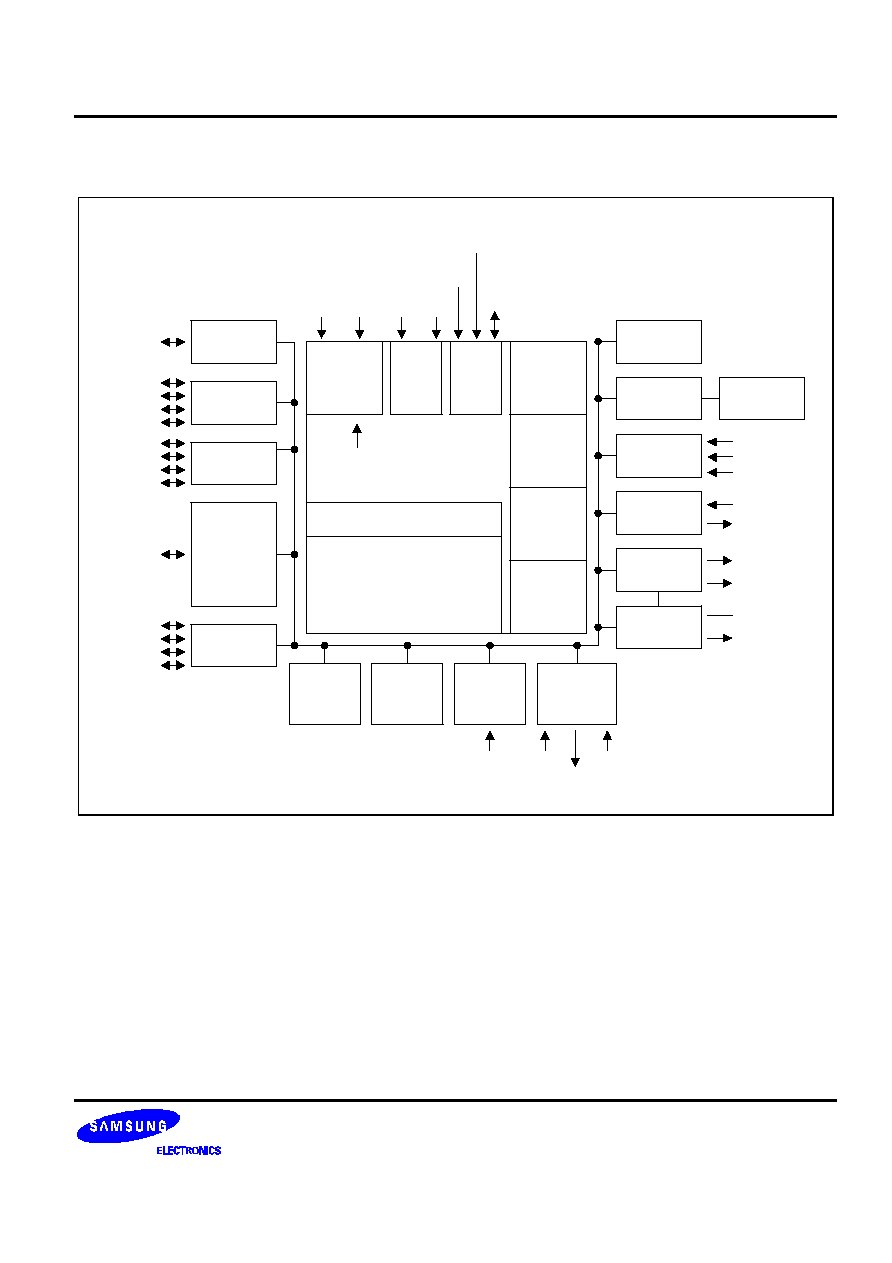
BLOCK DIAGRAM
Program
Status
Word
Stack
Pointer
Arithmetic
and
Logic Unit
Internal
Interrupts
RESET
Instruction
Register
512 x 4-Bit
Data
Memory
P0.0/ExtRef
P0.1/SDAT
P0.2/SCLK
COM0-COM3
FCL
I/O Port 4,5
I/O Port 0
I/O Port 2
I/O Port 3
I/O Port 6
P2.0/INT0
P2.1/INT1
P2.2/TCL0
P2.3/FCL
P3.0/TCLO0
P3.1/BTCO
P3.2/CLO
P3.3/BUZ
P4.0/C0P
P4.1/C0N
P4.2/C0OUT
P4.3/C1OUT
P5.0/C1P
P5.1/C1N
P6.0/KS0
P6.1/KS1
P6.2/KS2
P6.3/KS3
Interrupt
Control
Block
Program
Counter
Clock
OTP
Block
Instruction Decoder
8 K Byte
Program
Memory
Voltage
Level
Detector
Two Analog
Comparator
ExtRef
CnP
Cn
OUT
CnN
INT0, INT1
V
PP
/
TEST
X
OUT
X
IN
XT
OUT
XT
IN
SCLK
SDAT
Voltage
Booster
Watch
Timer
Basic
Timer
16-Bit FREQ
Counter
8-Bit
Timer
LCD Driver/
Controller
Watchdog
Timer
C0
OUT
C1
OUT
TCL0
TCLO0
SEG0-SEG25
CA, CB
V
LC0
-V
LC2
Figure 1-1. S3C72H8 Simplified Block Diagram
PRODUCT OVERVIEW
S3C72H8/P72H8
1-
4
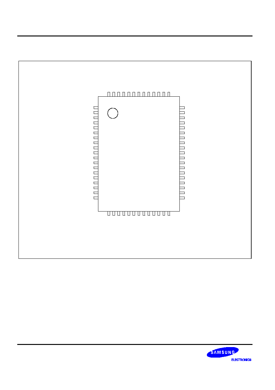
PIN ASSIGNMENTS
CA
CB
V
LC0
V
LC1
V
LC2
P0.0/ExtRef
SDAT/P0.1
SCLK/P0.2
V
DD
/V
DD
V
SS
/V
SS
X
OUT
X
IN
V
PP
/TEST
XT
IN
XT
OUT
RESET
RESET/RESET
P2.0/INT0
P2.1/INT1
P2.2/TCL0
COM0
COM1
COM2
COM3
SEG0
SEG1
SEG2
SEG3
SEG4
SEG5
SEG6
SEG7
SEG8
P2.3/FCL
P3.0/TCLO0
P3.1/BTCO
P3.2/CLO
P3.3/BUZ
P6.0/KS0
P6.1/KS1
P6.2/KS2
P6.3/KS3
P4.0/C0P
P4.1/C0N
P4.2/C0OUT
P4.3PC1OUT
S3C72H8
(TOP VIEW)
1
2
3
4
5
6
7
8
9
10
11
12
13
14
15
16
17
18
19
20
21
22
23
24
25
26
27
28
29
30
31
32
64
63
62
61
60
59
58
57
56
55
54
53
52
SEG9
SEG10
SEG11
SEG12
SEG13
SEG14
SEG15
SEG16
SEG17
SEG18
SEG19
SEG20
SEG21
SEG22
SEG23
SEG24
SEG25
P5.1/C1N
P5.0/C1P
51
50
43
48
47
46
45
44
43
42
41
40
39
38
37
36
35
34
33
Figure 1-2. S3C72H8 Pin Assignment Diagram
S3C72H8/P72H8
PRODUCT OVERVIEW
1-5
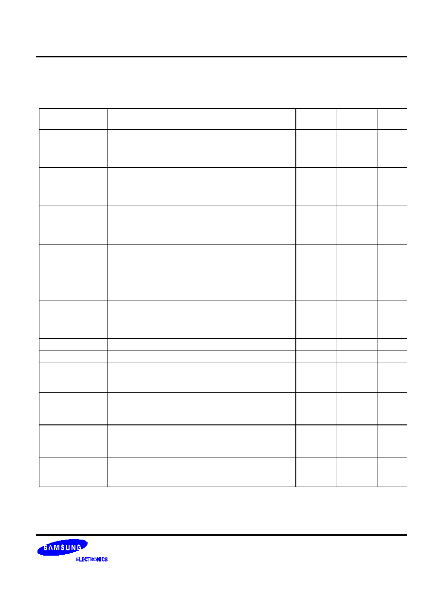
PIN DESCRIPTIONS
Table 1-1. S3C72H8 Pin Descriptions
Pin Name
Pin
Type
Description
Number
(64-QFP)
Share
Pin
Circuit
Type
P0.0
P0.1
P0.2
I/O
3-bit I/O port.
1-bit and 4-bit read/write and test is possible.
Port 0 is software configurable as input or output. 3-bit
pull-up resistors are software assignable.
6
7
8
ExtRef
≠
≠
D-1
P2.0
P2.1
P2.2
P2.3
I/O
4-bit I/O port.
1-bit and 4-bit read/write and test is possible.
Individual pins are software configurable as input or
output. 4-bit pull-up resistors are software assignable.
17
18
19
20
INT0
INT1
TCL0
FCL
D-1
P3.0
P3.1
P3.2
P3.3
I/O
Same as port 2.
Ports 2 and 3 can be addressed by 1, 4, and 8-bit
read/write and test instruction.
21
22
23
24
TCLO0
BTCO
CLO
BUZ
D-1
P4.0-P4.3
P5.0-P5.1
I/O
4/2-bit I/O ports. N-channel open-drain or push-pull
output. 1, 4, and 8-bit read/write and test is possible.
Ports 4 and 5 can be paired to support 8-bit data
transfer. Pull-up resistors are assignable to port unit by
software control.
29-32
33-34
C0P/
C0N/
C0OUT/
C1OUT
C1P/
C1N
E-1
P6.0-P6.3
I/O
4-bit I/O ports. Port 6 pins are individually software
configurable as input or output. 1-bit and 4-bit read/write
and test is possible. 4-bit pull-up resistors are software
assignable.
25-28
KS0-KS3
D-1
BTCO
I/O
Basic timer clock output
22
P3.1
D-1
CLO
I/O
CPU clock output
23
P3.2
D-1
BUZ
I/O
2, 4, 8 or 16 kHz frequency output for buzzer sound with
4.19MHz main-system clock or 32.768 kHz sub-system
clock.
24
P3.3
D-1
X
OUT
, X
IN
≠
Crystal, ceramic, or RC oscillator signal for main-
system clock. (For external clock input, use X
IN
and
input X
IN
's reverse phase to X
OUT
)
11, 12
≠
≠
XT
OUT
,
XT
IN
≠
Crystal oscillator signal for sub-system clock.
(For external clock input, use XT
IN
and input XT
IN
's
reverse phase to XT
OUT
)
14, 15
≠
≠
INT0, INT1
I/O
External interrupts. The triggering edge for INT0 and
Int1 is selectable. Only INT0 is synchronized with the
system clock.
17, 18
P2.0, P2.1
D-1
PRODUCT OVERVIEW
S3C72H8/P72H8
1-
6
Table 1-1. S3C72H8 Pin Descriptions (Continued)
Pin Name
Pin
Type
Description
Number
(64-QFP)
Share
Pin
Circuit
Type
KS0-KS3
I/O
Quasi-interrupt input with falling edge detection
25-28
P6.0-P6.3
D-1
ExtRef
I/O
External Reference input
6
P0.0
D-1
TCL0
I/O
External clock input for timer/counter 0
19
P2.2
D-1
FCL
I/O
External clock input for frequency counter
20
P2.3
D-1
TCLO0
I/O
Timer/counter 0 clock output
21
P3.0
D-1
COM0-COM3
O
LCD common signal output
61-64
≠
H-16
SEG0-SEG25
O
LCD segment output
35-60
≠
H-16
CA, CB
≠
Voltage booster capacitor pins
1, 2
≠
≠
V
LC0
-V
LC2
≠
Voltage booster output pins (V
LC0
is the regulated
output, V
LC1
is the 2* V
LC0
output, V
LC2
is the 3* V
LC0
output)
3-5
≠
≠
C0P, C0N,
C0OUT
I/O
Comparator 0 non-inverting input, inverting input and
output. C0Out can be configured as C-MOS push-pull
or N-Ch open drain output
29-31
P4.0-P4.2
≠
C1P, C1N,
C1OUT
I/O
I
Comparator 1 non-inverting input, inverting input and
output. C1Out can be configured as C-MOS push-pull
or N-Ch open drain output
32-34
P4.3-P5.1
≠
RESET
≠
Reset signal for chip initialization
16
≠
B
V
DD
≠
Main power supply
9
≠
≠
V
SS
≠
Ground
10
≠
≠
TEST
≠
Test signal input (must be connected to V
SS
)
13
V
PP
≠
SDAT
I/O
Serial data for OTP programming
7
P0.1
SCLK
I/O
Serial clock for OTP programming
8
P0.2
V
PP
≠
Power supply pin for EPROM cell writing
13
TEST
NOTE: Pull-up resistors for ports 0, 2, 3, and 6 are automatically disabled if they are configured to output mode.
But pull-up resistors for ports 4 and 5 are retained its state even though they are configured to output mode.
S3C72H8/P72H8
PRODUCT OVERVIEW
1-7
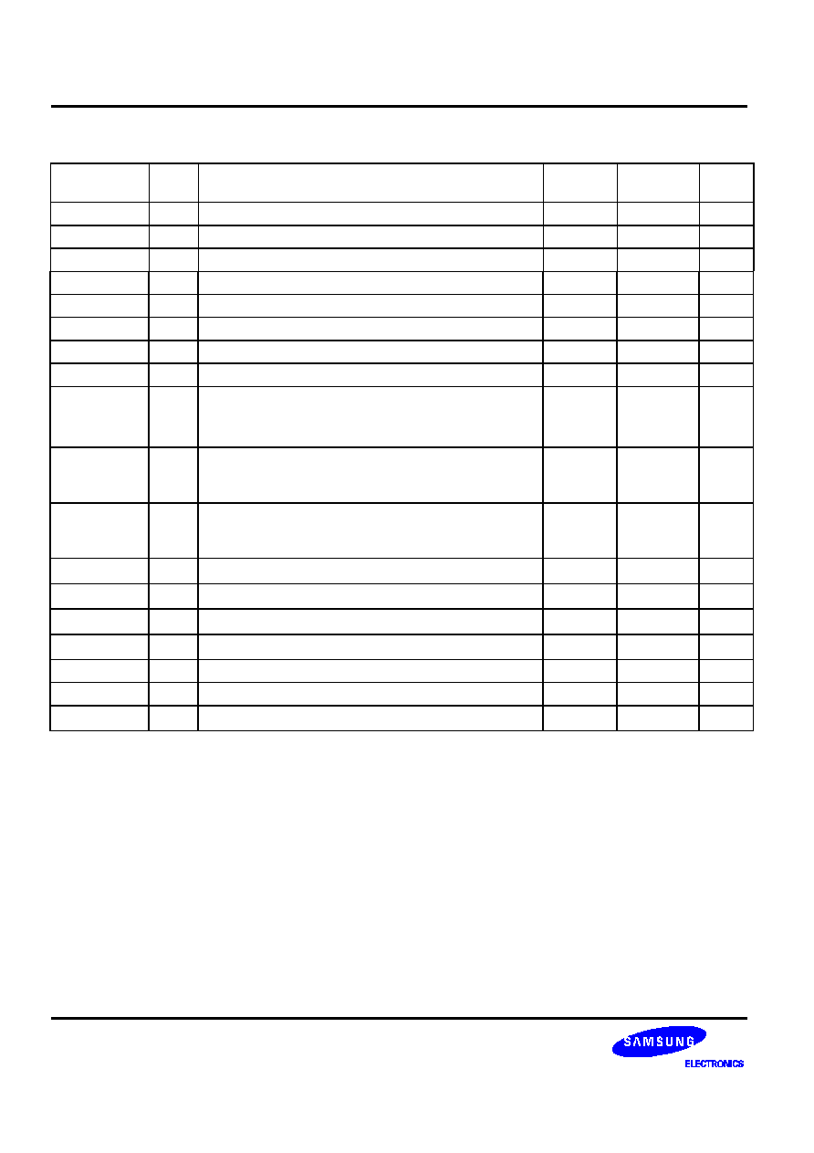
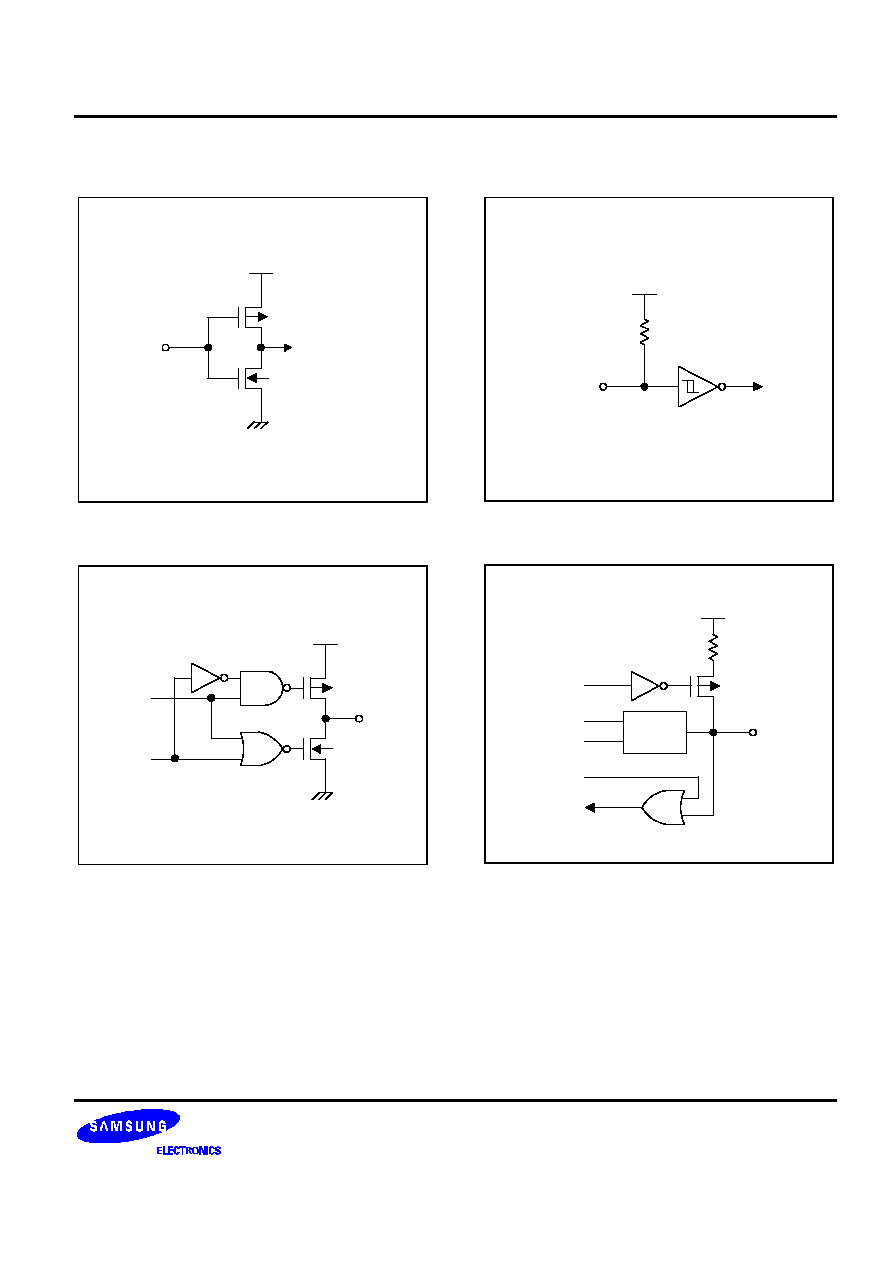
PIN CIRCUIT DIAGRAMS
P-Channel
N-Channel
In
V
DD
Figure 1-3. Pin Circuit Type A
V
DD
Out
Output
Disable
Data
P-Channel
N-Channel
Figure 1-5. Pin Circuit Type C
In
V
DD
Figure 1-4. Pin Circuit Type B (Reset)
I/O
Circuit
Type C
Pull-up
Resistor
P-Cannel
Output
Disable
Data
V
DD
Resistor
Enable
Input
Disable
Figure 1-6. Pin Circuit Type D-1 (P0, P2, P3, P6)
PRODUCT OVERVIEW
S3C72H8/P72H8
1-
8
V
DD
Pull-up
Enable
V
DD
In/Out
PNE
Output
Disable
Data
Input
Disable
To Data Bus
To Comparator
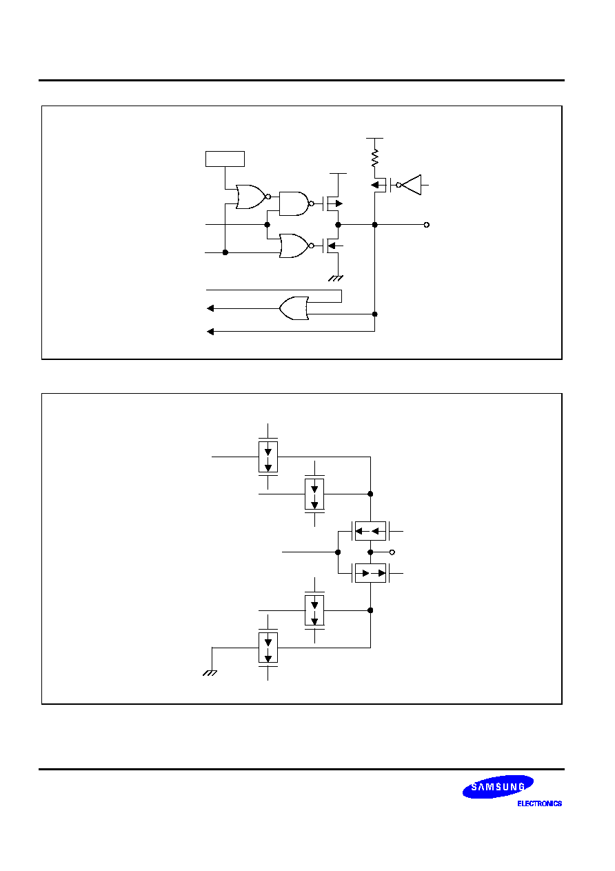
Figure 1-7. Pin Circuit Type E-1 (P4, P5)
Out
V
LC2
V
LC1
SEG/COM
DATA
V
LC0
Figure 1-8. Pin Circuit Type H-16 (COM/SEG)

S3C72H8/P72H8
ELECTRICAL DATA
16-1
16
ELECTRICAL DATA
OVERVIEW
In this section, information on S3C72H8 electrical characteristics is presented as tables and graphics. The
information is arranged in the following order:
Standard Electrical Characteristics
-- Absolute maximum ratings
-- D.C. electrical characteristics
-- Main system clock oscillator characteristics
-- Subsystem clock oscillator characteristics
-- I/O capacitance
-- A.C. electrical characteristics
-- Operating voltage range
Miscellaneous Timing Waveforms
-- A.C timing measurement point
-- Clock timing measurement at X
IN
-- Clock timing measurement at XT
IN
-- TCL timing
-- Input timing for
RESET
-- Input timing for external interrupts
Stop Mode Characteristics and Timing Waveforms
-- RAM data retention supply voltage in stop mode
-- Stop mode release timing when initiated by
RESET
-- Stop mode release timing when initiated by an interrupt request

ELECTRICAL DATA
S3C72H8/P72H8
16-2
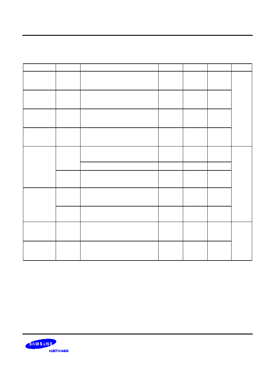
Table 16-1. Absolute Maximum Ratings
(T
A
= 25
∞
C)
Parameter
Symbol
Conditions
Rating
Units
Supply Voltage
V
DD
≠
≠ 0.3 to + 6.5
V
Input Voltage
V
IN
≠
≠ 0.3 to V
DD
+ 0.3
Output Voltage
V
O
All I/O ports
≠ 0.3 to V
DD
+ 0.3
Output Current High
I
OH
One I/O pin active
≠ 7
mA
All I/O ports active
≠ 40
Output Current Low
I
OL
One I/O pin active
+ 15
mA
Total pin circuit
+ 60
Operating Temperature
T
A
≠
≠ 40 to + 85
∞
C
Storage Temperature
T
STG
≠
≠ 65 to + 150
Table 16-2. D.C. Electrical Characteristics
(T
A
= ≠ 40
∞
C to + 85
∞
C, V
DD
= 1.8 V to 5.5 V)
Parameter
Symbol
Conditions
Min
Typ
Max
Units
Operation
voltage
V
DD
F
OSC
= 6 MHz
(CPU clock = 1.25 MHz)
2.7
≠
5.5
V
F
OSC
= 4.19 MHz
(Instruction clock = 1.04 MHz)
2.0
5.5
F
OSC
= 3 MHz
(CPU clock = 0.75 MHz)
1.8
5.5
Input High
V
IH1
P0, P2, P3, P4, P5 and P6
0.8 V
DD
≠
V
DD
voltage
V
IH2
RESET
0.85 V
DD
V
DD
V
IH3
X
IN
V
DD
-0.1
V
DD
Input low
V
IL1
P0, P2, P3, P4, P5 and P6
≠
0.2 V
DD
voltage
V
IL2
RESET
0.3 V
DD
V
IL3
X
IN
0.1
Output high
voltage
V
OH1
V
DD
= 5.0V
I
OH
= ≠ 1 mA
All output pins
V
DD
≠ 1.0
≠
≠
V
I
OH
= ≠ 100
µ
A
V
DD
≠ 0.5
Output low
voltage
V
OL1
V
DD
= 5.0 V, I
OL
= 2 mA
All output pins except V
OL2
≠
0.4
0.5
V
OL2
V
DD
= 5.0 V, I
OL
= 15 mA
Ports 2,3, and 4
0.4
1.0
S3C72H8/P72H8
ELECTRICAL DATA
16-3
Table 16-2. D.C. Electrical Characteristics (Continued)
(T
A
= ≠ 40
∞
C to + 85
∞
C, V
DD
= 1.8 V to 5.5 V)
Parameter
Symbol
Conditions
Min
Typ
Max
Units
Input high
leakage
current
(note)
I
LIH1
V
IN
= V
DD
All input pins
≠
≠
3
µA
Input low
leakage
current
(note)
I
LIL1
V
IN
= V
DD
; All input pins
except
RESET
≠
≠
≠ 3
Output high
leakage
current
(note)
I
LOH
V
OUT
= V
DD
All I/O pins and output pins
≠
≠
3
Output low
leakage
current
(note)
I
LOL
V
OUT
= 0 V
All I/O pins and output pins
≠
≠
≠ 3
Pull-up
resistors
R
L1
V
IN
= 0 V, V
DD
= 5 V
T
A
= 25
∞
C, Ports 0-6
25
47
100
K
V
DD
= 3 V
50
90
150
R
L2
V
IN
= 0 V; V
DD
= 5.0 V
150
250
350
T
A
= 25
∞
C,
RESET
Oscillator
feed back
resistors
R
OSC1
V
DD
= 5.0 V, T
A
= 25
∞
C
X
IN
= V
DD
, X
OUT
= 0V
400
700
1200
R
OSC2
V
DD
= 5.0 V, T
A
= 25
∞
C
XT
IN
= V
DD
, XT
OUT
= 0V
1000
1500
3000
|V
LC1
-COMi|
Voltage Drop
(I = 0-3)
V
DC
-15 uA per common pin
≠
≠
120
mV
|V
LC1
-SEGi|
Voltage Drop
(I = 0-25)
V
DS
-15 uA per segment pin
≠
≠
120
NOTE: Except X
IN
, X
OUT
, XT
IN
, XT
OUT

ELECTRICAL DATA
S3C72H8/P72H8
16-4
Table 16-2. D.C. Electrical Characteristics (Continued)
(T
A
= ≠ 40
∞
C to + 85
∞
C, V
DD
= 1.8 V to 5.5 V)
Parameter
Symbol
Conditions
Min
Typ
Max
Units
Supply
Current
(note)
I
DD1
Main operation mode:
V
DD
= 5 V
±
10%, 6-MHz crystal
≠
3.5
8
mA
V
DD
= 5 V
±
10%, 4.19 MHz
2.5
5.5
V
DD
= 3 V
±
10%, 6-MHz crystal
1.6
4
V
DD
= 3 V
±
10%, 4.19 MHz
1.2
3
I
DD2
Main Idle mode:
V
DD
= 5 V
±
10%, 6-MHz crystal
≠
1.8
3.5
V
DD
= 5 V
±
10%, 4.19 MHz
1.4
3.0
V
DD
= 3 V
±
10%, 6-MHz crystal
0.6
1.2
V
DD
= 3 V
±
10%, 4.19 MHz
0.5
1.1
I
DD3
Sub operation mode:
V
DD
= 3 V, 32768Hz
Main OSC stop, except I
VB
, I
VLD
,
Icomp, I
LCD
and external load.
≠
15
30
uA
I
DD4
Sub Idle mode;
V
DD
= 3.0, 32768Hz
Main OSC stop, except I
VB
, I
VLD
,
Icomp, I
LCD
and external load.
≠
6
15
I
DD5
Stop mode; Main & Sub
OSC stop, V
DD
=5 V ± 10%
except I
VD,
I
VLD,
Icomp and
external load.
SCMOD =
0100B
XT
IN
= 0V-
≠
0.3
3
uA
Stop & Sub OSC stop,
V
DD
= 3 V, except I
VD,
I
VLD,
Lcomp and external
load.
0.1
1
NOTE: Supply current does not include current drawn through internal pull-up resistors or external output current loads.
I
LCD
is LCD controller/driver operating current, I
VB
is voltage booster current, Icomp is comparator current and I
VLD
is voltage level detector current.
Table 16-3. Data Retention Supply Voltage in Stop Mode
(T
A
= ≠ 40
∞
C
to + 85
∞
C)
Parameter
Symbol
Conditions
Min
Typ
Max
Unit
Data retention supply
voltage
V
DDDR
1.0
-
5.5
V
Data retention supply
current
I
DDDR
V
DDDR
= 1.0 V
Stop mode; Main & Sub
OSC stop.
except I
VB
, I
VLD,
I
LCD
and
external load.
-
-
1
uA

S3C72H8/P72H8
ELECTRICAL DATA
16-5
Table 16-4. Main System Clock Oscillator Characteristics
(T
A
= ≠ 40
∞
C + 85
∞
C, V
DD
= 1.8 V to 5.5 V)
Oscillator
Clock
Configuration
Parameter
Test Condition
Min
Typ
Max
Units
Ceramic
Oscillator
X
IN
X
OUT
C1
C2
Oscillation frequency
(1)
≠
0.4
≠
6.0
MHz
Stabilization time
(2)
Stabilization occurs
when V
DD
is equal to
the minimum oscillator
voltage range.
≠
≠
4
ms
Crystal
Oscillator
C1
C2
X
IN
X
OUT
Oscillation frequency
(1)
≠
0.4
≠
6
MHz
Stabilization time
(2)
V
DD
= 4.5 V to 5.5 V
≠
≠
10
ms
V
DD
= 2.0 V to 4.5 V
≠
≠
30
External
Clock
X
IN
X
OUT
X
IN
input frequency
(1)
≠
0.4
≠
6.0
MHz
X
IN
input high and low
level width (t
XH
, t
XL
)
≠
83.3
≠
≠
ns
RC
Oscillator
R
X
IN
X
OUT
Frequency
(1)
V
DD
= 5 V
R = 25 K, V
DD
= 5 V
R = 50 K, V
DD
= 3 V
0.4
≠
2.0
1.0
2.5
MHz
NOTES:
1.
Oscillation frequency and X
IN
input frequency data are for oscillator characteristics only.
2.
Stabilization time is the interval required for oscillator stabilization after a power-on occurs, or when stop mode is
terminated.

ELECTRICAL DATA
S3C72H8/P72H8
16-6
Table 16-5. Subsystem Clock Oscillator Characteristics
(T
A
= ≠ 40
∞
C + 85
∞
C, V
DD
= 1.8 V to 5.5 V)
Oscillator
Clock
Configuration
Parameter
Test Condition
Min
Typ
Max
Units
Crystal
Oscillator
XT
IN
XT
OUT
C1
C2
Oscillation frequency
(1)
≠
32
32.768
35
kHz
Stabilization time
(2)
V
DD
= 4.5 V to 5.5 V
≠
1.0
2
s
V
DD
= 1.8 V to 4.5 V
≠
≠
10
External
Clock
XT
IN
XT
OUT
XT
IN
input frequency
(1)
≠
32
≠
100
kHz
XT
IN
input high and low
level width (t
XTL
, t
XTH
)
≠
5
≠
15
us
NOTES:
1.
Oscillation frequency and XT
IN
input frequency data are for oscillator characteristics only.
2.
Stabilization time is the interval required for oscillating stabilization after a power-on occurs.
Table 16-6. A.C. Electrical Characteristics
(T
A
= ≠ 40
∞
C to + 85
∞
C, V
DD
= 1.8 V to 5.5 V)
Parameter
Symbol
Conditions
Min
Typ
Max
Units
Instruction cycle
t
CY
V
DD
= 2.7 V to 5.5 V
0.67
≠
64
µs
time
(1)
V
DD
= 1.8 V to 5.5 V
1.33
≠
64
TCL0, FCL input
f
TI0,
f
TI0
V
DD
= 2.7 V to 5.5 V
0
≠
1.5
MHz
frequency
V
DD
= 1.8 V to 5.5V
1
TCL0, FCL input
t
TIH0,
t
TIL0 V
DD
= 2.7 V to 5.5 V
150
≠
≠
ns
high, low width
t
FCH,
t
FCL V
DD
= 1.8 V to 5.5 V
250
Interrupt input
t
INTH,
INT0
(2)
≠
≠
µs
high, low width
t
INTL
INT1, INT2 (KS0-KS3)
10
RESET
Input Low
Width
t
RSL
Input
10
≠
≠
µs
NOTES
1.
Unless otherwise specified, Instruction Cycle Time condition values assume a main system clock (fx) source.
2.
Minimum value for INT0 is based on a clock of 2t
CY
or 128/fx as assigned by the IMOD0 register setting.
S3C72H8/P72H8
ELECTRICAL DATA
16-7
1.5 MHz
CPU Clock
1.05 MHz
750 kHz
15.625 kHz
Main OSC Frequency
4.19 MHz
3 MHz
6 MHz
1
2
3
4
5
6
7
Supply Voltage (V)
CPU clock = 1/n x oscillator frequency (n = 4, 8, 64)
1.8 V
2.7 V
5.5 V
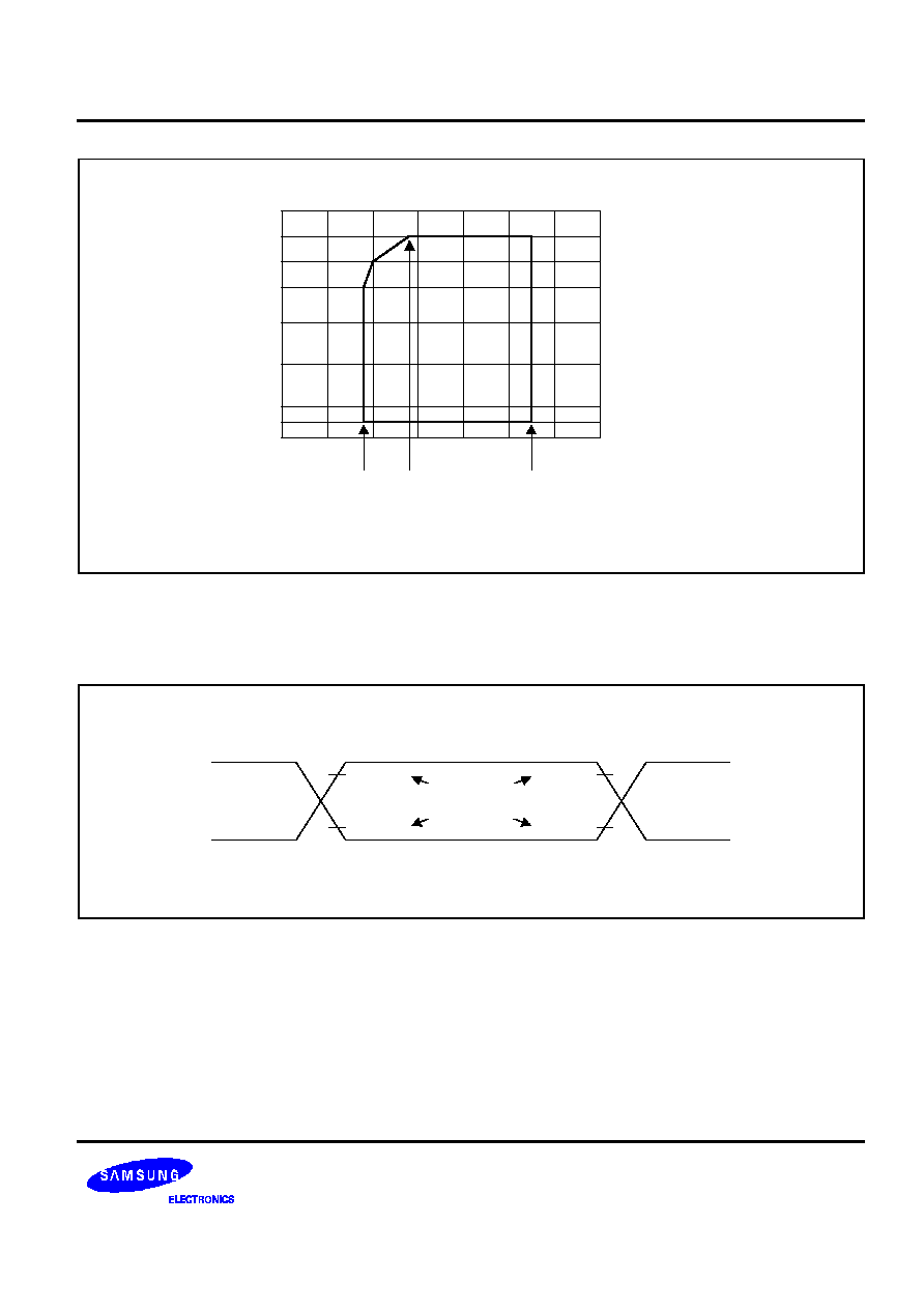
Figure 16-1. Standard Operating Voltage Range
0.8 V
DD
0.2 V
DD
0.8 V
DD
0.2 V
DD
Measurement
Points
Figure 16-2. A.C Timing Measure Pints (Except for X
IN
and XT
IN
)
ELECTRICAL DATA
S3C72H8/P72H8
16-8
Execution of
STOP Instrction
Internal
RESET
Operation
~ ~
V
DDDR
~ ~
Stop Mode
Idle Mode
Operationg Mode
Data Retention Mode
t
SREL
t
WAIT
RESET
V
DD
Figure 16-3. Stop Mode Release Timing When Initiated By
RESET
RESET
Execution of
STOP Instrction
V
DDDR
~ ~
Data Retention Mode
V
DD
Normal
Operating
Mode
~ ~
Stop Mode
Idle Mode
t
SREL
t
WAIT
Power-down Mode Terminating Signal
(Interrupt Request)
Figure 16-4.Stop Release Timing When Initiated By Interrupt Request
X
IN
t
XH
t
XL
1/fx
V
DD
- 0.5 V
0.4 V
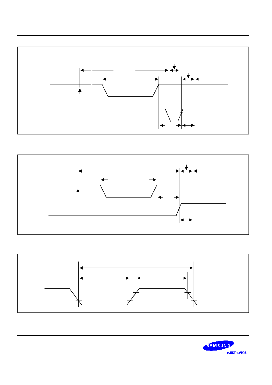
Figure 16-5. Clock Timing Measurement at X
IN

S3C72H8/P72H8
ELECTRICAL DATA
16-9
XT
IN
t
XTH
t
XTL
1/fxt
V
DD
- 0.5 V
0.4 V
Figure 16-6. Clock Timing Measurement at XT
IN
RESET
t
RSL
0.2 V
DD
Figure 16-7. Input Timing for
RESET
RESET
Signal
INT0, 1
KS0 to KS3
t
INTH
t
INTL
0.8 V
DD
0.2 V
DD
Figure 16-8. Input Timing External Interrupt

S3C72H8/P72H8
MECHANICAL DATA
17-1
17
MECHANICAL DATA
OVERVIEW
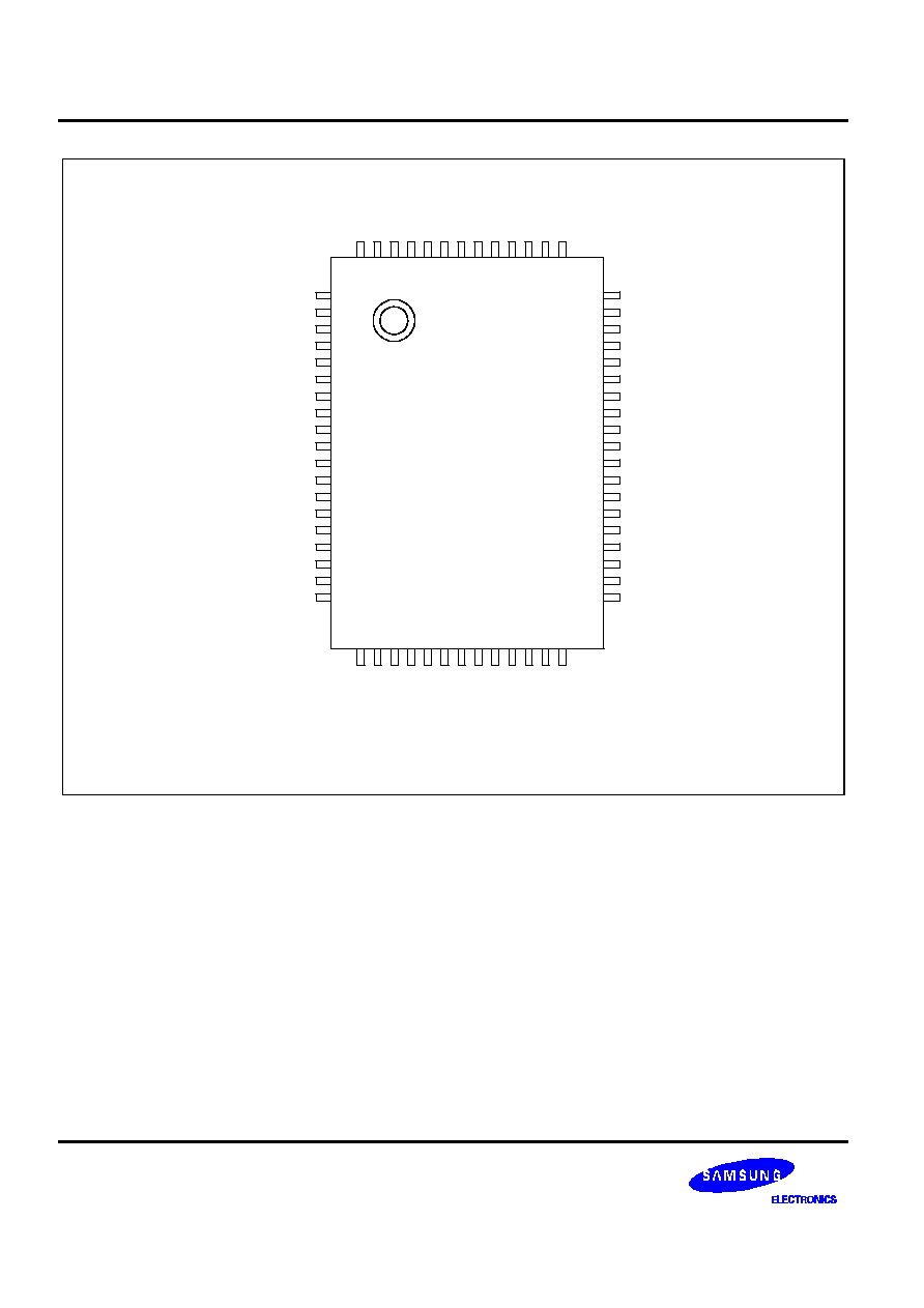
The S3C72H8/P72H8 microcontroller is available in a 64-pin QFP package (Samsung: 64-QFP-1420F)
Package dimensions are shown in Figure 17-1
64-QFP-1420F
#64
#1
NOTE: Dimensions are in millimeters.
20.00
± 0.2
14.00
± 0.2
17.90
± 0.3
23.90
± 0.3
(1.00)
(1.00)
0.80 ± 0.20
0.05-0.25
2.65
± 0.10
3.00 MAX
0.15
+0.10
-0.05
0-8
1.00
0.15 MAX
0.40+0.10
-0.05
0.80
± 0.20
0.10 MAX
Figure 17-1. 64-QFP-1420F Package Dimensions

S3C72H8/P72H8
S3P72H8 OTP
18-1
18
S3P72H8 OTP
OVERVIEW
The S3P72H8 single-chip CMOS microcontroller is the OTP (One Time Programmable)
version of the S3C72H8
microcontroller. It has an on-chip EPROM instead of masked ROM. The EPROM is accessed by a serial data
format.
The S3P72H8 is fully compatible with the S3C72H8, both in function and in pin configuration. Because of its
simple programming requirements, the S3P72H8 is ideal for use as an evaluation chip for the S3C72H8.
S3P72H8 OTP
S3C72H8/P72H8
18-2
CA
CB
V
LC0
V
LC1
V
LC2
P0.0/ExtRef
SDAT/P0.1
SCLK/P0.2
V
DD
/V
DD
V
SS
/V
SS
X
OUT
X
IN
V
PP
/TEST
XT
IN
XT
OUT
RESET
RESET/RESET
P2.0/INT0
P2.1/INT1
P2.2/TCL0
COM0
COM1
COM2
COM3
SEG0
SEG1
SEG2
SEG3
SEG4
SEG5
SEG6
SEG7
SEG8
FCL/P2.3
TCLO0/P3.0
BTCO/P3.1
CLO/P3.2
BUZ/P3.3
KS0/P6.0
KS1/P6.1
KS2/P6.2
KS3/P6.3
C0P/P4.0
C0N/P4.1
C0OUT/P4.2
C1OUT/P4.3
SEG9
SEG10
SEG11
SEG12
SEG13
SEG14
SEG15
SEG16
SEG17
SEG18
SEG19
SEG20
SEG21
SEG22
SEG23
SEG24
SEG25
P5.1/C1N
P5.0/C1P
S3P72H8
(TOP VIEW)
1
2
3
4
5
6
7
8
9
10
11
12
13
14
15
16
17
18
19
51
50
49
48
47
46
45
44
43
42
41
40
39
38
37
36
35
34
33
20
21
22
23
24
25
26
27
28
29
30
31
32
64
63
62
61
60
59
58
57
56
55
54
53
52
Figure 18-1. S3P72H8 Pin Assignments

S3C72H8/P72H8
S3P72H8 OTP
18-3
Table 18-1. Pin Descriptions Used to Read/Write the EPROM
Main Chip
During Programming
Pin Name
Pin Name
Pin No.
I/O
Function
P0.1
SDAT
7
I/O
Serial data pin. Output port when reading and
input port when writing can be assigned as
Input/push-pull output port respectively.
P0.2
SCLK
8
I/O
Serial clock pin. Input only pin.
TEST
V
PP
(TEST)
13
I
Power supply pin for EPROM cell writing
(indicates that OTP enters into the writing
mode). When 12.5 V is applied, OTP is in
writing mode and when 5 V is applied, OTP is in
reading mode. (Option)
RESET
RESET
16
I
Chip initialization
V
DD
/ V
SS
V
DD
/ V
SS
9/10
I
Logic power supply pin. V
DD
should be tied to
+ 5 V during programming.
Table 18-2. Comparison of S3P72H8 and S3C72H8 Features
Characteristic
S3P72H8
S3C72H8
Program Memory
8 K-byte EPROM
8 K-byte mask ROM
Operating Voltage (V
DD
)
1.8 V to 5.5 V
1.8 V to 5.5 V
OTP Programming Mode
V
DD
= 5 V, V
PP
(TEST) = 12.5 V
≠
Pin Configuration
64 QFP
64 QFP
EPROM Programmability
User Program 1 time
Programmed at the factory
OPERATING MODE CHARACTERISTICS
When 12.5 V is supplied to the V
PP
(TEST) pin of the S3P72H8, the EPROM programming mode is entered. The
operating mode (read, write, or read protection) is selected according to the input signals to the pins listed in
Table 18-3 below.
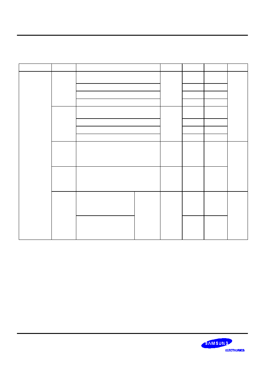
Table 18-3. Operating Mode Selection Criteria
V
DD
V
PP
(TEST)
REG/
MEM
MEM
Address
(A15-A0)
R/
W
W
Mode
5 V
5 V
0
0000H
1
EPROM read
12.5V
0
0000H
0
EPROM program
12.5V
0
0000H
1
EPROM verify
12.5V
1
0E3FH
0
EPROM read protection
NOTE: "0" means low level; "1" means high level.
S3P72H8 OTP
S3C72H8/P72H8
18-4
Table 18-4. D.C. Electrical Characteristics
(T
A
= ≠ 40
∞
C to + 85
∞
C, V
DD
= 1.8 V to 5.5 V)
Parameter
Symbol
Conditions
Min
Typ
Max
Units
Supply
Current
(note)
I
DD1
Main operation mode:
V
DD
= 5 V
±
10%, 6-MHz crystal
≠
3.5
8
mA
V
DD
= 5 V
±
10%, 4.19 MHz
2.5
5.5
V
DD
= 3 V
±
10%, 6-MHz crystal
1.6
4
V
DD
= 3 V
±
10%, 4.19 MHz
1.2
3
I
DD2
Main Idle mode:
V
DD
= 5 V
±
10%, 6-MHz crystal
≠
1.8
3.5
V
DD
= 5 V
±
10%, 4.19 MHz
1.4
3.0
V
DD
= 3 V
±
10%, 6-MHz crystal
0.6
1.2
V
DD
= 3 V
±
10%, 4.19 MHz
0.5
1.1
I
DD3
Sub operation mode:
V
DD
= 3 V, 32768Hz
Main OSC stop, except I
VB
, I
VLD
,
Icomp, I
LCD
and external load.
≠
15
30
uA
I
DD4
Sub Idle mode;
V
DD
= 3.0, 32768Hz
Main OSC stop, except I
VB
, I
VLD
,
Icomp, I
LCD
and external load.
≠
6
15
I
DD5
Stop mode; Main & Sub
OSC stop, V
DD
=5 V ± 10%
except I
VD,
I
VLD,
Icomp and
external load.
SCMOD =
0100B
XT
IN
= 0V-
≠
0.3
3
uA
Stop & Sub OSC stop,
V
DD
= 3 V, except I
VD,
I
VLD,
Lcomp and external
load.
0.1
1
NOTE: Supply current does not include current drawn through internal pull-up resistors or external output current loads.
I
LCD
is LCD controller/driver operating current, I
VB
is voltage booster current, Icomp is comparator current, and
I
VLD
is voltage level detector current.

S3C72H8/P72H8
S3P72H8 OTP
18-5
1.5 MHz
CPU Clock
1.05 MHz
750 kHz
15.625 kHz
Main OSC Frequency
4.19 MHz
3 MHz
6 MHz
1
2
3
4
5
6
7
Supply Voltage (V)
CPU clock = 1/n x oscillator frequency (n = 4, 8, 64)
1.8 V
2.7 V
5.5 V
Figure 18-2. Standard Operating Voltage Range

S3P72H8 OTP
S3C72H8/P72H8
18-6
START
Address= First Location
V
DD
=5V, V
PP
=12.5V
x = 0
Program One 1ms Pulse
Increment X
x = 10
Verify 1 Byte
Last Address
V
DD
= V
PP
= 5 V
Compare All Byte
Device Passed
Increment Address
Verify Byte
Device Failed
PASS
FAIL
NO
FAIL
YES
FAIL
NO
Figure 18-3. OTP Programming Algorithm