 | –≠–ª–µ–∫—Ç—Ä–æ–Ω–Ω—ã–π –∫–æ–º–ø–æ–Ω–µ–Ω—Ç: S3C80C5 | –°–∫–∞—á–∞—Ç—å:  PDF PDF  ZIP ZIP |
Document Outline
- ˛ˇ
- ˛ˇ
- ˛ˇ
- ˛ˇ
- ˛ˇ
- ˛ˇ
- ˛ˇ
- ˛ˇ
- ˛ˇ
- ˛ˇ
- ˛ˇ
- ˛ˇ
- ˛ˇ
- ˛ˇ
- ˛ˇ
- ˛ˇ

21-S3-P80C5/C80C5/C80C8 -052002
USER'S MANUAL
S3P80C5/C80C5/C80C8
8-Bit CMOS
Microcontrollers
Revision 1

S3P80C5/C80C5/C80C8
8-BIT CMOS
MICROCONTROLLERS
USER'S MANUAL
Revision 1

Important Notice
The information in this publication has been
carefully checked and is believed to be entirely
accurate at the time of publication. Samsung
assumes no responsibility, however, for possible
errors or omissions, or for any consequences
resulting from the use of the information contained
herein.
Samsung reserves the right to make changes in its
products or product specifications with the intent to
improve function or design at any time and without
notice and is not required to update this
documentation to reflect such changes.
This publication does not convey to a purchaser of
semiconductor devices described herein any license
under the patent rights of Samsung or others.
Samsung makes no warranty, representation, or
guarantee regarding the suitability of its products for
any particular purpose, nor does Samsung assume
any liability arising out of the application or use of
any product or circuit and specifically disclaims any
and all liability, including without limitation any
consequential or incidental damages.
"Typical" parameters can and do vary in different
applications. All operating parameters, including
"Typicals" must be validated for each customer
application by the customer's technical experts.
Samsung products are not designed, intended, or
authorized for use as components in systems
intended for surgical implant into the body, for other
applications intended to support or sustain life, or for
any other application in which the failure of the
Samsung product could create a situation where
personal injury or death may occur.
Should the Buyer purchase or use a Samsung
product for any such unintended or unauthorized
application, the Buyer shall indemnify and hold
Samsung and its officers, employees, subsidiaries,
affiliates, and distributors harmless against all
claims, costs, damages, expenses, and reasonable
attorney fees arising out of, either directly or
indirectly, any claim of personal injury or death that
may be associated with such unintended or
unauthorized use, even if such claim alleges that
Samsung was negligent regarding the design or
manufacture of said product.
S3P80C5/C80C5/C80C8 8-Bit CMOS Microcontrollers
User's Manual, Revision 1
Publication Number: 21-S3- P80C5/C80C5/C80C8-052002
© 2002 Samsung Electronics
All rights reserved. No part of this publication may be reproduced, stored in a retrieval system, or transmitted in
any form or by any means, electric or mechanical, by photocopying, recording, or otherwise, without the prior
written consent of Samsung Electronics.
Samsung Electronics' microcontroller business has been awarded full ISO-14001
certification (BSI Certificate No. FM24653). All semiconductor products are
designed and manufactured in accordance with the highest quality standards and
objectives.
Samsung Electronics Co., Ltd.
San #24 Nongseo-Ri, Giheung-Eup
Yongin-City, Gyeonggi-Do, Korea
C.P.O. Box #37, Suwon 440-900
TEL:
(82)-(31)-209-1934
FAX:
(82)-(31)-209-1899
Home Page: http://www.samsungsemi.com
Printed in the Republic of Korea

S3P80C5/C80C5/C80C8
MICROCONTROLLER
iii
Preface
The S3C80C5/C80C8 Microcontroller User's Manual is designed for application designers and programmers who
are using the S3C80C5/C80C8 microcontroller for application development.
It is organized in two main parts:
Part I Programming Model
Part II Hardware Descriptions
Part I contains software-related information to familiarize you with the microcontroller's architecture,
programming model, instruction set, and interrupt structure. It has six chapters:
Chapter 1
Product Overview
Chapter 2
Address Spaces
Chapter 3
Addressing Modes
Chapter 4
Control Registers
Chapter 5
Interrupt Structure
Chapter 6
Instruction Set
Chapter 1, "Product Overview," is a high-level introduction to S3C80C5/C80C8 with general product descriptions,
as well as detailed information about individual pin characteristics and pin circuit types.
Chapter 2, "Address Spaces," describes program and data memory spaces, the internal register file, and register
addressing. Chapter 2 also describes working register addressing, as well as system stack and user-defined stack
operations.
Chapter 3, "Addressing Modes," contains detailed descriptions of the addressing modes that are supported by the
KS88-series CPU.
Chapter 4, "Control Registers," contains overview tables for all mapped system and peripheral control register
values, as well as detailed one-page descriptions in a standardized format. You can use these easy-to-read,
alphabetically organized, register descriptions as a quick-reference source when writing programs.
Chapter 5, "Interrupt Structure," describes the S3C80C5/C80C8 interrupt structure in detail and further prepares
you for additional information presented in the individual hardware module descriptions in Part II.
Chapter 6, "Instruction Set," describes the features and conventions of the instruction set used for all S3C8-series
microcontrollers. Several summary tables are presented for orientation and reference. Detailed descriptions of
each instruction are presented in a standard format. Each instruction description includes one or more practical
examples of how to use the instruction when writing an application program.
A basic familiarity with the information in Part I will help you to understand the hardware module descriptions in
Part II. If you are not yet familiar with the S3C8-series microcontroller family and are reading this manual for the
first time, we recommend that you first read Chapters 1≠3 carefully. Then, briefly look over the detailed
information in Chapters 4, 5, and 6. Later, you can reference the information in Part I as necessary.
Part II "hardware Descriptions," has detailed information about specific hardware components of the
S3C80C5/C80C8 microcontroller. Also included in Part II are electrical, mechanical, OTP, and development tools
data. It has eight chapters:
Chapter 7
Clock Circuit
Chapter 8
RESET
and Power-Down
Chapter 9
I/O Ports
Chapter 10
Basic Timer and Timer 0
Chapter 11
Timer 1
Chapter 12
Counter A
Chapter 13
Electrical Data
Chapter 14
Mechanical Data
Two order forms are included at the back of this manual to facilitate customer order for S3C80C5/C80C8
microcontrollers: the Mask ROM Order Form, and the Mask Option Selection Form. You can photocopy these
forms, fill them out, and then forward them to your local Samsung Sales Representative.


S3P80C5/C80C5/C80C8
MICROCONTROLLER
v
Table of Contents
Part I -- Programming Model
Chapter 1
Product Overview
Overview .................................................................................................................................................1-1
S3P80C5/C80C5/C80C8 Microcontroller .................................................................................................1-1
Features ..................................................................................................................................................1-2
CPU ........................................................................................................................................................1-2
Block Diagram .........................................................................................................................................1-3
Pin Assignments......................................................................................................................................1-4
Pin Descriptions.......................................................................................................................................1-5
Pin Circuits ..............................................................................................................................................1-6
Chapter 2
Address Spaces
Overview .................................................................................................................................................2-1
Program Memory (ROM) .........................................................................................................................2-2
Register Architecture ...............................................................................................................................2-3
Register Page Pointer (PP) .............................................................................................................2-5
Register Set 1 .................................................................................................................................2-6
Register Set 2 .................................................................................................................................2-6
Prime Register Space .....................................................................................................................2-7
Working Registers ...........................................................................................................................2-8
Using The Register Pointers ............................................................................................................2-9
Register Addressing.................................................................................................................................2-11
Common Working Register Area (C0H≠CFH)..................................................................................2-13
4-Bit Working Register Addressing ..................................................................................................2-14
8-Bit Working Register Addressing ..................................................................................................2-16
System and User Stacks..........................................................................................................................2-18
Chapter 3
Addressing Modes
Overview .................................................................................................................................................3-1
Register Addressing Mode (R).........................................................................................................3-2
Indirect Register Addressing Mode (IR) ...........................................................................................3-3
Indexed Addressing Mode (X)..........................................................................................................3-7
Direct Address Mode (DA)...............................................................................................................3-10
Indirect Address Mode (IA) ..............................................................................................................3-12
Relative Address Mode (RA) ...........................................................................................................3-13
Immediate Mode (IM) ......................................................................................................................3-14

vi
S3P80C5/C80C5/C80C8
MICROCONTROLLER
Table of Contents
(Continued
Chapter
Control Registers
................................
................................
.................
Chapter 5
Overview ................................
................................................................
5-1
Interrupt Types
................................................................
5-2
Interrupt Structure
................................................................
5-3
Interrupt Vector Addresses
................................................................
5-5
Enable/Disable Interrupt Instructions (EI, DI)
...................................................
System-Level Interrupt Control Registers ................................
........................5-7
................................................................
..5-8
................................................................
5-9
System Mode Register (SYM)
................................................................
5-10
Interrupt Mask Register (IMR)
................................................................
5-11
Interrupt Priority Register (IPR)
................................................................
5-12
Interrupt Request Register (IRQ)
................................................................
5-14
Interrupt Pending Function Types
................................................................
5-15
Interrupt Source Polling Sequence
................................................................ 5-16
Interrupt Service Routines
................................................................
5-16
Generating Interrupt Vector Addresses
............................................................
Nesting of Vectored Interrupts ................................
.........................................
Instruction Pointer (IP)................................
.....................................................
7
Fast Interrupt Processing
................................................................
5-17
Chapter
Instruction Set
Overview
................................................................
.................6-1
................................................................
......................................
Register Addressing ................................
........................................................
Addressing Modes ................................
...........................................................
Flags Register (FLAGS) ................................
..................................................
Flag Descriptions................................
.............................................................
Instruction Set Notation ................................
...................................................
Condition Codes ................................
..............................................................
Instruction Descriptions ................................
...................................................

S3P80C5/C80C5/C80C8
MICROCONTROLLER
vii
Table of Contents
(Continued)
Part II Hardware Descriptions
Chapter 7
Clock Circuit
Overview .................................................................................................................................................7-1
System Clock Circuit .......................................................................................................................7-1
Clock Status During Power-Down Modes.........................................................................................7-2
System Clock Control Register (CLKCON) ......................................................................................7-3
Chapter 8
RESET
RESET
and Power-Down
System Reset ..........................................................................................................................................8-1
LVD Reset.......................................................................................................................................8-1
Interrupt with Reset (INTR)..............................................................................................................8-2
Watch-Dog Timer Reset..................................................................................................................8-2
Power-on Reset (POR)....................................................................................................................8-2
System Reset Operation .................................................................................................................8-3
Hardware Reset Values ...................................................................................................................8-4
Power-Down Modes.................................................................................................................................8-6
Stop mode.......................................................................................................................................8-6
Using POR to Release Stop Mode...................................................................................................8-6
Using an INTR to Release Stop Mode .............................................................................................8-6
Idle Mode ........................................................................................................................................8-9
Summary Table of Stop Mode, and Idle Mode.................................................................................8-10
Chapter 9
I/O Ports
Overview .................................................................................................................................................9-1
Port Data Registers .........................................................................................................................9-2
Pull-Up Resistor Enable Registers...................................................................................................9-2
Port 0 ..............................................................................................................................................9-4
Port 0 Interrupt Enable Register (P0INT) .........................................................................................9-5
Port 0 Interrupt Pending Register (P0PND)......................................................................................9-5
Port 1 ..............................................................................................................................................9-7
Port 2 ..............................................................................................................................................9-9
Chapter 10
Basic Timer and Timer 0
Module Overview.....................................................................................................................................10-1
Basic Timer Control Register (BTCON) ...............................................................................................10-1
Basic Timer Function Description ........................................................................................................10-3
Timer 0 Control Register (T0CON) ......................................................................................................10-3
Timer 0 Function Description...............................................................................................................10-5

viii
S3P80C5/C80C5/C80C8
MICROCONTROLLER
Table of Contents
(Concluded)
Chapter 11
Timer 1
Overview .................................................................................................................................................11-1
Timer 1 Overflow Interrupt...............................................................................................................11-2
Timer 1 Match Interrupt ...................................................................................................................11-2
Timer 1 Control Register (T1CON) ..................................................................................................11-4
Chapter 12
Counter A
Overview .................................................................................................................................................12-1
Counter A Control Register (CACON)..............................................................................................12-3
Counter A Pulse Width Calculations ................................................................................................12-4
Chapter 13
Electrical Data
Overview .................................................................................................................................................13-1
Chapter 14
Mechanical Data
Overview .................................................................................................................................................14-1

S3P80C5/C80C5/C80C8
MICROCONTROLLER
ix
List of Figures
Figure
Title
Page
Number
Number
1-1
Block Diagram........................................................................................................1-3
1-2
Pin Assignment Diagram (24-Pin SOP/SDIP Package) ..........................................1-4
1-3
Pin Circuit Type 1 (Port 0) ......................................................................................1-6
1-4
Pin Circuit Type 2 (Port 1) ......................................................................................1-7
1-5
Pin Circuit Type 3 (P2.0) ........................................................................................1-8
1-6
Pin Circuit Type 4 (P2.1) ........................................................................................1-9
1-7
Pin Circuit Type 5 (P2.2) ........................................................................................1-10
2-1
Program Memory Address Space ...........................................................................2-2
2-2
Internal Register File Organization .........................................................................2-4
2-3
Register Page Pointer (PP) ....................................................................................2-5
2-4
Set 1, Set 2, and Prime Area Register Map ............................................................2-7
2-5
8-Byte Working Register Areas (Slices)..................................................................2-8
2-6
Contiguous 16-Byte Working Register Block ..........................................................2-9
2-7
Non-Contiguous 16-Byte Working Register Block ...................................................2-10
2-8
16-Bit Register Pair ................................................................................................2-11
2-9
Register File Addressing.........................................................................................2-12
2-10
Common Working Register Area ............................................................................2-13
2-11
4-Bit Working Register Addressing .........................................................................2-15
2-12
4-Bit Working Register Addressing Example ..........................................................2-15
2-13
8-Bit Working Register Addressing .........................................................................2-16
2-14
8-Bit Working Register Addressing Example ..........................................................2-17
2-15
Stack Operations....................................................................................................2-18
3-1
Register Addressing ...............................................................................................3-2
3-2
Working Register Addressing .................................................................................3-2
3-3
Indirect Register Addressing to Register File ..........................................................3-3
3-4
Indirect Register Addressing to Program Memory...................................................3-4
3-5
Indirect Working Register Addressing to Register File ............................................3-5
3-6
Indirect Working Register Addressing to Program or Data Memory ........................3-6
3-7
Indexed Addressing to Register File .......................................................................3-7
3-8
Indexed Addressing to Program or Data Memory with Short Offset ........................3-8
3-9
Indexed Addressing to Program or Data Memory ...................................................3-9
3-10
Direct Addressing for Load Instructions ..................................................................3-10
3-11
Direct Addressing for Call and Jump Instructions....................................................3-11
3-12
Indirect Addressing.................................................................................................3-12
3-13
Relative Addressing ...............................................................................................3-13
3-14
Immediate Addressing............................................................................................3-14
4-1
Register Description Format ...................................................................................4-4

x
S3P80C5/C80C5/C80C8
MICROCONTROLLER
List of Figures
(Continued)
Figure
Title
Page
Number
Number
5-1
KS88-Series Interrupt Types...................................................................................5-2
5-3
ROM Vector Address Area .....................................................................................5-5
5-2
Interrupt Structure ..................................................................................................5-4
5-4
Interrupt Function Diagram .....................................................................................5-8
5-5
System Mode Register (SYM) ................................................................................5-10
5-6
Interrupt Mask Register (IMR).................................................................................5-11
5-7
Interrupt Request Priority Groups ...........................................................................5-12
5-8
Interrupt Priority Register (IPR)...............................................................................5-13
5-9
Interrupt Request Register (IRQ) ............................................................................5-14
6-1
System Flags Register (FLAGS).............................................................................6-6
7-1
Main Oscillator Circuit (External Crystal or Ceramic Resonator) .............................7-1
7-2
External Clock Circuit .............................................................................................7-1
7-3
System Clock Circuit Diagram ................................................................................7-2
7-4
System Clock Control Register (CLKCON) .............................................................7-3
8-1
Reset Block Diagram..............................................................................................8-1
8-2
Power-on Reset Circuit...........................................................................................8-2
8-3
Timing Diagram for Power-on Reset Circuit............................................................8-3
9-1
S3P80C5/C80C5/C80C8 I/O Port 0 Data Register Format......................................9-2
9-2
S3P80C5/C80C5/C80C8 I/O Port 1 Data Register Format......................................9-3
9-3
Port 0 High-Byte Control Register (P0CONH) .........................................................9-4
9-4
Port 0 Low-Byte Control Register (P0CONL) ..........................................................9-5
9-5
Port 0 External Interrupt Control Register (P0INT) ..................................................9-6
9-6
Port 0 External Interrupt Pending Register (P0PND)...............................................9-7
9-7
Port 1 High-Byte Control Register (P1CONH) .........................................................9-7
9-8
Port 1 Low-Byte Control Register (P1CONL) ..........................................................9-8
9-9
Port 2 Control Register (P2CON)............................................................................9-9
9-10
Port 2 Data Register (P2) .......................................................................................9-10

S3P80C5/C80C5/C80C8
MICROCONTROLLER
xi
List of Figures
(Concluded)
Figure
Title
Page
Number
Number
10-1
Basic Timer Control Register (BTCON) ..................................................................10-2
10-2
Timer 0 Control Register (T0CON) .........................................................................10-4
10-3
Simplified Timer 0 Function Diagram: Interval Timer Mode ....................................10-5
10-4
Simplified Timer 0 Function Diagram: PWM Mode .................................................10-6
11-1
Simplified Timer 1 Function Diagram: Interval Timer Mode ....................................11-2
11-2
Timer 1 Block Diagram...........................................................................................11-3
11-3
Timer 1 Control Register (T1CON) .........................................................................11-4
11-4
Timer 1 Registers ...................................................................................................11-5
12-1
Counter A Block Diagram .......................................................................................12-2
12-2
Counter A Control Register (CACON).....................................................................12-3
12-3
Counter A Registers ...............................................................................................12-4
12-4
Counter A Output Flip-Flop Waveforms in Repeat Mode........................................12-5
13-1
Input Timing for External Interrupts (Port 0)............................................................13-5
13-2
Operating Voltage Range ......................................................................................13-6
14-1
24-Pin SOP Package Mechanical Data ..................................................................14-1
14-2
24-Pin SDIP Package Mechanical Data..................................................................14-2


S3P80C5/C80C5/C80C8
MICROCONTROLLER
xiii
List of Tables
Table
Title
Page
Number
Number
1-1
Pin Descriptions .....................................................................................................1-5
2-1
Register Type Summary.........................................................................................2-3
4-1
Mapped Registers (Set1)........................................................................................4-2
5-1
Interrupt Vectors.....................................................................................................5-6
5-2
Interrupt Control Register Overview .......................................................................5-7
5-3
Interrupt Source Control and Data Registers...........................................................5-9
6-1
Instruction Group Summary....................................................................................6-2
6-2
Flag Notation Conventions .....................................................................................6-8
6-3
Instruction Set Symbols..........................................................................................6-8
6-4
Instruction Notation Conventions ............................................................................6-9
6-5
Opcode Quick Reference .......................................................................................6-10
6-6
Condition Codes.....................................................................................................6-12
8-1
Set 1 Register Values After Reset ..........................................................................8-4
8-2
Summary of Each Mode.........................................................................................8-10
9-1
S3P80C5/C80C5/C80C8 Port Configuration Overview ...........................................9-1
9-2
Port Data Register Summary..................................................................................9-2
13-1
Absolute Maximum Ratings....................................................................................13-2
13-2
D.C. Electrical Characteristics ................................................................................13-2
13-3
Characteristics of Low Voltage Detect circuit ..........................................................13-4
13-4
Data Retention Supply Voltage in Stop Mode .........................................................13-4
13-5
Input/Output Capacitance .......................................................................................13-4
13-6
A.C. Electrical Characteristics ................................................................................13-4
13-7
Oscillation Characteristics ......................................................................................13-5
13-8
Oscillation Stabilization Time .................................................................................13-6


S3P80C5/C80C5/C80C8
MICROCONTROLLER
xv
List of Programming Tips
Description
Page
Number
Chapter 2:
Address Spaces
Setting the Register Pointers ...............................................................................................................2-9
Using the RPs to Calculate the Sum of a Series of Registers...............................................................2-10
Addressing the Common Working Register Area .................................................................................2-14
Standard Stack Operations Using PUSH and POP ..............................................................................2-19
Chapter 8:
RESET
RESET
and Power-Down
To Divide STOP Mode Releasing and POR.........................................................................................8-8
Chapter 10:
Basic Timer and Timer 0
Configuring the Basic Timer ................................................................................................................10-8
Programming Timer 0..........................................................................................................................10-9
Chapter 12:
Counter A
To Generate 38 kHz, 1/3duty Signal Through P2.1 ..............................................................................12-6
To Generate a One Pulse Signal Through P2.1 ...................................................................................12-7


S3P80C5/C80C5/C80C8
MICROCONTROLLER
xvii
List of Register Descriptions
Register
Full Register Name
Page
Identifier
Number
BTCON
Basic Timer Control Register..................................................................................4-5
CACON
Counter A Control Register.....................................................................................4-6
CLKCON
System Clock Control Register ...............................................................................4-7
EMT
External Memory Timing Register ..........................................................................4-8
FLAGS
System Flags Register ...........................................................................................4-9
IMR
Interrupt Mask Register ..........................................................................................4-10
IPH
Instruction Pointer (High Byte) ...............................................................................4-11
IPL
Instruction Pointer (Low Byte) ................................................................................4-11
IPR
Interrupt Priority Register........................................................................................4-12
IRQ
Interrupt Request Register......................................................................................4-13
P0CONH
Port 0 Control Register (High Byte) ........................................................................4-14
P0CONL
Port 0 Control Register (Low Byte) .........................................................................4-15
P0INT
Port 0 Interrupt Control Register .............................................................................4-16
P0PND
Port 0 Interrupt Pending Register ...........................................................................4-17
P0PUR
Port 0 Pull-up Resistor Enable Register..................................................................4-18
P1CONH
Port 1 Control Register (High Byte) ........................................................................4-19
P1CONL
Port 1 Control Register (Low Byte) .........................................................................4-20
P1PUR
Port 1 Pull-up Resistor Enable Register .................................................................4-21
P2CON
Port 2 Control Register ...........................................................................................4-22
PP
Register Page Pointer ............................................................................................4-23
RP0
Register Pointer 0...................................................................................................4-24
RP1
Register Pointer 1...................................................................................................4-24
SPL
Stack Pointer (Low Byte) ........................................................................................4-25
STOPCON
Stop Control Register .............................................................................................4-25
SYM
System Mode Register ...........................................................................................4-26
T0CON
Timer 0 Control Register ........................................................................................4-27
T1CON
Timer 1 Control Register ........................................................................................4-28


S3P80C5/C80C5/C80C8
MICROCONTROLLER
xix
List of Instruction Descriptions
Instruction
Full Register Name
Page
Mnemonic
Number
ADC
Add with Carry........................................................................................................6-14
ADD
Add ........................................................................................................................6-15
AND
Logical AND ...........................................................................................................6-16
BAND
Bit AND ..................................................................................................................6-17
BCP
Bit Compare ...........................................................................................................6-18
BITC
Bit Complement .....................................................................................................6-19
BITR
Bit Reset ................................................................................................................6-20
BITS
Bit Set ....................................................................................................................6-21
BOR
Bit OR ....................................................................................................................6-22
BTJRF
Bit Test, Jump Relative on False............................................................................6-23
BTJRT
Bit Test, Jump Relative on True .............................................................................6-24
BXOR
Bit XOR..................................................................................................................6-25
CALL
Call Procedure .......................................................................................................6-26
CCF
Complement Carry Flag .........................................................................................6-27
CLR
Clear ......................................................................................................................6-28
COM
Complement...........................................................................................................6-29
CP
Compare ................................................................................................................6-30
CPIJE
Compare, Increment, and Jump on Equal ..............................................................6-31
CPIJNE
Compare, Increment, and Jump on Non-Equal .......................................................6-32
DA
Decimal Adjust .......................................................................................................6-33
DEC
Decrement .............................................................................................................6-35
DECW
Decrement Word ....................................................................................................6-36
DI
Disable Interrupts ...................................................................................................6-37
DIV
Divide (Unsigned)...................................................................................................6-38
DJNZ
Decrement and Jump if Non-Zero ..........................................................................6-39
EI
Enable Interrupts ....................................................................................................6-40
ENTER
Enter ......................................................................................................................6-41
EXIT
Exit ........................................................................................................................6-42
IDLE
Idle Operation ........................................................................................................6-43
INC
Increment ...............................................................................................................6-44
INCW
Increment Word .....................................................................................................6-45
IRET
Interrupt Return ......................................................................................................6-46
JP
Jump ......................................................................................................................6-47
JR
Jump Relative ........................................................................................................6-48
LD
Load.......................................................................................................................6-49
LDB
Load Bit..................................................................................................................6-51

xx
S3P80C5/C80C5/C80C8
MICROCONTROLLER
List of Instruction Descriptions
(Continued)
Instruction
Full Register Name
Page
Mnemonic
Number
LDC/LDE
Load Memory .........................................................................................................6-52
LDCD/LDED
Load Memory and Decrement ................................................................................6-54
LDCI/LDEI
Load Memory and Increment ..................................................................................6-55
LDCPD/LDEPD
Load Memory with Pre-Decrement .........................................................................6-56
LDCPI/LDEPI
Load Memory with Pre-Increment ...........................................................................6-57
LDW
Load Word .............................................................................................................6-58
MULT
Multiply (Unsigned).................................................................................................6-59
NEXT
Next .......................................................................................................................6-60
NOP
No Operation ..........................................................................................................6-61
OR
Logical OR .............................................................................................................6-62
POP
Pop from Stack.......................................................................................................6-63
POPUD
Pop User Stack (Decrementing) .............................................................................6-64
POPUI
Pop User Stack (Incrementing) ...............................................................................6-65
PUSH
Push to Stack .........................................................................................................6-66
PUSHUD
Push User Stack (Decrementing)............................................................................6-67
PUSHUI
Push User Stack (Incrementing) .............................................................................6-68
RCF
Reset Carry Flag ....................................................................................................6-69
RET
Return ....................................................................................................................6-70
RL
Rotate Left .............................................................................................................6-71
RLC
Rotate Left through Carry .......................................................................................6-72
RR
Rotate Right ...........................................................................................................6-73
RRC
Rotate Right through Carry .....................................................................................6-74
SB0
Select Bank 0 .........................................................................................................6-75
SB1
Select Bank 1 .........................................................................................................6-76
SBC
Subtract with Carry .................................................................................................6-77
SCF
Set Carry Flag ........................................................................................................6-78
SRA
Shift Right Arithmetic..............................................................................................6-79
SRP/SRP0/SRP1
Set Register Pointer ...............................................................................................6-80
STOP
Stop Operation .......................................................................................................6-81
SUB
Subtract..................................................................................................................6-82
SWAP
Swap Nibbles .........................................................................................................6-83
TCM
Test Complement under Mask ................................................................................6-84
TM
Test under Mask.....................................................................................................6-85
WFI
Wait for Interrupt ....................................................................................................6-86
XOR
Logical Exclusive OR .............................................................................................6-87

S3P80C5/C80C5/C80C8
PRODUCT OVERVIEW
1-1
1
PRODUCT OVERVIEW
OVERVIEW
Samsung's S3C8-series of 8-bit single-chip CMOS microcontrollers offers a fast and efficient CPU, a wide range
of integrated peripherals, and various mask-programmable ROM sizes. Important CPU features include:
-- Efficient register-oriented architecture
-- Selectable CPU clock sources
-- Idle and Stop power-down mode release by interrupt
-- Built-in basic timer with watchdog function
A sophisticated interrupt structure recognizes up to eight interrupt levels. Each level can have one or more
interrupt sources and vectors. Fast interrupt processing (within a minimum six CPU clocks) can be assigned to
specific interrupt levels.
S3P80C5/C80C5/C80C8 MICROCONTROLLER
The S3P80C5/C80C5/C80C8 single-chip CMOS microcontroller is fabricated using a highly advanced CMOS
process and is based on Samsung's newest CPU architecture.
The S3C80C5/C80C8 is the microcontroller which has mask-programmable ROM.
The S3P80C5 is the microcontroller which has one-time-programmable EPROM.
Using a proven modular design approach, Samsung engineers developed the S3P80C5/C80C5/C80C8 by
integrating the following peripheral modules with the powerful SAM87 RC core:
-- Three programmable I/O ports, including two 8-bit ports and one 3-bit port, for a total of 19 pins.
-- Internal LVD circuit and eight bit-programmable pins for external interrupts.
-- One 8-bit basic timer for oscillation stabilization and watchdog functions (system reset).
-- One 8-bit timer/counter and one 16-bit timer/counter with selectable operating modes.
-- One 8-bit counter with auto-reload function and one-shot or repeat control.
The S3P80C5/C80C5/C80C8 is a versatile general-purpose microcontroller which is especially suitable for use
as remote transmitter controller. It is currently available in a 24-pin SOP and SDIP package.

PRODUCT OVERVIEW
S3P80C5/C80C5/C80C8
1-2
FEATURES
CPU
∑
SAM87RC CPU core
Memory
∑
Program memory (ROM)
≠ S3C80C8: 8-Kbyte
(0000H≠1FFFH)
≠ S3C80C5: 15,872 byte
(0000H≠3E00H)
∑
Data memory: 256-byte RAM
Instruction Set
∑
78 instructions
∑
IDLE and STOP instructions added for power-
down modes
Instruction Execution Time
∑
1000 ns at 4-MHz f
OSC
(minimum)
Interrupts
∑
13 interrupt sources with 10 vector.
∑
5 level, 10 vector interrupt structure
I/O Ports
∑
Two 8-bit I/O ports (P0-P1) and one 3-bit port
(P2) for a total of 19 bit-programmable pins
∑
Eight input pins for external interrupts
Carrier Frequency Generator
∑
One 8-bit counter with auto-reload function and
one-shot or repeat control (Counter A)
Back-up mode
∑
When V
DD
is lower than V
LVD
, the chip enters
Back-up mode to block oscillation and reduce the
current consumption.
Timers and Timer/Counters
∑
One programmable 8-bit basic timer (BT) for
oscillation stabilization control or watchdog timer
function
∑
One 8-bit timer/counter (Timer 0) with two
operating modes; Interval mode and PWM mode.
∑
One 16-bit timer/counter with one operating
modes; Interval mode
Low Voltage Detect Circuit
∑
Low voltage detect for reset or Back-up mode.
∑
Low level detect voltage
≠ S3C80C5/C80C8:
1.90 V (Typ)
±
200 mV
Auto Reset Function
∑
Reset occurs when stop mode is released by P0.
∑
When a falling edge is detected at Port 0 during
Stop mode, system reset occurs.
Operating Temperature Range
∑ ≠40
∞
C to + 85
∞
C
Operating Voltage Range
∑
1.7 V to 3.6 V at 4 MHz f
OSC
Package Type
∑
24-pin SOP/SDIP
S3P80C5/C80C5/C80C8
PRODUCT OVERVIEW
1-3
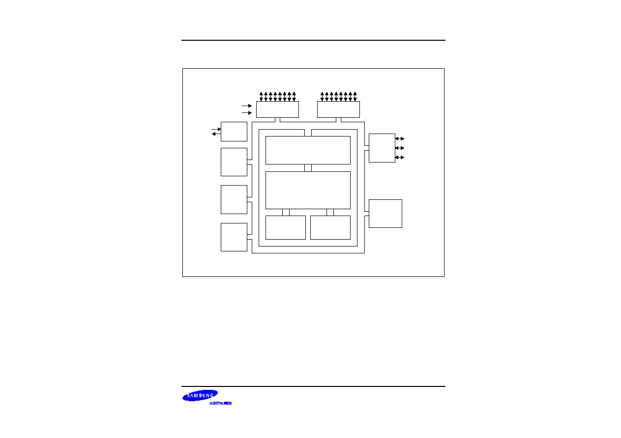
BLOCK DIAGRAM
8-bit
Basic
Timer
P0.0-P0.7/INT0-INT4
P1.0-P1.7
Port I/O and Interrupt
Control
SAM87RI CPU
Internal Bus
X
IN
X
OUT
Port 0(INTR)
Port 1
Main
OSC
P2.0/T0PWM
15-Kbyte ROM
256-Byte
Register File
8-bit
Timer/
Counter
16-bit
Timer/
Counter
Port 2
Carrier
Generator
(Counter A)
P2.1/REM
P2.2
LVD
TEST
Figure 1-1. Block Diagram

PRODUCT OVERVIEW
S3P80C5/C80C5/C80C8
1-4
PIN ASSIGNMENTS
V
SS
X
IN
X
OUT
TEST
P0.0/INT0/INTR
P0.1/INT1/INTR
RESET
RESET
/P0.2/INT2/INTR
P0.3/INT3/INTR
P0.4/INT4/INTR
P0.5/INT4/INTR
P0.6/INT4/INTR
P0.7/INT4/INTR
S3C80C5/C80C8
24-SOP/SDIP
(TOP VIEW)
1
2
3
4
5
6
7
8
9
10
11
12
V
DD
P2.2
P2.1/REM/SCLK
P2.0/T0PWN/T0CK/SDAT
P1.7
P1.6
P1.5
P1.4
P1.3
P1.2
P1.1
P1.0
24
23
22
21
20
19
18
17
16
15
14
13
Figure 1-2. Pin Assignment Diagram (24-Pin SOP/SDIP Package)
S3P80C5/C80C5/C80C8
PRODUCT OVERVIEW
1-5
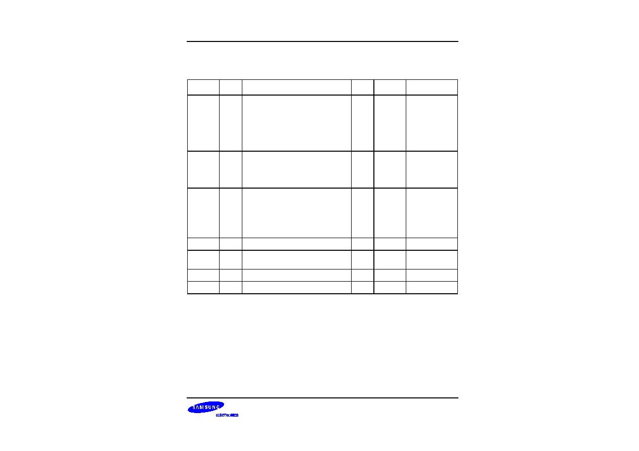
PIN DESCRIPTIONS
Table 1-1. Pin Descriptions
Pin
Names
Pin
Type
Pin
Description
Circuit
Type
24-Pin
Number
Shared
Functions
P0.0≠P0.7
I/O
I/O port with bit-programmable pins.
Configurable to input or push-pull output
mode. Pull-up resistors are assignable by
software. Pins can be assigned individually
as external interrupt inputs with noise filters,
interrupt enable/ disable, and interrupt
pending control. Interrupt with Reset(INTR)
is assigned to Port 0.
1
5≠12
INT0 ≠ INT4/INTR
P1.0≠P1.7
I/O
I/O port with bit-programmable pins.
Configurable to input mode or output mode.
Pin circuits are either push-pull or n-
channel open-drain type. Pull-up resistors
are assignable by software.
2
13≠20
P2.0
P2.1
P2.2
I/O
3-bit I/O port with bit-programmable pins.
Configurable to input mode, push-pull
output mode, or n-channel open-drain
output mode. Input mode with pull-up
resistors are assignable by software. The
two pins of port 2 have high current drive
capability.
3
4
5
21≠23
REM/T0CK
X
IN
, X
OUT
≠
System clock input and output pins
≠
2, 3
≠
TEST
I
Test signal input pin (for factory use only;
must be connected to V
SS
).
≠
4
≠
V
DD
≠
Power supply input pin
≠
24
≠
V
SS
≠
Ground pin
≠
1
≠

PRODUCT OVERVIEW
S3P80C5/C80C5/C80C8
1-6
PIN CIRCUITS
V
DD
Pull-up
Enable
V
DD
Input/Output
Pull-up
Resistor
Output
Disable
Data
V
SS
Noise
filter
External
Interrupt
Stop
INTR (Interrupt with
RESET)
Figure 1-3. Pin Circuit Type 1 (Port 0)
NOTE
Interrupt with reset (INTR) is assigned to port 0 of S3P80C5/C80C5/C80C8.
It is designed to release stop status with reset. When the falling/rising edge is detected at any pin of Port
0 during stop status, non vectored interrupt INTR signal occurs, after then system reset occurs
automatically. It is designed for a application which are using "stop mode" like remote controller. If stop
mode is not used, INTR do not operates and it can be discarded.
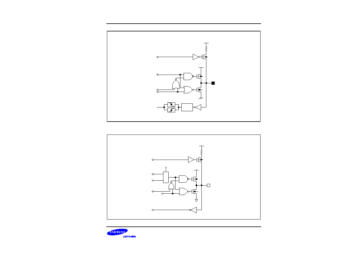
S3P80C5/C80C5/C80C8
PRODUCT OVERVIEW
1-7
V
DD
Pull-up
Enable
V
DD
Input/Output
Pull-up
Resistor
Output Disable
Data
V
SS
Noise
filter
Normal
Input
Open-drain
Figure 1-4. Pin Circuit Type 2 (Port 1)
V
DD
Pull-up
Enable
V
DD
P2.0/T0PWN
Pull-up Resistor
(Typical 21K
)
Open-drain
Port 2.0 Data
V
SS
M
U
X
P2.0 Input
Output
Disable
Data
T0_PWN
P2CON.0
Figure 1-5. Pin Circuit Type 3 (P2.0)

PRODUCT OVERVIEW
S3P80C5/C80C5/C80C8
1-8
V
DD
Pull-up
Enable
V
DD
P2.1/REM/T0CK
Pull-up
Resistor
(Typical 21K
)
Open-Drain
Port 2.1 Data
V
SS
P2.1 Input
M
U
X
P2CON.1
Data
Output
Disable
Noise filter
T0CK
CAOF(CACON.0)
Carrier On/Off (P2.5)
Figure 1-6. Pin Circuit Type 4 (P2.1)
V
DD
Pull-up
Enable
V
DD
In/Out
Pull-up Resistor
(Typical 21K
)
Open-drain
V
SS
Normal Input
Output
Disable
Data
Figure 1-7. Pin Circuit Type 5 (P2.2)

S3P80C5/C80C5/C80C8
ADDRESS SPACES
2-1
2
ADDRESS SPACES
OVERVIEW
The S3P80C5/C80C5/C80C8 microcontroller has two types of address space:
-- Internal program memory (ROM)
-- Internal register file
A 16-bit address bus supports program memory operations. A separate 8-bit register bus carries addresses and
data between the CPU and the register file.
The S3C80C5 has an internal 15,872 byte programmable ROM, the S3C80C8 has an internal 8-Kbyte
programmable ROM. An external memory interface is not implemented. The 256-byte physical RAM space is
expanded into an addressable area of 320 bytes by the use of addressing modes.
There are 312 mapped registers in the internal register file. Of these, 272 are for general-purpose use. (This
number includes a 16-byte working register common area that is used as a " scratch area" for data operations, a
256 prime register area that is used for general purpose and stack operation). Eighteen 8-bit registers are used
for CPU and system control and 22 registers are mapped peripheral control and data registers.

ADDRESS SPACES
S3P80C5/C80C5/C80C8
2-2
PROGRAM MEMORY (ROM)
Program memory stores program code or table data. The S3C80C5 has 15, 872 bytes of internal programmable
program memory, and the program memory address range is therefore 0000H-3E00H of ROM. The S3C80C8
has 8-Kbyte (0000H-1FFFH) of internal programmable program memory (see Figure 2-1).
The first 256 bytes of the ROM (0H≠0FFH) are reserved for interrupt vector addresses. Unused locations in this
address range can be used as normal program memory. If you do use the vector address area to store program
code, be careful to avoid overwriting vector addresses stored in these locations.
The ROM address at which program execution starts after a reset is 0100H.
15,872
15-Kbyte
ROM
8-Kbyte
ROM
Interrupt
Vector Area
8,191
255
0
3E00H
1FFFH
0FFH
0H
(Decimal)
(HEX)
S3C80C8
S3C80C5
Figure 2-1. Program Memory Address Space
S3P80C5/C80C5/C80C8
ADDRESS SPACES
2-3
REGISTER ARCHITECTURE
The S3P80C5/C80C5/C80C8 register file has 312 registers. The upper 64 bytes register files are addressed as
system control register and working register. The lower 192-byte area of the physical register file(00H≠BFH)
contains freely-addressable, general-purpose registers called prime registers. It can be also used for stack
operation.
The extension of register space into separately addressable sets is supported internally by addressing mode
restrictions.
Specific register types and the area (in bytes) they occupy in the S3P80C5/C80C5/C80C8 internal register space
are summarized in Table 2-1.
Table 2-1. S3P80C5/C80C5/C80C8 Register Type Summary
Register Type
Number of Bytes
General-purpose registers (including the 16-byte common working register area,
the 256-byte prime register area.)
272
CPU and system control registers
18
Mapped clock, peripheral, and I/O control and data registers
22
Total Addressable Bytes
312
ADDRESS SPACES
S3P80C5/C80C5/C80C8
2-4
Set 2
Set 1
~
BFH
00H
Prime Data Registers
(All Addressing Modes)
General-Purpose
Data Register
(Indirect Register or
Indexed addressing
modes or
stack operations)
FFH
C0H
192-Bytes
FFH
C0H
System and Peripheral
Control Registers
(Register Addressing
Mode)
System Registers
(Register Addressing
Mode)
64-Bytes
256-Bytes
~
~
Working Registers
(Working Register
Addressing Mode)
CFH
D0H
DFH
E0H
Figure 2-2. Internal Register File Organization

S3P80C5/C80C5/C80C8
ADDRESS SPACES
2-5
REGISTER PAGE POINTER (PP)
The S3C8-series architecture supports the logical expansion of the physical 256-byte internal register file (using
an 8-bit data bus) into as many as 15 separately addressable register pages. Page addressing is controlled by
the register page pointer (PP, DFH). In the S3P80C5/C80C5/C80C8 microcontroller, a paged register file
expansion is not implemented and the register page pointer settings therefore always point to "page 0."
Following a reset, the page pointer's source value (lower nibble) and destination value (upper nibble) are always
'0000', automatically selecting page 0 as the source and destination page for register addressing. These page
pointer (PP) register settings, as shown in Figure 2-3, should not be modified during normal operation.
Register Page Pointer (PP)
DFH, Set 1, R/W
.7
.6
.5
.4
.3
.2
.1
.0
MSB
LSB
Dectination register page selection bits:
0 0 0 0
Destination: page 0
Source register page selection bits:
0 0 0 0
Source: page 0
NOTE:
In the S3C80C5/C80C8 microcontroller, only pate 0 is implemented.
A hardware reset operation writes the 4-bit destination and source values
shown above to the register pate pointer. These values should not be
modified.
Figure 2-3. Register Page Pointer (PP)

ADDRESS SPACES
S3P80C5/C80C5/C80C8
2-6
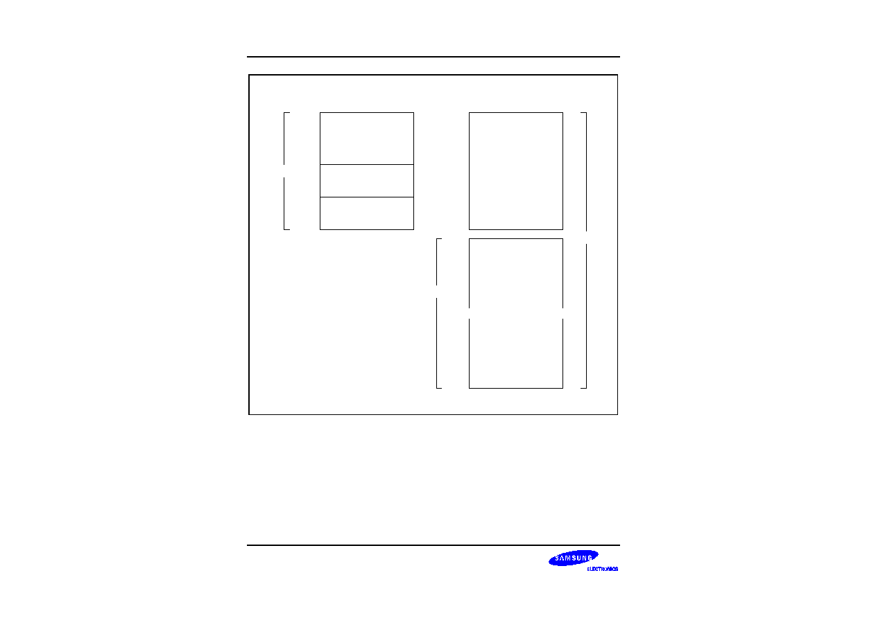
REGISTER SET 1
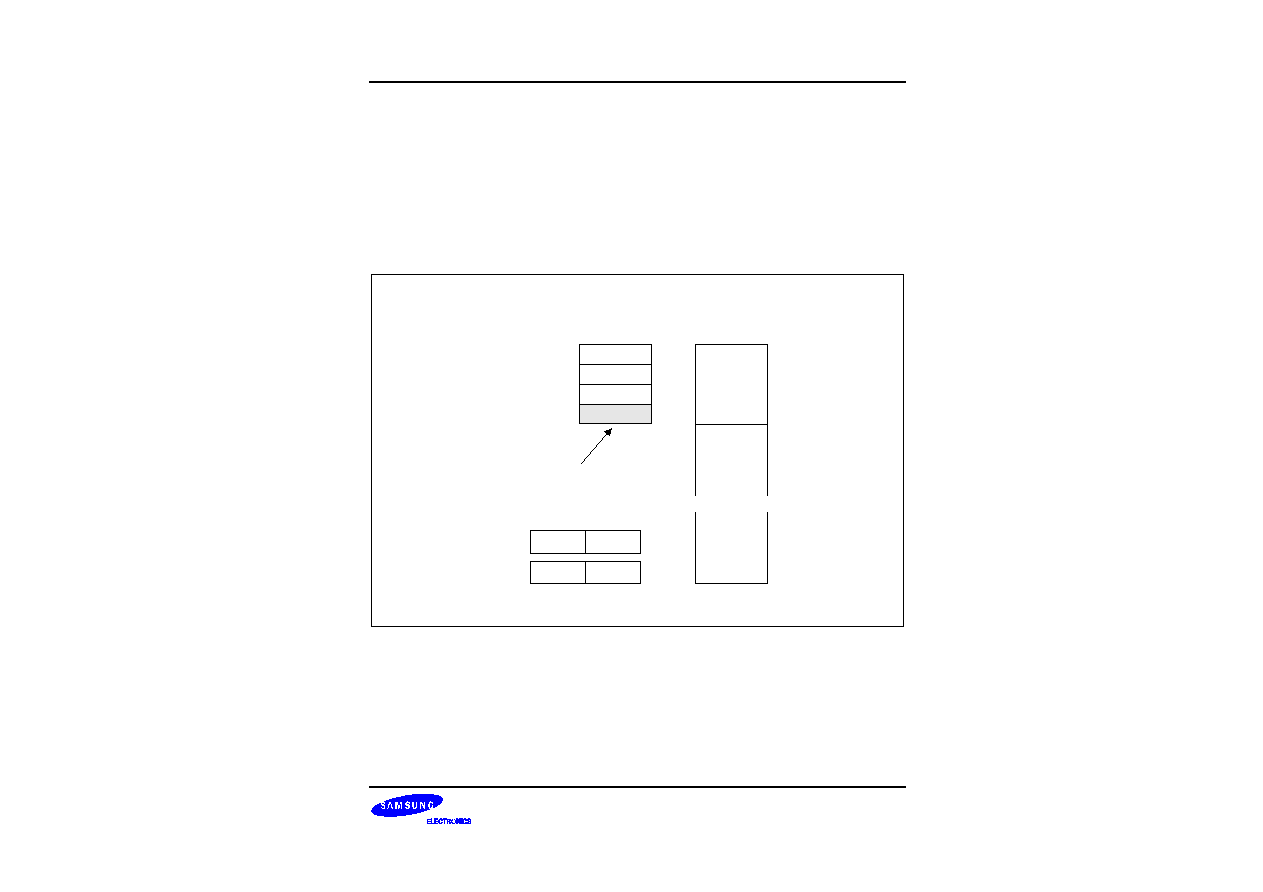
The term set 1 refers to the upper 64 bytes of the register file, locations C0H≠FFH.
In some S3C8-series microcontrollers, the upper 32-byte area of this 64-byte space (E0H≠FFH) is divided into
two 32-byte register banks, bank 0 and bank 1. The set register bank instructions SB0 or SB1 are used to
address one bank or the other. In the S3P80C5/C80C5/C80C8 microcontroller, bank 1 is not implemented. A
hardware reset operation therefore always selects bank 0 addressing, and the SB0 and SB1 instructions are not
necessary.
The upper 32-byte area of set 1 (FFH≠E0H) contains 26 mapped system and peripheral control registers. The
lower 32-byte area contains 16 system registers (DFH≠D0H) and a 16-byte common working register area (CFH≠
C0H). You can use the common working register area as a "scratch" area for data operations being performed in
other areas of the register file.
Registers in set 1 locations are directly accessible at all times using the Register addressing mode. The 16-byte
working register area can only be accessed using working register addressing. (For more information about
working register addressing, please refer to Section 3, "Addressing Modes," .)
REGISTER SET 2
The same 64-byte physical space that is used for set 1 locations C0H≠FFH is logically duplicated to add another
64 bytes of register space. This expanded area of the register file is called set 2. All set 2 locations (C0H≠FFH)
are addressed as part of page 0 in the S3P80C5/C80C5/C80C8 register space.
The logical division of set 1 and set 2 is maintained by means of addressing mode restrictions: You can use only
Register addressing mode to access set 1 locations; to access registers in set 2, you must use Register Indirect
addressing mode or Indexed addressing mode.
The set 2 register area is commonly used for stack operations.

S3P80C5/C80C5/C80C8
ADDRESS SPACES
2-7
PRIME REGISTER SPACE
The lower 192 bytes of the 256-byte physical internal register file (00H≠BFH) is called the prime register space
or, more simply, the prime area. You can access registers in this address using any addressing mode. (In other
words, there is no addressing mode restriction for these registers, as is the case for set 1 and set 2 registers.) All
registers in prime area locations are addressable immediately following a reset.
FFH
C0H
00H
Set 2
Prime
Register
Space
FFH
D0H
C0H
Set 1
FCH
E0H
General-purpose registers
CPU and system registers
Peripheral control registers
Figure 2-4. Set 1, Set 2 and Prime Area Register Map
ADDRESS SPACES
S3P80C5/C80C5/C80C8
2-8
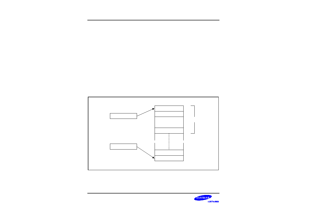
WORKING REGISTERS
Instructions can access specific 8-bit registers or 16-bit register pairs using either 4-bit or 8-bit address fields.
When 4-bit working register addressing is used, the 256-byte register file can be seen by the programmer as
consisting of 32 8-byte register groups or "slices." Each slice consists of eight 8-bit registers.
Using the two 8-bit register pointers, RP1 and RP0, two working register slices can be selected at any one time to
form a 16-byte working register block. Using the register pointers, you can move this 16-byte register block
anywhere in the addressable register file, except for the set 2 area.
The terms slice and block are used in this manual to help you visualize the size and relative locations of selected
working register spaces:
-- One working register slice is 8 bytes (eight 8-bit working registers; R0≠R7 or R8≠R15)
-- One working register block is 16 bytes (sixteen 8-bit working registers; R0≠R15)
All of the registers in an 8-byte working register slice have the same binary value for their five most significant
address bits. This makes it possible for each register pointer to point to one of the 24 slices in the register file.
The base addresses for the two selected 8-byte register slices are contained in register pointers RP0 and RP1.
After a reset, RP0 and RP1 always point to the 16-byte common area in set 1 (C0H≠CFH).
Each register pointer points to
one 8-byte slice of the register
space, selecting a total 16-byte
working register block.
1 1 1 1 1 X X X
RP1 (Registers R8-R15)
RP0 (Registers R0-R7)
Slice 32
Slice 31
~
~
CFH
C0H
FFH
F8H
F7H
F0H
FH
8H
7H
0H
Slice 2
Slice 1
10H
Set 1
Only
0 0 0 0 0 X X X
Figure 2-5. 8-Byte Working Register Areas (Slices)
S3P80C5/C80C5/C80C8
ADDRESS SPACES
2-9
USING THE REGISTER POINTERS
Register pointers RP0 and RP1, mapped to addresses D6H and D7H in set 1, are used to select two movable
8-byte working register slices in the register file. After a reset, they point to the working register common area:
RP0 points to addresses C0H≠C7H, and RP1 points to addresses C8H≠CFH.
To change a register pointer value, you load a new value to RP0 and/or RP1 using an SRP or LD instruction (see
Figures 2-6 and 2-7).
With working register addressing, you can only access those two 8-bit slices of the register file that are currently
pointed to by RP0 and RP1. You cannot, however, use the register pointers to select a working register space in
set 2, C0H≠FFH, because these locations can be accessed only using the Indirect Register or Indexed
addressing modes.
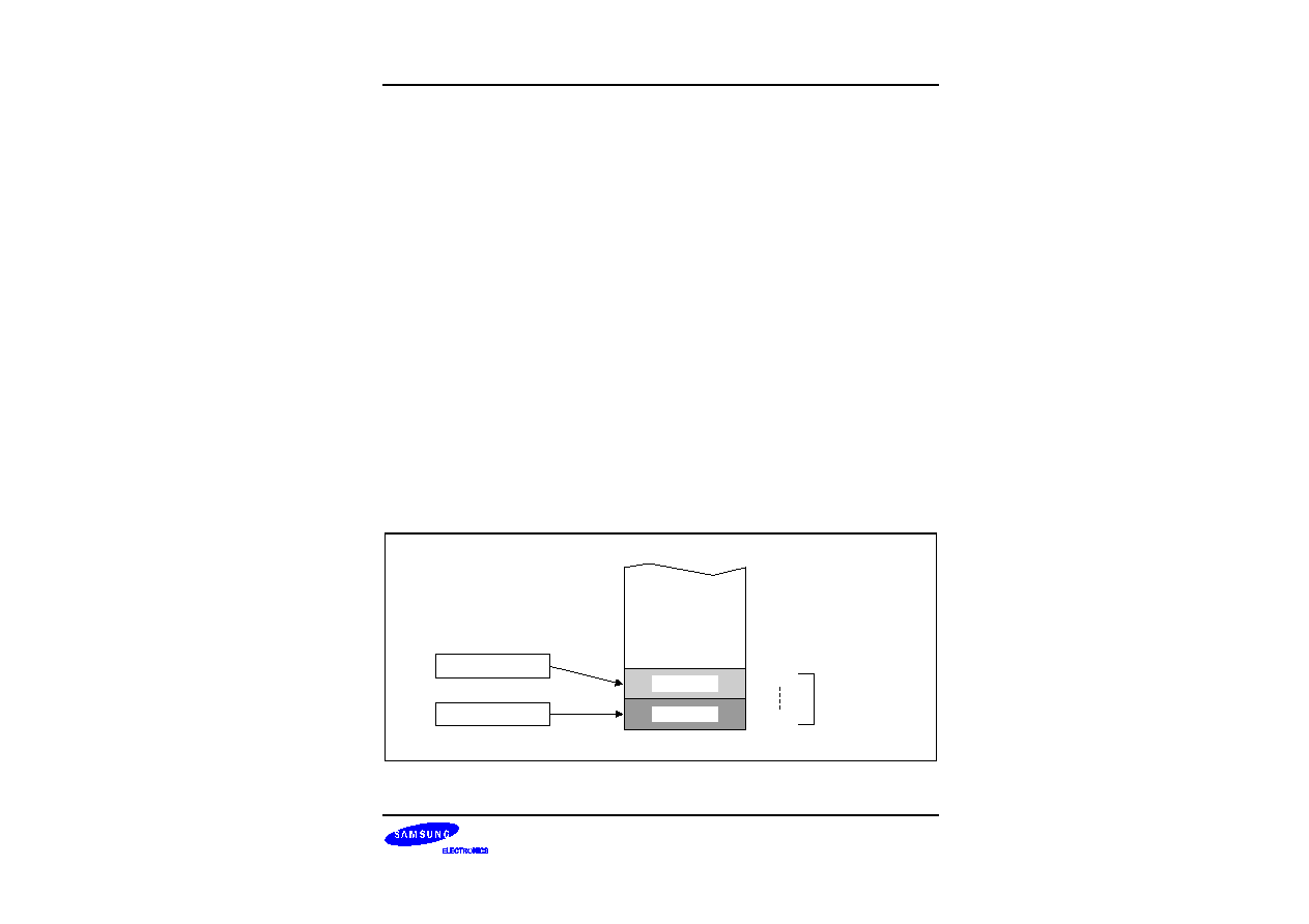
The selected 16-byte working register block usually consists of two contiguous 8-byte slices. As a general
programming guideline, we recommend that RP0 point to the "lower" slice and RP1 point to the "upper" slice (see
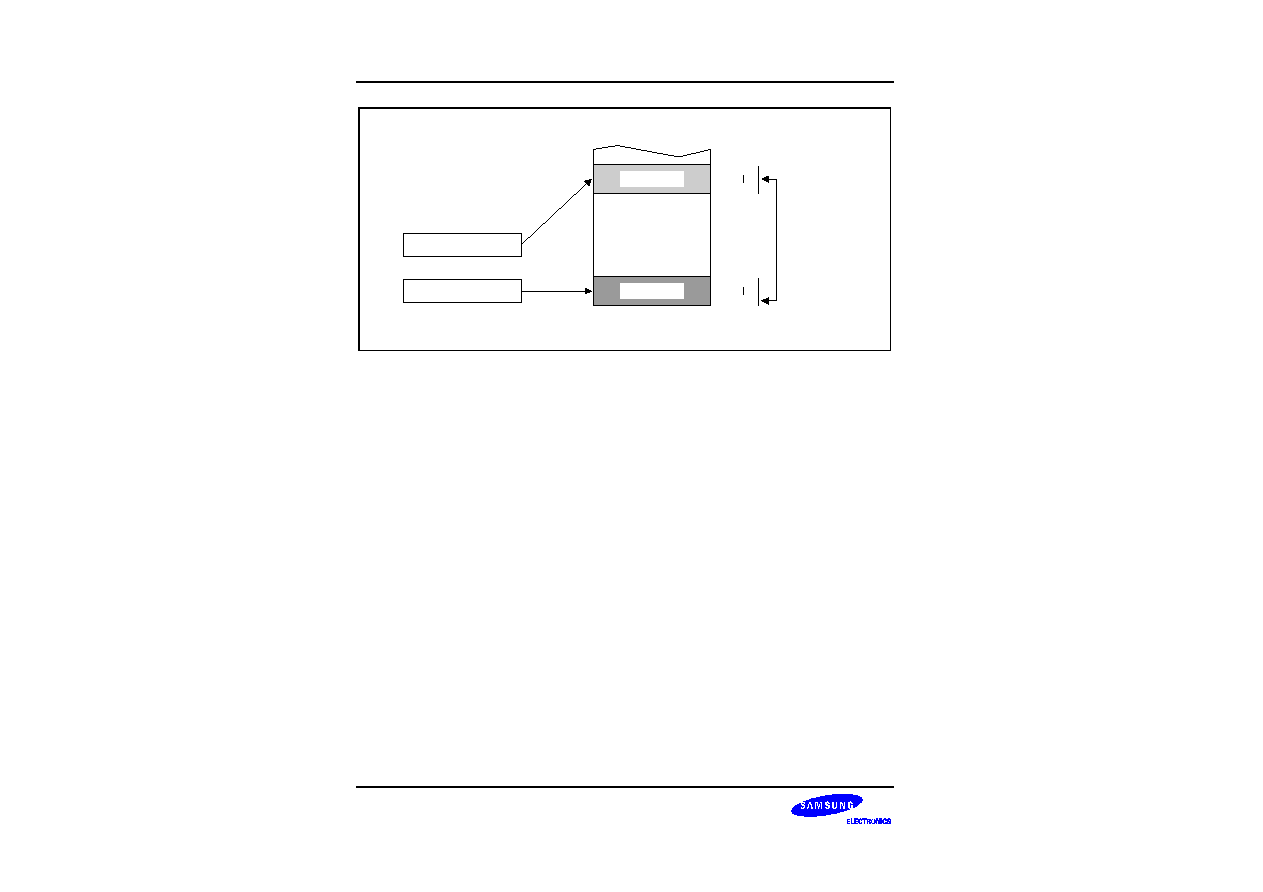
Figure 2-6). In some cases, it may be necessary to define working register areas in different (non-contiguous)
areas of the register file. In Figure 2-7, RP0 points to the "upper" slice and RP1 to the "lower" slice.
Because a register pointer can point to the either of the two 8-byte slices in the working register block, you can
define the working register area very flexibly to support program requirements.
F
F
PROGRAMMING TIP -- Setting the Register Pointers
SRP
#70H
; RP0
70H, RP1
78H
SRP1
#48H
; RP0
no change, RP1
48H,
SRP0
#0A0H
; RP0
A0H, RP1
no change
CLR
RP0
; RP0
00H, RP1
no change
LD
RP1,#0F8H
; RP0
no change, RP1
0F8H
FH (R15)
0H (R0)
16-Byte
Contiguous
Working
Register block
Register File
Contains 32
8-Byte Slices
RP0
RP1
8H
7H
0 0 0 0 1 X X X
0 0 0 0 0 X X X
8-Byte Slice
8-Byte Slice
Figure 2-6. Contiguous 16-Byte Working Register Block
ADDRESS SPACES
S3P80C5/C80C5/C80C8
2-10
16-Byte
Contiguous
working
Register block
Register File
Contains 32
8-Byte Slices
0 0 0 0 0 X X X
RP1
1 1 1 1 0 X X X
RP0
0H (R0)
7H (R15)
F0H (R0)
F7H (R7)
8-Byte Slice
8-Byte Slice
Figure 2-7. Non-Contiguous 16-Byte Working Register Block
F
F
PROGRAMMING TIP -- Using the RPs to Calculate the Sum of a Series of Registers
Calculate the sum of registers 80H≠85H using the register pointer. The register addresses 80H through 85H
contains the values 10H, 11H, 12H, 13H, 14H, and 15 H, respectively:
SRP0
#80H
; RP0
80H
ADD
R0,R1
; R0
R0 + R1
ADC
R0,R2
; R0
R0 + R2 + C
ADC
R0,R3
; R0
R0 + R3 + C
ADC
R0,R4
; R0
R0 + R4 + C
ADC
R0,R5
; R0
R0 + R5 + C
The sum of these six registers, 6FH, is located in the register R0 (80H). The instruction string used in this
example takes 12 bytes of instruction code and its execution time is 36 cycles. If the register pointer is not used
to calculate the sum of these registers, the following instruction sequence would have to be used:
ADD
80H,81H
; 80H
(80H) + (81H)
ADC
80H,82H
; 80H
(80H) + (82H) + C
ADC
80H,83H
; 80H
(80H) + (83H) + C
ADC
80H,84H
; 80H
(80H) + (84H) + C
ADC
80H,85H
; 80H
(80H) + (85H) + C
Now, the sum of the six registers is also located in register 80H. However, this instruction string takes 15 bytes of
instruction code instead of 12 bytes, and its execution time is 50 cycles instead of 36 cycles.

S3P80C5/C80C5/C80C8
ADDRESS SPACES
2-11
REGISTER ADDRESSING
The S3C8-series register architecture provides an efficient method of working register addressing that takes full
advantage of shorter instruction formats to reduce execution time.
With Register (R) addressing mode, in which the operand value is the content of a specific register or register
pair, you can access all locations in the register file except for set 2. With working register addressing, you use a
register pointer to specify an 8-byte working register space in the register file and an 8-bit register within that
space.
Registers are addressed either as a single 8-bit register or as a paired 16-bit register space. In a 16-bit register
pair, the address of the first 8-bit register is always an even number and the address of the next register is always
an odd number. The most significant byte of the 16-bit data is always stored in the even-numbered register; the
least significant byte is always stored in the next (+ 1) odd-numbered register.
Working register addressing differs from Register addressing because it uses a register pointer to identify a
specific 8-byte working register space in the internal register file and a specific 8-bit register within that space.
MSB
Rn
LSB
Rn+1
n = Even address
Figure 2-8. 16-Bit Register Pair

ADDRESS SPACES
S3P80C5/C80C5/C80C8
2-12
RP1
RP0
00H
C0H
BFH
Each register pointer (RP) can independently point
to one of the 24 8-byte "slices" of the register file
(other than set 2). After a reset, RP0 points to
locations C0H-C7H and RP1 to locations C8H-CFH
(that is, to the common working register area).
FFH
C0H
Set 2
CFH
D7H
D6H
Set 1
FFH
D0H
Special-Purpose Registers
General-Purpose Register
Register
Pointers
Control
Registers
All
Addressing
Modes
Page 0
Indirect
Register,
Indexed
Addressing
Modes
Page 0
Register Addressing Only
Can be Pointed by Register Pointer
Prime
Registers
System
Registers
NOTE:
Only page 0 is implemented. Page 0
Contains all of the addressable registers
in the internal register file.
Figure 2-9. Register File Addressing
S3P80C5/C80C5/C80C8
ADDRESS SPACES
2-13
COMMON WORKING REGISTER AREA (C0H≠CFH)
After a reset, register pointers RP0 and RP1 automatically select two 8-byte register slices in set 1, locations
C0H≠CFH, as the active 16-byte working register block:
RP0
C0H≠C7H
RP1
C8H≠CFH
This 16-byte address range is called common area. That is, locations in this area can be used as working
registers by operations that address any location on any page in the register file. Typically, these working
registers serve as temporary buffers for data operations between different pages.
Register a hardware reset, register
pointers RP0 and RP1 point to the
commom working register area,
locations C0H-CfH.
RP0 =
1 1 0 0
0 0 0 0
RP1 =
1 1 0 0
1 0 0 0
FFH
C0H
BFH
Set 2
00H
Prime
Area
Set 1
FFH
CFH
C0H
FCH
E0H
DFH
Page 0
~
~
Figure 2-10. Common Working Register Area

ADDRESS SPACES
S3P80C5/C80C5/C80C8
2-14
F
F
PROGRAMMING TIP -- Addressing the Common Working Register Area
As the following examples show, you should access working registers in the common area, locations C0H≠CFH,
using working register addressing mode only.
Example 1:
LD
0C2H,40H
; Invalid addressing mode!
Use working register addressing instead:
SRP
#0C0H
LD
R2,40H
; R2 (C2H)
the value in location 40H
Example 2:
ADD
0C3H,#45H
; Invalid addressing mode!
Use working register addressing instead:
SRP
#0C0H
ADD
R3,#45H
; R3 (C3H)
R3 + 45H
4-BIT WORKING REGISTER ADDRESSING
Each register pointer defines a movable 8-byte slice of working register space. The address information stored in
a register pointer serves as an addressing "window" that makes it possible for instructions to access working
registers very efficiently using short 4-bit addresses. When an instruction addresses a location in the selected
working register area, the address bits are concatenated in the following way to form a complete 8-bit address:
-- The high-order bit of the 4-bit address selects one of the register pointers ("0" selects RP0; "1" selects RP1);
-- The five high-order bits in the register pointer select an 8-byte slice of the register space;
-- The three low-order bits of the 4-bit address select one of the eight registers in the slice.
As shown in Figure 2-11, the result of this operation is that the five high-order bits from the register pointer are
concatenated with the three low-order bits from the instruction address to form the complete address. As long as
the address stored in the register pointer remains unchanged, the three bits from the address will always point to
an address in the same 8-byte register slice.
Figure 2-12 shows a typical example of 4-bit working register addressing: The high-order bit of the instruction
'INC R6' is "0", which selects RP0. The five high-order bits stored in RP0 (01110B) are concatenated with the
three low-order bits of the instruction's 4-bit address (110B) to produce the register address 76H (01110110B).
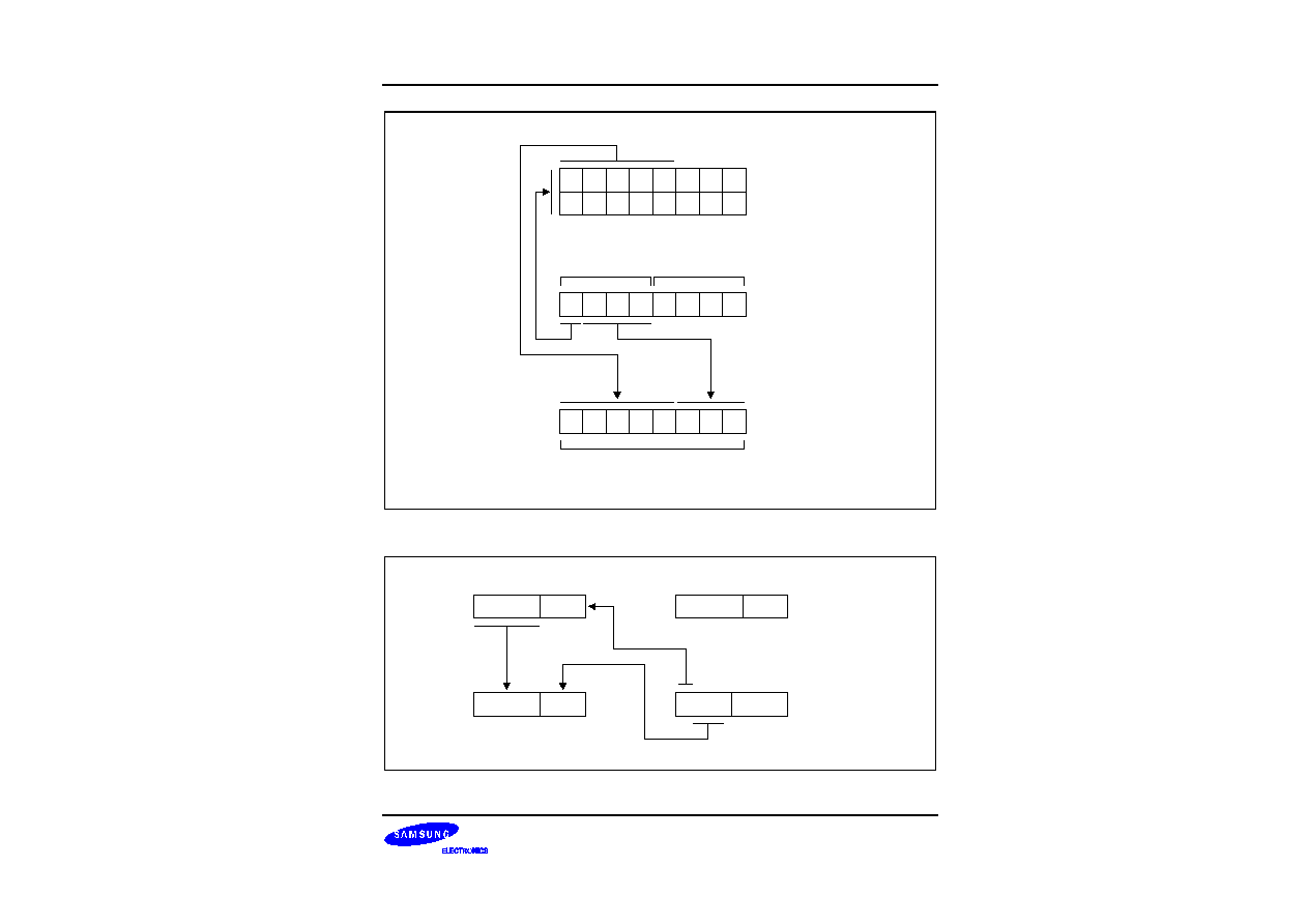
S3P80C5/C80C5/C80C8
ADDRESS SPACES
2-15
Together They Create an
8-bit Register Address
Register Pointer
Provides Five
High-order Bits
Address
OPCODE
Selects
RP0 or RP1
RP1
RP0
4-bit Address
Provides Three
Low-order Bits
Figure 2-11. 4-Bit Working Register Addressing
Register
Address
(76H)
RP0
0 1 1 1 0
0 0 0
0 1 1 1 0
1 1 0
R6
0 1 1 0
1 1 1 0
Selects RP0
Instruction:
'INC R6'
OPCODE
RP1
0 1 1 1 1
0 0 0
Figure 2-12. 4-Bit Working Register Addressing Example
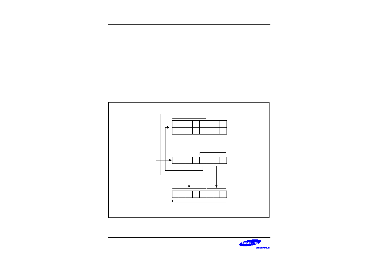
ADDRESS SPACES
S3P80C5/C80C5/C80C8
2-16
8-BIT WORKING REGISTER ADDRESSING
You can also use 8-bit working register addressing to access registers in a selected working register area. To
initiate 8-bit working register addressing, the upper four bits of the instruction address must contain the value
1100B. This 4-bit value (1100B) indicates that the remaining four bits have the same effect as 4-bit working
register addressing.
As shown in Figure 2-13, the lower nibble of the 8-bit address is concatenated in much the same way as for 4-bit
addressing: Bit 3 selects either RP0 or RP1, which then supplies the five high-order bits of the final address; the
three low-order bits of the complete address are provided by the original instruction.
Figure 2-14 shows an example of 8-bit working register addressing: The four high-order bits of the instruction
address (1100B) specify 8-bit working register addressing. Bit 4 ("1") selects RP1 and the five high-order bits in
RP1 (10101B) become the five high-order bits of the register address. The three low-order bits of the register
address (011) are provided by the three low-order bits of the 8-bit instruction address. The five address bits from
RP1 and the three address bits from the instruction are concatenated to form the complete register address,
0ABH (10101011B).
8-bit Logical
Address
8-bit Physical Address
Register Pointer
Provides Five
High-order Bits
Address
Selects
RP0 or RP1
RP1
RP0
Three low-
order Bits
These Address
Bits Indicate 8-bit
Working Register
Addressing
1
1
0
0
Figure 2-13. 8-Bit Working Register Addressing
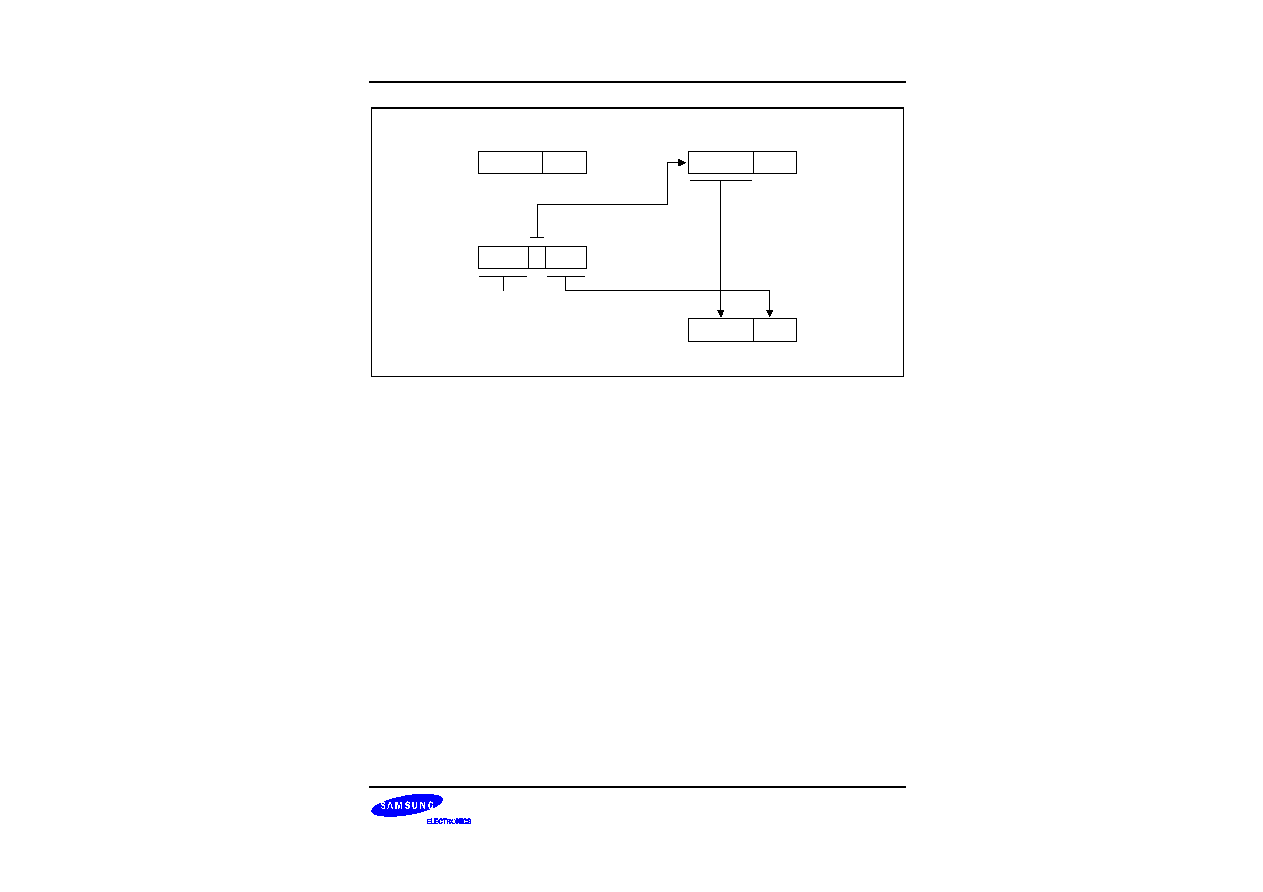
S3P80C5/C80C5/C80C8
ADDRESS SPACES
2-17
8-bit Address
Form Instruction
'LD R11, R2'
RP0
0 1 1 0 0
0 0 0
1 1 0 0 1 0 1 1
Selects RP1
R11
RP1
1 0 1 0 1
0 0 0
1 0 1 0 1
0 1 1
Specifies Working
Register Addressing
Register Address (0ABH)
Figure 2-14. 8-Bit Working Register Addressing Example
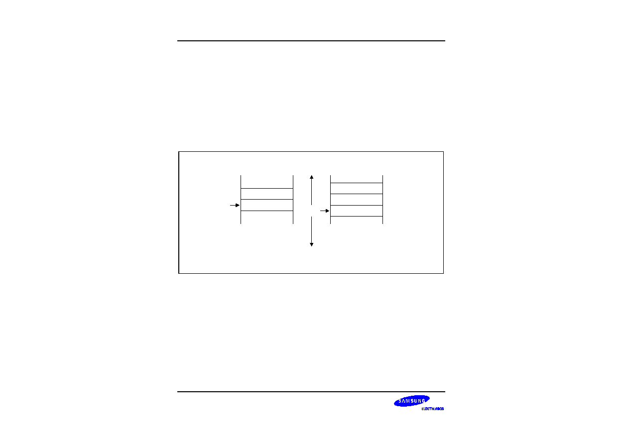
ADDRESS SPACES
S3P80C5/C80C5/C80C8
2-18
SYSTEM AND USER STACKS
S3C8-series microcontrollers use the system stack for subroutine calls and returns and to store data. The PUSH
and POP instructions are used to control system stack operations.
The S3P80C5/C80C5/C80C8 architecture supports stack operations in the internal register file.
Stack Operations
Return addresses for procedure calls and interrupts and data are stored on the stack. The contents of the PC are
saved to stack by a CALL instruction and restored by the RET instruction. When an interrupt occurs, the contents
of the PC and the FLAGS register are pushed to the stack. The IRET instruction then pops these values back to
their original locations. The stack address value is always decreased by one before a push operation and
increased by one after a pop operation. The stack pointer (SP) always points to the stack frame stored on the top
of the stack, as shown in Figure 2-15.
Stack Contents
After a Call
Instruction
Stack Contents
After an Interrupt
Top of
Stack
FLAGS
PCH
PCL
PCL
PCH
Top of
Stack
Low Address
High Address
Figure 2-15. Stack Operations
User-Defined Stacks
You can freely define stacks in the internal register file as data storage locations. The instructions PUSHUI,
PUSHUD, POPUI, and POPUD support user-defined stack operations.
Stack Pointers (SPL)
Register location D9H contain the 8-bit stack pointer (SPL) that is used for system stack operations. After a reset,
the SPL value is undetermined. Because only internal memory 256-byte is implemented in
S3P80C5/C80C5/C80C8, the SPL must be initialized to an 8-bit value in the range 00H≠FFH.

S3P80C5/C80C5/C80C8
ADDRESS SPACES
2-19
F
F
PROGRAMMING TIP -- Standard Stack Operations Using PUSH and POP
The following example shows you how to perform stack operations in the internal register file using PUSH and
POP instructions:
LD
SPL,#0FFH
; SPL
FFH
; (Normally, the SPL is set to 0FFH by the initialization
; routine)
∑
∑
∑
PUSH
PP
; Stack address 0FEH
PP
PUSH
RP0
; Stack address 0FDH
RP0
PUSH
RP1
; Stack address 0FCH
RP1
PUSH
R3
; Stack address 0FBH
R3
∑
∑
∑
POP
R3
; R3
Stack address 0FBH
POP
RP1
; RP1
Stack address 0FCH
POP
RP0
; RP0
Stack address 0FDH
POP
PP
; PP
Stack address 0FEH

ADDRESS SPACES
S3P80C5/C80C5/C80C8
2-20
NOTES

S3P80C5/C80C5/C80C8
ADDRESSING MODES
3-1
3
ADDRESSING MODES
OVERVIEW
The program counter is used to fetch instructions that are stored in program memory for execution. Instructions
indicate the operation to be performed and the data to be operated on. Addressing mode is the method used to
determine the location of the data operand. The operands specified in instructions may be condition codes,
immediate data, or a location in the register file, program memory, or data memory.
The S3C8-series instruction set supports seven explicit addressing modes. Not all of these addressing modes are
available for each instruction:
-- Register (R)
-- Indirect Register (IR)
-- Indexed (X)
-- Direct Address (DA)
-- Indirect Address (IA)
-- Relative Address (RA)
-- Immediate (IM)

ADDRESSING MODES
S3P80C5/C80C5/C80C8
3-2
REGISTER ADDRESSING MODE (R)
In Register addressing mode, the operand is the content of a specified register or register pair (see Figure 3-1).
Working register addressing differs from Register addressing because it uses a register pointer to specify an 8-
byte working register space in the register file and an 8-bit register within that space (see Figure 3-2).
dst
Value used in
Instruction Execution
OPCODE
OPERAND
8-bit Register
File Address
Point to One
Register in Register
File
One-Operand
Instruction
(Example)
Sample Instruction:
DEC
CNTR
; Where CNTR is the label of an 8-bit register address
Register File
Program Memory
Figure 3-1. Register Addressing
4-bit
Working Register
Points to the
Working Register
(1 of 8)
Two-Operand
Instruction
(Example)
Sample Instruction:
ADD
R1, R2
; Where R1 and R2 are registers in the currently
selected working register area.
Program Memory
Register File
3 LSBs
RP0 or RP1
Selected
RP Points
to Start
of Working
Register
Block
MSB Points to
RP0 ot RP1
dst
OPCODE
src
OPERAND
Figure 3-2. Working Register Addressing
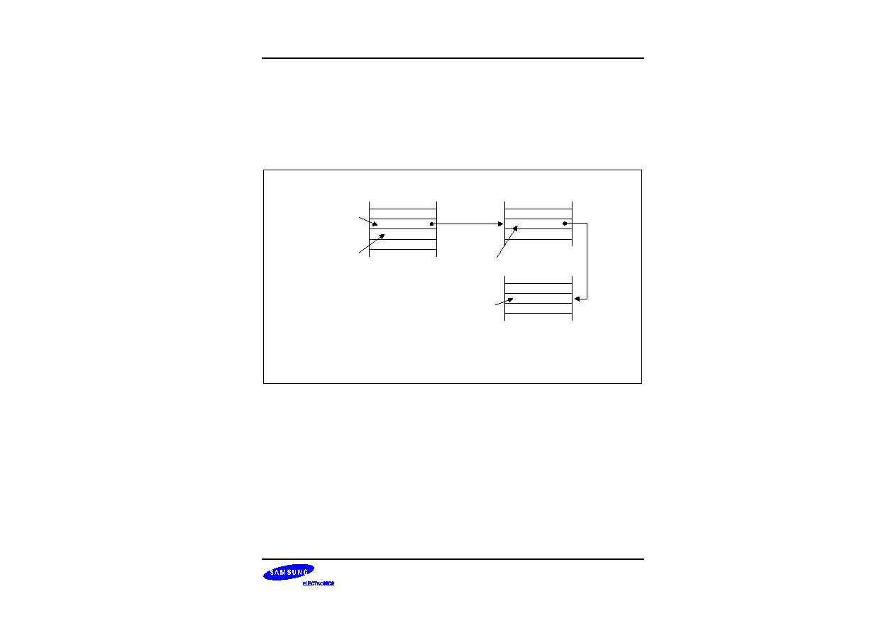
S3P80C5/C80C5/C80C8
ADDRESSING MODES
3-3
INDIRECT REGISTER ADDRESSING MODE (IR)
In Indirect Register (IR) addressing mode, the content of the specified register or register pair is the address of
the operand. Depending on the instruction used, the actual address may point to a register in the register file, to
program memory (ROM), or to an external memory space, if implemented (see Figures 3-3 through 3-6).
You can use any 8-bit register to indirectly address another register. Any 16-bit register pair can be used to
indirectly address another memory location. Remember, however, that locations C0H≠FFH in set 1 cannot be
accessed using Indirect Register addressing mode.
dst
Address of Operand
used by Instruction
OPCODE
ADDRESS
8-bit Register
File Address
Point to One
Register in
Register File
One-Operand
Instruction
(Example)
Sample Instruction:
RL
@SHIFT ; Where SHIFT is the label of an 8-bit register address.
Program Memory
Register File
Value used in
Instruction Execution
OPERAND
Figure 3-3. Indirect Register Addressing to Register File

ADDRESSING MODES
S3P80C5/C80C5/C80C8
3-4
INDIRECT REGISTER ADDRESSING MODE (Continued)
dst
OPCODE
Points to
Register Pair
Example
Instruction
References
Program
Memory
Sample Instructions:
CALL
@RR2
JP
@RR2
Program Memory
Register File
Value used in
Instruction
OPERAND
Register Pair
Program Memory
16-Bit
Address
Points to
Program
Memory
Figure 3-4. Indirect Register Addressing to Program Memory

S3P80C5/C80C5/C80C8
ADDRESSING MODES
3-5
INDIRECT REGISTER ADDRESSING MODE (Continued)
dst
OPCODE
ADDRESS
4-bit
Working
Register
Address
Point to the
Working Register
(1 of 8)
Sample Instruction:
OR
R3, @R6
Program Memory
Register File
src
3 LSBs
Selected
RP Points
to Start of
Woking
Register
Block
RP0 or RP1
MSB Points to
RP0 or RP1
~
~
~
~
Value used in
Instruction
OPERAND
Figure 3-5. Indirect Working Register Addressing to Register File
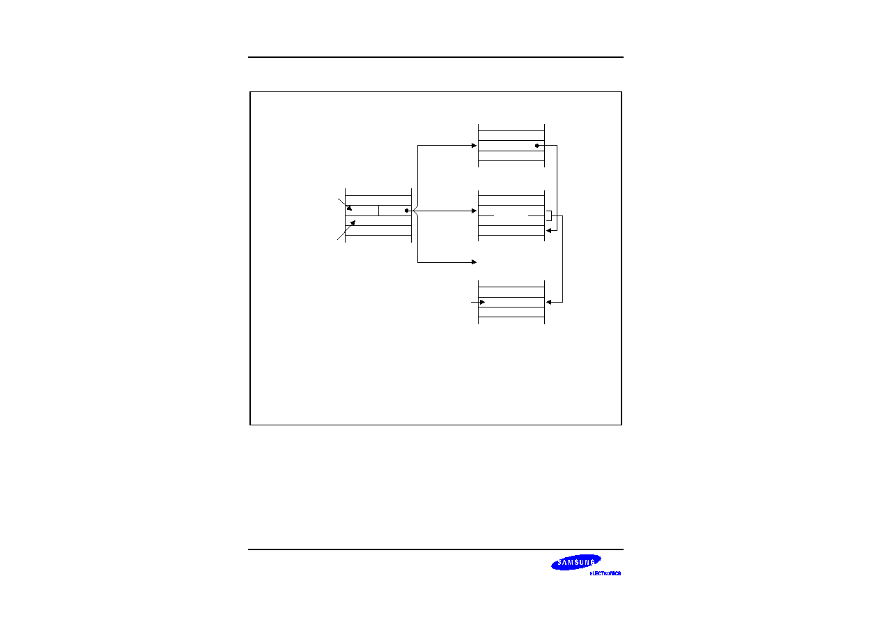
ADDRESSING MODES
S3P80C5/C80C5/C80C8
3-6
INDIRECT REGISTER ADDRESSING MODE (Continued)
dst
OPCODE
4-bit Working
Register Address
Sample Instructions:
LDC
R5,@RR6
; Program memory access
LDE
R3,@RR14
; External data memory access
LDE
@RR4, R8
; External data memory access
Program Memory
Register File
src
Value used in
Instruction
OPERAND
Example Instruction
References either
Program Memory or
Data Memory
Program Memory
or
Data Memory
Next 2-bit Point
to Working
Register Pair
(1 of 4)
LSB Selects
Register
Pair
16-Bit
Address
Points to
Program
Memory or
Data
Memory
RP0 or RP1
MSB Points to
RP0 or RP1
Selected
RP Points
to Start of
Working
Register
Block
NOTE:
LDE command is not available, because an external interface is not implemented for
the S3C80C5/C80C8/C80C4.
Figure 3-6. Indirect Working Register Addressing to Program or Data Memory
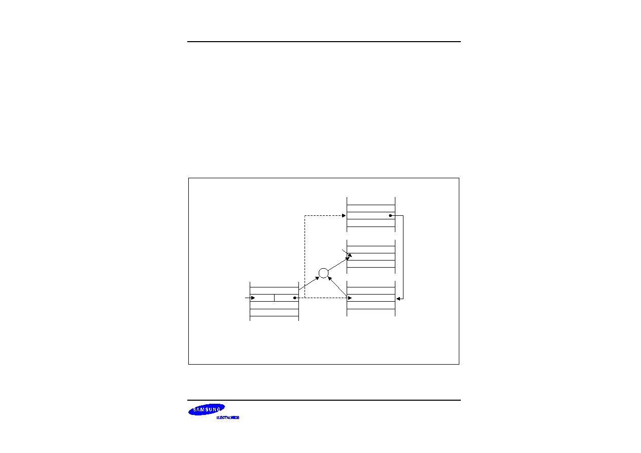
S3P80C5/C80C5/C80C8
ADDRESSING MODES
3-7
INDEXED ADDRESSING MODE (X)
Indexed (X) addressing mode adds an offset value to a base address during instruction execution in order to
calculate the effective operand address (see Figure 3-7). You can use Indexed addressing mode to access
locations in the internal register file or in external memory (if implemented). You cannot, however, access
locations C0H≠FFH in set 1 using Indexed addressing.
In short offset Indexed addressing mode, the 8-bit displacement is treated as a signed integer in the range ≠128
to +127. This applies to external memory accesses only (see Figure 3-8).
For register file addressing, an 8-bit base address provided by the instruction is added to an 8-bit offset contained
in a working register. For external memory accesses, the base address is stored in the working register pair
designated in the instruction. The 8-bit or 16-bit offset given in the instruction is then added to the base address
(see Figure 3-9).
The only instruction that supports Indexed addressing mode for the internal register file is the Load instruction
(LD). The LDC and LDE instructions support Indexed addressing mode for internal program memory and for
external data memory (if implemented).
dst/src
OPCODE
Two-Operand
Instruction
Example
Point to One of the
Working Register
(1 of 8)
Sample Instruction:
LD R0, #BASE[R1]
; Where BASE is an 8-bit immediate value
Program Memory
Register File
x
3 LSBs
Value used in
Instruction
OPERAND
INDEX
Base Address
RP0 or RP1
Selected RP
Points to
Start of
Working
Register
Block
~
~
~
~
+
MSB Points to
RP0 or RP1
Figure 3-7. Indexed Addressing to Register File
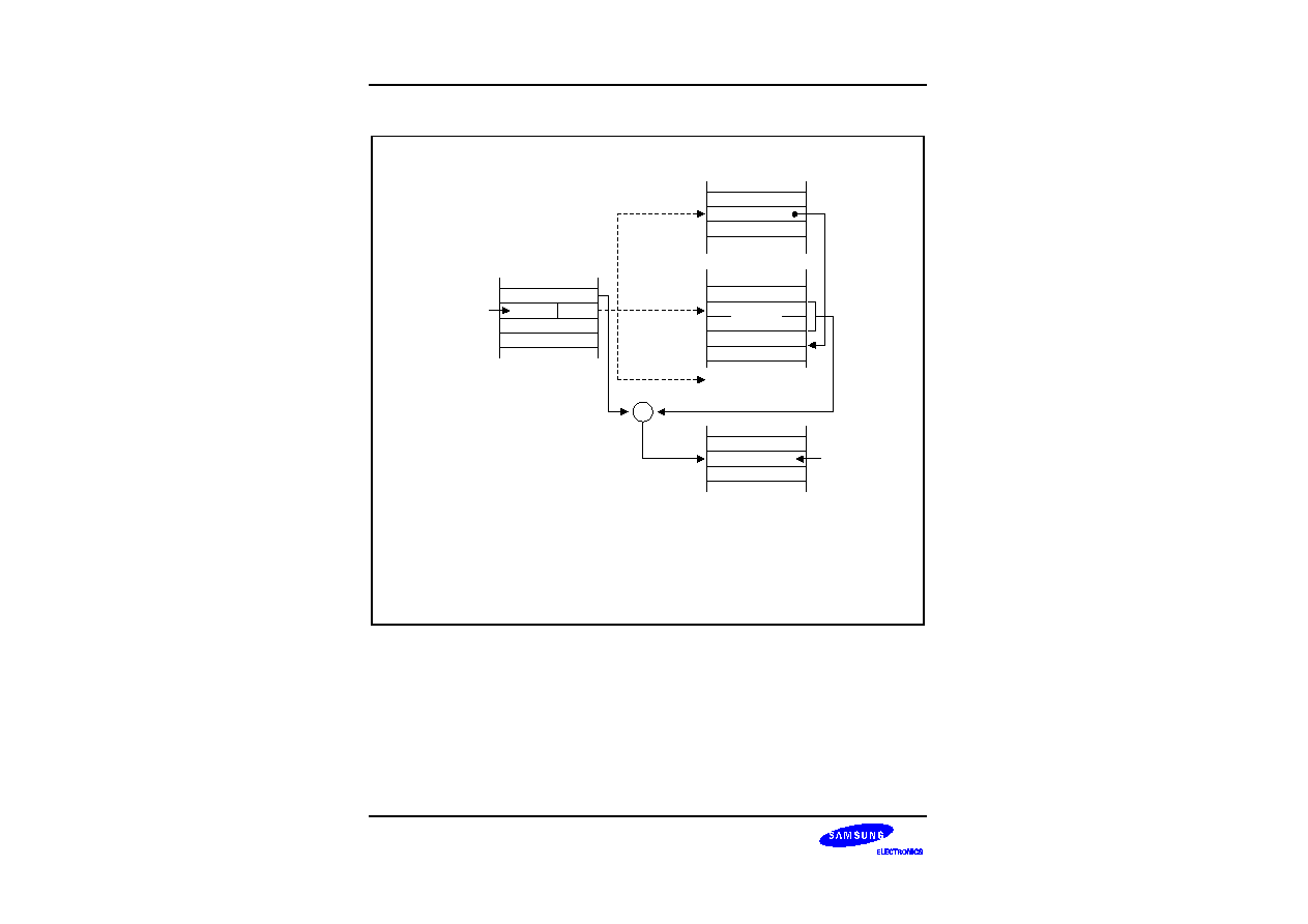
ADDRESSING MODES
S3P80C5/C80C5/C80C8
3-8
INDEXED ADDRESSING MODE (Continued)
Register File
OPERAND
Program Memory
or
Data Memory
Point to Working
Register Pair
(1 of 4)
LSB Selects
16-Bit
Address
Added to
Offset
RP0 or RP1
MSB Points to
RP0 or RP1
Selected
RP Points
to Start of
Working
Register
Block
dst/src
OPCODE
Program Memory
x
OFFSET
4 Bit Working
Register Address
Sample Instructions:
LDC
R4, #04H[RR2]
; The values in the program address (RR2 + 04H) are
loaded into register R4.
LDE
R4,#04H[RR2]
; Identical operation to LDC example, except that
external program memory is accessed.
Next 2 Bits
Register
Pair
Value used In
Instruction
8 Bits
16 Bits
16 Bits
+
~
~
NOTE:
LDE command is not available, because an external interface is not implemented for
the S3C80C5/C80C8/C80C4.
Figure 3-8. Indexed Addressing to Program or Data Memory with Short Offset
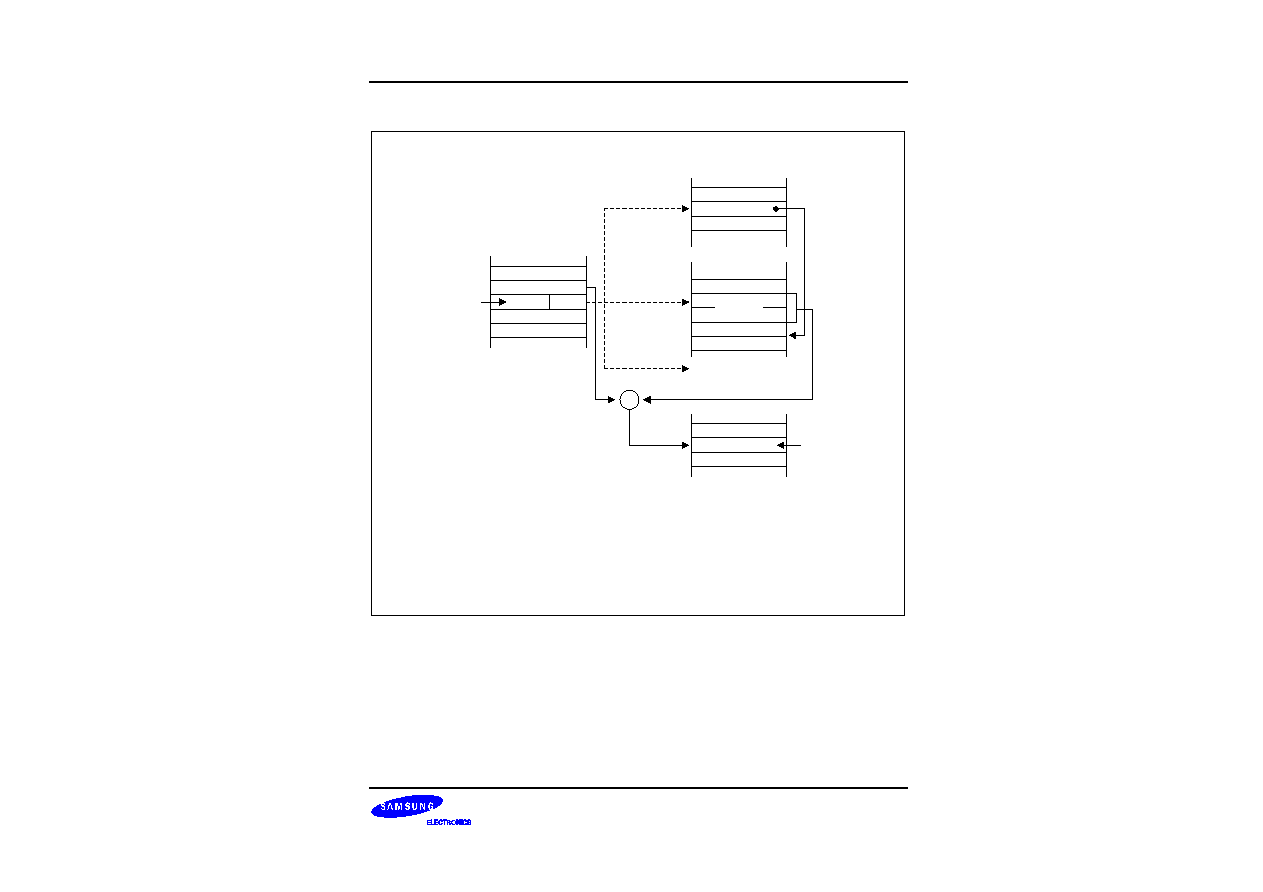
S3P80C5/C80C5/C80C8
ADDRESSING MODES
3-9
INDEXED ADDRESSING MODE (Continued)
Register File
OPERAND
Program Memory
or
Data Memory
Point to Working
Register Pair
LSB Selects
16 Bit
Address
Added to
Offset
RP0 or RP1
MSB Points to
RP0 or RP1
Selected
RP Points
to Start of
Working
Register
Block
Sample Instructions:
LDC
R4, #1000H[RR2]
; The values in the program address (RR2 + 1000H)
are loaded into register R4.
LDE
R4, #1000H[RR2]
; Identical operation to LDC example, except that
external program memory is accessed.
Next 2 Bits
Register
Pair
Value used in
Instruction
8-Bits
16-Bits
16-Bits
dst/src
OPCODE
Program Memory
x
OFFSET
4 Bit Working
Register Address
OFFSET
+
~
~
NOTE:
LDE command is not available, because an external interface is not implemented for
the S3C80C5/C80C8/C80C4.
Figure 3-9. Indexed Addressing to Program or Data Memory
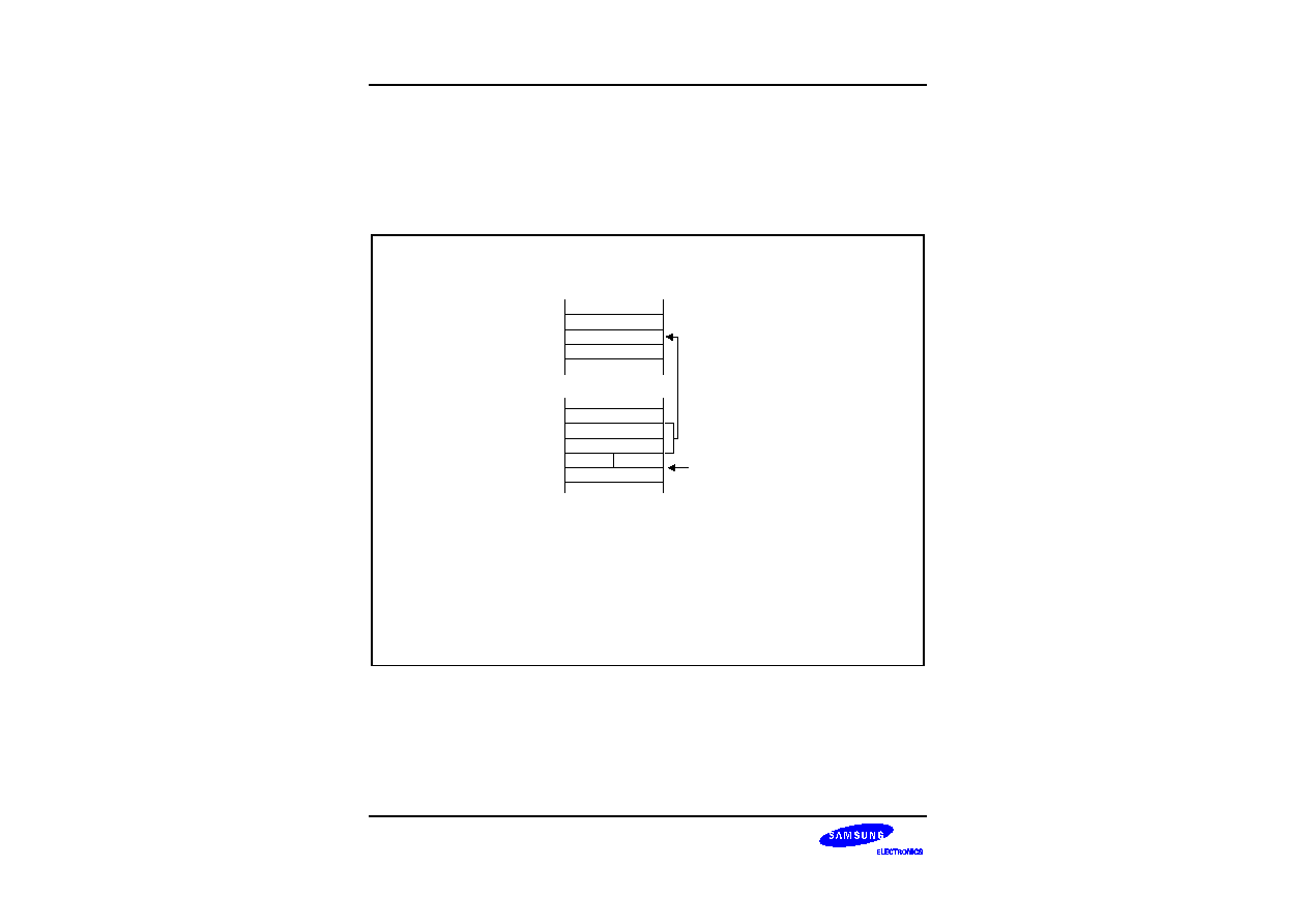
ADDRESSING MODES
S3P80C5/C80C5/C80C8
3-10
DIRECT ADDRESS MODE (DA)
In Direct Address (DA) mode, the instruction provides the operand's 16-bit memory address. Jump (JP) and Call
(CALL) instructions use this addressing mode to specify the 16-bit destination address that is loaded into the PC
whenever a JP or CALL instruction is executed.
The LDC and LDE instructions can use Direct Address mode to specify the source or destination address for
Load operations to program memory (LDC) or to external data memory (LDE), if implemented.
Sample Instructions:
LDC
R5,1234H ; The values in the program address (1234H)
are loaded into register R5.
LDE
R5,1234H ; Identical operation to LDC example, except that
external program memory is accessed.
dst/src
OPCODE
Program Memory
"0" or "1"
Lower Address Byte
LSB Selects Program
Memory or Data Memory:
"0" = Program Memory
"1" = Data Memory
Memory
Address
Used
Upper Address Byte
Program or
Data Memory
NOTE:
LDE command is not available, because an external interface
is not implemented for the S3C80C5/C80C8/C804C.
Figure 3-10. Direct Addressing for Load Instructions
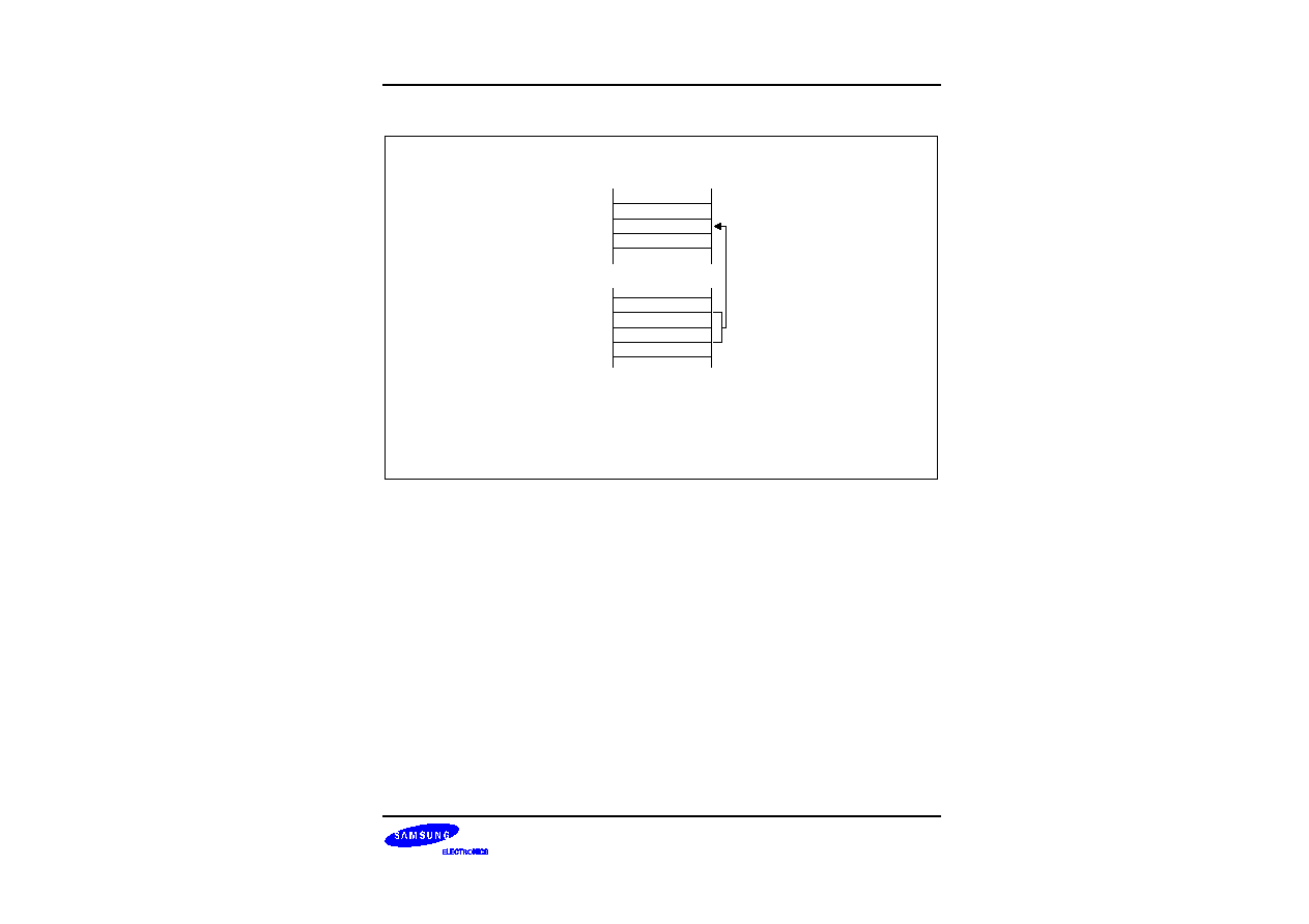
S3P80C5/C80C5/C80C8
ADDRESSING MODES
3-11
DIRECT ADDRESS MODE (Continued)
OPCODE
Program Memory
Lower Address Byte
Program Memory
Address Used
Upper Address Byte
Sample Instructions:
JP
C,JOB1
; Where JOB1 is a 16 bit immediate address
CALL
DISPLAY ; Where DISPLAY is a 16 bit immediate address
Next OPCODE
Figure 3-11. Direct Addressing for Call and Jump Instructions
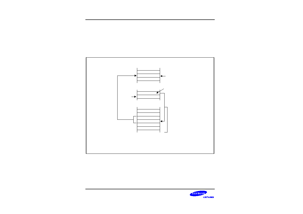
ADDRESSING MODES
S3P80C5/C80C5/C80C8
3-12
INDIRECT ADDRESS MODE (IA)
In Indirect Address (IA) mode, the instruction specifies an address located in the lowest 256 bytes of the program
memory. The selected pair of memory locations contains the actual address of the next instruction to be
executed. Only the CALL instruction can use the Indirect Address mode.
Because the Indirect Address mode assumes that the operand is located in the lowest 256 bytes of program
memory, only an 8-bit address is supplied in the instruction; the upper bytes of the destination address are
assumed to be all zeros.
Current
Instruction
Program Memory
Locations 0-255
Program Memory
OPCODE
dst
Lower Address Byte
Upper Address Byte
Next Instruction
LSB Must be Zero
Sample Instruction:
CALL
#40H ; The 16 bit value in program memory addresses 40H
and 41H is the subroutine start address.
Figure 3-12. Indirect Addressing
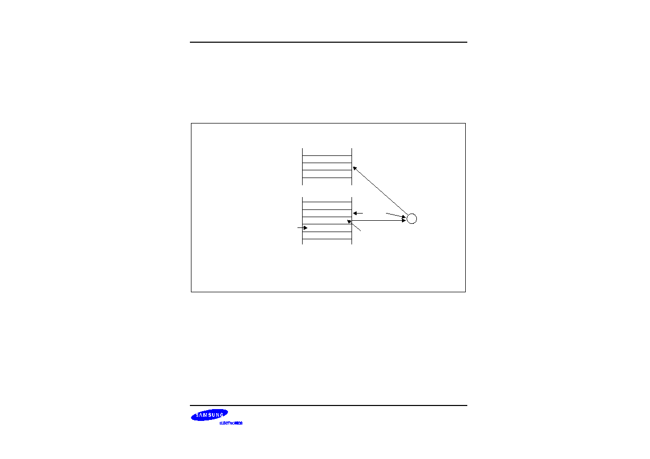
S3P80C5/C80C5/C80C8
ADDRESSING MODES
3-13
RELATIVE ADDRESS MODE (RA)
In Relative Address (RA) mode, a two's-complement signed displacement between ≠ 128 and + 127 is specified
in the instruction. The displacement value is then added to the current PC value. The result is the address of the
next instruction to be executed. Before this addition occurs, the PC contains the address of the instruction
immediately following the current instruction.
Several program control instructions use the Relative Address mode to perform conditional jumps. The
instructions that support RA addressing are BTJRF, BTJRT, DJNZ, CPIJE, CPIJNE, and JR.
OPCODE
Program Memory
Displacement
Program Memory
Address Used
Sample Instructions:
JR
ULT,$+OFFSET ; Where OFFSET is a value in the range +127 to -128
Next OPCODE
+
Signed Displacement
Value
Current Instruction
Current
PC Value
Figure 3-13. Relative Addressing
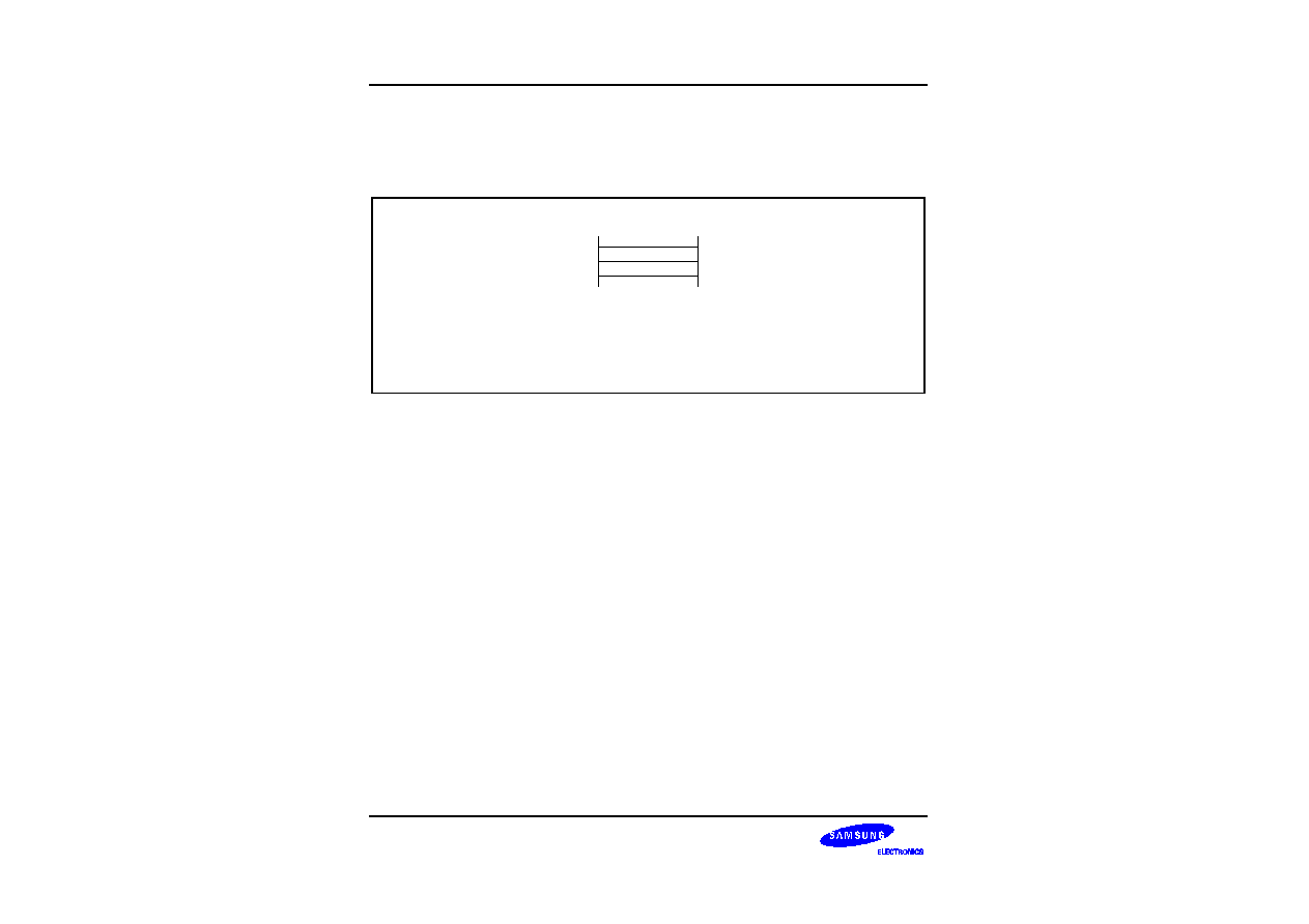
ADDRESSING MODES
S3P80C5/C80C5/C80C8
3-14
IMMEDIATE MODE (IM)
In Immediate (IM) mode, the operand value used in the instruction is the value supplied in the operand field itself.
The operand may be one byte or one word in length, depending on the instruction used. Immediate addressing
mode is useful for loading constant values into registers.
(The Operand value is in the instruction)
OPCODE
Sample Instruction:
LD R0,#0AAH
Program Memory
OPERAND
Figure 3-14. Immediate Addressing

S3P80C5/C80C5/C80C8
CONTROL REGISTERS
4-1
4
CONTROL REGISTERS
OVERVIEW
In this section, detailed descriptions of the S3P80C5/C80C5/C80C8 control registers are presented in an easy-to-
read format. You can use this section as a quick-reference source when writing application programs. Figure 4-1
illustrates the important features of the standard register description format.
Control register descriptions are arranged in alphabetical order according to register mnemonic. More detailed
information about control registers is presented in the context of the specific peripheral hardware descriptions in
Part II of this manual.
Data and counter registers are not described in detail in this reference section. More information about all of the
registers used by a specific peripheral is presented in the corresponding peripheral descriptions in Part II of this
manual.
CONTROL REGISTERS
S3P80C5/C80C5/C80C8
4-2
Table 4-1. Mapped Registers (Set 1)
Register Name
Mnemonic
Decimal
Hex
R/W
Timer 0 counter
T0CNT
208
D0H
R
(note)
Timer 0 data register
T0DATA
209
D1H
R/W
Timer 0 control register
T0CON
210
D2H
R/W
Basic timer control register
BTCON
211
D3H
R/W
Clock control register
CLKCON
212
D4H
R/W
System flags register
FLAGS
213
D5H
R/W
Register pointer 0
RP0
214
D6H
R/W
Register pointer 1
RP1
215
D7H
R/W
Locations D8H is not mapped.
Stack pointer (low byte)
SPL
217
D9H
R/W
Instruction pointer (high byte)
IPH
218
DAH
R/W
Instruction pointer (low byte)
IPL
219
DBH
R/W
Interrupt request register
IRQ
220
DCH
R
(note)
Interrupt mask register
IMR
221
DDH
R/W
System mode register
SYM
222
DEH
R/W
Register page pointer
PP
223
DFH
R/W
Port 0 data register
P0
224
E0H
R/W
Port 1 data register
P1
225
E1H
R/W
Port 2 data register
P2
226
E2H
R/W
Location E3H≠E6H is not mapped.
Port 0 pull-up resistor enable register
P0PUR
231
E7H
R/W
Port 0 control register (high byte)
P0CONH
232
E8H
R/W
Port 0 control register (low byte)
P0CONL
233
E9H
R/W
Port 1 control register (high byte)
P1CONH
234
EAH
R/W
Port 1 control register (low byte)
P1CONL
235
EBH
R/W
Port 1 pull-up resistor enable register
P1PUR
236
ECH
R/W
Location EDH≠EFH is not mapped.
Port 2 control register
P2CON
239
F0H
R/W
Port 0 interrupt enable register
P0INT
241
F1H
R/W
Port 0 interrupt pending register
P0PND
242
F2H
R/W
Counter A control register
CACON
243
F3H
R/W
Counter A data register (high byte)
CADATAH
244
F4H
R/W
Counter A data register (low byte)
CADATAL
245
F5H
R/W
Timer 1 counter register (high byte)
T1CNTH
246
F6H
R
(note)
Timer 1 counter register (low byte)
T1CNTL
247
F7H
R
(note)
Timer 1 data register (high byte)
T1DATAH
248
F8H
R/W
S3P80C5/C80C5/C80C8
CONTROL REGISTERS
4-3
Table 4-1. Mapped Registers (Continued)
Register Name
Mnemonic
Decimal
Hex
R/W
Timer 1 data register (low byte)
T1DATAL
249
F9H
R/W
Timer 1 control register
T1CON
250
FAH
R/W
STOP Control register
STOPCON
251
FBH
W
Locations FCH is not mapped.
Basic timer counter
BTCNT
253
FDH
R
(note)
External memory timing register
EMT
254
FEH
R/W
Interrupt priority register
IPR
255
FFH
R/W
NOTE: You cannot use a read-only register as a destination for the instructions OR, AND, LD, or LDB.
CONTROL REGISTERS
S3P80C5/C80C5/C80C8
4-4
FLAGS - System Flags Register
.7
Carry Flag (C)
.6
Zero Flag (Z)
.5
Bit Identifier
RESET
RESET
Value
Read/Write
Bit Addressing Mode
R = Read-only
W = Write-only
R/W = Read/write
'-' = Not used
Addressing mode or
modes you can use
to modify register
values
RESET value notation:
'-' = Not used
'x' = Undetermined value
'0' = Logic zero
'1' = Logic one
Bit number(s) that is/are appended to
the register name for bit addressing
Name of individual
bit or related bits
Register name
Register ID
Sign Flag (S)
0
Operation does not generate a carry or borrow condition
0
Operation generates carry-out or borrow into high-order bit 7
0
Operation result is a non-zero value
0
Operation result is zero
0
Operation generates positive number (MSB = "0")
0
Operation generates negative number (MSB = "1")
Description of the
effect of specific
bit settings
Set 1
Register location
in the internal
register file
D5H
Register address
(hexadecimal)
.7
.6
.5
x
x
x
R/W
R/W
R/W
Register addressing mode only
.4
.3
.2
.1
.0
x
R/W
x
R/W
x
R/W
x
R/W
0
R/W
Bit number:
MSB = Bit 7
LSB = Bit 0
Figure 4-1. Register Description Format
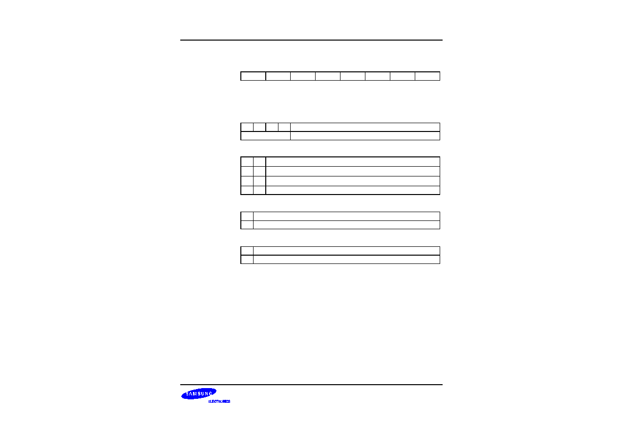
S3P80C5/C80C5/C80C8
CONTROL REGISTERS
4-5
BTCON
-- Basic Timer Control Register
D3H
Set 1
Bit Identifier
.7
.6
.5
.4
.3
.2
.1
.0
RESET
RESET
Value
0
0
0
0
0
0
0
0
Read/Write
R/W
R/W
R/W
R/W
R/W
R/W
R/W
R/W
Bit Addressing
Register addressing mode only
.7≠.4
Watchdog Timer Function Disable Code (for System Reset)
1
0
1
0
Disable watchdog timer function
Any other value
Enable watchdog timer function
.3≠.2
Basic Timer Input Clock Selection Bits
0
0
f
OSC
/4096
0
1
f
OSC
/1024
1
0
f
OSC
/128
1
1
Invalid setting; not used for S3P80C5/C80C5/C80C8.
.1
Basic Timer Counter Clear Bit
(1)
0
No effect
1
Clear the basic timer counter value
.0
Clock Frequency Divider Clear Bit for Basic Timer and Timer 0
(2)
0
No effect
1
Clear both clock frequency dividers
NOTES:
1.
When you write a "1" to BTCON.1, the basic timer counter value is cleared to '00H'. Immediately following the write
operation, the BTCON.1 value is automatically cleared to "0".
2.
When you write a "1" to BTCON.0, the corresponding frequency divider is cleared to '00H'. Immediately following the
write operation, the BTCON.0 value is automatically cleared to "0".
CONTROL REGISTERS
S3P80C5/C80C5/C80C8
4-6
CACON
--
Counter A Control Register
F3H
Set 1
Bit Identifier
.7
.6
.5
.4
.3
.2
.1
.0
RESET
RESET
Value
0
0
0
0
0
0
0
0
Read/Write
R/W
R/W
R/W
R/W
R/W
R/W
R/W
R/W
Addressing Mode
Register addressing mode only
.7≠.6
Counter A Input Clock Selection Bits
0
0
f
OSC
0
1
f
OSC
/2
1
0
f
OSC
/4
1
1
f
OSC
/8
.5≠.4
Counter A Interrupt Timing Selection Bits
0
0
Elapsed time for Low data value
0
1
Elapsed time for High data value
1
0
Elapsed time for combined Low and High data values
1
1
Invalid setting; not used for S3C80C5/C80C8.
.3
Counter A Interrupt Enable Bit
0
Disable interrupt
1
Enable interrupt
.2
Counter A Start Bit
0
Stop counter A
1
Start counter A
.1
Counter A Mode Selection Bit
0
One-shot mode
1
Repeating mode
.0
Counter A Output flip-flop Control Bit
0
Flip-flop Low level (T-FF = Low)
1
Flip-flop High level (T-FF = High)

S3P80C5/C80C5/C80C8
CONTROL REGISTERS
4-7
CLKCON
--
System Clock Control Register
D4H
Set 1
Bit Identifier
.7
.6
.5
.4
.3
.2
.1
.0
RESET
RESET
Value
0
0
0
0
0
0
0
0
Read/Write
R/W
R/W
R/W
R/W
R/W
R/W
R/W
R/W
Addressing Mode
Register addressing mode only
.7≠.6
Oscillator IRQ Wake-up Function Enable Bit
Not used for S3P80C5/C80C5/C80C8.
.6≠.5
Main Oscillator Stop Control Bits
Not used for S3P80C5/C80C5/C80C8.
.4≠.3
CPU Clock (System Clock) Selection Bits
(1)
0
0
f
OSC
/16
0
1
f
OSC
/8
1
0
f
OSC
/2
1
1
f
OSC
(non-divided)
.2≠.0
Subsystem Clock Selection Bit
(2)
1
0
1
Invalid setting for S3P80C5/C80C5/C80C8.
Other value
Select main system clock (MCLK)
NOTES:
1.
After a reset, the slowest clock (divided by 16) is selected as the system clock. To select faster clock speeds, load the
appropriate values to CLKCON.3 and CLKCON.4.
2.
These selection bits are required only for systems that have a main clock and a subsystem clock. The
S3P80C5/C80C5/C80C8 uses only the main oscillator clock circuit. For this reason, the setting '101B' is invalid.
CONTROL REGISTERS
S3P80C5/C80C5/C80C8
4-8
EMT
--
External Memory Timing Register
(note)
FEH
Set 1
Bit Identifier
.7
.6
.5
.4
.3
.2
.1
.0
RESET
RESET
Value
0
1
1
1
1
1
0
≠
Read/Write
R/W
R/W
R/W
R/W
R/W
R/W
R/W
≠
Addressing Mode
Register addressing mode only
.7
External
WAIT
WAIT
Input Function Enable Bit
0
Disable
WAIT
input function for external device
1
Enable
WAIT
input function for external device
.6
Slow Memory Timing Enable Bit
0
Disable
WAIT
input function for external device
1
Enable
WAIT
input function for external device
.5≠.4
Program Memory Automatic Wait Control Bits
0
0
No wait
0
1
Wait one cycle
1
0
Wait two cycles
1
1
Wait three cycles
.3≠.2
Data Memory Automatic Wait Control Bits
0
0
No wait
0
1
Wait one cycle
1
0
Wait two cycles
1
1
Wait three cycles
.1
Stack Area Selection Bit
0
Select internal register file area
1
Select external data memory area
.0
Not used for S3P80C5/C80C5/C80C8.
NOTE: The EMT register is not used for S3P80C5/C80C5/C80C8, because an external peripheral interface is not
implemented in the S3P80C5/C80C5/C80C8.
The program initialization routine should clear the EMT register to '00H' following a reset. Modification of EMT
values during normal operation may cause a system malfunction.
S3P80C5/C80C5/C80C8
CONTROL REGISTERS
4-9
FLAGS --
System Flags Register
D5H
Set 1
Bit Identifier
.7
.6
.5
.4
.3
.2
.1
.0
RESET
RESET
Value
x
x
x
x
x
x
0
0
Read/Write
R/W
R/W
R/W
R/W
R/W
R/W
R
R/W
Addressing Mode
Register addressing mode only
.7
Carry Flag (C)
0
Operation does not generate a carry or borrow condition
1
Operation generates a carry-out or borrow into high-order bit 7
.6
Zero Flag (Z)
0
Operation result is a non-zero value
1
Operation result is zero
.5
Sign Flag (S)
0
Operation generates a positive number (MSB = "0")
1
Operation generates a negative number (MSB = "1")
.4
Overflow Flag (V)
0
Operation result is
+127 or
≠128
1
Operation result is > +127 or < ≠128
.3
Decimal Adjust Flag (D)
0
Add operation completed
1
Subtraction operation completed
.2
Half-Carry Flag (H)
0
No carry-out of bit 3 or no borrow into bit 3 by addition or subtraction
1
Addition generated carry-out of bit 3 or subtraction generated borrow into bit 3
.1
Fast Interrupt Status Flag (FIS)
0
Interrupt return (IRET) in progress (when read)
1
Fast interrupt service routine in progress (when read)
.0
Bank Address Selection Flag (BA)
0
Bank 0 is selected
(normal setting for S3C80C5/C80C8)
1
Invalid selection (bank 1 is not implemented)
CONTROL REGISTERS
S3P80C5/C80C5/C80C8
4-10
IMR
-- Interrupt Mask Register
DDH
Set 1
Bit Identifier
.7
.6
.5
.4
.3
.2
.1
.0
RESET
RESET
Value
x
x
x
x
x
x
x
x
Read/Write
R/W
R/W
R/W
R/W
R/W
R/W
R/W
R/W
Addressing Mode
Register addressing mode only
.7
Interrupt Level 7 (IRQ7) Enable Bit; External Interrupts P0.7≠P0.4
1
Enable (un-mask)
.6
Interrupt Level 6 (IRQ6) Enable Bit; External Interrupts P0.3≠P0.0
0
Disable (mask)
1
Enable (un-mask)
.5
Not used for S3P80C5/C80C5/C80C8.
.4
Interrupt Level 4 (IRQ4) Enable Bit; Counter A Interrupt
0
Disable (mask)
1
Enable (un-mask)
.3≠.2
Not used for S3P80C5/C80C5/C80C8.
.1
Interrupt Level 1 (IRQ1) Enable Bit; Timer 1 Match or Overflow
0
Disable (mask)
1
Enable (un-mask)
.0
Interrupt Level 0 (IRQ0) Enable Bit; Timer 0 Match or Overflow
0
Disable (mask)
1
Enable (un-mask)
NOTES:
1.
When an interrupt level is masked, any interrupt requests that may be issued are not recognized by the CPU.
2.
Interrupt levels IRQ2, IRQ3 and IRQ5 are not used in the S3P80C5/C80C5/C80C8 interrupt structure.
S3P80C5/C80C5/C80C8
CONTROL REGISTERS
4-11
IPH
-- Instruction Pointer (High Byte)
DAH
Set 1
Bit Identifier
.7
.6
.5
.4
.3
.2
.1
.0
RESET
RESET
Value
x
x
x
x
x
x
x
x
Read/Write
R/W
R/W
R/W
R/W
R/W
R/W
R/W
R/W
Addressing Mode
Register addressing mode only
.7≠.0
Instruction Pointer Address (High Byte)
The high-byte instruction pointer value is the upper eight bits of the 16-bit instruction
pointer address (IP15≠IP8). The lower byte of the IP address is located in the IPL
register (DBH).
IPL
-- Instruction Pointer (Low Byte)
DBH
Set 1
Bit Identifier
.7
.6
.5
.4
.3
.2
.1
.0
RESET
RESET
Value
x
x
x
x
x
x
x
x
Read/Write
R/W
R/W
R/W
R/W
R/W
R/W
R/W
R/W
Addressing Mode
Register addressing mode only
.7≠.0
Instruction Pointer Address (Low Byte)
The low-byte instruction pointer value is the lower eight bits of the 16-bit instruction
pointer address (IP7≠IP0). The upper byte of the IP address is located in the IPH
register (DAH).
CONTROL REGISTERS
S3P80C5/C80C5/C80C8
4-12
IPR
-- Interrupt Priority Register
FFH
Set 1
Bit Identifier
.7
.6
.5
.4
.3
.2
.1
.0
RESET
RESET
Value
0
0
0
0
0
0
0
0
Read/Write
R/W
R/W
R/W
R/W
R/W
R/W
R/W
R/W
Bit Addressing
Register addressing mode only
.7, .4, and .1
Priority Control Bits for Interrupt Groups A, B, and C
0
0
0
Group priority undefined
0
0
1
B > C > A
0
1
0
A > B > C
0
1
1
B > A > C
1
0
0
C > A > B
1
0
1
C > B > A
1
1
0
A > C > B
1
1
1
Group priority undefined
.6
Interrupt Subgroup C Priority Control Bit
0
IRQ6 > IRQ7
1
IRQ7 > IRQ6
.5, .3
Not used for S3P80C5/C80C5/C80C8.
.2
Input Group B Priority Control Bit
0
IRQ4
1
IRQ4
.0
Interrupt Group A Priority Control Bit
0
IRQ0 > IRQ1
1
IRQ1 > IRQ0
NOTE: The S3P80C5/C80C5/C80C8 interrupt structure uses only five levels:
IRQ0, IRQ1, IRQ4, IRQ6≠IRQ7. Because IRQ2, IRQ3, IRQ5 are not recognized, the interrupt subgroup B and
group C settings (IPR.2,.3 and IPR.5) are not evaluated.
S3P80C5/C80C5/C80C8
CONTROL REGISTERS
4-13
IRQ
-- Interrupt Request Register
DCH
Set 1
Bit Identifier
.7
.6
.5
.4
.3
.2
.1
.0
RESET
RESET
Value
0
0
0
0
0
0
0
0
Read/Write
R
R
R
R
R
R
R
R
Addressing Mode
Register addressing mode only
.7
Level 7 (IRQ7) Request Pending Bit; External Interrupts P0.7≠P0.4
0
Not pending
1
Pending
.6
Level 6 (IRQ6) Request Pending Bit; External Interrupts P0.3≠P0.0
0
Not pending
1
Pending
.5
Not used for S3P80C5/C80C5/C80C8.
.4
Level 4 (IRQ4) Request Pending Bit; Counter A Interrupt
0
Not pending
1
Pending
.3≠.2
Not used for S3P80C5/C80C5/C80C8.
.1
Level 1 (IRQ1) Request Pending Bit; Timer 1 Match or Overflow
0
Not pending
1
Pending
.0
Level 0 (IRQ0) Request Pending Bit; Timer 0 Match or Overflow
0
Not pending
1
Pending
NOTE: Interrupt level IRQ2, IRQ3 and IRQ5 is not used in the S3P80C5/C80C5/C80C8 interrupt structure.
CONTROL REGISTERS
S3P80C5/C80C5/C80C8
4-14
P0CONH
-- Port 0 Control Register (High Byte)
E8H
Set 1
Bit Identifier
.7
.6
.5
.4
.3
.2
.1
.0
RESET
RESET
Value
0
0
0
0
0
0
0
0
Read/Write
R/W
R/W
R/W
R/W
R/W
R/W
R/W
R/W
Addressing Mode
Register addressing mode only
.7≠.6
P0.7/INT4 Mode Selection Bits
0
0
C-MOS input mode; interrupt on falling edges
0
1
C-MOS input mode; interrupt on rising and falling edges
1
0
Push-pull output mode
1
1
C-MOS input mode; interrupt on rising edges
.5≠.4
P0.6/INT4 Mode Selection Bits
0
0
C-MOS input mode; interrupt on falling edges
0
1
C-MOS input mode; interrupt on rising and falling edges
1
0
Push-pull output mode
1
1
C-MOS input mode; interrupt on rising edges
.3≠.2
P0.5/INT4 Mode Selection Bits
0
0
C-MOS input mode; interrupt on falling edges
0
1
C-MOS input mode; interrupt on rising and falling edges
1
0
Push-pull output mode
1
1
C-MOS input mode; interrupt on rising edges
.1≠.0
P0.4/INT4 Mode Selection Bits
0
0
C-MOS input mode; interrupt on falling edges
0
1
C-MOS input mode; interrupt on rising and falling edges
1
0
Push-pull output mode
1
1
C-MOS input mode; interrupt on rising edges
NOTES:
1.
The INT4 external interrupts at the P0.7≠P0.4 pins share the same interrupt level (IRQ7) and interrupt vector
address (E8H).
2.
You can assign pull-up resistors to individual port 0 pins by making the appropriate settings to the P0PUR register.

S3P80C5/C80C5/C80C8
CONTROL REGISTERS
4-15
P0CONL
-- Port 0 Control Register (Low Byte)
E9H
Set 1
Bit Identifier
.7
.6
.5
.4
.3
.2
.1
.0
RESET
RESET
Value
0
0
0
0
0
0
0
0
Read/Write
R/W
R/W
R/W
R/W
R/W
R/W
R/W
R/W
Addressing Mode
Register addressing mode only
.7≠.6
P0.3/INT3 Mode Selection Bits
0
0
C-MOS input mode; interrupt on falling edges
0
1
C-MOS input mode; interrupt on rising and falling edges
1
0
Push-pull output mode
1
1
C-MOS input mode; interrupt on rising edges
.5≠.4
P0.2/INT2 Mode Selection Bits
0
0
C-MOS input mode; interrupt on falling edges
0
1
C-MOS input mode; interrupt on rising and falling edges
1
0
Push-pull output mode
1
1
C-MOS input mode; interrupt on rising edges
.3≠.2
P0.1/INT1 Mode Selection Bits
0
0
C-MOS input mode; interrupt on falling edges
0
1
C-MOS input mode; interrupt on rising and falling edges
1
0
Push-pull output mode
1
1
C-MOS input mode; interrupt on rising edges
.1≠.0
P0.0/INT0 Mode Selection Bits
0
0
C-MOS input mode; interrupt on falling edges
0
1
C-MOS input mode; interrupt on rising and falling edges
1
0
Push-pull output mode
1
1
C-MOS input mode; interrupt on rising edges
NOTES:
1.
The INT3≠INT0 external interrupts at P0.3≠P0.0 are interrupt level IRQ6. Each interrupt has a separate vector
address.
2.
You can assign pull-up resistors to individual port 0 pins by making the appropriate settings to the P0PUR register.

CONTROL REGISTERS
S3P80C5/C80C5/C80C8
4-16
P0INT
-- Port 0 External Interrupt Enable Register
F1H
Set 1
Bit Identifier
.7
.6
.5
.4
.3
.2
.1
.0
RESET
RESET
Value
0
0
0
0
0
0
0
0
Read/Write
R
R
R
R
R
R
R
R
Addressing Mode
Register addressing mode only
.7
P0.7 External Interrupt (INT4) Enable Bit
0
Disable interrupt
1
Enable interrupt
.6
P0.6 External Interrupt (INT4) Enable Bit
0
Disable interrupt
1
Enable interrupt
.5
P0.5 External Interrupt (INT4) Enable Bit
0
Disable interrupt
1
Enable interrupt
.4
P0.4 External Interrupt (INT4) Enable Bit
0
Disable interrupt
1
Enable interrupt
.3
P0.3 External Interrupt (INT3) Enable Bit
0
Disable interrupt
1
Enable interrupt
.2
P0.2 External Interrupt (INT2) Enable Bit
0
Disable interrupt
1
Enable interrupt
.1
P0.1 External Interrupt (INT1) Enable Bit
0
Disable interrupt
1
Enable interrupt
.0
P0.0 External Interrupt (INT0) Enable Bit
0
Disable interrupt
1
Enable interrupt
S3P80C5/C80C5/C80C8
CONTROL REGISTERS
4-17
P0PND
-- Port 0 External Interrupt Pending Register
F2H
Set 1
Bit Identifier
.7
.6
.5
.4
.3
.2
.1
.0
RESET
RESET
Value
0
0
0
0
0
0
0
0
Read/Write
R/W
R/W
R/W
R/W
R/W
R/W
R/W
R/W
Addressing Mode
Register addressing mode only
.7
P0.7 External Interrupt (INT4) Pending Flag
(note)
0
No P0.7 external interrupt pending (when read)
1
P0.7 external interrupt is pending (when read)
.6
P0.6 External Interrupt (INT4) Pending Flag
0
No P0.6 external interrupt pending (when read)
1
P0.6 external interrupt is pending (when read)
.5
P0.5 External Interrupt (INT4) Pending Flag
0
No P0.5 external interrupt pending (when read)
1
P0.5 external interrupt is pending (when read)
.4
P0.4 External Interrupt (INT4) Pending Flag
0
No P0.4 external interrupt pending (when read)
1
P0.4 external interrupt is pending (when read)
.3
P0.3 External Interrupt (INT3) Pending Flag
0
No P0.3 external interrupt pending (when read)
1
P0.3 external interrupt is pending (when read)
.2
P0.2 External Interrupt (INT2) Pending Flag
0
No P0.2 external interrupt pending (when read)
1
P0.2 external interrupt is pending (when read)
.1
P0.1 External Interrupt (INT1) Pending Flag
0
No P0.1 external interrupt pending (when read)
1
P0.1 external interrupt is pending (when read)
.0
P0.0 External Interrupt (INT0) Pending Flag
0
No P0.0 external interrupt pending (when read)
1
P0.0 external interrupt is pending (when read)
NOTE: To clear an interrupt pending condition, write a "0" to the appropriate pending flag. Writing a "1" to an interrupt
pending flag (POND.0≠7) has no effect.
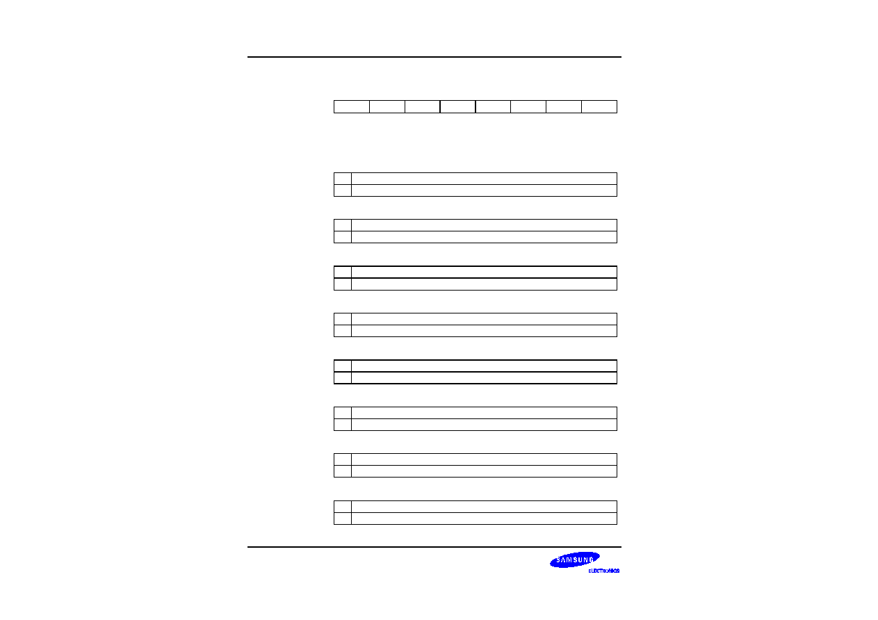
CONTROL REGISTERS
S3P80C5/C80C5/C80C8
4-18
P0PUR
-- Port 0 Pull-up Resistor Enable Register
E7H
Set 1
Bit Identifier
.7
.6
.5
.4
.3
.2
.1
.0
RESET
RESET
Value
0
0
0
0
0
0
0
0
Read/Write
R/W
R/W
R/W
R/W
R/W
R/W
R/W
R/W
Addressing Mode
Register addressing mode only
.7
P0.7 Pull-up Resistor Enable Bit
0
Enable pull-up resistor
1
Disable pull-up resistor
.6
P0.6 Pull-up Resistor Enable Bit
0
Enable pull-up resistor
1
Disable pull-up resistor
.5
P0.5 Pull-up Resistor Enable Bit
0
Enable pull-up resistor
1
Disable pull-up resistor
.4
P0.4 Pull-up Resistor Enable Bit
0
Enable pull-up resistor
1
Disable pull-up resistor
.3
P0.3 Pull-up Resistor Enable Bit
0
Enable pull-up resistor
1
Disable pull-up resistor
.2
P0.2 Pull-up Resistor Enable Bit
0
Enable pull-up resistor
1
Disable pull-up resistor
.1
P0.1 Pull-up Resistor Enable Bit
0
Enable pull-up resistor
1
Disable pull-up resistor
.0
P0.0 Pull-up Resistor Enable Bit
0
Enable pull-up resistor
1
Disable pull-up resistor
S3P80C5/C80C5/C80C8
CONTROL REGISTERS
4-19
P1CONH
-- Port 1 Control Register (High Byte)
EAH
Set 1
Bit Identifier
.7
.6
.5
.4
.3
.2
.1
.0
RESET
RESET
Value
0
0
0
0
0
0
0
0
Read/Write
R/W
R/W
R/W
R/W
R/W
R/W
R/W
R/W
Addressing Mode
Register addressing mode only
.7≠.6
P1.7 Mode Selection Bits
0
0
C-MOS input mode
0
1
Open-drain output mode
1
0
Push-pull output mode
1
1
Invalid setting
.5≠.4
P1.6 Mode Selection Bits
0
0
C-MOS input mode
0
1
Open-drain output mode
1
0
Push-pull output mode
1
1
Invalid setting
.3≠.2
P1.5 Mode Selection Bits
0
0
C-MOS input mode
0
1
Open-drain output mode
1
0
Push-pull output mode
1
1
Invalid setting
.1≠.0
P1.4 Mode Selection Bits
0
0
C-MOS input mode
0
1
Open-drain output mode
1
0
Push-pull output mode
1
1
Invalid setting

CONTROL REGISTERS
S3P80C5/C80C5/C80C8
4-20
P1CONL
-- Port 1 Control Register (Low Byte)
EBH
Set 1
Bit Identifier
.7
.6
.5
.4
.3
.2
.1
.0
RESET
RESET
Value
0
0
0
0
0
0
0
0
Read/Write
R/W
R/W
R/W
R/W
R/W
R/W
R/W
R/W
Addressing Mode
Register addressing mode only
.7≠.6
P1.3 Mode Selection Bits
0
0
C-MOS input mode
0
1
Open-drain output mode
1
0
Push-pull output mode
1
1
Invalid setting
.5≠.4
P1.2 Mode Selection Bits
0
0
C-MOS input mode
0
1
Open-drain output mode
1
0
Push-pull output mode
1
1
Invalid setting
.3≠.2
P1.1 Mode Selection Bits
0
0
C-MOS input mode
0
1
Open-drain output mode
1
0
Push-pull output mode
1
1
Invalid setting
.1≠.0
P1.0 Mode Selection Bits
0
0
C-MOS input mode
0
1
Open-drain output mode
1
0
Push-pull output mode
1
1
Invalid setting

S3P80C5/C80C5/C80C8
CONTROL REGISTERS
4-21
P1PUR
-- Port 0 Pull-up Resistor Enable Register
ECH
Set 1
Bit Identifier
.7
.6
.5
.4
.3
.2
.1
.0
RESET
RESET
Value
0
0
0
0
0
0
0
0
Read/Write
R/W
R/W
R/W
R/W
R/W
R/W
R/W
R/W
Addressing Mode
Register addressing mode only
.7
P1.7 Pull-up Resistor Enable Bit
0
Disable pull-up resistor
1
Enable pull-up resistor
.6
P1.6 Pull-up Resistor Enable Bit
0
Disable pull-up resistor
1
Enable pull-up resistor
.5
P1.5 Pull-up Resistor Enable Bit
0
Disable pull-up resistor
1
Enable pull-up resistor
.4
P1.4 Pull-up Resistor Enable Bit
0
Disable pull-up resistor
1
Enable pull-up resistor
.3
P1.3 Pull-up Resistor Enable Bit
0
Disable pull-up resistor
1
Enable pull-up resistor
.2
P1.2 Pull-up Resistor Enable Bit
0
Disable pull-up resistor
1
Enable pull-up resistor
.1
P1.1 Pull-up Resistor Enable Bit
0
Disable pull-up resistor
1
Enable pull-up resistor
.0
P1.0 Pull-up Resistor Enable Bit
0
Disable pull-up resistor
1
Enable pull-up resistor
CONTROL REGISTERS
S3P80C5/C80C5/C80C8
4-22
P2CON
-- Port 2 Control Register
F0H
Set 1
Bit Identifier
.7
.6
.5
.4
.3
.2
.1
.0
RESET
RESET
Value
0
0
0
0
0
0
0
0
Read/Write
R/W
R/W
R/W
R/W
R/W
R/W
R/W
R/W
Addressing Mode
Register addressing mode only
.7≠.6
P2.2 Mode Selection Bits
0
0
C-MOS input mode
0
1
Open-drain output mode
1
0
Push-pull output mode
1
1
C-MOS input with pull up mode
.5≠.4
P2.1 Mode Selection Bits
0
0
C-MOS input mode
0
1
Open-drain output mode
1
0
Push-pull output mode
1
1
C-MOS input with pull up mode
.3≠.2
P2.0 Mode Selection Bits
0
0
C-MOS input mode
0
1
Open-drain output mode
1
0
Push-pull output mode
1
1
C-MOS input with pull up mode
.1
P2.1 Alternative Function Selection Bits
0
Normal I/O function
0
REM/T0CK function
.0
P2.0 Alternative Function Selection Bits
0
Normal I/O function
0
T0PWN function
S3P80C5/C80C5/C80C8
CONTROL REGISTERS
4-23
PP
-- Register Page Pointer
DFH
Set 1
Bit Identifier
.7
.6
.5
.4
.3
.2
.1
.0
RESET
RESET
Value
0
0
0
0
0
0
0
0
Read/Write
R/W
R/W
R/W
R/W
R/W
R/W
R/W
R/W
Addressing Mode
Register addressing mode only
.7≠.4
Destination Register Page Selection Bits
0
0
0
0
Destination: page 0
(note)
.3≠.0
Source Register Page Selection Bits Bits
0
0
0
0
Source: page 0
(note)
NOTE: In the S3P80C5/C80C5/C80C8 microcontroller, a paged expansion of the
internal register file is not implemented. For this reason, only page 0 settings are valid. Register page pointer values
for the source and destination register page are automatically set to '0000B' following a hardware reset. These
values should not be changed during normal operation.
CONTROL REGISTERS
S3P80C5/C80C5/C80C8
4-24
RP0
-- Register Pointer 0
D6H
Set 1
Bit Identifier
.7
.6
.5
.4
.3
.2
.1
.0
RESET
RESET
Value
1
1
0
0
0
≠
≠
≠
Read/Write
R/W
R/W
R/W
R/W
R/W
≠
≠
≠
Addressing Mode
Register addressing mode only
.7≠.3
Destination Register Page Selection Bits
Register pointer 0 can independently point to one of the 24 8-byte working register
areas in the register file. Using the register pointers RP0 and RP1, you can select
two 8-byte register slices at one time as active working register space. After a reset,
RP0 points to address C0H in register set 1, selecting the 8-byte working register
slice C0H≠C7H.
.2≠.0
Not used for S3P80C5/C80C5/C80C8.
RP1
-- Register Pointer 1
D7H
Set 1
Bit Identifier
.7
.6
.5
.4
.3
.2
.1
.0
RESET
RESET
Value
1
1
0
0
1
≠
≠
≠
Read/Write
R/W
R/W
R/W
R/W
R/W
≠
≠
≠
Addressing Mode
Register addressing mode only
.7≠.3
Register Pointer 1 Address Value
Register pointer 1 can independently point to one of the 24 8-byte working register
areas in the register file. Using the register pointers RP0 and RP1, you can select
two 8-byte register slices at one time as active working register space. After a reset,
RP1 points to address C8H in register set 1, selecting the 8-byte working register
slice C8H≠CFH.
.2≠.0
Not used for S3P80C5/C80C5/C80C8.
S3P80C5/C80C5/C80C8
CONTROL REGISTERS
4-25
SPL
-- Stack Pointer (Low Byte)
D9H
Set 1
Bit Identifier
.7
.6
.5
.4
.3
.2
.1
.0
RESET
RESET
Value
x
x
x
x
x
x
x
x
Read/Write
R/W
R/W
R/W
R/W
R/W
R/W
R/W
R/W
Addressing Mode
Register addressing mode only
.7≠.0
Stack Pointer Address (Low Byte)
The SP value is undefined following a reset.
STOPCON
-- Stop Control Register
FBH
Set 1
Bit Identifier
.7
.6
.5
.4
.3
.2
.1
.0
RESET
RESET
Value
0
0
0
0
0
0
0
0
Read/Write
W
W
W
W
W
W
W
W
Addressing Mode
Register addressing mode only
.7≠.0
Stop Control Register enable bits
1
0
1
0
0
1
0
1
Enable STOPCON
NOTES:
1.
To get into STOP mode, stop control register must be enabled just before STOP instruction.
2.
When STOP mode is released, stop control register (STOPCON) value is cleared automatically.
3.
It is prohibited to write another value into STOPCON.
CONTROL REGISTERS
S3P80C5/C80C5/C80C8
4-26
SYM
-- System Mode Register
DEH
Set 1
Bit Identifier
.7
.6
.5
.4
.3
.2
.1
.0
RESET
RESET
Value
0
≠
≠
x
x
x
0
0
Read/Write
R/W
≠
≠
R/W
R/W
R/W
R/W
R/W
Addressing Mode
Register addressing mode only
.7
Tri-State External Interface Control Bit
(1)
0
Normal operation (disable tri-state operation)
1
Set external interface lines to high impedance (enable tri-state operation)
.6≠.5
Not used for S3P80C5/C80C5/C80C8.
.4≠.2
Fast Interrupt Level Selection Bits
(2)
0
0
0
IRQ0
0
0
1
IRQ1
0
1
0
Not used for
0
1
1
S3P80C5/C80C5/C80C8.
1
0
0
1
0
1
1
1
0
IRQ6
1
1
1
IRQ7
.1
Fast Interrupt Enable Bit
(3)
0
Disable fast interrupt processing
1
Enable fast interrupt processing
.0
Global Interrupt Enable Bit
(4)
0
Disable global interrupt processing
1
Enable global interrupt processing
NOTES:
1.
Because an external interface is not implemented for the S3P80C5/C80C5/C80C8, SYM.7 must always be "0".
2.
You can select only one interrupt level at a time for fast interrupt processing.
3.
Setting SYM.1 to "1" enables fast interrupt processing for the interrupt level currently selected by SYM.2≠SYM.4.
4.
Following a reset, you must enable global interrupt processing by executing an EI instruction (not by writing a "1"
to SYM.0).

S3P80C5/C80C5/C80C8
CONTROL REGISTERS
4-27
T0CON
-- Timer 0 Control Register
D2H
Set 1
Bit Identifier
.7
.6
.5
.4
.3
.2
.1
.0
RESET
RESET
Value
0
0
0
0
0
0
0
0
Read/Write
R/W
R/W
R/W
R/W
R/W
R/W
R/W
R/W
Addressing Mode
Register addressing mode only
.7≠.6
Timer 0 Input Clock Selection Bits
0
0
f
OSC
/4096
0
1
f
OSC
/256
1
0
f
OSC
/8
1
1
External clock input (at the T0CK pin, P2.1)
.5≠.4
Timer 0 Operating Mode Selection Bits
0
0
Interval timer mode (counter cleared by match signal)
0
1
Overflow mode (OVF interrupt can occur)
1
0
Overflow mode (OVF interrupt can occur)
1
1
PWM mode (OVF interrupt can occur)
.3
Timer 0 Counter Clear Bit
0
No effect (when write)
1
Clear T0 counter, T0CNT (when write)
.2
Timer 0 Overflow Interrupt Enable Bit
(note)
0
Disable T0 overflow interrupt
1
Enable T0 overflow interrupt
.1
Timer 0 Match Interrupt Enable Bit
0
Disable T0 match interrupt
1
Enable T0 match interrupt
.0
Timer 0 Match Interrupt Pending Flag
0
No T0 match interrupt pending (when read)
0
Clear T0 match interrupt pending condition (when write)
1
T0 match interrupt is pending (when read)
1
No effect (when write)
NOTE: A timer 0 overflow interrupt pending condition is automatically cleared by hardware. However, the timer 0
match/ capture interrupt, IRQ0, vector FCH, must be cleared by the interrupt service routine.

CONTROL REGISTERS
S3P80C5/C80C5/C80C8
4-28
T1CON
-- Timer 1 Control Register
FAH
Set 1
Bit Identifier
.7
.6
.5
.4
.3
.2
.1
.0
RESET
RESET
Value
0
0
0
0
0
0
0
0
Read/Write
R/W
R/W
R/W
R/W
R/W
R/W
R/W
R/W
Addressing Mode
Register addressing mode only
.7≠.6
Timer 1 Input Clock Selection Bits
0
0
f
OSC
/4
0
1
f
OSC
/8
1
0
f
OSC
/16
1
1
Internal clock (counter a flip-flop, T-FF)
.5≠.4
Timer 1 Operating Mode Selection Bits
0
0
Interval timer mode (counter cleared by match signal)
0
1
Overflow mode (OVF interrupt can occur)
1
0
Overflow mode (OVF interrupt can occur)
1
1
Overflow mode (OVF interrupt can occur)
.3
Timer 1 Counter Clear Bit
0
No effect (when write)
1
Clear T1 counter, T1CNT (when write)
.2
Timer 1 Overflow Interrupt Enable Bit
(note)
0
Disable T1 overflow interrupt
1
Enable T1 overflow interrupt
.1
Timer 1 Match/Capture Interrupt Enable Bit
0
Disable T1 match interrupt
1
Enable T1 match interrupt
.0
Timer 1 Match/Capture Interrupt Pending Flag
0
No T1 match interrupt pending (when read)
0
Clear T1 match interrupt pending condition (when write)
1
T1 match interrupt is pending (when read)
1
No effect (when write)
NOTE: A timer 1 overflow interrupt pending condition is automatically cleared by hardware. However, the timer 1 match/
capture interrupt, IRQ1, vector F6H, must be cleared by the interrupt service routine.

S3P80C5/C80C5/C80C8
INTERRUPT STRUCTURE
5-1
5
INTERRUPT STRUCTURE
OVERVIEW
The S3C8-series interrupt structure has three basic components: levels, vectors, and sources. The SAM87 CPU
recognizes up to eight interrupt levels and supports up to 128 interrupt vectors. When a specific interrupt level
has more than one vector address, the vector priorities are established in hardware. A vector address can be
assigned to one or more sources.
Levels
Interrupt levels are the main unit for interrupt priority assignment and recognition. All peripherals and I/O blocks
can issue interrupt requests. In other words, peripheral and I/O operations are interrupt-driven. There are eight
possible interrupt levels: IRQ0≠IRQ7, also called level 0 ≠ level 7. Each interrupt level directly corresponds to an
interrupt request number (IRQn). The total number of interrupt levels used in the interrupt structure varies from
device to device. The S3P80C5/C80C5/C80C8 interrupt structure recognizes five interrupt levels.
The interrupt level numbers 0 through 7 do not necessarily indicate the relative priority of the levels. They are
simply identifiers for the interrupt levels that are recognized by the CPU. The relative priority of different interrupt
levels is determined by settings in the interrupt priority register, IPR. Interrupt group and subgroup logic controlled
by IPR settings lets you define more complex priority relationships between different levels.
Vectors
Each interrupt level can have one or more interrupt vectors, or it may have no vector address assigned at all.
The maximum number of vectors that can be supported for a given level is 128. (The actual number of vectors
used for S3C8-series devices is always much smaller.) If an interrupt level has more than one vector address, the
vector priorities are set in hardware. The S3P80C5/C80C5/C80C8 uses ten vectors. One vector address is
shared by four interrupt sources.
Sources
A source is any peripheral that generates an interrupt. A source can be an external pin or a counter overflow, for
example. Each vector can have several interrupt sources. In the S3P80C5/C80C5/C80C8 interrupt structure,
there are thirteen possible interrupt sources.
When a service routine starts, the respective pending bit is either cleared automatically by hardware or is must
be cleared "manually" by program software. The characteristics of the source's pending mechanism determine
which method is used to clear its respective pending bit.
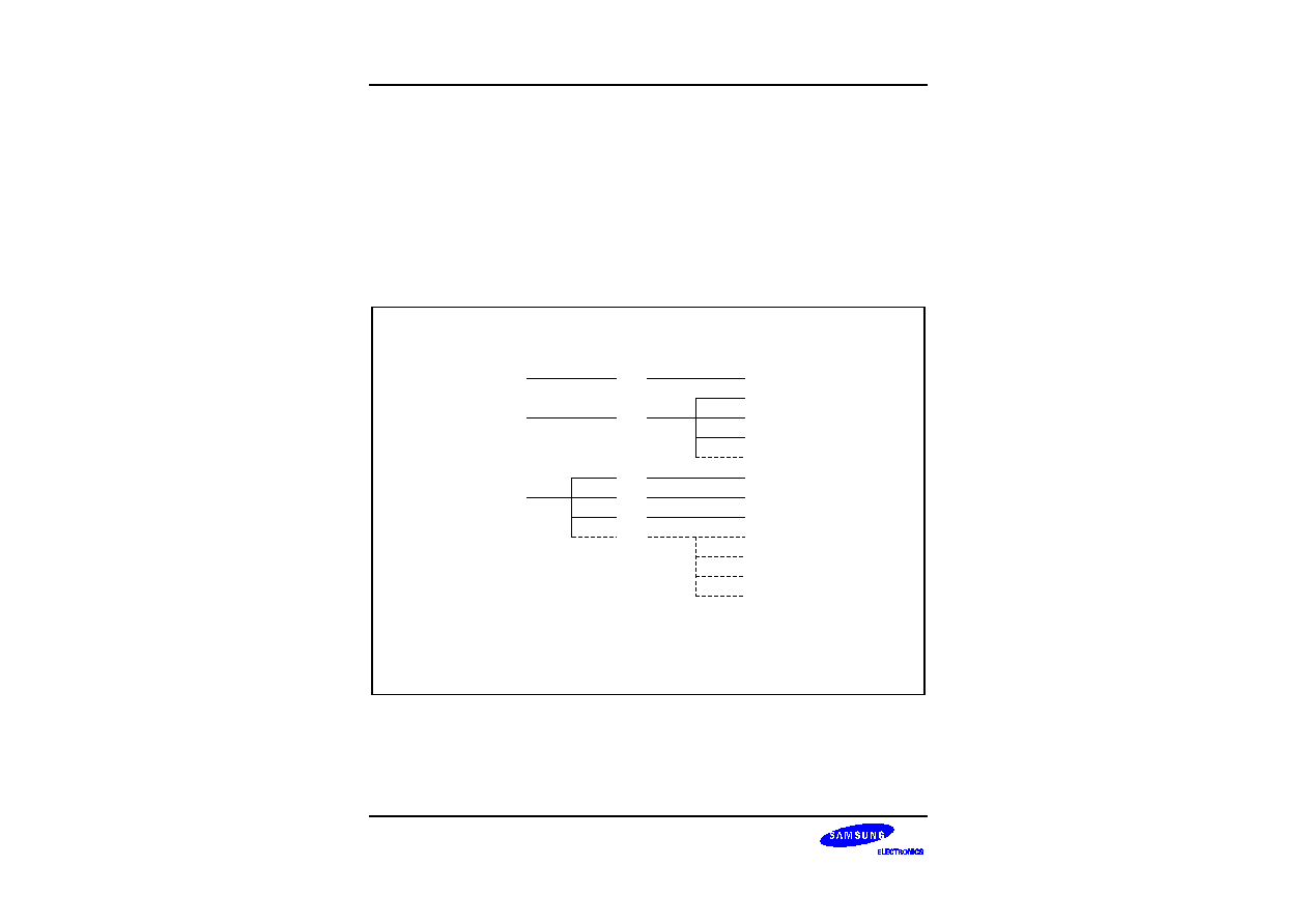
INTERRUPT STRUCTURE
S3P80C5/C80C5/C80C8
5-2
INTERRUPT TYPES
The three components of the S3C8 interrupt structure described above -- levels, vectors, and sources -- are
combined to determine the interrupt structure of an individual device and to make full use of its available
interrupt logic. There are three possible combinations of interrupt structure components, called interrupt types 1,
2, and 3. The types differ in the number of vectors and interrupt sources assigned to each level (see Figure 5-1):
Type 1:
One level (IRQn) + one vector (V
1
) + one source (S
1
)
Type 2:
One level (IRQn) + one vector (V
1
) + multiple sources (S
1
≠ S
n
)
Type 3:
One level (IRQn) + multiple vectors (V
1
≠ V
n
) + multiple sources (S
1
≠ S
n
, S
n+1
≠ S
n+m
)
In the S3P80C5/C80C5/C80C8 microcontroller, all three interrupt types are implemented.
Vectors
Sources
Levels
S
1
V
1
S
2
Type 2:
IRQn
S
3
S
n
V
1
S
1
V
2
S
2
Type 3:
IRQn
V
3
S
3
V
1
S
1
Type 1:
IRQn
V
n
S
n +
1
S
n
S
n +
2
S
n +
m
NOTES:
1. The number of S
n
and V
n
value is expandable.
2. In the S3P80C5/C80C5/C80C8 implementation, interrupt types 1, 2, and 3 is used.
Figure 5-1. S3C8-Series Interrupt Types

S3P80C5/C80C5/C80C8
INTERRUPT STRUCTURE
5-3
S3P80C5/C80C5/C80C8 INTERRUPT STRUCTURE
The S3P80C5 microcontroller supports two kinds interrupt structure
-- Vectored Interrupt
-- Non vectored interrupt (Reset interrupt): INTR
The S3P80C5/C80C5/C80C8 microcontroller supports thirteen interrupt sources. Nine of the interrupt sources
have a corresponding interrupt vector address; the remaining four interrupt sources share the same vector
address. Five interrupt levels are recognized by the CPU in this device-specific interrupt structure, as shown in
Figure 5-2.
When multiple interrupt levels are active, the interrupt priority register (IPR) determines the order in which
contending interrupts are to be serviced. If multiple interrupts occur within the same interrupt level, the interrupt
with the lowest vector address is usually processed first. (The relative priorities of multiple interrupts within a
single level are fixed in hardware.)
When the CPU grants an interrupt request, interrupt processing starts: All other interrupts are disabled and the
program counter value and state flags are pushed to stack. The starting address of the service routine is fetched
from the appropriate vector address (plus the next 8-bit value to concatenate the full 16-bit address) and the
service routine is executed. The S3P80C5/C80C5/C80C8 microcontroller supports non vectored interrupt -
Interrupt with Reset(INTR) - to occur interrupt with system reset. The Interrupt with Reset(INTR) has nothing to do
with interrupt levels, vectors and the registers that are related to interrupt setting. It occurs only according to the
"P0" during " STOP " regardless any other things. Namely, only when a falling/rising edge occurs at any pin of
Port 0 during STOP status, this INTR and a system reset occurs even though SYM.0 is "0"(Disable interrupt). But
it dose not occurs while the oscillation - "IDLE" or "OPERATING" status- even though a falling/rising edge occurs
at port 0.
Following is the sequence that occurs Interrupt with Reset(INTR).
1.
The oscillation status is "freeze" : STOP mode
2.
A falling/rising edge is detected to any pin of Port 0.
3.
INTR occurs and it makes system reset.
4.
STOP mode is released by this system reset.
NOTE
Because H/W reset occurs whenever INTR occurs. A user should aware of the each ports, system
register, control register etc."

INTERRUPT STRUCTURE
S3P80C5/C80C5/C80C8
5-4
NOTE:
For interrupt levels with two or more vectors, the lowest vector address
usually the highest priority. For example, FAH has the higher priority (0)
than FCH (1) within level IRQ0. These priorities are fixed in hardware.
Vectors
Sources
Levels
Reset/Clear
RESET
100H
Basic timer overflow/INTR/POR
H/W
Timer 0 match
S/W
IRQ0
Timer 0 overflow
H/W
Timer 1 match
S/W
IRQ1
Timer 1 overflow
H/W
Counter A
H/W
P0.3 external interrupt
S/W
P0.2 external interrupt
S/W
P0.1 external interrupt
S/W
P0.0 external interrupt
S/W
P0.7 external interrupt
S/W
P0.6 external interrupt
S/W
IRQ7
P0.5 external interrupt
S/W
P0.4 external interrupt
S/W
FCH
FAH
F6H
F4H
E8H
E6H
E4H
IRQ6
E2H
E0H
IRQ4
ECH
1
0
1
0
3
2
1
0
Figure 5-2. S3P80C5/C80C5/C80C8 Interrupt Structure
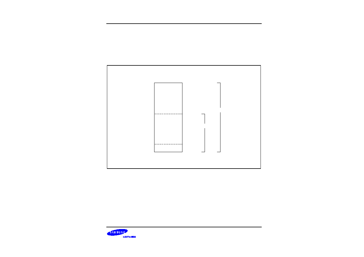
S3P80C5/C80C5/C80C8
INTERRUPT STRUCTURE
5-5
INTERRUPT VECTOR ADDRESSES
All interrupt vector addresses for the S3P80C5/C80C5/C80C8 interrupt structure are stored in the vector address
area of the internal program memory ROM, 00H≠FFH. You can allocate unused locations in the vector address
area as normal program memory. If you do so, please be careful not to overwrite any of the stored vector
addresses. (Table 5-2 lists all vector addresses.)
The program reset address in the ROM is 0100H.
15,872
15-Kbyte
ROM
8-Kbyte
ROM
Interrupt
Vector Area
8,191
255
0
3E00H
1FFFH
0FFH
0H
(Decimal)
(HEX)
S3C80C5
S3C80C8
Figure 5-3. ROM Vector Address Area

INTERRUPT STRUCTURE
S3P80C5/C80C5/C80C8
5-6
Table 5-1. S3P80C5/C80C5/C80C8 Interrupt Vectors
Vector Address
Interrupt Source
Request
Reset/Clear
Decimal
Value
Hex
Value
Interrupt
Level
Priority in
Level
H/W
S/W
254
100H
Basic timer overflow
RESET
≠
252
FCH
Timer 0 (match)
IRQ0
1
250
FAH
Timer 0 overflow
0
246
F6H
Timer 1 (match)
IRQ1
1
244
F4H
Timer 1 overflow
0
236
ECH
Counter A
IRQ4
≠
232
E8H
P0.7 external interrupt
IRQ7
≠
232
E8H
P0.6 external interrupt
≠
232
E8H
P0.5 external interrupt
≠
232
E8H
P0.4 external interrupt
≠
230
E6H
P0.3 external interrupt
IRQ6
3
228
E4H
P0.2 external interrupt
2
226
E2H
P0.1 external interrupt
1
224
E0H
P0.0 external interrupt
0
NOTES:
1.
Interrupt priorities are identified in inverse order: '0' is highest priority, '1' is the next highest, and so on.
2.
If two or more interrupts within the same level contend, the interrupt with the lowest vector address usually has priority
over one with a higher vector address. The priorities within a given level are fixed in hardware.
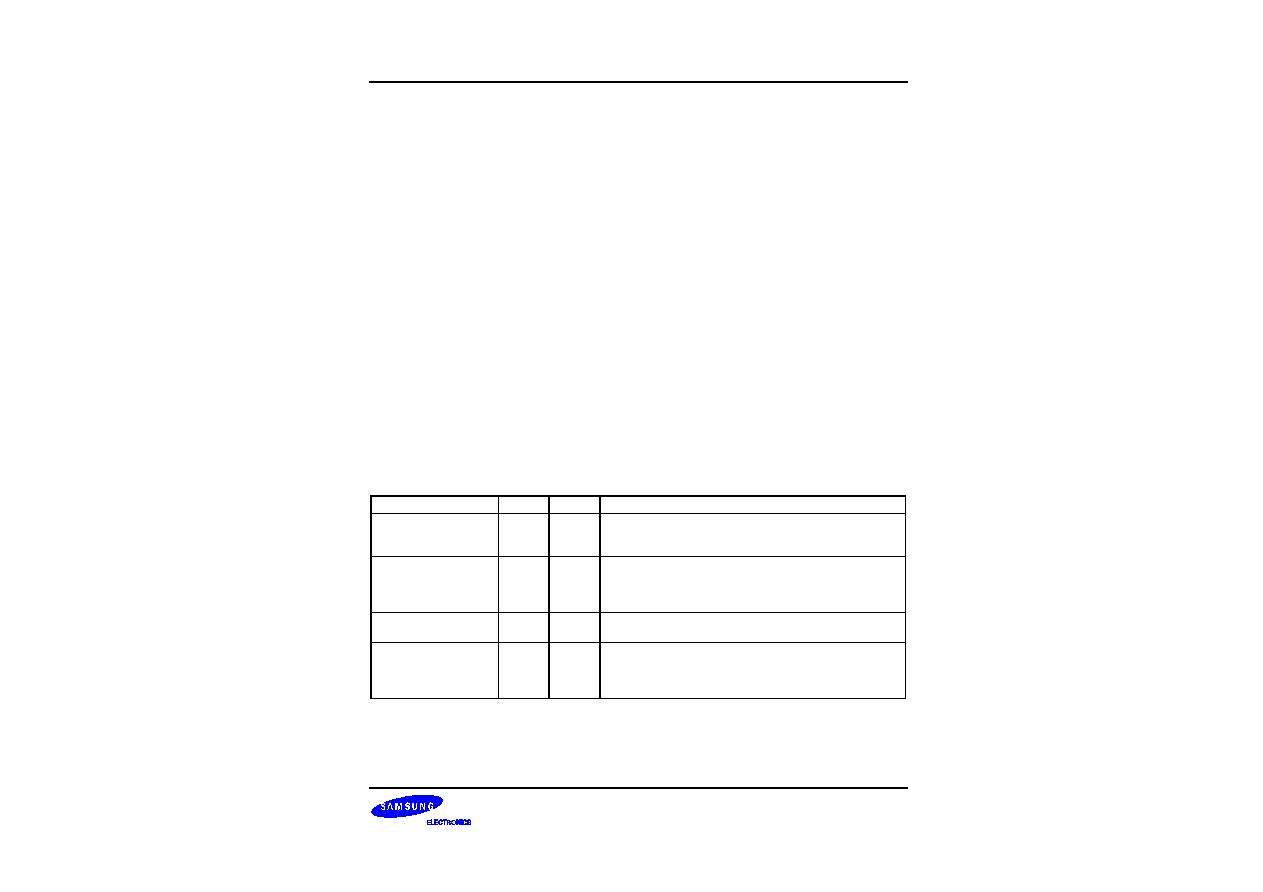
S3P80C5/C80C5/C80C8
INTERRUPT STRUCTURE
5-7
ENABLE/DISABLE INTERRUPT INSTRUCTIONS (EI, DI)
Executing the Enable Interrupts (EI) instruction globally enables the interrupt structure. All interrupts are then
serviced as they occur, and according to the established priorities.
NOTE
The system initialization routine that is executed following a reset must always contain an EI instruction
to globally enable the interrupt structure.
During normal operation, you can execute the DI (Disable Interrupt) instruction at any time to globally disable
interrupt processing. The EI and DI instructions change the value of bit 0 in the SYM register. Although you can
manipulate SYM.0 directly to enable or disable interrupts, we recommend that you use the EI and DI instructions
instead.
SYSTEM-LEVEL INTERRUPT CONTROL REGISTERS
In addition to the control registers for specific interrupt sources, four system-level registers control interrupt
processing:
-- The interrupt mask register, IMR, enables (un-masks) or disables (masks) interrupt levels.
-- The interrupt priority register, IPR, controls the relative priorities of interrupt levels.
-- The interrupt request register, IRQ, contains interrupt pending flags for each interrupt level (as opposed to
each interrupt source).
-- The system mode register, SYM, enables or disables global interrupt processing (SYM settings also enable
fast interrupts and control the activity of external interface, if implemented).
Table 5-2. Interrupt Control Register Overview
Control Register
ID
R/W
Function Description
Interrupt mask register
IMR
R/W
Bit settings in the IMR register enable or disable interrupt
processing for each of the five interrupt levels: IRQ0, IRQ1,
IRQ4, and IRQ6≠IRQ7.
Interrupt priority register
IPR
R/W
Controls the relative processing priorities of the interrupt
levels. The five levels of the S3P80C5/C80C5/C80C8 are
organized into three groups: A, B, and C. Group A is IRQ0 and
IRQ1, group B is IRQ4, and group C is IRQ6, and IRQ7.
Interrupt request register
IRQ
R
This register contains a request pending bit for each interrupt
level.
System mode register
SYM
R/W
Dynamic global interrupt processing enable/ disable, fast
interrupt processing, and external interface control (An
external memory interface is not implemented in the
S3P80C5/C80C5/C80C8 microcontroller).

INTERRUPT STRUCTURE
S3P80C5/C80C5/C80C8
5-8
INTERRUPT PROCESSING CONTROL POINTS
Interrupt processing can therefore be controlled in two ways: globally or by specific interrupt level and source.
The system-level control points in the interrupt structure are, therefore:
-- Global interrupt enable and disable (by EI and DI instructions or by direct manipulation of SYM.0 )
-- Interrupt level enable/disable settings (IMR register)
-- Interrupt level priority settings (IPR register)
-- Interrupt source enable/disable settings in the corresponding peripheral control registers
NOTE
When writing the part of your application program that handles interrupt processing, be sure to include
the necessary register file address (register pointer) information.
IRQ0, IRQ1,
IRQ4 and IRQ6- IRQ7
Interrupts
EI
Interrupt Request
Register (Read-only)
Polling
Cycle
Interrupt Mask
Register
S
R
Q
RESET
Interrupt Priority
Register
Vector
Interrupt
Cycle
Global Interrupt Control
(EI, DI, or SYM.0
manipulation)
Figure 5-4. Interrupt Function Diagram

S3P80C5/C80C5/C80C8
INTERRUPT STRUCTURE
5-9
PERIPHERAL INTERRUPT CONTROL REGISTERS
For each interrupt source there is one or more corresponding peripheral control registers that let you control the
interrupt generated by that peripheral (see Table 5-3).
Table 5-3. Interrupt Source Control and Data Registers
Interrupt Source
Interrupt Level
Register(s)
Location(s) in Set 1
Timer 0 match or timer 0
overflow
IRQ0
T0CON
(note)
T0DATA
D2H
D1H
Timer 1 match or timer 1
overflow
IRQ1
T1CON
(note)
T1DATAH, T1DATAL
FAH
F8H, F9H
Counter A
IRQ4
CACON
CADATAH, CADATAL
F3H
F4H, F5H
P0.7 external interrupt
P0.6 external interrupt
P0.5 external interrupt
P0.4 external interrupt
IRQ7
P0CONH
P0INT
P0PND
E8H
F1H
F2H
P0.3 external interrupt
P0.2 external interrupt
P0.1 external interrupt
P0.0 external interrupt
IRQ6
P0CONL
P0INT
P0PND
E9H
F1H
F2H
NOTE: Because the timer 0 and timer 1 overflow interrupts are cleared by hardware, the T0CON and T1CON registers
control only the enable/disable functions. The T0CON and T1CON registers contain enable/disable and pending
bits for the timer 0 and timer 1 match interrupts, respectively.
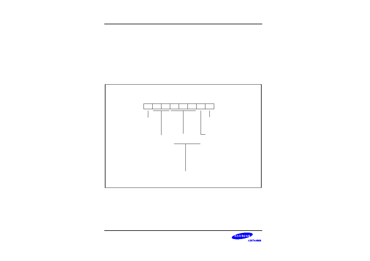
INTERRUPT STRUCTURE
S3P80C5/C80C5/C80C8
5-10
SYSTEM MODE REGISTER (SYM)
The system mode register, SYM (set 1, DEH), is used to globally enable and disable interrupt processing and to
control fast interrupt processing (see Figure 5-5).
A reset clears SYM.7, SYM.1, and SYM.0 to "0". The 3-bit value for fast interrupt level selection, SYM.4≠SYM.2,
is undetermined.
The instructions EI and DI enable and disable global interrupt processing, respectively, by modifying the bit 0
value of the SYM register. An Enable Interrupt (EI) instruction must be included in the initialization routine, which
follows a reset operation, in order to enable interrupt processing. Although you can manipulate SYM.0 directly to
enable and disable interrupts during normal operation, we recommend using the EI and DI instructions for this
purpose.
System Mode Register (SYM)
DEH, Set 1, R/W
Global interrupt enable bit:
0 = Disable all interrupts
1 = Enable all interrupts
Not used for the S3C80C5/C80C8.
External interface
tri-state enable bit:
0 = Normal (Tri-state)
1 = High (Tri-state)
Fast interrupt enable bit:
0 = Disable fast interrupt
1 = Enable fast interrupt
Fast interrupt level
selection bits:
0 0 0
0 0 1
0 1 0
0 1 1
1 0 0
1 0 1
1 1 0
1 1 1
IRQ0
IRQ1
Not used
Not used
Not used
Not used
IRQ6
IRQ7
NOTE:
An external memory interface is not implemented.
MSB
LSB
.5
.7
.6
.4
.3
.2
.1
.0
Figure 5-5. System Mode Register (SYM)
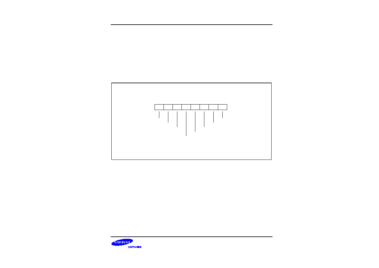
S3P80C5/C80C5/C80C8
INTERRUPT STRUCTURE
5-11
INTERRUPT MASK REGISTER (IMR)
The interrupt mask register, IMR (set 1, DDH) is used to enable or disable interrupt processing for individual
interrupt levels. After a reset, all IMR bit values are undetermined and must therefore be written to their required
settings by the initialization routine.
Each IMR bit corresponds to a specific interrupt level: bit 1 to IRQ1, bit 2 to IRQ2, and so on. When the IMR bit
of an interrupt level is cleared to "0", interrupt processing for that level is disabled (masked). When you set a
level's IMR bit to "1", interrupt processing for the level is enabled (not masked).
The IMR register is mapped to register location DDH in set 1. Bit values can be read and written by instructions
using the Register addressing mode.
Interrupt Mask Register (IMR)
DDH, Set 1, R/W
IRQ0
IRQ1
Not used
Not used
IRQ4
Not used
IRQ6
IRQ7
Interrupt level enable bits (7-6, 4, 1, 0):
0 = Disable (mask) interrupt
1 = Enable (un-mask) interrupt
MSB
LSB
.5
.7
.6
.4
.3
.2
.1
.0
Figure 5-6. Interrupt Mask Register (IMR)

INTERRUPT STRUCTURE
S3P80C5/C80C5/C80C8
5-12
INTERRUPT PRIORITY REGISTER (IPR)
The interrupt priority register, IPR (set 1, bank 0, FFH), is used to set the relative priorities of the interrupt levels
used in the microcontroller's interrupt structure. After a reset, all IPR bit values are undetermined and must
therefore be written to their required settings by the initialization routine.
When more than one interrupt source is active, the source with the highest priority level is serviced first. If both
sources belong to the same interrupt level, the source with the lowest vector address usually has priority (This
priority is fixed in hardware).
To support programming of the relative interrupt level priorities, they are organized into groups and subgroups by
the interrupt logic. Please note that these groups (and subgroups) are used only by IPR logic for the IPR register
priority definitions (see Figure 5-7):
Group A
IRQ0, IRQ1
Group B
IRQ4
Group C
IRQ6, IRQ7
IPR
Group B
IPR
Group C
IRQ4
IRQ6
C1
C2
IRQ7
IPR
Group A
IRQ1
A2
IRQ0
A1
Figure 5-7. Interrupt Request Priority Groups
As you can see in Figure 5-8, IPR.7, IPR.4, and IPR.1 control the relative priority of interrupt groups A, B, and C.
For example, the setting '001B' for these bits would select the group relationship B > C > A; the setting '101B'
would select the relationship C > B > A.
The functions of the other IPR bit settings are as follows:
-- IPR.5 controls the relative priorities of group C interrupts.
-- Interrupt group B has a subgroup to provide an additional priority relationship between for interrupt levels 2,
3, and 4. IPR.3 defines the possible subgroup B relationships. IPR.2 controls interrupt group B. In the
S3P80C5/C80C5/C80C8 implementation, interrupt levels 2 and 3 are not used. Therefore, IPR.2 and IPR.3
settings are not evaluated, as IRQ4 is the only remaining level in the group.
-- IPR.0 controls the relative priority setting of IRQ0 and IRQ1 interrupts.

S3P80C5/C80C5/C80C8
INTERRUPT STRUCTURE
5-13
Interrupt Priority Register (IPR)
FFH, Set 1, Bank 0, R/W
.7
.6
.5
.4
.3
.2
.1
.0
MSB
LSB
Group A
0 = IRQ0 > IRQ1
1 = IRQ1 > IRQ0
Subgroup B
(note)
0 = IRQ4
1 = IRQ4
Group C
(note)
0 = IRQ6, IRQ7
1 = IRQ6, IRQ7
Subgroup C
0 = IRQ6 > IRQ7
1 = IRQ7 > IRQ6
Group B
(note)
0 = IRQ4
1 = IRQ4
Group priority:
0 0 0
0 0 1
0 1 0
0 1 1
1 0 0
1 0 1
1 1 0
1 1 1
= Undefined
= B > C > A
= A > B > C
= B > A > C
= C > A > B
= C > B > A
= A > C > B
= Undefined
D7 D4 D1
NOTE: In this device interrupt structure, only levels IRQ0, IRQ1, IRQ4, IRQ6-IRQ7
are used. Settings for group/subgroup B, which control relative priorities for
levels IRQ2, IRQ3 and IRQ5, are therefore not evaluated.
Figure 5-8. Interrupt Priority Register (IPR)
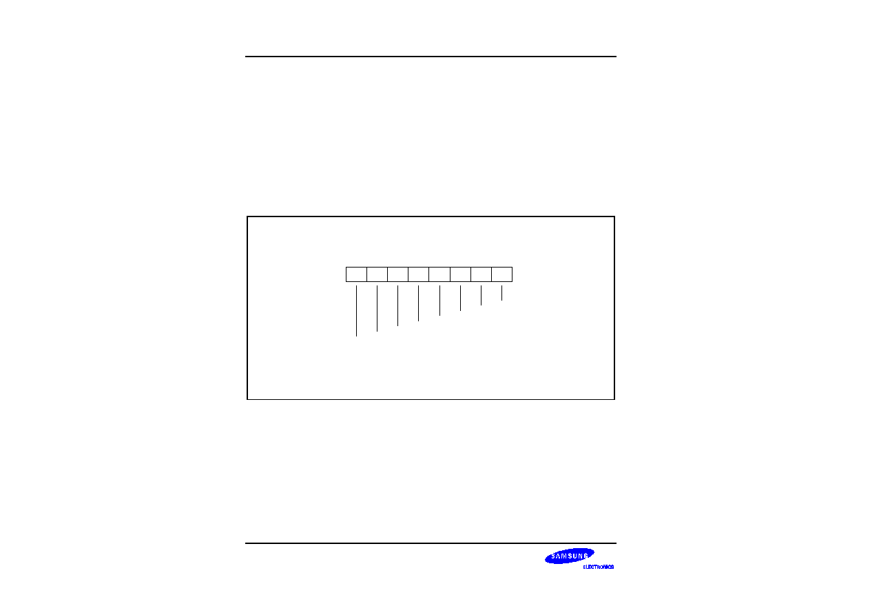
INTERRUPT STRUCTURE
S3P80C5/C80C5/C80C8
5-14
INTERRUPT REQUEST REGISTER (IRQ)
You can poll bit values in the interrupt request register, IRQ (set 1, DCH), to monitor interrupt request status for
all levels in the microcontroller's interrupt structure. Each bit corresponds to the interrupt level of the same
number: bit 0 to IRQ0, bit 1 to IRQ1, and so on. A "0" indicates that no interrupt request is currently being issued
for that level; a "1" indicates that an interrupt request has been generated for that level.
IRQ bit values are read-only addressable using Register addressing mode. You can read (test) the contents of
the IRQ register at any time using bit or byte addressing to determine the current interrupt request status of
specific interrupt levels. After a reset, all IRQ status bits are cleared to "0".
You can poll IRQ register values even if a DI instruction has been executed (that is, if global interrupt processing
is disabled). If an interrupt occurs while the interrupt structure is disabled, the CPU will not service it. You can,
however, still detect the interrupt request by polling the IRQ register. In this way, you can determine which events
occurred while the interrupt structure was globally disabled.
Interrupt Request Register (IRQ)
DCH, Set 1, Read-only
.7
.6
.5
.4
.3
.2
.1
.0
MSB
LSB
IRQ1
Not
used
Not
used
IRQ4
Not
used
IRQ6
IRQ7
IRQ0
Interrupt level request pending bits:
0 = Interrupt level is not pending
1 = Interrupt level is pending
Figure 5-9. Interrupt Request Register (IRQ)

S3P80C5/C80C5/C80C8
INTERRUPT STRUCTURE
5-15
INTERRUPT PENDING FUNCTION TYPES
Overview
There are two types of interrupt pending bits: One type is automatically cleared by hardware after the interrupt
service routine is acknowledged and executed; the other type must be cleared by the interrupt service routine.
Pending Bits Cleared Automatically by Hardware
For interrupt pending bits that are cleared automatically by hardware, interrupt logic sets the corresponding
pending bit to "1" when a request occurs. It then issues an IRQ pulse to inform the CPU that an interrupt is
waiting to be serviced. The CPU acknowledges the interrupt source by sending an IACK, executes the service
routine, and clears the pending bit to "0". This type of pending bit is not mapped and cannot, therefore, be read or
written by application software.
In the S3P80C5/C80C5/C80C8 interrupt structure, the timer 0 and timer 1 overflow interrupts (IRQ0 and IRQ1),
and the counter A interrupt (IRQ4) belong to this category of interrupts whose pending condition is cleared
automatically by hardware.
Pending Bits Cleared by the Service Routine
The second type of pending bit must be cleared by program software. The service routine must clear the
appropriate pending bit before a return-from-interrupt subroutine (IRET) occurs. To do this, a "0" must be written
to the corresponding pending bit location in the source's mode or control register.
In the S3P80C5/C80C5/C80C8 interrupt structure, pending conditions for all interrupt sources except the timer 0
and timer 1 overflow interrupts and the counter A borrow interrupt, must be cleared by the interrupt service
routine.

INTERRUPT STRUCTURE
S3P80C5/C80C5/C80C8
5-16
INTERRUPT SOURCE POLLING SEQUENCE
The interrupt request polling and servicing sequence is as follows:
1.
A source generates an interrupt request by setting the interrupt request bit to "1".
2.
The CPU polling procedure identifies a pending condition for that source.
3.
The CPU checks the source's interrupt level.
4.
The CPU generates an interrupt acknowledge signal.
5.
Interrupt logic determines the interrupt's vector address.
6.
The service routine starts and the source's pending bit is cleared to "0" (by hardware or by software).
7.
The CPU continues polling for interrupt requests.
INTERRUPT SERVICE ROUTINES
Before an interrupt request can be serviced, the following conditions must be met:
-- Interrupt processing must be globally enabled (EI, SYM.0 = "1")
-- The interrupt level must be enabled (IMR register)
-- The interrupt level must have the highest priority if more than one level is currently requesting service
-- The interrupt must be enabled at the interrupt's source (peripheral control register)
If all of the above conditions are met, the interrupt request is acknowledged at the end of the instruction cycle.
The CPU then initiates an interrupt machine cycle that completes the following processing sequence:
1.
Reset (clear to "0") the interrupt enable bit in the SYM register (SYM.0) to disable all subsequent interrupts.
2.
Save the program counter (PC) and status flags to the system stack.
3.
Branch to the interrupt vector to fetch the address of the service routine.
4.
Pass control to the interrupt service routine.
When the interrupt service routine is completed, the CPU issues an Interrupt Return (IRET). The IRET restores
the PC and status flags and sets SYM.0 to "1", allowing the CPU to process the next interrupt request.

S3P80C5/C80C5/C80C8
INTERRUPT STRUCTURE
5-17
GENERATING INTERRUPT VECTOR ADDRESSES
The interrupt vector area in the ROM (00H≠FFH) contains the addresses of interrupt service routines that
correspond to each level in the interrupt structure. Vectored interrupt processing follows this sequence:
1.
Push the program counter's low-byte value to the stack.
2.
Push the program counter's high-byte value to the stack.
3.
Push the FLAG register values to the stack.
4.
Fetch the service routine's high-byte address from the vector location.
5.
Fetch the service routine's low-byte address from the vector location.
6.
Branch to the service routine specified by the concatenated 16-bit vector address.
NOTE
A 16-bit vector address always begins at an even-numbered ROM address within the range 00H≠FFH.
NESTING OF VECTORED INTERRUPTS
It is possible to nest a higher-priority interrupt request while a lower-priority request is being serviced. To do this,
you must follow these steps:
1.
Push the current 8-bit interrupt mask register (IMR) value to the stack (PUSH IMR).
2.
Load the IMR register with a new mask value that enables only the higher priority interrupt.
3.
Execute an EI instruction to enable interrupt processing (a higher priority interrupt will be processed if it
occurs).
4.
When the lower-priority interrupt service routine ends, restore the IMR to its original value by returning the
previous mask value from the stack (POP IMR).
5.
Execute an IRET.
Depending on the application, you may be able to simplify the above procedure to some extent.
INSTRUCTION POINTER (IP)
The instruction pointer (IP) is used by all S3C8-series microcontrollers to control the optional high-speed interrupt
processing feature called fast interrupts. The IP consists of register pair DAH and DBH. The IP register names
are IPH (high byte, IP15≠IP8) and IPL (low byte, IP7≠IP0).
FAST INTERRUPT PROCESSING
The feature called fast interrupt processing lets you specify that an interrupt within a given level be completed in
approximately six clock cycles instead of the usual 16 clock cycles. To select a specific interrupt level for fast
interrupt processing, you write the appropriate 3-bit value to SYM.4≠SYM.2. Then, to enable fast interrupt
processing for the selected level, you set SYM.1 to "1".

INTERRUPT STRUCTURE
S3P80C5/C80C5/C80C8
5-18
FAST INTERRUPT PROCESSING (Continued)
Two other system registers support fast interrupt processing:
-- The instruction pointer (IP) contains the starting address of the service routine (and is later used to swap the
program counter values), and
-- When a fast interrupt occurs, the contents of the FLAGS register is stored in an unmapped, dedicated
register called FLAGS' ("FLAGS prime").
NOTE
For the S3P80C5/C80C5/C80C8 microcontroller, the service routine for any one of the five interrupt
levels: IRQ0, IRQ1, IRQ4 or IRQ6≠IRQ7, can be selected for fast interrupt processing.
Procedure for Initiating Fast Interrupts
To initiate fast interrupt processing, follow these steps:
1.
Load the start address of the service routine into the instruction pointer (IP).
2.
Load the interrupt level number (IRQn) into the fast interrupt selection field (SYM.4≠SYM.2)
3.
Write a "1" to the fast interrupt enable bit in the SYM register.
Fast Interrupt Service Routine
When an interrupt occurs in the level selected for fast interrupt processing, the following events occur:
1.
The contents of the instruction pointer and the PC are swapped.
2.
The FLAG register values are written to the FLAGS' ("FLAGS prime") register.
3.
The fast interrupt status bit in the FLAGS register is set.
4.
The interrupt is serviced.
5.
Assuming that the fast interrupt status bit is set, when the fast interrupt service routine ends, the instruction
pointer and PC values are swapped back.
6.
The content of FLAGS' ("FLAGS prime") is copied automatically back to the FLAGS register.
7.
The fast interrupt status bit in FLAGS is cleared automatically.
Relationship to Interrupt Pending Bit Types
As described previously, there are two types of interrupt pending bits: One type is automatically cleared by
hardware after the interrupt service routine is acknowledged and executed, and the other type must be cleared by
the application program's interrupt service routine. You can select fast interrupt processing for interrupts with
either type of pending condition clear function -- by hardware or by software.
Programming Guidelines
Remember that the only way to enable/disable a fast interrupt is to set/clear the fast interrupt enable bit in the
SYM register, SYM.1. Executing an EI or DI instruction globally enables or disables all interrupt processing,
including fast interrupts. If you use fast interrupts, remember to load the IP with a new start address when the fast
interrupt service routine ends.

S3P80C5/C80C5/C80C8
INSTRUCTION SET
6-1
6
INSTRUCTION SET
OVERVIEW
The SAM8 instruction set is specifically designed to support the large register files that are typical of most SAM8
microcontrollers. There are 78 instructions. The powerful data manipulation capabilities and features of the
instruction set include:
-- A full complement of 8-bit arithmetic and logic operations, including multiply and divide
-- No special I/O instructions (I/O control/data registers are mapped directly into the register file)
-- Decimal adjustment included in binary-coded decimal (BCD) operations
-- 16-bit (word) data can be incremented and decremented
-- Flexible instructions for bit addressing, rotate, and shift operations
DATA TYPES
The SAM8 CPU performs operations on bits, bytes, BCD digits, and two-byte words. Bits in the register file can
be set, cleared, complemented, and tested. Bits within a byte are numbered from 7 to 0, where bit 0 is the least
significant (right-most) bit.
REGISTER ADDRESSING
To access an individual register, an 8-bit address in the range 0-255 or the 4-bit address of a working register is
specified. Paired registers can be used to construct 16-bit data or 16-bit program memory or data memory
addresses. For detailed information about register addressing, please refer to Section 2, "Address Spaces."
ADDRESSING MODES
There are seven explicit addressing modes: Register (R), Indirect Register (IR), Indexed (X), Direct (DA),
Relative (RA), Immediate (IM), and Indirect (IA). For detailed descriptions of these addressing modes, please
refer to Section 3, "Addressing Modes."

INSTRUCTION SET
S3P80C5/C80C5/C80C8
6-2
Table 6-1. Instruction Group Summary
Mnemonic
Operands
Instruction
Load Instructions
CLR
dst
Clear
LD
dst, src
Load
LDB
dst, src
Load bit
LDE
dst, src
Load external data memory
LDC
dst, src
Load program memory
LDED
dst, src
Load external data memory and decrement
LDCD
dst, src
Load program memory and decrement
LDEI
dst, src
Load external data memory and increment
LDCI
dst, src
Load program memory and increment
LDEPD
dst, src
Load external data memory with pre-decrement
LDCPD
dst, src
Load program memory with pre-decrement
LDEPI
dst, src
Load external data memory with pre-increment
LDCPI
dst, src
Load program memory with pre-increment
LDW
dst, src
Load word
POP
dst
Pop from stack
POPUD
dst, src
Pop user stack (decrementing)
POPUI
dst, src
Pop user stack (incrementing)
PUSH
Src
Push to stack
PUSHUD
dst, src
Push user stack (decrementing)
PUSHUI
dst, src
Push user stack (incrementing)

S3P80C5/C80C5/C80C8
INSTRUCTION SET
6-3
Table 6-1. Instruction Group Summary (Continued)
Mnemonic
Operands
Instruction
Arithmetic Instructions
ADC
dst,src
Add with carry
ADD
dst,src
Add
CP
dst,src
Compare
DA
dst
Decimal adjust
DEC
dst
Decrement
DECW
dst
Decrement word
DIV
dst,src
Divide
INC
dst
Increment
INCW
dst
Increment word
MULT
dst,src
Multiply
SBC
dst,src
Subtract with carry
SUB
dst,src
Subtract
Logic Instructions
AND
dst,src
Logical AND
COM
dst
Complement
OR
dst,src
Logical OR
XOR
dst,src
Logical exclusive OR

INSTRUCTION SET
S3P80C5/C80C5/C80C8
6-4
Table 6-1. Instruction Group Summary (Continued)
Mnemonic
Operands
Instruction
Program Control Instructions
BTJRF
dst,src
Bit test and jump relative on false
BTJRT
dst,src
Bit test and jump relative on true
CALL
dst
Call procedure
CPIJE
dst,src
Compare, increment and jump on equal
CPIJNE
dst,src
Compare, increment and jump on non-equal
DJNZ
r,dst
Decrement register and jump on non-zero
ENTER
Enter
EXIT
Exit
IRET
Interrupt return
JP
cc,dst
Jump on condition code
JP
dst
Jump unconditional
JR
cc,dst
Jump relative on condition code
NEXT
Next
RET
Return
WFI
Wait for interrupt
Bit Manipulation Instructions
BAND
dst,src
Bit AND
BCP
dst,src
Bit compare
BITC
dst
Bit complement
BITR
dst
Bit reset
BITS
dst
Bit set
BOR
dst,src
Bit OR
BXOR
dst,src
Bit XOR
TCM
dst,src
Test complement under mask
TM
dst,src
Test under mask

S3P80C5/C80C5/C80C8
INSTRUCTION SET
6-5
Table 6-1. Instruction Group Summary (Concluded)
Mnemonic
Operands
Instruction
Rotate and Shift Instructions
RL
dst
Rotate left
RLC
dst
Rotate left through carry
RR
dst
Rotate right
RRC
dst
Rotate right through carry
SRA
dst
Shift right arithmetic
SWAP
dst
Swap nibbles
CPU Control Instructions
CCF
Complement carry flag
DI
Disable interrupts
EI
Enable interrupts
IDLE
Enter Idle mode
NOP
No operation
RCF
Reset carry flag
SB0
Set bank 0
SB1
Set bank 1
SCF
Set carry flag
SRP
src
Set register pointers
SRP0
src
Set register pointer 0
SRP1
src
Set register pointer 1
STOP
Enter Stop mode

INSTRUCTION SET
S3P80C5/C80C5/C80C8
6-6
FLAGS REGISTER (FLAGS)
The flags register FLAGS contains eight bits that describe the current status of CPU operations. Four of these
bits, FLAGS.7≠FLAGS.4, can be tested and used with conditional jump instructions; two others FLAGS.3 and
FLAGS.2 are used for BCD arithmetic.
The FLAGS register also contains a bit to indicate the status of fast interrupt processing (FLAGS.1) and a bank
address status bit (FLAGS.0) to indicate whether bank 0 or bank 1 is currently being addressed. FLAGS register
can be set or reset by instructions as long as its outcome does not affect the flags, such as, Load instruction.
Logical and Arithmetic instructions such as, AND, OR, XOR, ADD, and SUB can affect the Flags register. For
example, the AND instruction updates the Zero, Sign and Overflow flags based on the outcome of the AND
instruction. If the AND instruction uses the Flags register as the destination, then simultaneously, two write will
occur to the Flags register producing an unpredictable result.
System Flags Register (FLAGS)
D5H, Set 1, R/W
.7
.6
.5
.4
.3
.2
.1
.0
MSB
LSB
Bank address
status flag (BA)
First interrupt
status flag (FIS)
Half-carry flag (H)
Decimal adjust flag (D)
Overflow (V)
Sign flag (S)
Zero flag (Z)
Carry flag (C)
Figure 6-1. System Flags Register (FLAGS)

S3P80C5/C80C5/C80C8
INSTRUCTION SET
6-7
FLAG DESCRIPTIONS
C
Carry Flag (FLAGS.7)
The C flag is set to "1" if the result from an arithmetic operation generates a carry-out from or a borrow to
the bit 7 position (MSB). After rotate and shift operations, it contains the last value shifted out of the
specified register. Program instructions can set, clear, or complement the carry flag.
Z
Zero Flag (FLAGS.6)
For arithmetic and logic operations, the Z flag is set to "1" if the result of the operation is zero. For
operations that test register bits, and for shift and rotate operations, the Z flag is set to "1" if the result is
logic zero.
S
Sign Flag (FLAGS.5)
Following arithmetic, logic, rotate, or shift operations, the sign bit identifies the state of the MSB of the
result. A logic zero indicates a positive number and a logic one indicates a negative number.
V
Overflow Flag (FLAGS.4)
The V flag is set to "1" when the result of a two's-complement operation is greater than + 127 or less than
≠ 128. It is also cleared to "0" following logic operations.
D
Decimal Adjust Flag (FLAGS.3)
The DA bit is used to specify what type of instruction was executed last during BCD operations, so that a
subsequent decimal adjust operation can execute correctly. The DA bit is not usually accessed by
programmers, and cannot be used as a test condition.
H
Half-Carry Flag (FLAGS.2)
The H bit is set to "1" whenever an addition generates a carry-out of bit 3, or when a subtraction borrows
out of bit 4. It is used by the Decimal Adjust (DA) instruction to convert the binary result of a previous
addition or subtraction into the correct decimal (BCD) result. The H flag is seldom accessed directly by a
program.
FIS
Fast Interrupt Status Flag (FLAGS.1)
The FIS bit is set during a fast interrupt cycle and reset during the IRET following interrupt servicing.
When set, it inhibits all interrupts and causes the fast interrupt return to be executed when the IRET
instruction is executed.
BA
Bank Address Flag (FLAGS.0)
The BA flag indicates which register bank in the set 1 area of the internal register file is currently
selected, bank 0 or bank 1. The BA flag is cleared to "0" (select bank 0) when you execute the SB0
instruction and is set to "1" (select bank 1) when you execute the SB1 instruction.
INSTRUCTION SET
S3P80C5/C80C5/C80C8
6-8
INSTRUCTION SET NOTATION
Table 6-2. Flag Notation Conventions
Flag
Description
C
Carry flag
Z
Zero flag
S
Sign flag
V
Overflow flag
D
Decimal-adjust flag
H
Half-carry flag
0
Cleared to logic zero
1
Set to logic one
*
Set or cleared according to operation
≠
Value is unaffected
x
Value is undefined
Table 6-3. Instruction Set Symbols
Symbol
Description
dst
Destination operand
src
Source operand
@
Indirect register address prefix
PC
Program counter
IP
Instruction pointer
FLAGS
Flags register (D5H)
RP
Register pointer
#
Immediate operand or register address prefix
H
Hexadecimal number suffix
D
Decimal number suffix
B
Binary number suffix
opc
Opcode
S3P80C5/C80C5/C80C8
INSTRUCTION SET
6-9
Table 6-4. Instruction Notation Conventions
Notation
Description
Actual Operand Range
cc
Condition code
See list of condition codes in Table 6-6.
r
Working register only
Rn (n = 0≠15)
rb
Bit (b) of working register
Rn.b (n = 0≠15, b = 0≠7)
r0
Bit 0 (LSB) of working register
Rn (n = 0≠15)
rr
Working register pair
RRp (p = 0, 2, 4, ..., 14)
R
Register or working register
reg or Rn (reg = 0≠255, n = 0≠15)
Rb
Bit 'b' of register or working register
reg.b (reg = 0≠255, b = 0≠7)
RR
Register pair or working register pair
reg or RRp (reg = 0≠254, even number only, where
p = 0, 2, ..., 14)
IA
Indirect addressing mode
addr (addr = 0≠254, even number only)
Ir
Indirect working register only
@Rn (n = 0≠15)
IR
Indirect register or indirect working register @Rn or @reg (reg = 0≠255, n = 0≠15)
Irr
Indirect working register pair only
@RRp (p = 0, 2, ..., 14)
IRR
Indirect register pair or indirect working
register pair
@RRp or @reg (reg = 0≠254, even only, where
p = 0, 2, ..., 14)
X
Indexed addressing mode
#reg [Rn] (reg = 0≠255, n = 0≠15)
XS
Indexed (short offset) addressing mode
#addr [RRp] (addr = range ≠128 to +127, where
p = 0, 2, ..., 14)
xl
Indexed (long offset) addressing mode
#addr [RRp] (addr = range 0≠65535, where
p = 0, 2, ..., 14)
da
Direct addressing mode
addr (addr = range 0≠65535)
ra
Relative addressing mode
addr (addr = number in the range +127 to ≠128 that is
an offset relative to the address of the next instruction)
im
Immediate addressing mode
#data (data = 0≠255)
iml
Immediate (long) addressing mode
#data (data = range 0≠65535)

INSTRUCTION SET
S3P80C5/C80C5/C80C8
6-10
Table 6-5. Opcode Quick Reference
OPCODE MAP
LOWER NIBBLE (HEX)
≠
0
1
2
3
4
5
6
7
U
0
DEC
R1
DEC
IR1
ADD
r1,r2
ADD
r1,Ir2
ADD
R2,R1
ADD
IR2,R1
ADD
R1,IM
BOR
r0≠Rb
P
1
RLC
R1
RLC
IR1
ADC
r1,r2
ADC
r1,Ir2
ADC
R2,R1
ADC
IR2,R1
ADC
R1,IM
BCP
r1.b, R2
P
2
INC
R1
INC
IR1
SUB
r1,r2
SUB
r1,Ir2
SUB
R2,R1
SUB
IR2,R1
SUB
R1,IM
BXOR
r0≠Rb
E
3
JP
IRR1
SRP/0/1
IM
SBC
r1,r2
SBC
r1,Ir2
SBC
R2,R1
SBC
IR2,R1
SBC
R1,IM
BTJR
r2.b, RA
R
4
DA
R1
DA
IR1
OR
r1,r2
OR
r1,Ir2
OR
R2,R1
OR
IR2,R1
OR
R1,IM
LDB
r0≠Rb
5
POP
R1
POP
IR1
AND
r1,r2
AND
r1,Ir2
AND
R2,R1
AND
IR2,R1
AND
R1,IM
BITC
r1.b
N
6
COM
R1
COM
IR1
TCM
r1,r2
TCM
r1,Ir2
TCM
R2,R1
TCM
IR2,R1
TCM
R1,IM
BAND
r0≠Rb
I
7
PUSH
R2
PUSH
IR2
TM
r1,r2
TM
r1,Ir2
TM
R2,R1
TM
IR2,R1
TM
R1,IM
BIT
r1.b
B
8
DECW
RR1
DECW
IR1
PUSHUD
IR1,R2
PUSHUI
IR1,R2
MULT
R2,RR1
MULT
IR2,RR1
MULT
IM,RR1
LD
r1, x, r2
B
9
RL
R1
RL
IR1
POPUD
IR2,R1
POPUI
IR2,R1
DIV
R2,RR1
DIV
IR2,RR1
DIV
IM,RR1
LD
r2, x, r1
L
A
INCW
RR1
INCW
IR1
CP
r1,r2
CP
r1,Ir2
CP
R2,R1
CP
IR2,R1
CP
R1,IM
LDC
r1, Irr2, xL
E
B
CLR
R1
CLR
IR1
XOR
r1,r2
XOR
r1,Ir2
XOR
R2,R1
XOR
IR2,R1
XOR
R1,IM
LDC
r2, Irr2, xL
C
RRC
R1
RRC
IR1
CPIJE
Ir,r2,RA
LDC
r1,Irr2
LDW
RR2,RR1
LDW
IR2,RR1
LDW
RR1,IML
LD
r1, Ir2
H
D
SRA
R1
SRA
IR1
CPIJNE
Irr,r2,RA
LDC
r2,Irr1
CALL
IA1
LD
IR1,IM
LD
Ir1, r2
E
E
RR
R1
RR
IR1
LDCD
r1,Irr2
LDCI
r1,Irr2
LD
R2,R1
LD
R2,IR1
LD
R1,IM
LDC
r1, Irr2, xs
X
F
SWAP
R1
SWAP
IR1
LDCPD
r2,Irr1
LDCPI
r2,Irr1
CALL
IRR1
LD
IR2,R1
CALL
DA1
LDC
r2, Irr1, xs
S3P80C5/C80C5/C80C8
INSTRUCTION SET
6-11
Table 6-5. Opcode Quick Reference (Continued)
OPCODE MAP
LOWER NIBBLE (HEX)
≠
8
9
A
B
C
D
E
F
U
0
LD
r1,R2
LD
r2,R1
DJNZ
r1,RA
JR
cc,RA
LD
r1,IM
JP
cc,DA
INC
r1
NEXT
P
1
ENTER
P
2
EXIT
E
3
WFI
R
4
SB0
5
SB1
N
6
IDLE
I
7
STOP
B
8
DI
B
9
EI
L
A
RET
E
B
IRET
C
RCF
H
D
SCF
E
E
CCF
X
F
LD
r1,R2
LD
r2,R1
DJNZ
r1,RA
JR
cc,RA
LD
r1,IM
JP
cc,DA
INC
r1
NOP

INSTRUCTION SET
S3P80C5/C80C5/C80C8
6-12
CONDITION CODES
The opcode of a conditional jump always contains a 4-bit field called the condition code (cc). This specifies under
which conditions it is to execute the jump. For example, a conditional jump with the condition code for "equal"
after a compare operation only jumps if the two operands are equal. Condition codes are listed in Table 6-6.
The carry (C), zero (Z), sign (S), and overflow (V) flags are used to control the operation of conditional jump
instructions.
Table 6-6. Condition Codes
Binary
Mnemonic
Description
Flags Set
0000
F
Always false
≠
1000
T
Always true
≠
0111
(note)
C
Carry
C = 1
1111
(note)
NC
No carry
C = 0
0110
(note)
Z
Zero
Z = 1
1110
(note)
NZ
Not zero
Z = 0
1101
PL
Plus
S = 0
0101
MI
Minus
S = 1
0100
OV
Overflow
V = 1
1100
NOV
No overflow
V = 0
0110
(note)
EQ
Equal
Z = 1
1110
(note)
NE
Not equal
Z = 0
1001
GE
Greater than or equal
(S XOR V) = 0
0001
LT
Less than
(S XOR V) = 1
1010
GT
Greater than
(Z OR (S XOR V)) = 0
0010
LE
Less than or equal
(Z OR (S XOR V)) = 1
1111
(note)
UGE
Unsigned greater than or equal
C = 0
0111
(note)
ULT
Unsigned less than
C = 1
1011
UGT
Unsigned greater than
(C = 0 AND Z = 0) = 1
0011
ULE
Unsigned less than or equal
(C OR Z) = 1
NOTES:
1.
It indicates condition codes that are related to two different mnemonics but which test the same flag. For
example, Z and EQ are both true if the zero flag (Z) is set, but after an ADD instruction, Z would probably be used;
after a CP instruction, however, EQ would probably be used.
2.
For operations involving unsigned numbers, the special condition codes UGE, ULT, UGT, and ULE must be used.

S3P80C5/C80C5/C80C8
INSTRUCTION SET
6-13
INSTRUCTION DESCRIPTIONS
This section contains detailed information and programming examples for each instruction in the SAM8
instruction set. Information is arranged in a consistent format for improved readability and for fast referencing.
The following information is included in each instruction description:
-- Instruction name (mnemonic)
-- Full instruction name
-- Source/destination format of the instruction operand
-- Shorthand notation of the instruction's operation
-- Textual description of the instruction's effect
-- Specific flag settings affected by the instruction
-- Detailed description of the instruction's format, execution time, and addressing mode(s)
-- Programming example(s) explaining how to use the instruction
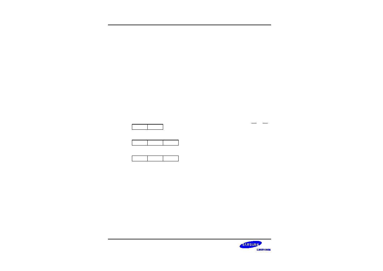
INSTRUCTION SET
S3P80C5/C80C5/C80C8
6-14
ADC
-- Add with carry
ADC
dst,src
Operation:
dst
dst + src + c
The source operand, along with the setting of the carry flag, is added to the destination operand
and the sum is stored in the destination. The contents of the source are unaffected. Two's-
complement addition is performed. In multiple precision arithmetic, this instruction permits the
carry from the addition of low-order operands to be carried into the addition of high-order
operands.
Flags:
C: Set if there is a carry from the most significant bit of the result; cleared otherwise.
Z: Set if the result is "0"; cleared otherwise.
S: Set if the result is negative; cleared otherwise.
V: Set if arithmetic overflow occurs, that is, if both operands are of the same sign and the result
is of the opposite sign; cleared otherwise.
D: Always cleared to "0".
H: Set if there is a carry from the most significant bit of the low-order four bits of the result;
cleared otherwise.
Format:
Bytes
Cycles
Opcode
(Hex)
Addr Mode
dst src
opc
dst | src
2
4
12
r
r
6
13
r
lr
opc
src
dst
3
6
14
R
R
6
15
R
IR
opc
dst
src
3
6
16
R
IM
Examples:
Given: R1 = 10H, R2 = 03H, C flag = "1", register 01H = 20H, register 02H = 03H, and
register 03H = 0AH:
ADC
R1,R2
R1 = 14H, R2 = 03H
ADC
R1,@R2
R1 = 1BH, R2 = 03H
ADC
01H,02H
Register 01H = 24H, register 02H = 03H
ADC
01H,@02H
Register 01H = 2BH, register 02H = 03H
ADC
01H,#11H
Register 01H = 32H
In the first example, destination register R1 contains the value 10H, the carry flag is set to "1",
and the source working register R2 contains the value 03H. The statement "ADC R1,R2" adds
03H and the carry flag value ("1") to the destination value 10H, leaving 14H in register R1.
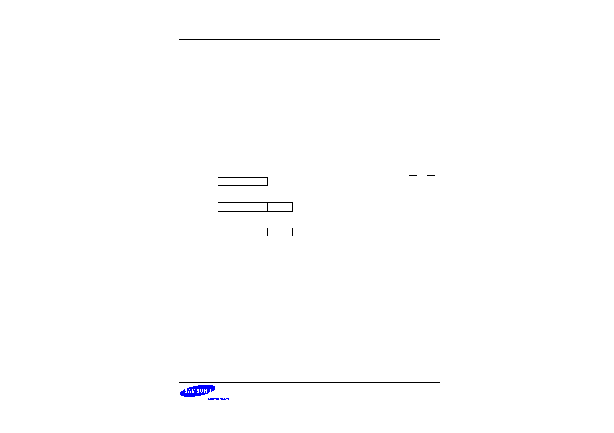
S3P80C5/C80C5/C80C8
INSTRUCTION SET
6-15
ADD
--
Add
ADD
dst,src
Operation:
dst
dst + src
The source operand is added to the destination operand and the sum is stored in the destination.
The contents of the source are unaffected. Two's-complement addition is performed.
Flags:
C: Set if there is a carry from the most significant bit of the result; cleared otherwise.
Z: Set if the result is "0"; cleared otherwise.
S: Set if the result is negative; cleared otherwise.
V: Set if arithmetic overflow occurred, that is, if both operands are of the same sign and the
result is of the opposite sign; cleared otherwise.
D: Always cleared to "0".
H: Set if a carry from the low-order nibble occurred.
Format:
Bytes
Cycles
Opcode
(Hex)
Addr Mode
dst src
opc
dst | src
2
4
02
r
r
6
03
r
lr
opc
src
dst
3
6
04
R
R
6
05
R
IR
opc
dst
src
3
6
06
R
IM
Examples:
Given: R1 = 12H, R2 = 03H, register 01H = 21H, register 02H = 03H, register 03H = 0AH:
ADD
R1,R2
R1 = 15H, R2 = 03H
ADD
R1,@R2
R1 = 1CH, R2 = 03H
ADD
01H,02H
Register 01H = 24H, register 02H = 03H
ADD
01H,@02H
Register 01H = 2BH, register 02H = 03H
ADD
01H,#25H
Register 01H = 46H
In the first example, destination working register R1 contains 12H and the source working
register R2 contains 03H. The statement "ADD R1,R2" adds 03H to 12H, leaving the value 15H
in register R1.

INSTRUCTION SET
S3P80C5/C80C5/C80C8
6-16
AND
--
Logical AND
AND
dst,src
Operation:
dst
dst AND src
The source operand is logically ANDed with the destination operand. The result is stored in the
destination. The AND operation results in a "1" bit being stored whenever the corresponding bits
in the two operands are both logic ones; otherwise a "0" bit value is stored. The contents of the
source are unaffected.
Flags:
C: Unaffected.
Z: Set if the result is "0"; cleared otherwise.
S: Set if the result bit 7 is set; cleared otherwise.
V: Always cleared to "0".
D: Unaffected.
H: Unaffected.
Format:
Bytes
Cycles
Opcode
(Hex)
Addr Mode
dst src
opc
dst | src
2
4
52
r
r
6
53
r
lr
opc
src
dst
3
6
54
R
R
6
55
R
IR
opc
dst
src
3
6
56
R
IM
Examples:
Given: R1 = 12H, R2 = 03H, register 01H = 21H, register 02H = 03H, register 03H = 0AH:
AND
R1,R2
R1 = 02H, R2 = 03H
AND
R1,@R2
R1 = 02H, R2 = 03H
AND
01H,02H
Register 01H = 01H, register 02H = 03H
AND
01H,@02H
Register 01H = 00H, register 02H = 03H
AND
01H,#25H
Register 01H = 21H
In the first example, destination working register R1 contains the value 12H and the source
working register R2 contains 03H. The statement "AND R1,R2" logically ANDs the source
operand 03H with the destination operand value 12H, leaving the value 02H in register R1.
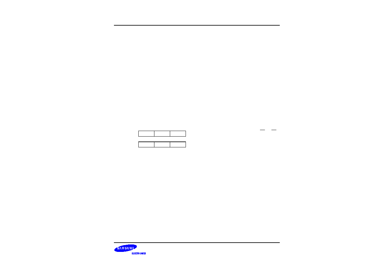
S3P80C5/C80C5/C80C8
INSTRUCTION SET
6-17
BAND
--
Bit AND
BAND
dst,src.b
BAND
dst.b,src
Operation:
dst(0)
dst(0) AND src(b)
or
dst(b)
dst(b) AND src(0)
The specified bit of the source (or the destination) is logically ANDed with the zero bit (LSB) of
the destination (or source). The resultant bit is stored in the specified bit of the destination. No
other bits of the destination are affected. The source is unaffected.
Flags:
C: Unaffected.
Z: Set if the result is "0"; cleared otherwise.
S: Cleared to "0".
V: Undefined.
D: Unaffected.
H: Unaffected.
Format:
Bytes
Cycles
Opcode
(Hex)
Addr Mode
dst src
opc
dst | b | 0
src
3
6
67
r0
Rb
opc
src | b | 1
dst
3
6
67
Rb
r0
NOTE: In the second byte of the 3-byte instruction formats, the destination (or source) address is four
bits, the bit address 'b' is three bits, and the LSB address value is one bit in length.
Examples:
Given: R1 = 07H and register 01H = 05H:
BAND R1,01H.1
R1 = 06H, register 01H = 05H
BAND 01H.1,R1
Register 01H = 05H, R1 = 07H
In the first example, source register 01H contains the value 05H (00000101B) and destination
working register R1 contains 07H (00000111B). The statement "BAND R1,01H.1" ANDs the bit 1
value of the source register ("0") with the bit 0 value of register R1 (destination), leaving the
value 06H (00000110B) in register R1.

INSTRUCTION SET
S3P80C5/C80C5/C80C8
6-18
BCP
--
Bit Compare
BCP
dst,src.b
Operation:
dst(0) ≠ src(b)
The specified bit of the source is compared to (subtracted from) bit zero (LSB) of the destination.
The zero flag is set if the bits are the same; otherwise it is cleared. The contents of both
operands are unaffected by the comparison.
Flags:
C: Unaffected.
Z: Set if the two bits are the same; cleared otherwise.
S: Cleared to "0".
V: Undefined.
D: Unaffected.
H: Unaffected.
Format:
Bytes
Cycles
Opcode
(Hex)
Addr Mode
dst src
opc
dst | b | 0
src
3
6
17
r0
Rb
NOTE: In the second byte of the instruction format, the destination address is four bits, the bit address 'b'
is three bits, and the LSB address value is one bit in length.
Example:
Given: R1 = 07H and register 01H = 01H:
BCP
R1,01H.1
R1 = 07H, register 01H = 01H
If destination working register R1 contains the value 07H (00000111B) and the source register
01H contains the value 01H (00000001B), the statement "BCP R1,01H.1" compares bit one of
the source register (01H) and bit zero of the destination register (R1). Because the bit values are
not identical, the zero flag bit (Z) is cleared in the FLAGS register (0D5H).

S3P80C5/C80C5/C80C8
INSTRUCTION SET
6-19
BITC
--
Bit Complement
BITC
dst.b
Operation:
dst(b)
NOT dst(b)
This instruction complements the specified bit within the destination without affecting any other
bits in the destination.
Flags:
C: Unaffected.
Z: Set if the result is "0"; cleared otherwise.
S: Cleared to "0".
V: Undefined.
D: Unaffected.
H: Unaffected.
Format:
Bytes
Cycles
Opcode
(Hex)
Addr Mode
dst
opc
dst | b | 0
2
4
57
rb
NOTE: In the second byte of the instruction format, the destination address is four bits, the bit address 'b'
is three bits, and the LSB address value is one bit in length.
Example:
Given: R1 = 07H
BITC
R1.1
R1 = 05H
If working register R1 contains the value 07H (00000111B), the statement "BITC R1.1"
complements bit one of the destination and leaves the value 05H (00000101B) in register R1.
Because the result of the complement is not "0", the zero flag (Z) in the FLAGS register (0D5H)
is cleared.
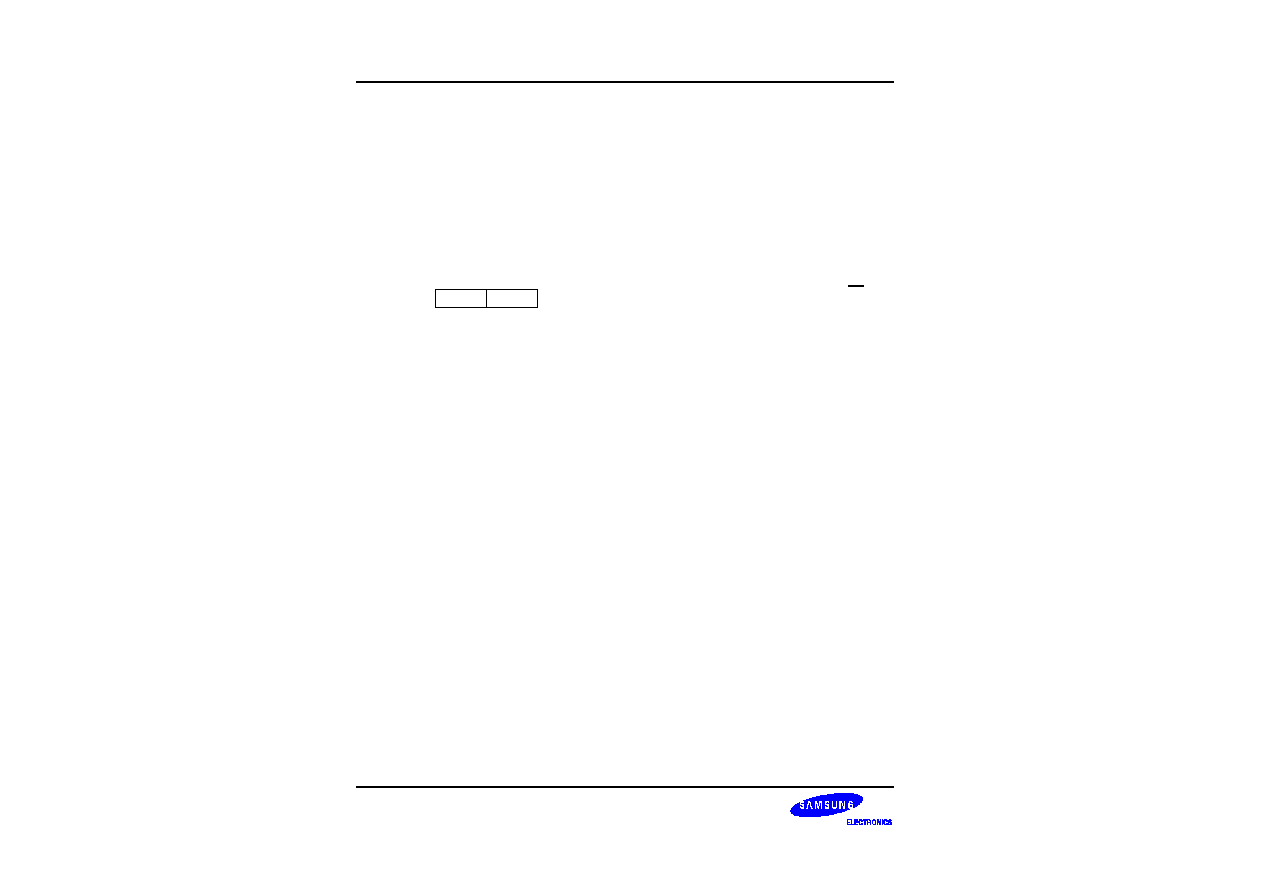
INSTRUCTION SET
S3P80C5/C80C5/C80C8
6-20
BITR
--
Bit Reset
BITR
dst.b
Operation:
dst(b)
0
The BITR instruction clears the specified bit within the destination without affecting any other bits
in the destination.
Flags:
No flags are affected.
Format:
Bytes
Cycles
Opcode
(Hex)
Addr Mode
dst
opc
dst | b | 0
2
4
77
rb
NOTE: In the second byte of the instruction format, the destination address is four bits, the bit address 'b'
is three bits, and the LSB address value is one bit in length.
Example:
Given: R1 = 07H:
BITR
R1.1
R1 = 05H
If the value of working register R1 is 07H (00000111B), the statement "BITR R1.1" clears bit one
of the destination register R1, leaving the value 05H (00000101B).
S3P80C5/C80C5/C80C8
INSTRUCTION SET
6-21
BITS
--
Bit Set
BITS
dst.b
Operation:
dst(b)
1
The BITS instruction sets the specified bit within the destination without affecting any other bits
in the destination.
Flags:
No flags are affected.
Format:
Bytes
Cycles
Opcode
(Hex)
Addr Mode
dst
opc
dst | b | 1
2
4
77
rb
NOTE: In the second byte of the instruction format, the destination address is four bits, the bit address 'b'
is three bits, and the LSB address value is one bit in length.
Example:
Given: R1 = 07H:
BITS
R1.3
R1 = 0FH
If working register R1 contains the value 07H (00000111B), the statement "BITS R1.3" sets bit
three of the destination register R1 to "1", leaving the value 0FH (00001111B).
INSTRUCTION SET
S3P80C5/C80C5/C80C8
6-22
BOR
--
Bit OR
BOR
dst,src.b
BOR
dst.b,src
Operation:
dst(0)
dst(0) OR src(b)
or
dst(b)
dst(b) OR src(0)
The specified bit of the source (or the destination) is logically ORed with bit zero (LSB) of the
destination (or the source). The resulting bit value is stored in the specified bit of the destination.
No other bits of the destination are affected. The source is unaffected.
Flags:
C: Unaffected.
Z: Set if the result is "0"; cleared otherwise.
S: Cleared to "0".
V: Undefined.
D: Unaffected.
H: Unaffected.
Format:
Bytes
Cycles
Opcode
(Hex)
Addr Mode
dst src
opc
dst | b | 0
src
3
6
07
r0
Rb
opc
src | b | 1
dst
3
6
07
Rb
r0
NOTE: In the second byte of the 3-byte instruction formats, the destination (or source) address is four
bits, the bit address 'b' is three bits, and the LSB address value is one bit.
Examples:
Given: R1 = 07H and register 01H = 03H:
BOR
R1, 01H.1
R1 = 07H, register 01H = 03H
BOR
01H.2, R1
Register 01H = 07H, R1 = 07H
In the first example, destination working register R1 contains the value 07H (00000111B) and
source register 01H the value 03H (00000011B). The statement "BOR R1,01H.1" logically ORs
bit one of register 01H (source) with bit zero of R1 (destination). This leaves the same value
(07H) in working register R1.
In the second example, destination register 01H contains the value 03H (00000011B) and the
source working register R1 the value 07H (00000111B). The statement "BOR 01H.2,R1" logically
ORs bit two of register 01H (destination) with bit zero of R1 (source). This leaves the value 07H
in register 01H.
S3P80C5/C80C5/C80C8
INSTRUCTION SET
6-23
BTJRF
--
Bit Test, Jump Relative on False
BTJRF
dst,src.b
Operation:
If src(b) is a "0", then PC
PC + dst
The specified bit within the source operand is tested. If it is a "0", the relative address is added to
the program counter and control passes to the statement whose address is now in the PC;
otherwise, the instruction following the BTJRF instruction is executed.
Flags:
No flags are affected.
Format:
(Note 1)
Bytes
Cycles
Opcode
(Hex)
Addr Mode
dst src
opc
src | b | 0
dst
3
10
37
RA
rb
NOTE: In the second byte of the instruction format, the source address is four bits, the bit address 'b' is
three bits, and the LSB address value is one bit in length.
Example:
Given: R1 = 07H:
BTJRF SKIP,R1.3
PC jumps to SKIP location
If working register R1 contains the value 07H (00000111B), the statement "BTJRF SKIP,R1.3"
tests bit 3. Because it is "0", the relative address is added to the PC and the PC jumps to the
memory location pointed to by the SKIP. (Remember that the memory location must be within
the allowed range of + 127 to ≠ 128.)
INSTRUCTION SET
S3P80C5/C80C5/C80C8
6-24
BTJRT
--
Bit Test, Jump Relative on True
BTJRT
dst,src.b
Operation:
If src(b) is a "1", then PC
PC + dst
The specified bit within the source operand is tested. If it is a "1", the relative address is added to
the program counter and control passes to the statement whose address is now in the PC;
otherwise, the instruction following the BTJRT instruction is executed.
Flags:
No flags are affected.
Format:
(Note 1)
Bytes
Cycles
Opcode
(Hex)
Addr Mode
dst src
opc
src | b | 1
dst
3
10
37
RA
rb
NOTE: In the second byte of the instruction format, the source address is four bits, the bit address 'b' is
three bits, and the LSB address value is one bit in length.
Example:
Given: R1 = 07H:
BTJRT
SKIP,R1.1
If working register R1 contains the value 07H (00000111B), the statement "BTJRT SKIP,R1.1"
tests bit one in the source register (R1). Because it is a "1", the relative address is added to the
PC and the PC jumps to the memory location pointed to by the SKIP. (Remember that the
memory location must be within the allowed range of + 127 to ≠ 128.)

S3P80C5/C80C5/C80C8
INSTRUCTION SET
6-25
BXOR
--
Bit XOR
BXOR
dst,src.b
BXOR
dst.b,src
Operation:
dst(0)
dst(0) XOR src(b)
or
dst(b)
dst(b) XOR src(0)
The specified bit of the source (or the destination) is logically exclusive-ORed with bit zero (LSB)
of the destination (or source). The result bit is stored in the specified bit of the destination. No
other bits of the destination are affected. The source is unaffected.
Flags:
C: Unaffected.
Z: Set if the result is "0"; cleared otherwise.
S: Cleared to "0".
V: Undefined.
D: Unaffected.
H: Unaffected.
Format:
Bytes
Cycles
Opcode
(Hex)
Addr Mode
dst src
opc
dst | b | 0
src
3
6
27
r0
Rb
opc
src | b | 1
dst
3
6
27
Rb
r0
NOTE: In the second byte of the 3-byte instruction formats, the destination (or source) address is four
bits, the bit address 'b' is three bits, and the LSB address value is one bit in length.
Examples:
Given: R1 = 07H (00000111B) and register 01H = 03H (00000011B):
BXOR R1,01H.1
R1 = 06H, register 01H = 03H
BXOR 01H.2,R1
Register 01H = 07H, R1 = 07H
In the first example, destination working register R1 has the value 07H (00000111B) and source
register 01H has the value 03H (00000011B). The statement "BXOR R1,01H.1" exclusive-ORs
bit one of register 01H (source) with bit zero of R1 (destination). The result bit value is stored in
bit zero of R1, changing its value from 07H to 06H. The value of source register 01H is
unaffected.
INSTRUCTION SET
S3P80C5/C80C5/C80C8
6-26
CALL
--
Call Procedure
CALL
dst
Operation:
SP
SP ≠ 1
@SP
PCL
SP
SP ≠1
@SP
PCH
PC
dst
The current contents of the program counter are pushed onto the top of the stack. The program
counter value used is the address of the first instruction following the CALL instruction. The
specified destination address is then loaded into the program counter and points to the first
instruction of a procedure. At the end of the procedure the return instruction (RET) can be used
to return to the original program flow. RET pops the top of the stack back into the program
counter.
Flags:
No flags are affected.
Format:
Bytes
Cycles
Opcode
(Hex)
Addr Mode
dst
opc
dst
3
14
F6
DA
opc
dst
2
12
F4
IRR
opc
dst
2
14
D4
IA
Examples:
Given: R0 = 35H, R1 = 21H, PC = 1A47H, and SP = 0002H:
CALL
3521H
SP = 0000H
(Memory locations 0000H = 1AH, 0001H = 4AH, where
4AH is the address that follows the instruction.)
CALL
@RR0
SP = 0000H (0000H = 1AH, 0001H = 49H)
CALL
#40H
SP = 0000H (0000H = 1AH, 0001H = 49H)
In the first example, if the program counter value is 1A47H and the stack pointer contains the
value 0002H, the statement "CALL 3521H" pushes the current PC value onto the top of the
stack. The stack pointer now points to memory location 0000H. The PC is then loaded with the
value 3521H, the address of the first instruction in the program sequence to be executed.
If the contents of the program counter and stack pointer are the same as in the first example, the
statement "CALL @RR0" produces the same result except that the 49H is stored in stack
location 0001H (because the two-byte instruction format was used). The PC is then loaded with
the value 3521H, the address of the first instruction in the program sequence to be executed.
Assuming that the contents of the program counter and stack pointer are the same as in the first
example, if program address 0040H contains 35H and program address 0041H contains 21H, the
statement "CALL #40H" produces the same result as in the second example.

S3P80C5/C80C5/C80C8
INSTRUCTION SET
6-27
CCF
--
Complement Carry Flag
CCF
Operation:
C
NOT C
The carry flag (C) is complemented. If C = "1", the value of the carry flag is changed to logic
zero; if C = "0", the value of the carry flag is changed to logic one.
Flags:
C: Complemented.
No other flags are affected.
Format:
Bytes
Cycles
Opcode
(Hex)
opc
1
4
EF
Example:
Given: The carry flag = "0":
CCF
If the carry flag = "0", the CCF instruction complements it in the FLAGS register (0D5H),
changing its value from logic zero to logic one.
INSTRUCTION SET
S3P80C5/C80C5/C80C8
6-28
CLR
--
Clear
CLR
dst
Operation:
dst
"0"
The destination location is cleared to "0".
Flags:
No flags are affected.
Format:
Bytes
Cycles
Opcode
(Hex)
Addr Mode
dst
opc
dst
2
4
B0
R
4
B1
IR
Examples:
Given: Register 00H = 4FH, register 01H = 02H, and register 02H = 5EH:
CLR
00H
Register 00H = 00H
CLR
@01H
Register 01H = 02H, register 02H = 00H
In Register (R) addressing mode, the statement "CLR 00H" clears the destination register 00H
value to 00H. In the second example, the statement "CLR @01H" uses Indirect Register (IR)
addressing mode to clear the 02H register value to 00H.

S3P80C5/C80C5/C80C8
INSTRUCTION SET
6-29
COM
--
Complement
COM
dst
Operation:
dst
NOT dst
The contents of the destination location are complemented (one's complement); all "1s" are
changed to "0s", and vice-versa.
Flags:
C: Unaffected.
Z: Set if the result is "0"; cleared otherwise.
S: Set if the result bit 7 is set; cleared otherwise.
V: Always reset to "0".
D: Unaffected.
H: Unaffected.
Format:
Bytes
Cycles
Opcode
(Hex)
Addr Mode
dst
opc
dst
2
4
60
R
4
61
IR
Examples:
Given: R1 = 07H and register 07H = 0F1H:
COM
R1
R1 = 0F8H
COM
@R1
R1 = 07H, register 07H = 0EH
In the first example, destination working register R1 contains the value 07H (00000111B). The
statement "COM R1" complements all the bits in R1: all logic ones are changed to logic zeros,
and vice-versa, leaving the value 0F8H (11111000B).
In the second example, Indirect Register (IR) addressing mode is used to complement the value
of destination register 07H (11110001B), leaving the new value 0EH (00001110B).

INSTRUCTION SET
S3P80C5/C80C5/C80C8
6-30
CP
--
Compare
CP
dst,src
Operation:
dst ≠ src
The source operand is compared to (subtracted from) the destination operand, and the
appropriate flags are set accordingly. The contents of both operands are unaffected by the
comparison.
Flags:
C: Set if a "borrow" occurred (src > dst); cleared otherwise.
Z: Set if the result is "0"; cleared otherwise.
S: Set if the result is negative; cleared otherwise.
V: Set if arithmetic overflow occurred; cleared otherwise.
D: Unaffected.
H: Unaffected.
Format:
Bytes
Cycles
Opcode
(Hex)
Addr Mode
dst src
opc
dst |
src
2
4
A2
r
r
6
A3
r
lr
opc
src
dst
3
6
A4
R
R
6
A5
R
IR
opc
dst
src
3
6
A6
R
IM
Examples:
1.
Given: R1 = 02H and R2 = 03H:
CP
R1,R2
Set the C and S flags
Destination working register R1 contains the value 02H and source register R2 contains the
value 03H. The statement "CP R1,R2" subtracts the R2 value (source/subtrahend) from the R1
value (destination/minuend). Because a "borrow" occurs and the difference is negative, C and S
are "1".
2.
Given: R1 = 05H and R2 = 0AH:
CP
R1,R2
JP
UGE,SKIP
INC
R1
SKIP
LD
R3,R1
In this example, destination working register R1 contains the value 05H which is less than the
contents of the source working register R2 (0AH). The statement "CP R1,R2" generates C = "1"
and the JP instruction does not jump to the SKIP location. After the statement "LD R3,R1"
executes, the value 06H remains in working register R3.

S3P80C5/C80C5/C80C8
INSTRUCTION SET
6-31
CPIJE
--
Compare, Increment, and Jump on Equal
CPIJE
dst,src,RA
Operation:
If dst ≠ src = "0", PC
PC + RA
Ir
Ir + 1
The source operand is compared to (subtracted from) the destination operand. If the result is "0",
the relative address is added to the program counter and control passes to the statement whose
address is now in the program counter. Otherwise, the instruction immediately following the
CPIJE instruction is executed. In either case, the source pointer is incremented by one before
the next instruction is executed.
Flags:
No flags are affected.
Format:
Bytes
Cycles
Opcode
(Hex)
Addr Mode
dst src
opc
src
dst
RA
3
12
C2
r
Ir
NOTE: Execution time is 18 cycles if the jump is taken or 16 cycles if it is not taken.
Example:
Given: R1 = 02H, R2 = 03H, and register 03H = 02H:
CPIJE R1,@R2,SKIP
R2 = 04H, PC jumps to SKIP location
In this example, working register R1 contains the value 02H, working register R2 the value 03H,
and register 03 contains 02H. The statement "CPIJE R1,@R2,SKIP" compares the @R2 value
02H (00000010B) to 02H (00000010B). Because the result of the comparison is equal, the
relative address is added to the PC and the PC then jumps to the memory location pointed to by
SKIP. The source register (R2) is incremented by one, leaving a value of 04H. (Remember that
the memory location must be within the allowed range of + 127 to ≠ 128.)
INSTRUCTION SET
S3P80C5/C80C5/C80C8
6-32
CPIJNE
--
Compare, Increment, and Jump on Non-Equal
CPIJNE
dst,src,RA
Operation:
If dst ≠ src "0", PC
PC + RA
Ir
Ir + 1
The source operand is compared to (subtracted from) the destination operand. If the result is not
"0", the relative address is added to the program counter and control passes to the statement
whose address is now in the program counter; otherwise the instruction following the CPIJNE
instruction is executed. In either case the source pointer is incremented by one before the next
instruction.
Flags:
No flags are affected.
Format:
Bytes
Cycles
Opcode
(Hex)
Addr Mode
dst src
opc
src
dst
RA
3
12
D2
r
Ir
NOTE: Execution time is 18 cycles if the jump is taken or 16 cycles if it is not taken.
Example:
Given: R1 = 02H, R2 = 03H, and register 03H = 04H:
CPIJNE
R1,@R2,SKIP
R2 = 04H, PC jumps to SKIP location
Working register R1 contains the value 02H, working register R2 (the source pointer) the value
03H, and general register 03 the value 04H. The statement "CPIJNE R1,@R2,SKIP" subtracts
04H (00000100B) from 02H (00000010B). Because the result of the comparison is non-equal,
the relative address is added to the PC and the PC then jumps to the memory location pointed to
by SKIP. The source pointer register (R2) is also incremented by one, leaving a value of 04H.
(Remember that the memory location must be within the allowed range of + 127 to ≠ 128.)

S3P80C5/C80C5/C80C8
INSTRUCTION SET
6-33
DA
--
Decimal Adjust
DA
dst
Operation:
dst
DA dst
The destination operand is adjusted to form two 4-bit BCD digits following an addition or
subtraction operation. For addition (ADD, ADC) or subtraction (SUB, SBC), the following table
indicates the operation performed. (The operation is undefined if the destination operand was not
the result of a valid addition or subtraction of BCD digits):
Instruction
Carry
Before DA
Bits 4≠7
Value (Hex)
H Flag
Before DA
Bits 0≠3
Value (Hex)
Number Added
to Byte
Carry
After DA
0
0≠9
0
0≠9
00
0
0
0≠8
0
A≠F
06
0
0
0≠9
1
0≠3
06
0
ADD
0
A≠F
0
0≠9
60
1
ADC
0
9≠F
0
A≠F
66
1
0
A≠F
1
0≠3
66
1
1
0≠2
0
0≠9
60
1
1
0≠2
0
A≠F
66
1
1
0≠3
1
0≠3
66
1
0
0≠9
0
0≠9
00 = ≠ 00
0
SUB
0
0≠8
1
6≠F
FA = ≠ 06
0
SBC
1
7≠F
0
0≠9
A0 = ≠ 60
1
1
6≠F
1
6≠F
9A = ≠ 66
1
Flags:
C: Set if there was a carry from the most significant bit; cleared otherwise (see table).
Z: Set if result is "0"; cleared otherwise.
S: Set if result bit 7 is set; cleared otherwise.
V: Undefined.
D: Unaffected.
H: Unaffected.
Format:
Bytes
Cycles
Opcode
(Hex)
Addr Mode
dst
opc
dst
2
4
40
R
4
41
IR

INSTRUCTION SET
S3P80C5/C80C5/C80C8
6-34
DA
--
Decimal Adjust
DA
(Continued)
Example:
Given: Working register R0 contains the value 15 (BCD), working register R1 contains
27 (BCD), and address 27H contains 46 (BCD):
ADD
R1,R0
;
C
"0", H
"0", Bits 4≠7 = 3, bits 0≠3 = C, R1
3CH
DA
R1
;
R1
3CH + 06
If addition is performed using the BCD values 15 and 27, the result should be 42. The sum is
incorrect, however, when the binary representations are added in the destination location using
standard binary arithmetic:
0 0 0 1 0 1 0 1
15
+ 0 0 1 0 0 1 1 1
27
0 0 1 1 1 1 0 0
=
3CH
The DA instruction adjusts this result so that the correct BCD representation is obtained:
0 0 1 1 1 1 0 0
+ 0 0 0 0 0 1 1 0
0 1 0 0 0 0 1 0
=
42
Assuming the same values given above, the statements
SUB
27H,R0 ;
C
"0", H
"0", Bits 4≠7 = 3, bits 0≠3 = 1
DA
@R1
;
@R1
31≠0
leave the value 31 (BCD) in address 27H (@R1).
S3P80C5/C80C5/C80C8
INSTRUCTION SET
6-35
DEC
--
Decrement
DEC
dst
Operation:
dst
dst ≠ 1
The contents of the destination operand are decremented by one.
Flags:
C: Unaffected.
Z: Set if the result is "0"; cleared otherwise.
S: Set if result is negative; cleared otherwise.
V: Set if arithmetic overflow occurred; cleared otherwise.
D: Unaffected.
H: Unaffected.
Format:
Bytes
Cycles
Opcode
(Hex)
Addr Mode
dst
opc
dst
2
4
00
R
4
01
IR
Examples:
Given: R1 = 03H and register 03H = 10H:
DEC
R1
R1 = 02H
DEC
@R1
Register 03H = 0FH
In the first example, if working register R1 contains the value 03H, the statement "DEC R1"
decrements the hexadecimal value by one, leaving the value 02H. In the second example, the
statement "DEC @R1" decrements the value 10H contained in the destination register 03H by
one, leaving the value 0FH.

INSTRUCTION SET
S3P80C5/C80C5/C80C8
6-36
DECW
--
Decrement Word
DECW
dst
Operation:
dst
dst ≠ 1
The contents of the destination location (which must be an even address) and the operand
following that location are treated as a single 16-bit value that is decremented by one.
Flags:
C: Unaffected.
Z: Set if the result is "0"; cleared otherwise.
S: Set if the result is negative; cleared otherwise.
V: Set if arithmetic overflow occurred; cleared otherwise.
D: Unaffected.
H: Unaffected.
Format:
Bytes
Cycles
Opcode
(Hex)
Addr Mode
dst
opc
dst
2
8
80
RR
8
81
IR
Examples:
Given: R0 = 12H, R1 = 34H, R2 = 30H, register 30H = 0FH, and register 31H = 21H:
DECW RR0
R0 = 12H, R1 = 33H
DECW @R2
Register 30H = 0FH, register 31H = 20H
In the first example, destination register R0 contains the value 12H and register R1 the value
34H. The statement "DECW RR0" addresses R0 and the following operand R1 as a 16-bit word
and decrements the value of R1 by one, leaving the value 33H.
NOTE:
A system malfunction may occur if you use a Zero flag (FLAGS.6) result together with a DECW
instruction. To avoid this problem, we recommend that you use DECW as shown in the following
example:
LOOP: DECW RR0
LD
R2,R1
OR
R2,R0
JR
NZ,LOOP

S3P80C5/C80C5/C80C8
INSTRUCTION SET
6-37
DI
--
Disable Interrupts
DI
Operation:
SYM (0)
0
Bit zero of the system mode control register, SYM.0, is cleared to "0", globally disabling all
interrupt processing. Interrupt requests will continue to set their respective interrupt pending bits,
but the CPU will not service them while interrupt processing is disabled.
Flags:
No flags are affected.
Format:
Bytes
Cycles
Opcode
(Hex)
opc
1
4
8F
Example:
Given: SYM = 01H:
DI
If the value of the SYM register is 01H, the statement "DI" leaves the new value 00H in the
register and clears SYM.0 to "0", disabling interrupt processing.
Before changing IMR, interrupt pending and interrupt source control register, be sure DI state.
INSTRUCTION SET
S3P80C5/C80C5/C80C8
6-38
DIV
--
Divide (Unsigned)
DIV
dst,src
Operation:
dst ˜ src
dst (UPPER)
REMAINDER
dst (LOWER)
QUOTIENT
The destination operand (16 bits) is divided by the source operand (8 bits). The quotient (8 bits)
is stored in the lower half of the destination. The remainder (8 bits) is stored in the upper half of
the destination. When the quotient is
2
8
, the numbers stored in the upper and lower halves of
the destination for quotient and remainder are incorrect. Both operands are treated as unsigned
integers.
Flags:
C: Set if the V flag is set and quotient is between 2
8
and 2
9
≠1; cleared otherwise.
Z: Set if divisor or quotient = "0"; cleared otherwise.
S: Set if MSB of quotient = "1"; cleared otherwise.
V: Set if quotient is
2
8
or if divisor = "0"; cleared otherwise.
D: Unaffected.
H: Unaffected.
Format:
Bytes
Cycles
Opcode
(Hex)
Addr Mode
dst src
opc
src
dst
3
26/10
94
RR
R
26/10
95
RR
IR
26/10
96
RR
IM
NOTE: Execution takes 10 cycles if the divide-by-zero is attempted; otherwise it takes 26 cycles.
Examples:
Given: R0 = 10H, R1 = 03H, R2 = 40H, register 40H = 80H:
DIV
RR0,R2
R0 = 03H, R1 = 40H
DIV
RR0,@R2
R0 = 03H, R1 = 20H
DIV
RR0,#20H
R0 = 03H, R1 = 80H
In the first example, destination working register pair RR0 contains the values 10H (R0) and 03H
(R1), and register R2 contains the value 40H. The statement "DIV RR0,R2" divides the 16-bit
RR0 value by the 8-bit value of the R2 (source) register. After the DIV instruction, R0 contains
the value 03H and R1 contains 40H. The 8-bit remainder is stored in the upper half of the
destination register RR0 (R0) and the quotient in the lower half (R1).
S3P80C5/C80C5/C80C8
INSTRUCTION SET
6-39
DJNZ
--
Decrement and Jump if Non-Zero
DJNZ
r,dst
Operation:
r
r ≠ 1
If r
0, PC
PC + dst
The working register being used as a counter is decremented. If the contents of the register are
not logic zero after decrementing, the relative address is added to the program counter and
control passes to the statement whose address is now in the PC. The range of the relative
address is +127 to ≠128, and the original value of the PC is taken to be the address of the
instruction byte following the DJNZ statement.
NOTE: In case of using DJNZ instruction, the working register being used as a counter should be set at
the one of location 0C0H to 0CFH with SRP, SRP0, or SRP1 instruction.
Flags:
No flags are affected.
Format:
Bytes
Cycles
Opcode
(Hex)
Addr Mode
dst
r | opc
dst
2
8 (jump taken)
rA
RA
8 (no jump)
r = 0 to F
Example:
Given: R1 = 02H and LOOP is the label of a relative address:
SRP
#0C0H
DJNZ
R1,LOOP
DJNZ is typically used to control a "loop" of instructions. In many cases, a label is used as the
destination operand instead of a numeric relative address value. In the example, working register
R1 contains the value 02H, and LOOP is the label for a relative address.
The statement "DJNZ R1, LOOP" decrements register R1 by one, leaving the value 01H.
Because the contents of R1 after the decrement are non-zero, the jump is taken to the relative
address specified by the LOOP label.

INSTRUCTION SET
S3P80C5/C80C5/C80C8
6-40
EI
--
Enable Interrupts
EI
Operation:
SYM (0)
1
An EI instruction sets bit zero of the system mode register, SYM.0 to "1". This allows interrupts to
be serviced as they occur (assuming they have highest priority). If an interrupt's pending bit was
set while interrupt processing was disabled (by executing a DI instruction), it will be serviced
when you execute the EI instruction.
Flags:
No flags are affected.
Format:
Bytes
Cycles
Opcode
(Hex)
opc
1
4
9F
Example:
Given: SYM = 00H:
EI
If the SYM register contains the value 00H, that is, if interrupts are currently disabled, the
statement "EI" sets the SYM register to 01H, enabling all interrupts. (SYM.0 is the enable bit for
global interrupt processing.)
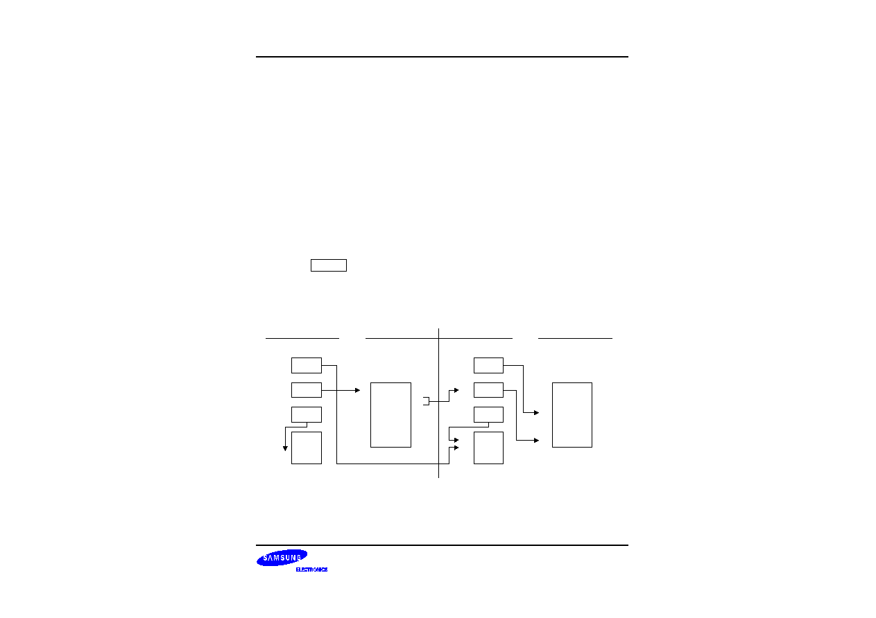
S3P80C5/C80C5/C80C8
INSTRUCTION SET
6-41
ENTER
--
Enter
ENTER
Operation:
SP
SP ≠ 2
@SP
IP
IP
PC
PC
@IP
IP
IP + 2
This instruction is useful when implementing threaded-code languages. The contents of the
instruction pointer are pushed to the stack. The program counter (PC) value is then written to the
instruction pointer. The program memory word that is pointed to by the instruction pointer is
loaded into the PC, and the instruction pointer is incremented by two.
Flags:
No flags are affected.
Format:
Bytes
Cycles
Opcode
(Hex)
opc
1
14
1F
Example:
The diagram below shows one example of how to use an ENTER statement.
0050
IP
0022
SP
22
Data
Address
Data
0040
PC
40
41
42
43
Enter
Address H
Address L
Address H
Address
Data
1F
01
10
Memory
0043
IP
0020
SP
20
21
22
IPH
IPL
Data
Address
Data
0110
PC
40
41
42
43
Enter
Address H
Address L
Address H
Address
Data
1F
01
10
Memory
00
50
Stack
Stack
110
Routine
Before
After
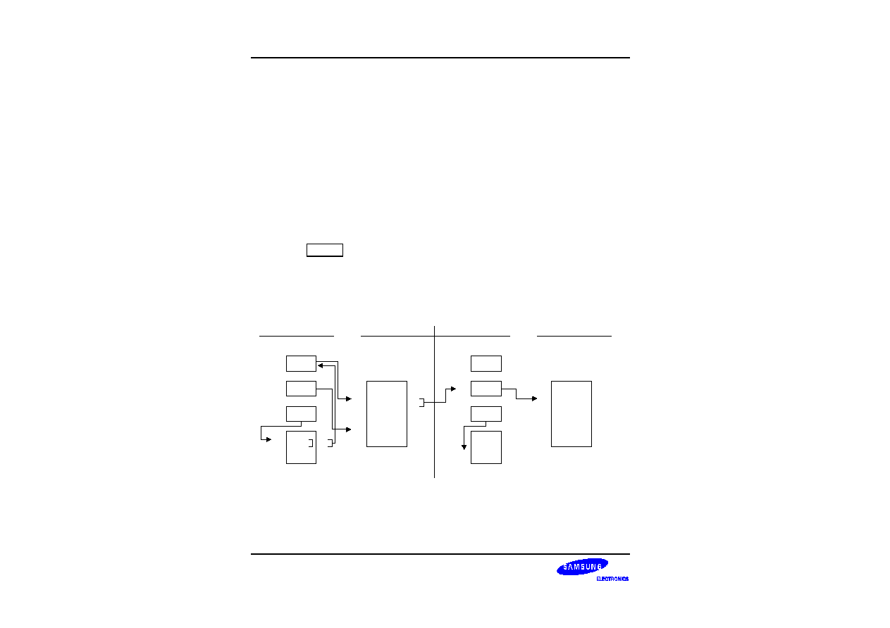
INSTRUCTION SET
S3P80C5/C80C5/C80C8
6-42
EXIT
--
Exit
EXIT
Operation:
IP
@SP
SP
SP + 2
PC
@IP
IP
IP + 2
This instruction is useful when implementing threaded-code languages. The stack value is
popped and loaded into the instruction pointer. The program memory word that is pointed to by
the instruction pointer is then loaded into the program counter, and the instruction pointer is
incremented by two.
Flags:
No flags are affected.
Format:
Bytes
Cycles
Opcode (Hex)
opc
1
14 (internal stack)
2F
16 (internal stack)
Example:
The diagram below shows one example of how to use an EXIT statement.
0050
IP
0022
SP
Address
Data
0040
PC
Address
Data
Memory
0052
IP
0022
SP
Address
Data
0060
PC
Address
Data
Memory
Stack
Stack
Before
After
22
Data
20
21
22
IPH
IPL
Data
00
50
50
51
140
PCL old
PCH
Exit
60
00
2F
60
Main

S3P80C5/C80C5/C80C8
INSTRUCTION SET
6-43
IDLE
--
Idle Operation
IDLE
Operation:
The IDLE instruction stops the CPU clock while allowing system clock oscillation to continue. Idle
mode can be released by an interrupt request (IRQ) or an external reset operation.
Flags:
No flags are affected.
Format:
Bytes
Cycles
Opcode
(Hex)
Addr Mode
dst src
opc
1
4
6F
≠
≠
Example:
The instruction
IDLE
stops the CPU clock but not the system clock.
INSTRUCTION SET
S3P80C5/C80C5/C80C8
6-44
INC
--
Increment
INC
dst
Operation:
dst
dst + 1
The contents of the destination operand are incremented by one.
Flags:
C: Unaffected.
Z: Set if the result is "0"; cleared otherwise.
S: Set if the result is negative; cleared otherwise.
V: Set if arithmetic overflow occurred; cleared otherwise.
D: Unaffected.
H: Unaffected.
Format:
Bytes
Cycles
Opcode
(Hex)
Addr Mode
dst
dst | opc
1
4
rE
r
r = 0 to F
opc
dst
2
4
20
R
4
21
IR
Examples:
Given: R0 = 1BH, register 00H = 0CH, and register 1BH = 0FH:
INC
R0
R0 = 1CH
INC
00H
Register 00H = 0DH
INC
@R0
R0 = 1BH, register 01H = 10H
In the first example, if destination working register R0 contains the value 1BH, the statement
"INC R0" leaves the value 1CH in that same register.
The next example shows the effect an INC instruction has on register 00H, assuming that it
contains the value 0CH.
In the third example, INC is used in Indirect Register (IR) addressing mode to increment the
value of register 1BH from 0FH to 10H.

S3P80C5/C80C5/C80C8
INSTRUCTION SET
6-45
INCW
--
Increment Word
INCW
dst
Operation:
dst
dst + 1
The contents of the destination (which must be an even address) and the byte following that
location are treated as a single 16-bit value that is incremented by one.
Flags:
C: Unaffected.
Z: Set if the result is "0"; cleared otherwise.
S: Set if the result is negative; cleared otherwise.
V: Set if arithmetic overflow occurred; cleared otherwise.
D: Unaffected.
H: Unaffected.
Format:
Bytes
Cycles
Opcode
(Hex)
Addr Mode
dst
opc
dst
2
8
A0
RR
8
A1
IR
Examples:
Given: R0 = 1AH, R1 = 02H, register 02H = 0FH, and register 03H = 0FFH:
INCW RR0
R0 = 1AH, R1 = 03H
INCW @R1
Register 02H = 10H, register 03H = 00H
In the first example, the working register pair RR0 contains the value 1AH in register R0 and 02H
in register R1. The statement "INCW RR0" increments the 16-bit destination by one, leaving the
value 03H in register R1. In the second example, the statement "INCW @R1" uses Indirect
Register (IR) addressing mode to increment the contents of general register 03H from 0FFH to
00H and register 02H from 0FH to 10H.
NOTE:
A system malfunction may occur if you use a Zero (Z) flag (FLAGS.6) result together with an
INCW instruction. To avoid this problem, we recommend that you use INCW as shown in the
following example:
LOOP:
INCW
RR0
LD
R2,R1
OR
R2,R0
JR
NZ,LOOP
INSTRUCTION SET
S3P80C5/C80C5/C80C8
6-46
IRET
--
Interrupt Return
IRET
IRET (Normal)
IRET (Fast)
Operation:
FLAGS
@SP
PC
IP
SP
SP + 1
FLAGS
FLAGS'
PC
@SP
FIS
0
SP
SP + 2
SYM(0)
1
This instruction is used at the end of an interrupt service routine. It restores the flag register and
the program counter. It also re-enables global interrupts. A "normal IRET" is executed only if the
fast interrupt status bit (FIS, bit one of the FLAGS register, 0D5H) is cleared (= "0"). If a fast
interrupt occurred, IRET clears the FIS bit that was set at the beginning of the service routine.
Flags:
All flags are restored to their original settings (that is, the settings before the interrupt occurred).
Format:
IRET
(Normal)
Bytes
Cycles
Opcode (Hex)
opc
1
10 (internal stack)
BF
12 (internal stack)
IRET
(Fast)
Bytes
Cycles
Opcode (Hex)
opc
1
6
BF
Example:
In the figure below, the instruction pointer is initially loaded with 100H in the main program
before interrupts are enabled. When an interrupt occurs, the program counter and instruction
pointer are swapped. This causes the PC to jump to address 100H and the IP to keep the return
address. The last instruction in the service routine normally is a jump to IRET at address FFH.
This causes the instruction pointer to be loaded with 100H "again" and the program counter to
jump back to the main program. Now, the next interrupt can occur and the IP is still correct at
100H.
IRET
Interrupt
Service
Routine
JP to FFH
0H
FFH
100H
FFFFH
NOTE:
In the fast interrupt example above, if the last instruction is not a jump to IRET, you must pay
attention to the order of the last two instructions. The IRET cannot be immediately proceeded by
a clearing of the interrupt status (as with a reset of the IPR register).
S3P80C5/C80C5/C80C8
INSTRUCTION SET
6-47
JP
--
Jump
JP
cc,dst
(Conditional)
JP
dst
(Unconditional)
Operation:
If cc is true, PC
dst
The conditional JUMP instruction transfers program control to the destination address if the
condition specified by the condition code (cc) is true; otherwise, the instruction following the JP
instruction is executed. The unconditional JP simply replaces the contents of the PC with the
contents of the specified register pair. Control then passes to the statement addressed by the
PC.
Flags:
No flags are affected.
Format:
(1)
(2)
Bytes
Cycles
Opcode
(Hex)
Addr Mode
dst
cc | opc
dst
3
8
ccD
DA
cc = 0 to F
opc
dst
2
8
30
IRR
NOTES:
1.
The 3-byte format is used for a conditional jump and the 2-byte format for an unconditional jump.
2.
In the first byte of the three-byte instruction format (conditional jump), the condition code and the
opcode are both four bits.
Examples:
Given: The carry flag (C) = "1", register 00 = 01H, and register 01 = 20H:
JP
C,LABEL_W
LABEL_W = 1000H, PC = 1000H
JP
@00H
PC = 0120H
The first example shows a conditional JP. Assuming that the carry flag is set to "1", the
statement
"JP C,LABEL_W" replaces the contents of the PC with the value 1000H and transfers control to
that location. Had the carry flag not been set, control would then have passed to the statement
immediately following the JP instruction.
The second example shows an unconditional JP. The statement "JP @00" replaces the contents
of the PC with the contents of the register pair 00H and 01H, leaving the value 0120H.

INSTRUCTION SET
S3P80C5/C80C5/C80C8
6-48
JR
--
Jump Relative
JR
cc,dst
Operation:
If cc is true, PC
PC + dst
If the condition specified by the condition code (cc) is true, the relative address is added to the
program counter and control passes to the statement whose address is now in the program
counter; otherwise, the instruction following the JR instruction is executed. (See list of condition
codes).
The range of the relative address is +127, ≠128, and the original value of the program counter is
taken to be the address of the first instruction byte following the JR statement.
Flags:
No flags are affected.
Format:
(1)
Bytes
Cycles
Opcode
(Hex)
Addr Mode
dst
cc | opc
dst
2
6
ccB
RA
cc = 0 to F
NOTE: In the first byte of the two-byte instruction format, the condition code and the opcode are each
four bits.
Example:
Given: The carry flag = "1" and LABEL_X = 1FF7H:
JR
C,LABEL_X
PC = 1FF7H
If the carry flag is set (that is, if the condition code is true), the statement "JR C,LABEL_X" will
pass control to the statement whose address is now in the PC. Otherwise, the program
instruction following the JR would be executed.
S3P80C5/C80C5/C80C8
INSTRUCTION SET
6-49
LD
--
Load
LD
dst,src
Operation:
dst
src
The contents of the source are loaded into the destination. The source's contents are unaffected.
Flags:
No flags are affected.
Format:
Bytes
Cycles
Opcode
(Hex)
Addr Mode
dst src
dst | opc
src
2
4
rC
r
IM
4
r8
r
R
src | opc
dst
2
4
r9
R
r
r = 0 to F
opc
dst | src
2
4
C7
r
lr
4
D7
Ir
r
opc
src
dst
3
6
E4
R
R
6
E5
R
IR
opc
dst
src
3
6
E6
R
IM
6
D6
IR
IM
opc
src
dst
3
6
F5
IR
R
opc
dst | src
x
3
6
87
r
x [r]
opc
src | dst
x
3
6
97
x [r]
r

INSTRUCTION SET
S3P80C5/C80C5/C80C8
6-50
LD
--
Load
LD
(Continued)
Examples:
Given: R0 = 01H, R1 = 0AH, register 00H = 01H, register 01H = 20H,
register 02H = 02H, LOOP = 30H, and register 3AH = 0FFH:
LD
R0,#10H
R0 = 10H
LD
R0,01H
R0 = 20H, register 01H = 20H
LD
01H,R0
Register 01H = 01H, R0 = 01H
LD
R1,@R0
R1 = 20H, R0 = 01H
LD
@R0,R1
R0 = 01H, R1 = 0AH, register 01H = 0AH
LD
00H,01H
Register 00H = 20H, register 01H = 20H
LD
02H,@00H
Register 02H = 20H, register 00H = 01H
LD
00H,#0AH
Register 00H = 0AH
LD
@00H,#10H
Register 00H = 01H, register 01H = 10H
LD
@00H,02H
Register 00H = 01H, register 01H = 02, register 02H = 02H
LD
R0,#LOOP[R1]
R0 = 0FFH, R1 = 0AH
LD
#LOOP[R0],R1
Register 31H = 0AH, R0 = 01H, R1 = 0AH
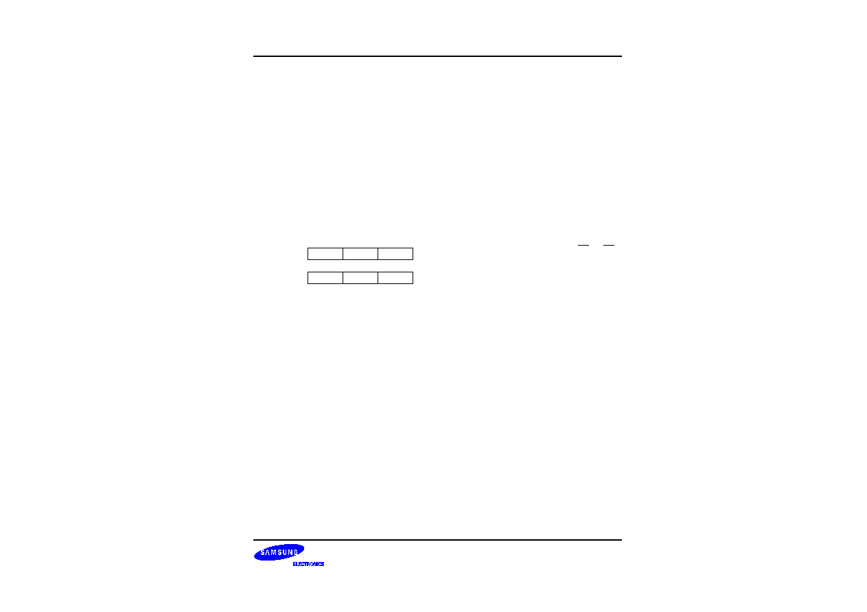
S3P80C5/C80C5/C80C8
INSTRUCTION SET
6-51
LDB
--
Load Bit
LDB
dst,src.b
LDB
dst.b,src
Operation:
dst(0)
src(b)
or
dst(b)
src(0)
The specified bit of the source is loaded into bit zero (LSB) of the destination, or bit zero of the
source is loaded into the specified bit of the destination. No other bits of the destination are
affected. The source is unaffected.
Flags:
No flags are affected.
Format:
Bytes
Cycles
Opcode
(Hex)
Addr Mode
dst src
opc
dst | b | 0
src
3
6
47
r0
Rb
opc
src | b | 1
dst
3
6
47
Rb
r0
NOTE: In the second byte of the instruction formats, the destination (or source) address is four bits, the
bit address 'b' is three bits, and the LSB address value is one bit in length.
Examples:
Given: R0 = 06H and general register 00H = 05H:
LDB
R0,00H.2
R0 = 07H, register 00H = 05H
LDB
00H.0,R0
R0 = 06H, register 00H = 04H
In the first example, destination working register R0 contains the value 06H and the source
general register 00H the value 05H. The statement "LD R0,00H.2" loads the bit two value of the
00H register into bit zero of the R0 register, leaving the value 07H in register R0.
In the second example, 00H is the destination register. The statement "LD 00H.0,R0" loads bit
zero of register R0 to the specified bit (bit zero) of the destination register, leaving 04H in
general register 00H.

INSTRUCTION SET
S3P80C5/C80C5/C80C8
6-52
LDC/LDE
--
Load Memory
LDC/LDE
dst,src
Operation:
dst
src
This instruction loads a byte from program or data memory into a working register or vice-versa.
The source values are unaffected. LDC refers to program memory and LDE to data memory.
The assembler makes 'Irr' or 'rr' values an even number for program memory and odd an odd
number for data memory.
Flags:
No flags are affected.
Format:
Bytes
Cycles
Opcode
(Hex)
Addr Mode
dst src
1.
opc
dst | src
2
10
C3
r
Irr
2.
opc
src | dst
2
10
D3
Irr
r
3.
opc
dst | src
XS
3
12
E7
r
XS [rr]
4.
opc
src | dst
XS
3
12
F7
XS [rr]
r
5.
opc
dst | src
XL
L
XL
H
4
14
A7
r
XL [rr]
6.
opc
src | dst
XL
L
XL
H
4
14
B7
XL [rr]
r
7.
opc
dst | 0000
DA
L
DA
H
4
14
A7
r
DA
8.
opc
src | 0000
DA
L
DA
H
4
14
B7
DA
r
9.
opc
dst | 0001
DA
L
DA
H
4
14
A7
r
DA
10.
opc
src | 0001
DA
L
DA
H
4
14
B7
DA
r
NOTES:
1.
The source (src) or working register pair [rr] for formats 5 and 6 cannot use register pair 0≠1.
2.
For formats 3 and 4, the destination address 'XS [rr]' and the source address 'XS [rr]' are each one
byte.
3.
For formats 5 and 6, the destination address 'XL [rr] and the source address 'XL [rr]' are each two
bytes.
4.
The DA and r source values for formats 7 and 8 are used to address program memory; the second set
of values, used in formats 9 and 10, are used to address data memory.

S3P80C5/C80C5/C80C8
INSTRUCTION SET
6-53
LDC/LDE
--
Load Memory
LDC/LDE
(Continued)
Examples:
Given: R0 = 11H, R1 = 34H, R2 = 01H, R3 = 04H; Program memory locations
0103H = 4FH, 0104H = 1A, 0105H = 6DH, and 1104H = 88H. External data memory
locations 0103H = 5FH, 0104H = 2AH, 0105H = 7DH, and 1104H = 98H:
LDC
R0,@RR2
; R0
contents of program memory location 0104H
; R0 = 1AH, R2 = 01H, R3 = 04H
LDE
R0,@RR2
; R0
contents of external data memory location 0104H
; R0 = 2AH, R2 = 01H, R3 = 04H
LDC
(note)
@RR2,R0
; 11H (contents of R0) is loaded into program memory
; location 0104H (RR2),
; working registers R0, R2, R3
no change
LDE
@RR2,R0
; 11H (contents of R0) is loaded into external data memory
; location 0104H (RR2),
; working registers R0, R2, R3
no change
LDC
R0,#01H[RR2]
; R0
contents of program memory location 0105H
; (01H + RR2),
; R0 = 6DH, R2 = 01H, R3 = 04H
LDE
R0,#01H[RR2]
; R0
contents of external data memory location 0105H
; (01H + RR2), R0 = 7DH, R2 = 01H, R3 = 04H
LDC
(note)
#01H[RR2],R0
; 11H (contents of R0) is loaded into program memory location
; 0105H (01H + 0104H)
LDE
#01H[RR2],R0
; 11H (contents of R0) is loaded into external data memory
; location 0105H (01H + 0104H)
LDC
R0,#1000H[RR2] ; R0
contents of program memory location 1104H
; (1000H + 0104H), R0 = 88H, R2 = 01H, R3 = 04H
LDE
R0,#1000H[RR2] ; R0
contents of external data memory location 1104H
; (1000H + 0104H), R0 = 98H, R2 = 01H, R3 = 04H
LDC
R0,1104H
; R0
contents of program memory location 1104H, R0 = 88H
LDE
R0,1104H
; R0
contents of external data memory location 1104H,
; R0 = 98H
LDC
(note)
1105H,R0
; 11H (contents of R0) is loaded into program memory location
; 1105H, (1105H)
11H
LDE
1105H,R0
; 11H (contents of R0) is loaded into external data memory
; location 1105H, (1105H)
11H
NOTE: These instructions are not supported by masked ROM type devices.
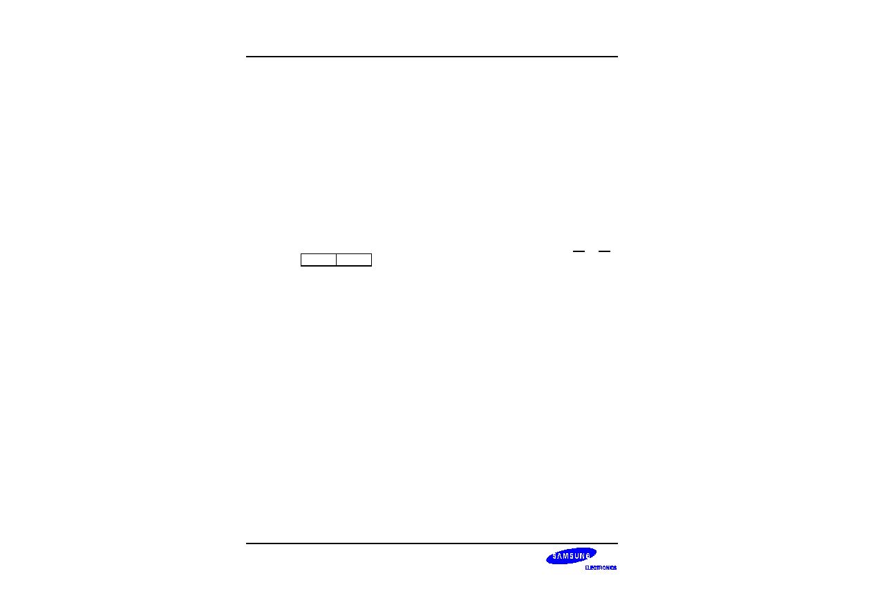
INSTRUCTION SET
S3P80C5/C80C5/C80C8
6-54
LDCD/LDED
--
Load Memory and Decrement
LDCD/LDED
dst,src
Operation:
dst
src
rr
rr ≠ 1
These instructions are used for user stacks or block transfers of data from program or data
memory to the register file. The address of the memory location is specified by a working register
pair. The contents of the source location are loaded into the destination location. The memory
address is then decremented. The contents of the source are unaffected.
LDCD references program memory and LDED references external data memory. The assembler
makes 'Irr' an even number for program memory and an odd number for data memory.
Flags:
No flags are affected.
Format:
Bytes
Cycles
Opcode
(Hex)
Addr Mode
dst src
opc
dst | src
2
10
E2
r
Irr
Examples:
Given: R6 = 10H, R7 = 33H, R8 = 12H, program memory location 1033H = 0CDH, and
external data memory location 1033H = 0DDH:
LDCD
R8,@RR6
; 0CDH (contents of program memory location 1033H) is loaded
; into R8 and RR6 is decremented by one
; R8 = 0CDH, R6 = 10H, R7 = 32H (RR6
RR6 ≠ 1)
LDED
R8,@RR6
; 0DDH (contents of data memory location 1033H) is loaded
; into R8 and RR6 is decremented by one (RR6
RR6 ≠ 1)
; R8 = 0DDH, R6 = 10H, R7 = 32H

S3P80C5/C80C5/C80C8
INSTRUCTION SET
6-55
LDCI/LDEI
--
Load Memory and Increment
LDCI/LDEI
dst,src
Operation:
dst
src
rr
rr + 1
These instructions are used for user stacks or block transfers of data from program or data
memory to the register file. The address of the memory location is specified by a working register
pair. The contents of the source location are loaded into the destination location. The memory
address is then incremented automatically. The contents of the source are unaffected.
LDCI refers to program memory and LDEI refers to external data memory. The assembler
makes 'Irr' even for program memory and odd for data memory.
Flags:
No flags are affected.
Format:
Bytes
Cycles
Opcode
(Hex)
Addr Mode
dst src
opc
dst | src
2
10
E3
r
Irr
Examples:
Given: R6 = 10H, R7 = 33H, R8 = 12H, program memory locations 1033H = 0CDH and
1034H = 0C5H; external data memory locations 1033H = 0DDH and 1034H = 0D5H:
LDCI
R8,@RR6
; 0CDH (contents of program memory location 1033H) is loaded
; into R8 and RR6 is incremented by one (RR6
RR6 + 1)
; R8 = 0CDH, R6 = 10H, R7 = 34H
LDEI
R8,@RR6
; 0DDH (contents of data memory location 1033H) is loaded
; into R8 and RR6 is incremented by one (RR6
RR6 + 1)
; R8 = 0DDH, R6 = 10H, R7 = 34H
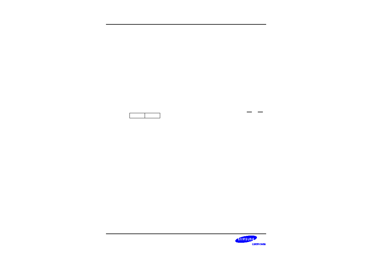
INSTRUCTION SET
S3P80C5/C80C5/C80C8
6-56
LDCPD/LDEPD
--
Load Memory with Pre-Decrement
LDCPD/
LDEPD
dst,src
Operation:
rr
rr ≠ 1
dst
src
These instructions are used for block transfers of data from program or data memory from the
register file. The address of the memory location is specified by a working register pair and is
first decremented. The contents of the source location are then loaded into the destination
location. The contents of the source are unaffected.
LDCPD refers to program memory and LDEPD refers to external data memory. The assembler
makes 'Irr' an even number for program memory and an odd number for external data memory.
Flags:
No flags are affected.
Format:
Bytes
Cycles
Opcode
(Hex)
Addr Mode
dst src
opc
src | dst
2
14
F2
Irr
r
Examples:
Given: R0 = 77H, R6 = 30H, and R7 = 00H:
LDCPD
@RR6,R0
; (RR6
RR6 ≠ 1)
; 77H (contents of R0) is loaded into program memory location
; 2FFFH (3000H ≠ 1H)
; R0 = 77H, R6 = 2FH, R7 = 0FFH
LDEPD
@RR6,R0
; (RR6
RR6 ≠ 1)
; 77H (contents of R0) is loaded into external data memory
; location 2FFFH (3000H ≠ 1H)
; R0 = 77H, R6 = 2FH, R7 = 0FFH

S3P80C5/C80C5/C80C8
INSTRUCTION SET
6-57
LDCPI/LDEPI
--
Load Memory with Pre-Increment
LDCPI/
LDEPI
dst,src
Operation:
rr
rr + 1
dst
src
These instructions are used for block transfers of data from program or data memory from the
register file. The address of the memory location is specified by a working register pair and is
first incremented. The contents of the source location are loaded into the destination location.
The contents of the source are unaffected.
LDCPI refers to program memory and LDEPI refers to external data memory. The assembler
makes 'Irr' an even number for program memory and an odd number for data memory.
Flags:
No flags are affected.
Format:
Bytes
Cycles
Opcode
(Hex)
Addr Mode
dst src
opc
src | dst
2
14
F3
Irr
r
Examples:
Given: R0 = 7FH, R6 = 21H, and R7 = 0FFH:
LDCPI
@RR6,R0
; (RR6
RR6 + 1)
; 7FH (contents of R0) is loaded into program memory
; location 2200H (21FFH + 1H)
; R0 = 7FH, R6 = 22H, R7 = 00H
LDEPI
@RR6,R0
; (RR6
RR6 + 1)
; 7FH (contents of R0) is loaded into external data memory
; location 2200H (21FFH + 1H)
; R0 = 7FH, R6 = 22H, R7 = 00H
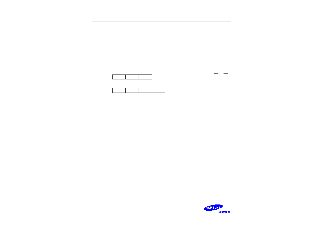
INSTRUCTION SET
S3P80C5/C80C5/C80C8
6-58
LDW
--
Load Word
LDW
dst,src
Operation:
dst
src
The contents of the source (a word) are loaded into the destination. The contents of the source
are unaffected.
Flags:
No flags are affected.
Format:
Bytes
Cycles
Opcode
(Hex)
Addr Mode
dst src
opc
src
dst
3
8
C4
RR
RR
8
C5
RR
IR
opc
dst
src
4
8
C6
RR
IML
Examples:
Given: R4 = 06H, R5 = 1CH, R6 = 05H, R7 = 02H, register 00H = 1AH,
register 01H = 02H, register 02H = 03H, and register 03H = 0FH:
LDW
RR6,RR4
R6 = 06H, R7 = 1CH, R4 = 06H, R5 = 1CH
LDW
00H,02H
Register 00H = 03H, register 01H = 0FH,
register 02H = 03H, register 03H = 0FH
LDW
RR2,@R7
R2 = 03H, R3 = 0FH,
LDW
04H,@01H
Register 04H = 03H, register 05H = 0FH
LDW
RR6,#1234H
R6 = 12H, R7 = 34H
LDW
02H,#0FEDH
Register 02H = 0FH, register 03H = 0EDH
In the second example, please note that the statement "LDW 00H,02H" loads the contents of
the source word 02H, 03H into the destination word 00H, 01H. This leaves the value 03H in
general register 00H and the value 0FH in register 01H.
The other examples show how to use the LDW instruction with various addressing modes and
formats.
S3P80C5/C80C5/C80C8
INSTRUCTION SET
6-59
MULT
--
Multiply (Unsigned)
MULT
dst,src
Operation:
dst
dst
◊
src
The 8-bit destination operand (even register of the register pair) is multiplied by the source
operand (8 bits) and the product (16 bits) is stored in the register pair specified by the destination
address. Both operands are treated as unsigned integers.
Flags:
C: Set if result is
>
255; cleared otherwise.
Z: Set if the result is "0"; cleared otherwise.
S: Set if MSB of the result is a "1"; cleared otherwise.
V: Cleared.
D: Unaffected.
H: Unaffected.
Format:
Bytes
Cycles
Opcode
(Hex)
Addr Mode
dst src
opc
src
dst
3
22
84
RR
R
22
85
RR
IR
22
86
RR
IM
Examples:
Given: Register 00H = 20H, register 01H = 03H, register 02H = 09H, register 03H = 06H:
MULT
00H, 02H
Register 00H = 01H, register 01H = 20H, register 02H = 09H
MULT
00H, @01H
Register 00H = 00H, register 01H = 0C0H
MULT
00H, #30H
Register 00H = 06H, register 01H = 00H
In the first example, the statement "MULT 00H,02H" multiplies the 8-bit destination operand (in
the register 00H of the register pair 00H, 01H) by the source register 02H operand (09H). The
16-bit product, 0120H, is stored in the register pair 00H, 01H.
INSTRUCTION SET
S3P80C5/C80C5/C80C8
6-60
NEXT
--
Next
NEXT
Operation:
PC
@ IP
IP
IP + 2
The NEXT instruction is useful when implementing threaded-code languages. The program
memory word that is pointed to by the instruction pointer is loaded into the program counter. The
instruction pointer is then incremented by two.
Flags:
No flags are affected.
Format:
Bytes
Cycles
Opcode
(Hex)
opc
1
10
0F
Example:
The following diagram shows one example of how to use the NEXT instruction.
Data
01
10
Before
After
0045
IP
Address
Data
0130
PC
43
44
45
Address H
Address L
Address H
Address
Data
Memory
130
Routine
0043
IP
Address
Data
0120
PC
43
44
45
Address H
Address L
Address H
Address
Data
Memory
120
Next

S3P80C5/C80C5/C80C8
INSTRUCTION SET
6-61
NOP
--
No Operation
NOP
Operation:
No action is performed when the CPU executes this instruction. Typically, one or more NOPs are
executed in sequence in order to effect a timing delay of variable duration.
Flags:
No flags are affected.
Format:
Bytes
Cycles
Opcode
(Hex)
opc
1
4
FF
Example:
When the instruction
NOP
is encountered in a program, no operation occurs. Instead, there is a delay in instruction
execution time.

INSTRUCTION SET
S3P80C5/C80C5/C80C8
6-62
OR
--
Logical OR
OR
dst,src
Operation:
dst
dst OR src
The source operand is logically ORed with the destination operand and the result is stored in the
destination. The contents of the source are unaffected. The OR operation results in a "1" being
stored whenever either of the corresponding bits in the two operands is a "1"; otherwise a "0" is
stored.
Flags:
C: Unaffected.
Z: Set if the result is "0"; cleared otherwise.
S: Set if the result bit 7 is set; cleared otherwise.
V: Always cleared to "0".
D: Unaffected.
H: Unaffected.
Format:
Bytes
Cycles
Opcode
(Hex)
Addr Mode
dst src
opc
dst | src
2
4
42
r
r
6
43
r
lr
opc
src
dst
3
6
44
R
R
6
45
R
IR
opc
dst
src
3
6
46
R
IM
Examples:
Given: R0 = 15H, R1 = 2AH, R2 = 01H, register 00H = 08H, register 01H = 37H, and
register 08H = 8AH:
OR
R0,R1
R0 = 3FH, R1 = 2AH
OR
R0,@R2
R0 = 37H, R2 = 01H, register 01H = 37H
OR
00H,01H
Register 00H = 3FH, register 01H = 37H
OR
01H,@00H
Register 00H = 08H, register 01H = 0BFH
OR
00H,#02H
Register 00H = 0AH
In the first example, if working register R0 contains the value 15H and register R1 the value
2AH, the statement "OR R0,R1" logical-ORs the R0 and R1 register contents and stores the
result (3FH) in destination register R0.
The other examples show the use of the logical OR instruction with the various addressing
modes and formats.

S3P80C5/C80C5/C80C8
INSTRUCTION SET
6-63
POP
--
Pop From Stack
POP
dst
Operation:
dst
@SP
SP
SP + 1
The contents of the location addressed by the stack pointer are loaded into the destination. The
stack pointer is then incremented by one.
Flags:
No flags affected.
Format:
Bytes
Cycles
Opcode
(Hex)
Addr Mode
dst
opc
dst
2
8
50
R
8
51
IR
Examples:
Given: Register 00H = 01H, register 01H = 1BH, SPH (0D8H) = 00H, SPL (0D9H) = 0FBH,
and stack register 0FBH = 55H:
POP
00H
Register 00H = 55H, SP = 00FCH
POP
@00H
Register 00H = 01H, register 01H = 55H, SP = 00FCH
In the first example, general register 00H contains the value 01H. The statement "POP 00H"
loads the contents of location 00FBH (55H) into destination register 00H and then increments the
stack pointer by one. Register 00H then contains the value 55H and the SP points to location
00FCH.
INSTRUCTION SET
S3P80C5/C80C5/C80C8
6-64
POPUD
--
Pop User Stack (Decrementing)
POPUD
dst,src
Operation:
dst
src
IR
IR ≠ 1
This instruction is used for user-defined stacks in the register file. The contents of the register file
location addressed by the user stack pointer are loaded into the destination. The user stack
pointer is then decremented.
Flags:
No flags are affected.
Format:
Bytes
Cycles
Opcode
(Hex)
Addr Mode
dst src
opc
src
dst
3
8
92
R
IR
Example:
Given: Register 00H = 42H (user stack pointer register), register 42H = 6FH, and
register 02H = 70H:
POPUD
02H,@00H
Register 00H = 41H, register 02H = 6FH, register 42H = 6FH
If general register 00H contains the value 42H and register 42H the value 6FH, the statement
"POPUD 02H,@00H" loads the contents of register 42H into the destination register 02H. The
user stack pointer is then decremented by one, leaving the value 41H.
S3P80C5/C80C5/C80C8
INSTRUCTION SET
6-65
POPUI
--
Pop User Stack (Incrementing)
POPUI
dst,src
Operation:
dst
src
IR
IR + 1
The POPUI instruction is used for user-defined stacks in the register file. The contents of the
register file location addressed by the user stack pointer are loaded into the destination. The user
stack pointer is then incremented.
Flags:
No flags are affected.
Format:
Bytes
Cycles
Opcode
(Hex)
Addr Mode
dst src
opc
src
dst
3
8
93
R
IR
Example:
Given: Register 00H = 01H and register 01H = 70H:
POPUI
02H,@00H
Register 00H = 02H, register 01H = 70H, register 02H = 70H
If general register 00H contains the value 01H and register 01H the value 70H, the statement
"POPUI 02H,@00H" loads the value 70H into the destination general register 02H. The user
stack pointer (register 00H) is then incremented by one, changing its value from 01H to 02H.

INSTRUCTION SET
S3P80C5/C80C5/C80C8
6-66
PUSH
--
Push To Stack
PUSH
src
Operation:
SP
SP ≠ 1
@SP
src
A PUSH instruction decrements the stack pointer value and loads the contents of the source
(src) into the location addressed by the decremented stack pointer. The operation then adds the
new value to the top of the stack.
Flags:
No flags are affected.
Format:
Bytes
Cycles
Opcode
(Hex)
Addr Mode
dst
opc
src
2
8 (internal clock)
70
R
8 (external clock)
8 (internal clock)
8 (external clock)
71
IR
Examples:
Given: Register 40H = 4FH, register 4FH = 0AAH, SPH = 00H, and SPL = 00H:
PUSH
40H
Register 40H = 4FH, stack register 0FFH = 4FH,
SPH = 0FFH, SPL = 0FFH
PUSH
@40H
Register 40H = 4FH, register 4FH = 0AAH, stack register
0FFH = 0AAH, SPH = 0FFH, SPL = 0FFH
In the first example, if the stack pointer contains the value 0000H, and general register 40H the
value 4FH, the statement "PUSH 40H" decrements the stack pointer from 0000 to 0FFFFH. It
then loads the contents of register 40H into location 0FFFFH and adds this new value to the top
of the stack.

S3P80C5/C80C5/C80C8
INSTRUCTION SET
6-67
PUSHUD
--
Push User Stack (Decrementing)
PUSHUD
dst,src
Operation:
IR
IR ≠ 1
dst
src
This instruction is used to address user-defined stacks in the register file. PUSHUD decrements
the user stack pointer and loads the contents of the source into the register addressed by the
decremented stack pointer.
Flags:
No flags are affected.
Format:
Bytes
Cycles
Opcode
(Hex)
Addr Mode
dst src
opc
dst
src
3
8
82
IR
R
Example:
Given: Register 00H = 03H, register 01H = 05H, and register 02H = 1AH:
PUSHUD @00H,01H
Register 00H = 02H, register 01H = 05H, register 02H = 05H
If the user stack pointer (register 00H, for example) contains the value 03H, the statement
"PUSHUD @00H,01H" decrements the user stack pointer by one, leaving the value 02H. The
01H register value, 05H, is then loaded into the register addressed by the decremented user
stack pointer.

INSTRUCTION SET
S3P80C5/C80C5/C80C8
6-68
PUSHUI
--
Push User Stack (Incrementing)
PUSHUI
dst,src
Operation:
IR
IR + 1
dst
src
This instruction is used for user-defined stacks in the register file. PUSHUI increments the user
stack pointer and then loads the contents of the source into the register location addressed by
the incremented user stack pointer.
Flags:
No flags are affected.
Format:
Bytes
Cycles
Opcode
(Hex)
Addr Mode
dst src
opc
dst
src
3
8
83
IR
R
Example:
Given: Register 00H = 03H, register 01H = 05H, and register 04H = 2AH:
PUSHUI
@00H,01H
Register 00H = 04H, register 01H = 05H, register 04H = 05H
If the user stack pointer (register 00H, for example) contains the value 03H, the statement
"PUSHUI @00H,01H" increments the user stack pointer by one, leaving the value 04H. The 01H
register value, 05H, is then loaded into the location addressed by the incremented user stack
pointer.

S3P80C5/C80C5/C80C8
INSTRUCTION SET
6-69
RCF
--
Reset Carry Flag
RCF
RCF
Operation:
C
0
The carry flag is cleared to logic zero, regardless of its previous value.
Flags:
C:
Cleared to "0".
No other flags are affected.
Format:
Bytes
Cycles
Opcode
(Hex)
opc
1
4
CF
Example:
Given: C = "1" or "0":
The instruction RCF clears the carry flag (C) to logic zero.

INSTRUCTION SET
S3P80C5/C80C5/C80C8
6-70
RET
--
Return
RET
Operation:
PC
@SP
SP
SP + 2
The RET instruction is normally used to return to the previously executing procedure at the end
of a procedure entered by a CALL instruction. The contents of the location addressed by the
stack pointer are popped into the program counter. The next statement that is executed is the
one that is addressed by the new program counter value.
Flags:
No flags are affected.
Format:
Bytes
Cycles
Opcode (Hex)
opc
1
8 (internal stack)
AF
10 (internal stack)
Example:
Given: SP = 00FCH, (SP) = 101AH, and PC = 1234:
RET
PC = 101AH, SP = 00FEH
The statement "RET" pops the contents of stack pointer location 00FCH (10H) into the high byte
of the program counter. The stack pointer then pops the value in location 00FEH (1AH) into the
PC's low byte and the instruction at location 101AH is executed. The stack pointer now points to
memory location 00FEH.

S3P80C5/C80C5/C80C8
INSTRUCTION SET
6-71
RL
--
Rotate Left
RL
dst
Operation:
C
dst (7)
dst (0)
dst (7)
dst (n + 1)
dst (n), n = 0≠6
The contents of the destination operand are rotated left one bit position. The initial value of bit 7
is moved to the bit zero (LSB) position and also replaces the carry flag.
7
0
C
Flags:
C: Set if the bit rotated from the most significant bit position (bit 7) was "1".
Z: Set if the result is "0"; cleared otherwise.
S: Set if the result bit 7 is set; cleared otherwise.
V: Set if arithmetic overflow occurred; cleared otherwise.
D: Unaffected.
H: Unaffected.
Format:
Bytes
Cycles
Opcode
(Hex)
Addr Mode
dst
opc
dst
2
4
90
R
4
91
IR
Examples:
Given: Register 00H = 0AAH, register 01H = 02H and register 02H = 17H:
RL
00H
Register 00H = 55H, C = "1"
RL
@01H
Register 01H = 02H, register 02H = 2EH, C = "0"
In the first example, if general register 00H contains the value 0AAH (10101010B), the statement
"RL 00H" rotates the 0AAH value left one bit position, leaving the new value 55H (01010101B)
and setting the carry and overflow flags.
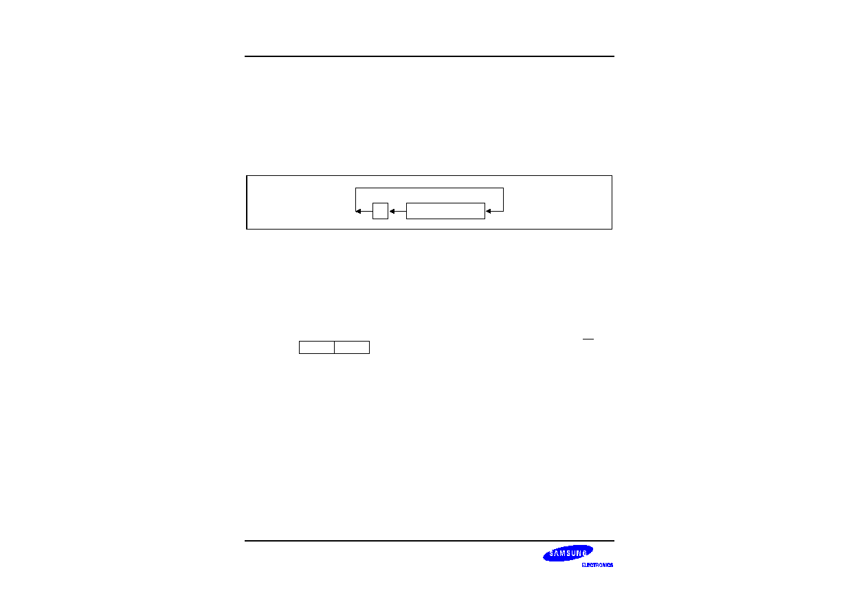
INSTRUCTION SET
S3P80C5/C80C5/C80C8
6-72
RLC
--
Rotate Left Through Carry
RLC
dst
Operation:
dst (0)
C
C
dst (7)
dst (n + 1)
dst (n), n = 0≠6
The contents of the destination operand with the carry flag are rotated left one bit position. The
initial value of bit 7 replaces the carry flag (C); the initial value of the carry flag replaces bit zero.
7
0
C
Flags:
C: Set if the bit rotated from the most significant bit position (bit 7) was "1".
Z: Set if the result is "0"; cleared otherwise.
S: Set if the result bit 7 is set; cleared otherwise.
V: Set if arithmetic overflow occurred, that is, if the sign of the destination changed during
rotation; cleared otherwise.
D: Unaffected.
H: Unaffected.
Format:
Bytes
Cycles
Opcode
(Hex)
Addr Mode
dst
opc
dst
2
4
10
R
4
11
IR
Examples:
Given: Register 00H = 0AAH, register 01H = 02H, and register 02H = 17H, C = "0":
RLC
00H
Register 00H = 54H, C = "1"
RLC
@01H
Register 01H = 02H, register 02H = 2EH, C = "0"
In the first example, if general register 00H has the value 0AAH (10101010B), the statement
"RLC 00H" rotates 0AAH one bit position to the left. The initial value of bit 7 sets the carry flag
and the initial value of the C flag replaces bit zero of register 00H, leaving the value 55H
(01010101B). The MSB of register 00H resets the carry flag to "1" and sets the overflow flag.
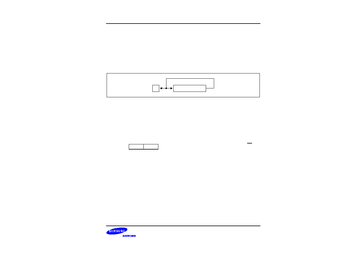
S3P80C5/C80C5/C80C8
INSTRUCTION SET
6-73
RR
--
Rotate Right
RR
dst
Operation:
C
dst (0)
dst (7)
dst (0)
dst (n
)
dst (n + 1), n = 0≠6
The contents of the destination operand are rotated right one bit position. The initial value of bit
zero (LSB) is moved to bit 7 (MSB) and also replaces the carry flag (C).
7
0
C
Flags:
C: Set if the bit rotated from the least significant bit position (bit zero) was "1".
Z: Set if the result is "0"; cleared otherwise.
S: Set if the result bit 7 is set; cleared otherwise.
V: Set if arithmetic overflow occurred, that is, if the sign of the destination changed during
rotation; cleared otherwise.
D: Unaffected.
H: Unaffected.
Format:
Bytes
Cycles
Opcode
(Hex)
Addr Mode
dst
opc
dst
2
4
E0
R
4
E1
IR
Examples:
Given: Register 00H = 31H, register 01H = 02H, and register 02H = 17H:
RR
00H
Register 00H = 98H, C = "1"
RR
@01H
Register 01H = 02H, register 02H = 8BH, C = "1"
In the first example, if general register 00H contains the value 31H (00110001B), the statement
"RR 00H" rotates this value one bit position to the right. The initial value of bit zero is moved to
bit 7, leaving the new value 98H (10011000B) in the destination register. The initial bit zero also
resets the C flag to "1" and the sign flag and overflow flag are also set to "1".
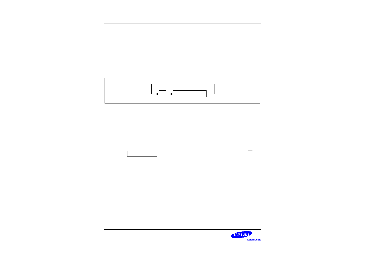
INSTRUCTION SET
S3P80C5/C80C5/C80C8
6-74
RRC
--
Rotate Right Through Carry
RRC
dst
Operation:
dst (7)
C
C
dst (0)
dst (n)
dst (n + 1), n = 0≠6
The contents of the destination operand and the carry flag are rotated right one bit position. The
initial value of bit zero (LSB) replaces the carry flag; the initial value of the carry flag replaces bit
7 (MSB).
7
0
C
Flags:
C: Set if the bit rotated from the least significant bit position (bit zero) was "1".
Z: Set if the result is "0" cleared otherwise.
S: Set if the result bit 7 is set; cleared otherwise.
V: Set if arithmetic overflow occurred, that is, if the sign of the destination changed during
rotation; cleared otherwise.
D: Unaffected.
H: Unaffected.
Format:
Bytes
Cycles
Opcode
(Hex)
Addr Mode
dst
opc
dst
2
4
C0
R
4
C1
IR
Examples:
Given: Register 00H = 55H, register 01H = 02H, register 02H = 17H, and C = "0":
RRC
00H
Register 00H = 2AH, C = "1"
RRC
@01H
Register 01H = 02H, register 02H = 0BH, C = "1"
In the first example, if general register 00H contains the value 55H (01010101B), the statement
"RRC 00H" rotates this value one bit position to the right. The initial value of bit zero ("1")
replaces the carry flag and the initial value of the C flag ("1") replaces bit 7. This leaves the new
value 2AH (00101010B) in destination register 00H. The sign flag and overflow flag are both
cleared to "0".

S3P80C5/C80C5/C80C8
INSTRUCTION SET
6-75
SB0
--
Select Bank 0
SB0
Operation:
BANK
0
The SB0 instruction clears the bank address flag in the FLAGS register (FLAGS.0) to logic zero,
selecting bank 0 register addressing in the set 1 area of the register file.
Flags:
No flags are affected.
Format:
Bytes
Cycles
Opcode
(Hex)
opc
1
4
4F
Example:
The statement
SB0
clears FLAGS.0 to "0", selecting bank 0 register addressing.

INSTRUCTION SET
S3P80C5/C80C5/C80C8
6-76
SB1
--
Select Bank 1
SB1
Operation:
BANK
1
The SB1 instruction sets the bank address flag in the FLAGS register (FLAGS.0) to logic one,
selecting bank 1 register addressing in the set 1 area of the register file. (Bank 1 is not
implemented in some KS88-series microcontrollers.)
Flags:
No flags are affected.
Format:
Bytes
Cycles
Opcode
(Hex)
opc
1
4
5F
Example:
The statement
SB1
sets FLAGS.0 to "1", selecting bank 1 register addressing, if implemented.
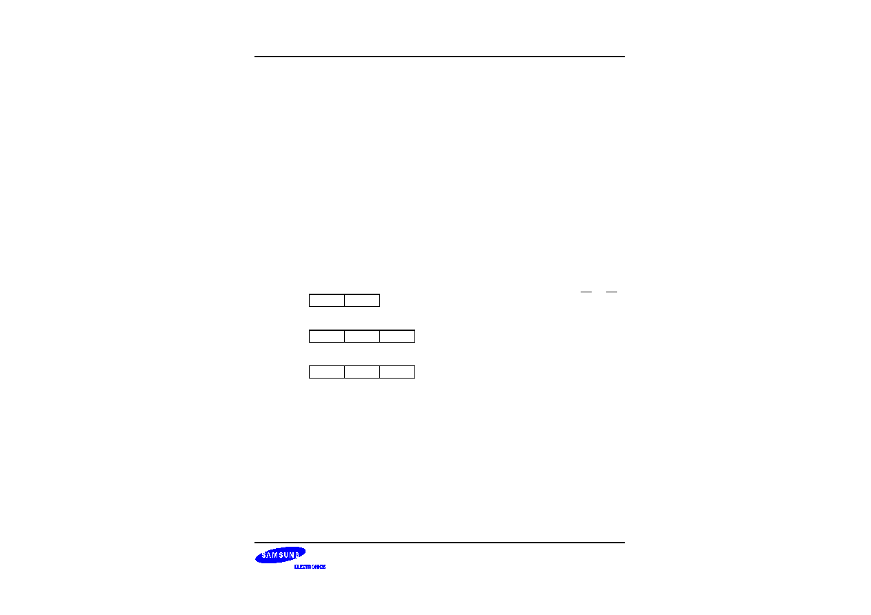
S3P80C5/C80C5/C80C8
INSTRUCTION SET
6-77
SBC
--
Subtract With Carry
SBC
dst,src
Operation:
dst
dst ≠ src ≠ c
The source operand, along with the current value of the carry flag, is subtracted from the
destination operand and the result is stored in the destination. The contents of the source are
unaffected. Subtraction is performed by adding the two's-complement of the source operand to
the destination operand. In multiple precision arithmetic, this instruction permits the carry
("borrow") from the subtraction of the low-order operands to be subtracted from the subtraction of
high-order operands.
Flags:
C: Set if a borrow occurred (src
>
dst); cleared otherwise.
Z: Set if the result is "0"; cleared otherwise.
S: Set if the result is negative; cleared otherwise.
V: Set if arithmetic overflow occurred, that is, if the operands were of opposite sign and the sign
of the result is the same as the sign of the source; cleared otherwise.
D: Always set to "1".
H: Cleared if there is a carry from the most significant bit of the low-order four bits of the result;
set otherwise, indicating a "borrow".
Format:
Bytes
Cycles
Opcode
(Hex)
Addr Mode
dst src
opc
dst | src
2
4
32
r
r
6
33
r
lr
opc
src
dst
3
6
34
R
R
6
35
R
IR
opc
dst
src
3
6
36
R
IM
Examples:
Given: R1 = 10H, R2 = 03H, C = "1", register 01H = 20H, register 02H = 03H, and
register 03H = 0AH:
SBC
R1,R2
R1 = 0CH, R2 = 03H
SBC
R1,@R2
R1 = 05H, R2 = 03H, register 03H = 0AH
SBC
01H,02H
Register 01H = 1CH, register 02H = 03H
SBC
01H,@02H
Register 01H = 15H,register 02H = 03H, register 03H = 0AH
SBC
01H,#8AH
Register 01H = 95H; C, S, and V = "1"
In the first example, if working register R1 contains the value 10H and register R2 the value 03H,
the statement "SBC R1,R2" subtracts the source value (03H) and the C flag value ("1") from the
destination (10H) and then stores the result (0CH) in register R1.

INSTRUCTION SET
S3P80C5/C80C5/C80C8
6-78
SCF
--
Set Carry Flag
SCF
Operation:
C
1
The carry flag (C) is set to logic one, regardless of its previous value.
Flags:
C: Set to "1".
No other flags are affected.
Format:
Bytes
Cycles
Opcode
(Hex)
opc
1
4
DF
Example:
The statement
SCF
sets the carry flag to logic one.
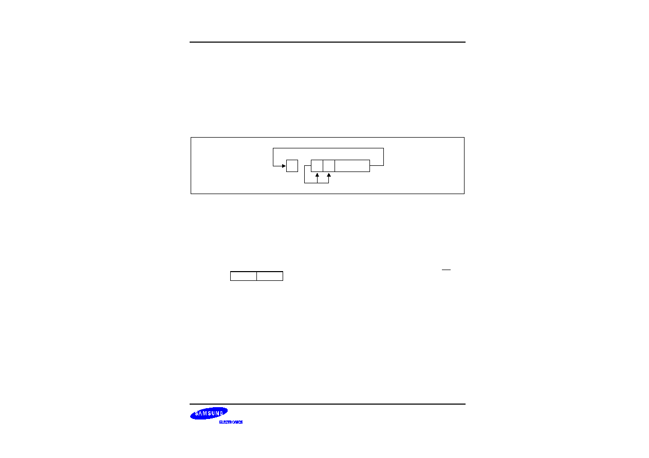
S3P80C5/C80C5/C80C8
INSTRUCTION SET
6-79
SRA
--
Shift Right Arithmetic
SRA
dst
Operation:
dst (7)
dst (7)
C
dst (0)
dst (n)
dst (n + 1), n = 0≠6
An arithmetic shift-right of one bit position is performed on the destination operand. Bit zero (the
LSB) replaces the carry flag. The value of bit 7 (the sign bit) is unchanged and is shifted into bit
position 6.
7
0
C
6
Flags:
C: Set if the bit shifted from the LSB position (bit zero) was "1".
Z: Set if the result is "0"; cleared otherwise.
S: Set if the result is negative; cleared otherwise.
V: Always cleared to "0".
D: Unaffected.
H: Unaffected.
Format:
Bytes
Cycles
Opcode
(Hex)
Addr Mode
dst
opc
dst
2
4
D0
R
4
D1
IR
Examples:
Given: Register 00H = 9AH, register 02H = 03H, register 03H = 0BCH, and C = "1":
SRA
00H
Register 00H = 0CD, C = "0"
SRA
@02H
Register 02H = 03H, register 03H = 0DEH, C = "0"
In the first example, if general register 00H contains the value 9AH (10011010B), the statement
"SRA 00H" shifts the bit values in register 00H right one bit position. Bit zero ("0") clears the C
flag and bit 7 ("1") is then shifted into the bit 6 position (bit 7 remains unchanged). This leaves
the value 0CDH (11001101B) in destination register 00H.
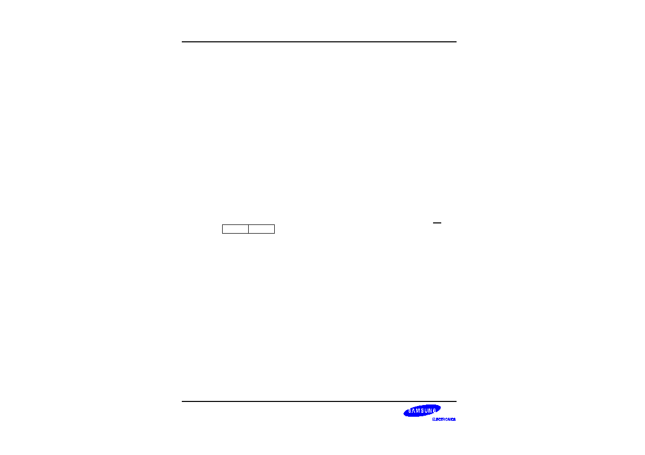
INSTRUCTION SET
S3P80C5/C80C5/C80C8
6-80
SRP/SRP0/SRP1
--
Set Register Pointer
SRP
src
SRP0
src
SRP1
src
Operation:
If src (1) = 1 and src (0) = 0 then: RP0 (3≠7)
src (3≠7)
If src (1) = 0 and src (0) = 1 then: RP1 (3≠7)
src (3≠7)
If src (1) = 0 and src (0) = 0 then: RP0 (4≠7)
src (4≠7),
RP0 (3)
0
RP1 (4≠7)
src (4≠7),
RP1 (3)
1
The source data bits one and zero (LSB) determine whether to write one or both of the register
pointers, RP0 and RP1. Bits 3≠7 of the selected register pointer are written unless both register
pointers are selected. RP0.3 is then cleared to logic zero and RP1.3 is set to logic one.
Flags:
No flags are affected.
Format:
Bytes
Cycles
Opcode
(Hex)
Addr Mode
src
opc
src
2
4
31
IM
Examples:
The statement
SRP #40H
sets register pointer 0 (RP0) at location 0D6H to 40H and register pointer 1 (RP1) at location
0D7H to 48H.
The statement "SRP0 #50H" sets RP0 to 50H, and the statement "SRP1 #68H" sets RP1 to
68H.

S3P80C5/C80C5/C80C8
INSTRUCTION SET
6-81
STOP
--
Stop Operation
STOP
Operation:
The STOP instruction stops the both the CPU clock and system clock and causes the
microcontroller to enter Stop mode. During Stop mode, the contents of on-chip CPU registers,
peripheral registers, and I/O port control and data registers are retained. Stop mode can be
released by an external reset operation or by external interrupts. For the reset operation, the
RESET
pin must be held to Low level until the required oscillation stabilization interval has
elapsed.
Flags:
No flags are affected.
Format:
Bytes
Cycles
Opcode
(Hex)
Addr Mode
dst src
opc
1
4
7F
≠
≠
Example:
The statement
STOP
halts all microcontroller operations.

INSTRUCTION SET
S3P80C5/C80C5/C80C8
6-82
SUB
--
Subtract
SUB
dst,src
Operation:
dst
dst ≠ src
The source operand is subtracted from the destination operand and the result is stored in the
destination. The contents of the source are unaffected. Subtraction is performed by adding the
two's complement of the source operand to the destination operand.
Flags:
C: Set if a "borrow" occurred; cleared otherwise.
Z: Set if the result is "0"; cleared otherwise.
S: Set if the result is negative; cleared otherwise.
V: Set if arithmetic overflow occurred, that is, if the operands were of opposite signs and the
sign of the result is of the same as the sign of the source operand; cleared otherwise.
D: Always set to "1".
H: Cleared if there is a carry from the most significant bit of the low-order four bits of the result;
set otherwise indicating a "borrow".
Format:
Bytes
Cycles
Opcode
(Hex)
Addr Mode
dst src
opc
dst |
src
2
4
22
r
r
6
23
r
lr
opc
src
dst
3
6
24
R
R
6
25
R
IR
opc
dst
src
3
6
26
R
IM
Examples:
Given: R1 = 12H, R2 = 03H, register 01H = 21H, register 02H = 03H, register 03H = 0AH:
SUB
R1,R2
R1 = 0FH, R2 = 03H
SUB
R1,@R2
R1 = 08H, R2 = 03H
SUB
01H,02H
Register 01H = 1EH, register 02H = 03H
SUB
01H,@02H
Register 01H = 17H, register 02H = 03H
SUB
01H,#90H
Register 01H = 91H; C, S, and V = "1"
SUB
01H,#65H
Register 01H = 0BCH; C and S = "1", V = "0"
In the first example, if working register R1 contains the value 12H and if register R2 contains the
value 03H, the statement "SUB R1,R2" subtracts the source value (03H) from the destination
value (12H) and stores the result (0FH) in destination register R1.

S3P80C5/C80C5/C80C8
INSTRUCTION SET
6-83
SWAP
--
Swap Nibbles
SWAP
dst
Operation:
dst (0 ≠ 3)
dst (4 ≠ 7)
The contents of the lower four bits and upper four bits of the destination operand are swapped.
7
0
4 3
Flags:
C: Undefined.
Z: Set if the result is "0"; cleared otherwise.
S: Set if the result bit 7 is set; cleared otherwise.
V: Undefined.
D: Unaffected.
H: Unaffected.
Format:
Bytes
Cycles
Opcode
(Hex)
Addr Mode
dst
opc
dst
2
4
F0
R
4
F1
IR
Examples:
Given: Register 00H = 3EH, register 02H = 03H, and register 03H = 0A4H:
SWAP
00H
Register 00H = 0E3H
SWAP
@02H
Register 02H = 03H, register 03H = 4AH
In the first example, if general register 00H contains the value 3EH (00111110B), the statement
"SWAP 00H" swaps the lower and upper four bits (nibbles) in the 00H register, leaving the value
0E3H (11100011B).
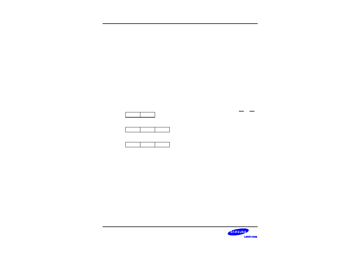
INSTRUCTION SET
S3P80C5/C80C5/C80C8
6-84
TCM
--
Test Complement Under Mask
TCM
dst,src
Operation:
(NOT dst) AND src
This instruction tests selected bits in the destination operand for a logic one value. The bits to be
tested are specified by setting a "1" bit in the corresponding position of the source operand
(mask). The TCM statement complements the destination operand, which is then ANDed with the
source mask. The zero (Z) flag can then be checked to determine the result. The destination and
source operands are unaffected.
Flags:
C: Unaffected.
Z: Set if the result is "0"; cleared otherwise.
S: Set if the result bit 7 is set; cleared otherwise.
V: Always cleared to "0".
D: Unaffected.
H: Unaffected.
Format:
Bytes
Cycles
Opcode
(Hex)
Addr Mode
dst src
opc
dst | src
2
4
62
r
r
6
63
r
lr
opc
src
dst
3
6
64
R
R
6
65
R
IR
opc
dst
src
3
6
66
R
IM
Examples:
Given: R0 = 0C7H, R1 = 02H, R2 = 12H, register 00H = 2BH, register 01H = 02H, and
register 02H = 23H:
TCM
R0,R1
R0 = 0C7H, R1 = 02H, Z = "1"
TCM
R0,@R1
R0 = 0C7H, R1 = 02H, register 02H = 23H, Z = "0"
TCM
00H,01H
Register 00H = 2BH, register 01H = 02H, Z = "1"
TCM
00H,@01H
Register 00H = 2BH, register 01H = 02H,
register 02H = 23H, Z = "1"
TCM
00H,#34
Register 00H = 2BH, Z = "0"
In the first example, if working register R0 contains the value 0C7H (11000111B) and register R1
the value 02H (00000010B), the statement "TCM R0,R1" tests bit one in the destination register
for a "1" value. Because the mask value corresponds to the test bit, the Z flag is set to logic one
and can be tested to determine the result of the TCM operation.
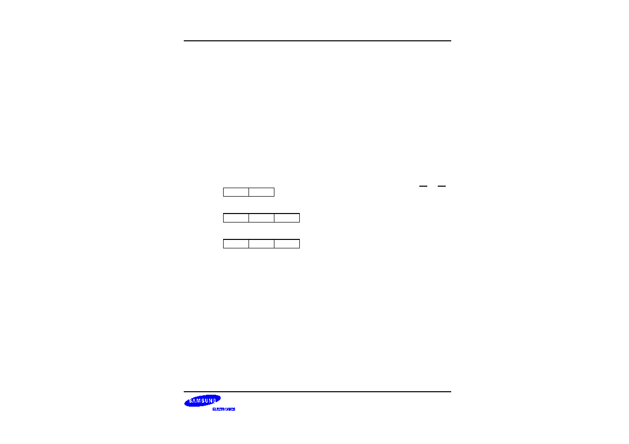
S3P80C5/C80C5/C80C8
INSTRUCTION SET
6-85
TM
--
Test Under Mask
TM
dst,src
Operation:
dst AND src
This instruction tests selected bits in the destination operand for a logic zero value. The bits to be
tested are specified by setting a "1" bit in the corresponding position of the source operand
(mask), which is ANDed with the destination operand. The zero (Z) flag can then be checked to
determine the result. The destination and source operands are unaffected.
Flags:
C: Unaffected.
Z: Set if the result is "0"; cleared otherwise.
S: Set if the result bit 7 is set; cleared otherwise.
V: Always reset to "0".
D: Unaffected.
H: Unaffected.
Format:
Bytes
Cycles
Opcode
(Hex)
Addr Mode
dst src
opc
dst | src
2
4
72
r
r
6
73
r
lr
opc
src
dst
3
6
74
R
R
6
75
R
IR
opc
dst
src
3
6
76
R
IM
Examples:
Given: R0 = 0C7H, R1 = 02H, R2 = 18H, register 00H = 2BH, register 01H = 02H, and
register 02H = 23H:
TM
R0,R1
R0 = 0C7H, R1 = 02H, Z = "0"
TM
R0,@R1
R0 = 0C7H, R1 = 02H, register 02H = 23H, Z = "0"
TM
00H,01H
Register 00H = 2BH, register 01H = 02H, Z = "0"
TM
00H,@01H
Register 00H = 2BH, register 01H = 02H,
register 02H = 23H, Z = "0"
TM
00H,#54H
Register 00H = 2BH, Z = "1"
In the first example, if working register R0 contains the value 0C7H (11000111B) and register R1
the value 02H (00000010B), the statement "TM R0,R1" tests bit one in the destination register
for a "0" value. Because the mask value does not match the test bit, the Z flag is cleared to logic
zero and can be tested to determine the result of the TM operation.

INSTRUCTION SET
S3P80C5/C80C5/C80C8
6-86
WFI
--
Wait For Interrupt
WFI
Operation:
The CPU is effectively halted until an interrupt occurs, except that DMA transfers can still take
place during this wait state. The WFI status can be released by an internal interrupt, including a
fast interrupt .
Flags:
No flags are affected.
Format:
Bytes
Cycles
Opcode
(Hex)
opc
1
4n
3F
(
n = 1, 2, 3, ... )
Example:
The following sample program structure shows the sequence of operations that follow a "WFI"
statement:
EI
WFI
(Next instruction)
Main program
.
.
.
.
.
.
Interrupt occurs
Interrupt service routine
.
.
.
Clear interrupt flag
IRET
Service routine completed
(Enable global interrupt)
(Wait for interrupt)

S3P80C5/C80C5/C80C8
INSTRUCTION SET
6-87
XOR
--
Logical Exclusive OR
XOR
dst,src
Operation:
dst
dst XOR src
The source operand is logically exclusive-ORed with the destination operand and the result is
stored in the destination. The exclusive-OR operation results in a "1" bit being stored whenever
the corresponding bits in the operands are different; otherwise, a "0" bit is stored.
Flags:
C: Unaffected.
Z: Set if the result is "0"; cleared otherwise.
S: Set if the result bit 7 is set; cleared otherwise.
V: Always reset to "0".
D: Unaffected.
H: Unaffected.
Format:
Bytes
Cycles
Opcode
(Hex)
Addr Mode
dst src
opc
dst | src
2
4
B2
r
r
6
B3
r
lr
opc
src
dst
3
6
B4
R
R
6
B5
R
IR
opc
dst
src
3
6
B6
R
IM
Examples:
Given: R0 = 0C7H, R1 = 02H, R2 = 18H, register 00H = 2BH, register 01H = 02H, and
register 02H = 23H:
XOR
R0,R1
R0 = 0C5H, R1 = 02H
XOR
R0,@R1
R0 = 0E4H, R1 = 02H, register 02H = 23H
XOR
00H,01H
Register 00H = 29H, register 01H = 02H
XOR
00H,@01H
Register 00H = 08H, register 01H = 02H, register 02H = 23H
XOR
00H,#54H
Register 00H = 7FH
In the first example, if working register R0 contains the value 0C7H and if register R1 contains
the value 02H, the statement "XOR R0,R1" logically exclusive-ORs the R1 value with the R0
value and stores the result (0C5H) in the destination register R0.

INSTRUCTION SET
S3P80C5/C80C5/C80C8
6-88
NOTES
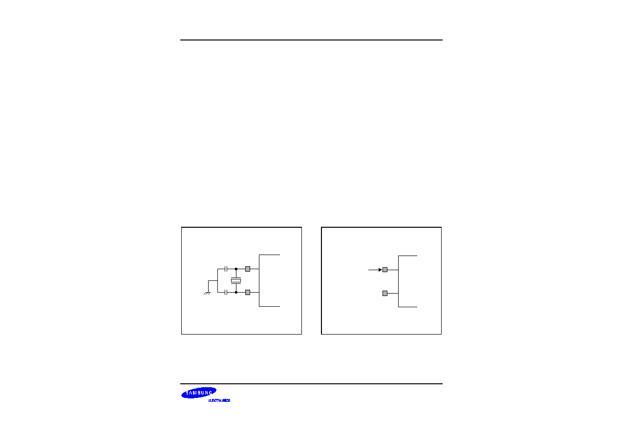
S3P80C5/C80C5/C80C8
CLOCK CIRCUITS
7-1
7
CLOCK CIRCUITS
OVERVIEW
The clock frequency generated for the S3P80C5/C80C5/C80C8 by an external crystal, or supplied by an external
clock source, can range from 1MHz to 4 MHz. The maximum CPU clock frequency, as determined by CLKCON
register settings, is 4 MHz. The X
IN
and X
OUT
pins connect the external oscillator or clock source to the on-chip
clock circuit.
SYSTEM CLOCK CIRCUIT
The system clock circuit has the following components:
-- External crystal or ceramic resonator oscillation source (or an external clock)
-- Oscillator stop and wake-up functions
-- Programmable frequency divider for the CPU clock (f
OSC
divided by 1, 2, 8, or 16)
-- Clock circuit control register, CLKCON
X
IN
X
OUT
C1
C2
Figure 7-1. Main Oscillator Circuit
(External Crystal or Ceramic Resonator)
X
IN
X
OUT
External
Clock
Open Pin
Figure 7-2. External Clock Circuit

CLOCK CIRCUITS
S3P80C5/C80C5/C80C8
7-2
CLOCK STATUS DURING POWER-DOWN MODES
The two power-down modes, Stop mode and Idle mode, affect the system clock as follows:
-- In Stop mode, the main oscillator is halted. Stop mode is released, and the oscillator started, by Power On
Reset operation or by a non-vectored interrupt - interrupt with reset (INTR). To enter the Stop mode,
STOPCON (STOP Control register) has to be loaded with value, #0A5H before STOP instruction execution.
After recovering from the Stop mode by reset or interrupt, STOPCON register is automatically cleared.
-- In Idle mode, the internal clock signal is gated away from the CPU, but continues to be supplied to the
interrupt structure, timer 0, and counter A. Idle mode is released by a reset or by an interrupt (external or
internally generated).
Main
OSC
STOP
Instruction
Noise
filter
Oscillator
Stop
Oscillator
Wake-up
INT Pin
(1)
1/16
1/2
1/8
M
U
X
CLKCON.3,.4
STOPCON
CPU
Clock
NOTES:
1. An external interrupt with an RC-delay noise filter (for S3C80C5/C80C8/,
INT0-4) is fiexed to release Stop mode and "wake up" the main
oscillator.
2. Because the S3C80C5/C80C8 has no subsystem clock, the 3-bit CLKCON
signature code (CLKCON.2-CLKCON.0) is no meaning.
Figure 7-3. System Clock Circuit Diagram
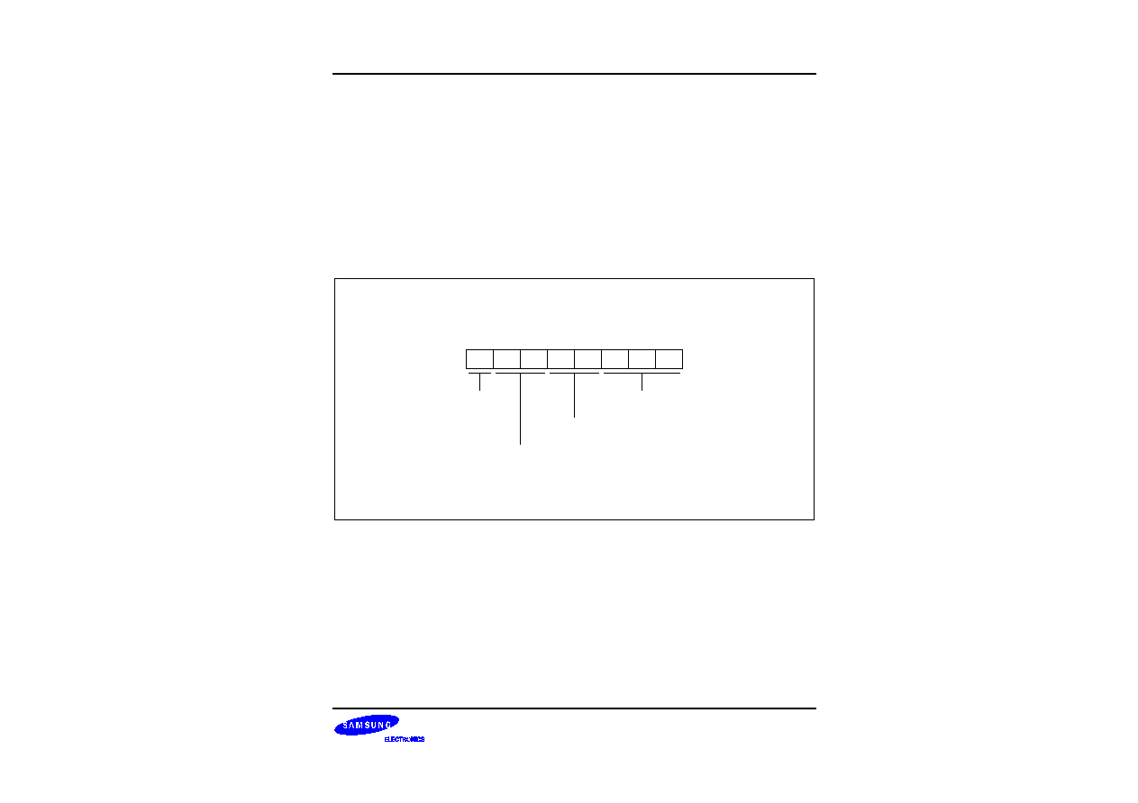
S3P80C5/C80C5/C80C8
CLOCK CIRCUITS
7-3
SYSTEM CLOCK CONTROL REGISTER (CLKCON)
The system clock control register, CLKCON, is located in set 1, address D4H. It is read/write addressable and
has the following functions:
-- Oscillator frequency divide-by value
CLKCON register settings control whether or not an external interrupt can be used to trigger a Stop mode
release. (This is called the "IRQ wake-up" function.) The IRQ wake-up enable bit is CLKCON.7. In
S3P80C5/C80C5/C80C8, this bit is not valid any more. Actually bit 7, 6, 5, 2, 1, and 0 are no meaning in
S3P80C5/C80C5/C80C8.
After a reset, the main oscillator is activated, and the f
OSC
/16 (the slowest clock speed) is selected as the CPU
clock. If necessary, you can then increase the CPU clock speed to f
OSC
, f
OSC
/2, or f
OSC
/8.
System Clock Control Register (CLKCON)
D4H, Set 1, R/W
.7
.6
.5
.4
.3
.2
.1
.0
MSB
LSB
Divide-by selection bits for
CPU clock frequency:
00 = f
OSC
/16
01 = f
OSC
/8
10 = f
OSC
/2
11 = f
OSC
(non-divided)
Not used
Not used
Not used
Figure 7-4. System Clock Control Register (CLKCON)

CLOCK CIRCUITS
S3P80C5/C80C5/C80C8
7-4
NOTES
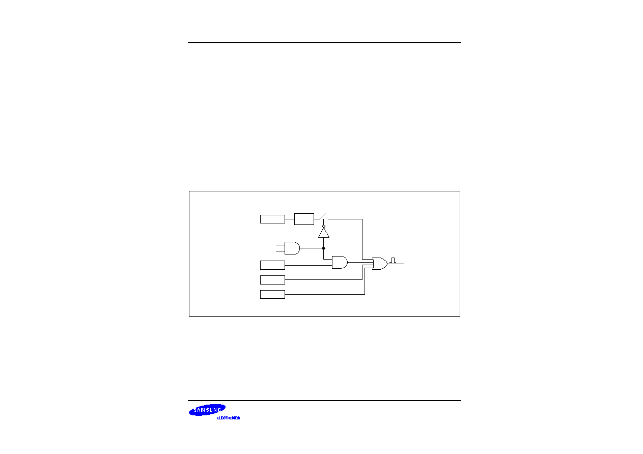
S3P80C5/C80C5/C80C8
RESET
RESET
and POWER-DOWN
8-1
8
RESET
RESET
and POWER-DOWN
SYSTEM RESET
S3P80C5/C80C5/C80C8 has four different system reset sources as followings:
-- Low Voltage Detect (LVD)
-- Internal POR circuit
-- INTR (Interrupt with
RESET
)
-- Basic Timer (Watchdog timer)
STOPCON
Noise
Filter
LVD
Stop
INTR
POR
BT(WDT)
Enable/Disable
Figure 8-1. Reset Block Diagram
LVD RESET
The Low Voltage detect circuit is built on the S3P80C5/C80C5/C80C8 product for system reset not in stop mode.
When the operating status is not stop mode it detects a slope of V
DD
by comparing the voltage at V
DD
with V
LVD
(Low level Detect Voltage). The reset pulse is generated by the rising slope of V
DD
. While the voltage at V
DD
is
rising up and passing V
LVD
, the reset pulse is occurred at the moment "V
DD
>=
V
LVD
". This function is disabled
when the operating state is "stop mode" to reduce the current consumption under 1 uA instead of 6 uA.
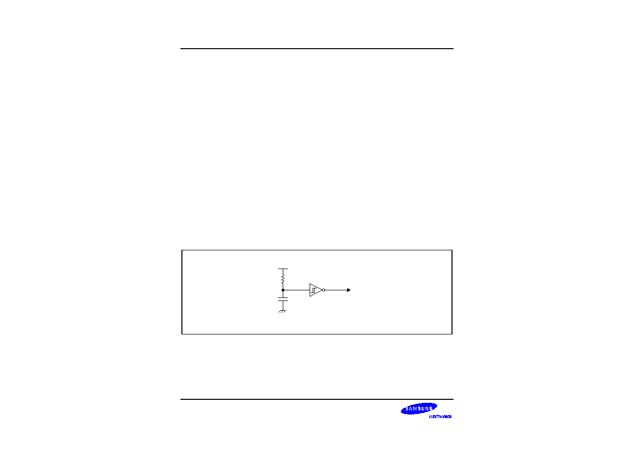
RESET
RESET
and POWER-DOWN
S3P80C5/C80C5/C80C8
8-2
INTERRUPT WITH RESET(INTR)
A non vectored interrupt called Interrupt with reset (INTR) is built in
S3C80C5/C80C8 to release stop status with system reset. When a falling/rising edge occurs at Port 0 during stop
mode, INTR signal is generated and it makes the system reset pulse. An INTR signal is generated relating to
interaction between Port 0 and operating status. It is enabled by STOP status and occurs by falling/rising edge at
port0. So only when the chip status is "STOP", it is available. If the operating status is not stop status INTR does
not occurs.
NOTE
This INTR is supplementary function to make system reset for an application which is using " stop mode"
like remote controller. If an application which is not using "stop mode" , INTR function can be discarded.
WATCHDOG TIMER RESET
The S3P80C5/C80C5/C80C8 build a watch-dog timer that can recover to normal operation from abnormal
function. Watchdog timer generates a system reset signal if not clearing a BT-Basic Counter within a specific
time by program. System reset can return to the proper operation of chip.
POWER-ON RESET(POR)
The power-on reset circuit is built on the S3P80C5/C80C5/C80C8 product. During a power-on reset, the voltage
at V
DD
goes to High level and the Schmitt trigger input of POR circuit is forced to Low level and then to High
level. The power-on reset circuit makes a reset signal whenever the power supply voltage is powering-up and the
Schmitt trigger input senses the Low level. This on-chip POR circuit consists of an internal resistor, an internal
capacitor, and a Schmitt trigger input transistor.
V
DD
System Reset
C
R : On-Chip Resistor
C : On-Chip Capacitor
Schmitt Trigger Inverter
V
SS
Figure 8-2. Power-on Reset Circuit

S3P80C5/C80C5/C80C8
RESET
RESET
and POWER-DOWN
8-3
Voltage [V]
Time
Reset pulse
Va
Reset Pulse Width
V
DD
V
IH
= 0.85 V
DD
V
IL
= 0.4 V
DD
TV
DD
(V
DD
Rising Time)
V
DD
If Va voltage is under the 0.4 V
DD
, Reset pulse signal is gernerated.
If Va voltage is over than 0.4 VDD, Reset pulse is not gernerated.
Figure 8-3. Timing Diagram for Power-on Reset Circuit
SYSTEM RESET OPERATION
System reset starts the oscillation circuit, synchronize chip operation with CPU clock, and initialize the internal
CPU and peripheral modules. This procedure brings the S3P80C5/C80C5/C80C8 into a known operating status.
To allow time for internal CPU clock oscillation to stabilize, the reset pulse generator must be held to active level
for a minimum time interval after the power supply comes within tolerance. The minimum required reset
operation for a oscillation stabilization time is 16 oscillation clocks. All system and peripheral control registers are
then reset to their default hardware values (see Tables 5-1).
In summary, the following sequence of events occurs during a reset operation:
-- All interrupts are disabled.
-- The watchdog function (basic timer) is enabled.
-- Ports 0, 1 and 2 are set to input mode and all pull-up resistors are disabled for the I/O port pin circuits.
-- Peripheral control and data register settings are disabled and reset to their default hardware values (see
Table 5-1).
-- The program counter (PC) is loaded with the program reset address in the ROM, 0100H.
-- When the programmed oscillation stabilization time interval has elapsed, the instruction stored in ROM
location 0100H (and 0101H) is fetched and executed.

RESET
RESET
and POWER-DOWN
S3P80C5/C80C5/C80C8
8-4
HARDWARE RESET VALUES
Tables 5-1 list the reset values for CPU and system registers, peripheral control registers, and peripheral data
registers following a reset operation. The following notation is used to represent reset values:
-- A "1" or a "0" shows the reset bit value as logic one or logic zero, respectively.
-- An 'x' means that the bit value is undefined after a reset.
-- A dash ('-') means that the bit is either not used or not mapped (but a 0 is read from the bit position)
Table 8-1. Set 1 Register Values After Reset
Register Name
Mnemonic
Address
Bit Values After Reset
Dec
Hex
7
6
5
4
3
2
1
0
Timer 0 counter (read-only)
T0CNT
208
D0H
0
0
0
0
0
0
0
0
Timer 0 data register
T0DATA
209
D1H
1
1
1
1
1
1
1
1
Timer 0 control register
T0CON
210
D2H
0
0
0
0
0
0
0
0
Basic timer control register
BTCON
211
D3H
0
0
0
0
0
0
0
0
Clock control register
CLKCON
212
D4H
0
0
0
0
0
0
0
0
System flags register
FLAGS
213
D5H
◊
◊
◊
◊
◊
◊
0
0
Register pointer 0
RP0
214
D6H
1
1
0
0
0
≠
≠
≠
Register pointer 1
RP1
215
D7H
1
1
0
0
1
≠
≠
≠
Location D8H (SPH) is not mapped.
Stack pointer (low byte)
SPL
217
D9H
◊
◊
◊
◊
◊
◊
◊
◊
Instruction pointer (high byte)
IPH
218
DAH
◊
◊
◊
◊
◊
◊
◊
◊
Instruction pointer (low byte)
IPL
219
DBH
◊
◊
◊
◊
◊
◊
◊
◊
Interrupt request register (read-only)
IRQ
220
DCH
0
0
0
0
0
0
0
0
Interrupt mask register
IMR
221
DDH
◊
◊
◊
◊
◊
◊
◊
◊
System mode register
SYM
222
DEH
0
≠
≠
◊
◊
◊
0
0
Register page pointer
PP
223
DFH
0
0
0
0
0
0
0
0
Port 0 data register
P0
224
E0H
0
0
0
0
0
0
0
0
Port 1 data register
P1
225
E1H
0
0
0
0
0
0
0
0
Port 2 data register
P2
226
E2H
0
0
0
0
0
0
0
0
Location E3H≠E6H is not mapped.
Port 0 pull-up enable register
P0PUR
231
E7H
0
0
0
0
0
0
0
0
Port 0 control register (high byte)
P0CONH
232
E8H
0
0
0
0
0
0
0
0
Port 0 control register (low byte)
P0CONL
233
E9H
0
0
0
0
0
0
0
0
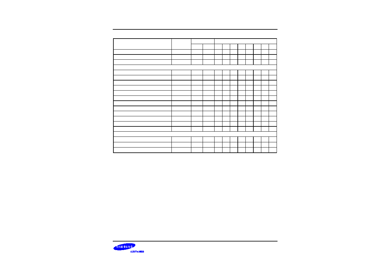
S3P80C5/C80C5/C80C8
RESET
RESET
and POWER-DOWN
8-5
Table 8-1. Set 1 Register Values After Reset (Continued)
Register Name
Mnemonic
Address
Bit Values After Reset
Dec
Hex
7
6
5
4
3
2
1
0
Port 1 control register (high byte)
P1CONH
234
EAH
0
0
0
0
0
0
0
0
Port 1 control register (low byte)
P1CONL
235
EBH
0
0
0
0
0
0
0
0
Port 1 pull-up enable register
P1PUR
236
ECH
0
0
0
0
0
0
0
0
Location EDH≠EFH is not mapped.
Port 2 control register
P2CON
240
F0H
≠
≠
0
0
0
0
0
0
Port 0 interrupt enable register
P0INT
241
F1H
0
0
0
0
0
0
0
0
Port 0 interrupt pending register
P0PND
242
F2H
0
0
0
0
0
0
0
0
Counter A control register
CACON
243
F3H
0
0
0
0
0
0
0
0
Counter A data register (high byte)
CADATAH
244
F4H
1
1
1
1
1
1
1
1
Counter A data register (low byte)
CADATAL
245
F5H
1
1
1
1
1
1
1
1
Timer 1 counter register (high byte)
T1CNTH
246
F6H
0
0
0
0
0
0
0
0
Timer 1 counter register (low byte)
T1CNTL
247
F7H
0
0
0
0
0
0
0
0
Timer 1 data register (high byte)
T1DATAH
248
F8H
1
1
1
1
1
1
1
1
Timer 1 data register (low byte)
T1DATAL
249
F9H
1
1
1
1
1
1
1
1
Timer 1 control register
T1CON
250
FAH
0
0
0
0
0
0
0
0
Stop control register
STOPCON
251
FBH
0
0
0
0
0
0
0
0
Locations FCH is not mapped.
Basic timer counter
BTCNT
253
FDH
◊
◊
◊
◊
◊
◊
◊
◊
External memory timing register
EMT
254
FEH
0
1
1
1
1
1
0
≠
Interrupt priority register
IPR
255
FFH
◊
◊
◊
◊
◊
◊
◊
◊
NOTES:
1. Although the SYM register is not used for the S3P80C5/C80C5/C80C8, SYM.5
should always be "0". If you accidentally write a 1 to this bit during normal operation, a system malfunction may occur.
2.
Except for T0CNT, IRQ, T1CNTH, T1CNTL, and BTCNT, which are read-only, all registers in set 1 are
read/write addressable.
3. You cannot use a read-only register as a destination field for the instructions OR, AND, LD, and LDB.
4. Interrupt pending flags are noted by shaded table cells.

RESET
RESET
and POWER-DOWN
S3P80C5/C80C5/C80C8
8-6
POWER-DOWN MODES
STOP MODE
Stop mode is invoked by stop control register (STOPCON) setting and the instruction STOP. In Stop mode, the
operation of the CPU and all peripherals is halted. That is, the on-chip main oscillator stops and the supply
current is reduced to less than 3 uA at 5.5 V. All system functions stop when the clock "freezes,"
Stop mode can be released of two ways : by an INTR (Interrupt with Reset) or by a POR (Power On Reset).
USING POR TO RELEASE STOP MODE
Stop mode is released when the reset signal goes active by power on reset (POR): all system and peripheral
control registers are reset to their default hardware values and the contents of all data registers are unknown
states. When the oscillation stabilization interval has elapsed, the CPU starts the system initialization routine by
fetching the program instruction stored in ROM location 0100H.
USING AN INTR TO RELEASE STOP MODE
Stop mode is released when INTR (Interrupt with Reset) occurs. INTR occurs when falling/rising edge is detected
at P0 during stop mode and it make system reset.
NOTE
1. Do not use stop mode if you are using an external clock source because X
IN
input must be cleared
internally to V
SS
to reduce current leakage.
2. STOP mode always be released by the system reset (INTR or POR) so the system register value and
control register value are initialized as reset value. And when the reset occurs from INTR, the prime
register value will be retained but it will be unknown states if it occurs from POR. So an application
which is using stop mode should be added specific S/W which divide the system reset into STOP
mode releasing or power on reset. Following Programming Tip can be useful for more
understanding.

S3P80C5/C80C5/C80C8
RESET
RESET
and POWER-DOWN
8-7
F
F
PROGRAMMING TIP -- To Divide STOP Mode Releasing and POR.
This example shows how to enter the stop mode and how to know it is stop mode releasing or power on
RESET
.
ORG
0100H
; Reset address
START
DI
;
LD
BTCON,#03h
; enable basic timer counter.
LD
SPL,#0FFH
; Initialize the system register
CLR
SYM
CLR
PP
CLR
EMT
CLR
IPR
∑
∑
LD
P0CONH,#00H
; Initialize the control register
LD
P0CONL,#00H
LD
P0PUR,#0FFH
∑
∑
∑
CHECK_RAM:
; Check the RAM data whether it is stop mode releasing
; or Power On RESET
LD
R0,#0BFH
; If Power On Reset , go to POR_RESET
CHK_R
CP
R0,@R0
;
JR
NE,POR_RESET
DEC
R0
CP
R0,#0B0H
JR
UGE, CHK_R
STOP_RESET:
; STOP mode releasing.
JR
MAIN
;
POR_RESET LD
R0,#0FFH
;Power On Reset
;CHECK RAM data are failed so clear all RAM data.
RAM_CLR
CLR
@R0
DJNJ
R0,RAMCLR
LD
R0,#0BFH
;Initialize the CHECK RAM data as default value .

RESET
RESET
and POWER-DOWN
S3P80C5/C80C5/C80C8
8-8
F
F
PROGRAMMING TIP -- To Divide STOP Mode Releasing and POR. (Continued)
CHK_W
LD
@R0,R0
DEC
R0
CP
R0,#0B0H
JR
UGE,CHK_W
MAIN:
CP
P0,#0FFH
;
JR
EQ,ENT_STOP
∑
∑
∑
JP
T,MAIN
ENT_STOP
LD
STOPCON,#0A5H
;Enter the STOP mode.
STOP
NOP
NOP
JP
RESET
∑
∑
∑

S3P80C5/C80C5/C80C8
RESET
RESET
and POWER-DOWN
8-9
IDLE MODE
Idle mode is invoked by the instruction IDLE (OPCODE 6FH). In Idle mode, CPU operations are halted while
some peripherals remain active. During idle mode, the internal clock signal is gated away from the CPU and from
all but the following peripherals, which remain active:
-- Interrupt logic
-- Timer 0
-- Timer 1
-- Counter A
I/O port pins retain the mode (input or output) they had at the time Idle mode was entered.
Idle Mode Release
You can release Idle mode in one of two ways:
1.
Execute a reset. All system and peripheral control registers are reset to their default values and the contents
of all data registers are retained. The reset automatically selects the slowest clock because of the hardware
reset value for the CLKCON register. If all external interrupts are masked in the IMR register, a reset is the
only way you can release Idle mode.
2. Activate any enabled interrupt ; internal or external. When you use an interrupt to release Idle mode, the 2-bit
CLKCON.4/CLKCON.3 value remains unchanged, and the currently selected clock value is used. The
interrupt is then serviced. When the return-from-interrupt condition (IRET) occurs, the instruction immediately
following the one which initiated Idle mode is executed.
NOTE
Only external interrupts with an RC delay built in to the pin circuit can be used to release Stop mode
without reset. To release Idle mode, you can use either an external interrupt or an internally-generated
interrupt.
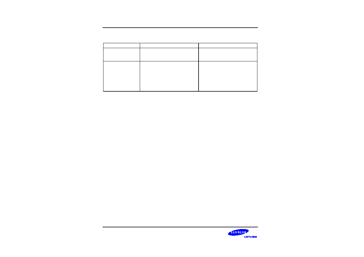
RESET
RESET
and POWER-DOWN
S3P80C5/C80C5/C80C8
8-10
SUMMARY TABLE OF STOP MODE, AND IDLE MODE
Table 8-2. Summary of Each Mode
Item/Mode
IDLE
STOP
Approach Condition
V
DD
is higher than V
LVD
(V
LVD
<
V
DD
).
IDLE (instruction).
V
DD
is higher than V
LVD
(V
LVD
<
V
DD
).
STOPCON
A5H
STOP instruction
Release Source
Interrupt
T0/T1 interrupt
Counter A interrupt
Ext. interrupt (Port0)
RESET
POR
LVD
WDT
RESET
INTR
POR
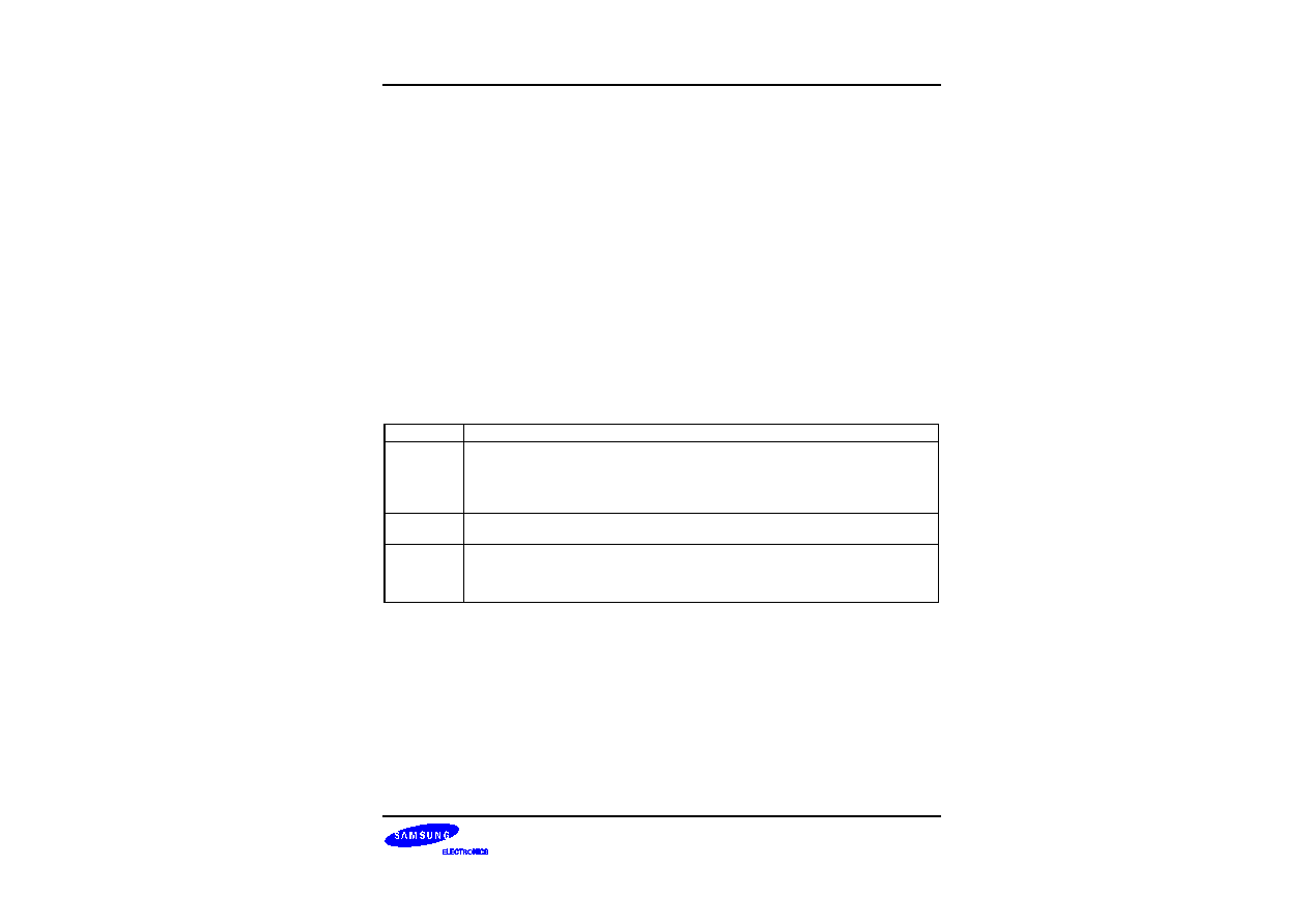
S3P80C5/C80C5/C80C8
I/O PORTS
9-1
9
I/O PORTS
OVERVIEW
The S3P80C5/C80C5/C80C8 microcontroller has three bit-programmable I/O ports, P0≠P2. Two ports, P0-P1,
are 8-bit ports and P2 is a 3-bit port. This gives a total of 19 I/O pins in the S3P80C5/C80C5/C80C8"s 24-pin
package. Each port is bit-programmable and can be flexibly configured to meet application design requirements.
The CPU accesses ports by directly writing or reading port registers. No special I/O instructions are required.
For IR universal remote controller applications, ports 0, and1 are usually configured to the keyboard matrix and
port 2 is used to transmit the remote controller carrier signal or to indicate operating status by turning on a LED.
Table 9-1 gives you a general overview of S3P80C5/C80C5/C80C8 I/O port functions.
Table 9-1. S3P80C5/C80C5/C80C8 Port Configuration Overview
Port
Configuration Options
0
8-bit general-purpose I/O port; Input or push-pull output; external interrupt input on falling
edges, rising edges, or both edges; all P0 pin circuits have noise filters and interrupt
enable/disable (P0INT) and pending control (P0PND); Pull-up resistors can be assigned to
individual P0 pins using P0PUR register settings. Specially Interrupt with Reset(INTR) is
assigned to release stop mode with system reset.
1
8-bit general-purpose I/O port; Input, open-drain output, or push-pull output. Pull-up resistors
can be assigned to individual P1 pins using P1PUR register settings.
2
3-bit I/O port; input mode with or without pull-up, push-pull or open-drain output mode. REM
and T0PWM can be assigned. Port 2 pins have high current drive capability to support LED
applications. The port 2 data register contains three status bits: three for P2.0, P2.1 and P2.2
and one for remote controller carrier signal on/off status.
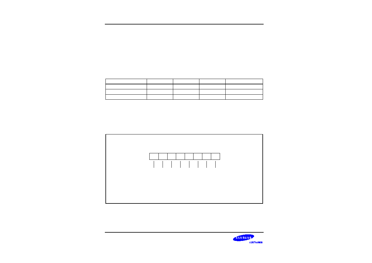
I/O PORTS
S3P80C5/C80C5/C80C8
9-2
PORT DATA REGISTERS
Table 9-2 gives you an overview of the register locations of all three S3C80C5/C80C8 port data registers. Data
registers for ports 0, and 1 have the general format.
NOTE
The data register for port 2, P2, contains three bits for P2.0, P2.1 and P2.2, and an additional status bit
for carrier signal on/off.
Table 9-2. Port Data Register Summary
Register Name
Mnemonic
Decimal
Hex
R/W
Port 0 data register
P0
224
E0H
R/W
Port 1 data register
P1
225
E1H
R/W
Port 2 data register
P2
226
E2H
R/W
Because port 2 is a 3-bit I/O port, the port 2 data register only contains values for P2.0, P2.1 and P2.2. The P2
register also contains values for P2.0, P2.1 and P2.2. The P2 register also contains a special carrier on/off
bit(P2.5). See the port 2 description for details. All other S3P80C5/C80C5/C80C8 I/O ports are 8-bit.
PULL-UP RESISTOR ENABLE REGISTERS
NOTE:
Pull-up resistors can be assigned to the port 2 pins, P2.0, P2.1 and
P2.2 by marking the appropriate the port 2 control register,P2CON.
Port0 Pull-up Resistor Enable Register (P0PUR)
E7H, R/W
.7
.6
.5
.4
.3
.2
.1
.0
MSB
LSB
P0.7
P0.6
P0.5
P0.4
P0.3
P0.2
P0.1
P0.0
Pull-up resistor enable bit:
0 = Enable pull-up resistor
1 = Disable pull-up resistor
Figure 9-1. S3P80C5/C80C5/C80C8 I/O Port 0 Data Register Format
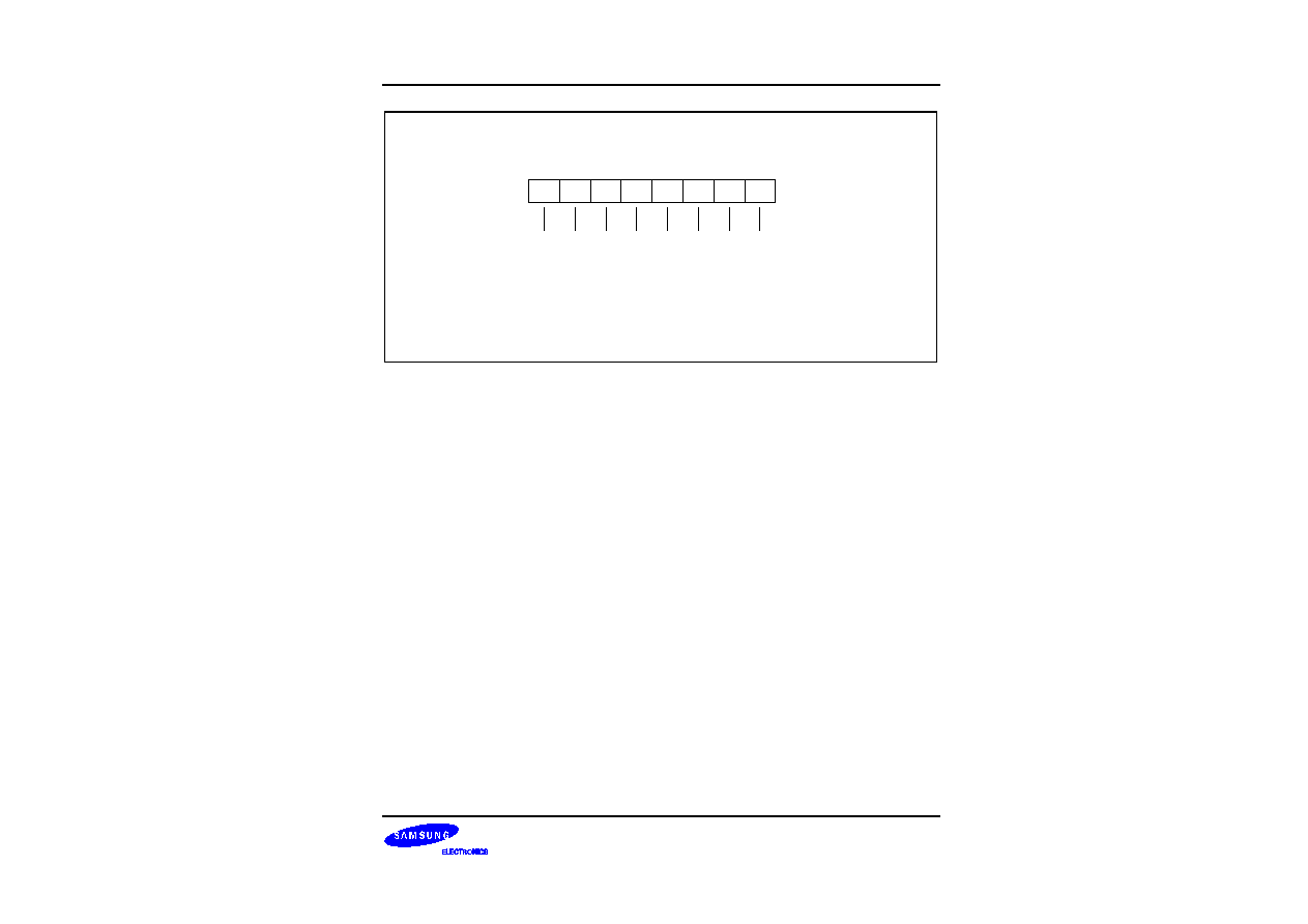
S3P80C5/C80C5/C80C8
I/O PORTS
9-3
Port1 Pull-up Resistor Enable Register (P1PUR)
ECH, R/W
.7
.6
.5
.4
.3
.2
.1
.0
MSB
LSB
P1.7
P1.6
P1.5
P1.4
P1.3
P1.2
P1.1
P1.0
Pull-up resistor enable bit:
0 = Disable pull-up resistor
1 = Enable pull-up resistor
NOTE:
Pull-up resistors can be assigned to the port 2 pins, P2.0, P2.1 and P2.2
by marking the appropriate the port 2 control register, P2CON.
Figure 9-2. S3P80C5/C80C5/C80C8 I/O Port 1 Data Register Format

I/O PORTS
S3P80C5/C80C5/C80C8
9-4
PORT 0
Port 0 is a general-purpose, 8-bit I/O port. It is bit-programmable. Port 0 pins are accessed directly by read/write
operations to the port 0 data register, P0 (set 1, E0H). The P0 pin circuits support pull-up resistor assignment
using P0PUR register settings and all pins have noise filters for external interrupt inputs.
Two 8-bit control registers are used to configure port 0 pins: P0CONH (set 1, E8H) for the upper nibble pins,
P0.7≠P0.4, and P0CONL (set 1, E9H) for lower nibble pins, P0.3≠P0.0. Each control register byte contains four
bit-pairs and each bit-pair configures one pin (see Figures 9-2 and 9-3). A hardware reset clears all P0 control
and data registers to '00H'.
A separate register, the port 0 interrupt control register, P0INT (set 1, F1H), is used to enable and disable
external interrupt input. You can poll the port 0 interrupt pending register, P0PND to detect and clear pending
conditions for these interrupts.
The lower-nibble pins, P0.3≠P0.0, are used for INT3≠INT0 input (IRQ6), respectively. The upper nibble pins,
P0.7≠P0.4, are all used for INT4 input (IRQ7). Interrupts that are detected at any of these four pins are processed
using the same vector address (E8H).
Port 0 , P0.0≠P0.7, is assigned interrupt with reset(INTR) to release stop mode with system reset.
Port 0 Control Register, High Byte (P0CONH)
E8H, Set 1, R/W
.7
.6
.5
.4
.3
.2
.1
.0
MSB
LSB
P0.7/INT4
P0.4/INT4
P0.6/INT4
P0.5/INT4
P0CONH Pin Configureation Settings:
00
01
10
11
Input mode; interrupt on falling edges
Input mode; interrupt on rising and falling edges
Push-pull output mode
Input mode; interrupt on rising edges
Figure 9-3. Port 0 High-Byte Control Register (P0CONH)
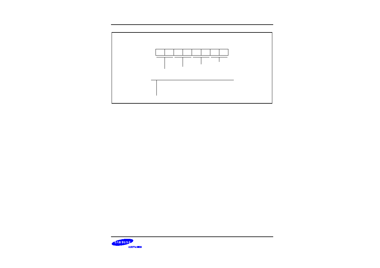
S3P80C5/C80C5/C80C8
I/O PORTS
9-5
Port 0 Control Register, Low Byte (P0CONL)
E9H, Set 1, R/W
.7
.6
.5
.4
.3
.2
.1
.0
MSB
LSB
P0.3/INT3
P0.0/INT0
P0.2/INT2
P0.1/INT1
P0CONL Pin Configureation Settings:
00
01
10
11
Input mode; interrupt on falling edges
Input mode; interrupt on rising and falling edges
Push-pull output mode
Input mode; interrupt on rising edges
Figure 9-4. Port 0 Low-Byte Control Register (P0CONL)
PORT 0 INTERRUPT ENABLE REGISTER (P0INT)
The port 0 interrupt control register, P0INT, is used to enable and disable external interrupt input at individual P0
pins (see Figure 10-5). To enable a specific external interrupt, you set its P0INT.n bit to "1". You must also be
sure to make the correct settings in the corresponding port 0 control register (P0CONH, P0CONL).
PORT 0 INTERRUPT PENDING REGISTER (P0PND)
The port 0 interrupt pending register, P0PND, contains pending bits (flags) for each port 0 interrupt (see Figure
10-6). When a P0 external interrupt is acknowledged by the CPU, the service routine must clear the pending
condition by writing a "0" to the appropriate pending flag in the P0PND register (Writing a "1" to the pending bit
has no effect).
NOTE
A hardware reset(INTR, POR) clears the P0INT and P0PND registers to '00H'. For this reason, the
application program's initialization routine must enable the required external interrupts for port 0, and for
the other I/O ports.

I/O PORTS
S3P80C5/C80C5/C80C8
9-6
Port 0 Interrup Enable Register (P0INT)
F1H, Set 1, R/W
.7
.6
.5
.4
.3
.2
.1
.0
MSB
LSB
Port 0 Interrupt Enable Bits:
0
1
Disable interrupt
Enable interrupt
P0.7/INT4
P0.6/INT4
P0.5/INT4
P0.4/INT4
P0.3/INT3
P0.2/INT2
P0.1/INT1
P0.0/INT0
Figure 9-5. Port 0 External Interrupt Control Register (P0INT)
Port 0 Interrup Pending Register (P0PND)
F2H, Set 1, R/W
.7
.6
.5
.4
.3
.2
.1
.0
MSB
LSB
Port 0 Interrupt Pending Bits:
0
0
1
1
Interrupt not pending
Clear P0.n pending condition (when write)
P0.n interrupt is pending
No effect (when write)
P0.7/INT4
P0.6/INT4
P0.5/INT4
P0.4/INT4
P0.3/INT3
P0.2/INT2
P0.1/INT1
P0.0/INT0
Figure 9-6. Port 0 External Interrupt Pending Register (P0PND)
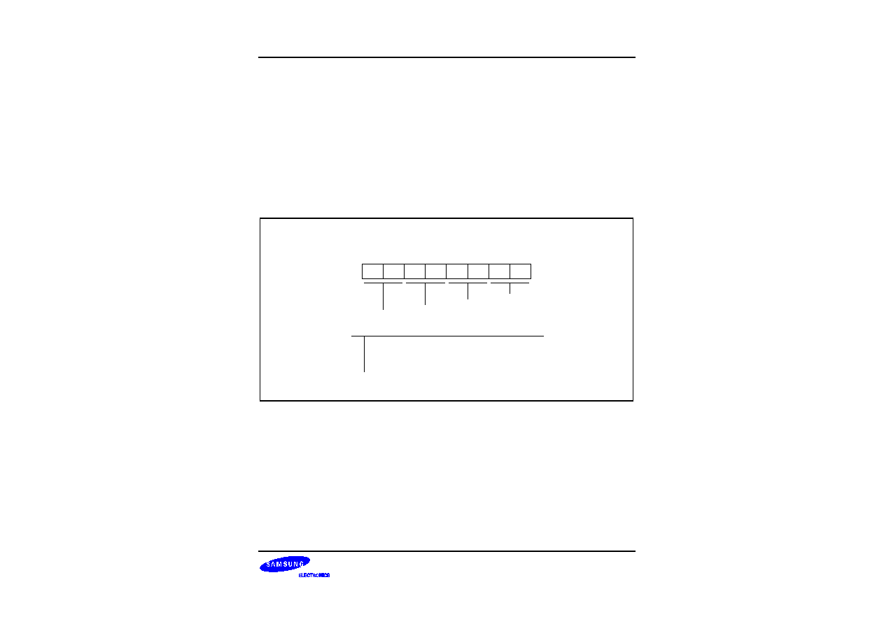
S3P80C5/C80C5/C80C8
I/O PORTS
9-7
PORT 1
Port 1 is a bit-programmable 8-bit I/O port. Port 1 pins are accessed directly by read/write operations to the port 1
data register, P1 (set 1, E1H).
To configure port 1, the initialization routine writes the appropriate values to the two port 1 control registers:
P1CONH (set 1, EAH) for the upper nibble pins, P1.7≠P1.4, and P1CONL (set 1, EBH) for the lower nibble pins,
P1.3≠P1.0. Each 8-bit control register contains four bit-pairs and each 2-bit value configures one port pin (see
Figures 9-6 and 9-7).
Following a hardware reset, the port 1 control registers are cleared to '00H', configuring port 0 initially to Input
mode.
To assign pull-up resistors to P1 pins, you make the appropriate settings to the port 1 pull-up resistor enable
register, P1PUR.
Port 1 Control Register, High Byte (P1CONH)
EAH, Set 1, R/W
.7
.6
.5
.4
.3
.2
.1
.0
MSB
LSB
P1.7
P1.4
P1.6
P1.5
P1CONH Pin Configureation Settings:
00
01
10
11
Input mode
Open-drain output mode
Push-pull output mode
Invalid setting
Figure 9-7. Port 1 High-Byte Control Register (P1CONH)

I/O PORTS
S3P80C5/C80C5/C80C8
9-8
Port 1 Control Register, Low Byte (P1CONL)
EBH, Set 1, R/W
.7
.6
.5
.4
.3
.2
.1
.0
MSB
LSB
P1.3
P1.0
P1.2
P1.1
P1CONL Pin Configureation Settings:
00
01
10
11
Input mode
Open-drain output mode
Push-pull output mode
Invalid setting
Figure 9-8. Port 1 Low-Byte Control Register (P1CONL)

S3P80C5/C80C5/C80C8
I/O PORTS
9-9
PORT 2
Port 2 is a bit-programmable 3-bit I/O port. Port 2 pins are accessed directly by read/write operations to the port 2
data register, P2 (set 1, E2H). You can configure port 2 pins individually to Input mode, open-drain output mode,
or push-pull output mode.
P2.0, P2.1 and P2.2 are configured by writing 6-bit data value to the port 2 control register, P2CON. You can
configure these pins to support input functions (Input mode, with or without pull-up, for T0CK) or output functions
(push-pull or open-drain output mode for REM and timer 0 PWM).
Port 2 pins have high current drive capability to support LED applications.
A reset operation clears P2CON to '00H', selecting Input mode as the initial port 2 function.
Port 2 Control Register (P2CON)
F0H, R/W
.7
.6
.5
.4
.3
.2
.1
.0
MSB
LSB
P2.2
P2.2
P2.1
P1.0
P2.1 Alternative Function Enable
0
1
Normal I/O Function
REM/T0CK
P2.0 Alternative Function Enable
0
1
Normal I/O Function
T0PWM
P2CON Pin Configuration Setting:
00
01
10
11
C-MOS input mode
Open-drain output mode
Push-pull output mode
C-MOS input mode with pull-up
Figure 9-9. Port 2 Control Register (P2CON)

I/O PORTS
S3P80C5/C80C5/C80C8
9-10
Port 2 Data Register (P2)
E2H, R/W
.7
.6
.5
.4
.3
.2
.1
.0
MSB
LSB
Not used for S3C80C5
P2.0/T0_PWM
Carrier on/off for Remote Controller
P2.2
P2.1/REM/TOCK
Not used for S3C80C5
Figure 9-10. Port 2 Data Register (P2)

S3P80C5/C80C5/C80C8
BASIC TIMER AND TIMER 0
10-1
10
BASIC TIMER and TIMER 0
MODULE OVERVIEW
The S3P80C5/C80C5/C80C8 has two default timers: an 8-bit basic timer and one 8-bit general-purpose
timer/counter. The 8-bit timer/counter is called timer 0.
Basic Timer (BT)
You can use the basic timer (BT) in two different ways:
-- As a watchdog timer to provide an automatic reset mechanism in the event of a system malfunction, or
-- To signal the end of the required oscillation stabilization interval after a reset or a Stop mode release.
BASIC TIMER CONTROL REGISTER (BTCON)
The basic timer control register, BTCON, is used to select the input clock frequency, to clear the basic timer
counter and frequency dividers, and to enable or disable the watchdog timer function. It is located in set 1,
address D3H, and is read/write addressable using Register addressing mode.
A system reset clears BTCON. This enables the watchdog function and selects a basic timer clock frequency of
f
OSC
/4096. To disable the watchdog function, you must write the signature code '1010B' to the basic timer
register control bits BTCON.7≠BTCON.4. For more reliability, we recommend to use the Watch-dog timer
function in remote controller and hand-held product application.

BASIC TIMER and TIMER 0
S3P80C5/C80C5/C80C8
10-2
Basic Timer Control Register (BTCON)
D3H, Set 1, R/W
.7
.6
.5
.4
.3
.2
.1
.0
MSB
LSB
Watchdog function enable bits:
1010B = Disable watchdog timer
Other value = Enable watchdog timer
Divider clear bit for basic
timer and timer 0:
0 = No effect
1 = Clear both dividers
Basic timer input clock selection bits:
0 = No effect
1 = Clear BTCNT
Basic timer input clock selection bits:
00
01
10
11
f
OSC
/4096
f
OSC
/1024
f
OSC
/128
Invalid selection
Figure 10-1. Basic Timer Control Register (BTCON)

S3P80C5/C80C5/C80C8
BASIC TIMER AND TIMER 0
10-3
BASIC TIMER FUNCTION DESCRIPTION
Watchdog Timer Function
You can program the basic timer overflow signal (BTOVF) to generate a reset by enabling the watchdog function.
A reset clears BTCON to '00H', automatically enabling the watchdog timer function. A reset also selects the CPU
clock (as determined by the current CLKCON register setting),divided by 4096, as the BT clock.
A reset whenever a basic timer counter overflow occurs. During normal operation, the application program must
prevent the overflow, and the accompanying reset operation, from occurring. To do this, the BTCNT value must
be cleared (by writing a "1" to BTCON.1) at regular intervals.
If a system malfunction occurs due to circuit noise or some other error condition, the BT counter clear operation
will not be executed and a basic timer overflow will occur, initiating a reset. In other words, during normal
operation, the basic timer overflow loop (a bit 7 overflow of the 8-bit basic timer counter, BTCNT) is always
broken by a BTCNT clear instruction. If a malfunction does occur, a reset is triggered automatically.
TIMER 0 CONTROL REGISTER (T0CON)
You use the timer 0 control register, T0CON, to
-- Select the timer 0 operating mode (interval timer)
-- Select the timer 0 input clock frequency
-- Clear the timer 0 counter, T0CNT
-- Enable the timer 0 overflow interrupt or timer 0 match interrupt
-- Clear timer 0 match interrupt pending conditions
T0CON is located in set 1, at address D2H, and is read/write addressable using Register addressing mode.
A reset clears T0CON to '00H'. This sets timer 0 to normal interval timer mode, selects an input clock frequency
of f
OSC
/4096, and disables all timer 0 interrupts. You can clear the timer 0 counter at any time during normal
operation by writing a "1" to T0CON.3.
The timer 0 overflow interrupt (T0OVF) is interrupt level IRQ0 and has the vector address FAH. When a timer 0
overflow interrupt occurs and is serviced by the CPU, the pending condition is cleared automatically by hardware.
To enable the timer 0 match interrupt (IRQ0, vector FCH), you must write T0CON.1 to "1". To detect a match
interrupt pending condition, the application program polls T0CON.0. When a "1" is detected, a timer 0 match
interrupt is pending. When the interrupt request has been serviced, the pending condition must be cleared by
software by writing a "0" to the timer 0 interrupt pending bit, T0CON.0.
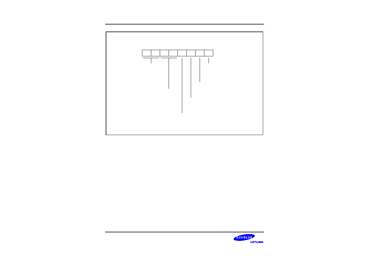
BASIC TIMER and TIMER 0
S3P80C5/C80C5/C80C8
10-4
Timer 0 Control Register (T0CON)
D2H, Set 1, R/W
.7
.6
.5
.4
.3
.2
.1
.0
MSB
LSB
Timer 0 counter clear bit:
0 = No effect
1 = Clear the timer 0 counter (when write)
Timer 0 input clock selection bits:
00 = f
OSC
/4096
01 = f
OSC
/256
10 = f
OSC
/8
11 = External clock (P2.1/T0CK)
Timer 0 operating mode selection bits:
00 = Interval mode
01 = Overflow mode (OVF interrupt can occur)
10 = Overflow mode (OVF interrupt can occur)
11 = PWM mode (OVF interrupt can occur)
Timer 0 overflow interrupt enable bit:
0 = Disable overflow interrupt
1 = Enable overflow interrupt
Timer 0 match interrupt enable bit:
0 = Disable interrupt
1 = Enable interrupt
Timer 0 match interrupt pending bit:
0 = No interrupt pending
0 = Clear pending bit (write)
1 = Interrupt is pending
Figure 10-2. Timer 0 Control Register (T0CON)
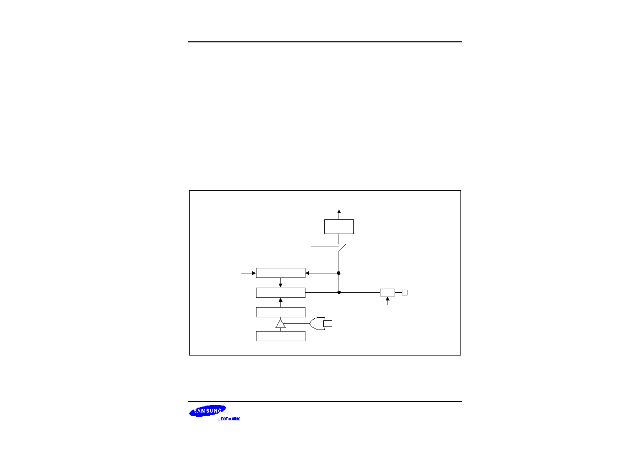
S3P80C5/C80C5/C80C8
BASIC TIMER AND TIMER 0
10-5
TIMER 0 FUNCTION DESCRIPTION
Timer 0 Interrupts (IRQ0, Vectors FAH and FCH)
The timer 0 module can generate two interrupts: the timer 0 overflow interrupt (T0OVF), and the timer 0 match
interrupt (T0INT). T0OVF is interrupt level IRQ0, vector FAH. T0INT also belongs to interrupt level IRQ0, but is
assigned the separate vector address, FCH.
A timer 0 overflow interrupt pending condition is automatically cleared by hardware when it has been serviced.
The T0INT pending condition must, however, be cleared by the application's interrupt service routine by writing a
"0" to the T0CON.0 interrupt pending bit.
Interval Timer Mode
In interval timer mode, a match signal is generated when the counter value is identical to the value written to the
T0 reference data register, T0DATA. The match signal generates a timer 0 match interrupt (T0INT, vector FCH)
and clears the counter.
If, for example, you write the value `10H' to T0DATA and `0BH' to T0CON, the counter will increment until it
reaches `10H'. At this point, the T0 interrupt request is generated, the counter value is reset, and counting
resumes. With each match, the level of the signal at the timer 0 output pin is inverted (see Figure 10-3).
Interrupt
Enable/Disable
(T0CON.1)
Pending
(T0CON.0)
CTL
P2.0
T0CON.5
T0CON.4
Match Signal
T0CON.3
IRQ0(INT)
R (Clear)
CLK
Match
Data Register
Buffer Register
Comparator
Counter
Figure 10-3. Simplified Timer 0 Function Diagram: Interval Timer Mode
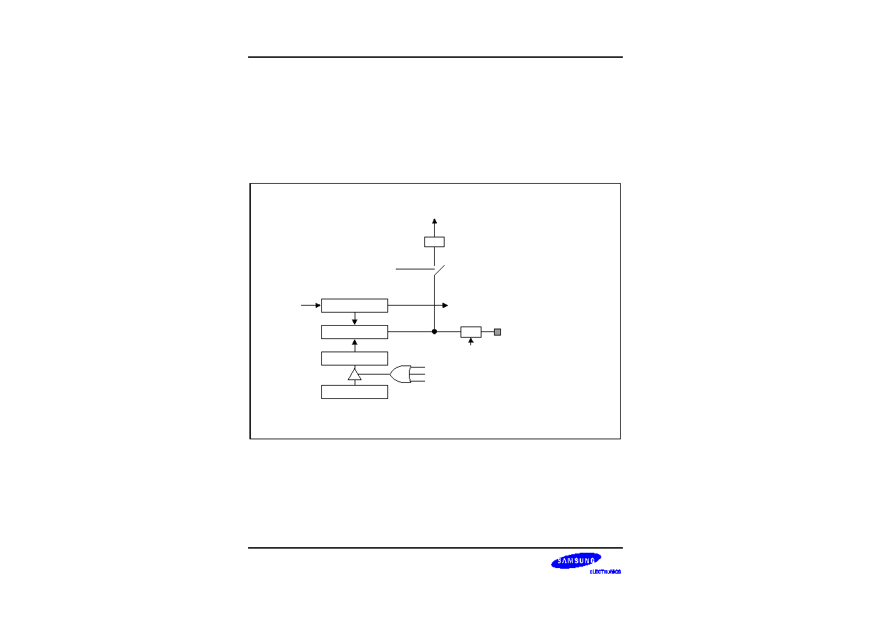
BASIC TIMER and TIMER 0
S3P80C5/C80C5/C80C8
10-6
Pulse Width Modulation Mode
Pulse width modulation (PWM) mode lets you program the width (duration) of the pulse that is output at the
T0PWM pin. As in interval timer mode, a match signal is generated when the counter value is identical to the
value written to the timer 0 data register. In PWM mode, however, the match signal does not clear the counter.
Instead, it runs continuously, overflowing at `FFH', and then continues incrementing from `00H'.
Although you can use the match signal to generate a timer 0 overflow interrupt, interrupts are not typically used
in PWM-type applications. Instead, the pulse at the T0PWM pin is held to Low level as long as the reference
data value is less than or equal to (
) the counter value and then the pulse is held to High level for as long as
the data value is greater than ( > ) the counter value. One pulse width is equal to t
CLK
◊
256 (see Figure 11-4).
Interrupt
Enable/Disable
(T0CON.1)
CTL
P2.0/
T0PWM
T0CON.5
T0CON.4
Match Signal
T0CON.3
IRQ0(T0INT)
IRQ0 (T0OVF)
CLK
Match
Data Register
Buffer Register
Comparator
Counter
T0OVF
(T0CON.0)
High level when
data > counter;
Low level when
data < counter
_
NOTE: Interrupts are usually not used when timer 0 is configurared to operate in PWM mode
PND
Figure 10-4. Simplified Timer 0 Function Diagram: PWM Mode

S3P80C5/C80C5/C80C8
BASIC TIMER AND TIMER 0
10-7
During a power-on reset operation, the CPU is idle during the required oscillation
stabilizatiin interval (until bit 4 of the basic timer counter overflows).
It is available only in using interval mode.
NOTES:
1.
2.
Bits 7,6
Bit 0
X
IN
Bits 3,2
RESET
or Stop
Clear
Data Bus
Bit 1
Data Bus
Match Signal
T0CON.3
T0OVF
8-Bit Basic Counter
(Read-Only)
OVF
Bit 2
Bit 3
OVF
DIV
R
1/4096
1/1024
1/128
P2.1/T0CK
Bit 1
PND
T0CON.0
Match
(2)
P2.0
Bits 5,4
T0PWM
T0INT
RESET
Data Bus
Basic Timer Control Register
Timer 0 Control Register
MUX
MUX
DIV
1/4096
1/1024
1/128
R
Basic Timer Control Register
(Write '1010xxxxB' to disable)
8-Bit Up-Counter
(Read-Only)
R
8-Bit Comparator
Timer 0 Buffer Reg
Timer 0 Data Register
(Read/Write)
Clear
Figure 10-5. Basic Timer and Timer 0 Block Diagram

BASIC TIMER and TIMER 0
S3P80C5/C80C5/C80C8
10-8
F
F
PROGRAMMING TIP -- Configuring the Basic Timer
This example shows how to configure the basic timer to sample specifications:
ORG
0100H
RESET
DI
; Disable all interrupts
LD
BTCON,#03H
; Enable the watchdog timer
LD
CLKCON,#18H
; Non-divided clock
CLR
SYM
; Disable global and fast interrupts
CLR
SPL
; Stack pointer low byte
"0"
; Stack area starts at 0FFH
∑
∑
∑
SRP
#0C0H
; Set register pointer
0C0H
EI
; Enable interrupts
∑
∑
∑
MAIN
LD
BTCON,#02H
; Enable the watchdog timer
; Basic timer clock: f
OSC
/4096
; Clear basic timer counter
NOP
NOP
∑
∑
∑
JP
T,MAIN
∑
∑
∑

S3P80C5/C80C5/C80C8
BASIC TIMER AND TIMER 0
10-9
F
F
Programming Tip -- Programming Timer 0
This sample program sets timer 0 to interval timer mode, sets the frequency of the oscillator clock, and
determines the execution sequence which follows a timer 0 interrupt. The program parameters are as follows:
-- Timer 0 is used in interval mode; the timer interval is set to 4 milliseconds
-- Oscillation frequency is 4 MHz
-- General register 60H (page 0)
60H + 61H + 62H + 63H + 64H (page 0) is executed after a timer 0
interrupt
ORG
0FAH
; Timer 0 overflow interrupt
VECTOR
T0OVER
ORG
0FCH
; Timer 0 match/capture interrupt
VECTOR
T0INT
ORG
0100H
RESET
DI
; Disable all interrupts
LD
BTCON,#0AAH
; Disable the watchdog timer
LD
CLKCON,#18H
; Select non-divided clock
CLR
SYM
; Disable global and fast interrupts
CLR
SPL
; Stack pointer low byte
"0"
; Stack area starts at 0FFH
∑
∑
∑
LD
T0CON,#4BH
; Write '01001011B'
; Input clock is f
OSC
/256
; Interval timer mode
; Enable the timer 0 interrupt
; Disable the timer 0 overflow interrupt
LD
T0DATA,#5DH
; Set timer interval to 4 milliseconds
; (4 MHz/256)
˜
(93 + 1) = 0.166 kHz (6 ms)
SRP
#0C0H
; Set register pointer
0C0H
EI
; Enable interrupts
∑
∑
∑

BASIC TIMER and TIMER 0
S3P80C5/C80C5/C80C8
10-10
F
F
PROGRAMMING TIP -- Programming Timer 0 (Continued)
T0INT
PUSH
RP0
; Save RP0 to stack
SRP0
#60H
; RP0
60H
INC
R0
; R0
R0 + 1
ADD
R2,R0
; R2
R2 + R0
ADC
R3,R2
; R3
R3 + R2 + Carry
ADC
R4,R0
; R4
R4 + R0 + Carry
CP
R0,#32H
; 50
◊
6 = 300 ms
JR
ULT,NO_300MS_SET
BITS
R1.2
; Bit setting (61.2H)
NO_300MS_SET:
LD
T0CON,#42H
; Clear pending bit
POP
RP0
; Restore register pointer 0 value
T0OVER
IRET
; Return from interrupt service routine

S3P80C5/C80C5/C80C8
TIMER 1
11-1
11
TIMER 1
OVERVIEW
The S3C80C5/C80C8 microcontroller has a 16-bit timer/counter called timer 1 (T1). For universal remote
controller applications, timer 1 can be used to generate the envelope pattern for the remote controller signal.
Timer 1 has the following components:
-- One control register, T1CON (set 1, FAH, R/W)
-- Two 8-bit counter registers, T1CNTH and T1CNTL (set 1, F6H and F7H, read-only)
-- Two 8-bit reference data registers, T1DATAH and T1DATAL (set 1, F8H and F9H, R/W)
-- A 16-bit comparator
You can select one of the following clock sources as the timer 1 clock:
-- Oscillator frequency (f
OSC
) divided by 4, 8, or 16
-- Internal clock input from the counter A module (counter A flip/flop output)
You can use Timer 1 in two ways:
-- As a normal free run counter, generating a timer 1 overflow interrupt (IRQ1, vector F4H) at programmed time
intervals.
-- To generate a timer 1 match interrupt (IRQ1, vector F6H) when the 16-bit timer 1 count value matches the
16-bit value written to the reference data registers.
In the S3C80C5/C80C8 interrupt structure, the timer 1 overflow interrupt has higher priority than the timer 1
match.
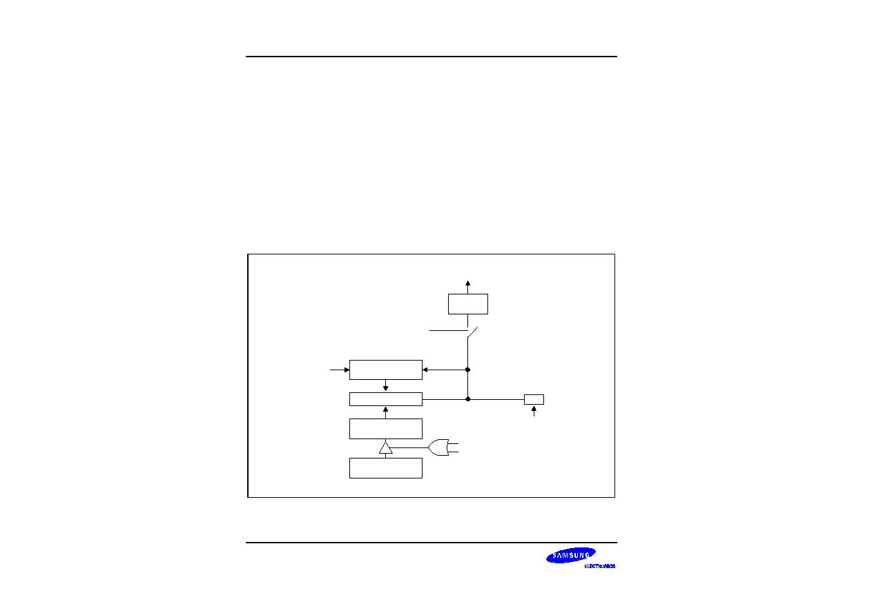
TIMER 1
S3P80C5/C80C5/C80C8
11-2
TIMER 1 OVERFLOW INTERRUPT
Timer 1 can be programmed to generate an overflow interrupt (IRQ1, F4H) whenever an overflow occurs in the
16-bit up counter. When you set the timer 1 overflow interrupt enable bit, T1CON.2, to "1", the overflow interrupt
is generated each time the 16-bit up counter reaches `FFFFH'. After the interrupt request is generated, the
counter value is automatically cleared to `00H' and up counting resumes. By writing a "1" to T1CON.3, you can
clear/reset the 16-bit counter value at any time during program operation.
TIMER 1 MATCH INTERRUPT
Timer 1 can also be used to generate a match interrupt (IRQ1, vector F6H) whenever the 16-bit counter value
matches the value that is written to the timer 1 reference data registers, T1DATAH and T1DATAL. When a
match condition is detected by the 16-bit comparator, the match interrupt is generated, the counter value is
cleared, and up counting resumes from `00H'.
In match mode, program software can poll the timer 1 match interrupt pending bit, T1CON.0, to detect when a
timer 1 match interrupt pending condition exists (T1CON.0 = "1"). When the interrupt request is acknowledged by
the CPU and the service routine starts, the interrupt service routine for vector F6H must clear the interrupt
pending condition by writing a "0" to T1CON.0.
Interrupt
Enable/Disable
(T1CON.2)
Pending
(T1CON.0)
CTL
T1CON.5
T1CON.4
Match Signal
T1CON.3
IRQ1(T1INT)
R (Clear)
CLK
Match
Timer 1 Data High/Low
Buffer Register
Timer 1 High/Low
Buffer Register
16-Bit Comparator
16-Bit UP Counter
(Read-Only)
Figure 11-1. Simplified Timer 1 Function Diagram: Interval Timer Mode
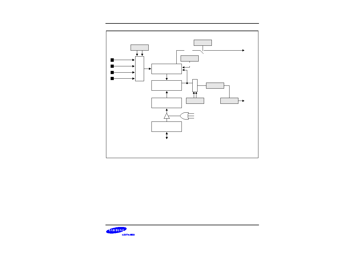
S3P80C5/C80C5/C80C8
TIMER 1
11-3
NOTES: Match signal is occured only in interval mode.
T1CON.7-.6
T1CON.3
Match Signal
T1OVF
OVF
M
U
X
Match
(note)
IRQ1
Data Bus
MUX
16-Bit Up-Counter
(Read-Only)
R
16-Bit Comparator
Timer 1 High/Low
Buffer Register
Timer 1 Data
High/Low Register
CAOF (T-F/F)
f
OSC
/4
f
OSC
/8
f
OSC
/16
Clear
T1CON.3
T1CON.2
IRQ1
T1CON.5-.4
T1CON.1
T1CON.0
Figure 11-2. Timer 1 Block Diagram
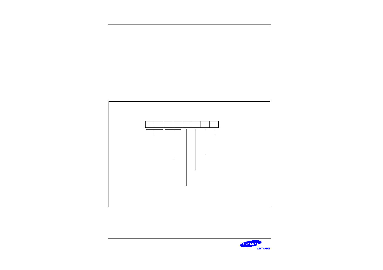
TIMER 1
S3P80C5/C80C5/C80C8
11-4
TIMER 1 CONTROL REGISTER (T1CON)
The timer 1 control register, T1CON, is located in set 1, FAH, and is read/write addressable. T1CON contains
control settings for the following T1 functions:
-- Timer 1 input clock selection
-- Timer 1 operating mode selection
-- Timer 1 16-bit down counter clear
-- Timer 1 overflow interrupt enable/disable
-- Timer 1 match interrupt enable/disable
-- Timer 1 interrupt pending control (read for status, write to clear)
A reset operation clears T1CON to `00H', selecting f
OSC
divided by 4 as the T1 clock, configuring timer 1 as a
normal interval timer, and disabling the timer 1 interrupts.
Timer 1 Control Register (T1CON)
FAH, R/W
.7
.6
.5
.4
.3
.2
.1
.0
MSB
LSB
Timer 1 counter clear bit:
0 = No effect
1 = Clear the timer 1 counter (when write)
Timer 1 input clock selection bits:
00 = f
OSC
/4
01 = f
OSC
/8
10 = f
OSC
/16
11 = Internal clock (T-F/F)
Timer 1 operating mode selection bits:
00 = Interval mode
01 = Overflow mode (OVF interrupt can occur)
01 = Overflow mode (OVF interrupt can occur)
01 = Overflow mode (OVF interrupt can occur)
Timer 1 overflow interrupt enable bit:
0 = Disable overflow interrupt
1 = Enable overflow interrupt
Timer 1 match interrupt enable bit:
0 = Disable interrupt
1 = Enable interrupt
Timer 1 match interrupt pending bit:
0 = No interrupt pending
0 = Clear pending bit (write)
1 = Interrupt is pending
Figure 11-3. Timer 1 Control Register (T1CON)

S3P80C5/C80C5/C80C8
TIMER 1
11-5
Timer 1 Counter Low-Byte Register (T1CNTL)
F7H, Set 1, R
.7
.6
.5
.4
.3
.2
.1
.0
MSB
LSB
Reset Value : 00H
Timer 1 Counter High-Byte Register (T1CNTH)
F6H, Set 1, R
.7
.6
.5
.4
.3
.2
.1
.0
MSB
LSB
Reset Value : 00H
Timer 1 Data High-Byte Register (T1DATAH)
F8H, Set 1, R/W
.7
.6
.5
.4
.3
.2
.1
.0
MSB
LSB
Reset Value : FFh
Timer 1 Data Low-Byte Register (T1DATAL)
F9H, Set 1, R/W
.7
.6
.5
.4
.3
.2
.1
.0
MSB
LSB
Reset Value : FFh
Figure 11-4. Timer 1 Registers

TIMER 1
S3P80C5/C80C5/C80C8
11-6
NOTES

S3P80C5/C80C5/C80C8
COUNTER A
12-1
12
COUNTER A
OVERVIEW
The S3P80C5/C80C5/C80C8 microcontroller has an 8-bit counter called counter A. Counter A, which can be
used to generate the carrier frequency, has the following components (see Figure 12-1):
-- Counter A control register, CACON
-- 8-bit down counter with auto-reload function
-- Two 8-bit reference data registers, CADATAH and CADATAL
Counter A has two functions:
-- As a normal interval timer, generating a counter A interrupt (IRQ4, vector ECH) at programmed time
intervals.
-- To supply a clock source to the 16-bit timer/counter module, timer 1, for generating the timer 1 overflow
interrupt.

COUNTER A
S3P80C5/C80C5/C80C8
12-2
NOTES: The value of the CADATAL register is loaded into the 8-bit counter when the operaion of the counter A
Starts. If a borrow occurs in the counter, the value of the CADATAH register is loaded into the 8-bit
counter. However, if the next borrow ovvurs, the value of the CADATAL register is loaded into the 8-bit
counter.
CACON.6-.7
MUX
DIV 1
DIV 2
DIV 4
DIV 8
CLK
CACON.0
(CAOF)
To Other Block
(P3.1/REM)
Repeat
Control
Interrupt
Control
CACON.4-.5
CACON.2
f
OSC
Counter A Data
High Byte Register
INT.GEN.
MUX
8-Bit
Down Counter
Counter A Data
Low Byte Register
CACON.3
IRQ4
(CAINT)
Data Bus
Figure 12-1. Counter A Block Diagram
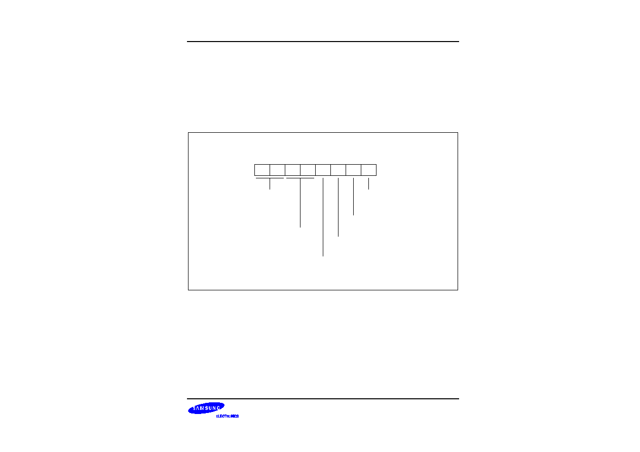
S3P80C5/C80C5/C80C8
COUNTER A
12-3
COUNTER A CONTROL REGISTER (CACON)
The counter A control register, CACON, is located in set 1, bank 0, F3H, and is read/write addressable. CACON
contains control settings for the following functions (see Figure 12-2):
-- Counter A clock source selection
-- Counter A interrupt enable/disable
-- Counter A interrupt pending control (read for status, write to clear)
-- Counter A interrupt time selection
Counter A Control Register (CACON)
F3H, Set 1, R/W
.7
.6
.5
.4
.3
.2
.1
.0
MSB
LSB
Counter A input clock
selection bits:
00 = f
OSC
01 = f
OSC
/2
10 = f
OSC
/4
11 = f
OSC
/8
Counter A output flip-flop
control bit:
0 = T-FF is Low
1 = T-FF is High
Counter A mode selection bit:
0 = One-shot mode
1 = Repeating mode
Counter A interrupt selection bits:
00 = Elapsed time for Low data value
01 = Elapsed time for High data value
10 = Elapsed time for Low and High
data values
11 = Invalid setting
Counter A interrupt enable bit:
0 = Disable interrupt
1 = Enable interrupt
Counter A start/stop bit:
0 = Stop counter A
1 = Start counter A
Figure 12-2. Counter A Control Register (CACON)

COUNTER A
S3P80C5/C80C5/C80C8
12-4
Counter A Data Low-Byte Register (CADATAL)
F5H, Set 1, R/W
.7
.6
.5
.4
.3
.2
.1
.0
MSB
LSB
Reset Value : FFh
Counter A Data High-Byte Register (CADATAH)
F4H, Set 1, R/W
.7
.6
.5
.4
.3
.2
.1
.0
MSB
LSB
Reset Value : FFh
Figure 12-3. Counter A Registers
COUNTER A PULSE WIDTH CALCULATIONS
t
LOW
t
HIGH
t
LOW
To generate the above repeated waveform consisted of low period time, t
LOW
, and high period time, t
HIGH
.
When CAOF = 0,
t
LOW
= (CADATAL + 2) x 1/fxx, 0H < CADATAL < 100H, where fx = The selected clock.
t
HIGH
= (CADATAH + 2) x 1/fxx, 0H < CADATAH < 100H, where fx = The selected clock.
When CAOF = 1,
t
LOW
= (CADATAH + 2) x 1/fxx, 0H < CADATAH < 100H, where fx = The selected clock.
t
HIGH
= (CADATAL + 2) x 1/fxx, 0H < CADATAL < 100H, where fx = The selected clock.
To make t
LOW
= 24 us and t
HIGH
= 15 us. f
OSC
= 4 MHz, fx = 4 MHz/4 = 1 MHz
[Method 1] When CAOF = 0,
t
LOW
= 24 us = (CADATAL + 2) /fx = (CADATAL + 2)
◊
1us, CADATAL = 22.
t
HIGH
= 15 us = (CADATAH + 2) /fx = (CADATAH + 2)
◊
1us, CADATAH = 13.
[Method 2] When CAOF = 1,
t
HIGH
= 15 us = (CADATAL + 2) /fx = (CADATAL + 2)
◊
1us, CADATAL = 13.
t
LOW
= 24 us = (CADATAH + 2) /fx = (CADATAH + 2)
◊
1us, CADATAH = 22.
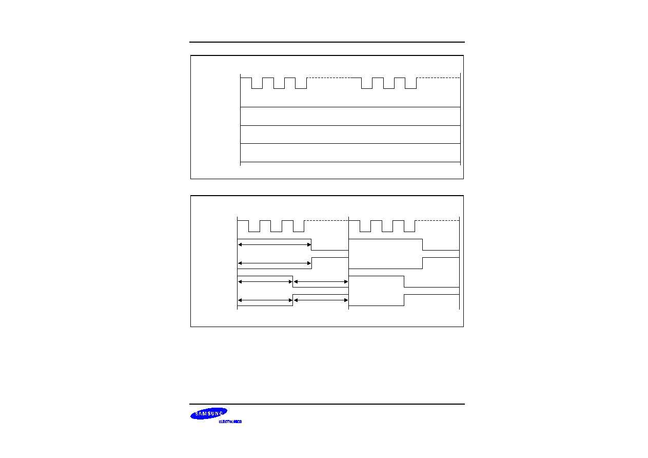
S3P80C5/C80C5/C80C8
COUNTER A
12-5
Low
High
High
Low
0H
Counter A
Clock
CAOF = '0'
CADATAL = 01-FFH
CADATAH = 001H
CAOF = '0'
CADATAL = 00H
CADATAH = 01-FFH
CAOF = '0'
CADATAL = 00H
CADATAH = 00H
CAOF = '1'
CADATAL = 00H
CADATAH = 00H
E0H
0H
Counter A
Clock
CAOF = '0'
CADATAL = DEH
CADATAH = 1EH
CAOF = '0'
CADATAL = DEH
CADATAH = 1EH
CAOF = '1'
CADATAL = 7EH
CADATAH = 7EH
CAOF = '0'
CADATAL = 7EH
CADATAH = 7EH
E0H
20H
20H
80H
80H
80H
80H
Figure 12-4. Counter A Output flip-flop Waveforms in Repeat Mode
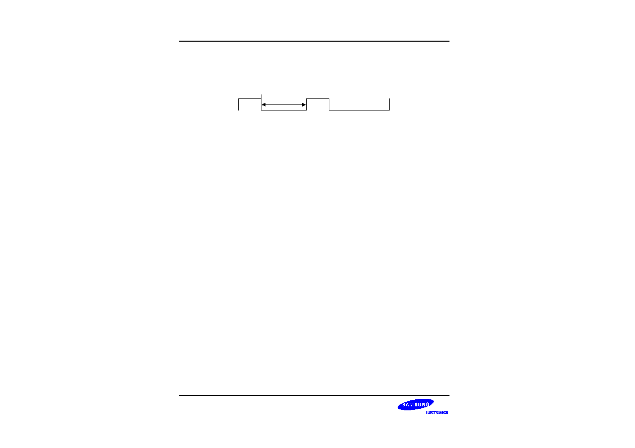
COUNTER A
S3P80C5/C80C5/C80C8
12-6
F
F
PROGRAMMING TIP -- To Generate 38 kHz, 1/3duty Signal Through P2.1
This example sets Counter A to the repeat mode, sets the oscillation frequency as the Counter A clock source,
and CADATAH and CADATAL to make a 38 kHz,1/3 Duty carrier frequency. The program parameters are:
17.59
µ
s
8.795
µ
s
37.9 kHz 1/3 Duty
-- Counter A is used in repeat mode
-- Oscillation frequency is 4 MHz (0.25
µ
s)
-- CADATAH = 8.795
µ
s / 0.25
µ
s = 35.18, CADATAL = 17.59
µ
s / 0.25
µ
s = 70.36
-- Set P2.1 C-MOS push-pull output and CAOF mode.
ORG
0100H
; Reset address
START
DI
∑
∑
∑
LD
CADATAL,#(70-2)
; Set 17.5
µ
s
LD
CADATAH,#(35-2)
; Set 8.75
µ
s
;
LD
P2CON,#10101010B
; Set P2 to C-MOS push-pull output.
; Set P2.1 to REM output
;
LD
CACON,#00000110B
; Clock Source
f
OSC
; Disable Counter A interrupt.
; Select repeat mode for Counter A.
; Start Counter A operation.
; Set Counter A Output Flip-flop(CAOF) high.
;
LD
P2,#20H
; Set P2.5(Carrier On/Off) to high.
; This command generates 38 kHz, 1/3duty pulse signal
; through P2.1
;
∑
∑
∑
S3P80C5/C80C5/C80C8
COUNTER A
12-7
F
F
PROGRAMMING TIP -- To Generate a One Pulse Signal Through P2.1
This example sets Counter A to the one shot mode, sets the oscillation frequency as the Counter A clock source,
and CADATAH and CADATAL to make a 40
µ
s width pulse. The program parameters are:
40
µ
s
-- Counter A is used in one shot mode
-- Oscillation frequency is 4 MHz (1 clock = 0.25
µ
s)
-- CADATAH = 40
µ
s / 0.25
µ
s = 160, CADATAL = 1
-- Set P2.1 C-MOS push-pull output and CAOF mode.
ORG
0100H
; Reset address
START
DI
∑
∑
LD
CADATAH,# (160-2)
; Set 40
µ
s
LD
CADATAL,# 1
; Set any value except 00H
;
LD
P2CON,#10101010B
; Set P2 to C-MOS push-pull output.
; Set P2.1 to REM output
;
LD
CACON,#00000001B
; Clock Source
f
OSC
; Disable Counter A interrupt.
; Select one shot mode for Counter A.
; Stop Counter A operation.
; Set Counter A Output flip-flop (CAOF) high
LD
P2,#20H
; Set P2.5(Carrier On/Off) to high.
∑
∑
∑
Pulse_out:
LD
CACON,#00000101B
; Start Counter A operation
; to make the pulse at this point.
∑
; After the instruction is executed, 0.75
µ
s is required
∑
; before the falling edge of the pulse starts.
∑

COUNTER A
S3P80C5/C80C5/C80C8
12-8
NOTES

S3P80C5/C80C5/C80C8
ELECTRICAL DATA
13-
1
13
ELECTRICAL DATA
OVERVIEW
In this section, S3P80C5/C80C5/C80C8 electrical characteristics are presented in tables and graphs. The
information is arranged in the following order:
-- Absolute maximum ratings
-- D.C. electrical characteristics
-- Data retention supply voltage in Stop mode
-- Stop mode release timing when initiated by a Reset
-- I/O capacitance
-- A.C. electrical characteristics
-- Input timing for external interrupts (port 0)
-- Oscillation characteristics
-- Oscillation stabilization time
ELECTRICAL DATA
S3P80C5/C80C5/C80C8
13-
2
Table 13-1. Absolute Maximum Ratings
(T
A
= 25
∞
C)
Parameter
Symbol
Conditions
Rating
Unit
Supply voltage
V
DD
≠
≠ 0.3 to + 6.5
V
Input voltage
V
IN
≠
≠ 0.3 to
V
DD
+ 0.3
V
Output voltage
V
O
All output pins
≠ 0.3 to V
DD
+ 0.3
V
Output current High
I
OH
One I/O pin active
≠ 18
mA
All I/O pins active
≠ 60
Output current Low
I
OL
One I/O pin active
+ 30
mA
Total pin current for ports 0, 1, and 2
+ 100
Total pin current for port 3
+ 40
Operating
temperature
T
A
≠
≠ 40 to + 85
∞
C
Storage
temperature
T
STG
≠
≠ 65 to + 150
∞
C
Table 13-2. D.C. Electrical Characteristics
(T
A
= ≠ 40
∞
C to + 85
∞
C, V
DD
= 2.0 V to 3.6 V)
Parameter
Symbol
Conditions
Min
Typ
Max
Unit
Operating Voltage
V
DD
f
OSC
=
4MHz
(Instruction clock = 0.67 MHz)
1.7
≠
3.6
V
Input High
voltage
V
IH1
All input pins except V
IH2
and V
IH3
0.8 V
DD
≠
V
DD
V
V
IH2
X
IN
V
DD
≠ 0.3
V
DD
Input Low voltage
V
IL1
All input pins except V
IL2
and V
IL3
0
≠
0.2 V
DD
V
V
IL2
X
IN
0.3
Output High
voltage
V
OH1
V
DD
= 2.4 V, I
OH
= ≠ 6 mA
Port 2.1 only, T
A
= 25
∞
C
V
DD
≠ 0.7
V
V
OH2
V
DD
= 2.4 V, I
OH
= ≠ 2.2mA
Port 2.0, 2.2, T
A
= 25
∞
C
V
DD
-
0.7
≠
≠
V
OH3
V
DD
= 2.4 V, I
OH
= ≠ 1 mA
All output pins except Port2,
T
A
= 25
∞
C
V
DD
-
1.0
≠
≠

S3P80C5/C80C5/C80C8
ELECTRICAL DATA
13-
3
Table 13-2. D.C. Electrical Characteristics (Continued)
(T
A
= ≠ 40
∞
C to + 85
∞
C, V
DD
= 2.0 V to 3.6 V)
Parameter
Symbol
Conditions
Min
Typ
Max
Unit
Output Low
voltage
V
OL1
V
DD
= 2.4 V, I
OL
= 12 mA, port
2.1 only, T
A
= 25
∞
C
0.4
0.5
V
OL2
V
DD
= 2.4 V, I
OL
= 5 mA
Port 2.0,2.2, T
A
= 25
∞
C
≠
0.4
0.5
V
OL3
I
OL
= 1 mA
Ports 0 and 1, T
A
= 25
∞
C
0.4
1.0
Input High
leakage current
I
LIH1
V
IN
= V
DD
All input pins except X
IN
and
X
OUT
≠
≠
1
µA
I
LIH2
V
IN
= V
DD
, X
IN
and X
OUT
20
Input Low
leakage current
I
LIL1
V
IN
= 0 V
All input pins except X
IN
, X
OUT
≠
≠
≠ 1
µA
I
LIL2
V
IN
= 0 V
X
IN
and X
OUT
≠ 20
Output High
leakage current
I
LOH
V
OUT
= V
DD
All output pins
≠
≠
1
µA
Output Low
leakage current
I
LOL
V
OUT
= 0 V
All output pins
≠
≠
≠ 1
µA
Pull-up resistors
R
L1
V
DD
= 2.4V, V
IN
= 0 V;
T
A
= 25
∞
C , Ports 0-2
44
55
95
K
Supply current
(note)
I
DD1
V
DD
= 3.6 V
±
10%
4-MHz crystal
≠
2.6
5
mA
I
DD2
Idle mode;
V
DD
= 3.6 V
±
10 %
4-MHz crystal
≠
0.7
2.0
I
DD3
Stop mode;
V
DD
= 3.6 V
≠
1
6
uA
NOTE: Supply current does not include current drawn through internal pull-up resistors or external output current loads.

ELECTRICAL DATA
S3P80C5/C80C5/C80C8
13-
4
Table 13-3. Characteristics of Low Voltage Detect circuit
(T
A
= ≠ 40
∞
C to + 85
∞
C)
Parameter
Symbol
Conditions
Min
Typ
Max
Unit
Hysteresys Voltage of LVD
(Slew Rate of LVD)
V
≠
≠
30
300
mV
Low level detect voltage
(S3C80C5/C80C8)
V
LVD
≠
1.70
1.90
2.1
V
Table 13-4. Data Retention Supply Voltage in Stop Mode
(T
A
= ≠ 40
∞
C to + 85
∞
C)
Parameter
Symbol
Conditions
Min
Typ
Max
Unit
Data retention supply
voltage
V
DDDR
≠
1.0
≠
3.6
V
Data retention supply
current
I
DDDR
V
DDDR
= 1.0 V
Stop mode
≠
≠
1
µA
Table 13-5. Input/output Capacitance
(T
A
= ≠ 40
∞
C to + 85
∞
C, V
DD
=
0 V)
Parameter
Symbol
Conditions
Min
Typ
Max
Unit
Input
capacitance
C
IN
f = 1 MHz; unmeasured pins
are connected to V
SS
--
--
10
pF
Output
capacitance
C
OUT
I/O capacitance
C
IO
Table 13-6. A.C. Electrical Characteristics
(T
A
= ≠ 40
∞
C to + 85
∞
C)
Parameter
Symbol
Conditions
Min
Typ
Max
Unit
Interrupt input,
High, Low width
t
INTH
,
t
INTL
P0.0≠P0.7, V
DD
=
3.6
V
200
300
--
ns
S3P80C5/C80C5/C80C8
ELECTRICAL DATA
13-
5
t
INTH
t
INTL
0.8 V
DD
0.2 V
DD
NOTE:
The unit t
CPU
means one CPU clock period.
Figure 13-1. Input Timing for External Interrupts (Port 0)
Table 13-7. Oscillation Characteristics
(T
A
= ≠ 40
∞
C + 85
∞
C)
Oscillator
Clock Circuit
Conditions
Min
Typ
Max
Unit
Crystal
X
OUT
X
IN
C2
C1
CPU clock oscillation
frequency
1
≠
4
MHz
Ceramic
XT
OUT
XT
IN
C2
C1
CPU clock oscillation
frequency
1
≠
4
MHz
External clock
X
OUT
X
IN
External
Clock
Open Pin
X
IN
input frequency
1
≠
4
MHz

ELECTRICAL DATA
S3P80C5/C80C5/C80C8
13-
6
Table 13-8. Oscillation Stabilization Time
(T
A
= ≠ 40
∞
C + 85
∞
C, V
DD
= 3.6 V)
Oscillator
Test Condition
Min
Typ
Max
Unit
Main crystal
f
OSC
> 400 kHz
≠
≠
20
ms
Main ceramic
Oscillation stabilization occurs when V
DD
is equal
to the minimum oscillator voltage range.
≠
≠
10
ms
External clock
(main system)
X
IN
input High and Low width (t
XH
, t
XL
)
25
≠
500
ns
Oscillator
stabilization
wait time
t
WAIT
when released by a reset
(1)
≠
2
16
/
f
OSC
≠
ms
t
WAIT
when released by an interrupt
(2)
≠
≠
≠
ms
NOTES:
1.
f
OSC
is the oscillator frequency.
2.
The duration of the oscillation stabilization time (t
WAIT
) when it is released by an interrupt is determined by the setting
in the basic timer control register, BTCON.
1.33 MHz
250 kHz
8.32 kHz
1
2
3
4
5
6
7
Supply Voltage (V)
Instruction Clock = 1/6n x oscillator frequency (n = 1, 2, 8, 16)
A 1.7 V:
4 MHz
b 2.0 V:
8 MHz
1.00 MHz
A
B
500 kHz
670 kHz
Instruction
Clock
8 MHz
6 MHz
4 kHz
Instruction
Clock
400 kHz
Figure 13-2. Operating Voltage Range of S3P80C5/C80C5/C80C8

S3P80C5/C80C5/C80C8
MECHANICAL DATA
14-1
14
MECHANICAL DATA
OVERVIEW
The S3P80C5/C80C5/C80C8 microcontroller is currently available in a 24-pin SOP and SDIP package.
NOTE: Dimensions are in millimeters.
24-SOP-375
10.30
±
0
.30
#13
#24
#1
#12
15.74 MAX
15.34
± 0.20
(0.69)
0-8
0.15
+ 0.10
- 0.05
9.53
7.50
±
0.20
0.85
±
0.20
0.05 MIN
2.30
±
0.10
2.50 MAX
0.38
0.10 MAX
+ 0.10
- 0.05
1.27
Figure 14-1. 24-Pin SOP Package Mechanical Data
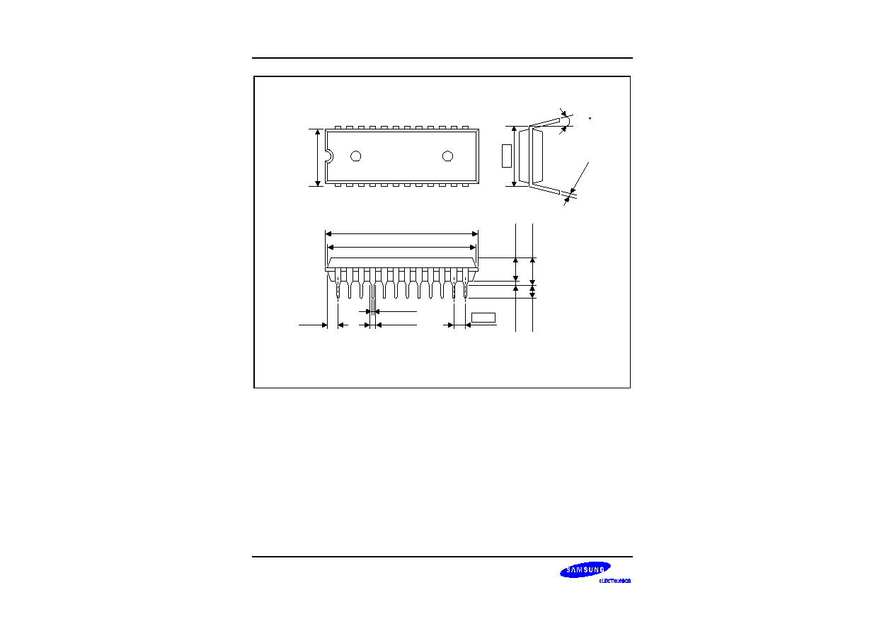
MECHANICAL DATA
S3P80C5/C80C5/C80C8
14-2
NOTE: Dimensions are in millimeters.
23.35 MAX
22.95
± 0.20
(1.70)
24-SDIP-300
6.40
±
0
.20
#24
#1
0.46 ±
0.10
0.89 ±
0.10
#13
#12
0-15
0.25
+ 0.10- 0.05
7.62
3.25
±
0.20
5.08 MAX
1.778
0.51 MIN
3.30
± 0.30
Figure 14-2. 24-Pin SDIP Package Mechanical Data

(For duplicate copies of this form, and for additional ordering information, please contact your local Samsung sales
representative. Samsung sales offices are listed on the back cover of this book.)
NOTE : Please one more check whether the selected device is S3C80A4/C80A8/C80A5 or S3C80B4/C80B8/C80B5.
S3C8 SERIES MASK ROM ORDER FORM
Product description:
Device Number: S3C80C5 S3C80C8
S3C__________- ___________(write down the ROM code number)
(note)
Product Order Form:
Package
Pellet Wafer
Package Type: __________
Package Marking (Check One):
Standard
Custom A
Custom B
(Max 10 chars)
(Max 10 chars each line)
@ : Assembly site code, Y : Last number of assembly year, WW : Week of assembly
@ YWW
Device Name
SEC
Device Name
@ YWW
@ YWW
Delivery Dates and Quantities:
Deliverable
Required Delivery Date
Quantity
Comments
ROM code
≠
Not applicable
See ROM Selection Form
Customer sample
Risk order
See Risk Order Sheet
Please answer the following questions:
F
F
For what kind of product will you be using this order?
New product
Upgrade of an existing product
Replacement of an existing product
Other
If you are replacing an existing product, please indicate the former product name
(
)
F
F
What are the main reasons you decided to use a Samsung microcontroller in your product?
Please check all that apply.
Price
Product quality
Features and functions
Development system
Technical support
Delivery on time
Used same micom before
Quality of documentation
Samsung reputation
Mask Charge (US$ / Won):
____________________________
Customer Information:
Company Name:
___________________ Telephone number
_________________________
Signatures:
________________________
__________________________________
(Person placing the order)
(Technical Manager)

(For duplicate copies of this form, and for additional ordering information, please contact your local Samsung
sales representative. Samsung sales offices are listed on the back cover of this book.)
NOTE : Please one more check whether the selected device is S3C80A4/C80A8/C80A5 or S3C80B4/C80B8/C80B5.
S3C8 SERIES
REQUEST FOR PRODUCTION AT CUSTOMER RISK
Customer Information:
Company Name:
________________________________________________________________
Department:
________________________________________________________________
Telephone Number:
__________________________
Fax: _____________________________
Date:
__________________________
Risk Order Information:
Device Number: S3C80C5 S3C80C8
S3C__________- ___________(write down the ROM code number)
(note)
Package:
Number of Pins: ____________
Package Type: _____________________
Intended Application:
________________________________________________________________
Product Model Number:
________________________________________________________________
Customer Risk Order Agreement:
We hereby request SEC to produce the above named product in the quantity stated below. We believe our risk
order product to be in full compliance with all SEC production specifications and, to this extent, agree to assume
responsibility for any and all production risks involved.
Order Quantity and Delivery Schedule:
Risk Order Quantity:
_____________________ PCS
Delivery Schedule:
Delivery Date (s)
Quantity
Comments
Signatures:
_______________________________
_______________________________________
(Person Placing the Risk Order) (SEC Sales Representative)


(For duplicate copies of this form, and for additional ordering information, please contact your local Samsung
sales representative. Samsung sales offices are listed on the back cover of this book.)
NOTE: Please one more check whether the selected device is S3P80A4/P80A8/P80A5 or S3P80B4/P80B8/P80B5.
S3C80C5/C80C8
MASK OPTION SELECTION FORM
Device Number: S3C80C5 S3C80C8
S3C8__________- ___________(write down the ROM code number)
(note)
Attachment (Check one):
Diskette
PROM
Customer Checksum:
________________________________________________________________
Company Name:
________________________________________________________________
Signature (Engineer):
________________________________________________________________
Please answer the following questions:
F
F
Application (Product Model ID: _______________________)
Audio
Video
Telecom
LCD Databank
Caller ID
LCD Game
Industrials
Home Appliance
Office Automation
Remocon
Other
Please describe in detail its application

(For duplicate copies of this form, and for additional ordering information, please contact your local Samsung
sales representative. Samsung sales offices are listed on the back cover of this book.)
NOTE: Please one more check whether the selected device is S3P80A4/P80A8/P80A5 or S3P80B4/P80B8/P80B5.
S3C8 SERIES OTP FACTORY WRITING ORDER FORM (1/2)
Product Description:
Device Number: S3P80C5
S3P8__________- ___________(write down the ROM code number)
(note)
Product Order Form:
Package
Pellet
Wafer
If the product order form is package:
Package Type: _____________________
Package Marking (Check One):
Standard
Custom A
Custom B
(Max 10 chars)
(Max 10 chars each line)
@ : Assembly site code, Y : Last number of assembly year, WW : Week of assembly
@ YWW
Device Name
SEC
Device Name
@ YWW
@ YWW
Delivery Dates and Quantity:
ROM Code Release Date
Required Delivery Date of Device
Quantity
Please answer the following questions:
F
F
What is the purpose of this order?
New product development
Upgrade of an existing product
Replacement of an existing microcontroller
Other
If you are replacing an existing microcontroller, please indicate the former microcontroller name
(
)
F
F
What are the main reasons you decided to use a Samsung microcontroller in your product?
Please check all that apply.
Price
Product quality
Features and functions
Development system
Technical support
Delivery on time
Used same micom before
Quality of documentation
Samsung reputation
Customer Information:
Company Name:
___________________ Telephone number
_________________________
Signatures:
________________________
__________________________________
(Person placing the order) (Technical Manager)


(For duplicate copies of this form, and for additional ordering information, please contact your local Samsung
sales representative. Samsung sales offices are listed on the back cover of this book.)
NOTE: Please one more check whether the selected device is S3P80A4/P80A8/P80A5 or S3P80B4/P80B8/P80B5.
S3C80C5/C80C8
OTP FACTORY WRITING ORDER FORM (2/2)
Device Number: S3P80C5
S3P8__________- ___________(write down the ROM code number)
(note)
Customer Checksums:
_______________________________________________________________
Company Name:
________________________________________________________________
Signature (Engineer):
________________________________________________________________
Read Protection
(1)
:
Yes
No
Please answer the following questions:
F
F
Are you going to continue ordering this device?
Yes
No
If so, how much will you be ordering? _________________pcs
F
F
Application (Product Model ID: _______________________)
Audio
Video
Telecom
LCD Databank
Caller ID
LCD Game
Industrials
Home Appliance
Office Automation
Remocon
Other
Please describe in detail its application
__________________________________________________________________________
NOTES
1.
Once you choose a read protection, you cannot read again the programming code from the EPROM.
2.
OTP Writing will be executed in our manufacturing site.
3.
The writing program is completely verified by a customer. Samsung does not take on any responsibility for errors
occurred from the writing program.

BOOK SPINE TEXT
SAMSUNG Logo S3P80C5/C80C5/C80C8 Microcontrollers User's Manual, Rev. 1 May 2002