 | –≠–ª–µ–∫—Ç—Ä–æ–Ω–Ω—ã–π –∫–æ–º–ø–æ–Ω–µ–Ω—Ç: S3C821A | –°–∫–∞—á–∞—Ç—å:  PDF PDF  ZIP ZIP |

S3C821A/P821A
PRODUCT OVERVIEW
1-1
1
PRODUCT OVERVIEW
S3C8-SERIES MICROCONTROLLES
Samsung's S3C8 series of 8-bit single-chip CMOS microcontrollers offers a fast and efficient CPU, a wide range
of integrated peripherals, and various mask-programmable ROM sizes. Among the major CPU features are:
-- Efficient register-oriented architecture
-- Selectable CPU clock sources
-- Idle and Stop power-down mode release by interrupt
-- Built-in basic timer with watchdog function
A sophisticated interrupt structure recognizes up to eight interrupt levels. Each level can have one or more
interrupt sources and vectors. Fast interrupt processing (within a minimum of six CPU clocks) can be assigned to
specific interrupt levels.
S3C821A/P821A MICROCONTROLLER
The S3C821A/P821A single-chip CMOS
microcontroller is fabricated using the highly
advanced CMOS process, based on Samsung's
newest CPU architecture.
The S3C821A is a microcontroller with a 48-Kbyte
mask-programmable ROM embedded.
The S3P821A is a microcontroller with a 48-Kbyte
one-time-programmable ROM embedded.
Using a proven modular design approach, Samsung
engineers have successfully developed the
S3C821A/P821A by integrating the following
peripheral modules with the powerful SAM8 core:
-- Six programmable I/O ports, including five 8-bit
ports and one 7-bit port, for a total of 47 pins.
-- Twelve bit-programmable pins for external
interrupts.
-- One 8-bit basic timer for oscillation stabilization
and watchdog functions (system reset).
-- One 8-bit timer/counter and one 16-bit
timer/counter with selectable operating modes.
-- Watch timer for real time.
-- 4-input A/D converter
-- Serial I/O interface
The S3C821A/P821A is versatile microcontroller for
cordless phone, pager, etc. They are currently
available in 80-pin TQFP and 80-pin QFP package.
OTP
The S3P821A is an OTP (One Time Programmable) version of the S3C821A microcontroller. The S3P821A
microcontroller has an on-chip 48-Kbyte one-time-programmable EPROM instead of a masked ROM. The
S3P821A is comparable to the S3C821A, both in function and in pin configuration.

PRODUCT OVERVIEW
S3C821A/P821A
1-2
FEATURES
CPU
∑
SAM8 CPU core
Memory
∑
Data memory: 1040-byte of internal register file
(Excluding LCD RAM)
∑
Program memory: 48-Kbyte internal program
memory (ROM)
External Interface
∑
64-Kbyte external data memory area
Instruction Execution Time
∑
750 ns at 8 MHz (minimum, Main oscillator)
∑
183
µ
s at 32,768 Hz (minimum, Sub oscillator)
Interrupts
∑
7 interrupt levels and 19 interrupt sources
∑
19 vectors
∑
Fast interrupt processing feature (for one
selected interrupt level)
I/O Ports
∑
Five 8-bit I/O ports (P0≠P4) and one 7-bit I/O
port (P5) for a total of 47 bit-programmable pins
8-Bit Basic Timer
∑
One programmable 8-bit basic timer (BT) for
oscillation stabilization control or watchdog timer
(software reset) function
Watch Timer
∑
Time internal generation: 3.91 ms, 0.5 s at
32,768 Hz
∑
Four frequency outputs to BUZ pin
∑
Clock source generation for LCD
Timers and Timer/Counters
∑
One 8-bit timer/counter (Timer 0) with three
operating modes: Interval, Capture, and PWM
∑
One 16-bit timer/counter (Timer 1) with two 8-bit
timer/counter modes
LCD Controller/Driver
∑
Up to 32 segment pins
∑
3, 4, and 8 common selectable
∑
Choice of duty cycle
∑
All dots can be switched on/off
∑
Internal resistor circuit for LCD bias
Serial Port
∑
One synchronous SIO
A/D Converter
∑
8-bit conversion resolution
◊
4 channel
∑
34
µ
s conversion time (4 MHz CPU clock, fxx/4)
Oscillation Sources
∑
Crystal, ceramic, or RC for main system clock
∑
Crystal or external oscillator for subsystem clock
∑
Main system clock frequency: 8 MHz
∑
Subsystem clock frequency: 32.768 kHz
Power-down Modes
∑
Main idle mode (only CPU clock stops)
∑
Sub idle mode
∑
Stop mode (main/sub system oscillation stops)
Operating Temperature Range
∑
≠ 40
∞
C to + 85
∞
C
Operating Voltage Range
∑
2.0 V to 5.5 V at 32 kHz (sub clock)-6 MHz
(main clock)
∑
2.2 V to 5.5 V at 8 MHz
Package Type
∑
80-pin TQFP, 80-pin QFP

S3C821A/P821A
PRODUCT OVERVIEW
1-3
BLOCK DIAGRAM
I/O PORT and INTERRUPT
CONTROL
SAM8 CPU
INTERNAL BUS
PORT 3
48-KB ROM
1-KBYTE
REGISTER
FILE
PORT 0
P1.0-P1.7
PORT 1
TIMER 0
SIO
PORT 4
P0.0-P0.7
LCD
DRIVER
COM0-COM3
SEG0-SEG3/
COM4-COM7
SEG4-SEG31
VLC1
T1CK
TA
TB
BUZ
SCK
SI
SO
WATCH
TIMER
RESET
MAIN
OSC
SUB
OSC
TIMER 1
A and B
A/D
CONVERTER
PORT 5
P2.0-P2.7
PORT 2
P3.0-P3.7
P4.0-P4.7
P5.0-P5.6
V
DD
1 (INTERNAL)
V
SS
1 (INTERNAL)
V
DD
2 (EXTERNAL)
V
SS
2 (EXTERNAL)
ADC0 -ADC3
AV
SS
AV
REF
T0CK
T0/T0CAP/
T0PWM
X
IN
X
OUT
X
IN
X
OUT
Figure 1-1. S3C821A Simplified Block Diagram
PRODUCT OVERVIEW
S3C821A/P821A
1-4
PIN ASSIGNMENTS
P1.1/SEG25/AD1
P1.2/SEG26/AD2
P1.3/SEG27/AD3
P1.4/SEG28/AD4
P1.5/SEG29/AD5
P1.6/SEG30/AD6
P1.7/SEG31/AD7
P2.0/
AS
P2.1/
DR
V
DD1
(INT)
V
SS1
X
OUT
X
IN
TEST
XT
IN
XT
OUT
RESET
P2.2/
DW
P2.3/
DM
P2.4/INT0/T0CK
S3C821A
(80-TQFP)
1
2
3
4
5
6
7
8
9
10
11
12
13
14
15
16
17
18
19
20
80
79
78
77
76
75
74
73
72
71
70
69
68
67
65
64
63
62
61
60
P2.5/INT1/T1CK
P2.6/INT2/TA
P2.7/INT3/TB
AV
REF
P3.0/ADC0
P3.1/ADC1
P3.2/ADC2
P3.3/ADC3
AV
SS
P3.4
P3.5
P3.6
P3.7/T0/T0PWM/T0CAP
P4.0/INT4
P4.1/INT5
P4.2/INT6
P4.3/INT7
P4.4/INT8
P4.5/INT9
P4.6/INT10
60
59
58
57
56
55
54
53
52
51
50
49
48
47
46
45
44
43
42
41
21
22
23
24
25
26
27
28
29
30
31
32
33
34
35
36
37
38
39
40
SEG4
SEG3/COM7
SEG2/COM6
SEG1/COM5
SEG0/COM4
COM3
COM2
COM1
COM0
V
DD2
(EXT)
V
SS2
V
LC1
P5.6
P5.5
P5.4
P5.3/BUZ
P5.2/SO
P5.1/SI
P5.0/SCK
P4.7/INT11
P1.0/SEG24/AD0
P0.7/SEG23/A15
P0.6/SEG22/A14
P0.5/SEG21/A13
P0.4/SEG20/A12
P0.3/SEG19/A11
P0.2/SEG18/A10
P0.1/SEG17/A9
P0.0/SEG16/A8
SEG15
SEG14
SEG13
SEG12
SEG11
SEG10
SEG9
SEG8
SEG7
SEG6
SEG5
Figure 1-2. S3C821A Pin Assignments (80-TQFP-1212)

S3C821A/P821A
PRODUCT OVERVIEW
1-5
P0.6/SEG22/A14
P0.5/SEG21/A13
P0.4/SEG20/A12
P0.3/SEG19/A11
P0.2/SEG18/A10
P0.1/SEG17/A9
P0.0/SEG16/A8
SEG15
SEG14
SEG13
SEG12
SEG11
SEG10
SEG9
SEG8
SEG7
P0.7/SEG23/A15
P1.0/SEG24/AD0
P1.1/SEG25/AD1
P1.2/SEG26/AD2
P1.3/SEG27/AD3
P1.4/SEG28/AD4
P1.5/SEG29/AD5
P1.6/SEG30/AD6
P1.7/SEG31/AD7
P2.0/
AS
P2.1/
DR
V
DD1
(INT)
V
SS1
X
OUT
X
IN
TEST
XT
IN
XT
OUT
RESET
P2.2/
DW
P2.3/
DM
P2.4/INT0/T0CK
P2.5/INT1/T1CK
P2.6/INT2/TA
S3C821A
(80-QFP)
64
63
62
61
60
59
58
57
56
55
54
53
52
51
50
49
48
47
46
45
44
43
42
41
1
2
3
4
5
6
7
8
9
10
11
12
13
14
15
16
17
18
19
20
21
22
23
24
80
79
78
77
76
75
74
73
72
71
70
69
68
67
66
65
25
26
27
28
29
30
31
32
33
34
35
36
37
38
39
40
P2.7/INT3/TB
AV
REF
P3.0/ADC0
P3.1/ADC1
P3.2/ADC2
P3.3/ADC3
AV
SS
P3.4
P3.5
P3.6
P3.7/T0/T0PWM/T0CAP
P4.0/INT4
P4.1/INT5
P4.2/INT6
P4.3/INT7
P4.4/INT8
SEG6
SEG5
SEG4
SEG3/COM7
SEG2/COM6
SEG1/COM5
SEG0/COM4
COM3
COM2
COM1
COM0
V
DD2
(EXT)
V
SS2
V
LC1
P5.6
P5.5
P5.4
P5.3/BUZ
P5.2/SO
P5.1/SI
P5.0/SCK
P4.7/INT11
P4.6/INT10
P4.5/INT9
Figure 1-3. S3C821A Pin Assignments (80-QFP-1420C)
PRODUCT OVERVIEW
S3C821A/P821A
1-6
PIN DESCRIPTIONS
Table 1-1. S3C821A Pin Descriptions
Pin
Names
Pin
Type
Pin
Description
Circuit
Type
Pin
Numbers
(note)
Share
Pins
P0.0≠P0.7
I/O
4-bit-programmable I/O port.
Pull-up resistors and open-drain outputs
are software assignable. Pull-up resistors
are automatically disabled for output
pins. Configurable as LCD segments/
external interface address and data lines
H-32
72≠79
(74-80, 1)
SEG16/A8
≠
SEG23/A15
P1.0≠1.7
I/O
4-bit-programmable I/O port.
Pull-up resistors and open-drain outputs
are software assignable. Pull-up resistors
are automatically disabled for output
pins. Configurable as LCD segments/
external interface address and data lines
H-32
80, 1≠7
(2-9)
SEG24/AD0
≠
SEG31/AD7
P2.0
P2.1
P2.2
P2.3
P2.4
P2.5
P2.6
P2.7
I/O
1-bit-programmable I/O port.
Pull-up resistors are software assignable,
and automatically disabled for output
pins. P2.0≠P2.3 can alternately be used
as external interface lines. P2.4≠P2.7 are
configurable as alternate functions or
external interrupts at falling edge with
noise filters.
D-4
8 (10)
9 (11)
18 (20)
19 (21)
20 (22)
21 (23)
22 (24)
23 (25)
AS
DR
DW
DM
INT0/T0CK
INT1/T1CK
INT2/TA
INT3/TB
P3.0≠P3.3
P3.4≠P3.6
P3.7
I/O
1-bit-programmable I/O port.
Pull-up resistors are software assignable,
and automatically disabled for output
pins. P3.0≠P3.3 can alternately be used
as ADC. P3.7 is configurable as an
alternate function.
F-16
D-4
D-4
25≠28
(27≠30)
30≠32
(32≠34)
33 (35)
ADC0≠ADC3
T0/T0PWM/
T0CAP
P4.0≠P4.7
I/O
1-bit-programmable I/O port.
Pull-up resistors and open-drain outputs
are software assignable. Pull-up resistors
are automatically disabled for output
pins. P4.0≠P4.7 are configurable as
external interrupts at a selectable edge
with noise filters.
E-4
34≠41
(36≠43)
INT4≠INT11
P5.0
P5.1
P5.2
P5.3
P5.4≠P5.6
I/O
1-bit-programmable I/O port.
Pull-up resistors are software assignable,
and automatically disabled for output
pins.
P5.0≠P5.3 are configurable as alternate
functions. If SCK and SI are used as
input, these pins have noise filters.
D-4
42 (44)
43 (45)
44 (46)
45 (47)
46≠48
(48≠50)
SCK
SI
SO
BUZ
NOTE: Parentheses indicate pin number for 80-QFP package.
S3C821A/P821A
PRODUCT OVERVIEW
1-7
Table 1-1. S3C821A Pin Descriptions (Continued)
Pin
Names
Pin
Type
Pin
Description
Circuit
Type
Pin
Numbers
(note)
Share
Pins
V
SS1
, V
DD1
≠
Power input pins for internal power block
≠
10, 11 (12, 13)
≠
X
OUT
,
X
IN
≠
Main oscillator pins
≠
12, 13 (14, 15)
≠
TEST
≠
Chip test input pin
Hold GND when the device is operating
≠
14 (16)
≠
XT
IN
, XT
OUT
≠
Sub oscillator pins for sub-system clock
≠
15, 16 (17,18)
≠
RESET
I
RESET
signal input pin. Schmitt trigger
input with internal pull-up resistor.
B
17 (19)
≠
INT0≠INT3
I/O
External interrupts input with noise filter.
D-4
20≠23 (22≠25)
P2.4≠P2.7
T0CK
I/O
8Bit Timer 0 external clock input.
D-4
20 (22)
P2.4
T1CK
I/O
Timer 1/A external clock input.
D-4
21 (23)
P2.5
TA
I/O
Timer 1/A clock output
D-4
22 (24)
P2.6
TB
I/O
Timer B clock output
D-4
23 (25)
P2.7
T0
I/O
Timer 0 clock output
D-4
33 (35)
P3.7
T0PWM
I/O
Timer 0 PWM output
D-4
33 (35)
P3.7
T0CAP
I/O
Timer 0 capture input
D-4
33 (35)
P3.7
ADC0≠ADC3
I/O
Analog input pins for A/D converts
module
F-16
25≠28 (27≠30)
P3.0≠P3.3
AV
REF
, AV
SS
≠
A/D converter reference voltage and
ground
≠
24, 29 (26, 31)
≠
INT4≠INT11
I/O
External interrupts input with noise filter.
E-4
34≠41 (36≠43)
P4.0≠P4.7
BUZ
I/O
Buzzer signal output
D-4
45 (47)
P5.3
SCK, SI, SO
I/O
Serial clock, serial data input, serial data
output
D-4
42≠44 (44≠46)
P5.0≠P5.2
V
LC1
≠
LCD bias voltage input pins
≠
49 (51)
≠
V
SS2
, V
DD2
≠
Power input pins for external power block
≠
50, 51 (52, 53)
≠
COM0≠COM3
O
LCD Common signal output
H-30
52≠55 (54≠57)
≠
SEG0≠SEG3
(COM4≠COM7)
O
LCD Common or Segment signal output
H-31
56≠59 (58≠61)
≠
SEG4≠SEG15
O
LCD segment signal output
H-29
60≠71 (62≠73)
≠
NOTE: Parentheses indicate pin number for 80-QFP package.
PRODUCT OVERVIEW
S3C821A/P821A
1-8
Table 1-1. S3C821A Pin Descriptions (Continued)
Pin
Names
Pin
Type
Pin
Description
Circuit
Type
Pin
Numbers
Share
Pins
SEG16≠
SEG23
I/O
LCD segment signal output
H-32
72≠79 (74≠80, 1)
P0.0≠P0.7
SEG24≠
SEG31
I/O
LCD segment signal output
H-32
80, 1≠7 (2≠9)
P1.0≠P1.7
A8≠A15
I/O
External interface address lines
H-32
72≠79 (74≠80, 1)
P0.0≠P0.7
AD0≠AD7
I/O
External interface address/data lines
H-32
80, 1≠7 (2≠9)
P1.0≠P1.7
AS
I/O
Address strobe
D-4
8 (10)
P2.0
DR
I/O
Data read
D-4
9 (11)
P2.1
DW
I/O
Data write
D-4
18 (20)
P2.2
DM
I/O
Data memory select
D-4
19 (21)
P2.3
NOTE: Parentheses indicate pin number for 80-QFP package.
S3C821A/P821A
PRODUCT OVERVIEW
1-9
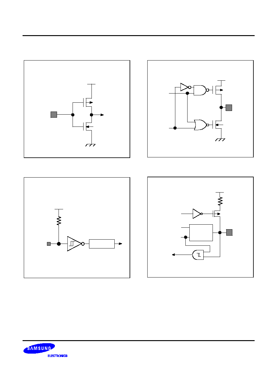
PIN CIRCUITS
V
DD
P
-
CHANNEL
N
-
CHANNEL
INPUT
Figure 1-4. Pin Circuit Type A
PULL-UP
RESISTOR
RESET
Noise Filter
V
DD
Figure 1-5. Pin Circuit Type B
OUTPUT
V
SS
DATA
OUTPUT
DISABLE
V
DD
Figure 1-6. Pin Circuit Type C
PULL-UP
ENABLE
DATA
OUTPUT
DISABLE
SCHMITT TRIGER
I/O
V
DD
CIRCUIT
TYPE C
Figure 1-7. Pin Circuit Type D-4
PRODUCT OVERVIEW
S3C821A/P821A
1-10
PULL-UP
RESISTOR
V
DD
I/O
V
SS
OPEN-DRAIN EN
PULL-UP
ENABLE
OUTPUT
DISABLE
V
DD
DATA
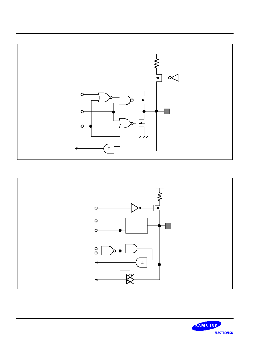
Figure 1-8. Pin Circuit Type E-4
PULL-UP
ENABLE
DATA
OUTPUT
DISABLE
I/O
V
DD
CIRCUIT
TYPE C
DATA
ADEN
ADSELECT
T0 ADC
Figure 1-9. Pin Circuit Type F-16

S3C821A/P821A
PRODUCT OVERVIEW
1-11
V
LC1
V
LC3
V
SS
V
LC4
OUTPUT
Figure 1-10. Pin Circuit Type H-29
V
LC1
V
LC2
V
SS
V
LC5
OUTPUT
Figure 1-11. Pin Circuit Type H-30
V
LC1
V
LC2
OUTPUT
V
LC3
V
LC4
V
LC5
V
SS
Figure 1-12. Pin Circuit Type H-31

PRODUCT OVERVIEW
S3C821A/P821A
1-12
PULL-UP
RESISTOR
V
DD
I/O
PULL-UP
ENABLE
V
SS
OUTPUT
DISABLE
V
DD
DATA
SEG
CIRCUIT
TYPE H-29
LCD OUT EN
OPEN-DRAIN EN
Figure 1-13. Pin Circuit Type H-32

S3C821A/P821A
ELECTRICAL DATA
17-1
17
ELECTRICAL DATA
OVERVIEW
In this section, S3C821A electrical characteristics are presented in tables and graphs. The information is
arranged in the following order:
-- Absolute maximum ratings
-- D.C. electrical characteristics
-- Data retention supply voltage in Stop mode
-- Stop mode release timing when initiated by an external interrupt
-- Stop mode release timing when initiated by a Reset
-- I/O capacitance
-- A.C. electrical characteristics
-- A/D converter electrical characteristics
-- Input timing for external interrupts (P4, P2.4≠P2.7)
-- Input timing for
RESET
-- Serial data transfer timing
-- Oscillation characteristics
-- Oscillation stabilization time
-- Operating voltage range
ELECTRICAL DATA
S3C821A/P821A
17-2
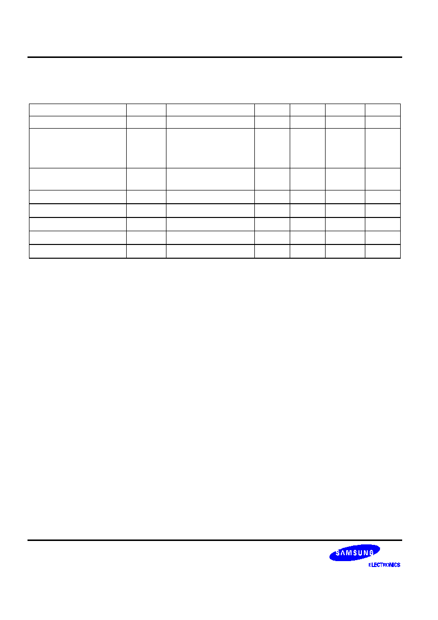
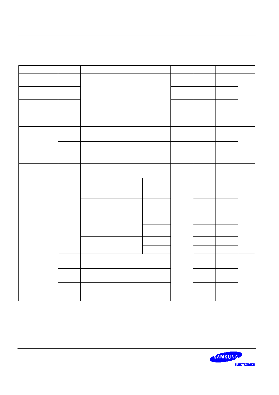
Table 17-1. Absolute Maximum Ratings
(T
A
= 25
∞
C)
Parameter
Symbol
Conditions
Rating
Unit
Supply voltage
V
DD
≠
≠ 0.3 to + 6.5
V
Input voltage
V
IN
All I/O ports
≠ 0.3 to
V
DD
+ 0.3
V
Output voltage
V
O
≠
≠ 0.3 to V
DD
+ 0.3
V
Output current High
I
OH
One I/O port active
≠ 18
mA
All I/O ports active
≠ 60
Output current Low
I
OL
One I/O port active
+ 30 (peak value)
mA
+ 15
(note)
Ports 0, 1, 2, and 3
+ 100 (peak value)
+ 60
(note)
Ports 4 and 5
+ 100 (peak value)
+ 60
(note)
Operating
temperature
T
A
≠
≠ 40 to + 85
∞
C
Storage temperature
T
STG
≠
≠ 65 to + 150
∞
C
NOTE: The values for Output Current Low (I
OL
) are calculated as Peak Value
◊
Duty .
S3C821A/P821A
ELECTRICAL DATA
17-3
Table 17-2. D.C. Electrical Characteristics
(T
A
= ≠ 40
∞
C to + 85
∞
C, V
DD
= 2.0 V to 5.5 V)
Parameter
Symbol
Conditions
Min
Typ
Max
Unit
Operating Voltage
V
DD
f
OSC
= 8 MHz
(Instruction clock = 1.33 MHz)
2.2
≠
5.5
V
f
OSC
= 6 MHz
(Instruction clock = 1 MHz)
2.0
Input High
voltage
V
IH1
P0 and P1
0.7 V
DD
≠
V
DD
V
V
IH2
RESET
, P2, P3, P4, and P5
0.8 V
DD
V
DD
V
IH3
X
IN
,
XT
IN
V
DD
≠ 0.1
V
DD
Input Low voltage
V
IL1
P0 and P1
0
≠
0.3 V
DD
V
IL2
RESET
, P2, P3, P4, and P5
0.2 V
DD
V
IL3
X
IN
,
XT
IN
0.1
Output High
voltage
V
OH
V
DD
= 3 V; I
OH
= ≠ 200
µ
A
All output pins
V
DD
≠ 1.0
≠
≠
Output Low
voltage
V
OL
V
DD
= 3 V; I
OL
= 1 mA
All output pins
≠
0.4
1.0
Input High
leakage current
I
LIH1
V
IN
= V
DD
All input pins except those specified
below for I
LIH2
≠
≠
1
µA
I
LIH2
V
IN
= V
DD
X
IN
,
X
OUT
,
XT
IN
,
and XT
OUT
20
Input Low
leakage current
I
LIL1
V
IN
= 0 V
All input pins except those specified
below for I
LIL2
and
RESET
≠
≠
≠ 1
I
LIL2
V
IN
= 0 V
X
IN
,
X
OUT
,
XT
IN
,
and XT
OUT
≠ 20
Output High
leakage current
I
LOH
V
OUT
= V
DD
All output pins
≠
≠
1
Output Low
leakage current
I
LOL
V
OUT
= 0 V
All output pins
≠
≠
≠ 1
|
V
DD
≠COMi
|
voltage drop
(i = 0≠7)
V
DC
V
DD
= 2.7 V to 5.5 V
≠ 15
µ
A per common pin
≠
≠
120
mV
|
V
DD
≠SEGx
|
voltage drop
(x = 0≠31)
V
DS
V
LCD
= 2.7 V to 5.5 V
≠ 15
µ
A per segment pin
≠
≠
120
ELECTRICAL DATA
S3C821A/P821A
17-4
Table 17-2. D.C. Electrical Characteristics (Continued)
(T
A
= ≠ 40
∞
C to + 85
∞
C, V
DD
= 2.0 V to 5.5 V)
Parameter
Symbol
Conditions
Min
Typ
Max
Unit
V
LC2
output
voltage
V
LC2
V
DD
= 2.7 V to 5.5 V
LCD clock = 0 Hz
0.8 V
DD
≠ 0.15
0.8 V
DD
0.8 V
DD
+ 0.15
V
V
LC3
output
voltage
V
LC3
V
LC1
= V
DD
0.6 V
DD
≠ 0.15
0.6 V
DD
0.6 V
DD
+ 0.15
V
LC4
output
voltage
V
LC4
0.4 V
DD
≠ 0.15
0.4 V
DD
0.4 V
DD
+ 0.15
V
LC5
output
voltage
V
LC5
0.2 V
DD
≠ 0.15
0.2 V
DD
0.2 V
DD
+ 0.15
Pull-up resistors
R
L1
V
IN
= 0 V; T
A
= 25
∞
C
V
DD
= 3.0
±
10 %; Ports 0≠5
30
80
200
k
R
L2
V
IN
= 0 V; T
A
= 25
∞
C
V
DD
= 3.0
±
10 %
RESET
only
200
450
800
LCD voltage
dividing resistor
R
LCD
V
LCD
= 2.7 V to 5.5 V
T
A
= 25
∞
C
45
65
80
k
Supply current
I
DD1
Run mode; V
DD
=5.0V
±
10%
6.0 MHz
≠
6.0
12
mA
(note)
Crystal oscillator
C1 = C2 = 22 pF
4.19 MHz
4.5
9.0
V
DD
= 3.0 V
±
10 %
6.0 MHz
2.9
5.8
4.19 MHz
2.0
4.0
I
DD2
Idle mode; V
DD
=5.0 V
±
0 %
6.0 MHz
1.3
2.6
Crystal oscillator
C1 = C2 = 22 pF
4.19 MHz
1.2
2.4
V
DD
= 3.0 V
±
10 %
6.0 MHz
0.6
1.2
4.19 MHz
0.4
0.8
I
DD3
Run mode; V
DD
= 3.0 V
±
10 %
32 kHz crystal oscillator
20
40
µA
I
DD4
Idle mode; V
DD
= 3.0 V
±
10 %
32 kHz crystal oscillator
7
14
I
DD5
Stop mode; V
DD
= 5.0 V
±
10 %
0.5
3
Stop mode; V
DD
= 3.0 V
±
10 %
0.3
2
NOTES:
1. Supply current does not include current drawn through internal pull-up resistors, LCD voltage dividing resistors, and
ADC.
2. I
DD1
and I
DD2
include power consumption for subsystem clock oscillation.
3. I
DD3
and I
DD4
are current when main system clock oscillation stops and the subsystem clock is used.
4. I
DD5
is current when main system clock and subsystem clock oscillation stops.
S3C821A/P821A
ELECTRICAL DATA
17-5
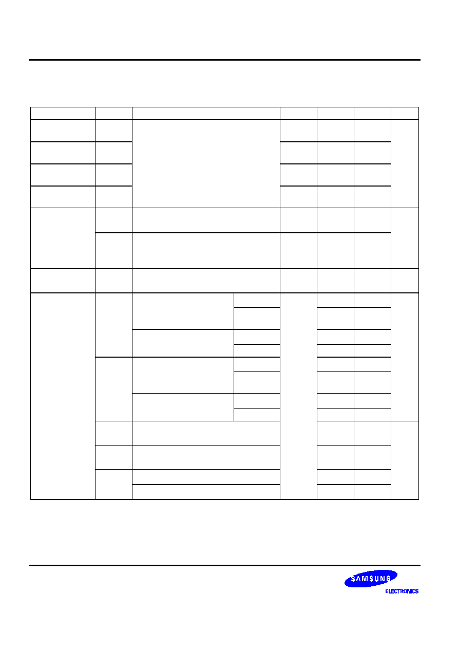
Table 17-3. Data Retention Supply Voltage in Stop Mode
(T
A
= ≠ 40
∞
C to + 85
∞
C)
Parameter
Symbol
Conditions
Min
Typ
Max
Unit
Data retention supply
voltage
V
DDDR
≠
2.2
≠
3.4
V
Data retention supply
current
I
DDDR
V
DDDR
= 1.0 V
Stop mode
≠
≠
1
µA
Oscillator stabilization
t
WAIT
Released by
RESET
≠
2
16
/fx
(1)
≠
ms
wait time
Released by interrupt
≠
(2)
≠
NOTES:
1.
fx
is the main oscillator frequency.
2.
The duration of the oscillation stabilization time (t
WAIT
) when it is released by an interrupt is determined by
the setting in the basic timer control register, BTCON.
V
DD
Interrupt Request
EXECUTION OF
STOP INSTRUCTION
V
DDDR
DATA RETENTION MODE
STOP MODE
NORMAL
OPERATING
MODE
t
WAIT
IDLE MODE
(Basic Timer active)
~~
0.8 V
DD
~~
Figure 17-1. Stop Mode Release Timing When Initiated by an External Interrupt
ELECTRICAL DATA
S3C821A/P821A
17-6
V
DD
RESET
EXECUTION OF
STOP INSTRUCTION
VDDDR
DATA RETENTION MODE
STOP MODE
NORMAL
OPERATING
MODE
tWAIT
OSCILLATION
STABILIZATION
TIME
RESET
OCCURS
0.2 V
DD
0.8 V
DD
~~
~~
Figure 17-2. Stop Mode Release Timing When Initiated by a
RESET
RESET
S3C821A/P821A
ELECTRICAL DATA
17-7
Table 17-4. Input/output Capacitance
(T
A
= ≠ 25
∞
C, V
DD
=
0 V)
Parameter
Symbol
Conditions
Min
Typ
Max
Unit
Input
capacitance
C
IN
f = 1 MHz; unmeasured pins
are connected to V
SS
≠
≠
10
pF
Output
capacitance
C
OUT
I/O capacitance
C
IO
Table 17-5. A.C. Electrical Characteristics
(T
A
= ≠ 40
∞
C to + 85
∞
C, V
DD
= 2.0 V to 5.5 V)
Parameter
Symbol
Conditions
Min
Typ
Max
Unit
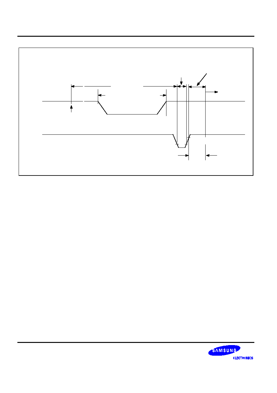
SCK cycle time
t
KCY
External SCK source
1,000
≠
≠
ns
Internal SCK source
1,000
SCK high, low
t
KH,
t
KL
External SCK source
500
width
Internal SCK source
t
KCY
/2≠50
SI setup time to
t
SIK
External SCK source
250
SCK high
Internal SCK source
250
SI hold time to
t
KSI
External SCK source
400
SCK high
Internal SCK source
400
Output delay for
t
KSO
External SCK source
≠
≠
300
ns
SCK to SO
Internal SCK source
250
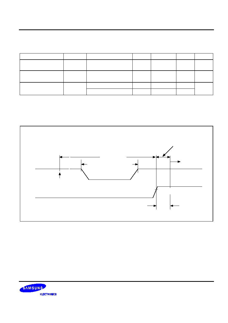
Interrupt input,
high, low width
t
INTH
,
t
INTL
All interrupt
V
DD
= 3 V
500
700
≠
ns
RESET
input low
width
t
RSL
Input
V
DD
= 3 V
2,000
≠
≠
ELECTRICAL DATA
S3C821A/P821A
17-8
Table 17-6. A/D Converter Electrical Characteristics
(T
A
= ≠ 40
∞
C to + 85
∞
C, V
DD
= 2.7 V to 5.5 V, V
SS
= 0 V)
Parameter
Symbol
Conditions
Min
Typ
Max
Unit
Resolution
≠
8
≠
bit
Total accuracy
V
DD
= 5.12 V
≠
≠
±
2
LSB
AV
REF
= 5.12 V
AV
SS
= 0 V
Conversion time
(1)
t
CON
8 bit conversion
34 x n/fxx
(2)
, n=1,4,8,16
17
≠
170
µ
s
Analog input voltage
V
IAN
≠
AV
SS
≠
AV
REF
V
Analog input impedance
R
AN
≠
2
1,000
≠
M
Analog reference voltage
AV
REF
≠
2.5
≠
V
DD
V
Analog ground
AV
SS
≠
V
SS
≠
V
SS
+ 0.3
V
Analog input current
I
ADIN
AV
REF
= V
DD
= 5V
≠
≠
10
µ
A
NOTES:
1.
"Conversion time" is the time required from the moment a conversion operation starts until it ends.
2.
fxx is a selected system clock for peripheral hardware.
S3C821A/P821A
ELECTRICAL DATA
17-9
0.8 V
DD
0.2 V
DD
t
INTL
t
INTH
NOTE: The unit t
CPU
means one CPU clock period.
Figure 17-3. Input Timing for External Interrupts
tRSL
0.2 V
DD
RESET
Figure 17-4. Input Timing for
RESET
RESET
SCK
t
KL
t
KH
t
KCY
0.8 V
DD
INPUT DATA
OUTPUT DATA
0.2 V
DD
0.8 V
DD
0.2 V
DD
SI
SO
t
KSO
t
SIK
t
KSI
Figure 17-5. Serial Data Transfer Timing
ELECTRICAL DATA
S3C821A/P821A
17-10
Table 17-7. Main System Oscillation Characteristics
(T
A
= ≠ 40
∞
C + 85
∞
C)
Oscillator
Clock Circuit
Parameter
Condition (V
DD
)
Min
Typ
Max
Unit
Crystal
C2
C1
X
IN
X
OUT
Main oscillation
frequency
2.2 V≠5.5 V
0.4
≠
8
MHz
2.0 V≠5.5 V
0.4
≠
6
Ceramic
C2
C1
X
IN
X
OUT
Main oscillation
frequency
2.2 V≠5.5 V
0.4
≠
8
2.0 V≠5.5 V
0.4
≠
6
External clock
X
IN
X
OUT
X
IN
input
frequency
2.2 V≠5.5 V
0.4
≠
8
2.0 V≠5.5 V
0.4
≠
6
RC
X
IN
X
OUT
R
Frequency
3.0 V
0.4
≠
2
Table 17-8. Subsystem Oscillation Characteristics
(T
A
= ≠ 40
∞
C + 85
∞
C)
Oscillator
Clock Circuit
Parameter
Condition (V
DD
)
Min
Typ
Max
Unit
Crystal
C2
C1
XT
IN
XT
OUT
Sub oscillation
frequency
2.0 V≠5.5 V
32
32.768
35
kHz
External clock
XT
IN
XT
OUT
XT
IN
input
frequency
2.0 V≠5.5 V
32
≠
500
kHz

S3C821A/P821A
ELECTRICAL DATA
17-11
Table 17-9. Main Oscillation Stabilization Time
(T
A
= ≠ 40
∞
C + 85
∞
C, V
DD
= 2.0 V to 5.5 V)
Oscillator
Test Condition
Min
Typ
Max
Unit
Crystal
fx > 400 kHz
≠
≠
20
ms
Ceramic
Oscillation stabilization occurs when V
DD
is equal
to the minimum oscillator voltage range.
≠
≠
10
ms
External clock
X
IN
input High and Low width (t
XH
, t
XL
)
25
≠
500
ns
X
IN
t
XL
t
XH
1 / f
x
V
DD
≠ 0.1 V
0.1 V
Figure 17-6. Clock Timing Measurement at X
IN
Table 17-10. Sub Oscillation Stabilization Time
(T
A
= ≠ 40
∞
C + 85
∞
C, V
DD
= 2.0 V to 5.5 V)
Oscillator
Test Condition
Min
Typ
Max
Unit
Crystal
≠
≠
≠
10
s
External clock
XT
IN
input High and Low width (t
XH
, t
XL
)
1
≠
18
µ
s
XT
IN
t
XTL
t
XTH
1 / f
xt
V
DD
≠ 0.1 V
0.1 V
Figure 17-7. Clock Timing Measurement at XT
IN

ELECTRICAL DATA
S3C821A/P821A
17-12
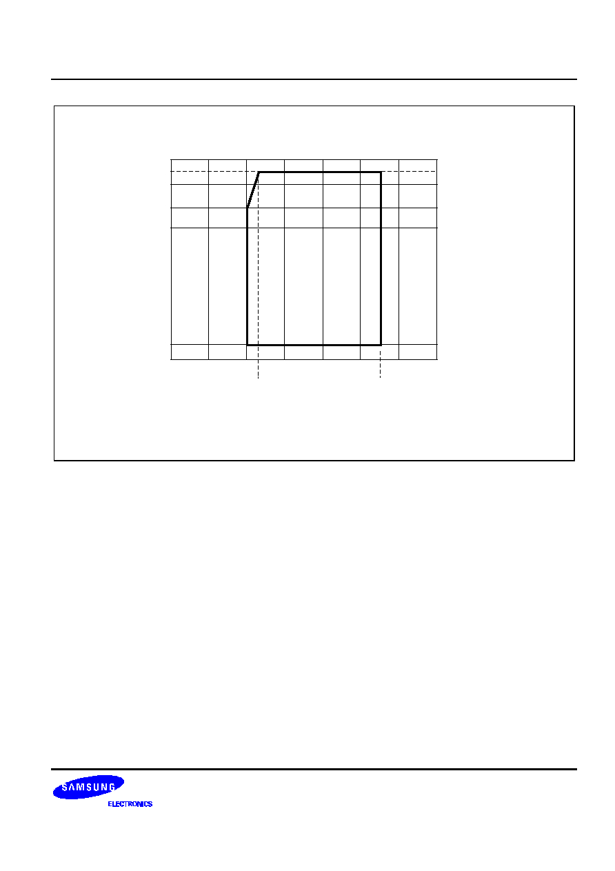
INSTRUCTION CLOCK = 1/6n x oscillator frequency (n = 1, 2, 8, 16)
SUPPLY VOLTAGE (V)
1.00 MHz
8.33 kHz
INSTRUCTION
CLOCK
2
3
7
f
x
(Main oscillation
frequency)
6 MHz
400 kHz
8 MHz
2.2
5.5
1.33 MHz
1
5
4
6
Figure 17-8. Operating Voltage Range
S3C821A/P821A
MECHANICAL DATA
18-1
18
MECHANICAL DATA
OVERVIEW
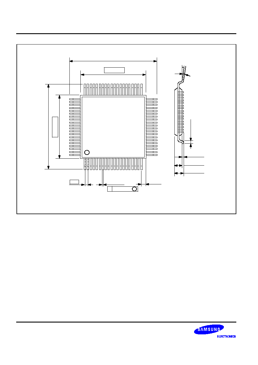
The S3C821A microcontroller is currently available in 80-pin QFP and TQFP package.
NOTE : Dimensions are in millimeters.
0.80
± 0.20
0.10 MAX
0.15
+0.10
- 0.05
0
-
8∞
2.65
± 0.10
3.00 MAX
0.05 MIN
17.90
± 0.3
14.00
± 0.2
(1.00)
80-QFP-1420C
23.90
± 0.3
#80
(0.80)
#1
0.35
± 0.1
±
0.15 MAX
20.00
± 0.2
0.80
0.80
± 0.20
Figure 18-1. 80-Pin QFP Package Demensions
MECHANICAL DATA
S3C821A/P821A
18-2
NOTE: Dimensions are in millimeters.
14.00BSC
12.00BSC
80-TQFP-1212
14.00BSC
12.00BSC
#80
(1.25)
#1
0.17
-
0.27
0.60
± 0.15
0.09
-
0.20
0
-
7∞
1.00
± 0.05
1.20 MAX
0.05-0.15
±
0.08 MAX M
0.50
Figure 18-2. 80-Pin TQFP Package Demensions

S3C821A/P821A
S3P821A OTP
20-1
20
S3P821A OTP
OVERVIEW
The S3P821A single-chip CMOS microcontroller is the OTP (One Time Programmable)
version of the S3C821A
microcontroller. It has an on-chip OTP ROM instead of a masked ROM. The EPROM is accessed by serial data
format.
The S3P821A is fully compatible with the S3C821A, both in function and in pin configuration. Because of its
simple programming requirements, the S3P821A is ideal as an evaluation chip for the S3C821A.
S3P821A OTP
S3C821A/P821A
20-2
P1.1/SEG25/AD1
P1.2/SEG26/AD2
P1.3/SEG27/AD3
P1.4/SEG28/AD4
P1.5/SEG29/AD5
P1.6/SEG30/AD6
P1.7/SEG31/AD7
SDAT/P2.0/
AS
SCLK/P2.1/
DR
V
DD1
/V
DD1
V
SS1
/V
SS1
X
OUT
X
IN
V
PP
/TEST
XT
IN
XT
OUT
RESET/RESET
P2.2/
DW
P2.3/
DM
P2.4/INT0/T0CK
S3P821A
(80-TQFP)
1
2
3
4
5
6
7
8
9
10
11
12
13
14
15
16
17
18
19
20
80
79
78
77
76
75
74
73
72
71
70
69
68
67
65
64
63
62
61
60
P2.5/INT1/T1CK
P2.6/INT2/TA
P2.7/INT3/TB
AV
REF
P3.0/ADC0
P3.1/ADC1
P3.2/ADC2
P3.3/ADC3
AV
SS
P3.4
P3.5
P3.6
P3.7/T0/T0PWM/T0CAP
P4.0/INT4
P4.1/INT5
P4.2/INT6
P4.3/INT7
P4.4/INT8
P4.5/INT9
P4.6/INT10
60
59
58
57
56
55
54
53
52
51
50
49
48
47
46
45
44
43
42
41
21
22
23
24
25
26
27
28
29
30
31
32
33
34
35
36
37
38
39
40
SEG4
SEG3/COM7
SEG2/COM6
SEG1/COM5
SEG0/COM4
COM3
COM2
COM1
COM0
V
DD2
(EXT)
V
SS2
V
LC1
P5.6
P5.5
P5.4
P5.3/BUZ
P5.2/SO
P5.1/SI
P5.0/SCK
P4.7/INT11
P1.0/SEG24/AD0
P0.7/SEG23/A15
P0.6/SEG22/A14
P0.5/SEG21/A13
P0.4/SEG20/A12
P0.3/SEG19/A11
P0.2/SEG18/A10
P0.1/SEG17/A9
P0.0/SEG16/A8
SEG15
SEG14
SEG13
SEG12
SEG11
SEG10
SEG9
SEG8
SEG7
SEG6
SEG5
Figure 20-1. S3P821A Pin Assignments (80-TQFP-1212 Package)
S3C821A/P821A
S3P821A OTP
20-3
P0.6/SEG22/A14
P0.5/SEG21/A13
P0.4/SEG20/A12
P0.3/SEG19/A11
P0.2/SEG18/A10
P0.1/SEG17/A9
P0.0/SEG16/A8
SEG15
SEG14
SEG13
SEG12
SEG11
SEG10
SEG9
SEG8
SEG7
P0.7/SEG23/A15
P1.0/SEG24/AD0
P1.1/SEG25/AD1
P1.2/SEG26/AD2
P1.3/SEG27/AD3
P1.4/SEG28/AD4
P1.5/SEG29/AD5
P1.6/SEG30/AD6
P1.7/SEG31/AD7
SDAT/P2.0/
AS
SCLK/P2.1/
DR
V
DD1
/V
DD1
V
SS1
/V
SS1
X
OUT
X
IN
V
PP
/TEST
XT
IN
XT
OUT
RESET
RESET/RESET
P2.2/
DW
P2.3/
DM
P2.4/INT0/T0CK
P2.5/INT1/T1CK
P2.6/INT2/TA
S3P821A
(80-QFP)
64
63
62
61
60
59
58
57
56
55
54
53
52
51
50
49
48
47
46
45
44
43
42
41
1
2
3
4
5
6
7
8
9
10
11
12
13
14
15
16
17
18
19
20
21
22
23
24
80
79
78
77
76
75
74
73
72
71
70
69
68
67
66
65
25
26
27
28
29
30
31
32
33
34
35
36
37
38
39
40
P2.7/INT3/TB
AV
REF
P3.0/ADC0
P3.1/ADC1
P3.2/ADC2
P3.3/ADC3
AV
SS
P3.4
P3.5
P3.6
P3.7/T0/T0PWM/T0CAP
P4.0/INT4
P4.1/INT5
P4.2/INT6
P4.3/INT7
P4.4/INT8
SEG6
SEG5
SEG4
SEG3/COM7
SEG2/COM6
SEG1/COM5
SEG0/COM4
COM3
COM2
COM1
COM0
V
DD2
(EXT)
V
SS2
V
LC1
P5.6
P5.5
P5.4
P5.3/BUZ
P5.2/SO
P5.1/SI
P5.0/SCK
P4.7/INT11
P4.6/INT10
P4.5/INT9
Figure 20-2. S3P821A Pin Assignments (80-QFP-1420C Package)

S3P821A OTP
S3C821A/P821A
20-4
Table 20-1. Descriptions of Pins Used to Read/Write the EPROM
Main Chip
During Programming
Pin Name
Pin Name
Pin No.
I/O
Function
P2.0
SDAT
8 (10)
I/O
Serial data pin. Output port when reading and
input port when writing. Can be assigned as a
Input/push-pull output port.
P2.1
SCLK
9 (11)
I/O
Serial clock pin. Input only pin.
V
PP
TEST
14 (16)
I
Power supply pin for EPROM cell writing
(indicates that OTP enters into the writing mode).
When 12.5 V is applied, OTP is in writing mode
and when 5 V is applied, OTP is in reading
mode. (Option)
RESET
RESET
17 (19)
I
Chip Initialization
V
DD1
/V
SS1
V
DD1
/V
SS1
10 (12)/11 (13)
≠
Logic power supply pin. V
DD
should be tied to + 5
V during programming.
NOTE: ( ) means 80 QFP package.
Table 20-2. Comparison of S3P821A and S3C821A Features
Characteristic
S3P821A
S3C821A
Program Memory
48-K byte EPROM
48-K byte mask ROM
Operating Voltage (V
DD
)
2.0 V to 5.5 V
2.0 V to 5.5 V
OTP Programming Mode
V
DD
= 5 V, V
PP
(TEST) = 12.5 V
Pin Configuration
80 QFP/80 TQFP
80 QFP/80 TQFP
EPROM Programmability
User Program 1 time
Programmed at the factory
OPERATING MODE CHARACTERISTICS
When 12.5 V is supplied to the V
PP
(TEST) pin of the S3P821A, the EPROM programming mode is entered. The
operating mode (read, write, or read protection) is selected according to the input signals to the pins listed in
Table 20-3 below.
Table 20-3. Operating Mode Selection Criteria
V
DD
V
PP
(
TEST
)
REG/
MEM
MEM
ADDRESS
(A15≠A0)
R/W
MODE
5 V
5 V
0
0000H
1
EPROM read
12.5 V
0
0000H
0
EPROM program
12.5 V
0
0000H
1
EPROM verify
12.5 V
1
0E3FH
0
EPROM read protection
NOTE: "0" means Low level; "1" means High level.

S3C821A/P821A
S3P821A OTP
20-5
Table 20-4. D.C. Electrical Characteristics
(T
A
= ≠ 40
∞
C to + 85
∞
C, V
DD
= 2.0 V to 5.5 V)
Parameter
Symbol
Conditions
Min
Typ
Max
Unit
Operating Voltage
V
DD
f
OSC
= 8 MHz
(Instruction clock = 1.33 MHz)
2.2
≠
5.5
V
f
OSC
= 6 MHz
(Instruction clock = 1 MHz)
2.0
Input High
voltage
V
IH1
P0 and P1
0.7 V
DD
≠
V
DD
V
V
IH2
RESET,
P2, P3, P4, and P5
0.8 V
DD
V
DD
V
IH3
X
IN
,
XT
IN
V
DD
≠ 0.1
V
DD
Input Low voltage
V
IL1
P0 and P1
0
≠
0.3 V
DD
V
IL2
RESET,
P2, P3, P4, and P5
0.2 V
DD
V
IL3
X
IN
,
XT
IN
0.1
Output High
voltage
V
OH
V
DD
= 3 V; I
OH
= ≠ 200
µ
A
All output pins
V
DD
≠ 1.0
≠
≠
Output Low
voltage
V
OL
V
DD
= 3 V; I
OL
= 1 mA
All output pins
≠
0.4
1.0
Input High
leakage current
I
LIH1
V
IN
= V
DD
All input pins except those specified
below for I
LIH2
≠
≠
1
µA
I
LIH2
V
IN
= V
DD
X
IN
,
X
OUT
,
XT
IN
,
and XT
OUT
20
Input Low
leakage current
I
LIL1
V
IN
= 0 V
All input pins except those specified
below for I
LIL2
and
RESET
≠
≠
≠ 1
I
LIL2
V
IN
= 0 V
X
IN
,
X
OUT
,
XT
IN
,
and XT
OUT
≠ 20
Output High
leakage current
I
LOH
V
OUT
= V
DD
All output pins
≠
≠
1
Output Low
leakage current
I
LOL
V
OUT
= 0 V
All output pins
≠
≠
≠ 1
|
V
DD
≠
COMi
|
voltage drop
(i = 0-7)
V
DC
V
DD
= 2.7 V to 5.5 V
≠ 15
µ
A per common pin
≠
≠
120
mV
|
V
DD
≠
SEGx
|
voltage drop
(x = 0-31)
V
DS
V
LCD
= 2.7 V to 5.5 V
≠ 15
µ
A per segment pin
≠
≠
120
S3P821A OTP
S3C821A/P821A
20-6
Table 20-4. D.C. Electrical Characteristics (Continued)
(T
A
= ≠ 40
∞
C to + 85
∞
C, V
DD
= 2.0 V to 5.5 V)
Parameter
Symbol
Conditions
Min
Typ
Max
Unit
V
LC2
output
voltage
V
LC2
V
DD
= 2.7 V to 5.5 V
LCD clock = 0 Hz
0.8 V
DD
≠ 0.15
0.8 V
DD
0.8 V
DD
+ 0.15
V
V
LC3
output
voltage
V
LC3
V
LC1
= V
DD
0.6 V
DD
≠ 0.15
0.6 V
DD
0.6 V
DD
+ 0.15
V
LC4
output
voltage
V
LC4
0.4 V
DD
≠ 0.15
0.4 V
DD
0.4 V
DD
+ 0.15
V
LC5
output
voltage
V
LC5
0.2 V
DD
≠ 0.15
0.2 V
DD
0.2 V
DD
+ 0.15
Pull-up resistors
R
L1
V
IN
= 0 V; T
A
= 25
∞
C
V
DD
= 3.0
±
10%; Ports 0≠5
30
80
200
k
R
L2
V
IN
= 0 V; T
A
= 25
∞
C
V
DD
= 3.0
±
10 %
RESET
only
300
500
800
LCD voltage
dividing resistor
R
LCD
V
LCD
= 2.7 V to 5.5 V
T
A
= 25
∞
C
45
65
80
k
Supply current
I
DD1
Run mode; V
DD
=5.0V
±
10%
6.0 MHz
≠
6.0
12
mA
(note)
Crystal oscillator
C1 = C2 = 22 pF
4.19 MHz
4.5
9.0
V
DD
= 3.0 V
±
10 %
6.0 MHz
2.9
5.8
4.19 MHz
2.0
4.0
I
DD2
Idle mode; V
DD
=5.0 V
±
0%
6.0 MHz
1.3
2.6
Crystal oscillator
C1 = C2 = 22 pF
4.19 MHz
1.2
2.4
V
DD
= 3.0 V
±
10 %
6.0 MHz
0.6
1.2
4.19 MHz
0.4
0.8
I
DD3
Run mode; V
DD
= 3.0 V
±
10 %
32 kHz crystal oscillator
20
40
µA
I
DD4
Idle mode; V
DD
= 3.0 V
±
10 %
32 kHz crystal oscillator
7
14
I
DD5
Stop mode; V
DD
= 5.0 V
±
10 %
0.5
3
Stop mode; V
DD
= 3.0 V
±
10 %
0.3
2
NOTES:
1.
Supply current does not include current drawn through internal pull-up resistors, LCD voltage dividing resistors, and
ADC.
2.
I
DD1
and I
DD2
include power consumption for subsystem clock oscillation.
3.
I
DD3
and I
DD4
are current when main system clock oscillation stops and the subsystem clock is used.
4.
I
DD5
is current when main system clock and subsystem clock oscillation stops.
S3C821A/P821A
S3P821A OTP
20-7
INSTRUCTION CLOCK = 1/6n x oscillator frequency (n = 1, 2, 8, 16)
SUPPLY VOLTAGE (V)
1.00 MHz
8.33 kHz
INSTRUCTION
CLOCK
2
3
7
f
x
(Main oscillation
frequency)
6 MHz
400 kHz
8 MHz
2.2
5.5
1.33 MHz
1
5
4
6
Figure 20-3. Operating Voltage Range