 | –≠–ª–µ–∫—Ç—Ä–æ–Ω–Ω—ã–π –∫–æ–º–ø–æ–Ω–µ–Ω—Ç: S3C8465 | –°–∫–∞—á–∞—Ç—å:  PDF PDF  ZIP ZIP |

S3C8465/C8469/P8469
PRODUCT OVERVIEW
1-1
1
PRODUCT OVERVIEW
SAM8 PRODUCT FAMILY
Samsung's new SAM8 family of 8-bit single-chip CMOS microcontrollers offers a fast and efficient CPU, a wide
range of integrated peripherals, and various mask-programmable ROM sizes.
A dual address/data bus architecture and a large number of bit- or nibble-configurable I/O ports provide a flexible
programming environment for applications with varied memory and I/O requirements. Timer/counters with
selectable operating modes are included to support real-time operations. Many SAM8 microcontrollers have an
external interface that provides access to external memory and other peripheral devices.
A sophisticated interrupt structure recognizes up to eight interrupt levels. Each level can have one or more
interrupt sources and vectors. Fast interrupt processing (within a minimum six CPU clocks) can be assigned to
one interrupt level at a time.
S3C8465/C8469 MICROCONTROLLER
The S3C8465/C8469 single-chip 8-bit microcontroller is designed for useful 10-bit resolution A/D converter,
UART, SIO, ZCD extended PWM application field. Its powerful SAM87 CPU architecture includes. The internal
register file is logically expanded to increase the on-chip register space.
The S3C8465/C8469 has 16/32K bytes of on-chip program ROM. A sophisticated bus interface enables access to
external memory and other peripherals when you use the chip in ROM-less mode. Following Samsung's modular
design approach, the following peripherals are integrated with the SAM87 core:
-- Large number of programmable I/O ports (total 56 pins)
-- One asynchronous UART module
-- One synchronous SIO module
-- Analog-to-digital converter with eight input channels and 10-bit resolution
-- One 8-bit basic timer for watchdog function
-- One 8-bit timer/counter with three operating modes (timer 0)
-- One 8-bit timer for zero-cross detection circuit (timer 2)
-- Two general-purpose 16-bit timer/counters with four operating modes (timer module 1)
-- PWM block with one capture module, 16-bit timer/counter, PWM extension mode, and two PWM outputs
-- One zero cross detection module
The S3C8465/C8469 is a versatile general-purpose microcontroller that is ideal for use in a wide range of
electronics applications requiring complex timer/counter, PWM, capture, SIO, UART and ZCD functions.
It is available in a 64-pin SDIP or 64-pin QFP package.
OTP
The S3P8469 is an OTP (One Time Programmable) version of the S3C8465/C8469 microcontroller. The
S3P8469 microcontroller has an on-chip 32-Kbyte one-time-programmable EPROM instead of a masked ROM.
The S3P8469 is comparable to the S3C8465/C8469, both in function and in pin configuration.

PRODUCT OVERVIEW
S3C8465/C8469/P8469
1-2
FEATURES
CPU
∑
SAM87 CPU core
Memory
∑
528-byte general purpose register area
∑
16/32K-byte internal program memory
∑
ROM-less operating mode
External Interface
∑
64K-byte external data memory area
∑
64K-byte external program memory area
(ROM-less mode)
Instruction Set
∑
79 instructions
∑
IDLE and STOP instructions added for
power-down modes
Instruction Execution Time
∑
500 ns at 12 MHz f
OSC
(minimum)
Interrupts
∑
21 interrupt sources and 21 vectors
∑
Eight interrupt levels
∑
Fast interrupt processing
General I/O
∑
Seven I/O ports (total 56 pins)
∑
Seven bit-programmable ports
PWM and Capture
∑
Two 14-bit PWM output
∑
One capture
Serial I/O
∑
One synchronous serial I/O module
∑
Selectable transmit and receive rates
∑
Selectable baud rate for Rx and Tx respectively
Timer/Counters
∑
One 8-bit basic timer for watchdog function
∑
One 8-bit timer/counter with three operating
modes (timer 0)
∑
One 8-bit timer for the zero-cross detection
circuit
∑
Two 16-bit general-purpose timer/counters with
four operating modes (timer C and D)
UART
∑
One UART module
∑
Full duplex serial I/O interface with three UART
modes
A/D Converter
∑
Eight analog input pins
∑
10-bit conversion resolution
∑
20 µs conversion time (10 MHz CPU clock)
Zero Cross Detection Circuit
∑
Zero cross detection circuit that generates a
digital signal in synchronization with an AC
signal input
Buzzer Frequency Output
∑
200 Hz to 20 kHz signal can be generated
Oscillator Frequency
∑
1 MHz to 12 MHz external crystal oscillator
∑
Maximum 12 MHz CPU clock
Operating Temperature Range
∑
≠ 40
∞
C to + 85
∞
C
Operating Voltage Range
∑
2.7 V to 5.5 V
Package Types
∑
64-pin SDIP, 64-pin QFP
S3C8465/C8469/P8469
PRODUCT OVERVIEW
1-3
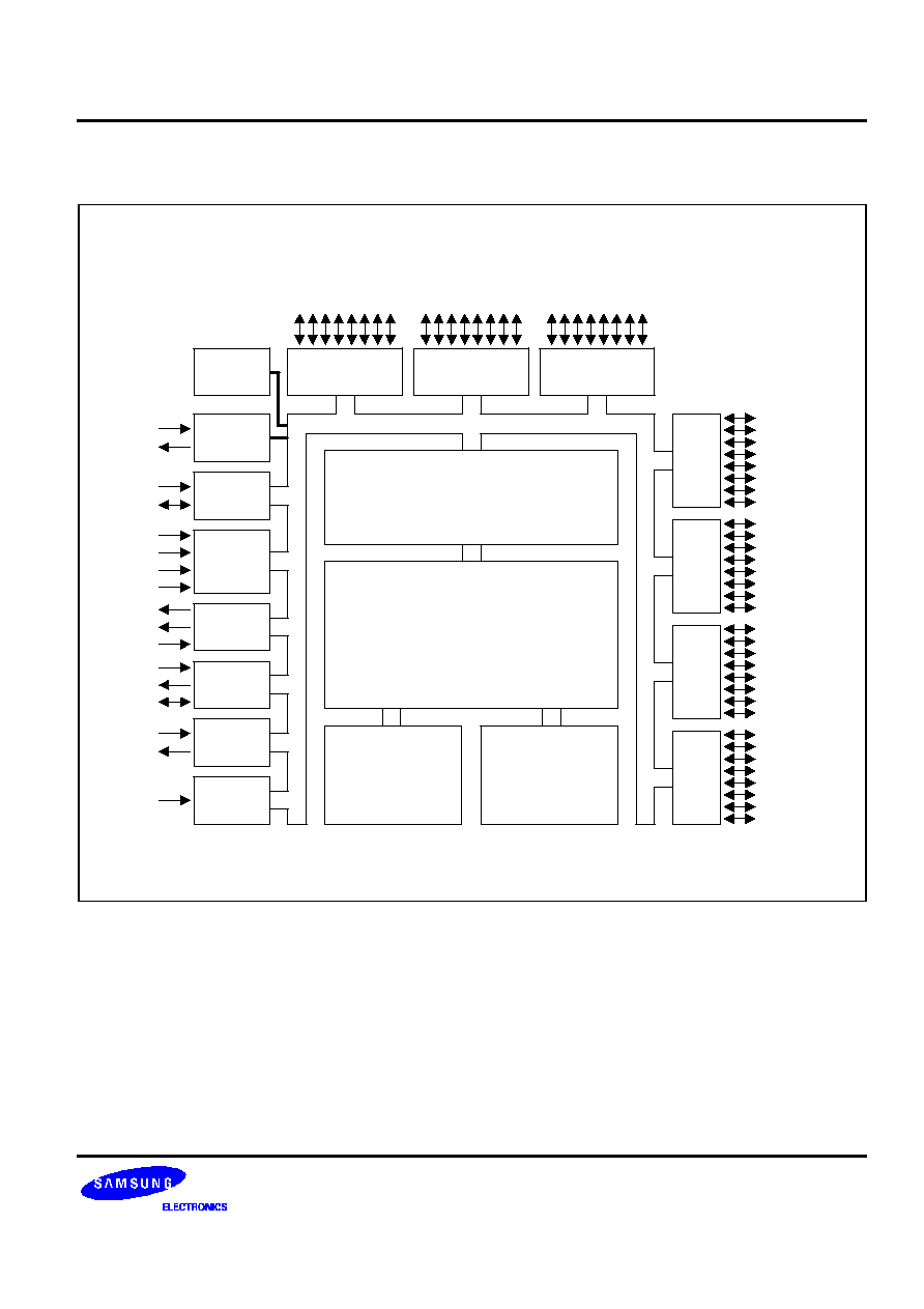
BLOCK DIAGRAM
Port I/O and Interrupt
Control
SAM8 CPU
Basic
Timer
Port 1
Port 0
Port 0
P0.0-P0.7
(A8-A15)
16/32-Kbyte
ROM
528-byte
Register File
P3.0-P3.7
Port 3
P4.0/INT4-
P4.7/INT11
Port 4
P5.0-P5.7
Port 5
P6.0-P6.7
Port 6
ADC0
-ADC7
ADC
TxD
RxD
UART
SIO
PWM/
CAP
Timers
C and D
TCG
X
OUT
X
IN
OSC
T0
T0CK
Timer
TCCK
TDCK
TDG
PWM1
CAPA
PWM0
SO
SCK
SI
SAM8 BUS
P1.0-P1.7
(AD0-AD7)
P2.0-P2.3
P2.4/ZCD-P2.7/INT3
Figure 1-1. Block Diagram
PRODUCT OVERVIEW
S3C8465/C8469/P8469
1-4
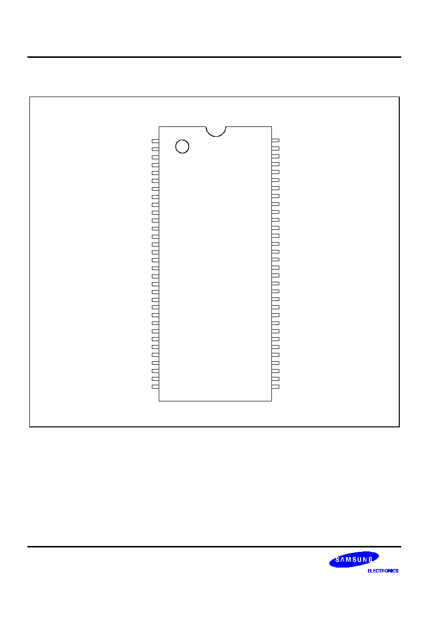
PIN ASSIGNMENTS
P0.7/A15
P0.6/A14
P0.5/A13
P0.4/A12
P0.3/A11
P0.2/A10
P0.1/A9
P0.0/A8
P4.7/INT11/TDG
P4.6/INT10/TCG
P4.5/INT9/TDCK
P4.4/INT8/TCCK
P4.3/INT7/CAPA
P4.2/INT6
P4.1/INT5/RxD
V
DD
V
SS
X
OUT
X
IN
EA
P4.0/INT4
P3.7/TxD
RESET
P3.6/SO
P3.5/SI
P3.4/
SCK
P3.3/T0CK
P3.2/T0
P3.1/PWM1
P3.0/PWM0
P2.7/INT3
P2.6/INT2
S3C8465
S3C8469
64-SDIP-750
(Top View)
1
2
3
4
5
6
7
8
9
10
11
12
13
14
15
16
17
18
19
20
21
22
23
24
25
26
27
28
29
30
31
32
P1.0/AD0
P1.1/AD1
P1.2/AD2
P1.3/AD3
P1.4/AD4
P1.5/AD5
P1.6/AD6
P1.7/AD7
P5.7/ADC7
P5.6/ADC6
P5.5/ADC5
P5.4/ADC4
P5.3/ADC3
P5.2/ADC2
P5.1/ADC1
P5.0/ADC0
AV
SS
AV
REF
P6.7
P6.6
P6.5
P6.4
P6.3
P6.2
P6.1
P6.0
P2.0/
AS
P2.1/
DS
P2.2/R/
W
P2.3/
DM
P2.4/ZCD
P2.5/BUZ
64
63
62
61
60
59
58
57
56
55
54
53
52
51
50
49
48
47
46
45
44
43
42
41
40
39
38
37
36
35
34
33
Figure 1-2. Pin Assignment Diagram (64-SDIP)
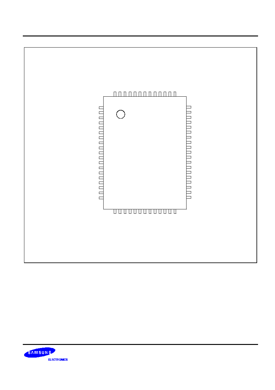
S3C8465/C8469/P8469
PRODUCT OVERVIEW
1-5
P0.0/A8
P4.7/INT11/TDG
P4.6/INT10/TCG
P4.5/INT9/TDCK
P4.4/INT8/TCCK
P4.3/INT7CAPA
P4.2/INT6
P4.1/INT5/RxD
V
DD
V
SS
X
OUT
X
IN
EA
P4.0/INT4
P3.7/TxD
RESET
P3.6/SO
P3.5/SI
P3.4/
SCK
S3C8465/C8469
64-QFP-1420F
(Top View)
1
2
3
4
5
6
7
8
9
10
11
12
13
14
15
16
17
18
19
P0.1/A9
P0.2/A10
P0.3/A11
P0.4/A12
P0.5/A13
P0.6/A14
P0.7/A15
P1.0/AD0
P1.1/AD1
P1.2/AD2
P1.3/AD3
P1.4/AD4
P1.5/AD5
64
63
62
61
60
59
58
57
56
55
54
53
52
P3.3/T0CK
P3.2/T0
P3.1/PWM1
P3.0/PWM0
P2.7/INT3
P2.6/INT2
P2.5/BUZ
P2.4/ZCD
P2.3/
DM
P2.2/R/
W
P2.1/
DS
P2.0/
AS
P6.0
20
21
22
23
24
25
26
27
28
29
30
31
32
51
50
49
48
47
46
45
44
43
42
41
40
39
38
37
36
35
34
33
P1.6/AD6
P1.7/AD7
P5.7/ADC7
P5.6/ADC6
P5.5/ADC5
P5.4/ADC4
P5.3/ADC3
P5.2/ADC2
P5.1/ADC1
P5.0/ADC0
AV
SS
AV
REF
P6.7
P6.6
P6.5
P6.4
P6.3
P6.2
P6.1
Figure 1-3. Pin Assignment Diagram (64-Pin QFP Package)
PRODUCT OVERVIEW
S3C8465/C8469/P8469
1-6
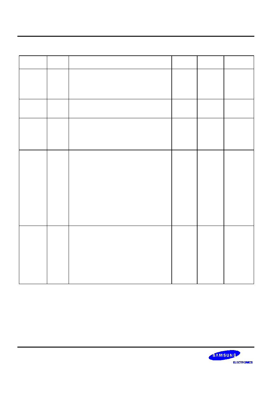
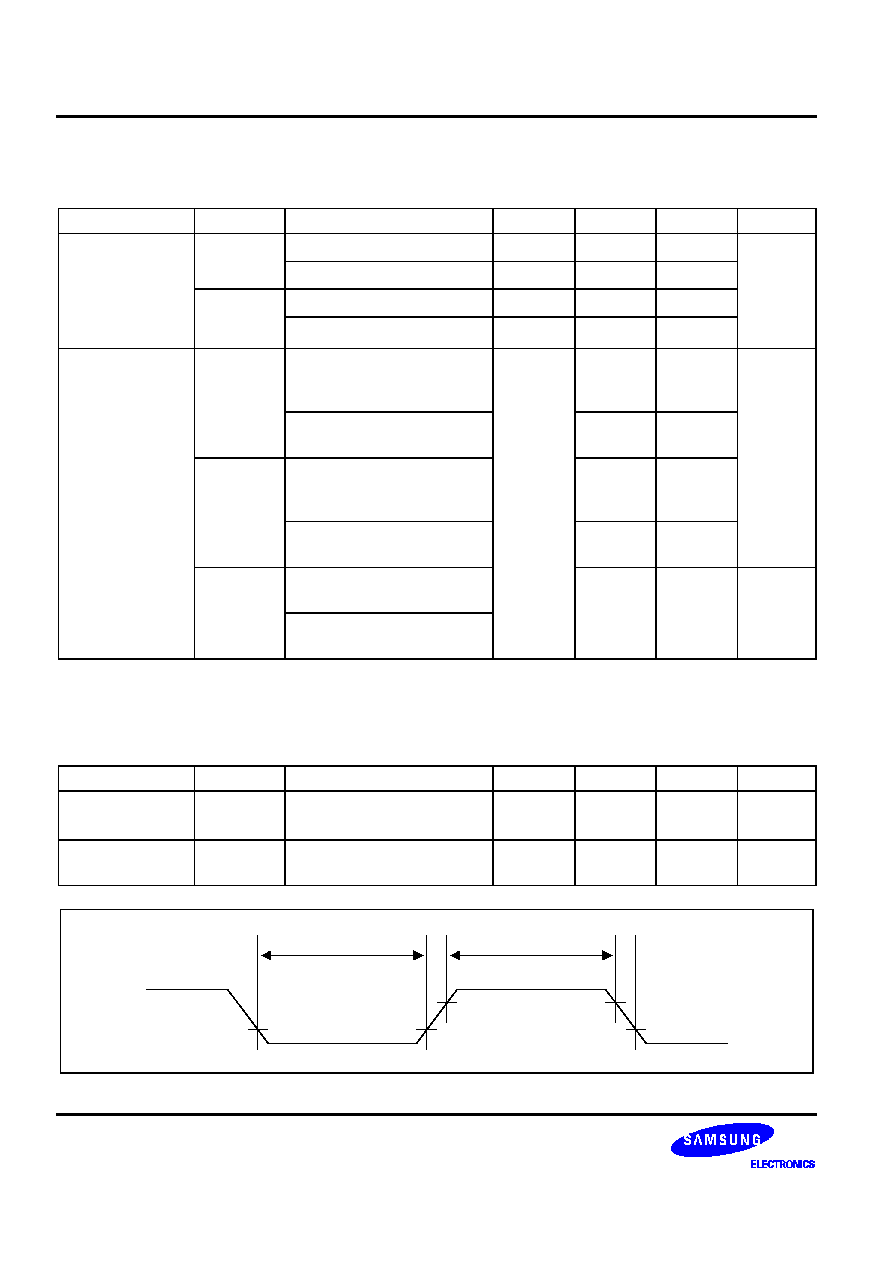
Table 1-1. S3C8465/C8469 Pin Descriptions
Pin
Name
Pin
Type
Pin Description
Circuit
Number
Pin
Number
Share
Pins
P0.0≠P0.7
I/O
Bit-programmable I/O port for Schmitt trigger
input or push-pull, open-drain, output. Pull-up
resistors are assignable by software.
Port 0 can also be configured as external
interface address line A8≠A15
1
8≠1
(1, 64≠58)
≠
A8≠A15
P1.0≠P1.7
I/O
Same general characteristics as port 0.
Port 1 can also be configured as external
interface address/data lines AD0≠AD7
1
64≠57
(57≠50)
≠
AD0≠AD7
P2.0≠P2.3
P2.4≠P2.7
I/O
Bit-programmable I/O port for Schmitt trigger
input or push-pull output. P2.0≠P2.3 can be
configured for external bus control signals.
P2.4≠P2.7 are used for general I/O or for the
ZCD, BUZ, INT2 and INT3
2
3
38≠35
(31≠28)
34≠31
(27≠24)
≠
AS, DS
DM, R/W
ZCD, BUZ
INT2, INT3
P3.0≠P3.7
I/O
Bit-programmable I/O port for Schmitt trigger
input or push-pull output. Each port 3 pin has
an alternative function:
P3.0: PWM0 (PWM0 module output)
P3.1: PWM1 (PWM1 module ouptut)
P3.2: T0 (T0 capture input or PWM output)
P3.3: T0CK (timer 0 external clock input)
P3.4:
SCK
(SIO module input)
P3.5: SI (SIO module clock I/O)
P3.6: SO (SIO module output)
P3.7: TxD: SO1
(The T0 function for P3.2 is selected using the
T0CON register.)
4
30≠22
(23≠15)
(See pin
description)
P4.0≠P4.7
I/O
Bit-programmable I/O port for Schmitt trigger
input or push-pull output. Port 4 pins are used
external interrupts INT4≠INT11 or for the
following share functions:
P4.1: RxD (UART module input)
P4.3: CAPA (capture input)
P4.4: TCCK (timer/counter C clock input)
P4.5: TDCK (timer/counter D clock input)
P4.6: TCG (timer C gate input)
P4.7: TDG (timer D gate input)
5
21, 15≠9
(14≠2)
(See pin
description)
S3C8465/C8469/P8469
PRODUCT OVERVIEW
1-7
Table 1-1. S3C8465/C8469 Pin Descriptions (Continued)
Pin
Name
Pin
Type
Pin Description
Circuit
Number
Pin
Number
Share
Pins
P5.0≠P5.7
I/O
Bit-programmable I/O port for Schmitt trigger
input or push-pull, output. Pull-up resistors are
assignable by software. Port 5 pins can also be
used as A/D converter inputs.
6
49≠56
(42≠49)
ADC0≠
ADC7
P6.0≠P6.7
I/O
Individual pins are software configurable as
input or push-pull, open-drain, output. Pull-up
resistors are assignable by software.
1
39≠46
(32≠39)
≠
AD0≠AD7
I/O
External interface address/data line
6
64≠57
(57≠50)
P1.0≠P1.7
AS
DS
R/
W
DM
I/O
External bus control signals
2
38≠35
(31≠28)
P2.0≠P2.3
ZCD
I/O
Zero cross detector input
2
34 (27)
P2.4
BUZ
I/O
200 Hz≠20 kHz frequency output for buzzer
sound
2
33 (26)
P2.5
PWM0
PWM1
I/O
PWM output
3
30, 29
(23, 22)
P3.0≠P3.1
T0 (CAP)
I/O
T0 capture input or PWM output
3
28 (21)
P3.2
T0CK
I/O
External clock input for Timer 0
3
27 (20)
P3.3
SCK
I/O
SIO clock signal
3
26 (19)
P3.4
SI, SO
I/O
SIO data input/output
3
25, 24
(18, 17)
P3.5≠P3.6
TxD
I/O
UART data output
3
22 (15)
P3.7
INT2≠INT3
I/O
External interrupts: the triggering edge is
selectable.
2
32, 31
(25, 24)
P2.6≠P2.7
INT4
I/O
External interrupts: the triggering edge is
selectable.
4
21 (14)
P4.0
RxD/INT5
I/O
UART data input or external interrupt: the
triggering edge is selectable.
4
15 (8)
P4.1
INT6
CAPA/INT7
I/O
Capture module input or external interrupt: the
triggering edge is selectable.
4
14,13
(7, 6)
P4.2≠P4.3
PRODUCT OVERVIEW
S3C8465/C8469/P8469
1-8
Table 1-1. S3C8465/C8469 Pin Descriptions (Concluded)
Pin
Name
Pin
Type
Pin Description
Circuit
Number
Pin
Number
Share
Pins
TCCK/INT8
TCDK/INT9
I/O
Timer/counter C and D clock input or external
interrupts: the triggering edge is selectable.
4
12, 11
(5, 4)
P4.4≠P4.5
TCG/INT10
TDG/INT11
I/O
Timer/counter C and D clock input or external
interrupts: the triggering edge is selectable.
4
10, 9
(3, 2)
P4.6≠P4.7
ADC0≠
ADC7
I/O
A/D converter inputs
5
49≠56
(42≠49)
P5.0≠P5.7
X
IN
, X
OUT
≠
System clock input and output pins
≠
19, 18
(12, 11)
≠
RESET
I
System reset pin
7
23 (16)
≠
EA
I
External access (EA) pin with three modes:
0 V: Normal operation (internal ROM)
5 V: ROM-less operation (external interface)
12.5 V: OTP read/write mode
≠
20 (13)
≠
AV
REF
,
AV
SS
≠
A/D converter reference voltage input and
ground
≠
47, 48
(40, 41)
≠
V
DD
,V
SS
≠
Voltage input pin and ground
≠
16, 17
(9, 10)
≠
NOTE: Pin numbers shown in parentheses "( )" are for the 64-pin QFP package.
S3C8465/C8469/P8469
PRODUCT OVERVIEW
1-9
PIN CIRCUITS
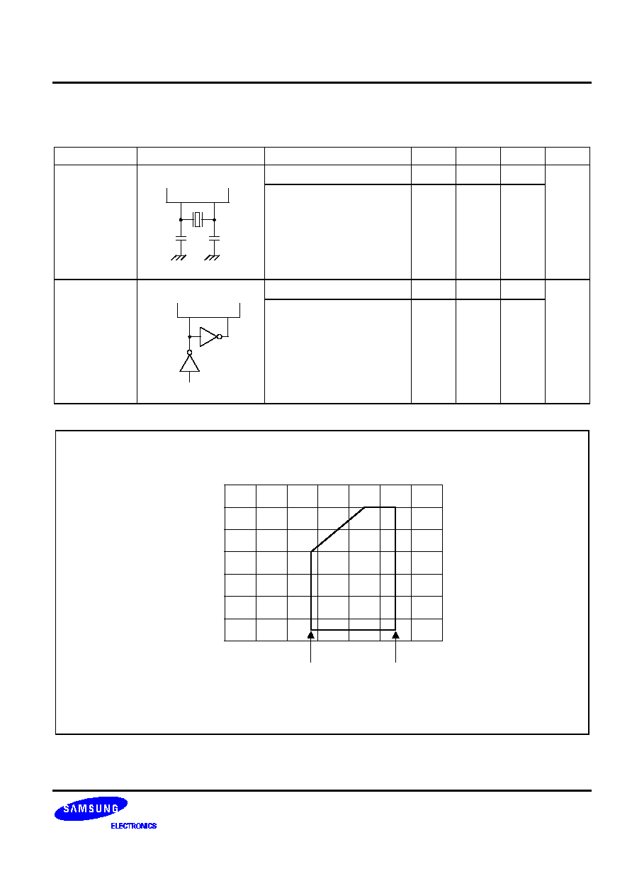
Table 1-2. Pin Circuit Assignments for the S3C8465/C8469
Circuit Number
Circuit Type
S3C8465/C8469 Assignments
1
I/O
Port 0,1 and port 6
2
I/O
Port 2 (P2.0≠P2.3 only)
3
I/O
Port 2 (P2.4≠P2.7 only)
4
I/O
Port 3
5
I/O
Port 4
6
I/O
Port 5
7
I
RESET
NOTE: Diagrams of circuit types 1≠7 are presented below.
PRODUCT OVERVIEW
S3C8465/C8469/P8469
1-10
V
DD
Open-drain
In/Out
In
Output DIsable
Pull-up Resistor
(Typical Value: 47 K
)
V
DD
Data
Pull-up
Enable
Figure 1-4. Pin Circuit Type 1 (Port 0,1 and Port 6)
V
DD
Pull-up Resistor
(Typical Value: 47 K
)
V
DD
Pull-up
Enable
External Interface
(
AS
,
DS
, R/
W
,
DM
)
Port 2 (Low Byte) Data
M
U
X
Select
In
Output DIsable
In/Out
Data
Figure 1-5. Pin Circuit Type 2 (Port 2, P2.0≠P2.3 only)
S3C8465/C8469/P8469
PRODUCT OVERVIEW
1-11
External
Interrupt Input
V
DD
Pull-up Resistor
(Typical Value: 47 K
)
V
DD
Pull-up
Enable
Control Output (BUZ)
Port 2 (High Byte) Data
M
U
X
Select
Output DIsable
In/Out
Noise Filter
Normal
Input
ZCD Input
Figure 1-6. Pin Circuit Type 3 (Port 2, P2.4≠P2.7 only)
PRODUCT OVERVIEW
S3C8465/C8469/P8469
1-12
V
DD
Pull-up Resistor
(Typical Value: 47 K
)
V
DD
Pull-up
Enable
Control
Output
Port 3
M
U
X
Select
Normal
Input
Output
DIsable
In/Out
Data
Figure 1-7. Pin Circuit Type 4 (Port 3)
External
Interrupt Input
V
DD
Pull-up Resistor
(Typical Value: 47 K
)
V
DD
Pull-up
Enable
Data
Output
DIsable
In/Out
Noise Filter
Alternative
Input
Normal
Input
Figure 1-8. Pin Circuit Type 5 (Port 4)
S3C8465/C8469/P8469
PRODUCT OVERVIEW
1-13
V
DD
Pull-up Resistor
(Typical Value: 47 K
)
V
DD
Pull-up
Enable
Data
Normal
Input
Output
DIsable
In/Out
Analog
Input
Figure 1-9. Pin Circuit Type 6 (Port 5)
RESET
Pull-up Resistor
(Typical Value: 200 K
)
V
DD
Figure 1-10. Pin Circuit Type 7 (
RESET
RESET
)

S3C8465/C8469/P8469
ELECTRICAL DATA
19-1
19
ELECTRICAL DATA
OVERVIEW
In this chapter, S3C8465/C8469 electrical characteristics are presented in tables and graphs. The information is
arranged in the following order:
-- Absolute maximum ratings
-- Input/output capacitance
-- D.C. electrical characteristics
-- A.C. electrical characteristics
-- Oscillation characteristics
-- Oscillation stabilization time
-- Data retention supply voltage in stop mode
-- Serial I/O timing characteristics
-- UART timing characteristics in mode 0
-- A/D converter electrical characteristics
-- Zero crossing detector
-- External memory timing characteristics
ELECTRICAL DATA
S3C8465/C8469/P8469
19-2
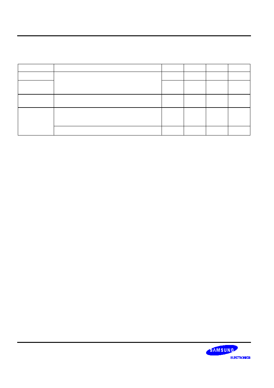
Table 19-1. Absolute Maximum Ratings
(T
A
= 25
∞
C)
Parameter
Symbol
Conditions
Rating
Unit
Supply Voltage
V
DD
≠
≠ 0.3 to + 6.5
V
Input Voltage
V
I
All input ports
≠ 0.3 to V
DD
+ 0.3
V
Output Voltage
V
O
All output ports
≠ 0.3 to V
DD
+ 0.3
V
Output Current High
I
OH
One I/O pin active
≠ 18
mA
All I/O pins active
≠ 60
Output Current Low
I
OL
One I/O pin active
+ 30
mA
Total pin current for ports 0, 2≠4, and 6
+ 100
Total pin current for ports 1 and 5
+ 200
Operating
Temperature
T
A
≠
≠ 40 to + 85
∞
C
Storage Temperature
T
STG
≠
≠ 65 to + 150
∞
C
Table 19-2. Input/Output Capacitance
(T
A
= ≠ 40
∞
C to 85
∞
C, V
DD
=
0 V )
Parameter
Symbol
Conditions
Min
Typ
Max
Unit
Input Capacitance
C
IN
f = 1 MHz; unmeasured pins
are tied to V
SS
≠
≠
10
pF
Output Capacitance
C
OUT
I/O Capacitance
C
IO

S3C8465/C8469/P8469
ELECTRICAL DATA
19-3
Table 19-3. D.C. Electrical Characteristics
(T
A
= ≠ 40
∞
C to + 85
∞
C, V
DD
= 2.7 V to 5.5 V)
Parameter
Symbol
Conditions
Min
Typ
Max
Unit
Input High Voltage
V
IH1
V
DD
= 2.7 V to 5.5 V
All Port and
RESET
0.8 V
DD
≠
V
DD
V
V
IH2
V
DD
= 4.5 V to 5.5 V
X
IN
and X
OUT
V
DD
≠ 1.0
Input Low Voltage
V
IL1
V
DD
= 2.7 V to 5.5 V
All Ports and
RESET
≠
≠
0.2 V
DD
V
V
IL2
V
DD
= 4.5 V to 5.5 V
X
IN
and X
OUT
0.1
Output High Voltage
V
OH
V
DD
= 4.5 V to 5.5 V
I
OH
= ≠ 1 mA
All Ports
V
DD
≠ 1.0
≠
≠
V
Output Low Voltage
V
OL1
V
DD
= 4.5 V to 5.5 V
I
OL
= 15 mA
Ports 1,5, and 6
≠
0.4
2.0
V
V
OL2
V
DD
= 4.5 V to 5.5 V
I
OL
= 4 mA
Ports 0, 2, 3, and 4
Input High Leakage
Current
I
LIH1
V
IN
= V
DD
All input pins except I
LIH2
≠
≠
1
µA
I
LIH2
V
IN
= V
DD
X
IN
, X
OUT
20
Input Low Leakage
Current
I
LIL1
V
IN
= 0 V
All input pins except and
I
LIL2
and
RESET
≠
≠
≠ 1
µA
I
LIL2
V
IN
= 0 V
X
IN
, X
OUT
≠ 20
Output High
Leakage Current
I
LOH1
V
OUT
= V
DD
All output pins
≠
≠
2
µA
Output Low Leakage
Current
I
LOL
V
OUT
= 0 V
All output pins
≠
≠
≠ 2
µA
ELECTRICAL DATA
S3C8465/C8469/P8469
19-4
Table 19-3. D.C. Electrical Characteristics (Continued)
(T
A
= ≠ 40
∞
C to + 85
∞
C, V
DD
= 2.7 V to 5.5 V)
Parameter
Symbol
Conditions
Min
Typ
Max
Unit
Pull-up Resistor
R
P1
V
DD
= 5 V; V
IN
= 0 V
30
47
70
k
V
DD
= 3 V; Ports 0≠6
30
≠
350
R
P2
V
DD
= 5 V; V
IN
= 0 V
100
200
400
V
DD
= 3 V;
RESET
only
200
400
800
Supply Current
(note)
I
DD1
V
DD
= 4.5 V to 5.5 V
RUN mode
12 MHz CPU clock
≠
16
30
mA
V
DD
= 2.7 V to 3.3 V
8 MHz CPU clock
5.5
12
I
DD2
V
DD
= 4.5 V to 5.5 V
Idle mode
12 MHz CPU clock
3
6
V
DD
= 2.7 V to 3.3 V
8 MHz CPU clock
1
2.5
I
DD3
V
DD
= 4.5 V to 5.5 V
Stop mode
1
5
µA
V
DD
= 2.7 V to 3.3 V
Stop mode
NOTE: Supply current does not include current drawn through internal pull-up resistors, ZCD, ADC and external output
current loads.
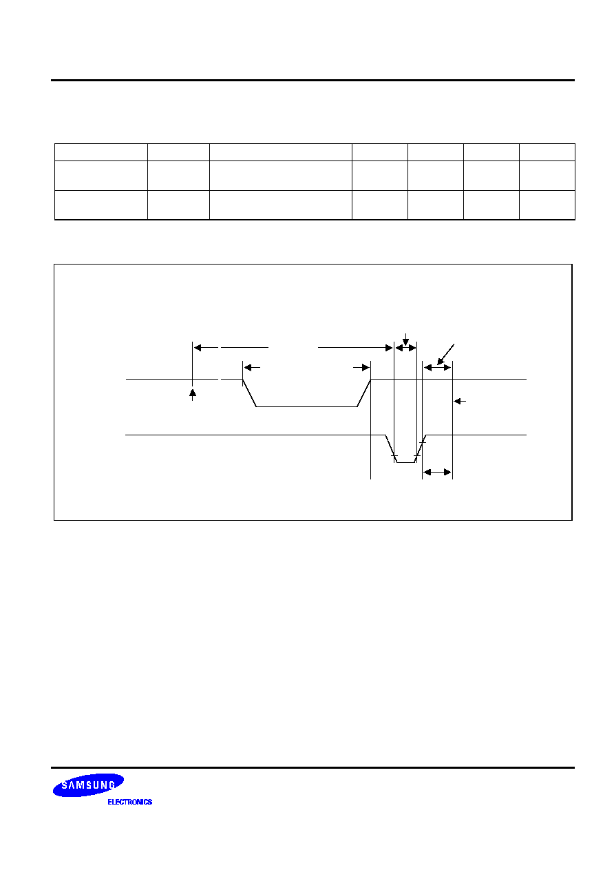
Table 19-4. A.C. Electrical Characteristics
(T
A
= ≠ 40
∞
C to + 85
∞
C, V
DD
= 2.7 V to 5.5 V)
Parameter
Symbol
Conditions
Min
Typ
Max
Unit
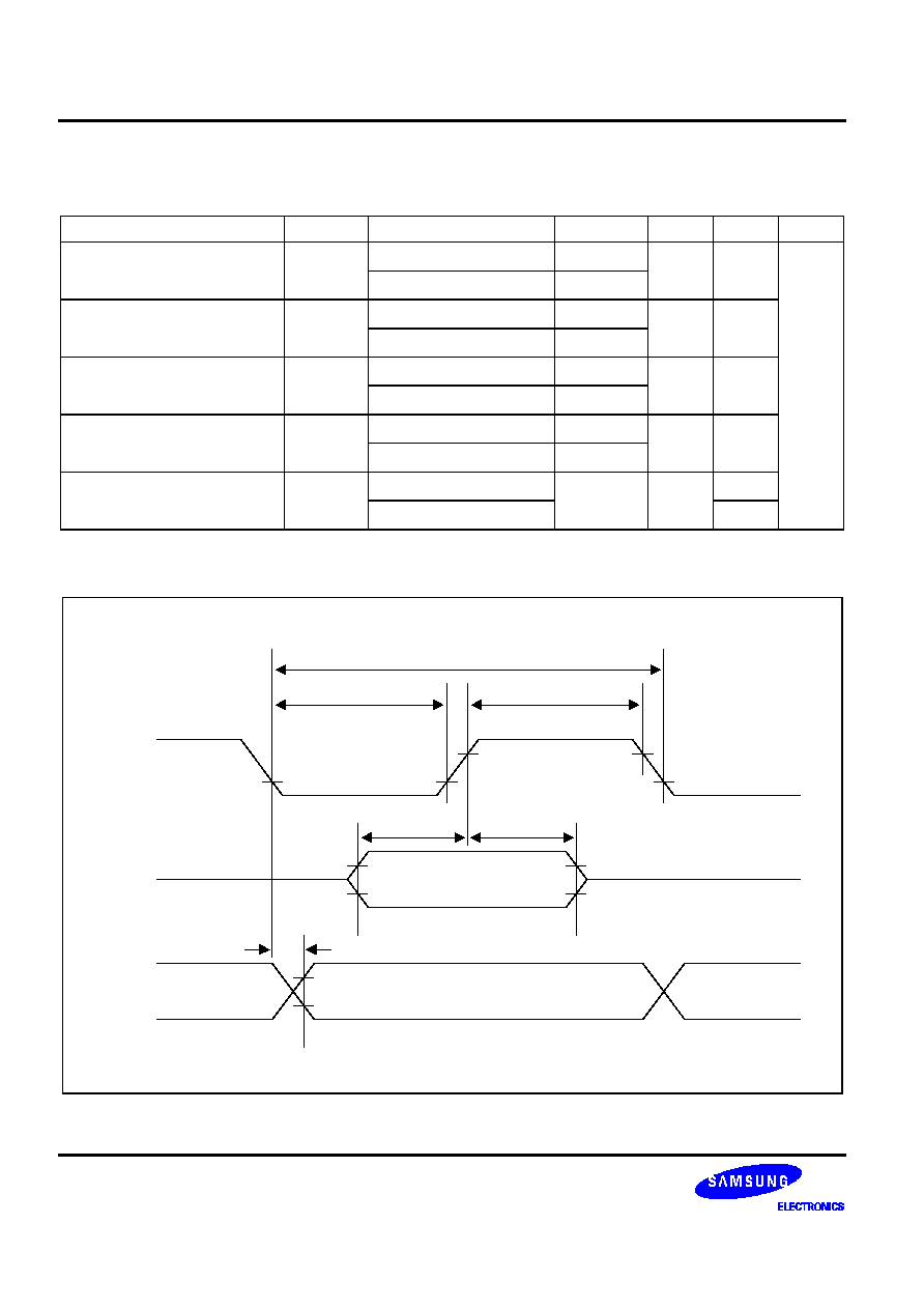
Interrupt Input
High, Low Width
t
INTH
,
t
INTL
Ports 2, 3, and 4
≠
270
≠
ns
RESET
Input
Low Width
t
RSL
Input
≠
1500
≠
ns
t
INTH
t
INTL
0.8 V
DD
0.2 V
DD
t
RSL
Figure 19-1. Input Timing Measurement Points
S3C8465/C8469/P8469
ELECTRICAL DATA
19-5
Table 19-5. Oscillation Characteristics
(T
A
= ≠ 40
∞
C + 85
∞
C)
Oscillator
Clock Circuit
Test Condition
Min
Typ
Max
Unit
Main Crystal or
V
DD
= 4.5 V to 5.5 V
1
≠
12
MHz
Ceramic
X
IN
C1
C2
X
OUT
V
DD
= 2.7 V to 4.5 V
1
≠
8
External Clock
V
DD
= 4.5 V to 5.5 V
1
≠
12
MHz
(Main System)
X
IN
X
OUT
V
DD
= 2.7 V to 4.5 V
1
≠
8
CPU Clock
1 kHz
Main Oscillator Frequency
1
2
3
4
5
6
7
Supply Voltage (V)
8 kHz
12 kHz
2.7 V
5.5 V
Figure 19-2. Operating Voltage Range
ELECTRICAL DATA
S3C8465/C8469/P8469
19-6
Table 19-6. Oscillation Stabilization Time
(T
A
= ≠ 40
∞
C + 85
∞
C, V
DD
= 2.7 V to 5.5 V)
Oscillator
Test Condition
Min
Typ
Max
Unit
Main Crystal
f
OSC
> 400 kHz;
≠
≠
20
ms
Main Ceramic
Oscillation stabilization occurs when V
DD
is equal
to the minimum oscillator voltage range.
≠
≠
10
ms
External Clock
(Main System)
X
IN
input High and Low width (t
XH
, t
XL
)
25
≠
500
ns
Oscillator
Stabilization
Wait Time
t
WAIT
when released by a reset
(1)
≠
2
16
/f
OSC
≠
ms
t
WAIT
when released by an interrupt
(2)
≠
≠
≠
ms
NOTES:
1.
f
OSC
is the oscillator frequency.
2.
The duration of the oscillator stabilization wait time, t
WAIT
, when it is released by an interrupt is determined by the
settings in the basic timer control register, BTCON.
S3C8465/C8469/P8469
ELECTRICAL DATA
19-7
Table 19-7. Data Retention Supply Voltage in Stop Mode
(T
A
= ≠ 40
∞
C to + 85
∞
C, V
DD
= 2.7 V to 5.5 V)
Parameter
Symbol
Conditions
Min
Typ
Max
Unit
Data Retention
Supply Voltage
V
DDDR
Stop mode
2
≠
5.5
V
Data Retention
Supply Current
I
DDDR
Stop mode, V
DDDR
= 2.0 V
≠
≠
5
µA
NOTE: Supply current does not include current drawn through internal pull-up resistors or external output current loads.
NOTE: t
WAIT
is the same as 4096 x 16 x 1/f
OSC
.
Execution of
STOP Instrction
RESET
occurs
~ ~
V
DDDR
~ ~
Stop Mode
Oscillation
Stabilzation
Time
Data Retention Mode
t
WAIT
RESET
V
DD
Normal
Operating
Mode
Figure 19-3. Stop Mode Release Timing When Initiated by a Reset
ELECTRICAL DATA
S3C8465/C8469/P8469
19-8
Table 19-8. Serial I/O Timing Characteristics
(T
A
= ≠ 40
∞
C to + 85
∞
C, V
DD
= 2.7 V to 5.5 V)
Parameter
Symbol
Conditions
Min
Typ
Max
Unit
SCK
Cycle Time
t
CKY
External
SCK
source
1000
≠
≠
ns
Internal
SCK
source
1000
SCK
High, Low Width
t
KH
, t
KL
External
SCK
source
500
≠
≠
Internal
SCK
source
t
KCY
/2 ≠ 50
SI Setup Time to
SCK
Low
t
SIK
External
SCK
source
250
≠
≠
Internal
SCK
source
250
SI Hold Time to
SCK
High
t
KSI
External
SCK
source
400
≠
≠
Internal
SCK
source
400
Output Delay for
SCK
to SO
t
KSO
External
SCK
source
≠
≠
300
Internal
SCK
source
250
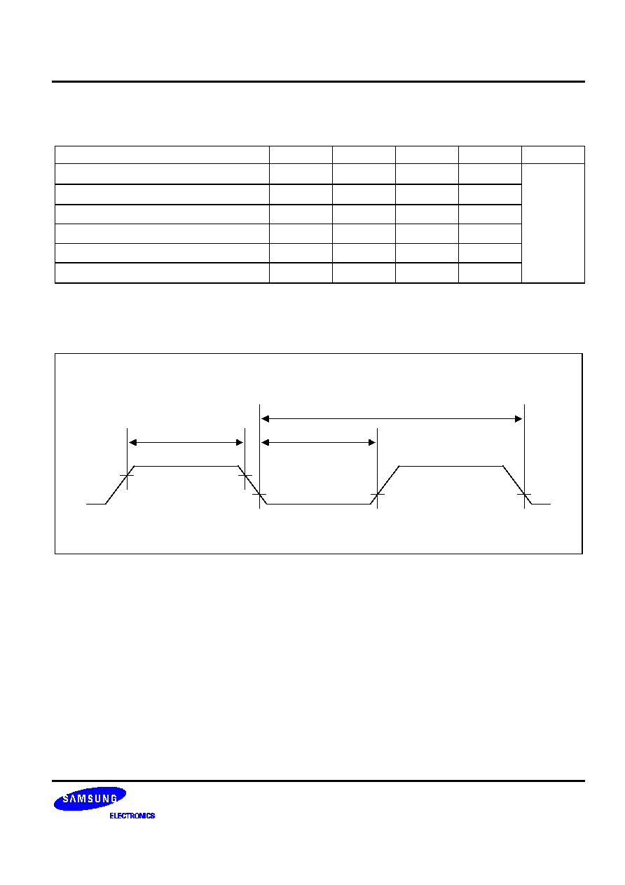
NOTE: "
SCK
" means serial I/O clock frequency, "SI" means serial data input, and "SO" means serial data output.
Output Data
Input Data
SCK
t
KH
t
KCY
t
KL
0.8 V
DD
0.2 V
DD
t
KSO
t
SIK
t
KSI
0.8 V
DD
0.2 V
DD
SI
SO
Figure 19-4. Serial Data Transfer Timing
S3C8465/C8469/P8469
ELECTRICAL DATA
19-9
Table 19-9. UART Timing Characteristics in Mode 0 (10 MHz)
(T
A
= ≠ 40
∞
C to + 85
∞
C, V
DD
= 2.7 V to 5.5 V, Load capacitance = 80 pF)
Parameter
Symbol
Min
Typ
Max
Unit
Serial port clock cycle time
t
SCK
500
t
CPU
◊
6
700
ns
Output data setup to clock rising edge
t
S1
300
t
CPU
◊
5
≠
Clock rising edge to input data valid
t
S2
≠
≠
300
Output data hold after clock rising edge
t
H1
t
CPU
≠ 50
t
CPU
≠
Input data hold after clock rising edge
t
H2
0
≠
≠
Serial port clock High, Low level width
t
HIGH,
t
LOW
200
t
CPU
◊
3
400
NOTES:
1.
All timings are in nanoseconds (ns) and assume a 10-MHz CPU clock frequency.
2.
The unit t
CPU
means one CPU clock period.
0.2 V
DD
0.8 V
DD
t
HIGH
t
LOW
t
SCK
Figure 19-5. Waveform for UART Timing Characteristics
ELECTRICAL DATA
S3C8465/C8469/P8469
19-10
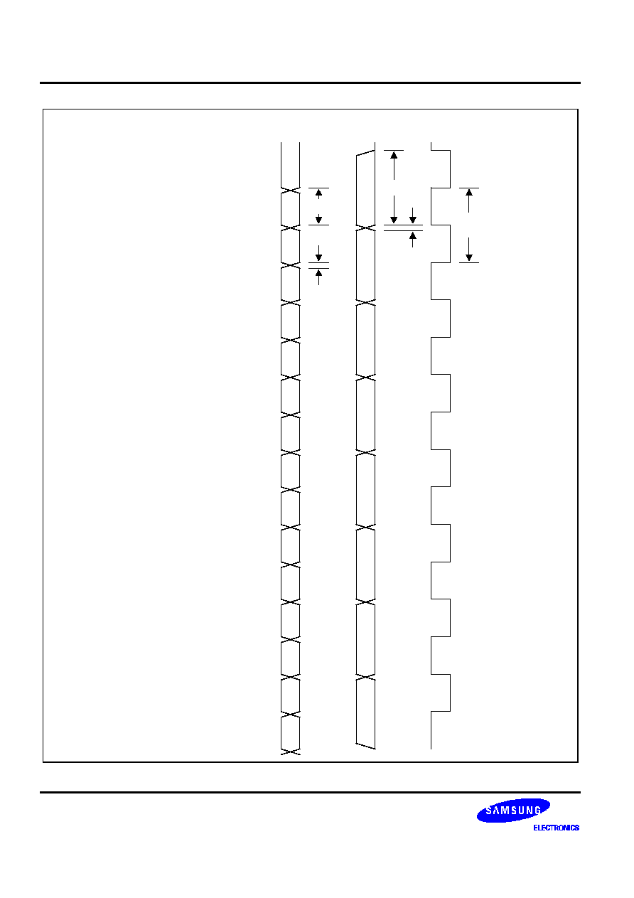
NOTE:
The symbols shown in this diagram are defined as follows:
fSCK
Serial port clock cycle time
tS1
Output data setup to clock rising edge
tS2
Clock rising edge to input data valid
tH1
Output data hold after clock rising edge
tH2
Input data hold after clock rising edge
Shift
Clock
Data
Out
D0
D1
D2
D3
D4
D5
D6
D7
Data
In
VALID
VALID
VALID
VALID
VALID
VALID
VALID
VALID
t
SCK
t
S1
t
S2
t
H1
t
H2
Figure 19-6. A.C. Timing Waveform for the UART Module
S3C8465/C8469/P8469
ELECTRICAL DATA
19-11
Table 19-10. A/D Converter Electrical Characteristics
(T
A
= ≠ 40
∞
C to + 85
∞
C, V
DD
= 2.7 V to 5.5 V, V
SS
= 0 V)
Parameter
Symbol
Test Conditions
Min
Typ
Max
Unit
Resolution
≠
10
≠
bit
Total accuracy
V
DD
= 5.12 V
≠
≠
±
3
LSB
Integral linearity
error
ILE
CPU clock = 10 MHz
AV
REF
= 5.12 V
≠
±
2
Differential
linearity error
DLE
AV
SS
= 0 V
≠
±
1
Offset error of
top
EOT
±
1
±
3
Offset error of
bottom
EOB
±
0.5
±
2
Conversion time
(1)
t
CON
10-bit conversion
50 x 4/f
OSC
(3)
, f
OSC
= 10 MHz
20
≠
≠
µ
s
Analog input
voltage
V
IAN
≠
AV
SS
≠
AV
REF
V
Analog input
impedance
R
AN
≠
2
≠
≠
M
Analog
reference
voltage
AV
REF
≠
2.5
≠
V
DD
V
Analog ground
AV
SS
≠
V
SS
≠
V
SS
+ 0.3
V
Analog input
current
I
ADIN
AV
REF
= V
DD
= 5 V
conversion time = 20
µ
s
≠
≠
10
µ
A
Analog block
current
(2)
I
ADC
AV
REF
= V
DD
= 5 V
conversion time = 20
µ
s
1
3
mA
AV
REF
= V
DD
= 3 V
conversion time = 20
µ
s
0.5
1.5
mA
AV
REF
= V
DD
= 5 V
when power down mode
100
500
nA
NOTES:
1.
"Conversion time" is the time required from the moment a conversion operation starts until it ends.
2.
I
ADC
is operating current during A/D conversion.
3.
f
OSC
is the main oscillator clock.
ELECTRICAL DATA
S3C8465/C8469/P8469
19-12
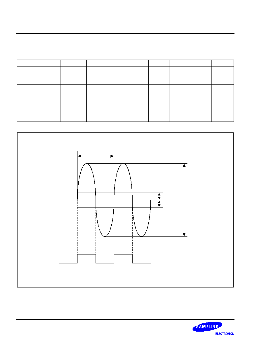
Table 19-11. Zero Crossing Detector
(T
A
= ≠ 40
∞
C to + 85
∞
C, V
DD
= 4.5 V to 5.5 V, V
SS
= 0 V)
Parameter
Symbol
Test Conditions
Min
Typ
Max
Unit
Zero-crossing
detection input
voltage
V
ZC
AC connection
c = 0.1
µ
F
1.0
≠
3.0
Vp-p
Zero-crossing
detection accuracy
V
AZC
f
ZC
= 60 Hz (sine wave)
V
DD
= 5 V
f
OSC
= 10 MHz
≠
≠
±
150
mV
Zero-crossing
detection input
frequency
f
ZC
≠
40
≠
200
Hz
1/fzc
V
AZC
ZCINT
AC input
V
AZ (P-P)
Figure 19-7. Zero Crossing Waveform Diagram
S3C8465/C8469/P8469
ELECTRICAL DATA
19-13
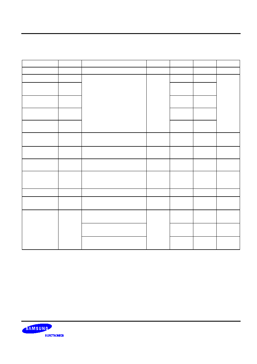
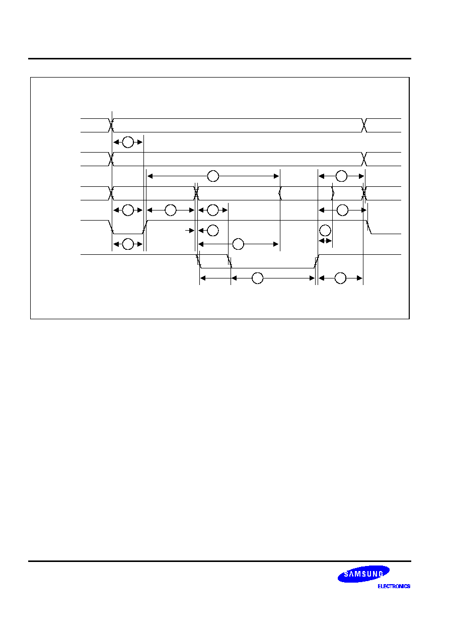
Table 19-12. External Memory Timing Characteristics (8 MHz)
(T
A
= ≠ 40
∞
C to + 85
∞
C, V
DD
= 2.7 V to 5.5 V)
Number
Symbol
Parameter
Normal Timing (ns)
Min
Max
1
t
dA
(AS)
Address valid to
AS
delay
10
≠
2
t
dAS
(A)
AS
to address float delay
35
≠
3
t
dAS
(DR)
AS
to read data required valid
≠
140
4
t
wAS
AS
Low width
43.75 (35)
≠
5
t
dA
(DS)
Address float to
DS
0
≠
6a
t
wDS
(read)
DS
(read) Low width
156.25 (125)
≠
6b
t
wDS
(write)
DS
(write) Low width
81.25 (65)
≠
7
t
dDS
(DR)
DS
to read data required valid
≠
80
8
t
hDS
(DR)
Read data to
DS
hold time
0
≠
9
t
dDS
(A)
DS
to address active delay
20
≠
10
t
dDS
(AS)
DS
to
AS
delay
30
≠
11
t
dDO
(DS)
Write data valid to
DS
(write)
delay
10
≠
12
t
dRW
(AS)
R/
W
valid to
AS
delay
20
≠
13
t
dDS
(DW)
DS
to write data not valid delay
20
≠
NOTES:
1.
All times are in nanoseconds (ns) and assume an 8-MHz input frequency.
2.
Wait states add 100 ns to the time of numbers 3, 6a, 6b, and 7.
3.
The values for twAS and twDS that are shown in parentheses "( )" assume a 10-MHz input clock.
ELECTRICAL DATA
S3C8465/C8469/P8469
19-14
R/
W
(P2.2)
Port 0
DM (P2.3)
Port 1
AS
(P2.0)
A8-A15,
DM
D0-D7 Out
A0-A7
12
3
9
10
8
1
4
11
2
5
7
13
6
D0-D7
In
Out
DS
(P2.1)
Figure 19-8. External Memory Read and Write Timing
(See Table 19-10 for a description of each timing point.)
S3C8465/C8469/P8469
MECHANICAL DATA
20-1
20
MECHANICAL DATA
OVERVIEW
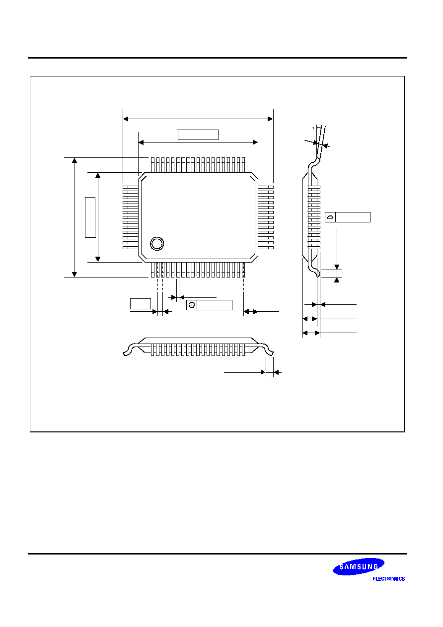
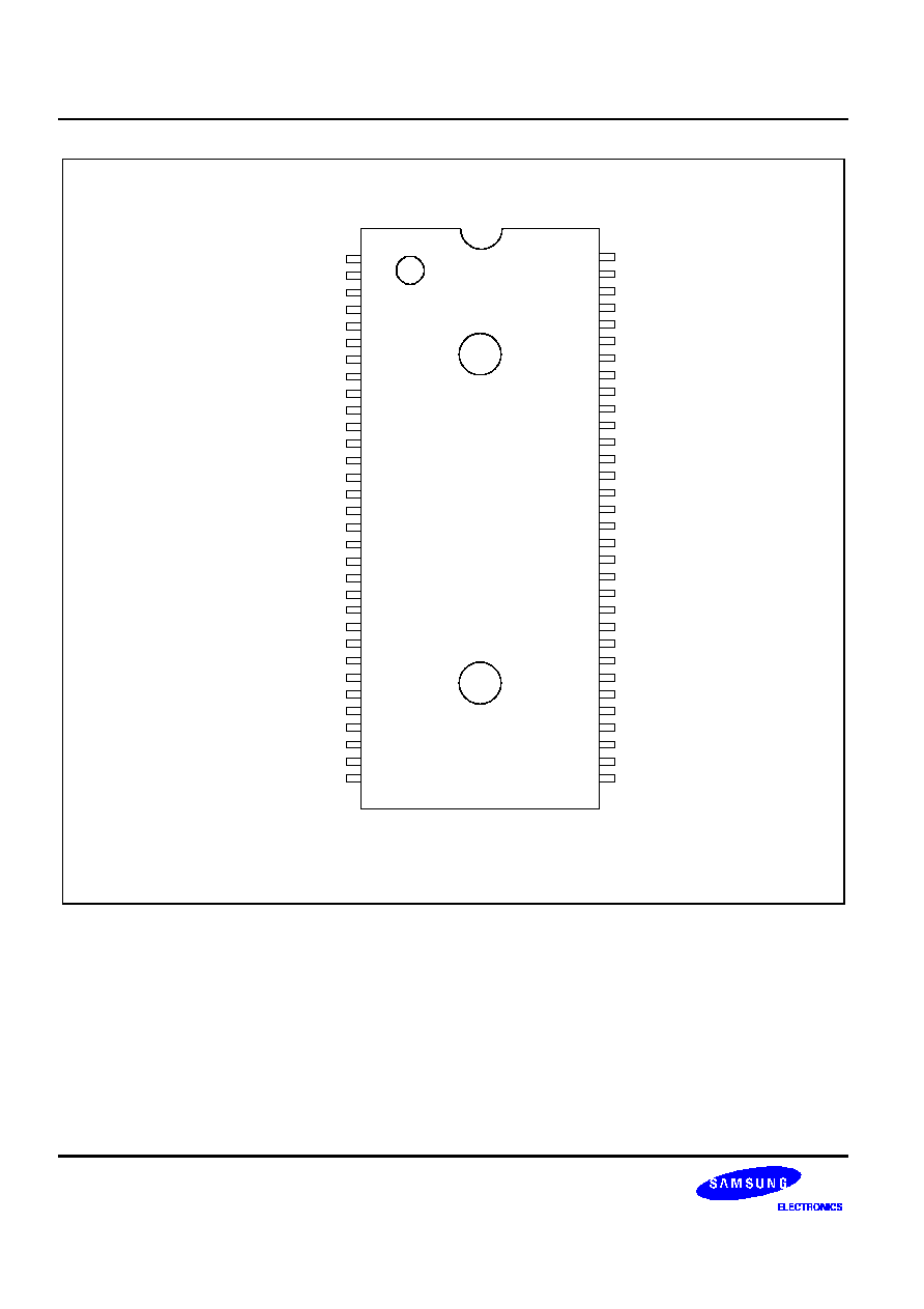
The S3C8465/C8469/P8469 microcontrollers are available in a 64-SDIP-750, 64-QFP-1420F package.
NOTE: Dimensions are in millimeters.
0-15
#64
#33
#32
#1
17.00
±
0
.20
58.20 MAX
57.80
± 0.20
0.45
±
0.10
1.00
±
0.10
1.778
0.51 MIN
3.30
± 0.30
4.10
±
0.20
5.08 MAX
19.05
(1.34)
64-SDIP-750
0.25
+ 0.10- 0.05
Figure 20-1. 64-SDIP-750 Package Dimensions
MECHANICAL DATA
S3C8465/C8469/P8469
20-2
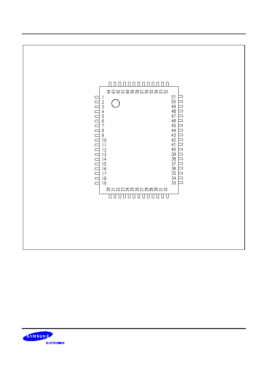
64-QFP-1420F
#64
20.00
± 0.20
23.90
± 0.30
14.00
± 0.20
17.90
± 0.30
#1
1.00
(1.00)
0.40
+ 0.10
- 0.05
NOTE: Dimensions are in millimeters.
0.80
± 0.20
0.10 MAX
0.15
+ 0.10
- 0.05
0-8
0.80
± 0.20
0.05 MIN
2.65
± 0.10
3.00 MAX
0.15 MAX
Figure 20-2. 64-QFP-1420F Package Dimensions

S3C8465/C8469/P8469
KS88P4632 OTP
21-1
21
S3P8469 OTP
OVERVIEW
The S3P8469 single-chip CMOS microcontroller is the OTP (One Time Programmable)
version of the
S3C8465/C8469 microcontroller. It has an on-chip OTP ROM instead of a masked ROM. The EPROM is
accessed by serial data format.
The S3P8469 is fully compatible with the S3C8465/C8469, both in function in D.C. electrical characteristics and
in pin configuration. Because of its simple programming requirements, the S3P8469 is ideal as an evaluation
chip for the S3C8465/C8469.
KS88P4632 OTP
S3C8465/C8469/P8469
21-2
P0.7/A15
P0.6/A14
P0.5/A13
P0.4/A12
P0.3/A11
P0.2/A10
P0.1/A9
P0.0/A8
P4.7/INT11/TDG
P4.6/INT10/TCG
P4.5/INT9/TDCK
P4.4/INT8/TCCK
P4.3/INT7/CAPA
SDAT/P4.2/INT6
SCLK/P4.1/INT5/RxD
V
DD
/V
DD
V
SS
/V
SS
X
OUT
X
IN
V
PP
/EA
P4.0/INT4
P3.7/TxD
RESET
RESET/RESET
P3.6/SO
P3.5/SI
P3.4/
SCK
P3.3/T0CK
P3.2/T0
P3.1/PWM1
P3.0/PWM0
P2.7/INT3
P2.6/INT2
S3C8465
S3C8469
(64-SDIP)
Top View
1
2
3
4
5
6
7
8
9
10
11
12
13
14
15
16
17
18
19
20
21
22
23
24
25
26
27
28
29
30
31
32
P1.0/AD0
P1.1/AD1
P1.2/AD2
P1.3/AD3
P1.4/AD4
P1.5/AD5
P1.6/AD6
P1.7/AD7
P5.7/ADC7
P5.6/ADC6
P5.5/ADC5
P5.4/ADC4
P5.3/ADC3
P5.2/ADC2
P5.1/ADC1
P5.0/ADC0
AV
SS
AV
REF
P6.7
P6.6
P6.5
P6.4
P6.3
P6.2
P6.1
P6.0
P2.0/
AS
P2.1/
DS
P2.2/R/
W
P2.3/
DM
P2.4/ZCD
P2.5/BUZ
64
63
62
61
60
59
58
57
56
55
54
53
52
51
50
49
48
47
46
45
44
43
42
41
40
39
38
37
36
35
34
33
NOTE:
The bolds indicate an OTP pin name.
Figure 21-1. S3P8469 Pin Assignments (64-SDIP Package)
S3C8465/C8469/P8469
KS88P4632 OTP
21-3
P0.0/A8
P4.7/INT11/TDG
P4.6/INT10/TCG
P4.5/INT9/TDCK
P4.4/INT8/TCCK
P4.3/INT7CAPA
SDAT/P4.2/INT6
SCLK/P4.1/INT5/RxD
V
DD
/V
DD
V
SS
/V
SS
X
OUT
X
IN
V
PP
/EA
P4.0/INT4
P3.7/TxD
RESET
RESET
/RESET
P3.6/SO
P3.5/SI
P3.4/
SCK
S3C8465
S3C8469
(64-QFP)
Top View
P0.1/A9
P0.2/A10
P0.3/A11
P0.4/A12
P0.5/A13
P0.6/A14
P0.7/A15
P1.0/AD0
P1.1/AD1
P1.2/AD2
P1.3/AD3
P1.4/AD4
P1.5/AD5
P3.3/T0CK
P3.2/T0
P3.1/PWM1
P3.0/PWM0
P2.7/INT3
P2.6/INT2
P2.5/BUZ
P2.4/ZCD
P2.3/DM
P2.2/R/
W
P2.1/DS
P2.0/AS
P6.0
P1.6/AD6
P1.7/AD7
P5.7/ADC7
P5.6/ADC6
P5.5/ADC5
P5.4/ADC4
P5.3/ADC3
P5.2/ADC2
P5.1/ADC1
P5.0/ADC0
AV
SS
AV
REF
P6.7
P6.6
P6.5
P6.4
P6.3
P6.2
P6.1
NOTE:
The bolds indicate an OTP pin name.
Figure 21-2. S3P8469 Pin Assignments (64-QFP Package)
KS88P4632 OTP
S3C8465/C8469/P8469
21-4
Table 21-1. Descriptions of Pins Used to Read/Write the EPROM
Main Chip
During Programming
Pin Name
Pin Name
Pin No.
I/O
Function
P4.2
SDAT
14(7)
I/O
Serial data pin. Output port when reading and
input port when writing. Can be assigned as a
Input/push-pull output port.
P4.1
SCLK
15(8)
I
Serial clock pin. Input only pin.
EA
V
PP
20(13)
I
Power supply pin for EPROM cell writing
(indicates that OTP enters into the writing mode).
When 12.5 V is applied, OTP is in writing mode
and when 5 V is aplied, OTP is in reading mode.
(Option)
RESET
RESET
23(16)
I
Chip Initialization
V
DD
/V
SS
V
DD
/V
SS
16(9)/17(10)
≠
Logic power supply pin. V
DD
should be tied to
+5 V during programming.
NOTE: ( ) means 64 QFP package.
Table 21-2. Comparison of S3P8469 and S3C8465/C8469 Features
Characteristic
S3P8469
S3C8465/C8469
Program Memory
32K-byte EPROM
16/32K-byte mask ROM
Operating Voltage (V
DD
)
2.7 V to 5.5 V
2.7 V to 5.5 V
OTP Programming Mode
V
DD
= 5 V, V
PP
(EA) = 12.5 V
Pin Configuration
64 SDIP/64 QFP
64 SDIP/64 QFP
EPROM Programmability
User Program 1 time
Programmed at the factory
OPERATING MODE CHARACTERISTICS
When 12.5 V is supplied to the V
PP
(EA) pin of the S3P8469, the EPROM programming mode is entered. The
operating mode (read, write, or read protection) is selected according to the input signals to the pins listed in
Table 21-3 below.
Table 21-3. Operating Mode Selection Criteria
V
DD
V
PP
(
EA
)
REG/
MEM
MEM
ADDRESS
(A15≠A0)
R/W
MODE
5 V
5 V
0
0000H
1
EPROM read
12.5 V
0
0000H
0
EPROM program
12.5 V
0
0000H
1
EPROM verify
12.5 V
1
0E3FH
0
EPROM read protection
NOTE: "0" means Low level; "1" means High level.