 | –≠–ª–µ–∫—Ç—Ä–æ–Ω–Ω—ã–π –∫–æ–º–ø–æ–Ω–µ–Ω—Ç: S3C84A4X | –°–∫–∞—á–∞—Ç—å:  PDF PDF  ZIP ZIP |

S3C84A4/P84A4
PRODUCT OVERVIEW
1-1
1
PRODUCT OVERVIEW
SAM88 RC PRODUCT FAMILY
Samsung's new SAM88RC family of 8-bit single-chip CMOS microcontrollers offers a fast and efficient CPU, a
wide range of integrated peripherals, and various mask-programmable ROM sizes. Timer/counters with
selectable operating modes are included to support real-time operations. Many SAM88RC microcontrollers have
an external interface that provides access to external memory and other peripheral devices. The sophisticated
interrupt structure recognizes up to eight interrupt levels. Each level can have one or more interrupt sources and
vectors. Fast interrupt processing (within a minimum six CPU clocks) can be assigned to specific interrupt levels.
S3C84A4X MICROCONTROLLER
The S3C84A4 single-chip microcontroller is fabricated using a highly advanced CMOS process. Its design is
based on the powerful SAM88RC CPU core. Stop and Idle power-down modes were implemented to reduce
power consumption. The size of the internal register file is logically expanded, increasing the addressable on-chip
register space to 784 bytes. A flexible yet sophisticated external interface is used to access up to 64-Kbytes of
program and data memory. The S3C84A4 is a versatile microcontroller that is ideal for use in a wide range of
general-purpose applications such as CD-ROM/DVD-ROM drives.
Using the SAM88RC modular design approach, the following peripherals were integrated with the SAM88RC
CPU core:
-- Three configurable 8-bit general I/O ports
-- One 5-bit general I/O ports
-- Two 8-bit timers with interval timer
-- Two 16-bit timers/counters with PWM operating modes 8-bit or capture modes
-- Voltage level detector circuit embedded.
-- Two embedded chip selection pins (CS0≠CS1) or normal I/O ports
-- Two programmable 8-bit PWM modules with corresponding output pins
-- A/D converter with 4 selectable input pins
OTP
The S3C84A4 microcontroller is also avaiable in OTP(One Time Programmable) version, S3P84A4.
The S3P84A4 microcontroller has an on-chip 4K-byte one-time-programmable EPROM instead of masked ROM.
The S3P84A4 is comparable to S3C84A4, both in function and in pin configuration.

PRODUCT OVERVIEW
S3C84A4/P84A4
1-2
FEATURES
CPU
∑
SAM88RC CPU core
Memory
∑
784-byte internal register file
∑
4-Kbyte internal program memory
External Interface
∑
64K-byte external data memory
∑
64K-byte external program memory area
(ROMless)
∑
60K-byte external program memory and 4K-byte
internal program memory
∑
Automatic wait control function by software.
ADC
∑
Can be used as a general input/output port
∑
8-bit resolution four channels
8-bit Timers
∑
Two 8-bit timers with interval timer mode
(Timer A and B)
16-bit Timer/Counters
∑
Two programmable 16-bit timer/counters
∑
Interval, or event counter mode operation
∑
16-bit capture and 8-bit PWM mode
∑
Internal or external clock source
Basic Timer (Watchdog Timer)
∑
Overflow signal makes a system reset
∑
8-bit timer with interval timer mode
General I/O Ports
∑
Three 8-bit general I/O ports (port 0, 1, 2)
∑
One 5-bit general I/O port (port 3)
∑
Port 2 can drive LED directly
Interrupts
∑
Two edge-driven external interrupts
∑
Two level-driven external interrupts
∑
Fast interrupt mode processing
PWM
∑
Four output channels
(PWM0, PWM1, TCPWM, TDPWM)
∑
8-bit resolution with a 4-bit prescaler
(PWM0, PWM1)
∑
From 8-bit counter (Timer C/D)
(TCPWM, TDPWM)
Embedded chip selection
∑
To reduce interface glue logic, chip selection
logic is embedded (256 byte address unit)
Voltage level detector
∑
To prevent MCU from malfunctioning in an
unstable power level, a voltage level detector
circuit is inserted
Operating Voltage Range
∑
4.5 V to 5.5 volts (@ 30 MHz)
Operating Temperature Range
∑
≠ 40
∞
C to + 85
∞
C
Package Types
∑
64-pin QFP
Operating frequency
∑
30 MHz (4.5 V to 5.5 V)
S3C84A4/P84A4
PRODUCT OVERVIEW
1-3
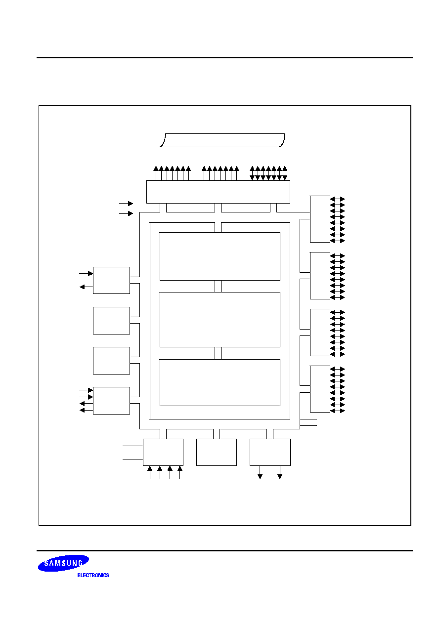
BLOCK DIAGRAM
ADC0/P0.0-
ADC3/P0.3
SAM88 RC CPU
Port 0
P0.0-P0.3/
ADC0-ADC3
P0.4-P0.7
Timers
C and D
Basic
Timer
784-Byte Register File
External Interface Block
SAM8 BUS
Timers
A and B
Port 1
TCCK
A/D
Converter
4-Kbyte
ROM
SAM8 BUS
PWM
Module
Port 2
P2.0-P2.3/
INT0-INT3
P2.4-P2.6
P2.7/WAIT
Port 3
P3.0-P3.1/
A16-A17
P3.2, P3.3/
CS0-CS1
P3.4
Port I/O
& Interrupt
Control
Watch-dog
Timer
V
DD1
V
SS1
PWM0 PWM1
AV
SS (Internally)
AV
REF
TDCK
TCOUT
TDOUT
P1.0-P1.7
TDCK,TCCK
TDCAP,TCCAP
TCOUT,TDOUT
PWM0,PWM1
X
IN
External Address Data
(A8-A15)
(A0-A7)
(D0-D7)
RESET
Main
OSC
EA
X
OUT
Figure 1-1. S3C84A4 Block Diagram
PRODUCT OVERVIEW
S3C84A4/P84A4
1-4
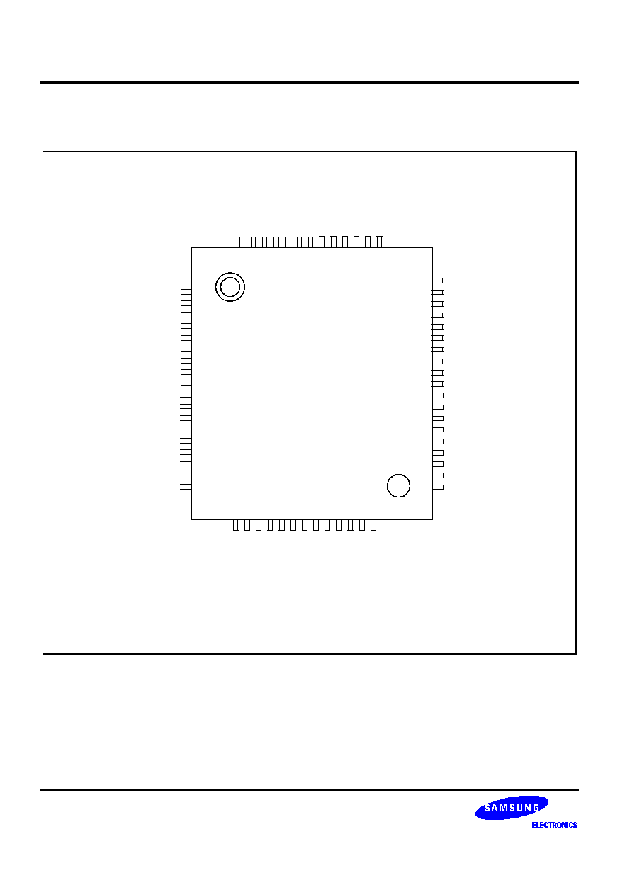
PIN ASSIGNMENT
A3
A4
A5
A6
A7
A8
A9
A10
A11
A12
A13
A14
A15
PM
DM
RD
WR
P3.4
CS1/P3.3
CS0/P3.2
A17/P3.1
V
DD
V
SS
X
OUT
X
IN
TEST/EA
A16/P3.0
WAIT/P2.7
RESET
P2.6
P2.5
P2.4
S3C84A4
(64-QFP)
51
50
49
48
47
46
45
44
43
42
41
40
39
38
37
36
35
34
33
1
2
3
4
5
6
7
8
9
10
11
12
13
14
15
16
17
18
19
53
53
54
55
56
57
58
59
60
61
62
63
64
A2
A1
A0
D7
D6
D5
D4
D3
D2
D1
D0
AV
REF
P0.0/ADC0
P0.1/ADC1
P0.2/ADC2
P0.3/ADC3
P0.4
P0.5
P0.6
32
31
30
29
28
27
26
25
24
23
22
21
20
P0.7
P1.0/TDCK
P1.1/TCCK
P1.2/TDCAP
P1.3/TCCAP
P1.4/TCOUT
P1.5/TDOUT
P1.6/PWM0
P1.7/PWM1
P2.0/INT0
P2.1/INT1
P2.2/INT2
P2.3/INT3
Figure 1-2. S3C84A4 Pin Assignments
S3C84A4/P84A4
PRODUCT OVERVIEW
1-5
PIN DESCRIPTIONS
Table 1-1. S3C84A4/P84A4 Pin Descriptions
Pin
Name
Pin
Type
Pin
Description
Circuit
Type
Pin
Number
Share
Pins
P0.0≠P0.7
I/O
Bit programmable port; input or output mode
selected by software; normal input or push-pull
Software assignable pull-up.
Alternately, P0.0≠P0.3 can be use as a ADC input
port with 8-bit resolution.
2,3
39≠32
ADC0≠
ADC3
P1.0≠P1.7
I/O
Bit programmable port; input or output mode
selected by software ; normal input or push-pull.
Software assignable pull-up. Respectively, each pin
can serve as:
P1.0 / timer D clock input (TDCK)
P1.1 / timer C clock input (TCCK)
P1.2 / timer D capture input (TDCAP)
P1.3 / timer C capture input (TCCAP)
P1.4 / timer C out (TCOUT) / PWM out (TCPWM)
P1.5 / timer D out (TDOUT) / PWM out (TDPWM)
P1.6 / PWM0 output port
P1.7 / PWM1 output port
3,5
31≠24
TDCK
TCCK
TDCAP
TCCAP
TCOUT/
TCPWM
TDOUT/
TDPWM
PWM0
PWM1
P2.0≠P2.7
I/O
General I/O port with normal input or push-pull
output. Software assignable pull-up.
Bit programmable;
Alternately, P2.0≠ P2.3 can be used as inputs for
external interrupts,INT0≠ INT3( with noise filter and
interrupt control). INT0/INT1 are level interrupts
3,4,5
23≠17
15
INT0≠INT3
P3.0≠P3.4
I/O
General I/O port with bit programmable pins.
Normal input or push-pull output with software
assignable pull-up. Input or output mode is
selectable by software. P3.0-P3.1 can alternately be
used as outputs of high address (A16,A17).
P3.2≠P3.3 can alternately be used as outputs for
embedded chip selection output.
P3.0 / A16
P3.1 / A17
P3.2 / CS0
P3.3 / CS1
3,5
14,
8≠5
A16, A17
CS0,CS1
PRODUCT OVERVIEW
S3C84A4/P84A4
1-6
Table 1-1. S3C84A4/P84A4 Pin Descriptions (Continued)
Pin
Name
Pin
Type
Pin
Description
Circuit
Type
Pin
Number
Share
Pins
ADC0-ADC3
I
Analog input pins for A/D converter module.
Alternatively, used as general-purpose I/O
2
39≠36
P0.0-P0.3
AV
REF
≠
A/D converter reference voltage
AV
SS
is connected to ground internally
≠
40
≠
PWM0,
PWM1
O
Pulse width modulation output pins
5
25,24
P1.6, P1.7
INT0-INT3
I
External interrupt input pins
4
23-20
P2.0≠P2.3
TCCK, TDCK
I
External clock input for timer C and timer D
3
30,31
P1.1/P1.0
TCCAP,
TDCAP
I
Timer C/ Timer D capture input
3
28,29
P1.3/P1.2
TCOUT,
TDOUT
O
Timer C/D 8-bit PWM mode output or counter
match toggle output
5
27,26
P1.4, P1.5
WAIT
I
Input pin for the slow memory timing signal
from the external interface
5
15
P2.7
RESET
I
System reset pin (pull-up resistor: 50 k
)
1
16
≠
EA
I
5V: ROMless operating
0V: internal 4K and external 60K
addressing mode
≠
13
≠
V
DD
, V
SS
≠
Power input pins
≠
9,10
≠
X
IN
, X
OUT
≠
Main oscillator pins
≠
12,11
≠
A0≠A15
O
Address output for external device
6
49≠64
≠
D0≠D7
I/O
Data I/O for external device
7
41≠48
≠
PM, DM
O
External memory selection output
≠
1,2
≠
RD,WR
O
External memory read/write output
≠
3, 4
≠
A16, A17
O
Extended memory high address output
5
14, 8
P3.0, P3.1
CS0
≠
CS1
O
Embedded chip selection output
5
7, 6
P3.2, P3.3

S3C84A4/P84A4
PRODUCT OVERVIEW
1-7
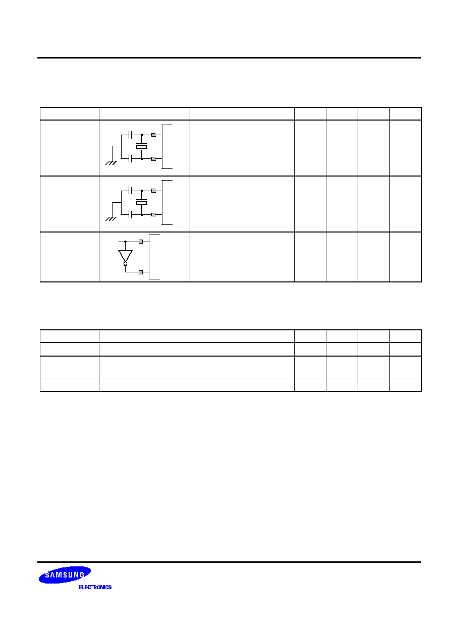
PIN CIRCUITS
Table 1-2. Pin Circuit Assignments for the S3C84A4/P84A4
Circuit Number
Circuit Type
S3C8414X Assignments
1
Input
RESET
pin
2
I/O
A/D converter input pins, ADC0≠ADC3, P0.0≠P0.3
3
I/O
Port 0, 2, and 3
4
I/O
P2 (INT0≠INT3)
5
I/O
P1 (TDCK, TCCK, TDCAP, TCCAP, TCOUT, TDOUT, TCPWM,
TDPWM, PWM0, PWM1)
6
Output
A0≠A15,
PM
,
DM
,
RD
,
WR
7
I/O
D0≠D7
PRODUCT OVERVIEW
S3C84A4/P84A4
1-8
Input
V
DD
Pull-up
Resistor
(Typical 50 k
)
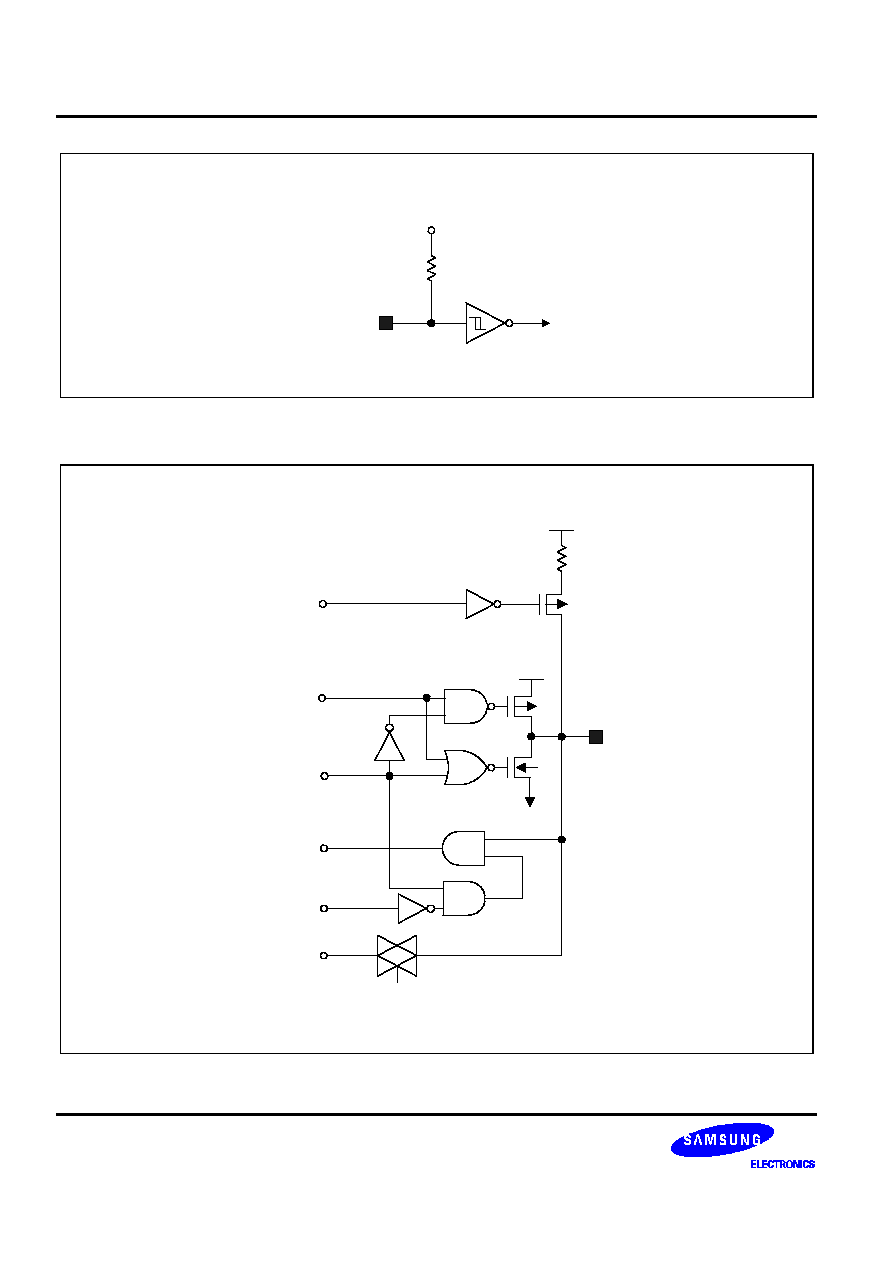
Figure 1-4. Pin Circuit Type 1 (
RESET
RESET
)
V
DD
I/O
Data
Output
Disable
Normal
Input
V
ss
ADC In
ADC Port
Selection
Pull-up
Resistor
Pull-Down
Enable
Enable ADC
V
DD
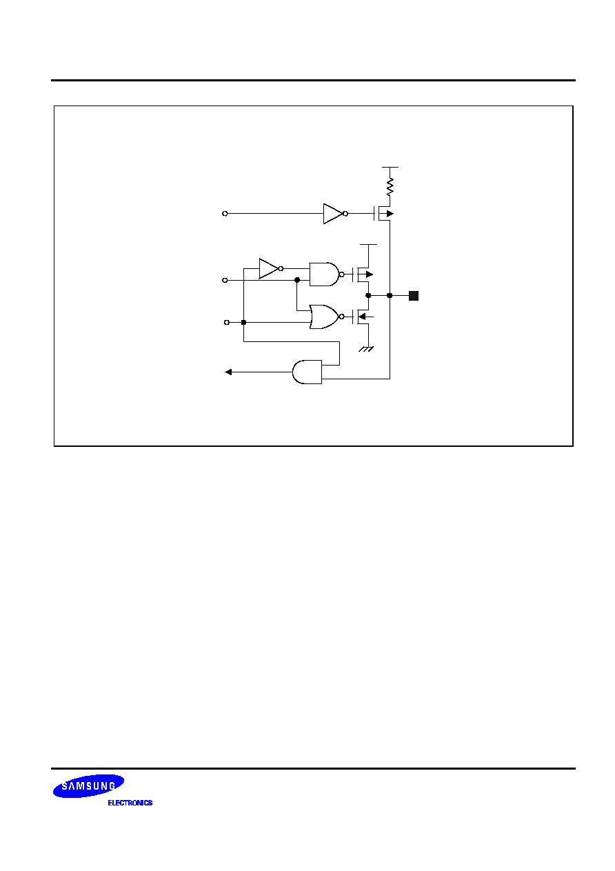
Figure 1-5. Pin Circuit Type 2 (ADC0≠ADC3)
S3C84A4/P84A4
PRODUCT OVERVIEW
1-9
V
DD
I/O
Data
Output
Disable
Normal
Input
V
DD
Pull-Up
Enable
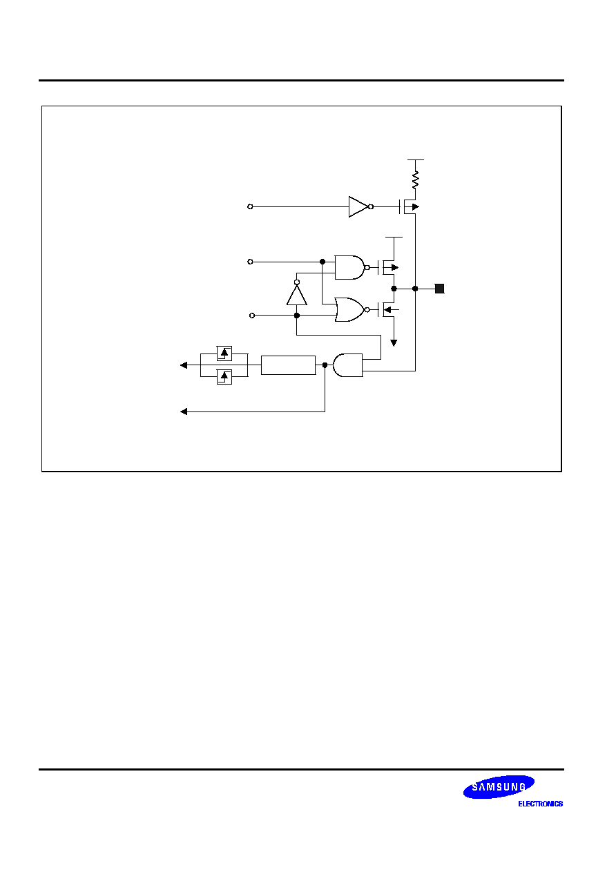
Figure 1-6. Pin Circuit Type 3
PRODUCT OVERVIEW
S3C84A4/P84A4
1-10
V
DD
I/O
Data
Output
Disable
External
Interrupt
Input
Noise Filter
V
DD
Pull-Up
Enable
Normal
Input
V
ss
Pull-Up
Resistor
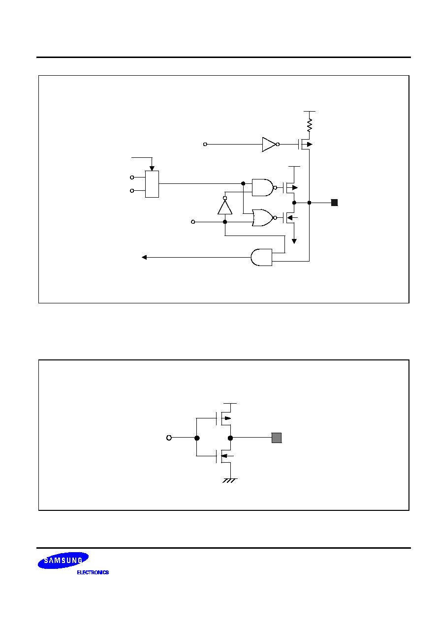
Figure 1-7. Pin Circuit Type 4
S3C84A4/P84A4
PRODUCT OVERVIEW
1-11
V
DD
Data
Output
Disable
V
DD
Pull-Up
Enable
V
ss
Pull-Up
Resistor
Input
Selection Bits
for Ports or
Other Function
I/O
Other
Function
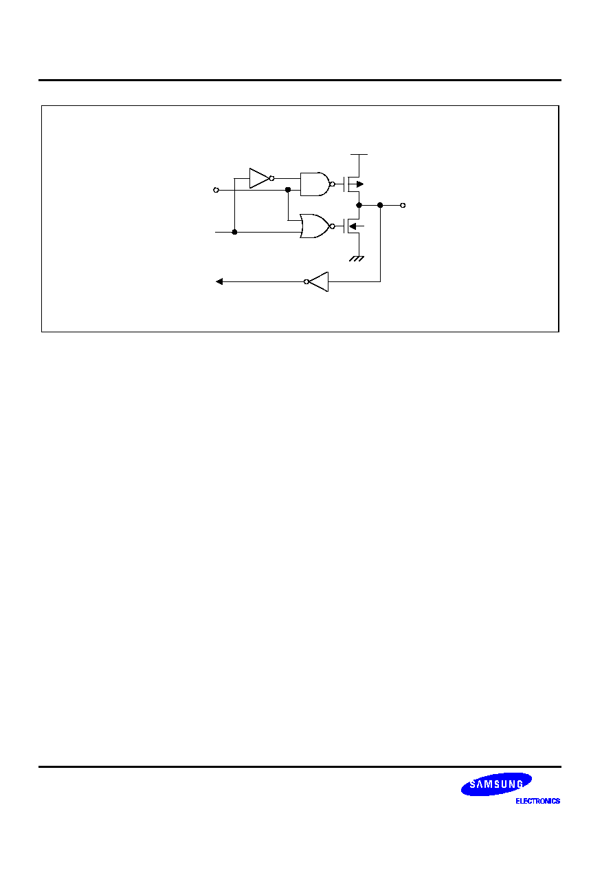
Figure 1-8. Pin Circuit Type 5
Out
V
DD
In
Figure 1-9. Pin Circuit Type 6
PRODUCT OVERVIEW
S3C84A4/P84A4
1-12
V
DD
I/O
Data
Output
Disable
Normal
Input
Figure 1-10. Pin Circuit Type 7

S3C84A4/P84A4
ELECTRICAL DATA
17-1
17
ELECTRICAL DATA
OVERVIEW
In this section, S3C84A4 electrical characteristics are presented in tables and graphs. The information is
arranged in the following order:
-- Absolute maximum ratings
-- D.C. electrical characteristics
-- A.C. electrical characteristics
-- I/O capacitance
-- Oscillation characteristics
-- Oscillation stabilization time
ELECTRICAL DATA
S3C84A4/P84A4
17-2
Table 17-1. Absolute Maximum Ratings
(T
A
= 25
∞
C)
Parameter
Symbol
Conditions
Rating
Unit
Supply voltage
V
DD
≠ 0.3 to + 6.5
V
Input voltage
V
I
≠ 0.3 to V
DD
+ 0.3
Output voltage
V
O
≠ 0.3 to V
DD
+ 0.3
V
Output current high
I
OH
One I/O pin active
≠ 18
mA
All I/O pins active
≠ 60
Output current low
I
OL
One I/O pin active
+ 30
mA
Total pin current for port
+ 100
Operating
temperature
T
A
≠ 40 to + 85
∞
C
Storage temperature
T
STG
≠ 65 to + 150
∞
C
S3C84A4/P84A4
ELECTRICAL DATA
17-3
Table 17-2. D.C. Electrical Characteristics
(T
A
= ≠ 40
∞
C to + 85
∞
C, V
DD
= 2.7 V to 5.5 V)
Parameter
Symbol
Conditions
Min
Typ
Max
Unit
Operating voltage
V
DD
F
OSC
= 30 MHz
(instruction clock = 7.5 MHz)
4.5
≠
5.5
V
Input high
V
IH1
All input pins except V
IH2,
V
IH3
0.51 V
DD
≠
V
DD
V
voltage
V
IH2
RESET
0.8 V
DD
V
IH3
X
IN
V
DD
≠ 0.5
Input low voltage
V
IL1
All input pins except V
IL2
≠
≠
0.2 V
DD
V
V
IL2
X
IN
0.4
Output high
V
OH
V
DD
= 5 V, I
OH
= ≠ 1 mA
V
DD
≠ 1.0
≠
≠
V
voltage
I
OH
= ≠ 100 uA
V
DD
≠ 0.5
≠
≠
Output low voltage
V
OL1
V
DD
= 5 V, I
OL
= 2 mA
All output pins except port 2
≠
≠
0.4
V
V
OL2
V
DD
= 5 V
I
OL
= 15 mA, port 2
≠
0.5
1.0
Input high leakage
current
I
LIH1
V
IN
= V
DD
All input pins except X
IN
≠
≠
3
µ
A
I
LIH2
V
IN
= V
DD
X
IN
20
Input low leakage
current
I
LIL1
V
IN
= 0 V
All input pins except X
IN
≠
≠
≠ 3
I
LIL2
V
IN
= 0 V, X
IN
≠ 20
Output high
leakage current
I
LOH
V
OUT
= V
DD
All I/O pins and output pins
≠
≠
5
Output low leakage
current
I
LOL
V
OUT
= 0 V
All I/O pins and output pins
≠
≠ 0
≠ 5
Pull-up and pull-
down resistor
R
L1
V
IN
= 0 V; V
DD
= 5 V
Ports 0≠3, T
A
= 25
∞
C
30
46
80
k
R
L2
V
IN
= 0 V; V
DD
= 5 V
T
A
= 25
∞
C,
RESET
only
30
50
80
ELECTRICAL DATA
S3C84A4/P84A4
17-4
Table 17-2. D.C. Electrical Characteristics (Continued)
(T
A
= ≠ 40
∞
C to + 85
∞
C, V
DD
= 2.7 V to 5.5 V)
Parameter
Symbol
Conditions
Min
Typ
Max
Unit
Supply current
(note)
I
DD1
V
DD
= 5 V
±
10%
30 MHz oscillation
≠
30
60
mA
I
DD2
Idle mode; V
DD
= 5 V
±
10%
30 MHz oscillation
10
20
I
DD3
Stop mode;
V
DD
= 5 V
±
10%
LVD enable, T
A
= 25
∞
C
100
200
µ
A
NOTE: Supply current does not include current drawn through internal pull-up resistors or external output current loads.
Table 17-3. A.C. Electrical Characteristics
(T
A
= -40
∞
C to + 85
∞
C)
Parameter
Symbol
Conditions
Min
Typ
Max
Unit
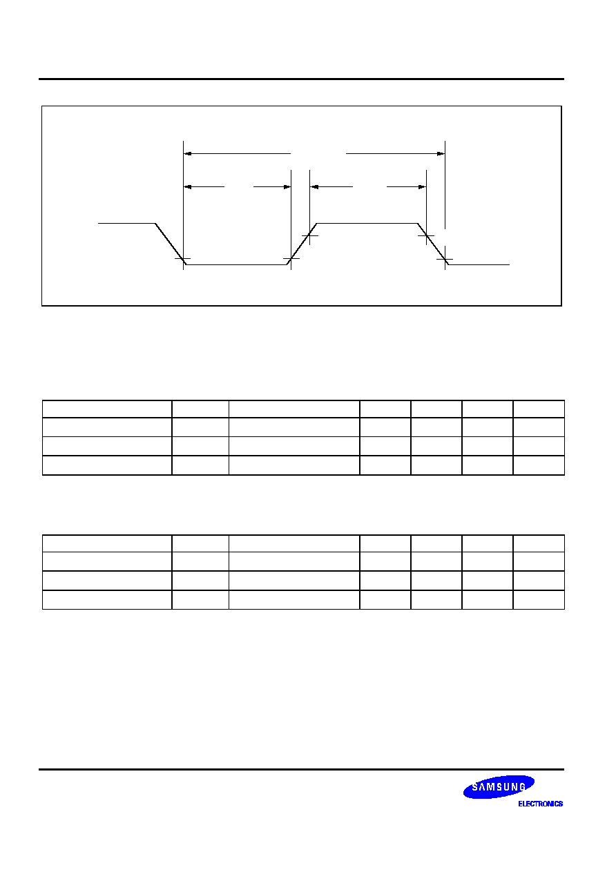
Interrupt input
high, low width
(P2.0-P2.7)
t
INTH,
t
INTL
V
DD
= 5V
180
≠
≠
nS
RESET
input low
width
t
RSL
V
DD
= 5V
1000
≠
≠
nS
NOTES:
1.
The unit t
CPU
means one CPU clock period.
2.
The oscillator frequency is the same as the CPU clock frequency.
t
INTL
t
INTH
0.8
V
DD
0.2
V
DD
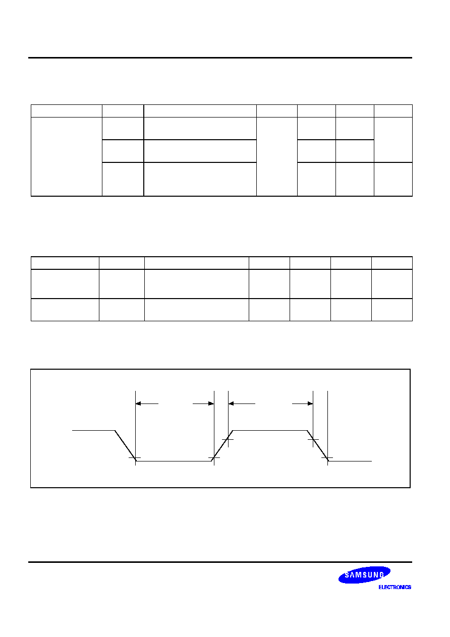
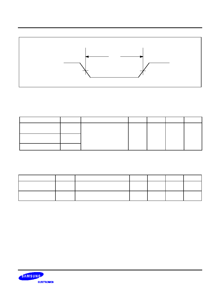
Figure 17-1. Input Timing for External Interrupts (Ports 2)
S3C84A4/P84A4
ELECTRICAL DATA
17-5
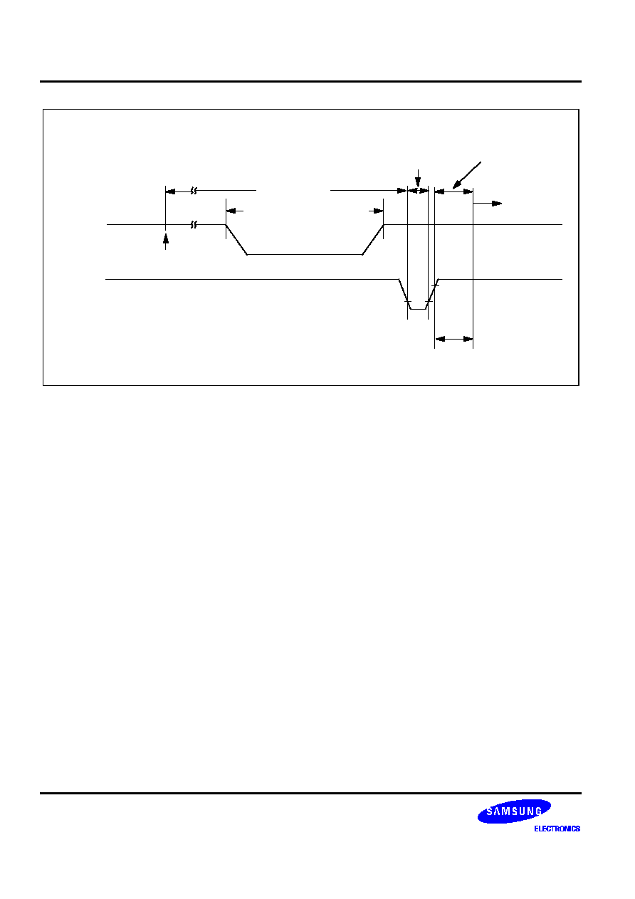
t
RSL
0.2 V
DD
RESET
Figure 17-2. Input Timing for
RESET
RESET
Table 17-4. Input/Output Capacitance
(T
A
= ≠ 40
∞
C to + 85
∞
C, V
DD
=
0 V)
Parameter
Symbol
Conditions
Min
Typ
Max
Unit
Input
capacitance
C
IN
f = 1 MHz; unmeasured
pins are connected to V
SS
≠
≠
10
pF
Output
capacitance
C
OUT
I/O capacitance
C
IO
Table 17-5. Data Retention Supply Voltage in Stop Mode
(T
A
= ≠ 40
∞
C to + 85
∞
C)
Parameter
Symbol
Conditions
Min
Typ
Max
Unit
Data retention
supply voltage
V
DDDR
2
≠
5.5
V
Data retention
supply current
I
DDDR
Stop mode, V
DDDR
= 2.0 V
≠
≠
50
µ
A
NOTES:
1.
During the oscillator stabilization wait time (t
WAIT
), all CPU operations must be stopped.
2.
Supply current does not include drawn through internal pull-up resistors and external output current loads.
ELECTRICAL DATA
S3C84A4/P84A4
17-6
V
DD
RESET
Execution of
Stop Instruction
V
DDDR
Data Retention Mode
Stop Mode
Reset
Occurs
Normal
Operating
Mode
Oscillation
Stabilization
Time
t
WAIT
NOTE: t
WAIT
is the same as 4096 x 16 x 1 / f
.
0.2 V
DD
OSC
Figure 17-3. Stop Mode Release Timing Initiated by
RESET
RESET
S3C84A4/P84A4
ELECTRICAL DATA
17-7
Table 17-6. A/D Converter Electrical Characteristics
(T
A
= ≠ 40
∞
C to + 85
∞
C)
Parameter
Symbol
Conditions
Min
Typ
Max
Unit
Resolution
≠
8
≠
bit
Total accuracy
V
DD
= 5 V
≠
≠
±
3
LSB
Integral linearity error
ILE
Conversion time = 5 us
≠
±
2
Integral linearity error
DLE
AV
REF
= 5 V
≠
±
1
Offset error of top
EOT
AV
SS
= 0 V
±
1
±
3
Offset error of bottom
EOB
±
0.5
±
2
Conversion time
(1)
t
CON
17
30
250
µ
s
Analog input voltage
V
IAN
AVss
≠
AVref
V
Analog input
impedance
R
AN
≠
2
1000
≠
M
Analog reference
voltage
AV
REF
≠
3.0
≠
V
DD
V
Analog input current
I
ADIN
AV
REF
= V
DD
= 5V
≠
≠
10
uA
Analog block
I
ADC
AV
REF
= V
DD
= 5V
1
3
mA
current
(2)
AV
REF
= V
DD
= 3V
0.5
1.5
mA
AVREF = VDD = 5V
When Power Down mode
100
500
nA
NOTES:
1.
'Conversion time' is the time required from the moment a conversion operation starts until it ends.
2.
IADC is an operating current during A/D conversion.
ELECTRICAL DATA
S3C84A4/P84A4
17-8
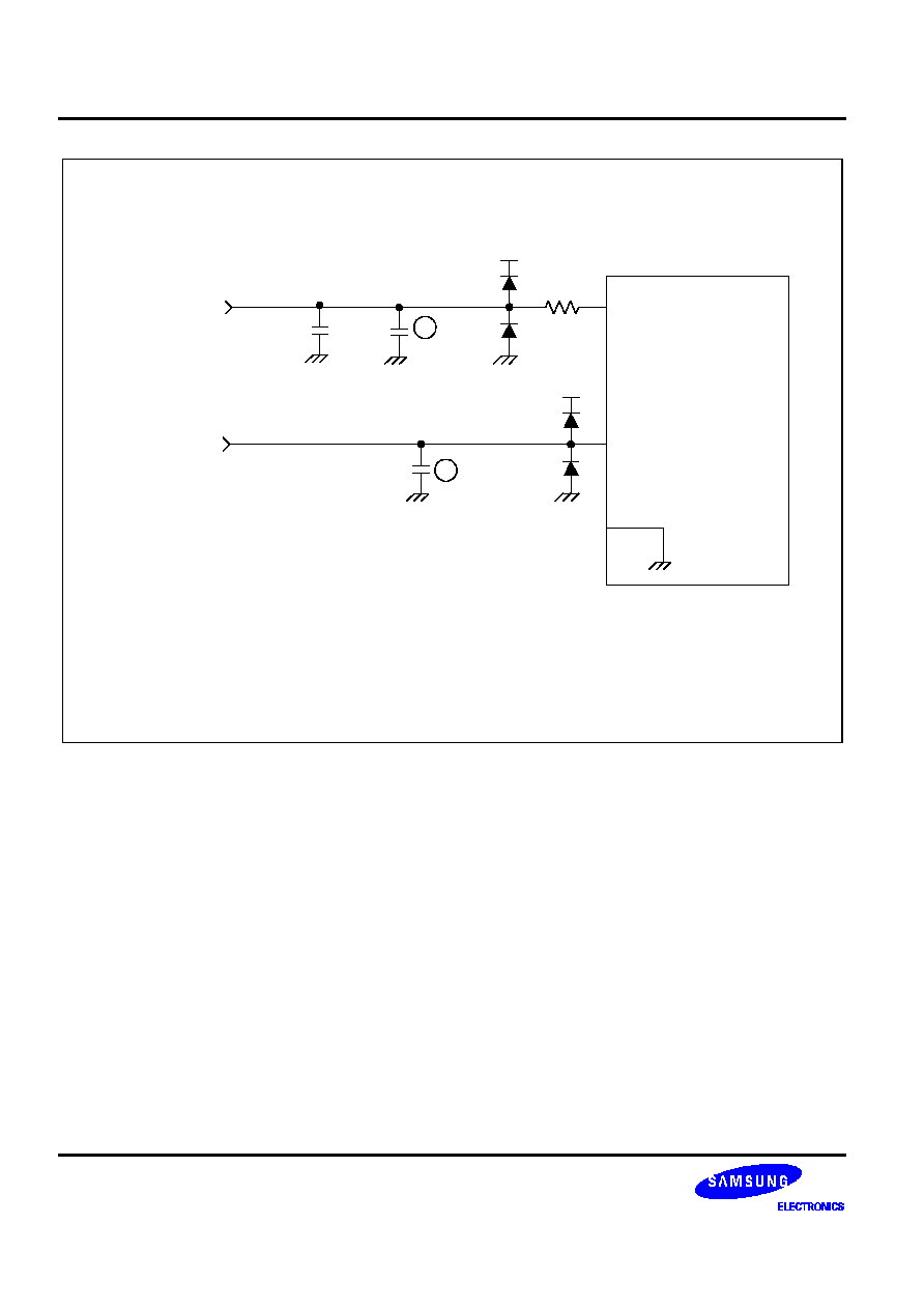
NOTE:
The symbol "R" signifies an offset resistor with a value of from 50 to 100.
If this resistor is omitted, the absolute accuracy will be maximum of 3 LSBs.
V
SS
S3C84A4
ADC0-ADC3
AV
REF
Reference
Voltage
Input
Analog
Input Voltage
R
V
DD
V
DD
10 pF
103
C
101
C
+
-
Figure 17-4. Recommended A/D Converter Circuit for Highest Absolute Accuracy
S3C84A4/P84A4
ELECTRICAL DATA
17-9
Table 17-7. Main Oscillator Frequency (f
OSC1
)
(T
A
= ≠ 40
∞
C + 85
∞
C, V
DD
= 4.5 V to 5.5 V)
Oscillator
Clock Circuit
Test Condition
Min
Typ
Max
Unit
Crystal
X
IN
C1
C2
X
OUT
CPU clock oscillation
frequency
4
≠
25
MHz
Ceramic
X
IN
C1
C2
X
OUT
CPU clock oscillation
frequency
4
≠
30
MHz
External clock
X
IN
X
OUT
X
IN
input frequency
4
≠
30
MHz
Table 17-8. Main Oscillator Clock Stabilization Time (t
ST1
)
(T
A
= -40
∞
C + 85
∞
C, V
DD
= 4.5 V to 5.5 V)
Oscillator
Test Condition
Min
Typ
Max
Unit
Crystal
V
DD
= 4.5 V to 5.5 V
≠
≠
10
ms
Ceramic
Stabilization occurs when V
DD
is equal to the minimum
oscillator voltage range.
≠
≠
4
ms
External clock
X
IN
input high and low level width (t
XH
, t
XL
)
50
≠
≠
ns
NOTE: Oscillation stabilization time (t
ST1
) is the time required for the CPU clock to return to its normal oscillation
frequency after a power-on occurs, or when Stop mode is ended by a
RESET
signal. The
RESET
should therefore
be held at low level until the tST1 time has elapsed.
ELECTRICAL DATA
S3C84A4/P84A4
17-10
X
IN
t
XL
t
XH
1 /
f
OSC1
V
DD
≠ 0.5
V
0.4
V
Figure 17-6. Clock Timing Measurement at X
IN
Table 17-9. Characteristics of Voltage Level Detect circuit
(T
A
= ≠ 40
∞
C + 85
∞
C) When Power off
Parameter
Symbol
Conditions
Min
Typ
Max
Unit
Operating Voltage of VLD
V
DD
≠
4.5
≠
5.5
V
Detect Voltage
V
DET
≠
3.1
3.7
4.1
V
Current consumption
I
VLD
V
DD
= 5.5 V
≠
100
200
uA
(T
A
= ≠ 40
∞
C + 85
∞
C) When Power on
Parameter
Symbol
Conditions
Min
Typ
Max
Unit
Operating Voltage of VLD
V
DD
≠
4.5
≠
5.5
V
Detect Voltage
V
DET
≠
3.4
4.0
4.4
V
Current consumption
I
VLD
V
DD
= 5.5 V
≠
100
200
uA
S3C84A4/P84A4
ELECTRICAL DATA
17-11
30 MHz
f
OSC
16 MHz
12 MHz
4 MHz
1
2
3
4
5
6
7
Minimum Instruction Clock = 1/4 x oscillator frequency
14 MHz
18 MHz
20 MHz
Supply Voltage (V)
Figure 17-7. Operating Voltage Range ( LVD Enable)
S3C84A4/P84A4
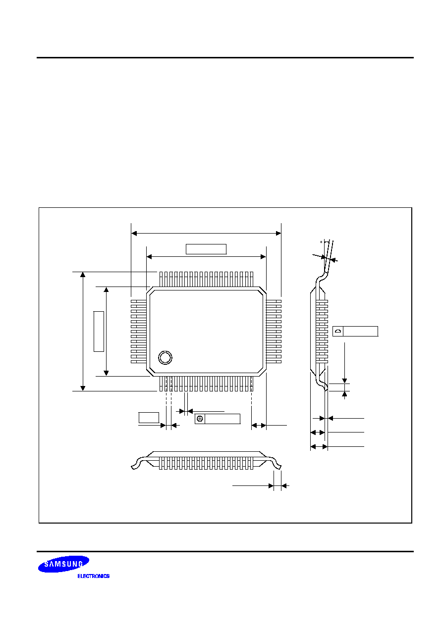
MECHANICAL DATA
18-1
18
MECHANICAL DATA
OVERVIEW
The S3C84A4 microcontroller is available in a 64-pin QFP package (64-QFP-1420C) .
64-QFP-1420C
#64
20.00
± 0.20
23.90
± 0.30
14.00
± 0.20
17.90
± 0.30
#1
1.00
(1.00)
0.40
+ 0.10
- 0.05
NOTE: Dimensions are in millimeters.
0.80
± 0.20
0.10 MAX
0.15
+ 0.10
- 0.05
0-8
0.80
± 0.20
0.05 MIN
2.65
± 0.10
3.00 MAX
0.15 MAX
Figure 18-1. 64-QFP-1420C Package Dimensions

S3C84A4/P84A4
S3P84A4 OTP
19-1
19
S3P84A4 OTP
OVERVIEW
The S3P84A4 single-chip CMOS microcontroller is the OTP (One Time Programmable)
version of the S3C84A4
microcontrollers. It has an on-chip EPROM instead of masked ROM. The EPROM is accessed by serial data
format.
S3C84A4 is fully compatible with S3C84A4, both in function and in pin configuration. As it has simple
programming requirements, S3P84A4 is ideal for use as an evaluation chip for the S3C84A4.
S3P84A4 OTP
S3C84A4/P84A4
19-2
A3
A4
A5
A6
A7
A8
A9
A10
A11
A12
A13
A14
A15
PM
DM
RD
WR
P3.4
CS1/P3.3
CS0/P3.2
A17/P3.1
V
DD
V
SS
X
OUT
X
IN
TEST/EA
A16/P3.0
WAIT/P2.7
RESET
P2.6
P2.5
P2.4
S3P84A4
(64-QFP)
51
50
49
48
47
46
45
44
43
42
41
40
39
38
37
36
35
34
33
1
2
3
4
5
6
7
8
9
10
11
12
13
14
15
16
17
18
19
52
53
54
55
56
57
58
59
60
61
62
63
64
32
31
30
29
28
27
26
25
24
23
22
21
20
P0.7
P1.0/TDCK
P1.1/TCCK
P1.2/TDCAP
P1.3/TCCAP
P1.4/TCOUT
P1.5/TDOUT
P1.6/PWM0
P1.7/PWM1
P2.0/INT0
P2.1/INT1
P2.2/INT2
P2.3/INT3
A2
A1
A0
D7
D6
D5
D4
D3
D2
D1
D0
AV
REF
P0.0/ADC0
P0.1/ADC1
P0.2/ADC2
P0.3/ADC3
P0.4
P0.5
P0.6
SDAT
SCLK
V
DD
Vss
Vpp
RESET
RESET
Figure 19-1. S3P84A4 Pin Assignments (64-QFP Package)
S3C84A4/P84A4
S3P84A4 OTP
19-3
Table 19-1. Descriptions of Pins Used to Read/Write the EPROM
Main Chip
During Programming
Pin Name
Pin Name
Pin No.
I/O
Function
P3.2
SDAT
7
I/O
Serial Data Pin (Output when reading, Input
when writing) Input and Push-pull Output Port
can be assigned.
P3.1
SCLK
8
I
Serial Clock Pin (Input Only Pin)
EA
V
PP
13
I
EPROM Cell Writing Power Supply Pin
(Indicates OTP Mode Entering) When writing
12.5V is applied and when reading 5 V is applied
(Option).
RESET
RESET
16
I
Chip Initialization
V
DD1
/V
SS1
V
DD
/V
SS
9/10
I
Logic Power Supply Pin. VDD should be tied to
5V during programming.
Table 19-2. Comparison of S3P84A4 and S3C84A4 Features
Characteristic
S3P84A4
S3C84A4
Program Memory
4 K byte EPROM
4 K bytes mask ROM
Operating Voltage (V
DD
)
2.7 V to 5.5 V
2.7 V to 5.5V
OTP Programming Mode
V
DD
= 5 V, V
PP
(TEST) = 12.5V
Pin Configuration
64 QFP
64 QFP
EPROM Programmability
User Program 1 time
Programmed at the factory
OPERATING MODE CHARACTERISTICS
When 12.5 V is supplied to the V
PP
(TEST) pin of S3P84A4, the EPROM programming mode is entered. The
operating mode (read, write, or read protection) is selected according to the input signals to the pins listed in
Table 19-3 below.
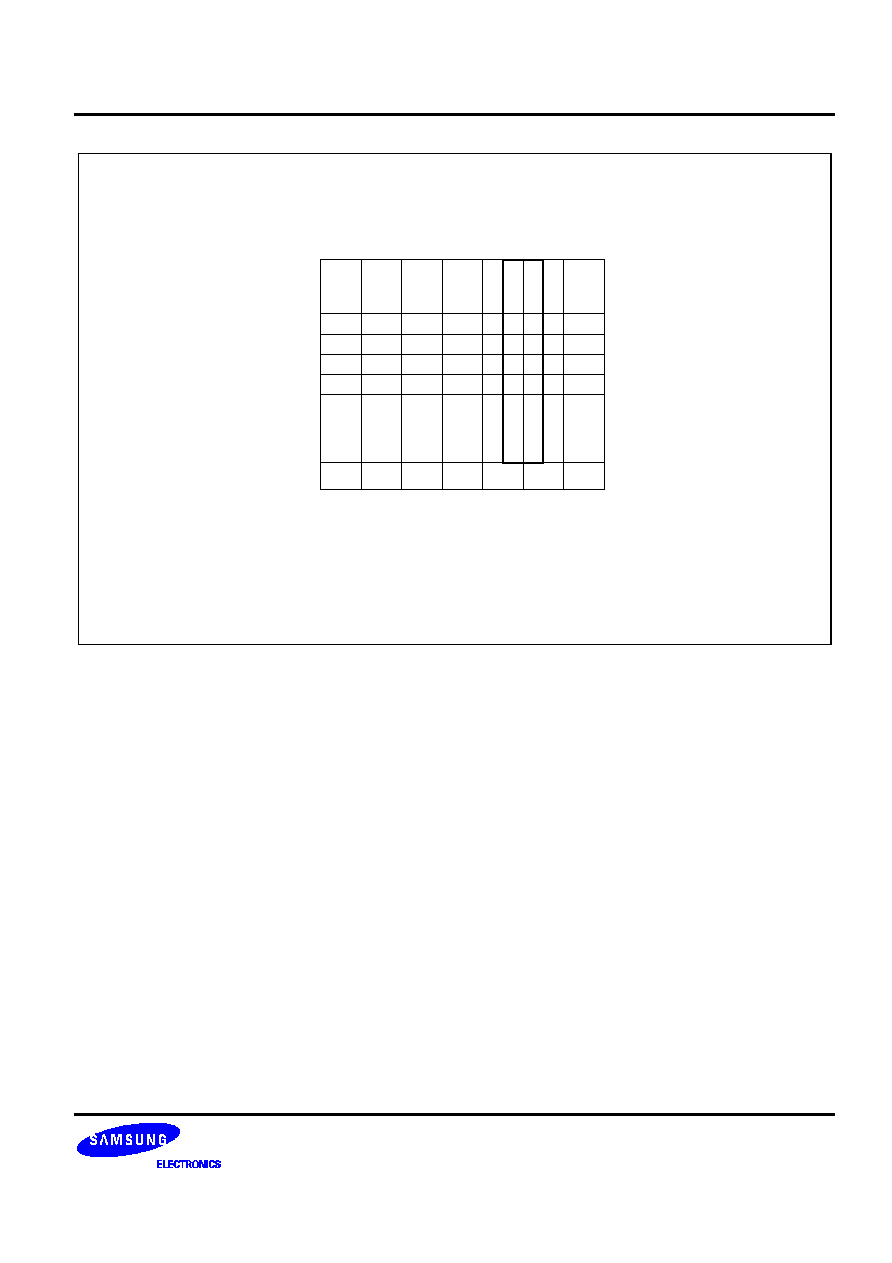
Table 19-3. Operating Mode Selection Criteria
VDD
Vpp
(TEST)
REG/
MEM
MEM
Address
(A15-A0)
R/
W
W
Mode
5 V
5 V
0
0000H
1
EPROM read
12.5 V
0
0000H
0
EPROM program
12.5 V
0
0000H
1
EPROM verify
12.5 V
1
0E3FH
0
EPROM read protection
NOTE: "0" means Low level; "1" means High level.
S3P84A4 OTP
S3C84A4/P84A4
19-4
D.C. ELECTRICAL CHARACTERISTICS
Table 19-4. D/C Electrical Characteristics
(T
A
= ≠ 40
∞
C to + 85
∞
C, V
DD
= 2.7 V to 5.5 V)
Parameter
Symbol
Conditions
Min
Typ
Max
Unit
Operating voltage
V
DD
F
OSC
= 30 MHz
(instruction clock = 7.5 MHz)
4.5
≠
5.5
V
Input high
V
IH1
All input pins except V
IH2,
V
IH3
0.51 V
DD
≠
V
DD
V
voltage
V
IH2
RESET
0.8 V
DD
V
IH3
X
IN
V
DD
≠ 0.5
Input low voltage
V
IL1
All input pins except V
IL2
≠
≠
0.2 V
DD
V
V
IL2
X
IN
0.4
Output high
V
OH
V
DD
= 5 V, I
OH
= ≠ 1 mA
V
DD
≠ 1.0
≠
≠
V
voltage
I
OH
= ≠ 100 uA
V
DD
≠ 0.5
≠
≠
Output low voltage
V
OL1
V
DD
= 5 V, I
OL
= 2 mA
All output pins except port 2
≠
≠
0.4
V
V
OL2
V
DD
= 5 V
I
OL
= 15 mA, port 2
≠
0.5
1.0
Input high leakage
current
I
LIH1
V
IN
= V
DD
All input pins except X
IN
≠
≠
3
µ
A
I
LIH2
V
IN
= V
DD
X
IN
20
Input low leakage
current
I
LIL1
V
IN
= 0 V
All input pins except X
IN
≠
≠
≠ 3
I
LIL2
V
IN
= 0 V, X
IN
≠ 20
Output high
leakage current
I
LOH
V
OUT
= V
DD
All I/O pins and output pins
≠
≠
5
Output low leakage
current
I
LOL
V
OUT
= 0 V
All I/O pins and output pins
≠
≠ 0
≠ 5
Pull-up and pull-
down resistor
R
L1
V
IN
= 0 V; V
DD
= 5 V
Ports 0≠3, T
A
= 25
∞
C
30
46
80
k
R
L2
V
IN
= 0 V; V
DD
= 5 V
T
A
= 25
∞
C,
RESET
only
30
50
80
S3C84A4/P84A4
S3P84A4 OTP
19-5
Table 19-4. D/C Electrical Characteristics (Continued)
(T
A
= ≠ 40
∞
C to + 85
∞
C, V
DD
= 2.7 V to 5.5 V)
Parameter
Symbol
Conditions
Min
Typ
Max
Unit
Supply current
(note)
I
DD1
V
DD
= 5 V
±
10%
30 MHz oscillation
≠
30
60
mA
I
DD2
Idle mode; V
DD
= 5 V
±
10%
30 MHz oscillation
10
20
I
DD3
Stop mode;
V
DD
= 5 V
±
10%
LVD enable, T
A
= 25
∞
C
100
200
µ
A
NOTE: Supply current does not include current drawn through internal pull-up resistors or external output current loads.