
S3C852B/P852B
8-BIT CMOS
MICROCONTROLLERS
USER'S MANUAL
Revision 0

Important Notice
Information in this publication has been carefully
checked and is believed to be entirely accurate at
the time of publication. SAMSUNG assumes no
responsibility, however, for possible errors or
omissions, or for any consequences resulting from
the use of the information contained herein.
SAMSUNG reserves the right to make changes in
its products or product specifications with the intent
to improve function or design at any time and
without notice and is not required to update this
documentation to reflect such changes.
This publication does not convey to a purchaser of
semiconductor devices described herein any license
under the patent rights of SAMSUNG or others.
SAMSUNG makes no warranty, representation, or
guarantee regarding the suitability of its products for
any particular purpose, nor does SAMSUNG
assume any liability arising out of the application or
use of any product or circuit and specifically
disclaims any and all liability, including without
limitation any consequential or incidental damages.
"Typical" parameters can and do vary in different
applications. All operating parameters, including
"Typicals" must be validated for each customer
application by the customer's technical experts.
SAMSUNG products are not designed, intended, or
authorized for use as components in systems
intended for surgical implant into the body, for other
applications intended to support or sustain life, or for
any other application in which the failure of the
SAMSUNG product could create a situation where
personal injury or death may occur.
Should the Buyer purchase or use a SAMSUNG
product for any such unintended or unauthorized
application, the Buyer shall indemnify and hold
SAMSUNG and its officers, employees,
subsidiaries, affiliates, and distributors harmless
against all claims, costs, damages, expenses, and
reasonable attorney fees arising out of, either
directly or indirectly, any claim of personal injury or
death that may be associated with such unintended
or unauthorized use, even if such claim alleges that
SAMSUNG was negligent regarding the design or
manufacture of said product.
S3C852B/P852B 8-Bit CMOS Microcontrollers
User's Manual, Revision 0
Publication Number: 20-S3-C852B/P852B-092002
� 2002 Samsung Electronics
All rights reserved. No part of this publication may be reproduced, stored in a retrieval system, or transmitted in
any form or by any means, electric or mechanical, by photocopying, recording, or otherwise, without the prior
written consent of Samsung Electronics.
All semiconductor products are designed and manufactured in accordance with
the highest quality standards and objectives.
Samsung Electronics Co., Ltd.
San #24 Nongseo-Ri, Giheung-Eup
Yongin-City, Gyeonggi-Do, Korea
C.P.O. Box #37, Suwon 440-900
TEL:
(82)-(31)-209-1934
FAX:
(82)-(31)-209-1899
Home Page: http://www.samsungsemi.com
Printed in the Republic of Korea

S3C852B/P852B MICROCONTROLLER
iii
Preface
The S3C852B/P852B Microcontroller User's Manual is designed for application designers and programmers who
are using the S3C852B/P852B microcontroller for application development.
It is organized in two main parts:
Part I Programming Model
Part II Hardware Descriptions
Part I contains software-related information to familiarize you with the microcontroller's architecture,
programming model, instruction set, and interrupt structure. It has six chapters:
Chapter 1
Product Overview
Chapter 2
Address Spaces
Chapter 3
Addressing Modes
Chapter 4
Control Registers
Chapter 5
Interrupt Structure
Chapter 6
Instruction Set
Chapter 1, "Product Overview," is a high-level introduction to S3C851B/P851B with general product descriptions,
as well as detailed information about individual pin characteristics and pin circuit types.
Chapter 2, "Address Spaces," describes program and data memory spaces, the internal register file, and register
addressing. Chapter 2 also describes working register addressing, as well as system stack and user-defined stack
operations.
Chapter 3, "Addressing Modes," contains detailed descriptions of the addressing modes that are supported by the
S3C8-series CPU.
Chapter 4, "Control Registers," contains overview tables for all mapped system and peripheral control register
values, as well as detailed one-page descriptions in a standardized format. You can use these easy-to-read,
alphabetically organized, register descriptions as a quick-reference source when writing programs.
Chapter 5, "Interrupt Structure," describes the S3C852B/P852B interrupt structure in detail and further prepares
you for additional information presented in the individual hardware module descriptions in Part II.
Chapter 6, "Instruction Set," describes the features and conventions of the instruction set used for all KS88-series
microcontrollers. Several summary tables are presented for orientation and reference. Detailed descriptions of
each instruction are presented in a standard format. Each instruction description includes one or more practical
examples of how to use the instruction when writing an application program.
A basic familiarity with the information in Part I will help you to understand the hardware module descriptions in
Part II. If you are not yet familiar with the S3C8-series microcontroller family and are reading this manual for the
first time, we recommend that you first read Chapters 1�3 carefully. Then, briefly look over the detailed
information in Chapters 4, 5, and 6. Later, you can reference the information in Part I as necessary.
Part II "hardware Descriptions," has detailed information about specific hardware components of the
S3C851B/P851B microcontroller. Also included in Part II are electrical, mechanical, and OTP. It has 13 chapters:
Chapter 7
Clock Circuits
Chapter 8
RESET
and Power-Down
Chapter 9
I/O Ports
Chapter 10
Basic Timer and Timer 0
Chapter 11
Timer 1
Chapter 12
Watch Timer
Chapter 13
Serial I/O Port
Chapter 14
Caller ID Block
Chapter 15
A/D Converter
Chapter 16
Extermal Interface
Chapter 17
Electrical Data
Chapter 18
Mechanical Data
Chapter 19
S3P852B OTP
Two order forms are included at the back of this manual to facilitate customer order for S3C852B/P852B
microcontrollers: the Mask ROM Order Form, and the Mask Option Selection Form. You can photocopy these
forms, fill them out, and then forward them to your local Samsung Sales Representative.


S3C852B/P852B MICROCONTROLLER
v
Table of Contents
Part I -- Programming Model
Chapter 1
Product Overview
SAM87RC Product Family .......................................................................................................................1-1
S3C852B Microcontroller .........................................................................................................................1-1
OTP.........................................................................................................................................................1-2
Features ..................................................................................................................................................1-3
Block Diagram .........................................................................................................................................1-4
Pin Assignments......................................................................................................................................1-5
Pin Descriptions.......................................................................................................................................1-6
Pin Circuits ..............................................................................................................................................1-10
Chapter 2
Address Spaces
Overview .................................................................................................................................................2-1
Program Memory (ROM) .........................................................................................................................2-2
Register Architecture ...............................................................................................................................2-4
Working Registers ...........................................................................................................................2-8
Using the Register Pointers .............................................................................................................2-9
Register Addressing.................................................................................................................................2-12
Common Working Register Area (C0H�CFH)..................................................................................2-14
4-Bit Working Register Addressing ..................................................................................................2-16
8-Bit Working Register Addressing ..................................................................................................2-18
System and User Stacks..........................................................................................................................2-20
Chapter 3
Addressing Modes
Overview .................................................................................................................................................3-1
Register Addressing Mode (R).........................................................................................................3-2
Indirect Register Addressing Mode (Ir).............................................................................................3-3
Indexed Addressing Mode (X)..........................................................................................................3-7
Direct Address Mode (DA) ...............................................................................................................3-10
Indirect Address Mode (IA) ..............................................................................................................3-12
Relative Address Mode (RA) ...........................................................................................................3-13
Immediate Mode (IM) ......................................................................................................................3-14

vi
S3C852B/P852B MICROCONTROLLER
Table of Contents
(Continued)
Chapter 4
Control Registers
Overview .................................................................................................................................................4-1
Chapter 5
Interrupt Structure
Overview .................................................................................................................................................4-1
Interrupt Types ................................................................................................................................4-2
S3C852B/P852B Interrupt Structure ................................................................................................4-3
Interrupt Vector Addresses ..............................................................................................................4-4
Enable/Disable Interrupt Instructions (EI, DI) ...................................................................................4-6
System-Level Interrupt Control Registers ........................................................................................4-6
Interrupt Processing Control Points..................................................................................................4-7
System Mode Register (SYM)..................................................................................................................4-8
Interrupt Mask Register (IMR)..........................................................................................................4-9
Interrupt Priority Register (IPR)........................................................................................................4-10
Interrupt Request Register (IRQ) .....................................................................................................4-12
Interrupt Pending Function Types ....................................................................................................4-13
Interrupt Source Polling Sequence ..................................................................................................4-14
Interrupt Service Routines ...............................................................................................................4-14
Generating Interrupt Vector Addresses ............................................................................................4-15
Nesting of Vectored Interrupts .........................................................................................................4-15
Instruction Pointer (IP).....................................................................................................................4-15
Fast Interrupt Processing.................................................................................................................4-16
Chapter 6
Instruction Set
Overview .................................................................................................................................................6-1
Data Types......................................................................................................................................6-1
Register Addressing ........................................................................................................................6-1
Addressing Modes ...........................................................................................................................6-1
Flags Register (FLAGS) ..................................................................................................................6-6
Flag Descriptions.............................................................................................................................6-7
Instruction Set Notation ...................................................................................................................6-8
Condition Codes ..............................................................................................................................6-12
Instruction Descriptions ...................................................................................................................6-13

S3C852B/P852B MICROCONTROLLER
vii
Table of Contents
(Continued)
Part II Hardware Descriptions
Chapter 7
Clock Circuits
Overview .................................................................................................................................................7-1
System Clock Circuit .......................................................................................................................7-1
Main Oscillator Circuits....................................................................................................................7-2
Sub Oscillator Circuits .....................................................................................................................7-2
Clock Status During Power-Down Modes.........................................................................................7-2
System Clock Control Register (CLKCON) ......................................................................................7-4
Oscillator Control Register (OSCCON) ............................................................................................7-5
Switching the CPU Clock.................................................................................................................7-6
Stop Control Register (STPCON) ....................................................................................................7-7
Phase Locked Loop (PLL)........................................................................................................................7-8
Main Clock Generation ....................................................................................................................7-8
Doubling Main Clock Frequency ......................................................................................................7-8
Chapter 8
RESET
RESET
and Power-Down
System Reset ..........................................................................................................................................8-1
Overview.........................................................................................................................................8-1
Normal Mode Reset Operation ........................................................................................................8-2
Rom-Less Mode Reset Operation....................................................................................................8-2
Hardware
RESET
Values ................................................................................................................8-3
Power-Down Modes.................................................................................................................................8-6
Stop Mode.......................................................................................................................................8-6
Idle Mode ........................................................................................................................................8-7
Chapter 9
I/O Ports
Overview .................................................................................................................................................9-1
Port Data Registers .........................................................................................................................9-3
Port 0 ..............................................................................................................................................9-4
Port 1 ..............................................................................................................................................9-7
Port 2 ..............................................................................................................................................9-10
Port 3 ..............................................................................................................................................9-11
Port 4 ..............................................................................................................................................9-13
Port 5 ..............................................................................................................................................9-14
Port 6 ..............................................................................................................................................9-15
Port 7 ..............................................................................................................................................9-16
Port 8 ..............................................................................................................................................9-17
Port 9 ..............................................................................................................................................9-18
Port 10 ............................................................................................................................................9-19

viii
S3C852B/P852B MICROCONTROLLER
Table of Contents
(Continued)
Chapter 10
Basic Timer & Timer 0
Module Overview.....................................................................................................................................10-1
Basic Timer Control Register (BTCON) ...........................................................................................10-2
Basic Timer Function Description ....................................................................................................10-3
Timer 0 Control Register (T0CON) ..................................................................................................10-5
Timer 0 Function Description...........................................................................................................10-7
Chapter 11
Timer 1
One 16-Bit Timer Mode (Timer 1) ............................................................................................................11-1
Overview.........................................................................................................................................11-1
Function Description........................................................................................................................11-1
Block Diagram .........................................................................................................................................11-3
Two 8-Bit Timers Mode (Timer A and B) ..................................................................................................11-4
Overview.........................................................................................................................................11-4
Function Description........................................................................................................................11-7
Chapter 12
Watch Timer
Overview .................................................................................................................................................12-1
Watch Timer Control Register (WTCON).........................................................................................12-2
Watch Timer Circuit Diagram ..........................................................................................................12-3
Chapter 13
Serial I/O Port
Overview .................................................................................................................................................13-1
Programming Procedure..................................................................................................................13-1
Sio Control Register (SIOCON) .......................................................................................................13-2
Sio Prescaler Register (SIOPS) .......................................................................................................13-3
Block Diagram.................................................................................................................................13-3
Serial I/O Timing Diagrams .............................................................................................................13-4

S3C852B/P852B MICROCONTROLLER
ix
Table of Contents
(Continued)
Chapter 14Caller ID Block
Overview .................................................................................................................................................14-1
Function Description of CID Block ...........................................................................................................14-3
Analog Input and Preprocessor........................................................................................................14-3
CAS Tone Detection........................................................................................................................14-5
FSK Data Reception........................................................................................................................14-6
Stutter Dial Tone(SDT) Detector......................................................................................................14-8
Ring or Line Reversal Detector........................................................................................................14-9
Tone Generator...............................................................................................................................14-11
Melody Generator............................................................................................................................14-16
Power-Down Mode of CID Block......................................................................................................14-18
Interrupt of CID Block ......................................................................................................................14-18
Register Maps of CID Block.............................................................................................................14-19
Chapter 15
A/D Converter
Overview .................................................................................................................................................15-1
Function Description ................................................................................................................................15-1
A/D Converter Control Register (ADCON) .......................................................................................15-2
Internal Reference Voltage Levels...................................................................................................15-3
Conversion Timing ..........................................................................................................................15-4
Internal A/D Conversion Procedure .................................................................................................15-5
Chapter 16
External Interface
Overview .................................................................................................................................................16-1
Configuration Options for External Program Memory ......................................................................16-3
External Interface Control Registers ................................................................................................16-4
System Mode Register (SYM) .........................................................................................................16-4
External Memory Timing Register (EMT).........................................................................................16-5
Port 3 Alternative Function Select Register (P3AFS) .......................................................................16-6
Port 4 Control Register (P4CON).....................................................................................................16-6
Port 5 Control Register (P5CON).....................................................................................................16-6
Port 6 Control Register (P6CON).....................................................................................................16-6
Configuring Separate External Program and Data Memory Areas ...................................................16-8
External Bus Operations..................................................................................................................16-9
Sam8 Instruction Execution Timing Diagrams .................................................................................16-15

x
S3C852B/P852B MICROCONTROLLER
Table of Contents
(Concluded)
Chapter 17
Electrical Data
Overview .................................................................................................................................................17-1
Chapter 18
Mechanical Data
Overview .................................................................................................................................................18-1
Chapter 19
S3P852B OTP
Overview .................................................................................................................................................19-1
Operating Mode Characteristics.......................................................................................................19-3

S3C852B/P852B MICROCONTROLLER
xi
List of Figures
Figure
Title
Page
Number
Number
1-1
Block Diagram........................................................................................................1-4
1-2
Pin Assignment (100-Pin QFP Package) ................................................................1-5
1-3
Pin Circuit Type 1...................................................................................................1-10
1-4
Pin Circuit Type 2 (RESET)....................................................................................1-10
1-5
Pin Circuit Type 3 (Port 0) ......................................................................................1-10
1-6
Pin Circuit Type 4 (Port 1.0-Port 1.3)......................................................................1-11
1-7
Pin Circuit Type 5 (Port 3) ......................................................................................1-12
1-8
Pin Circuit Type 6 (Port 4, 5, 6) ..............................................................................1-12
2-1
Program Memory Address Space ...........................................................................2-2
2-2
Internal Register File Organization .........................................................................2-4
2-3
Register Page Pointer (PP) ....................................................................................2-6
2-4
Map of Set 1, Set 2, and Prime Register Spaces ....................................................2-7
2-5
8-Byte Working Register Areas (Slices)..................................................................2-8
2-6
Contiguous 16-Byte Working Register Block ..........................................................2-10
2-7
Non-Contiguous 16-Byte Working Register Block ...................................................2-10
2-8
16-Bit Register Pairs ..............................................................................................2-12
2-9
Register File Addressing.........................................................................................2-13
2-10
Common Working Register Area ............................................................................2-14
2-11
4-Bit Working Register Addressing .........................................................................2-17
2-13
4-Bit Working Register Addressing Example ..........................................................2-17
2-13
8-Bit Working Register Addressing .........................................................................2-18
2-14
8-Bit Working Register Addressing Example ..........................................................2-19
2-15
Stack Operations....................................................................................................2-20
3-1
Register Addressing ...............................................................................................3-2
3-2
Working Register Addressing .................................................................................3-2
3-3
Indirect Register Addressing to Register File ..........................................................3-3
3-4
Indirect Register Addressing to Program Memory...................................................3-4
3-5
Indirect Working Register Addressing to Register File ............................................3-5
3-6
Indirect Working Register Addressing to Program or Data Memory ........................3-6
3-7
Indexed Addressing to Register File .......................................................................3-7
3-8
Indexed Addressing to Program or Data Memory with Short Offset ........................3-8
3-9
Indexed Addressing to Program or Data Memory ...................................................3-9
3-10
Direct Addressing for Load Instructions ..................................................................3-10
3-11
Direct Addressing for Call and Jump Instructions....................................................3-11
3-12
Indirect Addressing.................................................................................................3-12
3-13
Relative Addressing ...............................................................................................3-13
3-14
Immediate Addressing............................................................................................3-14

xii
S3C852B/P852B MICROCONTROLLER
List of Figures
(Continued)
Figure
Title
Page
Number
Number
4-1
Register Description Format ...................................................................................4-4
5-1
SAM8-Series Interrupt Types..................................................................................5-2
5-2
S3C852B Interrupt Structure...................................................................................5-3
5-3
Vector Address Area in Program Memory (ROM) ...................................................5-4
5-4
Interrupt Function Diagram .....................................................................................5-7
5-5
System Mode Register (SYM) ................................................................................5-8
5-6
Interrupt Mask Register (IMR).................................................................................5-9
5-7
Interrupt Request Priority Groups ...........................................................................5-10
5-8
Interrupt Priority Register (IPR)...............................................................................5-11
5-9
Interrupt Request Register (IRQ) ............................................................................5-12
6-1
System Flags Register (FLAGS).............................................................................6-6
7-1
Crystal Oscillator ....................................................................................................7-2
7-2
Crystal Oscillator ....................................................................................................7-2
7-3
System Clock Circuit Diagram ................................................................................7-3
7-4
System Clock Control Register (CLKCON) .............................................................7-4
7-5
Oscillator Control Register (OSCCON) ...................................................................7-5
7-6
STOP Control Register (STPCON) .........................................................................7-7
9-1
S3C852B I/O Port Data Register Format ................................................................9-3
9-2
Port 0 Control Register (P0CONH) .........................................................................9-5
9-3
Port 0 Control Register (P0CONL) ..........................................................................9-5
9-4
Port 0 Interrupt Enable Register (P0INT) ................................................................9-6
9-5
Port 0 Interrupt Pending Register (P0PND).............................................................9-6
9-6
Port 0 Interrupt State Register (P0STA)..................................................................9-6
9-7
Port 1 High-Byte Control Register (P1CONH) .........................................................9-8
9-8
Port 1 Low-Byte Control Register (P1CONL) ..........................................................9-8
9-9
Port 1 Alternative Function Select Register (P1AFS) ..............................................9-9
9-10
Port 2 Control Register (P2CON)............................................................................9-10
9-11
Port 3 Control Register (P3CON)............................................................................9-12
9-12
Port 3 Alternative Function Select Register (P3AFS) ..............................................9-12
9-13
Port 4 Control Register (P4CON)............................................................................9-13
9-14
Port 5 Control Register (P5CON)............................................................................9-14
9-15
Port 6 Control Register (P6CON)............................................................................9-15
9-16
Port 7 High-Byte Control Register (P7CONH) .........................................................9-16
9-17
Port 7 Low-Byte Control Register (P7CONL) ..........................................................9-16
9-18
Port 8 High-Byte Control Register (P8CONH) .........................................................9-17
9-19
Port 8 Low-Byte Control Register (P8CONL) ..........................................................9-17
9-20
Port 9 High-Byte Control Register (P9CONH) .........................................................9-18
9-21
Port 9 Low-Byte Control Register (P9CONL) ..........................................................9-18
9-22
Port 10 High-Byte Control Register (P10CONH) .....................................................9-19
9-23
Port 10 Low-Byte Control Register (P10CONL).......................................................9-19

S3C852B/P852B MICROCONTROLLER
xiii
List of Figures
(Continued)
Page
Title
Page
Number
Number
10-1
Basic Timer Control Register (BTCON) ..................................................................10-2
10-2
Basic Timer Block Diagram ....................................................................................10-4
10-3
Timer 0 Control Register (T0CON) .........................................................................10-6
10-4
Simplified Timer 0 Function Diagram: Interval Timer Mode ....................................10-7
10-5
Simplified Timer 0 Function Diagram: PWM Mode .................................................10-8
10-6
Simplified Timer 0 Function Diagram: Capture Mode .............................................10-9
10-7
Timer 0 Block Diagram...........................................................................................10-10
11-1
Timer 1 Control Register (TACON).........................................................................11-2
11-2
Timer 1 Functional Block Diagram .........................................................................11-3
11-3
Timer A Control Register (TACON) ........................................................................11-5
11-4
Timer B Control Register (TBCON) ........................................................................11-6
11-5
Timer A and B Function Block Diagram..................................................................11-8
11-6
Timer B PWM Function Block Diagram ..................................................................11-9
12-1
Watch Timer Control Register (WTCON) ...............................................................12-2
12-2
Watch Timer Circuit Diagram .................................................................................12-3
13-1
Serial I/O Module Control Registers (SIOCON) ......................................................13-2
13-2
SIO Prescaler Register (SIOPS).............................................................................13-3
13-3
SIO Functional Block Diagram ...............................................................................13-3
13-4
SIO Timing in Transmit/Receive Mode (Tx at falling edge, SIOCON.4=0) ..............13-4
13-5
SIO Timing in Transmit/Receive Mode (Tx at rising edge, SIOCON.4=1) ...............13-4
13-6
SIO Timing in Receive-Only Mode (Rising edge start)............................................13-5
14-1
CID Part Functional Block Diagram ........................................................................14-2
14-2
Differential Input Buffer of the S3C852B.................................................................14-3
14-3
Single Ended Buffer of the S3C852B......................................................................14-4
14-4
CASdetect, CASint and INT Related to the CAS Tone............................................14-5
14-5
Sequence to Receive an FSK Data Byte ................................................................14-6
14-6
Interrupt behavior of the FSK receiver with BOMDC = 1.........................................14-7
14-7
Interrupt behavior of the FSK receiver with BOMDC = 0.........................................14-7
14-8
SDT Detector Operation .........................................................................................14-8
14-9
External Component to Generate LRin ...................................................................14-9
14-10
Behavior of Signals on a Line Reversal ..................................................................14-10
14-11
Behavior of Signals During Ring.............................................................................14-10
14-12
Tone Generator Block ............................................................................................14-11
14-13
Block Diagram of NCO ...........................................................................................14-12
14-14
Block Diagram of Melody Generator.......................................................................14-17

xiv
S3C852B/P852B MICROCONTROLLER
List of Figures
(Continued)
Page
Title
Page
Number
Number
15-1
A/D Converter Control Register (ADCON) ..............................................................15-2
15-2
A/D Converter Data Register (ADDATAH/ADDATAL) .............................................15-2
15-3
A/D Converter Circuit Diagram ...............................................................................15-3
15-4
A/D Converter Timing Diagram ..............................................................................15-4
15-5
Recommended A/D Converter Circuit for Highest Absolute Accuracy .....................15-5
16-1
S3C852B External Memory Interface Function diagram .........................................16-2
16-2
Internal and External Program Memory Options .....................................................16-3
16-3
System Mode Register (SYM) ................................................................................16-4
16-4
External Memory Timing Control Register (EMT) ...................................................16-5
16-5
External Bus Write Cycle Timing Diagram (Address, and Data Separated )............16-10
16-6
External Bus Read Cycle Timing Diagram ..............................................................16-11
16-7
External Interface Function Diagram (with SRAM and EPROM or EEPROM) .........16-13
16-8
External Interface Function Diagram (External ROM Only).....................................16-14
16-9
External Bus Timing Diagram for 1-Byte Fetch Instructions ....................................16-15
16-10
External Bus Timing Diagram for 2-Byte Fetch Instructions ....................................16-15
16-11
External Bus Timing Diagram for 3-Byte Fetch Instructions ....................................16-16
16-12
External Bus Timing Diagram for 4-Byte Fetch Instructions ....................................16-16
17-1
Stop Mode Release Timing When Initiated by an External Interrupt .......................17-5
17-2
Stop Mode Release Timing When Initiated by a
RESET
.........................................17-6
17-3
Input Timing for External Interrupts (P0.0�P0.7) .....................................................17-7
17-4
Input Timing for
RESET
.........................................................................................17-7
17-5
Clock Timing Measurement at X
IN
..........................................................................17-9
17-6
Clock Timing Measurement at XT
IN
........................................................................17-9
17-7
Serial Data Transfer Timing....................................................................................17-11
17-8
Waveform for CAS Timing Characteristics .............................................................17-14
18-1
100-Pin QFP Package Mechanical Data .................................................................18-2
19-1
S3P852B Pin Assignments (100-Pin QFP Package) ...............................................19-2

S3C852B/P852B MICROCONTROLLER
xv
List of Tables
Table
Title
Page
Number
Number
1-1
Pin Descriptions .....................................................................................................1-6
2-1
S3C852B Register Type Summary .........................................................................2-4
4-1
Set 1, Bank 0 Registers..........................................................................................4-2
4-2
Set 1, Bank 1 Registers..........................................................................................4-3
5-1
S3C852B/P852B Interrupt Vectors .........................................................................5-5
5-2
Interrupt Control Register Overview .......................................................................5-6
6-1
Instruction Group Summary....................................................................................6-2
6-2
Flag Notation Conventions .....................................................................................6-8
6-3
Instruction Set Symbols..........................................................................................6-8
6-4
Instruction Notation Conventions ............................................................................6-9
6-5
Opcode Quick Reference .......................................................................................6-10
6-6
Condition Codes.....................................................................................................6-12
8-1
S3C851B/P852B Set 1 Register and Values after
RESET
(Masked ROM Mode) .............................................................................................8-3
8-2
S3C851B/P852B Set 1, Bank 0 Register and Values after
RESET
(Masked ROM Mode) .............................................................................................8-4
8-3
S3C851B/P852B Set 1, Bank 1 Register Values after
RESET
(Masked ROM Mode) .............................................................................................8-5
9-1
S3C851B Port Configuration Overview...................................................................9-2
9-2
Port Data Register Summary..................................................................................9-3
14-1
CAS detector parameters .......................................................................................14-5
14-2
FSK Receiver Parameters......................................................................................14-6
14-3
Stutter dial Tone Parameters..................................................................................14-8
14-4
DTMF Frequencies Code and Phase Input Data.....................................................14-14
14-5
Dual Tone Frequency of CAS and Phase Input Data ..............................................14-14
14-6
FSK Parameters.....................................................................................................14-15
14-7
The Frequencies and MREF1 Register Values for 3 Octave Musical Scale ............14-16
14-8
Interrupt Sources of the CID Block .........................................................................14-18
14-9
Register Overview..................................................................................................14-19

xvi
S3C852B/P852B MICROCONTROLLER
List of Tables
(Continued)
Table
Title
Page
Number
Number
16-1
Control Register Overview for the External Interface ..............................................16-6
16-2
External Interface Control Register Values after a
RESET
(Normal Mode) .............16-7
16-3
External Interface Control Register Values after a
RESET
(ROM-less Mode) .........16-7
16-4
S3C852B External Memory Interface Signal Descriptions.......................................16-12
17-1
Absolute Maximum Ratings ....................................................................................17-2
17-2
D.C. Electrical Characteristics ................................................................................17-3
17-3
Data Retention Supply Voltage in Stop Mode .........................................................17-5
17-4
Input/Output Capacitance .......................................................................................17-7
17-5
A.C. Electrical Characteristics ................................................................................17-7
17-6
Main Oscillation Characteristics..............................................................................17-8
17-7
Sub Oscillation Characteristics ...............................................................................17-8
17-8
Main Oscillation Stabilization Time .........................................................................17-9
17-9
Sub Oscillation Stabilization Time ..........................................................................17-9
17-10
Phase Locked Loop Characteristics ........................................................................17-10
17-11
Serial I/O Timing Characteristics ............................................................................17-11
17-12
A/D Converter Electrical Characteristics .................................................................17-12
17-13
Electrical Characteristics of CID Block (Receiver & Detectors) ...............................17-13
17-14
CAS Timing Characteristics....................................................................................17-14
17-15
Electrical Characteristics of CID Block (Tone Generator)........................................17-14
17-16
SDT Timing Characteristics ....................................................................................17-15
19-1
Descriptions of Pins Used to Read/Write the EPROM.............................................19-3
19-2
Comparison of S3P852B and S3C852B Features ...................................................19-3

S3C852B/P852B MICROCONTROLLER
xvii
List of Programming Tips
Description
Page
Number
Chapter 2:
Address Spaces
Setting the Register Pointers ...............................................................................................................2-9
Addressing the Common Working Register Area .................................................................................2-15
Standard Stack Operations Using PUSH and POP ..............................................................................2-21
Chapter 5:
Interrupt Structure
Setting Up the S3C852B Interrupt Control Structure ............................................................................5-18
Chapter 7:
Clock Circuits
Switching the CPU clock......................................................................................................................7-6
Chapter 8:
RESET
RESET
and Power-Down
Sample S3C852B Initialization Routine ...............................................................................................8-8
Chapter 10:
Basic Timer and Timer 0
Configuring the BASIC Timer ..............................................................................................................10-11
Programming Timer 0..........................................................................................................................10-12
Chapter 13:
Serial I/O Port
Use Internal Clock to Transfer and Receive Serial Data ......................................................................13-5
Chapter 15:
A/D Converter
Configuring A/D Converter ..................................................................................................................15-6


S3C852B/P852B MICROCONTROLLER
xix
List of Register Descriptions
Register
Full Register Name
Page
Identifier
Number
ADCON
A/D Converter Control Register ..............................................................................4-5
BTCON
Basic Timer Control Register..................................................................................4-6
CLKCON
System Clock Control Register ...............................................................................4-7
CLKMOD
Clock Output Mode Register...................................................................................4-8
EMT
External Memory Timing Register ..........................................................................4-9
FLAGS
System Flags Register ...........................................................................................4-10
IMR
Interrupt Mask Register ..........................................................................................4-11
INTPND
Interrupt Pending Register......................................................................................4-12
IPH
Instruction Pointer (High Byte)................................................................................4-13
IPL
Instruction Pointer (Low Byte).................................................................................4-13
IPR
Interrupt Priority Register........................................................................................4-14
IRQ
Interrupt Request Register......................................................................................4-15
OSCCON
Oscillator Control Register......................................................................................4-16
P0CONH
Port 0 Control Register (High byte) .........................................................................4-17
P0CONL
Port 0 Control Register(Low byte)...........................................................................4-18
P0INT
Port 0 Interrupt Enable Register .............................................................................4-19
P0PND
Port 0 Interrupt Pending Register ...........................................................................4-20
P0STA
Port 0 Interrupt State Register ................................................................................4-21
P1AFS
Port 1 Function Select Register ..............................................................................4-22
P1CONH
Port 1 Control Register(High byte) ..........................................................................4-23
P1CONL
Port 1 Control Register(Low byte)...........................................................................4-24
P2CON
Port 2 Control Register ...........................................................................................4-25
P3AFS
Port 3 Function Select Register ..............................................................................4-26
P3CON
Port 3 Control Register ...........................................................................................4-27
P4CON
Port 4 Control Register ...........................................................................................4-28
P5CON
Port 5 Control Register ...........................................................................................4-29
P6CON
Port 4 Control Register ...........................................................................................4-30
P7CONH
Port 7 Control Register(High byte) ..........................................................................4-31
P7CONL
Port 7 Control Register(Low byte)...........................................................................4-32
P8CONH
Port 8 Control Register(High byte) ..........................................................................4-33
P8CONL
Port 8 Control Register(Low byte)...........................................................................4-34
P9CONH
Port 9 Control Register(High byte) ..........................................................................4-35
P9CONL
Port 9 Control Register(Low byte)...........................................................................4-36
P10CONH
Port 10 Control Register(High byte) ........................................................................4-37
P10CONL
Port 10 Control Register(Low byte).........................................................................4-38

xx
S3C852B/P852B MICROCONTROLLER
List of Register Descriptions
(Continued)
Register
Full Register Name
Page
Identifier
Number
PP
Register Page Pointer.............................................................................................4-39
RP0
Register Pointer 0...................................................................................................4-40
RP1
Register Pointer 1...................................................................................................4-40
SIOCON
SIO Control Register ..............................................................................................4-41
SIOPS
SIO Prescaler Register ...........................................................................................4-42
SPH
Stack Pointer (High Byte) .......................................................................................4-43
SPL
Stack Pointer (Low Byte) ........................................................................................4-43
STPCON
Stop Control Register .............................................................................................4-44
SYM
System Mode Register ...........................................................................................4-45
T0CON
Timer A Control Register ........................................................................................4-46
TACON
Timer A Control Register ........................................................................................4-47
TBCON
Timer B Control Register ........................................................................................4-48
WTCON
Watch Timer Control Register ................................................................................4-49

S3C852B/P852B MICROCONTROLLER
xxi
List of Instruction Descriptions
Instruction
Full Register Name
Page
Mnemonic
Number
ADC
Add with Carry........................................................................................................6-14
ADD
Add ........................................................................................................................6-15
AND
Logical AND ...........................................................................................................6-16
BAND
Bit AND ..................................................................................................................6-17
BCP
Bit Compare ...........................................................................................................6-18
BITC
Bit Complement .....................................................................................................6-19
BITR
Bit Reset ................................................................................................................6-20
BITS
Bit Set ....................................................................................................................6-21
BOR
Bit OR ....................................................................................................................6-22
BTJRF
Bit Test, Jump Relative on False............................................................................6-23
BTJRT
Bit Test, Jump Relative on True .............................................................................6-24
BXOR
Bit XOR..................................................................................................................6-25
CALL
Call Procedure .......................................................................................................6-26
CCF
Complement Carry Flag .........................................................................................6-27
CLR
Clear ......................................................................................................................6-28
COM
Complement...........................................................................................................6-29
CP
Compare ................................................................................................................6-30
CPIJE
Compare, Increment, and Jump on Equal ..............................................................6-31
CPIJNE
Compare, Increment, and Jump on Non-Equal .......................................................6-32
DA
Decimal Adjust .......................................................................................................6-33
DEC
Decrement .............................................................................................................6-35
DECW
Decrement Word ....................................................................................................6-36
DI
Disable Interrupts ...................................................................................................6-37
DIV
Divide (Unsigned)...................................................................................................6-38
DJNZ
Decrement and Jump if Non-Zero ..........................................................................6-39
EI
Enable Interrupts ....................................................................................................6-40
ENTER
Enter ......................................................................................................................6-41
EXIT
Exit ........................................................................................................................6-42
IDLE
Idle Operation ........................................................................................................6-43
INC
Increment ...............................................................................................................6-44
INCW
Increment Word .....................................................................................................6-45
IRET
Interrupt Return ......................................................................................................6-46
JP
Jump ......................................................................................................................6-47
JR
Jump Relative ........................................................................................................6-48
LD
Load.......................................................................................................................6-49
LDB
Load Bit..................................................................................................................6-51

xxii
S3C852B/P852B MICROCONTROLLER
List of Instruction Descriptions
(Continued)
Instruction
Full Register Name
Page
Mnemonic
Number
LDC/LDE
Load Memory .........................................................................................................6-52
LDCD/LDED
Load Memory and Decrement ................................................................................6-54
LDCI/LDEI
Load Memory and Increment ..................................................................................6-55
LDCPD/LDEPD
Load Memory with Pre-Decrement .........................................................................6-56
LDCPI/LDEPI
Load Memory with Pre-Increment ...........................................................................6-57
LDW
Load Word .............................................................................................................6-58
MULT
Multiply (Unsigned).................................................................................................6-59
NEXT
Next .......................................................................................................................6-60
NOP
No Operation ..........................................................................................................6-61
OR
Logical OR .............................................................................................................6-62
POP
Pop from Stack.......................................................................................................6-63
POPUD
Pop User Stack (Decrementing) .............................................................................6-64
POPUI
Pop User Stack (Incrementing) ...............................................................................6-65
PUSH
Push to Stack .........................................................................................................6-66
PUSHUD
Push User Stack (Decrementing)............................................................................6-67
PUSHUI
Push User Stack (Incrementing) .............................................................................6-68
RCF
Reset Carry Flag ....................................................................................................6-69
RET
Return ....................................................................................................................6-70
RL
Rotate Left .............................................................................................................6-71
RLC
Rotate Left through Carry .......................................................................................6-72
RR
Rotate Right ...........................................................................................................6-73
RRC
Rotate Right through Carry .....................................................................................6-74
SB0
Select Bank 0 .........................................................................................................6-75
SB1
Select Bank 1 .........................................................................................................6-76
SBC
Subtract with Carry .................................................................................................6-77
SCF
Set Carry Flag ........................................................................................................6-78
SRA
Shift Right Arithmetic..............................................................................................6-79
SRP/SRP0/SRP1
Set Register Pointer ...............................................................................................6-80
STOP
Stop Operation .......................................................................................................6-81
SUB
Subtract..................................................................................................................6-82
SWAP
Swap Nibbles .........................................................................................................6-83
TCM
Test Complement under Mask ................................................................................6-84
TM
Test under Mask.....................................................................................................6-85
WFI
Wait for Interrupt ....................................................................................................6-86
XOR
Logical Exclusive OR .............................................................................................6-87

S3C852B/P852B (Preliminary Spec)
PRODUCT OVERVIEW
1-1
1
PRODUCT OVERVIEW
SAM87RC PRODUCT FAMILY
Samsung's new SAM87RC family of 8-bit single-chip CMOS microcontrollers offers a fast and efficient CPU, a
wide range of integrated peripherals, and various mask-programmable ROM sizes. Timer/counters with
selectable operating modes are included to support real-time operations. Many SAM87RC microcontrollers have
an external interface that provides access to external memory and other peripheral devices. The sophisticated
interrupt structure recognizes up to eight interrupt levels. Each level can have one or more interrupt sources and
vectors. Fast interrupt processing (within a minimum six CPU clocks) can be assigned to specific interrupt levels.
S3C852B MICROCONTROLLER
The S3C852B is a low power CMOS 8-bit micro controller, which has a micro control unit (MCU), Caller ID on
Call Waiting (CIDCW) receiver, tone generator, etc. The S3C852B single-chip microcontroller is fabricated using
a highly advanced CMOS process. Its design is based on the powerful SAM87RC CPU core. Stop and Idle
power-down modes were implemented to reduce power consumption. The S3C852B is used for receiving
physical layer signals like Bellcore's CPE Alerting Signal (CAS) and similar evolving systems and also meets the
requirements of emerging Caller ID on Call Waiting (CIDCW) services. In addition, two different signal inputs are
available to support Tip/Ring and Hybrid connectivity. The device also includes a 1200 baud Bell 202/V.23
compatible FSK data demodulator, a ring or line reversal detector, a Stutter Dial Tone detector and a tone
generator. Tone generator is capable of generating FSK signal and dual tone signals such as CAS, DTMF to
support various applications such as short messaging service (SMS). The size of the internal register file is
logically expanded, increasing the addressable on-chip register space to 1808 bytes. A flexible yet sophisticated
external interface is used to access up to 64-Kbytes of program and data memory. The S3C852B is a versatile
microcontroller that is ideal for use in a wide range of following applications.
�
Bellcore CID and CIDCW systems
�
CID and CIDCW feature phones and adjunct boxes
�
Voice-Mail and Short Messaging Service (SMS) Equipment
Using the S3C852B modular design approach, the following peripherals were integrated with the SAM87RC CPU
core:
�
Large number of programmable I/O ports (Total 80 pins)
�
One synchronous SIO module
�
One 8-bit timer/counter (Including Interval mode, Capture mode, PWM mode)
�
One 16-bit timer/counter (Including One 16-bit Timer/Counter mode and
Two 8-bit Timer/Counter mode)
�
A/D converter with 4 selectable input pins

PRODUCT OVERVIEW
S3C852B/P852B (Preliminary Spec)
1-2
OTP
The S3C852B microcontroller is also available in OTP(One Time Programmable) version, S3P852B.
The S3P852B microcontroller has an on-chip 64K-byte one-time-programmable EPROM instead of masked
ROM. The S3P852B is comparable to S3C852B, both in function and in pin configuration.

S3C852B/P852B (Preliminary Spec)
PRODUCT OVERVIEW
1-3
FEATURES
CPU
�
SAM87RC CPU core
Memory
�
1808-byte of internal register file
�
64-Kbyte internal program memory area
External Interface
�
64-Kbyte external data memory area
�
64-Kbyte external program memory (ROMless)
Instruction Set
�
78 instructions
�
IDLE and STOP instructions
Instruction Execution Time
�
558ns at 7.15909MHz fx
(minimum)
�
122us at 32.768kHz (sub clock)
Interrupts
�
Seven interrupt levels
�
Eight external interrupt pins
Timer / Counters
�
One 8-bit Basic Timer for watchdog function
�
One 8-bit Timer/Counter (Timer 0) with three
operating mode; Interval, Capture, PWM
�
One 16-bit Timer/Counter
� One 16-bit Timer/Counter mode
� Two 8-bit Timer/Counters A/B mode
� Timer/Counter B including PWM mode
(6, 7, 8-bit PWM with 1-channel output :
push-pull type)
Watch Timer
�
Interval Time:3.91ms, 0.25s, 0.5s, 1s at
32.768 kHz
�
Four frequency outputs to BUZ pin
8-bit Serial I/O
�
8-bit transmit/receive mode
�
8-bit receive mode
�
Selectable baud rate or external clock source
General I/O
�
80-bit I/O pins
Analog to Digital Converter
�
Four analog input pins
�
10-bit conversion resolution
�
Internal AV
REF
, AV
SS
only
Caller ID Receiver
�
FSK demodulator with sensitivity -45dBm (in
600
) conforms to Bell 202 and CCITT V.23
standards
�
Receive sensitivity of �38dBm (in 600
) for
CAS
�
Stutter Dial Tone detector with sensitivity
�38dBm (in 600
)
�
Ring or Line Reversal detector
�
On-hook and off-hook applications according to
Bellcore GR-30-CORE and SR-TSV-002476
�
�
Compatible with ETSI standards ETS 300 659-1
and ETS 300 659-2
Tone Generators
�
Dual tone generator with gain controller
�
FSK tone sequence generator with 1200bps
�
3 Octave melody generator
Power-Down Modes
�
Main Idle Mode (only CPU clock stops)
�
Sub Idle Mode (only CPU clock stops)
�
Stop Mode (main or sub oscillation stops)
Oscillation Sources
�
Crystal for main clock (fx)
�
Crystal for sub clock (fxt: 32.768kHz)
�
PLL for
7.159090Mhz
�
PLL for generating fx (3.579545MHz) from fxt
Operating Temperature Range
�
0�C to + 70�C
Operating Voltage Range
�
2.7 V to 5.5 V
PRODUCT OVERVIEW
S3C852B/P852B (Preliminary Spec)
1-4
Package Type
�
100-pin QFP package
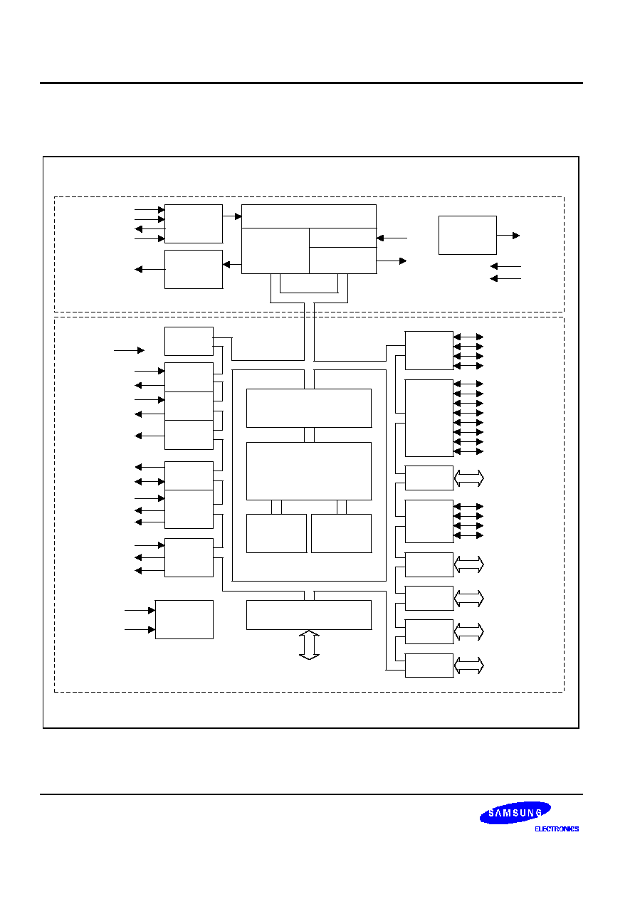
BLOCK DIAGRAM
P0.6/INT6
P0.5/INT5
P0.3/INT3
P0.1/INT1
TEST
P0.2/INT2
P0.4/INT4
Basic
Timer
64-Kbyte
ROM
14-Bit
A/D
Converter
Pulse
Density
Modulator
XIN
XOUT
XTIN
XTOUT
P0.1/BUZ
P0.2/T0CK
P0.3/T0/T0CAP
P0.4/T1CK
P0.5/TA
P0.7/INT7
P4.0-P4.7
P1.0-P1.7
INP
INN
OUT
Vref
Generator
VREF
INS
TONEO
RSTB
EA/Vpp
LRIN
I/O Port and
Interrupt Control
P0.6/TB
P5.0-P5.7
P6.0-P6.7
MLD
ADC2/P1.2
ADC1/P1.1
ADC0/P1.0
ADC3/P1.3
P1.4/SI
P1.5/SO
P1.6/
SCK
P2.2
P2.1
P2.0
P2.3
MCU BLOCK
PORT7/PORT8/PORT9/
PORT10
P7.0-P7.7, P8.0-P8.7, P9.0-P9.7
P10.0-P10.7,
P0.0/INT0
P3.0-P3.3
PLL
Melody
Generator
FSK/Dual
Tone
Generator
CAS/SDT Detector
FSK Receiver
LR/RING
SAM8 CPU
LR/RING
2048-Byte
Register File
Main
OSC
Sub
OSC
Watch
Timer
Timer 0
Timer 1
Serial I/O
A/D
Converter
Port 0
Port 1
Port 2
Port 4
Port 5
Port 6
Port 3
PLLC
CKSEL
Figure 1-1. Block Diagram
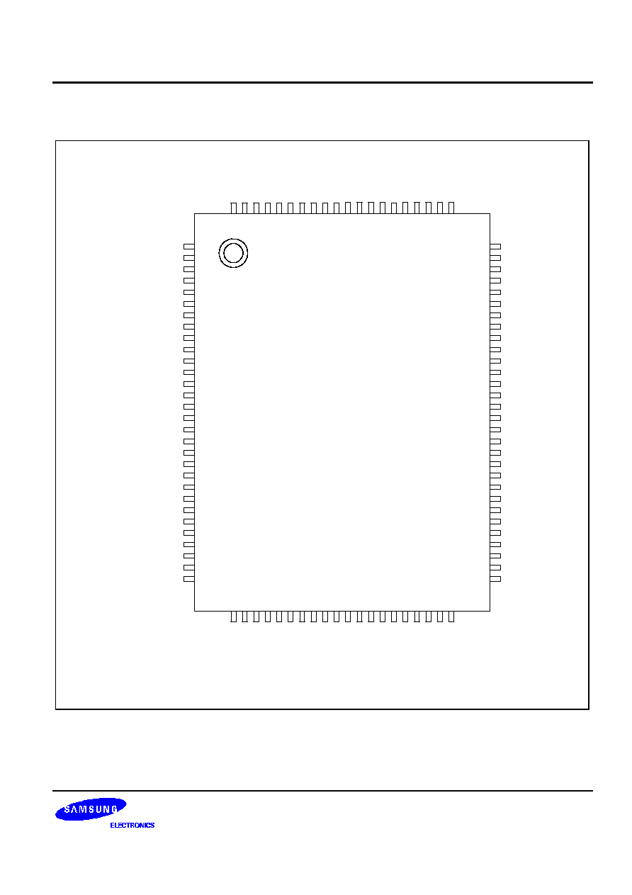
S3C852B/P852B (Preliminary Spec)
PRODUCT OVERVIEW
1-5
PIN ASSIGNMENTS
P5.7/A7
P5.6/A6
P5.5/A5
P5.4/A4
P5.3/A3
P5.2/A2
P5.1/A1
P5.0/A0
P4.7/D7
P4.6/D6
P4.5/D5
P4.4/D4
P4.3/D3
P4.2/D2
P4.1/D1
P4.0/D0
P3.3/
WR
P3.2/
RD
P3.1/
DM
P3.0/
PM
P7.7
P7.6
P7.5
P7.4
P7.3
P0.7/INT7
P0.6/INT6/TB
P0.5/INT5/TA
P0.4/INT4/T1CK
P0.3/INT3/T0/T0CAP
P2.0
P2.1
P2.2(SDAT)
P2.3(SCLK)
V
DD
V
SS
X
OUT
X
IN
EA
XT
IN
XT
OUT
RESET
P0.0/INT0
P0.1/INT1/BUZ
P0.2/INT2/T0CK
P9.7
P9.6
P9.5
P9.4
P9.3
S3C852B/P852B
100-QFP-1420C
80
79
78
77
76
75
74
73
72
71
70
69
68
67
66
65
64
63
62
61
60
59
58
57
56
55
54
53
52
51
1
2
3
4
5
6
7
8
9
10
11
12
13
14
15
16
17
18
19
20
21
22
23
24
25
26
27
28
29
30
81
82
83
84
85
86
87
88
89
90
91
92
93
94
95
96
97
98
99
100
50
49
48
47
46
45
44
43
42
41
40
39
38
37
36
35
34
33
32
31
P8.7
P8.6
P8.5
P8.4
P8.3
P8.2
P8.1
P8.0
PLLC
CKSEL
P7.2
P7.1
P7.0
VDDA
INP
INN
OUT
INS
V
REF
TONEO
VSSA
LR
IN
MLDO
P10.7
P10.6
P10.5
P10.4
P10.3
P10.2
P10.1
P10.0
P6.7/A15
P6.6/A14
P6.5/A13
P6.4/A12
P6.3/A11
P6.2/A10
P6.1/A9
P6.0/A8
P1.7/SSD/SD3
P1.6/
SCK
/SD2
P1.5/SO/SD1
P1.4/SI/SD0
P1.3/ADC3
P1.2/ADC2
P1.1/ADC1
P1.0/ADC0
P9.0
P9.1
P9.2
Figure 1-2. Pin Assignment (100-Pin QFP Package)

PRODUCT OVERVIEW
S3C852B/P852B (Preliminary Spec)
1-6
PIN DESCRIPTIONS
Table 1-1. Pin Descriptions
Pin Names
Pin Type
Pin No.
Pin Description
VDDA
Supply
67
Positive supply voltage for analog operation
INP
Analog Input
66
Input op-amp positive signal input for CAS, FSK and SDT
INN
Analog Input
65
Input op-amp negative signal input for CAS, FSK and SDT
OUT
Analog Output
64
Input op-amp output signal for CAS, FSK and SDT
INS
Analog Input
63
Input op-amp single ended input signal for CAS
V
REF
Analog Output
62
Reference voltage for Input signal
TONEO
Analog Output
61
FSK and dual tone signal output
VSSA
Supply
60
Negative supply pin for analog operation (ground)
LR
IN
Schmitt Input
59
Input for line reversal or ring detection
TEST
Input
71
Test pin, must be connected to ground
V
DD
Supply
15
Positive supply voltage
V
SS
Supply
16
Negative supply voltage (ground)
X
OUT
, X
IN
�
17,18
3.579545 MHz crystal input/output
EA/V
PP
�
19
Must be connected to ground (in case of OTP writing, It should be
connected to V
PP
)
XT
IN
, XT
OUT
�
20,21
Crystal oscillator pins for sub clock (32.768kHz)
RSTB
Input
22
Resets the S3C852B to known state
MLDO
output
58
Melody output
CKSEL
�
71
PLL output/X
IN
selection
PLLC
Analog Input
72
PLL capacitor
P0.0/INT0
P0.1/INT1/BUZ
P0.2/INT2/T0CK
P0.3/INT3/T0CAP/T0
P0.4/INT4/T1CK
P0.5/INT5/TA
P0.6/INT6/TB
P0.7/INT7
I/O
23
24
25
10
9
8
7
6
I/O port with bit-programmable pins;
Schmitt trigger input or push-pull output and software assignable
pull-up;
Alternative usage:
P0.1-P0.7 : external interrupt input
(P0.0 used for CID interrupt handling);
P0.1 : buzzer signal output pin;
P0.2 : timer0 clock input pin;
P0.3 : timer0 capture input or interval/PWM output pin;
P0.4 : tomer1 external clock input pin;
P0.5 & P0.6 : timer A & timer B clock output pin;
S3C852B/P852B (Preliminary Spec)
PRODUCT OVERVIEW
1-7
Table 1-1. Pin Descriptions (Continued)
Pin Names
Pin Type
Pin No.
Pin Description
P1.0/ADC0
P1.1/ADC1
P1.2/ADC2
P1.3/ADC3
P1.4/SI /SD0
P1.5/SO/ SD1
P1.6/
SCK
/SD2
P1.7/SSD/SD3
I/O
34
35
36
37
38
39
40
41
I/O port with bit-programmable pins;
Schmitt trigger input or push-pull, open-drain output and software
assignable pull-up;
Alternative usage:
P1.0-P1.3 : four channel analog inputs;
P1.4 : serial data input
P1.5 : serial data output
P1.6 : serial I/O interface clock signal
P2.0
P2.1
P2.2/SDAT
P2.3/SCLK
I/O
11
12
13
14
I/O port with bit-programmable pins;
Schmitt trigger input or push-pull, open-drain output and
software assignable pull-up;
Alternative usage:
P2.2 : serial data pin for OTP writing
P2.3 : serial clock pin for OTP writing
P3.0
P3.1
P3.2
P3.3
I/O
100
99
98
97
I/O port with bit-programmable pins;
Schmitt trigger input or push-pull, open-drain output and
software assignable pull-up;
P3.0-P3.4 are configurable for external interface signals
P4.0
P4.1
P4.2
P4.3
P4.4
P4.5
P4.6
P4.7
I/O
96
95
94
93
92
91
90
89
I/O port with bit-programmable pins;
Schmitt trigger input or push-pull, open-drain output and
software assignable pull-up;
Alternative usage:
P4 is configurable for external interface data lines D0-D7
P5.0
P5.1
P5.2
P5.3
P5.4
P5.5
P5.6
P5.7
I/O
88
87
86
85
84
83
82
81
I/O port with bit-programmable pins;
Schmitt trigger input or push-pull, open-drain output and
software assignable pull-up;
Alternative usage:
P5 is configurable for external interface address lines A0-A7

PRODUCT OVERVIEW
S3C852B/P852B (Preliminary Spec)
1-8
Table 1-1. Pin Descriptions (Continued)
Pin Names
Pin Type
Pin No.
Pin Description
P6.0
P6.1
P6.2
P6.3
P6.4
P6.5
P6.6
P6.7
I/O
42
43
44
45
46
47
48
49
I/O port with bit-programmable pins;
Schmitt trigger input or push-pull, open-drain output and
software assignable pull-up;
Alternative usage:
P6 is configurable for external interface address lines A8-A15
P7.7
P7.6
P7.5
P7.4
P7.3
P7.2
P7.1
P7.0
I/O
5
4
3
2
1
70
69
68
I/O port with bit-programmable pins;
Schmitt trigger input or push-pull, open-drain output and
software assignable pull-up;
P8.0
P8.1
P8.2
P8.3
P8.4
P8.5
P8.6
P8.7
I/O
73
74
75
76
77
78
79
80
I/O port with bit-programmable pins;
Schmitt trigger input or push-pull, open-drain output and
software assignable pull-up;
P9.0
P9.1
P9.2
P9.3
P9.4
P9.5
P9.6
P9.7
I/O
33
32
31
30
29
28
27
26
I/O port with bit-programmable pins;
Schmitt trigger input or push-pull, open-drain output and
software assignable pull-up;

S3C852B/P852B (Preliminary Spec)
PRODUCT OVERVIEW
1-9
Table 1-1. Pin Descriptions (Continued)
Pin Names
Pin Type
Pin No.
Pin Description
P10.0
P10.1
P10.2
P10.3
P10.4
P10.5
P10.6
P10.7
I/O
50
51
52
53
54
55
56
57
I/O port with bit-programmable pins;
Schmitt trigger input or push-pull, open-drain output and
software assignable pull-up;
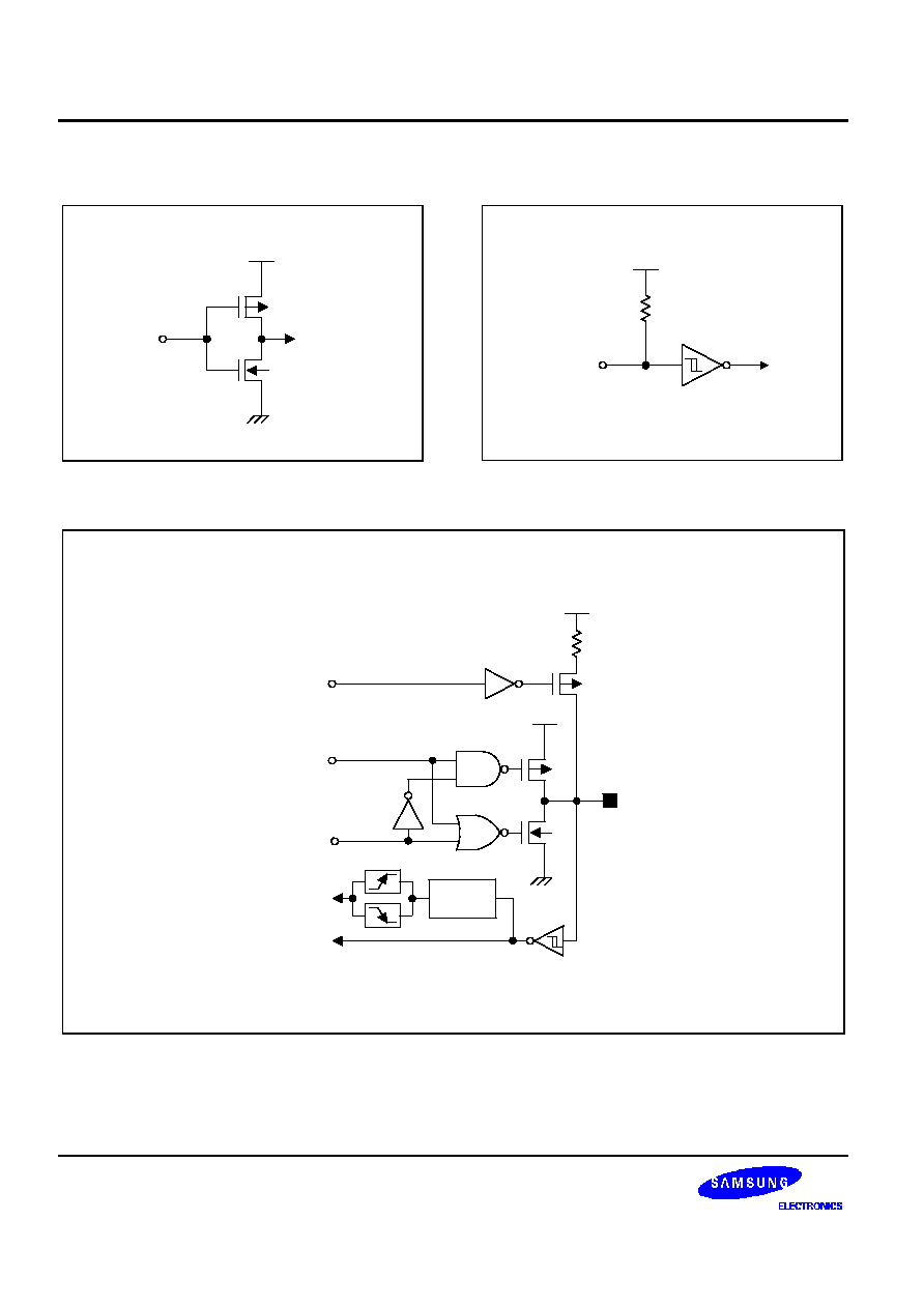
PRODUCT OVERVIEW
S3C852B/P852B (Preliminary Spec)
1-10
PIN CIRCUITS
In
V
DD
P-Channel
N-Channel
Figure 1-3. Pin Circuit Type 1
In
V
DD
Pull-Up
Resistor
Schmitt Trigger
Figure 1-4. Pin Circuit Type 2 (
RESET
RESET
)
V
DD
Output
Disable
Data
Pull-up
Resistor
V
DD
Noise
Filter
Pull-up
Enable
External
Interrupt
Input
Input
V
SS
I/O
Figure 1-5. Pin Circuit Type 3 (Port 0)
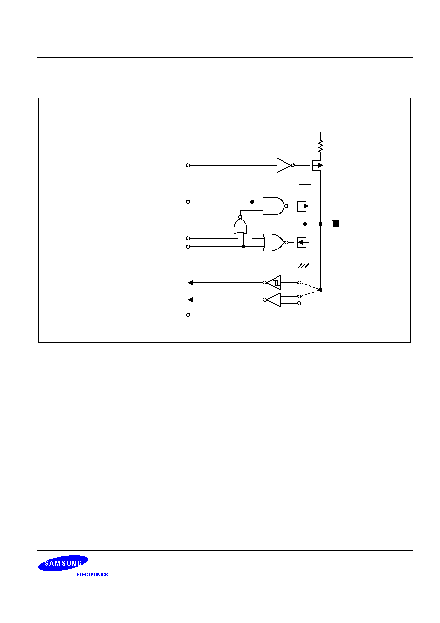
S3C852B/P852B (Preliminary Spec)
PRODUCT OVERVIEW
1-11
PIN CIRCUITS (Continued)
V
DD
Output Disable
Data
Pull-up
Resistor
V
DD
Pull-up
Enable
Analog Input
V
SS
Open-Drain
Select Digital or Analog Input
+
-
REF
Digital Input
I/O
Figure 1-6. Pin Circuit Type 4 (Port 1.0-Port 1.3)

PRODUCT OVERVIEW
S3C852B/P852B (Preliminary Spec)
1-12
PIN CIRCUITS (Continued)
V
DD
Output Disable
Data
Pull-up
Resistor
V
DD
Pull-up Enable
Input
V
SS
Open-Drain
M
U
X
Select
External Interface
(
PM, DM, RD, WR
)
I/O
Figure 1-7. Pin Circuit Type 5 (Port 3)
V
DD
Output Disable
Data
Pull-up
Resistor
V
DD
Pull-up Enable
Input
V
SS
Open-Drain
M
U
X
Select
External Interface
(A0-A7, A8-A15, D0-D7)
I/O
Figure 1-8. Pin Circuit Type 6 (Port 4, 5, 6)

S3C852B/P852B (Preliminary Spec)
ADDRESS SPACES
2-1
2
ADDRESS SPACES
OVERVIEW
The S3C852B microcontroller has four types of address space:
-- Internal program memory (ROM)
-- Internal register file
-- Internal data memory (RAM)
A 16-bit address bus supports both external program memory and external data memory operations. Special
instructions and related internal logic determine when the 16-bit bus carries addresses for external program
memory or for external data memory locations. SAM87RC bus architecture therefore supports up to 64 K bytes
of program memory (ROM). Using the external interface, you can address up to 64 K bytes of program memory
and 64 K bytes of data memory simultaneously. These spaces can be combined or kept separate.
The S3C852B/P852B microcontroller has 1808-byte registers in its internal register file. A separate 8-bit register
bus carries addresses and data between the CPU and the internal register file. The most of these registers can
serve as either a source or destination address, or as accumulators for data memory operations. Special 85
bytes of the register file are used for working registers, system and peripheral control functions.

ADDRESS SPACES
S3C852B/P852B (Preliminary Spec)
2-2
PROGRAM MEMORY (ROM)
Normal Operating Mode (Internal ROM)
The S3C852B/P852B has 64 K bytes (locations 0H�FFFFH) of internal mask-programmable program memory.
For normal (internal ROM) operation, the EA pin should be connected to V
SS
.
The first 256 bytes of the ROM (0H�0FFH) are reserved for interrupt vector addresses. Unused locations in this
address range can be used as normal program memory. If you do use the vector address area to store program
code, be careful to avoid overwriting vector addresses stored in these locations.
The program reset address in the ROM is 0100H.
ROM-Less Operating Mode (External ROM)
For special applications that require external program memory, you can use the ROM-less operating mode to
configure an up to 64-Kbyte area externally. Access to the internal 64-Kbyte program memory area is disabled in
ROM-less mode.
Mode selection (internal ROM or ROM-less) depends on the voltage that is applied to the EA pin during a power-
on reset operation:
-- When 0 V is applied to the EA pin, the S3C852B/P852B's internal ROM is configured normally and the 64-
Kbyte space (0H�FFFFH) is addressed.
-- When 5 V is applied to the EA pin, the S3C852B/P852B operates in ROM-less mode. External memory
locations 0000H�FFFFH are accessed over the 16-bit address/8-bit data bus, then the internal 64-Kbyte
program memory area is disabled.
When 5 V is applied to the EA pin during a power-on reset, the external peripheral interface is automatically
configured as follows:
-- The address and data lines for the external interface are configured at Port 4, Port 5 and Port 6 (The control
registers P4CON, P5CON and P6CON are set to their initial value for external interface).
-- P3AFS register values are set to configure the interface signals (
PM
,
DM
,
RD
, and
WR
) at Port 3.0�Port 3.3.

S3C852B/P852B (Preliminary Spec)
ADDRESS SPACES
2-3
(Decimal)
65,535
256
(HEX)
FFFFH
0100H
0000H
0
Program Start
ROM-Less Operating Mode
(Decimal)
65,535
256
(HEX)
FFFFH
0100H
0000H
0
Interrupt
Vector Area
64-Kbyte
Internal
Program
Memory
Area
Program Start
Normal Operating Mode
Interrupt
Vector Area
64-Kbyte
External
Program
Memory
Area
Figure 2-1. Program Memory Address Space

ADDRESS SPACES
S3C852B/P852B (Preliminary Spec)
2-4
REGISTER ARCHITECTURE
In the S3C852B/P852B implementation, the upper 64 bytes of the 256-byte physical register file is logically
divided into two 64-byte areas, called set 1 and set 2. Set 1 is further divided into bank 0(64-byte registers) and
bank 1(32-byte registers). In addition, the 256-byte area is logically expanded into seven separately addressable
register pages, page 0�page 6. This gives a giving a total of 1792 addressable general-purpose registers.
The 8-bit register bus can address up to 256 bytes (0H�FFH) in any one of the seven pages. The register file
area is, therefore, 1888-bytes, calculated as 256 bytes
�
7 (pages 0�6 in set 2) + 64 bytes (bank 0 in set 1) + 32
bytes (bank 1 in set 1). However, because 11-bytes are not mapped in set 1, the total number of addressable 8-
bit registers is 1877. Of these 1877 registers, 69-bytes are for CPU, system control, peripheral control and data
registers, 16 bytes are used as a shared working registers, and 1792-byte registers are for general-purpose use.
You can always address set 1 register locations, regardless of which of the seven register pages is currently
selected. Set 1 locations can, however, only be addressed using register addressing modes.
The extension of the physical register space into separately addressable areas (sets, banks, and pages) is
supported by various addressing mode restrictions, the select bank instructions, SB0 and SB1, and the register
page pointer (PP).
Specific register types and the area (in bytes) that they occupy in the register file are summarized in Table 2-1.
Table 2-1. S3C852B Register Type Summary
Register Type
Number of Bytes
CPU and system control registers
19
Peripheral, I/O, and clock control/data registers
50
Reserved working register area
16
General-purpose registers
1,792
Total Addressable Bytes
1,877
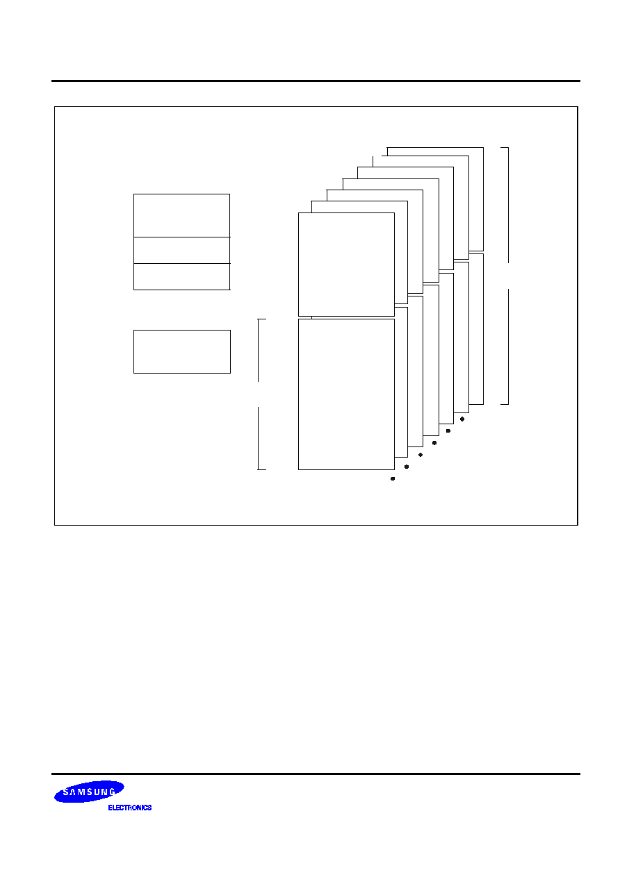
S3C852B/P852B (Preliminary Spec)
ADDRESS SPACES
2-5
Set 2
FFH
FCH
E0H
D0H
C0H
Set 1
Bank 0
FFH
FCH
E0H
Set 1
Bank 1
System and
Peripheral Control
Registers
(Register Addressing Mode)
Working Registers
(Working Register
Addressing Mode Only)
System Registers
(Register Addressing Mode)
System and
Peripheral Control
Registers
(Register Addressing Mode)
Set 2
Set 2
Set 2
Set 2
Set 2
FFH
FFH
FFH
FFH
FFH
FFH
C0H
00H
BFH
Page
(00H)
Page
(06H)
FFH
192
Bytes
Set 2
General Purpose
Data Registers
(Indirect Register
or Indexed
Addressing Mode
and Stack
Operations)
Prime Data
Registers
(All Addressing
Modes)
256
Bytes
FFH
Figure 2-2. Internal Register File Organization

ADDRESS SPACES
S3C852B/P852B (Preliminary Spec)
2-6
Register Page Pointer (PP)
In the S3C852B/P852B, the physical area of the internal register file is logically expanded by the additional of
seven register pages. Page addressing is controlled by the register page pointer (PP, DFH). See Figure 2-3.
Following a reset, the page pointer's source value (lower nibble) and destination value (upper nibble) are always
"0000", automatically selecting page 0 as the source and destination page for register addressing.
Whenever you select a different page, the current 256-byte address area (0H�FFH) is logically switched with the
address range of the new page (see section 4 "PP" register for more information).
Register Page Pointer (PP)
DFH ,Set 1, R/W
LSB
MSB
.7
.6
.5
.4
.3
.2
.1
.0
Destination Register Page Selection Bits:
0000
Destination: Page 0
Source Register Page Selection Bits:
0000
Source: Page 0
NOTE: In the S3C852B microcontroller, page 0H-6H are implemented.
A hardware reset operation writes the 4-bit destination and source values shown
above to the register page pointer. These values should be modified to address
other pages.
Figure 2-3. Register Page Pointer (PP)
Register Set 1
The term set 1 refers to the upper 64 bytes of the register file, locations C0H�FFH. This area can be accessed at
any time, regardless of which page is currently selected.
The upper 32-byte area of this 64-byte space is divided into two 32-byte register banks, called bank 0 and bank
1. You use the select register bank instructions, SB0 or SB1, to address one bank or the other. A reset operation
automatically selects bank 0 addressing.
The lower 32-byte area of set 1 is not banked. This area contains 16 bytes for mapped system registers (D0H�
DFH) and a 16-byte common area (C0H�CFH) for working register addressing.
Registers in set 1 are directly accessible at all times using the Register addressing mode. The 16-byte working
register area can only be accessed using working register addressing, however.
Working register addressing is a function of Register addressing mode (see Section 3, "Addressing Modes," for
more information).
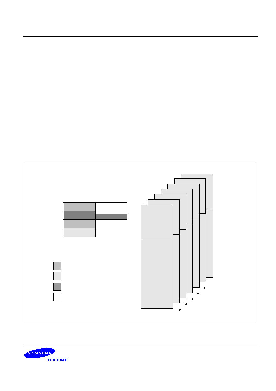
S3C852B/P852B (Preliminary Spec)
ADDRESS SPACES
2-7
Register Set 2
The same 64-byte physical space that is used for set 1 register locations C0H�FFH is logically duplicated to add
another 64 bytes. This expanded area of the register file is called set 2. For the S3C852B/P852B, the set 2
address range (C0H�FFH) is accessible on pages 0�6.
The logical division of set 1 and set 2 is maintained by means of addressing mode restrictions: While you can
access set 1 using Register addressing mode only, you can only use Register Indirect addressing mode or
Indexed addressing mode to access set 2.
Prime Register Space
The lower 192 bytes (00H�BFH) of the S3C852B/P852B's eight 256-byte register pages is called prime register
area. Prime registers can be accessed using any of the seven addressing modes (see Section 3, "Addressing
Modes").
The prime register area on page 0 is immediately addressable following a reset. In order to address prime
registers on pages 1, 2, 3, 4, 5 or 6, you must set the register page pointer (PP) to the appropriate source and
destination values.
Set 2
FFH
FCH
E0H
D0H
C0H
Set 1
Bank 0
Area not mapped
Bank 1
Peripheral and I/O
General-purpose
CPU and system control
Set 2
Set 2
Set 2
Set 2
Set 2
FFH
C0H
00H
Prime
Space
Set 2
Page 0
Page 6
Figure 2-4. Map of Set 1, Set 2, and Prime Register Spaces
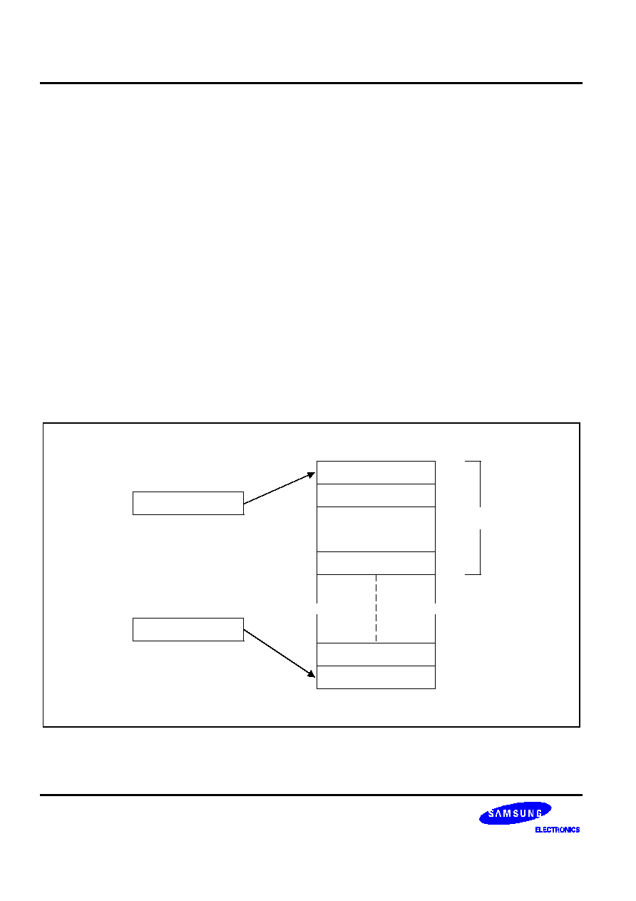
ADDRESS SPACES
S3C852B/P852B (Preliminary Spec)
2-8
WORKING REGISTERS
Instructions can access specific 8-bit registers or 16-bit register pairs using either 4-bit or 8-bit address fields.
When 4-bit working register addressing is used, the 256-byte register file can be viewed by the programmer as
consisting of 32 8-byte register groups or "slices."
Each slice consists of eight 8-bit registers. Using the two 8-bit register pointers, RP1 and RP0, two working
register slices can be selected at any one time to form a 16-byte working register block.
Using the register pointers, you can move this 16-byte register block anywhere in the addressable register file,
except for the set 2 area.
The terms slice and block are used in this manual to help you visualize the size and relative locations of selected
working register spaces:
-- One working register slice is 8 bytes (eight 8-bit working registers; R0�R7 or R8�R15)
-- One working register block is 16 bytes (sixteen 8-bit working registers; R0�R15)
All of the registers in an 8-byte working register slice have the same binary value for their five most significant
address bits. This makes it possible for each register pointer to point to one of the 24 slices in the register file.
The base addresses for the two selected 8-byte register slices are contained in register pointers RP0 and RP1.
After a reset, RP0 and RP1 always point to the 16-byte common area in set 1 (C0H�CFH).
Each register pointer points to
one 8-byte slice of the register
space, selecting a total 16-byte
working register block.
1 1 1 1 1 X X X
RP1 (Registers R8-R15)
RP0 (Registers R0-R7)
Slice 32
Slice 31
~
~
CFH
C0H
FFH
F8H
F7H
F0H
FH
8H
7H
0H
Slice 2
Slice 1
10H
Set 1
Only
0 0 0 0 0 X X X
Figure 2-5. 8-Byte Working Register Areas (Slices)

S3C852B/P852B (Preliminary Spec)
ADDRESS SPACES
2-9
USING THE REGISTER POINTERS
Register pointers RP0 and RP1 are mapped to addresses D6H and D7H in set 1. They are used to select two
movable 8-byte working register slices in the register file.
After a reset, they point to the working register common area: RP0 points to addresses C0H�C7H, and RP1
points to addresses C8H�CFH.
To change a register pointer value, you load a new value to RP0 and/or RP1 using an SRP or LD instruction (see
Figures 2-6 and 2-7).
With working register addressing, you can only access those locations that are pointed to by the register pointers.
Please note that you cannot use the register pointers to select working register area in set 2, C0H�FFH, because
these locations are accessible only using the Indirect Register or Indexed addressing modes.
The selected 16-byte working register block usually consists of two contiguous 8-byte slices. As a general
programming guideline, we recommend that RP0 point to the "lower" slice and RP1 point to the "upper" slice (see
Figure 2-6).
In some cases, you may need to define working register areas in different (non-contiguous) areas of the register
file. In Figure 2-7, RP0 points to the "upper" slice and RP1 to the "lower" slice.
Because a register pointer can point to the either of the two 8-byte slices in the working register block, definition
of the working register area is very flexible.
F
F
PROGRAMMING TIP -- Setting the Register Pointers
SRP
#70H
; RP0
70H, RP1
78H
SRP1
#48H
; RP0
no change, RP1
48H
SRP0
#0A0H
; RP0
A0H, RP1
no change
CLR
RP0
; RP0
00H, RP1
no change
LD
RP1,#0F8H
; RP0
no change, RP1
0F8H

ADDRESS SPACES
S3C852B/P852B (Preliminary Spec)
2-10
FH (R15)
0H (R0)
16-Byte
Contiguous
Working
Register block
Register File
Contains 32
8-Byte Slices
RP0
RP1
8H
7H
0 0 0 0 1 X X X
0 0 0 0 0 X X X
8-Byte Slice
8-Byte Slice
Figure 2-6. Contiguous 16-Byte Working Register Block
16-Byte
Contiguous
working
Register block
Register File
Contains 32
8-Byte Slices
0 0 0 0 0 X X X
RP1
1 0 1 1 0 X X X
RP0
0H (R0)
7H (R15)
F0H (R0)
F7H (R7)
8-Byte Slice
8-Byte Slice
Figure 2-7. Non-Contiguous 16-Byte Working Register Block

S3C852B/P852B (Preliminary Spec)
ADDRESS SPACES
2-11
Calculate the sum of registers 80H�85H using the register pointer. The register addresses 80H through 85H
contains the values 10H, 11H, 12H, 13H, 14H, and 15 H, respectively:
SRP0
#80H
; RP0
80H
ADD
R0,R1
; R0
R0 + R1
ADC
R0,R2
; R0
R0 + R2 + C
ADC
R0,R3
; R0
R0 + R3 + C
ADC
R0,R4
; R0
R0 + R4 + C
ADC
R0,R5
; R0
R0 + R5 + C
The sum of these six registers, 6FH, is located in the register R0 (80H). The instruction string used in this
example takes 12 bytes of instruction code and its execution time is 24 cycles. If the register pointer is not used
to calculate the sum of these registers, the following instruction sequence would have to be used:
ADD
80H,81H
; 80H
(80H) + (81H)
ADC
80H,82H
; 80H
(80H) + (82H) + C
ADC
80H,83H
; 80H
(80H) + (83H) + C
ADC
80H,84H
; 80H
(80H) + (84H) + C
ADC
80H,85H
; 80H
(80H) + (85H) + C
Now, the sum of the six registers is also located in register 80H. However, this instruction string takes 15 bytes of
instruction code instead of 12 bytes, and its execution time is 30 cycles instead of 24 cycles.

ADDRESS SPACES
S3C852B/P852B (Preliminary Spec)
2-12
REGISTER ADDRESSING
The SAM8 register architecture provides an efficient method of working register addressing that takes full
advantage of shorter instruction formats to reduce execution time.
The Register (R) addressing mode, in which the operand value is the content of a specific register or register
pair, can be used to access all locations in the register file except for set 2.
For working register addressing, the register pointers RP0 and RP1 are used to select a specific register within a
selected 16-byte working register area. To increase the speed of context switches in an application program, you
can use the register pointers to dynamically select different 8-byte "slices" of the register file as the program's
active working register space.
Registers are addressed either as a single 8-bit register or as a paired 16-bit register. In 16-bit register pairs, the
address of the first 8-bit register is always an even number and the address of the next register is an odd
number.
The most significant byte of the 16-bit data is always stored in the even-numbered register; the least significant
byte is always stored in the next (+ 1) odd-numbered register.
MSB
Rn
LSB
Rn+1
n = Even address
Figure 2-8. 16-Bit Register Pairs
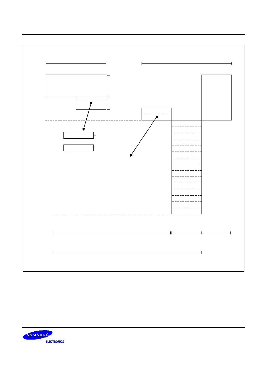
S3C852B/P852B (Preliminary Spec)
ADDRESS SPACES
2-13
RP1
RP0
Register
Pointers
00H
All
Addressing
Modes
Page 0
Indirect Register,
Indexed
Addressing
Modes
Page 0
Register Addressing Only
Can be Pointed by Register Pointer
FFH
E0H
BFH
Control
Registers
System
Registers
Special-Purpose Registers
D0H
C0H
Bank 1
Bank 1
Each register pointer (RP) can independently point
to one of the 24 8-byte "slices" of the register file
(other than set 2). After a reset, RP0 points to
locations C0H-C7H and RP1 to locations C8H-CFH
(that is, to the common working register area).
FFH
C0H
Set 2
Prime
Registers
CFH
General-Purpose Register
D6H
D7H
Figure 2-9. Register File Addressing
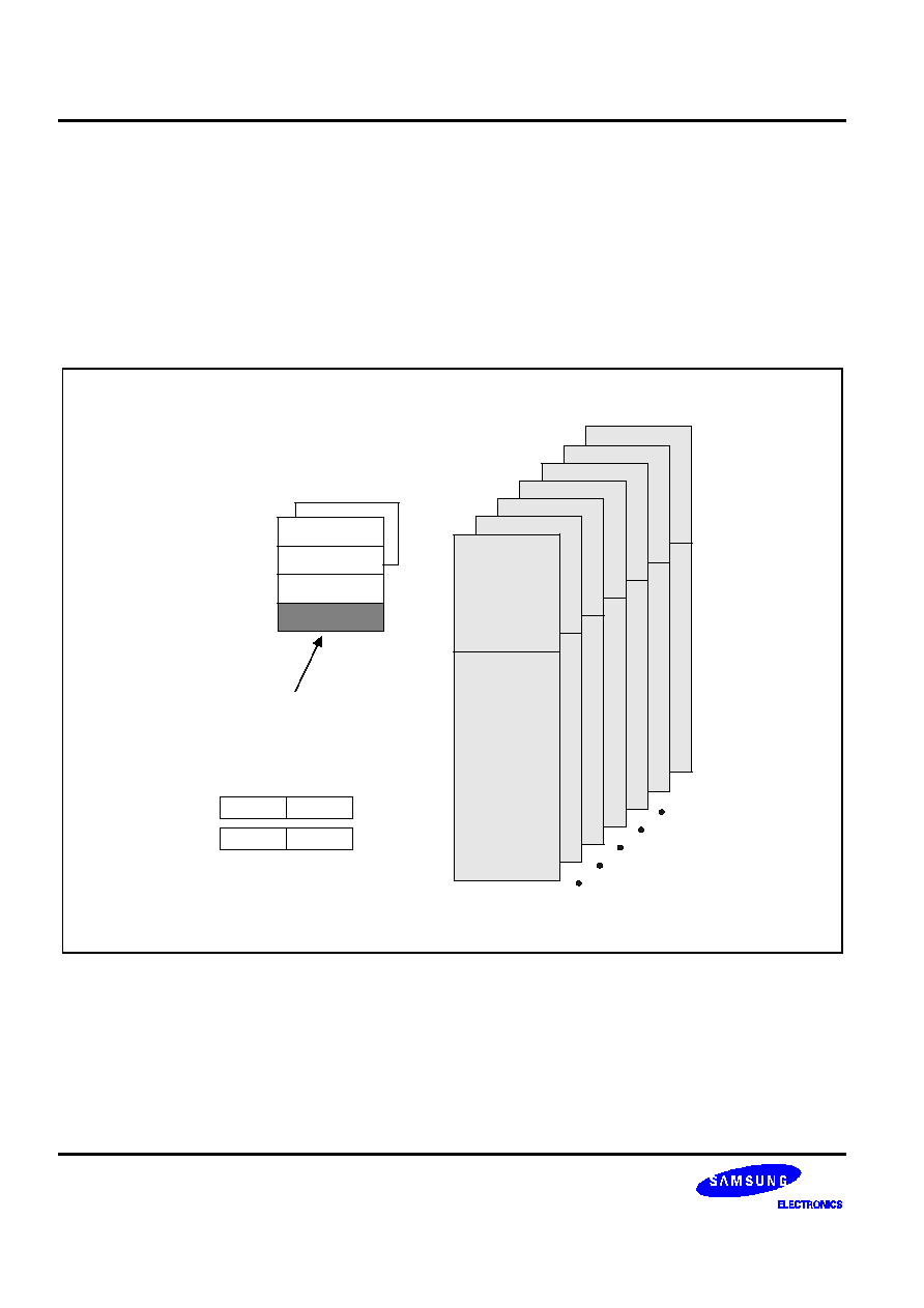
ADDRESS SPACES
S3C852B/P852B (Preliminary Spec)
2-14
COMMON WORKING REGISTER AREA (C0H�CFH)
After a reset, register pointers RP0 and RP1 automatically select two 8-byte register slices in set 1, locations
C0H�CFH, as the active 16-byte working register block:
RP0
C0H�C7H
RP1
C8H�CFH
This 16-byte address range is called the common area. You can use common area registers as working registers
for operations that address locations on different pages in the register file.
Page 0
Set 2
FFH
FCH
E0H
CFH
C0H
Set 1
Following a hardware reset, register
pointers RP0 and RP1 point to the
common working register area,
locations C0H-CFH.
RP0 =
RP1 =
1 1 0 0
0 0 0 0
1 1 0 0
1 0 0 0
DFH
Set 2
Set 2
Set 2
Set 2
Set 2
FFH
C0H
00H
Prime
Space
Set 2
Page 6
Figure 2-10. Common Working Register Area

S3C852B/P852B (Preliminary Spec)
ADDRESS SPACES
2-15
F
F
PROGRAMMING TIP -- Addressing the Common Working Register Area
As the following examples show, you should access working registers in the common area, locations C0H�CFH,
using working register addressing mode only.
Example 1:
LD
0C2H,40H
; Invalid addressing mode!
Use working register addressing instead:
SRP
#0C0H
LD
R2,40H
; R2 (C2H)
the value in location 40H
Example 2:
ADD
0C3H,#45H
; Invalid addressing mode!
Use working register addressing instead:
SRP
#0C0H
ADD
R3,#45H
; R3 (C3H)
R3 + 45H

ADDRESS SPACES
S3C852B/P852B (Preliminary Spec)
2-16
4-BIT WORKING REGISTER ADDRESSING
Each register pointer defines a movable 8-byte slice of working register space. The address information stored in
a register pointer serves as an addressing "window" that enables instructions to access working registers very
efficiently using short 4-bit addresses.
When an instruction addresses a location in the selected working register area, the address bits are concatenated
in the following way to form a complete 8-bit address:
-- The high-order bit of the 4-bit address selects one of the register pointers ("0" selects RP0; "1" selects RP1);
-- The five high-order bits in the register pointer select an 8-byte slice of the register space;
-- The three low-order bits of the 4-bit address select one of the eight registers in the slice.
As shown in Figure 2-11, the net effect of this operation is that the five high-order bits from the register pointer
are concatenated with the three low-order bits from the instruction address to form the complete address.
As long as the address stored in the register pointer remains unchanged, the three bits from the address will
always point to an address in the same 8-byte register slice.
Figure 2-12 shows a typical example of 4-bit working register addressing: The high-order bit of the instruction
'INC R6' is "0", which selects RP0.
The five high-order bits stored in RP0 (01110B) are concatenated with the three low-order bits of the instruction's
4-bit address (110B) to produce the register address 76H (01110110B).
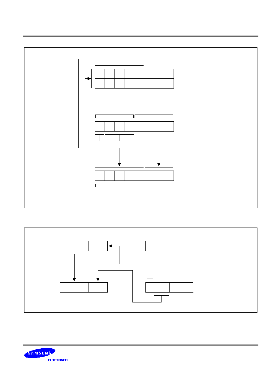
S3C852B/P852B (Preliminary Spec)
ADDRESS SPACES
2-17
Together they create an
8-bit register address
Register pointer
provides five
high-order bits
Address
OPCODE
Selects
RP0 or RP1
RP1
RP0
4-bit address
procides three
low-order bits
Figure 2-11. 4-Bit Working Register Addressing
Register
address
(76H)
RP0
0 1 1 1 0
0 0 0
0 1 1 1 0
1 1 0
R6
0 1 1 0
1 1 1 0
Selects RP0
Instruction:
'INC R6'
OPCODE
RP1
0 1 1 1 1
0 0 0
Figure 2-12. 4-Bit Working Register Addressing Example
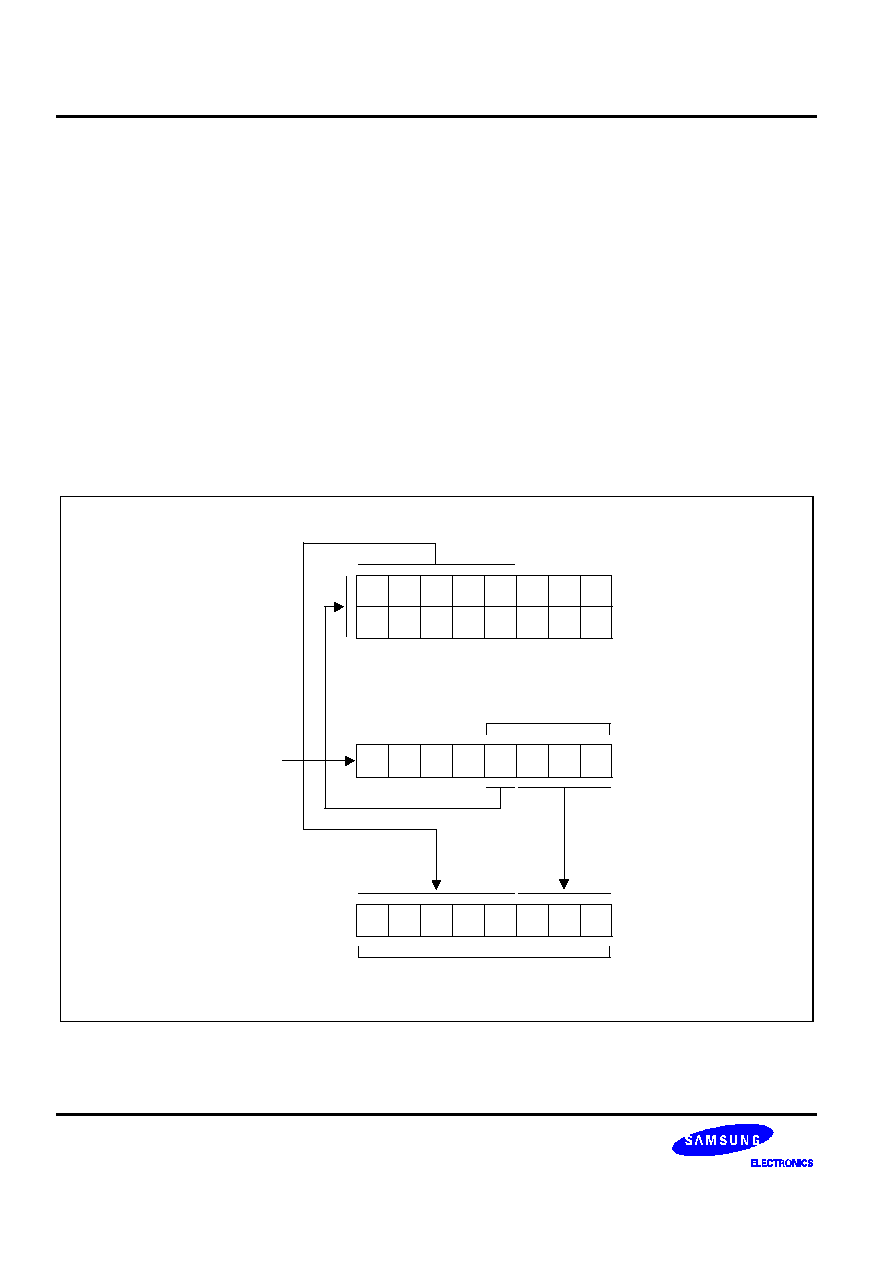
ADDRESS SPACES
S3C852B/P852B (Preliminary Spec)
2-18
8-BIT WORKING REGISTER ADDRESSING
You can also use 8-bit working register addressing to access registers in a selected working register area. In
order to initiate 8-bit working register addressing, the upper four bits of the instruction address must contain the
value 1100B. This 4-bit value (1100B) indicates that the remaining four bits have the same effect as 4-bit
working register addressing.
As shown in Figure 2-13, the lower nibble of the 8-bit address is concatenated in much the same way as for 4-bit
addressing: Bit 3 selects either RP0 or RP1, which then supplies the five high-order bits of the final address, and
the three low-order bits of the complete address are provided by the original instruction.
Figure 2-14 shows an example of 8-bit working register addressing: The four high-order bits of the instruction
address (1100B) specify 8-bit working register addressing. The fourth bit ("1") selects RP1 and the five high-order
bits in RP1 (10100B) become the five high-order bits of the register address.
The three low-order bits of the register address (011) are provided by the three low-order bits of the 8-bit
instruction address. Together, the five address bits from RP1 and the three address bits from the instruction
comprise the complete register address, 0ABH (10100011B).
8-bit physical address
Register pointer
provides five
high-order bits
Address
Selects
RP0 or RP1
RP1
RP0
Three low-
order bits
8-bit logical
address
These address
bits indicate 8-bit
working register
addressing
1
1
0
0
Figure 2-13. 8-Bit Working Register Addressing
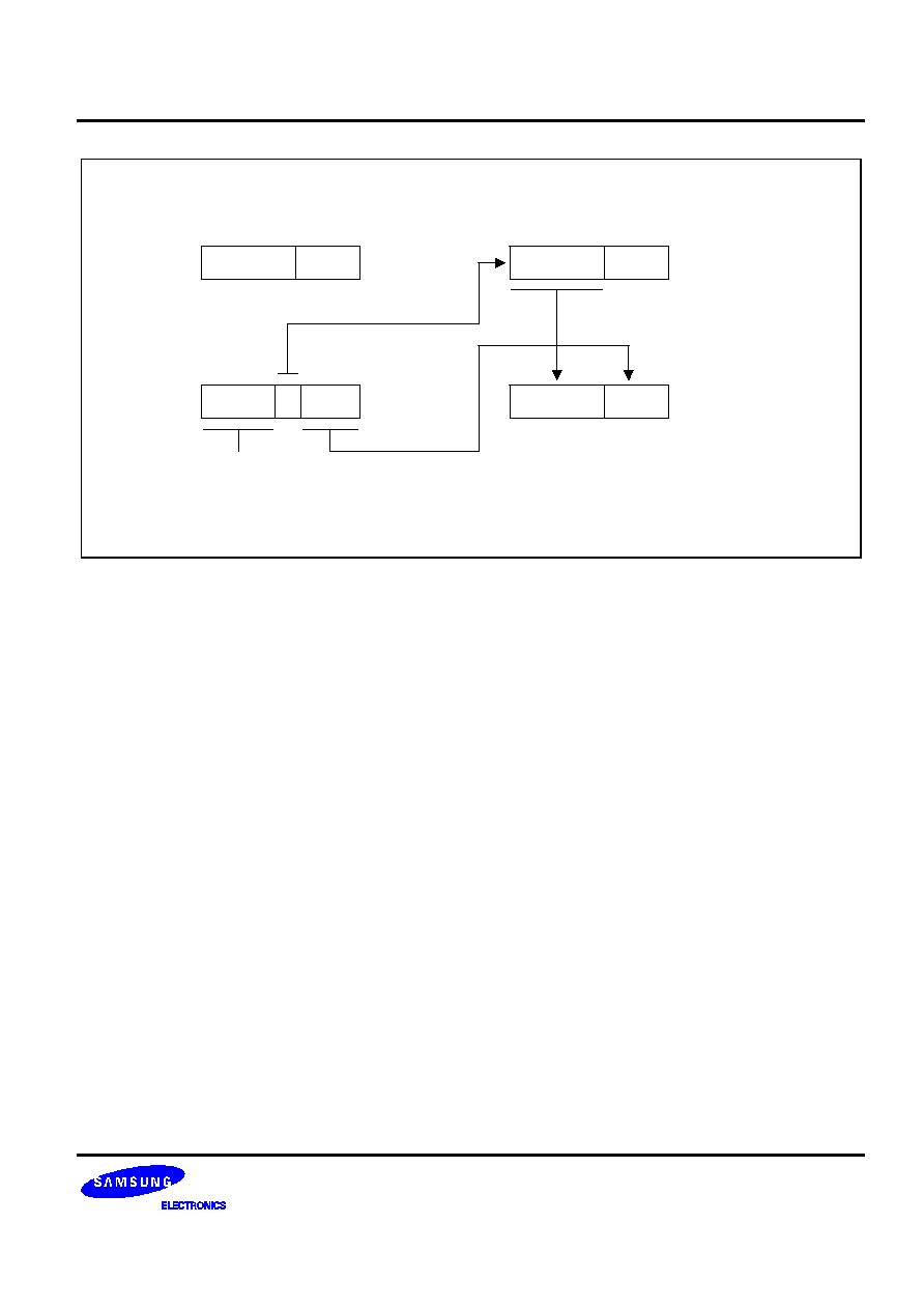
S3C852B/P852B (Preliminary Spec)
ADDRESS SPACES
2-19
8-bit address
form instruction
'LD R11, R2'
RP0
0 1 1 0 0
0 0 0
1 1 0 0 1 0 1 1
Selects RP1
R11
Register
address
(0ABH)
RP1
1 0 1 0 1
0 0 0
1 0 1 0 1
0 1 1
Specifies working
register addressing
Figure 2-14. 8-Bit Working Register Addressing Example
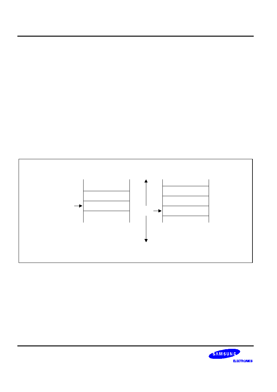
ADDRESS SPACES
S3C852B/P852B (Preliminary Spec)
2-20
SYSTEM AND USER STACKS
KS88-series microcontrollers can be programmed to use system stack for subroutine calls, returns, interrupts,
and to store data. The PUSH and POP instructions are used to control system stack operations.
The SAM8 architecture supports stack operations in the internal register file as well as in external data memory.
To select an internal or external stack area, you set bit 1 of the external memory timing register, EMT.1 to the
appropriate value.
Stack Operations
Return addresses for procedure calls and interrupts and data are stored on the stack. The contents of the PC are
saved to stack by a CALL instruction and restored by the RET instruction.
When an interrupt occurs, the contents of the PC and the FLAGS register are pushed to the stack. The IRET
instruction then pops these values back to their original locations.
The stack address is always decremented before a push operation and incremented after a pop operation. The
stack pointer (SP) always points to the stack frame stored on the top of the stack, as shown in Figure 2-15.
Stack contents
after a call
instruction
Stack contents
after an
interrupt
Top of
stack
Flags
PCH
PCL
PCL
PCH
Top of
stack
Low Address
High Address
Figure 2-15. Stack Operations
User-Defined Stacks
You can freely define stacks in the internal register file as data storage locations. The instructions PUSHUI,
PUSHUD, POPUI, and POPUD support user-defined stack operations.
These instructions cannot address external memory locations. Only PUSH and POP instructions can be used for
an externally defined stack.

S3C852B/P852B (Preliminary Spec)
ADDRESS SPACES
2-21
Stack Pointers (SPL, SPH)
Register locations D8H and D9H contain the 16-bit stack pointer (SP) that is used for system stack operations.
The most significant byte of the SP address, SP15�SP8, is stored in the SPH register (D8H); the least significant
byte, SP7�SP0, is stored in the SPL register (D9H). After a reset, the SP value is undetermined.
If only internal memory space is implemented, the SPL must be initialized to an 8-bit value in the range 00H�
FFH; the SPH register is not needed (and can be used as a general-purpose register, if needed). If external
memory is implemented, both SPL and SPH must be initialized with a full 16-bit address.
When the SPL register contains the only stack pointer value (that is, when it points to a system stack in the
register file), the SPH register can be used as a general-purpose data register.
However, if an overflow or underflow condition occurs as the result of incrementing or decrementing the stack
address in the SPL register during normal stack operations, the value in the SPL register will overflow (or
underflow) to the SPH register, overwriting any other data that is currently stored there.
To avoid overwriting data in the SPH register, you can initialize the SPL value to FFH instead of 00H.
Stack operation page is in only page 0, regardless the processing page.
F
F
PROGRAMMING TIP -- Standard Stack Operations Using PUSH and POP
The following example shows you how to perform stack operations in the internal register file using PUSH and
POP instructions:
LD
SPL,#0FFH
; SPL
FFH (Normally, the SPL is set to 0FFH by the
�
; initialization routine)
�
�
PUSH
PP
; Stack address 0FEH
PP
PUSH
RP0
; Stack address 0FDH
RP0
PUSH
RP1
; Stack address 0FCH
RP1
PUSH
R3
; Stack address 0FBH
R3
�
�
�
POP
R3
; R3
stack address 0FBH
POP
RP1
; RP1
stack address 0FCH
POP
RP0
; RP0
stack address 0FDH
POP
PP
; PP
stack address 0FEH

ADDRESS SPACES
S3C852B/P852B (Preliminary Spec)
2-22
NOTES

S3C852B/P852B (Preliminary Spec)
ADDRESSING MODES
3-1
3
ADDRESSING MODES
OVERVIEW
Instructions that are stored in program memory are fetched for execution using the program counter. Instructions
indicate the operation to be performed and the data to be operated on.
Addressing mode is the method used to determine the location of the data operand. The operands specified in
SAM87RC
instructions may be condition codes, immediate data, or a location in the register file, program memory, or data
memory.
The SAM87RC instruction set supports seven explicit addressing modes. Not all of these addressing modes are
available for each instruction. The addressing modes and their symbols are as follows:
-- Register (R)
-- Indirect Register (IR)
-- Indexed (X)
-- Direct Address (DA)
-- Indirect Address (IA)
-- Relative Address (RA)
-- Immediate (IM)
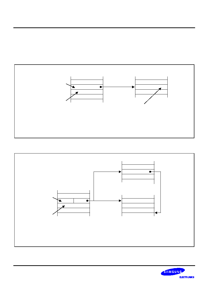
ADDRESSING MODES
S3C852B/P852B (Preliminary Spec)
3-2
REGISTER ADDRESSING MODE (R)
In Register addressing mode, the operand is the content of a specified register or register pair (see Figure 3-1).
Working register addressing differs from Register addressing because it uses a register pointer to specify an
8-byte working register space in the register file and an 8-bit register within that space (see Figure 3-2).
dst
Value used in
Instruction Execution
OPCODE
OPERAND
8-bit Register
File Address
Point to One
Rigister in Register
File
One-Operand
Instruction
(Example)
Sample Instruction:
DEC
CNTR
; Where CNTR is the label of an 8-bit register address
Program Memory
Register File
Figure 3-1. Register Addressing
dst
OPCODE
4-bit
Working Register
Points to the
Woking Register
(1 of 8)
Two-Operand
Instruction
(Example)
Sample Instruction:
ADD
R1, R2
; Where R1 and R2 are registers in the currently
selected working register area.
Program Memory
Register File
src
3 LSBs
RP0 or RP1
Selected
RP points
to start
of working
register
block
OPERAND
MSB Points to
RP0 ot RP1
Figure 3-2. Working Register Addressing

S3C852B/P852B (Preliminary Spec)
ADDRESSING MODES
3-3
INDIRECT REGISTER ADDRESSING MODE (IR)
In Indirect Register (IR) addressing mode, the content of the specified register or register pair is the address of
the operand.
Depending on the instruction used, the actual address may point to a register in the register file, to program
memory (ROM), or to an external memory space (see Figures 3-3 through 3-6).
You can use any 8-bit register to indirectly address another register. Any 16-bit register pair can be used to
indirectly address another memory location.
You cannot, however, access locations C0H�FFH in set 1 using Indirect Register addressing mode.
dst
Address of Operand
used by Instruction
OPCODE
ADDRESS
8-Bit Register
File Address
Points to One
Rigister in Register
File
One-Operand
Instruction
(Example)
Sample Instruction:
RL
@SHIFT
; Where SHIFT is the label of an 8-bit register address
Program Memory
Register File
Value used in
Instruction Execution
OPERAND
Figure 3-3. Indirect Register Addressing to Register File
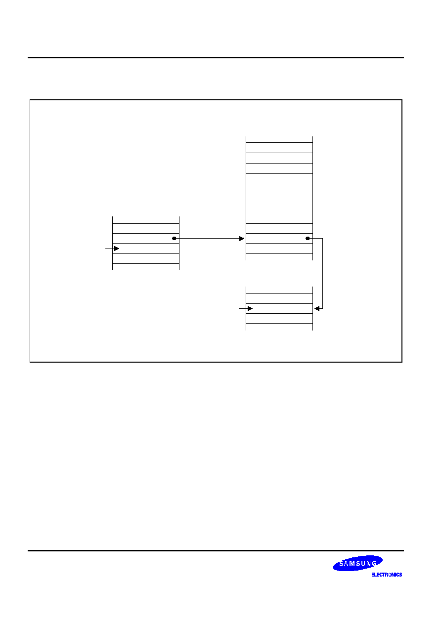
ADDRESSING MODES
S3C852B/P852B (Preliminary Spec)
3-4
INDIRECT REGISTER ADDRESSING MODE (Continued)
dst
OPCODE
PAIR
Points to
Register Pair
Example
Instruction
References
Program
Memory
Sample Instructions:
CALL
@RR2
JP
@RR2
Program Memory
Register File
Value used in
Instruction
OPERAND
REGISTER
Program Memory
16-Bit
Address
Points to
Program
Memory
Figure 3-4. Indirect Register Addressing to Program Memory
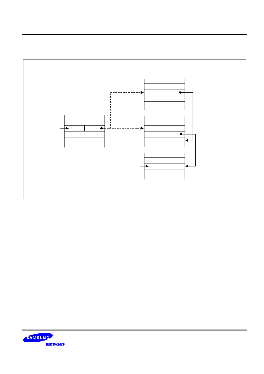
S3C852B/P852B (Preliminary Spec)
ADDRESSING MODES
3-5
INDIRECT REGISTER ADDRESSING MODE (Continued)
dst
OPCODE
ADDRESS
4-bit
Working
Register
Address
Points to the
Woking Register
(1 of 8)
Sample Instruction:
OR
R3, @R6
Program Memory
Register File
src
3 LSBs
Value used in
Instruction
OPERAND
Selected
RP points
to start fo
woking register
block
RP0 or RP1
MSB Points to
RP0 or RP1
~
~
~
~
Figure 3-5. Indirect Working Register Addressing to Register File
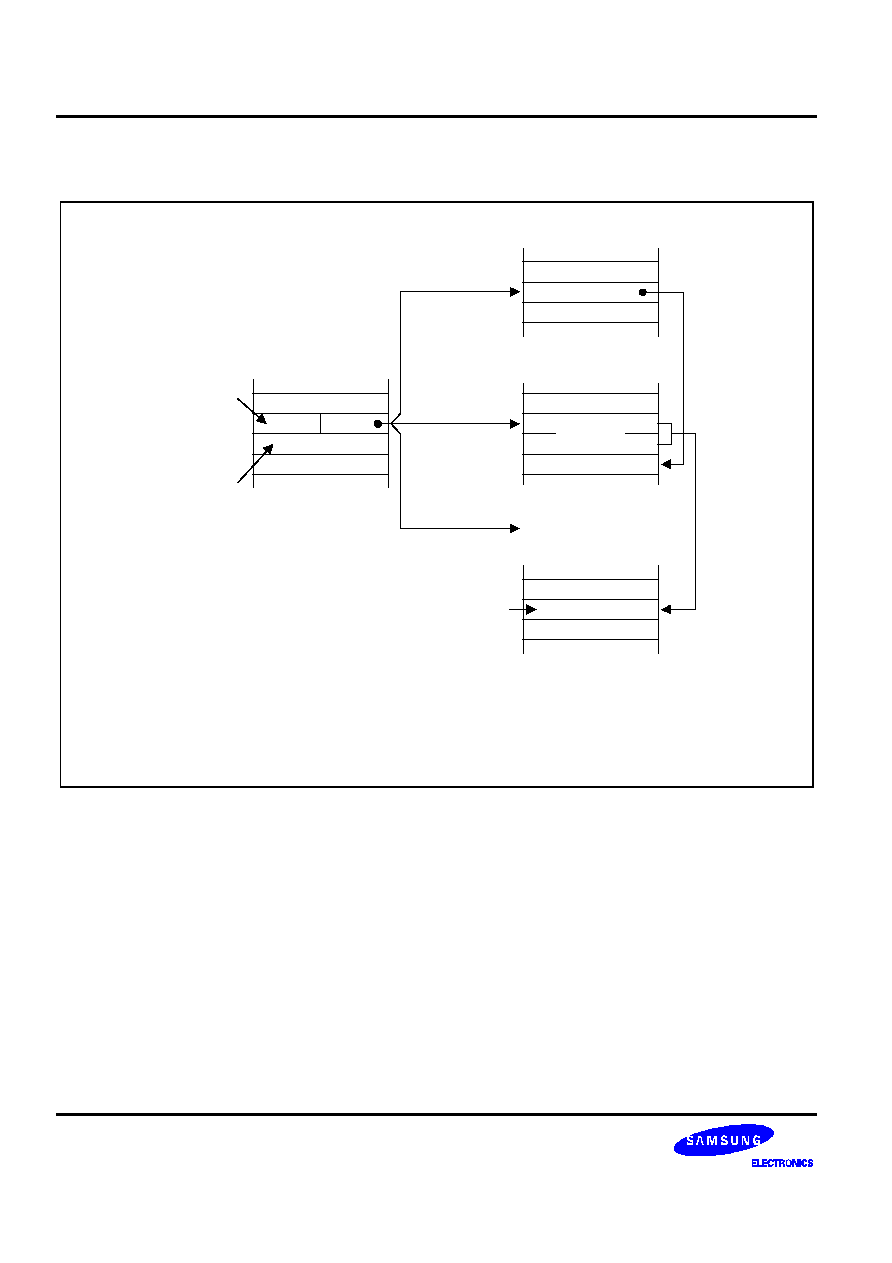
ADDRESSING MODES
S3C852B/P852B (Preliminary Spec)
3-6
INDIRECT REGISTER ADDRESSING MODE (Concluded)
dst
OPCODE
4-bit Working
Register Address
Sample Instructions:
LCD
R5,@RR6
; Program memory access
LDE
R3,@RR0
; External data memory access
LDE
@RR4, R8
; External data memory access
Program Memory
Register File
src
Value used in
Instruction
OPERAND
Example Instruction
References either
Program Memory or
Data Memory
Program Memory
or
Data Memory
Next 2-bit Point
to Working
Register Pair
(1 of 4)
LSB Selects
Register
Pair
16-Bit
address
points to
program
memory
or data
memory
RP0 or RP1
MSB Points to
RP0 or RP1
Selected
RP points
to start of
working
register
block
Figure 3-6. Indirect Working Register Addressing to Program or Data Memory
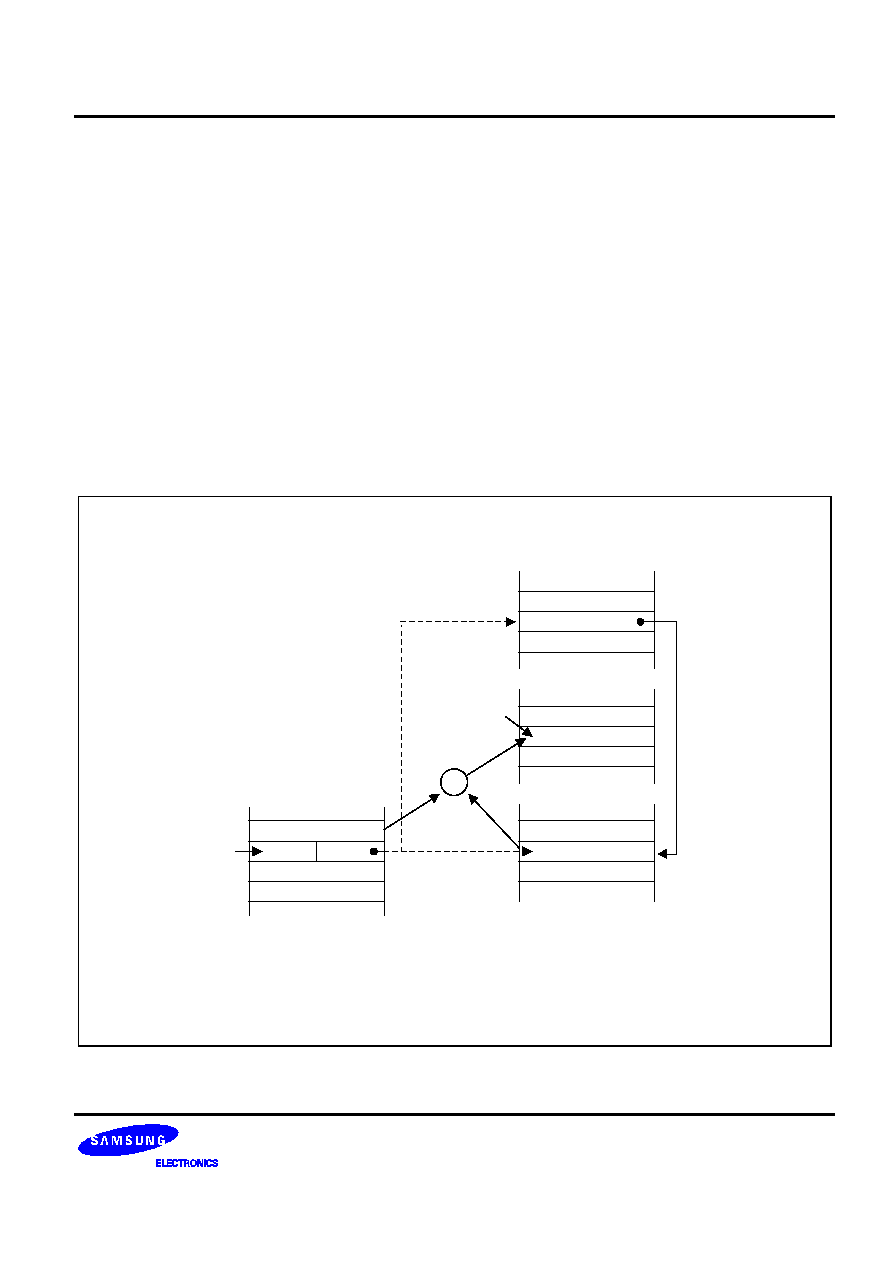
S3C852B/P852B (Preliminary Spec)
ADDRESSING MODES
3-7
INDEXED ADDRESSING MODE (X)
Indexed (X) addressing mode adds an offset value to a base address during instruction execution in order to
calculate the effective operand address (see Figure 3-7). You can use Indexed addressing mode to access
locations in the internal register file or in external memory. You cannot, however, access locations C0H�FFH in
set 1 using Indexed addressing mode.
In short offset Indexed addressing mode, the 8-bit displacement is treated as a signed integer in the range
�128 to +127. This applies to external memory accesses only (see Figure 3-8.)
For register file addressing, an 8-bit base address provided by the instruction is added to an 8-bit offset contained
in a working register. For external memory accesses, the base address is stored in the working register pair
designated in the instruction. The 8-bit or 16-bit offset given in the instruction is then added to the base address
(see Figure 3-9).
The only instruction that supports Indexed addressing mode for the internal register file is the Load instruction
(LD). The LDC and LDE instructions support Indexed addressing mode for internal program memory and for
external data memory, when implemented.
dst/src
OPCODE
Two-Operand
Instruction
Example
Point to One of the
Woking Register
(1 of 8)
Sample Instruction:
LD R0, #BASE[R1]
; Where BASE is an 8-bit immediate value
Program Memory
Register File
x
3 LSBs
Value used in
Instruction
OPERAND
INDEX
Base Address
RP0 or RP1
Selected RP
points to
start of
working
register
block
~
~
~
~
+
MSB Points to
RP0 or RP1
Figure 3-7. Indexed Addressing to Register File

ADDRESSING MODES
S3C852B/P852B (Preliminary Spec)
3-8
INDEXED ADDRESSING MODE (Continued)
Register File
OPERAND
Program Memory
or
Data Memory
Point to Working
Register Pair
(1 of 4)
LSB Selects
16-Bit
address
added to
offset
RP0 or RP1
MSB Points to
RP0 or RP1
Selected
RP points
to start of
working
register
block
dst/src
OPCODE
Program Memory
x
OFFSET
4-bit Working
Register Address
Sample Instructions:
LDC
R4, #04H[RR2]
; The values in the program address (RR2 + 04H)
are loaded into register R4.
LDE
R4,#04H[RR2]
; Identical operation to LDC example, except that
external program memory is accessed.
NEXT 2 BITS
Register
Pair
Value used in
Instruction
8-Bits
16-Bits
16-Bits
+
~
~
Figure 3-8. Indexed Addressing to Program or Data Memory with Short Offset

S3C852B/P852B (Preliminary Spec)
ADDRESSING MODES
3-9
INDEXED ADDRESSING MODE (Concluded)
Register File
OPERAND
Program Memory
or
Data Memory
Point to Working
Register Pair
LSB Selects
16-Bit
address
added to
offset
RP0 or RP1
MSB Points to
RP0 or RP1
Selected
RP points
to start of
working
register
block
Sample Instructions:
LDC
R4, #1000H[RR2]
; The values in the program address (RR2 + 1000H)
are loaded into register R4.
LDE
R4,#1000H[RR2]
; Identical operation to LDC example, except that
external program memory is accessed.
NEXT 2 BITS
Register
Pair
Value used in
Instruction
16-Bits
16-Bits
16-Bits
dst/src
OPCODE
Program Memory
x
OFFSET
4-Bit Working
Register Address
OFFSET
+
~
~
Figure 3-9. Indexed Addressing to Program or Data Memory
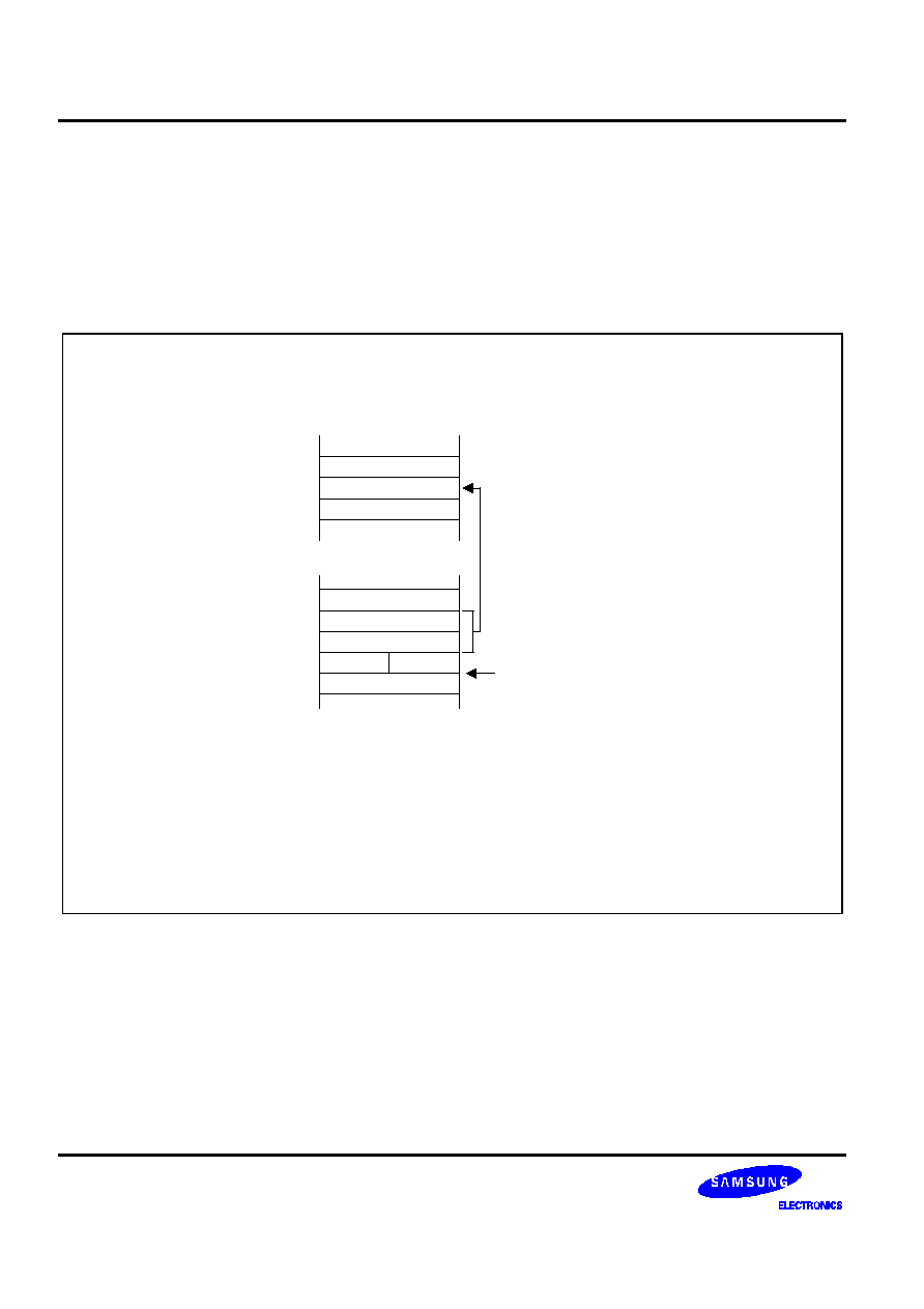
ADDRESSING MODES
S3C852B/P852B (Preliminary Spec)
3-10
DIRECT ADDRESS MODE (DA)
In Direct Address (DA) mode, the instruction provides the operand's 16-bit memory address. Jump (JP) and Call
(CALL) instructions use this addressing mode to specify the 16-bit destination address that is loaded into the PC
whenever a JP or CALL instruction is executed.
The LDC and LDE instructions can use Direct Address mode to specify the source or destination address for
Load operations to program memory (LDC) or to external data memory (LDE), if implemented.
Sample Instructions:
LDC
R5,1234H
; The values in the program address (1234H)
are loaded into register R5.
LDE
R5,1234H
; Identical operation to LDC example, except that
external program memory is accessed.
dst/src
OPCODE
Program Memory
"0" or "1"
Lower Address Byte
LSB Selects Program
Memory or Data Memory:
"0" = Program Memory
"1" = Data Memory
Memory
Address
Used
Upper Address Byte
Program or
Data Memory
Figure 3-10. Direct Addressing for Load Instructions
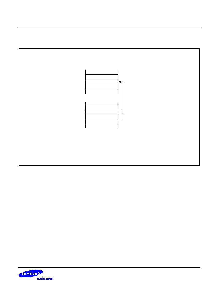
S3C852B/P852B (Preliminary Spec)
ADDRESSING MODES
3-11
DIRECT ADDRESS MODE (Continued)
OPCODE
Program Memory
Lower Address Byte
Memory
Address
Used
Upper Address Byte
Sample Instructions:
JP
C,JOB1
; Where JOB1 is a 16-bit immediate address
CALL
DISPLAY
; Where DISPLAY is a 16-bit immediate address
Next OPCODE
Figure 3-11. Direct Addressing for Call and Jump Instructions
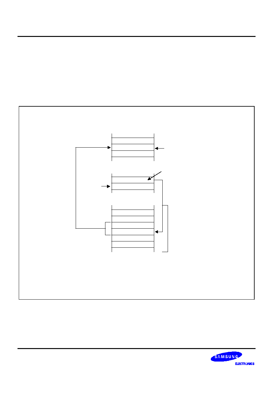
ADDRESSING MODES
S3C852B/P852B (Preliminary Spec)
3-12
INDIRECT ADDRESS MODE (IA)
In Indirect Address (IA) mode, the instruction specifies an address located in the lowest 256 bytes of the program
memory. The selected pair of memory locations contains the actual address of the next instruction to be
executed. Only the CALL instruction can use the Indirect Address mode.
Because the Indirect Address mode assumes that the operand is located in the lowest 256 bytes of program
memory, only an 8-bit address is supplied in the instruction; the upper bytes of the destination address are
assumed to be all zeros.
Current
Instruction
Program Memory
Locations 0-255
Program Memory
OPCODE
dst
Lower Address Byte
Upper Address Byte
Next Instruction
LSB Must be Zero
Sample Instruction:
CALL
#40H
; The 16-bit value in program memory addresses 40H
and 41H is the subroutine start address.
Figure 3-12. Indirect Addressing
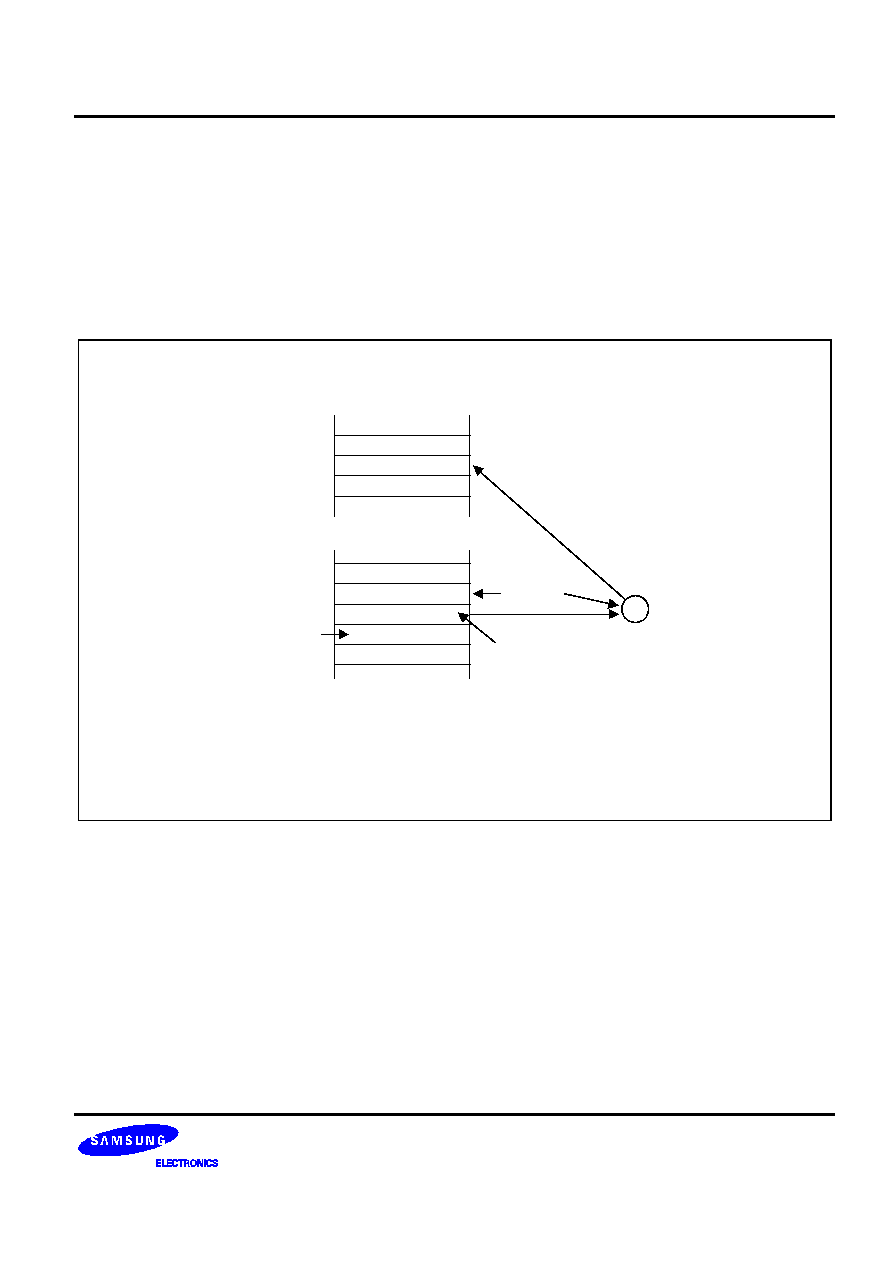
S3C852B/P852B (Preliminary Spec)
ADDRESSING MODES
3-13
RELATIVE ADDRESS MODE (RA)
In Relative Address (RA) mode, a two's-complement signed displacement between � 128 and + 127 is specified
in the instruction. The displacement value is then added to the current PC value. The result is the address of the
next instruction to be executed. Before this addition occurs, the PC contains the address of the instruction
immediately following the current instruction.
Several program control instructions use the Relative Address mode to perform conditional jumps. The
instructions that support RA addressing are BTJRF, BTJRT, DJNZ, CPIJE, CPIJNE, and JR.
OPCODE
Program Memory
Displacement
Program Memory
Address Used
Sample Instructions:
JR
ULT,$+OFFSET ; Where OFFSET is a value in the range +127 to -128
Next OPCODE
+
Signed
Displacement Value
Current Instruction
Current
PC Value
Figure 3-13. Relative Addressing

ADDRESSING MODES
S3C852B/P852B (Preliminary Spec)
3-14
IMMEDIATE MODE (IM)
In Immediate (IM) addressing mode, the operand value used in the instruction is the value supplied in the
operand field itself. The operand may be one byte or one word in length, depending on the instruction used.
Immediate addressing mode is useful for loading constant values into registers.
(The Operand value is in the instruction)
OPCODE
Sample Instruction:
LD R0,#0AAH
Program Memory
OPERAND
Figure 3-14. Immediate Addressing

S3C852B/P852B (Preliminary Spec)
CONTROL REGISTERS
4-1
4
CONTROL REGISTERS
OVERVIEW
In this section, detailed descriptions of the S3C852B/P852B control registers are presented in an easy-to-read
format.
These descriptions will help familiarize you with the mapped locations in the register file. You can also use them
as a quick-reference source when writing application programs.
System and peripheral registers are summarized in Tables 4-1, 4-2, and 4-3. Figure 4-1 illustrates the important
features of the standard register description format.
CID registers are mapped to Set 2 register page 8.
Control register descriptions are arranged in alphabetical order according to register mnemonic. More information
about control registers is presented in the context of the various peripheral hardware descriptions in Part II of this
manual.
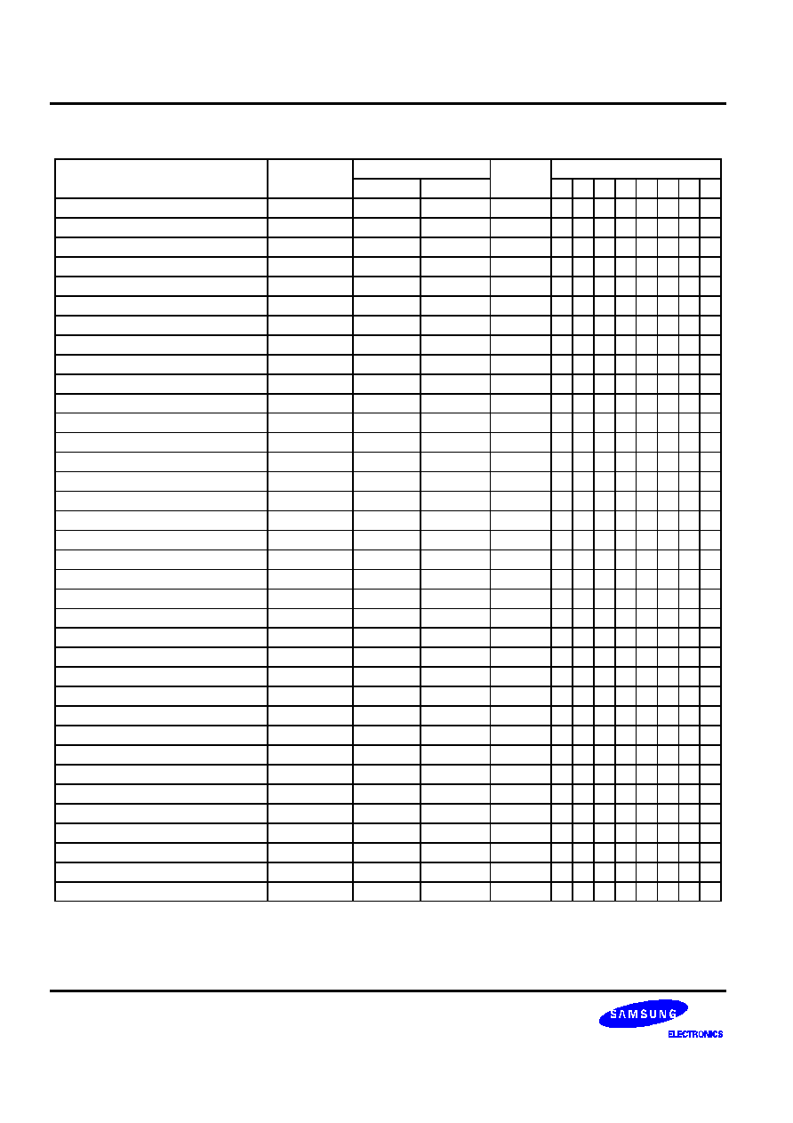
CONTROL REGISTERS
S3C852B/P852B (Preliminary Spec)
4-2
Table 4-1. Set 1, Bank 0 Registers
Register Name
Mnemonic
Address
R/W
RESET Values(bit)
Decimal
Hex
7
6
5
4
3
2
1
0
Timer 0 counter
T0CNT
208
D0H
R
0
0
0
0
0
0
0
0
Timer 0 data register
T0DATA
209
D1H
R/W
1
1
1
1
1
1
1
1
Timer 0 control register
T0CON
210
D2H
R/W
0
0
0
0
0
0
0
0
Basic timer control register
BTCON
211
D3H
R/W
0
0
0
0
0
0
0
0
Clock control register
CLKCON
212
D4H
R/W
0
0
0
0
0
0
0
0
System flags register
FLAGS
213
D5H
R/W
x
x
x
x
x
x
0
0
Register pointer 0
RP0
214
D6H
R/W
1
1
0
0
0
�
�
�
Register pointer 1
RP1
215
D7H
R/W
1
1
0
0
1
�
�
�
Stack pointer (high byte)
SPH
216
D8H
R/W
x
x
x
x
x
x
x
x
Stack pointer (low byte)
SPL
217
D9H
R/W
x
x
x
x
x
x
x
x
Instruction pointer (high byte)
IPH
218
DAH
R/W
x
x
x
x
x
x
x
x
Instruction pointer (low byte)
IPL
219
DBH
R/W
x
x
x
x
x
x
x
x
Interrupt request register
IRQ
220
DCH
R
0
0
0
0
0
0
0
0
Interrupt mask register
IMR
221
DDH
R/W
x
x
x
x
x
x
x
x
System mode register
SYM
222
DEH
R/W
0
�
�
x
x
x
0
0
Register page pointer
PP
223
DFH
R/W
0
0
0
0
0
0
0
0
Port 0 data register
P0
224
E0H
R/W
0
0
0
0
0
0
0
0
Port 1 data register
P1
225
E1H
R/W
0
0
0
0
0
0
0
0
Port 2 data register
P2
226
E2H
R/W
0
0
0
0
0
0
0
0
Port 3 data register
P3
227
E3H
R/W
0
0
0
0
0
0
0
0
Port 4 data register
P4
228
E4H
R/W
0
0
0
0
0
0
0
0
Port 5 data register
P5
229
E5H
R/W
0
0
0
0
0
0
0
0
Port 6 data register
P6
230
E6H
R/W
0
0
0
0
0
0
0
0
Port 0 interrupt control register
P0INT
231
E7H
R/W
�
0
0
0
0
0
0
0
Port 0 interrupt pending register
P0PND
232
E8H
R/W
�
0
0
0
0
0
0
0
Port 0 interrupt state register
P0STA
233
E9H
R/W
�
0
0
0
0
0
0
0
Port 0 control register(high byte)
P0CONH
234
EAH
R/W
0
0
0
0
0
0
0
0
Port 0 control register(low byte)
P0CONL
235
EBH
R/W
0
0
0
0
0
0
0
0
Port 1 control register(high byte)
P1CONH
236
ECH
R/W
0
0
0
0
0
0
0
0
Port 1 control register(low byte)
P1CONL
237
EDH
R/W
0
0
0
0
0
0
0
0
Port 1 function select register
P1AFS
238
EEH
R/W
-
-
-
-
0
0
0
0
Port 2 control register
P2CON
239
EFH
R/W
0
0
0
0
0
0
0
0
Port 3 control register
P3CON
241
F1H
R/W
0
0
0
0
0
0
0
0
Port 3 function select register
P3AFS
242
F2H
R/W
�
�
�
�
0
0
0
0
Port 4 control register
P4CON
243
F3H
R/W
0
0
0
0
0
0
0
0
Port 5 control register
P5CON
244
F4H
R/W
0
0
0
0
0
0
0
0

S3C852B/P852B (Preliminary Spec)
CONTROL REGISTERS
4-3
Table 4-1. Set 1, Bank 0 Registers (Continued)
Register Name
Mnemonic
Address
R/W
RESET Values(bit)
Decimal
Hex
7
6
5
4
3
2
1
0
Port 6 control register
P6CON
245
F5H
R/W
0
0
0
0
0
0
0
0
Location F6H-F7H is not mapped.
Clock output mode register
CLKMOD
248
F8H
R/W
�
�
�
�
�
0
0
0
Interrupt pending register
INTPND
249
F9H
R/W
�
�
�
�
�
0
0
0
Oscillator control register
OSCCON
250
FAH
R/W
�
�
�
�
0
0
�
0
STOP control register
STPCON
251
FBH
R/W
0
0
0
0
0
0
0
0
Location FCH is not mapped.
Basic timer counter
BTCNT
253
FDH
R
x
x
x
x
x
x
x
x
External Memory timing register
EMT
254
FEH
R/W
�
1
1
1
1
1
0
�
Interrupt priority register
IPR
255
FFH
R/W
x
x
x
x
x
x
x
x
Table 4-2. Set 1, Bank 1 Registers
Register Name
Mnemonic
Address
R/W
RESET Values(bit)
Decimal
Hex
7
6
5
4
3
2
1
0
Timer A counter
TACNT
224
E0H
R
0
0
0
0
0
0
0
0
Timer B counter
TBCNT
225
E1H
R
0
0
0
0
0
0
0
0
Timer A data register
TADATA
226
E2H
R/W
1
1
1
1
1
1
1
1
Timer B data register
TBDATA
227
E3H
R/W
1
1
1
1
1
1
1
1
Timer A control register
TACON
228
E4H
R/W
0
0
0
0
0
0
0
0
Timer B control register
TBCON
229
E5H
R/W
0
0
0
0
0
0
0
0
W/T control register
WTCON
230
E6H
R/W
0
0
0
0
0
0
0
0
SIO data register
SIODATA
234
EAH
R/W
1
1
1
1
1
1
1
1
SIO control register
SIOCON
235
EBH
R/W
0
0
0
0
0
0
0
0
SIO Pre-scaler register
SIOPS
236
ECH
R/W
0
0
0
0
0
0
0
0
Port 7 data register
P7
237
EDH
R/W
0
0
0
0
0
0
0
0
A/D data register(high byte)
ADDATAH
242
F2H
R
x
x
x
x
x
x
X
x
A/D data register(low byte)
ADDATAL
243
F3H
R
�
�
�
�
�
�
X
x
A/D control register
ADCON
244
F4H
R/W
0
0
0
0
0
0
0
0
Port 8 data register
P8
245
F5H
R/W
0
0
0
0
0
0
0
0
Port 9 data register
P9
246
F6H
R/W
0
0
0
0
0
0
0
0
Port 10 data register
P10
247
F7H
R/W
0
0
0
0
0
0
0
0
Port 7 control register (high byte)
P7CONH
248
F8H
R/W
0
0
0
0
0
0
0
0
Port 7 control register (low byte)
P7CONL
249
F9H
R/W
0
0
0
0
0
0
0
0
Port 8 control register (high byte)
P8CONH
250
FAH
R/W
0
0
0
0
0
0
0
0
Port 8 control register (low byte)
P8CONL
251
FBH
R/W
0
0
0
0
0
0
0
0
Port 9 control register (high byte)
P9CONH
252
FCH
R/W
0
0
0
0
0
0
0
0
Port 9 control register (low byte)
P9CONL
253
FDH
R/W
0
0
0
0
0
0
0
0
Port 10 control register (high byte)
P10CONH
254
FEH
R/W
0
0
0
0
0
0
0
0
Port 10 control register (low byte)
P10CONL
255
FFH
R/W
0
0
0
0
0
0
0
0
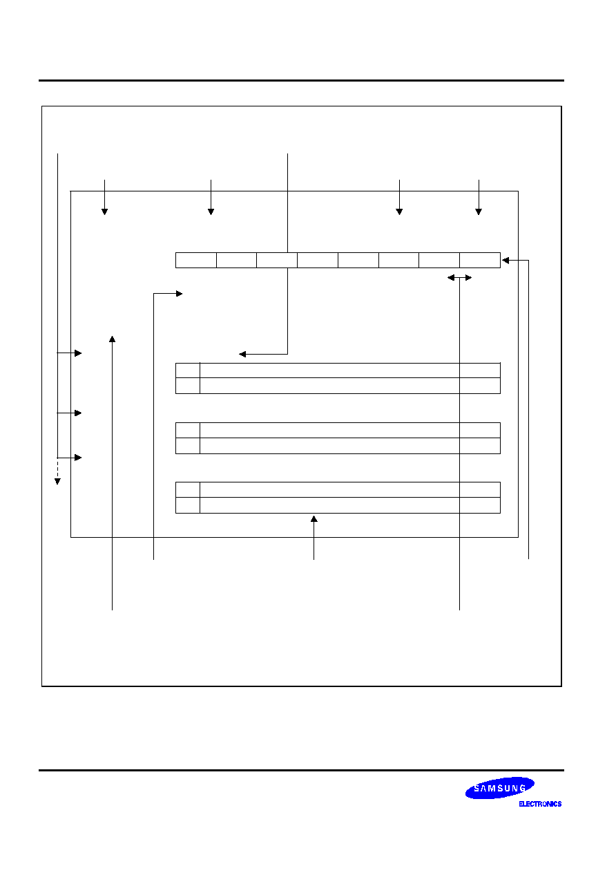
CONTROL REGISTERS
S3C852B/P852B (Preliminary Spec)
4-4
FLAGS - System Flags Register
.7
Carry Flag (C)
.6
Zero Flag (Z)
.5
Bit Identifier
RESET
RESET
Value
Read/Write
Bit Addressing
Mode
R = Read-only
W = Write-only
R/W = Read/write
'-' = Not used
Type of addressing
that must be used to
address the bit
(1-bit, 4-bit, or 8-bit)
RESET
value notation:
'-' = Not used
'x' = Undetermined value
'0' = Logic zero
'1' = Logic one
Bit number(s) that is/are appended to
the register name for bit addressing
Name of individual
bit or related bits
Register name
Register ID
Sign Flag (S)
0
Operation does not generate a carry or borrow condition
0
Operation generates carry-out or borrow into high-order bit 7
0
Operation result is a non-zero value
0
Operation result is zero
0
Operation generates positive number (MSB = "0")
0
Operation generates negative number (MSB = "1")
Description of the
effect of specific
bit settings
Set 1
Register location
in the internal
register file
D5H
Register address
(hexadecimal)
.7
.6
.5
x
x
x
R/W
R/W
R/W
Register addressing mode only
.4
.3
.2
.1
.0
x
R/W
x
R/W
x
R/W
x
R/W
0
R/W
Bit number:
MSB = Bit 7
LSB = Bit 0
Figure 4-1. Register Description Format
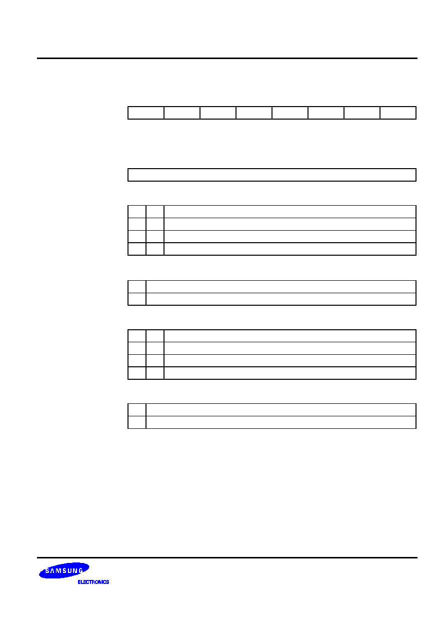
S3C852B/P852B (Preliminary Spec)
CONTROL REGISTERS
4-5
ADCON
-- A/D Converter Control Register
F4H
Set 1, Bank 1
Bit Identifier
.7
.6
.5
.4
.3
.2
.1
.0
RESET
RESET
Value
0
0
0
0
0
0
0
0
Read/Write
�
�
R/W
R/W
R
R/W
R/W
R/W
Addressing Mode
Register addressing mode only
.7 - .6
Not used for S3C852B/P852B
.5�.4
A/D Converter Analog Input Pin Selection Bits
0
0
ADC0 (P1.0)
0
1
ADC1 (P1.1)
1
0
ADC2 (P1.2)
1
1
ADC3 (P1.3)
.3
End-of-Conversion Bit (Read-only)
(note)
0
A/D conversion operation is in progress
1
A/D conversion operation is complete
.2�.1
Clock Source Selection
0
0
fxx/16
0
1
fxx/8
1
0
fxx/4
1
1
fxx/1
.0
Start or Enable Bit
0
Disable operation
1
Start operation
NOTE: This bit is read-only. You can poll ADCON.3 to determine internally when an A/D conversion operation has been
completed. A reset operation sets ADCON.3 to "0".
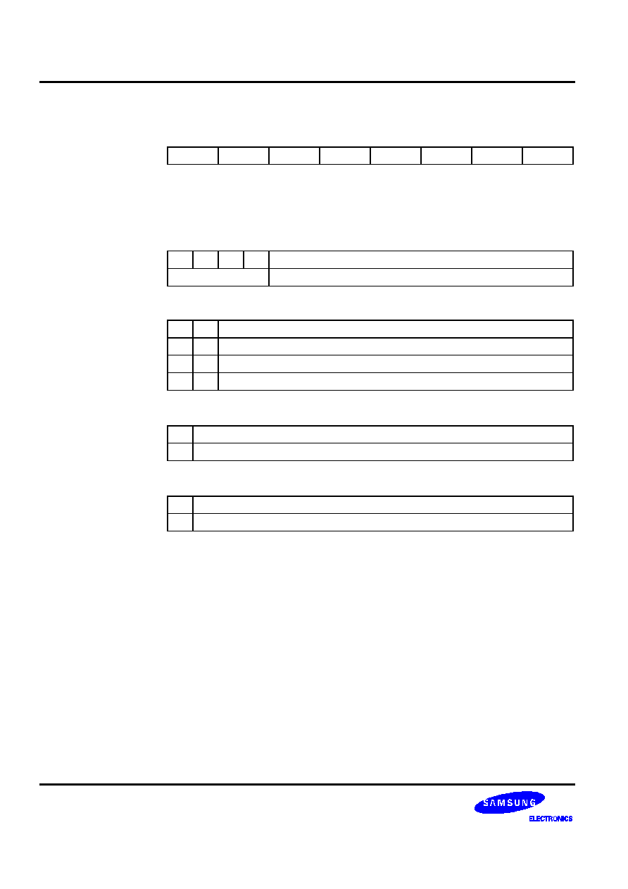
CONTROL REGISTERS
S3C852B/P852B (Preliminary Spec)
4-6
BTCON
--
Basic Timer Control Register
D3H
Set 1
Bit Identifier
.7
.6
.5
.4
.3
.2
.1
.0
RESET
RESET
Value
0
0
0
0
0
0
0
0
Read/Write
R/W
R/W
R/W
R/W
R/W
R/W
R/W
R/W
Addressing Mode
Register addressing mode only
.7�.4
Watchdog Timer Function Disable Code (for Reset)
1
0
1
0
Disable watchdog timer function
Any other value
Enable watchdog timer function
.3 and .2
Basic Timer Input Clock Selection Bits
0
0
fxx/4096
0
1
fxx/1024
1
0
fxx/128
1
1
fxx/16
.1
Basic Timer Counter Clear Bit
(1)
0
No effect
1
Clear the basic timer counter value
.0
Clock Frequency Divider Clear Bit for Basic Timer
(2)
0
No effect
1
Clear divider
NOTES:
1.
When you write a "1" to BTCON.1, the basic timer counter value is cleared to `00H'. Immediately following the write
operation, the BTCON.1 value is automatically cleared to "0".
2.
When you write a "1" to BTCON.0, the corresponding frequency divider is cleared to '00H'. Immediately following the
write operation, the BTCON.0 value is automatically cleared to "0".
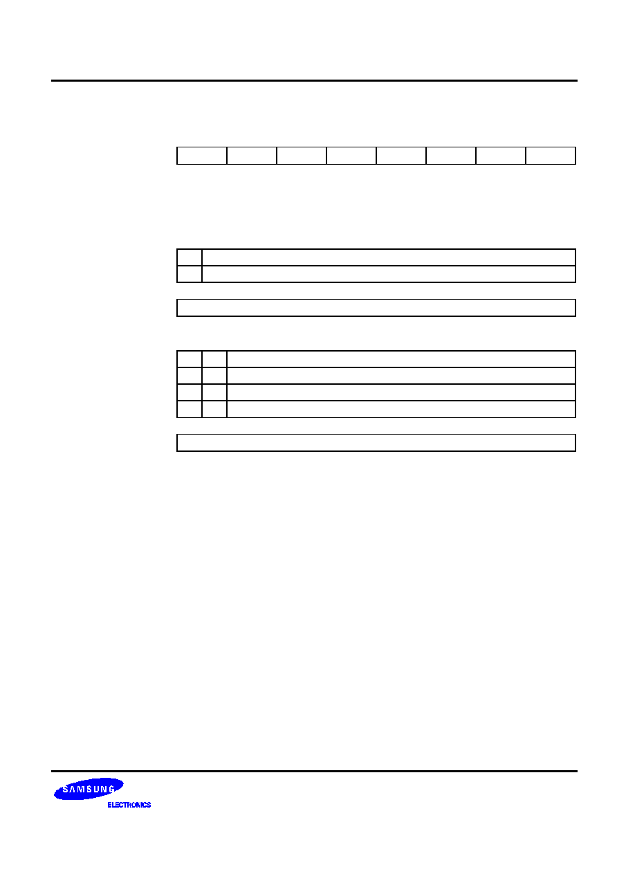
S3C852B/P852B (Preliminary Spec)
CONTROL REGISTERS
4-7
CLKCON
-- System Clock Control Register D4H
Set 1
Bit Identifier
.7
.6
.5
.4
.3
.2
.1
.0
RESET
RESET
Value
0
0
0
0
0
0
0
0
Read/Write
R/W
�
�
R/W
R/W
R/W
R/W
R/W
Addressing Mode
Register addressing mode only
.7
Oscillator IRQ Wake-up Function Enable Bit
0
Enable IRQ for main system oscillator wake-up in power-down mode
1
Disable IRQ for main system oscillator wake-up in power-down mode
.6 and .5
Not used for S3C852B/P852B
.4 and .3
CPU Clock (System Clock) Selection Bits
(1)
0
0
Divide by 16 (fx/16) or fxt
0
1
Divide by 8 (fx/8) or fxt
1
0
Divide by 2 (fx/2) or fxt
1
1
Non-divided clock (fx) or fxt
.2�.0
Not used for S3C852B/P852B
NOTE: After a reset, the slowest clock (divided by 16) is selected as the system clock. To select faster clock speeds, load
he appropriate values to CLKCON.3 and CLKCON.4.
CONTROL REGISTERS
S3C852B/P852B (Preliminary Spec)
4-8
CLKMOD
-- Clock Output Mode Register F8H Set 1, Bank 0
Bit Identifier
.7
.6
.5
.4
.3
.2
.1
.0
RESET
RESET
Value
�
�
�
�
�
0
0
0
Read/Write
�
�
�
�
�
R/W
R/W
R/W
Addressing Mode
Register addressing mode only
.7�.3
Not used for S3C852B/P852B
.2
M signal selection bit
0
M signal
1
Inversed M signal
.1 and .0
Output clock selection bits
0
0
fxx
0
1
fxx/2
3
1
0
fxx/2
6
1
1
CPU clock output
S3C852B/P852B (Preliminary Spec)
CONTROL REGISTERS
4-9
EMT
-- External Memory Timing Register
FEH
Set 1, Bank 0
Bit Identifier
.7
.6
.5
.4
.3
.2
.1
.0
RESET
RESET
Value
�
1
1
1
1
1
0
�
Read/Write
�
�
�
�
�
�
R/W
�
Addressing Mode
Register addressing mode only
.7�.2
Not used for S3C852B/P852B
.1
Stack Area Selection Bit
0
Select internal register file area
1
Select external data memory area
.0
Not used for S3C852B/P852B

CONTROL REGISTERS
S3C852B/P852B (Preliminary Spec)
4-10
FLAGS
-- System Flags Register
D5H
Set 1
Bit Identifier
.7
.6
.5
.4
.3
.2
.1
.0
RESET
RESET
Value
x
x
x
x
x
x
0
0
Read/Write
R/W
R/W
R/W
R/W
R/W
R/W
R/W
R/W
Addressing Mode
Register addressing mode only
.7
Carry Flag (C)
0
Operation does not generate a carry or borrow condition
1
Operation generates a carry-out or borrow into high-order bit 7
.6
Zero Flag (Z)
0
Operation result is a non-zero value
1
Operation result is zero
.5
Sign Flag (S)
0
Operation generates a positive number (MSB = "0")
1
Operation generates a negative number (MSB = "1")
.4
Overflow Flag (V)
0
Operation result is
+127 or
�128
1
Operation result is > +127 or < �128
.3
Decimal Adjust Flag (D)
0
Add operation completed
1
Subtraction operation completed
.2
Half-Carry Flag (H)
0
No carry-out of bit 3 or no borrow into bit 3 by addition or subtraction
1
Addition generated carry-out of bit 3 or subtraction generated borrow into bit 3
.1
Fast Interrupt Status Flag (FIS)
0
Cleared automatically during an interrupt return (IRET)
1
Automatically set to "1" during a fast interrupt service routine
.0
Bank Address Selection Flag (BA)
0
Bank 0 is selected
1
Bank 1 is selected

S3C852B/P852B (Preliminary Spec)
CONTROL REGISTERS
4-11
IMR
-- Interrupt Mask Register
DDH
Set 1
Bit Identifier
.7
.6
.5
.4
.3
.2
.1
.0
RESET
RESET
Value
x
x
x
x
x
x
x
x
Read/Write
R/W
R/W
�-
R/W
R/W
R/W
R/W
R/W
Addressing Mode
Register addressing mode only
.7
Interrupt Level 7 (IRQ7) Enable Bit; External Interrupt INT4�INT7
0
Disable IRQ7 interrupts
1
Enable IRQ7 interrupts
.6
Interrupt Level 6 (IRQ6) Enable Bit; External Interrupt INT0�INT3
0
Disable IRQ6 interrupts
1
Enable IRQ6 interrupts
.5
Not used for S3C852B/P852B
.4
Interrupt Level 4 (IRQ4) Enable Bit; Serial data receive/transmit Interrupt
0
Disable IRQ4 interrupts
1
Enable IRQ4 interrupts
.3
Interrupt Level 3 (IRQ3) Enable Bit; Watch Timer overflow
0
Disable IRQ3 interrupts
1
Enable IRQ3 interrupts
.2
Interrupt Level 2 (IRQ2) Enable Bit; CID block Interrupt
0
Disable IRQ2 interrupts
1
Enable IRQ2 interrupts
.1
Interrupt Level 1 (IRQ1) Enable Bit; Timer A match, Timer B match/overflow
0
Disable IRQ1 interrupts
1
Enable IRQ1 interrupts
.0
Interrupt Level 0 (IRQ0) Enable Bit; Timer 0 match/capture/overflow
0
Disable IRQ0 interrupts
1
Enable IRQ0 interrupts
CONTROL REGISTERS
S3C852B/P852B (Preliminary Spec)
4-12
INTPND
-- Interrupt Pending Register F9H Set 1, Bank 0
Bit Identifier
.7
.6
.5
.4
.3
.2
.1
.0
RESET
RESET
Value
�
�
�
�
�
0
0
0
Read/Write
�
�
�
�
�
R/W
R/W
R/W
Addressing Mode
Register addressing mode only
.7�.3
Not used for S3C852B/P852B
.2
Timer B match Interrupt pending bit
0
No interrupt pending
0
Clear pending bit (write)
1
Interrupt is pending
.1
Timer B overflow Interrupt pending bit
0
No interrupt pending
0
Clear pending bit (write)
1
Interrupt is pending
.0
Timer 0 overflow Interrupt pending bit
0
No interrupt pending
0
Clear pending bit (write)
1
Interrupt is pending
S3C852B/P852B (Preliminary Spec)
CONTROL REGISTERS
4-13
IPH
-- Instruction Pointer (High Byte)
DAH
Set 1
Bit Identifier
.7
.6
.5
.4
.3
.2
.1
.0
RESET
RESET
Value
x
x
x
x
x
x
x
x
Read/Write
R/W
R/W
R/W
R/W
R/W
R/W
R/W
R/W
Addressing Mode
Register addressing mode only
.7�.0
Instruction Pointer Address (High Byte)
The high-byte instruction pointer value is the upper eight bits of the 16-bit instruction
pointer address (IP15�IP8). The lower byte of the IP address is located in the IPL
register (DBH).
IPL
-- Instruction Pointer (Low Byte)
DBH
Set 1
Bit Identifier
.7
.6
.5
.4
.3
.2
.1
.0
RESET
RESET
Value
x
x
x
x
x
x
x
x
Read/Write
R/W
R/W
R/W
R/W
R/W
R/W
R/W
R/W
Addressing Mode
Register addressing mode only
.7�.0
Instruction Pointer Address (Low Byte)
The low-byte instruction pointer value is the lower eight bits of the 16-bit instruction
pointer address (IP7�IP0). The upper byte of the IP address is located in the IPH
register (DAH).

CONTROL REGISTERS
S3C852B/P852B (Preliminary Spec)
4-14
IPR
-- Interrupt Priority Register
FFH Set 1, Bank 0
Bit Identifier
.7
.6
.5
.4
.3
.2
.1
.0
RESET
RESET
Value
x
x
x
x
x
x
x
x
Read/Write
R/W
R/W
�
R/W
R/W
R/W
R/W
R/W
Addressing Mode
Register addressing mode only
.7, .4, and .1
Priority Control Bits for Interrupt Groups A, B, and C
0
0
0
Group priority undefined
0
0
1
B
>
C
>
A
0
1
0
A
>
B
>
C
0
1
1
B
>
A
>
C
1
0
0
C
>
A
>
B
1
0
1
C
>
B
>
A
1
1
0
A
>
C
>
B
1
1
1
Group priority undefined
.6
Interrupt Subgroup C Priority Control Bit
0
IRQ6
>
IRQ7
1
IRQ7
>
IRQ6
.5
Not used for S3C852B/P852B
.3
Interrupt Group B Priority Control Bit
0
IRQ3
>
IRQ4
1
IRQ4
>
IRQ3
.2
Interrupt Group B Priority Control Bit
0
IRQ2
>
(IRQ3, IRQ4)
1
(IRQ3, IRQ4)
>
IRQ2
.0
Interrupt Group A Priority Control Bit
0
IRQ0
>
IRQ1
1
IRQ1
>
IRQ0
NOTE: Interrupt group A is IRQ0 and IRQ1; interrupt group B is IRQ3, IRQ4 and IRQ2; interrupt group C is IRQ6,
and IRQ7.
S3C852B/P852B (Preliminary Spec)
CONTROL REGISTERS
4-15
IRQ
-- Interrupt Request Register
DCH
Set 1
Bit Identifier
.7
.6
.5
.4
.3
.2
.1
.0
RESET
RESET
Value
0
0
�
0
0
0
0
0
Read/Write
R
R
�
R
R
R
R
R
Addressing Mode
Register addressing mode only
.7
Interrupt Level 7 (IRQ7) Request Pending Bit; INT4�INT7
0
No IRQ7 interrupt pending
1
IRQ7 interrupt is pending
.6
Interrupt Level 6 (IRQ6) Request Pending Bit; INT0�INT3
0
No IRQ6 interrupt pending
1
IRQ6 interrupt is pending
.5
Not used for S3C852B/P852B
.4
Interrupt Level 4 (IRQ4) Request Pending Bit;
Serial data receive/transmit interrupt
0
No IRQ4 interrupt pending
1
IRQ4 interrupt is pending
.3
Interrupt Level 3 (IRQ3) Request Pending Bit; Watch Timer overflow
0
No IRQ3 interrupt pending
1
IRQ3 interrupt is pending
.2
Interrupt Level 2 (IRQ2) Request Pending Bit; Caller ID functions
0
No IRQ2 interrupt pending
1
IRQ2 interrupt pending
.1
Interrupt Level 1 (IRQ1) Request Pending Bit;
Timer A match, Timer B match/overflow
0
No IRQ1 interrupt pending
1
IRQ1 interrupt is pending
.0
Interrupt Level 0 (IRQ0) Request Pending Bit; Timer 0 match/capture/overflow
0
No IRQ0 interrupt pending
1
IRQ0 interrupt is pending
CONTROL REGISTERS
S3C852B/P852B (Preliminary Spec)
4-16
OSCCON
-- oscillator Control Register FAH Set 1, Bank 0
Bit Identifier
.7
.6
.5
.4
.3
.2
.1
.0
RESET
RESET
Value
�
�
�
�
0
0
�
0
Read/Write
�
�
�
�
R/W
R/W
�
R/W
Addressing Mode
Register addressing mode only
.7�.4
Not used for S3C852B/P852B
.3
Main system oscillator control bit
0
Main system oscillator RUN
1
Main system oscillator STOP
.2
Subsystem oscillator control bit
0
Subsystem oscillator RUN
1
Subsystem oscillator STOP
.1
Not used for S3C852B/P852B
.0
System clock selection bit
0
Select Main system clock
1
Select Subsystem clock

S3C852B/P852B (Preliminary Spec)
CONTROL REGISTERS
4-17
P0CONH
-- Port 0 Control Register (High byte)
EAH
Set 1, Bank 0
Bit Identifier
.7
.6
.5
.4
.3
.2
.1
.0
RESET
RESET
Value
0
0
0
0
0
0
0
0
Read/Write
R/W
R/W
R/W
R/W
R/W
R/W
R/W
R/W
Addressing Mode
Register addressing mode only
.7�.6
Port 0.7/INT7
0
0
Input, Schmitt trigger
0
1
Input, Schmitt trigger, Pull-up resistor
1
0
Output, Push-pull
1
1
Not used
.5�.4
Port 0.6/INT6/TB
0
0
Input, Schmitt trigger
0
1
Input, Schmitt trigger, Pull-up resistor
1
0
Output, Push-pull
1
1
Select alternative function for TB
.3�.2
Port 0.5/INT5/TA
0
0
Input, Schmitt trigger
0
1
Input, Schmitt trigger, Pull-up resistor
1
0
Output, Push-pull
1
1
Select alternative function for TA
.1�.0
Port 0.4/INT4/T1CK
0
0
Input, Schmitt trigger (T1CK)
0
1
Input, Schmitt trigger, Pull-up resistor (T1CK)
1
0
Output, Push-pull
1
1
Not used

CONTROL REGISTERS
S3C852B/P852B (Preliminary Spec)
4-18
P0CONL
-- Port 0 Control Register(Low byte)
EBH
Set 1, Bank 0
Bit Identifier
.7
.6
.5
.4
.3
.2
.1
.0
RESET
RESET
Value
0
0
0
0
0
0
0
0
Read/Write
R/W
R/W
R/W
R/W
R/W
R/W
R/W
R/W
Addressing Mode
Register addressing mode only
.7�.6
Port 0.3/INT3/T0/T0CAP
0
0
Input, Schmitt trigger (T0CAP)
0
1
Input, Schmitt trigger, Pull-up resistor (T0 CAP)
1
0
Output, Push-pull
1
1
Select alternative function for T0
.5�.4
Port 0.2/INT2/T0CK
0
0
Input, Schmitt trigger (T0CK)
0
1
Input, Schmitt trigger, Pull-up resistor (T0CK)
1
0
Output, Push-pull
1
1
Not used
.3�.2
Port 0.1/INT1/BUZ
0
0
Input, Schmitt trigger
0
1
Input, Schmitt trigger, Pull-up resistor
1
0
Output, Push-pull
1
1
Select alternative function for BUZ
.1�.0
Port 0.0/INT0
0
0
Input, Schmitt trigger
0
1
Input, Schmitt trigger, Pull-up resistor
1
0
Output, Push-pull
1
1
Not used

S3C852B/P852B (Preliminary Spec)
CONTROL REGISTERS
4-19
P0INT
-- Port 0 Interrupt Enable Register
E7H
Set 1, Bank 0
Bit Identifier
.7
.6
.5
.4
.3
.2
.1
.0
RESET
RESET
Value
0
0
0
0
0
0
0
0
Read/Write
R/W
R/W
R/W
R/W
R/W
R/W
R/W
R/W
Addressing Mode
Register addressing mode only
.7
INT7/P0.7 Interrupt Enable bit
0
Disable INT7
1
Enable INT7
.6
INT6/P0.6 Interrupt Enable bit
0
Disable INT6
1
Enable INT6
.5
INT5/P0.5 Interrupt Enable bit
0
Disable INT5
1
Enable INT5
.4
INT4/P0.4 Interrupt Enable bit
0
Disable INT4
1
Enable INT4
.3
INT3/P0.3 Interrupt Enable bit
0
Disable INT3
1
Enable INT3
.2
INT2/P0.2 Interrupt Enable bit
0
Disable INT2
1
Enable INT2
.1
INT1/P0.1 Interrupt Enable bit
0
Disable INT1
1
Enable INT1
.0
INT0/P0.0 Interrupt Enable bit
0
Disable INT0
1
Enable INT0
CONTROL REGISTERS
S3C852B/P852B (Preliminary Spec)
4-20
P0PND
-- Port 0 Interrupt Pending Register
E8H
Set 1, Bank 0
Bit Identifier
.7
.6
.5
.4
.3
.2
.1
.0
RESET
RESET
Value
0
0
0
0
0
0
0
0
Read/Write
R/W
R/W
R/W
R/W
R/W
R/W
R/W
R/W
Addressing Mode
Register addressing mode only
.7
INT7/P0.7 Interrupt Pending bit
0
INT7 Interrupt request is not pending
1
INT7 Interrupt request is pending
.6
INT6/P0.6 Interrupt Pending bit
0
INT6 Interrupt request is not pending
1
INT6 Interrupt request is pending
.5
INT5/P0.5 Interrupt Pending bit
0
INT5 Interrupt request is not pending
1
INT5 Interrupt request is pending
.4
INT4/P0.4 Interrupt Pending bit
0
INT4 Interrupt request is not pending
1
INT4 Interrupt request is pending
.3
INT3/P0.3 Interrupt Pending bit
0
INT3 Interrupt request is not pending
1
INT3 Interrupt request is pending
.2
INT2/P0.2 Interrupt Pending bit
0
INT2 Interrupt request is not pending
1
INT2 Interrupt request is pending
.1
INT1/P0.1 Interrupt Pending bit
0
INT1 Interrupt request is not pending
1
INT1 Interrupt request is pending
.0
INT0/P0.0 Interrupt Pending bit
0
INT0 Interrupt request is not pending
1
INT0 Interrupt request is pending
S3C852B/P852B (Preliminary Spec)
CONTROL REGISTERS
4-21
P0STA
-- Port 0 Interrupt State Register
E9H
Set 1, Bank 0
Bit Identifier
.7
.6
.5
.4
.3
.2
.1
.0
RESET
RESET
Value
0
0
0
0
0
0
0
0
Read/Write
R/W
R/W
R/W
R/W
R/W
R/W
R/W
R/W
Addressing Mode
Register addressing mode only
.7
INT7/P0.7 Interrupt State Setting bit
0
INT7 falling edge detection
1
INT7 rising edge detection
.6
INT6/P0.6 Interrupt State Setting bit
0
INT6 falling edge detection
1
INT6 rising edge detection
.5
INT5/P0.5 Interrupt State Setting bit
0
INT5 falling edge detection
1
INT5 rising edge detection
.4
INT4/P0.4 Interrupt State Setting bit
0
INT4 falling edge detection
1
INT4 rising edge detection
.3
INT3/P0.3 Interrupt State Setting bit
0
INT3 falling edge detection
1
INT3 rising edge detection
.2
INT2/P0.2 Interrupt State Setting bit
0
INT2 falling edge detection
1
INT2 rising edge detection
.1
INT1/P0.1 Interrupt State Setting bit
0
INT1 falling edge detection
1
INT1 rising edge detection
.0
INT0/P0.0 Interrupt State Setting bit
0
INT0 falling edge detection
1
INT0 rising edge detection
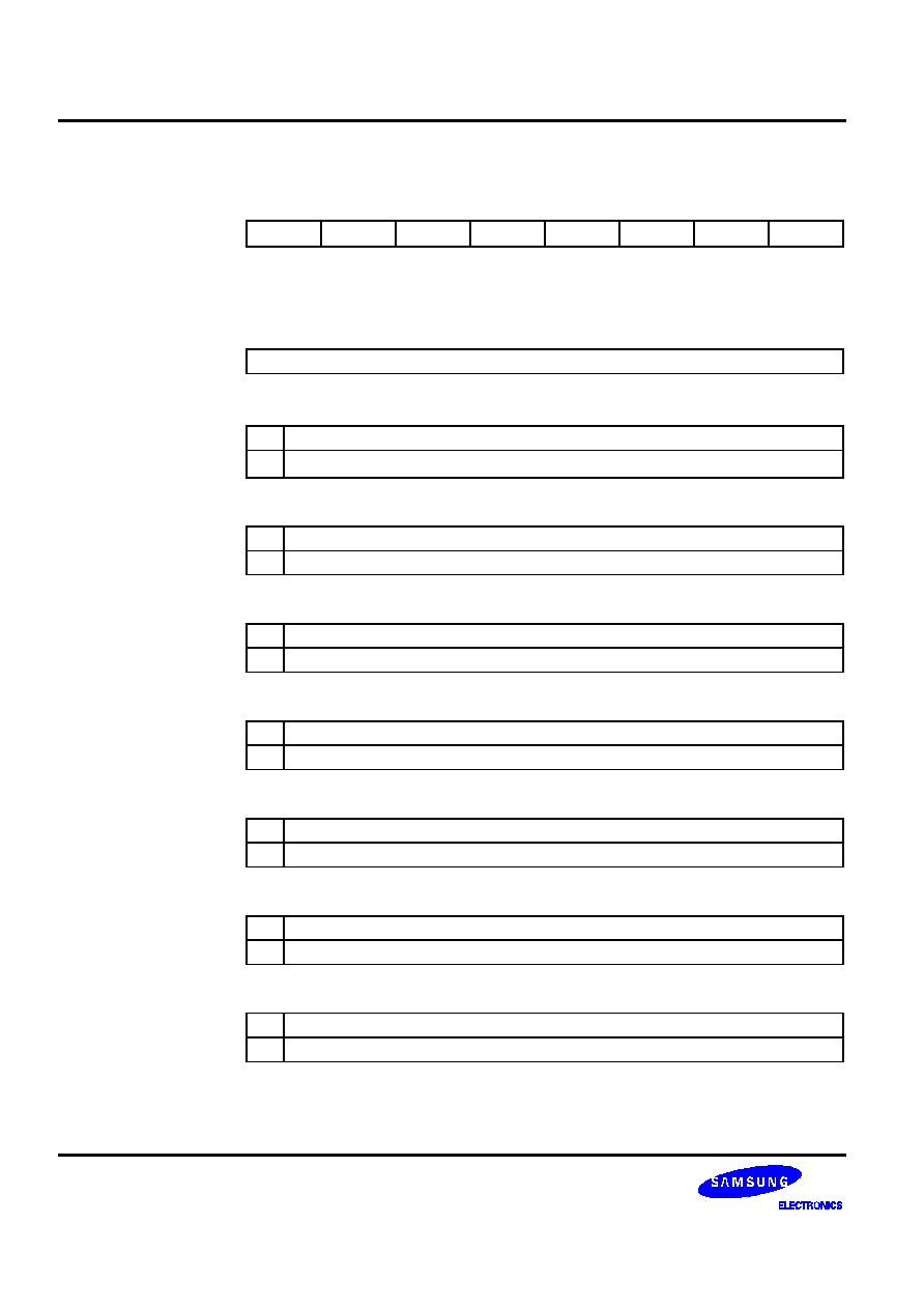
CONTROL REGISTERS
S3C852B/P852B (Preliminary Spec)
4-22
P1AFS
-- Port 1 Function Select Register
EEH
Set 1, Bank 0
Bit Identifier
.7
.6
.5
.4
.3
.2
.1
.0
RESET
RESET
Value
�
0
0
0
0
0
0
0
Read/Write
�
R/W
R/W
R/W
R/W
R/W
R/W
R/W
Addressing Mode
Register addressing mode only
.7
Not used for S3C852B/P852B
.6
Port 1.6/
SCK
SCK
0
Normal I/O port
1
Select alternative function for
SCK
.5
Port 1.5/SO
0
Normal I/O port
1
Select alternative function for SO
.4
Port 1.4/SI
0
Normal I/O port
1
Select alternative function for SI
.3
Port 1.3/ADC3
0
Normal I/O port
1
Select Analog Input function for ADC3
.2
Port 1.2/ADC2
0
Normal I/O port
1
Select Analog Input function for ADC2
.1
Port 1.1/ADC1
0
Normal I/O port
1
Select Analog Input function for ADC1
.0
Port 1.0/ADC0
0
Normal I/O port
1
Select Analog Input function for ADC0
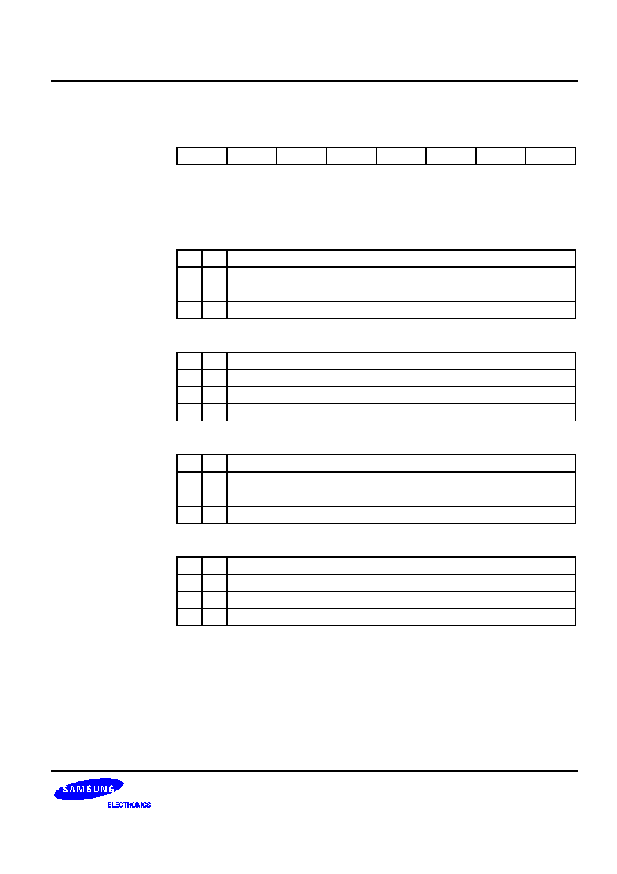
S3C852B/P852B (Preliminary Spec)
CONTROL REGISTERS
4-23
P1CONH
-- Port 1 Control Register(High byte)
ECH
Set 1, Bank 0
Bit Identifier
.7
.6
.5
.4
.3
.2
.1
.0
RESET
RESET
Value
0
0
0
0
0
0
0
0
Read/Write
R/W
R/W
R/W
R/W
R/W
R/W
R/W
R/W
Addressing Mode
Register addressing mode only
.7�.6
Port 1.7
0
0
Input, Schmitt trigger
0
1
Input, Schmitt trigger, Pull-up resistor
1
0
Output, Push-pull
1
1
Output, Open-drain
.5�.4
Port 1.6
0
0
Input, Schmitt trigger
0
1
Input, Schmitt trigger, Pull-up resistor
1
0
Output, Push-pull
1
1
Output, Open-drain
.3�.2
Port 1.5
0
0
Input, Schmitt trigger
0
1
Input, Schmitt trigger, Pull-up resistor
1
0
Output, Push-pull
1
1
Output, Open-drain
.1�.0
Port 1.4
0
0
Input, Schmitt trigger
0
1
Input, Schmitt trigger, Pull-up resistor
1
0
Output, Push-pull
1
1
Output, Open-drain

CONTROL REGISTERS
S3C852B/P852B (Preliminary Spec)
4-24
P1CONL
-- Port 1 Control Register(Low byte)
EDH
Set 1, Bank 0
Bit Identifier
.7
.6
.5
.4
.3
.2
.1
.0
RESET
RESET
Value
0
0
0
0
0
0
0
0
Read/Write
R/W
R/W
R/W
R/W
R/W
R/W
R/W
R/W
Addressing Mode
Register addressing mode only
.7�.6
Port 1.3/ADC3
0
0
Input, Schmitt trigger
0
1
Input, Schmitt trigger, Pull-up resistor
1
0
Output, Push-pull
1
1
Output, Open-drain
.5�.4
Port 1.2/ADC2
0
0
Input, Schmitt trigger
0
1
Input, Schmitt trigger, Pull-up resistor
1
0
Output, Push-pull
1
1
Output, Open-drain
.3�.2
Port 1.1/ADC1
0
0
Input, Schmitt trigger
0
1
Input, Schmitt trigger, Pull-up resistor
1
0
Output, Push-pull
1
1
Output, Open-drain
.1�.0
Port 1.0/ADC0
0
0
Input, Schmitt trigger
0
1
Input, Schmitt trigger, Pull-up resistor
1
0
Output, Push-pull
1
1
Output, Open-drain

S3C852B/P852B (Preliminary Spec)
CONTROL REGISTERS
4-25
P2CON
-- Port 2 Control Register
EFH
Set 1, Bank 0
Bit Identifier
.7
.6
.5
.4
.3
.2
.1
.0
RESET
RESET
Value
0
0
0
0
0
0
0
0
Read/Write
R/W
R/W
R/W
R/W
R/W
R/W
R/W
R/W
Addressing Mode
Register addressing mode only
.7�.6
Port 2.3
0
0
Input, Schmitt trigger
0
1
Input, Schmitt trigger, Pull-up resistor
1
0
Output, Push-pull
1
1
Output, Open-drain
.5� .4
Port 2.2
0
0
Input, Schmitt trigger
0
1
Input, Schmitt trigger, Pull-up resistor
1
0
Output, Push-pull
1
1
Output, Open-drain
.3�2
Port 2.1
0
0
Input, Schmitt trigger
0
1
Input, Schmitt trigger, Pull-up resistor
1
0
Output, Push-pull
1
1
Output, Open-drain
.1� .0
Port 2.0
0
0
Input, Schmitt trigger
0
1
Input, Schmitt trigger, Pull-up resistor
1
0
Output, Push-pull
1
1
Output, Open-drain
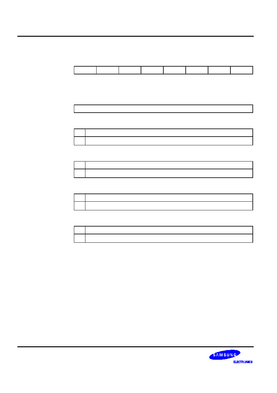
CONTROL REGISTERS
S3C852B/P852B (Preliminary Spec)
4-26
P3AFS
-- Port 3 Function Select Register
F2H
Set 1, Bank 0
Bit Identifier
.7
.6
.5
.4
.3
.2
.1
.0
RESET
RESET
Value
�
�
�
�
0
0
0
0
Read/Write
�
�
�
�
R/W
R/W
R/W
R/W
Addressing Mode
Register addressing mode only
.7�.4
Not used for S3C852B/P852B
.3
Port 3.3/
WR
WR
0
Normal I/O port
1
Select alternative function for
WR
.2
Port 3.2/
RD
RD
0
Normal I/O port
1
Select alternative function for
RD
.1
Port 3.1/
DM
DM
0
Normal I/O port
1
Select alternative function for
DM
.0
Port 3.0/
PM
PM
0
Normal I/O port
1
Select alternative function for
PM
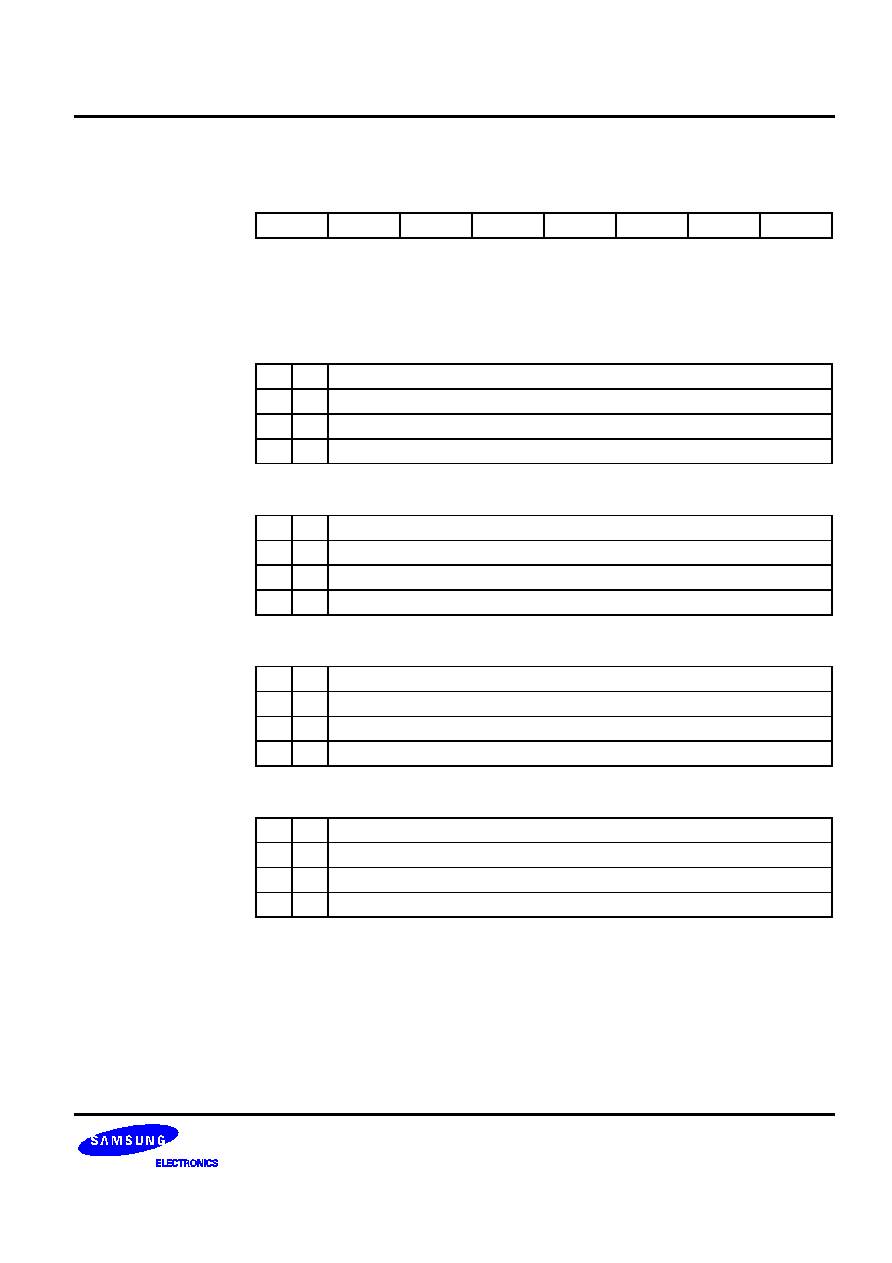
S3C852B/P852B (Preliminary Spec)
CONTROL REGISTERS
4-27
P3CON
-- Port 3 Control Register
F1H
Set 1, Bank 0
Bit Identifier
.7
.6
.5
.4
.3
.2
.1
.0
RESET
RESET
Value
0
0
0
0
0
0
0
0
Read/Write
R/W
R/W
R/W
R/W
R/W
R/W
R/W
R/W
Addressing Mode
Register addressing mode only
.7�.6
Port 3.3/
WR
WR
0
0
Input, Schmitt trigger
0
1
Input, Schmitt trigger, Pull-up resistor
1
0
Output, Push-pull
1
1
Output, Open-drain
.5�.4
Port 3.2/
RD
RD
0
0
Input, Schmitt trigger
0
1
Input, Schmitt trigger, Pull-up resistor
1
0
Output, Push-pull
1
1
Output, Open-drain
.3�.2
Port 3.1/
DM
DM
0
0
Input, Schmitt trigger
0
1
Input, Schmitt trigger, Pull-up resistor
1
0
Output, Push-pull
1
1
Output, Open-drain
.1�.0
Port 3.0/
PM
PM
0
0
Input, Schmitt trigger
0
1
Input, Schmitt trigger, Pull-up resistor
1
0
Output, Push-pull
1
1
Output, Open-drain

CONTROL REGISTERS
S3C852B/P852B (Preliminary Spec)
4-28
P4CON
-- Port 4 Control Register
F3H
Set 1, Bank 0
Bit Identifier
.7
.6
.5
.4
.3
.2
.1
.0
RESET
RESET
Value
0
0
0
0
0
0
0
0
Read/Write
R/W
R/W
R/W
R/W
R/W
R/W
R/W
R/W
Addressing Mode
Register addressing mode only
.7�.4
Port 4.7�Port 4.4/D7�D4
0
0
0
0
Input, Schmitt trigger
0
0
0
1
Input, Schmitt trigger, pull-up resistor
0
0
1
0
Output, Push-Pull
0
0
1
1
Output, Open-drain
0
1
0
0
Select External memory interface line at D7�D4
.3�.0
Port 4.3�Port 4.0/D3�D0
0
0
0
0
Input, Schmitt trigger
0
0
0
1
Input, Schmitt trigger, pull-up resistor
0
0
1
0
Output, Push-Pull
0
0
1
1
Output, Open-drain
0
1
0
0
Select External memory interface line at D3�D0
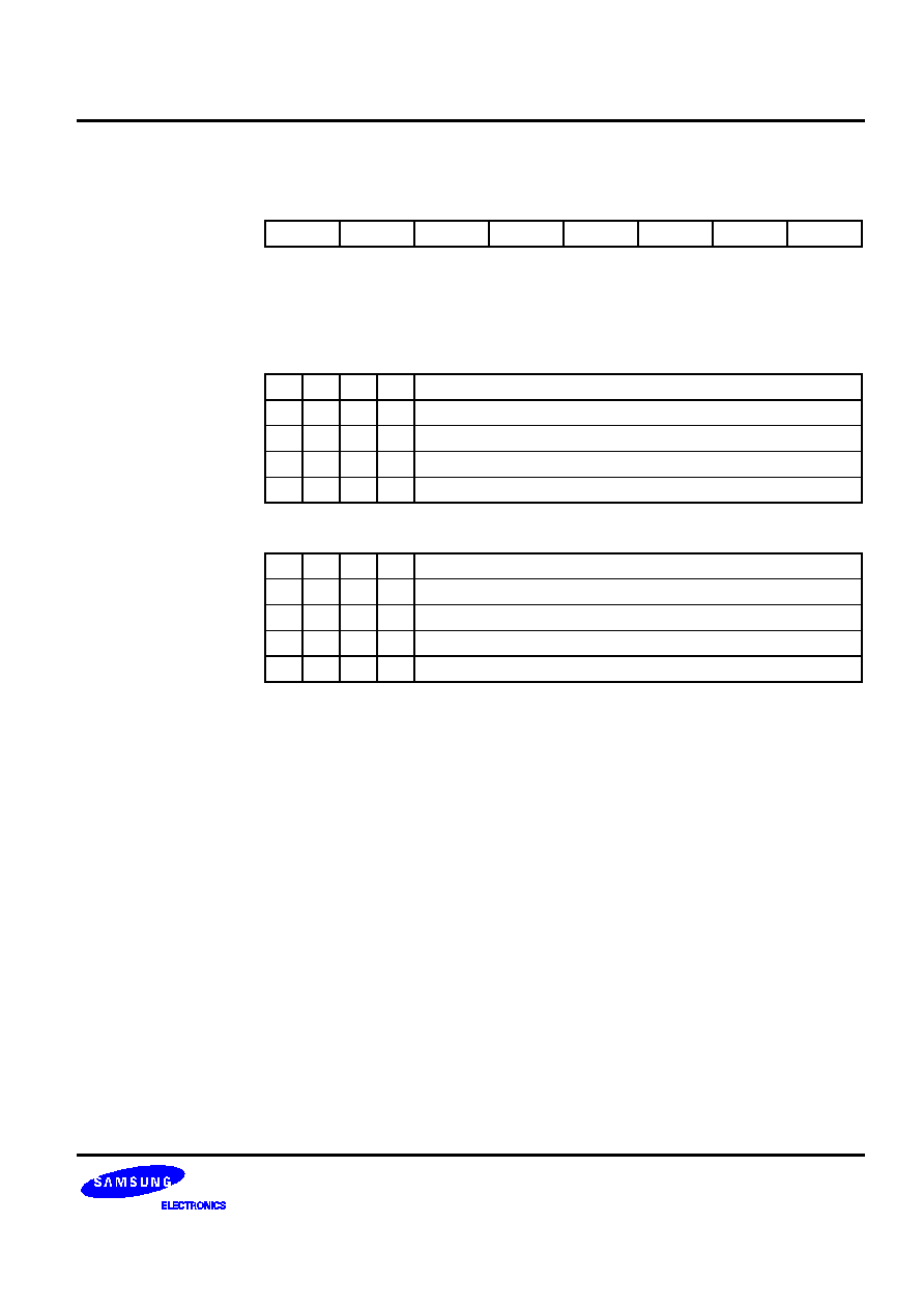
S3C852B/P852B (Preliminary Spec)
CONTROL REGISTERS
4-29
P5CON
-- Port 5 Control Register
F4H
Set 1, Bank 0
Bit Identifier
.7
.6
.5
.4
.3
.2
.1
.0
RESET
RESET
Value
0
0
0
0
0
0
0
0
Read/Write
R/W
R/W
R/W
R/W
R/W
R/W
R/W
R/W
Addressing Mode
Register addressing mode only
.7�.4
Port 5.7�Port 5.4/A7�A4
0
0
0
0
Input, Schmitt trigger
0
0
0
1
Input, Schmitt trigger, pull-up resistor
0
0
1
0
Output, Push-Pull
0
0
1
1
Output, Open-drain
0
1
0
0
Select External memory interface line at A7�A4
.3�.0
Port 5.3�Port 5.0/A3�A0
0
0
0
0
Input, Schmitt trigger
0
0
0
1
Input, Schmitt trigger, pull-up resistor
0
0
1
0
Output, Push-Pull
0
0
1
1
Output, Open-drain
0
1
0
0
Select External memory interface line at A3�A0

CONTROL REGISTERS
S3C852B/P852B (Preliminary Spec)
4-30
P6CON
-- Port 6 Control Register
F5H
Set 1, Bank 0
Bit Identifier
.7
.6
.5
.4
.3
.2
.1
.0
RESET
RESET
Value
0
0
0
0
0
0
0
0
Read/Write
R/W
R/W
R/W
R/W
R/W
R/W
R/W
R/W
Addressing Mode
Register addressing mode only
.7�4
Port 6.7�Port 6.4/A15�A12
0
0
0
0
Input, Schmitt trigger
0
0
0
1
Input, Schmitt trigger, pull-up resistor
0
0
1
0
Output, Push-Pull
0
0
1
1
Output, Open-drain
0
1
0
0
Select External memory interface line at A15�A12
.3�0
Port 6.3�Port 6.0/A11�A8
0
0
0
0
Input, Schmitt trigger
0
0
0
1
Input, Schmitt trigger, pull-up resistor
0
0
1
0
Output, Push-Pull
0
0
1
1
Output, Open-drain
0
1
0
0
Select External memory interface line at A11�A8

S3C852B/P852B (Preliminary Spec)
CONTROL REGISTERS
4-31
P7CONH
-- Port 7 Control Register(High byte)
F8H
Set 1, Bank 1
Bit Identifier
.7
.6
.5
.4
.3
.2
.1
.0
RESET
RESET
Value
0
0
0
0
0
0
0
0
Read/Write
R/W
R/W
R/W
R/W
R/W
R/W
R/W
R/W
Addressing Mode
Register addressing mode only
.7�.6
Port 7.7
0
0
Input, Schmitt trigger
0
1
Input, Schmitt trigger, Pull-up resistor
1
0
Output, Push-pull
1
1
Output, Open-drain
.5�.4
Port 7.6
0
0
Input, Schmitt trigger
0
1
Input, Schmitt trigger, Pull-up resistor
1
0
Output, Push-pull
1
1
Output, Open-drain
.3�.2
Port 7.5
0
0
Input, Schmitt trigger
0
1
Input, Schmitt trigger, Pull-up resistor
1
0
Output, Push-pull
1
1
Output, Open-drain
.1�.0
Port 7.4
0
0
Input, Schmitt trigger
0
1
Input, Schmitt trigger, Pull-up resistor
1
0
Output, Push-pull
1
1
Output, Open-drain
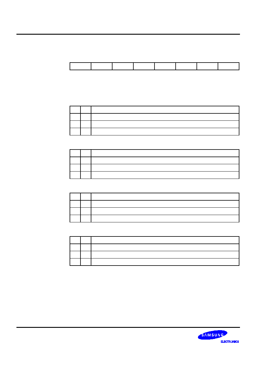
CONTROL REGISTERS
S3C852B/P852B (Preliminary Spec)
4-32
P7CONL
-- Port 7 Control Register(Low byte)
F9H
Set 1, Bank 1
Bit Identifier
.7
.6
.5
.4
.3
.2
.1
.0
RESET
RESET
Value
0
0
0
0
0
0
0
0
Read/Write
R/W
R/W
R/W
R/W
R/W
R/W
R/W
R/W
Addressing Mode
Register addressing mode only
.7�.6
Port 7.3
0
0
Input, Schmitt trigger
0
1
Input, Schmitt trigger, Pull-up resistor
1
0
Output, Push-pull
1
1
Output, Open-drain
.5�.4
Port 7.2
0
0
Input, Schmitt trigger
0
1
Input, Schmitt trigger, Pull-up resistor
1
0
Output, Push-pull
1
1
Output, Open-drain
.3�.2
Port 7.1
0
0
Input, Schmitt trigger
0
1
Input, Schmitt trigger, Pull-up resistor
1
0
Output, Push-pull
1
1
Output, Open-drain
.1�.0
Port 7.0
0
0
Input, Schmitt trigger
0
1
Input, Schmitt trigger, Pull-up resistor
1
0
Output, Push-pull
1
1
Output, Open-drain

S3C852B/P852B (Preliminary Spec)
CONTROL REGISTERS
4-33
P8CONH
-- Port 8 Control Register(High byte)
FAH
Set 1, Bank 1
Bit Identifier
.7
.6
.5
.4
.3
.2
.1
.0
RESET
RESET
Value
0
0
0
0
0
0
0
0
Read/Write
R/W
R/W
R/W
R/W
R/W
R/W
R/W
R/W
Addressing Mode
Register addressing mode only
.7�.6
Port 8.7
0
0
Input, Schmitt trigger
0
1
Input, Schmitt trigger, Pull-up resistor
1
0
Output, Push-pull
1
1
Output, Open-drain
.5�.4
Port 8.6
0
0
Input, Schmitt trigger
0
1
Input, Schmitt trigger, Pull-up resistor
1
0
Output, Push-pull
1
1
Output, Open-drain
.3�.2
Port 8.5
0
0
Input, Schmitt trigger
0
1
Input, Schmitt trigger, Pull-up resistor
1
0
Output, Push-pull
1
1
Output, Open-drain
.1�.0
Port 8.4
0
0
Input, Schmitt trigger
0
1
Input, Schmitt trigger, Pull-up resistor
1
0
Output, Push-pull
1
1
Output, Open-drain

CONTROL REGISTERS
S3C852B/P852B (Preliminary Spec)
4-34
P8CONL
-- Port 8 Control Register(Low byte)
FBH
Set 1, Bank 1
Bit Identifier
.7
.6
.5
.4
.3
.2
.1
.0
RESET
RESET
Value
0
0
0
0
0
0
0
0
Read/Write
R/W
R/W
R/W
R/W
R/W
R/W
R/W
R/W
Addressing Mode
Register addressing mode only
.7�.6
Port 8.3
0
0
Input, Schmitt trigger
0
1
Input, Schmitt trigger, Pull-up resistor
1
0
Output, Push-pull
1
1
Output, Open-drain
.5�.4
Port 8.2
0
0
Input, Schmitt trigger
0
1
Input, Schmitt trigger, Pull-up resistor
1
0
Output, Push-pull
1
1
Output, Open-drain
.3�.2
Port 8.1
0
0
Input, Schmitt trigger
0
1
Input, Schmitt trigger, Pull-up resistor
1
0
Output, Push-pull
1
1
Output, Open-drain
.1�.0
Port 8.0
0
0
Input, Schmitt trigger
0
1
Input, Schmitt trigger, Pull-up resistor
1
0
Output, Push-pull
1
1
Output, Open-drain

S3C852B/P852B (Preliminary Spec)
CONTROL REGISTERS
4-35
P9CONH
-- Port 9 Control Register(High byte)
FCH
Set 1, Bank 1
Bit Identifier
.7
.6
.5
.4
.3
.2
.1
.0
RESET
RESET
Value
0
0
0
0
0
0
0
0
Read/Write
R/W
R/W
R/W
R/W
R/W
R/W
R/W
R/W
Addressing Mode
Register addressing mode only
.7�.6
Port 9.7
0
0
Input, Schmitt trigger
0
1
Input, Schmitt trigger, Pull-up resistor
1
0
Output, Push-pull
1
1
Output, Open-drain
.5�.4
Port 9.6
0
0
Input, Schmitt trigger
0
1
Input, Schmitt trigger, Pull-up resistor
1
0
Output, Push-pull
1
1
Output, Open-drain
.3�.2
Port 9.5
0
0
Input, Schmitt trigger
0
1
Input, Schmitt trigger, Pull-up resistor
1
0
Output, Push-pull
1
1
Output, Open-drain
.1�.0
Port 9.4
0
0
Input, Schmitt trigger
0
1
Input, Schmitt trigger, Pull-up resistor
1
0
Output, Push-pull
1
1
Output, Open-drain

CONTROL REGISTERS
S3C852B/P852B (Preliminary Spec)
4-36
P9CONL
-- Port 9 Control Register(Low byte)
FDH
Set 1, Bank 1
Bit Identifier
.7
.6
.5
.4
.3
.2
.1
.0
RESET
RESET
Value
0
0
0
0
0
0
0
0
Read/Write
R/W
R/W
R/W
R/W
R/W
R/W
R/W
R/W
Addressing Mode
Register addressing mode only
.7�.6
Port 9.3
0
0
Input, Schmitt trigger
0
1
Input, Schmitt trigger, Pull-up resistor
1
0
Output, Push-pull
1
1
Output, Open-drain
.5�.4
Port 9.2
0
0
Input, Schmitt trigger
0
1
Input, Schmitt trigger, Pull-up resistor
1
0
Output, Push-pull
1
1
Output, Open-drain
.3�.2
Port 9.1
0
0
Input, Schmitt trigger
0
1
Input, Schmitt trigger, Pull-up resistor
1
0
Output, Push-pull
1
1
Output, Open-drain
.1�.0
Port 9.0
0
0
Input, Schmitt trigger
0
1
Input, Schmitt trigger, Pull-up resistor
1
0
Output, Push-pull
1
1
Output, Open-drain

S3C852B/P852B (Preliminary Spec)
CONTROL REGISTERS
4-37
P10CONH
-- Port 10 Control Register(High byte)
FEH
Set 1, Bank 1
Bit Identifier
.7
.6
.5
.4
.3
.2
.1
.0
RESET
RESET
Value
0
0
0
0
0
0
0
0
Read/Write
R/W
R/W
R/W
R/W
R/W
R/W
R/W
R/W
Addressing Mode
Register addressing mode only
.7�.6
Port 10.7
0
0
Input, Schmitt trigger
0
1
Input, Schmitt trigger, Pull-up resistor
1
0
Output, Push-pull
1
1
Output, Open-drain
.5�.4
Port 10.6
0
0
Input, Schmitt trigger
0
1
Input, Schmitt trigger, Pull-up resistor
1
0
Output, Push-pull
1
1
Output, Open-drain
.3�.2
Port 10.5
0
0
Input, Schmitt trigger
0
1
Input, Schmitt trigger, Pull-up resistor
1
0
Output, Push-pull
1
1
Output, Open-drain
.1�.0
Port 10.4
0
0
Input, Schmitt trigger
0
1
Input, Schmitt trigger, Pull-up resistor
1
0
Output, Push-pull
1
1
Output, Open-drain

CONTROL REGISTERS
S3C852B/P852B (Preliminary Spec)
4-38
P10CONL
-- Port 10 Control Register(Low byte)
FFH
Set 1, Bank 1
Bit Identifier
.7
.6
.5
.4
.3
.2
.1
.0
RESET
RESET
Value
0
0
0
0
0
0
0
0
Read/Write
R/W
R/W
R/W
R/W
R/W
R/W
R/W
R/W
Addressing Mode
Register addressing mode only
.7�.6
Port 10.3
0
0
Input, Schmitt trigger
0
1
Input, Schmitt trigger, Pull-up resistor
1
0
Output, Push-pull
1
1
Output, Open-drain
.5�.4
Port 10.2
0
0
Input, Schmitt trigger
0
1
Input, Schmitt trigger, Pull-up resistor
1
0
Output, Push-pull
1
1
Output, Open-drain
.3�.2
Port 10.1
0
0
Input, Schmitt trigger
0
1
Input, Schmitt trigger, Pull-up resistor
1
0
Output, Push-pull
1
1
Output, Open-drain
.1�.0
Port 10.0
0
0
Input, Schmitt trigger
0
1
Input, Schmitt trigger, Pull-up resistor
1
0
Output, Push-pull
1
1
Output, Open-drain

S3C852B/P852B (Preliminary Spec)
CONTROL REGISTERS
4-39
PP
--
Register Page Pointer
DFH Set 1
Bit Identifier
.7
.6
.5
.4
.3
.2
.1
.0
RESET
RESET
Value
0
0
0
0
0
0
0
0
Read/Write
R/W
R/W
R/W
R/W
R/W
R/W
R/W
R/W
Addressing Mode
Register addressing mode only
.7�.4
Destination Register Page Selection Bits
0
0
0
0
Destination: page 0
0
0
0
1
Destination: page 1
0
0
1
0
Destination: page 2
0
0
1
1
Destination: page 3
0
1
0
0
Destination: page 4
�
�
�
�
�
�
1
1
1
1
Destination: page F
.3�.0
Source Register Page Selection Bit
0
0
0
0
Source: page 0
0
0
0
1
Source: page 1
0
0
1
0
Source: page 2
0
0
1
1
Source: page 3
0
1
0
0
Source: page 4
�
�
�
�
�
�
1
1
1
1
Source: page F
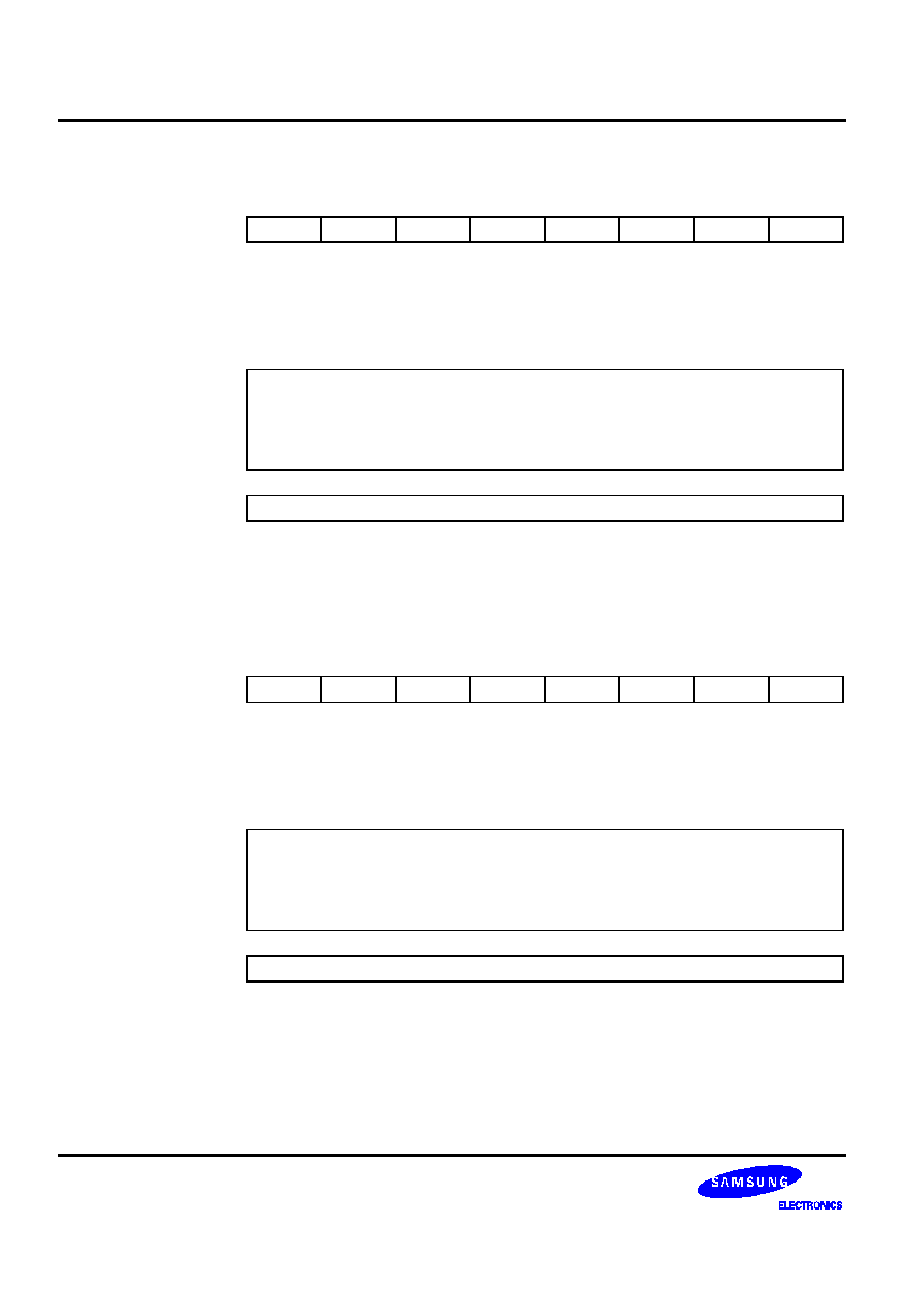
CONTROL REGISTERS
S3C852B/P852B (Preliminary Spec)
4-40
RP0
-- Register Pointer 0
D6H
Set 1
Bit Identifier
.7
.6
.5
.4
.3
.2
.1
.0
RESET
RESET
Value
1
1
0
0
0
�
�
�
Read/Write
R/W
R/W
R/W
R/W
R/W
�
�
�
Addressing Mode
Register addressing only
.7�.3
Register Pointer 0 Address Value
Register pointer 0 can independently point to one of the 24 8-byte working register
areas in the register file. Using the register pointers RP0 and RP1, you can select
two 8-byte register slices at one time as active working register space. After a reset,
RP0 points to address C0H in register set 1, selecting the 8-byte working register
slice C0H�C7H.
.2�.0
Not used for S3C852B/P852B
RP1
-- Register Pointer 1
D7H
Set 1
Bit Identifier
.7
.6
.5
.4
.3
.2
.1
.0
RESET
RESET
Value
1
1
0
0
1
�
�
�
Read/Write
R/W
R/W
R/W
R/W
R/W
�
�
�
Addressing Mode
Register addressing only
.7�.3
Register Pointer 1 Address Value
Register pointer 1 can independently point to one of the 24 8-byte working register
areas in the register file. Using the register pointers RP0 and RP1, you can select
two 8-byte register slices at one time as active working register space. After a reset,
RP1 points to address C8H in register set 1, selecting the 8-byte working register
slice C8H�CFH.
.2�.0
Not used for S3C852B/P852B
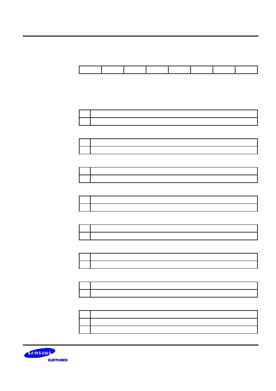
S3C852B/P852B (Preliminary Spec)
CONTROL REGISTERS
4-41
SIOCON
-- SIO Control Register
EBH
Set 1, Bank 1
Bit Identifier
.7
.6
.5
.4
.3
.2
.1
.0
RESET
RESET
Value
0
0
0
0
0
0
0
0
Read/Write
R/W
R/W
R/W
R/W
R/W
R/W
R/W
R/W
Addressing Mode
Register addressing mode only
.7
SIO Shift Clock Selection Bit
0
Internal clock (P.S clock)
1
External clock (SCK)
.6
Data Direction Control Bit
0
MSB first mode
1
LSB first mode
.5
SIO Mode Selection Bit
0
Receive only mode
1
Transmit/receive mode
.4
Shift Start Edge Selection Bit
0
Tx at falling edges, Rx at rising edges
1
Tx at rising edges, Rx at falling edges
.3
SIO Counter Clear and Shift Start Bit
0
No action
1
Clear 3-bit counter and start shifting
.2
SIO Shift Operation Enable Bit
0
Disable shifter and clock counter
1
Enable shifter and clock counter
.1
SIO Interrupt Enable Bit
0
Disable SIO interrupt
1
Enable SIO interrupt
.0
SIO Interrupt Pending Bit
0
No interrupt pending
0
Clear pending condition (when write)
1
Interrupt is pending

CONTROL REGISTERS
S3C852B/P852B (Preliminary Spec)
4-42
SIOPS
-- SIO Prescaler Register
ECH
Set 1, Bank 1
Bit Identifier
.7
.6
.5
.4
.3
.2
.1
.0
RESET
RESET
Value
0
0
0
0
0
0
0
0
Read/Write
R/W
R/W
R/W
R/W
R/W
R/W
R/W
R/W
Addressing Mode
Register addressing mode only
.7�.0
Baud rate = Input clock (fxx)/[(SIOPS + 1) �4] or SCLK input clock

S3C852B/P852B (Preliminary Spec)
CONTROL REGISTERS
4-43
SPH
-- Stack Pointer (High Byte)
D8H
Set 1
Bit Identifier
.7
.6
.5
.4
.3
.2
.1
.0
RESET
RESET
Value
x
x
x
x
x
x
x
x
Read/Write
R/W
R/W
R/W
R/W
R/W
R/W
R/W
R/W
Addressing Mode
Register addressing mode only
.7�.0
Stack Pointer Address (High Byte)
The high-byte stack pointer value is the upper eight bits of the 16-bit stack pointer
address (SP15�SP8). The lower byte of the stack pointer value is located in register
SPL (D9H). The SP value is undefined following a reset.
NOTE: If you only use the internal register file as stack area, SPH can serve as a general-purpose register. To avoid
possible overflows or under flows of the SPL register by operations that increment or decrement the stack, we
recommend that you initialize SPL with the value 'FFH' instead of '00H'. If you use external memory as stack area,
the stack pointer requires a full 16-bit address.
SPL
-- Stack Pointer (Low Byte)
D9H
Set 1
Bit Identifier
.7
.6
.5
.4
.3
.2
.1
.0
RESET
RESET
Value
x
x
x
x
x
x
x
x
Read/Write
R/W
R/W
R/W
R/W
R/W
R/W
R/W
R/W
Addressing Mode
Register addressing mode only
.7�.0
Stack Pointer Address (Low Byte)
The low-byte stack pointer value is the lower eight bits of the 16-bit stack pointer
address (SP7�SP0). The upper byte of the stack pointer value is located in register
SPH (D8H). The SP value is undefined following a reset.
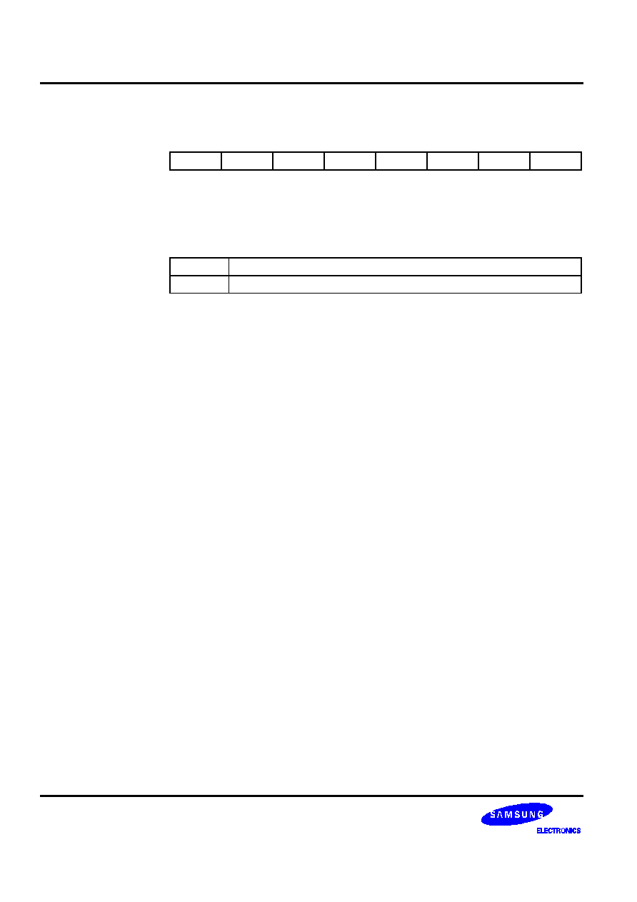
CONTROL REGISTERS
S3C852B/P852B (Preliminary Spec)
4-44
STPCON
-- Stop Control Register
FBH Set 1, Bank 0
Bit Identifier
.7
.6
.5
.4
.3
.2
.1
.0
RESET
RESET
Value
0
0
0
0
0
0
0
0
Read/Write
R/W
R/W
R/W
R/W
R/W
R/W
R/W
R/W
Addressing Mode
Register addressing mode only
.7�.0
Stop control bits
00000000
Disable STOP instruction
10100101
Enable STOP instruction
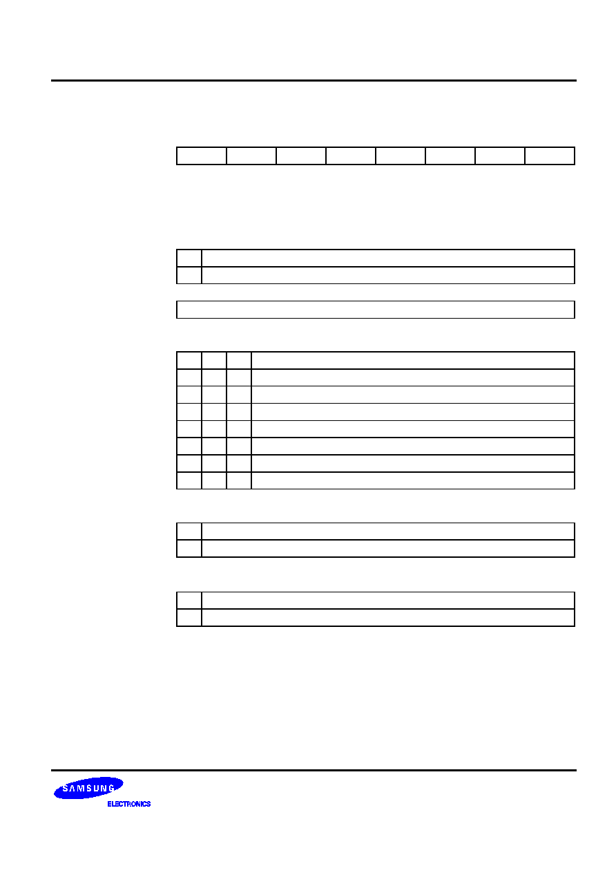
S3C852B/P852B (Preliminary Spec)
CONTROL REGISTERS
4-45
SYM
-- System Mode Register
DEH
Set 1
Bit Identifier
.7
.6
.5
.4
.3
.2
.1
.0
RESET
RESET
Value
0
�
�
x
x
x
0
0
Read/Write
R/W
�
�
R/W
R/W
R/W
R/W
R/W
Addressing Mode
Register addressing mode only
.7
Tri-State External Interface Control Bit
0
Normal operation (disable tri-state operation)
1
Set external interface lines to high impedance (enable tri-state operation)
.6 and .5
Not used for S3C852B/P852B
.4�.2
Fast Interrupt Level Selection Bits
0
0
0
IRQ0 (timer 0 overflow/match and capture)
0
0
1
IRQ1 (timer A match, Timer B overflow/match)
0
1
0
IRQ2 (Caller ID functions)
0
1
1
IRQ3 (Watch Timer overflow)
1
0
0
IRQ4 (Serial data receive/transmit Interrupt)
1
0
1
Not used for S3C852B/P852B
1
1
0
IRQ6 (INT0�INT3)
1
1
1
IRQ7 (INT4�INT7)
.1
Fast Interrupt Enable Bit
0
Disable fast interrupt processing
1
Enable fast interrupt processing
.0
Global Interrupt Enable Bit
(note)
0
Disable global interrupt processing
1
Enable global interrupt processing
NOTE: Following a reset, you enable global interrupt processing by executing an EI instruction
(not by writing a "1" to SYM.0).
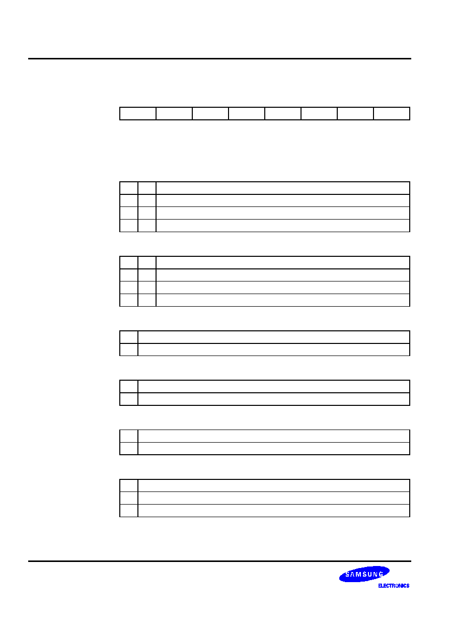
CONTROL REGISTERS
S3C852B/P852B (Preliminary Spec)
4-46
T0CON
-- Timer A Control Register
D2H
Set 1
Bit Identifier
.7
.6
.5
.4
.3
.2
.1
.0
RESET
RESET
Value
0
0
0
0
0
0
0
0
Read/Write
R/W
R/W
R/W
R/W
R/W
R/W
R/W
R/W
Addressing Mode
Register addressing mode only
.7�.6
Timer 0 Input Clock Selection Bits
0
0
fxx/1024
0
1
fxx/256
1
0
fxx/64
1
1
External clock (P0.2/T0CK)
.5 - .4
Timer 0 operating mode selection bits
0
0
Interval mode (P0.3/T0)
0
1
Capture mode (capture on rising edge, counter running, OVF can occur)
1
0
Capture mode (capture on falling edge, counter running, OVF can occur)
1
1
PWM mode (OVF interrupt can occur)
.3
Timer 0 counter clear bit
0
No effect
1
Clear the timer 0 counter (when write)
.2
Timer 0 overflow interrupt enable bit
0
Disable interrupt
1
Enable interrupt
.1
Timer 0 match/capture interrupt enable bit
0
Disable interrupt
1
Enable interrupt
.0
Timer 0 match/capture interrupt pending bit
0
No interrupt pending
0
Clear pending bit (write)
1
Interrupt is pending
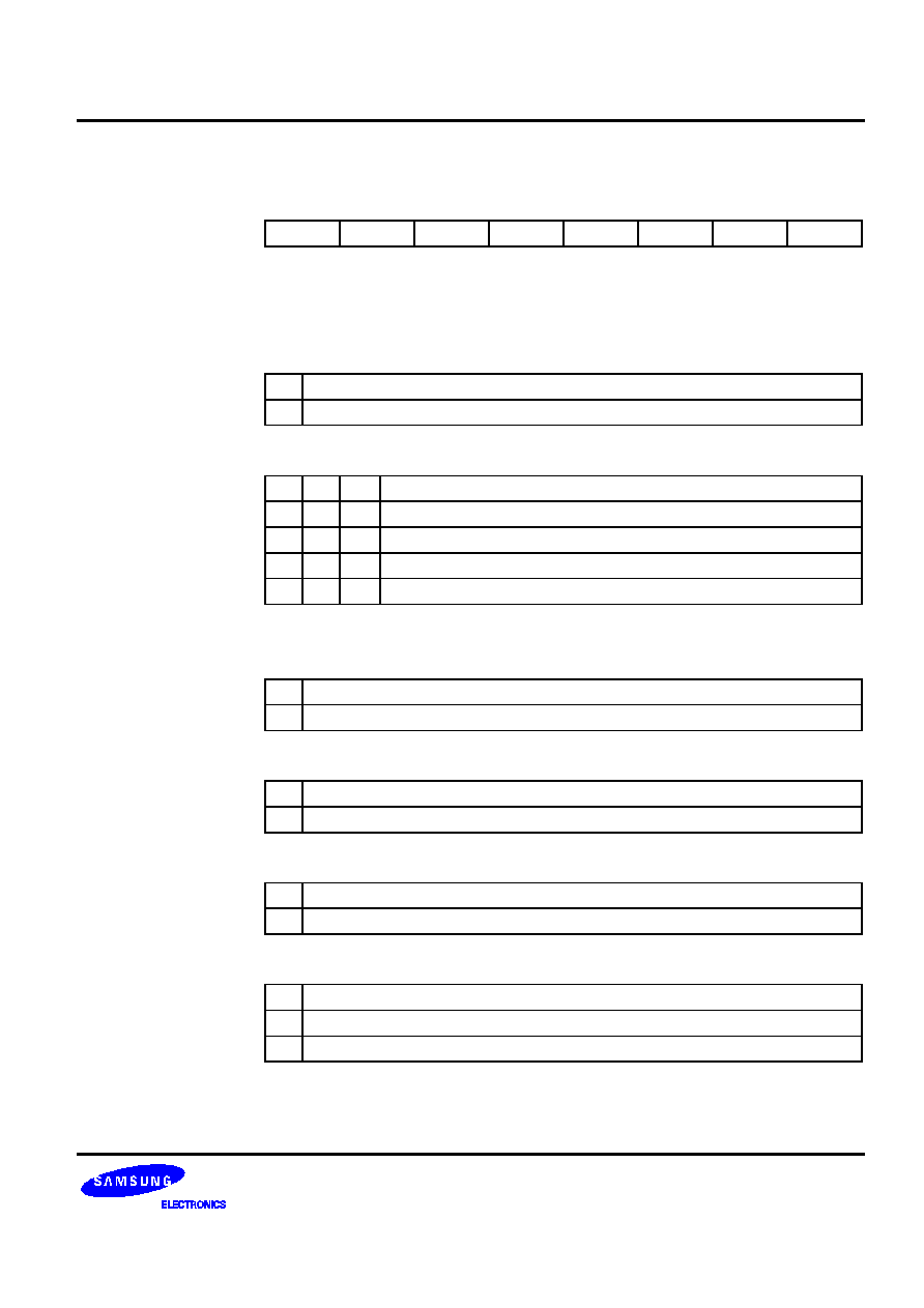
S3C852B/P852B (Preliminary Spec)
CONTROL REGISTERS
4-47
TACON
-- Timer A Control Register
E4H
Set 1, Bank 1
Bit Identifier
.7
.6
.5
.4
.3
.2
.1
.0
RESET
RESET
Value
0
0
0
0
0
0
0
0
Read/Write
R/W
R/W
R/W
R/W
R/W
R/W
R/W
R/W
Addressing Mode
Register addressing mode only
.7
One 16-bit timer or Two 8-bit timers mode selection bit
0
Two 8-bit timers mode (Timer A/Timer B)
1
One 16-bit timer mode (Timer 1)
.6�.4
Timer A clock selection bits
0
0
0
fxx/1024
0
0
1
fxx/512
0
1
0
fxx/8
0
1
1
fxx
1
x
x
T1CK (external clock)
(`x' means don't care.)
.3
Timer A Counter Clear Bit
0
No effect
1
Clear the timer A counter (when write)
.2
Timer A Count Enable Bit
0
Disable count operation
1
Enable count operation
.1
Timer A Interrupt Enable Bit
0
Disable interrupt
1
Enable interrupt
.0
Timer A Interrupt Pending Bit
0
No interrupt pending
0
Clear pending bit (when write)
1
Interrupt is pending
CONTROL REGISTERS
S3C852B/P852B (Preliminary Spec)
4-48
TBCON
-- Timer B Control Register
E5H
Set 1, Bank 1
Bit Identifier
.7
.6
.5
.4
.3
.2
.1
.0
RESET
RESET
Value
0
0
0
0
0
0
0
0
Read/Write
R/W
R/W
R/W
R/W
R/W
R/W
R/W
R/W
Addressing Mode
Register addressing mode only
.7�.6
Timer B operating mode selection bits
0
0
Interval mode
0
1
6-bit PWM mode (OVF interrupt can occur)
1
0
7-bit PWM mode (OVF interrupt can occur)
1
1
8-bit PWM mode (OVF interrupt can occur)
.5�.4
Timer B clock selection bits
0
0
fxx/8
0
1
fxx/4
1
0
fxx/2
1
1
fxx
.3
Timer B Counter Clear Bit
0
No effect
1
Clear the timer B counter (when write)
.2
Timer B Count Enable Bit
0
Disable count operation
1
Enable count operation
.1
Timer B match Interrupt Enable Bit
0
Disable interrupt
1
Enable interrupt
.0
Timer B overflow interrupt enable bit
0
Disable interrupt
1
Enable interrupt
S3C852B/P852B (Preliminary Spec)
CONTROL REGISTERS
4-49
WTCON
-- Watch Timer Control Register
E6H
Set 1, Bank 1
Bit Identifier
.7
.6
.5
.4
.3
.2
.1
.0
RESET
RESET
Value
0
0
0
0
0
0
0
0
Read/Write
R/W
R/W
R/W
R/W
R/W
R/W
R/W
R/W
Addressing Mode
Register addressing mode only
.7
Watch Timer clock selection bit
0
Main clock divide by 2
7
(fx/128)
1
Sub clock (fxt)
.6
Watch Timer INT Enable/Disable bit
0
Disable watch timer interrupt
1
Enable watch timer interrupt
.5�.4
Buzzer signal selection bits
0
0
2 kHz
0
1
4 kHz
1
0
8 kHz
1
1
16 kHz
.3�.2
Watch Timer speed selection bits
0
0
Set watch timer interrupt to 1 s
0
1
Set watch timer interrupt to 0.5 s
1
0
Set watch timer interrupt to 0.25 s
1
1
Set watch timer interrupt to 3.91ms
NOTE: The above values of watch timer interrupt are accurate when fw = fxt.
.1
Watch Timer Enable/Disable bit
0
Disable watch timer; clear frequency dividing circuits
1
Enable watch timer
.0
Watch Timer interrupt pending bit
0
Watch Timer Interrupt request is not pending
1
Watch Timer Interrupt request is pending

CONTROL REGISTERS
S3C852B/P852B (Preliminary Spec)
4-50
NOTES

S3C852B/P852B (Preliminary Spec)
INTERRUPT STRUCTURE
5-1
5
INTERRUPT STRUCTURE
OVERVIEW
The SAM8 interrupt structure has three basic components: levels, vectors, and sources. The CPU recognizes
eight interrupt levels and supports up to 128 interrupt vectors. When a specific interrupt level has more than one
vector address, the vector priorities are established in hardware. Each vector can have one or more sources.
Levels
Interrupt levels are the main unit for interrupt priority assignment and recognition. All peripherals and I/O blocks
can issue interrupt requests. In other words, peripheral and I/O operations are interrupt-driven. There are eight
interrupt levels: IRQ0�IRQ7, also called level 0-level 7. Each interrupt level directly corresponds to an interrupt
request number (IRQn). The total number of interrupt levels used in the interrupt structure varies from device to
device. The S3C852B/P852B interrupt structure recognizes eight interrupt levels, IRQ0�IRQ7.
The interrupt level numbers 0 through 7 do not necessarily indicate the relative priority of the levels. They are
simply identifiers for the interrupt levels that are recognized by the CPU. The relative priority of different interrupt
levels is determined by settings in the interrupt priority register, IPR. Interrupt group and subgroup logic
controlled by IPR settings lets you define more complex priority relationships between different levels.
Vectors
Each interrupt level can have one or more interrupt vectors, or it may have no vector address assigned at all.
The maximum number of vectors that can be supported for a given level is 128. (The actual number of vectors
used for TCC12X-series devices will always be much smaller.) If an interrupt level has more than one vector
address, the vector priorities are set in hardware. S3C852B/P852B have eighteen vectors-- corresponding to
each of the eighteen possible interrupt sources.
Sources
A source is any peripheral that generates an interrupt. A source can be an external pin or a counter overflow, for
example. Each vector can have several interrupt sources. In the S3C852B/P852B interrupt structure, each
source has its own vector address.
When a service routine starts, the respective pending bit is either cleared automatically by hardware cleared
"manually" by program software. The characteristics of the source's pending mechanism determine which
method is used to clear its respective pending bit.

INTERRUPT STRUCTURE
S3C852B/P852B (Preliminary Spec)
5-2
INTERRUPT TYPES
The three components of the SAM8 interrupt structure described above ( levels, vectors, and sources ) are
combined to determine the interrupt structure of an individual device and to make full use of its available
interrupt logic. There are three possible combinations of interrupt structure components, called interrupt types 1,
2, and 3. The types differ in the number of vectors and interrupt sources assigned to each level (see Figure 5-1):
Type 1:
One level (IRQn) + one vector (V
1
) + one source (S
1
)
Type 2:
One level (IRQn) + one vector (V
1
) + multiple sources (S
1
�S
n
)
Type 3:
One level (IRQn) + multiple vectors (V
1
�V
n
) + multiple sources (S
1
�S
n
, S
n+1�
S
n+m
)
In the S3C852B/P852B microcontrollers, only interrupt types 1 and 3 are implemented.
Vectors
Sources
Levels
S
1
V
1
S
2
Type 2:
IRQn
S
3
S
n
V
1
S
1
V
2
S
2
Type 3:
IRQn
V
3
S
3
V
1
S
1
Type 1:
IRQn
V
n
S
n +
1
S
n
S
n +
2
S
n +
m
NOTES:
1. The number of S
n
and V
n
value is expandable.
2. In the S3C852B/P852B implementation,
only interrupt types 1 and 3 are used.
Figure 5-1. SAM8-Series Interrupt Types

S3C852B/P852B (Preliminary Spec)
INTERRUPT STRUCTURE
5-3
S3C852B/P852B INTERRUPT STRUCTURE
The S3C852B/P852B microcontroller supports eighteen interrupt sources. Each interrupt source has a
corresponding interrupt vector address. seventh interrupt levels are used in the device-specific interrupt
structure, which is shown in Figure 5-2.
When multiple interrupt levels are active, the interrupt priority register (IPR) determines the order in which
contending interrupts are to be serviced. If multiple interrupts occur within the same interrupt level, the interrupt
with the lowest vector address is usually processed first.
When the CPU grants an interrupt request, interrupt processing starts: All other interrupts are disabled and the
program counter value and status flags are pushed to stack. The starting address of the service routine is fetched
from the appropriate vector address (plus the next 8-bit value to concatenate the full 16-bit address) and the
service routine is executed.
Vectors
Sources
Levels
Reset/Clear
IRQ1
F6H
Timer B overflow
F4H
Timer A match
Timer 0 overflow
FAH
Timer B match
F8H
IRQ0
Watch timer oveflow
F2H
Serial data reveive/transmit
F0H
IRQ3
IRQ4
P0.3 external interrupt
P0.2 external interrupt
P0.1 external interrupt
P0.0 external interrupt
IRQ6
D6H
D4H
D2H
D0H
P0.7 external interrupt
P0.6 external interrupt
P0.5 external interrupt
P0.4 external interrupt
IRQ7
EAH
E8H
E6H
E4H
Basic timer overflow
RESET
FCH
Timer 0 match & capture
100H
H/W
H/W
S/W
S/W
H/W
S/W
S/W
S/W
S/W
S/W
S/W
S/W
S/W
S/W
S/W
S/W
0
2
1
0
0
1
0
3
2
0
3
1
1
2
0
CID interrupt
D8H
IRQ2
0
S/W
Figure 5-2. S3C852B Interrupt Structure
INTERRUPT STRUCTURE
S3C852B/P852B (Preliminary Spec)
5-4
INTERRUPT VECTOR ADDRESSES
Interrupt vector addresses for the S3C852B/P852B are stored in the first 256 bytes of the program memory
(ROM). Vectors for all interrupt levels are stored in the vector address area, 0H�FFH.
Unused locations in this range can be used as normal program memory. When writing an application program,
you should be careful not to overwrite the address data stored in this area.
The program reset address in the program memory is 0100H.
65,535
0
(Decimal)
255
00H
0100H
FFH
FFFFH
(HEX)
RESET
Address
Interrupt
Vector Area
64-Kbyte
Memory Area
~
~
~
~
Figure 5-3. Vector Address Area in Program Memory (ROM)
S3C852B/P852B (Preliminary Spec)
INTERRUPT STRUCTURE
5-5
Table 5-1. S3C852B/P852B Interrupt Vectors
Vector Address
Interrupt Source
Request
Reset/Clear
Decimal
Value
Hex
Value
Interrupt
Level
Priority
in Level
H/W
S/W
208
D0H
P0.0 External Interrupt(edge trigger)
IRQ6
0
210
D2H
P0.1 External Interrupt(edge trigger)
1
212
D4H
P0.2 External Interrupt(edge trigger)
2
214
D6H
P0.3 External Interrupt(edge trigger)
3
216
D8H
CID interrupt
IRQ2
2
228
E4H
P0.4 External Interrupt(edge trigger)
IRQ7
0
230
E6H
P0.5 External Interrupt(edge trigger)
1
232
E8H
P0.6 External Interrupt(edge trigger)
2
234
EAH
P0.7 External Interrupt(edge trigger)
3
240
F0H
Serial data receive/transmit
IRQ4
-
242
F2H
Watch Timer overflow
IRQ3
-
244
F4H
Timer A match
IRQ1
0
246
F6H
Timer B overflow
1
248
F8H
Timer B match
2
250
FAH
Timer 0 overflow
IRQ0
0
252
FCH
Timer 0 match & capture
1
256
100H
Basic Timer overflow
-
-
NOTES:
1.
Interrupt priorities are identified in inverse order: '0' is highest priority, '1' is the next highest, and so on.
2.
If two or more interrupts within the same level contend, the interrupt with the lowest vector address has priority over one
with a higher vector address. These priorities within levels are preset at the factory.
INTERRUPT STRUCTURE
S3C852B/P852B (Preliminary Spec)
5-6
ENABLE/DISABLE INTERRUPT INSTRUCTIONS (EI, DI)
Executing the Enable Interrupts (EI) instruction enables the interrupt structure. All interrupts are then serviced as
they occur, and according to the established priorities.
NOTE
The system initialization routine that is executed following a reset must always contain an EI instruction
(assuming one or more interrupts are used in the application).
During normal operation, you can execute the DI (Disable Interrupt) instruction at any time to globally disable
interrupt processing. The EI and DI instructions change the value of bit 0 in the SYM register. Although you can
manipulate SYM.0 directly to enable or disable interrupts, we recommend that you use the EI and DI instructions
instead.
SYSTEM-LEVEL INTERRUPT CONTROL REGISTERS
In addition to the control registers for specific interrupt sources, four system-level registers control interrupt
processing:
-- The interrupt mask register, IMR, enables (un-masks) or disables (masks) interrupt levels.
-- The interrupt priority register, IPR, controls the relative priorities of interrupt levels.
-- The interrupt request register, IRQ, contains interrupt pending flags for each interrupt level (as opposed to
each interrupt source).
-- The system mode register, SYM, enables or disables global interrupt processing. (SYM settings also enable
fast interrupts and control the activity of external interface, if implemented.)
Table 5-2. Interrupt Control Register Overview
Control Register
ID
R/W
Function Description
Interrupt mask register
IMR
R/W
Bit settings in the IMR register enable or disable interrupt
processing for each of the seven interrupt levels, IRQ0�IRQ7.
Interrupt priority register
IPR
R/W
Controls the relative processing priorities of the interrupt
levels. The eight levels of the S3C852B/P852B are organized
into three groups: A, B, and C. Group A is IRQ0 and IRQ1,
group B is IRQ2�IRQ4, and group C is IRQ6�IRQ7
Interrupt request register
IRQ
R
This register contains a request pending bit for each of the
seven interrupt levels, IRQ0�RQ7.
System mode register
SYM
R/W
Dynamic global interrupt processing enable and disable, fast
interrupt processing.
NOTE
DI instruction must be used before changing the IMR, interrupt pending register and interrupt source
control register. If IMR, interrupt pending register or source control register is controlled in EI status,
program control could be in uncontrollable state.
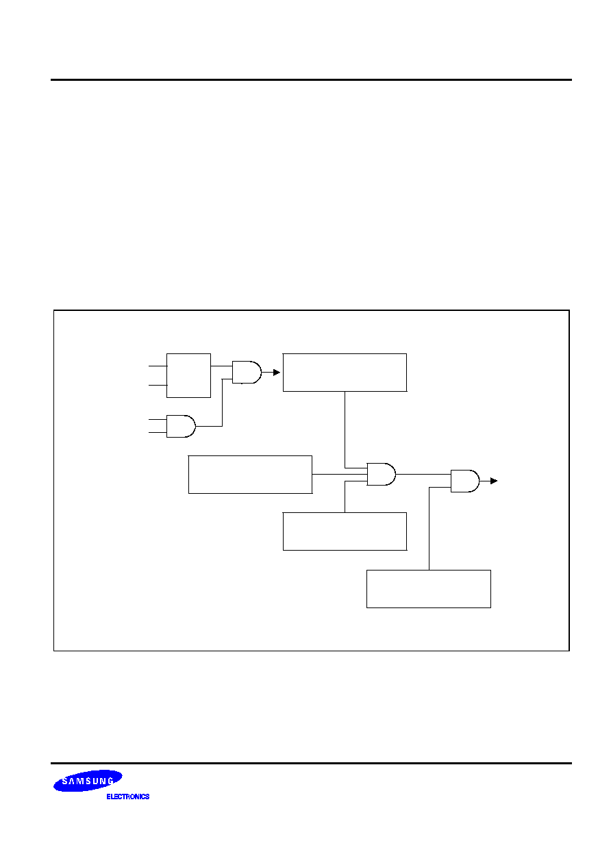
S3C852B/P852B (Preliminary Spec)
INTERRUPT STRUCTURE
5-7
INTERRUPT PROCESSING CONTROL POINTS
Interrupt processing can therefore be controlled in two ways: globally or by specific interrupt level and source.
The system-level control points in the interrupt structure are, therefore:
-- Global interrupt enable and disable (by EI and DI instructions or by direct manipulation of SYM.0 )
-- Interrupt level enable/disable settings (IMR register)
-- Interrupt level priority settings (IPR register)
-- Interrupt source enable/disable settings in the corresponding peripheral control registers
NOTE
When writing the part of your application program that handles interrupt processing, be sure to include
the necessary register file address (register pointer) information.
Interrupt Request Register
(Read-only)
Interrup Pending
(Read-Only)
Interrupt Mask
Register
Interrupt Priority
Register
Global Interrupt Control
(EI, DI or SYM.0
manipulation)
S
R
Q
RESET
EI Instruction
Execution
Vector
Interrupt
Cycle
Source Interrupt
Enable
Figure 5-4. Interrupt Function Diagram
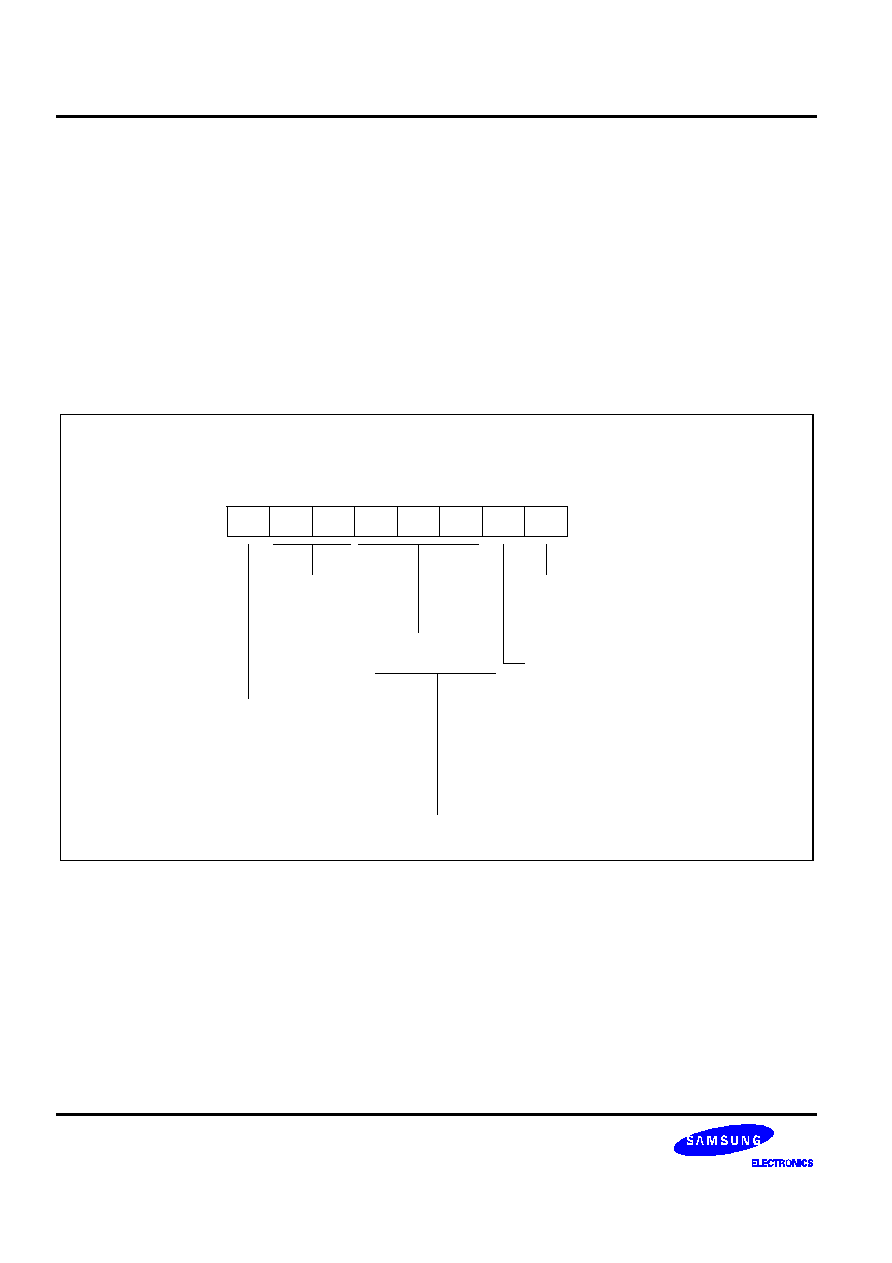
INTERRUPT STRUCTURE
S3C852B/P852B (Preliminary Spec)
5-8
SYSTEM MODE REGISTER (SYM)
The system mode register, SYM (set 1, DEH), is used to globally enable and disable interrupt processing and to
control fast interrupt processing. Figure 5-5 shows the effect of the various control settings.
A reset clears SYM.7, SYM.1, and SYM.0 to "0" and the other SYM bit values (for fast interrupt level selection)
are undetermined.
The instructions EI and DI enable and disable global interrupt processing, respectively, by modifying the bit 0
value of the SYM register. An Enable Interrupt (EI) instruction must be included in the initialization routine, which
follows a reset operation, in order to enable interrupt processing. Although you can manipulate SYM.0 directly to
enable and disable interrupts during normal operation, we recommend using the EI and DI instructions for this
purpose.
System Mode Register (SYM)
DEH, Set 1, R/W
.7
.6
.5
.4
.3
.2
.1
.0
MSB
LSB
Global interrupt enable bit:
0 = Disable all interrupts
1 = Enable all interrupts
Fast interrupt enable bit:
0 = Disable fast interrupts
1 = Enable fast interrupts
Fast interrupt level
selection bits:
0 0 0
0 0 1
0 1 0
0 1 1
1 0 0
1 0 1
1 1 0
1 1 1
IRQ0
IRQ1
IRQ2
IRQ3
IRQ4
Not used for S3C852B/P852B
IRQ6
IRQ7
Not used
External interface tri-state
enable bit:
0 = Normal operation
(Tri-state disable)
0 = High inpedence
(Tri-state enable)
Figure 5-5. System Mode Register (SYM)
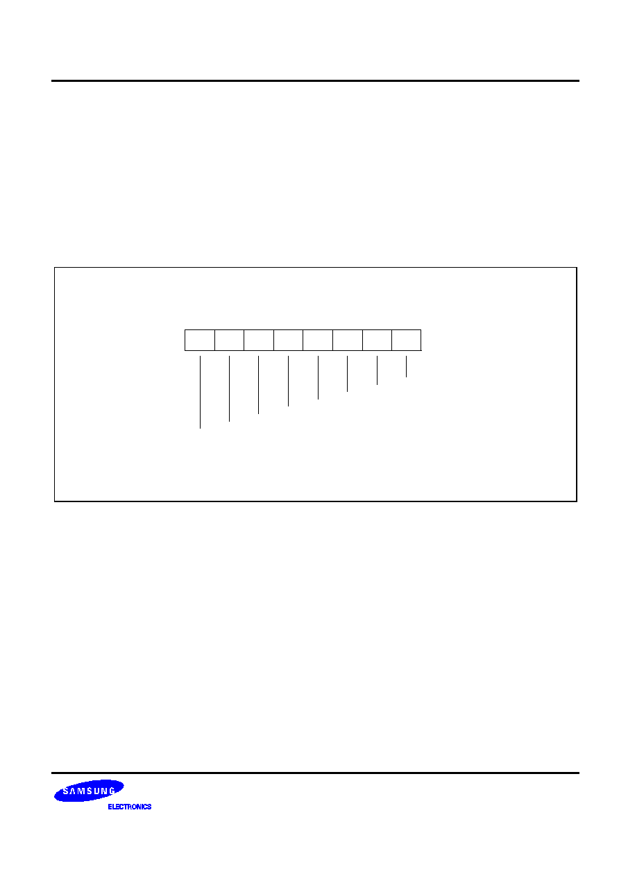
S3C852B/P852B (Preliminary Spec)
INTERRUPT STRUCTURE
5-9
INTERRUPT MASK REGISTER (IMR)
The interrupt mask register, IMR (set 1, DDH) is used to enable or disable interrupt processing for individual
interrupt levels. After a reset, all IMR bit values are undetermined and must therefore be written to their required
settings by the initialization routine.
Each IMR bit corresponds to a specific interrupt level: bit 1 to IRQ1, bit 2 to IRQ2, and so on. When the IMR bit
of an interrupt level is cleared to "0", interrupt processing for that level is disabled (masked). When you set a
level's IMR bit to "1", interrupt processing for the level is enabled (not masked).
The IMR register is mapped to register location DDH in set 1. Bit values can be read and written by instructions
using the Register addressing mode.
Interrupt Mask Register (IMR)
DDH, Set 1, R/W
.7
.6
.5
.4
.3
.2
.1
.0
MSB
LSB
IRQ1
IRQ2
IRQ4
Not used for S3C852B/P852B
IRQ6
IRQ7
IRQ0
Interrupt level enable bits
0 = Disable (mask) interrupt level
1 = Enable (un-mask) interrupt level
IRQ3
Figure 5-6. Interrupt Mask Register (IMR)
NOTE
Before IMR register is changed to any value, all interrupts must be disable. Using DI instruction is
recommended.
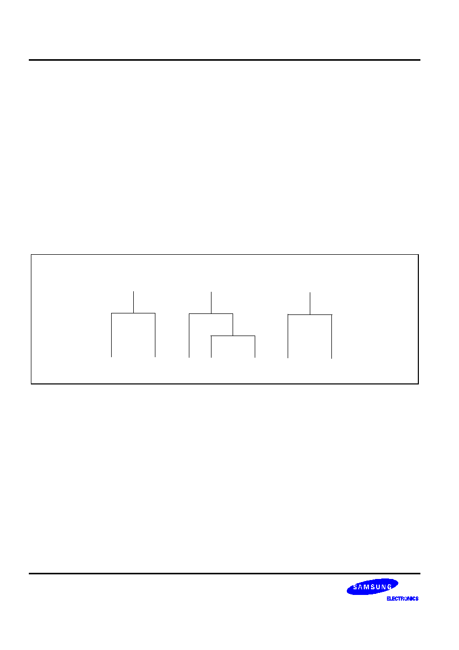
INTERRUPT STRUCTURE
S3C852B/P852B (Preliminary Spec)
5-10
INTERRUPT PRIORITY REGISTER (IPR)
The interrupt priority register, IPR (set 1, bank 0, FFH), is used to set the relative priorities of the interrupt levels
used in the microcontroller's interrupt structure. After a reset, all IPR bit values are undetermined and must
therefore be written to their required settings by the initialization routine.
When more than one interrupt source is active, the source with the highest priority level is serviced first. If both
sources belong to the same interrupt level, the source with the lowest vector address usually has priority. (This
priority is fixed in hardware.)
To support programming of the relative interrupt level priorities, they are organized into groups and subgroups by
the interrupt logic. Please note that these groups (and subgroups) are used only by IPR logic for the IPR register
priority definitions (see Figure 5-7):
Group A
IRQ0, IRQ1
Group B
IRQ2, IRQ3, IRQ4
Group C
IRQ6, IRQ7
IPR
Group B
IPR
Group C
C2
IRQ7
IRQ2
B1
IRQ4
B2
IRQ3
B22
B21
IPR
Group A
IRQ1
A2
IRQ0
A1
IRQ6
C1
Figure 5-7. Interrupt Request Priority Groups
As you can see in Figure 5-8, IPR.7, IPR.4, and IPR.1 control the relative priority of interrupt groups A, B, and C.
For example, the setting '001B' for these bits would select the group relationship B > C > A; the setting '101B'
would select the relationship C > B > A.
The functions of the other IPR bit settings are as follows:
-- IPR.6 controls the relative priorities of group C interrupts.
-- Interrupt group B has a subgroup to provide an additional priority relationship between for interrupt levels 2,
3, and 4. IPR.2 defines the possible subgroup B relationships.
-- IPR.3 controls the relative priorities setting of IRQ3 and IRQ4 interrupts.
-- IPR.0 controls the relative priority setting of IRQ0 and IRQ1 interrupts.

S3C852B/P852B (Preliminary Spec)
INTERRUPT STRUCTURE
5-11
Interrupt Priority Register (IPR)
FFH, Set 1, Bank 0, R/W
.7
.6
.5
.4
.3
.2
.1
.0
MSB
LSB
Group A
0 = IRQ0 > IRQ1
1 = IRQ1 > IRQ0
Subgroup B
0 = IRQ3 > IRQ4
1 = IRQ4 > IRQ3
Group C
0 = IRQ6 > IRQ7
1 = IRQ7 > IRQ6
Subgroup C
0 = IRQ6 > IRQ7
1 = IRQ7 > IRQ6
Group B
0 = IRQ2 > (IRQ3,IRQ4)
1 = (IRQ3,IRQ4) > IRQ2
Group priority:
0 0 0
0 0 1
0 1 0
0 1 1
1 0 0
1 0 1
1 1 0
1 1 1
= Undefined
= B > C > A
= A > B > C
= B > A > C
= C > A > B
= C > B > A
= A > C > B
= Not used
D7 D4 D1
Figure 5-8. Interrupt Priority Register (IPR)

INTERRUPT STRUCTURE
S3C852B/P852B (Preliminary Spec)
5-12
INTERRUPT REQUEST REGISTER (IRQ)
You can poll bit values in the interrupt request register, IRQ (set 1, DCH), to monitor interrupt request status for
all levels in the microcontroller' interrupt structure. Each bit corresponds to the interrupt level of the same
number: bit 0 to IRQ0, bit 1 to IRQ1, and so on. A "0" indicates that no interrupt request is currently being issued
for that level; a "1" indicates that an interrupt request has been generated for that level.
IRQ bit values are read-only addressable using Register addressing mode. You can read (test) the contents of
the IRQ register at any time using bit or byte addressing to determine the current interrupt request status of
specific interrupt levels. After a reset, all IRQ status bits are cleared to "0".
You can poll IRQ register values even if a DI instruction has been executed (that is, if global interrupt processing
is disabled). If an interrupt occurs while the interrupt structure is disabled, the CPU will not service it. You can,
however, still detect the interrupt request by polling the IRQ register. In this way, you can determine which events
occurred while the interrupt structure was globally disabled.
Interrupt Request Register (IRQ)
DCH, Set 1, Read-only
.7
.6
.5
.4
.3
.2
.1
.0
MSB
LSB
IRQ1
IRQ2
IRQ3
IRQ4
Not used for S3C852B/P852B
IRQ6
IRQ7
IRQ0
Interrupt level request pending bits:
0 = Interrupt level is not pending
1 = Interrupt level is pending
Figure 5-9. Interrupt Request Register (IRQ)

S3C852B/P852B (Preliminary Spec)
INTERRUPT STRUCTURE
5-13
INTERRUPT PENDING FUNCTION TYPES
Overview
There are two types of interrupt pending bits: One type is automatically cleared by hardware after the interrupt
service routine is acknowledged and executed; the other type must be cleared by the application program's
interrupt service routine.
Pending Bits Cleared Automatically by Hardware
For interrupt pending bits that are cleared automatically by hardware, interrupt logic sets the corresponding
pending bit to "1" when a request occurs. It then issues an IRQ pulse to inform the CPU that an interrupt is
waiting to be serviced. The CPU acknowledges the interrupt source, executes the service routine, and clears the
pending bit to "0". This type of pending bit is mapped and can, therefore, be read or written by application
software.
Please refer to the page 5-4 (interrupt structure) to recognize which interrupts belong to this category of interrupts
whose pending conditions are cleared automatically by hardware.
Pending Bits Cleared by the Service Routine
The second type of pending bit must be cleared by program software. The service routine must clear the
appropriate pending bit before a return-from-interrupt subroutine (IRET) occurs. To do this, a "0" must be written
to the corresponding pending bit location in the source or control register.
In the S3C852B/P852B interrupt structure, pending conditions for all external interrupt sources must be cleared
by the program software's interrupt service routine.

INTERRUPT STRUCTURE
S3C852B/P852B (Preliminary Spec)
5-14
INTERRUPT SOURCE POLLING SEQUENCE
The interrupt request polling and servicing sequence is as follows:
1.
A source generates an interrupt request by setting the interrupt request bit to "1".
2.
The CPU polling procedure identifies a pending condition for that source.
3.
The CPU checks the source's interrupt level.
4.
The CPU generates an interrupt acknowledge signal.
5.
Interrupt logic determines the interrupt's vector address.
6.
The service routine starts and the source's pending bit is cleared to "0" (by hardware or by software).
7.
The CPU continues polling for interrupt requests.
INTERRUPT SERVICE ROUTINES
Before an interrupt request can be serviced, the following conditions must be met:
-- Interrupt processing must be globally enabled (EI, SYM.0 = "1")
-- The interrupt level must be enabled (IMR register)
-- The interrupt level must have the highest priority if more than one level is currently requesting service
-- The interrupt must be enabled at the interrupt's source (peripheral control register)
If all of the above conditions are met, the interrupt request is acknowledged at the end of the instruction cycle.
The CPU then initiates an interrupt machine cycle that completes the following processing sequence:
1.
Reset (clear to "0") the interrupt enable bit in the SYM register (SYM.0) to disable all subsequent interrupts.
2.
Save the program counter (PC) and status flags to the system stack.
3.
Branch to the interrupt vector to fetch the address of the service routine'.
4.
Pass control to the interrupt service routine.
When the interrupt service routine is completed, the CPU issues an Interrupt Return (IRET). The IRET restores
the PC and status flags and sets SYM.0 to "1", allowing the CPU to process the next interrupt request.

S3C852B/P852B (Preliminary Spec)
INTERRUPT STRUCTURE
5-15
GENERATING INTERRUPT VECTOR ADDRESSES
The interrupt vector area in the ROM (00H�FFH) contains the addresses of interrupt service routines that
correspond to each level in the interrupt structure. Vectored interrupt processing follows this sequence:
1.
Push the program counter's low-byte value to the stack.
2.
Push the program counter's high-byte value to the stack.
3.
Push the FLAG register values to the stack.
4.
Fetch the service routine's high-byte address from the vector location.
5.
Fetch the service routine's low-byte address from the vector location.
6.
Branch to the service routine specified by the concatenated 16-bit vector address.
NOTE
A 16-bit vector address always begins at an even-numbered ROM address within the range 00H - FFH.
NESTING OF VECTORED INTERRUPTS
It is possible to nest a higher-priority interrupt request while a lower-priority request is being serviced. To do this,
you must follow these steps:
1.
Push the current 8-bit interrupt mask register (IMR) value to the stack (PUSH IMR).
2.
Load the IMR register with a new mask value that enables only the higher priority interrupt.
3.
Execute an EI instruction to enable interrupt processing (a higher priority interrupt will be processed if it
occurs).
4.
When the lower-priority interrupt service routine ends, execute DI, and restore the IMR to its original value by
returning the previous mask value from the stack (POP IMR).
5.
Execute an IRET.
Depending on the application, you may be able to simplify the above procedure to some extent.
INSTRUCTION POINTER (IP)
The instruction pointer (IP) is used by all KS88-series microcontrollers to control the optional high-speed interrupt
processing feature called fast interrupts. The IP consists of register pair DAH and DBH. The IP register names
are IPH (high byte, IP15�IP8) and IPL (low byte, IP7�IP0).

INTERRUPT STRUCTURE
S3C852B/P852B (Preliminary Spec)
5-16
FAST INTERRUPT PROCESSING
The feature called fast interrupt processing lets you specify that an interrupt within a given level be completed in
approximately six clock cycles instead of the usual 16 clock cycles. SYM.4�SYM.2 are used to select a specific
interrupt level for fast processing and SYM.1 enables or disables fast interrupt processing.
Two other system registers support fast interrupt processing:
-- The instruction pointer (IP) contains the starting address of the service routine (and is later used to swap the
program counter values), and
-- When a fast interrupt occurs, the contents of the FLAGS register is stored in an unmapped, dedicated
register called FLAGS' (FLAGS prime).
NOTES
1. For the S3C852B/P852B microcontroller's, the service routine for any of the seven interrupt levels
can be selected for fast interrupt processing.
2. If you want to use a fast interrupt in multi source interrupt vector, the fast interrupt may not be processed
when you use two sources as interrupt vector in normal mode. But it is possible when you use only one
source as interrupt vector.
Procedure for Initiating Fast Interrupts
To initiate fast interrupt processing, follow these steps:
1.
Load the start address of the service routine into the instruction pointer (IP).
2.
Load the interrupt level number (IRQn) into the fast interrupt selection field (SYM.4�SYM.2)
3.
Write a "1" to the fast interrupt enable bit in the SYM register.
Fast Interrupt Service Routine
When an interrupt occurs in the level selected for fast interrupt processing, the following events occur:
1.
The contents of the instruction pointer and the PC are swapped.
2.
The FLAG register values are written to the FLAGS' ("FLAGS prime") register.
3.
The fast interrupt status bit in the FLAGS register is set.
4.
The interrupt is serviced.
5.
Assuming that the fast interrupt status bit is set, when the fast interrupt service routine ends, the instruction
pointer and PC values are swapped back.
6.
The content of FLAGS' ("FLAGS prime") is copied automatically back to the FLAGS register.
7.
The fast interrupt status bit in FLAGS is cleared automatically.

S3C852B/P852B (Preliminary Spec)
INTERRUPT STRUCTURE
5-17
Relationship to Interrupt Pending Bit Types
As described previously, there are two types of interrupt pending bits: One type is automatically cleared by
hardware after the interrupt service routine is acknowledged and executed, and the other type must be cleared by
the application program's interrupt service routine. You can select fast interrupt processing for interrupts with
either type of pending condition clear function -- by hardware or by software.
Programming Guidelines
Remember that the only way to enable/disable a fast interrupt is to set/clear the fast interrupt enable bit in the
SYM register, SYM.1. Executing an EI or DI instruction globally enables or disables all interrupt processing,
including fast interrupts.
NOTE
If you use fast interrupts, remember to load the IP with a new start address when the fast interrupt
service routine ends.

INTERRUPT STRUCTURE
S3C852B/P852B (Preliminary Spec)
5-18
F
F
PROGRAMMING TIP -- Setting Up the S3C852B Interrupt Control Structure
This example shows how to enable interrupts for select interrupt sources, disable interrupt for other sources, and
to set interrupt priorities for the S3C852B. The program does the following:
-- Enable interrupts for timer 0, serial, and External Interrupt(INT4 � INT7)
-- Set interrupt priorities as SIO > timer 0 > External Interrupt(INT4 � INT7)
�
�
�
DI
; Disable interrupts
LD
IMR,#91H
; IRQ0, IRQ4, IRQ7 are selected
LD
IPR,#12H
; IRQ4 > IRQ0 > IRQ7
LD
T0DATA,#0FFH
;
LD
T0CON,#12H
; Timer 0 interrupt enable, Timer 0 pending clear
SB1
LD
SIOCON,#3EH
; SIO interrupt enable
LD
SIOPS,#29H
; SIO Prescaler setting
LD
P0INT, #0F0H
; External Interrupt(INT4 � INT7) enable
�
�
�
EI
; Enable interrupts
Assuming interrupt sources and priorities have been set by the above instruction sequence, you could then select
interrupt level 0, 2, or 7 for fast interrupt processing. The following instructions enable fast interrupt processing
for IRQ7:
DI
; Disable interrupts
LDW
IPH,#3000H
; Load the service routine address for IRQ7
LD
SYM,#1EH
; Enable fast interrupt processing
EI
; Enable interrupts

S3C852B/P852B (Preliminary Spec)
INSTRUCTION SET
6-1
6
INSTRUCTION SET
OVERVIEW
The SAM87RC instruction set is specifically designed to support the large register files that are typical of most
SAM87RC microcontrollers. There are 78 instructions. The powerful data manipulation capabilities and features
of the instruction set include:
-- A full complement of 8-bit arithmetic and logic operations, including multiply and divide
-- No special I/O instructions (I/O control/data registers are mapped directly into the register file)
-- Decimal adjustment included in binary-coded decimal (BCD) operations
-- 16-bit (word) data can be incremented and decremented
-- Flexible instructions for bit addressing, rotate, and shift operations
DATA TYPES
The SAM87RC CPU performs operations on bits, bytes, BCD digits, and two-byte words. Bits in the register file
can be set, cleared, complemented, and tested. Bits within a byte are numbered from 7 to 0, where bit 0 is the
least significant (right-most) bit.
REGISTER ADDRESSING
To access an individual register, an 8-bit address in the range 0-255 or the 4-bit address of a working register is
specified. Paired registers can be used to construct 16-bit data or 16-bit program memory or data memory
addresses. For detailed information about register addressing, please refer to Section 2, "Address Spaces."
ADDRESSING MODES
There are seven explicit addressing modes: Register (R), Indirect Register (IR), Indexed (X), Direct (DA),
Relative (RA), Immediate (IM), and Indirect (IA). For detailed descriptions of these addressing modes, please
refer to Section 3, "Addressing Modes."

INSTRUCTION SET
S3C852B/P852B (Preliminary Spec)
6-2
Table 6-1. Instruction Group Summary
Mnemonic
Operands
Instruction
Load Instructions
CLR
dst
Clear
LD
dst, src
Load
LDB
dst, src
Load bit
LDE
dst, src
Load external data memory
LDC
dst, src
Load program memory
LDED
dst, src
Load external data memory and decrement
LDCD
dst, src
Load program memory and decrement
LDEI
dst, src
Load external data memory and increment
LDCI
dst, src
Load program memory and increment
LDEPD
dst, src
Load external data memory with pre-decrement
LDCPD
dst, src
Load program memory with pre-decrement
LDEPI
dst, src
Load external data memory with pre-increment
LDCPI
dst, src
Load program memory with pre-increment
LDW
dst, src
Load word
POP
dst
Pop from stack
POPUD
dst, src
Pop user stack (decrementing)
POPUI
dst, src
Pop user stack (incrementing)
PUSH
src
Push to stack
PUSHUD
dst, src
Push user stack (decrementing)
PUSHUI
dst, src
Push user stack (incrementing)

S3C852B/P852B (Preliminary Spec)
INSTRUCTION SET
6-3
Table 6-1. Instruction Group Summary (Continued)
Mnemonic
Operands
Instruction
Arithmetic Instructions
ADC
dst, src
Add with carry
ADD
dst, src
Add
CP
dst, src
Compare
DA
dst
Decimal adjust
DEC
dst
Decrement
DECW
dst
Decrement word
DIV
dst, src
Divide
INC
dst
Increment
INCW
dst
Increment word
MULT
dst, src
Multiply
SBC
dst, src
Subtract with carry
SUB
dst, src
Subtract
Logic Instructions
AND
dst, src
Logical AND
COM
dst
Complement
OR
dst, src
Logical OR
XOR
dst, src
Logical exclusive OR

INSTRUCTION SET
S3C852B/P852B (Preliminary Spec)
6-4
Table 6-1. Instruction Group Summary (Continued)
Mnemonic
Operands
Instruction
Program Control Instructions
BTJRF
dst, src
Bit test and jump relative on false
BTJRT
dst, src
Bit test and jump relative on true
CALL
dst
Call procedure
CPIJE
dst, src
Compare, increment and jump on equal
CPIJNE
dst, src
Compare, increment and jump on non-equal
DJNZ
r, dst
Decrement register and jump on non-zero
ENTER
Enter
EXIT
Exit
IRET
Interrupt return
JP
cc dst
Jump on condition code
JP
dst
Jump unconditional
JR
cc dst
Jump relative on condition code
NEXT
Next
RET
Return
WFI
Wait for interrupt
Bit Manipulation Instructions
BAND
dst, src
Bit AND
BCP
dst, src
Bit compare
BITC
dst
Bit complement
BITR
dst
Bit reset
BITS
dst
Bit set
BOR
dst, src
Bit OR
BXOR
dst, src
Bit XOR
TCM
dst, src
Test complement under mask
TM
dst, src
Test under mask

S3C852B/P852B (Preliminary Spec)
INSTRUCTION SET
6-5
Table 6-1. Instruction Group Summary (Concluded)
Mnemonic
Operands
Instruction
Rotate and Shift Instructions
RL
dst
Rotate left
RLC
dst
Rotate left through carry
RR
dst
Rotate right
RRC
dst
Rotate right through carry
SRA
dst
Shift right arithmetic
SWAP
dst
Swap nibbles
CPU Control Instructions
CCF
Complement carry flag
DI
Disable interrupts
EI
Enable interrupts
IDLE
Enter Idle mode
NOP
No operation
RCF
Reset carry flag
SB0
Set bank 0
SB1
Set bank 1
SCF
Set carry flag
SRP
src
Set register pointers
SRP0
src
Set register pointer 0
SRP1
src
Set register pointer 1
STOP
Enter Stop mode
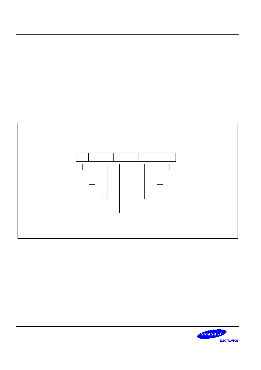
INSTRUCTION SET
S3C852B/P852B (Preliminary Spec)
6-6
FLAGS REGISTER (FLAGS)
The flags register FLAGS contains eight bits that describe the current status of CPU operations. Four of these
bits, FLAGS.7�FLAGS.4, can be tested and used with conditional jump instructions; two others FLAGS.3 and
FLAGS.2 are used for BCD arithmetic.
The FLAGS register also contains a bit to indicate the status of fast interrupt processing (FLAGS.1) and a bank
address status bit (FLAGS.0) to indicate whether bank 0 or bank 1 is currently being addressed. FLAGS register
can be set or reset by instructions as long as its outcome does not affect the flags, such as, Load instruction.
Logical and Arithmetic instructions such as, AND, OR, XOR, ADD, and SUB can affect the Flags register. For
example, the AND instruction updates the Zero, Sign and Overflow flags based on the outcome of the AND
instruction. If the AND instruction uses the Flags register as the destination, then simultaneously, two write will
occur to the Flags register producing an unpredictable result.
System Flags Register (FLAGS)
D5H, Set 1, R/W
.7
.6
.5
.4
.3
.2
.1
.0
MSB
LSB
Bank address
status flag (BA)
Fast interrupt
status flag (FS)
Half-carry flag (H)
Decimal adjust flag (D)
Carry flag (C)
Zero flag (Z)
Sign flag (S)
Overflow flag (V)
Figure 6-1. System Flags Register (FLAGS)

S3C852B/P852B (Preliminary Spec)
INSTRUCTION SET
6-7
FLAG DESCRIPTIONS
C
Carry Flag (FLAGS.7)
The C flag is set to "1" if the result from an arithmetic operation generates a carry-out from or a borrow to
the bit 7 position (MSB). After rotate and shift operations, it contains the last value shifted out of the
specified register. Program instructions can set, clear, or complement the carry flag.
Z
Zero Flag (FLAGS.6)
For arithmetic and logic operations, the Z flag is set to "1" if the result of the operation is zero. For
operations that test register bits, and for shift and rotate operations, the Z flag is set to "1" if the result is
logic zero.
S
Sign Flag (FLAGS.5)
Following arithmetic, logic, rotate, or shift operations, the sign bit identifies the state of the MSB of the
result. A logic zero indicates a positive number and a logic one indicates a negative number.
V
Overflow Flag (FLAGS.4)
The V flag is set to "1" when the result of a two's-complement operation is greater than + 127 or less than
� 128. It is also cleared to "0" following logic operations.
D
Decimal Adjust Flag (FLAGS.3)
The DA bit is used to specify what type of instruction was executed last during BCD operations, so that a
subsequent decimal adjust operation can execute correctly. The DA bit is not usually accessed by
programmers, and cannot be used as a test condition.
H
Half-Carry Flag (FLAGS.2)
The H bit is set to "1" whenever an addition generates a carry-out of bit 3, or when a subtraction borrows
out of bit 4. It is used by the Decimal Adjust (DA) instruction to convert the binary result of a previous
addition or subtraction into the correct decimal (BCD) result. The H flag is seldom accessed directly by a
program.
FIS
Fast Interrupt Status Flag (FLAGS.1)
The FIS bit is set during a fast interrupt cycle and reset during the IRET following interrupt servicing.
When set, it inhibits all interrupts and causes the fast interrupt return to be executed when the IRET
instruction is executed.
BA
Bank Address Flag (FLAGS.0)
The BA flag indicates which register bank in the set 1 area of the internal register file is currently
selected, bank 0 or bank 1. The BA flag is cleared to "0" (select bank 0) when you execute the SB0
instruction and is set to "1" (select bank 1) when you execute the SB1 instruction.

INSTRUCTION SET
S3C852B/P852B (Preliminary Spec)
6-8
INSTRUCTION SET NOTATION
Table 6-2. Flag Notation Conventions
Flag
Description
C
Carry flag
Z
Zero flag
S
Sign flag
V
Overflow flag
D
Decimal-adjust flag
H
Half-carry flag
0
Cleared to logic zero
1
Set to logic one
*
Set or cleared according to operation
�
Value is unaffected
x
Value is undefined
Table 6-3. Instruction Set Symbols
Symbol
Description
dst
Destination operand
src
Source operand
@
Indirect register address prefix
PC
Program counter
IP
Instruction pointer
FLAGS
Flags register (D5H)
RP
Register pointer
#
Immediate operand or register address prefix
H
Hexadecimal number suffix
D
Decimal number suffix
B
Binary number suffix
opc
Opcode

S3C852B/P852B (Preliminary Spec)
INSTRUCTION SET
6-9
Table 6-4. Instruction Notation Conventions
Notation
Description
Actual Operand Range
cc
Condition code
See list of condition codes in Table 6-6.
r
Working register only
Rn (n = 0�15)
rb
Bit (b) of working register
Rn.b (n = 0�15, b = 0�7)
r0
Bit 0 (LSB) of working register
Rn (n = 0�15)
rr
Working register pair
RRp (p = 0, 2, 4, ..., 14)
R
Register or working register
reg or Rn (reg = 0�255, n = 0�15)
Rb
Bit 'b' of register or working register
reg.b (reg = 0�255, b = 0�7)
RR
Register pair or working register pair
reg or RRp (reg = 0�254, even number only, where
p = 0, 2, ..., 14)
IA
Indirect addressing mode
addr (addr = 0�254, even number only)
Ir
Indirect working register only
@Rn (n = 0�15)
IR
Indirect register or indirect working register @Rn or @reg (reg = 0�255, n = 0�15)
Irr
Indirect working register pair only
@RRp (p = 0, 2, ..., 14)
IRR
Indirect register pair or indirect working
register pair
@RRp or @reg (reg = 0�254, even only, where
p = 0, 2, ..., 14)
X
Indexed addressing mode
#reg [Rn] (reg = 0�255, n = 0�15)
XS
Indexed (short offset) addressing mode
#addr [RRp] (addr = range �128 to +127, where
p = 0, 2, ..., 14)
xl
Indexed (long offset) addressing mode
#addr [RRp] (addr = range 0�65535, where
p = 0, 2, ..., 14)
da
Direct addressing mode
addr (addr = range 0�65535)
ra
Relative addressing mode
addr (addr = number in the range +127 to �128 that is
an offset relative to the address of the next instruction)
im
Immediate addressing mode
#data (data = 0�255)
iml
Immediate (long) addressing mode
#data (data = range 0�65535)

INSTRUCTION SET
S3C852B/P852B (Preliminary Spec)
6-10
Table 6-5. Opcode Quick Reference
OPCODE MAP
LOWER NIBBLE (HEX)
�
0
1
2
3
4
5
6
7
U
0
DEC
R1
DEC
IR1
ADD
r1, r2
ADD
r1, Ir2
ADD
R2, R1
ADD
IR2, R1
ADD
R1, IM
BOR
r0�Rb
P
1
RLC
R1
RLC
IR1
ADC
r1, r2
ADC
r1, Ir2
ADC
R2, R1
ADC
IR2, R1
ADC
R1, IM
BCP
r1.b, R2
P
2
INC
R1
INC
IR1
SUB
r1, r2
SUB
r1, Ir2
SUB
R2, R1
SUB
IR2, R1
SUB
R1, IM
BXOR
r0�Rb
E
3
JP
IRR1
SRP/0/1
IM
SBC
r1, r2
SBC
r1, Ir2
SBC
R2, R1
SBC
IR2, R1
SBC
R1, IM
BTJR
r2.b, RA
R
4
DA
R1
DA
IR1
OR
r1, r2
OR
r1, Ir2
OR
R2, R1
OR
IR2, R1
OR
R1, IM
LDB
r0�Rb
5
POP
R1
POP
IR1
AND
r1, r2
AND
r1, Ir2
AND
R2, R1
AND
IR2, R1
AND
R1, IM
BITC
r1.b
N
6
COM
R1
COM
IR1
TCM
r1, r2
TCM
r1, Ir2
TCM
R2, R1
TCM
IR2, R1
TCM
R1, IM
BAND
r0�Rb
I
7
PUSH
R2
PUSH
IR2
TM
r1, r2
TM
r1, Ir2
TM
R2, R1
TM
IR2, R1
TM
R1, IM
BIT
r1.b
B
8
DECW
RR1
DECW
IR1
PUSHUD
IR1, R2
PUSHUI
IR1, R2
MULT
R2, RR1
MULT
IR2, RR1
MULT
IM, RR1
LD
r1, x, r2
B
9
RL
R1
RL
IR1
POPUD
IR2, R1
POPUI
IR2, R1
DIV
R2, RR1
DIV
IR2, RR1
DIV
IM, RR1
LD
r2, x, r1
L
A
INCW
RR1
INCW
IR1
CP
r1, r2
CP
r1, Ir2
CP
R2, R1
CP
IR2, R1
CP
R1, IM
LDC
r1, Irr2, xL
E
B
CLR
R1
CLR
IR1
XOR
r1, r2
XOR
r1, Ir2
XOR
R2, R1
XOR
IR2, R1
XOR
R1, IM
LDC
r2, Irr2, xL
C
RRC
R1
RRC
IR1
CPIJE
Ir, r2, RA
LDC
r1, Irr2
LDW
RR2, RR1
LDW
IR2, RR1
LDW
RR1, IML
LD
r1, Ir2
H
D
SRA
R1
SRA
IR1
CPIJNE
Irr, r2, RA
LDC
r2, Irr1
CALL
IA1
LD
IR1, IM
LD
Ir1, r2
E
E
RR
R1
RR
IR1
LDCD
r1, Irr2
LDCI
r1, Irr2
LD
R2, R1
LD
R2, IR1
LD
R1, IM
LDC
r1, Irr2, xs
X
F
SWAP
R1
SWAP
IR1
LDCPD
r2, Irr1
LDCPI
r2, Irr1
CALL
IRR1
LD
IR2, R1
CALL
DA1
LDC
r2, Irr1, xs

S3C852B/P852B (Preliminary Spec)
INSTRUCTION SET
6-11
Table 6-5. Opcode Quick Reference (Continued)
OPCODE MAP
LOWER NIBBLE (HEX)
�
8
9
A
B
C
D
E
F
U
0
LD
r1, R2
LD
r2, R1
DJNZ
r1, RA
JR
cc, RA
LD
r1, IM
JP
cc dA
INC
r1
NEXT
P
1
ENTER
P
2
EXIT
E
3
WFI
R
4
SB0
5
SB1
N
6
IDLE
I
7
STOP
B
8
DI
B
9
EI
L
A
RET
E
B
IRET
C
RCF
H
D
SCF
E
E
CCF
X
F
LD
r1, R2
LD
r2, R1
DJNZ
r1, RA
JR
cc, RA
LD
r1, IM
JP
cc, DA
INC
r1
NOP

INSTRUCTION SET
S3C852B/P852B (Preliminary Spec)
6-12
CONDITION CODES
The opcode of a conditional jump always contains a 4-bit field called the condition code (cc). This specifies under
which conditions it is to execute the jump. For example, a conditional jump with the condition code for "equal"
after a compare operation only jumps if the two operands are equal. Condition codes are listed in Table 6-6.
The carry (C), zero (Z), sign (S), and overflow (V) flags are used to control the operation of conditional jump
instructions.
Table 6-6. Condition Codes
Binary
Mnemonic
Description
Flags Set
0000
F
Always false
�
1000
T
Always true
�
0111
(note)
C
Carry
C = 1
1111
(note)
NC
No carry
C = 0
0110
(note)
Z
Zero
Z = 1
1110
(note)
NZ
Not zero
Z = 0
1101
PL
Plus
S = 0
0101
MI
Minus
S = 1
0100
OV
Overflow
V = 1
1100
NOV
No overflow
V = 0
0110
(note)
EQ
Equal
Z = 1
1110
(note)
NE
Not equal
Z = 0
1001
GE
Greater than or equal
(S XOR V) = 0
0001
LT
Less than
(S XOR V) = 1
1010
GT
Greater than
(Z OR (S XOR V)) = 0
0010
LE
Less than or equal
(Z OR (S XOR V)) = 1
1111
(note)
UGE
Unsigned greater than or equal
C = 0
0111
(note)
ULT
Unsigned less than
C = 1
1011
UGT
Unsigned greater than
(C = 0 AND Z = 0) = 1
0011
ULE
Unsigned less than or equal
(C OR Z) = 1
NOTES:
1.
It indicates condition codes that are related to two different mnemonics but which test the same flag. For
example, Z and EQ are both true if the zero flag (Z) is set, but after an ADD instruction, Z would probably be used;
after a CP instruction, however, EQ would probably be used.
2.
For operations involving unsigned numbers, the special condition codes UGE, ULT, UGT, and ULE must be used.

S3C852B/P852B (Preliminary Spec)
INSTRUCTION SET
6-13
INSTRUCTION DESCRIPTIONS
This section contains detailed information and programming examples for each instruction in the SAM8
instruction set. Information is arranged in a consistent format for improved readability and for fast referencing.
The following information is included in each instruction description:
-- Instruction name (mnemonic)
-- Full instruction name
-- Source/destination format of the instruction operand
-- Shorthand notation of the instruction's operation
-- Textual description of the instruction's effect
-- Specific flag settings affected by the instruction
-- Detailed description of the instruction's format, execution time, and addressing mode(s)
-- Programming example(s) explaining how to use the instruction

INSTRUCTION SET
S3C852B/P852B (Preliminary Spec)
6-14
ADC
-- Add with carry
ADC
dst, src
Operation:
dst
dst + src + c
The source operand, along with the setting of the carry flag, is added to the destination operand
and the sum is stored in the destination. The contents of the source are unaffected. Two's-
complement addition is performed. In multiple precision arithmetic, this instruction permits the
carry from the addition of low-order operands to be carried into the addition of high-order
operands.
Flags:
C: Set if there is a carry from the most significant bit of the result; cleared otherwise.
Z: Set if the result is "0"; cleared otherwise.
S: Set if the result is negative; cleared otherwise.
V: Set if arithmetic overflow occurs, that is, if both operands are of the same sign and the result
is of the opposite sign; cleared otherwise.
D: Always cleared to "0".
H: Set if there is a carry from the most significant bit of the low-order four bits of the result;
cleared otherwise.
Format:
Bytes
Cycles
Opcode
(Hex)
Addr Mode
dst src
opc
dst | src
2
4
12
r
r
6
13
r
lr
opc
src
dst
3
6
14
R
R
6
15
R
IR
opc
dst
src
3
6
16
R
IM
Examples:
Given: R1 = 10H, R2 = 03H, C flag = "1", register 01H = 20H, register 02H = 03H, and
register 03H = 0AH:
ADC
R1, R2
R1 = 14H, R2 = 03H
ADC
R1, @R2
R1 = 1BH, R2 = 03H
ADC
01H, 02H
Register 01H = 24H, register 02H = 03H
ADC
01H, @02H
Register 01H = 2BH, register 02H = 03H
ADC
01H, #11H
Register 01H = 32H
In the first example, destination register R1 contains the value 10H, the carry flag is set to "1",
and the source working register R2 contains the value 03H. The statement "ADC R1, R2" adds
03H and the carry flag value ("1") to the destination value 10H, leaving 14H in register R1.
S3C852B/P852B (Preliminary Spec)
INSTRUCTION SET
6-15
ADD
--
Add
ADD
dst, src
Operation:
dst
dst + src
The source operand is added to the destination operand and the sum is stored in the destination.
The contents of the source are unaffected. Two's-complement addition is performed.
Flags:
C: Set if there is a carry from the most significant bit of the result; cleared otherwise.
Z: Set if the result is "0"; cleared otherwise.
S: Set if the result is negative; cleared otherwise.
V: Set if arithmetic overflow occurred, that is, if both operands are of the same sign and the
result is of the opposite sign; cleared otherwise.
D: Always cleared to "0".
H: Set if a carry from the low-order nibble occurred.
Format:
Bytes
Cycles
Opcode
(Hex)
Addr Mode
dst src
opc
dst | src
2
4
02
r
r
6
03
r
lr
opc
src
dst
3
6
04
R
R
6
05
R
IR
opc
dst
src
3
6
06
R
IM
Examples:
Given: R1 = 12H, R2 = 03H, register 01H = 21H, register 02H = 03H, register 03H = 0AH:
ADD
R1, R2
R1 = 15H, R2 = 03H
ADD
R1, @R2
R1 = 1CH, R2 = 03H
ADD
01H, 02H
Register 01H = 24H, register 02H = 03H
ADD
01H, @02H
Register 01H = 2BH, register 02H = 03H
ADD
01H, #25H
Register 01H = 46H
In the first example, destination working register R1 contains 12H and the source working
register R2 contains 03H. The statement "ADD R1, R2" adds 03H to 12H, leaving the value 15H
in register R1.
INSTRUCTION SET
S3C852B/P852B (Preliminary Spec)
6-16
AND
--
Logical AND
AND
dst, src
Operation:
dst
dst AND src
The source operand is logically ANDed with the destination operand. The result is stored in the
destination. The AND operation results in a "1" bit being stored whenever the corresponding bits
in the two operands are both logic ones; otherwise a "0" bit value is stored. The contents of the
source are unaffected.
Flags:
C: Unaffected.
Z: Set if the result is "0"; cleared otherwise.
S: Set if the result bit 7 is set; cleared otherwise.
V: Always cleared to "0".
D: Unaffected.
H: Unaffected.
Format:
Bytes
Cycles
Opcode
(Hex)
Addr Mode
dst src
opc
dst | src
2
4
52
r
r
6
53
r
lr
opc
src
dst
3
6
54
R
R
6
55
R
IR
opc
dst
src
3
6
56
R
IM
Examples:
Given: R1 = 12H, R2 = 03H, register 01H = 21H, register 02H = 03H, register 03H = 0AH:
AND
R1, R2
R1 = 02H, R2 = 03H
AND
R1, @R2
R1 = 02H, R2 = 03H
AND
01H, 02H
Register 01H = 01H, register 02H = 03H
AND
01H, @02H
Register 01H = 00H, register 02H = 03H
AND
01H, #25H
Register 01H = 21H
In the first example, destination working register R1 contains the value 12H and the source
working register R2 contains 03H. The statement "AND R1, R2" logically ANDs the source
operand 03H with the destination operand value 12H, leaving the value 02H in register R1.

S3C852B/P852B (Preliminary Spec)
INSTRUCTION SET
6-17
BAND
--
Bit AND
BAND
dst, src.b
BAND
dst.b, src
Operation:
dst (0)
dst (0) AND src (b)
or
dst (b)
dst (b) AND src (0)
The specified bit of the source (or the destination) is logically ANDed with the zero bit (LSB) of
the destination (or source). The resultant bit is stored in the specified bit of the destination. No
other bits of the destination are affected. The source is unaffected.
Flags:
C: Unaffected.
Z: Set if the result is "0"; cleared otherwise.
S: Cleared to "0".
V: Undefined.
D: Unaffected.
H: Unaffected.
Format:
Bytes
Cycles
Opcode
(Hex)
Addr Mode
dst src
opc
dst | b | 0
src
3
6
67
r0
Rb
opc
src | b | 1
dst
3
6
67
Rb
r0
NOTE: In the second byte of the 3-byte instruction formats, the destination (or source) address is four
bits, the bit address 'b' is three bits, and the LSB address value is one bit in length.
Examples:
Given: R1 = 07H and register 01H = 05H:
BAND
R1, 01H.1
R1 = 06H, register 01H = 05H
BAND
01H.1, R1
Register 01H = 05H, R1 = 07H
In the first example, source register 01H contains the value 05H (00000101B) and destination
working register R1 contains 07H (00000111B). The statement "BAND R1, 01H.1" ANDs the bit
1 value of the source register ("0") with the bit 0 value of register R1 (destination), leaving the
value 06H (00000110B) in register R1.

INSTRUCTION SET
S3C852B/P852B (Preliminary Spec)
6-18
BCP
--
Bit Compare
BCP
dst, src.b
Operation:
dst (0) � src (b)
The specified bit of the source is compared to (subtracted from) bit zero (LSB) of the destination.
The zero flag is set if the bits are the same; otherwise it is cleared. The contents of both
operands are unaffected by the comparison.
Flags:
C: Unaffected.
Z: Set if the two bits are the same; cleared otherwise.
S: Cleared to "0".
V: Undefined.
D: Unaffected.
H: Unaffected.
Format:
Bytes
Cycles
Opcode
(Hex)
Addr Mode
dst src
opc
dst | b | 0
src
3
6
17
r0
Rb
NOTE: In the second byte of the instruction format, the destination address is four bits, the bit address 'b'
is three bits, and the LSB address value is one bit in length.
Example:
Given: R1 = 07H and register 01H = 01H:
BCP
R1, 01H.1
R1 = 07H, register 01H = 01H
If destination working register R1 contains the value 07H (00000111B) and the source register
01H contains the value 01H (00000001B), the statement "BCP R1, 01H.1" compares bit one of
the source register (01H) and bit zero of the destination register (R1). Because the bit values are
not identical, the zero flag bit (Z) is cleared in the FLAGS register (0D5H).

S3C852B/P852B (Preliminary Spec)
INSTRUCTION SET
6-19
BITC
--
Bit Complement
BITC
dst.b
Operation:
dst(b)
NOT dst(b)
This instruction complements the specified bit within the destination without affecting any other
bits in the destination.
Flags:
C: Unaffected.
Z: Set if the result is "0"; cleared otherwise.
S: Cleared to "0".
V: Undefined.
D: Unaffected.
H: Unaffected.
Format:
Bytes
Cycles
Opcode
(Hex)
Addr Mode
dst
opc
dst | b | 0
2
4
57
rb
NOTE: In the second byte of the instruction format, the destination address is four bits, the bit address 'b'
is three bits, and the LSB address value is one bit in length.
Example:
Given: R1 = 07H
BITC
R1.1
R1 = 05H
If working register R1 contains the value 07H (00000111B), the statement "BITC R1.1"
complements bit one of the destination and leaves the value 05H (00000101B) in register R1.
Because the result of the complement is not "0", the zero flag (Z) in the FLAGS register (0D5H)
is cleared.

INSTRUCTION SET
S3C852B/P852B (Preliminary Spec)
6-20
BITR
--
Bit Reset
BITR
dst.b
Operation:
dst(b)
0
The BITR instruction clears the specified bit within the destination without affecting any other bits
in the destination.
Flags:
No flags are affected.
Format:
Bytes
Cycles
Opcode
(Hex)
Addr Mode
dst
opc
dst | b | 0
2
4
77
rb
NOTE: In the second byte of the instruction format, the destination address is four bits, the bit address 'b'
is three bits, and the LSB address value is one bit in length.
Example:
Given: R1 = 07H:
BITR
R1.1
R1 = 05H
If the value of working register R1 is 07H (00000111B), the statement "BITR R1.1" clears bit one
of the destination register R1, leaving the value 05H (00000101B).

S3C852B/P852B (Preliminary Spec)
INSTRUCTION SET
6-21
BITS
--
Bit Set
BITS
dst.b
Operation:
dst(b)
1
The BITS instruction sets the specified bit within the destination without affecting any other bits
in the destination.
Flags:
No flags are affected.
Format:
Bytes
Cycles
Opcode
(Hex)
Addr Mode
dst
opc
dst | b | 1
2
4
77
rb
NOTE: In the second byte of the instruction format, the destination address is four bits, the bit address 'b'
is three bits, and the LSB address value is one bit in length.
Example:
Given: R1 = 07H:
BITS
R1.3
R1 = 0FH
If working register R1 contains the value 07H (00000111B), the statement "BITS R1.3" sets bit
three of the destination register R1 to "1", leaving the value 0FH (00001111B).

INSTRUCTION SET
S3C852B/P852B (Preliminary Spec)
6-22
BOR
--
Bit OR
BOR
dst, src.b
BOR
dst.b, src
Operation:
dst (0)
dst (0) OR src (b)
or
dst(b)
dst(b) OR src (0)
The specified bit of the source (or the destination) is logically ORed with bit zero (LSB) of the
destination (or the source). The resulting bit value is stored in the specified bit of the destination.
No other bits of the destination are affected. The source is unaffected.
Flags:
C: Unaffected.
Z: Set if the result is "0"; cleared otherwise.
S: Cleared to "0".
V: Undefined.
D: Unaffected.
H: Unaffected.
Format:
Bytes
Cycles
Opcode
(Hex)
Addr Mode
dst src
opc
dst | b | 0
src
3
6
07
r0
Rb
opc
src | b | 1
dst
3
6
07
Rb
r0
NOTE: In the second byte of the 3-byte instruction formats, the destination (or source) address is four
bits, the bit address 'b' is three bits, and the LSB address value is one bit.
Examples:
Given: R1 = 07H and register 01H = 03H:
BOR
R1, 01H.1
R1 = 07H, register 01H = 03H
BOR
01H.2, R1
Register 01H = 07H, R1 = 07H
In the first example, destination working register R1 contains the value 07H (00000111B) and
source register 01H the value 03H (00000011B). The statement "BOR R1, 01H.1" logically ORs
bit one of register 01H (source) with bit zero of R1 (destination). This leaves the same value
(07H) in working register R1.
In the second example, destination register 01H contains the value 03H (00000011B) and the
source working register R1 the value 07H (00000111B). The statement "BOR 01H.2, R1"
logically ORs bit two of register 01H (destination) with bit zero of R1 (source). This leaves the
value 07H in register 01H.

S3C852B/P852B (Preliminary Spec)
INSTRUCTION SET
6-23
BTJRF
--
Bit Test, Jump Relative on False
BTJRF
dst, src.b
Operation:
If src (b) is a "0", then PC
PC + dst
The specified bit within the source operand is tested. If it is a "0", the relative address is added to
the program counter and control passes to the statement whose address is now in the PC;
otherwise, the instruction following the BTJRF instruction is executed.
Flags:
No flags are affected.
Format:
(Note 1)
Bytes
Cycles
Opcode
(Hex)
Addr Mode
dst src
opc
src | b | 0
dst
3
10
37
RA
rb
NOTE: In the second byte of the instruction format, the source address is four bits, the bit address 'b' is
three bits, and the LSB address value is one bit in length.
Example:
Given: R1 = 07H:
BTJRF
SKIP, R1.3
PC jumps to SKIP location
If working register R1 contains the value 07H (00000111B), the statement "BTJRF SKIP, R1.3"
tests bit 3. Because it is "0", the relative address is added to the PC and the PC jumps to the
memory location pointed to by the SKIP. (Remember that the memory location must be within
the allowed range of + 127 to � 128.)

INSTRUCTION SET
S3C852B/P852B (Preliminary Spec)
6-24
BTJRT
--
Bit Test, Jump Relative on True
BTJRT
dst, src.b
Operation:
If src (b) is a "1", then PC
PC + dst
The specified bit within the source operand is tested. If it is a "1", the relative address is added to
the program counter and control passes to the statement whose address is now in the PC;
otherwise, the instruction following the BTJRT instruction is executed.
Flags:
No flags are affected.
Format:
(Note 1)
Bytes
Cycles
Opcode
(Hex)
Addr Mode
dst src
opc
src | b | 1
dst
3
10
37
RA
rb
NOTE: In the second byte of the instruction format, the source address is four bits, the bit address 'b' is
three bits, and the LSB address value is one bit in length.
Example:
Given: R1 = 07H:
BTJRT
SKIP, R1.1
If working register R1 contains the value 07H (00000111B), the statement "BTJRT SKIP, R1.1"
tests bit one in the source register (R1). Because it is a "1", the relative address is added to the
PC and the PC jumps to the memory location pointed to by the SKIP. (Remember that the
memory location must be within the allowed range of + 127 to � 128.)

S3C852B/P852B (Preliminary Spec)
INSTRUCTION SET
6-25
BXOR
--
Bit XOR
BXOR
dst, src.b
BXOR
dst.b, src
Operation:
dst (0)
dst (0) XOR src (b)
or
dst(b)
dst(b) XOR src (0)
The specified bit of the source (or the destination) is logically exclusive-ORed with bit zero (LSB)
of the destination (or source). The result bit is stored in the specified bit of the destination. No
other bits of the destination are affected. The source is unaffected.
Flags:
C: Unaffected.
Z: Set if the result is "0"; cleared otherwise.
S: Cleared to "0".
V: Undefined.
D: Unaffected.
H: Unaffected.
Format:
Bytes
Cycles
Opcode
(Hex)
Addr Mode
dst src
opc
dst | b | 0
src
3
6
27
r0
Rb
opc
src | b | 1
dst
3
6
27
Rb
r0
NOTE: In the second byte of the 3-byte instruction formats, the destination (or source) address is four
bits, the bit address 'b' is three bits, and the LSB address value is one bit in length.
Examples:
Given: R1 = 07H (00000111B) and register 01H = 03H (00000011B):
BXOR
R1, 01H.1
R1 = 06H, register 01H = 03H
BXOR
01H.2, R1
Register 01H = 07H, R1 = 07H
In the first example, destination working register R1 has the value 07H (00000111B) and source
register 01H has the value 03H (00000011B). The statement "BXOR R1, 01H.1" exclusive-ORs
bit one of register 01H (source) with bit zero of R1 (destination). The result bit value is stored in
bit zero of R1, changing its value from 07H to 06H. The value of source register 01H is
unaffected.

INSTRUCTION SET
S3C852B/P852B (Preliminary Spec)
6-26
CALL
--
Call Procedure
CALL
dst
Operation:
SP
SP � 1
@SP
PCL
SP
SP �1
@SP
PCH
PC
dst
The current contents of the program counter are pushed onto the top of the stack. The program
counter value used is the address of the first instruction following the CALL instruction. The
specified destination address is then loaded into the program counter and points to the first
instruction of a procedure. At the end of the procedure the return instruction (RET) can be used
to return to the original program flow. RET pops the top of the stack back into the program
counter.
Flags:
No flags are affected.
Format:
Bytes
Cycles
Opcode
(Hex)
Addr Mode
dst
opc
dst
3
14
F6
DA
opc
dst
2
12
F4
IRR
opc
dst
2
14
D4
IA
Examples:
Given: R0 = 35H, R1 = 21H, PC = 1A47H, and SP = 0002H:
CALL
3521H
SP = 0000H
(Memory locations 0000H = 1AH, 0001H = 4AH, where
4AH is the address that follows the instruction.)
CALL
@RR0
SP = 0000H (0000H = 1AH, 0001H = 49H)
CALL
#40H
SP = 0000H (0000H = 1AH, 0001H = 49H)
In the first example, if the program counter value is 1A47H and the stack pointer contains the
value 0002H, the statement "CALL 3521H" pushes the current PC value onto the top of the
stack. The stack pointer now points to memory location 0000H. The PC is then loaded with the
value 3521H, the address of the first instruction in the program sequence to be executed.
If the contents of the program counter and stack pointer are the same as in the first example, the
statement "CALL @RR0" produces the same result except that the 49H is stored in stack
location 0001H (because the two-byte instruction format was used). The PC is then loaded with
the value 3521H, the address of the first instruction in the program sequence to be executed.
Assuming that the contents of the program counter and stack pointer are the same as in the first
example, if program address 0040H contains 35H and program address 0041H contains 21H, the
statement "CALL #40H" produces the same result as in the second example.

S3C852B/P852B (Preliminary Spec)
INSTRUCTION SET
6-27
CCF
--
Complement Carry Flag
CCF
Operation:
C
NOT C
The carry flag (C) is complemented. If C = "1", the value of the carry flag is changed to logic
zero; if C = "0", the value of the carry flag is changed to logic one.
Flags:
C: Complemented.
No other flags are affected.
Format:
Bytes
Cycles
Opcode
(Hex)
opc
1
4
EF
Example:
Given: The carry flag = "0":
CCF
If the carry flag = "0", the CCF instruction complements it in the FLAGS register (0D5H),
changing its value from logic zero to logic one.

INSTRUCTION SET
S3C852B/P852B (Preliminary Spec)
6-28
CLR
--
Clear
CLR
dst
Operation:
dst
"0"
The destination location is cleared to "0".
Flags:
No flags are affected.
Format:
Bytes
Cycles
Opcode
(Hex)
Addr Mode
dst
opc
dst
2
4
B0
R
4
B1
IR
Examples:
Given: Register 00H = 4FH, register 01H = 02H, and register 02H = 5EH:
CLR
00H
Register 00H = 00H
CLR
@01H
Register 01H = 02H, register 02H = 00H
In Register (R) addressing mode, the statement "CLR 00H" clears the destination register 00H
value to 00H. In the second example, the statement "CLR @01H" uses Indirect Register (IR)
addressing mode to clear the 02H register value to 00H.

S3C852B/P852B (Preliminary Spec)
INSTRUCTION SET
6-29
COM
--
Complement
COM
dst
Operation:
dst
NOT dst
The contents of the destination location are complemented (one's complement); all "1s" are
changed to "0s", and vice-versa.
Flags:
C: Unaffected.
Z: Set if the result is "0"; cleared otherwise.
S: Set if the result bit 7 is set; cleared otherwise.
V: Always reset to "0".
D: Unaffected.
H: Unaffected.
Format:
Bytes
Cycles
Opcode
(Hex)
Addr Mode
dst
opc
dst
2
4
60
R
4
61
IR
Examples:
Given: R1 = 07H and register 07H = 0F1H:
COM
R1
R1 = 0F8H
COM
@R1
R1 = 07H, register 07H = 0EH
In the first example, destination working register R1 contains the value 07H (00000111B). The
statement "COM R1" complements all the bits in R1: all logic ones are changed to logic zeros,
and vice-versa, leaving the value 0F8H (11111000B).
In the second example, Indirect Register (IR) addressing mode is used to complement the value
of destination register 07H (11110001B), leaving the new value 0EH (00001110B).

INSTRUCTION SET
S3C852B/P852B (Preliminary Spec)
6-30
CP
--
Compare
CP
dst, src
Operation:
dst � src
The source operand is compared to (subtracted from) the destination operand, and the
appropriate flags are set accordingly. The contents of both operands are unaffected by the
comparison.
Flags:
C: Set if a "borrow" occurred (src > dst); cleared otherwise.
Z: Set if the result is "0"; cleared otherwise.
S: Set if the result is negative; cleared otherwise.
V: Set if arithmetic overflow occurred; cleared otherwise.
D: Unaffected.
H: Unaffected.
Format:
Bytes
Cycles
Opcode
(Hex)
Addr Mode
dst src
opc
dst | src
2
4
A2
r
r
6
A3
r
lr
opc
src
dst
3
6
A4
R
R
6
A5
R
IR
opc
dst
src
3
6
A6
R
IM
Examples:
1.
Given: R1 = 02H and R2 = 03H:
CP
R1, R2
Set the C and S flags
Destination working register R1 contains the value 02H and source register R2 contains the
value 03H. The statement "CP R1, R2" subtracts the R2 value (source/subtrahend) from the R1
value (destination/minuend). Because a "borrow" occurs and the difference is negative, C and S
are "1".
2.
Given: R1 = 05H and R2 = 0AH:
CP
R1, R2
JP
UGE, SKIP
INC
R1
SKIP
LD
R3, R1
In this example, destination working register R1 contains the value 05H which is less than the
contents of the source working register R2 (0AH). The statement "CP R1, R2" generates C = "1"
and the JP instruction does not jump to the SKIP location. After the statement "LD R3, R1"
executes, the value 06H remains in working register R3.

S3C852B/P852B (Preliminary Spec)
INSTRUCTION SET
6-31
CPIJE
--
Compare, Increment, and Jump on Equal
CPIJE
dst, src, RA
Operation:
If dst � src = "0", PC
PC + RA
Ir
Ir + 1
The source operand is compared to (subtracted from) the destination operand. If the result is "0",
the relative address is added to the program counter and control passes to the statement whose
address is now in the program counter. Otherwise, the instruction immediately following the
CPIJE instruction is executed. In either case, the source pointer is incremented by one before
the next instruction is executed.
Flags:
No flags are affected.
Format:
Bytes
Cycles
Opcode
(Hex)
Addr Mode
dst src
opc
src
dst
RA
3
12
C2
r
Ir
NOTE: Execution time is 18 cycles if the jump is taken or 16 cycles if it is not taken.
Example:
Given: R1 = 02H, R2 = 03H, and register 03H = 02H:
CPIJE
R1, @R2, SKIP
R2 = 04H, PC jumps to SKIP location
In this example, working register R1 contains the value 02H, working register R2 the value 03H,
and register 03 contains 02H. The statement "CPIJE R1, @R2, SKIP" compares the @R2 value
02H (00000010B) to 02H (00000010B). Because the result of the comparison is equal, the
relative address is added to the PC and the PC then jumps to the memory location pointed to by
SKIP. The source register (R2) is incremented by one, leaving a value of 04H. (Remember that
the memory location must be within the allowed range of + 127 to � 128.)

INSTRUCTION SET
S3C852B/P852B (Preliminary Spec)
6-32
CPIJNE
--
Compare, Increment, and Jump on Non-Equal
CPIJNE
dst, src, RA
Operation:
If dst � src �� "0", PC
PC + RA
Ir
Ir + 1
The source operand is compared to (subtracted from) the destination operand. If the result is not
"0", the relative address is added to the program counter and control passes to the statement
whose address is now in the program counter; otherwise the instruction following the CPIJNE
instruction is executed. In either case the source pointer is incremented by one before the next
instruction.
Flags:
No flags are affected.
Format:
Bytes
Cycles
Opcode
(Hex)
Addr Mode
dst src
opc
src
dst
RA
3
12
D2
r
Ir
NOTE: Execution time is 18 cycles if the jump is taken or 16 cycles if it is not taken.
Example:
Given: R1 = 02H, R2 = 03H, and register 03H = 04H:
CPIJNE
R1, @R2, SKIP
R2 = 04H, PC jumps to SKIP location
Working register R1 contains the value 02H, working register R2 (the source pointer) the value
03H, and general register 03 the value 04H. The statement "CPIJNE R1, @R2, SKIP" subtracts
04H (00000100B) from 02H (00000010B). Because the result of the comparison is non-equal,
the relative address is added to the PC and the PC then jumps to the memory location pointed to
by SKIP. The source pointer register (R2) is also incremented by one, leaving a value of 04H.
(Remember that the memory location must be within the allowed range of + 127 to � 128.)

S3C852B/P852B (Preliminary Spec)
INSTRUCTION SET
6-33
DA
--
Decimal Adjust
DA
dst
Operation:
dst
DA dst
The destination operand is adjusted to form two 4-bit BCD digits following an addition or
subtraction operation. For addition (ADD, ADC) or subtraction (SUB, SBC), the following table
indicates the operation performed. (The operation is undefined if the destination operand was not
the result of a valid addition or subtraction of BCD digits):
Instruction
Carry
Before DA
Bits 4�7
Value (Hex)
H Flag
Before DA
Bits 0�3
Value (Hex)
Number Added
to Byte
Carry
After DA
0
0�9
0
0�9
00
0
0
0�8
0
A�F
06
0
0
0�9
1
0�3
06
0
ADD
0
A�F
0
0�9
60
1
ADC
0
9�F
0
A�F
66
1
0
A�F
1
0�3
66
1
1
0�2
0
0�9
60
1
1
0�2
0
A�F
66
1
1
0�3
1
0�3
66
1
0
0�9
0
0�9
00 = � 00
0
SUB
0
0�8
1
6�F
FA = � 06
0
SBC
1
7�F
0
0�9
A0 = � 60
1
1
6�F
1
6�F
9A = � 66
1
Flags:
C: Set if there was a carry from the most significant bit; cleared otherwise (see table).
Z: Set if result is "0"; cleared otherwise.
S: Set if result bit 7 is set; cleared otherwise.
V: Undefined.
D: Unaffected.
H: Unaffected.
Format:
Bytes
Cycles
Opcode
(Hex)
Addr Mode
dst
opc
dst
2
4
40
R
4
41
IR

INSTRUCTION SET
S3C852B/P852B (Preliminary Spec)
6-34
DA
--
Decimal Adjust
DA
(Continued)
Example:
Given: Working register R0 contains the value 15 (BCD), working register R1 contains
27 (BCD), and address 27H contains 46 (BCD):
ADD
R1, R0
;
C
"0", H
"0", Bits 4�7 = 3, bits 0�3 = C, R1
3CH
DA
R1
;
R1
3CH + 06
If addition is performed using the BCD values 15 and 27, the result should be 42. The sum is
incorrect, however, when the binary representations are added in the destination location using
standard binary arithmetic:
0 0 0 1 0 1 0 1
15
+ 0 0 1 0 0 1 1 1
27
0 0 1 1 1 1 0 0
=
3CH
The DA instruction adjusts this result so that the correct BCD representation is obtained:
0 0 1 1 1 1 0 0
+ 0 0 0 0 0 1 1 0
0 1 0 0 0 0 1 0
=
42
Assuming the same values given above, the statements
SUB
27H, R0
;
C
"0", H
"0", Bits 4�7 = 3, bits 0�3 = 1
DA
@R1
;
@R1
31�0
leave the value 31 (BCD) in address 27H (@R1).

S3C852B/P852B (Preliminary Spec)
INSTRUCTION SET
6-35
DEC
--
Decrement
DEC
dst
Operation:
dst
dst � 1
The contents of the destination operand are decremented by one.
Flags:
C: Unaffected.
Z: Set if the result is "0"; cleared otherwise.
S: Set if result is negative; cleared otherwise.
V: Set if arithmetic overflow occurred; cleared otherwise.
D: Unaffected.
H: Unaffected.
Format:
Bytes
Cycles
Opcode
(Hex)
Addr Mode
dst
opc
dst
2
4
00
R
4
01
IR
Examples:
Given: R1 = 03H and register 03H = 10H:
DEC
R1
R1 = 02H
DEC
@R1
Register 03H = 0FH
In the first example, if working register R1 contains the value 03H, the statement "DEC R1"
decrements the hexadecimal value by one, leaving the value 02H. In the second example, the
statement "DEC @R1" decrements the value 10H contained in the destination register 03H by
one, leaving the value 0FH.

INSTRUCTION SET
S3C852B/P852B (Preliminary Spec)
6-36
DECW
--
Decrement Word
DECW
dst
Operation:
dst
dst � 1
The contents of the destination location (which must be an even address) and the operand
following that location are treated as a single 16-bit value that is decremented by one.
Flags:
C: Unaffected.
Z: Set if the result is "0"; cleared otherwise.
S: Set if the result is negative; cleared otherwise.
V: Set if arithmetic overflow occurred; cleared otherwise.
D: Unaffected.
H: Unaffected.
Format:
Bytes
Cycles
Opcode
(Hex)
Addr Mode
dst
opc
dst
2
8
80
RR
8
81
IR
Examples:
Given: R0 = 12H, R1 = 34H, R2 = 30H, register 30H = 0FH, and register 31H = 21H:
DECW
RR0
R0 = 12H, R1 = 33H
DECW
@R2
Register 30H = 0FH, register 31H = 20H
In the first example, destination register R0 contains the value 12H and register R1 the value
34H. The statement "DECW RR0" addresses R0 and the following operand R1 as a 16-bit word
and decrements the value of R1 by one, leaving the value 33H.
NOTE:
A system malfunction may occur if you use a Zero flag (FLAGS.6) result together with a DECW
instruction. To avoid this problem, we recommend that you use DECW as shown in the following
example:
LOOP:
DECW
RR0
LD
R2, R1
OR
R2, R0
JR
NZ, LOOP

S3C852B/P852B (Preliminary Spec)
INSTRUCTION SET
6-37
DI
--
Disable Interrupts
DI
Operation:
SYM (0)
0
Bit zero of the system mode control register, SYM.0, is cleared to "0", globally disabling all
interrupt processing. Interrupt requests will continue to set their respective interrupt pending bits,
but the CPU will not service them while interrupt processing is disabled.
Flags:
No flags are affected.
Format:
Bytes
Cycles
Opcode
(Hex)
opc
1
4
8F
Example:
Given: SYM = 01H:
DI
If the value of the SYM register is 01H, the statement "DI" leaves the new value 00H in the
register and clears SYM.0 to "0", disabling interrupt processing.
Before changing IMR, interrupt pending and interrupt source control register, be sure DI state.

INSTRUCTION SET
S3C852B/P852B (Preliminary Spec)
6-38
DIV
--
Divide (Unsigned)
DIV
dst, src
Operation:
dst � src
dst (UPPER)
REMAINDER
dst (LOWER)
QUOTIENT
The destination operand (16 bits) is divided by the source operand (8 bits). The quotient (8 bits)
is stored in the lower half of the destination. The remainder (8 bits) is stored in the upper half of
the destination. When the quotient is
2
8
, the numbers stored in the upper and lower halves of
the destination for quotient and remainder are incorrect. Both operands are treated as unsigned
integers.
Flags:
C: Set if the V flag is set and quotient is between 2
8
and 2
9
�1; cleared otherwise.
Z: Set if divisor or quotient = "0"; cleared otherwise.
S: Set if MSB of quotient = "1"; cleared otherwise.
V: Set if quotient is
2
8
or if divisor = "0"; cleared otherwise.
D: Unaffected.
H: Unaffected.
Format:
Bytes
Cycles
Opcode
(Hex)
Addr Mode
dst src
opc
src
dst
3
26/10
94
RR
R
26/10
95
RR
IR
26/10
96
RR
IM
NOTE: Execution takes 10 cycles if the divide-by-zero is attempted; otherwise it takes 26 cycles.
Examples:
Given: R0 = 10H, R1 = 03H, R2 = 40H, register 40H = 80H:
DIV
RR0, R2
R0 = 03H, R1 = 40H
DIV
RR0, @R2
R0 = 03H, R1 = 20H
DIV
RR0, #20H
R0 = 03H, R1 = 80H
In the first example, destination working register pair RR0 contains the values 10H (R0) and 03H
(R1), and register R2 contains the value 40H. The statement "DIV RR0, R2" divides the 16-bit
RR0 value by the 8-bit value of the R2 (source) register. After the DIV instruction, R0 contains
the value 03H and R1 contains 40H. The 8-bit remainder is stored in the upper half of the
destination register RR0 (R0) and the quotient in the lower half (R1).

S3C852B/P852B (Preliminary Spec)
INSTRUCTION SET
6-39
DJNZ
--
Decrement and Jump if Non-Zero
DJNZ
r, dst
Operation:
r
r � 1
If r
0, PC
PC + dst
The working register being used as a counter is decremented. If the contents of the register are
not logic zero after decrementing, the relative address is added to the program counter and
control passes to the statement whose address is now in the PC. The range of the relative
address is +127 to �128, and the original value of the PC is taken to be the address of the
instruction byte following the DJNZ statement.
NOTE: In case of using DJNZ instruction, the working register being used as a counter should be set at
the one of location 0C0H to 0CFH with SRP, SRP0, or SRP1 instruction.
Flags:
No flags are affected.
Format:
Bytes
Cycles
Opcode
(Hex)
Addr Mode
dst
r | opc
dst
2
8 (jump taken)
rA
RA
8 (no jump)
r = 0 to F
Example:
Given: R1 = 02H and LOOP is the label of a relative address:
SRP
#0C0H
DJNZ
R1, LOOP
DJNZ is typically used to control a "loop" of instructions. In many cases, a label is used as the
destination operand instead of a numeric relative address value. In the example, working register
R1 contains the value 02H, and LOOP is the label for a relative address.
The statement "DJNZ R1, LOOP" decrements register R1 by one, leaving the value 01H.
Because the contents of R1 after the decrement are non-zero, the jump is taken to the relative
address specified by the LOOP label.

INSTRUCTION SET
S3C852B/P852B (Preliminary Spec)
6-40
EI
--
Enable Interrupts
EI
Operation:
SYM (0)
1
An EI instruction sets bit zero of the system mode register, SYM.0 to "1". This allows interrupts to
be serviced as they occur (assuming they have highest priority). If an interrupt's pending bit was
set while interrupt processing was disabled (by executing a DI instruction), it will be serviced
when you execute the EI instruction.
Flags:
No flags are affected.
Format:
Bytes
Cycles
Opcode
(Hex)
opc
1
4
9F
Example:
Given: SYM = 00H:
EI
If the SYM register contains the value 00H, that is, if interrupts are currently disabled, the
statement "EI" sets the SYM register to 01H, enabling all interrupts. (SYM.0 is the enable bit for
global interrupt processing.)
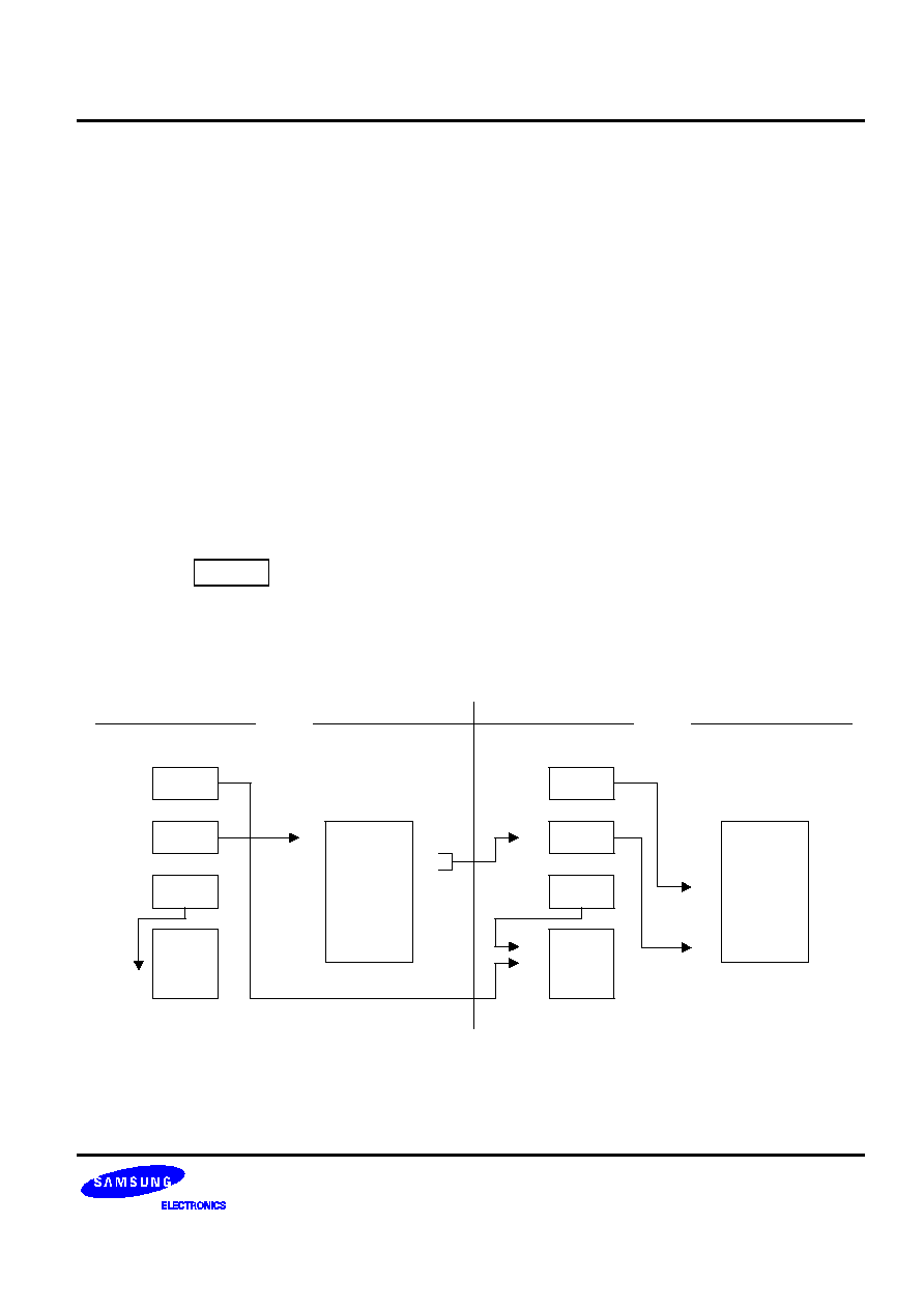
S3C852B/P852B (Preliminary Spec)
INSTRUCTION SET
6-41
ENTER
--
Enter
ENTER
Operation:
SP
SP � 2
@SP
IP
IP
PC
PC
@IP
IP
IP + 2
This instruction is useful when implementing threaded-code languages. The contents of the
instruction pointer are pushed to the stack. The program counter (PC) value is then written to the
instruction pointer. The program memory word that is pointed to by the instruction pointer is
loaded into the PC, and the instruction pointer is incremented by two.
Flags:
No flags are affected.
Format:
Bytes
Cycles
Opcode
(Hex)
opc
1
14
1F
Example:
The diagram below shows one example of how to use an ENTER statement.
0050
1P
0022
SP
22
Data
Address
Data
0040
PC
40
41
42
43
Enter
Address H
Address L
Address H
Address
Data
1F
01
10
Memory
0043
1P
0020
SP
20
21
22
IPH
IPL
Data
Address
Data
0110
PC
40
41
42
43
Enter
Address H
Address L
Address H
Address
Data
1F
01
10
Memory
00
50
Stack
Stack
110
Routine
Before
After
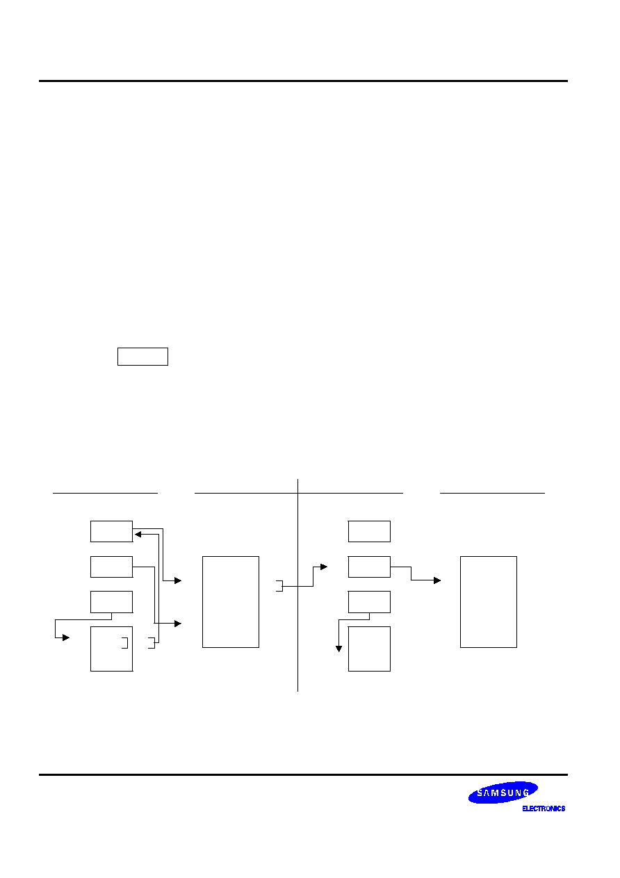
INSTRUCTION SET
S3C852B/P852B (Preliminary Spec)
6-42
EXIT
--
Exit
EXIT
Operation:
IP
@SP
SP
SP + 2
PC
@IP
IP
IP + 2
This instruction is useful when implementing threaded-code languages. The stack value is
popped and loaded into the instruction pointer. The program memory word that is pointed to by
the instruction pointer is then loaded into the program counter, and the instruction pointer is
incremented by two.
Flags:
No flags are affected.
Format:
Bytes
Cycles
Opcode (Hex)
opc
1
14 (internal stack)
2F
16 (internal stack)
Example:
The diagram below shows one example of how to use an EXIT statement.
0050
1P
0022
SP
Address
Data
0040
PC
Address
Data
Memory
0052
1P
0022
SP
Address
Data
0060
PC
Address
Data
Memory
Stack
Stack
Before
After
22
Data
20
21
22
IPH
IPL
Data
00
50
50
51
140
PCL old
PCH
Exit
60
00
2F
60
Main

S3C852B/P852B (Preliminary Spec)
INSTRUCTION SET
6-43
IDLE
--
Idle Operation
IDLE
Operation:
The IDLE instruction stops the CPU clock while allowing system clock oscillation to continue. Idle
mode can be released by an interrupt request (IRQ) or an external reset operation.
Flags:
No flags are affected.
Format:
Bytes
Cycles
Opcode
(Hex)
opc
1
4
6F
Example:
The instruction
IDLE
Stops the CPU clock but not the system clock

INSTRUCTION SET
S3C852B/P852B (Preliminary Spec)
6-44
INC
--
Increment
INC
dst
Operation:
dst
dst + 1
The contents of the destination operand are incremented by one.
Flags:
C: Unaffected.
Z: Set if the result is "0"; cleared otherwise.
S: Set if the result is negative; cleared otherwise.
V: Set if arithmetic overflow occurred; cleared otherwise.
D: Unaffected.
H: Unaffected.
Format:
Bytes
Cycles
Opcode
(Hex)
Addr Mode
dst
dst | opc
1
4
rE
r
r = 0 to
F
opc
dst
2
4
20
R
4
21
IR
Examples:
Given: R0 = 1BH, register 00H = 0CH, and register 1BH = 0FH:
INC
R0
R0 = 1CH
INC
00H
Register 00H = 0DH
INC
@R0
R0 = 1BH, register 01H = 10H
In the first example, if destination working register R0 contains the value 1BH, the statement
"INC R0" leaves the value 1CH in that same register.
The next example shows the effect an INC instruction has on register 00H, assuming that it
contains the value 0CH.
In the third example, INC is used in Indirect Register (IR) addressing mode to increment the
value of register 1BH from 0FH to 10H.

S3C852B/P852B (Preliminary Spec)
INSTRUCTION SET
6-45
INCW
--
Increment Word
INCW
dst
Operation:
dst
dst + 1
The contents of the destination (which must be an even address) and the byte following that
location are treated as a single 16-bit value that is incremented by one.
Flags:
C: Unaffected.
Z: Set if the result is "0"; cleared otherwise.
S: Set if the result is negative; cleared otherwise.
V: Set if arithmetic overflow occurred; cleared otherwise.
D: Unaffected.
H: Unaffected.
Format:
Bytes
Cycles
Opcode
(Hex)
Addr Mode
dst
opc
dst
2
8
A0
RR
8
A1
IR
Examples:
Given: R0 = 1AH, R1 = 02H, register 02H = 0FH, and register 03H = 0FFH:
INCW
RR0
R0 = 1AH, R1 = 03H
INCW
@R1
Register 02H = 10H, register 03H = 00H
In the first example, the working register pair RR0 contains the value 1AH in register R0 and 02H
in register R1. The statement "INCW RR0" increments the 16-bit destination by one, leaving the
value 03H in register R1. In the second example, the statement "INCW @R1" uses Indirect
Register (IR) addressing mode to increment the contents of general register 03H from 0FFH to
00H and register 02H from 0FH to 10H.
NOTE:
A system malfunction may occur if you use a Zero (Z) flag (FLAGS.6) result together with an
INCW instruction. To avoid this problem, we recommend that you use INCW as shown in the
following example:
LOOP:
INCW
RR0
LD
R2, R1
OR
R2, R0
JR
NZ, LOOP

INSTRUCTION SET
S3C852B/P852B (Preliminary Spec)
6-46
IRET
--
Interrupt Return
IRET
IRET (Normal)
IRET (Fast)
Operation:
FLAGS
@SP
PC
IP
SP
SP + 1
FLAGS
FLAGS'
PC
@SP
FIS
0
SP
SP + 2
SYM(0)
1
This instruction is used at the end of an interrupt service routine. It restores the flag register and
the program counter. It also re-enables global interrupts. A "normal IRET" is executed only if the
fast interrupt status bit (FIS, bit one of the FLAGS register, 0D5H) is cleared (= "0"). If a fast
interrupt occurred, IRET clears the FIS bit that was set at the beginning of the service routine.
Flags:
All flags are restored to their original settings (that is, the settings before the interrupt occurred).
Format:
IRET
(Normal)
Bytes
Cycles
Opcode (Hex)
opc
1
10 (internal stack)
BF
12 (internal stack)
IRET
(Fast)
Bytes
Cycles
Opcode (Hex)
opc
1
6
BF
Example:
In the figure below, the instruction pointer is initially loaded with 100H in the main program
before interrupts are enabled. When an interrupt occurs, the program counter and instruction
pointer are swapped. This causes the PC to jump to address 100H and the IP to keep the return
address. The last instruction in the service routine normally is a jump to IRET at address FFH.
This causes the instruction pointer to be loaded with 100H "again" and the program counter to
jump back to the main program. Now, the next interrupt can occur and the IP is still correct at
100H.
IRET
Interrupt
Service
Routine
JP to FFH
0H
FFH
100H
FFFFH
NOTE
In the fast interrupt example above, if the last instruction is not a jump to IRET, you must pay
attention to the order of the last two instructions. The IRET cannot be immediately proceeded by a
clearing of the interrupt status (as with a reset of the IPR register).

S3C852B/P852B (Preliminary Spec)
INSTRUCTION SET
6-47
JP
--
Jump
JP
cc, dst
(Conditional)
JP
dst
(Unconditional)
Operation:
If cc is true, PC
dst
The conditional JUMP instruction transfers program control to the destination address if the
condition specified by the condition code (cc) is true; otherwise, the instruction following the JP
instruction is executed. The unconditional JP simply replaces the contents of the PC with the
contents of the specified register pair. Control then passes to the statement addressed by the
PC.
Flags:
No flags are affected.
Format:
(1)
(2)
Bytes
Cycles
Opcode
(Hex)
Addr Mode
dst
cc | opc
dst
3
8
ccD
DA
cc = 0 to F
opc
dst
2
8
30
IRR
NOTES:
1.
The 3-byte format is used for a conditional jump and the 2-byte format for an unconditional jump.
2.
In the first byte of the three-byte instruction format (conditional jump), the condition code and the
opcode are both four bits.
Examples:
Given: The carry flag (C) = "1", register 00 = 01H, and register 01 = 20H:
JP
C, LABEL_W
LABEL_W = 1000H, PC = 1000H
JP
@00H
PC = 0120H
The first example shows a conditional JP. Assuming that the carry flag is set to "1", the
statement
"JP C, LABEL_W" replaces the contents of the PC with the value 1000H and transfers control to
that location. Had the carry flag not been set, control would then have passed to the statement
immediately following the JP instruction.
The second example shows an unconditional JP. The statement "JP @00" replaces the contents
of the PC with the contents of the register pair 00H and 01H, leaving the value 0120H.

INSTRUCTION SET
S3C852B/P852B (Preliminary Spec)
6-48
JR
--
Jump Relative
JR
cc, dst
Operation:
If cc is true, PC
PC + dst
If the condition specified by the condition code (cc) is true, the relative address is added to the
program counter and control passes to the statement whose address is now in the program
counter; otherwise, the instruction following the JR instruction is executed. (See list of condition
codes).
The range of the relative address is +127, �128, and the original value of the program counter is
taken to be the address of the first instruction byte following the JR statement.
Flags:
No flags are affected.
Format:
(1)
Bytes
Cycles
Opcode
(Hex)
Addr Mode
dst
cc | opc
dst
2
6
ccB
RA
cc = 0 to F
NOTE: In the first byte of the two-byte instruction format, the condition code and the opcode are each
four bits.
Example:
Given: The carry flag = "1" and LABEL_X = 1FF7H:
JR
C, LABEL_X
PC = 1FF7H
If the carry flag is set (that is, if the condition code is true), the statement "JR C, LABEL_X" will
pass control to the statement whose address is now in the PC. Otherwise, the program
instruction following the JR would be executed.

S3C852B/P852B (Preliminary Spec)
INSTRUCTION SET
6-49
LD
--
Load
LD
dst, src
Operation:
dst
src
The contents of the source are loaded into the destination. The source's contents are unaffected.
Flags:
No flags are affected.
Format:
Bytes
Cycles
Opcode
(Hex)
Addr Mode
dst src
dst | opc
src
2
4
rC
r
IM
4
r8
r
R
src | opc
dst
2
4
r9
R
r
r = 0 to F
opc
dst | src
2
4
C7
r
lr
4
D7
Ir
r
opc
src
dst
3
6
E4
R
R
6
E5
R
IR
opc
dst
src
3
6
E6
R
IM
6
D6
IR
IM
opc
src
dst
3
6
F5
IR
R
opc
dst | src
x
3
6
87
r
x [r]
opc
src | dst
x
3
6
97
x [r]
r

INSTRUCTION SET
S3C852B/P852B (Preliminary Spec)
6-50
LD
--
Load
LD
(Continued)
Examples:
Given: R0 = 01H, R1 = 0AH, register 00H = 01H, register 01H = 20H,
register 02H = 02H, LOOP = 30H, and register 3AH = 0FFH:
LD
R0, #10H
R0 = 10H
LD
R0, 01H
R0 = 20H, register 01H = 20H
LD
01H, R0
Register 01H = 01H, R0 = 01H
LD
R1, @R0
R1 = 20H, R0 = 01H
LD
@R0, R1
R0 = 01H, R1 = 0AH, register 01H = 0AH
LD
00H, 01H
Register 00H = 20H, register 01H = 20H
LD
02H, @00H
Register 02H = 20H, register 00H = 01H
LD
00H, #0AH
Register 00H = 0AH
LD
@00H, #10H
Register 00H = 01H, register 01H = 10H
LD
@00H, 02H
Register 00H = 01H, register 01H = 02, register 02H = 02H
LD
R0, #LOOP[R1]
R0 = 0FFH, R1 = 0AH
LD
#LOOP[R0], R1
Register 31H = 0AH, R0 = 01H, R1 = 0AH

S3C852B/P852B (Preliminary Spec)
INSTRUCTION SET
6-51
LDB
--
Load Bit
LDB
dst, src.b
LDB
dst.b, src
Operation:
dst (0)
src (b)
or
dst(b)
src (0)
The specified bit of the source is loaded into bit zero (LSB) of the destination, or bit zero of the
source is loaded into the specified bit of the destination. No other bits of the destination are
affected. The source is unaffected.
Flags:
No flags are affected.
Format:
Bytes
Cycles
Opcode
(Hex)
Addr Mode
dst src
opc
dst | b | 0
src
3
6
47
r0
Rb
opc
src | b | 1
dst
3
6
47
Rb
r0
NOTE: In the second byte of the instruction formats, the destination (or source) address is four bits, the
bit address 'b' is three bits, and the LSB address value is one bit in length.
Examples:
Given: R0 = 06H and general register 00H = 05H:
LDB
R0, 00H.2
R0 = 07H, register 00H = 05H
LDB
00H.0, R0
R0 = 06H, register 00H = 04H
In the first example, destination working register R0 contains the value 06H and the source
general register 00H the value 05H. The statement "LD R0, 00H.2" loads the bit two value of the
00H register into bit zero of the R0 register, leaving the value 07H in register R0.
In the second example, 00H is the destination register. The statement "LD 00H.0, R0" loads bit
zero of register R0 to the specified bit (bit zero) of the destination register, leaving 04H in
general register 00H.
INSTRUCTION SET
S3C852B/P852B (Preliminary Spec)
6-52
LDC/LDE
--
Load Memory
LDC/LDE
dst, src
Operation:
dst
src
This instruction loads a byte from program or data memory into a working register or vice-versa.
The source values are unaffected. LDC refers to program memory and LDE to data memory.
The assembler makes 'Irr' or 'rr' values an even number for program memory and odd an odd
number for data memory.
Flags:
No flags are affected.
Format:
Bytes
Cycles
Opcode
(Hex)
Addr Mode
dst src
1.
opc
dst | src
2
10
C3
r
Irr
2.
opc
src | dst
2
10
D3
Irr
r
3.
opc
dst | src
XS
3
12
E7
r
XS [rr]
4.
opc
src | dst
XS
3
12
F7
XS [rr]
r
5.
opc
dst | src
XL
L
XL
H
4
14
A7
r
XL [rr]
6.
opc
src | dst
XL
L
XL
H
4
14
B7
XL [rr]
r
7.
opc
dst | 0000
DA
L
DA
H
4
14
A7
r
DA
8.
opc
src | 0000
DA
L
DA
H
4
14
B7
DA
r
9.
opc
dst | 0001
DA
L
DA
H
4
14
A7
r
DA
10.
opc
src | 0001
DA
L
DA
H
4
14
B7
DA
r
NOTES:
1.
The source (src) or working register pair [rr] for formats 5 and 6 cannot use register pair 0�1.
2.
For formats 3 and 4, the destination address 'XS [rr]' and the source address 'XS [rr]' are each one
byte.
3.
For formats 5 and 6, the destination address 'XL [rr] and the source address 'XL [rr]' are each two
bytes.
4.
The DA and r source values for formats 7 and 8 are used to address program memory; the second set
of values, used in formats 9 and 10, are used to address data memory.

S3C852B/P852B (Preliminary Spec)
INSTRUCTION SET
6-53
LDC/LDE
--
Load Memory
LDC/LDE
(Continued)
Examples:
Given: R0 = 11H, R1 = 34H, R2 = 01H, R3 = 04H; Program memory locations
0103H = 4FH, 0104H = 1A, 0105H = 6DH, and 1104H = 88H. External data memory
locations 0103H = 5FH, 0104H = 2AH, 0105H = 7DH, and 1104H = 98H:
LDC
R0, @RR2
; R0
contents of program memory location 0104H
; R0 = 1AH, R2 = 01H, R3 = 04H
LDE
R0, @RR2
; R0
contents of external data memory location 0104H
; R0 = 2AH, R2 = 01H, R3 = 04H
LDC
(note)
@RR2, R0
; 11H (contents of R0) is loaded into program memory
; location 0104H (RR2),
; working registers R0, R2, R3
no change
LDE
@RR2, R0
; 11H (contents of R0) is loaded into external data memory
; location 0104H (RR2),
; working registers R0, R2, R3
no change
LDC
R0, #01H[RR2]
; R0
contents of program memory location 0105H
; (01H + RR2),
; R0 = 6DH, R2 = 01H, R3 = 04H
LDE
R0, #01H[RR2]
; R0
contents of external data memory location 0105H
; (01H + RR2), R0 = 7DH, R2 = 01H, R3 = 04H
LDC
(note)
#01H[RR2], R0
; 11H (contents of R0) is loaded into program memory location
; 0105H (01H + 0104H)
LDE
#01H[RR2], R0
; 11H (contents of R0) is loaded into external data memory
; location 0105H (01H + 0104H)
LDC
R0, #1000H[RR2] ; R0
contents of program memory location 1104H
; (1000H + 0104H), R0 = 88H, R2 = 01H, R3 = 04H
LDE
R0, #1000H[RR2] ; R0
contents of external data memory location 1104H
; (1000H + 0104H), R0 = 98H, R2 = 01H, R3 = 04H
LDC
R0, 1104H
; R0
contents of program memory location 1104H, R0 = 88H
LDE
R0, 1104H
; R0
contents of external data memory location 1104H,
; R0 = 98H
LDC
(note)
1105H, R0
; 11H (contents of R0) is loaded into program memory location
; 1105H, (1105H)
11H
LDE
1105H, R0
; 11H (contents of R0) is loaded into external data memory
; location 1105H, (1105H)
11H
NOTE: These instructions are not supported by masked ROM type devices.

INSTRUCTION SET
S3C852B/P852B (Preliminary Spec)
6-54
LDCD/LDED
--
Load Memory and Decrement
LDCD/LDED
dst, src
Operation:
dst
src
rr
rr � 1
These instructions are used for user stacks or block transfers of data from program or data
memory to the register file. The address of the memory location is specified by a working register
pair. The contents of the source location are loaded into the destination location. The memory
address is then decremented. The contents of the source are unaffected.
LDCD references program memory and LDED references external data memory. The assembler
makes 'Irr' an even number for program memory and an odd number for data memory.
Flags:
No flags are affected.
Format:
Bytes
Cycles
Opcode
(Hex)
Addr Mode
dst src
opc
dst | src
2
10
E2
r
Irr
Examples:
Given: R6 = 10H, R7 = 33H, R8 = 12H, program memory location 1033H = 0CDH, and
external data memory location 1033H = 0DDH:
LDCD
R8, @RR6
; 0CDH (contents of program memory location 1033H) is loaded
; into R8 and RR6 is decremented by one
; R8 = 0CDH, R6 = 10H, R7 = 32H (RR6
RR6 � 1)
LDED
R8, @RR6
; 0DDH (contents of data memory location 1033H) is loaded
; into R8 and RR6 is decremented by one (RR6
RR6 � 1)
; R8 = 0DDH, R6 = 10H, R7 = 32H

S3C852B/P852B (Preliminary Spec)
INSTRUCTION SET
6-55
LDCI/LDEI
--
Load Memory and Increment
LDCI/LDEI
dst, src
Operation:
dst
src
rr
rr + 1
These instructions are used for user stacks or block transfers of data from program or data
memory to the register file. The address of the memory location is specified by a working register
pair. The contents of the source location are loaded into the destination location. The memory
address is then incremented automatically. The contents of the source are unaffected.
LDCI refers to program memory and LDEI refers to external data memory. The assembler
makes 'Irr' even for program memory and odd for data memory.
Flags:
No flags are affected.
Format:
Bytes
Cycles
Opcode
(Hex)
Addr Mode
dst src
opc
dst | src
2
10
E3
r
Irr
Examples:
Given: R6 = 10H, R7 = 33H, R8 = 12H, program memory locations 1033H = 0CDH and
1034H = 0C5H; external data memory locations 1033H = 0DDH and 1034H = 0D5H:
LDCI
R8, @RR6
; 0CDH (contents of program memory location 1033H) is loaded
; into R8 and RR6 is incremented by one (RR6
RR6 + 1)
; R8 = 0CDH, R6 = 10H, R7 = 34H
LDEI
R8, @RR6
; 0DDH (contents of data memory location 1033H) is loaded
; into R8 and RR6 is incremented by one (RR6
RR6 + 1)
; R8 = 0DDH, R6 = 10H, R7 = 34H

INSTRUCTION SET
S3C852B/P852B (Preliminary Spec)
6-56
LDCPD/LDEPD
--
Load Memory with Pre-Decrement
LDCPD/
LDEPD
dst, src
Operation:
rr
rr � 1
dst
src
These instructions are used for block transfers of data from program or data memory from the
register file. The address of the memory location is specified by a working register pair and is
first decremented. The contents of the source location are then loaded into the destination
location. The contents of the source are unaffected.
LDCPD refers to program memory and LDEPD refers to external data memory. The assembler
makes 'Irr' an even number for program memory and an odd number for external data memory.
Flags:
No flags are affected.
Format:
Bytes
Cycles
Opcode
(Hex)
Addr Mode
dst src
opc
src | dst
2
14
F2
Irr
r
Examples:
Given: R0 = 77H, R6 = 30H, and R7 = 00H:
LDCPD
@RR6, R0
; (RR6
RR6 � 1)
; 77H (contents of R0) is loaded into program memory location
; 2FFFH (3000H � 1H)
; R0 = 77H, R6 = 2FH, R7 = 0FFH
LDEPD
@RR6, R0
; (RR6
RR6 � 1)
; 77H (contents of R0) is loaded into external data memory
; location 2FFFH (3000H � 1H)
; R0 = 77H, R6 = 2FH, R7 = 0FFH

S3C852B/P852B (Preliminary Spec)
INSTRUCTION SET
6-57
LDCPI/LDEPI
--
Load Memory with Pre-Increment
LDCPI/
LDEPI
dst, src
Operation:
rr
rr + 1
dst
src
These instructions are used for block transfers of data from program or data memory from the
register file. The address of the memory location is specified by a working register pair and is
first incremented. The contents of the source location are loaded into the destination location.
The contents of the source are unaffected.
LDCPI refers to program memory and LDEPI refers to external data memory. The assembler
makes 'Irr' an even number for program memory and an odd number for data memory.
Flags:
No flags are affected.
Format:
Bytes
Cycles
Opcode
(Hex)
Addr Mode
dst src
opc
src | dst
2
14
F3
Irr
r
Examples:
Given: R0 = 7FH, R6 = 21H, and R7 = 0FFH:
LDCPI
@RR6, R0
; (RR6
RR6 + 1)
; 7FH (contents of R0) is loaded into program memory
; location 2200H (21FFH + 1H)
; R0 = 7FH, R6 = 22H, R7 = 00H
LDEPI
@RR6, R0
; (RR6
RR6 + 1)
; 7FH (contents of R0) is loaded into external data memory
; location 2200H (21FFH + 1H)
; R0 = 7FH, R6 = 22H, R7 = 00H

INSTRUCTION SET
S3C852B/P852B (Preliminary Spec)
6-58
LDW
--
Load Word
LDW
dst, src
Operation:
dst
src
The contents of the source (a word) are loaded into the destination. The contents of the source
are unaffected.
Flags:
No flags are affected.
Format:
Bytes
Cycles
Opcode
(Hex)
Addr Mode
dst src
opc
src
dst
3
8
C4
RR
RR
8
C5
RR
IR
opc
dst
src
4
8
C6
RR
IML
Examples:
Given: R4 = 06H, R5 = 1CH, R6 = 05H, R7 = 02H, register 00H = 1AH,
register 01H = 02H, register 02H = 03H, and register 03H = 0FH:
LDW
RR6, RR4
R6 = 06H, R7 = 1CH, R4 = 06H, R5 = 1CH
LDW
00H, 02H
Register 00H = 03H, register 01H = 0FH,
register 02H = 03H, register 03H = 0FH
LDW
RR2, @R7
R2 = 03H, R3 = 0FH,
LDW
04H, @01H
Register 04H = 03H, register 05H = 0FH
LDW
RR6, #1234H
R6 = 12H, R7 = 34H
LDW
02H, #0FEDH
Register 02H = 0FH, register 03H = 0EDH
In the second example, please note that the statement "LDW 00H, 02H" loads the contents of
the source word 02H, 03H into the destination word 00H, 01H. This leaves the value 03H in
general register 00H and the value 0FH in register 01H.
The other examples show how to use the LDW instruction with various addressing modes and
formats.

S3C852B/P852B (Preliminary Spec)
INSTRUCTION SET
6-59
MULT
--
Multiply (Unsigned)
MULT
dst, src
Operation:
dst
dst
�
src
The 8-bit destination operand (even register of the register pair) is multiplied by the source
operand (8 bits) and the product (16 bits) is stored in the register pair specified by the destination
address. Both operands are treated as unsigned integers.
Flags:
C: Set if result is
>
255; cleared otherwise.
Z: Set if the result is "0"; cleared otherwise.
S: Set if MSB of the result is a "1"; cleared otherwise.
V: Cleared.
D: Unaffected.
H: Unaffected.
Format:
Bytes
Cycles
Opcode
(Hex)
Addr Mode
dst src
opc
src
dst
3
22
84
RR
R
22
85
RR
IR
22
86
RR
IM
Examples:
Given: Register 00H = 20H, register 01H = 03H, register 02H = 09H, register 03H = 06H:
MULT 00H, 02H
Register 00H = 01H, register 01H = 20H, register 02H = 09H
MULT 00H, @01H
Register 00H = 00H, register 01H = 0C0H
MULT 00H, #30H
Register 00H = 06H, register 01H = 00H
In the first example, the statement "MULT 00H, 02H" multiplies the 8-bit destination operand (in
the register 00H of the register pair 00H, 01H) by the source register 02H operand (09H). The
16-bit product, 0120H, is stored in the register pair 00H, 01H.
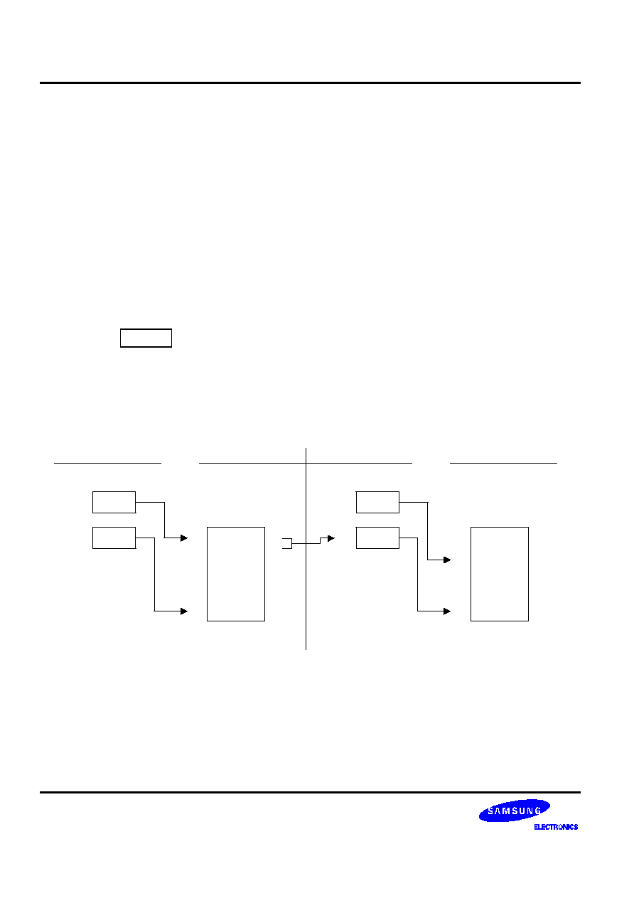
INSTRUCTION SET
S3C852B/P852B (Preliminary Spec)
6-60
NEXT
--
Next
NEXT
Operation:
PC
@ IP
IP
IP + 2
The NEXT instruction is useful when implementing threaded-code languages. The program
memory word that is pointed to by the instruction pointer is loaded into the program counter. The
instruction pointer is then incremented by two.
Flags:
No flags are affected.
Format:
Bytes
Cycles
Opcode
(Hex)
opc
1
10
0F
Example:
The following diagram shows one example of how to use the NEXT instruction.
Data
01
30
Before
After
0045
1P
Address
Data
0130
PC
43
44
45
Address H
Address L
Address H
Address
Data
Memory
130
Routine
0043
1P
Address
Data
0120
PC
43
44
45
Address H
Address L
Address H
Address
Data
Memory
120
Next

S3C852B/P852B (Preliminary Spec)
INSTRUCTION SET
6-61
NOP
--
No Operation
NOP
Operation:
No action is performed when the CPU executes this instruction. Typically, one or more NOPs are
executed in sequence in order to effect a timing delay of variable duration.
Flags:
No flags are affected.
Format:
Bytes
Cycles
Opcode
(Hex)
opc
1
4
FF
Example:
When the instruction
NOP
is encountered in a program, no operation occurs. Instead, there is a delay in instruction
execution time.

INSTRUCTION SET
S3C852B/P852B (Preliminary Spec)
6-62
OR
--
Logical OR
OR
dst, src
Operation:
dst
dst OR src
The source operand is logically ORed with the destination operand and the result is stored in the
destination. The contents of the source are unaffected. The OR operation results in a "1" being
stored whenever either of the corresponding bits in the two operands is a "1"; otherwise a "0" is
stored.
Flags:
C: Unaffected.
Z: Set if the result is "0"; cleared otherwise.
S: Set if the result bit 7 is set; cleared otherwise.
V: Always cleared to "0".
D: Unaffected.
H: Unaffected.
Format:
Bytes
Cycles
Opcode
(Hex)
Addr Mode
dst src
opc
dst | src
2
4
42
r
r
6
43
r
lr
opc
src
dst
3
6
44
R
R
6
45
R
IR
opc
dst
src
3
6
46
R
IM
Examples:
Given: R0 = 15H, R1 = 2AH, R2 = 01H, register 00H = 08H, register 01H = 37H, and
register 08H = 8AH:
OR
R0, R1
R0 = 3FH, R1 = 2AH
OR
R0, @R2
R0 = 37H, R2 = 01H, register 01H = 37H
OR
00H, 01H
Register 00H = 3FH, register 01H = 37H
OR
01H, @00H
Register 00H = 08H, register 01H = 0BFH
OR
00H, #02H
Register 00H = 0AH
In the first example, if working register R0 contains the value 15H and register R1 the value
2AH, the statement "OR R0, R1" logical-ORs the R0 and R1 register contents and stores the
result (3FH) in destination register R0.
The other examples show the use of the logical OR instruction with the various addressing
modes and formats.

S3C852B/P852B (Preliminary Spec)
INSTRUCTION SET
6-63
POP
--
Pop From Stack
POP
dst
Operation:
dst
@SP
SP
SP + 1
The contents of the location addressed by the stack pointer are loaded into the destination. The
stack pointer is then incremented by one.
Flags:
No flags affected.
Format:
Bytes
Cycles
Opcode
(Hex)
Addr Mode
dst
opc
dst
2
8
50
R
8
51
IR
Examples:
Given: Register 00H = 01H, register 01H = 1BH, SPH (0D8H) = 00H, SPL (0D9H) = 0FBH,
and stack register 0FBH = 55H:
POP
00H
Register 00H = 55H, SP = 00FCH
POP
@00H
Register 00H = 01H, register 01H = 55H, SP = 00FCH
In the first example, general register 00H contains the value 01H. The statement "POP 00H"
loads the contents of location 00FBH (55H) into destination register 00H and then increments the
stack pointer by one. Register 00H then contains the value 55H and the SP points to location
00FCH.

INSTRUCTION SET
S3C852B/P852B (Preliminary Spec)
6-64
POPUD
--
Pop User Stack (Decrementing)
POPUD
dst, src
Operation:
dst
src
IR
IR � 1
This instruction is used for user-defined stacks in the register file. The contents of the register file
location addressed by the user stack pointer are loaded into the destination. The user stack
pointer is then decremented.
Flags:
No flags are affected.
Format:
Bytes
Cycles
Opcode
(Hex)
Addr Mode
dst src
opc
src
dst
3
8
92
R
IR
Example:
Given: Register 00H = 42H (user stack pointer register), register 42H = 6FH, and
register 02H = 70H:
POPUD
02H, @00H
Register 00H = 41H, register 02H = 6FH, register 42H = 6FH
If general register 00H contains the value 42H and register 42H the value 6FH, the statement
"POPUD 02H, @00H" loads the contents of register 42H into the destination register 02H. The
user stack pointer is then decremented by one, leaving the value 41H.

S3C852B/P852B (Preliminary Spec)
INSTRUCTION SET
6-65
POPUI
--
Pop User Stack (Incrementing)
POPUI
dst, src
Operation:
dst
src
IR
IR + 1
The POPUI instruction is used for user-defined stacks in the register file. The contents of the
register file location addressed by the user stack pointer are loaded into the destination. The user
stack pointer is then incremented.
Flags:
No flags are affected.
Format:
Bytes
Cycles
Opcode
(Hex)
Addr Mode
dst src
opc
src
dst
3
8
93
R
IR
Example:
Given: Register 00H = 01H and register 01H = 70H:
POPUI
02H, @00H
Register 00H = 02H, register 01H = 70H, register 02H = 70H
If general register 00H contains the value 01H and register 01H the value 70H, the statement
"POPUI 02H, @00H" loads the value 70H into the destination general register 02H. The user
stack pointer (register 00H) is then incremented by one, changing its value from 01H to 02H.

INSTRUCTION SET
S3C852B/P852B (Preliminary Spec)
6-66
PUSH
--
Push To Stack
PUSH
src
Operation:
SP
SP � 1
@SP
src
A PUSH instruction decrements the stack pointer value and loads the contents of the source
(src) into the location addressed by the decremented stack pointer. The operation then adds the
new value to the top of the stack.
Flags:
No flags are affected.
Format:
Bytes
Cycles
Opcode
(Hex)
Addr Mode
dst
opc
src
2
8 (internal clock)
70
R
8 (external clock)
8 (internal clock)
8 (external clock)
71
IR
Examples:
Given: Register 40H = 4FH, register 4FH = 0AAH, SPH = 00H, and SPL = 00H:
PUSH
40H
Register 40H = 4FH, stack register 0FFH = 4FH,
SPH = 0FFH, SPL = 0FFH
PUSH
@40H
Register 40H = 4FH, register 4FH = 0AAH, stack register
0FFH = 0AAH, SPH = 0FFH, SPL = 0FFH
In the first example, if the stack pointer contains the value 0000H, and general register 40H the
value 4FH, the statement "PUSH 40H" decrements the stack pointer from 0000 to 0FFFFH. It
then loads the contents of register 40H into location 0FFFFH and adds this new value to the top
of the stack.

S3C852B/P852B (Preliminary Spec)
INSTRUCTION SET
6-67
PUSHUD
--
Push User Stack (Decrementing)
PUSHUD
dst, src
Operation:
IR
IR � 1
dst
src
This instruction is used to address user-defined stacks in the register file. PUSHUD decrements
the user stack pointer and loads the contents of the source into the register addressed by the
decremented stack pointer.
Flags:
No flags are affected.
Format:
Bytes
Cycles
Opcode
(Hex)
Addr Mode
dst src
opc
dst
src
3
8
82
IR
R
Example:
Given: Register 00H = 03H, register 01H = 05H, and register 02H = 1AH:
PUSHUD @00H, 01H
Register 00H = 02H, register 01H = 05H, register 02H = 05H
If the user stack pointer (register 00H, for example) contains the value 03H, the statement
"PUSHUD @00H, 01H" decrements the user stack pointer by one, leaving the value 02H. The
01H register value, 05H, is then loaded into the register addressed by the decremented user
stack pointer.

INSTRUCTION SET
S3C852B/P852B (Preliminary Spec)
6-68
PUSHUI
--
Push User Stack (Incrementing)
PUSHUI
dst, src
Operation:
IR
IR + 1
dst
src
This instruction is used for user-defined stacks in the register file. PUSHUI increments the user
stack pointer and then loads the contents of the source into the register location addressed by
the incremented user stack pointer.
Flags:
No flags are affected.
Format:
Bytes
Cycles
Opcode
(Hex)
Addr Mode
dst src
opc
dst
src
3
8
83
IR
R
Example:
Given: Register 00H = 03H, register 01H = 05H, and register 04H = 2AH:
PUSHUI
@00H, 01H
Register 00H = 04H, register 01H = 05H, register 04H = 05H
If the user stack pointer (register 00H, for example) contains the value 03H, the statement
"PUSHUI @00H, 01H" increments the user stack pointer by one, leaving the value 04H. The 01H
register value, 05H, is then loaded into the location addressed by the incremented user stack
pointer.

S3C852B/P852B (Preliminary Spec)
INSTRUCTION SET
6-69
RCF
--
Reset Carry Flag
RCF
RCF
Operation:
C
0
The carry flag is cleared to logic zero, regardless of its previous value.
Flags:
C:
Cleared to "0".
No other flags are affected.
Format:
Bytes
Cycles
Opcode
(Hex)
opc
1
4
CF
Example:
Given: C = "1" or "0":
The instruction RCF clears the carry flag (C) to logic zero.

INSTRUCTION SET
S3C852B/P852B (Preliminary Spec)
6-70
RET
--
Return
RET
Operation:
PC
@SP
SP
SP + 2
The RET instruction is normally used to return to the previously executing procedure at the end
of a procedure entered by a CALL instruction. The contents of the location addressed by the
stack pointer are popped into the program counter. The next statement that is executed is the
one that is addressed by the new program counter value.
Flags:
No flags are affected.
Format:
Bytes
Cycles
Opcode (Hex)
opc
1
8 (internal stack)
AF
10 (internal stack)
Example:
Given: SP = 00FCH, (SP) = 101AH, and PC = 1234:
RET
PC = 101AH, SP = 00FEH
The statement "RET" pops the contents of stack pointer location 00FCH (10H) into the high byte
of the program counter. The stack pointer then pops the value in location 00FEH (1AH) into the
PC's low byte and the instruction at location 101AH is executed. The stack pointer now points to
memory location 00FEH.

S3C852B/P852B (Preliminary Spec)
INSTRUCTION SET
6-71
RL
--
Rotate Left
RL
dst
Operation:
C
dst (7)
dst (0)
dst (7)
dst (n + 1)
dst (n), n = 0�6
The contents of the destination operand are rotated left one bit position. The initial value of bit 7
is moved to the bit zero (LSB) position and also replaces the carry flag.
7
0
C
Flags:
C: Set if the bit rotated from the most significant bit position (bit 7) was "1".
Z: Set if the result is "0"; cleared otherwise.
S: Set if the result bit 7 is set; cleared otherwise.
V: Set if arithmetic overflow occurred; cleared otherwise.
D: Unaffected.
H: Unaffected.
Format:
Bytes
Cycles
Opcode
(Hex)
Addr Mode
dst
opc
dst
2
4
90
R
4
91
IR
Examples:
Given: Register 00H = 0AAH, register 01H = 02H and register 02H = 17H:
RL
00H
Register 00H = 55H, C = "1"
RL
@01H
Register 01H = 02H, register 02H = 2EH, C = "0"
In the first example, if general register 00H contains the value 0AAH (10101010B), the statement
"RL 00H" rotates the 0AAH value left one bit position, leaving the new value 55H (01010101B)
and setting the carry and overflow flags.
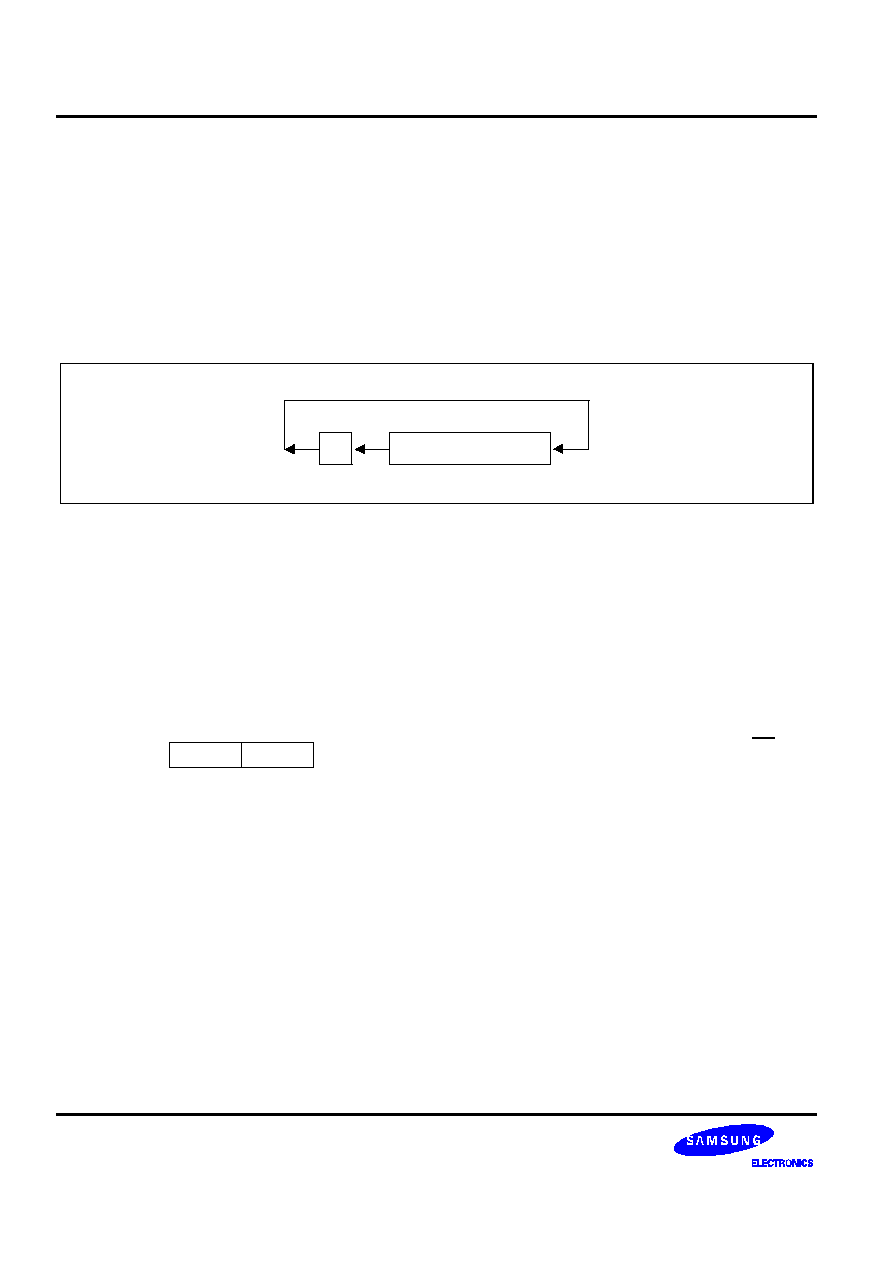
INSTRUCTION SET
S3C852B/P852B (Preliminary Spec)
6-72
RLC
--
Rotate Left Through Carry
RLC
dst
Operation:
dst (0)
C
C
dst (7)
dst (n + 1)
dst (n), n = 0�6
The contents of the destination operand with the carry flag are rotated left one bit position. The
initial value of bit 7 replaces the carry flag (C); the initial value of the carry flag replaces bit zero.
7
0
C
Flags:
C: Set if the bit rotated from the most significant bit position (bit 7) was "1".
Z: Set if the result is "0"; cleared otherwise.
S: Set if the result bit 7 is set; cleared otherwise.
V: Set if arithmetic overflow occurred, that is, if the sign of the destination changed during
rotation; cleared otherwise.
D: Unaffected.
H: Unaffected.
Format:
Bytes
Cycles
Opcode
(Hex)
Addr Mode
dst
opc
dst
2
4
10
R
4
11
IR
Examples:
Given: Register 00H = 0AAH, register 01H = 02H, and register 02H = 17H, C = "0":
RLC
00H
Register 00H = 54H, C = "1"
RLC
@01H
Register 01H = 02H, register 02H = 2EH, C = "0"
In the first example, if general register 00H has the value 0AAH (10101010B), the statement
"RLC 00H" rotates 0AAH one bit position to the left. The initial value of bit 7 sets the carry flag
and the initial value of the C flag replaces bit zero of register 00H, leaving the value 55H
(01010101B). The MSB of register 00H resets the carry flag to "1" and sets the overflow flag.
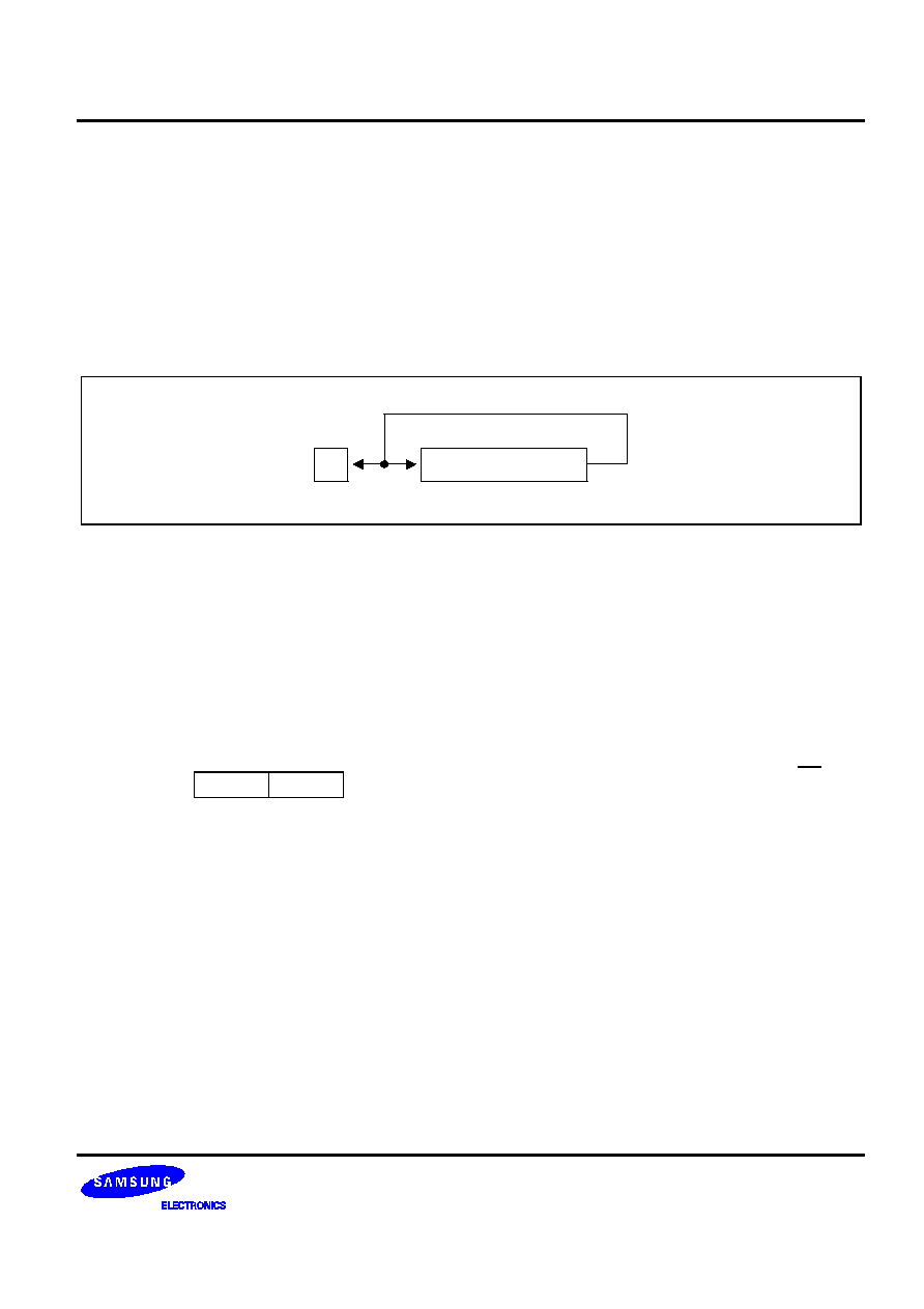
S3C852B/P852B (Preliminary Spec)
INSTRUCTION SET
6-73
RR
--
Rotate Right
RR
dst
Operation:
C
dst (0)
dst (7)
dst (0)
dst (n)
dst (n + 1), n = 0�6
The contents of the destination operand are rotated right one bit position. The initial value of bit
zero (LSB) is moved to bit 7 (MSB) and also replaces the carry flag (C).
7
0
C
Flags:
C: Set if the bit rotated from the least significant bit position (bit zero) was "1".
Z: Set if the result is "0"; cleared otherwise.
S: Set if the result bit 7 is set; cleared otherwise.
V: Set if arithmetic overflow occurred, that is, if the sign of the destination changed during
rotation; cleared otherwise.
D: Unaffected.
H: Unaffected.
Format:
Bytes
Cycles
Opcode
(Hex)
Addr Mode
dst
opc
dst
2
4
E0
R
4
E1
IR
Examples:
Given: Register 00H = 31H, register 01H = 02H, and register 02H = 17H:
RR
00H
Register 00H = 98H, C = "1"
RR
@01H
Register 01H = 02H, register 02H = 8BH, C = "1"
In the first example, if general register 00H contains the value 31H (00110001B), the statement
"RR 00H" rotates this value one bit position to the right. The initial value of bit zero is moved to
bit 7, leaving the new value 98H (10011000B) in the destination register. The initial bit zero also
resets the C flag to "1" and the sign flag and overflow flag are also set to "1".
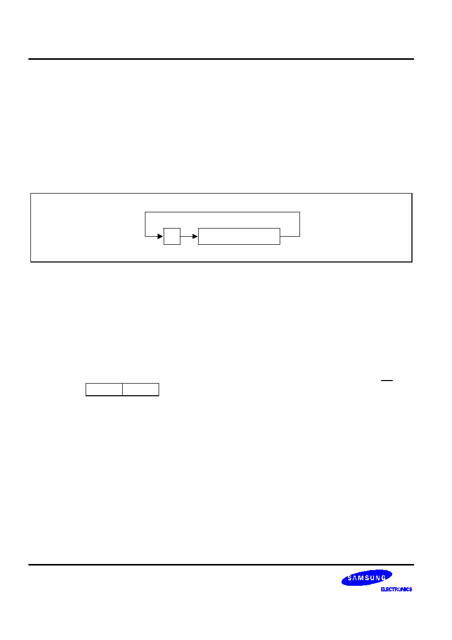
INSTRUCTION SET
S3C852B/P852B (Preliminary Spec)
6-74
RRC
--
Rotate Right Through Carry
RRC
dst
Operation:
dst (7)
C
C
dst (0)
dst (n)
dst (n + 1), n = 0�6
The contents of the destination operand and the carry flag are rotated right one bit position. The
initial value of bit zero (LSB) replaces the carry flag; the initial value of the carry flag replaces bit
7 (MSB).
7
0
C
Flags:
C: Set if the bit rotated from the least significant bit position (bit zero) was "1".
Z: Set if the result is "0" cleared otherwise.
S: Set if the result bit 7 is set; cleared otherwise.
V: Set if arithmetic overflow occurred, that is, if the sign of the destination changed during
rotation; cleared otherwise.
D: Unaffected.
H: Unaffected.
Format:
Bytes
Cycles
Opcode
(Hex)
Addr Mode
dst
opc
dst
2
4
C0
R
4
C1
IR
Examples:
Given: Register 00H = 55H, register 01H = 02H, register 02H = 17H, and C = "0":
RRC
00H
Register 00H = 2AH, C = "1"
RRC
@01H
Register 01H = 02H, register 02H = 0BH, C = "1"
In the first example, if general register 00H contains the value 55H (01010101B), the statement
"RRC 00H" rotates this value one bit position to the right. The initial value of bit zero ("1")
replaces the carry flag and the initial value of the C flag ("1") replaces bit 7. This leaves the new
value 2AH (00101010B) in destination register 00H. The sign flag and overflow flag are both
cleared to "0".

S3C852B/P852B (Preliminary Spec)
INSTRUCTION SET
6-75
SB0
--
Select Bank 0
SB0
Operation:
BANK
0
The SB0 instruction clears the bank address flag in the FLAGS register (FLAGS.0) to logic zero,
selecting bank 0 register addressing in the set 1 area of the register file.
Flags:
No flags are affected.
Format:
Bytes
Cycles
Opcode
(Hex)
opc
1
4
4F
Example:
The statement
SB0
clears FLAGS.0 to "0", selecting bank 0 register addressing.

INSTRUCTION SET
S3C852B/P852B (Preliminary Spec)
6-76
SB1
--
Select Bank 1
SB1
Operation:
BANK
1
The SB1 instruction sets the bank address flag in the FLAGS register (FLAGS.0) to logic one,
selecting bank 1 register addressing in the set 1 area of the register file. (Bank 1 is not
implemented in some KS88-series microcontrollers.)
Flags:
No flags are affected.
Format:
Bytes
Cycles
Opcode
(Hex)
opc
1
4
5F
Example:
The statement
SB1
sets FLAGS.0 to "1", selecting bank 1 register addressing, if implemented.
S3C852B/P852B (Preliminary Spec)
INSTRUCTION SET
6-77
SBC
--
Subtract With Carry
SBC
dst, src
Operation:
dst
dst � src � c
The source operand, along with the current value of the carry flag, is subtracted from the
destination operand and the result is stored in the destination. The contents of the source are
unaffected. Subtraction is performed by adding the two's-complement of the source operand to
the destination operand. In multiple precision arithmetic, this instruction permits the carry
("borrow") from the subtraction of the low-order operands to be subtracted from the subtraction of
high-order operands.
Flags:
C: Set if a borrow occurred (src
>
dst); cleared otherwise.
Z: Set if the result is "0"; cleared otherwise.
S: Set if the result is negative; cleared otherwise.
V: Set if arithmetic overflow occurred, that is, if the operands were of opposite sign and the sign
of the result is the same as the sign of the source; cleared otherwise.
D: Always set to "1".
H: Cleared if there is a carry from the most significant bit of the low-order four bits of the result;
set otherwise, indicating a "borrow".
Format:
Bytes
Cycles
Opcode
(Hex)
Addr Mode
dst src
opc
dst | src
2
4
32
r
r
6
33
r
lr
opc
src
dst
3
6
34
R
R
6
35
R
IR
opc
dst
src
3
6
36
R
IM
Examples:
Given: R1 = 10H, R2 = 03H, C = "1", register 01H = 20H, register 02H = 03H, and
register 03H = 0AH:
SBC
R1, R2
R1 = 0CH, R2 = 03H
SBC
R1, @R2
R1 = 05H, R2 = 03H, register 03H = 0AH
SBC
01H, 02H
Register 01H = 1CH, register 02H = 03H
SBC
01H, @02H
Register 01H = 15H, register 02H = 03H, register 03H = 0AH
SBC
01H, #8AH
Register 01H = 95H; C, S, and V = "1"
In the first example, if working register R1 contains the value 10H and register R2 the value 03H,
the statement "SBC R1, R2" subtracts the source value (03H) and the C flag value ("1") from
the destination (10H) and then stores the result (0CH) in register R1.

INSTRUCTION SET
S3C852B/P852B (Preliminary Spec)
6-78
SCF
--
Set Carry Flag
SCF
Operation:
C
1
The carry flag (C) is set to logic one, regardless of its previous value.
Flags:
C: Set to "1".
No other flags are affected.
Format:
Bytes
Cycles
Opcode
(Hex)
opc
1
4
DF
Example:
The statement
SCF
sets the carry flag to logic one.
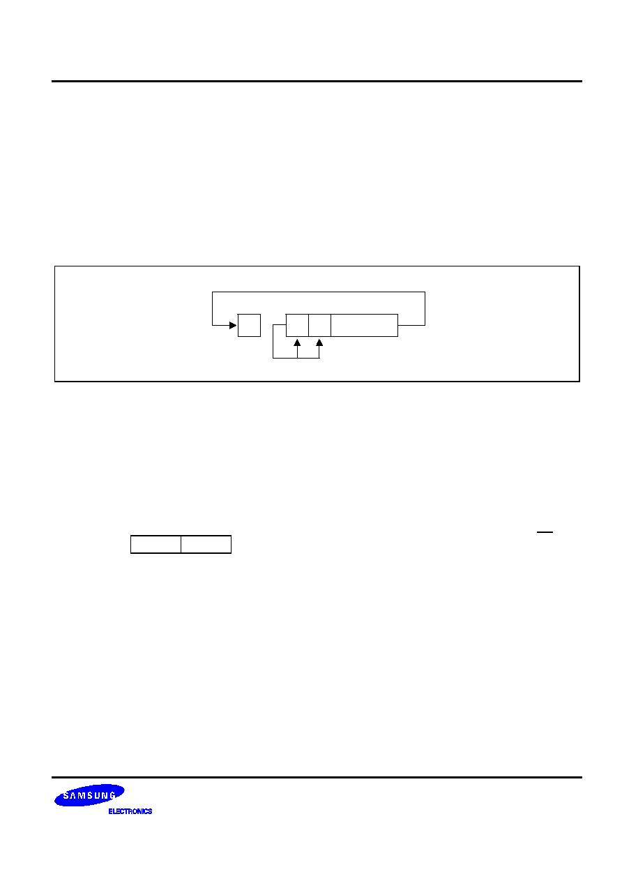
S3C852B/P852B (Preliminary Spec)
INSTRUCTION SET
6-79
SRA
--
Shift Right Arithmetic
SRA
dst
Operation:
dst (7)
dst (7)
C
dst (0)
dst (n)
dst (n + 1), n = 0�6
An arithmetic shift-right of one bit position is performed on the destination operand. Bit zero (the
LSB) replaces the carry flag. The value of bit 7 (the sign bit) is unchanged and is shifted into bit
position 6.
7
0
C
6
Flags:
C: Set if the bit shifted from the LSB position (bit zero) was "1".
Z: Set if the result is "0"; cleared otherwise.
S: Set if the result is negative; cleared otherwise.
V: Always cleared to "0".
D: Unaffected.
H: Unaffected.
Format:
Bytes
Cycles
Opcode
(Hex)
Addr Mode
dst
opc
dst
2
4
D0
R
4
D1
IR
Examples:
Given: Register 00H = 9AH, register 02H = 03H, register 03H = 0BCH, and C = "1":
SRA
00H
Register 00H = 0CD, C = "0"
SRA
@02H
Register 02H = 03H, register 03H = 0DEH, C = "0"
In the first example, if general register 00H contains the value 9AH (10011010B), the statement
"SRA 00H" shifts the bit values in register 00H right one bit position. Bit zero ("0") clears the C
flag and bit 7 ("1") is then shifted into the bit 6 position (bit 7 remains unchanged). This leaves
the value 0CDH (11001101B) in destination register 00H.

INSTRUCTION SET
S3C852B/P852B (Preliminary Spec)
6-80
SRP/SRP0/SRP1
--
Set Register Pointer
SRP
src
SRP0
src
SRP1
src
Operation:
If src (1) = 1 and src (0) = 0 then: RP0 (3�7)
src (3�7)
If src (1) = 0 and src (0) = 1 then: RP1 (3�7)
src (3�7)
If src (1) = 0 and src (0) = 0 then: RP0 (4�7)
src (4�7),
RP0 (3)
0
RP1 (4�7)
src (4�7),
RP1 (3)
1
The source data bits one and zero (LSB) determine whether to write one or both of the register
pointers, RP0 and RP1. Bits 3�7 of the selected register pointer are written unless both register
pointers are selected. RP0.3 is then cleared to logic zero and RP1.3 is set to logic one.
Flags:
No flags are affected.
Format:
Bytes
Cycles
Opcode
(Hex)
Addr Mode
src
opc
src
2
4
31
IM
Examples:
The statement
SRP #40H
sets register pointer 0 (RP0) at location 0D6H to 40H and register pointer 1 (RP1) at location
0D7H to 48H.
The statement "SRP0 #50H" sets RP0 to 50H, and the statement "SRP1 #68H" sets RP1 to
68H.

S3C852B/P852B (Preliminary Spec)
INSTRUCTION SET
6-81
STOP
--
Stop Operation
STOP
Operation:
The STOP instruction stops the both the CPU clock and system clock and causes the
microcontroller to enter Stop mode. During Stop mode, the contents of on-chip CPU registers,
peripheral registers, and I/O port control and data registers are retained. Stop mode can be
released by an external reset operation or by external interrupts. For the reset operation, the
RESET
pin must be held to Low level until the required oscillation stabilization interval has
elapsed.
Flags:
No flags are affected.
Format:
Bytes
Cycles
Opcode
(Hex)
Addr Mode
dst src
opc
1
4
7F
�
�
Example:
The statement
STOP
halts all microcontroller operations.

INSTRUCTION SET
S3C852B/P852B (Preliminary Spec)
6-82
SUB
--
Subtract
SUB
dst, src
Operation:
dst
dst � src
The source operand is subtracted from the destination operand and the result is stored in the
destination. The contents of the source are unaffected. Subtraction is performed by adding the
two's complement of the source operand to the destination operand.
Flags:
C: Set if a "borrow" occurred; cleared otherwise.
Z: Set if the result is "0"; cleared otherwise.
S: Set if the result is negative; cleared otherwise.
V: Set if arithmetic overflow occurred, that is, if the operands were of opposite signs and the
sign of the result is of the same as the sign of the source operand; cleared otherwise.
D: Always set to "1".
H: Cleared if there is a carry from the most significant bit of the low-order four bits of the result;
set otherwise indicating a "borrow".
Format:
Bytes
Cycles
Opcode
(Hex)
Addr Mode
dst src
opc
dst | src
2
4
22
r
r
6
23
r
lr
opc
src
dst
3
6
24
R
R
6
25
R
IR
opc
dst
src
3
6
26
R
IM
Examples:
Given: R1 = 12H, R2 = 03H, register 01H = 21H, register 02H = 03H, register 03H = 0AH:
SUB
R1, R2
R1 = 0FH, R2 = 03H
SUB
R1, @R2
R1 = 08H, R2 = 03H
SUB
01H, 02H
Register 01H = 1EH, register 02H = 03H
SUB
01H, @02H
Register 01H = 17H, register 02H = 03H
SUB
01H, #90H
Register 01H = 91H; C, S, and V = "1"
SUB
01H, #65H
Register 01H = 0BCH; C and S = "1", V = "0"
In the first example, if working register R1 contains the value 12H and if register R2 contains the
value 03H, the statement "SUB R1, R2" subtracts the source value (03H) from the destination
value (12H) and stores the result (0FH) in destination register R1.
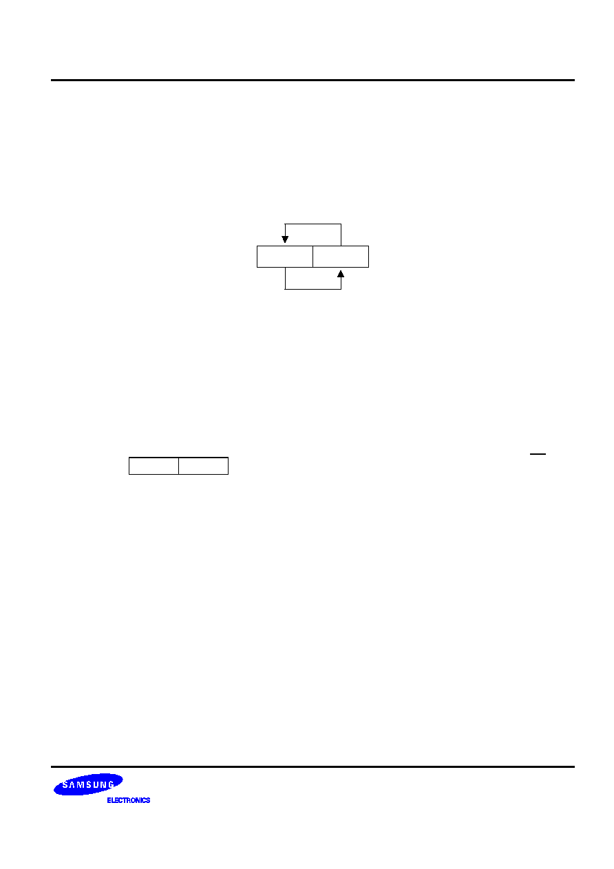
S3C852B/P852B (Preliminary Spec)
INSTRUCTION SET
6-83
SWAP
--
Swap Nibbles
SWAP
dst
Operation:
dst (0 � 3)
dst (4 � 7)
The contents of the lower four bits and upper four bits of the destination operand are swapped.
7
0
4 3
Flags:
C: Undefined.
Z: Set if the result is "0"; cleared otherwise.
S: Set if the result bit 7 is set; cleared otherwise.
V: Undefined.
D: Unaffected.
H: Unaffected.
Format:
Bytes
Cycles
Opcode
(Hex)
Addr Mode
dst
opc
dst
2
4
F0
R
4
F1
IR
Examples:
Given: Register 00H = 3EH, register 02H = 03H, and register 03H = 0A4H:
SWAP
00H
Register 00H = 0E3H
SWAP
@02H
Register 02H = 03H, register 03H = 4AH
In the first example, if general register 00H contains the value 3EH (00111110B), the statement
"SWAP 00H" swaps the lower and upper four bits (nibbles) in the 00H register, leaving the value
0E3H (11100011B).

INSTRUCTION SET
S3C852B/P852B (Preliminary Spec)
6-84
TCM
--
Test Complement Under Mask
TCM
dst, src
Operation:
(NOT dst) AND src
This instruction tests selected bits in the destination operand for a logic one value. The bits to be
tested are specified by setting a "1" bit in the corresponding position of the source operand
(mask). The TCM statement complements the destination operand, which is then ANDed with the
source mask. The zero (Z) flag can then be checked to determine the result. The destination and
source operands are unaffected.
Flags:
C: Unaffected.
Z: Set if the result is "0"; cleared otherwise.
S: Set if the result bit 7 is set; cleared otherwise.
V: Always cleared to "0".
D: Unaffected.
H: Unaffected.
Format:
Bytes
Cycles
Opcode
(Hex)
Addr Mode
dst src
opc
dst | src
2
4
62
r
r
6
63
r
lr
opc
src
dst
3
6
64
R
R
6
65
R
IR
opc
dst
src
3
6
66
R
IM
Examples:
Given: R0 = 0C7H, R1 = 02H, R2 = 12H, register 00H = 2BH, register 01H = 02H, and
register 02H = 23H:
TCM
R0, R1
R0 = 0C7H, R1 = 02H, Z = "1"
TCM
R0, @R1
R0 = 0C7H, R1 = 02H, register 02H = 23H, Z = "0"
TCM
00H, 01H
Register 00H = 2BH, register 01H = 02H, Z = "1"
TCM
00H, @01H
Register 00H = 2BH, register 01H = 02H,
register 02H = 23H, Z = "1"
TCM
00H, #34
Register 00H = 2BH, Z = "0"
In the first example, if working register R0 contains the value 0C7H (11000111B) and register R1
the value 02H (00000010B), the statement "TCM R0, R1" tests bit one in the destination register
for a "1" value. Because the mask value corresponds to the test bit, the Z flag is set to logic one
and can be tested to determine the result of the TCM operation.
S3C852B/P852B (Preliminary Spec)
INSTRUCTION SET
6-85
TM
--
Test Under Mask
TM
dst, src
Operation:
dst AND src
This instruction tests selected bits in the destination operand for a logic zero value. The bits to be
tested are specified by setting a "1" bit in the corresponding position of the source operand
(mask), which is ANDed with the destination operand. The zero (Z) flag can then be checked to
determine the result. The destination and source operands are unaffected.
Flags:
C: Unaffected.
Z: Set if the result is "0"; cleared otherwise.
S: Set if the result bit 7 is set; cleared otherwise.
V: Always reset to "0".
D: Unaffected.
H: Unaffected.
Format:
Bytes
Cycles
Opcode
(Hex)
Addr Mode
dst src
opc
dst | src
2
4
72
r
r
6
73
r
lr
opc
src
dst
3
6
74
R
R
6
75
R
IR
opc
dst
src
3
6
76
R
IM
Examples:
Given: R0 = 0C7H, R1 = 02H, R2 = 18H, register 00H = 2BH, register 01H = 02H, and
register 02H = 23H:
TM
R0, R1
R0 = 0C7H, R1 = 02H, Z = "0"
TM
R0, @R1
R0 = 0C7H, R1 = 02H, register 02H = 23H, Z = "0"
TM
00H, 01H
Register 00H = 2BH, register 01H = 02H, Z = "0"
TM
00H, @01H
Register 00H = 2BH, register 01H = 02H,
register 02H = 23H, Z = "0"
TM
00H, #54H
Register 00H = 2BH, Z = "1"
In the first example, if working register R0 contains the value 0C7H (11000111B) and register R1
the value 02H (00000010B), the statement "TM R0, R1" tests bit one in the destination register
for a "0" value. Because the mask value does not match the test bit, the Z flag is cleared to logic
zero and can be tested to determine the result of the TM operation.
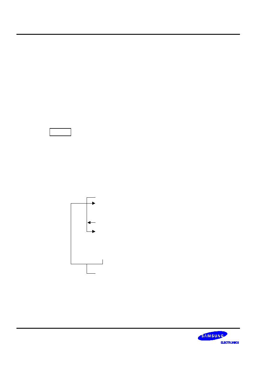
INSTRUCTION SET
S3C852B/P852B (Preliminary Spec)
6-86
WFI
--
Wait For Interrupt
WFI
Operation:
The CPU is effectively halted until an interrupt occurs, except that DMA transfers can still take
place during this wait state. The WFI status can be released by an internal interrupt, including a
fast interrupt .
Flags:
No flags are affected.
Format:
Bytes
Cycles
Opcode
(Hex)
opc
1
4n
3F
(
n = 1, 2, 3, ... )
Example:
The following sample program structure shows the sequence of operations that follow a "WFI"
statement:
Main program
EI
WFI
(Next instruction)
Interrupt occurs
Interrupt service routine
Clear interrupt flag
IRET
Service routine completed
(Enable global interrupt)
(Wait for interrupt)
.
.
.
.
.
.
.
.
.

S3C852B/P852B (Preliminary Spec)
INSTRUCTION SET
6-87
XOR
--
Logical Exclusive OR
XOR
dst, src
Operation:
dst
dst XOR src
The source operand is logically exclusive-ORed with the destination operand and the result is
stored in the destination. The exclusive-OR operation results in a "1" bit being stored whenever
the corresponding bits in the operands are different; otherwise, a "0" bit is stored.
Flags:
C: Unaffected.
Z: Set if the result is "0"; cleared otherwise.
S: Set if the result bit 7 is set; cleared otherwise.
V: Always reset to "0".
D: Unaffected.
H: Unaffected.
Format:
Bytes
Cycles
Opcode
(Hex)
Addr Mode
dst src
opc
dst | src
2
4
B2
r
r
6
B3
r
lr
opc
src
dst
3
6
B4
R
R
6
B5
R
IR
opc
dst
src
3
6
B6
R
IM
Examples:
Given: R0 = 0C7H, R1 = 02H, R2 = 18H, register 00H = 2BH, register 01H = 02H, and
register 02H = 23H:
XOR
R0, R1
R0 = 0C5H, R1 = 02H
XOR
R0, @R1
R0 = 0E4H, R1 = 02H, register 02H = 23H
XOR
00H, 01H
Register 00H = 29H, register 01H = 02H
XOR
00H, @01H
Register 00H = 08H, register 01H = 02H, register 02H = 23H
XOR
00H, #54H
Register 00H = 7FH
In the first example, if working register R0 contains the value 0C7H and if register R1 contains
the value 02H, the statement "XOR R0, R1" logically exclusive-ORs the R1 value with the R0
value and stores the result (0C5H) in the destination register R0.

INSTRUCTION SET
S3C852B/P852B (Preliminary Spec)
6-88
NOTES

S3C852B/P852B (Preliminary Spec)
CLOCK CIRCUITS
7-1
7
CLOCK CIRCUITS
OVERVIEW
The S3C852B microcontroller has two oscillator circuits: a main system clock, and a subsystem clock circuit. The
CPU and peripheral hardware operate on the system clock frequency supplied through these circuits. The
maximum CPU clock frequency, is determined by CLKCON register settings.
SYSTEM CLOCK CIRCUIT
The system clock circuit has the following components:
-- External crystal source (main clock only), or an external clock
-- Programmable frequency divider for the CPU clock (fx divided by 1, 2, 8, or 16 or fxt)
-- Clock circuit control register, CLKCON
-- Oscillator control register, OSCCON
-- Main clock control flag, MCLKSEL
-- Phase locked loop for generating fx (3.579545 MHz) from fxt (32.768 kHz) and generating fx*2 (7.159090
MHz)
CPU Clock Notation
In this document, the following notation is used for descriptions of the CPU clock:
fx
main clock
fxt sub clock
fxx selected system clock
CLOCK CIRCUITS
S3C852B/P852B (Preliminary Spec)
7-2
MAIN OSCILLATOR CIRCUITS
X
IN
X
OUT
Figure 7-1. Crystal Oscillator
SUB OSCILLATOR CIRCUITS
XT
IN
XT
OUT
32.768 kHz
Figure 7-2. Crystal Oscillator
CLOCK STATUS DURING POWER-DOWN MODES
Stop mode affect the system clock as follows:
-- In Stop mode, the main oscillator is halted. Stop mode is released, and the oscillator started, by a reset
operation, by an external interrupt, or by a watch timer interrupt if sub clock is selected as watch timer clock
source (When the fx is selected as system clock).
S3C852B/P852B (Preliminary Spec)
CLOCK CIRCUITS
7-3
1/1-1/4096
Frequency
Dividing
Circuit
Main-System
Oscillator
Selector 1
f
X
fxt
Sub-System
Oscillator
CLKCON.7
OSCCON.0
OSCCON.3
OSCCON.2
1/1
1/16
1/2
1/8
Selector 2
STOP OSC
CLKCON.4-.3
Watch Timer (fxt)
ADC
SIO
Basic Timer
Watch Timer (fxx/128)
Timer/Counters
INT
INT
CPU Clock
Figure 7-3. System Clock Circuit Diagram
CLOCK CIRCUITS
S3C852B/P852B (Preliminary Spec)
7-4
SYSTEM CLOCK CONTROL REGISTER (CLKCON)
The system clock control register, CLKCON, is located in set 1, address D4H. It is read/write addressable and
has the following functions:
-- Oscillator IRQ wake-up function enable/disable
-- Oscillator frequency divide-by value
CLKCON register settings control whether or not an external interrupt can be used to trigger a Stop mode release
(This is called the "IRQ wake-up" function). The IRQ "wake-up" enable bit is CLKCON.7.
After a reset, the external interrupt oscillator wake-up function is enabled, the main oscillator is activated, and the
fx/16 (the slowest clock speed) is selected as the CPU clock. If necessary, you can then increase the CPU clock
speed to fx, fx/2, or fx/8 by setting the CLKCON, and you can change system clock from main clock to sub clock
by setting the OSCCON.
For the S3C852B microcontroller, the CLKCON.2�CLKCON.0 system clock signature code can be any value
(The "101B" setting selects sub clock as system clock). The reset value for the clock signature code is "000B".
System Clock Control Register (CLKCON)
Set 1, D4H, R/W
.7
.6
.5
.4
.3
.2
.1
.0
MSB
LSB
Not use for S3C852B (must keep always "0")
Divide-by selection bits for
CPU clock frequency:
00 = f
X
/16 or fxt
01 = f
X
/8 or fxt
10 = f
X
/2 or fxt
11 = fX or fxt (non-divided)
Oscillator IRQ wake-up enable bit:
0 = Enable IRQ for main system
oscillator wake-up function in
power down mode
1 = Disable IRQ for main system
oscillator wake-up function in
power down mode
Not use for S3C852B (must keep always "0")
Figure 7-4. System Clock Control Register (CLKCON)
S3C852B/P852B (Preliminary Spec)
CLOCK CIRCUITS
7-5
OSCILLATOR CONTROL REGISTER (OSCCON)
The oscillator control register, OSCCON, is located in set 1, address FAH. It is read/write addressable and has
the following functions:
-- System clock selection
-- Main system oscillator control
-- Subsystem oscillator control
OSCCON.0 register settings select Main system clock or Subsystem clock as system clock.
After a reset, Main system clock is selected for system clockn because The reset value of OSCCON.0 is "0".
You can stop or run main system oscillator by setting OSCCON.3.
You can stop or run Subsystem oscillator by setting OSCCON.2.
Oscillator Control Register (OSCCON)
Set 1, Bank 0, FAH, R/W
.7
.6
.5
.4
.3
.2
.1
.0
MSB
LSB
Not use for S3C852B.
Main system oscillator control bit:
0 = Main system oscillator RUN
1 = Main system oscillator STOP
Subsystem oscillator control bit:
0 = Subsystem oscillator RUN
1 = Subsystem oscillator STOP
Not used for S3C852B.
System clock selection bit:
0 = Main system select
1 = Subsystem oscillator select
Figure 7-5. Oscillator Control Register (OSCCON)

CLOCK CIRCUITS
S3C852B/P852B (Preliminary Spec)
7-6
SWITCHING THE CPU CLOCK
Data loadings in the oscillator control register, OSCCON, determine whether a main or a sub clock is selected as
the CPU clock, and also how this frequency is to be divided by setting CLKCON. This makes it possible to switch
dynamically between main and sub clocks and to modify operating frequencies.
OSCCON.0 select the main clock (fx) or the sub clock (fxt) for the CPU clock. OSCCON .3 start or stop main
clock oscillation, and OSCCON.2 start or stop subsystem clock oscillation. CLKCON.4�.3 control the frequency
divider circuit, and divide the selected fx clock by 1, 2, 8, 16, or fxt clock by 1.
For example, you are using the default CPU clock (normal operating mode and a main clock of fx/16 and you
want to switch from the fx clock to a sub clock and to stop the main clock. To do this, you need to set OSCCON.0
to "1" and OSCCON.3 to "1" simultaneously. This switches the clock from fx to fxt and stops main clock
oscillation.
The following steps must be taken to switch from a sub clock to the main clock: first, set OSCCON.3 to "0" to
enable main system clock oscillation. Then, after a certain number of machine cycles has elapsed, select the
main clock by setting OSCCON.0 to "0".
Main clock (fx) can be double input crystal when the MCLKSEL is setting to "1".
F
F
PROGRAMMING TIP -- Switching the CPU clock
1.
This example shows how to change from the main clock to the sub clock:
MA2SUB
LD
OSCCON,#01H
; Switches to the sub clock
; Stop the main clock oscillation
RET
2. This example shows how to change from sub clock to main clock:
SUB2MA
AND
OSCCON,#07H
; Start the main clock oscillation
CALL
DLY16
; Delay 16 ms
AND
OSCCON,#06H
; Switch to the main clock
RET
DLY16
SRP
#0C0H
LD
R0,#20H
DEL
NOP
DJNZ
R0,DEL
RET
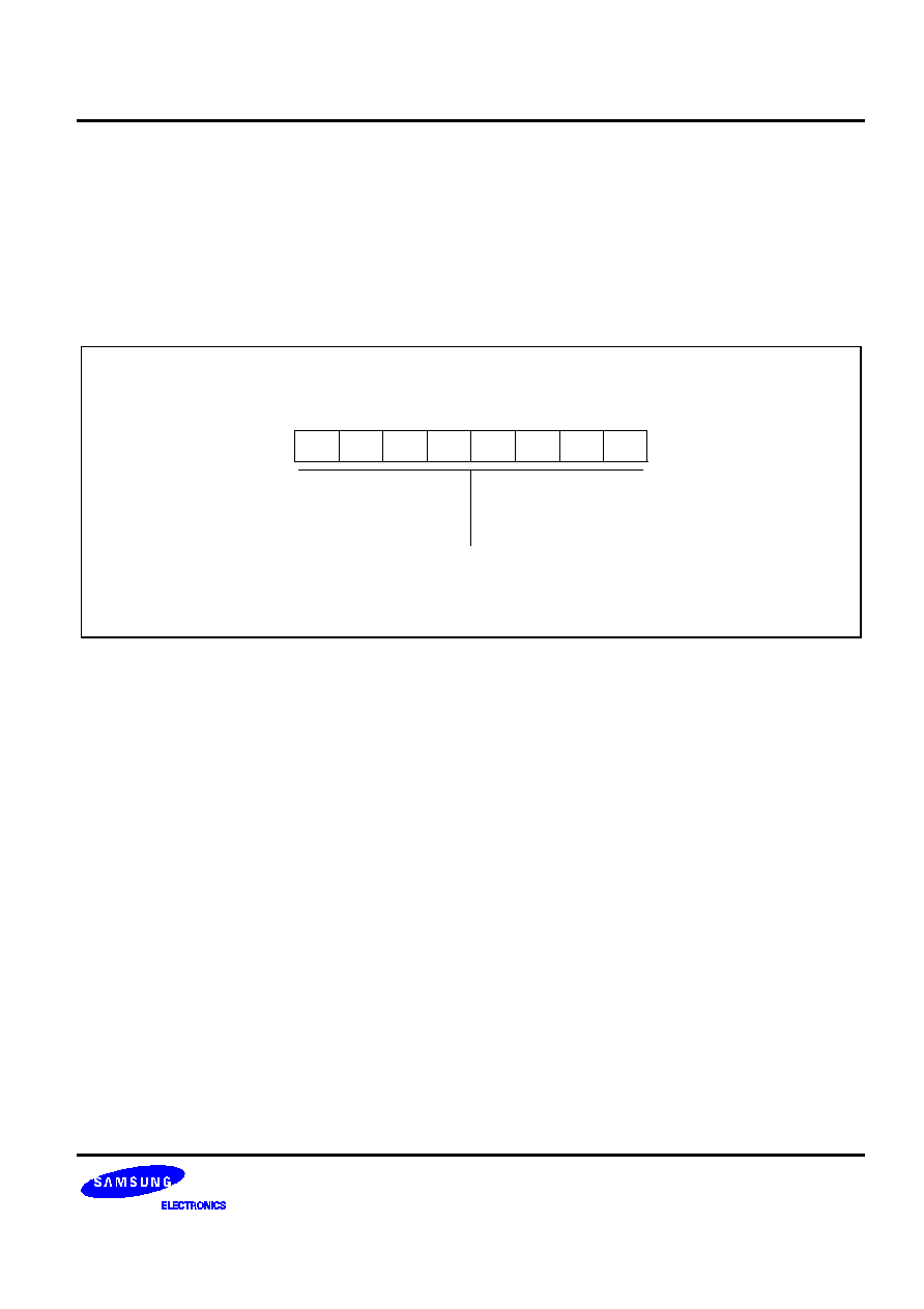
S3C852B/P852B (Preliminary Spec)
CLOCK CIRCUITS
7-7
STOP CONTROL REGISTER (STPCON)
The STOP control register, STPCON, is located in set 1, address FBH. It is read/write addressable and has the
following functions:
-- Enable/Disable STOP instruction
After a reset, the STOP instruction is disabled, because the value of STPCON is "00000000B".
If necessary, you can use the STOP instruction by setting the value of STPCON to "10100101B".
Stop Control Register (STPCON)
Set 1, Bank 0, FBH, R/W
.7
.6
.5
.4
.3
.2
.1
.0
MSB
LSB
STOP control bits:
00000000 = Disable STOP instruction
10100101 = Enable STOP instruction
Figure 7-6. STOP Control Register (STPCON)

CLOCK CIRCUITS
S3C852B/P852B (Preliminary Spec)
7-8
PHASE LOCKED LOOP (PLL)
MAIN CLOCK GENERATION
The PLL is able to generate main clock (fx = 3.579545MHz) from sub clock (fxt). In this case crystal oscillator for XIN and
XOUT is removed. To enable the function generating main clock, connect CKSEL (pin 71) to VDD and PLLC (pin72) to
GND through a capacitor (0.1uF).
In STOP mode, the PLL function also stopped as main clock oscillator
DOUBLING MAIN CLOCK FREQUENCY
PLL is able to double the main clock frequency (fx) to (fx*2 = 7.159090MHz) for CPU clock. To enable the
function, set the MSCLK bit (CONT2.7) of CONT2 (95H, page 8, refer to P14-19 & P14-27). In this case the
frequency for CPU clock will be doubled, but the frequency of the clock for CID block wouldn't be changed and
remains at 3.579545MHz.
Operating voltage of the PLL is from 4.5V to 5.5V.

S3C852B/P852B (Preliminary Spec)
RESET
RESET
and POWER-DOWN
8-1
8
RESET
RESET
and POWER-DOWN
SYSTEM RESET
OVERVIEW
During a power-on reset, the voltage at V
DD
goes to High level and the
RESET
pin is forced to Low level. The
RESET
signal is input through a schmitt trigger circuit where it is then synchronized with the CPU clock. This
procedure brings S3C852B/P852B into a known operating status.
To allow time for internal CPU clock oscillation to stabilize, the
RESET
pin must be held to Low level for a
minimum time interval after the power supply comes within tolerance. The minimum required oscillation
stabilization time for a reset operation is 1 millisecond.
Whenever a reset occurs during normal operation (that is, when both V
DD
and
RESET
are High level), the
RESET
pin is forced Low and the reset operation starts. All system and peripheral control registers are then reset
to their default hardware values (see Tables 8-1, 8-2, and 8-3).
In summary, the following sequence of events occurs during a reset operation:
-- All interrupts are disabled.
-- The watchdog function (basic timer) is enabled.
-- Ports 0, 1, 2, 3, 4, 5, 6, 7, 8, 9 and 10 are set to schmitt trigger input mode and all pull-up resistors are
disabled for the I/O port pin circuits.
-- Peripheral control and data registers are disabled and reset to their default hardware values.
-- The program counter (PC) is loaded with the program reset address in the ROM, 0100H.
-- When the programmed oscillation stabilization time interval has elapsed, the instruction stored in ROM
location 0100H (and 0101H) is fetched and executed.
-- EXTBUS register is set to 00H, it can affect external interface output while EA pin is low.

RESET
RESET
and POWER-DOWN
S3C852B/P852B (Preliminary Spec)
8-2
NORMAL MODE RESET OPERATION
In normal (masked ROM) mode, the EA pin is tied to V
SS
. A reset enables access to the 64-Kbyte on-chip ROM.
(The external interface is not automatically configured).
ROM-LESS MODE RESET OPERATION
To configure S3C852B/P852B as a ROM-less device, you must apply a constant 5 V current to the EA pin.
Assuming the EA pin is held to high level (5 V) when a reset occurs, ROM-less mode is entered and the external
interface is configured automatically.
NOTE
To program the duration of the oscillation stabilization interval, you make the appropriate settings to the
basic timer control register, BTCON, before entering Stop mode. Also, if you do not want to use the basic
timer watchdog function (which causes a system reset if a basic timer counter overflow occurs), you can
disable it by writing '1010B' to the upper nibble of BTCON.
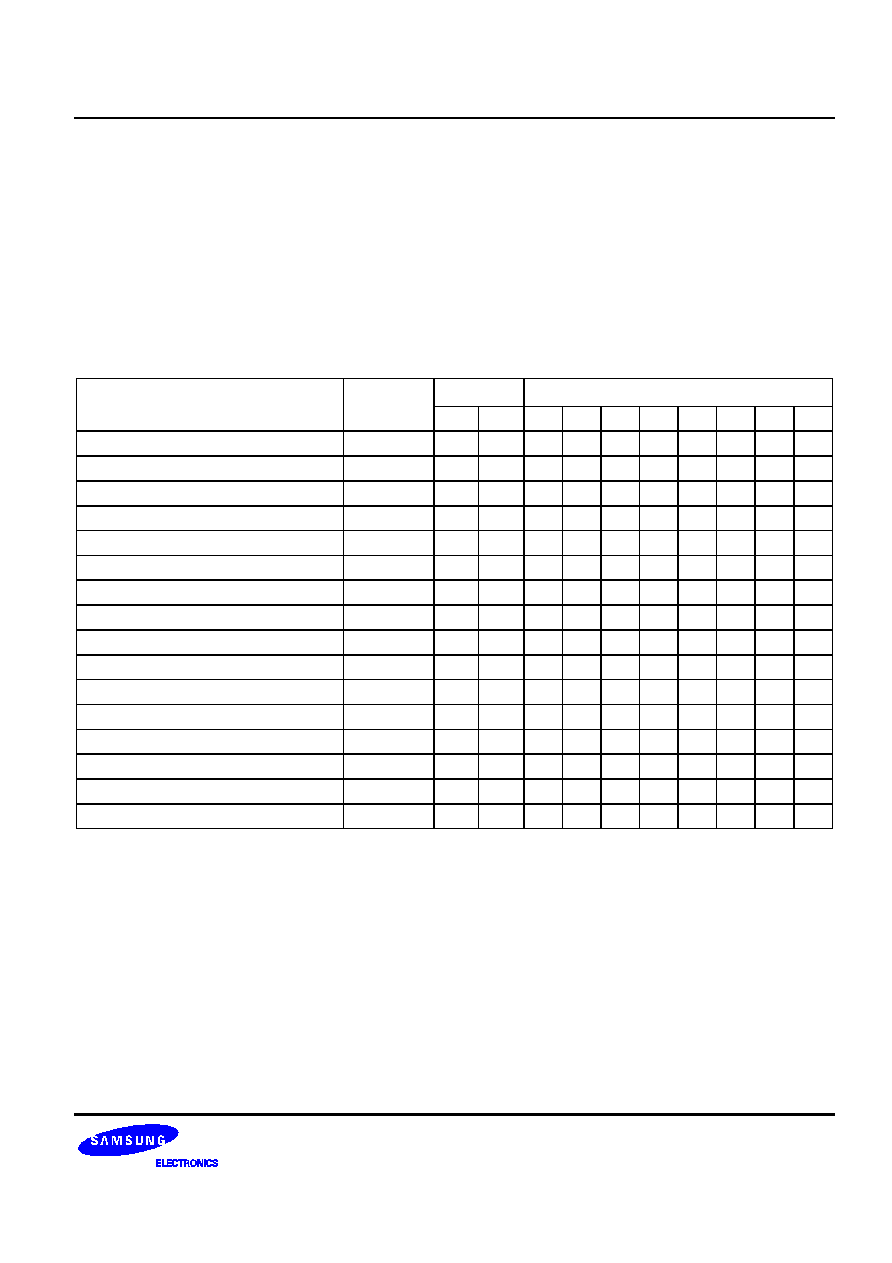
S3C852B/P852B (Preliminary Spec)
RESET
RESET
and POWER-DOWN
8-3
HARDWARE
RESET
RESET
VALUES
Tables 8-1, 8-2, and 8-3 list the reset values for CPU and system registers, peripheral control registers, and
peripheral data registers following a reset operation. The following notation is used to represent reset values:
-- A "1" or a "0" shows the reset bit value as logic one or logic zero, respectively.
-- An 'x' means that the bit value is undefined after a reset.
-- A dash ( � ) means that the bit is either not used or not mapped.
Table 8-1. S3C852B/P852B Set 1 Register and Values after
RESET
RESET
(Masked ROM Mode)
Register Name
Mnemonic
Address
Bit Values after
RESET
RESET
(EA Pin is Low)
Dec
Hex
7
6
5
4
3
2
1
0
Timer 0 counter
T0CNT
208
D0H
0
0
0
0
0
0
0
0
Timer 0 Data Register
T0DATA
209
D1H
1
1
1
1
1
1
1
1
Timer 0 Control Register
T0CON
210
D2H
0
0
0
0
0
0
0
0
Basic Timer Control Register
BTCON
211
D3H
0
0
0
0
0
0
0
0
Clock Control Register
CLKCON
212
D4H
0
0
0
0
0
0
0
0
System Flags Register
FLAGS
213
D5H
x
x
x
x
x
x
0
0
Register Pointer 0
RP0
214
D6H
1
1
0
0
0
�
�
�
Register Pointer 1
RP1
215
D7H
1
1
0
0
1
�
�
�
Stack Pointer (High Byte)
SPH
216
D8H
x
x
x
x
x
x
x
x
Stack Pointer (Low Byte)
SPL
217
D9H
x
x
x
x
x
x
x
x
Instruction Pointer (High Byte)
IPH
218
DAH
x
x
x
x
x
x
x
x
Instruction Pointer (Low Byte)
IPL
219
DBH
x
x
x
x
x
x
x
x
Interrupt Request Register
IRQ
220
DCH
0
0
0
0
0
0
0
0
Interrupt Mask Register
IMR
221
DDH
x
x
x
x
x
x
x
x
System Mode Register
SYM
222
DEH
0
�
�
x
x
x
0
0
Register Page Pointer
PP
223
DFH
0
0
0
0
0
0
0
0

RESET
RESET
and POWER-DOWN
S3C852B/P852B (Preliminary Spec)
8-4
Table 8-2. S3C852B/P852B Set 1, Bank 0 Register and Values after
RESET
RESET
(Masked ROM Mode)
Register Name
Mnemonic
Address
Bit Values after
RESET
RESET
(EA Pin is Low)
Dec
Hex
7
6
5
4
3
2
1
0
Port 0 Data Register
P0
224
E0H
0
0
0
0
0
0
0
0
Port 1 Data Register
P1
225
E1H
0
0
0
0
0
0
0
0
Port 2 Data Register
P2
226
E2H
0
0
0
0
0
0
0
0
Port 3 Data Register
P3
227
E3H
0
0
0
0
0
0
0
0
Port 4 Data Register
P4
228
E4H
0
0
0
0
0
0
0
0
Port 5 Data Register
P5
229
E5H
0
0
0
0
0
0
0
0
Port 6 Data Register
P6
230
E6H
0
0
0
0
0
0
0
0
Port 0 interrupt control register
P0INT
231
E7H
0
0
0
0
0
0
0
0
Port 0 interrupt pending register
P0PND
232
E8H
0
0
0
0
0
0
0
0
Port 0 interrupt state register
P0STA
233
E9H
0
0
0
0
0
0
0
0
Port 0 control register (high byte)
P0CONH
234
EAH
0
0
0
0
0
0
0
0
Port 0 control register (low byte)
P0CONL
135
EBH
0
0
0
0
0
0
0
0
Port 1 control register (high byte)
P1CONH
236
ECH
0
0
0
0
0
0
0
0
Port 1 control register (low byte)
P1CONL
237
EDH
0
0
0
0
0
0
0
0
Port 1 function select register
P1AFS
238
EEH
0
0
0
0
0
0
0
0
Port 2 function select register
P2AFS
240
F0H
�
�
�
�
0
0
0
0
Port 3 control register
P3CON
241
F1H
0
0
0
0
0
0
0
0
Port 3 function select register
P3AFS
242
F2H
�
�
�
�
0
0
0
0
Port 4 control register
P4CON
243
F3H
0
0
0
0
0
0
0
0
Port 5 control register
P5CON
244
F4H
0
0
0
0
0
0
0
0
Port 6 control register
P6CON
245
F5H
0
0
0
0
0
0
0
0
Clock output mode register
CLKMOD
248
F8H
�
�
�
�
�
0
0
0
Interrupt pending register
INTPND
249
F9H
�
�
�
�
�
0
0
0
Oscillator control register
OSCCON
250
FAH
�
�
�
�
0
0
�
0
STOP control register
STPCON
251
FBH
0
0
0
0
0
0
0
0
Basic timer counter
BTCNT
253
FDH
x
x
x
x
x
x
x
x
External Memory timing register
EMT
254
FEH
�
1
1
1
1
1
0
�
Interrupt priority register
IPR
255
FFH
x
x
x
x
x
x
x
x
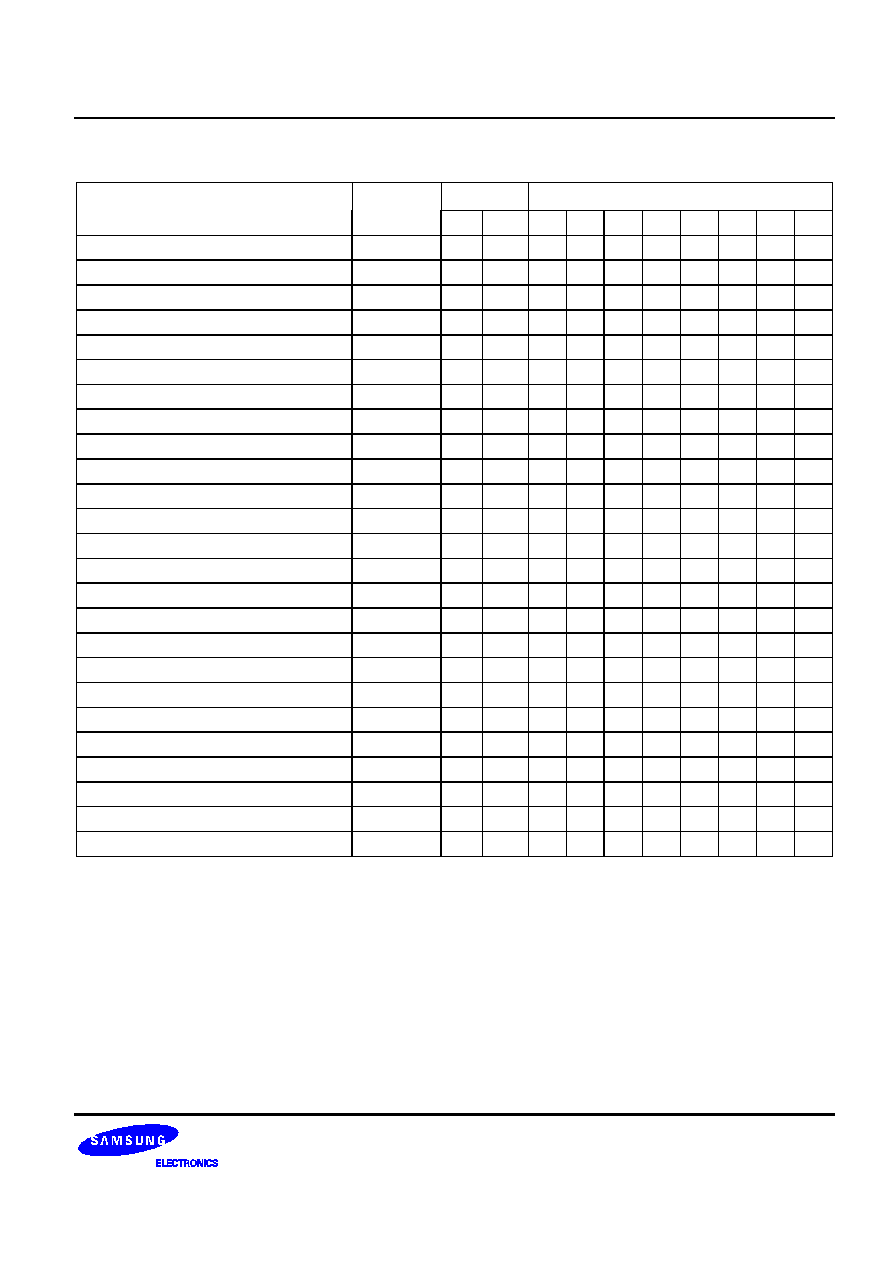
S3C852B/P852B (Preliminary Spec)
RESET
RESET
and POWER-DOWN
8-5
Table 8-3. S3C852B/P852B Set 1, Bank 1 Register Values after
RESET
RESET
(Masked ROM Mode)
Register Name
Mnemonic
Address
Bit Values after
RESET
RESET
(EA Pin is Low)
Dec
Hex
7
6
5
4
3
2
1
0
Timer A counter
TACNT
224
E0H
0
0
0
0
0
0
0
0
Timer B counter
TBCNT
225
E1H
0
0
0
0
0
0
0
0
Timer A data register
TADATA
226
E2H
1
1
1
1
1
1
1
1
Timer B data register
TBDATA
227
E3H
1
1
1
1
1
1
1
1
Timer A control register
TACON
228
E4H
0
0
0
0
0
0
0
0
Timer B control register
TBCON
229
E5H
0
0
0
0
0
0
0
0
Watch Timer control register
WTCON
230
E6H
0
0
0
0
0
0
0
0
SIO data register
SIODATA
234
EAH
1
1
1
1
1
1
1
1
SIO control register
SIOCON
235
EBH
0
0
0
0
0
0
0
0
SIO Pre-scaler register
SIOPS
236
ECH
0
0
0
0
0
0
0
0
Port 7 data register
P7
237
EDH
0
0
0
0
0
0
0
0
A/D data register(high byte)
ADDATAH
242
F2H
x
x
x
x
x
x
x
x
A/D data register(low byte)
ADDATAL
243
F3H
�
�
�
�
�
�
x
x
A/D control register
ADCON
244
F4H
0
0
0
0
0
0
0
0
Port 8 data register
P8
245
F5H
0
0
0
0
0
0
0
0
Port 9 data register
P9
246
F6H
0
0
0
0
0
0
0
0
Port 10 data register
P10
247
F7H
0
0
0
0
0
0
0
0
Port 7 control register (high byte)
P7CONH
248
F8H
0
0
0
0
0
0
0
0
Port 7 control register (low byte)
P7CONL
249
F9H
0
0
0
0
0
0
0
0
Port 8 control register (high byte)
P8CONH
250
FAH
0
0
0
0
0
0
0
0
Port 8 control register (low byte)
P8CONL
251
FBH
0
0
0
0
0
0
0
0
Port 9 control register (high byte)
P9CONH
252
FCH
0
0
0
0
0
0
0
0
Port 9 control register (low byte)
P9CONL
253
FDH
0
0
0
0
0
0
0
0
Port 10 control register (high byte)
P10CONH
254
FEH
0
0
0
0
0
0
0
0
Port 10 control register (low byte)
P10CONL
255
FFH
0
0
0
0
0
0
0
0

RESET
RESET
and POWER-DOWN
S3C852B/P852B (Preliminary Spec)
8-6
POWER-DOWN MODES
STOP MODE
Stop mode is invoked by the instruction STOP. In Stop mode, the operation of the CPU and main oscillator is
halted. All peripherals which the main oscillator is selected as a clock source stop also because main oscillator
stops. But, the watch timer will not halted in stop mode if the sub clock is selected as watch timer clock source.
The data stored in the internal register file are retained in stop mode. Stop mode can be released in one of three
ways: by a system reset, by an internal watch timer interrupt (when sub clock is selected as clock source of watch
timer), or by an external interrupt.
Example:
STOP
NOP
NOP
NOP
NOTES
1.
Do not use stop mode if you are using an external clock source because XIN input must be restricted
internally to VSS to reduce current leakage.
2.
In application programs, a STOP instruction must be immediately followed by at least three NOP
instructions. This ensures an adequate time interval for the clock to stabilize before the next
instruction is executed. If three or more NOP instructions are not used after STOP instruction,
leakage current could be flown because of the floating state in the internal bus.
Using
RESET
to Release Stop Mode
Stop mode is released when the
RESET
signal goes active (Low level): all system and peripheral control
registers are reset to their default hardware values and the contents of all data registers are retained. When the
programmed oscillation stabilization interval has elapsed, the CPU starts the system initialization routine by
fetching the program instruction stored in ROM location 0100H.
Using an External Interrupt to Release Stop Mode
External interrupts can be used to release stop mode. For the S3C852B microcontroller, we recommend using
the INT0�INT7 interrupt, P0.0�P0.7.
Using an Internal Interrupt to Release Stop Mode
An internal interrupt, watch timer, can be used to release stop mode because the watch timer operates in stop
mode if the clock source of watch timer is sub clock. If system clock is sub clock, you can't use any interrupts to
release stop mode.
Please note the following conditions for Stop mode release:
-- If you release stop mode using an internal or external interrupt, the current values in system and peripheral
control registers are unchanged.
-- If you use an internal or external interrupt for stop mode release, you can also program the duration of the
oscillation stabilization interval. To do this, you must make the appropriate control and clock settings before
entering stop mode.
-- If you use an interrupt to release stop mode, the bit-pair setting for CLKCON.4/CLKCON.3 remains
unchanged and the currently selected clock value is used.
-- The internal or external interrupt is serviced when the stop mode release occurs. Following the IRET from the
service routine, the instruction immediately following the one that initiated stop mode is executed.

S3C852B/P852B (Preliminary Spec)
RESET
RESET
and POWER-DOWN
8-7
IDLE MODE
Idle mode is invoked by the instruction IDL (opcode 6FH). In Idle mode, CPU operations are halted while some
peripherals remain active. During Idle mode, the internal clock signal is gated away from the CPU and from all
but the following peripherals, which remain active :
Interrupt logic
Basic timer
Timer 0
Timer 1 (Timer A and B)
Watch timer
I/O port pins retain the mode (input or output) they had at the time Idle mode was entered. External interface pins
are halted by high or low level, in the idle mode.
Idle Mode Release
You can release Idle mode in one of two ways:
1.
Execute a reset. All system and peripheral control registers are reset to their default values and the
contents of all data registers are retained. The reset automatically selects the slowest clock (1/16)
because of the hardware reset value for the CLKCON register. If all external interrupts are masked in the
IMR register, a reset is the only way you can release Idle mode.
2.
Activate any enabled interrupt
internal or external. When you use an interrupt to release Idle mode,
the 2-bit CLKCON.4/CLKCON.3 value remains unchanged, and the currently selected clock value is
used. The interrupt is then serviced. When the return-from-interrupt condition (IRET) occurs, the
instruction immediately following the one which initiated Idle mode is executed.

RESET
RESET
and POWER-DOWN
S3C852B/P852B (Preliminary Spec)
8-8
F
F
PROGRAMMING TIP -- Sample S3C852B Initialization Routine
The following sample program suggests initialization settings for the S3C852B address space, interrupt vectors,
and peripheral functions:
;
<< Register file reference >>
.INCLUDE
"C:\SMDS2P\INCLUDE\REG\S3C852B.REG"
;
<< User Equation Definition >>
.INCLUDE
"C:\EQU.TBL"
;
<< Interrupt Vector Addresses >>
.ORG
00D0H
.DW
EXT00_int
; IRQ6: Edge triggered ext. int.
.DW
EXT01_int
; IRQ6
.DW
EXT02_int
; IRQ6
.DW
EXT03_int
; IRQ6
;
00D8H�00E3H: Reserved
.ORG 00E4H
.DW
EXT04_int
; IRQ7: Edge triggered ext. int.
.DW
EXT05_int
; IRQ7
.DW
EXT06_int
; IRQ7
.DW
EXT07_int
; IRQ7
.ORG
00F0H
.DW
SERIAL_R_T
; IRQ4 Serial data receive/transmit interrupt
.ORG
00F2H
.DW
WT
; IRQ3 Watch Timer overflow interrupt
.ORG
00F4H
.DW
TA_Match
; IRQ1 Timer A match interrupt
.DW
TB_Overflow
; IRQ1 Timer B overflow interrupt
.DW
TB_Match
; IRQ1 Timer B match interrupt
.ORG
00FAH
.DW
T0_Overflow
; IRQ0 Timer 0 overflow interrupt
.DW
T0_M_C
; IRQ0 Timer 0 match/capture interrupt
;
00FEH�00FFH: Reserved

S3C852B/P852B (Preliminary Spec)
RESET
RESET
and POWER-DOWN
8-9
F
F
PROGRAMMING TIP -- Sample S3C852B Initialization Routine (Continued)
;
<< Reset Vector >>
.ORG
0100H
JP
t, INITIAL
�
�
�
;
<< System and Peripheral Initialization >>
.ORG
0200H
INITIAL:
DI
;
<System register setting>
LD
SYM,#00000000B
; Fast, global interrupt disable
LD
EMT,#00000000B
; 'No wait' and internal stack area select
LD
SPH,#00H
; Stack pointer (high byte) to zero
LD
SPL,#0FFH
; Stack pointer (low byte) to zero
LD
OSCCON,#00H
; Select main clock as system clock
LD
CLKCON,#10H
; f
OSC
/2 is selected for CPU clock
;
<Interrupt settings>
LD
IPR,#16H
; Interrupt priorities
; IRQ3 > 4 > 0 > 1 > 5 > 6 > 7
LD
IMR,#10001001B
; IRQ levels 0, 3, and 7 enable
; Level 0 = Timer 0 interrupt
; Level 3 = Watch Timer interrupt
; Level 7 = External interrupt

RESET
RESET
and POWER-DOWN
S3C852B/P852B (Preliminary Spec)
8-10
F
F
PROGRAMMING TIP -- Sample S3C852B Initialization Routine (Continued)
INI_PERI_SET:
;
<Port 0 setting>
LD
P0CONH,#55H
; Input, Schmitt trigger, Pull-up resistor enabled
LD
P0CONL,#55H
LD
P0STA, #00H
; Select Falling edge interrupt detection
LD
P0PND,#00H
; Clear External interrupt pending bits
LD
P0INT, #0FFH
; All external interrupt enable
;
<Port 1 setting>
LD
P1AFS,#00H
; Select Normal I/O Port 1
LD
P1CONH,#0AAH
; Output, push-pull
LD
P1CONL,#0AAH
;
<Port 2 setting>
LD
P2CON,#0AAH
; Output, push-pull
;
<Port 3 setting>
LD
P3AFS, #00H
; Select Normal I/O Port 3
LD
P3CON,#0AAH
; Output, push-pull

S3C852B/P852B (Preliminary Spec)
RESET
RESET
and POWER-DOWN
8-11
F
F
PROGRAMMING TIP -- Sample S3C852B Initialization Routine (Continued)
;
<Port 4 setting>
LD
P4CON,#22H
; Output, push-pull
;
<Port 5 setting>
LD
P5CON,#22H
; Output, push-pull
;
<Port 6 setting>
LD
P6CON,#22H
; Output, push-pull
;
<Port 7 setting>
LD
P7CONH,#0AAH
; Output, push-pull
LD
P7CONL,#0AAH
;
<Port 8 setting>
LD
P8CONH,#0AAH
;
Output, push-pull
LD
P8CONL,#0AAH
;
<Port 9 setting>
LD
P9CONH,#0AAH
;
Output, push-pull
LD
P9CONL,#0AAH
;
<Port 10 setting>
LD
P10CONH,#0AAH
;
Output, push-pull
LD
P10CONL,#0AAH
;
<Timer 0>
LD
T0DATA,#08H
; Timer A clock source clock divided by 9
LD
T0CON,#10001100B
; Select fxx/64 as Timer 0 clock source
; Enable overflow interrupt
;
<Timer A>
; Disabled
SB1
LD
TACON,#00H
;
<Timer B>
; Disabled
LD
TBCON,#00H

RESET
RESET
and POWER-DOWN
S3C852B/P852B (Preliminary Spec)
8-12
F
F
PROGRAMMING TIP -- Sample S3C852B Initialization Routine (Continued)
;
<SIO setting>
; Disable
LD
SIOCON,#00H
;
<< Register Initialization >>
SB0
SRP
#0C0H
;
<Clear all data registers 00H�0FFH>
LD
R0,#0FFH
RAMCLR:
CLR
@R0
DJNZ
R0,RAMCLR
;
<Initialize other registers>
�
�
�
EI
; Must be executed in this position
; before external interrupt is executed
;
<< Main Loop >>
MAIN:
NOP
; Start main loop
LD
BTCON,#03H
; Enable watchdog timer, clear BTCNT, and
; Basic timer clock input divider.
;
�
�
�
CALL
KEY_SCAN
�
�
�
�
�
�
CALL
JOB
�
�
�
JP
t,MAIN

S3C852B/P852B (Preliminary Spec)
RESET
RESET
and POWER-DOWN
8-13
F
F
PROGRAMMING TIP -- Sample S3C852B Initialization Routine (Continued)
;
<Subroutine 1>
KEY_SCAN:
NOP
�
�
�
RET
;
<Subroutine 2>
JOB:
NOP
�
�
�
RET
;
<< Interrupt Service Routine >>
T0_Overflow:PUSH
RP0
; IRQ0
PUSH
RP1
SRP
#T0_REG
; Example: T0_REG = 00H
�
�
�
AND
INTPND,#11111110B
; Clear pending bit (omissible)
POP
RP1
POP
RP0
IRET
T0_M_C:
AND
T0CON,#11111110B
; Clear pending bit, IRQ0
IRET
TA_Match:
AND
TACON,#11111110B
; Clear pending bit, IRQ1
IRET
TB_Overflow: AND
INTPND,#11111101B
; Clear pending bit (omissible), IRQ1
IRET
TB_Match: AND
INTPND,#11111011B ; Clear pending bit, IRQ1
IRET
WT: AND
WTCON,#11111110B ; Clear pending bit, IRQ3
IRET

RESET
RESET
and POWER-DOWN
S3C852B/P852B (Preliminary Spec)
8-14
F
F
PROGRAMMING TIP -- Sample S3C852B Initialization Routine (Concluded)
;
<< Other Interrupt Vectors >>
SERIAL_R_T: AND
SIOCON,#11111110H
; Clear pending bit, IRQ4
IRET
EXT00_int:
LD
P0PND,#11111110B
; Clear pending bit, IRQ6
�
�
IRET
EXT01_int:
LD
P0PND,#11111101B
; Clear pending bit, IRQ6
�
�
IRET
EXT02_int:
LD
P0PND,#11111011B
; Clear pending bit, IRQ6
�
�
IRET
EXT03_int:
LD
P0PND,#11110111B
; Clear pending bit, IRQ6
�
�
IRET
EXT04_int:
LD
P0PND,#11101111B
; Clear pending bit, IRQ7
�
�
IRET
EXT05_int:
LD
P0PND,#11011111B
; Clear pending bit, IRQ7
�
�
IRET
EXT06_int:
LD
P0PND,#10111111B
; Clear pending bit, IRQ7
�
�
IRET
EXT07_int:
LD
P0PND,#01111111B
; Clear pending bit, IRQ7
�
�
IRET
END
NOTE: When clearing a interrupt pending bit by software, using LD instruction is recommended to prevent
malfunction of interrupt operation.

S3C852B/P852B (Preliminary Spec)
I/O PORTS
9-1
9
I/O PORTS
OVERVIEW
The S3C852B/P852B microcontrollers have P0�P10 I/O ports. P2 and P3 are 4-bit ports, the others are 8-bit
ports. So, This gives a total of 80 I/O pins. Each port can be flexibly configured to meet application design
requirements. The CPU accesses ports by directly writing or reading port registers. No special I/O instructions are
required.
All ports of the S3C852B/P852B can be configured to input or output mode and P3�P6 are sharing with external
interface, A0�A15, D0�D7,
PM
,
DM
,
RD
,
WR
.
Table 9-1 gives you a general overview of S3C852B I/O port functions.

I/O PORTS
S3C852B/P852B (Preliminary Spec)
9-2
Table 9-1. S3C852B Port Configuration Overview
Port
Configuration Options
0
8-bit general-purpose I/O port; Schmitt trigger input, schmitt trigger input with pull-up resistor,
push-pull output. P0.1, P0.3, P0.5 and P0.6 can be used as alternative function (BUZ, T0, TA,
TB). All P0 pin circuits have interrupt enable/disable (P0INT), pending control(P0PND), and
rising/falling edge control (P0STA).
1
8-bit general-purpose I/O port; Schmitt trigger input, schmitt trigger input with pull-up resistor,
push-pull output, open-drain output. All P1 pin circuits have alternative function
control(P1AFS), the alternative functions of P1.0�P1.3 are the analog input function(ADC0�
ADC3).
2
4-bit general-purpose I/O port; Schmitt trigger input, schmitt trigger input with pull-up resistor,
push-pull output, open-drain output.
3
4-bit general-purpose I/O port; Schmitt trigger input, schmitt trigger input with pull-up resistor,
push-pull output, open-drain output. All P3 pin circuits have alternative function control
(P2AFS), and the alternative functions of P3.0�P3.3 are the external memory interface
function(PM, DM, RD, WR).
4
8-bit general-purpose I/O port; Schmitt trigger input, schmitt trigger input with pull-up resistor,
push-pull output, open-drain output. All P4 pin circuits can be used as alternative function for
external memory interface function (D0�D7).
5
8-bit general-purpose I/O port; Schmitt trigger input, schmitt trigger input with pull-up resistor,
push-pull output, open-drain output. All P5 pin circuits can be used as alternative function for
external memory interface function (A0�A7).
6
8-bit general-purpose I/O port; Schmitt trigger input, schmitt trigger input with pull-up resistor,
push-pull output, open-drain output. All P6 pin circuits can be used as alternative function for
external memory interface function (A8�A15).
7
8-bit general-purpose I/O port; Schmitt trigger input, schmitt trigger input with pull-up resistor,
push-pull output, open-drain output.
8
8-bit general-purpose I/O port; Schmitt trigger input, schmitt trigger input with pull-up resistor,
push-pull output, open-drain output.
9
8-bit general-purpose I/O port; Schmitt trigger input, schmitt trigger input with pull-up resistor,
push-pull output, open-drain output.
10
8-bit general-purpose I/O port; Schmitt trigger input, schmitt trigger input with pull-up resistor,
push-pull output, open-drain output.
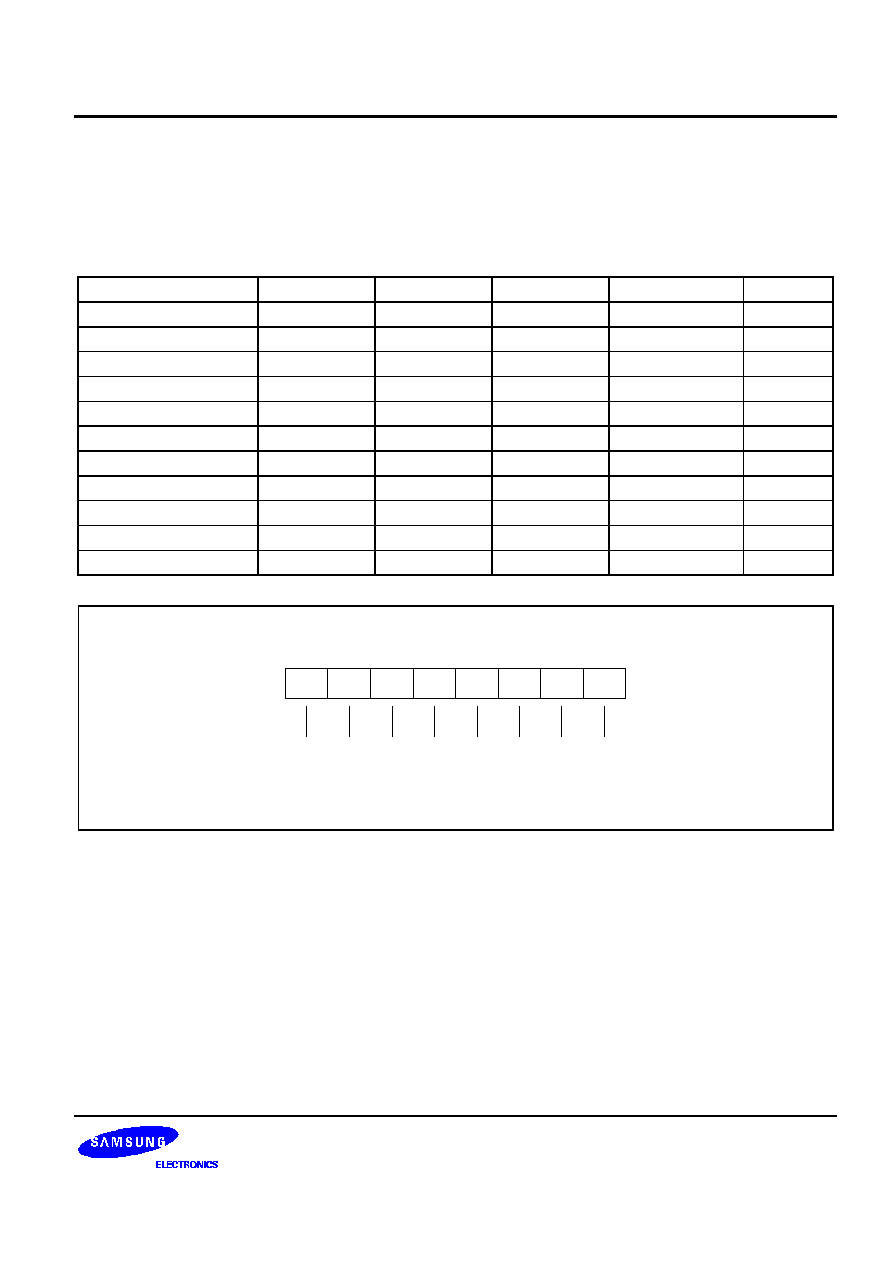
S3C852B/P852B (Preliminary Spec)
I/O PORTS
9-3
PORT DATA REGISTERS
Table 9-2 gives you an overview of the register locations of all seven S3C852B I/O port data registers. Data
registers for ports 0 to 10 have the general format shown in Figure 9-1.
Table 9-2. Port Data Register Summary
Register Name
Mnemonic
Decimal
Hex
Location
R/W
Port 0 data register
P0
224
E0H
Set 1
R/W
Port 1 data register
P1
225
E1H
Set 1
R/W
Port 2 data register
P2
226
E2H
Set 1
R/W
Port 3 data register
P3
227
E3H
Set 1
R/W
Port 4 data register
P4
228
E4H
Set 1
R/W
Port 5 data register
P5
229
E5H
Set 1
R/W
Port 6 data register
P6
230
E6H
Set 1
R/W
Port 7 data register
P7
237
EDH
Set 1
R/W
Port 8 data register
P8
245
F5H
Set 1
R/W
Port 9 data register
P9
246
F6H
Set 1
R/W
Port 10 data register
P10
247
F7H
Set 1
R/W
S3C852B I/O Port Data Register Format (n = 0-6)
.7
.6
.5
.4
.3
.2
.1
.0
MSB
LSB
NOTE: P2 and P3 have the only Pn.0-Pn.3
Pn.7
Pn.6
Pn.5
Pn.4
Pn.3
Pn.2
Pn.1
Pn.0
Figure 9-1. S3C852B I/O Port Data Register Format

I/O PORTS
S3C852B/P852B (Preliminary Spec)
9-4
PORT 0
Port 0 is an 8-bit I/O port with individually configurable pins. Port 0 can serve either as a general-purpose 8-bit
I/O port, alternative functions (BUZ for buzzer signal output, T0 for timer 0 output, TA for timer 1/A output and TB
for timer B output), or its pins can be configured individually as external interrupt inputs. All inputs are schmitt
triggered. Port 0 is accessed directly by writing or reading the Port 0 data register, P0 (R224, E0H) in set 1.
Port 0 Control Registers (P0CONH, P0CONL)
The direction of each port pin is configured by bit-pair settings in two control registers: P0CONH (high byte, EAH,
set 1) and P0CONL (low byte, EBH, set 1). P0CONH controls pins P0.4�P0.7 (pins 32�35) and P0CONL controls
pins P0.0�P0.3 (pins 28�31). Both registers are read-write addressable using 8-bit instructions.
When select alternative function by setting bit-pair to "11"(P0.1, P0.3, P0.5, P0.6), P0.1, P0.3, P0.5, P0.6 can be
automatically configured respectively, as BUZ, timer 0, timer 1/A and timer B output.
There are two input mode and one output mode: Schmitt trigger input, schmitt trigger input with pull-up resistor
and Push-pull output.
A reset clears all P0CONH and P0CONL bits to logic zero. This configures Port 0 pins to schmitt trigger input.
Port 0 Interrupt Enable and Pending Registers (P0INT, P0PND)
To process external interrupts, two additional control registers are provided: the Port 0 interrupt enable register,
P0INT (R231, E7H, set 1) and the Port 0 interrupt pending register, P0PND (R232, E8H, set 1).
By setting bits in the Port 0 interrupt enable register P0INT to "1", you can use specific Port 0 pins to generate
interrupt requests when specific signal edges are detected. The interrupt names INT0�INT7 correspond to pins
P0.0�P0.7. After a reset, P0INT bits are cleared to "00H", disabling all external interrupts.
The Port 0 interrupt pending register P0PND lets you check for interrupt pending conditions and clear the pending
condition when the interrupt request has been serviced. Incoming interrupt requests are detected by polling the
P0PND bit values.
When the interrupt enable bit of any Port 0 pin is set to "1", a rising or falling signal edge at that pin generates an
interrupt request. (Remember that the Port 0 interrupt pins must first be configured by setting them to input mode
in the corresponding P0CONH or P0CONL register.)
The corresponding P0PND bit is then set to "1" and the IRQ pulse goes high to signal the CPU that an interrupt
request is waiting.
When a Port 0 interrupt request has been serviced, the application program must clear the appropriate interrupt
pending register bit by writing a "0" to the correct pending bit in the P0PND register. Please note that writing a "0"
value has no effect.
Port 0 Interrupt State Register (P0STA)
P0 interrupt can be generated in falling edge or rising edge, depending on the value of the P0 interrupt state
register (R233, E9H, set 1) P0STA. If the value is set to "1", P0 interrupt is generated in rising edge. If the value
is set to "0", P0 interrupt is generated in falling edge.
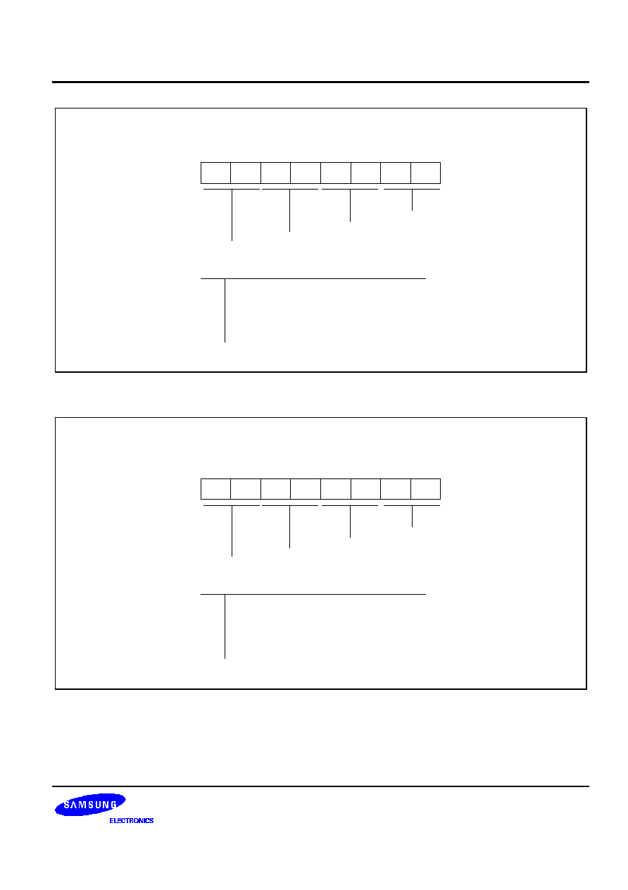
S3C852B/P852B (Preliminary Spec)
I/O PORTS
9-5
Port 0 Control Register, High Byte (P0CONH)
EAH, Set 1, Bank 0, R/W
.7
.6
.5
.4
.3
.2
.1
.0
MSB
LSB
P0.7/INT7
P0CONH bit-pair pin configuration settings:
00
01
10
11
input, schmitt trigger (T1CK)
input, schmitt trigger, pull-up resistor (T1CK)
Output, push-pull
Select alternative function at P0.5 and P0.6
P0.6/INT6/TB
P0.5/INT5/TA
P0.4/INT4/T1CK
Figure 9-2. Port 0 Control Register (P0CONH)
Port 0 Control Register, Low Byte (P0CONL)
EBH, Set 1, Bank 0, R/W
.7
.6
.5
.4
.3
.2
.1
.0
MSB
LSB
P0.3/INT3/T0
P0CONL bit-pair pin configuration settings:
00
01
10
11
input, schmitt trigger (T0CK, T0)
input, schmitt trigger, pull-up resistor (T0CK, T0)
Output, push-pull
Select alternative function at P0.1 and P0.3
P0.2/INT2/T0CK
P0.1/INT1/BUZ
P0.0/INT0
Figure 9-3. Port 0 Control Register (P0CONL)
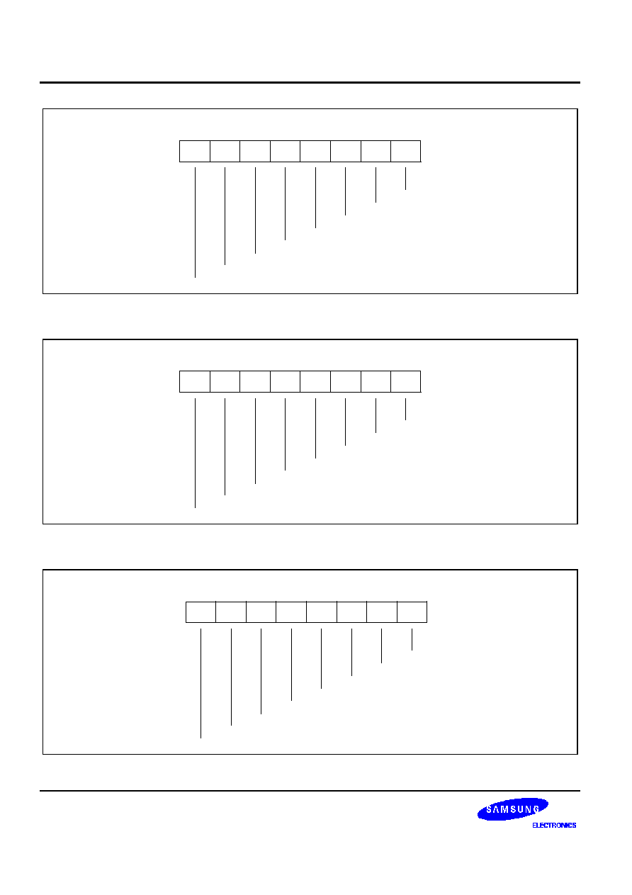
I/O PORTS
S3C852B/P852B (Preliminary Spec)
9-6
Port 0 Interrupt Enable Register (P0INT)
E7H, Set 1, Bank 0, R/W
.7
.6
.5
.4
.3
.2
.1
.0
MSB
LSB
Port 0 interrupt control setting bits:
0 = Disable interrupt at P0.n
1 = Enable interrupt at P0.n
P0.7/INT7
P0.6/INT6
P0.5/INT5
P0.4/INT4
P0.3/INT3
P0.2/INT2
P0.1/INT1
P0.0/INT0
Figure 9-4. Port 0 Interrupt Enable Register (P0INT)
Port 0 Interrupt Pending Register (P0PND)
E8H, Set 1, Bank 0, R/W
.7
.6
.5
.4
.3
.2
.1
.0
MSB
LSB
Port 0 interrupt repuest pending bits:
0 = Interrupt request is not pending
1 = Interrupt request is pending
P0.7/INT7
P0.6/INT6
P0.5/INT5
P0.4/INT4
P0.3/INT3
P0.2/INT2
P0.1/INT1
P0.0/INT0
Figure 9-5. Port 0 Interrupt Pending Register (P0PND)
Port 0 Interrupt State Register (P0STA)
E9H, Set 1, Bank 0, R/W
.7
.6
.5
.4
.3
.2
.1
.0
MSB
LSB
Port 0 interrupt state setting bits:
0 = Falling edge interrupt at P0.n
1 = Rising edge interrupt at P0.n
P0.7/INT7
P0.6/INT6
P0.5/INT5
P0.4/INT4
P0.3/INT3
P0.2/INT2
P0.1/INT1
P0.0/INT0
Figure 9-6. Port 0 Interrupt State Register (P0STA)

S3C852B/P852B (Preliminary Spec)
I/O PORTS
9-7
PORT 1
Port 1 is an 8-bit I/O port with individually configurable pins. Port 1 can serve either as a general-purpose 8-bit
I/O port, alternative functions (ADC0�ADC3) for analog to digital input.
Port 1 have the Port 1 alternative function select register (P1AFS) for selection alternative function of Port 1.
Port 1 is accessed directly by writing or reading the Port 1 data register, P1 (R225, E1H) in set 1. You can use
port 1 for general I/O, or for the alternative functions by setting P1AFS:
Port 1 Control Registers (P1CONH, P1CONL)
The direction of each port pin is configured by bit-pair settings in two control registers: P1CONH (high byte, ECH,
set 1) and P1CONL (low byte, EDH, set 1). P1CONH controls pins P1.4�P1.7 (pins 40�43) and P1CONL controls
pins P1.0�P1.3 (pins 36�39). Both registers are read-write addressable using 8-bit instructions.
There are two input mode and two output mode: Schmitt trigger input, schmitt trigger input with pull-up resistor,
Push-pull output and Open-drain output.
A reset clears all P1CONH and P1CONL bits to logic zero. This configures Port 1 pins to schmitt trigger input.
Port 1 Alternative Function Select Register (P1AFS)
Port 1 can be used either as a general-purpose 8-bit I/O port or alternative functions, depending on the value of
the Port 1 alternative function select register (R238, EEH, set 1) P1AFS.
If the P1AFS is set to "11111111B", the corresponding pins are selected to alternative functions.
If the P1AFS is set to "00000000B", the corresponding pins are selected to general I/O ports.
That is,
-- P1.0�P1.3 can be configured as ADC0�ADC3 for analog to digital input by setting P1AFS.0�P1AFS.3 to "1".
The special functions that you can program using the port 1 high byte control register must also be enabled in the
associated peripheral. Also, when using port 1 pins for functions other than general I/O, you must still set the
corresponding port 1 control register value to configure each bit to input or output mode.
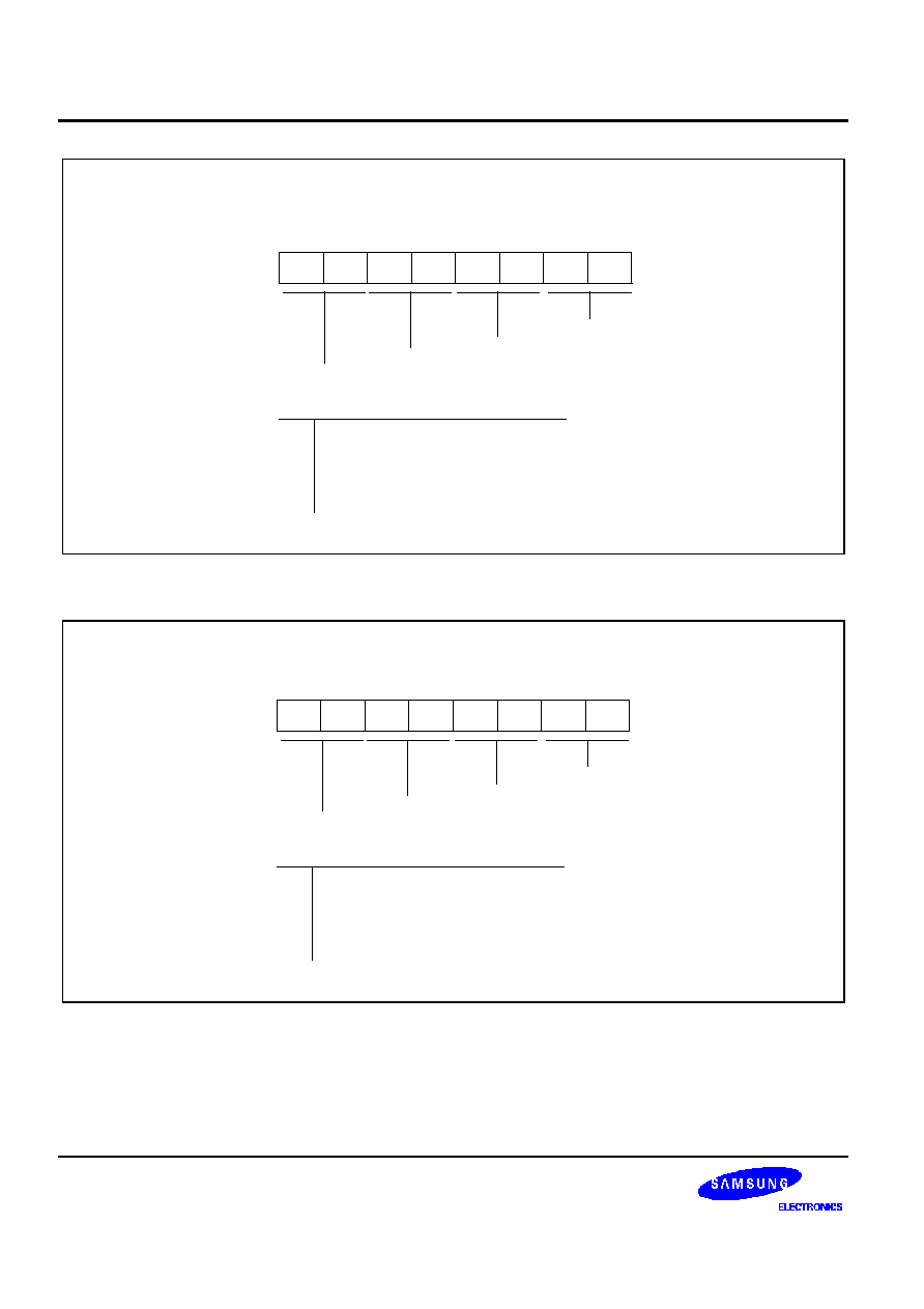
I/O PORTS
S3C852B/P852B (Preliminary Spec)
9-8
Port 1 Control Register, High Byte (P1CONH)
ECH, Set 1, Bank 0, R/W
.7
.6
.5
.4
.3
.2
.1
.0
MSB
LSB
P1.7
P1CONH bit-pair pin configuration settings:
00
01
10
11
Output, Push-pull
Output, Open-drain
P1.6/SCK
P1.5/SO
P1.4/SI
Input, Schmitt trigger, Pull-up resistor
Input, Schmitt trigger
Figure 9-7. Port 1 High-Byte Control Register (P1CONH)
Port 1 Control Register, Low Byte (P1CONL)
EDH, Set 1, Bank 0, R/W
.7
.6
.5
.4
.3
.2
.1
.0
MSB
LSB
P1.3/ADC3
P1CONL bit-pair pin configuration settings:
00
01
10
11
Output, Push-pull
Output, Open-drain
P1.2/ADC2
P1.1/ADC1
P1.0/ADC0
Input, Schmitt trigger, Pull-up resistor
Input, Schmitt trigger
Figure 9-8. Port 1 Low-Byte Control Register (P1CONL)
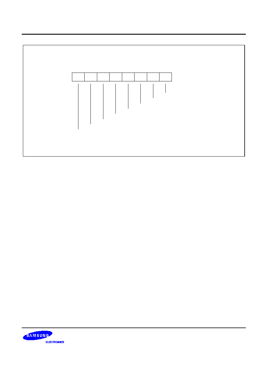
S3C852B/P852B (Preliminary Spec)
I/O PORTS
9-9
Port 1 Alternative Function Select Register (P1AFS)
EEH, Set 1, Bank 0, R/W
.7
.6
.5
.4
.3
.2
.1
.0
MSB
LSB
Port 0 alternative function state settings:
0 = Normal I/O port at P1.n
1 = Select analog input function at P1.0-P1.3
P1.7
P1.6/SCK
P1.5/SO
P1.4/SI
P1.3/ADC3
P1.2/ADC2
P1.1/ADC1
P1.0/ADC0
Figure 9-9. Port 1 Alternative Function Select Register (P1AFS)
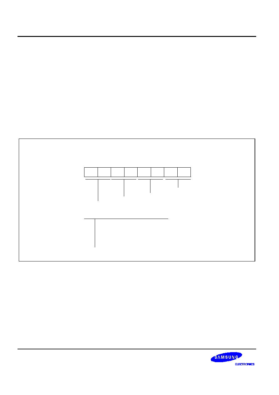
I/O PORTS
S3C852B/P852B (Preliminary Spec)
9-10
PORT 2
Port 2 is an 4-bit I/O port with individually configurable pins. Port 2 is accessed directly by writing or reading the
Port 2 data register, P2 (R226, E2H) in set 1. You can use port 2 for general I/O.
Port 2 Control Registers (P2CON)
The direction of each port pin is configured by bit-pair settings in Port 2 control register: P2CON (EFH, set 1).
P2CON controls pins P2.0�P2.3 (pins 16�19). Port 2 control registers is read-write addressable using 8-bit
instructions.
There are two input mode and two output mode: Schmitt trigger input, schmitt trigger input with pull-up resistor,
Push-pull output and Open-drain output.
A reset clears all P2CON bits to logic zero. This configures Port 2 pins to schmitt trigger input.
Port 2 Control Register, Low Byte (P2CON)
EFH, Set 1, Bank 0, R/W
.7
.6
.5
.4
.3
.2
.1
.0
MSB
LSB
P2.3
P2.2
P2.1
P2.0
P2CON bit-pair pin configuration settings:
00
01
10
11
Output, Push-pull
Output, Open-drain
Input, Schmitt trigger, Pull-up resistor
Input, Schmitt trigger
Figure 9-10. Port 2 Control Register (P2CON)

S3C852B/P852B (Preliminary Spec)
I/O PORTS
9-11
PORT 3
Port 3 is an 4-bit I/O port with individually configurable pins. Port 3 can serve either as a general-purpose 4-bit
I/O port, alternative functions (
PM, DM, RD, WR
for controlling external memory interface).
Port 3 have the Port 3 alternative function select register(P3AFS) for selection alternative function of Port 3.
Port 3 is accessed directly by writing or reading the Port 3 data register, P3 (R227, E3H) in set 1. You can use
port 3 for general I/O, or for the alternative functions by setting P3AFS.
Port 3 Control Registers (P3CON)
The direction of each port pin is configured by bit-pair settings in Port 3 control register: P3CON (F1H, set 1).
P3CON controls pins P3.0�P3.3 (pins 12�15). Port 3 control registers is read-write addressable using 8-bit
instructions.
There are two input mode and two output mode: Schmitt trigger input, schmitt trigger input with pull-up resistor,
Push-pull output and Open-drain output.
A reset clears all P3CON bits to logic zero. This configures Port 3 pins to schmitt trigger input.
Port 3 Alternative Function Select Register (P3AFS)
Port 3 can be used either as a general-purpose 4-bit I/O port or alternative functions, depending on the value of
the Port 3 alternative function select register (R242, F2H, set 1) P3AFS.
If the P3AFS is set to "11111111B", the corresponding pins are selected to alternative functions.
If the P3AFS is set to "00000000B", the corresponding pins are selected to general I/O ports.
That is,
-- P3.0�P3.3 can be configured as
PM, DM, RD, WR
for controlling external memory interface setting
P3AFS.0�F3AFS.3 to "1".
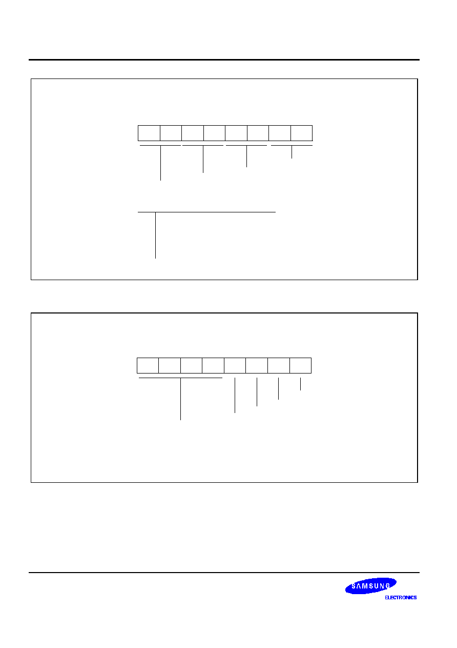
I/O PORTS
S3C852B/P852B (Preliminary Spec)
9-12
Port 3 Control Register, Low Byte (P3CON)
F1H, Set 1, Bank 0, R/W
.7
.6
.5
.4
.3
.2
.1
.0
MSB
LSB
P3.3/
WR
P3CON bit-pair pin configuration settings:
00
01
10
11
Output, Push_pull
Output, Open-drain
Input, Schmitt trigger, Pull_up
Input, Schmitt trigger
P3.2/
RD
P3.1/
DM
P3.0/
PM
Figure 9-11. Port 3 Control Register (P3CON)
Port 3 Alternative FunctionSelect Register (P3AFS)
F2H, Set 1, Bank 0, R/W
.7
.6
.5
.4
.3
.2
.1
.0
MSB
LSB
Not used for S3C852B
Port 3 alternative function state settings:
0 = Normal I/O port at P3.n
1 = Select alternative function at P3.n
P3.3/
WR
P3.2/
RD
P3.1/
DM
P3.0/
PM
Figure 9-12. Port 3 Alternative Function Select Register (P3AFS)
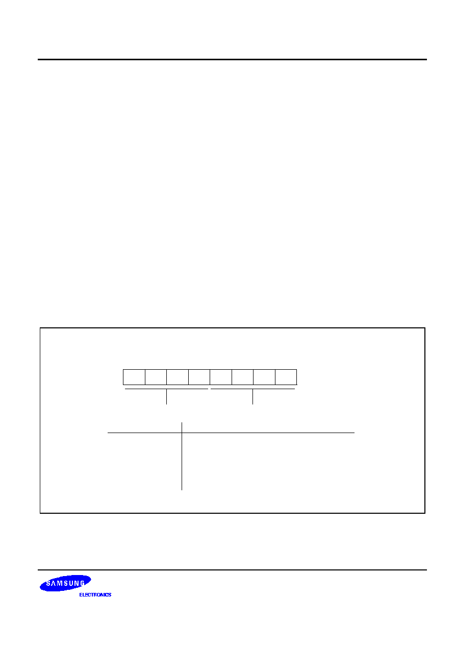
S3C852B/P852B (Preliminary Spec)
I/O PORTS
9-13
PORT 4
Port 4 can be configured on a nibble basis for general data input or output. Port 4 can serve either as a general-
purpose 8-bit I/O port or alternative functions (D0�D7 for the external peripheral interface).
Port 4 is accessed directly by writing or reading the Port 4 data register, P4 (R228, E4H) in set 1. You can use
port 4 for general I/O, or for the alternative functions by P4CON setting "0100B" for each nibble configures the
pins as external interface lines.
The port 4 data register cannot be written, however, when port 4 bits are configured as data lines for the external
interface: writes have no effect and reads only return the state of the pin.
Port 4 Control Registers (P4CON)
The direction of each port pin is configured by nibble settings in Port 4 control register: P4CON (F3H, set 1).
P4CON controls pins P4.0�P4.7 (pins 148�155). Port 4 control registers is read-write addressable using 8-bit
instructions.
The P4CON setting "0100B" for each nibble configures the pins as external interface lines. Bits 4�7 of P4CON
control the upper nibble pins, P4.4�P4.7, and bits 0�3 of P4CON control the lower nibble pins, P4.0�P4.3.
There are two input mode and two output mode: Schmitt trigger input, schmitt trigger input with pull-up resistor,
Push-pull output and Open-drain output.
In normal operating mode a reset operation clears all P4CON register values to "0" , this configures Port 4 pins to
schmitt trigger input. If you want to configure an external memory area, you can use routine to set the P4CON
value to "01000100B". This setting correctly configures data lines D0�D7.
Output, Open-drain
Port 4 Control Register (P4CON)
F3H, Set 1, Bank 0, R/W
.7
.6
.5
.4
.3
.2
.1
.0
MSB
LSB
Port 4 mode selection:
Input, Schmitt trigger, Pull_up resistor
Upper nibble port configuration
Input, Schmitt trigger
Output, Push_pull
Lower nibble port configuration
7(3) 6(2) 5(1) 4(0)
0 0 0 0
0 0 0 1
0 0 1 0
0 0 1 1
0 1 0 0
Select external memory interface line at P4.n (D0-D7)
Figure 9-13. Port 4 Control Register (P4CON)
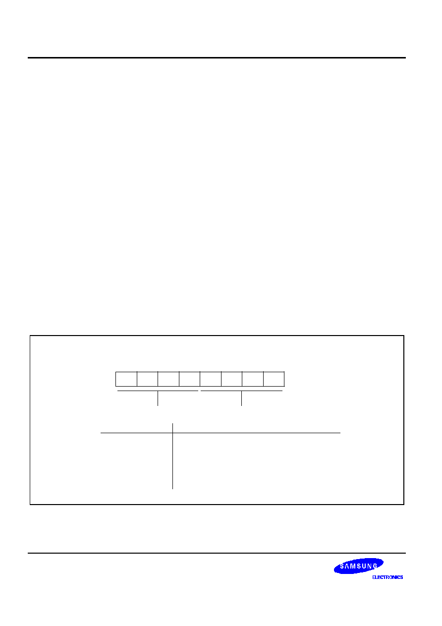
I/O PORTS
S3C852B/P852B (Preliminary Spec)
9-14
PORT 5
Port 5 is basically identical to port 4, except that its alternate use is as the address lines (A0�A7) for the external
interface. (Port 4 can alternately be configures as the data lines D0�D7.)
Port 5 can be configured on a nibble basis for general data input or output. Port 5 can serve either as a general-
purpose 8-bit I/O port or alternative functions (A0�A7 for the external peripheral interface).
Port 5 is accessed directly by writing or reading the Port 5 data register, P5 (R229, E5H) in set 1. You can use
port 5 for general I/O, or for the alternative functions by P5CON setting "0100B" for each nibble configures the
pins as external interface lines.
The port 5 data register cannot be written, however, when port 5 bits are configured as address lines for the
external interface: writes have no effect and reads only return the state of the pin.
Port 5 Control Registers (P5CON)
The direction of each port pin is configured by nibble settings in Port 5 control register: P5CON (F4H, set 1).
P5CON controls pins P5.0�P5.7 (pins 156�3). Port 5 control registers is read-write addressable using 8-bit
instructions.
The P5CON setting "0100B" for each nibble configures the pins as external interface lines. Bits 4�7 of P5CON
control the upper nibble pins, P5.4�P5.7, and bits 0�3 of P5CON control the lower nibble pins, P5.0�P5.3.
There are two input mode and two output mode: Schmitt trigger input, schmitt trigger input with pull-up resistor,
Push-pull output and Open-drain output.
In normal operating mode a reset operation clears all P5CON register values to "0" , this configures Port 5 pins to
schmitt trigger input. If you want to configure an external memory area, you can use routine to set the P5CON
value to "01000100B". This setting correctly configures address lines A0�A7.
Output, Open-drain
Port 5 Control Register (P5CON)
F4H, Set 1, Bank 0, R/W
.7
.6
.5
.4
.3
.2
.1
.0
MSB
LSB
Port 5 mode selection:
Input, Schmitt trigger, Pull_up resistor
Upper nibble port configuration
Input, Schmitt trigger
Output, Push_pull
Lower nibble port configuration
7(3) 6(2) 5(1) 4(0)
0 0 0 0
0 0 0 1
0 0 1 0
0 0 1 1
0 1 0 0
Select external memory interface line at P5.n (A0-A7)
Figure 9-14. Port 5 Control Register (P5CON)
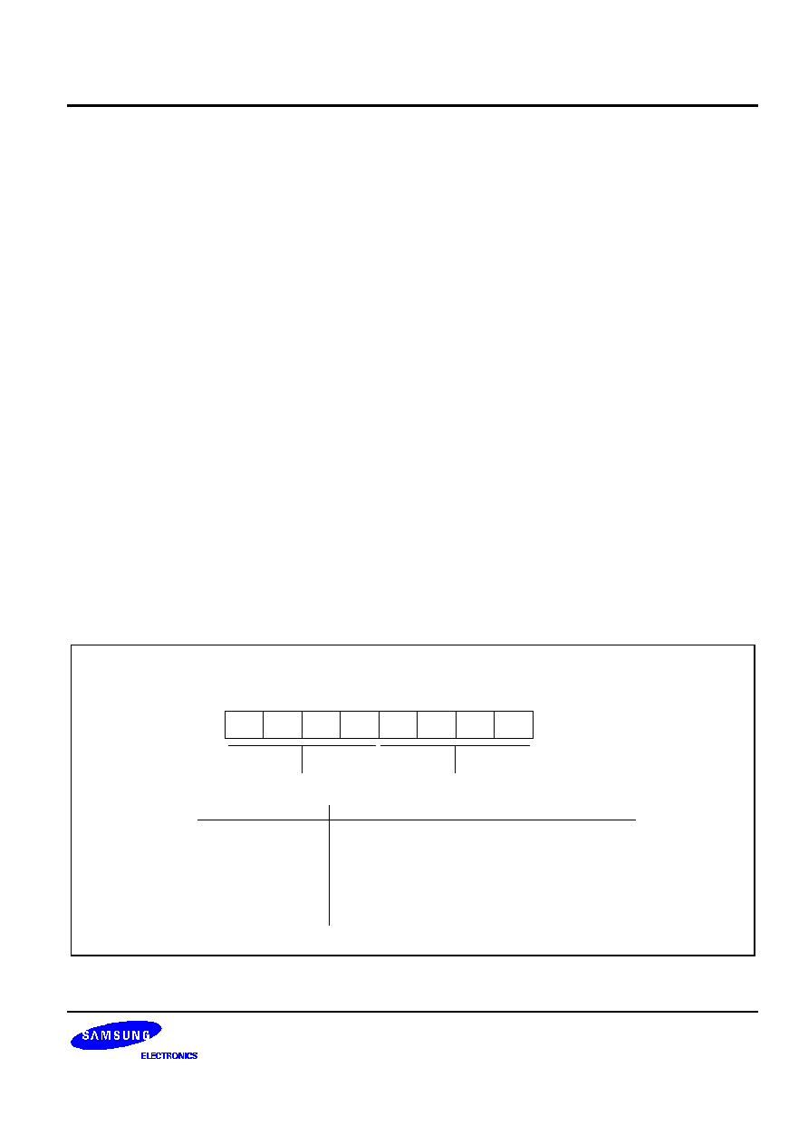
S3C852B/P852B (Preliminary Spec)
I/O PORTS
9-15
PORT 6
Port 6 is basically identical to port 4, except that its alternate use is as the address lines (A8� A15) for the
external interface. (Port 4 can alternately be configures as the data lines D0�D7.)
Port 6 can be configured on a nibble basis for general data input or output. Port 6 can serve either as a general-
purpose 8-bit I/O port or alternative functions (A8�A15 for the external peripheral interface). It is possible to
configure the lower nibble as external interface address lines A8�A11, and to use the upper nibble pins for
general I/O.
Port 6 is accessed directly by writing or reading the Port 6 data register, P6 (R230, E6H) in set 1. You can use
port 6 for general I/O, or for the alternative functions by P6CON setting "0100B" for each nibble configures the
pins as external interface lines.
The port 6 data register cannot be written, however, when port 6 bits are configured as address lines for the
external interface: writes have no effect and reads only return the state of the pin.
Port 6 Control Registers (P6CON)
The direction of each port pin is configured by nibble settings in Port 6 control register: P6CON (F5H, set 1).
P6CON controls pins P6.0�P6.7 (pins 4�11). Port 6 control registers is read-write addressable using 8-bit
instructions.
The P6CON setting "0100B" for each nibble configures the pins as external interface lines. Bits 4�7 of P6CON
control the upper nibble pins, P6.4�P6.7, and bits 0�3 of P6CON control the lower nibble pins, P6.0�P6.3.
There are two input mode and two output mode: Schmitt trigger input, schmitt trigger input with pull-up resistor,
Push-pull output and Open-drain output.
In normal operating mode a reset operation clears all P6CON register values to "0" , this configures Port 6 pins to
schmitt trigger input. If you want to configure an external memory area, you can use routine to set the P6CON
value to "01000100B". This setting correctly configures address lines A8�A15.
Output, Open-drain
Port 6 Control Register (P6CON)
F5H, Set 1, Bank 0, R/W
.7
.6
.5
.4
.3
.2
.1
.0
MSB
LSB
Port 6 mode selection:
Input, Schmitt trigger, Pull_up resistor
Upper nibble port configuration
Input, Schmitt trigger
Output, Push_pull
Lower nibble port configuration
7(3) 6(2) 5(1) 4(0)
0 0 0 0
0 0 0 1
0 0 1 0
0 0 1 1
0 1 0 0
Select external memory interface line at P6.n (A8-A15)
Figure 9-15. Port 6 Control Register (P6CON)

I/O PORTS
S3C852B/P852B (Preliminary Spec)
9-16
PORT 7
Port 7 is an 8-bit I/O port with individually configurable pins. Port 7 is accessed directly by writing or reading the
Port 7 data register, P7 (R237, EDH) in set 1. You can use port 1 for general I/O.
Port 7 Control Registers (P7CONH, P7CONL)
The direction of each port pin is configured by bit-pair settings in two control registers: P7CONH (high byte, F8H,
set 1) and P7CONL (low byte, F9H, set 1). P7CONH controls pins P7.4�P7.7 and P7CONL controls pins P7.0�
P7.3. Both registers are read-write addressable using 8-bit instructions.
There are two input mode and two output mode: Schmitt trigger input, schmitt trigger input with pull-up resistor,
Push-pull output and Open-drain output.
A reset clears all P7CONH and P7CONL bits to logic zero. This configures Port 7 pins to schmitt trigger input.
Port 7 Control Register, High Byte (P7CONH)
F8H, Set 1, Bank 1, R/W
.7
.6
.5
.4
.3
.2
.1
.0
MSB
LSB
P7.7
P7CONH bit-pair pin configuration settings:
00
01
10
11
Output, Push-pull
Output, Open-drain
P7.6
P7.5
P7.4
Input, Schmitt trigger, Pull-up resistor
Input, Schmitt trigger
Figure 9-16. Port 7 High-Byte Control Register (P7CONH)
Port 7 Control Register, Low Byte (P7CONL)
F9H, Set 1, Bank 1, R/W
.7
.6
.5
.4
.3
.2
.1
.0
MSB
LSB
P7.3
P7CONL bit-pair pin configuration settings:
00
01
10
11
Output, Push-pull
Output, Open-drain
P7.2
P7.1
P7.0
Input, Schmitt trigger, Pull-up resistor
Input, Schmitt trigger
Figure 9-17. Port 7 Low-Byte Control Register (P7CONL)

S3C852B/P852B (Preliminary Spec)
I/O PORTS
9-17
PORT 8
Port 8 is an 8-bit I/O port with individually configurable pins. Port 8 is accessed directly by writing or reading the
Port 8 data register, P8 (R245, F5H) in set 1. You can use port 8 for general I/O.
Port 8 Control Registers (P8CONH, P8CONL)
The direction of each port pin is configured by bit-pair settings in two control registers: P8CONH (high byte, FAH,
set 1) and P8CONL (low byte, FBH, set 1). P8CONH controls pins P8.4�P8.7 and P8CONL controls pins P8.0�
P8.3. Both registers are read-write addressable using 8-bit instructions.
There are two input mode and two output mode: Schmitt trigger input, schmitt trigger input with pull-up resistor,
Push-pull output and Open-drain output.
A reset clears all P8CONH and P8CONL bits to logic zero. This configures Port 8 pins to schmitt trigger input.
Port 8 Control Register, High Byte (P8CONH)
FAH, Set 1, Bank 1, R/W
.7
.6
.5
.4
.3
.2
.1
.0
MSB
LSB
P8.7
P8CONH bit-pair pin configuration settings:
00
01
10
11
Output, Push-pull
Output, Open-drain
P8.6
P8.5
P8.4
Input, Schmitt trigger, Pull-up resistor
Input, Schmitt trigger
Figure 9-18. Port 8 High-Byte Control Register (P8CONH)
Port 8 Control Register, Low Byte (P8CONL)
FBH, Set 1, Bank 1, R/W
.7
.6
.5
.4
.3
.2
.1
.0
MSB
LSB
P8.3
P8CONL bit-pair pin configuration settings:
00
01
10
11
Output, Push-pull
Output, Open-drain
P8.2
P8.1
P8.0
Input, Schmitt trigger, Pull-up resistor
Input, Schmitt trigger
Figure 9-19. Port 8 Low-Byte Control Register (P8CONL)

I/O PORTS
S3C852B/P852B (Preliminary Spec)
9-18
PORT 9
Port 9 is an 8-bit I/O port with individually configurable pins. Port 9 is accessed directly by writing or reading the
Port 9 data register, P9 (R246, F6H) in set 1. You can use port 9 for general I/O.
Port 9 Control Registers (P9CONH, P9CONL)
The direction of each port pin is configured by bit-pair settings in two control registers: P9CONH (high byte, FCH,
set 1) and P9CONL (low byte, FDH, set 1). P9CONH controls pins P9.4�P9.7 and P9CONL controls pins P9.0�
P9.3. Both registers are read-write addressable using 8-bit instructions.
There are two input mode and two output mode: Schmitt trigger input, schmitt trigger input with pull-up resistor,
Push-pull output and Open-drain output.
A reset clears all P9CONH and P9CONL bits to logic zero. This configures Port 9 pins to schmitt trigger input.
Port 9 Control Register, High Byte (P9CONH)
FCH, Set 1, Bank 1, R/W
.7
.6
.5
.4
.3
.2
.1
.0
MSB
LSB
P9.7
P9CONH bit-pair pin configuration settings:
00
01
10
11
Output, Push-pull
Output, Open-drain
P9.6
P9.5
P9.4
Input, Schmitt trigger, Pull-up resistor
Input, Schmitt trigger
Figure 9-20. Port 9 High-Byte Control Register (P9CONH)
Port 9 Control Register, Low Byte (P9CONL)
FDH, Set 1, Bank 1, R/W
.7
.6
.5
.4
.3
.2
.1
.0
MSB
LSB
P9.3
P9CONL bit-pair pin configuration settings:
00
01
10
11
Output, Push-pull
Output, Open-drain
P9.2
P9.1
P9.0
Input, Schmitt trigger, Pull-up resistor
Input, Schmitt trigger
Figure 9-21. Port 9 Low-Byte Control Register (P9CONL)
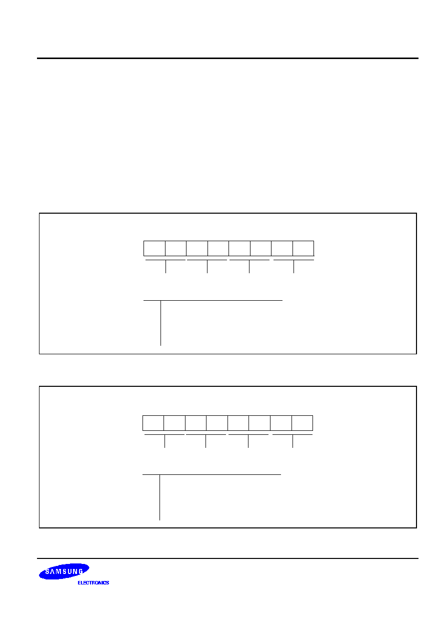
S3C852B/P852B (Preliminary Spec)
I/O PORTS
9-19
PORT 10
Port 10 is an 8-bit I/O port with individually configurable pins. Port 10 is accessed directly by writing or reading
the Port 10 data register, P10 (R247, F7H) in set 1. You can use port 10 for general I/O.
Port 10 Control Registers (P10CONH, P10CONL)
The direction of each port pin is configured by bit-pair settings in two control registers: P10CONH (high byte,
FEH, set 1) and P10CONL (low byte, FFH, set 1). P10CONH controls pins P10.4�P10.7 and P10CONL controls
pins P10.0�P10.3. Both registers are read-write addressable using 8-bit instructions.
There are two input mode and two output mode: Schmitt trigger input, schmitt trigger input with pull-up resistor,
Push-pull output and Open-drain output.
A reset clears all P10CONH and P10CONL bits to logic zero. This configures Port 10 pins to schmitt trigger input.
Port 10 Control Register, High Byte (P10CONH)
FEH, Set 1, Bank 1, R/W
.7
.6
.5
.4
.3
.2
.1
.0
MSB
LSB
P10.7
P10CONH bit-pair pin configuration settings:
00
01
10
11
Output, Push-pull
Output, Open-drain
P10.6
P10.5
P10.4
Input, Schmitt trigger, Pull-up resistor
Input, Schmitt trigger
Figure 9-22. Port 10 High-Byte Control Register (P10CONH)
Port 10 Control Register, Low Byte (P10CONL)
FFH, Set 1, Bank 1, R/W
.7
.6
.5
.4
.3
.2
.1
.0
MSB
LSB
P10.3
P10CONL bit-pair pin configuration settings:
00
01
10
11
Output, Push-pull
Output, Open-drain
P10.2
P10.5
P10.0
Input, Schmitt trigger, Pull-up resistor
Input, Schmitt trigger
Figure 9-23. Port 10 Low-Byte Control Register (P10CONL)

I/O PORTS
S3C852B/P852B (Preliminary Spec)
9-20
NOTES

S3C852B/P852B (Preliminary Spec)
BASIC TIMER and TIMER 0
10-1
10
BASIC TIMER and TIMER 0
MODULE OVERVIEW
The S3C852B has two default timers: an 8-bit basic timer and one 8-bit general-purpose timer/counter. The 8-bit
timer/counter is called timer 0.
Basic Timer (BT)
You can use the basic timer (BT) in two different ways:
-- As a watchdog timer to provide an automatic reset mechanism in the event of a system malfunction.
-- To signal the end of the required oscillation stabilization interval after a reset or a stop mode release.
The functional components of the basic timer block are:
-- Clock frequency divider (f
xx
divided by 4096, 1024, 128, or 16) with multiplexer
-- 8-bit basic timer counter, BTCNT (set 1, bank 0, FDH, read-only)
-- Basic timer control register, BTCON (set 1, D3H, read/write)
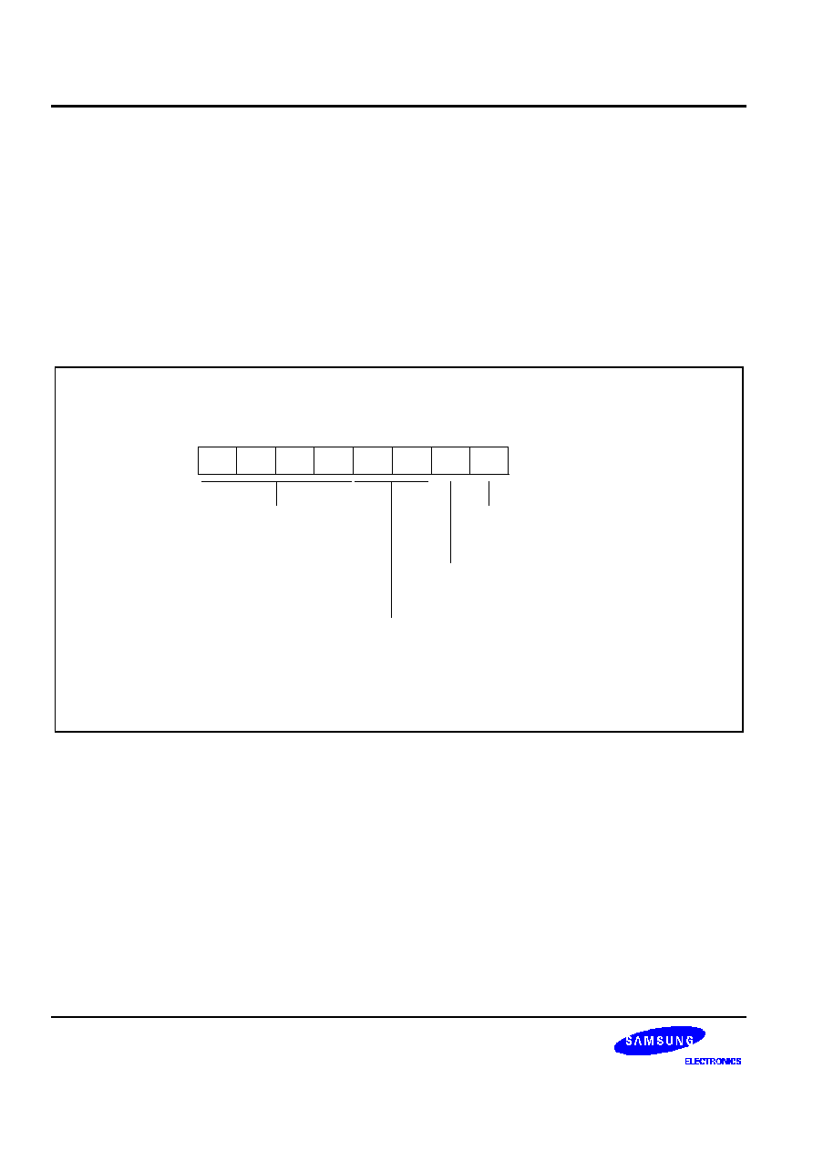
BASIC TIMER and TIMER 0
S3C852B/P852B (Preliminary Spec)
10-2
BASIC TIMER CONTROL REGISTER (BTCON)
The basic timer control register, BTCON, is used to select the input clock frequency, to clear the basic timer
counter and frequency dividers, and to enable or disable the watchdog timer function. It is located in set 1,
address D3H, and is read/write addressable using Register addressing mode.
A reset clears BTCON to "00H". This enables the watchdog function and selects a basic timer clock frequency of
f
xx
/4096. To disable the watchdog function, you must write the signature code "1010B" to the basic timer register
control bits BTCON.7�BTCON.4.
The 8-bit basic timer counter, BTCNT (set 1, bank 0, FDH), can be cleared at any time during normal operation
by writing a "1" to BTCON.1. To clear the frequency dividers for both the basic timer input clock, you write a "1"
to BTCON.0.
Basic TImer Control Register (BTCON)
D3H, Set 1, R/W
.7
.6
.5
.4
.3
.2
.1
.0
MSB
LSB
Divider clear bit for basic timer :
0 = No effect
1 = Clear divider
Basic timer counter clear bit:
0 = No effect
1 = Clear BTCNT
Basic timer input clock selection bits:
00 = f
XX
/4096
01 = f
XX
/1024
10 = f
XX
/128
11 = f
XX
/16
Watchdog function enable bits:
1010B
Other Value
= Disable watchdog timer
= Enable watchdog timer
Figure 10-1. Basic Timer Control Register (BTCON)

S3C852B/P852B (Preliminary Spec)
BASIC TIMER and TIMER 0
10-3
BASIC TIMER FUNCTION DESCRIPTION
Watchdog Timer Function
You can program the basic timer overflow signal (BTOVF) to generate a reset by setting BTCON.7�BTCON.4 to
any value other than "1010B". (The "1010B" value disables the watchdog function.) A reset clears BTCON to
"00H", automatically enabling the watchdog timer function. A reset also selects the CPU clock (as determined by
the current CLKCON register setting), divided by 4096, as the BT clock.
A reset whenever a basic timer counter overflow occurs. During normal operation, the application program must
prevent the overflow, and the accompanying reset operation, from occurring. To do this, the BTCNT value must
be cleared (by writing a "1" to BTCON.1) at regular intervals.
If a system malfunction occurs due to circuit noise or some other error condition, the BT counter clear operation
will not be executed and a basic timer overflow will occur, initiating a reset. In other words, during normal
operation, the basic timer overflow loop (a bit 7 overflow of the 8-bit basic timer counter, BTCNT) is always
broken by a BTCNT clear instruction. If a malfunction does occur, a reset is triggered automatically.
Oscillation Stabilization Interval Timer Function
You can also use the basic timer to program a specific oscillation stabilization interval following a reset or when
stop mode has been released by an external interrupt.
In stop mode, whenever a reset or an internal and an external interrupt occurs, the oscillator starts. The BTCNT
value then starts increasing at the rate of fxx/4096 (for reset), or at the rate of the preset clock source (for an
internal and an external interrupt). When BTCNT.3 overflows, a signal is generated to indicate that the
stabilization interval has elapsed and to gate the clock signal off to the CPU so that it can resume normal
operation.
In summary, the following events occur when stop mode is released:
1.
During stop mode, a power-on reset or an internal and an external interrupt occurs to trigger the stop mode
release and oscillation starts.
2.
If a power-on reset occurred, the basic timer counter will increase at the rate of fx
x
/4096. If an internal and an
external interrupt is used to release stop mode, the BTCNT value increases at the rate of the preset clock
source.
3.
Clock oscillation stabilization interval begins and continues until bit 3 of the basic timer counter overflows.
4.
When a BTCNT.3 overflow occurs, normal CPU operation resumes.
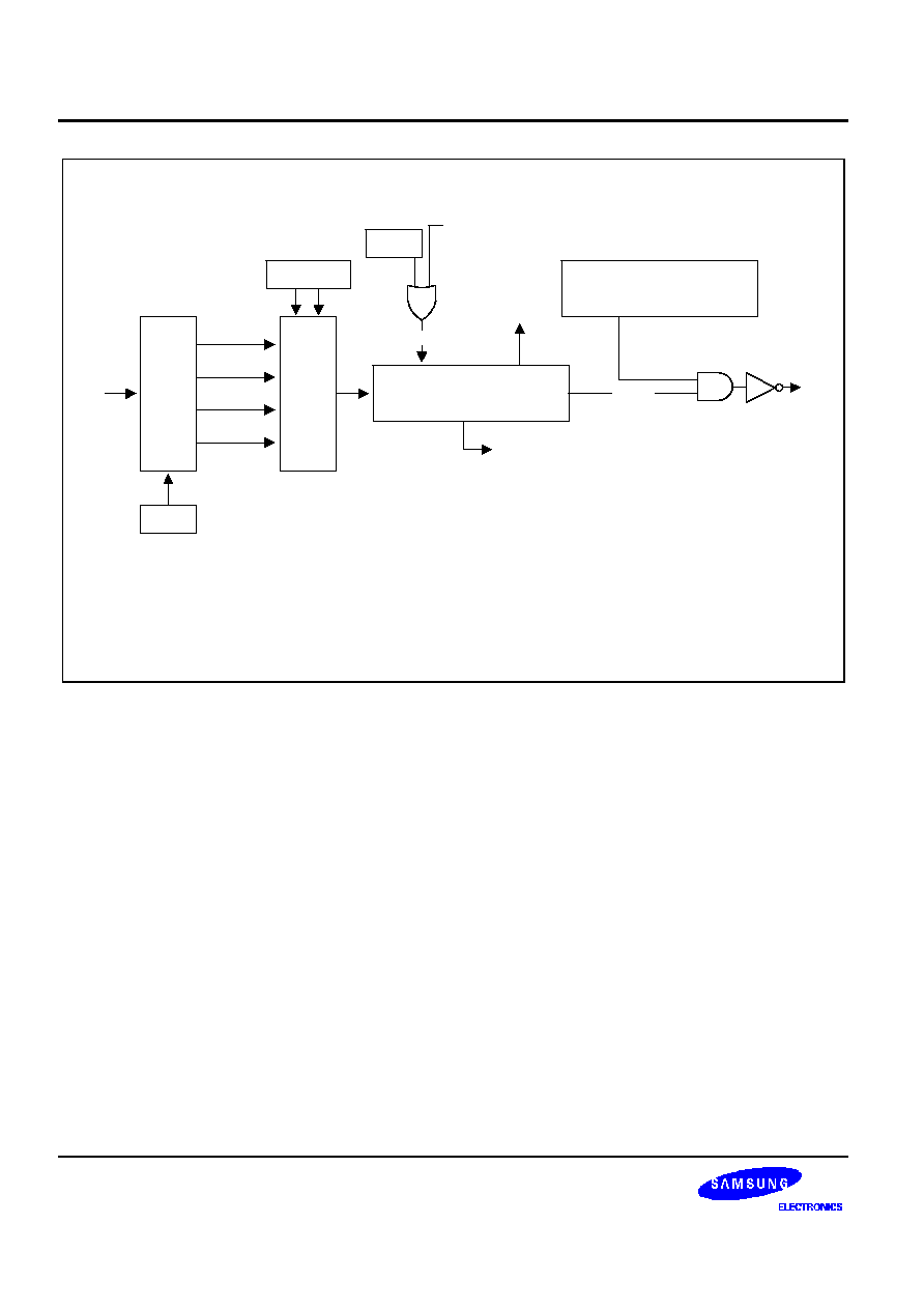
BASIC TIMER and TIMER 0
S3C852B/P852B (Preliminary Spec)
10-4
NOTE:
During a power-on reset operation, the CPU is idle during the required oscillation
stabilization interval (until bit 4 of the basic timer counter overflows).
MUX
f
XX
/4096
DIV
f
XX
/1024
f
XX
/128
f
XX
/16
f
XX
Bits 3, 2
Bit 0
Basic Timer Control Register
(Write '1010xxxxB' to Disable)
Clear
Bit 1
RESET
or STOP
Data Bus
8-Bit Up Counter
(BTCNT, Read-Only)
Start the CPU
(note)
OVF
RESET
R
Figure 10-2. Basic Timer Block Diagram

S3C852B/P852B (Preliminary Spec)
BASIC TIMER and TIMER 0
10-5
8-Bit Timer 0
Timer 0 has three operating modes, one of which you select using the appropriate T0CON setting:
-- Interval timer mode
-- Capture input mode with a rising or falling edge trigger at the P0.3 pin
-- PWM mode
Timer 0 has the following functional components:
-- Clock frequency divider (fxx divided by 1024, 256, or 64) with multiplexer
-- External clock input pin (P0.2, T0CK)
-- 8-bit counter (T0CNT), 8-bit comparator, and 8-bit reference data register (T0DATA)
-- I/O pins for capture input or match output (P0.3, T0)
-- Timer 0 overflow interrupt (IRQ0, vector FAH) and match/capture interrupt (IRQ0, vector FCH) generation
-- Timer 0 control register, T0CON (set 1, D2H, read/write)
TIMER 0 CONTROL REGISTER (T0CON)
You use the timer 0 control register, T0CON, to
-- Select the timer 0 operating mode (interval timer, capture mode, or PWM mode)
-- Select the timer 0 input clock frequency
-- Clear the timer 0 counter, T0CNT
-- Enable the timer 0 overflow interrupt or timer 0 match/capture interrupt
-- Clear timer 0 match/capture interrupt pending conditions

BASIC TIMER and TIMER 0
S3C852B/P852B (Preliminary Spec)
10-6
T0CON is located in set 1, at address D2H, and is read/write addressable using Register addressing mode.
A reset clears T0CON to "00H". This sets timer 0 to normal interval timer mode, selects an input clock frequency
of fxx/1024, and disables all timer 0 interrupts. You can clear the timer 0 counter at any time during normal
operation by writing a "1" to T0CON.3.
The timer 0 overflow interrupt (T0OVF) is interrupt level IRQ0 and has the vector address FAH. When a timer 0
overflow interrupt occurs and is serviced by the CPU, the pending condition is cleared automatically by hardware.
To enable the timer 0 match/capture interrupt (IRQ0, vector FCH), you must write T0CON.1 to "1". To detect a
match/capture interrupt pending condition, the application program polls T0CON.0. When a "1" is detected, a
timer 0 match or capture interrupt is pending. When the interrupt request has been serviced, the pending
condition must be cleared by software by writing a "0" to the timer 0 interrupt pending bit, T0CON.0.
Timer 0 Control Register (T0CON)
D2H, Set 1, Bank 0, R/W
.7
.6
.5
.4
.3
.2
.1
.0
MSB
LSB
Timer 0 counter clear bit:
0 = No effect
1 = Clear the timer 0 counter (when write)
Timer 0 input clock selection bits:
00 = fxx/1024
01 = fxx/256
10 = fxx/64
11 = External clock (P0.2/T0CK)
Timer 0 operating mode selection bits:
00 = Interval mode (P0.3/T0)
01 = Capture mode (capture on rising edge,
counter running, OVF can occur)
10 = Capture mode (capture on falling edge,
counter running, OVF can occur)
11 = PWM mode (OVF interrupt can occur)
Timer 0 overflow interrupt enable bit:
0 = Disable overflow interrupt
1 = Enable overflow interrupt
Timer 0 match/capture interrupt enable bit:
0 = Disable interrupt
1 = Enable interrupt
Timer 0 match/capture interrupt pending bit:
0 = No interrupt pending
0 = Clear pending bit (write)
1 = Interrupt is pending
Figure 10-3. Timer 0 Control Register (T0CON)
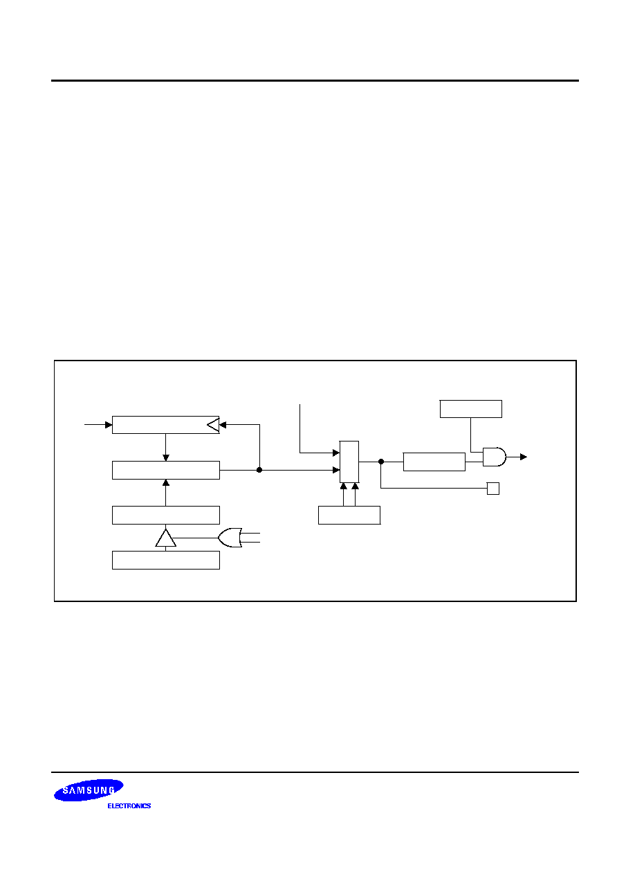
S3C852B/P852B (Preliminary Spec)
BASIC TIMER and TIMER 0
10-7
TIMER 0 FUNCTION DESCRIPTION
Timer 0 Interrupts (IRQ0, Vectors FAH and FCH)
The timer 0 module can generate two interrupts: the timer 0 overflow interrupt (T0OVF), and the timer 0 match/
capture interrupt (T0INT). T0OVF is interrupt level IRQ0, vector FAH. T0INT also belongs to interrupt level IRQ0,
but is assigned the separate vector address, FCH.
A timer 0 overflow interrupt pending condition is automatically cleared by hardware when it has been serviced.
However, the timer 0 match/capture interrupt pending condition must be cleared by the application's interrupt
service routine by writing a "0" to the T0CON.0 interrupt pending bit.
Interval Timer Mode
In interval timer mode, a match signal is generated when the counter value is identical to the value written to the
timer 0 reference data register, T0DATA. The match signal generates a timer 0 match interrupt (T0INT, vector
FCH) and clears the counter.
If, for example, you write the value "10H" to T0DATA, the counter will increment until it reaches "10H". At this
point, the timer 0 interrupt request is generated, the counter value is reset, and counting resumes. With each
match, the level of the signal at the timer 0 output pin is inverted (see Figure 10-4).
Match Signal
M
U
X
8-Bit Up Counter
Timer 0 Buffer Register
8-Bit Comparator
Timer 0 Data Register
T0CON.3
T0CON.5-.4
T0CON.0
Capture Signal
T0CON.1
T0INT (IRQ0)
T0 (P0.3)
Pending
Interrupt Enable/Disable
Match
R (Clear)
CLK
(Match INT)
Figure 10-4. Simplified Timer 0 Function Diagram: Interval Timer Mode

BASIC TIMER and TIMER 0
S3C852B/P852B (Preliminary Spec)
10-8
Pulse Width Modulation Mode
Pulse width modulation (PWM) mode lets you program the width (duration) of the pulse that is output at the T0
(P0.3) pin. As in interval timer mode, a match signal is generated when the counter value is identical to the value
written to the timer 0 data register. In PWM mode, however, the match signal does not clear the counter. Instead,
it runs continuously, overflowing at "FFH", and then continues incrementing from "00H".
Although you can use the match signal to generate a timer 0 overflow interrupt, interrupts are not typically used in
PWM-type applications. Instead, the pulse at the T0 (P0.3) pin is held to Low level as long as the reference data
value is less than or equal to (
) the counter value and then the pulse is held to High level for as long as the
data value is greater than ( > ) the counter value. One pulse width is equal to t
CLK
�
256 (see Figure 10-5).
Match Signal
M
U
X
8-Bit Up Counter
Timer 0 Buffer Register
8-Bit Comparator
Timer 0 Data Register
T0CON.3
T0CON.5-.4
T0CON.0
Capture Signal
T0CON.1
T0INT (IRQ0)
T0/PWM
Output (P0.3)
Pending
Interrupt Enable/Disable
Match
T0OVF
(IRQ0)
CLK
T0OVF
High level when
data > counter,
Lower level when
data < counter
NOTE:
Interrupts are usually not used when timer 0 is configured to operate in PWM mode.
(Match INT)
Figure 10-5. Simplified Timer 0 Function Diagram: PWM Mode
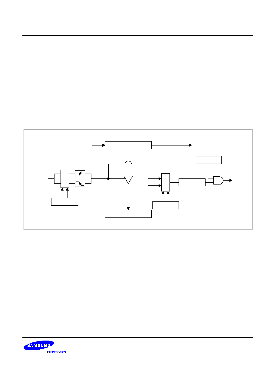
S3C852B/P852B (Preliminary Spec)
BASIC TIMER and TIMER 0
10-9
Capture Mode
In capture mode, a signal edge that is detected at the T0CAP (P0.3) pin opens a gate and loads the current
counter value into the timer 0 data register. You can select rising or falling edges to trigger this operation.
Timer 0 also gives you capture input source: the signal edge at the T0CAP (P0.3) pin. You select the capture
input by setting the values of the timer 0 capture input selection bits in the port 0 control register, P0CONL.7�.6,
(set 1, bank 0, EBH). When P0CONL.7�.6 is "00" or "01", the T0CAP input is selected.
Both kinds of timer 0 interrupts can be used in capture mode: the timer 0 overflow interrupt is generated
whenever a counter overflow occurs; the timer 0 match/capture interrupt is generated whenever the counter
value is loaded into the timer 0 data register.
By reading the captured data value in T0DATA, and assuming a specific value for the timer 0 clock frequency,
you can calculate the pulse width (duration) of the signal that is being input at the T0CAP pin (see Figure 10-6).
M
U
X
T0CON.5-.4
T0CON.0
T0CON.1
T0INT (IRQ0)
Pending
Interrupt Enable/Disable
Match Signal
8-Bit Up Counter
Timer 0 Data Register
CLK
T0OVF (IRQ0)
T0CON.5-.4
T0CAP input
(P0.3)
(Capture INT)
Figure 10-6. Simplified Timer 0 Function Diagram: Capture Mode
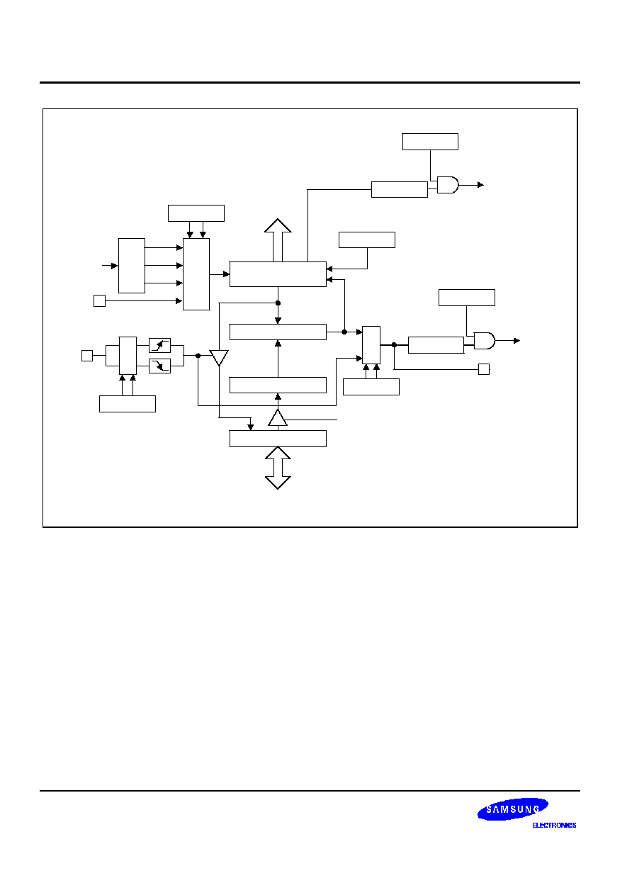
BASIC TIMER and TIMER 0
S3C852B/P852B (Preliminary Spec)
10-10
T0/PWM
Output (P0.3)
MUX
1/1024
fxx
1/64
1/256
DIV
T0CK Input
(P0.2)
T0CON.7-.6
M
U
X
T0CON.5-.4
T0CON.0
T0CON.1
T0INT (IRQ0)
Pending
T0CON.5-.4
T0CAP Input
(P0.3)
Timer 0 Buffer Register
8-Bit Comparator
Timer 0 Data Register
8-Bit Up Counter
(Read-Only)
R
Counter Clear Signal
8
Data BUS
8
T0CON.3
INTPND.0
T0CON.2
T0INT (IRQ0)
Pending
OVF
Data BUS
(OVF INT)
(Match/Capture INT)
Figure 10-7. Timer 0 Block Diagram

S3C852B/P852B (Preliminary Spec)
BASIC TIMER and TIMER 0
10-11
F
F
PROGRAMMING TIP -- Configuring the Basic Timer
This example shows how to configure the basic timer to sample specifications:
ORG
0100H
RESET
DI
; Disable all interrupts
LD
BTCON,#0AAH
; Disable the watchdog timer
LD
CLKCON,#18H
; Non-divided clock
CLR
SYM
; Disable global and fast interrupts
CLR
SPL
; Stack pointer low byte
"0"
; Stack area starts at 0FFH
�
�
�
SRP
#0C0H
; Set register pointer
0C0H
EI
; Enable interrupts
�
�
�
MAIN
LD
BTCON,#52H
; Enable the watchdog timer
; Basic timer clock: f
xx
/4096
; Clear basic timer counter
NOP
NOP
�
�
�
JP
T,MAIN
�
�
�

BASIC TIMER and TIMER 0
S3C852B/P852B (Preliminary Spec)
10-12
F
F
PROGRAMMING TIP -- Programming Timer 0
This sample program sets timer 0 to interval timer mode, sets the frequency of the oscillator clock, and
determines the execution sequence which follows a timer 0 interrupt. The program parameters are as follows:
-- Timer 0 is used in interval mode; the timer interval is set to 4 milliseconds
-- Oscillation frequency is 4 MHz
-- General register 64H (page 0)
60H + 62H + 63H + 64H (page 0) + 1H (value) is executed after a timer 0
interrupt
ORG
0FAH
; Timer 0 overflow interrupt
VECTOR
T0OVER
ORG
0FCH
; Timer 0 match/capture interrupt
VECTOR
T0INT
ORG
0100H
RESET
DI
; Disable all interrupts
LD
BTCON,#0AAH
; Disable the watchdog timer
LD
CLKCON,#18H
; Select non-divided clock
CLR
SYM
; Disable global and fast interrupts
CLR
SPL
; Stack pointer low byte
"0"
; Stack area starts at 0FFH
�
�
�
LD
T0CON,#4AH
; Write "01001010B"
; Input clock is f
xx
/256
; Interval timer mode
; Enable the timer 0 interrupt
; Disable the timer 0 overflow interrupt
LD
T0DATA,#3FH
; Set timer interval to 4 milliseconds
; (4 MHz/256) � (62.5 + 1) = 0.25 kHz (4 ms)
SRP
#0C0H
; Set register pointer
0C0H
EI
; Enable interrupts
�
�
�
T0INT
PUSH
RP0
; Save RP0 to stack
SRP0
#60H
; RP0
60H
INC
R0
; R0
R0 + 1
ADD
R2,R0
; R2
R2 + R0
ADC
R3,R2
; R3
R3 + R2 + Carry
ADC
R4,R3
; R4
R4 + R3 + Carry
(Continued on next page)

S3C852B/P852B (Preliminary Spec)
BASIC TIMER and TIMER 0
10-13
F
F
PROGRAMMING TIP -- Programming Timer 0 (Continued)
CP
R0,#32H
; 50
�
4 = 200 ms
JR
ULT,NO_200MS_SET
BITS
R1.2
; Bit setting (61.2H)
NO_200MS_SET:
LD
T0CON,#4AH
; Clear pending bit
POP
RP0
; Restore register pointer 0 value
T0OVER
IRET
; Return from interrupt service routine

BASIC TIMER and TIMER 0
S3C852B/P852B (Preliminary Spec)
10-14
NOTES

S3C852B/P852B (Preliminary Spec)
TIMER 1
11-1
11
TIMER 1
ONE 16-BIT TIMER MODE (TIMER 1)
The 16-bit timer 1 is used in one 16-bit timer or two 8-bit timers mode. If TACON.7 is set to "1", as a 16-bit timer.
If TACON.7 is set to "0", timer 1 is used as two 8-bit timers.
-- One 16-bit timer mode (Timer 1)
-- Two 8-bit timers mode (Timer A and B)
OVERVIEW
The 16-bit timer 1 is an 16-bit general-purpose timer. Timer 1 has the interval timer mode by using the
appropriate TACON setting.
Timer 1 has the following functional components:
-- Clock frequency divider (fxx divided by 1024, 512, 8, or 1 and T1CK: External clock) with multiplexer
-- 16-bit counter (TACNT, TBCNT), 16-bit comparator, and 16-bit reference data register (TADATA, TBDATA)
-- Timer 1 match interrupt (IRQ1, vector F4H) generation
-- Timer 1 control register, TACON (set 1, bank 1, E4H, read/write)
FUNCTION DESCRIPTION
Interval Timer Function
The timer 1 module can generate an interrupt: the timer 1 match interrupt (T1INT). T1INT belongs to interrupt
level IRQ1, and is assigned the separate vector address, F4H.
The T1INT pending condition should be cleared by software when it has been serviced. Even though T1INT is
disabled, the application's service routine can detect a pending condition of T1INT by the software and execute
it's sub-routine. When this case is used, the T1INT pending bit must be cleared by the application sub-routine by
writing a "0" to the TACON.0 pending bit.
In interval timer mode, a match signal is generated when the counter value is identical to the values written to
the timer 1 reference data registers, TADATA and TBDATA(FFH). The match signal generates a timer 1 match
interrupt (T1INT, vector F4H) and clears the counter.
If, for example, you write the value 32H to TADATA, and 8EH to TACON, the counter will increment until it
reaches 32FFH. At this point, the timer 1 interrupt request is generated, the counter value is reset, and counting
resumes.
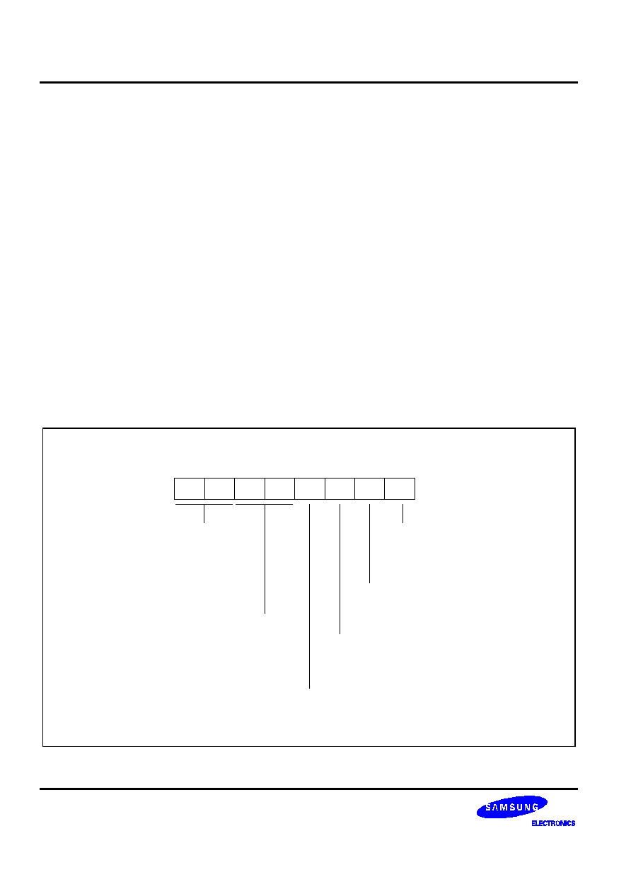
TIMER 1
S3C852B/P852B (Preliminary Spec)
11-2
Timer 1 Control Register (TACON)
You use the timer 1 control register, TACON, to
-- Enable the timer 1 operating (interval timer)
-- Select the timer 1 input clock frequency
-- Clear the timer 1 counter, TACNT and TBCNT
-- Enable the timer 1 interrupt
-- Clear timer 1 interrupt pending conditions
TACON is located in set 1, bank 1, at address E4H, and is read/write addressable using register addressing
mode.
A reset clears TACON to "00H". This sets timer 1 to disable interval timer mode, selects an input clock frequency
of fxx/1024, and disables timer 1 interrupt. You can clear the timer 1 counter at any time during normal operation
by writing a "1" to TACON.3.
To enable the timer 1 interrupt (IRQ1, vector F4H), you must write TACON.7, TACON.2, and TACON.1 to "1".
To generate the exact time interval, you should write TACON.3 and TACON.0, which cleared counter and
interrupt pending bit. To detect an interrupt pending condition when T1INT is disabled, the application program
polls pending bit, TACON.0. When a "1" is detected, a timer 1 interrupt is pending. When the T1INT sub-routine
has been serviced, the pending condition must be cleared by software by writing a "0" to the timer 1 interrupt
pending bit, TACON.0.
Timer A Control Register (TACON)
E4H, Set 1, Bank 1, R/W
.7
.6
.5
.4
.3
.2
.1
.0
MSB
LSB
Timer A interrupt enable bit:
0 = Disable interrupt
1 = Enable interrupt
Timer A interrupt pending bit:
0 = No interrupt pending
0 = Clear pending bit (when write)
1 = Interrupt is pending
Timer A counter enable bit:
0 = Disable counting operation
1 = Enable counting operation
Timer A counter clear bit:
0 = No affect
1 = Clear the timer A counter (when write)
One 16-bit timer or Two 8-bit timers
mode:
0 = Two 8-bit timers mode (Timer A/B)
1 = One 16-bit timer mode (Timer 1)
Timer A clock selection bits:
000 = fxx/1024
001 = fxx/512
010 = fxx/8
011 = fxx
1xx = T1CK (external clock)
('x' means don't care.)
Figure 11-1. Timer 1 Control Register (TACON)
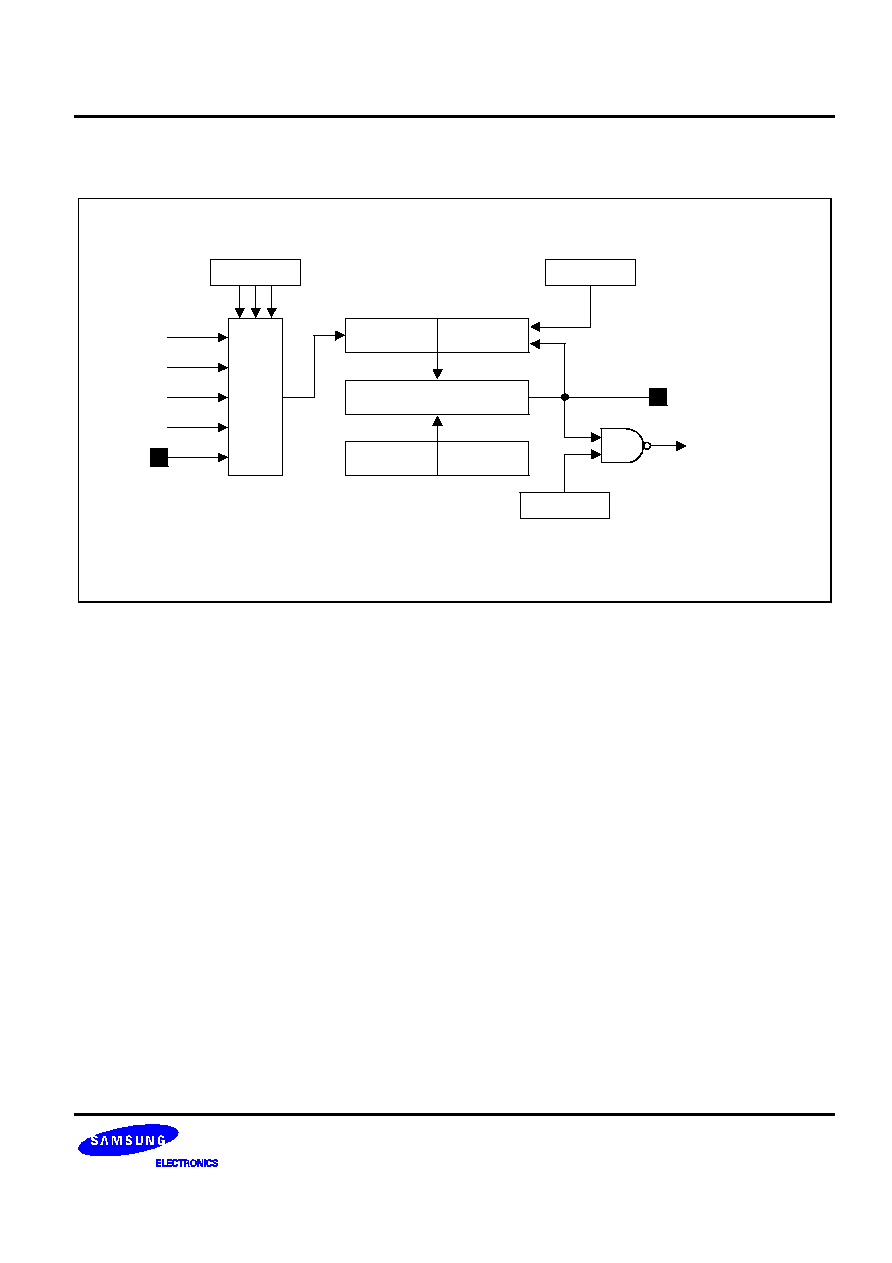
S3C852B/P852B (Preliminary Spec)
TIMER 1
11-3
BLOCK DIAGRAM
NOTE: When TACON.7 is '1', one 16-bit timer A.
TACON.6-.4
M
U
X
TACON.3
T1CK
P0.4
Comparator
f
XX
/1
f
XX
/8
f
XX
/512
f
XX
/1024
TBCNT(FFH)
TACNT
TBDATA(FFH)
TADATA
LSB
MSB
TACON.1
TA (Interval)
P0.5
Match
IRQ1
(Match INT)
LSB
MSB
Clear
Figure 11-2. Timer 1 Functional Block Diagram

TIMER 1
S3C852B/P852B (Preliminary Spec)
11-4
TWO 8-BIT TIMERS MODE (TIMER A and B)
OVERVIEW
The 8-bit timer A and B are the 8-bit general-purpose timers. Timer A have the interval timer mode, and the
timer B have the interval timer mode and PWM mode by using the appropriate TACON and TBCON setting,
respectively.
Timer A and B have the following functional components:
-- Clock frequency divider with multiplexer
� fxx divided by 1024, 512, 8, or 1 and T1CK (External clock) for timer A
� fxx divided by 8, 4, 2, or 1 for timer B
-- 8-bit counter (TACNT, TBCNT), 8-bit comparator, and 8-bit reference data register (TADATA, TBDATA)
-- Timer A have I/O pin for match output (P0.5, TA)
-- Timer A match interrupt (IRQ1, vector F4H) generation
-- Timer A control register, TACON (set 1, bank 1, E4H, read/write)
-- Timer B have I/O pin for match and PWM output (P0.6, TB)
-- Timer B overflow interrupt (IRQ1, vector F6H) generation
-- Timer B match interrupt (IRQ1, vector F8H) generation
-- Timer B control register, TBCON (set 1, bank 1, E5H, read/write)
Timer A and B Control Register (TACON, TBCON)
You use the timer A and B control register, TACON and TBCON, to
-- Enable the timer A (interval timer mode) and B operating (interval timer mode and PWM mode)
-- Select the timer A and B input clock frequency
-- Clear the timer A and B counter, TACNT and TBCNT
-- Enable the timer A and B interrupt
-- Clear timer A and B interrupt pending conditions
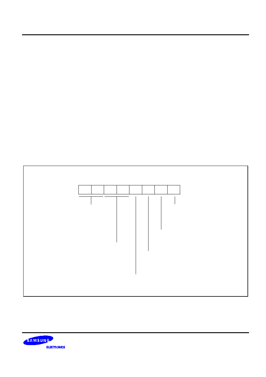
S3C852B/P852B (Preliminary Spec)
TIMER 1
11-5
TACON and TBCON are located in set 1, bank 1, at address E4H and E5H, and is read/write addressable using
register addressing mode.
A reset clears TACON to "00H". This sets timer A to disable interval timer mode, selects an input clock frequency
of fxx/1024, and disables timer A interrupt. You can clear the timer A counter at any time during normal
operation by writing a "1" to TACON.3.
A reset clears TBCON to "00H". This sets timer B to disable interval timer mode and PWM mode, selects an
input clock frequency of fxx/8, and disables timer A interrupt. You can clear the timer B counter at any time
during normal operation by writing a "1" to TBCON.3.
To enable the timer A interrupt (TAINT) and timer B interrupt (TBINT), (IRQ1, vector F4H, F8H), you must write
TACON.7 to "0", TACON.2 (TBCON.2) and TACON.1 (TBCON.1) to "1". To generate the exact time interval, you
should write TACON.3 (TBCON.3) and TACON.0 (INTPND.2), which cleared counter and interrupt pending bit.
To detect an interrupt pending condition when TAINT and TBINT is disabled, the application program polls
pending bit, TACON.0 and INTPND.2. When a "1" is detected, a timer A interrupt (TAINT) and timer B interrupt
(TBINT) is pending. When the TAINT and TBINT sub-routine has been serviced, the pending condition must be
cleared by software by writing a "0" to the timer A and B interrupt pending bit, TACON.0 and INTPND.2.
Also, to enable timer B overflow interrupt (TBOVF), (IRQ1, vector F6H), you must write TACON.7 to "0",
TBCON.2 and TBCON.0 to "1". To generate the exact time interval, you should write TBCON.3 and INTPND.2,
witch cleared counter and interrupt pending bit.
Timer A Control Register (TACON)
E4H, Set 1, Bank 1, R/W
.7
.6
.5
.4
.3
.2
.1
.0
MSB
LSB
Timer A interrupt enable bit:
0 = Disable interrupt
1 = Enable interrupt
Timer A interrupt pending bit:
0 = No interrupt pending
0 = Clear pending bit (when write)
1 = Interrupt is pending
Timer A counter enable bit:
0 = Disable counting operation
1 = Enable counting operation
Timer A counter clear bit:
0 = No affect
1 = Clear the timer A counter (when write)
One 16-bit timer or Two 8-bit timers
mode:
0 = Two 8-bit timers mode (Timer A/B)
1 = One 16-bit timer mode (Timer 1)
Timer A clock selection bits:
000 = fxx/1024
001 = fxx/512
010 = fxx/8
011 = fxx
1xx = T1CK (external clock)
('x' means don't care.)
Figure 11-3. Timer A Control Register (TACON)
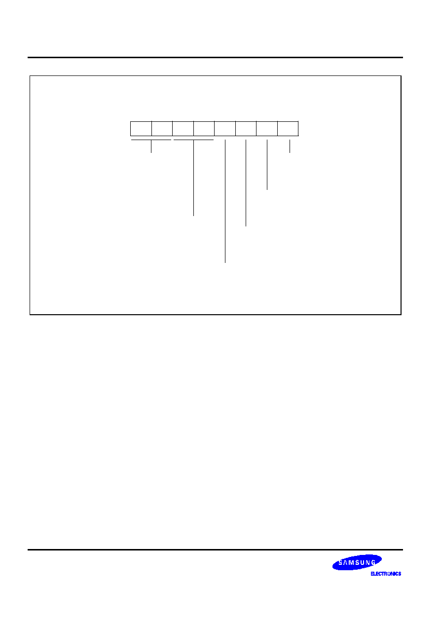
TIMER 1
S3C852B/P852B (Preliminary Spec)
11-6
Timer B Control Register (TBCON)
E5H, Set 1, Bank 1, R/W
.7
.6
.5
.4
.3
.2
.1
.0
MSB
LSB
Timer B match interrupt enable bit:
0 = Disable match interrupt
1 = Enable match interrupt
Timer B overflow interrupt enable bit:
0 = Disable overflow interrupt
1 = Enable overflow interrupt
Timer B count enable bit:
0 = Disable counting operating
1 = Enable counting operating
Timer B counter clear bit:
0 = No effect
1 = Clear the timer B counter (when write)
Timer B clock selection bits:
00 = fxx/8
01 = fxx/4
10 = fxx/2
11 = fxx
Timer B operating mode selection bits:
00 = Interval mode
01 = 6-bit PWM mode (OVF interrupt can occur)
10 = 7-bit PWM mode (OVF interrupt can occur)
11 = 8-bit PWM mode (OVF interrupt can occur)
Figure 11-4. Timer B Control Register (TBCON)

S3C852B/P852B (Preliminary Spec)
TIMER 1
11-7
FUNCTION DESCRIPTION
Interval Timer Function (Timer A and Timer B)
The timer A and B module can generate an interrupt: the timer A match interrupt (TAINT) and the timer B match
interrupt (TBINT). TAINT belongs to interrupt level IRQ1, and is assigned the separate vector address, F4H.
TBINT belongs to interrupt level IRQ1 and is assigned the separate vector address, F8H.
The timer A match interrupt pending condition (TACON.0) and the timer B match interrupt pending condition
(INTPND.2) must be cleared by software in the application's interrupt service by means of writing a "0" to the
TACON.0 and INTPND.2 interrupt pending bit.
Even though TAINT and TBINT are disabled, the application's service routine can detect a pending condition of
TAINT and TBINT by the software and execute it's sub-routine. When this case is used, the TAINT and TBINT
pending bit must be cleared by the application sub-routine by writing a "0" to the corresponding pending bit
TACON.0 and INTPND.2.
In interval timer mode, a match signal is generated when the counter value is identical to the values written to
the timer A or timer B reference data registers, TADATA or TBDATA. The match signal generates corresponding
match interrupt (TAINT, vector F4H; TBINT, vector F8H) and clears the counter.
If, for example, you write the value 20H to TADATA and 0EH to TACON, the counter will increment until it
reaches 20H. At this point, the timer A interrupt request is generated, the counter value is cleared, and counting
resumes and you write the value 10H to TBDATA, "0" to TACON.7, and 0EH to TBCON, the counter will
increment until it reaches 10H. At this point, TB interrupt request is generated, the counter value is cleared and
counting resumes.
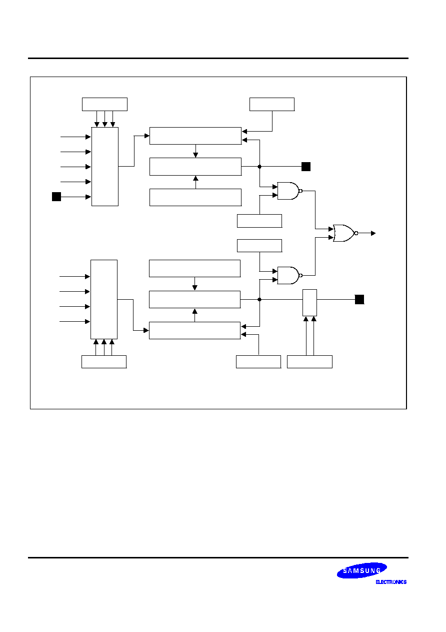
TIMER 1
S3C852B/P852B (Preliminary Spec)
11-8
NOTE:
When TACON.7 is '0', two 8-bit timer A/B (Interval mode).
TACON.6-.4
M
U
X
TACON.3
T1CK
P0.4
Comparator
f
XX
/1
f
XX
/8
f
XX
/512
f
XX
/1024
TACNT
TADATA
TACON.1
TA (Interval)
P0.5
Match
R
Clear
Comparator
f
XX
/1
f
XX
/2
f
XX
/4
f
XX
/8
TB (Interval)
P0.6
Match
TBCON.1
TBCON.3
Clear
TBCNT
TBDATA
R
TBCON.5-.4
M
U
X
IRQ1
TBCON.6,.7
M
U
X
(Match INT)
Figure 11-5. Timer A and B Function Block Diagram

S3C852B/P852B (Preliminary Spec)
TIMER 1
11-9
Pulse Width Modulation Mode (Timer B)
Pulse width modulation (PWM) mode lets you program the width (duration) of the pulse that is output at the TB
(P0.6) pin. As in interval timer mode, a match signal is generated when the counter value is identical to the
value written to the timer B data register. In PWM mode, however, the match signal does not clear the counter.
Instead, it runs continuously, overflowing at "FFH", and then continues incrementing from "00H".
Although you can use the match signal to generate a timer B overflow interrupt, interrupts are not typically used
in PWM-type applications. Instead, the pulse at the TB pin is held to Low level as long as the reference data
value is less than or equal to (
) the counter value and then the pulse is held to High level for as long as the data
value is greater than (>) the counter value. One pulse width is equal to t
CLK
�
256 (see Figure 11-6).
TBCON.5-.4
TBCON.3
8-Bit Comparator
Up-Counter
(Read-Only)
MUX
Match
R
Clear
Selected TBOVF
TBCON.6-.7
IRQ1
(OVF INT)
f
XX
/1
f
XX
/2
f
XX
/4
f
XX
/8
M
U
X
Timer B Buffer
Register
Timer B Data Register
(Read/Write)
Data Bus
6-Bit Match
7-Bit Match
8-Bit Match
6-Bit OVF
7-Bit OVF
8-Bit OVF
MUX
MUX
TBCON.6-.7
INTPND.1
TBCON.0
TBCON.3
TBCON.6-.7
P0.6
INTPND.2
TBCON.1
IRQ1
(Match INT)
Pending Bit
TB(PWM, Interval)
Figure 11-6. Timer B PWM Function Block Diagram

TIMER 1
S3C852B/P852B (Preliminary Spec)
11-10
NOTES

S3C852B/P852B (Preliminary Spec)
WATCH TIMER
12-1
12
WATCH TIMER
OVERVIEW
Watch timer functions include real-time and watch-time measurement and interval timing for the system clock.
To start watch timer operation, set bit 1 of the watch timer control register, WTCON.1 to "1".
And if you want to service watch timer overflow interrupt (IRQ3, vector F2H), then set the WTCON.6 to "1".
The watch timer overflow interrupt pending condition (WTCON.0) must be cleared by software in the application's
interrupt service routine by means of writing a "0" to the WTCON.0 interrupt pending bit.
After the watch timer starts and elapses a time, the watch timer interrupt pending bit (WTCON.0) is automatically
set to "1", and interrupt requests commence in 3.91ms, 0.25, 0.5 and 1-second intervals by setting Watch timer
speed selection bits (WTCON.3 � .2).
The watch timer can generate a steady 2 kHz, 4 kHz, 8 kHz, or 16 kHz signal to BUZ output pin for Buzzer. By
setting WTCON.3 and WTCON.2 to "11b", the watch timer will function in high-speed mode, generating an
interrupt every 3.91 ms. High-speed mode is useful for timing events for program debugging sequences.
Also, you can select watch timer clock source by setting the WTCON.7 appropriatly value.
Watch timer has the following functional components:
-- Real Time and Watch-Time Measurement
-- Using a Main System or Subsystem Clock Source (Main clock divided by 2
7
(fx/128) or Sub clock(fxt))
-- I/O pin for Buzzer Output Frequency Generator (P0.1, BUZ)
-- Timing Tests in High-Speed Mode
-- Watch timer overflow interrupt (IRQ1, vector F2H) generation
-- Watch timer control register, WTCON (set 1, bank 1, E6H, read/write)
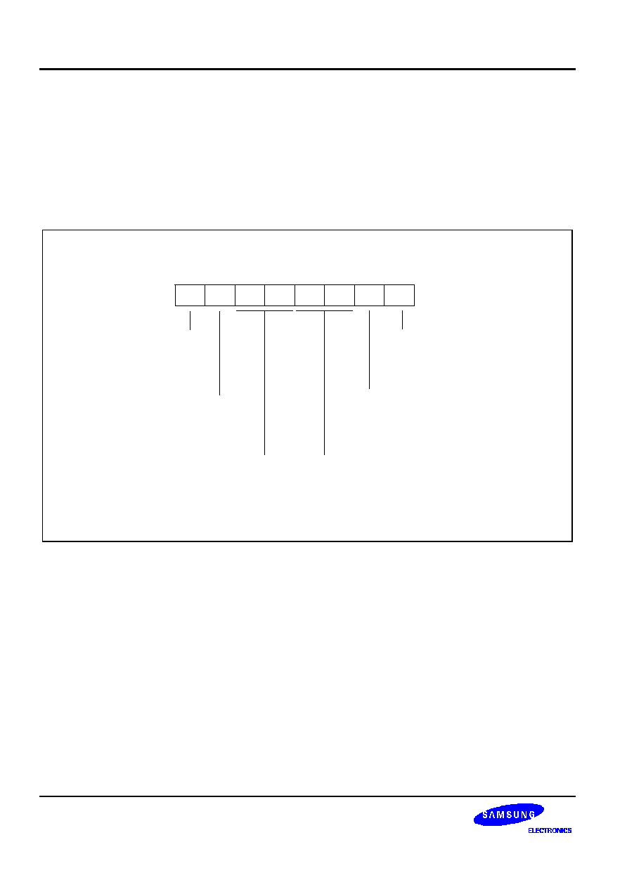
WATCH TIMER
S3C852B/P852B (Preliminary Spec)
12-2
WATCH TIMER CONTROL REGISTER (WTCON)
The watch timer control register, WTCON is used to select the input clock source, the watch timer interrupt time
and Buzzer signal, to enable or disable the watch timer function. It is located in set 1, bank 1 at address E6H, and
is read/write addressable using register addressing mode.
A reset clears WTCON to "00H". This disable the watch timer and select fx/128 as the watch timer clock.
So, if you want to use the watch timer, you must write appropriate value to WTCON.
To values of watch timer speed are accurate when watch timer clock is fxt. So, if you select fx/128 as watch timer
clock, the speed will be changed according to the frequency fx.
Buzzer signal selection bits:
00 = 2 kHz
01 = 4 kHz
10 = 8 kHz
11 = 16 kHz
Watch Timer Control Register (WTCON)
E6H, Set 1, Bank 1, R/W
.7
.6
.5
.4
.3
.2
.1
.0
MSB
LSB
Watch timer Enable/Disable bit:
0 = Disable watch timer;
clear frequency dividing circuits
1 = Enable watch timer
Watch timer interrupt pending bit:
0 = Interrupt request is not pending
1 = Interrupt request is pending
Watch timer speed selection bits:
00 = Set watch timer interrupt to 1 s
01 = Set watch timer interrupt to 0.5 s
10 = Set watch timer interrupt to 0.25 s
11 = Set watch timer interrupt to 3.91 ms
Watch timer clock selection bit:
0 = Main clock divided by
2
7
(fx/128)
1 = Sub clock (fxt)
Watch timer INT Enable/Disable bit:
0 = Disable watch timer INT
1 = Enable watch timer INT
Figure 12-1. Watch Timer Control Register (WTCON)
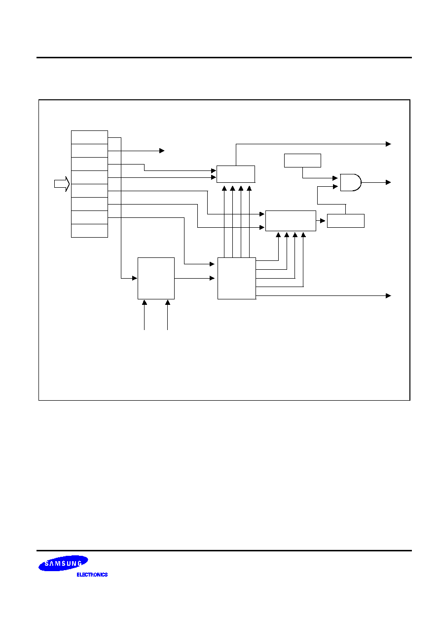
S3C852B/P852B (Preliminary Spec)
WATCH TIMER
12-3
WATCH TIMER CIRCUIT DIAGRAM
WT INT Enable
WTCON.1
WTCON.2
WTCON.3
WTCON.4
WTCON.5
WTCON.6
Enable/Disable
Selector
Circuit
MUX
WTCON.0
IRQ3
WTCON.6
BUZZER Output
f
W
/2
15
f
W
/2
14
f
W
/2
13
f
W
/2
7
f
W
/16 (2 kHz)
f
W
/8 (4 kHz)
f
W
/4 (8 kHz)
f
W
/2 (16 kHz)
(1 Hz)
f
X
= Main system clock
fxt = Subsystem clock (32,768 Hz)
f
W
= Watch timer frequency
Clock
Selector
Frequency
Dividing
Circuit
f
W
32.768 kHz
fxt
f
X
/128
(1)
fw
WTCON.7
WTCON.0
(Pending Bit)
Pending Bit
NOTE:
The BUZZER output Enable/Disable is controled by setting P0CONL.3-.2.
That is, if the value of P0CONL.3-.2 is "11" (P0.1 is configured to select alternative
function), the BUZZER output enabled, at this time, Watch timer must be enabled.
The other value except "11" of P0CONL.3-.2 disable the BUZZER output.
8
BUZ (P0.1)
Figure 12-2. Watch Timer Circuit Diagram

WATCH TIMER
S3C852B/P852B (Preliminary Spec)
12-4
NOTES

S3C852B/P852B (Preliminary Spec)
SERIAL I/O PORT
13-1
13
SERIAL I/O PORT
OVERVIEW
Serial I/O module, SIO can interface with various types of external devices that require serial data transfer.
SIO has the following functional components:
-- SIO data receive/transmit interrupt (IRQ4, vector F0H) generation
-- 8-bit control register, SIOCON (set 1, bank 1, EBH, read/write)
-- Clock selection logic
-- 8-bit data buffer, SIODATA
-- 8-bit prescaler (SIOPS), (set 1, bank 1, ECH, read/write)
-- 3-bit serial clock counter
-- Serial data I/O pins (P1.4�P1.5, SI, SO)
-- External clock input/output pin (P1.6,
SCK
)
The SIO module can transmit or receive 8-bit serial data at a frequency determined by its corresponding control
register settings. To ensure flexible data transmission rates, you can select an internal or external clock source.
PROGRAMMING PROCEDURE
To program the SIO modules, follow these basic steps:
1.
Configure P1.4, P1.5 and P1.6 to alternative function (SI, SO,
SCK
) for interfacing SIO module by setting the
P1AFS register to appropriatly value.
2.
Load an 8-bit value to the SIOCON control register to properly configure the serial I/O module. In this
operation, SIOCON.2 must be set to "1" to enable the data shifter.
3.
For interrupt generation, set the serial I/O interrupt enable bit, SIOCON.1 to "1".
4.
To transmit data to the serial buffer, write data to SIODATA and set SIOCON.3 to 1, then the shift operation
starts.
5.
When the shift operation (transmit/receive) is completed, the SIO pending bit (SIOCON.0) is set to "1" and
an SIO interrupt request is generated.
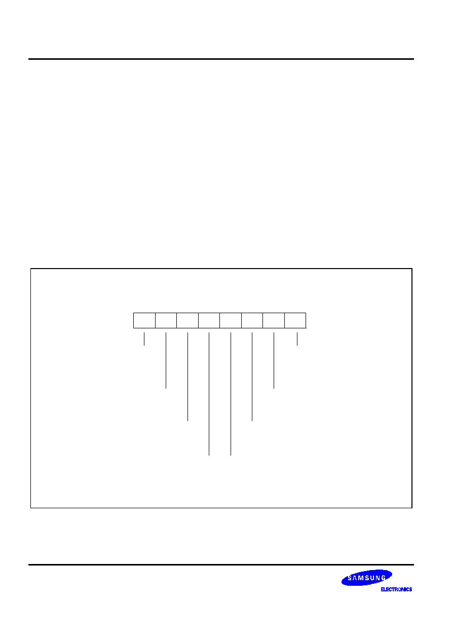
SERIAL I/O PORT
S3C852B/P852B (Preliminary Spec)
13-2
SIO CONTROL REGISTER (SIOCON)
The control register for the serial I/O interface module, SIOCON, is located in set 1, bank 1 at address EBH. It
has the control settings for SIO module.
--
Clock source selection (internal or external) for shift clock
--
Interrupt enable
--
Edge selection for shift operation
--
Clear 3-bit counter and start shift operation
--
Shift operation (transmit) enable
--
Mode selection (transmit/receive or receive-only)
--
Data direction selection (MSB first or LSB first)
A reset clears the SIOCON value to '00H'. This configures the corresponding module with an internal clock
source, P.S clock, at the SCK , selects receive-only operating mode, the data shift operation and the interrupt
are disabled, and the data direction is selected to MSB-first.
So, if you want to use SIO module, you must write appropriate value to SIOCON.
Serial I/O Module Control Registers (SIOCON)
EBH, Set 1, Bank 1, R/W
.7
.6
.5
.4
.3
.2
.1
.0
MSB
LSB
SIO interrupt enable bit:
0 = Disable SIO interrupt
1 = Enable SIO interrupt
SIO interrupt pending bit:
0 = No interrupt pending
0 = Clear pending condition
(when write)
1 = Interrupt is pending
SIO shift operation enable bit:
0 = Disable shifter and clock counter
1 = Enable shifter and clock counter
Shift clock edge selection bit:
0 = T
X
at falling edeges, R
X
at rising edges
1 = T
X
at rising edeges, R
X
at falling edges
Data direction control bit:
0 = MSB-first mode
1 = LSB-first mode
SIO mode selection bit:
0 = Receive-only mode
1 = Transmit/receive mode
SIO counter clear and shift start bit:
0 = No action
1 = Clear 3-bit counter and start shifting
SIO Shift clock selection bit:
0 = Internal clock (P.S clock)
1 = External Clock (
SCK
)
Figure 13-1. Serial I/O Module Control Registers (SIOCON)
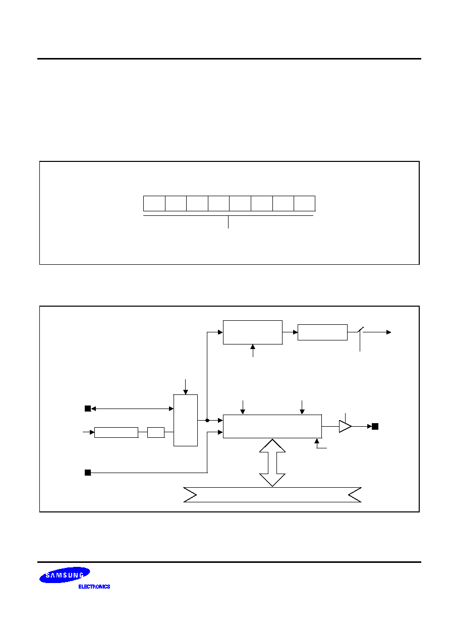
S3C852B/P852B (Preliminary Spec)
SERIAL I/O PORT
13-3
SIO PRESCALER REGISTER (SIOPS)
The control register for the serial I/O interface module, SIOPS, is located in set 1, bank 1, at address ECH.
The value stored in the SIO prescaler registers, SIOPS, lets you determine the SIO clock rate (baud rate) as
follows:
Baud rate = Input clock (fxx)/[(SIOPS value + 1) � 4] or
SCK
input clock.
SIO Pre-Scaler Register (SIOPS)
ECH, Set 1, Bank 1, R/W
.7
.6
.5
.4
.3
.2
.1
.0
MSB
LSB
SIOPS Data Value
Baud rate = Input clock (fxx)/[(SIOPS + 1) x 4] or SCLK input clock
Figure 13-2. SIO Prescaler Register (SIOPS)
BLOCK DIAGRAM
SIO INT
Pending
3-Bit Counter
Clear
SIOCON.0
8-Bit SIO Shift Buffer
(SIODATA)
fxx/2
SIOPS
SCK
(P1.6)
SIOCON.7
(Shift Clock
Source Select)
Prescaled Value = 1/(SIOPS +1)
CLK
SIOCON.1
(Interrupt Enable)
CLK
SI (P1.4)
SIOCON.3
SIOCON.4
(Shift Clock
Edge Select)
SIOCON.5
(Mode Select)
SIOCON.2
(Shift Enable)
SIOCON.6
(LSB/MSB First Mode Select)
Data BUS
8
SO (P1.5)
M
U
X
1/2
8-bit P.S.
IRQ4
Figure 13-3. SIO Functional Block Diagram
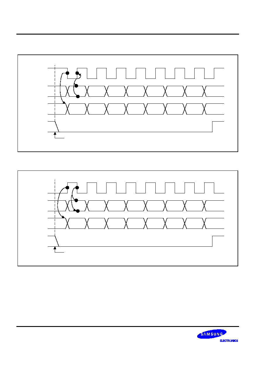
SERIAL I/O PORT
S3C852B/P852B (Preliminary Spec)
13-4
SERIAL I/O TIMING DIAGRAMS
SO
(Data Output)
SI
(Data Input)
Shift
Clock
Transmit
Complete
IRQ4
SET SIOCON.3
D7
D6
D5
D4
D3
D2
D1
D0
D7
D6
D5
D4
D3
D2
D1
D0
Figure 13-4. SIO Timing in Transmit/Receive Mode (Tx at falling edge, SIOCON.4=0)
SO
(Data Output)
SI
(Data Input)
Shift
Clock
Transmit
Complete
IRQ4
SET SIOCON.3
D7
D6
D5
D4
D3
D2
D1
D0
D7
D6
D5
D4
D3
D2
D1
D0
Figure 13-5. SIO Timing in Transmit/Receive Mode (Tx at rising edge, SIOCON.4=1)

S3C852B/P852B (Preliminary Spec)
SERIAL I/O PORT
13-5
SO
SI
Shift
Clock
Transmit
Complete
IRQ4
SET SIOCON.3
D7
D6
D5
D4
D3
D2
D1
D0
High Impedance
Figure 13-6. SIO Timing in Receive-Only Mode (Rising edge start)
F
F
PROGRAMMING TIP -- Use Internal Clock to Transfer And Receive Serial Data
1. The method that uses hardware pending check is used.
�
�
�
DI
; Disable All interrupts
LD
P1AFS, #70H
; P1.4�P1.6 are selected to alternative function for
; SI, SO,
SCK
, respectively
EI
SB1
LD
SIODATA,TDATA
; Load data to SIO buffer
LD
SIOPS,#90H
; Baud rate = input clock(fxx)/[(144 + 1) x 4]
LD
SIOCON,#2EH
; Interval clock, MSB first, transmit/receive mode
SB0
; Select falling edges to start shift operation
; Clear 3-bit counter and start shifting
; Enable shifter and clock counter
; Enable SIO interrupt and clear pending
�
�
�
SIOINT
PUSH
RP0
;
SRP0
#RDATA
;
SB1
LD
R0,SIODATA
; Load received data to general register
OR
SIOCON,#08H
; SIO restart
POP
RP0
IRET

SERIAL I/O PORT
S3C852B/P852B (Preliminary Spec)
13-6
F
F
PROGRAMMING TIP -- Use Internal Clock to Transfer And Receive Serial Data (Continued)
2. The method that uses software pending check is used.
�
�
�
DI
; Disable All interrupts
LD
P1AFS, #70H
; P1.4�P1.6 are selected to alternative function for
; SI, SO,
SCK
, respectively
EI
SB1
LD
SIODATA,TDATA
; Load data to SIO buffer
LD
SIOPS,#90H
; Baud rate = input clock(fxx)/[(144 + 1)
�
4]
LD
SIOCON,#2CH
; Internal clock, MSB first, transmit/receive mode
; Select falling edges to start shift operation
; clear 3-bit counter and start shifting
; Disable SIO interrup
SIOtest:
LD
R6,SIOCON
; To check whether transmit and receive is finished
BTJRF
SIOtest,R6.0
; Check pending bit
NOP
AND
SIOCON,#0FEH
; Pending clear by software
LD
RDATA,SIODATA
; Load received data to RDATA
�
�
�
SB0
�
�
�

S3C852B/P852B (Preliminary Spec)
CALLER ID BLOCK
14-1
14
CALLER ID BLOCK
OVERVIEW
The S3C852B/P852B microcontroller has a Caller ID on Call Waiting (CIDCW) receiver, tone generator, etc. The
S3C852B is used for receiving physical layer signals like Bellcore's CPE Alerting Signal (CAS) and similar
evolving systems and also meets the requirements of emerging Caller ID on Call Waiting (CIDCW) services. In
addition, two different signal inputs are available to support Tip/Ring and Hybrid connectivity. The device also
includes a 1200 baud Bell 202/V.23 compatible FSK data demodulator, a ring or line reversal detector, a line
voltage measurement unit, a TIA/EIA PN-4159 compatible Stutter Dial Tone detector, and a tone generator is
capable of generating FSK signal and dual tone signals such as CAS, DTMF to support various applications such
as short messaging service (SMS).
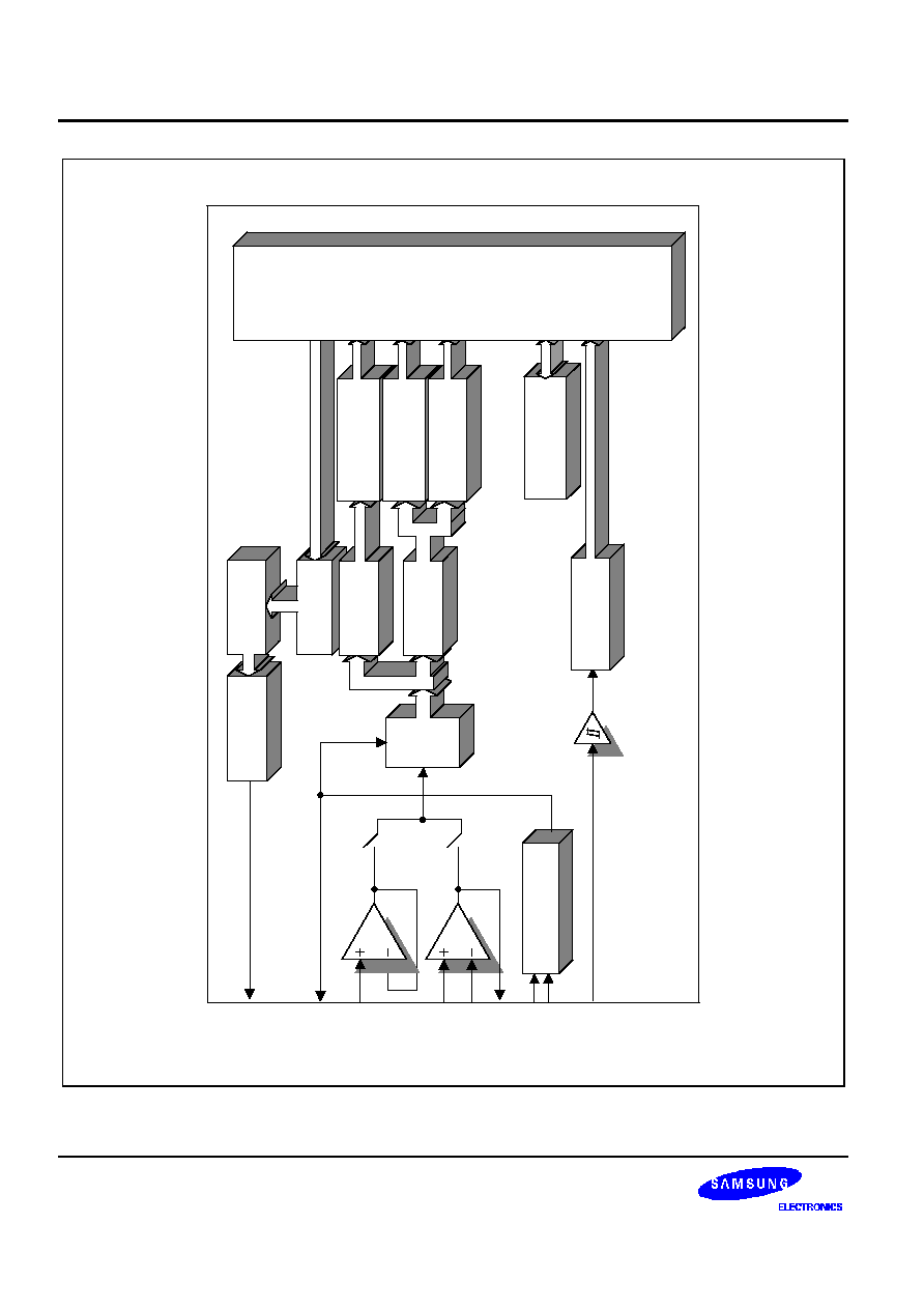
CALLER ID BLCOK
S3C852B/P852B (Preliminary Spec)
14-2
ADC
Tone
Geneator
Gain
Controller
PDM
BandPass
Filter
FSK Receiver
BandPass
Filter
LRIN
OUT
INN
INP
INS
CAS Detector
SDT Detector
Line Reversal /
Ring Detector
Bias Voltage
VDDA
VSSA
Melody
Generator
Mode
Control
Figure 14-1. CID Part Functional Block Diagram

S3C852B/P852B (Preliminary Spec)
CALLER ID BLOCK
14-3
FUNCTION DESCRIPTION OF CID BLOCK
ANALOG INPUT AND PREPROCESSOR
The preprocessor for the FSK receiver ,the CAS and the SDT detectors, comprises two input signal buffers, an
14-bit Analog-to-Digital Converter (14-bit ADC) and digital bandpass filters. Bandpass filters are used to attenuate
out band noise and interfering signals, which might otherwise reach the FSK receiver and CAS, SDT detectors.
The CAS and SDT detectors share a single digital filter while the FSK receiver has its own separate filter.
In CID Block's power down mode, the CID block can be forced into a power-down state by switching off the
3.579545 MHz main clock and ADC's and op-amps.
Differential Input Buffer
The differential input buffer is used to convert the balanced telephone line signal to the input signal of 14-bit ADC
in the S3C852B.
S3C852B
Tip/A
Ring/B
R1a
C1a
to 14-bit
ADC
R3
R1b
INp
C1b
R4
R5
INn
OUT
VREF
+
-
Figure 14-2. Differential Input Buffer of the S3C852B
Design equations for this buffer are;
The differential voltage gain = R5/R1b.
R1a = R1b
C1a = C1b
R3 = R4 * R5/(R4 + R5)
The target differential voltage gain should be adjusted to obtain the expected signal level at the "OUT" pin.
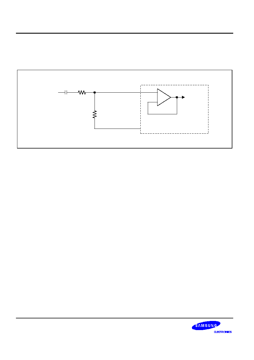
CALLER ID BLCOK
S3C852B/P852B (Preliminary Spec)
14-4
Single Ended Input Buffer
The single ended input buffer may also be used with the telephone line signal connected to the hybrid as shown
in Figure 14-3.
S3C852B
A
Connected
to Hybrid
R6
C4
to 14-bit
ADC
R7
INs
VREF
+
-
Figure 14-3. Single Ended Buffer of the S3C852B
The voltage gain is R7/( R6 + R7 )
The target voltage gain should be adjusted to obtain the expected signal level at the INS input.
The BFS (Buffer selection) bit in the Function register chooses between the output of the single-ended input
buffer and the output of the differential input buffer, sending the selected output to the 14-bit ADC. The
differential input buffer is selected when BFS is "0" and the single ended input buffer is selected when BFS is "1".
The default value of BFS is "0"
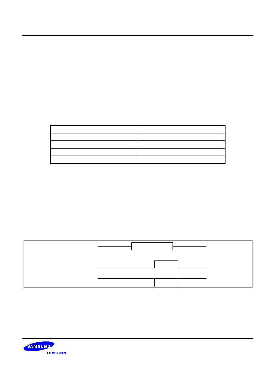
S3C852B/P852B (Preliminary Spec)
CALLER ID BLOCK
14-5
CAS TONE DETECTION
The S3C852B CAS detection algorithm is capable of detecting the CAS signals during speech with high talk-
down and talk-off performance, and 100% Bellcore compliant performance with use of a hybrid.
If the CAS detection is enabled the CID block will generate an interrupt (Interrupt register, bit 1 is set) when a
correct dual tone (2130 and 2750 Hz) is detected.
CAS detection is enabled when the CASenable bit in the Function register is set and the FSK and SDT enable
bits in the Function register are cleared.
The parameters of the CAS Detector are shown in Table 14-1.
Table 14-1. CAS detector parameters
Parameter
Value
Low tone frequency
2130Hz
�
0.5%
High tone frequency
2750Hz
�
0.5%
Accepted signal level
-5.2dBm to �38dBm
Twist
-6dB to +6dB
When a valid CAS signal is detected, the CASdetect status bit of the Status register and the CASint bit of the
interrupt register are set and an interrupt is generated. When the signal level is below the accepted signal level
the status bit of the status register is cleared and the CASint interrupt bit is set , generating another interrupt.
The CASint interrupt bit is reset when the interrupt register is read (see Figure 14-4).
In order to accurately detect the end of a CAS tone, it is recommended to mute the near end speech immediately
after the CAS tone has been detected.
To disable the CAS detection function, set the CASenable bit to 0 when the CASdetect bit is 0, or after the
second CAS interrupt.
CAS signal
Line signal
CASdetect
INT
Figure 14-4. CASdetect, CASint and INT Related to the CAS Tone

CALLER ID BLCOK
S3C852B/P852B (Preliminary Spec)
14-6
FSK DATA RECEPTION
FSK Data Reception Sequence
The on-chip FSK receiver satisfies all target specifications of Bellcore. The FSK receiver function can be enabled
by setting the FSKenable bit (Function register, bit2) and clearing the CASenable (Function register, bit1) and the
SDTenable (Function register, bit5) bits.
When the FSK receiver is enabled, the CID BLOCK continuously checks for a signal in the FSK band (~1200 -
~2200 Hz) above the minimum signal level threshold. An FSK data word consists of one start bit (space) followed
by eight data bits and one stop bit (mark). After the FSK receiver has detected a start bit it starts receiving the
data bits (LSB first). After the 8
th
data bit the FSKint interrupt bit (Interrupt register, bit2) is set and an interrupt is
generated.
The FSKint interrupt bit is cleared when the Interrupt register is read. The interrupt register and the FSKDT
register should be read every time an interrupt occurs.
D0
FSK data
FSKint
INT
D1
D2
D3
D4
D5
D6
D7
Interrupt register is read.
Figure 14-5. Sequence to Receive an FSK Data Byte
The parameters of the FSK receiver are shown in Table 14-2.
Table 14-2. FSK Receiver Parameters
Parameter
Bellcore
CCITT/ V23
Mark frequency (logic 1)
1200Hz
�
1%
1300Hz
�
1.5%
Space frequency (logic 0)
2200Hz
�
1%
2100Hz
�
1.5%
Maximum allowed signal level
0dBm
-8dBV
Minimum signal level threshold
<-45dBm
<-52dBV
Twist
-10dB to +10dB
-6dB to +6dB
Accepted S/N (0Hz � 200Hz)
<-20dB
<-20dB
Accepted S/N (200Hz � 3200Hz)
<6dB
<6dB
Accepted S/N (3200Hz � 15000Hz)
<-20dB
<-20dB
Transmission rate
1200 bits per second 1%
1200 bits per second 1%
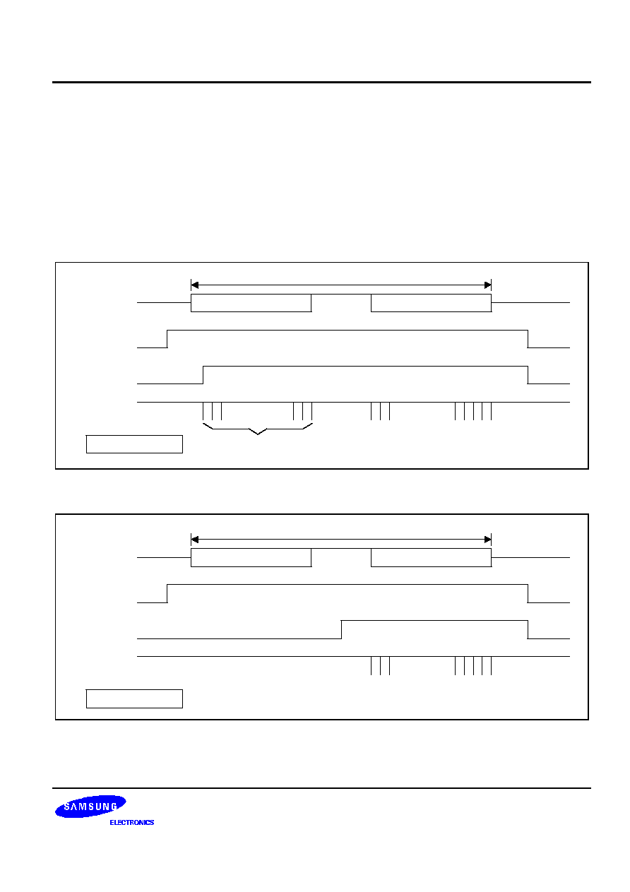
S3C852B/P852B (Preliminary Spec)
CALLER ID BLOCK
14-7
Begin Of Mark (BOM) Detection
BOMDC bit of MODE register (MODE register, bit 6) is utilized for detecting begin of mark or channel seizure. If
BOMDC is cleared, the BOMdetect signal (STAT register, bit 4) will be set after the begin of mark has been
detected, and if BOMDC is '1', BOMdetect will be set after the channel seizure detected. When BOMDC is '1' and
BOMdetect is set, the interrupts occur due to channel seizure as shown in Figure 14-6. If BOMDC is '0', interrupt
will therefore not be generated during the channel seizure and during the block of marks as shown in Figure 9.
The FSK interrupts of data bytes will be generated after a mark period of at least 16 sequential 1's has been
detected. Behavior of BOMdetect (STAT register, bit 4) is shown in Figure 14-7. This bit will be cleared when the
FSK receiver is disabled or a signal drop out occurs for more than 18.3ms. In the latter case the FSK receiver will
behave as if it has just been disabled.
FSK transmission
Line signal
Mark
lnterrupts due to channel seizure
Channel seizure(optional)
Data
Noise
Noise
FSK enabie
BOM detect
...
...
INT
When BOMDC = 1
Figure 14-6. Interrupt behavior of the FSK receiver with BOMDC = 1
FSK transmission
Line signal
Mark
Channel seizure(optional)
Data
Noise
Noise
FSK enabie
BOM detect
...
INT
When BOMDC = 0
Figure 14-7. Interrupt behavior of the FSK receiver with BOMDC = 0
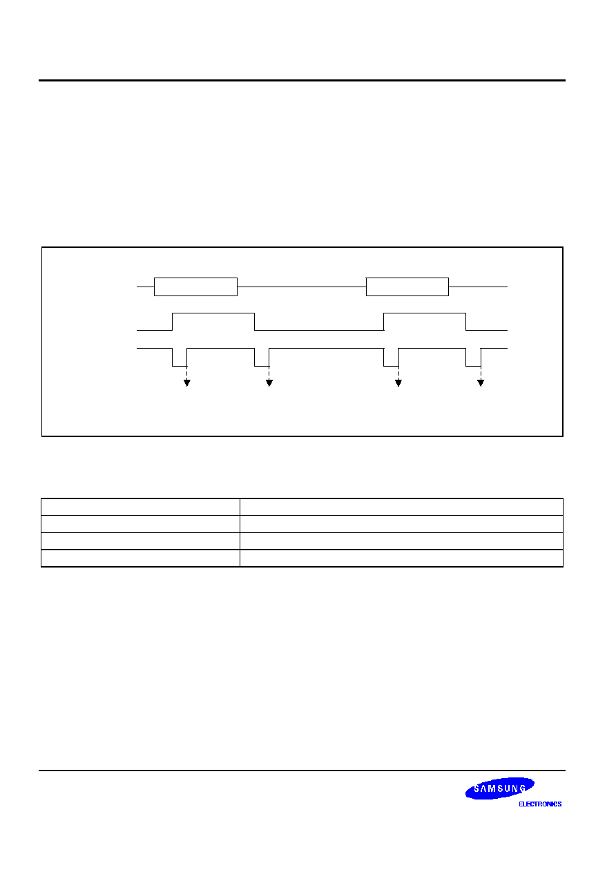
CALLER ID BLCOK
S3C852B/P852B (Preliminary Spec)
14-8
STUTTER DIAL TONE(SDT) DETECTOR
This block is enabled when the S3C852B is set to SDT enable mode (Function register, bit5) and all the other
functions in the Function register are disabled.
The detector measures the total signal level for every 31.5ms. When the total signal level is above -36dBm and
the frequencies of dual tone are 350Hz and 440Hz dial tone band, the SDTdetect bit in the Status register is set.
When the total signal level is below �38dBm the SDTdetect bit is cleared (see Table 14-3). Each time SDTdetect
changes the SDTint bit is set and an interrupt is generated. The SDTint bit is cleared when the Interrupt register is
read. This behavior is shown in Figure 14-8.
Line signal
SDT signal
PTEdetect
INT
lnterrupt register
is read.
SDT signal
lnterrupt register
is read.
lnterrupt register
is read.
lnterrupt register
is read.
Figure 14-8. SDT Detector Operation
Table 14-3. Stutter dial Tone Parameters
Parameters
Values
Frequencies
350Hz + 440Hz dual tone
Signal amplitude power
-1dBm to -48dBm
Duration
80 to 160ms on/off, with a duty cycle from 40% to 60%
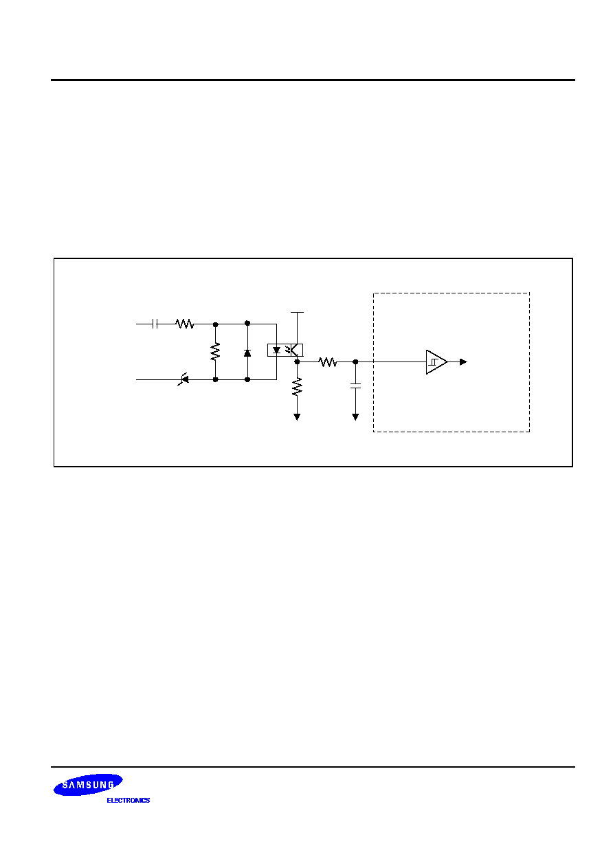
S3C852B/P852B (Preliminary Spec)
CALLER ID BLOCK
14-9
RING OR LINE REVERSAL DETECTOR
For ring or line reversal detection, some external components are needed to generate a pulse each time a ring or
line reversal occurs, as shown in Figure 14-9. Interrupt generation of the ring or line reversal detector is
controlled by the LRenable bit in the Function register. When LRenable is set to "1", the LRint bit of the interrupt
register will be set and interrupts will be generated at every transition of the LRstatus bit. When LRenable is "0",
interrupts will not generated.
The LRstatus bit (reset value is high) in the Status register is cleared to "0" at any positive edge of the LRin. If no
positive edges of LRin are detected in Tguard time the LRstatus bit is set to "1". The LRint bit is cleared when the
Interrupt register is read.
S3C852B
LRin
Tip/A
Ring/B
R8
C2
to Ring/Line
reversal
detector
R9
D6
D5
P1
R11
R10
C3
Figure 14-9. External Component to Generate LRin
If an LRint interrupt has been generated in power-down mode, it is recommended to disable power-down mode to
be able to count the guard time counter using the sub clock (XTIN). The guard time counter is reset when LRin is
high. The guard time (Tguard) can be programmed by writing the GTIME register as follows.
Tguard = 183us * ( GTIME[6:0] * 4 + 3 )
(Ex. Tguard = 44.469ms = 0.153ms * (0111100B * 4 + 3 ) )
Figure 14-10 and Figure 14-11 show line reversal and ring detection respectively.
The LRin of Figure 14-11 shows the behavior of LRin signal when the reference circuit of Figure 14-9 is used.

CALLER ID BLCOK
S3C852B/P852B (Preliminary Spec)
14-10
Line signal
LRstatus
INT
lnterrupt register is read.
LRin
LRint
PWD = 0
PWD = 1
LRenable = 1
T
guard
Figure 14-10. Behavior of Signals on a Line Reversal
Line signal
LRstatus
INT
lnterrupt register is read.
LRin
LRint
T
guard
lnterrupt register is read.
Figure 14-11. Behavior of Signals During Ring

S3C852B/P852B (Preliminary Spec)
CALLER ID BLOCK
14-11
TONE GENERATOR
S3C852B has a tone generator capable of generating general single tone such as FSK and general dual tone
such as CAS or DTMF. The block diagram of tone generator is shown in Figure 14-12. The tone generator
contains a numerically controlled oscillator (NCO) to generate the addresses of two sine lookup tables (LUT) for
producing dual tone. The input tone of NCO is selected by TONES register value. The output power of each low
and high tone can be controlled through two gain controllers (multipliers), and the added value of dual tone is
converted to analog sine wave through pulse density modulator (PDM) and external RC circuit. To enable the
tone generator, TONEenable bit of function register (FUNC register, bit 3) must be set to '1' for the first. If
TONEenable bit is '0', no tone will be generated. TONEenable bit must be set before writing the control and data
registers related to tone generation. To generate dual tone, dual tone ON-OFF (DTONonoff) bit (TONES register
bit 1) must be set to '1' and FSK ON-OFF (FSKonoff) bit (TONES register bit 0) bit to '0'. For FSK generation, set
FSKonoff bit to '1' and clear DTONonoff bit to '0'.
FSKMOD
S3C852B
NCO
HTONE<15:0>
LTONE<15:0>
Input
Selection
Sine
LUT
FSK
sequence
generator
Sine
LUT
TONES
TONEGL
TONEGH
Low Tone
High Tone
PDM
TONEO
FSKTint
FSKTD
R11
C8
Figure 14-12. Tone Generator Block
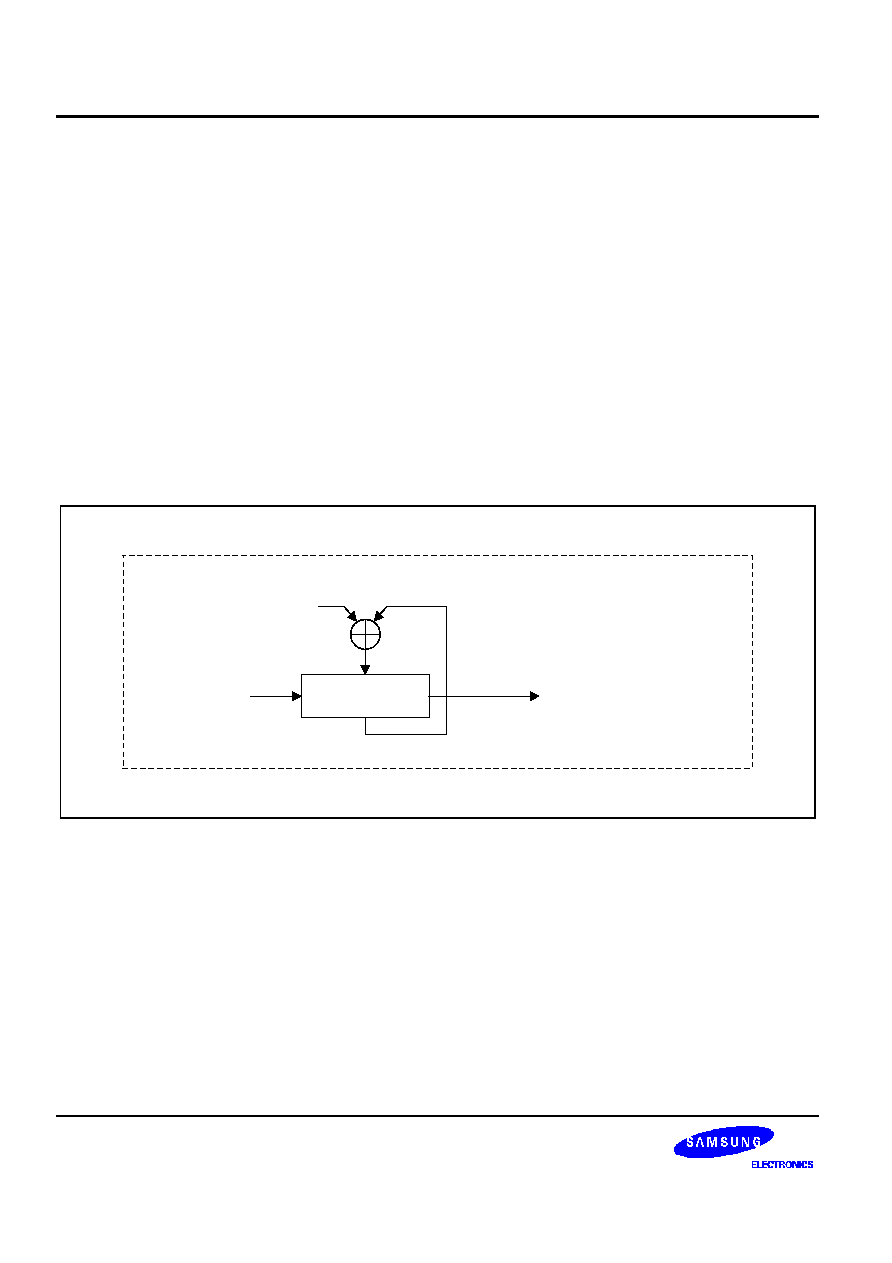
CALLER ID BLCOK
S3C852B/P852B (Preliminary Spec)
14-12
Numerically Controlled Oscillator
S3C852B contains two sets of NCO for generating dual tone, which receives 16-bit phase data (Dfreq) written by
the MCU and continuously add and accumulate it using 24-bit phase accumulator at every clock cycle. The 5
most significant bits of accumulator is utilized as the address (n) of sine LUT, which contains 32 amplitude values
of sine(2
n/32). The resolution (minimum frequency) and output frequency (f
OUT
) of the NCO is described below,
when f
CLK
is frequency of input clock (f
CLK
= 1.789973 MHz = 3.579545/2 MHz).
Resolution = f
CLK
/2
24
= 0.107Hz
f
OUT
= Dfreq* f
CLK
/2
24
So the phase input (Dfreq) is determined as follows
Dfreq = f
OUT
*2
24
/f
CLK
The block diagram of NCO is shown in Figure 14-13.
16-bit (Dfreq)
24-bit phase
accumulator
5-bit MSB's
Address of
sine LUT
f
CLK
= 1.789973MHz
S3C852B
Figure 14-13. Block Diagram of NCO
For example, 16-bit data of LTONE1<7:0> and LTONE0<15:0> for low frequency of DTMF character "1" (=
697Hz) are determined as follows;
f
OUT
= 697Hz
f
CLK
= 1789973Hz
Dfreq = f
OUT
*2
24
/f
CLK
= 6534 = 1986h
LTONE1<7:0> = 19h
LTONE0<7:0> = 86h
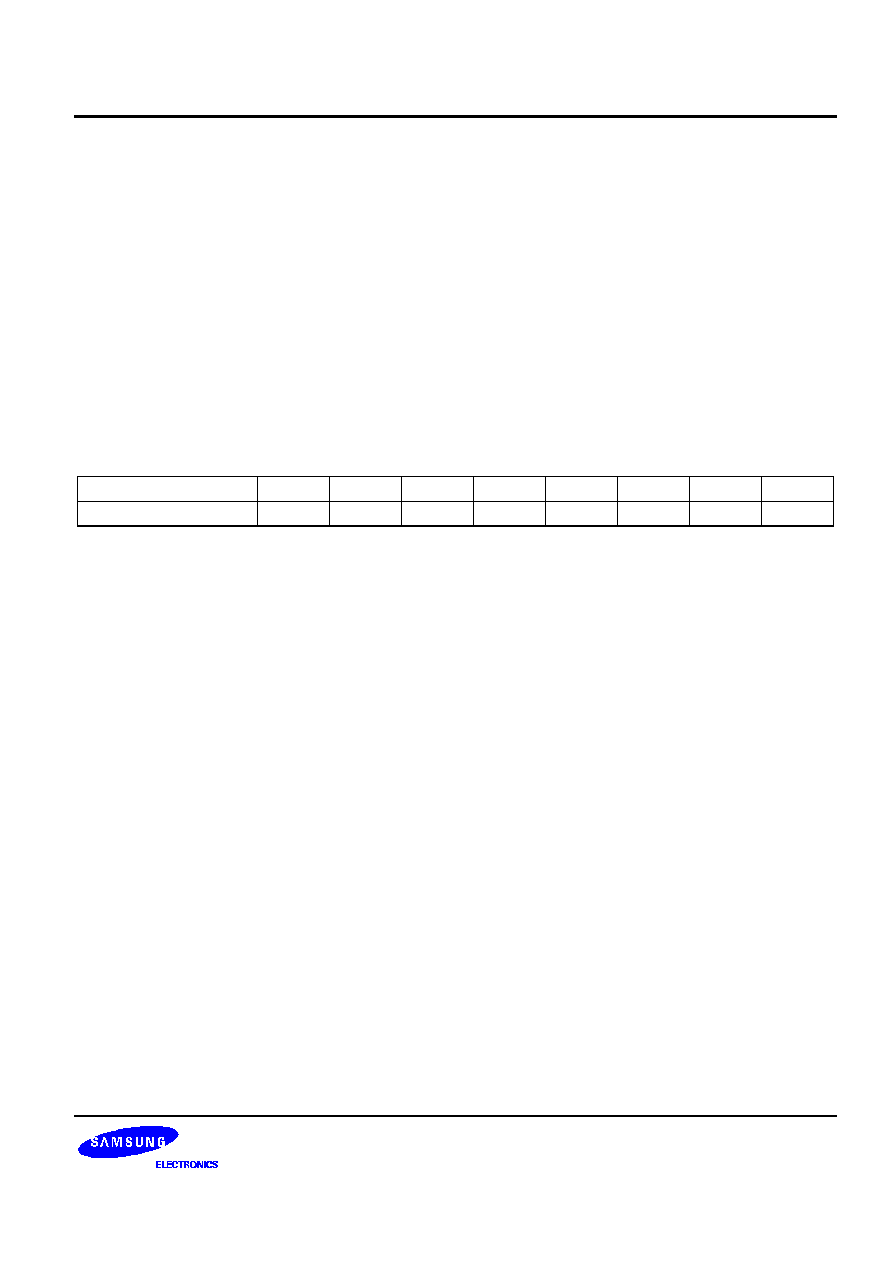
S3C852B/P852B (Preliminary Spec)
CALLER ID BLOCK
14-13
Dual Tone Generation Function
The tone generator can be utilized as CAS, DTMF or other dual or other single sine wave generator. To enable
the function of generating general dual tone, TONEenable bit (FUNC.3) must be set to '1', and the dual tone will
be generated by setting dual tone ON-OFF bit (DTONonoff) in tone select register (TONES, bit 1) to '1' and FSK
ON-OFF (FSKonoff) bit (TONES register, bit 0) of TONES to '0'. If DTONonoff bit is programmed to '0', dual tone
generation function will be off. The 16-bit phase input data of high tone must be written in high tone data
registers, which are HTONE1 (MSB) and HTONE0 (LSB), the data of low tone in low tone data registers, which
are LTONE1 (MSB) and LTONE0 (LSB).
The Tone gain registers (TONEGH for high tone and TONEGL for low tone) can control the output gain of high
and low tone. The default power of each tone is �4.3dBm with +/-5% deviation when V
DD
is 3.3V on DTMF
generation. The TONEGH & TONEL registers contain the gain factors those are multiplied to the default signal
power to obtain the dual tone signal power. The gain factor is an unsigned number. The most significant bit (M) of
the TONEGH/L register is the mantissa and the remaining bits (E3 to E0) denote the exponent. The output power
of the each tone signal can be obtained by the following equation.
Tone signal power = Default signal power * TONEGH/L
Symbol
7
6
5
4
3
2
1
0
TONEGH (L)
�
�
�
M
E3
E2
E1
E0
The TONEGH & TONEL register can be programmed within the range from 0.0001B (0.0625 in decimal) to
1.0000B (1.0000 in decimal). Don't write the gain value above 1.0000, because the default power is the
maximum available power. For example, if TONEGH & TONEL is set to 10H (1.0000 in binary or 1.0 in decimal)
signal power of dual tone will be the same as the default power. If the TONEGH register is 0.0111H (0.4375 in
decimal) and the TONEGL register 0.0110H (0.3750 in decimal), the signal power will be determined as follows.
20log(default power*0.4375) � 20log(default power) = 20log0.4375 = -7.16dB
20log(default power*0.3750) � 20log(default power) = 20log0.3750 = -8.50dB
The high tone power = -11.66dB
The low Tone power = -13.00dB
The default (reset) values of TONEGH & TONEGL are 00h .
The output power of TONEO signal also can be varied by change of the external R or C values and additional
hardwares.
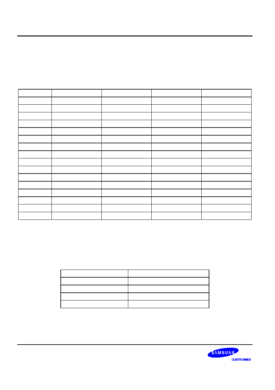
CALLER ID BLCOK
S3C852B/P852B (Preliminary Spec)
14-14
DTMF Tone Generation
To generate DTMF signal, TONEenable bit (FUNC.3) and DTONEonoff bit (TONES.2) must be set to '1' and the
phase input data (Dfreq) for high and low tone, which are corresponding to DTMF frequencies, must be written in
HTONE1, HTONE0, LTONE1 and LTONE0 as shown in Table 14-4.
Table 14-4. DTMF Frequencies Code and Phase Input Data
Character
Low frequency
LTONE1:0
High frequency
HTONE1:0
1
697Hz
1986H
1209Hz
2C46H
2
697Hz
1986H
1336Hz
30ECH
3
697Hz
1986H
1477Hz
3615H
4
770Hz
1C32H
1209Hz
2C46H
5
770Hz
1C32H
1336Hz
30ECH
6
770Hz
1C32H
1477Hz
3615H
7
852Hz
1F32H
1209Hz
2C46H
8
852Hz
1F32H
1336Hz
30ECH
9
852Hz
1F32H
1477Hz
3615H
0
941Hz
2274H
1336Hz
30ECH
*
941Hz
2274H
1209Hz
2C46H
#
941Hz
2274H
1477Hz
3615H
A
697Hz
1986H
1633Hz
3BCCH
B
770Hz
1C32H
1633Hz
3BCCH
C
852Hz
1F32H
1633Hz
3BCCH
D
941Hz
2274H
1633Hz
3BCCH
CAS Tone Generation
To generate CAS signal, TONEenable bit (FUNC.3) and DTONEonoff bit (TONES.1) must be set to '1' and the
phase input data (Dfreq) for the high and low tone, which are corresponding to CAS frequencies, must be written
in HTONE1, HTONE0, LTONE1 and LTONE0 as shown in Table 14-5.
Table 14-5. Dual Tone Frequency of CAS and Phase Input Data
Parameter
Values
Low tone frequency
2130Hz 0.1%
LTONE1:0
4DFEH
High tone frequency
2750Hz 0.1%
HTONE1:0
64B2H
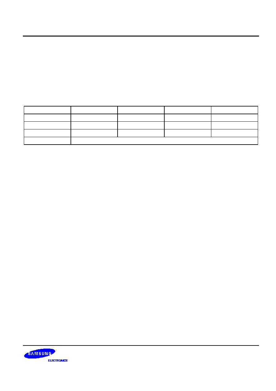
S3C852B/P852B (Preliminary Spec)
CALLER ID BLOCK
14-15
FSK Data Generation
Tone generator is able to generate Frequency Shift Keying (FSK) signal that satisfies all kinds of target
specification and capable of producing the sequence of channel seizure, mark and data bytes only by setting FSK
mode register (FSKMOD) and FSKTD (FSK transmission data register), because it includes baud clock generator
and FSK sequence generator. To generate FSK tone, the phase input data for space frequency must be written to
HTONE1 and HTONE0, and the phase input values for mark frequency to LTONE1 and LTONE0. The frequency
and phase input values of FSK are shown in Table 14-6.
Table 14-6. FSK Parameters
Specification
Space frequency
HTONE1:0
Mark frequency
LTONE1:0
Bell202
2200
508EH
1200
2BF0H
V.23
2100
4CE6
1300
2F9A
V.21
1180
2B36
980
23E2
Baud rate
1200 bps 1%
The FSK generation function is enabled by setting TONE enable bit (FUNC register, bit 3) to "1" and FSK signal
will be generated by setting FSK ON-OFF bit (TONES.0) to "1". In this case, DTONonoff bit must be set to "0"; if
FSK ON-OFF is cleared to "0", FSK signal will not be generated. If the FSK generation fuction is ON, the FSK
sequence generator, shown in Figure 14-20, automatically produces sequence of selection bit for mark and space
frequency by baud rate.
FSK sequence includes channel seizure, mark and FSK data, and FSK data is composed of 10-bit data including
start bit (space), a byte of data and stop bit (mark) as shown in Figure 14-5. Basically, FSK sequence generator
receives the data of FSKTD and generates 10-bit FSK sequence by baud rate. When the MCU set FSK onoff bit
to '1' after writing FSKTD and FSKMOD, FSK sequence generator loads the data of FSKTD and produces FSK
transmission interrupt (FSKTint) while generating FSK sequence, so the MCU can write the next FSKTD data and
FSKMOD in the interrupt service routine. After finishing transmission of 10-bit data, the generator continuously
loads the next FSKTD and FSKMOD and produces FSKTint to receive the next FSK data until the FSK
generation function disabled. To generate channel seizure signal, clear MARK enable (MARKenable) bit
(FSKMOD register, bit 0: it determines the value of start bit; '1': MARK, '0': SPACE) and write '55H' to FSKTD
register, then 10-bit sequence of channel seizure signal will be generated. To generate mark sequence, write
'FFH' to FSKTD and set MARKenable bit to '1', then 10-bit of mark sequence will be generated. Normal FSK data
can be generated by clearing MARKenable bit to '0'. In this case, start (space) and stop (mark) bit will be attached
to the head and tail of the data byte.
If you don't change the contents of FSKTD or FSKMOD after FSKTint has occured, the tone generator generates
previous FSK tone. After sending all FSK data successfully, set FSKonoff bit to '0', and FSK sequence
generation will be stopped after sending the last loaded data.
If TONEenable bit is cleared to '0', the tone generator stopped directly, so TONEenable bit must be remained as
'1' until sending sequence of the last data has been finished. To prevent loosing the last data due to TONEenable
bit reset, insert a dummy (no operation) interrupt routine after writing the last data and before clearing
TONEenable bit.
The value of TONEGH is the gain factor of FSK, because FSK uses high tone generator,
NOTE
Please disable all other interrupts except for FSKTint while FSK sequence is generating to prevent the
distortion of FSK sequencing time due to interrupt processing of other functions.
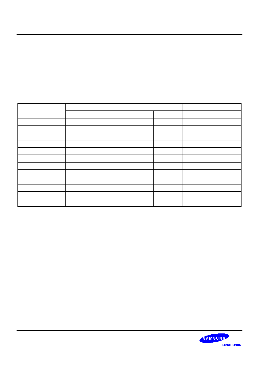
CALLER ID BLCOK
S3C852B/P852B (Preliminary Spec)
14-16
MELODY GENERATOR
S3C852B contains dual frequency generator for providing melody generation. The high frequency generator is a
musical scale (melody - tone1) generator, and the low frequency generator makes the length of the musical scale
(rhythm - tone2). The tone1 generator provides 3 octaves 36 music scales, and the tone2 generator is able to
control the rhythm with multiples of fx/2
15
(109.24Hz) time scale.
The frequencies of 3 octave music scale is shown in Table 14-7.
Table 14-7. The Frequencies and MREF1 Register Values for 3 Octave Musical Scale
Scale
C3
C4
C5
Freq.
MREF1
Freq.
MREF1
Freq.
MREF1
C
130.8
099H
261.6
135H
523.2
269H
C#
138.9
0A3H
272.2
141H
554.3
28EH
D
146.8
0ACH
293.7
15AH
587.3
2B4H
D#
155.5
0B6H
311.1
16FH
622.2
2DEH
E
164.8
0C1H
329.6
185H
659.2
309H
F
174.6
0CDH
349.2
19CH
698.4
337H
F#
185.0
0D9H
370.0
1B4H
739.9
368H
G
196.0
0E6H
392.0
1CEH
783.9
39CH
G#
207.6
0F3H
415.3
1EAH
830.5
3D3H
A
220.0
102H
440.0
207H
879.9
40DH
A#
223.1
105H
466.2
20EH
932.2
44BH
B
246.9
121H
493.9
246H
987.7
48CH
The melody function can be enabled by MLDenable bit (FUNC register, bit 6). If MLDenable bit is "1", the melody
tone (MLDT) is generated through MLDO pin (#58). If MLDenable bit is "0" the melody function is disabled and
MLDT and MLDint will be stopped.
As shown in Table 14-9, tone1 (melody) can be generated by melody reference register MREF1. When MREF1 is
set to 00H, the no melody tone is generated (mute). Tone2 (rhythm) is generated by melody reference register
MREF2. The value of MREF2 is the scale factor of fx/2
15
(109.24Hz) duty cycle. Tone2 pulse generates MLDint
interrupt. So user can program an interrupt service routine for melody generation. The routine is activated by
MLDint and user can write new MREF1 and MREF2 data to create new musical scale and length in the melody
interrupt service routines. For example, to generate one-time, insert 52H into MREF2 then the MLDint will occure
every 0.75 second.
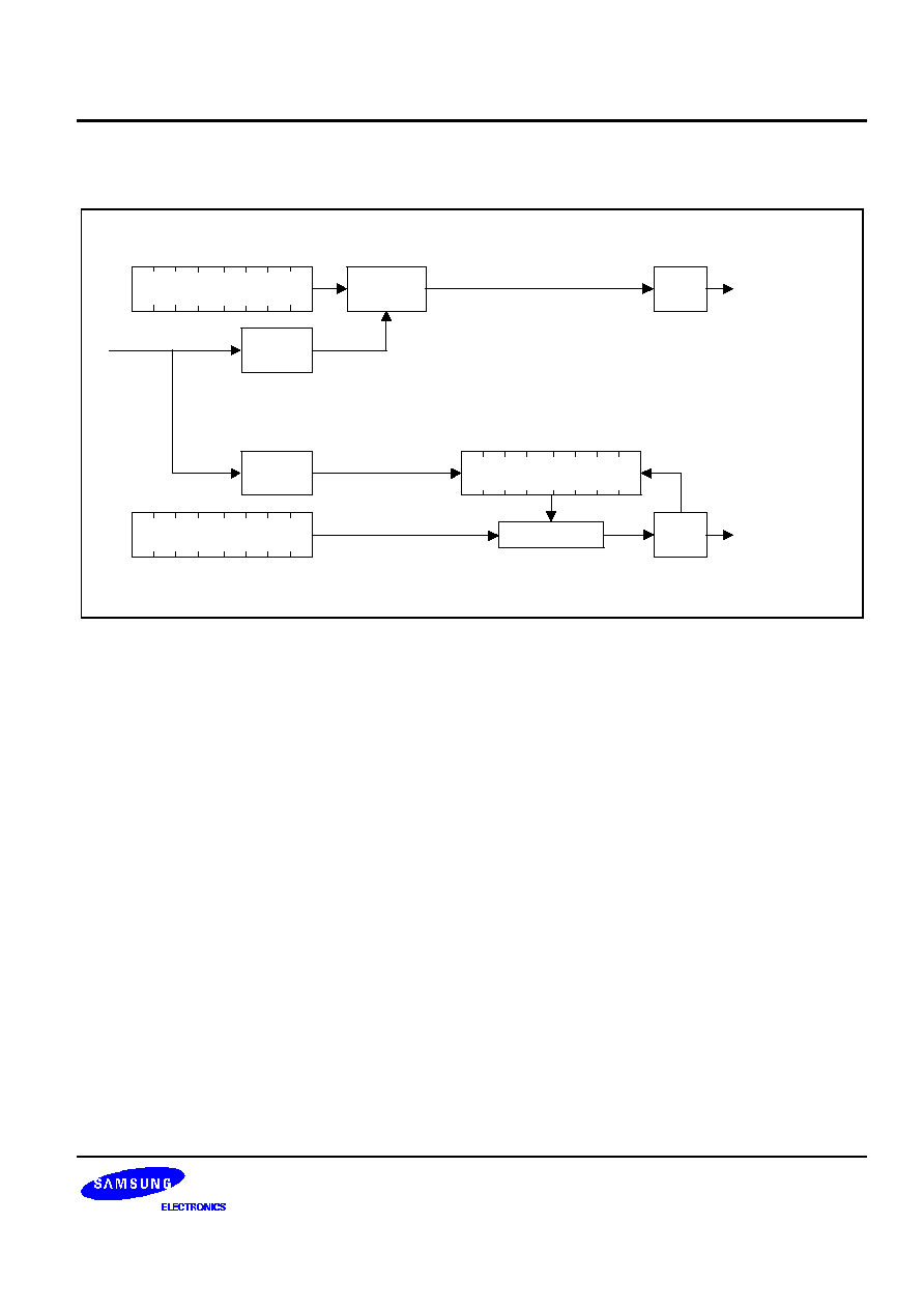
S3C852B/P852B (Preliminary Spec)
CALLER ID BLOCK
14-17
The block diagram of melody generator is shown in Figure 14-14.
MREF1
/2
/2
15
main clock (MCLK)
counter value
MREF2
NCO
tone 1 clock
MCNT2
tone 2 duty cycle
Compare logic
Pulse
gen
TONE1
(To buzzer)
Pulse
gen
TONE2
(To interrupt)
counter reset
1
Figure 14-14. Block Diagram of Melody Generator
CALLER ID BLCOK
S3C852B/P852B (Preliminary Spec)
14-18
POWER-DOWN MODE OF CID BLOCK
The CID block of the S3C852B can be put in power-down mode by programming the PDW bit in the Mode
register to "1". In this mode the input signal buffers, 14-bit ADC's, the reference bias generator of 14-bit ADC, the
tone generator and clock input from MCU are switched off. However the Ring/Line Reversal detection can be
active by programming the LRenable bit in the function register to be set. The serial interface can always be
accessed, even in power-down mode. In power-down mode, if ring or line reversal occur when LRenable bit is
"1", the LRint bit is set and an interrupt is generated. When the CID block of the S3C852B is put in power-down
mode, all interrupt bits in the interrupt register of CID block cannot be set except for the LRint bit.
The Reset condition of CID block is power-down mode, that is, the default value of PWD bit is "1", so you should
set the PWD bit to "0" to activate CID block.
INTERRUPT OF CID BLOCK
The CID interrupt (
INT
/P0.0) is active low. The flag in the interrupt register of CID block indicates the interrupt
cause. Interrupt flags of the CID block are set by hardware but must be reset by software. All flags of the interrupt
register are reset when the register is read via the serial interface.
The Table 14-8 shows interrupt sources of the CID block.
Table 14-8. Interrupt Sources of the CID Block
Source Block
Generation
Ring/line reversal detector
When LRstatus changes
FSK receiver
Reception of a new FSK data byte
Tone generator
Transmission of FSK data byte
CAS detector
When CASdetect changes
SDT detector
When SDTdetect changes
Melody generator
When the duration (MREF2) of current tone is expired
S3C852B/P852B (Preliminary Spec)
CALLER ID BLOCK
14-19
REGISTER MAPS OF CID BLOCK
The registers that are available in the CID block are shown in the following tables.
Table 14-9. Register Overview
Register Name
Address
Function
Default Value
Read/Write
MODE
00H
Mode register
1000 0000
Read/Write
FUNC
01H
Function register
0000 0000
Read/Write
TONES
02H
TONE select register
0000 0000
Read/Write
GTIME
0AH
Guard time register
0000 0000
Read/Write
MREF2
0BH
Melody generator Duration Control
0000 0000
Read/Write
MREF1H
0CH
Melody generator reference register (High)
0000 0000
Read/Write
MREF1L
0DH
Melody generator reference register (Low)
0000 0000
Read/Write
INTR
80H
Interrupt register
0000 0000
Read/Write
STAT
81H
Status register
0000 0000
Read Only
FSKDT
82H
FSK data register
0000 0000
Read Only
HTONE1
87H
MSB of high tone register
0000 0000
Read/Write
HTONE0
88H
LSB of high tone register
0000 0000
Read/Write
LTONE1
89H
MSB of low tone register
0000 0000
Read/Write
LTONE0
8AH
LSB of low tone register
0000 0000
Read/Write
TONEGH
90H
High tone output gain control register
0000 0000
Read/Write
TONEGL
91H
Low tone output gain control register
0000 0000
Read/Write
FSKTD
92H
FSK transmission data register
0000 0000
Read/Write
FSKMOD
93H
FSK mode register
0000 0000
Read/Write
CONT1
94H
Special control register1
0000 0000
Read/Write
CONT2
95H
Special control register2
0000 0000
Read/Write
TMODSEL
98H
Test Mode Selection Register
0000 0000
Read/Write
CASTh
99H
CAS/SDT Rejection Level Control Register
0010 0011
Read/Write

CALLER ID BLCOK
S3C852B/P852B (Preliminary Spec)
14-20
MODE -- Mode Register
Address Page 8 00H; read/write
7
6
5
4
3
2
1
0
PDW
BOMDC
�
�
�
�
�
�
Description of MODE bits
Bit
Symbol
Description
MODE.7
PWD
1: Puts the CID block in power-down mode
0: Puts the CID block in active mode
MODE.6
BOMDC
0: Indicates that BOMdetection bit is set to "1" after beginning of mark has been
detected
1: Indicates that BOMdetection bit is set to "1" after channel seizure has been
detected
FUNC � Function Register
Address Page 8 01H; read/write.
7
6
5
4
3
2
1
0
BFS
MLDenable SDTenable
�
TONEenable
FSKenable
CASenable
LRenable
Description of FUNC bits
Bit
Symbol
Description
FUNC.7
BFS
1: Selects the single-ended input buffer
0: Selects the differential input buffer
FUNC.6
MLDenable
1: Enables the melody generator
0: Disables the melody generator
FUNC.5
SDTenable
1: Enables the SDT detector
0: Disables the SDT detector
FUNC.4
�
Not used for S3C852B/P852B
FUNC.3
TONEenable
1: Enables the tone generator
0: Disables the tone generator
FUNC.2
FSKenable
1: Enables FSK receiver
0: Disables FSK receiver
FUNC.1
CASenable
1: Enables CAS detector
0: Disables CAS detector
FUNC.0
LRenable
1: Enables LR interrupts
0: Disables LR interrupts
S3C852B/P852B (Preliminary Spec)
CALLER ID BLOCK
14-21
TONES � Tone Select Register
Address Page 8 02H; read/write.
7
6
5
4
3
2
1
0
�
�
�
�
�
�
DTONonoff
FSKonoff
Description of TONES bits
Bit
Symbol
Description
TONES.1
DTONonoff
1: Enables dual tone output
0: Disables dual tone output
TONES.0
FSKonoff
1: Enables FSK tone output
0: Disables FSK tone output
GTIME � Guard Time Register
Address Page 8 0aH; read/write.
7
6
5
4
3
2
1
0
�
G6
G5
G4
G3
G2
G1
G0
Description of GTIME bits
Bit
Symbol
Description
GTIME.6 to GTIME.0
G6 to G0
Guard time to indicate the end of a line reversal or ring
MREF2 � Melody Reference Counter Register2
Adress Page 8 0bH; read/write
7
6
5
4
3
2
1
0
D7
D6
D5
D4
D3
D2
D1
D0
Description of MREF2 bits
Bit
Symbol
Description
MREF2H.7 to MREF2H.0
D7 to D0
The data of melody generator reference register 2
CALLER ID BLCOK
S3C852B/P852B (Preliminary Spec)
14-22
MREF1H �Melody Reference Counter Register1 (High Byte)
Address Page 8 0cH; read/write.
7
6
5
4
3
2
1
0
D7
D6
D5
D4
D3
D2
D1
D0
Description of MREF1H bits
Bit
Symbol
Description
MREF1H.7 to MREF1H.0
D7 to D0
The data of melody frequency (high byte)
MREF1L �Melody Reference Counter Register1 (Low Byte)
Address Page 8 0dH; read/write.
7
6
5
4
3
2
1
0
D7
D6
D5
D4
D3
D2
D1
D0
Description of MREF1H bits
Bit
Symbol
Description
MREF1L.7 to MREF1L.0
D7 to D0
The data of melody frequency (low byte)
S3C852B/P852B (Preliminary Spec)
CALLER ID BLOCK
14-23
INTR �Interrupt Register
Address Page 8 80H; read/write.
7
6
5
4
3
2
1
0
MLDint
FSKTint
SDTint
�
�
FSKint
CASint
LRint
Description of INTR bits
Bit
Symbol
Description
INTR.7
MLDint
1: Indicates that the current melody tone duration has been finished
INTR.6
FSKTint
1: indicates that previous FSK data transmission has been finished for FSK tone
generation and is waiting for the next FSK data byte.
INTR.5
SDTint
1: Indicates that SDTdetect has been changed and a SDT interrupt has occurred
INTR.4
Not used for S3C852B/P852B
INTR.2
FSKint
1: Indicates that a new FSK data has been received
INTR.1
CASint
1: Indicates that CAS signal has been detected
INTR.0
LRint
1: Indicates that LRstatus has been changed and a LR interrupt has occurred.
NOTE: INTR register is cleared by S/W by writing "0", but cannot write "1"
STAT �Status Register
Address Page 8 81H; read only.
7
6
5
4
3
2
1
0
�
�
SDTdetect
BOMdetect
�
�
CASdetect
LRstatus
Description of STAT bits
Bit
Symbol
Description
STAT.5
SDTdetect
1: Indicates that the SDT detector detects the signal that satisfies the specified
frequency and energy level;
0: No more stutter dial tone is detected
STAT.4
BOMdetect
1: Indicates that the Begin Of the Mark period during FSK reception has been
detected
STAT.1
CASdetect
1: Indicates that a CAS tone has been detected
0: No more CAS Tone is detected
STAT.0
LRstatus
1: LRint has not occurred until expiring GTIME (reset value)
0: LRint has occurred before expiring GTIME

CALLER ID BLCOK
S3C852B/P852B (Preliminary Spec)
14-24
FSKDT � FSK Data Register
Address Page 8 82H; read only.
7
6
5
4
3
2
1
0
D7
D6
D5
D4
D3
D2
D1
D0
Description of FSKDT bits
Bit
Symbol
Description
FSKDT.7 to FSKDT.0
D7 to D0
Last received FSK data byte
HTONE1 � MSB of High Tone Register
Address Page 8 87H; read/write.
7
6
5
4
3
2
1
0
D7
D6
D5
D4
D3
D2
D1
D0
Description of HTONE1 bits
Bit
Symbol
Description
HTONE1.7 to HTONE1.0
D7 to D0
MSB of 16-bit high tone register
HTONE0 � LSB of High Tone Register
Address Page 8 88H; read/write.
7
6
5
4
3
2
1
0
D7
D6
D5
D4
D3
D2
D1
D0
Description of HTONE0 bits
Bit
Symbol
Description
HTONE0.7 to HTONE0.0
D7 to D0
LSB of 16-bit high tone register

S3C852B/P852B (Preliminary Spec)
CALLER ID BLOCK
14-25
LTONE1 � MSB of Low Tone Register
Address Page 8 89H; read/write.
7
6
5
4
3
2
1
0
D7
D6
D5
D4
D3
D2
D1
D0
Description of LTONE1 bits
Bit
Symbol
Description
LTONE1.7 to LTONE1.0
D7 to D0
MSB of 16-bit low tone register
LTONE0 � LSB of Low Tone Register
Address Page 8 8AH; read/write.
7
6
5
4
3
2
1
0
D7
D6
D5
D4
D3
D2
D1
D0
Description of LTONE0 bits
Bit
Symbol
Description
LTONE0.7 to LTONE0.0
D7 to D0
LSB of 16-bit low tone register
TONEGH � High Tone Output Gain Control Register
Address Page 8 90H; read/write
7
6
5
4
3
2
1
0
�
�
�
D4
D3
D2
D1
D0
Description of TONEGH bits
Bit
Symbol
Description
TONEGH.7 to TONEGH.0 D7 to D0
This byte multiplied to control the output gain of TONE generator
CALLER ID BLCOK
S3C852B/P852B (Preliminary Spec)
14-26
TONEGL � Low Tone Output Gain Control Register
Address Page 8 91H; read/write
7
6
5
4
3
2
1
0
�
�
�
D4
D3
D2
D1
D0
Description of TONEGL bits
Bit
Symbol
Description
TONEGL.7 to TONEGL.0
D7 to D0
This byte multiplied to control the output gain of TONE generator
FSKTD � FSK Transmission Data Register
Address Page 8 92H; read/write.
7
6
5
4
3
2
1
0
D7
D6
D5
D4
D3
D2
D1
D0
Description of FSKTD bits
Bit
Symbol
Description
FSKTD.7 to FSKTD.0
D7 to D0
This byte is the FSK data to be transmitted.
FSKMOD � FSK Mode Register
Address Page 8 93H; read only.
7
6
5
4
3
2
1
0
�
�
�
�
�
�
�
MARKen
Description of FSKMOD bits
Bit
Symbol
Description
FSKMOD.0 MARKen
1: Set FSK start bit to MARK for MARK sequence generation
0: Set FSK start bit to space for normal FSK data generation
S3C852B/P852B (Preliminary Spec)
CALLER ID BLOCK
14-27
CONT1 � Special Control Register
Address Page 8 94H; read/write
7
6
5
4
3
2
1
0
1
1
0
0
0
1
1
1
This register should be written with "1100 0111b"
CONT2 � Special Control Register
Address Page 8 95H; read/write
7
6
5
4
3
2
1
0
MCLKSEL
0
0
0
0
0
0
0
This register should be written with "X000 0000b"
Description of CONT2 bits
Bit
Symbol
Description
CONT2.7
MCLKSEL
1: Set MCU main clock to 7.15909MHz
0: Set MCU main clock to 3.579545MHz
TMODESEL � Test Mode Selection Register
Address Page 8 98H; read/write
7
6
5
4
3
2
1
0
0
0
0
0
0
0
0
0
This register should be written with "0000 0000b"
CASth � CAS/SDT Threshold Control Register
Address Page 8 99H; read/write
7
6
5
4
3
2
1
0
0
0
1
0
0
0
1
1
This register should be written with "0011 0011b"
NOTES
1. To allow for future extensions, reserved bits (indicated with "-") must be written with "0".
2. When reading from a register, the reserved bits (indicated with "-") return an undefined value
(either "0" or "1").

CALLER ID BLCOK
S3C852B/P852B (Preliminary Spec)
14-28
NOTES

S3C852B/P852B (Preliminary Spec)
A/D CONVERTER
15-1
15
A/D CONVERTER
OVERVIEW
The 10-bit A/D converter (ADC) module uses successive approximation logic to convert analog levels entering at
one of the four input channels to equivalent 10-bit digital values. The analog input level must lie between the
AV
REF
and AV
SS
values. The A/D converter has the following components:
-- Analog comparator with successive approximation logic
-- D/A converter logic (resistor string type)
-- ADC control register, ADCON (set 1, bank 1, F4H, read/write, but ADCON.3 is read only)
-- Four multiplexed analog data input pins (ADC0�ADC3)
-- 10-bit A/D conversion data output register (ADDATAH, ADDATAL)
-- Internal AV
REF
and AV
SS
FUNCTION DESCRIPTION
To initiate an analog-to-digital conversion procedure, at first, you must configure P1.0�P1.3 to analog input
before A/D conversions because the P1.0 � P1.3 pins can be used alternatively as normal data I/O or analog
input pins. To do this, you load the appropriate value to the P1AFS.0 � P1AFS.3 (for ADC0 � ADC3) register.
And you write the channel selection data in the A/D converter control register ADCON to select one of the four
analog input pins (ADCn, n = 0�3) and set the conversion start or enable bit, ADCON.0.
An 10-bit conversion operation can be performed for only one analog input channel at a time.
The read-write ADCON register is located in set 1, bank 1 at address F4H.
During a normal conversion, ADC logic initially sets the successive approximation register to 200H (the
approximate half-way point of an 10-bit register). This register is then updated automatically during each
conversion step. The successive approximation block performs 10-bit conversions for one input channel at a
time. You can dynamically select different channels by manipulating the channel selection bit value (ADCON.5�
4) in the ADCON register.
To start the A/D conversion, you should set the enable bit, ADCON.0. When a conversion is completed, ACON.3,
the end-of-conversion (EOC) bit is automatically set to 1 and the result is dumped into the ADDATAH, ADDATAL
registers where it can be read. The ADC module enters an idle state. Remember to read the contents of
ADDATAH and ADDATAL before another conversion starts. Otherwise, the previous result will be overwritten by
the next conversion result.
NOTE
Because the ADC does not use sample-and-hold circuitry, it is important that any fluctuations in the
analog level at the ADC0�ADC3 input pins during a conversion procedure be kept to an absolute
minimum. Any change in the input level, perhaps due to circuit noise, will invalidate the result.
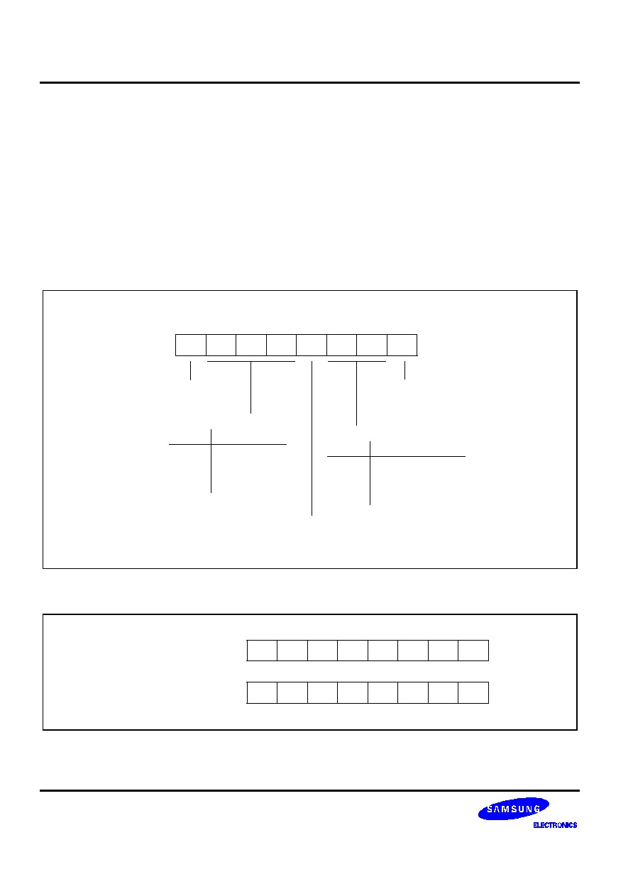
A/D CONVERTER
S3C852B/P852B (Preliminary Spec)
15-2
A/D CONVERTER CONTROL REGISTER (ADCON)
The A/D converter control register, ADCON, is located in set1, bank 1 at address F4H. ADCON is read-write
addressable using 8-bit instructions only. But EOC bit, ADCON.3 is read only. ADCON has four functions:
-- Bits 5�4 select an analog input pin (ADC0�ADC3).
-- Bit 3 indicates the end of conversion status of the A/D conversion.
-- Bits 2�1 select a conversion speed.
-- Bit 0 starts the A/D conversion.
Only one analog input channel can be selected at a time. You can dynamically select any one of the four analog
input pins, ADC0�ADC3 by manipulating the 2-bit value for ADCON.5�ADCON.4
Start or Enable bit
0 = Disable Operation
1 = Start Operation
A/D Converter Control Register (ADCON)
F4H, Set 1, Bank 1, R/W (ADCON.3 bit is read-only)
.7
.6
.5
.4
.3
.2
.1
.0
MSB
LSB
End-of-Conversion bit (realy only):
0 = Conversion not complete
1 = Conversion complete
Always Logic Zero
A/D Input Pin Selection bits:
A/D Input Pin
Clock Selection bit:
.4
.5
0
1
0
1
0
0
1
1
ADC0
ADC1
ADC2
ADC3
Conversion Clock
.1
.2
0
1
0
1
0
0
1
1
1/16
1/8
1/4
1/1
Figure 15-1. A/D Converter Control Register (ADCON)
.9
.8
.7
.6
.5
.4
.3
.2
LSB
MSB
ADDATAH
(set 1, bank 1, F2H)
-
-
-
-
-
-
.1
.0
LSB
MSB
ADDATAL
(set 1, bank 1, F3H)
Figure 15-2. A/D Converter Data Register (ADDATAH/ADDATAL)
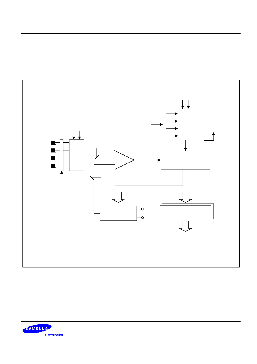
S3C852B/P852B (Preliminary Spec)
A/D CONVERTER
15-3
INTERNAL REFERENCE VOLTAGE LEVELS
In the ADC function block, the analog input voltage level is compared to the reference voltage. The analog input
level must remain within the range AV
SS
to AV
REF
(AV
REF
= V
DD
).
Different reference voltage levels are generated internally along the resistor tree during the analog conversion
process for each conversion step. The reference voltage level for the first bit conversion is always 1/2 AV
REF
.
Conversion Result
(ADCDATAH/ADCDATAL)
+
-
To Data BUS
To ADCON.3
(EOC Flag)
Successive
Approximation
Logic and Register
AV
REF
AV
SS
Analog
Comparator
10-bit D/A
Converter
M
U
X
P1AFS.0-.3
(Select analog input function)
ADCON.0
(ADC Enable)
ADCON.0
(ADC Enable)
P1.0/ADC0
Input Pins
P1.1/ADC1
P1.2/ADC2
P1.3/ADC3
M
U
X
1/16
1/8
1/4
1/1
ADCON.4-.5
(Select one input pin of the assigned pins)
ADCON.2-.1
(Select ADC Clock)
NOTES:
1. ADCON.0 will be "0" automatically when ADC conversion is completed.
2. Interval AV
REF
only.
3. Internal AV
SS
only.
fxx
Figure 15-3. A/D Converter Circuit Diagram

A/D CONVERTER
S3C852B/P852B (Preliminary Spec)
15-4
CONVERSION TIMING
The A/D conversion process requires 4 steps (4 clock edges) to convert each bit and 10 clocks to step-up A/D
conversion. Therefore, total of 50 clocks are required to complete an 10-bit conversion: With an 10 MHz CPU
clock frequency, one clock cycle is 400 ns (4/fxx). If each bit conversion requires 4 clocks, the conversion rate is
calculated as follows:
4 clocks/bit x 10-bits + step-up time (10 clock) = 50 clocks
50 clock x 400 ns = 20
�
s at 10 MHz, 1 clock time = 4/fxx
50 ADC Clock
ADCON.0 1
. . .
40 Clock
Previous
Value
Valid
Data
Set up time
10 clock
ADDATAH (8-Bit) + ADDATAL (2-Bit)
9
8
7
6
5
4
3
2
1
0
Conversion
Start
EOC
ADDATA
Figure 15-4. A/D Converter Timing Diagram
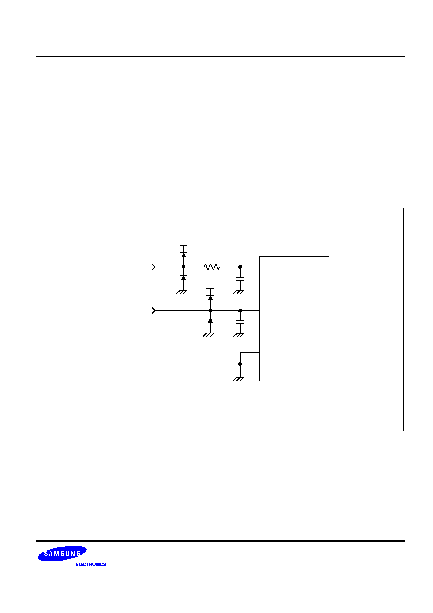
S3C852B/P852B (Preliminary Spec)
A/D CONVERTER
15-5
INTERNAL A/D CONVERSION PROCEDURE
1.
Analog input must remain between the voltage range of AV
SS
and AV
REF
.
2. Configure P1.0�P1.3 for analog input before A/D conversions. To do this, you load the appropriate value to
the P1AFS.0�P1AFS.3 (for ADC0�ADC3) register.
3. Before the conversion operation starts, you must first select one of the four input pins (ADC0�ADC3) by
writing the appropriate value to the ADCON register.
4.
When conversion has been completed, (50 clocks have elapsed), the EOC, ADCON.3 flag is set to "1", so
that a check can be made to verify that the conversion was successful.
5.
The converted digital value is loaded to the output register, ADDATAH (8-bit) and ADDATAL (2-bit), than the
ADC module enters an idle state.
6. The digital conversion result can now be read from the ADDATAH and ADDATAL register.
Reference
Voltage
Input
Analog
Input Pin
NOTE:
The symbol "R" signifies an offset resistor with a value of
from 50 to 100
.
V
SS
S3C852B
ADC0-ADC3
AV
REF
R
V
DD
V
DD
104
101
AV
SS
Figure 15-5. Recommended A/D Converter Circuit for Highest Absolute Accuracy

A/D CONVERTER
S3C852B/P852B (Preliminary Spec)
15-6
F
F
PROGRAMMING TIP -- Configuring A/D Converter
�
�
SB0
LD
P1AFS,#00001111B
; P1.3�P1.0 A/D Input MODE
�
�
SB1
LD
ADCON,#00000001B
; Channel AD0: P1.0/Conversion start
AD0_CHK:
TM
ADCON,#00001000B
; A/D conversion end ?
EOC check
JR
Z,AD0_CHK
; No
LD
AD0BUFH,ADDATAH
; 8-bit Conversion data
LD
AD0BUFL,ADDATAL
; 2-bit Conversion data
SB0
�
�
SB1
LD
ADCON,#00110001B
; Channel AD3: P1.3/Conversion start
AD6_CHK:
TM
ADCON,#00001000B
; A/D conversion end ?
EOC check
JR
Z,AD6_CHK
; No
LD
AD6BUFH,ADDATAH
; 8-bit Conversion data
LD
AD6BUFL,ADDATAL
; 2-bit Conversion data
SB0
�
�

S3C852B/P852B (Preliminary Spec)
EXTERNAL INTERFACE
16-1
16
EXTERNAL INTERFACE
OVERVIEW
The S3C8 architecture supports accesses to memory and other peripheral devices over an external memory
interface. Both program and data memory areas can be accessed over the 16-bit address and an 8-bit data bus.
Instruction code can be fetched from external program memory. If external program memory is implemented in a
RAM-type device, you can write data to this memory space.
The S3C852B has 100 pins in its QFP-type package, 80 of which are used for I/O. Of these 80 pins, up to 28 can
alternately be configured as external interface lines. The on-chip ROM contains 64 K bytes of program memory.
Because the address bus carries 16-bit addresses, up to 64 K bytes of external memory space is supported.
Using the ROM-less operating mode, you can configure up to 64 K bytes of program memory space externally.
To configure the S3C852B to ROM-less mode, you must first tie the EA pin to VDD. Then, when a power-on
reset occurs, the external interface lines at port 3, port 4, port 5 and port 6 are configured automatically.
A 64-Kbyte external data memory can also be implemented using the external peripheral interface. A data
memory (
DM
) signal line (P3.1) selects data memory during external data accesses.
DM
output remains high
level whenever instructions are being fetched or when the external program memory is being accessed.
DM
output goes active low when an external data memory location is addressed.
To initialize the external interface, you must configure ports 3, 4, 5 and 6. Port 4 pins are configured as data bus
lines D0�D7 and port 5 pins are configured as address bus lines A0�A7. Port 6 pins can be configured as needed
to provide up to eight more address lines (A8�A15).
The external program memory and data memory is controlled and selected by the program memory select signal
(
PM
), the data memory signal (
DM
), the read signal (
RD
), and the write signal (
WR
). These select and control
lines (
PM, DM, RD, WR
) are configured by bit settings in the port 3 alternative function select register, P3AFS.
The port 4, 5, 6 control registers, port 3 alternative function select register and two system registers are used to
program the external interface. The two system registers are the system mode register, SYM, and the external
memory timing register, EMT. SYM.7 is the enable bit for the tri-state interface function. When tri-stating is
enabled, the bus control lines of the external interface `float' at high impedance. This feature is useful for
applications requiring a shared external bus and for multiprocessor applications. EMT register contains a control
bit for selecting an external or internal stack area.

EXTERNAL INTERFACE
S3C852B/P852B (Preliminary Spec)
16-2
S3C852B
(top view)
EA
P3.0/
PM
P3.1/
DM
P3.2/
RD
P3.3/
WR
Port 5, 6
External Interface
Address Lines
(A5-A15)
Port 3
External Interface
Signals
0 V = Normal Mode
5 V = ROM-Less Mode
P5.5/A5
P5.6/A6
P5.7/A7
P6.0/A8
P6.1/A9
P6.2/A10
P6.3/A11
P6.4/A12
P6.5/A13
P6.6/A14
P6.7/A15
P4.2/D2
P4.3/D3
P4.4/D4
P4.5/D5
P4.6/D6
P4.7/D7
P5.0/A0
P5.1/A1
P5.2/A2
P5.3/A3
P5.4/A4
P4.0/D0
P4.1/D1
Port 4, 5
External Interface
Address and Data Lines
(A0-A4) and (D0-D7)
Figure 16-1. S3C852B External Memory Interface Function diagram
S3C852B/P852B (Preliminary Spec)
EXTERNAL INTERFACE
16-3
CONFIGURATION OPTIONS FOR EXTERNAL PROGRAM MEMORY
Program memory (ROM) stores program code and table data. Instructions can be fetched, or data read, from
ROM locations. The S3C852B has 64 K bytes internal mask-programmable ROM (locations 0H�FFFFH).
Also. Using the external interface, it is possible to configure additional program memory space externally for
applications. There are one way to configure external program memory:
Option 1:
Using the ROM-less mode option, configure the entire 64-Kbyte area (0000H�FFFFH) externally.
Option 1:
Using ROM-less Mode to Configure 64-Kbytes of Program Memory Externally
Option 1 will usually be chosen if external program memory is required.
To configure the entire 64-Kbyte ROM address range externally, you must configure the S3C852B to operate in
ROM-less mode. This is done by applying 5 V to the EA pin (pin 19). You may recall that the S3C852B operates
in normal (64-Kbyte internal ROM) mode when 0 V is applied to the EA pin.
In ROM-less mode, access to the internal ROM is disabled. A reset automatically configures the external
interface lines at ports 3, 4, 5 and 6. Please note that the 5 V must be applied to the EA pin prior to
RESET
and
must remain at the 5-volt level during normal operation. You should not change the default settings in the port 3,
4, 5 and 6 control registers during normal operation. Otherwise the external interface may be disabled.
If you plan to implement Option 1, the S3C852B's internal 64-Kbyte ROM does not need to be mask-
programmed.
(Decimal)
65,528
256
(HEX)
FFFFH
0100H
0000H
0
Interrupt
Vector Area
64-Kbyte
External
Program
Memory
Area
Program Start
(Decimal)
65,528
256
(HEX)
FFFFH
0100H
0000H
0
Interrupt
Vector Area
64-Kbyte
Internal
Program
Memory
Area
Program Start
Internal ROM Mode
External ROM Mode
(Normal Operating Mode, EA = 0 V)
(ROM-Less Operating Mode, EA = 5 V)
Figure 16-2. Internal and External Program Memory Options

EXTERNAL INTERFACE
S3C852B/P852B (Preliminary Spec)
16-4
EXTERNAL INTERFACE CONTROL REGISTERS
The following registers are used to configure and control the external peripheral interface:
-- System mode register, SYM
-- External memory timing register, EMT
-- Port 3 alternative function select register, P3AFS
-- Port 4 control register, P4CON
-- Port 5 control register, P5CON
-- Port 6 control register, P6CON
Detailed descriptions of each of these registers can be found in Part I, Section 4, "Control Registers."
SYSTEM MODE REGISTER (SYM)
The system mode register SYM controls interrupt processing and also contains the enable bit (SYM.7) for the 3-
state external memory interface.
SYM is located in set 1 at address DEH and can be read or written by 1-bit and 8-bit instructions. When 3-stating
is enabled, the lines of the external memory interface 'float' in a high-impedance state. 3-stating is commonly
used multiprocessing applications that require a shared external bus.
Not used
.7
.6
.5
.4
.3
.2
.1
.0
LSB
MSB
System Mode Register (SYM)
DFH, R/W
Global interrupt enable bit:
0 = Disable all interrupts
1 = Enable all interrupts
Fast interrupt enable bit:
0 = Disable fast interrupts
1 = Enable fast interrupts
Fast interrupt level
selection bits:
IRQ0
IRQ1
IRQ2
IRQ3
IRQ4
Not used for S3C852B
IRQ6
IRQ7
0
0
0
0
1
1
1
1
0
1
0
1
0
1
0
1
0
0
1
1
0
0
1
1
External interface tri-state
enable bit:
0 = Normal operation
(Tri-state disabled)
1 = High impedance
(Tri-state enabled)
Figure 16-3. System Mode Register (SYM)
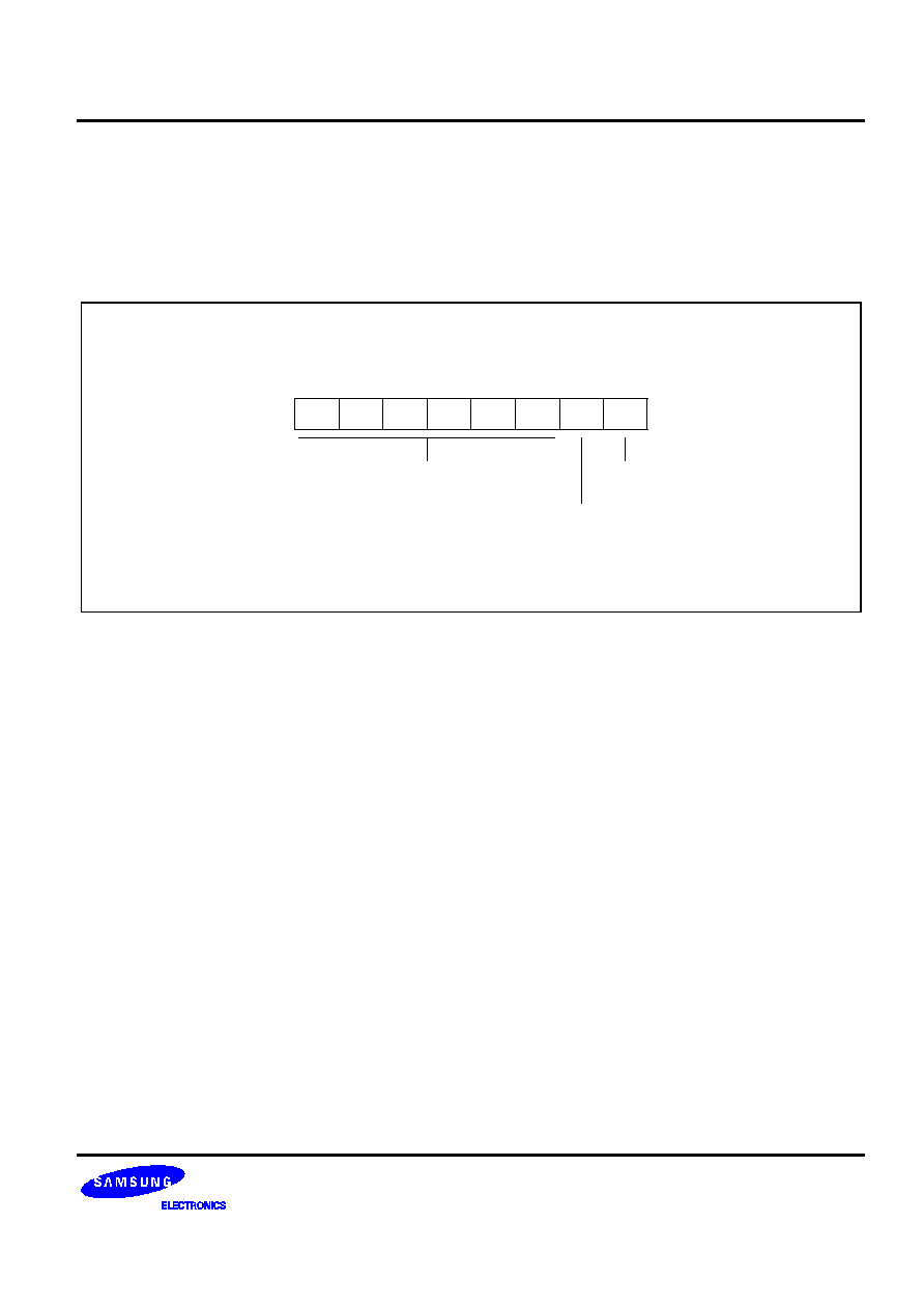
S3C852B/P852B (Preliminary Spec)
EXTERNAL INTERFACE
16-5
EXTERNAL MEMORY TIMING REGISTER (EMT)
The external memory timing register, EMT, is used to control bus operations for external peripheral interface,
including:
-- Stack area selection (external or internal area)
.7
.6
.5
.4
.3
.2
.1
.0
LSB
MSB
External Memory Timing Control Register (EMT)
FEH, Set 1, Bank 0, R/W
Stack area selection bit:
0 = Internal stack area
1 = External stack area
Not used
Not used
Figure 16-4. External Memory Timing Control Register (EMT)

EXTERNAL INTERFACE
S3C852B/P852B (Preliminary Spec)
16-6
PORT 3 ALTERNATIVE FUNCTION SELECT REGISTER (P3AFS)
The P3AFS register is used to configure the port 3 pins, P3.0�P3.3, as control signal lines for the external
interface. In normal operating mode a reset clears P3AFS to `00H', configuring P3.0�P3.3 as normal I/O port. In
ROM-less mode, a reset automatically configures these pins as bus control lines. Bit settings in the P3AFS
register activate P3.0�P3.3 as external memory control lines
PM, DM, RD, WR
, respectively.
PORT 4 CONTROL REGISTER (P4CON)
The port 4 control register, P4CON is used to configure the data lines D0�D7. In normal (internal ROM) mode, a
reset clears P4CON to `00H', thereby configuring P4.0�P4.7 to Schmitt trigger input mode. When using the
S3C852B in ROM-less mode, a reset automatically configures P4.0�P4.7 as data lines D0�D7, respectively.
PORT 5 CONTROL REGISTER (P5CON)
The port 5 control register, P5CON is used to configure the address lines A0�A7. In normal (internal ROM)
mode, a reset clears P5CON to `00H', thereby configuring P5.0�P5.7 to Schmitt trigger input mode. When using
the S3C852B in ROM-less mode, a reset automatically configures P5.0�P5.7 as address lines A0�A7,
respectively.
PORT 6 CONTROL REGISTER (P6CON)
The port 6 control register, P6CON is used to configure the address lines A8�A15. In normal (internal ROM)
mode, a reset clears P6CON to `00H', thereby configuring P6.0�P6.7 to Schmitt trigger input mode. When using
the S3C852B in ROM-less mode, a reset automatically configures P6.0�P6.7 as address lines A8�A15,
respectively.
If you do not need all of the port 6 address lines for your application, you can use the remaining port 6 pins for
general I/O. In this case, read operations will return valid port data only from the pins you configure for general
I/O.
Table 16-1. Control Register Overview for the External Interface
Register
Location
Description
SYM
DEH, set 1
External tri-state interface enable bit (SYM.7)
EMT
FEH, set 1, bank 0
External/internal stack selection control
P3AFS
F2H, set 1, bank 0
Select program memory signal (
PM
) at P3.0
Select data memory signal (
DM
) at P3.1
Enable read signal (
RD
) at P3.2
Enable write signal (
WR
) at P3.3
P4CON
F3H, set 1, bank 0
Configure data lines D0�D7 at P4.0�P4.7
P5CON
F4H, set 1, bank 0
Configure address lines A0�A7 at P5.0�P5.7
P6CON
F5H, set 1, bank 0
Configure address lines A8�A15 at P6.0�P6.7
NOTE: When the S3C852B is used in ROM-less mode (that is, when the EA pin is High level), a reset sets ports 3, 4, 5
and 6 to external interface pins. Access to the internal ROM is disable, and the entire 64-Kbyte program memory
address range is addressed externally over the external interface.
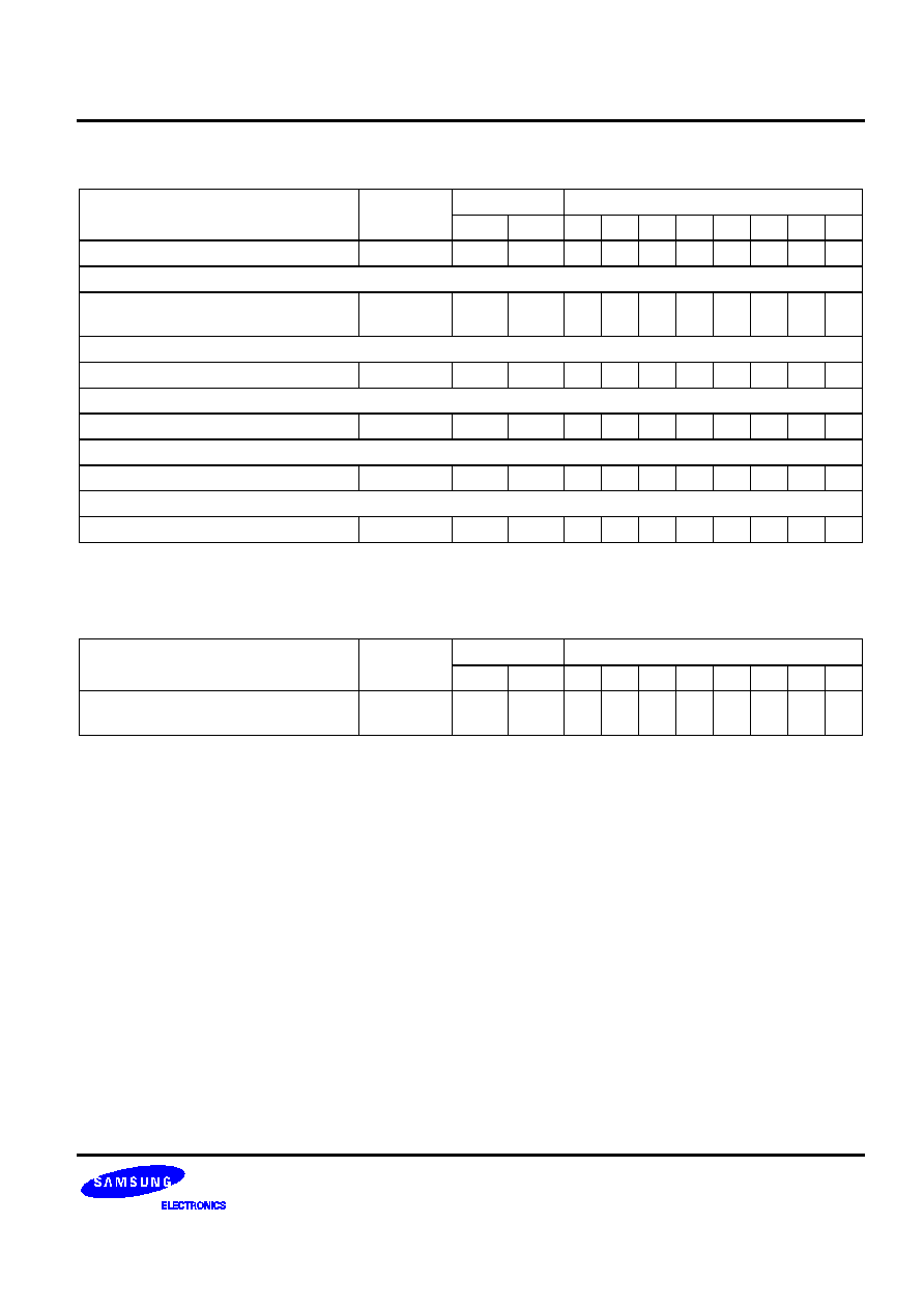
S3C852B/P852B (Preliminary Spec)
EXTERNAL INTERFACE
16-7
Table 16-2. External Interface Control Register Values after a
RESET
RESET
(Normal Mode)
Register Name
Mnemonic
Address
Bit Values after Reset
(EA Low)
Dec
Hex
7
6
5
4
3
2
1
0
System mode register
SYM
222
DEH
0
�
�
x
x
x
0
0
Port 3 alternative function select
register
P3AFS
242
F2H
�
�
�
�
0
0
0
0
Port 4 control register
P4CON
243
F3H
0
0
0
0
0
0
0
0
Port 5 control register
P5CON
244
F4H
0
0
0
0
0
0
0
0
Port 6 control register
P6CON
245
F5H
0
0
0
0
0
0
0
0
External memory timing register
EMT
254
FEH
�
1
1
1
1
1
0
�
NOTE: A dash (�) indicates that the bit is not used or not mapped; an 'x' means that the value is undefined after a reset.
Table 16-3. External Interface Control Register Values after a
R
RESET
ESET
(ROM-less Mode)
Register Name
Mnemonic
Address
Bit Values after
RESET
(EA High)
Dec
Hex
7
6
5
4
3
2
1
0
Port 3 alternative function select
register
P3AFS
242
F2H
�
�
�
�
1
1
1
1
NOTE: In ROM-less operating mode, a reset initializes all external interface control registers to their normal reset values,
with the exception of P3AFS. However, the external interface pins at port 4, port 5, port 6 and P3.0�P3.3 are
internally configured to external interface mode.

EXTERNAL INTERFACE
S3C852B/P852B (Preliminary Spec)
16-8
CONFIGURING SEPARATE EXTERNAL PROGRAM AND DATA MEMORY AREAS
You can address external program and data memory locations as a single combined space or as two separate
spaces. If the program and data memory spaces are implemented separately, this separation is maintained
logically using the data and program memory select signal (
DM and PM)
.
To select external data memory, you must set the bit 1 in the port3 alternative function select register, P3AFS.1,
to "1", because the P3AFS.1 bit enable the
DM
output pin. The
DM
output is controlled automatically by
hardware, that is,
DM
pin's state goes active Low to select the data memory area whenever one of the following
instructions is executed:
These instructions are used for accessing the external data and program memory.
-- LDE
(Load external data memory)
-- LDED
(Load external data memory and decrement)
-- LDEI
(Load external data memory and increment)
-- LDEPD
(Load external data memory with pre-decrement)
-- LDEPI
(Load external data memory with pre-increment)
If you set the stack area selection bit in the EMT register, EMT.1 to "1", the system stack area is configured
externally. In this case, the
DM
signal will go active low whenever a CALL, POP, PUSH, RET, or IRET instruction
is executed.
Using An External System Stack
The KS88 architecture supports stack operations in either the internal register file or in externally configured data
memory. The PUSH and POP instructions support external system stack operations.
To select the external stack area option, you must set bit 1 in the external memory timing register (EMT, FEH) to
"1".
NOTE
The instruction you use to modify the stack selection bit in the EMT register should not be immediately
followed by an instruction that uses the stack. This could cause a program error. Also, remember to
disable interrupts by executing a DI instruction before you modify the stack selection bit.
A 16-bit stack pointer value (SPH and SPL) is required for external stack operations. After a reset, the SP values
are undetermined.
Return addresses for procedure calls and interrupts, as well as dynamically generated data are stored on an
externally-defined stack. The contents of the PC are saved on the external stack during a CALL instruction and
restored by a RET instruction. When an interrupt occurs, the contents of the PC and the FLAGS register are
saved to the external stack. These values are then restored by an IRET instruction.

S3C852B/P852B (Preliminary Spec)
EXTERNAL INTERFACE
16-9
EXTERNAL BUS OPERATIONS
The number of machine cycles that are required for external memory operations is two machine cycle.
The notation used to describe basic timing periods in Figures 16-5 to 16-12 are machine cycles (Mn), timing
states (Tn), and clock periods. The clock wave form is shown for clarification only and does not have a specific
timing relationship to the other signals.
Controlling External Bus Operations
Whenever the S3C852B/P852B external peripheral interface is active, the addresses of all internal program
memory references will also appear on the external bus. This should have no effect on the external system,
however, because the
RD
and
WR
signals are always high. (
RD and WR
goes low only during external memory
references.)
Shared Bus Feature
The
RD, WR, DM
,
PM
signals, address, and data bus can be set to high impedance to enable the
S3C852B/P852B to share common resources with other bus masters. This feature is often required for
multiprocessor or related applications that require two or more devices that share the same external bus.
The tri-state memory interface enable bit in the system mode register (SYM.7) controls this function. When
SYM.7 = "1", the tri-state function is enabled, all external interface lines are set to high impedance, and the
external bus is put under software control.
EXTERNAL INTERFACE
S3C852B/P852B (Preliminary Spec)
16-10
T1
T2
T1
Clock
Address
Data
RD
WR
DM
PM
Write Cycle
Machine Cycle (Mn)
T2
D0-D7
A0-A15
Figure 16-5. External Bus Write Cycle Timing Diagram (Address, and Data Separated )
S3C852B/P852B (Preliminary Spec)
EXTERNAL INTERFACE
16-11
T1
T2
T1
Clock
Address
Data
WR
RD
DM
PM
Read Cycle
Machine Cycle (Mn)
T2
D0-D7
A0-A15
Figure 16-6. External Bus Read Cycle Timing Diagram

EXTERNAL INTERFACE
S3C852B/P852B (Preliminary Spec)
16-12
Table 16-4. S3C852B External Memory Interface Signal Descriptions
Signal Name
Symbol
Pin
Active Level
Description
Read
RD
14
Low
RD
determines the data transfer direction for
external memory operations.
Write
WR
15
Low
WR
is low when writing to external program
memory or data memory locations, and is high
for all other operations.
Memory select
DM
13
Low
When it is low,
DM
selects data memory.
PM
12
Low
When it is low,
PM
selects program memory.
NOTE: If bit 7 of the SYM register is high level, and assuming the external memory interface is configured, the
RD, PM,
WR,
and
DM
signals, as well as address and data signal, will be set to high impedance state. This causes the
external interface signals to 'float'.
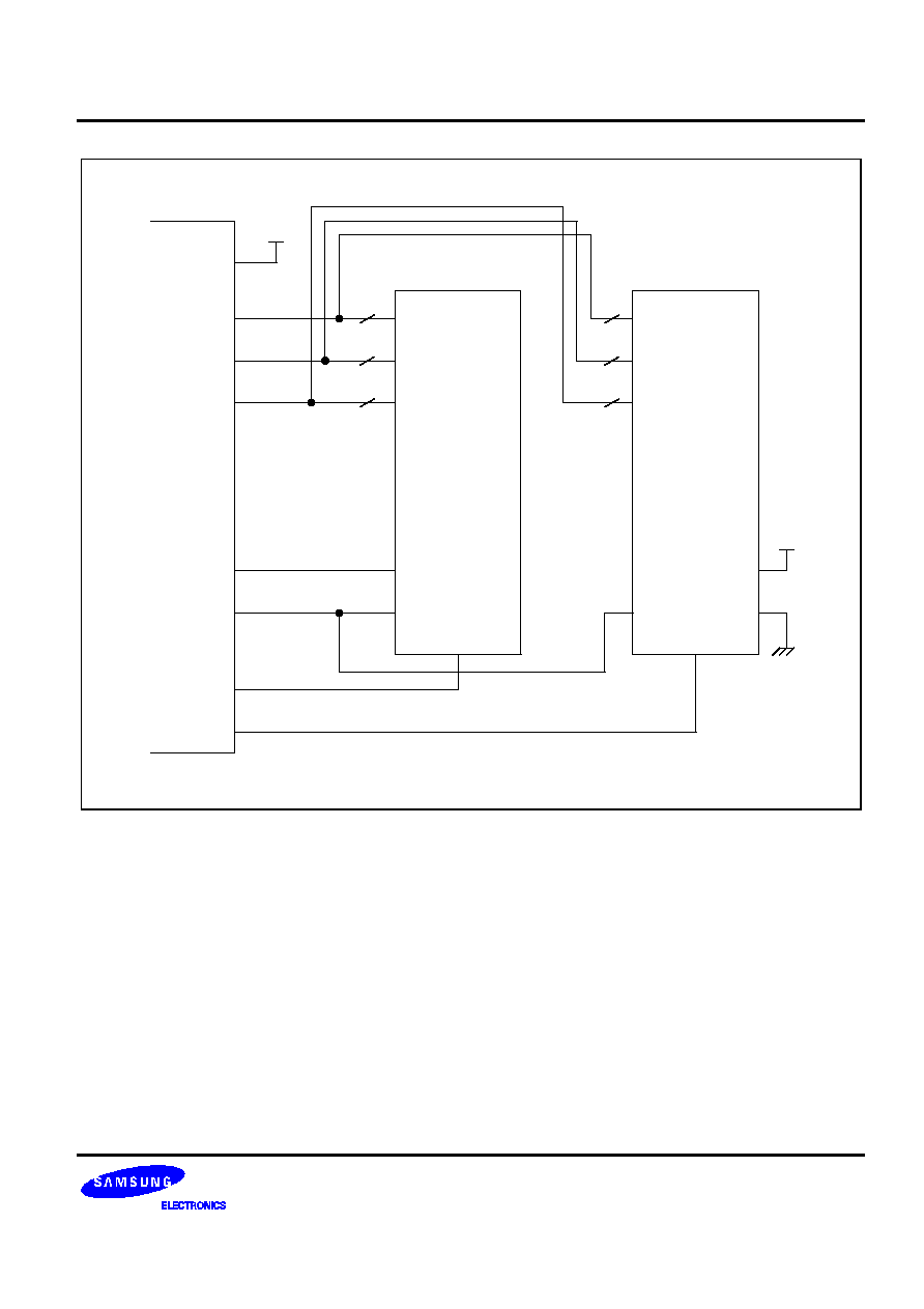
S3C852B/P852B (Preliminary Spec)
EXTERNAL INTERFACE
16-13
S3C852B
EA
V
DD
A8-A15
A0-A7
D0-D7
8
8
8
SRAM
or
Equivalent
EPROM,
EEPROM
or
Equivalent
8
8
8
A8-A15
A0-A7
D0-D7
A8-A15
A0-A7
D0-D7
WE
OE
CS
WR
RD
DM
PM
OE
CS
WE
Figure 16-7. External Interface Function Diagram (with SRAM and EPROM or EEPROM)
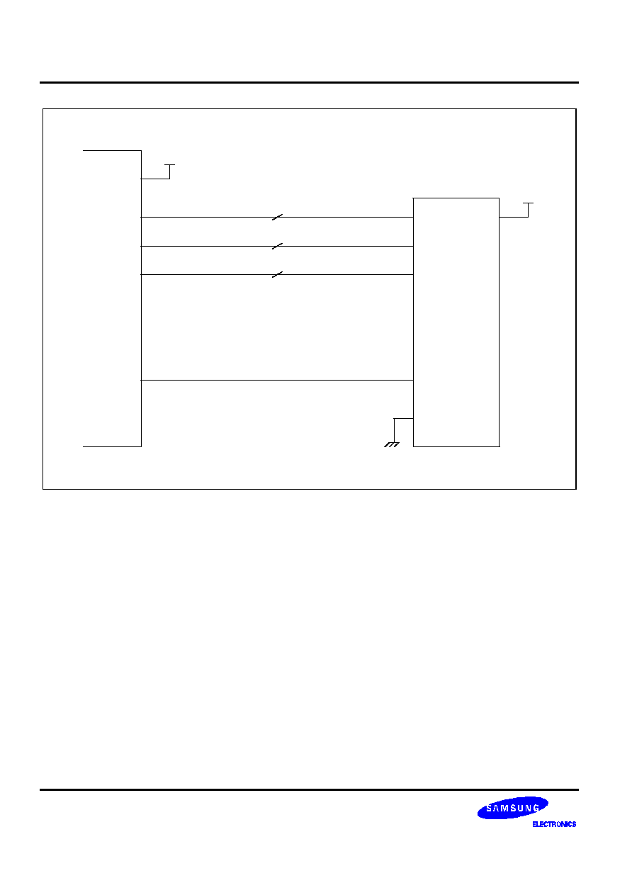
EXTERNAL INTERFACE
S3C852B/P852B (Preliminary Spec)
16-14
S3C852B
EA
A8-A15
A0-A7
D0-D7
8
8
8
EPROM,
EEPROM
or
Equivalent
A8-A15
A0-A7
D0-D7
RD
OE
CE
V
DD
V
DD
WE
Figure 16-8. External Interface Function Diagram (External ROM Only)
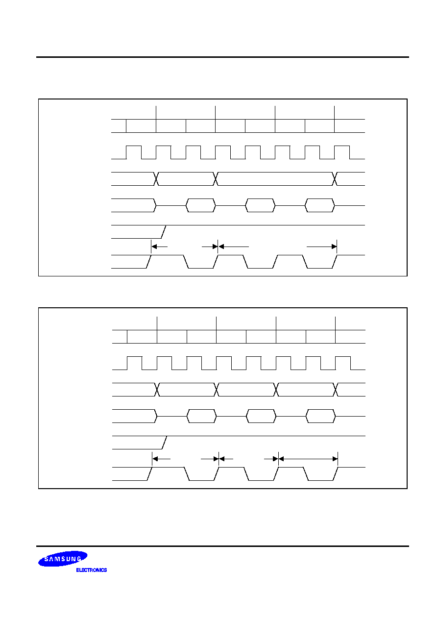
S3C852B/P852B (Preliminary Spec)
EXTERNAL INTERFACE
16-15
SAM8 INSTRUCTION EXECUTION TIMING DIAGRAMS
T2
CPU CLK
Address
Data
WR
RD
T1
A0-A15
T2
T1
T2
T1
A0-A15
D0-D7
D0-D7
D0-D7
M1
M2
M1
Fetch
Instruction
Fetch 1st Byte of
Next Instruction
Figure 16-9. External Bus Timing Diagram for 1-Byte Fetch Instructions
T2
CPU CLK
Address
Data
WR
RD
T1
T2
T1
T2
T1
A0-A15
D0-D7
D0-D7
D0-D7
M1
M2
M1
A0-A15
A0-A15
Fetch
1st Byte
Fetch
2nd Byte
Fetch 1st Byte of
Next Instruction
Figure 16-10. External Bus Timing Diagram for 2-Byte Fetch Instructions
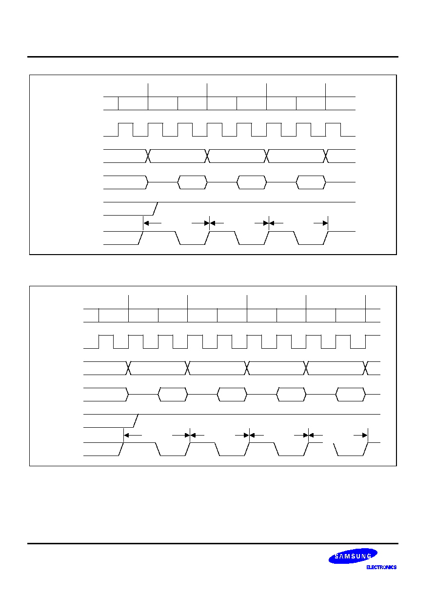
EXTERNAL INTERFACE
S3C852B/P852B (Preliminary Spec)
16-16
T2
CPU CLK
Address
Data
WR
RD
T1
T2
T1
T2
T1
A0-A15
D0-D7
D0-D7
D0-D7
M1
M2
M1
A0-A15
A0-A15
Fetch
1st Byte
Fetch
2nd Byte
Fetch
3rd Byte
Figure 16-11. External Bus Timing Diagram for 3-Byte Fetch Instructions
T2
CPU CLK
Address
Data
WR
RD
T1
T2
T1
T2
T1
A0-A15
D0-D7
D0-D7
D0-D7
M1
M2
M1
A0-A15
A0-A15
T2
T1
M1
A0-A15
D0-D7
Fetch
1st Byte
Fetch
2nd Byte
Fetch
3rd Byte
Fetch
4th Byte
Figure 16-12. External Bus Timing Diagram for 4-Byte Fetch Instructions

S3C852B/P852B (Preliminary Spec)
ELECTRICAL DATA
17-1
17
ELECTRICAL DATA
OVERVIEW
In this chapter, S3C852B electrical characteristics are presented in tables and graphs. The information is
arranged in the following order:
-- Absolute maximum ratings
-- D.C. electrical characteristics
-- Data retention supply voltage in Stop mode
-- Stop mode release timing when initiated by an external interrupt
-- Stop mode release timing when initiated by a Reset
-- I/O capacitance
-- A.C. electrical characteristics
-- Input timing for external interrupts (port 0)
-- Input timing for
RESET
-- Oscillation characteristics
-- Oscillation stabilization time
-- Phase locked loop characteristics
-- Serial I/O Timing Characteristics
-- A/D Converter Electrical Characteristics
-- Analog Circuit Characteristics and Consumed Current
-- Electrical characteristics of CID Block
-- CAS timing characteristics
-- SDT timing characteristics
-- Serial Interface timing characteristics
-- Oscillation stabilization time
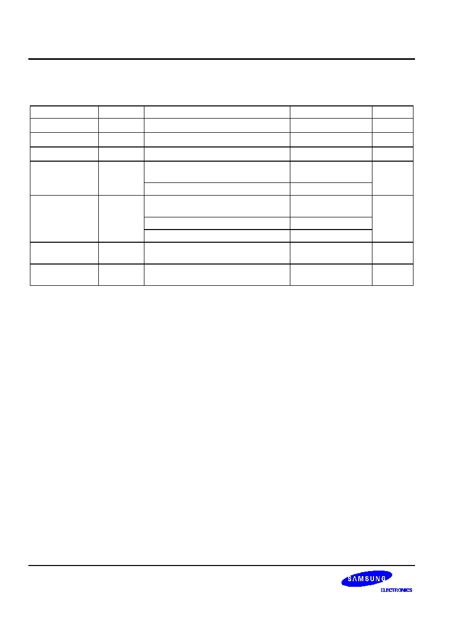
ELECTRICAL DATA
S3C852B/P852B (Preliminary Spec)
17-2
Table 17-1. Absolute Maximum Ratings
(T
A
= 25
�
C)
Parameter
Symbol
Conditions
Rating
Unit
Supply voltage
V
DD
�
� 0.3 to + 7.0
V
Input voltage
V
IN
Ports 0, 1, 2, 3, 4, 5, 6, 7, 8, 9 and 10
� 0.3 to
V
DD
+ 0.3
V
Output voltage
V
O
All output pins
� 0.3 to V
DD
+ 0.3
V
Output current
High
I
OH
One I/O pin active
� 18
mA
All I/O pins active
� 60
Output current
Low
I
OL
One I/O pin active
+ 30
mA
Total pin current for ports 0, 1, and 3�10
+ 100
Total pin current for port 2
+ 40
Operating
temperature
T
A
�
0 to + 70
�
C
Storage
temperature
T
STG
�
� 10 to + 100
�
C
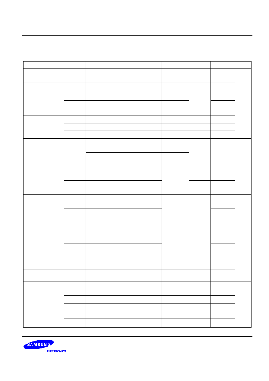
S3C852B/P852B (Preliminary Spec)
ELECTRICAL DATA
17-3
Table 17-2. D.C. Electrical Characteristics
(T
A
= 0
�
C to + 70
�
C, V
DD
= 2.7 V to 5.5 V)
Parameter
Symbol
Conditions
Min
Typ
Max
Unit
Operating Voltage
V
DD
fx = 3.579545 MHz
(Instruction clock=0.89 MHz)
(note)
2.7
�
5.5
V
Input High
voltage
V
IH1
All input pins except V
IH2
and V
IH3
0.8 V
DD
�
V
DD
V
IH2
RESET
0.7 V
DD
V
DD
V
IH3
X
IN
,
XT
IN
V
DD
� 0.3
V
DD
Input Low voltage
V
IL1
All input pins except V
IL2
and V
IL3
0
�
0.2 V
DD
V
IL2
RESET
0
�
0.3 V
DD
V
IL3
X
OUT
,
XT
OUT
0.3
Output High
voltage
V
OH
V
DD
= 4.5 to 6.0 V;
I
OH
= � 1 mA Ports 0 - 6
V
DD
� 1.0
�
�
V
I
OH
= � 100 uA
V
DD
� 0.5
Output Low
voltage
V
OL1
V
DD
= 4.5 to 6.0 V;
I
OL
= 2 mA, All output pins
except V
OL2
�
0.4
2.0
V
OL2
V
DD
= 4.5 to 6.0 V;
I
OL
= 15 mA, Ports 2
0.4
2.0
Input High
leakage current
I
LIH1
V
IN
= V
DD
; All input pins except
X
IN
,
X
OUT
,
XT
IN
,
and XT
OUT
�
�
1
�
A
I
LIH2
V
IN
= V
DD
;
X
IN
,
X
OUT
,
XT
IN
,
and XT
OUT
20
Input Low
leakage current
I
LIL1
V
IN
= 0 V; All input pins except
RESET
, X
IN
,
X
OUT
,
XT
IN
,
and
XT
OUT
�
�
� 1
I
LIL2
V
IN
= 0 V;
X
IN
,
X
OUT
,
XT
IN
,
and XT
OUT
� 20
Output High
leakage current
I
LOH
V
OUT
= V
DD
;All output pins
�
�
1
Output Low
leakage current
I
LOL
V
OUT
= 0 V ;All output pins
�
�
� 1
Pull-up resistors
R
L1
V
IN
=0 V; T
A
=25
�
C; V
DD
=5.0 V
Ports 0 � 10
25
47
100
k
V
DD
=3.0 V
50
90
150
R
L2
V
IN
=0 V; T
A
=25
�
C; V
DD
=5.0 V
RESET
only
150
250
350
V
DD
=3.0 V
300
500
700
NOTE: Minimum instruction clock.
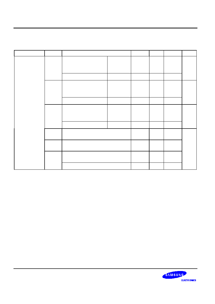
ELECTRICAL DATA
S3C852B/P852B (Preliminary Spec)
17-4
Table 17-2. D.C. Electrical Characteristics (Continued)
(T
A
= 0
�
C to + 70
�
C, V
DD
= 2.7 V to 5.5 V)
Parameter
Symbol
Conditions
Min
Typ
Max
Unit
Supply current
(note)
I
DD1
V
DD
= 5.0 V
�
10%
Crystal oscillator
3.58MHz
�
4.0
8.0
mA
C1 = C2 = 22pF
V
DD
= 3.0 V
�
10%
3.58MHz
�
2.0
4.0
I
DD1CID
V
DD
= 5.0 V
�
10%
Crystal oscillator
3.58MHz
�
8.0
16.0
mA
C1 = C2 = 22pF
V
DD
= 3.0 V
�
10%
3.58MHz
�
4.0
8.0
I
DD2
V
DD
= 5.0 V
�
10%
Crystal oscillator
3.58MHz
�
2.5
4.6-
mA
C1 = C2 = 22pF
V
DD
= 3.0 V
�
10%
3.58MHz
�
0.8
1.6
I
DD3
V
DD
= 3.0 V
�
10%, 32.768 kHz C1 =
C2 = 22pF
�
20
40
�
A
I
DD4
V
DD
= 3.0 V
�
10%, 32.768 kHz C1 =
C2 = 22pF
�
10
20
I
DD5
Stop mode;
V
DD
=5.0V
�
10%, OSCCON.2=1
�
0.5
5
V
DD
=3.0V
�
10%,
0.2
2
NOTES:
1. Supply current does not include current drawn through internal pull-up resistors, ADC or external output current loads.
2. I
DD1
, I
DD2
, I
DD3
and I
DD4
include power consumption for subsystem clock oscillation.
3. I
DD3
is the supply current when CAS signal is receiving
4. Every values in this table is measured when bits 4-3 of the system clock control register (CLKCON.4-.3) is set to 11B.
5. I
DD5
is current when bit2 of the oscillator control register (OSCCON.2) is set to logic 1.
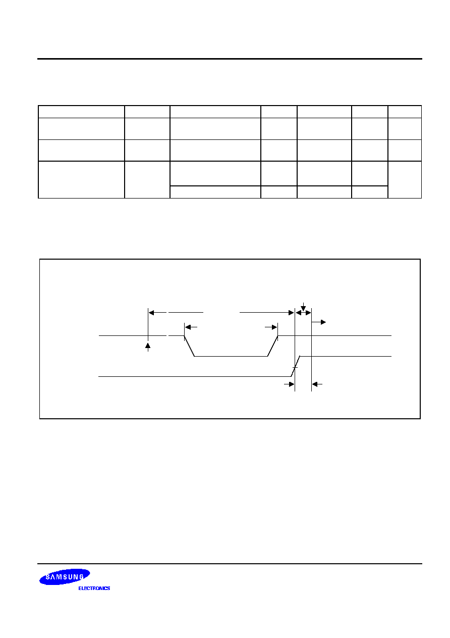
S3C852B/P852B (Preliminary Spec)
ELECTRICAL DATA
17-5
Table 17-3. Data Retention Supply Voltage in Stop Mode
(T
A
= 0
�
C to + 70
�
C)
Parameter
Symbol
Conditions
Min
Typ
Max
Unit
Data retention supply
voltage
V
DDDR
�
1.0
�
6.0
V
Data retention supply
current
I
DDDR
Stop mode,V
DDDR
=1.0 V
�
�
1
�
A
Oscillator stabilization
wait time
t
WAIT
Released by
RESET
�
2
16
/fx
(1)
�
ms
Released by interrupt
�
(2)
�
NOTES:
1.
fx is the main oscillator frequency.
2.
The duration of the oscillation stabilization time (t
WAIT
) when it is released by an interrupt is determined by
the setting
in the basic timer control register, BTCON.
Execution of
STOP Instruction
Idle Mode
(Basic Timer Active)
~ ~
V
DDDR
~ ~
Stop Mode
Normal
Operating Mode
Data Retention Mode
Interrupt
Request
V
DD
0.8 V
DD
t
WAIT
Figure 17-1. Stop Mode Release Timing When Initiated by an External Interrupt
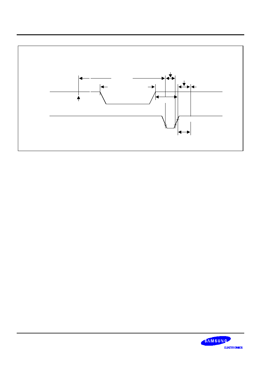
ELECTRICAL DATA
S3C852B/P852B (Preliminary Spec)
17-6
Execution of
STOP Instrction
RESET
Occurs
~ ~
V
DDDR
~ ~
Stop Mode
Oscillation
Stabilization
TIme
Normal
Operating Mode
Data Retention Mode
t
WAIT
RESET
V
DD
0.2 V
DD
0.8 V
DD
t
SRL
Figure 17-2. Stop Mode Release Timing When Initiated by a
RESET
RESET
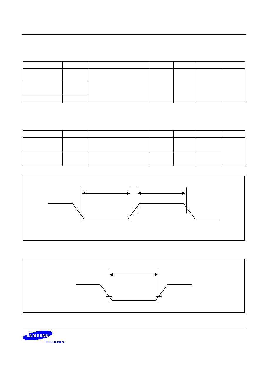
S3C852B/P852B (Preliminary Spec)
ELECTRICAL DATA
17-7
Table 17-4. Input/Output Capacitance
(T
A
= 0
�
C to + 70
�
C, V
DD
=
0 V)
Parameter
Symbol
Conditions
Min
Typ
Max
Unit
Input
capacitance
C
IN
f = 1 MHz; unmeasured pins
are connected to V
SS
�
�
10
pF
Output
capacitance
C
OUT
I/O capacitance
C
IO
Table 17-5. A.C. Electrical Characteristics
(T
A
= 0
�
C to + 70
�
C)
Parameter
Symbol
Conditions
Min
Typ
Max
Unit
Interrupt input,
High, Low width
t
INTH
,
t
INTL
P0.1 � P0.7
V
DD
= 5 V
150
200
�
ns
RESET
input Low
width
t
RSL
Input
V
DD
= 5 V
1000
�
10000
t
INTH
t
INTL
0.8 V
DD
0.2 V
DD
NOTE:
The unit t
CPU
means one CPU clock period.
External
Interrupt
Figure 17-3. Input Timing for External Interrupts (P0.0�P0.7)
RESET
t
RSL
0.3 V
DD
Figure 17-4. Input Timing for
RESET
RESET
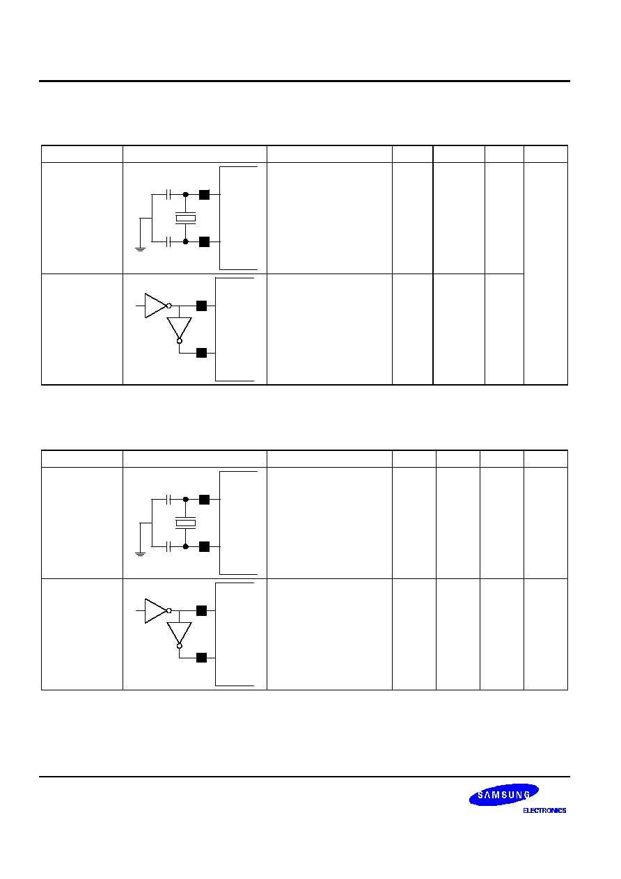
ELECTRICAL DATA
S3C852B/P852B (Preliminary Spec)
17-8
Table 17-6. Main Oscillation Characteristics
(T
A
= 0
�
C to + 70
�
C, V
DD
= 2.7 V to 5.5 V)
Oscillator
Clock Circuit
Conditions
Min
Typ
Max
Unit
Crystal
Oscillator
X
IN
X
OUT
C2
C1
CPU clock oscillation
frequency
V
DD
= 2.2 V to 6.0 V
�
3.579545
�
MHz
External clock
X
IN
X
OUT
X
IN
input frequency
V
DD
= 2.2 V to 6.0 V
�
3.579545
�
Table 17-7. Sub Oscillation Characteristics
(T
A
= 0
�
C to + 70
�
C, V
DD
= 2.7 V to 5.5 V)
Oscillator
Clock Circuit
Conditions
Min
Typ
Max
Unit
Crystal
Oscillator
XT
IN
XT
OUT
C2
C1
CPU clock oscillation
frequency
32
32.768
35
kHz
External clock
XT
IN
XT
OUT
XT
IN
input frequency
32
�
100
kHz
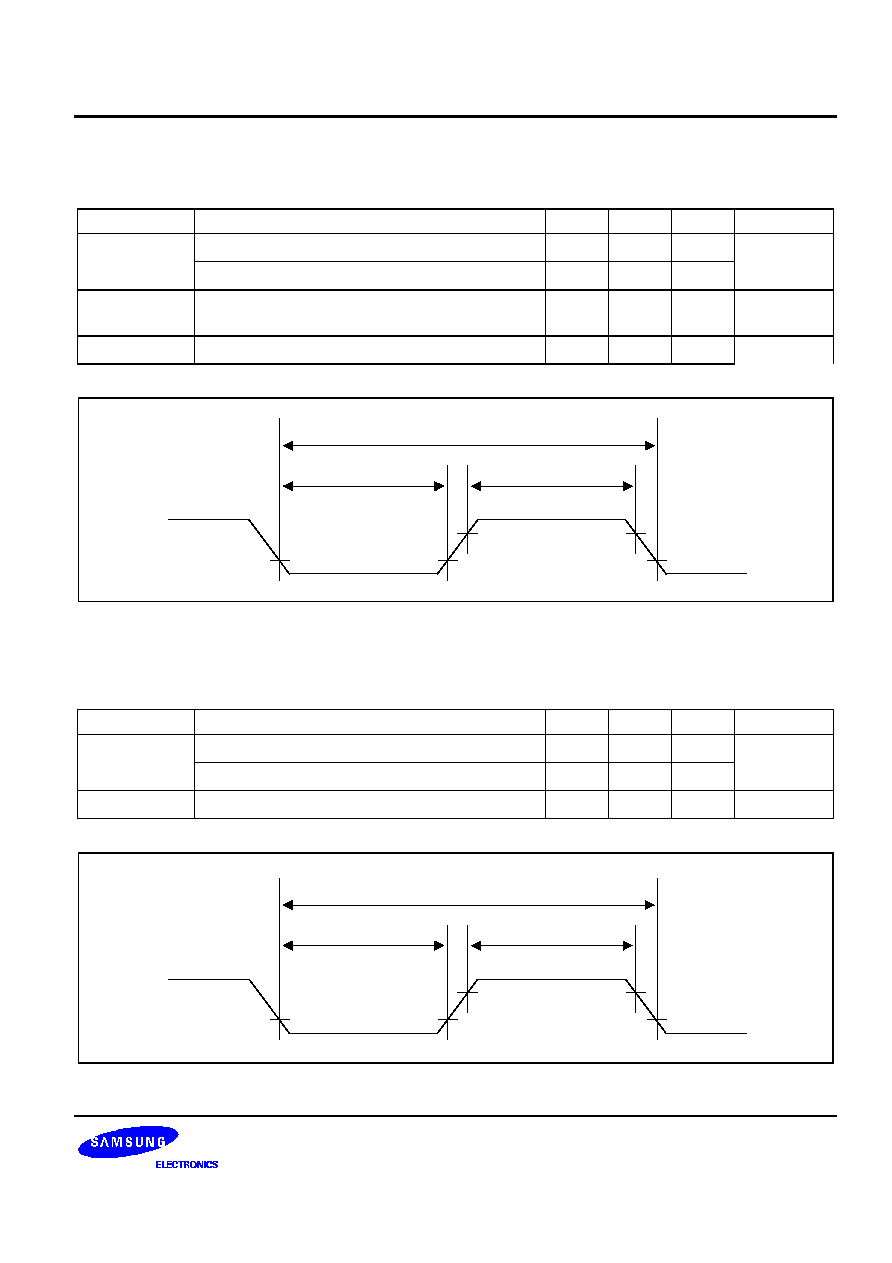
S3C852B/P852B (Preliminary Spec)
ELECTRICAL DATA
17-9
Table 17-8. Main Oscillation Stabilization Time
(T
A
= 0
�
C to + 70
�
C)
Oscillator
Test Condition
Min
Typ
Max
Unit
Crystal
V
DD
= 4.5 V to 6.0 V
�
�
10
ms
Oscillator
V
DD
= 2.0 V to 4.5 V
�
�
30
Ceramic
Oscillator
Oscillation stabilization occurs when V
DD
is equal
to the minimum oscillator voltage range.
�
�
4
ms
External clock
X
IN
input High and Low width (t
XH
, t
XL
)
62.0
�
1250
ns
t
XH
t
XL
V
DD
-0.5 V
0.5 V
X
IN
1/fx
Figure 17-5. Clock Timing Measurement at X
IN
Table 17-9. Sub Oscillation Stabilization Time
(T
A
= 0
�
C to + 70
�
C, V
DD
= 3.0 V
�
10 %)
Oscillator
Test Condition
Min
Typ
Max
Unit
Crystal
V
DD
= 4.5 V to 6.0 V
�
1.0
2
s
V
DD
= 2.0 V to 4.5 V
�
�
10
External clock
X
IN
input High and Low width (t
XH
, t
XL
)
5
�
15
�
s
t
XTH
t
XTL
V
DD
-0.5 V
0.5 V
XT
IN
1/fxt
Figure 17-6. Clock Timing Measurement at XT
IN

ELECTRICAL DATA
S3C852B/P852B (Preliminary Spec)
17-10
Table 17-10. Phase Locked Loop Characteristics
(T
A
= 0
�
C to + 70
�
C, V
DD
= 2.7 V to 5.5V, X
TIN
= 32.768kHz
�
0.05%, X
IN
= 3.579545MHz, C
PLLC
= 0.1
�
F)
Parameter
Test Condition
Min
Typ
Max
Unit
Operating
Voltage
T
A
= 0
�
C to + 70
�
4.5
�
5.5
V
Output
Frequency
V
DD
= 2.7 V to 5.5 V
Main clock (fx) generation
3.579
3.579545
3.58
Main clock doubling (fx*2)
7.158
7.15909
7.160
Stabilization
Time
V
DD
= 2.7 V to 5.5 V
Main clock (fx) generation
�
�
0.5
S

S3C852B/P852B (Preliminary Spec)
ELECTRICAL DATA
17-11
Table 17-11. Serial I/O Timing Characteristics
(T
A
= 0
�
C to + 70
�
C, V
DD
= 2.7 V to 5.5 V)
Parameter
Symbol
Conditions
Min
Typ
Max
Unit
SCK
Cycle Time
T
CKY
External
SCK
source
1000
�
�
ns
Internal
SCK
source
1000
SCK
High, Low Width
t
KH
, t
KL
External
SCK
source
500
�
�
Internal
SCK
source
t
KCY
/2 � 50
SI Setup Time to
SCK
Low
T
SIK
External
SCK
source
250
�
�
Internal
SCK
source
250
SI Hold Time to
SCK
High
T
KSI
External
SCK
source
400
�
�
Internal
SCK
source
400
Output Delay for
SCK
to SO
T
KSO
External
SCK
source
�
�
300
Internal
SCK
source
250
NOTE: "
SCK
" means serial I/O clock frequency, "SI" means serial data input, and "SO" means serial data output.
Output Data
Input Data
SCK
t
KH
t
KCY
t
KL
0.8 V
DD
0.2 V
DD
t
KSO
t
SK
t
KSI
0.8 V
DD
0.2 V
DD
SI
SO
Figure 17-7. Serial Data Transfer Timing

ELECTRICAL DATA
S3C852B/P852B (Preliminary Spec)
17-12
Table 17-12. A/D Converter Electrical Characteristics
( T
A
= 0
�
C to + 70
�
C, V
DD
= 2.7 V to 5.5 V, V
SS
= 0 V)
Parameter
Symbol
Conditions
Min
Typ
Max
Unit
Resolution
10
10
10
bit
Absolute
accuracy
(1)
V
DD
= 5.12 V
fx = 8 MHz
AV
REF
= (10/10)V
DD
AV
SS
= 0 V
�
�
| 3 |
LSB
Conversion
time
(2)
t
CON
Conversion clock = fx
(3)
50/fx
�
�
uS
Analog reference
voltage
AV
REF
�
V
DD
- 0.1
V
DD
V
DD
+ 0.1
V
Analog ground
AV
SS
�
V
SS
�
�
V
Analog input
voltage
V
IAN
�
AV
SS
�
AV
REF
V
Analog input
impedance
R
AN
�
2
�
�
M
NOTES:
1.
Excluding quantization error, absolute accuracy equals
�
1/2 LSB.
2.
'Conversion time' is the time required from the moment a conversion operation starts until it ends.
3.
The conversion clock is selected by bits 2-1 of A/D converter control register, ADCON.2-.1.
S3C852B/P852B (Preliminary Spec)
ELECTRICAL DATA
17-13
Table 17-13. Electrical Characteristics of CID Block (Receiver & Detectors)
( T
A
= 0
�
C to + 70
�
C, V
DD
= 5.0 V
�
5 %, X
IN
= 3.579545MHz
�
0.1% )
Symbol
Parameter
Min
Typ
Max
Unit
Voltage reference
V
REF
Reference voltage output
2.25
V
CAS detector
THac
Input accept threshold (in 600
load )
-38
dBm
Pic
Input signal power ( in 600
load )
-37
0
dBm
flc
Low tone frequency
2130
Hz
fhc
High tone frequency
2750
Hz
fmaxc
maximum frequency deviation
-0.6
+0.6
%
T
WC
Twist
-6
6
dB
FSK receiver
Pif
Input signal power ( in 600
load )
-42
0
dBm
fD
data transmission rate frequency
1188
1200
1212
Baud
fmb
mark frequency (Bell202)
1188
1200
1212
Hz
fsb
space frequency (Bell202)
2178
2200
2222
Hz
fmv
mark frequency (CCITT/V23)
1300
Hz
fsv
space frequency (CCITT/V23)
2100
Hz
Twf
twist
-10
10
dB
S/N0
signal to noise ratio (0Hz � 200Hz)
-25
dB
S/N1
signal to noise ratio (200Hz � 3.2kHz)
6
dB
S/N3
signal to noise ratio (3.2kHz � 15kHz)
-25
dB
SDT detector
fls
Low tone frequency
350
Hz
fhs
High tone frequency
440
Hz
Tws
Twist
-6
+6
dB
THap
Input accept threshold (in 600
load )
-38
-5
dBm
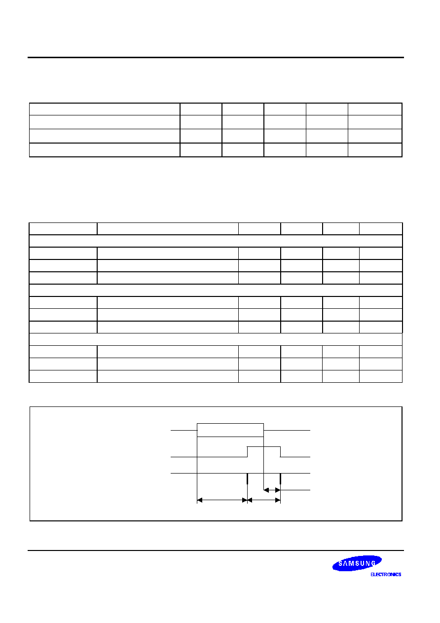
ELECTRICAL DATA
S3C852B/P852B (Preliminary Spec)
17-14
Table 17-14. CAS Timing Characteristics
(
T
A
= 0
�
C
+ 70
�
C
, V
DD
= 2.7 V to 5.5 V, X
IN
= 3.579545MHz
�
0.1%
)
Parameter
Symbol
Min
Typ
Max
Unit
CAS detection time from CAS start
T
DETC
67
ms
Detection off time from CAS end
T
OFFC
30
ms
CAS detection time width
T
WIDTHC
8
ms
Table 17-15. Electrical Characteristics of CID Block (Tone Generator)
( T
A
= 25
�
C, V
DD
= 5.0 V
�
5% (Max), 3.3V
�
5% (Typ), XIN = 3.579545MHz
�
0.1%
High & Low Tone Gain = 10H, R11 = 9k
, C8 = 2.2nF, terminal impedence = 600
)
Symbol
Parameter
Min
Typ
Max
Unit
DTMF Generation
Pod
output signal power (for high tone)
�
-4.3
0.4
dBm
fmaxd_g
maximum frequency deviation
-0.1
+0.1
%
S/Nd
signal to noise ratio (0 � 6kHz)
-32
dBV
FSK Generation
Pof
output signal power (for high tone)
�
-4.3
0.2
dBm
fmaxf_g
maximum frequency deviation
-0.1
+0.1
%
S/Nf
signal to noise ratio (0 � 6kHz)
-45
dBV
CAS Generation
Poc
output signal power (for high tone)
�
-5.3
-0.2
dBm
fmaxc_g
maximum frequency deviation
-0.1
+0.1
%
S/Nc
signal to noise ratio (0 � 6kHz)
-34
dBV
Line signal
T
DETC
CASdet
T
WIDTHC
INT
CAS signal
T
OFFC
Figure 17-8. Waveform for CAS Timing Characteristics

S3C852B/P852B (Preliminary Spec)
ELECTRICAL DATA
17-15
Table 17-16. SDT Timing Characteristics
(
T
A
= 0
�
C
+ 70
�
C
, V
DD
= 2.7 V to 5.5 V X
IN
= 3.579545MHz
�
0.1%
)
Parameter
Symbol
Min
Typ
Max
Unit
SDT detection time from SDT start
T
DETS
60
ms
Detection off time from SDT end
T
OFFC
30
ms
Line signal
T
DETS
SDTdet
INT
SDT signal
T
OFFS
Figure 17-9. Waveform for SDT Timing Characteristics

ELECTRICAL DATA
S3C852B/P852B (Preliminary Spec)
17-16
NOTES

S3C852B/P852B (Preliminary Spec)
MECHANICAL DATA
18-1
18
MECHANICAL DATA
OVERVIEW
The S3C852B microcontroller is currently available in a 100-pin QFP package.

MECHANICAL DATA
S3C852B/P852B (Preliminary Spec)
18-2
#100
NOTE: Dimensions are in millimeters.
#1
0.65BSC
0.30
�
0.08
0.15 MAX
(0.58)
20.00
�
0.20
23.90
�
0.30
14.00
�
0.20
17.90
�
0.30
0.10 MAX
0.15
0-8
0.80 - 0.20
0.05MIN
2.65
3.00 MAX
�
0.10
+ 0.10
- 0.05
100-QFP-1420C
Figure 18-1. 100-Pin QFP Package Mechanical Data

S3C852B/P852B (Preliminary Spec)
S3P852B OTP
19-1
19
S3P852B OTP
OVERVIEW
The S3P852B single-chip CMOS microcontroller is the OTP (One Time Programmable)
version of the S3C852B
microcontroller. It has an on-chip OTP ROM instead of a masked ROM. The EPROM is accessed by serial data
format.
The S3P852B is fully compatible with the S3C852B, both in function in D.C. electrical characteristics, bonding
information and in pin configuration. Because of its simple programming requirements, the S3P852B is ideal as
an evaluation chip for the S3C852B.
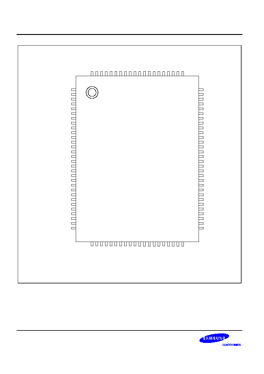
S3P852B OTP
S3C852B/P852B (Preliminary Spec)
19-2
P5.7/A7
P5.6/A6
P5.5/A5
P5.4/A4
P5.3/A3
P5.2/A2
P5.1/A1
P5.0/A0
P4.7/D7
P4.6/D6
P4.5/D5
P4.4/D4
P4.3/D3
P4.2/D2
P4.1/D1
P4.0/D0
P3.3/
WR
P3.2/
RD
P3.1/
DM
P3.0/
PM
P7.7
P7.6
P7.5
P7.4
P7.3
P0.7/INT7
P0.6/INT6/TB
P0.5/INT5/TA
P0.4/INT4/T1CK
P0.3/INT3/T0/T0CAP
P2.0
P2.1
P2.2(SDAT)
P2.3(SCLK)
V
DD
V
SS
X
OUT
X
IN
EA
XT
IN
XT
OUT
RESET
P0.0/INT0
P0.1/INT1/BUZ
P0.2/INT2/T0CK
P9.7
P9.6
P9.5
P9.4
P9.3
S3C852B/P852B
100-QFP-1420C
80
79
78
77
76
75
74
73
72
71
70
69
68
67
66
65
64
63
62
61
60
59
58
57
56
55
54
53
52
51
1
2
3
4
5
6
7
8
9
10
11
12
13
14
15
16
17
18
19
20
21
22
23
24
25
26
27
28
29
30
81
82
83
84
85
86
87
88
89
90
91
92
93
94
95
96
97
98
99
100
50
49
48
47
46
45
44
43
42
41
40
39
38
37
36
35
34
33
32
31
P8.7
P8.6
P8.5
P8.4
P8.3
P8.2
P8.1
P8.0
PLLC
CKSEL
P7.2
P7.1
P7.0
VDDA
INP
INN
OUT
INS
V
REF
TONEO
VSSA
LR
IN
MLDO
P10.7
P10.6
P10.5
P10.4
P10.3
P10.2
P10.1
P10.0
P6.7/A15
P6.6/A14
P6.5/A13
P6.4/A12
P6.3/A11
P6.2/A10
P6.1/A9
P6.0/A8
P1.7/SSD/SD3
P1.6/
SCK
/SD2
P1.5/SO/SD1
P1.4/SI/SD0
P1.3/ADC3
P1.2/ADC2
P1.1/ADC1
P1.0/ADC0
P9.0
P9.1
P9.2
Figure 19-1. S3P852B Pin Assignments (100-Pin QFP Package)
S3C852B/P852B (Preliminary Spec)
S3P852B OTP
19-3
Table 19-1. Descriptions of Pins Used to Read/Write the EPROM
Main Chip
During Programming
Pin Name
Pin Name
Pin No.
I/O
Function
P2.2
SDAT
13
I/O
Serial data pin. Output port when reading and
input port when writing. Can be assigned as a
Input/push-pull output port.
P2.3
SCLK
14
I
Serial clock pin. Input only pin.
EA
V
PP
19
I
Power supply pin for EPROM cell writing
(indicates that OTP enters into the writing mode).
When 12.5 V is applied, OTP is in writing mode
and when 5 V is aplied, OTP is in reading mode.
(Option)
RESET
RESET
22
I
Chip Initialization
V
DD
/V
SS
V
DD
/V
SS
15/16
�
Logic power supply pin. V
DD
should be tied to
+5 V during programming.
Table 19-2. Comparison of S3P852B and S3C852B Features
Characteristic
S3P852B
S3C852B
Program Memory
64-Kbyte EPROM
64-Kbyte mask ROM
Operating Voltage (V
DD
)
2.7 V to 5.5 V
2.7 V to 5.5 V
OTP Programming Mode
V
DD
= 5 V, V
PP
(EA) = 12.5 V
Pin Configuration
100 QFP
100 QFP
EPROM Programmability
User Program 1 time
Programmed at the factory
OPERATING MODE CHARACTERISTICS
When 12.5 V is supplied to the V
PP
(EA) pin of the S3P852B, the EPROM programming mode is entered.

S3P852B OTP
S3C852B/P852B (Preliminary Spec)
19-4
NOTES

(For duplicate copies of this form, and for additional ordering information, please contact your local
Samsung sales representative. Samsung sales offices are listed on the back cover of this book.)
S3C8- SERIES MASK ROM ORDER FORM
Product description:
Device Number: S3C852B_ _- ___________(write down the ROM code number)
Product Order Form:
Package
Pellet Wafer
Package Type: __________
Package Marking (Check One):
Standard
Custom A
Custom B
(Max 10 chars)
(Max 10 chars each line)
@ : Assembly site code, Y : Last number of assembly year, WW : Week of assembly
@ YWW
Device Name
SEC
Device Name
@ YWW
@ YWW
Delivery Dates and Quantities:
Deliverable
Required Delivery Date
Quantity
Comments
ROM code
�
Not applicable
See ROM Selection Form
Customer sample
Risk order
See Risk Order Sheet
Please answer the following questions:
F
F
For what kind of product will you be using this order?
New model
Upgrade of an existing model
Replacement of an existing model
Others
If you are replacing an existing model, please indicate the former product name
(
)
F
F
What are the main reasons you decided to use a Samsung microcontroller in your product?
Please check all that apply.
Price
Product quality
Features and functions
Development system
Technical support
Delivery on time
Used same MCU before
Quality of documentation
Samsung reputation
Mask Charge (US$ / Won):
____________________________
Customer Information:
Company Name:
___________________ Telephone number
_________________________
Signatures:
________________________
__________________________________
(Person placing the order)
(Technical Manager)


(For duplicate copies of this form, and for additional ordering information, please contact your local
Samsung sales representative. Samsung sales offices are listed on the back cover of this book.)
S3C8- SERIES
REQUEST FOR PRODUCTION AT CUSTOMER RISK
Customer Information:
Company Name:
________________________________________________________________
Department:
________________________________________________________________
Telephone Number:
__________________________
Fax: _____________________________
Date:
__________________________
Risk Order Information:
Device Number:
S3C852B___- ________ (write down the ROM code number)
Package:
Number of Pins: ____________
Package Type: _____________________
Intended Application:
________________________________________________________________
Product Model Number:
________________________________________________________________
Customer Risk Order Agreement:
We hereby request SEC to produce the above named product in the quantity stated below. We believe our risk
order product to be in full compliance with all SEC production specifications and, to this extent, agree to assume
responsibility for any and all production risks involved.
Order Quantity and Delivery Schedule:
Risk Order Quantity:
_____________________ PCS
Delivery Schedule:
Delivery Date (s)
Quantity
Comments
Signatures:
_______________________________
_______________________________________
(Person Placing the Risk Order) (SEC Sales Representative)


(For duplicate copies of this form, and for additional ordering information, please contact your local
Samsung sales representative. Samsung sales offices are listed on the back cover of this book.)
S3C852B MASK OPTION SELECTION FORM
Device Number:
S3C852B___-________(write down the ROM code number)
Attachment (Check one):
Diskette
PROM
Customer Checksum:
________________________________________________________________
Company Name:
________________________________________________________________
Signature (Engineer):
________________________________________________________________
Please answer the following questions:
F
F
Application (Product Model ID: _______________________)
Audio
Video
Telecom
LCD Databank
Caller ID
LCD Game
Industrials
Home Appliance
Office Automation
Remocon
Other
Please describe in detail its application

(For duplicate copies of this form, and for additional ordering information, please contact your local
Samsung sales representative. Samsung sales offices are listed on the back cover of this book.)
S3P8- SERIES OTP MCU
FACTORY WRITING ORDER FORM (1/2)
Product Description:
Device Number:
S3P852B___-________(write down the ROM code number)
Product Order Form:
Package
Pellet
Wafer
If the product order form is package:
Package Type: _____________________
Package Marking (Check One):
Standard
Custom A
Custom B
(Max 10 chars)
(Max 10 chars each line)
@ : Assembly site code, Y : Last number of assembly year, WW : Week of assembly
@ YWW
Device Name
SEC
Device Name
@ YWW
@ YWW
Delivery Dates and Quantity:
ROM Code Release Date
Required Delivery Date of Device
Quantity
Please answer the following questions:
F
F
What is the purpose of this order?
New product development
Upgrade of an existing product
Replacement of an existing microcontroller
Others
If you are replacing an existing microcontroller, please indicate the former microcontroller name
(
)
F
F
What are the main reasons you decided to use a Samsung microcontroller in your product?
Please check all that apply.
Price
Product quality
Features and functions
Development system
Technical support
Delivery on time
Used same MCU before
Quality of documentation
Samsung reputation
Customer Information:
Company Name:
___________________ Telephone number
_________________________
Signatures:
________________________
__________________________________
(Person placing the order) (Technical Manager)


(For duplicate copies of this form, and for additional ordering information, please contact your local
Samsung sales representative. Samsung sales offices are listed on the back cover of this book.)
S3P852B OTP MCU
FACTORY WRITING ORDER FORM (2/2)
Device Number:
S3P852B ___-__________ (write down the ROM code number)
Customer Checksums:
_______________________________________________________________
Company Name:
________________________________________________________________
Signature (Engineer):
________________________________________________________________
Read Protection
(1)
:
Yes
No
Please answer the following questions:
F
F
Are you going to continue ordering this device?
Yes
No
If so, how much will you be ordering? _________________pcs
F
F
Application (Product Model ID: _______________________)
Audio
Video
Telecom
LCD Databank
Caller ID
LCD Game
Industrials
Home Appliance
Office Automation
Remocon
Other
Please describe in detail its application
___________________________________________________________________________
NOTES
1.
Once you choose a read protection, you cannot read again the programming code from the EPROM.
2.
OTP MCU Writing will be executed in our manufacturing site.
3.
The writing program is completely verified by a customer. Samsung does not take on any responsibility for errors
occurred from the writing program.