 | –≠–ª–µ–∫—Ç—Ä–æ–Ω–Ω—ã–π –∫–æ–º–ø–æ–Ω–µ–Ω—Ç: S3C8805 | –°–∫–∞—á–∞—Ç—å:  PDF PDF  ZIP ZIP |
Document Outline
- s3c8639_rev.2.1_072001.pdf

S3C8639/C863A/P863A/C8647/F8647
PRODUCT OVERVIEW
1-1
1
PRODUCT OVERVIEW
SAM8 PRODUCT FAMILY
Samsung's SAM8 family of 8-bit single-chip CMOS microcontrollers offers a fast and efficient CPU with a wide
range of integrated peripherals, in various mask-programmable ROM sizes. Analog its major CPU features are:
-- Efficient register-oriented architecture
-- Selectable CPU clock sources
-- Idle and Stop power-down mode release by interrupt
-- Built-in basic timer with watchdog function
The sophisticated interrupt structure recognizes up to eight interrupt levels. Each level can have one or more
interrupt sources and vectors. Fast interrupt processing (within a minimum of four CPU clocks) can be assigned
to specific interrupt levels.
S3C8639/C863A/P863A MICROCONTROLLERS
S3C8639/C863A/P863A single-chip 8-bit
microcontrollers are based on the powerful SAM8
CPU architecture. The internal register file is logically
expanded to increase the on-chip register space.
S3C8639/C863A/P863A contain 32/48 Kbytes of on-
chip program ROM.
In line with Samsung's modular design approach, the
following peripherals are integrated with the SAM8
core:
-- Four programmable I/O ports (total 27 pins)
-- One 8-bit basic timer for oscillation stabilization
and watchdog functions
-- One 8-bit general-purpose timer/counter with
selectable clock sources
-- One interval timer
-- One 12-bit counter with selectable clock sources,
including Hsync or Csync input
-- PWM block with seven 8-bit PWM circuits
-- Sync processor block (for Vsync and Hsync I/O,
Csync input, and Clamp signal output)
-- DDC Multi-master and slave-only IIC-Bus
-- 4-channel A/D converter (8-bit resolution)
S3C8639/C863A/P863A are a versatile
microcontrollers which are ideal for use in multi-sync
monitors or in general-purpose applications that
require sophisticated timer/counter, PWM, sync
signal processing, A/D converter, and multi-master
IIC-bus support with DDC. They are available in a
42-pin SDIP or a 44-pin QFP package.
OTP
S3C8639/C863A microcontrollers are also available in OTP (One Time Programmable) version named,
S3P863A. S3P863A microcontroller has an on-chip 48-Kbyte one-time-programmable EPROM instead of
masked ROM. S3P863A is comparable to S3C8639/C863A, both in function and pin configuration except its
ROM size.

PRODUCT OVERVIEW
S3C8639/C863A/P863A/C8647/F8647
1-2
S3C8647/F8647 MICROCONTROLLERS
S3C8647/F8647 single-chip 8-bit microcontrollers are
based on the powerful SAM8 CPU architecture. The
internal register file is logically expanded to increase
the on-chip register space.
S3C8647/F8647 contain 24 Kbytes of on-chip
program ROM.
In line with Samsung's modular design approach, the
following peripherals are integrated with the SAM8
core:
-- Three programmable I/O ports (total 19 pins)
-- One 8-bit basic timer for oscillation stabilization
and watchdog functions
-- One 8-bit general-purpose timer/counter with
selectable clock sources
-- One interval timer
-- One 12-bit counter with selectable clock sources,
including Hsync or Csync input
-- PWM block with six 8-bit PWM circuits
-- Sync processor block (for Vsync and Hsync I/O,
Csync input, and Clamp signal output)
-- DDC Multi-master IIC-Bus
-- 4-channel A/D converter (4-bit resolution)
S3C8647/F8647 are a versatile microcontrollers
which are ideal for use in multi-sync monitors or in
general-purpose applications that require
sophisticated timer/counter, PWM, sync signal
processing, A/D converter, and multi-master IIC-bus
support with DDC. They are available in a 32-pin
SDIP/SOP package.
FLASH
S3C8647 microcontroller is also available in Flash version named, S3F8647. S3F8647 microcontroller has an
on-chip 24-Kbyte flash cells instead of masked ROM. S3F8647 is comparable to S3C8647, both in function and
pin configuration.

S3C8639/C863A/P863A/C8647/F8647
PRODUCT OVERVIEW
1-3
FEATURES
CPU
∑
SAM88RC CPU core
Memory
∑
S3C8639: 32-Kbyte program memory (ROM)
S3C863A: 48-Kbyte program memory (ROM)
S3C8647: 24-Kbyte program memory (ROM)
∑
S3C8639: 784-byte general-purpose
register area
S3C863A: 1040-byte general-purpose
register area
S3C8647: 400-byte general-purpose
register area
Instruction Set
∑
78 instructions
∑
IDLE and STOP instructions added for
power-down modes
Instruction Execution Time
∑
Minimum 333 ns (with 12 MHz CPU clock)
Interrupts
∑
Ten (nine)* interrupt sources/vectors (S3C8647)*
∑
Eight (seven)* interrupt level (S3C8647)*
∑
Fast interrupt feature
General I/O
∑
S3C863X: four I/O ports (total 27pins)
S3C8647: three I/O ports (total 19pins)
8-Bit Basic Timer
∑
Programmable timer for oscillation stabilization
interval control or watchdog timer function
∑
Three selective internal clock frequencies
Timer/Counters
∑
One 8-bit Timer/Counter with several clock
sources (Capture mode)
∑
One 12-bit Counter with H-/C-sync and several
clock sources
∑
One Interval Timer
Low Voltage Detector (LVD & POR)
Pulse Width Modulator (PWM)
∑
8-bit PWM: 7(6)*-Ch (S3C8647)*
(6-bit basic frame with 2-bit extension)
Sync-Processor Block
∑
Vsync-I, Hsync-I, Csync-I input and Vsync-O,
Hsync-O, Clamp-O output pins
∑
Programmable Pseudo sync signal generation
∑
Auto SOG detection
∑
Auto H-/V-sync polarity detection
∑
Composite sync detection
DDC Multi-Master IIC-Bus 1-Ch
∑
Serial Peripheral Interface
∑
Support for Display Data Channel
(DDC1/DDC2B/DDC2Bi/DDC2B+)
Slave Only IIC-Bus 1-Ch (Only S3C863X)
∑
Serial Peripheral Interface
A/D Converter
∑
4-channel; 8(4)*-bit resolution (S3C8647)*
Oscillator Frequency
∑
8 MHz to 12 MHz crystal operation
∑
Internal Max. 12 MHz CPU clock
Operating Temperature Range
∑
≠ 40
∞
C to + 85
∞
C
Operating Voltage Range
∑
3.0(4.0)* V to 5.5 V (S3C8647)*
Package Types
∑
S3C863X: 42-pin SDIP, 44-pin QFP
S3C8647: 32-pin SDIP, 32-pin SOP

PRODUCT OVERVIEW
S3C8639/C863A/P863A/C8647/F8647
1-4
BLOCK DIAGRAM
Port 0
P0.0-P0.7/INT0-INT2
I/O Port and Interrupt
Control
32/48-
Kbyte
ROM
784/1040-
Byte
Register File
SAM8 CPU
Port 2
Port 1
P1.0-P1.2
P2.0-P2.7
V
DD1
, V
DD2
V
SS1
, V
SS2
TEST
RESET
INT0-INT2
ADC
Port 3
P3.0-P3.7
Slave
Only
IIC-Bus
AD0-AD3
SCL1
SDA1
Main
Osc
8-Bit
PWM
(7-Ch)
Sync-
Processor
X
OUT
X
IN
PWM0
PWM6
8-Bit
Counter
(Timer M0)
TM0CAP
Vsync-I
Hsync-I
Csync-I
Vsync-O
Hsync-O
Clamp-O
12-Bit
Counter
(Timer M1)
Interval
Timer
(Timer M2)
Multi-master IIC-Bus
and DDC1/2B/2Bi/2B+
SCL0
SDA0
* S3C8639
- 32 Kbyte ROM
- 784 Byte RAM
* S3C863A
- 48 Kbyte ROM
- 1040 Byte RAM
Figure 1-1. Block Diagram (S3C863X)

S3C8639/C863A/P863A/C8647/F8647
PRODUCT OVERVIEW
1-5
Port 0
P0.0-P0.2, P0.4/
INT0-INT2
I/O Port and Interrupt
Control
32/48-Kbyte
ROM
400-Byte
Register File
SAM8 CPU
Port 2
P2.0-P2.5,
P2.7
V
DD
V
SS
TEST
RESET
INT0-INT2
8-Bit
Counter
(Timer M0)
Interval
Timer
(Timer M2)
MT0CAP
Sync-
Processor
Vsync-I
Hsync-I
Csync-I
Vsync-O
Hsync-O
Clamp-O
8-Bit
PWM
(6-Ch)
PWM0
PWM5
Main
Osc
X
OUT
X
IN
Port 3
P3.0-P3.7
Multi-
master
IIC-bus
(DDC1/
2B/2Bi/
2B+)
SCL0
VCLK
SDA0
12-Bit
Counter
(Timer M1)
ADC
AD0-AD3
Figure 1-2. Block Diagram (S3C8647)

PRODUCT OVERVIEW
S3C8639/C863A/P863A/C8647/F8647
1-6
PIN ASSIGNMENTS
P0.0/INT0
P0.1/INT1
P0.2/INT2
P0.3
P0.4/TM0CAP
P0.5
P0.6
P0.7
P1.0/SDA1
P1.1/SCL1
V
DD1
V
SS1
X
OUT
X
IN
TEST (GND)
SDA0
SCL0
RESET
P1.2
P2.0/PWM0
P2.1/PWM1
S3C8639/C863A
(42-SDIP)
1
2
3
4
5
6
7
8
9
10
11
12
13
14
15
16
17
18
19
20
21
P3.7
P3.6
P3.5
P3.4
P3.3/AD3
P3.2/AD2
P3.1/AD1
P3.0/AD0
V
DD2
V
SS2
P2.7/Csync-I (SOG)
Hsync-I
Vsync-I
Vsync-O
Hsync-O
Clamp-O
P2.6/PWM6
P2.5/PWM5
P2.4/PWM4
P2.3/PWM3
P2.2/PWM2
42
41
40
39
38
37
36
35
34
33
32
31
30
29
28
27
26
25
24
23
22
NOTE: The TEST pin must connect to V
SS
(GND) in the normal operation mode.
Figure 1-3. S3C8639/C863A Pin Assignment (42-SDIP)

S3C8639/C863A/P863A/C8647/F8647
PRODUCT OVERVIEW
1-7
SCL0
RESET
P1.2
P2.0/PWM0
P2.1/PWM1
P2.2/PWM2
N.C.
P2.3/PWM3
P2.4/PWM4
P2.5/PWM5
P2.6/PWM6
P3.2/AD2
P3.1/AD1
P3.0/AD0
V
DD2
V
SS2
P2.7/Csync-I (SOG)
Hsync-I
Vsync-I
Vsync-O
Hsync-O
Clamp-O
P0.4/TM0CAP
P0.3
P0.2/INT2
P0.1/INT1
N.C.
P0.0/INT0
P3.7
P3.6
P3.5
P3.4
P3.3/AD3
P0.5
P0.6
P0.7
P1.0/SDA1
P1.1/SCL1
V
DD1
V
SS1
X
OUT
X
IN
TEST (GND)
SDA0
S3C8639/C863A
(44-QFP)
1
2
3
4
5
6
7
8
9
10
11
44
43
42
41
40
39
38
37
36
35
34
33
32
31
30
29
28
27
26
25
24
23
12
13
14
15
16
17
18
19
20
21
22
NOTE: The TEST pin must connect to V
SS
(GND) in the normal operation mode.
Figure 1-4. S3C8639/C863A Pin Assignment (44-QFP)

PRODUCT OVERVIEW
S3C8639/C863A/P863A/C8647/F8647
1-8
V
SS
X
OUT
X
IN
TEST
P0.0/INT0
P0.1/INT1
RESET
P0.2/INT2
P0.4/TM0CAP
SDA
SCL
P2.0/PWM0
P2.1/PWM1
P2.2/PWM2
P2.3/PWM3
P2.4/PWM4
S3C8647
(32-SDIP)
1
2
3
4
5
6
7
8
9
10
11
12
13
14
15
16
V
DD
P3.7
P3.6
P3.5
P3.4
P3.3/AD3
P3.2/AD2
P3.1/AD1
P3.0/AD0
P2.7/Csync-I(SOG)
Hsync-I
Vsync-I
Vsync-O
Hsync-O
Clamp-O
P2.5/PWM5
32
31
30
29
28
27
26
25
24
23
22
21
20
19
18
17
Figure 1-5. S3C8647 Pin Assignment (32-SDIP)
S3C8647
(32-SOP)
1
2
3
4
5
6
7
8
9
10
11
12
13
14
15
16
32
31
30
29
28
27
26
25
24
23
22
21
20
19
18
17
V
SS
X
OUT
X
IN
TEST
P0.0/INT0
P0.1/INT1
RESET
P0.2/INT2
P0.4/TM0CAP
SDA
SCL
P2.0/PWM0
P2.1/PWM1
P2.2/PWM2
P2.3/PWM3
P2.4/PWM4
V
DD
P3.7
P3.6
P3.5
P3.4
P3.3/AD3
P3.2/AD2
P3.1/AD1
P3.0/AD0
P2.7/Csync-I(SOG)
Hsync-I
Vsync-I
Vsync-O
Hsync-O
Clamp-O
P2.5/PWM5
Figure 1-6. S3C8647 Pin Assignment (32-SOP)

S3C8639/C863A/P863A/C8647/F8647
PRODUCT OVERVIEW
1-9
PIN DESCRIPTIONS
Table 1-1. S3C8639/C863A Pin Descriptions
Pin
Names
Pin
Type
Pin
Description
Circuit
Type
SDIP Pin
Numbers
Shared
Functions
P0.0
P0.1
P0.2
P0.3
(note)
P0.4
P0.5
(note)
P0.6
(note)
P0.7
(note)
I/O
General-purpose, 8-bit I/O port. Shared
functions include three external interrupt
inputs and I/O for timer M0. Selective
configuration of port 0 pins to input or output
mode is supported.
D-1
D-1
D-1
D-1
D-1
D-1
D-1
D-1
1
2
3
4
5
6
7
8
INT0
INT1
INT2
TM0CAP
P1.0
(note)
P1.1
(note)
P1.2
(note)
I/O
General-purpose, 8-bit I/O port. Selective
configuration is available for port 1 pins to
input, push-pull output, n-channel open-drain
mode, or IIC-bus clock and data I/O.
E-1
E-1
E-1
9
10
19
SDA1
SCL1
P2.0
P2.1
P2.2
P2.3
P2.4
P2.5
P2.6
(note)
P2.7
I/O
General-purpose, 8-bit I/O port Selective
configuration of port 2 pins to input or output
mode is supported. The port 2 pin circuits are
designed to push-pull PWM output and Csync
(SOG) signal input.
D-1
D-1
D-1
D-1
E-1
E-1
E-1
D-1
20
21
22
23
24
25
26
32
PWM0
PWM1
PWM2
PWM3
PWM4
PWM5
PWM6
Csync-I
P3.0≠P3.3
P3.4≠P3.7
I/O
General-purpose, 8-bit I/O port Selective
configuration port 3 pins to input or output
mode is supported. Multiplexed for alternative
use as A/D converter inputs AD0≠AD3.
E-1
E
35≠38
39≠42
AD0≠AD3
Hsync-I
Vsync-I
Clamp-O
Hsync-O
Vsync-O
SDA0
SCL0
I
I
O
O
O
I/O
I/O
The pins are sync processor signal I/O and
IIC-bus clock and data I/O.
A-3
A-3
A
A
A
G-3
G-3
31
30
27
28
29
16
17
≠
V
DD1
, V
SS1
(note)
,
V
DD2
, V
SS2
(note)
≠
Power pins
≠
≠
11, 12
34, 33
≠
X
IN
, X
OUT
≠
System clock I/O pins
≠
14, 13
≠
RESET
I
System
RESET
pin
B
18
≠
TEST
I
Factory test pin input
0 V: Normal operation, 5 V: Factory test
mode
≠
15
≠
NOTE: Not used in S3C8647.
PRODUCT OVERVIEW
S3C8639/C863A/P863A/C8647/F8647
1-10
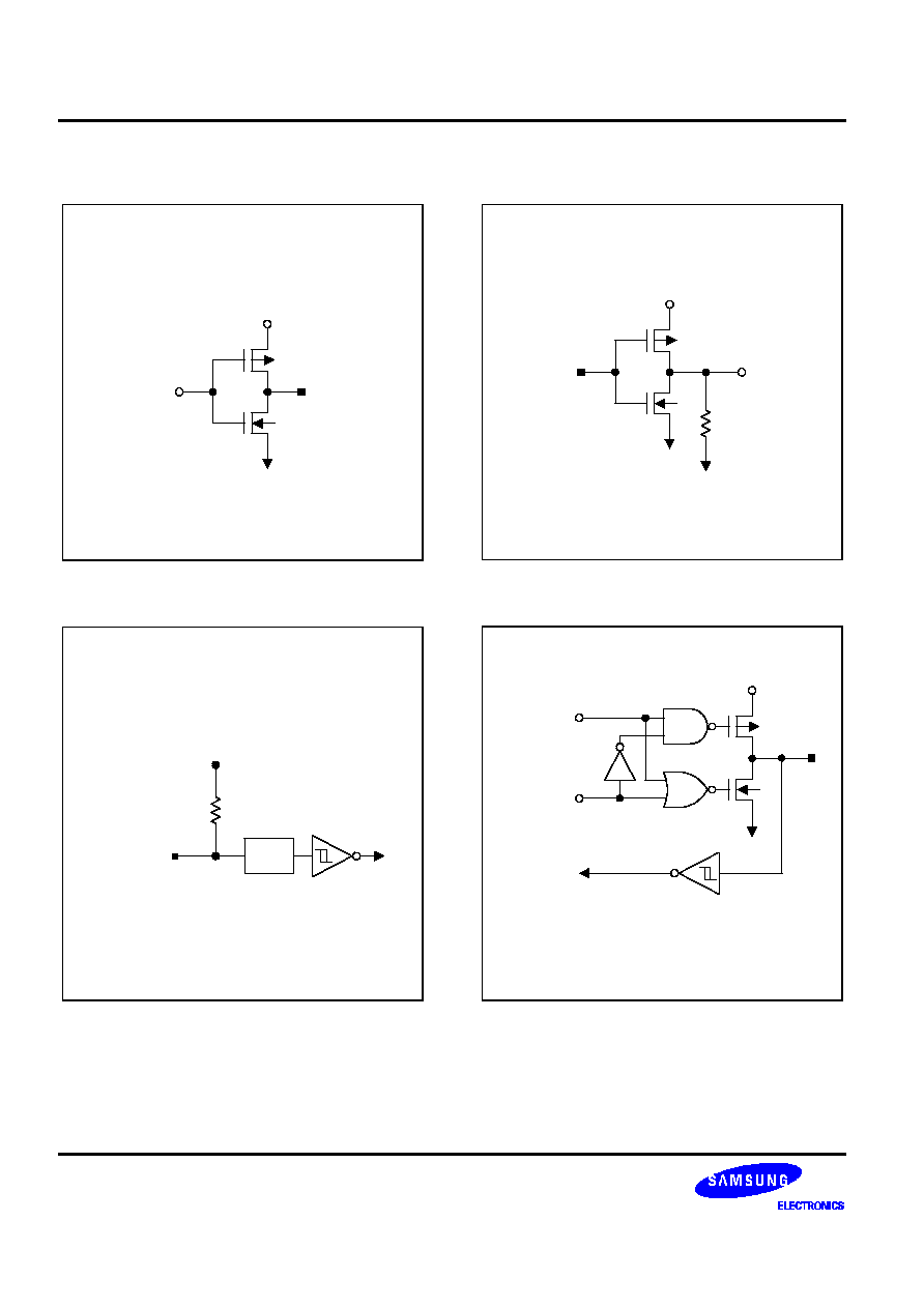
PIN CIRCUITS DIAGRAM
Data
V
SS
Output
V
DD
Figure 1-7. Pin Circuit Type A
RESET
V
DD
280 k
Noise
Filter
Figure 1-9. Pin Circuit Type B (
RESET
RESET
)
Input
V
SS
Output
V
SS
300 k
Typical
V
DD
Figure 1-8. Pin Circuit Type A-3
Data or
Other
Function
V
SS
Output
Output
Disable
Digital
Input,
TTL Input
NOTE:
The noise filter must be built in the
external interrupts.
V
DD
Figure 1-10. Pin Circuit Type D-1

S3C8639/C863A/P863A/C8647/F8647
PRODUCT OVERVIEW
1-11
Data
V
SS
Output
Typical
47 k
Pull-up
Enable
V
DD
V
DD
Output
Disable
Open
Drain
Input
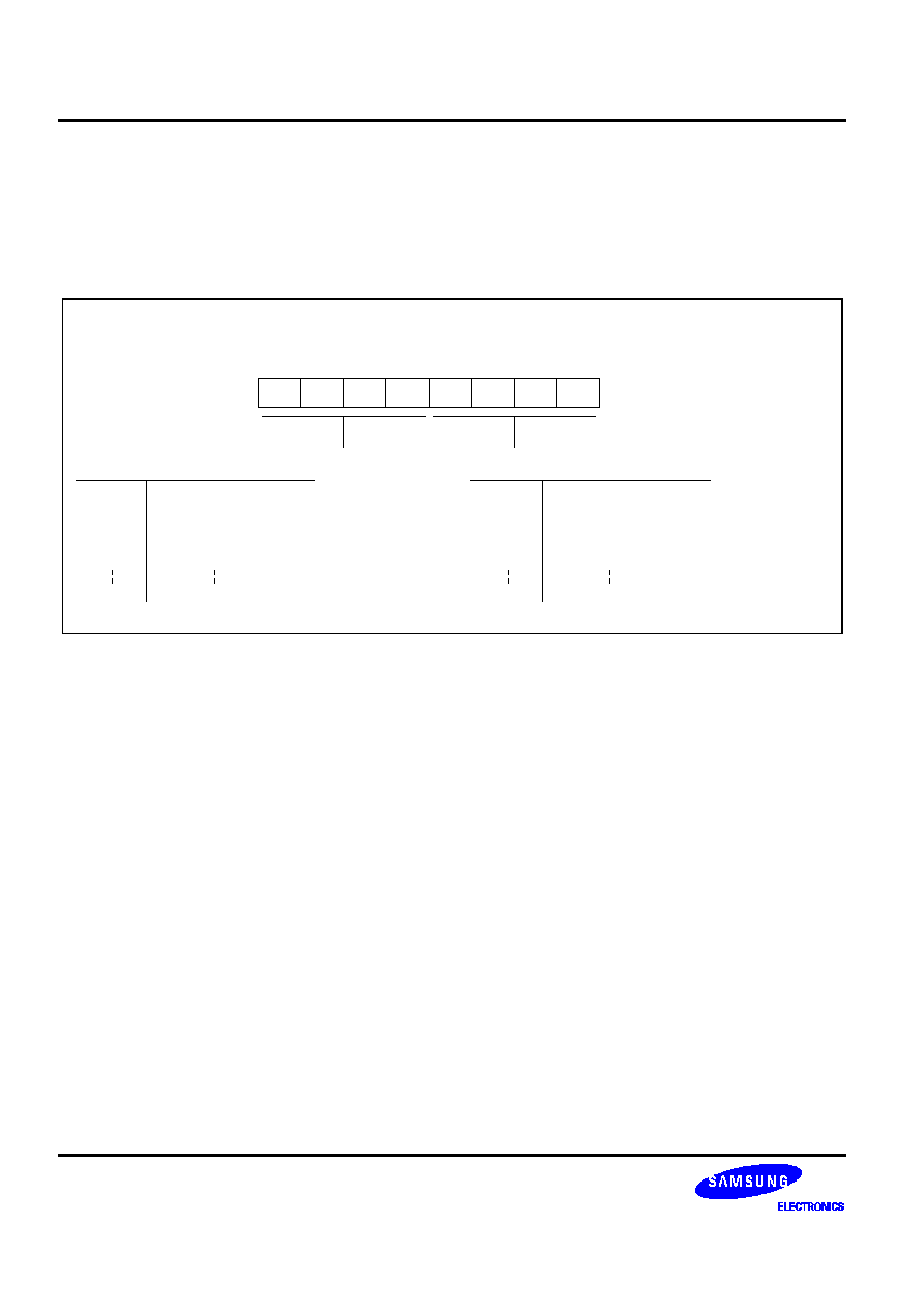
Figure 1-11. Pin Circuit Type E
V
SS
Output
Data
Input
Figure 1-13. Pin Circuit Type G-3
Data
V
SS
Output
V
DD
Output
Disable
Open
Drain
Digital Input
or ADC Input
Figure 1-12. Pin Circuit Type E-1

PRODUCT OVERVIEW
S3C8639/C863A/P863A/C8647/F8647
1-12
NOTES

S3C8639/C863A/P863A/C8647/F8647
ADDRESS SPACES
2-1
2
ADDRESS SPACES
OVERVIEW
S3C8639/C863A/C8647 microcontrollers have two types of address space:
-- Internal program memory (ROM)
-- Internal register file
The 16-bit address and data bus support program memory operations. The separate 8-bit register bus carries
addresses and data between the CPU and the internal register file. S3C8639/C863A/C8647 employ an internal
32/48/24-Kbyte mask-programmable ROM. External memory interface is not implemented.
There are 852/1108/462 8-bit registers in the internal register file. In this space, there are 784/1040/400 registers
for general use, 19 for CPU and system control, and 49(43) for peripheral control and data. An area of 16-byte
common working register (scratch) is part of the general-purpose register space. Most of these registers serve as
either a source or destination address, or as accumulators for data memory operations.

ADDRESS SPACES
S3C8639/C863A/P863A/C8647/F8647
2-2
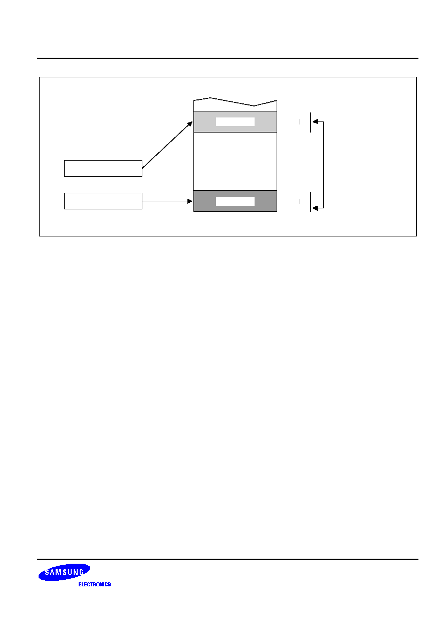
PROGRAM MEMORY (ROM)
Program memory (ROM) stores program code or table data. S3C8639/C863A employ 32/48-Kbytes of
mask-programmable program memory. The memory address range is 0H≠7FFFH/BFFFH (see Figure 2-1).
S3C8647 employs 24-Kbytes of mask-programmable program memory.
The memory address large is 0H-5FFFH.
The first 256 bytes of the ROM (0H≠FFH) are reserved for interrupt vector addresses. Unoccupied locations in
the address range can be used as normal program memory. When you use the vector address area to store
program code, be careful not to overwrite vector addresses stored in these locations.
The ROM address at which program execution starts after a reset is 0100H.
49,151
(Decimal)
Interrupt
Vector Area
48-Kbyte Internal
Program Memory
BFFFH
(HEX)
32,767
255
0
24-Kbyte Internal
Program Memory
7FFFH
0H
S3C8639
S3C863A
0FFH
24,575
32-Kbyte
S3C8647
Figure 2-1. Program Memory Address Space

S3C8639/C863A/P863A/C8647/F8647
ADDRESS SPACES
2-3
REGISTER ARCHITECTURE
The upper 64-byte area of the S3C8639/C863A/C8647 files is logically expanded to two 64-byte areas, called set
1 and set 2. The upper 32-byte area of set 1 is divided into two register banks, bank 0 and bank 1. The total
physical register space is thereby expanded internal register to 864/1120 bytes. Within this physical space, there
are 864/1120/462-byte registers, of which 852/1108/450 are addressable.
Given the microcontroller's 8-bit register bus architecture, up to 256 bytes of physical register space can be
addressed as a single page. The S3C8639 register files have three pages, page 0, page 1 and page 2. And the
S3C863A register files have four pages, page 0, page 1, page 2 and page 3. The S3C8647 register files have
two pages, page 0, and page 1. All page contain 256 bytes respectively.
The extension of physical register space into separately addressable areas (sets, banks, and pages) is enabled
by addressing mode restrictions, the select bank instructions SB0 and SB1, and the register page pointer, PP.
Specific register types and areas (in bytes) they occupy in the S3C8639/C863A/C8647 internal register files are
summarized in Table 2-1.
Table 2-1. Register Type Summary
Register Type
Number of Bytes
(S3C8639/C863A)
Number of Bytes
(S3C8647)
General-purpose registers (including the 16-byte
common working register area)
784/1040
400
CPU and system control registers
19
19
Clock, peripheral, I/O control, and data registers
49
43
Total Addressable Bytes
852/1108
462

ADDRESS SPACES
S3C8639/C863A/P863A/C8647/F8647
2-4
Page 3
~
Page 2
~
Page 1
~
D0H
CFH
E0H
DFH
C0H
System and
Peripheral
Control Registers
System Registers
Working Registers
FFH
Bank 0
Bank 1
Set 1
32 Bytes
64 Bytes
E0H
192 Bytes
FFH
C0H
BFH
NOTE: To address registers in bank 0, bank 1, and the system register area, you must use the register
addressing mode. To address working registers, you must use working register addressing mode.
00H
256 Bytes
Page 0
General Purpose
Data Registers
(Indirect register,
indexed addressing
modes or stack
operations)
Prime Data
Registers
(All addressing
modes)
~
Set 2
(S3C863A only)
Figure 2-2. Internal Register File Organization (S3C863X)

S3C8639/C863A/P863A/C8647/F8647
ADDRESS SPACES
2-5
FFH
FCH
E0H
D0H
C0H
Set 1
Bank 0
Bank 1
FFH
F2H
C0H
00H
FFH
BFH
Page 0
Set 2
DFH
00H
7FH
Page 1
General-purpose registers file
Peripheral registers and I/O ports
Working registers only
CPU control and system registers
Not mapped
Figure 2-3. Register File Layout (S3C8647)
ADDRESS SPACES
S3C8639/C863A/P863A/C8647/F8647
2-6
REGISTER PAGE POINTER (PP)
The SAM8 architecture supports the logical expansion of the physical 256-byte internal register file (which use an
8-bit data bus) to as many as 16 separately addressable register pages. Page addressing is controlled by the
register page pointer (PP, DFH). Two logical pages are implemented in S3C8639/C863A/C8647. These pages
are used as general purpose register space.
Source: page 0
Source: page 1
Source: page 2 (Not used for the S3C8647)
Source: page 3 (Not used for the S3C8639)
Not used for the S3C8639/C863A/C8647
Not used for the S3C8639/C863A/C8647
Register Page Pointer (PP)
DFH, Set 1, R/W
.7
.6
.5
.4
.3
.2
.1
.0
MSB
LSB
Destination register page seleciton bits:
0 0 0 0 B
0 0 0 1 B
0 0 1 0 B
0 0 1 1 B
0 1 0 0 B
1 1 1 1 B
Destination: page 0
Destination: page 1
Destination: page 2 (Not used for the S3C8647)
Destination: page 3 (Not used for the S3C8639)
Not used for the S3C8639/C863A/C8647
Not used for the S3C8639/C863A/C8647
Source register page selection bits:
0 0 0 0 B
0 0 0 1 B
0 0 1 0 B
0 0 1 1 B
0 1 0 0 B
1 1 1 1 B
Figure 2-4. Register Page Pointer (PP)
REGISTER SET 1
The term set 1 refers to the upper 64 bytes of the register file, locations C0H≠FFH. The upper 32-byte area of
this 64-byte space (E0H≠FFH) is divided into two 32-byte register banks, bank 0 and bank 1. You execute the set
register bank instructions SB0 or SB1 to address one bank or the other. Bank 0 is automatically selected by a
reset operation.
In S3C8639/C863A, register locations of only E0H≠F4H are addressable in the bank 1 area; the remaining
locations (F5H≠FFH) are not mapped. The lower 32-byte area of set 1 is not banked and can be addressed at
any time. It contains 16 mapped system registers (D0H≠DFH) and a 16-byte "scratch" area (C0H≠CFH) for
working register addressing.
Registers in set 1 are directly accessible at all times using Register addressing mode. The 16-byte working
register area can only be accessed using working register addressing. (For more information about working
register addressing, please refer to Chapter 3, "Addressing Modes.")
REGISTER SET 2
The same 64-byte physical space that is used for set 1 register locations C0H≠FFH is logically duplicated to add
another 64 bytes of space. This expanded area of the register file is called set 2. All set 2 locations (C0H≠FFH)
can be addressed in all page of the S3C8639/C863A register space.
The logical division of set 1 and set 2 is maintained by means of addressing mode. In order to access set 1, you
should use resister addressing mode. When you want to access register locations in set 2, you have to select
Register Indirect addressing mode or Indexed addressing mode access register locations in set 2.

S3C8639/C863A/P863A/C8647/F8647
ADDRESS SPACES
2-7
PRIME REGISTER SPACE
The lower 192 bytes of the 256-byte physical internal register file (00H≠BFH) is called the prime register space,
or more simply, the prime area. You can access registers in this address range at all page using any of the seven
explicit addressing modes (see chapter 3, "Addressing Modes"). All registers in the prime area can be addressed
immediately after a reset.
Prime
Area
Page 3
~
Set 2
Prime
Area
Page 2
~
Set 2
~
Prime
Area
Page 1
~
Set 2
FFH
FCH
E0H
DFH
CFH
C0H
Set 1
RP0 =
1 1 0 0
0 0 0 0
RP1 =
1 1 0 0
1 0 0 0
Register pointers RP0 and RP1 point to the
common working register area, locations
C0H-CFH, after a reset.
FFH
C0H
BFH
00H
FFH
C0H
BFH
00H
Page 0
Set 2
Prime
Area
~
~
(S3C863A only)
Figure 2-5. Set 1, Set 2, and Prime Area Register Map (S3C863X)
ADDRESS SPACES
S3C8639/C863A/P863A/C8647/F8647
2-8
Page 1
FFH
FCH
E0H
DFH
CFH
C0H
Set 1
RP0 =
1 1 0 0
0 0 0 0
RP1 =
1 1 0 0
1 0 0 0
Register pointers RP0 and RP1 point to the
common working register area, locations
C0H-CFH, after a reset.
FFH
C0H
BFH
00H
Page 0
Set 2
Prime
Area
~
~
Prime
Area
7FH
00H
Figure 2-6. Set 1, Set 2, and Prime Area Register Map (S3C8647)

S3C8639/C863A/P863A/C8647/F8647
ADDRESS SPACES
2-9
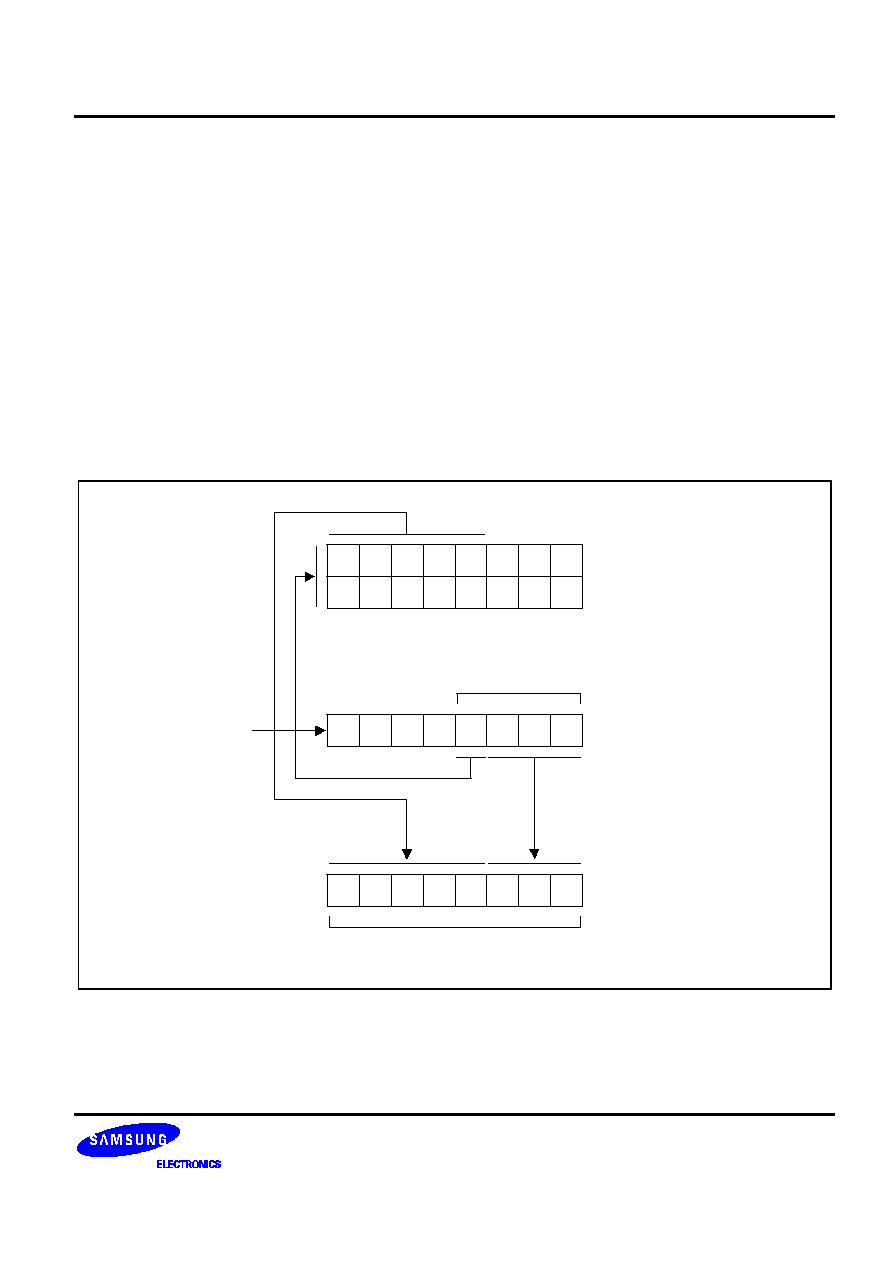
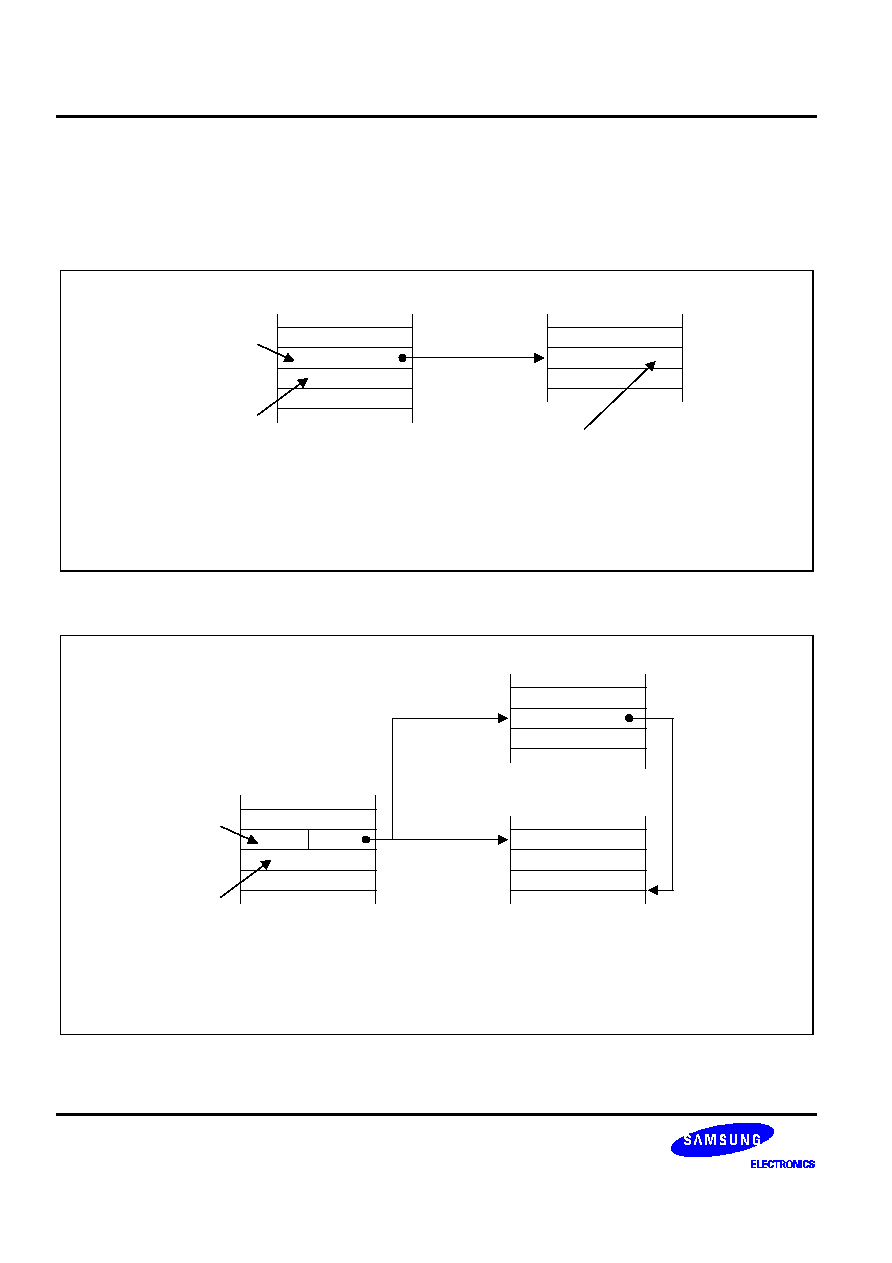
WORKING REGISTERS
Instructions can access specific 8-bit registers or 16-bit register pairs using either 4-bit or 8-bit address fields.
When 4-bit working register addressing is used, the 256-byte register file can be seen by the programmer as one
that consists of 32 8-byte register groups or "slices." Each slice comprises of eight 8-bit registers.
With the two 8-bit register pointers, RP1 and RP0 employed, two working register slices can be selected at any
time to form a 16-byte working register block. The register pointers help, you move this 16-byte register block to
anywhere in the addressable register file, except for the set 2 area.
The terms slice and block are used in this manual to help you visualize the size and relative locations of selected
working register spaces:
-- One working register slice is 8 bytes (eight 8-bit working registers; R0≠R7 or R8≠R15)
-- One working register block is 16 bytes (sixteen 8-bit working registers; R0≠R15)
All the registers in an 8-byte working register slice have the same binary value for their five most significant
address bits. This makes it possible for each register pointer to point to one of the 24 slices in the register file.
The base addresses for the two 8-byte register slices selected are contained in register pointers RP0 and RP1.
After a reset, RP0 and RP1 always point to the 16-byte common area in set 1 (C0H≠CFH).
Each register pointer points to
one 8-byte slice of the register
space, selecting a total of
16-byte working register block.
1 1 1 1 1 X X X
RP1 (Registers R8-R15)
RP0 (Registers R0-R7)
Slice 32
~
~
CFH
C0H
FFH
F8H
F7H
F0H
FH
8H
7H
0H
Slice 1
10H
Set 1
Only
0 0 0 0 0 X X X
Figure 2-7. 8-Byte Working Register Areas (Slices)
ADDRESS SPACES
S3C8639/C863A/P863A/C8647/F8647
2-10
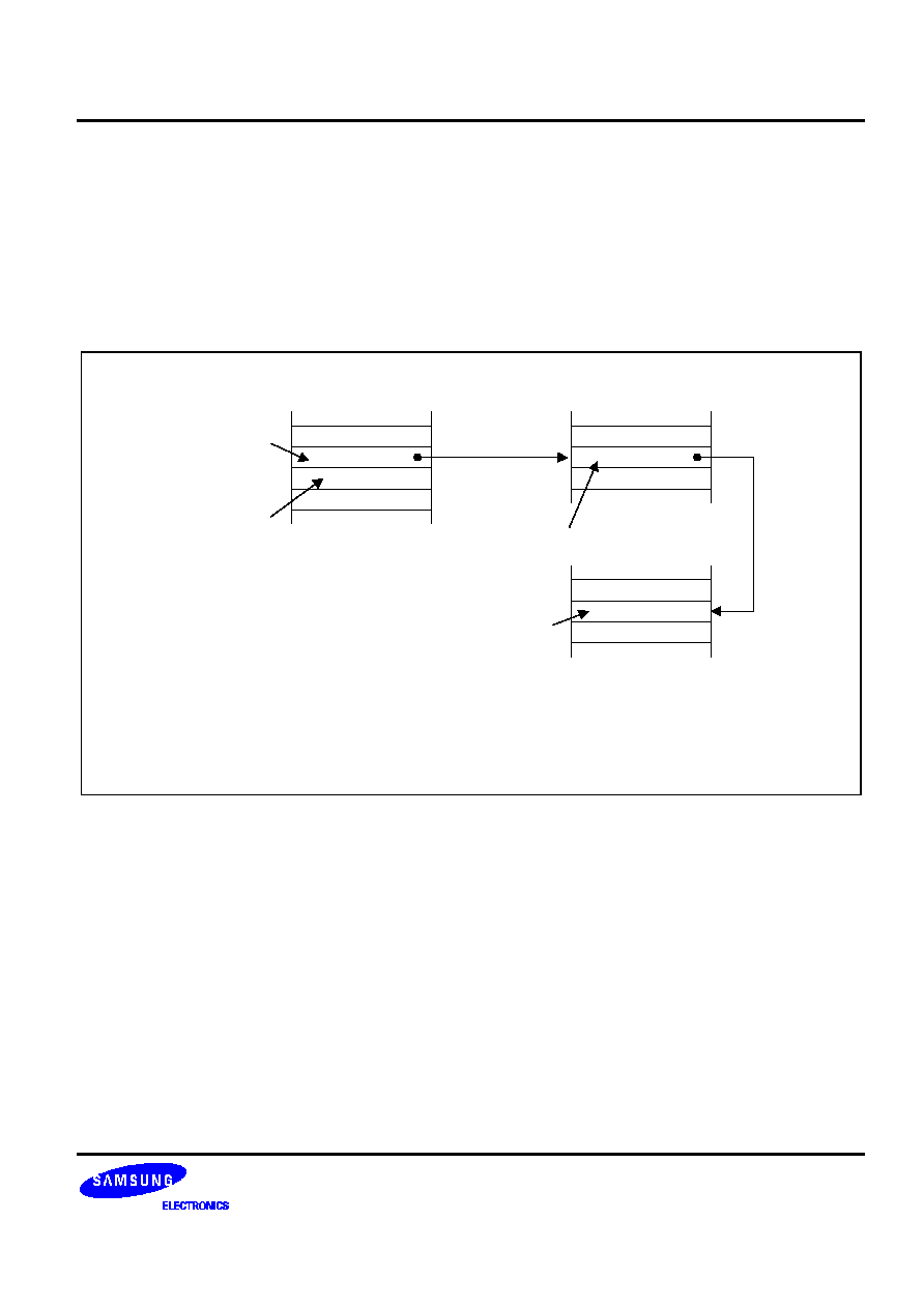
USING THE REGISTER POINTERS
Register pointers of RP0 and RP1 which are mapped to the addresses D6H and D7H in set 1, are used to select
two movable 8-byte working register slices in the register file. After a reset, they point to the working register
common area: RP0 points to the addresses C0H≠C7H, and RP1 points to the addresses C8H≠CFH.
You can change a register pointer value, by loading a new value to RP0 and/or RP1 using an SRP or LD
instruction (see Figures 2-6 and 2-7).
In working register addressing, you can only access those two 8-bit slices of the register file that are currently
pointed to by RP0 and RP1. You cannot use the register pointers to select a working register area in set 2, C0H≠
FFH, because these locations can be accessed only with Indirect Register or Indexed addressing modes.
The 16-byte working register block selected usually consists of two contiguous 8-byte slices. As a general
programming guideline, we recommend that RP0 point to the "lower" slice and RP1 point to the "upper" slice (see
Figure 2-6). In some cases, it may be necessary to define working register areas in different (non-contiguous)
areas of the register file. In Figure 2-7, RP0 points to the "upper" slice and RP1 to the "lower" slice.
As a register pointer can point to either of the two 8-byte slices in the working register block, you can flexibly
define the working register area to support a variety of program requirements.
F
F
PROGRAMMING TIP -- Setting the Register Pointers
SRP
#70H
; RP0
70H, RP1
78H
SRP1
#48H
; RP0
no change, RP1
48H
SRP0
#0A0H
; RP0
A0H, RP1
no change
CLR
RP0
; RP0
00H, RP1
no change
LD
RP1,#0F8H
; RP0
no change, RP1
0F8H
FH (R15)
0H (R0)
16-byte
contiguous
working
register block
Register File
Contains 32
8-Byte Slices
RP0
RP1
8H
7H
0 0 0 0 1 X X X
0 0 0 0 0 X X X
8-Byte Slice
8-Byte Slice
Figure 2-8. Contiguous 16-Byte Working Register Block
S3C8639/C863A/P863A/C8647/F8647
ADDRESS SPACES
2-11
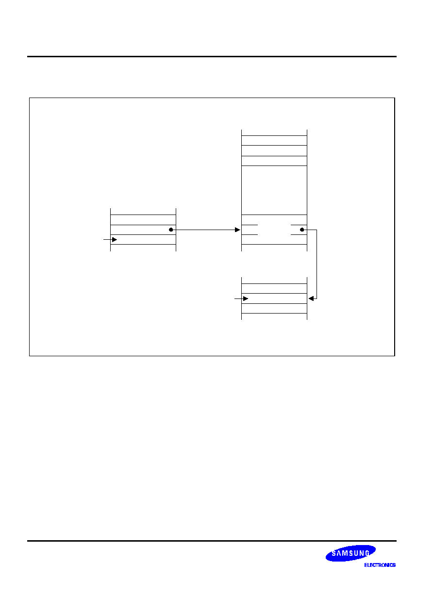
16-byte non-
contiguous
working
register block
Register File
Contains 32
8-Byte Slices
0H (R0)
7H (R15)
F0H (R0)
F7H (R7)
RP1
RP0
1 1 1 1 0 X X X
0 0 0 0 0 X X X
8-Byte Slice
8-Byte Slice
Figure 2-9. Non-Contiguous 16-Byte Working Register Block
F
F
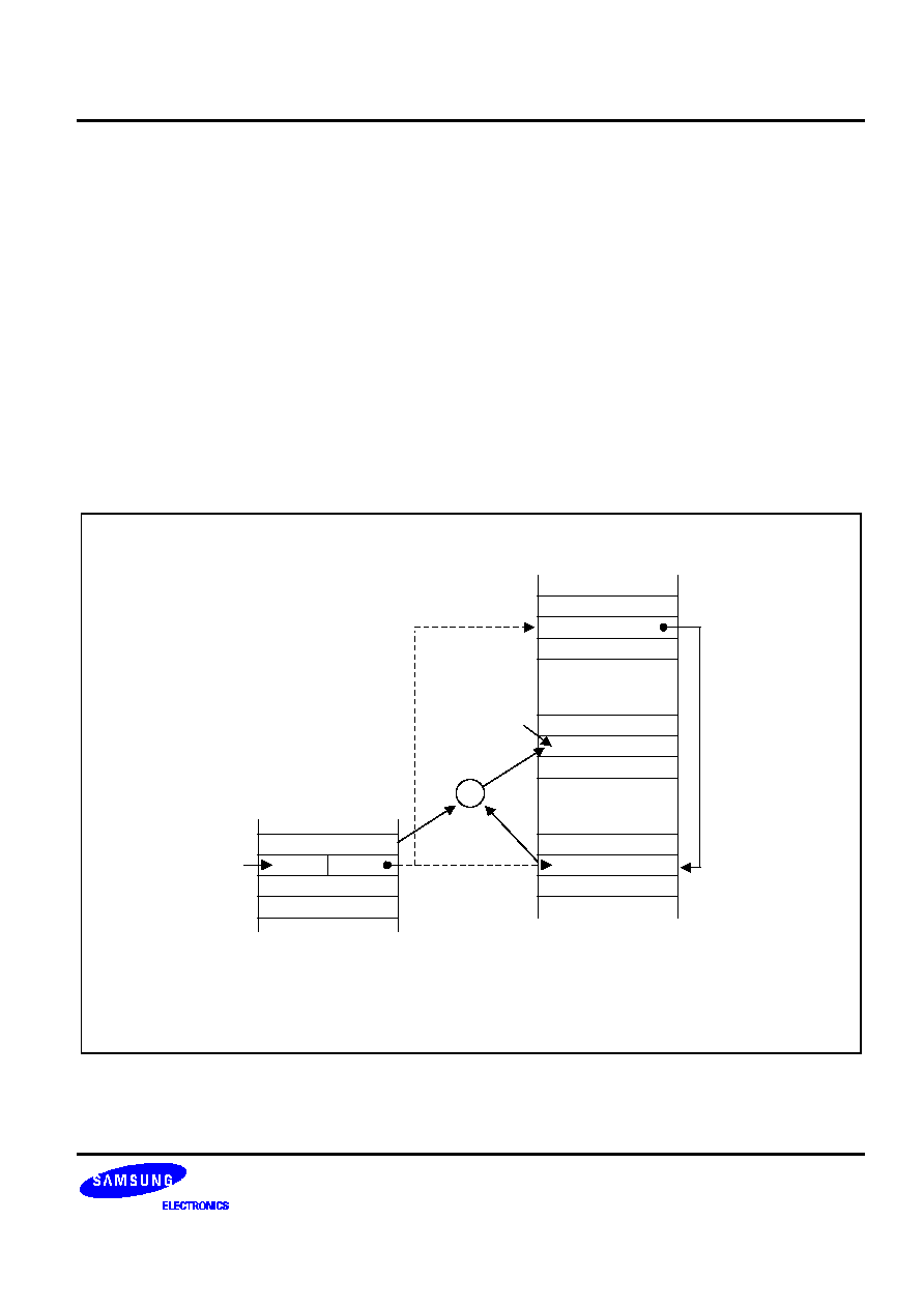
PROGRAMMING TIP -- Calculate the Sum of a Series of Registers Using the RPs
Calculate the sum of registers 80H≠85H using the register pointer and working register addressing. The register
addresses from 80H through 85H contain the values 10H, 11H, 12H, 13H, 14H, and 15H, respectively:
SRP0
#80H
; RP0
80H
ADD
R0,R1
; R0
R0 + R1
ADC
R0,R2
; R0
R0 + R2 + C
ADC
R0,R3
; R0
R0 + R3 + C
ADC
R0,R4
; R0
R0 + R4 + C
ADC
R0,R5
; R0
R0 + R5 + C
The sum of these six registers, 6FH, is located in the register R0 (80H). The instruction string used in this
example takes 12 bytes of instruction code and its execution time is 24 cycles. If the register pointer is not used
to calculate the sum of these registers, the following instruction sequence would have to be used:
ADD
80H,81H
; 80H
(80H) + (81H)
ADC
80H,82H
; 80H
(80H) + (82H) + C
ADC
80H,83H
; 80H
(80H) + (83H) + C
ADC
80H,84H
; 80H
(80H) + (84H) + C
ADC
80H,85H
; 80H
(80H) + (85H) + C
The sum of the six registers, here, is also located in the register 80H. This instruction string, however, takes 15
bytes of instruction code instead of 12 bytes, and its execution time is 30 cycles instead of 24 cycles.

ADDRESS SPACES
S3C8639/C863A/P863A/C8647/F8647
2-12
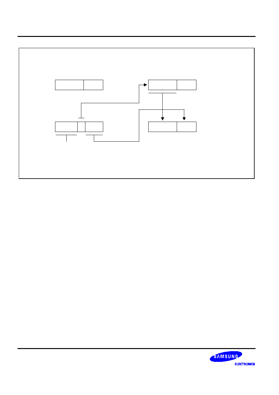
REGISTER ADDRESSING
The SAM8 register architecture provides an efficient method of working register addressing that takes full
advantage of shorter instruction formats to reduce execution time.
With Register (R) addressing mode, in which the operand value is the content of a specific register or register
pair, you can access all locations in the register file except for set 2. With working register addressing, you use a
register pointer to specify an 8-byte working register space in the register file and an 8-bit register within that
space.
Registers are addressed either as a single 8-bit register or as a paired 16-bit register space. In a 16-bit register
pair, the address of the first 8-bit register is always an even number and the address of the next register is always
an odd number. The most significant byte of the 16-bit data is always stored in the even-numbered register; the
least significant byte is always stored in the next (+1) odd-numbered register.
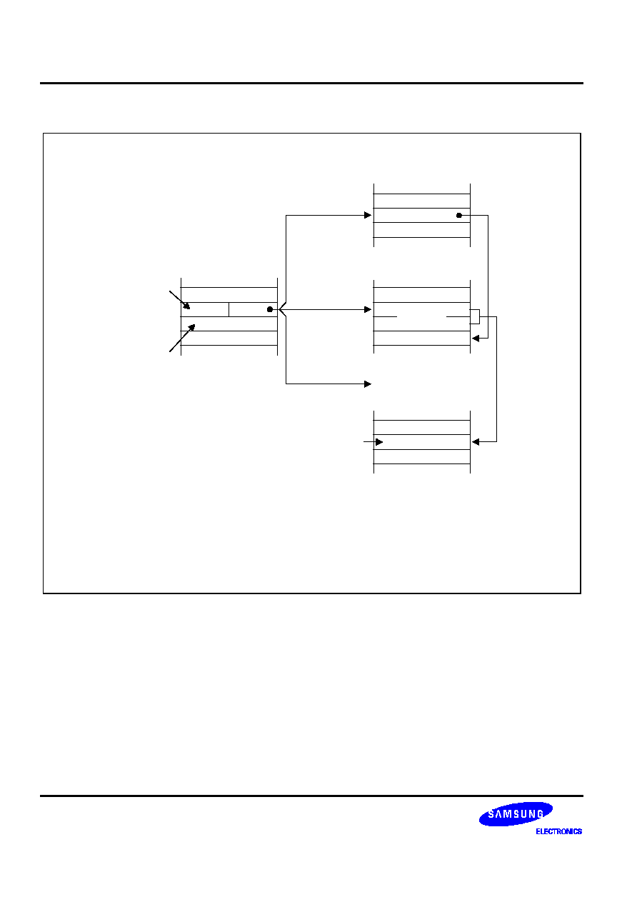
Working register addressing differs from Register addressing in a way that it uses a register pointer to specify an
8-byte working register space in the register file and an 8-bit register within that space (see Figure 3-2).
MSB
Rn
LSB
Rn+1
n = Even address
Figure 2-10. 16-Bit Register Pair

S3C8639/C863A/P863A/C8647/F8647
ADDRESS SPACES
2-13
FFH
D0H
FFH
C0H
Set 2
CFH
D7H
RP1
D6H
RP0
Register
Pointers
C0H
BFH
00H
General-Purpose
Registers
Each register pointer (RP) can independently point
to one of the 24 8-byte "slices" of the register file
(other than set 2). After a reset, RP0 points to
locations C0H-C7H and RP1 to locations C8H-CFH
(the common working register area).
Special-Purpose
Registers
Set 1
Bank 1
Bank 0
Control
Registers
System
Registers
E0H
(S3C863A: Page 0, 1, 2, 3
S3C8639: Page 0, 1, 2
S3C8647: Page 0, 1)
All
Addressing
Modes
Page 0, 1, 2, 3
Indirect
Register,
Indexed
Addressing
Modes
Register Addressing Only
Can be Pointed to by Register Pointer
Page 0, 1, 2, 3
Figure 2-11. Register File Addressing
ADDRESS SPACES
S3C8639/C863A/P863A/C8647/F8647
2-14
COMMON WORKING REGISTER AREA (C0H≠CFH)
After a reset, register pointers RP0 and RP1 automatically select two 8-byte register slices in set 1, locations
C0H≠CFH, as the active 16-byte working register block:
RP0
C0H≠C7H
RP1
C8H≠CFH
This16-byte address range is called common working register area. That is, locations in this area can be used as
working registers by operations that address any location on any page in the register file. Typically, these working
registers serve as temporary buffers for data operations between different pages.
Prime
Area
Page 3
~
Set 2
Prime
Area
Page 2
~
Set 2
~
Prime
Area
Page 1
~
Set 2
FFH
FCH
E0H
DFH
CFH
C0H
Set 1
RP0 =
1 1 0 0
0 0 0 0
RP1 =
1 1 0 0
1 0 0 0
Register pointers RP0 and RP1 point to the
common working register area, locations
C0H-CFH, after a reset.
FFH
C0H
BFH
00H
FFH
C0H
BFH
00H
Page 0
Set 2
Prime
Area
~
~
(S3C863A only)
Figure 2-12. Common Working Register Area (S3C863X)

S3C8639/C863A/P863A/C8647/F8647
ADDRESS SPACES
2-15
Page 1
FFH
FCH
E0H
DFH
CFH
C0H
Set 1
RP0 =
1 1 0 0
0 0 0 0
RP1 =
1 1 0 0
1 0 0 0
Register pointers RP0 and RP1 point to the
common working register area, locations
C0H-CFH, after a reset.
FFH
C0H
BFH
00H
Page 0
Set 2
Prime
Area
~
~
Prime
Area
7FH
00H
Figure 2-13. Common Working Register Area (S3C8647)

ADDRESS SPACES
S3C8639/C863A/P863A/C8647/F8647
2-16
F
F
PROGRAMMING TIP -- Addressing the Common Working Register Area
As the following examples show, you should access working registers in the common area, locations C0H≠CFH,
using working register addressing mode only.
Examples:
1.
LD
0C2H,40H
; Invalid addressing mode!
Use working register addressing instead:
SRP
#0C0H
LD
R2,40H
; R2 (C2H)
the value in location 40H
2. ADD
0C3H,#45H
; Invalid addressing mode!
Use working register addressing instead:
SRP
#0C0H
ADD
R3,#45H
; R3 (C3H)
R3 + 45H

S3C8639/C863A/P863A/C8647/F8647
ADDRESS SPACES
2-17
4-BIT WORKING REGISTER ADDRESSING
Each register pointer defines a movable 8-byte slice of working register space. The address information stored in
a register pointer serves as an addressing "window" that makes it possible for instructions to access working
registers very efficiently using short 4-bit addresses. When an instruction addresses a location in the selected
working register area, the address bits are concatenated in the following way to form a complete 8-bit address:
-- The high-order bit of the 4-bit address selects one of the register pointers ("0" selects RP0; "1" selects RP1);
-- The five high-order bits in the register pointer select an 8-byte slice of the register space;
-- The three low-order bits of the 4-bit address select one of the eight registers in the slice.
As shown in Figure 2-11, the result of this operation is that the five high-order bits from the register pointer are
concatenated with the three low-order bits from the instruction address to form the complete address. As long as
the address stored in the register pointer remains unchanged, the three bits from the address will always point to
an address in the same 8-byte register slice.
Figure 2-12 shows a typical example of 4-bit working register addressing: the high-order bit of the instruction
"INC R6" is "0", which selects RP0. The five high-order bits stored in RP0 (01110B) are concatenated with the
three low-order bits of the instruction's 4-bit address (110B) to produce the register address 76H (01110110B).
Together they create an
8-bit register address
Register pointer
provides five
high-order bits
Address
OPCODE
Selects
RP0 or RP1
RP1
RP0
4-bit address
provides three
low-order bits
Figure 2-14. 4-Bit Working Register Addressing

ADDRESS SPACES
S3C8639/C863A/P863A/C8647/F8647
2-18
Register
address
(76H)
RP0
0 1 1 1 0
0 0 0
0 1 1 1 0
1 1 0
R6
0 1 1 0
1 1 1 0
Selects RP0
Instruction
'INC R6'
OPCODE
RP1
0 1 1 1 1
0 0 0
Figure 2-15. 4-Bit Working Register Addressing Example
S3C8639/C863A/P863A/C8647/F8647
ADDRESS SPACES
2-19
8-BIT WORKING REGISTER ADDRESSING
You can also use 8-bit working register addressing to access registers in a selected working register area. To
initiate 8-bit working register addressing, the upper four bits of the instruction address must contain the value of
1100B. This 4-bit value (1100B) indicates that the remaining four bits have the same effect as 4-bit working
register addressing.
As shown in Figure 2-13, the lower nibble of the 8-bit address is concatenated in much the same way as for 4-bit
addressing: Bit 3 selects either RP0 or RP1, which then supplies the five high-order bits of the final address; the
three low-order bits of the complete address are provided by the original instruction.
Figure 2-14 shows an example of 8-bit working register addressing: the four high-order bits of the instruction
address (1100B) specify 8-bit working register addressing. Bit 4 ("1") selects RP1 and the five high-order bits in
RP1 (10101B) become the five high-order bits of the register address. The three low-order bits of the register
address (011) are provided by the three low-order bits of the 8-bit instruction address. The five address bits from
RP1 and the three address bits from the instruction are concatenated to form the complete register address,
0ABH (10101011B).
8-bit logical
address
8-bit physical address
Register pointer
provides five
high-order bits
Address
Selects
RP0 or RP1
RP1
RP0
Three low-order bits
These address
bits indicate 8-bit
working register
addressing
1
1
0
0
Figure 2-16. 8-Bit Working Register Addressing
ADDRESS SPACES
S3C8639/C863A/P863A/C8647/F8647
2-20
8-bit address
form instruction
'LD R11, R2'
RP0
0 1 1 0 0
0 0 0
1 1 0 0 1 0 1 1
Selects RP1
R11
Register
address
(0ABH)
RP1
1 0 1 0 1
0 0 0
1 0 1 0 1
0 1 1
Specifies working
register addressing
Figure 2-17. 8-Bit Working Register Addressing Example

S3C8639/C863A/P863A/C8647/F8647
ADDRESS SPACES
2-21
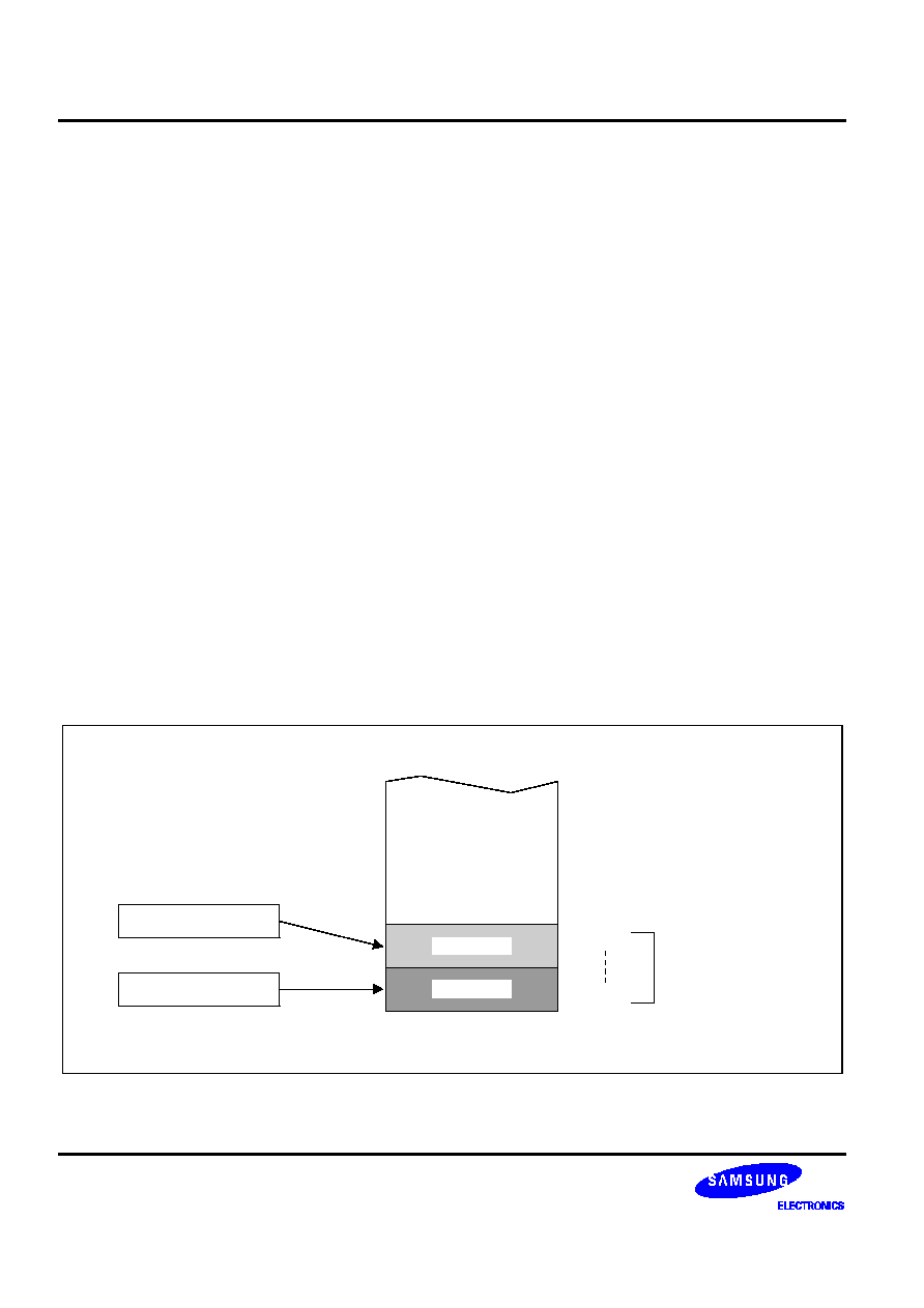
SYSTEM AND USER STACKS
S3-series microcontrollers can be programmed to use the system stack for subroutine calls, returns and
interrupts and to store data. The PUSH and POP instructions are used to control system stack operations. The
S3C8639/C863A architecture supports stack operations in the internal register file.
Stack Operations
Return addresses for procedure calls and interrupts and data are stored on the stack. The contents of the PC are
saved to stack by a CALL instruction and restored by the RET instruction. When an interrupt occurs, the contents
of the PC and the FLAGS register are pushed to the stack. The IRET instruction then pops these values back to
their original locations. The stack address is always decremented before a push operation and incremented after
a pop operation. The stack pointer (SP) always points to the stack frame stored on the top of the stack, as shown
in Figure 2-15.
Stack contents
after a call
instruction
Stack contents
after an
interrupt
Top of
stack
Flags
PCH
PCL
PCL
PCH
Top of
stack
Low Address
High Address
Figure 2-18. Stack Operations
User-Defined Stacks
You can freely define stacks in the internal register file as data storage locations. The instructions PUSHUI,
PUSHUD, POPUI, and POPUD support user-defined stack operations.
Stack Pointers (SPL, SPH)
Register locations D8H and D9H contain the 16-bit stack pointer (SP) that is used for system stack operations.
The most significant byte of the SP address, SP15≠SP8, is stored in the SPH register (D8H) and the least
significant byte, SP7≠SP0, is stored in the SPL register (D9H). After a reset, the SP value is undetermined.
Because only internal memory space is implemented in S3C8639/C863A, the SPL must be initialized to an 8-bit
value in the range 00H≠FFH. The SPH register is not needed here and can be used as a general-purpose
register, if necessary.
When the SPL register contains the only stack pointer value (that is, when it points to a system stack in the
register file), you can use the SPH register as a general-purpose data register. However, if an overflow or
underflow condition occurs as the result of incrementing or decrementing the stack address in the SPL register
during normal stack operations, the value in the SPL register will overflow (or underflow) to the SPH register,
overwriting any data that is currently stored there. To avoid overwriting data in the SPH register, you can
initialize the SPL value to "FFH" rather than "00H".

ADDRESS SPACES
S3C8639/C863A/P863A/C8647/F8647
2-22
F
F
PROGRAMMING TIP -- Standard Stack Operations Using PUSH and POP
The following example shows you how to perform stack operations in the internal register file using PUSH and
POP instructions:
LD
SPL,#0FFH
; SPL
FFH
; (Normally, the SPL is set to 0FFH by the initialization
; routine)
∑
∑
∑
PUSH
PP
; Stack address 0FEH
PP
PUSH
RP0
; Stack address 0FDH
RP0
PUSH
RP1
; Stack address 0FCH
RP1
PUSH
R3
; Stack address 0FBH
R3
∑
∑
∑
POP
R3
; R3
Stack address 0FBH
POP
RP1
; RP1
Stack address 0FCH
POP
RP0
; RP0
Stack address 0FDH
POP
PP
; PP
Stack address 0FEH

S3C8639/C863A/P863A/C8647/F8647
ADDRESSING MODES
3-1
3
ADDRESSING MODES
OVERVIEW
The program counter is used to fetch instructions that are stored in program memory for execution. Instructions
indicate the operation to be performed and the data to be operated on. Addressing mode is used to determine the
location of the data operand. The operands specified in SAM8 instructions may be condition codes, immediate
data, or a location in the register file, program memory, or data memory.
The SAM8 instruction set supports seven explicit addressing modes. Not all of these addressing modes are
available for each instruction:
-- Register (R)
-- Indirect Register (IR)
-- Indexed (X)
-- Direct Address (DA)
-- Indirect Address (IA)
-- Relative Address (RA)
-- Immediate (IM)
ADDRESSING MODES
S3C8639/C863A/P863A/C8647/F8647
3-2
REGISTER ADDRESSING MODE (R)
In Register addressing mode, the operand is the content of a specified register or register pair (see Figure 3-1).
Working register addressing differs from Register addressing as it uses a register pointer to specify an 8-byte
working register space in the register file and an 8-bit register within that space (see Figure 3-2).
dst
Value used in
Instruction Execution
OPCODE
OPERAND
8-bit Register
File Address
Point to One
Rigister in Register
File
One-Operand
Instruction
(Example)
Sample Instruction:
DEC
CNTR
; Where CNTR is the label of an 8-bit register address
Program Memory
Register File
Figure 3-1. Register Addressing
dst
OPCODE
4-bit
Working Register
Point to the
Woking Register
(1 of 8)
Two-Operand
Instruction
(Example)
Sample Instruction:
ADD
R1, R2
; Where R1 and R2 are registers in the working register area
currently selected
Program Memory
Register File
src
3 LSBs
RP0 or RP1
Selected
RP points
to start
of working
register
block
OPERAND
MSB Point to
RP0 of RP1
Figure 3-2. Working Register Addressing
S3C8639/C863A/P863A/C8647/F8647
ADDRESSING MODES
3-3
INDIRECT REGISTER ADDRESSING MODE (IR)
In Indirect Register (IR) addressing mode, the content of the specified register or register pair is the address of
the operand. Depending on the instruction used, the actual address may point to a register in the register file, to
program memory (ROM), or to an external memory space, if implemented (see Figures 3-3 through 3-6).
You can use any 8-bit register to indirectly address another register. Any 16-bit register pair can be used to
indirectly address another memory location. Remember, however, that locations C0H≠FFH in set 1 cannot be
accessed using Indirect Register addressing mode.
dst
Address of Operand
used by Instruction
OPCODE
ADDRESS
8-bit Register
File Address
Point to One
Rigister in Register
File
One-Operand
Instruction
(Example)
Sample Instruction:
RL
@SHIFT
; Where SHIFT is the label of an 8-bit register address
Program Memory
Register File
Value used in
Instruction Execution
OPERAND
Figure 3-3. Indirect Register Addressing to Register File
ADDRESSING MODES
S3C8639/C863A/P863A/C8647/F8647
3-4
INDIRECT REGISTER ADDRESSING MODE (Continued)
dst
OPCODE
Points to
Rigister Pair
Example
Instruction
References
Program
Memory
Sample Instructions:
CALL
@RR2
JP
@RR2
Program Memory
Register File
Value used in
Instruction
OPERAND
Register
Pair
Program Memory
16-Bit
Address
Points to
Program
Memory
Figure 3-4. Indirect Register Addressing to Program Memory

S3C8639/C863A/P863A/C8647/F8647
ADDRESSING MODES
3-5
INDIRECT REGISTER ADDRESSING MODE (Continued)
dst
OPCODE
ADDRESS
4-Bit
Working
Register
Address
Point to the
Working Register
(1 of 8)
Sample Instruction:
OR
R3,@R6
Program Memory
Register File
src
3 LSBs
Value used in
Instruction
OPERAND
Selected
RP points
to start of
woking register
block
RP0 or RP1
MSB Points to
RP0 or RP1
~
~
~
~
Figure 3-5. Indirect Working Register Addressing to Register File
ADDRESSING MODES
S3C8639/C863A/P863A/C8647/F8647
3-6
INDIRECT REGISTER ADDRESSING MODE (Concluded)
dst
OPCODE
4-bit Working
Register Address
Sample Instructions:
LCD
R5,@RR6
; Program memory access
LDE
R3,@RR14
; External data memory access
LDE
@RR4,R8
; External data memory access
Program Memory
Register File
src
Value used in
Instruction
OPERAND
Example Instruction
References either
Program Memory or
Data Memory
Program Memory
or
Data Memory
Next 2-bit Point to
Working Register
Pair (1 of 4)
LSB Selects
Register
Pair
16-Bit
address
points to
program
memory
or data
memory
RP0 or RP1
MSB Points to
RP0 or RP1
Selected
RP points
to start of
working
register
block
Figure 3-6. Indirect Working Register Addressing to Program or Data Memory
S3C8639/C863A/P863A/C8647/F8647
ADDRESSING MODES
3-7
INDEXED ADDRESSING MODE (X)
Indexed (X) addressing mode adds an offset value to a base address during instruction execution in order to
calculate the effective operand address (see Figure 3-7). You can use Indexed addressing mode to access
locations in the internal register file or in external memory (if implemented). You cannot, however, access
locations C0H≠FFH in set 1 using Indexed addressing.
In short offset Indexed addressing mode, the 8-bit displacement is treated as a signed integer in the range from ≠
128 to +127. This applies to external memory accesses only (see Figure 3-8).
For register file addressing, an 8-bit base address provided by the instruction is added to an 8-bit offset contained
in a working register. For external memory access, the base address is stored in the working register pair
designated in the instruction. The 8-bit or 16-bit offset given in the instruction is then added to the base address
(see Figure 3-9).
The only instruction that supports Indexed addressing mode for the internal register file is the Load instruction
(LD). The LDC and LDE instructions support Indexed addressing mode for internal program memory and for
external data memory (if implemented).
dst/src
OPCODE
Two-Operand
Instruction
Example
Point to One of the
Woking Register
(1 of 8)
Sample Instruction:
LD R0,#BASE[R1]
; Where BASE is an 8-bit immediate value
Program Memory
Register File
x
3 LSBs
Value used in
Instruction
OPERAND
INDEX
Base Address
RP0 or RP1
Selected RP
points to
start of
working
register
block
~
~
~
~
+
MSB Points to
RP0 to RP1
Figure 3-7. Indexed Addressing to Register File

ADDRESSING MODES
S3C8639/C863A/P863A/C8647/F8647
3-8
INDEXED ADDRESSING MODE (Continued)
Register File
OPERAND
Program Memory
or
Data Memory
Point to Working
Register Pair
(1 of 4)
LSB Selects
16-Bit
address
added to
offset
RP0 or RP1
MSB Points to
RP0 or RP1
Selected
RP points
to start of
working
register
block
dst/src
OPCODE
Program Memory
x
OFFSET
4-bit Working
Register Address
Sample Instructions:
LDC
R4, #04H[RR2]
; The values in the program address (RR2 + 04H)
are loaded into register R4.
LDE
R4,#04H[RR2]
; Identical operation to LDC example, except that
external program memory is accessed.
NEXT 2 Bits
Register
Pair
Value used in
Instruction
8-Bits
16-Bits
16-Bits
+
~
~
Figure 3-8. Indexed Addressing to Program or Data Memory with Short Offset

S3C8639/C863A/P863A/C8647/F8647
ADDRESSING MODES
3-9
INDEXED ADDRESSING MODE (Concluded)
Register File
OPERAND
Program Memory
or
Data Memory
Point to Working
Register Pair
LSB Selects
16-Bit
address
added to
OFFSET
RP0 or RP1
MSB Points to
RP0 or RP1
Selected
RP points
to start of
working
register
block
Sample Instructions:
LDC
R4,#1000H[RR2]
; The values in the program address (RR2 + 1000H)
are loaded into register R4.
LDE
R4,#1000H[RR2]
; Identical operation to LDC example, except that
external program memory is accessed.
NEXT 2 Bits
Register
Pair
Value used in
Instruction
8-Bits
16-Bits
16-Bits
dst/src
OPCODE
Program Memory
src
OFFSET
4-bit Working
Register Address
OFFSET
+
~
~
Figure 3-9. Indexed Addressing to Program or Data Memory

ADDRESSING MODES
S3C8639/C863A/P863A/C8647/F8647
3-10
DIRECT ADDRESS MODE (DA)
In Direct Address (DA) mode, the instruction provides the operand's 16-bit memory address. Jump (JP) and Call
(CALL) instructions use this addressing mode to specify the 16-bit destination address that is loaded into the PC
whenever a JP or CALL instruction is executed.
The LDC and LDE instructions can use Direct Address mode to specify the source or destination address for
Load operations to program memory (LDC) or to external data memory (LDE), if implemented.
Sample Instructions:
LDC
R5,1234H
; The values in the program address (1234H)
are loaded into register R5.
LDE
R5,1234H
; Identical operation to LDC example, except that
external program memory is accessed.
dst/src
OPCODE
Program Memory
"0" or "1"
Lower Address Byte
LSB Selects Program
Memory or Data Memory:
"0" = Program Memory
"1" = Data Memory
Memory
Address
Used
Upper Address Byte
Program or
Data Memory
Figure 3-10. Direct Addressing for Load Instructions

S3C8639/C863A/P863A/C8647/F8647
ADDRESSING MODES
3-11
DIRECT ADDRESS MODE (Continued)
OPCODE
Program Memory
Upper Address Byte
Program
Memory
Address
Used
Lower Address Byte
Sample Instructions:
JP
C,JOB1
; Where JOB1 is a 16-bit immediate address
CALL
DISPLAY
; Where DISPLAY is a 16-bit immediate address
Next OPCODE
Figure 3-11. Direct Addressing for Call and Jump Instructions

ADDRESSING MODES
S3C8639/C863A/P863A/C8647/F8647
3-12
INDIRECT ADDRESS MODE (IA)
In Indirect Address (IA) mode, the instruction specifies an address located in the lowest 256 bytes of the program
memory. The selected pair of memory locations contains the actual address of the next instruction to be
executed. Only the CALL instruction can use Indirect Address mode.
Because Indirect Address mode assumes that the operand is located in the lowest 256 bytes of program
memory, only an 8-bit address is supplied in the instruction. The upper bytes of the destination address are
assumed to be all zeros.
Current
Instruction
Program Memory
Locations 0-255
Program Memory
OPCODE
dst
Lower Address Byte
Upper Address Byte
Next Instruction
LSB must be Zero
Sample Instruction:
CALL
#40H
; The 16-bit value in program memory addresses 40H
and 41H is the subroutine start address.
Figure 3-12. Indirect Addressing

S3C8639/C863A/P863A/C8647/F8647
ADDRESSING MODES
3-13
RELATIVE ADDRESS MODE (RA)
In Relative Address (RA) mode, a two's-complement signed displacement between ≠ 128 and + 127 is specified
in the instruction. The displacement value is then added to the current PC value. The result is the address of the
next instruction to be executed. Before this addition occurs, the PC contains the address of the next instruction
immediately following the current instruction.
Several program control instructions use the Relative Address mode to perform conditional jumps. The
instructions that support RA addressing are BTJRF, BTJRT, DJNZ, CPIJE, CPIJNE, and JR.
OPCODE
Program Memory
Displacement
Program Memory
Address Used
Sample Instruction:
JR
ULT,$+OFFSET
; Where OFFSET is a value in the range +127 to -128
Next OPCODE
+
Signed
Displacement Value
Current Instruction
Current
PC Value
Figure 3-13. Relative Addressing

ADDRESSING MODES
S3C8639/C863A/P863A/C8647/F8647
3-14
IMMEDIATE MODE (IM)
In Immediate (IM) mode, the operand value used in the instruction is the value supplied in the operand field
itself. The operand may be one byte or one word in length, depending on the instruction used. Immediate
addressing mode is useful for loading constant values into registers.
(The Operand value is in the instruction)
OPCODE
Sample Instruction:
LD R0,#0AAH
Program Memory
OPERAND
Figure 3-14. Immediate Addressing

S3C8639/C863A/P863A/C8647/F8647
CONTROL REGISTERS
4-1
4
CONTROL REGISTERS
OVERVIEW
In this chapter, detailed descriptions of the S3C8639/C863A/C8647 control registers are presented in an easy-to-
read format. You can use this chapter as a quick-reference source when writing application programs.
The locations and read/write characteristics of all mapped registers in the S3C8639/C863A/C8647 register files
are presented in Tables 4-1, 4-2, and 4-3. The hardware reset values for these registers are described in Chapter
8, "
RESET
and Power-Down."
Figure 4-1 illustrates the important features of the standard register description format.
Control register descriptions are arranged in alphabetical order according to register mnemonic. More detailed
information about control registers is presented in the context of the specific peripheral hardware descriptions in
Part II of this manual.

CONTROL REGISTERS
S3C8639/C863A/P863A/C8647/F8647
4-2
Table 4-1. Set 1 Registers
Register Name
Mnemonic
Decimal
Hex
R/W
Timer M0 counter register
TM0CNT
208
D0H
R
(note)
Timer M0 data register
TM0DATA
209
D1H
R
(note)
Timer M0 control register
TM0CON
210
D2H
R/W
Basic timer control register
BTCON
211
D3H
R/W
Clock control register
CLKCON
212
D4H
R/W
System flags register
FLAGS
213
D5H
R/W
Register pointer 0
RP0
214
D6H
R/W
Register pointer 1
RP1
215
D7H
R/W
Stack pointer (high byte)
SPH
216
D8H
R/W
Stack pointer (low byte)
SPL
217
D9H
R/W
Instruction pointer (high byte)
IPH
218
DAH
R/W
Instruction pointer (low byte)
IPL
219
DBH
R/W
Interrupt request register
IRQ
220
DCH
R
(note)
Interrupt mask register
IMR
221
DDH
R/W
System mode register
SYM
222
DEH
R/W
Page pointer register
PP
223
DFH
R/W
NOTE: You cannot use a read-only register (TM0CNT, TM0DATA, IRQ) as a destination field for the instructions OR, AND,
LD, or LDB.

S3C8639/C863A/P863A/C8647/F8647
CONTROL REGISTERS
4-3
Table 4-2. Set 1, Bank 0 Registers
Register Name
Mnemonic
Decimal
Hex
R/W
Port 0 data register
P0
224
E0H
R/W
Port 1 data register
(2)
P1
225
E1H
R/W
Port 2 data register
P2
226
E2H
R/W
Port 3 data register
P3
227
E3H
R/W
Port 0 control register (high byte)
P0CONH
228
E4H
R/W
Port 0 control register (low byte)
P0CONL
229
E5H
R/W
Port 1 control register
(2)
P1CON
230
E6H
R/W
Port 2 control register (high byte)
P2CONH
231
E7H
R/W
Port 2 control register (low byte)
P2CONL
232
E8H
R/W
Port 3 control register (high byte)
P3CONH
233
E9H
R/W
Port 3 control register (low byte)
P3CONL
234
EAH
R/W
Port 0 external interrupt control register
P0INT
235
EBH
R/W
Watchdog time control register
WDTCON
236
ECH
R/W
Sync control register 0
SYNCON0
237
EDH
R/W
Sync control register 1
SYNCON1
238
EEH
R/W
Sync control register 2
SYNCON2
239
EFH
R/W
Sync port read data register
SYNCRD
240
F0H
R
(1)
Timer M1 counter register (high byte)
TM1CNTH
241
F1H
R
(1)
Timer M1 counter register (low byte)
TM1CNTL
242
F2H
R
(1)
Timer M1 data register (high byte)
TM1DATAH
243
F3H
R
(1)
Timer M1 data register (low byte)
TM1DATAL
244
F4H
R
(1)
Timer M1 control register
TM1CON
245
F5H
R/W
Timer M2 control register
TM2CON
246
F6H
R/W
A/D converter control register
ADCON
247
F7H
R/W
A/D converter data register
ADDATA
248
F8H
R
(1)
Pseudo Hsync generation register
PHGEN
249
F9H
R/W
Pseudo Vsync generation register
PVGEN
250
FAH
R/W
Stop control register
STOPCON
251
FBH
R/W
Location FCH is not mapped
Basic timer counter register
BTCNT
253
FDH
R
(1)
External memory timing register
EMT
254
FEH
R/W
Interrupt priority register
IPR
255
FFH
R/W
NOTES:
1.
You cannot use a read-only register (SYNCRD, TM1CNTH, TM1TNCL, TM1DATAH, TM1DATAL, ADDATA, BTCNT)
as a destination field for the instructions OR, AND, LD, or LDB.
2.
Not used for the S3C8647.

CONTROL REGISTERS
S3C8639/C863A/P863A/C8647/F8647
4-4
Table 4-3. Set 1, Bank 1 Registers
Register Name
Mnemonic
Decimal
Hex
R/W
PWM 0 data register
PWM0
224
E0H
R/W
PWM 1 data register
PWM1
225
E1H
R/W
PWM 2 data register
PWM2
226
E2H
R/W
PWM 3 data register
PWM3
227
E3H
R/W
PWM 4 data register
PWM4
228
E4H
R/W
PWM 5 data register
PWM5
229
E5H
R/W
PWM 6 data register
(2)
PWM6
230
E6H
R/W
PWM control register
PWMCON
231
E7H
R/W
PWM counter register
PWMCNT
232
E8H
R
(1)
DDC control register
DCON
233
E9H
R/W
DDC address register 0
DAR0
234
EAH
R/W
DDC clock control register
DCCR
235
EBH
R/W
DDC control/status register 0
DCSR0
236
ECH
R/W
DDC control/status register 1
DCSR1
237
EDH
R/W
DDC address register 1
DAR1
238
EEH
R/W
Transmit prebuffer data register
TBDR
239
EFH
R/W
Receive prebuffer data register
RBDR
240
F0H
R
(1)
DDC data shift register
DDSR
241
F1H
R/W
Slave IIC-Bus control/status register
(2)
SICSR
243
F2H
R/W
Slave IIC-Bus address register
(2)
SIAR
242
F3H
R/W
Slave IIC-Bus data shift register
(2)
SIDSR
244
F4H
R/W
Locations F5H≠FFH are not mapped
NOTES:
1.
You cannot use a read-only register (PWMCNT, RBDR) as a destination field for the instructions OR, AND, LD, or LDB.
2.
Not used for the S3C8647.

S3C8639/C863A/P863A/C8647/F8647
CONTROL REGISTERS
4-5
FLAGS - System Flags Register
.7
Carry Flag (C)
.6
Zero Flag (Z)
.5
Bit Identifier
RESET Value
Read/Write
Bit Addressing
Mode
R = Read-only
W = Write-only
R/W = Read/write
'-' = Not used
Type of addressing
that must be used to
address the bit
(1-bit, 4-bit, or 8-bit)
RESET value notation:
'-' = Not used
'x' = Undetermined value
'0' = Logic zero
'1' = Logic one
Bit number(s) that is/are appended to
the register name for bit addressing
Name of individual
bit or related bits
Register name
Register ID
Sign Flag (S)
0
Operation does not generate a carry or borrow condition
0
Operation generates carry-out or borrow into high-order bit 7
0
Operation result is a non-zero value
0
Operation result is zero
0
Operation generates positive number (MSB = "0")
0
Operation generates negative number (MSB = "1")
Description of the
effect of specific
bit settings
Set 1
Register location
in the internal
register file
D5H
Register address
(hexadecimal)
.7
.6
.5
x
x
x
R/W
R/W
R/W
Register addressing mode only
.4
.3
.2
.1
.0
x
R/W
x
R/W
x
R/W
x
R/W
0
R/W
Bit number:
MSB = Bit 7
LSB = Bit 0
Figure 4-1. Register Description Format

CONTROL REGISTERS
S3C8639/C863A/P863A/C8647/F8647
4-6
ADCON
-- A/D Converter Control Register
F7H
Set 1, Bank 0
Bit Identifier
.7
.6
.5
.4
.3
.2
.1
.0
RESET
RESET
Value
≠
0
0
0
0
0
0
0
Read/Write
≠
R/W
R/W
R/W
R
R/W
R/W
R/W
Addressing Mode
Register addressing mode only
.7
Not used for the S3C8639/C863A/C8647
.6 and .4
Analog Input Pin Selection Bits
0
0
0
ADC0 (Port 3.0)
0
0
1
ADC1 (Port 3.1)
0
1
0
ADC2 (Port 3.2)
0
1
1
ADC3 (Port 3.3)
Others
Not used
.3
End-of Conversion (EOC) Flag (read-only)
0
Conversion not complete
1
Conversion is complete
.2 and .1
Clock Source Selection Bits
0
0
f
OSC
/16
0
1
f
OSC
/8
1
0
f
OSC
/4
1
1
f
OSC
.0
Start or Enable Bit
0
Disable operation
1
Start operation

S3C8639/C863A/P863A/C8647/F8647
CONTROL REGISTERS
4-7
BTCON
-- Basic Timer Control Register
D3H
Set 1
Bit Identifier
.7
.6
.5
.4
.3
.2
.1
.0
RESET
RESET
Value
0
0
0
0
0
0
0
0
Read/Write
R/W
R/W
R/W
R/W
R/W
R/W
R/W
R/W
Addressing Mode
Register addressing mode only
.7≠.4
Watchdog Timer Function Disable Bits
1
0
1
0
Disable watchdog timer function
Others
Enable watchdog timer function
.3 and .2
Basic Timer Input Clock Selection Bits
0
0
f
OSC
/4096
0
1
f
OSC
/1024
1
0
f
OSC
/128
1
1
Invalid setting; not used for the S3C8639/C863A/C8647
.1
Basic Timer Counter Clear Bit
(1)
0
No effect
1
Clear the basic timer counter value
.0
Clock Frequency Divider Clear Bit for Basic Timer and Timer M0
(2)
0
No effect
1
Clear basic timer and timer M0 frequency dividers
NOTES:
1.
When you write a "1" to BTCON.1, the basic timer counter value is cleared to "00H". Immediately after the write
operation, the BTCON.1 value is automatically cleared to "0".
2.
When you write a "1" to BTCON.0, the corresponding frequency divider is cleared to "00H". Immediately after the
write operation, the BTCON.0 value is automatically cleared to "0".
CONTROL REGISTERS
S3C8639/C863A/P863A/C8647/F8647
4-8
CLKCON
-- System Clock Control Register
D4H
Set 1
Bit Identifier
.7
.6
.5
.4
.3
.2
.1
.0
RESET
RESET
Value
0
0
0
0
0
0
0
0
Read/Write
R/W
R/W
R/W
R/W
R/W
R/W
R/W
R/W
Addressing Mode
Register addressing mode only
.7
Oscillator IRQ Wake-up Function Enable Bit
0
Enable IRQ for main system oscillator wake-up in power-down mode
1
Disable IRQ for main system oscillator wake-up in power-down mode
.6 and .5
Main Oscillator Stop Control Bits
0
0
No effect
0
1
No effect
1
0
Stop main oscillator
1
1
No effect
.4 and .3
CPU Clock (System Clock) Selection Bits
(1)
0
0
Divide by 16 (f
OSC
/16)
0
1
Divide by 8 (f
OSC
/8)
1
0
Divide by 2 (f
OSC
/2)
1
1
Non-divided clock (f
OSC
)
(2)
.2≠.0
Subsystem Clock Selection Bits
(3)
1
0
1
Invalid setting for S3C8639/C863A/C8647
Others
Select main system clock (MCLK)
NOTES:
1.
After a reset, the slowest clock (divided by 16) is selected as the system clock. To select faster clock speeds,
load the appropriate values to CLKCON.3 and CLKCON.4.
2.
If the oscillator frequency is higher than 12 MHz, this selection is invalid.
3.
These selection bits are required only for systems that have a main clock and a subsystem clock.
S3C8639/C863A/C8647 use only the main oscillator clock circuit. For this reason, the setting "101B" is invalid.

S3C8639/C863A/P863A/C8647/F8647
CONTROL REGISTERS
4-9
DAR0
-- DDC Address Register 0
EAH
Set 1, Bank 1
Bit Identifier
.7
.6
.5
.4
.3
.2
.1
.0
RESET
RESET
Value
1
0
1
0
≠
≠
≠
≠
Read/Write
R/W
R/W
R/W
R/W
≠
≠
≠
≠
Addressing Mode
Register addressing mode only
.7≠.4
4-Slave Address Bits
These bits are operate only when receive the slave address. Read enable anytime.
Write enable when DCSR0.4 is "0".
.3≠.0
Not used for the S3C8639/C863A/C8647
DAR1
-- DDC Address Register 1
EEH
Set 1, Bank 1
Bit Identifier
.7
.6
.5
.4
.3
.2
.1
.0
RESET
RESET
Value
x
x
x
x
x
x
x
≠
Read/Write
R/W
R/W
R/W
R/W
R/W
R/W
R/W
≠
Addressing Mode
Register addressing mode only
.7≠.1
7-Slave Address Bits
These bits are operate only when receive the slave address. Read enable anytime.
Write enable when DCSR0.4 is "0".
.0
Not used for the S3C8639/C863A/C8647
CONTROL REGISTERS
S3C8639/C863A/P863A/C8647/F8647
4-10
DCCR
-- DDC Clock Control Register
EBH
Set 1, Bank 1
Bit Identifier
.7
.6
.5
.4
.3
.2
.1
.0
RESET
RESET
Value
0
0
0
0
1
1
1
1
Read/Write
R/W
R/W
R/W
R/W
R/W
R/W
R/W
R/W
Addressing Mode
Register addressing mode only
.7
Transmit acknowledgement enable mode when this bit is "1".
.6
Tx Clock Selection Bit
0
f
OSC
/10
1
f
OSC
/256
.5
DDC Module Interrupt Enable Bit
0
Disable interrupt
1
Enable interrupt
.4
DDC Module Interrupt Pending Bit
0
When write "0" to this bit (write "1" has no effect)
0
When DCSR0.4 is "0"
1
When slave address match occurred
1
When arbitration lost (master mode)
1
When an 1-byte transmit or receive operation is terminated
1
As soon as the DDC1 mode is enabled after the prebuffer is used
.3≠.0
Transmit Clock 4-Bit Prescaler Bits (CCR3≠CCR0)
SCL clock = IICLK/(CCR < 3: 0 > +1)
where, IICLK is f
OSC
/10 when DCCR.6 is "0"
IICLK is f
OSC
/256 when DCCR.6 is "1"

S3C8639/C863A/P863A/C8647/F8647
CONTROL REGISTERS
4-11
DCON
-- DDC Control Register
E9H
Set 1, Bank 1
Bit Identifier
.7
.6
.5
.4
.3
.2
.1
.0
RESET
RESET
Value
≠
≠
≠
≠
1
0
0
0
Read/Write
≠
≠
≠
≠
R/W
R/W
R/W
R/W
Addressing Mode
Register addressing mode only
.7≠.4
Not used for the S3C8639/C863A/C8647.
.3
Tx/Rx Pre-Buffer Data Registers Enable Bit
0
Normal IIC-bus mode (Pre-buffer data registers are not used.)
1
Pre-buffer data registers enable mode. This bit is set by writing "1" or by a
reset.
.2
DDC Address Match Bit
0
When start or stop or reset
1
When DDC received address matchs to DAR0 register
.1
DDC1 Tx Mode Enable Bit
0
IIC-bus interface mode (SCL pin is also selected)
1
DDC1 Tx mode (VCLK pin is also selected)
.0
SCL Pin Falling Edge Detection Flag
(note)
0
SCL pin level remains high after a reset (when read)
0
This bit can be cleared by S/W written "0" (when write)
1
Falling edge can be detected at the SCL pin after a reset or after this flag is
cleared by software (when read)
After start condition, the clock source of DDC module automatically charges
from VCLK (Vsync-I) to SCL0 (DCON.1 is "1" to "0") and slave address match
possible.
1
No effect (when write)
NOTE: When DDC interrupt is occurred, the SCL line is not pull-down in the DDC1 mode and Tx/Rx pre-buffer data
registers enable bit, DCON.3 is "1" (only slave mode).

CONTROL REGISTERS
S3C8639/C863A/P863A/C8647/F8647
4-12
DCSR0 --
DDC Control/Status Register 0
ECH Set 1, Bank 1
Bit Identifier
.7
.6
.5
.4
.3
.2
.1
.0
RESET
RESET
Value
0
0
0
0
0
0
≠
0
Read/Write
R/W
R/W
R/W
R/W
R
R
≠
R
Addressing Mode
Register addressing mode only
.7≠.6
Master/Slave, Tx/Rx Mode Selection Bits
0
0
Slave receiver mode (Default mode)
0
1
Slave transmitter mode
1
0
Master receiver mode
1
1
Master transmitter mode
.5
Bus Busy Bit
0
IIC-bus is not busy (when read), stop condition generation (when write)
1
IIC-bus is busy (when read), start condition generation (when write)
.4
DDC Module Enable Bit
0
Disable DDC module
1
Enable DDC module
.3
Arbitration Lost Bit
0
Bus arbitration status okay
1
Bus arbitration failed during serial I/O
.2
DDC Address/Data classification Bit
0
When reset or start/stop condition is generated, or when the received data is
in the data field.
1
When the received slave address matchs to DAR0, DAR1 register
.1
Not used for the S3C8639/C863A/C8647
.0
Received Acknowledgement (ACK) Bit
0
ACK is received
1
ACK is not received
NOTE: Bits 3≠0 are read only.
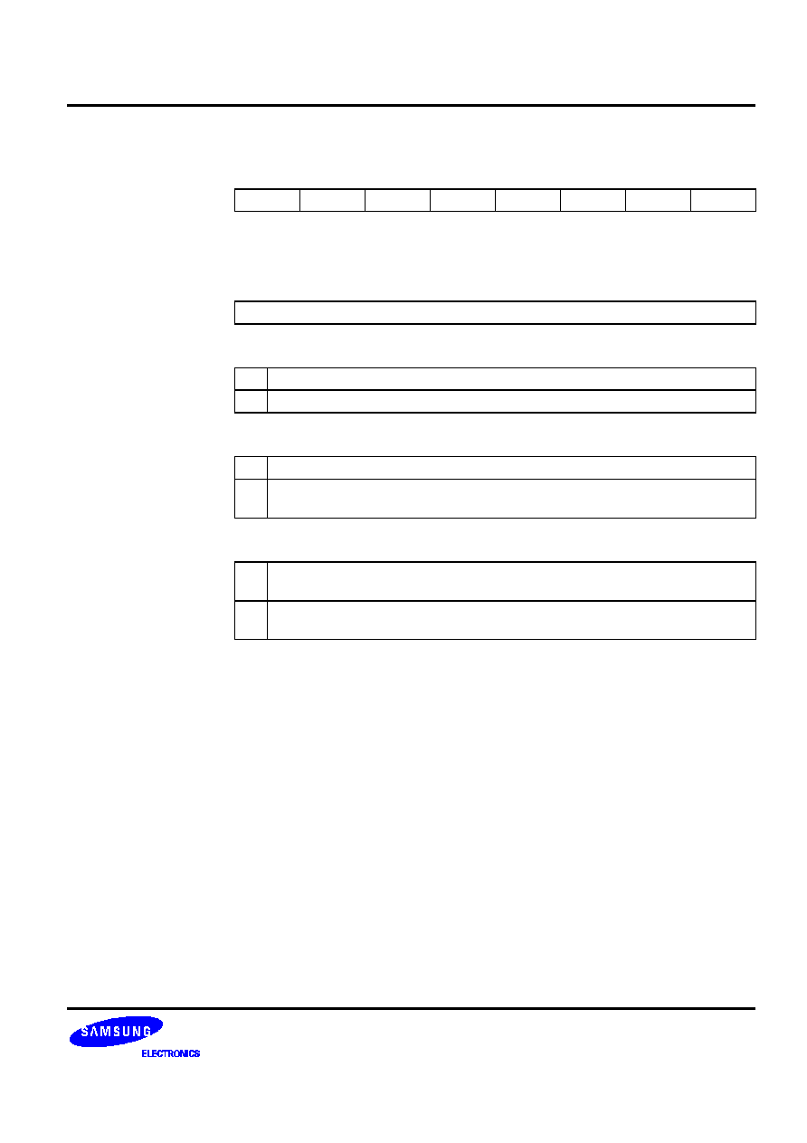
S3C8639/C863A/P863A/C8647/F8647
CONTROL REGISTERS
4-13
DCSR1
-- DDC Control/Status Register 1
EDH
Set 1, Bank 1
Bit Identifier
.7
.6
.5
.4
.3
.2
.1
.0
RESET
RESET
Value
≠
≠
≠
≠
≠
0
1
0
Read/Write
≠
≠
≠
≠
≠
R/W
R/W
R/W
Addressing Mode
Register addressing mode only
.7≠.3
Not used for the S3C8639/C863A/C8647
.2
Stop Condition Detection Bit
0
When it writes "0" to this bit, it is reset or master mode.
1
When a STOP condition is detected after START and slave address reception
.1
Data Buffer Empty Status Bit
0
When the CPU writes the transmitted data into the TBDR register
1
When the data of the TBDR register is loads to the DDSR register or when a
STOP condition is detected in DCSR0.7-.6 (slave transmitter mode) = "01"
.0
Data Buffer Full Status Bit
0
When the CPU reads the received data from the RBDR register or STOP
condition
1
When the data or matched address is transferred from the DDSR register to
the RBDR register

CONTROL REGISTERS
S3C8639/C863A/P863A/C8647/F8647
4-14
DDSR
-- DDC Data Shift Register
F1H
Set 1, Bank 1
Bit Identifier
.7
.6
.5
.4
.3
.2
.1
.0
RESET
RESET
Value
x
x
x
x
x
x
x
x
Read/Write
R/W
R/W
R/W
R/W
R/W
R/W
R/W
R/W
Addressing Mode
Register addressing mode only
.7≠.0
Write enable when DCSR0.4 is "1" and DCON.3 is "0". Read enable anytime.

S3C8639/C863A/P863A/C8647/F8647
CONTROL REGISTERS
4-15
EMT
-- External Memory Timing Register
FEH
Set 1, Bank 0
Bit Identifier
.7
.6
.5
.4
.3
.2
.1
.0
RESET
RESET
Value
0
1
1
1
1
1
0
≠
Read/Write
R/W
R/W
R/W
R/W
R/W
R/W
R/W
≠
Addressing Mode
Register addressing mode only
.7
External WAIT Input Function Enable Bit
0
Disable WAIT input function for external device
1
Enable WAIT input function for external device
.6
Slow Memory Timing Enable Bit
0
Disable slow memory timing
1
Enable slow memory timing
.5 and .4
Program Memory Automatic Wait Control Bits
0
0
No wait (Normal Operation)
0
1
Wait one cycle
1
0
Wait two cycles
1
1
Wait three cycles
.3 and .2
Data Memory Automatic Wait Control Bits
0
0
No wait (Normal Operation)
0
1
Wait one cycle
1
0
Wait two cycles
1
1
Wait three cycles
.1
Stack Area Selection Bit
0
Select internal register file area
1
Select external data memory area
.0
Not used for the S3C8639/C863A/C8647
NOTE: As external peripheral interface is not implemented in S3C8639/C863A/C8647, EMT register is not used. The
program initialization routine should clear the EMT register to "00H" after a reset. Modification of EMT values during
the normal operation may cause a system malfunction.
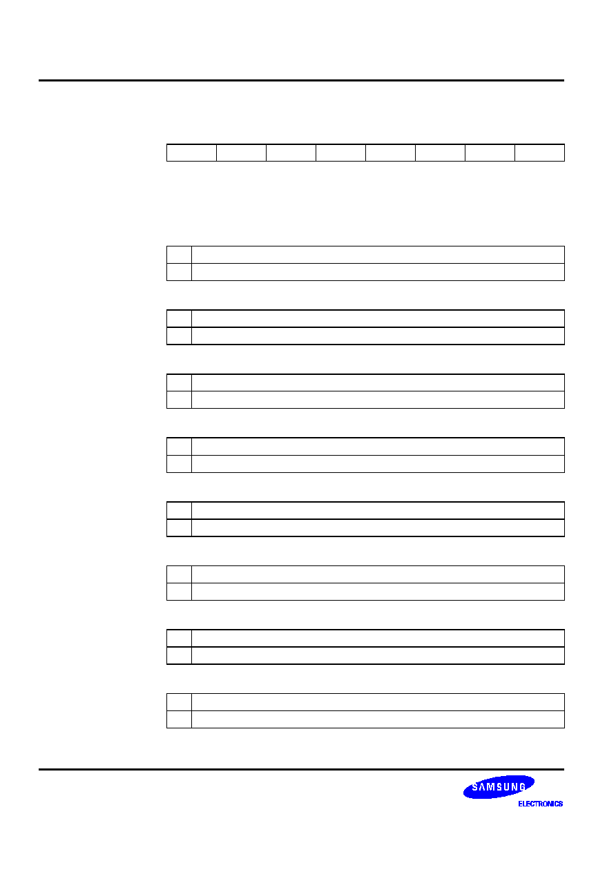
CONTROL REGISTERS
S3C8639/C863A/P863A/C8647/F8647
4-16
FLAGS
-- System Flags Register
D5H
Set 1
Bit Identifier
.7
.6
.5
.4
.3
.2
.1
.0
RESET
RESET
Value
x
x
x
x
x
x
0
0
Read/Write
R/W
R/W
R/W
R/W
R/W
R/W
R/W
R/W
Addressing Mode
Register addressing mode only
.7
Carry Flag (C)
0
Operation does not generate a carry or borrow condition
1
Operation generates a carry-out or borrow into high-order bit 7
.6
Zero Flag (Z)
0
Operation result is a non-zero value
1
Operation result is zero
.5
Sign Flag (S)
0
Operation generates a positive number (MSB = "0")
1
Operation generates a negative number (MSB = "1")
.4
Overflow Flag (V)
0
Operation result is
+127 or
≠128
1
Operation result is > +127 or < ≠128
.3
Decimal Adjust Flag (D)
0
Add operation completed
1
Subtraction operation completed
.2
Half-Carry Flag (H)
0
No carry-out of bit 3 or no borrow into bit 3 by addition or subtraction
1
Addition generated carry-out of bit 3 or subtraction generated borrow into bit 3
.1
Fast Interrupt Status Flag (FIS)
0
Cleared automatically during an interrupt return (IRET)
1
Automatically set to logic one during a fast interrupt service routine
.0
Bank Address Selection Flag (BA)
0
Bank 0 is selected (by executing the instruction SB0)
1
Bank 1 is selected (by executing the instruction SB1)
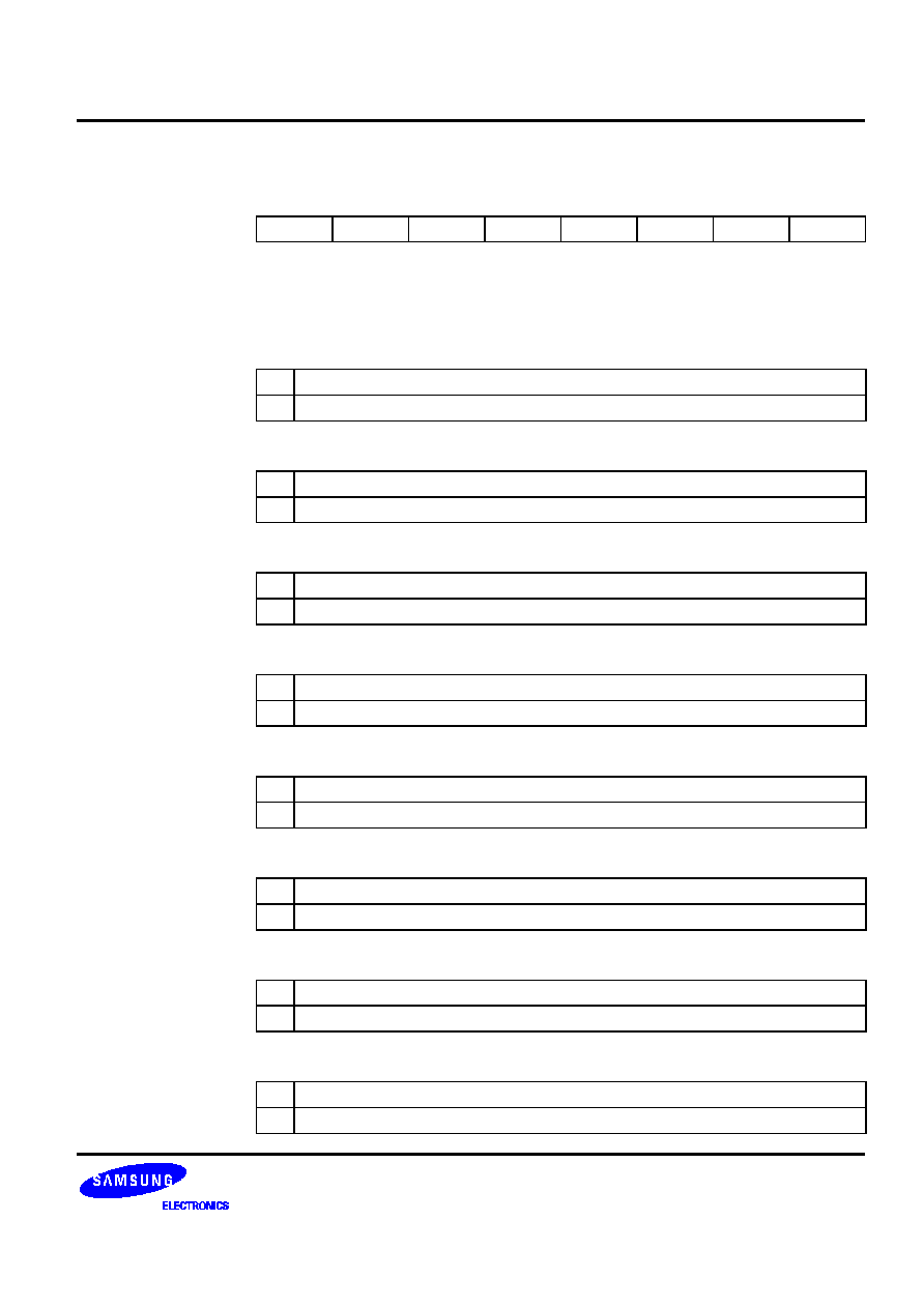
S3C8639/C863A/P863A/C8647/F8647
CONTROL REGISTERS
4-17
IMR
-- Interrupt Mask Register
DDH
Set 1
Bit Identifier
.7
.6
.5
.4
.3
.2
.1
.0
RESET
RESET
Value
x
x
x
x
x
x
x
x
Read/Write
R/W
R/W
R/W
R/W
R/W
R/W
R/W
R/W
Addressing Mode
Register addressing mode only
.7
Interrupt Level 7 (IRQ7) Enable Bit; Slave Only IIC-Bus Interrupt (Only S3C863X)
0
Disable IRQ7 interrupt
1
Enable IRQ7 interrupt
.6
Interrupt Level 6 (IRQ6) Enable Bit; P0.2 External Interrupt (INT2)
0
Disable IRQ6 interrupt
1
Enable IRQ6 interrupt
.5
Interrupt Level 5 (IRQ5) Enable Bit; P0.1 External Interrupt (INT1)
0
Disable IRQ5 interrupt
1
Enable IRQ5 interrupt
.4
Interrupt Level 4 (IRQ4) Enable Bit; P0.0 External Interrupt (INT0)
0
Disable IRQ4 interrupt
1
Enable IRQ4 interrupt
.3
Interrupt Level 3 (IRQ3) Enable Bit; DDC (Multi-Master IIC-Bus) Interrupt
0
Disable IRQ3 interrupt
1
Enable IRQ3 interrupt
.2
Interrupt Level 2 (IRQ2) Enable Bit; Timer M1 Capture/Overflow Interrupt
0
Disable IRQ2 interrupt
1
Enable IRQ2 interrupt
.1
Interrupt Level 1 (IRQ1) Enable Bit; Timer M2 Interval Interrupt
0
Disable IRQ1 interrupt
1
Enable IRQ1 interrupt
.0
Interrupt Level 0 (IRQ0) Enable Bit; Timer M0 Overflow/Capture Interrupt
0
Disable IRQ0 interrupt
1
Enable IRQ0 interrupt

CONTROL REGISTERS
S3C8639/C863A/P863A/C8647/F8647
4-18
IPH
-- Instruction Pointer (High Byte)
DAH
Set 1
Bit Identifier
.7
.6
.5
.4
.3
.2
.1
.0
RESET
RESET
Value
x
x
x
x
x
x
x
x
Read/Write
R/W
R/W
R/W
R/W
R/W
R/W
R/W
R/W
Addressing Mode
Register addressing mode only
.7≠.0
Instruction Pointer Address (High Byte)
The high-byte instruction pointer value is the upper eight bits of the 16-bit instruction
pointer address (IP15≠IP8). The lower byte of the IP address is located in the IPL
register (DBH).
IPL
-- Instruction Pointer (Low Byte)
DBH
Set 1
Bit Identifier
.7
.6
.5
.4
.3
.2
.1
.0
RESET
RESET
Value
x
x
x
x
x
x
x
x
Read/Write
R/W
R/W
R/W
R/W
R/W
R/W
R/W
R/W
Addressing Mode
Register addressing mode only
.7≠.0
Instruction Pointer Address (Low Byte)
The low-byte instruction pointer value is the lower eight bits of the 16-bit instruction
pointer address (IP7≠IP0). The upper byte of the IP address is located in the IPH
register (DAH).

S3C8639/C863A/P863A/C8647/F8647
CONTROL REGISTERS
4-19
IPR
-- Interrupt Priority Register
FFH
Set 1, Bank 0
Bit Identifier
.7
.6
.5
.4
.3
.2
.1
.0
RESET
RESET
Value
x
x
x
x
x
x
x
x
Read/Write
R/W
R/W
R/W
R/W
R/W
R/W
R/W
R/W
Addressing Mode
Register addressing mode only
.7, .4 and .1
Priority Control Bits for Interrupt Groups A, B and C
0
0
0
Not used
0
0
1
B > C > A
0
1
0
A > B > C
0
1
1
B > A > C
1
0
0
C > A > B
1
0
1
C > B > A
1
1
0
A > C > B
1
1
1
Not used
.6
Interrupt Sub-group C Priority Control Bit
0
IRQ6 > IRQ7
1
IRQ7 > IRQ6
.5
Interrupt Group C Priority Control Bit
0
IRQ5 > (IRQ6, IRQ7)
1
(IRQ6, IRQ7) > IRQ5
.3
Interrupt Sub-group B Priority Control Bit
0
IRQ3 > IRQ4
1
IRQ4 > IRQ3
.2
Interrupt Group B Priority Control Bit
0
IRQ2 > (IRQ3, IRQ4)
1
(IRQ3, IRQ4) > IRQ2
.0
Interrupt Group A Priority Control Bit
0
IRQ0 > IRQ1
1
IRQ1 > IRQ0
NOTE: Interrupt group A is IRQ0 and IRQ1. Interrupt group B is IRQ2, IRQ3, and IRQ4. Interrupt group C is IRQ5,
IRQ6 and IRQ7.

CONTROL REGISTERS
S3C8639/C863A/P863A/C8647/F8647
4-20
IRQ
-- Interrupt Request Register
DCH
Set 1
Bit Identifier
.7
.6
.5
.4
.3
.2
.1
.0
RESET
RESET
Value
0
0
0
0
0
0
0
0
Read/Write
R
R
R
R
R
R
R
R
Addressing Mode
Register addressing mode only
.7
Level 7 (IRQ7) Request Pending Bit; Slave Only IIC-Bus Interrupt (Only S3C863X)
0
No IRQ7 interrupt pending
1
IRQ7 interrupt is pending
.6
Level 6 (IRQ6) Request Pending Bit; P0.2 External Interrupt (INT2)
0
No IRQ6 interrupt pending
1
IRQ6 interrupt is pending
.5
Level 5 (IRQ5) Request Pending Bit; P0.1 External Interrupt (INT1)
0
No IRQ5 interrupt pending
1
IRQ5 interrupt is pending
.4
Level 4 (IRQ4) Request Pending Bit; P0.0 External Interrupt (INT0)
0
No IRQ4 interrupt pending
1
IRQ4 interrupt is pending
.3
Level 3 (IRQ3) Request Pending Bit; DDC (Multi-Master IIC-Bus) Interrupt
0
No IRQ3 interrupt pending
1
IRQ3 interrupt is pending
.2
Level 2 (IRQ2) Request Pending Bit; Timer M1 Capture/Overflow Interrupt
0
No IRQ2 interrupt pending
1
IRQ2 interrupt is pending
.1
Level 1 (IRQ1) Request Pending Bit; Timer M2 Interval Interrupt
0
No IRQ1 interrupt pending
1
IRQ1 interrupt is pending
.0
Level 0 (IRQ0) Request Pending Bit; Timer M0 Overflow/Capture Interrupt
0
No IRQ0 interrupt pending
1
IRQ0 interrupt is pending
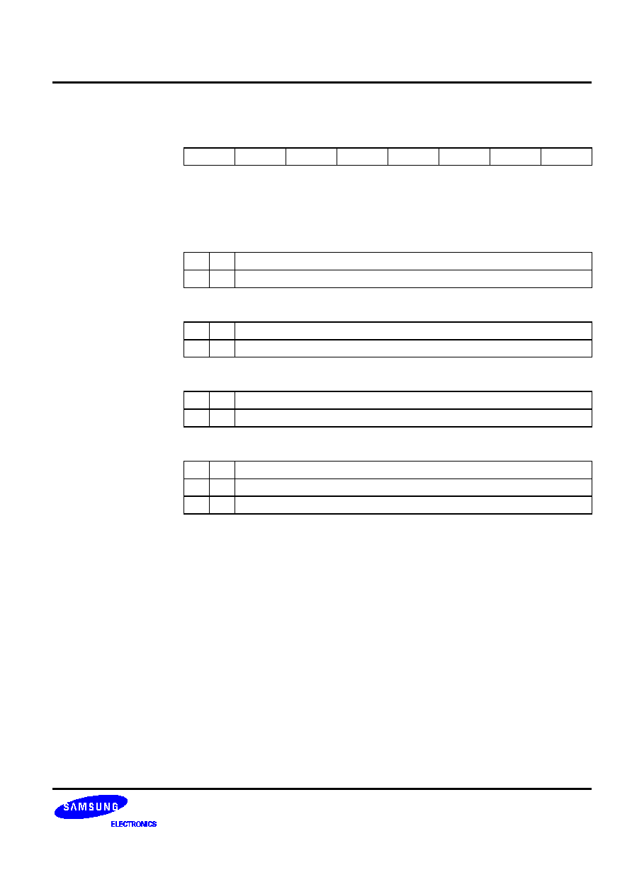
S3C8639/C863A/P863A/C8647/F8647
CONTROL REGISTERS
4-21
P0CONH
-- Port 0 Control Register (High Byte)
E4H
Set 1, Bank 0
Bit Identifier
.7
.6
.5
.4
.3
.2
.1
.0
RESET
RESET
Value
0
0
0
0
0
0
0
0
Read/Write
R/W
R/W
R/W
R/W
R/W
R/W
R/W
R/W
Addressing Mode
Register addressing mode only
.7 and .6
P0.7 Mode Selection Bits (Not Used for S3C8647)
0
x
Input mode
1
x
Push-pull output mode
.5 and .4
P0.6 Mode Selection Bits (Not Used for S3C8647)
0
x
Input mode
1
x
Push-pull output mode
.3 and .2
P0.5 Mode Selection Bits (Not Used for S3C8647)
0
x
Input mode
1
x
Push-pull output mode
.1 and .0
P0.4/TM0CAP Mode Selection Bits
0
0
Input mode
0
1
TM0CAP input mode
1
x
Push-pull output mode

CONTROL REGISTERS
S3C8639/C863A/P863A/C8647/F8647
4-22
P0CONL
-- Port 0 Control Register (Low Byte)
E5H
Set 1, Bank 0
Bit Identifier
.7
.6
.5
.4
.3
.2
.1
.0
RESET
RESET
Value
0
0
0
0
0
0
0
0
Read/Write
R/W
R/W
R/W
R/W
R/W
R/W
R/W
R/W
Addressing Mode
Register addressing mode only
.7 and .6
P0.3 Mode Selection Bits (Not Used for S3C8647)
0
0
Input mode
0
1
Input mode
1
0
Input mode
1
1
Push-pull output mode
.5 and .4
P0.2/INT2 Mode Selection Bits
0
0
Input mode (P0.2)
0
1
Input mode, rising edge interrupt detection (INT2)
1
0
Input mode, falling edge interrupt detection (INT2)
1
1
Push-pull output mode
.3 and .2
P0.1/INT1 Mode Selection Bits
0
0
Input mode (P0.1)
0
1
Input mode, rising edge interrupt detection (INT1)
1
0
Input mode, falling edge interrupt detection (INT1)
1
1
Push-pull output mode
.1 and .0
P0.0/INT0 Mode Selection Bits
0
0
Input mode (P0.0)
0
1
Input mode, rising edge interrupt detection (INT0)
1
0
Input mode, falling edge interrupt detection (INT0)
1
1
Push-pull output mode
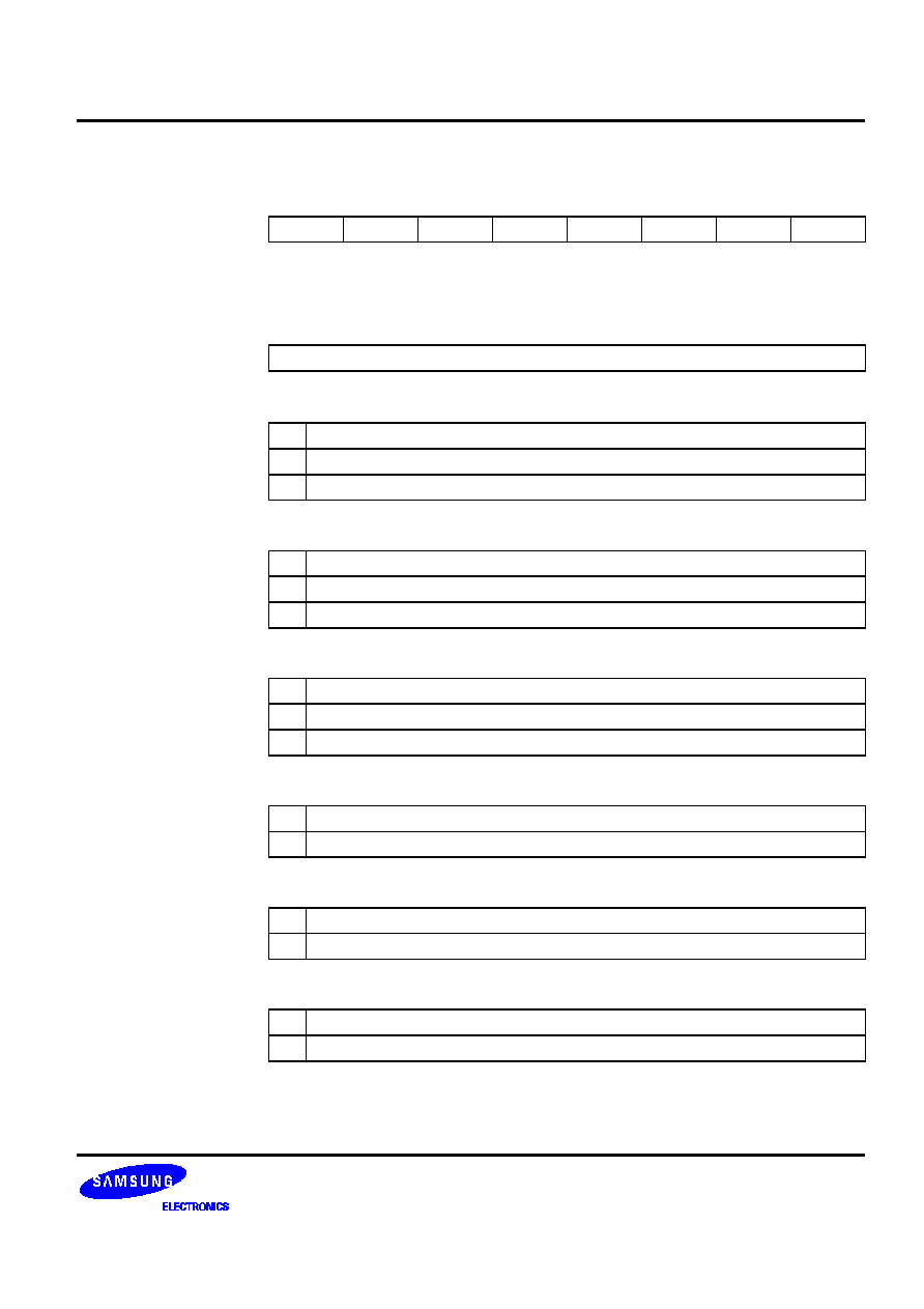
S3C8639/C863A/P863A/C8647/F8647
CONTROL REGISTERS
4-23
P0INT
-- Port 0 External Interrupt Control Register
EBH
Set 1, Bank 0
Bit Identifier
.7
.6
.5
.4
.3
.2
.1
.0
RESET
RESET
Value
≠
0
0
0
≠
0
0
0
Read/Write
≠
R/W
R/W
R/W
≠
R/W
R/W
R/W
Addressing Mode
Register addressing mode only
.7 and .3
Not used for the S3C8639/C863A/C8647
.6
P0.2 External Interrupt (INT2, IRQ6) Pending Flag
(note)
0
No P0.2 external interrupt pending (when read)
0
Clear P0.2 interrupt pending condition (when write)
1
P0.2 external interrupt is pending (when read)
.5
P0.1 External Interrupt (INT1, IRQ5) Pending Flag
0
No P0.1 external interrupt pending (when read)
0
Clear P0.1 interrupt pending condition (when write)
1
P0.1 external interrupt is pending (when read)
.4
P0.0 External Interrupt (INT0, IRQ4) Pending Flag
0
No P0.0 external interrupt pending (when read)
0
Clear P0.0 interrupt pending condition (when write)
1
P0.0 external interrupt is pending (when read)
.2
P0.2 External Interrupt (INT2, IRQ6) Enable Bit
0
Disable P0.2 interrupt
1
Enable P0.2 interrupt
.1
P0.1 External Interrupt (INT1, IRQ5) Enable Bit
0
Disable P0.1 interrupt
1
Enable P0.1 interrupt
.0
P0.0 External Interrupt (INT0, IRQ4) Enable Bit
0
Disable P0.0 interrupt
1
Enable P0.0 interrupt
NOTE: Writing a "1" to an interrupt pending flag (P0.2, P0.1, P0.0) has no effect.
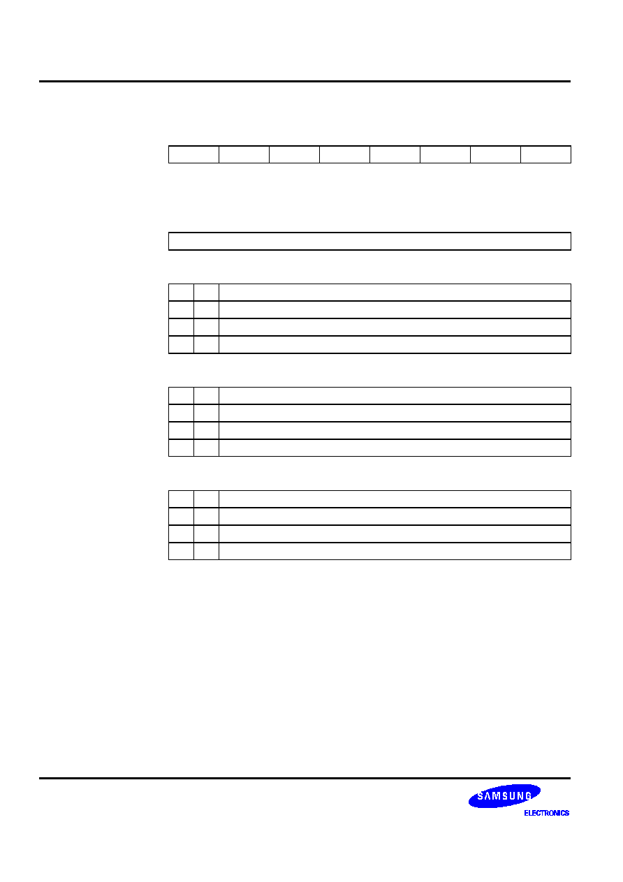
CONTROL REGISTERS
S3C8639/C863A/P863A/C8647/F8647
4-24
P1CON
-- Port 1 Control Register (Only S3C863X)
E6H
Set 1, Bank 0
Bit Identifier
.7
.6
.5
.4
.3
.2
.1
.0
RESET
RESET
Value
≠
≠
0
0
0
0
0
0
Read/Write
≠
≠
R/W
R/W
R/W
R/W
R/W
R/W
Addressing Mode
Register addressing mode only
.7 and .6
Not used for the S3C8639/C863A/C8647
.5 and .4
P1.2 Mode Selection Bits
0
0
Input mode
0
1
Push-pull output mode
1
0
N-channel open-drain output mode (5 V load capability)
1
1
Not used
.3 and .2
P1.1/SCL1 Mode Selection Bits
0
0
Input mode
0
1
Push-pull output mode
1
0
N-channel open-drain output mode (5 V load capability)
1
1
Multiplexed mode (SCL1 (P1.1))
.1 and .0
P1.0/SDA1 Mode Selection Bits
0
0
Input mode
0
1
Push-pull output mode
1
0
N-channel open-drain output mode (5 V load capability)
1
1
Multiplexed mode (SDA1 (P1.0))

S3C8639/C863A/P863A/C8647/F8647
CONTROL REGISTERS
4-25
P2CONH
-- Port 2 Control Register (High Byte)
E7H
Set 1, Bank 0
Bit Identifier
.7
.6
.5
.4
.3
.2
.1
.0
RESET
RESET
Value
0
0
0
0
0
0
0
0
Read/Write
R/W
R/W
R/W
R/W
R/W
R/W
R/W
R/W
Addressing Mode
Register addressing mode only
.7 and .6
P2.7/Csync-I
0
x
TTL input mode (Csync-I)
1
x
Push-pull output mode
.5 and .4
P2.6/PWM6 Mode Selection Bits (Not Used for S3C8647)
0
0
Input mode
0
1
Push-pull output mode
1
0
Push-pull PWM output mode
1
1
N-channel open-drain PWM output mode (5 V load capability)
.3 and .2
P2.5/PWM5 Mode Selection Bits
0
0
Input mode
0
1
Push-pull output mode
1
0
Push-pull PWM output mode
1
1
N-channel open-drain PWM output mode (5 V load capability)
.1 and .0
P2.4/PWM4 Mode Selection Bits
0
0
Input mode
0
1
Push-pull output mode
1
0
Push-pull PWM output mode
1
1
N-channel open-drain PWM output mode (5 V load capability)

CONTROL REGISTERS
S3C8639/C863A/P863A/C8647/F8647
4-26
P2CONL
-- Port 2 Control Register (Low Byte)
E8H
Set 1, Bank 0
Bit Identifier
.7
.6
.5
.4
.3
.2
.1
.0
RESET
RESET
Value
0
0
0
0
0
0
0
0
Read/Write
R/W
R/W
R/W
R/W
R/W
R/W
R/W
R/W
Addressing Mode
Register addressing mode only
.7 and .6
P2.3/PWM3 Mode Selection Bits
0
x
Input mode
1
0
Push-pull output mode
1
1
Push-pull PWM output mode (5 V load capability)
.5 and .4
P2.2/PWM2 Mode Selection Bits
0
x
Input mode
1
0
Push-pull output mode
1
1
Push-pull PWM output mode (5 V load capability)
.3 and .2
P2.1/PWM1 Mode Selection Bits
0
x
Input mode
1
0
Push-pull output mode
1
1
Push-pull PWM output mode (5 V load capability)
.1 and .0
P2.0/PWM0 Mode Selection Bits
0
x
Input mode
1
0
Push-pull output mode
1
1
Push-pull PWM output mode (5 V load capability)

S3C8639/C863A/P863A/C8647/F8647
CONTROL REGISTERS
4-27
P3CONH
-- Port 3 Control Register (High Byte)
E9H
Set 1, Bank 0
Bit Identifier
.7
.6
.5
.4
.3
.2
.1
.0
RESET
RESET
Value
0
0
0
0
0
0
0
0
Read/Write
R/W
R/W
R/W
R/W
R/W
R/W
R/W
R/W
Addressing Mode
Register addressing mode only
.7 and .6
P3.7 Mode Selection Bits
0
0
Input mode
0
1
Input mode with pull-up resistor
1
0
Push-pull output mode
1
1
N-channel open-drain output mode
.5 and .4
P3.6 Mode Selection Bits
0
0
Input mode
0
1
Input mode with pull-up resistor
1
0
Push-pull output mode
1
1
N-channel open-drain output mode
.3 and .2
P3.5 Mode Selection Bits
0
0
Input mode
0
1
Input mode with pull-up resistor
1
0
Push-pull output mode
1
1
N-channel open-drain output mode
.1 and .0
P3.4 Mode Selection Bits
0
0
Input mode
0
1
Input mode with pull-up resistor
1
0
Push-pull output mode
1
1
N-channel open-drain output mode

CONTROL REGISTERS
S3C8639/C863A/P863A/C8647/F8647
4-28
P3CONL
-- Port 3 Control Register (Low Byte)
EAH
Set 1, Bank 0
Bit Identifier
.7
.6
.5
.4
.3
.2
.1
.0
RESET
RESET
Value
0
0
0
0
0
0
0
0
Read/Write
R/W
R/W
R/W
R/W
R/W
R/W
R/W
R/W
Addressing Mode
Register addressing mode only
.7 and .6
P3.3/AD3 Mode Selection Bits
0
0
Input mode
0
1
Analog Input mode (AD3)
1
0
Push-pull output mode
1
1
N-channel open-drain output mode
.5 and .4
P3.2/AD2 Mode Selection Bits
0
0
Input mode
0
1
Analog Input mode (AD2)
1
0
Push-pull output mode
1
1
N-channel open-drain output mode
.3 and .2
P3.1/AD1 Mode Selection Bits
0
0
Input mode
0
1
Analog Input mode (AD1)
1
0
Push-pull output mode
1
1
N-channel open-drain output mode
.1 and .0
P3.0/AD0 Mode Selection Bits
0
0
Input mode
0
1
Analog Input mode (AD0)
1
0
Push-pull output mode
1
1
N-channel open-drain output mode

S3C8639/C863A/P863A/C8647/F8647
CONTROL REGISTERS
4-29
PHGEN ≠
Pseudo Hsync Generation Register
F9H
Set 1, Bank 0
Bit Identifier
.7
.6
.5
.4
.3
.2
.1
.0
RESET
RESET
Value
0
1
0
1
0
0
1
1
Read/Write
R/W
R/W
R/W
R/W
R/W
R/W
R/W
R/W
Addressing Mode
Register addressing mode only
.7≠.0
Write enable when SYNCON2.4 is "0". (General Pseudo H/Vsync generation mode)
Read enable any time
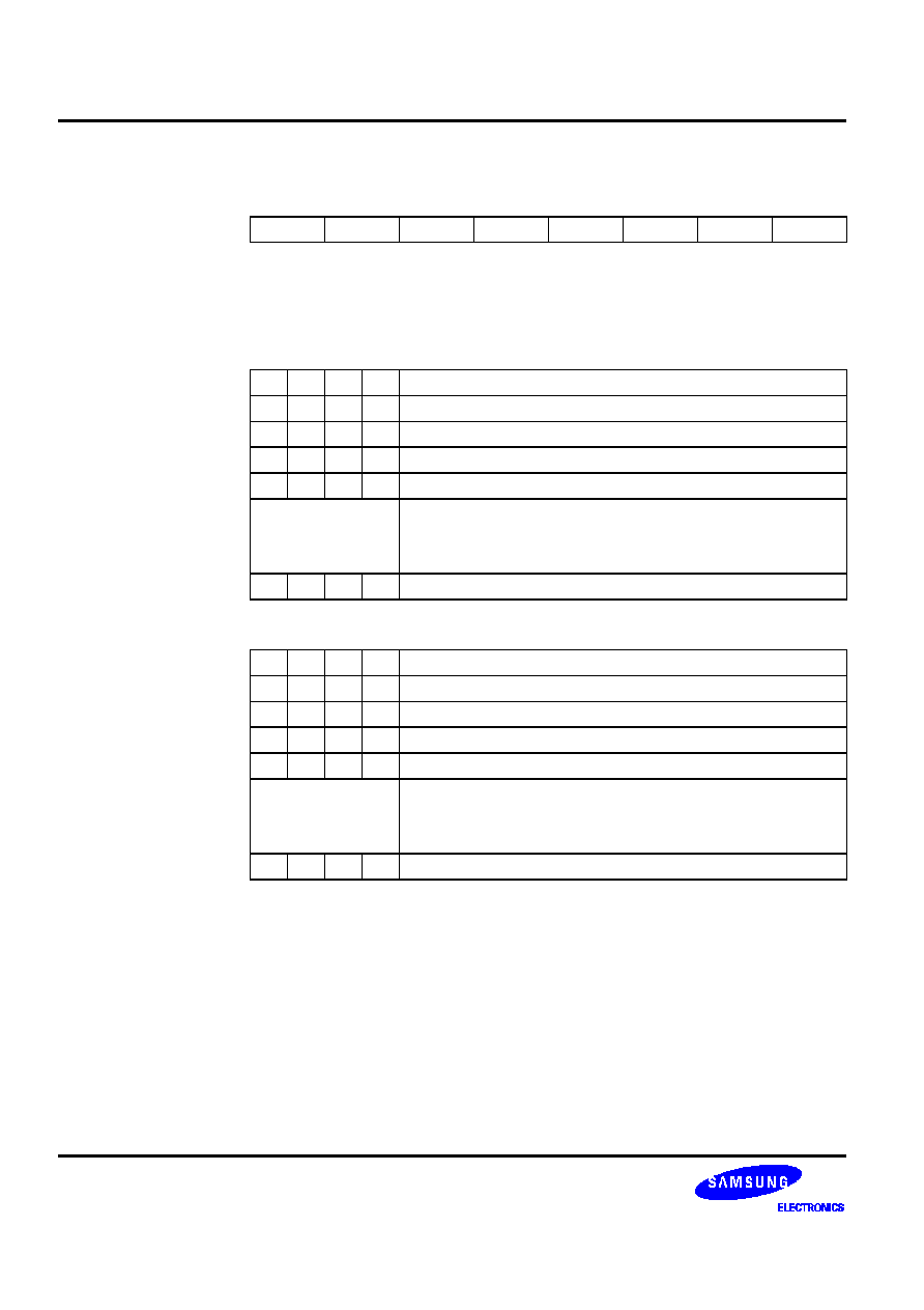
CONTROL REGISTERS
S3C8639/C863A/P863A/C8647/F8647
4-30
PP
-- Page Pointer Register
DFH
Set 1
Bit Identifier
.7
.6
.5
.4
.3
.2
.1
.0
RESET
RESET
Value
0
0
0
0
0
0
0
0
Read/Write
R/W
R/W
R/W
R/W
R/W
R/W
R/W
R/W
Addressing Mode
Register addressing mode only
.7≠.4
Destination Register Page Selection Bits
0
0
0
0
Destination: page 0
0
0
0
1
Destination: page 1
0
0
1
0
Destination: page 2 (Not used for the S3C8647)
0
0
1
1
Destination: page 3 (Not used for the S3C8639)
0
1
0
0
Not used for the S3C8639/C863A/C8647
∑
∑
∑
∑
∑
∑
1
1
1
1
Not used for the S3C8639/C863A/C8647
.3≠.0
Source Register Page Selection Bits
0
0
0
0
Source: page 0
0
0
0
1
Source: page 1
0
0
1
0
Source: page 2 (Not used for the S3C8647)
0
0
1
1
Source: page 3 (Not used for the S3C8639)
0
1
0
0
Not used for the S3C8639/C863A/C8647
∑
∑
∑
∑
∑
∑
1
1
1
1
Not used for the S3C8639/C863A/C8647

S3C8639/C863A/P863A/C8647/F8647
CONTROL REGISTERS
4-31
PVGEN ≠
Pseudo Vsync Generation Register
FAH
Set 1, Bank 0
Bit Identifier
.7
.6
.5
.4
.3
.2
.1
.0
RESET
RESET
Value
0
1
0
1
0
0
1
1
Read/Write
R/W
R/W
R/W
R/W
R/W
R/W
R/W
R/W
Addressing Mode
Register addressing mode only
.7≠.0
Write enable SYNCON2.4 is "0". (General Pseudo H/Vsync generation mode) Read
enable any time

CONTROL REGISTERS
S3C8639/C863A/P863A/C8647/F8647
4-32
PWMCON
-- PWM Control Register
E7H
Set 1, Bank 1
Bit Identifier
.7
.6
.5
.4
.3
.2
.1
.0
RESET
RESET
Value
0
0
0
≠
≠
≠
≠
≠
Read/Write
R/W
R/W
R/W
≠
≠
≠
≠
≠
Addressing Mode
Register addressing mode only
.7 and .6
2-Bit Prescaler Value for PWM Counter Input Clock
0
0
Non-divided input clock
0
1
Input clock divided into two
1
0
Input clock divided into three
1
1
Input clock divided into four
.5
PWM Counter Enable Bit
0
Stop PWM counter operation (No current leakage)
1
Start (or resume) PWM counter operation
.4≠.0
Not used for the S3C8639/C863A/C8647

S3C8639/C863A/P863A/C8647/F8647
CONTROL REGISTERS
4-33
RBDR
-- Receive Pre-Buffer Data Register
F0H
Set 1, Bank 1
Bit Identifier
.7
.6
.5
.4
.3
.2
.1
.0
RESET
RESET
Value
x
x
x
x
x
x
x
x
Read/Write
R
R
R
R
R
R
R
R
Addressing Mode
Register addressing mode only
.7≠.0
It is a read-only register. Read enable anytime. This register will be updated after a
data byte is received when the DCSR0.2 is "1" and the DCSR1.0 will be "1". The
read operation of this register will clear the DCSR1.0. After the DCSR1.0 is cleared,
the register can load the received data again and set the DCSR1.0.

CONTROL REGISTERS
S3C8639/C863A/P863A/C8647/F8647
4-34
RP0
-- Register Pointer 0
D6H
Set 1
Bit Identifier
.7
.6
.5
.4
.3
.2
.1
.0
RESET
RESET
Value
1
1
0
0
0
≠
≠
≠
Read/Write
R/W
R/W
R/W
R/W
R/W
≠
≠
≠
Addressing Mode
Register addressing only
.7≠.3
Register Pointer 0 Address Value
Register pointer 0 can independently point to one of the 18 8-byte working register
areas in the register file. Using the register pointers, RP0 and RP1, you can select
two 8-byte register slices at one time as active working register space. After a reset,
RP0 points to address C0H in register set 1, selecting the 8-byte working register
slice C0H≠C7H.
.2≠.0
Not used for the S3C8639/C863A/C8647
RP1
--
Register Pointer 1
D7H
Set 1
Bit Identifier
.7
.6
.5
.4
.3
.2
.1
.0
RESET
RESET
Value
1
1
0
0
1
≠
≠
≠
Read/Write
R/W
R/W
R/W
R/W
R/W
≠
≠
≠
Addressing Mode
Register addressing only
.7≠.3
Register Pointer 1 Address Value
Register pointer 1 can independently point to one of the 18 8-byte working register
areas in the register file. Using the register pointers, RP0 and RP1, you can select
two 8-byte register slices at one time as active working register space. After a reset,
RP1 points to address C8H in register set 1, selecting the 8-byte working register
slice C8H≠CFH.
.2≠.0
Not used for the S3C8639/C863A/C8647

S3C8639/C863A/P863A/C8647/F8647
CONTROL REGISTERS
4-35
SIAR
-- Slave IIC-Bus Address Register (Only S3C863X)
F3H
Set 1, Bank 1
Bit Identifier
.7
.6
.5
.4
.3
.2
.1
.0
RESET
RESET
Value
x
x
x
x
x
x
x
≠
Read/Write
R/W
R/W
R/W
R/W
R/W
R/W
R/W
≠
Addressing Mode
Register addressing only
.7≠.1
7-Bit Slave Address Bits
These bits are operated only when receive the slave address and general call.
Write enable when SICSR.6 is "0", but read enable anytime.
.0
Not used for the S3C8639/C863A/C8647

CONTROL REGISTERS
S3C8639/C863A/P863A/C8647/F8647
4-36
SICSR
-- Slave IIC-Bus Control/Status Register (Only S3C863X)
F2H
Bit Identifier
.7
.6
.5
.4
.3
.2
.1
.0
RESET
RESET
Value
0
0
0
0
0
0
0
0
Read/Write
R/W
R/W
R/W
R/W
R/W
R
R
R
Addressing Mode
Register addressing mode only
.7
Acknowledgement Enable Bit
0
Disable ACK generation
1
Enable ACK generation
.6
Slave IIC-Bus Module Enable Bit
0
Disable IIC-Bus module
1
Enable IIC-Bus module (Enable serial data Tx/Rx)
.5
Slave IIC-Bus Tx/Rx Interrupt Enable Bit
0
Disable interrupt
1
Enable interrupt
.4
Slave IIC-Bus Tx/Rx Interrupt Pending Bit
0
No interrupt pending (when read) clear pending condition (when write)
0
When SICSR.6 is "0"
1
When 1-Byte Tx/Rx is terminated
1
When slave address match occurred
.3
Slave IIC-Bus Tx/Rx Mode Status Bit
0
Slave receive mode (Default mode)
1
Slave transmitter mode
.2
IIC-Bus Busy Status Bit
0
IIC-Bus is not busy
1
IIC-Bus is busy
.1
Slave Address Match Bit
0
When start or stop or reset
1
When received slave address matchs to SIAR register
.0
Received Acknowledge (ACK) Bit
0
ACK is received
1
ACK is not received
NOTE: Bit 2-0 are read only.
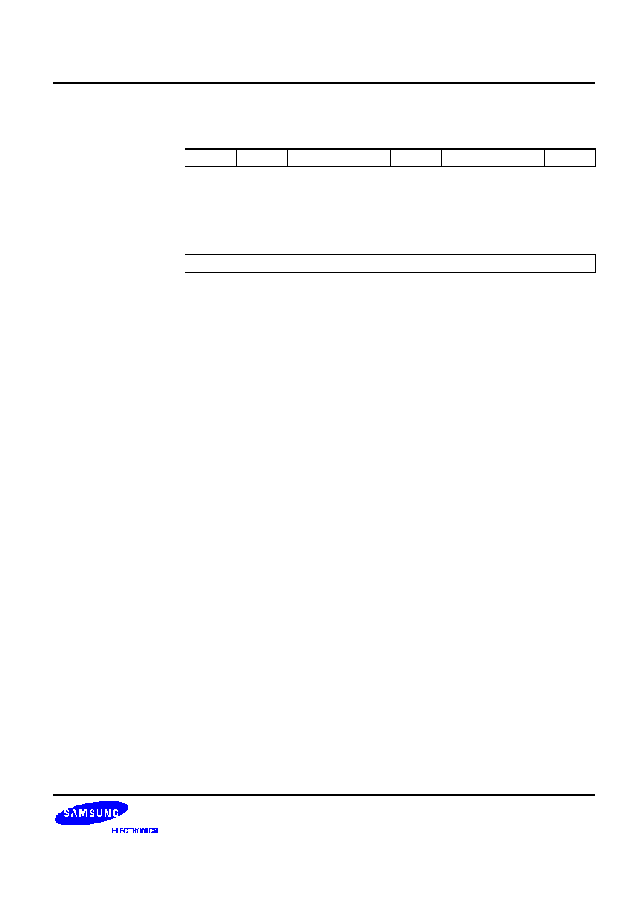
S3C8639/C863A/P863A/C8647/F8647
CONTROL REGISTERS
4-37
SIDSR
-- Slave IIC-Bus Tx/Rx Data Shift Register (Only S3C863X) F4H Set 1, Bank 1
Bit Identifier
.7
.6
.5
.4
.3
.2
.1
.0
RESET
RESET
Value
x
x
x
x
x
x
x
x
Read/Write
R/W
R/W
R/W
R/W
R/W
R/W
R/W
R/W
Addressing Mode
Register addressing only
.7≠.0
Slave IIC-Bus Transmit/Receive Data Shift Bus
Write enable when SICSR.6 is "1", but read enable anytime.

CONTROL REGISTERS
S3C8639/C863A/P863A/C8647/F8647
4-38
SPH
--
Stack Pointer (High Byte)
D8H
Set 1
Bit Identifier
.7
.6
.5
.4
.3
.2
.1
.0
RESET
RESET
Value
x
x
x
x
x
x
x
x
Read/Write
R/W
R/W
R/W
R/W
R/W
R/W
R/W
R/W
Addressing Mode
Register addressing mode only
.7≠.0
Stack Pointer Address (High Byte)
The high-byte stack pointer value is the upper eight bits of the 16-bit stack pointer
address (SP15≠SP8). The lower byte of the stack pointer value is located in the
register SPL (D9H). The SP value is undefined after a reset.
SPL
-- Stack Pointer (Low Byte)
D9H
Set 1
Bit Identifier
.7
.6
.5
.4
.3
.2
.1
.0
RESET
RESET
Value
x
x
x
x
x
x
x
x
Read/Write
R/W
R/W
R/W
R/W
R/W
R/W
R/W
R/W
Addressing Mode
Register addressing mode only
.7≠.0
Stack Pointer Address (Low Byte)
The low-byte stack pointer value is the lower eight bits of the 16-bit stack pointer
address (SP7≠SP0). The upper byte of the stack pointer value is located in the
register SPH (D8H). The SP value is undefined after a reset.
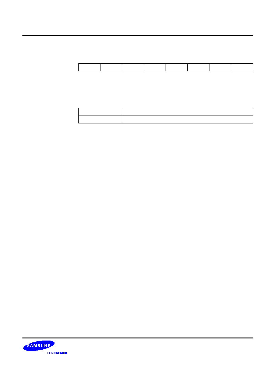
S3C8639/C863A/P863A/C8647/F8647
CONTROL REGISTERS
4-39
STOPCON
-- Stop Control Register
FBH
Set 1, Bank 0
Bit Identifier
.7
.6
.5
.4
.3
.2
.1
.0
RESET
RESET
Value
0
0
0
0
0
0
0
0
Read/Write
R/W
R/W
R/W
R/W
R/W
R/W
R/W
R/W
Addressing Mode
Register addressing mode only
.7≠.0
Stop Operation Enable Bits
1 0 1 0 0 1 0 1
Enable the stop (power saving) function
Others
Disable the stop function
NOTES:
1.
If you intend to stop function for power saving, before Stop OP-code, you must set this register value to A5H
(10100101B).
2.
When STOP mode is released, stop control register (STOPCON) value is cleared automatically.

CONTROL REGISTERS
S3C8639/C863A/P863A/C8647/F8647
4-40
SYM
-- System Mode Register
DEH
Set 1
Bit Identifier
.7
.6
.5
.4
.3
.2
.1
.0
RESET
RESET
Value
0
≠
≠
x
x
x
0
0
Read/Write
R/W
≠
≠
R/W
R/W
R/W
R/W
R/W
Addressing Mode
Register addressing mode only
.7
Tri-State External Interface Control Bit
(1)
0
Normal operation (disable tri-state operation)
1
Set external interface lines to high impedance (enable tri-state operation)
.6 and .5
Not used for the S3C8639/C863A/C8647
.4≠.2
Fast Interrupt Level Selection Bits
(2)
0
0
0
IRQ0
0
0
1
IRQ1
0
1
0
IRQ2
0
1
1
IRQ3
1
0
0
IRQ4
1
0
1
IRQ5
1
1
0
IRQ6
1
1
1
IRQ7 (Not used for the S3C8647)
.1
Fast Interrupt Enable Bit
(3)
0
Disable fast interrupt processing
1
Enable fast interrupt processing
.0
Global Interrupt Enable Bit
(4)
0
Disable global interrupt processing
1
Enable global interrupt processing
NOTES:
1.
As external interface is not implemented in S3C8639/C863A/C8647, SYM.7 must always be "0".
2.
You can select only one interrupt level at a time for fast interrupt processing.
3.
Setting SYM.1 to "1" enables fast interrupt processing for the interrupt level currently selected by SYM.2≠SYM.4.
4.
After a reset, you must enable global interrupt processing by executing an EI instruction (not by writing a "1"
to SYM.0).

S3C8639/C863A/P863A/C8647/F8647
CONTROL REGISTERS
4-41
SYNCON0
-- Sync Processor Control Register 0
EDH
Set 1, Bank 0
Bit Identifier
.7
.6
.5
.4
.3
.2
.1
.0
RESET
RESET
Value
0
0
0
0
0
0
0
0
Read/Write
R/W
R/W
R/W
R
R
R
R
R
Addressing Mode
Register addressing mode only
.7
Sync Input Selection (SIS) Bit
0
Hsync-I input is selected
1
Csync-I input is selected
.6
Hsync Blanking Enable Bit
0
Disable (Hsync signal by-pass) (When SYNCON0.5 = "0")
1
Enable Hsync blanking automatically (During the Vsync signal extraction
period) (When SYNCON0.5 = "1")
.5
Vsync-O Output Selection (VOS) Bit
0
Select Vsync-I port input (when separate sync input mode)
1
Select 5-bit compare output (when composite sync input mode)
.4≠.0
5-Bit Counter Value Bits
5-bit counter increases when a high level is detected, while an overflow dose not
occur (Stop at "11111"). It decreases when a low level is detected, while an
underflow does not occur (Stop at "00000")
When SYNCON0.5 is "1": Sync separation and output (When counter value
increases to "11111", output the high through the MUX and when counter value
decreases to "00000", output becomes low. Resume the previous status when
"11111" > counter value > "00000")
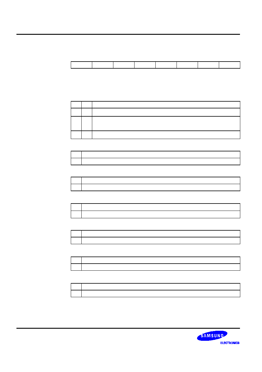
CONTROL REGISTERS
S3C8639/C863A/P863A/C8647/F8647
4-42
SYNCON1
-- Sync Processor Control Register 1
EEH
Set 1, Bank 0
Bit Identifier
.7
.6
.5
.4
.3
.2
.1
.0
RESET
RESET
Value
0
0
0
0
0
0
0
0
Read/Write
R/W
R/W
R/W
R/W
R/W
R/W
R
R
Addressing Mode
Register addressing mode only
.7 and .6
Clamp Signal Generator Selection Bits
0
0
Inhibit Clamp signal output (Clamp-O)
0
1
(f
OSC
◊
2) clock pulse output (250 ns at 8 MHz f
OSC
)
1
0
(f
OSC
◊
4) clock pulse output
(500 ns at 8 MHz f
OSC
, 333 ns at 12 MHz f
OSC
)
1
1
(f
OSC
◊
8) clock pulse output (1
µ
s at 8 MHz f
OSC
, 666ns at 12 MHz f
OSC
)
.5
"Front Porch"/"Back Porch" Mode Selection Bit
0
Generate Clamp-O after the rising edge of Hsync ("front porch" mode)
1
Generate Clamp-O after the falling edge of Hsync ("back porch" mode)
.4
Clamp Signal Output Status Control Bit (COSC)
0
Negative polarity
1
Positive polarity
.3
Vsync-O Status Control Bit
0
Do not invert (by-pass)
1
Invert output signal
.2
Hsync-O Status Control Bit (HOSC)
0
Do not invert (by-pass)
1
Invert output signal
.1
Vsync Polarity Detection Bit
(1)
0
Negative polarity
1
Positive polarity
.0
Hsync Polarity Detection Bit
(2)
0
Negative polarity
1
Positive polarity
NOTES:
1.
To check Hsync/Vsync polarity, it uses 16 clocks of timer M2 (f
OSC
/1000). If the Vsync polarity is changing, this bit will
be updated after a typical delay of 2 ms, at 8 MHz f
OSC
(1.33 ms at 12 MHz f
OSC
).
2.
The SYNCON1.0 may not be accurate when the Hsync-I is composite-sync signal output.
.

S3C8639/C863A/P863A/C8647/F8647
CONTROL REGISTERS
4-43
SYNCON2
-- Sync Processor Control Register 2
EFH
Set 1, Bank 0
Bit Identifier
.7
≠
.5
.4
.3
.2
.1
.0
RESET
RESET
Value
0
≠
0
0
0
0
0
0
Read/Write
R/W
≠
R/W
R/W
R/W
R/W
R/W
R/W
Addressing Mode
Register addressing mode only
.7
Unmixed Hsync Detection Bit (When SYNCON0.5 is "1")
0
Mixed Hsync period with Vsync of a composite sync input (This bit still cleared
before being read this bit or it is been in mixed Hsync period)
1
Unmixed Hsync periods
.6
Not used for the S3C8639/C863A/C8647(Only "0")
.5
5-Bit Counter Source Clock (fsync) Input Selection Bit
(1)
0
f
OSC
/3 (when f
CPU
is 12 MHz)
1
f
OSC
/2 (when f
CPU
is 8 MHz)
.4
Pseudo Sync Generation Disable Bit (Positive Polarity Only)
0
Enable Pseudo Hsync/Vsync generation
1
Normal Sync-processor operation (by-pass)
.3
Sync Signal Output Disable Bit
0
Enable Sync signal output
1
Inhibit Sync signal output (Output level is low)
.2
SOG (Sync On Green) Detection Bit
0
No SOG signal (when read)
0
Clear SOG detection 6-bit counter (when write)
1
Csync-I is SOG signal
(2)
.1
5-Bit up/down Counter Latch Status Changing Detection Bit
0
When the latch status is not changed or it writes"0" to this bit
1
When the latch status changing is detected.
.0
V
DD
Level Selection Bit for TTL Sync-Input Port (Not used for the S3C8647)
0
When V
DD
is +5 V
1
When V
DD
is +3 V
NOTES:
1.
Countable maximum Hsync pulse width = 7.85 us (when fsync is 4 MHz)
2.
To check SOG presence, it uses 64 Csync-I input edge signal.
3.
The SYNCON2.1 can be used to check the presence of composite-sync signal input.

CONTROL REGISTERS
S3C8639/C863A/P863A/C8647/F8647
4-44
SYNCRD
-- Sync Processor Port Read Data Register
F0H
Set 1, Bank 0
Bit Identifier
.7
.6
.5
.4
.3
.2
.1
.0
RESET
RESET
Value
≠
≠
≠
≠
0
0
0
0
Read/Write
≠
≠
≠
≠
R
R
R
R
Addressing Mode
Register addressing mode only
.7≠.4
Not used for the S3C8639/C863A/C8647
.3
Vertical Sync Signal Output Data Bit (Vsync-O)
0
Low data
1
High data
.2
Horizontal Sync Signal Output Data Bit (Hsync-O)
0
Low data
1
High data
.1
Vertical Sync Signal Input Data Bit (Vsync-I)
0
Low data
1
High data
.0
Horizontal Sync Signal Input Data Bit (Hsync-I)
0
Low data
1
High data

S3C8639/C863A/P863A/C8647/F8647
CONTROL REGISTERS
4-45
TBDR
-- Transmit Pre-Buffer Data Register
EFH
Set 1, Bank 1
Bit Identifier
.7
.6
.5
.4
.3
.2
.1
.0
RESET
RESET
Value
x
x
x
x
x
x
x
x
Read/Write
R/W
R/W
R/W
R/W
R/W
R/W
R/W
R/W
Addressing Mode
Register addressing mode only
.7≠.0
Write enable when DCSR0.4 is "1", Read enable anytime When DCON.3 (TBDR
Enable bit) = "1" and DCSR1.1 = "0", the data written into his register will be
automatically downloaded to the DDC Data Shift Register (DDSR) and generate the
interrupt request when the module detects the calling address is matched and the bit
0 of the received data is "1" (DCSR0.7-6 = "01") and when the data in the DDSR
register has been transmitted with received acknowledge bit, DCSR0.0 = "0". At this
interrupt service routine, the CPU must write the next data to the TBDR register to
clear DCSR1.1 and for the auto downloading of data to the DDSR register after the
data in the DDSR register is transmitted over again with DCSR0.0 = "0".When
DCON.3 = "1" and DDSR1.1 = "1", the data stored in this register will not be
downloaded to the DDSR register and generated the interrupt request when the
module detects the calling address is matched and the bit 0 of the received data is
"1". At this interrupt service routine, the CPU must write the current data and rewrite
the next data to the TBDR register to clear DCSR1.1.
If the master receiver doesn't acknowledge the transmitted data, DCSR0.0 = "1", the
module will release the SDA line for master to generate STOP or Repeated START
conditions.
If DCON.3 (TBDR Enable bit) is "0", the module will pull-down the SCL line in the
IIC-Bus interrupt service routine when the DCSR0.2 is "1". And the module will
release the SCL line if the CPU writes a data to the DDSR registers and the interrupt
pending bit is cleared.
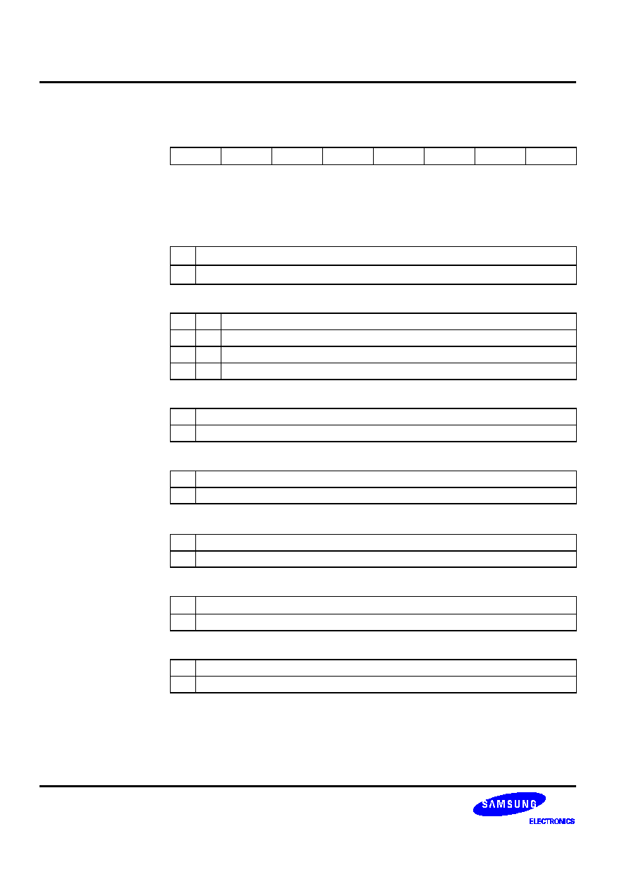
CONTROL REGISTERS
S3C8639/C863A/P863A/C8647/F8647
4-46
TM0CON
-- Timer m0 Control Register
D2H
Set 1
Bit Identifier
.7
.6
.5
.4
.3
.2
.1
.0
RESET
RESET
Value
0
0
0
0
0
0
0
0
Read/Write
R/W
R/W
R/W
R/W
R/W
R/W
R/W
R/W
Addressing Mode
Register addressing mode only
.7
Timer M0 Input Clock Selection Bit
0
f
OSC
/128
1
f
OSC
/8
.6 and .5
2 Bit Prescaler Bits
0
0
No division
0
1
Divided by 2
1
0
Divided by 3
1
1
Divided by 4
.4
Timer M0 Capture Mode Selection Bit
0
Capture on rising mode
1
Capture on falling mode
.3
Timer M0 Counter Clear Bit (TM0CLR)
0
No effect
1
Clear timer M0 counter, TM0CNT (when write)
.2
Timer M0 Overflow Interrupt Enable Bit (TM0OVINT)
(1)
0
Disable timer M0 overflow interrupt
1
Enable timer M0 overflow interrupt
.1
Timer M0 Capture Interrupt Enable Bit (TM0INT)
0
Disable timer M0 interrupt
(2)
1
Enable timer M0 interrupt
.0
Timer M0 Capture Input Selection Bit (TM0CAPSEL)
0
TM0CAP input pin selection
1
Vsync output path selection from sync-processor
NOTES:
1.
When the captured value is #0FFH, the overflow interrupt does not occurred. If the captured value is changed from
#0FFH to #00H, the overflow interrupt occurs. When the captured value is #00H, the overflow interrupt occurs first.
2.
When the timer M0 interrupt is disabled, the timer M0 overflow interrupt by f
OSC
can happen.

S3C8639/C863A/P863A/C8647/F8647
CONTROL REGISTERS
4-47
TM1CON
-- Timer M1 Control Register
F5H
Set 1, Bank 0
Bit Identifier
.7
.6
.5
.4
.3
.2
.1
.0
RESET
RESET
Value
0
0
0
0
0
0
0
0
Read/Write
R/W
R/W
R/W
R/W
R/W
R/W
R/W
R/W
Addressing Mode
Register addressing mode only
.7
Capture Signal Source Selection Bit
0
Signal from timer M2 interval time
1
Vsync-O from sync-processor
.6
Vsync-O Capture Egde Selection Bit (When TM1CON.7 = "1")
0
Capture Vsync-O (from sync-processor) on rising edge
1
Capture Vsync-O (from sync-processor) on falling edge
.5
Timer M1 Capture Interrupt Enable Bit (TM1INT)
0
Disable timer M1 capture
1
Enable timer M1 capture
.4
Timer M1 Capture Pending Bit (TM1PND)
0
Interrupt is not pending (when read)
0
Clear this pending bit (when write)
1
Interrupt is pending (when read)
1
No effect (when write)
.3
Timer M1 Counter Clear Bit (TM1CLR; when write)
0
No effect
1
Clear timer M1 counter
.2
Timer M1 Overflow Interrupt Enable Bit (TM1OVF)
0
Disable timer M1 overflow interrupt
1
Enable timer M1 overflow interrupt
.1≠.0
Timer M1 Clock Input Selection Bit
0
0
Hsync-I or Csync-I from sync processor
0
1
f
OSC
/2
1
0
f
OSC
/128
1
1
f
OSC
/512
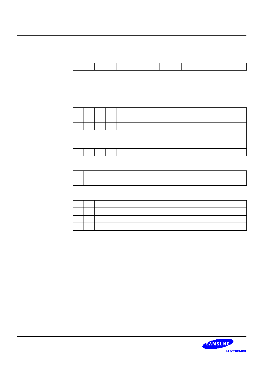
CONTROL REGISTERS
S3C8639/C863A/P863A/C8647/F8647
4-48
TM2CON
-- Timer M2 Control Register
F6H
Set 1, Bank 0
Bit Identifier
.7
.6
.5
.4
.3
.2
.1
.0
RESET
RESET
Value
1
1
1
1
1
0
0
0
Read/Write
R/W
R/W
R/W
R/W
R/W
R/W
R/W
R/W
Addressing Mode
Register addressing mode only
.7≠.3
5-bit Prescale Bits (TM2PS4≠TM2PS0)
0
0
0
0
0
No division
0
0
0
0
1
Divide by 2
0
0
0
1
0
Divide by 3
∑
∑
∑
∑
∑
∑
1
1
1
1
1
Divide by 32
.2
Timer M2 Interrupt Enable Bit (TM2INT)
0
Disable timer M2 interrupt
1
Enable timer M2 interrupt
.1 and .0
Timer M2 Capture Interval Time Selection Bits (When TM2CON.5 is "1")
0
0
Timer M2 interval (by pass)
0
1
Timer M2 interval
◊
10
1
0
Timer M2 interval
◊
20
1
1
Timer M2 interval
◊
30
NOTES:
1.
When the timer M1 capture mode is enabled (TM1CON.5 = "1"), the value of 5/2-bit prescaler is changed only in the
timer M1 capture interrupt routine.
2.
When the timer M1 capture mode is disabled (TM1CON.5 = "0"), the value of 5-bit prescaler is changed only in the timer
M2 interval interrupt routine.

S3C8639/C863A/P863A/C8647/F8647
CONTROL REGISTERS
4-49
WDTCON
-- Watchdog Time Control Register
ECH
Set 1, Bank 0
Bit Identifier
.7
.6
.5
.4
.3
.2
.1
.0
RESET
RESET
Value
≠
≠
≠
≠
0
0
0
0
Read/Write
≠
≠
≠
≠
R/W
R/W
R/W
R/W
Addressing Mode
Register addressing mode only
.7≠.4
Not used for the S3C8639/C863A/C8647
.3
Hsync-O Divide Enable Bit
0
Hsync-O = Hsync-I (Non-divide)
1
Hsync-O = Hsync-I/2
.2≠.0
Watchdog Time Generation Control Bits
0
0
0
tBTOVF
(note)
0
0
1
tBTOVF/2
0
1
0
tBTOVF/3
0
1
1
tBTOVF/4
1
0
0
tBTOVF/5
1
0
1
tBTOVF/6
1
1
0
tBTOVF/7
1
1
1
tBTOVF/8
NOTE: tBTOVF = (1/f
OSC
)
◊
(Divider count of basic timer input clock)
◊
256

CONTROL REGISTERS
S3C8639/C863A/P863A/C8647/F8647
4-50
NOTES

S3C8639/C863A/P863A/C8647/F8647
INTERRUPT STRUCTURE
5-1
5
INTERRUPT STRUCTURE
OVERVIEW
The SAM8 interrupt structure has three basic components: levels, vectors, and sources. The CPU recognizes
eight interrupt levels and supports up to 128 interrupt vectors. When a specific interrupt level has more than one
vector address, the vector priorities are established in hardware. Each vector can have one or more sources.
Levels
Interrupt levels are the main unit for interrupt priority assignment and recognition. All peripherals and I/O blocks
can issue interrupt requests. In other words, peripheral and I/O operations are interrupt-driven. There are eight
interrupt levels: IRQ0≠IRQ7, also called level 0≠level 7. Each interrupt level directly corresponds to an interrupt
request number (IRQn). The total number of interrupt levels used in the interrupt structure varies from device to
device.
The interrupt level numbers 0 through 7 do not necessarily indicate the relative priority of the levels. They are just
identifiers for the interrupt levels that are recognized by the CPU. The relative priority of different interrupt levels
is determined by settings in the interrupt priority register, IPR. Interrupt group and subgroup logic controlled by
IPR settings lets you define more complex priority relationships between different levels.
Vectors
Each interrupt level can have one or more interrupt vectors, or it may have no vector address assigned at all.
The maximum number of vectors that can be supported for a given level is 128. (The actual number of vectors
used for S3C8-series devices will always be much smaller.) If an interrupt level has more than one vector
address, the vector priorities are set in hardware. S3C8639/C863A/C8647* have ten (nine)* vectors -- one
corresponding to each of the ten (nine)* possible interrupt sources.
Sources
A source is any peripheral that generates an interrupt. A source can be an external pin or a counter overflow.
Each vector can have several interrupt sources. In the S3C8639/C863A/C8647* interrupt structure, each source
has its own vector address.
When a service routine starts, the respective pending bit should be either cleared automatically by hardware or
cleared "manually" by program software. The characteristics of the source's pending mechanism determine which
method would be used to clear its respective pending bit.
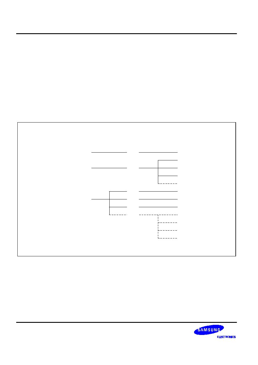
INTERRUPT STRUCTURE
S3C8639/C863A/P863A/C8647/F8647
5-2
INTERRUPT TYPES
The three components of the SAM8 interrupt structure described before -- levels, vectors, and sources -- are
combined to determine the interrupt structure of an individual device and to make full use of its available
interrupt logic. There are three possible combinations of interrupt structure components, called interrupt types 1,
2, and 3. The types differ in the number of vectors and interrupt sources assigned to each level (see Figure 5-1):
Type 1: One level (IRQn) + one vector (V
1
) + one source (S
1
)
Type 2: One level (IRQn) + one vector (V
1
) + multiple sources (S
1
≠ S
n
)
Type 3: One level (IRQn) + multiple vectors (V
1
≠ V
n
) + multiple sources (S
1
≠ S
n
, S
n+1
≠ S
n+m
)
In the S3C8639/C863A/C8647 microcontrollers, only interrupt types 1 and 3 are implemented.
Vectors
Sources
Levels
S
1
V
1
S
2
Type 2:
IRQn
S
3
S
n
V
1
S
1
V
2
S
2
Type 3:
IRQn
V
3
S
3
V
1
S
1
Type 1:
IRQn
V
n
S
n +
1
S
n
S
n +
2
S
n +
m
NOTES:
1. The number of S
n
and V
n
value is expandable.
2. In the S3C8639/C863A/C8647 implementation,
interrupt types 1 and 3 are used.
Figure 5-1. S3C8-Series Interrupt Types

S3C8639/C863A/P863A/C8647/F8647
INTERRUPT STRUCTURE
5-3
S3C8639/C863A/C8647 INTERRUPT STRUCTURE
The S3C8639/C863A/C8647 microcontrollers support ten interrupt sources. Each interrupt source has a
corresponding interrupt vector address. All eight interrupt levels are used in the device-specific interrupt
structure, which is shown in Figure 5-2.
When multiple interrupt levels are active, the interrupt priority register (IPR) determines the order in which
contending interrupts are to be serviced. If multiple interrupts occur within the same interrupt level, the interrupt
with the lowest vector address is usually processed first. (The relative priorities of multiple interrupts within a
single level are fixed in hardware.)
When the CPU grants an interrupt request, interrupt processing starts: All other interrupts are disabled and the
program counter value and status flags are pushed to stack. The starting address of the service routine is fetched
from the appropriate vector address (plus the next 8-bit value to concatenate the full 16-bit address) and the
service routine is executed.
Vectors
Sources
Levels
Timer M2 interval interrupt
IRQ1
Timer M1 overflow interrupt
Timer M1 capture interrupt
IRQ2
DDC (Multi-master IIC-bus) interrupt
P0.0 external interrupt (INT0)
IRQ4
P0.1 external interrupt (INT1)
P0.2 external interrupt (INT2)
Slave only IIC-bus interrupt
(note)
Timer M0 overflow interrupt
IRQ0
Timer M0 capture interrupt
Reset/Clear
H/W
H/W
S/W
S/W
S/W
S/W
S/W
S/W
H/W
H/W
IRQ3
IRQ5
IRQ6
IRQ7
E4H
E6H
E8H
EAH
ECH
EEH
F0H
F2H
E0H
E2H
NOTE:
Not used for the S3C8647.
Figure 5-2. S3C8639/C863A/C8647 Interrupt Structure

INTERRUPT STRUCTURE
S3C8639/C863A/P863A/C8647/F8647
5-4
INTERRUPT VECTOR ADDRESSES
All interrupt vector addresses for the S3C8639/C863A/C8647 interrupt structure are stored in the vector address
area of the ROM, 00H≠FFH (see Figure 5-3). You can allocate unused locations in the vector address area as
normal program memory. If you do so, please be careful not to overwrite any of the stored vector addresses.
(Table 5-1 lists all vector addresses.)
The program reset address in the ROM is 0100H.
49,151
0
(Decimal)
255
Interrupt Vector
AddressArea
32/48-Kbyte
Addressable
Pregram Memory
(ROM) Area
(S3C863X)
33,767
0H
0100H
0FFH
BFFFH
(Hex)
7FFFH
RESET
Address
8000H
24,535
5FFFH
24-Kbyte
Addressable
Pregram Memory
(ROM) Area
(S3C8647)
Figure 5-3. ROM Vector Address Area
S3C8639/C863A/P863A/C8647/F8647
INTERRUPT STRUCTURE
5-5
Table 5-1. S3C8639/C863A/C8647 Interrupt Vectors
Vector Address
Request
Reset/Clear
Decimal
Value
Hex
Value
Interrupt Source
Interrupt
Level
Priority in
Level
H/W
S/W
224
226
E0H
E2H
Timer M0 overflow interrupt
Timer M0 capture interrupt
IRQ0
0
1
228
E4H
Timer M2 interval interrupt
IRQ1
≠
230
232
E6H
E8H
Timer M1 overflow interrupt
Timer M1 capture interrupt
IRQ2
0
1
234
EAH
DDC (Multi-master IIC-bus) interrupt
IRQ3
≠
236
ECH
P0.0 external interrupt (INT0)
IRQ4
≠
238
EEH
P0.1 external interrupt (INT1)
IRQ5
≠
240
F0H
P0.2 external interrupt (INT2)
IRQ6
≠
242
F2H
Slave only IIC-bus interrupt
(3)
IRQ7
≠
NOTES:
1.
Interrupt priorities are identified in inverse order: "0" is the highest priority, "1" is the next highest, and so on.
2.
If two or more interrupts within the same level contend, the interrupt with the lowest vector address usually has priority
over one with a higher vector address. The priorities within a given level are fixed in hardware.
3.
Not used for the S3C8647.

INTERRUPT STRUCTURE
S3C8639/C863A/P863A/C8647/F8647
5-6
ENABLE/DISABLE INTERRUPT INSTRUCTIONS (EI, DI)
Executing the Enable Interrupts (EI) instruction enables the interrupt structure. All interrupts are then serviced as
they occur according to the established priorities.
NOTE
The system initialization routine executed after a reset must always contain an EI instruction
(assuming one or more interrupts are used in the application).
During the normal operation, you can execute the DI (Disable Interrupt) instruction at any time to globally disable
interrupt processing. The EI and DI instructions change the value of bit 0 in the SYM register. Although you can
directly manipulate SYM.0 to enable or disable interrupts, it is recommended that you use the EI and DI
instructions instead.
SYSTEM-LEVEL INTERRUPT CONTROL REGISTERS
In addition to the control registers for specific interrupt sources, four system-level registers control interrupt
processing:
-- The interrupt mask register, IMR, enables (un-masks) or disables (masks) interrupt levels.
-- The interrupt priority register, IPR, controls the relative priorities of interrupt levels.
-- The interrupt request register, IRQ, contains interrupt pending flags for each interrupt level (as opposed to
each interrupt source).
-- The system mode register, SYM, enables or disables global interrupt processing. (SYM settings also enable
fast interrupts and control the activity of external interface, if implemented.)
Table 5-2. Interrupt Control Register Overview
Control Register
ID
R/W
Function Description
Interrupt mask register
IMR
R/W
Bit settings in the IMR register enable or disable interrupt
processing for each of the eight interrupt levels, IRQ0≠IRQ7.
Interrupt priority register
IPR
R/W
Controls the relative processing priorities of the interrupt
levels. The eight levels are organized into three groups: A, B,
and C. Group A is IRQ0 and IRQ1, group B is IRQ2≠IRQ4,
and group C is IRQ5≠IRQ7.
Interrupt request register
IRQ
R
This register contains a request pending bit for each of the
seven interrupt levels, IRQ0≠IRQ7.
System mode register
SYM
R/W
This register enables and disables dynamic global interrupt
processing and fast interrupt processing.

S3C8639/C863A/P863A/C8647/F8647
INTERRUPT STRUCTURE
5-7
INTERRUPT PROCESSING CONTROL POINTS
Interrupt processing can therefore be controlled in two ways: globally or by specific interrupt level and source.
Among the system-level control points in the interrupt structure are:
-- Global interrupt enabled and disabled (by EI and DI instructions or by direct manipulation of SYM.0 )
-- Interrupt level enable/disable settings (IMR register)
-- Interrupt level priority settings (IPR register)
-- Interrupt source enable/disable settings in the corresponding peripheral control registers
NOTE
When writing an application program that handles interrupt processing, be sure to include the necessary
register file address (register pointer) information.
Source Interrupts
S
R
Q
RESET
"EI" Instruction
Execution
Source Interrupts
Enable
Interrupt Pending Register
(Read-only)
Polling
Cycle
Interrupt Request Register
(Read-only)
Global Interrupt Control
(EI, DI instruction)
Interrupt Priority
Register
Global Interrupt Control
(EI, DI or SYM.0
manipulation)
Vector
Interrupt
Cycle
Figure 5-4. Interrupt Function Diagram

INTERRUPT STRUCTURE
S3C8639/C863A/P863A/C8647/F8647
5-8
PERIPHERAL INTERRUPT CONTROL REGISTERS
For each interrupt source there is a corresponding peripheral control register (or registers) controlling the
interrupts generated by the related peripheral. These registers and their locations are listed in Table 5-3.
Table 5-3. Interrupt Source Control Registers
Interrupt Source
Interrupt Level
Control Register(s)
Register Location(s)
Timer M0 overflow interrupt
Timer M0 capture interrupt
IRQ0
TM0CON
Set 1, D2H
Timer M2 interval interrupt
IRQ1
TM2CON
Set 1, bank 0, F6H
Timer M1 overflow interrupt
Timer M1 capture interrupt
IRQ2
TM1CON
Set 1, bank 0, F5H
DDC (Multi-master IIC-bus) interrupt
IRQ3
DCCR
DCSR0
Set 1, bank 1, EBH
Set 1, bank 1, ECH
P0.0 external interrupt
IRQ4
P0CONL
P0INT
Set 1, bank 0, E5H
Set 1, bank 0, EBH
P0.1 external interrupt
IRQ5
P0CONL
P0INT
Set 1, bank 0, E5H
Set 1, bank 0, EBH
P0.2 external interrupt
IRQ6
P0CONL
P0INT
Set 1, bank 0, E5H
Set 1, bank 0, EBH
Slave only IIC-bus interrupt
(note)
IRQ7
SICSR
Set 1, bank 1, F2H
NOTE: Not used for the S3C8647.
S3C8639/C863A/P863A/C8647/F8647
INTERRUPT STRUCTURE
5-9
SYSTEM MODE REGISTER (SYM)
The system mode register, SYM (set 1, DEH), is used to globally enable and disable interrupt processing and to
control fast interrupt processing. Figure 5-5 shows the effect of the various control settings.
A reset clears SYM.7, SYM.1, and SYM.0 to "0". Other SYM bit values (for fast interrupt level selection) are
undetermined.
The instructions EI and DI enable and disable global interrupt processing, respectively, by modifying the bit 0
value of the SYM register. In order to enable interrupt processing an Enable Interrupt (EI) instruction must be
included in the initialization routine, which follows a reset operation. Although you can manipulate SYM.0 directly
to enable and disable interrupts during the normal operation, it is recommended to use the EI and DI instructions
for this purpose.
NOTE:
Not used for the S3C8647.
System Mode Register (SYM)
DEH, Set 1, R/W
.7
.6
.5
.4
.3
.2
.1
.0
MSB
LSB
Global interrupt enable bit:
0 = Disable all interrupts
1 = Enable all interrupts
Fast interrupt enable bit:
0 = Disable fast interrupts
1 = Enable fast interrupts
Not used for
S3C8639/C863A/C8647
External interface tri-state enable bit:
0 = Normal operation (Tri-state disabled)
1 = High impedance (Tri-state enabled)
Fast interrupt level selection bits:
0 0 0
0 0 1
0 1 0
0 1 1
1 0 0
1 0 1
1 1 0
1 1 1
IRQ0
IRQ1
IRQ2
IRQ3
IRQ4
IRQ5
IRQ6
IRQ7
(note)
Figure 5-5. System Mode Register (SYM)
INTERRUPT STRUCTURE
S3C8639/C863A/P863A/C8647/F8647
5-10
INTERRUPT MASK REGISTER (IMR)
The interrupt mask register, IMR (set 1, DDH) is used to enable or disable interrupt processing for individual
interrupt levels. After a reset, all IMR bit values are undetermined and must therefore be written to their required
settings by the initialization routine.
Each IMR bit corresponds to a specific interrupt level: bit 1 to IRQ1, bit 2 to IRQ2, and so on. When the IMR bit
of an interrupt level is cleared to "0", interrupt processing for that level is disabled (masked). When you set a
level's IMR bit to "1", interrupt processing for the level is enabled (not masked).
The IMR register is mapped to register location DDH in set 1. Bit values can be read and written by instructions
using the Register addressing mode.
Interrupt Mask Register (IMR)
DDH, Set 1, R/W
.7
.6
.5
.4
.3
.2
.1
.0
MSB
LSB
IRQ1
IRQ2
IRQ3
IRQ4
IRQ5
IRQ6
IRQ7
(note)
IRQ0
Interrupt level enable bits (7-0):
0 = Disable (mask) interrupt level
1 = Enable (un-mask)interrupt level
NOTE:
Not used for the S3C8647.
Figure 5-6. Interrupt Mask Register (IMR)

S3C8639/C863A/P863A/C8647/F8647
INTERRUPT STRUCTURE
5-11
INTERRUPT PRIORITY REGISTER (IPR)
The interrupt priority register, IPR (set 1, bank 0, FFH), is used to set the relative priorities of the interrupt levels
in the microcontroller's interrupt structure. After a reset, all IPR bit values are undetermined and must therefore
be written to their required settings by the initialization routine.
When more than one interrupt sources are active, the source with the highest priority is serviced first. If two
sources belong to the same interrupt level, the source with the lower vector address usually has priority. (This
priority is fixed in hardware.)
To support programming of the relative interrupt level priorities, they are organized into groups and subgroups by
the interrupt logic. Please note that these groups (and subgroups) are used only by IPR logic for the IPR register
priority definitions (see Figure 5-7):
Group A
IRQ0, IRQ1
Group B
IRQ2, IRQ3, IRQ4
Group C
IRQ5, IRQ6, IRQ7
IPR
Group A
IRQ1
A2
IRQ0
A1
IRQ2
B1
IRQ4
B2
IPR
Group B
IRQ3
IRQ5
C1
IRQ7
C2
IPR
Group C
IRQ6
B21
B22
C21
C22
Figure 5-7. Interrupt Request Priority Groups
As you can see in Figure 5-8, IPR.7, IPR.4, and IPR.1 control the relative priority of interrupt groups A, B, and C.
For example, the setting "001B" for these bits would select the group relationship B > C > A. The setting "101B"
would select the relationship C > B > A.
The functions of the other IPR bit settings are as follows:
-- Interrupt group C includes a sub group that has an additional priority relationship among interrupt levels 5, 6,
and 7. IPR.6 defines the subgroup C relationship.
-- IPR.5 controls the relative priorities of group C interrupts.
-- Interrupt group B includes a subgroup that has an additional priority relationship among interrupt levels 2, 3,
and 4. IPR.3 defines the subgroup B relationship.
-- IPR.2 controls interrupt group B.
-- IPR.0 controls the relative priority setting of IRQ0 and IRQ1 interrupts.

INTERRUPT STRUCTURE
S3C8639/C863A/P863A/C8647/F8647
5-12
Interrupt Priority Register (IPR)
FFH, Set 1, Bank 0, R/W
.7
.6
.5
.4
.3
.2
.1
.0
MSB
LSB
Group A
0 = IRQ0 > IRQ1
1 = IRQ1 > IRQ0
Subgroup B
0 = IRQ3 > IRQ4
1 = IRQ4 > IRQ3
Group C
0 = IRQ5 > (IRQ6, IRQ7)
1 = (IRQ6, IRQ7) > IRQ5
Subgroup C
0 = IRQ6 > IRQ7
1 = IRQ7 > IRQ6
Group B
0 = IRQ2 > (IRQ3, IRQ4)
1 = (IRQ3, IRQ4) > IRQ2
Group priority:
0 0 0
0 0 1
0 1 0
0 1 1
1 0 0
1 0 1
1 1 0
1 1 1
= Not used
= B > C > A
= A > B > C
= B > A > C
= C > A > B
= C > B > A
= A > C > B
= Not used
D7 D4 D1
Figure 5-8. Interrupt Priority Register (IPR)

S3C8639/C863A/P863A/C8647/F8647
INTERRUPT STRUCTURE
5-13
INTERRUPT REQUEST REGISTER (IRQ)
You can poll bit values in the interrupt request register, IRQ (set 1, DCH), to monitor interrupt request status for
all levels in the microcontroller's interrupt structure. Each bit corresponds to the interrupt level of the same
number: bit 0 to IRQ0, bit 1 to IRQ1, and so on. A "0" indicates that no interrupt request is currently being issued
for that level. A "1" indicates that an interrupt request has been generated for that level.
IRQ bit values are addressable in read-only using Register addressing mode. You can read (test) the contents of
the IRQ register at any time using bit or byte addressing to determine the current interrupt request status of
specific interrupt levels. After a reset, all IRQ status bits are cleared to "0".
You can poll IRQ register values even if a DI instruction has been executed (that is, if global interrupt processing
is disabled). If an interrupt occurs while the interrupt structure is disabled, the CPU will not service it. You can,
however, still detect the interrupt request by polling the IRQ register. In this way, you can determine which events
occurred while the interrupt structure was globally disabled.
Interrupt Request Register (IRQ)
DCH, Set 1, Read-only
.7
.6
.5
.4
.3
.2
.1
.0
MSB
LSB
IRQ1
IRQ2
IRQ3
IRQ4
IRQ5
IRQ6
IRQ7
(note)
IRQ0
Interrupt level request pending bits:
0 = Interrupt level is not pending
1 = Interrupt level is pending
NOTE:
Not used for the S3C8647.
Figure 5-9. Interrupt Request Register (IRQ)

INTERRUPT STRUCTURE
S3C8639/C863A/P863A/C8647/F8647
5-14
INTERRUPT PENDING FUNCTION TYPES
Overview
There are two types of interrupt pending bits: One type that is automatically cleared by hardware after the
interrupt service routine is acknowledged and executed; the other that must be cleared by the application
program's interrupt service routine.
Pending Bits Cleared Automatically by Hardware
For interrupt pending bits that are cleared automatically by hardware, interrupt logic sets the corresponding
pending bit to "1" when a request occurs. It then issues an IRQ pulse to inform the CPU that an interrupt is
waiting to be serviced. The CPU acknowledges the interrupt source, executes the service routine, and clears the
pending bit to "0". This type of pending bit is not mapped and cannot, therefore, be read or written by application
software.
In the S3C8639/C863A/C8647 interrupt structure, the timer M0 overflow interrupt (IRQ0, vector E0H), the timer
M0 capture interrupt (IRQ0, vector E2H), the timer M2 interval interrupt (IRQ1, vector E4H), and the timer M1
overflow interrupt (IRQ2, vector E6H) belong to this category of interrupts in which pending conditions are
cleared automatically by hardware.
Pending Bits Cleared by the Service Routine
The second type of pending bit is the one that should be cleared by program software. The service routine must
clear the appropriate pending bit before a return-from-interrupt subroutine (IRET) occurs. To do this, a "0" must
be written to the corresponding pending bit location in the source's mode or control register.
In the S3C8639/C863A/C8647 interrupt structure, pending conditions for all interrupt sources, except the timer
M0 overflow/capture, the timer M2 interval interrupt and the timer M1 overflow interrupt, must be cleared by the
program software's interrupt service routine.

S3C8639/C863A/P863A/C8647/F8647
INTERRUPT STRUCTURE
5-15
INTERRUPT SOURCE POLLING SEQUENCE
The interrupt request polling and servicing sequence is as follows:
1.
A source generates an interrupt request by setting the interrupt request bit to "1".
2.
The CPU polling procedure identifies a pending condition for that source.
3.
The CPU checks the source's interrupt level.
4.
The CPU generates an interrupt acknowledge signal.
5.
Interrupt logic determines the interrupt's vector address.
6.
The service routine starts and the source's pending bit is cleared to "0" (by hardware or by software).
7.
The CPU continues polling for interrupt requests.
INTERRUPT SERVICE ROUTINES
Before an interrupt request is serviced, the following conditions must be met:
-- Interrupt processing must be globally enabled (EI, SYM.0 = "1")
-- The interrupt level must be enabled (IMR register)
-- The interrupt level must have the highest priority if more than one levels are currently requesting service
-- The interrupt must be enabled at the interrupt's source (peripheral control register)
When all of the above conditions are met, the interrupt request is acknowledged at the end of the instruction
cycle. The CPU then initiates an interrupt machine cycle that completes the following processing sequence:
1.
Reset (clear to "0") the interrupt enable bit in the SYM register (SYM.0) to disable all subsequent interrupts.
2.
Save the program counter (PC) and status flags to the system stack.
3.
Branch to the interrupt vector to fetch the address of the service routine.
4.
Pass control to the interrupt service routine.
When the interrupt service routine is completed, the CPU issues an Interrupt Return (IRET). The IRET restores
the PC and status flags, setting SYM.0 to "1". It allows the CPU to process the next interrupt request.

INTERRUPT STRUCTURE
S3C8639/C863A/P863A/C8647/F8647
5-16
GENERATING INTERRUPT VECTOR ADDRESSES
The interrupt vector area in the ROM (00H≠FFH) contains the addresses of interrupt service routines that
correspond to each level in the interrupt structure. Vectored interrupt processing follows this sequence:
1.
Push the program counter's low-byte value to the stack.
2.
Push the program counter's high-byte value to the stack.
3.
Push the FLAG register values to the stack.
4.
Fetch the service routine's high-byte address from the vector location.
5.
Fetch the service routine's low-byte address from the vector location.
6.
Branch to the service routine specified by the concatenated 16-bit vector address.
NOTE
A 16-bit vector address always begins at an even-numbered ROM address within the range of 00H≠FFH.
NESTING OF VECTORED INTERRUPTS
It is possible to nest a higher-priority interrupt request while a lower-priority request is being serviced. To do this,
you must follow these steps:
1.
Push the current 8-bit interrupt mask register (IMR) value to the stack (PUSH IMR).
2.
Load the IMR register with a new mask value that enables only the higher priority interrupt.
3.
Execute an EI instruction to enable interrupt processing (a higher priority interrupt will be processed if it
occurs).
4.
When the lower-priority interrupt service routine ends, restore the IMR to its original value by returning the
previous mask value from the stack (POP IMR).
5.
Execute an IRET.
Depending on the application, you may be able to simplify the above procedure to some extent.
INSTRUCTION POINTER (IP)
The instruction pointer (IP) is adopted by all the S3C8-series microcontrollers to control the optional high-speed
interrupt processing feature called fast interrupts. The IP consists of register pair DAH and DBH. The names IP of
registers are IPH (high byte, IP15≠IP8) and IPL (low byte, IP7≠IP0).

S3C8639/C863A/P863A/C8647/F8647
INTERRUPT STRUCTURE
5-17
FAST INTERRUPT PROCESSING
The feature called fast interrupt processing allows an interrupt within a given level to be completed in
approximately six clock cycles rather than the usual 10 clock cycles. SYM.4≠SYM.2 are used to select a specific
interrupt level for fast processing and SYM.1 enables or disables fast interrupt processing.
Two other system registers support fast interrupt processing:
-- The instruction pointer (IP) contains the starting address of the service routine (and is later used to swap the
program counter values), and
-- When a fast interrupt occurs, the contents of the FLAGS register is stored in an unmapped, dedicated
register called FLAGS' ("FLAGS prime").
NOTES
1. For the S3C8639/C863A/C8647 microcontrollers, the service routine for any of the seven interrupt
levels (IRQ0≠IRQ7) can be selected for fast interrupt processing.
The S3C8647 microcontroller has six interrupt levels (IRQ0-IRQ6) for fast interrupt processing.
2. When you use a fast interrupt in a multi-source interrupt vector, the fast interrupt may not be
processed if you use two sources as interrupt vector in normal mode. But it is possible when you use
only one source as interrupt vector.
Procedure for Initiating Fast Interrupts
To initiate fast interrupt processing, follow these steps:
1.
Load the start address of the service routine into the instruction pointer (IP).
2.
Load the interrupt level number (IRQn) into the fast interrupt selection field (SYM.4≠SYM.2)
3.
Write a "1" to the fast interrupt enable bit in the SYM register.
Fast Interrupt Service Routine
When an interrupt occurs in the level selected for fast interrupt processing, the following events occur:
1.
The contents of the instruction pointer and the PC are swapped.
2.
The FLAG register values are written to the FLAGS' ("FLAGS prime") register.
3.
The fast interrupt status bit in the FLAGS register is set.
4.
The interrupt is serviced.
5.
Assuming that the fast interrupt status bit is set, when the fast interrupt service routine ends, the instruction
pointer and PC values are swapped back.
6.
The content of FLAGS' ("FLAGS prime") is copied automatically back to the FLAGS register.
7.
The fast interrupt status bit in FLAGS is cleared automatically.
Relationship to Interrupt Pending Bit Types
As described previously, there are two types of interrupt pending bits: One is the type that is automatically
cleared by hardware after the interrupt service routine is acknowledged and executed, and the other is the one
that must be cleared by the application program's interrupt service routine. You can select fast interrupt
processing for interrupts with either type of pending condition clear function -- by hardware or by software.

INTERRUPT STRUCTURE
S3C8639/C863A/P863A/C8647/F8647
5-18
Programming Guidelines
Remember that the only way to enable/disable a fast interrupt is to set/clear the fast interrupt enable bit in the
SYM register, SYM.1. Executing an EI or DI instruction globally enables or disables all interrupt processing,
including fast interrupts.
NOTE
If you use fast interrupts, remember to load the IP with a new start address when the fast interrupt service
routine ends.
F
F
PROGRAMMING TIP -- Setting Up the Interrupt Control Structure
This example shows you how to enable interrupts for select interrupt sources, disable interrupts for other sources,
and set interrupt priorities for the S3C8639/C863A/C8647 interrupt structure. The following is a sample program:
-- Disables the watchdog function.
-- Enables the following interrupts: P0.0 external interrupt, timer M0 capture/overflow, timer M1
capture/overflow, timer M2 interval interrupt, and DDC interrupt.
-- Disables the following interrupts: P0.1 and P0.2 external interrupts, and slave only IIC-bus interrupt.
-- Sets interrupt priorities as P0.0 > timer M2 > timer M0 > timer M1 > DDC.
∑
∑
∑
DI
; Disable interrupts globally
LD
BTCON,#0A0H
; Disable watchdog function
LD
P0CONL,#01H
; P0.0
enable rising edge interrupts
LD
P0INT,#01H
; Enable P0.0 external interrupt
; Disable P0.1 and P0.2 external interrupts
LD
TM0CON,#8FH
; Enable timer M0 capture interrupt
; (capture on rising edges)
; Enable timer M0 overflow interrupt
LD
TM1CON,#3CH
; Enable timer M1 capture/overflow interrupt
LD
TM2CON,#3DH
; Enable timer M2 interval interrupt
LD
TM2DATA,#249
; Setting 1ms interval
LD
DCCR,#0A3H
; Enable DDC interrupt, SCL clock = 100 kHz
LD
IMR,#1FH
; Enable interrupt levels IRQ0, IRQ1, IRQ2, IRQ3 and
; IRQ4
LD
IPR,#1EH
; IRQ4 > IRQ0 > IRQ1 > IRQ2 > IRQ3
; (P0.0 > timer M0 > timer M2 > timer M1 > DDC)
EI
; Enable interrupts globally
∑
∑
∑

S3C8639/C863A/P863A/C8647/F8647
INTERRUPT STRUCTURE
5-19
F
F
PROGRAMMING TIP -- Programming Level IRQ0 as a Fast Interrupt
The following example shows you how to program fast interrupt processing for a selected interrupt level -- in this
case, for the timer M0 capture interrupt:
∑
∑
∑
LD
TM0CON,#8FH
; Enable TM0OVF interrupt
; Enable TM0CAP interrupt
; Capture mode (on rising signal edges)
; Select f
OSC
/8 as the T0 clock source
LD
P0CONH,#01H
; Set P0.4 to capture input mode
LDW
IPH,#T0_INT
; IPH
high byte of interrupt service routine
; IPL
low byte of interrupt service routine
LD
SYM,#02H
; Enable fast interrupt processing
; Select IRQ0 for fast interrupt service
EI
; Enable interrupts
∑
∑
∑
FAST_RET: IRET
; IP
Address of T0_INT (again)
T0_INT:
∑
∑
∑
(Fast service routine executes)
∑
∑
∑
LD
TM0CON,#8FH
; Clear TM0INT interrupt pending bit
JP
T,FAST_RET

INTERRUPT STRUCTURE
S3C8639/C863A/P863A/C8647/F8647
5-20
NOTES

S3C8639/C863A/P863A/C8647/F8647
INSTRUCTION SET
6-1
6
INSTRUCTION SET
OVERVIEW
The SAM8RC instruction set is specifically designed to support the large register files that are typical of most
SAM8RC microcontrollers. There are 78 instructions. The powerful data manipulation capabilities and features of
the instruction set include:
-- A full complement of 8-bit arithmetic and logic operations, including multiply and divide
-- No special I/O instructions (I/O control/data registers are mapped directly into the register file)
-- Decimal adjustment included in binary-coded decimal (BCD) operations
-- 16-bit (word) data can be incremented and decremented
-- Flexible instructions for bit addressing, rotate, and shift operations
DATA TYPES
The SAM8RC CPU performs operations on bits, bytes, BCD digits, and two-byte words. Bits in the register file
can be set, cleared, complemented, and tested. Bits within a byte are numbered from 7 to 0, where bit 0 is the
least significant (right-most) bit.
REGISTER ADDRESSING
To access an individual register, an 8-bit address in the range 0-255 or the 4-bit address of a working register is
specified. Paired registers can be used to construct 16-bit data or 16-bit program memory or data memory
addresses. For detailed information about register addressing, please refer to Section 2, "Address Spaces."
ADDRESSING MODES
There are seven explicit addressing modes: Register (R), Indirect Register (IR), Indexed (X), Direct (DA),
Relative (RA), Immediate (IM), and Indirect (IA). For detailed descriptions of these addressing modes, please
refer to Section 3, "Addressing Modes."

INSTRUCTION SET
S3C8639/C863A/P863A/C8647/F8647
6-2
Table 6-1. Instruction Group Summary
Mnemonic
Operands
Instruction
Load Instructions
CLR
dst
Clear
LD
dst,src
Load
LDB
dst,src
Load bit
LDE
dst,src
Load external data memory
LDC
dst,src
Load program memory
LDED
dst,src
Load external data memory and decrement
LDCD
dst,src
Load program memory and decrement
LDEI
dst,src
Load external data memory and increment
LDCI
dst,src
Load program memory and increment
LDEPD
dst,src
Load external data memory with pre-decrement
LDCPD
dst,src
Load program memory with pre-decrement
LDEPI
dst,src
Load external data memory with pre-increment
LDCPI
dst,src
Load program memory with pre-increment
LDW
dst,src
Load word
POP
dst
Pop from stack
POPUD
dst,src
Pop user stack (decrementing)
POPUI
dst,src
Pop user stack (incrementing)
PUSH
src
Push to stack
PUSHUD
dst,src
Push user stack (decrementing)
PUSHUI
dst,src
Push user stack (incrementing)

S3C8639/C863A/P863A/C8647/F8647
INSTRUCTION SET
6-3
Table 6-1. Instruction Group Summary (Continued)
Mnemonic
Operands
Instruction
Arithmetic Instructions
ADC
dst,src
Add with carry
ADD
dst,src
Add
CP
dst,src
Compare
DA
dst
Decimal adjust
DEC
dst
Decrement
DECW
dst
Decrement word
DIV
dst,src
Divide
INC
dst
Increment
INCW
dst
Increment word
MULT
dst,src
Multiply
SBC
dst,src
Subtract with carry
SUB
dst,src
Subtract
Logic Instructions
AND
dst,src
Logical AND
COM
dst
Complement
OR
dst,src
Logical OR
XOR
dst,src
Logical exclusive OR

INSTRUCTION SET
S3C8639/C863A/P863A/C8647/F8647
6-4
Table 6-1. Instruction Group Summary (Continued)
Mnemonic
Operands
Instruction
Program Control Instructions
BTJRF
dst,src
Bit test and jump relative on false
BTJRT
dst,src
Bit test and jump relative on true
CALL
dst
Call procedure
CPIJE
dst,src
Compare, increment and jump on equal
CPIJNE
dst,src
Compare, increment and jump on non-equal
DJNZ
r,dst
Decrement register and jump on non-zero
ENTER
Enter
EXIT
Exit
IRET
Interrupt return
JP
cc,dst
Jump on condition code
JP
dst
Jump unconditional
JR
cc,dst
Jump relative on condition code
NEXT
Next
RET
Return
WFI
Wait for interrupt
Bit Manipulation Instructions
BAND
dst,src
Bit AND
BCP
dst,src
Bit compare
BITC
dst
Bit complement
BITR
dst
Bit reset
BITS
dst
Bit set
BOR
dst,src
Bit OR
BXOR
dst,src
Bit XOR
TCM
dst,src
Test complement under mask
TM
dst,src
Test under mask

S3C8639/C863A/P863A/C8647/F8647
INSTRUCTION SET
6-5
Table 6-1. Instruction Group Summary (Concluded)
Mnemonic
Operands
Instruction
Rotate and Shift Instructions
RL
dst
Rotate left
RLC
dst
Rotate left through carry
RR
dst
Rotate right
RRC
dst
Rotate right through carry
SRA
dst
Shift right arithmetic
SWAP
dst
Swap nibbles
CPU Control Instructions
CCF
Complement carry flag
DI
Disable interrupts
EI
Enable interrupts
IDLE
Enter Idle mode
NOP
No operation
RCF
Reset carry flag
SB0
Set bank 0
SB1
Set bank 1
SCF
Set carry flag
SRP
src
Set register pointers
SRP0
src
Set register pointer 0
SRP1
src
Set register pointer 1
STOP
Enter Stop mode

INSTRUCTION SET
S3C8639/C863A/P863A/C8647/F8647
6-6
FLAGS REGISTER (FLAGS)
The flags register FLAGS contains eight bits that describe the current status of CPU operations. Four of these
bits, FLAGS.7≠FLAGS.4, can be tested and used with conditional jump instructions; two others FLAGS.3 and
FLAGS.2 are used for BCD arithmetic.
The FLAGS register also contains a bit to indicate the status of fast interrupt processing (FLAGS.1) and a bank
address status bit (FLAGS.0) to indicate whether bank 0 or bank 1 is currently being addressed. FLAGS register
can be set or reset by instructions as long as its outcome does not affect the flags, such as, Load instruction.
Logical and Arithmetic instructions such as, AND, OR, XOR, ADD, and SUB can affect the Flags register.
For example, the AND instruction updates the Zero, Sign and Overflow flags based on the outcome of
the AND instruction. If the AND instruction uses the Flags register as the destination, then
simultaneously, two write will occur to the Flags register producing an unpredictable result.
System Flags Register (FLAGS)
D5H, Set 1, R/W
.7
.6
.5
.4
.3
.2
.1
.0
MSB
LSB
Bank address
status flag (BA)
Fast interrupt
status flag (FIS)
Half-carry flag (H)
Decimal adjust flag (D)
Overflow flag (V)
Sign flag (S)
Zero flag (Z)
Carry flag (C)
Figure 6-1. System Flags Register (FLAGS)

S3C8639/C863A/P863A/C8647/F8647
INSTRUCTION SET
6-7
FLAG DESCRIPTIONS
C
Carry Flag (FLAGS.7)
The C flag is set to "1" if the result from an arithmetic operation generates a carry-out from or a borrow to
the bit 7 position (MSB). After rotate and shift operations, it contains the last value shifted out of the
specified register. Program instructions can set, clear, or complement the carry flag.
Z
Zero Flag (FLAGS.6)
For arithmetic and logic operations, the Z flag is set to "1" if the result of the operation is zero. For
operations that test register bits, and for shift and rotate operations, the Z flag is set to "1" if the result is
logic zero.
S
Sign Flag (FLAGS.5)
Following arithmetic, logic, rotate, or shift operations, the sign bit identifies the state of the MSB of the
result. A logic zero indicates a positive number and a logic one indicates a negative number.
V
Overflow Flag (FLAGS.4)
The V flag is set to "1" when the result of a two's-complement operation is greater than + 127 or less than
≠ 128. It is also cleared to "0" following logic operations.
D
Decimal Adjust Flag (FLAGS.3)
The DA bit is used to specify what type of instruction was executed last during BCD operations, so that a
subsequent decimal adjust operation can execute correctly. The DA bit is not usually accessed by
programmers, and cannot be used as a test condition.
H
Half-Carry Flag (FLAGS.2)
The H bit is set to "1" whenever an addition generates a carry-out of bit 3, or when a subtraction borrows
out of bit 4. It is used by the Decimal Adjust (DA) instruction to convert the binary result of a previous
addition or subtraction into the correct decimal (BCD) result. The H flag is seldom accessed directly by a
program.
FIS
Fast Interrupt Status Flag (FLAGS.1)
The FIS bit is set during a fast interrupt cycle and reset during the IRET following interrupt servicing.
When set, it inhibits all interrupts and causes the fast interrupt return to be executed when the IRET
instruction is executed.
BA
Bank Address Flag (FLAGS.0)
The BA flag indicates which register bank in the set 1 area of the internal register file is currently
selected, bank 0 or bank 1. The BA flag is cleared to "0" (select bank 0) when you execute the SB0
instruction and is set to "1" (select bank 1) when you execute the SB1 instruction.

INSTRUCTION SET
S3C8639/C863A/P863A/C8647/F8647
6-8
INSTRUCTION SET NOTATION
Table 6-2. Flag Notation Conventions
Flag
Description
C
Carry flag
Z
Zero flag
S
Sign flag
V
Overflow flag
D
Decimal-adjust flag
H
Half-carry flag
0
Cleared to logic zero
1
Set to logic one
*
Set or cleared according to operation
≠
Value is unaffected
x
Value is undefined
Table 6-3. Instruction Set Symbols
Symbol
Description
dst
Destination operand
src
Source operand
@
Indirect register address prefix
PC
Program counter
IP
Instruction pointer
FLAGS
Flags register (D5H)
RP
Register pointer
#
Immediate operand or register address prefix
H
Hexadecimal number suffix
D
Decimal number suffix
B
Binary number suffix
opc
Opcode

S3C8639/C863A/P863A/C8647/F8647
INSTRUCTION SET
6-9
Table 6-4. Instruction Notation Conventions
Notation
Description
Actual Operand Range
cc
Condition code
See list of condition codes in Table 6-6.
r
Working register only
Rn (n = 0≠15)
rb
Bit (b) of working register
Rn.b (n = 0≠15, b = 0≠7)
r0
Bit 0 (LSB) of working register
Rn (n = 0≠15)
rr
Working register pair
RRp (p = 0, 2, 4, ..., 14)
R
Register or working register
reg or Rn (reg = 0≠255, n = 0≠15)
Rb
Bit 'b' of register or working register
reg.b (reg = 0≠255, b = 0≠7)
RR
Register pair or working register pair
reg or RRp (reg = 0≠254, even number only, where
p = 0, 2, ..., 14)
IA
Indirect addressing mode
addr (addr = 0≠254, even number only)
Ir
Indirect working register only
@Rn (n = 0≠15)
IR
Indirect register or indirect working register @Rn or @reg (reg = 0≠255, n = 0≠15)
Irr
Indirect working register pair only
@RRp (p = 0, 2, ..., 14)
IRR
Indirect register pair or indirect working
register pair
@RRp or @reg (reg = 0≠254, even only, where
p = 0, 2, ..., 14)
X
Indexed addressing mode
#reg [Rn] (reg = 0≠255, n = 0≠15)
XS
Indexed (short offset) addressing mode
#addr [RRp] (addr = range ≠128 to +127, where
p = 0, 2, ..., 14)
XL
Indexed (long offset) addressing mode
#addr [RRp] (addr = range 0≠65535, where
p = 0, 2, ..., 14)
DA
Direct addressing mode
addr (addr = range 0≠65535)
RA
Relative addressing mode
addr (addr = number in the range +127 to ≠128 that is
an offset relative to the address of the next instruction)
IM
Immediate addressing mode
#data (data = 0≠255)
IML
Immediate (long) addressing mode
#data (data = range 0≠65535)

INSTRUCTION SET
S3C8639/C863A/P863A/C8647/F8647
6-10
Table 6-5. Opcode Quick Reference
OPCODE MAP
LOWER NIBBLE (HEX)
≠
0
1
2
3
4
5
6
7
U
0
DEC
R1
DEC
IR1
ADD
r1,r2
ADD
r1,Ir2
ADD
R2,R1
ADD
IR2,R1
ADD
R1,IM
BOR
r0≠Rb
P
1
RLC
R1
RLC
IR1
ADC
r1,r2
ADC
r1,Ir2
ADC
R2,R1
ADC
IR2,R1
ADC
R1,IM
BCP
r1.b, R2
P
2
INC
R1
INC
IR1
SUB
r1,r2
SUB
r1,Ir2
SUB
R2,R1
SUB
IR2,R1
SUB
R1,IM
BXOR
r0≠Rb
E
3
JP
IRR1
SRP/0/1
IM
SBC
r1,r2
SBC
r1,Ir2
SBC
R2,R1
SBC
IR2,R1
SBC
R1,IM
BTJR
r2.b, RA
R
4
DA
R1
DA
IR1
OR
r1,r2
OR
r1,Ir2
OR
R2,R1
OR
IR2,R1
OR
R1,IM
LDB
r0≠Rb
5
POP
R1
POP
IR1
AND
r1,r2
AND
r1,Ir2
AND
R2,R1
AND
IR2,R1
AND
R1,IM
BITC
r1.b
N
6
COM
R1
COM
IR1
TCM
r1,r2
TCM
r1,Ir2
TCM
R2,R1
TCM
IR2,R1
TCM
R1,IM
BAND
r0≠Rb
I
7
PUSH
R2
PUSH
IR2
TM
r1,r2
TM
r1,Ir2
TM
R2,R1
TM
IR2,R1
TM
R1,IM
BIT
r1.b
B
8
DECW
RR1
DECW
IR1
PUSHUD
IR1,R2
PUSHUI
IR1,R2
MULT
R2,RR1
MULT
IR2,RR1
MULT
IM,RR1
LD
r1, x, r2
B
9
RL
R1
RL
IR1
POPUD
IR2,R1
POPUI
IR2,R1
DIV
R2,RR1
DIV
IR2,RR1
DIV
IM,RR1
LD
r2, x, r1
L
A
INCW
RR1
INCW
IR1
CP
r1,r2
CP
r1,Ir2
CP
R2,R1
CP
IR2,R1
CP
R1,IM
LDC
r1, Irr2, xL
E
B
CLR
R1
CLR
IR1
XOR
r1,r2
XOR
r1,Ir2
XOR
R2,R1
XOR
IR2,R1
XOR
R1,IM
LDC
r2, Irr2, xL
C
RRC
R1
RRC
IR1
CPIJE
Ir,r2,RA
LDC
r1,Irr2
LDW
RR2,RR1
LDW
IR2,RR1
LDW
RR1,IML
LD
r1, Ir2
H
D
SRA
R1
SRA
IR1
CPIJNE
Irr,r2,RA
LDC
r2,Irr1
CALL
IA1
LD
IR1,IM
LD
Ir1, r2
E
E
RR
R1
RR
IR1
LDCD
r1,Irr2
LDCI
r1,Irr2
LD
R2,R1
LD
R2,IR1
LD
R1,IM
LDC
r1, Irr2, xs
X
F
SWAP
R1
SWAP
IR1
LDCPD
r2,Irr1
LDCPI
r2,Irr1
CALL
IRR1
LD
IR2,R1
CALL
DA1
LDC
r2, Irr1, xs

S3C8639/C863A/P863A/C8647/F8647
INSTRUCTION SET
6-11
Table 6-5. Opcode Quick Reference (Continued)
OPCODE MAP
LOWER NIBBLE (HEX)
≠
8
9
A
B
C
D
E
F
U
0
LD
r1,R2
LD
r2,R1
DJNZ
r1,RA
JR
cc,RA
LD
r1,IM
JP
cc,DA
INC
r1
NEXT
P
1
ENTER
P
2
EXIT
E
3
WFI
R
4
SB0
5
SB1
N
6
IDLE
I
7
STOP
B
8
DI
B
9
EI
L
A
RET
E
B
IRET
C
RCF
H
D
SCF
E
E
CCF
X
F
LD
r1,R2
LD
r2,R1
DJNZ
r1,RA
JR
cc,RA
LD
r1,IM
JP
cc,DA
INC
r1
NOP

INSTRUCTION SET
S3C8639/C863A/P863A/C8647/F8647
6-12
CONDITION CODES
The opcode of a conditional jump always contains a 4-bit field called the condition code (cc). This specifies under
which conditions it is to execute the jump. For example, a conditional jump with the condition code for "equal"
after a compare operation only jumps if the two operands are equal. Condition codes are listed in Table 6-6.
The carry (C), zero (Z), sign (S), and overflow (V) flags are used to control the operation of conditional jump
instructions.
Table 6-6. Condition Codes
Binary
Mnemonic
Description
Flags Set
0000
F
Always false
≠
1000
T
Always true
≠
0111
(note)
C
Carry
C = 1
1111
(note)
NC
No carry
C = 0
0110
(note)
Z
Zero
Z = 1
1110
(note)
NZ
Not zero
Z = 0
1101
PL
Plus
S = 0
0101
MI
Minus
S = 1
0100
OV
Overflow
V = 1
1100
NOV
No overflow
V = 0
0110
(note)
EQ
Equal
Z = 1
1110
(note)
NE
Not equal
Z = 0
1001
GE
Greater than or equal
(S XOR V) = 0
0001
LT
Less than
(S XOR V) = 1
1010
GT
Greater than
(Z OR (S XOR V)) = 0
0010
LE
Less than or equal
(Z OR (S XOR V)) = 1
1111
(note)
UGE
Unsigned greater than or equal
C = 0
0111
(note)
ULT
Unsigned less than
C = 1
1011
UGT
Unsigned greater than
(C = 0 AND Z = 0) = 1
0011
ULE
Unsigned less than or equal
(C OR Z) = 1
NOTES:
1.
It indicates condition codes that are related to two different mnemonics but which test the same flag. For
example, Z and EQ are both true if the zero flag (Z) is set, but after an ADD instruction, Z would probably be used;
after a CP instruction, however, EQ would probably be used.
2.
For operations involving unsigned numbers, the special condition codes UGE, ULT, UGT, and ULE must be used.

S3C8639/C863A/P863A/C8647/F8647
INSTRUCTION SET
6-13
INSTRUCTION DESCRIPTIONS
This section contains detailed information and programming examples for each instruction in the SAM8RC
instruction set. Information is arranged in a consistent format for improved readability and for fast referencing.
The following information is included in each instruction description:
-- Instruction name (mnemonic)
-- Full instruction name
-- Source/destination format of the instruction operand
-- Shorthand notation of the instruction's operation
-- Textual description of the instruction's effect
-- Specific flag settings affected by the instruction
-- Detailed description of the instruction's format, execution time, and addressing mode(s)
-- Programming example(s) explaining how to use the instruction

INSTRUCTION SET
S3C8639/C863A/P863A/C8647/F8647
6-14
ADC
-- Add with carry
ADC
dst,src
Operation:
dst
dst + src + c
The source operand, along with the setting of the carry flag, is added to the destination operand
and the sum is stored in the destination. The contents of the source are unaffected. Two's-
complement addition is performed. In multiple precision arithmetic, this instruction permits the
carry from the addition of low-order operands to be carried into the addition of high-order
operands.
Flags:
C: Set if there is a carry from the most significant bit of the result; cleared otherwise.
Z: Set if the result is "0"; cleared otherwise.
S: Set if the result is negative; cleared otherwise.
V: Set if arithmetic overflow occurs, that is, if both operands are of the same sign and the result
is of the opposite sign; cleared otherwise.
D: Always cleared to "0".
H: Set if there is a carry from the most significant bit of the low-order four bits of the result;
cleared otherwise.
Format:
Bytes
Cycles
Opcode
(Hex)
Addr Mode
dst src
opc
dst | src
2
4
12
r
r
6
13
r
lr
opc
src
dst
3
6
14
R
R
6
15
R
IR
opc
dst
src
3
6
16
R
IM
Example:
Given: R1 = 10H, R2 = 03H, C flag = "1", register 01H = 20H, register 02H = 03H, and
register 03H = 0AH:
ADC
R1,R2
R1 = 14H, R2 = 03H
ADC
R1,@R2
R1 = 1BH, R2 = 03H
ADC
01H,02H
Register 01H = 24H, register 02H = 03H
ADC
01H,@02H
Register 01H = 2BH, register 02H = 03H
ADC
01H,#11H
Register 01H = 32H
In the first example, destination register R1 contains the value 10H, the carry flag is set to "1",
and the source working register R2 contains the value 03H. The statement "ADC R1,R2" adds
03H and the carry flag value ("1") to the destination value 10H, leaving 14H in register R1.
S3C8639/C863A/P863A/C8647/F8647
INSTRUCTION SET
6-15
ADD
--
Add
ADD
dst,src
Operation:
dst
dst + src
The source operand is added to the destination operand and the sum is stored in the destination.
The contents of the source are unaffected. Two's-complement addition is performed.
Flags:
C: Set if there is a carry from the most significant bit of the result; cleared otherwise.
Z: Set if the result is "0"; cleared otherwise.
S: Set if the result is negative; cleared otherwise.
V: Set if arithmetic overflow occurred, that is, if both operands are of the same sign and the
result is of the opposite sign; cleared otherwise.
D: Always cleared to "0".
H: Set if a carry from the low-order nibble occurred.
Format:
Bytes
Cycles
Opcode
(Hex)
Addr Mode
dst src
opc
dst | src
2
4
02
r
r
6
03
r
lr
opc
src
dst
3
6
04
R
R
6
05
R
IR
opc
dst
src
3
6
06
R
IM
Example:
Given: R1 = 12H, R2 = 03H, register 01H = 21H, register 02H = 03H, register 03H = 0AH:
ADD
R1,R2
R1 = 15H, R2 = 03H
ADD
R1,@R2
R1 = 1CH, R2 = 03H
ADD
01H,02H
Register 01H = 24H, register 02H = 03H
ADD
01H,@02H
Register 01H = 2BH, register 02H = 03H
ADD
01H,#25H
Register 01H = 46H
In the first example, destination working register R1 contains 12H and the source working
register R2 contains 03H. The statement "ADD R1,R2" adds 03H to 12H, leaving the value 15H
in register R1.

INSTRUCTION SET
S3C8639/C863A/P863A/C8647/F8647
6-16
AND
--
Logical AND
AND
dst,src
Operation:
dst
dst AND src
The source operand is logically ANDed with the destination operand. The result is stored in the
destination. The AND operation results in a "1" bit being stored whenever the corresponding bits
in the two operands are both logic ones; otherwise a "0" bit value is stored. The contents of the
source are unaffected.
Flags:
C: Unaffected.
Z: Set if the result is "0"; cleared otherwise.
S: Set if the result bit 7 is set; cleared otherwise.
V: Always cleared to "0".
D: Unaffected.
H: Unaffected.
Format:
Bytes
Cycles
Opcode
(Hex)
Addr Mode
dst src
opc
dst | src
2
4
52
r
r
6
53
r
lr
opc
src
dst
3
6
54
R
R
6
55
R
IR
opc
dst
src
3
6
56
R
IM
Example:
Given: R1 = 12H, R2 = 03H, register 01H = 21H, register 02H = 03H, register 03H = 0AH:
AND
R1,R2
R1 = 02H, R2 = 03H
AND
R1,@R2
R1 = 02H, R2 = 03H
AND
01H,02H
Register 01H = 01H, register 02H = 03H
AND
01H,@02H
Register 01H = 00H, register 02H = 03H
AND
01H,#25H
Register 01H = 21H
In the first example, destination working register R1 contains the value 12H and the source
working register R2 contains 03H. The statement "AND R1,R2" logically ANDs the source
operand 03H with the destination operand value 12H, leaving the value 02H in register R1.

S3C8639/C863A/P863A/C8647/F8647
INSTRUCTION SET
6-17
BAND
--
Bit AND
BAND
dst,src.b
BAND
dst.b,src
Operation:
dst(0)
dst(0) AND src(b)
or
dst(b)
dst(b) AND src(0)
The specified bit of the source (or the destination) is logically ANDed with the zero bit (LSB) of
the destination (or source). The resultant bit is stored in the specified bit of the destination. No
other bits of the destination are affected. The source is unaffected.
Flags:
C: Unaffected.
Z: Set if the result is "0"; cleared otherwise.
S: Cleared to "0".
V: Undefined.
D: Unaffected.
H: Unaffected.
Format:
Bytes
Cycles
Opcode
(Hex)
Addr Mode
dst src
opc
dst | b | 0
src
3
6
67
r0
Rb
opc
src | b | 1
dst
3
6
67
Rb
r0
NOTE: In the second byte of the 3-byte instruction formats, the destination (or source) address is four
bits, the bit address 'b' is three bits, and the LSB address value is one bit in length.
Example:
Given: R1 = 07H and register 01H = 05H:
BAND
R1,01H.1
R1 = 06H, register 01H = 05H
BAND
01H.1,R1
Register 01H = 05H, R1 = 07H
In the first example, source register 01H contains the value 05H (00000101B) and destination
working register R1 contains 07H (00000111B). The statement "BAND R1,01H.1" ANDs the bit 1
value of the source register ("0") with the bit 0 value of register R1 (destination), leaving the
value 06H (00000110B) in register R1.
INSTRUCTION SET
S3C8639/C863A/P863A/C8647/F8647
6-18
BCP
--
Bit Compare
BCP
dst,src.b
Operation:
dst(0) ≠ src(b)
The specified bit of the source is compared to (subtracted from) bit zero (LSB) of the destination.
The zero flag is set if the bits are the same; otherwise it is cleared. The contents of both
operands are unaffected by the comparison.
Flags:
C: Unaffected.
Z: Set if the two bits are the same; cleared otherwise.
S: Cleared to "0".
V: Undefined.
D: Unaffected.
H: Unaffected.
Format:
Bytes
Cycles
Opcode
(Hex)
Addr Mode
dst src
opc
dst | b | 0
src
3
6
17
r0
Rb
NOTE: In the second byte of the instruction format, the destination address is four bits, the bit address 'b'
is three bits, and the LSB address value is one bit in length.
Example:
Given: R1 = 07H and register 01H = 01H:
BCP
R1,01H.1
R1 = 07H, register 01H = 01H
If destination working register R1 contains the value 07H (00000111B) and the source register
01H contains the value 01H (00000001B), the statement "BCP R1,01H.1" compares bit one of
the source register (01H) and bit zero of the destination register (R1). Because the bit values are
not identical, the zero flag bit (Z) is cleared in the FLAGS register (0D5H).

S3C8639/C863A/P863A/C8647/F8647
INSTRUCTION SET
6-19
BITC
--
Bit Complement
BITC
dst.b
Operation:
dst(b)
NOT dst(b)
This instruction complements the specified bit within the destination without affecting any other
bits in the destination.
Flags:
C: Unaffected.
Z: Set if the result is "0"; cleared otherwise.
S: Cleared to "0".
V: Undefined.
D: Unaffected.
H: Unaffected.
Format:
Bytes
Cycles
Opcode
(Hex)
Addr Mode
dst
opc
dst | b | 0
2
4
57
rb
NOTE: In the second byte of the instruction format, the destination address is four bits, the bit address 'b'
is three bits, and the LSB address value is one bit in length.
Example:
Given: R1 = 07H
BITC
R1.1
R1 = 05H
If working register R1 contains the value 07H (00000111B), the statement "BITC R1.1"
complements bit one of the destination and leaves the value 05H (00000101B) in register R1.
Because the result of the complement is not "0", the zero flag (Z) in the FLAGS register (0D5H)
is cleared.

INSTRUCTION SET
S3C8639/C863A/P863A/C8647/F8647
6-20
BITR
--
Bit Reset
BITR
dst.b
Operation:
dst(b)
0
The BITR instruction clears the specified bit within the destination without affecting any other bits
in the destination.
Flags:
No flags are affected.
Format:
Bytes
Cycles
Opcode
(Hex)
Addr Mode
dst
opc
dst | b | 0
2
4
77
rb
NOTE: In the second byte of the instruction format, the destination address is four bits, the bit address 'b'
is three bits, and the LSB address value is one bit in length.
Example:
Given: R1 = 07H:
BITR
R1.1
R1 = 05H
If the value of working register R1 is 07H (00000111B), the statement "BITR R1.1" clears bit one
of the destination register R1, leaving the value 05H (00000101B).

S3C8639/C863A/P863A/C8647/F8647
INSTRUCTION SET
6-21
BITS
--
Bit Set
BITS
dst.b
Operation:
dst(b)
1
The BITS instruction sets the specified bit within the destination without affecting any other bits
in the destination.
Flags:
No flags are affected.
Format:
Bytes
Cycles
Opcode
(Hex)
Addr Mode
dst
opc
dst | b | 1
2
4
77
rb
NOTE: In the second byte of the instruction format, the destination address is four bits, the bit address 'b'
is three bits, and the LSB address value is one bit in length.
Example:
Given: R1 = 07H:
BITS
R1.3
R1 = 0FH
If working register R1 contains the value 07H (00000111B), the statement "BITS R1.3" sets bit
three of the destination register R1 to "1", leaving the value 0FH (00001111B).

INSTRUCTION SET
S3C8639/C863A/P863A/C8647/F8647
6-22
BOR
--
Bit OR
BOR
dst,src.b
BOR
dst.b,src
Operation:
dst(0)
dst(0) OR src(b)
or
dst(b)
dst(b) OR src(0)
The specified bit of the source (or the destination) is logically ORed with bit zero (LSB) of the
destination (or the source). The resulting bit value is stored in the specified bit of the destination.
No other bits of the destination are affected. The source is unaffected.
Flags:
C: Unaffected.
Z: Set if the result is "0"; cleared otherwise.
S: Cleared to "0".
V: Undefined.
D: Unaffected.
H: Unaffected.
Format:
Bytes
Cycles
Opcode
(Hex)
Addr Mode
dst src
opc
dst | b | 0
src
3
6
07
r0
Rb
opc
src | b | 1
dst
3
6
07
Rb
r0
NOTE: In the second byte of the 3-byte instruction formats, the destination (or source) address is four
bits, the bit address 'b' is three bits, and the LSB address value is one bit.
Example:
Given: R1 = 07H and register 01H = 03H:
BOR
R1, 01H.1
R1 = 07H, register 01H = 03H
BOR
01H.2, R1
Register 01H = 07H, R1 = 07H
In the first example, destination working register R1 contains the value 07H (00000111B) and
source register 01H the value 03H (00000011B). The statement "BOR R1,01H.1" logically ORs
bit one of register 01H (source) with bit zero of R1 (destination). This leaves the same value
(07H) in working register R1.
In the second example, destination register 01H contains the value 03H (00000011B) and the
source working register R1 the value 07H (00000111B). The statement "BOR 01H.2,R1" logically
ORs bit two of register 01H (destination) with bit zero of R1 (source). This leaves the value 07H
in register 01H.
S3C8639/C863A/P863A/C8647/F8647
INSTRUCTION SET
6-23
BTJRF
--
Bit Test, Jump Relative on False
BTJRF
dst,src.b
Operation:
If src(b) is a "0", then PC
PC + dst
The specified bit within the source operand is tested. If it is a "0", the relative address is added to
the program counter and control passes to the statement whose address is now in the PC;
otherwise, the instruction following the BTJRF instruction is executed.
Flags:
No flags are affected.
Format:
(Note 1)
Bytes
Cycles
Opcode
(Hex)
Addr Mode
dst src
opc
src | b | 0
dst
3
10
37
RA
rb
NOTE: In the second byte of the instruction format, the source address is four bits, the bit address 'b' is
three bits, and the LSB address value is one bit in length.
Example:
Given: R1 = 07H:
BTJRF
SKIP,R1.3
PC jumps to SKIP location
If working register R1 contains the value 07H (00000111B), the statement "BTJRF SKIP,R1.3"
tests bit 3. Because it is "0", the relative address is added to the PC and the PC jumps to the
memory location pointed to by the SKIP. (Remember that the memory location must be within
the allowed range of + 127 to ≠ 128.)

INSTRUCTION SET
S3C8639/C863A/P863A/C8647/F8647
6-24
BTJRT
--
Bit Test, Jump Relative on True
BTJRT
dst,src.b
Operation:
If src(b) is a "1", then PC
PC + dst
The specified bit within the source operand is tested. If it is a "1", the relative address is added to
the program counter and control passes to the statement whose address is now in the PC;
otherwise, the instruction following the BTJRT instruction is executed.
Flags:
No flags are affected.
Format:
(Note 1)
Bytes
Cycles
Opcode
(Hex)
Addr Mode
dst src
opc
src | b | 1
dst
3
10
37
RA
rb
NOTE: In the second byte of the instruction format, the source address is four bits, the bit address 'b' is
three bits, and the LSB address value is one bit in length.
Example:
Given: R1 = 07H:
BTJRT
SKIP,R1.1
If working register R1 contains the value 07H (00000111B), the statement "BTJRT SKIP,R1.1"
tests bit one in the source register (R1). Because it is a "1", the relative address is added to the
PC and the PC jumps to the memory location pointed to by the SKIP. (Remember that the
memory location must be within the allowed range of + 127 to ≠ 128.)

S3C8639/C863A/P863A/C8647/F8647
INSTRUCTION SET
6-25
BXOR
--
Bit XOR
BXOR
dst,src.b
BXOR
dst.b,src
Operation:
dst(0)
dst(0) XOR src(b)
or
dst(b)
dst(b) XOR src(0)
The specified bit of the source (or the destination) is logically exclusive-ORed with bit zero (LSB)
of the destination (or source). The result bit is stored in the specified bit of the destination. No
other bits of the destination are affected. The source is unaffected.
Flags:
C: Unaffected.
Z: Set if the result is "0"; cleared otherwise.
S: Cleared to "0".
V: Undefined.
D: Unaffected.
H: Unaffected.
Format:
Bytes
Cycles
Opcode
(Hex)
Addr Mode
dst src
opc
dst | b | 0
src
3
6
27
r0
Rb
opc
src | b | 1
dst
3
6
27
Rb
r0
NOTE: In the second byte of the 3-byte instruction formats, the destination (or source) address is four
bits, the bit address 'b' is three bits, and the LSB address value is one bit in length.
Example:
Given: R1 = 07H (00000111B) and register 01H = 03H (00000011B):
BXOR
R1,01H.1
R1 = 06H, register 01H = 03H
BXOR
01H.2,R1
Register 01H = 07H, R1 = 07H
In the first example, destination working register R1 has the value 07H (00000111B) and source
register 01H has the value 03H (00000011B). The statement "BXOR R1,01H.1" exclusive-ORs
bit one of register 01H (source) with bit zero of R1 (destination). The result bit value is stored in
bit zero of R1, changing its value from 07H to 06H. The value of source register 01H is
unaffected.
INSTRUCTION SET
S3C8639/C863A/P863A/C8647/F8647
6-26
CALL
--
Call Procedure
CALL
dst
Operation:
SP
SP ≠ 1
@SP
PCL
SP
SP ≠1
@SP
PCH
PC
dst
The current contents of the program counter are pushed onto the top of the stack. The program
counter value used is the address of the first instruction following the CALL instruction. The
specified destination address is then loaded into the program counter and points to the first
instruction of a procedure. At the end of the procedure the return instruction (RET) can be used
to return to the original program flow. RET pops the top of the stack back into the program
counter.
Flags:
No flags are affected.
Format:
Bytes
Cycles
Opcode
(Hex)
Addr Mode
dst
opc
dst
3
14
F6
DA
opc
dst
2
12
F4
IRR
opc
dst
2
14
D4
IA
Example:
Given: R0 = 35H, R1 = 21H, PC = 1A47H, and SP = 0002H:
CALL
3521H
SP = 0000H
(Memory locations 0000H = 1AH, 0001H = 4AH, where
4AH is the address that follows the instruction.)
CALL
@RR0
SP = 0000H (0000H = 1AH, 0001H = 49H)
CALL
#40H
SP = 0000H (0000H = 1AH, 0001H = 49H)
In the first example, if the program counter value is 1A47H and the stack pointer contains the
value 0002H, the statement "CALL 3521H" pushes the current PC value onto the top of the
stack. The stack pointer now points to memory location 0000H. The PC is then loaded with the
value 3521H, the address of the first instruction in the program sequence to be executed.
If the contents of the program counter and stack pointer are the same as in the first example, the
statement "CALL @RR0" produces the same result except that the 49H is stored in stack
location 0001H (because the two-byte instruction format was used). The PC is then loaded with
the value 3521H, the address of the first instruction in the program sequence to be executed.
Assuming that the contents of the program counter and stack pointer are the same as in the first
example, if program address 0040H contains 35H and program address 0041H contains 21H, the
statement "CALL #40H" produces the same result as in the second example.

S3C8639/C863A/P863A/C8647/F8647
INSTRUCTION SET
6-27
CCF
--
Complement Carry Flag
CCF
Operation:
C
NOT C
The carry flag (C) is complemented. If C = "1", the value of the carry flag is changed to logic
zero; if C = "0", the value of the carry flag is changed to logic one.
Flags:
C: Complemented.
No other flags are affected.
Format:
Bytes
Cycles
Opcode
(Hex)
opc
1
4
EF
Example:
Given: The carry flag = "0":
CCF
If the carry flag = "0", the CCF instruction complements it in the FLAGS register (0D5H),
changing its value from logic zero to logic one.
INSTRUCTION SET
S3C8639/C863A/P863A/C8647/F8647
6-28
CLR
--
Clear
CLR
dst
Operation:
dst
"0"
The destination location is cleared to "0".
Flags:
No flags are affected.
Format:
Bytes
Cycles
Opcode
(Hex)
Addr Mode
dst
opc
dst
2
4
B0
R
4
B1
IR
Example:
Given: Register 00H = 4FH, register 01H = 02H, and register 02H = 5EH:
CLR
00H
Register 00H = 00H
CLR
@01H
Register 01H = 02H, register 02H = 00H
In Register (R) addressing mode, the statement "CLR 00H" clears the destination register 00H
value to 00H. In the second example, the statement "CLR @01H" uses Indirect Register (IR)
addressing mode to clear the 02H register value to 00H.

S3C8639/C863A/P863A/C8647/F8647
INSTRUCTION SET
6-29
COM
--
Complement
COM
dst
Operation:
dst
NOT dst
The contents of the destination location are complemented (one's complement); all "1s" are
changed to "0s", and vice-versa.
Flags:
C: Unaffected.
Z: Set if the result is "0"; cleared otherwise.
S: Set if the result bit 7 is set; cleared otherwise.
V: Always reset to "0".
D: Unaffected.
H: Unaffected.
Format:
Bytes
Cycles
Opcode
(Hex)
Addr Mode
dst
opc
dst
2
4
60
R
4
61
IR
Example:
Given: R1 = 07H and register 07H = 0F1H:
COM
R1
R1 = 0F8H
COM
@R1
R1 = 07H, register 07H = 0EH
In the first example, destination working register R1 contains the value 07H (00000111B). The
statement "COM R1" complements all the bits in R1: all logic ones are changed to logic zeros,
and vice-versa, leaving the value 0F8H (11111000B).
In the second example, Indirect Register (IR) addressing mode is used to complement the value
of destination register 07H (11110001B), leaving the new value 0EH (00001110B).

INSTRUCTION SET
S3C8639/C863A/P863A/C8647/F8647
6-30
CP
--
Compare
CP
dst,src
Operation:
dst ≠ src
The source operand is compared to (subtracted from) the destination operand, and the
appropriate flags are set accordingly. The contents of both operands are unaffected by the
comparison.
Flags:
C: Set if a "borrow" occurred (src > dst); cleared otherwise.
Z: Set if the result is "0"; cleared otherwise.
S: Set if the result is negative; cleared otherwise.
V: Set if arithmetic overflow occurred; cleared otherwise.
D: Unaffected.
H: Unaffected.
Format:
Bytes
Cycles
Opcode
(Hex)
Addr Mode
dst src
opc
dst |
src
2
4
A2
r
r
6
A3
r
lr
opc
src
dst
3
6
A4
R
R
6
A5
R
IR
opc
dst
src
3
6
A6
R
IM
Examples:
1.
Given: R1 = 02H and R2 = 03H:
CP
R1,R2
Set the C and S flags
Destination working register R1 contains the value 02H and source register R2 contains the
value 03H. The statement "CP R1,R2" subtracts the R2 value (source/subtrahend) from the R1
value (destination/minuend). Because a "borrow" occurs and the difference is negative, C and S
are "1".
2.
Given: R1 = 05H and R2 = 0AH:
CP
R1,R2
JP
UGE,SKIP
INC
R1
SKIP
LD
R3,R1
In this example, destination working register R1 contains the value 05H which is less than the
contents of the source working register R2 (0AH). The statement "CP R1,R2" generates C = "1"
and the JP instruction does not jump to the SKIP location. After the statement "LD R3,R1"
executes, the value 06H remains in working register R3.
S3C8639/C863A/P863A/C8647/F8647
INSTRUCTION SET
6-31
CPIJE
--
Compare, Increment, and Jump on Equal
CPIJE
dst,src,RA
Operation:
If dst ≠ src = "0", PC
PC + RA
Ir
Ir + 1
The source operand is compared to (subtracted from) the destination operand. If the result is "0",
the relative address is added to the program counter and control passes to the statement whose
address is now in the program counter. Otherwise, the instruction immediately following the
CPIJE instruction is executed. In either case, the source pointer is incremented by one before
the next instruction is executed.
Flags:
No flags are affected.
Format:
Bytes
Cycles
Opcode
(Hex)
Addr Mode
dst src
opc
src
dst
RA
3
12
C2
r
Ir
NOTE: Execution time is 18 cycles if the jump is taken or 16 cycles if it is not taken.
Example:
Given: R1 = 02H, R2 = 03H, and register 03H = 02H:
CPIJE
R1,@R2,SKIP
R2 = 04H, PC jumps to SKIP location
In this example, working register R1 contains the value 02H, working register R2 the value 03H,
and register 03 contains 02H. The statement "CPIJE R1,@R2,SKIP" compares the @R2 value
02H (00000010B) to 02H (00000010B). Because the result of the comparison is equal, the
relative address is added to the PC and the PC then jumps to the memory location pointed to by
SKIP. The source register (R2) is incremented by one, leaving a value of 04H. (Remember that
the memory location must be within the allowed range of + 127 to ≠ 128.)

INSTRUCTION SET
S3C8639/C863A/P863A/C8647/F8647
6-32
CPIJNE
--
Compare, Increment, and Jump on Non-Equal
CPIJNE
dst,src,RA
Operation:
If dst ≠ src _ "0", PC
PC + RA
Ir
Ir + 1
The source operand is compared to (subtracted from) the destination operand. If the result is not
"0", the relative address is added to the program counter and control passes to the statement
whose address is now in the program counter; otherwise the instruction following the CPIJNE
instruction is executed. In either case the source pointer is incremented by one before the next
instruction.
Flags:
No flags are affected.
Format:
Bytes
Cycles
Opcode
(Hex)
Addr Mode
dst src
opc
src
dst
RA
3
12
D2
r
Ir
NOTE: Execution time is 18 cycles if the jump is taken or 16 cycles if it is not taken.
Example:
Given: R1 = 02H, R2 = 03H, and register 03H = 04H:
CPIJNE
R1,@R2,SKIP
R2 = 04H, PC jumps to SKIP location
Working register R1 contains the value 02H, working register R2 (the source pointer) the value
03H, and general register 03 the value 04H. The statement "CPIJNE R1,@R2,SKIP" subtracts
04H (00000100B) from 02H (00000010B). Because the result of the comparison is non-equal,
the relative address is added to the PC and the PC then jumps to the memory location pointed to
by SKIP. The source pointer register (R2) is also incremented by one, leaving a value of 04H.
(Remember that the memory location must be within the allowed range of + 127 to ≠ 128.)

S3C8639/C863A/P863A/C8647/F8647
INSTRUCTION SET
6-33
DA
--
Decimal Adjust
DA
dst
Operation:
dst
DA dst
The destination operand is adjusted to form two 4-bit BCD digits following an addition or
subtraction operation. For addition (ADD, ADC) or subtraction (SUB, SBC), the following table
indicates the operation performed. (The operation is undefined if the destination operand was not
the result of a valid addition or subtraction of BCD digits):
Instruction
Carry
Before DA
Bits 4≠7
Value (Hex)
H Flag
Before DA
Bits 0≠3
Value (Hex)
Number Added
to Byte
Carry
After DA
0
0≠9
0
0≠9
00
0
0
0≠8
0
A≠F
06
0
0
0≠9
1
0≠3
06
0
ADD
0
A≠F
0
0≠9
60
1
ADC
0
9≠F
0
A≠F
66
1
0
A≠F
1
0≠3
66
1
1
0≠2
0
0≠9
60
1
1
0≠2
0
A≠F
66
1
1
0≠3
1
0≠3
66
1
0
0≠9
0
0≠9
00 = ≠ 00
0
SUB
0
0≠8
1
6≠F
FA = ≠ 06
0
SBC
1
7≠F
0
0≠9
A0 = ≠ 60
1
1
6≠F
1
6≠F
9A = ≠ 66
1
Flags:
C: Set if there was a carry from the most significant bit; cleared otherwise (see table).
Z: Set if result is "0"; cleared otherwise.
S: Set if result bit 7 is set; cleared otherwise.
V: Undefined.
D: Unaffected.
H: Unaffected.
Format:
Bytes
Cycles
Opcode
(Hex)
Addr Mode
dst
opc
dst
2
4
40
R
4
41
IR

INSTRUCTION SET
S3C8639/C863A/P863A/C8647/F8647
6-34
DA
--
Decimal Adjust
DA
(Continued)
Example:
Given: Working register R0 contains the value 15 (BCD), working register R1 contains
27 (BCD), and address 27H contains 46 (BCD):
ADD
R1,R0
;
C
"0", H
"0", Bits 4≠7 = 3, bits 0≠3 = C, R1
3CH
DA
R1
;
R1
3CH + 06
If addition is performed using the BCD values 15 and 27, the result should be 42. The sum is
incorrect, however, when the binary representations are added in the destination location using
standard binary arithmetic:
0 0 0 1 0 1 0 1
15
+ 0 0 1 0 0 1 1 1
27
0 0 1 1 1 1 0 0
=
3CH
The DA instruction adjusts this result so that the correct BCD representation is obtained:
0 0 1 1 1 1 0 0
+ 0 0 0 0 0 1 1 0
0 1 0 0 0 0 1 0
=
42
Assuming the same values given above, the statements
SUB
27H,R0
;
C
"0", H
"0", Bits 4≠7 = 3, bits 0≠3 = 1
DA
@R1
;
@R1
31≠0
leave the value 31 (BCD) in address 27H (@R1).

S3C8639/C863A/P863A/C8647/F8647
INSTRUCTION SET
6-35
DEC
--
Decrement
DEC
dst
Operation:
dst
dst ≠ 1
The contents of the destination operand are decremented by one.
Flags:
C: Unaffected.
Z: Set if the result is "0"; cleared otherwise.
S: Set if result is negative; cleared otherwise.
V: Set if arithmetic overflow occurred; cleared otherwise.
D: Unaffected.
H: Unaffected.
Format:
Bytes
Cycles
Opcode
(Hex)
Addr Mode
dst
opc
dst
2
4
00
R
4
01
IR
Example:
Given: R1 = 03H and register 03H = 10H:
DEC
R1
R1 = 02H
DEC
@R1
Register 03H = 0FH
In the first example, if working register R1 contains the value 03H, the statement "DEC R1"
decrements the hexadecimal value by one, leaving the value 02H. In the second example, the
statement "DEC @R1" decrements the value 10H contained in the destination register 03H by
one, leaving the value 0FH.

INSTRUCTION SET
S3C8639/C863A/P863A/C8647/F8647
6-36
DECW
--
Decrement Word
DECW
dst
Operation:
dst
dst ≠ 1
The contents of the destination location (which must be an even address) and the operand
following that location are treated as a single 16-bit value that is decremented by one.
Flags:
C: Unaffected.
Z: Set if the result is "0"; cleared otherwise.
S: Set if the result is negative; cleared otherwise.
V: Set if arithmetic overflow occurred; cleared otherwise.
D: Unaffected.
H: Unaffected.
Format:
Bytes
Cycles
Opcode
(Hex)
Addr Mode
dst
opc
dst
2
8
80
RR
8
81
IR
Example:
Given: R0 = 12H, R1 = 34H, R2 = 30H, register 30H = 0FH, and register 31H = 21H:
DECW
RR0
R0 = 12H, R1 = 33H
DECW
@R2
Register 30H = 0FH, register 31H = 20H
In the first example, destination register R0 contains the value 12H and register R1 the value
34H. The statement "DECW RR0" addresses R0 and the following operand R1 as a 16-bit word
and decrements the value of R1 by one, leaving the value 33H.
NOTE:
A system malfunction may occur if you use a Zero flag (FLAGS.6) result together with a DECW
instruction. To avoid this problem, we recommend that you use DECW as shown in the following
example:
LOOP:
DECW
RR0
LD
R2,R1
OR
R2,R0
JR
NZ,LOOP

S3C8639/C863A/P863A/C8647/F8647
INSTRUCTION SET
6-37
DI
--
Disable Interrupts
DI
Operation:
SYM (0)
0
Bit zero of the system mode control register, SYM.0, is cleared to "0", globally disabling all
interrupt processing. Interrupt requests will continue to set their respective interrupt pending bits,
but the CPU will not service them while interrupt processing is disabled.
Flags:
No flags are affected.
Format:
Bytes
Cycles
Opcode
(Hex)
opc
1
4
8F
Example:
Given: SYM = 01H:
DI
If the value of the SYM register is 01H, the statement "DI" leaves the new value 00H in the
register and clears SYM.0 to "0", disabling interrupt processing.
Before changing IMR, interrupt pending and interrupt source control register, be sure DI state.

INSTRUCTION SET
S3C8639/C863A/P863A/C8647/F8647
6-38
DIV
--
Divide (Unsigned)
DIV
dst,src
Operation:
dst ˜ src
dst (UPPER)
REMAINDER
dst (LOWER)
QUOTIENT
The destination operand (16 bits) is divided by the source operand (8 bits). The quotient (8 bits)
is stored in the lower half of the destination. The remainder (8 bits) is stored in the upper half of
the destination. When the quotient is
2
8
, the numbers stored in the upper and lower halves of
the destination for quotient and remainder are incorrect. Both operands are treated as unsigned
integers.
Flags:
C: Set if the V flag is set and quotient is between 2
8
and 2
9
≠1; cleared otherwise.
Z: Set if divisor or quotient = "0"; cleared otherwise.
S: Set if MSB of quotient = "1"; cleared otherwise.
V: Set if quotient is
2
8
or if divisor = "0"; cleared otherwise.
D: Unaffected.
H: Unaffected.
Format:
Bytes
Cycles
Opcode
(Hex)
Addr Mode
dst src
opc
src
dst
3
26/10
94
RR
R
26/10
95
RR
IR
26/10
96
RR
IM
NOTE: Execution takes 10 cycles if the divide-by-zero is attempted; otherwise it takes 26 cycles.
Examples:
Given: R0 = 10H, R1 = 03H, R2 = 40H, register 40H = 80H:
DIV
RR0,R2
R0 = 03H, R1 = 40H
DIV
RR0,@R2
R0 = 03H, R1 = 20H
DIV
RR0,#20H
R0 = 03H, R1 = 80H
In the first example, destination working register pair RR0 contains the values 10H (R0) and 03H
(R1), and register R2 contains the value 40H. The statement "DIV RR0,R2" divides the 16-bit
RR0 value by the 8-bit value of the R2 (source) register. After the DIV instruction, R0 contains
the value 03H and R1 contains 40H. The 8-bit remainder is stored in the upper half of the
destination register RR0 (R0) and the quotient in the lower half (R1).

S3C8639/C863A/P863A/C8647/F8647
INSTRUCTION SET
6-39
DJNZ
--
Decrement and Jump if Non-Zero
DJNZ
r,dst
Operation:
r
r ≠ 1
If r _ 0, PC
PC + dst
The working register being used as a counter is decremented. If the contents of the register are
not logic zero after decrementing, the relative address is added to the program counter and
control passes to the statement whose address is now in the PC. The range of the relative
address is +127 to ≠128, and the original value of the PC is taken to be the address of the
instruction byte following the DJNZ statement.
NOTE: In case of using DJNZ instruction, the working register being used as a counter should be set at
the one of location 0C0H to 0CFH with SRP, SRP0, or SRP1 instruction.
Flags:
No flags are affected.
Format:
Bytes
Cycles
Opcode
(Hex)
Addr Mode
dst
r | opc
dst
2
8 (jump taken)
rA
RA
8 (no jump)
r = 0 to F
Example:
Given: R1 = 02H and LOOP is the label of a relative address:
SRP
#0C0H
DJNZ
R1,LOOP
DJNZ is typically used to control a "loop" of instructions. In many cases, a label is used as the
destination operand instead of a numeric relative address value. In the example, working register
R1 contains the value 02H, and LOOP is the label for a relative address.
The statement "DJNZ R1, LOOP" decrements register R1 by one, leaving the value 01H.
Because the contents of R1 after the decrement are non-zero, the jump is taken to the relative
address specified by the LOOP label.

INSTRUCTION SET
S3C8639/C863A/P863A/C8647/F8647
6-40
EI
--
Enable Interrupts
EI
Operation:
SYM (0)
1
An EI instruction sets bit zero of the system mode register, SYM.0 to "1". This allows interrupts to
be serviced as they occur (assuming they have highest priority). If an interrupt's pending bit was
set while interrupt processing was disabled (by executing a DI instruction), it will be serviced
when you execute the EI instruction.
Flags:
No flags are affected.
Format:
Bytes
Cycles
Opcode
(Hex)
opc
1
4
9F
Example:
Given: SYM = 00H:
EI
If the SYM register contains the value 00H, that is, if interrupts are currently disabled, the
statement "EI" sets the SYM register to 01H, enabling all interrupts. (SYM.0 is the enable bit for
global interrupt processing.)
S3C8639/C863A/P863A/C8647/F8647
INSTRUCTION SET
6-41
ENTER
--
Enter
ENTER
Operation:
SP
SP ≠ 2
@SP
IP
IP
PC
PC
@IP
IP
IP + 2
This instruction is useful when implementing threaded-code languages. The contents of the
instruction pointer are pushed to the stack. The program counter (PC) value is then written to the
instruction pointer. The program memory word that is pointed to by the instruction pointer is
loaded into the PC, and the instruction pointer is incremented by two.
Flags:
No flags are affected.
Format:
Bytes
Cycles
Opcode
(Hex)
opc
1
14
1F
Example:
The diagram below shows one example of how to use an ENTER statement.
0050
IP
0022
SP
22
Data
Address
Data
0040
PC
40
41
42
43
Enter
Address H
Address L
Address H
Address
Data
1F
01
10
Memory
0043
IP
0020
SP
20
21
22
IPH
IPL
Data
Address
Data
0110
PC
40
41
42
43
Enter
Address H
Address L
Address H
Address
Data
1F
01
10
Memory
00
50
Stack
Stack
110
Routine
Before
After

INSTRUCTION SET
S3C8639/C863A/P863A/C8647/F8647
6-42
EXIT
--
Exit
EXIT
Operation:
IP
@SP
SP
SP + 2
PC
@IP
IP
IP + 2
This instruction is useful when implementing threaded-code languages. The stack value is
popped and loaded into the instruction pointer. The program memory word that is pointed to by
the instruction pointer is then loaded into the program counter, and the instruction pointer is
incremented by two.
Flags:
No flags are affected.
Format:
Bytes
Cycles
Opcode (Hex)
opc
1
14 (internal stack)
2F
16 (internal stack)
Example:
The diagram below shows one example of how to use an EXIT statement.
0050
IP
0022
SP
Address
Data
0040
PC
Address
Data
Memory
0052
IP
0022
SP
Address
Data
0060
PC
Address
Data
Memory
Stack
Stack
Before
After
22
Data
20
21
22
IPH
IPL
Data
00
50
50
51
140
PCL old
PCH
Exit
60
00
2F
60
Main

S3C8639/C863A/P863A/C8647/F8647
INSTRUCTION SET
6-43
IDLE
--
Idle Operation
IDLE
Operation:
The IDLE instruction stops the CPU clock while allowing system clock oscillation to continue. Idle
mode can be released by an interrupt request (IRQ) or an external reset operation.
Flags:
No flags are affected.
Format:
Bytes
Cycles
Opcode
(Hex)
Addr Mode
dst src
opc
1
4
6F
≠
≠
Example:
The instruction
IDLE
NOP
NOP
NOP
stops the CPU clock but not the system clock.
INSTRUCTION SET
S3C8639/C863A/P863A/C8647/F8647
6-44
INC
--
Increment
INC
dst
Operation:
dst
dst + 1
The contents of the destination operand are incremented by one.
Flags:
C: Unaffected.
Z: Set if the result is "0"; cleared otherwise.
S: Set if the result is negative; cleared otherwise.
V: Set if arithmetic overflow occurred; cleared otherwise.
D: Unaffected.
H: Unaffected.
Format:
Bytes
Cycles
Opcode
(Hex)
Addr Mode
dst
dst | opc
1
4
rE
r
r = 0 to
F
opc
dst
2
4
20
R
4
21
IR
Example:
Given: R0 = 1BH, register 00H = 0CH, and register 1BH = 0FH:
INC
R0
R0 = 1CH
INC
00H
Register 00H = 0DH
INC
@R0
R0 = 1BH, register 01H = 10H
In the first example, if destination working register R0 contains the value 1BH, the statement
"INC R0" leaves the value 1CH in that same register.
The next example shows the effect an INC instruction has on register 00H, assuming that it
contains the value 0CH.
In the third example, INC is used in Indirect Register (IR) addressing mode to increment the
value of register 1BH from 0FH to 10H.

S3C8639/C863A/P863A/C8647/F8647
INSTRUCTION SET
6-45
INCW
--
Increment Word
INCW
dst
Operation:
dst
dst + 1
The contents of the destination (which must be an even address) and the byte following that
location are treated as a single 16-bit value that is incremented by one.
Flags:
C: Unaffected.
Z: Set if the result is "0"; cleared otherwise.
S: Set if the result is negative; cleared otherwise.
V: Set if arithmetic overflow occurred; cleared otherwise.
D: Unaffected.
H: Unaffected.
Format:
Bytes
Cycles
Opcode
(Hex)
Addr Mode
dst
opc
dst
2
8
A0
RR
8
A1
IR
Example:
Given: R0 = 1AH, R1 = 02H, register 02H = 0FH, and register 03H = 0FFH:
INCW
RR0
R0 = 1AH, R1 = 03H
INCW
@R1
Register 02H = 10H, register 03H = 00H
In the first example, the working register pair RR0 contains the value 1AH in register R0 and 02H
in register R1. The statement "INCW RR0" increments the 16-bit destination by one, leaving the
value 03H in register R1. In the second example, the statement "INCW @R1" uses Indirect
Register (IR) addressing mode to increment the contents of general register 03H from 0FFH to
00H and register 02H from 0FH to 10H.
NOTE:
A system malfunction may occur if you use a Zero (Z) flag (FLAGS.6) result together with an
INCW instruction. To avoid this problem, we recommend that you use INCW as shown in the
following example:
LOOP:
INCW
RR0
LD
R2,R1
OR
R2,R0
JR
NZ,LOOP

INSTRUCTION SET
S3C8639/C863A/P863A/C8647/F8647
6-46
IRET
--
Interrupt Return
IRET
IRET (Normal)
IRET (Fast)
Operation:
FLAGS
@SP
PC
IP
SP
SP + 1
FLAGS
FLAGS'
PC
@SP
FIS
0
SP
SP + 2
SYM(0)
1
This instruction is used at the end of an interrupt service routine. It restores the flag register and
the program counter. It also re-enables global interrupts. A "normal IRET" is executed only if the
fast interrupt status bit (FIS, bit one of the FLAGS register, 0D5H) is cleared (= "0"). If a fast
interrupt occurred, IRET clears the FIS bit that was set at the beginning of the service routine.
Flags:
All flags are restored to their original settings (that is, the settings before the interrupt occurred).
Format:
IRET
(Normal)
Bytes
Cycles
Opcode (Hex)
opc
1
10 (internal stack)
BF
12 (external stack)
IRET
(Fast)
Bytes
Cycles
Opcode (Hex)
opc
1
6
BF
Example:
In the figure below, the instruction pointer is initially loaded with 100H in the main program
before interrupts are enabled. When an interrupt occurs, the program counter and instruction
pointer are swapped. This causes the PC to jump to address 100H and the IP to keep the return
address. The last instruction in the service routine normally is a jump to IRET at address FFH.
This causes the instruction pointer to be loaded with 100H "again" and the program counter to
jump back to the main program. Now, the next interrupt can occur and the IP is still correct at
100H.
IRET
Interrupt
Service
Routine
JP to FFH
0H
FFH
100H
FFFFH
NOTE:
In the fast interrupt example above, if the last instruction is not a jump to IRET, you must pay
attention to the order of the last two instructions. The IRET cannot be immediately proceeded by
a clearing of the interrupt status (as with a reset of the IPR register).

S3C8639/C863A/P863A/C8647/F8647
INSTRUCTION SET
6-47
JP
--
Jump
JP
cc,dst
(Conditional)
JP
dst
(Unconditional)
Operation:
If cc is true, PC
dst
The conditional JUMP instruction transfers program control to the destination address if the
condition specified by the condition code (cc) is true; otherwise, the instruction following the JP
instruction is executed. The unconditional JP simply replaces the contents of the PC with the
contents of the specified register pair. Control then passes to the statement addressed by the
PC.
Flags:
No flags are affected.
Format:
(1)
(2)
Bytes
Cycles
Opcode
(Hex)
Addr Mode
dst
cc | opc
dst
3
8
ccD
DA
cc = 0 to F
opc
dst
2
8
30
IRR
NOTES:
1.
The 3-byte format is used for a conditional jump and the 2-byte format for an unconditional jump.
2.
In the first byte of the three-byte instruction format (conditional jump), the condition code and the
opcode are both four bits.
Example:
Given: The carry flag (C) = "1", register 00 = 01H, and register 01 = 20H:
JP
C,LABEL_W
LABEL_W = 1000H, PC = 1000H
JP
@00H
PC = 0120H
The first example shows a conditional JP. Assuming that the carry flag is set to "1", the
statement
"JP C,LABEL_W" replaces the contents of the PC with the value 1000H and transfers control to
that location. Had the carry flag not been set, control would then have passed to the statement
immediately following the JP instruction.
The second example shows an unconditional JP. The statement "JP @00" replaces the contents
of the PC with the contents of the register pair 00H and 01H, leaving the value 0120H.

INSTRUCTION SET
S3C8639/C863A/P863A/C8647/F8647
6-48
JR
--
Jump Relative
JR
cc,dst
Operation:
If cc is true, PC
PC + dst
If the condition specified by the condition code (cc) is true, the relative address is added to the
program counter and control passes to the statement whose address is now in the program
counter; otherwise, the instruction following the JR instruction is executed. (See list of condition
codes).
The range of the relative address is +127, ≠128, and the original value of the program counter is
taken to be the address of the first instruction byte following the JR statement.
Flags:
No flags are affected.
Format:
(1)
Bytes
Cycles
Opcode
(Hex)
Addr Mode
dst
cc | opc
dst
2
6
ccB
RA
cc = 0 to F
NOTE: In the first byte of the two-byte instruction format, the condition code and the opcode are each
four bits.
Example:
Given: The carry flag = "1" and LABEL_X = 1FF7H:
JR
C,LABEL_X
PC = 1FF7H
If the carry flag is set (that is, if the condition code is true), the statement "JR C,LABEL_X" will
pass control to the statement whose address is now in the PC. Otherwise, the program
instruction following the JR would be executed.
S3C8639/C863A/P863A/C8647/F8647
INSTRUCTION SET
6-49
LD
--
Load
LD
dst,src
Operation:
dst
src
The contents of the source are loaded into the destination. The source's contents are unaffected.
Flags:
No flags are affected.
Format:
Bytes
Cycles
Opcode
(Hex)
Addr Mode
dst src
dst | opc
src
2
4
rC
r
IM
4
r8
r
R
src | opc
dst
2
4
r9
R
r
r = 0 to F
opc
dst | src
2
4
C7
r
lr
4
D7
Ir
r
opc
src
dst
3
6
E4
R
R
6
E5
R
IR
opc
dst
src
3
6
E6
R
IM
6
D6
IR
IM
opc
src
dst
3
6
F5
IR
R
opc
dst | src
x
3
6
87
r
x [r]
opc
src | dst
x
3
6
97
x [r]
r

INSTRUCTION SET
S3C8639/C863A/P863A/C8647/F8647
6-50
LD
--
Load
LD
(Continued)
Examples:
Given: R0 = 01H, R1 = 0AH, register 00H = 01H, register 01H = 20H,
register 02H = 02H, LOOP = 30H, and register 3AH = 0FFH:
LD
R0,#10H
R0 = 10H
LD
R0,01H
R0 = 20H, register 01H = 20H
LD
01H,R0
Register 01H = 01H, R0 = 01H
LD
R1,@R0
R1 = 20H, R0 = 01H
LD
@R0,R1
R0 = 01H, R1 = 0AH, register 01H = 0AH
LD
00H,01H
Register 00H = 20H, register 01H = 20H
LD
02H,@00H
Register 02H = 20H, register 00H = 01H
LD
00H,#0AH
Register 00H = 0AH
LD
@00H,#10H
Register 00H = 01H, register 01H = 10H
LD
@00H,02H
Register 00H = 01H, register 01H = 02, register 02H = 02H
LD
R0,#LOOP[R1]
R0 = 0FFH, R1 = 0AH
LD
#LOOP[R0],R1
Register 31H = 0AH, R0 = 01H, R1 = 0AH
S3C8639/C863A/P863A/C8647/F8647
INSTRUCTION SET
6-51
LDB
--
Load Bit
LDB
dst,src.b
LDB
dst.b,src
Operation:
dst(0)
src(b)
or
dst(b)
src(0)
The specified bit of the source is loaded into bit zero (LSB) of the destination, or bit zero of the
source is loaded into the specified bit of the destination. No other bits of the destination are
affected. The source is unaffected.
Flags:
No flags are affected.
Format:
Bytes
Cycles
Opcode
(Hex)
Addr Mode
dst src
opc
dst | b | 0
src
3
6
47
r0
Rb
opc
src | b | 1
dst
3
6
47
Rb
r0
NOTE: In the second byte of the instruction formats, the destination (or source) address is four bits, the
bit address 'b' is three bits, and the LSB address value is one bit in length.
Examples:
Given: R0 = 06H and general register 00H = 05H:
LDB
R0,00H.2
R0 = 07H, register 00H = 05H
LDB
00H.0,R0
R0 = 06H, register 00H = 04H
In the first example, destination working register R0 contains the value 06H and the source
general register 00H the value 05H. The statement "LD R0,00H.2" loads the bit two value of the
00H register into bit zero of the R0 register, leaving the value 07H in register R0.
In the second example, 00H is the destination register. The statement "LD 00H.0,R0" loads bit
zero of register R0 to the specified bit (bit zero) of the destination register, leaving 04H in
general register 00H.

INSTRUCTION SET
S3C8639/C863A/P863A/C8647/F8647
6-52
LDC/LDE
--
Load Memory
LDC/LDE
dst,src
Operation:
dst
src
This instruction loads a byte from program or data memory into a working register or vice-versa.
The source values are unaffected. LDC refers to program memory and LDE to data memory.
The assembler makes 'Irr' or 'rr' values an even number for program memory and odd an odd
number for data memory.
Flags:
No flags are affected.
Format:
Bytes
Cycles
Opcode
(Hex)
Addr Mode
dst src
1.
opc
dst | src
2
10
C3
r
Irr
2.
opc
src | dst
2
10
D3
Irr
r
3.
opc
dst | src
XS
3
12
E7
r
XS [rr]
4.
opc
src | dst
XS
3
12
F7
XS [rr]
r
5.
opc
dst | src
XL
L
XL
H
4
14
A7
r
XL [rr]
6.
opc
src | dst
XL
L
XL
H
4
14
B7
XL [rr]
r
7.
opc
dst | 0000
DA
L
DA
H
4
14
A7
r
DA
8.
opc
src | 0000
DA
L
DA
H
4
14
B7
DA
r
9.
opc
dst | 0001
DA
L
DA
H
4
14
A7
r
DA
10.
opc
src | 0001
DA
L
DA
H
4
14
B7
DA
r
NOTES:
1.
The source (src) or working register pair [rr] for formats 5 and 6 cannot use register pair 0≠1.
2.
For formats 3 and 4, the destination address 'XS [rr]' and the source address 'XS [rr]' are each one
byte.
3.
For formats 5 and 6, the destination address 'XL [rr] and the source address 'XL [rr]' are each two
bytes.
4.
The DA and r source values for formats 7 and 8 are used to address program memory; the second set
of values, used in formats 9 and 10, are used to address data memory.

S3C8639/C863A/P863A/C8647/F8647
INSTRUCTION SET
6-53
LDC/LDE
--
Load Memory
LDC/LDE
(Continued)
Examples:
Given: R0 = 11H, R1 = 34H, R2 = 01H, R3 = 04H; Program memory locations
0103H = 4FH, 0104H = 1A, 0105H = 6DH, and 1104H = 88H. External data memory
locations 0103H = 5FH, 0104H = 2AH, 0105H = 7DH, and 1104H = 98H:
LDC
R0,@RR2
; R0
contents of program memory location 0104H
; R0 = 1AH, R2 = 01H, R3 = 04H
LDE
R0,@RR2
; R0
contents of external data memory location 0104H
; R0 = 2AH, R2 = 01H, R3 = 04H
LDC
(note)
@RR2,R0
; 11H (contents of R0) is loaded into program memory
; location 0104H (RR2),
; working registers R0, R2, R3
no change
LDE
@RR2,R0
; 11H (contents of R0) is loaded into external data memory
; location 0104H (RR2),
; working registers R0, R2, R3
no change
LDC
R0,#01H[RR2]
; R0
contents of program memory location 0105H
; (01H + RR2),
; R0 = 6DH, R2 = 01H, R3 = 04H
LDE
R0,#01H[RR2]
; R0
contents of external data memory location 0105H
; (01H + RR2), R0 = 7DH, R2 = 01H, R3 = 04H
LDC
(note)
#01H[RR2],R0
; 11H (contents of R0) is loaded into program memory location
; 0105H (01H + 0104H)
LDE
#01H[RR2],R0
; 11H (contents of R0) is loaded into external data memory
; location 0105H (01H + 0104H)
LDC
R0,#1000H[RR2] ; R0
contents of program memory location 1104H
; (1000H + 0104H), R0 = 88H, R2 = 01H, R3 = 04H
LDE
R0,#1000H[RR2] ; R0
contents of external data memory location 1104H
; (1000H + 0104H), R0 = 98H, R2 = 01H, R3 = 04H
LDC
R0,1104H
; R0
contents of program memory location 1104H, R0 = 88H
LDE
R0,1104H
; R0
contents of external data memory location 1104H,
; R0 = 98H
LDC
(note)
1105H,R0
; 11H (contents of R0) is loaded into program memory location
; 1105H, (1105H)
11H
LDE
1105H,R0
; 11H (contents of R0) is loaded into external data memory
; location 1105H, (1105H)
11H
NOTE: These instructions are not supported by masked ROM type devices.

INSTRUCTION SET
S3C8639/C863A/P863A/C8647/F8647
6-54
LDCD/LDED
--
Load Memory and Decrement
LDCD/LDED
dst,src
Operation:
dst
src
rr
rr ≠ 1
These instructions are used for user stacks or block transfers of data from program or data
memory to the register file. The address of the memory location is specified by a working register
pair. The contents of the source location are loaded into the destination location. The memory
address is then decremented. The contents of the source are unaffected.
LDCD references program memory and LDED references external data memory. The assembler
makes 'Irr' an even number for program memory and an odd number for data memory.
Flags:
No flags are affected.
Format:
Bytes
Cycles
Opcode
(Hex)
Addr Mode
dst src
opc
dst | src
2
10
E2
r
Irr
Examples:
Given: R6 = 10H, R7 = 33H, R8 = 12H, program memory location 1033H = 0CDH, and
external data memory location 1033H = 0DDH:
LDCD
R8,@RR6
; 0CDH (contents of program memory location 1033H) is loaded
; into R8 and RR6 is decremented by one
; R8 = 0CDH, R6 = 10H, R7 = 32H (RR6
RR6 ≠ 1)
LDED
R8,@RR6
; 0DDH (contents of data memory location 1033H) is loaded
; into R8 and RR6 is decremented by one (RR6
RR6 ≠ 1)
; R8 = 0DDH, R6 = 10H, R7 = 32H
S3C8639/C863A/P863A/C8647/F8647
INSTRUCTION SET
6-55
LDCI/LDEI
--
Load Memory and Increment
LDCI/LDEI
dst,src
Operation:
dst
src
rr
rr + 1
These instructions are used for user stacks or block transfers of data from program or data
memory to the register file. The address of the memory location is specified by a working register
pair. The contents of the source location are loaded into the destination location. The memory
address is then incremented automatically. The contents of the source are unaffected.
LDCI refers to program memory and LDEI refers to external data memory. The assembler
makes 'Irr' even for program memory and odd for data memory.
Flags:
No flags are affected.
Format:
Bytes
Cycles
Opcode
(Hex)
Addr Mode
dst src
opc
dst | src
2
10
E3
r
Irr
Examples:
Given: R6 = 10H, R7 = 33H, R8 = 12H, program memory locations 1033H = 0CDH and
1034H = 0C5H; external data memory locations 1033H = 0DDH and 1034H = 0D5H:
LDCI
R8,@RR6
; 0CDH (contents of program memory location 1033H) is loaded
; into R8 and RR6 is incremented by one (RR6
RR6 + 1)
; R8 = 0CDH, R6 = 10H, R7 = 34H
LDEI
R8,@RR6
; 0DDH (contents of data memory location 1033H) is loaded
; into R8 and RR6 is incremented by one (RR6
RR6 + 1)
; R8 = 0DDH, R6 = 10H, R7 = 34H

INSTRUCTION SET
S3C8639/C863A/P863A/C8647/F8647
6-56
LDCPD/LDEPD
--
Load Memory with Pre-Decrement
LDCPD/
LDEPD
dst,src
Operation:
rr
rr ≠ 1
dst
src
These instructions are used for block transfers of data from program or data memory from the
register file. The address of the memory location is specified by a working register pair and is
first decremented. The contents of the source location are then loaded into the destination
location. The contents of the source are unaffected.
LDCPD refers to program memory and LDEPD refers to external data memory. The assembler
makes 'Irr' an even number for program memory and an odd number for external data memory.
Flags:
No flags are affected.
Format:
Bytes
Cycles
Opcode
(Hex)
Addr Mode
dst src
opc
src | dst
2
14
F2
Irr
r
Examples:
Given: R0 = 77H, R6 = 30H, and R7 = 00H:
LDCPD
@RR6,R0
; (RR6
RR6 ≠ 1)
; 77H (contents of R0) is loaded into program memory location
; 2FFFH (3000H ≠ 1H)
; R0 = 77H, R6 = 2FH, R7 = 0FFH
LDEPD
@RR6,R0
; (RR6
RR6 ≠ 1)
; 77H (contents of R0) is loaded into external data memory
; location 2FFFH (3000H ≠ 1H)
; R0 = 77H, R6 = 2FH, R7 = 0FFH

S3C8639/C863A/P863A/C8647/F8647
INSTRUCTION SET
6-57
LDCPI/LDEPI
--
Load Memory with Pre-Increment
LDCPI/
LDEPI
dst,src
Operation:
rr
rr + 1
dst
src
These instructions are used for block transfers of data from program or data memory from the
register file. The address of the memory location is specified by a working register pair and is
first incremented. The contents of the source location are loaded into the destination location.
The contents of the source are unaffected.
LDCPI refers to program memory and LDEPI refers to external data memory. The assembler
makes 'Irr' an even number for program memory and an odd number for data memory.
Flags:
No flags are affected.
Format:
Bytes
Cycles
Opcode
(Hex)
Addr Mode
dst src
opc
src | dst
2
14
F3
Irr
r
Examples:
Given: R0 = 7FH, R6 = 21H, and R7 = 0FFH:
LDCPI
@RR6,R0
; (RR6
RR6 + 1)
; 7FH (contents of R0) is loaded into program memory
; location 2200H (21FFH + 1H)
; R0 = 7FH, R6 = 22H, R7 = 00H
LDEPI
@RR6,R0
; (RR6
RR6 + 1)
; 7FH (contents of R0) is loaded into external data memory
; location 2200H (21FFH + 1H)
; R0 = 7FH, R6 = 22H, R7 = 00H

INSTRUCTION SET
S3C8639/C863A/P863A/C8647/F8647
6-58
LDW
--
Load Word
LDW
dst,src
Operation:
dst
src
The contents of the source (a word) are loaded into the destination. The contents of the source
are unaffected.
Flags:
No flags are affected.
Format:
Bytes
Cycles
Opcode
(Hex)
Addr Mode
dst src
opc
src
dst
3
8
C4
RR
RR
8
C5
RR
IR
opc
dst
src
4
8
C6
RR
IML
Examples:
Given: R4 = 06H, R5 = 1CH, R6 = 05H, R7 = 02H, register 00H = 1AH,
register 01H = 02H, register 02H = 03H, and register 03H = 0FH:
LDW
RR6,RR4
R6 = 06H, R7 = 1CH, R4 = 06H, R5 = 1CH
LDW
00H,02H
Register 00H = 03H, register 01H = 0FH,
register 02H = 03H, register 03H = 0FH
LDW
RR2,@R7
R2 = 03H, R3 = 0FH,
LDW
04H,@01H
Register 04H = 03H, register 05H = 0FH
LDW
RR6,#1234H
R6 = 12H, R7 = 34H
LDW
02H,#0FEDH
Register 02H = 0FH, register 03H = 0EDH
In the second example, please note that the statement "LDW 00H,02H" loads the contents of
the source word 02H, 03H into the destination word 00H, 01H. This leaves the value 03H in
general register 00H and the value 0FH in register 01H.
The other examples show how to use the LDW instruction with various addressing modes and
formats.

S3C8639/C863A/P863A/C8647/F8647
INSTRUCTION SET
6-59
MULT
--
Multiply (Unsigned)
MULT
dst,src
Operation:
dst
dst
◊
src
The 8-bit destination operand (even register of the register pair) is multiplied by the source
operand (8 bits) and the product (16 bits) is stored in the register pair specified by the destination
address. Both operands are treated as unsigned integers.
Flags:
C: Set if result is
>
255; cleared otherwise.
Z: Set if the result is "0"; cleared otherwise.
S: Set if MSB of the result is a "1"; cleared otherwise.
V: Cleared.
D: Unaffected.
H: Unaffected.
Format:
Bytes
Cycles
Opcode
(Hex)
Addr Mode
dst src
opc
src
dst
3
22
84
RR
R
22
85
RR
IR
22
86
RR
IM
Examples:
Given: Register 00H = 20H, register 01H = 03H, register 02H = 09H, register 03H = 06H:
MULT
00H, 02H
Register 00H = 01H, register 01H = 20H, register 02H = 09H
MULT
00H, @01H
Register 00H = 00H, register 01H = 0C0H
MULT
00H, #30H
Register 00H = 06H, register 01H = 00H
In the first example, the statement "MULT 00H,02H" multiplies the 8-bit destination operand (in
the register 00H of the register pair 00H, 01H) by the source register 02H operand (09H). The
16-bit product, 0120H, is stored in the register pair 00H, 01H.

INSTRUCTION SET
S3C8639/C863A/P863A/C8647/F8647
6-60
NEXT
--
Next
NEXT
Operation:
PC
@ IP
IP
IP + 2
The NEXT instruction is useful when implementing threaded-code languages. The program
memory word that is pointed to by the instruction pointer is loaded into the program counter. The
instruction pointer is then incremented by two.
Flags:
No flags are affected.
Format:
Bytes
Cycles
Opcode
(Hex)
opc
1
10
0F
Example:
The following diagram shows one example of how to use the NEXT instruction.
Data
01
10
Before
After
0045
IP
Address
Data
0130
PC
43
44
45
Address H
Address L
Address H
Address
Data
Memory
130
Routine
0043
IP
Address
Data
0120
PC
43
44
45
Address H
Address L
Address H
Address
Data
Memory
120
Next

S3C8639/C863A/P863A/C8647/F8647
INSTRUCTION SET
6-61
NOP
--
No Operation
NOP
Operation:
No action is performed when the CPU executes this instruction. Typically, one or more NOPs are
executed in sequence in order to effect a timing delay of variable duration.
Flags:
No flags are affected.
Format:
Bytes
Cycles
Opcode
(Hex)
opc
1
4
FF
Example:
When the instruction
NOP
is encountered in a program, no operation occurs. Instead, there is a delay in instruction
execution time.

INSTRUCTION SET
S3C8639/C863A/P863A/C8647/F8647
6-62
OR
--
Logical OR
OR
dst,src
Operation:
dst
dst OR src
The source operand is logically ORed with the destination operand and the result is stored in the
destination. The contents of the source are unaffected. The OR operation results in a "1" being
stored whenever either of the corresponding bits in the two operands is a "1"; otherwise a "0" is
stored.
Flags:
C: Unaffected.
Z: Set if the result is "0"; cleared otherwise.
S: Set if the result bit 7 is set; cleared otherwise.
V: Always cleared to "0".
D: Unaffected.
H: Unaffected.
Format:
Bytes
Cycles
Opcode
(Hex)
Addr Mode
dst src
opc
dst | src
2
4
42
r
r
6
43
r
lr
opc
src
dst
3
6
44
R
R
6
45
R
IR
opc
dst
src
3
6
46
R
IM
Examples:
Given: R0 = 15H, R1 = 2AH, R2 = 01H, register 00H = 08H, register 01H = 37H, and
register 08H = 8AH:
OR
R0,R1
R0 = 3FH, R1 = 2AH
OR
R0,@R2
R0 = 37H, R2 = 01H, register 01H = 37H
OR
00H,01H
Register 00H = 3FH, register 01H = 37H
OR
01H,@00H
Register 00H = 08H, register 01H = 0BFH
OR
00H,#02H
Register 00H = 0AH
In the first example, if working register R0 contains the value 15H and register R1 the value
2AH, the statement "OR R0,R1" logical-ORs the R0 and R1 register contents and stores the
result (3FH) in destination register R0.
The other examples show the use of the logical OR instruction with the various addressing
modes and formats.

S3C8639/C863A/P863A/C8647/F8647
INSTRUCTION SET
6-63
POP
--
Pop From Stack
POP
dst
Operation:
dst
@SP
SP
SP + 1
The contents of the location addressed by the stack pointer are loaded into the destination. The
stack pointer is then incremented by one.
Flags:
No flags affected.
Format:
Bytes
Cycles
Opcode
(Hex)
Addr Mode
dst
opc
dst
2
8
50
R
8
51
IR
Examples:
Given: Register 00H = 01H, register 01H = 1BH, SPH (0D8H) = 00H, SPL (0D9H) = 0FBH,
and stack register 0FBH = 55H:
POP
00H
Register 00H = 55H, SP = 00FCH
POP
@00H
Register 00H = 01H, register 01H = 55H, SP = 00FCH
In the first example, general register 00H contains the value 01H. The statement "POP 00H"
loads the contents of location 00FBH (55H) into destination register 00H and then increments the
stack pointer by one. Register 00H then contains the value 55H and the SP points to location
00FCH.

INSTRUCTION SET
S3C8639/C863A/P863A/C8647/F8647
6-64
POPUD
--
Pop User Stack (Decrementing)
POPUD
dst,src
Operation:
dst
src
IR
IR ≠ 1
This instruction is used for user-defined stacks in the register file. The contents of the register file
location addressed by the user stack pointer are loaded into the destination. The user stack
pointer is then decremented.
Flags:
No flags are affected.
Format:
Bytes
Cycles
Opcode
(Hex)
Addr Mode
dst src
opc
src
dst
3
8
92
R
IR
Example:
Given: Register 00H = 42H (user stack pointer register), register 42H = 6FH, and
register 02H = 70H:
POPUD
02H,@00H
Register 00H = 41H, register 02H = 6FH, register 42H = 6FH
If general register 00H contains the value 42H and register 42H the value 6FH, the statement
"POPUD 02H,@00H" loads the contents of register 42H into the destination register 02H. The
user stack pointer is then decremented by one, leaving the value 41H.

S3C8639/C863A/P863A/C8647/F8647
INSTRUCTION SET
6-65
POPUI
--
Pop User Stack (Incrementing)
POPUI
dst,src
Operation:
dst
src
IR
IR + 1
The POPUI instruction is used for user-defined stacks in the register file. The contents of the
register file location addressed by the user stack pointer are loaded into the destination. The user
stack pointer is then incremented.
Flags:
No flags are affected.
Format:
Bytes
Cycles
Opcode
(Hex)
Addr Mode
dst src
opc
src
dst
3
8
93
R
IR
Example:
Given: Register 00H = 01H and register 01H = 70H:
POPUI
02H,@00H
Register 00H = 02H, register 01H = 70H, register 02H = 70H
If general register 00H contains the value 01H and register 01H the value 70H, the statement
"POPUI 02H,@00H" loads the value 70H into the destination general register 02H. The user
stack pointer (register 00H) is then incremented by one, changing its value from 01H to 02H.

INSTRUCTION SET
S3C8639/C863A/P863A/C8647/F8647
6-66
PUSH
--
Push To Stack
PUSH
src
Operation:
SP
SP ≠ 1
@SP
src
A PUSH instruction decrements the stack pointer value and loads the contents of the source
(src) into the location addressed by the decremented stack pointer. The operation then adds the
new value to the top of the stack.
Flags:
No flags are affected.
Format:
Bytes
Cycles
Opcode
(Hex)
Addr Mode
dst
opc
src
2
8 (internal clock)
70
R
8 (external clock)
8 (internal clock)
8 (external clock)
71
IR
Examples:
Given: Register 40H = 4FH, register 4FH = 0AAH, SPH = 00H, and SPL = 00H:
PUSH
40H
Register 40H = 4FH, stack register 0FFH = 4FH,
SPH = 0FFH, SPL = 0FFH
PUSH
@40H
Register 40H = 4FH, register 4FH = 0AAH, stack register
0FFH = 0AAH, SPH = 0FFH, SPL = 0FFH
In the first example, if the stack pointer contains the value 0000H, and general register 40H the
value 4FH, the statement "PUSH 40H" decrements the stack pointer from 0000 to 0FFFFH. It
then loads the contents of register 40H into location 0FFFFH and adds this new value to the top
of the stack.

S3C8639/C863A/P863A/C8647/F8647
INSTRUCTION SET
6-67
PUSHUD
--
Push User Stack (Decrementing)
PUSHUD
dst,src
Operation:
IR
IR ≠ 1
dst
src
This instruction is used to address user-defined stacks in the register file. PUSHUD decrements
the user stack pointer and loads the contents of the source into the register addressed by the
decremented stack pointer.
Flags:
No flags are affected.
Format:
Bytes
Cycles
Opcode
(Hex)
Addr Mode
dst src
opc
dst
src
3
8
82
IR
R
Example:
Given: Register 00H = 03H, register 01H = 05H, and register 02H = 1AH:
PUSHUD @00H,01H
Register 00H = 02H, register 01H = 05H, register 02H = 05H
If the user stack pointer (register 00H, for example) contains the value 03H, the statement
"PUSHUD @00H,01H" decrements the user stack pointer by one, leaving the value 02H. The
01H register value, 05H, is then loaded into the register addressed by the decremented user
stack pointer.

INSTRUCTION SET
S3C8639/C863A/P863A/C8647/F8647
6-68
PUSHUI
--
Push User Stack (Incrementing)
PUSHUI
dst,src
Operation:
IR
IR + 1
dst
src
This instruction is used for user-defined stacks in the register file. PUSHUI increments the user
stack pointer and then loads the contents of the source into the register location addressed by
the incremented user stack pointer.
Flags:
No flags are affected.
Format:
Bytes
Cycles
Opcode
(Hex)
Addr Mode
dst src
opc
dst
src
3
8
83
IR
R
Example:
Given: Register 00H = 03H, register 01H = 05H, and register 04H = 2AH:
PUSHUI
@00H,01H
Register 00H = 04H, register 01H = 05H, register 04H = 05H
If the user stack pointer (register 00H, for example) contains the value 03H, the statement
"PUSHUI @00H,01H" increments the user stack pointer by one, leaving the value 04H. The 01H
register value, 05H, is then loaded into the location addressed by the incremented user stack
pointer.

S3C8639/C863A/P863A/C8647/F8647
INSTRUCTION SET
6-69
RCF
--
Reset Carry Flag
RCF
RCF
Operation:
C
0
The carry flag is cleared to logic zero, regardless of its previous value.
Flags:
C:
Cleared to "0".
No other flags are affected.
Format:
Bytes
Cycles
Opcode
(Hex)
opc
1
4
CF
Example:
Given: C = "1" or "0":
The instruction RCF clears the carry flag (C) to logic zero.

INSTRUCTION SET
S3C8639/C863A/P863A/C8647/F8647
6-70
RET
--
Return
RET
Operation:
PC
@SP
SP
SP + 2
The RET instruction is normally used to return to the previously executing procedure at the end
of a procedure entered by a CALL instruction. The contents of the location addressed by the
stack pointer are popped into the program counter. The next statement that is executed is the
one that is addressed by the new program counter value.
Flags:
No flags are affected.
Format:
Bytes
Cycles
Opcode (Hex)
opc
1
8 (internal stack)
AF
10 (external stack)
Example:
Given: SP = 00FCH, (SP) = 101AH, and PC = 1234:
RET
PC = 101AH, SP = 00FEH
The statement "RET" pops the contents of stack pointer location 00FCH (10H) into the high byte
of the program counter. The stack pointer then pops the value in location 00FEH (1AH) into the
PC's low byte and the instruction at location 101AH is executed. The stack pointer now points to
memory location 00FEH.

S3C8639/C863A/P863A/C8647/F8647
INSTRUCTION SET
6-71
RL
--
Rotate Left
RL
dst
Operation:
C
dst (7)
dst (0)
dst (7)
dst (n + 1)
dst (n), n = 0≠6
The contents of the destination operand are rotated left one bit position. The initial value of bit 7
is moved to the bit zero (LSB) position and also replaces the carry flag.
7
0
C
Flags:
C: Set if the bit rotated from the most significant bit position (bit 7) was "1".
Z: Set if the result is "0"; cleared otherwise.
S: Set if the result bit 7 is set; cleared otherwise.
V: Set if arithmetic overflow occurred; cleared otherwise.
D: Unaffected.
H: Unaffected.
Format:
Bytes
Cycles
Opcode
(Hex)
Addr Mode
dst
opc
dst
2
4
90
R
4
91
IR
Examples:
Given: Register 00H = 0AAH, register 01H = 02H and register 02H = 17H:
RL
00H
Register 00H = 55H, C = "1"
RL
@01H
Register 01H = 02H, register 02H = 2EH, C = "0"
In the first example, if general register 00H contains the value 0AAH (10101010B), the statement
"RL 00H" rotates the 0AAH value left one bit position, leaving the new value 55H (01010101B)
and setting the carry and overflow flags.
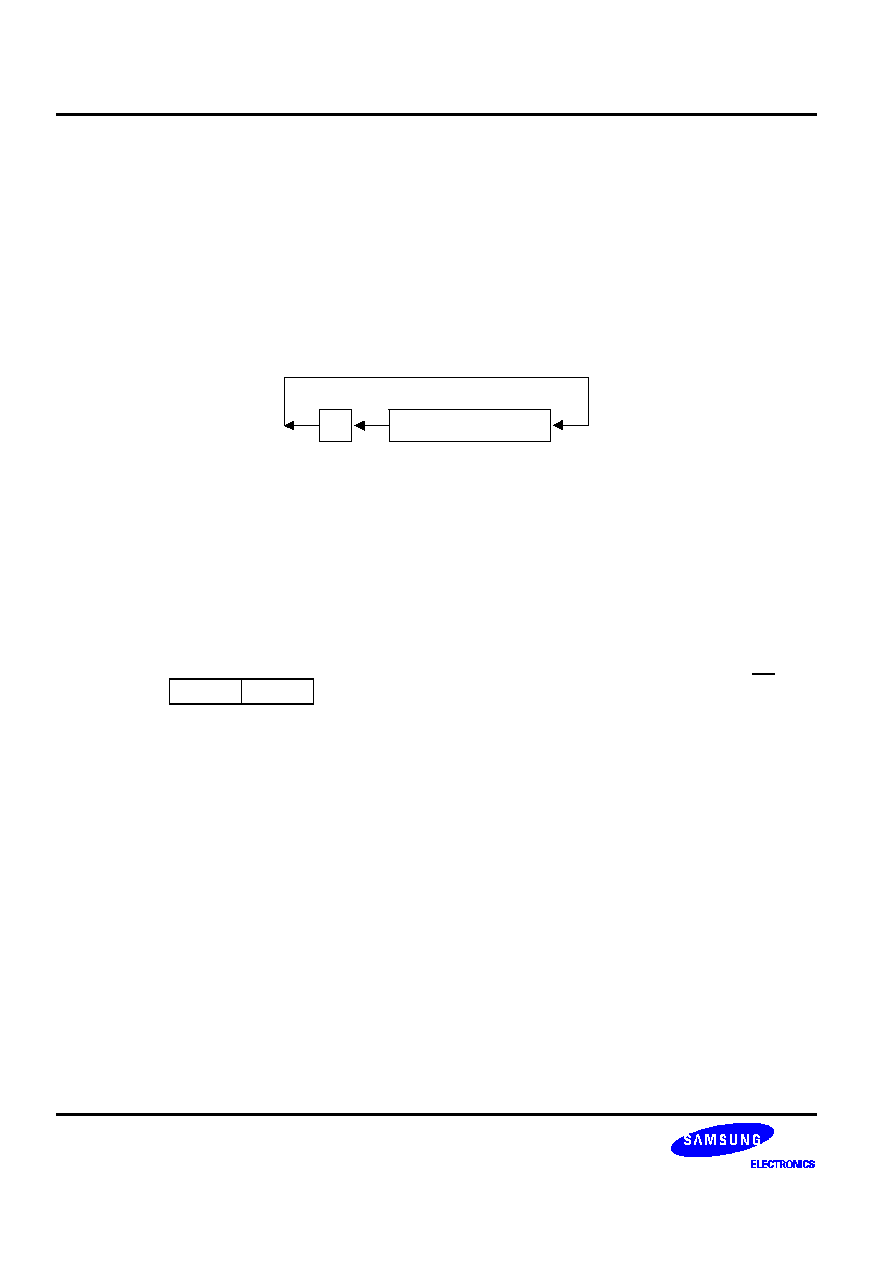
INSTRUCTION SET
S3C8639/C863A/P863A/C8647/F8647
6-72
RLC
--
Rotate Left Through Carry
RLC
dst
Operation:
dst (0)
C
C
dst (7)
dst (n + 1)
dst (n), n = 0≠6
The contents of the destination operand with the carry flag are rotated left one bit position. The
initial value of bit 7 replaces the carry flag (C); the initial value of the carry flag replaces bit zero.
7
0
C
Flags:
C: Set if the bit rotated from the most significant bit position (bit 7) was "1".
Z: Set if the result is "0"; cleared otherwise.
S: Set if the result bit 7 is set; cleared otherwise.
V: Set if arithmetic overflow occurred, that is, if the sign of the destination changed during
rotation; cleared otherwise.
D: Unaffected.
H: Unaffected.
Format:
Bytes
Cycles
Opcode
(Hex)
Addr Mode
dst
opc
dst
2
4
10
R
4
11
IR
Examples:
Given: Register 00H = 0AAH, register 01H = 02H, and register 02H = 17H, C = "0":
RLC
00H
Register 00H = 54H, C = "1"
RLC
@01H
Register 01H = 02H, register 02H = 2EH, C = "0"
In the first example, if general register 00H has the value 0AAH (10101010B), the statement
"RLC 00H" rotates 0AAH one bit position to the left. The initial value of bit 7 sets the carry flag
and the initial value of the C flag replaces bit zero of register 00H, leaving the value 55H
(01010101B). The MSB of register 00H resets the carry flag to "1" and sets the overflow flag.

S3C8639/C863A/P863A/C8647/F8647
INSTRUCTION SET
6-73
RR
--
Rotate Right
RR
dst
Operation:
C
dst (0)
dst (7)
dst (0)
dst (n)
dst (n + 1), n = 0≠6
The contents of the destination operand are rotated right one bit position. The initial value of bit
zero (LSB) is moved to bit 7 (MSB) and also replaces the carry flag (C).
7
0
C
Flags:
C: Set if the bit rotated from the least significant bit position (bit zero) was "1".
Z: Set if the result is "0"; cleared otherwise.
S: Set if the result bit 7 is set; cleared otherwise.
V: Set if arithmetic overflow occurred, that is, if the sign of the destination changed during
rotation; cleared otherwise.
D: Unaffected.
H: Unaffected.
Format:
Bytes
Cycles
Opcode
(Hex)
Addr Mode
dst
opc
dst
2
4
E0
R
4
E1
IR
Examples:
Given: Register 00H = 31H, register 01H = 02H, and register 02H = 17H:
RR
00H
Register 00H = 98H, C = "1"
RR
@01H
Register 01H = 02H, register 02H = 8BH, C = "1"
In the first example, if general register 00H contains the value 31H (00110001B), the statement
"RR 00H" rotates this value one bit position to the right. The initial value of bit zero is moved to
bit 7, leaving the new value 98H (10011000B) in the destination register. The initial bit zero also
resets the C flag to "1" and the sign flag and overflow flag are also set to "1".
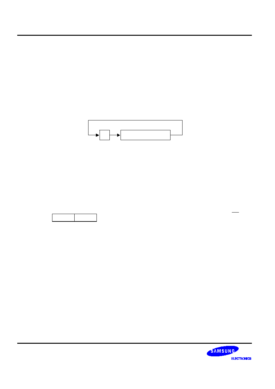
INSTRUCTION SET
S3C8639/C863A/P863A/C8647/F8647
6-74
RRC
--
Rotate Right Through Carry
RRC
dst
Operation:
dst (7)
C
C
dst (0)
dst (n)
dst (n + 1), n = 0≠6
The contents of the destination operand and the carry flag are rotated right one bit position. The
initial value of bit zero (LSB) replaces the carry flag; the initial value of the carry flag replaces bit
7 (MSB).
7
0
C
Flags:
C: Set if the bit rotated from the least significant bit position (bit zero) was "1".
Z: Set if the result is "0" cleared otherwise.
S: Set if the result bit 7 is set; cleared otherwise.
V: Set if arithmetic overflow occurred, that is, if the sign of the destination changed during
rotation; cleared otherwise.
D: Unaffected.
H: Unaffected.
Format:
Bytes
Cycles
Opcode
(Hex)
Addr Mode
dst
opc
dst
2
4
C0
R
4
C1
IR
Examples:
Given: Register 00H = 55H, register 01H = 02H, register 02H = 17H, and C = "0":
RRC
00H
Register 00H = 2AH, C = "1"
RRC
@01H
Register 01H = 02H, register 02H = 0BH, C = "1"
In the first example, if general register 00H contains the value 55H (01010101B), the statement
"RRC 00H" rotates this value one bit position to the right. The initial value of bit zero ("1")
replaces the carry flag and the initial value of the C flag ("1") replaces bit 7. This leaves the new
value 2AH (00101010B) in destination register 00H. The sign flag and overflow flag are both
cleared to "0".

S3C8639/C863A/P863A/C8647/F8647
INSTRUCTION SET
6-75
SB0
--
Select Bank 0
SB0
Operation:
BANK
0
The SB0 instruction clears the bank address flag in the FLAGS register (FLAGS.0) to logic zero,
selecting bank 0 register addressing in the set 1 area of the register file.
Flags:
No flags are affected.
Format:
Bytes
Cycles
Opcode
(Hex)
opc
1
4
4F
Example:
The statement
SB0
clears FLAGS.0 to "0", selecting bank 0 register addressing.

INSTRUCTION SET
S3C8639/C863A/P863A/C8647/F8647
6-76
SB1
--
Select Bank 1
SB1
Operation:
BANK
1
The SB1 instruction sets the bank address flag in the FLAGS register (FLAGS.0) to logic one,
selecting bank 1 register addressing in the set 1 area of the register file. (Bank 1 is not
implemented in some KS88-series microcontrollers.)
Flags:
No flags are affected.
Format:
Bytes
Cycles
Opcode
(Hex)
opc
1
4
5F
Example:
The statement
SB1
sets FLAGS.0 to "1", selecting bank 1 register addressing, if implemented.

S3C8639/C863A/P863A/C8647/F8647
INSTRUCTION SET
6-77
SBC
--
Subtract With Carry
SBC
dst,src
Operation:
dst
dst ≠ src ≠ c
The source operand, along with the current value of the carry flag, is subtracted from the
destination operand and the result is stored in the destination. The contents of the source are
unaffected. Subtraction is performed by adding the two's-complement of the source operand to
the destination operand. In multiple precision arithmetic, this instruction permits the carry
("borrow") from the subtraction of the low-order operands to be subtracted from the subtraction of
high-order operands.
Flags:
C: Set if a borrow occurred (src
>
dst); cleared otherwise.
Z: Set if the result is "0"; cleared otherwise.
S: Set if the result is negative; cleared otherwise.
V: Set if arithmetic overflow occurred, that is, if the operands were of opposite sign and the sign
of the result is the same as the sign of the source; cleared otherwise.
D: Always set to "1".
H: Cleared if there is a carry from the most significant bit of the low-order four bits of the result;
set otherwise, indicating a "borrow".
Format:
Bytes
Cycles
Opcode
(Hex)
Addr Mode
dst src
opc
dst | src
2
4
32
r
r
6
33
r
lr
opc
src
dst
3
6
34
R
R
6
35
R
IR
opc
dst
src
3
6
36
R
IM
Examples:
Given: R1 = 10H, R2 = 03H, C = "1", register 01H = 20H, register 02H = 03H, and
register 03H = 0AH:
SBC
R1,R2
R1 = 0CH, R2 = 03H
SBC
R1,@R2
R1 = 05H, R2 = 03H, register 03H = 0AH
SBC
01H,02H
Register 01H = 1CH, register 02H = 03H
SBC
01H,@02H
Register 01H = 15H,register 02H = 03H, register 03H = 0AH
SBC
01H,#8AH
Register 01H = 95H; C, S, and V = "1"
In the first example, if working register R1 contains the value 10H and register R2 the value 03H,
the statement "SBC R1,R2" subtracts the source value (03H) and the C flag value ("1") from the
destination (10H) and then stores the result (0CH) in register R1.

INSTRUCTION SET
S3C8639/C863A/P863A/C8647/F8647
6-78
SCF
--
Set Carry Flag
SCF
Operation:
C
1
The carry flag (C) is set to logic one, regardless of its previous value.
Flags:
C: Set to "1".
No other flags are affected.
Format:
Bytes
Cycles
Opcode
(Hex)
opc
1
4
DF
Example:
The statement
SCF
sets the carry flag to logic one.
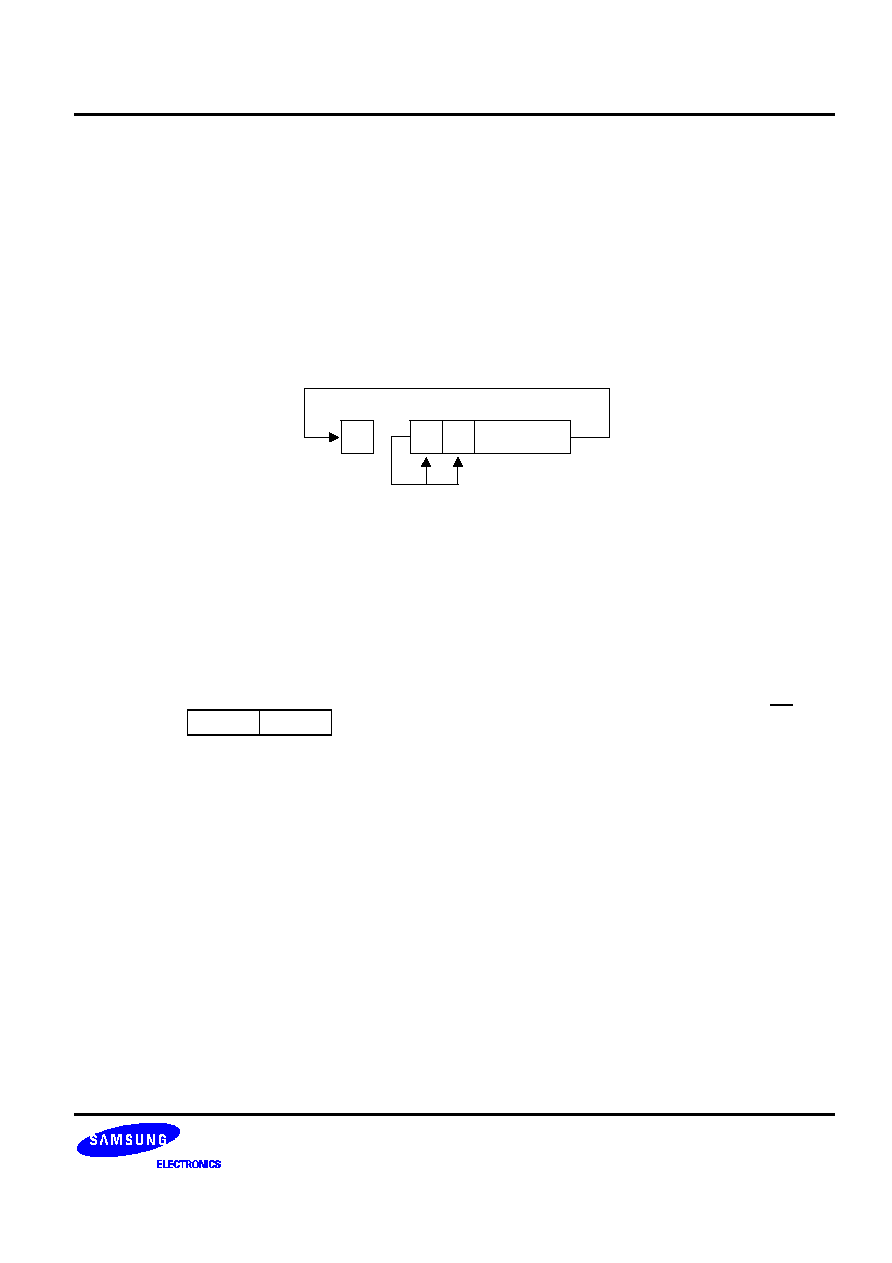
S3C8639/C863A/P863A/C8647/F8647
INSTRUCTION SET
6-79
SRA
--
Shift Right Arithmetic
SRA
dst
Operation:
dst (7)
dst (7)
C
dst (0)
dst (n)
dst (n + 1), n = 0≠6
An arithmetic shift-right of one bit position is performed on the destination operand. Bit zero (the
LSB) replaces the carry flag. The value of bit 7 (the sign bit) is unchanged and is shifted into bit
position 6.
7
0
C
6
Flags:
C: Set if the bit shifted from the LSB position (bit zero) was "1".
Z: Set if the result is "0"; cleared otherwise.
S: Set if the result is negative; cleared otherwise.
V: Always cleared to "0".
D: Unaffected.
H: Unaffected.
Format:
Bytes
Cycles
Opcode
(Hex)
Addr Mode
dst
opc
dst
2
4
D0
R
4
D1
IR
Examples:
Given: Register 00H = 9AH, register 02H = 03H, register 03H = 0BCH, and C = "1":
SRA
00H
Register 00H = 0CD, C = "0"
SRA
@02H
Register 02H = 03H, register 03H = 0DEH, C = "0"
In the first example, if general register 00H contains the value 9AH (10011010B), the statement
"SRA 00H" shifts the bit values in register 00H right one bit position. Bit zero ("0") clears the C
flag and bit 7 ("1") is then shifted into the bit 6 position (bit 7 remains unchanged). This leaves
the value 0CDH (11001101B) in destination register 00H.

INSTRUCTION SET
S3C8639/C863A/P863A/C8647/F8647
6-80
SRP/SRP0/SRP1
--
Set Register Pointer
SRP
src
SRP0
src
SRP1
src
Operation:
If src (1) = 1 and src (0) = 0 then: RP0 (3≠7)
src (3≠7)
If src (1) = 0 and src (0) = 1 then: RP1 (3≠7)
src (3≠7)
If src (1) = 0 and src (0) = 0 then: RP0 (4≠7)
src (4≠7),
RP0 (3)
0
RP1 (4≠7)
src (4≠7),
RP1 (3)
1
The source data bits one and zero (LSB) determine whether to write one or both of the register
pointers, RP0 and RP1. Bits 3≠7 of the selected register pointer are written unless both register
pointers are selected. RP0.3 is then cleared to logic zero and RP1.3 is set to logic one.
Flags:
No flags are affected.
Format:
Bytes
Cycles
Opcode
(Hex)
Addr Mode
src
opc
src
2
4
31
IM
Examples:
The statement
SRP #40H
sets register pointer 0 (RP0) at location 0D6H to 40H and register pointer 1 (RP1) at location
0D7H to 48H.
The statement "SRP0 #50H" sets RP0 to 50H, and the statement "SRP1 #68H" sets RP1 to
68H.

S3C8639/C863A/P863A/C8647/F8647
INSTRUCTION SET
6-81
STOP
--
Stop Operation
STOP
Operation:
The STOP instruction stops the both the CPU clock and system clock and causes the
microcontroller to enter Stop mode. During Stop mode, the contents of on-chip CPU registers,
peripheral registers, and I/O port control and data registers are retained. Stop mode can be
released by an external reset operation or by external interrupts. For the reset operation, the
RESET
pin must be held to Low level until the required oscillation stabilization interval has
elapsed.
Flags:
No flags are affected.
Format:
Bytes
Cycles
Opcode
(Hex)
Addr Mode
dst src
opc
1
4
7F
≠
≠
Example:
The statement
STOP
NOP
NOP
NOP
halts all microcontroller operations.
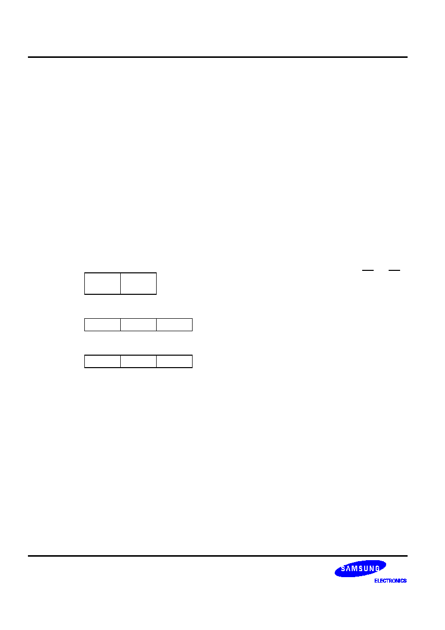
INSTRUCTION SET
S3C8639/C863A/P863A/C8647/F8647
6-82
SUB
--
Subtract
SUB
dst,src
Operation:
dst
dst ≠ src
The source operand is subtracted from the destination operand and the result is stored in the
destination. The contents of the source are unaffected. Subtraction is performed by adding the
two's complement of the source operand to the destination operand.
Flags:
C: Set if a "borrow" occurred; cleared otherwise.
Z: Set if the result is "0"; cleared otherwise.
S: Set if the result is negative; cleared otherwise.
V: Set if arithmetic overflow occurred, that is, if the operands were of opposite signs and the
sign of the result is of the same as the sign of the source operand; cleared otherwise.
D: Always set to "1".
H: Cleared if there is a carry from the most significant bit of the low-order four bits of the result;
set otherwise indicating a "borrow".
Format:
Bytes
Cycles
Opcode
(Hex)
Addr Mode
dst src
opc
dst |
src
2
4
22
r
r
6
23
r
lr
opc
src
dst
3
6
24
R
R
6
25
R
IR
opc
dst
src
3
6
26
R
IM
Examples:
Given: R1 = 12H, R2 = 03H, register 01H = 21H, register 02H = 03H, register 03H = 0AH:
SUB
R1,R2
R1 = 0FH, R2 = 03H
SUB
R1,@R2
R1 = 08H, R2 = 03H
SUB
01H,02H
Register 01H = 1EH, register 02H = 03H
SUB
01H,@02H
Register 01H = 17H, register 02H = 03H
SUB
01H,#90H
Register 01H = 91H; C, S, and V = "1"
SUB
01H,#65H
Register 01H = 0BCH; C and S = "1", V = "0"
In the first example, if working register R1 contains the value 12H and if register R2 contains the
value 03H, the statement "SUB R1,R2" subtracts the source value (03H) from the destination
value (12H) and stores the result (0FH) in destination register R1.

S3C8639/C863A/P863A/C8647/F8647
INSTRUCTION SET
6-83
SWAP
--
Swap Nibbles
SWAP
dst
Operation:
dst (0 ≠ 3)
dst (4 ≠ 7)
The contents of the lower four bits and upper four bits of the destination operand are swapped.
7
0
4 3
Flags:
C: Undefined.
Z: Set if the result is "0"; cleared otherwise.
S: Set if the result bit 7 is set; cleared otherwise.
V: Undefined.
D: Unaffected.
H: Unaffected.
Format:
Bytes
Cycles
Opcode
(Hex)
Addr Mode
dst
opc
dst
2
4
F0
R
4
F1
IR
Examples:
Given: Register 00H = 3EH, register 02H = 03H, and register 03H = 0A4H:
SWAP
00H
Register 00H = 0E3H
SWAP
@02H
Register 02H = 03H, register 03H = 4AH
In the first example, if general register 00H contains the value 3EH (00111110B), the statement
"SWAP 00H" swaps the lower and upper four bits (nibbles) in the 00H register, leaving the value
0E3H (11100011B).

INSTRUCTION SET
S3C8639/C863A/P863A/C8647/F8647
6-84
TCM
--
Test Complement Under Mask
TCM
dst,src
Operation:
(NOT dst) AND src
This instruction tests selected bits in the destination operand for a logic one value. The bits to be
tested are specified by setting a "1" bit in the corresponding position of the source operand
(mask). The TCM statement complements the destination operand, which is then ANDed with the
source mask. The zero (Z) flag can then be checked to determine the result. The destination and
source operands are unaffected.
Flags:
C: Unaffected.
Z: Set if the result is "0"; cleared otherwise.
S: Set if the result bit 7 is set; cleared otherwise.
V: Always cleared to "0".
D: Unaffected.
H: Unaffected.
Format:
Bytes
Cycles
Opcode
(Hex)
Addr Mode
dst src
opc
dst | src
2
4
62
r
r
6
63
r
lr
opc
src
dst
3
6
64
R
R
6
65
R
IR
opc
dst
src
3
6
66
R
IM
Examples:
Given: R0 = 0C7H, R1 = 02H, R2 = 12H, register 00H = 2BH, register 01H = 02H, and
register 02H = 23H:
TCM
R0,R1
R0 = 0C7H, R1 = 02H, Z = "1"
TCM
R0,@R1
R0 = 0C7H, R1 = 02H, register 02H = 23H, Z = "0"
TCM
00H,01H
Register 00H = 2BH, register 01H = 02H, Z = "1"
TCM
00H,@01H
Register 00H = 2BH, register 01H = 02H,
register 02H = 23H, Z = "1"
TCM
00H,#34
Register 00H = 2BH, Z = "0"
In the first example, if working register R0 contains the value 0C7H (11000111B) and register R1
the value 02H (00000010B), the statement "TCM R0,R1" tests bit one in the destination register
for a "1" value. Because the mask value corresponds to the test bit, the Z flag is set to logic one
and can be tested to determine the result of the TCM operation.
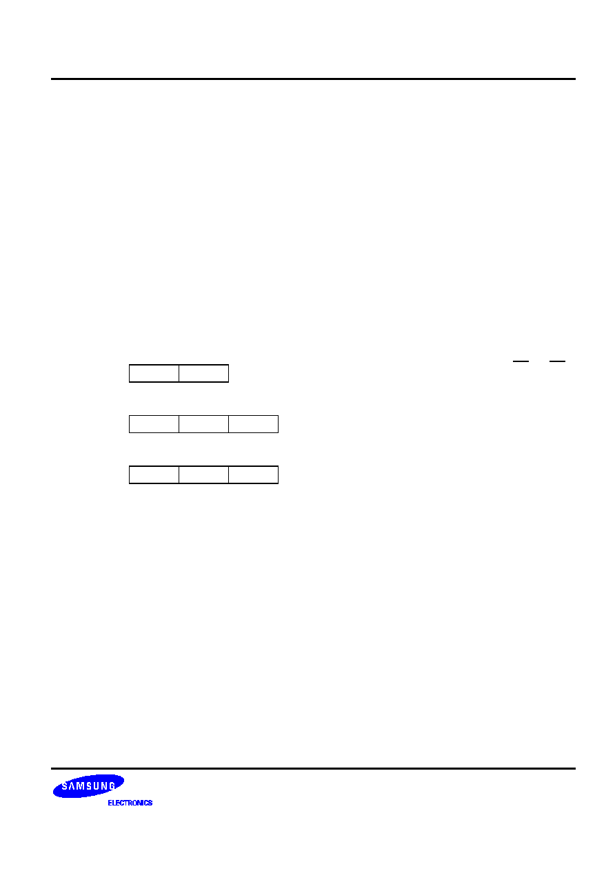
S3C8639/C863A/P863A/C8647/F8647
INSTRUCTION SET
6-85
TM
--
Test Under Mask
TM
dst,src
Operation:
dst AND src
This instruction tests selected bits in the destination operand for a logic zero value. The bits to be
tested are specified by setting a "1" bit in the corresponding position of the source operand
(mask), which is ANDed with the destination operand. The zero (Z) flag can then be checked to
determine the result. The destination and source operands are unaffected.
Flags:
C: Unaffected.
Z: Set if the result is "0"; cleared otherwise.
S: Set if the result bit 7 is set; cleared otherwise.
V: Always reset to "0".
D: Unaffected.
H: Unaffected.
Format:
Bytes
Cycles
Opcode
(Hex)
Addr Mode
dst src
opc
dst | src
2
4
72
r
r
6
73
r
lr
opc
src
dst
3
6
74
R
R
6
75
R
IR
opc
dst
src
3
6
76
R
IM
Examples:
Given: R0 = 0C7H, R1 = 02H, R2 = 18H, register 00H = 2BH, register 01H = 02H, and
register 02H = 23H:
TM
R0,R1
R0 = 0C7H, R1 = 02H, Z = "0"
TM
R0,@R1
R0 = 0C7H, R1 = 02H, register 02H = 23H, Z = "0"
TM
00H,01H
Register 00H = 2BH, register 01H = 02H, Z = "0"
TM
00H,@01H
Register 00H = 2BH, register 01H = 02H,
register 02H = 23H, Z = "0"
TM
00H,#54H
Register 00H = 2BH, Z = "1"
In the first example, if working register R0 contains the value 0C7H (11000111B) and register R1
the value 02H (00000010B), the statement "TM R0,R1" tests bit one in the destination register
for a "0" value. Because the mask value does not match the test bit, the Z flag is cleared to logic
zero and can be tested to determine the result of the TM operation.
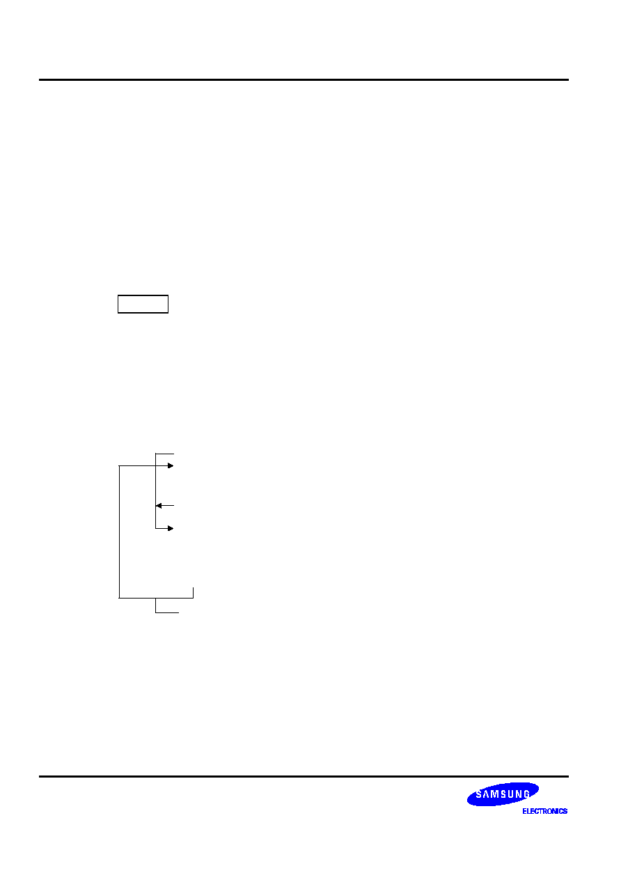
INSTRUCTION SET
S3C8639/C863A/P863A/C8647/F8647
6-86
WFI
--
Wait For Interrupt
WFI
Operation:
The CPU is effectively halted until an interrupt occurs, except that DMA transfers can still take
place during this wait state. The WFI status can be released by an internal interrupt, including a
fast interrupt .
Flags:
No flags are affected.
Format:
Bytes
Cycles
Opcode
(Hex)
opc
1
4n
3F
(
n = 1, 2, 3, ... )
Example:
The following sample program structure shows the sequence of operations that follow a "WFI"
statement:
EI
WFI
(Next instruction)
Main program
.
.
.
.
.
.
Interrupt occurs
Interrupt service routine
.
.
.
Clear interrupt flag
IRET
Service routine completed
(Enable global interrupt)
(Wait for interrupt)

S3C8639/C863A/P863A/C8647/F8647
INSTRUCTION SET
6-87
XOR
--
Logical Exclusive OR
XOR
dst,src
Operation:
dst
dst XOR src
The source operand is logically exclusive-ORed with the destination operand and the result is
stored in the destination. The exclusive-OR operation results in a "1" bit being stored whenever
the corresponding bits in the operands are different; otherwise, a "0" bit is stored.
Flags:
C: Unaffected.
Z: Set if the result is "0"; cleared otherwise.
S: Set if the result bit 7 is set; cleared otherwise.
V: Always reset to "0".
D: Unaffected.
H: Unaffected.
Format:
Bytes
Cycles
Opcode
(Hex)
Addr Mode
dst src
opc
dst | src
2
4
B2
r
r
6
B3
r
lr
opc
src
dst
3
6
B4
R
R
6
B5
R
IR
opc
dst
src
3
6
B6
R
IM
Examples:
Given: R0 = 0C7H, R1 = 02H, R2 = 18H, register 00H = 2BH, register 01H = 02H, and
register 02H = 23H:
XOR
R0,R1
R0 = 0C5H, R1 = 02H
XOR
R0,@R1
R0 = 0E4H, R1 = 02H, register 02H = 23H
XOR
00H,01H
Register 00H = 29H, register 01H = 02H
XOR
00H,@01H
Register 00H = 08H, register 01H = 02H, register 02H = 23H
XOR
00H,#54H
Register 00H = 7FH
In the first example, if working register R0 contains the value 0C7H and if register R1 contains
the value 02H, the statement "XOR R0,R1" logically exclusive-ORs the R1 value with the R0
value and stores the result (0C5H) in the destination register R0.

INSTRUCTION SET
S3C8639/C863A/P863A/C8647/F8647
6-88
NOTES

Clock Circuit
RESET
RESET
and Power-Down
I/O Ports
Basic Timer
Timer M0
Timer M1
Timer M2
Analog-to-Digital Converter
Pulse Width Modulation
Sync Processor
DDC and IIC-Bus Interface
Slave IIC-Bus Interface
Electrical Data
Mechanical Data
S3P863A OTP
Development Tools


S3C8639/C863A/P863A/C8647/F8647
CLOCK CIRCUIT
7-1
7
CLOCK CIRCUIT
OVERVIEW
The clock frequency generated for S3C8639/C863A/C8647 by an external crystal ranges from 8 MHz to 12 MHz.
The maximum CPU clock frequency is 12 MHz. The X
IN
and X
OUT
pins connect the external oscillator or clock
source to the on-chip clock circuit.
SYSTEM CLOCK CIRCUIT
The system clock circuit has the following components:
-- External crystal or ceramic resonator oscillation source (or an external clock source)
-- Oscillator stop and wake-up functions
-- Programmable frequency divider for the CPU clock (f
OSC
divided by 1, 2, 8, or 16)
-- System clock control register, CLKCON
S3C8639/C863A/C8647
X
IN
X
OUT
C1
C2
Figure 7-1. Main Oscillator Circuit
(External Crystal or Ceramic Resonator)

CLOCK CIRCUIT
S3C8639/C863A/P863A/C8647/F8647
7-2
CLOCK STATUS DURING POWER-DOWN MODES
The two power-down modes, Stop mode and Idle mode, affect the system clock as follows:
-- In Stop mode, the main oscillator is halted. Stop mode is released and the oscillator is started by a reset
operation or an external interrupt (with RC delay noise filter).
-- In Idle mode, the internal clock signal is gated to the CPU, but not to interrupt structure, timers and timer/
counters, and the IIC-bus interface functions. Idle mode is released by a reset or by an external or internal
interrupt.
Main
OSC
Noise
Filter
Oscillator
Wake-up
Oscillator
Stop
CLKCON.7
INT Pin
(1)
STOPCON
NOTES:
1. An external interrupt (with RC-delay noise filter) can be used
to release Stop mode and "wake up" the main oscillator.
In S3C8639/C863A/C8647, the P0.0-P0.2 and external
interrupts are of this type.
2. For S3C8639/C863A/C8647, the CLKCON signature code
(CLKCON.0-CLKCON.2) should not be '101B' (because no
subsystem clock is implemented).
CLKCON.3,.4
1/2
1/8
1/16
M
U
X
CLKCON.0-.2
3-Bit Signature Code
(2)
M
U
X
CPU Clock
CLKCON.5,.6
Stop Instruction
Figure 7-2. System Clock Circuit Diagram

S3C8639/C863A/P863A/C8647/F8647
CLOCK CIRCUIT
7-3
SYSTEM CLOCK CONTROL REGISTER (CLKCON)
The system clock control register, CLKCON, is located in set 1, address D4H. It is read/write addressable and has
the following functions:
-- Oscillator IRQ wake-up function enable/disable
-- Main oscillator stop control
-- Oscillator frequency divide-by value
-- System clock signal selection
The CLKCON register controls whether or not an external interrupt can be used to trigger a power down mode
release. (This is called the "IRQ wake-up" function.) The IRQ wake-up enable bit is CLKCON.7.
After a reset, the external interrupt oscillator wake-up function is enabled, the main oscillator is activated, and the
f
OSC
/16 (the slowest clock speed) is selected as the CPU clock. If necessary, you can raise the CPU clock
speed to f
OSC
, f
OSC
/2, or f
OSC
/8.
For the S3C8639/C863A/C8647 microcontrollers, the CLKCON.2≠CLKCON.0 system clock signature code must
be any value other than "101B". (The "101B" setting is invalid because a subsystem clock is not implemented.)
The reset value for the clock signature code is "000B" and should remain so during the normal operation.
System clock selection bits:
101B = Invalid selection
Others = Normal operating mode
LSB
MSB
System Clock Control Register (CLKCON)
D4H, Set 1, R/W
.7
.6
.5
.4
.3
.2
.1
.0
Divide-by selection bits for CPU clock frequency:
00 = f
OSC
/16
01 = f
OSC
/8
10 = f
OSC
/2
11 = f
OSC
(non-divided)
Main oscillator stop control bits:
00 = No effect
01 = No effect
10 = stop main oscillator
11 = No effect
Oscillator IRQ wake-up enable bit:
0 = Enable IRQ for main system oscillator
wake-up function in power down mode
1 = Disable IRQ for main system oscillator
wake-up function in power down mode
Figure 7-3. System Clock Control Register (CLKCON)

CLOCK CIRCUIT
S3C8639/C863A/P863A/C8647/F8647
7-4
NOTES

S3C8639/C863A/P863A/C8647/F8647
RESET
RESET
and POWER-DOWN
8-1
8
RESET
RESET
and POWER-DOWN
SYSTEM RESET
OVERVIEW
During a power-on reset, the voltage at V
DD
goes to High level and the
RESET
pin is forced to Low level.
The
RESET
signal is input through a schmitt trigger circuit where it is then synchronized with the CPU clock.
This procedure brings S3C8639/C863A/C8647 into a known operating status.
To spare time for internal CPU clock oscillation to stabilize, the
RESET
pin must be held to Low level for a
minimum time interval after the power supply comes within tolerance. The minimum required time for oscillation
stabilization in a reset operation is 1 millisecond.
Whenever a reset occurs during the normal operation (that is, when both V
DD
and
RESET
are at High level), the
RESET
pin is forced Low and the reset operation starts. All system and peripheral control registers are then reset
to their default hardware values (see Tables 8-1, 8-2, and 8-3).
In summary, the following sequence of events occurs during a reset operation:
-- All interrupts are disabled.
-- The watchdog function (basic timer) is enabled.
-- Ports 0≠3 are set to input mode.
-- Peripheral control and data registers are disabled and reset to their default hardware values.
-- The program counter (PC) is loaded with the program reset address in the ROM, 0100H.
-- When the programmed oscillation stabilization time interval has elapsed, the instruction stored in the ROM
location 0100H (and 0101H) is fetched and executed.
NOTE
To program the duration of the oscillation stabilization interval, you should make the settings appropriate
to the basic timer control register, BTCON, before entering Stop mode. Also, if you do not want to use
the basic timer watchdog function (which causes a system reset if a basic timer counter overflow occurs),
you can disable it by writing "1010B" to the upper nibble of BTCON.

RESET
RESET
and POWER-DOWN
S3C8639/C863A/P863A/C8647/F8647
8-2
HARDWARE RESET VALUES
Tables 8-1, 8-2, and 8-3 list the reset values for CPU and system registers, peripheral control registers, and
peripheral data registers after a reset operation. The following notation is used to represent reset values:
-- A "1" or a "0" shows the reset bit value as logic one or logic zero, respectively.
-- An "x" means that the bit value is undefined after a reset.
-- A dash ("≠") means that the bit is either not used or not mapped.
Table 8-1. Set 1 Register Values After Reset
Register Name
Mnemonic
Address
Bit Values After Reset
Dec
Hex
7
6
5
4
3
2
1
0
Timer M0 counter register
TM0CNT
208
D0H
0
0
0
0
0
0
0
0
Timer M0 data register
TM0DATA
209
D1H
0
0
0
0
0
0
0
0
Timer M0 control register
TM0CON
210
D2H
0
0
0
0
0
0
0
0
Basic timer control register
BTCON
211
D3H
0
0
0
0
0
0
0
0
Clock control register
CLKCON
212
D4H
0
0
0
0
0
0
0
0
System flags register
FLAGS
213
D5H
x
x
x
x
x
x
0
0
Register pointer 0
RP0
214
D6H
1
1
0
0
0
≠
≠
≠
Register pointer 1
RP1
215
D7H
1
1
0
0
1
≠
≠
≠
Stack pointer (high byte)
SPH
216
D8H
x
x
x
x
x
x
x
x
Stack pointer (low byte)
SPL
217
D9H
x
x
x
x
x
x
x
x
Instruction pointer (high byte)
IPH
218
DAH
x
x
x
x
x
x
x
x
Instruction pointer (low byte)
IPL
219
DBH
x
x
x
x
x
x
x
x
Interrupt request register
IRQ
220
DCH
0
0
0
0
0
0
0
0
Interrupt mask register
IMR
221
DDH
x
x
x
x
x
x
x
x
System mode register
SYM
222
DEH
0
≠
≠
x
x
x
0
0
Page pointer register
PP
223
DFH
0
0
0
0
0
0
0
0
NOTES:
1.
As the SYM register is not used for S3C8639/C863A/C8647, SYM.5 should always be "0". If you accidentally
write a "1" to this bit during the normal operation, a system malfunction may occur.
2.
Except for TM0CNT, TMODATA, and IRQ, all registers in set 1 are read/write addressable.
3.
You cannot use a read-only register as a destination field for the instructions OR, AND, LD, and LDB. The read-only
registers in the S3C8639/C863A/C8647 register file are: TM0CNT, TM0DATA, IRQ, SYNCRD, TM1CNTH, TM1CNTL,
TM1DATAH, TM1DATAL, ADDATA, BTCNT, PWMCNT, and RBDR.
4.
Interrupt pending flags that must be cleared by software are noted by shaded table cells.
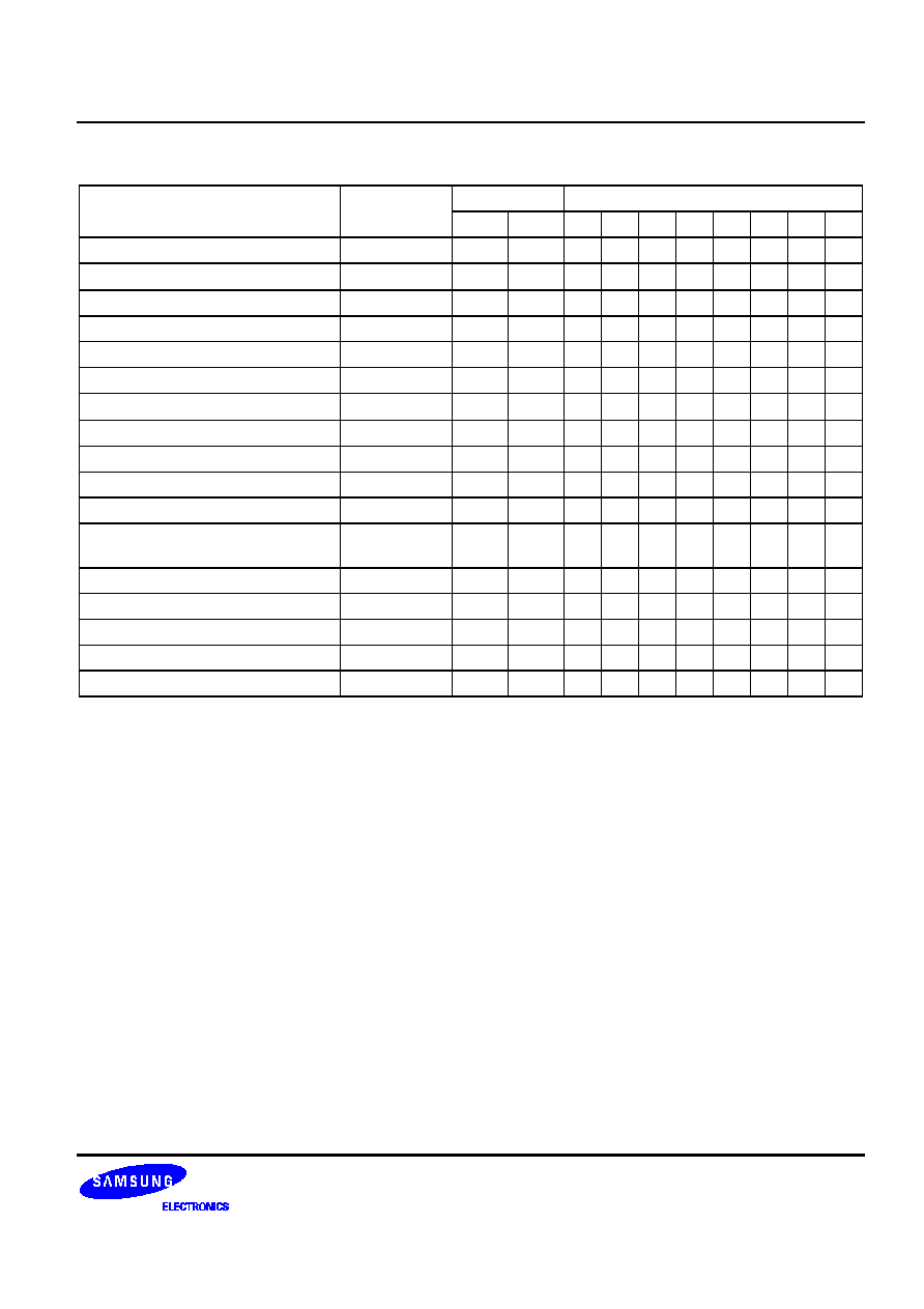
S3C8639/C863A/P863A/C8647/F8647
RESET
RESET
and POWER-DOWN
8-3
Table 8-2. Set 1, Bank 0 Register Values after Reset
Register Name
Mnemonic
Address
Bit Values After Reset
Dec
Hex
7
6
5
4
3
2
1
0
Port 0 data register
P0
224
E0H
0
0
0
0
0
0
0
0
Port 1 data register
(note)
P1
225
E1H
≠
≠
≠
≠
≠
0
0
0
Port 2 data register
P2
226
E2H
0
0
0
0
0
0
0
0
Port 3 data register
P3
227
E3H
0
0
0
0
0
0
0
0
Port 0 control register (high byte)
P0CONH
228
E4H
0
0
0
0
0
0
0
0
Port 0 control register (low byte)
P0CONL
229
E5H
0
0
0
0
0
0
0
0
Port 1 control register
(note)
P1CON
230
E6H
≠
≠
0
0
0
0
0
0
Port 2 control register (high byte)
P2CONH
231
E7H
0
0
0
0
0
0
0
0
Port 2 control register (low byte)
P2CONL
232
E8H
0
0
0
0
0
0
0
0
Port 3 control register (high byte)
P3CONH
233
E9H
0
0
0
0
0
0
0
0
Port 3 control register (low byte)
P3CONL
234
EAH
0
0
0
0
0
0
0
0
Port 0 external interrupt control
register
P0INT
235
EBH
≠
0
0
0
≠
0
0
0
Watchdog time control register
WDTCON
236
ECH
≠
≠
≠
≠
0
0
0
0
Sync control register 0
SYNCON0
237
EDH
0
0
0
0
0
0
0
0
Sync control register 1
SYNCON1
238
EEH
0
0
0
0
0
0
0
0
Sync control register 2
SYNCON2
239
EFH
0
0
0
0
0
0
0
0
Sync port read data register
SYNCRD
240
F0H
≠
≠
≠
≠
0
0
0
0
NOTE: Not used for the S3C8647.

RESET
RESET
and POWER-DOWN
S3C8639/C863A/P863A/C8647/F8647
8-4
Table 8-2. Set 1, Bank 0 Register Values after Reset (Continued)
Register Name
Mnemonic
Address
Bit Values After Reset
Dec
Hex
7
6
5
4
3
2
1
0
Timer M1 counter register high
TM1CNTH
241
F1H
≠
≠
≠
≠
0
0
0
0
Timer M1 counter register low
TM1CNTL
242
F2H
0
0
0
0
0
0
0
0
Timer M1 data register high
TM1DATAH
243
F3H
≠
≠
≠
≠
0
0
0
0
Timer M1 data register low
TM1DATAL
244
F4H
0
0
0
0
0
0
0
0
Timer M1 control register
TM1CON
245
F5H
0
0
0
0
0
0
0
0
Timer M2 control register
TM2CON
246
F6H
1
1
1
1
1
0
0
0
A/D converter control register
ADCON
247
F7H
≠
0
0
0
0
0
0
0
A/D converter data register
ADDATA
248
F8H
x
x
x
x
x
(4)
x
(4)
x
(4)
x
(4)
Pseudo Hsync generation register
PHGEN
249
F9H
0
1
0
1
0
0
1
1
Pseudo Vsync generation register
PVGEN
250
FAH
0
1
0
1
0
0
1
1
Stop control register
STOPCON
251
FBH
0
0
0
0
0
0
0
0
Location FCH is not mapped.
Basic timer counter register
BTCNT
253
FDH
0
0
0
0
0
0
0
0
External memory timing register
EMT
254
FEH
0
1
1
1
1
1
0
≠
Interrupt priority register
IPR
255
FFH
x
x
x
x
x
x
x
x
NOTES:
1.
Except for SYNCRD, TM1CNTH, TM1CNTL, TM1DATAH, TM1DATAL, ADDATA, and BTCNT, all registers in set 1,
bank 0 are read/write addressable.
2.
You cannot use a read-only register as a destination field for the instructions OR, AND, LD, and LDB. The read-only
registers in the S3C8639/C863A/C8647 register file are: TM0CNT, TM0DATA, IRQ, SYNCRD, TM1CNTH, TM1CNTL,
TM1DATAH, TM1DATAL, ADDATA, BTCNT, PWMCNT, and RBDR.
3.
Interrupt pending flags that must be cleared by software are noted by shaded table cells.
4.
Not mapped for the S3C8647.

S3C8639/C863A/P863A/C8647/F8647
RESET
RESET
and POWER-DOWN
8-5
Table 8-3. Set 1, Bank 1 Register Values after Reset
Register Name
Mnemonic
Address
Bit Values After Reset
Dec
Hex
7
6
5
4
3
2
1
0
PWM 0 data register
PWM0
224
E0H
0
0
0
0
0
0
0
0
PWM 1 data register
PWM1
225
E1H
0
0
0
0
0
0
0
0
PWM 2 data register
PWM2
226
E2H
0
0
0
0
0
0
0
0
PWM 3 data register
PWM3
227
E3H
0
0
0
0
0
0
0
0
PWM 4 data register
PWM4
228
E4H
0
0
0
0
0
0
0
0
PWM 5 data register
PWM5
229
E5H
0
0
0
0
0
0
0
0
PWM 6 data register
(4)
PWM6
230
E6H
0
0
0
0
0
0
0
0
PWM control register
PWMCON
231
E7H
0
0
0
≠
≠
≠
≠
≠
PWM counter register
PWMCNT
232
E8H
0
0
0
0
0
0
0
0
DDC control register
DCON
233
E9H
≠
≠
≠
≠
1
0
0
0
DDC address register 0
DAR0
234
EAH
1
0
1
0
≠
≠
≠
≠
DDC clock control register
DCCR
235
EBH
0
0
0
0
1
1
1
1
DDC control/status register 0
DCSR0
236
ECH
0
0
0
0
0
0
≠
0
DDC control/status register 1
DCSR1
237
EDH
≠
≠
≠
≠
≠
0
1
0
DDC address register 1
DAR1
238
EEH
x
x
x
x
x
x
x
≠
Transmit prebuffer data register
TBDR
239
EFH
x
x
x
x
x
x
x
x
Receive prebuffer data register
RBDR
240
F0H
x
x
x
x
x
x
x
x
DDC data shift register
DDSR
241
F1H
x
x
x
x
x
x
x
x
Slave IIC-bus control/status register
(4)
SICSR
242
F2H
0
0
0
0
0
0
0
0
Slave IIC-bus address register
(4)
SIAR
243
F3H
x
x
x
x
x
x
x
≠
Slave IIC-bus data shift register
(4)
SIDSR
244
F4H
x
x
x
x
x
x
x
x
Locations F5H≠FFH are not mapped.
NOTES:
1.
Except for PWMCNT and RBDR, all registers in set 1, bank 1 are read/write addressable.
2.
You cannot use a read-only register as a destination field for the instructions OR, AND, LD, and LDB. The read-only
registers in the S3C8639/C863A/C8647 register file are: TM0CNT, TM0DATA, IRQ, SYNCRD, TM1CNTH, TM1CNTL,
TM1DATAH, TM1DATAL, ADDATA, BTCNT, PWMCNT, and RBDR.
3.
Interrupt pending flags that must be cleared by software are noted by shaded table cells.
4.
Not used for the S3C8647.

RESET
RESET
and POWER-DOWN
S3C8639/C863A/P863A/C8647/F8647
8-6
POWER-DOWN MODES
STOP MODE
Stop mode is invoked by the instruction STOP (opcode 7FH) and the stop control register (STOPCON). In Stop
mode, the operation of the CPU and all peripherals is halted. That is, the on-chip main oscillator stops and the
supply current is reduced to less than 5
µ
A. All system functions stop when the clock "freezes," but data stored in
the internal register file is retained. Stop mode can be released in one of two ways: by a reset or by an external
interrupt (with RC delay).
NOTE
Do not use stop mode if you are using an external clock source as X
IN
input must be restricted internally
to V
SS
to reduce current leakage.
Using
RESET
RESET
to Release Stop Mode
Stop mode is released when the
RESET
signal goes active (High level): all system and peripheral control
registers are reset to their default hardware values and the contents of all data registers are retained. A reset
operation automatically selects a slow clock (1/16) because CLKCON.3 and CLKCON.4 are cleared to "00B".
After the programmed oscillation stabilization interval has elapsed, the CPU starts the system initialization
routine by fetching the program instruction stored in the ROM location 0100H (and 0101H).
Using an External Interrupt to Release Stop Mode
Only external interrupts with an RC-delay noise filter circuit can be used to release Stop mode. Which interrupt
you can use to release Stop mode in a given situation depends on the microcontroller's current internal operating
mode. The external interrupts in the S3C8639/C863A/C8647 interrupt structure that can be used to release Stop
mode are:
-- External interrupts P0.0 (INT0), P0.1 (INT1), and P0.2 (INT2)
-- Timer M0 capture interrupt in capture mode (with rising or falling edge trigger at the TM0CAP pin and
Vsync-O from sync-processor.)
Please note the following conditions for Stop mode release:
-- If you release Stop mode using an external interrupt, the current values in system and peripheral control
registers are unchanged.
-- If you use an external interrupt for Stop mode release, you can also program the duration of the oscillation
stabilization interval. To do this, you must make the control and clock settings appropriate before entering
Stop mode.
-- If you use an interrupt to release Stop mode, the CLKCON.4 and CLKCON.3 bit-pair setting remains
unchanged and the currently selected clock value is used.
-- The external interrupt is serviced when the Stop mode release occurs. Following the IRET from the service
routine, the instruction right next to the one that initiated Stop mode is executed.

S3C8639/C863A/P863A/C8647/F8647
RESET
RESET
and POWER-DOWN
8-7
IDLE MODE
Idle mode is invoked by the instruction IDLE (opcode 6FH). In Idle mode, CPU operations are halted while some
peripherals remain active. In idle mode, the internal clock signal is gated away from the CPU, but all peripherals
timers remain active. Port pins retain the mode (input or output) they had at the time Idle mode was entered.
There are two ways to release idle mode:
1.
Execute a reset. All system and peripheral control registers are reset to their default values and the contents
of all data registers are retained. The reset automatically selects a slow clock (1/16) because CLKCON.4 and
CLKCON.3 are cleared to "00B". If interrupts are masked, a reset is the only way to release Idle mode.
2.
Activate any enabled interrupt, causing Idle mode to be released. When you use an interrupt to release Idle
mode, the CLKCON.4 and CLKCON.3 register values remain unchanged, and the currently selected clock
value is used. The interrupt is then serviced. When the return-from-interrupt (IRET) occurs, the instruction
right next to the one that initiated Idle mode is executed.
NOTE
Only external interrupts can be used to release Stop mode. To release idle mode, you can use either an
internally-generated or externally-generated interrupt.

RESET
RESET
and POWER-DOWN
S3C8639/C863A/P863A/C8647/F8647
8-8
F
F
PROGRAMMING TIP -- Sample S3C8639/C863A/C8647 Initialization Routine
The following sample program shows you how to make initial settings for the S3C8639/C863A/C8647 address
space, interrupt vectors, and peripheral functions. Program comments guide you through the steps:
;
<< Base Number Setting >>
DECIMAL
;
<< Definition >>
TM0_REG
EQU
40H
ORG
0000H
;
<< Interrupt Vector Addresses >>
ORG
00ECH
VECTOR
TM0_OVF_INT
; IRQ0
VECTOR
TM0_CAP_INT
; IRQ0
VECTOR
TM2 _INT
; IRQ1
VECTOR
TM1_OVF_INT
; IRQ2
VECTOR
TM1_CAP_INT
; IRQ2
VECTOR
DDC_INT
; IRQ3
VECTOR
P00_INT
; IRQ4
VECTOR
P01_INT
; IRQ5
VECTOR
P02_INT
; IRQ6
VECTOR
SIIC_INT
; IRQ7 (used only S3C863X)
;
<< Initialize System and Peripherals >>
ORG
0100H
; Reset address
LD
BTCON,#0A0H
; Disable watchdog timer
LD
CLKCON,#10H
; Select divided-by-two oscillator frequency as CPU clock
; Enable IRQ for main system oscillator wake-up
;
< System Register Settings >
CLR
SYM
; Disable fast interrupts; global interrupt disable
CLR
EMT
; No access wait time; select internal stack area
LD
SPH,#00H
; Set stack pointer (stack starts from #0FFH)
;
< Interrupt Settings >
LD
IPR,#8FH
; Set interrupt priorities as follows:
; IRQ3 > IRQ2 > IRQ1 > IRQ0
LD
IMR,#0FH
; Enable IRQ levels 0, 1, 2, and 3
;
< Timer M0 Settings >
LD
TM0CON,#8FH
; Enable timer M0 overflow and capture interrupts

S3C8639/C863A/P863A/C8647/F8647
RESET
RESET
and POWER-DOWN
8-9
F
F
PROGRAMMING TIP -- Sample S3C8639/C863A/C8647 Initialization Routine (Continued)
INI_PERI_SET:
SB0
; Select bank 0
LD
P0CONH,#0FFH
; Set port 0 high byte to push-pull output mode
LD
P0CONL,#0FFH
; Set port 0 low byte to push-pull output mode
LD
P0INT,#00H
; Disable P0.0, P0.1 and P0.2 external interrupts
;
LD
P1CON,#00H
; Set P1.0≠P1.2 to input mode
LD
P2CONH,#0FFH
; Set port 2 high byte to n-channel open-drain PWM
; output mode
LD
P2CONL,#0FFH
; Set port 2 low byte to push-pull PWM output mode
LD
P3CONH,#0AAH
; Set port 3 high byte to push-pull output mode
LD
P3CONL,#0AAH
; Set port 3 low byte to push-pull output mode
;
< Timer M1 Settings >
LD
TM1CON,#2CH
; Enable timer M1 capture and overflow interrupt,
Timer M1
; clock source is HsyncI from sync processor
;
< Timer M2 Settings >
LD
TM2CON,#3DH
; Enable timer M2 capture and overflow interrupt
;
< Sync Processor Settings >
LD
SYNCON0,#20H
; 5 bit counter capture mode
LD
SYNCON1,#80H
; Set negative polarity (500 ns at 8 MHz) for clampO
LD
SYNCON2,#0A0H
; Pseudo sync output
;
< PWM Settings >
SB1
; Select Bank 1
LD
PWMCON,#20H
; Start PWM counter, PWM counter clock is f
OSC
;
< DDC Tx/Rx Interface Settings >
LD
DCON,#0AH
; Select DDC1 Tx mode
LD
DCCR,#0A3H
; Enable DDC interrupt, DDC clock is 100 kHz
;
<< Initialize Data Registers >>
SB0
; Select bank 0
SRP
#0C0H
; Set register pointer
;
< Clear all data registers from 00H to FFH >
LD
R0,#0FFH
; Enable timer M2 interrupt
RAMCLR:
CLR
@R0
; Page 0 RAM clear
DJNZ
R0,RAMCLR

RESET
RESET
and POWER-DOWN
S3C8639/C863A/P863A/C8647/F8647
8-10
F
F
PROGRAMMING TIP -- Sample S3C8639/C863A/C8647 Initialization Routine (Continued)
;
< Initialize Other Registers >
∑
∑
EI
; You must execute an EI instruction in this position
; in the initialization routine to enable servicing of
; external interrupts
;
<< Main Loop >>
MAIN:
NOP
; Start main loop
∑
∑
CALL
KEY_SCAN
; Sub-program module
∑
∑
CALL
LED_DISPLAY
; Sub-program module
∑
∑
CALL
JOB
; Sub-program module
∑
∑
JR
t,MAIN
; For main loop
;
< Subroutines >
KEY_SCAN:
NOP
∑
∑
∑
RET
LED_DISPLAY:
NOP
∑
∑
∑
RET
JOB:
NOP
∑
∑
∑
RET

S3C8639/C863A/P863A/C8647/F8647
RESET
RESET
and POWER-DOWN
8-11
F
F
PROGRAMMING TIP -- Sample S3C8639/C863A/C8647 Initialization Routine (Concluded)
;
<< Interrupt Service Routines >>
P00_INT:
PUSH
RP0
; Save old RP0 value
SRP0
#60H
; Set RP0 for P0.0 interrupt service routine
∑
∑
∑
POP
RP0
; Restore the RP0 value
IRET
; Return from the interrupt
DDC_INT:
PUSH
RP0
; Save old RP0 value
SRP0
#50H
; Set RP0 for IIC-bus interrupt service routine
∑
∑
∑
SB1
AND
DDCR, #11101111B
; Clear DDC interrupt pending bit
SB0
POP
RP0
; Restore the RP0 value
IRET
; Return from the interrupt
TM0_CAP_INT:
PUSH
RP0
; Save old RP0 value
SRP
#TM0_REG
; TM0_REG value should be defined
∑
∑
∑
POP
RP0
; Restore the RP0 value
IRET
; Return from the interrupt
∑
∑
∑
END

RESET
RESET
and POWER-DOWN
S3C8639/C863A/P863A/C8647/F8647
8-12
NOTES
S3C8639/C863A/P863A/C8647/F8647
I/O PORTS
9-1
9
I/O PORTS
OVERVIEW
The S3C8639/C863A/C8647 microcontrollers have four I/O ports with a total of 27 pins. And the S3C8647
microcontroller has three I/O port 0 with a total of 19 pins. Each port can be flexibly configured to meet
application design requirements. The CPU accesses ports by directly writing or reading port registers. No special
I/O instructions are required. Table 9-1 gives you an overview of port functions:
Table 9-1. S3C8639/C863A/C8647 Port Configuration Overview
Port
Configuration Options
Programmability
0
8-bit general I/O port. Alternatively used for external interrupt inputs
and for timer M0 input function.
Bit programmable
1
(Only S3C863X)
3-bit I/O port for normal I/O or n-channel open drain output.
Alternatively used for IIC-bus clock and data I/O.
Bit programmable
2
8-bit I/O port for normal I/O, PWM push-pull outputs, PWM n-channel
open-drain outputs with 5-volt load capability, or Csync signal input.
Bit programmable
3
8-bit general I/O port. Alternatively used as n-channel open-drain,
push-pull outputs with 5-volt load capability or for normal input with
pull-up resistor. Multiplexed for alternative use as A/D converter
inputs, AD0≠AD3.
Bit programmable
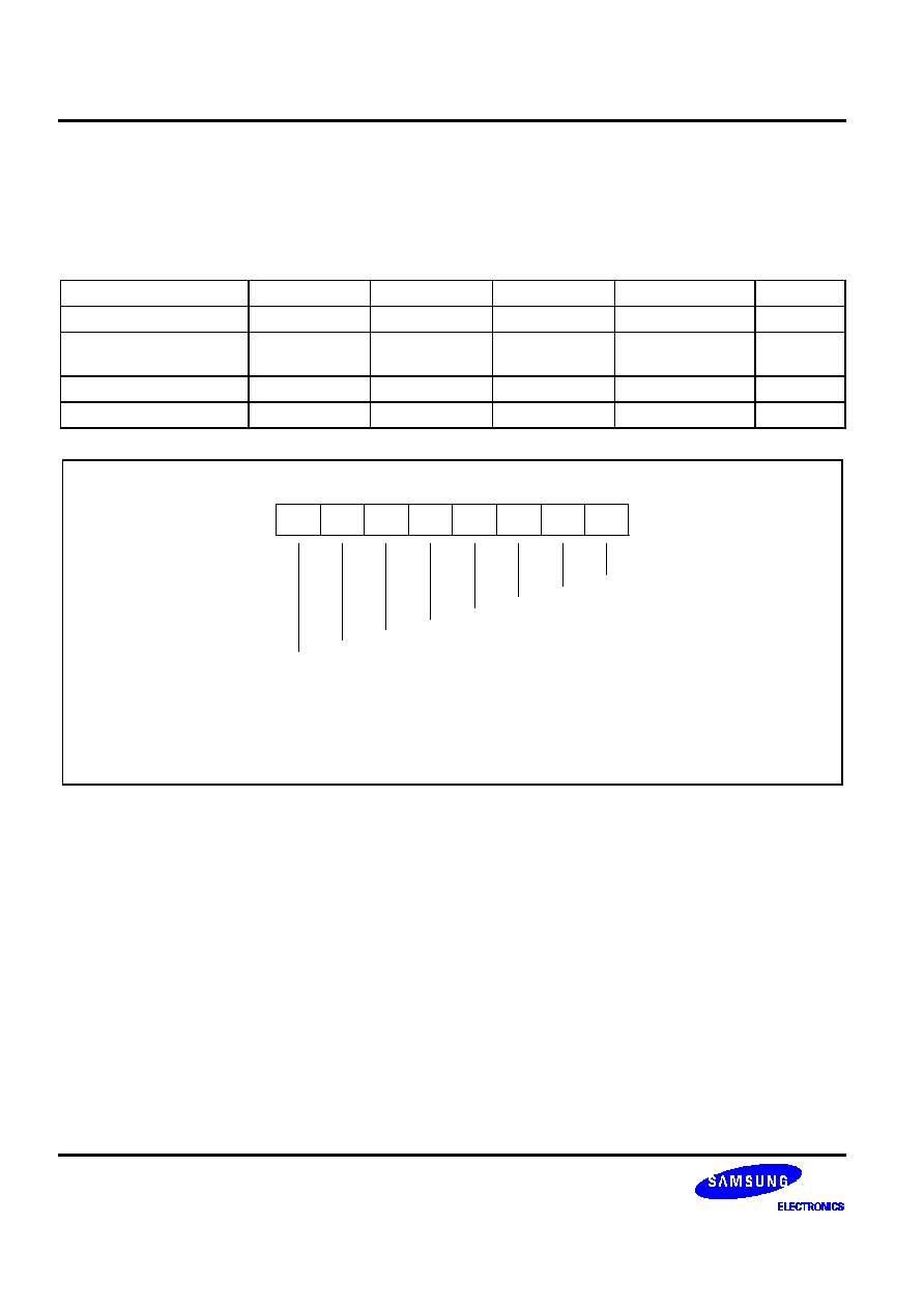
I/O PORTS
S3C8639/C863A/P863A/C8647/F8647
9-2
PORT DATA REGISTERS
Data registers for ports 0≠3 have the format shown in Figure 9-1. Table 9-2 gives you an overview of the port
data register locations:
Table 9-2. Port Data Register Summary
Register Name
Mnemonic
Decimal
Hex
Location
R/W
Port 0 data register
P0
224
E0H
Set 1, bank 0
R/W
Port 1 data register
(only S3C863X)
P1
225
E1H
Set 1, bank 0
R/W
Port 2 data register
P2
226
E2H
Set 1, bank 0
R/W
Port 3 data register
P3
227
E3H
Set 1, bank 0
R/W
Pn.4
Pn.3
I/O Port Data Register Format (n = 0-3)
.7
.6
.5
.4
.3
.2
.1
.0
MSB
LSB
Pn.1
Pn.2
Pn.5
Pn.6
Pn.7
Pn.0
NOTE:
Port 1 is a 3-bit port. Only bits P1.2-P1.0 of
the port 1 data register are mapped. All the
other S3C8639/C863A I/O ports are 8-bit.
Figure 9-1. Port Data Register Format
PORT 0
Port 0 is an 8-bit I/O port with individually configurable pins. You can directly access port 0 pins by writing or
reading the port 0 data register, P0 (set 1, bank 0, E0H). You can use port 0 for general I/O, or for the following
alternative functions:
-- Low-byte pins (P0.3≠P0.0) can be configured as push-pull outputs, while P0.2≠P0.0 as a multiplexed input
pins for external interrupts INT2≠INT0 with rising or falling edge detection.
-- High-byte pins (P0.7≠P0.4) can be configured as multiplexed inputs and push-pull outputs. P0.4 can serve as
the timer M0 capture input pin (TM0CAP).
Two 8-bit control registers are used to configure port 0 pins: P0CONH (set 1, bank 0, E4H) for P0.7≠P0.4 and
P0CONL (set 1, bank 0, E5H) for P0.3≠P0.0. Each byte contains four bit-pairs and each bit-pair configures one
pin. The low-byte port 0 control register, P0CONL, is also used to enable and disable the external interrupts,
INT2≠INT0, at pins P0.2≠P0.0, respectively.
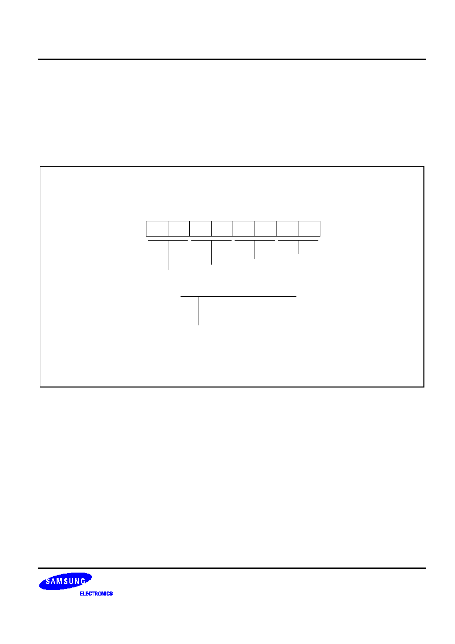
S3C8639/C863A/P863A/C8647/F8647
I/O PORTS
9-3
Port 0 High-Byte Control Register (P0CONH)
The four bit-pairs in the port 0 high-byte control register, P0CONH, have the following functions:
-- To configure individual port 0 pins to multiplexed input mode or push-pull output mode.
-- To configure alternative input or output functions for P0.7≠P0.4.
Bit-pair 1/0 configures the capture signal input pin for timer M0 at P0.4.
Port 0 Control Register, High Byte (P0CONH)
E4H, Set 1, Bank 0, R/W
.7
.6
.5
.4
.3
.2
.1
.0
MSB
LSB
P0.7
(note)
Normal input mode
Multiplexed input mode (TM0CAP)
Push-pull output mode
P0CONH Pin Configuration Settings:
00
01
1x
P0.6
(note)
P0.5
(note)
P0.4/TM0CAP
NOTE:
Not used for the S3C8647.
Figure 9-2. Port 0 High-Byte Control Register (P0CONH)
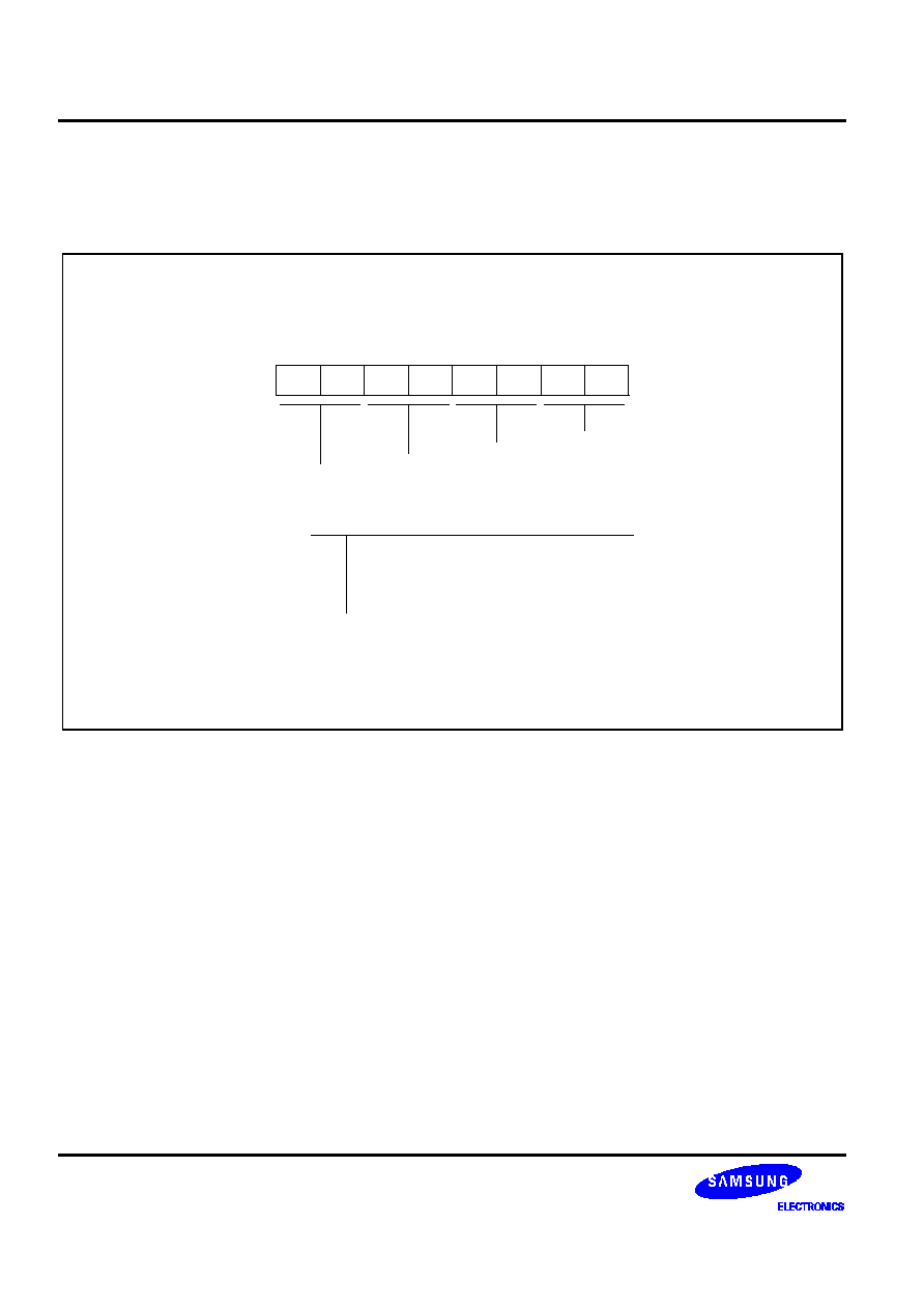
I/O PORTS
S3C8639/C863A/P863A/C8647/F8647
9-4
Port 0 Low-Byte Control Register (P0CONL)
The low-byte port 0 pins, P0.3≠P0.0 can be configured individually as inputs or as push-pull outputs. You can
alternatively configure the pins P0.2≠P0.0 as external interrupt inputs with rising or falling edge detection.
Port 0 Control Register, Low Byte (P0CONL)
E5H, Set 1, Bank 0, R/W
.7
.6
.5
.4
.3
.2
.1
.0
MSB
LSB
P0.3
(note)
Normal input mode
Input mode, rising edge interrupt detection
Input mode, falling edge interrupt detection
Push-pull output mode
P0CONL Pin Configuration Settings:
00
01
10
11
P0.2/INT2
P0.1/INT1
P0.0/INT0
NOTE:
Not used for the S3C8647.
Figure 9-3. Port 0 Low-Byte Control Register (P0CONL)

S3C8639/C863A/P863A/C8647/F8647
I/O PORTS
9-5
Port 0 External Interrupt Control Register (P0INT)
The port 0 external interrupt control register, P0INT, is used to enable and disable the external interrupts INT2≠
INT0 at P0.2≠P0.0, respectively, and also to detect and clear external interrupt pending conditions at these pins.
To selectively enable the external interrupts INT0, INT1, and INT2, you set P0INT.0, P0INT.1, and P0INT.2 to
"1", respectively. The application program can poll the corresponding interrupt pending bits -- P0INT.4 for INT0,
P0INT.5 for INT1, and P0INT.6 for INT2 -- to detect external interrupt pending conditions.
After an external interrupt has been serviced, the service routine must clear the pending condition by writing a "0"
to the appropriate pending bit. Writing a "1" to the pending bit has no effect.
Port 0 External Interrupt Control Register (P0INT)
EBH, Set 1, Bank 0, R/W
-
.6
.5
.4
-
.2
.1
.0
MSB
LSB
Not used for
S3C8639/C863A/C8647
No interrupt pending (when read)
Clear pending condition (when write)
Interrupt is pending (when read)
No effect (when write)
P0.2-P0.0 interrupt pending flags
0
0
1
1
Interrupt pending flags for P0.2-P0.0
Not used for
S3C8639/C863A/C8647
Disable interrupt
Enable interrupt
P0.2-P0.0 interrupt enable bits
0
1
Interrupt enable bit for P0.2-P0.0
Figure 9-4. Port 0 External Interrupt Control Register (P0INT)

I/O PORTS
S3C8639/C863A/P863A/C8647/F8647
9-6
PORT 1 (Only S3C863X)
Port 1 is an 3-bit port with individually configurable pins. You can directly access it by writing or reading the port
1 data register, P1 (set 1, bank 0, E1H). You can use port 1 for normal output, input mode, or n-channel open-
drain output mode.
The port 1 control register, P1CON (set 1, bank 0, E6H) is used to configure port 1 pins. Each byte contains four
bit-pairs and each bit-pair configures one pin.
Bit pair 3/2 configures the IIC-bus clock pin for SCL1 at P1.1. Bit pair 1/0 controls P1.0 when it is set to "11B",
the SDA1 is enabled for IIC-bus data pin.
Port 1 Control Register (P1CON)
E6H, Set 1, Bank 0, R/W
.7
.6
.5
.4
.3
.2
.1
.0
MSB
LSB
Not used for
S3C8639/C863A/C8647
Input mode
Push-pull output mode
N-channel open-drain output mode
(5 V load capability)
Multiplexed mode (SCL1/SDA1)
P1CON Pin Configuration Settings:
00
01
10
11
P1.2
P1.1/SCL1
P1.0/SDA1
Figure 9-5. Port 1 Control Register (P1CON)
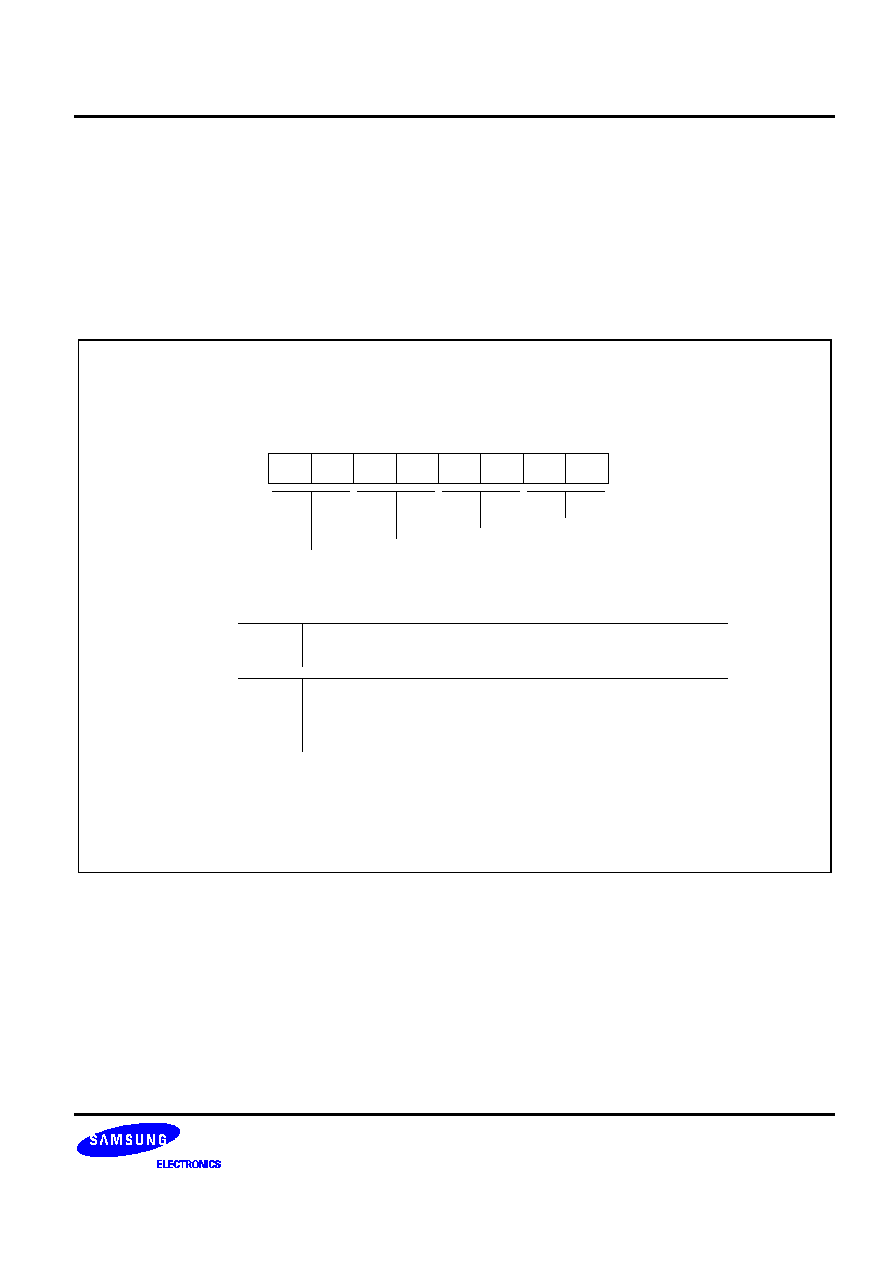
S3C8639/C863A/P863A/C8647/F8647
I/O PORTS
9-7
PORT 2
Port 2 is an 8-bit I/O port with individually configurable pins. You can directly access port 2 pins by writing or
reading the port 2 data register, P2 (set 1, bank 0, E2H).
Two 8-bit control registers are used to configure port 2 pins: P2CONH (set 1, bank 0, E7H) which let you select
digital input mode (or TTL input mode), normal or PWM push-pull output mode, or n-channel open drain PWM
output mode. And you can select digital input mode, normal or PWM push-pull output mode at the P2CONL
(set 1, bank 0, E8H)
Port 2 Control Register, High Byte (P2CONH)
E7H, Set 1, Bank 0, R/W
.7
.6
.5
.4
.3
.2
.1
.0
MSB
LSB
P2.7/Csync-l
P2CONH Pin Configuration Settings:
P2.6/PWM6
(note)
P2.5/PWM5
P2.4/PWM4
0x TTL input mode (Csync-l)
1x Push-pull output mode
bits 7,6
00 Input mode
01 Push-pull output mode
10 Push-pull PWM output mode (5 V load capability)
11 N-channel open-drain PWM output mode (5 V load capability)
bits 5-0
NOTE:
Not used for the S3C8647.
Figure 9-6. Port 2 High-Byte Control Register (P2CONH)

I/O PORTS
S3C8639/C863A/P863A/C8647/F8647
9-8
Port 2 Control Register, Low Byte (P2CONL)
E8H, Set 1, Bank 0, R/W
.7
.6
.5
.4
.3
.2
.1
.0
MSB
LSB
P2.3/PWM3
P2CONL Pin Configuration Settings:
P2.2/PWM2
P2.1/PWM1
P2.0/PWM0
Input mode
Push-pull output mode
Push-pull PWM output mode (5 V load capability)
0x
10
11
Figure 9-7. Port 2 Low-Byte Control Register (P2CONL)

S3C8639/C863A/P863A/C8647/F8647
I/O PORTS
9-9
PORT 3
Port 3 is an 8-bit I/O port with individually configurable pins. You can directly access it by writing or reading the
port 3 data register, P3 (set 1, bank 0, E3H). You can selectively configure P3 pins to input or output mode. In
input mode, you can also select A/D converter input mode (P3.0≠P3.3 only) or normal digital input mode (with or
without pull-up resistor). Output mode is push-pull mode or n-channel open-drain mode (P3.4≠P3.7 only).
Two 8-bit control registers are used to configure port 3 pins: P3CONH (E9H, set 1, bank 0) for P3.7≠P3.4 and
P3CONL (set 1, bank 0, EAH) for P3.3≠P3.0. Each byte contains four bit-pairs and each bit-pair configures one
pin.
Port 3 Control Register, High Byte (P3CONH)
E9H, Set 1, Bank 0, R/W
.7
.6
.5
.4
.3
.2
.1
.0
MSB
LSB
P3.7
P3CONH Pin Configuration Settings:
P3.6
P3.5
P3.4
Input mode
Input mode with pull-up resistor
Push-pull output mode
N-channel open-drain output mode (5 V load capability)
00
01
10
11
Figure 9-8. Port 3 High-Byte Control Register (P3CONH)
Port 3 Control Register, High Byte (P3CONL)
EAH, Set 1, Bank 0, R/W
.7
.6
.5
.4
.3
.2
.1
.0
MSB
LSB
P3.3/ADC3
P3CONL Pin Configuration Settings:
P3.2/ADC2
P3.1/ADC1
P3.0/ADC0
Input mode
Analog input mode
Push-pull output mode
N-channel open-drain output mode
00
01
10
11
Figure 9-9. Port 3 Low-Byte Control Register (P3CONL)

I/O PORTS
S3C8639/C863A/P863A/C8647/F8647
9-10
FUNCTION-FIXED PORT
These I/O pins are used only for the input and output of video synchronization signals to the sync processor or
DDC & IIC-bus interface. The horizontal and vertical sync signals can be monitored directly through the Sync
Port Read Data Register (SYNCRD).
Sync signal ports
-- Csync-I: Composite (SOG) synchronization input port (TTL level)
-- Hsync-I: Horizontal synchronization input (TTL level)
-- Vsync-I: Vertical synchronization input and synchro clock (VCLK) for DDC1 (TTL level)
-- Hsync-O: Horizontal synchronization output from the sync processor
-- Vsync-O: Vertical synchronization output from the sync processor
-- Clamp-O: Clamp signal output with programmable width from the sync processor
DDC and IIC-bus interface ports
-- SDA0: DDC and IIC-bus interface serial data
-- SCL0: DDC and IIC-bus interface serial clock
SYNC Port Read Data Register (SYNCRD)
F0H, Set 1, Bank 0, Read-only
.7
.6
.5
.4
.3
.2
.1
.0
MSB
LSB
SYNCRD Pin Configuration Settings:
Not use for
S3C8639/C863A
Hsync-I
Low data
High data
0
1
Vsync-I
Hsync-O
Vsync-O
Figure 9-10. Sync Port Read Data Register (SYNCRD)

S3C8639/C863A/P863A/C8647/F8647
I/O PORTS
9-11
F
F
PROGRAMMING TIP -- Configuring I/O Port Pins to Specification
The following sample program shows you how to configure the S3C8639/C863A/C8647 I/O ports to specification.
The program comments explain the effect of the settings:
∑
∑
∑
SB0
; Select bank 0
LD
P0CONH,#0FFH
; Set port 0 high byte to push-pull output mode
LD
P0CONL,#0D5H
; Set P0.3 to push-pull output mode
; Set P0.0≠P0.2 to rising edge interrupt mode
LD
P0INT,#0FH
; Enable port 0 external interrupt
LD
P1CON,#00H
; Set port 1 to input mode
LD
P2CONH,#3FH
; Set port 2 high byte to PWM n-channel open-drain
; output mode (5-volt capability) and Csync input mode
LD
P2CONL,#0FFH
; Set port 2 low byte to PWM push-pull output mode
LD
P3CONH,#0AAH
; Set port 3 high byte to push-pull output mode
LD
P3CONL,#55H
; Set port 3 low byte to analog input mode
∑
∑
∑

I/O PORTS
S3C8639/C863A/P863A/C8647/F8647
9-12
NOTES

S3C8639/C863A/P863A/C8647/F8647
BASIC TIMER
10-1
10
BASIC TIMER
OVERVIEW
S3C8639/C863A/C8647 has a default timer: an 8-bit basic timer.
You can use the basic timer (BT) in two different ways:
-- As a watchdog timer, it provides an automatic reset mechanism in the event of a system malfunction.
-- Signals the end of the required oscillation stabilization interval after a reset or a Stop mode release.
The functional components of the basic timer block are:
-- Clock frequency divider (f
OSC
divided by 4096, 1024, or 128) with multiplexer
-- 8-bit basic timer counter, BTCNT (set 1, bank 0, FDH, read-only)
-- Basic timer control register, BTCON (set 1, D3H, read/write)
-- Watchdog timer control register, WDTCON (set 1, bank 0, ECH, read/write)
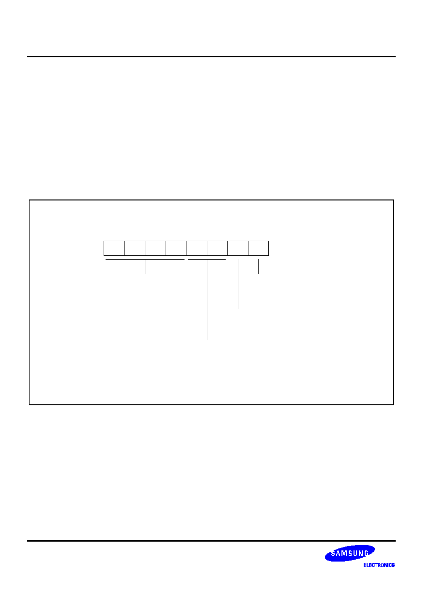
BASIC TIMER
S3C8639/C863A/P863A/C8647/F8647
10-2
BASIC TIMER CONTROL REGISTER (BTCON)
The basic timer control register, BTCON, is used to select the input clock frequency, to clear the basic timer
counter and frequency dividers, and to enable or disable the watchdog timer function. It is located in set 1,
address D3H, and is read/write addressable using register addressing mode.
A reset clears BTCON to "00H". This enables the watchdog function and selects a basic timer clock frequency of
f
OSC
/4096. To disable the watchdog function, you must write the signature code "1010B" to the basic timer
register control bits BTCON.7≠BTCON.4.
The 8-bit basic timer counter, BTCNT (set 1, bank 0, FDH), can be cleared at any time during the normal
operation by writing a "1" to BTCON.1. To clear the frequency dividers for both the basic timer input clock and
the timer M0 clock (unless timer M0 uses an external clock source), you should write a "1" to BTCON.0.
Basic Timer Control Register (BTCON)
D3H, Set 1, R/W
.7
.6
.5
.4
.3
.2
.1
.0
MSB
LSB
Divider clear bit for BT and T0:
0 = No effect
1 = Clear both dividers
(basic timer, timer M0)
Basic timer/counter clear bit:
0 = No effect
1 = Clear basic timer
Watchdog time enable bits:
1010B = Disable watchdog function
Others = Enable watchdog function
Basic timer input clock selection bits:
00 = f
OSC
/4096
01 = f
OSC
/1024
10 = f
OSC
/128
11 = Not used
Figure 10-1. Basic Timer Control Register (BTCON)

S3C8639/C863A/P863A/C8647/F8647
BASIC TIMER
10-3
WATCHDOG TIME CONTROL REGISTER (WDTCON)
The watchdog time control register, WDTCON, is used to generate various watchdog time and to select Hsync
output. It is located in set 1, bank 0, address ECH, and is read/write addressable using register addressing mode.
Watchdog Time Control Register (WDTCON)
ECH, Set 1, Bank 0, R/W
-
-
-
-
.2
.1
.0
MSB
LSB
Watchdog time generation control bits:
Not use for S3C8639/C863A/C8647
000
001
010
011
100
101
110
111
t
BTOVF
t
BTOVF
/2
t
BTOVF
/3
t
BTOVF
/4
t
BTOVF
/5
t
BTOVF
/6
t
BTOVF
/7
t
BTOVF
/8
NOTE:
t
BTOVF
= (1/f
OSC
) x (divider count of basic timer input clock) x 256
.3
Hsync-O divide enable bit:
0 = Hsync-I (Non-divide)
1 = Hsync-I/2
Figure 10-2. Watchdog Time Control Register (WDTCON)

BASIC TIMER
S3C8639/C863A/P863A/C8647/F8647
10-4
BASIC TIMER FUNCTION DESCRIPTION
Watchdog Timer Function
You can program the basic timer overflow signal (BTOVF) to generate a reset by setting BTCON.7≠BTCON.4 to
any value other than "1010B" (The "1010B" value disables the watchdog function). A reset clears BTCON to
"00H", automatically enabling the watchdog timer function. A reset also selects the CPU clock (as determined by
the current CLKCON register setting),divided by 4096, as the BT clock.
A reset whenever a basic timer counter overflow occurs. During the normal operation, the application program
must prevent the overflow and the accompanying reset operation from occurring. To do this, the BTCNT value
must be cleared (by writing a "1" to BTCON.1) at regular intervals. And you can generate the various watchdog
time by setting WDTCON.2-WDTCON.0.
If a system malfunction occurs due to circuit noise or some other error condition, the BT counter clear operation
will not be executed and a basic timer overflow will occur, initiating a reset. In other words, during the normal
operation, the basic timer overflow loop (a bit 7 overflow of the 8-bit basic timer counter, BTCNT) is always
broken by a BTCNT clear instruction. If a malfunction does occur, a reset is triggered automatically.
Oscillation Stabilization Interval Timer Function
You can also use the basic timer to program a specific oscillation stabilization interval after a reset or when stop
mode has been released by an external interrupt.
In Stop mode, whenever a reset or an external interrupt occurs, the oscillator starts. The BTCNT value then
starts increasing at the rate of f
OSC
/4096 (for reset), or at the rate of the preset clock source (for an external
interrupt). When BTCNT.4 overflows, a signal is generated to indicate that the stabilization interval has elapsed
and to gate the clock signal off to the CPU so that it can resume the normal operation.
In summary, the following events occur when Stop mode is released:
1.
During the stop mode, a power-on reset or an external interrupt occurs to trigger the stop mode release and
oscillation starts.
2.
If a power-on reset occurred, the basic timer counter would increase at the rate of f
OSC
/4096. If an external
interrupt is used to release Stop mode, the BTCNT value increases at the rate of the preset clock source.
3.
Clock oscillation stabilization interval begins and continues until bit 4 of the basic timer counter overflows.
4.
When a BTCNT.4 overflow occurs, the normal CPU operation resumes.

S3C8639/C863A/P863A/C8647/F8647
BASIC TIMER
10-5
NOTE:
In a power-on reset operation, the CPU is idle during the required oscillation stabilization
interval when BTCNT.4 is set after releasing from
RESET
or STOP mode, CPU clock
starts.
MUX
1/4096
DIV
1/128
f
OSC
Bit 0
Basic Timer Control Register
(Write '1010xxxxB' to Disable)
Clear
RESET
or STOP
Data Bus
8-Bit Basic Counter
(Read-Only)
OVF
RESET
R
1/1024
Bits 3, 2
Bit 1
Watchdog Time
Control Register
Figure 10-3. Basic Timer Block Diagram

BASIC TIMER
S3C8639/C863A/P863A/C8647/F8647
10-6
F
F
PROGRAMMING TIP -- Configuring the Basic Timer
This example shows how to configure the basic timer to sample specifications:
ORG
0100H
RESET
DI
; Disable all interrupts
SB0
; Select bank 0
LD
BTCON,#0AAH
; Disable the watchdog timer
LD
CLKCON,#98H
; Non-divided clock
CLR
SYM
; Disable global and fast interrupts
CLR
SPL
; Stack pointer low byte
"0"
; Stack area starts at 0FFH
∑
∑
∑
SRP
#0C0H
; Set register pointer
0C0H
EI
; Enable interrupts
∑
∑
∑
MAIN
LD
BTCON,#A2H
; Watchdog timer disable
; Basic timer/counter clear
LD
BTCON,#52H
; Enable the watchdog timer
; Basic timer clock: f
OSC
/4096
; Clear basic timer counter
LD
WDTCON,#03H
; Watchdog time: t
BTOVF
/4
NOP
NOP
∑
∑
∑
JP
T,MAIN
∑
∑
∑

S3C8639/C863A/P863A/C8647/F8647
TIMER M0
11-1
11
TIMER M0
OVERVIEW
The 8-bit timer M0 is for monitor application. Timer M0 includes capture timer mode using the appropriate
TM0CON setting.
Timer M0 has the following functional components:
-- Clock frequency divider (f
OSC
divided by 128 or 8 ) with multiplexer
-- 2-bit prescaler for the timer M0 input clock
-- 8-bit counter (TM0CNT; set1, D0H, read-only) and 8-bit reference data register (TM0DATA; set1, D1H, read-
only)
-- Timer M0 capture or overflow interrupt (IRQ0, vector E2H, E0H) generation
-- Timer M0 control register, TM0CON (set 1, D2H, read/write)
FUNCTION DESCRIPTION
CAPTURE TIMER FUNCTION
The timer M0 module can generate two interrupts: the timer M0 capture interrupt (TM0INT), and the timer M0
overflow interrupt (TM0OVF). TM0INT belongs to interrupt level IRQ0, and is assigned the separate vector
address, E2H. TM0OVF is interrupt level IRQ0, vector E0H.
The TM0INT and TM0OVF pending conditions are automatically cleared by hardware after they are serviced.
In capture timer mode, a signal edge that is detected at the TM0CAP pin opens a gate and loads the current
counter value into the timer M0 data register (TM0DATA). You can select rising or falling edge to trigger this
operation.
Both kinds of timer M0 interrupts can be used in capture mode: the timer M0 overflow interrupt is generated
whenever a counter overflow occurs; the timer M0 capture interrupt is generated whenever the counter value is
loaded into the timer M0 data register.
By reading captured data value in TM0DATA, and assuming a specific value for the timer M0 clock frequency,
you can calculate the internal time of the signal being input to the TM0CAP pin or the vertical sync output signal
being output from the sync-processor module.

TIMER M0
S3C8639/C863A/P863A/C8647/F8647
11-2
Timer M0 Control Register (TM0CON)
You use the timer M0 control register, TM0CON, to
-- Select the timer M0 operating mode (capture mode)
-- Select the timer M0 input clock frequency
-- Clear the timer M0 counter, TM0CNT
-- Enable the timer M0 overflow interrupt and timer M0 capture interrupt
-- Select a 2-bit prescaler value for the Timer M0 input clock
-- Select the timer M0 capture input source
TM0CON is located in set 1, at address D2H, and is read/write addressable using Register addressing mode.
A reset clears TM0CON to "00H". This sets timer M0 to disable capture timer mode, selects an input clock
frequency of f
OSC
/128, and disables timer M0 overflow and capture interrupts. You can clear the timer M0
counter at any time during the normal operation by writing a "1" to TM0CON.2.
The timer M0 overflow interrupt (TM0OVF) is in the interrupt level IRQ0 and has the vector address E0H. When
the timer M0 capture interrupt is disabled, the Timer M0 overflow interrupt by clock (f
OSC
) is possible. When a
timer M0 overflow interrupt occurs and is serviced by the CPU, the pending condition is cleared automatically by
hardware.
To enable the timer M0 capture interrupt (IRQ0, vector E2H), you must write TM0CON.1 to "1". There is no
pending bit cleared by software or static read bit which is H/W pending. After the interrupt request is serviced, the
pending condition is automatically cleared by hardware.
Timer M0 Control Register (TM0CON)
D2H, Set 1, R/W
.7
.6
.5
.4
.3
.2
.1
.0
MSB
LSB
Timer M0 input clock
selection bit:
0 = f
OSC
/128
1 = f
OSC
/8
Timer M0 capture input selection bit:
0 = TM0CAP input pin selection
1 = V-sync output path selection from
sync-processor
Timer M0 capture interrupt enable bit:
0 = Disable the timer M0 capture interrupt
1 = Enable the timer M0 capture interrupt
Timer M0 capture mode selection bit:
0 = Capture on rising mode
1 = Capture on falling mode
Timer M0 overflow interrupt enable bit:
0 = Disable the timer M0 overflow interrupt
1 = Enable the timer M0 overflow interrupt
2-bit prescaler bits:
00 = No division
01 = Divide by 2
10 = Divide by 3
11 = Divide by 4
Timer M0 counter clear bit:
0 = No effect
1 = Clear timer M0 counter (when write)
NOTE:
When the captured value is #0FFh, the overflow interrupt does not occur.
When the vlaue of capture is changed from #0FFh to #00h, the overflow interrupt
always occurs. When the captured value is #00h, the overflow interrupt occurs in
advance.
Figure 11-1. Timer M0 Control Register (TM0CON)

S3C8639/C863A/P863A/C8647/F8647
TIMER M0
11-3
BLOCK DIAGRAM
8-Bit Counter
(Read-Only)
TM0CNT
Bit 3
TM0CLR
Timer M0 Data Register
(Read-Only)
TM0DATA
R
Clear
Bit 7
f
OSC
/8
f
OSC
/128
Data Bus
2-Bit
Pre-
scaler
Bits 6, 5
Data Bus
IRQ0
(Timer M0 Capture)
IRQ0
(Timer M0 Overflow)
Bit 1
TM0INT
Bit 0
Bit 4
TM0CAP
Vsync-O
from sync
processor
Bit 2
OVINT
Timer M0 control register
Figure 11-2. Timer M0 Functional Block Diagram

TIMER M0
S3C8639/C863A/P863A/C8647/F8647
11-4
NOTES

S3C8639/C863A/P863A/C8647/F8647
TIMER M1
12-1
12
TIMER M1
OVERVIEW
The 12-bit timer M1 is an 12-bit timer/counter for monitor application. Timer M1 offers capture/overflow timer
mode using the appropriate TM1CON setting.
Timer M1 has the following functional components:
-- Clock frequency selector as the timer M1 clock (f
OSC
divided by 512, 128, or 2, Hsync-I or Csync-I from sync-
processor) with multiplexer
-- Capture signal selector from V-syncO (sync-processor) or the timer M2 interval time
-- 12-bit counter (TM1CNTH, TM1CNTL; set1, bank0, F1H, F2H, read-only) and 12-bit reference data register
(TM1DATAH, TM1DATAL; set1, bank0, F3H, F4H, read-only)
-- Timer M1 capture or overflow interrupt (IRQ2, vector E8H, E6H) generation
-- Timer M1 control register, TM1CON (set 1, bank0, F5H, read/write)
FUNCTION DESCRIPTION
Overflow Timer Function
The timer M1 module generates an overflow signal whenever the timer M1 counter overflow occurs. If you set the
timer M1 overflow interrupt enable bit, TM1CON.2, to "1", an interrupt is generated whenever an overflow state is
detected. After the interrupt request is generated, the counter register value is cleared and counting resumes
from "00H".
The timer M1 overflow interrupt pending condition is automatically cleared by hardware when it has been
serviced.
Capture Timer Function
The Timer M1 module can generate, the timer M1 capture interrupt (TM1INT). TM1INT belongs to interrupt level
IRQ2, and is assigned the vector address, E8H.
In capture timer mode, a capture signal from Vsync-O (sync-processor) or the timer M2 interval timer opens a
gate and loads the current counter value into the timer M1 data register (TM1DATA). You can select Vsync-O or
the timer M2 interval timer as the capture signal source to trigger this operation.
By reading captured data value in TM1DATAH and TM1DATAL, and assuming a specific value for the timer M1
clock frequency, you can calculate the frequency of the signal being input to the Hsync-I or Csync-I from sync-
processor by capture signal.

TIMER M1
S3C8639/C863A/P863A/C8647/F8647
12-2
Timer M1 Control Register (TM1CON)
You use the timer M1 control register, TM1CON, to
-- Select the capture signal source
-- Select the timer M1 clock input
-- Clear the timer M1 counter, TM1CNTH and TM1CNTL
-- Enable the timer M1 capture and overflow interrupt
-- Clear the timer M1 capture interrupt pending bit
-- Select Vsync-O capture edge as capture signal source (When TM1CON.7 = "1")
TM1CON is located in set 1, bank0, at address F5H, and is read/write addressable using Register addressing
mode.
The setting for bit-pair TM1CON.0 and TM1CON.1 selects the timer M1 counter clock input. The timer M1
capture and overflow interrupt (TM1INT, TM1OVF) are in the interrupt level IRQ2, but has the different vector
address (E8H, E6H respectively).
TM1CON.4 is the interrupt pending flag for the timer M1 capture interrupt. To clear a timer M1 interrupt pending
condition, the interrupt service routine must write a "0" to TM1CON.4 after the CPU has acknowledged the
request. TM1CON.3 is flag to clear the 12-bit Timer M1 counter.
TM1CON.7 is flag to select the capture signal source (timer M2 interval time or Vsync-O from sync-processor)
and TM1CON.6 is flag to select the capture edge as the Vsync-O capture signal source.
A reset operation clears TM1CON to "00H", selecting the Hsync-I or Csync-l from sync-processor are the timer
M1 clock and disabling the timer M1 capture and overflow interrupt.

S3C8639/C863A/P863A/C8647/F8647
TIMER M1
12-3
Timer M1 Control Register (TM1CON)
F5H, Set 1, R/W
.7
.6
.5
.4
.3
.2
.1
.0
MSB
LSB
Timer M1 capture
signal source
selection bit:
0 = Signal from the
timer M2 interval
time
1 = Vsync-O from
sync-processor
Timer M1 clock input selection bits:
00 = Hsync-l or Csync-l from sync-processor
01 = f
OSC
/2
10 = f
OSC
/128
11 = f
OSC
/512
Vsync-O capture source edge
selection bit (when TM1CON.7=1):
0 = Vsync-O rising edge
from sync-processor
1 = Vsync-O falling edge
from sync-processor
Timer M1 overflow interrupt enable bit:
0 = Disable the timer M1 overflow interrupt
1 = Enable the timer M1 overflow interrupt
Timer M1 counter clear bit (when write):
0 = No effect
1 = Clear timer M1 counter
Timer M1 capture interrupt enable bit:
0 = Disable the timer M1 capture interrupt
1 = Enable the timer M1 capture interrupt
Timer M1 capture interrupt pending bit:
0 = Interrupt i snot pending (when read)
0 = Clear the pending bit (when write)
1 = Interrupt is pending (when read)
1 = No effect (when write)
Figure 12-1. Timer M1 Control Register (TM1CON)

TIMER M1
S3C8639/C863A/P863A/C8647/F8647
12-4
BLOCK DIAGRAM
12-Bit Counter
TM1CNTL TM1CNTH
CAP
8
TM1CON.1-.0
f
OSC
/512
MUX
(The TM1DATAL and TM1DATAH
registers are read-only.)
IRQ2
TM1CON.2
f
OSC
/128
f
OSC
/2
Hsync-I/Csync-I
from sync processor
TM1CON.3
4
(The TM1CNTL and
TM1CNTH registers
are read-only.)
OVF
TM1CON.5
Capture signal
from timer M2
interval time
(TM2CON1,0)
TM1CON.7
TM1CON.6
Vsync-O from
sync-processor
Clear
Clear
12
TM1CON.4
TM1CON.5
IRQ2
Timer M1 Data Register
TM1DATAL TM1DATAH
Figure 12-2. Timer M1 Functional Block Diagram

S3C8639/C863A/P863A/C8647/F8647
TIMER M2
13-1
13
TIMER M2
OVERVIEW
The interval timer M2 is no-counter timer for monitor application. Timer M2 offers interval timer mode using the
appropriate TM1CON setting.
Timer M2 has the following functional components:
-- 5-bit scaler by f
OSC
/1000 for timer M2 interval source
-- Timer M1 capture interval time source selector (When TM1CON.5 is "1") with 2-bit scaler
-- Timer M2 interval interrupt (IRQ1, vector E4H) generation
-- Timer M2 control register, TM2CON (set 1, F6H, read/write)
FUNCTION DESCRIPTION
Interval Timer Function
The timer M2 module generates an interval interrupt whenever the TM2CON.2 is "1". TM2INT belongs to the
interrupt level IRQ1, and is assigned the separate vector address, E4H. The TM2INT pending condition is
automatically cleared by hardware when it has been serviced.
Timer M2 Control Register (TM2CON)
You use the timer M2 control register, TM2CON, to
-- Select the interval time signal source by 5-bit scaler
-- Enable the timer M2 interval interrupt
-- Select timer M1 capture interval time by 2-bit scaler (When TM1CON.5 = "1")
TM2CON is located in set 1, bank0, at address F6H, and is read/write addressable using Register addressing
mode.
A reset operation clears TM2CON to "F8H" (11111000B), thereby setting the 5-bit scaler value to be divided
by 32.

TIMER M2
S3C8639/C863A/P863A/C8647/F8647
13-2
Timer M2 Control Register (TM2CON)
F6H, Set 1, R/W
.7
.6
.5
.4
.3
.2
.1
.0
MSB
LSB
5-bit scaler bits:
00000 = No division
00001 = Divide by 2
00010 = Divide by 3
. . .
11111 = Divide by 32
Timer M1 capture interval time
selection bits:
00 = Timer M2 interval (bypass)
01 = Timer M2 interval x 10
10 = Timer M2 interval x 20
11 = Timer M2 interval x30
Timer M2 interval interrupt enable bit:
0 = Disable the timer M2 interval interrupt
1 = Enable the timer M2 interval interrupt
NOTES:
1.
When the timer M1 capture mode is enabled (TM1CON.5 = "1"), the value of 5-bit or
2-bit scaler can be changed only in the timer M1capture interrupt routine.
2.
When the timer M1 capture mode is disabled (TM1CON.5 = "0"), the value of 5-bit
scaler can be changed only in the timer M2 interval interrupt routine.
Figure 13-1. Timer M2 Control Register (TM2CON)

S3C8639/C863A/P863A/C8647/F8647
TIMER M2
13-3
BLOCK DIAGRAM
Timer M1 capture signal
2-Bit
Scaler
TM2CON.1,.0
/10
Divider
5-Bit
Scaler
TM2CON.2
TM2CON.7-.3
f
OSC
/1000
IRQ1
(Timer M2 Interval Interrupt)
"00"
"01"
"10"
"11"
Figure 13-2. Timer M2 Functional Block Diagram

TIMER M2
S3C8639/C863A/P863A/C8647/F8647
13-4
NOTES

S3C8639/C863A/P863A/C8647/F8647
ANALOG TO DIGITAL CONVERTER
14-1
14
ANALOG-TO-DIGITAL CONVERTER
OVERVIEW
The 8-bit A/D converter (ADC) module of S3C8639/C863A/C8647 employs successive approximation logic to
convert analog levels entering one of the four input channels to equivalent 8-bit digital values. The analog input
level must lie between the V
DD2
and V
SS2
values. The A/D converter has the following components:
-- Analog comparator with successive approximation logic
-- D/A converter logic (resistor string type)
-- 8-bit ADC control register (ADCON)
-- Four multiplexed analog data input pins (ADC0≠ADC3)
-- 8-bit A/D conversion data output register (ADDATA) (S3C863X)
-- 4-bit A/D conversion data output register (ADDATA) (S3C8647)
-- 8-bit digital input port (Alternatively, I/O port )
-- V
DD2
and V
SS2
pins (S3C863X)
FUNCTION DESCRIPTION
To initiate an analog-to-digital conversion procedure, write the channel selection data in the A/D converter control
register ADCON to select one of the four analog input pins (ADCn, n = 0≠3) and set the conversion start or
enable bit, ADCON.0. The read-write ADCON register is located in set 1, bank0, at address F7H.
During the normal conversion, ADC block initially sets the successive approximation register to 80H
(approximately the half-way point of an 8-bit register). This register is then updated automatically in each
conversion step. The successive approximation block performs 8-bit conversions for one input channel at a time.
You can dynamically select different channels by manipulating the channel selection bit value (ADCON.5≠.4) in
the ADCON register. To start the A/D conversion, you should set, ADCON.0. When a conversion is completed,
ADCON.3, the end-of-conversion (EOC) bit, is automatically set to 1 and the result is dumped into the ADDATA
register where it can be read. The A/D converter then enters an idle state. Remember to read the contents of
ADDATA before another conversion starts. Otherwise, the previous result will be overwritten by the next
conversion result.
NOTE
As the A/D converter does not include any sample-and-hold circuitry, it is very important to keep the
fluctuation in the analog level at the ADC0≠ADC3 input pins to an absolute minimum during the
conversion process. Any change in the input level, perhaps due to noise, will invalidate the result. If the
chip enters to STOP or IDLE mode in conversion process, there will be a leakage current path in A/D
block. You must use STOP or IDLE mode after A/D converting operation is finished.

ANALOG TO DIGITAL CONVERTER
S3C8639/C863A/P863A/C8647/F8647
14-2
CONVERSION TIMING
The A/D conversion process requires 4 steps (8 clock edges) to convert each bit. Therefore, a total of 48 clocks
are required to complete an 10-bit conversion. With an 8 MHz f
OSC
clock frequency, one clock cycle is 1
µ
s
(when ADCON.2, .1 are "01"). If each bit conversion requires 4 clocks, the conversion rate is calculated as
follows:
start (4 clocks) + (4 clocks/bit
◊
n bits) + EOC (4 clocks) = 4(n+2) clocks, 1
µ
s x 4(n+2) = 4(n+2)
µ
s at 8 MHz
where, n = 4 (S3C8647), 10 (S3C863x)
A/D CONVERTER CONTROL REGISTER (ADCON)
The A/D converter control register, ADCON, is located at address F7H in set 1, bank0. It has four functions:
-- Analog input pin selection (bits 4,5 and 6)
-- End-of-conversion status detection (bit 3)
-- Clock source selection (bits 2 and 1)
-- A/D operation start or enable (bit 0)
After a reset, the ADC0 pin is automatically selected as the analog data input pin, and the start bit is turned off.
You can select only one analog input channel at a time. Other analog input pins (ADC0≠ADC3) can be selected
dynamically by manipulating the ADCON.6≠.4 bits.
Start or enable bit:
0 = Disable operation
1 = Start operation
Not used for the
S3C8639/C863A/C8647
End-of conversion bit (read-only):
0 = Conversion is not complete
1 = Conversion is complete
-
.6
.5
.4
.3
.2
.1
.0
LSB
MSB
A/D Cconverter Control Register (ADCON)
F7H, Set 1, Bank 0, R/W (EOC bit is read-only)
A/D input pin selection bits:
5
0
0
1
1
Clock source select:
f
OSC
/16
f
OSC
/8
f
OSC
/4
f
OSC
0
1
0
1
0
0
1
1
4
0
1
0
1
6
0
0
0
0
A/D input pin
ADC0 (P3.0)
ADC1 (P3.1)
ADC2 (P3.2)
ADC3 (P3.3)
Not used
Others
Figure 14-1. A/D Converter Control Register (ADCON)
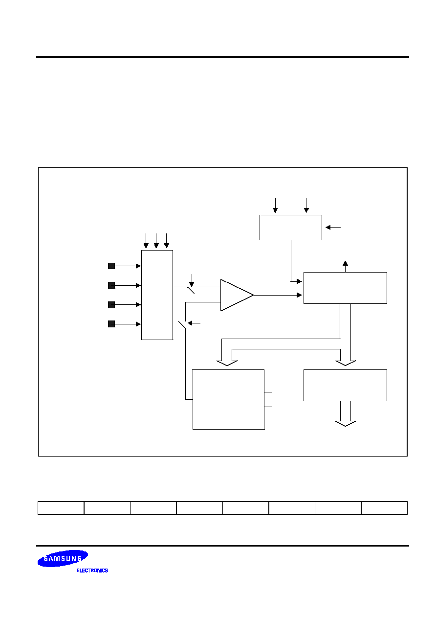
S3C8639/C863A/P863A/C8647/F8647
ANALOG TO DIGITAL CONVERTER
14-3
INTERNAL REFERENCE VOLTAGE LEVELS
In the ADC function block, the analog input voltage level is compared to the reference voltage. The analog input
level must remain within the range of AV
SS
(V
SS2
)
to AV
REF
(V
DD2
).
Different reference voltage levels are generated internally along the resistor tree during the analog conversion
process for each conversion step. The reference voltage level for the first conversion bit is always 1/2 V
DD2
.
BLOCK DIAGRAM
Input Pins
ADC3-ADC0
(P3.3-P3.0)
Clock
Select
Conversion
Result (ADDATA
F8H, Set 1, Bank 0)
-
+
To ADCON.3
(EOC Flag)
Successive
Approximation
Logic & Register
Analog
Comparator
MUX
ADCON.6-.4
( Analog Input Pin Select)
ADCON.0
(ADC Enable)
f
OSC
/n
ADCON.2-.1
To Data Bus
ADCON.0
(ADC Enable)
AV
REF
(V
DD2
)
AV
SS
(V
SS2
)
8-Bit D/A
Converter (S3C863X)
4-Bit D/A
Converter (S3C8647)
Figure 14-2. A/D Converter Functional Block Diagram
A/D Converter Data Register (ADDATA)
Bit 7
Bit 6
Bit 5
Bit 4
Bit 3
(note)
Bit 2
(note)
Bit 1
(note)
Bit 0
(note)
NOTE: Not mapped for the S3C8647.

ANALOG TO DIGITAL CONVERTER
S3C8639/C863A/P863A/C8647/F8647
14-4
Table 14-1. A/D Converter Electrical Characteristics (S3C863X)
(T
A
= ≠ 40
∞
C to + 85
∞
C, V
DD
= 3.0 V to 5.5 V, V
SS
= 0 V)
Parameter
Symbol
Conditions
Min
Typ
Max
Unit
Resolution
≠
8
≠
bit
Total accuracy
V
DD
= 5 V
Conversion time = 5
µ
s
≠
≠
±
2
LSB
Integral linearity error
ILE
AV
REF
= 5 V
≠
±
1
Differential linearity error
DLE
AV
SS
= 0 V
≠
±
1
Offset error of top
EOT
±
1
±
2
Offset error of bottom
EOB
±
0.5
±
2
Conversion time
(1)
t
CON
8-bit conversion
48
◊
n/f
OSC
(3)
,
n = 1, 4, 8, 16
20
≠
170
µ
s
Analog input voltage
V
IAN
≠
AV
SS
≠
AV
REF
V
Analog input impedance
R
AN
≠
2
1000
≠
M
Analog reference voltage
AV
REF
≠
2.5
≠
V
DD
V
Analog ground
AV
SS
≠
V
SS
≠
V
SS
+ 0.3
V
Analog input current
I
ADIN
AV
REF
= V
DD
= 5V
≠
≠
10
µ
A
Analog block Current
(2)
I
ADC
AV
REF
= V
DD
= 5V
≠
1
3
mA
AV
REF
= V
DD
= 3V
0.5
1.5
mA
AV
REF
= V
DD
= 5V
When power down mode
100
500
nA
NOTES:
1.
"Conversion time" is the time required from the moment a conversion operation starts until it ends.
2.
I
ADC
is an operating current during the A/D conversion.
3.
f
OSC
is the main oscillator clock.

S3C8639/C863A/P863A/C8647/F8647
ANALOG TO DIGITAL CONVERTER
14-5
Table 14-2. A/D Converter Electrical Characteristics (S3C8647)
(T
A
= ≠ 40
∞
C to + 85
∞
C, V
DD
= 4.0 V to 5.5 V, V
SS
= 0 V)
Parameter
Symbol
Conditions
Min
Typ
Max
Unit
Resolution
≠
≠
4
≠
bit
Absolute accuracy
(1)
≠
4 bit conversion
24 x n/f
OSC
(3)
,
n = 1, 4, 8, 16
≠
≠
±
0.5
LSB
Conversion time
(2)
t
CON
3
≠
≠
us
Analog input voltage
V
IAN
≠
V
SS
≠
V
DD
V
Analog input impedance
R
AN
≠
2
≠
≠
M
NOTES:
1.
Excluding quantization error, absolute accuracy values are within
±
0.5 LSB.
2.
"Conversion time" is the time required from the moment a conversion operation starts until it ends.
3.
f
OSC
is the main oscillator clock.

ANALOG TO DIGITAL CONVERTER
S3C8639/C863A/P863A/C8647/F8647
14-6
NOTES

S3C8639/C863A/P863A/C8647/F8647
PULSE WIDTH MODULATION
15-1
15
PULSE WIDTH MODULATION
PWM MODULE
The S3C8639/C863A/C8647 microcontrollers include seven 8-bit PWM circuits, PWM0≠PWM6. The S3C8647
microcontroller includes six 8-bit PWM circuits, PWM0≠PWM5. The operation of all PWM circuits is controlled by
a single control register, PWMCON.
The PWM counter, a 8-bit incrementing counter, is used by the 8-bit PWM circuits. To start the counter and
enable the PWM circuits, set PWMCON.5 to "1". If the counter is stopped, it retains its current count value.
When restarted, it resumes counting from the retained count value.
By modifying the prescaler value, you can divide the input clock by one (non-divided), two, three, or four. The
prescaler output is the clock frequency of the PWM counter.
The PWM counter overflows when it reaches "3FH", and then continues counting from zero.

PULSE WIDTH MODULATION
S3C8639/C863A/P863A/C8647/F8647
15-2
PWM CONTROL REGISTER (PWMCON)
The control register for the PWM module, PWMCON, is located in set 1, bank 1, at register address E7H. You
use PWMCON bit settings to control the following functions in the 8-bit:
-- PWM counter operation: stop/start (or resume counting)
A reset clears PWMCON to "00H", disabling all PWM functions.
PWM Control Register (PWMCON)
E7H, Set 1, Bank 1, R/W
.7
.6
.5
.4
.3
.2
.1
.0
MSB
LSB
Not used for S3C8639/C863A/C8647
PWM counter enable bit:
0 = Stop the PWM counter
1 = Start the PWM counter
2-bit prescaler for
PWM counter clock:
00 = Non-divided
01 = Divide by 2
10 = Divide by 3
11 = Divide by 4
Figure 15-1. PWM Control Register (PWMCON)
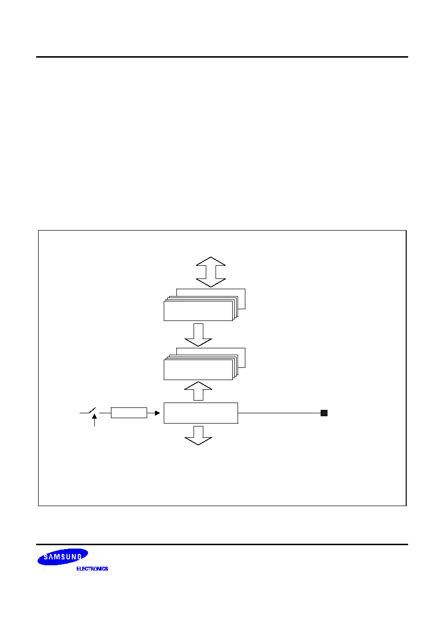
S3C8639/C863A/P863A/C8647/F8647
PULSE WIDTH MODULATION
15-3
PWM0≠PWM6
The S3C8639/C863A/C8647 microcontrollers include seven 8-bit PWM circuits, PWM0≠PWM6. The S3C8647
microcontroller include six 8-bit PWM circuits, PWM0≠PWM5. Each 8-bit PWM data unit is comprised of an 8-bit
basic frame. The 8-bit PWM circuits have the following components:
-- 8-bit counter
-- 8-bit comparators
-- 8-bit PWM data registers (PWM0≠PWM5, PWM6
(note)
)
-- PWM output pins (PWM0≠PWM5, PWM6
(note)
)
The PWM0≠PWM6 circuits are controlled by the PWMCON register (set 1, bank 1, E7H).
NOTE: Not used for the S3C8647.
8-Bit Counter
(6-Bit + 2-Bit Counter)
x 7
PWM0-PWM5,
PWM6
(note)
Output Pins
"1" When Reg > Counter
"0" When Reg < Counter
=
8
x 7
8
8-Bit PWM
8-Bit PWM
8-Bit PWM
8-Bit PWM0-PWM5,
PWM6
(note)
Registers
8-Bit PWM
8
8
Data Bus
2-Bit P.S.
PWMCON.5
f
OSC
8-Bit PWM0-PWM5,
PWM6
(note)
Registers
NOTE:
Not used for the S3C8647.
Figure 15-2. Block Diagram for PWM0≠PWM6

PULSE WIDTH MODULATION
S3C8639/C863A/P863A/C8647/F8647
15-4
PWM0≠PWM6 FUNCTION DESCRIPTION
All the seven 8-bit PWM circuits have an identical function and each has its own 8-bit data register and 8-bit
comparator. Each circuit compares a unique data register value to the 8-bit PWM counter.
The PWM0≠PWM6 data registers are located in set 1, bank 1, at locations E0H≠E6H, respectively. These data
registers are read/write addressable. By loading specific values into the respective data registers, you can
modulate the pulse width at the corresponding PWM output pins, PWM0≠PWM6. (PWM0≠PWM6 correspond to
port 2 pins P2.0≠P2.6.)
The level at the output pins toggles High and Low at a frequency equal to the counter clock, divided by 64 (2
6
).
The duty cycle of the 8-bit PWM pins ranges from 0% to 98.44% (63/64), based on the corresponding data
register values.
To determine the output duty cycle of an 8-bit PWM circuit, its 8-bit comparator sends the output level High when
the data register value is greater than the lower 8-bit count value. The output level is Low when the data register
value is less than or equal to the lower 8-bit count value. The output level at the PWM0≠PWM6 pins remains at
Low level for the first 256 counter clocks. Then, each PWM waveform is repeated continuously, at the same
frequency and duty cycle, until one of the following three events occurs:
-- The counter is stopped
-- The counter clock frequency is changed
-- A new value is written to the PWM data register
STAGGERED PWM OUTPUTS
The PWM0≠PWM6 outputs are staggered to reduce the overall noise level on the pulse width modulation
circuits. If you load the same value to the PWM0≠PWM6 data registers, a match condition (data register value is
equal to the 8-bit count value) will occur on the same clock cycle for all the seven 8-bit PWM circuits.
For example, the PWM0 output is delayed by one-half of a counter clock, PWM1 output by one-half of a counter
clock, PWM2 output by one-half of a counter clock, and so on for the subsequent clock cycles (see Figure 15-4).
NOTE: The S3C8647 microcontroller includes just six 8-bit PWM circuits, PWM0≠PWM5.

S3C8639/C863A/P863A/C8647/F8647
PULSE WIDTH MODULATION
15-5
Counter
Value
(HEX)
0H
40H
Counter
Clock
PWMn = "0"
0C0H
PWMn = "1"
PWMn = 20 H
PWMn = 3FH
6.4 us
PWM Cycle
100 ns
3.2 us
100 ns
80H
NOTES:
1.
A counter clock value of 8 MHz is assumed for all timing values.
2.
'n' = 0 to 6, for PWM0-PWM5, PWM6
(3)
.
3.
Not used for the S3C8647.
Figure 15-3. PWM Waveforms for PWM0≠PWM6
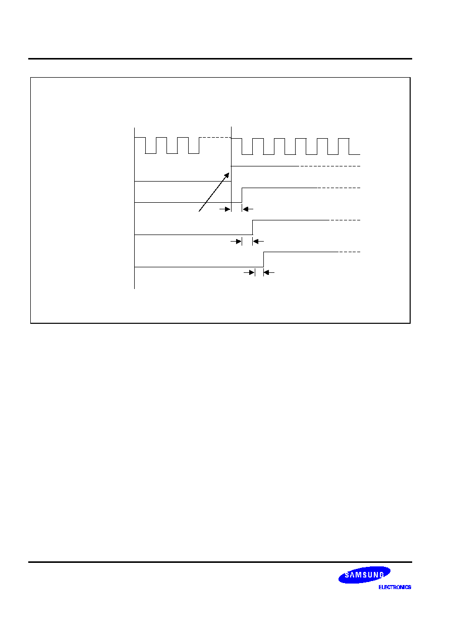
PULSE WIDTH MODULATION
S3C8639/C863A/P863A/C8647/F8647
15-6
0H (After
RESET
)
40H
Counter
Clock
PWM0
PWM1
PWM2
PWM3
1/2 Clock Delay
1/2 Clock Delay
1/2 Clock Delay
Match occurs;
PWM0 toggles to
high level.
Figure 15-4. PWM Clock to PWM0≠PWM6 Output Delays

S3C8639/C863A/P863A/C8647/F8647
PULSE WIDTH MODULATION
15-7
PWM COUNTER
The PWM counter is an 8-bit incrementing counter. The same 8-bit counter is used by all PWM circuits. To
determine the PWM module's base operating frequency, the counter is compared to the PWM data register
value.
PWM DATA REGISTERS
A reset operation disables all PWM output. The current counter value is retained when the counter stops. When
the counter starts, counting resumes from the retained value.
PWM CLOCK RATE
The timing of the 8-bit output channel is based on the maximum 12 MHz CPU clock frequency. The 2-bit
prescaler value in the PWMCON register determines the frequency of the counter clock. You can set
PWMCON.6 and PWMCON.7 to divide the CPU clock frequency by one (non-divided), two, three, or four.
As the maximum CPU clock rate for the S3C8639/C863A/C8647 microcontrollers is 12 MHz, the maximum base
PWM frequency is 187.5 kHz (12 MHz divided by 64). This assumes a non-divided CPU clock.

PULSE WIDTH MODULATION
S3C8639/C863A/P863A/C8647/F8647
15-8
F
F
PROGRAMMING TIP -- Programming PWM0 to Sample Specifications
This sample program executes a test of the PWM block. The program parameters are as follows:
-- The oscillation frequency of the main crystal is 8 MHz
-- PWM frequency is 125 kHz
RESET:
DI
; Disable global interrupts
SB0
; Select bank 0
∑
∑
∑
LD
P2CONH,#11111111B
; Select n-channel open-drain PWM output
LD
P2CONL,#11111111B
; Select push-pull PWM output
SB1
; Select bank 1
OR
PWMCON,#00100000B
; PWMCON.5
1; start the counter
; PWM counter clock is f
OSC
SB0
; Select bank 0
EI
; Enable global interrupts
∑
∑
∑
PWMstart:
SB1
; Select bank 1
LD
PWM0, #80H
; Load PWM0 data
SB0
; Select bank 0
RET

S3C8639/C863A/P863A/C8647/F8647
SYNC PROCESSOR
16-1
16
SYNC PROCESSOR
OVERVIEW
The S3C8639/C863A/C8647 multi-sync signal processor (sync processor) is designed to process horizontal
(Hsync) and vertical (Vsync) signals that are input to a multi-sync monitor. The sync processor can perform the
following functions:
-- Detect sync input signals (Vsync-I, Hsync-I, and Csync-I, also called Screen-On-Green, or SOG)
-- Output a programmable pseudo sync generation signal
-- Detect the polarity of sync input signals
-- Separate and output sync signals (Hsync-O, Vsync-O, and Clamp-O)
The sync processor circuits are controlled by three control registers: SYNCON0, SYNCON1, and SYNCON2.
Vsync SEPARATION
SYNCON0 register setting controls the output path of the sync processor's 5-bit counter. Using the 5-bit counter,
the sync processor can separate the Vsync signal from composite (H+V) sync signal.
The counter value increments when a High level sync signal is detected and decrements when a Low level signal
is detected. No overflow or underflow can occur. That is, the 5-bit counter increments until it reaches the
maximum value of 11111B and then stops or decrements until it reaches the minimum value of 00000B. You can
select fOSC/2 or fOSC/3 as the counter's clock input source.
When SYNCON0.5 is "1", a High signal level is output to a multiplexer whenever the counter value reaches
11111B and a Low level is output when the counter value reaches 00000B. The signal level remains constant
when the counter value is less than 11111B or greater than 00000B.
CLAMP SIGNAL OUTPUT
SYNCON1 register settings control Clamp signal output and pulse width. Clamp output can be completely
inhibited, or it can be generated at two, four, or eight times fOSC. You can specify the signal edge on which the
selected Clamp pulse width is to be output ("front porch" or "back porch"). When SYNCON1.7≠.6 is set to "00",
the clamp signal output is inhibited. In this case the clamp signal level (Clamp-O) can be either "low" (when
SYNCON1.4 is set to "1") or "high" (when SYNCON1.4 is "0").
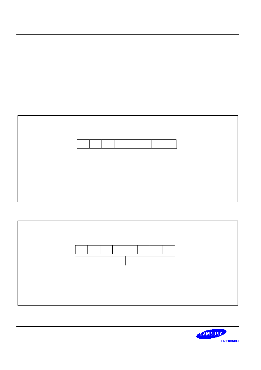
SYNC PROCESSOR
S3C8639/C863A/P863A/C8647/F8647
16-2
Logic for Detecting Sync-On-Green (SOG)
Special logic in the sync processor block can compare Hsync and Csync input signals to detect Sync-On-Green
(SOG). The interrupt SOG through Csync-I port is detected automatically at the SOG detection block. You can
confirm to SOG by means of reading SYNCON2.2 (SOG detection bit).
Pseudo Sync Generator
SYNCON2 settings (SYNCON2.4 = "0") control the pseudo Hsync and Vsync generation registers value (See
figure 16.1 and 16.2). The polarity of these frequencies is always positive, with pulse width of 2us (eight fsync
clock, when fsync is 4 MHz) and 6 x PHGEN periods, respectively. The pseudo sync generator supports factory
testing of the sync processor block and also protects a system against the effect of unexpected signals in
transition period while mode changing.
Pseudo Hsync Generation Register (PHGEN)
F9H, Set 1, Bank 0, R/W
.7
.6
.5
.4
.3
.2
.1
.0
LSB
Pseudo Hsync generation bits:
When SYNCON2.4 (generation pseudo H/Vsync generation mode) = "0"
- Positive polarity only
- Pulse width: 2 us (eight fsync clock, when fsync is 4 MHz)
- Range: 15.68 kHz (PHGEN = FFh) -400 kHz (PHGEN = 10h)
Figure 16-1. Pseudo Hsync Generation Register (PHGEN)
Pseudo Vsync Generation Register (PVGEN)
FAH, Set 1, Bank 0, R/W
.7
.6
.5
.4
.3
.2
.1
.0
MSB
LSB
When SYNCON2.4 (generation pseudo H/Vsync generation mode) = "0"
- Positive polarity only
- Pulse width: 6 PHGEN periods
- PVGEN value must be in [2-255] range
Pseudo Vsync generation bits:
Figure 16-2. Pseudo Vsync Generation Register (PVGEN)

S3C8639/C863A/P863A/C8647/F8647
SYNC PROCESSOR
16-3
Hsync & Vsync Polarity Detection, Unmixed Hsync Detection and Hsync Blanking
The polarity of Hsync & Vsync signal input to Hsync-I & Vsync-I pin is automatically detected. If the Hsync
polarity is negative, SYNCON1.0 equals to "0". If the Hsync polarity is positive, SYNCON1.0 equals to "1". This
polarity detection bit (SYNCON1.0) may be not accurate when the sync level is not in a transitional condition.
And if the Vsync polarity is negative, SYNCON1.1 equals to "1". This polarity detection bit (SYNCON1.1) may be
not accurate when the sync level is not in a transitional condition.
In composite sync mode, if SYNCON2.7 is set to "1", the current period of checked Hsync is stable, unmixed
with Vsync signal. If SYNCON2.7 is "0", the current period of checked Hsync is mixed with Vsync signal, in which
case it is recommended not to calculate the sync frequency. In this mode, the Hsync signal is automatically
blanked during the Vsync signal extraction period.
Table 16-1. VESA Monitor Timing Standards & PHGEN/PVGEN Value
Standard
Hsync Freq.
[kHz]
Standard
Vsync Freq.
[Hz]
Resolution
Line Num.
[Hf/Vf]
Pseudo
Hf/(PHGEN)
[kHz]
Pseudo
Vf/(PVGEN)
[Hz]
31.469
59.940
640
◊
480
525
31.49 (127)
59.65 (66)
37.861
72.807
520
38.09 (105)
73.26 (65)
37.500
75.000
500
37.73 (106)
74.87 (63)
35.156
56.250
800
◊
600
625
35.08 (114)
56.23 (78)
37.879
60.317
628
38.09 (105)
60.27 (79)
48.077
72.188
666
48.19 (83)
72.57 (83)
Reset Value
46.875
75.000
625
47.06 (85)
75.41 (78)
35.522
43.479
1024
◊
768
817
35.71 (112)
43.76 (102)
48.363
60.004
806
48.19 (83)
59.64 (101)
56.476
70.069
806
56.33 (71)
69.72 (101)
60.023
75.029
800
59.70 (67)
74.62 (100)
63.995
70.016
1152
◊
864
914
63.49 (63)
70.23 (113)
77.487
85.057
911
76.92 (52)
85.09 (113)
75.000
75.000
1280
◊
960
1000
75.47 (53)
75.47 (125)
63.974
60.013
1280
◊
1024
1066
63.49 (63)
60.12 (132)
79.976
75.025
1066
80.00 (50)
75.18 (133)
75.000
60.000
1600
◊
1200
1250
75.47 (53)
60.08 (157)
107.043
85.022
1259
108.11 (37)
85.52 (158)
NOTE: Pseudo Hsync frequency = fsync/PHGEN value
Pseudo Vsync frequency = Pseudo Hsync frequency/(8
◊
PVGEN value)

SYNC PROCESSOR
S3C8639/C863A/P863A/C8647/F8647
16-4
SYNC PROCESSOR CONTROL REGISTER 0 (SYNCON0)
The sync processor control register 0, SYNCON0, is located in set 1, bank 0, at address EDH. It is read/write
addressable. SYNCON0 bits 4≠0 hold the 5-bit counter value which is used for compare function. Whenever a
High signal level is detected, the count value is incremented by one until it reaches the maximum value of
"11111B" (No overflow occurs). Whenever a Low signal level is detected, the count value is decremented by one
until it reaches the minimum value of "00000B" (No underflow occurs).
NOTE
When the composit sync is inputted, compare mode is also called Vsync separation mode. In this mode,
output to the multiplexer is enabled. When the counter value is "11111B", the output is High level; when
the counter value is "00000B", the output is Low level. Whenever the counter value is less than ( < )
"11111B", or greater than ( > ) "00000B", the previous output level is retained.
SYNCON0 settings also control the following sync processor functions:
-- Horizontal or composite sync input (Hsync-I or Csync-I) selection
-- Automatically enable Hsync blanking or Hsync signal bypass
-- Vsync port input or 5-bit counter compare mode
-- Select the clock source for Vsync-O
See Figure 16-3 for a detailed description of SYNCON0 register settings.
SYNC Processor Control Register 0 (SYNCON0)
EDH, Set 1, Bank 0, R/W
.7
.6
.5
.4
.3
.2
.1
.0
MSB
LSB
5-bit compare counter value bits:
High signal: increment until "11111B"
Low signal: decrement until "00000B"
Vsync-O output source selection bit
(during Vsync signal extraction period):
0 = Select Vsync-I port input
(when separate sync input mode)
1 = Select 5-bit compare output
(when composite sync input mode)
Sync input selection bit:
0 = Hsync-I
1 = Csync-I
Hsync blanking enable bit:
0 = Disable (Hsync signal bypass)
(When SYNCON0.5="0")
1 = Enable automatically Hsync
blanking (during Vsync signal
extraction period)
(When SYNCON0.5="1")
Figure 16-3. Sync Processor Control Register 0 (SYNCON0)

S3C8639/C863A/P863A/C8647/F8647
SYNC PROCESSOR
16-5
SYNC PROCESSOR CONTROL REGISTER 1 (SYNCON1)
The sync processor control register 1, SYNCON1, is located in set 1, bank 0, at address EEH. It is read/write
addressable. Using SYNCON1 settings, you can:
-- Generate a clock pulse for Clamp signal output
-- Select "front porch" or "back porch" mode for Clamp-O
-- Control Clamp-O, Vsync-O, and Hsync-O status
-- Detect Hsync & Vsync polarity
See Figure 16-3 for a detailed description of SYNCON1 register settings.
SYNC Processor Control Register 1 (SYNCON1)
EEH, Set 1, Bank 0, R/W
.7
.6
.5
.4
.3
.2
.1
.0
MSB
LSB
Clamp output signal generation bits
(CSG1,0):
00 = Inhibit clamp signal output
01 = (f
OSC
x 2) clock pulse
(250 ns at 8 MHz f
OSC
)
10 = (f
OSC
x 4) clock pulse
(500 ns at 8 MHz f
OSC,
333 ns at 12 MHz f
OSC
)
11 = (fOSC x 8) clock pulse
(1 us at 8 MHz,
666 ns at 12 MHz)
Front/back porch clamp-O mode selection bit:
0 = Output clamp signal after rising
edge of Hsync-I (front porch)
1 = Output clamp signal after falling
edge of Hsync-I (back porch)
Hsync polarity detection bit:
(2)
0 = Negative
1 = Positive
Vsync polarity detection bit:
(1)
0 = Negative
1 = Positive
Hsync ouput status bit:
0 = Do not invert (by pass)
1 = Invert Hsync-O signal
Vsync ouput status bit:
0 = Do not invert (by pass)
1 = Invert Vsync-O signal
Clamp signal ouput status bit:
0 = Negative polarity
1 = Positive polarity
NOTES:
1.
To check Hsync/Vsync polarity, it uses 16 clocks of timer M2 (fx/1000). If the Vsync
polarity is changing, this bit will be updated after a typical delay of 2 ms, at 8 MHz f
OSC
(1.33 ms at 12 MHz f
OSC
)
2.
The SYNCON1.0 may not be accurate when the Hsync-I is composite sync signal
input.
Figure 16-4. Sync Processor Control Register 1 (SYNCON1)
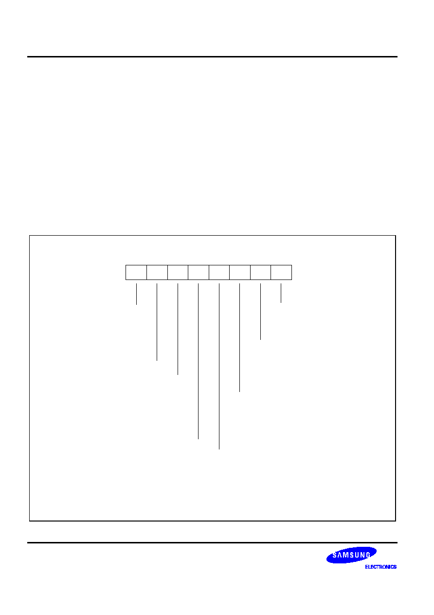
SYNC PROCESSOR
S3C8639/C863A/P863A/C8647/F8647
16-6
SYNC PROCESSOR CONTROL REGISTER 2 (SYNCON2)
The sync processor control register 2, SYNCON2, is located in set 1, bank 0, at address EFH. It is read/write
addressable. Using SYNCON2 settings, you can:
-- Detect mixed and unmixed Hsync period in composite sync
-- Select the pseudo sync generation enable mode
-- Select the clock source for the 5-bit counter
-- Sync signal output disable or enable
-- SOG signal detection
-- 5-bit up/down counter latch status changing detection
-- V
DD
level selection for TTL sync input ports
See Figure 16-5 for a detailed description of SYNCON2 register settings.
SYNC Processor Control Register 2 (SYNCON2)
EFH, Set 1, Bank 0, R/W
.7
.6
.5
.4
.3
.2
.1
.0
MSB
LSB
Unmixed Hsync detection bit
(when SYNCON0.5 is "1", read only)
0 = Mixed Hsync period with
Vsync of composite sync
input
(1)
1 = Unmixed Hsync periods
5-bit counter source clock (fsync) input
selection bit:
0 = f
OSC
/3 (when f
OSC
is 12 MHz)
1 = f
OSC
/2 (when f
OSC
is 8 MHz)
* Countable maximum Hsync pulse width:
7.85 us (when fsync is 4 MHz)
V
DD
level selection bit for
TTL sync input ports (only S3C863X)
0 = When V
DD
is +5 V
1 = When V
DD
is +3 V
5-bit up/down counter latch status
changing detection bit:
(2)
0 = When the latch status is not
changed or it writes "0" to this bit
1 = When the latch status changing is
detected
SOG detection bit:
0 = No SOG signal (when read)
0 = Clear SOG detection 5-bit
counter (when write)
1 = Csync-I is SOG signal (to check SOG
presence, it uses 64 Csync input edge
signal)
Sync signal output disable bit:
0 = Enable sync signal output
1 = Inhibit sync signal otput
(output level is low)
Pseudo sync generation disable bit:
0 = Enable pseudo Hsync/Vsync generation
(positive polarity only)
1 = Normal sync-processor operation (by pass)
NOTES:
1.
The SYNCON2.7 is still cleared before read this bit or it has been in mixed Hsync period.
2.
The SYNCON2.1 can be used to check the presence of composite sync signal input
Not used for KS88C6332/C6348 (only "0")
Figure 16-5. Sync Processor Control Register 2 (SYNCON2)

S3C8639/C863A/P863A/C8647/F8647
SYNC PROCESSOR
16-7
5-Bit Up/Down
Counter
(SYNCON0.4-.0)
Clamp-O
SYNCON2.5
Hsync
Polarity
Detector
Vsync
Polarity
Detector
4-Bit
Counter
3-Bit
Up/Down
Counter
N.F.
8-Bit Scaler
(PVGEN)
SYNCON2.4
Pseudo
Vsync
Generator
1/8
8-Bit Scaler
(PHGEN)
Pseudo
Hsync
Generator
Vsync-O
SYNCON1.3
f
OSC
/3
f
OSC
/2
Hsync-I
SYNCON2.4
SYNCON0.7
Csync-I
SYNCON1.2
SYNCON1.4
Clamp
Signal
Generator
f
OSC
/1000
To Timer M0/Timer M1
Capture Input
Hsync-O
SOG Detection Logic
SYNCON2.2
Hsync Blanking
Polarity
N.F.
To 12-Bit
Counter TM1
SYNCON1.5
SYNCON0.6
fsync
Vsync-I
(VCLK)
Port Read
OVF
SYNCON0.5
Data Bus
Figure 16-6. Sync Processor Block Diagram

SYNC PROCESSOR
S3C8639/C863A/P863A/C8647/F8647
16-8
DETECTING SYNC SIGNAL INPUT
You can detect the presence of a sync signal in two ways -- directly or indirectly. The direct detection method
can be implemented in read port. The indirect detection method is interrupt-driven and uses the
S3C8639/C863A/C8647 sync processor hardware. These methods are explained in detail below.
Direct Detection Method
By reading the input status directly on the sync input pins Vsync-I, Hsync-I, Csync-I, you can detect the presence
of the incoming sync for a corresponding output.
To enable direct sync input detection, you set SYNCON0.5 to "0" (for Vsync-I), SYNCON0.7 to "0" (for Hsync-I),
and SYNCON0.7 to "1" (for Csync-I).
You then read the state of the input pin(s) over a period of time to detect transitions in the signal level(s). If a
transition is detected, it can be assumed that a sync signal is present.
Indirect Detection Method
To indirectly detect vertical sync input at the Vsync-I pin, you use register settings to assign either the timer M0
capture interrupt to this pin.
For indirect detection of horizontal or composite input at the Hsync-I or Csync-I pin, you use the timer 1 input
clock source to generate a timer M1 capture/overflow interrupt by capture signal from timer M2 interval or Vsync-
O from sync-processor, when a signal level transition occurs. Or to detect composite sync , you can confirm to
presence with checking SYNCON2.1. (This bit is used to check the presence of composite sync signal input.)
When the correct settings have been made, the application software polls for the respective interrupts to
determine the presence of sync input signals, as follows:
-- Indirect Vsync input detection
Check for the occurrence of a timer M0 capture interrupt (IRQ0).
-- Indirect Hsync input detection
Check for the occurrence of a timer M1 capture/overflow interrupt (IRQ2).
-- Indirect Csync input detection (SOG)
Check for the occurrence of a timer M1 capture/overflow interrupt (IRQ2).
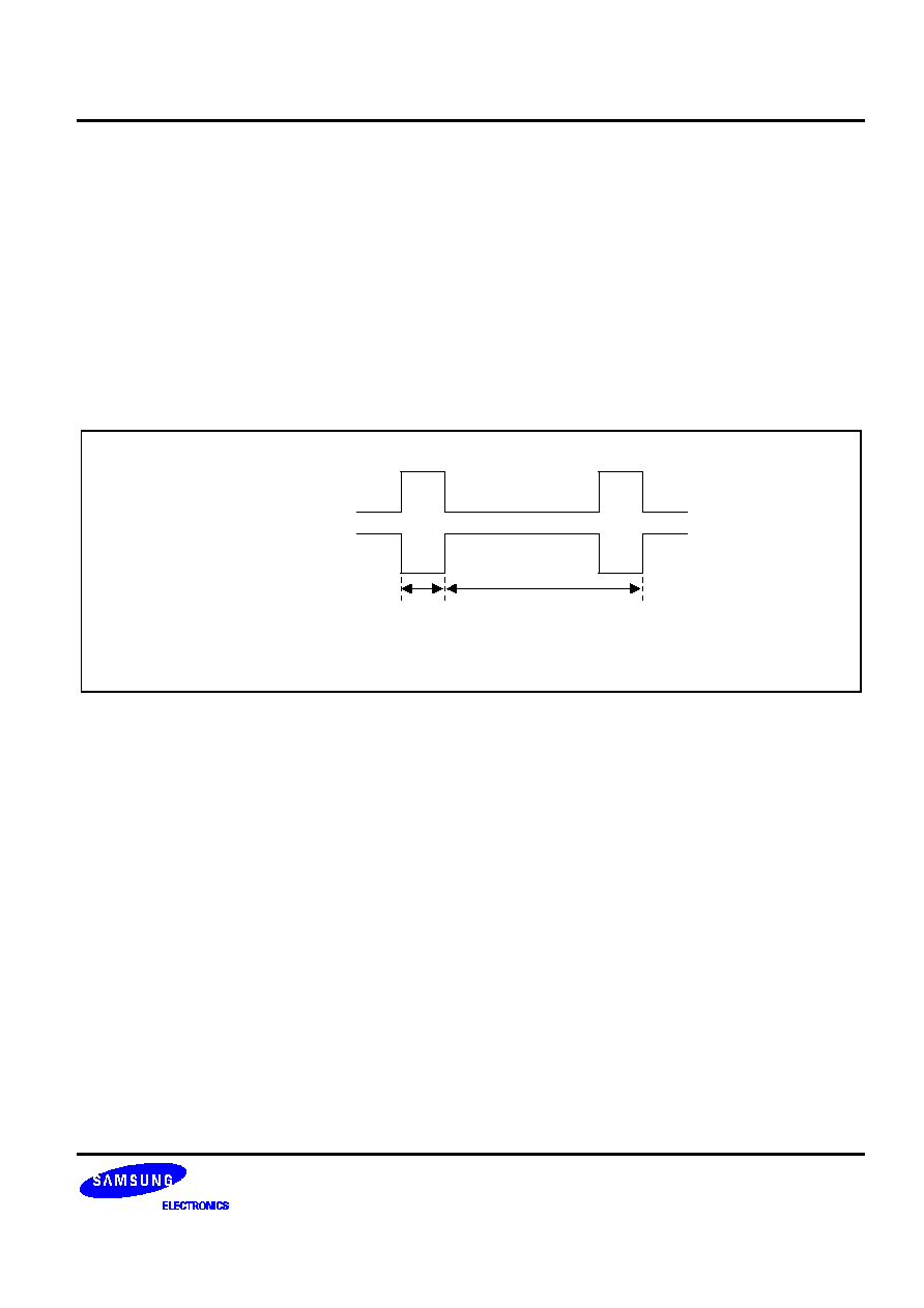
S3C8639/C863A/P863A/C8647/F8647
SYNC PROCESSOR
16-9
AUTO-DETECTING SYNC SIGNAL POLARITY
The S3C8639/C863A/C8647 sync processor lets you detect automatically the polarity of Vsync or Hsync signals
by hardware. To check H/Vsync polarity, it uses 16 clocks of timer M2 (f
OSC
/1000).
You can detect the polarity of Hsync signal inputted to Hsync-I port through checking SYNCON1.0 by the 5-bit
counter of sync processor. If SYNCON1.0 is "1", the polarity of the inputting Hsync signal is positive. When
SYNCON1.0 is "0", the polarity of Hsync signal is negative. But when the inputted sync signal to Hsync-I is
composite sync signal (H+Vsync signal), the staus of SYNCON1.0 may not be accurate.
To detect the polarity of Vsync signal, it uses SYNCON1.1. If SYNCON1.1 is "1", the polarity of Vsync signal is
positive. When the polarity of Vsync signal is negative, SYNCON1.1 is "0". If Vsync polarity is changing,
SYNCON1.1 will be updated after a typical delay of 2ms, at 8 MHz f
OSC
(1.33ms at 12 MHz f
OSC
).
Positive Type
Negative Type
Vsync Frequency:
Max: 200 Hz (5 ms)
Vsync Pulse Width:
Min: 10us
Max: 600 us
Figure 16-7. Vsync Input Timing Diagram
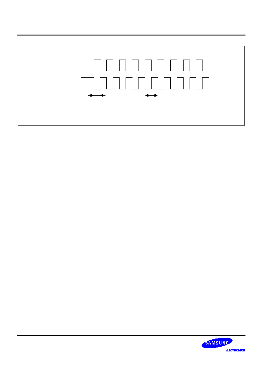
SYNC PROCESSOR
S3C8639/C863A/P863A/C8647/F8647
16-10
Positive Type
Negative Type
Hsync Frequency:
Max: 160 kHz (6.25 us)
Hsync Pulse Width:
Min: 0.5 us
Max: 7.85 us
Figure 16-8. Hsync Input Timing Diagram
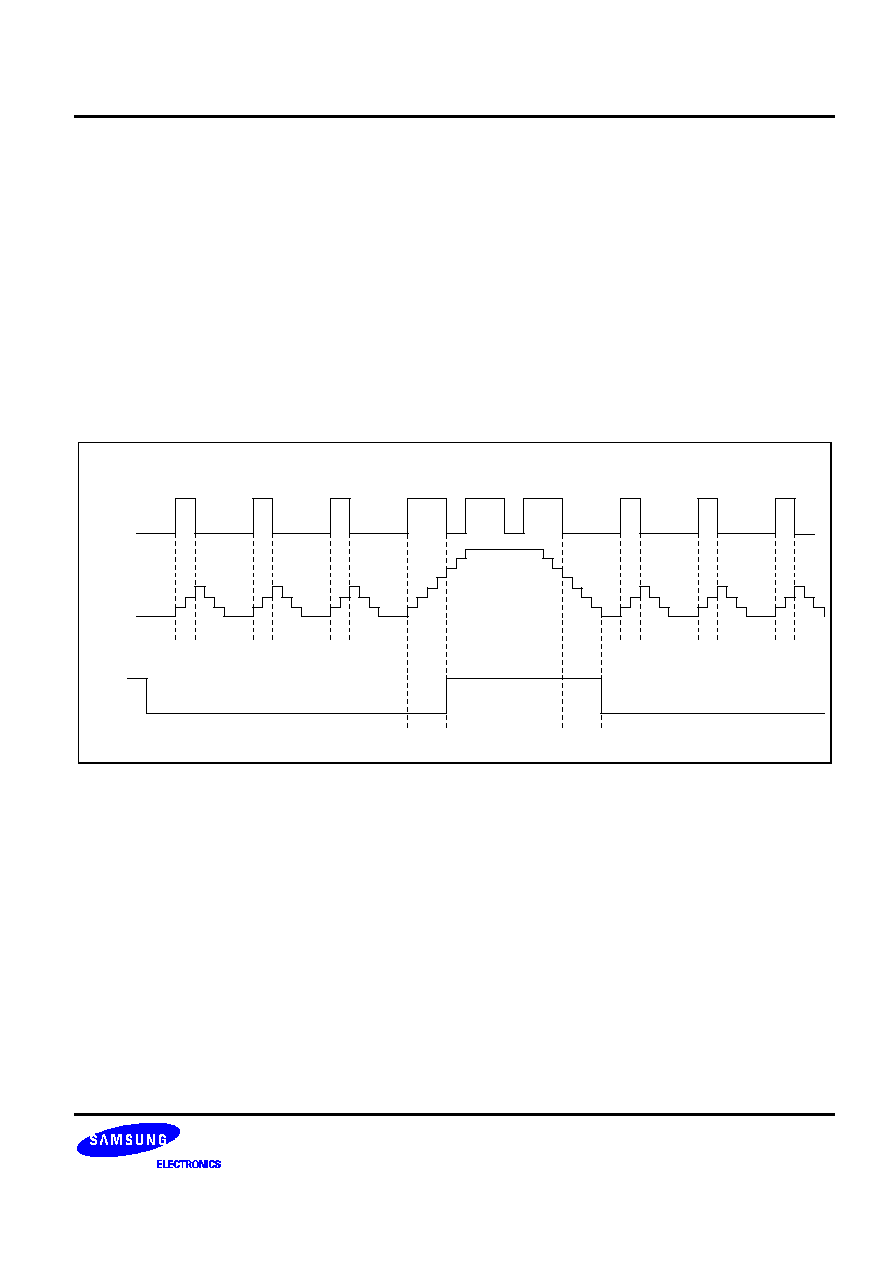
S3C8639/C863A/P863A/C8647/F8647
SYNC PROCESSOR
16-11
EXTRACTING VSYNC OUTPUT
When the Vsync input at Hsync-I or Csync-I (P2.7) also contains Hsync signals, you must extract the Vsync
component from the Hsync (or Csync) input. To do this, you use the 5-bit up/down counter.
To extract the Vsync component of the input signal, you first set the 5-bit up/down counter to operate in compare
mode (SYNCON0.5 = "1"). Vsync output is enabled only when the minimum or maximum threshold value is
reached.
During vertical blanking, the counter decreases until it reaches a minimum value while the Hsync-I or Csync-I
signal level is negative. Or, the counter value increases until it reaches a maximum value while the Hsync-I or
Csync-I signal level is positive (no overflow or borrow occurs).
The timer M1 capture interrupt (IRQ2) can be enabled to verify that the Vsync signal has been extracted
successfully from the mixed input signal.
Composite
Sync
(Hsync-I
Input)
5-bit
Counter
Value
5-bit
Counter
Output
Figure 16-9. Vsync Extraction Using an Up/Down Counter
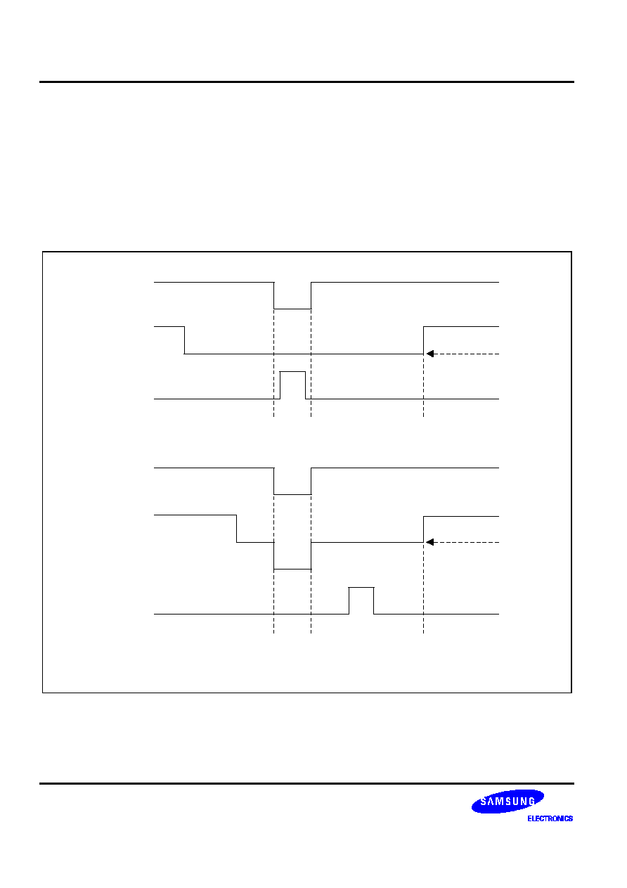
SYNC PROCESSOR
S3C8639/C863A/P863A/C8647/F8647
16-12
CLAMP SIGNAL OUTPUT
Clamp signal output (Clamp-O) must be synchronized with Hsync output. The Clamp-O signal can be transmitted
to a vertically or horizontally driven integrated circuit to provide a pedestal level for image signals with
programmable pulse width.
The Clamp signal is output on the "front porch" of an Hsync signal (NO SOG condition) or on the "back porch" of
an Csync signal (SOG condition). You can control the polarity of clamp output signal with using SYNCON1.4.
If you want to the negative pulse of clamp signal, you must set SYNCON1.4 to "0". If you set SYNCON1.4 to "1",
the polarity of clamp output signal is positive.
Source Hsync
Pedestal
Level
Front Porch
(No SOG)
Back Porch
Image Signal
Clamp-O Port
Output
Source Hsync
Pedestal
Level
Front Porch
(No SOG)
Back Porch
Image Signal
Clamp-O Port
Output
Figure 16-10. Clamp-O Signal (SOG and NO SOG Condition)

S3C8639/C863A/P863A/C8647/F8647
SYNC PROCESSOR
16-13
DIFFERENTIATING SOG FROM NO SOG
The pulse width at the Csync-I pin is different in SOG and NO SOG conditions. In a SOG condition, the pulse
width at Csync-I and Hsync-I is identical. If a NO SOG condition exists, Csync-I has a wider pulse width than
Hsync-I because the Csync-I pulse is truncated at the base of the pedestal level (see Figure 16-10).
To differentiate the Csync pulse, you must delay the Csync-I pulse for about 150 ns and then compare its phase
with that of the Hsync-I pin signal.
To indicate a SOG condition, comparator logic for Hsync and Csync sets the SYNCON2.2 flag to "1" whenever
Csync status differs from Hsync status more than 32 times at the rising edge of Hsync-I. To perform the
comparison, first detect the polarity of the Hsync-I signal. Then configure the pin for positive output. (Csync-I is
always positive and requires no special settings.) To recognize the SOG condition, you can poll the SYNCON2.2
status flag to detect when it is set to "1".
Csync Port Input
150 ns
150 ns
Hsync Port Input
After 150 ns delay SOG
After 150 ns delay NO SOG
Figure 16-11. Sync Input at the Hsync-I and Csync-I Pins
Hsync-O
Maximum delay is 250 ns
Clamp-O
Programmable Clamping Width (0, 250
ns, 500 ns, 1 us)
Figure 16-12. Clamp-O Signal Delay Timing

SYNC PROCESSOR
S3C8639/C863A/P863A/C8647/F8647
16-14
F
F
PROGRAMMING TIP -- Programming the Sync Processor
This example shows how to program the sync processor to sample specifications. The sample program performs
the following actions:
--
Confirm the presence of sync signal input
--
Detect the polarity of Hsync or Vsync signal input
;//**************************************************************
;//** Title : Definition Flag Ram for user (00h - 0Fh)
*
;//**
*
;//**
*
;//**************************************************************
;
DeGausport
equ
3
;P0.3=Degauss control pin(Active High)
Suspndport
equ
4
;P0.4=Suspend control pin(High)
Offport
equ
5
;P0.5=Off control pin(Low)
Muteport
equ
7
;P0.7=Video mute control pin(Low)
;
SelfRastport
equ
0
;P1.0=Self-Raster input pin
S1
equ
1
;P1.1=S-correction 1
S2
equ
2
;P1.2=S-correction 1
;
;X-Ray
equ
0
;Not used
;Rotation
equ
1
;P2.1=Pwm1 Out (Rotation)
;H-Size
equ
2
;P2.2=Pwm2 Out (H-Size)
;Contrast
equ
3
;Not used
;Brightness
equ
4
;Not used
;ACL
equ
5
;P2.5=Pwm5 Out (ACL)
Hsize_Min
equ
6
;Not used
ModelSelport
equ
7
;P2.7=Model Sel.input pin(14":L/15":H)
;
Pwrkeyport
equ
0
;P3.0=S/W power key input pin
Ledport
equ
5
;P3.5=LED control
SCL
equ
6
;P3.6=SCL(S/W IIC.bus)
SDA
equ
7
;P3.7=SDA
;
;Fixed port.
;H_Input
equ
1
;H-Sync. Input
;V_Input
equ
2
;V-Sync. Input
;Clamp
equ
3
;Clamp Output
;H_Out
equ
4
;H-Sync. Output
;V_Out
equ
5
;V-Sync. Output
;DDC_Clock
equ
6
;DDC Clock
;DDC_Data
equ
7
;DDC Data
;
HsyncIport
equ
0
;SYNCRD.0=HsyncI pin
VsyncIport
equ
1
;SYNCRD.1=VsyncI pin
VsyncOport
equ
3
;SYNCRD.3=VsyncO pin
;
;

S3C8639/C863A/P863A/C8647/F8647
SYNC PROCESSOR
16-15
// Define flags
;
;
SyncP_FGR0
EQU
00h
;SYNC-PROCESSOR
HSyncFin_FG
equ
7
;Hsync signal counting every 10ms
VSyncFin_FG
equ
6
;Vsync signal find flag(Vsync capture interrupt)
VstblFreq_FG
equ
5
;Stable Vsync frequency input status
HstblFreq_FG
equ
4
;Stable Hsync frequency input status
NormSync_FG
equ
3
;Normal sync output mode(No pseudo sync signal)
SetSepSync_FG
equ
2
;Indicate separate sync mode
MixedSync_FG
equ
1
;Mixed sync input period(composite sync input mode)
DdcHighSpd_FG
equ
0
;DDC1 high speed mode(over 400Hz)
;
SyncP_FGR1
EQU
01h
;
HPolarity_FG
equ
7
;Hsync polarity => 1=positive, 0=negative
VPolarity_FG
equ
6
;Vsync polarity => 1=positive, 0=negative
HNosync_FG
equ
5
;Hsync freq. < 10KHz
VNosync_FG
equ
4
;Vsync freq. < 40Hz
NoSync_FG
equ
3
;No Vsync & No Hsync signal
OverHsync_FG
equ
2
;Hsync over range : over 62KHz
OverRange_FG
equ
1
;Vsync over range : over 135Hz
;
Mute_FGR
EQU
02h
;
Vmute_FG
equ
7
;Being video mute
ChkSyncStus_FG
equ
6
;Video mute time end
MuteWaiting_FG
equ
5
;Being video mute extension
MuteRelse_FG
equ
4
;Video mute release
PwrOnWait_FG
equ
3
;Power-on mute delay(2sec)
PsyncOut_FG
equ
2
;Pseudo sync output status
NormMwait_FG
equ
1
;Count mute extension time(350ms)
;
Time_FGR
EQU
03h
;
KeyDetect_FG
equ
7
;Key detecting per 10ms
DeGTime_FG
equ
6
;Degaussing time(3sec)
ChkPwrKey_FG
equ
5
;Checking power-key status per 10ms
;
Status_FGR
EQU
04h
;
SfRasterIn_FG
equ
7
;Self-Raster mode
Recall_FG
equ
6
;Recall function(Continuous key=3sec)
UserDel_FG
equ
5
;Delete user data in EEPROM(Continuous key=5sec)
FindSyncSrc_FG
equ
4
;
EepRom_FGR
EQU
05h
;
UserArea_FG
equ
7
;Checking EEPROM user data area
ClosHsync_FG
equ
6
;Searching closest Hsync mode
SavedEep_FG
equ
5
;Factory data saved EEPROM ?
EepDataRd_FG
equ
4
;EEPROM data read after mode changing
NoFactSave_FG
equ
3
;EEPROM data read after mode changing
;
Tda9109_FGR
EQU
05h
;
TdaWrite_FG
equ
2
;Write PWM data to TDA9109
TdaRead_FG
equ
1
;Read from TDA9109
;

SYNC PROCESSOR
S3C8639/C863A/P863A/C8647/F8647
16-16
Dpms_FGR
EQU
09h
;
DpmsStart_FG
equ
7
;DPMS mode start(3sec after abnormal sync signal)
ChkDpmsCon_FG
equ
6
;DPMS condition input(H<10KHz,V<40Hz)
PwrOffIn_FG
equ
5
;Power Saving Mode
OffMode_FG
equ
4
;Off mode
Suspend_FG
equ
3
;Suspend mode
StandBy_FG
equ
2
;Standby mode
;
IIC_FGR
EQU
0Ah
DDCCmd_FG
equ
7
;Get DDC2B+ command
LastByte_FG
equ
6
;Last Tx Data
CommFail_FG
equ
5
;Communication fail(Not ACK)
ReWrite_FG
equ
4
;Rewrite to EEPROM
ReRead_FG
equ
4
Ddc2mode_FG
equ
3
RevA0match_FG
equ
2
Ddc2BTxmode_FG
equ
1
;
CheckSum
EQU
0Bh
;DDC2B+
ByteCnt
EQU 0Ch
;Count number of Tx data
SendType
EQU 0Dh
;Reply type
NumTxdByte
EQU 0Eh
;#(Total Tx byte -1) in master Tx mode
xXCntr
EQU 0Fh
;Number of Rx data
;
;
;//*****************************************************************
;//** Title : Definition general purpose Ram (10h - BFh) *
;//**
*
;//**
*
;//*****************************************************************
;
TB1mSR
EQU 10h
;1ms interval register(basic time reg.)
TB10mSR
EQU 11h
;10ms(Count Hsync event signal)
TB100mSR
EQU 12h
;100ms(Func valid time => 7sec)
DLY1mSR
EQU 13h
;1ms(Cehcking writecycle time => 10ms)
M10mSR
EQU 14h
;10ms(Checking mute time => sec,350ms)
S100mSR
EQU 15h
;100ms(Saving start time => 2sec)
DG100mSR
EQU 16h
;100ms(Degaussing time => 3sec)
DPMS100mSR
EQU 17h
;Check DPMS start(after No Sync : 3sec)
ChkSRasTime
EQU 18h
;Check self-raster input(maintain 70ms ?)
;
HCount
EQU
20h
;Double byte(even address + odd address)
;
EQU
21h
HFreqStCnt
EQU
22h
FreqSpCnt
EQU
23h
AverageHf
EQU
24h
HfHighNew
EQU 25h
;Current value of Hsync freq high byte
HfLowNew
EQU 26h
HfHighData
EQU 27h
;Saved value of Hsync freq high byte
HfLowData
EQU
28h
;Real Hsync frequency = Low nibble of Hfreq high data +
;Hfreq low data

S3C8639/C863A/P863A/C8647/F8647
SYNC PROCESSOR
16-17
;ex> if, HfHighData=#x2h,
;HfLowData=#58h => Hsync frequency = 258h=60.0Khz
Vcount
EQU
30h
;total number of timer0 counter within Vsync period
;
EQU
31h
;Double Byte
NoVTime
EQU 32h
;Checking the sustaining time of no Vsync signal
;if NoVTime > 30ms(under 33Hz) => Mute
VFreqCHigh
EQU 33h
;Temp storage of Timer0(Vsync) overflow count
T0OvfCntr
EQU
34h
;No vsync-int. service if DDC1 high freq. Mode
VfCurrNew
EQU 35h
;Current Vsync freq
VFreqData
EQU 36h
;Saved Vsync freq.
VclkCntr
EQU
37h
;For auto recovery of DDC mode (DDC2B -> DDC1)
;
PolaCntr
EQU
38h
;Count number of polarity checking
VPolaCntr
EQU
39h
;Increment when positive polarity
;
UmodeNo
EQU 40h
;Matched number of user mode
FmodeNo
EQU 41h
;Factory mode
ReadData
EQU
42h
;Readed Data from EEPROM
;
EP_BPlus
EQU
50h
;EEPROM & RAM data
EP_CONTRAST
EQU
51h
;KA2504
EP_RGain
EQU
52h
EP_GGain
EQU
53h
EP_BGain
EQU
54h
EP_CoffBRIGHT
EQU
55h
;KA2504
EP_RCutoff
EQU
56h
EP_GCutoff
EQU
57h
EP_BCutoff
EQU
58h
EP_ACL
EQU
59h
;PWM5
;
;
EdidAddr
EQU
80h
;Page1 RAM register
;EDID address(00~7Fh:128-byte)
;
;// WORKING REGISTERS -> GENERNAL RAM
;
;R14
EQU
EepSubAddr
;Sub address of EEPROM/TDA9109
;R15
EQU
EepWrData
;Data to write in EEPROM/TDA9109
;---> KA2504 Pre-amp control
;R14
EQU
PreAmpSubAddr
;Sub address
;R15
EQU
PreAmpCtrlData
;Data address
;
;// Buffer for DDC2B+ protocol
;
MBusBuff
EQU 0B0h
;For DDC2B+(00h-0BFh:16-byte)
AbusDstAddr
EQU
0B0h
AbusSrcAddr
EQU
0B1h
AbusPLength
EQU
0B2h
AbusCommand
EQU
0B3h
; :
:
;
EQU
0BFh
;

SYNC PROCESSOR
S3C8639/C863A/P863A/C8647/F8647
16-18
;##############################################################
;
;// DDC EDID AREA : 00h - 7Fh (128-Byte : Page 1)
;
;##############################################################
;
;//**************************************************************
;//** Title : Define Control register's flags
;//**
;//**
;//**************************************************************
;// IIC.bus Control Register
;// DCON
BUFEN
equ
3
;Tx/Rx pre-buffer data register enable(0:Normal,
;1: Pre-buffer Mode)
DDC1MAT
equ
2
;DDC address match(0:Not match, 1:match)
DDC1EN
equ
1
;DDC1 Tx mode enable
SCLF
equ
0
;SCL falling edge detection
;
;// DCCR(DDC Clock Control Reg)
DTXACKEN
equ
7
DCLKSEL
equ
6
DINTEN
equ
5
DPND
equ
4
CCR3
equ
3
CCR2
equ
2
CCR1
equ
1
CCR0
equ
0
;
;// DCSR0(DDC Control/Status Reg0)
DMTX
equ
7
DSTX
equ
6
DBB
equ
5
DDCEN
equ
4
DAL
equ
3
DADDMAT
equ
2
;equ
1
;Not Used for the KS88C6332/48/P6348
DRXACK
equ
0
;
;// DCSR1(DDC Control/Status Reg1)
STCONDET
equ
2
;IIC-Bus Stop Condition Detect
DBUFEMT
equ
1
;Data buffer empty status
;(0:Write to TBDR, 1:TBDR -> DDSR) when Tx
DBUFFUL
equ
0
;Data buffer full status
;(0:Read from RBDR, 1:DDSR -> RDBR) when Rx
;
;TBDR
;Transmit pre-buffer data register
;RBDR
;Receive pre-buffer data register
;DDSR
;DDC data shift register
;
;// Sync-processor control register
;// SYNCON0
SIS
equ
7
;Sync input selection(0:Hsync, 1:Csync)

S3C8639/C863A/P863A/C8647/F8647
SYNC PROCESSOR
16-19
HBLKEN
equ
6
;Hsync Blanking Enable(0:Bypass, 1:Blanking)
VOSS
equ
5
;VsyncO source selection(0:VsyncI, 1:5-bit compare out)
;
;// SYNCON1
CLMP1
equ
7
;
CLMP0
equ
6
;ClampO pulse width
FBPS
equ
5
;Front/Back porch selection(0:back, 1:front)
CLMPS
equ
4
;ClampO polarity control(0:negative, 1:positive)
VOS
equ
3
;VsyncO polarity control(0:by-pass, 1:invert)
HOS
equ
2
;HsyncO polarity control(0:by-pass, 1:invert)
VPOL
equ
1
;Vsync polarity detection(0:negative, 1:positive)
;Read only
HPOL
equ
0
;Hsync polarity detection(0:negative, 1:positive)
;Read only
;
;// SYNCON2
UNMIXHSYNC
equ
7
;Unmixed Hsync detection
;(0:Mixed sync, 1:Unmixed sync), Read only
CCSS
equ
5
;5-bit counter clock selection(0:fosc/2, 1:fosc/3)
PSGEN
equ
4
;Pseudo Sync Generation Disable
SYNOD
equ
3
;Sync Signal Output Diasble
SOGI
equ
2
;SOG check
UP5BSDET
equ
1
;5-Bit Up/Down Counter Status Changing Det.
VDDLS
equ
0
;VDD Level Selection(0:VDD=5V,1:VDD=3V)
;
;// Watch-dog(Basic) Timer
BTCLR
equ
1
;
;// Timer M0
T0EDGSEL
equ
4
;Timer M0 Capture Mode Selection
T0CLR
equ
3
;Counter clear
T0OVINT
equ
2
;Overflow interrupt enable
T0INT
equ
1
;Capture enable
T0CAPSEL
equ
0
;Capture input selection
;(0:External pin, 1:Vsync from sync-processor)
;
;// Timer M1
T1CAPSEL
equ
7
;Capture signal source selection
;(0:Timer2, 1:VsyncO from P)
VEDGSEL
equ
6
;VsyncO capture edge selection(0:rising, 1:falling)
T1CAPEN
equ
5
;Capture interrupt enable
T1PND
equ
4
;Capture interrupt pending flag
T1CLR
equ
3
;Counter clear
T1OVFINT
equ
2
;Overflow interrupt enable
;
;// Timer M2
T2INT
equ
2
CAPINTV1
equ
1
CAPINTV0
equ
0
;
;
;
;

SYNC PROCESSOR
S3C8639/C863A/P863A/C8647/F8647
16-20
;// Pre-Amp Sub-address Mapping
;Slave address=DCh
;
PSubA_Cont
EQU
00h
;Contrast control
PSubA_SBnBr
EQU
01h
;bit7=Soft Blanking(1:ON, 0:OFF)
;Bit6-5=Cut-off control offset current switch
;(CS2:160uA, CS1:80uA)
;Bit4-0=Brightness control
PSubA_RGain
EQU
02h
;R Gain Control
PSubA_GGain
EQU
03h
;G Gain Control
PSubA_BGain
EQU
04h
;B Gain Control
PSubA_CoBr
EQU
05h
;Cut-off brightness control
PSubA_RCo
EQU
06h
;R Cut-off control
PSubA_GCo
EQU
07h
;G Cut-off control
PSubA_BCo
EQU
08h
;B Cut-off control
PSubA_Sw
EQU
0Ah
;Blanking On-Off Control
;
;// EEPROM Address Mapping
;
EPA_CoBr
EQU
0F6h
;KA2504 Cut-off Brightness
EPA_Cont
EQU
0F7h
;KA2504 Cut-off Contrast
EPA_RGain
EQU
0F8h
;KA2504 R-Gain
EPA_GGain
EQU
0F9h
EPA_BGain
EQU
0Fah
EPA_RCo
EQU
0FBh
;KA2504 R-Cut off
EPA_GCo
EQU
0FCh
EPA_BCo
EQU
0FDh
EPA_ACL
EQU
0Feh
;
;
;
;------------------------------------------------------------------
;----- DDC2ab comunication command code ------
;------------------------------------------------------------------
I_Reset
equ
0F0h
I_IdReq
equ
0F1h
;
I_AsgnAdr
equ
0F2h
I_CapReq
equ
0F3h
I_ApplRprt
equ
0F5h
;
I_Attention
equ
0E0h
I_IdReply
equ
0E1h
I_CapReply
equ
0E3h
;
I_GetVCP
equ
01h
I_VCPFReply
equ
02h
I_SetVCP
equ
03h
I_GetTiming
equ
07h
I_ResetVCPF
equ
09h
I_DisableVCPF
equ
0Ah
I_EnableVCPF
equ
0Bh

S3C8639/C863A/P863A/C8647/F8647
SYNC PROCESSOR
16-21
SaveCurrSet
equ
58h
I_TimingReport
equ
4Eh
;
I_GetEdid
equ
54h
SaveEdid
equ
69h
;
DelUser
equ
50h
AllModeSve
equ
52h
;
SaveColorSet
equ
7Dh
BrtContMax
equ
0D2h
;
;
;//*************************************************************
;//** Title : Interrupt Vector Table
*
;//**
*
;//*************************************************************
;
ORG
00E0h
VECTOR TM0Ovf_Int
;Timer M0 overflow int.(IRQ0)
VECTOR VSyncDet_Int
;Timer M0 capture int.(IRQ0)
VECTOR TM2Intv_Int
;Timer M2 interval int.(IRQ2)
;
ORG
00E8h
VECTOR TM1Cap_Int
;Timer M1 capture int.(IRQ1)
;
ORG
00EAh
VECTOR DDCnFA_Int
;DDC IIC-bus Tx/Rx int.(IRQ3)
;
;________________________________________________________________
;
ORG 0100h
;________________________________________________________________
;//**************************************************************
;//** Title : Main Program start from here
*
;//**
*
;//**************************************************************
;
;//**************************************************************
;//** Title : << System Reg. Files Initialization >>
*
;//**
*
;//**
*
;//**************************************************************
;
RESET:
DI
;Disable interrupt
CLR PP
;Source, Destination = page0
CLR
SYM
;Disable fast interrupt
LD SPL,#0FFh
;Stack pointer
SRP #0C0h
;Working reg. area
LD IMR,#00001111B
;Timer M0,M1,M2, & DDC Int.
;bit7 -> not used
;bit6 -> not used
;bit5 -> not used

SYNC PROCESSOR
S3C8639/C863A/P863A/C8647/F8647
16-22
;bit4 -> not used
;bit3 -> IRQ3 DDC Int.
;bit2 -> IRQ2 Timer M1 Cap. Int.
;bit1 -> IRQ1 Timer M2 Int.
;bit0 -> IRQ0 Timer M0 Cap. & Ovf. Int.
SB0
;Select bank 0
CLR EMT
;0 wait, Internal stack area
LD IPR,#00010001B
;Group priority(int) undefined(A>B>C)
;TM2/TM1 > TM0 > DDC
LD CLKCON,#18h
;CPU=fx(no division)
LD BTCON,#0A2h
;WatchDog Timer Disable
LD
WDTCON,#00h
;Watchdog Time = tBTOVF
LD
STOPCON,#5Ah
;Stop Function Disable
;Initialize Sync-processor control register
;
LD
SYNCON2,#10100000B
;Bit7=read only
LD
SYNCON1,#11000000B
;ClampO=negative polarity
;VsyncO=5-bit counter compare output
LD
SYNCON0,#00100000B
;Automatic Hsync blanking,
;syncO source=VsyncI port
LD
PHGEN,#83
;Pseudo Hsync = 48.19KHz
LD
PVGEN,#101
;Pseudo Vsync = 59.64KHz
;
;Initialize Timer control register
;
LD
TM0CON,#10001111B
;Timer0 clock source=@8MHz/8=1MHz(1us)
;Capture rising mode
;Enable capture/overflow interrupt
;Capture source=Vsync output path
;from sync-processor
LD
TM1CON,#00001100B
;source=HsyncI
;Capture disable
;Capture Source=Timer2 interval time*10(10ms)
;Enable capture interrupt
LD
TM2CON,#00111101B
;Timer2 interval=@8MHz/(8*1000)=1ms
;
;*****************************************************************************
MAIN:
CALL
ChkDDC2Bi
CALL
ChkDDCRecover
CALL
ChkHVPres
;Check H/Vsync presence
CALL
ChkHVPol
;Check H/Vsync polarity
;
;
JR
MAIN
;*****************************************************************************
;
;******************************************************
;******* DDC2Bi service routine *******
;******************************************************
ChkDDC2Bi
TM
IIC_FGR,#01<<DDCCmd_FG
;DDCCmd_FG=0 ?
JR
Z,DDC2BPrtn
SB1

S3C8639/C863A/P863A/C8647/F8647
SYNC PROCESSOR
16-23
TM
DCSR0,#01<<DBB
;End of Rx(Not usy) ?
JR
NZ,DDC2BPrtn
SB0
CLR RxXCntr
;RxXCntr <- #00h
AND
IIC_FGR,#0FFh-(01<<DDCCmd_FG)
;ActIIC_FG <- 0
CALL
DDC2biRxd
DDC2BPrtn
SB0
RET
;
;
*************************************************************
;***** DDC mode checking service routine ******
;************************************************************
ChkDdcRecover
TM
IIC_FGR,#01<<Ddc2BIn_FG
;Already DDC2B mode ?
JR
NZ,ChkDdcRtn
SB1
TM
DCON,#01<<SCLF
JR
NZ,ChkDdc2In
ChkDdcRtn
SB0
RET
;
ChkDdc2In
TM
DCON,#01<<DDC1EN
;DDC1 Tx mode ?
JR
NZ,ChkDdcRtn
CP
VclkCntr,#128
JR
ULE,ChkDdcRtn
OR
DCON,#01<<DDC1EN
;Switch back to DDC1 from DDC2B
AND
DCON,#0FFh-(01<<SCLF)
AND
IIC_FGR,#0FFh-(01<<Ddc2BIn_FG)
CLR
VclkCntr
LD
TBDR,#00h
LD
PP,#11h
LD
EdidAddr,#01h
CLR
PP
JR
ChkDdcRtn
;
DDC2BiRxd
NOP
RET
;
;//*************************************************************************************
;//** Title : Check H/V presence, a kind of sync source and mode changing
;//**
;//**
;//** Inputs:
;//** Outputs:
;//** Preserves:
;//** Corrupts: R0,
;//*************************************************************************************
ChkHVPres:
TM
SyncP_FGR0,#01<<HSyncFin_FG
;Checking period of Hsync frequency
;is 10ms by timer M1/2 interrupt
JR
Z,ChkPresnVsync
AND SyncP_FGR0,#0FFh-(01<<HSyncFin_FG)
;
; Every by 10ms
CALL
Chk10msTimer
; Time counter(100ms,1sec,2sec,3sec,7sec)

SYNC PROCESSOR
S3C8639/C863A/P863A/C8647/F8647
16-24
;
CheckHV_Range
CALL ChkHNosyncRange
JP
C,SyncOffState
;Under 10KHz ?
;
ChkHsyncData
CALL UHSyncChk
;Check changing rate of Hsync frequency
JP
C,SyncOffState
;If changing rate > 00Hz
CALL UPolaChk
;Check Polarity data
JP
C,SyncOffState
;
ChkPresnVsync
CP
NoVTime,#25
;If NoVTime > 25ms(under 40Hz) => Mute
JP
UGT,ChkVsyncSrc
TM
SyncP_FGR0,#01<<VSyncFin_FG
;Being Vsync signal(Vsync interrupt) ?
JP
Z,ChkHVPrtn
AND
SyncP_FGR0,#0FFh-(01<<VSyncFin_FG)
TM
Status_FGR,#01<<FindSyncSrc_FG
;Already find sync source ?
JP
NZ,SkipChkVsyncSrc
OR
Status_FGR,#01<<FindSyncSrc_FG
;First checking source is
;composite sync then seperate sync
AND
SyncP_FGR0,#0FFh-(01<<SetSepSync_FG)
JP
ChkSOGsignal
;
ChkVsyncSrc
CLR
NoVTime
TM
Status_FGR,#01<<FindSyncSrc_FG
;New sync source ?
JR
NZ,NoPresVsync
TM
SyncP_FGR0,#01<<SetSepSync_FG
;No Vsync input
JR
NZ,NoPresVsync
OR
SyncP_FGR0,#01<<SetSepSync_FG
AND
SYNCON0,#0FFh-(01<<VOSS)
;Changing to separate-sync mode
AND
SYNCON0,#0FFh-(01<<HBLKEN)
OR
TM1CON,#01<<T1CAPEN
;Enable Timer M1 capture mode
RET
;
NoPresVsync
CALL
ClrSyncSrcFlag
OR
SyncP_FGR1,#01<<VNosync_FG
;VNosync_FG <- 1
OR
Dpms_FGR,#01<<ChkDpmsCon_FG
;ChkDpmsCon_FG <- 1
;(Start DPMS check)
TM
SyncP_FGR1,#01<<HNosync_FG
;No Hsync & No Vsync
JP
Z,SyncOffState
OR
SyncP_FGR1,#01<<NoSync_FG
JP
SyncOffState
;Mute
;
SkipChkVsyncSrc :
ChkSOGsignal
TM
SYNCON2,#01<<SOGI
;Check SOG signal input ?
JR
Z,CountVfreq
AND
SYNCON1,#01<<FBPS
;Back porch
;
CountVfreq
CALL
NormalVfCnt
;Calculate Vsync freq.
CALL
UVSyncChk
;Check changing rate of sync frequency
JP
C,SyncOffState
CALL
ChkHVRange
;Check video signal range
JP
C,SyncOffState
;Range Over !
;
StableFreqIn
TM
Mute_FGR,#01<<MuteRelse_FG

S3C8639/C863A/P863A/C8647/F8647
SYNC PROCESSOR
16-25
JR
Z,ChkMuteTime
ChkHVPrtn
RET
;
ChkMuteTime
TM
Mute_FGR,#01<<ChkSyncStus_FG
;Checking sync status every Vsync
;signal event
JP
Z,VMuteRtn
TM
Mute_FGR,#01<<MuteWaiting_FG
;Already previous mute-release step ?
JP
NZ,MuteRelease
TM
SyncP_FGR0,#01<<HstblFreq_FG
;Stable Hsync input ?
JR
NZ,ChkStblVsync
OR
Mute_FGR,#01<<ChkSyncStus_FG
RET
;
ChkStblVsync
TM
SyncP_FGR0,#01<<VstblFreq_FG
;Stable Vsync input ?
JR
NZ,NormalSyncOut
OR
Mute_FGR,#01<<ChkSyncStus_FG
RET
;
NormalSyncOut
CALL
PosiPolOut
;Adjust polarity to positive
CALL
PolaUpDate
;Polarity data update
LD
SYNCON2,#10110000B
;Normal sync operation
AND
Mute_FGR,#0FFh-(01<<PsyncOut_FG)
OR
SyncP_FGR0,#01<<NormSync_FG
;Re-start polarity checking
;
LoadDAC
CALL
UpdateHDuty
;Adjust Hsync duty value in KB2511
CALL
AdjModeSize
;Adjust mode size according to Hsync freq. range
CALL
B_PlusOut
;Adjust B+ reference value in KB2511
CALL
S_Correct
;Adjust S-correction port
;
OR
EepRom_FGR,#01<<EepDataRd_FG
;Load PWM data
;(processing in 'MAIN' routine)
OR
Mute_FGR,#01<<MuteWaiting_FG
;Start time checking for mute extension
AND
Mute_FGR,#0FFh-(01<<ChkSyncStus_FG)
TM
Mute_FGR,#01<<PwrOnWait_FG
JR
NZ,MuteDelay
CLR
M10mSR
;2sec
RET
MuteDelay
OR
Mute_FGR,#01<<NormMwait_FG
;Load image data -> 350ms delay
; -> Mute release
CLR
M10mSR
RET
;
MuteRelease
AND
Mute_FGR,#0FFh-(01<<ChkSyncStus_FG)
AND
Mute_FGR,#0FFh-(01<<MuteWaiting_FG)
AND
Mute_FGR,#0FFh-(01<<Vmute_FG)
OR
Mute_FGR,#01<<MuteRelse_FG
OR
P0,#01<<Muteport
;P0.7 <- 1 : mute port release
;
LD
R14,#PSubA_SBnBr
;Off soft blanking(bit7 <- 0, KA2504)
LD
R15,#00h
;R14= device(KA2504) sub-address,
;R15= control data
CALL
Preamp_RGB_Drv

SYNC PROCESSOR
S3C8639/C863A/P863A/C8647/F8647
16-26
RET
SyncOffState:
TM
Status_FGR,#01<<SfRasterIn_FG
;Self-raster mode ?
JR
NZ,VMuteRtn
TM
Mute_FGR,#01<<PsyncOut_FG
;Already pseudo sync output mode ?
JR
NZ,VMuteRtn
;
VideoMute
AND
P0,#0FFh-(01<<Muteport)
;V-Mute(P0.7=Active low) <- 0
AND
SYNCON1,#11110011B
;Pseudo Sync=only positive Pol.
LD
SYNCON2,#10100000B
;Pseudo sync Enable
LD
PHGEN,#83
;Pseudo Hsync = 48.19KHz
LD
PVGEN,#101
;Pseudo Vsync = 59.64KHz
;
MutePross
LD
R14,#PSubA_SBnBr
;Soft blanking(bit7 <- 1)
LD
R15,#80h
CALL
Preamp_RGB_Drv
;
OR
P1,#01<<S1
;P1.2(S1) <- High (Free run=48KHz)
AND
P1,#0FFh-(01<<S2)
;P1.3(S2) <- Low
;
OR
Mute_FGR,#01<<Vmute_FG
;Set video mute flag
OR
Mute_FGR,#01<<PsyncOut_FG
;Set pseudo sync output flag
AND
Mute_FGR,#0FFh-(01<<MuteRelse_FG)
;Clear mute release status flag
AND
Mute_FGR,#0FFh-(01<<MuteWaiting_FG) ;Clear mute extension start flag
AND
Mute_FGR,#0FFh-(01<<NormMwait_FG)
AND
SyncP_FGR0,#0FFh-(01<<NormSync_FG) ;Clear sync relation register data
AND
SyncP_FGR0,#0FFh-(01<<HstblFreq_FG)
AND
SyncP_FGR0,#0FFh-(01<<VstblFreq_FG)
OR
Mute_FGR,#01<<ChkSyncStus_FG
CALL
ClrSyncSrcFlag
;Return to default sync source checking mode
VMuteRtn
RET
;
ClrSyncSrcFlag
TM
SyncP_FGR0,#01<<DdcHighSpd_FG
;DDC1 high speed(over 400Hz) mode ?
JR
NZ,ClrFlagRtn
OR
SYNCON0,#01<<VOSS
;VsyncO=5-bit compare output for composite sync
OR
SYNCON0,#01<<HBLKEN
AND
TM1CON,#0FFh-(01<<T1CAPEN)
;Disable Timer1 capture mode
AND Status_FGR,#0FFh-(01<<FindSyncSrc_FG)
AND
SyncP_FGR0,#0FFh-(01<<SetSepSync_FG)
ClrFlagRtn
RET
;Sync source checking: composite -> separate ->composite
;
;
;//**************************************************************************
;//** Title :
S-Correction
;
;
Hsync freq. < 35KHz => S1=L, S2=L
;
(R5=xxKHz) < 40KHz => S1=L, S2=H
;
< 49KHz => S1=H, S2=L
;
< 60KHz => S1=H, S2=H
;//**************************************************************************
;
H_CountLoad
LD R4,HfHighData
AND
R4,#00000011B
LD R5,HfLowData

S3C8639/C863A/P863A/C8647/F8647
SYNC PROCESSOR
16-27
DIV
RR4,#10
RET
S_Correct
CALL
H_CountLoad
CP
R5,#35
;Under 35Khz
;
;
RET
;
;//*****************************************************************************************
;//** Title :
Adjust Horizontal Duty Cycle(TDA9109)
;
;
Hsync freq. < 35KHz => 00h(TDA9109 address)=48h
;
< 41KHz => 00h=49h
;
< 46KHz => 00h=4Ah
;
< 52KHz => 00h=4Bh
;
< 56KHz => 00h=4Ch
;//****************************************************************************************
;
UpdateHDuty
CALL
H_CountLoad
CP
R5,#35
;Under 35KHz
;
;
RET
;
;//************************************************************************
;//** Title :
Adjust Mode Size(PWM6, 14/15")
;15"
H_sync freq. < 41KHz => PWM6=#1Bh
;
(R5=xxKHz) < 46KHz => PWM6=#4Ah
;
< 50KHz => PWM6=#50h
;
< 56KHz => PWM6=#91h
;
< 62KHz => PWM6=#CDh
;//************************************************************************
;
AdjModeSize
CALL
H_CountLoad
CP
R5,#41
;Under 41Khz
;
;
RET
;
;//*******************************************************************
;//** Title :
Adjust B_Plus Output
;//*******************************************************************
;
B_PlusOut
LD
R6,EP_BPlus
;EP_BPlus=KA2511 B+ referance data
CALL
H_CountLoad
;
CP
R5,#41
;Under 41Khz
;
;
ADD
R6,#0
;51KHz - 55.9KHz
ModeBplusOut
LD
R14,#0Bh
;B+ sub-address
LD
R15,R6
;B+ data
OR
Tda9109_FGR,#01<<TdaWrite_FG

SYNC PROCESSOR
S3C8639/C863A/P863A/C8647/F8647
16-28
CALL
WriteCycle
RET
;//*********************************************************************************************
;//** Title : Check mode change and h/v frequency range for mode detection
;//** Normal Fh <= 500Hz
;//** Normal Fv <= 1Hz
;//** if there is in the sync range , Set carry
;//** HfHighNew --> bit7---> H-polarity
;//**
bit6---> V-polarity
;//**
;//** Inputs: R0,R1
;//** Outputs:
;//** Preserves:
;//** Corrupts:
;//*********************************************************************************************
;
;//***************************************************************************
;//** Title : Check New polarity and old polarity
;//**
;//***************************************************************************
;
UPolaChk
TM
SyncP_FGR0,#01<<NormSync_FG
;Pseudo sync output status ?
JR
Z,PolChkRtn
;
LD R0,SyncP_FGR1
AND R0,#11000000b
LD R1,HfHighData
;bit 7 & 6 are used for POL.
AND R1,#11000000b
CP R0,R1
JR
NE,PolaUpDate
;Compare hv_polarity.
;
PosiPolOut
TM
SyncP_FGR1,#01<<HPolarity_FG
JR
Z,InvHPola
AND
SYNCON1,#0FFh-(01<<HOS)
;HOS=HsyncO status(polarity) control bit
ChkVPola
TM
SyncP_FGR1,#01<<VPolarity_FG
JR
Z,InvVPola
AND
SYNCON1,#0FFh-(01<<VOS)
;VOS=VsyncO status(polarity by-pass)
PolChkRtn
RCF
RET
;
InvHPola
OR
SYNCON1,#01<<HOS
;HsyncO=Invert HsyncI signal
JR
ChkVPola
InvVPola
OR
SYNCON1,#01<<VOS
JR
PolChkRtn
;
PolaUpDate
LD
R4,HfHighNew
AND
R4,#00000011b
LD
R5,SyncP_FGR1
AND
R5,#11000000b
;Masking except polarity flag
OR
R4,R5
LD
HfHighData,R4
SCF

S3C8639/C863A/P863A/C8647/F8647
SYNC PROCESSOR
16-29
RET
;
;//***************************************************************************
;//** Title : Compare Vertical Frequency
;//**
;//**
;//***************************************************************************
UVSyncChk:
LD
R0,VfCurrNew
CP
R0,VFreqData
JR
ULT,RevVSub
SUB
R0,VFreqData
;
CmpFvRng
CP
R0,#1
;Compare 1Hz
JR
UGT,UpdateVfData
OR
SyncP_FGR0,#01<<VstblFreq_FG
;Set stable Vsync signal input flag
RCF
RET
;
RevVSub
LD
R0,VFreqData
;VFreqData= saved stable Vsync frequency
SUB R0,VfCurrNew
;VfCurrNew= inputted new Vsync frequency
JR CmpFvRng
;
UpdateVfData
AND SyncP_FGR0,#0FFh-(01<<VstblFreq_FG)
LD VFreqData,VfCurrNew
;Refresh v-frequency
SCF
RET
;
;//***************************************************************************
;//** Title : Compare Horizontal Frequency
;//**
;//**
;//***************************************************************************
UHSyncChk
LD R0,HfLowNew
SUB
R0,HfLowData
;R0 = |HfLowNew - HfLowData|
LD R1,HfHighNew
LD R2,HfHighData
AND R2,#00000011b
;R1 = |HfHighNew - HfHighData|
SBC
R1,R2
JR C,RevHSub
;
CmpFhRng
CP
R1,#00h
;HfHighNew =/ HfHighData ?
JR
NE,UpdateHfData
;
TM
SYNCON0,#01<<VOSS
;Composite sync signal ?
JR
Z,ChkNormHfRng
CP
R0,#9
;Compare 1KHz
JR
UGT,UpdateHfData
JR
StblHsyncIn
;
ChkNormHfRng
CP R0,#4
;Changing rate < 500Hz ?
JR UGT,UpdateHfData

SYNC PROCESSOR
S3C8639/C863A/P863A/C8647/F8647
16-30
StblHsyncIn
OR
SyncP_FGR0,#01<<HstblFreq_FG
;Set stable Hsync signal input flag
;
LD
R4,HfHighNew
LD
R5,HfLowNew
DIV
RR4,#10
LD
AverageHf,R5
RCF
RET
;
RevHSub
LD R0,HfLowData
SUB R0,HfLowNew
LD R1,HfHighData
LD R2,HfHighNew
AND R1,#00000011b
SBC R1,R2
JR CmpFhRng
;
UpdateHfData
AND
SyncP_FGR0,#0FFh-(01<<HstblFreq_FG)
AND
HfHighData,#11000000B
OR
HfHighData,HfHighNew
LD
HfLowData,HfLowNew
;Refresh h-frequency
SCF
RET
;
;//***************************************************************************
;//** Title : Normalize vertical Counter
;//** counter source = @8M/8 =1us(Timer0 capture mode)
;//** x = Vcount(70h,71h)
;//** Fv=1000000 / x
;//** Inputs: Vcount,Vcount+1(=net #T0CNT)
;//** Outputs: VfCurrNew
;//** Preserves:
;//** Corrupts:
;//***************************************************************************
;Calculation method-1.
NormalVfCnt
CLR
R4
;Vsync interval time(Vcount=#0XXXXXus)
LD
R5,Vcount
;1/#0XXXXX us(frequency) = 1000000/0XXXXX
DIV
RR4,#10
; = (1000000/10) / (0XXXXX/10)
LD
R6,R5
;High = (100000 /2) / (00XXXX/2)
LD
R5,Vcount+1
DIV
RR4,#10
;Vcount/10
LD
R7,R5
;Low
RCF
RRC
R6
;
RRC
R7
;RR6(time=XX.XXms)/2
;
LD
R4,#0C3h
;#C350=50000
LD
R5,#50h
CLR
R0
;
ContiSub
RCF
SUB
R5,R7
SBC
R4,R6

S3C8639/C863A/P863A/C8647/F8647
SYNC PROCESSOR
16-31
JR
C,FiniVfCal
ADD
R0,#1
;R0=xxHz(Frequency=1/Time)
JR
C,NoVsyncSignal
;Overflow(over 256Hz) ?
JR
ContiSub
FiniVfCal
LD
VfCurrNew,R0
RET
;
NoVsyncSignal
CLR
VfCurrNew
;VfCurrNew <- 00Hz
RET
;
;//***************************************************************************
;//** Title : Check H/V Sync Range
;//** 27Khz(10Eh) < Fh < 62KHz(15" 26Ch)
;//** 40Hz(28h) < Fv < 135Hz(87h)
;//**
;//**
;//** Inputs:
;//** Outputs:
;//** Preserves:
;//** Corrupts:
;//***************************************************************************
ChkHVRange:
LD
R2,HfHighNew
LD R3,HfLowNew
RCF
SUB R3,#0Eh
;#10Eh=27KHz
SBC R2,#01
JR C,OverHfRange
LD R2,HfHighNew
LD R3,HfLowNew
RCF
SUB R3,#6Ch
;#26Ch=62KHz
SBC R2,#02
JR
NC,OverHfRange
AND
SyncP_FGR1,#0FFh-(01<<NoSync_FG)
AND
SyncP_FGR1,#0FFh-(01<<OverHsync_FG)
;
ChkVfreqRange
CP
VfCurrNew,#40
;40Hz
JR
ULT,NoVsyncIn
CP
VfCurrNew,#135
;135Hz
JR
UGT,OverRange
;
NormHVsyncIn
AND
SyncP_FGR1,#0FFh-(01<<VNosync_FG)
AND
SyncP_FGR1,#0FFh-(01<<NoSync_FG)
AND
SyncP_FGR1,#0FFh-(01<<OverRange_FG)
AND
P0,#0FFh-(01<<Suspndport)
;Stop Suspend
NOP
NOP
NOP
NOP
OR
P0,#01<<Offport
;Stop Off
;
TM
Dpms_FGR,#01<<PwrOffIn_FG
;Power off/suspend mode ?
JR
Z,ClrDpmsFlags

SYNC PROCESSOR
S3C8639/C863A/P863A/C8647/F8647
16-32
PreAmpRelese
CALL
CtrlPreAmp
;Control pre-amp
CALL
InitialKB2511
;TDA9109(Initializing) G
CLR
M10mSR
;
CALL
VideoMute
;Set power on condition
;
ClrDpmsFlags
CLR
DPMS100mSR
;Clear dpms checking counter
AND
Dpms_FGR,#00000011B
;Clear DPMS flags
TM
Status_FGR,#01<<SfRasterIn_FG ;Self Raster in ?
JR
Z,ChkHVRrtn
CALL
SfRasterEnd
;Release self_raster input mode
ChkHVRrtn
RCF
RET
;
OverHfRange
OR
SyncP_FGR1,#01<<OverHsync_FG
OR
SyncP_FGR1,#01<<OverRange_FG
JR
ChkVfreqRange
OverRange
OR
SyncP_FGR1,#01<<OverRange_FG
JR
OverRngRtn
;
NoVsyncIn
OR
SyncP_FGR1,#01<<VNosync_FG
OR
Dpms_FGR,#01<<ChkDpmsCon_FG
;Start checking the maintaining time of
;dpms mode
TM
SyncP_FGR1,#01<<HNosync_FG
;No Hsync & No Vsync ?
JR
Z,OverRngRtn
OR
SyncP_FGR1,#01<<NoSync_FG
OverRngRtn
SCF
RET
;
;
;//***************************************************************************
;//** Title : Check Horizontal No sync Range
;//** Fh < 10Khz(64h)
;//**
;//**
;//** Inputs:
;//** Outputs:
;//** Preserves:
;//** Corrupts:
;//***************************************************************************
;
ChkHNoSyncRange LD R0,HfHighNew
LD R1,HfLowNew
SUB R1,#64h
;#64h=100=10.0KHz
SBC R0,#00
JR c,HNosyncRange
AND
SyncP_FGR1,#0FFh-(01<<HNosync_FG)
AND
SyncP_FGR1,#0FFh-(01<<NoSync_FG)
RET
;
HNosyncRange
OR
SyncP_FGR1,#01<<HNosync_FG
;HNosync_FG <- 1
OR
Dpms_FGR,#01<<ChkDpmsCon_FG
;Start DPMS condition counting
RET

S3C8639/C863A/P863A/C8647/F8647
SYNC PROCESSOR
16-33
;
;
;//***************************************************************************
;//** Title : Check H/V polarity for every 5ms
;//**
;//**
;//** Inputs: VsyncI port data, SYNCON1.0
;//** Outputs: HPolarity_FG/VPolarity_FG (in SyncP_FGR1)
;//** Preserves:
;//** Corrupts:
;//***************************************************************************
;
ChkHVPol:
TM
SYNCON0,#01<<VOSS
;Composite sync(H+V) ?
JR
Z,ChkSepSyncPol
TM
SYNCON1,#01<<HPOL
;Hsync polarity=positive ?
JR
NZ,HVposiPola
AND
SyncP_FGR1,#0FFh-(01<<HPolarity_FG)
AND
SyncP_FGR1,#0FFh-(01<<VPolarity_FG)
OR
TM1CON,#01<<VEDGSEL
OR
TM0CON,#01<<T0EDGSEL
JR
ChkHVPol_rtn
;
HVposiPola
OR
SyncP_FGR1,#01<<HPolarity_FG
OR
SyncP_FGR1,#01<<VPolarity_FG
AND
TM1CON,#0FFh-(01<<VEDGSEL)
AND
TM0CON,#0FFh-(01<<T0EDGSEL)
JR
ChkHVPol_rtn
;
ChkSepSyncPol
TM
SYNCON1,#01<<HPOL
;Seperated sync signal
JR
NZ,HposiPola
AND
SyncP_FGR1,#0FFh-(01<<HPolarity_FG)
JR
ChkVsyncPol
;
HposiPola
OR
SyncP_FGR1,#01<<HPolarity_FG
ChkVsyncPol
CP
SYNCON1,#01<<VPOL
JR
Z,VNegaPola
OR
SyncP_FGR1,#01<<VPolarity_FG
AND
TM1CON,#0FFh-(01<<VEDGSEL)
AND
TM0CON,#0FFh-(01<<T0EDGSEL)
RET
;
VNegaPola
AND
SyncP_FGR1,#0FFh-(01<<VPolarity_FG)
OR
TM1CON,#01<<VEDGSEL
OR
TM0CON,#01<<T0EDGSEL
ChkHVPol_rtn
RET
;
;//***************************************************************************
;//** Title : Timer 0 overflow interrupt(interval=256us(1us*256))
;//**
;//**
;//** Inputs: fosc(@8MHz)/8=1us(Timer0 clock source)
;//** Outputs: Overflow count for Vsync interval
;//** Preserves:

SYNC PROCESSOR
S3C8639/C863A/P863A/C8647/F8647
16-34
;//** Corrupts:
;//***************************************************************************
TM0Ovf_Int:
PUSH PP
;256us interval interrupt
CLR
PP
INC
VFreqCHigh
;Overflow counter for Vsync freq. calculation
INC
T0OvfCntr
POP
PP
IRET
;
;//**************************************************************************************************
;//** Title : Timer 1 capture interrupt(T1DATA=Number of Hsync signal for 10ms)
;//**
;//**
;//** Inputs: Hsync signal(event counter source)
;//** Outputs: Number of Hsync signal for 10ms(separate sync input mode)
;//** Preserves:
;//** Corrupts:
;//**************************************************************************************************
;
TM1Cap_Int:
SB0
PUSH PP
CLR
PP
AND
TM1CON,#0FFh-(01<<T1PND)
;Pending clear
TM
TM1CON,#01<<T1CAPEN
;Composite sync signal ?
JR
Z,T1CapRtn
;
LD
HfHighNew,TM1DATAH
;TM1DATA is 12-bit event counter for 10ms
LD
HfLowNew,TM1DATAL
CLR
AverageHf
OR
SyncP_FGR0,#01<<HSyncFin_FG ;Set Hsync signal find flag
OR Time_FGR,#01<<KeyDetect_FG ;Key scanning(interval time=every 10ms)
OR Time_FGR,#01<<ChkPwrKey_FG ;Power key checking
T1CapRtn
POP
PP
IRET
;
;
;//******************************************************************************************
;//** Title : Timer 2 base time interrupt(interval=1ms)
;//**
;//**
;//** Inputs: fosc(@8MHz)/(1000*8)=1ms interrupt
;//** Outputs: Number of Hsync signal for 10ms(composite sync input mode)
;//** Preserves:
;//** Corrupts:
;//******************************************************************************************
;
T2Intv_Int:
SB0
;1ms interval timer
PUSH PP
PUSH R0
CLR
PP
TM
SYNCON0,#01<<VOSS
;Separated sync signal ?
JP
Z,T2IntvIrtn
;

S3C8639/C863A/P863A/C8647/F8647
SYNC PROCESSOR
16-35
CompSyncCalcu
LD
HFreqStCnt,HFreqSpCnt
LD
HFreqSpCnt,TM1CNTL
TM
SYNCON2,#01<<UNMIXHSYNC
;Mixed sync signal
;(Hsync period with Vsync signal) ?
JR
Z,MixedSyncInput
TM
SyncP_FGR0,#01<<MixedSync_FG
JR
Z,NormHcount
;
MixedSyncInput
ADD
HCount+1,AverageHf
;if input sync is mixed sync input for this 1ms period
ADC
HCount,#0
JR
BaseTimer
;
NormHcount
LD
R0,HFreqSpCnt
SUB
R0,HFreqStCnt
ADD
HCount+1,R0
;R0=number of Hsync signal for 1ms
ADC
HCount,#0
;
BaseTimer
TM SYNCON2,#01<<UNMIXHSYNC
;Not finish mixed-sync period ?
JR
Z,Check10ms
AND
SyncP_FGR0,#0FFh-(01<<MixedSync_FG)
Check10ms
INC
TB1mSR
CP
TB1mSR,#10
JR
ULT,T2IntvIrtn
;
LD
HfHighNew,HCount
;Number of Hsync signal for 10ms
LD
HfLowNew,HCount+1
CLR
TB1mSR
LDW
HCount,#00h
OR SyncP_FGR0,#01<<HSyncFin_FG
;Set Hsync signal find flag
OR Time_FGR,#01<<KeyDetect_FG
;Key scanning
OR Time_FGR,#01<<ChkPwrKey_FG
;Power key checking
T2IntvIrtn
POP
R0
POP
PP
IRET
;
;//***************************************************************************
;//** Title : 10msec time base
;//**
;//***************************************************************************
Chk10msTimer:
TM
Mute_FGR,#01<<NormMwait_FG
JR
Z,PwrUpMTime
INC
M10mSR
CP
M10mSR,#35
;Mute delay=350ms
JR
UGT,SetMuteChkTime
JR
TimeB10mS
;
PwrUpMTime
TM
Mute_FGR,#01<<PwrOnWait_FG
JR
NZ,TimeB10mS
INC
M10mSR
CP
M10mSR,#200
;Power-up mute=2sec
JR
ULE,TimeB10mS
OR
Mute_FGR,#01<<PwrOnWait_FG
AND
Mute_FGR,#0FFh-(01<<Vmute_FG)

SYNC PROCESSOR
S3C8639/C863A/P863A/C8647/F8647
16-36
SetMuteChkTime
AND
Mute_FGR,#0FFh-(01<<NormMwait_FG)
OR
Mute_FGR,#01<<ChkSyncStus_FG
;ChkSyncStus_FG <- 1
TimeB10mS
DEC TB10mSR
JR ne,TBaseRtn
LD
TB10mSR,#10
;
;//***************************************************************************
;//** Title : 100msec time base
;//**
;//***************************************************************************
Time100mS
CALL
ChkDegEndTime
TM
SyncP_FGR1,#01<<OverRange_FG
;Over range ?
JR
NZ,CheckDpmsIn
TM
Dpms_FGR,#01<<ChkDpmsCon_FG
;DPMS condition ?
JR
Z,TBaseRtn
;
CheckDpmsIn
CP
DPMS100mSR,#30
;3sec ?
JR
UGE,SetDpmsChk
INC
DPMS100mSR
JR
TBaseRtn
SetDpmsChk
OR
Dpms_FGR,#01<<DpmsStart_FG
TBaseRtn
RET
;
;
;//***************************************************************************
;//** Title : Degaussing time check
;//**
;//**
;//***************************************************************************
;
ChkDegEndTime
TM
Time_FGR,#01<<DeGTime_FG
JR
Z,ChkDegEndRet
DEC DG100mSR
JR NE,ChkDegEndRet
AND
P0,#0FFh-(01<<DeGausport)
;Degaussing(3sec) Off
AND
Time_FGR,#0FFh-(01<<DeGTime_FG)
ChkDegEndRet
RET
;
;
;//**********************************************************************************
;//** Title : Timer0 Vsync edge interrupt
;//**
;//**
;//** Inputs : VFreqCHigh(=T0 ovf count), T0DATA(=T0 capture data)
;//** Outputs: Vcount(=Vsync interval time[us])
;//** Preserves:
;//** Corrupts:
;//**********************************************************************************
;
VSyncDet_Int:
PUSH PP
CLR
PP
CLR NoVTime
CP
T0OvfCntr,#10
;Over 400Hz(DDC1 mode) ?

S3C8639/C863A/P863A/C8647/F8647
SYNC PROCESSOR
16-37
JR
UGT,VsyncDetSrv
CLR
T0OvfCntr
OR
SyncP_FGR0,#01<<DdcHighSpd_FG
POP
PP
IRET
;
VsyncDetSrv
SB0
OR SyncP_FGR0,#01<<VSyncFin_FG ;bit finsih vsync counter
LD
Vcount,VFreqCHigh
;Number of Timer0 overflow counter
MULT Vcount,#255
ADD
Vcount+1,VFreqCHigh
;VFreqCHigh*256
ADC
Vcount,#0
ADD
Vcount+1,TM0DATA
;Vcount(2-byte)=(#Overflow*256)+T0CNT
ADC
Vcount,#0
CLR
VFreqCHigh
CLR
T0OvfCntr
AND
SyncP_FGR0,#0FFh-(01<<DdcHighSpd_FG)
;
CheckDdcVclk
TM
IIC_FGR,#01<<Ddc2mode_FG
;Correct DDC2B mode ?
JR
NZ,SetMixSyncFlag
SB1
TM
DCON,#01<<DDC1EN
;DDC1 mode ?
JR
NZ,SetMixSyncFlag
INC
VclkCntr
;Increment Vsync counter for DDC recovery
SetMixSyncFlag
SB0
TM SYNCON0,#01<<VOSS
JR
Z,VsyncDetIrtn
OR
SyncP_FGR0,#01<<MixedSync_FG
VsyncDetIrtn
POP PP
IRET
;
;//***************************************************************************
;//** Title : Interrupt for multi master I2c bus processor
;//** - Vector address --> 00F8h for Irq1
;//**
;//** Inputs: PC/Control jig -> Monitor (DDC1/2B/2B+)
;//** Outputs: Monitor -> PC/Control jig (DDC1/2B/2B+)
;//** Preserves:
;//** Corrupts:
;//***************************************************************************
;
DDCnFA_Int:
SB1
PUSH PP
CLR
PP
;
;-------------------------------------------------------------
;---- DDC1 Tx protocol processor -----
;-------------------------------------------------------------
TM
DCON,#01<<DDC1EN
;Normal interface mode(No DDC1) ?
JR
Z,DDC2Routine
TM
DCON,#01<<SCLF
;Is falling edge detected at SCL pin ?
JP
Z,EdidTx
;DDC1 EDID Tx
LD
PP,#11h

SYNC PROCESSOR
S3C8639/C863A/P863A/C8647/F8647
16-38
CLR
TBDR
;First EDID(#00h)
CLR
EdidAddr
AND
DCON,#0FFh-(01<<DDC1EN)
;DDC1 -> Normal IIC-bus
AND DCCR,#0FFh-(01<<DPND)
;Clear IIC.bus int. pending bit
POP
PP
SB0
IRET
;
;---------------------------------------------------------------
;--- DDC2 protocol mode checking ---
;---------------------------------------------------------------
DDC2Routine
TM
DCSR0,#01<<DMTX
;Master Tx : DDC2B+ (Monitor -> PC)
JP
NZ,Master
TM
DCSR0,#01<<DSTX
;Slave Tx : DDC2Bi (Monitor <-> PC)
JR
NZ,ChkDDC2mode
TM
DCON,#01<<DDC1MAT
;DDC2B(#A0h) mode ?
JP
NZ,DDC2Bmode
TM
IIC_FGR,#01<<RevA0match_FG ;Already received slave address #A0h ?
JP
NZ,DDC2Bmode
;
OR
IIC_FGR,#01<<Ddc2mode_FG
OR
IIC_FGR,#01<<DDCCmd_FG
;If Rx mode(DDC2B+/Ci), set DDCCmd_FG
PUSH R0
LD R0,#MBusBuff
;DDC2B+ : PC -> Monitor
ADD R0,RxXCntr
LD @R0,RBDR
;@(#MBusBuff+RxXCntr) <- RBDR(=Rx buffer)
INC
RxXCntr
POP
R0
CLR
VclkCntr
;DDC error checking timer
AND
DCON,#0FFh-(01<<DDC1EN)
;DDC1 -> Normal IIC-bus interface mode
DdcSrvRtn
AND DCCR,#0FFh-(01<<DPND)
;Clear IIC.bus int. pending bit
POP
PP
SB0
IRET
;
;---------------------------------------------------------------------------
;---
DDC2B protocol processor
---
;---------------------------------------------------------------------------
ChkDDC2mode
AND
IIC_FGR,#0FFh-(01<<RevA0match_FG)
TM
DCON,#01<<DDC1MAT
;Address match as #A0h(DDC2B mode)
JP
Z,DDC2BiPrss
;
TM
DCSR0,#01<<DRXACK
;Is ACK received ?
JR
NZ,DdcCommFail
;
TM
IIC_FGR,#01<<Ddc2BTxmode_FG
JR
NZ,EdidTx
OR
IIC_FGR,#01<<Ddc2BTxmode_FG
;Set match flag of slave Tx mode
;address(#A1h)
CP
DDSR,#00h
;In this case : A0h -> 00h -> P & S -> A1h -> ..
JR
NE,EdidTx
LD
PP,#11h
;In this case : A0h -> 00h -> S -> A1h ->
INC
EdidAddr
;EdidAddr : 00h -> 01h (Repeat start case)

S3C8639/C863A/P863A/C8647/F8647
SYNC PROCESSOR
16-39
;
EdidTx
LD
PP,#11h
CP
EdidAddr,#7Fh
;EDID=00h~7Fh(Page1)
JR
ULE,PrepNextAddr
CLR
EdidAddr
;First data
PrepNextAddr
LD
TBDR,@EdidAddr
;TBDR=Tx buffer
TM
DCSR1,#01<<DBUFEMT
JR
NZ,ReloadTxBuff
INC
EdidAddr
AND DCCR,#0FFh-(01<<DPND)
;Clear IIC.bus int. pending bit
POP
PP
SB0
IRET
;
ReloadTxBuff
INC
EdidAddr
LD
TBDR,@EdidAddr
;For keeping normal pre-buffer mode
INC
EdidAddr
AND DCCR,#0FFh-(01<<DPND)
POP
PP
SB0
IRET
;
DdcCommFail
LD
PP,#11h
CLR
TBDR
;First data of EDID
CLR
EdidAddr
AND
DCSR0,#0FFh-(01<<DSTX)
;Return slave Rx mode
AND DCCR,#0FFh-(01<<DPND)
;Clear IIC.bus int. pending bit
POP
PP
SB0
IRET
;/ DDC1 -> DDC2B mode
DDC2Bmode
CLR
VclkCntr
;For DDC1 recovery mode
OR
IIC_FGR,#01<<Ddc2mode_FG
CP
RBDR,#0A0h
;Slave address ?
JR
EQ,RevDdc2bAddr
LD
PP,#11h
CP
RBDR,#00h
;Sub-address ?
JR
NE,RandomAddr
CLR
TBDR
;First data of EDID(#00h)
CLR
EdidAddr
AND DCCR,#0FFh-(01<<DPND)
;Clear IIC.bus int. pending bit
POP
PP
SB0
IRET
;
RandomAddr
LD
TBDR,@RBDR
LD
EdidAddr,RBDR
AND DCCR,#0FFh-(01<<DPND)
;Clear IIC.bus int. pending bit
POP
PP
SB0
IRET
;
RevDdc2bAddr
OR
IIC_FGR,#01<<RevA0match_FG
;Set slave address(#A0h) match flag

SYNC PROCESSOR
S3C8639/C863A/P863A/C8647/F8647
16-40
AND
IIC_FGR,#0FFh-(01<<Ddc2BTxmode_FG) ;Clear slave Tx address match flag
LD
PP,#11h
CLR
EdidAddr
AND DCCR,#0FFh-(01<<DPND)
;Clear IIC.bus int. pending bit
POP
PP
SB0
IRET
;
;----------------------------------------------------------------------------
;---
DDC2Bi protocol processor
---
;----------------------------------------------------------------------------
DDC2BiPrss
CLR
PP
CP
ByteCnt,#1
;Check the Number of Tx Data
JR
ULE,CountZero
DEC
ByteCnt
;
PUSH R0
LD
R0,NumTxdByte
LD
TBDR,@R0
;Load Tx Data to TBDR
INC
NumTxdByte
POP
R0
JP
DdcSrvRtn
;
CountZero:
AND
DCSR0,#0FFh-(01<<DSTX)
;Return Slave Rx Mode
JP
DdcSrvRtn
;
;//***************************************************************************
;//** Title : Mater transmitter processor
;//**
;//**
;//***************************************************************************
Master:
PUSH
IMR
LD
IMR,#00000011B
;Enable T0/T1/T2 int.
EI
;
TM
DCSR1,#01<<MISPLS
JR
NZ,CommFail
;Mispalced condition error
TM
DCSR0,#01<<DAL
JR
NZ,CommFail
;Bus arbitration failed during communication
TM
DCSR0,#01<<DRXACK
JR
NZ,CommFail
;Not received ACK
;
PUSH
R0
PUSH R2
PUSH
R3
PUSH
R4
PUSH
R5
PUSH
R6
CALL
TxdComPart
;DDC2B+ communication (Monitor -> PC(Control jig))
POP
R6
POP
R5
POP
R4
POP
R3

S3C8639/C863A/P863A/C8647/F8647
SYNC PROCESSOR
16-41
POP
R2
POP
R0
DI
POP
IMR
POP
PP
AND
DCCR,#0FFh-(01<<DPND)
;Clear IIC.bus int. pending bit
SB0
IRET
;
CommFail
CLR
SendType
;SendType <- #00h
CLR
ByteCnt
;ByteCnt <- #00h
DI
AND
DCSR0,#0FFh-(01<<DBB)
;Stop IIC.bus interface
AND
DCCR,#0FFh-(01<<DPND)
;Clear IIC.bus int. pending bit
POP
IMR
POP
PP
SB0
IRET
;
;********************************************************************************
;*****
SendType
*****
;*****
1 : Attention
*****
;*****
2 : Reply Identify
*****
;*****
3 : Reply Capability
*****
;*****
4 : Reply Vcp
*****
;*****
5 : Reply Timing
*****
;*****
6 : Reply All mode save(EDID data dump)
*****
;*****
7 : Reply Factory Save
*****
;********************************************************************************
;
;********************************************************************************
;*****
Common parts transmit data
*****
;*****
Master Transmit in IIC Interrupt
*****
*********************************************************************************
TxdComPart:
NOP
NOP
RET
;
;********************************************************************************
VcpTbl
;DB V_HPosition
;$20
;0 !HPosition Vcp
;DB V_VPosition
;$30
;1 !VPosition Vcp
;DB V_HSize
;$22
;2 !HSize Vcp
;DB V_VSize
;$32
;3 !VSize Vcp
;DB V_Pincushion
;$24
;4 !Pincushion Vcp
;DB V_Trapezoid
;$42
;5 !Trapeziod Vcp
;DB V_Parallel
;$40
;6 !Parallel Vcp
;DB V_Pinbalance
;$26
;7 !Pinbalance Vcp
;DB V_VLinearity
;$3A
;8 !VLinearity Vcp
;DB V_Tilt
;$44
;9 !Tilt Vcp
;DB V_HSizeMin
;$E4
;10 !HSizeMin Vcp
;DB V_SSelect
;3Ch
;11
;DB V_VMoire
;58h
;12
;KA2504 Pre-amp

SYNC PROCESSOR
S3C8639/C863A/P863A/C8647/F8647
16-42
;DB V_Contrast
;$12
;13
;DB V_RGain
;16h
;14
;DB V_GGain
;18h
;15
;DB V_BGain
;1Ah
;16
;DB V_CoffBright
;10h
;17
;DB V_RCOff
;6Ch
;18
;DB V_GCOff
;6Eh
;19
;DB V_BCOff
;70h
;20
;DB V_ACL
;F6h
;21
;DB V_Degauss
;01h
;22
;
;
;********************************************************************
;*****
Pre_Amp Data Transfer Format
******
;*****
******
;*****
IIC_P_Amp_Start
******
;*****
Slave Address :#0DCh
******
;*****
Sub Address :Rgb_Drv_Tbl
******
;*****
Data
:@DataAddr
******
;*****
IIC_P_Amp_Stop
******
;********************************************************************
;
Preamp_RGB_Drv: PUSH R0
PUSH R1
PUSH R2
;
SB0
CLR
R2
Preamp_One_Drv
CALL
IICbus_Start
LD
R0,#0DCh
;KA5204 slave address(#0DCh)
CALL
P_Amp_Drv_Byte
TM
IIC_FGR,#01<<CommFail_FG
JR
NZ,KA2504Stop
;
LD
R0,R14
;KA2504 sub-address
CALL
P_Amp_Drv_Byte
TM
IIC_FGR,#01<<CommFail_FG
JR
NZ,KA2504Stop
;
LD
R0,R15
;KA2504 control data
CALL
P_Amp_Drv_Byte
KA2504Stop
CALL
IICbus_Stop
TM
IIC_FGR,#01<<CommFail_FG
JR
Z,PreAmpDrvRtn
AND
IIC_FGR,#0FFh-(01<<CommFail_FG)
INC
R2
CP
R2,#2
;Error ?
JR
ULE,Preamp_One_Drv
;
PreAmpDrvRtn
POP
R2
POP
R1
POP
R0
RET

S3C8639/C863A/P863A/C8647/F8647
SYNC PROCESSOR
16-43
;
;
Rgb_Drv_Tbl
DB
00h
;Pre_amp (Contrast)
DB
01h
;Pre_amp (Brightness)
DB
02h
;Pre_amp (R_Gain)
DB
03h
;Pre_amp (G_Gain)
DB 04h
;Pre_amp (B_Gain)
DB
05h
;Pre_amp (OSD Contrast)
DB
07h
;Pre_amp (R_Cutoff)
DB
08h
;Pre_amp (G_Cutoff)
DB
09h
;Pre_amp (B_Cutoff)
DB
0Ah
;Switch
;
;
;*********************************************************************
;******
PreAmp DISPLAY INITIDAL
*******
;******
Mfr. : samsung electronc
*******
;******
Type : KA2504
*******
;*********************************************************************
;******
PreAmp Start Condition
*******
;*********************************************************************
IICbus_Start
OR
BTCON,#01<<BTCLR
;Clear Watch-dog timer
OR
P3,#11000000B
;P3.7/6 <- High(SDA,SCL)
Call
DelayNop
;IIC-Start
AND
P3,#0FFh-(01<<SDA)
Call
DelayNop
AND
P3,#0FFh-(01<<SCL)
RET
;
;------------------------------------------------------------------------------
;------
IIC_Bus Clock Generation
-------
;------------------------------------------------------------------------------
IIC_Clock_1Bit
OR
P3,#01<<SCL
;Clock Generation.
CALL
DelayNop
AND
P3,#0FFh-(01<<SCL)
CALL
DelayNop
RET
;
DelayNop
NOP
NOP
RET
;
;--------------------------------------------------------------------------------
;-----
IIC Stop Condition
--------
;--------------------------------------------------------------------------------
IICbus_Stop
AND
P3,#0FFh-(01<<SDA)
NOP
NOP
NOP
OR
P3,#01<<SCL
CALL
DelayNop
OR
P3,#01<<SDA
;SDA <- High(Stop condition)

SYNC PROCESSOR
S3C8639/C863A/P863A/C8647/F8647
16-44
RET
;
;-------------------------------------------------------------------------------
;------
SHIFT LEFT ONE BYTE
--------
;------
Parameter : R10 : Shift Data
--------
;------
R11 : Bit Counter
--------
;-------------------------------------------------------------------------------
P_Amp_Drv_Byte
LD
R1,#8
ShiftLeft
RLC
R0
JR
NC,Data_Low
OR
P3,#01<<SDA
;
Gen_Clock
OR
P3,#01<<SCL
;Clock Generation.
NOP
NOP
AND
P3,#0FFh-(01<<SCL)
DJNZ
R1,ShiftLeft
;R1=DataCntr
;
ACK_Check
AND
P3CONH,#00111111B
;SDA(P3.7)=Input
CALL
DelayNop
OR
P3,#01<<SCL
;Acknowledge clock
NOP
NOP
NOP
TM
P3,#01<<SDA
;Ack in ?
JR
NZ,ACK_Fail
;
ACK_OK
OR
P3CONH,#11000000B
;SDA(P3.7)=Output
AND
P3,#0FFh-(01<<SCL)
AND
IIC_FGR,#0FFh-(01<<CommFail_FG)
RET
;
ACK_Fail
OR
P3CONH,#11000000B
;SDA(P3.7)=Output
AND
P3,#0FFh-(01<<SCL)
OR
IIC_FGR,#01<<CommFail_FG
RET
;
Data_Low
AND
P3,#0FFh-(01<<SDA)
JR
GEN_Clock
;
CtrlPreAmp
CALL
TimeDelay
CALL
TimeDelay
CALL
CtrlPreDrv_Sub
;
CALL
TimeDelay
CALL
TimeDelay
CALL
CtrlPreDrv_Sub
RET
;
CtrlPreDrv_Sub
TM
EepRom_FGR,#01<<SavedEep_FG
JR
NZ,LdEepRGB
;
LD
EP_CoffBRIGHT,#0C0h

S3C8639/C863A/P863A/C8647/F8647
SYNC PROCESSOR
16-45
LD
EP_CONTRAST,#0FFh
LD
EP_RGain,#3Fh
LD
EP_GGain,#39h
LD
EP_BGain,#32h
LD
EP_RCutoff,#8Ah
LD
EP_GCutoff,#80h
LD
EP_BCutoff,#0A6h
LD
EP_ACL,#76h
JR
CtrlKA2504
;
LdEepRGB
LD
R14,#EPA_CoBr
;Brightness data
CALL
ReadEepData
LD
EP_CoffBRIGHT,ReadData
INC
R14
;Contrast data
CALL
ReadEepData
LD
EP_CONTRAST,ReadData
INC
R14
;R-Gain
CALL
ReadEepData
LD
EP_RGain,ReadData
INC
R14
;G-Gain
CALL
ReadEepData
LD
EP_GGain,ReadData
INC
R14
;B-Gain
CALL
ReadEepData
LD
EP_BGain,ReadData
INC
R14
;R-CutOff
CALL
ReadEepData
LD
EP_RCutoff,ReadData
INC
R14
;G-CutOff
CALL
ReadEepData
LD
EP_GCutoff,ReadData
INC
R14
;B-CutOff
CALL
ReadEepData
LD
EP_BCutoff,ReadData
;
LD
R14,#EPA_ACL
;ACL data
CALL
ReadEepData
LD
EP_ACL,ReadData
;
CtrlKA2504
LD
R14,#PSubA_SBnBr
;Brightness & Soft blanking
LD
R15,#80h
CALL
Preamp_RGB_Drv
SB1
LD
PWM5,EP_ACL
;ACL
SB0
;
RepeatPreamp
LD
R14,#PSubA_Cont
LD
R15,EP_CONTRAST
CALL
Preamp_RGB_Drv
LD
R14,#PSubA_CoBr
LD
R15,EP_CoffBRIGHT
CALL
Preamp_RGB_Drv
;

SYNC PROCESSOR
S3C8639/C863A/P863A/C8647/F8647
16-46
LD
R14,#PSubA_RGain
;KA2504 sub address
LD
R15,EP_RGain
;DataAddr
CALL
Preamp_RGB_Drv
LD
R14,#PSubA_GGain
LD
R15,EP_Ggain
CALL
Preamp_RGB_Drv
LD
R14,#PSubA_BGain
LD
R15,EP_Bgain
CALL
Preamp_RGB_Drv
LD
R14,#PSubA_RCo
LD
R15,EP_Rcutoff
CALL
Preamp_RGB_Drv
LD
R14,#PSubA_GCo
LD
R15,EP_GCutoff
CALL
Preamp_RGB_Drv
LD
R14,#PSubA_BCo
LD
R15,EP_Bcutoff
CALL
Preamp_RGB_Drv
RET
;
;--------------------------------------------------------------------------------------
;--------
Initialize IIC.bus control register
-----------
;--------------------------------------------------------------------------------------
IniDDCmodule
SB1
LD DCCR,#10100100b
;Enable Tx ACK signal
;Enable IIC.bus Tx/Rx int.
;Include DDC1 Tx int.
;100KHz clock speed
CLR
DCSR0
LD
DAR0,#0A0h
;#0A0h=Monitor address(DDC2B)
LD DAR1,#6Eh
;#6Eh=Monitor address(DDC2B+/2Bi)
LD DCSR0,#00010000B
;DCSR.7/6=Master/Slave mode
;DCSR.5=Start/Stop(When write),
;busy signal status(Read)
;DCSR.4=Enable DDC module
;DCSR.3=Arbitration procedure status
;DCSR.2=Address-as-slave status
;DCSR.1=General call
;DCSR.0=ACK bit status
CLR
TBDR
;First EDID data
LD
PP,#11h
INC
EdidAddr
CLR
PP
SB0
RET
;
;********************************************************************
;******
Read 1Byte in EEPROM
******
;******
by S/W IIC.bus interface
******
;********************************************************************
;
Read1Byte:
PUSH R0
PUSH R1

S3C8639/C863A/P863A/C8647/F8647
SYNC PROCESSOR
16-47
PUSH R2
CALL
IICbus_Start
;IIC.bus protocol start
TM
Tda9109_FGR,#01<<TdaRead_FG
JR
NZ,LdTdaSlave
LD
R0,#0A0h
;Random read= #A0h -> Slave -> S -> #A1h -> READ
CLR
R2
JR
ShiftStart
;
LdTdaSlave
LD
R0,#8Dh
;#8C/8Dh=TDA9109 salve address
LD
R2,#2
AND
Tda9109_FGR,#0FFh-(01<<TdaRead_FG)
;
ShiftStart
LD
R1,#8
;1byte
DataShift
RLC
R0
;Rotate left SDADATA(=R0)
JP
C,Data1
AND
P3,#0FFh-(01<<SDA)
;Data 0
OR
P3,#01<<SCL
;Clock Generation.
NOP
NOP
AND
P3,#0FFh-(01<<SCL)
SDA8bit
DJNZ
R1,DataShift
AND
P3CONH,#00111111B
;SDA(P3.7)=Input
OR
P3,#01<<SCL
;Acknowledge clock
NOP
NOP
NOP
TM
P3,#01<<SDA
;Ack in ?
JP
NZ,CommuniFail
OR
P3CONH,#11000000B
;SDA(P3.7)=Output
AND
P3,#0FFh-(01<<SCL)
;
CP
R2,#02
;SDACNTR=R2
JR
UGE,DataRxStart
CP
R2,#01
JR
UGE,ReStartSignal
;
LD
R0,R14
;SDADATA <- R14
INC
R2
;SDACNTR++
JR
ShiftStart
;
ReStartSignal
CALL
IICbus_Start
LD
R0,#0A1h
;SDADATA <- #0A1h
INC
R2
;SDACNTR++
JR
ShiftStart
;
DataRxStart
AND
P3CONH,#00111111B
;SDA(P3.7)=Input
NOP
LD
R1,#8
RotateConti
OR
P3,#01<<SCL
;SCL <- High
TM
P3,#01<<SDA
;Data value check
JR
NZ,SetCF
RCF
JR
DataRotate

SYNC PROCESSOR
S3C8639/C863A/P863A/C8647/F8647
16-48
SetCF
SCF
DataRotate
RLC
R0
AND
P3,#0FFh-(01<<SCL)
;SCL <- Low
DJNZ
R1,RotateConti
;End of 1byte ?
LD
ReadData,R0
;
No_ACK
OR
P3CONH,#11000000B
;SDA(P3.7)=Output
OR
P3,#01<<SDA
;SDA <- High(ACK=High):communication end
OR
P3,#01<<SCL
;SCL <- High(9th clock)
NOP
NOP
AND
P3,#0FFh-(01<<SCL)
;SCL <- Low
GenIicStop
ALL
IICbus_Stop
POP
R2
POP
R1
POP
R0
RET
;
Data1
OR
P3,#01<<SDA
OR
P3,#01<<SCL
;Clock Generation.
NOP
NOP
AND
P3,#0FFh-(01<<SCL)
JP
SDA8bit
;
ReadEepData:
PUSH R3
PUSH R4
PUSH R5
PUSH R6
CLR
R3
ContiDataRead
CALL
Read1Byte
CP
R3,#2
JR
UGT,CmpReadData
CP
R3,#1
JR
UGT,Read3rd
CP
R3,#0
JR
UGT,Read2nd
LD
R4,ReadData
;R3=0
XOR
R5,R4
XOR
R6,R5
INC
R3
JR
ContiDataRead
Read2nd
LD
R5,ReadData
;R3=1
INC
R3
JR
ContiDataRead
Read3rd
LD
R6,ReadData
;R3=2
INC
R3
JR
ContiDataRead
;
CmpReadData
CP
R4,R5
JR
EQ,RdDataRtn
CP
R4,R6
JR
EQ,RdDataRtn

S3C8639/C863A/P863A/C8647/F8647
SYNC PROCESSOR
16-49
CP
R5,R6
JR
EQ,RdDataRtn
TM
IIC_FGR,#01<<ReRead_FG
JR
NZ,RdDataRtn
OR
IIC_FGR,#01<<ReRead_FG
CLR
R3
JR
ContiDataRead
;
RdDataRtn
AND
IIC_FGR,#0FFh-(01<<ReRead_FG)
POP
R6
POP
R5
POP
R4
POP
R3
RET
;
;
;*********************************************************************
;******
Write 1Byte in EEPROM
*******
;******
by S/W IIC.bus interface
*******
;*********************************************************************
;
Write1Byte:
PUSH R0
PUSH R1
PUSH R2
CALL
IICbus_Start
;IIC.bus protocol start
;
TM
Tda9109_FGR,#01<<TdaWrite_FG
JR
NZ,WriteTDA
LD
R0,#0A0h
;Write : #A0h -> Sub -> Data
CLR
R2
JR
WriteStart
;
WriteTDA
LD
R0,#8Ch
;#8Ch=TDA9109 salve address
;
CLR
R2
WriteStart
LD
R1,#8
TxDataShift
RLC
R0
JR
C,TxData1
AND
P3,#0FFh-(01<<SDA)
;Data 0
AND
P3,#0FFh-(01<<SDA)
;Data 0
OR
P3,#01<<SCL
;Clock Generation.
NOP
NOP
AND
P3,#0FFh-(01<<SCL)
Tx1Byte
DJNZ
R1,TxDataShift
;Acknowledge check
;
AND
P3CONH,#00111111B
;SDA(P3.7)=Input
OR
P3,#01<<SCL
;Acknowledge clock
NOP
NOP
NOP
TM
P3,#01<<SDA
;Ack in ?
JR
NZ,CommuniFail

SYNC PROCESSOR
S3C8639/C863A/P863A/C8647/F8647
16-50
NextBWrite
OR
P3CONH,#11000000B
;SDA(P3.7)=Output
AND
P3,#0FFh-(01<<SCL)
CP
R2,#2
JR
UGE,EepWriteEnd
CP
R2,#1
JR
UGE,DataTxStart
LD
R0,R14
;SDADATA <- R14(Address)
INC
R2
;SDACNTR++
JR
WriteStart
;
DataTxStart
LD
R0,R15
;SDADATA <- R15(Data)
INC
R2
;SDACNTR++
JR
WriteStart
;
TxData1
OR
P3,#01<<SDA
OR
P3,#01<<SCL
;Clock Generation.
NOP
NOP
AND
P3,#0FFh-(01<<SCL)
AND
P3,#0FFh-(01<<SDA)
JR
Tx1Byte
;
CommuniFail
OR
P3CONH,#11000000B
;SDA(P3.7)=Output
OR
IIC_FGR,#01<<CommFail_FG
JP
GenIicStop
EepWriteEnd
AND
IIC_FGR,#0FFh-(01<<CommFail_FG)
JP
GenIicStop
;
;********************************************************************
;******
Write 4Byte in EEPROM
******
;****** by S/W IIC.bus interface
******
;********************************************************************
WriteNByte:
PUSH R0
PUSH R1
PUSH R2
CALL
IICbus_Start
;IIC.bus protocol start
;
LD
R0,#0A0h
;Page write= #A0h->Word->D1>D2->D3->D4->STOP
LD
R2,#6
;Word addr -> D1 -> D2 -> D3 -> D4
NextTx1Byte
LD
R1,#8
TxNDataShift
RLC
R0
JR
C,TxNData1
AND
P3,#0FFh-(01<<SDA)
;Data 0
OR
P3,#01<<SCL
;Clock Generation
NOP
NOP
AND
P3,#0FFh-(01<<SCL)
TxN1Byte
DJNZ
R1,TxNDataShift
;
OR
P3,#01<<SCL
;Acknowledge clock
AND
P3CONH,#00111111B
;SDA(P3.7)=Input
TM
P3,#01<<SDA
;Ack in ?
JR
NZ,CommuniFail
;Fail

S3C8639/C863A/P863A/C8647/F8647
SYNC PROCESSOR
16-51
OR
P3CONH,#11000000B
;SDA(P3.7)=Output
AND
P3,#0FFh-(01<<SCL)
LD
R0,R14
;SDADATA <- R14(Address)
CP
R2,#5
JR
ULE,DataTxNStart
DEC
R2
JR
NextTx1Byte
;
DataTxNStart
LD
R0,R15
;SDADATA <- R15(Data=#0FFh)
DJNZ
R2,NextTx1Byte
JR
EepWriteEnd
;Stop condition
;
TxNData1
OR
P3,#01<<SDA
OR
P3,#01<<SCL
;Clock Generation.
NOP
NOP
AND
P3,#0FFh-(01<<SCL)
AND
P3,#0FFh-(01<<SDA)
JR
TxN1Byte
;
WriteCycle:
SB0
CALL
Write1Byte
TM
Tda9109_FGR,#01<<TdaWrite_FG
JR
NZ,ChkReWrite
CLR
DLY1mSR
CALL
WriteWait
;Check write cycle(Typ=6ms, Max=10ms)
;
ChkReWrite
TM
IIC_FGR,#01<<ReWrite_FG
;ReWrite ?
JR
NZ,ClrReWrite
TM
IIC_FGR,#01<<CommFail_FG
JR
Z,ClrReWrite
;WrCycleRtn
OR
IIC_FGR,#01<<ReWrite_FG
JR
WriteCycle
;
ClrReWrite
AND
IIC_FGR,#0FFh-(01<<ReWrite_FG)
AND
IIC_FGR,#0FFh-(01<<CommFail_FG)
WrCycleRtn
AND
Tda9109_FGR,#0FFh-(01<<TdaWrite_FG)
RET
;
;
;//****************************************************************************
;//** Title :
Waiting for write time
***
;//****************************************************************************
;
WriteWait:
PUSH R0
;Check write cycle
PUSH R1
IICbusRestart
CALL
IICbus_Start
;IIC.bus protocol start
;
LD
R0,#0A0h
LD
R1,#8
;1byte
SlaveA0h
RLC
R0
;Rotate left SDADATA(=R0)
JP
C,ACKData1
AND
P3,#0FFh-(01<<SDA)
;Data 0

SYNC PROCESSOR
S3C8639/C863A/P863A/C8647/F8647
16-52
OR
P3,#01<<SCL
;Clock Generation.
NOP
NOP
AND
P3,#0FFh-(01<<SCL)
TxA0hData
DJNZ
R1,SlaveA0h
AND
P3CONH,#00111111B
;SDA(P3.7)=Input
OR
P3,#01<<SCL
;Acknowledge clock
NOP
NOP
NOP
TM
P3,#01<<SDA
;Ack in ?
JR
NZ,RechkWrCycle
EndWrCycle
AND
P3,#0FFh-(01<<SCL)
OR
P3CONH,#11000000B
;SDA(P3.7)=Output
CALL
IICbus_Stop
POP
R1
POP
R0
RET
;
RechkWrCycle
CP
DLY1mSR,#10
;Over 10ms ?
JR
UGE,EndWrCycle
AND
P3,#0FFh-(01<<SCL)
OR
P3CONH,#11000000B
;SDA(P3.7)=Output
CALL
IICbus_Stop
JR
IICbusRestart
;
ACKData1
OR
P3,#01<<SDA
OR
P3,#01<<SCL
;Clock Generation.
NOP
NOP
AND
P3,#0FFh-(01<<SCL)
JR
TxA0hData
;
;//10ms delay routine
;
TimeDelay
PUSH R4
PUSH R5
LD R4,#9
WaitLoop0
LD R5,#250
;Write-waiting time=10ms
WaitLoop1
NOP
NOP
DJNZ R5,WaitLoop1
ContiDec
DJNZ R4,WaitLoop0
POP
R5
POP
R4
RET
;
;---------------------------------------------------
;
; < EDID Data >
DDCDUMP:
LD
PP,#11h
LDW
RR2,#DDCData
LD
R4,#00h
;R4=Address(00h-7Fh:128-Byte)

S3C8639/C863A/P863A/C8647/F8647
SYNC PROCESSOR
16-53
WriteEDID
LDCI
R5,@RR2
;R5=Data
LD
@R4,R5
INC
R4
CP
R4,#80h
JR
ULT,WriteEDID
CLR
PP
RET
;-----------------------
DDCData
DB
00h,0FFh,0FFh,0FFh,0FFh,0FFh,0FFh,00h
DB
4CH,2DH,70H,4DH,00H,00H,00H,00H
DB
0AH,05H,01H,00H,2EH,1FH,17H,71H,0E8H,07H,65H,0A0H,57H,46H,9AH,26H
DB
10H,48H,4CH,0FFH,0FEH,00H,01H,01H,01H,01H,01H,01,01H,01H,01H,01H
DB
01H,01H,01H,01H,01H,01H,68H,29H,00H,80H,51H,00,24H,40H,30H,90H
DB
33H,00H,32H,0E6H,10H,00H,00H,18H,01H,01H,01H,01H,01H,01H,01H,01H
DB
01H,01H,01H,01H,01H,01H,01H,01H,01H,01H,01H,01H,01H,01H,01H,01H
DB
01H,01H,01H,01H,01H,01H,01H,01H,01H,01H,01H,01H,01H,01H,01H,01H
DB
01H,01H,01H,01H,01H,01H,01H,01H,01H,01H,01H,01H,01H,01H,00H,0BAH
;
;
; < EDID Data >
EDIDtoRAM:
PUSH R0
;Write EDID(128-btye) to EEPROM page0
PUSH R1
PUSH R2
PUSH PP
LD
PP,#11h
LD
R4,#00h
;R4=RAM address(50h-CFh:128-Byte)
LD
R14,#00h
;R14=Start address of EDID
;
CALL
IICbus_Start
;IIC.bus protocol start
;
LD
R0,#0A0h
;Sequential read operation
CLR
R2
; <= #A0h(Page0) -> Word -> S -> #A1h -> EAD....
Shift1Byte
LD
R1,#8
;1byte
RotateData
RLC
R0
;Rotate left SDADATA(=R0)
JP
C,SeqData1
AND
P3,#0FFh-(01<<SDA)
;Data 0
OR
P3,#01<<SCL
;Clock Generation.
NOP
NOP
AND
P3,#0FFh-(01<<SCL)
Chk1ByteEnd
DJNZ
R1,RotateData
AND
P3CONH,#11110011B
;SDA(P3.5)=Input
OR
P3,#01<<SCL
;Acknowledge clock
NOP
NOP
NOP
TM
P3,#01<<SDA
;Ack in ?
JP
NZ,CommuniFail
OR
P3CONH,#00001100B
;SDA(P3.5)=Output
AND
P3,#0FFh-(01<<SCL)
;
CP
R2,#02
;SDACNTR=R2
JR
UGE,DataRx

SYNC PROCESSOR
S3C8639/C863A/P863A/C8647/F8647
16-54
CP
R2,#01
JR
UGE,ReStart
LD
R0,R14
;SDADATA <- R14
INC
R2
;SDACNTR++
JR
Shift1Byte
;
ReStart
CALL
IICbus_Start
LD
R0,#0A1h
;SDADATA <- #0A1h
INC
R2
;SDACNTR++
JR
Shift1Byte
;
DataRx
AND
P3CONH,#11110011B
;SDA(P3.5)=Input
NOP
LD
R1,#8
DataRead
OR
P3,#01<<SCL
;SCL <- High
TM
P3,#01<<SDA
;Data value check
JR
NZ,SetCFlag
RCF
JR
RxRotate
SetCFlag
SCF
RxRotate
RLC
R0
AND
P3,#0FFh-(01<<SCL)
;SCL <- Low
DJNZ
R1,DataRead
;End of 1byte ?
;
OR
P3CONH,#00001100B
;SDA(P3.5)=Output
AND
P3,#0FFh-(01<<SDA)
;ACK generation
OR
P3,#01<<SCL
;SCL <- High(9th clock)
NOP
NOP
AND
P3,#0FFh-(01<<SCL)
;SCL <- Low
LD
@R4,R0
;R4=50h~CFh, R0=Read data
INC
R4
CP
R4,#80h
;00~7Fh : EDID
JR
ULE,DataRx
POP
PP
JP
No_ACK
;Communication stop
;
SeqData1
OR
P3,#01<<SDA
OR
P3,#01<<SCL
;Clock Generation.
NOP
NOP
AND
P3,#0FFh-(01<<SCL)
JP
Chk1ByteEnd
;
;
;*********************************************************************
;******
TDA9109 Initializing
*******
;*********************************************************************
InitialKB2511:
CLR
R14
;R14=Sub address
Conti2511Ini
LDW
RR2,#TdaFRunTbl
ADD
R3,R14
LDC
R15,@RR2
;R15=Data
OR
Tda9109_FGR,#01<<TdaWrite_FG

S3C8639/C863A/P863A/C8647/F8647
SYNC PROCESSOR
16-55
CALL
WriteCycle
INC
R14
CP
R14,#0Fh
;00-0Fh ?
JR
ULE,Conti2511Ini
RET
;
;// KB2511 Default Data
;H_Duty(40) / H Posi(40) / Free Run(00) / HFocus(90)
;HFocusKey(10) / Vramp(C0) / VPosi(40) / S Correct(20)
;C Correct(20) / Keystone(A0) / EW Size(C0) / B Plus(40)
;V Moire(00) / Side Pin(A0) / Parallel(A0) / VFocus(20)
;
TdaFRunTbl
DB
4Bh,40h,15h,9Fh,14h,0C0h,40h,16h
;9109(0-7)
DB
32h,0A0h,0C0h,30h,00h,0A0h,0A0h,20h
;48KHz free running
;
;//************************************************************************************
;//**********
The H/W IIC Read/Write Programming Tip ************
;//************************************************************************************
;
Rxmode
equ
6
;IIC Receive Mode Flag
RxACK
equ
0
;Acknowledgement Check Flag
;
IIC_FGR
EQU
10h
;IIC Status Control Check Register
CommFail_FG
equ
3
;IIC Communication Fail Check Flag
EepromWri_FG
equ
2
;Eeprom Writing Flag
IICRead_FG
equ
1
;IIC Reading Flag
RW_End_FG
equ
0
;IIC Read/Write Ending Check Flag
;
RxTemp
EQU
20h
;Temporary Receiving Data Register
TxTemp
EQU
21h
;Temporary Transmitting Data Register
IICCNTR
EQU
22h
;IIC Read/Write Counter Register
Sub_Addr
EQU
23h
;Slave Device Sub-address
Trans_Data
EQU
80h
;Transmitting Data
Rx_Data
EQU
90h
;Receiving Data
;
;//************************************************************************************
;//**********
< N-Byte Write Program >
************
;//************************************************************************************
;//S(Start) -> A0h -> SubAddress -> N-ByteData -> P(Stop)
Write_NByte:
LD
Sub_Addr,#10h
;Sub_Addr = Subaddress
LD
Trans_Data,#01h
;Trans_Data = Tx Data(8-Byte)
LD
Trans_Data+1,#23h
LD
Trans_Data+2,#45h
LD
Trans_Data+3,#67h
LD
Trans_Data+4,#89h
LD
Trans_Data+5,#0Abh
LD
Trans_Data+6,#0CDh
LD
Trans_Data+7,#0Efh
LD
TxTemp,#80h
OR
IIC_FGR,#01<<EepromWri_FG
;Enable Eeprom Write
AND
IIC_FGR,#0FFh-(01<<IICRead_FG)
CALL
Write_Cycle
RET

SYNC PROCESSOR
S3C8639/C863A/P863A/C8647/F8647
16-56
;
Write_Cycle:
SB1
;Select Bank 1
LD
DCON,#08h
;Enable Prebuffer Register
LD
DCCR,#00100101b
;Enable IIC Interrupt
OR
DCSR0,#11010000b
;Master Tx Mode & IIC Module Enable
LD
TBDR,#0A0h
;#0A0h=Slave Device Address
OR
DCSR0,#00100000b
;IIC Start Signal Generation
SB0
;Select Bank 0
;
IIC_Write:
TM
IIC_FGR,#01<<RW_End_FG
JR
NZ,Write_Rtn
TM
IIC_FGR,#01<<CommFail_FG
;Communication Fail Check
JR
Z,IIC_Write
CLR
IICCNTR
;Clear Tx Counter
JR
W_Rtn
;
Write_Rtn
AND
IIC_FGR,#0FFh-(01<<RW_End_FG)
TM
IIC_FGR,#01<<EepromWri_FG
;Eeprom Writing Check
JR
Z,W_Rtn
CALL
WriteWait
;Eeprom Write Waiting Time
;
W_Rtn
AND
IIC_FGR,#0FFh-(01<< CommFail_FG)
AND
IIC_FGR,#0FFh-(01<<EepromWri_FG)
RET
;
WriteWait:
PUSH R4
PUSH R5
LD R4,#15
;Write-waiting time=10ms
W_Loop0
LD R5,#250
;at Fosc=12MHz
W_Loop1
NOP
NOP
NOP
DJNZ R5,W_Loop1
Conti_Dec
DJNZ R4,W_Loop0
POP
R5
POP
R4
RET
;
;//************************************************************************************
;//*** The IIC-Bus Interrupt Routine for H/W Read/Write ***
;//************************************************************************************
;
IICBUS_INT:
SB1
;Select Bank 1
TM
DCSR0,#01<<RxACK
;ACK Check
JR
NZ,Com_Fail
;
CP
IICCNTR,#0
JR
EQ,WriteAddr
;
CP
IICCNTR,#1
JR
EQ,WriteData
;
TM
DCSR0,#01<<RxMode
;Is It Read/Write Mode?

S3C8639/C863A/P863A/C8647/F8647
SYNC PROCESSOR
16-57
JR
Z,IICReadMode
;
CP
IICCNTR,#9
;IICCNTR(2-9) = 8-Byte Write
JR
ULT,Conti_Wri
AND DCSR0,#11011111b
;Stop Signal Output
CLR IICCNTR
;Clear Tx Counter
OR IIC_FGR,#01<<RW_End_FG
;Write Ending Flag Set
JR
IIC_Rtn
;
Conti_Wri
INC IICCNTR
INC TxTemp
LD
TBDR,@TxTemp
;@TxTemp = Transmitting Data
IIC_Rtn
AND DCCR,#11101111b
;IIC-Bus Int. Pending Bit Clear
SB0
;Select Bank 0
IRET
;Interrupt Return
;
IICReadMode:
CP
IICCNTR,#2
JR
EQ,ModeChange
;
CP
IICCNTR,#10
;IICCNTR(3-10) => 8-Byte Read
JR
ULT,Conti_Read
;
AND DCSR0,#11011111b
;Stop Signal Output
CLR IICCNTR
;Clear Rx Counter
LD
@RxTemp,RBDR
;@RxTemp = Last Rx Data
OR IIC_FGR,#01<<RW_End_FG
;Read Ending Flag Set
JR
IIC_Rtn
;
Conti_Read
CP
IICCNTR,#9
JR
EQ,DisA_IIC
;
ComRead
INC IICCNTR
LD
Rx Temp,RBDR
;@Rx Temp = Received Data
INC Rx Temp
JR
IIC_Rtn
;
DisA_IIC
AND DCCR,#01111111b
;Disable ACK Signal
JR
ComRead
;
ModeChange
INC IICCNTR
;#0A1h(Read Mode) Write
JR
IIC_Rtn
;
WriteAddr
LD
TBDR,Sub_Addr
;TBDR <- Slave Device Subaddress
INC IICCNTR
JR
IIC_Rtn
;
WriteData
TM
IIC_FGR,#01<<IICRead_FG
;Read Mode Check
JR
NZ,Read_Mode
LD
TBDR,Trans_Data
;TBDR <- First Tx Data
INC IICCNTR
JR
IIC_Rtn
;
Com_Fail:
OR IIC_FGR,#01<<CommFail_FG
;IIC Comm. Fail

SYNC PROCESSOR
S3C8639/C863A/P863A/C8647/F8647
16-58
AND DCSR0,#11011111b
;Stop Signal Output
JR
IIC_Rtn
Read_Mode
LD
TBDR,#0A1h
;Read Mode Slave Address
INC IICCNTR
;Change to Read Mode
OR DCSR0,#10000000b
AND DCSR0,#10111111b
;Master Receive Mode
OR DCSR0,#00100000b
;IIC Restart Signal Output
JR
IIC_Rtn
;
;//************************************************************************************
;//**********
< N-Byte Read Program >
***********
;//************************************************************************************
;S(Start) -> A0h -> Sub Address -> RS(Restart) -> A1h -> N-Byte Read -> P(Stop)
Read_1Byte:
LD
Sub_Addr,#10h
;Slave Device Subaddress
LD
RxTemp,#90h
OR
IIC_FGR,#01<<IICRead_FG
;Read Mode Flag Set
CALL
ReadCycle
RET
;
ReadCycle:
SB1
;Select bank 1
LD
DCON,#08h
;Enable Prebuffer Register
LD
DCCR,#10100101b
;Enable IIC-Bus Interrupt
OR
DCSR0,#11010000b
;Master Tx Mode & IIC Module Enable
LD
TBDR,#0A0h
;#0A0h=Slave Device Address
OR
DCSR0,#00100000b
;IIC Start Signal Generation
SB0
;Select Bank 0
;
IIC_Read
TM
IIC_FGR,#01<<RW_End_FG
JR
NZ,R_Rtn
TM
IIC_FGR,#01<<CommFail_FG
;IIC Comm. Fail Check
JR
Z,IIC_Read
CLR
IICCNTR
;
R_Rtn:
AND
IIC_FGR,#0FFh-(01<<RW_End_FG)
AND
IIC_FGR,#0FFh-(01<<CommFail_FG)
AND
IIC_FGR,#0FFh-(01<<IICRead_FG)
AND
IIC_FGR,#0FFh-(01<<EepromWri_FG)
RET
;

S3C8639/C863A/P863A/C8647/F8647
SYNC PROCESSOR
16-59
//#include "S3C863A.h"
//#include "insam8.h"
// type definition
typedef unsigned char usch;
typedef unsigned int usin;
//*********************
// macro definition
// ********************
#define BitTru(sfr,bit) (sfr & (1<<bit))
#define BitFals(sfr,bit) (!(sfr & (1<<bit)))
#define BitSet(sfr,bit) (sfr |= (1<<bit))
#define BitClr(sfr,bit) (sfr &= ~(1<<bit))
#define BitTgg(sfr,bit) (sfr ^= (1<<bit))
// ********************
// interrupt vector
// ********************
#define t2intv_int (0xee)
#define t1cap_int (0xf6)
#define ddcnfa_int (0xf8)
#define t0ovf_int (0xfa)
#define vsync_int (0xfc)
// Timer0 capture interrupt
// ********************
// Port function definition
// ********************
// port0
#define MUTEPORT
0
#define STBYPORT
0
#define SUSPNDPORT 1
#define OFFPORT
2
#define LEDPORT
3
// port3
#define DEGAUSPORT 0
#define CS1
3
#define CS2
4
#define CS3
5
#define SCL
6
#define SDA
7

SYNC PROCESSOR
S3C8639/C863A/P863A/C8647/F8647
16-60
// *****************************
// Control register definition
// *****************************
// sync-processor part
// SYNCON0
#define HIPORT
7
// Hsync input selection (or Csync-I)
#define HBLKEN
6
// Enable Hsync blanking
#define UDCNTOUT
5
// VsyncI port selection (or 5-bit compare output)
// SYNCON1
#define CLMP1
7
// Clamp generation
#define CLMP0
6
#define BPORCH
5
// Back porch clamp signal (or front porch)
#define CLMPPOL
4
// Clamp signal polarity
#define INVTVPOL
3
// Invert Vsync-O signal (or by-pass)
#define INVTHPOL
2
// Invert Hsync-O signal (or by-pass)
#define POSIVPOL
1
// Positive Vsync-I polarity (or negative)
#define POSIHPOL
0
// Positive Hsync-I polarity (or negative)
// SYNCON2
#define UNMIXHPERI
7
// Unmixed Hsync periods
#define CNT5SRC
5
// 5-bit counter source
#define DISPSEUDO
4
// Disable pseudo sync
#define DISSYNCOUT
3
// Inhibit sync signal output
#define SOGI
2
// SOG detection
#define COMPSYNC
1
// Composite sync detection
#define SYNCSRC
1
#define VDD3VSEL
0
// When Vdd=3V
// DDC(IIC) part
// DCON (DDC Control Reg.)
#define PREBUFEN
3
// Enable pre-buffer data register
#define DDC1MAT
2
// DAR0 address match
#define DDC1EN
1
// Enable DDC1 module
#define SCLF
0
// Detect falling edge of SCL line
// DCCR (DDC Clock Control Reg.)
#define DTXACKEN
7
// Enable transmit acknowledge
#define DCLKSEL
6
// Tx clock source selection
#define ENDDCINT
5
// Enable DDC module interrupt
#define DDCPND
4
// DDC module interrupt pending
// DCSR0 (DDC Control/Status Reg.0)
#define MST
7
// 1=master, 0=slave mode
#define TXD
6
// 1=transmit, 0=receive mode
#define BUSSTSP
5
// 1=bus busy or start signal
#define ENDDC
4
// DDC module enable
#define AL
3
// Arbitration lose
#define DATAFLD
2
// 1=data field, 0=address field
#define NACK
0
// Not received acknowledge
// DCSR1 (DDC Control/Status Reg.1)
#define STOPDET
2
// Stop condition detection
#define BUFEMT
1
// Data buffer empty
#define BUFFUL
0
// Data buffer full

S3C8639/C863A/P863A/C8647/F8647
SYNC PROCESSOR
16-61
// Timer part
// BTCON (Watch-dog timer)
#define WDCLR
1
// Clear Basic timer counter
// TM0CON (Timer0)
#define CAPFALL
4
// Capture on falling mode
#define T0CLR
3
// Clear Timer0 counter
#define T0OVFINT
2
// Enable Timer0 overflow interrupt
#define T0CAPINT
1
// Enable Timer0 capture interrupt
#define T0CAPVS
0
// Capture source selection(1:Vsync, 0:TM0CAP)
// TM1CON (Timer1)
#define T1CAPVS
7
// Capture source selection(1:Vsync, 0:T2 interval)
#define T1CAPFLEG
6
// VsyncO capture edge selection
#define T1CAPINT
5
// Enable Timer1 capture
#define T1PND
4
// Timer1 pending bit
#define T1CLR
3
// Clear Timer1 counter
#define T1OVFINT
2
// Enable Timer1 overflow interrupt
//TM2CON (Timer2)
#define T2INT
2
// Enable Timer2 interrupt
/********************************************************************
Definition of Slave Address
********************************************************************/
#define
DEFL
0x8C
//; Deflection processor
#define
EEP
0xA0
//; EEPROM
#define
PREAMP
0xDC
//; Video Amplifier
#define
OSD
0xBA
//; OSD processor
// *****************************
// General Registers definition
// *****************************
//
#define bit0 0
struct reg00 {
usin keydetect
: 1;
usin mvaccel
: 1;
usin chkhfreq
: 1;
usin keyscan
: 1;
usin degaussing
: 1;
usin keyactive
: 1;
usin chksvtime
: 1;
} ; // time_fgr
struct reg01 {
usin pwronmute
: 1;
usin selfrasin
: 1;
usin recall
: 1;

SYNC PROCESSOR
S3C8639/C863A/P863A/C8647/F8647
16-62
usin userdel
: 1;
usin powerdown
: 1;
usin overrange
: 1;
usin vsyncdet
: 1;
} ; // status_fgr
struct reg02 {
usin ddc2b
: 1;
usin ddccmd
: 1;
usin ddcciTxd
: 1;
} ; // ddc_fgr
struct reg03 {
usin novsync
: 1;
usin nohsync
: 1;
usin nohvsync
: 1;
usin dpmsstart
: 1;
usin dpmscond
: 1;
} ; // dpms_fgr
struct reg04 {
usin dataread
: 1;
usin datasave
: 1;
usin usedeeprom
: 1;
usin nearhfreq
: 1;
usin endmodesrch
: 1;
usin nofactmode
: 1;
} ; // eeprom_fgr
//*************************************************
//
code usch edid_tbl[0x80]= {
0x00,0xff,0xff,0xff,0xff,0xff,0xff,0x00,
0x4c,0x2d,0x70,0x4d,0x00,0x00,0x00,0x00,
0x0a,0x05,0x01,0x00,0x2e,0x1f,0x17,0x71,
0xe8,0x07,0x65,0xa0,0x57,0x46,0x9a,0x26,
0x10,0x48,0x4c,0xff,0xfe,0x00,0x01,0x01,
0x01,0x01,0x01,0x01,0x01,0x01,0x01,0x01,
0x01,0x01,0x01,0x01,0x01,0x01,0x68,0x29,
0x00,0x80,0x51,0x00,0x24,0x40,0x30,0x90,
0x33,0x00,0x32,0xe6,0x10,0x00,0x00,0x18,
0x01,0x01,0x01,0x01,0x01,0x01,0x01,0x01,
0x01,0x01,0x01,0x01,0x01,0x01,0x01,0x01,
0x01,0x01,0x01,0x01,0x01,0x01,0x01,0x01,
0x01,0x01,0x01,0x01,0x01,0x01,0x01,0x01,
0x01,0x01,0x01,0x01,0x01,0x01,0x01,0x01,
0x01,0x01,0x01,0x01,0x01,0x01,0x01,0x01,
0x01,0x01,0x01,0x01,0x01,0x01,0x00,0xba
};

S3C8639/C863A/P863A/C8647/F8647
SYNC PROCESSOR
16-63
#include <S3C863A.h>
#include <insam8.h>
#include <define.h>
#define COMP_RANGE 10
// KHz (tolerance of composite-sync)
#define SEP_RANGE
5
// KHz
#define NoH_RANGE
10
// under 10KHz
#define HF_MIN
28
// normal hsync range=28KHz-96KHz
#define HF_MAX
96
#define VF_MIN
40
// normal vsync range=40Hz-160Hz
#define VF_MAX
160
usch delta_hf;
// output to Timer2 interrupt routine
usin hfreq_save;
// output
usch vfreq_save;
extern usin hf_new;
// from Timer1(sep-sync)/Timer2(comp-sync) interrupt
extern usin vcount;
// from Vsync interrupt
extern usch novsynctime;
// from Vsync interrupt
extern usch tdpms100ms;
extern struct reg00
time_fgr;
extern struct reg01
status_fgr;
extern struct reg03
dpms_fgr;
extern struct reg04
eeprom_fgr;
static usin hf_old;
static usch vf_new;
static usch vf_old;
static usch tmute10ms;
static struct reg0 {
usin stbvfreq
: 1;
usin stbhfreq
: 1;
usin ddchighspd : 1;
usin
: 3;
// not used
usin posihsync
: 1;
usin posivsync
: 1;
} syncp_fgr0, *psyncp_fgr0;
static struct reg1 {
usin scrnmute
: 1;
usin muterelse
: 1;
usin psyncout
: 1;
usin endmute
: 1;
usin normmute : 1;
usin quitpsync
: 1;
} syncp_fgr1;

SYNC PROCESSOR
S3C8639/C863A/P863A/C8647/F8647
16-64
extern void selfraster_end(void);
// 'main.c'
extern void osd_off(void);
// 'osd_drv.c'
extern void deflect_ini(void);
// 'initial.c'
extern void ctrl_preamp(void);
// 'initial.c'
extern void timedelay_ms10(void);
// 'initial.c'
extern void write_swiic(usch, usch, usch);
// 'swiic.c'
usch chk_hnosync_range(void);
usch chk_hf_change(void);
usch chk_pol_change(void);
usch chk_vf_change(void);
usch chk_hv_range(void);
void pseudosync_gen(void);
void chng_vsync_src_sep(void);
void chng_vsync_src_comp(void);
void mute_release(void);
void quit_psync_out(void);
void s_correct(void);
void h_lin_out(void);
void update_hsync(usin hfnew);
void stable_hsync(usin hfave);
void pola_update(void);
void set_posi_pola(void);
void chkmutetime(void);
//
// Strat sync-processor function
void syncprocessor(void)
{
psyncp_fgr0 = &syncp_fgr0;
// check hsync frequency & polarity
if(chk_pol_change())
pseudosync_gen();
else if(time_fgr.chkhfreq==1) {
// 10ms flag
time_fgr.chkhfreq=0;
chkmutetime();
if(chk_hnosync_range() || chk_hf_change())
pseudosync_gen();
// video mute
}
// check vsync source, frequency & status
// Vsync freq. is under 40Hz
if(novsynctime>25) {
novsynctime=0;
dpms_fgr.novsync=1;
if(dpms_fgr.nohsync==1)
dpms_fgr.nohvsync=1;
if(BitFals(SYNCON2,COMPSYNC))
chng_vsync_src_sep();
// Change Vsync input source to Vsync-I port
else
chng_vsync_src_comp();
// Vsync-I port -> 5-bit U/D counter output
pseudosync_gen();

S3C8639/C863A/P863A/C8647/F8647
SYNC PROCESSOR
16-65
}
// Vsync freq. is over 40Hz
else if(status_fgr.vsyncdet==1) {
// Vsync interrupt flag
dpms_fgr.novsync=0;
dpms_fgr.nohvsync=0;
status_fgr.vsyncdet=0;
if(BitTru(SYNCON2,SOGI)) {
BitSet(SYNCON1,BPORCH);
// Back porch clamp signal
BitClr(SYNCON0,HIPORT);
// Select Csync port
}
// Calculate Vsync freq.
if(vcount)
// 'vcount' is a interval time
// vcount(time)= 2us * num. of Timer1 counter
vf_new=500000/vcount;
// freq=1/time
if(chk_vf_change() || chk_hv_range())
pseudosync_gen();
// change rate of Vfreq > 1Hz, or Over frequency range
// Normal H/Vsync signal input
// test condition of video-mute release
else if(syncp_fgr1.muterelse==1)
;
// after video-mute has been released
// Video-mute processing routine
else if(syncp_fgr1.endmute==1)
// 'endmute' flag is set after 'quit_psync_out()'
// and if mute-delay time is passed.
mute_release();
else if(syncp_fgr0.stbhfreq==1
&& syncp_fgr0.stbvfreq==1)
quit_psync_out();
// output : pseudo-sync -> input sync-signal
}
}
// *******************************
// This function is executed when
// 1. mode change
// 2. no/over sync input
// 3. polarity change
// *******************************
void pseudosync_gen(void)
{
if(status_fgr.selfrasin==0
// self-raster mode or already mute processing ?
&& syncp_fgr1.psyncout==0){
BitClr(P0,MUTEPORT);
// active low
BitSet(SYNCON1,POSIVPOL);
// pseudo-Vsync polarity is positive
BitSet(SYNCON1,POSIHPOL);
BitClr(SYNCON2,DISPSEUDO);
// pseudo-sync gen.
BitSet(P3,CS1);
// control s-correction cap.(free run=48KHz)
:
osd_off();
// OSD window off

SYNC PROCESSOR
S3C8639/C863A/P863A/C8647/F8647
16-66
syncp_fgr1.scrnmute=1;
syncp_fgr1.psyncout=1;
syncp_fgr1.quitpsync=0;
syncp_fgr1.muterelse=0;
syncp_fgr1.endmute=0;
syncp_fgr0.stbvfreq=0;
syncp_fgr0.stbhfreq=0;
eeprom_fgr.datasave=0;
time_fgr.chksvtime=0;
}
}
// Change Vsync input source : Vsync-I port <-> 5-bit up/down counter output
//
void chng_vsync_src_sep(void)
{
BitClr(SYNCON0,UDCNTOUT);
// Change Vsync input source to Vsync-I port
BitClr(SYNCON0,HBLKEN);
// Disable Hsync blanking
BitSet(TM1CON,T1CAPINT);
// Enable Timer1 capture mode
}
void chng_vsync_src_comp(void)
{
BitSet(SYNCON0,UDCNTOUT);
// Input source: Vsync-I -> 5-bit u/d counter output
BitClr(TM1CON,T1CAPINT);
// Disable T1 capture interrupt
// Change calculation method of Hsync frequency
// => 10ms interval -> sum(each 1ms counter by 10)
BitClr(SYNCON2,COMPSYNC);
// Clear latch status of 5-bit u/d couner
BitClr(SYNCON2,SOGI);
// Clear SOG detection counter
}
// after stable sync signal input
//
void quit_psync_out(void)
{
pola_update();
set_posi_pola();
// setting positive polarity for H/Vsync-O
if(syncp_fgr1.quitpsync==0) {
BitSet(SYNCON2,DISPSEUDO);
// quit pseudo-sync gen.
syncp_fgr1.psyncout=0;
syncp_fgr1.quitpsync=1;
s_correct();
h_lin_out();
eeprom_fgr.dataread=1;
// loading PWM data from EEPROM in 'eeprom_rdwr.c'
if(status_fgr.pwronmute==1) {
// power-on muting time:2sec
syncp_fgr1.normmute=1;
// load data -> 300ms delay -> mute release
tmute10ms=0;
}
}
}

S3C8639/C863A/P863A/C8647/F8647
SYNC PROCESSOR
16-67
// after stable sync signal input & video-mute waiting & DAC output
void mute_release(void)
{
syncp_fgr1.scrnmute=0;
//syncp_fgr1.endmute=0;
syncp_fgr1.muterelse=1;
BitSet(P0,MUTEPORT);
// release mute-port(P0.0)
}
usch hfkhz_load(usin hfreq)
{
usin hfreq_khz;
hfreq_khz=hfreq;
hfreq_khz &= 0x03ff;
// hsync range is under 100KHz
hfreq_khz /= 10;
return hfreq_khz;
}
// *******************************
// Checking the condition of no Hsync signal
// *******************************
usch chk_hnosync_range(void)
{
usch hf_khz;
hf_khz=hfkhz_load(hf_new);
if(hf_khz < NoH_RANGE) {
// under 10KHz
dpms_fgr.nohsync=1;
return 1;
}
else {
dpms_fgr.nohsync=0;
dpms_fgr.nohvsync=0;
return 0;
}
}
// *****************************************
// Check changing rate of Hsync frequency
// Tolerance of stable hsync signal
// is under 500Hz(seperate-sync)
// *****************************************
usch chk_hf_change(void)
{
usin hfreq, hf_ave, temp;
hf_ave=(hf_new+hf_old)/2;
hf_old=hf_new;
delta_hf=hf_ave/10;
// KHz
_DI();
temp=hfreq_save&0x03ff;

SYNC PROCESSOR
S3C8639/C863A/P863A/C8647/F8647
16-68
hfreq=(temp>=hf_new)? (temp-hf_new):(hf_new-temp)
_EI();
// always positve value
if((BitTru(SYNCON0,UDCNTOUT) && (hfreq>COMP_RANGE)) {
update_hsync(hfreq);
// update freq. of hsync input signal
return 1;
}
else if((BitFlas(SYNCON0,UDCNTOUT) && (hfreq>SEP_RANGE)) {
update_hsync(hfreq);
return 1;
}
else
stable_hsync(hf_ave);
// stable state of hsync input
return 0;
}
}
//
void update_hsync(usin hfnew)
{
syncp_fgr0.stbhfreq=0;
hfreq_save &= 0xc000;
// bit 15,14=polarity
hfreq_save |= hfnew;
}
//
void stable_hsync(usin hfave)
{
syncp_fgr0.stbhfreq=1;
hfreq_save &= 0xc000;
hfreq_save |= hfave;
}
// **********************************************
// Check changing rate of Vsync frequency
// Tolerance of stable Vsync signal is under 1Hz
// **********************************************
usch chk_vf_change(void)
{
usch temp;
vf_old=vf_new;
vfreq_save=vf_new;
temp=(vf_old>=vf_new)? (vf_old-vf_new):(vf_new-vf_old);
if(temp>1) {
// temp=|vf_old-vf_new|
syncp_fgr0.stbvfreq=0;
return 1;
}
else {
// stable Vsync signal
syncp_fgr0.stbvfreq=1;
return 0;
}
}

S3C8639/C863A/P863A/C8647/F8647
SYNC PROCESSOR
16-69
// *******************************
// Checking polarity change
// *******************************
usch chk_pol_change(void)
{
if(syncp_fgr1.psyncout==0) {
if(syncp_fgr0.posivsync != BitTru(SYNCON1,POSIVPOL)) {
pola_update();
return 1;
}
else if(BitFals(SYNCON0,UDCNTOUT)) {
// separate-sync
if(syncp_fgr0.posihsync != BitTru(SYNCON1,POSIHPOL)) {
pola_update();
return 1;
}
else {
set_posi_pola();
return 0;
}
}
}
return 0;
}
// update polarity flags
void pola_update(void)
{
usin hf_temp, pola_temp;
if(BitTru(SYNCON0,UDCNTOUT)) {
// composite-sync
if(BitTru(SYNCON1,POSIVPOL)) {
syncp_fgr0.posivsync=1;
syncp_fgr0.posihsync=1;
}
else {
syncp_fgr0.posivsync=0;
syncp_fgr0.posihsync=0;
}
}
else {
// seperate-sync
if(BitTru(SYNCON1,POSIVPOL))
syncp_fgr0.posivsync=1;
else
syncp_fgr0.posivsync=0;
if(BitTru(SYNCON1,POSIHPOL))
syncp_fgr0.posihsync=1;
else
syncp_fgr0.posihsync=0;
}
hf_temp=hf_new;

SYNC PROCESSOR
S3C8639/C863A/P863A/C8647/F8647
16-70
hf_temp &= 0x03ff;
pola_temp=*(usin *)psyncp_fgr0;
pola_temp <<= 8;
pola_temp &= 0xc000;
// masking except polarity flags
hf_temp |= pola_temp;
hfreq_save=hf_temp;
// bit15/14=polarity, bit9~0=Hsync frequency
}
void set_posi_pola(void)
{
if(syncp_fgr0.posivsync==1)
BitClr(SYNCON1,INVTVPOL);
// by-pass Vsync signal
else
BitSet(SYNCON1,INVTVPOL);
// inverting Vsync signal
if(syncp_fgr0.posihsync==1)
BitClr(SYNCON1,INVTHPOL);
else
BitSet(SYNCON1,INVTHPOL);
}
// *******************************
// Check range of the H/Vsync signal
// *******************************
usch chk_hv_range(void)
{
usch hf_khz;
hf_khz=hfkhz_load(hf_new);
// checking range of Hsync/Vsync signal
if(hf_khz<HF_MIN || hf_khz>HF_MAX
|| vf_new<VF_MIN || vf_new>VF_MAX) {
status_fgr.overrange=1;
return 1;
}
else {
// normal H/Vsync signal (28KHz<Hf<95KHz, 40Hz<Vf<160Hz)
status_fgr.overrange=0;
if(status_fgr.powerdown==1) {
//off(DPMS) mode -> Normal sync mode
BitClr(P0,SUSPNDPORT);
// release suspand port(12V line)
timedelay_ms10();
BitSet(P0,OFFPORT);
// release off port(5V line)
write_swiic(DEFL,HDUTY,0);
// h-duty off
deflect_ini();
// free running
ctrl_preamp();
tmute10ms=0;
pseudosync_gen();
// video-mute
status_fgr.pwronmute=0;
// waiting time=2sec
status_fgr.powerdown=0;
}
tdpms100ms=0;

S3C8639/C863A/P863A/C8647/F8647
SYNC PROCESSOR
16-71
dpms_fgr.dpmsstart=0;
if(status_fgr.selfrasin==1)
selfraster_end();
return 0;
}
}
// control s-correction cap.
void s_correction(void)
{
usch hf_khz;
hf_khz=hfkhz_load(hfreq_save);
if(hf_khz<33) {
:
}
else if(hf_khz<36) {
:
}
:
}
// Control H-linearity with PWM6
void h_lin_out(void)
{
usch hf_khz;
hf_khz=hfkhz_load(hfreq_save);
if(hf_khz<=30) {
:
}
:
}
// *******************************
// 10ms timer for video-mute
// *******************************
void chkmutetime(void)
{
if(syncp_fgr1.normmute==1) {
if(++tmute10ms>30) {
// mute delay time=300ms
syncp_fgr1.normmute=0;
syncp_fgr1.endmute=1;
}
}
else if(status_fgr.pwronmute==0) {
if(++tmute10ms>200) {
// mute delay time=2sec
status_fgr.pwronmute=1;
syncp_fgr1.endmute=1;
}
}
}

SYNC PROCESSOR
S3C8639/C863A/P863A/C8647/F8647
16-72
#include <S3C863A.h>
#include <insam8.h>
#include <define.h>
usch novsynctime
// to "syncproc.c"
usin vcount;
// to "syncproc.c"
usch vclkcntr;
// to "syncproc.c"
usin hf_new;
// to "syncproc.c"
usch tbase10ms;
usch tkeyact100ms;
usch tdgaus100ms;
usch tsave100ms;
usch tdpms100ms;
usch DDC_rxtxbuf[32];
// ddc comm. buffer.
// 1'st byte = dest. address (2Bi: 6Eh(Host to Display), 6Fh(DtoH))
// 2'nd byte = src. address (2Bi: 51h(HtoD), 6Eh(DtoH))
// 3'rd byte = length
// 4'th byte = command
extern usch delta_hf;
// from "syncproc.c"
extern usch wrcycletime;
// from "swiic.c"
extern usch *txdata;
// from "ddc2bci.c"
extern usch bytecnt;
usch t0ovfcnt;
extern struct reg00 time_fgr;
extern struct reg01 status_fgr;
extern struct reg02 ddc_fgr;
extern struct reg03 dpms_fgr;
extern struct reg04 eeprom_fgr;
extern tinyp usch tinyp *edidaddr;
;DDC
extern tinyp usch DDC_page1[0x80];
#define END_DDC 0x7f
void ms10timer(void);
void ddc2bi(void);
// Timer0 overflow interrupt (count Vsync interval)
//
interrupt [t0ovf_int] void t0ovf_interrupt(void)
{
usch pp_copy;
pp_copy=PP;
// push pp
PP=0;

S3C8639/C863A/P863A/C8647/F8647
SYNC PROCESSOR
16-73
t0ovfcnt++;
PP=pp_copy;
}
// Timer0 capture interrupt (capture Vsync signal)
//
interrupt [vsync_int] void vsync_interrupt(void)
{
usch pp_copy;
_SB0();
pp_copy=PP;
PP=0;
novsynctime=0;
if(t0ovfcnt>10) {
// Under 195Hz (256*2*10 us) ?
status_fgr.vsyncdet=1;
vcount=(TM0DATA+(t0ovfcnt*256));
t0ovfcnt=0;
// increment vsync counter for DDC1 recovery
_SB1();
if(ddc_fgr.ddc2b==0 && BitFals(DCON,DDC1EN))
vclkcntr++;
_SB0();
}
else
t0ovfcnt=0;
PP=pp_copy;
}
// Timer1 capture interrupt (event counter for Hsync signal(seperate-sync))
//
interrupt [t1cap_int] void t1cap_interrupt(void)
{
usin temp, pp_copy;
_SB0();
pp_copy=PP;
PP=0;
BitClr(TM1CON,T1PND);
// clear pending bit
if(BitTru(TM1CON,T1CAPINT)) {
temp=(usin)TM1DATAH;
temp <<= 8;
temp += (usin)TM1DATAL;
hf_new=temp;
// Hsync frequency for 10ms(Timer2 interval * 10)
delta_hf=0;
}
PP=pp_copy;
}

SYNC PROCESSOR
S3C8639/C863A/P863A/C8647/F8647
16-74
// Timer2 interval interrupt (1ms interval int. & Calcu. Hsync freq.(comp-sync))
//
interrupt [t2intv_int] void t2intv_interrupt(void)
{
usin hf_cnt;
usch pp_copy;
static usch hf_startcnt;
static usch hf_stopcnt;
static usin hcount;
static usch tbase1ms;
static usch tbase10ms;
_SB0();
pp_copy=PP;
PP=0;
if(BitTru(SYNCON0,UDCNTOUT)) {
hf_startcnt=hf_stopcnt;
hf_stopcnt=TM1CNTL;
if(BitFals(SYNCON2,UNMIXHPERI))
hcount += delta_hf;
else {
hf_cnt=hf_stopcnt-hf_startcnt;
hcount += hf_cnt;
}
}
if((++tbase1ms)>=10) {
// Over 10ms ?
tbase1ms=0;
time_fgr.chkhfreq=1;
time_fgr.keyscan=1;
ms10timer();
// set reletive reg. to time
if(BitTru(SYNCON0,UDCNTOUT))
hf_new=hcount;
// Hsync freq.(number of Hsync event for 10ms)
}
novsynctime++;
PP=pp_copy;
}
void ms10timer(void)
{
wrcycletime++;
if(++tbase10ms>10) {
tbase10ms=0;
// Check degaussing time
if(time_fgr.degaussing==1 && !(--tdgaus100ms)) {
BitClr(P3,DEGAUSPORT);
time_fgr.degaussing=0;
}
if(dpms_fgr.dpmscond==1) {

S3C8639/C863A/P863A/C8647/F8647
SYNC PROCESSOR
16-75
if(++tdpms100ms>30)
// 3sec
dpms_fgr.dpmsstart=1;
}
else if(time_fgr.chksvtime==1 && !(--tsave100ms)) {
time_fgr.chksvtime=0;
// 2sec
eeprom_fgr.datasave=1;
}
if(time_fgr.keyactive==1 && !(--tkeyact100ms))
time_fgr.keyactive=0;
// 7sec
}
}
// Multi-master IIC.bus interrupt (DDC & FA)
//
interrupt [ddcnfa_int] void multiIIC_interrupt(void)
{
usch pp_copy, *pt;
int edid_addtemp, ddc_addtemp;
static usch *rxbuf_addr;
static usch rxcntr;
static struct reg {
usin revA0address : 1;
} iic_fgr;
_SB1();
pp_copy=PP;
PP=0;
edid_addtemp=(int)edidaddr;
ddc_addtemp=(int)DDC_page1;
// start address of ram buffer with EDID
if(BitFals(DCON,DDC1EN)) {
// DDC2 mode
if(BitTru(DCSR0,MST)) {
// master mode
_NOP();
}
else if(BitTru(DCSR0,TXD)) {
// slave Tx mode
iic_fgr.revA0address=0;
if(BitFals(DCON,DDC1MAT))
// DDC1 match mode ?
ddc2bi();
else if(BitTru(DCSR0,NACK)) {
// NACK ?
// DDC communication error
TBDR=0;
edidaddr=DDC_page1;
// edid <- start address
BitClr(DCSR0,TXD);
// return slave Rx mode
}
else {

SYNC PROCESSOR
S3C8639/C863A/P863A/C8647/F8647
16-76
// transmit EDID data
if(edid_addtemp > (ddc_addtemp+END_DDC))
edidaddr=DDC_page1;
TBDR=*edidaddr;
edidaddr++;
}
}
// slave receive mode
else if(BitTru(DCON,DDC1MAT) || iic_fgr.revA0address==1) {
// slave address = A0h
if(BitTru(DCSR0,DATAFLD)) {
if(RBDR==0x00) {
// sub-address=00h ?
TBDR=0;
edidaddr=DDC_page1;
}
else {
pt=(usch*)RBDR;
// ramdom addressing case
TBDR=*pt;
edidaddr=DDC_page1+RBDR;
}
}
else
// address field
iic_fgr.revA0address=1;
}
else {
// slave address = 6Eh
ddc_fgr.ddccmd=1;
if(rxcntr++ < 32)
// check buffer overflow
rxbuf_addr=DDC_rxtxbuf+rxcntr;
*rxbuf_addr=RBDR;
// receive ddc command/data
}
vclkcntr=0;
// DDC1 recover timer
ddc_fgr.ddc2b=1;
// change DDC1 to DDC2 mode
}
// not yet changed to DDC2B (still DDC1 mode)
else if(BitFals(DCON,SCLF)) {
// EDID Tx mode
if(edid_addtemp > (ddc_addtemp+END_DDC))
edidaddr=DDC_page1;
TBDR=*edidaddr;
edidaddr++;
}
else {
TBDR=0;
edidaddr=DDC_page1;
BitClr(DCON,DDC1EN);
// DDC -> normal IIC
}
BitClr(DCCR,DDCPND);
// clear pending bit
PP=pp_copy;
_SB0();
}
// DDC2Bi protocol service

S3C8639/C863A/P863A/C8647/F8647
SYNC PROCESSOR
16-77
//
void ddc2bi(void)
{
if (bytecnt-- > 1) {
TBDR = *txdata;
Tx buffer pointer
txdata++;
}
else
BitClr(DCSR0,TxD);
// return slave Rx mode
}

SYNC PROCESSOR
S3C8639/C863A/P863A/C8647/F8647
16-78
NOTES

S3C8639/C863A/P863A/C8647/F8647
DDC MODULE
17-1
17
DDC MODULE
OVERVIEW
The S3C8639/C863A/C8647 microcontroller supports the DDC (Display Data Channel) interface. A pair of serial
data (SDA0) and serial clock (SCL0) line (except DDC1 mode) is provided to carry information between the
master and peripheral that are connected to the bus. The SDA0 and SCL0 lines are bi-directional. The DDC1
mode uses vertical sync input at the Vsync-I or VCLK (VCLK is input-only). DDC1 is implemented physically
using VCLK input and SDA0 output.
Protocols for the DDC2B, DDC2Bi, and DDC2B+ are supported in hardware by multi-master IIC-bus logic and in
software by the EDID (Extended Display Identification) and VDIF (Video Display Interface) formats.
To control DDC interface, you write values to the following registers:
-- DDC Control Register, DCON
-- DDC Clock Control Register, DCCR
-- DDC Control/Status Registers 0,1, DCSR0,1
-- DDC Data Shift Register, DDSR
-- DDC Address Registers 0,1, DAR0,1
-- Transmit Pre-buffer Data Register, TBDR
-- Receive Pre-buffer Data Register, RBDR
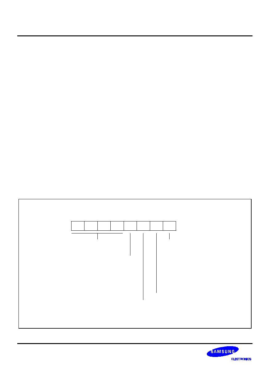
DDC MODULE
S3C8639/C863A/P863A/C8647/F8647
17-2
DDC CONTROL REGISTER (DCON)
The programmable DCON register to control the DDC is located at E9H in set 1, bank 1. It is read/write
addressable. Only four bits are mapped in this register.
The DCON.0 setting lets you detect falling edges at the serial clock, SCL0. If the DCON.0 is set to "0", the SCL0
(serial clock) is still high after reset (when read), or the bit can be cleared by S/W written "0" (when write). If the
DCON.1 is set to "1", falling edge is detected at SCL0 pin after RESET or after this bit is cleared by S/W.
NOTE
When the DDC interrupt is occurred, SCL0 line is not pull-down at the following cases:
-- DDC1 mode
-- Tx/Rx pre-buffer data registers `enable' bit, DCON.3 is "1" (only slave mode).
The DCON.1 setting lets you select normal IIC-bus interface mode or DDC1 transmit mode. If you select normal
IIC-bus interface mode (DCON.1 = "0"), SCL0 pin is selected for clock line and the SCL0 falling edge (SCLF)
interrupt is disabled. Or if you select DDC1 transmit mode (DCON.1 = "1"), VCLK pin is selected for clock line
and the SCLF interrupt is enable.
The DCON.2 is a DDC address match bit and read-only. When the received DDC address matches to DAR0
register, DCON.2 is "1". And when it is start, stop or reset condition, DCON.2 is "0". To enable transmit or receive
pre-buffer data register, DCON.3 is used. When the transmit or receive pre-buffer data register is not used,
DCON.3 is "0" (normal IIC-bus mode). DCON.3 is set by writing One to it or by reset. If DCON.3 is "1", the
transmit or receive pre-buffer data register is enable.
DDC Control Register (DCON)
E9H, Set 1, Bank 1, R/W (Bit 2 is read-only)
-
-
-
-
.3
.2
.1
.0
MSB
LSB
SCL0 (Serial Clock) falling
edge detection bit (SCLF):
0 = SCL0 is high after
RESET
(when read)
0 = Cleared by S/W written
"0" (when write)
1 = Falling edge is detected
(when read)
1 = No effect (when write)
Not used for the
S3C8639/C863A/C8647
DDC1 transmit mode enable bit:
0 = IIC-bus interface mode
(SCL0 pins is also selected)
1 = DDC1 transmit mode
(VCLK pin is also selected)
Transmit or receive pre-buffer data register
enable bit:
0 = Normal IIC-bus mode
(Pre-buffer data registers are not used)
1 = Pre-buffer data registers enable mode
(This bit is set by writing one to it or by
reset)
DDC address match bit (read-only):
0 = When start or stop or reset
1 = When the received DDC address
matches to DAR0 register
Figure 17-1. DDC Control Register (DCON)

S3C8639/C863A/P863A/C8647/F8647
DDC MODULE
17-3
DDC Clock Control Register (DCCR)
The DDC clock control register, DCCR, is located at EBH in set 1, bank 1. It is read/write addressable. DCCR
settings control the following functions:
-- CPU acknowledge signal (ACK) enable or suppress
-- DDC clock source selection (f
OSC
/10 or f
OSC
/256)
-- DDC interrupt enable or disable
-- DDC interrupt pending control
-- 4-bit prescaler for the serial clock (SCL0)
When DCCR.7 bit is set to "1", it is enable to acknowledgment signal. DCCR.6 is bit for transmit clock source
selection by f
OSC
/10 or f
OSC
/256. DCCR.3≠DCCR.0 bits (CCR3≠CCR0) are 4-bit prescaler for the transmit clock
(SCL0). The SCL0 clock may be "Stretched" if a slow slave device holds the clock for clock synchronization.
In the S3C8639/C863A/C8647 interrupt structure, the DDC interrupt is assigned level IRQ3, vector EAH. To
enable this interrupt, you set DCCR.5 to "1". Program software can then poll the DDC interrupt pending
bit(DCCR.4) to detect DDC interrupt request. When the CPU acknowledges the interrupt request from the DDC,
the interrupt service routine must clear the interrupt pending condition by writing a "0" to DCCR.4.
DDC Clock Control Register (DCCR)
EBH, Set 1, Bank 1, R/W
.7
.6
.5
.4
.3
.2
.1
.0
MSB
LSB
Transmit clock 4-bit prescaler bits:
The transmit clock (SCL0) frequency is
determined by the clock source selection
(DCCR.6) and this 4-bit prescaler
value, according to the following formula:
SCL0 clock = IICCLK/(DCCR.3-DCCR.0) + 1
where, IICCLK is f
OSC
/10 (DCCR.6 = "0") or
IICCLK is f
OSC
/256 (DCCR.6 = "1")
Transmit acknowledge (ACK)
enable bit:
0 = Disable ACK generation
1 = Enable ACK generation
Transmit clock source selection bit:
0 = f
OSC
/10
1 = f
OSC
/256
DDC module interrupt enable bit:
0 = Disable DDC interrupt
1 = Enable DDC interrupt
DDC module interrupt pending flag:
0 = When write "0" to this bit (write "1" has no effect)
0 = When DCSR0.4 is "0"
1 = When slave address match occurred
1 = When arbitration lost (master mode)
1 = When a 1-byte transmit or receive operation is terminated
1 = As soon as the DDC1 mode is enable after the prebuffer is used
Figure 17-2. DDC Clock Control Register (DCCR)

DDC MODULE
S3C8639/C863A/P863A/C8647/F8647
17-4
Table 17-1. Sample Timing Calculations for the DDC Transmit Clock (SCL0)
DCCR.3≠DCCR.0
Value
(IICLK = 4 MHz)
IICLK
(DCCR.3≠DCCR.0
Settings + 1)
(f
OSC
= 8 MHz)
DCCR.6 = 0 (f
OSC
/10)
IICLK = 400 kHz
(f
OSC
= 8 MHz)
DCCR.6 = 1 (f
OSC
/256)
IICLK = 15.625 kHz
0000
IICLK/1
400 kHz
15.625 kHz
0001
IICLK/2
200 kHz
7.1825 kHz
0010
IICLK/3
133.3 kHz
5.2038 kHz
0011
IICLK/4
100 kHz
3.9063 kHz
0100
IICLK/5
80.0 kHz
3.1250 kHz
0101
IICLK/6
66.7 kHz
2.6042 kHz
0110
IICLK/7
57.1 kHz
2.2321 kHz
0111
IICLK/8
50.0 kHz
1.9531 kHz
1000
IICLK/9
44.4 kHz
1.7361 kHz
1001
IICLK/10
40.0 kHz
1.5625 kHz
1010
IICLK/11
36.4 kHz
1.4205 kHz
1011
IICLK/12
33.3 kHz
1.3021 kHz
1100
IICLK/13
30.8 kHz
1.2019 kHz
1101
IICLK/14
28.7 kHz
1.1160 kHz
1110
IICLK/15
26.7 kHz
1.0417 kHz
1111
IICLK/16
25.0 kHz
0.9766 kHz

S3C8639/C863A/P863A/C8647/F8647
DDC MODULE
17-5
DDC CONTROL/STATUS REGISTER 0 (DCSR0)
The DDC control/status register 0, DCSR0, is located at ECH in set 1, bank 1. It is read/write addressable.
Although the DCSR0 register is read/write addressable, four bits are read only: DCSR0.3≠DCSR0.0.
DCSR0 register settings are used to control or monitor the following functions:
-- Master/slave transmit or receive mode selection
-- Bus busy status flag
-- DDC module enable or disable
-- Failed bus arbitration procedure status flag
-- Received address register match status flag
-- Last received bit status flag (No ACK = "1", ACK = "0")
DCSR0.3 is automatically set to "1" when a bus arbitration procedure fails over serial I/O interface, while the IIC-
bus is set to master mode. If slave mode is selected, DCSR0.3 is automatically set to "1" if the value of
DCSR0.7≠.4 are changed by program when the busy signal bit, DCSR0.5 is "1", and the DDC address/data field
classification bit, DCSR0.2 is "0". When the DDC module is transmitting a One to SDA0 line but detected a Zero
from SDA0 line in master mode at the slave mode, DCSR0.3 is set.
DDC Control/Status Register 0 (DCSR0)
ECH, Set 1, Bank 1, R/W (Bit 3-0 is read-only)
.7
.6
.5
.4
.3
.2
.1
.0
MSB
LSB
DDC module enable bit:
0 = Disable DDC module
1 = Enable DDC module
Master/Slave Tx/Rx mode selection bits:
00 = Slave receive mode (default mode)
01 = Slave transmit mode
10 = Master receive mode
11 = Master transmit mode
Bus busy signal bit:
0 = Bus is not busy (when read)
0 = Stop condition generation (when write)
1 = Bus is busy (when read)
1 = Start condition generation (when write)
Arbitration lost bit:
0 = Bus arbitration status okay
1 = Bus arbitration failed during serial I/O
Received acknowledgement
(ACK) bit:
0 = ACK is received
1 = ACK is not received
Not used for the S3C8639/C863A
DDC address/data field classification bit:
0 = When reset or START/STOP, or when the
received data is in the data field.
1 = When received slave address
matches to DAR0, DAR1 register or
general call
Figure 17-3. DDC Control/Status Register 0 (DCSR0)

DDC MODULE
S3C8639/C863A/P863A/C8647/F8647
17-6
DDC CONTROL/STATUS REGISTER 1 (DCSR1)
The DDC control/status register 1, called DCSR1, is located at EDH in set 1, bank 1. It is read/write addressable.
Only three bits are mapped in this register. Two bits are read-only: DCSR1.1 and DCSR1.0.
DCSR1 register settings are used to control or monitor the following functions:
-- Stop condition detection flag
-- Data buffer empty status flag
-- Data buffer full status flag
DDC Control/Status Register 1 (DCSR1)
EDH, Set 1, Bank 1, R/W (Bits 1 and 0 are read-only)
-
-
-
-
-
.2
.1
.0
MSB
LSB
Data buffer full status bit:
0 = When the CPU reads the
received data from the
RBDR register or STOP
condition
1 = When thd data or matched
address is transferred from
the DDSR register to the
RBDR register
Not used for the S3C8639/C863A/C8647
Data buffer empty status bit:
0 = When the CPU writes the transmitting data into the
TBDR register
1 = When the data of the TBDR register loads to the DDSR
register or when a stop condition is detected in PCSR0.7-6
(slave transmission mode) = "01"
Stop condition detection bit:
0 = When it writes "0" to this bit, and
reset or master mode
1 = When a stop condition isdetected
after START and slave address
reception
Figure 17-4. DDC Control/Status Register 1 (DCSR1)

S3C8639/C863A/P863A/C8647/F8647
DDC MODULE
17-7
DDC DATA SHIFT REGISTER (DDSR)
The DDC data shift register for DDC interface, called DDSR, is located at F1H in set 1, bank 1. It is read/write
addressable. The transmitted data output serially from most significant bit (MSB) after writing a data to DDSR. In
addition, the received data from the IIC-bus input to DDSR serially from least significant bit (LSB). DDSR register
capable to write while DCSR0.4 is set to "1" and DCON.3 is set to "0", and to read anytime regardless of
ICSR0.4.
DDC Data Shift Register (DDSR)
F1H, Set 1, Bank 1, R/W
.7
.6
.5
.4
.3
.2
.1
.0
MSB
LSB
8-bit data shift register for DDC Tx/Rx operations:
Write enable when DCSR0.4 is "1" and DCON.3 is
"0". Read enable anytime.
Figure 17-5. DDC Data Shift Register (DDSR)

DDC MODULE
S3C8639/C863A/P863A/C8647/F8647
17-8
DDC ADDRESS REGISTER 0 (DAR0)
The DDC address register 0 for DDC interface, called DAR0, is located at EAH in set 1, bank 1. It is read/write
addressable. This register is consisted of 4-bit slave address latch (DAR0.3≠DAR0.0 is not mapped at the
S3C8639/C863A/C8647). DAR0 register is capable to write when DCSR0.4 is "0", and to read anytime regardless
of DCSR0.4. 4-bits of the DAR0 register are operate only when receive the slave address.
DDC Address Register 0 (DAR0)
EAH, Set 1, Bank 1, R/W
.7
.6
.5
.4
-
-
-
-
MSB
LSB
4-Slave address bits:
These bits are operated only
when receive the slave address.
Write enable when DCSR0.4 is
"0". Read enable anytime.
Not used for the
S3C8639/C863A/C8647
Figure 17-6. DDC Address Register 0 (DAR0)
DDC ADDRESS REGISTER 1 (DAR1)
The DDC address register 1 for DDC interface, called DAR1, is located at EEH in set 1, bank 1. It is read/write
addressable. This register is consisted of 7-bit slave address latch (DAR1.0 is not mapped at the
S3C8639/C863A/C8647). DAR1 register is capable to write when DCSR0.4 is "0", and to read anytime regardless
of DCSR0.4. 7-bits of the DAR1 register are operate only when receive the slave address.
DDC Address Register 1 (DAR1)
EEH, Set 1, Bank 1, R/W
.7
.6
.5
.4
.3
.2
.1
-
MSB
LSB
7-slave address bits:
These bits are operated only
when receive the slave address.
Write enable when DCSR0.4 is
"0". Read enable anytime.
Not used for the
S3C8639/C863A/C8647
Figure 17-7. DDC Address Register 1 (DAR1)

S3C8639/C863A/P863A/C8647/F8647
DDC MODULE
17-9
TRANSMIT PRE-BUFFER DATA REGISTER (TBDR)
The transmit pre-buffer data register, called TBDR, is located at EFH in set 1, bank 1. It is read/write
addressable. TBDR register is capable to write when DCSR0.4 is "1", and to read anytime regardless of
DCSR0.4.
When DCON.3 (TBDR enable bit) = "1" and DCSR1.1 = "0", the data written into this register will be
automatically downloaded to the DDC data shift register (DDSR) and generate the interrupt request when the
module detects the calling address is matched and the bit 0 of the received data is "1" (DCSR0.7-6 = "01") and
when the data in the DDSR register has been transmitted with received acknowledge bit, DCSR0.0 = "0".
At this interrupt service routine, the CPU must write the next data to the TBDR register to clear DCSR1.1 and for
the auto downloading of data to the DDSR register after the data in the DDSR register is transmitted over again
with DCSR0.0 = "0". When DCON.3 = "1" and DCSR1.1 = "1", the data stored in this register will not be
downloaded to the module detects the calling address is matched and the bit 0 of the received data is "1".
At this interrupt service routine, the CPU must write the current data and rewrite the next data to the TBDR
register to clear DCSR1.1. If the master receiver doesn't acknowledge the transmitted data, DCSR0.0 = "1", the
module will release the SDA line for master to generate STOP or repeated START conditions. If DCON.3 (TBDR
enable bit) is "0", the module will pull-down the SCL line in the IIC-bus interrupt service routine when the
DCSR0.2 is "1". And the module will release the SCL line if the CPU writes a data to the DDSR registers and the
interrupt pending bit is cleared.
Transmit Pre-buffer Data Register (TBDR)
EFH, Set 1, Bank 1, R/W
.7
.6
.5
.4
.5
.3
.2
.1
MSB
LSB
8-bit transmit pre-buffer data register: Write enable
when DCSR0.4 is "1". Read enable anytime.
Figure 17-8. Transmit Pre-buffer Data Register (TBDR)

DDC MODULE
S3C8639/C863A/P863A/C8647/F8647
17-10
RECEIVE PRE-BUFFER DATA REGISTER (RBDR)
The receive pre-buffer data register, called RBDR, is located at F0H in set 1, bank 1. It is read-only addressable.
RBDR register is capable to read anytime.
RBDR register will be updated after a data byte is received when the DCSR0.2 is "1"and the DCSR1.0 will be "1".
The read operation of RBDR register will clear the DCSR1.0. After the DCSR1.0 is cleared, the register can load
the received data again and set the DCSR1.0.
Receive Pre-buffer Data Register (RBDR)
F0H, Set 1, Bank 1, Read only
.7
.6
.5
.4
.5
.3
.2
.1
MSB
LSB
8-bit receive pre-buffer data register:
It is read only register.
Read enable anytime.
Figure 17-9. Receive Pre-buffer Data Register (RBDR)
SDA
D7
ACK
D0
D6
D7
1st
2nd
8th
9th
1st
t
V
t
L
t
H
Max. 25 kHz
t
V
t
V
t
V
Where,
t
V
= Data valid time (min. 30 us)
t
H
= VCLK high pulse width (min. 20 us)
t
L
= VCLK low pulse width (min. 20 us)
(Max. VCLK input frequency = 25 kHz)
NOTE:
MSB (Most Significant Bit) first output in each bytes.
VCLK
Figure 17-10. DDC1 Mode Timing Diagram (One-Byte Transfer)
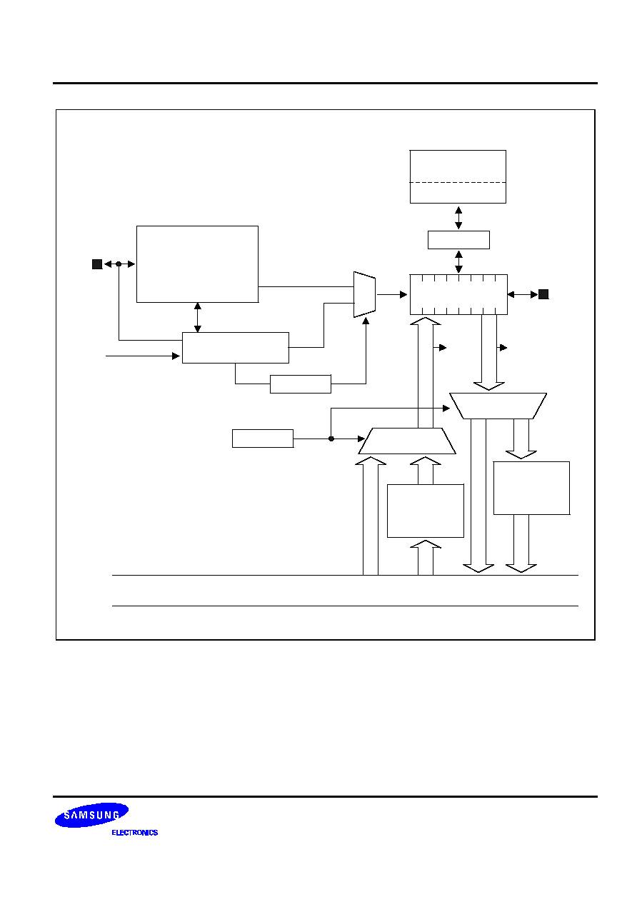
S3C8639/C863A/P863A/C8647/F8647
DDC MODULE
17-11
IIC-Bus
Control Logic
(DCCR, DCSR0, DCSR1)
Receive
Pre-buffer
Data Register
(RBDR)
0
1
Data Bus
DDC Control Logic
SCL0
"DDC1EN"
DDC Data Shifter
(DDSR)
SDA0
Comparator
Address Register
(DAR0)
(DAR1)
IRQ3
0
1
0
1
Transmit
Pre-buffer
Data Register
(TBDR)
"BUFEN"
IRQ3
Vsync-I
(From Sync Processor)
(VCLK = Max. 25 kHz)
Figure 17-11. DDC Module Block Diagram

DDC MODULE
S3C8639/C863A/P863A/C8647/F8647
17-12
THE DDC INTERFACE
DDC2BI MODE
Overview
DDC2B capable graphic hosts have limited and mono-directional communications with the display devices. At the
contrary, DDC2Bi mode is an extension of the DDC2B level in order to offer a bi-direction communication
between the computer graphic host and the display device. DDC2Bi brings DDC2B+ functionality to DDC2B
graphic hosts using a simple S/W driver. So DDC2Bi display device is made by simple S/W upgrade to DDC2B+
capable displays. DDC2Bi protocol relies on the DDC2B H/W definition and the Access bus messages protocol.
The Graphic host behaves as an IIC single master host, and the display device behaves as an IIC slave device.
The DDC2Bi is a modification of the Access bus multi-master protocol to fit single master communication.
DDC2Bi Host and Display Device
DDC2Bi host is considered as an IIC single master capable device. The virtual IIC slave address of the host is
50/51H. But DDC2Bi display device is considered as a fixed address display device (6E/6F), and uses only IIC
slave mode to communicate with the host.
A display dependent devices are geographically located around the display and follow the same DDC2Bi data
protocol than the display device. And fixed address IIC slave devices group all the existing stand-alone and
brain-less IIC slave device. These devices can coexist and be connected to the DDC/IIC-bus.
DDC2Bi S/W Implementation
In order to describe the display that the received message is of DDC2Bi type, the source address byte bit 0 is set.
And when the host expects an answer from the display, the host reads the answer message at the display device
slave address 6FH. The checksum is still computed by using the 50H, virtual host address.
A null message can be defined as an Access bus message without any data byte. The null message is used in
the following cases:
-- To detect that the display is DDC2Bi capable by reading it at 6FH, IIC slave address.
-- To describe the host that the display does not have any answer to give to the host
-- The enable application report has not been sent prior application messages exchange with the host
DDC2Bi Communication
In the DDC2Bi communication, it is capable to retrials when a communication fails (bus error or bad checksum).
So the host is responsible for resending its message and trying to get an answer from the display again. When
the communication fail is occurred, the DDC2Bi devices must answer by the retry of host.
The DDC2Bi capable device must properly send and receive all its supported messages. This determines the
maximum internal data communication buffer required size for proper display operation. If the device receive a
message which size is lager than the maximum supported by the device, the message be accepted entirely by
the device, but does not need to be supported internally, and then be discarded. Therefore the DDC2Bi capable
device must acknowledge all received data bytes from the host.

S3C8639/C863A/P863A/C8647/F8647
DDC MODULE
17-13
THE IIC-BUS INTERFACE
The S3C8639/C863A/C8647 IIC-bus interface has four operating modes:
-- Master transmitter mode
-- Master receive mode
-- Slave transmitter mode
-- Slave receive mode
Functional relationships between these operating modes are described below.
START AND STOP CONDITIONS
When the IIC-bus interface is inactive, it is in slave mode. The interface is therefore always in slave mode when
a start condition is detected on the SDA line. (A start condition is a High-to-Low transition of the SDA line while
the clock signal, SCL, is High level.) When the interface enters master mode, it initiates a data transfer and
generates the SCL signal.
A start condition initiates a one-byte serial data transfer over the SDA line and a stop condition ends the transfer.
(A stop condition is a Low-to-High transition of the SDA line while SCL is High level.) Start and stop conditions
are always generated by the master. The IIC-bus is "busy" when a start condition is generated. A few clocks after
a stop condition is generated, the IIC-bus is again "free".
When a master initiates a start condition, it sends its slave address onto the bus. The address byte consists of a
7-bit address and a 1-bit transfer direction indicator (that is, write or read). If bit 8 is "0", a transmit operation
(write) is indicated; if bit 8 is "1", a request for data (read) is indicated.
The master ends the indicated transfer operation by transmitting a stop condition. If the master wants to continue
sending data over the bus, it can the generate another start condition and another slave address. In this way,
read-write operations can be performed in various formats.
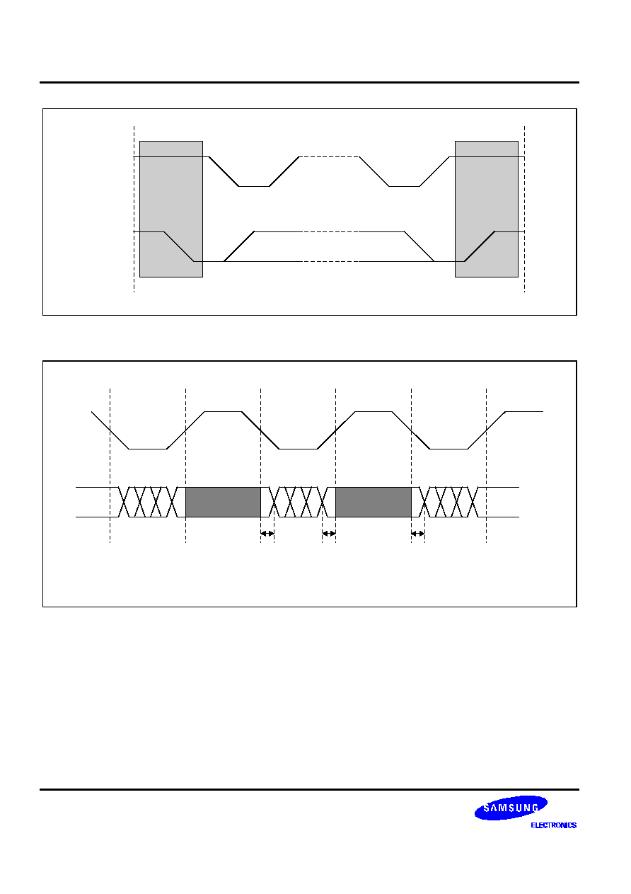
DDC MODULE
S3C8639/C863A/P863A/C8647/F8647
17-14
STOP
Condition
START
Condition
SCLK
SDA
In
Figure 17-12. Start and Stop Conditions
Start
condition
hold time
Data must
remain stable
while clock is
HIGH
Change of
data allowed
Stop
condition
setup
Data must
remain stable
while clock is
HIGH
Start
condition
hold time
Figure 17-13. Input Data Protocol

S3C8639/C863A/P863A/C8647/F8647
DDC MODULE
17-15
DATA TRANSFER FORMATS
Every byte put on the SDA line must be eight bits in length. The number of bytes which can be transmitted per
transfer is unlimited. The first byte following a start condition is the address byte. This address byte is transmitted
by the master when the IIC-bus is operating in master mode. Each byte must be followed by an acknowledge
(ACK) bit. Serial data and addresses are always sent MSB first.
Single Byte Write Mode Format
Data Transferred (Data + Acknowledge)
A
DATA
A
P
A
Sub
Address
A
DATA
Multigle Byte Write Mode Format
A
DATA
A
P
Data Transferred (Data n + Acknowledge)
Auto Increment of Sub Address
Single Byte Read Mode Format
Data Transferred (Data + Acknowledge)
A
DATA
A
P
A
Sub
Address
A
Multigle Byte Read Mode Format
NOTES:
1. S: start, A: acknowledge, P: stop
2. The "Sub Address" indicates the internal address of the slave device.
Slave
Address
DATA
A
P
A
DATA
A
Data Transferred (Data n + Acknowledge)
R
S
Slave
Address
W
"0" (write)
S
Slave
Address
W
"0" (write)
S
Slave
Address
R
"1" (read)
S
Slave
Address
W
"0" (write)
S
Figure 17-14. IIC-Bus Interface Data Formats
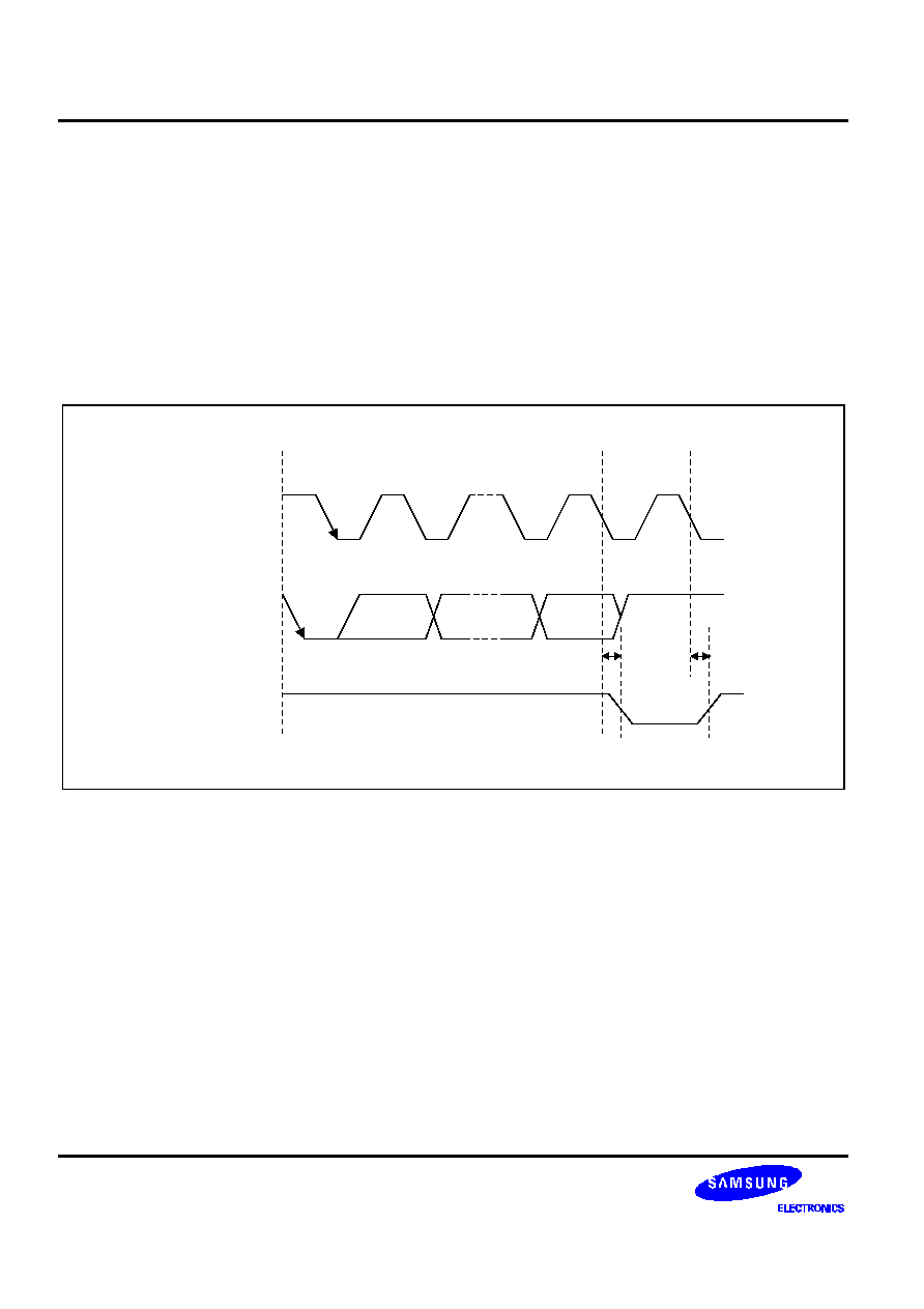
DDC MODULE
S3C8639/C863A/P863A/C8647/F8647
17-16
ACK SIGNAL TRANSMISSION
To complete a one-byte transfer operation, the receiver must send an ACK bit to the transmitter. The ACK pulse
occurs at the ninth clock of the SCL line (eight clocks are required to complete the one-byte transfer). The clock
pulse required for the transmission of the ACK bit is always generated by the master.
The transmitter releases the SDA line (that is, it sends the SDA line High) when the ACK clock pulse is received.
The receiver must drive the SDA line Low during the ACK clock pulse so that SDA is Low during the High period
of the ninth SCL pulse.
The ACK bit transmit function can be enabled and disabled by software (DCCR.7). However, the ACK pulse on
the ninth clock of SCL is required to complete a one-byte data transfer operation.
SCLK
from
Master
Clock to output
Data Output
from
Transmitter
Data Output
from
Receiver
Clock to output
ACK
9
8
1
Start Condition
Figure 17-15. Acknowledge Response from Receiver

S3C8639/C863A/P863A/C8647/F8647
DDC MODULE
17-17
READ-WRITE OPERATIONS
When operating in transmitter mode, the IIC-bus interface interrupt routine waits for the master (the
KS88C6332/C6348) to write a data byte into the IIC-bus data shift register (DDSR). To do this, it holds the SCL
line Low prior to transmission.
In receive mode, the IIC-bus interface waits for the master to read the byte from the IIC-bus data shift register
(DDSR). It does this by holding the SCL line Low following the complete reception of a data byte.
BUS ARBITRATION PROCEDURES
Arbitration takes place on the SDA line to prevent contention on the bus between two masters. If a master with a
SDA High level detects another master with an SDA active Low level, it will not initiate a data transfer because
the current level on the bus does not correspond to its own. The master which loses the arbitration can generate
SCL pulses only until the end of the last-transmitted data byte. The arbitration procedure can continue while data
continues to be transferred over the bus.
The first stage of arbitration is the comparison of address bits. If a master loses the arbitration during the
addressing stage of a data transfer, it is possible that the master which won the arbitration is attempting to
address the master which lost. In this case, the losing master must immediately switch to slave receiver mode.
ABORT CONDITIONS
If a slave receiver does not acknowledge the slave address, it must hold the level of the SDA line High. This
signals the master to generate a stop condition and to abort the transfer.
If a master receiver is involved in the aborted transfer, it must also signal the end of the slave transmit operation.
It does this by not generating an ACK after the last data byte received from the slave. The slave transmitter must
then release the SDA to allow a master to generate a stop condition.
CONFIGURING THE IIC-BUS
To control the frequency of the serial clock (SCL), you program the 4-bit prescaler value in the DCCR register.
The IIC-bus interface address is stored in IIC-bus address register, DIAR0/DAR1. (By default, the IIC-bus
interface address is an unknown value.)

DDC MODULE
S3C8639/C863A/P863A/C8647/F8647
17-18
NOTES

S3C8639/C863A/P863A/C8647/F8647
SLAVE IIC-BUS INTERFACE
18-1
18
SLAVE IIC-BUS INTERFACE (Only S3C863X)
OVERVIEW
The S3C8639/C863A microcontroller supports a slave only IIC-bus serial interface.
A dedicated serial data line (SDA) and a serial clock line (SCL) carry information between bus master and slave
devices which are connected to the IIC-bus. The SDA is bi-directional. But in the S3C8639/C863A/C8647, the
SCL line is uni-directional (input only).
S3C8639/C863A microcontroller can receive and transmit serial data to and from master. When the IIC-bus is
free, the SDA and SCL lines are both at high level.
To control slave-only IIC-bus operations, you write values to the following registers:
-- Slave only IIC-bus control/status register, SICSR
-- Slave only IIC-bus Tx/Rx data shift register, SIDSR
-- Slave only IIC-bus address register, SIAR
Start and Stop conditions are always generated by the master. A 7-bit address value in the first data byte that is
put onto the bus after the Start condition is initiated determines which slave device the bus master selects. The
8th bit determines the direction of the transfer (read or write).
Every data byte that is put onto the SDA line must total eight bits. The number of bytes which can be sent or
received per bus transfer operation is unlimited.
Refer to the IIC-bus interface (slave Tx/Rx) of chapter 17 for the protocol of the slave IIC-bus at the
S3C8639/C863A.
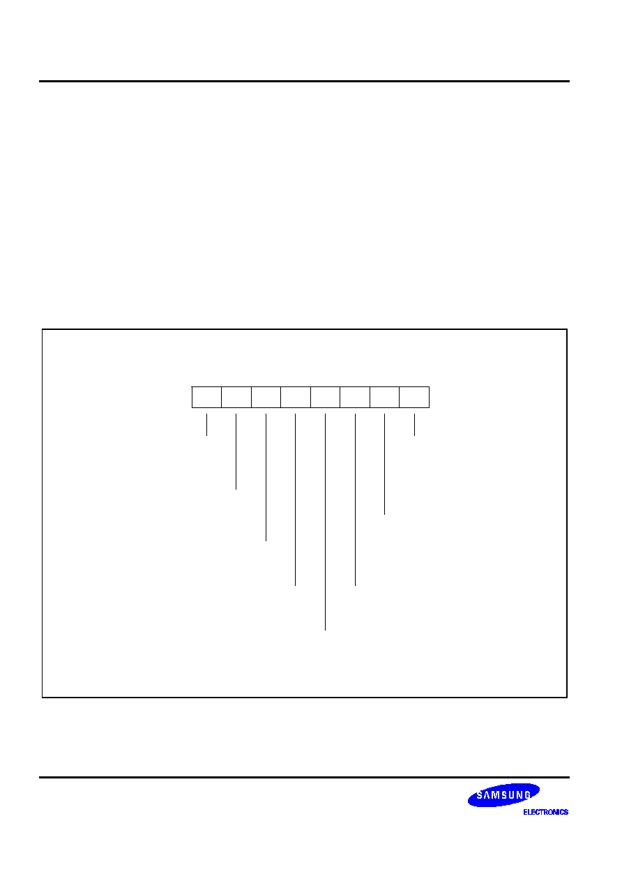
SLAVE IIC-BUS INTERFACE
S3C8639/C863A/P863A/C8647/F8647
18-2
SLAVE ONLY IIC-BUS CONTROL/STATUS REGISTER (SICSR)
The slave only IIC-bus control/status register, SICSR, is located in set 1, bank 1, at address F2H. SICSR register
settings are used to control or monitor the following slave IIC-bus functions (see figure 18-4):
-- Slave IIC-bus acknowledgement (ACK) signal generation enable or suppress
-- Slave IIC-bus module enable
-- Slave IIC-bus Tx/Rx interrupt enable
-- Slave IIC-bus Tx/Rx interrupt pending condition control
-- Slave IIC-bus Tx/Rx mode status detect/control
-- Slave IIC-bus busy status detect
-- Slave IIC-bus address match status detect
-- Received acknowledge signal detect (No ACK = "1", ACK = "0")
LSB
MSB
Slave Only IIC-Bus Control/Status Register (SICSR)
F2H, Set 1, Bank 0, R/W
Slave IIC-bus Tx/Rx interrupt pending bit:
0 = No interrupt pending (when read),
clear pending condition (when write)
0 = When SICSR.6 is "0"
1 = When 1-byte Tx/Rx is terminated
1 = When slave address match occurred
Slave IIC-bus acknowledgement
(ACK) enable bit:
0 = Disable ACK generation
1 = Enabel ACK generation
Slave IIC-bus Tx/Rx interrupt enable bit:
0 = Disable interrupt
1 = Enable interrupt
IIC-bus busy status bit:
0 = IIC-bus is not busy
1 = IIC-bus is busy
Slave address match bit :
0 = when start or stop or reset
condition is generated
1 = when received slave address
value matches to SIAR register
Slave IIC-bus last received
bit status flag:
0 = Last-received bit is "0"
(ACK was received)
1 = Last-received bit is "1"
(ACK was not received)
.7
.6
.5
.4
.3
.2
.1
.0
Slave IIC-bus module enable bit:
0 = Disable IIC-bus module
1 = Enabel IIC-bus module
(Enable serial data Tx/Rx)
Slave IIC-bus Tx/Rx mode status bit:
0 = Slave receiver mode (default mode)
1 = Slave transmitter mode
Figure 18-1. Slave only IIC-Bus Control/Status Register (SICSR)
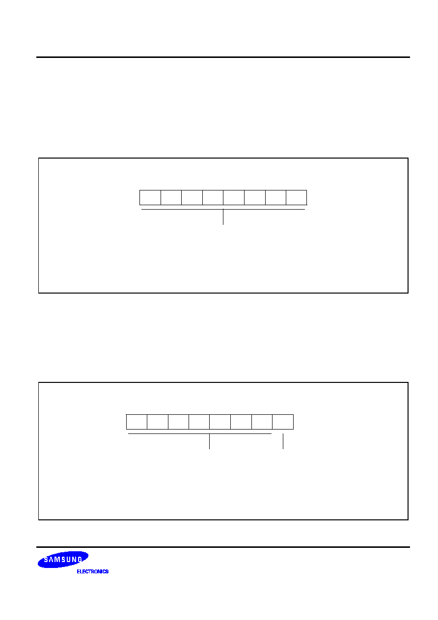
S3C8639/C863A/P863A/C8647/F8647
SLAVE IIC-BUS INTERFACE
18-3
SLAVE ONLY IIC-BUS TRANSMIT/RECEIVE DATA SHIFT REGISTER (SIDSR)
The slave IIC-bus data shift register, SIDSR, is located in set 1, bank 1, at address F4H. In a transmit operation,
data that is written to the IIC is transmitted serially.
The SICSR.6 setting enables or disables serial transmit/receive operations. When SICSR.6 = "1", data can be
written to the shift register. The slave IIC-bus shift register can, however, be read at any time, regardless of the
current SICSR.6 setting.
LSB
MSB
Slve Only IIC-Bus Transmit/Receive Data Shift Register (SIDSR)
F4H, Set 1, Bank 1, R/W
When SICSR, 6 = "0", write operation is enabled.
You can read the SIDSR data value at anytime,
regardless of the current SICSR.6 setting.
.7
.6
.5
.4
.3
.2
.1
.0
8-bit data shift register for slave IIC-bus
Tx/Rx operations:
Figure 18-2. Slave Only IIC-Bus Tx/Rx Data Shift Register (SIDSR)
SLAVE ONLY IIC-BUS ADDRESS REGISTER (SIAR)
The address register for the IIC-bus interface, SIAR, is located, in set 1, bank 1, at address F3H. It is used to
store a latched 7-bit slave address. This address is mapped to IAR.7≠IAR.1; bit 0 is not used (see figure 18-3).
The latched slave address is compared to the next received slave address.
LSB
MSB
Slave Only IIC-Bus Address Register (SIAR)
F3H, Set 1, Bank 1, R/W
These bits are operate only when receive the slave address.
When SICSR.6 = "0", read operation is enabled. You can read
the SIDSR data value at any time, regardless of the current
SICSR.6 setting.
.7
.6
.5
.4
.3
.2
.1
-
7-bit slave address, latched from the IIC-bus
Not used for the
S3C8639/C863A
Figure 18-3. Slave only IIC-Bus Address Register (SIAR)

SLAVE IIC-BUS INTERFACE
S3C8639/C863A/P863A/C8647/F8647
18-4
Data Shifter
(SIDSR)
IIC-Bus
Control Logic
(SICSR)
SCL1
SDA1
Comparator
Address Register
(SIAR)
IRQ7
Data Bus
NOTE:
The IIC-bus interrupt (IRQ7) is generated when a 1-byte receive or transmit
operation is terminated before the shift operation has been completed.
Figure 18-4. IIC-Bus Block Diagram

S3C8639/C863A/P863A/C8647/F8647
ELECTRICAL DATA
19-1
19
ELECTRICAL DATA
OVERVIEW
In this section, S3C8639/C863A/C8647 electrical characteristics are presented in tables and graphs. The
information is arranged in the following order:
-- Absolute maximum ratings
-- D.C. electrical characteristics
-- Data retention supply voltage in stop mode
-- Stop mode release timing when initiated by a reset
-- I/O capacitance
-- A/D Converter electrical characteristics
-- A.C. electrical characteristics
-- Input timing measurement points for P0.0≠P0.2 and TM0CAP
-- Oscillation characteristics
-- Oscillation stabilization time
-- Clock timing measurement points for X
IN
-- Schmitt trigger characteristics
-- Power-on reset circuit characteristics

ELECTRICAL DATA
S3C8639/C863A/P863A/C8647/F8647
19-2
Table 19-1. Absolute Maximum Ratings
(T
A
= 25
∞
C)
Parameter
Symbol
Conditions
Rating
Unit
Supply voltage
V
DD
≠
≠ 0.3 to + 6.5
V
Input voltage
V
I1
Type G-3 (n-channel open drain)
≠ 0.3 to + 7.0
V
I2
All port pins except V
I1
≠ 0.3 to V
DD
+ 0.3
Output voltage
V
O
All output pins
≠ 0.3 to V
DD
+ 0.3
Output current
High
I
OH
One I/O pin active
≠ 10
mA
All I/O pins active
≠ 60
Output current
Low
I
OL
One I/O pin active
+ 30
Total pin current except port 3
+ 100
Sync-processor I/O pins and IIC-bus
clock and data pins
+ 150
Operating
temperature
T
A
≠
≠ 40 to + 85
∞
C
Storage
temperature
T
STG
≠
≠ 65 to + 150
Table 19-2. D.C. Electrical Characteristics
(T
A
= ≠ 40
∞
C to + 85
∞
C, V
DD
= 3.0 V to 5.5 V (S3C863X), V
DD
= 4.0 V to 5.5 V (S3C8647))
Parameter
Symbo
l
Conditions
Min
Typ
Max
Unit
Input High
V
IH1
All input pins except V
IH2
, V
IH3
and V
IH4
0.8 V
DD
≠
V
DD
V
voltage
V
IH2
X
IN
V
DD
≠0.5
V
DD
V
IH3
TTL input (Hsync-I, Vsync-I, and Csync-I)
2.0
V
DD
V
IH4
SCL0/SDA0, SCL1/SDA1
0.7V
DD
V
DD
Input Low
V
IL1
All input pins except V
IL2
and V
IL3
≠
0.2 V
DD
voltage
V
IL2
X
IN
0.4
V
IL3
TTL input (Hsync-I, Vsync-I, and Csync-I)
0.8
V
IL4
SCL0/SDA0, SCL1/SDA1
0.3V
DD
Output High
voltage
V
OH1
V
DD
= 5 V
±
10%; I
OH
= ≠ 15 mA (S3C863x),
I
OH
= ≠ 14 mA (S3C8647); Port 3.6≠3.7
V
DD
≠ 1.2
≠
V
OH2
V
DD
= 5 V
±
10%; I
OH
= ≠ 4 mA (S3C863x),
I
OH
= ≠3.6 mA (S3C8647);
Port 1.2, Port 3.0≠3.5
V
OH3
V
DD
= 5 V
±
10%; I
OH
= ≠ 2 mA;
Port 0, 2, Clamp-O, H, and Vsync-O
V
DD
≠ 1.0
V
OH4
V
DD
= 5 V
±
10%; I
OH
= ≠ 6 mA;
Port 1.0≠P1.1, SCL0 and SDA0

S3C8639/C863A/P863A/C8647/F8647
ELECTRICAL DATA
19-3
Table 19-2. D.C. Electrical Characteristics (Continued)
(T
A
= ≠ 40
∞
C to + 85
∞
C, V
DD
= 3.0 V to 5.5 V (S3C863X), V
DD
= 4.0 V to 5.5 V (S3C8647))
Parameter
Symbol
Conditions
Min
Typ
Max
Unit
Output Low
voltage
V
OL1
V
DD
= 5 V
±
10%; I
OL
= 15 mA
Port 3.6≠3.7
≠
≠
0.4
V
V
OL2
V
DD
= 5 V
±
10%; I
OL
= 4 mA
Port 3.0≠3.5 and Port 1.2
0.4
V
OL3
V
DD
= 5 V
±
10%; I
OL
= 2 mA
Port 0, 2, Clamp-O, H, and Vsync-O
0.4
V
OL4
V
DD
= 5 V
±
10%; I
OL
= 6 mA
Port 1.0≠1.1; SCL0 and SDA0
0.6
Input High
leakage current
I
LIH1
V
IN
= V
DD
All input pins except X
IN
,
X
OUT
≠
≠
3
µA
I
LIH2
V
IN
= V
DD
;
X
OUT
only
≠
≠
20
I
LIH3
V
IN
= V
DD
;
X
IN
only
2.5
6
20
Input Low
leakage current
I
LIL1
V
IN
= 0 V; All input pins except X
IN
,
X
OUT
,
RESET
, HsyncI & VsyncI
≠
≠
≠ 3
I
LIL2
V
IN
= 0 V; X
OUT
only
≠
≠
≠ 20
I
LIL3
V
IN
= 0 V; X
IN
only
≠ 2.5
≠ 6
≠ 20
Output High
leakage current
I
LOH1
V
OUT
= V
DD
≠
≠
3
Output Low
leakage current
I
LOL1
V
OUT
= 0 V
≠
≠
≠ 3
Pull-up resistor
R
U1
V
IN
= 0 V; V
DD
= 5 V
±
10%
Ports 3.7≠3.4
20
47
80
k
R
U2
V
IN
= 0 V; V
DD
= 5 V
±
10%
RESET
only
150
280
480
Pull-down
resistor
R
D
V
IN
= 0 V; V
DD
= 5 V
±
10%
HsyncI & VsyncI
150
300
500
Supply current
(note)
I
DD1
V
DD
= 5 V
±
10%
Operation mode; 12 MHz crystal
C1 = C2 = 22pF
≠
10
20
mA
I
DD2
V
DD
= 5 V
±
10%
Idle mode; 12 MHz crystal
C1 = C2 = 22pF
4
8
I
DD3
V
DD
= 5 V
±
10%
Stop mode
100
150
µA
NOTE: Supply current does not include drawn internal pull-up/pull-down resistors and external loads of output.
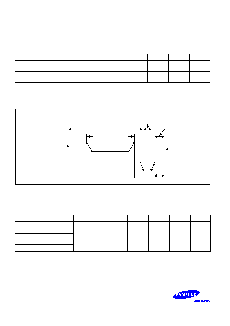
ELECTRICAL DATA
S3C8639/C863A/P863A/C8647/F8647
19-4
Table 19-3. Data Retention Supply Voltage in Stop Mode
(T
A
= ≠ 40
∞
C to + 85
∞
C)
Parameter
Symbol
Conditions
Min
Typ
Max
Unit
Data retention
supply voltage
V
DDDR
Stop mode
2
≠
5.5
V
Data retention
supply current
I
DDDR
Stop mode, V
DDDR
= 2.0 V
≠
≠
5
µA
NOTES:
1.
During the oscillator stabilization wait time (t
WAIT
), all CPU operations must be stopped.
2.
Supply current does not include drawn through internal pull≠up resistors and external output current loads.
NOTE: t
WAIT
is the same as 4096 x 16 x 1/f
OSC
.
Execution of
STOP Instrction
RESET
occurs
~ ~
V
DDDR
~ ~
Stop Mode
Oscillation
Stabilzation
Time
Data Retention Mode
t
WAIT
RESET
V
DD
Normal
Operating
Mode
Figure 19-1. Stop Mode Release Timing When Initiated by a Reset
Table 19-4. Input/Output Capacitance
(T
A
= ≠40
∞
C to + 85
∞
C, V
DD
=
0 V)
Parameter
Symbol
Conditions
Min
Typ
Max
Unit
Input
capacitance
C
IN
f = 1 MHz; unmeasured pins
are connected to V
SS
≠
≠
10
pF
Output
capacitance
C
OUT
I/O capacitance
C
IO

S3C8639/C863A/P863A/C8647/F8647
ELECTRICAL DATA
19-5
Table 19-5. A/D Converter Electrical Characteristics (S3C863X)
(T
A
= ≠ 40
∞
C to + 85
∞
C, V
DD
= 3.0 V to 5.5 V, V
SS
= 0 V)
Parameter
Symbol
Conditions
Min
Typ
Max
Unit
Resolution
≠
8
≠
bit
Total accuracy
V
DD
= 5 V
Conversion time = 5
µ
s
≠
≠
±
2
LSB
Integral linearity error
ILE
AV
REF
= 5 V
≠
±
1
Differential linearity error
DLE
AV
SS
= 0 V
≠
±
1
Offset error of top
EOT
±
1
±
2
Offset error of bottom
EOB
±
0.5
±
2
Conversion time
(1)
t
CON
8-bit conversion
48 x n/f
OSC
(3)
,
n = 1, 4, 8, 16
20
≠
170
µ
s
Analog input voltage
V
IAN
≠
AV
SS
≠
AV
REF
V
Analog input impedance
R
AN
≠
2
1000
≠
M
Analog reference voltage
AV
REF
≠
2.5
≠
V
DD
V
Analog ground
AV
SS
≠
V
SS
≠
V
SS
+ 0.3
V
Analog input current
I
ADIN
AV
REF
= V
DD
= 5V
≠
≠
10
µ
A
Analog block Current
(2)
I
ADC
AV
REF
= V
DD
= 5V
≠
1
3
mA
AV
REF
= V
DD
= 3V
0.5
1.5
mA
AV
REF
= V
DD
= 5V
When power down mode
100
500
nA
NOTES:
1.
"Conversion time" is the time required from the moment a conversion operation starts until it ends.
2.
I
ADC
is an operating current during the A/D conversion.
3.
f
OSC
is the main oscillator clock.

ELECTRICAL DATA
S3C8639/C863A/P863A/C8647/F8647
19-6
Table 19-6. A/D Converter Electrical Characteristics (S3C8647)
(T
A
= ≠ 40
∞
C to + 85
∞
C, V
DD
= 4.0 V to 5.5 V, V
SS
= 0 V)
Parameter
Symbol
Conditions
Min
Typ
Max
Unit
Resolution
≠
≠
4
≠
bit
Absolute accuracy
(1)
≠
4 bit conversion
24 x n/f
OSC
(3)
,
n = 1, 4, 8, 16
≠
≠
±
0.5
LSB
Conversion time
(2)
t
CON
3
≠
≠
us
Analog input voltage
V
IAN
≠
V
SS
≠
V
DD
V
Analog input impedance
R
AN
≠
2
≠
≠
M
NOTES:
1.
Excluding quantization error, absolute accuracy values are within
±
0.5 LSB.
2.
"Conversion time" is the time required from the moment a conversion operation starts until it ends.
3.
f
OSC
is the mean oscillator clock.
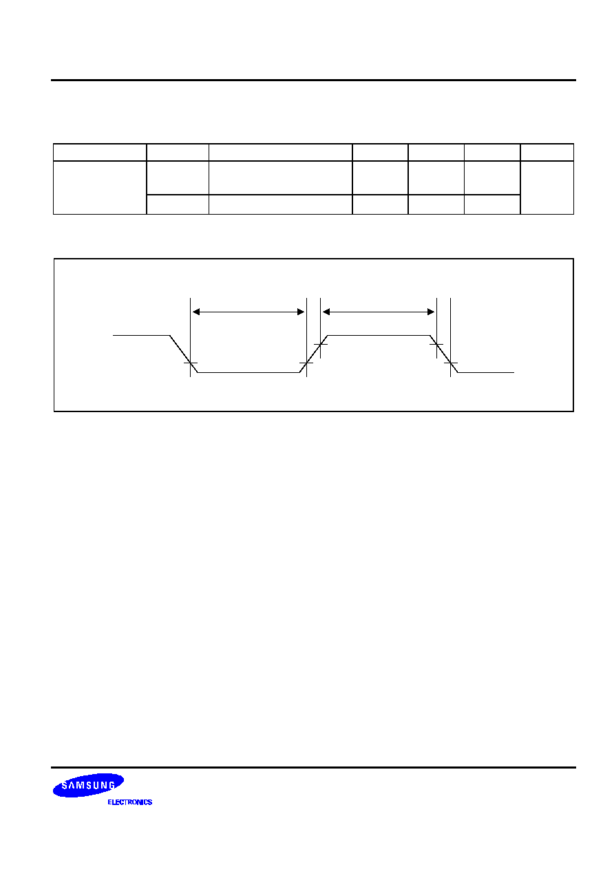
S3C8639/C863A/P863A/C8647/F8647
ELECTRICAL DATA
19-7
Table 19-7. A.C. Electrical Characteristics
(T
A
= ≠ 40
∞
C to + 85
∞
C, V
DD
= 3.0 V to 5.5 V (S3C863X), V
DD
= 4.0 V to 5.5 V (S3C8647))
Parameter
Symbol
Conditions
Min
Typ
Max
Unit
Noise Filter
t
NF1H
t
NF1L
INT0≠2 and TM0CAP (RC
delay)
300
≠
≠
ns
t
NF2
RESET
only (RC delay)
1000
≠
≠
t
NF1H
t
NF1L
0.8 V
DD
0.2 V
DD
t
NF2
Figure 19-2. Input Timing Measurement Points for P0.0≠P0.2 and TM0CAP
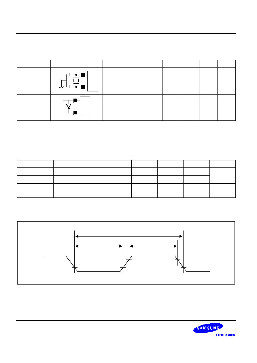
ELECTRICAL DATA
S3C8639/C863A/P863A/C8647/F8647
19-8
Table 19-8. Oscillation Characteristics
(T
A
= ≠ 40
∞
C + 85
∞
C)
Oscillator
Clock Circuit
Conditions
Min
Typ
Max
Unit
Main crystal or
ceramic
C2
C1
X
IN
X
OUT
V
DD
= 3.0 V to 5.5 V
(S3C863X)
V
DD
= 4.0 V to 5.5 V
(S3C8647)
8
≠
12
MHz
External clock
(main)
X
IN
X
OUT
V
DD
= 3.0 V to 5.5 V
(S3C863X)
V
DD
= 4.0 V to 5.5 V
(S3C8647)
8
≠
12
MHz
NOTE: The maximum oscillator frequency is 12 MHz. If you use an oscillator frequency higher than 12 MHz, you cannot
select a non-divided CPU clock using CLKCON settings. That is, you must select one of the divide-by values.
Table 19-9. Oscillation Stabilization Time
(T
A
= ≠ 40
∞
C to + 85
∞
C, V
DD
= 3.0 V to 5.5 V (S3C863X), V
DD
= 4.0 V to 5.5 V (S3C8647))
Oscillator
Test Condition
Min
Typ
Max
Unit
Crystal
V
DD
= 3.0 V (or 4.0 V) to 5.5 V
≠
≠
20
ms
Ceramic
V
DD
= 3.0 V (or 4.0 V) to 5.5V
≠
≠
10
External clock
X
IN
input high and low level width
(t
XH
, t
XL
)
25
≠
500
ns
NOTE: Oscillation stabilization time is the time required for the CPU clock to return to its normal oscillation frequency after
a power-on occurs, or when Stop mode is released.
X
IN
t
XH
t
XL
1/fx
V
DD
- 0.5 V
0.4 V
Figure 19-3. Clock Timing Measurement Points for X
IN

S3C8639/C863A/P863A/C8647/F8647
ELECTRICAL DATA
19-9
A = 0.2 V
DD
B = 0.4 V
DD
C = 0.6 V
DD
D = 0.8 V
DD
V
DD
V
OUT
V
SS
V
IN
A
B
C
D
Figure 19-4. Schmitt Trigger Characteristics (Normal Port; except TTL Input)
Table 19-10. Power-on Reset Circuit Characteristics
(T
A
= ≠ 40
∞
C to + 85
∞
C, V
DD
= 3.0 V to 5.5 V (S3C863X), V
DD
= 4.0 V to 5.5 V (S3C8647))
Parameter
Symbol
Conditions
Min
Typ
Max
Unit
Power-on reset release
voltage
V
DDLVD
2.3
3.1
(2)
2.65
3.4
(2)
3.0
3.7
(2)
V
Power-on reset detection
voltage
V
LVD
2.3
3.1
(2)
2.65
3.4
(2)
3.0
3.7
(2)
V
Power supply voltage off
time
t
off
10
≠
≠
ms
Power-on reset circuit
consumption current
(2)
I
DDPR
V
DD
= 5 V
±
10%
100
150
µ
A
V
DD
= 3.3 V
60
100
µ
A
NOTES:
1.
Current contained when power-on reset circuit is provided internally.
2.
Only S3C8647.

ELECTRICAL DATA
S3C8639/C863A/P863A/C8647/F8647
19-10
t
off
V
DDLVD
V
LVD
V
DD
Figure 19-5. Power-on Reset Timing

S3C8639/C863A/P863A/C8647/F8647
MECHANICAL DATA
20-1
20
MECHANICAL DATA
OVERVIEW
The S3C8639/C863A/C8647 microcontroller is available in a 42-pin SDIP package (Samsung part number 42-
SDIP-600) and a 44-QFP package (Samsung part number 44-QFP-1010B).
NOTE: Dimensions are in millimeters.
39.50 MAX
39.10
±
0.2
0.50
±
0.1
1.778
(1.77)
0.51 MIN
3.30
±
0.3
3.50
±
0.2
5.08 MAX
42-SDIP-600
0-15
1.00
±
0.1
0.25
+ 0.1
- 0.05
15.24
14.00
±
0
.2
#42
#22
#21
#1
Figure 20-1. 42-Pin SDIP Package Dimensions (42-SDIP-600)

MECHANICAL DATA
S3C8639/C863A/P863A/C8647/F8647
20-2
44-QFP-1010B
#44
NOTE: Dimensions are in millimeters.
10.00
±
0.2
13.20
±
0.3
10.00
±
0.2
13.20
±
0.3
#1
0.35
+ 0.10
- 0.05
0.80
(1.00)
0.10 MAX
0.80
±
0.20
0.05 MIN
2.05
±
0.10
2.30 MAX
0.15
+ 0.10
- 0.05
0-8
Figure 20-2. 44-Pin QFP Package Dimensions (44-QFP-1010B)

S3C8639/C863A/P863A/C8647/F8647
MECHANICAL DATA
20-3
NOTE: Dimensions are in millimeters.
27.88 MAX
27.48
±
0.20
(1.37)
32-SDIP-400
9.10
±
0
.20
#32
#1
0.45
±
0.10
1.00
±
0.10
3.80
±
0.20
5.08 MAX
1.778
0.51 MIN
3.30
±
0.30
#17
#16
0-15
0.25
+ 0.10- 0.05
10.16
Figure 20-3. 32-Pin SDIP Package Dimensions (32-SDIP-400)

MECHANICAL DATA
S3C8639/C863A/P863A/C8647/F8647
20-4
32-SOP-450A
20.30 MAX
19.90
± 0.20
#17
#16
0-8
0.25
+ 0.10
- 0.05
11.43
8.34
±
0.20
0.90
±
0.20
0.05 MIN
2.00
±
0.10
2.20 MAX
0.10 MAX
1.27
NOTE: Dimensions are in millimeters.
12.00
±
0
.30
#32
#1
(0.43)
0.40
± 0.10
Figure 20-4. 32-Pin SOP Package Dimensions (32-SOP-450A)

S3C8639/C863A/P863A/C8647/F8647
S3P863A OTP
21-1
21
S3P863A OTP
OVERVIEW
The S3P863A single-chip CMOS microcontroller is the OTP (One Time Programmable)
version of the
S3C8639/C863A microcontrollers. It has an on-chip EPROM instead of masked ROM. The EPROM is accessed
by serial data format.
The S3P863A is fully compatible with the S3C8639/C863A, both in function and in pin configuration. Because of
its simple programming requirements, the S3P863A is ideal for use as an evaluation chip for the
S3C8639/C863A.
P0.0/INT0
P0.1/INT1
P0.2/INT2
P0.3
P0.4/TM0CAP
P0.5
P0.6
P0.7
SDAT/P1.0/SDA1
SCLK/P1.1/SCL1
V
DD1
V
SS1
X
OUT
X
IN
V
PP
/TEST (GND)
SDA0
SCL0
RESET
RESET/RESET
P1.2
P2.0/PWM0
P2.1/PWM1
S3P863A
(42-SDIP)
1
2
3
4
5
6
7
8
9
10
11
12
13
14
15
16
17
18
19
20
21
P3.7
P3.6
P3.5
P3.4
P3.3/AD3
P3.2/AD2
P3.1/AD1
P3.0/AD0
V
DD2
V
SS2
P2.7/Csync-I (SOG)
Hsync-I
Vsync-I
Vsync-O
Hsync-O
Clamp-O
P2.6/PWM6
P2.5/PWM5
P2.4/PWM4
P2.3/PWM3
P2.2/PWM2
42
41
40
39
38
37
36
35
34
33
32
31
30
29
28
27
26
25
24
23
22
NOTE:
The bolds indicate an OTP pin name.
Figure 21-1. S3P863A Pin Assignments (42-SDIP Package)

S3P863A OTP
S3C8639/C863A/P863A/C8647/F8647
21-2
P0.5
P0.6
P0.7
SDAT/P1.0/SDA1
SCLK/P1.1/SCL1
V
DD1
V
SS1
X
OUT
X
IN
V
PP
/TEST (GND)
SDA0
S3P863A
(44-QFP)
1
2
3
4
5
6
7
8
9
10
11
P0.4/TM0CAP
P0.3
P0.2/INT2
P0.1/INT1
N.C.
P0.0/INT0
P3.7
P3.6
P3.5
P3.4
P3.3/AD3
44
43
42
41
40
39
38
37
36
35
34
P3.2/AD2
P3.1/AD1
P3.0/AD0
V
DD2
V
SS2
P2.7/Csync-I (SOG)
Hsync-I
Vsync-I
Vsync-O
Hsync-O
Clamp-O
33
32
31
30
29
28
27
26
25
24
23
SCL0
RESET
RESET
/
RESET
P1.2
P2.0/PWM0
P2.1/PWM1
P2.2/PWM2
N.C.
P2.3/PWM3
P2.4/PWM4
P2.5/PWM5
P2.6/PWM6
12
13
14
15
16
17
18
19
20
21
22
NOTE:
The bolds indicate an OTP pin name.
Figure 21-2. S3P863A Pin Assignments (44-QFP Package)
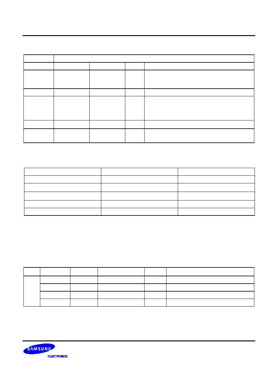
S3C8639/C863A/P863A/C8647/F8647
S3P863A OTP
21-3
Table 21-1. Descriptions of Pins Used to Read/Write the EPROM
Main Chip
During Programming
Pin Name
Pin Name
Pin Number
I/O
Function
P1.0
SDAT
9 (4)
I/O
Serial data pin. Output port when reading and input
port when writing. Can be assigned as a Input/push-
pull output port.
P1.1
SCLK
10 (5)
I
Serial clock pin. Input only pin.
TEST
V
PP
(TEST)
15 (10)
I
Power supply pin for EPROM cell writing (indicates
that OTP enters into the writing mode). When 12.5
V is applied, OTP is in writing mode and when 5 V
is applied, OTP is in reading mode. (Option)
RESET
RESET
18 (13)
I
Chip Initialization
V
DD1
/V
SS1
V
DD1
/V
SS1
11/12 (6/7)
I
Logic power supply pin. V
DD
should be tied to +5 V
during programming.
NOTE: Parentheses indicate 44-QFP OTP pin number.
Table 21-2. Comparison of S3P863A and S3C8639/C863A Features
Characteristic
S3P863A
S3C8639/C863A
Program Memory
48-Kbyte EPROM
32/48-Kbyte mask ROM
Operating Voltage (V
DD
)
3.0 V to 5.5 V
3.0 V to 5.5V
OTP Programming Mode
V
DD
= 5 V, V
PP
(TEST) = 12.5V
Pin Configuration
42 SDIP, 44 QFP
42 SDIP, 44 QFP
EPROM Programmability
User Program 1 time
Programmed at the factory
OPERATING MODE CHARACTERISTICS
When 12.5 V is supplied to the V
PP
(TEST) pin of the S3P863A, the EPROM programming mode is entered. The
operating mode (read, write, or read protection) is selected according to the input signals to the pins listed in
Table 21-3 below.
Table 21-3. Operating Mode Selection Criteria
V
DD
V
PP
(TEST)
REG/MEM
Address (A15≠A0)
R/W
Mode
5 V
5 V
0
0000H
1
EPROM read
12.5 V
0
0000H
0
EPROM program
12.5 V
0
0000H
1
EPROM verify
12.5 V
1
0E3FH
0
EPROM read protection
NOTE: "0" means Low level; "1" means High level.

S3P863A OTP
S3C8639/C863A/P863A/C8647/F8647
21-4
D.C. ELECTRICAL CHARACTERISTICS
Table 21-4. D.C. Electrical Characteristics
(T
A
= ≠ 40
∞
C to + 85
∞
C, V
DD
= 3.0 V to 5.5 V)
Parameter
Symbol
Conditions
Min
Typ
Max
Unit
Input High
leakage current
I
LIH1
V
IN
= V
DD
All input pins except X
IN
,
X
OUT
≠
≠
3
µA
I
LIH2
V
IN
= V
DD
;
X
OUT
only
≠
≠
20
I
LIH3
V
IN
= V
DD
;
X
IN
only
2.5
6
20
Input Low
leakage current
I
LIL1
V
IN
= 0 V; All input pins except X
IN
,
X
OUT
,
RESET
, Hsync-I and Vsync-I
≠
≠
≠ 3
I
LIL2
V
IN
= 0 V; X
OUT
only
≠
≠
≠ 20
I
LIL3
V
IN
= 0 V; X
IN
only
≠ 2.5
≠ 6
≠ 20
Output High
leakage current
I
LOH1
V
OUT
= V
DD
≠
≠
3
Output Low
leakage current
I
LOL1
V
OUT
= 0 V
≠
≠
≠ 3
Pull-up resistor
R
U1
V
IN
= 0 V; V
DD
= 5 V
±
10%
Port 3.7≠3.4
20
47
80
k
R
U2
V
IN
= 0 V; V
DD
= 5 V
±
10%
RESET
only
150
280
480
Pull-down
resistor
R
D
V
IN
= 0 V; V
DD
= 5 V
±
10%
Hsync-I and Vsync-I
150
300
500
Supply current
(note)
I
DD1
V
DD
= 5 V
±
10%
Operation mode; 12 MHz crystal
C1 = C2 = 22pF
≠
10
20
mA
I
DD2
V
DD
= 5 V
±
10%
Idle mode; 12 MHz crystal
C1 = C2 = 22pF
4
8
I
DD3
V
DD
= 5 V
±
10%
Stop mode
100
150
µA
NOTE: Supply current does not include drawn internal pull-up/pull-down resistors and external loads of output.

S3C8639/C863A/P863A/C8647/F8647
S3F8647 FLASH MCU
22-1
22
S3F8647 FLASH MCU
OVERVIEW
The S3F8647 single-chip CMOS microcontroller is the FLASH version of the S3C8647 microcontrollers.
It has an on-chip FLASH ROM instead of masked ROM. The FLASH ROM is accessed in serial data format.
The S3F8647 is fully compatible with the S3C8647, both in function and in pin configuration. Because of its
simple programming requirements, the S3F8647 is ideal for use as an evaluation chip for the S3C8647.
V
SS
/V
SS
X
OUT
X
IN
V
PP
/TEST
P0.0/INT0
P0.1/INT1
RESET
RESET/RESET
P0.2/INT2
P0.4/TM0CAP
SDA
SCL
P2.0/PWM0
P2.1/PWM1
P2.2/PWM2
P2.3/PWM3
P2.4/PWM4
S3F8647
(32-SDIP)
1
2
3
4
5
6
7
8
9
10
11
12
13
14
15
16
V
DD/
V
DD
P3.7/SCLK
P3.6/SDAT
P3.5
P3.4
P3.3/AD3
P3.2/AD2
P3.1/AD1
P3.0/AD0
P2.7/Csync-I(SOG)
Hsync-I
Vsync-I
Vsync-O
Hsync-O
Clamp-O
P2.5/PWM5
32
31
30
29
28
27
26
25
24
23
22
21
20
19
18
17
Figure 22-1. S3F8647 Pin Assignments (32-SDIP Package)

S3F8647 FLASH MCU
S3C8639/C863A/P863A/C8647/F8647
22-2
S3C8647
(32-SOP)
1
2
3
4
5
6
7
8
9
10
11
12
13
14
15
16
32
31
30
29
28
27
26
25
24
23
22
21
20
19
18
17
V
SS
/V
SS
X
OUT
X
IN
V
PP
/TEST
P0.0/INT0
P0.1/INT1
RESET
RESET/RESET
P0.2/INT2
P0.4/TM0CAP
SDA
SCL
P2.0/PWM0
P2.1/PWM1
P2.2/PWM2
P2.3/PWM3
P2.4/PWM4
V
DD/
V
DD
P3.7/SCLK
P3.6/SDAT
P3.5
P3.4
P3.3/AD3
P3.2/AD2
P3.1/AD1
P3.0/AD0
P2.7/Csync-I(SOG)
Hsync-I
Vsync-I
Vsync-O
Hsync-O
Clamp-O
P2.5/PWM5
Figure 22-2. S3F8647 Pin Assignments (32-SOP Package)

S3C8639/C863A/P863A/C8647/F8647
S3F8647 FLASH MCU
22-3
Table 22-1. Descriptions of Pins Used to Read/Write the FLASH ROM
Main Chip
During Programming
Pin Name
Pin Name
Pin Number
I/O
Function
P3.6
SDAT
30
I/O
Serial data pin. Output port when reading and input
port when writing. Can be assigned as a Input/push-
pull output port.
P3.7
SCLK
31
I
Serial clock pin. Input only pin.
TEST
V
PP
(TEST)
4
I
Power supply pin for EPROM cell writing (indicates
that OTP enters into the writing mode). When 12.5
V is applied, OTP is in writing mode and when 5 V
is applied, OTP is in reading mode. (Option)
RESET
RESET
7
I
Chip Initialization
V
DD
/V
SS
V
DD
/V
SS
32/1
I
Logic power supply pin. V
DD
should be tied to +5 V
during programming.
Table 22-2. Comparison of S3F8647 and S3C8647 Features
Characteristic
S3F8647
S3C8647
Program Memory
24-Kbyte flash ROM
24-Kbyte mask ROM
Operating Voltage (V
DD
)
4.0 V to 5.5 V
4.0 V to 5.5V
OTP Programming Mode
V
DD
= 5 V, V
PP
(TEST) = 12.5V
Pin Configuration
32 SDIP
32 SDIP
EPROM Programmability
User Program 1 time
Programmed at the factory
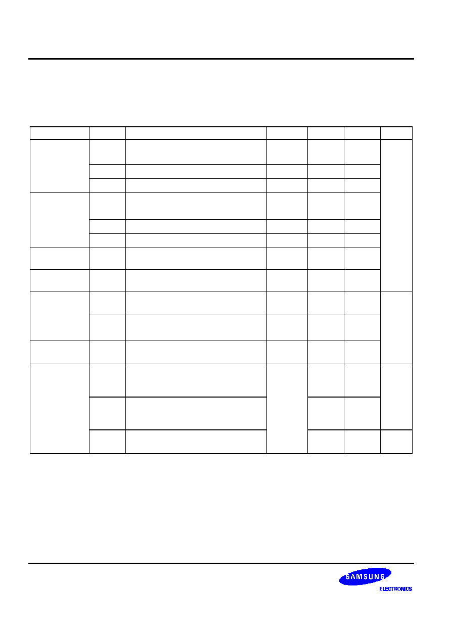
S3F8647 FLASH MCU
S3C8639/C863A/P863A/C8647/F8647
22-4
D.C. ELECTRICAL CHARACTERISTICS
Table 22-3. D.C. Electrical Characteristics
(V
DD
= 4.0 V to 5.5 V)
Parameter
Symbol
Conditions
Min
Typ
Max
Unit
Input High
leakage current
I
LIH1
V
IN
= V
DD
All input pins except X
IN
,
X
OUT
≠
≠
3
µA
I
LIH2
V
IN
= V
DD
;
X
OUT
only
≠
≠
20
I
LIH3
V
IN
= V
DD
;
X
IN
only
2.5
6
20
Input Low
leakage current
I
LIL1
V
IN
= 0 V; All input pins except X
IN
,
X
OUT
,
RESET
, Hsync-I and Vsync-I
≠
≠
≠ 3
I
LIL2
V
IN
= 0 V; X
OUT
only
≠
≠
≠ 20
I
LIL3
V
IN
= 0 V; X
IN
only
≠ 2.5
≠ 6
≠ 20
Output High
leakage current
I
LOH1
V
OUT
= V
DD
≠
≠
3
Output Low
leakage current
I
LOL1
V
OUT
= 0 V
≠
≠
≠ 3
Pull-up resistor
R
U1
V
IN
= 0 V; V
DD
= 5 V
±
10%
Port 3.7≠3.4
20
47
80
k
R
U2
V
IN
= 0 V; V
DD
= 5 V
±
10%
RESET
only
150
280
480
Pull-down
resistor
R
D
V
IN
= 0 V; V
DD
= 5 V
±
10%
Hsync-I and Vsync-I
150
300
500
Supply current
(note)
I
DD1
V
DD
= 5 V
±
10%
Operation mode; 12 MHz crystal
C1 = C2 = 22pF
≠
10
20
mA
I
DD2
V
DD
= 5 V
±
10%
Idle mode; 12 MHz crystal
C1 = C2 = 22pF
4
8
I
DD3
V
DD
= 5 V
±
10%
Stop mode
100
150
µA
NOTE: Supply current does not include drawn internal pull-up/pull-down resistors and external loads of output.

S3C8639/C863A/P863A/C8647/F8647
S3F8647 FLASH MCU
22-5
NOTES

S3C8639/C863A/P863A/C8647/F8647
DEVELOPMENT TOOLS
23-1
23
DEVELOPMENT TOOLS
OVERVIEW
Samsung provides a powerful and easy-to-use development support system in turnkey form. The development
support system is configured with a host system, debugging tools, and support software. For the host system, any
standard computer that operates with MS-DOS as its operating system can be used. One type of debugging tool
including hardware and software is provided: the sophisticated and powerful in-circuit emulator, SMDS2+, for
S3C7, S3C9, S3C8 families of microcontrollers. The SMDS2+ is a new and improved version of SMDS2.
Samsung also offers support software that includes debugger, assembler, and a program for setting options.
SHINE
Samsung Host Interface for In-Circuit Emulator, SHINE, is a multi-window based debugger for SMDS2+. SHINE
provides pull-down and pop-up menus, mouse support, function/hot keys, and context-sensitive hyper-linked
help. It has an advanced, multiple-windowed user interface that emphasizes ease of use. Each window can be
sized, moved, scrolled, highlighted, added, or removed completely.
SAMA ASSEMBLER
The Samsung Arrangeable Microcontroller (SAM) Assembler, SAMA, is a universal assembler, and generates
object code in standard hexadecimal format. Assembled program code includes the object code that is used for
ROM data and required SMDS program control data. To assemble programs, SAMA requires a source file and
an auxiliary definition (DEF) file with device specific information.
SASM88
The SASM88 is an relocatable assembler for Samsung's S3C8-series microcontrollers. The SASM88 takes a
source file containing assembly language statements and translates into a corresponding source code, object
code and comments. The SASM88 supports macros and conditional assembly. It runs on the MS-DOS operating
system. It produces the relocatable object code only, so the user should link object file. Object files can be linked
with other object files and loaded into memory.
HEX2ROM
HEX2ROM file generates ROM code from HEX file which has been produced by assembler. ROM code must be
needed to fabricate a microcontroller which has a mask ROM. When generating the ROM code (.OBJ file) by
HEX2ROM, the value "FF" is filled into the unused ROM area upto the maximum ROM size of the target device
automatically.
TARGET BOARDS
Target boards are available for all S3C8-series microcontrollers. All required target system cables and adapters
are included with the device-specific target board.

DEVELOPMENT TOOLS
S3C8639/C863A/P863A/C8647/F8647
23-2
OTPs
One time programmable microcontroller (OTP) for the S3C8639/C863A microcontroller and OTP programmer
(Gang) are now available.
Bus
SMDS2+
RS-232C
POD
Probe
Adapter
PROM/OTP Writer Unit
RAM Break/Display Unit
Trace/Timer Unit
SAM8 Base Unit
Power Supply Unit
IBM-PC AT or Compatible
TB886332B/6348B
(TB8639/863A)
Target Board
EVA
Chip
Target
Application
System
Figure 23-1. SMDS Product Configuration (SMDS2+)

S3C8639/C863A/P863A/C8647/F8647
DEVELOPMENT TOOLS
23-3
TB886332B/6348B (TB8639/863A) TARGET BOARD
The TB886332B/6348B (TB8639/863A) target board is used for the S3C8639/C863A microcontroller. It is
supported by the SMDS2+ development system.
TB886332B/6348B
(TB8639/863A)
SM1335B
GND
V
CC
+
Idle
+
Stop
100-Pin Connector
25
1
RESET
To User_V
CC
Off
On
74HC11
U1
External
Triggers
CH1
CH2
SW1
SMDS2+
SMDS2
144 QFP
S3E8630
EVA Chip
J101
50-Pin Connector
42
1
21
22
J101
50-Pin Connector
44
1
22
23
Figure 23-2. TB886332B/6348B (TB8639/863A) Target Board Configuration
DEVELOPMENT TOOLS
S3C8639/C863A/P863A/C8647/F8647
23-4
TB886424A (TB8647) TARGET BOARD
The TB886424A (TB8647) target board is used for the S3C8647 microcontroller. It is supported by the SMDS2+
development system.
TB886424A
(TB8647)
SM1339A
GND
V
CC
+
Idle
+
Stop
100-Pin Connector
25
1
RESET
To User_V
CC
Off
On
74HC11
U1
External
Triggers
CH1
CH2
SW1
SMDS2+
SMDS2
144 QFP
S3E8630
EVA Chip
J101
50-Pin Connector
30
1
15
16
Figure 23-3. TB886424A (TB8647) Target Board Configuration
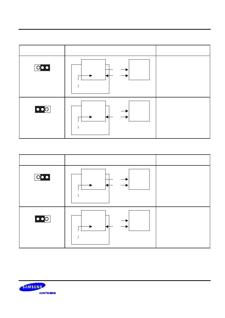
S3C8639/C863A/P863A/C8647/F8647
DEVELOPMENT TOOLS
23-5
Table 23-1. Power Selection Settings for TB886332B/TB886348B (TB8639/863A)
"To User_Vcc"
Settings
Operating Mode
Comments
To User_Vcc
ON
OFF
Target
System
SMDS2/SMDS2+
TB886332B
TB886348B
(TB8639/863A)
V
CC
V
SS
V
CC
The SMDS2/SMDS2+
supplies V
CC
to the target
board (evaluation chip) and
the target system.
To User_Vcc
ON
OFF
Target
System
SMDS2/SMDS2+
TB886332B
TB886348B
(TB8639/863A)
External
V
CC
V
SS
V
CC
The SMDS2/SMDS2+
supplies V
CC
only to the
target board (evaluation chip).
The target system must have
its own power supply.
Table 23-2. Power Selection Settings for TB886424A (TB8647)
"To User_Vcc"
Settings
Operating Mode
Comments
To User_Vcc
ON
OFF
Target
System
SMDS2/SMDS2+
TB886424A
(TB8647)
V
CC
V
SS
V
CC
The SMDS2/SMDS2+
supplies V
CC
to the target
board (evaluation chip) and
the target system.
To User_Vcc
ON
OFF
Target
System
SMDS2/SMDS2+
TB886424A
(TB8647)
External
V
CC
V
SS
V
CC
The SMDS2/SMDS2+
supplies V
CC
only to the
target board (evaluation chip).
The target system must have
its own power supply.

DEVELOPMENT TOOLS
S3C8639/C863A/P863A/C8647/F8647
23-6
SMDS2+ SELECTION (SAM8)
In order to write data into program memory that is available in SMDS2+, the target board should be selected to
be for SMDS2+ through a switch as follows. Otherwise, the program memory writing function is not available.
Table 23-3. The SMDS2+ Tool Selection Setting
"SW1" Setting
Operating Mode
SMDS2
SMDS2+
SMDS2+
TARGET
BOARD
R/W*
R/W*
Table 23-4. Using Single Header Pins as the Input Path for External Trigger Sources
Target Board Part
Comments
EXTERNAL
TRIGGERS
CH1
CH2
Connector from
external trigger
sources of the
application system
You can connect an external trigger source to one of the two external
trigger channels (CH1 or CH2) for the SMDS2+ breakpoint and trace
functions.
IDLE LED
This LED is ON when the evaluation chip (S3E8630) is in idle mode.
STOP LED
This LED is ON when the evaluation chip (S3E8630) is in stop mode.
S3C8639/C863A/P863A/C8647/F8647
DEVELOPMENT TOOLS
23-7
P0.0/INT0
P0.1/INT1
P0.2/INT2
P0.3
P0.4/TM0CAP
P0.5
P0.6
P0.7
P1.0/SDA1
P1.1/SCL1
V
DD1
V
SS1
TEST(GND)
SDA0
SCL0
RESET
P1.2
P2.0/PWM0
P2.1/PWM1
P2.2/PWM2
P3.7
P3.6
P3.5
P3.4
P3.3/AD3
P3.2/AD2
P3.1/AD1
P3.0/AD0
V
DD2
V
SS2
P2.7/Csync-I
Hsync-I
Vsync-I
Vsync-O
Hsync-O
Clamp-O
P2.6/PWM6
P2.5/PWM5
P2.4/PWM4
P2.3/PWM3
1
2
3
4
5
6
7
8
9
10
11
12
13
14
15
16
17
18
19
20
40
39
38
37
36
35
34
33
32
31
30
29
28
27
26
25
24
23
22
21
40-Pin DIP Connector
J101
Figure 23-4. 40-Pin Connector for TB886332B/6348B (TB8639/A)
V
SS
TEST
P0.0/INT0
P0.1/INT1
RESET
P0.2/INT2
P0.4/TM0CAP
SDA
SCL
P2.0/PWM0
P2.1/PWM1
P2.2/PWM2
P2.3/PWM3
P2.4/PWM4
P2.5/PWM5
V
DD
P3.7
P3.6
P3.5
P3.4
P3.3/AD3
P3.2/AD2
P3.1/AD1
P3.0/AD0
P2.7/Csync-I(SOG)
Hsync-I
Vsync-I
Vsync-O
Hsync-O
Clamp-O
1
2
3
4
5
6
7
8
9
10
11
12
13
14
15
30
29
28
27
26
25
24
23
22
21
20
19
18
17
16
30-Pin DIP Connector
J101
Figure 23-5. 30-Pin Connector for TB886424A (TB8647)
DEVELOPMENT TOOLS
S3C8639/C863A/P863A/C8647/F8647
23-8
Target Board
Target System
Target Cable for 42-SDIP Package
Part Name: AP42SD-G
Order Code: SM6520
40-Pin DIP Connector
J101
1
40
20
21
1
40
20
21
1
21
42
22
Figure 23-6. TB886332B/6348B (TB8639/A) Adapter Cable for 42-SDIP Package
Target Board
Target System
Target Cable for 30-SDIP Package
Part Name: AP30SD-G
Order Code: SM6520
30-Pin DIP Connector
J101
1
30
15
16
1
30
15
16
1
16
32
17
Figure 23-7. TB886424A (TB8647) Adapter Cable for 32-SDIP Package