Document Outline
- TOC
- 1 Product Overview
- 2 Addres Spaces
- 3 Addressing Modes
- 4 Control Registers
- 5 Interrupt Structure
- 6 SAM8 Instruction Set
- 7 Clock Circuits
- 8 nRESET and Power Down
- 9 IO Ports
- 10 Basic Timer and Timer 0
- 11 Timer A
- 12 PWM and Capture
- 13 On-screen Disaplay (OSD)
- 14 ADC
- 15 Electrical Data
- 16 Mechanical Data
- 17 S3F880A MTP
- 18 Development Tools

S3C880A/F880A
8-BIT CMOS
MICROCONTROLLERS
USER'S MANUAL
Revision 3

Important Notice
The information in this publication has been carefully
checked and is believed to be entirely accurate at the
time of publication. Samsung assumes no
responsibility, however, for possible errors or
omissions, or for any consequences resulting from
the use of the information contained herein.
Samsung reserves the right to make changes in its
products or product specifications with the intent to
improve function or design at any time and without
notice and is not required to update this
documentation to reflect such changes.
This publication does not convey to a purchaser of
semiconductor devices described herein any license
under the patent rights of Samsung or others.
Samsung makes no warranty, representation, or
guarantee regarding the suitability of its products for
any particular purpose, nor does Samsung assume
any liability arising out of the application or use of any
product or circuit and specifically disclaims any and
all liability, including without limitation any
consequential or incidental damages.
"Typical" parameters can and do vary in different
applications. All operating parameters, including
"Typicals" must be validated for each customer
application by the customer's technical experts.
Samsung products are not designed, intended, or
authorized for use as components in systems
intended for surgical implant into the body, for other
applications intended to support or sustain life, or for
any other application in which the failure of the
Samsung product could create a situation where
personal injury or death may occur.
Should the Buyer purchase or use a Samsung
product for any such unintended or unauthorized
application, the Buyer shall indemnify and hold
Samsung and its officers, employees, subsidiaries,
affiliates, and distributors harmless against all claims,
costs, damages, expenses, and reasonable attorney
fees arising out of, either directly or indirectly, any
claim of personal injury or death that may be
associated with such unintended or unauthorized use,
even if such claim alleges that Samsung was
negligent regarding the design or manufacture of said
product.
S3C880A/F880A 8-Bit CMOS Microcontrollers
User's Manual, Revision 3
Publication Number: 23-S3-C880A/F880A-072004
� 2004 Samsung Electronics
All rights reserved. No part of this publication may be reproduced, stored in a retrieval system, or transmitted in any
form or by any means, electric or mechanical, by photocopying, recording, or otherwise, without the prior written
consent of Samsung Electronics.
Samsung Electronics' microcontroller business has been awarded full ISO-14001 certification (BSI
Certificate No. FM24653). All semiconductor products are designed and manufactured in
accordance with the highest quality standards and objectives.
Samsung Electronics Co., Ltd.
San #24 Nongseo-Ri, Kiheung-Eup
Yongin-City, Kyunggi-Do, Korea
C.P.O. Box #37, Suwon 449-900
TEL: (82)-(31)-209-1907
FAX: (82)-(31)-209-1889
Home-Page URL: Http://www.intl.samsungsemi.com
Printed in the Republic of Korea

S3C880A/F880A MICROCONTROLLER
iii
Preface
The S3C880A/F880A Microcontroller User's Manual is designed for application designers and programmers who are
using the S3C880A/F880A microcontroller for application development.
It is organized in two main parts:
Part I
Programming Model
Part II
Hardware Descriptions
Part I contains software-related information to familiarize you with the microcontroller's architecture, programming
model, instruction set, and interrupt structure. It has six chapters:
Chapter 1
Product Overview
Chapter 2
Address Spaces
Chapter 3
Addressing Modes
Chapter 4
Control Registers
Chapter 5
Interrupt Structure
Chapter 6
SAM8 Instruction Set
Chapter 1, "Product Overview," is a high-level introduction to S3C880A/F880A with general product descriptions, as
well as detailed information about individual pin characteristics and pin circuit types.
Chapter 2, "Address Spaces," describes program and data memory spaces, the internal register file, and register
addressing. Chapter 2 also describes working register addressing, as well as system stack and user-defined stack
operations.
Chapter 3, "Addressing Modes," contains detailed descriptions of the addressing modes that are supported by the
S3C8-series CPU.
Chapter 4, "Control Registers," contains overview tables for all mapped system and peripheral control register values,
as well as detailed one-page descriptions in a standardized format. You can use these easy-to-read, alphabetically
organized, register descriptions as a quick-reference source when writing programs.
Chapter 5, "Interrupt Structure," describes the S3C880A/F880A interrupt structure in detail and further prepares you
for additional information presented in the individual hardware module descriptions in Part II.
Chapter 6, "SAM8 Instruction Set," describes the features and conventions of the instruction set used for all S3C8-
series microcontrollers. Several summary tables are presented for orientation and reference. Detailed descriptions of
each instruction are presented in a standard format. Each instruction description includes one or more practical
examples of how to use the instruction when writing an application program.
A basic familiarity with the information in Part I will help you to understand the hardware module descriptions in Part
II. If you are not yet familiar with the S3C8-series microcontroller family and are reading this manual for the first time,
we recommend that you first read Chapters 1�3 carefully. Then, briefly look over the detailed information in Chapters
4, 5, and 6. Later, you can reference the information in Part I as necessary.
Part II "hardware Descriptions," has detailed information about specific hardware components of the S3C880A/F880A
microcontroller. Also included in Part II are electrical, mechanical, MTP, and development tools data. It has 11
chapters:
Chapter 7
Clock Circuits
Chapter 8
nRESET and Power-Down
Chapter 9
I/O Ports
Chapter 10
Basic Timer and Timer 0
Chapter 11
Timer A
Chapter 12
PWM and Capture
Chapter 13
On-Screen Display (OSD)
Chapter 14
Analog-to-Digital Converter
Chapter 15
Electrical Data
Chapter 16
Mechanical Data
Chapter 17
S3F880A MTP
Chapter 18
Development Tools
Two order forms are included at the back of this manual to facilitate customer order for S3C880A/F880A
microcontrollers: the Mask ROM Order Form, and the Mask Option Selection Form. You can photocopy these
forms, fill them out, and then forward them to your local Samsung Sales Representative.


S3C880A/F880A MICROCONTROLLER
v
Table of Contents
Part I -- Programming Model
Chapter 1
Product Overview
Overview .............................................................................................................................................1-1
Features .............................................................................................................................................1-2
Block Diagram ....................................................................................................................................1-3
Pin Assignments.................................................................................................................................1-4
Pin Descriptions ..................................................................................................................................1-5
Pin Circuits.........................................................................................................................................1-7
Chapter 2
Address Spaces
Overview .............................................................................................................................................2-1
Program Memory (ROM) ......................................................................................................................2-2
Register Architecture ...........................................................................................................................2-3
ROM Code Option (RCOD_OPT)...........................................................................................................2-5
Register Page Pointer (PP) ..........................................................................................................2-6
Effect of Different Instructions For Inter-Page Data Operations .........................................................2-7
Register Set 1.............................................................................................................................2-14
Register Set 2.............................................................................................................................2-14
Prime Register Space..................................................................................................................2-14
Working Registers .......................................................................................................................2-16
Using The Register Pointers .........................................................................................................2-17
Register Addressing ............................................................................................................................2-19
Common Working Register Area (C0H�CFH) .................................................................................2-21
4-Bit Working Register Addressing................................................................................................2-22
8-Bit Working Register Addressing................................................................................................2-24
System and User Stacks .....................................................................................................................2-26
Chapter 3
Addressing Modes
Overview .............................................................................................................................................3-1
Register Addressing Mode (R) ......................................................................................................3-2
Indirect Register Addressing Mode (IR)..........................................................................................3-3
Indexed Addressing Mode (X) .......................................................................................................3-7
Direct Address Mode (DA)............................................................................................................3-10
Indirect Address Mode (IA)...........................................................................................................3-12
Relative Address Mode (RA).........................................................................................................3-13
Immediate Mode (IM) ...................................................................................................................3-14

vi
S3C880A/F880A MICROCONTROLLER
Table of Contents
(Continued)
Chapter 4
Control Registers
Overview .............................................................................................................................................4-1
Chapter 5
Interrupt Structure
Overview .............................................................................................................................................5-1
Interrupt Types ............................................................................................................................5-1
S3C880A/F880A Interrupt Structure ..............................................................................................5-2
Interrupt Vector Addresses ...........................................................................................................5-4
Enable/Disable Interrupt Instructions (EI, DI) ..................................................................................5-6
System-Level Interrupt Control Registers .......................................................................................5-6
Interrupt Processing Control Points ...............................................................................................5-7
Peripheral Interrupt Control Registers ............................................................................................5-8
System Mode Register (SYM) ......................................................................................................5-9
Interrupt Mask Register (IMR) .......................................................................................................5-10
Interrupt Priority Register (IPR) .....................................................................................................5-11
Interrupt Request Register (IRQ) ...................................................................................................5-12
Interrupt Pending Function Types ..................................................................................................5-13
Interrupt Source Polling Sequence ................................................................................................5-14
Interrupt Service Routines.............................................................................................................5-14
Generating Interrupt Vector Addresses ..........................................................................................5-15
Nesting of Vectored Interrupts.......................................................................................................5-15
Instruction Pointer (IP) .................................................................................................................5-15
Fast Interrupt Processing .............................................................................................................5-16
Chapter 6
SAM8 Instruction Set
Overview .............................................................................................................................................6-1
Data Types .................................................................................................................................6-1
Register Addressing ....................................................................................................................6-1
Addressing Modes.......................................................................................................................6-1
Flags Register (FLAGS)...............................................................................................................6-6
Flag Descriptions ........................................................................................................................6-7
Instruction Set Notation................................................................................................................6-8
Condition Codes ..........................................................................................................................6-12
Instruction Descriptions................................................................................................................6-13

S3C880A/F880A MICROCONTROLLER
vii
Table of Contents
(Continued)
Part II Hardware Descriptions
Chapter 7
Clock Circuit
Overview .............................................................................................................................................7-1
System Clock Circuit...................................................................................................................7-1
Clock Status During Power-Down Modes .......................................................................................7-2
System Clock Control Register (CLKCON).....................................................................................7-3
Relation Between L-C Oscillator and CPU Clock ............................................................................7-5
Chapter 8
nRESET and Power-Down
System Reset .....................................................................................................................................8-1
Overview .....................................................................................................................................8-1
Hardware Reset Values................................................................................................................8-2
Power-Down Modes .............................................................................................................................8-5
Stop Mode..................................................................................................................................8-5
Idle Mode....................................................................................................................................8-6
Chapter 9
I/O Ports
Overview .............................................................................................................................................9-1
Port Data Registers .....................................................................................................................9-2
Port 0.........................................................................................................................................9-2
Port 1.........................................................................................................................................9-4
Port 2.........................................................................................................................................9-5
Port 3.........................................................................................................................................9-6
Chapter 10
Basic Timer and Timer 0
Module Overview..................................................................................................................................10-1
Basic Timer Control Register (BTCON) ..........................................................................................10-2
Basic Timer Function Description..................................................................................................10-3
Timer 0 Control Register (T0CON) .................................................................................................10-6
Timer 0 Function Description ........................................................................................................10-7

viii
S3C880A/F880A MICROCONTROLLER
Table of Contents
(Continued)
Chapter 11
Timer A
Overview .............................................................................................................................................11-1
Timer Clock Input ........................................................................................................................11-1
Timer A Interrupt Control ..............................................................................................................11-1
Timer A Function Description........................................................................................................11-2
Timer A Control Register (TACON) ................................................................................................11-3
Chapter 12
PWM and Capture
PWM/Capture Module..........................................................................................................................12-1
PWM Control Register (PWMCON)...............................................................................................12-2
PWM2�PWM5....................................................................................................................................12-3
PWM2�PWM5 Function Description .............................................................................................12-4
Staggered PWM Outputs .............................................................................................................12-5
PWM0�PWM1....................................................................................................................................12-7
PWM Counter .............................................................................................................................12-7
PWM Data and Extension Registers .............................................................................................12-7
PWM Clock Rate ........................................................................................................................12-7
PWM0 and PWM1 Function Description........................................................................................12-8
Capture Unit................................................................................................................................12-12
Chapter 13
On-Screen Display (OSD)
Overview .............................................................................................................................................13-1
Pattern Generation Software.........................................................................................................13-1
Internal OSD Clock......................................................................................................................13-2
OSD Video RAM .........................................................................................................................13-2
OSD Control Register Overview.............................................................................................................13-5
Display Control Register (DSPCON)..............................................................................................13-6
Character Size Control Register (CHACON) ...................................................................................13-8
Fade-In and Fade-Out Control Register (FADECON) .......................................................................13-10
Display Position Control.......................................................................................................................13-14
Row Control Register (ROWCON) .................................................................................................13-15
Column Control Register (CLMCON)..............................................................................................13-15
Character Color Control Register (COLBUF)...................................................................................13-17
Background Color Control.....................................................................................................................13-18
V-SYNC Blank Control Register (VSBCON) ...................................................................................13-20
V-SYNC Blank and Top Margin Timing Diagram .............................................................................13-21
Halftone Signal Control Register (HTCON)......................................................................................13-22
OSD Field Control Register (OSDFLD) ..................................................................................................13-25
OSD Palette Color Control............................................................................................................13-27
OSD Space Color Control Register (OSDCOL) ...............................................................................13-31
OSD Border/Fringe Function.........................................................................................................13-33
OSD Smooth Fucntion.................................................................................................................13-35

S3C880A/F880A MICROCONTROLLER
ix
Table of Contents
(Concluded)
Chapter 14
Analog-to-Digital Converter
Overview .............................................................................................................................................14-1
Using A/D Pins for Standard Digital Input .......................................................................................14-2
A/D Converter Control Register (ADCON).......................................................................................14-2
Internal Reference Voltage Levels..................................................................................................14-3
Conversion Timing .......................................................................................................................14-4
Internal A/D Conversion Procedure ................................................................................................14-4
Chapter 15
Electrical Data
Overview .............................................................................................................................................15-1
Chapter 16
Mechanical Data
Overview .............................................................................................................................................16-1
Chapter 17
S3F880A
Overview .............................................................................................................................................17-1
Chapter 18
Development Tools
Overview .............................................................................................................................................18-1
Shine .........................................................................................................................................18-1
SAMA Assembler........................................................................................................................18-1
SASM88.....................................................................................................................................18-1
HEX2ROM ..................................................................................................................................18-1
Target Boards .............................................................................................................................18-2
TB880A Target Board...................................................................................................................18-3


S3C880A/F880A MICROCONTROLLER
xi
List of Figures
Figure
Title
Page
Number
Number
1-1
Block Diagram ....................................................................................................1-3
1-2
S3C880A/F880A Pin Assignment (42-SDIP) ..........................................................1-4
1-3
S3C880A/F880A Pin Assignment (44-QFP)...........................................................1-5
1-4
Pin Circuit Type 1 (V-Sync H-Sync, CAPA) ...........................................................1-8
1-5
Pin Circuit Type 2 (P2.0�P2.7, P0.0�P0.3, PWM0�PWM5, T0, OSDHT) ..................1-8
1-6
Pin Circuit Type 3 (P0.4�P0.5, P1.6�P1.7, T0CK) ..................................................1-8
1-7
Pin Circuit Type 4 (Vblue, Vgreen, Vred, Vblank)....................................................1-9
1-8
Pin Circuit Type 5 (P1.4�P1.5)..............................................................................1-9
1-9
Pin Circuit Type 6 (P3.0�P3.1, P0.6�P0.7, ADC0�ADC3)........................................1-9
1-10
Pin Circuit Type 7 (P1.0�P1.3, INT0�INT3).............................................................1-10
1-11
Pin Circuit Type 8 (nRESET) ................................................................................1-10
2-1
Program Memory Address Spaces........................................................................2-2
2-2
Internal Register File Organization.........................................................................2-4
2-3
ROM Code Option (RCOD_OPT)...........................................................................2-5
2-4
Register Page Pointer (PP) ..................................................................................2-6
2-5
Programming Tip Example for Inter-Page Data Operations.......................................2-7
2-6
Set 1, Set 2, and Prime Area Register Map ...........................................................2-15
2-7
8-Byte Working Register Areas (Slices).................................................................2-16
2-8
Contiguous 16-Byte Working Register Block..........................................................2-17
2-9
Non-Contiguous 16-Byte Working Register Block ...................................................2-18
2-9
16-Bit Register Pairs............................................................................................2-19
2-10
Register File Addressing ......................................................................................2-20
2-12
Common Working Register Area...........................................................................2-21
2-13
4-Bit Working Register Addressing........................................................................2-23
2-14
4-Bit Working Register Addressing Example..........................................................2-23
2-15
8-Bit Working Register Addressing........................................................................2-24
2-16
8-Bit Working Register Addressing Example..........................................................2-25
2-17
Stack Operations ................................................................................................2-26
3-1
Register Addressing ............................................................................................3-2
3-2
Working Register Addressing ...............................................................................3-2
3-3
Indirect Register Addressing to Register File..........................................................3-3
3-4
Indirect Register Addressing to Program Memory ...................................................3-4
3-5
Indirect Working Register Addressing to Register File.............................................3-5
3-6
Indirect Working Register Addressing to Program or Data Memory...........................3-6
3-7
Indexed Addressing to Register File ......................................................................3-7
3-8
Indexed Addressing to Program or Data Memory with Short Offset ...........................3-8
3-9
Indexed Addressing to Program or Data Memory ....................................................3-9
3-10
Direct Addressing for Load Instructions..................................................................3-10
3-11
Direct Addressing for Call and Jump Instructions ....................................................3-11
3-12
Indirect Addressing..............................................................................................3-12
3-13
Relative Addressing .............................................................................................3-13
3-14
Immediate Addressing .........................................................................................3-14
4-1
Register Description Format .................................................................................4-5

xii
S3C880A/F880A MICROCONTROLLER
List of Figures
(Continued)
Figure
Title
Page
Number
Number
5-1
S3C8-Series Interrupt Types .................................................................................5-2
5-2
S3C880A/F880A Interrupt Structure ......................................................................5-3
5-3
ROM Vector Address Area...................................................................................5-4
5-4
Interrupt Function Diagram ...................................................................................5-7
5-5
System Mode Register (SYM) ..............................................................................5-9
5-6
Interrupt Mask Register (IMR) ...............................................................................5-10
5-7
Interrupt Priority Register (IPR) .............................................................................5-11
5-8
Interrupt Request Register (IRQ) ...........................................................................5-12
6-1
System Flags Register (FLAGS)...........................................................................6-6
7-1
Main Oscillator Circuit (External Crystal or Ceramic Resonator)...............................7-1
7-2
System Clock Circuit Diagram..............................................................................7-2
7-3
System Clock Control Register (CLKCON).............................................................7-3
7-4
L-C Oscillator Circuit for OSD...............................................................................7-4
8-1
Stop State Timing Diagram...................................................................................8-7
9-1
Port Data Register Format....................................................................................9-2
9-2
Port 0 High-Byte Control Register (P0CONH) .........................................................9-3
9-3
Port 0 Low-Byte Control Register (P0CONL) ..........................................................9-3
9-4
Port 1 High-Byte Control Register (P1CONH) .........................................................9-4
9-5
Port 1 Low-Byte Control Register (P1CONL) ..........................................................9-4
9-6
Port 2 High-Byte Control Register (P2CONH) .........................................................9-5
9-7
Port 2 Low-Byte Control Register (P2CONL) ..........................................................9-5
9-8
Port 3 Control Register (P3CON)...........................................................................9-6
10-1
Basic Timer Control Register (BTCON) ..................................................................10-2
10-2
Oscillation Stabilization Time on RESET ...............................................................10-4
10-3
Oscillation Stabilization Time on STOP Mode Release............................................10-5
10-4
Timer 0 Control Register (T0CON) .........................................................................10-6
10-5
Timer 0 Function Diagram (Interval Timer Mode) .....................................................10-7
10-6
Timer 0 Function Diagram (PWM Mode) ................................................................10-8
10-7
Basic Timer and Timer 0 Block Diagram ................................................................10-9
11-1
Timer A Block Diagram ........................................................................................11-2
11-2
Timer A Control Register (TACON) ........................................................................11-3

S3C880A/F880A MICROCONTROLLER
xiii
List of Figures
(Continued)
Figure
Title
Page
Number
Number
12-1
PWM Control Register (PWMCON).......................................................................12-2
12-2
Block Diagram for PWM2�PWM5 .........................................................................12-3
12-3
PWM Waveforms for PWM2�PWM5 .....................................................................12-5
12-4
PWM Clock to PWM2�PWM5 Output Delays........................................................12-6
12-5
Block Diagram for PWM0 and PWM1....................................................................12-9
12-6
Decision Flowchart for PWM0 Programming Tip .....................................................12-10
12-7
Block Diagram for Capture A ................................................................................12-12
12-8
Decision Flowchart (Main Routine and Timer A Interrupt).........................................12-14
12-9
Decision Flowchart for Capture A Interrupt .............................................................12-15
13-1
On-Screen Display Function Block Diagram...........................................................13-3
13-2
On-Screen Display Video RAM Data Organization..................................................13-4
13-3
OSD Display Control Register (DSPCON)..............................................................13-6
13-4
OSD Character Size Control Register (CHACON) ...................................................13-8
13-5
OSD Character Sizing Dimensions........................................................................13-9
13-6
OSD Fade Control Register (FADECON) ...............................................................13-10
13-7
Line and Row Addressing Conventions when ROWCON.2-.0 = "100"........................13-11
13-8
OSD Fade Function Example: Fade After ..............................................................13-12
13-9
OSD Fade Function Example: Fade Before............................................................13-13
13-10
252-Byte On-Screen Character Display Map (Decimal) ...........................................13-14
13-11
252-Byte On-Screen Character Display Map (Hexadecimal) ....................................13-14
13-12
OSD Row Control Register (ROWCON) .................................................................13-15
13-13
OSD Column Control Register (CLMCON)..............................................................13-15
13-14
OSD Display Formatting and Spacing Conventions .................................................13-16
13-15
OSD Character Color Buffer Register (COLBUF).....................................................13-17
13-16
Background Color Display Conventions..................................................................13-18
13-17
OSD Background Color Control Register (COLCON) ...............................................13-19
13-18
V-sync Blank Control Register (VSBCON) .............................................................13-20
13-19
V-sync Blank and Top Margin Timing Diagram .......................................................13-21
13-20
Halftone Signal Control Register (HTCON)..............................................................13-23
13-21
Halftone or Character Backgound Signal Output .....................................................13-24
13-22
OSD Field Control Register (OSDFLD) ..................................................................13-25
13-23
Field Detect in Before V-sync ...............................................................................13-26
13-24
Field Detect in After V-sync..................................................................................13-26
13-25
OSD Palette Color Mode Register R1 (OSDPLTR1) ................................................13-27
13-26
OSD Palette Color Mode Register R2 (OSDPLTR2) ................................................13-28
13-27
OSD Palette Color Mode Register G1 (OSDPLTG1)................................................13-29
13-28
OSD Palette Color Mode Register G2 (OSDPLTG2)................................................13-29
13-29
OSD Palette Color Mode Register B1 (OSDPLTB1) ................................................13-30
13-30
OSD Palette Color Mode Register B2 (OSDPLTB2) ................................................13-30
13-31
OSD Space Color Control Register (OSDCOL) .......................................................13-32
13-32
OSD Fringe/Border Control Register 1 (OSDFRG1).................................................13-34
13-33
OSD Fringe/Border Control Register 2 (OSDFRG2).................................................13-34

xiv
S3C880A/F880A MICROCONTROLLER
List of Figures
(Concluded)
Figure
Title
Page
Number
Number
13-34
OSD Smooth Control Register 1 (OSDSMH1) ........................................................13-35
13-35
OSD Smooth Control Register 2 (OSDSMH2) ........................................................13-36
13-36
Smoothing/Fringing/Priority of Smoothing and Fringing............................................13-36
13-37
Decision Flowchart for Row Interrupt Function Programming Tip...............................13-37
13-38
Decision Flowchart for Fade Function Programming Tip ..........................................13-40
14-1
A/D Converter Control Register (ADCON)...............................................................14-2
14-2
A/D Converter Circuit Diagram ..............................................................................14-3
14-3
A/D Converter Data Register (ADDATAH/L)............................................................14-3
14-4
S3C880A/F880A A/D Converter Timing Diagram.....................................................14-4
14-5
Recommended A/D Converter Circuit for Highest Absolute Accuracy........................14-5
15-1
Input Timing Measurement Points for t
NF1
and t
NF2
.................................................15-5
15-2
Stop Mode Release Timing When Initiated by a nRESET........................................15-5
15-3
Clock Timing Measurement Points for X
IN
..............................................................15-6
16-1
42-Pin SDIP Package Dimensions (42-SDIP-600)...................................................16-1
16-2
44-Pin QFP Package Dimensions (44-QFP-1010B) ................................................16-2
17-1
Descriptions of Pins Used to Read/Write the Flash ROM (S3F880A)........................17-2
18-1
SMDS Product Configuration (SMDS2+)................................................................18-2
18-2
TB880A Target Board Configuration.......................................................................18-3
18-3
50-Pin DIP Connector J101 for TB880A..................................................................18-7
18-4
S3C880A/F880A Probe Adapter for 42-SDIP Package ............................................18-7

S3C880A/F880A MICROCONTROLLER
xv
List of Tables
Table
Title
Page
Number
Number
1-1
S3C880A/F880A Pin Descriptions.........................................................................1-5
2-1
Program ROM and Character ROM Area by the Font Figure....................................2-3
2-2
Register Type Summary.......................................................................................2-3
4-1
Set 1 Registers ...................................................................................................4-2
4-2
Set 1, Bank 0 Registers .......................................................................................4-2
4-3
Set 1, Bank 1 Registers .......................................................................................4-4
5-1
S3C880A/F880A Interrupt Vectors ........................................................................5-5
5-2
Interrupt Control Register Overview ........................................................................5-6
5-3
Interrupt Source Control Registers.........................................................................5-8
6-1
Instruction Group Summary ..................................................................................6-2
6-2
Flag Notation Conventions ....................................................................................6-8
6-3
Instruction Set Symbols.......................................................................................6-8
6-4
Instruction Notation Conventions ...........................................................................6-9
6-5
Opcode Quick Reference .....................................................................................6-10
6-6
Condition Codes ..................................................................................................6-12
8-1
Set 1 Register Values after a Reset ......................................................................8-2
8-2
Set 1, Bank 0 Register Values after a Reset ..........................................................8-3
8-3
Page 1 Video RAM Register Values after a Reset ..................................................8-4
9-1
S3C880A/F880A Port Configuration Overview .........................................................9-1
9-2
Port Data Register Summary ................................................................................9-2
12-1
PWM0 and PWM1 Control and Data Registers ......................................................12-8
12-2
PWM Output "Stretch" Values for Extension Registers PWM0EX and PWM1EX.......12-8
13-1
OSD Function Block Summary .............................................................................13-1
15-1
Absolute Maximum Ratings..................................................................................15-2
15-2
D.C. Electrical Characteristics..............................................................................15-2
15-3
Input/Output Capacitance.....................................................................................15-4
15-4
A.C. Electrical Characteristics..............................................................................15-4
15-5
Analog R,G,B Output ...........................................................................................15-4
15-6
Data Retention Supply Voltage in Stop Mode.........................................................15-5
15-7
Main Oscillator and L-C Oscillator Frequency.........................................................15-6
15-8
Main Oscillator Clock Stabilization Time................................................................15-7
15-9
A/D Converter Electrical Characteristics ................................................................15-7
17-1
Power Selection Settings for TB880A ....................................................................17-4
17-2
The SMDS2 + Tool Selection Setting ....................................................................17-5
17-3
OSD Font ROM Selection Setting.........................................................................17-5
17-4
Using Single Header Pins as the Input Path for External Trigger Sources..................17-6


S3C880A/F880A MICROCONTROLLER
xvii
List of Programming Tips
Description
Page
Number
Chapter 2:
Address Spaces
Data Operations Between Register Pages .........................................................................................2-7
Examples of Inter-Page Data Transfer Operations ...............................................................................2-8
Setting the Register Pointers ............................................................................................................2-17
Using the RPs to Calculate the Sum of a Series of Registers ..............................................................2-18
Addressing the Common Working Register Area ................................................................................2-22
Chapter 5:
Interrupt Structure
Programming Level IRQ0 as a Fast Interrupt ......................................................................................5-18
Chapter 12:
PWM and Capture
Programming PWM0 to Sample Specifications ..................................................................................12-10
Programming the Capture Module to Sample Specifications ................................................................12-16
Chapter 13:
On-Screen Display (OSD)
Row Interrupt Function .....................................................................................................................13-37
Writing Character Code and Color Data to the OSD Video RAM...........................................................13-39
OSD Fade Function; Line and Row Counters .....................................................................................13-39
Manipulating OSD Character Colors; Halftone Function.......................................................................13-43
OSD Character Size, Background Color, and Display Position.............................................................13-45
Helpful Hints About COLBUF and OSD Character Code 0 ...................................................................13-45
Chapter 14:
Analog-to-Digital Converter
Configuring A/D Converter.................................................................................................................14-5


S3C880A/F880A MICROCONTROLLER
xix
List of Register Descriptions
Register
Full Register Name
Page
Identifier
Number
ADCON
A/D Converter Control Register .............................................................................4-6
BTCON
Basic Timer Control Register ................................................................................4-7
CHACON
OSD Character Size Control Register....................................................................4-8
CLKCON
System Clock Control Register.............................................................................4-9
CLMCON
OSD Column Control Register ..............................................................................4-10
COLBUF
OSD Character Color Buffer..................................................................................4-11
COLCON
OSD Background Color Control Register................................................................4-12
DSPCON
On-Screen Display Control Register ......................................................................4-13
EMT
External Memory Timing Register .........................................................................4-14
FADECON
OSD Fade Control Register ..................................................................................4-15
FLAGS
System Flag Register ..........................................................................................4-16
HCON
HDLC Control Register.........................................................................................4-17
IMR
Interrupt Mask Register .......................................................................................4-18
IPH
Instruction Pointer (High Byte) ..............................................................................4-19
IPL
Instruction Pointer (Low Byte)...............................................................................4-19
IPR
Interrupt Priority Register......................................................................................4-20
IRQ
Interrupt Request Register....................................................................................4-21
OSDCOL
OSD Space Color Control Register........................................................................4-22
OSDFLD
OSD Field Control Register ..................................................................................4-23
OSDFRG1
OSD Fringe/Border Control Register 1...................................................................4-24
OSDFRG2
OSD Fringe/Border Control Register 2...................................................................4-25
OSDPLTB1
OSD Palette Color Mode Register B1....................................................................4-26
OSDPLTB2
OSD Palette Color Mode Register B2....................................................................4-27
OSDPLTG1
OSD Palette Color Mode Register G1....................................................................4-28
OSDPLTG2
OSD Palette Color Mode Register G2....................................................................4-29
OSDPLTR1
OSD Palette Color Mode Register R1....................................................................4-30
OSDPLTR2
OSD Palette Color Mode Register R2....................................................................4-31

xx
S3C880A/F880A MICROCONTROLLER
List of Register Descriptions
(Continued)
Register
Full Register Name
Page
Identifier
Number
OSDSMH1
OSD Smooth Control Register 1 ...........................................................................4-32
OSDSMH2
OSD Smooth Control Register 2 ...........................................................................4-33
P0CONH
Port 0 Control Register (High Byte) .......................................................................4-34
P0CONL
Port 0 Control Register (Low Byte) ........................................................................4-35
P1CONH
Port 1 Control Register (High Byte) .......................................................................4-36
P1CONL
Port 1 Control Register (Low Byte) ........................................................................4-37
P2CONH
Port 2 Control Register (High Byte) .......................................................................4-38
P2CONL
Port 2 Control Register (Low Byte) ........................................................................4-39
P3CONH
Port 3 Control Register (High Byte) .......................................................................4-40
PP
Register Page Pointer..........................................................................................4-41
PWMCON
PWM Control Register .........................................................................................4-42
ROWCON
OSD Row Position Control Register ......................................................................4-43
RP0
Register Pointer 0................................................................................................4-44
RP1
Register Pointer 1................................................................................................4-44
SPH
Stack Pointer (High Byte).....................................................................................4-45
SPL
Stack Pointer (Low Byte) .....................................................................................4-45
STCON
Stop Control Register...........................................................................................4-46
SYM
System Mode Register ........................................................................................4-47
TACON
8-Bit Timer A Control Register ..............................................................................4-48
T0CON
Timer 0 Control Register.......................................................................................4-49
VSBCON
V-Sync Blank Control Register .............................................................................4-50

S3C880A/F880A MICROCONTROLLER
xxi
List of Instruction Descriptions
Instruction
Full Register Name
Page
Mnemonic
Number
ADC
Add with Carry ....................................................................................................6-14
ADD
Add....................................................................................................................6-15
AND
Logical AND........................................................................................................6-16
BAND
Bit AND..............................................................................................................6-17
BCP
Bit Compare........................................................................................................6-18
BITC
Bit Complement ..................................................................................................6-19
BITR
Bit Reset ............................................................................................................6-20
BITS
Bit Set................................................................................................................6-21
BOR
Bit OR................................................................................................................6-22
BTJRF
Bit Test, Jump Relative on False...........................................................................6-23
BTJRT
Bit Test, Jump Relative on True.............................................................................6-24
BXOR
Bit XOR ..............................................................................................................6-25
CALL
Call Procedure ....................................................................................................6-26
CCF
Complement Carry Flag .......................................................................................6-27
CLR
Clear ..................................................................................................................6-28
COM
Complement .......................................................................................................6-29
CP
Compare.............................................................................................................6-30
CPIJE
Compare, Increment, and Jump on Equal...............................................................6-31
CPIJNE
Compare, Increment, and Jump on Non-Equal........................................................6-32
DA
Decimal Adjust....................................................................................................6-33
DEC
Decrement ..........................................................................................................6-35
DECW
Decrement Word .................................................................................................6-36
DI
Disable Interrupts ................................................................................................6-37
DIV
Divide (Unsigned).................................................................................................6-38
DJNZ
Decrement and Jump if Non-Zero ..........................................................................6-39
EI
Enable Interrupts .................................................................................................6-40
ENTER
Enter..................................................................................................................6-41
EXIT
Exit....................................................................................................................6-42
IDLE
Idle Operation......................................................................................................6-43
INC
Increment ...........................................................................................................6-44
INCW
Increment Word...................................................................................................6-45
IRET
Interrupt Return ...................................................................................................6-46
JP
Jump..................................................................................................................6-47
JR
Jump Relative......................................................................................................6-48
LD
Load...................................................................................................................6-49
LDB
Load Bit..............................................................................................................6-51

xxii
S3C880A/F880A MICROCONTROLLER
List of Instruction Descriptions
(Continued)
Instruction
Full Register Name
Page
Mnemonic
Number
LDC/LDE
Load Memory ......................................................................................................6-52
LDCD/LDED
Load Memory and Decrement ...............................................................................6-54
LDCI/LDEI
Load Memory and Increment ................................................................................6-55
LDCPD/LDEPD
Load Memory with Pre-Decrement ........................................................................6-56
LDCPI/LDEPI
Load Memory with Pre-Increment ..........................................................................6-57
LDW
Load Word..........................................................................................................6-58
MULT
Multiply (Unsigned)..............................................................................................6-59
NEXT
Next...................................................................................................................6-60
NOP
No Operation.......................................................................................................6-61
OR
Logical OR..........................................................................................................6-62
POP
Pop from Stack ...................................................................................................6-63
POPUD
Pop User Stack (Decrementing)............................................................................6-64
POPUI
Pop User Stack (Incrementing) .............................................................................6-65
PUSH
Push to Stack.....................................................................................................6-66
PUSHUD
Push User Stack (Decrementing)..........................................................................6-67
PUSHUI
Push User Stack (Incrementing) ...........................................................................6-68
RCF
Reset Carry Flag .................................................................................................6-69
RET
Return ................................................................................................................6-70
RL
Rotate Left ..........................................................................................................6-71
RLC
Rotate Left through Carry .....................................................................................6-72
RR
Rotate Right........................................................................................................6-73
RRC
Rotate Right through Carry ...................................................................................6-74
SB0
Select Bank 0.....................................................................................................6-75
SB1
Select Bank 1.....................................................................................................6-76
SBC
Subtract with Carry ..............................................................................................6-77
SCF
Set Carry Flag.....................................................................................................6-78
SRA
Shift Right Arithmetic...........................................................................................6-79
SRP/SRP0/SRP1
Set Register Pointer ............................................................................................6-80
STOP
Stop Operation....................................................................................................6-81
SUB
Subtract .............................................................................................................6-82
SWAP
Swap Nibbles ......................................................................................................6-83
TCM
Test Complement under Mask ..............................................................................6-84
TM
Test under Mask .................................................................................................6-85
WFI
Wait for Interrupt..................................................................................................6-86
XOR
Logical Exclusive OR...........................................................................................6-87

S3C880A/F880A
PRODUCT OVERVIEW
1-1
1
PRODUCT OVERVIEW
OVERVIEW
The S3C880A/F880A microcontroller has 48-Kbytes of on-chip program memory. This chips have a 336-byte general-
purpose internal register file. The interrupt structure has 9 interrupt sources with 9 interrupt vectors. The CPU
recognizes seven interrupt priority levels.
Using a modular design approach, the following peripherals were integrated with the SAM88LP core to make the
S3C880A/F880A microcontrollers suitable for use in color television and other types of screen display applications:
-- Four programmable I/O ports (26 pins total: 16 general-purpose I/O pins; 10 n-channel,
open-drain output pins)
-- Four Channel A/D converter (8-bit resolution)
-- Two 14-bit PWM output and four 8-bit PWM output.
-- Basic timer (BT) with watchdog timer function
-- One 8-bit general-purpose timer/counter (T0)
with interval timer Mode and PWM Output Mode
-- One 8-bit timer/counters (TA) with prescalers
and interval timer mode
-- On-screen display (OSD) with a wide range
of programmable features, including halftone
control signal output
The S3C880A/F880A is available in a versatile 42-pin SDIP, 44-pin QFP package.

PRODUCT OVERVIEW
S3C880A/F880A
1-2
FEATURES
CPU
�
SAM88LP CPU core
Memory
�
48-Kbyte internal program and OSD font memory
�
336-byte general-purpose register area
Instruction Set
�
78 instructions
�
IDLE and STOP instructions added for power-down
modes
Instruction Execution Time
�
750 ns (minimum) with an 8-MHz CPU clock
Interrupts
�
9 interrupt sources with 9 vectors
�
7 interrupt levels
�
Fast interrupt processing for select levels
General I/O
�
Four I/O ports (26 pins total)
�
Six open-drain pins for up to 6-volt loads
�
Four open-drain pins for up to 5-volt loads
8-Bit Basic Timer
�
Three select able internal clock frequencies
�
Watchdog or oscillation stabilization function
Timer/Counters
�
One 8-bit timer/counter (T0) with three internal
clocks or an external clock, and two operating
modes; Interval mode or PWM mode
�
One general-purpose 8-bit timer/counters with
interval timer (timer A)
A/D Converter
�
Four analog input pins
�
8-bit resolution
�
25 us conversion time (8-MHz CPU clock)
Pulse Width Modulation Module
�
14-bit PWM with 2-channel output
�
8-bit PWM with 4-channel output
�
PWM counter and data capture input pin
�
Frequency: 5.859 kHz to 23.437 kHz with a
6-MHz CPU clock
On-Screen Display (OSD)
�
Video RAM: 252
�
14 bits
�
Character generator ROM: Variable size
Max:1024
�
18
�
16 bits
Min: Default 2 font reserved.
(1024 display characters: fixed: 2, variable: 1022)
�
252 display positions (12 rows
�
21 columns)
�
16-dot
�
18-dot character resolution
�
16 different character sizes
�
64 character colors
�
Fade In/Out
�
64 colors for character and frame background
�
Halftone control signal output; select able for
individual characters
�
Synchronous polarity selector for H-sync and
V-sync input
�
Bordering function
�
Smoothing function
�
Fringing function
Oscillator Frequency
�
5-MHz to 8-MHz external crystal oscillator
(when OSD block active)
�
Maximum 8-MHz CPU clock
Operating Temperature Range
�
- 20
�
C to + 85
�
C
Operating Voltage Range
�
4.5 V to 5.5 V
Package Type
�
42-pin SDIP, 44-pin QFP
S3C880A/F880A
PRODUCT OVERVIEW
1-3
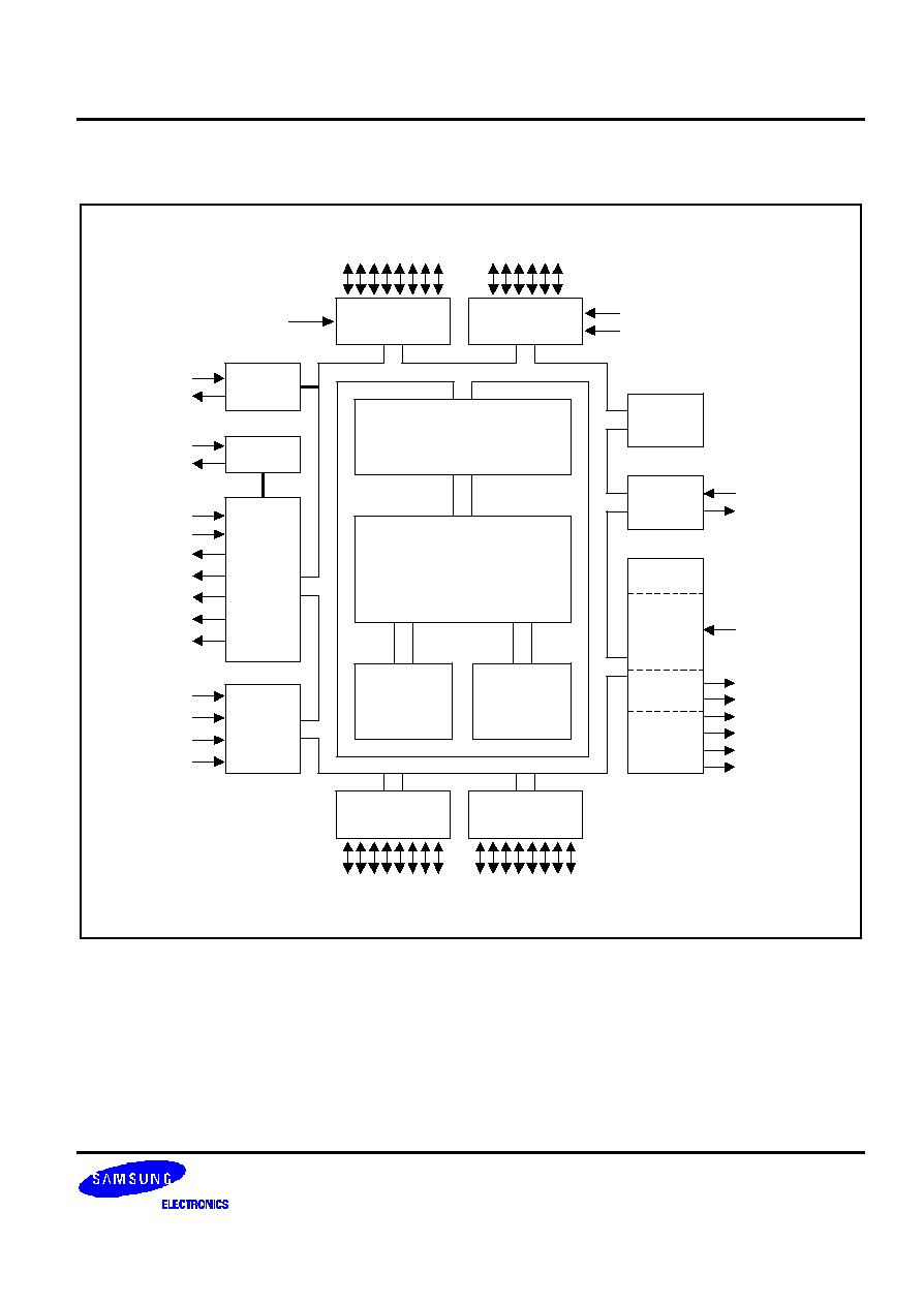
BLOCK DIAGRAM
Main
OSC
L-C OSC
Port 0
P0.0-P0.7
Port I/O and Interrupt
Control
48-Kbyte
ROM
336-Byte
Register
File
SAM88LP CPU
Port 1
SAM88 Bus
X
OUT
X
IN
OSC
OUT
OSC
IN
nRESET
P1.0-P1.7
INT0-INT3
Test
Timers A
CAPA
Port 2
P2.0-P2.7
Port 3
P3.0-P3.1
PWM
Block
PWM
Counter
and Data
Capture
14-Bit
PWM
8-Bit
PWM
Timer 0
CAPA
T0
8-Bit ADC
ADC0
ADC1
ADC2
ADC3
On-
Screen
Display
H-sync
V-sync
Vred
Vgreen
Vblue
Vblank
OSDHT
PWM0
PWM1
PWM2
PWM3
PWM4
PWM5
Figure 1-1. Block Diagram
PRODUCT OVERVIEW
S3C880A/F880A
1-4
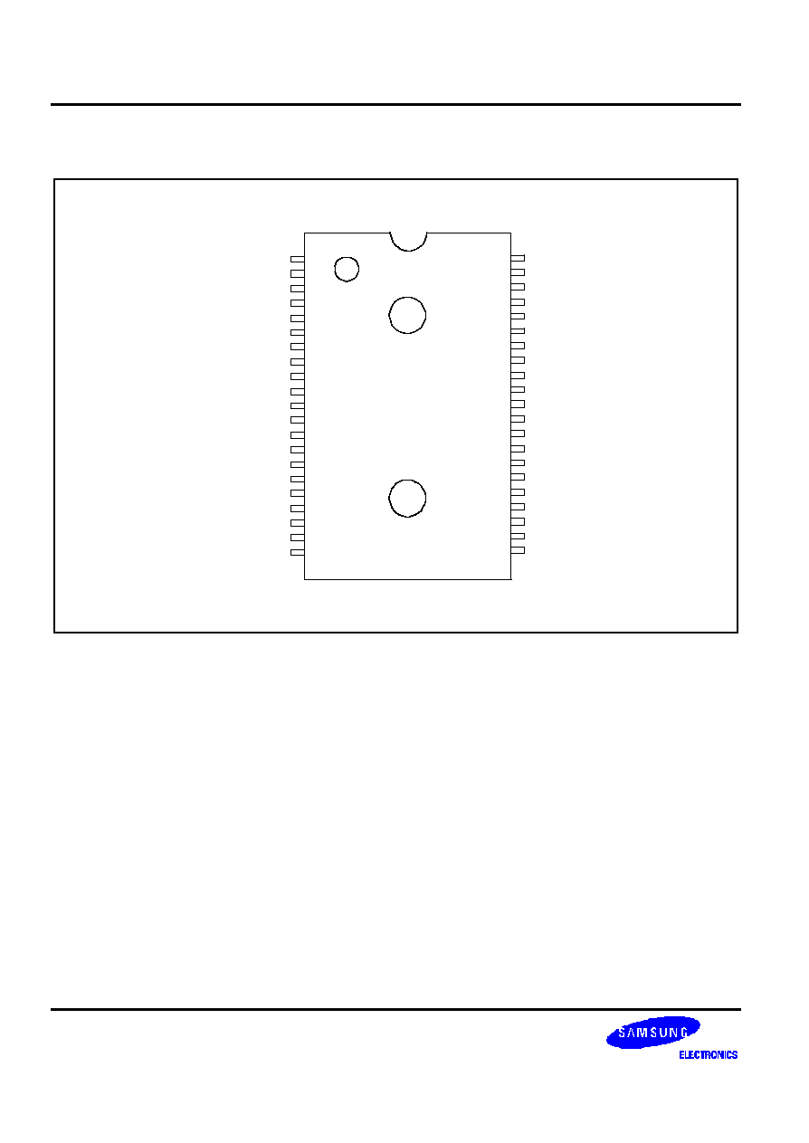
PIN ASSIGNMENTS
PWM0/P2.5
PWM1/P2.1
PWM2/P2.2
PWM3/P2.3
PWM4/P2.4
PWM5/P2.0
T0/P2.6
T0CK/P1.7
ADC0/P3.0
ADC1/P3.1
ADC2/P0.6
ADC3/P0.7
TEST
INT0/P1.0
INT1/P1.1
INT2/P1.2
INT3/P1.3
P1.4
P1.5
P1.6
OSDHT/P2.7
S3C880A
S3F880A
(42-SDIP)
1
2
3
4
5
6
7
8
9
10
11
12
13
14
15
16
17
18
19
20
21
P0.0
P0.1
P0.2
P0.3
P0.4
V
SS
CAP.A
P0.5
V
DD
nRESET
X
OUT
X
IN
V
SS1
OSC
OUT
OSC
IN
V-sync
H-sync
Vblank
Vred
Vgreen
Vblue
42
41
40
39
38
37
36
35
34
33
32
31
30
29
28
27
26
25
24
23
22
Figure 1-2. S3C880A/F880A Pin Assignment (42-SDIP)
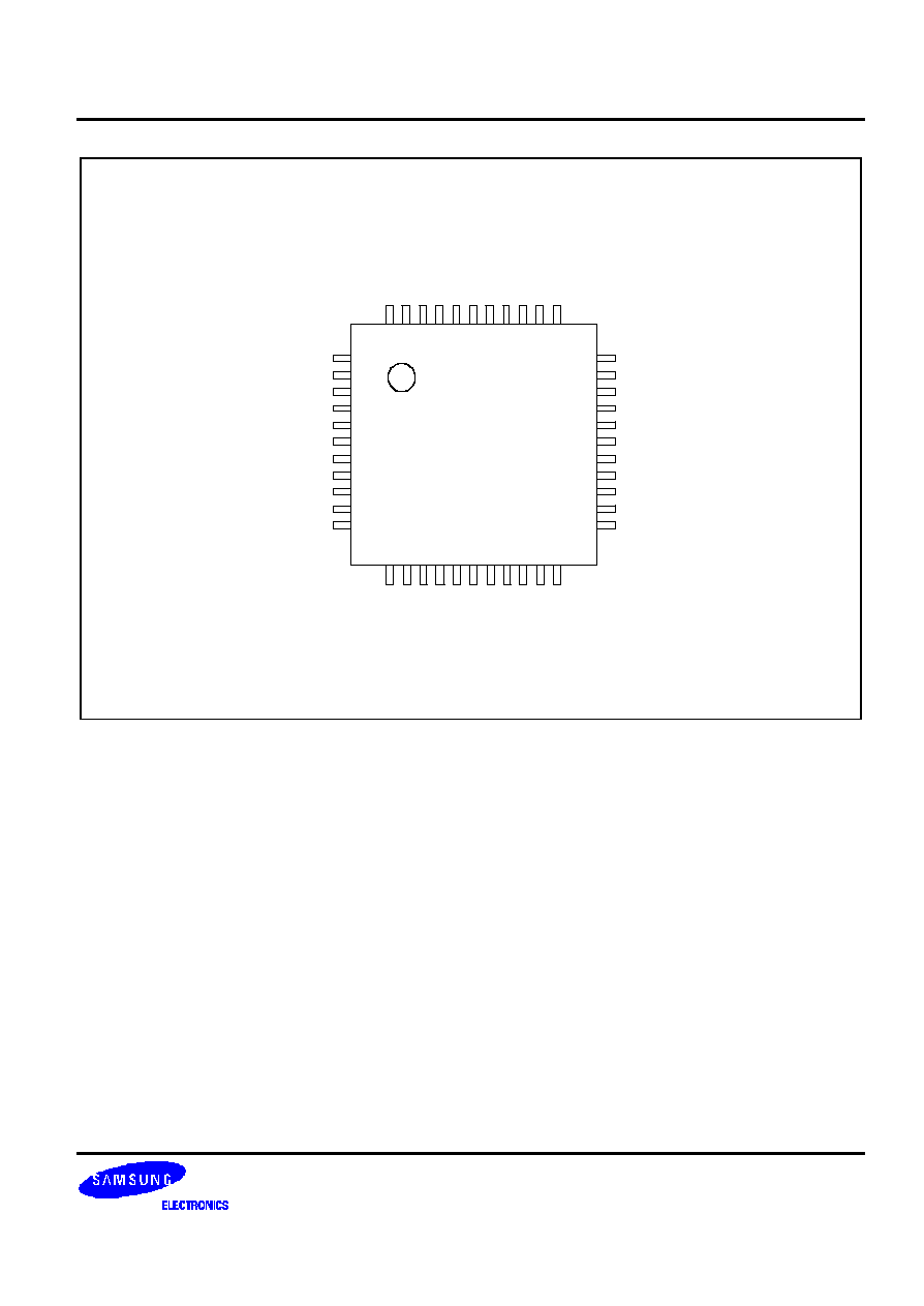
S3C880A/F880A
PRODUCT OVERVIEW
1-5
P1.3/INT3
P1.4
P1.5
P1.6
P2.7/OSDHT
Vblue
Vgreen
Vred
Vblank
H-sync
V-sync
NC
CAP.A
P0.5
V
DD
nRESET
X
OUT
X
IN
V
SS1
NC
OSC
OUT
OSC
IN
P2.4/PWM4
P2.3/PWM3
P2.2/PWM2
P2.1/PWM1
P2.5/PWM0
P0.0
P0.1
P0.2
P0.3
P0.4
V
SS
P2.0/PWM5
P2.6/T0
P1.7/T0CLK
P3.0/ADC0
P3.1/ADC1
P0.6/ADC2
P0.7/ADC3
TEST
P1.0/INT0
P1.1/INT1
P1.2/INT2
S3C880A
S3F880A
(44-QFP)
1
2
3
4
5
6
7
8
9
10
11
44
43
42
41
40
39
38
37
36
35
34
33
32
31
30
29
28
27
26
25
24
23
12
13
14
15
16
17
18
19
20
21
22
Figure 1-3. S3C880A/F880A Pin Assignment (44-QFP)
PRODUCT OVERVIEW
S3C880A/F880A
1-6
PIN DESCRIPTIONS
Table 1-1. S3C880A/F880A Pin Descriptions
Pin Name
Pin
Type
Pin Description
Circuit
Type
Pin
Numbers
Share
Pins
P0.0�P0.3
I/O
General I/O port (4-bit), configurable for digital input
or n-channel open-drain, push-pull output.
Pins can withstand up to 5-volt loads.
2
39�42
(39�36)
(See pin
description)
P0.4�P0.5
General I/O port (2-bit), configurable for digital input
or push-pull output.
3
38, 35
(35, 31)
P0.6�P0.7
General I/O port (2-bit), configurable for digital input
or n-channel open-drain output.
P0.6-P0.7 can withstand up to 5-volt loads.
Multiplexed for alternative use as external inputs
ADC2-ADC3.
6
11�12
(6�7)
ADC2�ADC3
P1.0�P1.3
I/O
General I/O port (4-bit), configurable for digital input
or n-channel open-drain output.
P1.0-P1.3 can withstand up to 6-volt loads.
Multiplexed for alternative use as external interrupt
inputs INT0-INT3
7
14�17
(9�11)
INT0�INT3
P1.4�P1.5
General I/O port (2-bit). configurable for digital input
or n-channel open-drain output.
P1.4-P1.5 can withstand up to 6-volt loads. High
current port (10mA).
5
18�19
(13�14)
P1.6�P1.7
General I/O port (2-bit). configurable for digital input
or push-pull output. Each pin
has an alternative function. P1.7: T0CK
(Timer 0 Clock Input)
3
20, 8
(15, 3)
T0CK
P2.0�P2.7
I/O
General I/O port (8-bit). Input/output mode or n-
channel open-drain, push-pull output mode is
software configurable. Pins can withstand up to 5-
volt loads. Each pin has an alternative function.
P2.0: PWM5 (8-bit PWM output)
P2.1: PWM1 (14-bit PWM output)
P2.2: PWM2 (8-bit PWM output)
P2.3: PWM3 (8-bit PWM output)
P2.4: PWM4 (8-bit PWM output)
P2.5: PWM0 (14-bit PWM output)
P2.6: T0 (Timer 0 PWM and Interval output)
P2.7: OSDHT (Halftone signal output)
2
1�7, 21
(1, 41�44,
40, 2, 16)
PWM0�PWM5
T0, OSDHT
P3.0�P3.1
I/O
General I/O port (2-bit), configurable for digital input
or n-channel open-drain output.
P3.0-P3.1 can withstand up to 5-volt loads.
Multiplexed for alternative use as external inputs
ADC0-ADC1.
6
9�10
(4�5)
ADC0�ADC1
NOTE: Parentheses indicate pin number for 44-QFP package.
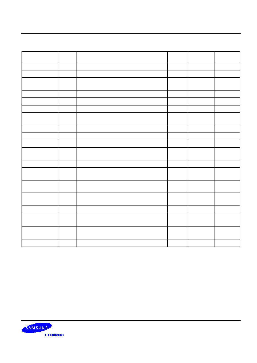
S3C880A/F880A
PRODUCT OVERVIEW
1-7
Table 1-1. S3C880A/F880A Pin Descriptions (Continued)
Pin Name
Pin
Type
Pin Description
Circuit
Type
Pin
Numbers
Share
Pins
PWM0
O
Output pin for 14-bit PWM circuit
1
1 (40)
P2.5
PWM1
O
Output pin for 14-bit PWM circuit
2
2 (41)
P2.1
PWM2�PWM4
O
Output pin for 8-bit PWM circuit
2
3�5
(42�44)
P2.2�P2.4
PWM5
O
Output pin for 8-bit PWM circuit
2
6 (1)
P2.0
ADC0�ADC1
I
Analog inputs for 8-bit A/D converter
6
9,10 (4,5)
P3.0�P3.1
ADC2�ADC3
I
Analog inputs for 8-bit A/D converter
6
11,12 (6,7)
P0.6�P0.7
INT0�INT3
I
External interrupt input pins
7
14�17
(9�11)
P1.0�P1.3
T0
O
Timer 0 output (interval, PWM)
2
7 (2)
P2.6
T0CK
I
Timer 0 clock input
3
8 (3)
P1.7
OSDHT
O
Halftone control signal output for OSD
2
21 (16)
P2.7
Vblue, Vgreen
Vred
O
Digital blue, green and red signal outputs for
OSD
4
22�24
(17�19)
�
Vblank
O
Digital video blank signal outputs for OSD
4
25 (20)
�
H-sync, V-sync
I
H-sync, V-sync input for OSD
1
26, 27
(21,22)
�
OSC
IN
, OSC
OUT
I, O
L-C oscillator pins for OSD clock frequency
generation
�
28, 29
(23,24)
�
X
IN
, X
OUT
I, O
System clock pins
�
31, 32
(27,28)
�
nRESET
I
System reset input pin
8
33 (29)
�
TEST
�
Test Pin (must be connected to V
SS
). Factory
test mode is activated when 12 V is applied.
�
13 (8)
�
V
DD
, V
SS
�
Power supply pins
�
30, 34, 37
(26,30,34)
�
CAPA
I
Input for capture A module
1
36 (32)
�
NOTE: Parentheses indicate pin number for 44-QFP package.
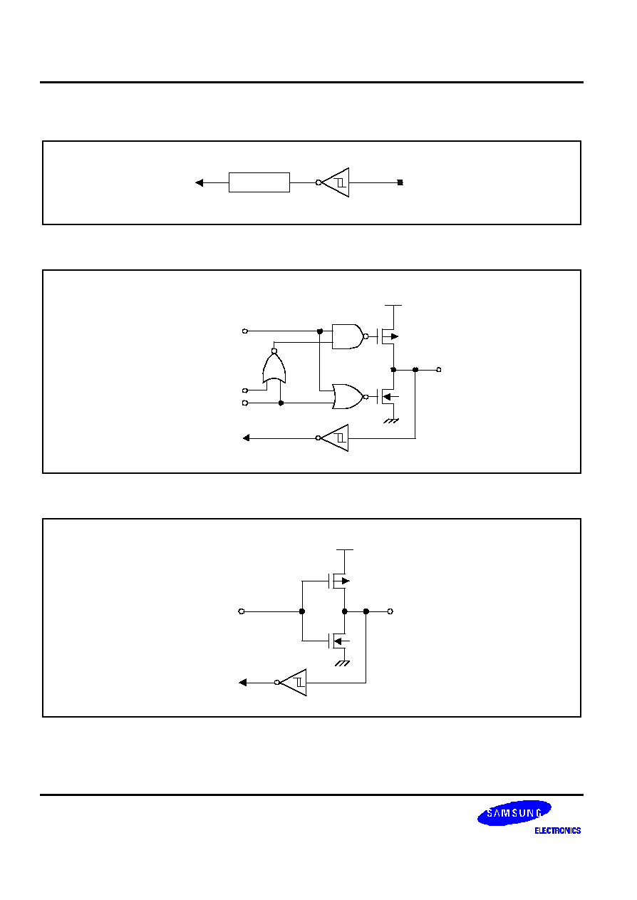
PRODUCT OVERVIEW
S3C880A/F880A
1-8
PIN CIRCUITS
Input
Noise Filter
Figure 1-4. Pin Circuit Type 1 (V-Sync H-Sync, CAPA)
V
DD
Data
Output Disable
Input
I/O
Open-Drain
Figure 1-5. Pin Circuit Type 2 (P2.0�P2.7, P0.0�P0.3, PWM0�PWM5, T0, OSDHT)
V
DD
Data
Input
Output
V
SS
Figure 1-6. Pin Circuit Type 3 (P0.4�P0.5, P1.6�P1.7, T0CK)
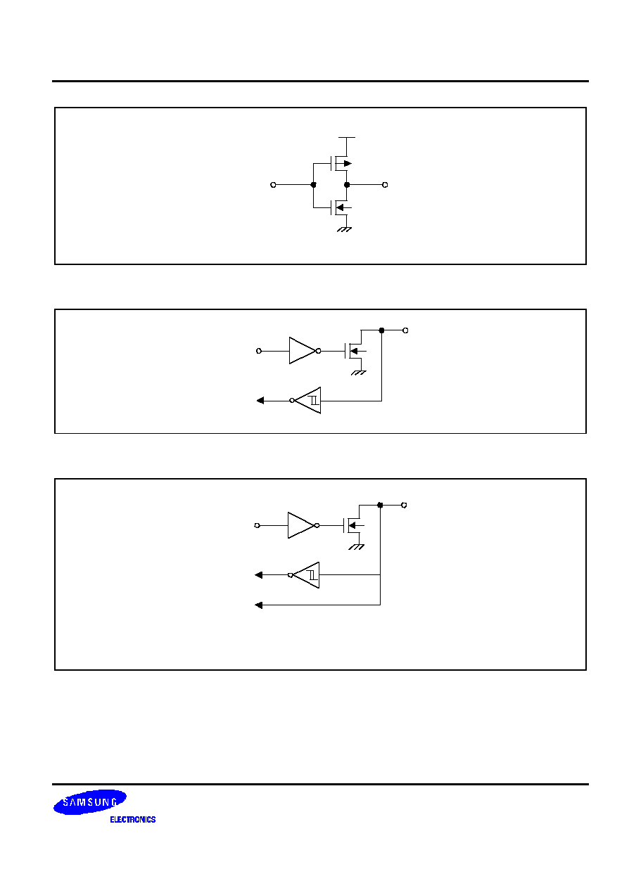
S3C880A/F880A
PRODUCT OVERVIEW
1-9
V
DD
Data
Output
V
SS
Figure 1-7. Pin Circuit Type 4 (Vblue, Vgreen, Vred, Vblank)
Data
Input
I/O
V
SS
Figure 1-8. Pin Circuit Type 5 (P1.4�P1.5)
Data
Input
I/O
V
SS
A/D In
NOTE: Circuit type 6 can withstand up to 5 V loads.
Figure 1-9. Pin Circuit Type 6 (P3.0�P3.1, P0.6�P0.7, ADC0�ADC3)

PRODUCT OVERVIEW
S3C880A/F880A
1-10
Data
Input
I/O
INT
NOTE: Circuit type 7 can withstand up to 6 V loads.
Noise Filter
V
SS
Figure 1-10. Pin Circuit Type 7 (P1.0�P1.3, INT0�INT3)
Noise Filter
V
DD
250 K
Figure 1-11. Pin Circuit Type 8 (nRESET)

S3C880A/F880A
ADDRESS SPACES
2-1
2
ADDRESS SPACES
OVERVIEW
The S3C880A/F880A microcontroller has two kinds of address space:
-- Internal program memory (ROM)
-- Internal register file
The S3C880A/F880A has an on-chip 48-Kbyte mask-programmable.
There are 336 general-purpose 8-bit data registers in the register file. Seventeen 8-bit registers are used for CPU and
system control. To support peripheral, I/O, and clock functions, there are 33 control registers and 16 data registers.
In addition, there is a 252
�
4-bit area for on-screen display (OSD) video RAM.
ADDRESS SPACES
S3C880A/F880A
2-2
PROGRAM MEMORY (ROM)
The S3C880A/F880A has a 48-Kbyte mask-programmable program memory. Program memory stores program
codes , table data or OSD font codes.
As shown in Figure 2-1, the first 256 bytes of the ROM (0H�0FFH) are reserved for interrupt vector addresses.
Unused locations in this range can be used as normal program memory. If the vector address area is used to store
normal program data, care must be taken to avoid overwriting vector addresses stored in these locations. The ROM
address at which program execution starts after a nRESET is 0100H.
Interrupt
Vector Area
Program Memory
and Character
Generator Memory
0H
BFFFH
ROM Code Option Area
3CH
40H
100H
Figure 2-1. Program Memory Address Spaces
S3C880A/F880A
ADDRESS SPACES
2-3
Table 2-1. Program ROM and Character ROM Area by the Font Figure
Font
ROM
Program ROM
Character ROM
0
ROM size
48-Kbyte
0-Kbyte
ROM address
0-BFFFH
0
256
ROM size
39-Kbyte
9-Kbyte
ROM address
0-9BFFH
9C00H-BFFFH
384
ROM size
34.5-Kbyte
13.5-Kbyte
ROM address
0-89FFH
8A00H-BFFFH
512
ROM size
30-Kbyte
18-Kbyte
ROM address
0-77FFH
7800H-BFFFH
640
ROM size
25.5-Kbyte
22.5-Kbyte
ROM address
0-65FFH
6600H-BFFFH
768
ROM size
21-Kbyte
27-Kbyte
ROM address
0-53FFH
5400H-BFFFH
1024
ROM size
12-Kbyte
36-Kbyte
ROM address
0-2FFFH
3000H-BFFFH
REGISTER ARCHITECTURE
The upper 64 bytes of the S3C880A/F880A internal register file is logically expanded into two 64-byte areas, called
set 1 and set 2. The upper 32-byte area of set 1 is divided into two register banks, called bank 0 and bank 1. In
addition, two register pages are implemented, called page 0 and page 1. The total addressable register space is
thereby expanded from 256 bytes to 654 bytes.
The extension of the physical register space into separately addressable areas (sets, banks, and pages) is
supported by various addressing mode restrictions, the select bank instructions, SB0 and SB1, and the register
page pointer (PP).
Specific register types and the area (in bytes) that they occupy in the register file are summarized in Table 2-1.
Table 2-2. Register Type Summary
Register Type
Number of Bytes
General-purpose registers (including the 16-byte
working register common area)
336
CPU and system control registers
17
Peripheral, I/O, and clock control/data registers
49
On-screen display (OSD) video RAM
252
Total Addressable Bytes
654
ADDRESS SPACES
S3C880A/F880A
2-4
BANK 1
FFH
E0H
D0H
C0H
SET 2
General purpose
registers
(indirect address
mode)
C0H
00H
Prime data
registers
(all address
mode)
Page 0
FFH
BFH
SET 2
OSD registers
(indirect
address
mode)
C0H
00H
OSD registers
(all address
mode)
Page 1
FFH
BFH
40H
00H
FFH
3FH
Prime data
register area
(all address
mode)
Page 2
DFH
BANK 0
CFH
FFH
E0H
SET 1
FBH
Not used
System registers
Data register area
Display register area
(Video RAM)
Working registers
System and peripheral
control registers
Figure 2-2. Internal Register File Organization
S3C880A/F880A
ADDRESS SPACES
2-5
ROM CODE OPTION (RCOD_OPT)
The address of RCOD_OPT, from 3CH to 3FH, are ROM code option area. By setting the value of RCOD_OPT,
S3C880A/F880A operates optionally. But in S3C880A/F880A, the ROM code option is not available. So
RCOD_OPT area can be used as the normal ROM area in S3C880A/F880A.
LSB
MSB
Not used
.7
.6
.5
.4
.3
.2
.1
.0
ROM Address: 3DH
LSB
MSB
Not used
.7
.6
.5
.4
.3
.2
.1
.0
ROM Address: 3FH
LSB
MSB
ROM Address: 3EH
Not used
LSB
MSB
ROM_CODE Option (RCOD_OPT)
ROM Address: 3CH
Not used
.7
.6
.5
.4
.3
.2
.1
.0
.7
.6
.5
.4
.3
.2
.1
.0
Figure 2-3. ROM Code Option (RCOD_OPT)
ADDRESS SPACES
S3C880A/F880A
2-6
REGISTER PAGE POINTER (PP)
The SAM88LP architecture supports the logical expansion of the physical 256-byte register file in up to 16
separately addressable register pages. Page addressing is controlled by the register page pointer, PP, DFH. Only
two pages are implemented in the S3C880A/F880A microcontrollers: page 0 and page 2 (00H�3FH) are used as
general-purpose register space and page 1 contains a 252
�
4-bit area for the on-screen display (OSD) video ROM.
As shown in Figure 2-3, when the upper nibble of the PP register is '0000B', the selected destination address is
located on page 0. When the upper nibble value is '0001B', page 1 is the selected destination. The lower nibble of
the page pointer controls the source register page destination addressing: when the lower nibble is '0000B', page 0
is the selected source register page; when the lower nibble is '0001B', page 1 is the source register page.
After a reset, the page pointer's source value (the lower nibble) and the destination value (the upper nibble) are
always '0000B', automatically selecting page 0 as both the source and the destination. To select page 1 as the
source or destination register page, you must modify the register page pointer values accordingly. Because only
page 0, page 1 and page 2 are used in the S3C880A/F880A implementation, only pointer values '0000B', `0001B'
and `0010B'' are used.
Register Page Pointer (PP)
DFH, Set 1, R/W
.7
.6
.5
.4
.3
.2
.1
.0
MSB
LSB
Destination register page seleciton bits:
0 0 0 0 B
0 0 0 1 B
0 0 1 0 B
1 1 1 1 B
Destination: page 0
Destination: page 1
Destinaton: page 2
Not used for the
S3F880A
Not used for the
S3F880A
.
.
.
.
.
.
Source register page seleciton bits:
0 0 0 0 B
0 0 0 1 B
0 0 1 0 B
1 1 1 1 B
Destination: page 0
Destination: page 1
Destination: page 2
Not used for the
S3F880A
Not used for the
S3F880A
.
.
.
.
.
.
Figure 2-4. Register Page Pointer (PP)

S3C880A/F880A
ADDRESS SPACES
2-7
F
PROGRAMMING TIP � Data Operations Between Register Pages
LD
PP,#10H
; Destination register page 1, source register page 0
LD
20H,45H
; Register 20H in page 1
Content of the register 45H
; in page 0
�
�
�
ADD
30H,40H
; Register 30H in page 1
Content of 30H in page 1
; plus (+) the content of 40H in page 0
Page 1
20H
30H
Page 0
40H
45H
+
Figure 2-5. Programming Tip Example for Inter-Page Data Operations
EFFECT OF DIFFERENT INSTRUCTIONS FOR INTER-PAGE DATA OPERATIONS
The source and the destination pages for data operations between pages differ, depending on which instruction you
use. The following programming tip, "Examples of Inter-Page Data Transfer Operations," provides you with a detailed
list of various case.

ADDRESS SPACES
S3C880A/F880A
2-8
F
PROGRAMMING TIP � Examples of Inter-Page Data Transfer Operations
Example 1.
a) ADC
R1,R0
; R0 � source page
; R1 � destination page
b) ADC
R4,@R2
; R2, 40H � source page
R2 contains 40H
; R4 � destination page
c) ADC
R0,#0AAH
; R0 � destination page
d) ADC
40H,42H
; 42H � source page
; 40H � destination page
e) ADC
40H,@42H
; 42H, 60H � source page
42H contains 60H
; 40H � destination page
f)
ADC
40H,#02H
; 40H � destination page
NOTE:
The above examples also apply to the instructions ADD, SUB, AND, OR, and XOR.
Example 2.
a) BAND
R0,40H.7
; 40H � source page
; R0 � destination page
b) BAND
40H.7,R0
; R0 � source page
; 40H � destination page
NOTE:
The above examples also apply to the instructions BOR, BXOR, and LDB.
Example 3.
a) BCP
R3,44H.7
; 44H � source page
; R3 � destination page
Example 4.
a) BITC
R3.7
; R3 � destination page
NOTE:
The above examples also apply to the instructions BITR and BITS.

S3C880A/F880A
ADDRESS SPACES
2-9
F
PROGRAMMING TIP � Examples of Inter-Page Data Transfer Operations (continued)
Example 5.
a) BTJRF
SKIP,R6.7
; R6 � source page
NOTE:
The above example also applies to the instructions BTJRT.
Example 6.
a) CALL
@60H
; 60H, 61H � source page
Example 7.
a) CLR
30H
; 30H � destination page
b) CLR
@44H
; 44H � source page
44H contains 40H
; 40H � destination page
NOTE:
The above examples also apply to the instructions RL, RLC, and SRA.
Example 8.
a) COM
03H
; 03H � destination page
b) COM
@44H
; 44H � source page
44H contains 40H
; 40H � destination page
NOTE:
The above examples also apply to the instructions DEC, INC, RR, and RRC.
Example 9.
a) CP
R1,R0
; R0 � source page
; R1 � destination page
b) CP
R2,@R4
; R4, 40H � source page
R4 contains 40H
; R2 � destination page
c) CP
40H,42H
; 42H � source page
; 40H � destination page
d) CP
40H,@42H
; 42H, 44H � source page
42H contains 44H
; 40H � destination page
e) CP
20H,#0AAH
; 20H � destination page
NOTE:
The above examples also apply to the instructions TCM and TM.

ADDRESS SPACES
S3C880A/F880A
2-10
F
PROGRAMMING TIP � Examples of Inter-Page Data Transfer Operations (Continued)
Example 10.
a) CPIJE
R3,@R5,SKIP
; R5, 40H � source page
R5 contains 40H
; R3 � destination page
NOTE:
The above example also applies to the instruction CPIJNE.
Example 11.
a) DA
00H
; 00H � source page
b) DA
@02H
; 02H � source page
02H contains 40H
; 40H � destination page
Example 12.
a) DECW
60H
; 60H, 61H � destination page
b) DECW
@00H
; 00H, 01H � source page
00H contains 48H
; 48H, 49H � destination page
01H contains 49H
NOTE:
The above example also applies to the instruction INCW.
Example 13.
a) DIV
60H,40H
; 40H � source page
; 60H, 61H � destination page
b) DIV
60H,@20H
; 20H, 40H � source page
20H contains 40H
; 60H, 61H � destination page
c) DIV
60H,#03H
; 60H, 61H � destination page
NOTE:
The above example also applies to the instruction INCW.
Example 14.
a) DJNZ
R6,LOOP
; R6 � destination page
NOTE: Incase PP = 10H, 11H, this instruction is not valid.
Example 15.
a) JP
@60H
; 60H, 61H � source page

S3C880A/F880A
ADDRESS SPACES
2-11
F
PROGRAMMING TIP � Examples of Inter-Page Data Transfer Operations (Continued)
Example 16. a) LD
R0,#0AAH
; R0 � destination page
b) LD
R0,40H
; 40H � source page
; R0 � destination page
c) LD
40H,R0
; R0 � source page
; 40H � destination page
d) LD
R0,@R2
; R2, 50H � source page
R2 contains 50H
; R0 � destination page
e) LD
@R4,R2
; R4, R2 � source page
R4 contains 40H
; 40H � destination page
f)
LD
40H,41H
; 41H � source page
; 40H � destination page
g) LD
40H,@42H
; 42H, 44H � source page
42H contains 44H
; 40H � destination page
h) LD
45H,#02H
; 45H � destination page
i)
LD
@40H,#02H
; 40H � source page
40H contains 44H
; 44H � destination page
j)
LD
@40H,42H
; 40H, 42H � source page
40H contains 44H
; 44H � destination page
k) LD
R5,#04H(R0)
; R0, 04H(2 + offset) � source page
R0 contains 02H
; R5 � destination page
l)
LD
#04H(R0),R1
; R0, R1 � source page
R0 contains 02H
; 04H � destination page

ADDRESS SPACES
S3C880A/F880A
2-12
F
PROGRAMMING TIP � Examples of Inter-Page Data Transfer Operations (Continued)
Example 17.
a) LDC
R0,@RR6
; R6, R7 � source page
; R0 � destination page
b) LDC
@RR6,R2
; R6, R7, R2 � source page
RR6 contains an external memory address
c) LDC
R0,#01H(RR6)
; R6, R7 � source page
; R0 � destination page
d) LDC
#01H(RR6),R0
; R0, R6, R7 � source page
e) LDC
R0,#1000H(RR6)
; R6, R7 � source page
; R0 � destination page
f)
LDC
#1000H(RR6),R0
; R0, R6, R7 � source page
Example 18.
a) LDCD
R0,@RR6
; R6, R7 � source page
; R0 � destination page
b) LDCPD
@RR6,R0
; R0, R6, R7 � source page
NOTE:
The above examples also apply to the instructions LDCI and LDCPI.
Example 19.
a) LDW
40H,20H
; 20H, 21H � source page
; 40H, 41H � destination page
b) LDW
60H,@20H
; 20H, 40H � source page
20H contains 40H
; 60H, 61H � destination page
c) LDW
40H,#02H
; 40H, 41H � destination page

S3C880A/F880A
ADDRESS SPACES
2-13
F
PROGRAMMING TIP � Examples of Inter-Page Data Transfer Operations (Concluded)
Example 20.
a) MULT
40H,20H
; 20H � source page
; 40H, 41H � destination page
b) MULT
60H,@20H
; 20H, 40H � source page
20H contains 40H
; 60H, 61H � destination page
c) MULT
40H,#02H
; 40H, 41H � destination page
Example 21.
a) POP
00H
; 00H � destination page
b) POP
@20H
; 20H � source page
20H contains 40H
; 40H � destination page
Example 22.
a) POPUD 00H,@20H
;
20H, 40H � source page
20H contains 40H
; 00H � destination page
NOTE:
The above example also applies to the instruction POPUI.
Example 23.
a) PUSH
00H
; 00H � destination page
b) PUSH
@20H
; 20H, 40H � source page
20H contains 40H
Example 24.
a) PUSHUD
@60H,20H
; 60H, 20H � source page
60H contains 44H
; 44H � destination page
NOTE:
The above example also applies to the instruction PUSHUI.
Example 25.
a) SWAP
00H
; 00H � destination page
b) SWAP
@20H
; 20H � source page
20H contains 40H
; 40H � destination page

ADDRESS SPACES
S3C880A/F880A
2-14
REGISTER SET 1
The term set 1 refers to the upper 64 bytes of the register file, locations C0H�FFH. This area can be accessed at
any time, regardless of which page is currently selected. The upper 32-byte area of this 64-byte space is divided into
two 32-byte register banks, called bank 0 and bank 1. You use the select register bank instructions, SB0 or SB1,
to address one bank or the other. A reset operation automatically selects bank 0 addressing.
The lower 32-byte area of set 1 is not banked. This area contains 16 bytes for mapped system registers (D0H�DFH)
and a 16-byte common area (C0H�CFH) for working register addressing.
Registers in set 1 are directly accessible at all times using Register addressing mode. The 16-byte working register
area ,however, can only be accessed using working register addressing. Working register addressing is a function of
Register addressing mode (see Chapter 3, "Addressing Modes," for more information).
REGISTER SET 2
The same 64-byte physical space that is used for the set 1 register locations C0H�FFH is logically duplicated to add
another 64 bytes. This expanded area of the register file is called set 2. The logical division of set 1 and set 2 is
maintained by means of addressing mode restrictions: while you can access set 1 using Register addressing mode
only, you should use Register Indirect addressing mode or Indexed addressing mode to access set 2.
For the S3C880A/F880A, the set 2 address range (C0H�FFH) is accessible on page 0 and page 1. Please note,
however, that on page 1, the set 2 locations FCH�FFH are not mapped.
Part of the OSD video RAM is in page 1, set 2 (C0H�FBH), and the other part (00H�BFH) is in the page 1 prime
register area. To avoid programming errors, we recommend using either Register Indirect or Indexed mode to
address the entire 252-byte video RAM area.
PRIME REGISTER SPACE
The lower 192 bytes (00H�BFH) of the S3C880A/F880A 's two 256-byte register pages and the 64 bytes (00H�3FH)
of register page 2 are called prime register area. Prime registers can be accessed using any of the seven addressing
modes. The prime register area on page 0 is immediately addressable after a reset. In order to address registers on
page 1 (in the OSD video RAM), you must first set the register page pointer (PP) to the appropriate source and
destination values.
S3C880A/F880A
ADDRESS SPACES
2-15
C0H
00H
Page 0
FFH
Set 2
Prime
Space
C0H
00H
Page 1
FFH
Set 2
Prime
Space
FBH
FFH
FCH
E0H
D0H
C0H
Set 1
Bank 0
Bank 1
Peripheral and I/O
General-purpose
CPU and system control
OSD video RAM
Area not mapped
3FH
00H
Page 2
FFH
Set 2
Prime
Space
Figure 2-6. Set 1, Set 2, and Prime Area Register Map

ADDRESS SPACES
S3C880A/F880A
2-16
WORKING REGISTERS
Instructions can access specific 8-bit registers or 16-bit register pairs using either 4-bit or 8-bit address fields. When
4-bit working register addressing is used, the 256-byte register file is viewed as thirty two 8-byte register groups or
"slices." Each slice consists of eight 8-bit registers. When the two 8-bit register pointers, RP1 and RP0, are used,
two working register slices can be selected at any time to form a 16-byte working register block. Using the register
pointers, you can move this 16-byte register block anywhere in the addressable register file (except for the set 2
area).
The terms slice and block are used in this manual to help you visualize the size and relative locations of selected
working register spaces:
-- One working register slice is 8 bytes (eight 8-bit working registers; R0�R7 or R8�R15)
-- One working register block is 16 bytes (sixteen 8-bit working registers; R0�R15)
All the registers in an 8-byte working register slice have the same binary value for their five most significant address
bits. This makes it possible for each register pointer to point to one of the 24 slices in the register file. The base
addresses for the two selected 8-byte register slices are contained in the register pointers, RP0 and RP1. After a
reset, RP0 and RP1 always point to the 16-byte common area in set 1 (C0H�CFH).
Each register pointer points to
one 8-byte slice of the register
space, selecting a total 16-byte
working register block in total.
1 1 1 1 1 X X X
RP1 (Registers R8-R15)
RP0 (Registers R0-R7)
Slice 32
~
~
CFH
C0H
FFH
F8H
F7H
F0H
FH
8H
7H
0H
Slice 1
10H
Set 1
Only
0 0 0 0 0 X X X
Figure 2-7. 8-Byte Working Register Areas (Slices)
S3C880A/F880A
ADDRESS SPACES
2-17
USING THE REGISTER POINTERS
The register pointers, RP0 and RP1, are mapped to the addresses D6H and D7H in set 1. They are used to select
two movable 8-byte working register slices in the register file. After a reset, they point to the working register
common area: RP0 points to the addresses C0H�C7H, and RP1 points to the addresses C8H�CFH. If you want to
change a register pointer value, you should load a new value to RP0 and/or RP1 using an SRP or LD instruction (see
Figures 2-7 and 2-8).
With working register addressing, you can only access those locations that are pointed to by the register pointers.
Please note that you cannot use the register pointers to select the working register area in set 2, C0H�FFH,
because these locations are accessible only using the Indirect Register or Indexed addressing mode.
The selected 16-byte working register block usually consists of two contiguous 8-byte slices. As a general
programming guideline, we recommend that RP0 point to the "lower" slice and RP1 point to the "upper" slice (see
Figure 2-7). In some cases, it may be necessary to define working register areas in different (non-contiguous) areas
of the register file. In Figure 2-8, RP0 points to the "upper" slice and RP1 to the "lower" slice.
Because a register pointer can point to either of the two 8-byte slices in the working register block, you can flexibly
define the working register area.
F
PROGRAMMING TIP -- Setting the Register Pointers
SRP
#70H
; RP0
70H, RP1
78H
SRP1
#48H
; RP0
no change, RP1
48H
SRP0
#0A0H
; RP0
A0H, RP1
no change
CLR
RP0
; RP0
00H, RP1
no change
LD
RP1,#0F8H
; RP0
no change, RP1
0F8H
FH (R15)
0H (R0)
8-Byte Slice
16-byte
contiguous
working
register block
Register File
Contains 32
8-Byte Slices
8-Byte Slice
RP0
RP1
8H
7H
0 0 0 0 1 X X X
0 0 0 0 0 X X X
Figure 2-8. Contiguous 16-Byte Working Register Block
ADDRESS SPACES
S3C880A/F880A
2-18
8-Byte Slice
16-byte
contiguous
working
register block
Register File
Contains 32
8-Byte Slices
8-Byte Slice
0H (R0)
7H (R15)
F0H (R0)
F7H (R7)
RP1
RP0
1 1 1 1 0 X X X
0 0 0 0 0 X X X
Figure 2-9. Non-Contiguous 16-Byte Working Register Block
F
PROGRAMMING TIP -- Using the RPs to Calculate the Sum of a Series of Registers
Calculate the sum of the registers, 80H�85H, using the register pointer. The register addresses 80H through 85H
contain the values 10H, 11H, 12H, 13H, 14H, and 15 H, respectively:
SRP0
#80H
; RP0
80H
ADD
R0,R1
; R0
R0 + R1
ADC
R0,R2
; R0
R0 + R2 + C
ADC
R0,R3
; R0
R0 + R3 + C
ADC
R0,R4
; R0
R0 + R4 + C
ADC
R0,R5
; R0
R0 + R5 + C
The sum of these six registers, 6FH, is located in the register R0 (80H). The instruction string used in this example
takes 12 bytes of instruction code and its execution time is 36 cycles. If you do not use the register pointer to
calculate the sum of these registers, you would have to execute the following instruction sequence:
ADD
80H,81H
; 80H
(80H) + (81H)
ADC
80H,82H
; 80H
(80H) + (82H) + C
ADC
80H,83H
; 80H
(80H) + (83H) + C
ADC
80H,84H
; 80H
(80H) + (84H) + C
ADC
80H,85H
; 80H
(80H) + (85H) + C
Here, the sum of the six registers is also located in the register 80H. This instruction string, however, takes 15 bytes
of instruction code rather than 12 bytes, and the execution time is 50 cycles rather than 36 cycles.
S3C880A/F880A
ADDRESS SPACES
2-19
REGISTER ADDRESSING
The SAM8 register architecture provides an efficient method of working register addressing that takes full advantage
of shorter instruction formats to reduce execution time.
Register (R) addressing mode, in which the operand value is the content of a specific register or register pair, can be
used to access any location in the register file except for set 2.
For working register addressing, the register pointers, RP0 and RP1, are used to select a specific register within a
selected 16-byte working register area. To increase the speed of context switches in an application program, the
register pointers can be used to dynamically select different 8-byte "slices" of the register file as the active working
register space.
Registers are addressed either as a single 8-bit register or a paired 16-bit register. In 16-bit register pairs, the
address of the first 8-bit register is always an even number and that of the next register is an odd number. The most
significant byte of the 16-bit data is always stored in the even-numbered register; the least significant byte is always
stored in the next (+ 1) odd-numbered register.
MSB
Rn
LSB
Rn+1
n = Even address
Figure 2-9. 16-Bit Register Pairs
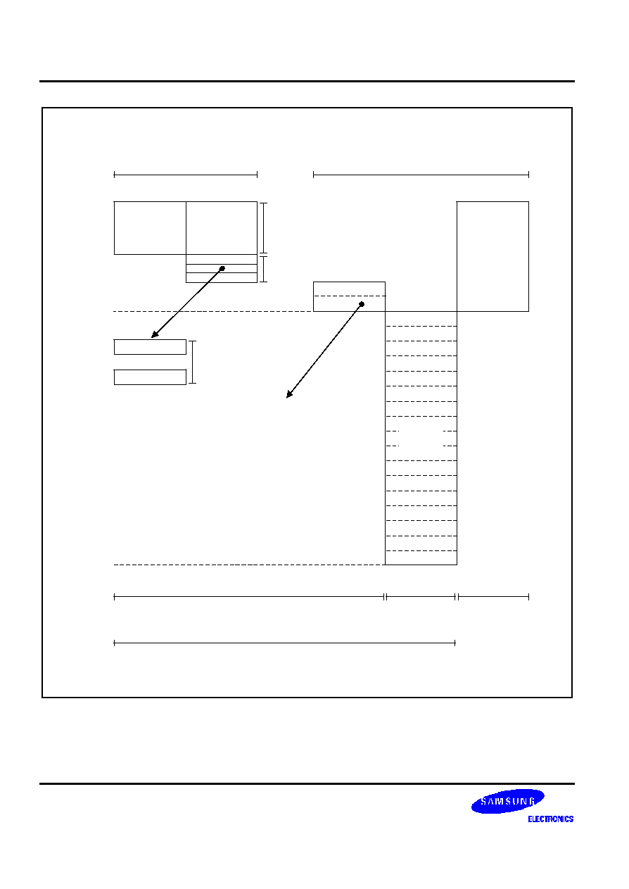
ADDRESS SPACES
S3C880A/F880A
2-20
FFH
D0H
FFH
C0H
Set 2
CFH
D7H
RP1
D6H
RP0
Register
Pointers
C0H
BFH
00H
Special-Purpose
Registers
General-Purpose
Registers
All
Addressing
Modes
Page 0, 1
Indirect
Register,
Indexed
Addressing
Modes
Page 0, 1
Register Addressing Only
Can be Pointed by Register Pointer
Each register pointer (RP) can independently point to
one of the twenty 8-byte "slices" of the register file
(other than set 2). After a reset, RP0 points to
locations C0H-C7H and RP1 to locations C8H-CFH
(the common working register area).
Bank 1
Prime
Registers
Control
Registers
System
Registers
Set 1
Bank 0
Figure 2-11. Register File Addressing
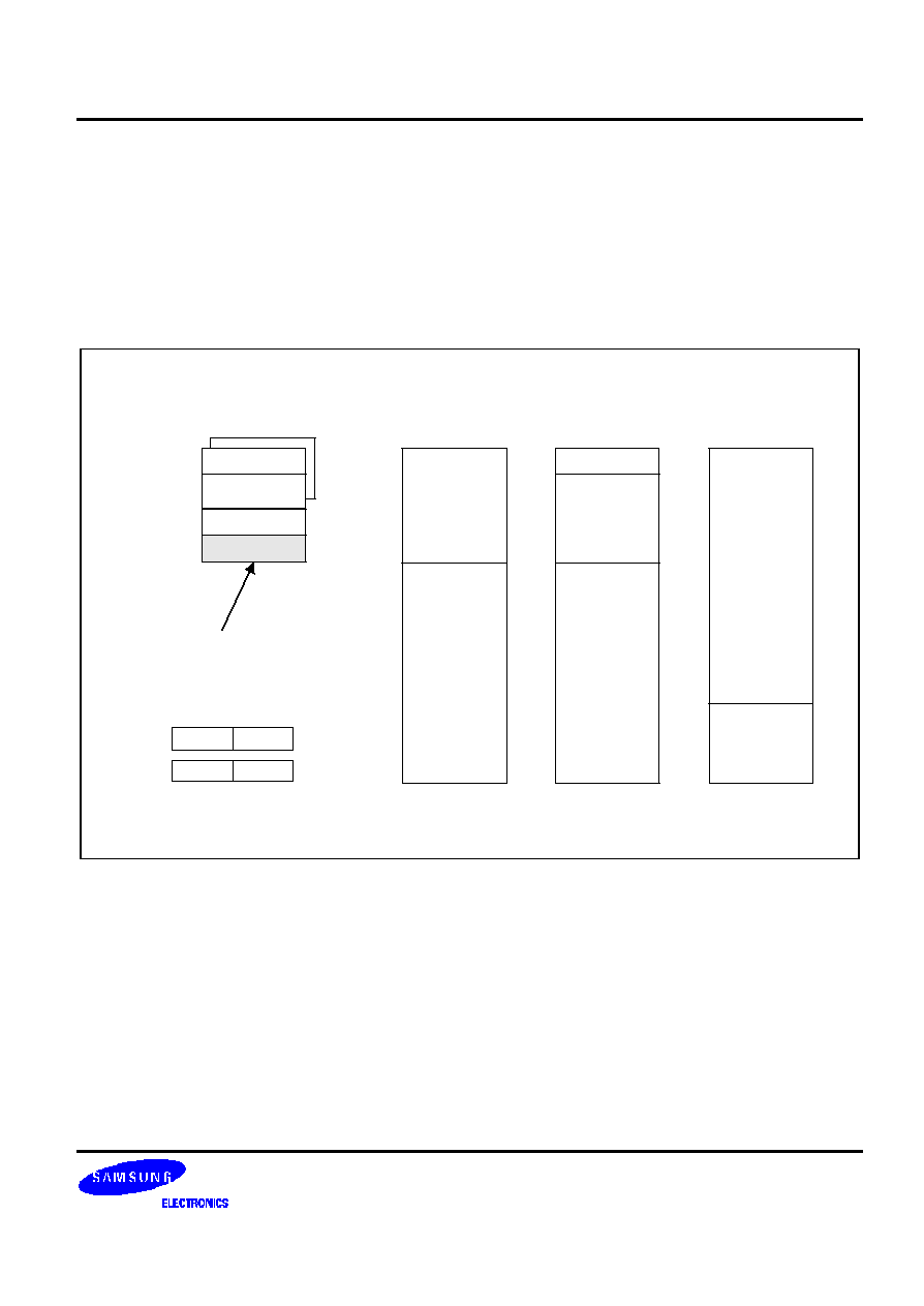
S3C880A/F880A
ADDRESS SPACES
2-21
COMMON WORKING REGISTER AREA (C0H�CFH)
After a reset, the register pointers, RP0 and RP1, automatically point to two 8-byte register slices in set 1, locations
C0H�CFH, as the active 16-byte working register block:
RP0
C0H�C7H
RP1
C8H�CFH
This 16-byte address range is a common area. That is, locations in this area can be accessed using working
register addressing only.
1 1 0 0
0 0 0 0
1 1 0 0
1 0 0 0
RP0 =
RP1 =
Register pointers RP0 and RP1 point
to the common working register area
(COH-CFH) after a reset.
C0H
00H
Page 0
FFH
Set 2
Prime
Area
BFH
~
~
Set 1
FFH
FCH
E0H
CFH
C0H
DFH
Set 2
C0H
00H
Page 1
FFH
Prime
Area
BFH
~
Not used
FBH
~
00H
Page 2
FFH
Prime
Area
3FH
~
Not used
~
Figure 2-12. Common Working Register Area

ADDRESS SPACES
S3C880A/F880A
2-22
F
PROGRAMMING TIP � Addressing the Common Working Register Area
As the following examples show, you should access working registers in the common area, locations C0H�CFH,
using working register addressing mode only.
Examples:
1. LD
0C2H,40H
; Invalid addressing mode!
Use working register addressing instead:
SRP
#0C0H
LD
R2,40H
; R2 (C2H)
the value in location 40H
2. ADD
0C3H,#45H
; Invalid addressing mode!
Use working register addressing instead:
SRP
#0C0H
ADD
R3,#45H
; R3 (C3H)
R3 + 45H
4-BIT WORKING REGISTER ADDRESSING
Each register pointer defines a movable 8-byte slice of working register space. The address information stored in a
register pointer serves as an addressing "window" that enables instructions to access working registers very
efficiently using short 4-bit addresses. When an instruction addresses a location in the selected working register
area, the address bits are concatenated in the following way to form a complete 8-bit address:
-- The high-order bit of the 4-bit address selects one of the register pointers ("0" selects RP0; "1" selects RP1);
-- The five high-order bits in the register pointer select an 8-byte slice of the register space;
-- The three low-order bits of the 4-bit address select one of the eight registers in the slice.
As shown in Figure 2-12, the net effect of this operation is that the five high-order bits from the register pointer are
concatenated with the three low-order bits from the instruction address to form a complete address. As long as the
address stored in the register pointer remains unchanged, the three bits from the address will always point to an
address in the same 8-byte register slice.
Figure 2-13 shows a typical example of 4-bit working register addressing: the high-order bit of the instruction 'INC R6'
is "0", which selects RP0. The five high-order bits stored in RP0 (01110B) are concatenated with the three low-order
bits of the instruction's 4-bit address (110B) to produce the register address 76H (01110110B).
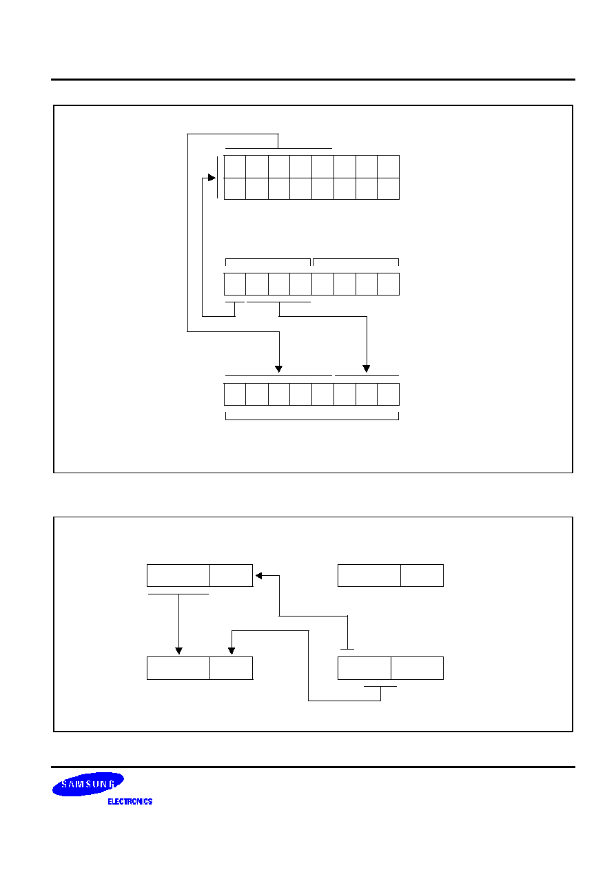
S3C880A/F880A
ADDRESS SPACES
2-23
Together they create an
8-bit register address
Register pointer
provides five
high-order bits
Address
OPCODE
Selects
RP0 or RP1
RP1
RP0
4-bit address
procides three
low-order bits
Figure 2-13. 4-Bit Working Register Addressing
Register
address
(76H)
RP0
0 1 1 1 0
0 0 0
0 1 1 1 0
1 1 0
R6
0 1 1 0
1 1 1 0
Selects RP0
Instruction:
'INC R6'
OPCODE
RP1
0 1 1 1 1
0 0 0
Figure 2-14. 4-Bit Working Register Addressing Example
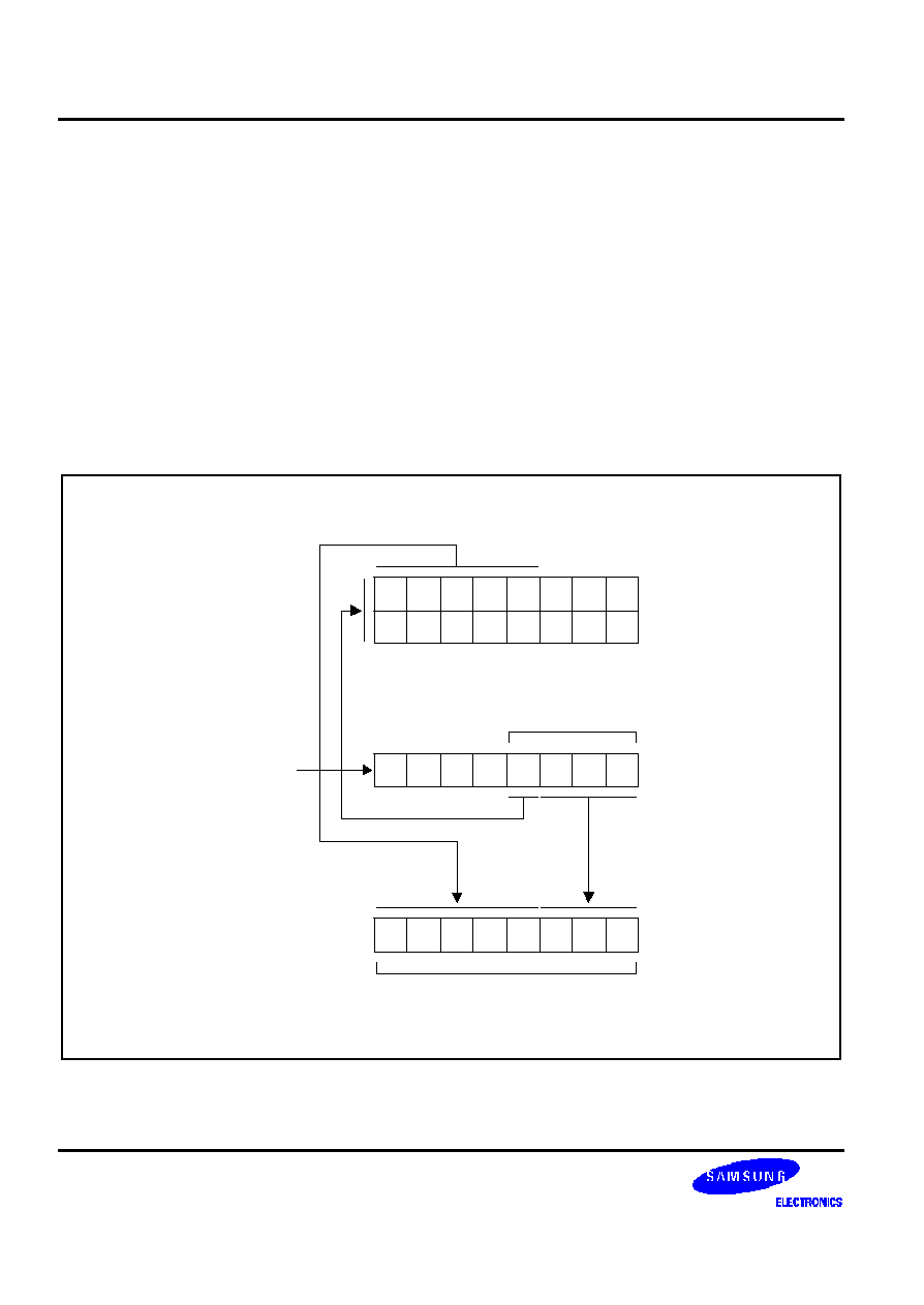
ADDRESS SPACES
S3C880A/F880A
2-24
8-BIT WORKING REGISTER ADDRESSING
You can also use 8-bit working register addressing to access registers in a selected working register area. In order
to initiate 8-bit working register addressing, the upper four bits of the instruction address must contain the value
1100B. This 4-bit value (1100B) indicates that the remaining four bits have the same effect as 4-bit working register
addressing.
As shown in Figure 2-14, the lower nibble of the 8-bit address is concatenated in much the same way as for 4-bit
addressing: bit 3 selects either RP0 or RP1, which then supplies the five high-order bits of the final address, and the
three low-order bits of the complete address are provided by the original instruction.
Figure 2-15 shows an example of 8-bit working register addressing: the four high-order bits of the instruction address
(1100B) specify 8-bit working register addressing. The fourth bit ("1") selects RP1 and the five high-order bits in RP1
(10100B) become the five high-order bits of the register address. The three low-order bits of the register address
(011) are provided by the three low-order bits of the 8-bit instruction address. Together, the five address bits from
RP1 and the three address bits from the instruction comprise the complete register address, R163 (10100011B).
8-bit physical address
Register pointer
provides five
high-order bits
Address
Selects
RP0 or RP1
RP1
RP0
Three low-
order bits
8-bit logical
address
These address
bits indicate 8-bit
working register
addressing
1
1
0
0
Figure 2-15. 8-Bit Working Register Addressing
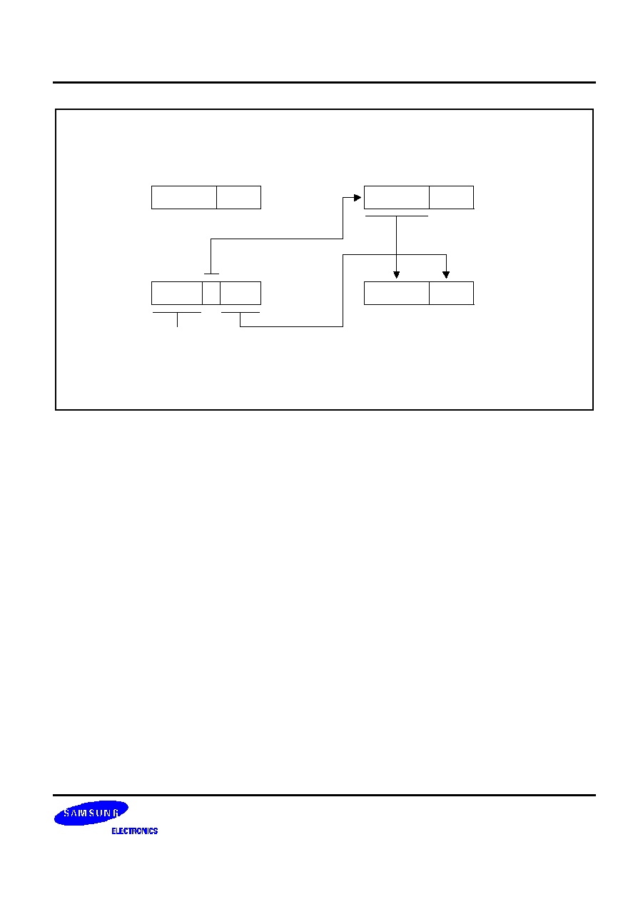
S3C880A/F880A
ADDRESS SPACES
2-25
8-bit address
form instruction
'LD R11, R2'
RP0
0 1 1 0 0
0 0 0
1 1 0 0 1 0 1 1
Selects RP1
R11
Register
address
(0ABH)
RP1
1 0 1 0 1
0 0 0
1 0 1 0 1
0 1 1
Specifies working
register addressing
Figure 2-16. 8-Bit Working Register Addressing Example

ADDRESS SPACES
S3C880A/F880A
2-26
SYSTEM AND USER STACKS
The S3C8-series microcontrollers use the system stack for subroutine calls and returns, interrupt processing, and
data storage. The PUSH and POP instructions support system stack operations. Stack operations in the internal
register file and in external data memory are supported by hardware. (The S3C880A/F880A do not support an
external memory access.) Bit 1 in the external memory timing register EMT selects an internal or external stack
area. The 16-bit stack pointer register (SPH, SPL) is used to access an externally defined system stack. An 8-bit
stack pointer (SPL) is sufficient for internal stack addressing.
Stack Operations
Return addresses for procedure calls and interrupts and data are stored on the stack. The contents of the PC are
saved to stack by a CALL instruction and restored by an RET instruction. When an interrupt occurs, the contents of
the PC and the FLAGS register are pushed to the stack. The IRET instruction then pops these values back to their
original locations. The stack address is always decremented before a push operation and incremented after a pop
operation. The stack pointer (SP) always points to the stack frame stored on the top of the stack, as shown in
Figure 2-16.
Low Address
High Address
Stack contects
after a call
instruction
Stack contects
after an
interrupt
Top of
stack
Flags
PCH
PCL
PCL
PCH
Top of
stack
Figure 2-17. Stack Operations
User-Defined Stacks
You can freely define stacks in the internal register file as data storage locations. The instructions, PUSHUI,
PUSHUD, POPUI, and POPUD, support user-defined stack operations.
Stack Pointers (SPL, SPH)
The register locations D8H and D9H contain the 16-bit stack pointer (SP) value. The most significant byte of a 16-bit
stack address is stored in the SPH register (D8H) and the least significant byte is stored in the SPL register (D9H).
Because an external memory interface is not implemented for the S3C880A/F880A microcontrollers, a single 8-bit
stack pointer (SPL) is sufficient to address stack locations in the internal register file.
After a reset, the stack pointer value is undetermined. The SPL register must then be initialized to an 8-bit value in
the range 00H�FFH, page 0.
You can use the SPH register as a general-purpose data register. Please note that when you do so, data stored in
SPH may be overwritten if an overflow or underflow of the SPL register occurs during normal stack operations. To
prevent this, you can initialize the SPL value to FFH instead of 00H.

S3C880A/F880A
ADDRESS SPACES
2-27
F
PROGRAMMING TIP � Standard Stack Operations Using PUSH and POP
The following sample code shows how to perform stack operations in the internal register file using PUSH and POP
instructions:
LD
SPL,#0FFH
; SPL
FFH (Normally, the SPL is set to 0FFH by the
�
; initialization routine)
�
�
PUSH
PP
; Stack address 0FEH
PP
PUSH
RP0
; Stack address 0FDH
RP0
PUSH
RP1
; Stack address 0FCH
RP1
PUSH
R3
; Stack address 0FBH
R3
�
�
�
POP
R3
; R3
Stack address 0FBH
POP
RP1
; RP1
Stack address 0FCH
POP
RP0
; RP0
Stack address 0FDH
POP
PP
; PP
Stack address 0FEH

ADDRESS SPACES
S3C880A/F880A
2-28
NOTES

S3C880A/F880A
ADDRESSING MODES
3-1
3
ADDRESSING MODES
OVERVIEW
Instructions that are stored in program memory are fetched for execution using the program counter. Instructions
indicate the operation to be performed and the data to be operated on. Addressing mode is used to determine the
location of the data operand. The operands specified in SAM87 instructions may be condition codes, immediate
data, or a location in the register file, program memory, or data memory.
The SAM87 instruction set supports seven explicit addressing modes. Not all of these addressing modes are
available for each instruction. The addressing modes and their symbols are as follows:
-- Register (R)
-- Indirect Register (IR)
-- Indexed (X)
-- Direct Address (DA)
-- Indirect Address (IA)
-- Relative Address (RA)
-- Immediate (IM)
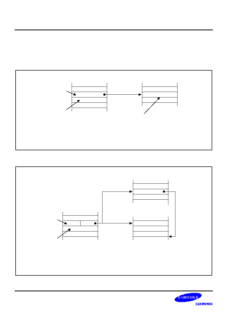
ADDRESSING MODES
S3C880A/F880A
3-2
REGISTER ADDRESSING MODE (R)
In Register addressing mode, the operand is the content of a specified register or register pair (see Figure 3-1).
Working register addressing differs from Register addressing as it uses a register pointer to specify an 8-byte
working register space in the register file and an 8-bit register within that space (see Figure 3-2).
dst
Value used in
Instruction Execution
OPCODE
OPERAND
8-bit Register
File Address
Point to One
Register in
Register File
One-Operand
Instruction
(Example)
Sample Instruction:
DEC
CNTR
; Where CNTR is the label of an 8-bit register address
Program Memory
Register File
Figure 3-1. Register Addressing
dst
OPCODE
4-bit
Working Register
Point to the
Working Register
(1 of 8)
Two-Operand
Instruction
(Example)
Sample Instruction:
ADD
R1, R2
; Where R1 and R2 are registers in the curruntly
selected working register area.
Program Memory
Register File
src
3 LSBs
RP0 or RP1
Selected
RP points
to start
of working
register
block
OPERAND
MSB Point to
RP0 ot RP1
Figure 3-2. Working Register Addressing
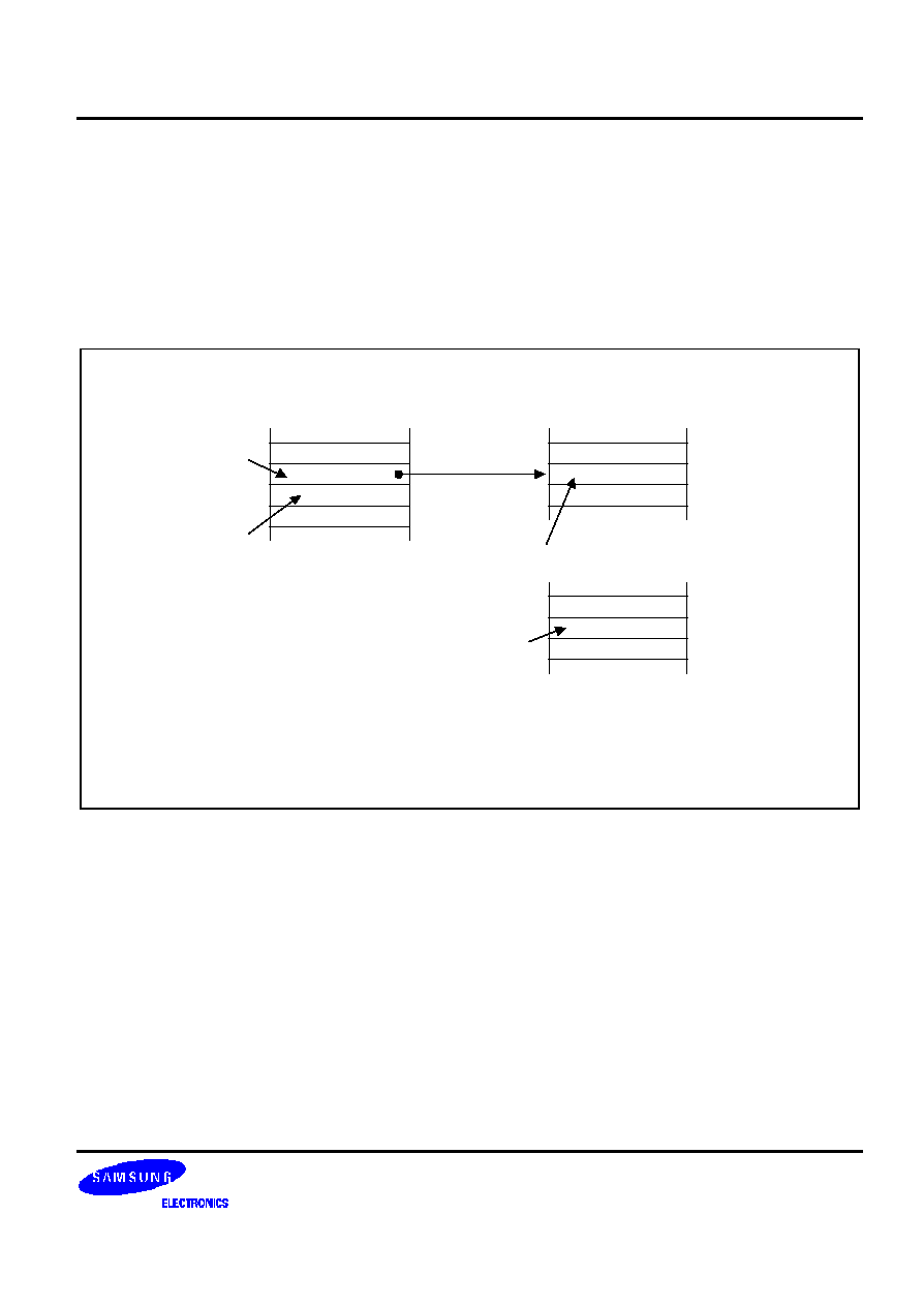
S3C880A/F880A
ADDRESSING MODES
3-3
INDIRECT REGISTER ADDRESSING MODE (IR)
In Indirect Register (IR) addressing mode, the content of the specified register or register pair is the address of the
operand. Depending on the instruction used, the actual address may point to a register in the register file, program
memory (ROM), or an external memory space (see Figures 3-3 through 3-6).
You can use any 8-bit register to indirectly address another register. Any 16-bit register pair can be used to
indirectly address another memory location. You cannot, however, access the locations C0H�FFH in set 1 using
Indirect Register addressing mode.
dst
Address of Operand
used by Instruction
OPCODE
ADDRESS
8-bit Register
File Address
Point to One
Register in Register
File
One-Operand
Instruction
(Example)
Sample Instruction:
RL
@SHIFT
; Where SHIFT is the label of an 8-bit register address
Program Memory
Register File
Value used in
Instruction Execution
OPERAND
Figure 3-3. Indirect Register Addressing to Register File
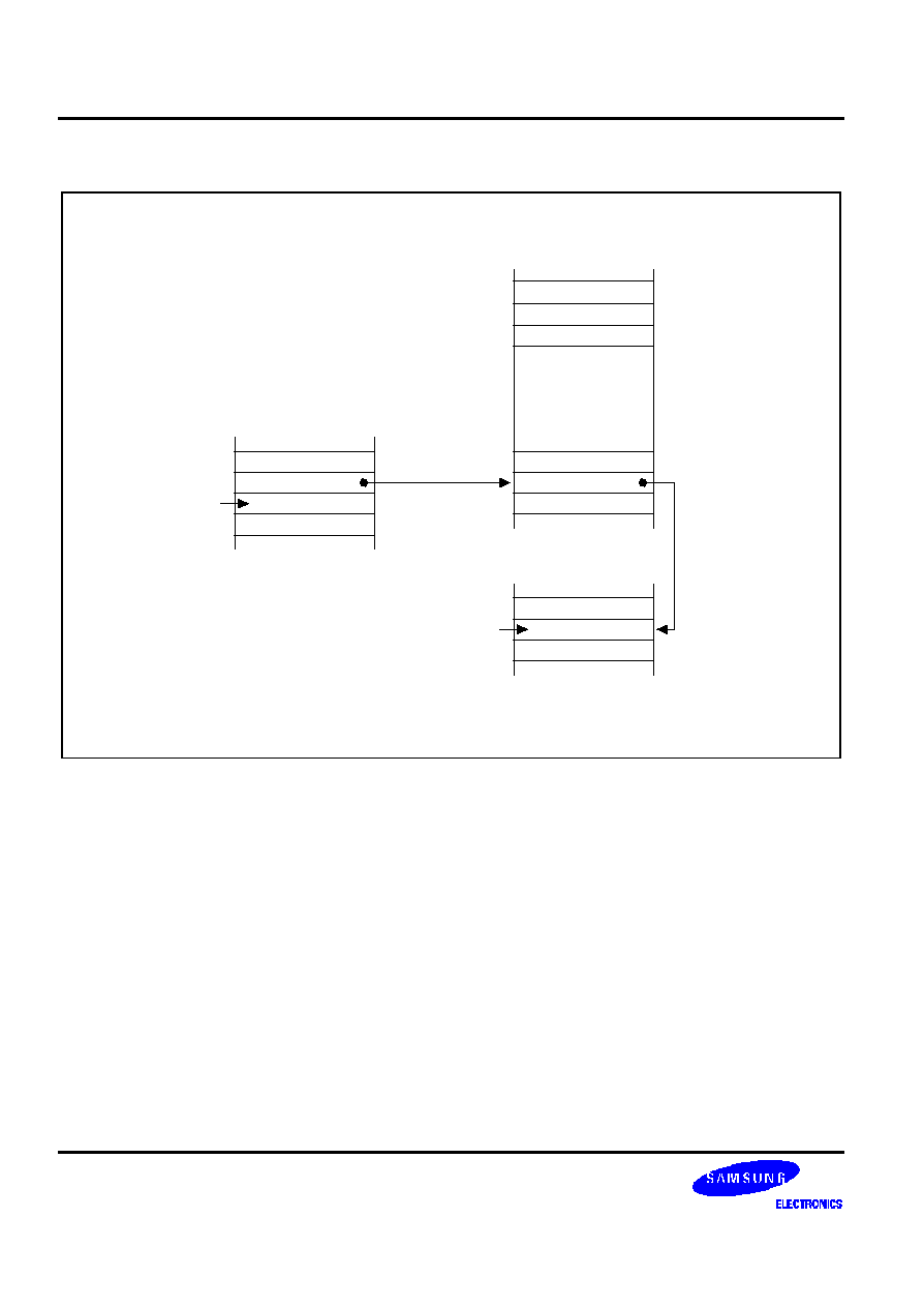
ADDRESSING MODES
S3C880A/F880A
3-4
INDIRECT REGISTER ADDRESSING MODE (Continued)
dst
OPCODE
Pair
Points to
Register Pair
Example
Instruction
References
Program
Memory
Sample Instructions:
CALL
@RR2
JP
@RR2
Program Memory
Register File
Value used in
Instruction
OPERAND
Register
Program Memory
16-Bit
Address
Points to
Program
Memory
Figure 3-4. Indirect Register Addressing to Program Memory

S3C880A/F880A
ADDRESSING MODES
3-5
INDIRECT REGISTER ADDRESSING MODE (Continued)
dst
OPCODE
ADDRESS
4-Bit
Working
Register
Address
Point to the
Working Register
(1 of 8)
Sample Instruction:
OR
R3, @R6
Program Memory
Register File
src
3 LSBs
Value used in
Instruction
OPERAND
Selected
RP Points to
Start of
Working Register
Block
RP0 or RP1
MSB Points to
RP0 or RP1
Figure 3-5. Indirect Working Register Addressing to Register File
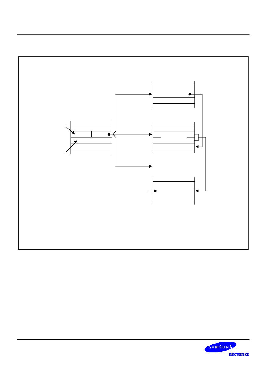
ADDRESSING MODES
S3C880A/F880A
3-6
INDIRECT REGISTER ADDRESSING MODE (Concluded)
dst
OPCODE
4-bit Working
Register Address
Sample Instructions:
LCD
R5,@RR6
; Program memory access
LDE
R3,@RR14
; External data memory access
LDE
@RR4, R8
; External data memory access
Program Memory
Register File
src
Value used in
Instruction
OPERAND
Example Instruction
References either
Program Memory or
Data Memory
Program Memory
or
Data Memory
Next 2-bit Point
to Working
Register Pair
(1 of 4)
LSB Selects
REGISTER
PAIR
16-Bit Address
Points to
Program Memory
or Data Memory
RP0 or RP1
MSB Points to
RP0 or RP1
Selected
RP points to
Start of
Working Register
Block
Figure 3-6. Indirect Working Register Addressing to Program or Data Memory
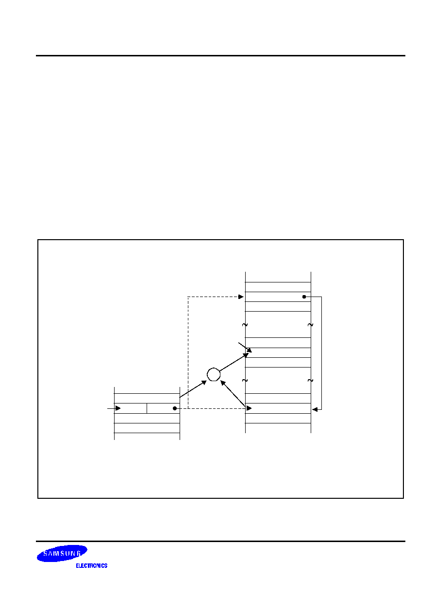
S3C880A/F880A
ADDRESSING MODES
3-7
INDEXED ADDRESSING MODE (X)
Indexed (X) addressing mode adds an offset value to a base address during the instruction execution in order to
calculate the effective operand address (see Figure 3-7). You can use Indexed addressing mode to access locations
in the internal register file or in external memory. You cannot, however, access the locations C0H�FFH in set 1
using Indexed addressing mode.
In short offset Indexed addressing mode, the 8-bit displacement is treated as a signed integer in the range
� 128 to + 127. This applies to external memory accesses only (see Figure 3-8).
For register file addressing, an 8-bit base address provided by the instruction is added to an 8-bit offset contained in
a working register. For external memory accesses, the base address is stored in the working register pair
designated in the instruction. The 8-bit or 16-bit offset given in the instruction is then added to the base address (see
Figure 3-9).
The only instruction that supports Indexed addressing mode for the internal register file is the Load instruction (LD).
The LDC and LDE instructions support Indexed addressing mode for internal program memory and for external data
memory, when implemented.
dst/src
OPCODE
Two-Operand
Instruction
Example
Point to One of the
Working Register
(1 of 8)
Sample Instruction:
LD R0, #BASE[R1]
; Where BASE is an 8-bit immediate value
Program Memory
Register File
x
3 LSBs
Value used in
Instruction
OPERAND
INDEX
Base Address
RP0 or RP1
Selected RP
Points to Start of
Working Register
Block
+
Figure 3-7. Indexed Addressing to Register File
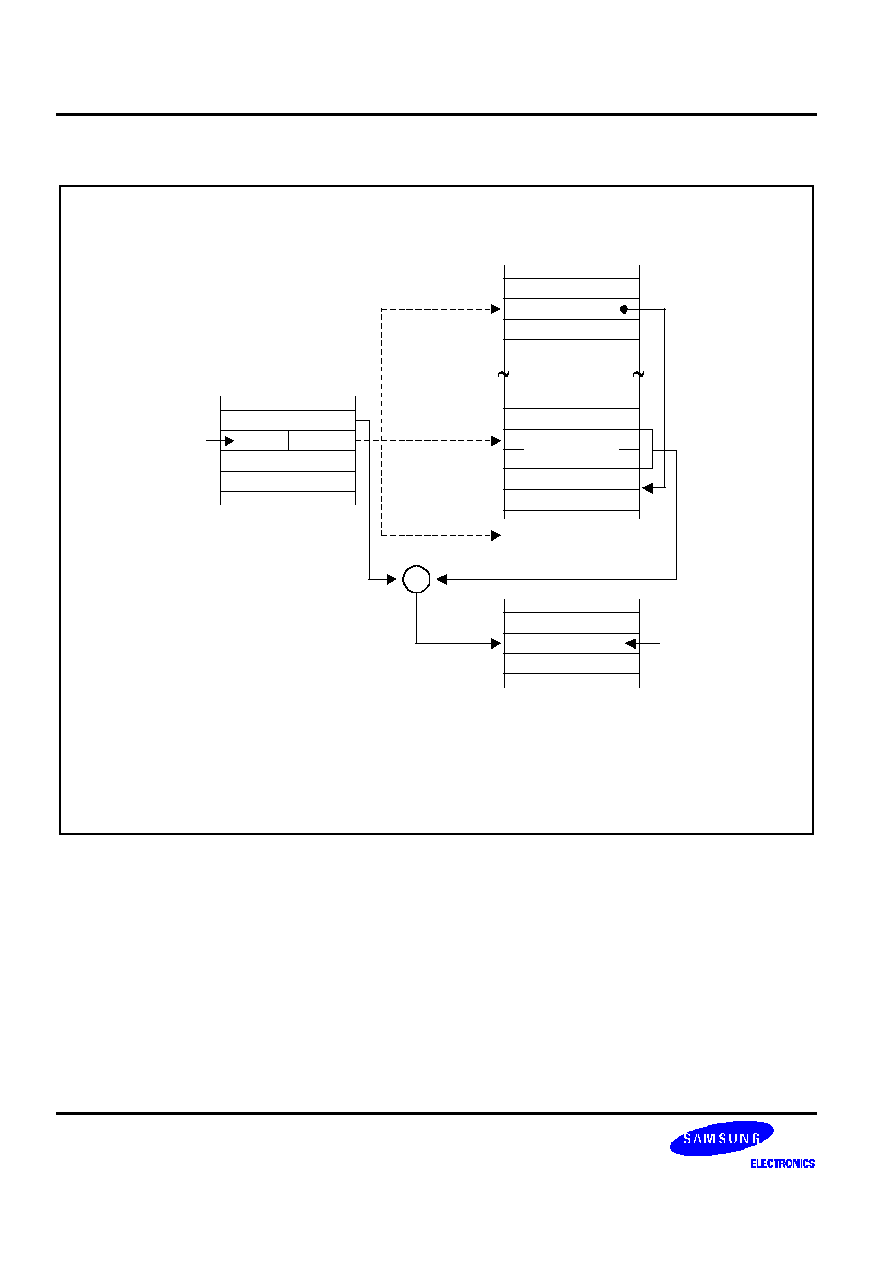
ADDRESSING MODES
S3C880A/F880A
3-8
INDEXED ADDRESSING MODE (Continued)
Register File
OPERAND
Program Memory
or
Data Memory
Point to Working
Register Pair
(1 of 4)
LSB Selects
16-Bit Address
Added to Offset
RP0 or RP1
MSB Points to
RP0 or RP1
Selected RP
Points to Start of
Working Register
Block
dst/src
OPCODE
Program Memory
x
OFFSET
4-bit Working
Register Address
Sample Instructions:
LDC
R4, #04H[RR2]
; The values in the program address (RR2 + 04H)
are loaded into register R4.
LDE
R4,#04H[RR2]
; Identical operation to LDC example, except that
external program memory is accessed.
NEXT 2 BITS
REGISTER
PAIR
Value used in
Instruction
8-Bits
16-Bits
16-Bits
+
Figure 3-8. Indexed Addressing to Program or Data Memory with Short Offset
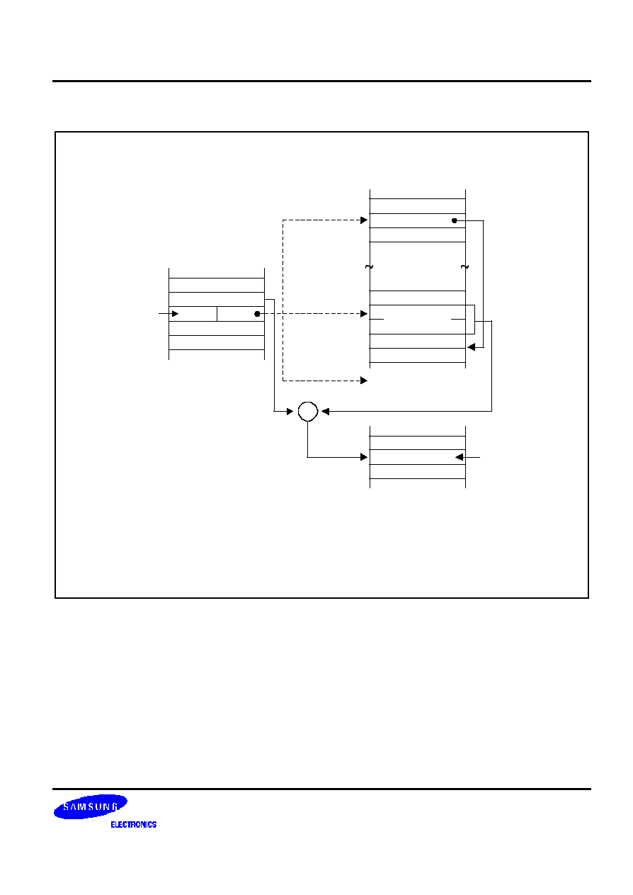
S3C880A/F880A
ADDRESSING MODES
3-9
INDEXED ADDRESSING MODE (Concluded)
Register File
OPERAND
Program Memory
or
Data Memory
Point to Working
Register Pair
LSB Selects
16-Bit Address
Added to Offset
RP0 or RP1
MSB Points to
RP0 or RP1
Selected RP
Points to Start of
Working Register
Block
Sample Instructions:
LDC
R4, #1000H[RR2]
; The values in the program address (RR2 + 1000H)
are loaded into register R4.
LDE
R4,#1000H[RR2]
; Identical operation to LDC example, except that
external program memory is accessed.
NEXT 2 BITS
REGISTER
FAIR
Value used in
Instruction
8-Bits
16-Bits
16-Bits
dst/src
OPCODE
Program Memory
src
OFFSET
4-bit Working
Register Address
OFFSET
+
Figure 3-9. Indexed Addressing to Program or Data Memory
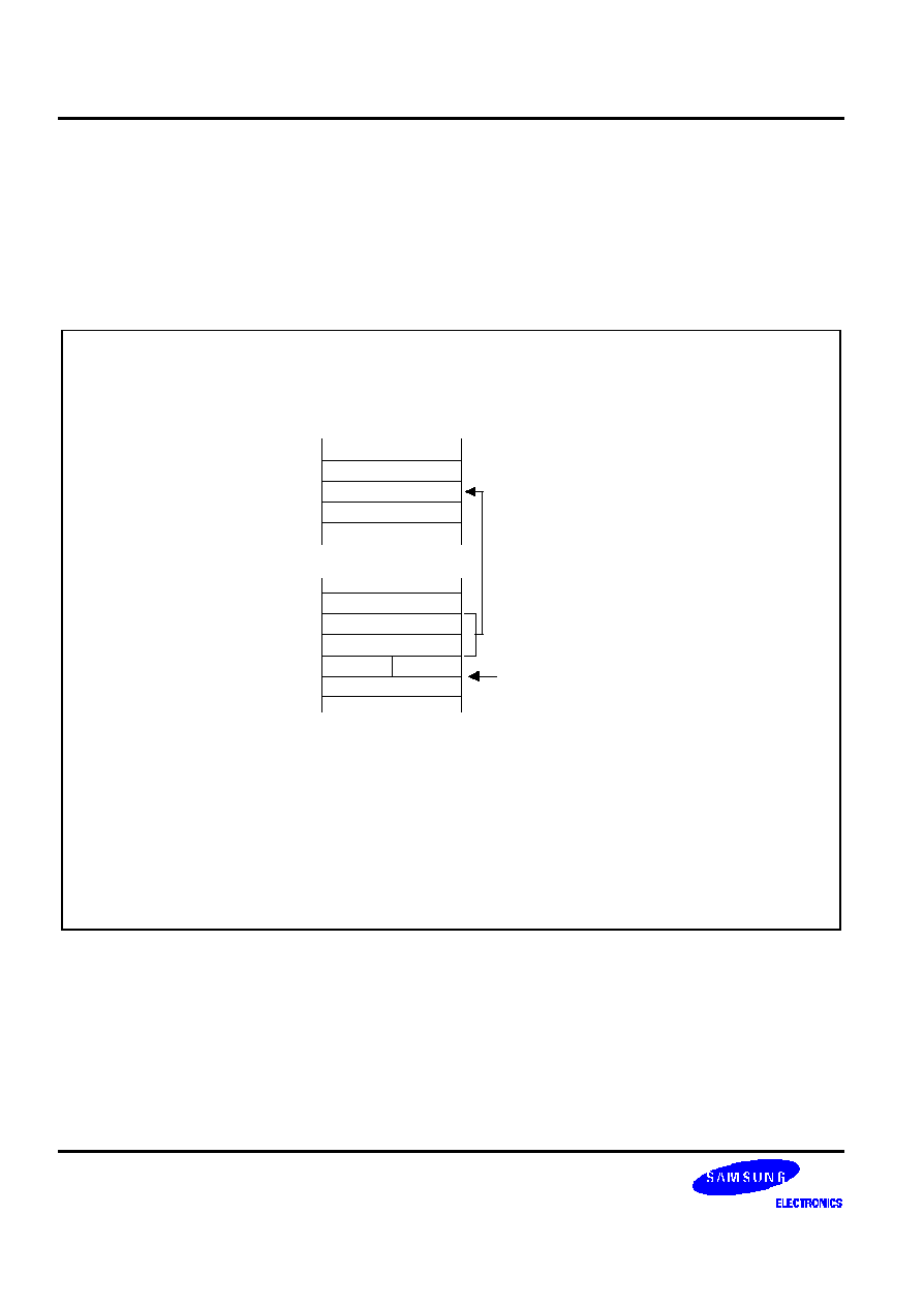
ADDRESSING MODES
S3C880A/F880A
3-10
DIRECT ADDRESS MODE (DA)
In Direct Address (DA) mode, the instruction provides the operand's 16-bit memory address. Jump (JP) and Call
(CALL) instructions use this addressing mode to specify the 16-bit destination address that is loaded into the PC
whenever a JP or CALL instruction is executed.
The LDC and LDE instructions can use Direct Address mode to specify the source or the destination address for
Load operations to program memory (LDC) or to external data memory (LDE), if implemented.
Sample Instructions:
LDC
R5,1234H; The values in the program address (1234H)
are loaded into register R5.
LDE
R5,1234H; Identical operation to LDC example, except that
external program memory is accessed.
dst/src
OPCODE
Program Memory
"0" or "1"
Lower Address Byte
LSB Selects Program
Memory or Data Memory:
"0" = Program Memory
"1" = Data Memory
Memory
Address
Used
Upper Address Byte
Program or
Data Memory
Figure 3-10. Direct Addressing for Load Instructions
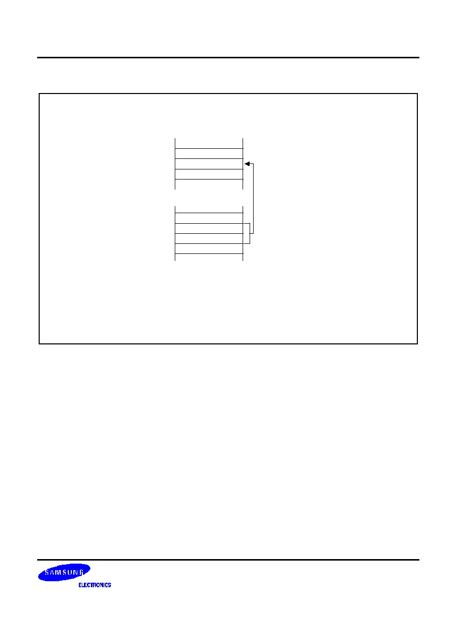
S3C880A/F880A
ADDRESSING MODES
3-11
DIRECT ADDRESS MODE (Continued)
OPCODE
Program Memory
Lower Address Byte
Memory
Address
Used
Upper Address Byte
Sample Instructions:
JP
C,JOB1
; Where JOB1 is a 16-bit immediate address
CALL
DISPLAY
; Where DISPLAY is a 16-bit immediate address
Next OPCODE
Figure 3-11. Direct Addressing for Call and Jump Instructions
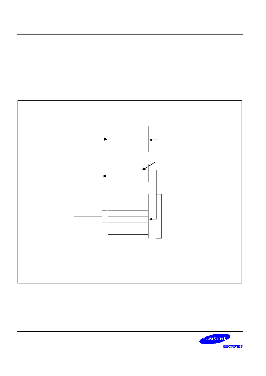
ADDRESSING MODES
S3C880A/F880A
3-12
INDIRECT ADDRESS MODE (IA)
In Indirect Address (IA) mode, the instruction specifies an address located in the lower 256 bytes of the program
memory. The selected pair of memory locations contains the actual address of the next instruction to be executed.
Only the CALL instruction can use Indirect Address mode.
As Indirect Address mode assumes that the operand is located in the lower 256 bytes of the program memory, only
an 8-bit address is provided in the instruction; the upper bytes of the destination address are assumed to be all
zeros.
Current
Instruction
Program Memory
Locations 0-255
Program Memory
OPCODE
dst
Lower Address Byte
Upper Address Byte
Next Instruction
LSB Must be Zero
Sample Instruction:
CALL
#40H
; The 16-bit value in program memory addresses
40H and 41H is the subroutine start address.
Figure 3-12. Indirect Addressing

S3C880A/F880A
ADDRESSING MODES
3-13
RELATIVE ADDRESS MODE (RA)
In Relative Address (RA) mode, a two's-complement signed displacement between � 128 and + 127 is specified in
the instruction. The displacement value is then added to the current PC value. The result is the address of the next
instruction to be executed. Before this addition occurs, the PC contains the address of the instruction immediately
following the current instruction.
Several program control instructions use Relative Address mode to perform conditional jumps. The instructions that
support RA addressing are BTJRF, BTJRT, DJNZ, CPIJE, CPIJNE, and JR.
OPCODE
Program Memory
Displacement
Program Memory
Address Used
Sample Instructions:
JR
ULT,$+OFFSET
; Where OFFSET is a value in the range +127 to -128
Next OPCODE
+
Signed
Displacement Value
Current Instruction
Current
PC Value
Figure 3-13. Relative Addressing

ADDRESSING MODES
S3C880A/F880A
3-14
IMMEDIATE MODE (IM)
In Immediate (IM) addressing mode, the operand value used in the instruction is the value supplied in the operand
field itself. The operand may be one byte or one word in length, depending on the instruction used. Immediate
addressing mode is useful for loading constant values into registers.
(The Operand value is in the instruction)
OPCODE
Sample Instruction:
LD R0,#0AAH
Program Memory
OPERAND
Figure 3-14. Immediate Addressing

S3C880A/F880A
CONTROL REGISTERS
4-1
4
CONTROL REGISTERS
OVERVIEW
In this chapter, detailed descriptions of the S3C880A/F880A control registers are presented in an easy-to-read
format. These descriptions will help familiarize you with the mapped locations in the register file. You can also use
them as a quick-reference source when writing application programs.
System and peripheral registers are summarized in Tables 4-1, 4-2, and 4-3. Figure 4-1 illustrates the important
features of the standard register description format.
Control register descriptions are arranged in alphabetical order according to register mnemonic. More information
about control registers is presented in the context of the various peripheral hardware descriptions in Part II of this
manual.
CONTROL REGISTERS
S3C880A/F880A
4-2
Table 4-1. Set 1 Registers
Register Name
Mnemonic
Decimal
Hex
R/W
Timer 0 counter
T0CNT
208
D0H
R
Timer 0 data register
T0DATA
209
D1H
R/W
Timer 0 control register
T0CON
210
D2H
R/W
Basic timer control register
BTCON
211
D3H
R/W
Clock control register
CLKCON
212
D4H
R/W
System flags register
FLAGS
213
D5H
R/W
Register pointer 0
RP0
214
D6H
R/W
Register pointer 1
RP1
215
D7H
R/W
Stack pointer (high byte)
SPH
216
D8H
R/W
Stack pointer (low byte)
SPL
217
D9H
R/W
Instruction pointer (high byte)
IPH
218
DAH
R/W
Instruction pointer (low byte)
IPL
219
DBH
R/W
Interrupt request register
IRQ
220
DCH
R
Interrupt mask register
IMR
221
DDH
R/W
System mode register
SYM
222
DEH
R/W
Register page pointer
PP
223
DFH
R/W
Table 4-2. Set 1, Bank 0 Registers
Register Name
Mnemonic
Decimal
Hex
R/W
Port 0 data register
P0
224
E0H
R/W
Port 1 data register
P1
225
E1H
R/W
Port 2 data register
P2
226
E2H
R/W
Port 3 data register
P3
227
E3H
R/W
Port 0 control register (high byte)
P0CONH
228
E4H
R/W
Port 0 control register (low byte)
P0CONL
229
E5H
R/W
Port 1 control register (high byte)
P1CONH
230
E6H
R/W
Port 1 control register (low byte)
P1CONL
231
E7H
R/W
Port 2 control register (high byte)
P2CONH
232
E8H
R/W
Port 2 control register (low byte)
P2CONL
233
E9H
R/W
Location EAH in set 1, bank 0, are not mapped.
Port 3 control register (low byte)
P3CONL
235
EBH
R/W
Locations ECH - EEH in set 1, bank 0, are not mapped.
PLL control register
(note)
PLLCON
236
EFH
R/W
NOTE: PLL control register, PLLCON, is a system register for factory test. So user should not access this register.
S3C880A/F880A
CONTROL REGISTERS
4-3
Table 4-2. Set 1, Bank 0 Registers (Continued)
Register Name
Mnemonic
Decimal
Hex
R/W
Timer A data register
TADATA
240
F0H
R/W
Location F1H in set 1, bank 0, are not mapped.
STOP control register
STCON
238
F3H
R/W
Timer A control register
TACON
242
F2H
R/W
PWM0 data register (main byte)
PWM0
244
F4H
R/W
PWM0 data register (extension byte)
PWM0EX
245
F5H
R/W
PWM1 data register (main byte)
PWM1
246
F6H
R/W
PWM1 data register (extension byte)
PWM1EX
247
F7H
R/W
PWM control register
PWMCON
248
F8H
R/W
Capture A data register
CAPA
249
F9H
R
A/D converter control register
ADCON
250
FAH
R/W
(2)
A/D conversion data register
ADDATA
251
FBH
R
Test control register
TSTC
252
FCH
R/W
(1)
Basic timer counter
BTCNT
253
FDH
R
External memory timing register
EMT
254
FEH
R/W
Interrupt priority register
IPR
255
FFH
R/W
NOTE:
Test control register, TSTC, is a system register for factory test. So user should not access this register.
CONTROL REGISTERS
S3C880A/F880A
4-4
Table 4-3. Set 1, Bank 1 Registers
Register Name
Mnemonic
Decimal
Hex
R/W
OSD fringe/border control register 1
OSDFRG1
224
E0H
R/W
OSD fringe/border control register 2
OSDFRG2
225
E1H
R/W
OSD smooth control register 1
OSDSMH1
226
E2H
R/W
OSD smooth control register 2
OSDSMH2
227
E3H
R/W
OSD space color control register
OSDCOL
236
E4H
R/W
OSD field control register
OSDFLD
237
E5H
R/W
OSD palette color mode R 1
OSDPLTR1
230
E6H
R/W
OSD palette color mode R 2
OSDPLTR2
231
E7H
R/W
OSD palette color mode G 1
OSDPLTG1
232
E8H
R/W
OSD palette color mode G 2
OSDPLTG2
233
E9H
R/W
OSD palette color mode B 1
OSDPLTB1
234
EAH
R/W
OSD palette color mode B 2
OSDPLTB2
235
EBH
R/W
Locations ECH�EFH in set 1, bank 1, are not mapped.
OSD character size control register
CHACON
240
F0H
R/W
OSD fade control register
FADECON
241
F1H
R/W
OSD row position control register
ROWCON
242
F2H
R/W
OSD column position control register
CLMCON
243
F3H
R/W
OSD background color control register
COLCON
244
F4H
R/W
On-screen display control register
DSPCON
245
F5H
R/W
Halftone signal control register
HTCON
246
F6H
R/W
V-SYNC blank control register
VSBCON
251
F7H
R/W
PWM2 Data register
PWM2
247
F8H
R/W
PWM3 Data register
PWM3
248
F9H
R/W
PWM4 Data register
PWM4
249
FAH
R/W
PWM5 Data register
PWM5
250
FBH
R/W
OSD Color Buffer
COLBUF
252
FCH
R/W
Locations FDH�FFH in set 1, bank 1, are not mapped.
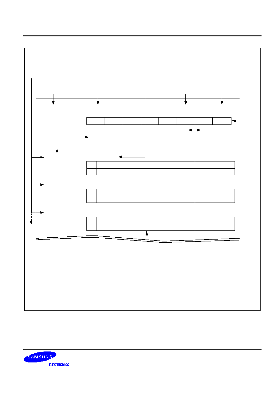
S3C880A/F880A
CONTROL REGISTERS
4-5
FLAGS -- System Flags Register
D5H
Set 1
Bit Identifier
RESET
Value
Read/Write
Addressing Mode
.7
.6
Carry Flag (C)
0
1
Operation does not generate a carry or borrow condition
Operation generates a carry-out or a borrow condition in high-order bit 7
Register
mnemonic
Full register name
Register address
(hexadecimal)
Bit number:
MSB = Bit 7
LSB = Bit 0
R
W
R/W
'�'
=
=
=
=
Read-only
Write-only
Read/write
Not used
Bit number(s) that is/are appended to
the register name for bit addressing
Description of the
effect of specific
bit settings
Name of an
individual
bit or bit function
Addressing mode or
modes you can use to
modify register values
Register addressing mode only
.7
.6
.5
.4
.3
.2
.1
.0
x
x
x
x
x
x
0
0
R/W
R/W
R/W
R/W
R/W
R/W
R/W
R/W
Not used
Undetermined value
Logic zero
Logic one
'�'
'x'
'0'
'1'
=
=
=
=
RESET value notation:
Register location
in the internal
register file
Zero Flag (Z)
0
1
Operation result is a non-zero value
Operation result is zero
Sign Flag (S)
0
1
Operation generates a positive number (MSB = "0")
Operation generates a negative number (MSB = "1")
.5
Figure 4-1. Register Description Format

CONTROL REGISTERS
S3C880A/F880A
4-6
ADCON
--
A/D Converter Control Register
FAH
Set 1, Bank 0
Bit Identifier
.7
.6
.5
.4
.3
.2
.1
.0
nRESET Value
�
�
0
0
x
0
0
0
Read/Write
�
�
R/W
R/W
R
R/W
R/W
R/W
Addressing Mode
Register addressing mode only
.7�.6
Not used for the S3C880A/F880A
.5�.4
A/D Converter Input Pin Selection Bits
0
0
ADC0 (P3.0)
0
1
ADC1 (P3.1)
1
0
ADC2 (P0.6)
1
1
ADC3 (P0.7)
.3
End-of-Conversion Status Bit (Read Only)
0
A/D conversion is in progress
1
A/D conversion complete
.2 and .1
Clock Source Selection Bits
0
0
fosc/16 (fosc < 8 MHz)
0
1
fosc/8 (fosc < 8 MHz)
1
0
fosc/14(fosc < 8 MHz)
1
1
fosc/2 (fosc < 8 MHz)
.0
Conversion Start Bit
0
No meaning
0
A/D conversion start
S3C880A/F880A
CONTROL REGISTERS
4-7
BTCON
--
Basic Timer Control Register
D3H
Set 1
Bit Identifier
.7
.6
.5
.4
.3
.2
.1
.0
nRESET Value
0
0
0
0
0
0
0
0
Read/Write
R/W
R/W
R/W
R/W
R/W
R/W
R/W
R/W
Addressing Mode
Register addressing mode only
.7�.4
Watchdog Timer Function Disable Code (for Reset)
1
0
1
0
Disable watchdog timer function
Others
Enable watchdog timer function
.3 and .2
Basic Timer Input Clock Selection Bits
0
0
f
OSC
/4096
0
1
f
OSC
/1024
1
0
f
OSC
/128
1
1
Invalid selection
.1
Basic Timer Counter Clear Bit
(note)
0
No effect
1
Clear the basic timer counter value
.0
Clock Divider Clear Bit for Basic Timer and Timer 0
(note)
0
No effect
1
Clear both dividers
NOTE:
When you write a "1" to bit 0 or bit 1, the corresponding divider or counter value is cleared to '00H'. The
corresponding BTCON bit is then automatically reset by hardware to "0".
CONTROL REGISTERS
S3C880A/F880A
4-8
CHACON
-- OSD Character Size Control Register
F0H
Set 1, Bank 1
Bit Identifier
.7
.6
.5
.4
.3
.2
.1
.0
nRESET Value
0
0
0
0
0
0
0
0
Read/Write
R/W
R/W
R/W
R/W
R/W
R/W
R/W
R/W
Addressing Mode
Register addressing mode only
.7 and .6
Vertical Character Size Selection Bits
0
0
Select 'x1' vertical character size
0
1
Select 'x2' vertical character size
1
0
Select 'x3' vertical character size
1
1
Select 'x4' vertical character size
.5 and .4
Horizontal Character Size Selection Bits
0
0
Select 'x1' horizontal character size
0
1
Select 'x2' horizontal character size
1
0
Select 'x3' horizontal character size
1
1
Select 'x4' horizontal character size
.3�.0
Fade Row Address Selection for Rows 0�11 in On-Screen Display
0
0
0
0
Row 0 selected
0
0
0
1
Row 1 selected
0
0
1
0
Row 2 selected
0
0
1
1
Row 3 selected
0
1
0
0
Row 4 selected
0
1
0
1
Row 5 selected
0
1
1
0
Row 6 selected
0
1
1
1
Row 7 selected
1
0
0
0
Row 8 selected
1
0
0
1
Row 9 selected
1
0
1
0
Row 10 selected
1
0
1
1
Row 11 selected
Others
Invalid selection
S3C880A/F880A
CONTROL REGISTERS
4-9
CLKCON
--
System Clock Control Register
D4H
Set 1
Bit Identifier
.7
.6
.5
.4
.3
.2
.1
.0
nRESET Value
0
0
0
0
0
0
0
0
Read/Write
R/W
R/W
R/W
R/W
R/W
R/W
R/W
R/W
Addressing Mode
Register addressing mode only
.7
Oscillator IRQ Wake-up Function Enable Bit
0
Enable IRQ for main system oscillator wake-up in power-down mode
1
Disable IRQ for main system oscillator wake-up in power-down mode
.6 and .5
Main Oscillator Stop Control Bits
0
0
No effect
0
1
No effect
1
0
Stop main oscillator
1
1
No effect
.4 and .3
CPU Clock (System Clock) Selection Bits
(1)
0
0
Divide by 16 (f
OSC
/16)
0
1
Divide by 8 (f
OSC
/8)
1
0
Divide by 2 (f
OSC
/2)
1
1
Non-divided clock (f
OSC
)
.2�.0
Subsystem Clock Selection Bits
(2)
1
0
1
Invalid selection for S3C880A/F880A
Others
Select main system clock (MCLK)
NOTES:
1.
After a reset, the slowest clock (divide by 16) is selected as the system clock. To select faster clock speeds, load the
appropriate values to CLKCON.3 and CLKCON.4.
2.
These selection bits are required only for systems that have a main clock and a subsystem clock. The S3C880A/F880A
microcontrollers have only a main oscillator (and an L-C oscillator for the OSD module). For this reason, the setting
'101B' is invalid.
CONTROL REGISTERS
S3C880A/F880A
4-10
CLMCON
-- OSD Column Control Register
F3H
Set 1, Bank 1
Bit Identifier
.7
.6
.5
.4
.3
.2
.1
.0
nRESET Value
0
0
0
0
0
0
0
0
Read/Write
R/W
R/W
R/W
R/W
R/W
R/W
R/W
R/W
Addressing Mode
Register addressing mode only
.7�.3
Left Margin Display Position Control Bits (16 + 4 x LMG value of 0�31 dots)
0
0
0
0
0
Left margin = 16 dot clocks
0
0
0
0
1
Left margin = 16 + 4
�
1 dot clock
� � �
� � �
1
1
1
1
1
Left margin = 16 + 4
�
31 dot clocks
.2�.0
Inter-Column Spacing Control Selection (0�7 dots)
0
0
0
No inter-column spacing
0
0
1
Inter-column spacing = 1 dot
� � �
� � �
1
1
1
Inter-column spacing = 7 dots
NOTE:
To set left margin and inter-column spacing, separate decimal values must be calculated, converted to their binary
equivalents, and then written to the CLMCON register.
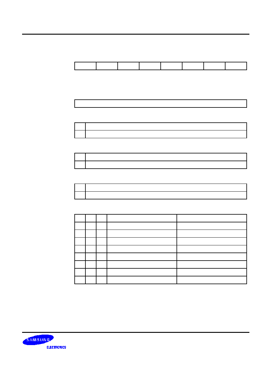
S3C880A/F880A
CONTROL REGISTERS
4-11
COLBUF
-- OSD Character Color Buffer
FCH
Set 1, Bank 1
Bit Identifier
.7
.6
.5
.4
.3
.2
.1
.0
nRESET Value
�
�
�
x
x
x
x
x
Read/Write
�
�
�
R/W
R/W
R/W
R/W
R/W
Addressing Mode
Register addressing mode only
.7�.6
Not used for the S3C880A/F880A.
.5
Video RAM Bit-9 Enable Bit
0
Disable VRAM bit-9
1
Enable VAM bit-9
.4
Video RAM Bit-8 Enable Bit
0
Disable VRAM bit-8
1
Enable VRAM bit-8
.3
H/T and BGRND Enable Bit
0
Disable H/T and BRGND
1
Enable H/T and BRGND
.2�.0
Character Color Selection Bits
.2
.1
.0
OSDCOL.0 = 0
OSDCOL.0 = 1
0
0
0
Black
Color mode 0
0
0
1
Blue
Color mode 1
0
1
0
Green
Color mode 2
0
1
1
Cyan
Color mode 3
1
0
0
Red
Color mode 4
1
0
1
Magenta
Color mode 5
1
1
0
Yellow
Color mode 6
1
1
1
White
Color mode 7
CONTROL REGISTERS
S3C880A/F880A
4-12
COLCON
-- OSD Background Color Control Register
F4H
Set 1, Bank 1
Bit Identifier
.7
.6
.5
.4
.3
.2
.1
.0
nRESET Value
0
0
0
0
0
0
0
0
Read/Write
R/W
R/W
R/W
R/W
R/W
R/W
R/W
R/W
Addressing Mode
Register addressing mode only
.7
Frame Background Color Enable Bit
0
Disable frame background color (no background color is displayed)
1
Enable frame background color
.6�.4
Frame Background Color Selection Bits (when .7 = "1")
.6
.5
.4
OSDCOL.0 = 0
OSDCOL.0 = 1
0
0
0
Black
Color mode 0
0
0
1
Blue
Color mode 1
0
1
0
Green
Color mode 2
0
1
1
Cyan
Color mode 3
1
0
0
Red
Color mode 4
1
0
1
Magenta
Color mode 5
1
1
0
Yellow
Color mode 6
1
1
1
White
Color mode 7
.3
Character Background Color Enable Bit
0
Disable character background color (no background color is displayed)
1
Enable character background color display
.2�.0
Character Background Color Selection Bits (when .3 = "1")
.2
.1
.0
OSDCOL.0 = 0
OSDCOL.0 = 1
0
0
0
Black
Color mode 0
0
0
1
Blue
Color mode 1
0
1
0
Green
Color mode 2
0
1
1
Cyan
Color mode 3
1
0
0
Red
Color mode 4
1
0
1
Magenta
Color mode 5
1
1
0
Yellow
Color mode 6
1
1
1
White
Color mode 7
S3C880A/F880A
CONTROL REGISTERS
4-13
DSPCON
-- On-Screen Display Control Register
F5H
Set 1, Bank 1
Bit Identifier
.7
.6
.5
.4
.3
.2
.1
.0
nRESET Value
0
0
0
0
0
0
0
0
Read/Write
R
R
R
R
R/W
R/W
R/W
R/W
Addressing Mode
Register addressing mode only
.7�.4
OSD Row Counter (Read-only)
0
0
0
0
Row 0
0
0
0
1
Row 1
0
0
1
0
Row 2
0
0
1
1
Row 3
0
1
0
0
Row 4
0
1
0
1
Row 5
0
1
1
0
Row 6
0
1
1
1
Row 7
1
0
0
0
Row 8
1
0
0
1
Row 9
1
0
1
0
Row 10
1
0
1
1
Row 11
Others
1100-1111 are not used
.3
Clock Edge Selection for H/V-Sync Polarity
0
Rising edge
1
Falling edge
.2�.1
Halftone or Background Color Selection Bits
0
0
Character background color
0
1
Not used
1
0
Halftone output
1
1
Character halftone and background color
.0
Display Enable Bit
0
Disable OSD (turn off L-C OSC)
1
Enable OSD (turn on L-C OSC)

CONTROL REGISTERS
S3C880A/F880A
4-14
EMT
-- External Memory Timing Register
FEH
Set 1, Bank 0
Bit Identifier
.7
.6
.5
.4
.3
.2
.1
.0
nRESET Value
0
0
0
0
0
0
0
�
Read/Write
R/W
R/W
R/W
R/W
R/W
R/W
R/W
�
Addressing Mode
Register addressing mode only
.7
External nWAIT Input Function Enable Bit
0
Disable nWAIT input function for external device (normal operating mode)
1
Enable nWAIT input function for external device
.6
Slow Memory Timing Enable Bit
0
Disable slow memory timing
1
Enable slow memory timing
.5 and .4
Program Memory Automatic Wait Control Bits
0
0
No wait (normal operation)
0
1
Wait one cycle
1
0
Wait two cycles
1
1
Wait three cycles
.3 and .2
Data Memory Automatic Wait Control Bits
0
0
No wait (normal operation)
0
1
Wait one cycle
1
0
Wait two cycles
1
1
Wait three cycles
.1
Stack Area Selection Bit
0
Select internal register file area
1
Select external data memory area
.0
Not used for the S3C880A/F880A.
NOTE: Because an external interface is not implemented for the S3C880A/F880A, the EMT values should
always be "0".

S3C880A/F880A
CONTROL REGISTERS
4-15
FADECON
-- OSD Fade Control Register
F1H
Set 1, Bank 1
Bit Identifier
.7
.6
.5
.4
.3
.2
.1
.0
nRESET Value
�
0
0
0
0
0
0
0
Read/Write
�
R/W
R/W
R/W
R/W
R/W
R/W
R/W
Addressing Mode
Register addressing mode only
.7
Not used for the S3C880A/F880A.
.6
Fade Function Enable Bit
0
Fade disable
1
Fade enable
.5
Fade Direction Selection Bit
0
Fade before matrix
1
Fade after matrix
.4�.0
Halftone or Background Color Selection Bits
(1)
0
0
0
0
0
Line 0
0
0
0
0
1
Line 1
. . . .
. . . .
1
0
0
0
0
Line 16
1
0
0
0
1
Line 17
1
0
0
1
0
Inter-row space Line 1 (1H)
1
0
0
1
1
Inter-row space Line 2 (1H)
1
0
1
0
0
Inter-row space Line 3 (1H)
1
0
1
0
1
Inter-row space Line 4 (1H)
1
0
1
1
0
Inter-row space Line 5 (1H)
1
0
1
1
1
Inter-row space Line 6 (1H)
1
1
0
0
0
Inter-row space Line 7 (1H)
1
1
0
0
1
Not used
. . . .
. . . .
1
1
1
1
1
Not used
NOTE: There are two choices of fade direction: before (FADECON.5="0") and after (FADECON.5="1"). When you select
fade before, the character matrix is faded starting with current line +1 (not including current line). When you
select fade after, the character matrix is faded starting with current line.

CONTROL REGISTERS
S3C880A/F880A
4-16
FLAGS
--
System Flags Register
D5H
Set 1
Bit Identifier
.7
.6
.5
.4
.3
.2
.1
.0
nRESET Value
x
x
x
x
x
x
0
0
Read/Write
R/W
R/W
R/W
R/W
R/W
R/W
R/W
R/W
Addressing Mode
Register addressing mode only
.7
Carry Flag (C)
0
Operation does not generate a carry or borrow condition
1
Operation generates a carry-out or borrow into high-order bit-7
.6
Zero Flag (Z)
0
Operation result is a non-zero value
1
Operation result is zero
.5
Sign Flag (S)
0
Operation generates a positive number (MSB = "0")
1
Operation generates a negative number (MSB = "1")
.4
Overflow Flag (V)
0
Operation result is
+ 127 or
� 128
1
Operation result is > + 127 or < � 128
.3
Decimal Adjust Flag (D)
0
Add operation has completed
1
Subtraction operation has completed
.2
Half-Carry Flag (H)
0
No carry-out of bit 3 or no borrow into bit 3 by addition or subtraction
1
Addition generated carry-out of bit 3 or subtraction generated borrow into bit 3
.1
Fast Interrupt Status Flag (FIS)
0
Cleared automatically during an interrupt return (IRET)
1
Automatically set to logic one during a fast interrupt service routine
.0
Bank Address Selection Flag (BA)
0
Bank 0 is selected (using the SB0 instruction)
1
Bank 1 is selected (using the SB1 instruction)
S3C880A/F880A
CONTROL REGISTERS
4-17
HTCON
-- Halftone Signal Control Register
F6H
Set 1, Bank 1
Bit Identifier
.7
.6
.5
.4
.3
.2
.1
.0
nRESET Value
0
0
0
0
0
0
0
0
Read/Write
R/W
R/W
R/W
R/W
R/W
R/W
R/W
R/W
Addressing Mode
Register addressing mode only
.7
Halftone Output Polarity Selection Bit (HT Only)
0
Active high (normal halftone output is Low level)
1
Active low (normal halftone output is High level)
.6
RGB Output Polarity Selection Bit
0
Active high (normal RGB polarity is Low level)
1
Active low (normal RGB polarity is High level)
.5
OSD ROW Interrupt Enable Bit
0
Disable the OSD ROW interrupt
1
Enable the OSD ROW interrupt
.4
OSD ROW Interrupt Pending Bit
0
No interrupt is pending (when read); clear pending bit (when write)
1
Interrupt is pending (when read); no effect (when write)
.3
Halftone Function Enable Bit
0
Disable the halftone control signal
1
Enable the halftone control signal
.2
Halftone Option Selection Bit
0
Halftone output for character periods only (as selected by video RAM bit-13)
1
Halftone output for all frame periods (regardless of video RAM bit-13 setting)
.1
V-Sync Interrupt Enable Bit
0
Disable the V-sync interrupt
1
Enable the V-sync interrupt
.0
V-Sync Interrupt Pending Bit
0
No OSD ROW interrupt is pending (when read)
0
Clear pending bit (when write)
1
OSD ROW interrupt is pending (when read)
1
No effect (when write)

CONTROL REGISTERS
S3C880A/F880A
4-18
IMR
-- Interrupt Mask Register
DDH
Set 1
Bit Identifier
.7
.6
.5
.4
.3
.2
.1
.0
nRESET Value
x
x
�
x
x
x
x
x
Read/Write
R/W
R/W
�
R/W
R/W
R/W
R/W
R/W
Addressing Mode
Register addressing mode only
.7
Interrupt Priority Level 7 (IRQ7) Enable Bit; V-Sync
0
Disable IRQ7 interrupt
1
Enable IRQ7 interrupt
.6
Interrupt Priority Level 6 (IRQ6) Enable Bit; Timer A
0
Disable IRQ6 interrupt
1
Enable IRQ6 interrupt
.5
Not used for S3C880A/F880A
.4
Interrupt Priority Level 4 (IRQ4) Enable Bit; P1.2 and P1.3 External Interrupt
0
Disable IRQ4 interrupt
1
Enable IRQ4 interrupt
.3
Interrupt Priority Level 3 (IRQ3) Enable Bit; CAPA
0
Disable IRQ3 interrupt
1
Enable IRQ3 interrupt
.2
Interrupt Priority Level 2 (IRQ2) Enable Bit; OSD ROW Interrupt
0
Disable IRQ2 interrupt
1
Enable IRQ2 interrupt
.1
Interrupt Priority Level 1 (IRQ1) Enable Bit; P1.0 and P1.1 External Interrupt
0
Disable IRQ1 interrupt
1
Enable IRQ1 interrupt
.0
Interrupt Priority Level 0 (IRQ0) Enable Bit; T0INT (Match)
0
Disable IRQ0 interrupt
1
Enable IRQ0 interrupt
S3C880A/F880A
CONTROL REGISTERS
4-19
IPH
-- Instruction Pointer (High Byte)
DAH
Set 1
Bit Identifier
.7
.6
.5
.4
.3
.2
.1
.0
nRESET Value
x
x
x
x
x
x
x
x
Read/Write
R/W
R/W
R/W
R/W
R/W
R/W
R/W
R/W
Addressing Mode
Register addressing mode only
.7�.0
Instruction Pointer Address (High Byte)
The high-byte instruction pointer value is the upper eight bits of the 16-bit instruction
pointer address (IP15�IP8). The lower byte of the IP address is located in the IPL
register (DBH).
IPL
-- Instruction Pointer (Low Byte)
DBH
Set 1
Bit Identifier
.7
.6
.5
.4
.3
.2
.1
.0
nRESET Value
x
x
x
x
x
x
x
x
Read/Write
R/W
R/W
R/W
R/W
R/W
R/W
R/W
R/W
Addressing Mode
Register addressing mode only
.7 � .0
Instruction Pointer Address (Low Byte)
The low-byte instruction pointer value is the lower eight bits of the 16-bit instruction
pointer address (IP7�IP0). The upper byte of the IP address is located in the IPH
register (DAH).
CONTROL REGISTERS
S3C880A/F880A
4-20
IPR
-- Interrupt Priority Register
FFH
Set 1, Bank 0
Bit Identifier
.7
.6
.5
.4
.3
.2
.1
.0
nRESET Value
x
x
�
x
x
x
x
x
Read/Write
R/W
R/W
�
R/W
R/W
R/W
R/W
R/W
Addressing Mode
Register addressing mode only
.7, .4, and .1
Priority Control Bits for Interrupt Groups A, B, and C
(1)
0
0
0
Group priority undefined
0
0
1
B > C > A
0
1
0
A > B > C
0
1
1
B > A > C
1
0
0
C > A > B
1
0
1
C > B > A
1
1
0
A > C > B
1
1
1
Group priority undefined
.6
Interrupt Group C Priority Control Bit
0
IRQ6 > IRQ7
1
IRQ7 > IRQ6
.5
Not used for the S3C880A/F880A
(2)
.3
Interrupt Sub Group B Priority Control Bit
0
IRQ3 > IRQ4
1
IRQ4 > IRQ3
.2
Interrupt Group B Priority Control Bit
0
IRQ2 > (IRQ3, IRQ4)
1
(IRQ3, IRQ4) > IRQ2
.0
Interrupt Group A Priority Control Bit
0
IRQ0 > IRQ1
1
IRQ1 > IRQ0
NOTES:
1.
Interrupt group A is IRQ0 and IRQ1; interrupt group B is IRQ2, IRQ3, and IRQ4; interrupt group C is IRQ6 and IRQ7.
2.
Interrupt level IRQ5 is not used in the S3C880A/F880A interrupt structure. For this reason, IPR.5 is not used.
S3C880A/F880A
CONTROL REGISTERS
4-21
IRQ
-- Interrupt Request Register
DCH
Set 1
Bit Identifier
.7
.6
.5
.4
.3
.2
.1
.0
nRESET Value
0
0
�
0
0
0
0
0
Read/Write
R
R
�
R
R
R
R
R
Addressing Mode
Register addressing mode only
.7
Interrupt Level 7 (IRQ7) Request Pending Bit; V-Sync
0
No IRQ7 interrupt pending
1
IRQ7 interrupt is pending
.6
Interrupt Level 6 (IRQ6) Request Pending Bit; Timer A
0
No IRQ6 interrupt pending
1
IRQ6 interrupt is pending
.5
Not used for the S3C880A/F880A
.4
Interrupt Level 4 (IRQ4) Request Pending Bit; P1.2 and P1.3 External Interrupt
0
No IRQ4 interrupt pending
1
IRQ4 interrupt is pending
.3
Interrupt Level 3 (IRQ3) Request Pending Bit; CAPA
0
No IRQ3 interrupt pending
1
IRQ3 interrupt is pending
.2
Interrupt Level 2 (IRQ2) Request Pending Bit; OSD ROW Interrupt
0
No IRQ2 interrupt pending
1
IRQ2 interrupt is pending
.1
Interrupt Level 1 (IRQ1) Request Pending Bit; P1.0 and P1.1 External Interrupt
0
No IRQ1 interrupt pending
1
IRQ1 interrupt is pending
.0
Interrupt Level 0 (IRQ0) Request Pending Bit; T0INT (Match)
0
No IRQ0 interrupt pending
1
IRQ0 interrupt is pending
NOTE:
Interrupt level request pending bits can be polled by software to detect an interrupt request pending condition on
any of the seven valid interrupt levels (IRQ0�IRQ4, IRQ6, and IRQ7). Interrupt pending bits are read-only
addressable.
CONTROL REGISTERS
S3C880A/F880A
4-22
OSDCOL
-- OSD Space Color Control Register
E4H
Set 1, Bank 1
Bit Identifier
.7
.6
.5
.4
.3
.2
.1
.0
nRESET Value
�
�
�
0
0
0
0
0
Read/Write
�
�
�
R/W
R/W
R/W
R/W
R/W
Addressing Mode
Register addressing mode only
.7�,5
Not used for the S3C880A/F880A.
.4
Inter Character Smoothing Control Bit
(note)
0
Disable inter character smoothing
1
Enable inter character smoothing
.3
Fringe Dot Size Selection Bit
0
1 dot
1
1/2 dot
.2
Inter-row Space Half Tone
0
Depend on character background half tone
1
Depend on frame background half tone
.1
Inter-row Space Color
0
Depend on character background color
1
Depend on frame background color
.0
RGB Output Selection Bit
0
Digital RGB output (disable palette color mode)
1
Analog RGB output (enable palette color mode)
NOTE:
In 1-dot fringe mode (OSDCOL.3 = "0") , Inter-character smooth function is disabled.
S3C880A/F880A
CONTROL REGISTERS
4-23
OSDFLD
-- OSD Field Control Register
E5H
Set 1, Bank 1
Bit Identifier
.7
.6
.5
.4
.3
.2
.1
.0
nRESET Value
�
�
x
0
0
1
1
0
Read/Write
�
�
R
R/W
R/W
R/W
R/W
R/W
Addressing Mode
Register addressing mode only
.7�,6
Not used for the S3C880A/F880A.
.5
Field Data (Read Only)
0
Even field
1
Odd field
.4
H-sync Detect Position Select Bit
0
Detect H-sync before V-sync
1
Detect H-sync after V-sync
.3�.0
Even Field Range
0
0
0
0
Not used
0
0
0
1
f
CPU
/16
�
1
0
0
1
0
f
CPU
/16
�
2
0
0
1
1
f
CPU
/16
�
3
0
1
0
0
f
CPU
/16
�
4
0
1
0
1
f
CPU
/16
�
5
0
1
1
0
f
CPU
/16
�
6 (Reset value)
0
1
1
1
f
CPU
/16
�
7
1
0
0
0
f
CPU
/16
�
8
1
0
0
1
f
CPU
/16
�
9
1
0
1
0
f
CPU
/16
�
10
1
0
1
1
f
CPU
/16
�
11
1
1
0
0
f
CPU
/16
�
12
1
1
0
1
f
CPU
/16
�
13
1
1
1
0
f
CPU
/16
�
14
1
1
1
1
f
CPU
/16
�
15
CONTROL REGISTERS
S3C880A/F880A
4-24
OSDFRG1
-- OSD Fringe/Border Control Register 1
E0H
Set 1, Bank 1
Bit Identifier
.7
.6
.5
.4
.3
.2
.1
.0
nRESET Value
0
0
0
0
0
0
0
0
Read/Write
R/W
R/W
R/W
R/W
R/W
R/W
R/W
R/W
Addressing Mode
Register addressing mode only
.7�.0
Fringe/Border Function Enable Bit
0
Disable Fringe/Border function at row n (n = 0�7)
1
Enable Fringe/Border function at row n (n = 0�7)
NOTE: Row n is respectively correspond with bit n (n = 0�7).
S3C880A/F880A
CONTROL REGISTERS
4-25
OSDFRG2
-- OSD Fringe/Border Control Register 2
E1H
Set 1, Bank 1
Bit Identifier
.7
.6
.5
.4
.3
.2
.1
.0
nRESET Value
0
0
0
0
0
0
0
0
Read/Write
R/W
R/W
R/W
R/W
R/W
R/W
R/W
R/W
Addressing Mode
Register addressing mode only
.7
Fringe or Border Selection Bit
0
Border function select
1
Fringe function select
.6�.4
Fringe/Border Color Selection Bits (.6: Red, .5: Green, .4: Blue)
.6
.5
.4
OSDCOL.0 = 0
OSDCOL.0 = 1
0
0
0
Black
Color mode 0
0
0
1
Blue
Color mode 1
0
1
0
Green
Color mode 2
0
1
1
Cyan
Color mode 3
1
0
0
Red
Color mode 4
1
0
1
Magenta
Color mode 5
1
1
0
Yellow
Color mode 6
1
1
1
White
Color mode 7
.3�.0
Fringe/Border Function Enable Bits
0
Disable Fringe/Border function at row n (n = 8�11)
1
Enable Fringe/Border function at row n (n = 8�11)
NOTE: Row 8, row 9, row 10, row 11 are correspond with bit 0, bit 1, bit 2, bit3, respectively.

CONTROL REGISTERS
S3C880A/F880A
4-26
OSDPLTB1
-- OSD Palette Color Mode Register B1
EAH
Set 1, Bank 1
Bit Identifier
.7
.6
.5
.4
.3
.2
.1
.0
nRESET Value
1
1
0
0
1
1
0
0
Read/Write
R/W
R/W
R/W
R/W
R/W
R/W
R/W
R/W
Addressing Mode
Register addressing mode only
.7�.6
OSD Mode 3 Blue Level
0
0
Disable
0
1
33 %
1
0
66 %
1
1
100 %
.5�.4
OSD Mode 2 Blue Level
0
0
Disable
0
1
33 %
1
0
66 %
1
1
100 %
.3�.2
OSD Mode 1 Blue Level
0
0
Disable
0
1
33 %
1
0
66 %
1
1
100 %
.1�.0
OSD Mode 1 Blue Level
0
0
Disable
0
1
33 %
1
0
66 %
1
1
100 %

S3C880A/F880A
CONTROL REGISTERS
4-27
OSDPLTB2
-- OSD Palette Color Mode Register B2
EBH
Set 1, Bank 1
Bit Identifier
.7
.6
.5
.4
.3
.2
.1
.0
nRESET Value
1
1
0
0
1
1
0
0
Read/Write
R/W
R/W
R/W
R/W
R/W
R/W
R/W
R/W
Addressing Mode
Register addressing mode only
.7�.6
OSD Mode 7 Blue Level
0
0
Disable
0
1
33 %
1
0
66 %
1
1
100 %
.5�.4
OSD Mode 6 Blue Level
0
0
Disable
0
1
33 %
1
0
66 %
1
1
100 %
.3�.2
OSD Mode 5 Blue Level
0
0
Disable
0
1
33 %
1
0
66 %
1
1
100 %
.1�.0
OSD Mode 4 Blue Level
0
0
Disable
0
1
33 %
1
0
66 %
1
1
100 %

CONTROL REGISTERS
S3C880A/F880A
4-28
OSDPLTG1
-- OSD Palette Color Mode Register G1
E8H
Set 1, Bank 1
Bit Identifier
.7
.6
.5
.4
.3
.2
.1
.0
nRESET Value
1
1
1
1
0
0
0
0
Read/Write
R/W
R/W
R/W
R/W
R/W
R/W
R/W
R/W
Addressing Mode
Register addressing mode only
.7�.6
OSD Mode 3 Green Level
0
0
Disable
0
1
33 %
1
0
66 %
1
1
100 %
.5�.4
OSD Mode 2 Green Level
0
0
Disable
0
1
33 %
1
0
66 %
1
1
100 %
.3�.2
OSD Mode 1 Green Level
0
0
Disable
0
1
33 %
1
0
66 %
1
1
100 %
.1�.0
OSD Mode 1 Green Level
0
0
Disable
0
1
33 %
1
0
66 %
1
1
100 %

S3C880A/F880A
CONTROL REGISTERS
4-29
OSDPLTG2
-- OSD Palette Color Mode Register G2
E9H
Set 1, Bank 1
Bit Identifier
.7
.6
.5
.4
.3
.2
.1
.0
nRESET Value
1
1
1
1
0
0
0
0
Read/Write
R/W
R/W
R/W
R/W
R/W
R/W
R/W
R/W
Addressing Mode
Register addressing mode only
.7�.6
OSD Mode 7 Green Level
0
0
Disable
0
1
33 %
1
0
66 %
1
1
100 %
.5�.4
OSD Mode 6 Green Level
0
0
Disable
0
1
33 %
1
0
66 %
1
1
100 %
.3�.2
OSD Mode 5 Green Level
0
0
Disable
0
1
33 %
1
0
66 %
1
1
100 %
.1�.0
OSD Mode 4 Green Level
0
0
Disable
0
1
33 %
1
0
66 %
1
1
100 %

CONTROL REGISTERS
S3C880A/F880A
4-30
OSDPLTR1
-- OSD Palette Color Mode Register R1
E6H
Set 1, Bank 1
Bit Identifier
.7
.6
.5
.4
.3
.2
.1
.0
nRESET Value
0
0
0
0
0
0
0
0
Read/Write
R/W
R/W
R/W
R/W
R/W
R/W
R/W
R/W
Addressing Mode
Register addressing mode only
.7�.6
OSD Mode 3 Red Level
0
0
Disable
0
1
33 %
1
0
66 %
1
1
100 %
.5�.4
OSD Mode 2 Red Level
0
0
Disable
0
1
33 %
1
0
66 %
1
1
100 %
.3�.2
OSD Mode 1 Red Level
0
0
Disable
0
1
33 %
1
0
66 %
1
1
100 %
.1�.0
OSD Mode 1 Red Level
0
0
Disable
0
1
33 %
1
0
66 %
1
1
100 %

S3C880A/F880A
CONTROL REGISTERS
4-31
OSDPLTR2
-- OSD Palette Color Mode Register R2
E7H
Set 1, Bank 1
Bit Identifier
.7
.6
.5
.4
.3
.2
.1
.0
nRESET Value
1
1
1
1
1
1
1
1
Read/Write
R/W
R/W
R/W
R/W
R/W
R/W
R/W
R/W
Addressing Mode
Register addressing mode only
.7�.6
OSD Mode 7 Red Level
0
0
Disable
0
1
33 %
1
0
66 %
1
1
100 %
.5�.4
OSD Mode 6 Red Level
0
0
Disable
0
1
33 %
1
0
66 %
1
1
100 %
.3�.2
OSD Mode 5 Red Level
0
0
Disable
0
1
33 %
1
0
66 %
1
1
100 %
.1�.0
OSD Mode 4 Red Level
0
0
Disable
0
1
33 %
1
0
66 %
1
1
100 %
CONTROL REGISTERS
S3C880A/F880A
4-32
OSDSMH1
-- OSD Smooth Control Register 1
E2H
Set 1, Bank 1
Bit Identifier
.7
.6
.5
.4
.3
.2
.1
.0
nRESET Value
0
0
0
0
0
0
0
0
Read/Write
R/W
R/W
R/W
R/W
R/W
R/W
R/W
R/W
Addressing Mode
Register addressing mode only
.7
Row 7 Smooth Function Enable Bit
0
Disable smooth function at Row 7
1
Enable smooth function at Row 7
.6
Row 6 Smooth Function Enable Bit
0
Disable smooth function at Row 6
1
Enable smooth function at Row 6
.5
Row 5 Smooth Function Enable Bit
0
Disable smooth function at Row 5
1
Enable smooth function at Row 5
.4
Row 4 Smooth Function Enable Bit
0
Disable smooth function at Row 4
1
Enable smooth function at Row 4
.3
Row 3 Smooth Function Enable Bit
0
Disable smooth function at Row 3
1
Enable smooth function at Row 3
.2
Row 2 Smooth Function Enable Bit
0
Disable smooth function at Row 2
1
Enable smooth function at Row 2
.1
Row 1 Smooth Function Enable Bit
0
Disable smooth function at Row 1
1
Enable smooth function at Row 1
.0
Row 0 Smooth Function Enable Bit
0
Disable smooth function at Row 0
1
Enable smooth function at Row 0
S3C880A/F880A
CONTROL REGISTERS
4-33
OSDSMH2
-- OSD Smooth Control Register 2
E3H
Set 1, Bank 1
Bit Identifier
.7
.6
.5
.4
.3
.2
.1
.0
nRESET Value
�
�
�
�
0
0
0
0
Read/Write
�
�
�
�
R/W
R/W
R/W
R/W
Addressing Mode
Register addressing mode only
.7�,4
Not used for the S3C880A/F880A
.3
Row 11 Smooth Function Enable Bit
0
Disable smooth function at Row 11
1
Enable smooth function at Row 11
.2
Row 10 Smooth Function Enable Bit
0
Disable smooth function at Row 10
1
Enable smooth function at Row 10
.1
Row 9 Smooth Function Enable Bit
0
Disable smooth function at Row 9
1
Enable smooth function at Row 9
.0
Row 8 Smooth Function Enable Bit
0
Disable smooth function at Row 8
1
Enable smooth function at Row 8

CONTROL REGISTERS
S3C880A/F880A
4-34
P0CONH
-- Port 0 Control Register (High Byte)
E4H
Set 1, Bank 0
Bit Identifier
.7
.6
.5
.4
.3
.2
.1
.0
nRESET Value
1
1
1
1
0
0
0
0
Read/Write
R/W
R/W
R/W
R/W
R/W
R/W
R/W
R/W
Addressing Mode
Register addressing mode only
.7 and .6
Port 0.7 Configuration Bits
0
0
Input mode
0
1
ADC Input mode
1
0
Open-drain output mode
1
1
Open-drain output mode
.5 and .4
Port 0.6 Configuration Bits
0
0
Input mode
0
1
ADC Input mode
1
0
Open-drain output mode
1
1
Open-drain output mode
.3 and .2
Port 0.5 Configuration Bits
0
0
Input mode
0
1
Input mode
1
0
Push-pull output mode
1
1
Push-pull output mode
.1 and .0
Port 0.4 Configuration Bits
0
0
Input mode
0
1
Input mode
1
0
Push-pull output mode
1
1
Push-pull output mode

S3C880A/F880A
CONTROL REGISTERS
4-35
P0CONL
-- Port 0 Control Register (Low Byte)
E5H
Set 1, Bank 0
Bit Identifier
.7
.6
.5
.4
.3
.2
.1
.0
nRESET Value
0
0
0
0
0
0
0
0
Read/Write
R/W
R/W
R/W
R/W
R/W
R/W
R/W
R/W
Addressing Mode
Register addressing mode only
.7 and .6
Port 0.3 Configuration Bits
0
0
Input mode
0
1
Input mode
1
0
N-channel open-drain output mode (5 V load)
1
1
Push-pull output mode
.5 and .4
Port 0.2 Configuration Bits
0
0
Input mode
0
1
Input mode
1
0
N-channel open-drain output mode (5 V load)
1
1
Push-pull output mode
.3 and .2
Port 0.1 Configuration Bits
0
0
Input mode
0
1
Input mode
1
0
N-channel open-drain output mode (5 V load)
1
1
Push-pull output mode
.1 and .0
Port 0.0 Configuration Bits
0
0
Input mode
0
1
Input mode
1
0
N-channel open-drain output mode (5 V load)
1
1
Push-pull output mode

CONTROL REGISTERS
S3C880A/F880A
4-36
P1CONH
-- Port 1 Control Register (High Byte)
E6H
Set 1, Bank 0
Bit Identifier
.7
.6
.5
.4
.3
.2
.1
.0
nRESET Value
0
0
0
0
1
1
1
1
Read/Write
R/W
R/W
R/W
R/W
R/W
R/W
R/W
R/W
Addressing Mode
Register addressing mode only
.7 and .6
Port 1.7/T0CK Configuration Bits
0
0
Input mode
0
1
Timer 0 clock Input mode
1
0
Push-pull output mode
1
1
Push-pull output mode
.5 and .4
Port 1.6 Configuration Bits
0
0
Input mode
0
1
Input mode
1
0
Push-pull output mode
1
1
Push-pull output mode
.3 and .2
Port 1.5 Configuration Bits
0
0
Input mode
0
1
Input mode
1
0
N-channel open-drain mode (6-volt load capacity)
1
1
N-channel open-drain mode (6-volt load capacity)
.1 and .0
Port 1.4 Configuration Bits
0
0
Input mode
0
1
Input mode
1
0
N-channel open-drain mode (6-volt load capacity)
1
1
N-channel open-drain mode (6-volt load capacity)
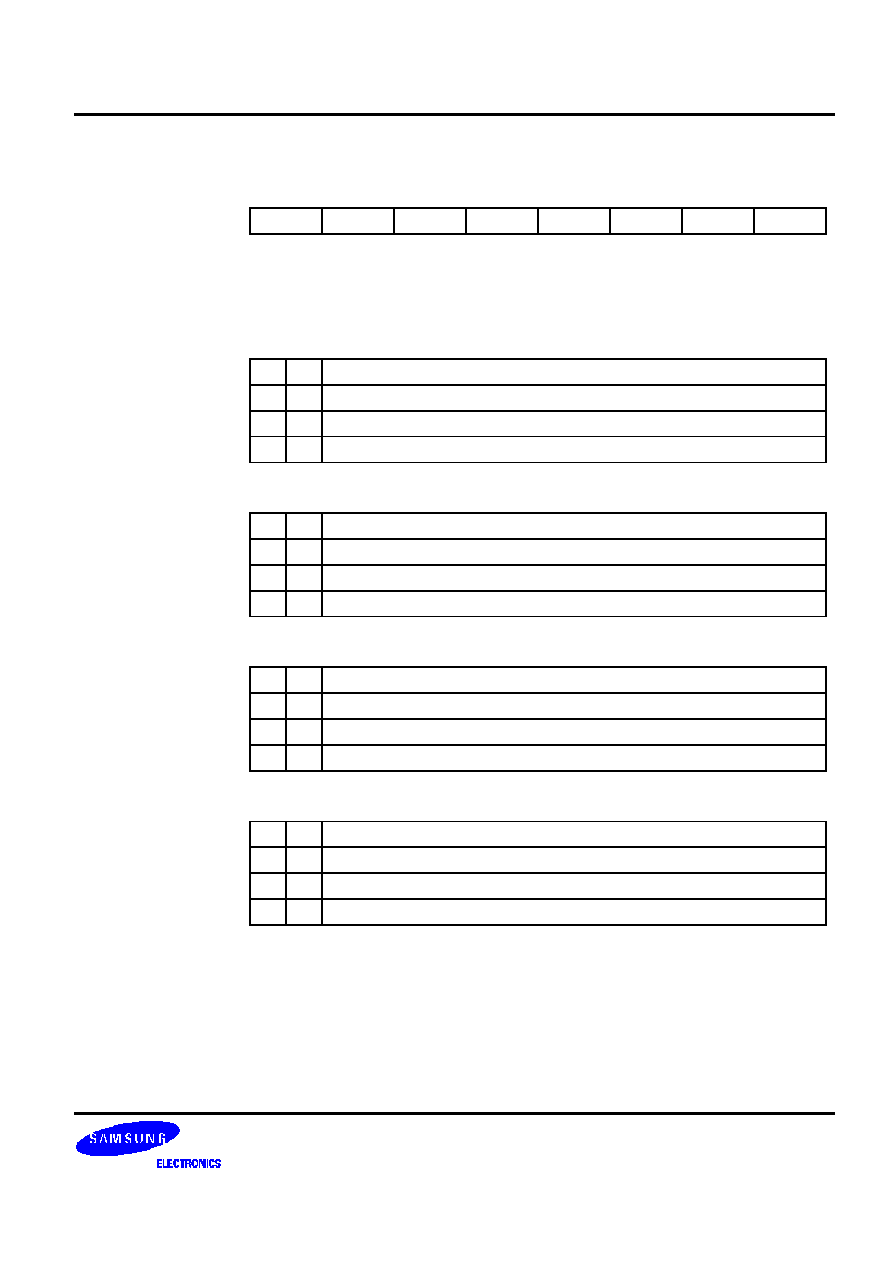
S3C880A/F880A
CONTROL REGISTERS
4-37
P1CONL
-- Port 1 Control Register (Low Byte)
E7H
Set 1, Bank 0
Bit Identifier
.7
.6
.5
.4
.3
.2
.1
.0
nRESET Value
1
1
1
1
1
1
1
1
Read/Write
R/W
R/W
R/W
R/W
R/W
R/W
R/W
R/W
Addressing Mode
Register addressing mode only
.7 and .6
Port 1.3/INT3 Configuration Bits
0
0
Input mode; interrupt disabled
0
1
Input mode; interrupt on rising edge
1
0
Input mode; interrupt on falling edge
1
1
N-channel open-drain output mode (6-volt load capacity)
.5 and .4
Port 1.2/INT2 Configuration Bits
0
0
Input mode; interrupt disabled
0
1
Input mode; interrupt on rising edge
1
0
Input mode; interrupt on falling edge
1
1
N-channel open-drain output mode (6-volt load capacity)
.3 and .2
Port 1.1/INT1 Configuration Bits
0
0
Input mode; interrupt disabled
0
1
Input mode; interrupt on rising edge
1
0
Input mode; interrupt on falling edge
1
1
N-channel open-drain output mode (6-volt load capacity)
.1 and .0
Port 1.0/INT0 Configuration Bits
0
0
Input mode; interrupt disabled
0
1
Input mode; interrupt on rising edge
1
0
Input mode; interrupt on falling edge
1
1
N-channel open-drain output mode (6-volt load capacity)
CONTROL REGISTERS
S3C880A/F880A
4-38
P2CONH
-- Port 2 Control Register (High Byte)
E8H
Set 1, Bank 0
Bit Identifier
.7
.6
.5
.4
.3
.2
.1
.0
nRESET Value
0
0
0
0
0
0
0
0
Read/Write
R/W
R/W
R/W
R/W
R/W
R/W
R/W
R/W
Addressing Mode
Register addressing mode only
.7 and .6
Port 2.7/OSDHT Configuration Bits
0
0
Input mode
0
1
N-channel open-drain output mode (5-volt load capacity)
1
0
Push-pull output mode
1
1
OSD half-tone output mode (push-pull circuit type)
.5 and .4
Port 2.6/T0 Configuration Bits
0
0
Input mode
0
1
N-channel open-drain output mode (5-volt load capacity)
1
0
Push-pull output mode
1
1
Timer 0 output mode (interval or PWM; N-channel open-drain type)
.3 and .2
Port 2.5/PWM0 Configuration Bits
0
0
Input mode
0
1
N-channel open-drain output mode (5-volt load capacity)
1
0
Push-pull output mode
1
1
PWM0 output mode (push-pull circuit type)
.1 and .0
Port 2.4/PWM4 Configuration Bits
0
0
Input mode
0
1
N-channel open-drain output mode (5-volt load capacity)
1
0
Push-pull output mode
1
1
PWM4 output mode (N-channel open-drain type)
S3C880A/F880A
CONTROL REGISTERS
4-39
P2CONL
-- Port 2 Control Register (Low Byte)
E9H
Set 1, Bank 0
Bit Identifier
.7
.6
.5
.4
.3
.2
.1
.0
nRESET Value
0
0
0
0
0
0
0
0
Read/Write
R/W
R/W
R/W
R/W
R/W
R/W
R/W
R/W
Addressing Mode
Register addressing mode only
.7 and .6
Port 2.3/PWM3 Configuration Bits
0
0
Normal input mode
0
1
Normal input mode
1
0
PWM3 output mode; N-channel, open-drain output mode
With 5-volt load capacity
1
1
Push-pull output mode
.5 and .4
Port 2.2/PWM2 Configuration Bits
0
0
Normal input mode
0
1
Normal input mode
1
0
PWM2 output mode; N-channel, open-drain output mode
With 5-volt load capacity
1
1
Push-pull output mode
.3 and .2
Port 2.1/PWM1 Configuration Bits
0
0
Normal input mode
0
1
Normal input mode
1
0
PWM1 output mode; N-channel, open-drain output mode
With 5-volt load capacity
1
1
Push-pull output mode
.1 and .0
Port 2.0/PWM5 Configuration Bits
0
0
Normal input mode
0
1
Normal input mode
1
0
PWM5 output mode; N-channel, open-drain output mode
With 5-volt load capacity
1
1
Push-pull output mode
CONTROL REGISTERS
S3C880A/F880A
4-40
P3CONL
-- Port 3 Control Register (Low Byte)
EBH
Set 1, Bank 0
Bit Identifier
.7
.6
.5
.4
.3
.2
.1
.0
nRESET Value
�
�
�
�
1
1
1
1
Read/Write
�
�
�
�
R/W
R/W
R/W
R/W
Addressing Mode
Register addressing mode only
.7 � .4
No effect
.3 and .2
Port 3.1/ADC1 Configuration Bits
0
0
Input mode
0
1
ADC input mode
1
0
Input mode
1
1
N-channel, open-drain output mode with 5-volt load capacity
.1 and .0
Port 3.0/ADC0 Configuration Bits
0
0
Input mode
0
1
ADC input mode
1
0
Input mode
1
1
N-channel, open-drain output mode with 5-volt load capacity
S3C880A/F880A
CONTROL REGISTERS
4-41
PP
-- Register Page Pointer
DFH
Set 1
Bit Identifier
.7
.6
.5
.4
.3
.2
.1
.0
nRESET Value
0
0
0
0
0
0
0
0
Read/Write
R/W
R/W
R/W
R/W
R/W
R/W
R/W
R/W
Addressing Mode
Register addressing mode only
.7�.4
Destination Register Page Selection Bits
0
0
0
0
Destination: page 0
0
0
0
1
Destination: page 1
0
0
1
0
Destination: page 2
0
0
1
1
Not used for the S3C880A/F880A
� � �
"
1
1
1
1
Not used for the S3C880A/F880A
.3�.0
Source Register Page Selection Bits
0
0
0
0
Source: page 0
0
0
0
1
Source: page 1
0
0
1
0
Source: page 2
0
0
1
1
Not used for the S3C880A/F880A
� � �
"
1
1
1
1
Not used for the S3C880A/F880A
CONTROL REGISTERS
S3C880A/F880A
4-42
PWMCON
-- PWM Control Register
F8H
Set 1, Bank 0
Bit Identifier
.7
.6
.5
.4
.3
.2
.1
.0
nRESET Value
0
0
0
0
0
�
0
0
Read/Write
R/W
R/W
R/W
R/W
R/W
�
R/W
R/W
Addressing Mode
Register addressing mode only
.4, .7, and .6
3-Bit Prescaler Value for PWM Counter Input Clock
0
0
0
Non-divided input clock
0
0
1
Divided-by-two input clock
0
1
0
Divided-by-three input clock
0
1
1
Divided-by-four input clock
1
0
0
Divided-by-five input clock
1
0
1
Divided-by-six input clock
1
1
0
Divided-by-seven input clock
1
1
1
Divided-by-eight input clock
.5
PWM Counter Enable Bit
0
Stop PWM counter operation
1
Start (or resume) PWM counter operation
.3
Capture A Interrupt Enable Bit
0
Disable capture A interrupt
1
Enable capture A interrupt
.2
Not used for the S3C880A/F880A
.1 and .0
Capture A Module Control Bits
0
0
Disable capture A module
0
1
Capture on falling edges only
1
0
Capture on rising edges only
1
1
Capture on both rising and falling edges
S3C880A/F880A
CONTROL REGISTERS
4-43
ROWCON
-- OSD Row Position Control Register
F2H
Set 1, Bank 1
Bit Identifier
.7
.6
.5
.4
.3
.2
.1
.0
nRESET Value
0
0
0
0
0
0
0
0
Read/Write
R/W
R/W
R/W
R/W
R/W
R/W
R/W
R/W
Addressing Mode
Register addressing mode only
.7�.3
Top Margin Display Position Control Value (4 x TMG value of 0�31 dots)
0
0
0
0
0
Top margin position = 0H
0
0
0
0
1
Top margin position = 4H
� � �
� � �
1
1
1
1
1
Top margin position = 124H
.2�.0
Inter-Row Spacing Control Value (0�7H)
0
0
0
No inter-row spacing
0
0
1
Inter-row spacing = 1H
� � �
� � �
1
1
1
Inter-row spacing = 7H
NOTE:
To set top margin and inter-row spacing, separate decimal values must be calculated, converted to their binary
equivalents, and then written to the ROWCON register.
CONTROL REGISTERS
S3C880A/F880A
4-44
RP0
-- Register Pointer 0
D6H
Set 1
Bit Identifier
.7
.6
.5
.4
.3
.2
.1
.0
nRESET Value
1
1
0
0
0
�
�
�
Read/Write
R/W
R/W
R/W
R/W
R/W
�
�
�
Addressing Mode
Register addressing mode only
.7�.3
Register Pointer 0 Address Value
Register pointer 0 can independently point to one of the twenty four 8-byte working
register areas in the register file. Using the register pointers RP0 and RP1, you can
select two 8-byte register slices at one time as active working register space. After a
reset, RP0 points to the address C0H in the register set 1, selecting the 8-byte
working register slice C0H�C7H.
.2�.0
Not used for the S3C880A/F880A
RP1
-- Register Pointer 1
D7H
Set 1
Bit Identifier
.7
.6
.5
.4
.3
.2
.1
.0
nRESET Value
1
1
0
0
1
�
�
�
Read/Write
R/W
R/W
R/W
R/W
R/W
�
�
�
Addressing Mode
Register addressing mode only
.7�.3
Register Pointer 1 Address Value
Register pointer 1 can independently point to one of the twenty four 8-byte working
register areas in the register file. Using the register pointers RP0 and RP1, you can
select two 8-byte register slices at one time as active working register space. After a
reset, RP1 points to the address C8H in the register set 1, selecting the 8-byte
working register slice C8H�CFH.
.2�.0
Not used for the S3C880A/F880A.
S3C880A/F880A
CONTROL REGISTERS
4-45
SPH
-- Stack Pointer (High Byte)
D8H
Set 1
Bit Identifier
.7
.6
.5
.4
.3
.2
.1
.0
nRESET Value
x
x
x
x
x
x
x
x
Read/Write
R/W
R/W
R/W
R/W
R/W
R/W
R/W
R/W
Addressing Mode
Register addressing mode only
.7�.0
Stack Pointer Address (High Byte)
The high-byte stack pointer value is the upper 8 bits of the 16-bit stack pointer address
(SP15�SP8). The lower byte of the stack pointer value is located in the register SPL
(D9H). The SP value is undefined after a reset.
SPL
-- Stack Pointer (Low Byte)
D9H
Set 1
Bit Identifier
.7
.6
.5
.4
.3
.2
.1
.0
nRESET Value
x
x
x
x
x
x
x
x
Read/Write
R/W
R/W
R/W
R/W
R/W
R/W
R/W
R/W
Addressing Mode
Register addressing mode only
.7�.0
Stack Pointer Address (Low Byte)
The low-byte stack pointer value is the lower 8 bits of the 16-bit stack pointer address
(SP7�SP0). The upper byte of the stack pointer value is located in the register SPH
(D8H). The SP value is undefined after a reset.

CONTROL REGISTERS
S3C880A/F880A
4-46
STCON
-- Stop Control Register
F3H
Set 1, Bank 0
Bit Identifier
.7
.6
.5
.4
.3
.2
.1
.0
nRESET Value
0
0
0
0
0
0
0
0
Read/Write
R/W
R/W
R/W
R/W
R/W
R/W
R/W
R/W
Addressing Mode
Register addressing mode only
.7�.0
Stop Condition Enable Bits
Other set value
Stop Condition Disable (Stop instruction is not available)
10100101
Stop Condition Enable (Stop instruction is available)
NOTE: When the Stop control register, STCON, is set by '10100101B', Stop instruction is available.
The other value except '10100101B' make Stop instruction not available. When Stop condition is disabled,
using "stop" instruction make state reset. Once Stop instruction is executed in state of STOP instruction available,
the state is changed to Stop instruction not available.

S3C880A/F880A
CONTROL REGISTERS
4-47
SYM
-- System Mode Register
DEH
Set 1
Bit Identifier
.7
.6
.5
.4
.3
.2
.1
.0
nRESET Value
0
�
�
x
x
x
0
0
Read/Write
R/W
�
�
R/W
R/W
R/W
R/W
R/W
Addressing Mode
Register addressing mode only
.7
Tri-State External Interface Control Bit
(1)
0
Normal operation (disable tri-state operation)
1
Set external interface lines to high impedance (enable tri-state operation)
.6�.5
Not used for the S3C880A/F880A.
.4�.2
Fast Interrupt Level Selection Bits
0
0
0
Level 0 (IRQ0)
0
0
1
Level 1 (IRQ1)
0
1
0
Level 2 (IRQ2)
0
1
1
Level 3 (IRQ3)
1
0
0
Level 4 (IRQ4)
1
0
1
Not used for S3C880A/F880A
1
1
0
Level 6 (IRQ6)
1
1
1
Level 7 (IRQ7)
.1
Fast Interrupt Enable Bit
0
Disable fast interrupt processing
1
Enable fast interrupt processing
.0
Global Interrupt Enable Bit
(2)
0
Disable global interrupt processing
1
Enable global interrupt processing
NOTES:
1.
Because the S3C880A/F880A microcontrollers do not have an external interface, bit 7 should always be "0".
2.
After a reset, the initialization routine must enable global interrupt processing by executing an EI instruction (and not by
writing a "1" to SYM.0).
CONTROL REGISTERS
S3C880A/F880A
4-48
TACON
-- Timer A Control Register
F2H
Set 1, Bank 0
Bit Identifier
.7
.6
.5
.4
.3
.2
.1
.0
nRESET Value
0
0
0
0
0
0
0
�
Read/Write
R/W
R/W
R/W
R/W
R/W
R/W
R/W
�
Addressing Mode
Register addressing mode only
.7�.4
4-Bit Prescaler for Timer A Clock Input
0
0
0
0
Divide input by 1 (non-divided)
0
0
0
1
Divide input by 2
� � �
� � �
1
1
1
1
Divide input by 16
.3
Timer A Clock Source Selection Bit
0
CPU clock divided by 1000
1
Non-divided CPU clock
.2
Timer A Interrupt Enable Bit
0
Disable interrupt
1
Enable interrupt
.1
Timer A Interrupt Pending Bit
0
No interrupt pending (when read)
0
Clear pending bit (when write)
1
Interrupt is pending (when read)
1
No effect (when write)
.0
Not used for the S3C880A/F880A
S3C880A/F880A
CONTROL REGISTERS
4-49
T0CON
-- Timer 0 Control Register
D2H
Set 1
Bit Identifier
.7
.6
.5
.4
.3
.2
.1
.0
nRESET Value
0
0
0
0
0
�
0
0
Read/Write
R/W
R/W
R/W
R/W
R/W
�
R/W
R/W
Addressing Mode
Register addressing mode only
.7 and .6
T0 Input Clock Selection Bits
0
0
f
OSC
/4096
0
1
f
OSC
/256
1
0
f
OSC
/8
1
1
External clock (T0CLK)
.5 and .4
T0 Operating Mode Selection Bits
0
0
Interval mode
0
1
PWM mode
1
0
PWM mode
1
1
PWM mode
.3
T0 Counter Clear Bit
0
No effect
1
Clear the T0 counter (when write)
.2
No effect
.1
T0 Interrupt Enable Bit
0
Disable T0 interrupt
1
Enable T0 interrupt
.0
T0 Interrupt Pending Bit
0
No timer 0 interrupt pending (when read)
0
Clear timer 0 pending bit (when write)
1
Timer 0 interrupt is pending (when read)
1
No effect (when write)
CONTROL REGISTERS
S3C880A/F880A
4-50
VSBCON
-- V-SYNC Blank Control Register
F7H
Set 1, Bank1
Bit Identifier
.7
.6
.5
.4
.3
.2
.1
.0
nRESET Value
�
�
�
0
1
0
0
1
Read/Write
�
�
�
R/W
R/W
R/W
R/W
R/W
Addressing Mode
Register addressing mode only
.7 and .5
Not used for the S3C880A/F880A
.4�.0
V-SYNC Blank Time Control Bits:
0
0
0
0
0
9 Horizontal Sync
� � �
0
1
0
0
1
9 Horizontal Sync
0
1
0
1
0
10 Horizontal Sync
0
1
0
1
1
11 Horizontal Sync
� � �
� � �
1
1
1
1
1
31 Horizontal Sync

S3C880A/F880A
INTERRUPT STRUCTURE
5-1
5
INTERRUPT STRUCTURE
OVERVIEW
The SAM87 interrupt structure has three basic components: levels, vectors, and sources. The CPU recognizes 8
interrupt levels and supports up to 128 interrupt vectors. When a specific interrupt level has more than one vector
address, the vector priorities are established in hardware. Each vector can have one or more interrupt sources.
Levels
Levels provide the highest-level method of interrupt priority assignment and recognition. All peripherals and I/O
blocks can issue interrupt requests. In other words, peripheral and I/O operations are interrupt-driven. There are eight
interrupt levels: IRQ0�IRQ7. Each interrupt level directly corresponds to an interrupt request number (IRQn). The total
number of interrupt levels used in the interrupt structure varies from device to device. For the S3C880A/F880A
microcontrollers, seven levels are recognized: IRQ0�IRQ4, IRQ6, and IRQ7.
The interrupt level numbers 0 through 7 do not necessarily indicate the relative priority of the levels. They are simply
identifiers for the interrupt levels that are recognized by the CPU (IRQ0�IRQ7). The relative priority of different
interrupt levels is determined by settings in the interrupt priority register, IPR. Interrupt logic controlled by the IPR
settings lets you define additional priority relationship for specific interrupt levels.
Vectors
Each interrupt level can have one or more interrupt vectors, or it may have no vector address assigned at all. The
maximum number of vectors that can be supported for a given level is 128. (The actual number of vectors used for
the S3C8-series microcontrollers is always much smaller.) If an interrupt level has more than one vector address, the
vector priorities are set in hardware. The S3C880A/F880A have 9 vectors, one corresponding to each of the 9
possible sources.
Sources
A source is any peripheral that generates an interrupt. A source can be an external pin or a counter overflow, for
example. Each vector can have several interrupt sources. In the S3C880A/F880A interrupt structure, each source
has its own vector address. When a service routine starts, the respective pending bit is either cleared automatically
by hardware or "manually" by the program software. The characteristics of the source's pending mechanism
determine which method is used to clear its pending bit.
INTERRUPT TYPES
The three components of the SAM87 interrupt structure described above -- levels, vectors, and sources -- are
combined to determine the interrupt structure of an individual device and to make full use of its available interrupt
logic. There are three possible combinations of interrupt structure components, called interrupt types 1, 2, and 3.
The types differ in the number of vectors and interrupt sources assigned to each level (see Figure 5-1):
Type 1:
One level (IRQn) + one vector (V
1
) + one source (S
1
)
Type 2:
One level (IRQn) + one vector (V
1
) + multiple sources (S
1
� S
n
)
Type 3:
One level (IRQn) + multiple vectors (V
1
� V
n
) + multiple sources (S
1
� S
n
, S
n+1
� S
n+m
)
In the S3C880A/F880A interrupt structure, only interrupt types 1 and 3 are implemented.
INTERRUPT STRUCTURE
S3C880A/F880A
5-2
VECTORS
SOURCES
LEVELS
S
1
V
1
S
2
Type 2:
IRQn
S
3
S
n
V
1
S
1
V
2
S
2
Type 3:
IRQn
V
3
S
3
V
1
S
1
Type 1:
IRQn
V
n
S
n +
1
S
n
S
n +
2
S
n +
m
NOTES:
1. The number of S
n
and V
n
value is expandable.
2. In the S3F880A implementation,
only interrupt types 1 and 3 are used.
Figure 5-1. S3C8-Series Interrupt Types
S3C880A/F880A INTERRUPT STRUCTURE
The S3C880A/F880A microcontrollers have 9 standard interrupt sources. Nine different vector addresses are used to
support these interrupt sources. Seven of the eight available levels are used for the interrupt structure: IRQ0�IRQ4,
IRQ6, and IRQ7. The device-specific interrupt structure is shown in Figure 5-2.
When multiple interrupt levels are active, the interrupt priority register (IPR) determines the order in which contending
interrupts are to be serviced. If multiple interrupts occur within the same interrupt level, the interrupt with the lowest
vector address is usually processed first. (The relative priorities of multiple interrupts within a single level are
hardwired.)
When an interrupt request is granted, interrupt processing starts: subsequent interrupts are disabled and the
program counter value and status flags are pushed to stack. The starting address of the service routine is fetched
from the appropriate vector address (plus the next 8-bit value to concatenate the full 16-bit address) and the service
routine is executed.
S3C880A/F880A
INTERRUPT STRUCTURE
5-3
0
NOTES:
1. The interrupt level IRQ5 is not used in the S3F880A interrupt structure.
2. For interrupt levels with two or more vectors, the lowest vector address usually has the highest
priority. For example, C0H has higher priority (0) than C2H (1) within the level IRQ1.
These priorities (see numbers) are hardwired.
3. The interrupt names in the 'Identifier' column are used in this documentation to refer to specific
interrupts, as distinguished from the interrupt source name or the pin at which an external
interrupt request arrives.
VECTORS
SOURCES
LEVELS
C0H
P1.0 external interrupt
IRQ1
C2H
P1.1 external interrupt
RESET
H/W
H/W
OSD ROW interrupt
IRQ2
C4H
02H
Capture A (8-bit)
IRQ3
H/W
Timer 0 interrupt (match)
IRQ0
FCH
C6H
P1.2 external interrupt
IRQ4
C8H
P1.3 external interrupt
H/W
H/W
Timer A
IRQ6
BEH
D4H
V-sync
IRQ7
S/W
IDENTIFIER
T0INT
P10INT
CAPA
P12INT
P13INT
VSYNC
P11INT
ROWINT
TAINT
S/W
S/W
S/W
1
0
1
Figure 5-2. S3C880A/F880A Interrupt Structure
INTERRUPT STRUCTURE
S3C880A/F880A
5-4
INTERRUPT VECTOR ADDRESSES
Interrupt vector addresses for the S3C880A/F880A are stored in the first 256 bytes of the ROM. The reset address is
0100H. Vectors for all interrupt levels are stored in the vector address area (0H�FFH). Unused ROM in the range
00H�FFH can be used as program memory locations. You must be careful, however, not to overwrite interrupt vector
addresses stored in this area.
45,151
0
(Decimal)
256
255
Interrupt Vector
Address Area
Addressable
Program Memory
(ROM) Area
100H
FFH
BFFFH
(for S3F880A)
(HEX)
nRESET Address
Figure 5-3. ROM Vector Address Area
S3C880A/F880A
INTERRUPT STRUCTURE
5-5
Table 5-1. S3C880A/F880A Interrupt Vectors
Vector Address
Interrupt Source
Request
Reset/Clear
Decimal
Value
Hex
Value
Interrupt
Level
Priority in
Level
H/W
S/W
252
FCH
Timer 0 (match)
IRQ0
�
212
D4H
V-sync
IRQ7
�
200
C8H
P1.3 external interrupt
IRQ4
1
198
C6H
P1.2 external interrupt
0
196
C4H
OSD ROW interrupt
IRQ2
�
194
C2H
P1.1 external interrupt
IRQ1
1
192
C0H
P1.0 external interrupt
0
190
BEH
Timer A
IRQ6
�
2
02H
Capture A (8-bit)
IRQ3
�
NOTES:
1.
Interrupt priorities are identified in inverse order: '0' is the highest priority, '1' is the next highest, and so on.
2.
If two or more interrupts within the same level contend, the interrupt with the lowest vector address usually has priority
over one with a higher vector address. (The priorities within a level are hardwired) For example, in the interrupt level
IRQ1, the higher-priority interrupt vector is the P1.0 external interrupt, vector C0H; the lower-priority interrupt within that
level is the P1.1 external interrupt, vector C2H.
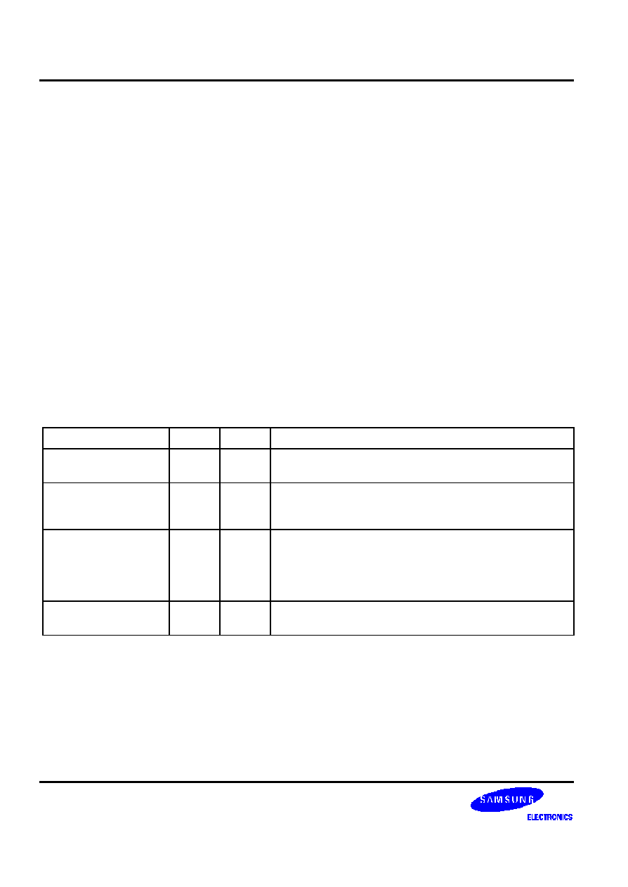
INTERRUPT STRUCTURE
S3C880A/F880A
5-6
ENABLE/DISABLE INTERRUPT INSTRUCTIONS (EI, DI)
The Enable Interrupts (EI) instruction globally enables the interrupt structure. All interrupts are serviced as they
occur, and according to established priorities. The system initialization routine that is executed following a reset
must always contain an EI instruction (assuming one or more interrupts are used in the application).
During the normal operation, you can execute the DI (Disable Interrupt) instruction at any time to globally disable
interrupt processing. The EI and DI instructions change the value of bit 0 in the SYM register. Although you can
manipulate SYM.0 directly to enable or disable interrupts, we recommend that you use the EI and DI instructions
instead.
SYSTEM-LEVEL INTERRUPT CONTROL REGISTERS
In addition to the control registers for specific interrupt sources, four system-level control registers control interrupt
processing:
-- Each interrupt level is enabled or disabled (masked) by bit settings in the interrupt mask register (IMR).
-- Relative priorities of interrupt levels are controlled by the interrupt priority register (IPR).
-- The interrupt request register (IRQ) contains interrupt pending flags for each level.
-- The system mode register (SYM) dynamically enables or disables global interrupt processing. SYM settings
also enable fast interrupts and control external interface, if implemented.
Table 5-2. Interrupt Control Register Overview
Control Register
ID
R/W
Function Description
System mode register
SYM
R/W
Global interrupt processing enable and disable, fast interrupt
processing.
Interrupt mask register
IMR
R/W
Bit settings in the IMR register enable and disable interrupt
processing for each of the seven recognized interrupt levels,
IRQ0�IRQ4, IRQ6, and IRQ7.
Interrupt priority register
IPR
R/W
Controls the relative processing priorities of the interrupt levels.
For the S3C880A/F880A, the seven levels are organized into
three groups: A, B, and C. Group A includes IRQ0 and IRQ1,
group B is IRQ2, IRQ3, and IRQ4, and group C is IRQ6 and
IRQ7.
Interrupt request register
IRQ
R
This register contains a request pending bit for each interrupt
level.
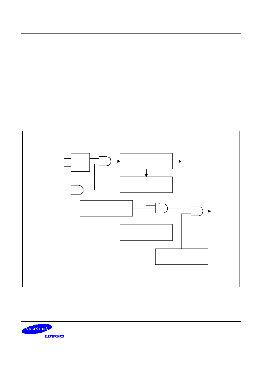
S3C880A/F880A
INTERRUPT STRUCTURE
5-7
INTERRUPT PROCESSING CONTROL POINTS
Interrupt processing can therefore be controlled in two ways: either globally, or by specific interrupt level and source.
The system-level control points in the interrupt structure are therefore:
-- Global interrupt enable and disable (by EI and DI instructions or by direct manipulation of SYM.0 )
-- Interrupt level enable and disable settings (IMR register)
-- Interrupt level priority settings (IPR register)
-- Interrupt source enable and disable settings in the corresponding peripheral control register(s)
NOTE
When writing an interrupt service routine, be sure that it properly manages the register pointer values (RP0
and RP1).
Interrupt Mask
Register
Interrupt Priority
Register
Global Interrupt Control (EI,
DI or SYM.0 manipulation)
Vector
Interrupt
Cycle
Source
Interrupt
Source
Interrupts
Enable
Interrupt Request Register
(Read-only)
S
R
Q
RESET
"EI" Instruction
Execution
Interrupt Pending
Register
Polling Cycle
NOTE: In the S3F880A microcontrollers, only seven
interrupt levels (IRQ0-IRQ4, IRQ6, and IRQ7) are
recognized by the CPU.
Figure 5-4. Interrupt Function Diagram
INTERRUPT STRUCTURE
S3C880A/F880A
5-8
PERIPHERAL INTERRUPT CONTROL REGISTERS
For each interrupt source there is a corresponding peripheral control register (or registers) that controls the interrupts
generated by the peripheral. These registers and their locations are listed in Table 5-3.
Table 5-3. Interrupt Source Control Registers
Interrupt Source
Interrupt Level
Control Register
Register Location
Timer 0 (match)
IRQ0
T0CON
Set 1, D2H
P1.0 external interrupt
IRQ1
P1CONL
Set 1, bank 0, E7H
P1.1 external interrupt
OSD ROW interrupt
IRQ2
HTCON
Set 1, bank 1, E6H
Capture A (8-bit)
IRQ3
PWMCON
Set 1, bank 0, F8H
P1.2 external interrupt
IRQ4
P1CONL
Set 1, bank 0, E7H
P1.3 external interrupt
Timer A
IRQ6
TACON
Set 1, bank 0, F2H
V-sync
IRQ7
HTCON
Set 1, bank 1, F6H
S3C880A/F880A
INTERRUPT STRUCTURE
5-9
SYSTEM MODE REGISTER (SYM)
The system mode register, SYM (DEH, set 1), is used to enable and disable interrupt processing and control fast
interrupt processing.
SYM.0 is the enable and disable bit for global interrupt processing. SYM.1�SYM.4 control fast interrupt processing:
SYM.1 is the enable bit; SYM.2�SYM.4 are the fast interrupt level selection bits. SYM.7 is the enable bit for the tri-
state external memory interface (not implemented in the S3C880A/F880A). A reset clears SYM.0, SYM.1, and
SYM.7 to "0"; other bit values are undetermined.
The instructions EI and DI enable and disable global interrupt processing, respectively, by modifying the bit 0 value of
the SYM register. An Enable Interrupt (EI) instruction must be included in the initialization routine, which follows a
reset operation, in order to enable interrupt processing. Although you can manipulate SYM.0 directly to enable and
disable interrupts during the normal operation, we recommend using the EI and DI instructions for this purpose.
System Mode Register (SYM)
DFH, Set 1, R/W
.7
.6
.5
.4
.3
.2
.1
.0
MSB
LSB
Fast interrupt level
selection bits:
0 0 0
0 0 1
0 1 0
0 1 1
1 0 0
1 0 1
1 1 0
1 1 1
IRQ0
IRQ1
IRQ2
IRQ3
IRQ4
Not used
IRQ6
IRQ7
Global interrupt enable bit:
0 = Disable all interrupts
1 = Enable all interrupts
Fast interrupt enable bit:
0 = Disable fast interrupts
1 = Enable fast interrupts
Not used
External interface tri-state
enable bit:
0 = Normal operation
(Tri-state disabled)
1 = High inpendence
(Tri-state disabled)
NOTE: The external interface is
not implemented for
the S3F880A microcontroller.
Figure 5-5. System Mode Register (SYM)

INTERRUPT STRUCTURE
S3C880A/F880A
5-10
INTERRUPT MASK REGISTER (IMR)
The interrupt mask register (IMR) is used to enable or disable interrupt processing for each of the seven interrupt
levels used in the S3C880A/F880A interrupt structure, IRQ0�IRQ4, IRQ6, and IRQ7. After a reset, all the IMR
register values are undetermined.
Each IMR bit corresponds to a specific interrupt level: bit 1 to IRQ1, bit 2 to IRQ2, and so on. When the IMR bit of an
interrupt level is cleared to "0", interrupt processing for that level is disabled (masked). When you set a level's IMR
bit to "1", interrupt processing for the level is enabled (not masked).
The IMR register is mapped to the register location DDH in set 1. Bit values can be read and written by instructions
using Register addressing mode.
Interrupt Mask Register (IMR)
DDH, Set 1, R/W
.7
.6
.5
.4
.3
.2
.1
.0
MSB
LSB
IRQ1
IRQ3
IRQ4
Not
used
IRQ6
IRQ7
IRQ0
Interrupt level enable bits:
0 = Disable interrupt level
1 = Enable interrupt level
IRQ2
Figure 5-6. Interrupt Mask Register (IMR)
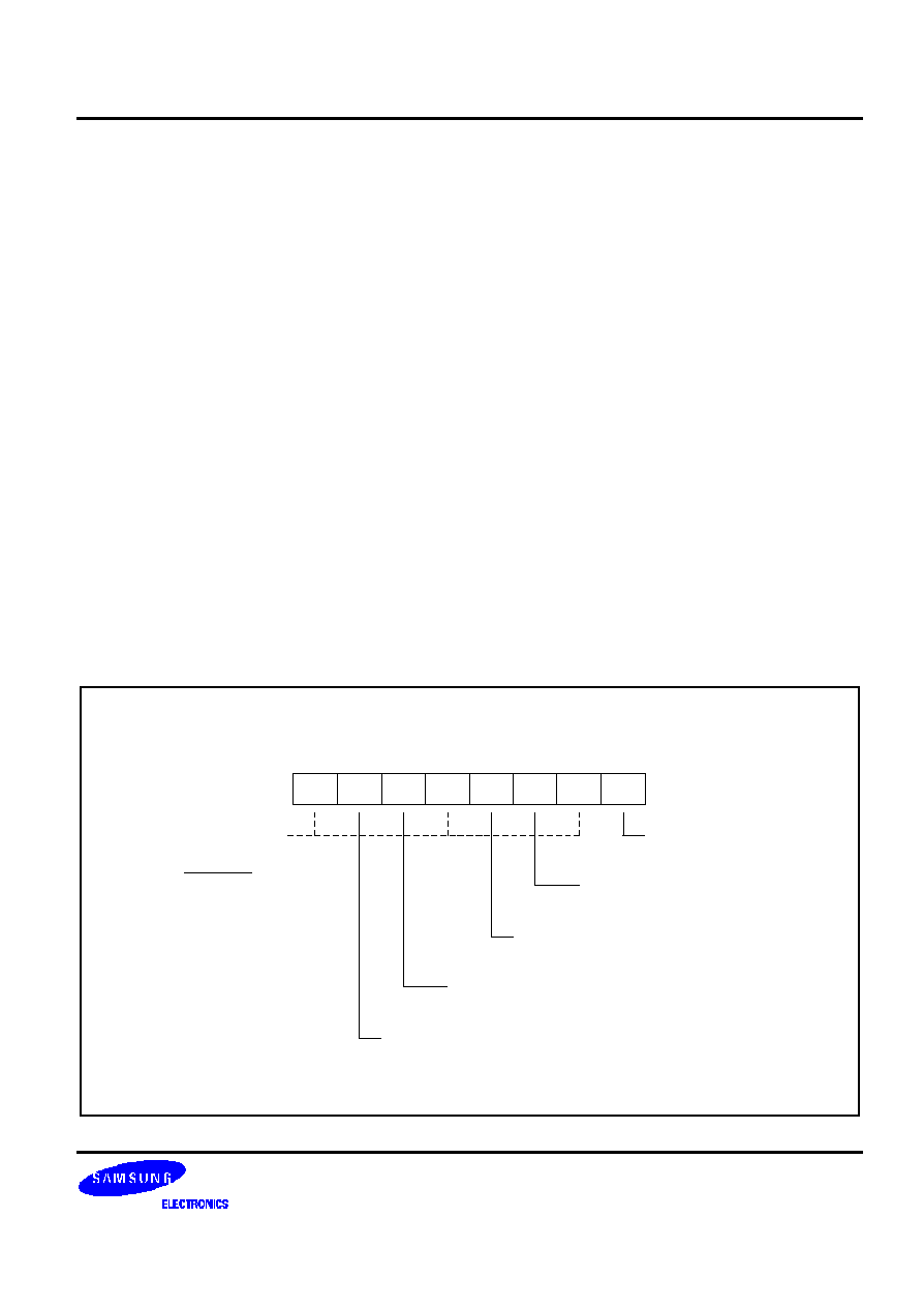
S3C880A/F880A
INTERRUPT STRUCTURE
5-11
INTERRUPT PRIORITY REGISTER (IPR)
The interrupt priority register, IPR, is used to set the relative priorities of the seven interrupt levels used in the
S3C880A/F880A interrupt structure. The IPR register is mapped to the register location FFH in set 1, bank 0. After a
reset, the IPR register values are undetermined. If more than one interrupt source is active, the source with the
highest priority level is serviced first. If both sources belong to the same interrupt level, the source with the lowest
vector address usually has priority. (This priority is hardwired.)
In order to define the relative priorities of interrupt levels, they are organized into groups and subgroups by the
interrupt logic. Three interrupt groups are defined for the IPR logic (see Figure 5-7). These groups and subgroups are
used only for IPR register priority definitions:
Group A
IRQ0, IRQ1
Group B
IRQ2, IRQ3, and IRQ4
Group C
IRQ6, IRQ7
Bits 7, 4, and 1 of the IPR register control the relative priority of interrupt groups A, B, and C. For example, the
setting '001B' would select the group relationship B > C > A, and '101B' would select C > B > A. The functions of
other IPR bit settings are as follows:
-- IPR.0 controls the relative priority setting of IRQ0 and IRQ1 interrupts.
-- IPR.2 controls interrupt group B.
-- Interrupt group B has a subgroup to provide an additional priority relationship among interrupt levels 2, 3, and 4.
IPR.3 defines possible subgroup B relationship.
-- IPR.6 controls the relative priorities of group C interrupts.
Interrupt Priority Register (IPR)
FEH, Set 1, R/W
.7
.6
.5
.4
.3
.2
.1
.0
MSB
LSB
Group A
0 = IRQ0 > IRQ1
1 = IRQ1 > IRQ0
Subgroup B
0 = IRQ3 > IRQ4
1 = IRQ4 > IRQ3
Not used
Group C
0 = IRQ6 > IRQ7
1 = IRQ7 > IRQ6
Group B
0 = IRQ2 > (IRQ3, IRQ4)
1 = (IRQ3, IRQ4) > IRQ2
Group priority:
0 0 0
0 0 1
0 1 0
0 1 1
1 0 0
1 0 1
1 1 0
1 1 1
= Undefined
= B > C > A
= A > B > C
= B > A > C
= C > A > B
= C > B > A
= A > C > B
= Undefined
D7 D4 D1
Figure 5-7. Interrupt Priority Register (IPR)
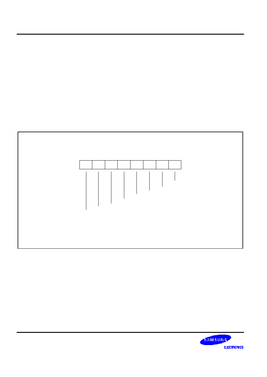
INTERRUPT STRUCTURE
S3C880A/F880A
5-12
INTERRUPT REQUEST REGISTER (IRQ)
Bit values in the interrupt request register, IRQ, are polled to determine interrupt request status for the seven
interrupt levels in the S3C880A/F880A interrupt structure (IRQ0�IRQ4, IRQ6, and IRQ7). Each bit corresponds to the
interrupt level of the same number: bit 0 to IRQ0, bit 1 to IRQ1, and so on. A "0" indicates that no interrupt is
requested and a "1" indicates that an interrupt is requested for that level.
The IRQ register is mapped to the register location DCH in set 1. IRQ bit values are read-only addressable using
Register addressing mode. You can read (test) the contents of the IRQ register at any time using bit or byte
addressing to determine the current interrupt request status of specific interrupt levels. After a reset, the IRQ register
is cleared to 00H.
IRQ register values can be polled even if a DI instruction has been executed. If an interrupt occurs while the interrupt
structure is disabled, it will not be serviced. But the interrupt request can still be detected by polling IRQ values. This
can be useful in order to determine which events occurred while the interrupt structure was disabled.
Interrupt Request Register (IRQ)
DCH, Set 1, Read-only
.7
.6
.5
.4
.3
.2
.1
.0
MSB
LSB
IRQ1
IRQ2
IRQ3
IRQ4
Not used for the S3F880A.
IRQ6
IRQ7
IRQ0
Interrupt level request pending bits:
0 = Interrupt level is not pending
1 = Interrupt level is pending
Figure 5-8. Interrupt Request Register (IRQ)

S3C880A/F880A
INTERRUPT STRUCTURE
5-13
INTERRUPT PENDING FUNCTION TYPES
Overview
There are two types of interrupt pending bits: one is the type that automatically cleared by hardware after the
interrupt service routine is acknowledged and executed; the other is the one that must be cleared by the application
program's interrupt service routine.
Each interrupt level has a corresponding interrupt request bit in the IRQ register that the CPU polls for interrupt
requests.
Pending Bits Cleared Automatically by Hardware
For interrupt pending bits that are cleared automatically by hardware, interrupt logic sets the corresponding pending
bit to "1" when a request occurs. It then issues an IRQ pulse to tell the CPU that an interrupt is waiting to be
serviced. The CPU acknowledges the interrupt source, executes the service routine, and clears the pending bit to
"0". This type of pending bit is not mapped and cannot, therefore, be read or written by software.
In the S3C880A/F880A interrupt structure, the P1.0, P1.1, P1.2 and P1.3 external interrupts, and the capture A
interrupt belong to this category of interrupts whose pending conditions are cleared automatically by hardware.
Pending Bits Cleared by the Service Routine
The second type of pending bit must be cleared by program software. The service routine must clear the appropriate
pending bit before a return-from-interrupt subroutine (IRET) occurs. To do this, a "0" must be written to the pending
bit location in the corresponding mode or control register.
Pending conditions for the timer 0 match interrupt, the timer A interrupt, the OSD row interrupt and the V-sync
interrupt must be cleared by the application's service routines.

INTERRUPT STRUCTURE
S3C880A/F880A
5-14
INTERRUPT SOURCE POLLING SEQUENCE
The interrupt request polling and servicing sequence is as follows:
1. A source generates an interrupt request by setting the interrupt request bit to "1".
2. The CPU polling procedure identifies a pending condition for that source.
3. The CPU checks the source's interrupt level.
4. The CPU generates an interrupt acknowledge signal.
5. Interrupt logic determines the interrupt's vector address.
6. The service routine starts and the source's pending flag is cleared to "0" (either by hardware or by software).
7. The CPU continues polling for interrupt requests.
INTERRUPT SERVICE ROUTINES
Before an interrupt request is serviced, the following conditions must be met:
-- Interrupt processing must be enabled (EI, SYM.0 = "1")
-- Interrupt level must be enabled (IMR register)
-- Interrupt level must have the highest priority if more than one level is currently requesting service
-- Interrupt must be enabled at the interrupt's source (peripheral control register)
If all the above conditions are met, the interrupt request is acknowledged at the end of the instruction cycle. The
CPU then initiates an interrupt machine cycle that completes the following processing sequence:
1. Reset (clear to "0") the interrupt enable bit in the SYM register (SYM.0) to disable all subsequent interrupts.
2. Save the program counter and status flags to stack.
3. Branch to the interrupt vector to fetch the service routine's address.
4. Pass control to the interrupt service routine.
When the interrupt service routine is completed, an Interrupt Return instruction (IRET) occurs. The IRET restores the
PC and status flags and sets SYM.0 to "1", allowing the CPU to process the next interrupt request.

S3C880A/F880A
INTERRUPT STRUCTURE
5-15
GENERATING INTERRUPT VECTOR ADDRESSES
The interrupt vector area in the ROM contains the addresses of the interrupt service routine that corresponds to each
level in the interrupt structure. Vectored interrupt processing follows this sequence:
1. Push the program counter's low-byte value to stack.
2. Push the program counter's high-byte value to stack.
3. Push the FLAGS register values to stack.
4. Fetch the service routine's high-byte address from the vector address.
5. Fetch the service routine's low-byte address from the vector address.
6. Branch to the service routine specified by the 16-bit vector address.
NOTE
A 16-bit vector address always begins at an even-numbered ROM location from 00H�FFH.
NESTING OF VECTORED INTERRUPTS
You can nest a higher priority interrupt request while a lower priority request is being serviced. To do this, you must
follow these steps:
1. Push the current 8-bit interrupt mask register (IMR) value to the stack (PUSH IMR).
2. Load the IMR register with a new mask to enable the higher priority interrupt only.
3. Execute an EI instruction to enable interrupt processing (a higher priority interrupt will be processed if it occurs).
4. When the lower-priority interrupt service routine ends, return the IMR to its original value by restoring the
previous mask from the stack (POP IMR).
5. Execute an IRET.
Depending on the application, you may be able to simplify this procedure to some extent.
INSTRUCTION POINTER (IP)
The instruction pointer (IP) is used by all the S3C8-series microcontrollers to control optional high-speed interrupt
processing called fast interrupts. The IP consists of the register pair, DAH and DBH. The IP register names are IPH
(high byte, IP15�IP8) and IPL (low byte, IP7�IP0).

INTERRUPT STRUCTURE
S3C880A/F880A
5-16
FAST INTERRUPT PROCESSING
The feature called fast interrupt processing lets designated interrupts be completed in approximately six clock
cycles instead of the usual 22 clock cycles. Bit 1 of the system mode register, SYM.1, enables fast interrupt
processing while SYM.2�SYM.4 are used to select a specific level for fast processing.
Two other system registers support fast interrupts:
-- The instruction pointer (IP) holds the starting address of the service routine (and is later used to swap the
program counter values), and
-- When a fast interrupt occurs, the contents of the FLAGS register is stored in an unmapped, dedicated register
called FLAGS' (FLAGS prime).
NOTE
For the S3C880A/F880A microcontrollers, the service routine for any one of the seven interrupt levels (IRQ0�
IRQ4, IRQ6, or IRQ7) can be designated as a fast interrupt.
Procedure for Initiating Fast Interrupts
To initiate fast interrupt processing, follow these steps:
1. Load the start address of the service routine into the instruction pointer.
2. Load the level number into the fast interrupt select field.
3. Write a "1" to the fast interrupt enable bit in the SYM register.
Fast Interrupt Service Routine
When an interrupt occurs in the level selected for fast interrupt processing, the following events occur:
1. The contents of the instruction pointer and the PC are swapped.
2. The FLAGS register values are written to the dedicated FLAGS' register.
3. The fast interrupt status bit in the FLAGS register is set.
4. The interrupt is serviced.
5. Assuming that the fast interrupt status bit is set, when the fast interrupt service routine ends, the instruction
pointer and PC values are swapped back.
6. The content of FLAGS' (FLAGS prime) is copied automatically back into the FLAGS register.
7. The fast interrupt status bit in FLAGS is cleared automatically.
Programming Guidelines
Remember that the only way to enable or disable a fast interrupt is to set or clear the fast interrupt enable bit in the
SYM register (SYM.1), respectively. Executing an EI or DI instruction affects only normal interrupt processing.
Also, if you use fast interrupts, remember to load the IP with a new start address when the fast interrupt service
routine ends. (Please refer to the programming tip on page 5�17 for an example.)

S3C880A/F880A
INTERRUPT STRUCTURE
5-17
F
PROGRAMMING TIP -- Programming Level IRQ0 as a Fast Interrupt
This example shows you how to program fast interrupt processing for a select interrupt level -- in this case, for the
timer 0 (capture) interrupt, INT0:
�
�
�
LD
T0CON,#52H
; Enable T0 interrupt
; Select f
OSC
/256 as T0 clock source
LDW
IPH,#T0_INT
; IPH
high byte of interrupt service routine
; IPL
low byte of interrupt service routine
LD
SYM,#02H
; Enable fast interrupt processing
; Select IRQ0 for fast service
EI
; Enable interrupts
�
�
�
FAST_RET:
; IP
Address of T0_INT (again)
T0_INT:
�
�
�
(Fast service routine executes)
�
�
�
LD
T0CON,#52H
; Clear T0INT interrupt pending bit
JP
T,FAST_RET

INTERRUPT STRUCTURE
S3C880A/F880A
5-18
NOTES

S3C880A/F880A
SAM8 INSTRUCTION SET
6-1
6
SAM8 INSTRUCTION SET
OVERVIEW
The SAM8 instruction set is designed to support a large register file. It includes a full complement of 8-bit arithmetic
and logic operations, including multiplying and dividing. There are 78 instructions. No special I/O instructions are
necessary because I/O control and data registers are mapped directly into the register file. Decimal adjustment is
included in binary-coded decimal (BCD) operations. 16-bit word data can be incremented and decremented. Flexible
instructions for bit addressing, rotate, and shift operations complete the powerful data manipulation capabilities of
the SAM8 instruction set.
DATA TYPES
The SAM8 CPU performs operations on bits, bytes, BCD digits, and two-byte words. Bits in the register file can be
set, cleared, complemented, and tested. Bits within a byte are numbered from 7 to 0, where bit 0 is the least
significant (right-most) bit.
REGISTER ADDRESSING
To access an individual register, an 8-bit address in the range 0�255 or the 4-bit address of a working register is
specified. Paired registers can be used to construct 16-bit data or 16-bit program memory or data memory
addresses. For detailed information about register addressing, please refer to Chapter 2, "Address Spaces."
ADDRESSING MODES
There are seven addressing modes: Register (R), Indirect Register (IR), Indexed (X), Direct (DA), Relative (RA),
Immediate (IM), and Indirect (IA). For detailed descriptions of these addressing modes, please refer to chapter 3,
"Addressing Modes."

SAM8 INSTRUCTION SET
S3C880A/F880A
6-2
Table 6-1. Instruction Group Summary
Mnemonic
Operands
Instruction
Load Instructions
CLR
dst
Clear
LD
dst,src
Load
LDB
dst,src
Load bit
LDE
dst,src
Load external data memory
LDC
dst,src
Load program memory
LDED
dst,src
Load external data memory and decrement
LDCD
dst,src
Load program memory and decrement
LDEI
dst,src
Load external data memory and increment
LDCI
dst,src
Load program memory and increment
LDEPD
dst,src
Load external data memory with pre-decrement
LDCPD
dst,src
Load program memory with pre-decrement
LDEPI
dst,src
Load external data memory with pre-increment
LDCPI
dst,src
Load program memory with pre-increment
LDW
dst,src
Load word
POP
dst
Pop from stack
POPUD
dst,src
Pop user stack (decrementing)
POPUI
dst,src
Pop user stack (incrementing)
PUSH
src
Push to stack
PUSHUD
dst,src
Push user stack (decrementing)
PUSHUI
dst,src
Push user stack (incrementing)

S3C880A/F880A
SAM8 INSTRUCTION SET
6-3
Table 6-1. Instruction Group Summary (Continued)
Mnemonic
Operands
Instruction
Arithmetic Instructions
ADC
dst,src
Add with carry
ADD
dst,src
Add
CP
dst,src
Compare
DA
dst
Decimal adjust
DEC
dst
Decrement
DECW
dst
Decrement word
DIV
dst,src
Divide
INC
dst
Increment
INCW
dst
Increment word
MULT
dst,src
Multiply
SBC
dst,src
Subtract with carry
SUB
dst,src
Subtract
Logic Instructions
AND
dst,src
Logical AND
COM
dst
Complement
OR
dst,src
Logical OR
XOR
dst,src
Logical exclusive OR

SAM8 INSTRUCTION SET
S3C880A/F880A
6-4
Table 6-1. Instruction Group Summary (Continued)
Mnemonic
Operands
Instruction
Program Control Instructions
BTJRF
dst,src
Bit test and jump relative on false
BTJRT
dst,src
Bit test and jump relative on true
CALL
dst
Call procedure
CPIJE
dst,src
Compare, increment and jump on equal
CPIJNE
dst,src
Compare, increment and jump on non-equal
DJNZ
r,dst
Decrement register and jump on non-zero
ENTER
Enter
EXIT
Exit
IRET
Interrupt return
JP
cc,dst
Jump on condition code
JP
dst
Jump unconditional
JR
cc,dst
Jump relative on condition code
NEXT
Next
RET
Return
WFI
Wait for interrupt
Bit Manipulation Instructions
BAND
dst,src
Bit AND
BCP
dst,src
Bit compare
BITC
dst
Bit complement
BITR
dst
Bit reset
BITS
dst
Bit set
BOR
dst,src
Bit OR
BXOR
dst,src
Bit XOR
TCM
dst,src
Test complement under mask
TM
dst,src
Test under mask

S3C880A/F880A
SAM8 INSTRUCTION SET
6-5
Table 6-1. Instruction Group Summary (Concluded)
Mnemonic
Operands
Instruction
Rotate and Shift Instructions
RL
dst
Rotate left
RLC
dst
Rotate left through carry
RR
dst
Rotate right
RRC
dst
Rotate right through carry
SRA
dst
Shift right arithmetic
SWAP
dst
Swap nibbles
CPU Control Instructions
CCF
Complement carry flag
DI
Disable interrupts
EI
Enable interrupts
IDLE
Enter Idle mode
NOP
No operation
RCF
Reset carry flag
SB0
Set bank 0
SB1
Set bank 1
SCF
Set carry flag
SRP
src
Set register pointers
SRP0
src
Set register pointer 0
SRP1
src
Set register pointer 1
STOP
Enter Stop mode
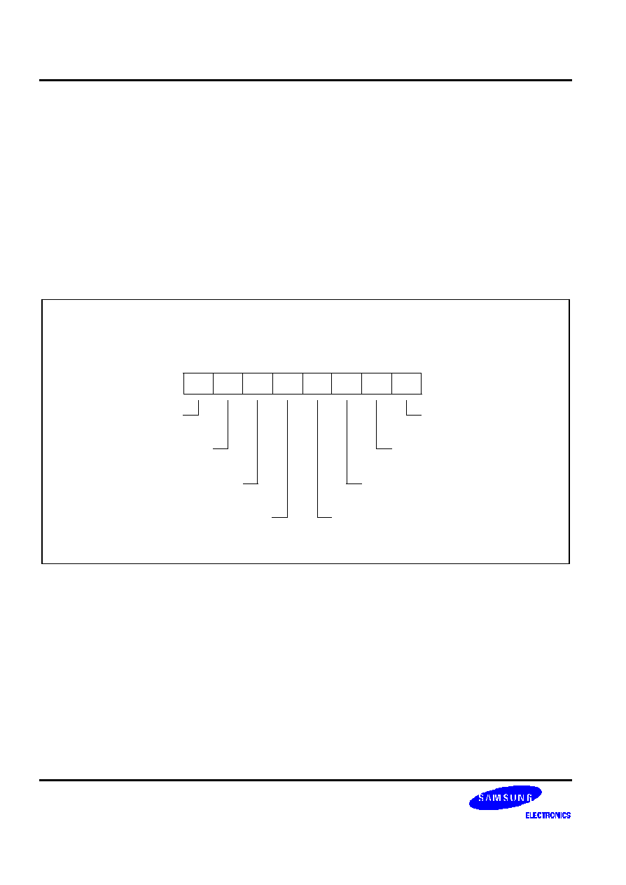
SAM8 INSTRUCTION SET
S3C880A/F880A
6-6
FLAGS REGISTER (FLAGS)
The flags register FLAGS contains eight bits that describe the current status of the CPU operations. Four of these
bits, FLAGS.4 � FLAGS.7, can be tested and used with conditional jump instructions; two others FLAGS.2 and
FLAGS.3 are used for BCD arithmetic. The FLAGS register also contains a bit to indicate the status of fast interrupt
processing (FLAGS.1) and a bank address status bit (FLAGS.0) to indicate whether bank 0 or bank 1 is being
addressed.
FLAGS is located in the system control register area of set 1 (D5H). FLAGS register can be set or reset by
instructions as long as its outcome does not affect the flags, such as, Load instruction. Logical and Arithmetic
instructions such as, AND, OR, XOR, ADD, and SUB can affect the Flags register. For example, the AND
instruction updates the Zero, Sign and Overflow flags based on the outcome of the AND instruction. If the AND
instruction uses the Flags register as the destination, then simultaneously, two writes will occur to the Flags
register, producing an unpredictable result.
System Flags Register (FLAGS)
D5H, Set 1, R/W
.7
.6
.5
.4
.3
.2
.1
.0
MSB
LSB
Bank address
status flag (BA)
First interrupt
status flag (FIS)
Half-carry flag (H)
Decimal adjust flag (D)
Overflow (V)
Sign flag (S)
Zero flag (Z)
Carry flag (C)
Figure 6-1. System Flags Register (FLAGS)

S3C880A/F880A
SAM8 INSTRUCTION SET
6-7
FLAG DESCRIPTIONS
C
Carry Flag (FLAGS.7)
The C flag is set to "1" if the result from an arithmetic operation generates a carry-out from or a borrow to the
bit 7 position (MSB). After rotate and shift operations, it contains the last value shifted out of the specified
register. Program instructions can set, clear, or complement the carry flag.
Z
Zero Flag (FLAGS.6)
For arithmetic and logic operations, the Z flag is set to "1" if the result of the operation is zero. For
operations that test register bits, and for shift and rotate operations, the Z flag is set to "1" if the result is
logic zero.
S
Sign Flag (FLAGS.5)
Following arithmetic, logic, rotate, or shift operations, the sign bit identifies the state of the MSB of the
result. A logic zero indicates a positive number and a logic one indicates a negative number.
V
Overflow Flag (FLAGS.4)
The V flag is set to "1" when the result of a two's-complement operation is greater than + 127 or less than �
128. It is also cleared to "0" following logic operations.
D
Decimal Adjust Flag (FLAGS.3)
The DA bit is used to specify what type of instruction was executed last during BCD operations, so that a
subsequent decimal adjust operation can execute correctly. The DA bit is not usually accessed by
programmers, and cannot be used as a test condition.
H
Half-Carry Flag (FLAGS.2)
The H bit is set to "1" whenever an addition generates a carry-out of bit 3, or when a subtraction borrows out
of bit 4. It is used by the Decimal Adjust (DA) instruction to convert the binary result of a previous addition or
subtraction into the correct decimal (BCD) result. The H flag is seldom accessed directly by a program.
FIS
Fast Interrupt Status Flag (FLAGS.1)
The FIS bit is set during a fast interrupt cycle and reset during the IRET following interrupt servicing. When
set, it inhibits all interrupts and causes the fast interrupt return to be executed when the IRET instruction is
executed.
BA
Bank Address Flag (FLAGS.0)
The BA flag indicates which register bank in the set 1 area of the internal register file is currently selected,
bank 0 or bank 1. The BA flag is cleared to "0" (select bank 0) when you execute the SB0 instruction and is
set to "1" (select bank 1) when you execute the SB1 instruction.

SAM8 INSTRUCTION SET
S3C880A/F880A
6-8
INSTRUCTION SET NOTATION
Table 6-2. Flag Notation Conventions
Flag
Description
C
Carry flag
Z
Zero flag
S
Sign flag
V
Overflow flag
D
Decimal-adjust flag
H
Half-carry flag
0
Cleared to logic zero
1
Set to logic one
*
Set or cleared according to operation
�
Value is unaffected
x
Value is undefined
Table 6-3. Instruction Set Symbols
Symbol
Description
dst
Destination operand
src
Source operand
@
Indirect register address prefix
PC
Program counter
IP
Instruction pointer
FLAGS
Flags register (D5H)
RP
Register pointer
#
Immediate operand or register address prefix
H
Hexadecimal number suffix
D
Decimal number suffix
B
Binary number suffix
opc
Opcode
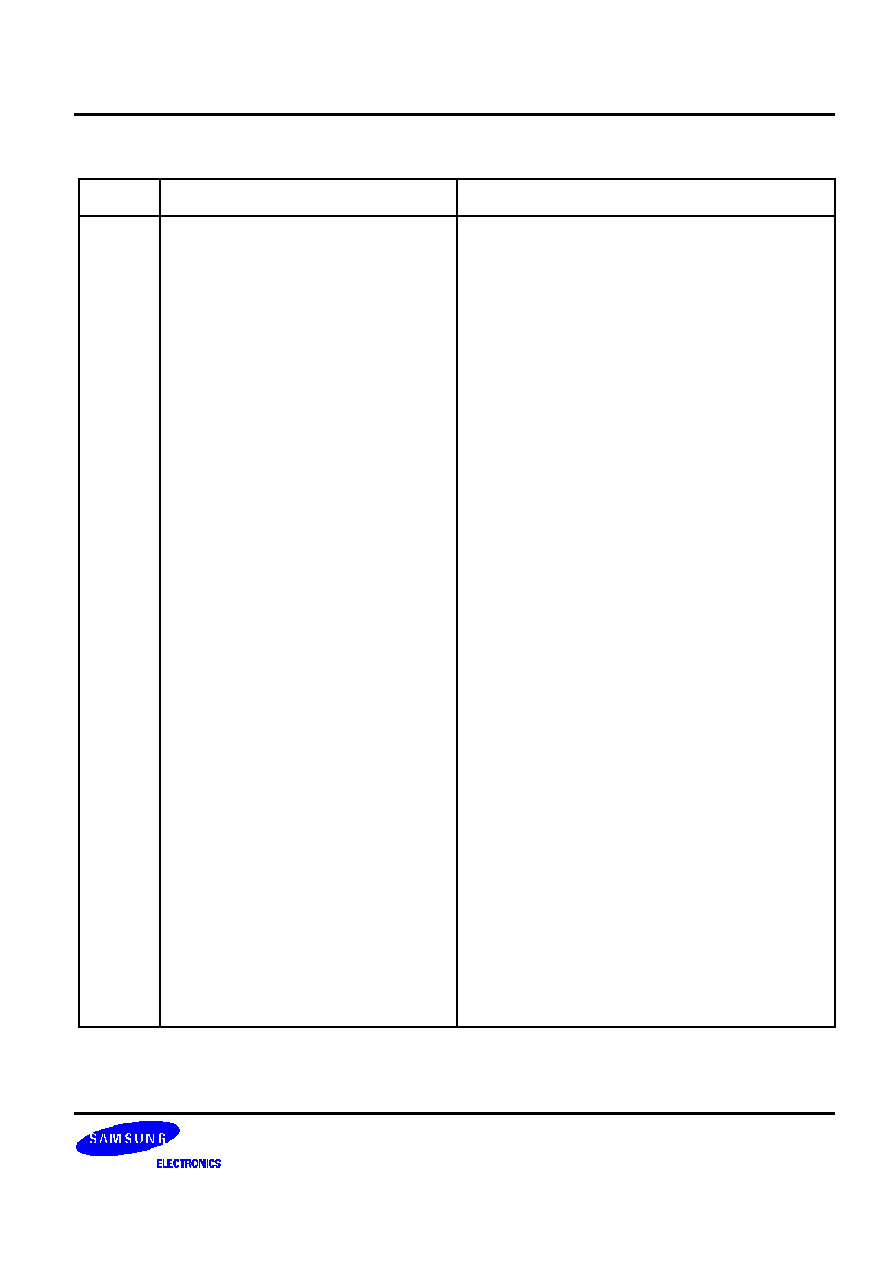
S3C880A/F880A
SAM8 INSTRUCTION SET
6-9
Table 6-4. Instruction Notation Conventions
Notation
Description
Actual Operand Range
cc
Condition code
See list of condition codes in Table 6-6.
r
Working register only
Rn (n = 0�15)
rb
Bit (b) of working register
Rn.b (n = 0�15, b = 0�7)
r0
Bit 0 (LSB) of working register
Rn (n = 0�15)
rr
Working register pair
RRp (p = 0, 2, 4, ..., 14)
R
Register or working register
reg or Rn (reg = 0�255, n = 0�15)
Rb
Bit 'b' of register or working register
reg.b (reg = 0�255, b = 0�7)
RR
Register pair or working register pair
reg or RRp (reg = 0�254, even number only, where
p = 0, 2, ..., 14)
IA
Indirect addressing mode
addr (addr = 0�254, even number only)
Ir
Indirect working register only
@Rn (n = 0�15)
IR
Indirect register or indirect working register
@Rn or @reg (reg = 0�255, n = 0�15)
Irr
Indirect working register pair only
@RRp (p = 0, 2, ..., 14)
IRR
Indirect register pair or indirect working
register pair
@RRp or @reg (reg = 0�254, even only, where
p = 0, 2, ..., 14)
X
Indexed addressing mode
#reg[Rn] (reg = 0�255, n = 0�15)
XS
Indexed (short offset) addressing mode
#addr[RRp] (addr = range �128 to +127, where
p = 0, 2, ..., 14)
XL
Indexed (long offset) addressing mode
#addr [RRp] (addr = range 0�65535, where
p = 0, 2, ..., 14)
DA
Direct addressing mode
addr (addr = range 0�65535)
RA
Relative addressing mode
addr (addr = number in the range +127 to �128 that is
an offset relative to the address of the next instruction)
IM
Immediate addressing mode
#data (data = 0�255)
IML
Immediate (long) addressing mode
#data (data = range 0�65535)

SAM8 INSTRUCTION SET
S3C880A/F880A
6-10
Table 6-5. Opcode Quick Reference
OPCODE MAP
LOWER NIBBLE (HEX)
--
0
1
2
3
4
5
6
7
U
0
DEC
R1
DEC
IR1
ADD
r1,r2
ADD
r1,Ir2
ADD
R2,R1
ADD
IR2,R1
ADD
R1,IM
BOR
r0�Rb
P
1
RLC
R1
RLC
IR1
ADC
r1,r2
ADC
r1,Ir2
ADC
R2,R1
ADC
IR2,R1
ADC
R1,IM
BCP
r1.b, R2
P
2
INC
R1
INC
IR1
SUB
r1,r2
SUB
r1,Ir2
SUB
R2,R1
SUB
IR2,R1
SUB
R1,IM
BXOR
r0�Rb
E
3
JP
IRR1
SRP/0/1
IM
SBC
r1,r2
SBC
r1,Ir2
SBC
R2,R1
SBC
IR2,R1
SBC
R1,IM
BTJR
r2.b, RA
R
4
DA
R1
DA
IR1
OR
r1,r2
OR
r1,Ir2
OR
R2,R1
OR
IR2,R1
OR
R1,IM
LDB
r0�Rb
5
POP
R1
POP
IR1
AND
r1,r2
AND
r1,Ir2
AND
R2,R1
AND
IR2,R1
AND
R1,IM
BITC
r1.b
N
6
COM
R1
COM
IR1
TCM
r1,r2
TCM
r1,Ir2
TCM
R2,R1
TCM
IR2,R1
TCM
R1,IM
BAND
r0�Rb
I
7
PUSH
R2
PUSH
IR2
TM
r1,r2
TM
r1,Ir2
TM
R2,R1
TM
IR2,R1
TM
R1,IM
BIT
r1.b
B
8
DECW
RR1
DECW
IR1
PUSHUD
IR1,R2
PUSHUI
IR1,R2
MULT
R2,RR1
MULT
IR2,RR1
MULT
IM,RR1
LD
r1, x, r2
B
9
RL
R1
RL
IR1
POPUD
IR2,R1
POPUI
IR2,R1
DIV
R2,RR1
DIV
IR2,RR1
DIV
IM,RR1
LD
r2, x, r1
L
A
INCW
RR1
INCW
IR1
CP
r1,r2
CP
r1,Ir2
CP
R2,R1
CP
IR2,R1
CP
R1,IM
LDC
r1, Irr2, xL
E
B
CLR
R1
CLR
IR1
XOR
r1,r2
XOR
r1,Ir2
XOR
R2,R1
XOR
IR2,R1
XOR
R1,IM
LDC
r2, Irr2, xL
C
RRC
R1
RRC
IR1
CPIJE
Ir,r2,RA
LDC
r1,Irr2
LDW
RR2,RR1
LDW
IR2,RR1
LDW
RR1,IML
LD
r1, Ir2
H
D
SRA
R1
SRA
IR1
CPIJNE
Irr,r2,RA
LDC
r2,Irr1
CALL
IA1
LD
IR1,IM
LD
Ir1, r2
E
E
RR
R1
RR
IR1
LDCD
r1,Irr2
LDCI
r1,Irr2
LD
R2,R1
LD
IR2,R1
LD
R1,IM
LDC
r1, Irr2, xs
X
F
SWAP
R1
SWAP
IR1
LDCPD
r2,Irr1
LDCPI
r2,Irr1
CALL
IRR1
LD
R2,IR1
CALL
DA1
LDC
r2, Irr1, xs

S3C880A/F880A
SAM8 INSTRUCTION SET
6-11
Table 6-5. Opcode Quick Reference (Continued)
OPCODE MAP
LOWER NIBBLE (HEX)
--
8
9
A
B
C
D
E
F
U
0
LD
r1,R2
LD
r2,R1
DJNZ
r1,RA
JR
cc,RA
LD
r1,IM
JP
cc,DA
INC
r1
NEXT
P
1
ENTER
P
2
EXIT
E
3
WFI
R
4
SB0
5
SB1
N
6
IDLE
I
7
STOP
B
8
DI
B
9
EI
L
A
RET
E
B
IRET
C
RCF
H
D
SCF
E
E
CCF
X
F
LD
r1,R2
LD
r2,R1
DJNZ
r1,RA
JR
cc,RA
LD
r1,IM
JP
cc,DA
INC
r1
NOP

SAM8 INSTRUCTION SET
S3C880A/F880A
6-12
CONDITION CODES
The opcode of a conditional jump always contains a 4-bit field called the condition code (cc). This specifies under
which conditions it is to execute the jump. For example, a conditional jump with the condition code for "equal" after
a compare operation only jumps if the two operands are equal. Condition codes are listed in Table 6-6.
The carry (C), zero (Z), sign (S), and overflow (V) flags are used to control the operation of conditional jump
instructions.
Table 6-6. Condition Codes
Binary
Mnemonic
Description
Flags Set
0000
F
Always false
�
1000
T
Always true
�
0111
(1)
C
Carry
C = 1
1111
(1)
NC
No carry
C = 0
0110
(1)
Z
Zero
Z = 1
1110
(1)
NZ
Not zero
Z = 0
1101
PL
Plus
S = 0
0101
MI
Minus
S = 1
0100
OV
Overflow
V = 1
1100
NOV
No overflow
V = 0
0110
(1)
EQ
Equal
Z = 1
1110
(1)
NE
Not equal
Z = 0
1001
GE
Greater than or equal
(S XOR V) = 0
0001
LT
Less than
(S XOR V) = 1
1010
GT
Greater than
(Z OR (S XOR V)) = 0
0010
LE
Less than or equal
(Z OR (S XOR V)) = 1
1111
(1)
UGE
Unsigned greater than or equal
C = 0
0111
(1)
ULT
Unsigned less than
C = 1
1011
UGT
Unsigned greater than
(C = 0 AND Z = 0) = 1
0011
ULE
Unsigned less than or equal
(C OR Z) = 1
NOTES:
1.
It indicates condition codes that are related to two different mnemonics but which test the same flag. For
example, Z and EQ are both true if the zero flag (Z) is set, but after an ADD instruction, Z would probably be used;
after a CP instruction, however, EQ would probably be used.
2.
For operations involving unsigned numbers, the special condition codes UGE, ULT, UGT, and ULE must be used.

S3C880A/F880A
SAM8 INSTRUCTION SET
6-13
INSTRUCTION DESCRIPTIONS
This chapter contains detailed information and programming examples for each instruction in the SAM8 instruction
set. Information is arranged in a consistent format for improved readability and fast referencing. The following
information is included in each instruction description:
--
Instruction name (mnemonic)
--
Full instruction name
--
Source/destination format of the instruction operand
--
Shorthand notation of the instruction's operation
--
Textual description of the instruction's effect
--
Specific flag settings affected by the instruction
--
Detailed description of the instruction's format, execution time, and addressing mode(s)
--
Programming example(s) explaining how to use the instruction
SAM8 INSTRUCTION SET
S3C880A/F880A
6-14
ADC
-- Add with Carry
ADC
dst,src
Operation:
dst
dst + src + c
The source operand, along with the setting of the carry flag, is added to the destination operand and
the sum is stored in the destination. The contents of the source are unaffected. Two's-complement
addition is performed. In multiple precision arithmetic, this instruction permits the carry from the
addition of low-order operands to be carried into the addition of high-order operands.
Flags:
C: Set if there is a carry from the most significant bit of the result; cleared otherwise.
Z: Set if the result is "0"; cleared otherwise.
S: Set if the result is negative; cleared otherwise.
V: Set if arithmetic overflow occurs, that is, if both operands are of the same sign and the result is
of the opposite sign; cleared otherwise.
D: Always cleared to "0".
H: Set if there is a carry from the most significant bit of the low-order four bits of the result; cleared
otherwise.
Format:
Bytes
Cycles
Opcode
(Hex)
Addr Mode
dst src
opc
dst | src
2
6
12
r
r
13
r
lr
opc
src
dst
3
10
14
R
R
15
R
IR
opc
dst
src
3
10
16
R
IM
Examples:
Given: R1 = 10H, R2 = 03H, C flag = "1", register 01H = 20H, register 02H = 03H, and
register 03H = 0AH:
ADC
R1,R2
R1 = 14H, R2 = 03H
ADC
R1,@R2
R1 = 1BH, R2 = 03H
ADC
01H,02H
Register 01H = 24H, register 02H = 03H
ADC
01H,@02H
Register 01H = 2BH, register 02H = 03H
ADC
01H,#11H
Register 01H = 32H
In the first example, the destination register R1 contains the value 10H, the carry flag is set to "1",
and the source working register R2 contains the value 03H. The statement "ADC R1,R2" adds 03H
and the carry flag value ("1") to the destination value 10H, leaving 14H in the register R1.

S3C880A/F880A
SAM8 INSTRUCTION SET
6-15
ADD
--
Add
ADD
dst,src
Operation:
dst
dst + src
The source operand is added to the destination operand and the sum is stored in the destination.
The contents of the source are unaffected. Two's-complement addition is performed.
Flags:
C: Set if there is a carry from the most significant bit of the result; cleared otherwise.
Z: Set if the result is "0"; cleared otherwise.
S: Set if the result is negative; cleared otherwise.
V: Set if arithmetic overflow occurred, that is, if both operands are of the same sign and the result
is of the opposite sign; cleared otherwise.
D: Always cleared to "0".
H: Set if a carry from the low-order nibble occurred.
Format:
Bytes
Cycles
Opcode
(Hex)
Addr Mode
dst src
opc
dst | src
2
6
02
r
r
03
r
lr
opc
src
dst
3
10
04
R
R
05
R
IR
opc
dst
src
3
10
06
R
IM
Examples:
Given: R1 = 12H, R2 = 03H, register 01H = 21H, register 02H = 03H, register 03H = 0AH:
ADD
R1,R2
R1 = 15H, R2 = 03H
ADD
R1,@R2
R1 = 1CH, R2 = 03H
ADD
01H,02H
Register 01H = 24H, register 02H = 03H
ADD
01H,@02H
Register 01H = 2BH, register 02H = 03H
ADD
01H,#25H
Register 01H = 46H
In the first example, the destination working register R1 contains 12H and the source working
register R2 contains 03H. The statement "ADD R1,R2" adds 03H to 12H, leaving the value 15H in
the register R1.
SAM8 INSTRUCTION SET
S3C880A/F880A
6-16
AND
-- Logical AND
AND
dst,src
Operation:
dst
dst AND src
The source operand is logically ANDed with the destination operand. The result is stored in the
destination. The AND operation results in a "1" bit being stored whenever the corresponding bits in
the two operands are both logic ones; otherwise a "0" bit value is stored. The contents of the source
are unaffected.
Flags:
C: Unaffected.
Z: Set if the result is "0"; cleared otherwise.
S: Set if the result bit 7 is set; cleared otherwise.
V: Always cleared to "0".
D: Unaffected.
H: Unaffected.
Format:
Bytes
Cycles
Opcode
(Hex)
Addr Mode
dst src
opc
dst | src
2
6
52
r
r
53
r
lr
opc
src
dst
3
10
54
R
R
55
R
IR
opc
dst
src
3
10
56
R
IM
Examples:
Given: R1 = 12H, R2 = 03H, register 01H = 21H, register 02H = 03H, register 03H = 0AH:
AND
R1,R2
R1 = 02H, R2 = 03H
AND
R1,@R2
R1 = 02H, R2 = 03H
AND
01H,02H
Register 01H = 01H, register 02H = 03H
AND
01H,@02H
Register 01H = 00H, register 02H = 03H
AND
01H,#25H
Register 01H = 21H
In the first example, the destination working register R1 contains the value 12H and the source
working register R2 contains 03H. The statement "AND R1,R2" logically ANDs the source operand
03H with the destination operand value 12H, leaving the value 02H in the register R1.

S3C880A/F880A
SAM8 INSTRUCTION SET
6-17
BAND
� Bit AND
BAND
dst,src.b
BAND
dst.b,src
Operation:
dst(0)
dst(0) AND src(b)
or
dst(b)
dst(b) AND src(0)
The specified bit of the source (or the destination) is logically ANDed with the zero bit (LSB) of the
destination (or source). The resultant bit is stored in the specified bit of the destination. No other
bits of the destination are affected. The source is unaffected.
Flags:
C: Unaffected.
Z: Set if the result is "0"; cleared otherwise.
S: Cleared to "0".
V: Undefined.
D: Unaffected.
H: Unaffected.
Format:
Bytes
Cycles
Opcode
(Hex)
Addr Mode
dst src
opc
dst | b | 0
src
3
10
67
r0
Rb
opc
src | b | 1
dst
3
10
67
Rb
r0
NOTE:
In the second byte of the 3-byte instruction formats, the destination (or source) address is four
bits, the bit address 'b' is three bits, and the LSB address value is one bit in length.
Examples:
Given: R1 = 07H and register 01H = 05H:
BAND
R1,01H.1
R1 = 05H, register 01H = 05H
BAND
01H.1,R1
Register 01H = 05H, R1 = 07H
In the first example, the source register 01H contains the value 05H (00000101B) and the
destination working register R1 contains 07H (00000111B). The statement "BAND R1,01H.1" ANDs
the bit 1 value of the source register ("0") with the bit 0 value of the register R1 (destination), leaving
the value 0525H (00000101B) in the register R1.

SAM8 INSTRUCTION SET
S3C880A/F880A
6-18
BCP
� Bit Compare
BCP
dst,src.b
Operation:
dst(0) � src(b)
The specified bit of the source is compared to (subtracted from) bit zero (LSB) of the destination.
The zero flag is set if the bits are the same; otherwise it is cleared. The contents of both operands
are unaffected by the comparison.
Flags:
C: Unaffected.
Z: Set if the two bits are the same; cleared otherwise.
S: Cleared to "0".
V: Undefined.
D: Unaffected.
H: Unaffected.
Format:
Bytes
Cycles
Opcode
(Hex)
Addr Mode
dst src
opc
dst | b | 0
src
3
10
17
r0
Rb
NOTE:
In the second byte of the instruction format, the destination address is four bits, the bit address 'b'
is three bits, and the LSB address value is one bit in length.
Example:
Given: R1 = 07H and register 01H = 01H:
BCP
R1,01H.1
R1 = 07H, register 01H = 01H
If the destination working register R1 contains the value 07H (00000111B) and the source register
01H contains the value 01H (00000001B), the statement "BCP R1,01H.1" compares bit one of the
source register (01H) and bit zero of the destination register (R1). Because the bit values are not
identical, the zero flag bit (Z) is cleared in the FLAGS register (0D5H).

S3C880A/F880A
SAM8 INSTRUCTION SET
6-19
BITC
� Bit Complement
BITC
dst.b
Operation:
dst(b)
NOT dst(b)
This instruction complements the specified bit within the destination without affecting any other bit
in the destination.
Flags:
C: Unaffected.
Z: Set if the result is "0"; cleared otherwise.
S: Cleared to "0".
V: Undefined.
D: Unaffected.
H: Unaffected.
Format:
Bytes
Cycles
Opcode
(Hex)
Addr Mode
dst
opc
dst | b | 0
2
8
57
rb
NOTE:
In the second byte of the instruction format, the destination address is four bits, the bit address 'b'
is three bits, and the LSB address value is one bit in length.
Example:
Given: R1 = 07H
BITC
R1.1
R1 = 05H
If the working register R1 contains the value 07H (00000111B), the statement "BITC R1.1"
complements bit one of the destination, leaving the value 05H (00000101B) in the register R1.
Because the result of the complement is not "0", the zero flag (Z) in the FLAGS register (0D5H) is
cleared.

SAM8 INSTRUCTION SET
S3C880A/F880A
6-20
BITR
� Bit Reset
BITR
dst.b
Operation:
dst(b)
0
The BITR instruction clears the specified bit within the destination without affecting any other bit in
the destination.
Flags:
No flags are affected.
Format:
Bytes
Cycles
Opcode
(Hex)
Addr Mode
dst
opc
dst | b | 0
2
8
77
rb
NOTE:
In the second byte of the instruction format, the destination address is four bits, the bit address 'b'
is three bits, and the LSB address value is one bit in length.
Example:
Given: R1 = 07H:
BITR
R1.1
R1 = 05H
If the value of the working register R1 is 07H (00000111B), the statement "BITR R1.1" clears bit
one of the destination register R1, leaving the value 05H (00000101B).

S3C880A/F880A
SAM8 INSTRUCTION SET
6-21
BITS
� Bit Set
BITS
dst.b
Operation:
dst(b)
1
The BITS instruction sets the specified bit within the destination without affecting any other bit in the
destination.
Flags:
No flags are affected.
Format:
Bytes
Cycles
Opcode
(Hex)
Addr Mode
dst
opc
dst | b | 1
2
8
77
rb
NOTE:
In the second byte of the instruction format, the destination address is four bits, the bit address 'b'
is three bits, and the LSB address value is one bit in length.
Example:
Given: R1 = 07H:
BITS
R1.3
R1 = 0FH
If the working register R1 contains the value 07H (00000111B), the statement "BITS R1.3" sets bit
three of the destination register R1 to "1", leaving the value 0FH (00001111B).
SAM8 INSTRUCTION SET
S3C880A/F880A
6-22
BOR
� Bit OR
BOR
dst,src.b
BOR
dst.b,src
Operation:
dst(0)
dst(0) OR src(b)
or
dst(b)
dst(b) OR src(0)
The specified bit of the source (or destination) is logically ORed with bit zero (LSB) of the
destination (or source). The resulting bit value is stored in the specified bit of the destination. No
other bits of the destination are affected. The source is unaffected.
Flags:
C: Unaffected.
Z: Set if the result is "0"; cleared otherwise.
S: Cleared to "0".
V: Undefined.
D: Unaffected.
H: Unaffected.
Format:
Bytes
Cycles
Opcode
(Hex)
Addr Mode
dst src
opc
dst | b | 0
src
3
10
07
r0
Rb
opc
src | b | 1
dst
3
10
07
Rb
r0
NOTE:
In the second byte of the 3-byte instruction formats, the destination (or source) address is four
bits, the bit address 'b' is three bits, and the LSB address value is one bit.
Examples:
Given: R1 = 07H and register 01H = 03H:
BOR
R1, 01H.1
R1 = 07H, register 01H = 03H
BOR
01H.2, R1
Register 01H = 07H, R1 = 07H
In the first example, the destination working register R1 contains the value 07H (00000111B) and
the source register 01H the value 03H (00000011B). The statement "BOR R1,01H.1" logically ORs
bit one of the register 01H (source) with bit zero of R1 (destination). This leaves the same value
(07H) in the working register R1.
In the second example, the destination register 01H contains the value 03H (00000011B) and the
source working register R1 the value 07H (00000111B). The statement "BOR 01H.2,R1" logically
ORs bit two of the register 01H (destination) with bit zero of R1 (source). This leaves the value 07H
in the register 01H.

S3C880A/F880A
SAM8 INSTRUCTION SET
6-23
BTJRF
� Bit Test, Jump Relative on False
BTJRF
dst,src.b
Operation:
If src(b) is a "0", then PC
PC + dst
The specified bit within the source operand is tested. If it is a "0", the relative address is added to
the program counter and control passes to the statement whose address is now in the PC;
otherwise, the instruction following the BTJRF instruction is executed.
Flags:
No flags are affected.
Format:
(1)
Bytes
Cycles
Opcode
(Hex)
Addr Mode
dst src
opc
src | b | 0
dst
3
16/18
(2)
37
RA
rb
NOTES:
1.
In the second byte of the instruction format, the source address is four bits, the bit address 'b' is three
bits, and the LSB address value is one bit in length.
2.
Execution time is 18 cycles if the jump is taken or 16 cycles if it is not taken.
Example:
Given: R1 = 07H:
BTJRF
SKIP,R1.3
PC jumps to SKIP location
If the working register R1 contains the value 07H (00000111B), the statement "BTJRF SKIP,R1.3"
tests bit 3. Because it is "0", the relative address is added to the PC and the PC jumps to the
memory location pointed to by the SKIP. (Remember that the memory location must be within the
allowed range of + 127 to � 128.)

SAM8 INSTRUCTION SET
S3C880A/F880A
6-24
BTJRT
� Bit Test, Jump Relative on True
BTJRT
dst,src.b
Operation:
If src(b) is a "1", then PC
PC + dst
The specified bit within the source operand is tested. If it is a "1", the relative address is added to
the program counter and control passes to the statement whose address is now in the PC;
otherwise, the instruction following the BTJRT instruction is executed.
Flags:
No flags are affected.
Format:
(1)
Bytes
Cycles
Opcode
(Hex)
Addr Mode
dst src
opc
src | b | 1
dst
3
16/18
(2)
37
RA
rb
NOTES:
1.
In the second byte of the instruction format, the source address is four bits, the bit address 'b' is three
bits, and the LSB address value is one bit in length.
2.
Execution time is 18 cycles if the jump is taken or 16 cycles if it is not taken.
Example:
Given: R1 = 07H:
BTJRT
SKIP,R1.1
If the working register R1 contains the value 07H (00000111B), the statement "BTJRT SKIP,R1.1"
tests bit one in the source register (R1). Because it is a "1", the relative address is added to the PC
and the PC jumps to the memory location pointed to by the SKIP. (Remember that the memory
location must be within the allowed range of + 127 to � 128.)

S3C880A/F880A
SAM8 INSTRUCTION SET
6-25
BXOR
� Bit XOR
BXOR
dst,src.b
BXOR
dst.b,src
Operation:
dst(0)
dst(0) XOR src(b)
or
dst(b)
dst(b) XOR src(0)
The specified bit of the source (or destination) is logically exclusive-ORed with bit zero (LSB) of the
destination (or source). The result bit is stored in the specified bit of the destination. No other bits of
the destination are affected. The source is unaffected.
Flags:
C: Unaffected.
Z: Set if the result is "0"; cleared otherwise.
S: Cleared to "0".
V: Undefined.
D: Unaffected.
H: Unaffected.
Format:
Bytes
Cycles
Opcode
(Hex)
Addr Mode
dst src
opc
dst | b | 0
src
3
10
27
r0
Rb
opc
src | b | 1
dst
3
10
27
Rb
r0
NOTE:
In the second byte of the 3-byte instruction format, the destination (or source) address is four bits,
the bit address 'b' is three bits, and the LSB address value is one bit in length.
Examples:
Given: R1 = 07H (00000111B) and register 01H = 03H (00000011B):
BXOR
R1,01H.1
R1 = 05H, register 01H = 03H
BXOR
01H.2,R1
Register 01H = 07H, R1 = 07H
In the first example, the destination working register R1 has the value 07H (00000111B) and the
source register 01H has the value 03H (00000011B). The statement "BXOR R1,01H.1" exclusive-
ORs bit one of the register 01H (source) with bit zero of R1 (destination). The result bit value is
stored in bit zero of R1, changing its value from 07H to 05H. The value of the source register 01H is
unaffected.

SAM8 INSTRUCTION SET
S3C880A/F880A
6-26
CALL
� Call Procedure
CALL
dst
Operation:
SP
SP � 1
@SP
PCL
SP
SP �1
@SP
PCH
PC
dst
The current contents of the program counter are pushed onto the top of the stack. The program
counter value used is the address of the first instruction following the CALL instruction. The
specified destination address is then loaded into the program counter and points to the first
instruction of a procedure. At the end of the procedure the return instruction (RET) can be used to
return to the original program flow. RET pops the top of the stack back into the program counter.
Flags:
No flags are affected.
Format:
Bytes
Cycles
Opcode
(Hex)
Addr Mode
dst
opc
dst
3
18
F6
DA
opc
dst
2
18
F4
IRR
opc
dst
2
20
D4
IA
Examples:
Given: R0 = 35H, R1 = 21H, PC = 1A47H, and SP = 0002H:
CALL
3521H
SP = 0000H
(Memory locations 0000H = 1AH, 0001H = 4AH, where
4AH is the address that follows the instruction.)
CALL
@RR0
SP = 0000H (0000H = 1AH, 0001H = 49H)
CALL
#40H
SP = 0000H (0000H = 1AH, 0001H = 49H)
In the first example, if the program counter value is 1A47H and the stack pointer contains the value
0002H, the statement "CALL 3521H" pushes the current PC value onto the top of the stack. The
stack pointer now points to the memory location 0000H. The PC is then loaded with the value
3521H, the address of the first instruction in the program sequence to be executed.
If the contents of the program counter and stack pointer are the same as in the first example, the
statement "CALL @RR0" produces the same result except that 49H is stored in stack location
0001H (because the two-byte instruction format was used). The PC is then loaded with the value
3521H, the address of the first instruction in the program sequence to be executed. Assuming that
the contents of the program counter and stack pointer are the same as in the first example, if the
program address 0040H contains 35H and the program address 0041H contains 21H, the statement
"CALL #40H" produces the same result as in the second example.

S3C880A/F880A
SAM8 INSTRUCTION SET
6-27
CCF
� Complement Carry Flag
CCF
Operation:
C
NOT C
The carry flag (C) is complemented. If C = "1", the value of the carry flag is changed to logic zero;
if C = "0", the value of the carry flag is changed to logic one.
Flags:
C: Complemented.
No other flags are affected.
Format:
Bytes
Cycles
Opcode
(Hex)
opc
1
6
EF
Example:
Given: The carry flag = "0":
CCF
If the carry flag = "0", the CCF instruction complements it in the FLAGS register (0D5H), changing
its value from logic zero to logic one.

SAM8 INSTRUCTION SET
S3C880A/F880A
6-28
CLR
� Clear
CLR
dst
Operation:
dst
dst XOR dst
The destination location is cleared to "0".
Flags:
No flags are affected.
Format:
Bytes
Cycles
Opcode
(Hex)
Addr Mode
dst
opc
dst
2
6
B0
R
B1
IR
Examples:
Given: Register 00H = 4FH, register 01H = 02H, and register 02H = 5EH:
CLR
00H
Register 00H = 00H
CLR
@01H
Register 01H = 02H, register 02H = 00H
In Register (R) addressing mode, the statement "CLR 00H" clears the destination register 00H
value to 00H. In the second example, the statement "CLR @01H" uses Indirect Register (IR)
addressing mode to clear the 02H register value to 00H.

S3C880A/F880A
SAM8 INSTRUCTION SET
6-29
COM
� Complement
COM
dst
Operation:
dst
NOT dst
The contents of the destination location are complemented (one's complement); all "1s" are
changed to "0s", and vice-versa.
Flags:
C: Unaffected.
Z: Set if the result is "0"; cleared otherwise.
S: Set if the result bit 7 is set; cleared otherwise.
V: Always reset to "0".
D: Unaffected.
H: Unaffected.
Format:
Bytes
Cycles
Opcode
(Hex)
Addr Mode
dst
opc
dst
2
6
60
R
61
IR
Examples:
Given: R1 = 07H and register 07H = 0F1H:
COM
R1
R1 = 0F8H
COM
@R1
R1 = 07H, register 07H = 0EH
In the first example, the destination working register R1 contains the value 07H (00000111B). The
statement "COM R1" complements all the bits in R1: all logic ones are changed to logic zeros, and
vice-versa, leaving the value 0F8H (11111000B).
In the second example, Indirect Register (IR) addressing mode is used to complement the value of
the destination register 07H (11110001B), leaving the new value 0EH (00001110B).
SAM8 INSTRUCTION SET
S3C880A/F880A
6-30
CP
� Compare
CP
dst,src
Operation:
dst � src
The source operand is compared to (subtracted from) the destination operand, and the appropriate
flags are set accordingly. The contents of both operands are unaffected by the comparison.
Flags:
C: Set if a "borrow" occurred (src > dst); cleared otherwise.
Z: Set if the result is "0"; cleared otherwise.
S: Set if the result is negative; cleared otherwise.
V: Set if arithmetic overflow occurred; cleared otherwise.
D: Unaffected.
H: Unaffected.
Format:
Bytes
Cycles
Opcode
(Hex)
Addr Mode
dst src
opc
dst | src
2
6
A2
r
r
A3
r
lr
opc
src
dst
3
10
A4
R
R
A5
R
IR
opc
dst
src
3
10
A6
R
IM
Examples:
1. Given: R1 = 02H and R2 = 03H:
CP R1,R2
Set the C and S flags
The destination working register R1 contains the value 02H and the source register R2 contains the
value 03H. The statement "CP R1,R2" subtracts the R2 value (source/subtrahend) from the R1
value (destination/minuend). Because a "borrow" occurs and the difference is negative, C and S are
"1".
2. Given: R1 = 05H and R2 = 0AH:
CP
R1,R2
JP
UGE,SKIP
INC
R1
SKIP
LD
R3,R1
In this example, the destination working register R1 contains the value 05H which is less than the
contents of the source working register R2 (0AH). The statement "CP R1,R2" generates C = "1"
and the JP instruction does not jump to the SKIP location. After the statement "LD R3,R1"
executes, the value 06H remains in the working register R3.

S3C880A/F880A
SAM8 INSTRUCTION SET
6-31
CPIJE
� Compare, Increment, and Jump on Equal
CPIJE
dst,src,RA
Operation:
If dst � src = "0", PC
PC + RA
Ir
Ir + 1
The source operand is compared to (subtracted from) the destination operand. If the result is "0",
the relative address is added to the program counter and control passes to the statement whose
address is now in the program counter. Otherwise, the instruction immediately following the CPIJE
instruction is executed. In either case, the source pointer is incremented by one before the next
instruction is executed.
Flags:
No flags are affected.
Format:
Bytes
Cycles
Opcode
(Hex)
Addr Mode
dst src
opc
src
dst
RA
3
16/18
C2
r
Ir
NOTE: Execution time is 18 cycles if the jump is taken or 16 cycles if it is not taken.
Example:
Given: R1 = 02H, R2 = 03H, and register 03H = 02H:
CPIJE
R1,@R2,SKIP
R2 = 04H, PC jumps to SKIP location
In this example, the working register R1 contains the value 02H, the working register R2 the value
03H, and the register 03H contains 02H. The statement "CPIJE R1,@R2,SKIP" compares the @R2
value 02H (00000010B) to 02H (00000010B). Because the result of the comparison is equal, the
relative address is added to the PC and the PC then jumps to the memory location pointed to by
SKIP. The source register (R2) is incremented by one, leaving a value of 04H. (Remember that the
memory location must be within the allowed range of + 127 to � 128.)

SAM8 INSTRUCTION SET
S3C880A/F880A
6-32
CPIJNE
� Compare, Increment, and Jump on Non-Equal
CPIJNE
dst,src,RA
Operation:
If dst � src
"0", PC
PC + RA
Ir
Ir + 1
The source operand is compared to (subtracted from) the destination operand. If the result is not
"0", the relative address is added to the program counter and control passes to the statement
whose address is now in the program counter; otherwise the instruction following the CPIJNE
instruction is executed. In either case the source pointer is incremented by one before the next
instruction.
Flags:
No flags are affected.
Format:
Bytes
Cycles
Opcode
(Hex)
Addr Mode
dst src
opc
src
dst
RA
3
16/18
D2
r
Ir
NOTE: Execution time is 18 cycles if the jump is taken or 16 cycles if it is not taken.
Example:
Given: R1 = 02H, R2 = 03H, and register 03H = 04H:
CPIJNE
R1,@R2,SKIP
R2 = 04H, PC jumps to SKIP location
The working register R1 contains the value 02H, the working register R2 (the source pointer) the
value 03H, and the general register 03H contains the value 04H. The statement "CPIJNE
R1,@R2,SKIP" subtracts 04H (00000100B) from 02H (00000010B). Because the result of the
comparison is non-equal, the relative address is added to the PC and the PC then jumps to the
memory location pointed to by SKIP. The source pointer register (R2) is also incremented by one,
leaving a value of 04H. (Remember that the memory location must be within the allowed range of +
127 to � 128.)

S3C880A/F880A
SAM8 INSTRUCTION SET
6-33
DA
� Decimal Adjust
DA
dst
Operation:
dst
DA dst
The destination operand is adjusted to form two 4-bit BCD digits after an addition or subtraction
operation. For addition (ADD, ADC) or subtraction (SUB, SBC), the following table indicates the
operation performed. (The operation is undefined if the destination operand was not the result of a
valid addition or subtraction of BCD digits):
Instruction
Carry
Before DA
Bits 4�7
Value (Hex)
H Flag
Before DA
Bits 0�3
Value (Hex)
Number Added
to Byte
Carry
After DA
0
0�9
0
0�9
00
0
0
0�8
0
A�F
06
0
0
0�9
1
0�3
06
0
ADD
0
A�F
0
0�9
60
1
ADC
0
9�F
0
A�F
66
1
0
A�F
1
0�3
66
1
1
0�2
0
0�9
60
1
1
0�2
0
A�F
66
1
1
0�3
1
0�3
66
1
0
0�9
0
0�9
00 = � 00
0
SUB
0
0�8
1
6�F
FA = � 06
0
SBC
1
7�F
0
0�9
A0 = � 60
1
1
6�F
1
6�F
9A = � 66
1
Flags:
C: Set if there was a carry from the most significant bit; cleared otherwise (see table).
Z: Set if the result is "0"; cleared otherwise.
S: Set if the result bit 7 is set; cleared otherwise.
V: Undefined.
D: Unaffected.
H: Unaffected.
Format:
Bytes
Cycles
Opcode
(Hex)
Addr Mode
dst
opc
dst
2
6
40
R
41
IR

SAM8 INSTRUCTION SET
S3C880A/F880A
6-34
DA
� Decimal Adjust
DA
(Continued)
Example:
Given: The working register R0 contains the value 15 (BCD), working register R1 contains
27 (BCD), and address 27H contains 46 (BCD):
ADD
R1,R0 ;
C
"0", H
"0", Bits 4�7 = 3, bits 0�3 = C, R1
3CH
DA
R1
;
R1
3CH + 06
If an addition is performed using the BCD values 15 and 27, the result should be 42. The sum is
incorrect, however, when the binary representations are added in the destination location using
standard binary arithmetic:
0 0 0 1 0 1 0 1
15
+ 0 0 1 0 0 1 1 1
27
0 0 1 1 1 1 0 0
=
3CH
The DA instruction adjusts this result so that the correct BCD representation is obtained:
0 0 1 1 1 1 0 0
+ 0 0 0 0 0 1 1 0
0 1 0 0 0 0 1 0
=
42
Assuming the same values given above, the statements
SUB
27H,R0
;
C
"0", H � "0", Bits 4�7 = 3, bits 0�3 = 1
DA
@R1
;
@R1
31�0
leave the value 31 (BCD) in the address 27H (@R1).

S3C880A/F880A
SAM8 INSTRUCTION SET
6-35
DEC
� Decrement
DEC
dst
Operation:
dst
dst � 1
The contents of the destination operand are decremented by one.
Flags:
C: Unaffected.
Z: Set if the result is "0"; cleared otherwise.
S: Set if the result is negative; cleared otherwise.
V: Set if arithmetic overflow occurred; cleared otherwise.
D: Unaffected.
H: Unaffected.
Format:
Bytes
Cycles
Opcode
(Hex)
Addr Mode
dst
opc
dst
2
6
00
R
01
IR
Examples:
Given: R1 = 03H and register 03H = 10H:
DEC
R1
R1 = 02H
DEC
@R1
Register 03H = 0FH
In the first example, if the working register R1 contains the value 03H, the statement "DEC R1"
decrements the hexadecimal value by one, leaving the value 02H. In the second example, the
statement "DEC @R1" decrements the value 10H contained in the destination register 03H by one,
leaving the value 0FH.

SAM8 INSTRUCTION SET
S3C880A/F880A
6-36
DECW
� Decrement Word
DECW
dst
Operation:
dst
dst � 1
The contents of the destination location (which must be an even address) and the operand following
that location are treated as a single 16-bit value that is decremented by one.
Flags:
C: Unaffected.
Z: Set if the result is "0"; cleared otherwise.
S: Set if the result is negative; cleared otherwise.
V: Set if arithmetic overflow occurred; cleared otherwise.
D: Unaffected.
H: Unaffected.
Format:
Bytes
Cycles
Opcode
(Hex)
Addr Mode
dst
opc
dst
2
10
80
RR
81
IR
Examples:
Given: R0 = 12H, R1 = 34H, R2 = 30H, register 30H = 0FH, and register 31H = 21H:
DECW
RR0
R0 = 12H, R1 = 33H
DECW
@R2
Register 30H = 0FH, register 31H = 20H
In the first example, the destination register R0 contains the value 12H and the register R1 the value
34H. The statement "DECW RR0" addresses R0 and the following operand R1 as a 16-bit word and
decrements the value of R1 by one, leaving the value 33H.
NOTE:
A system malfunction may occur if you use a Zero flag (FLAGS.6) result together with a DECW
instruction. To avoid this problem, we recommend that you use DECW as shown in the following
example:
LOOP:
DECW
RR0
LD
R2,R1
OR
R2,R0
JR
NZ,LOOP

S3C880A/F880A
SAM8 INSTRUCTION SET
6-37
DI
� Disable Interrupts
DI
Operation:
SYM (0)
0
Bit zero of the system mode control register, SYM.0, is cleared to "0", globally disabling all
interrupt processing. Interrupt requests will continue to set their respective interrupt pending bits,
but the CPU will not service them while interrupt processing is disabled.
Flags:
No flags are affected.
Format:
Bytes
Cycles
Opcode
(Hex)
opc
1
6
8F
Example:
Given: SYM = 01H:
DI
If the value of the SYM register is 01H, the statement "DI" leaves the new value 00H in the register
and clears SYM.0 to "0", disabling interrupt processing.

SAM8 INSTRUCTION SET
S3C880A/F880A
6-38
DIV
� Divide (Unsigned)
DIV
dst,src
Operation:
dst � src
dst (UPPER)
REMAINDER
dst (LOWER)
QUOTIENT
The destination operand (16 bits) is divided by the source operand (8 bits). The quotient (8 bits) is
stored in the lower half of the destination. The remainder (8 bits) is stored in the upper half of the
destination. When the quotient is
2
8
, the numbers stored in the upper and lower halves of the
destination for quotient and remainder are incorrect. Both operands are treated as unsigned
integers.
Flags:
C: Set if the V flag is set and the quotient is between 2
8
and 2
9
�1; cleared otherwise.
Z: Set if the divisor or quotient = "0"; cleared otherwise.
S: Set if the MSB of quotient = "1"; cleared otherwise.
V: Set if the quotient is
2
8
or if the divisor = "0"; cleared otherwise.
D: Unaffected.
H: Unaffected.
Format:
Bytes
Cycles
Opcode
(Hex)
Addr Mode
dst src
opc
src
dst
3
28/12 *
94
RR
R
28/12 *
95
RR
IR
28/12 *
96
RR
IM
* Execution takes 12 cycles if divide-by-zero
is attempted; otherwise it takes 28 cycles.
Examples:
Given: R0 = 10H, R1 = 03H, R2 = 40H, register 40H = 80H:
DIV
RR0,R2
R0 = 03H, R1 = 40H
DIV
RR0,@R2
R0 = 03H, R1 = 20H
DIV
RR0,#20H
R0 = 03H, R1 = 80H
In the first example, the destination working register pair RR0 contains the values 10H (R0) and 03H
(R1), and the register R2 contains the value 40H. The statement "DIV RR0,R2" divides the 16-bit
RR0 value by the 8-bit value of the R2 (source) register. After the DIV instruction, R0 contains the
value 03H and R1 contains 40H. The 8-bit remainder is stored in the upper half of the destination
register RR0 (R0) and the quotient in the lower half (R1).

S3C880A/F880A
SAM8 INSTRUCTION SET
6-39
DJNZ
� Decrement and Jump if Non-Zero
DJNZ
r,dst
Operation:
r
r � 1
If r
0, PC
PC + dst
The working register being used as a counter is decremented. If the contents of the register are not
logic zero after decrementing, the relative address is added to the program counter and control
passes to the statement whose address is now in the PC. The range of the relative address is
+127 to �128, and the original value of the PC is taken to be the address of the instruction byte
following the DJNZ statement.
Flags:
No flags are affected.
Format:
Bytes
Cycles
Opcode
(Hex)
Addr Mode
dst
r | opc
dst
2
12 (jump taken)
rA
RA
10 (no jump)
r = 0 to F
Example:
Given: R1 = 02H and LOOP is the label of a relative address:
DJNZ
R1,LOOP
DJNZ is typically used to control a "loop" of instructions. In many cases, a label is used as the
destination operand instead of a numeric relative address value. In the example, the working register
R1 contains the value 02H, and LOOP is the label for a relative address.
The statement "DJNZ R1, LOOP" decrements the register R1 by one, leaving the value 01H.
Because the contents of R1 after the decrement are non-zero, the jump is taken to the relative
address specified by the LOOP label.
NOTE:
When PP = 11H or 10H and working register area is NOT in C0H�CFH, DJNZ instruction can not be
used.

SAM8 INSTRUCTION SET
S3C880A/F880A
6-40
EI
� Enable Interrupts
EI
Operation:
SYM (0)
1
An EI instruction sets bit zero of the system mode register, SYM.0 to "1". This allows interrupts to
be serviced as they occur (assuming they have highest priority). If an interrupt's pending bit was set
while interrupt processing was disabled (by executing a DI instruction), it will be serviced when you
execute the EI instruction.
Flags:
No flags are affected.
Format:
Bytes
Cycles
Opcode
(Hex)
opc
1
6
9F
Example:
Given: SYM = 00H:
EI
If the SYM register contains the value 00H, that is, if interrupts are currently disabled, the statement
"EI" sets the SYM register to 01H, enabling all interrupts. (SYM.0 is the enable bit for global
interrupt processing.)
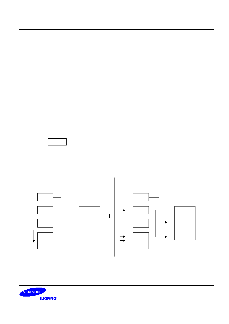
S3C880A/F880A
SAM8 INSTRUCTION SET
6-41
ENTER
� Enter
ENTER
Operation:
SP
SP � 2
@SP
IP
IP
PC
PC
@IP
IP
IP + 2
This instruction is useful when implementing threaded-code languages. The contents of the
instruction pointer are pushed to the stack. The program counter (PC) value is then written to the
instruction pointer. The program memory word that is pointed to by the instruction pointer is loaded
into the PC, and the instruction pointer is incremented by two.
Flags:
No flags are affected.
Format:
Bytes
Cycles
Opcode
(Hex)
opc
1
20
1F
Example:
The diagram below shows one example of how to use an ENTER statement.
0050
1P
0022
SP
22
Data
Address
Data
0040
PC
40
41
42
43
Enter
Address H
Address L
Address H
Address
Data
1F
01
10
Memory
0043
1P
0020
SP
20
21
22
IPH
IPL
Data
Address
Data
0110
PC
40
41
42
43
Enter
Address H
Address L
Address H
Address
Data
1F
01
10
Memory
00
50
Stack
Stack
110
Routine
Before
After
SAM8 INSTRUCTION SET
S3C880A/F880A
6-42
EXIT
� Exit
EXIT
Operation:
IP
@SP
SP
SP + 2
PC
@IP
IP
IP + 2
This instruction is useful when implementing threaded-code languages. The stack value is popped
and loaded into the instruction pointer. The program memory word that is pointed to by the
instruction pointer is then loaded into the program counter, and the instruction pointer is
incremented by two.
Flags:
No flags are affected.
Format:
Bytes
Cycles
Opcode
(Hex)
opc
1
22
2F
Example:
The diagram below shows one example of how to use an EXIT statement.
0050
1P
0022
SP
Address
Data
0040
PC
Address
Data
Memory
0052
1P
0022
SP
Address
Data
0060
PC
Address
Data
Memory
Stack
Stack
Before
After
22
Data
20
21
22
IPH
IPL
Data
00
50
50
51
140
PCL old
PCH
Exit
60
00
2F
60
Main

S3C880A/F880A
SAM8 INSTRUCTION SET
6-43
IDLE
� Idle Operation
IDLE
Operation:
The IDLE instruction stops the CPU clock while allowing system clock oscillation to continue. Idle
mode can be released by an interrupt request (IRQ) or an external reset operation.
Flags:
No flags are affected.
Format:
Bytes
Cycles
Opcode
(Hex)
Addr Mode
dst src
opc
1
3
6F
�
�
Example:
The instruction
IDLE
stops the CPU clock but not the system clock.
SAM8 INSTRUCTION SET
S3C880A/F880A
6-44
INC
� Increment
INC
dst
Operation:
dst
dst + 1
The contents of the destination operand are incremented by one.
Flags:
C: Unaffected.
Z: Set if the result is "0"; cleared otherwise.
S: Set if the result is negative; cleared otherwise.
V: Set if arithmetic overflow occurred; cleared otherwise.
D: Unaffected.
H: Unaffected.
Format:
Bytes
Cycles
Opcode
(Hex)
Addr Mode
dst
dst | opc
1
6
rE
r
r = 0 to
F
opc
dst
2
6
20
R
21
IR
Examples:
Given: R0 = 1BH, register 00H = 0CH, and register 1BH = 0FH:
INC
R0
R0 = 1CH
INC
00H
Register 00H = 0DH
INC
@R0
R0 = 1BH, register 01H = 10H
In the first example, if the destination working register R0 contains the value 1BH, the statement
"INC R0" leaves the value 1CH in that same register.
The next example shows the effect an INC instruction has on the register 00H, assuming that it
contains the value 0CH.
In the third example, INC is used in Indirect Register (IR) addressing mode to increment the value of
the register 1BH from 0FH to 10H.

S3C880A/F880A
SAM8 INSTRUCTION SET
6-45
INCW
� Increment Word
INCW
dst
Operation:
dst
dst + 1
The contents of the destination (which must be an even address) and the byte following that location
are treated as a single 16-bit value that is incremented by one.
Flags:
C: Unaffected.
Z: Set if the result is "0"; cleared otherwise.
S: Set if the result is negative; cleared otherwise.
V: Set if arithmetic overflow occurred; cleared otherwise.
D: Unaffected.
H: Unaffected.
Format:
Bytes
Cycles
Opcode
(Hex)
Addr Mode
dst
opc
dst
2
10
A0
RR
A1
IR
Examples:
Given: R0 = 1AH, R1 = 02H, register 02H = 0FH, and register 03H = 0FFH:
INCW
RR0
R0 = 1AH, R1 = 03H
INCW
@R1
Register 02H = 10H, register 03H = 00H
In the first example, the working register pair RR0 contains the value 1AH in the register R0 and
02H in the register R1. The statement "INCW RR0" increments the 16-bit destination by one,
leaving the value 03H in the register R1. In the second example, the statement "INCW @R1" uses
Indirect Register (IR) addressing mode to increment the contents of the general register 03H from
0FFH to 00H and the register 02H from 0FH to 10H.
NOTE:
A system malfunction may occur if you use a Zero (Z) flag (FLAGS.6) result together with an INCW
instruction. To avoid this problem, we recommend that you use INCW as shown in the following
example:
LOOP:
INCW
RR0
LD
R2,R1
OR
R2,R0
JR
NZ,LOOP
SAM8 INSTRUCTION SET
S3C880A/F880A
6-46
IRET
� Interrupt Return
IRET
IRET (Normal)
IRET (Fast)
Operation:
FLAGS
@SP
PC
IP
SP
SP + 1
FLAGS
FLAGS'
PC
@SP
FIS
0
SP
SP + 2
SYM(0)
1
This instruction is used at the end of an interrupt service routine. It restores the flag register and the
program counter. It also re-enables global interrupts. A "normal IRET" is executed only if the fast
interrupt status bit (FIS, bit one of the FLAGS register, 0D5H) is cleared (= "0"). If a fast interrupt
occurred, IRET clears the FIS bit that was set at the beginning of the service routine.
Flags:
All flags are restored to their original settings (that is, the settings before the interrupt occurred).
Format:
IRET
(Normal)
Bytes
Cycles
Opcode
(Hex)
opc
1
16
BF
IRET
(Fast)
Bytes
Cycles
Opcode
(Hex)
opc
1
6
BF
Example:
In the figure below, the instruction pointer is initially loaded with 100H in the main program before
interrupts are enabled. When an interrupt occurs, the program counter and the instruction pointer
are swapped. This causes the PC to jump to the address 100H and the IP to keep the return
address. The last instruction in the service routine normally is a jump to IRET at the address FFH.
This causes the instruction pointer to be loaded with 100H "again" and the program counter to jump
back to the main program. Now, the next interrupt can occur and the IP is still correct at 100H.
IRET
Interrupt
Service
Routine
JP to FFH
0H
FFH
100H
FFFFH
Note that in the fast interrupt example above, if the last instruction is not a jump to IRET, you must
pay attention to the order of the last two instructions. The IRET cannot be immediately proceeded
by clearing the interrupt status (as with a reset of the IPR register).

S3C880A/F880A
SAM8 INSTRUCTION SET
6-47
JP
� Jump
JP
cc,dst
(Conditional)
JP
dst
(Unconditional)
Operation:
If cc is true, PC
dst
The conditional JUMP instruction transfers program control to the destination address if the
condition specified by the condition code (cc) is true; otherwise, the instruction following the JP
instruction is executed. The unconditional JP simply replaces the contents of the PC with the
contents of the specified register pair. Control then passes to the statement addressed by the PC.
Flags:
No flags are affected.
Format:
(1)
(2)
Bytes
Cycles
Opcode
(Hex)
Addr Mode
dst
cc | opc
dst
3
10/12
(3)
ccD
DA
cc = 0 to F
opc
dst
2
10
30
IRR
NOTES:
1.
The 3-byte format is used for a conditional jump and the 2-byte format for an unconditional jump.
2.
In the first byte of the 3-byte instruction format (conditional jump), the condition code and the opcode
are both four bits.
3.
For a conditional jump, execution time is 12 cycles if the jump is taken or 10 cycles if it is not taken.
Examples:
Given: The carry flag (C) = "1", register 00 = 01H, and register 01 = 20H:
JP
C,LABEL_W
LABEL_W = 1000H, PC = 1000H
JP
@00H
PC = 0120H
The first example shows a conditional JP. Assuming that the carry flag is set to "1", the statement
"JP C,LABEL_W" replaces the contents of the PC with the value 1000H and transfers control to
that location. Had the carry flag not been set, control would then have passed to the statement
immediately following the JP instruction.
The second example shows an unconditional JP. The statement "JP @00" replaces the contents of
the PC with the contents of the register pair 00H and 01H, leaving the value 0120H.

SAM8 INSTRUCTION SET
S3C880A/F880A
6-48
JR
� Jump Relative
JR
cc,dst
Operation:
If cc is true, PC
PC + dst
If the condition specified by the condition code (cc) is true, the relative address is added to the
program counter and control passes to the statement whose address is now in the program
counter; otherwise, the instruction following the JR instruction is executed. (See the list of condition
codes).
The range of the relative address is +127 to �128, and the original value of the program counter is
taken to be the address of the first instruction byte following the JR statement.
Flags:
No flags are affected.
Format:
(1)
Bytes
Cycles
Opcode
(Hex)
Addr Mode
dst
cc | opc
dst
2
10/12
(2)
ccB
RA
cc = 0 to F
NOTES:
1.
In the first byte of the two-byte instruction format, the condition code and the opcode are four bits
each.
2.
Instruction execution time is 12 cycles if the jump is taken or 10 cycles if it is not taken.
Example:
Given: The carry flag = "1" and LABEL_X = 1FF7H:
JR
C,LABEL_X
PC = 1FF7H
If the carry flag is set (that is, if the condition code is true), the statement "JR C,LABEL_X" will
pass control to the statement whose address is now in the PC. Otherwise, the program instruction
following the JR would be executed.
S3C880A/F880A
SAM8 INSTRUCTION SET
6-49
LD
� Load
LD
dst,src
Operation:
dst
src
The contents of the source are loaded into the destination. The source's contents are unaffected.
Flags:
No flags are affected.
Format:
Bytes
Cycles
Opcode
(Hex)
Addr Mode
dst src
dst | opc
src
2
6
rC
r
IM
6
r8
r
R
src | opc
dst
2
6
r9
R
r
r = 0 to F
opc
dst | src
2
6
C7
r
lr
6
D7
Ir
r
opc
src
dst
3
10
E4
R
R
10
E5
R
IR
opc
dst
src
3
10
E6
R
IM
10
D6
IR
IM
opc
src
dst
3
10
F5
IR
R
opc
dst | src
x
3
10
87
r
x [r]
opc
src | dst
x
3
10
97
x [r]
r

SAM8 INSTRUCTION SET
S3C880A/F880A
6-50
LD
� Load
LD
(Continued)
Examples:
Given: R0 = 01H, R1 = 0AH, register 00H = 01H, register 01H = 20H,
register 02H = 02H, LOOP = 30H, and register 3AH = 0FFH:
LD
R0,#10H
R0 = 10H
LD
R0,01H
R0 = 20H, register 01H = 20H
LD
01H,R0
Register 01H = 01H, R0 = 01H
LD
R1,@R0
R1 = 20H, R0 = 01H
LD
@R0,R1
R0 = 01H, R1 = 0AH, register 01H = 0AH
LD
00H,01H
Register 00H = 20H, register 01H = 20H
LD
02H,@00H
Register 02H = 20H, register 00H = 01H
LD
00H,#0AH
Register 00H = 0AH
LD
@00H,#10H
Register 00H = 01H, register 01H = 10H
LD
@00H,02H
Register 00H = 01H, register 01H = 02H, register 02H = 02H
LD
R0,#LOOP[R1]
R0 = 0FFH, R1 = 0AH
LD
#LOOP[R0],R1
Register 31H = 0AH, R0 = 01H, R1 = 0AH

S3C880A/F880A
SAM8 INSTRUCTION SET
6-51
LDB
� Load Bit
LDB
dst,src.b
LDB
dst.b,src
Operation:
dst(0)
src(b)
or
dst(b)
src(0)
The specified bit of the source is loaded into bit zero (LSB) of the destination, or bit zero of the
source is loaded into the specified bit of the destination. No other bits of the destination are
affected. The source is unaffected.
Flags:
No flags are affected.
Format:
Bytes
Cycles
Opcode
(Hex)
Addr Mode
dst src
opc
dst | b | 0
src
3
10
47
r0
Rb
opc
src | b | 1
dst
3
10
47
Rb
r0
NOTE:
In the second byte of the instruction format, the destination (or source) address is four bits, the bit
address 'b' is three bits, and the LSB address value is one bit in length.
Examples:
Given: R0 = 06H and general register 00H = 05H:
LDB
R0,00H.2
R0 = 07H, register 00H = 05H
LDB
00H.0,R0
R0 = 06H, register 00H = 04H
In the first example, the destination working register R0 contains the value 06H and the source
general register 00H the value 05H. The statement "LD R0,00H.2" loads the bit two value of the 00H
register into bit zero of the R0 register, leaving the value 07H in the register R0.
In the second example, 00H is the destination register. The statement "LD 00H.0,R0" loads bit
zero of the register R0 to the specified bit (bit zero) of the destination register, leaving 04H in the
general register 00H.

SAM8 INSTRUCTION SET
S3C880A/F880A
6-52
LDC/LDE
� Load Memory
LDC/LDE
dst,src
Operation:
dst
src
This instruction loads a byte from program or data memory into a working register or vice-versa. The
source values are unaffected. LDC refers to program memory and LDE to data memory. The
assembler makes 'Irr' or 'rr' values an even number for program memory and an odd number for data
memory.
Flags:
No flags are affected.
Format:
Bytes
Cycles
Opcode
(Hex)
Addr Mode
dst src
1.
opc
dst | src
2
12
C3
r
Irr
2.
opc
src | dst
2
12
D3
Irr
r
3.
opc
dst | src
XS
3
18
E7
r
XS [rr]
4.
opc
src | dst
XS
3
18
F7
XS [rr]
r
5.
opc
dst | src
XL
L
XL
H
4
20
A7
r
XL [rr]
6.
opc
src | dst
XL
L
XL
H
4
20
B7
XL [rr]
r
7.
opc
dst | 0000
DA
L
DA
H
4
20
A7
r
DA
8.
opc
src | 0000
DA
L
DA
H
4
20
B7
DA
r
9.
opc
dst | 0001
DA
L
DA
H
4
20
A7
r
DA
10.
opc
src | 0001
DA
L
DA
H
4
20
B7
DA
r
NOTES:
1.
The source (src) or the working register pair [rr] for formats 5 and 6 cannot use the register pair 0�1.
2.
For formats 3 and 4, the destination address 'XS [rr]' and the source address 'XS [rr]' are one byte each.
3.
For formats 5 and 6, the destination address 'XL [rr] and the source address 'XL [rr]' are two bytes each.
4.
The DA and r source values for formats 7 and 8 are used to address program memory; the second set of values, used
in formats 9 and 10, are used to address data memory.

S3C880A/F880A
SAM8 INSTRUCTION SET
6-53
LDC/LDE
� Load Memory
LDC/LDE
(Continued)
Examples:
Given: R0 = 11H, R1 = 34H, R2 = 01H, R3 = 04H; Program memory locations
0103H = 4FH, 0104H = 1A, 0105H = 6DH, and 1104H = 88H. External data memory locations
0103H = 5FH, 0104H = 2AH, 0105H = 7DH, and 1104H = 98H:
LDC
R0,@RR2
; R0
contents of program memory location 0104H
; R0 = 1AH, R2 = 01H, R3 = 04H
LDE
R0,@RR2
; R0
contents of external data memory location 0104H
; R0 = 2AH, R2 = 01H, R3 = 04H
LDC
(note)
@RR2,R0
; 11H (contents of R0) is loaded into program memory
; location 0104H (RR2),
; working registers R0, R2, R3
no change
LDE
@RR2,R0
; 11H (contents of R0) is loaded into external data memory
; location 0104H (RR2),
; working registers R0, R2, R3
no change
LDC
R0,#01H[RR2]
; R0
contents of program memory location 0105H
; (01H + RR2),
; R0 = 6DH, R2 = 01H, R3 = 04H
LDE
R0,#01H[RR2]
; R0
contents of external data memory location 0105H
; (01H + RR2), R0 = 7DH, R2 = 01H, R3 = 04H
LDC
(note)
#01H[RR2],R0
; 11H (contents of R0) is loaded into program memory location
; 0105H (01H + 0104H)
LDE
#01H[RR2],R0
; 11H (contents of R0) is loaded into external data memory
; location 0105H (01H + 0104H)
LDC
R0,#1000H[RR2]
; R0
contents of program memory location 1104H
; (1000H + 0104H), R0 = 88H, R2 = 01H, R3 = 04H
LDE
R0,#1000H[RR2]
; R0
contents of external data memory location 1104H
; (1000H + 0104H), R0 = 98H, R2 = 01H, R3 = 04H
LDC
R0,1104H
; R0
contents of program memory location 1104H, R0 = 88H
LDE
R0,1104H
; R0
contents of external data memory location 1104H,
; R0 = 98H
LDC
(note)
1105H,R0
; 11H (contents of R0) is loaded into program memory location
; 1105H, (1105H)
11H
LDE
1105H,R0
; 11H (contents of R0) is loaded into external data memory
; location 1105H, (1105H)
11H
NOTE: These instructions are not supported by masked ROM type devices.

SAM8 INSTRUCTION SET
S3C880A/F880A
6-54
LDCD/LDED
� Load Memory and Decrement
LDCD/LDED
dst,src
Operation:
dst
src
rr
rr � 1
These instructions are used for user stacks or block transfers of data from program or data memory
to the register file. The address of the memory location is specified by a working register pair. The
contents of the source location are loaded into the destination location. The memory address is
then decremented. The contents of the source are unaffected.
LDCD refers to program memory and LDED refers to external data memory. The assembler makes
'Irr' an even number for program memory and an odd number for data memory.
Flags:
No flags are affected.
Format:
Bytes
Cycles
Opcode
(Hex)
Addr Mode
dst src
opc
dst | src
2
16
E2
r
Irr
Examples:
Given: R6 = 10H, R7 = 33H, R8 = 12H, program memory location 1033H = 0CDH, and
external data memory location 1033H = 0DDH:
LDCD
R8,@RR6
; 0CDH (contents of program memory location 1033H) is loaded
; into R8 and RR6 is decremented by one
; R8 = 0CDH, R6 = 10H, R7 = 32H (RR6
RR6 � 1)
LDED
R8,@RR6
; 0DDH (contents of data memory location 1033H) is loaded
; into R8 and RR6 is decremented by one (RR6
RR6 � 1)
; R8 = 0DDH, R6 = 10H, R7 = 32H

S3C880A/F880A
SAM8 INSTRUCTION SET
6-55
LDCI/LDEI
� Load Memory and Increment
LDCI/LDEI
dst,src
Operation:
dst
src
rr
rr + 1
These instructions are used for user stacks or block transfers of data from program or data memory
to the register file. The address of the memory location is specified by a working register pair. The
contents of the source location are loaded into the destination location. The memory address is
then incremented automatically. The contents of the source are unaffected.
LDCI refers to program memory and LDEI refers to external data memory. The assembler makes 'Irr'
even number for program memory and odd number for data memory.
Flags:
No flags are affected.
Format:
Bytes
Cycles
Opcode
(Hex)
Addr Mode
dst src
opc
dst | src
2
16
E3
r
Irr
Examples:
Given: R6 = 10H, R7 = 33H, R8 = 12H, program memory locations 1033H = 0CDH and
1034H = 0C5H; external data memory locations 1033H = 0DDH and 1034H = 0D5H:
LDCI
R8,@RR6
; 0CDH (contents of program memory location 1033H) is loaded
; into R8 and RR6 is incremented by one (RR6
RR6 + 1)
; R8 = 0CDH, R6 = 10H, R7 = 34H
LDEI
R8,@RR6
; 0DDH (contents of data memory location 1033H) is loaded
; into R8 and RR6 is incremented by one (RR6
RR6 + 1)
; R8 = 0DDH, R6 = 10H, R7 = 34H

SAM8 INSTRUCTION SET
S3C880A/F880A
6-56
LDCPD/LDEPD
� Load Memory with Pre-Decrement
LDCPD/
LDEPD
dst,src
Operation:
rr
rr � 1
dst
src
These instructions are used for block transfers of data from program or data memory from the
register file. The address of the memory location is specified by a working register pair and is first
decremented. The contents of the source location are then loaded into the destination location. The
contents of the source are unaffected.
LDCPD refers to program memory and LDEPD refers to external data memory. The assembler
makes 'Irr' an even number for program memory and an odd number for external data memory.
Flags:
No flags are affected.
Format:
Bytes
Cycles
Opcode
(Hex)
Addr Mode
dst src
opc
src | dst
2
16
F2
Irr
r
Examples:
Given: R0 = 77H, R6 = 30H, and R7 = 00H:
LDCPD
@RR6,R0
; (RR6
RR6 � 1)
; 77H (contents of R0) is loaded into program memory location
; 2FFFH (3000H � 1H)
; R0 = 77H, R6 = 2FH, R7 = 0FFH
LDEPD
@RR6,R0
; (RR6
RR6 � 1)
; 77H (contents of R0) is loaded into external data memory
;
location 2FFFH (3000H � 1H)
; R0 = 77H, R6 = 2FH, R7 = 0FFH

S3C880A/F880A
SAM8 INSTRUCTION SET
6-57
LDCPI/LDEPI
� Load Memory with Pre-Increment
LDCPI/
LDEPI
dst,src
Operation:
rr
rr + 1
dst
src
These instructions are used for block transfers of data from program or data memory from the
register file. The address of the memory location is specified by a working register pair and is first
incremented. The contents of the source location are loaded into the destination location. The
contents of the source are unaffected.
LDCPI refers to program memory and LDEPI refers to external data memory. The assembler makes
'Irr' an even number for program memory and an odd number for data memory.
Flags:
No flags are affected.
Format:
Bytes
Cycles
Opcode
(Hex)
Addr Mode
dst src
opc
src | dst
2
16
F3
Irr
r
Examples:
Given: R0 = 7FH, R6 = 21H, and R7 = 0FFH:
LDCPI
@RR6,R0
; (RR6
RR6 + 1)
; 7FH (contents of R0) is loaded into program memory
; location 2200H (21FFH + 1H)
; R0 = 7FH, R6 = 22H, R7 = 00H
LDEPI
@RR6,R0
; (RR6
RR6 + 1)
; 7FH (contents of R0) is loaded into external data memory
; location 2200H (21FFH + 1H)
; R0 = 7FH, R6 = 22H, R7 = 00H
SAM8 INSTRUCTION SET
S3C880A/F880A
6-58
LDW
� Load Word
LDW
dst,src
Operation:
dst
src
The contents of the source (a word) are loaded into the destination. The contents of the source are
unaffected.
Flags:
No flags are affected.
Format:
Bytes
Cycles
Opcode
(Hex)
Addr Mode
dst src
opc
src
dst
3
10
C4
RR
RR
10
C5
RR
IR
opc
dst
src
4
12
C6
RR
IML
Examples:
Given: R4 = 06H, R5 = 1CH, R6 = 05H, R7 = 02H, register 00H = 1AH,
register 01H = 02H, register 02H = 03H, and register 03H = 0FH:
LDW
RR6,RR4
R6 = 06H, R7 = 1CH, R4 = 06H, R5 = 1CH
LDW
00H,02H
Register 00H = 03H, register 01H = 0FH,
register 02H = 03H, register 03H = 0FH
LDW
RR2,@R7
R2 = 03H, R3 = 0FH,
LDW
04H,@01H
Register 04H = 03H, register 05H = 0FH
LDW
RR6,#1234H
R6 = 12H, R7 = 34H
LDW
02H,#0FEDH
Register 02H = 0FH, register 03H = 0EDH
In the second example, please note that the statement "LDW 00H,02H" loads the contents of the
source word 02H, 03H into the destination word 00H, 01H. This leaves the value 03H in the general
register 00H and the value 0FH in the register 01H.
Other examples show how to use the LDW instruction with various addressing modes and formats.

S3C880A/F880A
SAM8 INSTRUCTION SET
6-59
MULT
� Multiply (Unsigned)
MULT
dst,src
Operation:
dst
dst
�
src
The 8-bit destination operand (the even register of the register pair) is multiplied by the source
operand (8 bits) and the product (16 bits) is stored in the register pair specified by the destination
address. Both operands are treated as unsigned integers.
Flags:
C: Set if the result is > 255; cleared otherwise.
Z: Set if the result is "0"; cleared otherwise.
S: Set if MSB of the result is a "1"; cleared otherwise.
V: Cleared.
D: Unaffected.
H: Unaffected.
Format:
Bytes
Cycles
Opcode
(Hex)
Addr Mode
dst src
opc
src
dst
3
24
84
RR
R
24
85
RR
IR
24
86
RR
IM
Examples:
Given: Register 00H = 20H, register 01H = 03H, register 02H = 09H, register 03H = 06H:
MULT
00H, 02H
Register 00H = 01H, register 01H = 20H, register 02H = 09H
MULT
00H, @01H
Register 00H = 00H, register 01H = 0C0H
MULT
00H, #30H
Register 00H = 06H, register 01H = 00H
In the first example, the statement "MULT 00H,02H" multiplies the 8-bit destination operand (in the
register 00H of the register pair 00H, 01H) by the source register 02H operand (09H). The 16-bit
product, 0120H, is stored in the register pair 00H, 01H.
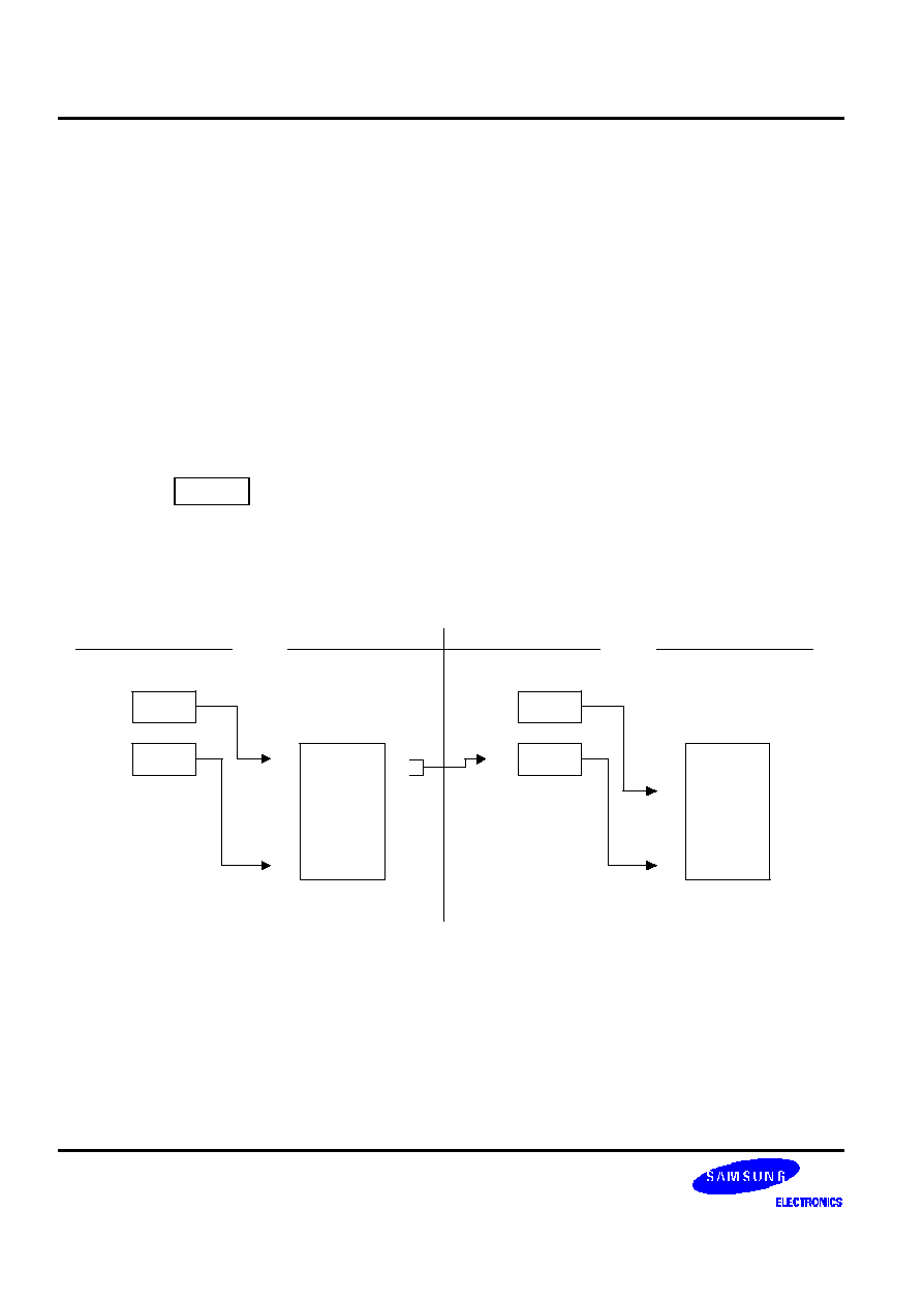
SAM8 INSTRUCTION SET
S3C880A/F880A
6-60
NEXT
� Next
NEXT
Operation:
PC
@IP
IP
IP + 2
The NEXT instruction is useful when implementing threaded-code languages. The program memory
word that is pointed to by the instruction pointer is loaded into the program counter. The instruction
pointer is then incremented by two.
Flags:
No flags are affected.
Format:
Bytes
Cycles
Opcode
(Hex)
opc
1
14
0F
Example:
The following diagram shows one example of how to use the NEXT instruction.
Data
01
10
Before
After
0045
1P
Address
Data
0130
PC
43
44
45
Address H
Address L
Address H
Address
Data
Memory
130
Routine
0043
1P
Address
Data
0120
PC
43
44
45
Address H
Address L
Address H
Address
Data
Memory
120 Next

S3C880A/F880A
SAM8 INSTRUCTION SET
6-61
NOP
� No Operation
NOP
Operation:
No action is performed when the CPU executes this instruction. Typically, one or more NOPs are
executed in sequence in order to effect a timing delay of variable duration.
Flags:
No flags are affected.
Format:
Bytes
Cycles
Opcode
(Hex)
opc
1
6
FF
Example:
When the instruction
NOP
is encountered in a program, no operation occurs. Instead, there happens a delay in instruction
execution.

SAM8 INSTRUCTION SET
S3C880A/F880A
6-62
OR
� Logical OR
OR
dst,src
Operation:
dst
dst OR src
The source operand is logically ORed with the destination operand and the result is stored in the
destination. The contents of the source are unaffected. The OR operation results in a "1" being
stored whenever either of the corresponding bits in the two operands is a "1"; otherwise a "0" is
stored.
Flags:
C: Unaffected.
Z: Set if the result is "0"; cleared otherwise.
S: Set if the result bit 7 is set; cleared otherwise.
V: Always cleared to "0".
D: Unaffected.
H: Unaffected.
Format:
Bytes
Cycles
Opcode
(Hex)
Addr Mode
dst src
opc
dst | src
2
6
42
r
r
6
43
r
lr
opc
src
dst
3
10
44
R
R
10
45
R
IR
opc
dst
src
3
10
46
R
IM
Examples:
Given: R0 = 15H, R1 = 2AH, R2 = 01H, register 00H = 08H, register 01H = 37H, and
register 08H = 8AH:
OR
R0,R1
R0 = 3FH, R1 = 2AH
OR
R0,@R2
R0 = 37H, R2 = 01H, register 01H = 37H
OR
00H,01H
Register 00H = 3FH, register 01H = 37H
OR
01H,@00H
Register 00H = 08H, register 01H = 0BFH
OR
00H,#02H
Register 00H = 0AH
In the first example, if the working register R0 contains the value 15H and the register R1 the value
2AH, the statement "OR R0,R1" logical-ORs the R0 and R1 register contents and stores the result
(3FH) in the destination register R0.
Other examples show the use of the logical OR instruction with the various addressing modes and
formats.

S3C880A/F880A
SAM8 INSTRUCTION SET
6-63
POP
� Pop From Stack
POP
dst
Operation:
dst
@SP
SP
SP + 1
The contents of the location addressed by the stack pointer are loaded into the destination. The
stack pointer is then incremented by one.
Flags:
No flags affected.
Format:
Bytes
Cycles
Opcode
(Hex)
Addr Mode
dst
opc
dst
2
10
50
R
10
51
IR
Examples:
Given: Register 00H = 01H, register 01H = 1BH, SPH (0D8H) = 00H, SPL (0D9H) = 0FBH,
and stack register 0FBH = 55H:
POP
00H
Register 00H = 55H, SP = 00FCH
POP
@00H
Register 00H = 01H, register 01H = 55H, SP = 00FCH
In the first example, the general register 00H contains the value 01H. The statement "POP 00H"
loads the contents of the location 00FBH (55H) into the destination register 00H and then
increments the stack pointer by one. The register 00H then contains the value 55H and the SP
points to the location 00FCH.

SAM8 INSTRUCTION SET
S3C880A/F880A
6-64
POPUD
� Pop User Stack (Decrementing)
POPUD
dst,src
Operation:
dst
src
IR
IR � 1
This instruction is used for user-defined stacks in the register file. The contents of the register file
location addressed by the user stack pointer are loaded into the destination. The user stack pointer
is then decremented.
Flags:
No flags are affected.
Format:
Bytes
Cycles
Opcode
(Hex)
Addr Mode
dst src
opc
src
dst
3
10
92
R
IR
Example:
Given: Register 00H = 42H (user stack pointer register), register 42H = 6FH, and
register 02H = 70H:
POPUD
02H,@00H
Register 00H = 41H, register 02H = 6FH, register 42H = 6FH
If the general register 00H contains the value 42H and the register 42H the value 6FH, the statement
"POPUD 02H,@00H" loads the contents of the register 42H into the destination register 02H. The
user stack pointer is then decremented by one, leaving the value 41H.

S3C880A/F880A
SAM8 INSTRUCTION SET
6-65
POPUI
� Pop User Stack (Incrementing)
POPUI
dst,src
Operation:
dst
src
IR
IR + 1
The POPUI instruction is used for user-defined stacks in the register file. The contents of the
register file location addressed by the user stack pointer are loaded into the destination. The user
stack pointer is then incremented.
Flags:
No flags are affected.
Format:
Bytes
Cycles
Opcode
(Hex)
Addr Mode
dst src
opc
src
dst
3
10
93
R
IR
Example:
Given: Register 00H = 01H and register 01H = 70H:
POPUI
02H,@00H
Register 00H = 02H, register 01H = 70H, register 02H = 70H
If the general register 00H contains the value 01H and the register 01H the value 70H, the statement
"POPUI 02H,@00H" loads the value 70H into the destination general register 02H. The user stack
pointer (register 00H) is then incremented by one, changing its value from 01H to 02H.

SAM8 INSTRUCTION SET
S3C880A/F880A
6-66
PUSH
� Push to Stack
PUSH
src
Operation:
SP
SP � 1
@SP
src
A PUSH instruction decrements the stack pointer value and loads the contents of the source (src)
into the location addressed by the decremented stack pointer. The operation then adds the new
value to the top of the stack.
Flags:
No flags are affected.
Format:
Bytes
Cycles
Opcode
(Hex)
Addr Mode
dst
opc
src
2
10 (internal clock)
70
R
12 (external clock)
12 (internal clock)
14 (external clock)
71
IR
Examples:
Given: Register 40H = 4FH, register 4FH = 0AAH, SPH = 00H, and SPL = 00H:
PUSH
40H
Register 40H = 4FH, stack register 0FFH = 4FH,
SPH = 0FFH, SPL = 0FFH
PUSH
@40H
Register 40H = 4FH, register 4FH = 0AAH, stack register
0FFH = 0AAH, SPH = 0FFH, SPL = 0FFH
In the first example, if the stack pointer contains the value 0000H, and the general register 40H the
value 4FH, the statement "PUSH 40H" decrements the stack pointer from 0000 to 0FFFFH. It then
loads the contents of the register 40H into the location 0FFFFH and adds this new value to the top
of the stack.

S3C880A/F880A
SAM8 INSTRUCTION SET
6-67
PUSHUD
� Push User Stack (Decrementing)
PUSHUD
dst,src
Operation:
IR
IR � 1
dst
src
This instruction is used to address user-defined stacks in the register file. PUSHUD decrements the
user stack pointer and loads the contents of the source into the register addressed by the
decremented stack pointer.
Flags:
No flags are affected.
Format:
Bytes
Cycles
Opcode
(Hex)
Addr Mode
dst src
opc
dst
src
3
10
82
IR
R
Example:
Given: Register 00H = 03H, register 01H = 05H, and register 02H = 1AH:
PUSHUD @00H,01H
Register 00H = 02H, register 01H = 05H, register 02H = 05H
If the user stack pointer (register 00H, for example) contains the value 03H, the statement
"PUSHUD @00H,01H" decrements the user stack pointer by one, leaving the value 02H. The 01H
register value, 05H, is then loaded into the register addressed by the decremented user stack
pointer.

SAM8 INSTRUCTION SET
S3C880A/F880A
6-68
PUSHUI
� Push User Stack (Incrementing)
PUSHUI
dst,src
Operation:
IR
IR + 1
dst
src
This instruction is used for user-defined stacks in the register file. PUSHUI increments the user
stack pointer and then loads the contents of the source into the register location addressed by the
incremented user stack pointer.
Flags:
No flags are affected.
Format:
Bytes
Cycles
Opcode
(Hex)
Addr Mode
dst src
opc
dst
src
3
10
83
IR
R
Example:
Given: Register 00H = 03H, register 01H = 05H, and register 04H = 2AH:
PUSHUI
@00H,01H
Register 00H = 04H, register 01H = 05H, register 04H = 05H
If the user stack pointer (register 00H, for example) contains the value 03H, the statement
"PUSHUI @00H,01H" increments the user stack pointer by one, leaving the value 04H. The 01H
register value, 05H, is then loaded into the location addressed by the incremented user stack
pointer.

S3C880A/F880A
SAM8 INSTRUCTION SET
6-69
RCF
� Reset Carry Flag
RCF
RCF
Operation:
C
0
The carry flag is cleared to logic zero, regardless of its previous value.
Flags:
C:
Cleared to "0".
No other flags are affected.
Format:
Bytes
Cycles
Opcode
(Hex)
opc
1
6
CF
Example:
Given: C = "1" or "0":
The instruction RCF clears the carry flag (C) to logic zero.

SAM8 INSTRUCTION SET
S3C880A/F880A
6-70
RET
� Return
RET
Operation:
PC
@SP
SP
SP + 2
The RET instruction is normally used to return to the previously executed procedure at the end of a
procedure entered by a CALL instruction. The contents of the location addressed by the stack
pointer are popped into the program counter. The next statement that is executed is the one that is
addressed by the new program counter value.
Flags:
No flags are affected.
Format:
Bytes
Cycles
Opcode
(Hex)
opc
1
14
AF
Example:
Given: SP = 00FCH, (SP) = 101AH, and PC = 1234:
RET
PC = 101AH, SP = 00FEH
The statement "RET" pops the contents of the stack pointer location 00FCH (10H) into the high
byte of the program counter. The stack pointer then pops the value in the location 00FEH (1AH) into
the PC's low byte and the instruction at the location 101AH is executed. The stack pointer now
points to the memory location 00FEH.
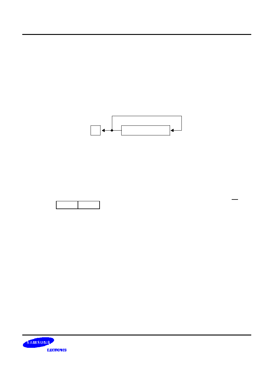
S3C880A/F880A
SAM8 INSTRUCTION SET
6-71
RL
� Rotate Left
RL
dst
Operation:
C
dst (7)
dst (0)
dst (7)
dst (n + 1)
dst (n), n = 0�6
The contents of the destination operand are rotated left one bit position. The initial value of bit 7 is
moved to the bit zero (LSB) position and also replaces the carry flag.
7
0
C
Flags:
C: Set if the bit rotated from the most significant bit position (bit 7) was "1".
Z: Set if the result is "0"; cleared otherwise.
S: Set if the result bit 7 is set; cleared otherwise.
V: Set if arithmetic overflow occurred; cleared otherwise.
D: Unaffected.
H: Unaffected.
Format:
Bytes
Cycles
Opcode
(Hex)
Addr Mode
dst
opc
dst
2
6
90
R
6
91
IR
Examples:
Given: Register 00H = 0AAH, register 01H = 02H and register 02H = 17H:
RL
00H
Register 00H = 55H, C = "1"
RL
@01H
Register 01H = 02H, register 02H = 2EH, C = "0"
In the first example, if the general register 00H contains the value 0AAH (10101010B), the
statement "RL 00H" rotates the 0AAH value left one bit position, leaving the new value 55H
(01010101B) and setting the carry and overflow flags.
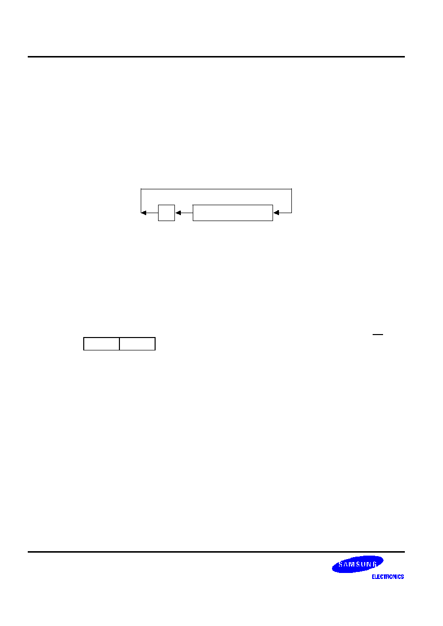
SAM8 INSTRUCTION SET
S3C880A/F880A
6-72
RLC
� Rotate Left Through Carry
RLC
dst
Operation:
dst (0)
C
C
dst (7)
dst (n + 1)
dst (n), n = 0�6
The contents of the destination operand with the carry flag are rotated left one bit position. The initial
value of bit 7 replaces the carry flag (C); the initial value of the carry flag replaces bit zero.
7
0
C
Flags:
C: Set if the bit rotated from the most significant bit position (bit 7) was "1".
Z: Set if the result is "0"; cleared otherwise.
S: Set if the result bit 7 is set; cleared otherwise.
V: Set if arithmetic overflow occurred, that is, if the sign of the destination changed during rotation;
cleared otherwise.
D: Unaffected.
H: Unaffected.
Format:
Bytes
Cycles
Opcode
(Hex)
Addr Mode
dst
opc
dst
2
6
10
R
6
11
IR
Examples:
Given: Register 00H = 0AAH, register 01H = 02H, and register 02H = 17H, C = "0":
RLC
00H
Register 00H = 54H, C = "1"
RLC
@01H
Register 01H = 02H, register 02H = 2EH, C = "0"
In the first example, if the general register 00H has the value 0AAH (10101010B), the statement
"RLC 00H" rotates 0AAH one bit position to the left. The initial value of bit 7 sets the carry flag and
the initial value of the C flag replaces bit zero of the register 00H, leaving the value 55H
(01010101B). The MSB of the register 00H resets the carry flag to "1", setting the overflow flag.

S3C880A/F880A
SAM8 INSTRUCTION SET
6-73
RR
� Rotate Right
RR
dst
Operation:
C
dst (0)
dst (7)
dst (0)
dst (n)
dst (n + 1), n = 0�6
The contents of the destination operand are rotated right one bit position. The initial value of bit zero
(LSB) is moved to bit 7 (MSB) and also replaces the carry flag (C).
7
0
C
Flags:
C: Set if the bit rotated from the least significant bit position (bit zero) was "1".
Z: Set if the result is "0"; cleared otherwise.
S: Set if the result bit 7 is set; cleared otherwise.
V: Set if arithmetic overflow occurred, that is, if the sign of the destination changed during rotation;
cleared otherwise.
D: Unaffected.
H: Unaffected.
Format:
Bytes
Cycles
Opcode
(Hex)
Addr Mode
dst
opc
dst
2
6
E0
R
6
E1
IR
Examples:
Given: Register 00H = 31H, register 01H = 02H, and register 02H = 17H:
RR
00H
Register 00H = 98H, C = "1"
RR
@01H
Register 01H = 02H, register 02H = 8BH, C = "1"
In the first example, if the general register 00H contains the value 31H (00110001B), the statement
"RR 00H" rotates this value one bit position to the right. The initial value of bit zero is moved to bit 7,
leaving the new value 98H (10011000B) in the destination register. The initial bit zero also resets the
C flag to "1" and the sign flag and overflow flag are also set to "1".
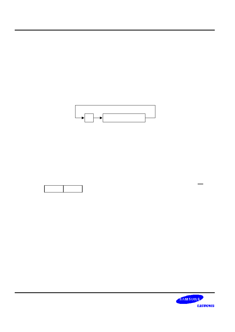
SAM8 INSTRUCTION SET
S3C880A/F880A
6-74
RRC
� Rotate Right Through Carry
RRC
dst
Operation:
dst (7)
C
C
dst (0)
dst (n)
dst (n + 1), n = 0�6
The contents of the destination operand and the carry flag are rotated right one bit position. The
initial value of bit zero (LSB) replaces the carry flag; the initial value of the carry flag replaces bit 7
(MSB).
7
0
C
Flags:
C: Set if the bit rotated from the least significant bit position (bit zero) was "1".
Z: Set if the result is "0" cleared otherwise.
S: Set if the result bit 7 is set; cleared otherwise.
V: Set if arithmetic overflow occurred, that is, if the sign of the destination changed during rotation;
cleared otherwise.
D: Unaffected.
H: Unaffected.
Format:
Bytes
Cycles
Opcode
(Hex)
Addr Mode
dst
opc
dst
2
6
C0
R
6
C1
IR
Examples:
Given: Register 00H = 55H, register 01H = 02H, register 02H = 17H, and C = "0":
RRC
00H
Register 00H = 2AH, C = "1"
RRC
@01H
Register 01H = 02H, register 02H = 0BH, C = "1"
In the first example, if the general register 00H contains the value 55H (01010101B), the statement
"RRC 00H" rotates this value one bit position to the right. The initial value of bit zero ("1") replaces
the carry flag and the initial value of the C flag ("1") replaces bit 7. This leaves the new value 2AH
(00101010B) in the destination register 00H. The sign flag and the overflow flag are both cleared to
"0".

S3C880A/F880A
SAM8 INSTRUCTION SET
6-75
SB0
� Select Bank 0
SB0
Operation:
BANK
0
The SB0 instruction clears the bank address flag in the FLAGS register (FLAGS.0) to logic zero,
selecting bank 0 register addressing in the set 1 area of the register file.
Flags:
No flags are affected.
Format:
Bytes
Cycles
Opcode
(Hex)
opc
1
6
4F
Example:
The statement
SB0
clears FLAGS.0 to "0", selecting bank 0 register addressing.

SAM8 INSTRUCTION SET
S3C880A/F880A
6-76
SB1
� Select Bank 1
SB1
Operation:
BANK
1
The SB1 instruction sets the bank address flag in the FLAGS register (FLAGS.0) to logic one,
selecting bank 1 register addressing in the set 1 area of the register file. (Bank 1 is not
implemented in some KS88-series microcontrollers.)
Flags:
No flags are affected.
Format:
Bytes
Cycles
Opcode
(Hex)
opc
1
6
5F
Example:
The statement
SB1
sets FLAGS.0 to "1", selecting bank 1 register addressing, if implemented.

S3C880A/F880A
SAM8 INSTRUCTION SET
6-77
SBC
� Subtract with Carry
SBC
dst,src
Operation:
dst
dst � src � c
The source operand, along with the current value of the carry flag, is subtracted from the destination
operand and the result is stored in the destination. The contents of the source are unaffected.
Subtraction is performed by adding the two's-complement of the source operand to the destination
operand. In multiple precision arithmetic, this instruction permits the carry ("borrow") from the
subtraction of the low-order operands to be subtracted from the subtraction of high-order operands.
Flags:
C: Set if a borrow occurred (src > dst); cleared otherwise.
Z: Set if the result is "0"; cleared otherwise.
S: Set if the result is negative; cleared otherwise.
V: Set if arithmetic overflow occurred, that is, if the operands were of opposite sign and the sign of
the result is the same as the sign of the source; cleared otherwise.
D: Always set to "1".
H: Cleared if there is a carry from the most significant bit of the low-order four bits of the result; set
otherwise, indicating a "borrow".
Format:
Bytes
Cycles
Opcode
(Hex)
Addr Mode
dst src
opc
dst | src
2
6
32
r
r
6
33
r
lr
opc
src
dst
3
10
34
R
R
10
35
R
IR
opc
dst
src
3
10
36
R
IM
Examples:
Given: R1 = 10H, R2 = 03H, C = "1", register 01H = 20H, register 02H = 03H, and register
03H = 0AH:
SBC
R1,R2
R1 = 0CH, R2 = 03H
SBC
R1,@R2
R1 = 05H, R2 = 03H, register 03H = 0AH
SBC
01H,02H
Register 01H = 1CH, register 02H = 03H
SBC
01H,@02H
Register 01H = 15H,register 02H = 03H, register 03H = 0AH
SBC
01H,#8AH
Register 01H = 95H; C, S, and V = "1"
In the first example, if the working register R1 contains the value 10H and the register R2 the value
03H, the statement "SBC R1,R2" subtracts the source value (03H) and the C flag value ("1") from
the destination (10H) and then stores the result (0CH) in the register R1.

SAM8 INSTRUCTION SET
S3C880A/F880A
6-78
SCF
� Set Carry Flag
SCF
Operation:
C
1
The carry flag (C) is set to logic one, regardless of its previous value.
Flags:
C: Set to "1".
No other flags are affected.
Format:
Bytes
Cycles
Opcode
(Hex)
opc
1
6
DF
Example:
The statement
SCF
sets the carry flag to logic one.
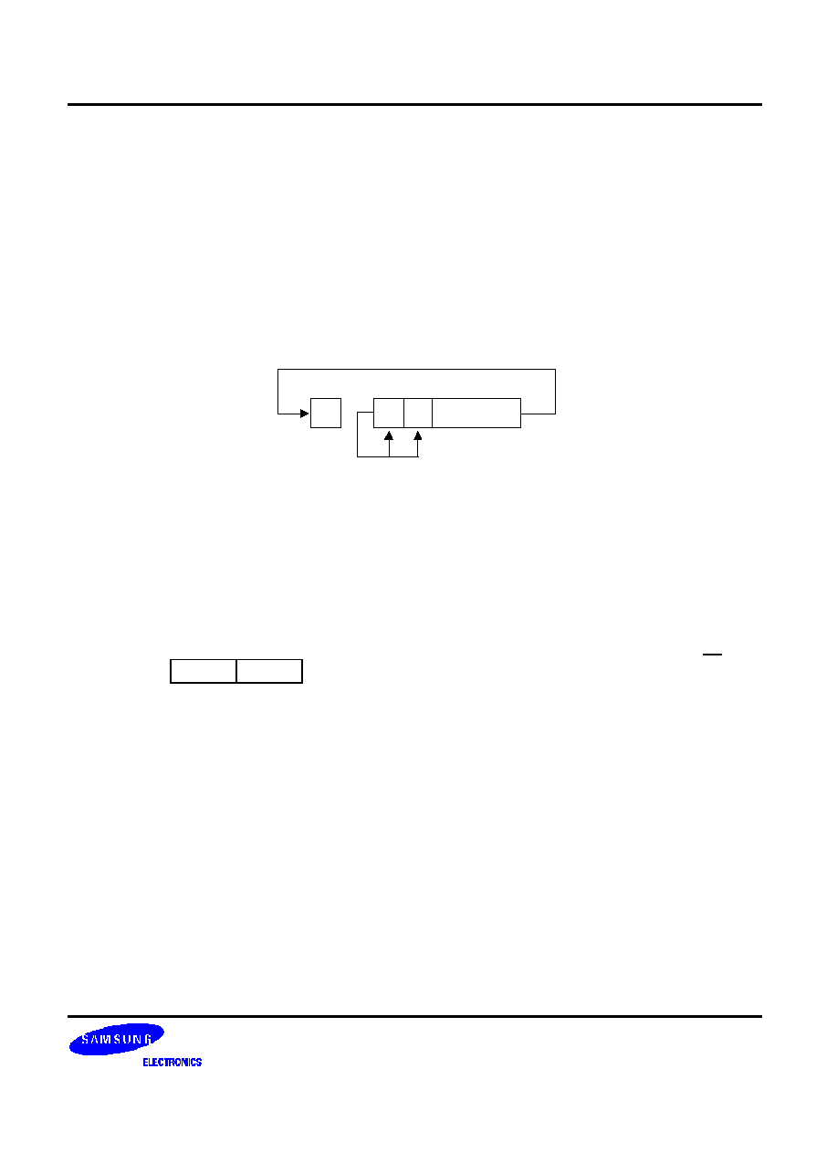
S3C880A/F880A
SAM8 INSTRUCTION SET
6-79
SRA
� Shift Right Arithmetic
SRA
dst
Operation:
dst (7)
dst (7)
C
dst (0)
dst (n)
dst (n + 1), n = 0�6
An arithmetic shift-right of one bit position is performed on the destination operand. Bit zero (the
LSB) replaces the carry flag. The value of bit 7 (the sign bit) is unchanged and is shifted into the bit
position 6.
7
0
C
6
Flags:
C: Set if the bit shifted from the LSB position (bit zero) was "1".
Z: Set if the result is "0"; cleared otherwise.
S: Set if the result is negative; cleared otherwise.
V: Always cleared to "0".
D: Unaffected.
H: Unaffected.
Format:
Bytes
Cycles
Opcode
(Hex)
Addr Mode
dst
opc
dst
2
6
D0
R
6
D1
IR
Examples:
Given: Register 00H = 9AH, register 02H = 03H, register 03H = 0BCH, and C = "1":
SRA
00H
Register 00H = 0CDH, C = "0"
SRA
@02H
Register 02H = 03H, register 03H = 0DEH, C = "0"
In the first example, if the general register 00H contains the value 9AH (10011010B), the statement
"SRA 00H" shifts the bit values in the register 00H right one bit position. Bit zero ("0") clears the C
flag and bit 7 ("1") is then shifted into the bit 6 position (bit 7 remains unchanged). This leaves the
value 0CDH (11001101B) in the destination register 00H.

SAM8 INSTRUCTION SET
S3C880A/F880A
6-80
SRP/SRP0/SRP1
� Set Register Pointer
SRP
src
SRP0
src
SRP1
src
Operation:
If src (1) = 1 and src (0) = 0 then:
RP0 (3�7)
src (3�7)
If src (1) = 0 and src (0) = 1 then:
RP1 (3�7)
src (3�7)
If src (1) = 0 and src (0) = 0 then:
RP0 (4�7)
src (4�7),
RP0 (3)
0
RP1 (4�7)
src (4�7),
RP1 (3)
1
The source data bits one and zero (LSB) determine whether to write one or both of the register
pointers, RP0 and RP1. Bits 3�7 of the selected register pointer are written unless both register
pointers are selected. RP0.3 is then cleared to logic zero and RP1.3 is set to logic one.
Flags:
No flags are affected.
Format:
Bytes
Cycles
Opcode
(Hex)
Addr Mode
src
opc
src
2
6
31
IM
Examples:
The statement
SRP #40H
sets the register pointer 0 (RP0) at location 0D6H to 40H and the register pointer 1 (RP1) at location
0D7H to 48H.
The statement "SRP0 #50H" sets RP0 to 50H, and the statement "SRP1 #68H" sets RP1 to 68H.

S3C880A/F880A
SAM8 INSTRUCTION SET
6-81
STOP
� Stop Operation
STOP
Operation:
The STOP instruction stops both the CPU clock and the system clock causing the microcontroller
to enter Stop mode. During Stop mode, the contents of on-chip CPU registers, peripheral registers,
and I/O port control and data registers are retained. Stop mode can be released only by an external
reset operation. For the reset operation, the nRESET pin must be held to Low level until the required
oscillation stabilization interval has elapsed.
Flags:
No flags are affected.
Format:
Bytes
Cycles
Opcode
(Hex)
Addr Mode
dst src
opc
1
3
7F
�
�
Example:
The statement
STOP
halts all microcontroller operations.
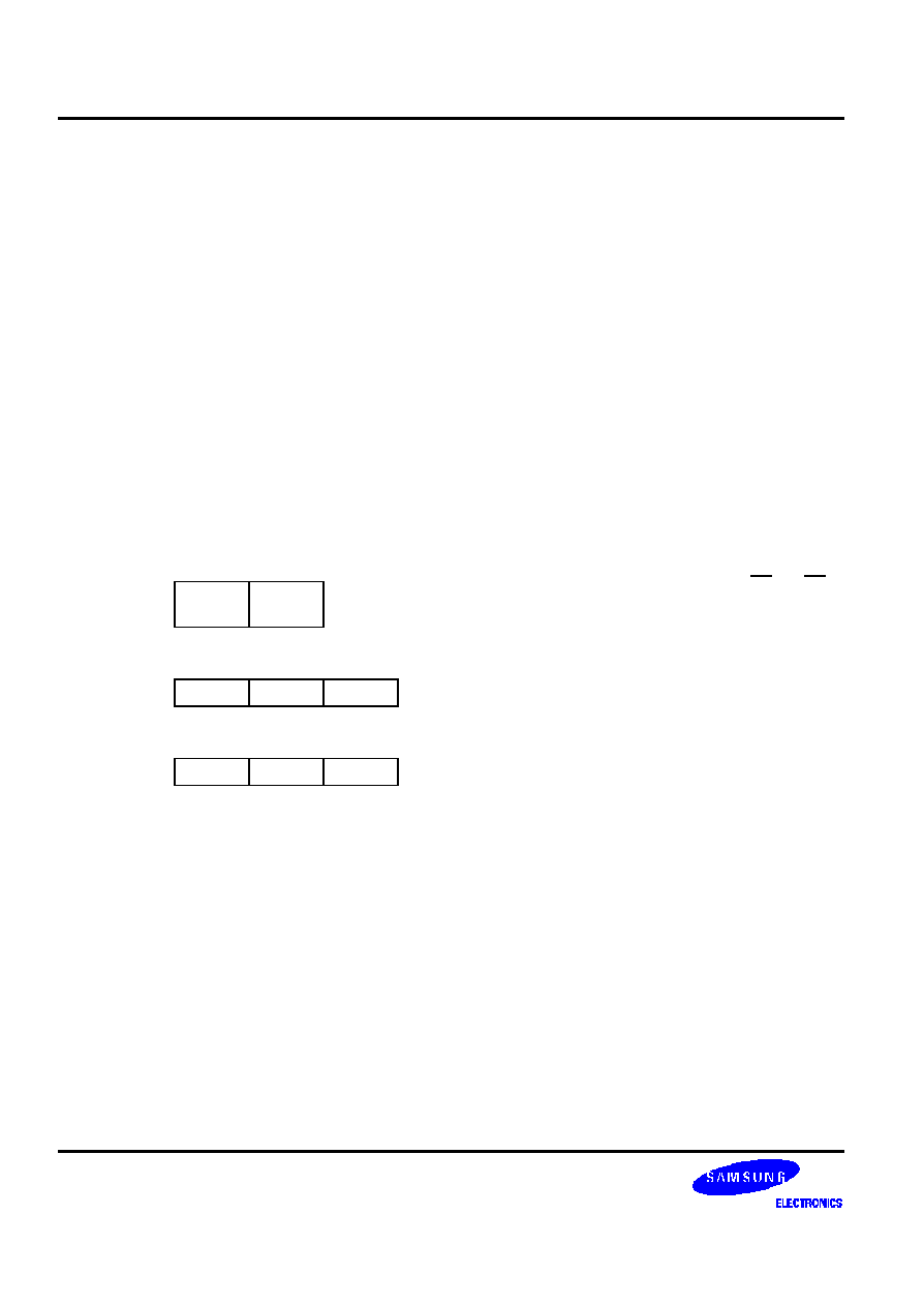
SAM8 INSTRUCTION SET
S3C880A/F880A
6-82
SUB
� Subtract
SUB
dst,src
Operation:
dst
dst � src
The source operand is subtracted from the destination operand and the result is stored in the
destination. The contents of the source are unaffected. Subtraction is performed by adding the two's
complement of the source operand to the destination operand.
Flags:
C: Set if a "borrow" occurred; cleared otherwise.
Z: Set if the result is "0"; cleared otherwise.
S: Set if the result is negative; cleared otherwise.
V: Set if arithmetic overflow occurred, that is, if the operands were of opposite signs and the sign
of the result is of the same as the sign of the source operand; cleared otherwise.
D: Always set to "1".
H: Cleared if there is a carry from the most significant bit of the low-order four bits of the result; set
otherwise, indicating a "borrow".
Format:
Bytes
Cycles
Opcode
(Hex)
Addr Mode
dst src
opc
dst |
src
2
6
22
r
r
6
23
r
lr
opc
src
dst
3
10
24
R
R
10
25
R
IR
opc
dst
src
3
10
26
R
IM
Examples:
Given: R1 = 12H, R2 = 03H, register 01H = 21H, register 02H = 03H, register 03H = 0AH:
SUB
R1,R2
R1 = 0FH, R2 = 03H
SUB
R1,@R2
R1 = 08H, R2 = 03H
SUB
01H,02H
Register 01H = 1EH, register 02H = 03H
SUB
01H,@02H
Register 01H = 17H, register 02H = 03H
SUB
01H,#90H
Register 01H = 91H; C, S, and V = "1"
SUB
01H,#65H
Register 01H = 0BCH; C and S = "1", V = "0"
In the first example, if the working register R1 contains the value 12H and the register R2 contains
the value 03H, the statement "SUB R1,R2" subtracts the source value (03H) from the destination
value (12H), storing the result (0FH) in the destination register R1.
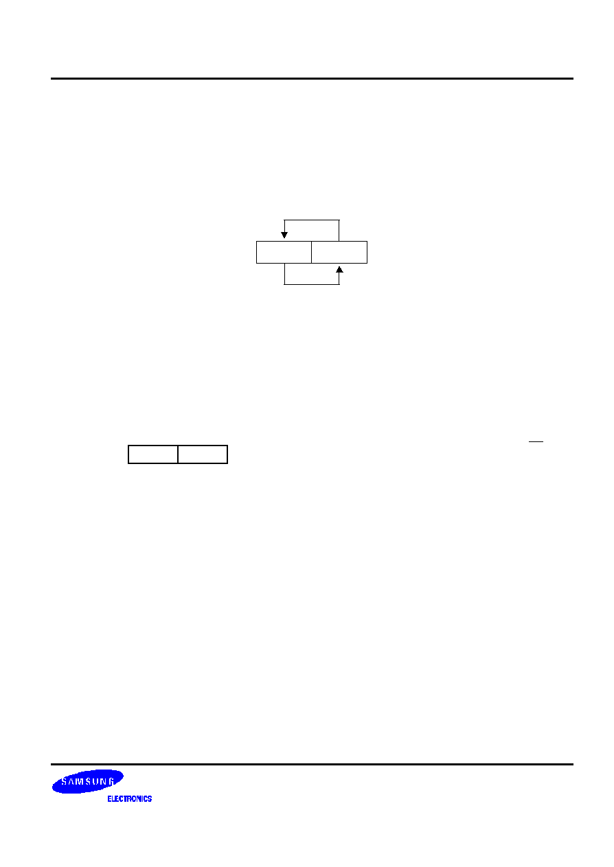
S3C880A/F880A
SAM8 INSTRUCTION SET
6-83
SWAP
� Swap Nibbles
SWAP
dst
Operation:
dst (0 � 3)
dst (4 � 7)
The contents of the lower four bits and the upper four bits of the destination operand are swapped.
7
0
4 3
Flags:
C: Undefined.
Z: Set if the result is "0"; cleared otherwise.
S: Set if the result bit 7 is set; cleared otherwise.
V: Undefined.
D: Unaffected.
H: Unaffected.
Format:
Bytes
Cycles
Opcode
(Hex)
Addr Mode
dst
opc
dst
2
8
F0
R
8
F1
IR
Examples:
Given: Register 00H = 3EH, register 02H = 03H, and register 03H = 0A4H:
SWAP
00H
Register 00H = 0E3H
SWAP
@02H
Register 02H = 03H, register 03H = 4AH
In the first example, if the general register 00H contains the value 3EH (00111110B), the statement
"SWAP 00H" swaps the lower and the upper four bits (nibbles) in the 00H register, leaving the value
0E3H (11100011B).
SAM8 INSTRUCTION SET
S3C880A/F880A
6-84
TCM
� Test Complement under Mask
TCM
dst,src
Operation:
(NOT dst) AND src
This instruction tests selected bits in the destination operand for a logic one value. The bits to be
tested are specified by setting a "1" bit in the corresponding position of the source operand (mask).
The TCM statement complements the destination operand, which is then ANDed with the source
mask. The zero (Z) flag can then be checked to determine the result. The destination and source
operands are unaffected.
Flags:
C: Unaffected.
Z: Set if the result is "0"; cleared otherwise.
S: Set if the result bit 7 is set; cleared otherwise.
V: Always cleared to "0".
D: Unaffected.
H: Unaffected.
Format:
Bytes
Cycles
Opcode
(Hex)
Addr Mode
dst src
opc
dst | src
2
6
62
r
r
6
63
r
lr
opc
src
dst
3
10
64
R
R
10
65
R
IR
opc
dst
src
3
10
66
R
IM
Examples:
Given: R0 = 0C7H, R1 = 02H, R2 = 12H, register 00H = 2BH, register 01H = 02H, and
register 02H = 23H:
TCM
R0,R1
R0 = 0C7H, R1 = 02H, Z = "1"
TCM
R0,@R1
R0 = 0C7H, R1 = 02H, register 02H = 23H, Z = "0"
TCM
00H,01H
Register 00H = 2BH, register 01H = 02H, Z = "1"
TCM
00H,@01H
Register 00H = 2BH, register 01H = 02H,
register 02H = 23H, Z = "1"
TCM
00H,#34
Register 00H = 2BH, Z = "0"
In the first example, if the working register R0 contains the value 0C7H (11000111B) and the register
R1 the value 02H (00000010B), the statement "TCM R0,R1" tests bit one in the destination register
for a "1" value. Because the mask value corresponds to the test bit, the Z flag is set to logic one
and can be tested to determine the result of the TCM operation.
S3C880A/F880A
SAM8 INSTRUCTION SET
6-85
TM
� Test under Mask
TM
dst,src
Operation:
dst AND src
This instruction tests selected bits in the destination operand for a logic zero value. The bits to be
tested are specified by setting a "1" bit in the corresponding position of the source operand (mask),
which is ANDed with the destination operand. The zero (Z) flag can then be checked to determine
the result. The destination and source operands are unaffected.
Flags:
C: Unaffected.
Z: Set if the result is "0"; cleared otherwise.
S: Set if the result bit 7 is set; cleared otherwise.
V: Always reset to "0".
D: Unaffected.
H: Unaffected.
Format:
Bytes
Cycles
Opcode
(Hex)
Addr Mode
dst src
opc
dst | src
2
6
72
r
r
6
73
r
lr
opc
src
dst
3
10
74
R
R
10
75
R
IR
opc
dst
src
3
10
76
R
IM
Examples:
Given: R0 = 0C7H, R1 = 02H, R2 = 18H, register 00H = 2BH, register 01H = 02H, and
register 02H = 23H:
TM
R0,R1
R0 = 0C7H, R1 = 02H, Z = "0"
TM
R0,@R1
R0 = 0C7H, R1 = 02H, register 02H = 23H, Z = "0"
TM
00H,01H
Register 00H = 2BH, register 01H = 02H, Z = "0"
TM
00H,@01H
Register 00H = 2BH, register 01H = 02H,
register 02H = 23H, Z = "0"
TM
00H,#54H
Register 00H = 2BH, Z = "1"
In the first example, if the working register R0 contains the value 0C7H (11000111B) and the register
R1 the value 02H (00000010B), the statement "TM R0,R1" tests bit one in the destination register
for a "0" value. Because the mask value does not match the test bit, the Z flag is cleared to logic
zero and can be tested to determine the result of the TM operation.
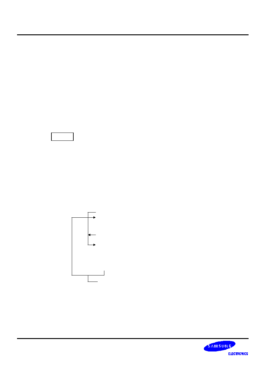
SAM8 INSTRUCTION SET
S3C880A/F880A
6-86
WFI
� Wait for Interrupt
WFI
Operation:
The CPU is effectively halted until an interrupt occurs, except in the case that DMA transfers can
still take place during this wait state. The WFI status can be released by an internal interrupt,
including a fast interrupt .
Flags:
No flags are affected.
Format:
Bytes
Cycles
Opcode
(Hex)
opc
1
6n
3F
(
n = 1, 2, 3, ... )
Example:
The following sample program structure shows the sequence of operations that follow a "WFI"
statement:
EI
WFI
(Next instruction)
Main program
.
.
.
.
.
.
Interrupt occurs
Interrupt service routine
.
.
.
Clear interrupt flag
IRET
Service routine completed
(Enable global interrupt)
(Wait for interrupt)
S3C880A/F880A
SAM8 INSTRUCTION SET
6-87
XOR
� Logical Exclusive OR
XOR
dst,src
Operation:
dst
dst XOR src
The source operand is logically exclusive-ORed with the destination operand and the result is stored
in the destination. The exclusive-OR operation results in a "1" bit being stored whenever the
corresponding bits in the operands are different; otherwise, a "0" bit is stored.
Flags:
C: Unaffected.
Z: Set if the result is "0"; cleared otherwise.
S: Set if the result bit 7 is set; cleared otherwise.
V: Always reset to "0".
D: Unaffected.
H: Unaffected.
Format:
Bytes
Cycles
Opcode
(Hex)
Addr Mode
dst src
opc
dst | src
2
6
B2
r
r
6
B3
r
lr
opc
src
dst
3
10
B4
R
R
10
B5
R
IR
opc
dst
src
3
10
B6
R
IM
Examples:
Given: R0 = 0C7H, R1 = 02H, R2 = 18H, register 00H = 2BH, register 01H = 02H, and
register 02H = 23H:
XOR
R0,R1
R0 = 0C5H, R1 = 02H
XOR
R0,@R1
R0 = 0E4H, R1 = 02H, register 02H = 23H
XOR
00H,01H
Register 00H = 29H, register 01H = 02H
XOR
00H,@01H
Register 00H = 08H, register 01H = 02H, register 02H = 23H
XOR
00H,#54H
Register 00H = 7FH
In the first example, if the working register R0 contains the value 0C7H and the register R1 contains
the value 02H, the statement "XOR R0,R1" logically exclusive-ORs the R1 value with the R0 value,
storing the result (0C5H) in the destination register R0.

SAM8 INSTRUCTION SET
S3C880A/F880A
6-88
NOTES
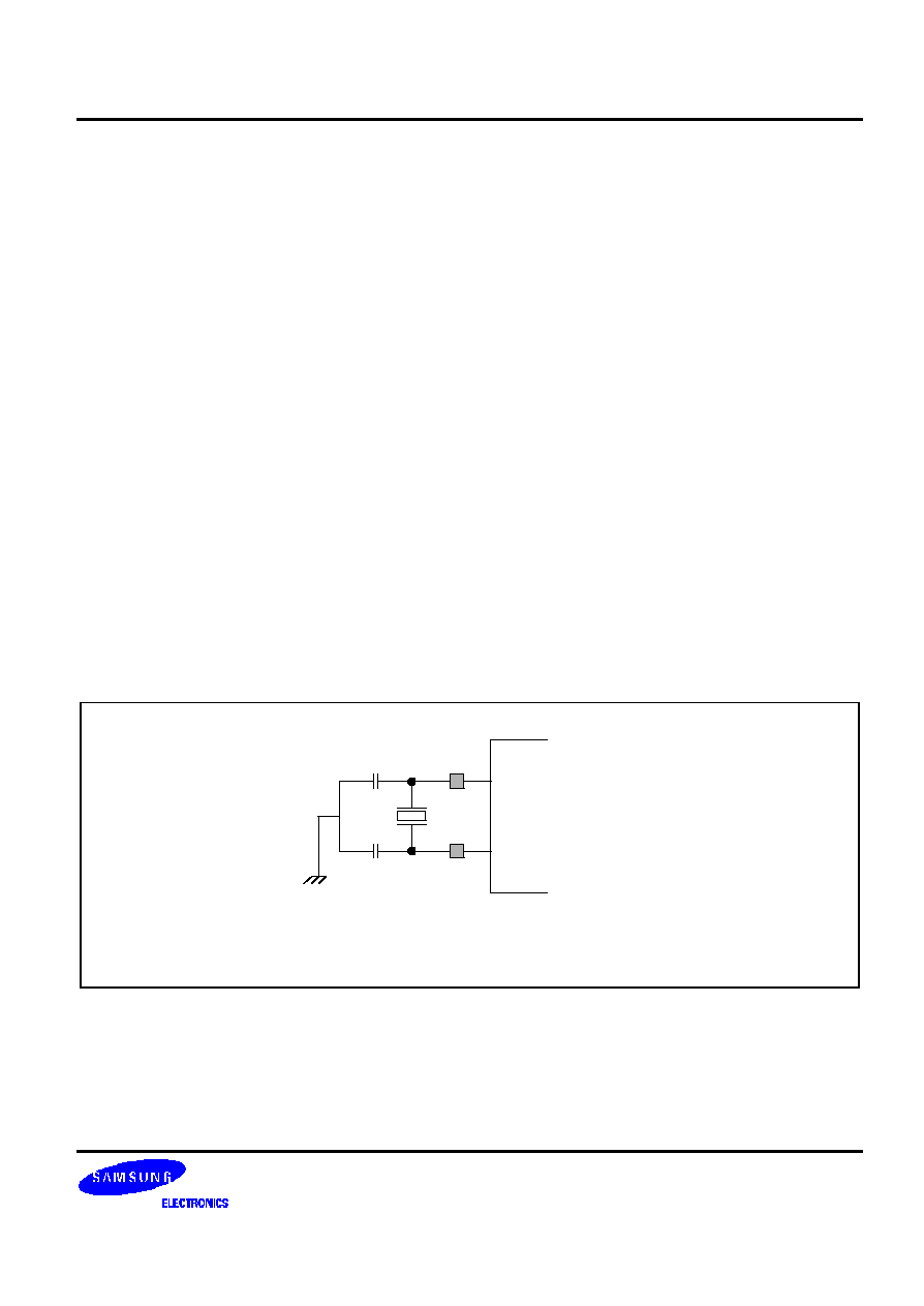
S3C880A/F880A
CLOCK CIRCUITS
7-1
7
CLOCK CIRCUITS
OVERVIEW
The clock frequency generated by an external crystal or ceramic resonator may range from 0.5 MHz to 8 MHz. The
maximum CPU clock frequency is 8 MHz. The X
IN
and X
OUT
pins connect the external oscillation source to the on-
chip clock circuit.
A separate external L-C resonator circuit generates a clock pulse for the on-screen display (OSD) block.
SYSTEM CLOCK CIRCUIT
The system clock circuit has the following components:
-- External crystal or ceramic oscillation source
-- Oscillator stop and wake-up functions
-- Programmable frequency divider for the CPU clock (f
OSC
divided by 1, 2, 8, or 16)
-- Clock circuit control register, CLKCON
S3C880A/F880A
X
IN
X
OUT
C1
C2
NOTE: In X
IN,
X
OUT
pin, 10 pF load capacitor is built-in.
Figure 7-1. Main Oscillator Circuit (External Crystal or Ceramic Resonator)
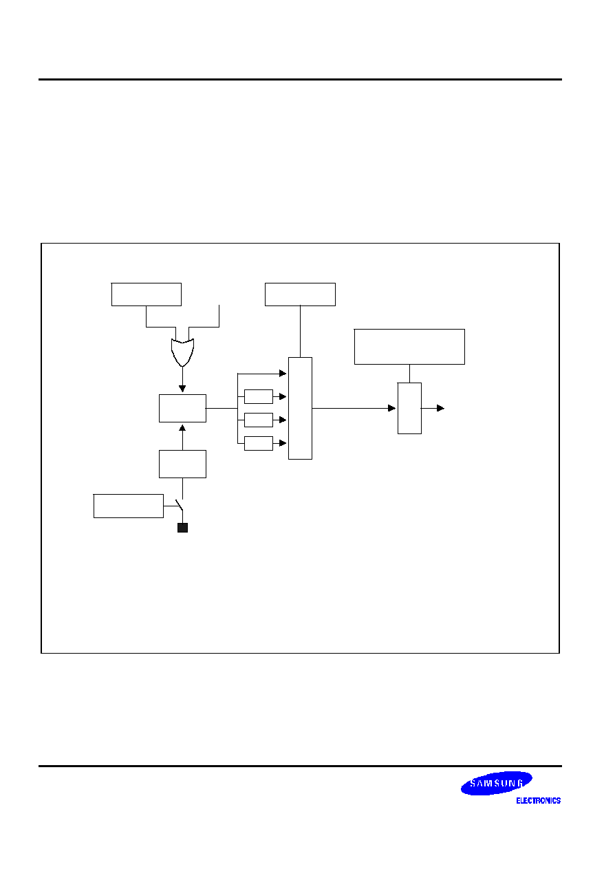
CLOCK CIRCUITS
S3C880A/F880A
7-
2
CLOCK STATUS DURING POWER-DOWN MODES
The two power-down modes, Stop mode and Idle mode, affect system clock oscillation as follows:
-- In Stop mode, the main oscillator is halted. Stop mode is released, and the oscillator started, by a reset
operation or by an external interrupt (with RC-delay noise filter).
-- In Idle mode, the internal clock signal is gated off to the CPU and to all peripherals except for the OSD block,
Timer A counter, PWM, and capture (CAPA), which are inactive. Idle mode is released by a reset or by all
interrupt.
Main
OSC
Noise
Filter
Oscillator
Wake-up
Oscillator
Stop
CLKCON.7
INT Pin
(1)
Stop
Instruction
NOTES:
1. An external interrupt (with RC-delay noise filter) can be used to release Stop mode and
"wake up" the main oscillator. This interrupt type includes INT0-INT3 and CAPA input.
2. For S3F880A, the CLKCON signature code (CLKCON.0-CLKCON.2) should not be
'101B' (because no subsystem clock is implemented)
CLKCON.3, .4
1/2
1/8
1/16
M
U
X
CLKCON.0-.2
3-Bit Signature Code
(2)
M
U
X
CPU Clock
CLKCON.5, .6
Figure 7-2. System Clock Circuit Diagram
S3C880A/F880A
CLOCK CIRCUITS
7-3
SYSTEM CLOCK CONTROL REGISTER (CLKCON)
The system clock control register, CLKCON, is located in set 1 at address D4H. It is read/write addressable and has
the following functions:
-- Oscillator IRQ wake-up function enable/disable
-- Main oscillator stop control
-- Oscillator frequency divide-by value: non-divided, 2, 8, or 16
-- System clock signal selection
The CLKCON register controls whether or not an external interrupt can be used to trigger a power-down mode
release. (This is called the "IRQ wake-up" function.) The IRQ wake-up enable bit is CLKCON.7.
After a reset, the external interrupt oscillator wake-up bit is set to "1", the main oscillator is activated, and the
f
OSC
/16 (the slowest clock speed) is selected as the CPU clock. If necessary, you can then increase the CPU
clock speed to f
OSC
, f
OSC
/2, or f
OSC
/8.
For the S3C880A/F880A, the CLKCON.0�CLKCON.2 system clock signature code should be any value other than
'101B'. (This setting is invalid because a subsystem clock is not implemented.) The reset value for the clock
signature code is '000B'.
System Clock Control Register (CLKCON)
D4H, Set 1, R/W
.7
.6
.5
.4
.3
.2
.1
.0
MSB
LSB
Divide-by selection bits for
CPU clock frequency:
00 = f
OSC
/16
01 = f
OSC
/8
10 = f
OSC
/2
11 = f
OSC
/(non-divided)
System clock selection bits:
(note)
101B = Invalid selection
Other value = Normal operating mode
Main oscillator stop control bits:
(note)
00 = No effect
01 = No effect
10 = Stop main oscillator
11 = No effect
Oscillator IRQ wake-up enable bit:
0 = Enable IRQ for main system
oscillator wake-up in
power-down mode
1 = Disable IRQ for main system
Oscillator wake-up in
power-down mode
NOTE:
Not used in S3C880A.
These setting is valid in subsystem clock operation.
S3C880A is not implemented subsystem operation function.
Figure 7-3. System Clock Control Register (CLKCON)
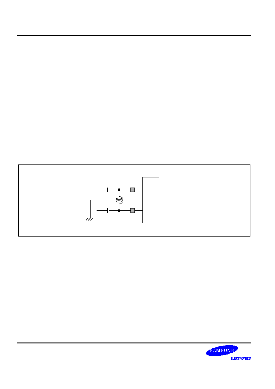
CLOCK CIRCUITS
S3C880A/F880A
7-
4
L-C Oscillator Circuit
The L-C oscillator circuit has the following components:
-- External L-C oscillator with a 5-8 MHz frequency range
-- Oscillator clock divider value (CHACON.4 and CHACON.5)
-- OSC
IN
and OSC
OUT
pins
-- On/off control bit (DSPCON.0)
Red-green-blue (RGB) color outputs, as well as display rates and positions, are determined by the L-C clock signal.
This signal is scaled by the dot and column counter. The clock signal equals to the OSD oscillator clock divided by
the clock divider value. The clock divider value is determined by the horizontal character size settings in the
CHACON register.
The rate at which each new display line is generated is determined strictly by the H-sync input. The rate at which
each new frame (screen) is generated is determined by the V-sync input.
NOTE: For stable on screen display operation, the CPU clock frequency should faster than L-C (OSD) clock.
S3C880A/F880A
OSC
IN
OSD
OUT
C1 = 20 pF
C2 = 20 pF
L
Figure 7-4. L-C Oscillator Circuit for OSD
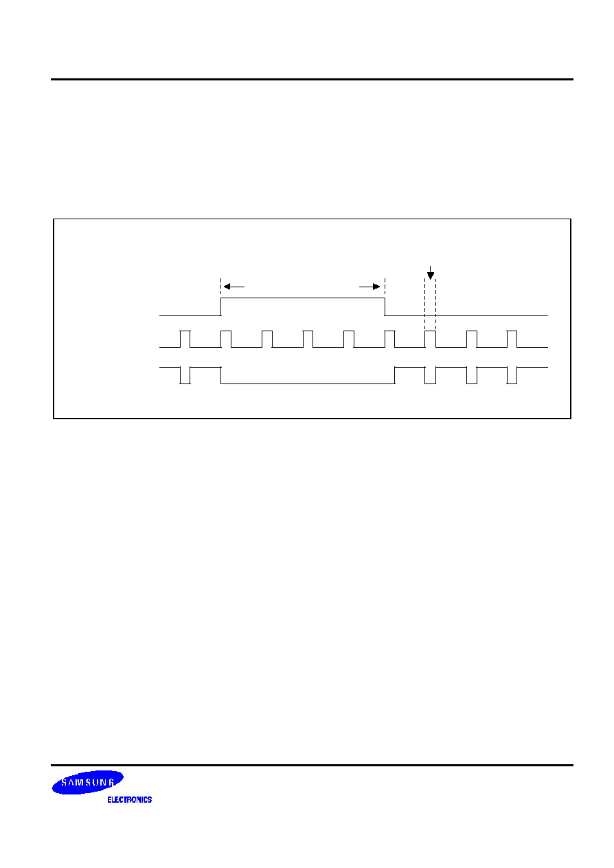
S3C880A/F880A
CLOCK CIRCUITS
7-5
L-C oscillator Operating Condition
To operate the LC oscillator, the following conditions must be satisfied.
-- LC oscillator operation must be enabled by setting DSPCON.0 to "1".
-- V-sync signal and H-sync signal must be input.
-- LC oscillator must be operated except at the range of H-sync blanking and V-sync blanking.
V-sync Signal
H-sync Signal
L-C OSC on
L-C OSC off
V-sync Blanking Range
H-sync Blanking Range
RELATION BETWEEN L-C OSCILLATOR AND CPU CLOCK
For normal On Screen Display, L-C oscillator less than CPU Clock + 10 % is better. For 8 MHz CPU clock, an
active L-C oscillator clock range is lower than 9MHz.

CLOCK CIRCUITS
S3C880A/F880A
7-
6
NOTES

S3C880A/F880A
nRESET and POWER-DOWN
8-1
8
nRESET and POWER-DOWN
SYSTEM nRESET
OVERVIEW
During a power-on reset, the voltage at V
DD
is High level and the nRESET pin is forced to Low level. The nRESET
signal is input through a Schmitt trigger circuit where it is then synchronized with the CPU clock. This brings the
S3C880A/F880A into a normal operating status.
The nRESET pin must be held to Low level for a minimum time interval after the power supply comes within
tolerance in order to allow time for internal CPU clock oscillation to stabilize. The minimum time required for
oscillation stabilization for a reset is 1 millisecond.
When a reset occurs during the normal operation (that is, when V
DD
and nRESET are High level), the nRESET pin is
forced Low and the reset operation starts. All system and peripheral control registers are set to their default
hardware reset values (see Table 8-1). In summary, the following sequence of events occurs during a reset operation:
-- All interrupts are disabled.
-- The watchdog function (basic timer) is enabled.
-- Ports P0.0�P0.5, P1.6�P1.7 and P2are set to input mode, and P0.6�P0.7, P1.0�P1.5 and P3, these ports set
to N-channel open-drain output mode.
-- Peripheral control and data registers are disabled and reset to their initial control values.
-- The program counter is loaded with the ROM's reset address, 0100H.
-- When the programmed oscillation stabilization time interval has elapsed, the instruction stored in the ROM
location 0100H (and 0101H) is fetched and executed.
NOTE
You can program the duration of the oscillation stabilization interval by making the appropriate settings to
the basic timer control register, BTCON, before entering Stop mode. Also, you if you do not want to use the
basic timer watchdog function (which causes a system reset if a basic timer counter overflow occurs), you
can disable it by writing '1010B' to the upper nibble of BTCON.
nRESET and POWER-DOWN
S3C880A/F880A
8-2
HARDWARE RESET VALUES
Tables 8-1 through 8-3 list the reset values for CPU and system registers, peripheral control registers, and peripheral
data registers after a reset operation. The following notation is used to represent reset values:
-- A "1" or a "0" shows the reset bit value as logic one or logic zero, respectively.
-- An 'x' means that the bit value is undefined after a reset.
-- A dash ('�') means that the bit is either not used or not mapped.
Table 8-1. Set 1 Register Values after a Reset
Register Name
Mnemonic
Address
Bit Values After a Reset
Dec
Hex
7
6
5
4
3
2
1
0
Timer 0 counter
T0CNT
208
D0H
0
0
0
0
0
0
0
0
Timer 0 data register
T0DATA
209
D1H
1
1
1
1
1
1
1
1
Timer 0 control register
T0CON
210
D2H
0
0
0
0
0
0
0
0
Basic timer control register
BTCON
211
D3H
0
0
0
0
0
0
0
0
Clock control register
CLKCON
212
D4H
0
0
0
0
0
0
0
0
System flags register
FLAGS
213
D5H
x
x
x
x
x
x
0
0
Register pointer 0
RP0
214
D6H
1
1
0
0
0
�
�
�
Register pointer 1
RP1
215
D7H
1
1
0
0
1
�
�
�
Stack pointer (high byte)
SPH
216
D8H
x
x
x
x
x
x
x
x
Stack pointer (low byte)
SPL
217
D9H
x
x
x
x
x
x
x
x
Instruction pointer (high byte)
IPH
218
DAH
x
x
x
x
x
x
x
x
Instruction pointer (low byte)
IPL
219
DBH
x
x
x
x
x
x
x
x
Interrupt request register
IRQ
220
DCH
0
0
�
0
0
0
0
0
Interrupt mask register
IMR
221
DDH
x
x
�
x
x
x
x
x
System mode register
SYM
222
DEH
0
�
0
x
x
x
0
0
Register page pointer
PP
223
DFH
0
0
0
0
0
0
0
0
NOTE: Although it is not used for the S3C880A/F880A, bit 5 of the SYM register should always be "0". If this bit is
accidentally written to "1" by software, a system malfunction may occur.
S3C880A/F880A
nRESET and POWER-DOWN
8-3
Table 8-2. Set 1, Bank 0 Register Values after a Reset
Register Name
Mnemonic
Address
Bit Values After a Reset
Dec
Hex
7
6
5
4
3
2
1
0
Port 0 data register
P0
224
E0H
0
0
0
0
0
0
0
0
Port 1 data register
P1
225
E1H
0
0
0
0
0
0
0
0
Port 2 data register
P2
226
E2H
0
0
0
0
0
0
0
0
Port 3 data register
P3
227
E3H
�
�
�
�
�
�
0
0
Port 0 control register (high byte)
P0CONH
228
E4H
1
1
1
1
0
0
0
0
Port 0 control register (low byte)
P0CONL
229
E5H
0
0
0
0
0
0
0
0
Port 1 control register (high byte)
P1CONH
230
E6H
0
0
0
0
1
1
1
1
Port 1 control register (low byte)
P1CONL
231
E7H
1
1
1
1
1
1
1
1
Port 2 control register (high byte)
P2CONH
232
E8H
0
0
0
0
0
0
0
0
Port 2 control register (low byte)
P2CONL
233
E9H
0
0
0
0
0
0
0
0
Location EAH in set 1, bank 0, are not mapped.
Port 3 control register (low byte)
P3CONL
235
EBH
�
�
�
�
1
1
1
1
Locations ECH�EFH in set 1, bank 0, are not mapped.
Timer A data register
TADATA
240
F0H
0
0
0
0
0
0
0
0
Location F1H in set 1, bank 0, are not mapped.
Timer A control register
TACON
242
F2H
0
0
0
0
0
0
0
�
STOP control register
STCON
238
F3H
0
0
0
0
0
0
0
0
PWM0 data register (main byte)
PWM0
244
F4H
1
1
1
1
1
1
1
1
PWM0 data register (extension byte)
PWM0EX
245
F5H
0
0
0
0
0
0
�
�
PWM1 data register (main byte)
PWM1
246
F6H
1
1
1
1
1
1
1
1
PWM1 data register (extension byte)
PWM1EX
247
F7H
0
0
0
0
0
0
�
�
PWM control register
PWMCON
248
F8H
0
0
0
0
0
�
0
0
Capture A data register
CAPA
249
F9H
0
0
0
0
0
0
0
0
A/D converter control register
ADCON
250
FAH
�
�
0
0
x
0
0
0
A/D conversion data register
ADDATA
251
FBH
x
x
x
x
x
x
x
x
Location FCH in set 1, bank 0, are not mapped.
Basic timer counter
BTCNT
253
FDH
0
0
0
0
0
0
0
0
External memory timing register
EMT
254
FEH
0
0
0
0
0
0
0
�
Interrupt priority register
IPR
255
FFH
x
x
�
x
x
x
x
x
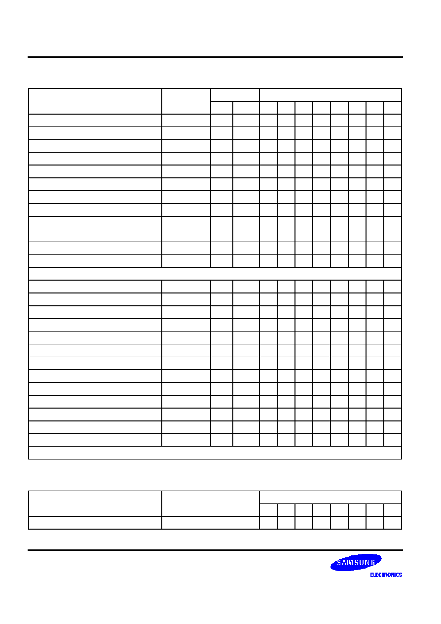
nRESET and POWER-DOWN
S3C880A/F880A
8-4
Table 8-2. Set 1, Bank 1 Register Values after a Reset
Register Name
Mnemonic
Address
Bit Values After a Reset
Dec
Hex
7
6
5
4
3
2
1
0
OSD fringe/border control register 1
OSDFRG1
224
E0H
0
0
0
0
0
0
0
0
OSD fringe/border control register 2
OSDFRG2
225
E1H
0
0
0
0
0
0
0
0
OSD smooth control register 1
OSDSMH1
226
E2H
0
0
0
0
0
0
0
0
OSD smooth control register 2
OSDSMH2
227
E3H
�
�
�
�
0
0
0
0
OSD space color control register
OSDCOL
236
E4H
�
�
�
�
0
0
0
0
OSD field control register
OSDFLD
237
E5H
�
�
x
0
0
1
1
0
OSD palette color mode R 1
OSDPLTR1
230
E6H
0
0
0
0
0
0
0
0
OSD palette color mode R 2
OSDPLTR2
231
E7H
1
1
1
1
1
1
1
1
OSD palette color mode G 1
OSDPLTG1
232
E8H
1
1
1
1
0
0
0
0
OSD palette color mode G 2
OSDPLTG2
233
E9H
1
1
1
1
0
0
0
0
OSD palette color mode B 1
OSDPLTB1
234
EAH
1
1
0
0
1
1
0
0
OSD palette color mode B 2
OSDPLTB2
235
EBH
1
1
0
0
1
1
0
0
Locations ECH�EFH in set 1, bank 1, are not mapped.
OSD character size control register
CHACON
240
F0H
0
0
0
0
0
0
0
0
OSD fade control register
FADECON
241
F1H
0
0
0
0
0
0
0
0
OSD row position control register
ROWCON
242
F2H
0
0
0
0
0
0
0
0
OSD column position control register
CLMCON
243
F3H
0
0
0
0
0
0
0
0
OSD background color control register
COLCON
244
F4H
0
0
0
0
0
0
0
0
On-screen display control register
DSPCON
245
F5H
0
0
0
0
0
0
0
0
Halftone signal control register
HTCON
246
F6H
0
0
0
0
0
0
0
0
V-SYNC blank control register
VSBCON
252
F7H
�
�
�
0
1
0
0
1
PWM2 data register
PWM2
248
F8H
x
x
x
x
x
x
x
x
PWM3 data register
PWM3
249
F9H
x
x
x
x
x
x
x
x
PWM4 data register
PWM4
250
FAH
x
x
x
x
x
x
x
x
PWM5 data register
PWM5
251
FBH
x
x
x
x
x
x
x
x
OSD color buffer
COLBUF
247
FCH
�
�
�
x
x
x
x
x
Locations FDH�FFH in set 1, bank 1, are not mapped.
Table 8-3. Page 1 Video RAM Register Values after a Reset
Register Name
Address
Bit Values After a Reset
7
6
5
4
3
2
1
0
OSD video RAM
00H�FBH
x
x
x
x
x
x
x
x

S3C880A/F880A
nRESET and POWER-DOWN
8-5
POWER-DOWN MODES
STOP MODE
Stop mode is invoked by the instruction Stop (opcode 7FH) however Stop available state must be set by value
"10100101b" in "STCON" register before Stop instruction is invoked. If Stop instruction (opcode 7FH) is executed in
Stop not available state (STCON = other value except "10100101b") CPU go to RESET address. After Stop
instruction is executed the state return to Stop not available state.
In Stop mode, the operation of the CPU and all peripherals is halted. That is, the on-chip main oscillator stops and
the supply current is reduced to less than maximum 10 �A. All system functions stop when the clock "freezes," but
data stored in the internal register file is retained. Stop mode can be released in one of two ways: by a nRESET
signal or by an external interrupt.
Using nRESET to Release Stop Mode
Stop mode is released when the nRESET signal goes inactive (High level) from active (Low level) state.
All system and peripheral control registers are reset to their default values and the contents of all data registers are
retained. A reset operation automatically selects a slow clock (1/16) because CLKCON.3 and CLKCON.4 are
cleared to '00B'. After the programmed oscillation stabilization interval has elapsed, the CPU starts the system
initialization routine by fetching the address stored in the ROM location 0100H.
Using an External Interrupt to Release Stop Mode
Two kinds of external interrupts with an RC-delay noise filter circuit can be used to release Stop mode. One external
interrupts in the S3C880A/F880A interrupt structure that meet this requirement are INT0�INT3 (P1.0�P1.3) and the
other one is V-sync input. Which interrupt you can use to release Stop mode in a given situation depends on the
microcontroller's current internal operating mode.
Note that when Stop mode is released by an external interrupt, the current values in system and peripheral control
registers are not changed. When you use an interrupt to release Stop mode, the CLKCON.3 and CLKCON.4 register
values remain unchanged, and the currently selected clock value is used. If you use an external interrupt for Stop
mode release, you can also program the duration of the oscillation stabilization interval. To do this, you must make
the appropriate control and clock settings before entering Stop mode.
The external interrupt is serviced when a Stop mode release occurs. Following the IRET from the service routine, the
instruction immediately following the one that initiated Stop mode is executed.
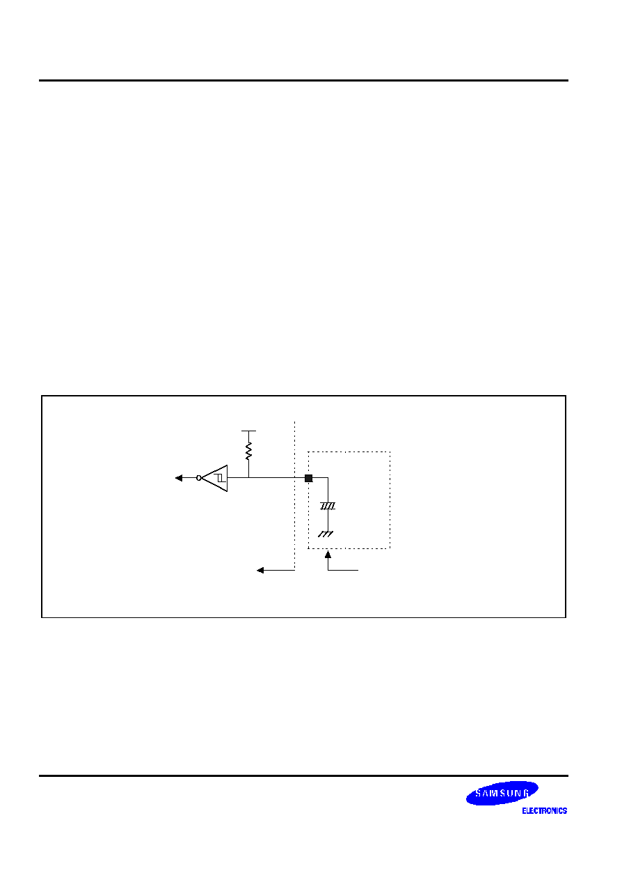
nRESET and POWER-DOWN
S3C880A/F880A
8-6
IDLE MODE
Idle mode is invoked by the instruction IDLE (opcode 6FH). In Idle mode, the CPU operations are halted while
selected peripherals remain active. During Idle mode, the internal clock signal is gated off to the CPU and all
peripherals except the OSD block timer A counter, PWM and capture (CAPA). Port pins retain the mode (input or
output) they had at the time Idle mode was entered.
There are two ways to release Idle mode:
1. Execute a reset. All system and peripheral control registers are reset to their default values and the contents of
all data registers are retained. The reset automatically selects a slow clock (1/16) because CLKCON.3 and
CLKCON.4 are cleared to '00B'. If interrupts are masked, a reset is the only way to release Idle mode.
2. Activate any enabled interrupt, causing Idle mode to be released. When you use an interrupt to release Idle
mode, the CLKCON.3 and CLKCON.4 register values remain unchanged, and the currently selected clock value
is used. The interrupt is then serviced. When the return-from-interrupt (IRET) occurs, the instruction immediately
following the one that initiated Idle mode is executed.
NOTE
Only external interrupts can be used to release Stop mode. To release Idle mode, you can use either type of
interrupt (internal or external).
0.1-10
�
F
Internal
Recommand
External Circuit
200 k
Figure 8-1. Reset Circuit Application
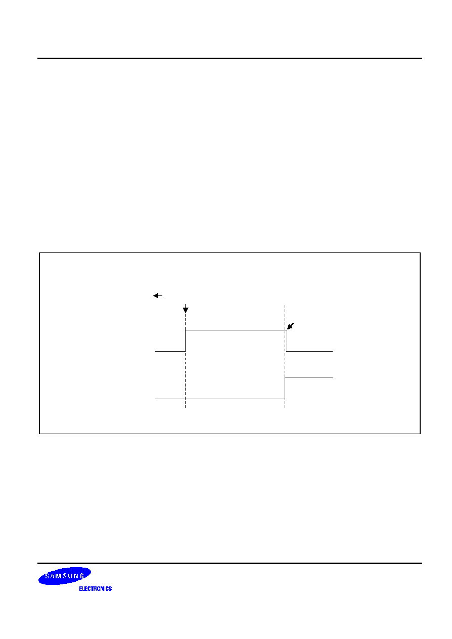
S3C880A/F880A
nRESET and POWER-DOWN
8-7
F
PROGRAMMING TIP -- Enter to Stop Mode
The following sample program shows you recommended entering Stop mode for the S3C880A/F880A.
�
�
�
ld
STCON, #10100101b
; After this instruction is executed
; Stop instruction is available
STOP
NOP
; NOP need more than three after STOP instruction
NOP
NOP
�
�
�
Stop Available
State
STCON
#10100101b
STON
Instruction
Stop State
Enable
Disable
Enable
Disable
Stop available state is released
automatically after STOP
instruction.
Figure 8-2. Stop State Timing Diagram

nRESET and POWER-DOWN
S3C880A/F880A
8-8
F
PROGRAMMING TIP -- Initial Settings for Address Space, Vectors, and Peripherals
The following sample program shows you recommended initial settings for the S3C880A/F880A address space,
interrupt vectors, and peripheral functions. Program comments guide you through the required steps:
�
�
�
OSD_REG
EQU
0C8H
; OSD working register area
OSD_FLG
EQU
8
DSP_TYP
EQU
9
VRAMAD
EQU
0CH
WORK1
EQU
0BH
; General-purpose area
WORK2
EQU
0AH
; General-purpose area
REMOCON
EQU
3FH
; CAPA data save register
�
�
�
ORG
02H
DW
CAPA_INT;
Capture A interrupt
ORG
0BEH
DW
TIMERA_INT
; Timer A interrupt
ORG
0C0H
DW
P10_INT
; P1.0 external interrupt
DW
P11_INT
; P1.1 external interrupt
DW
OSD ROW_INT
; OSD ROW interrupt
DW
P12_INT
; P1.2 external interrupt
DW
P13_INT
; P1.3 external interrupt
ORG
0D4H
DW
V_SYNC_INT
; V-sync interrupt
ORG
0FCH
DW
TIMER0_INT
; Timer 0 interrupt
ORG
0100H
START
DI
; Disable all interrupts
LD
BTCON,#0AAH
; Disable the watchdog timer
LD
CLKCON,#98H
; Non-divided clock
CLR
SYM
; Disable global and fast interrupts
CLR
SPL
; Stack pointer low byte
"0"
; Stack area will start at 0FFH
SB1
; Select bank 1
(Continued on next page)

S3C880A/F880A
nRESET and POWER-DOWN
8-9
F
PROGRAMMING TIP -- Initial Settings for Address Space, Vectors, and Peripherals (Continued)
; Enable OSD ROW interrupt
LD
HTCON,#2AH
; Enable V-sync interrupt
LD
DSPCON,#0A0H
; Disable OSD logic
SB0
; Select bank 0
LD
PWMCON,#0E9H
; Prescaler
4
; Enable PWM counter
; Enable capture A interrupt
LD
IPR,#0AEH
; Interrupt priority settings
; IRQ6 > 7 > 3 > 2 > 0 > 1
LD
IMR,#0CCH
; Enable level 2, 3, 6, and 7 interrupts
LD
P0CONH,#00H
; Input mode
LD
P0CONL,#0FFH
; Push-pull output mode
LD
P1CONH,#0FFH
; Output mode
LD
P1CONL,#00H
; Input mode
LD
P2CONH,#00H
; Input mode
LD
P2CONL,#00H
; Input mode
LD
P3CONL,#00H
; Input mode
LD
TACON,#54H
; Prescaler
6
; Clock source
CPU clock / 1000
; Enable timer A interrupt
; Interval timer mode
LD
TADATA,#03H
; 4-millisecond interrupt
EI
MAIN
NOP
NOP
�
�
�
NOP
JP
T,MAIN
; Jump MAIN
CAPA_INT:
; CAPA interrupt service
PUSH
PP
; Save page pointer to stack
PUSH
RP0
; Save register pointer 0 to stack
PUSH
RP1
; Save register pointer 1 to stack
�
�
�
LD
REMOCON,CAPA
; REMOCON
CAPA data
POP
RP1
; Restore register pointer 1 value
POP
RP0
; Restore register pointer 0 value
POP
PP
; Restore page pointer value
IRET
; Return from interrupt service routine
(Continued on next page)

nRESET and POWER-DOWN
S3C880A/F880A
8-10
F
PROGRAMMING TIP -- Initial Settings for Address Space, Vectors, and Peripherals (Continued)
TIMERA_INT
PUSH
PP
; TIMER_A interrupt service
PUSH
RP0
PUSH
RP1
�
�
�
LD
TACON, #54H
; Clear pending bit
POP
RP1
POP
RP0
POP
PP
IRET
; Return from interrupt service routine
V_SYNC_INT
PUSH
PP
; V_SYNC interrupt service
PUSH
RP0
PUSH
RP1
�
�
�
SB1
LD
HTCON, #3AH
; Clear pending bit
POP
RP1
POP
RP0
POP
PP
IRET
; Return from interrupt service routine
OSD ROW_INT:
PUSH
PP
PUSH
RP0
PUSH
RP1
�
�
�
SB1
LD
HTCON, #2BH
; Clear pending bit
POP
RP1
POP
RP0
POP
PP
IRET
P10_INT:
; P1.0 external interrupt
P11_INT:
; P1.1 external interrupt
P12_INT:
; P1.2 external interrupt
P13_INT:
; P1.3 external interrupt
TIMER0_INT:
; Timer 0 interrupt
IRET
; Return from interrupt service routine
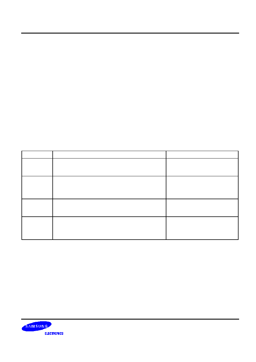
S3C880A/F880A
I/O PORTS
9-1
9
I/O PORTS
OVERVIEW
The S3C880A/F880A and the S3C880A/F880A microcontrollers have four I/O ports with a total of 26 pins. Up to 10
pins can be configured as n-channel open-drain outputs. Of these 10 open-drain pins, 6 pins can withstand loads of
up to 6 volts and 4 pins can withstand loads of up to 5 volts.
The CPU accesses ports by directly writing or reading port registers. No special I/O instructions are required. Table
9-1 gives you a summary of port functions:
Table 9-1. S3C880A/F880A Port Configuration Overview
Port
Configuration Options
Programmability
0
General I/O port, configurable for digital input or
push-pull output. Pins P0.6�P0.7 are multiplexed to
support alternative function.
Bit programmable
1
General I/O port, configurable for digital input or
n-channel open-drain output. Pins 1.0�P1.5 can withstand
up to 6-volt loads. Pins 1.0�P1.3 are multiplexed to
support alternative functions.
Bit programmable
2
General I/O port, configurable for n-channel open-drain or
push-pull output mode by software. Pins can withstand up
to 5-volt loads. Each pin has an alternative function.
Bit programmable
3
General 2-bit I/O port, configurable for digital input or
n-channel open-drain output. Pins can withstand up to 5 V.
P3.0�P3.1 can be alternately used as external interrupt
inputs ADC0�ADC1.
Bit programmable
I/O PORTS
S3C880A/F880A
9-2
PORT DATA REGISTERS
Data registers for ports 0�3 have the structure shown in Figure 9-1. Table 9-2 gives you an overview of the port data
register locations:
Table 9-2. Port Data Register Summary
Register Name
Mnemonic
Decimal
Hex
Location
R/W
Port 0 data register
P0
224
E0H
Set 1, bank 0
R/W
Port 1 data register
P1
225
E1H
Set 1, bank 0
R/W
Port 2 data register
P2
226
E2H
Set 1, bank 0
R/W
Port 3 data register
P3
227
E3H
Set 1, bank 0
R/W
I/O Port n Data Register (n = 0-3)
LSB
MSB
.7
.6
.5
.4
.3
.2
.1
.0
Pn.0
Pn.4
Pn.1
Pn.2
Pn.3
Pn.7
Pn.5
Pn.6
Figure 9-1. Port Data Register Format
Port 0
Port 0 is a bit-programmable general I/O port. Port 0 is accessed directly by writing or reading the port 0 data
register, P0 (E0H, set 1, bank 0).
The port 0 pins are configured by bit-pair settings in the P0CONH and P0CONL registers. P0CONH controls I/O for
the upper byte pins and P0CONL controls I/O for the lower byte pins.

S3C880A/F880A
I/O PORTS
9-3
Port 0 Control Register, High Byte (P0CONH)
E4H, Set 1, Bank 0, R/W
LSB
MSB
.7
.6
.5
.4
.3
.2
.1
.0
P0.7/ADC2 P0.6/ADC2
P0.4
P0.5
P0CONH Pin Configuration Settings:
00
01
10
11
Input mode
Input mode (P0.4-P0.5), ADC input mode (P0.6-P0.7)
Push-pull output mode (P0.4-P0.5), open-drain output mode (P0.6-P0.7)
Push-pull output mode (P0.4-P0.5), open-drain output mode (P0.6-P0.7)
Figure 9-2. Port 0 High-Byte Control Register (P0CONH)
Port 0 Control Register, Low Byte (P0CONL)
E5H, Set 1, Bank 0, R/W
LSB
MSB
.7
.6
.5
.4
.3
.2
.1
.0
P0.3
P0.2
P0.1
P0.0
P0CONL Pin Configuration Settings:
00
01
10
11
Input mode
Input mode
N-channel open-drain output mode (5V load capacity)
Push-pull output mode
Figure 9-3. Port 0 Low-Byte Control Register (P0CONL)
I/O PORTS
S3C880A/F880A
9-4
PORT 1
Port 1 is a bit-programmable general I/O port. Port 1 is accessed directly by writing or reading the port 1 data
register, P1 (E1H, set 1, bank 0). The upper byte (P1.4�P1.7) and the lower byte (P1.0�P1.3) are controlled by the
P1CONH and P1CONL registers, respectively. P1CONH is located at E6H in set 1, bank 0 and P1CONL is located
at E7H in set 1, bank 0.
Port 1 Control Register, High Byte (P1CONH)
E6H, Set 1, Bank 0, R/W
LSB
MSB
.7
.6
.5
.4
.3
.2
.1
.0
P1.4
P1CONH Pin Configuration Settings:
00
01
10
11
Input mode
Inputmode (P1.4-P1.6), Timer 0 clock input: T0CK (P1.7)
P1.4-P1.5: N-channel open-drain mode (6V load capacity),
P1.6-P1.7: Push-pull output mode
P1.4-P1.5: N-channel open-drain mode (6V load capacity),
P1.6-P1.7: Push-pull output mode
P1.5
P1.6
P1.7/T0CK
Figure 9-4. Port 1 High-Byte Control Register (P1CONH)
Port 1 Control Register, Low Byte (P1CONL)
E7H, Set 1, Bank 0, R/W
LSB
MSB
.7
.6
.5
.4
.3
.2
.1
.0
P1.0/INT0
P1CONL Pin Configuration Settings:
00
01
10
11
Input mode: Interrupt disabled
Input mode: Interrupt on rising edge
Input mode: Interrupt on falling edge
N-channel open-drain output mode (6V load capacity)
P1.1/INT1
P1.2/INT2
P1.3/INT3
Figure 9-5. Port 1 Low-Byte Control Register (P1CONL)

S3C880A/F880A
I/O PORTS
9-5
PORT 2
Port 2 is a bit-programmable general I/O port. Port 2 is accessed directly by writing or reading the port 2 data
register, P2 (E2H, set 1, bank 0). The upper byte (P2.4�P2.7) and the lower byte (P2.0�P2.3) are controlled by the
P2CONH and P2CONL registers, respectively.
A reset clears the port 2 control registers to '00H', configuring the port 2 pins to normal input mode (P2.0�P2.3) and
input mode (2.4�P2.7). You use P2CONH and P2CONL register settings to configure individual port 2 pins:
Port 2 Control Register, High Byte (P2CONH)
E8H, Set 1, Bank 0, R/W
LSB
MSB
.7
.6
.5
.4
.3
.2
.1
.0
P2.4/PWM4
P2CONH Pin Configuration Settings:
00
01
10
11
Input mode
N-channel open-drain output mode (5V load capacity)
Push-pull output mode
P2.4: PWM4 output mode (open-drain type)
P2.5: PWM5 output mode (push-pull circuit type)
P2.6: Timer 0 output mode (PWM or Interval; open-drain type)
P2.7: OSD half-tone output mode (push-pull circuit type)
P2.5/PWM0
P2.6/T0
P2.7/OSDHT
Figure 9-6. Port 2 High-Byte Control Register (P2CONH)
Port 2 Control Register, Low Byte (P2CONL)
E9H, Set 1, Bank 0, R/W
LSB
MSB
.7
.6
.5
.4
.3
.2
.1
.0
P2.0/PWM5
P2CONL Pin Configuration Settings:
00
01
10
11
Normal input mode
N-channel open-drain output mode with 5V load capacity
PWM output mode: N-channel open-drain type
Push-pull output mode
P2.1/PWM1
P2.2/PWM2
P2.3/PWM3
Figure 9-7. Port 2 Low-Byte Control Register (P2CONL)
I/O PORTS
S3C880A/F880A
9-6
PORT 3
Port 3 is a bit-programmable general I/O port. Only two bits are used. Port 3 is accessed directly by writing or
reading the port 3 data register, P3 (E3H, set 1, bank 0).
A reset operation sets the P3 data register to '00H', and the port 3 control register to `0FH', configuring the port 3
pins to output (open-drain) mode.
Port 3 Control Register (P3CON)
EBH, Set 1, Bank 0, R/W
LSB
MSB
.7
.6
.5
.4
.3
.2
.1
.0
P3.0/ADC0
P3CON Pin Configuration Settings:
00
01
10
11
Input mode
ADC input mode
Input mode
N-channel open-drain output mode (with 5V load capacity)
P3.1/ADC1
No effect
Figure 9-8. Port 3 Control Register (P3CON)

S3C880A/F880A
I/O PORTS
9-7
F
PROGRAMMING TIP -- Configuring I/O Port Pins to Specification
The following sample program shows you how to configure the S3C880A/F880A I/O ports to specification. The
following parameters are given for ports 0, 1, 2, and 3:
-- Set P0.0 and P0.1 to input mode
-- Set P0.2 and P0.3 to output mode
-- Set P0.4 and P0.5 to input mode
-- Set P0.6 and P0.7 to open-drain output mode
-- Set P1.0�P1.1 to interrupt rising edge mode
-- Set P1.2�1.5 to open-drain output mode
-- Set P1.6� P1.7 to push-pull output mode
-- Set P2.0 and P2.1 to open-drain output mode
-- Set P2.2�P2.4 to input mode
-- Set P2.6�2.7 to push-pull output mode
-- Set P2.5 to PWM0 output mode
-- Set P3.0�P3.1 to ADC input mode
�
�
�
SB0
; Select bank 0
LD
P0CONH,#0F0H
; P0.4, P0.5
Input mode
; P0.6, P0.7
Open-drain output mode
LD
P0CONL,#0F0H
; P0.0, P0.1
Input mode
; P0.2, P0.3
Output mode
LD
P1CONH,#0FFH
; P1.6�1.7
Push-pull output mode
; P1.2�1.5
Open-drain output mode
LD
P1CONL,#0F5H
; P1.0, P1.1
Interrupt rising edge mode
LD
P2CONH,#0ACH
; P2.4
Input mode
; P2.6, 2.7
Push-pull output mode
; P2.5
PWM0 output mode
LD
P2CONL,#05H
; P2.0, P2.1
Open-drain output mode
; P2.2, P2.3
Input mode
LD
P3CONL,#05H
; P3.0, P3.1
ADC input mode
�
�
�

I/O PORTS
S3C880A/F880A
9-8
F
PROGRAMMING TIP -- Clearing Port 0 Interrupt Pending Bits
This sample program shows you how to clear the interrupt pending bits for port 1. The program parameters are as
follows:
-- Enable only the interrupt level 1 (IRQ1) for P1.0�P1.1
-- Set the interrupt priorities as P1.0 > P1.1
ORG
0C0H
VECTOR
EXT_INT_P10
VECTOR
EXT_INT_P11
�
�
�
ORG
0100H
nRESET
DI
; Disable all interrupts
SB0
; Select bank 0
LD
BTCON,#0AAH
; Disable the watchdog timer
LD
CLKCON,#98H
; Non-divided clock
CLR
SPL
; Stack pointer low byte
"0"
; Stack area starts at 0FFH
�
�
�
LD
IMR,#06H
; Enable IRQ1 and IRQ2 interrupts
LD
IPR,#11H
; IRQ1 > IRQ2
LD
P1CONL,#0AH
; P1.0, P1.1
Input mode; falling edge interrupts
�
�
�
SRP
#0C0H
; Set register pointer to 0C0H
EI
; Enable interrupts
�
�
�
MAIN
NOP
NOP
�
�
�
JP
T,MAIN
�
�
�
(Continued on next page)

S3C880A/F880A
I/O PORTS
9-9
F
PROGRAMMING TIP -- Clearing Port 1 Interrupt Pending Bits (Continued)
EXT_INT_P10:
; P1.0 external interrupt service
PUSH
PP
; Save page pointer to stack
PUSH
RP0
; Save register pointer 0 to stack
PUSH
RP1
; Save register pointer 1 to stack
�
�
�
POP
RP1
; Restore register pointer 1 value
POP
RP0
; Restore register pointer 0 value
POP
PP
; Restore page pointer value
IRET
; Return from interrupt service routine
EXT_INT_P11:
; P1.1 external interrupt service
PUSH
PP
PUSH
RP0
PUSH
RP1
�
�
�
POP
RP1
POP
RP0
POP
PP
IRET

I/O PORTS
S3C880A/F880A
9-10
NOTES

S3C880A/F880A
BASIC TIMER and TIMER 0
10-1
10
BASIC TIMER and TIMER 0
MODULE OVERVIEW
The S3C880A/F880A microcontrollers have two default timers: an 8-bit basic timer (BT) and an 8-bit general-purpose
timer/counter, called timer 0 (T0).
The basic timer (BT) has two alternative functions: 1) it can be used as a watchdog timer that provides an automatic
reset mechanism in the event of a system malfunction, and 2) it can be used to signal the end of the required
oscillation stabilization interval after a reset or a Stop mode release. The components of the basic timer are:
-- Clock frequency divider (f
OSC
divided by 4096, 1024, or 128) with multiplexer
-- 8-bit basic counter, BTCNT (set 1, bank 0, FDH, read-only)
-- Basic timer control register, BTCON (set 1, D3H, read/write)
-- Clock frequency divider (f
OSC
divided by 4096, 256, or 8) with multiplexer
-- 8-bit counter (T0CNT), 8-bit comparator, and 8-bit reference data register (T0DATA)
-- Timer 0 match interrupt (T0INT) generation
-- Timer 0 control register, T0CON (set 1, D2H, read/write)
BASIC TIMER and TIMER 0
S3C880A/F880A
10-2
BASIC TIMER CONTROL REGISTER (BTCON)
The basic timer control register, BTCON, is used to select the input clock frequency, clear the basic timer counter
and frequency dividers, and enable or disable the watchdog timer function. It is located in set 1, address D3H, and is
read/write addressable using Register addressing mode only.
A reset clears BTCON to '00H'. This enables the watchdog function and selects a basic timer clock frequency of
f
OSC
/4096. To disable the watchdog function, you must write the signature code '1010B' to the basic timer register
control bits BTCON.7�BTCON.4.
The 8-bit basic timer counter, BTCNT (set 1, bank 0, FDH), can be cleared during the normal operation by writing a
"1" to BTCON.1. To clear the frequency dividers for both the basic timer input clock and the timer 0 clock, you
should write a "1" to BTCON.0.
Basic Timer Control Register (BTCON)
D3H, Set 1, R/W
LSB
MSB
.7
.6
.5
.4
.3
.2
.1
.0
Divider clear bit for basic timer and T0:
0 = No effect
1 = Clear divider
Basic timer counter clear bit:
0 = No effect
1 = Clear basic timer counter
Basic timer input clock selection bits:
00 = fosc/4096
01 = fosc/1024
10 = fosc/128
11 = fosc/16
Watchdog timer enable bit:
1010B = Disable watchdog function
Other value = Enable watchdog function
Figure 10-1. Basic Timer Control Register (BTCON)

S3C880A/F880A
BASIC TIMER and TIMER 0
10-3
BASIC TIMER FUNCTION DESCRIPTION
Watchdog Timer Function
The basic timer overflow signal can be programmed to generate a reset by setting the BTCON.7�BTCON.4 bits to
any value other than '1010B'. (The '1010B' value disables the watchdog function.) A reset clears the BTCON register
to '00H', automatically enabling the watchdog timer function. A reset also selects the CPU clock (as determined by
the CLKCON register setting) divided by 4096 as the BT clock.
With every overflow of the basic timer counter, a reset occurs. During the normal operation, this overflow-generated
reset should be prevented from occurring. To do this, the basic timer counter value must be cleared by software
(write BTCON.1 to "1") in regular intervals.
If a system malfunction occurs due to circuit noise or some other error condition, the basic timer counter clear
operation may not be executed and a basic timer overflow will occur, initiating a system reset. In other words, in
normal operating condition the basic timer overflow loop (a bit 7 overflow of the 8-bit BT counter) is always broken by
a clear counter instruction.
An application program can use the basic timer as a watchdog timer to trigger an automatic system reset in case a
malfunction occurs.
Oscillation Stabilization Interval Timer Function
The basic timer determines the oscillation stabilization interval after a reset or the release of Stop mode by an
external interrupt. Whenever a reset or an external interrupt occurs during Stop mode, the oscillator begins operating.
The basic timer value then starts increasing at the rate of f
OSC
/4096 (in the case of a reset), or at the rate of the
preset clock source (in the case of an external interrupt).
When bit 4 of the BT counter is set to "1", a signal is generated to indicate that the stabilization interval has elapsed.
This allows the clock signal to be gated on to the CPU so that it can resume normal operation. In summary, the
following events occur when Stop mode is released:
1. During Stop mode a power-on reset or an external interrupt occurs to trigger a Stop mode release, and
oscillation starts.
2. If a power-on reset occurrs, the basic timer counter increases at the rate of f
OSC
/4096. If an external interrupt is
used to release Stop mode, the basic timer value increases at the rate of the preset clock source.
3. Clock oscillation stabilization interval begins and continues until bit 3 of the basic timer counter overflows.
4. When bit 4 of BTCNT is set to "1", the normal CPU operation resumes.
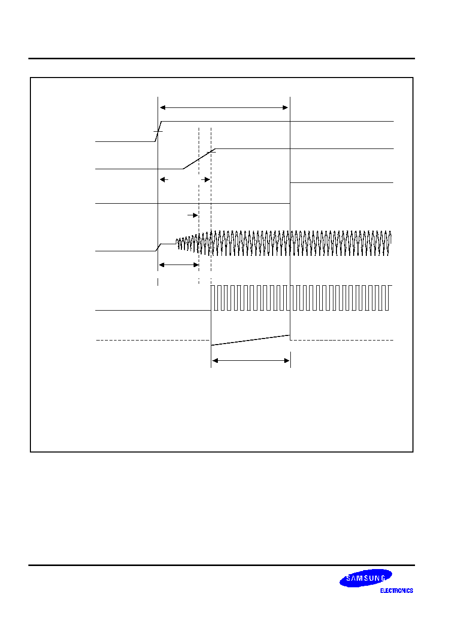
BASIC TIMER and TIMER 0
S3C880A/F880A
10-4
Oscillation Stabilization Time
Normal Operating mode
0.8 V
DD
t
WAIT
= (4096x16)/f
OSC
Basic timer increment and
CPU operations are IDLE mode
10000B
00000B
Reset Release Voltage
NOTE:
Duration of the oscillator stabilization wait time, t
WAIT
, when it is released by a
Power-on-reset is 4096 x 16/f
OSC
.
t
RST
RC (R is external resistor and C is on chip capacitor)
V
DD
RESET
Internal
Reset
Release
Oscillator
(X
OUT
)
BTCNT
clock
BTCNT
value
Oscillator Stabilization Time
trst
~
RC
~
~
~
0.8 V
DD
Figure 10-2. Oscillation Stabilization Time on nRESET
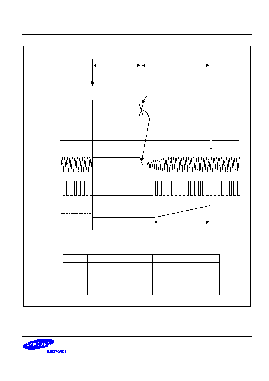
S3C880A/F880A
BASIC TIMER and TIMER 0
10-5
NOTE:
Duration of the oscillator stabilzation wait time, t
WAIT
, it is released by an
interrupt is determined by the setting in basic timer control register, BTCON.
V
DD
Oscillation Stabilization Time
RESET
External
Interrupt
Oscillator
(X
OUT
)
BTCNT
clock
BTCNT
Value
t
WAIT
Basic Timer Increment
10000B
STOP
Release
Signal
00000B
Normal
Operating
Mode
Normal
Operating
Mode
STOP Mode
STOP Mode
Release Signal
STOP
Instruction
Execution
BTCON.3
BTCON.2
0
0
1
1
0
1
0
1
t
WAIT
(4096 x 16)/fosc
(1024 x 16)/fosc
(128 x 16)/fosc
Invalid setting
t
WAIT
(When f
OSC
is 8 MHz)
10.92 ms
2.7 ms
0.341 ms
Figure 10-3. Oscillation Stabilization Time on STOP Mode Release
BASIC TIMER and TIMER 0
S3C880A/F880A
10-6
TIMER 0 CONTROL REGISTER (T0CON)
The timer 0 control register, T0CON, is used to select the timer 0 operating mode (interval timer) and input clock
frequency, clear the timer 0 counter, and enable the T0 match interrupt. It also contains a pending bit for T0 match
interrupt. It is located in set 1, address D2H, and is read/write addressable using register addressing mode.
A reset clears T0CON to '00H'. This sets timer 0 to normal interval timer mode, selects an input clock frequency of
f
OSC
/4096, and disables the T0 match interrupt. The T0 counter can be cleared at any time during the normal
operation by writing a "1" to T0CON.3.
To enable the T0 match interrupt (T0INT, IRQ0, vector FCH), you must set T0CON.1 to "1". The interrupt service
routine must clear the pending condition by writing a "0" to the T0 interrupt pending bit, T0CON.0.
Timer 0 Control Register (T0CON)
D2H, Set 1, R/W
LSB
MSB
.7
.6
.5
.4
.3
.2
.1
.0
T0 interrupt pending bit:
0 = No T0 interrupt pending
0 = Clear T0 pending bit (write)
1 = T0 interrupt is pending
T0 counter clear bit:
0 = No effect
1 = Clear the T0 counter (when write)
T0 operation mode
selection bits:
00 = Interval mode
01 = PWM mode
10 = PWM mode
11 = PWM mode
T0 input clock selection bits:
00 = fosc/4096
01 = fosc/256
10 = fosc/8
11 = External clock (T0CK)
(Max fosc/8)
T0 interrupt enable bit:
0 = Disable T0 interrupt
1 = Enable T0 interrupt
No effect
Figure 10-4. Timer 0 Control Register (T0CON)

S3C880A/F880A
BASIC TIMER and TIMER 0
10-7
TIMER 0 FUNCTION DESCRIPTION
T0 Interrupts (IRQ0, Vector FCH)
The T0 module can generate one interrupt: the timer 0 match interrupt (T0INT). T0INT is also in the level IRQ0, vector
address: FCH. The T0INT pending condition must be cleared by software by writing a "0" to the T0CON.0 pending bit.
Interval Timer Mode
In interval timer mode, a match signal is generated when the counter value is identical to the value written to the T0
reference data register, T0DATA. The match signal generates a T0 match interrupt (T0INT, vector FCH) and then
clears the counter. If, for example, you write the value '10H' to T0DATA, the counter will increment until it reaches
'10H'. At this point, the T0 interrupt request is generated, the counter value is reset and counting resumes.
CLK
Counter
R (Clear)
Comparator
Data Register
Match
PND
T0CNT
Interrupt
Enable/Disable
T0DATA
IRQ0
(T0INT)
Figure 10-5. Timer 0 Function Diagram (Interval Timer Mode)
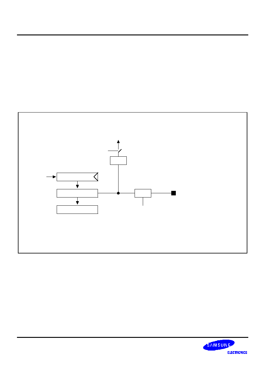
BASIC TIMER and TIMER 0
S3C880A/F880A
10-8
Pulse Width Modulation Mode
Pulse width modulation (PWM) mode lets you program the width (duration) of the pulse that is output at the T0 pin.
As in interval timer mode, a match signal is generated when the counter value is identical to the value written to the
T0 data register. In PWM mode, however, the match signal does not clear the counter (it runs continuously,
overflowing at 'FFH', and continuing incrementing from '00H').
Although it is possible to use the match signal to generate a T0INT interrupt, an interrupt is typically not used in
PWM-type applications. Instead, the pulse at the T0 pin is held to Low level as long as the reference data value is
less than or equal to the counter value; the pulse is then held to high level for as long as the data value is greater
than the counter value. One pulse width is equal to t
CLK
x 256. (See figure 10-6)
NOTE: When timer 0 is configured to operate in PWM mode,
interrupts are typically not used.
CLK
Counter
Comparator
Data Register
Match
PND
T0CNT
Interrupt
Enable/Disable
T0DATA
IRQ0
(T0INT)
CTL
T0CON
T0 pin
High level when data > counter;
Low level when data < counter
=
Figure 10-6. Timer 0 Function Diagram (PWM Mode)
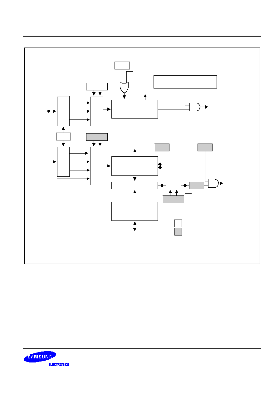
S3C880A/F880A
BASIC TIMER and TIMER 0
10-9
DIV
DIV
nRESET or
STOP
nRESET
Data Bus
X
IN
R
1/4096
1/1024
1/128
R
1/4096
1/8
1/256
Bit 0
MUX
Bit 3, 2
Bit 1
Bits 7, 6
BTCNT
8-Bit Basic Counter
(Read-Only)
Overflow
Basic Timer Control Register
(Write '1010xxxxB' to disable)
MUX
T0CK
T0CNT
8-Bit Counter
(Read-Only)
8-Bit Comparator
Data Bus
CTL
R
Match
Clear
Bit 3
Bits 4, 5
T0DATA
Timer 0 Data Register
(Read/Write)
Bit 3
T0 (PWM & Interval)
IRQ0
Bit 3
Interrupt
Enable
Data Bus
Basic Timer Counter Register
Timer 0 Counter Register
NOTE: During a power-on reset operation, the CPU is idle during the required oscillation
stabilization interval (until bit 4 of the basic timer counter is set to "1").
Figure 10-7. Basic Timer and Timer 0 Block Diagram

BASIC TIMER and TIMER 0
S3C880A/F880A
10-10
F
PROGRAMMING TIP -- Configuring the Basic Timer
This example shows how to configure the basic timer to sample specifications:
ORG
0100H
nRESET
DI
; Disable all interrupts
SB0
; Select bank 0
LD
BTCON,#0AAH
; Disable the watchdog timer
LD
CLKCON,#98H
; Non-divided clock
CLR
SYM
; Disable global and fast interrupts
CLR
SPL
; Stack pointer low byte
"0"
; Stack area starts at 0FFH
�
�
�
SRP
#0C0H
; Set register pointer
0C0H
EI
; Enable interrupts
�
�
�
MAIN
LD
BTCON,#52H
; Enable the watchdog timer
; Basic timer clock: f
OSC
/4096
; Clear basic timer counter
NOP
NOP
�
�
�
JP
T,MAIN
�
�
�

S3C880A/F880A
BASIC TIMER and TIMER 0
10-11
F
PROGRAMMING TIP -- Configuring Timer 0
This sample program sets timer 0 to interval timer mode, determining the frequency of the oscillator clock, and the
execution sequence which follows a timer 0 interrupt. The program givens are as follows:
-- Timer 0 is used in interval mode; the timer interval is set to 4 milliseconds
-- Oscillation frequency is 6 MHz
-- General register 60H (page 0)
60H + 61H + 62H + 63H + 64H (page 0) is executed after a timer 0 interrupt
ORG
0FCH
; Timer 0 interrupt (match)
VECTOR
T0INT
ORG
0100H
nRESET
DI
; Disable all interrupts
SB0
; Select bank 0
LD
BTCON,#0AAH
; Disable the watchdog timer
LD
CLKCON,#98H
; Non-divided clock
CLR
SYM
; Disable global and fast interrupts
CLR
SPL
; Stack pointer low byte
"0"
; Stack area starts at 0FFH
�
�
LD
T0CON,#42H
; 01000010B
; Input clock is f
OSC
/256
; Interval timer mode
; Enable the timer 0 interrupt
LD
T0DATA,#5DH
; Set timer interval to 4 milliseconds
; (6 MHz/256) � (93 + 1) = 0.25 kHz (4 ms)
SRP
#0C0H
; Set register pointer
0C0H
EI
; Enable interrupts
�
�
T0INT
PUSH
PP
; Save page pointer to the stack
PUSH
RP0
; Save RP0 to stack
SB0
; Select bank 0
LD
PP,#00H
; Page pointer
00H (select page 0)
SRP0
#60H
; RP0
60H
INC
R0
; R0
R0 + 1
ADD
R2,R0
; R2
R2 + R0
ADC
R3,R2
; R3
R3 + R2 + Carry
ADC
R4,R0
; R4
R4 + R0 + Carry
CP
R0,#32H
; 50
�
4 = 200 ms
JR
ult,NO_200MS_SET
BITS
R1.2
; Bit setting (61.2H)
NO_200MS_SET:
LD
T0CON,#42H
; Clear pending bit
POP
RP0
; Restore register pointer 0 value
POP
PP
; Restore page pointer value
IRET
; Return from interrupt service routine

BASIC TIMER and TIMER 0
S3C880A/F880A
10-12
NOTES

S3C880A/F880A
TIMER A
11-1
11
TIMER A
OVERVIEW
The S3C880A/F880A microcontrollers have an 8-bit timer/counter (timer A). Each timer has a control register, an
8-bit counter register, an 8-bit data register, an 8-bit comparator. Timer A runs continuously. Counter register
addresses are not mapped and they cannot, therefore, be read or written.
TIMER CLOCK INPUT
Timer A has different clock input options. You can select the non-divided CPU clock or the CPU clock divided by
1000. The selected clock input frequency for each timer can be scaled using the 4-bit prescaler that is located in
bits 4�7 of the TACON register.
TIMER A INTERRUPT CONTROL
Timer A generate a match signal when the count value is equal to the referenced data value in the TADATA. When
the interrupt enable bit is set for timer A, an interrupt is generated whenever a match is detected. The corresponding
count register is then cleared and counting resumes. To enable the timer A interrupt, you should set TACON.2 to
"1".
The timer A interrupt pending bit is TACON.1. When a timer A pending bit read operation shows a "0" value, no
interrupt is pending; when it is "1", an interrupt request is pending. When the request is acknowledged by the CPU
and the service routine starts, the pending bit must be cleared by the interrupt service routine. To do this, you must
write a "0" to the appropriate bit location.

TIMER A
S3C880A/F880A
11-2
TIMER A FUNCTION DESCRIPTION
When a match occurs, the timer is reset to zero.
CPU
CLK
TA Counter
Comparator
TADATA
Match
PND
R
TACON.2
TACON.1
Timer A
Interrupt
(IRQ6,BEH)
4-Bit
Prescaler
M
U
X
TACON.3
1 + 1000
8-Bit
8-Bit
Figure 11-1. Timer A Block Diagram
S3C880A/F880A
TIMER A
11-3
TIMER A CONTROL REGISTER (TACON)
The timer A control register, TACON, is located at F2H in set 1, bank 0. All bits are read/write addressable. The
TACON register settings control four functions:
-- Interrupt enable/disable
-- Interrupt pending control (read for status, write to clear)
-- Clock source selection
-- Prescaler (4-bit) for timer clock input
TACON.1 is the pending flag for the timer A interrupt (IRQ6, vector BEH). Application software can poll the TAIP bit
to detect timer A interrupt requests. When an interrupt request is acknowledged, the interrupt service routine must
clear TACON.1 by writing a "0" to the bit location.
Note that there are two clock source selections for timer A: the CPU clock divided by 1000 or the non-divided CPU
clock.
A reset clears TACON to '00H', selecting the CPU clock/1000, and disabling the timer A interrupt.
Timer A Control Register (TACON)
F2H, Set 1, Bank 0, R/W
LSB
MSB
.7
.6
.5
.4
.3
.2
.1
.0
Not used
Timer A interrupt pending bit:
0 = No interrupt pending (when read)
0 = Clear pending bit (when write)
1 = Interrupt is pending (when read)
1 = No effect (when write)
4-bit prescaler for timer A clock
Divide input by 1 (non-divided)
Divide input by 2
0000
0001
Divide input by 3-15
1111
Timer A interrupt enable:
0 = Disable interrupt
1 = Enable interrupt
Timer A clock source selection bit:
0 = CPU clock divided by 1000
1 = Non-divided CPU clock
Figure 11-2. Timer A Control Register (TACON)

TIMER A
S3C880A/F880A
11-4
F
PROGRAMMING TIP -- Configuring Timer A
This example sets timer A to normal interval mode, determining the oscillation frequency of the timer clock, the
execution sequence that follows a timer A interrupt. The program parameters are:
-- The timer interval is set to 10 milliseconds
-- Oscillation frequency = 6 MHz
-- General register 70H (page 0)
70H + 71H + 72H + 73H + 74H (page 0) is executed after a timer A interrupt
ORG
0BEH
; Timer A interrupt
VECTOR
TAINT
ORG
0100H
nRESET
DI
; Disable all interrupts
SB0
; Select bank 0
LD
BTCON,#0AAH
; Disable the watchdog timer
LD
CLKCON,#98H
; Non-divided clock
CLR
SYM
; Disable global and fast interrupts
CLR
SPL
; Stack pointer low byte
"0"
; Stack area starts at 0FFH
�
�
�
LD
TACON,#54H
; 01010100B
; PS
5 (divide-by-6)
; CPU clock/1000
; Select interval mode for timer A
LD
TADATA,#59H
; 10-ms interval time
; (6 MHz/1000) � (59 + 1) = 100 Hz (10 ms)
SRP
#0C0H
; Set register pointer
0C0H
EI
; Enable interrupts
�
�
�
TAINT
PUSH
PP
; Save page pointer to stack
PUSH
RP0
; Save register pointer 0 to stack
SB0
; Select bank 0
LD
PP,#00H
; Page pointer
00H (select page 0)
SRP0
#70H
; RP0
70H
INC
R0
; R0
R0 + 1
ADD
R2,R0
; R2
R2 + R0
ADC
R3,R2
; R3
R3 + R2 + Carry
ADC
R4,R0
; R4
R4 + R0 + Carry
CP
R0,#64H
; 100
�
10 ms = 1000 ms (1 second)
JR
ult,NO_1SEC_SET
BITS
R1.2
; Bit setting (71.2H)
(Continued on next page)

S3C880A/F880A
TIMER A
11-5
F
PROGRAMMING TIP -- Configuring Timer A (Continued)
NO_1SEC_SET:
LD
TACON,#54H
; Clear pending bit
POP
RP0
; Restore register pointer 0 value
POP
PP
; Restore page pointer value
IRET
; Return from interrupt service routine

TIMER A
S3C880A/F880A
11-6
NOTES

S3C880A/F880A
PWM and CAPTURE
12-1
12
PWM AND CAPTURE
PWM/CAPTURE MODULE
The S3C880A/F880A microcontrollers have two 14-bit PWM circuits and four 8-bit PWM circuits. The 14-bit circuits
are called PWM0 and PWM1; the 8-bit circuits are PWM2�PWM5. The operation of all the PWM circuits is
controlled by a single control register, PWMCON. PWMCON also contains a 3-bit prescaler for adjusting the PWM
frequency (cycle).
The capture function, called capture A, is integrated in this block. Using PWMCON settings, you can enable the
capture A interrupt and select the desired triggering edge for data capture on the CAPA input pin.
The PWM counter is a 14-bit incrementing counter. It is used by the 14-bit PWM circuits. To start the counter and
enable the PWM circuits, you must set PWMCON.5 to "1". If the counter is stopped, it retains its current count
value; when re-started, it resumes counting from the retained count value.
A 3-bit prescaler controls the clock input frequency to the PWM counter. By modifying the prescaler value, you can
divide the input clock by one (non-divided), two, three, four, five, six, seven, or eight. The prescaler output is the clock
frequency of the PWM counter.
PWM and CAPTURE
S3C880A/F880A
12-2
PWM CONTROL REGISTER (PWMCON)
The control register for the PWM module, PWMCON, is located at the register address F8H in set 1, bank 0. Bit
settings in the PWMCON register control the following functions:
-- 3-bit prescaler for scaling the PWM counter clock
-- Stop/start (or resume) the PWM counter operation
-- Capture A interrupt enable and capture A edge selection
A reset clears all PWMCON bits to logic zero, disabling the entire PWM module.
PWM Control Register (PWMCON)
F8H, Set 1, Bank 0, R/W
LSB
MSB
.7
.6
.5
.4
.3
.2
.1
.0
Capture function control bits:
00 = Disable capture function
01 = Capture on falling edges
10 = Capture on rising edges
11 = Capture on both edges
3-bit prescaler for PWM
counter clock:
Non-divide
Divide by 2
Divide by 3
Divide by 4
Divide by 5
Divide by 6
Divide by 7
Divide by 8
Not used
PWM counter enable bit:
0 = Stop counter
1 = Start (resume) counting
.4 .7 .6
0 0 0
0 0 1
0 1 0
0 1 1
1 0 0
1 0 1
1 1 0
1 1 1
Capture interrupt enable bit:
0 = Disable capture interrupt
1 = Enable capture interrupt
Figure 12-1. PWM Control Register (PWMCON)
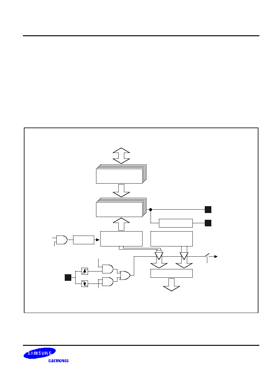
S3C880A/F880A
PWM and CAPTURE
12-3
PWM2�PWM5
The S3C880A/F880A microcontrollers have four 8-bit PWM circuits, called PWM2�PWM5. These 8-bit circuits have
the following components:
-- 14-bit counter with 3-bit prescaler
-- 8-bit comparators
-- 8-bit PWM data registers (PWM2�PWM5)
-- PWM output pins (PWM2�PWM5)
The PWM2�PWM5 circuits are controlled by the PWMCON register (F8H, set 1, bank 0).
CPU
CLK
8-bit PWM2-PWM5
Registers
8 x 4
Data Bus
8-bit PWM2-PWM5
Comparators
x 4
8
Lower 8-bit of
14-bit Counter
PWM0/1 Logic
"1" When Reg > Count
"0" When Reg < Count
=
PWM2-PWM5
Output pins
PWM2-PWM5
Output pins
3-bit P.S.
PWMCON.5
Upper 6-bit of
14-bit Counter
Capture Register
6
2
8
8
CAP Input
PWMCON.1
PWMCON.0
PWMCON.3
IRQ3 (02H)
Data Bus
Figure 12-2. Block Diagram for PWM2�PWM5

PWM and CAPTURE
S3C880A/F880A
12-4
PWM2�PWM5 FUNCTION DESCRIPTION
All the four 8-bit PWM circuits function identically: each has its own 8-bit data register and 8-bit comparator. Each
circuit compares a unique data register value to the lower 8-bit value of the 14-bit PWM counter.
The PWM2�PWM5 data registers are located in set 1, bank 1, at locations F8H�FBH, respectively. These data
registers are read/write addressable. By loading specific values into the respective data registers, you can modulate
the pulse width at the corresponding PWM output pins, PWM2�PWM5.
The level at the output pins toggles High and Low at a frequency equal to the counter clock, divided by 256 (2
8
). The
duty cycle of the PWM0 and PWM1 pins ranges from 0% to 99.6%, based on the corresponding data register
values.
To determine the PWM output duty cycle, its 8-bit comparator sends the output level High when the data register
value is greater than the lower 8-bit count value. The output level is Low when the data register value is less than or
equal to the lower 8-bit count value. The output level at the PWM2�PWM5 pins remains at Low level for the first 256
counter clocks. Then, each PWM waveform is repeated continuously, at the same frequency and duty cycle, until
one of the following three events occurs:
-- The counter is stopped
-- The counter clock frequency is changed
-- A new value is written to the PWM data register
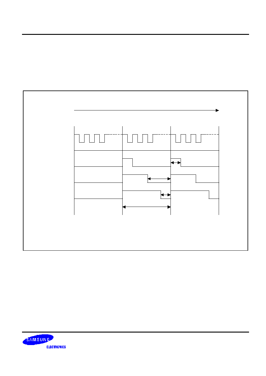
S3C880A/F880A
PWM and CAPTURE
12-5
STAGGERED PWM OUTPUTS
The PWM2�PWM5 outputs are staggered in order to reduce the overall noise level on the pulse width modulation
circuits. If you load the same value to the PWM2�PWM5 data registers, a match condition (data register value is
equal to the lower 8-bit count value) will occur on the same clock cycle for all the four 8-bit PWM circuits. The output
of PWM3, PWM4, and PWM5 are delayed by one-half of a counter clock for subsequent clock cycles (see Figure
12-4).
NOTES:
1. A counter clock value of 8 MHz is assumed for all timing values.
2. 'n' = 2-5, for PWM2-PWM5
Counter
Value
(HEX)
PWM = "0"
0H
125 ns
100H
12.5
�
s
125 ns
PWM Cycle
25
�
s
200H
300H
Counter
Clock
(8 MHz)
PWM = "1"
PWMn = 80H
PWMn = FFH
Figure 12-3. PWM Waveforms for PWM2�PWM5

PWM and CAPTURE
S3C880A/F880A
12-6
PWM2
0H (After
RESET
)
100H
CPU
Clock
PWM3
PWM4
PWM5
Match occurs;
PWM2 toggles to high level
1/2-Clock Delay
1/2-Clock Delay
1/2-Clock Delay
Figure 12-4. PWM Clock to PWM2�PWM5 Output Delays

S3C880A/F880A
PWM and CAPTURE
12-7
PWM0�PWM1
The S3C880A/F880A pulse width modulation (PWM) module has two 14-bit PWM circuits (PWM0 and PWM1). The
14-bit PWM circuits have the following components:
-- 14-bit counter with 3-bit prescaler (an 8-bit counter with 6-bit extension is used for 14-bit output resolution)
-- 8-bit comparator and extension cycle circuit
-- 8-bit reference data registers (PWM0, PWM1)
-- 6-bit extension data registers (PWM0EX, PWM1EX)
-- PWM output pins (PWM0, PWM1)
The PWM0 and PWM1 circuits are enabled by the PWMCON register (F8H, set 1, bank 0).
PWM COUNTER
The PWM counter is a 14-bit increasing counter comprised of a lower byte counter and an upper byte counter.
To determine the PWM module's base operating frequency, the lower byte counter is compared to the PWM data
register value. In order to achieve higher resolutions, the lower six bits of the upper byte counter can be used to
modulate the "stretch" cycle. To control the "stretching" of the PWM output duty cycle at specific intervals, the 6-bit
extended counter value is compared with the 6-bit value (bits 2�7) that you write to the module's extension register.
PWM DATA AND EXTENSION REGISTERS
Two PWM (duty) data registers, located in set 1, bank 0, determine the output value generated by each 14-bit PWM
circuit. PWM0 and PWM1 are read/write addressable.
-- 8-bit data registers PWM0 (F4H) and PWM1(F6H)
-- 6-bit extension registers PWM0EX (F5H) and PWM1EX (F7H) of which only bits 2�7 are used
To program the required PWM output, you should load the appropriate initialization values into the 8-bit data registers
(PWM0, PWM1) and the 6-bit extension registers (PWM0EX, PWM1EX). To start the PWM counter, or to resume
counting, you should set PWMCON.5 to "1".
A reset operation disables all PWM output. The current counter value is retained when the counter stops. When the
counter starts, counting resumes at the retained value.
PWM CLOCK RATE
The timing characteristics of both 14-bit output channels are identical, and are based on the maximum 8-MHz CPU
clock frequency. The 2-bit prescaler value in the PWMCON register determines the frequency of the counter clock.
You can set PWMCON.6 and PWMCON.7 to divide the CPU clock frequency by 1 (non-divided), 2, 3, 4, 5, 6, 7, or
8.
Because the maximum CPU clock rate for the S3C880A/F880A microcontrollers is 8 MHz, the maximum base
PWM frequency is 31.25 kHz (8 MHz divided by 256). This assumes a non-divided CPU clock.
PWM and CAPTURE
S3C880A/F880A
12-8
Table 12-1. PWM0 and PWM1 Control and Data Registers
Register Name
Mnemonic
Address (Set 1, Bank 0)
Function
PWM0 data registers
PWM0
F4H
8-bit PWM0 basic cycle frame value
PWM0EX
F5H
6-bit extension ("stretch") value
PWM1 data registers
PWM1
F6H
8-bit PWM1 basic cycle frame value
PWM1EX
F7H
6-bit extension ("stretch") value
PWM control register
PWMCON
F8H
PWM0 counter stop/start (resume),
and 3-bit prescaler for CPU clock; also
contains capture A control settings
PWM0 AND PWM1 FUNCTION DESCRIPTION
The PWM output signal toggles to Low level whenever the lower 8-bit counter matches the reference value stored in
the module's data register (PWM0, PWM1). If the value in the PWM data register is not zero, an overflow of the lower
counter causes the PWM output to toggle to High level. In this way, the reference value written to the data register
determines the module's base duty cycle.
The value in the 6-bit extension counter (the lower six bits of the upper counter) is compared with the extension
settings in the 6-bit extension data register (PWM0EX, PWM1EX). This 6-bit extension counter value (bits 2�7),
together with extension logic and the PWM module's extension register, is then used to "stretch" the duty cycle of
the PWM output. The "stretch" value is one extra clock period at specific intervals, or cycles (see Table 12-2).
If, for example, the value in the extension register is '1', the 32nd cycle will be one pulse longer than the other 63
cycles. If the base duty cycle is 50%, the duty of the 32nd cycle will therefore be "stretched" to approximately 51%
duty. For example, if you write 80H to the extension register, all odd-numbered pulses will be one cycle longer. If you
write FCH to the extension register, all pulses will be stretched by one cycle except the 64th pulse. PWM output
goes to an output buffer and then to the corresponding PWM0 and PWM1 output pin. In this way, you can obtain
high output resolution at high frequencies.
Table 12-2. PWM Output "Stretch" Values for Extension Registers PWM0EX and PWM1EX
PWM0EX/PWM1EX Bit
"Stretched" Cycle Number
7
1, 3, 5, 7, 9,
...
, 55, 57, 59, 61, 63
6
2, 6, 10, 14,
...
, 50, 54, 58, 62
5
4, 12, 20,
...
, 44, 52, 60
4
8, 24, 40, 56
3
16, 48
2
32
1
Not used
0
Not used
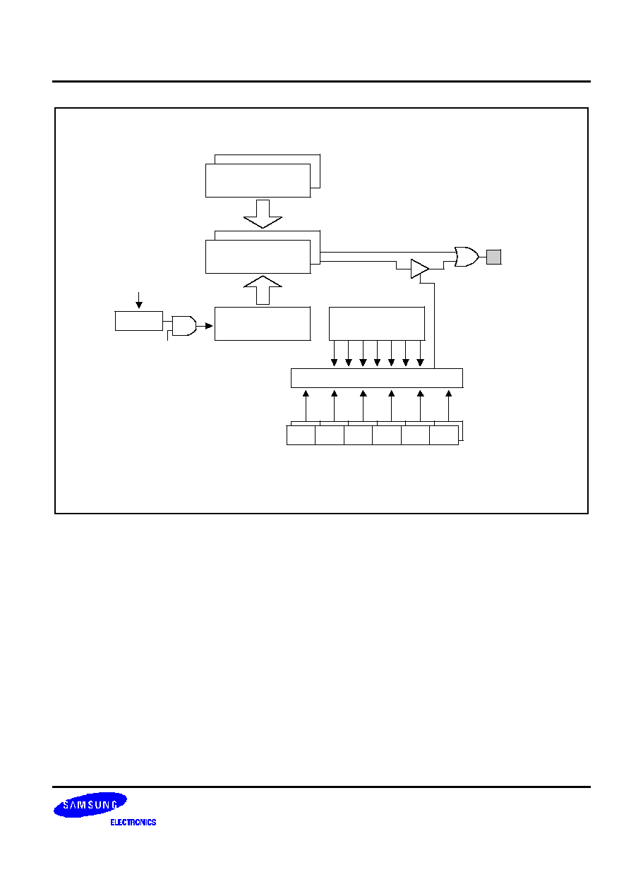
S3C880A/F880A
PWM and CAPTURE
12-9
CPU CLK
8-bit PWM2-PWM5
Comparators
Lower 8-bit of
14-bit Counter
"1" When Reg > Count
"0" When Reg < Count
PWM0,PWM1
Output pins
3-bit P.S.
PWMCON.5
Upper 6-bit of
14-bit Counter
Extension Logic
8
6-bit Extension Registers
(PWM0EX, PWM1EX)
8-bit PWM2-PWM5
Registers
8
Match when
Reg = Count
Bit 7
Bit2
32
1, 3, ..., 61, 63
Figure 12-5. Block Diagram for PWM0 and PWM1
PWM and CAPTURE
S3C880A/F880A
12-10
F
PROGRAMMING TIP -- Programming PWM0 to Sample Specifications
This example shows how to program the 14-bit pulse-width modulation module, PWM0. The program parameters are
as follows:
-- The oscillation frequency of the main crystal is
6 MHz
-- PWM0 data is in the working register R0
-- PWM0EX (PWM0 extension value) is in the working register R1, bits 2�7
The program performs the following operations:
1. Set the PWM0 frequency to 23.437 kHz
2. If R3.0 = "1", then PWM
PWM + 12H
(If an overflow occurs from R0, then R0
0FFH and R1
0FCH.)
3. If R3.0 = "0", then PWM
PWM � 11H
(If an underflow occurs from R0, then R0
00H and R1
00H.)
N (0)
PWMCON #20H
R3.0 = 1?
R1 R1 - #20H
Underflow?
R1 R1 - #20H
Borrow?
R1 R1 + #48H
Carry?
R0 Min. value
R1 Min. value
Carry?
R0 R1 + #01H
R0 Max. value
R1 Max. value
PWM Control Register Setting
Y (1)
N
Y
Y
N
N
Y
Y
N
PWM0EX R1
PWM0 R0
Figure 12-6. Decision Flowchart for PWM0 Programming Tip

S3C880A/F880A
PWM and CAPTURE
12-11
F
PROGRAMMING TIP -- Programming PWM0 to Sample Specifications (Continued)
�
�
�
LD
PWMCON,#20H
; PS
0 (Select 23.437-kHz PWM frequency)
; Enable the PWM counter
�
�
�
BTJRF
pwm0_dec,R3.0
; If R3.0 = "0", then jump to pwm0_dec
pwm0_inc:
ADD
R1,#48H
; If R3.0 = "1", then add 48H to the PWM data
JR
NC,pwm0_data_end
; If no carry, go to pwm0_data_end
INC
R0
; R0
R0 + 1
JR
NZ,pwm0_data_end
; If no overflow, jump to pwm0_data_end for update
LD
R0,#0FFH
; If overflow, set 0FFH to R0
LD
R1,#0FCH
; Set 0FCH to R1
JR
T,pwm0_data_end
; Jump to pwm0_data_end unconditionally
pwm0_dec:
SUB
R1,#44H
; R3.0 = "0", so subtract 44H from PWM data
JP
NC,pwm0_data_end
; If no borrow, jump to pwm0_data_end for update
SUB
R0,#01H
; Decrement R0 (R0
R0 � 1)
JR
NC,pwm0_data_end
; If no borrow, jump to pwm0_data_end
CLR
R0
; Clear data R0
CLR
R1
; Clear data R1
pwm0_data_end:
LD
PWM0EX,R1
; Load new value to PWM0EX (bits 2�7)
LD
PWM0,R0
; Load new value to PWM0
�
�
�

PWM and CAPTURE
S3C880A/F880A
12-12
CAPTURE UNIT
An 8-bit capture unit is integrated in the PWM module. The capture unit detects incoming signal edges and can be
used to measure the pulse width of the incoming signals. PWMCON register settings control the capture unit, which
has the following components:
-- 8-bit capture data register (CAPA)
-- Capture input pin (CAPA/Pin 36)
-- 8-bit capture interrupt (IRQ3, vector 02H)
The capture unit captures the upper 8-bit value of the 14-bit counter when a signal edge transition is detected at the
CAPA pin. The captured value is then dumped into the capture A data register, also called CAPA, where it can be
read.
Using PWMCON.0 and PWMCON.1 settings, you can set edge detection at the CAPA pin for rising edges, falling
edges, or for both signal edge types.
You can also use signal edges at the CAPA pin to generate an interrupt. PWMCON.3 is the capture A interrupt
enable bit.
The capture interrupt is in the level 3 (IRQ3) and its vector address is 02H.
Using the capture A interrupt, you can read the contents of the CAPA data register from edge to edge and use the
values to calculate the elapsed time between pulses.
CPU
CLK
Lower 8-bit of
14-bit Counter
PWMCON.5
Upper 6-bit of
14-bit Counter
Capture Register
8
CAP Input
PWMCON.1
PWMCON.0
PWMCON.3
IRQ3 (02H)
Data Bus
3-bit P.S.
6
2
Figure 12-7. Block Diagram for Capture A
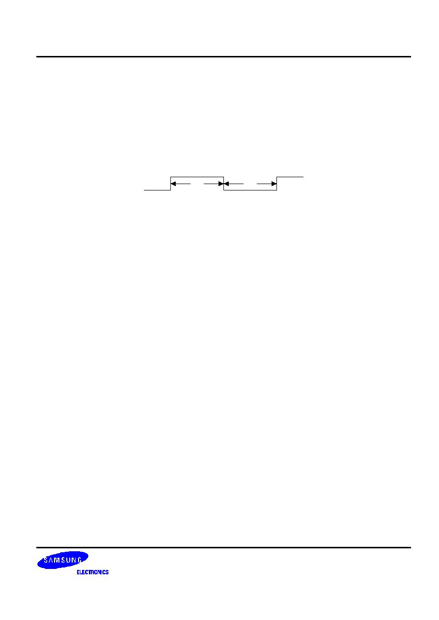
S3C880A/F880A
PWM and CAPTURE
12-13
F
PROGRAMMING TIP -- Programming the Capture Module to Sample Specifications
This example shows you how to program the S3C880A/F880A capture A module. The sample parameters are as
follows:
-- The main oscillator frequency is 6 MHz
-- Timer A interrupt occurs every 2 ms
-- The following waveform is currently being input at the capture (CAPA) pin:
t
H
t
L
-- The following registers are assigned for program values:
Register 70H
LDR
; First captured count value
Register 71H
; Second captured count value
Register 72H
; Third captured count value
Register 73H
DWNCNT
; Down-counter; decremented by 1 with each timer A interrupt
Register 74H
CAPCNT
; Capture counter
Register 77H
FLAG
; Flags
Here is some additional information about the sample program:
1. If 4.35 ms < t
H
, t
L
< 4.6 ms, then set bit zero (LDR) in the register 77H; otherwise clear the zero bit (LDR) in
the register 77H.
2. If the interval between two rising signal edges (capture trigger) is > 30 ms, disregard the capture setting.
Figures 12-4 and 12-5 show decision flowcharts for the sample program.
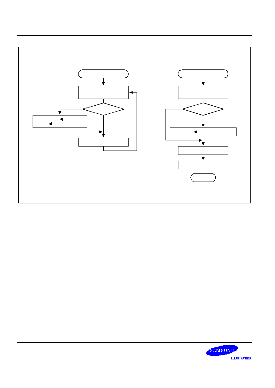
PWM and CAPTURE
S3C880A/F880A
12-14
Y (zero)
Timer A Setting
Capture Unit Setting
DWNCNT = 0?
Flag 0
CAPA Rising Enable
Main JOB
N (not zero)
Main Routine
Timer A Interrupt
Back up the PP, PR0
DWNCNT = 0?
DWNCNT DWNCNT - #1H
Y (zero)
Other JOB
Restore PP, RP0
RET
N (not zero)
Figure 12-8. Decision Flowchart (Main Routine and Timer A Interrupt)
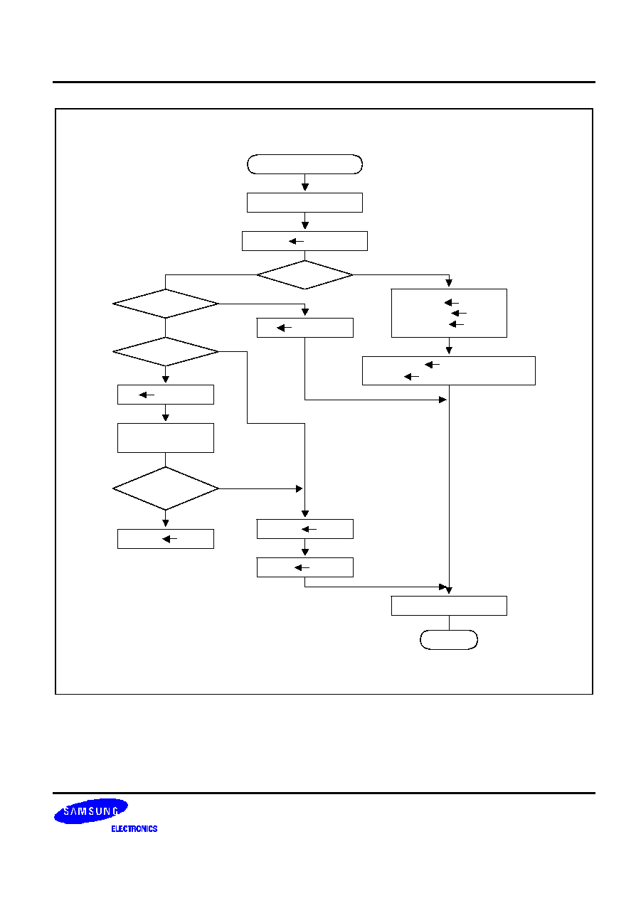
S3C880A/F880A
PWM and CAPTURE
12-15
Capture A Interrupt
Save PP, RP0
Flag = 0?
"0"
CAPCNT CAPCNT + 1
CAPCNT = #01?
CAPCNT = #02?
R2 3rd capture
Y (#02)
Flag "1"
DWNCNT #0FH
CAPCNT #00H
R0 1st capture
CAPA Interrupt on both edges
SUB R2, R1
SUB R1, R0
R1 2nd capture
4.35 ms < R1
R2 < 4.6 ms
LDR "1"
LDR "0"
CAPA Disable
N
N
Y
Restore PP, RP0
"1"
Y (#01)
RET
Figure 12-9. Decision Flowchart for Capture A Interrupt

PWM and CAPTURE
S3C880A/F880A
12-16
F
PROGRAMMING TIP -- Programming the Capture Module to Sample Specifications
�
�
�
LDR
EQU
0
DWNCNT
EQU
3
CAPCNT
EQU
4
FLAG
EQU
7
�
�
�
CLR
PP
; Select page 0
LD
TACON,#54H
; PS
5, interval mode
; Enable timer A interrupt
LD
TADATA,#01H
; 2-ms interval (6 MHz /1000 � 6 � 2 = 0.5 kHz = 2 ms)
�
�
�
EXEC_MAIN:
SRP0
#70H
; RP0
70H
CP
RDWNCNT,#00H
; Down-counter = "0"?
JP
NE,MAIN
; If not zero, then jump to MAIN
BITR
R7.FLAG
; Clear the 'FLAG'
LD
PWMCON,#0AH
; Enable capture A interrupt
; Trigger interrupt on rising edges
MAIN:
; Other job...
�
�
�
JP
T,exec_main
; For looping
�
�
�
TAINT
PUSH
PP
; Save page pointer
PUSH
RP0
; Save register pointer 0
SRP0
#70H
; RP0
70H
CP
RDWNCNT,#00H
; R3 (down-counter) = "0"?
JP
EQ,ta_exec
;
DEC
RDWNCNT
; If not zero, then decrement R3 by 1
TA_EXEC:
�
�
�
POP
RP0
; Restore register pointer 0
POP
PP
; Restore page pointer
IRET
; Return from timer A interrupt service routine
(Continued on next page)

S3C880A/F880A
PWM and CAPTURE
12-17
F
PROGRAMMING TIP -- Programming the Capture Module to Sample Specifications (Continued)
CAPINT
PUSH
PP
; Save the page pointer to stack
PUSH
RP0
; Save register pointer 0 to stack
SRP0
#70H
; RP0
70H
INC
RCAPCNT
; Increment the capture counter
BTJRT
cap_one,R7.FLAG
; R7.FLAG
"1", then jump to cap_one
BITS
R7.FLAG
; Set R7.FLAG
CLR
RCAPCNT
; Clear capture counter
LD
RDWNCNT,#0FH
; Down-counter
15 (for counting 30 ms)
LD
R0,CAPA
; R0
1st captured count value
; CAPA = 0F9H, page 0
LD
PWMCON,#0BH
; Enable capture interrupt
; Trigger interrupt on both rising and falling edges
CAP_END
POP
RP0
; Restore the register pointer 0 value
POP
PP
; Restore the page pointer value
IRET
;
CAP_ONE
CP
RCAPCNT,#01H
; CAPCNT = #01H?
JP
NE,cap_con2
;
LD
R1,CAPA
; R1
2nd captured count value
JR
T,cap_end
;
CAP_CON2 CP
RCAPCNT,#02H
; CAPCNT = #02H?
JP
EQ,cap_con3
;
CAP_CON4 BITR
R7.LDR
; Clear the LDR bit in R7
CAP_CON5 LD
PWMCON,#00H
; Disable the capture module
JR
T,cap_end
;
(Continued on next page)

PWM and CAPTURE
S3C880A/F880A
12-18
F
PROGRAMMING TIP -- Programming the Capture Module to Sample Specifications (Concluded)
CAP_CON3 LD
R2,CAPA
; R2
3rd capture count value
SUB
R2,R1
; R2
(3rd capture value � 2nd capture value)
SUB
R1,R0
; R1
(2nd capture value � 1st capture value)
CP
R1,#24H
; 24H = 4.6 ms
JP
UGT,cap_con4
; If High signal period > 4.6 ms, then go to cap_con4
CP
R2,#24H
;
JP
UGT,cap_con4
; If Low signal period > 4.6 ms, then go to cap_con4
CP
R1,#22H
; 22H = 4.35 ms
JP
ULT,cap_con4
; If High signal period < 4.35 ms, then go to cap_con4
CP
R2,#22H
;
JP
ULT,cap_con4
; If Low signal period < 4.35 ms, then go to cap_con4
BITS
R7.LDR
; Set bit 'LDR'
JP
T,cap_con5
; Jump to cap_con5 unconditionally
�
�
�
S3C880A/F880A
ON-SCREEN DISPLAY
13-1
13
ON-SCREEN DISPLAY (OSD)
OVERVIEW
The on-screen display (OSD) module displays channel number, the time, and other information on a display screen.
The OSD character display module has 252 locations and supports a set of maximum 1024 characters. (Two
characters are reserved: 00H for the blank function and 01H for the test pattern.) There are sixty four display colors.
PATTERN GENERATION SOFTWARE
For application development using the S3C880A/F880A microcontrollers, Samsung provides OSD pattern generation
software (OSDFONT.exe). You can customize standard OSD patterns contained in this file.
Table 13-1. OSD Function Block Summary
OSD Function Block
Function Description
Video RAM
(note)
Located in register page 1, the video RAM contains 252 "word" lines. Each line is
14 bits long. Each 14-bit RAM address stores an 10-bit character code, a character
halftone or character background color display control bit, and a 3-bit color code. Video
RAM locations can be read or written: 00H�BFH can be accessed using any
addressing mode; C0H�FBH can be accessed using Indirect Register or Indexed
addressing mode only.
Character ROM
The character ROM contains an 18-dot
�
16-dot matrix data for 1024 characters. It is
synchronized with the internal dot clock. The ROM outputs the dot matrix data for
each character. The function of two characters is pre-determined: 00H is used for blank
(no-display) data and 01H is for a factory test pattern.
Output control logic
Output control logic receives input from the Character ROM, OSD control registers,
and fade control circuits. It then decides what to display on the screen and what color
the display should be. On the basis of truth table calculations, the final OSD signals
(blue, green, red, blank, and H/T) are output from the OSD block at pins
22�25, 21.
NOTE: The video RAM can be cleared only by "LD" instruction.

ON-SCREEN DISPLAY
S3C880A/F880A
13-2
INTERNAL OSD CLOCK
Red-green-blue (RGB) color outputs, as well as display rates and positions, are determined by the clock signal,
DOT_CLK. This signal is generated by the L-C oscillator and is scaled by the dot and column counter. DOT_CLK
equals the OSD oscillator clock divided by the clock divider value. The clock divider value is set by the horizontal
character size settings in the CHACON register.
The rate at which each new display line is generated is determined by H-sync input. The rate at which each new
frame (screen) is generated is determined by V-sync input. For stable on screen display operation, the CPU clock
frequency should faster than OSD clock.
OSD VIDEO RAM
The OSD video RAM contains 252 word lines. Each line is 14 bits long. Of these 14 bits, eight are character display
codes (bits 0-9). Bit 13 is the character halftone or character background color display control bit and bits 10-12 are
used to determine the red, green, and blue components of the character color.

S3C880A/F880A
ON-SCREEN DISPLAY
13-3
Register Data Bus
Register Address Bus
XOR
XOR
Polarity
Selector
H-SYNC
V-SYNC
f
OSD
ROW interrupt
(IRQ2, 0C4H)
Line Address (5)
Dot and Column
Counter
Character
Generator
ROM
(1024 x 18 x 16)
Output Control
Logic
Character Out
(16-Dot)
Dot Clock
Line
Count (6)
Video RAM
(252 x 14 Bits)
CHAR
CODE (10)
Column
Address
(5)
Row
Address
(4)
Line and Row
Counter
ROWINT
Halfone (1)
Character Color (3)
Red
Green
Blue
Blank
Halftone
Color
Buffer
(5)
Figure 13-1. On-Screen Display Function Block Diagram
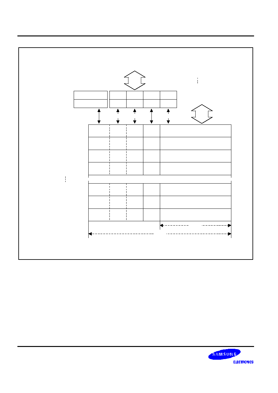
ON-SCREEN DISPLAY
S3C880A/F880A
13-4
Bit 3
H/T and BGRND
Bit 2
R
Bit 1
G
Bit 0
B
Bit 4-5
VRAM
H/T and
BGRND
R
G
B
Character Code (10-Bit)
H/T and
BGRND
R
G
B
Character Code (10-Bit)
H/T and
BGRND
R
G
B
Character Code (10-Bit)
H/T and
BGRND
R
G
B
Character Code (10-Bit)
Row 0, Column 0
Row 0, Column 1
Row 0, Column 2
Row 0, Column 3
00H = Row 0, Column 0
01H = Row 0, Column 1
FBH = Row 11, Column 20
Color Code
VRAM (Bit8-9)
MSB(Bit 9)
LSB(Bit 0)
8-Bit
6-Bit
Data Bus
Data Bus
Color Buffer
(FCH), Bits 0-5
H/T and
BGRND
R
G
B
Character Code (10-Bit)
H/T and
BGRND
R
G
B
Character Code (10-Bit)
H/T and
BGRND
R
G
B
Character Code (10-Bit)
~
~
~
~
10-Bit
14-Bit
Row 11, Column 18
Row 11, Column 19
Row 11, Column 20
Figure 13-2. On-Screen Display Video RAM Data Organization

S3C880A/F880A
ON-SCREEN DISPLAY
13-5
OSD CONTROL REGISTER OVERVIEW
Seven control registers are used to control specific functions of the on-screen display module:
There are seven control registers for OSD functions and one color buffer register:
DSPCON
Display control register
CHACON
Character size and fade control register
FADECON
Fade control register
ROWCON
Row display position and inter-row spacing control register
CLMCON
Column display position and inter-column spacing control register
COLCON
Background color control register
HTCON
Halftone signal control register
COLBUF
Character color buffer register
VSBCON
V-sync blank time control register
OSDFRG1/2
Fringe or border control registers
OSDSMH1/2
Smooth display control registers
OSDCOL
OSD factor control register
OSDFLD
Field control register
OSDPLTR1/2
Palette color mode Red 1/2
OSDPLTG1/2
Palette color mode Green 1/2
OSDPLTB1/2
Palette color mode Blue 1/2
These registers are described in this section within the context of the OSD hardware module description. For
detailed quick-reference descriptions of the control register bit settings, please refer to Section 4, "Control
Registers."
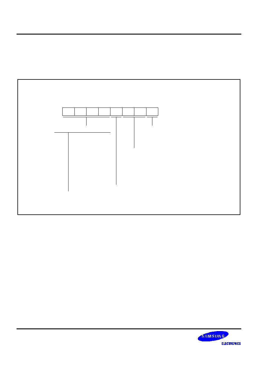
ON-SCREEN DISPLAY
S3C880A/F880A
13-6
DISPLAY CONTROL REGISTER (DSPCON)
Settings in the display control register, DSPCON (F5H, set 1, bank 1), are used to enable and disable the
on-screen display to select halftone or background color for character displays, choose the polarity for H-sync and
V-sync signal synchronization, and as OSD ROW counter which is read-only (bit4�bit7).
Display Control Register (DSPCON)
F5H, Set 1, Bank 1, R/W
LSB
MSB
.7
.6
.5
.4
.3
.2
.1
.0
Display enable bit:
0 = Disable OSD (turn off L-C osc)
1 = Enable OSD (turn on L-C osc)
Halftone or background color selection bits
(for character data in bit 13 of video RAM):
00 = Character background color
01 = Not used
10 = Halftone output
11 = Character halftone and background color
Clock edge selection for H/V-sync polarity:
0 = Rising edges
1 = Falling edges
OSD Row counter (Read-only)
0000
0001
0010
0011
0100
0101
0110
0111
1000
1001
1010
1011
Row0
Row1
Row2
Row3
Row4
Row5
Row6
Row7
Row8
Row9
Row10
Row11
1100-1111: Not used
Figure 13-3. OSD Display Control Register (DSPCON)
NOTE
Refer to the PROGRAMMING TIP � Row Interrupt Function of 13-24.

S3C880A/F880A
ON-SCREEN DISPLAY
13-7
OSD Enable/Disable
The DSPCON.0 setting enables or disables the on-screen display module. To enable the OSD (turn L-C oscillation
on), set DSPCON.0 to "1"; to disable OSD (turn L-C oscillation off), clear DSPCON.0 to "0". When you do not use
the display module, we recommend that you keep DSPCON.0 cleared to "0" in order to reduce possible noise
generation by the L-C oscillator.
The DSPCON.0 settings determine the on/off condition of L-C oscillation, synchronized with Vsync input. And the
OSD output can be turned on or off in OSD row units when L-C oscillation is on. At the point the value of DSPCON.0
is changed from "1" to "0" in the middle of a frame, OSD is disabled (OSD output is off). In this condition, L-C
oscillation becomes off at the next Vsync input. When the value is shifted from "0" to "1", OSD is enabled (OSD
output is on) and L-C oscillation returns to "on" at the following Vsync input.
H-Sync and V-Sync Polarity Selection
DSPCON.3 selects the triggering edge of H-sync and V-sync inputs to the OSD block. Incoming sync pulses enter
a polarity option circuit that is controlled by the SYNC bit. If DSPCON.3 = "0", rising edges are selected; if it is "1",
falling edges are selected.
Character Halftone or Character Background Color Selection
DSPCON.2 and DSPCON.1 let you select a halftone or background color display for individual characters.
(Which characters are displayed as halftones, or with character background color, or with character halftone, or with
character background color, or with character halftone and background color, depends on the bit 13 settings in the
character video RAM data)
When DSPCON.2-.1 = "00", the character background color option is selected; when DSPCON.2-.1 = "10", the
character halftone function is selected; when DSPCON.2-.1 = "11", the character halftone and background color
option are selected; but DSPCON.2-.1 = "01" is not used.
ROW Counter Function
DSPCON.4�DSPCON.7 to the OSD ROW read data. OSD ROW counter indicates the OSD ROW currently
displayed. One ROW comprises one character (18 lines) and inter-ROW space (ROWCON.2�.0).
The Row counter value for the first ROW after a Vsync input is set to "0".
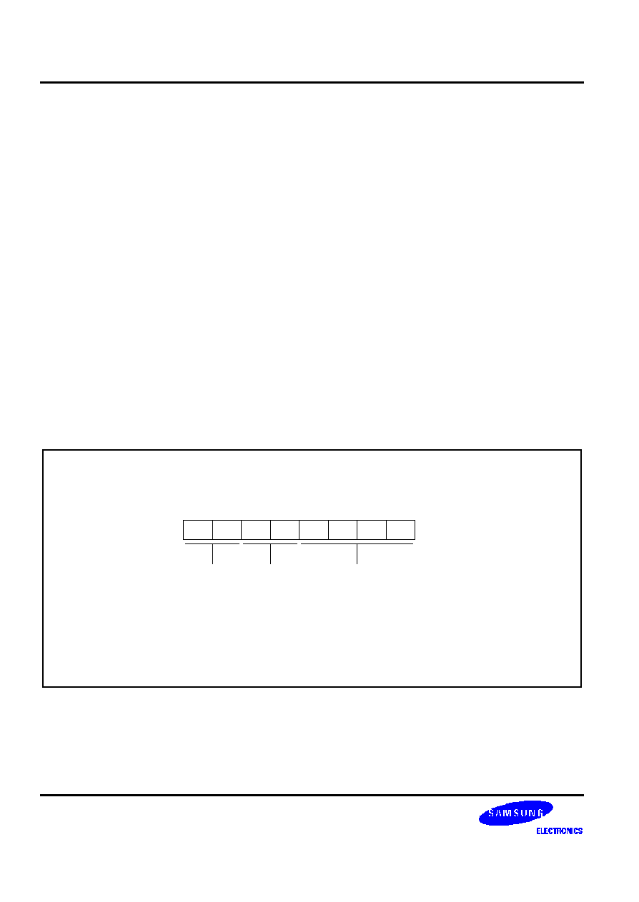
ON-SCREEN DISPLAY
S3C880A/F880A
13-8
CHARACTER SIZE CONTROL REGISTER (CHACON)
Using the character size control register, CHACON, you can specify four different standard character sizes in both
vertical and horizontal directions. You also use the CHACON register to select rows (0�11) for the character fade
function (see Figure 13-5).
Vertical character size is defined by bits 6 and 7 of the CHACON register; horizontal direction is defined by bits 4
and 5. There are four basic character size settings:
�
1,
�
2,
�
3, and
�
4. Size '
�
1' is the smallest and '
�
4' is the
largest. For example, to display a '
�
1' (horizontal) by '
�
1' (vertical) size character, you should clear CHACON.4�
CHACON.7 to "0". To display a '
�
4' by '
�
4' size character, you should set bits 4�7 to '1111B'.
You can also combine different vertical and horizontal size selections to produce flattened or elongated characters
(see Figure 13-5).
"1 dot" is a minimum unit of character size. 1 character is composed of 16 dots in width and 18 dots in length. 1 dot
in width is 1 fosd clock and 1 dot in length is 1 H-sync line. 1 dot of 1x1 character size (minimum unit) is composed
of 1 fosd clock and 2 H-sync line (even + odd field).
Character size in width is increased by 1 clock. So x1, x2, x3, and x4 in width are the same as 1, 2, 3 and 4 clock,
respectively. Character size in length is increased by 2 H-sync line (even field + odd field), so x1 and x2 in length are
the same as 2 H-sync line (even field + odd field) and 4 H- sync line (even field + odd field + even field + odd field),
respectively. Half dot in width is 1/2 fosd clock, and 1/2 dot in length is 1 H-sync line (even or odd field).
In the fringe and boarder function, 1/2 dot setting can be used. So, please be more careful in using the 1/2 dot to
prevent the blink. (Because the character size is changed in 1 dot unit or set to 1/2 dot in fringing or boarder
function, blinking can occur in interlace scan, so care must be taken when 1/2 dot is used for width.)
OSD Character Size Control Register (CHACON)
F0H, Set 1, Bank 1, R/W
LSB
MSB
.7
.6
.5
.4
.3
.2
.1
.0
Vertical character
size selection bits:
00 = 'x1' size
01 = 'x2' size
10 = 'x3' size
11 = 'x4' size
Fade row address selection bits:
0000 = Row 0
0110 = Row 6
0001 = Row 1
0111 = Row 7
0010 = Row 2
1000 = Row 8
0011 = Row 3
1001 = Row 9
0100 = Row 4
1010 = Row 10
0101 = Row 5
1011 = Row 11
Horizontal character
size selection bits:
00 = 'x1' size
01 = 'x2' size
10 = 'x3' size
11 = 'x4' size
Figure 13-4. OSD Character Size Control Register (CHACON)
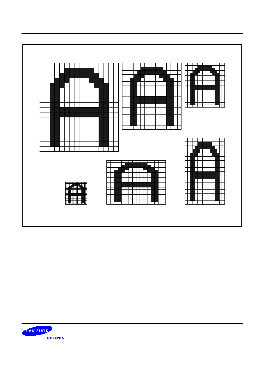
S3C880A/F880A
ON-SCREEN DISPLAY
13-9
Horizontal = x3
Vertical = x2
Horizontal = x2
Vertical = x3
Horizontal = x1
Vertical = x1
Horizontal = x4
Vertical = x4
Horizontal = x3
Vertical = x3
Horizontal = x2
Vertical = x2
Figure 13-5. OSD Character Sizing Dimensions
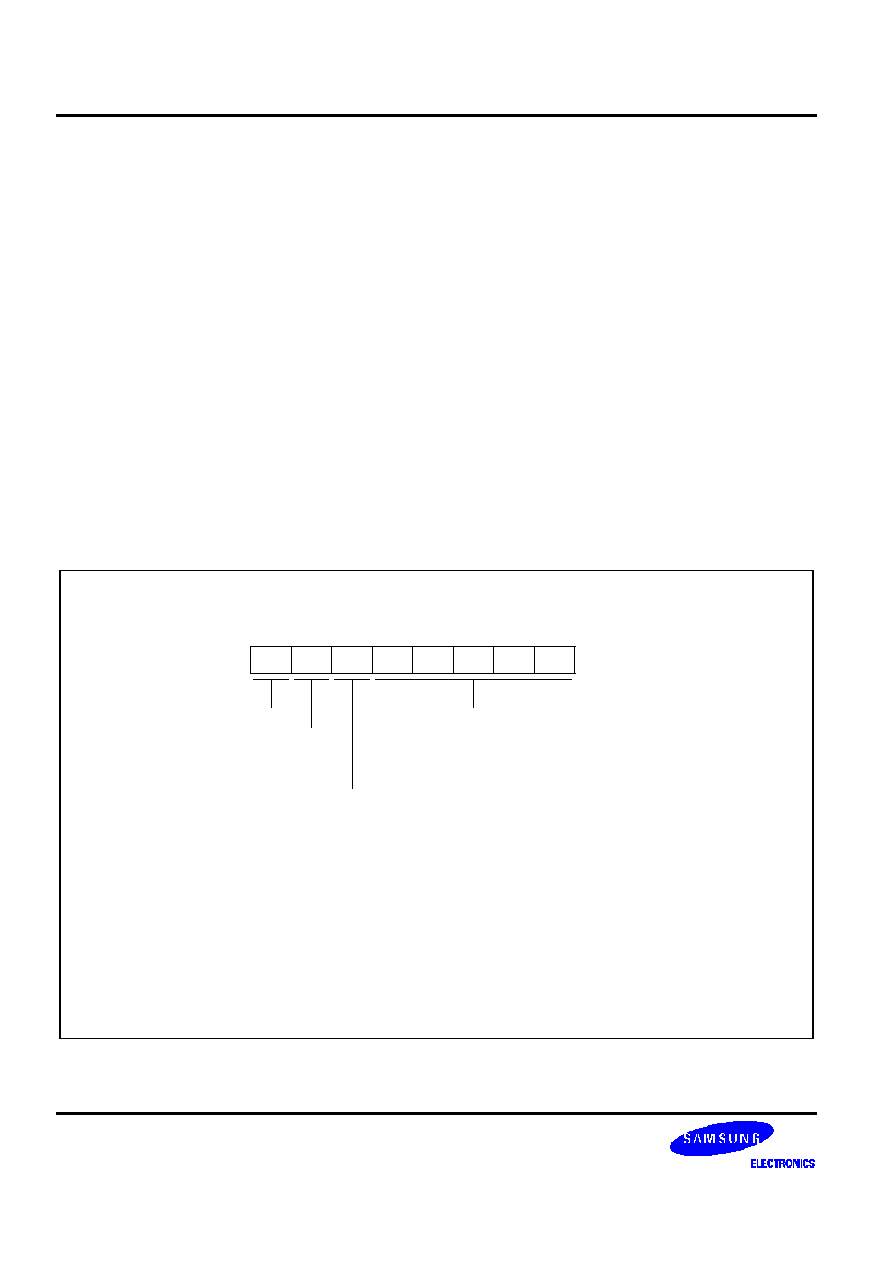
ON-SCREEN DISPLAY
S3C880A/F880A
13-10
FADE-IN AND FADE-OUT CONTROL REGISTER (FADECON)
The OSD block lets you program fade-in and fade-out displays. A fade-in display is one in which a character matrix
is displayed incrementally until the complete character "appears". A fade-out display shows the complete character
matrix first and then decrements the matrix line-by-line until the character "disappears" from the display field.
The address of the character display (and the specific line) to be faded-in or faded-out is selected by writing bit
values into the CHACON and FADECON registers. Bits 3�0 in the CHACON register specify the 4-bit video RAM
address of one of the twelve rows (0�11) of the fade display. Bits 0�4 in the FADECON register specify the 5-bit line
address within the selected row.
Fade direction is controlled by FADECON.5. There are two choices of fade direction: before (FADECON.5 = "0") and
after (FADECON.5 = "1"). When you select fade before, the character matrix is faded starting with line 0. When you
select fade after, the matrix is faded starting with inter-row space line 6. (The inter = row space line 6 start position
is only a suggestion, however, as the fade interval is assignable by software.) To enable the fade function, you
should set FADECON.6 to "1". (FADECON.7 is not used).
NOTE
To avoid confusion in determining fade row and line addresses in the CHACON and FADECON registers,
please note that line is a horizontal value that encompasses the entire character display field while row is a
horizontal value for the character display matrix.
OSD Fade Control Register (FADECON)
F1H, Set 1, Bank 1, R/W
LSB
MSB
.7
.6
.5
.4
.3
.2
.1
.0
Fade function enable bit:
0 = Fade disable
1 = Fade enable
Fade row address selection bits:
00000 = Line 0
00001 = Line 1
00010 = Line 2
00011 = Line 3
00100 = Line 4
00101 = Line 5
00110 = Line 6
00111 = Line 7
01000 = Line 8
01001 = Line 9
01010 = Line 10
01011 = Line 11
01100 = Line 12
01101 = Line 13
01110 = Line 14
01111 = Line 15
10000 = Line 16
10001 = Line 17
10010 = Inter-row space Line 0 (1H)
10011 = Inter-row space Line 1 (2H)
10100 = Inter-row space Line 2 (3H)
10101 = Inter-row space Line 3 (4H)
10110 = Inter-row space Line 4 (5H)
10111 = Inter-row space Line 5 (6H)
11000 = Inter-row space Line 6 (7H)
11001-11111 = Not used
Not used
Fade direction selection bit:
0 = Fade before matrix
1 = Fade after matrix
Figure 13-6. OSD Fade Control Register (FADECON)
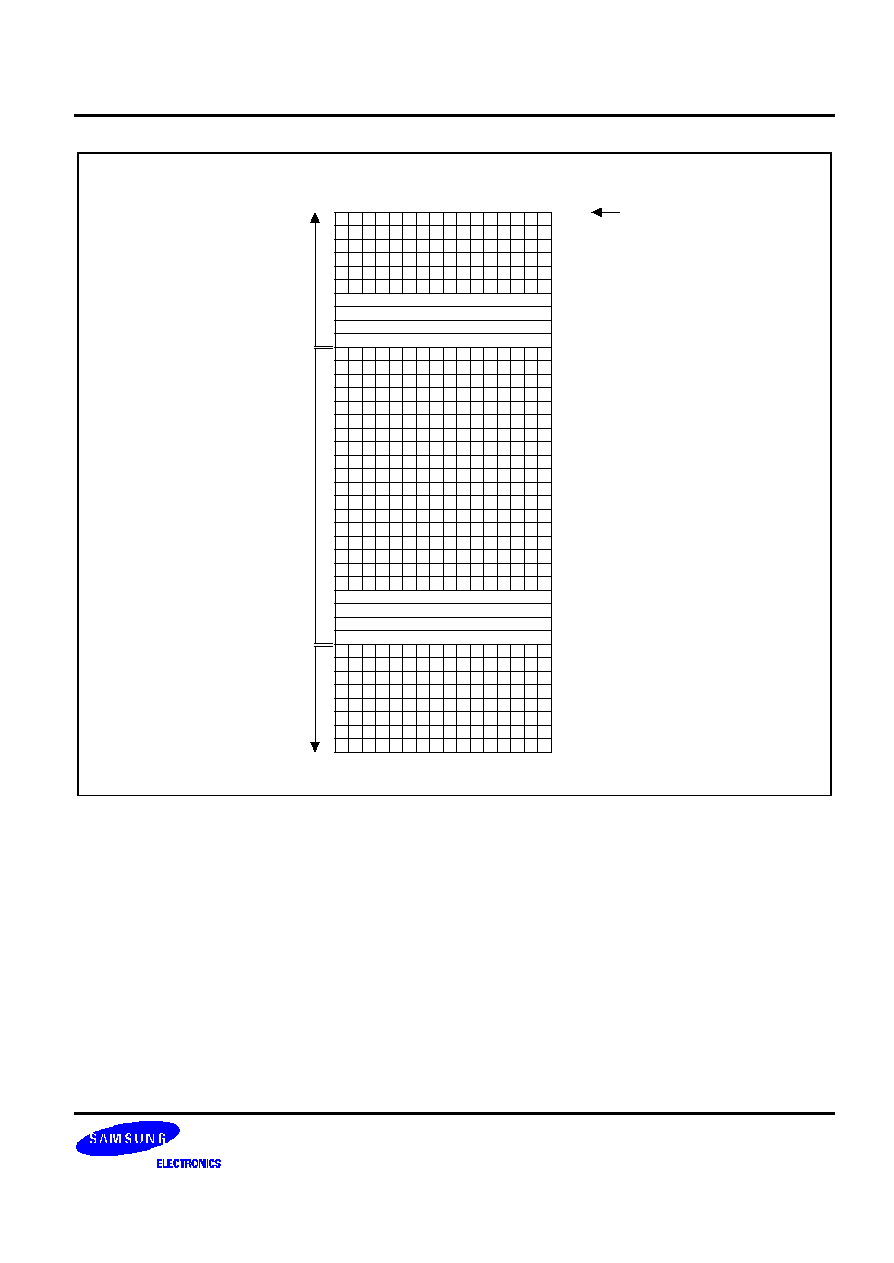
S3C880A/F880A
ON-SCREEN DISPLAY
13-11
n
n - 1
n + 1
Line
12
13
14
15
16
17
18 (Inter-row space Line 0)
19 (Inter-row space Line 1)
20 (Inter-row space Line 2)
21 (Inter-row space Line 3)
0
1
2
3
4
5
6
7
10
11
12
13
14
15
16
17
8
9
0
1
2
3
4
5
6
7
18 (Inter-row space Line 0)
19 (Inter-row space Line 1)
20 (Inter-row space Line 2)
21 (Inter-row space Line 3)
ROW
Figure 13-7. Line and Row Addressing Conventions when ROWCON.2-.0 = "100"

ON-SCREEN DISPLAY
S3C880A/F880A
13-12
Fade After (Fade Line = 13, Fade Line = No Display)
P Q
M N
J K
G H
D E
A B
COLUMNS 0-20
ROWS 0-11
Line = 0
Line = 12
CHACON
FADECON
05H (Fade Row = 5)
6DH (Fade Line = 13;
Fade Afte r Selected)
Figure 13-8. OSD Fade Function Example: Fade After
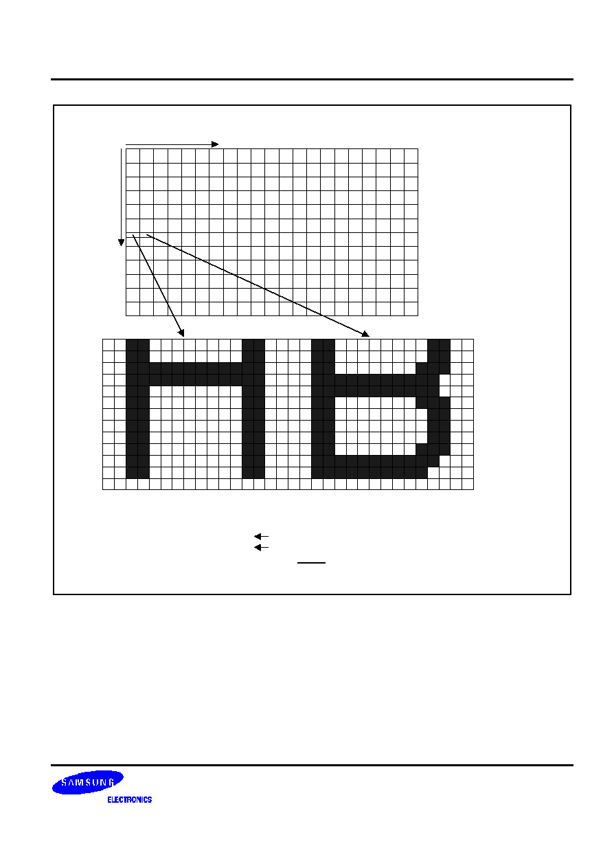
S3C880A/F880A
ON-SCREEN DISPLAY
13-13
P Q
COLUMNS 0-20
ROWS 0-11
Line = 5
Line = 17
Fade Before (Fade Line = 5, Fade Line = Display)
CHACON
FADECON
06H (Fade Row = 6)
45H (Fade Line = 5;
Fade Before Selected)
M N
J K
G H
D E
A B
Figure 13-9. OSD Fade Function Example: Fade Before
ON-SCREEN DISPLAY
S3C880A/F880A
13-14
DISPLAY POSITION CONTROL
The on-screen display has 252 character display positions. There are 21 horizontal columns and 12 vertical rows.
Positions can be numbered sequentially from 0�251 (decimal) or from 0�FB (hexadecimal), as shown in Figures 13-
11 and 13-12. To control display position, you can adjust the top and left margins and the inter-column and inter-row
spacing between characters on the screen.
COLUMNS 0-20
ROWS 0-11
DECIMAL
0
1
2
3
4
5
6
7
8
9 10 11 12 13 14 15 16 17 18 19 20
21 22 23 24 25 26 27 28 29 30 31 32 33 34 35 36 37 38 39 40 41
42 43 44 45 46 47 48 49 50 51 52 53 54 55 56 57 58 59 60 61 62
63 64 65 66 67 68 69 70 71 72 73 74 75 76 77 78 79 80 81 82
84 85 86 87 88 89 90 91 92 93 94 95 96 97 98 99 100 101 102
105 106 107 108 109 110 111 112 113 114 115 116 117 118 119 120 121 122
126 127 128 129 130 131 132 133 134 135 136 137 138 139 140 141 142
83
103 104
123 124 125
143 144 145 146
147 148 149 150 151 152 153 154 155 156 157 158 159 160 161 162 163 164 165 166 167
168 169 170 171 172 173 174 175 176 177 178 179 180 181 182 183 184 185 186 187 188
189 180 191 192 193 194 195 196 197 198 199 200 201 202 203 204 205 206 207 208 209
210 211 212 213 214 215 216 217 218 219 220 221 222 223 224 225 226 227 228 229 230
231 232 233 234 235 236 237 238 239 240 241 242 243 244 245 246 247 248 249 250 251
Figure 13-10. 252-Byte On-Screen Character Display Map (Decimal)
COLUMNS 0-20
ROWS 0-11
HEXADECIMAL
0
1
2
3
4
5
6
7
8
9
A
11 12 13 14
15 16 17 18 19
20 21 22 23 24 25 26 27 28 29
30 31 32 33 34 35 36 37 38 39
40 41 42 43 44 45 46 47 48 49
50 51 52 53
54 55 56 57 58 59
60 61 62 63 64 65 66 67 68
69
70 71 72 73 74 75 76 77 78 79
80 81 82
84 85 86 87 88 89
90 91 92
93 94 95 96 97 98 99
83
B
C
D
E
F 10
1A 1B 1C 1D 1E 1F
2A 2B 2C 2D 2E 2F
3A 3B 3C 3D 3E
3F
4A 4B 4C 4D 4E 4F
5A 5B 5C 5D 5E 5F
6A 6B 6C 6D 6E 6F
7A 7B 7C 7D
7E 7F
8A 8B 8C 8D 8E 8F
9A 9B 9C 9D 9E 9F A0 A1 A2 A3 A4 A5 A6 A7
A8 A9 AA AB AC AD AE AF B0 B1 B2 B3 B4 B5 B6 B7 B8 B9 BA BB BC
BD BE BF C0 C1 C2 C3 C4 C5 C6 C7 C8 C9 CA CB CC CD CE CF D0 D1
D4 D5
D2 D3
D8 D9
D6 D7
DA DB
DE DF
DC DD
E0 E1 E2 E3 E4 E5 E6
E7 E8 E9 EA EB EC ED EE
F0 F1 F2 F3 F4 F5 F6 F7 F8 F9 FA FB
EF
Figure 13-11. 252-Byte On-Screen Character Display Map (Hexadecimal)
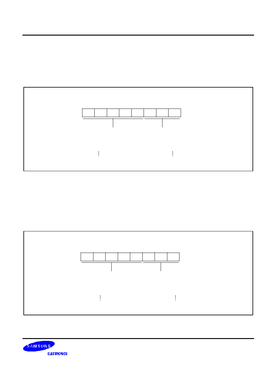
S3C880A/F880A
ON-SCREEN DISPLAY
13-15
ROW CONTROL REGISTER (ROWCON)
The row control register, ROWCON, controls the top margin and inter-row spacing. Top margin is the distance (in H-
sync pulses) to the top row of a character display from the top edge of its display frame. Inter-row spacing is the
distance (in H-sync pulses) between two rows of displayed characters. The inter-row spacing value you select is
applied equally to all rows in the display.
OSD Row Control Register (ROWCON)
F2H, Set 1, Bank 1, R/W
LSB
MSB
.7
.6
.5
.4
.3
.2
.1
.0
Inter-row spacing control bits
(0H-7H in H-sync pulses):
000 = No inter-row spacing (0H)
001 = Inter-row spacing = 1H
111 = Inter-row spacing = 7H
Top margin display position control bits
(4 x TMG value of 0-31 dots):
00000 = Top margin = 0H
00001 = Top margin = 4H
11111 = Top margin = 124H
Figure 13-12. OSD Row Control Register (ROWCON)
COLUMN CONTROL REGISTER (CLMCON)
The column control register, CLMCON, controls the left margin and inter-column spacing. Left margin is the distance
to the character display from the left edge of the display frame. Inter-column spacing is the distance (0�7 dots)
between space separating the characters displayed in a row. The inter-column spacing value that you select is
applied equally to all columns in the display.
OSD Column Control Register (CLMCON)
F3H, Set 1, Bank 1, R/W
LSB
MSB
.7
.6
.5
.4
.3
.2
.1
.0
Left margin display position control value
(16 + 4 x LMG value of 0-31 dots):
00000 = Left margin = 16 dots clock
00001 = Left margin = 16 + 4 x 1 dot clock
11111 = Left margin = 16 + 4 x 31 dot clock
Inter-column spacing control value
(0-7 dots):
000 = No inter-column spacing
001 = Inter-column spacing = 1 dot
111 = Inter-column spacing = 7 dots
Figure 13-13. OSD Column Control Register (CLMCON)
ON-SCREEN DISPLAY
S3C880A/F880A
13-16
Inter-Row Space
Inter-Column Space
Left
Margin
Top Margin
Figure 13-14. OSD Display Formatting and Spacing Conventions
Calculating Row and Column Spacing
Inter-row spacing and inter-column spacing are controlled by the ROWCON and CLMCON registers. You can select
from zero to seven dots of spacing.
For inter-row spacing, the desired spacing value (0�7) is written to bits 0�2 of the ROWCON register. For inter-
column spacing, the desired spacing value (0�7) is written to bits 0�2 of the CLMCON register.
Calculating Margin Settings
By writing a value to ROWCON.3�ROWCON.7, you can set the top margin at 4
�
the top margin dot value (TMG).
Because TMG is a 5-bit value, you can select any dot value in the range 0�31.
By writing a value to CLMCON.3�CLMCON.7, you can set the left margin at 16 + 4
�
the left margin dot value
(LMG). Because LMG is a 5-bit value, you can select any dot value in the range 0�31. The zero position for the left
margin is always 16 dots.
-- Top margin = 4
�
(top margin register value) H
-- Left margin = 16 + 4
�
(left margin register value) dot clock
-- Inter-column space = (Register value) dot clock
-- Inter-row space = (Register value) H
S3C880A/F880A
ON-SCREEN DISPLAY
13-17
CHARACTER COLOR CONTROL REGISTER (COLBUF)
The color of the character matrix display is controlled by manipulating a 5-bit value in the OSD video RAM. You can
modify the character color selection bits only by addressing the OSD color buffer register, COLBUF (FCH, set 1,
bank 1). The color selection bits are COLBUF.2, COLBUF.1, COLBUF.0 and COLBUF.3 (H/T and BGRND). These
four bits comprise the RGB value (bit 10, 11, 12) and H/T and BGRND enable bit (bit 13) of the character data stored
in the video RAM.
When programming the display RAM values for a character display, you must first load a 3-bit color value into the
color buffer. This color setting is automatically appended to each 10-bit character code as it is written to the OSD
RAM addresses. If only one COLBUF value is loaded, all characters in the screen display will, of course, be the
same color. To change the display color of successive characters, modify the COLBUF value before you load the
address data for a specific row and column into the video RAM.
OSD Character Color Buffer (COLBUF)
FCH, Set 1, Bank 1, R/W
LSB
MSB
.7
.6
.5
.4
.3
.2
.1
.0
Not used
Video RAM bit 9 enable bit:
0 = Disable VRAM bit 9
1 = Enable VRAM bit 9
Character color selection bits
(.2 = red, .1 = green, .0 = blue)
Video RAM bit 8 enable bit:
0 = Disable VRAM bit 8
1 = Enable VRAM bit 8
H/T and BGRND enable bit:
0 = Disable H/T and BGRND
1 = Enable H/T and BGRND
(VRAM bit 13)
Character color
.0
OSDCOL.0 = 0
OSDCOL.0 = 1
.1
.2
0
0
0
0
0
0
0
0
0
0
0
0
1
1
1
1
1
1
1
1
1
1
1
1
Black
Blue
Green
Cyan
Red
Magenta
Yellow
White
Color Mode 0
Color Mode 1
Color Mode 2
Color Mode 3
Color Mode 4
Color Mode 5
Color Mode 6
Color Mode 7
Figure 13-15. OSD Character Color Buffer Register (COLBUF)

ON-SCREEN DISPLAY
S3C880A/F880A
13-18
BACKGROUND COLOR CONTROL
The background color control register, COLCON, lets you select background colors for both the display frame and
characters:
-- Frame background is the full-screen display field upon which the character display is imposed.
-- Character background is a color field that surrounds the individual character. To enhance readability, the
background is usually a color that contrasts or highlights the characters in a pleasing manner.
Frame
Background
Color
Wide Screen
Color TV
Wide Screen
Color TV
Character
Background
Color
No Character
Background
Color
Character
Background
Off
Wide Screen
Color TV
Color TV
Wide Screen
Wide Screen
Color TV
Wide Screen
Color TV
Figure 13-16. Background Color Display Conventions
S3C880A/F880A
ON-SCREEN DISPLAY
13-19
OSD Background Color Control Register (COLCON)
F3H, Set 1, Bank 1, R/W
LSB
MSB
.7
.6
.5
.4
.3
.2
.1
.0
Frame background color enable bit:
0 = Disable frame background color
(No color is displayed)
1 = Enable frame background color
Character color selection bits
(See table)
Character background color enable bit:
0 = Disable character background color
(No color is displayed)
1 = Enable character background color
Frame background color selection bit:
Frame Character Background color
.4 or .0
.5 or .1
.6 or .2
0
x
OSDCOL.0 = 1
Color Mode 0
Color Mode 1
Color Mode 2
Color Mode 3
Color Mode 4
Color Mode 5
Color Mode 6
Color Mode 7
OSDCOL.0 = 0
Black
Blue
Green
Cyan
Red
Magenta
Yellow
White
.7 or .3
x
x
1
0
0
0
0
0
0
0
0
1
1
1
No background display
1
1
1
1
1
1
1
1
1
1
1
1
1
1
0
0
0
1
0
1
Figure 13-17. OSD Background Color Control Register (COLCON)
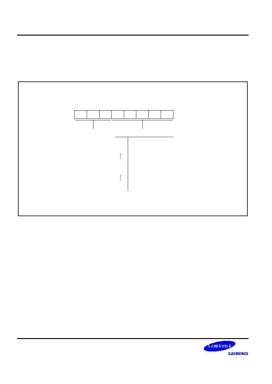
ON-SCREEN DISPLAY
S3C880A/F880A
13-20
V-SYNC BLANK CONTROL REGISTER (VSBCON)
VSBCON sets the blank area, which stops the L-C oscillator during the defined time from the V-sync input time. Unit
of V-sync blank time is 1 H-sync. It can be set up to a maximum of 31 H-syncs. If VSBCON.4 is set from"0" to
"1001B", blank time is always 9 H-syncs regardless of the setting value.
V-sync Blank Control Register (VSBCON)
F7H, Set 1, Bank 1, R/W
LSB
MSB
.7
.6
.5
.4
.3
.2
.1
.0
V-sync blank time control bit:
Not used
00000
00001
00010
9 Horizontal sync
9 Horizontal sync
9 Horizontal sync
01001
01010
01011
11110
11111
9 Horizontal sync
10 Horizontal sync
11 Horizontal sync
30 Horizontal sync
31 Horizontal sync
NOTE: Frame background is disabled during the V-sync blank time.
Figure 13-18. V-sync Blank Control Register (VSBCON)
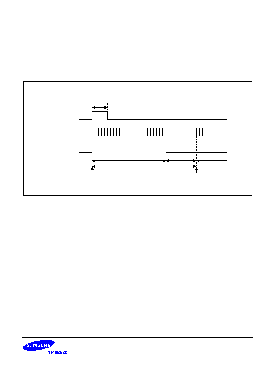
S3C880A/F880A
ON-SCREEN DISPLAY
13-21
V-SYNC BLANK AND TOP MARGIN TIMING DIAGRAM
The following is a timing diagram simplified with external V-sync input and H-sync input signals. V-sync blank and
top margin are controlled by VSBCON and ROWCON VSBCON .4�.0 = 01011B (V-sync blank time = 11 Horizontal
sync). ROWCON.7�.3 = 00100B (top margin control value = 16, top margin = 5).
V-sync
blank
V-sync blank time on chip
Row 0
V-sync interrupt
Row 0 interrupt
V-sync input
H-sync input
Internal V-sync
H-line count
1
0
3
2
5
4
7
6
9
8
10 11
13
12
15
14
17
16
19
18
20 21
1
0
3
2
5
4
7
6
9
8
10 11
13
12
15
14
16
1
0
3
2
4
Top margin
ROWCON.7-.3 (Top margin control value)
Figure 13-19. V-sync Blank and Top Margin Timing Diagram

ON-SCREEN DISPLAY
S3C880A/F880A
13-22
HALFTONE SIGNAL CONTROL REGISTER (HTCON)
The halftone function lets you output halftone control signals to peripherals such as a chroma-IC. You can select
halftone output for character back ground periods (as selected by bit 13 in the video RAM) or for frame periods
(regardless of the bit 13 setting). The halftone signal control register, HTCON, has the following functions:
-- Halftone option selection (character or frame)
-- Halftone display enable/disable
-- V-sync interrupt enable and pending control
-- Polarity selection of RGB and halftone outputs
Bits 4 and 5 are used for OSD Row interrupt function.
OSD ROW Interrupt Control
The S3C880A/F880A has a total of 12 OSD display rows. When enabled, an OSD ROW interrupt occurs in the first
line of each row. Up to 12 OSD ROW interrupts can be generated, while this number can be reduced according to
different settings in top margin (ROWCON.7�.3), inter row space (ROWCON.2�.0), vertical character size
(CHACON.7�.6), and Vsync blank time (VSBCON). The ROW counter of DSPCON.7�.4 informs the order of an OSD
ROW interrupt occurring within a frame. An OSD ROW interrupt is generated at the beginning of a ROW (for ROW0
through ROW11).
OSD ROW interrupt allow different controls to each ROW. If the OSD control register is adjusted in the N-th row
area, the new value is applied from (N+1)th row. That is, if the OSD control register is adjusted in the first OSD ROW
interrupt (DSPCON.7�.4 = 0000B) service routine, the new value is applied from ROW1. A change in the 12 th OSD
ROW interrupt service routine affects the rows from ROW0.
NOTE: OSD output enable/disable (DSPCON.0) settings are immediately applied. Top margin (ROWCON.7�.3) and
VSBCON are applied in accordance with Vsync input signals.
Halftone Option Selection
In character periods only (HTCON.2 = "0"), the character specified in COLBUF.3 may have the halftone function
according to the condition of DSPCON.2�.1 (DSPCON.2�.1 = "10" or DSPCON.2�.1 = "11").
In all frame periods (HTCON.2 = "1"), the entire section can have the function, regardless of the COLBUF.3 condition.
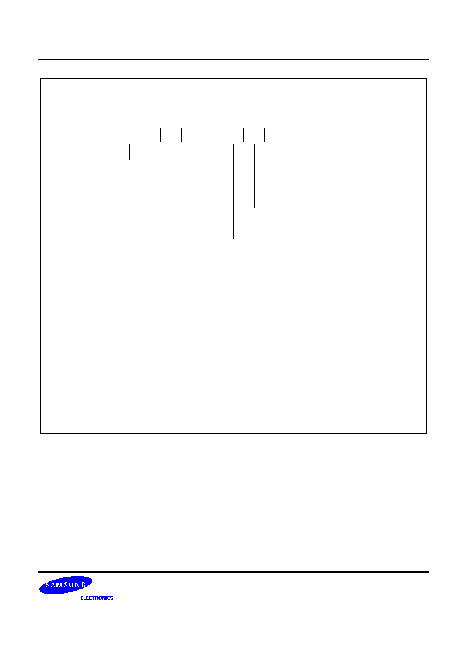
S3C880A/F880A
ON-SCREEN DISPLAY
13-23
Halftone Signal Control Register (HTCON)
F3H, Set 1, Bank 1, R/W
LSB
MSB
.7
.6
.5
.4
.3
.2
.1
.0
Halftone signal output
polarity selection bit:
(1)
0 = Active high level
1 = Active low level
V-sync interrupt pending bit:
0 = No interrupt pending (when read)
0 = Clear pending bit (when write)
1 = Interrupt is pending (when read)
1 = No effect (when write)
V-sync interrupt enable bit:
0 = Disable the V-sync interrupt
1 = Enable the V-sync interrupt
Halftone option selection bit:
(3)
0 = Character back ground periods only
(when bit 3 of COLBUF is set to "1")
1 = All frame periods (disregard COLBUF "Bit 3")
RGB polarity selection bit:
(2)
0 = Active high level
1 = Active low level
Halftone control signal enable bit:
0 = Disable halftone signal
1 = Enable halftone signal
OSD Row interrupt enable bit:
0 = Disable the OSD Row interrupt
1 = Enable the OSD Row interrupt
OSD Row interrupt pending bit:
0 = No interrupt pending (when read)
0 = Clear pending bit (when write)
1 = Interrupt is pending (when read)
1 = No effect (when write)
NOTES:
1. The HTCON.7 setting applies to halftone output only. The active high setting ("0") means
that the normal halftone signal output is Low level. when you select the active low setting ("1"),
the normal halftone signal output is High level.
2. The active high setting ("0") for HTCON.6 means that the normal RGB polarity is Low level.
When you select the active low setting ("1"), the normal RGB polarity is High level.
3. In case HTCON.2 = 1, character halftone and background color (DSPCON.2-.1 = "11B") do not operate.
Figure 13-20. Halftone Signal Control Register (HTCON)
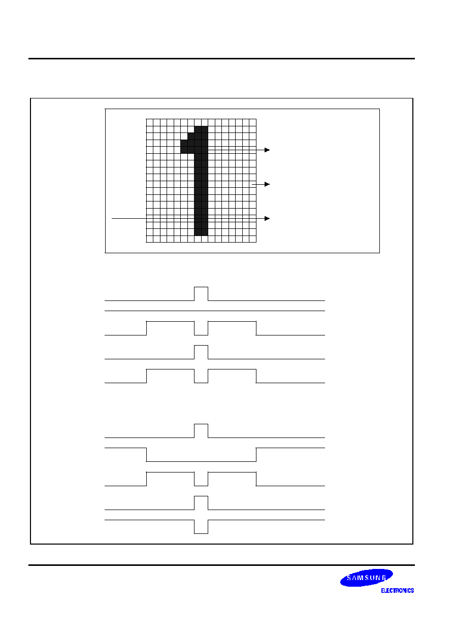
ON-SCREEN DISPLAY
S3C880A/F880A
13-24
Background Color and Halftone Function Mode
R
G
B
Blank
OSDHT
R
G
B
Blank
OSDHT
COLCON.7 = "0", If OSDCOL.0 = "0", COLCON = 29H, HTCON.3-.2 ="10b"
Frame background: Disable, Frame halftone: Disable, Character background: Enable with Blue color,
Character background halftone: Enable
If OSDCOL.0 = "0", COLCON = A1H, HTCON.3-.2 ="11b"
Frame background: Enable with Green coler, Frame halftone: Enable,
Character background: Enable with Blue color, Character background halftone: Enable
Background Color: Blue
Character Color: Red
Frame background color: Green
SCAN
Figure 13-21. Halftone or Character Backgound Signal Output
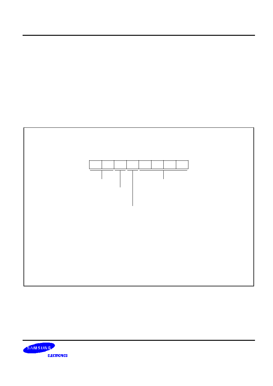
S3C880A/F880A
ON-SCREEN DISPLAY
13-25
OSD FIELD CONTROL REGISTER (OSDFLD)
OSD field control register helps recognizing whether the current field is an EVEN field or an ODD one, in a TV signal
frame. This control register must be defined for a current field recognition of V-sync and H-sync entering the
S3C880A/F880A. In order to recognize an even field, OSDFLD.0�.3 defines the range starting from the point of
V-sync edge, where H-sync must be present. If H-sync exits within the range, the field is recongnized as an EVEN
field.
OSDFLD.4 defines when H-sync must be detected. If it is set to "0", the existence of H-sync is detected within the
range set by OSDFLD.0�.3 before V-sync is input. If it is set "1", it is detected after V-sync is input.
OSDFLD.5 describes whether the current, field input by the field control which is set by OSDFLD.0�.3 and
OSDFLD.4 is an EVEN field or an ODD one.
OSD Field Control Register (OSDFLD)
E5H, Set 1, Bank 1, R/W
LSB
MSB
.7
.6
.5
.4
.3
.2
.1
.0
Not used
Field data (read only):
0 = Even field
1 = Odd field
Even field range:
0000 = Not used
0001 = f
CPU
/16 x 1
0010 = f
CPU
/16 x 2
0011 = f
CPU
/16 x 3
0100 = f
CPU
/16 x 4
0101 = f
CPU
/16 x 5
0110 = f
CPU
/16 x 6
0111 = f
CPU
/16 x 7
1000 = f
CPU
/16 x 8
1001 = f
CPU
/16 x 9
1010 = f
CPU
/16 x 10
1011 = f
CPU
/16 x 11
1100 = f
CPU
/16 x 12
1101 = f
CPU
/16 x 13
1110 = f
CPU
/16 x 14
1111 = f
CPU
/16 x 15
H-sync detect position select:
0 = Detect H-sync before V-sync
1 = Detect H-sync after V-sync
Figure 13-22. OSD Field Control Register (OSDFLD)
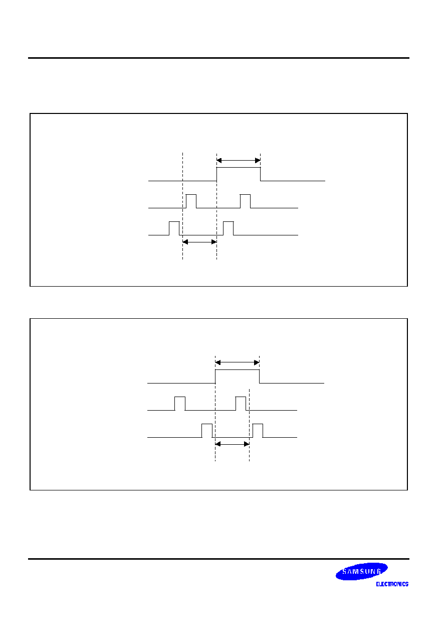
ON-SCREEN DISPLAY
S3C880A/F880A
13-26
Field Detect by OSDFLD Control
When control register set is OSDFLD.0-.3 = "1010B", OSDFLD.4 = 0
f
CPU
/
16 x 10
V-sync
blank
Even filed
Odd filed
V-sync input
H-sync input
H-sync input
Figure 13-23. Field Detect in Before V-sync
f
CPU
/
16 x 10
V-sync
blank
Even filed
Odd filed
V-sync input
H-sync input
V-sync input
Figure 13-24. Field Detect in After V-sync
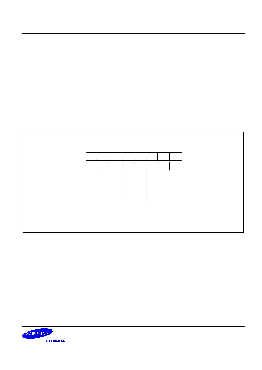
S3C880A/F880A
ON-SCREEN DISPLAY
13-27
OSD PALETTE COLOR CONTROL
OSD Palette Color Mode Registers (OSDPLTR, OSDPLTG, OSDPLTB)
OSD palette color mode register R, G, B controls the color of OSD R, G, B output. OSDPLTR1, OSDPLTR2,
OSDPLTG1, OSDPLTG2, OSDPLTB1, and OSDPLTB2 are composed of 8 bits each, in which the combinations of
bit0-bit1, bit2-bit3, bit4-bit5, bit6-bit7 of OSDPLTx1 (x = R, G, B) define color mode 0 to 3 and bit0-bit1, bit2-bit3,
bit4-bit5, bit6-bit7 of OSDPLTx2 (x = R, G, B) define color mode 4 to 7, respectively.
Each color mode can express upto 64 color by combing the six registers (OSDPLTR1, OSDPLTR2, OSDPLTG1,
OSDPLTG2, OSDPLTB1, OSDPLTB2). As one color mode can select one color out of 64 choices, and there are 8
color modes, a total of 8 colors can be displayed at time. For example, when combining color mode 0, each of
OSDPLTR1.0-1, and OSDPLTB1.0-1 can produce 4 kids of red level, which can be multiplied upto 64 combinations.
Each 2 bits define a color mode make 4 color levels available. When the standard lighting is 100%, the value "00B"
means disabled, "01B" means 33% and "10B" means 66% of the standard light level.
OSD Palette Color Mode Register R1 (OSDPLTR1)
E6H, Set 1, Bank 0, R/W
LSB
MSB
.7
.6
.5
.4
.3
.2
.1
.0
OSD mode 3 red level
00 = Disable
01 = 33%
10 = 66%
11 = 100%
OSD mode 2 red level
00 = Disable
01 = 33%
10 = 66%
11 = 100%
OSD mode 0 red level
00 = Disable
01 = 33%
10 = 66%
11 = 100%
OSD mode 1 red level
00 = Disable
01 = 33%
10 = 66%
11 = 100%
Figure 13-25. OSD Palette Color Mode Register R1 (OSDPLTR1)
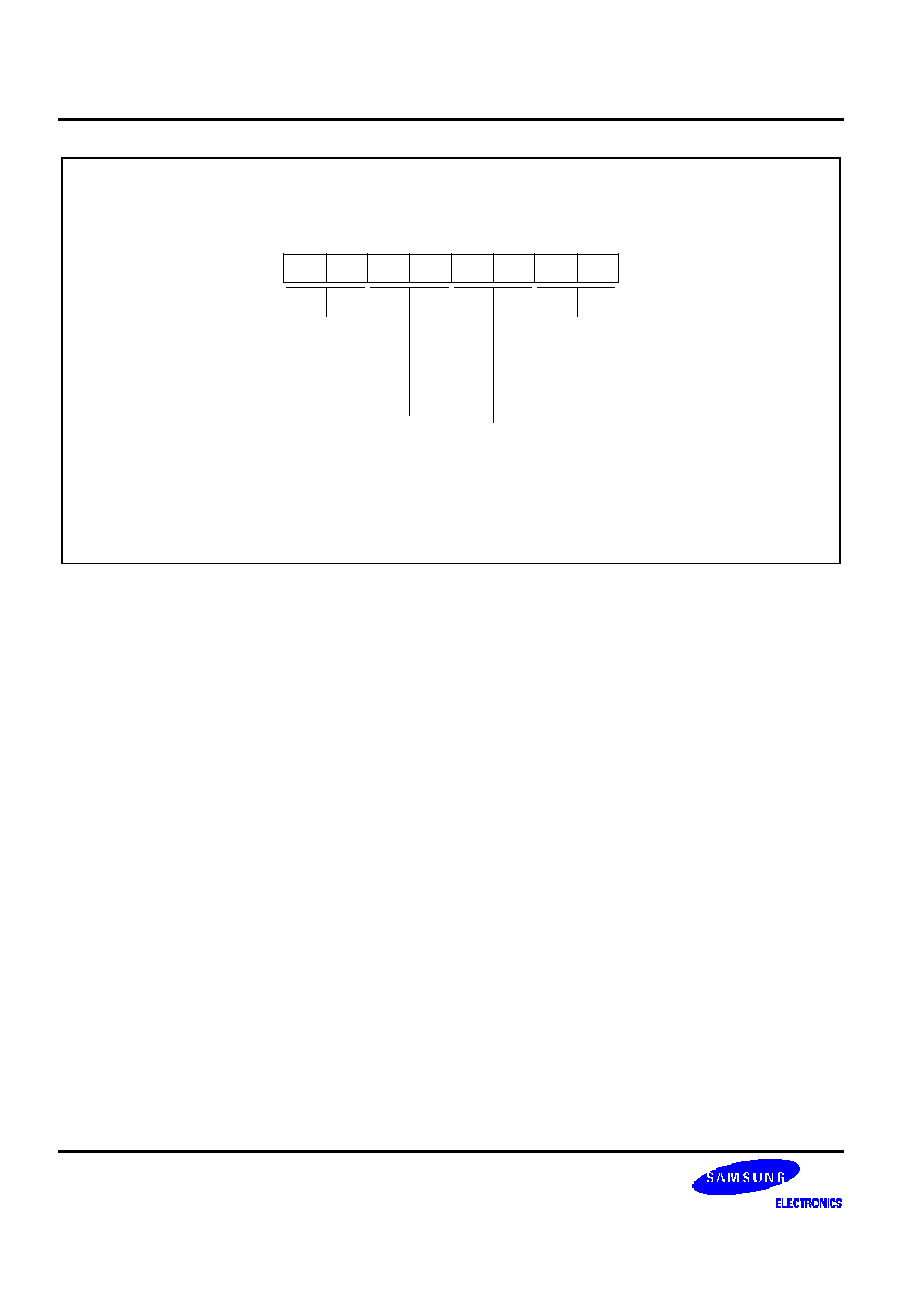
ON-SCREEN DISPLAY
S3C880A/F880A
13-28
OSD Palette Color Mode Register R2 (OSDPLTR2)
E7H, Set 1, Bank 1, R/W
LSB
MSB
.7
.6
.5
.4
.3
.2
.1
.0
OSD mode 7 red level
00 = Disable
01 = 33%
10 = 66%
11 = 100%
OSD mode 6 red level
00 = Disable
01 = 33%
10 = 66%
11 = 100%
OSD mode 4 red level
00 = Disable
01 = 33%
10 = 66%
11 = 100%
OSD mode 5 red level
00 = Disable
01 = 33%
10 = 66%
11 = 100%
Figure 13-26. OSD Palette Color Mode Register R2 (OSDPLTR2)
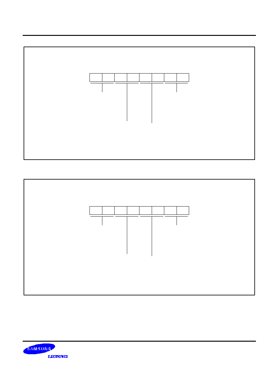
S3C880A/F880A
ON-SCREEN DISPLAY
13-29
OSD Palette Color Mode Register G1 (OSDPLTG1)
E8H, Set 1, Bank 0, R/W
LSB
MSB
.7
.6
.5
.4
.3
.2
.1
.0
OSD mode 3 green level
00 = Disable
01 = 33%
10 = 66%
11 = 100%
OSD mode 2 green level
00 = Disable
01 = 33%
10 = 66%
11 = 100%
OSD mode 0 green level
00 = Disable
01 = 33%
10 = 66%
11 = 100%
OSD mode 1 green level
00 = Disable
01 = 33%
10 = 66%
11 = 100%
Figure 13-27. OSD Palette Color Mode Register G1 (OSDPLTG1)
OSD Palette Color Mode Register G2 (OSDPLTG2)
E9H, Set 1, Bank 0, R/W
LSB
MSB
.7
.6
.5
.4
.3
.2
.1
.0
OSD mode 7 green level
00 = Disable
01 = 33%
10 = 66%
11 = 100%
OSD mode 6 green level
00 = Disable
01 = 33%
10 = 66%
11 = 100%
OSD mode 4 green level
00 = Disable
01 = 33%
10 = 66%
11 = 100%
OSD mode 5 green level
00 = Disable
01 = 33%
10 = 66%
11 = 100%
Figure 13-28. OSD Palette Color Mode Register G2 (OSDPLTG2)
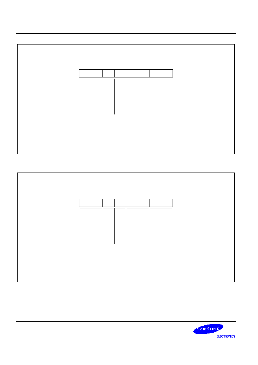
ON-SCREEN DISPLAY
S3C880A/F880A
13-30
OSD Palette Color Mode Register B1 (OSDPLTB1)
EAH, Set 1, Bank 0, R/W
LSB
MSB
.7
.6
.5
.4
.3
.2
.1
.0
OSD mode 3 blue level
00 = Disable
01 = 33%
10 = 66%
11 = 100%
OSD mode 2 blue level
00 = Disable
01 = 33%
10 = 66%
11 = 100%
OSD mode 0 blue level
00 = Disable
01 = 33%
10 = 66%
11 = 100%
OSD mode 1 bluelevel
00 = Disable
01 = 33%
10 = 66%
11 = 100%
Figure 13-29. OSD Palette Color Mode Register B1 (OSDPLTB1)
OSD Palette Color Mode Register B2 (OSDPLTB2)
EBH, Set 1, Bank 0, R/W
LSB
MSB
.7
.6
.5
.4
.3
.2
.1
.0
OSD mode 7 blue level
00 = Disable
01 = 33%
10 = 66%
11 = 100%
OSD mode 6 blue level
00 = Disable
01 = 33%
10 = 66%
11 = 100%
OSD mode 4 blue level
00 = Disable
01 = 33%
10 = 66%
11 = 100%
OSD mode 5 bluelevel
00 = Disable
01 = 33%
10 = 66%
11 = 100%
Figure 13-30. OSD Palette Color Mode Register B2 (OSDPLTB2)

S3C880A/F880A
ON-SCREEN DISPLAY
13-31
OSD SPACE COLOR CONTROL REGISTER (OSDCOL)
RGB output selection
S3C880A/F880A has two RGB output mode: digital mode and analog mode.
In Digital mode, OSDCOL.0 must be set to 0. RGB output has two levels, VSS and VDD. Eight colors can be
produced: black, blue, green, cyan, red, magenta, yellow and white. OSD palette color control registers,
OSDPLTR1, OSDPLTR2, OSDPLTG1, OSDPLTG2, OSDPLTB1, and OSDPLTB2, are not used in this mode.
In analog mode, OSDCOL.0 must be set to 1. R.G.B output color bright can be selected among four levels
respectively. 64 colors can be selected by setting OSD palette color control registers, OSDPLTR1, OSDPLTR2,
OSDPLTG1, OSDPLTG2, OSDPLTB1, and OSDPLTB2. In one display row you can select 8 colors, color mode 0�7,
by setting COLBUF.2�.0. The color selected by color mode 0�7 can be changed in every display row.
Inter-row space halftone
Inter-row spacing is the distance (in H-sync pulses) between two rows of displayed characters and can be changed
by setting ROWCON.2-.0. Also halftone character can be changed for this inter-row spacing.
For OSDCOL.1=0, halftone function of inter-row space region is the same as that of the character background
region. That is, if the halftone function of character background region is enabled by setting HTCON.3 to "1", the
halftone function of inter-row space region is enabled. When HTCON.3 is set to "1", halftone function of character
background is enabled regardless of the value of HTCON.2.
For OSDCOL=1 (depend on frame background halftone), inter-row space halftone function is enabled when the value
of HTCON.3 and HTCON.2 are set to "1".
Inter-row space color
Inter-row space color depends on the character background color and frame background color by COLCON. When
OSDCOL.2 is "0", inter-row space color depends on the current character background color; when OSDCOL.2 is "1",
inter-row space color depends on the current frame background color.
Fringe dot size selection
1 dot (when OSDCOL.3 is "0") is a fringe size, which is set by OSDFRG1 and OSDFRG2.
For 1/2 dot fringe size (when OSDCOL.3 is "1"), fringe function is set by 1/2 dot unit. In the interlaced scan, even
field line and odd field line are added to form 1 dot of length. If character size of length is x1 or x3 in the 1/2 dot fringe
size, blinking can occur. So, 1 dot fringe size method is recommended.
Inter character smoothing control
If inter character smoothing is enabled (when OSDCOL.4 is "1"), adjacent character is considered as one character
and smoothing function is enabled.

ON-SCREEN DISPLAY
S3C880A/F880A
13-32
OSD Space Color Control Register (OSDCOL)
E4H, Set 1, Bank 0, R/W
LSB
MSB
.7
.6
.5
.4
.3
.2
.1
.0
Not used
Inter character smoothing control bit
(note)
:
0 = Disable inter character smoothing
1 = Enable inter character smoothing
RGB output selection bit:
0 = Digital RGB output (Disable palette color mode)
1 = Analog RGB output (Enable palette color mode)
Fringe dot size
selection bit:
0 = 1 dot
1 = 1/2 dot
Inter-row space halftone
0 = Depend on character background halftone
1 = Depend on frame background halftone
Inter-row space color
0 = Depend on character background color
1 = Depend on frame background color
Figure 13-31. OSD Space Color Control Register (OSDCOL)

S3C880A/F880A
ON-SCREEN DISPLAY
13-33
OSD BORDER/FRINGE FUNCTION
Fringing Function
The fringing function is used to display a character with a fringe (fringe means shadowed character at bottom and
right direction) width is 1 or 1/2 dot in a different color from that of the character. For all character size, fringe width is
1 or 1/2 dot by set of OSDCOL.3. When a character is displayed with the maximum of 18 vertical dots and 16
horizontal dots, the fringe exceeds right and bottom of the character display area. The exceeded fringe can be
displayed; however , display characters have higher priority to fringe. In this case, If you want to display both fringe
and character, you should set inter-row space and inter-column space. When 1dot fringe function is selected, you
should set minimum two dots of inter-row space or inter-column space. When 1/2 dot fringe function is selected, you
should set minimum one dot of inter-row space or inter-column space.
Fringing is enabled for each line by setting each bit of OSDFRG1 and OSDFRG2 to "1" when OSDFRG2.7="1".
Three bits of OSDFRG2.6-.4 are control Border color. A color for fringe is specified common to selected row and a
color for fringe to each row are controlled differently.
NOTE: When Vertical size x1 and x3 in 1/2 fringe enabled, the flickering may be generated. Because vertical 1 dot
means even and odd field, that is 1/2 dot is even or odd field area. So interlace scan TV system, you can
see the flickering.
Border Function
The Border function is used to display a character with a Border (Border means shadowed at all character boundary)
width is 1/2 dot in a different color from that of the character. For all character size, Border width is 1/2 dot. When a
character is displayed with the maximum of 18 vertical dots and 16 horizontal dots, the fringe exceeds right and
bottom of the character display area. The exceeded Border can be displayed; however , display characters have
higher priority to fringe. In this case, If you want to display both Border and character, you should set inter-row space
and inter-column space over minimum one dot. Border is enabled for each line by setting each bit of OSDFRG1 and
OSDFRG2 to "1" when OSDFRG2.7="0".
Three bits of OSDFRG2.6-.4 are control Border color. A color for Border is specified common to selected row and a
color for fringe to each row are controlled differently.
NOTE: When Vertical size x1 and x3, the flickering may be generated. Because vertical 1 dot means even and odd field,
that is 1/2 dot is even or odd field area. So interlace scan TV system, you can see the flickering.
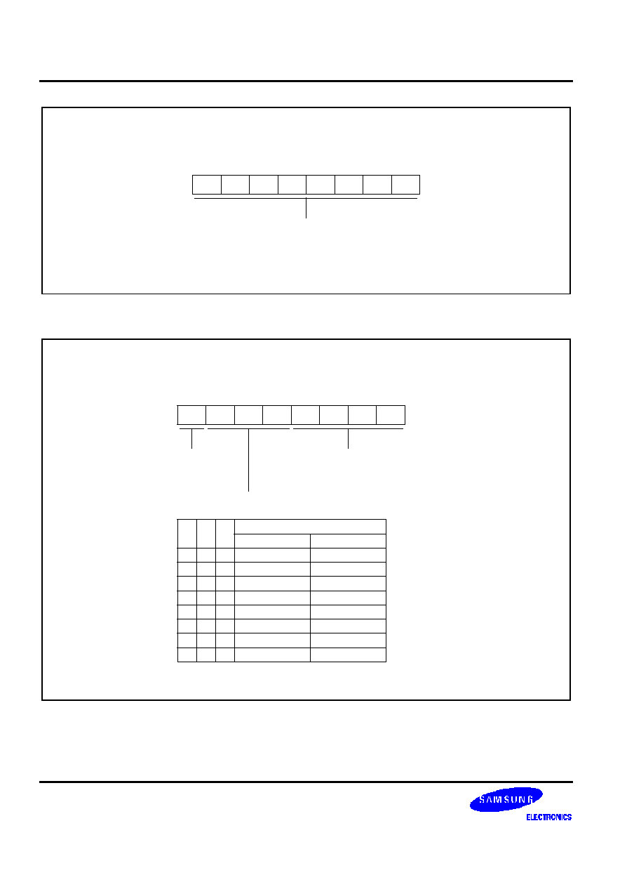
ON-SCREEN DISPLAY
S3C880A/F880A
13-34
OSD Fringe/Border Control Register 1 (OSDFRG1)
E0H, Set 1, Bank 1, R/W
LSB
MSB
.7
.6
.5
.4
.3
.2
.1
.0
Fringe/Border function enable bit:
0 = Disable fringe/border function at row n (n = 0-7)
1 = Enable fringe/border function at row n (n = 0-7)
Figure 13-32. OSD Fringe/Border Control Register 1 (OSDFRG1)
LSB
MSB
.7
.6
.5
.4
.3
.2
.1
.0
Fringe/Border color selection bits:
(.6 = red, .5 = green, .4 = blue)
Fringe/Border Color
.4
OSDCOL.0 = 0
OSDCOL.0 = 1
.5
.6
0
0
0
0
0
0
0
0
0
0
0
0
1
1
1
1
1
1
1
1
1
1
1
1
Black
Blue
Green
Cyan
Red
Magenta
Yellow
White
Color Mode 0
Color Mode 1
Color Mode 2
Color Mode 3
Color Mode 4
Color Mode 5
Color Mode 6
Color Mode 7
OSD Fringe/Border Control Register 2 (OSDFRG2)
E1H, Set 1, Bank 1, R/W
Fringe/Border function enable bit:
0 = Disable fringe/border function at row n (n = 8-11)
1 = Enable fringe/border function at row n (n = 8-11)
Fringe or Border selection bit:
0 = Border function select
1 = Fringe function select
Figure 13-33. OSD Fringe/Border Control Register 2 (OSDFRG2)
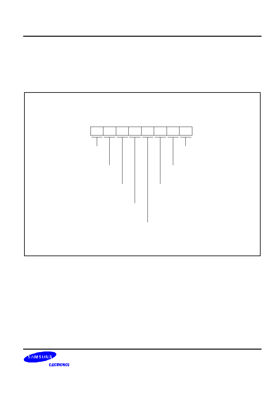
S3C880A/F880A
ON-SCREEN DISPLAY
13-35
OSD SMOOTH FUCNTION
Smoothing function
The smoothing function is used to make characters look smooth. Enabling smoothing displays 1/4 dot between two
dots connecting corner to corner within a character. Smoothing is enabled by setting each bit of OSDSMH1 and
OSDSMH2 to "1". A smooth is specified common to selected row.
OSD Smooth Control Register 1(OSDSMH1)
E2H, Set 1, Bank 1, R/W
LSB
MSB
.7
.6
.5
.4
.3
.2
.1
.0
Row 0 smooth function enable bit:
0 = Disable smooth function at Row 0
1 = Enable smooth function at Row 0
Row 1 smooth function enable bit:
0 = Disable smooth function at Row 1
1 = Enable smooth function at Row 1
Row 2 smooth function enable bit:
0 = Disable smooth function at Row 2
1 = Enable smooth function at Row 2
Row 3 smooth function enable bit:
0 = Disable smooth function at Row 3
1 = Enable smooth function at Row 3
Row 7 smooth function enable bit:
0 = Disable smooth function at Row 7
1 = Enable smooth function at Row 7
Row 6 smooth function enable bit:
0 = Disable smooth function at Row 6
1 = Enable smooth function at Row 6
Row 5 smooth function enable bit:
0 = Disable smooth function at Row 5
1 = Enable smooth function at Row 5
Row 4 smooth function enable bit:
0 = Disable smooth function at Row 4
1 = Enable smooth function at Row 4
Figure 13-34. OSD Smooth Control Register 1 (OSDSMH1)
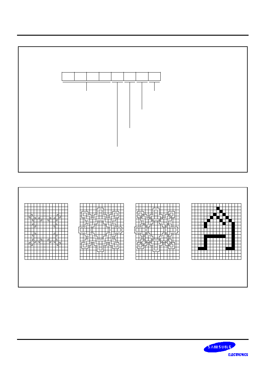
ON-SCREEN DISPLAY
S3C880A/F880A
13-36
OSD Smooth Control Register 2 (OSDSMH2)
E3H, Set 1, Bank 1, R/W
LSB
MSB
.7
.6
.5
.4
.3
.2
.1
.0
Row 8 smooth function enable bit:
0 = Disable smooth function at Row 8
1 = Enable smooth function at Row 8
Row 9 smooth function enable bit:
0 = Disable smooth function at Row 9
1 = Enable smooth function at Row 9
Row 10 smooth function enable bit:
0 = Disable smooth function at Row 10
1 = Enable smooth function at Row 10
Row 11 smooth function enable bit:
0 = Disable smooth function at Row 11
1 = Enable smooth function at Row 11
Not used
Figure 13-35. OSD Smooth Control Register 2 (OSDSMH2)
(a) Smoothing
(b) Bordering
(c) Priority of Smoothing
and Bordering
(d) Fringing (1 dot)
Figure 13-36. Smoothing/Fringing/Priority of Smoothing and Fringing
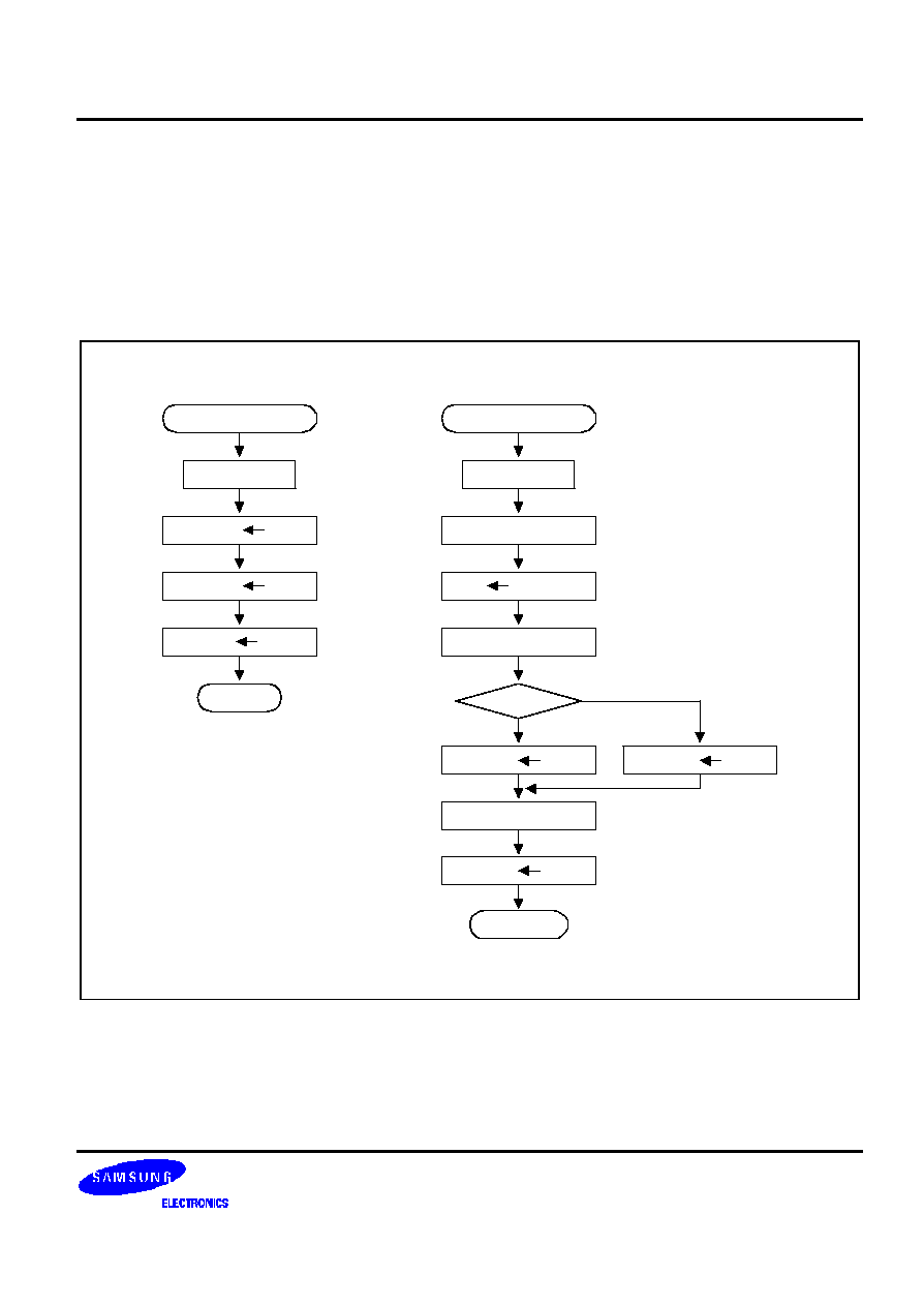
S3C880A/F880A
ON-SCREEN DISPLAY
13-37
F
PROGRAMMING TIP -- Row Interrupt Function
This example shows the effect of the control register setting excluding the HTCON.5,4,1,0 and DSPCON 3,0 occurs
in the next row. The sample program should meet the following specifications:
1. The character size of the row 2 must be double-sized (
�
2).
2. The character size of the other rows must be normal (
�
1).
R0 = 10H
V-sync interrupt
SB1
DSPCON #01H
CHACON #00H
HTCON #32H
IRET
OSD Row interrupt
SB1
PUSH R0
R0 DSPCON
AND R0, #0F0H
CHACON #50H
POP R0
Yes
CHACON #00H
HTCON #23H
IRET
No
Figure 13-37. Decision Flowchart for Row Interrupt Function Programming Tip

ON-SCREEN DISPLAY
S3C880A/F880A
13-38
F
PROGRAMMING TIP -- Row Interrupt Function (Continued)
Vsync_int:
SB1
; Select bank 1
LD
DSPCON,#01H
; OSD on, H/V sync rising edge
;This is Vsync interrupt service routine.
Interrupt_end:
LD
HTCON, #32H
; Pending bit clear
IRET
Row_int:
SB1
; Select bank 1
PUSH
R0
; Stack
R0
LD
R0,DSPCON
; R0
DSPCON data
AND
R0,#0F0H
; 11110000b, bit0-bit3 clear
CP
R0,#10H
; Row 1 interrupt?
JR
NE, No_Char_Change
LD
CHACON,#50H
;
Double size character at row 2
JR
t, Row_interrupt_end
No_char_change:
LD
CHACON, #00H
; X1 size character except row 2
Row_interrupt_end:
POP
R0
LD
HTCON, #23H
; Pending bit clear
IRET

S3C880A/F880A
ON-SCREEN DISPLAY
13-39
F
PROGRAMMING TIP -- Writing Character Code and Color Data to the OSD Video RAM
This example shows how to write character code and color data to the OSD video RAM. The sample program
performs the following operations:
1. Write red character 'A' (code 0A, for example) to the video RAM from address 00H to 77H.
2. Write green character 'B' (code 0B, for example) to the video RAM from address 78H to 0FBH.
�
�
�
SB1
; Select bank 1
LD
DSPCON,#0F9H
; OSD module on; negative sync trigger is selected
LD
OSDCOL,#0
; Digital RGB selection
LD
PP,#11H
; Select OSD video RAM page (page 1)
SRP0
#0C0H
; Select common working register area
LD
COLBUF,#04H
; Load color buffer (red color)
CLR
R0
; Load starting address (00H) to R0
OSDLP1
LD
@R0,#0AH
; Write red character A to video RAM address 00H�77H
INC
R0
;
"
CP
R0,#77H
;
"
JP
ULE,OSDLP1
;
"
LD
COLBUF,#02H
; Load green color code (02H) to the color buffer
OSDLP2
LD
@R0,#0BH
; Write green character B to RAM address 78H�0FBH
INC
R0
;
"
CP
R0,#0FBH
;
"
JP
ULE,OSDLP2
;
"
SB0
; Select bank 0
�
�
�
F
PROGRAMMING TIP -- OSD Fade Function; Line and Row Counters
This example is a continuation of the previous OSD example in which character code and color data were written to
the video RAM. Assuming a timer A interrupt interval of 2 milliseconds, the sample program should meet the
following specifications:
1. If bit fade (R4.0) is set, then enable the fade function.
2. Interval time between two lines = 20 ms. (The flag 'INTVAL' is set at 20-ms intervals in the timer A service
routine.)
3. Fade direction is 'fade after'.
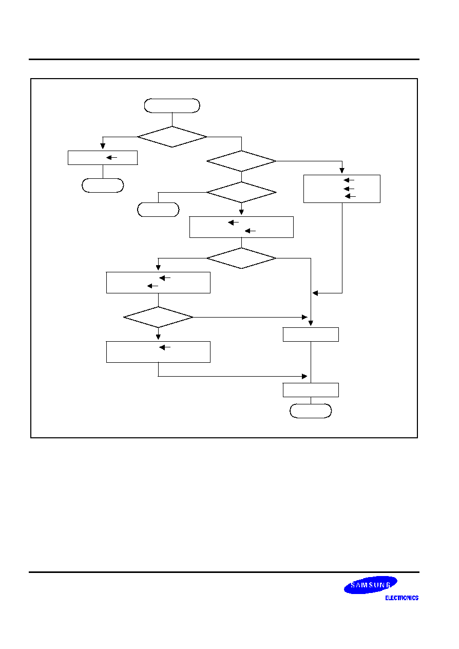
ON-SCREEN DISPLAY
S3C880A/F880A
13-40
Yes ("1")
Fade = "1"?
FADECON
F_STRT = "1"?
F_STRT "1"
Exit
INTVAL = "1"?
ROWCNT #00H
LINECNT #00H
F_STRT "1"
No ("0")
Exit
No ("0")
No ("0")
LINECNT LINECNT + #1
INTVAL "1"
LINECNT = #19?
Yes ("1")
LINECNT #00H
ROWCNT ROWCNT + 1
N (< #19)
Y (> #19)
=
ROWCNT = #11?
Fade 0
Disable Fade Function
Enable Fade
N (< #12)
OSD ON
Exit
Yes (Initial)
Figure 13-38. Decision Flowchart for Fade Function Programming Tip

S3C880A/F880A
ON-SCREEN DISPLAY
13-41
F
PROGRAMMING TIP -- OSD Fade Function; Line and Row Counters (Continued)
ROWCNT
EQU
6
LINECNT
EQU
7
FADE
EQU
0
F_STRT
EQU
1
INT_CNT
EQU
5
INTVAL
EQU
2
�
�
�
SB1
; Select bank 1
LD
PP,#11H
; Select OSD video RAM page (page 1)
SRP0
#0C0H
; RP0
0C0H (common working register area)
BTJRF
EXIT1,R4.FADE
; If flag FADE = "0", then jump to EXIT1
BTJRT
FAD1,R4.F_STRT
; If F_STRT = "1", then jump to FAD1
BTJRF
EXIT,R4.INTVAL
; If INTVAL = "1", then jump to EXT
INC
RLINECNT
; Line counter
line counter + 1
BITR
R4.INTVAL
; INTVAL
"0"
CP
RLINECNT,#13H
; Line counter
19?
JP
ULT,FAD2
; If line counter < 19, then jump to FAD2
CLR
RLINECNT
; Line counter
"0"
INC
RROWCNT
; Row counter
row counter + 1
CP
RROWCNT,#0DH
; Row counter < 11?
JP
ULT,FAD2
; If row
12, then jump to FAD2
LD
R1,#0F1H
; If row > 12, then finish the fade function
LD
R2,@R1
BITR
R2.6
; Fade disable
LD
@R1,R2
FAD3
LD
DSPCON,#0F9H
; OSD module on
JR
T,EXIT
(Continued on next page)

ON-SCREEN DISPLAY
S3C880A/F880A
13-42
F
PROGRAMMING TIP -- OSD Fade Function; Line and Row Counters (Continued)
FAD1
CLR
RROWCNT
; Row counter (R6)
0H
CLR
RLINECNT
; Line counter (Rn)
0H
BITS
R4.F_STRT
FAD2
LD
R2,CHACON
; R2
CHACON
AND
R2,#0F0H
; Clear the fade row address
OR
R2,RROWCNT
; Load new fade row address to R2
LD
CHACON,R2
; CHACON
R2
INC
R1
; R1
0F1H (fade line address)
LD
R2,RLINECNT
; R2
new fade line address
OR
R2,#60H
; Enable fade function, select fade after
LD
FADECON,R2
JR
T,FAD3
EXIT1
BITS
R4.F_STRT
EXIT
SB0
; Select bank 0
�
�
�
TAINT
PUSH
PP
PUSH
RP0
LD
PP,#11
; Select video RAM page (page 1)
SRP0
#0C0H
; RP0
0C0H
INC
RINT_CNT
; Interval counter
interval counter + 1
CP
RINT_CNT,#0AH
; Interval counter
10? (Has 20 ms elapsed?)
JP
ULE,TA1
; If yes, then jump to TA1
CLR
RINT_CNT
; 20 ms has elapsed, so clear interval counter
BITS
R4.INTVAL
; INTVAL
"1"
TA1
NOP
�
�
�
POP
RP0
POP
PP
IRET

S3C880A/F880A
ON-SCREEN DISPLAY
13-43
F
PROGRAMMING TIP -- Manipulating OSD Character Colors; Halftone Function
This example is a continuation of the previous OSD examples. Following the second sample program, red character
A is in the video RAM address 00H�77H and green character B has been written to addresses 78H�0EFH. The
program performs the following additional actions:
1. Change the color of character 'A' to white.
2. Change the color of character 'B' to its complementary color.
3. Enable the halftone function for character 'B'.
�
�
�
SB1
; Select bank 1
LD
PP,#11H
; Select video RAM page (page 1)
SRP0
#0C0H
; RP0
0C0H (common working register area)
LD
COLBUF,#0FH
; Color buffer
white color code (07H), character
; background enable
CLR
R0
; R0 (video RAM address)
00H
OSDLP1
LD
@R0,#0AH
; Video RAM (00H�77H)
white 'A'
INC
R0
;
"
CP
R0,#77H
;
"
JP
ULE,OSDLP1
;
"
LD
R2,COLBUF
; R2
color buffer (color of character in address 78H)
COM
R2
; R2
(not R2)
AND
R2,#0FH
; Mask out bit 7 through bit 3 of R2
LD
COLBUF,R2
; Color buffer
complementary color of the character
; in address 78H
LD
DSPCON,#0F9H
; OSD module on; negative sync trigger selected
�
�
�
(Continued on next page)

ON-SCREEN DISPLAY
S3C880A/F880A
13-44
F
PROGRAMMING TIP -- Manipulating Character Colors; Halftone Function (Continued)
halftone
CALL
halftone1
; Halftone signal control
�
�
�
halftone1
PUSH
PP
; Stack
PP
PUSH
RP0
; Stack
RP0
PUSH
FLAGS
; Save flags to stack
SB1
; Select bank 1
LD
PP,#11H
; Page 1 selected
SRP0
#20H
; RP0
20H (working register area)
CLR
R0
; R0
00H
loop_halftone
LD
HTCON,#02H
; Disable halftone control register
; Enable V-sync interrupt
LD
DSPCON,#09H
; Enable OSD; select negative sync trigger
LD
R1,@R0
; Video RAM zero address
INC
R0
CP
R0,#0FBH
; Video RAM end?
JP
UGT,end_halftone
tm
COLBUF,#08H
; Check COLBUF.3 (character background enable?)
JR
Z,loop_halftone
LD
HTCON,#0AH
; Enable halftone
; Enable V-sync interrupt
LD
DSPCON,#0DH
; Halftone output mode
; Select negative sync trigger
; No line is double size
JP
t,loop_halftone
end_halftone
POP
FLAGS
; Restore flag values from stack
POP
RP0
; Restore register pointer 0 value
POP
PP
; Restore page pointer
RET
; Return
�
�
�

S3C880A/F880A
ON-SCREEN DISPLAY
13-45
F
PROGRAMMING TIP -- OSD Character Size, Background Color, and Display Position
This example is a continuation of the previous OSD examples. It performs the following additional actions:
1. Change the character size to horizontal
�
3 and vertical
�
2.
2. Enable character background color to the complementary color of the character code in address 0EFH of the
video RAM.
3. Enable the frame background; select the color cyan.
4. Set top margin to 16H, inter-row spacing to 1H, left margin to 24 dots, and inter-column spacing to three (3)
dots.
�
�
�
SB1
; Select bank 1
LD
PP,#11H
; Select video RAM page (page 1)
SRP0
#0C0H
; Select common working register area
LD
COLCON,#0
; Digital RGB selection
LD
CHACON,#60H
; Horizontal
�
3, vertical
�
2 for character size
LD
FADECON,#00H
; Disable the fade function
LD
ROWCON,#21H
; Top margin
16H, inter-row space
1H
LD
CLMCON,#1BH
; Left margin
24 dots, inter-column space
3 dots
LD
R3,COLBUF
; R3
color of the character in address 0EFH
COM
R3
; R3
not R3
AND
R3,#07H
; Mask out bit 7 through bit 3 of R3
OR
R3,#0B8H
; R3
cyan frame background color
LD
COLBUF,R3
; Enable character and frame background color
LD
DSPCON,#09H
; Falling edge sync trigger, OSD on
SB0
; Select bank 0
�
�
�
F
PROGRAMMING TIP -- Helpful Hints About COLBUF and OSD Character Code 0
When working with the OSD module, please note the somewhat unusual characteristics of the color buffer register
(COLBUF) and the OSD character code 0:
-- The color buffer register, COLBUF (F7C, set 1, bank 1) provides a somewhat unusual method for manipulating
character color data.
-- OSD character code 0 produces a no-display and no-background condition, regardless of the font coding
used.

ON-SCREEN DISPLAY
S3C880A/F880A
13-46
NOTES

S3C880A/F880A
A/D CONVERTER
14-1
14
ANALOG-TO-DIGITAL CONVERTER
OVERVIEW
The 8-bit A/D converter (ADC) module uses successive approximation logic to convert analog levels entering at one
of the four input channels to equivalent 8-bit digital values. The analog input level must lie between the V
DD
and V
SS
values. The A/D converter has the following components:
-- Analog comparator with successive approximation logic
-- D/A converter logic (resistor string type)
-- ADC control register (ADCON)
-- Four multiplexed analog data input pins (ADC0�ADC3)
-- 8-bit A/D conversion data output register (ADDATA)
To initiate an analog-to-digital conversion procedure, you write the channel selection data in the A/D converter control
register ADCON to select one of the four analog input pins (ADCn, n = 0�3) and set the conversion start or enable
bit, ADCON.0. The read-write ADCON register is located at address FAH.
During a normal conversion, A/D C logic initially sets the successive approximation register to 80H (the approximate
half-way point of an 8-bit register). This register is then updated automatically during each conversion step. The
successive approximation block performs 8-bit conversions for one input channel at a time. You can dynamically
select different channels by manipulating the channel selection bit value (ADCON.5�4) in the ADCON register. To
start the A/D conversion, you should set a the enable bit, ADCON.0. When a conversion is completed, ADCON.3,
the end-of-conversion (EOC) bit is automatically set to 1 and the result is dumped into the ADDATA register where it
can be read. The A/D converter ten enters an idle state. Remember to read the contents of ADDATA before another
conversion starts. Otherwise, the previous result will be overwritten by the next conversion result.
NOTE
Because the ADC does not use sample-and-hold circuitry, it is important that any fluctuations in the analog
level at the ADC0�ADC3 input pins during a conversion procedure be kept to an absolute minimum. Any
change in the input level, perhaps due to circuit noise, will invalidate the result.
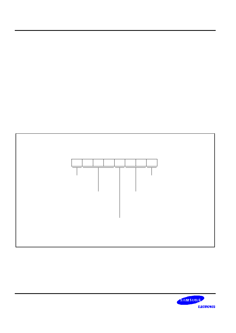
A/D CONVERTER
S3C880A/F880A
14-2
USING A/D PINS FOR STANDARD DIGITAL INPUT
The ADC module's input pins are alternatively used as digital input in port 0 and port 3. The ADC0�ADC1 share pin
names are P3.0�P3.1 and ADC2�ADC3 share pin names are P0.6�P0.7, respectively.
A/D CONVERTER CONTROL REGISTER (ADCON)
The A/D converter control register, ADCON, is located at address FAH. Only bits 5-0 are used in the
S3C880A/F880A implementation. ADCON has three functions:
-- Bits 5�4 select an analog input pin (ADC0�ADC3).
-- Bit 3 indicates the status of the A/D conversion.
-- Bit 2-1 select a conversion speed.
-- Bit 0 starts the A/D conversion.
Only one analog input channel can be selected at a time. You can dynamically select any one of the four analog
input pins (ADC0�ADC3) by manipulating the 2-bit value for ADCON.5�ADCON.4.
A/D Converter Control Register (ADCON)
FAH, Set 1, Bank 0, R/W
LSB
MSB
.7
.6
.5
.4
.3
.2
.1
.0
Conversion start bit:
0 = No effect
1 = A/D conversion start
Analog input pin selection bits:
00 = ADC0 (P3.0)
01 = ADC1 (P3.1)
10 = ADC2 (P0.6)
11 = ADC3 (P0.7)
Not used
Clock source selection bit:
00 = f
OSC
/16
01 = f
OSC
/8
10 = f
OSC
/4
11 = f
OSC
/2
End-of-conversion status bit: (Read only)
0 = A/D conversion is in progress
1 = A/D conversion complete
Figure 14-1. A/D Converter Control Register (ADCON)
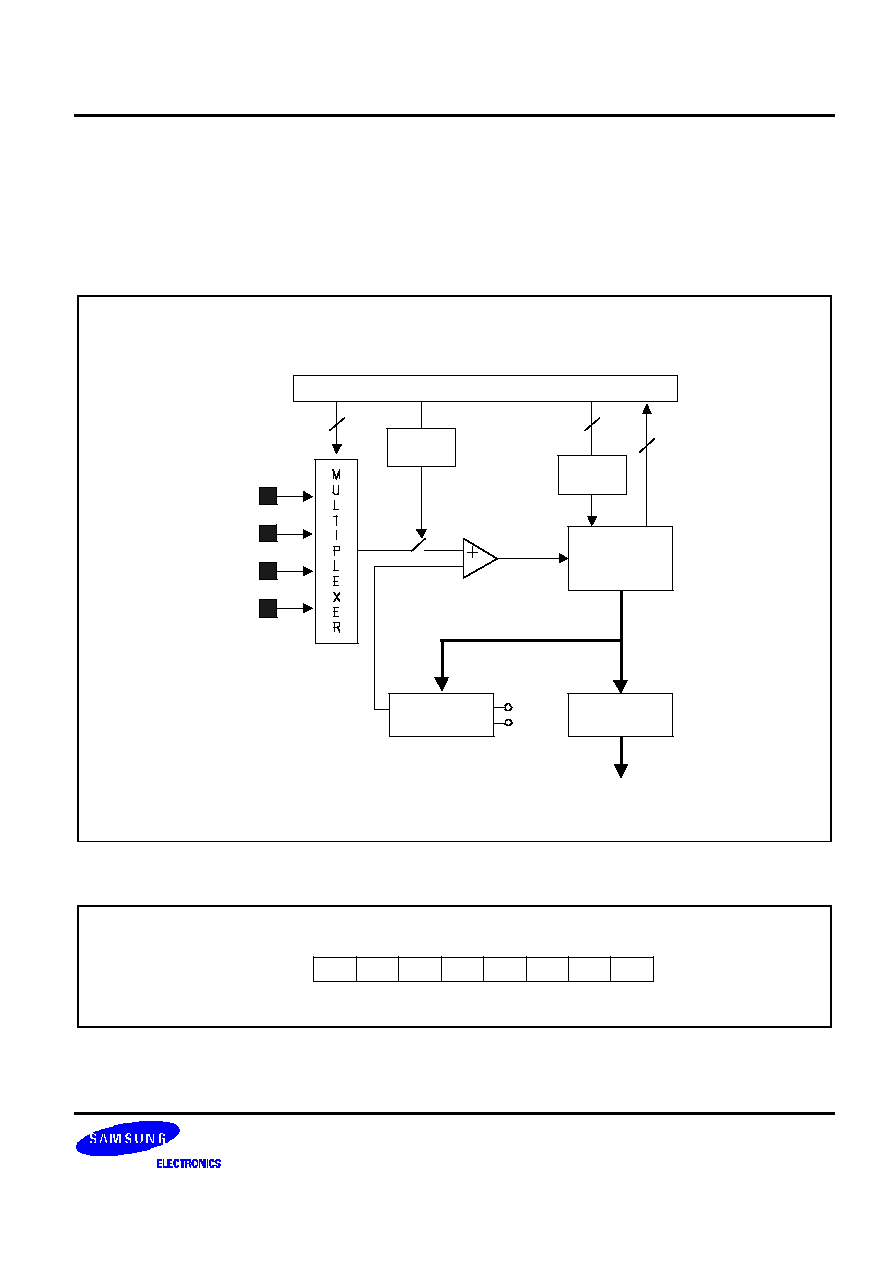
S3C880A/F880A
A/D CONVERTER
14-3
INTERNAL REFERENCE VOLTAGE LEVELS
In the ADC function block, the analog input voltage level is compared to the reference voltage. The analog input level
must remain within the range AV
SS
to AV
REF
(usually, AV
REF
= V
DD
).
Different reference voltage levels are generated internally along the resistor tree during the analog conversion process
for each conversion step. The reference voltage level for the first bit conversion is always 1/2 AV
REF.
A/D Converter Control Register
ADCON (FAH)
ADCON .5-4
_
Control
Circuit
Successive
Approximation
Circuit
Clock
Selector
D/A Converter
AV
REF
AV
SS
ADCON .0 (ADEN)
ADCON .2-1
ADCON .3
(EOC Flag)
Analog
Comparator
Conversion
Result
To Data Bus
ADC0/P3.0
ADC1/P3.1
ADC3/P0.7
ADC2/P0.6
ADDATA
(FBH)
Figure 14-2. A/D Converter Circuit Diagram
.7
.6
.5
.4
.3
.2
ADDATA (FBH)
.1
.0
Figure 14-3. A/D Converter Data Register (ADDATA)
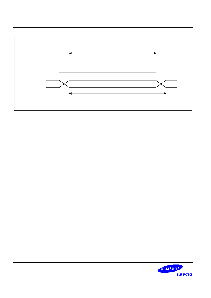
A/D CONVERTER
S3C880A/F880A
14-4
t
CON
= 50 CPU Clock
Value Remains Undetermined
Conversion
Start
EOC
ADDATA
Previous
Value
Valid
Data
Figure 14-4. S3C880A/F880A A/D Converter Timing Diagram
CONVERSION TIMING
The A/D conversion process requires 4 steps (4 clock edges) to convert each bit and 18 clocks to step-up A/D
conversion. Therefore, total of 50 clocks are required to complete an 8-bit conversion: With an 10 MHz CPU clock
frequency, one clock cycle is 100 ns. If each bit conversion requires 4 clocks, the conversion rate is calculated as
follows:
4 clocks/bit x 8-bits + step-up time (18 clock) = 50 clocks
50 clock x 100 ns = 5
�
s at 10 MHz, 1 clock time = CPU clock
INTERNAL A/D CONVERSION PROCEDURE
1. Analog input must remain between the voltage range of AV
SS
and AV
REF
.
2. Configure the analog input pins to input mode by making the appropriate settings in P3CONL and P0CONH
registers.
3. Before the conversion operation starts, you must first select one of the four input pins (ADC0�ADC3) by writing
the appropriate value to the ADCON register.
4. When conversion has been completed, (50 CPU clocks have elapsed), the EOC flag is set to "1", so that a
check can be made to verify that the conversion was successful.
5. The converted digital value is loaded to the output register, ADDATA, than the ADC module enters an idle state.
6. The digital conversion result can now be read from the ADDATA register.

S3C880A/F880A
A/D CONVERTER
14-5
NOTE: The symbol 'R' signifies an offset resistor with a value of from 50 to 100 Ohm.
V
SS
S3F880A
AV
SS
ADC0-ADC3
AV
REF
Reference
Voltage
Input
Analog
Input Pin
R
104
101
V
DD
V
DD
Figure 14-5. Recommended A/D Converter Circuit for Highest Absolute Accuracy
F
PROGRAMMING TIP � Configuring A/D Converter
�
�
�
LD
P3CONL,#00000101B
; P3.1-0 A/D Input MODE
LD
P0CONH,#01010000B
; P0.7-6 A/D Input MODE
�
�
�
LD
ADCON,#00000001B
; channel ADC0: P3.0/conversion start
AD0_CHK:
TM
ADCON,#00001000B
; A/D conversion end ?
EOC check
JR
Z,AD0_CHK
; no
LD
AD0BUF,ADDATA
; Conversion data
�
�
LD
ADCON,#00010001B
; channel ADC1: P3.1/conversion start
AD1_CHK:
TM
ADCON,#00001000B
; A/D conversion end ?
EOC check
JR
Z,AD1_CHK
; no
LD
AD1BUF,ADDATA
; Conversion data
�
�

A/D CONVERTER
S3C880A/F880A
14-6
NOTES

S3C880A/F880A
ELECTRICAL DATA
15-1
15
ELECTRICAL DATA
OVERVIEW
In this section, S3C880A/F880A electrical characteristics are presented in tables and graphs. The information is
arranged in the following order:
-- Absolute maximum ratings
-- D.C. electrical characteristics
-- I/O capacitance
-- A.C. electrical characteristics
-- Input timing measurement points for t
NF1
and t
NF2
-- Data retention supply voltage in Stop mode
-- Stop mode release timing when initiated by nRESET
-- Main oscillator and L-C oscillator frequency
-- Clock timing measurement points for X
IN
-- Main oscillator clock stabilization time (t
ST
)
-- A/D converter electrical characteristics
-- Characteristic curves
ELECTRICAL DATA
S3C880A/F880A
15-2
Table 15-1. Absolute Maximum Ratings
(T
A
= 25
�
C)
Parameter
Symbol
Conditions
Rating
Unit
Supply Voltage
V
DD
�
� 0.3 to + 6.0
V
Input Voltage
V
I1
P1.0�P1.5 (open-drain)
� 0.3 to
+ 7
V
V
I2
All port pins except V
I1
� 0.3 to V
DD
+ 0.3
Output Voltage
V
O
All output pins
� 0.3 to V
DD
+ 0.3
V
Output Current
High
I
OH
One I/O pin active
� 18
mA
All I/O pins active
� 60
Output Current
Low
I
OL
One I/O pin active
+ 30
mA
Total pin current for port 1
+ 100
Total pin current for ports 0, 2, and 3
+ 100
Operating
Temperature
T
A
�
� 20 to + 85
�
C
Storage
Temperature
T
STG
�
� 65 to + 150
�
C
Table 15-2. D.C. Electrical Characteristics
(T
A
= � 20
�
C to + 85
�
C, V
DD
= 4.5 V to 5.5 V)
Parameter
Symbol
Conditions
Min
Typ
Max
Unit
Input High
V
IH1
All input pins except V
IH2
0.8 V
DD
�
V
DD
V
Voltage
V
IH2
X
IN
, X
OUT
2.7 V
Input Low Voltage
V
IL1
All input pins except V
IL2
�
�
0.2 V
DD
V
V
IL2
X
IN
,
X
OUT
1.0 V
Output High
Voltage
V
OH
I
OH
= � 500 �A
P0.0�P0.5, P1.6�P1.7, P2
R, G, B (digital level), Vblank
V
DD
� 0.8
�
�
V
Output Low
Voltage
V
OL1
I
OL
= 4 mA
P0.0�P0.5, P1.6�P1.7
�
�
0.5
V
V
OL2
I
OL
= 10 mA
P1.4�P1.5
�
�
0.8
V
OL3
I
OL
= 2 mA
P1.0�P1.3, P3.0�P3.1, P0.6�P0.7
�
�
0.5
V
OL4
I
OL
= 1 mA
R, G, B (digital level), Vblank, P2
�
�
0.4
V
S3C880A/F880A
ELECTRICAL DATA
15-3
Table 15-2. D.C. Electrical Characteristics (Continued)
(T
A
= � 20
�
C to + 85
�
C, V
DD
= 4.5 V to 5.5 V)
Parameter
Symbol
Conditions
Min
Typ
Max
Unit
Input High
Leakage Current
I
LIH1
V
IN
= V
DD
All input pins except I
LIH2
and
I
LIH3
�
�
1
�A
I
LIH2
V
IN
= V
DD
, OSC
IN
, OSC
OUT
10
I
LIH3
V
IN
= V
DD
, X
IN
,
X
OUT
2.5
10
20
Input Low Leakage
Current
I
LIL1
V
IN
= 0 V
All input pins except I
LIL2
,
I
LIL3
, and nRESET
�
�
� 1
�A
I
LIL2
V
IN
= 0 V,
OSC
IN
, OSC
OUT
� 10
I
LIL3
V
IN
= 0 V, X
IN
,
X
OUT
� 2.5
� 10
� 20
Output High
Leakage Current
I
LOH1
V
OUT
= V
DD
All output pins except I
LOH2
�
�
1
�A
I
LOH2
V
OUT
= 6 V
P1.0�P1.5
10
Output Low
Leakage Current
I
LOL
V
OUT
= 0 V
All output pins
�
�
� 1
�A
Supply Current
(note)
I
DD1
Normal mode;
V
DD
= 4.5 V to 5.5 V
8-MHz CPU clock
�
7
20
mA
I
DD2
Idle mode;
V
DD
= 4.5 V to 5.5 V
8-MHz CPU clock
4
10
I
DD3
Stop mode;
V
DD
= 4.5 V to 5.5 V
1
10
�A
NOTE: Supply current does not include the current drawn through internal pull-up resistors or external output current
loads.
ELECTRICAL DATA
S3C880A/F880A
15-4
Table 15-3. Input/Output Capacitance
(T
A
= � 20
�
C to + 85
�
C, V
DD
=
0 V)
Parameter
Symbol
Conditions
Min
Typ
Max
Unit
Input
capacitance
C
IN
f = 1 MHz; unmeasured pins
are connected to V
SS
�
�
10
pF
Output
capacitance
C
OUT
I/O capacitance
C
IO
Table 15-4. A.C. Electrical Characteristics
(T
A
= � 20
�
C to + 85
�
C, V
DD
= 4.5 V to 5.5 V)
Parameter
Symbol
Conditions
Min
Typ
Max
Unit
V-sync Pulse
Width
t
VW
�
4
�
�
�s
H-sync Pulse
Width
t
HW
�
3
�
�
�s
Noise Filter
t
NF1
P1.0�P1.3, H-sync, V-sync
�
350
�
ns
t
NF2
nRESET
�
1000
t
NF3
Glitch filter (oscillator block)
�
25
t
NF4
CAPA
�
5
�
t
CAPA
NOTE: f
CAPA
= f
OSC
/128.
Table 15-5. Analog R,G,B Output
(T
A
= � 20
�
C to + 85
�
C, V
DD
= 4.75 V to 5.25 V)
Output Voltage (50 k
load)
Remark
V
DD
= 4.75 V
V
DD
= 5.00 V
V
DD
= 5.25 V
Data = 11
4.00 V
�
0.30 V
4.20 V
�
0.30 V
4.40 V
�
0.30 V
Data = 10
3.10 V
�
0.25 V
3.35 V
�
0.25 V
3.40 V
�
0.25 V
Data = 01
1.90 V
�
0.20 V
2.00 V
�
0.20 V
2.10 V
�
0.20 V
Data = 00
0.00 V � 0.65 V
0.00 V � 0.75 V
0.00 V � 0.75 V
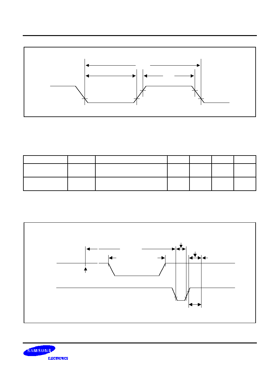
S3C880A/F880A
ELECTRICAL DATA
15-5
t
NF1L
0.8 V
DD
0.2 V
DD
t
NF2H
1t
CPU
t
NF2
Figure 15-1. Input Timing Measurement Points for t
NF1
and t
NF2
Table 15-6. Data Retention Supply Voltage in Stop Mode
(T
A
= � 20
�
C to + 85
�
C)
Parameter
Symbol
Conditions
Min
Typ
Max
Unit
Data Retention
Supply Voltage
V
DDDR
Stop mode
2
�
6
V
Data Retention
Supply Current
I
DDDR
Stop mode, V
DDDR
= 2.0 V
�
�
5
�A
NOTES:
1.
Supply current does not include the current drawn through internal pull-up resistors or external output current loads.
2.
During the oscillator stabilization wait time (t
WAIT
), all the CPU operations must be stopped.
Execution of
STOP Instrction
RESET
Occurs
~ ~
V
DDDR
~ ~
Stop Mode
Oscillation
Stabilization
Time
Normal
Operating Mode
Data Retention Mode
t
WAIT
nRESET
V
DD
NOTE: t
WAIT
is the same as 4096 x 16 x 1/f
OSC
0.2 V
DD
Figure 15-2. Stop Mode Release Timing When Initiated by a nRESET
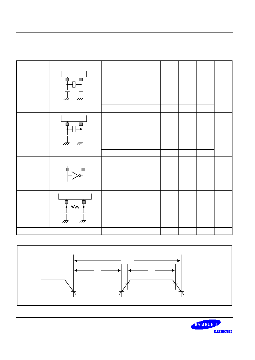
ELECTRICAL DATA
S3C880A/F880A
15-6
Table 15-7. Main Oscillator and L-C Oscillator Frequency
(T
A
= � 20
�
C + 85
�
C, V
DD
= 4.5 V to 5.5 V)
Oscillator
Clock Circuit
Conditions
Min
Typ
Max
Unit
Crystal
X
IN
C1
C2
X
OUT
OSD block active
5
6
8
MHz
OSD block inactive
0.5
6
8
Ceramic
X
IN
C1
C2
X
OUT
OSD block active
5
6
8
MHz
OSD block inactive
0.5
6
8
External Clock
X
IN
X
OUT
OSD block active
5
6
8
MHz
OSD block inactive
0.5
6
8
L-C Oscillator
OSC
IN
C1
C2
OSC
OUT
Recommend value;
C1 = C2 = 20 pF
5
6.5
8
MHz
CPU Clock Frequency
�
0.032
6.0
8
MHz
X
IN
t
XH
t
XL
1/f
OSC
2.7 V
1.0 V
Figure 15-3. Clock Timing Measurement Points for X
IN
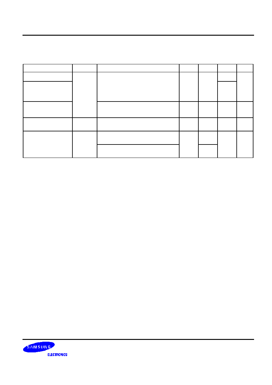
S3C880A/F880A
ELECTRICAL DATA
15-7
Table 15-8. Main Oscillator Clock Stabilization Time
(T
A
= � 20
�
C + 85
�
C, V
DD
= 4.5 V to 5.5 V)
Oscillator
Symbol
Test Condition
Min
Typ
Max
Unit
Crystal
�
V
DD
= 4.5 V to 6.0 V
�
�
20
ms
Ceramic
(Oscillation stabilization occurs when
V
DD
is equal to the minimum oscillator
voltage range.)
10
External Clock
X
IN
input High and Low level width (t
XH
,
t
XL
)
65
�
100
ns
Release Signal Setup
Time
t
SREL
Normal operation
�
1000
�
ns
Oscillation
Stabilization Wait
t
WAIT
CPU clock = 8 MHz; Stop mode
released by nRESET
�
8.3
�
ms
Time
(1)
CPU clock = 8 MHz; Stop mode
released by an interrupt
(2)
NOTES:
1.
Oscillation stabilization time is the time required for the CPU clock to return to its normal oscillation frequency after a
power-on occurs, or when Stop mode is released.
2.
The oscillation stabilization interval is determined by the basic timer (BT) input clock setting.
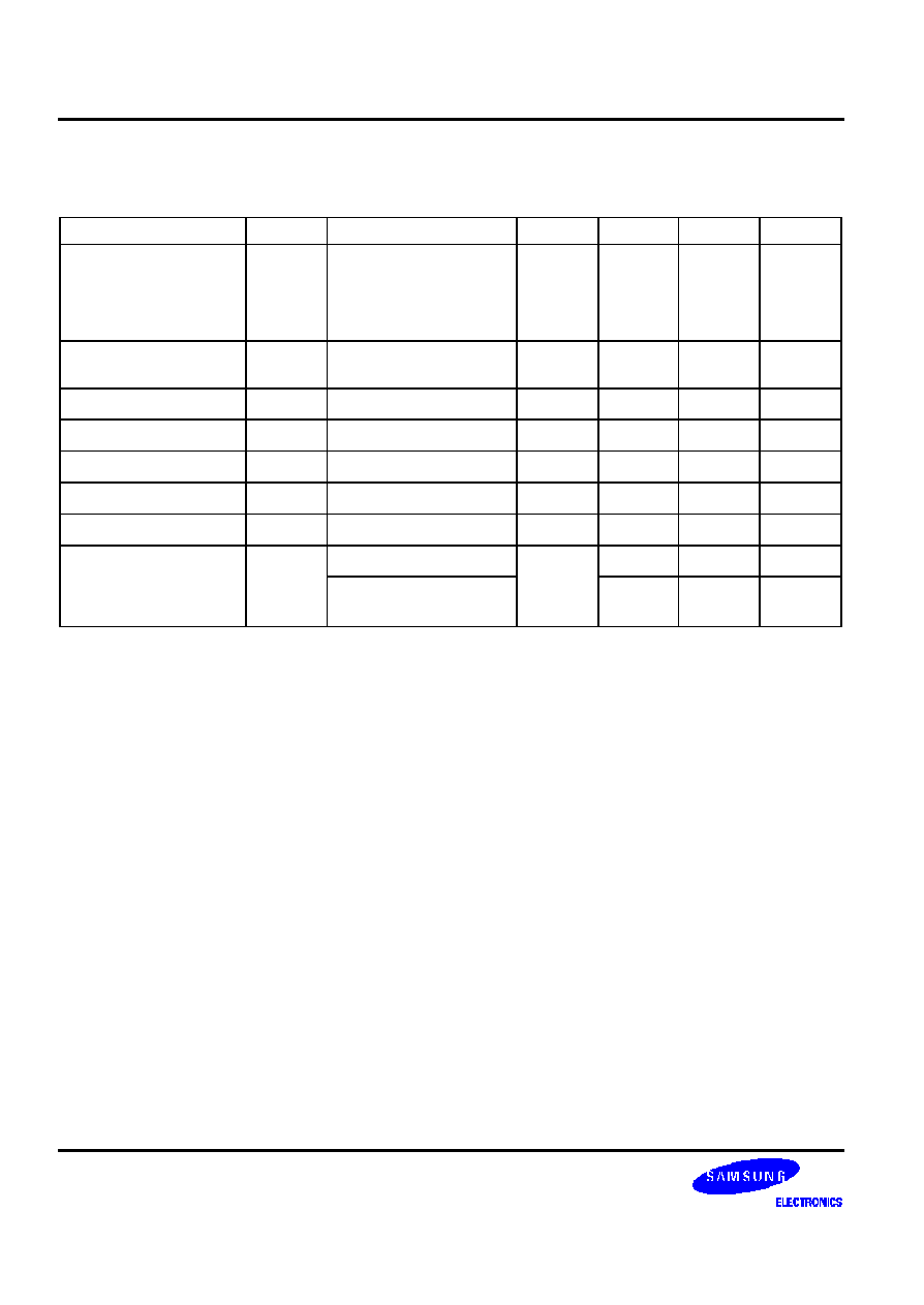
ELECTRICAL DATA
S3C880A/F880A
15-8
Table 15-9. A/D Converter Electrical Characteristics
(T
A
= � 20
�
C to + 85
�
C, V
DD
= 4.5 V to 5.5 V, V
SS
= 0 V)
Parameter
Symbol
Test Conditions
Min
Typ
Max
Unit
Absolute
Accuracy
V
DD
= 5.12 V
CPU CLOCK = 8 MHz
AV
REF
= 5.12 V
AV
SS
= 0 V
�
�
�
2
LSB
Conversion
Time
(1)
t
CON
f
OSC
= 8 MHz
25
�
�
us
Analog Input Voltage
V
IAN
�
AV
SS
�
AV
REF
V
Analog Input Impedance
R
AN
�
2
�
�
M
ADC Reference Voltage
AV
REF
�
2.5
�
V
DD
V
ADC Reference Ground
AV
SS
�
V
SS
�
V
SS
+ 0.3
V
Analog input current
I
ADIN
AV
REF
= V
DD
= 5 V
�
�
10
uA
ADC block current
(2)
I
ADC
AV
REF
= V
DD
= 5 V
�
1
3
mA
AV
REF
= V
DD
= 5 V
Power down mode
�
100
500
nA
NOTES:
1.
'Conversion time' is the time required from the moment a conversion operation starts until it ends.
2. I
ADC
is operating current during A/D conversion.
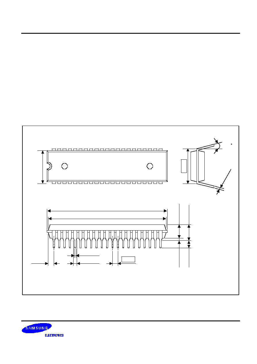
S3C880A/F880A
MECHANICAL DATA
16-1
16
MECHANICAL DATA
OVERVIEW
The S3C880A/F880A microcontrollers are available in 42-pin SIP package (42-SDIP-600), 44-pin QFP package (44-
QFP-1010B) .
NOTE: Dimensions are in millimeters.
39.50 MAX
39.10
� 0.20
0.50 �
0.10
1.78
(1.77)
0.51 MIN
3.30
� 0.30
3.50
�
0.20
5.08 MAX
42-SDIP-600
0-15
1.00 �
0.10
0.25
+ 0.10- 0.05
15.24
14.00
�
0
.20
#42
#22
#21
#1
Figure 16-1. 42-Pin SDIP Package Dimensions (42-SDIP-600)
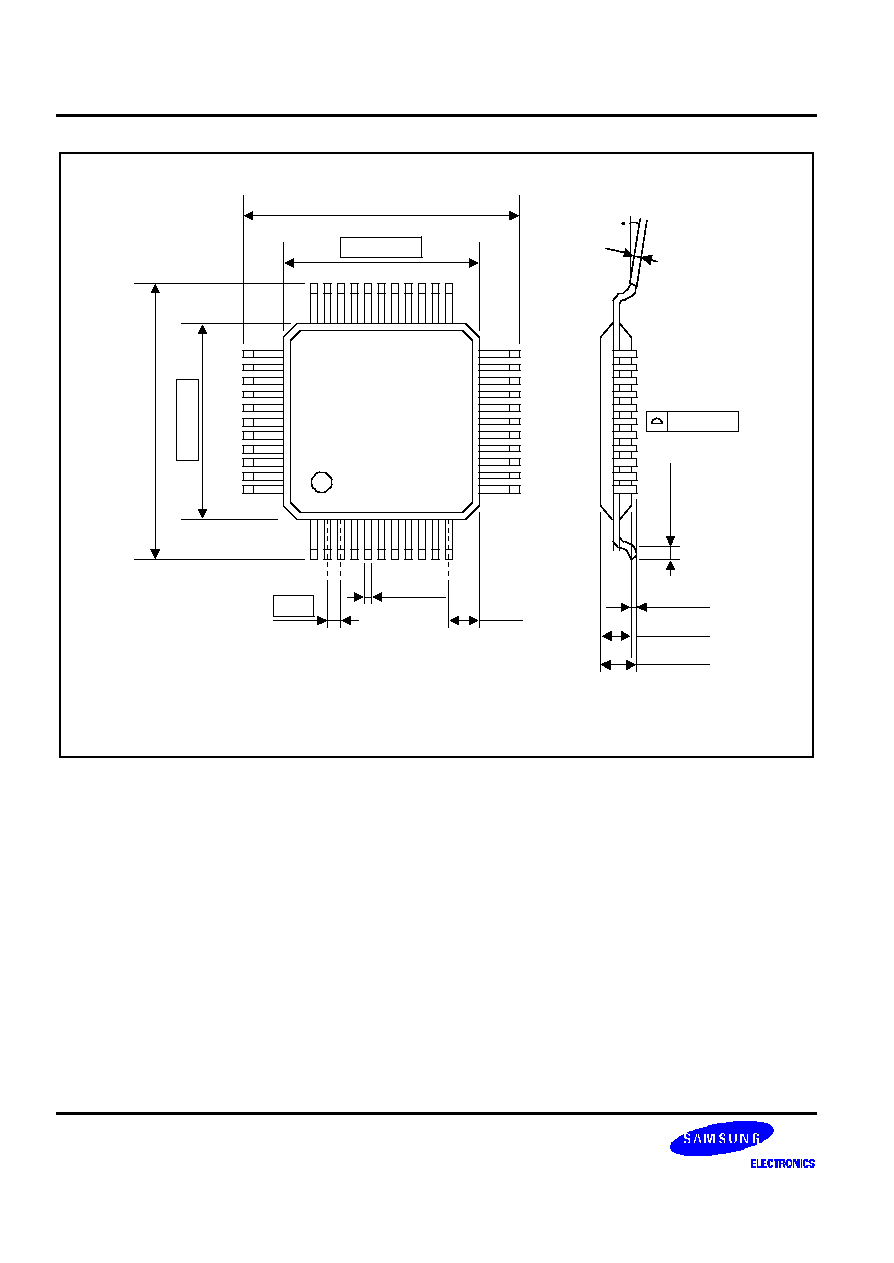
MECHANICAL DATA
S3C880A/F880A
16-2
44-QFP-1010B
#44
NOTE : Dimensions are in millimeters.
10.00
�
0.2
13.20
�
0.3
10.00
�
0.2
13.20
�
0.3
#1
0.35
+ 0.10
- 0.05
0.80
(1.00)
0.10 MAX
0.80
�
0.20
0.05 MIN
2.05
�
0.10
2.30 MAX
0.15
+ 0.10
- 0.05
0-8
Figure 16-2. 44-Pin QFP Package Dimensions (44-QFP-1010B)
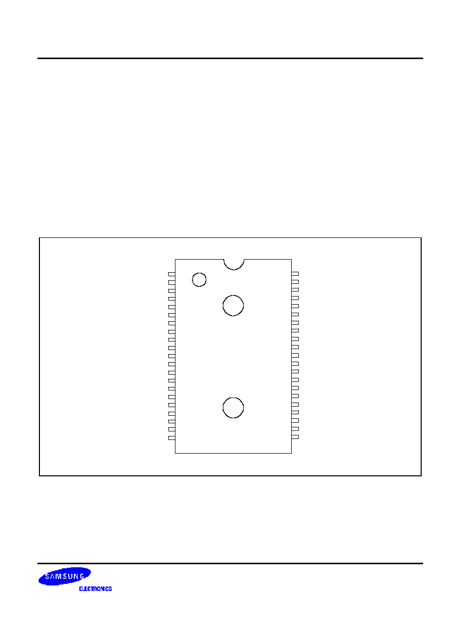
S3C880A/F880A
S3C880A/F880A MTP
17-1
17
S3F880A MTP
OVERVIEW
The S3C880A/F880A single-chip CMOS microcontroller is the MTP flash ROM
version. It has an on-chip flash ROM
instead of a masked ROM. The flash ROM is accessed by serial data format.
PWM0/P2.5
PWM1/P2.1
PWM2/P2.2 (SCLK)
PWM3/P2.3 (SDAT)
PWM4/P2.4
PWM5/P2.0
T0/P2.6
T0CK/P1.7
ADC0/P3.0
ADC1/P3.1
ADC2/P0.6
ADC3/P0.7
TEST/TEST
INT0/P1.0
INT1/P1.1
INT2/P1.2
INT3/P1.3
P1.4
P1.5
P1.6
OSDHT/P2.7
S3F880A
(42-SDIP)
1
2
3
4
5
6
7
8
9
10
11
12
13
14
15
16
17
18
19
20
21
P0.0
P0.1
P0.2
P0.3
P0.4
V
SS/
V
SS
CAP.A
P0.5
V
DD/
V
DD
nRESET/nRESET
X
OUT
X
IN
V
SS1
OSC
OUT
OSC
IN
V-sync
H-sync
Vblank
Vred
Vgreen
Vblue
42
41
40
39
38
37
36
35
34
33
32
31
30
29
28
27
26
25
24
23
22
Figure 17-1. S3F880A Pin Assignment (42-SDIP)
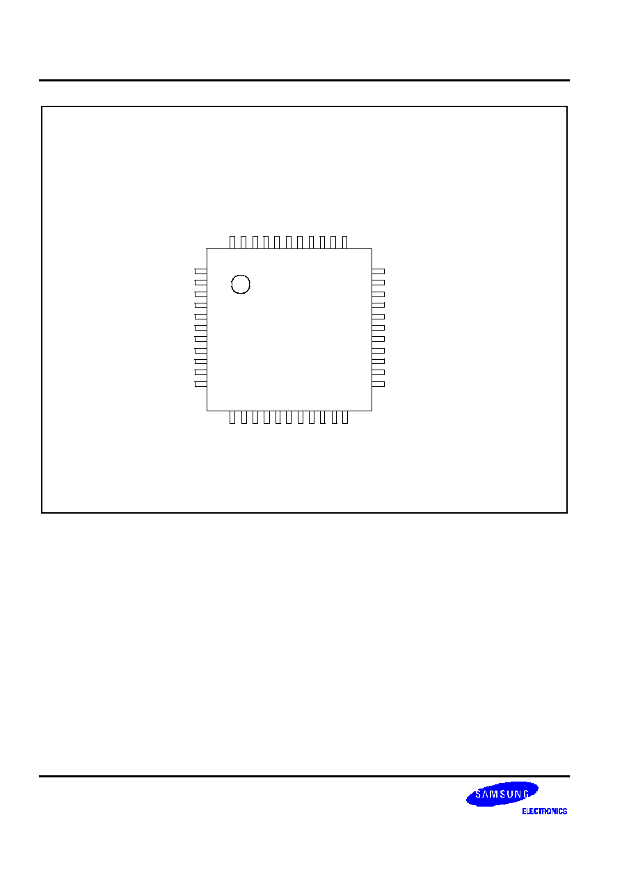
S3C880A/F880A MTP
S3C880A/F880A
17-2
P1.3/INT3
P1.4
P1.5
P1.6
P2.7/OSDHT
Vblue
Vgreen
Vred
Vblank
H-sync
V-sync
NC
CAP.A
P0.5
V
DD
/V
DD
nRESET/nRESET
X
OUT
X
IN
V
SS1
NC
OSC
OUT
OSC
IN
P2.4/PWM4
P2.3/PWM3
P2.2/PWM2
(
SCLK
)
P2.1/PWM1
(SDAT)
P2.5/PWM0
P0.0
P0.1
P0.2
P0.3
P0.4
V
SS
P2.0/PWM5
P2.6/T0
P1.7/T0CLK
P3.0/ADC0
P3.1/ADC1
P0.6/ADC2
P0.7/ADC3
TEST /TEST
P1.0/INT0
P1.1/INT1
P1.2/INT2
S3F880A
(44-QFP)
1
2
3
4
5
6
7
8
9
10
11
44
43
42
41
40
39
38
37
36
35
34
33
32
31
30
29
28
27
26
25
24
23
12
13
14
15
16
17
18
19
20
21
22
Figure 17-2. S3F880A Pin Assignment (44-QFP)
S3C880A/F880A
S3C880A/F880A MTP
17-3
Table 17-1. Descriptions of Pins Used to Read/Write the Flash ROM (S3F880A)
Main Chip
During Programming
Pin Name
Pin Name
Pin No.
I/O
Function
P2.3 (Pin 4)
SDAT
4
(43)
I/O
Serial data pin (output when reading, Input when writing)
Input and push-pull output port can be assigned
P2.2 (Pin 3)
SCLK
3 (42)
I/O
Serial clock pin (Input only pin)
TEST
V
PP
(TEST)
13 (8)
I
0 V: operating mode
5 V: test mode
12.5 V: flash ROM writing mode
RESET
RESET
33 (29)
I
5 V: operating mode, 0 V: flash ROM writing mode
V
DD
/V
SS
V
DD
/V
SS
34/30, 37
(30/26, 34)
I
Logic power supply pin.
NOTE: Parentheses indicate pin number for 44-QFP package.

S3C880A/F880A MTP
S3C880A/F880A
17-4
NOTES

S3C880A/F880A
DEVELOPMENT TOOLS
18-1
18
DEVELOPMENT TOOLS
OVERVIEW
Samsung provides a powerful and easy-to-use development support system in turnkey form. The development
support system is configured with a host system, debugging tools, and support software. For the host system, any
standard computer that operates with MS-DOS as its operating system can be used. One type of debugging tool
including hardware and software is provided: the sophisticated and powerful in-circuit emulator, SMDS2+, for S3C7,
S3C8, S3C9 families of microcontrollers. The SMDS2+ is a new and improved version of SMDS2. Samsung also
offers support software that includes debugger, assembler, and a program for setting options.
SHINE
Samsung Host Interface for in-circuit Emulator, SHINE, is a multi-window based debugger for SMDS2+. SHINE
provides pull-down and pop-up menus, mouse support, function/hot keys, and context-sensitive hyper-linked help. It
has an advanced, multiple-windowed user interface that emphasizes ease of use. Each window can be sized,
moved, scrolled, highlighted, added, or removed completely.
SAMA ASSEMBLER
The Samsung Arrangeable Microcontroller (SAM) Assembler, SAMA, is a universal assembler, and generates object
code in standard hexadecimal format. Assembled program code includes the object code that is used for ROM data
and required SMDS program control data. To assemble programs, SAMA requires a source file and an auxiliary
definition (DEF) file with device specific information.
SASM88
The SASM88 is an relocatable assembler for Samsung's S3C8-series microcontrollers. The SASM88 takes a source
file containing assembly language statements and translates into a corresponding source code, object code and
comments. The SASM88 supports macros and conditional assembly. It runs on the MS-DOS operating system. It
produces the relocatable object code only, so the user should link object file. Object files can be linked with other
object files and loaded into memory.
HEX2ROM
HEX2ROM file generates ROM code from HEX file which has been produced by assembler. ROM code must be
needed to fabricate a microcontroller which has a mask ROM. When generating the ROM code.(OBJ file) by
HEX2ROM, the value 'FF' is filled into the unused ROM area up to the maximum ROM size of the target device
automatically.
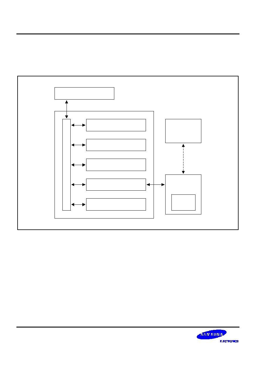
DEVELOPMENT TOOLS
S3C880A/F880A
18-2
TARGET BOARDS
Target boards are available for all S3C8-series microcontrollers. All required target system cables and adapters are
included with the device-specific target board.
SMDS2+
RS-232C
POD
Probe
Adapter
TB880A
Target
Board
IBM-PC AT or Compatible
PROM/OTP Writer Unit
Bus
RAM Break/Display Unit
Trace/Timer Unit
SAM8 Base Unit
Power Supply Unit
Target
Application
System
Eva
Chip
Figure 18-1. SMDS Product Configuration (SMDS2+)
S3C880A/F880A
DEVELOPMENT TOOLS
18-3
TB880A TARGET BOARD
The TB880A target board is used for the S3C880A/F880A microcontrollers. It is supported with the SMDS2+. The
TB880A target board can also be used for S3C880A/F880A.
TB880A
SM1342A
100-Pin Connector
25
1
RESET
J101
42
1
144 QFP
S3E8800
EVA Chip
40-Pin Connector
GND
V
CC
21
22
74HC10
To User_V
CC
Off
On
74HC4050
74HC4050
Idle Stop
27C512
External
Triggers
Ch1
Ch2
SMDS2+
SMDS2
CN
+
+
MDS
EPROM
1
L-C clock
Figure 18-2. TB880A Target Board Configuration
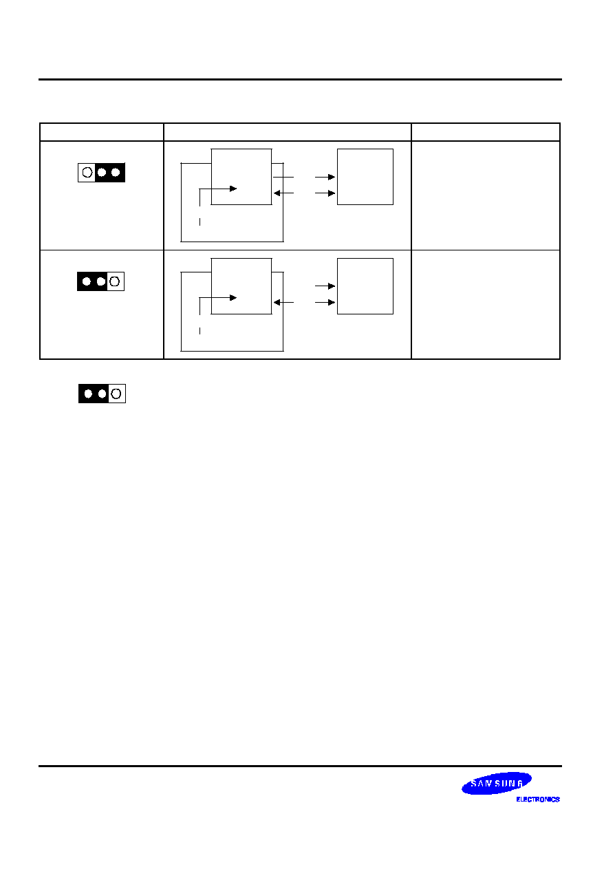
DEVELOPMENT TOOLS
S3C880A/F880A
18-4
Table 17-1. Power Selection Settings for TB880A
'To User_Vcc' Settings
Operating Mode
Comments
To User_V
CC
Off
On
Target
System
SMDS2+
TB880A
V
CC
V
SS
V
CC
The SMDS2+ main board
supplies V
CC
to the target
board (evaluation chip) and the
target system.
To User_V
CC
Off
On
Target
System
SMDS2+
External
V
CC
V
SS
V
CC
TB880A
The SMDS2+ main board
supplies V
CC
only to the target
board (evaluation chip). The
target system must have its
own power supply.
NOTE: The following symbol in the 'To User_Vcc' Setting column indicates the electrical short (off) configuration:
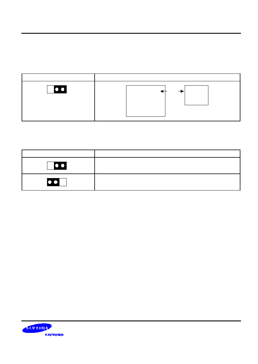
S3C880A/F880A
DEVELOPMENT TOOLS
18-5
SMDS2+ Selection (SAM8)
In order to write data into program memory that is available in SMDS2+, the target board should be selected to be for
SMDS2+ through a switch as follows. Otherwise, the program memory writing function is not available.
Table 17-2. The SMDS2 + Tool Selection Setting
'SW1' Setting
Operating Mode
SMDS2
SMDS2+
R/W
R/W
SMDS2+
Target
System
OSD Font ROM Selection
Table 17-3. OSD Font ROM Selection Setting
'SW2' Setting
Comments
MDS
EPROM
EPROM (27C512) is used for OSD font ROM
MDS
EPROM
Not used
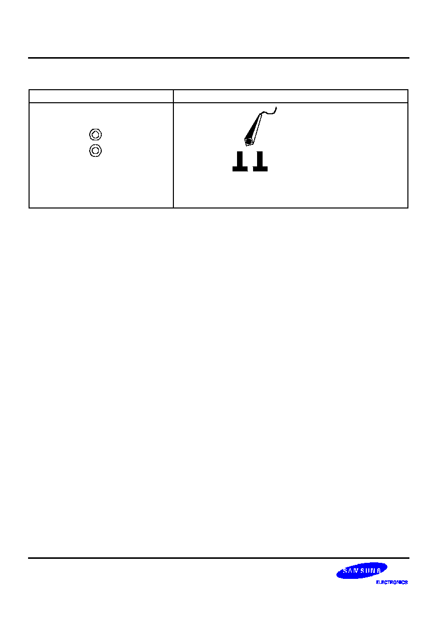
DEVELOPMENT TOOLS
S3C880A/F880A
18-6
Table 17-4. Using Single Header Pins as the Input Path for External Trigger Sources
Target Board Part
Comments
External
Triggers
Ch1
Ch2
Connector from
External Trigger
Sources of the
Application System
You can connect an external trigger source to one of the two external
trigger channels (CH1 or CH2) for the SMDS2+ breakpoint and trace
functions.
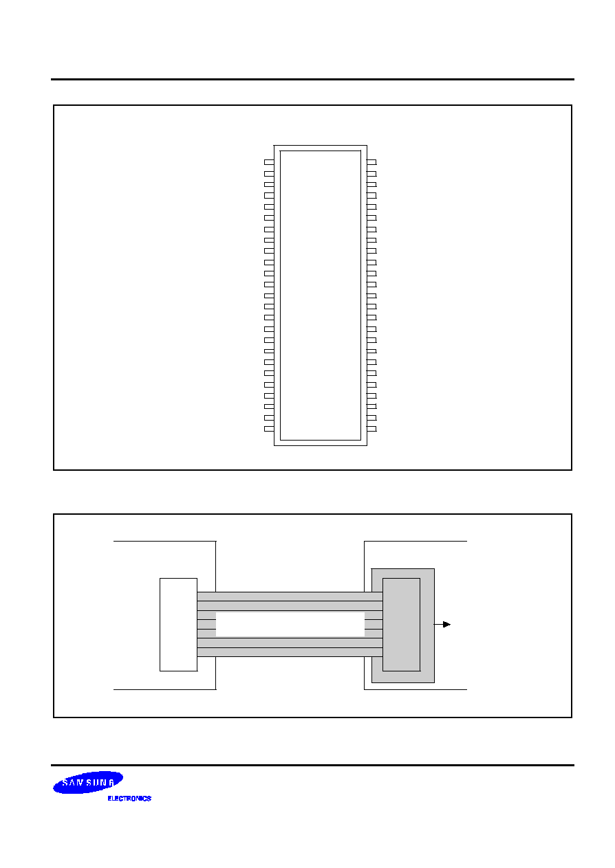
S3C880A/F880A
DEVELOPMENT TOOLS
18-7
J101
1
2
3
4
5
6
7
8
9
10
11
12
13
14
15
16
17
18
19
20
21
42
41
40
39
38
37
36
35
34
33
32
31
30
29
28
27
26
25
24
23
22
50-Pin DIP Connector
PWM0/P2.5
PWM1/P2.1
PWM2/P2.2 (SCLK)
PWM3/P2.3 (SDAT)
PWM4/P2.4
PWM5/P2.0
T0/P2.6
T0CK/P1.7
ADC0/P3.0
ADC1/P3.1
ADC2/P0.6
ADC3/P0.7
V
SS
INT0/P1.0
INT1/P1.1
INT2/P1.2
INT3/P1.3
P1.4
P1.5
P1.6
OSDHT/P2.7
NC
NC
NC
NC
P0.0
P0.1
P0.2
P0.3
P0.4
V
SS
CAP.A
P0.5
V
DD/
V
DD
nRESET/nRESET
N.C
N.C
V
SS
OSC
OUT
OSC
IN
V-sync
H-sync
Vblank
Vred
Vgreen
Vblue
NC
NC
NC
NC
Figure 17-3. 50-Pin DIP Connector J101 for TB880A
Target Board
50-Pin DIP Connector
Target System
42-SDIP
Conversion
PCB
J101
1
50
25 26
Part Name: AP42SD
Order Cods: SM6538
1
50
25 26
1
42
21
22
S3C880A
Figure 17-4. S3C880A/F880A Probe Adapter for 42-SDIP Package

DEVELOPMENT TOOLS
S3C880A/F880A
18-8
NOTES