 | –≠–ª–µ–∫—Ç—Ä–æ–Ω–Ω—ã–π –∫–æ–º–ø–æ–Ω–µ–Ω—Ç: S3C9442 | –°–∫–∞—á–∞—Ç—å:  PDF PDF  ZIP ZIP |

S3C9442/C9444/F9444/C9452/C9454/F9454
PRODUCT OVERVIEW
1-1
1
PRODUCT OVERVIEW
SAM88RCRI PRODUCT FAMILY
Samsung's SAM88RCRI family of 8-bit single-chip CMOS microcontrollers offers a fast and efficient CPU, a wide
range of integrated peripherals, and various mask-programmable ROM sizes.
A address/data bus architecture and a large number of bit-configurable I/O ports provide a flexible programming
environment for applications with varied memory and I/O requirements. Timer/counters with selectable operating
modes are included to support real-time operations.
S3C9442/C9444/C9452/C9454 MICROCONTROLLER
The S3C9442/C9444/C9452/C9454 single-chip 8-bit microcontroller is designed for useful A/D converter , SIO
application field. The S3C9442/C9444/C9452/C9454 uses powerful SAM88RCRI CPU and
S3C9442/C9444/C9452/C9454 architecture. The internal register file is logically expanded to increase the on-
chip register space.
The S3C9442/C9444/C9452/C9454 has 2K/4K bytes of on-chip program ROM and 208 bytes of RAM. The
S3C9442/C9444/C9452/C9454 is a versatile general-purpose microcontroller that is ideal for use in a wide range
of electronics applications requiring simple timer/counter, PWM. In addition, the S3C9442/C9444/C9452/C9454's
advanced CMOS technology provides for low power consumption and wide operating voltage range.
Using the SAM88RCRI design approach, the following peripherals were integrated with the SAM88RCRI core:
-- Three configurable I/O ports (18 pins)
-- Four interrupt sources with one vector and one interrupt level
-- One 8-bit timer/counter with time interval mode
-- Analog to digital converter with nine input channels and 10-bit resolution
-- One 8-bit PWM output
The S3C9442/C9444/C9452/C9454 microcontroller is ideal for use in a wide range of electronic applications
requiring simple timer/counter, PWM, ADC. S3C9452/C9454 is available in a 20/16-pin DIP and a 20-pin SOP
package. S3C9452/C9454 is available in a 8-pin and a 8-pin SOP package.
MTP
The S3F9444/F9454 is an MTP (Multi Time Programmable) version of the S3C9442/C9444/C9452/C9454
microcontroller. The S3F9444/F9454 has on-chip 4-Kbyte multi-time programmable flash ROM instead of
masked ROM. The S3F9444/F9454 is fully compatible with the S3C9442/C9444/C9452/C9454, in function, in
D.C. electrical characteristics and in pin configuration.

PRODUCT OVERVIEW
S3C9442/C9444/F9444/C9452/C9454/F9454
1-2
FEATURES
CPU
∑
SAM88RCRI CPU core
∑
The SAM88RCRI core is low-end version of the
current SAM87 core.
Memory
∑
2/4-Kbyte internal program memory
∑
208-byte general purpose register area
Instruction Set
∑
41 instructions
∑
The SAM88RCRI core provides all the SAM87
core instruction except the word-oriented
instruction, multiplication, division, and some
one-byte instruction.
Instruction Execution Time
∑
400 ns at 10 MHz f
OSC
(minimum)
Interrupts
∑
4 interrupt sources with one vector
∑
One interrupt level
General I/O
∑
Three I/O ports (Max 18 pins)
∑
Bit programmable ports
8-bit High-speed PWM
∑
8-bit PWM 1-ch (Max: 156 kHz)
∑
6-bit base + 2-bit extension
Built-in reset Circuit
∑
Low voltage detector for safe reset
Timer/Counters
∑
One 8-bit basic timer for watchdog function
∑
One 8-bit timer/counter with time interval modes
A/D Converter
∑
Nine analog input pins
∑
10-bit conversion resolution
Oscillation Frequency
∑
1 MHz to 10 MHz external crystal oscillator
∑
Maximum 10 MHz CPU clock
∑
Internal RC: 3.2 MHz (typ.), 0.5 MHz (typ.) in
V
DD
= 5 V
Operating Temperature Range
∑
≠ 40
∞
C to + 85
∞
C
Operating Voltage Range
∑
2.0 V (LVR Level) to 5.5 V
Smart Option
Package Types
∑
S3C9452/C9454:
≠
20-DIP-300A
≠
20-SOP-375
≠
16-DIP-300A
∑
S3C9442/C9444
≠
8-DIP-300
≠
8-SOP-225
S3C9442/C9444/F9444/C9452/C9454/F9454
PRODUCT OVERVIEW
1-3
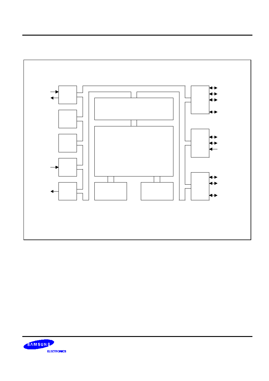
BLOCK DIAGRAM
88RCRI
SAMRI CPU
Port I/O and
Interrupt Control
2 KB ROM
4 KB ROM
208 Byte
Register file
Timer 0
ADC
PWM
X
IN
X
OUT
OSC
Basic
Timer
ADC0-ADC8
P0.6/PWM
Port 0
Port 2
Port 1
P0.0/ADC0/INT0
P0.1/ADC1/INT1
P0.2/ADC2
P0.7/ADC7
...
P1.0
P1.1
P1.2
P2.0/T0
P2.1
P2.6
...
NOTE:
P1.2 is used as input only
Figure 1-1. Block Diagram

PRODUCT OVERVIEW
S3C9442/C9444/F9444/C9452/C9454/F9454
1-4
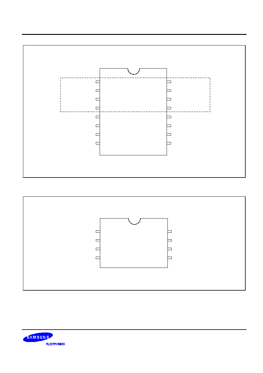
PIN ASSIGNMENTS
S3C9452/C9454
(20-DIP-300A/
20-SOP-375)
20
19
18
17
16
15
14
13
12
11
1
2
3
4
5
6
7
8
9
10
V
SS
X
IN
/P1.0
X
OUT
/P1.1
RESET
/P1.2
P2.0/T0
P2.1
P2.2
P2.3
P2.4
P2.5
V
DD
P0.0/ADC0/INT0
P0.1/ADC1/INT1
P0.2/ADC2
P0.3/ADC3
P0.4/ADC4
P0.5/ADC5
P0.6/ADC6/PWM
P0.7/ADC7
P2.6/ADC8/CLO
Figure 1-2. Pin Assignment Diagram (20-Pin DIP/SOP Package)
S3C9442/C9444/F9444/C9452/C9454/F9454
PRODUCT OVERVIEW
1-5
S3C9452/C9454
(16-DIP-300A)
V
DD
P0.0/ADC0/INT0
P0.1/ADC1/INT1
P0.2/ADC2
P0.3/ADC3
P0.4/ADC4
P0.5/ADC5
P0.6/ADC6/PWM
16
15
14
13
12
11
10
9
V
SS
X
IN
/P1.0
X
OUT
/P1.1
RESET
/P1.2
P2.0/T0
P2.1
P2.2
P2.3
1
2
3
4
5
6
7
8
Figure 1-3. Pin Assignment Diagram (16-Pin DIP Package)
S3C9442/C9444
(8-DIP-300
8-SOP-225)
V
DD
P0.0/ADC0/INT0
P0.1/ADC1/INT1
P0.2/ADC2
8
7
6
5
V
SS
X
IN
/P1.0
X
OUT
/P1.1
RESET
/P1.2
1
2
3
4
Figure 1-4. Pin Assignment Diagram (8-Pin DIP/SOP Package)

PRODUCT OVERVIEW
S3C9442/C9444/F9444/C9452/C9454/F9454
1-6
PIN DESCRIPTIONS
Table 1-1. S3C9452/C9454 Pin Descriptions
Pin
Name
In/Out
Pin Description
Pin
Type
Share
Pins
P0.0≠P0.7
I/O
Bit-programmable I/O port for Schmitt trigger input or
push-pull output. Pull-up resistors are assignable by
software. Port0 pins can also be used as A/D converter
input, PWM output or external interrupt input.
E-1
ADC0≠ADC7
INT0/INT1
PWM
P1.0≠P1.1
I/O
Bit-programmable I/O port for Schmitt trigger input or
push-pull, open-drain output. Pull-up resistors or pull-down
resistors are assignable by software.
E-2
X
IN,
X
OUT
P1.2
I
Schmitt trigger input port
B
RESET
P2.0≠P2.6
I/O
Bit-programmable I/O port for Schmitt trigger input or
push-pull, open-drain output. Pull-up resistors are
assignable by software.
E
E-1
≠
ADC8/CLO
T0
X
IN,
X
OUT
≠
Crystal/Ceramic, or RC oscillator signal for system clock.
P1.0≠P1.1
RESET
I
Internal LVR or External
RESET
B
P1.2
V
DD,
V
SS
≠
Voltage input pin and ground
≠
CLO
O
System clock output port
E-1
P2.6
INT0≠INT1
I
External interrupt input port
E-1
P0.0, P0.1
PWM
O
8-Bit high speed PWM output
E-1
P0.6
T0
O
Timer0 match output
E-1
P2.0
ADC0≠ADC8
I
A/D converter input
E-1
E
P0.0≠P0.7
P2.6
S3C9442/C9444/F9444/C9452/C9454/F9454
PRODUCT OVERVIEW
1-7
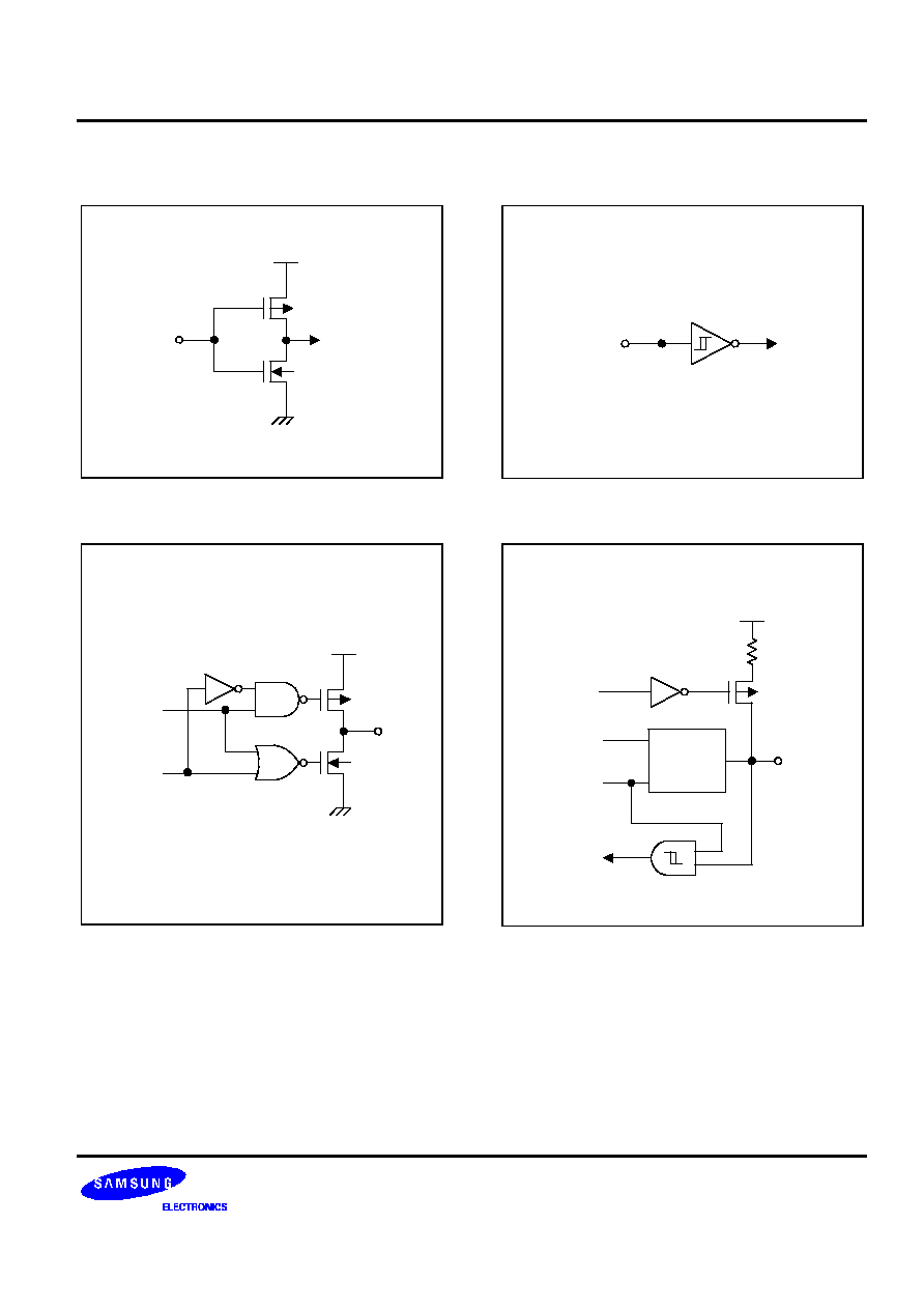
PIN CIRCUITS
V
DD
IN
N-channel
P-channel
Figure 1-5. Pin Circuit Type A
IN
Figure 1-6. Pin Circuit Type B
V
DD
Out
Output
DIsable
Data
Figure 1-7. Pin Circuit Type C
I/O
Output
Disable
Data
Circuit
Type C
Pull-up
Enable
V
DD
Digital
Input
Figure 1-8. Pin Circuit Type D
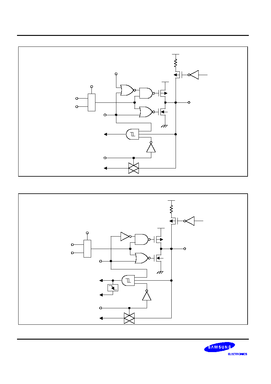
PRODUCT OVERVIEW
S3C9442/C9444/F9444/C9452/C9454/F9454
1-8
V
DD
I/O
Digital
Input
P-CH
V
DD
Open-drain
Enable
Pull-up
enable
Analog Input
Enable
ADC
Output Disable
(Input Mode)
Data
M
U
X
Alternative
Output
P2.x
P2CONH
P2CONL
N-CH
Figure 1-9. Pin Circuit Type E
V
DD
I/O
Digital Input
P-CH
V
DD
Pull-up
enable
Output Disable
(Input Mode)
Data
M
U
X
Alternative
Output
P0.x
P0CONH
N-CH
Analog Input
Enable
ADC
Interrupt Input
Figure 1-10. Pin Circuit Type E-1

S3C9442/C9444/F9444/C9452/C9454/F9454
PRODUCT OVERVIEW
1-9
V
DD
I/O
X
IN
X
OUT
V
DD
Open-drain
Enable
Output Disable
(Input Mode)
P1.x
Digital
Input
Pull-up
enable
Pull-down
enable
Figure 1-11. Pin Circuit Type E-2

S3C9442/C9444/F9444/C9452/C9454/F9454
ELECTRICAL DATA
13-1
13
ELECTRICAL DATA
OVERVIEW
In this section, the following S3C9442/C9444/C9452/C9454 electrical characteristics are presented in tables and
graphs:
-- Absolute maximum ratings
-- D.C. electrical characteristics
-- A.C. electrical characteristics
-- Input Timing Measurement Points
-- Oscillator characteristics
-- Oscillation stabilization time
-- Operating Voltage Range
-- Schmitt trigger input characteristics
-- Data retention supply voltage in Stop mode
-- Stop mode release timing when initiated by a
RESET
-- A/D converter electrical characteristics
-- LVR circuit characteristics
-- LVR reset Timing

ELECTRICAL DATA
S3C9442/C9444/F9444/C9452/C9454/F9454
13-2
Table 13-1. Absolute Maximum Ratings
(T
A
= 25
∞
C)
Parameter
Symbol
Conditions
Rating
Unit
Supply voltage
V
DD
≠
≠ 0.3 to + 6.5
V
Input voltage
V
I
All ports
≠ 0.3 to V
DD
+ 0.3
V
Output voltage
V
O
All output ports
≠ 0.3 to V
DD
+ 0.3
V
Output current high
I
OH
One I/O pin active
≠ 25
mA
All I/O pins active
≠ 80
Output current low
I
OL
One I/O pin active
+ 30
mA
All I/O pins active
+ 150
Operating temperature
T
A
≠
≠ 40 to + 85
∞
C
Storage temperature
T
STG
≠
≠ 65 to + 150
∞
C

S3C9442/C9444/F9444/C9452/C9454/F9454
ELECTRICAL DATA
13-3
Table 13-2. DC Electrical Characteristics
(T
A
= ≠ 40
∞
C to + 85
∞
C, V
DD
= 2.0 V to 5.5 V)
Parameter
Symbol
Conditions
Min
Typ
Max
Unit
Input high
voltage
V
IH1
Ports 0, 1, 2 and
RESET
V
DD
= 2.0 to 5.5 V
0.8 V
DD
≠
V
DD
V
V
IH2
X
IN
and X
OUT
V
DD
- 0.1
Input low
voltage
V
IL1
Ports 0, 1, 2 and
RESET
V
DD
= 2.0 to 5.5 V
≠
≠
0.2 V
DD
V
V
IL2
X
IN
and X
OUT
0.1
Output high
voltage
V
OH
I
OH
= ≠ 10 mA
ports 0, 1, 2
V
DD
= 4.5 to 5.5 V
V
DD
-1.5
V
DD
- 0.4
≠
V
Output low
voltage
V
OL
I
OL
= 25 mA
port 0, 1, and 2
V
DD
= 4.5 to 5.5 V
≠
0.4
2.0
V
Input high
leakage current
I
LIH1
All input except
I
LIH2
V
IN
= V
DD
≠
≠
1
uA
I
LIH2
X
IN
,
X
OUT
V
IN
= V
DD
20
Input low
leakage current
I
LIL1
All input except
I
LIL2
and
RESET
V
IN
= 0 V
≠
≠
≠1
uA
I
LIL2
X
IN
, X
OUT
V
IN
= 0 V
≠20
Output high
leakage current
I
LOH
All output pins
V
OUT
= V
DD
≠
≠
2
uA
Output low
leakage current
I
LOL
All output pins
V
OUT
= 0 V
≠
≠
≠2
uA
Pull-up resistors
R
P
V
IN
= 0 V
Ports 0, 1, 2
V
DD
= 5 V
25
50
100
k
Pull-down
resistors
R
P
V
IN
= 0 V
Ports 1
V
DD
= 5 V
25
50
100
Supply current
I
DD1
Run mode
10 MHz CPU clock
V
DD
= 4.5 to 5.5 V
≠
5
10
mA
3 MHz CPU clock
V
DD
= 2.0 V
2
5
I
DD2
Idle mode
10 MHz CPU clock
V
DD
= 4.5 to 5.5 V
≠
2
4
3 MHz CPU clock
V
DD
= 2.0 V
0.5
1.5
I
DD3
Stop mode
V
DD
= 4.5 to 5.5 V
(LVR disable)
≠
0.1
5
uA
V
DD
= 4.5 to 5.5 V
(LVR enable)
100
200
V
DD
= 2.6 V
(LVR enable)
30
60
NOTE: In STOP (I
DD3
), IDLE (I
DD2
) current, current by ADC module is not included.
ELECTRICAL DATA
S3C9442/C9444/F9444/C9452/C9454/F9454
13-4
Table 13-3. AC Electrical Characteristics
(T
A
= ≠ 40
∞
C to + 85
∞
C, V
DD
= 2.0 V to 5.5 V)
Parameter
Symbol
Conditions
Min
Typ
Max
Unit
Interrupt input
low width
t
INTL
INT0, INT1
V
DD
= 5 V
±
10 %
≠
200
≠
ns
RESET
input
low width
t
RSL
Input
V
DD
= 5 V
±
10 %
≠
1
≠
us
t
INTL
t
INTH
X
IN
0.8 V
DD
0.2 V
DD
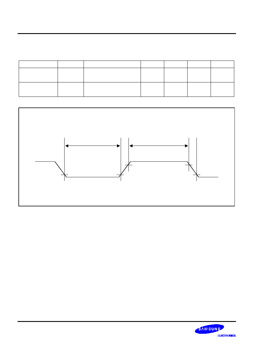
Figure 13-1. Input Timing Measurement Points

S3C9442/C9444/F9444/C9452/C9454/F9454
ELECTRICAL DATA
13-5
Table 13-4. Oscillator Characteristics
(T
A
= ≠ 40
∞
C to + 85
∞
C)
Oscillator
Clock Circuit
Test Condition
Min
Typ
Max
Unit
Main crystal or
ceramic
X
IN
X
OUT
C1
C2
V
DD
= 4.5 to 5.5 V
1
≠
10
MHz
V
DD
= 2.7 to 4.5 V
1
≠
6
MHz
V
DD
= 2.0 to 2.7 V
1
≠
3
MHz
External clock
(Main System)
X
IN
X
OUT
V
DD
= 4.5 to 5.5 V
1
≠
10
MHz
V
DD
= 2.7 to 4.5 V
1
≠
6
MHz
V
DD
= 2.0 to 2.7 V
1
≠
3
MHz
External RC
oscillator
≠
V
DD
= 4.75 to 5.25 V
Tolerance:10 %
≠
4
≠
MHz
Internal RC
V
DD
= 4.75 to 5.25 V
3.2
Oscillator
0.5
Table 13-5. Oscillation Stabilization Time
(T
A
= - 40
∞
C to + 85
∞
C, V
DD
= 3.0 V to 5.5 V)
Oscillator
Test Condition
Min
Typ
Max
Unit
Main crystal
f
OSC
> 1.0 MHz
≠
≠
20
ms
Main ceramic
Oscillation stabilization occurs when V
DD
is
equal to the minimum oscillator voltage range.
≠
≠
10
ms
External clock
(main system)
X
IN
input high and low width (t
XH
, t
XL
)
25
≠
500
ns
Oscillator
stabilization
t
WAIT
when released by a reset
(1)
≠
2
16
/f
OSC
≠
ms
wait time
t
WAIT
when released by an interrupt
(2)
≠
≠
≠
ms
NOTES:
1.
f
OSC
is the oscillator frequency.
2.
The duration of the oscillator stabilization wait time, t
WAIT
, when it is released by an interrupt is determined by the
settings in the basic timer control register, BTCON.

ELECTRICAL DATA
S3C9442/C9444/F9444/C9452/C9454/F9454
13-6
10 MHz
CPU Clock
6 MHz
1 MHz
1
2
3
4
5
6
7
Supply Voltage (V)
2 MHz
3 MHz
4 MHz
2.7
5.5
4.5
Figure 13-2. Operating Voltage Range
V
SS
A
A = 0.2 V
DD
B = 0.4 V
DD
C = 0.6 V
DD
D = 0.8 V
DD
V
DD
V
OUT
V
IN
B
C
D
0.3 V
DD
0.7 V
DD
Figure 13-3. Schmitt Trigger Input Characteristics Diagram
S3C9442/C9444/F9444/C9452/C9454/F9454
ELECTRICAL DATA
13-7
Table 13-6. Data Retention Supply Voltage in Stop Mode
(T
A
= ≠ 40
∞
C to + 85
∞
C, V
DD
= 2.0 V to 5.5 V)
Parameter
Symbol
Conditions
Min
Typ
Max
Unit
Data retention
supply voltage
V
DDDR
Stop mode
2.0
≠
5.5
V
Data retention
supply current
I
DDDR
Stop mode; V
DDDR
= 2.0 V
≠
0.1
5
uA
NOTE: Supply current does not include current drawn through internal pull-up resistors or external output current loads.
Data Retention Mode
V
DDDR
Execution Of
Stop Instrction
V
DD
Normal
Operating
Mode
Oscillation
Stabilization
Time
Stop Mode
t
WAIT
RESET
RESET
Occurs
NOTE: t
WAIT
is the same as 4096 x 16 x 1/f
OSC
~ ~
~ ~
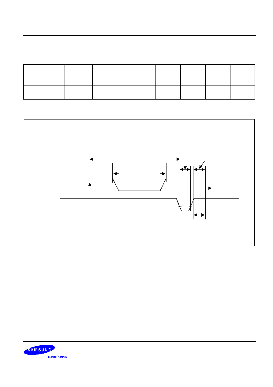
Figure 13-4. Stop Mode Release Timing When Initiated by a
RESET

ELECTRICAL DATA
S3C9442/C9444/F9444/C9452/C9454/F9454
13-8
Table 13-7. A/D Converter Electrical Characteristics
(T
A
= ≠ 40
∞
C to + 85
∞
C, V
DD
= 2.7 V to 5.5 V, V
SS
= 0 V)
Parameter
Symbol
Test Conditions
Min
Typ
Max
Unit
Total accuracy
≠
V
DD
= 5.12 V
CPU clock = 10 MHz
V
SS
= 0 V
≠
≠
±
3
LSB
Integral linearity
error
ILE
≠
≠
±
2
Differential linearity
error
DLE
≠
≠
±
1
Offset error of top
EOT
≠
±
1
±
3
Offset error of
bottom
EOB
≠
±
1
±
2
Conversion
time
(1)
t
CON
f
OSC
= 10 MHz
≠
20
≠
µ
s
Analog input
voltage
V
IAN
≠
V
SS
≠
V
DD
V
Analog input
impedance
R
AN
≠
2
≠
≠
M
Analog input
current
I
ADIN
V
DD
= 5 V
≠
≠
10
µ
A
Analog block
current
(2)
I
ADC
V
DD
= 5 V
≠
1
3
mA
V
DD
= 3 V
0.5
1.5
V
DD
= 5 V
power down mode
≠
100
500
nA
NOTES:
1.
"Conversion time" is the time required from the moment a conversion operation starts until it ends.
2.
I
ADC
is operating current during A/D conversion.

S3C9442/C9444/F9444/C9452/C9454/F9454
ELECTRICAL DATA
13-9
Table 13-8. LVR Circuit Characteristics
(T
A
= 25
∞
C, V
DD
= 2.0 V to 5.5 V)
Parameter
Symbol
Conditions
Min
Typ
Max
Unit
Low voltage reset
V
LVR
≠
≠
2.3
3.0
3.9
V
LVR hysteresis voltage
V
HYS
≠
0.3
≠
V
Power supply voltage
rise time
t
R
10
(note)
us
Power supply voltage
off time
t
OFF
0.5
s
NOTE: 2
16
/fx ( = 6.55 ms at fx = 10 MHz)
V
DD
V
LVR,MAX
V
HYS
V
HYS
V
LVR
V
LVR,MIN
t
OFF
t
R
Figure 13-5. LVR Reset Timing

S3C9442/C9444/F9444/C9452/C9454/F9454
MECHANICAL DATA
14-1
14
MECHANICAL DATA
OVERVIEW
The S3C9452/C9454 is available in a 20-pin DIP package (Samsung: 20-DIP-300A), a 20-pin SOP package
(Samsung: 20-SOP-375), a 16-pin DIP package (Samsung: 16-DIP-300A). Package dimensions are shown in
Figure 15-1, 15-2, and 15-3.
The S3C9442/C9444 is available in a 8-pin DIP package (SAMSUNG 8-DIP-300A), a 8-pin SOP package
(SAMSUNG 8-SOP-225).
Package dimensions are shown in figure 14-4 and 14-5.
NOTE: Dimensions are in millimeters.
26.80 MAX
26.40
±
0.20
(1.77)
20-DIP-300A
6.40
±
0
.20
#20
#1
0.46
±
0.10
1.52
±
0.10
#11
#10
0-15
0.25
+ 0.10- 0.05
7.62
2.54
0.51 MIN
3.30
±
0.30
3.25
±
0.20
5.08 MAX
Figure 14-1. 20-DIP-300A Package Dimensions
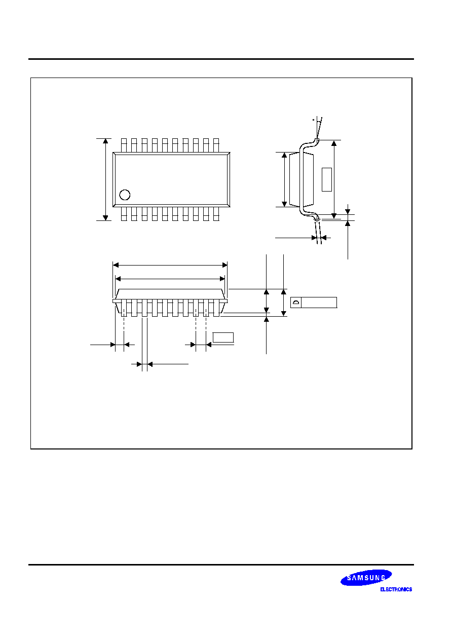
MECHANICAL DATA
S3C9442/C9444/F9444/C9452/C9454/F9454
14-2
NOTE: Dimensions are in millimeters.
20-SOP-375
10.30
±
0
.30
#11
#20
#1
#10
13.14 MAX
12.74
±
0.20
(0.66)
0-8
0.203
+ 0.10
- 0.05
9.53
7.50
±
0.20
0.85
±
0.20
0.05 MIN
2.30
±
0.10
2.50 MAX
0.40
0.10 MAX
+ 0.10
- 0.05
1.27
Figure 14-2. 20-SOP-375 Package Dimensions
S3C9442/C9444/F9444/C9452/C9454/F9454
MECHANICAL DATA
14-3
NOTE: Dimensions are in millimeters.
19.80 MAX
19.40
± 0.20
(0.81)
6.40
±
0
.20
#16
#1
16-DIP-300A
0.46
±
0.10
1.50
±
0.10
#9
#8
0-15
0.25
+ 0.10- 0.05
7.62
2.54
0.38 MIN
3.30
± 0.30
3.25
±
0.20
5.08 MAX
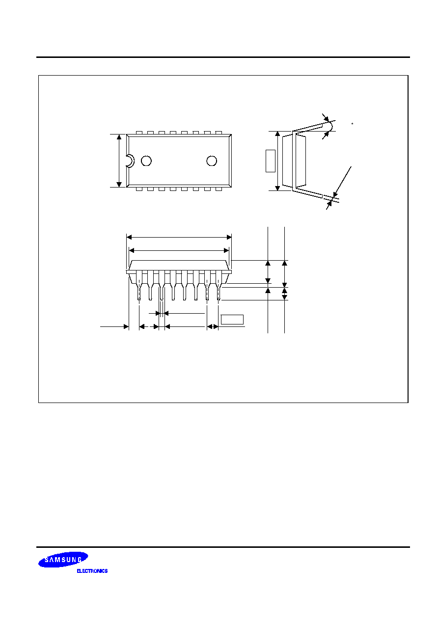
Figure 14-3. 16-DIP-300A Package Dimensions

MECHANICAL DATA
S3C9442/C9444/F9444/C9452/C9454/F9454
14-4
NOTE: Dimensions are in millimeters.
9.60 MAX
9.20
±
0.20
2.54
0.46
±
0.10
1.52
±
0.10
(0.79)
0.33 MIN
3.30
±
0.30
3.40
±
0.20
5.08 MAX
0-15
0.25
+ 0.10- 0.05
7.62
8-DIP-300
6.40
±
0
.20
#8
#1
#5
#4
Figure 14-4. 8-DIP-300 Package Dimensions

S3C9442/C9444/F9444/C9452/C9454/F9454
MECHANICAL DATA
14-5
NOTE: Dimensions are in millimeters.
8-SOP-225
6.00
±
0
.30
#5
#8
#1
#4
5.13 MAX
4.92
±
0.20
(0.56)
1.27
0.1-0.25 MIN
1.55
±
0.20
1.80 MAX
0.41
±
0.10
0-8
0.15
+ 0.10
- 0.05
5.72
3.95
±
0.20
0.50
±
0.20
0.10 MAX
Figure 14-5. 8-SOP-225 Package Dimensions

S3C9442/C9444/F9444/C9452/C9454/F9454
S3F9444/F9454 MTP
15-1
15
S3F9444/F9454 MTP
OVERVIEW
The S3F9444/F9454 single-chip CMOS microcontroller is the MTP (Multi Time Programmable)
version of the
S3C9442/C9444/C9452/C9454 microcontroller. It has an on-chip Flash ROM instead of masked ROM. The Flash
ROM is accessed by serial data format.
The S3F9444/F9454 is fully compatible with the S3C9442/C9444/C9452/C9454, in function, in D.C. electrical
characteristics, and in pin configuration. Because of its simple programming requirements, the S3F9444/F9454 is
ideal for use as an evaluation chip for the S3C9442/C9444/C9452/C9454.
V
DD
/V
DD
P0.0/ADC0/INT0/SCL
P0.1/ADC1/INT1/SDA
P0.2/ADC2
P0.3/ADC3
P0.4/ADC4
P0.5/ADC5
P0.6/ADC6/PWM
P0.7/ADC7
P2.6/ADC8/CLO
S3F9454
20
19
18
17
16
15
14
13
12
11
V
SS
/V
SS
X
IN
/P1.0
X
OUT
/P1.1
V
PP
/
RESET
/P1.2
T0/P2.0
P2.1
P2.2
P2.3
P2.4
P2.5
1
2
3
4
5
6
7
8
9
10
NOTE:
The bolds indicate MTP pin name.
Figure 15-1. Pin Assignment Diagram (20-Pin Package)
S3F9444/F9454 MTP
S3C9442/C9444/F9444/C9452/C9454/F9454
15-2
S3F9454
V
DD
/V
DD
P0.0/ADC0/INT0/SCL
P0.1/ADC1/INT1/SDA
P0.2/ADC2
P0.3/ADC3
P0.4/ADC4
P0.5/ADC5
P0.6/ADC6/PWM
16
15
14
13
12
11
10
9
V
SS
/V
SS
X
IN
/P1.0
X
OUT
/P1.1
V
PP
/
RESET
/P1.2
T0/P2.0
P2.1
P2.2
P2.3
1
2
3
4
5
6
7
8
NOTE:
The bolds indicate MTP pin name.
Figure 15-2. Pin Assignment Diagram (16-Pin Package)
S3F9444
V
DD
/V
DD
P0.0/ADC0/INT0/SCL
P0.1/ADC1/INT1/SDA
P0.2/ADC2
8
7
6
5
V
SS
/V
SS
X
IN
/P1.0
X
OUT
/P1.1
V
PP
/
RESET
/P1.2
1
2
3
4
NOTE:
The bolds indicate MTP pin name.
Figure 15-3. Pin Assignment Diagram (8-Pin Package)

S3C9442/C9444/F9444/C9452/C9454/F9454
S3F9444/F9454 MTP
15-3
Table 15-1. Descriptions of Pins Used to Read/Write the Flash ROM
Main Chip
During Programming
Pin Name
Pin Name
Pin No.
I/O
Function
P0.1
SDA
18 (20-pin)
14 (16-pin)
I/O
Serial data pin (output when reading, Input
when writing) Input and push-pull output port
can be assigned
P0.0
SCL
19 (20-pin)
15 (16-pin)
I
Serial clock pin (input only pin)
RESET
, P1.2
V
PP
4
I
Power supply pin for flash ROM cell writing
(indicates that MTP enters into the writing
mode). When 12.5 V is applied, MTP is in
writing mode and when 5 V is applied,
MTP is in reading mode. (Option)
V
DD
/V
SS
V
DD
/V
SS
20 (20-pin), 16 (16-pin)
1 (20-pin), 1 (16-pin)
I
Logic power supply pin.
Table 15-2. Comparison of S3F9444/F9454 and S3C9442/C9444/C9452/C9454 Features
Characteristic
S3F9444/F9454
S3C9442/C9444/C9452/C9454
Program Memory
4 Kbyte Flash ROM
2K/4K byte mask ROM
Operating Voltage (V
DD
)
2.0 V to 5.5 V
2.0 V to 5.5 V
OTP Programming Mode
V
DD
= 5 V, V
PP
= 12.5 V
Pin Configuration
20 DIP/20 SOP/16 DIP/8 DIP/8 SOP
EPROM Programmability
User Program multi time
Programmed at the factory
OPERATING MODE CHARACTERISTICS
When 12.5 V is supplied to the V
PP
pin of the S3F9444/F9454 Flash ROM programming mode is entered. The
operating mode (read, write, or read protection) is selected according to the input signals to the pins listed in
Table 15-3 below.
Table 15-3. Operating Mode Selection Criteria
V
DD
V
PP
REG/
MEM
Address
(A15≠A0)
R/W
Mode
5 V
5 V
0
0000H
1
Flash ROM read
12.5 V
0
0000H
0
Flash ROM program
12.5 V
0
0000H
1
Flash ROM verify
12.5 V
1
0E3FH
0
Flash ROM read protection
NOTE: "0" means Low level; "1" means High level.