 | –≠–ª–µ–∫—Ç—Ä–æ–Ω–Ω—ã–π –∫–æ–º–ø–æ–Ω–µ–Ω—Ç: S3C9688 | –°–∫–∞—á–∞—Ç—å:  PDF PDF  ZIP ZIP |
Document Outline
- ˛ˇ
- ˛ˇ
- ˛ˇ
- ˛ˇ
- ˛ˇ
- ˛ˇ
- ˛ˇ
- ˛ˇ
- ˛ˇ
- ˛ˇ
- ˛ˇ
- ˛ˇ
- ˛ˇ
- ˛ˇ
- ˛ˇ
- ˛ˇ

S3C9688/P9688
PRODUCT OVERVIEW
1-1
1
PRODUCT OVERVIEW
SAM88RCRI PRODUCT FAMILY
Samsung's SAM88RCRI family of 8-bit single-chip CMOS microcontrollers offers a fast and efficient CPU, a wide range of integrated
peripherals, and various mask-programmable ROM sizes.
A dual address/data bus architecture and a large number of bit- or nibble-configurable I/O ports provide a flexible programming environment for
applications with varied memory and I/O requirements. Timer/counters with selectable operating modes are included to support real-time
operations. Many SAM88RCRI microcontrollers have an external interface that provides access to external memory and other peripheral
devices.
S3C9688/P9688 MICROCONTROLLER
The S3C9688/P9688 single-chip 8-bit microcontroller is fabricated using an advanced CMOS process. It is built around the powerful
SAM88RCRI CPU core.
Stop and Idle power-down modes were implemented to reduce power consumption. To increase on-chip register space, the size of the internal
register file was logically expanded. The S3C9688 has 8 K bytes of program memory on-chip.
Using the SAM88RCRI design approach, the following peripherals were integrated with the SAM88RCRI core:
-- Five configurable I/O ports (32 pins)
-- 20 bit-programmable pins for external interrupts
-- 8-bit timer/counter with three operating modes
-- Low speed USB function
The S3C9688/P9688 is a versatile microcontroller that can be used in a wide range of low speed USB support general purpose applications. It
is especially suitable for use as a keyboard controller and is available in a 42-pin SDIP and a 44-pin QFP package.
OTP
The S3C9688/P9688 microcontroller is also available in OTP (One Time Programmable) version, S3P9688. S3P9688 microcontroller has an
on-chip 8-Kbyte one-time-programmable EPROM instead of masked ROM. The S3P9688 is comparable to S3C9688/P9688, both in function
and in pin configuration.

PRODUCT OVERVIEW
S3C9688/P9688
1-2
FEATURES
CPU
∑
SAM88RCRI CPU core
Memory
∑
8 K byte internal program memory (ROM)
∑
208 byte RAM
Instruction Set
∑
41 instructions
∑
IDLE and STOP instructions added for power-down modes
Instruction Execution Time
∑
0.66
µ
s at 6 MHz f
OSC
Interrupts
∑
29 interrupt sources with one vector, each source has its
pending bit
∑
One level, one vector interrupt structure
Oscillation Circuit
∑
6 MHz crystal/ceramic oscillator
∑
External clock source (6 MHz)
∑
Embedded oscillation capacitor (XI, XO, 33pF)
General I/O
∑
Bit programmable five I/O ports (34 pins total)
-- (D+/PS2, D-/PS2 Included)
Timer/Counter
∑
One 8-bit basic timer for watchdog function and
programmable oscillation stabilization interval generation
function
∑
One 8-bit timer/counter with Compare/Overflow
USB Serial Bus
∑
Compatible to USB low speed (1.5 Mbps) device 2.0
specification.
∑
1 Control endpoint and 2 Interrupt endpoint
∑
Serial bus interface engine (SIE)
-- Packet decoding/generation
-- CRC generation and checking
-- NRZI encoding/decoding and bit-stuffing
∑
8 bytes each receive/transmit USB buffer
Low Voltage Reset
∑
Low voltage detect for RESET
∑
Power on Reset
Operating Temperature Range
∑
≠ 40
∞
C to + 85
∞
C
Operating Voltage Range
∑
4.0 V to 5.25 V
Package Types
∑
42-pin SDIP
∑
44-pin QFP
S3C9688/P9688
PRODUCT OVERVIEW
1-3
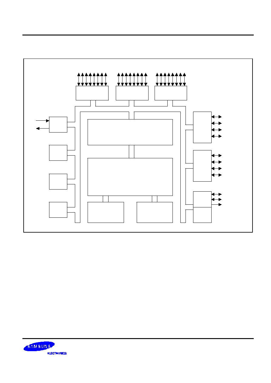
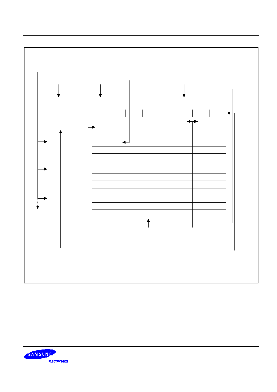
BLOCK DIAGRAM
P0.0-P0.7/INT2
SAM88RCRI Bus
X
IN
X
OUT
P2.0-P2.7/INT0
P1.0-P1.7
P3.0
P3.1
P3.2
P3.3/CLO
P4.0/INT1
P4.1/INT1
P4.2/INT1
P4.3/INT1
D+/PS2
D-/PS2
3.3 V OUT
I/O Port and Interrupt Control
SAM88RCRI CPU
Port 0
Port 1
Port 2
Main
OSC
Basic
Timer
LVR
Timer
Port 3
Port 4
USB
40 bytes
USB
Buffer
4 K/8KB ROM
208-Byte
Register File
Figure 1-1. Block Diagram

PRODUCT OVERVIEW
S3C9688/P9688
1-4
PIN ASSIGNMENTS
S3C9688/P9688
(42-SDIP)
P3.1
P3.0
INT0/P2.0
INT0/P2.1
INT0/P2.2
INT0/P2.3
INT0/P2.4
INT0/P2.5
INT0/P2.6
INT0/P2.7
V
DD
V
SS
X
OUT
X
IN
TEST
INT1/P4.0
INT1/P4.1
RESET
INT1/P4.2
INT1/P4.3
P1.7
1
2
3
4
5
6
7
8
9
10
11
12
13
14
15
16
17
18
19
20
21
P3.2
P3.3/CLO
D+/PS2
D-/PS2
3.3V
OUT
NC
P0.0/INT2
P0.1/INT2
P0.2/INT2
P0.3/INT2
P0.4/INT2
P0.5/INT2
P0.6/INT2
P0.7/INT2
P1.0
P1.1
P1.2
P1.3
P1.4
P1.5
P1.6
42
41
40
39
38
37
36
35
34
33
32
31
30
29
28
27
26
25
24
23
22
Figure 1-2. Pin Assignment Diagram (42-Pin SDIP Package)
S3C9688/P9688
PRODUCT OVERVIEW
1-5
INT0/P2.4
INT0/P2.5
INT0/P2.6 INT0/P2.7
V
DD
V
SS
X
OUT
X
IN
TEST
INT1/P4.0 INT1/P4.1
P1.0
P1.1
P1.2
P1.3
P1.4
P1.5
P1.6
P1.7
P4.3/INT1
P4.2/INT1
RESET
NC NC
NC P0.0/INT2 P0.1/INT2
P0.2/INT2 P0.3/INT2
P0.4/INT2
P0.5/INT2 P0.6/INT2 P0.7/INT2
3.3V
OUT
D- /PS2
D+/PS2
CLO/P3.3
P3.2
P3.1
P3.0
P2.0/INT0
P2.1/INT0
P2.2/INT0
P2.3/INT0
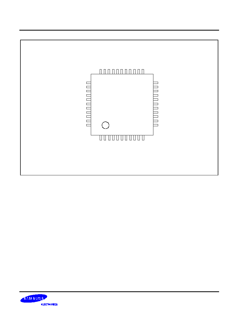
S3C9688/P9688
44-QFP
(Top View)
NOTE:
The TEST pin must connect to V
SS
(GND) in the normal operation mode.
1 2
3 4 5
6 7
8 9 10
11
34
35
36
37
38
39
40
41
42
43
44
33 32
31 30
29 28 27
26 25 24
23
22
21
20
19
18
17
16
15
14
13
12
Figure 1-3. Pin Assignment Diagram (44-Pin QFP Package)
PRODUCT OVERVIEW
S3C9688/P9688
1-6
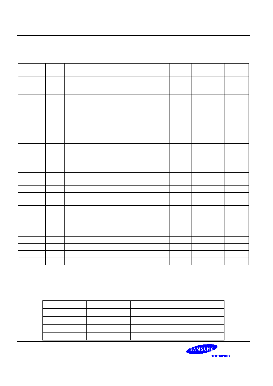
PIN DESCRIPTIONS
Table 1-1. S3C9688/P9688 Pin Descriptions
Pin Names
Pin
Type
Pin
Description
Circuit
Number
Pin
Numbers
Share
Pins
P0.0≠P0.7
I/O
Bit-programmable I/O port for Schmitt trigger input or open-
drain output. Port0 can be individually configured as external
interrupt inputs. Pull-up resistors are assignable by software.
B
36≠29
(30≠23)
INT2
P1.0≠P1.7
I/O
Bit-programmable I/O port for Schmitt trigger input or open-
drain output. Pull-up resistors are assignable by software.
B
28≠21
(22≠15)
≠
P2.0≠P2.7
I/O
Bit-programmable I/O port for Schmitt trigger input or open-
drain output. Port2 can be individually configured as external
interrupt inputs. Pull-up resistors are assignable by software.
B
3≠10
(41≠44, 1≠4)
INT0
P3.0≠P3.3
I/O
Bit-programmable I/O port for Schmitt trigger input, open-
drain or push-pull output. P3.3 can be used to system clock
output (CLO) pin.
C
2, 1, 42, 41
(40≠37)
P3.3/CLO
P4.0≠P4.3
I/O
Bit-programmable I/O port for Schmitt trigger input or open-
drain output or push-pull output. Port4 can be individually
configured as external interrupt inputs. In output mode, pull-
up resistors are assignable by software. But in input mode,
pull-up resistors are fixed.
D
16, 17, 19, 20
(10, 11, 13, 14)
INT1
D+/PS2 D-
/PS2
I/O
Programmable port for USB interface
or PS2 interface.
≠
40≠39
(36≠35)
≠
3.3 V
OUT
≠
3.3 V output from internal voltage regulator
≠
38 (34)
≠
X
IN
, X
OUT
≠
System clock input and output pin (crystal/ceramic oscillator,
or external clock source)
≠
14, 13
(8, 7)
≠
INT0
INT1
INT2
I
External interrupt for bit-programmable port0, port2 and port4
pins when set to input mode.
≠
3-10, 16,17, 19,
20, 29-36
(30-23, 41-44, 1-
4, 10, 11, 13, 14)
PORT2/
PORT4/
PORT0
RESET
I
RESET signal input pin. Input with internal pull-up resistor.
A
18 (12)
≠
TEST
I
Test signal input pin (for factory use only; connected to V
SS
)
≠
15 (9)
≠
V
DD
≠
Power input pin
≠
11 (5)
≠
V
SS
≠
Ground input pin
≠
12, (6)
≠
NC
≠
No connection
≠
37 (31,32, 33)
≠
NOTE
:
Pin numbers shown in parenthesis '( )' are for the 44-QFP package; others are for the 42-SDIP package.
PIN CIRCUITS DIAGRAMS
Table 1-2. Pin Circuit Assignments for the S3C9688/P9688
Circuit Number
Circuit Type
S3C9688/P9688 Assignments
A
I
RESET
signal input
B
I/O
Ports 0, 1, and 2
C
I/O
Port 3
D
I/O
Port 4
S3C9688/P9688
PRODUCT OVERVIEW
1-7
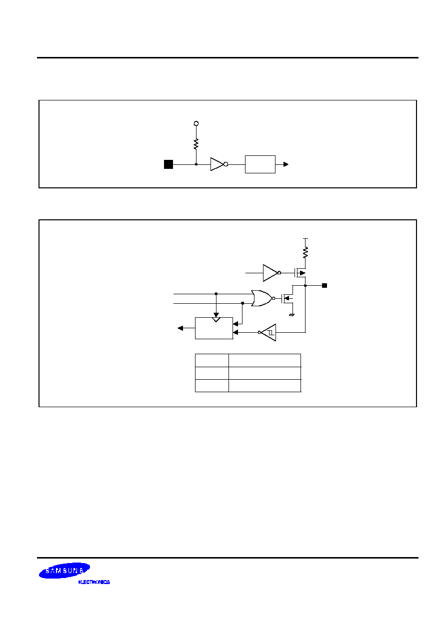
V
DD
Pull-up
Resistor
Noise
Filter
Figure 1-4. Pin Circuit Type A (RESET)
V
DD
Pull-up
Resistor
V
SS
Pull-up Enable
Output Disable
Open Data
D0
D1
MUX
Input Data
I/O
Mode
Input Data
Output
D0
Input
D1
Figure 1-5. Pin Circuit Type B (Ports 0, 1 and 2)
PRODUCT OVERVIEW
S3C9688/P9688
1-8
V
DD
V
SS
Output Data
Open Drain
D0
D1
MUX
Input Data
I/O
Mode
Input Data
Output
D0
Input
D1
Output
Disable
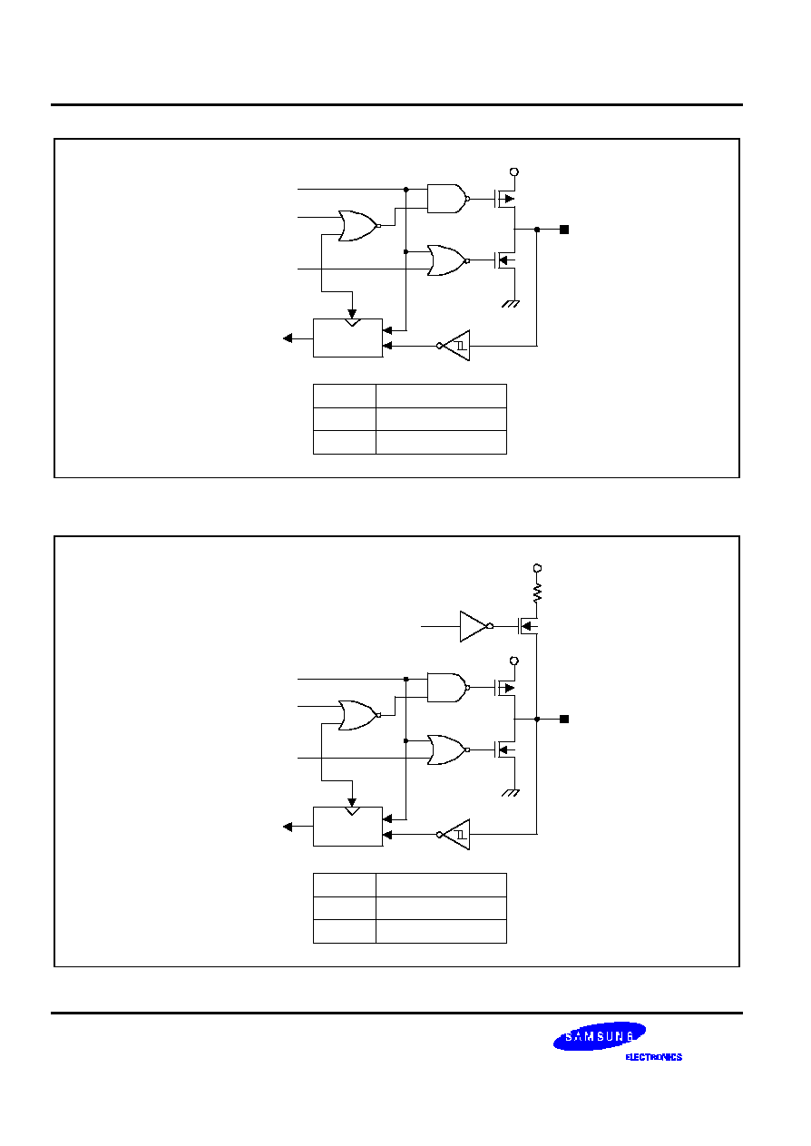
Figure 1-6. Pin Circuit Type C (Port 3)
V
DD
V
SS
Output Data
Open Drain
D0
D1
MUX
Input Data
I/O
Mode
Input Data
Output
D0
Input
D1
Output
Disable
Pull-up
Resistor
Pull-up Enable
V
DD
Figure 1-7. Pin Circuit Type D (Port 4)
S3C9688/P9688
PRODUCT OVERVIEW
1-9
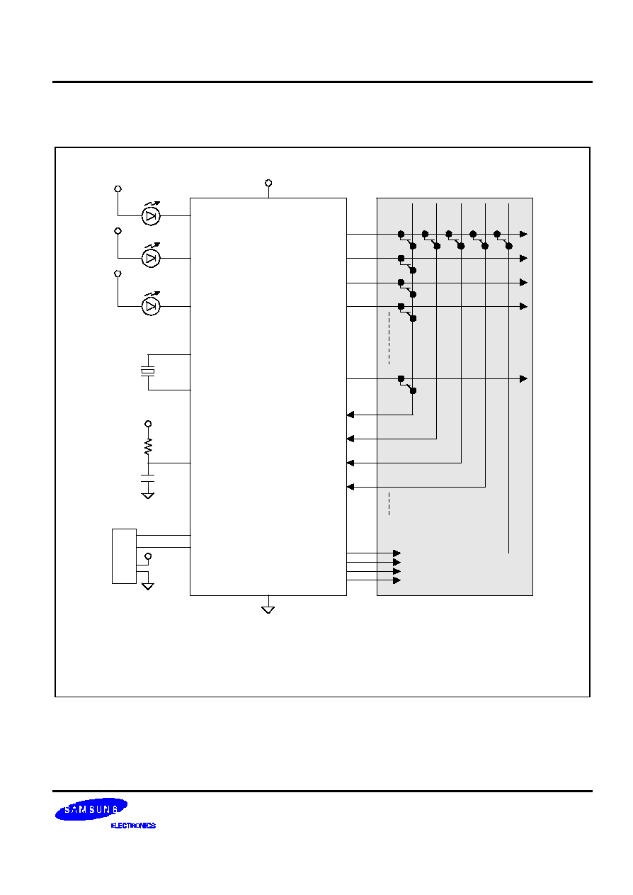
APPLICATION CIRCUIT
5V
Port 0
Port 1
Port 2
RESET
DP
DM
Port 4
D+/PS2
D-/PS2
NOTE:
Port4 can use expend keyboard MATRIX.
D+/PS2, D-/PS2 can use PS2 keyboard interface (see PS2CONINT, page 4-34).
Port 4.2, 4.3 can use PS2 mouse interface.
Port 3 can use LED direct drive.
S3C9688/P9688
Port 3
V
DD
5V
X
IN
X
OUT
V
SS1
H
O
S
T
15
0
1
2
3
0
1
2
3
7
KEYBOARD
MATRIX
Figure 1-8. Keyboard Application Circuit Diagram

PRODUCT OVERVIEW
S3C9688/P9688
1-10
NOTES

S 3 C 9 6 8 8 / P 9 6 8 8
ADDRESS SPACES
2 -1
2
A D D R E S S S P A C E S
O V E R V I E W
T h e S 3 C 9 6 8 8 / P 9 6 8 8 m i c r o c o n t r o l l e r h a s t w o k i n d s o f a d d r e s s s p a c e :
--
P r o g r a m m e m o r y ( R O M ) , i n t e r n a l
--
Internal register file
A 1 3 -b i t a d d r e s s b u s s u p p o r t s b o t h p r o g r a m m e m o r y . A s e p a r a t e 8 -b i t r e g i s t e r b u s c a r r i e s a d d r e s s e s a n d d a t a
between the CPU and the internal register file.
T h e S 3 C 9 6 8 8 h a s 8 K b y t e s o f m a s k -p r o g r a m m a b l e p r o g r a m m e m o r y o n -c h i p . T h e r e i s o n e p r o g r a m m e m o r y
configuration option:
--
I n t e r n a l R O M m o d e , i n w h i c h o n l y t h e 8 K b y t e i n t e r n a l p r o g r a m m e m o r y i s u s e d .
T h e S 3 C 9 6 8 8 / P 9 6 8 8 m i c r o c o n t r o l l e r h a s 2 0 8 g e n e r a l-purpose registers in its internal register file. Twenty -seven
b y t e s i n t h e r e g i s t e r f i l e a r e m a p p e d f o r s y s t e m a n d p e r i p h e r a l c o n t r o l f u n c t i o n s .
ADDRESS SAPCES
S3C9 6 8 8 / P 9 6 8 8
2 -2
P R O G R A M M E M O R Y ( R O M )
N o r m a l O p e r a t i n g M o d e ( I n t e r n a l R O M )
T h e S 3 C 9 6 8 8 / P 9 6 8 8 h a s 8 K b y t e s ( l o c a t i o n s 0 H ≠ 1 F F F H ) o f i n t e r n a l m a s k -p r o g r a m m a b l e p r o g r a m m e m o r y .
T h e f i r s t 2 b y t e s o f t h e R O M ( 0 0 0 0 H ≠ 0 0 0 1 H ) a r e a n i n t e r r u p t v e c t o r a d d r e s s .
T h e p r o g r a m r e s e t a d d r e s s i n t h e R O M i s 0 1 0 0 H .
8 K byte Internal
Program Memory
Area
8,191
(DECIMAL)
(HEX)
1FFFH (S3C9688/P9688)
256
2
1
0
0100H
0002H
0001H
0000H
Interrupt Vector
4-Kbyte Internal
Program Memory
Area
4,095
0FFFH
Program Start
F i g u r e 2 -1 . P r o g r a m M e m o r y A d d r e s s S p a c e

S 3 C 9 6 8 8 / P 9 6 8 8
ADDRESS SPACES
2 -3
R E G I S T E R A R C H I T E C T U R E
The upper 64 by t e s o f t h e S 3 C 9 6 8 8 / P 9 6 8 8 ' s i n t e r n a l r e g i s t e r f i l e a r e a d d r e s s e d a s w o r k i n g r e g i s t e r s , s y s t e m c o n t r o l
registers and peripheral control registers. The lower 192 bytes of internal register file (00H≠ B F H ) i s c a l l e d t h e g e n e r a l
p u r p o s e r e g i s t e r s p a c e . T h e t o t a l a d d r e s s a b l e r e g i s t e r s p a c e i s t h e r e b y 2 5 6 b y t e s . 2 3 3 r e g i s t e r s i n t h i s s p a c e c a n
b e a c c e s s e d . ; 2 0 8 a r e a v a i l a b l e f o r g e n e r a l-p u r p o s e u s e .
F o r m a n y S A M 8 8 R C R I m i c r o c o n t r o l l e r s , t h e a d d r e s s a b l e a r e a o f t h e i n t e r n a l r e g i s t e r f i l e i s f u r t h e r e x p a n d e d b y t h e
a d d i t i o n a l o f o n e o r m o r e r e g i s t e r p a g e s a t g e n e r a l p u r p o s e r e g i s t e r s p a c e ( 0 0 H ≠ B F H ) . T h i s r e g i s t e r f i l e e x p a n s i o n i s
n o t i m p l e m e n t e d i n t h e S 3 C 9 6 8 8 / P 9 6 8 8 , h o w e v e r . P a g e a d d r e s s i n g i s c o n t r o l l e d b y t h e S y s t e m M o d e R e g i s t e r
( S Y M . 1 ≠ S Y M . 0 ) .
T h e s p e c i f i c r e g i s t e r t y p e s a n d t h e a r e a ( i n b y t e s ) t h a t t h e y o c c u p y i n t h e i n t e r n a l r e g i s t e r f i l e a r e s u m m a r i z e d i n
Table 2-1 .
T a b l e 2 -1 . R e g i s t e r T y p e S u m m a r y
R e g i s t e r T y p e
N u m b e r o f B y t e s
C P U a n d s y s t e m c o n t r o l r e g i s t e r s
1 1
P eripheral, I/O, and clock control and data registers
3 4
G e n e r a l-p u r p o s e r e g i s t e r s ( i n c l u d i n g t h e 1 6 -b i t c o m m o n w o r k i n g r e g i s t e r a r e a )
2 0 8
T o t a l A d d r e s s a b l e B y t e s
2 5 3
ADDRESS SAPCES
S3C9 6 8 8 / P 9 6 8 8
2 -4
Peripheral Control
Register
System Control
Registers
Working Register
General Purpose
Register File
and Stack Area
FFH
E0H
DFH
D0H
CFH
C0H
BFH
00H
64 Bytes of
Common Area
192 Bytes
F i g u r e 2 -2 . I n t e r n a l R e g i s t e r F i l e O r g a n i z a t i o n
S 3 C 9 6 8 8 / P 9 6 8 8
ADDRESS SPACES
2 -5
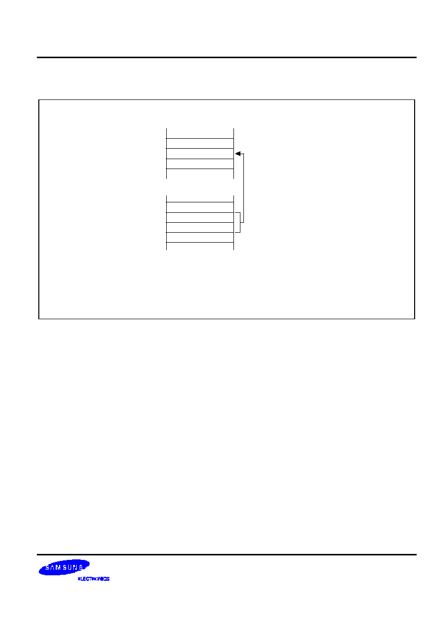
C O M M O N W O R K I N G R E G I S T E R A R E A ( C 0 H ≠C F H )
T h e S A M 8 8 R C R I r e g i s t e r a r c h i t e c t u r e p r o v i d e s a n e f f i c i e n t m e t h o d o f w o r k i n g r e g i s t e r a d d r e s s i n g t h a t t a k e s f u l l
advantage of shorter instruction form a t s t o r e d u c e e x e c u t i o n t i m e .
T h i s 1 6 -b y t e a d d r e s s r a n g e i s c a l l e d c o m m o n a r e a . T h a t i s , l o c a t i o n s i n t h i s a r e a c a n b e u s e d a s w o r k i n g r e g i s t e r s
b y o p e r a t i o n s t h a t a d d r e s s a n y l o c a t i o n o n a n y p a g e i n t h e r e g i s t e r f i l e . T y p i c a l l y , t h e s e w o r k i n g r e g i s t e r s s e r v e a s
t e m p o r a r y b u f f e r s f o r d a t a o p e r a t i o n s b e t w e e n d i f f e r e n t p a g e s . H o w e v e r , b e c a u s e t h e S 3 C 9 6 8 8 / P 9 6 8 8 u s e s o n l y
p a g e 0 , y o u c a n u s e t h e c o m m o n a r e a f o r a n y i n t e r n a l d a t a o p e r a t i o n .
T h e R e g i s t e r ( R ) a d d r e s s i n g m o d e c a n b e u s e d t o a c c e s s t h i s a r e a
R e g i s te r s a r e a d d r e s s e d e i t h e r a s a s i n g l e 8 -bit register or as a paired 16-bit register. In 16-bit register pairs, the
address of the first 8-b i t r e g i s t e r i s a l w a y s a n e v e n n u m b e r a n d t h e a d d r e s s o f t h e n e x t r e g i s t e r i s a n o d d n u m b e r .
T h e m o s t s i g n i f i c a n t b y t e o f t h e 1 6 -b i t d a t a i s a l w a y s s t o r e d i n t h e e v e n -n u m b e r e d r e g i s t e r ; t h e l e a s t s i g n i f i c a n t b y t e
i s a l w a y s s t o r e d i n t h e n e x t ( + 1 ) o d d -n u m b e r e d r e g i s t e r .
MSB
LSB
Rn
Rn+1
n = Even Address
F i g u r e 2 -3 . 1 6 -B i t R e g i s t e r P a i r s
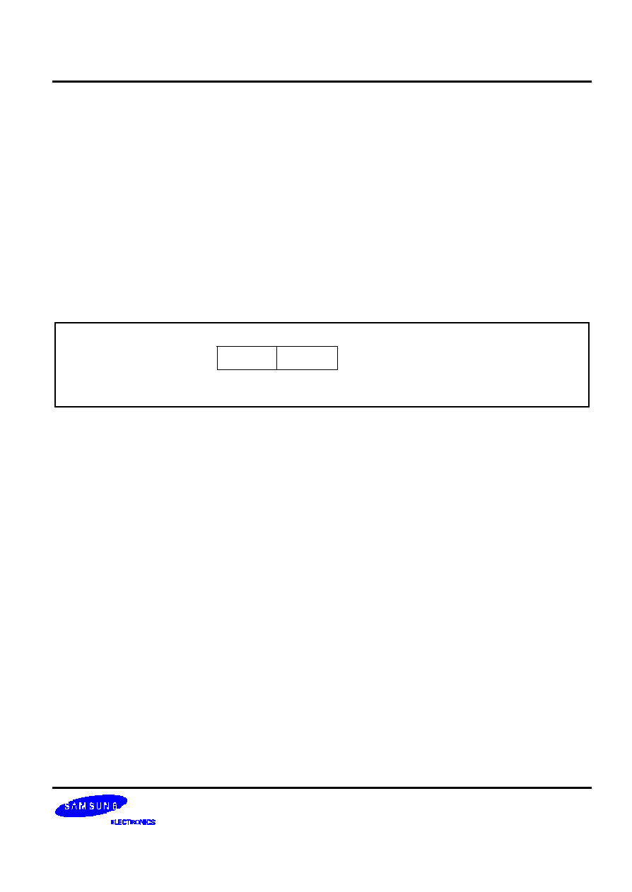
F
P R O G R A M M I N G T I P -- A d d r e s s i n g t h e C o m m o n W o r k i n g R e g i s t e r A r e a
A s t h e f o l l o w i n g e x a m p l e s s h o w , y o u s h o u l d a c c e s s w o r k i n g r e g i s t e r s i n t h e c o m m o n a r e a , l o c a t i o n s C 0 H ≠ C F H ,
u s i n g w o r k i n g r e g i s t e r a d d r e s s i n g m o d e o n l y .
E x a m p l e s :
1 . L D
0 C 2 H , 4 0 H
; Invalid addressing mode!
U s e w o r k i n g r e g i s t e r a d d r e s s i n g i n s t e a d :
L D
R 2 , 4 0 H
; R 2 ( C 2 H ) ® t h e v a l u e i n l o c a t i o n 4 0 H
2 . A D D
0 C 3 H , # 4 5 H
; Invalid addressing mode!
U s e w o r k i n g r e g is t e r a d d r e s s i n g i n s t e a d :
A D D
R 3 , # 4 5 H
; R 3 ( C 3 H ) ® R 3 + 4 5 H
ADDRESS SAPCES
S3C9 6 8 8 / P 9 6 8 8
2 -6
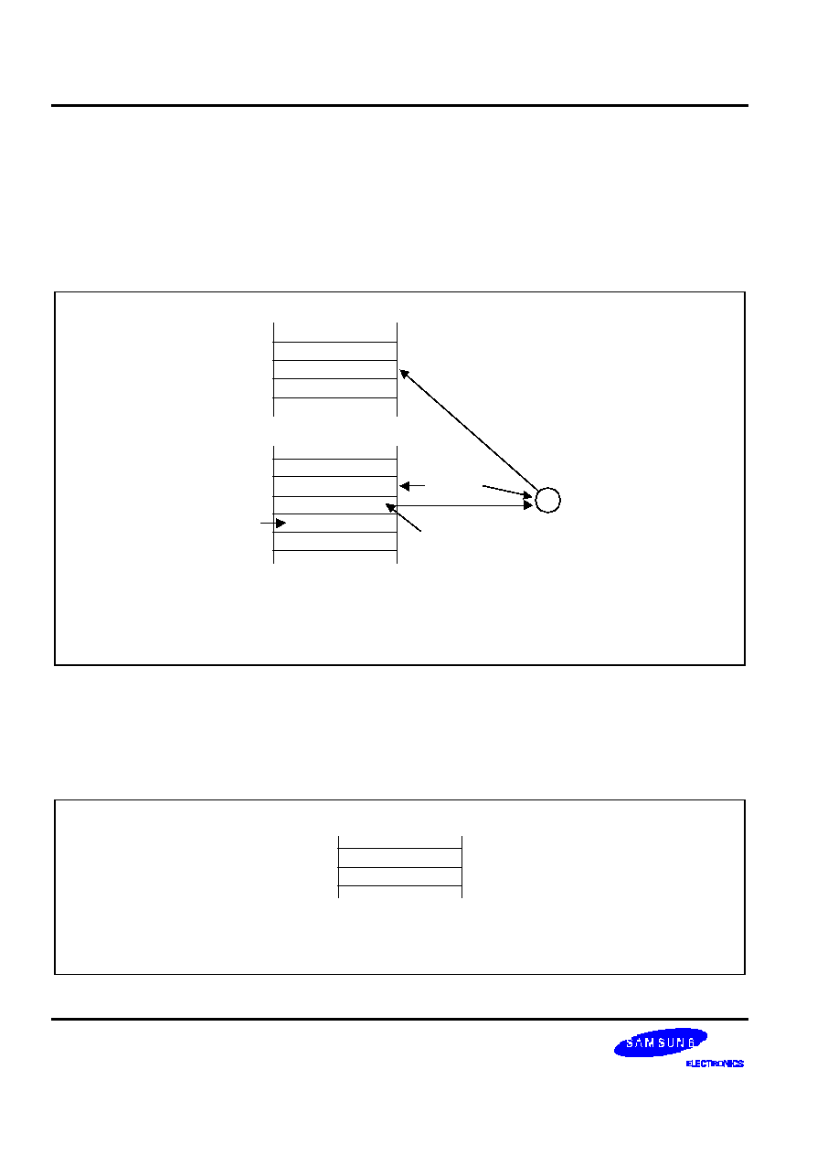
S Y S T E M S T A C K
S 3 C 9 -s e r i e s m i c r o c o n t r o l l e r s u s e t h e s y s t e m s t a c k f o r s t o r i n g d a t a i n s u b r o u t i n e c a l l a n d r e t u r n . T h e P U S H a n d
P O P i n s t r u c t i o n s a r e u s e d t o c o n t r o l s y s t e m s t a c k o p e r a t i o n s . T h e S 3 C 9 6 8 8 / P 9 6 8 8 a r c h i t e c t u r e s u p p o r t s s t a c k
operations in the internal register file.
S t a c k O p e r a t i o n s
R e t u r n a d d r e s s e s f o r p r o c e d u r e c a l l s a n d i n t e r r u p t s a n d d a t a a r e s t o r e d o n t h e s t a c k . T h e c o n t e n t s o f t h e P C a r e
s a v e d t o s t a c k b y a C A L L i n s t r u c t i o n a n d r e s t o r e d b y t h e R E T i n s t r u c t i o n . W h e n a n i n t e r r u p t o c c u r s , t h e c o n t e n t s o f
t h e P C a n d t h e F L A G S r e g i s t e r a r e p u s h e d t o t h e s t a c k . T h e I R E T i n s t r u c t i o n t h e n p o p s t h e s e v a l u e s b a c k t o t h e i r
o r i g i n a l l o c a t i o n s . T h e s t a c k a d d r e s s i s a l w a y s d e c r e m e n t e d b e f o r e a p u s h o p e r a t i o n a n d i n c r e m e n t e d a f t e r a p o p
o p e r a t i o n . T h e s t a c k p o i n t e r ( S P ) a l w a y s p o i n t s t o t h e s t a c k f r a m e s t o r e d o n t h e t o p o f t h e s t a c k , a s s h o w n i n F i g u r e
2 -4 .
PCL
PCH
Top of
Stack
Stack Contents
After a Call
Instruction
PCL
PCH
FLAGS
Top of
Stack
High Address
Low Address
Stack Contents
After an
Interrupt
F i g u r e 2 -4 . S t a c k O p e r a t i o n s
S t a c k P o i n t e r ( S P )
R e g i s t e r l o c a t i o n D 9 H c o n t a i n s t h e 8 -b i t s t a c k p o i n t e r ( S P ) t h a t i s u s e d f o r s y s t e m s t a c k o p e r a t i o n s . A f t e r a r e s e t ,
t h e S P v a l u e i s u n d e t e r m i n e d .
B e c a u s e o n l y i n t e r n a l m e m o r y s p a c e i s i m p l e m e n t e d i n t h e S 3 C 9 6 8 8 / P 9 6 8 8 , t h e S P m u s t b e i n i t i a l i z e d t o a n 8 -bit
value in the range 00H≠ B F H .
N O T E
I n c a s e a S t a c k P o i n t e r i s i n i t i a l i z e d t o 0 0 H , i t i s d e c r e a s e d t o F F H w h e n s t a c k o p e r a t i o n s t a r t s . T h i s m e a n s
t h a t a S t a c k P o i n t e r a c c e s s i n v a l i d s t a c k a r e a .

S 3 C 9 6 8 8 / P 9 6 8 8
ADDRESS SPACES
2 -7
F
P R O G R A M M I N G T I P -- S t a n d a r d S t a c k O p e r a t i o n s U s i n g P U S H a n d P O P
T h e f o l l o w i n g e x a m p l e s h o w s y o u h o w t o p e r f o r m s t a c k o p e r a t i o n s i n t h e i n t e r n a l r e g i s t e r f i l e u s i n g P U S H a n d P O P
i n s t r u c t i o n s :
L D
S P , # 0 C 0 H
; S P ® C 0 H ( N o r m a l l y , t h e S P i s s e t t o 0 C 0 H b y t h e
; initialization routine)
∑
∑
∑
P U S H
S Y M
; S t a c k a d d r e s s 0 B F H ® S Y M
P U S H
C L K C O N
; S t a c k a d d r e s s 0 B E H ® C L K CO N
P U S H
2 0 H
; S t a c k a d d r e s s 0 B D H ® 2 0 H
P U S H
R 3
; S t a c k a d d r e s s 0 B C H ® R 3
∑
∑
∑
P O P
R 3
; R 3 ® S t a c k a d d r e s s 0 B C H
P O P
2 0 H
; 2 0 H ® S t a c k a d d r e s s 0 B D H
P O P
C L K C O N
; C L K C O N ® S t a c k a d d r e s s 0 B E H
P O P
S Y M
; S Y M ® S t a c k a d d r e s s 0 B F H

ADDRESS SAPCES
S3C9 6 8 8 / P 9 6 8 8
2 -8
N O T E S

S 3 C 9 6 8 8 / P 9 6 8 8
ADDRESSING MODES
3 -1
3
A D D R E S S I N G M O D E S
O V E R V I E W
I n s t r u c t i o n s t h a t a r e s t o r e d i n p r o g r a m m e m o r y a r e f e t c h e d f o r e x e c u t i o n u s i n g t h e p r o g r a m c o u n t e r . I n s t r u c t i o n s
i n d i c a t e t h e o p e r a t i o n t o b e p e r f o r m e d a n d t h e d a t a t o b e o p e r a t e d o n . A d d r e s s i n g m o d e i s t h e m e t h o d u s e d t o
d e t e r m i n e t h e l o c a t i o n o f t h e d a t a o p e r a n d . T h e o p e r a n d s s p e c i f i e d i n S A M 8 8 R C R I i n s t r u c t i o n s m a y b e c o n d i t i o n
c o d e s , i m m e d i a t e d a t a , o r a l o c a t i o n i n t h e r e g i s t e r f i l e , p r o g r a m m e m o r y , o r d a t a m e m o r y .
T h e S A M 8 8 R C R I i n s t r u c t i o n s e t s u p p o r t s s i x e x p l i c i t a d d r e s s i n g m o d e s . N o t a l l o f t h e s e a d d r e s s i n g m o d e s a r e
a v a i l a b l e f o r e a c h i n s t r u c t i o n . T h e a d d r e s s i n g m o d e s a n d t h e i r s y m b o l s a r e a s f o l l o w s :
--
R e g i s t e r ( R )
--
Indirect Register (IR)
--
Indexed (X)
--
D i r e c t A d d r e s s ( D A )
--
R e l a t i v e A d d r e s s ( R A )
--
I m m e d i a t e ( I M )

ADDRESSING MODES
S 3 C 9 6 8 8 / P 9 6 8 8
3 -2
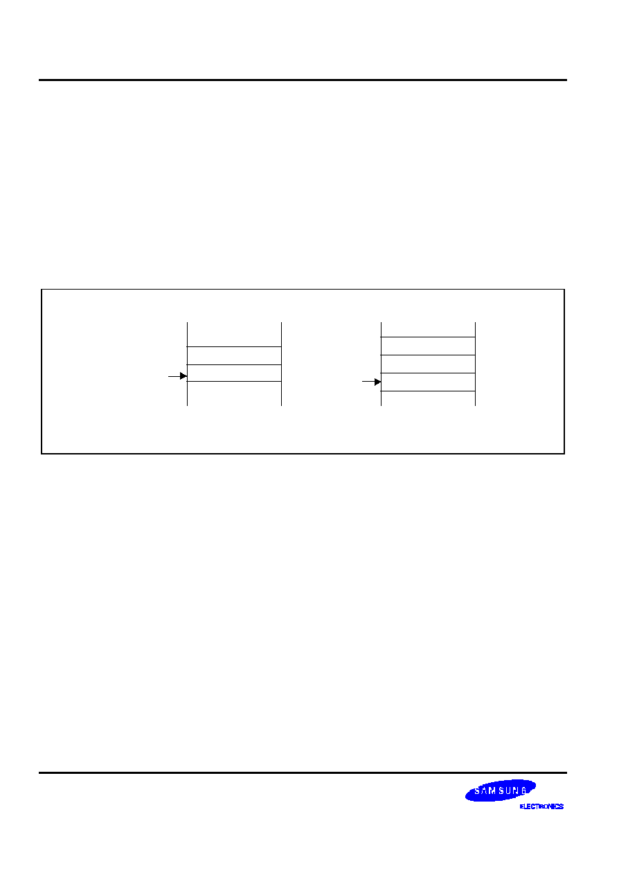
R E G I S T E R A D D R E S S I N G M O D E ( R )
I n R e g i s t e r a d d r e s s i n g m o d e , t h e o p e r a n d i s t h e c o n t e n t o f a s p e c i f i e d r e g i s t e r ( s e e F i g u r e 3 -1 ) . W o r k i n g r e g i s t e r
a d d r e s s i n g d i f f e r s f r o m R e g i s t e r a d d r e s s i n g b e c a u s e i t u s e s a n 1 6 -byte working register space in the register file and
a n 4 -b i t r e g i s t e r w i t h i n t h a t s p a c e ( s e e F i g u r e 3 -2).
dst
Value used in
Instruction Execution
OPCODE
OPERAND
8-Bit Register
File Address
Point to One
Rigister in Register
File
One-Operand
Instruction
(Example)
Sample Instruction:
DEC
CNTR
; Where CNTR is the label of an 8-bit register address
Program Memory
Register File
F i g u r e 3 -1 . R e g i s t e r A d d r e s s i n g
dst
OPCODE
4-Bit
Working Register
Point to the
Woking Register
(1 of 16)
Two-Operand
Instruction
(Example)
Sample Instruction:
ADD R1, R2 ; Where R1 = C1H and R2 = C2H
Program Memory
Register File
src
4 LSBs
OPERAND
CFH
C0H
F i g u r e 3 -2 . W o r k i n g R e g i s t e r A d d r e s s i n g

S 3 C 9 6 8 8 / P 9 6 8 8
ADDRESSING MODES
3 -3
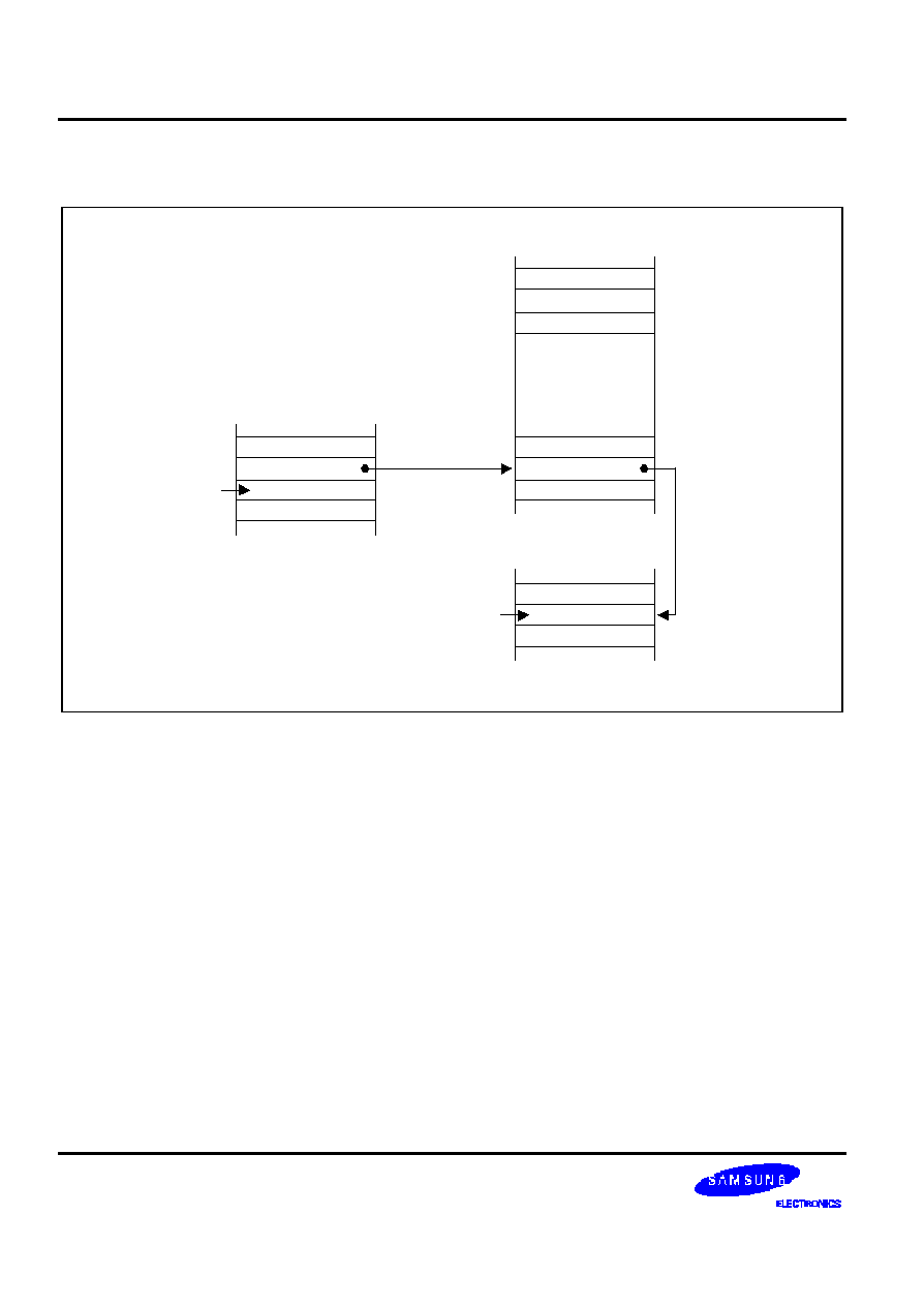
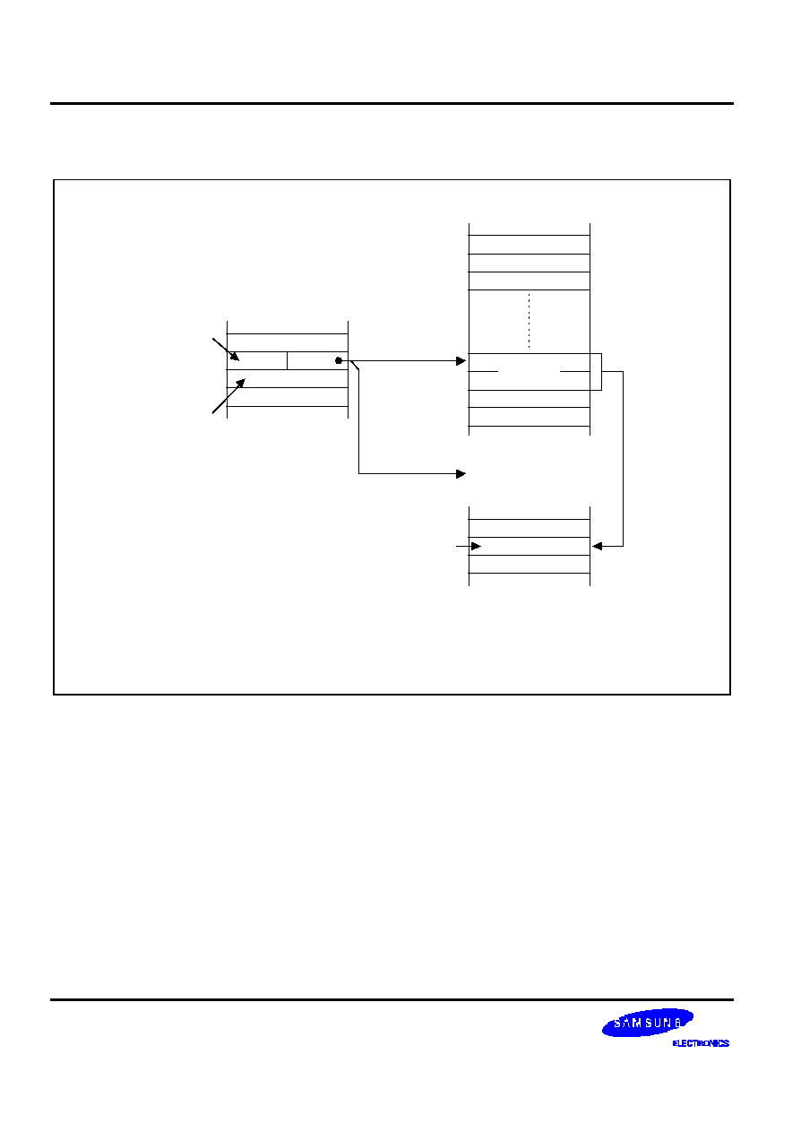
I N D I R E C T R E G I S T E R A D D R E S S I N G M O D E ( I R )
In Indirect Register (IR) addressing mode, the content of the specified register or register pair is the address of the
o p e r a n d . D e p e n d i n g o n t h e i n s t r u c t i o n u s e d , t h e a c t u a l a d d r e s s m a y p o i n t t o a r e g i s t e r i n t h e r e g i s t e r f i l e , t o p r o g r a m
m e m o r y ( R O M ) , o r t o a n e x t e r n a l m e m o r y s p a c e ( s e e F i g u r e s 3 -3 t h r o u g h 3 -6).
Y o u c a n u s e a n y 8 -b i t r e g i s t e r t o i n d i r e c t l y a d d r e s s a n o t h e r r e g i s t e r . A n y 1 6 -bit register pair can be used to indirectly
a d d r e s s a n o t h e r m e m o r y l o c a t i o n .
dst
Address of Operand
used by Instruction
OPCODE
ADDRESS
8-Bit Register
File Address
Point to One
Rigister in Register
File
One-Operand
Instruction
(Example)
Sample Instruction:
RL
@SHIFT
; Where SHIFT is the label of an 8-Bit register address
Program Memory
Register File
Value used in
Instruction Execution
OPERAND
F i g u r e 3 -3 . I n d i r e c t R e g i s t e r A d d r e s s i n g t o R e g i s t e r F i l e
ADDRESSING MODES
S 3 C 9 6 8 8 / P 9 6 8 8
3 -4
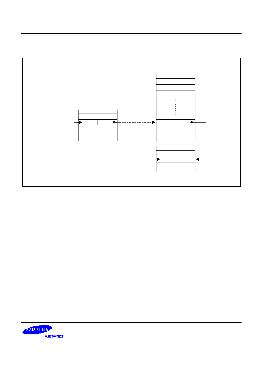
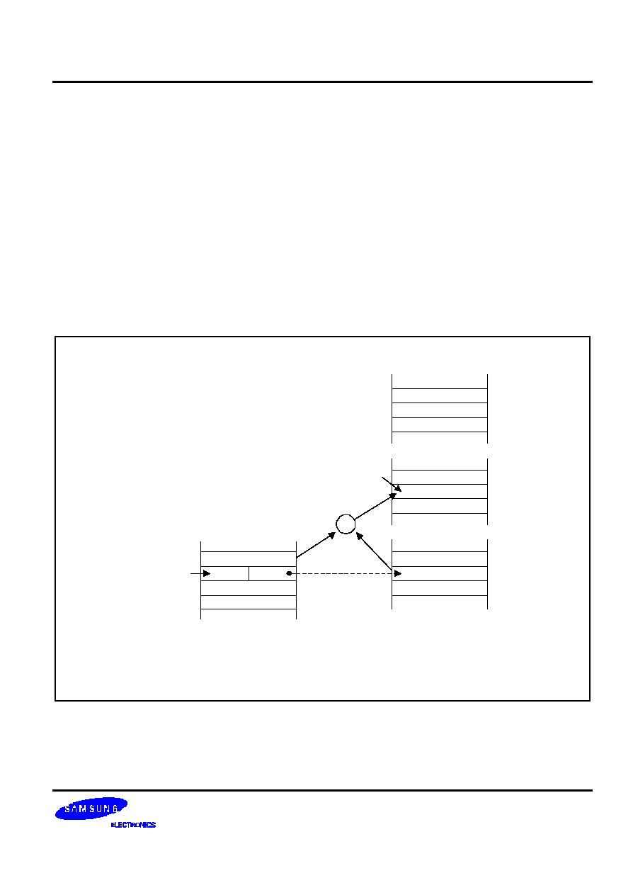
I N D I R E C T R E G I S T E R A D D R E S S I N G M O D E ( C o n t i n u e d)
dst
OPCODE
PAIR
Points to
Rigister Pair
Example
Instruction
References
Program
Memory
Sample Instructions:
CALL
@RR2
JP
@RR2
Program Memory
Register File
Value used in
Instruction
OPERAND
REGISTER
Program Memory
16-Bit
Address
Points to
Program
Memory
F i g u r e 3 -4 . I n d i r e c t R e g i s t e r A d d r e s s i n g t o P r o g r a m M e m o r y
S 3 C 9 6 8 8 / P 9 6 8 8
ADDRESSING MODES
3 -5
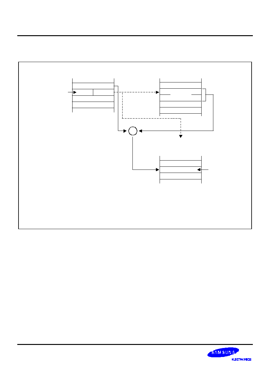
I N D I R E C T R E G I S T E R A D D R E S S I N G M O D E ( C o n t i n u e d)
dst
OPCODE
4-Bit
Working
Register
Address
Point to the
Woking Register
(1 of 16)
Sample Instruction:
OR
R6, @R2
Program Memory
Register File
src
4 LSBs
Value used in
Instruction
OPERAND
C0H
CFH
OPERAND
F i g u r e 3 -5 . I n d i r e c t W o r k i n g R e g i s t e r A d d r e s s i n g t o R e g i s t e r F i l e
ADDRESSING MODES
S 3 C 9 6 8 8 / P 9 6 8 8
3 -6
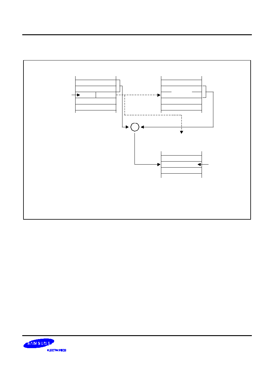
I N D I R E C T R E G I S T E R A D D R E S S I N G M O D E ( C o n c l u d e d)
dst
OPCODE
4-Bit Working
Register Address
Sample Instructions:
LCD
R5,@RR2 ; Program memory access
LDE
R3,@RR14 ; External data memory access
LDE
@RR4, R8 ; External data memory access
Program Memory
Register File
src
Value used in
Instruction
OPERAND
Example Instruction
References either
Program Memory or
Data Memory
Program Memory
or
Data Memory
Next 3-Bits Point
to Working
Register Pair
(1 of 8)
LSB Selects
Register
Pair
16-Bit
address
points to
program
memory
or data
memory
CFH
C0H
F i g u r e 3 -6 . I n d i r e c t W o r k i n g R e g i s t e r A d d r e s s i n g t o P r o g r a m o r D a t a M e m o r y
S 3 C 9 6 8 8 / P 9 6 8 8
ADDRESSING MODES
3 -7
I N D E X E D A D D R E S S I N G M O D E ( X )
I n d e x e d ( X ) a d d r e s s i n g m o d e a d d s a n o f f s e t v a l u e t o a b a s e a d d r e s s d u r i n g i n s t r u c t i o n e x e c u t i o n i n o r d e r t o c a l c u l a t e
the effective operand address (see Figure 3-7 ) . Y o u c a n u s e I n d e x e d a d d r e s s i n g m o d e t o a c c e s s l o c a t i o n s i n t h e
internal register file or in external memory.
I n s h o r t o f f s e t I n d e x e d a d d r e s s i n g m o d e , t h e 8 -b i t d i s p l a c e m e n t i s t r e a t e d a s a s i g n e d i n t e g e r i n t h e r a n g e
≠ 1 2 8 t o + 1 2 7 . T h i s a p p l i e s t o e x t e r n a l m e m o r y a c c e s s e s o n l y ( s e e F i g u r e 3 -8).
For register file addressing, an 8-b i t b a s e a d d r e s s p r o v i d e d b y t h e i n s t r u c t i o n i s a d d e d t o a n 8 -bit offset contained in
a w o r k i n g r e g i s t e r . F o r e x t e r n a l m e m o r y a c c e s s e s , t h e b a s e a d d r e s s i s s t o r e d i n t h e w o r k i n g r e g i s t e r p a i r
d e s i g n a t e d i n t h e i n s t r u c t i o n . T h e 8 -bit or 16-b i t o f f s e t g i v e n i n t h e i n s t r u c t i o n i s t h e n a d d e d t o t h e b a s e a d d r e s s ( s e e
Fi g ur e 3 -9).
Th e o n l y i n s t r u c t i o n t h a t s u p p o r t s I n d e x e d a d d r e s s i n g m o d e f o r t h e i n t e r n a l r e g i s t e r f i l e i s t h e L o a d i n s t r u c t i o n ( L D ) .
T h e L D C a n d L D E i n s t r u c t i o n s s u p p o r t I n d e x e d a d d r e s s i n g m o d e f o r i n t e r n a l p r o g r a m m e m o r y , e x t e r n a l p r o g r a m
m e m o r y , a n d f o r e x t e r n a l d a t a m e m o r y , w h e n i m p l e m e n t e d .
dst
OPCODE
Two-Operand
Instruction
Example
Point to One of the
Woking Register
(1 of 16)
Sample Instruction:
LD R0, #BASE[R1] ; Where BASE is an 8-bit immediate value
Program Memory
Register File
src
4 LSBs
Value used in
Instruction
OPERAND
INDEX
X (OFFSET)
~
~
+
~
~
F i g u r e 3 -7 . I n d e x e d A d d r e s s i n g t o R e g i s t e r F i l e
ADDRESSING MODES
S 3 C 9 6 8 8 / P 9 6 8 8
3 -8
I N D E X E D A D D R E S S I N G M O D E ( C o n t i n u e d)
Point to Working
Register Pair
(1 of 8)
LSB Selects
16-Bit
address
added to
offset
dst
OPCODE
Program Memory
XS (OFFSET)
4-Bit Working
Register Address
Sample Instructions:
LDC
R4, #04H[RR2] ; The values in the program address (RR2 + #04H)
are loaded into register R4.
LDE
R4,#04H[RR2] ; Identical operation to LDC example, except that
external program memory is accessed.
NEXT 3-Bit
Register
Pair
src
8-Bit
16-Bit
+
Program Memory
or
Datamemory
OPERAND
Value used in
Instruction
16-Bit
Register File
F i g u r e 3 -8 . I n d e x e d A d d r e s s i n g t o P r o g r a m o r D a t a M e m o r y w i t h S h o r t O f f s e t
S 3 C 9 6 8 8 / P 9 6 8 8
ADDRESSING MODES
3 -9
I N D E X E D A D D R E S S I N G M O D E ( C o n c l u d e d)
Point to Working
Register Pair
(1 of 8)
LSB Selects
16-Bit
address
added to
offset
Program Memory
4-Bit Working
Register Address
Sample Instructions:
LDC
R4, #1000H[RR2]
; The values in the program address (RR2 + #1000H)
are loaded into register R4.
LDE
R4,#1000H[RR2]
; Identical operation to LDC example, except that
external program memory is accessed.
NEXT 3-Bit
Register
Pair
16-Bit
16-Bit
+
Program Memory
or
Datamemory
OPERAND
Value used in
Instruction
16-Bit
Register File
OPCODE
XL
H
(OFFSET)
XL
L
(OFFSET)
dst
src
F i g u r e 3 -9 . I n d e x e d A d d r e s s i n g t o P r o g r a m o r D a t a M e m o r y w i t h L o n g O f f s e t

ADDRESSING MODES
S 3 C 9 6 8 8 / P 9 6 8 8
3 -1 0
D I R E C T A D D R E S S M O D E ( D A )
I n D i r e c t A d d r e s s ( D A ) m o d e , t h e i n s t r u c t i o n p r o v i d e s t h e o p e r a n d ' s 1 6 -b i t m e m o r y a d d r e s s . J u m p ( J P ) a n d C a l l
( C A L L ) i n s t r u c t i o n s u s e t h i s a d d r e s s i n g m o d e t o s p e c i f y t h e 1 6 -b i t d e s t i n a t i o n a d d r e s s t h a t i s l o a d e d i n t o t h e P C
w h e n e v e r a J P o r C A L L i n s t r u c t i o n i s e x e c u t e d .
T h e L D C a n d L D E i n s t r u c t i o n s c a n u s e D i r e c t A d d r e s s m o d e t o s p e c i f y t h e s o u r c e o r d e s t i n a t i o n a d d r e s s f o r L o a d
o p e r a t i o n s t o p r o g r a m m e m o r y ( L D C ) o r t o e x t e r n a l d a t a m e m o r y ( L D E ) , i f i m p l e m e n t e d .
Sample Instructions:
LDC
R5,1234H ; The values in the program address (1234H)
are loaded into register R5.
LDE
R5,1234H ; Identical operation to LDC example, except that
external program memory is accessed.
dst/src
OPCODE
Program Memory
"0" or "1"
Lower Address Byte
LSB Selects Program
Memory or Data Memory:
"0" = Program Memory
"1" = Data Memory
Memory
Address
Used
Upper Address Byte
Program or
Data Memory
F i g u r e 3 -1 0 . D i r e c t A d d r e s s i n g f o r L o a d I n s t r u c t i o n s
S 3 C 9 6 8 8 / P 9 6 8 8
ADDRESSING MODES
3 -1 1
D I R E C T A D D R E S S M O D E (C o n t i n u e d)
OPCODE
Program Memory
Lower Address Byte
Program
Memory
Address
Used
Upper Address Byte
Sample Instructions:
JP
C,JOB1
; Where JOB1 is a 16-Bit immediate address
CALL
DISPLAY
; Where DISPLAY is a 16-Bit immediate address
Next OPCODE
F i g u r e 3 -1 1 . D i r e c t A d d r e s s i n g f o r C a l l a n d J u m p I n s t r u c t i o n s
ADDRESSING MODES
S 3 C 9 6 8 8 / P 9 6 8 8
3 -1 2
R E L A T I V E A D D R E S S M O D E ( R A )
In Relative Address (RA) mode, a two's -c o m p l e m e n t s i g n e d d i s p l a c e m e n t b e t w e e n ≠ 1 2 8 a n d + 1 2 7 i s s p e c i f i e d i n
t h e i n s t r u c t i o n . T h e d i s p l a c em e n t v a l u e i s t h e n a d d e d t o t h e c u r r e n t P C v a l u e . T h e r e s u l t i s t h e a d d r e s s o f t h e n e x t
i n s t r u c t i o n t o b e e x e c u t e d . B e f o r e t h i s a d d i t i o n o c c u r s , t h e P C c o n t a i n s t h e a d d r e s s o f t h e i n s t r u c t i o n i m m e d i a t e l y
following the current instruction.
T h e i n s t r u c t i o n s t h a t s u p p o r t R A a d d r e s s i n g i s J R .
OPCODE
Program Memory
Displacement
Program Memory
Address Used
Sample Instructions:
JR
ULT,$+OFFSET ; Where OFFSET is a value in the range +127 to -128
Next OPCODE
+
Signed
Displacement Value
Current Instruction
Current
PC Value
F i g u r e 3 -1 2 . R e l a t i v e A d d r e s s i n g
I M M E D I A T E M O D E ( I M )
I n I m m e d i a t e ( I M ) a d d r e s s i n g m o d e , t h e o p e r a n d v a l u e u s e d i n t h e i n struction is the value supplied in the operand
field itself. Immediate addressing mode is useful for loading constant values into registers.
(The Operand value is in the instruction)
OPCODE
Sample Instruction:LD R0,#0AAH
Program Memory
OPERAND
F i g u r e 3 -1 3 . I m m e d i a t e A d d r e s s i n g

S 3 C 9 6 8 8 / P 9 6 8 8
CONTROL REGISTERS
4-
1
4
C O N T R O L R E G I S T E R S
O V E R V I E W
I n t h i s s e c t i o n , d e t a i l e d d e s c r i p t i o n s o f t h e S 3 C 9 6 8 8 / P 9 6 8 8 c o n t r o l r e g i s t e r s a r e p r e s e n t e d i n a n e a s y -t o -read format.
T h e s e d e s c r i p t i o n s w i l l h e l p y o u t o f a m i l i a r i z e y o u r s e l f w i t h t h e m a p p e d l o c a t i o n s i n t h e r e g i s t e r f i l e . Y o u c a n a l s o
u s e t h e m a s a q u i c k -r e f e r e n c e s o u r c e w h e n w r i t i n g a p p l i c a t i o n p r o g r a m s .
S y s t e m a n d p e r i p h e r a l r e g i s t e r s a r e s u m m a r i z e d i n T a b l e 4 -1 . F i g u r e 4 -1 illustrates the important features of the
s t a n d a r d r e g i s t e r d e s c r i p t i o n f o r m a t .
C o n t r o l r e g i s t e r d e s c r i p t i o n s a r e a r r a n g e d i n a l p h a b e t i c a l o r d e r a c c o r d i n g t o r e g i s t e r m n e m o n i c . M o r e i n f o r m a t i o n
about control registers is presented in the context of the various peripheral hardware descriptions in Part II of this
m a n u a l .
CONTROL REGISTERS
S 3 C 9 6 8 8 / P 9 6 8 8
4 -2
T a b l e 4 -1 . S y s t e m a n d P e r i p h e r a l c o n t r o l R e g i s t e r s
R e g i s t e r N a m e
M n e m o n i c
D e c i m a l
H e x
R / W
T i m e r 0 c o u n t e r r e g i s t e r
T 0 C N T
2 0 8
D 0 H
R
T i m e r 0 d a t a r e g i s t e r
T 0 D A T A
2 0 9
D 1 H
R / W
T i m e r 0 c o n t r o l r e g i s t e r
T 0 C O N
2 1 0
D 2 H
R / W
U S B s e l e c t i o n a n d T r a n s c e i v e r c r o s s o v e r p o i n t
c o n t r o l r e g i s t e r
U S X C O N
2 1 1
D 3 H
R / W
C l o c k c o n t r o l r e g i s t e r
C L K C O N
2 1 2
D 4 H
R / W
S y s t e m f l a g s r e g i s t e r
F L A G S
2 1 3
D 5 H
R / W
D + / P S 2 , D -/ P S 2 d a t a r e g i s t e r
( O n l y P S 2 M o d e )
P S 2 D A T A
2 1 4
D 6 H
R / W
P S 2 c o n t r o l a n d i n t e r r u p t p e n d i n g r e g i s t e r
P S 2 C O N I N T
2 1 5
D 7 H
R / W
Port 0 interrupt control register
P 0 I N T
2 1 6
D 8 H
R / W
S t a c k p o i n t e r
S P
2 1 7
D 9 H
R / W
Port 0 interrupt pending register
P 0 P N D
2 1 8
D A H
R / W
L o c a t i o n D B H i s n o t m a p p e d .
B a s i c t i m e r c o n t r o l r e g i s t e r
B T C O N
2 2 0
D C H
R / W
B a s i c t i m e r c o u n t e r r e g i s t e r
B T C N T
2 2 1
D D H
R
L o c a t i o n D E H i s n o t m a p p e d .
S y s t e m m o d e r e g i s t e r
S Y M
2 2 3
D F H
R / W
P o r t 0 d a t a r e g i s t e r
P 0
2 2 4
E 0 H
R / W
P o r t 1 d a t a r e g i s t e r
P 1
2 2 5
E 1 H
R / W
P o r t 2 d a t a r e g i s t e r
P 2
2 2 6
E 2 H
R / W
P o r t 3 d a t a r e g i s t e r
P 3
2 2 7
E 3 H
R / W
P o r t 4 d a t a r e g i s t e r
P 4
2 2 8
E 4 H
R / W
P o r t 3 c o n t r o l r e g i s t e r
P 3 C O N
2 2 9
E 5 H
R / W
P o r t 0 c o n t r o l r e g i s t e r ( h i g h b y t e )
P 0 C O N H
2 3 0
E 6 H
R / W
P o r t 0 c o n t r o l r e g i s t e r ( l o w b y t e )
P 0 C O N L
2 3 1
E 7 H
R / W
P o r t 1 c o n t r o l r e g i s t e r ( h i g h b y t e )
P 1 C O N H
2 3 2
E 8 H
R / W
P o r t 1 c o n t r o l r e g i s t e r ( l o w b y t e )
P 1 C O N L
2 3 3
E 9 H
R / W
P o r t 2 c o n t r o l r e g i s t e r ( h i g h b y t e )
P 2 C O N H
2 3 4
E A H
R / W
P o r t 2 c o n t r o l r e g i s t e r ( l o w b y t e )
P 2 C O N L
2 3 5
E B H
R / W
Port 2 interrupt control register
P 2 I N T
2 3 6
E C H
R / W
Port 2 interrupt pending register
P 2 P N D
2 3 7
E D H
R / W
P o r t 4 c o n t r o l r e g i s t e r
P 4 C O N
2 3 8
E E H
R / W
Port 4 interrupt enable/pending register
P 4 I N T P N D
2 3 9
E F H
R / W

S 3 C 9 6 8 8 / P 9 6 8 8
CONTROL REGISTERS
4 -3
CONTROL REGISTERS
S 3 C 9 6 8 8 / P 9 6 8 8
4 -4
T a b l e 4 -1 . S y s t e m a n d P e r i p h e r a l c o n t r o l R e g i s t e r s ( C o n t i n u e d )
R e g i s t e r N a m e
M n e m o n i c
D e c i m a l
H e x
R / W
U S B f u n c t i o n a d d r e s s r e g i s t e r
F A D D R
2 4 0
F 0 H
R / W
C o n t r o l e n d p o i n t s t a t u s r e g i s t e r
E P 0 C S R
2 4 1
F 1 H
R / W
I n t e r r u p t e n d p o i n t 1 c o n t r o l s t a t u s r e g i s t e r
E P 1 C S R
2 4 2
F 2 H
R / W
Control endpoin t b y t e c o u n t r e g i s t e r
E P 0 B C N T
2 4 3
F 3 H
R / W
C o n t r o l e n d p o i n t F I F O r e g i s t e r
E P 0 F I F O
2 4 4
F 4 H
R / W
Interrupt endpoint 1 FIFO register
E P 1 F I F O
2 4 5
F 5 H
R / W
U S B i n t e r r u p t p e n d i n g r e g i s t e r
U S B P N D
2 4 6
F 6 H
R / W
U S B i n t e r r u p t e n a b l e r e g i s t e r
U S B I N T
2 4 7
F 7 H
R / W
U S B p o w e r m a n a g e m e n t r e g i s t e r
P W R M G R
2 4 8
F 8 H
R / W
I n t e r r u p t e n d p o i n t 2 c o n t r o l s t a t u s r e g i s t e r
E P 2 C S R
2 4 9
F 9 H
R / W
Interrupt endpoint 2 FIFO register
E P 2 F I F O
2 5 0
F A H
R / W
E n d p o i n t m o d e r e g i s t e r
E P M O D E
2 5 1
F B H
R / W
E n d p o i n t 1 b y t e c o u n t
E P 1 B C N T
2 5 2
F C H
R / W
E n d p o i n t 2 b y t e c o u n t
E P 2 B C N T
2 5 3
F D H
R / W
U S B c o n t r o l r e g i s t e r
U S B C O N
2 5 4
F E H
R / W
L o c a t i o n F F H i s n o t m a p p e d .
S 3 C 9 6 8 8 / P 9 6 8 8
CONTROL REGISTERS
4 -5
FLAGS
- System Flags Register
.7
.6
.5
Bit Identifier
RESET
Value
Read/Write
R = Read-only
W = Write-only
R/W = Read/write
' - ' = Not used
Bit number:
MSB = Bit 7
LSB = Bit 0
Addressing mode or
modes you can use to
modify register values
Description of the
effect of specific
bit settings
RESET
value notation:
'-' = Not used
'x' = Undetermind value
'0' = Logic zero
'1' = Logic one
Bit number(s) that is/are appended to the
register name for bit addressing
D5H
Register address
(hexadecimal)
Full Register name
Register
mnemonic
Name of individual
bit or bit function
.7
.6
.5
.4
.2
.3
.1
.0
x
R/W
x
R/W
x
R/W
x
R/W
0
R/W
x
R/W
0
R/W
x
R/W
Carry Flag (C)
0
Operation dose not generate a carry or borrow condition
1
Operation generates carry-out or borrow into high-order bit7
Zero Flag
0
Operation result is a non-zero value
1
Operation result is zero
Sign Flag
0
Operation generates positive number (MSB = "0")
1
Operation generates negative number (MSB = "1")
F i g u r e 4 -1 . R e g i s t e r D e s c r i p t i o n F o r m a t
CONTROL REGISTERS
S 3 C 9 6 8 8 / P 9 6 8 8
4 -6
B T C O N
-- B a s i c T i m e r C o n t r o l R e g i s t e r
D C H
B i t I d e n t i f i e r
. 7
. 6
. 5
. 4
. 3
. 2
. 1
. 0
RESET
V a l u e
0
0
0
0
0
0
0
0
R e a d / W r i t e
R / W
R / W
R / W
R / W
R / W
R / W
R / W
R / W
. 7 -. 4
W a t c h d o g T i m e r E n a b l e B i t s
1
0
1
0
D i s a b l e w a t c h d o g f u n c t i o n
A n y o t h e r v a l u e
E n a b l e w a t c h d o g f u n c t i o n
. 3 a n d . 2
B a s i c T i m e r I n p u t C l o c k S e l e c t i o n B i t s
0
0
f
OSC
/ 4 0 9 6
0
1
f
OSC
/ 1 0 2 4
1
0
f
OSC
/ 1 2 8
1
1
Invalid setting
. 1
B a s i c T i m e r C o u n t e r C l e a r B i t
(note)
0
N o e f f e c t
1
C l e a r B T C N T
. 0
B a s i c T i m e r D i v i d e r C l e a r B i t
(note)
0
N o e f f e c t
1
Clear both dividers
NOTE:
When you write a "1" to BTCON.0 (or BTCON.1), the basic timer counter (or basic timer divider) is cleared. The bit
is then cleared automatically to "0".
S 3 C 9 6 8 8 / P 9 6 8 8
CONTROL REGISTERS
4 -7
C L K C O N
-- S y s t e m C l o c k C o n t r o l R e g i s t e r
D 4 H
B i t I d e n t i f i e r
. 7
. 6
. 5
. 4
. 3
. 2
. 1
. 0
RESET
V a l u e
0
≠
≠
0
0
≠
≠
≠
R e a d / W r i t e
R / W
≠
≠
R / W
R / W
≠
≠
≠
. 7
O s c i l l a t o r I R Q W a k e -u p F u n c t i o n B i t
0
E n a b l e I R Q f o r m a i n s y s t e m o s c i l l a t o r w a k e-u p i n p o w e r d o w n m o d e
1
D i s a b l e I R Q f o r m a i n s y s t e m o s c i l l a t o r w a k e-u p i n p o w e r d o w n m o d e
. 6 a n d . 5
N o t u s e d f o r S 3 C 9 6 8 8 / P 9 6 8 8
. 4 a n d . 3
C P U C l o c k ( S y s t e m C l o c k ) S e l e c t i o n B i t s
(1)
0
0
Divide by 16 (f
OSC
/ 1 6 )
0
1
Divide by 8 (f
OSC
/ 8 )
1
0
Divide by 2 (f
OSC
/ 2 )
1
1
N o n -divided clock (f
OSC
)
(2)
. 2 ≠. 0
N o t u s e d f o r S 3 C 9 6 8 8 / P 9 6 8 8
NOTES
:
1.
After a reset, the slowest clock (divided by 16) is selected as the system clock. To select faster clock speeds, load the
appropriate values to CLKCON.3 and CLKCON.4.
2.
f
OSC
means oscillator frequency.
CONTROL REGISTERS
S 3 C 9 6 8 8 / P 9 6 8 8
4 -8
E P 0 B C N T
-- E n d p o i n t 0 W r i t e C o u n t e r R e g i s t e r
F 3 H
B i t I d e n t i f i e r
. 7
. 6
. 5
. 4
. 3
. 2
. 1
. 0
RESET
V a l u e
0
0
0
0
0
0
0
0
R e a d / W r i t e
R
R
R
R / W
R
R
R
R
. 7
D a t a _ T o g g l e _ C h e c k B i t
0
D A T A 0 t r a n s a c t i o n t o g g l e
1
D A T A 1 t r a n s a c t i o n t o g g l e
. 6
S e t u p _ t r a n s a c t i o n B i t
0
N o t s e t u p t r a n s a c t i o n
1
S e t u p t r a n s a c t i o n
. 5
R C V _ O v e r _ 8 _ B Y T E B i t
0
N o r m a l O p e r a t i o n
1
Indicates over 8 bytes received
. 4
E n a b l e B i t
0
D i s a b l e E n d p o i n t 0
1
E n a b l e E n d p o i n t 0
. 3 ≠. 0
T h e B y t e c o u n t e r o f D a t a t h a t s t o r e d i n E n d p o i n t 0
0 0 0 0
M i n i m u m b y t e s s t o r e d i n E n d p o i n t 0
1 0 0 0
M a x i m u m b y t e s s t o r e d i n E n d p o i n t 0
S 3 C 9 6 8 8 / P 9 6 8 8
CONTROL REGISTERS
4 -9
E P 0 C S R
-- C o n t r o l E n d p o i n t 0 S t a t u s R e g i s t e r
F 1 H
B i t I d e n t i f i e r
. 7
. 6
. 5
. 4
. 3
. 2
. 1
. 0
RESET
V a l u e
0
0
0
0
0
0
0
0
R e a d / W r i t e
R / W
R / W
R / W
R / W
R / W
R / W
R / W
R / W
. 7
S e t u p T r a n s f e r E n d C l e a r B i t
0
No effect (when write)
1
T o c l e a r S E T U P _ T R A N S F E R _ E N D b i t
. 6
O u t P a c k e t R e a d y C l e a r B i t
0
No effect (when write)
1
T o c l e a r O U T _ P K T _ R D Y b i t
. 5
S e n d i n g S t a l l B i t
0
No effect (when write)
1
T o s e n d S T A L L s i g n a l
. 4
S e t u p T r a n s f e r E n d B i t
0
No effect (when write)
1
S I E s e t s t h i s b i t w h e n a c o n t r o l t r a n s f e r e n d s b e f o r e D A T A _ E N D ( b i t 3 ) i s s e t
. 3
S e t u p D a t a E n d B i t
0
No effect (when write )
1
M C U s e t t h i s b i t a f t e r l o a d i n g o r u n l o a d i n g t h e l a s t p a c k e t d a t a i n t o t h e F I F O
. 2
S e n t S t a l l B i t
0
M C U c l e a r t h i s b i t t o e n d t h e S T A L L c o n d i t i o n
1
S I E s e t s t h i s b i t i f a c o n t r o l t r a n s a c t i o n i s e n d e d d u e t o a p r o t o c o l v i o l a t i o n
. 1
I n P a c k e t R e a d y B i t
0
S I E c l e a r t h i s b i t o n c e t h e p a c k e t h a s b e e n s u c c e s s f u l l y s e n t t o t h e h o s t
1
M C U s e t s t h i s b i t a f t e r w r i t i n g a p a c k e t o f d a t a i n t o E N D P O I N T 0 F I F O
. 0
O u t P a c k e t R e a d y B i t
0
No effect (when write)
1
S I E s e t s t h i s b i t o n c e a v a l i d t o k e n i s w r i t t e n t o t h e F I F O

CONTROL REGISTERS
S 3 C 9 6 8 8 / P 9 6 8 8
4 -1 0

S 3 C 9 6 8 8 / P 9 6 8 8
CONTROL REGISTERS
4 -1 1
EP0FIFO
-- E n d p o i n t 0 F I F O A d d r e s s R e g i s t e r
F 4 H
B i t I d e n t i f i e r
. 7
. 6
. 5
. 4
. 3
. 2
. 1
. 0
RESET
V a l u e
0
0
0
0
0
0
0
0
R e a d / W r i t e
R / W
R / W
R / W
R / W
R / W
R / W
R / W
R / W
. 7 ≠. 0
E n d p o i n t 0 F I F O
This register is bi-directional 8-b y t e d e p t h F I F O u s e d t o t r a n s f e r c o n t r o l E n d p o i n t 0
d a t a .

CONTROL REGISTERS
S 3 C 9 6 8 8 / P 9 6 8 8
4 -1 2
E P 1 B C N T
-- E n d p o i n t 1 W r i t e C o u n t e r R e g i s t e r
F C H
B i t I d e n t i f i e r
. 7
. 6
. 5
. 4
. 3
. 2
. 1
. 0
RESET
V a l u e
0
≠
0
0
0
0
0
0
R e a d / W r i t e
R
≠
R
R / W
R
R
R
R
. 7
D a t a _ T o g g l e _ C h e c k B i t
0
D A T A 0 t r a n s a c t i o n t o g g l e
1
D A T A 1 t r a n s a c t i o n t o g g l e
. 6
R e s e r v e d
. 5
R C V _ O v e r _ 8 _ B Y T E B i t
0
N o r m a l O p e r a t i o n
1
Indicates over 8 bytes received
. 4
E n a b l e B i t
0
D i s a b l e E n d p o i n t 1
1
E n a b l e E n d p o i n t 1
. 3 ≠. 0
T h e B y t e c o u n t e r o f D a t a t h a t s t o r e d i n E n d p o i n t 1
0 0 0 0
M i n i m u m b y t e s s t o r e d i n E n d p o i n t 1
1 0 0 0
M a x i m u m b y t e s s t o r e d i n E n d p o i n t 1

S 3 C 9 6 8 8 / P 9 6 8 8
CONTROL REGISTERS
4 -1 3
E P 1 C S R
-- C o n t r o l E n d p o i n t 1 S t a t u s R e g i s t e r
F 2 H
B i t I d e n t i f i e r
. 7
. 6
. 5
. 4
. 3
. 2
. 1
. 0
RESET
V a l u e
0
0
0
0
0
0
0
0
R e a d / W r i t e
R / W
R / W
R / W
R / W
R / W
R / W
R / W
R / W
a ) T h e b e l l o w s a r e c o n f i g u r e d a s I N m o d e
. 7
D a t a T o g g l e S e q u e n c e C l e a r B i t
0
No effect (when write)
1
M C U s e t s t h i s b i t t o c l e a r t h e d a t a t o g g l e s e q u e n c e b i t . T h e d a t a t o g g l e i s
i n i t i a l i z e d t o D A T A 0 .
. 6 ≠. 3
M a x i m u m P a c k e t S i z e B i t s
0
No effect (when write)
1
T h e s e b i t s i n d i c a t e t h e m a x i m u m p a c k e t s i z e f o r I N e n d p o i n t , a n d n e e d s t o b e
u p d a t e d b y t h e M C U b e f o r e i t s e t s I N _ P K T _ R D Y . O n c e s e t , t h e c o n t e n t s a r e
valid till MCU re -w r i t e s t h e m .
. 2
F I F O F l u s h B i t
0
No effect (when write)
1
W h e n M C U w r i t e s a o n e t o t h i s r e g i s t e r , t h e F I F O i s f l u s h e d , a n d I N _ P K T _ R D Y
c l e a r e d . T h e M C U s h o u l d w a i t f o r I N _ P K T _ R D Y t o b e c l e a r e d f o r t h e f l u s h t o t a k e
p l a c e .
. 1
F o r c e S T A L L B i t
0
No effect (when write)
1
M C U w r i t e s a 1 t o t h i s r e g i s t e r t o i s s u e a S T A L L h a n d s h a k e t o U S B . M C U c l e a r s
t h i s b i t , t o e n d t h e S T A L L c o n d i t i o n .
. 0
I n P a c k e t R e a d y B i t
0
S I E c l e a r t h i s b i t o n c e t h e p a c k e t h a s b e e n s u c c e s s f u l l y s e n t t o t h e h o s t
1
M C U s e t s t h i s b i t , a f t e r w r i t i n g a p a c k e t o f d a t a i n t o E N D P O I N T 1 F I F O . U S B
c l e a r s t h i s b i t , o n c e t h e p a c k e t h a s b e e n s u c c e s s f u l l y s e n t t o t h e h o s t . A n
i n t e r r u p t i s g e n e r a t e d w h e n U S B c l e a r s t h i s b i t , s o M C U c a n l o a d t h e n e x t
p a c k e t .
CONTROL REGISTERS
S 3 C 9 6 8 8 / P 9 6 8 8
4 -1 4
E P 1 C S R
-- C o n t r o l E n d p o i n t 1 S t a t u s R e g i s t e r
F 2 H
B i t I d e n t i f i e r
. 7
. 6
. 5
. 4
. 3
. 2
. 1
. 0
RESET
V a l u e
≠
0
≠
≠
0
0
0
0
R e a d / W r i t e
≠
R / W
≠
≠
R / W
R / W
R / W
R / W
b ) T h e b e l l o w s a r e c o n f i g u r e d a s O U T m o d e
. 7
R e s e r v e d
. 6
C L R _ O U T _ P K T _ R D Y B i t
0
No effect (when write)
1
C l e a r O U T _ P K T _ R D Y ( b i t 0 ) b i t . .
. 5 ≠. 4
R e s e r v e d
. 3
R C V _ S T A L L _ S I G B i t
0
M C U c a n c l e a r t h i s b i t
1
S I E s e t s t h i s b i t a f t e r s e n d i n g s t a l l p a c k e t
. 2
F L U S H _ F I F O B i t
0
No effect (when write)
1
F I F O i s f l u s h e d , a n d O U T _ P K T _ R D Y b i t i s c l e a r e d . .
. 1
F O R C E _ S T A L L B i t
0
M C U c l e a r s t h i s b i t t o e n d t h e S T A L L c o n d i t i o n
1
I s s u e s a S T A L L h a n d s h a k e t o U S B
. 0
O U T _ P a c k e t R e a d y B i t
0
No effect (when write)
1
S I E s e t s t h i s b i t o n c e a valid token is written to the FIFO

S 3 C 9 6 8 8 / P 9 6 8 8
CONTROL REGISTERS
4 -1 5
EP1FIFO
-- E n d p o i n t 1 F I F O A d d r e s s R e g i s t e r
F 5 H
B i t I d e n t i f i e r
. 7
. 6
. 5
. 4
. 3
. 2
. 1
. 0
RESET
V a l u e
0
0
0
0
0
0
0
0
R e a d / W r i t e
R / W
R / W
R / W
R / W
R / W
R / W
R / W
R / W
. 7 ≠. 0
E n d p o i n t 1 F I F O
This register is bi-directional 8-b y t e d e p t h F I F O u s e d t o t r a n s f e r c o n t r o l E n d p o i n t 1
d a t a .
CONTROL REGISTERS
S 3 C 9 6 8 8 / P 9 6 8 8
4 -1 6
E P 2 B C N T
-- E n d p o i n t 2 W r i t e C o u n t e r R e g i s t e r
F D H
B i t I d e n t i f i e r
. 7
. 6
. 5
. 4
. 3
. 2
. 1
. 0
RESET
V a l u e
0
≠
0
0
0
0
0
0
R e a d / W r i t e
R
≠
R
R / W
R
R
R
R
. 7
D a t a _ T o g g l e _ C h e c k B i t
0
D A T A 0 t r a n s a c t i o n t o g g l e
1
D A T A 1 t r a n s a c t i o n t o g g l e
. 6
R e s e r v e d
. 5
R C V _ O v e r _ 8 _ B Y T E B i t
0
N o r m a l O p e r a t i o n
1
Indicates over 8 bytes received
. 4
E n a b l e B i t
0
D i s a b l e E n d p o i n t 2
1
E n a b l e E n d p o i n t 2
. 3 ≠. 0
T h e B y t e c o u n t e r o f D a t a t h a t s t o r e d i n E n d p o i n t 2
0 0 0 0
M i n i m u m b y t e s s t o r e d i n E n d p o i n t 2
1 0 0 0
M a x i m u m b y t e s s t o r e d i n E n d p o i n t 2
S 3 C 9 6 8 8 / P 9 6 8 8
CONTROL REGISTERS
4 -1 7
E P 2 C S R
-- C o n t r o l E n d p o i n t 2 S t a t u s R e g i s t e r
F 9 H
B i t I d e n t i f i e r
. 7
. 6
. 5
. 4
. 3
. 2
. 1
. 0
RESET
V a l u e
0
0
0
0
0
0
0
0
R e a d / W r i t e
R / W
R / W
R / W
R / W
R / W
R / W
R / W
R / W
a ) T h e b e l l o w s a r e c o n f i g u r e d a s I N m o d e
. 7
D a t a T o g g l e S e q u e n c e C l e a r B i t
0
No effect (when write)
1
M C U s e t s t h i s b i t t o c l e a r t h e d a t a t o g g l e s e q u e n c e b i t . T h e d a t a t o g g l e i s
i n i t i a l i z e d t o D A T A 0 .
. 6 ≠. 3
M a x i m u m P a c k e t S i z e B i t s
0
No effect (when write)
1
T h e s e b i t s i n d i c a t e t h e m a x i m u m p a c k e t s i z e f o r I N e n d p o i n t , a n d n e e d s t o b e
u p d a t e d b y t h e M C U b e f o r e i t s e t s I N _ P K T _ R D Y . O n c e s e t , t h e c o n t e n t s a r e
valid till MCU re -w r i t e s t h e m .
. 2
F I F O F l u s h B i t
0
No effect (when write)
1
W h e n M C U w r i t e s a o n e t o t h i s r e g i s t e r , t h e F I F O i s f l u s h e d , a n d I N _ P K T _ R D Y
c l e a r e d . T h e M C U s h o u l d w a i t f o r I N _ P K T _ R D Y t o b e c l e a r e d f o r t h e f l u s h t o t a k e
p l a c e .
. 1
F o r c e S T A L L B i t
0
No effect (when write)
1
M C U w r i t e s a 1 t o t h i s r e g i s t e r t o i s s u e a S T A L L h a n d s h a k e t o U S B . M C U c l e a r s
t h i s b i t , t o e n d t h e S T A L L c o n d i t i o n .
. 0
I n P a c k e t R e a d y B i t
0
S I E c l e a r t h i s b i t o n c e t h e p a c k e t h a s b e e n s u c c e s s f u l l y s e n t t o t h e h o s t
1
M C U s e t s t h i s b i t , a f t e r w r i t i n g a p a c k e t o f d a t a i n t o E N D P O I N T 2 F I F O . U S B
c l e a r s t h i s b i t , o n c e t h e p a c k e t h a s b e e n s u c c e s s f u l l y s e n t t o t h e h o s t . A n
i n t e r r u p t i s g e n e r a t e d w h e n U S B c l e a r s t h i s b i t , s o M C U c a n l o a d t h e n e x t
p a c k e t .
CONTROL REGISTERS
S 3 C 9 6 8 8 / P 9 6 8 8
4 -1 8
E P 2 C S R
-- C o n t r o l E n d p o i n t 2 S t a t u s R e g i s t e r
F 9 H
B i t I d e n t i f i e r
. 7
. 6
. 5
. 4
. 3
. 2
. 1
. 0
RESET
V a l u e
≠
0
≠
≠
0
0
0
0
R e a d / W r i t e
≠
R / W
≠
≠
R / W
R / W
R / W
R / W
b) The bellows are configured a s O U T m o d e
. 7
R e s e r v e d
. 6
C L R _ O U T _ P K T _ R D Y B i t
0
No effect (when write)
1
C l e a r O U T _ P K T _ R D Y ( b i t 0 ) b i t . .
. 5 ≠. 4
R e s e r v e d
. 3
R C V _ S T A L L _ S I G B i t
0
M C U c a n c l e a r t h i s b i t
1
S I E s e t s t h i s b i t a f t e r s e n d i n g s t a l l p a c k e t
. 2
F L U S H _ F I F O B i t
0
No effect (when write)
1
F I F O i s f l u s h e d , a n d O U T _ P K T _ R D Y b i t i s c l e a r e d . .
. 1
F O R C E _ S T A L L B i t
0
M C U c l e a r s t h i s b i t t o e n d t h e S T A L L c o n d i t i o n
1
I s s u e s a S T A L L h a n d s h a k e t o U S B
. 0
O U T _ P a c k e t R e a d y B i t
0
No effect (when write)
1
S I E s e t s t h i s b i t o n c e a v a l i d t o k e n i s w r i t t e n t o t h e F I F O

S 3 C 9 6 8 8 / P 9 6 8 8
CONTROL REGISTERS
4 -1 9
EP2FIFO
-- E n d p o i n t 2 F I F O A d d r e s s R e g i s t e r
F A H
B i t I d e n t i f i e r
. 7
. 6
. 5
. 4
. 3
. 2
. 1
. 0
RESET
V a l u e
0
0
0
0
0
0
0
0
R e a d / W r i t e
R / W
R / W
R / W
R / W
R / W
R / W
R / W
R / W
. 7 ≠. 0
E n d p o i n t 2 F I F O
This register is bi-directional 8-b y t e d e p t h F I F O u s e d t o t r a n s f e r c o n t r o l E n d p o i n t 2
d a t a .
CONTROL REGISTERS
S 3 C 9 6 8 8 / P 9 6 8 8
4 -2 0
E P M O D E
-- E n d p o i n t M o d e R e g i s t e r
F B H
B i t I d e n t i f i e r
. 7
. 6
. 5
. 4
. 3
. 2
. 1
. 0
RESET
V a l u e
0
0
≠
≠
0
0
0
0
R e a d / W r i t e
R / W
R / W
≠
≠
R / W
R / W
R / W
R / W
. 7 a n d . 6
R e s e t L e n g t h S e l e c t i o n B i t s
0
0
2 0 . 9 5 4 u s
0
1
1 0 . 4 7 6 u s
1
0
5 . 2 3 6 u s
1
1
2 . 6 6 4 u s
. 5 ≠. 4
N o t u s e d f o r C 9 6 8 8 / P 9 6 8 8
. 3
C h i p T e s t M o d e : U s e r m u s t n o t s e t t h i s b i t .
0
N o r m a l m o d e
1
T e s t m o d e
. 2
O u t p u t E n a b l e M o d e
0
E n h a n c e d m o d e
1
N o r m a l m o d e
. 1
E n d p o i n t 2 M o d e
0
E n d p o i n t 2 a c t s a s I N i n t e r r u p t e n d p o i n t
1
E n d p o i n t 2 a c t s a s a n O U T i n t e r r u p t e n d p o i n t
. 0
E n d p o i n t 1 M o d e
0
E n d p o i n t 1 a c t s a s a n I N i n t e r r u p t e n d p o i n t
1
E n d p o i n t 1 a c t s a s a n OUT interrupt endpoint

S 3 C 9 6 8 8 / P 9 6 8 8
CONTROL REGISTERS
4 -2 1
F A D D R
-- U S B F u n c t i o n A d d r e s s R e g i s t e r
F 0 H
.
B i t I d e n t i f i e r
. 7
. 6
. 5
. 4
. 3
. 2
. 1
. 0
RESET
V a l u e
0
0
0
0
0
0
0
0
R e a d / W r i t e
R / W
R / W
R / W
R / W
R / W
R / W
R / W
R / W
. 7
T h i s r e g i s t e r b i t i s u s e d a s t e s t m o d e o r s p e c i a l p u r p o s e m o d e , s o u s e r s h o u l d s e t
zero value,
. 6 ≠. 0
F A D D R
T h i s r e g i s t e r h o l d s t h e U S B a d d r e s s a s s i g n e d b y t h e h o s t c o m p u t e r . F A D D R i s
l o c a t e d a t a d d r e s s F 0 H a n d i s r e a d / w r i t e a d d r e s s a b l e .

CONTROL REGISTERS
S 3 C 9 6 8 8 / P 9 6 8 8
4 -2 2
F L A G S
-- S y s t e m F l a g s R e g i s t e r
D 5 H
B i t I d e n t i f i e r
. 7
. 6
. 5
. 4
. 3
. 2
. 1
. 0
RESET
V a l u e
0
0
0
0
≠
≠
≠
≠
R e a d / W r i t e
R / W
R / W
R / W
R / W
≠
≠
≠
≠
. 7
C a r r y F l a g ( C )
0
O p e r a t i o n d o e s n o t g e n e r a t e a c a r r y o r b o r r o w c o n d i t i o n
. 6
Z e r o F l a g ( Z )
0
O p e r a t i o n r e s u l t i s a n o n -zero value
1
Operation result is zero
. 5
S i g n F l a g ( S )
0
O p e r a t i o n g e n e r a t e s a p o s i t i v e n u m b e r ( M S B = " 0 " )
1
O p e r a t i o n g e n e r a t e s a n e g a t i v e n u m b e r ( M S B = " 1 " )
. 4
O v e r f l o w F l a g ( V )
0
O p e r a t i o n r e s u l t i s
+ 1 2 7 o r
≠ 1 2 8
1
O p e r a t i o n r e s u l t i s
+ 1 2 7 o r
≠ 1 2 8
. 3 ≠. 0
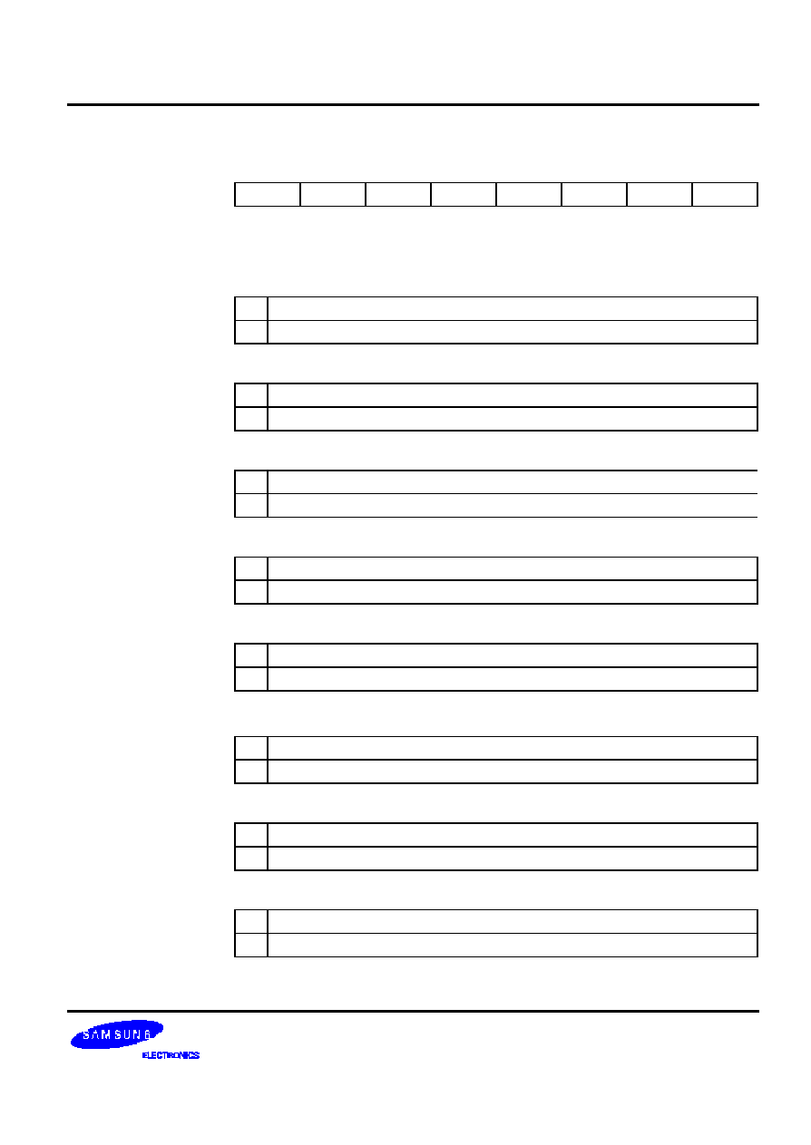
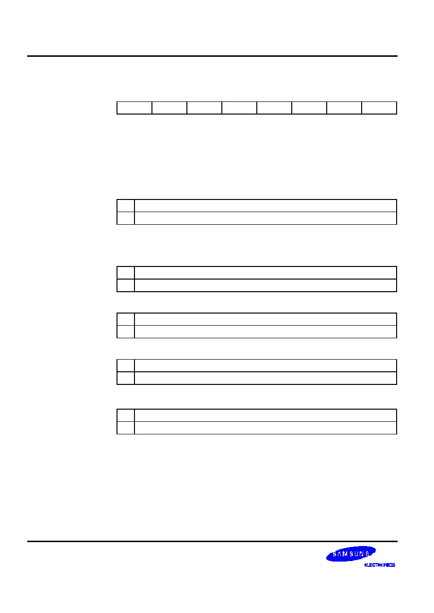
N o t u s e d f o r S 3 C 9 6 8 8 / P 9 6 8 8

S 3 C 9 6 8 8 / P 9 6 8 8
CONTROL REGISTERS
4 -2 3
P 0 C O N H
-- P o r t 0 C o n t r o l R e g i s t e r ( H i g h B y t e )
E 6 H
B i t I d e n t i f i e r
. 7
. 6
. 5
. 4
. 3
. 2
. 1
. 0
RESET
V a l u e
0
0
0
0
0
0
0
0
R e a d / W r i t e
R / W
R / W
R / W
R / W
R / W
R / W
R / W
R / W
. 7 a n d . 6
P o r t 0 , P 0 . 7 C o n f i g u r a t i o n B i t s
0
0
Schmitt trigger input, rising edge external interrupt
0
1
Schmitt trigger input, falling edge external interrupt with pull-u p
1
0
N -C H o p e n d r a i n o u t p u t m o d e
1
1
N -C H o p e n d r a i n o u t p u t m o d e w i t h p u l l -u p
. 5 a n d . 4
P o r t 0 , P 0 . 6 C o n f i g u r a t i o n B i t s
0
0
Schmitt trigger input, rising edge external interrupt
0
1
Schmitt trigger input, falling edge external interrupt with pull-u p
1
0
N -C H o p e n d r a i n o u t p u t m o d e
1
1
N -C H o p e n d r a i n o u t p u t m o d e w i t h p u l l -u p
. 3 a n d . 2
P o r t 0 , P 0 . 5 C o n f i g u r a t i o n B i t s
0
0
Schmitt trigger input, rising edge external interrupt
0
1
S c h m i t t t r i g g e r i n p u t , f a lling edge external interrupt with pull-u p
1
0
N -C H o p e n d r a i n o u t p u t m o d e
1
1
N -C H o p e n d r a i n o u t p u t m o d e w i t h p u l l -u p
. 1 a n d . 0
P o r t 0 , P 0 . 4 C o n f i g u r a t i o n B i t s
0
0
Schmitt trigger input, rising edge external interrupt
0
1
Schmitt trigger input, falling edge external interrupt with pull-u p
1
0
N -C H o p e n d r a i n o u t p u t m o d e
1
1
N -C H o p e n d r a i n o u t p u t m o d e w i t h p u l l -u p

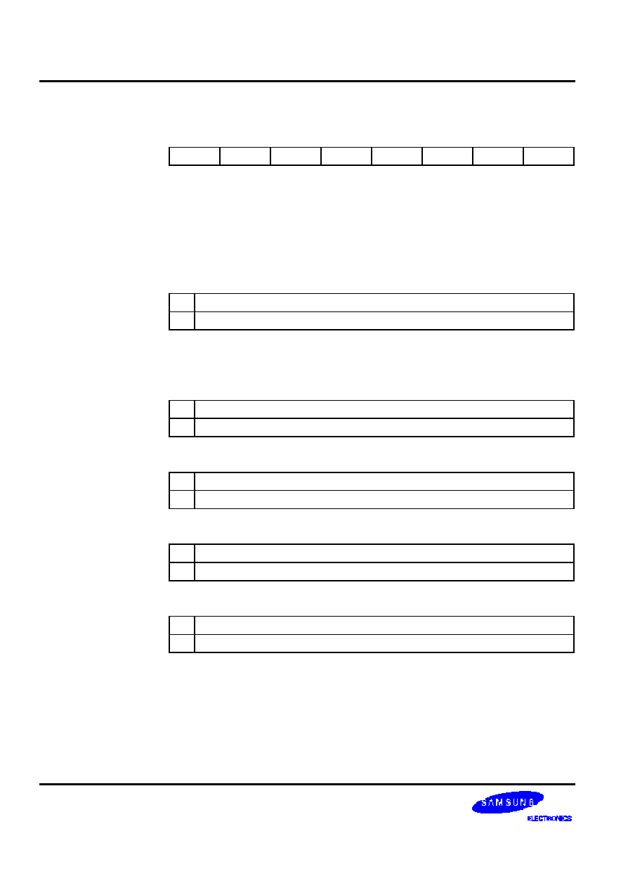
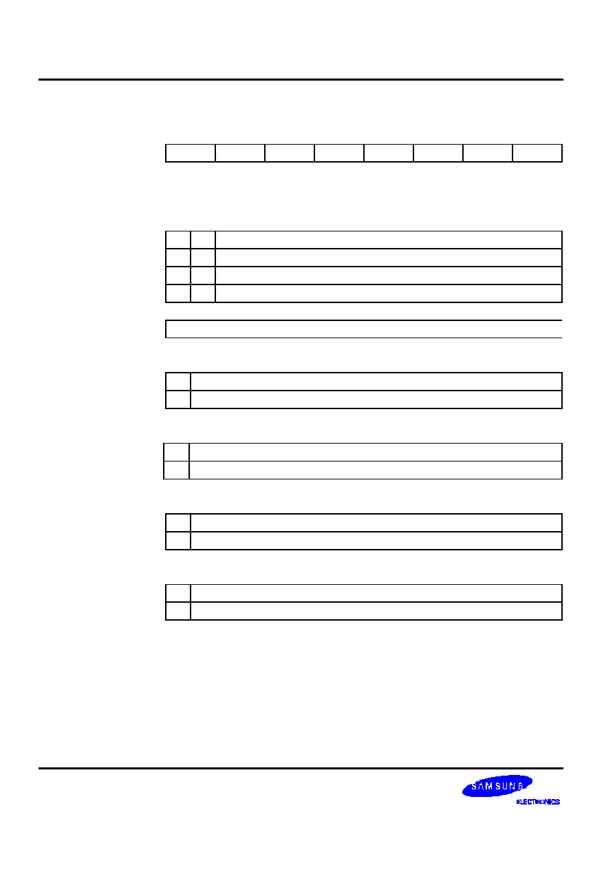
CONTROL REGISTERS
S 3 C 9 6 8 8 / P 9 6 8 8
4 -2 4
P 0 C O N L
-- P o r t 0 C o n t r o l R e g i s t e r ( L o w B y t e )
E 7 H
B i t I d e n t i f i e r
. 7
. 6
. 5
. 4
. 3
. 2
. 1
. 0
RESET
V a l u e
0
0
0
0
0
0
0
0
R e a d / W r i t e
R / W
R / W
R / W
R / W
R / W
R / W
R / W
R / W
. 7 a n d . 6
P o r t 0 , P 0 . 3 C o n f i g u r a t i o n B i t s
0
0
Schmitt trigger input, rising edge external interrupt
0
1
Schmitt trigger input, falling edge external interrupt with pull-u p
1
0
N -C H o p e n d r a i n o u t p u t m o d e
1
1
N -C H o p e n d r a i n o u t p u t m o d e w i t h p u l l -u p
. 5 a n d . 4
P o r t 0 , P 0 . 2 C o n f i g u r a t i o n B i t s
0
0
Schmitt trigger input, rising edge external interrupt
0
1
Schmitt trigger input, falling edge external interrupt with pull-u p
1
0
N -C H o p e n d r a i n o u t p u t m o d e
1
1
N -C H o p e n d r a i n o u t p u t m o d e w i t h p u l l -u p
. 3 a n d . 2
P o r t 0 , P 0 . 1 C o n f i g u r a t i o n B i t s
0
0
Schmitt trigger input, rising edge external interrupt
0
1
Schmitt trigger input, falling edge external interrupt with pull-u p
1
0
N -C H o p e n d r a i n o u t p u t m o d e
1
1
N -C H o p e n d r a i n o u t p u t m o d e w i t h p u l l -u p
. 1 a n d . 0
P o r t 0 , P 0 . 0 C o n f i g u r a t i o n B i t s
0
0
Schmitt trigger input, rising edge external interrupt
0
1
Schmitt trigger input, falling edge external interrupt with pull-u p
1
0
N -C H o p e n d r a i n o u t p u t m o d e
1
1
N -C H o p e n d r a i n o u t p u t m o d e w i t h p u l l -u p
S 3 C 9 6 8 8 / P 9 6 8 8
CONTROL REGISTERS
4 -2 5
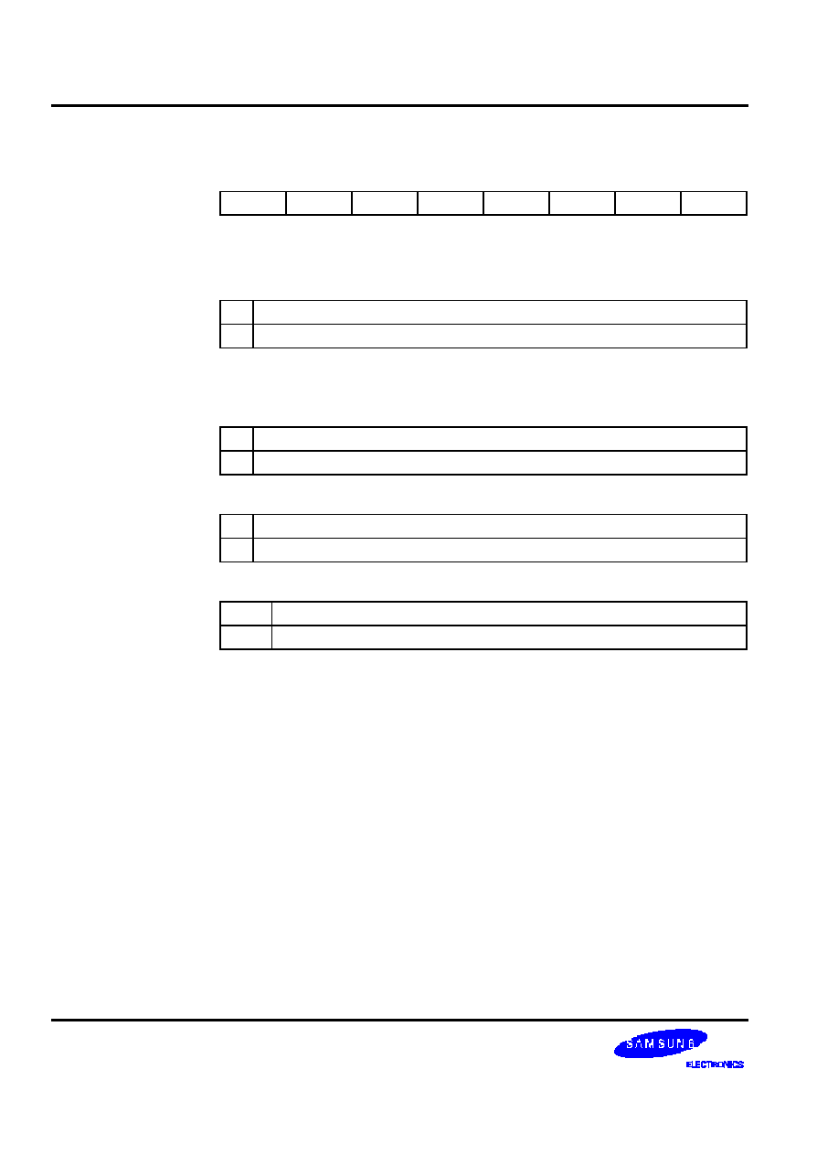
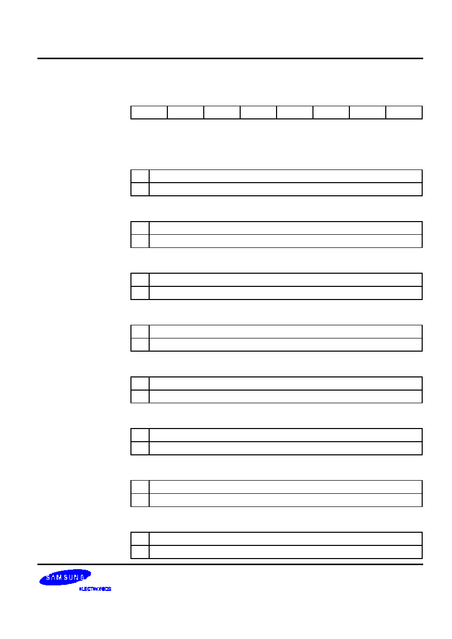
P0INT
-- Port 0 Interrupt Control Register
D 8 H
B i t I d e n t i f i e r
. 7
. 6
. 5
. 4
. 3
. 2
. 1
. 0
RESET
V a l u e
0
0
0
0
0
0
0
0
R e a d / W r i t e
R / W
R / W
R / W
R / W
R / W
R / W
R / W
R / W
. 7
P 0 . 7 C o n f i g u r a t i o n B i t s
0
External interrupt disable
1
External interrupt enable
. 6
P 0 . 6 C o n f i g u r a t i o n B i t s
0
External interrupt disable
1
External interrupt enable
. 5
P 0 . 5 C o n f i g u r a t i o n B i t s
0
External interrupt dis able
1
External interrupt enable
. 4
P 0 . 4 C o n f i g u r a t i o n B i t s
0
External interrupt disable
1
External interrupt enable
. 3
P 0 . 3 C o n f i g u r a t i o n B i t s
0
External interrupt disable
1
External interrupt enable
. 2
P 0 . 2 C o n f i g u r a t i o n B i t s
0
External interrupt disable
1
External interrupt enable
. 1
P 0 . 1 C o n f i g u r a t i o n B i t s
0
External interrupt disable
1
External interrupt enable
. 0
P 0 . 0 C o n f i g u r a t i o n B i t s
0
External interrupt disable
1
External interrupt enable

CONTROL REGISTERS
S 3 C 9 6 8 8 / P 9 6 8 8
4 -2 6

S 3 C 9 6 8 8 / P 9 6 8 8
CONTROL REGISTERS
4 -2 7
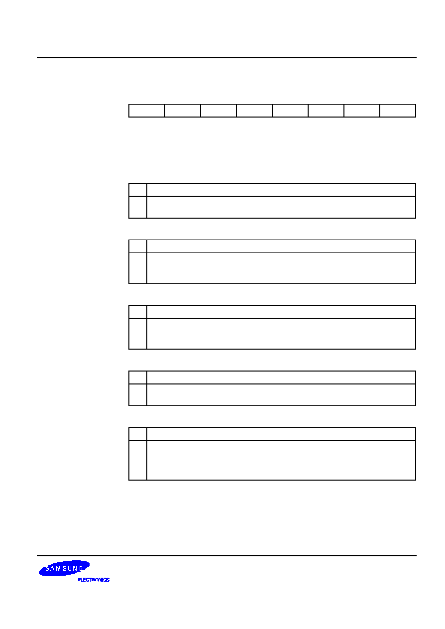
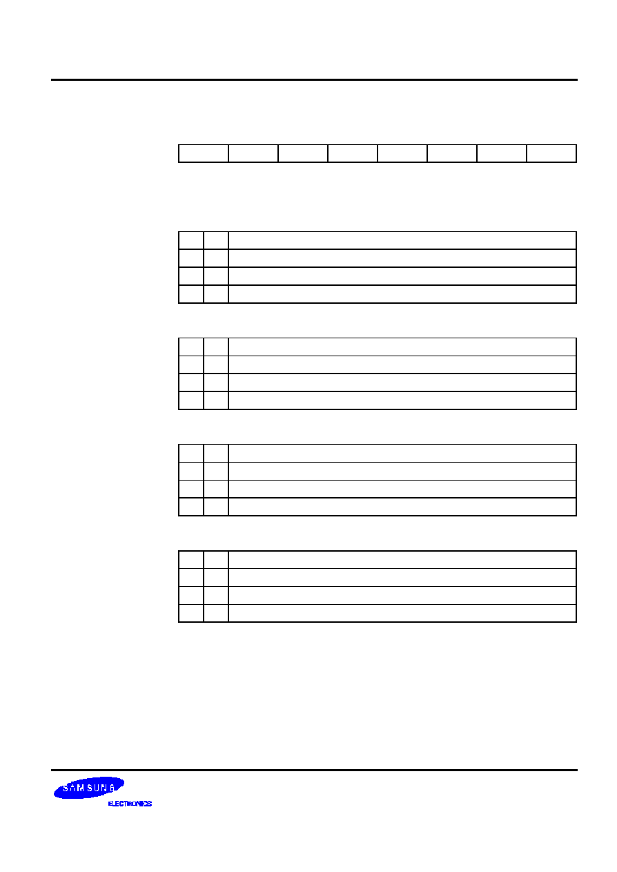
P 0 P N D
-- Port 0 Inte r r u p t P e n d i n g R e g i s t e r
D A H
B i t I d e n t i f i e r
. 7
. 6
. 5
. 4
. 3
. 2
. 1
. 0
RESET
V a l u e
0
0
0
0
0
0
0
0
R e a d / W r i t e
(NOTE)
R / W
R / W
R / W
R / W
R / W
R / W
R / W
R / W
. 7
P 0 . 7 I n t e r r u p t P e n d i n g B i t
0
N o p e n d i n g ( w h e n r e a d ) / c l e a r p e n d i n g b i t ( w h e n w r i t e )
1
Pending (when read)/no effect (when write)
. 6
P 0 . 6 I n t e r r u p t P e n d i n g B i t
0
N o p e n d i n g ( w h e n r e a d ) / c l e a r p e n d i n g b i t ( w h e n w r i t e )
1
Pending (when read)/no effect (when write)
. 5
P 0 . 5 I n t e r r u p t P e n d i n g B i t
0
N o p e n d i n g ( w h e n r e a d ) / c l e a r p e n d i n g b i t ( w h e n w r i t e )
1
Pending (when read)/no effect (when write)
. 4
P 0 . 4 I n t e r r u p t P e n d i n g B i t
0
N o p e n d i n g ( w h e n r e a d ) / c l e a r p e n d i n g b i t ( w h e n w r i t e )
1
Pending (when read)/no effect (when write)
. 3
P 0 . 3 I n t e r r u p t P e n d i n g B i t
0
N o p e n d i n g ( w h e n r e a d ) / c l e a r p e n d i n g b i t ( w h e n w r i t e )
1
Pending (when read)/no effect (when write)
. 2
P 0 . 2 I n t e r r u p t P e n d i n g B i t
0
N o p e n d i n g ( w h e n r e a d ) / c l e a r p e n d i n g b i t ( w h e n w r i t e )
1
Pending (when read)/no effect (when w rite)
. 1
P 0 . 1 I n t e r r u p t P e n d i n g B i t
0
N o p e n d i n g ( w h e n r e a d ) / c l e a r p e n d i n g b i t ( w h e n w r i t e )
1
Pending (when read)/no effect (when write)
. 0
P 0 . 0 I n t e r r u p t P e n d i n g B i t
0
N o p e n d i n g ( w h e n r e a d ) / c l e a r p e n d i n g b i t ( w h e n w r i t e )
1
Pending (when read)/no effect (when write)

CONTROL REGISTERS
S 3 C 9 6 8 8 / P 9 6 8 8
4 -2 8
S 3 C 9 6 8 8 / P 9 6 8 8
CONTROL REGISTERS
4 -2 9
P 1 C O N H
-- P o r t 1 C o n t r o l R e g i s t e r ( H i g h B y t e )
E 8 H
B i t I d e n t i f i e r
. 7
. 6
. 5
. 4
. 3
. 2
. 1
. 0
RESET
V a l u e
0
0
0
0
0
0
0
0
R e a d / W r i t e
R / W
R / W
R / W
R / W
R / W
R / W
R / W
R / W
. 7 a n d . 6
P o r t 1 , P 1 . 7 C o n f i g u r a t i o n B i t s
0
0
S c h m i t t t r i g g e r i n p u t
0
1
S c h m i t t t r i g g e r i n p u t w i t h p u l l -u p
1
0
N -C H o p e n d r a i n o u t p u t m o d e
1
1
N -C H o p e n d r a i n o u t p u t m o d e w i t h p u l l -u p
. 5 a n d . 4
P o r t 1 , P 1 . 6 C o n f i g u r a t i o n B i t s
0
0
S c h m i t t t r i g g e r i n p u t
0
1
S c h m i t t t r i g g e r i n p u t w i t h p u l l -u p
1
0
N -C H o p e n d r a i n o u t p u t m o d e
1
1
N -C H o p e n d r a i n o u t p u t m o d e w i t h p u l l -u p
. 3 a n d . 2
P o r t 1 , P 1 . 5 C o n f i g u r a t i o n B i t s
0
0
S c h m i t t t r i g g e r i n p u t
0
1
S c h m i t t t r i g g e r i n p u t w i t h p u l l -u p
1
0
N -C H o p e n d r a i n o u t p u t m o d e
1
1
N -C H o p e n d r a i n o u t p u t m o d e w i t h p u l l -u p
. 1 a n d . 0
P o r t 1 , P 1 . 4 C o n f i g u r a t i o n B i t s
0
0
S c h m i t t t r i g g e r i n p u t
0
1
S c h m i t t t r i g g e r i n p u t w i t h p u l l -u p
1
0
N -C H o p e n d r a i n o u t p u t m o d e
1
1
N -C H o p e n d r a i n o u t p u t m o d e w i t h p u l l -u p
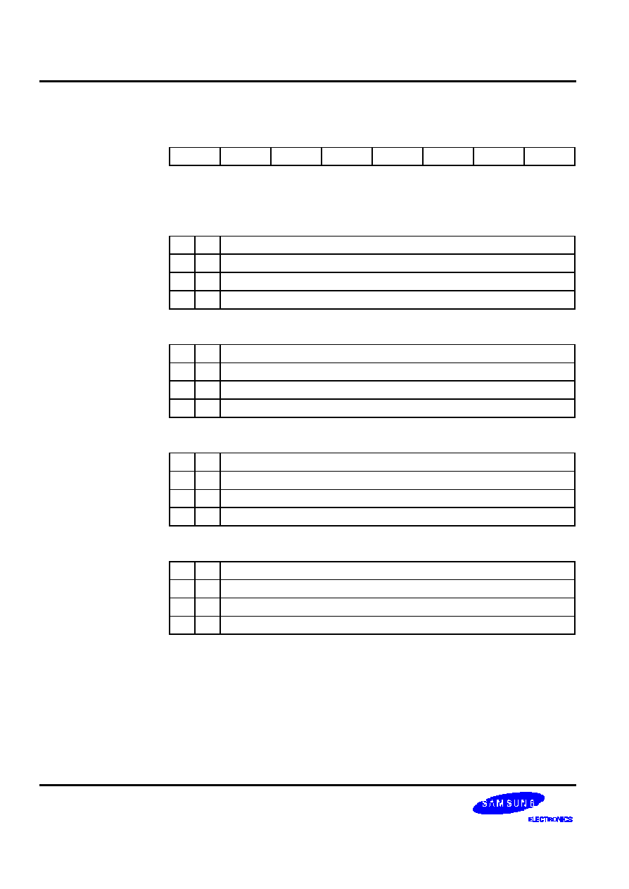
CONTROL REGISTERS
S 3 C 9 6 8 8 / P 9 6 8 8
4 -3 0
P 1 C O N L
-- P o r t 1 C o n t r o l R e g i s t e r ( L o w B y t e )
E 9 H
B i t I d e n t i f i e r
. 7
. 6
. 5
. 4
. 3
. 2
. 1
. 0
RESET
V a l u e
0
0
0
0
0
0
0
0
R e a d / W r i t e
R / W
R / W
R / W
R / W
R / W
R / W
R / W
R / W
. 7 a n d . 6
P o r t 1 , P 1 . 3 C o n f i g u r a t i o n B i t s
0
0
S c h m i t t t r i g g e r i n p u t
0
1
S c h m i t t t r i g g e r i n p u t w i t h p u l l -u p
1
0
N -C H o p e n d r a i n o u t p u t m o d e
1
1
N -C H o p e n d r a i n o u t p u t m o d e w i t h p u l l -u p
. 5 a n d . 4
P o r t 1 , P 1 . 2 C o n f i g u r a t i o n B i t s
0
0
S c h m i t t t r i g g e r i n p u t
0
1
S c h m i t t t r i g g e r i n p u t w i t h p u l l -u p
1
0
N -C H o p e n d r a i n o u t p u t m o d e
1
1
N -C H o p e n d r a i n o u t p u t m o d e w i t h p u l l -u p
. 3 a n d . 2
P o r t 1 , P 1 . 1 C o n f i g u r a t i o n B i t s
0
0
S c h m i t t t r i g g e r i n p u t
0
1
S c h m i t t t r i g g e r i n p u t w i t h p u l l -u p
1
0
N -C H o p e n d r a i n o u t p u t m o d e
1
1
N -C H o p e n d r a i n o u t p u t m o d e w i t h p u l l -u p
. 1 a n d . 0
P o r t 1 , P 1 . 0 C o n f i g u r a t i o n B i t s
0
0
S c h m i t t t r i g g e r i n p u t
0
1
S c h m i t t t r i g g e r i n p u t w i t h p u l l -u p
1
0
N -C H o p e n d r a i n o u t p u t m o d e
1
1
N -C H o p e n d r a i n o u t p u t m o d e w i t h p u l l -u p

S 3 C 9 6 8 8 / P 9 6 8 8
CONTROL REGISTERS
4 -3 1
P 2 C O N H
-- P o r t 2 C o n t r o l R e g i s t e r ( H i g h B y t e )
E A H
B i t I d e n t i f i e r
. 7
. 6
. 5
. 4
. 3
. 2
. 1
. 0
RESET
V a l u e
0
0
0
0
0
0
0
0
R e a d / W r i t e
R / W
R / W
R / W
R / W
R / W
R / W
R / W
R / W
. 7 a n d . 6
P o r t 2 , P 2 . 7 C o n f i g u r a t i o n B i t s
0
0
S c h m itt trigger input, rising edge external interrupt
0
1
Schmitt trigger input, falling edges external interrupt with pull-u p
1
0
N -C H o p e n d r a i n o u t p u t m o d e
1
1
N -C H o p e n d r a i n o u t p u t m o d e w i t h p u l l -u p
. 5 a n d . 4
P o r t 2 , P 2 . 6 C o n f i g u r a t i o n B i t s
0
0
Schmitt trigger input, rising edge external interrupt
0
1
Schmitt trigger input, falling edges external interrupt with pull-u p
1
0
N -C H o p e n d r a i n o u t p u t m o d e
1
1
N -C H o p e n d r a i n o u t p u t m o d e w i t h p u l l -u p
. 3 a n d . 2
P o r t 2 , P 2 . 5 C o n f i g u r a t i o n B i t s
0
0
Schmitt trigger input, rising edge external interrupt
0
1
Schmitt trigger input, falling edges external interrupt with pull-u p
1
0
N -C H o p e n d r a i n o u t p u t m o d e
1
1
N -C H o p e n d r a i n o u t p u t m o d e w i t h p u l l -u p
. 1 a n d . 0
P o r t 2 , P 2 . 4 C o n f i g u r a t i o n B i t s
0
0
Schmitt trigger input, rising edge external interrupt
0
1
Schmitt trigger input, falling edges external interrupt with pull-u p
1
0
N -C H o p e n d r a i n o u t p u t m o d e
1
1
N -C H o p e n d r a i n o u t p u t m o d e w i t h p u l l -u p

CONTROL REGISTERS
S 3 C 9 6 8 8 / P 9 6 8 8
4 -3 2
P 2 C O N L
-- Port 2 Control Registe r ( L o w B y t e )
E B H
B i t I d e n t i f i e r
. 7
. 6
. 5
. 4
. 3
. 2
. 1
. 0
RESET
V a l u e
0
0
0
0
0
0
0
0
R e a d / W r i t e
R / W
R / W
R / W
R / W
R / W
R / W
R / W
R / W
. 7 a n d . 6
P o r t 2 , P 2 . 3 C o n f i g u r a t i o n B i t s
0
0
Schmitt trigger input, rising edge external interrupt
0
1
Schmitt trigger input, falling edges external interrupt with pull-u p
1
0
N -C H o p e n d r a i n o u t p u t m o d e
1
1
N -C H o p e n d r a i n o u t p u t m o d e w i t h p u l l -u p
. 5 a n d . 4
P o r t 2 , P 2 . 2 C o n f i g u r a t i o n B i t s
0
0
S c h m i t t t r i g g e r input, rising edge external interrupt
0
1
Schmitt trigger input, falling edges external interrupt with pull-u p
1
0
N -C H o p e n d r a i n o u t p u t m o d e
1
1
N -C H o p e n d r a i n o u t p u t m o d e w i t h p u l l -u p
. 3 a n d . 2
P o r t 2 , P 2 . 1 C o n f i g u r a t i o n B i t s
0
0
Schmitt trigger input, rising edge external interrupt
0
1
Schmitt trigger input, falling edges external interrupt with pull-u p
1
0
N -C H o p e n d r a i n o u t p u t m o d e
1
1
N -C H o p e n d r a i n o u t p u t m o d e w i t h p u l l -u p
. 1 a n d . 0
P o r t 2 , P 2 . 0 C o n f i g u r a t i o n B i t s
0
0
S c h m itt trigger input, rising edge external interrupt
0
1
Schmitt trigger input, falling edges external interrupt with pull-u p
1
0
N -C H o p e n d r a i n o u t p u t m o d e
1
1
N -C H o p e n d r a i n o u t p u t m o d e w i t h p u l l -u p

S 3 C 9 6 8 8 / P 9 6 8 8
CONTROL REGISTERS
4 -3 3
P2INT
-- Port 2 Interrupt Enable Register
E C H
B i t I d e n t i f i e r
. 7
. 6
. 5
. 4
. 3
. 2
. 1
. 0
RESET
V a l u e
0
0
0
0
0
0
0
0
R e a d / W r i t e
R / W
R / W
R / W
R / W
R / W
R / W
R / W
R / W
. 7
P 2 . 7 I n t e r r u p t E n a b l e B i t
0
External interrupt disable
1
External interrupt enable
. 6
P 2 . 6 I n t e r r u p t E n a b l e B i t
0
External interrupt disable
1
External interrupt enable
. 5
P 2 . 5 I n t e r r u p t E n a b l e B i t
0
External interrupt disable
1
External interrupt enable
. 4
P 2 . 4 I n t e r r u p t E n a b l e B i t
0
External interrupt disable
1
External interrupt enable
. 3
P 2 . 3 I n t e r r u p t E n a b l e B i t
0
External interrupt disable
1
External interrupt enable
. 2
P 2 . 2 I n t e r r u p t E n a b l e B i t
0
External interrupt disable
1
External interrupt enable
. 1
P 2 . 1 I n t e r r u p t E n a b l e B i t
0
E x t e r n a l i nterrupt disable
1
External interrupt enable
. 0
P 2 . 0 I n t e r r u p t E n a b l e B i t
0
External interrupt disable
1
External interrupt enable

CONTROL REGISTERS
S 3 C 9 6 8 8 / P 9 6 8 8
4 -3 4
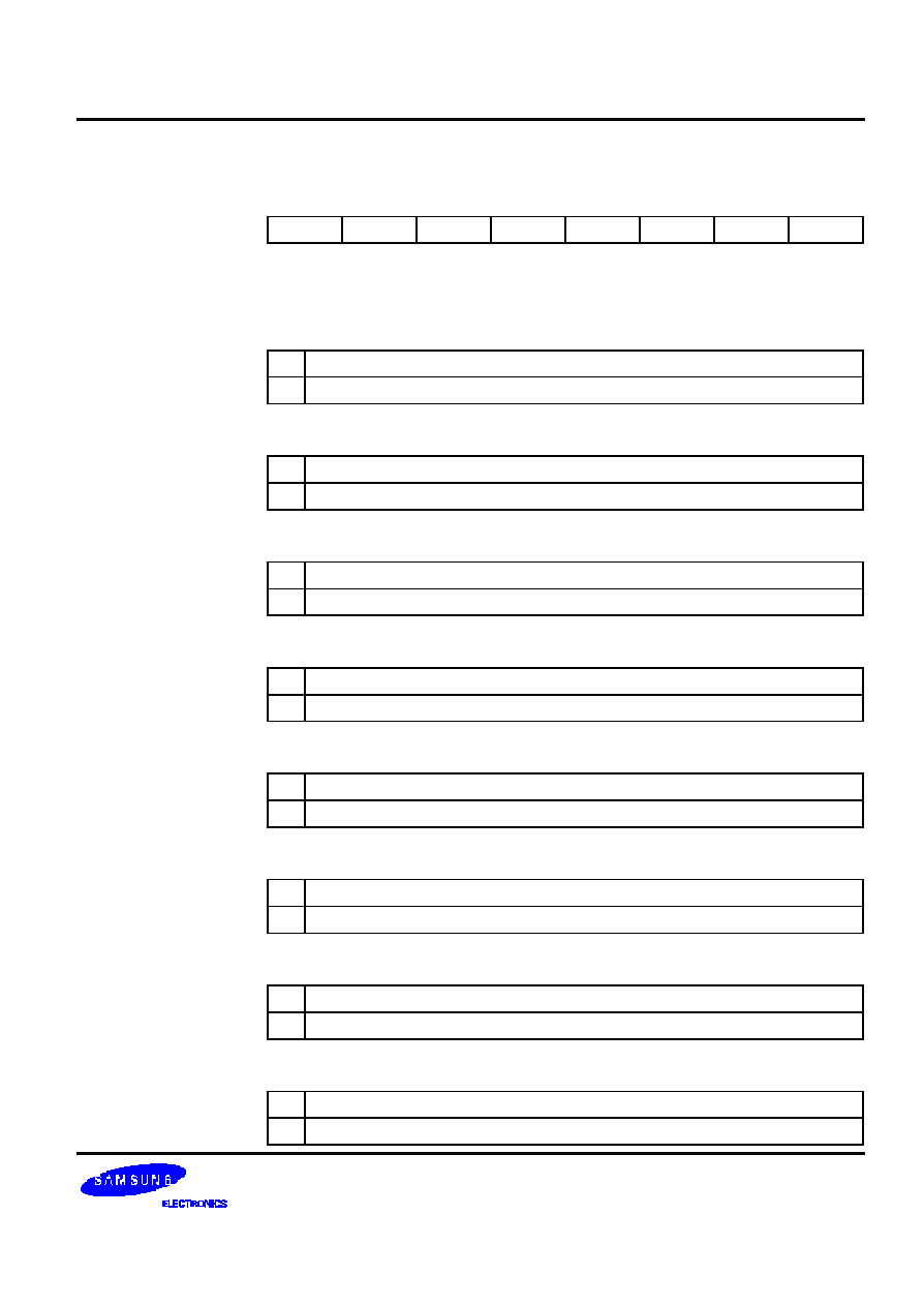
S 3 C 9 6 8 8 / P 9 6 8 8
CONTROL REGISTERS
4 -3 5
P 2 P N D
-- Port 2 Interrupt Pending Register
E D H
B i t I d e n t i f i e r
. 7
. 6
. 5
. 4
. 3
. 2
. 1
. 0
RESET
V a l u e
0
0
0
0
0
0
0
0
R e a d / W r i t e (NOTE)
R / W
R / W
R / W
R / W
R / W
R / W
R / W
R / W
. 7
P 2 . 7 I n t e r r u p t P e n d i n g B i t
0
N o p e n d i n g ( w h e n r e a d ) / c l e a r p e n d i n g b i t ( w h e n w r i t e )
1
Pending (when read)/no effect (when write)
. 6
P 2 . 6 I n t e r r u p t P e n d i n g B i t
0
N o p e n d i n g ( w h e n r e a d ) / c l e a r p e n d i n g b i t ( w h e n w r i t e )
1
Pending (when read)/no effect (when write)
. 5
P 2 . 5 I n t e r r u p t P e n d i n g B i t
0
N o p e n d i n g ( w h e n r e a d ) / c l e a r p e n d i n g b i t ( w h e n w r i t e )
1
Pending (when read)/no effect (when write)
. 4
P 2 . 4 I n t e r r u p t P e n d i n g B i t
0
N o p e n d i n g ( w h e n r e a d ) / c l e a r p e n d i n g b i t ( w h e n w r i t e )
1
Pending (when read)/no effect (when write)
. 3
P 2 . 3 I n t e r r u p t P e n d i n g B i t
0
N o p e n d i n g ( w h e n r e a d ) / c l e a r p e n d i n g b i t ( w h e n w r i t e )
1
P e n d i n g ( w h e n read)/no effect (when write)
. 2
P 2 . 2 I n t e r r u p t P e n d i n g B i t
0
N o p e n d i n g ( w h e n r e a d ) / c l e a r p e n d i n g b i t ( w h e n w r i t e )
1
Pending (when read)/no effect (when write)
. 1
P 2 . 1 I n t e r r u p t P e n d i n g B i t
0
N o p e n d i n g ( w h e n r e a d ) / c l e a r p e n d i n g b i t ( w h e n w r i t e )
1
Pending (when read)/no effect (when write)
. 0
P 2 . 0 I n t e r r u p t P e n d i n g B i t
0
N o p e n d i n g ( w h e n r e a d ) / c l e a r p e n d i n g b i t ( w h e n w r i t e )
1
Pending (when read)/no effect (when write)

CONTROL REGISTERS
S 3 C 9 6 8 8 / P 9 6 8 8
4 -3 6
NOTE
: To clear a port 2 interrupt pending condition, write a "0" to the corresponding P2PND register bit location.
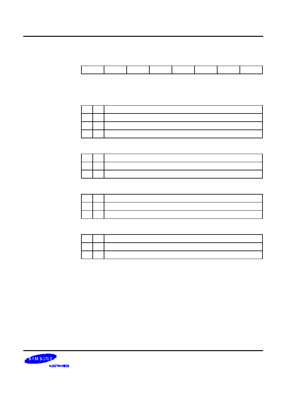
S 3 C 9 6 8 8 / P 9 6 8 8
CONTROL REGISTERS
4 -3 7
P 3 C O N
-- Port 3 Control Register
E 5 H
B i t I d e n t i f i e r
. 7
. 6
. 5
. 4
. 3
. 2
. 1
. 0
RESET
V a l u e
0
0
0
0
0
0
0
0
R e a d / W r i t e
R / W
R / W
R / W
R / W
R / W
R / W
R / W
R / W
. 7 a n d . 6
P o r t 3 , P 3 . 3 C o n f i g u r a t i o n B i t s
0
0
S c h m i t t t r i g g e r i n p u t
0
1
S y s t e m c l o c k o u t p u t ( C L O ) m o d e . C L O c o m e s f r o m s y s t e m c l o c k c i r c u i t .
1
0
P u s h-pull output
1
1
N -c h a n n e l o p e n -d r a i n o u t p u t m o d e
. 5 a n d . 4
P o r t 3 , P 3 . 2 C o n f i g u r a t i o n B i t s
0
x
S c h m i t t t r i gger input
1
0
P u s h-pull output
1
1
N -c h a n n e l o p e n -d r a i n o u t p u t m o d e
. 3 a n d . 2
P o r t 3 , P 3 . 1 C o n f i g u r a t i o n B i t s
0
x
S c h m i t t t r i g g e r i n p u t
1
0
P u s h-pull output
1
1
N -c h a n n e l o p e n -d r a i n o u t p u t m o d e
. 1 a n d . 0
P o r t 3 , P 3 . 0 C o n f i g u r a t i o n B i t s
0
x
S c h m i t t t r i g g e r i n p u t
1
0
P u s h-pull output
1
1
N -c h a n n e l o p e n -d r a i n o u t p u t m o d e
NOTE:
"x" means don't care.

CONTROL REGISTERS
S 3 C 9 6 8 8 / P 9 6 8 8
4 -3 8
P 4 C O N
-- P o r t 4 C o n t r o l R e g i s t e r
E E H
B i t I d e n t i f i e r
. 7
. 6
. 5
. 4
. 3
. 2
. 1
. 0
RESET
V a l u e
0
0
0
0
0
0
0
0
R e a d / W r i t e
R / W
R / W
R / W
R / W
R / W
R / W
R / W
R / W
. 7 a n d . 6
P o r t 4 , P 4 . 3 C o n f i g u r a t i o n C o n t r o l B i t s
0
0
Schmitt trigger input, falling edge external interrupt with pull-u p
0
1
N -C H o p e n d r a i n o u t p u t m o d e w i t h p u l l -u p
1
0
N -C H o p e n d r a i n o u t p u t m o d e
1
1
O u t p u t p u s h-p u l l m o d e
. 5 a n d . 4
P o r t 4 , P 4 . 2 C o n f i g u r a t i o n C o n t r o l B i t s
0
0
Schmitt trigger input, falling edge external interrupt with pull-u p
0
1
N -C H o p e n d r a i n o u t p u t m o d e w i t h p u l l -u p
1
0
N -C H o p e n d r a i n o u t p u t m o d e
1
1
O u t p u t p u s h -p u l l m o d e
. 3 a n d . 2
P o r t 4 , P 4 . 1 C o n f i g u r a t i o n C o n t r o l B i t s
0
0
Schmitt trigger input, falling edge external interrupt with pull-u p
0
1
N -C H o p e n d r a i n o u t p u t m o d e w i t h p u l l -u p
1
0
N -C H o p e n d r a i n o u t p u t m o d e
1
1
O u t p u t p u s h -p u l l m o d e
. 1 a n d . 0
P o r t 4 , P 4 . 0 C o n f i g u r a t i o n C o n t r o l B i t s
0
0
Schmitt trigger input, falling edge external interrupt with pull-u p
0
1
N -C H o p e n d r a i n o u t p u t m o d e w i t h p u l l -u p
1
0
N -C H o p e n d r a i n o u t p u t m o d e
1
1
O u t p u t p u s h -p u l l m o d e

S 3 C 9 6 8 8 / P 9 6 8 8
CONTROL REGISTERS
4 -3 9
P4INTPND
-- P o rt 4 I n t e r r u p t E n a b l e a n d P e n d i n g R e g i s t e r
E F H
B i t I d e n t i f i e r
. 7
. 6
. 5
. 4
. 3
. 2
. 1
. 0
RESET
V a l u e
0
0
0
0
0
0
0
0
R e a d / W r i t e
R / W
R / W
R / W
R / W
R / W
R / W
R / W
R / W
. 7
P 4 . 3 I n t e r r u p t E n a b l e B i t
0
External interrupt disable
1
External interrupt enable
. 6
P 4 . 2 I n t e r r u p t E n a b l e B i t
0
External interrupt disable
1
External interrupt enable
. 5
P 4 . 1 I n t e r r u p t E n a b l e B i t
0
External interrupt disable
1
External interrupt enable
. 4
P 4 . 0 I n t e r r u p t E n a b l e B i t
0
External interrupt disable
1
External interrupt enable
. 3
P 4 . 3 I n t e r r u p t P e n d i n g B i t
0
No pending (when bit is read)/clear pending bit (when bit is write)
1
Pending (when bit is read)/no effect (when bit is write)
. 2
P 4 . 2 I n t e r r u p t P e n d i n g B i t
0
No pending (when bit is read)/clear pending bit (when bit is write)
1
Pending (when bit is read)/no effect (when bit is write)
. 1
P 4 . 1 I n t e r r u p t P e n d i n g B i t
0
N o p e n d i n g ( w h e n b i t i s r e a d ) / c l e a r p e n d i n g b i t ( w h e n b it is write)
1
Pending (when bit is read)/no effect (when bit is write)
. 0
P 4 . 0 I n t e r r u p t P e n d i n g B i t
0
No pending (when bit is read)/clear pending bit (when bit is write)
1
Pending (when bit is read)/no effect (when bit is write)

CONTROL REGISTERS
S 3 C 9 6 8 8 / P 9 6 8 8
4 -4 0
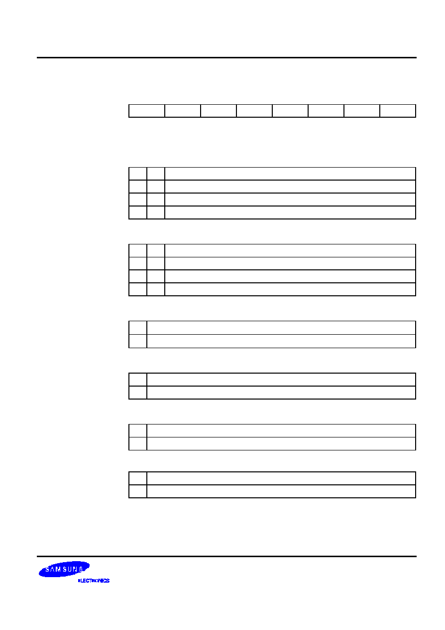
S 3 C 9 6 8 8 / P 9 6 8 8
CONTROL REGISTERS
4 -4 1
PS2CONINT
-- P S 2 C o n t r o l a n d I n t e r r u p t P e n d i n g R e g i s t e r ( P S 2 M o d e o n l y )
D 7 H
B i t I d e n t i f i e r
. 7
. 6
. 5
. 4
. 3
. 2
. 1
. 0
RESET
V a l u e
0
0
0
0
0
0
0
0
R e a d / W r i t e
R / W
R / W
R / W
R / W
R / W
R / W
R / W
R / W
. 7 a n d . 6
D + / P S 2 C o n f i g u r a t i o n C o n trol Bits
0
0
Schmitt trigger input, falling edge external interrupt
0
1
Schmitt trigger input, falling edge external interrupt with pull-u p
1
0
N -C H o p e n d r a i n o u t p u t m o d e
1
1
N -C H o p e n d r a i n o u t p u t m o d e w i t h p u l l -u p
. 5 a n d . 4
D -/ P S 2 C o n f i g u r a t i o n C o n t r o l B i t s
0
0
Schmitt trigger input, falling edge external interrupt
0
1
Schmitt trigger input, falling edge external interrupt with pull-u p
1
0
N -C H o p e n d r a i n o u t p u t m o d e
1
1
N -C H o p e n d r a i n o u t p u t m o d e w i t h p u l l -u p
. 4
D + / P S 2 I n t e r r u p t E n a b l e B i t
0
External interrupt disable
1
External interrupt enable
. 3
D -/ P S 2 I n t e r r u p t E n a b l e B i t
0
External interrupt disable
1
External interrupt enable
. 1
D + / P S 2 I n t e r r u p t P e n d i n g B i t
0
No pending (when bit is read)/clear pending bit (when bit is write)
1
Pending (when bit is read)/no effect (when bit is write)
. 0
D -/ P S 2 I n t e r r u p t P e n d i n g B i t
0
No pending (when bit is read)/clear pending bit (when bit is write)
1
Pending (when bit is read)/no effect (when bit is write)
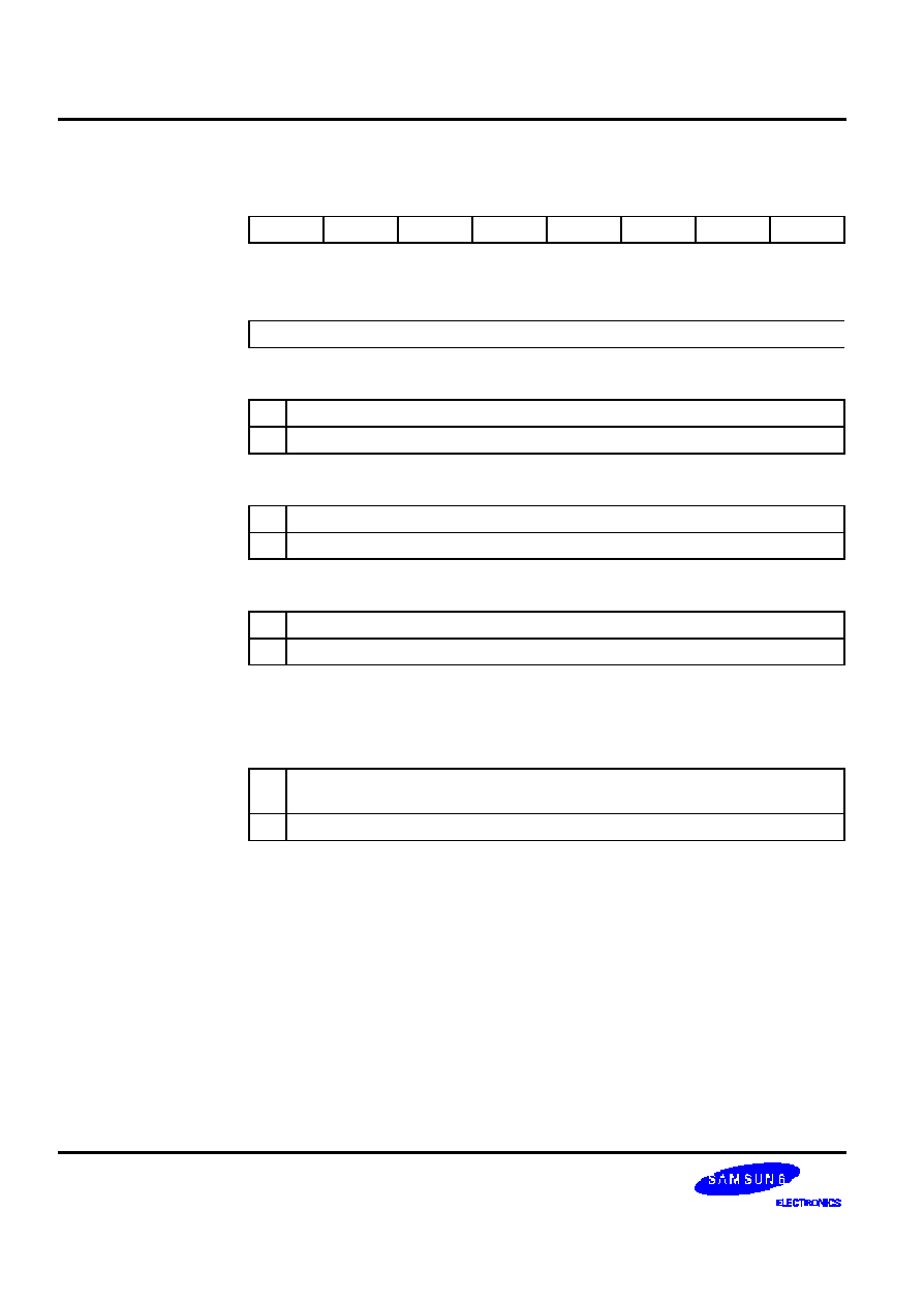
CONTROL REGISTERS
S 3 C 9 6 8 8 / P 9 6 8 8
4 -4 2
P W R M G R
-- U S B P o w e r M a n a g e m e n t R e g i s t e r
F 8 H
B i t I d e n t i f i e r
. 7
. 6
. 5
. 4
. 3
. 2
. 1
. 0
RESET
V a l u e
≠
≠
≠
0
0
0
≠
0
R e a d / W r i t e
≠
≠
≠
R / W
R / W
R / W
≠
R / W
. 7 ≠. 5
N o t u s e d f o r C 9 6 8 8 / P 9 6 8 8
. 4
D A T A + m o n i t o r i n g B i t
0
D A T A + i s z e r o
1
D A T A - i s o n e
. 3
D A T A - m o n i t o r i n g B i t
0
D A T A - is zero
1
D A T A - i s o n e
. 2
C l e a r S u s p e n d C o u n t e r B i t
0
-
1
C l e a r i n t e r n a l s u s p e n d c o u n t e r r e g i s t e r . .
. 1
N o t u s e d f o r S 3 P 9 6 8 8
. 0
S U S P E N D S t a t u s B i t
0
C l e a r e d w h e n f u n c t i o n r e c e i v e s r e s u m e s i g n a l f r o m t h e h o s t w h i l e i n s u s p e n d
m o d e
1
T h i s b i t i s s e t w h e n S U S P E N D i n t e r r u p t o c c u r
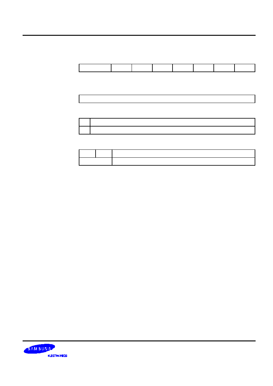
S 3 C 9 6 8 8 / P 9 6 8 8
CONTROL REGISTERS
4 -4 3
SYM
-- S y s t e m M o d e R e g i s t e r
D F H
B i t I d e n t i f i e r
.7
. 6
. 5
. 4
. 3
. 2
. 1
. 0
RESET
V a l u e
≠
≠
≠
≠
≠
0
0
0
R e a d / W r i t e
≠
≠
≠
≠
≠
R / W
R / W
R / W
. 7 ≠. 3
N o t u s e d f o r S 3 C 9 6 8 8 / P 9 6 8 8
. 2
G l o b a l I n t e r r u p t E n a b l e B i t
(note)
0
D i s a b l e g l o b a l i n t e r r u p t p r o c e s s i n g
1
E n a b l e g l o b a l i n t e r r u p t p r o c e s s i n g
. 1 a n d . 0
P a g e S e l e c t i o n B i t s
0
0
A d d r e s s i n g p a g e 0 l o c a t i o n s f o r S 3 C 9 6 8 8 / P 9 6 8 8
Other values
N o t a l l o w e d i n S 3 C 9 6 8 8 / P 9 6 8 8
NOTE
: SYM must be selected bit 1 and 0 into 00 for S3C9688/P9688.

CONTROL REGISTERS
S 3 C 9 6 8 8 / P 9 6 8 8
4 -4 4
T 0 C O N
-- T i m e r 0 C o n t r o l R e g i s t e r
D 2 H
B i t I d e n t i f i e r
. 7
. 6
. 5
. 4
. 3
. 2
. 1
. 0
RESET
V a l u e
0
0
0
0
0
0
0
0
R e a d / W r i t e
R / W
R / W
R / W
R / W
R / W
R / W
R / W
R / W
. 7 a n d . 6
T 0 C o u n t e r I n p u t C l o c k S e l e c t i o n B i t s
0
0
C P U c l o c k / 4 0 9 6
0
1
C P U c l o c k / 2 5 6
1
0
C P U c l o c k / 8
1
1
Invalid selection
. 5 a n d . 4
T 0 O p e r a t i n g M o d e S e l e c t i o n B i t s
0
0
I n t e r v a l t i m e r m o d e ( T h e c o u n t e r i s a u t o m a t i c a l l y c l e a r e d w h e n e v e r T 0 D A T A
value equals to T0CNT value)
0
1
Invalid selection
1
0
1
1
O v e r f l o w m o d e ( O V F i n t e r r u p t c a n o c c u r )
. 3
T 0 C o u n t e r C l e a r B i t ( T 0 C L R )
0
No effect when written
1
C l e a r T 0 c o u n t e r
. 2
T 0 O v e r f l o w I n t e r r u p t E n a b l e B i t ( T 0 O V F )
0
Disable T0 overflow interrupt
1
Enable T0 overflow interrupt
. 1
T 0 M a t c h I n t e r r u p t E n a b l e B i t ( T 0 I N T )
0
D i s a b l e T 0 m a t c h i n t e r r u p t
1
E n a b l e T 0 m a t c h i n t e r r u p t
. 0
T 0 I n t e r r u p t P e n d i n g B i t ( T 0 P N D )
0
No interrupt pending/Clear this pending bit (when write)
1
Interrupt is pending(when read)/No effect (when write)
NOTE
: When you write a "1" to T0CON.3, the timer 0 counter is cleared. The bit is then cleared automatically to "0".
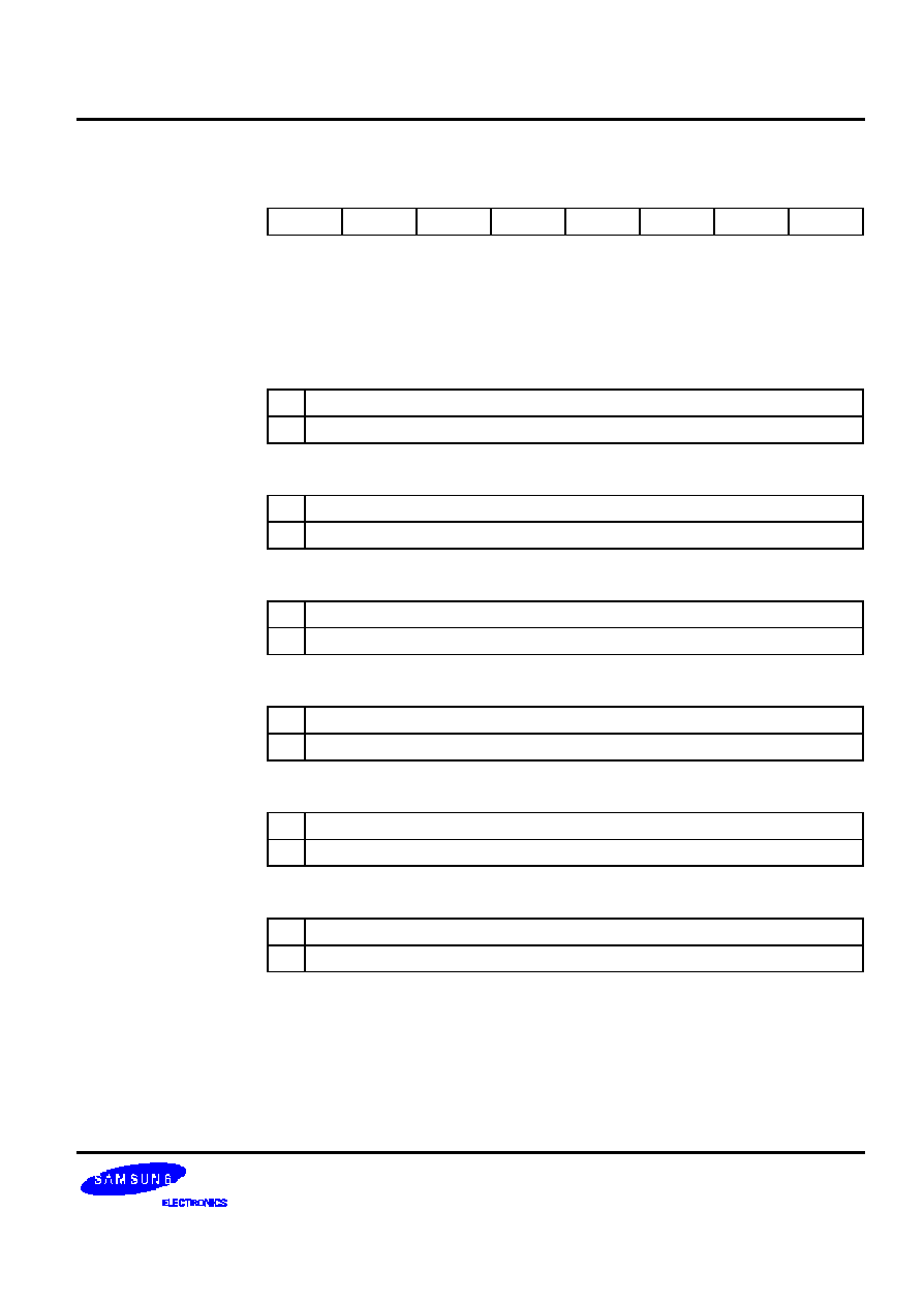
S 3 C 9 6 8 8 / P 9 6 8 8
CONTROL REGISTERS
4 -4 5
U S B C O N
-- U S B C o n t r o l R e g i s t e r
F E H
B i t I d e n t i f i e r
. 7
. 6
. 5
. 4
. 3
. 2
. 1
. 0
RESET
V a l u e
≠
≠
0
0
1
0
1
1
R e a d / W r i t e
≠
≠
R / W
R / W
R / W
R / W
R / W
R
. 7 a n d . 6
R e s e r v e d
. 5
D P / D M C o n t r o l B i t
0
D P / D M c a n n o t b e i n d i v i d u a l l y c o n t r o l l e d b y M C U
1
D P / D M c a n b e i n d i v i d u a l l y c o n t r o l l e d b y M C U t o s e t U S B C O N . 4 a n d U S B C O N . 3
. 4
D P S t a t u s B i t
0
D P i s l o w
1
D P i s h i g h
. 3
D M S t a t u s B i t
0
D M i s l o w
1
D M i s h i g h
. 2
U S B R e s e t M C U B i t
0
U S B w h i c h i s b e e n o n R E S E T c a n n o t m a k e M C U r e s e t
1
U S B w h i c h i s b e e n o n R E S E T c a n b e a b l e t o r e s e t M C U
. 1
M C U r e s e t U S B B i t
0
N o e f f e c t
1
M C U f o r c e s U S B b e r e s e t
. 0
U S B R E S E T S i g n a l R e c e i v e B i t
0
U S B R e s e t i s d e t e c t e d .
1
U S B R e s e t i s u n d e t e c t e d
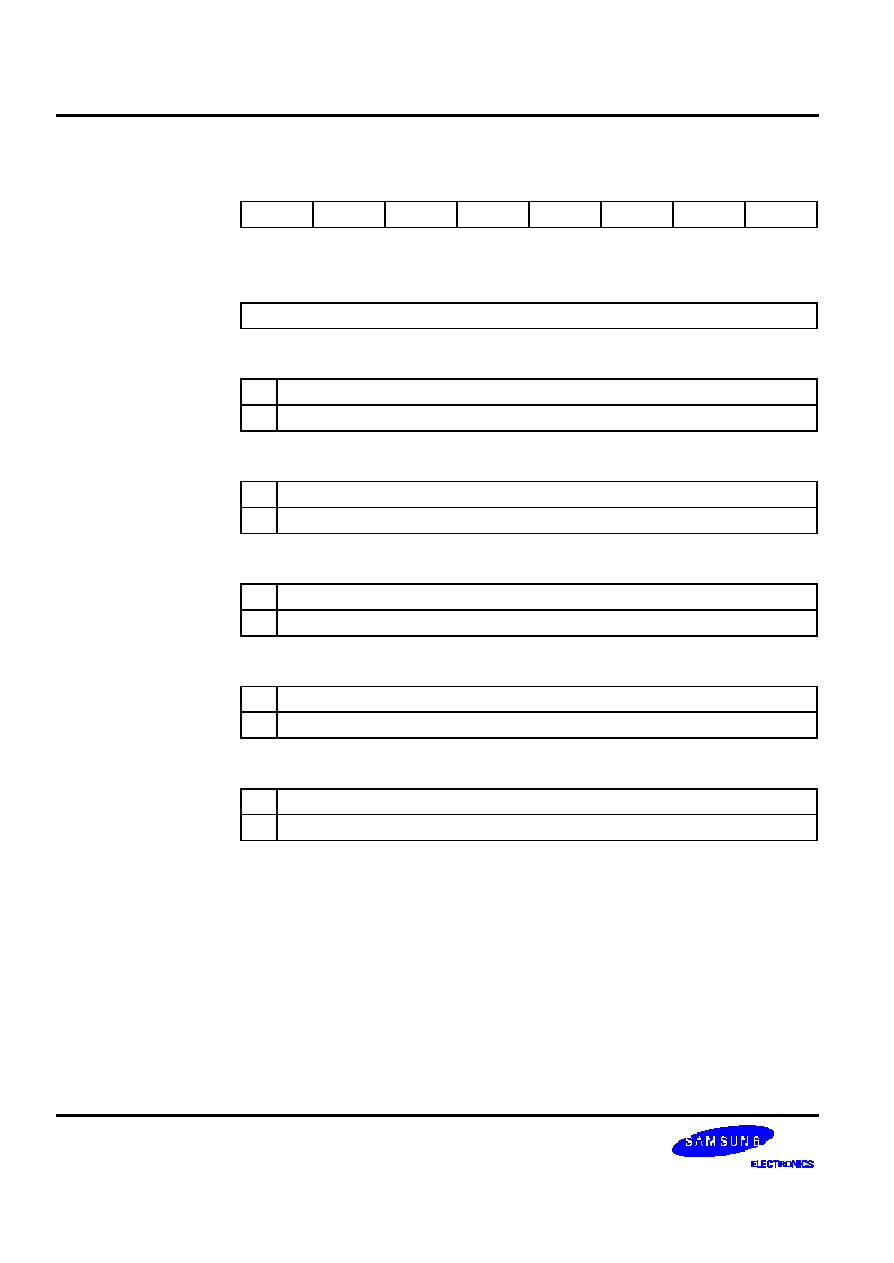
CONTROL REGISTERS
S 3 C 9 6 8 8 / P 9 6 8 8
4 -4 6
U S B I N T
-- U S B I n t e r r u p t E n a b l e R e g i s t e r
F 7 H
B i t I d e n t i f i e r
. 7
. 6
. 5
. 4
. 3
. 2
. 1
. 0
RESET
V a l u e
≠
≠
≠
0
0
0
0
0
R e a d / W r i t e
≠
≠
≠
R / W
R / W
R / W
R / W
R / W
. 7 ≠. 5
N o t u s e d f o r C 9 6 8 8 / P 9 6 8 8
. 4
U S B R e s e t I n t e r r u p t P e n d i n g B i t
0
D i s a b l e U S B R e s e t I n t e r r u p t
1
E n a b l e U S B R e s e t I n t e r r u p t
. 3
E N D P O I N T 2 I n t e r r u p t P e n d i n g B i t
0
D i s a b l e E N D P O I N T 2 i n t e r r u p t
1
E n a b l e E N D P O I N T 2 i n t e r r u p t
. 2
S U S P E N D / R E S U M E I n t e r r u p t E n a b l e B i t
0
D i s a b l e S U S P E N D a n d R E S U M E i n t e r r u p t
1
E n a b l e S U S P E N D a n d R E S U M E i n t e r r u p t
. 1
E N D P O I N T 1 I n t e r r u p t P e n d i n g B i t
0
D i s a b l e E N D P O I N T 1 i n t e r r u p t
1
E n a b l e E N D P O I N T 1 i n t e r r u p t
. 0
E N D P O I N T 0 I n t e r r u p t P e n d i n g B i t
0
D i s a b l e E N D P O I N T 0 i n t e r r u p t
1
E n a b l e E N D P O I N T 0 i n t e r r u p t
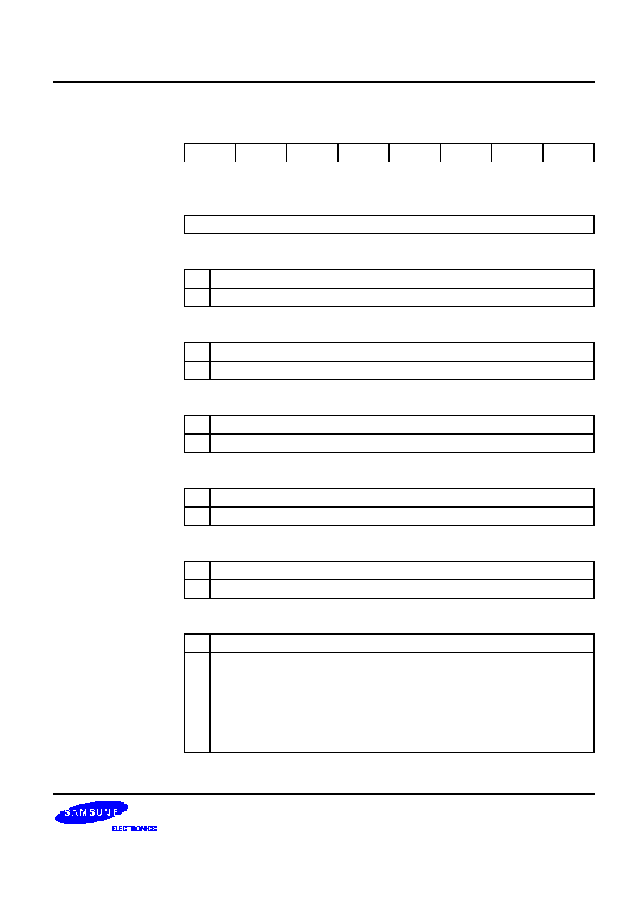
S 3 C 9 6 8 8 / P 9 6 8 8
CONTROL REGISTERS
4 -4 7
U S B P N D
-- U S B I n t e r r u p t P e n d i n g R e g i s t e r
F 6 H
B i t I d e n t i f i e r
. 7
. 6
. 5
. 4
. 3
. 2
. 1
. 0
RESET
V a l u e
≠
≠
0
0
0
0
0
0
R e a d / W r i t e
≠
≠
R / W
R / W
R / W
R / W
R / W
R / W
. 7 ≠. 6
N o t u s e d f o r C 9 6 8 8 / P 9 6 8 8
. 5
U S B R e s e t I n t e r r u p t P e n d i n g B i t
0
N o e f f e c t ( W r i t e 1 , t h i s b i t i s c l e a r e d )
1
T h i s b i t i s s e t , w h e n U S B b u s r e s e t i s d e t e c t e d o n t h e b u s .
. 4
E N D P O I N T 2 I n t e r r u p t P e n d i n g B i t
0
No effect (Write 1, this b i t i s c l e a r e d )
1
T h i s b i t i s s e t , w h e n e n d p o i n t 2 n e e d s t o b e s e r v i c e d
. 3
R E S U M E I n t e r r u p t P e n d i n g B i t
0
N o e f f e c t ( W r i t e 1 , t h i s b i t i s c l e a r e d )
1
W h i l e i n s u s p e n d m o d e , i f r e s u m e s i g n a l i n g i s r e c e i v e d t h i s b i t g e t s s e t
. 2
S U S P E N D I n t e r r u p t P e n d i n g B i t
0
N o e f f e c t ( W r i t e 1 , t h i s b i t i s c l e a r e d )
1
T h i s b i t i s s e t , w h e n s u s p e n d s i g n a l i n g i s r e c e i v e d
. 1
E N D P O I N T 1 I n t e r r u p t P e n d i n g B i t
0
N o e f f e c t ( W r i t e 1 , t h i s b i t i s c l e a r e d )
1
T h i s b i t i s s e t , w h e n e n d p o i n t 1 n e e d s t o b e s e r v i c e d
. 0
E N D P O I N T 0 I n t e r r u p t P e n d i n g B i t
0
N o e f f e c t ( W r i t e 1 , t h i s b i t i s c l e a r e d )
1
This bit is set, while endpoint 0 needs to serviced. It is set under the following
c o n d i t i o n s ;
-- O U T _ P K T _ R D Y i s s e t
-- I N _ P K T _ R D Y g e t c l e a r e d
-- S E N T _ S T A L L g e t s s e t
-- S E T U P _ D A T A _ E N D g e t s c l e a r e d
-- S E T U P _ T R A N S F E R _ E N D g e t s s e t
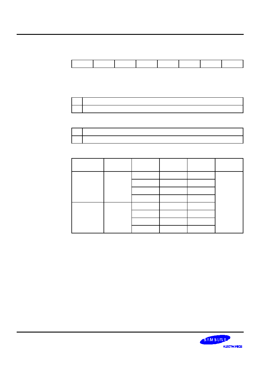
CONTROL REGISTERS
S 3 C 9 6 8 8 / P 9 6 8 8
4 -4 8
U S X C O N
-- U S B S e l e c t i o n a n d S i g n a l C r o s s o v e r P o i n t C o n t r o l R e g i s t e r
D 3 H
B i t I d e n t i f i e r
. 7
. 6
. 5
. 4
. 3
. 2
. 1
. 0
RESET
V a l u e
0
0
0
0
0
0
0
0
R e a d / W r i t e
R / W
R / W
R / W
R / W
R / W
R / W
R / W
R / W
. 7
U S B / P S 2 M o d e s e l e c t B i t
0
P S 2 M o d e
1
U S B M o d e
. 6
U S B P u l l -U p C o n t r o l r e g i s t e r
0
P u l l -U p D i s a b l e
1
P u l l -U p E n a b l e
. 5 ≠. 0
U S B S i g n a l C r o s s o v e r P o i n t C o n t r o l B i t
E d g e d e l a y
C o n t r o l
B i t 5 , ( 2 )
B i t 4 , ( 1 )
B i t 3 , ( 0 )
D e l a y
V a l u e
Delay
U n i t
0
0
0
R I S E
0
0
1
1
e d g e
1
0
2
( a b o u t )
1
1
4
2 . 5 n s e c
0
0
0
F A L L
1
0
1
1
e d g e
1
0
2
1
1
4
NOTE:
Bit 5, 4, 3: DM, Bit 2, 1, 0: DP

S 3 C 9 6 8 8 / P 9 6 8 8
CONTROL REGISTERS
4 -4 9
N O T E S
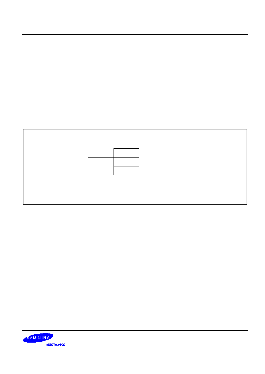
S 3 C 9 6 8 8 / P 9 6 8 8
INTERRUPT STRUCTURE
5 -1
5
I N T E R R U P T S T R U C T U R E
O V E R V I E W
T h e S A M 8 8 R C R I i n t e r r u p t s t r u c t u r e h a s t w o b a s i c c o m p o n e n t s : a v e c t o r , a n d s o u r c e s . T h e n u m b e r o f i n t e r r u p t
s o u r c e s c a n b e s e r v i c e d t h r o u g h a i n t e r r u p t v e c t o r w h i c h i s a s s i g n e d i n R O M a d d r e s s 0 0 0 0 H ≠ 0 0 0 1 H .
SOURCES
VECTOR
S1
S2
S3
Sn
0000H
0001H
NOTES:
1. The SAM88RCRI interrupt has only one vector address (0000H-0001H).
2. The number of Sn value is expandable.
F i g u r e 5 -1 . S 3 C 9 -S e r i e s I n t e r r u p t T y p e
I N T E R R U P T P R O C E S S I N G C O N T R O L P O I N T S
I n t e r r u p t p r o c e s s i n g c a n b e c o n t r o l l e d i n t w o w a y s : e i t h e r g l o b a l l y , o r b y s p e c i f i c i n t e r r u p t l e v e l a n d s o u r c e . T h e
m a j o r f e a t u r e s o f s y s t e m -level control in the interrupt structure are as follows:
--
G l o b a l i n t e r r u p t e n a b l e a n d d i s a b l e ( b y E I a n d D I i n s t r u c t i o n s )
--
Interrupt sourc e e n a b l e a n d d i s a b l e s e t t i n g s i n t h e c o r r e s p o n d i n g p e r i p h e r a l c o n t r o l r e g i s t e r ( s )
E N A B L E / D I S A B L E I N T E R R U P T I N S T R U C T I O N S ( E I , D I )
T h e s y s t e m m o d e r e g i s t e r , S Y M ( D F H ) , i s u s e d i n s e t t i n g s i n t e r r u p t p r o c e s s i n g e n a b l e d o r d i s a b l e d .
S Y M . 2 i s t h e e n a b l e a n d d i s a b l e b i t f o r g l o b a l i n t e r r u p t p r o c e s s i n g r e s p e c t i v e l y , b y m o d i f y i n g S Y M . 2 . A n E n a b l e
Interrupt (EI) instruction must be included in the initialization routine that follows a reset operation in order t o e n a b l e
i n t e r r u p t p r o c e s s i n g . A l t h o u g h y o u c a n m a n i p u l a t e S Y M . 2 d i r e c t l y t o e n a b l e a n d d i s a b l e i n t e r r u p t s d u r i n g n o r m a l
o p e r a t i o n , w e r e c o m m e n d t h a t y o u u s e t h e E I a n d D I i n s t r u c t i o n s f o r t h i s p u r p o s e .
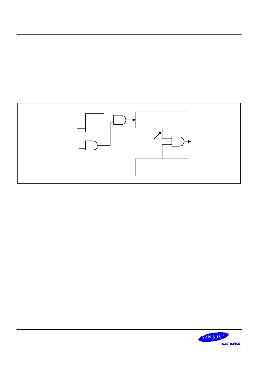
INTERRUPT STRUCTURE
S 3 C 9 6 8 8 / P 9 6 8 8
5 -2
I N T E R R U P T P E N D I N G F U N C T I O N T Y P E S
W h e n t h e i n t e r r u p t s e r v i c e r o u t i n e h a s b e e n e x e c u t e d , t h e a p p r o p r i a t e p e n d i n g b i t m u s t b e c l e a r e d i n t h e a p p l i c a t i o n
program's service routine before the return from interrupt subroutine (IRET) occurs.
I N T E R R U P T P R I O R I T Y
B e c a u s e t h e r e i s n o t a i n t e r r u p t p r i o r i t y r e g i s t e r i n S A M 8 8 R C R I , t h e o r d e r o f s e r v i c e i s d e t e r m i n e d b y a s e q u e n c e o f
s o u r c e w h i c h i s e x e c u t e d i n i n t e r r u p t s e r v i c e r o u t i n e .
Interrupt Pending Register
Global Interrupt Control
(EI, DI instruction)
Vector
Interrupt
Cycle
Interrpt priority
is determind by
software polling
method
S
R
Q
"EI" Instruction
Execution
RESET
Source
Interrupts
Source
Interrupt
Enable
F i g u r e 5 -2 . I n t e r r u p t F u n c t i o n D i a g r a m
I N T E R R U P T S O U R C E S E R V I C E S E Q U E N C E
T h e i n t e r r u p t r e q u e s t p o l l i n g a n d s e r v i c i n g s e q u e n c e i s a s f o l l o w s :
1 . A s o u r c e g e n e r a t e s a n i n t e r r u p t r e q u e s t b y s e t t i n g t h e i n t e r r u p t r e q u e s t p e n d ing bit to "1".
2 . T h e C P U g e n e r a t e s a n i n t e r r u p t a c k n o w l e d g e s i g n a l .
3 . T h e s e r v i c e r o u t i n e s t a r t s a n d t h e s o u r c e ' s p e n d i n g f l a g i s c l e a r e d t o " 0 " b y s o f t w a r e .
4 . I n t e r r u p t p r i o r i t y m u s t b e d e t e r m i n e d b y s o f t w a r e p o l l i n g m e t h o d .

S 3 C 9 6 8 8 / P 9 6 8 8
INTERRUPT STRUCTURE
5 -3
I N T E R R U P T S E R V I C E R O U T I N E S
B e f o r e a n i n t e r r u p t r e q u e s t c a n b e s e r v i c e d , t h e f o l l o w i n g c o n d i t i o n s m u s t b e m e t :
--
I n t e r r u p t p r o c e s s i n g m u s t b e e n a b l e d ( E I , S Y M . 2 = " 1 " )
--
Interrupt must be enabled at the interrupt's source (peripheral control re gister)
I f a l l o f t h e a b o v e c o n d i t i o n s a r e m e t , t h e i n t e r r u p t r e q u e s t i s a c k n o w l e d g e d a t t h e e n d o f t h e i n s t r u c t i o n c y c l e . T h e
C P U t h e n i n i t i a t e s a n i n t e r r u p t m a c h i n e c y c l e t h a t c o m p l e t e s t h e f o l l o w i n g p r o c e s s i n g s e q u e n c e :
1 . R e s e t ( c l e a r t o " 0 " ) t h e g l o b a l i n t e r r u p t e n a b l e b i t i n t h e S Y M r e g i s t e r ( D I , S Y M . 2 = " 0 " )
t o d i s a b l e a l l s u b s e q u e n t i n t e r r u p t s .
2 . S a v e t h e p r o g r a m c o u n t e r ( P C ) a n d s t a t u s f l a g s ( F L A G s ) t o s t a c k .
3 . Branch to the interrupt vector to fetch the service routine's address.
4 . P a s s c o n t r o l to the interrupt service routine.
W h e n t h e i n t e r r u p t s e r v i c e r o u t i n e i s c o m p l e t e d , a n I n t e r r u p t R e t u r n i n s t r u c t i o n ( I R E T ) o c c u r s . T h e I R E T r e s t o r e s t h e
P C a n d s t a t u s f l a g s a n d s e t s S Y M . 2 t o " 1 " ( E I ) , a l l o w i n g t h e C P U t o p r o c e s s t h e n e x t i n t e r r u p t r e q u e s t .
G E N E R A T I N G I N T E R R U P T V E C T O R A D D R E S S E S
The interrupt vector area in the ROM contains the address of the interrupt service routine. Vectored interrupt
p r o c e s s i n g f o l l o w s t h i s s e q u e n c e :
1 . P u s h t h e p r o g r a m c o u n ter's low-b y t e v a l u e t o s t a c k .
2 . P u s h t h e p r o g r a m c o u n t e r ' s h i g h -b y t e v a l u e t o s t a c k .
3 . P u s h t h e F L A G S r e g i s t e r v a l u e s t o s t a c k .
4 . Fetch the service routine's high-b y t e a d d r e s s f r o m t h e v e c t o r a d d r e s s 0 0 0 0 H .
5 . Fetch the service routine's low-b y t e a d d r e s s f r o m t h e v e c t o r a d d r e s s 0 0 0 1 H .
6 . B r a n c h t o t h e s e r v i c e r o u t i n e s p e c i f i e d b y t h e 1 6 -b i t v e c t o r a d d r e s s .
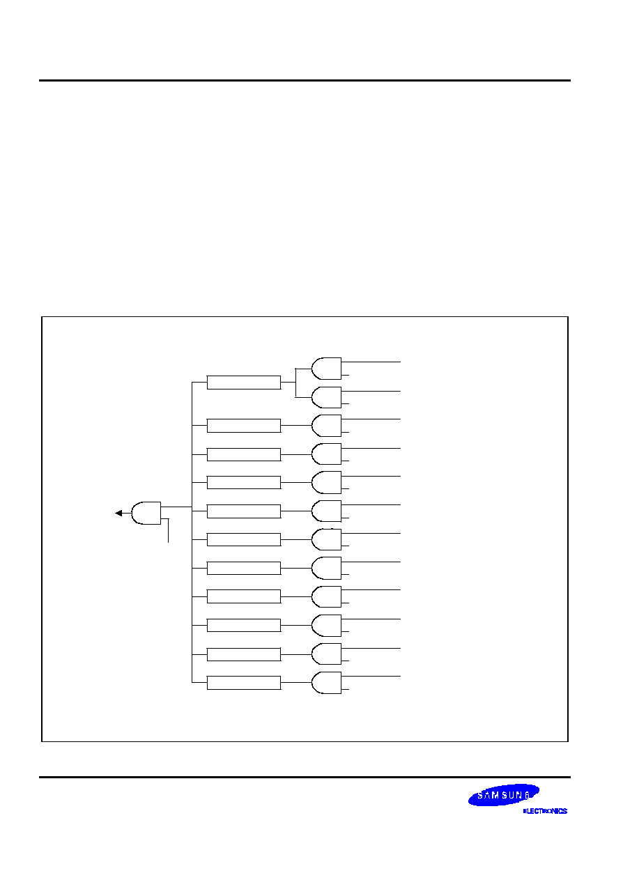
INTERRUPT STRUCTURE
S 3 C 9 6 8 8 / P 9 6 8 8
5 -4
S 3 C 9 6 8 8 / P 9 6 8 8 I N T E R R U P T S T R U C T U R E
T h e S 3 C 9 6 8 8 / P 9 6 8 8 m i c r o c o n t r o l l e r h a s 2 9 p e r i p h e r a l i n t e r r u p t s o u r c e s :
--
T i m e r 0 m a t c h i n t e r r u p t
--
Timer 0 overflow interrupt
--
Eight external interrupts for port 2, P2.0≠ P 2 . 7
--
Four external interrupts for port 4, P4.0≠ P 4 . 3
--
D -/ P S 2 a n d D + / P s 2 e x t e r n a l i n t e r r u p t s ( o n l y i n P S 2 m o d e )
--
U S B E P 0 , 1 , 2 I n t e r r u p t
--
S u s p e n d i n t e r r u p t
--
R e s u m e i n t e r r u p t
Vector
Pending Bits
0000H
(EI/DI)
SYM.2
Sources
Enable/Disable
Timer 0 Match Interrupt
Timer 0 Overflow Interrupt
P2.X External Interrupt
P4.0-3 External Interrupt
T0CON.1
T0CON.2
P0INT.X
P2INT.X
P4INTPND.4-7
P0PND.X
P2PND.X
P4INTPND.0-3
P4INTPND.0
Endpoint 0 Interrupt
Endpoint 1 Interrupt
Endpoint 2 Interrupt
Suspend Interrupt
USBINT.0
USBINT.1
USBINT.3
USBINT.2
P4INTPND.1
P4INTPND.4
USBPND.2
P0.X External Interrupt
NOTE:
"X" means 0-7 bit.
D-/PS2 Interrupt
D+/PS2 Interrupt
PS2CONINT.2
PS2CONINT.3
PS2CONINT.0
PS2CONINT.1
Resume Interrupt
USBINT.2
USBPND.3
T0CON
F i g u r e 5 -3 . S 3 C 9 6 8 8 / P 9 6 8 8 I n t e r r u p t S t r u c t u r e

S 3 C 9 6 8 8 / P 9 6 8 8
S A M 8 8RCRI INSTRUCTION SET
6 -1
6
S A M 8 8 R C R I I N S T R U C T I O N S E T
O V E R V I E W
T h e S A M 8 8 R C R I i n s t r u c t i o n s e t i s d e s i g n e d t o s u p p o r t t h e l a r g e r e g i s t e r f i l e . I t i n c l u d e s a f u l l c o m p l e m e n t o f 8 -bit
a r i t h m e t i c a n d l o g i c o p e r a t i o n s . T h e r e a r e 4 1 i n s t r u c t i o n s . N o s p e c i a l I / O i n s t r u c t i o n s a r e n e c e s s a r y b e c a u s e I / O
control and data registers are mapped directly into the register file. Flexible instructions for bit addressing, rotate,
a n d s h i f t o p e r a t i o n s c o m p l e t e t h e p o w e r f u l d a t a m a n i p u l a t i o n c a p a b i l i t i e s o f t h e S A M 8 8 R C R I i n s t r u c t i o n s e t .
R E G I S T E R A D D R E S S I N G
T o a c c e s s a n i n d i v i d u a l r e g i s t e r , a n 8 -b i t a d d r e s s i n t h e r a n g e 0 -2 5 5 o r t h e 4 -bit address of a working register is
s p e c i f i e d . P a i r e d r e g i s t e r s c a n b e u s e d t o c o n s tr u c t 1 3 -b i t p r o g r a m m e m o r y o r d a t a m e m o r y a d d r e s s e s . F o r d e t a i l e d
i n f o r m a t i o n a b o u t r e g i s t e r a d d r e s s i n g , p l e a s e r e f e r t o S e c t i o n 2 , " A d d r e s s S p a c e s " .
A D D R E S S I N G M O D E S
There are six addressing modes: Register (R), Indirect Register (IR), Indexed (X), Direct (DA), Relative (RA), and
I m m e d i a t e ( I M ) . F o r d e t a i l e d d e s c r i p t i o n s o f t h e s e a d d r e s s i n g m o d e s , p l e a s e r e f e r t o S e c t i o n 3 , " A d d r e s s i n g
M o d e s " .

SAM88RI INSTRUCTION SET
S 3 C 9 6 8 8 / P 9 6 8 8
6 -2
T a b l e 6 -1 . I n s t r u c t i o n G r o u p S u m m a r y
M n e m o n i c
O p e r a n d s
I n s t r u c t i o n
L o a d I n s t r u c t i o n s
C L R
d s t
C l e a r
L D
d s t , s r c
L o a d
L D C
d s t , s r c
L o a d p r o g r a m m e m o r y
L D E
d s t , s r c
L o a d e x t e r n a l d a t a m e m o r y
L D C D
d s t , s r c
L o a d p r o g r a m m e m o r y a n d d e c r e m e n t
L D E D
d s t , s r c
L o a d e x t e r n a l d a t a m e m o r y a n d d e c r e m e n t
L D C I
d s t , s r c
L o a d p r o g r a m m e m o r y a n d i n c r e m e n t
L D E I
d s t , s r c
L o a d e x t e r n a l d a t a m e m o r y a n d i n c r e m e n t
P O P
d s t
P o p f r o m s t a c k
P U S H
src
P u s h t o s t a c k
A r i t h m e t i c I n s t r u c t i o n s
A D C
d s t , s r c
A d d w i t h c a r r y
A D D
d s t , s r c
A d d
C P
d s t , s r c
C o m p a r e
D E C
d s t
D e c r e m e n t
INC
d s t
I n c r e m e n t
S B C
d s t , s r c
S u b t r a c t w i t h c a r r y
S U B
d s t , s r c
S u b t r a c t
L o g i c I n s t r u c t i o n s
A N D
d s t , s r c
L o g i c a l A N D
C O M
d s t
C o m p l e m e n t
O R
d s t , s r c
L o g i c a l O R
X O R
d s t , s r c
L o g i c a l e x c l u s i v e O R

S 3 C 9 6 8 8 / P 9 6 8 8
S A M 8 8RCRI INSTRUCTION SET
6 -3
T a b l e 6 -1 . I n s t r u c t i o n G r o u p S u m m a r y ( C o n t i n u e d )
M n e m o n i c
O p e r a n d s
I n s t r u c t i o n
P r o g r a m C o n t r o l I n s t r u c t i o n s
C A L L
d s t
Call procedure
I R E T
Interrupt return
JP
c c , d s t
J u m p o n c o n d i t i o n c o d e
JP
d s t
J u m p u n c o n d i t i o n a l
JR
c c , d s t
J u m p r e l a t i v e o n c o n d i t i o n c o d e
R E T
Return
B i t M a n i p u l a t i o n I n s t r u c t i o n s
T C M
d s t , s r c
T e s t c o m p l e m e n t u n d e r m a s k
TM
d s t , s r c
T e s t u n d e r m a s k
R o t a t e a n d S h i f t I n s t r u c t i o n s
R L
d s t
Rotate left
R L C
d s t
Rotate left through carry
R R
d s t
Rotate right
R R C
d s t
Rotate right through carry
S R A
d s t
Shift right arithmetic
C P U C o n t r o l I n s t r u c t i o n s
C C F
C o m p l e m e n t c a r r y f l a g
D I
Disable interrupts
E I
Enable interrupts
IDLE
E n t e r I d l e m o d e
N O P
N o o p e r a t i o n
R C F
R e s e t c a r r y f l a g
S C F
S e t c a r r y f l a g
S T O P
E n t e r S t o p m o d e
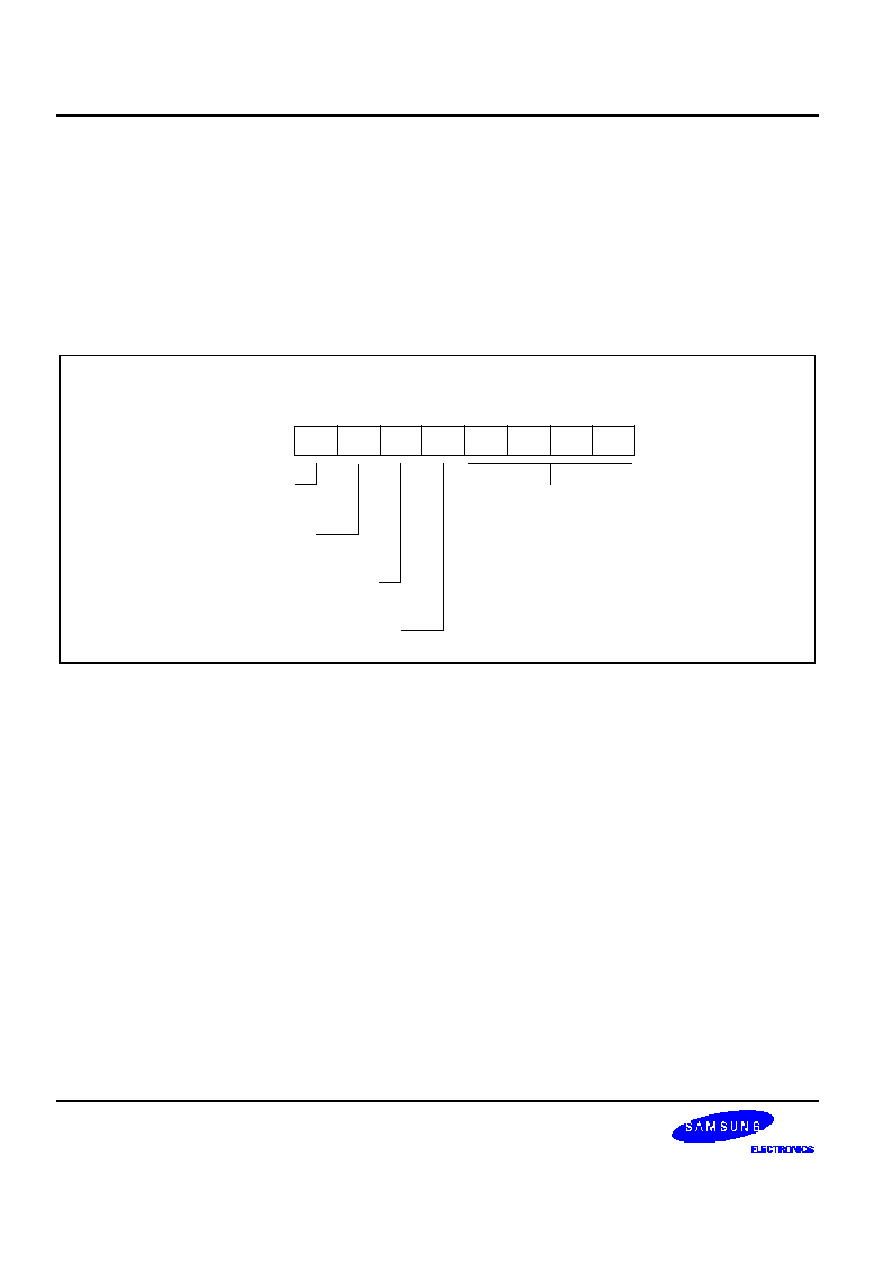
SAM88RI INSTRUCTION SET
S 3 C 9 6 8 8 / P 9 6 8 8
6 -4
F L A G S R E G I S T E R ( F L A G S )
T h e F L A G S r e g i s t e r c o n t a i n s e i g h t b i t s t h a t d e s c r i b e t h e c u r r e n t s t a t u s o f C P U o p e r a t i o n s . F o u r o f t h e s e b i t s ,
F L A G S . 4 ≠ F L A G S . 7 , c a n b e t e s t e d a n d u s e d w i t h c o n d i t i o n a l j u m p i n s t r u c t i o n s ;
F L A G S r e g i s t e r c a n b e s e t o r r e s e t b y i n s t r u c t i o n s a s l o n g a s i t s o u t c o m e d o e s n o t a f f e c t t h e f l a g s , s u c h a s , L o a d
i n s t r u c t i o n . L o g i c a l a n d A r i t h m e t i c i n s t r u c t i o n s s u c h a s , A N D , O R , X O R , A D D , a n d S U B c a n a f f e c t t h e F l a g s
r e g i s t e r . F o r e x a m p l e , t h e A N D i n s t r u c t i o n u p d a t e s t h e Z e r o , S i g n a n d O v e r f l o w f l a g s b a s e d o n t h e o u t c o m e o f t h e
A N D i n s t r u c t i o n . I f t h e A N D i n s t r u c t i o n u s e s t h e F l a g s r e g i s t e r a s t h e d e s t i n a t i o n , t h e n s i m u l t a n e o u s l y , t w o w r i t e w i l l
o c c u r t o t h e F l a g s r e g i s t e r p r o d u c i n g a n u n p r e d i c t a b l e r e s u l t .
System Flags Register (FLAGS)
D5H, R/W
.7
.6
.5
.4
.3
.2
.1
.0
MSB
LSB
Not mapped
Overflow (V)
Sign flag (S)
Zero flag (Z)
Carry flag (C)
F i g u r e 6 -1 . S y s t e m F l a g s R e g i s t e r ( F L A G S )
F L A G D E S C R I P T I O N S
O v e r f l o w F l a g ( F L A G S . 4 , V )
The V flag is set to "1" when the result of a two's -c o m p l e m e n t o p e r a t i o n i s g r e a t e r t h a n + 1 2 7 o r l e s s t h a n ≠ 128. It is
a l s o c l e a r e d t o " 0 " f o l l o w i n g l o g i c o p e r a t i o n s .
S i g n F l a g ( F L A G S . 5 , S )
F o l l o w i n g a r i t h m e t i c , l o g i c , r o t a t e , o r s h i f t o p e r a t i o n s , t h e s i g n b i t i d e n t i f i e s t h e s t a t e o f t h e M S B o f t h e r e s u l t . A l o g i c
z e r o i n d i c a t e s a p o s i t i v e n u m b e r a n d a l o g i c o n e i n d i c a t e s a n e g a t i v e n u m b e r .
Z e r o F l a g ( F L A G S . 6 , Z )
For arithmetic and logic operations, the Z flag is set to "1" if the result of the operation is zero. For operations t h a t
test register bits, and for shift and rotate operations, the Z flag is set to "1" if the result is logic zero.
C a r r y F l a g ( F L A G S . 7 , C )
The C flag is set to "1" if the result from an arithmetic operation generates a carry -out from or a borrow to the bit 7
position (MSB). After rotate and shift operations, it contains the last value shifted out of the specified register.
P r o g r a m i n s t r u c t i o n s c a n s e t , c l e a r , o r c o m p l e m e n t t h e c a r r y f l a g .
S 3 C 9 6 8 8 / P 9 6 8 8
S A M 8 8RCRI INSTRUCTION SET
6 -5
I N S T R U C T I O N S E T N O T A T I O N
T a b l e 6 -2 . F l a g N o t a t i o n C o n v e n t i o n s
F l a g
D e s c r i p t i o n
C
Carry flag
Z
Zero flag
S
Sign flag
V
Overflow flag
0
Cleared to logic zero
1
S e t t o l o g i c o n e
*
S e t o r c l e a r e d a c c o r d i n g t o o p e r a t i o n
≠
V a l u e i s u n a f f e c t e d
x
V a l u e i s u n d e f i n e d
T a b l e 6 -3 . I n s t r u c t i o n S e t S y m b o l s
S y m b o l
D e s c r i p t i o n
d s t
D e s t i n a t i o n o p e r a n d
src
S o u r c e o p e r a n d
@
Indirect register address prefix
P C
Pro g r a m c o u n t e r
F L A G S
F l a g s r e g i s t e r ( D 5 H )
#
Immediate operand or register address prefix
H
H e x a d e c i m a l n u m b e r s u f f i x
D
D e c i m a l n u m b e r s u f f i x
B
B i n a r y n u m b e r s u f f i x
opc
O p c o d e

SAM88RI INSTRUCTION SET
S 3 C 9 6 8 8 / P 9 6 8 8
6 -6
T a b l e 6 -4 . I n s t r u c t i o n N o t a t i o n C o n v e n t i o n s
N o t a t i o n
D e s c r i p t i o n
A c t u a l O p e r a n d R a n g e
c c
C o n d i t i o n c o d e
S e e l i s t o f c o n d i t i o n c o d e s i n T a b l e 6 -6 .
r
W o r k i n g r e g i s t e r o n l y
R n ( n = 0 ≠ 1 5 )
rr
W o r k i n g r e g i s t e r p a i r
R R p ( p = 0 , 2 , 4 , . . . , 1 4 )
R
R e g i s t e r o r w o r k i n g r e g i s t e r
re g o r R n ( r e g = 0 ≠ 2 5 5 , n = 0 ≠ 1 5 )
R R
Register pair or working register pair
r e g o r R R p ( r e g = 0 ≠ 2 5 4 , e v e n n u m b e r o n l y , w h e r e
p = 0 , 2 , . . . , 1 4 )
Ir
Indirect working register only
@ R n ( n = 0 ≠ 1 5 )
IR
Indirect register or indirect working register
@ R n o r @ r e g ( r e g = 0 ≠ 2 5 5 , n = 0 ≠ 1 5 )
Irr
Indirect working register pair only
@ R R p ( p = 0 , 2 , . . . , 1 4 )
IRR
Indirect register pair or indirect working
register pair
@ R R p o r @ r e g ( r e g = 0 ≠ 254, even only, where
p = 0 , 2 , . . . , 1 4 )
X
I n d e x e d a d d r e s s i n g m o d e
#reg[R n ] ( r e g = 0 ≠ 2 5 5 , n = 0 ≠ 1 5 )
XS
I n d e x e d ( s h o r t o f f s e t ) a d d r e s s i n g m o d e
# a d d r [ R R p ] ( a d d r = r a n g e ≠ 1 2 8 t o + 1 2 7 , w h e r e
p = 0 , 2 , . . . , 1 4 )
x l
I n d e x e d ( l o n g o f f s e t ) a d d r e s s i n g m o d e
# a d d r [ R R p ] ( a d d r = r a n g e 0 ≠ 8191, where
p = 0 , 2 , . . . , 1 4 )
d a
D i r e c t a d d r e s s i n g m o d e
addr (addr = range 0≠ 8 1 9 1 )
ra
R e l a t i v e a d d r e s s i n g m o d e
a d d r ( a d d r = n u m b e r i n t h e r a n g e + 1 2 7 t o ≠ 1 2 8 t h a t i s
an offset relative to the address of the next instruction)
im
I m m e d i a t e a d d r e s s i n g m o d e
# d a t a ( d a t a = 0 ≠ 2 5 5 )
S 3 C 9 6 8 8 / P 9 6 8 8
S A M 8 8RCRI INSTRUCTION SET
6 -7
T a b l e 6 -5 . O p c o d e Q u ic k R e f e r e n c e
O P C O D E M A P
L O W E R N I B B L E ( H E X )
≠
0
1
2
3
4
5
6
7
U
0
D E C
R 1
D E C
IR1
A D D
r1,r2
A D D
r1,Ir2
A D D
R 2 , R 1
A D D
I R 2 , R 1
A D D
R1,IM
P
1
R L C
R 1
R L C
IR1
A D C
r1,r2
A D C
r1,Ir2
A D C
R 2 , R 1
A D C
I R 2 , R 1
A D C
R1,IM
P
2
INC
R 1
INC
IR1
S U B
r1,r2
S U B
r1,Ir2
S U B
R 2 , R 1
S U B
I R 2 , R 1
S U B
R1,IM
E
3
JP
I R R 1
S B C
r1,r2
S B C
r1,Ir2
S B C
R 2 , R 1
S B C
I R 2 , R 1
S B C
R1,IM
R
4
O R
r1,r2
O R
r1,Ir2
O R
R 2 , R 1
O R
I R 2 , R 1
O R
R1,IM
5
P O P
R 1
P O P
IR1
A N D
r1,r2
A N D
r1,Ir2
A N D
R 2 , R 1
A N D
IR2,R 1
A N D
R1,IM
N
6
C O M
R 1
C O M
IR1
T C M
r1,r2
T C M
r1,Ir2
T C M
R 2 , R 1
T C M
I R 2 , R 1
T C M
R1,IM
I
7
P U S H
R 2
P U S H
IR2
TM
r1,r2
TM
r1,Ir2
TM
R 2 , R 1
TM
I R 2 , R 1
TM
R1,IM
B
8
L D
r1, x, r2
B
9
R L
R 1
R L
IR1
L D
r2, x, r1
L
A
C P
r1,r2
C P
r1,Ir2
C P
R 2 , R 1
C P
I R 2 , R 1
C P
R1,IM
L D C
r1, Irr2, xL
E
B
C L R
R 1
C L R
IR1
X O R
r1,r2
X O R
r1,Ir2
X O R
R 2 , R 1
X O R
I R 2 , R 1
X O R
R1,IM
L D C
r2, Irr2, xL
C
R R C
R 1
R R C
IR1
L D C
r1,Irr2
L D
r1, Ir2
H
D
S R A
R 1
S R A
IR1
L D C
r2,Irr1
L D
IR1,IM
L D
Ir1, r2
E
E
R R
R 1
R R
IR1
L D C D
r1,Irr2
L D C I
r1,Irr2
L D
R 2 , R 1
L D
R 2 , I R 1
L D
R1,IM
L D C
r1, Irr2, xs
X
F
C A L L
I R R 1
L D
I R 2 , R 1
C A L L
D A 1
L D C
r2, Irr1, xs
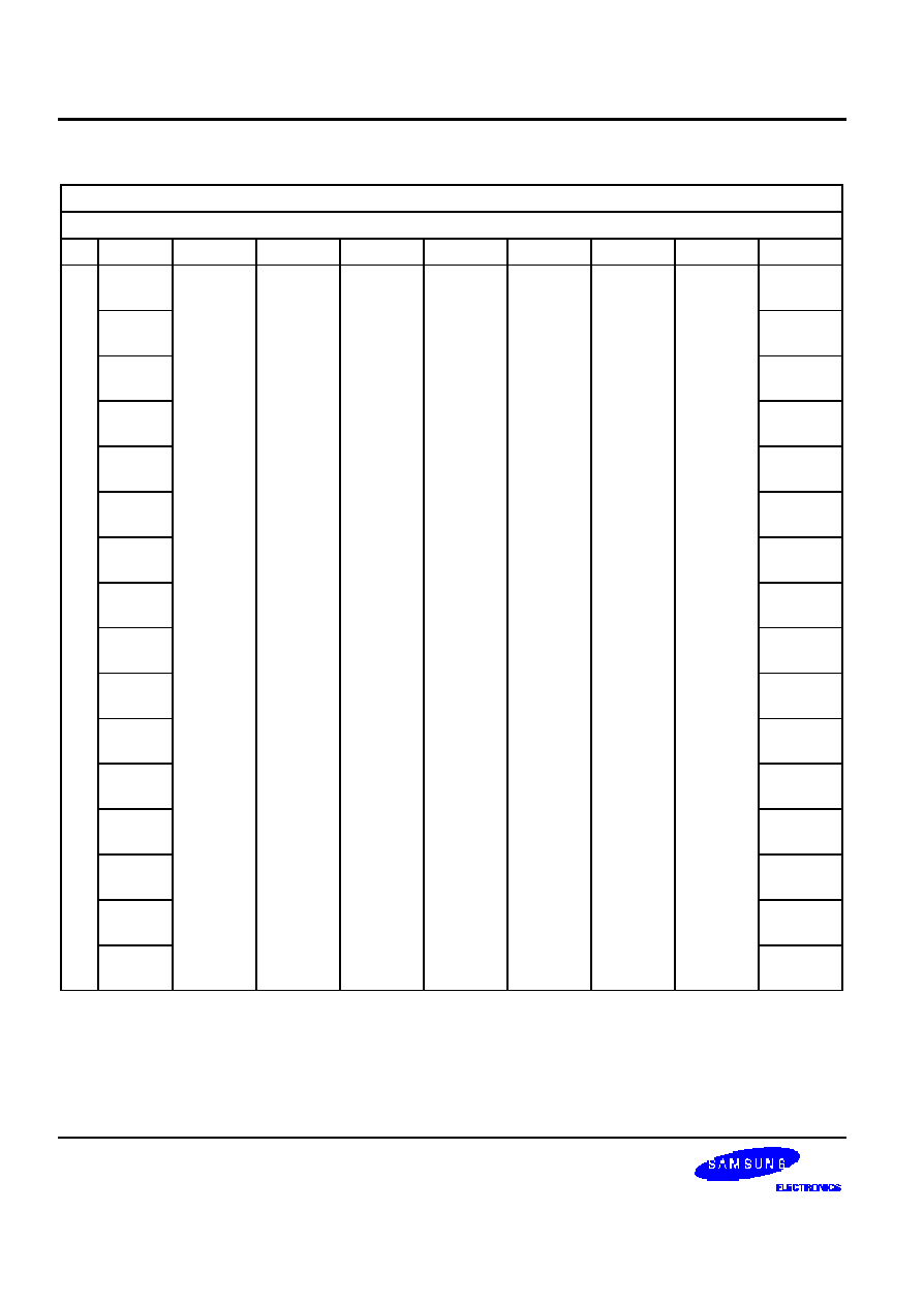
SAM88RI INSTRUCTION SET
S 3 C 9 6 8 8 / P 9 6 8 8
6 -8
T a b l e 6 -5 . O p c o d e Q u i c k R e f e r e n c e ( C o n t i n u e d )
O P C O D E M A P
L O W E R N I B B L E ( H E X )
≠
8
9
A
B
C
D
E
F
U
0
L D
r 1 , R 2
L D
r 2 , R 1
JR
c c , R A
L D
r1,IM
JP
c c , D A
INC
r1
P
1
P
2
E
3
R
4
5
N
6
IDLE
I
7
S T O P
B
8
D I
B
9
E I
L
A
R E T
E
B
I R E T
C
R C F
H
D
S C F
E
E
C C F
X
F
L D
r 1 , R 2
L D
r 2 , R 1
JR
c c , R A
L D
r1,IM
JP
c c , D A
INC
r1
N O P

S 3 C 9 6 8 8 / P 9 6 8 8
S A M 8 8RCRI INSTRUCTION SET
6 -9
C O N D I T I O N C O D E S
T h e o p c o d e o f a c o n d i t i o n a l j u m p a l w a y s c o n t a i n s a 4 -bit field called the condition code (cc). This specifies under
w h i c h c o n d i t i o n s i t i s t o e x e c u t e t h e j u m p . F o r e x a m p l e , a c o n d i t i o n a l j u m p w i t h t h e c o n d i t i o n c o d e f o r " e q u a l " a f t e r a
c o m p a r e o p e r a t i o n o n l y j u m p s i f t h e t w o o p e r a n d s a r e e q u a l . C o n d i t i o n c o d e s a r e l i s t e d i n T a b l e 6 -6 .
The carry (C), zero (Z), sign (S), and overflow (V) flags are used to control the operation of conditional jump
i n s t r u c t i o n s .
T a b l e 6 -6 . C o n d i t i o n C o d e s
B i n a r y
M n e m o n i c
D e s c r i p t i o n
F l a g s S e t
0 0 0 0
F
A l w a y s f a l s e
≠
1 0 0 0
T
A l w a y s t r u e
≠
0 1 1 1 (1)
C
Carry
C = 1
1 1 1 1 (1)
N C
No carry
C = 0
0 1 1 0 (1)
Z
Zero
Z = 1
1 1 1 0 (1)
N Z
Not zero
Z = 0
1 1 0 1
P L
P l u s
S = 0
0 1 0 1
M I
M i n u s
S = 1
0 1 0 0
O V
Overflow
V = 1
1 1 0 0
N O V
No overflow
V = 0
0 1 1 0 (1)
E Q
E q u a l
Z = 1
1 1 1 0 (1)
N E
N o t e q u a l
Z = 0
1 0 0 1
G E
G r e a t e r t h a n o r e q u a l
( S X O R V ) = 0
0 0 0 1
L T
L e s s t h a n
( S X O R V ) = 1
1 0 1 0
G T
G r e a t e r t h a n
( Z O R ( S X O R V ) ) = 0
0 0 1 0
L E
L e s s t h a n o r e q u a l
( Z O R ( S X O R V ) ) = 1
1 1 1 1 (1)
U G E
U n s i g n e d g r e a t e r t h a n o r e q u a l
C = 0
0 1 1 1 (1)
U L T
U n s i g n e d l e s s t h a n
C = 1
1 0 1 1
U G T
U n s i g n e d g r e a t e r t h a n
( C = 0 A N D Z = 0 ) = 1
0 0 1 1
U L E
U n s i g n e d l e s s t h a n o r e q u a l
( C O R Z ) = 1
NOTES:
1.
Indicate condition codes that are related to two different mnemonics but which test the same flag.
For
example, Z and EQ are both true if the zero flag (Z) is set, but after an ADD instruction, Z would probably be used;
after a CP instruction, however, EQ would probably be used.
2.
For operations involving unsigned numbers, the special condition codes UGE, ULT, UGT, and ULE must be used.

SAM88RI INSTRUCTION SET
S 3 C 9 6 8 8 / P 9 6 8 8
6 -1 0
I N S T R U C T I O N D E S C R I P T I O N S
T h i s s e c t i o n c o n t a i n s d e t a i l e d i n f o r m a t i o n a n d p r o g r a m m i n g e x a m p l e s f o r e a c h i n s t r u c t i o n i n t h e S A M 8 8 R C R I
instruction set. Information is arranged in a consistent format for improved readability and for fast referencing. The
followi n g i n f o r m a t i o n i s i n c l u d e d i n e a c h i n s t r u c t i o n d e s c r i p t i o n :
--
I n s t r u c t i o n n a m e ( m n e m o n i c )
--
F u l l i n s t r u c t i o n n a m e
--
S o u r c e / d e s t i n a t i o n f o r m a t o f t h e i n s t r u c t i o n o p e r a n d
--
Shorthand notation of the instruction's operation
--
Textual description of the instruction's effect
--
S p e c i f i c f l a g s e t t i n g s a f f e c t e d b y t h e i n s t r u c t i o n
--
D e t a i l e d d e s c r i p t i o n o f t h e i n s t r u c t i o n ' s f o r m a t , e x e c u t i o n t i m e , a n d a d d r e s s i n g m o d e ( s )
--
P r o g r a m m i n g e x a m p l e ( s ) e x p l a i n i n g h o w t o u s e t h e i n s t r u c t i o n

S 3 C 9 6 8 8 / P 9 6 8 8
S A M 8 8RCRI INSTRUCTION SET
6 -1 1
A D C
-- Add With C arry
A D C
d s t , s r c
O p e r a t i o n :
d s t
d s t + s r c + c
T h e s o u r c e o p e r a n d , a l o n g w i t h t h e s e t t i n g o f t h e c a r r y f l a g , i s a d d e d t o t h e d e s t i n a t i o n o p e r a n d a n d
t h e s u m i s s t o r e d i n t h e d e s t i n a t i o n . T h e c o n t e n t s o f t h e s o u r c e a r e u n a f f e c t e d . T w o ' s -c o m p l e m e n t
a d d i t i o n i s p e r f o r m e d . I n m u l t i p l e p r e c i s i o n a r i t h m e t i c , t h i s i n s t r u c t i o n p e r m i t s t h e c a r r y f r o m t h e
addition of low-order operands to be carried into the addition of high-o r d e r o p e r a n d s .
F l a g s :
C :
Set if there is a carry from the most significant bit of t h e r e s u l t ; c l e a r e d o t h e r w i s e .
Z:
S e t i f t h e r e s u l t i s " 0 " ; c l e a r e d o t h e r w i s e .
S :
Set if the result is negative; cleared otherwise.
V :
S e t i f a r i t h m e t i c o v e r f l o w o c c u r s , t h a t i s , i f b o t h o p e r a n d s a r e o f t h e s a m e s i g n a n d t h e
r e s u l t i s o f t h e o p p o s i t e s i g n ; c l e a r e d o t h e r w i s e .
D :
A l w a y s c l e a r e d t o " 0 " .
H :
S e t i f t h e r e i s a c a r r y f r o m t h e m o s t s i g n i f i c a n t b i t o f t h e l o w -order four bits of the result;
c l e a r e d o t h e r w i s e .
F o r m a t :
B y t e s
C y c l e s
O p c o d e
( H e x )
A d d r M o d e
dst src
o pc
dst | src
2
4
1 2
r
r
6
1 3
r
lr
opc
src
d s t
3
6
1 4
R
R
6
1 5
R
IR
opc
d s t
src
3
6
1 6
R
IM
E x a m p l e s :
Given:
R 1 = 1 0 H , R 2 = 0 3 H , C f l a g = " 1 " , r e g i s t e r 0 1 H = 2 0 H , r e g i s t e r 0 2 H = 0 3 H , a n d
r e g i s t e r 0 3 H = 0 A H :
A D C
R 1 , R 2
R 1 = 1 4 H , R 2 = 0 3 H
A D C
R 1 , @ R 2
R 1 = 1 B H , R 2 = 0 3 H
A D C
0 1 H , 0 2 H
R e g i s t e r 0 1 H = 2 4 H , r e g i s t e r 0 2 H = 0 3 H
A D C
0 1 H , @ 0 2 H
R e g i s t e r 0 1 H = 2 B H , r e g i s t e r 0 2 H = 0 3 H
A D C
0 1 H , # 1 1 H
R e g i s t e r 0 1 H = 3 2 H
I n t h e f i r s t e x a m p le , d e s t i n a t i o n r e g i s t e r R 1 c o n t a i n s t h e v a l u e 1 0 H , t h e c a r r y f l a g i s s e t t o " 1 " , a n d
t h e s o u r c e w o r k i n g r e g i s t e r R 2 c o n t a i n s t h e v a l u e 0 3 H . T h e s t a t e m e n t " A D C R 1 , R 2 " a d d s 0 3 H a n d
the carry flag value ("1") to the destination value 10H, leaving 14H in register R1.

SAM88RI INSTRUCTION SET
S 3 C 9 6 8 8 / P 9 6 8 8
6 -1 2
A D D
-- A d d
A D D
d s t , s r c
O p e r a t i o n :
d s t
d s t + s r c
T h e s o u r c e o p e r a n d i s a d d e d t o t h e d e s t i n a t i o n o p e r a n d a n d t h e s u m i s s t o r e d i n t h e d e s t i n a t i o n .
The contents of the source are unaffected. Two's -c o m p l e m e n t a d d i t i o n i s p e r f o r m e d .
F l a g s :
C :
S e t i f t h e r e i s a c a r r y f r o m t h e m o s t s i g n i f i c a n t b i t o f t h e r e s u l t ; c l e a r e d o t h e r w i s e
Z:
S e t i f t h e r e s u l t i s " 0 " ; c l e a r e d o t h e r w i s e .
S :
Set if the result is negative; cleared otherwise.
V :
S e t i f a r i t h m e t i c o v e r f l o w o c c u r r e d , t h a t i s , i f b o t h o p e r a n d s a r e o f t h e s a m e s i g n a n d
t h e r e s u l t i s o f t h e o p p o s i t e s i g n ; c l e a r e d o t h e r w i s e .
D :
A l w a y s c l e a r e d t o " 0 " .
H :
S e t i f a c a r r y f r o m t h e l o w-order nibble occurred.
F o r m a t :
B y t e s
C y c l e s
O p c o d e
( H e x )
A d d r M o d e
dst src
opc
dst | src
2
4
0 2
r
r
6
0 3
r
lr
opc
src
d s t
3
6
0 4
R
R
6
0 5
R
IR
opc
d s t
src
3
6
0 6
R
IM
E x a m p l e s :
Given: R 1 = 1 2 H , R 2 = 0 3 H , r e g i s t e r 0 1 H = 2 1 H , r e g i s t e r 0 2 H = 0 3 H , r e g i s t e r 0 3 H = 0 A H :
A D D
R 1 , R 2
R 1 = 1 5 H , R 2 = 0 3 H
A D D
R 1 , @ R 2
R 1 = 1 C H , R 2 = 0 3 H
A D D
0 1 H , 0 2 H
R e g i s t e r 0 1 H = 2 4 H , r e g i s t e r 0 2 H = 0 3 H
A D D
0 1 H , @ 0 2 H
R e g i s t e r 0 1 H = 2 B H , r e g i s t e r 0 2 H = 0 3 H
A D D
0 1 H , # 2 5 H
R e g i s t e r 0 1 H = 4 6 H
In the first example, destination working regis t e r R 1 c o n t a i n s 1 2 H a n d t h e s o u r c e w o r k i n g r e g i s t e r
R 2 c o n t a i n s 0 3 H . T h e s t a t e m e n t " A D D R 1 , R 2 " a d d s 0 3 H t o 1 2 H , l e a v i n g t h e v a l u e 1 5 H i n r e g i s t e r
R 1 .
S 3 C 9 6 8 8 / P 9 6 8 8
S A M 8 8RCRI INSTRUCTION SET
6 -1 3
A N D
-- L o g i c a l A N D
A N D
d s t , s r c
O p e r a t i o n :
d s t
d s t A N D s r c
T h e s o u r c e o p e r a n d i s l o g i c a l l y A N D e d w i t h t h e d e s t i n a t i o n o p e r a n d . T h e r e s u l t i s s t o r e d i n t h e
d e s t i n a t i o n . T h e A N D o p e r a t i o n r e s u l t s i n a " 1 " b i t b e i n g s t o r e d w h e n e v e r t h e c o r r e s p o n d i n g b i t s i n
t h e t w o o p e r a n d s a r e b o t h l o g i c o n e s ; o t h e r w i s e a " 0 " b i t v a l u e i s s t o r e d . T h e c o n t e n t s o f t h e s o u r c e
are unaffected.
F l a g s :
C :
Unaffected.
Z:
S e t i f t h e r e s u l t i s " 0 " ; c l e a r e d o t h e r w i s e .
S :
S e t i f t h e r e s u l t b i t 7 i s s e t ; c l e a r e d o t h e r w i s e .
V :
A l w a y s c l e a r e d t o " 0 " .
D :
Unaffected.
H :
Unaffected.
F o r m a t :
B y t e s
C y c l e s
O p c o d e
( H e x )
A d d r M o d e
dst src
opc
dst | src
2
4
5 2
r
r
6
5 3
r
lr
opc
src
d s t
3
6
5 4
R
R
6
5 5
R
IR
opc
d s t
src
3
6
5 6
R
IM
E x a m p l e s :
Given: R 1 = 1 2 H , R 2 = 0 3 H , r e g i s t e r 0 1 H = 2 1 H , r e g i s t e r 0 2 H = 0 3 H , r e g i s t e r 0 3 H = 0 A H :
A N D
R 1 , R 2
R 1 = 0 2 H , R 2 = 0 3 H
A N D
R 1 , @ R 2
R 1 = 0 2 H , R 2 = 0 3 H
A N D
0 1 H , 0 2 H
R e g i s t e r 0 1 H = 0 1 H , r e g i s t e r 0 2 H = 0 3 H
A N D
0 1 H , @ 0 2 H
R e g i s t e r 0 1 H = 0 0 H , r e g i s t e r 0 2 H = 0 3 H
A N D
0 1 H , # 2 5 H
R e g i s t e r 0 1 H = 2 1 H
I n t h e f i r s t e x a m p l e , d e s t i n a t i o n w o r k i n g r e g i s t e r R 1 c o n t a i n s t h e v a l u e 1 2 H a n d t h e s o u r c e w o r k i n g
r e g i s t e r R 2 c o n t a i n s 0 3 H . T h e s t a t e m e n t " A N D R 1 , R 2 " l o g i c a l l y A N D s t h e s o u r c e o p e r a n d 0 3 H w i t h
the destination operand value 12H, leaving the value 02H in register R1.
SAM88RI INSTRUCTION SET
S 3 C 9 6 8 8 / P 9 6 8 8
6 -1 4
C A L L
-- Call Procedure
C A L L
d s t
O p e r a t i o n :
S P
S P ≠ 1
@ S P
P C L
S P
S P ≠ 1
@ S P
P C H
P C
d s t
T h e c u r r e n t c o n t e n t s o f t h e p r o g r a m c o u n t e r a r e p u s h e d o n t o t h e t o p o f t h e s t a c k . T h e p r o g r a m
counter value used is the address of the first instruction following the CALL instruction. The specified
d e s t i n a t i o n a d d r e s s i s t h e n l o a d e d i n t o t h e p r o g r a m c o u n t e r a n d p o i n t s t o t h e f i r s t i n s t r u c t i o n o f a
p r o c e d u r e . A t t h e e n d o f t h e p r o c e d u r e t h e r e t u r n i n s t r u c t i o n ( R E T ) c a n b e u s e d t o return to the
o r i g i n a l p r o g r a m f l o w . R E T p o p s t h e t o p o f t h e s t a c k b a c k i n t o t h e p r o g r a m c o u n t e r .
F l a g s :
No flags are affected.
F o r m a t :
B y t e s
C y c l e s
O p c o d e
( H e x )
A d d r M o d e
dst
opc
d s t
3
1 4
F 6
D A
opc
d s t
2
1 2
F 4
IRR
E x a m p l e s :
Given: R 0 = 1 5 H , R 1 = 2 1 H , P C = 1 A 4 7 H , a n d S P = 0 B 2 H :
C A L L
1 5 2 1 H
S P = 0 B 0 H
( M e m o r y l o c a t i o n s 0 0 H = 1 A H , 0 1 H = 4 A H , w h e r e 4 A H
i s t h e a d d r e s s t h a t f o l l o w s t h e i n s t r u c t i o n . )
C A L L
@ R R 0
S P = 0 B 0 H ( 0 0 H = 1 A H , 0 1 H = 4 9 H )
In the first exam p l e , i f t h e p r o g r a m c o u n t e r v a l u e i s 1 A 4 7 H a n d t h e s t a c k p o i n t e r c o n t a i n s t h e v a l u e
0 B 2 H , t h e s t a t e m e n t " C A L L 1 5 2 1 H " p u s h e s t h e c u r r e n t P C v a l u e o n t o t h e t o p o f t h e s t a c k . T h e
s t a c k p o i n t e r n o w p o i n t s t o m e m o r y l o c a t i o n 0 0 H . T h e P C i s t h e n l o a d e d w i t h t h e v a l u e 1 5 2 1 H , t h e
a d d r e s s o f t h e f i r s t i n s t r u c t i o n i n t h e p r o g r a m s e q u e n c e t o b e e x e c u t e d .
I f t h e c o n t e n t s o f t h e p r o g r a m c o u n t e r a n d s t a c k p o i n t e r a r e t h e s a m e a s i n t h e f i r s t e x a m p l e , t h e
s t a t e m e n t " C A L L @ R R 0 " p r o d u c e s t h e s a m e r e s u l t e x c e p t t h a t t h e 4 9 H i s s t o r e d i n s t a c k l o c a t i o n
0 1 H ( b e c a u s e t h e t w o -b y t e i n s t r u c t i o n f o r m a t w a s u s e d ) . T h e P C i s t h e n l o a d e d w i t h t h e v a l u e
1 5 2 1 H , t h e a d d r e s s o f t h e f i r s t i n s t r u c t i o n i n t h e p r o g r a m s e q u e n c e t o b e e x e c u t e d .

S 3 C 9 6 8 8 / P 9 6 8 8
S A M 8 8RCRI INSTRUCTION SET
6 -1 5
C C F
-- C o m p l e m e n t C a r r y F l a g
C C F
O p e r a t i o n :
C
N O T C
The carry flag (C) is complemented. If C = "1", the value of the carry flag is changed to logic zero; if
C = " 0 " , t h e v a l u e o f t h e c a r r y f l a g i s c h a n g e d t o l o g i c o n e .
F l a g s :
C :
C o m p l e m e n t e d .
No other flags are affected.
F o r m a t:
B y t e s
C y c l e s
O p c o d e
( H e x )
opc
1
4
E F
E x a m p l e :
Given: T h e c a r r y f l a g = " 0 " :
C C F
I f t h e c a r r y f l a g = " 0 " , t h e C C F i n s t r u c t i o n c o m p l e m e n t s i t i n t h e F L A G S r e g i s t e r ( 0 D 5 H ) , c h a n g i n g
its value from logic zero to logic one.

SAM88RI INSTRUCTION SET
S 3 C 9 6 8 8 / P 9 6 8 8
6 -1 6
C L R
-- C l e a r
C L R
d s t
O p e r a t i o n :
d s t
" 0 "
T h e d e s t i n a t i o n l o c a t i o n i s c l e a r e d t o " 0 " .
F l a g s :
No flags are affected.
F o r m a t :
B y t e s
C y c l e s
O p c o d e
( H e x )
A d d r M o d e
dst
opc
d s t
2
4
B 0
R
4
B 1
IR
E x a m p l e s :
Given: R e g i s t e r 0 0 H = 4 F H , r e g is t e r 0 1 H = 0 2 H , a n d r e g i s t e r 0 2 H = 5 E H :
C L R
0 0 H
R e g i s t e r 0 0 H = 0 0 H
C L R
@ 0 1 H
R e g i s t e r 0 1 H = 0 2 H , r e g i s t e r 0 2 H = 0 0 H
I n R e g i s t e r ( R ) a d d r e s s i n g m o d e , t h e s t a t e m e n t " C L R 0 0 H " c l e a r s t h e d e s t i n a t i o n r e g i s t e r 0 0 H
v a l u e t o 0 0 H . I n t h e s e c o n d e x a m p l e , t h e s t a t e m e n t " C L R @ 0 1 H " u s e s I n d i r e c t R e g i s t e r ( I R )
a d d r e s s i n g m o d e t o c l e a r t h e 0 2 H r e g i s t e r v a l u e t o 0 0 H .

S 3 C 9 6 8 8 / P 9 6 8 8
S A M 8 8RCRI INSTRUCTION SET
6 -1 7
C O M
-- C o m p l e m e n t
C O M
d s t
O p e r a t i o n :
d s t
N O T d s t
T h e c o n t e n t s o f t h e d e s t i n a t i o n l o c a t i o n a r e c o m p l e m e n t e d ( o n e ' s c o m p l e m e n t ) ; a l l " 1 s " a r e
c h a n g e d t o " 0 s " , a n d v i c e-versa.
F l a g s :
C :
Unaffected.
Z:
S e t i f t h e r e s u l t i s " 0 " ; c l e a r e d o t h e r w i s e .
S :
S e t i f t h e r e s u l t b i t 7 i s s e t ; c l e a r e d o t h e r w i s e .
V :
A l w a y s r e s e t t o " 0 " .
D :
Unaffected.
H :
Unaffected.
F o r m a t :
B y t e s
C y c l e s
O p c o d e
( H e x )
A d d r M o d e
dst
opc
d s t
2
4
6 0
R
4
6 1
IR
E x a m p l e s :
Given: R 1 = 0 7 H a n d r e g i s t e r 0 7 H = 0 F 1 H :
C O M
R 1
R 1 = 0 F 8 H
C O M
@ R 1
R 1 = 0 7 H , r e g i s t e r 0 7 H = 0 E H
In the first example, destination working register R 1 c o n t a i n s t h e v a l u e 0 7 H ( 0 0 0 0 0 1 1 1 B ) . T h e
s t a t e m e n t " C O M R 1 " c o m p l e m e n t s a l l t h e b i t s i n R 1 : a l l l o g i c o n e s a r e c h a n g e d t o l o g i c z e r o s , a n d
v i c e-versa, leaving the value 0F8H (11111000B).
I n t h e s e c o n d e x a m p l e , I n d i r e c t R e g i s t e r ( I R ) a d d r e s s i n g m o d e i s u s e d t o c o m p l e m e n t t h e v a l u e o f
d e s t i n a t i o n r e g i s t e r 0 7 H ( 1 1 1 1 0 0 0 1 B ) , l e a v i n g t h e n e w v a l u e 0 E H ( 0 0 0 0 1 1 1 0 B ) .
SAM88RI INSTRUCTION SET
S 3 C 9 6 8 8 / P 9 6 8 8
6 -1 8
C P
-- C o m p a r e
C P
d s t , s r c
O p e r a t i o n :
d s t ≠ src
T h e s o u r c e o p e r a n d i s c o m p a r e d t o ( s u b t r a c t e d f r o m ) t h e d e s t i n a t i o n o p e r a n d , a n d t h e a ppropriate
f l a g s a r e s e t a c c o r d i n g l y . T h e c o n t e n t s o f b o t h o p e r a n d s a r e u n a f f e c t e d b y t h e c o m p a r i s o n .
F l a g s :
C :
S e t i f a " b o r r o w " o c c u r r e d ( s r c > d s t ) ; c l e a r e d o t h e r w i s e .
Z:
S e t i f t h e r e s u l t i s " 0 " ; c l e a r e d o t h e r w i s e .
S :
Set if the result is negative; cleared otherwise.
V :
Set if arithmetic overflow occurred, that is, if the operands were of opposite signs and
t h e s i g n o f t h e r e s u l t i s o f t h e s a m e a s t h e s i g n o f t h e s o u r c e o p e r a n d ; c l e a r e d o t h e r w i s e .
D :
Unaffected.
H :
Unaffected.
F o r m a t:
B y t e s
C y c l e s
O p c o d e
( H e x )
A d d r M o d e
dst src
opc
dst | src
2
4
A 2
r
r
6
A 3
r
lr
opc
src
d s t
3
6
A 4
R
R
6
A 5
R
IR
opc
d s t
src
3
6
A 6
R
IM
E x a m p l e s :
1 . G i v e n : R 1 = 0 2 H a n d R 2 = 0 3 H :
C P
R 1 , R 2
S e t t h e C a n d S f l a g s
D e s t i n a t i o n w o r k i n g r e g i s t e r R 1 c o n t a i n s t h e v a l u e 0 2 H a n d s o u r c e r e g i s t e r R 2 c o n t a i n s t h e v a l u e
0 3 H . T h e s t a t e m e n t " C P R 1 , R 2 " s u b t r a c t s t h e R 2 v a l u e ( s o u r c e / s u b t r a h e n d ) f r o m t h e R 1 v a l u e
( d e s t i n a t i o n / m i n u e n d ) . B e c a u s e a " b o r r o w " o c c u r s a n d t h e d i f f e r e n c e i s n e g a t i v e , C a n d S a r e " 1 " .
2 . Given: R 1 = 0 5 H a n d R 2 = 0 A H :
C P
R 1 , R 2
JP
U G E , S K I P
INC
R 1
S K I P
L D
R 3 , R 1
I n t h i s e x a m p l e , d e s t i n a t i o n w o r k i n g r e g i s t e r R 1 c o n t a i n s t h e v a l u e 0 5 H w h i c h i s l e s s t h a n t h e
c o n t e n t s o f t h e s o u r c e w o r k i n g r e g i s t e r R 2 ( 0 A H ) . T h e s t a t e m e n t " C P R 1 , R 2 " g e n e r a t e s C = " 1 "
a n d t h e J P i n s t r u c t i o n d o e s n o t j u m p t o t h e S K I P l o c a t i o n . A f t e r t h e s t a t e m e n t " L D R 3 , R 1 "
e x e c u t e s , t h e v a l u e 0 6 H r e m a i n s i n w o r k i n g r e g i s t e r R 3 .

S 3 C 9 6 8 8 / P 9 6 8 8
S A M 8 8RCRI INSTRUCTION SET
6 -1 9
D E C
-- D e c r e m e n t
D E C
d s t
O p e r a t i o n :
d s t
d s t ≠ 1
T h e c o n t e n t s o f t h e d e s t i n a t i o n o p e r a n d a r e d e c r e m e n t e d b y o n e .
F l a g s :
C :
Unaffected.
Z:
S e t i f t h e r e s u l t i s " 0 " ; c l e a r e d o t h e r w i s e .
S :
Set if result is negative; cleared otherwise.
V :
Set if arithmetic overflow occurred, that is, dst value is ≠ 128(80H) and result value
i s + 1 2 7 ( 7 F H ) ; c l e a r e d o t h e r w i s e .
D :
Unaffected.
H :
Unaffected.
F o r m a t :
B y t e s
C y c l e s
O p c o d e
( H e x )
A d d r M o d e
dst
opc
d s t
2
4
0 0
R
4
0 1
IR
E x a m p l e s :
Given: R 1 = 0 3 H a n d r e g i s t e r 0 3 H = 1 0 H :
D E C
R 1
R 1 = 0 2 H
D E C
@ R 1
R e g i s t e r 0 3 H = 0 F H
I n t h e f i r s t e x a m p l e , i f w o r k i n g r e g i s t e r R 1 c o n t a i n s t h e v a l u e 0 3 H , t h e s t a t e m e n t " D E C R 1 "
d e c r e m e n t s t h e h e x a d e c i m a l v a l u e b y o n e , l e a v i n g t h e v a l u e 0 2 H . I n t h e s e c o n d e x a m p l e , t h e
s t a t e m e n t " D E C @ R 1 " d e c r e m e n t s t h e v a l u e 1 0 H c o n t a i n e d i n t h e d e s t i n a t i o n r e g i s t e r 0 3 H b y o n e ,
leaving the value 0FH.

SAM88RI INSTRUCTION SET
S 3 C 9 6 8 8 / P 9 6 8 8
6 -2 0
DI
-- Disable Interrupts
D I
O p e r a t i o n :
S Y M ( 2 )
0
B i t z e r o o f t h e s y s t e m m o d e r e g i s t e r , S Y M . 2 , i s c l e a r e d t o " 0 " , g l o bally disabling all interrupt
processing. Interrupt requests will continue to set their respective interrupt pending bits, but the
C P U w i l l n o t s e r v i c e t h e m w h i l e i n t e r r u p t p r o c e s s i n g i s d i s a b l e d .
F l a g s :
No flags are affected.
F o r m a t :
B y t e s
C y c l e s
O p c o d e
( H e x )
opc
1
4
8 F
E x a m p l e :
Given: S Y M = 0 4 H :
D I
I f t h e v a l u e o f t h e S Y M r e g i s t e r i s 0 4 H , t h e s t a t e m e n t " D I " l e a v e s t h e n e w v a l u e 0 0 H i n t h e r e g i s t e r
a n d c l e a r s S Y M . 2 t o " 0 " , d i s a b l i n g i n t e r r u p t p r o c e s s i n g .

S 3 C 9 6 8 8 / P 9 6 8 8
S A M 8 8RCRI INSTRUCTION SET
6 -2 1
E I
-- Enable Interrupts
E I
O p e r a t i o n :
S Y M ( 2 )
1
A n E I i n s t r u c t i o n s e t s b i t 2 o f t h e s y s t e m m o d e r e g i s t e r , S Y M . 2 t o " 1 " . T h i s a l l o w s i n t e r r u p t s t o b e
s e r v i c e d a s t h e y o c c u r . I f a n i n t e r r u p t ' s p e n d i n g b i t w a s s e t w h i l e i n t e r r u p t p r o c e s s i n g w a s d i s a b l e d
( b y e x e c u t i n g a D I i n s t r u c t i o n ) , i t w i l l b e s e r v i c e d w h e n y o u e x e c u t e t h e E I i n s t r u c t i o n .
F l a g s :
No flags are affected.
F o r m a t :
B y t e s
C y c l e s
O p c o d e
( H e x )
opc
1
4
9 F
E x a m p l e :
Given: S Y M = 0 0 H :
E I
I f t h e S Y M r e g i s t e r c o n t a i n s t h e v a l u e 0 0 H , t h a t i s , i f i n t e rr u p t s a r e c u r r e n t l y d i s a b l e d , t h e s t a t e m e n t
" E I " s e t s t h e S Y M r e g i s t e r t o 0 4 H , e n a b l i n g a l l i n t e r r u p t s ( S Y M . 2 i s t h e e n a b l e b i t f o r g l o b a l i n t e r r u p t
processing).

SAM88RI INSTRUCTION SET
S 3 C 9 6 8 8 / P 9 6 8 8
6 -2 2
IDLE
-- Idle Operation
I D L E
O p e r a t i o n :
T h e I D L E i n s t r u c t i o n s t o p s t h e C P U c l o c k w h i l e a l l o w i n g s y s t e m c l o c k o s c i l l a t i o n t o c o n t i n u e . I d l e
m o d e c a n b e r e l e a s e d b y a n i n t e r r u p t r e q u e s t ( I R Q ) o r a n e x t e r n a l r e s e t o p e r a t i o n .
F l a g s :
No flags are affected.
F o r m a t :
B y t e s
C y c l e s
O p c o d e
( H e x )
A d d r M o d e
dst src
opc
1
4
6 F
≠
≠
E x a m p l e :
T h e in s tr u ct io n
I D L E
s t o p s t h e C P U c l o c k b u t n o t t h e s y s t e m c l o c k .
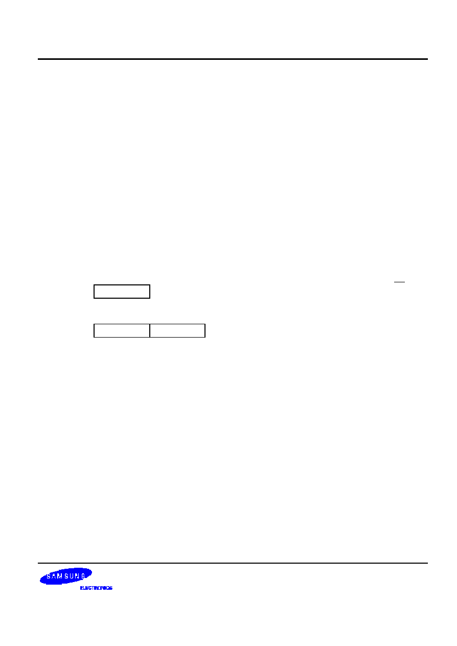
S 3 C 9 6 8 8 / P 9 6 8 8
S A M 8 8RCRI INSTRUCTION SET
6 -2 3
INC
-- I n c r e m e n t
I N C
d s t
O p e r a t i o n :
d s t
d s t + 1
T h e c o n t e n t s o f t h e d e s t i n a t i o n o p e r a n d a r e i n c r e m e n t e d b y o n e .
F l a g s :
C :
Unaffected.
Z:
S e t i f t h e r e s u l t i s " 0 " ; c l e a r e d o t h e r w i s e .
S :
Set if the result is negative; cleared otherwise.
V :
Set if arithmetic overflow occurred, that is dst value is +127(7FH) and result is ≠
1 2 8 ( 8 0 H ) ; c l e a r e d o t h e r w i s e .
D :
Unaffected.
H :
Unaffected.
F o rm a t :
B y t e s
C y c l e s
O p c o d e
( H e x )
A d d r M o d e
dst
dst | opc
1
4
rE
r
r = 0 t o F
opc
d s t
2
4
2 0
R
4
2 1
IR
E x a m p l e s :
Given: R 0 = 1 B H , r e g i s t e r 0 0 H = 0 C H , a n d r e g i s t e r 1 B H = 0 F H :
INC
R 0
R 0 = 1 C H
INC
0 0 H
R e g i s t e r 0 0 H = 0 D H
INC
@ R 0
R 0 = 1 B H , r e g i s t e r 0 1 H = 1 0 H
I n t h e f i r s t e x a m p l e , i f d e s t i n a t i o n w o r k i n g r e g i s t e r R 0 c o n t a i n s t h e v a l u e 1 B H , t h e s t a t e m e n t " I N C
R 0 " l e a v e s t h e v a l u e 1 C H i n t h a t s a m e r e g i s t e r .
T h e n e x t e x a m p l e s h o w s t h e e f f e c t a n I N C i n s t r u c t i o n h a s o n r e g i s t e r 0 0 H , a s s u m i n g t h a t i t
c o n t a i n s t h e v a l u e 0 C H .
I n t h e t h i r d e x a m p l e , I N C i s u s e d i n I n d i r e c t R e g i s t e r ( I R ) a d d r e s s i n g m o d e t o i n c r e m e n t t h e v a l u e o f
r e g i s t e r 1 B H f r o m 0 F H t o 1 0 H .

SAM88RI INSTRUCTION SET
S 3 C 9 6 8 8 / P 9 6 8 8
6 -2 4
IRET
-- Interrupt Return
I R E T
I R E T
O p e r a t i o n :
F L A G S
@ S P
S P
S P + 1
P C
@ S P
S P
S P + 2
S Y M ( 2 )
1
This instruction is used at the end of an interrupt service routine. It restores the flag register and the
program counter. It also re -e n a b l e s g l o b a l i n t e r r u p t s .
F l a g s :
All flags are restored to their original settings (that is, the settings before the interrupt occurred).
F o r m a t :
I R E T
(Normal)
B y t e s
C y c l e s
O p c o d e
( H e x )
opc
1
6
B F

S 3 C 9 6 8 8 / P 9 6 8 8
S A M 8 8RCRI INSTRUCTION SET
6 -2 5
JP
-- J u m p
J P
c c , d s t
(Conditional)
J P
d s t
(Unconditional)
O p e r a t i o n :
I f c c i s t r u e , P C
d s t
T h e c o n d i t i o n a l J U M P i n s t r u c t i o n t r a n s f e r s p r o g r a m c o n t r o l t o t h e d e s t i n a t i o n a d d r e s s i f t h e
c o n d i t i o n s p e c i f i e d b y t h e c o n d i t i o n c o d e ( c c ) i s t r u e ; o t h e r w i s e , t h e i n s t r u c t i o n f o l l o w i n g t h e J P
i n s t r u c t i o n i s e x ec u t e d . T h e u n c o n d i t i o n a l J P s i m p l y r e p l a c e s t h e c o n t e n t s o f t h e P C w i t h t h e
c o n t e n t s o f t h e s p e c i f i e d r e g i s t e r p a i r . C o n t r o l t h e n p a s s e s t o t h e s t a t e m e n t a d d r e s s e d b y t h e P C .
F l a g s :
No flags are affected.
F o r m a t :
(1)
(2)
B y t e s
C y c l e s
O p c o d e
( H e x )
A d d r M o d e
dst
c c | o p c
d s t
3
8
(3)
c c D
D A
c c = 0 t o F
opc
d s t
2
8
3 0
IRR
NOTES:
1.
The 3-byte format is used for a conditional jump and the 2-byte format for an unconditional jump.
2.
In the first byte of the three-byte instruction format (conditional jump), the condition code and the opcode are both
four bits.
E x a m p l e s :
Given: T h e c a r r y f l a g ( C ) = " 1 " , r e g i s t e r 0 0 = 0 1 H , a n d r e g i s t e r 0 1 = 2 0 H :
JP
C , L A B E L _ W
L A B E L _ W = 1 0 0 0 H , P C = 1 0 0 0 H
JP
@ 0 0 H
P C = 0 1 2 0 H
T h e f i r s t e x a m p l e s h o w s a c o n d i t i o n a l J P . A s s u m i n g t h a t t h e c a r r y f l a g i s s e t t o " 1 " , t h e s t a t e m e n t
" J P C , L A B E L _ W " r e p l a c e s t h e c o n t e n t s o f t h e P C w i t h t h e v a l u e 1 0 0 0 H a n d t r a n s f e r s c o n t r o l t o
t h a t l o c a t i o n . H a d t h e c a r r y f l a g n o t b e e n s e t , c o n t r o l w o u l d t h e n h a v e p a s s e d t o t h e s t a t e m e n t
i m m e d i a t e l y f o l l o w i n g t h e J P i n s t r u c t i o n .
T h e s e c o n d e x a m p l e s h o w s a n u n c o n d i t i o n a l J P . T h e s t a t e m e n t " J P @ 0 0 " r e p l a c e s t h e c o n t e n t s o f
t h e P C w i t h t h e c o n t e n t s o f t h e r e g i s t e r p a i r 0 0 H a n d 0 1 H , l e a v i n g t h e v a l u e 0 1 2 0 H .

SAM88RI INSTRUCTION SET
S 3 C 9 6 8 8 / P 9 6 8 8
6 -2 6
JR
-- J u m p R e l a t i v e
J R
c c , d s t
O p e r a t i o n :
I f c c i s t r u e , P C
P C + d s t
I f t h e c o n d i t i o n s p e c i f i e d b y t h e c o n d i t i o n c o d e ( c c ) i s t r u e , t h e r e l a t i v e a d d r e s s i s a d d e d t o t h e
p r o g r a m c o u n t e r a n d c o n t r o l p a s s e s t o t h e s t a t e m e n t w h o s e a d d r e s s i s n o w i n t h e p r o g r a m c o u n t e r ;
o t h e r w i s e , t h e i n s t r u c t i o n f o l l o w i n g t h e J R i n s t r u c t i o n i s e x e c u t e d ( S e e l i s t o f c o n d i t i o n c o d e s ) .
The range of the relative address is +127, ≠ 128, and the original value of the program counter is
t a k e n t o b e t h e a d d r e s s o f t h e f i r s t i n s t r u c t i o n b y t e f o l l o w i n g t h e J R s t a t e m e n t .
F l a g s :
No flags are affected.
F o r m a t :
(1)
B y t e s
C y c l e s
O p c o d e
( H e x )
A d d r M o d e
dst
c c | o p c
d s t
2
6
(2)
c c B
R A
c c = 0 t o F
NOTE
:
In the first byte of the two-byte instruction format, the condition code and the opcode are each four bits.
E x a m p l e :
Given: T h e c a r r y f l a g = " 1 " a n d L A B E L _ X = 1 F F 7 H :
JR
C , L A B E L _ X
P C = 1 F F 7 H
I f t h e c a r r y f l a g i s s e t ( t h a t i s , i f t h e c o n d i t i o n c o d e i s t r u e ) , t h e s t a t e m e n t " J R C , L A B E L _ X " w i l l
p a s s c o n t r o l t o t h e s t a t e m e n t w h o s e a d d r e s s i s n o w i n t h e P C . O t h e r w i s e , t h e p r o g r a m i n s t r u c t i o n
f o l l o w i n g t h e J R w o u l d b e e x e c u t e d .
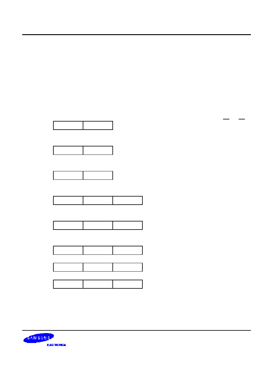
S 3 C 9 6 8 8 / P 9 6 8 8
S A M 8 8RCRI INSTRUCTION SET
6 -2 7
L D
-- L o a d
L D
d s t , s r c
O p e r a t i o n :
d s t
src
T h e c o n t e n t s o f t h e s o u r c e a r e l o a d e d i n t o t h e d e s t i n a t i o n . T h e s o u r c e ' s c ontents are unaffected.
F l a g s :
No flags are affected.
F o r m a t :
B y t e s
C y c l e s
O p c o d e
( H e x )
A d d r M o d e
dst src
dst | opc
src
2
4
rC
r
IM
4
r8
r
R
src | opc
d s t
2
4
r9
R
r
r = 0 t o F
opc
dst | src
2
4
C 7
r
lr
4
D 7
Ir
r
opc
src
d s t
3
6
E 4
R
R
6
E 5
R
IR
opc
d s t
src
3
6
E 6
R
IM
6
D 6
IR
IM
opc
src
d s t
3
6
F 5
IR
R
opc
dst | src
x
3
6
8 7
r
x [r]
opc
s r c | d s t
x
3
6
9 7
x [r]
r

SAM88RI INSTRUCTION SET
S 3 C 9 6 8 8 / P 9 6 8 8
6 -2 8
L D
-- L o a d
L D
( C o n t i n u e d )
E x a m p l e s :
Given: R 0 = 0 1 H , R 1 = 0 A H , r e g i s t e r 0 0 H = 0 1 H , r e g i s t e r 0 1 H = 2 0 H ,
r e g i s t e r 0 2 H = 0 2 H , L O O P = 3 0 H , a n d r e g i s t e r 3 A H = 0 F F H :
L D
R 0 , # 1 0 H
R 0 = 1 0 H
L D
R 0 , 0 1 H
R 0 = 2 0 H , r e g i s t e r 0 1 H = 2 0 H
L D
0 1 H , R 0
R e g i s t e r 0 1 H = 0 1 H , R 0 = 0 1 H
L D
R 1 , @ R 0
R 1 = 2 0 H , R 0 = 0 1 H
L D
@ R 0 , R 1
R 0 = 0 1 H , R 1 = 0 A H , r e g i s t e r 0 1 H = 0 A H
L D
0 0 H , 0 1 H
R e g i s t e r 0 0 H = 2 0 H , r e g i s t e r 0 1 H = 2 0 H
L D
0 2 H , @ 0 0 H
R e g i s t e r 0 2 H = 2 0 H , r e g i s t e r 0 0 H = 0 1 H
L D
0 0 H , # 0 A H
R e g i s t e r 0 0 H = 0 A H
L D
@ 0 0 H , # 1 0 H
R e g i s t e r 0 0 H = 0 1 H , r e g i s t e r 0 1 H = 1 0 H
L D
@ 0 0 H , 0 2 H
R e g i s t e r 0 0 H = 0 1 H , r e g i s t e r 0 1 H = 0 2 , r e g i s t e r 0 2 H = 0 2 H
L D
R 0 , # L O O P [ R 1 ]
R 0 = 0 F F H , R 1 = 0 A H
L D
# L O O P [ R 0 ] , R 1
R e g i s t e r 3 1 H = 0 A H , R 0 = 0 1 H , R 1 = 0 A H
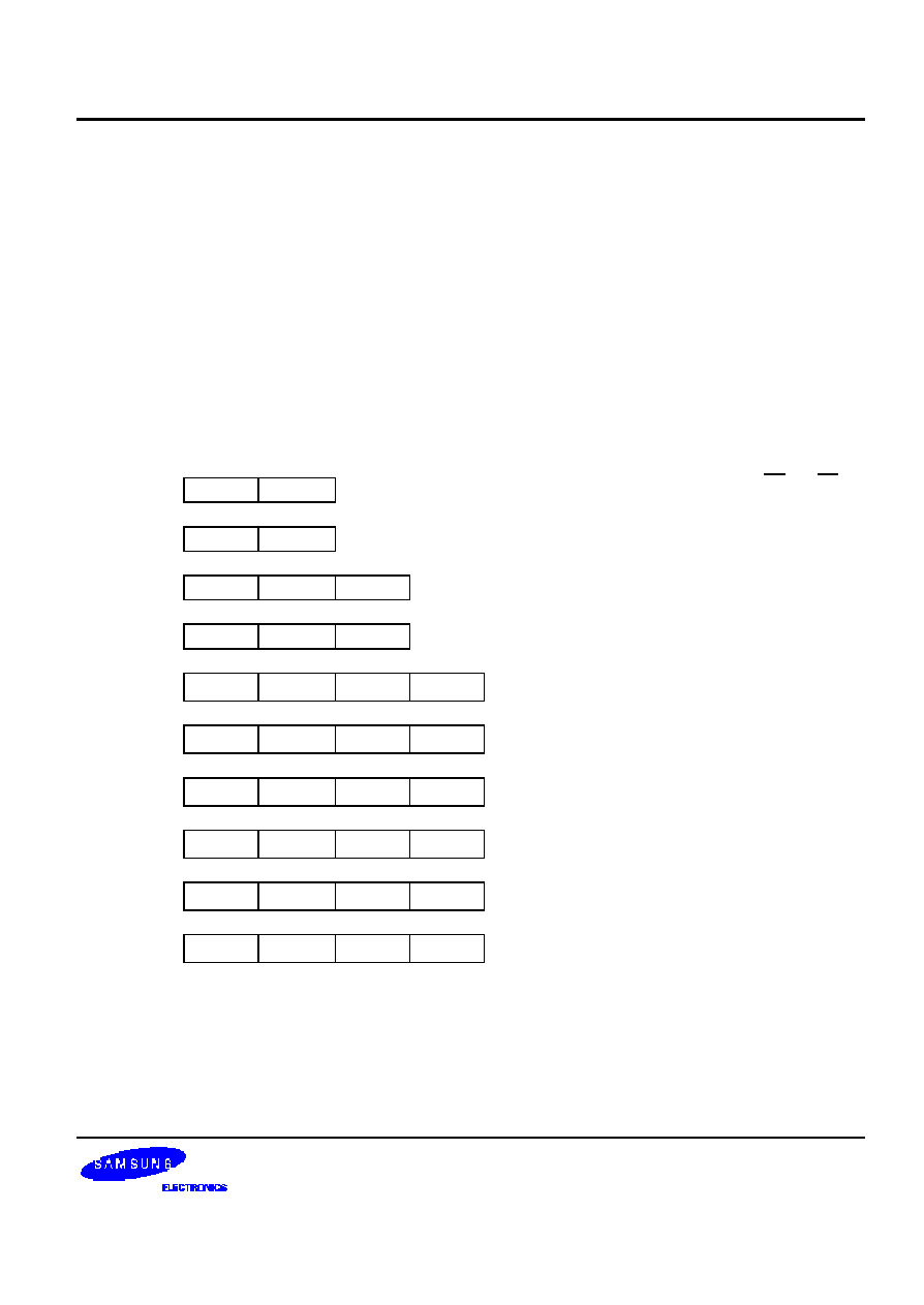
S 3 C 9 6 8 8 / P 9 6 8 8
S A M 8 8RCRI INSTRUCTION SET
6 -2 9
L D C / L D E
-- L o a d M e m o r y
L D C / L D E
d s t , s r c
O p e r a t i o n :
d s t
src
T h i s i n s t r u c t i o n l o a d s a b y t e f r o m p r o g r a m o r d a t a m e m o r y i n t o a w o r k i n g r e g i s t e r o r v i c e-versa. The
s o u r c e v a l u e s a r e u n a f f e c t e d . L D C r e f e r s t o p r o g r a m m e m o r y a n d L D E t o d a t a m e m o r y . T h e
assembler makes 'Irr' or 'rr' values an even number for program memory and an odd number for data
m e m o r y .
F l a g s :
No flags are affected.
F o r m a t :
B y t e s
C y c l e s
O p c o d e
( H e x )
A d d r M o d e
dst src
1 .
opc
dst | src
2
10
C3
r
Irr
2 .
opc
src | dst
2
10
D3
Irr
r
3 .
opc
dst | src
XS
3
12
E7
r
XS [rr]
4 .
opc
src | dst
XS
3
12
F7
XS [rr]
r
5 .
opc
dst | src
XL
L
XL
H
4
14
A7
r
XL [rr]
6 .
opc
src | dst
XL
L
XL
H
4
14
B7
XL [rr]
r
7 .
opc
dst | 0000
D A
L
D A
H
4
14
A7
r
DA
8 .
opc
src | 0000
D A
L
D A
H
4
14
B7
DA
r
9 .
opc
dst | 0001
D A
L
D A
H
4
14
A7
r
DA
1 0 .
opc
src | 0001
D A
L
D A
H
4
14
B7
DA
r
NOTES:
1.
The source (src) or working register pair [rr] for formats 5 and 6 cannot use register pair 0≠1.
2.
For formats 3 and 4, the destination address 'XS [rr]' and the source address 'XS [rr]' are each one byte.
3.
For formats 5 and 6, the destination address 'XL [rr] and the source address 'XL [rr]' are each two bytes.
4.
The DA and r source values for formats 7 and 8 are used to address program memory; the second set of values,
used in formats 9 and 10, are used to address data memory.

SAM88RI INSTRUCTION SET
S 3 C 9 6 8 8 / P 9 6 8 8
6 -3 0
L D C / L D E
-- L o a d M e m o r y
L D C / L D E
( C o n t i n u e d )
E x a m p l e s :
Given: R 0 = 1 1 H , R 1 = 3 4 H , R 2 = 0 1 H , R 3 = 0 4 H , R 4 = 0 0 H , R 5 = 6 0 H ; P r o g r a m m e m o r y
l o c a t i o n s 0 0 6 1 = A A H , 0 1 0 3 H = 4 F H , 0 1 0 4 H = 1 A , 0 1 0 5 H = 6 D H , a n d 1 1 0 4 H = 8 8 H .
E x t e r n a l d a t a m e m o r y l o c a t i o n s 0 0 6 1 H = B B H , 0 1 0 3 H = 5 F H , 0 1 0 4 H = 2 A H , 0 1 0 5 H = 7 D H ,
a n d 1 1 0 4 H = 9 8 H :
L D C
R 0 , @ R R 2
; R 0
c o n t e n t s o f p r o g r a m m e m o r y l o c a t i o n 0 1 0 4 H
; R 0 = 1 A H , R 2 = 0 1 H , R 3 = 0 4 H
L D E
R 0 , @ R R 2
; R 0
c o n t e n t s o f e x t e r n a l d a t a m e m o r y l o c a t i o n 0 1 0 4 H
; R 0 = 2 A H , R 2 = 0 1 H , R 3 = 0 4 H
L D C *
@ R R 2 , R 0
; 1 1 H ( c o n t e n t s o f R 0 ) i s l o a d e d i n t o p r o g r a m m e m o r y
; l o c a t i o n 0 1 0 4 H ( R R 2 ) ,
; w o r k i n g r e g i s t e r s R 0 , R 2 , R 3
n o c h a n g e
L D E
@ R R 2 , R 0
; 1 1 H ( c o n t e n t s o f R 0 ) i s l o a d e d i n t o e x t e r n a l d a t a m e m o r y
; l o c a t i o n 0 1 0 4 H ( R R 2 ) ,
; w o r k i n g r e g i s t e r s R 0 , R 2 , R 3
n o c h a n g e
L D C
R 0 , # 0 1 H [ R R 4 ]
; R 0
c o n t e n t s o f p r o g r a m m e m o r y l o c a t i o n 0 0 6 1 H
; ( 0 1 H + R R 4 ) ,
; R 0 = A A H , R 2 = 0 0 H , R 3 = 6 0 H
L D E
R 0 , # 0 1 H [ R R 4 ]
; R 0
c o n t e n t s o f e x t e r n a l d a t a m e m o r y l o c a t i o n 0 0 6 1 H
; ( 0 1 H + R R 4 ) , R 0 = B B H , R 4 = 0 0 H , R 5 = 6 0 H
L D C
(note)
# 0 1 H [ R R 4 ] , R 0
; 1 1 H ( c o n t e n t s o f R 0 ) i s l o a d e d i n t o p r o g r a m m e m o r y l o c a t i o n
; 0 0 6 1 H ( 0 1 H + 0 0 6 0 H )
L D E
# 0 1 H [ R R 4 ] , R 0
; 1 1 H ( c o n t e n t s o f R 0 ) i s l o a d e d i n t o e x t e r n a l d a t a m e m o r y
; locatio n 0 0 6 1 H ( 0 1 H + 0 0 6 0 H )
L D C
R 0 , # 1 0 0 0 H [ R R 2 ] ; R 0
c o n t e n t s o f p r o g r a m m e m o r y l o c a t i o n 1 1 0 4 H
; ( 1 0 0 0 H + 0 1 0 4 H ) , R 0 = 8 8 H , R 2 = 0 1 H , R 3 = 0 4 H
L D E
R 0 , # 1 0 0 0 H [ R R 2 ] ; R 0
c o n t e n t s o f e x t e r n a l d a t a m e m o r y l o c a t i o n 1 1 0 4 H
; ( 1 0 0 0 H + 0 1 0 4 H ) , R 0 = 9 8 H , R 2 = 0 1 H , R 3 = 0 4 H
L D C
R 0 , 1 1 0 4 H
; R 0
c o n t e n t s o f p r o g r a m m e m o r y l o c a t i o n 1 1 0 4 H , R 0 = 8 8 H
L D E
R 0 , 1 1 0 4 H
; R 0
c o n t e n t s o f e x t e r n a l d a t a m e m o r y l o c a t i o n 1 1 0 4 H ,
; R 0 = 9 8 H
L D C
(note)
1 1 0 5 H , R 0
; 1 1 H ( c o n t e n t s o f R 0 ) i s l o a d e d i n t o p r o g r a m m e m o r y l o c a t i o n
; 1 1 0 5 H , ( 1 1 0 5 H )
1 1 H
L D E
1 1 0 5 H , R 0
; 1 1 H ( c o n t e n t s o f R 0 ) i s l o a d e d i n t o e x t e r n a l d a t a m e m o r y
; l o c a t i o n 1 1 0 5 H , ( 1 1 0 5 H )
1 1 H
NOTE:
These instructions are not supported by masked ROM type devices.

S 3 C 9 6 8 8 / P 9 6 8 8
S A M 8 8RCRI INSTRUCTION SET
6 -3 1
L D C D / L D E D
-- L o a d M e m o r y a n d D e c r e m e n t
L D C D / L D E D
d s t , s r c
O p e r a t i o n :
d s t
src
rr
rr ≠ 1
T h e s e i n s t r u c t i o n s a r e u s e d f o r u s e r s t a c k s o r b l o c k t r a n s f e r s o f d a t a f r o m p r o g r a m o r d a t a m e m o r y
t o t h e r e g i s t e r f i l e . T h e a d d r e s s o f t h e m e m o r y l o c a t i o n i s s p e c i f i e d b y a working register pair. The
c o n t e n t s o f t h e s o u r c e l o c a t i o n a r e l o a d e d i n t o t h e d e s t i n a t i o n l o c a t i o n . T h e m e m o r y a d d r e s s i s t h e n
d e c r e m e n t e d . T h e c o n t e n t s o f t h e s o u r c e a r e u n a f f e c t e d .
L D C D r e f e r e n c e s p r o g r a m m e m o r y a n d L D E D r e f e r e n c e s e x t e r n a l d a t a m e m o r y . T h e a s s e m b l e r
m a k e s ` I r r ' a n e v e n n u m b e r f o r p r o g r a m m e m o r y a n d a n o d d n u m b e r f o r d a t a m e m o r y .
F l a g s :
No flags are affected.
F o r m a t :
B y t e s
C y c l e s
O p c o d e
( H e x )
A d d r M o d e
dst src
opc
dst | src
2
1 0
E 2
r
Irr
E x a m p l e s :
Given: R 6 = 1 0 H , R 7 = 3 3 H , R 8 = 1 2 H , p r o g r a m m e m o r y l o c a t i o n 1 0 3 3 H = 0 C D H , a n d
e x t e r n a l d a t a m e m o r y l o c a t i o n 1 0 3 3 H = 0 D D H :
L D C D
R 8 , @ R R 6
; 0 C D H ( c o n t e n t s o f p r o g r a m m e m o r y l o c a t i o n 1 0 3 3 H ) i s l o a d e d
; i n t o R 8 a n d R R 6 i s d e c r e m e n t e d b y o n e
; R 8 = 0 C D H , R 6 = 1 0 H , R 7 = 3 2 H ( R R 6
R R 6 ≠ 1 )
L D E D
R 8 , @ R R 6
; 0 D D H ( c o n t e n t s o f d a t a m e m o r y l o c a t i o n 1 0 3 3 H ) i s l o a d e d
; i n t o R 8 a n d R R 6 i s d e c r e m e n t e d b y o n e ( R R 6
R R 6 ≠ 1 )
; R 8 = 0 D D H , R 6 = 1 0 H , R 7 = 3 2 H

SAM88RI INSTRUCTION SET
S 3 C 9 6 8 8 / P 9 6 8 8
6 -3 2
LDCI/LDEI
-- L o a d M e m o r y a n d I n c r e m e n t
L D C I / L D E I
d s t , s r c
O p e r a t i o n :
d s t
src
rr
rr + 1
T h e s e i n s t r u c t i o n s a r e u s e d f o r u s e r s t a c k s o r b l o c k t r a n s f e r s o f d a t a f r o m p r o g r a m o r d a t a m e m o r y
t o t h e r e g i s t e r f i l e . T h e a d d r e s s o f t h e m e m o r y l o c a t i o n i s s p e c i f i e d b y a w o r k i n g r e g i s t e r p a i r . T h e
c o n t e n t s o f t h e s o u r c e l o c a t i o n a r e l o a d e d i n t o t h e d e s t i n a t i o n l o c a t i o n . T h e m e m o r y a d d r e s s i s t h e n
i n c r e m e n t e d a u t o m a t i c a l l y . T h e c o n t e n t s o f t h e s o u r c e a r e u n a f f e c t e d .
L D C I r e f e r s t o p r o g r a m m e m o r y a n d L D E I r e f e r s t o e x t e r n a l d a t a m e m o r y . T h e a s s e m b l e r m a k e s ' I r r '
e v e n f o r p r o g r a m m e m o r y a n d o d d f o r d a t a m e m o r y .
F l a g s :
No flags are affected.
F o r m a t :
B y t e s
C y c l e s
O p c o d e
( H e x )
A d d r M o d e
dst src
opc
dst | src
2
1 0
E 3
r
Irr
E x a m p l e s :
Given: R 6 = 1 0 H , R 7 = 3 3 H , R 8 = 1 2 H , p r o g r a m m e m o r y l o c a t i o n s 1 0 3 3 H = 0 C D H a n d
1 0 3 4 H = 0 C 5 H ; e x t e r n a l d a t a m e m o r y l o c a t i o n s 1 0 3 3 H = 0 D D H a n d 1 0 3 4 H = 0 D 5 H :
L D C I
R 8 , @ R R 6
; 0 C D H ( c o n t e n t s o f p r o g r a m m e m o r y l o c a t i o n 1 0 3 3 H ) i s l o a d e d
; i n t o R 8 a n d R R 6 i s i n c r e m e n t e d b y o n e ( R R 6
R R 6 + 1 )
; R 8 = 0 C D H , R 6 = 1 0 H , R 7 = 3 4 H
L D E I
R 8 , @ R R 6
; 0 D D H ( c o n t e n t s o f d a t a m e m o r y l o c a t i o n 1 0 3 3 H ) i s l o a d e d
; i n t o R 8 a n d R R 6 i s i n c r e m e n t e d b y o n e ( R R 6
R R 6 + 1 )
; R 8 = 0 D D H , R 6 = 1 0 H , R 7 = 3 4 H

S 3 C 9 6 8 8 / P 9 6 8 8
S A M 8 8RCRI INSTRUCTION SET
6 -3 3
N O P
-- No Operation
N O P
O p e r a t i o n :
N o a c t i o n i s p e r f o r m e d w h e n t h e C P U e x e c u t e s t h i s i n s t r u c t i o n . T y p i c a l l y , o n e o r m o r e N O P s a r e
executed in sequence in order to effect a timing delay of variable duration.
F l a g s :
No flags are affected.
F o r m a t :
B y t e s
C y c l e s
O p c o d e
( H e x )
opc
1
4
F F
E x a m p l e :
W h e n t h e i n s t r u c t i o n
N O P
i s e n c o u n t e r e d i n a p r o g r a m , n o o p e r a t i o n o c c u r s . I n s t e a d , t h e r e i s a d e l a y i n i n s t r u c t i o n e x e c u t i o n
t i m e .
SAM88RI INSTRUCTION SET
S 3 C 9 6 8 8 / P 9 6 8 8
6 -3 4
O R
-- Logical OR
O R
d s t , s r c
O p e r a t i o n :
d s t
d s t O R s r c
T h e s o u r c e o p e r a n d i s l o g i c a l l y O R e d w i t h t h e d e s t i n a t i o n o p e r a n d a n d t h e r e s u l t i s s t o r e d i n t h e
d e s t i n a t i o n . T h e c o n t e n t s o f t h e s o u r c e a r e u n a f f e c t e d . T h e O R o p e r a t i o n r e s u l t s i n a " 1 " b e i n g
s t o r e d w h e n e v e r e i t h e r o f t h e c o r r e s p o n d i n g b i t s i n t h e t w o o p e r a n d s i s a " 1 " ; o t h e r w i s e a " 0 " i s
s t o r e d .
F l a g s :
C :
Unaffected.
Z:
S e t i f t h e r e s u l t i s " 0 " ; c l e a r e d o t h e r w i s e .
S :
S e t i f t h e r e s u l t b i t 7 i s s e t ; c l e a r e d o t h e r w i s e .
V :
A l w a y s c l e a r e d t o " 0 " .
D :
Unaffected.
H :
Unaffected.
F o r m a t :
B y t e s
C y c l e s
O p c o d e
( H e x )
A d d r M o d e
dst src
opc
dst | src
2
4
4 2
r
r
6
4 3
r
lr
opc
src
d s t
3
6
4 4
R
R
6
4 5
R
IR
opc
d s t
src
3
6
4 6
R
IM
E x a m p l e s :
Given: R 0 = 1 5 H , R 1 = 2 A H , R 2 = 0 1 H , r e g i s t e r 0 0 H = 0 8 H , r e g i s t e r 0 1 H = 3 7 H , a n d
r e g i s t e r 0 8 H = 8 A H :
O R
R 0 , R 1
R 0 = 3 F H , R 1 = 2 A H
O R
R 0 , @ R 2
R 0 = 3 7 H , R 2 = 0 1 H , r e g i s t e r 0 1 H = 3 7 H
O R
0 0 H , 0 1 H
R e g i s t e r 0 0 H = 3 F H , r e g i s t e r 0 1 H = 3 7 H
O R
0 1 H , @ 0 0 H
R e g i s t e r 0 0 H = 0 8 H , r e g i s t e r 0 1 H = 0 B F H
O R
0 0 H , # 0 2 H
R e g i s t e r 0 0 H = 0 A H
I n t h e f i r s t e x a m p l e , i f w o r k i n g r e g i s t e r R 0 c o n t a i n s t h e v a l u e 1 5 H a n d r e g i s t e r R 1 t h e v a l u e 2 A H , t h e
s t a t e m e n t " O R R 0 , R 1 " l o g i c a l-O R s t h e R 0 a n d R 1 r e g i s t e r c o n t e n t s a n d s t o r e s t h e r e s u l t ( 3 F H ) i n
d e s t i n a t i o n r e g i s t e r R 0 .
T h e o t h e r e x a m p l e s s h o w t h e u s e o f t h e l o g i c a l O R i n s t r u c t i o n w i t h t h e v a r i o u s a d d r e s s i n g m o d e s
a n d f o r m a t s .

S 3 C 9 6 8 8 / P 9 6 8 8
S A M 8 8RCRI INSTRUCTION SET
6 -3 5
P O P
-- P O P F r o m S t a c k
P O P
d s t
O p e r a t i o n :
d s t
@ S P
S P
S P + 1
T h e c o n t e n t s o f t h e l o c a t i o n a d d r e s s e d b y t h e s t a c k p o i n t e r a r e l o a d e d i n t o t h e d e s t i n a t i o n . T h e
s t a c k p o i n t e r i s t h e n i n c r e m e n t e d b y o n e .
F l a g s :
No flags affected.
F o r m a t :
B y t e s
C y c l e s
O p c o d e
( H e x )
A d d r M o d e
dst
opc
d s t
2
8
5 0
R
8
5 1
IR
E x a m p l e s :
Given: R e g i s t e r 0 0 H = 0 1 H , r e g i s t e r 0 1 H = 1 B H , S P ( 0 D 9 H ) = 0 B B H , a n d s t a c k r e g i s t e r 0 B B H
= 5 5 H :
P O P
0 0 H
R e g i s t e r 0 0 H = 5 5 H , S P = 0 B C H
P O P
@ 0 0 H
R e g i s t e r 0 0 H = 0 1 H , r e g i s t e r 0 1 H = 5 5 H , S P = 0 B C H
I n t h e f i r s t e x a m p l e , g e n e r a l r e g i s t e r 0 0 H c o n t a i n s t h e v a l u e 0 1 H . T h e s t a t e m e n t " P O P 0 0 H " l o a d s
t h e c o n t e n t s o f l o c a t i o n 0 B B H ( 5 5 H ) i n t o d e s t i n a t i o n r e g i s t e r 0 0 H a n d t h e n i n c r e m e n t s t h e s t a c k
p o i n t e r b y o n e . R e g i s t e r 0 0 H t h e n c o n t a i n s t h e v a l u e 5 5 H a n d t h e S P p o i n t s t o l o c a t i o n 0 B C H .

SAM88RI INSTRUCTION SET
S 3 C 9 6 8 8 / P 9 6 8 8
6 -3 6
P U S H
-- P u s h T o S t a c k
P U S H
src
O p e r a t i o n :
S P
S P ≠ 1
@ S P
src
A P U S H i n s t r u c t i o n d e c r e m e n t s t h e s t a c k p o i n t e r v a l u e a n d l o a d s t h e c o n t e n t s o f t h e s o u r c e ( s r c )
i n t o t h e l o c a t i o n a d d r e s s e d b y t h e d e c r e m e n t e d s t a c k p o i n t e r . T h e o p e r a t i o n t h e n a d d s t h e n e w
v a l u e t o t h e t o p o f t h e s t a c k .
F l a g s :
No flags are affected.
F o r m a t :
B y t e s
C y c l e s
O p c o d e
( H e x )
A d d r M o d e
dst
opc
src
2
8
7 0
R
8
7 1
IR
E x a m p l e s :
Given: R e g i s t e r 4 0 H = 4 F H , r e g i s t e r 4 F H = 0 A A H , S P = 0 C 0 H :
P U S H
4 0 H
R e g i s t e r 4 0 H = 4 F H , s t a c k r e g i s t e r 0 B F H = 4 F H ,
S P = 0 B F H
P U S H
@ 4 0 H
R e g i s t e r 4 0 H = 4 F H , r e g i s t e r 4 F H = 0 A A H , s t a c k r e g i s t e r
0 B F H = 0 A A H , S P = 0 B F H
In the first example, if the stack pointer contains the value 0C0H, and general register 40H the value
4 F H , t h e s t a t e m e n t " P U S H 4 0 H " d e c r e m e n t s t h e s t a c k p o i n t e r f r o m 0 C 0 t o 0 B F H . I t t h e n l o a d s t h e
c o n t e n t s o f r e g i s t e r 4 0 H i n t o l o c a t i o n 0 B F H . R e g i s t e r 0 B F H t h e n c o n t a i n s t h e v a l u e 4 F H a n d S P
p o i n t s t o l o c a t i o n 0 B F H .

S 3 C 9 6 8 8 / P 9 6 8 8
S A M 8 8RCRI INSTRUCTION SET
6 -3 7
R C F
-- R e s e t C a r r y F l a g
R C F
R C F
O p e r a t i o n :
C
0
The carry flag is cleared to logic zero, regardless of its previous value.
F l a g s :
C :
C l e a r e d t o " 0 " .
No other flags are affected.
F o r m a t :
B y t e s
C y c l e s
O p c o d e
( H e x )
opc
1
4
C F
E x a m p l e :
Given: C = " 1 " o r " 0 " :
T h e i n s t r u c t i o n R C F c l e a r s t h e c a r r y f l a g ( C ) t o l o g i c z e r o .

SAM88RI INSTRUCTION SET
S 3 C 9 6 8 8 / P 9 6 8 8
6 -3 8
R E T
-- Return
R E T
O p e r a t i o n :
P C
@ S P
S P
S P + 2
T h e R E T i n s t r u c t i o n i s n o r m a l l y u s e d t o r e t u r n t o t h e p r e v i o u s l y e x e c u t i n g p r o c e d u r e a t t h e e n d o f a
p r o c e d u r e e n t e r e d b y a C A L L i n s t r u c t i o n . T h e c o n t e n t s o f t h e l o c a t i o n a d d r e s s e d b y t h e s t a c k
p o i n t e r a r e p o p p e d i n t o t h e p r o g r a m c o u n t e r . T h e n e x t s t a t e m e n t t h a t i s e x e c u t e d i s t h e o n e t h a t i s
a d d r e s s e d b y t h e n e w p r o g r a m c o u n t e r v a l u e .
F l a g s :
No flags are affected.
F o r m a t :
B y t e s
C y c l e s
O p c o d e
( H e x )
opc
1
8
A F
E x a m p l e :
Given: S P = 0 B C H , ( S P ) = 1 0 1 A H , a n d P C = 1 2 3 4 :
R E T
P C = 1 0 1 A H , S P = 0 B E H
T h e s t a t e m e n t " R E T " p o p s t h e c o n t e n t s o f s t a c k p o i n t e r l o c a t i o n 0 B C H ( 1 0 H ) i n t o t h e h i g h b y t e o f
t h e p r o g r a m c o u n t e r . T h e s t a c k p o i n t e r t h e n p o p s t h e v a l u e i n l o c a t i o n 0 B D H ( 1 A H ) i n t o t h e P C ' s
l o w b y t e a n d t h e i n s t r u c t i o n a t l o c a t i o n 1 0 1 A H i s e x e c u t e d . T h e s t a c k p o i n t e r n o w p o i n t s t o m e m o r y
l o c a t i o n 0 B E H .

S 3 C 9 6 8 8 / P 9 6 8 8
S A M 8 8RCRI INSTRUCTION SET
6 -3 9
R L
-- Rotate Left
R L
d s t
O p e r a t i o n :
C
d s t ( 7 )
dst (0)
d s t ( 7 )
d s t ( n + 1 )
d s t ( n ) , n = 0 ≠ 6
The contents of the destination operand are rotated left one bit position. The initial value of bit 7 is
m o v e d t o t h e b i t z e r o ( L S B ) p o s i t i o n a n d a l s o r e p l a c e s t h e c a r r y f l a g .
7
0
C
F l a g s :
C :
Set if the bit rotated from the m o s t s i g n i f i c a n t b i t p o s i t i o n ( b i t 7 ) w a s " 1 " .
Z:
S e t i f t h e r e s u l t i s " 0 " ; c l e a r e d o t h e r w i s e .
S :
S e t i f t h e r e s u l t b i t 7 i s s e t ; c l e a r e d o t h e r w i s e .
V :
Set if arithmetic overflow occurred, that is, if the sign of the destination changed during
rotation; cleared otherwise.
D :
Unaffected.
H :
Unaffected.
F o r m a t :
B y t e s
C y c l e s
O p c o d e
( H e x )
A d d r M o d e
dst
opc
d s t
2
4
9 0
R
4
9 1
IR
E x a m p l e s :
Given: R e g i s t e r 0 0 H = 0 A A H , r e g i s t e r 0 1 H = 0 2 H a n d r e g i s t e r 0 2 H = 1 7 H :
R L
0 0 H
R e g i s t e r 0 0 H = 5 5 H , C = " 1 "
R L
@ 0 1 H
R e g i s t e r 0 1 H = 0 2 H , r e g i s t e r 0 2 H = 2 E H , C = " 0 "
I n t h e f i r s t e x a m p l e , i f g e n e r a l r e g i s t e r 0 0 H c o n t a i n s t h e v a l u e 0 A A H ( 1 0 1 0 1 0 1 0 B ) , t h e s t a t e m e n t
" R L 0 0 H " r o t a t e s t h e 0 A A H v a l u e l e f t o n e b i t p o s i t i o n , l e a v i n g t h e n e w v a l u e 5 5 H ( 0 1 0 1 0 1 0 1 B ) a n d
setting the carry and overflow flags.
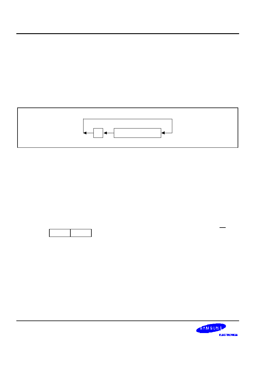
SAM88RI INSTRUCTION SET
S 3 C 9 6 8 8 / P 9 6 8 8
6 -4 0
R L C
-- R o t a t e L e f t T h r o u g h C a r r y
R L C
d s t
O p e r a t i o n :
dst (0)
C
C
d s t ( 7 )
d s t ( n + 1 )
d s t ( n ) , n = 0 ≠ 6
T h e c o n t e n t s o f t h e d e s t i n a t i o n o p e r a n d w i t h t he carry flag are rotated left one bit position. The initial
value of bit 7 replaces the carry flag (C); the initial value of the carry flag replaces bit zero.
7
0
C
F l a g s :
C :
S e t i f t h e b i t r o t a t e d f r o m t h e m o s t s i g n i f i c a n t b i t p o s i t i o n ( b i t 7 ) w a s " 1 " .
Z:
S e t i f t h e r e s u l t i s " 0 " ; c l e a r e d o t h e r w i s e .
S :
S e t i f t h e r e s u l t b i t 7 i s s e t ; c l e a r e d o t h e r w i s e .
V :
Set if arithmetic overflow occurred, that is, if the sign of the destination changed during
rotation; cleared otherwis e .
D :
Unaffected.
H :
Unaffected.
F o r m a t :
B y t e s
C y c l e s
O p c o d e
( H e x )
A d d r M o d e
dst
opc
d s t
2
4
1 0
R
4
1 1
IR
E x a m p l e s :
Given: R e g i s t e r 0 0 H = 0 A A H , r e g i s t e r 0 1 H = 0 2 H , a n d r e g i s t e r 0 2 H = 1 7 H , C = " 0 " :
R L C
0 0 H
R e g i s t e r 0 0 H = 5 4 H , C = " 1 "
R L C
@ 0 1 H
R e g i s t e r 0 1 H = 0 2 H , r e g i s t e r 0 2 H = 2 E H , C = " 0 "
I n t h e f i r s t e x a m p l e , i f g e n e r a l r e g i s t e r 0 0 H h a s t h e v a l u e 0 A A H ( 1 0 1 0 1 0 1 0 B ) , t h e s t a t e m e n t " R L C
00H" rotates 0AAH one bit position to the left. The initial value of bit 7 s e t s t h e c a r r y f l a g a n d t h e
initial value of the C flag replaces bit zero of register 00H, leaving the value 55H (01010101B). The
M S B o f r e g i s t e r 0 0 H r e s e t s t h e c a r r y f l a g t o " 1 " a n d s e t s t h e o v e r f l o w f l a g .
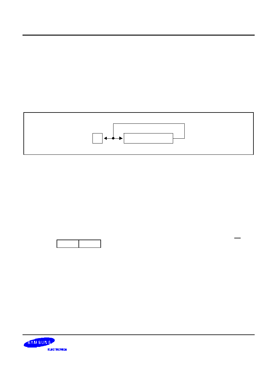
S 3 C 9 6 8 8 / P 9 6 8 8
S A M 8 8RCRI INSTRUCTION SET
6 -4 1
R R
-- R o t a t e R i g h t
R R
d s t
O p e r a t i o n :
C
d s t ( 0 )
dst (7)
d s t ( 0 )
dst (n)
d s t ( n + 1 ) , n = 0 ≠ 6
The contents of the destination operand are rotated right one bit position. The initial value of bit zero
( L S B ) i s m o v e d t o b i t 7 ( M S B ) a n d a l s o r e p l a c e s t h e c a r r y f l a g ( C ) .
7
0
C
F l a g s :
C :
Set if the bit rotated from the least significant bit position (bit zero) was "1".
Z:
S e t i f t h e r e s u l t i s " 0 " ; c l e a r e d o t h e r w i s e .
S :
S e t i f t h e r e s u l t b i t 7 i s s e t ; c l e a r e d o t h e r w i s e .
V :
Set if arithmetic overflow occurred, that is, if the sign of the destination changed during
rotation; cleared otherwise.
D :
Unaffected.
H :
Unaffected.
F o r m a t :
B y t e s
C y c l e s
O p c o d e
( H e x )
A d d r M o d e
dst
opc
d s t
2
4
E 0
R
4
E 1
IR
E x a m p l e s :
Given: R e g i s t e r 0 0 H = 3 1 H , r e g i s t e r 0 1 H = 0 2 H , a n d r e g i s t e r 0 2 H = 1 7 H :
R R
0 0 H
R e g i s t e r 0 0 H = 9 8 H , C = " 1 "
R R
@ 0 1 H
R e g i s t e r 0 1 H = 0 2 H , r e g i s t e r 0 2 H = 8 B H , C = " 1 "
I n t h e f i r s t e x a m p l e , i f g e n e r a l r e g i s t e r 0 0 H c o n t a i n s t h e v a l u e 3 1 H ( 0 0 1 1 0 0 0 1 B ) , t h e s t a t e m e n t " R R
00H" rotates this value one bit position to the right. The initial value of bit zero is moved to bit 7 ,
leaving the new value 98H (10011000B) in the destination register. The initial bit zero also resets the
C flag to "1" and the sign flag and overfl o w f l a g a r e a l s o s e t t o " 1 " .

SAM88RI INSTRUCTION SET
S 3 C 9 6 8 8 / P 9 6 8 8
6 -4 2
R R C
-- R o t a t e R i g h t T h r o u g h C a r r y
R R C
d s t
O p e r a t i o n :
dst (7)
C
C
d s t ( 0 )
dst (n)
d s t ( n + 1 ) , n = 0 ≠ 6
The contents of the destination operand and the carry flag are rotated right one bit position. The
initial value of bit zero (LSB) replaces the carry flag; the initial value of the carry flag replaces bit 7
( M S B ) .
7
0
C
F l a g s :
C :
Set if the bit rotated from the least significant bit position (bit zero) was "1".
Z:
Set if the result is " 0 " c l e a r e d o t h e r w i s e .
S :
S e t i f t h e r e s u l t b i t 7 i s s e t ; c l e a r e d o t h e r w i s e .
V :
Set if arithmetic overflow occurred, that is, if the sign of the destination changed during
rotation; cleared otherwise.
D :
Unaffected.
H :
Unaffected.
F o r m a t :
B y t e s
C y c l e s
O p c o d e
( H e x )
A d d r M o d e
dst
opc
d s t
2
4
C 0
R
4
C 1
IR
E x a m p l e s :
Given: R e g i s t e r 0 0 H = 5 5 H , r e g i s t e r 0 1 H = 0 2 H , r e g i s t e r 0 2 H = 1 7 H , a n d C = " 0 " :
R R C
0 0 H
R e g i s t e r 0 0 H = 2 A H , C = " 1 "
R R C
@ 0 1 H
R e g i s t e r 0 1 H = 0 2 H , r e g i s t e r 0 2 H = 0 B H , C = " 1 "
I n t h e f i r s t e x a m p l e , i f g e n e r a l r e g i s t e r 0 0 H c o n t a i n s t h e v a l u e 5 5 H ( 0 1 0 1 0 1 0 1 B ) , t h e s t a t e m e n t
"RRC 00H" rotates this value one bit position to the right. The initial value of bit zero ("1") replaces
the carry flag and the initial value of the C flag ("1") replaces bit 7. This leaves the new value 2AH
(00101010B) in destination register 00H. The sign flag and overflow flag are both cleared to "0".
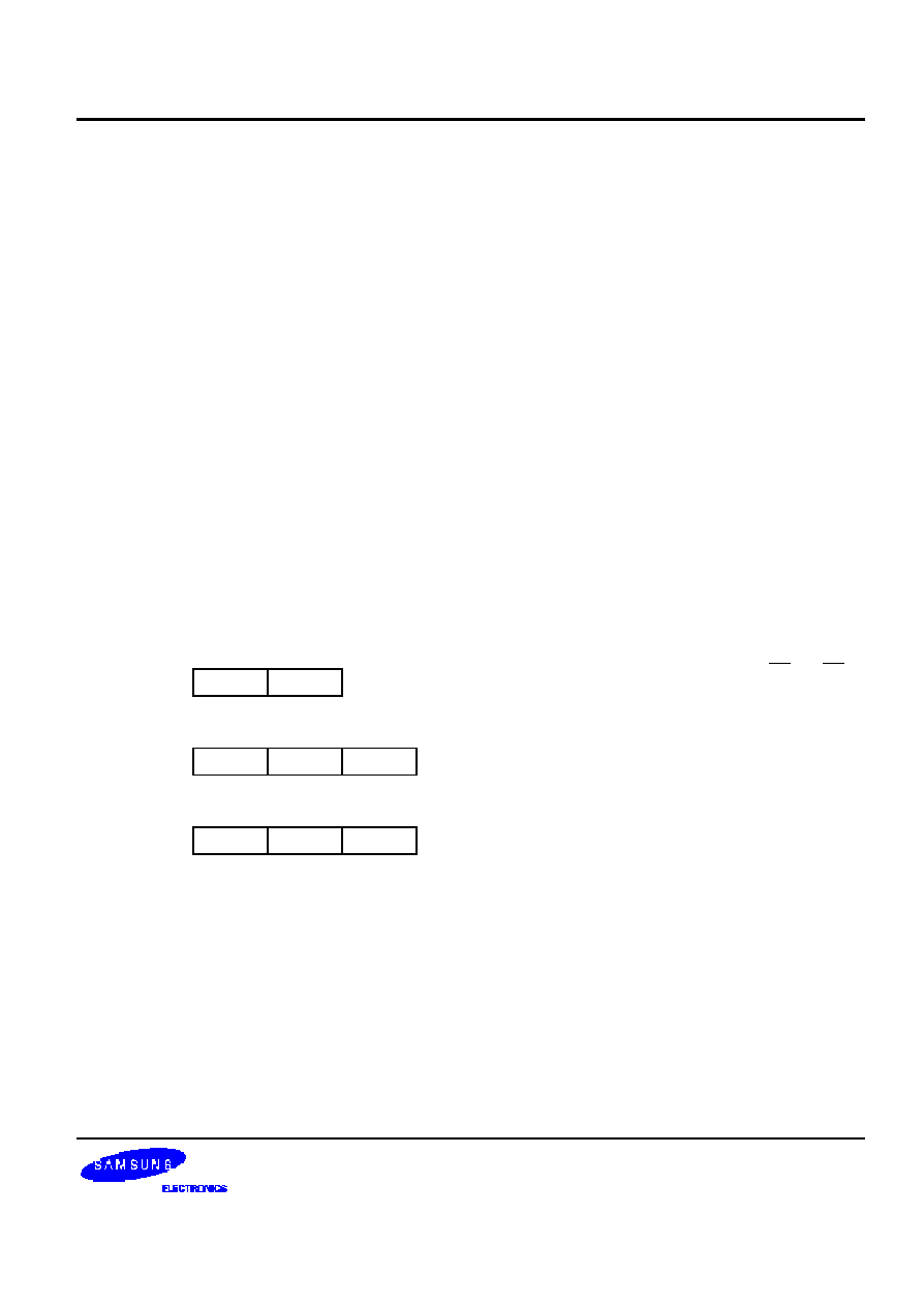
S 3 C 9 6 8 8 / P 9 6 8 8
S A M 8 8RCRI INSTRUCTION SET
6 -4 3
S B C
-- Subtract With Carry
S B C
d s t , s r c
O p e r a t i o n :
d s t
d s t ≠ s r c ≠ c
The source operand, along with the current value of the carry flag, is subtracted from the destination
o p e r a n d a n d t h e r e s u l t i s s t o r e d i n t h e d e s t i n a t i o n . T h e c o n t e n t s o f t h e s o u r c e a r e u n a f f e c t e d .
S u b t r a c t i o n i s p e r f o r m e d b y a d d i n g t h e t w o ' s -c o m p l e m e n t o f t h e s o u r c e o p e r a n d t o t h e d e s t i n a t i o n
o p e r a n d . I n m u l t i p l e p r e c i s i o n a r i t h m e t i c , t h i s i n s t r u c t i o n p e r m i t s t h e c a r r y ( " b o r r o w " ) f r o m t h e
s u b t r a c t i o n o f t h e l o w -o r d e r o p e r a n d s t o b e s u b t r a c t e d f r o m t h e s u b t r a c t i o n o f h i g h -o r d e r o p e r a n d s .
F l a g s :
C :
S e t i f a b o r r o w o c c u r r e d ( s r c > d s t ) ; c l e a r e d o t h e r w i s e .
Z:
S e t i f t h e r e s u l t i s " 0 " ; c l e a r e d o t h e r w i s e .
S :
Set if the result is negative; cleared otherwise.
V :
Set if arithmetic overflow occurred, that is, if the operands were of opposite sign and the
s i g n o f t h e r e s u l t i s t h e s a m e a s t h e s i g n o f t h e s o u r c e ; c l e a r e d o t h e r w i s e .
D :
A l w a y s s e t t o " 1 " .
H :
Cleared if there is a carry from the most significant bit of the low-order four bits of the
r e s u l t ; s e t o t h e r w i s e , i n d i c a t i n g a " b o rrow".
F o r m a t :
B y t e s
C y c l e s
O p c o d e
( H e x )
A d d r M o d e
dst src
opc
dst | src
2
4
3 2
r
r
6
3 3
r
lr
opc
src
d s t
3
6
3 4
R
R
6
3 5
R
IR
opc
d s t
src
3
6
3 6
R
IM
E x a m p l e s :
Given: R 1 = 1 0 H , R 2 = 0 3 H , C = " 1 " , r e g i s t e r 0 1 H = 2 0 H , r e g i s t e r 0 2 H = 0 3 H , a n d r e g i s t e r
0 3 H = 0 A H :
S B C
R 1 , R 2
R 1 = 0 C H , R 2 = 0 3 H
S B C
R 1 , @ R 2
R 1 = 0 5 H , R 2 = 0 3 H , r e g i s t e r 0 3 H = 0 A H
S B C
0 1 H , 0 2 H
R e g i s t e r 0 1 H = 1 C H , r e g i s t e r 0 2 H = 0 3 H
S B C
0 1 H , @ 0 2 H
R e g i s t e r 0 1 H = 1 5 H , r e g i s t e r 0 2 H = 0 3 H , r e g i s t e r 0 3 H = 0 A H
S B C
0 1 H , # 8 A H
R e g i s t e r 0 1 H = 9 5 H ; C , S , a n d V = " 1 "
In the first example, if working register R1 contains the value 10H and register R2 the value 03H, the
s t a t e m e n t " S B C R 1 , R 2 " s u b t r a c t s t h e s o u r c e v a l u e ( 0 3 H ) a n d t h e C f l a g v a l u e ( " 1 " ) f r o m t h e
d e s t i n a t i o n ( 1 0 H ) a n d t h e n s t o r e s t h e r e s u l t ( 0 C H ) i n r e g i s t e r R 1 .

SAM88RI INSTRUCTION SET
S 3 C 9 6 8 8 / P 9 6 8 8
6 -4 4
S C F
-- S e t C a r r y F l a g
S C F
O p e r a t i o n :
C
1
The carry flag (C) is set to logic one, regardless of its previous value.
F l a g s :
C :
S e t t o " 1 " .
No other flags are affected.
F o r m a t :
B y t e s
C y c l e s
O p c o d e
( H e x )
opc
1
4
D F
E x a m p l e :
T h e s t a t e m e n t
S C F
s e t s t h e c a r r y f l a g t o l o g i c o n e .

S 3 C 9 6 8 8 / P 9 6 8 8
S A M 8 8RCRI INSTRUCTION SET
6 -4 5
S R A
-- Shift Right Arithmetic
S R A
d s t
O p e r a t i o n :
dst (7)
d s t ( 7 )
C
d s t ( 0 )
dst (n)
d s t ( n + 1 ) , n = 0 ≠ 6
An arithmetic shift -right of one bit position is performed on the destination operand. Bit zero (the
LSB) replaces the carry flag. The value of bit 7 (the sign bit) is unchanged and is shifted into bit
p o s i t i o n 6 .
7
0
C
6
F l a g s :
C :
S e t i f t h e b i t s h i f t e d f r o m t h e L S B p o s i t i o n ( b i t z e r o ) w a s " 1 " .
Z:
S e t i f t h e r e s u l t i s " 0 " ; c l e a r e d o t h e r w i s e .
S :
Set if the result is negative; cleared otherwise.
V :
A l w a y s c l e a r e d t o " 0 " .
D :
Unaffected.
H :
Unaffected.
F o r m a t :
B y t e s
C y c l e s
O p c o d e
( H e x )
A d d r M o d e
dst
opc
d s t
2
4
D 0
R
4
D 1
IR
E x a m p l e s :
Given: R e g i s t e r 0 0 H = 9 A H , r e g i s t e r 0 2 H = 0 3 H , r e g i s t e r 0 3 H = 0 B C H , a n d C = " 1 " :
S R A
0 0 H
R e g i s t e r 0 0 H = 0 C D , C = " 0 "
S R A
@ 0 2 H
R e g i s t e r 0 2 H = 0 3 H , r e g i s t e r 0 3 H = 0 D E H , C = " 0 "
I n t h e f i r s t e x a m p l e , i f g e n e r a l r e g i s t e r 0 0 H c o n t a i n s t h e v a l u e 9 A H ( 1 0 0 1 1 0 1 0 B ) , t h e s t a t e m e n t
" S R A 0 0 H " s h i f t s t h e b i t v a l u e s i n r e g i s t e r 0 0 H r i g h t o n e b i t p o s i t i o n . B i t z e r o ( " 0 " ) c l e a r s t h e C f l a g
and bit 7 ("1") is then shifted into the bit 6 position (bit 7 remains unchanged). This leaves the value
0 C D H ( 1 1 0 0 1 1 0 1 B ) i n d e s t i n a t i o n r e g i s t e r 0 0 H .

SAM88RI INSTRUCTION SET
S 3 C 9 6 8 8 / P 9 6 8 8
6 -4 6
S T O P
-- S t o p O p e r a t i o n
S T O P
O p e r a t i o n :
T h e S T O P i n s t r u c t i o n s t o p s b o t h t h e C P U c l o c k a n d s y s t e m c l o c k a n d c a u s e s t h e m i c r o c o n t r o l l e r
t o e n t e r S t o p m o d e . D u r i n g S t o p m o d e , t h e c o n t e n t s o f o n -c h i p C P U r e g i s t e r s , p e r i p h e r a l r e g i s t e r s ,
a n d I / O p o r t c o n t r o l a n d d a t a r e g i s t e r s a r e r e t a i n e d . S t o p m o d e c a n b e r e l e a s e d b y a n e x t e r n a l r e s e t
operation or External interrupt input. For the reset operation, the
RESET
p i n m u s t b e h e l d t o L o w l e v e l
until the required oscillation stabilization interval has elapsed.
F l a g s :
No flags are affected.
F o r m a t :
B y t e s
C y c l e s
O p c o d e
( H e x )
A d d r M o d e
dst src
opc
1
4
7 F
≠
≠
E x a m p l e :
T h e s t a t e m e n t
S T O P
h a l t s a l l m i c r o c o n t r o l l e r o p e r a t i o n s .
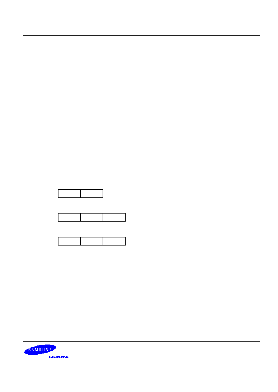
S 3 C 9 6 8 8 / P 9 6 8 8
S A M 8 8RCRI INSTRUCTION SET
6 -4 7
S U B
-- S u b t r a c t
S U B
d s t , s r c
O p e r a t i o n :
d s t
d s t ≠ src
T h e s o u r c e o p e r a n d i s s u b t r a c t e d f r o m t h e d e s t i n a t i o n o p e r a n d a n d t h e r e s u l t i s s t o r e d i n t h e
d e s t i n a t i o n . T h e c o n t e n t s o f t h e s o u r c e a r e u n a f f e c t e d . S u b t r a c t i o n i s p e r f o r m e d b y a d d i n g t h e t w o ' s
c o m p l e m e n t o f t h e s o u r c e o p e r a n d t o t h e d e s t i n a t i o n o p e r a n d .
F l a g s :
C :
S e t i f a " b o r r o w " o c c u r r e d ; c l e a r e d o t h e r w i s e .
Z:
S e t i f t h e r e s u l t i s " 0 " ; c l e a r e d o t h e r w i s e .
S :
Set if the re sult is negative; cleared otherwise.
V :
Set if arithmetic overflow occurred, that is, if the operands were of opposite signs and the
s i g n o f t h e r e s u l t i s o f t h e s a m e a s t h e s i g n o f t h e s o u r c e o p e r a n d ; c l e a r e d o t h e r w i s e .
D :
A l w a y s s e t t o " 1 " .
H :
Cleared if there is a carry from the most significant bit of the low-order four bits of the
r e s u l t ; s e t o t h e r w i s e i n d i c a t i n g a " b o r r o w " .
F o r m a t :
B y t e s
C y c l e s
O p c o d e
( H e x )
A d d r M o d e
dst src
opc
dst | src
2
4
2 2
r
r
6
2 3
r
lr
opc
src
d s t
3
6
2 4
R
R
6
2 5
R
IR
opc
d s t
src
3
6
2 6
R
IM
E x a m p l e s :
Given: R 1 = 1 2 H , R 2 = 0 3 H , r e g i s t e r 0 1 H = 2 1 H , r e g i s t e r 0 2 H = 0 3 H , r e g i s t e r 0 3 H = 0 A H :
S U B
R 1 , R 2
R 1 = 0 F H , R 2 = 0 3 H
S U B
R 1 , @ R 2
R 1 = 0 8 H , R 2 = 0 3 H
S U B
0 1 H , 0 2 H
R e g i s t e r 0 1 H = 1 E H , r e g i s t e r 0 2 H = 0 3 H
S U B
0 1 H , @ 0 2 H
R e g i s t e r 0 1 H = 1 7 H , r e g i s t e r 0 2 H = 0 3 H
S U B
0 1 H , # 9 0 H
R e g i s t e r 0 1 H = 9 1 H ; C , S , a n d V = " 1 "
S U B
0 1 H , # 6 5 H
R e g i s t e r 0 1 H = 0 B CH ; C a n d S = " 1 " , V = " 0 "
In the first example, if working register R1 contains the value 12H and if register R2 contains the
v a l u e 0 3 H , t h e s t a t e m e n t " S U B R 1 , R 2 " s u b t r a c t s t h e s o u r c e v a l u e ( 0 3 H ) f r o m t h e d e s t i n a t i o n v a l u e
( 1 2 H ) a n d s t o r e s t h e r e s u l t ( 0 F H ) i n d e s t i n a t i o n r e g i s t e r R 1 .
SAM88RI INSTRUCTION SET
S 3 C 9 6 8 8 / P 9 6 8 8
6 -4 8
T C M
-- T e s t C o m p l e m e n t U n d e r M a s k
T C M
d s t , s r c
O p e r a t i o n :
( N O T d s t ) A N D s r c
T h i s i n s t r u c t i o n t e s t s s e l e c t e d b i t s i n t h e d e s t i n a t i o n o p e r a n d f o r a l o g i c o n e v a l u e . T h e b i t s t o b e
t e s t e d a r e s p e c i f i e d b y s e t t i n g a " 1 " b i t i n t h e c o r r e s p o n d i n g p o s i t i o n o f t h e s o u r c e o p e r a n d ( m a s k ) .
T h e T C M s t a t e m e n t c o m p l e m e n t s t h e d e s t i n a t i o n o p e r a n d , w h i c h i s t h e n A N D e d w i t h t h e s o u r c e
m a s k . T h e z e r o ( Z ) f l a g c a n t h e n b e c h e c k e d t o d e t e r m i n e t h e r e s u l t . T h e d e s t i n a t i o n a n d s o u r c e
operands are unaffected.
F l a g s :
C :
Unaffected.
Z:
S e t i f t h e r e s u l t i s " 0 " ; c l e a r e d o t h e r w i s e .
S :
S e t i f t h e r e s u l t b i t 7 i s s e t ; c l e a r e d o t h e r w i s e .
V :
A l w a y s c l e a r e d t o " 0 " .
D :
Unaffected.
H :
Unaffected.
F o r m a t :
B y t e s
C y c l e s
O p c o d e
( H e x )
A d d r M o d e
dst src
opc
dst | src
2
4
6 2
r
r
6
6 3
r
lr
opc
src
d s t
3
6
6 4
R
R
6
6 5
R
IR
opc
d s t
src
3
6
6 6
R
IM
E x a m p l e s :
Given: R 0 = 0 C 7 H , R 1 = 0 2 H , R 2 = 1 2 H , r e g i s t e r 0 0 H = 2 B H , r e g i s t e r 0 1 H = 0 2 H , a n d
r e g i s t e r 0 2 H = 2 3 H :
T C M
R 0 , R 1
R 0 = 0 C 7 H , R 1 = 0 2 H , Z = " 1 "
T C M
R 0 , @ R 1
R 0 = 0 C 7 H , R 1 = 0 2 H , r e g i s t e r 0 2 H = 2 3 H , Z = " 0 "
T C M
0 0 H , 0 1 H
R e g i s t e r 0 0 H = 2 B H , r e g i s t e r 0 1 H = 0 2 H , Z = " 1 "
T C M
0 0 H , @ 0 1 H
R e g i s t e r 0 0 H = 2 B H, r e g i s t e r 0 1 H = 0 2 H ,
r e g i s t e r 0 2 H = 2 3 H , Z = " 1 "
T C M
0 0 H , # 3 4
R e g i s t e r 0 0 H = 2 B H , Z = " 0 "
I n t h e f i r s t e x a m p l e , i f w o r k i n g r e g i s t e r R 0 c o n t a i n s t h e v a l u e 0 C 7 H ( 1 1 0 0 0 1 1 1 B ) a n d r e g i s t e r R 1 t h e
v a l u e 0 2 H ( 0 0 0 0 0 0 1 0 B ) , t h e s t a t e m e n t " T C M R 0 , R 1 " t e s t s b i t o n e i n t h e d e s t i n a t i o n r e g i s t e r f o r a
" 1 " v a l u e . B e c a u s e t h e m a s k v a l u e c o r r e s p o n d s t o t h e t e s t b i t , t h e Z f l a g i s s e t t o l o g i c o n e a n d c a n
b e t e s t e d t o d e t e r m i n e t h e r e s u l t o f t h e T C M o p e r a t i o n .

S 3 C 9 6 8 8 / P 9 6 8 8
S A M 8 8RCRI INSTRUCTION SET
6 -4 9
T M
-- T e s t U n d e r M a s k
T M
d s t , s r c
O p e r a t i o n :
d s t A N D s r c
T h i s i n s t r u c t i o n t e s t s s e l e c t e d b i t s i n t h e d e s t i n a t i o n o p e r a n d f o r a l o g i c z e r o v a l u e . T h e b i t s t o b e
t e s t e d a r e s p e c i f i e d b y s e t t i n g a " 1 " b i t i n t h e c o r r e s p o n d i n g p o s i t i o n o f t h e s o u r c e o p e r a n d ( m a s k ) ,
w h i c h i s A N D e d w i t h t h e d e s t i n a t i o n o p e r a n d . T h e z e r o ( Z ) f l a g c a n t h e n b e c h e c k e d t o d e t e r m i n e
t h e r e s u l t . T h e d e s t i n a t i o n a n d s o u r c e o p e r a n d s a r e u n a f f e c t e d .
F l a g s :
C :
Unaffected.
Z:
S e t i f t h e r e s u l t i s " 0 " ; c l e a r e d o t h e r w i s e .
S :
S e t i f t h e r e s u l t b i t 7 i s s e t ; c l e a r e d o t h e r w i s e .
V :
A l w a y s r e s e t t o " 0 " .
D :
Unaffected.
H :
Unaffected.
F o r m a t :
B y t e s
C y c l e s
O p c o d e
( H e x )
A d d r M o d e
dst src
opc
dst | src
2
4
7 2
r
r
6
7 3
r
lr
opc
src
d s t
3
6
7 4
R
R
6
7 5
R
IR
opc
d s t
src
3
6
7 6
R
IM
E x a m p l e s :
Given: R 0 = 0 C 7 H , R 1 = 0 2 H , R 2 = 1 8 H , r e g i s t e r 0 0 H = 2 B H , r e g i s t e r 0 1 H = 0 2 H , a n d
r e g i s t e r 0 2 H = 2 3 H :
TM
R 0 , R 1
R 0 = 0 C 7 H , R 1 = 0 2 H , Z = " 0 "
TM
R 0 , @ R 1
R 0 = 0 C 7 H , R 1 = 0 2 H , r e g i s t e r 0 2 H = 2 3 H , Z = " 0 "
TM
0 0 H , 0 1 H
R e g i s t e r 0 0 H = 2 B H , r e g i s t e r 0 1 H = 0 2 H , Z = " 0 "
TM
0 0 H , @ 0 1 H
R e g i s t e r 0 0 H = 2 B H , r e g i s t e r 0 1 H = 0 2 H ,
r e g i s t e r 0 2 H = 2 3 H , Z = " 0 "
TM
0 0 H , # 5 4 H
R e g i s t e r 0 0 H = 2 B H , Z = " 1 "
I n t h e f i r s t e x a m p l e , i f w o r k i n g r e g i s t e r R 0 c o n t a i n s t h e v a l u e 0 C 7 H ( 1 1 0 0 0 1 1 1 B ) a n d r e g i s t e r R 1 t h e
v a l u e 0 2 H ( 0 0 0 0 0 0 1 0 B ) , t h e s t a t e m e n t " T M R 0 , R 1 " t e s t s b i t o n e i n t h e d e s t i n a t i o n r e g i s t e r f o r a " 0 "
v a l u e . B e c a u s e t h e m a s k v a l u e d o e s n o t m a t c h t h e t e s t b i t , t h e Z f l a g i s c l e a r e d t o l o g i c z e r o a n d
c a n b e t e s t e d t o d e t e r m i n e t h e r e s u l t o f t h e T M o p e r a t i o n .
SAM88RI INSTRUCTION SET
S 3 C 9 6 8 8 / P 9 6 8 8
6 -5 0
X O R
-- Logical Exclusive OR
X O R
d s t , s r c
O p e r a t i o n :
d s t
d s t X O R s r c
T h e s o u r c e o p e r a n d i s l o g i c a l l y e x c l u s i v e -O R e d w i t h t h e d e s t i n a t i o n o p e r a n d a n d t h e r e s u l t i s s t o r e d
in the destination. The exclusive -O R o p e r a t i o n r e s u l t s i n a " 1 " b i t b e i n g s t o r e d w h e n e v e r t h e
corresponding bits in the operands are different; otherwise, a "0" bit is stored.
F l a g s :
C :
Unaffected.
Z:
S e t i f t h e r e s u l t i s " 0 " ; c l e a r e d o t h e r w i s e .
S :
S e t i f t h e r e s u l t b i t 7 i s s e t ; c l e a r e d o t h e r w i s e .
V :
A l w a y s r e s e t t o " 0 " .
D :
Unaffected.
H :
Unaffected.
F o r m a t :
B y t e s
C y c l e s
O p c o d e
( H e x )
A d d r M o d e
dst src
opc
dst | src
2
4
B 2
r
r
6
B 3
r
lr
opc
src
d s t
3
6
B 4
R
R
6
B 5
R
IR
opc
d s t
src
3
6
B 6
R
IM
E x a m p l e s :
Given: R 0 = 0 C 7 H , R 1 = 0 2 H , R 2 = 1 8 H , r e g i s t e r 0 0 H = 2 B H , r e g i s t e r 0 1 H = 0 2 H , a n d
r e g i s t e r 0 2 H = 2 3 H :
X O R
R 0 , R 1
R 0 = 0 C 5 H , R 1 = 0 2 H
X O R
R 0 , @ R 1
R 0 = 0 E 4 H , R 1 = 0 2 H , r e g i s t e r 0 2 H = 2 3 H
X O R
0 0 H , 0 1 H
R e g i s t e r 0 0 H = 2 9 H , r e g i s t e r 0 1 H = 0 2 H
X O R
0 0 H , @ 0 1 H
R e g i s t e r 0 0 H = 0 8 H , r e g i s t e r 0 1 H = 0 2 H , r e g i s t e r 0 2 H = 2 3 H
X O R
0 0 H , # 5 4 H
R e g i s t e r 0 0 H = 7 F H
I n t h e f i r s t e x a m p l e , i f w o r k i n g r e g i s t e r R 0 c o n t a i n s t h e v a l u e 0 C 7 H a n d i f r e g i s t e r R 1 c o n t a i n s t h e
v a l u e 0 2 H , t h e s t a t e m e n t " X O R R 0 , R 1 " l o g i c a l l y e x c l u s i v e -O R s t h e R 1 v a l u e w i t h t h e R 0 v a l u e a n d
s t o r e s t h e r e s u l t ( 0 C 5 H ) i n t h e d e s t i n a t i o n r e g i s t e r R 0 .

S 3 C 9 6 8 8 / P 9 6 8 8
CLOCK CIRCUIT
7 -1
7
CLOCK CIRCUIT
O V E R V I E W A E
T h e c r y s t a l o r c e r a m i c o s c i l l a t i o n s o u r c e p r o v i d e s a m a x i m u m 6 M H z c l o c k f o r t h e S 3 C 9 6 8 8 / P 9 6 8 8 . T h e X
IN
a n d X
OUT
p i n s a r e c o n n e c t e d w i t h t h e o s c i l l a t i o n s o u r c e t o t h e o n -c h i p c l o c k c i r c u i t .
S3C9688/P9688
X
IN
X
OUT
6 MHz
F i g u r e 7 -1 . M a i n O s c i l l a t o r C i r c u i t ( C r y s t a l / C e r a m i c O s c i l l a t o r )
M A I N O S C I L L A T O R L O G IC
T o i n c r e a s e p r o c e s s i n g s p e e d a n d t o r e d u c e c l o c k n o i s e , n o n -d i v i d e d l o g i c i s i m p l e m e n t e d f o r t h e m a i n o s c i l l a t o r
c i r c u i t . F o r t h i s r e a s o n , v e r y h i g h r e s o l u t i o n w a v e f o r m s ( s q u a r e s i g n a l e d g e s ) m u s t b e g e n e r a t e d i n o r d e r f o r t h e C P U
t o e f f i c i e n t l y p r o c e s s l o g i c o p e r a t i o n s .
C L O C K S T A T U S D U R I N G P O W E R -D O W N M O D E S
T h e t w o p o w e r-d o w n m o d e s , S t o p m o d e a n d I d l e m o d e , a f f e c t c l o c k o s c i l l a t i o n a s f o l l o w s :
--
I n S t o p m o d e , t h e m a i n o s c i l l a t o r " f r e e z e s " , h a l t i n g t h e C P U a n d p e r i p h e r a l s . T h e c o n t e n t s o f t h e r e g i s t e r f i l e a n d
c u r r e n t s y s t e m r e g i s t e r v a l u e s a r e r e t a i n e d . S t o p m o d e i s r e l e a s e d , a n d t h e o s c i l l a t o r s t a r t e d , b y a r e s e t
operation or by an external interrupt with RC-delay noise filter (for S3C9688/P9688, INT0 ≠ INT2).
--
I n I d l e m o d e , t h e i n t e r n a l c l o c k s i g n a l i s g a t e d o f f t o t h e C P U , b u t n o t t o i n t e r r u p t c o n t r o l a n d t h e t i m e r . T h e
c u r r e n t C P U s t a t u s i s p r e s erved, including stack pointer, program counter, and flags. Data in the register file is
retained. Idle mode is released by a reset or by an interrupt (external or internally -generated).
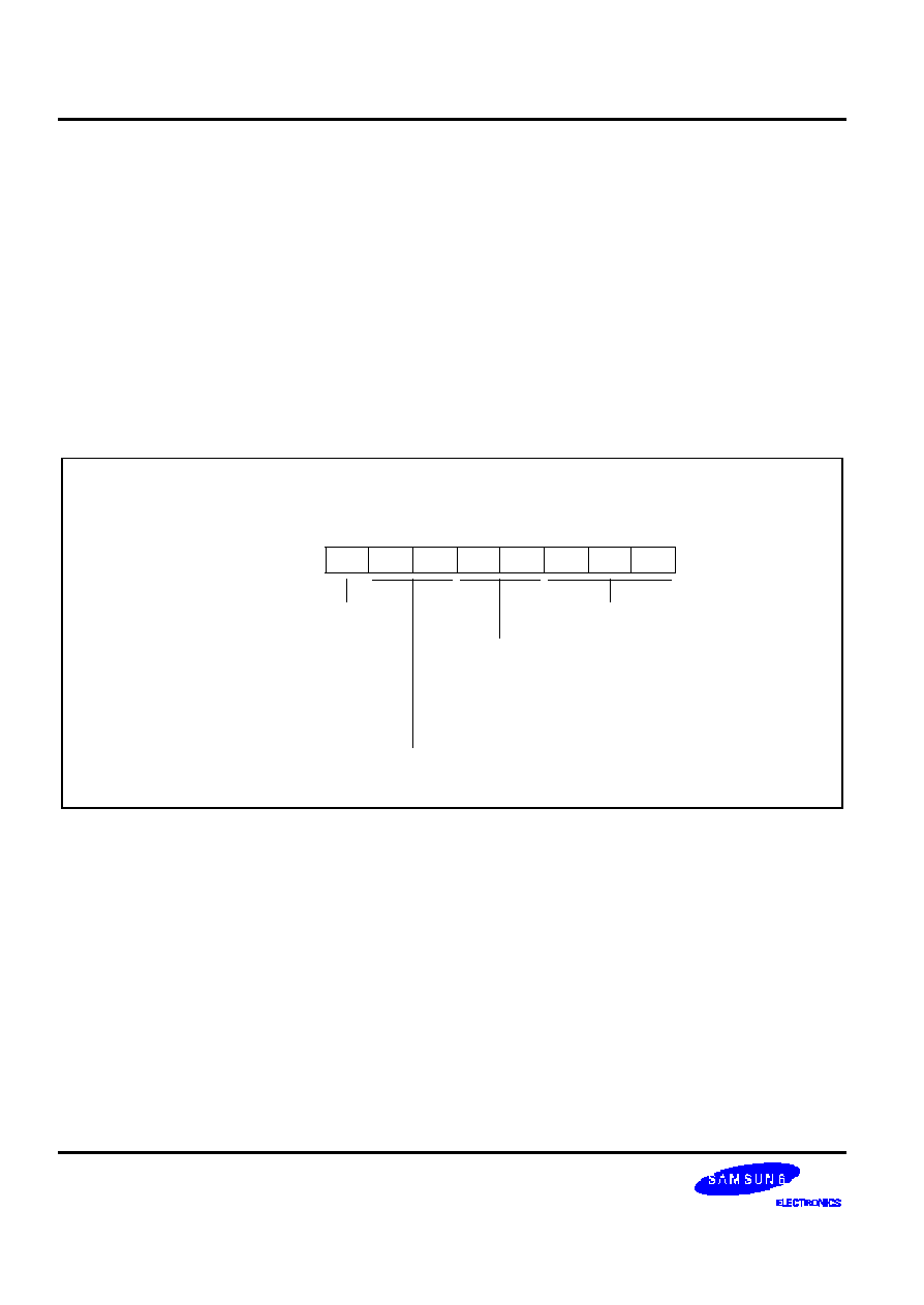
CLOCK CIRCUIT
S 3 C 9 6 8 8 / P 9 6 8 8
7 -2
S Y S T E M C L O C K C O N T R O L R E G I S T E R ( C L K C O N )
T h e s y s t e m c l o c k c o n t r o l r e g i s t e r , C L K C O N , i s l o c a t e d i n l o c a t i o n D 4 H . I t i s r e a d / w r i t e a d d r e s s a b l e a n d h a s t h e
following functions:
--
O s c i l l a t o r I R Q w a k e-u p f u n c t i o n e n a b l e / d i s a b l e ( C L K C O N . 7 )
--
Oscillator frequency divide-by value: non -d i v i d e d , 2 , 8 o r 1 6 ( C L K C O N . 4 a n d C L K C O N . 3 )
T h e C L K C O N r e g i s t e r c o n t r o l s w h e t h e r o r n o t a n e x t e r n a l i n t e r r u p t c a n b e u s e d t o t r i g g e r a S t o p m o d e r e l e a s e ( T h i s
i s c a l l e d t h e " I R Q w a k e-u p " f u n c t i o n ) . T h e I R Q w a k e-u p e n a b l e b i t i s C L K C O N . 7 .
A f t e r a r e s e t , t h e e x t e r n a l i n t e r r u p t o s c i l l a t o r w a k e-u p f u n c t i o n i s e n a b l e d , t h e m a i n o s c i l l a t o r i s a c t i v a t e d , a n d t h e
f
OSC
/ 1 6 ( t h e s l o w e s t c l o c k s p e e d ) i s s e l e c t e d a s t h e C P U c l o c k . I f n e c e s s a r y , y o u c a n t h e n i n c r e a s e t h e C P U c l o c k
s p e e d t o f
OSC
, f
OSC
/2 or f
s
/8.
.7
.6
.5
.4
.3
.2
.1
.0
LSB
MSB
System Clock Control Register (CLKCON)
D4H, R/W
Divide-by selection bits for
CPU clock frequency:
00 = f
OSC
/16
01 = f
OSC
/8
10 = f
OSC
/2
11 = f
OSC
(non-divided)
Oscillator IRQ wake-up enable bit:
0 = Enable IRQ for main-system
oscillator wake-up function
1 = Disable IRQ for main-system
oscillator wake-up function
Not used for S3C9688/P9688
Not used for S3C9688/P9688
F i g u r e 7 -2 . S y s t e m C l o c k C o n t r o l R e g i s t e r ( C L K C O N )
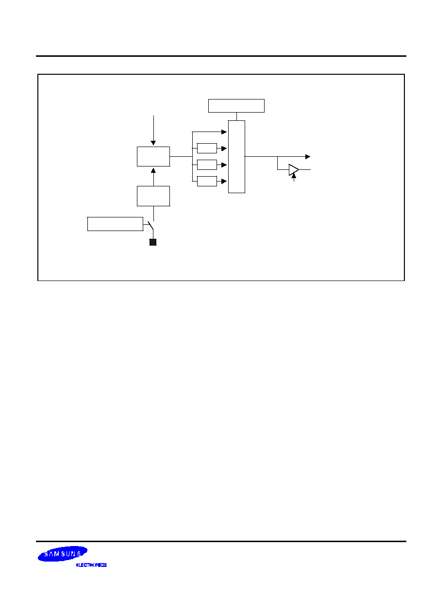
S 3 C 9 6 8 8 / P 9 6 8 8
CLOCK CIRCUIT
7 -3
Main
OSC
Noise
Filter
Oscillator
Wake-up
Oscillator
Stop
CLKCON.7
INT Pin
CLKCON.3, .4
1/2
1/8
1/16
M
U
X
Stop
Instruction
CPU Clock
P3.3/CLO
P3CON
F i g u r e 7 -3 . S y s t e m C l o c k C i r c u i t D i a g r a m

CLOCK CIRCUIT
S 3 C 9 6 8 8 / P 9 6 8 8
7 -4
N O T E S

S 3 C 9 6 8 8 / P 9 6 8 8
RESET AND POWER-D O W N
8 -1
8
RESET
A N D P O W E R -D O W N
S Y S T E M R E S E T
O V E R V I E W
D u r i n g a p o w e r-on reset, the voltage at V
DD
is High level and the
RESET
pin is forced to Low level. The
RESET
s i g n a l i s
input through a s c h m i t t t r i g g e r c i r c u i t w h e r e i t i s t h e n s y n c h r o n i z e d w i t h t h e C P U c l o c k . T h i s b r i n g s t h e
S 3 C 9 6 8 8 / P 9 6 8 8 i n t o a k n o w n o p e r a t i n g s t a t u s .
T h e R E S E T p i n m u s t b e h e l d t o L o w l e v e l f o r a m i n i m u m t i m e i n t e r v a l a f t e r t h e p o w e r s u p p l y c o m e s w i t h i n t o l e r a n c e
i n o r d e r t o a l l o w t i m e f o r i n t e r n a l C P U c l o c k o s c i l l a t i o n t o s t a b i l i z e . T h e m i n i m u m r e q u i r e d o s c i l l a t i o n s t a b i l i z a t i o n
t i m e f o r a r e s e t i s a p p r o x i m a t e l y 1 0 m s ( @ 2
16
/
f
OSC
, f
OSC
= 6 M H z ) .
W h e n a r e s e t o c c u r s d u r i n g n o r m a l o p e r a t i o n ( w i t h b o t h V
DD
a n d
RESET
at Hig h level), the signal at the
RESET
pin is
f o r c e d L o w a n d t h e r e s e t o p e r a t i o n s t a r t s . A l l s y s t e m a n d p e r i p h e r a l c o n t r o l r e g i s t e r s a r e t h e n s e t t o t h e i r d e f a u l t
hardware reset values (see Table 8-1).
T h e f o l l o w i n g s e q u e n c e o f e v e n t s o c c u r s d u r i n g a r e s e t o p e r a t i o n :
--
All interrupts are disabled.
--
T h e w a t c h d o g f u n c t i o n ( b a s i c t i m e r ) i s e n a b l e d .
--
P o r t s 0 -4 a r e s e t t o s c h m i t t t r i g g e r i n p u t m o d e a n d a l l p u l l -u p r e s i s t o r s a r e d i s a b l e d .
--
Peripheral control and data registers are disabled and reset to their initial values.
--
T h e p r o g r a m c o u n t e r i s l o a d e d w i t h t h e R O M r e s e t a d d r e s s , 0 1 0 0 H .
--
W h e n t h e p r o g r a m m e d o s c i l l a t i o n s t a b i l i z a t i o n t i m e i n t e r v a l h a s e l a p s e d , t h e a d d r e s s s t o r e d i n R O M l o c a t i o n
0 1 0 0 H ( a n d 0 1 0 1 H ) i s f e t c h e d a n d e x e c u t e d .
N O T E
T o p r o g r a m t h e d u r a t i o n o f t h e o s c i l l a t i o n s t a b i l i z a t i o n i n t e r v a l , y o u m u s t m a k e t h e a p p r o p r i a t e s e t t i n g s t o
t h e b a s i c t i m e r c o n t r o l r e g i s t e r , B T C O N , b e f o r e e n t e r i n g S t o p m o d e . A l s o , i f y o u d o n o t w a n t t o u s e t h e
b a s i c t i m e r w a t c h d o g f u n c t i o n ( w h i c h c a u s e s a s y s t e m r e s e t i f a b a s i c t i m e r c o u n t e r o v e r f l o w o c c u r s ) , y o u
c a n d i s a b l e i t b y w r i t i n g ' 1 0 1 0 B ' t o t h e u p p e r n i b b l e o f B T C O N .

RESET AND POWER-D O W N
S 3 C 9 6 8 8 / P 9 6 8 8
8 -
2
P O W E R -D O W N M O D E S
S T O P M O D E
S t o p m o d e i s i n v o k e d b y t h e i n s t r u c t i o n S T O P ( o p c o d e 7 F H ) . I n S t o p m o d e , t h e o p e r a t i o n o f t h e C P U a n d a l l
peripherals is halted. That is, the on-c h i p m a i n o s c i l l a t o r s t o p s a n d t h e s u p p l y c u r r e n t i s r e d u c e d t o l e s s t h a n
3 0 0
µ
A . A l l s y s t e m f u n c t i o n s a r e h a l t e d w h e n t h e c l o c k " f r e e z e s " , b u t d a t a s t o r e d i n t h e i n t e r n a l r e g i s t e r f i le is
r e t a i n e d . S t o p m o d e c a n b e r e l e a s e d i n b o t h w a y s : b y a
RESET
signal or by an external interrupt.
U s i n g R E S E T t o R e l e a s e S t o p M o d e
S t o p m o d e i s r e l e a s e d w h e n t h e
RESET
s i g n a l i s r e l e a s e d a n d r e t u r n s t o H i g h l e v e l . A l l s y s t e m a n d p e r i p h e r a l c o n t r o l
registers are then reset to their default values and the contents of all data registers are retained. A reset operation
a u t o m a t i c a l l y s e l e c t s a s l o w c l o c k ( 1 / 1 6 ) b e c a u s e C L K C O N . 3 a n d C L K C O N . 4 a r e c l e a r e d t o ` 0 0 B ' . A fter the
o s c i l l a t i o n s t a b i l i z a t i o n i n t e r v a l h a s e l a p s e d , t h e C P U e x e c u t e s t h e s y s t e m i n i t i a l i z a t i o n r o u t i n e b y f e t c h i n g t h e 1 6 -bit
a d d r e s s s t o r e d i n R O M l o c a t i o n s 0 1 0 0 H a n d 0 1 0 1 H .
U s i n g a n E x t e r n a l I n t e r r u p t t o R e l e a s e S t o p M o d e
O n l y e x t e r n a l i n t e r r u p t s w i t h a n R C -d e l a y n o i s e f i l t e r c i r c u i t c a n b e u s e d t o r e l e a s e S t o p m o d e ( C l o c k -related
external interrupts cannot be used). External interrupts INT0 ≠ I N T 2 i n t h e S 3 C 9 6 8 8 / P 9 6 8 8 i n t e r r u p t s t r u c t u r e m e e t
this criteria.
N o t e t h a t w h e n S t o p m o d e i s r e l e a s e d b y a n e x t e r n a l i n t e r r u p t , t h e c u r r e n t v a l u e s i n s y s t e m a n d p e r i p h e r a l c o n t r o l
r e g i s t e r s a r e n o t c h a n g e d . W h e n y o u u s e a n i n t e r r u p t t o r e l e a s e S t o p m o d e , t h e C L K C O N . 3 a n d C L K C O N . 4 r e g i s t e r
v a l u e s r e m a i n u n c h a n g e d , a n d t h e c u r r e n t l y s e l e c t e d c l o c k v a l u e i s u s e d . I f y o u u s e a n e x t e r n a l i n t e r r u p t f o r S t o p
m o d e r e l e a s e , y o u c a n a l s o p r o g r a m t h e d u r a t i o n o f t h e o s c i l l a t i o n s t a b i l i z a t i o n i n t e r v a l . T o d o t h i s , y o u m u s t m a k e
t h e a p p r o p r i a t e c o n t r o l a n d c l o c k s e t t i n g s before entering Stop mode.
T h e e x t e r n a l i n t e r r u p t i s s e r v i c e d w h e n t h e S t o p m o d e r e l e a s e o c c u r s . F o l l o w i n g t h e I R E T f r o m t h e s e r v i c e r o u t i n e ,
t h e i n s t r u c t i o n i m m e d i a t e l y f o l l o w i n g t h e o n e t h a t i n i t i a t e d S t o p m o d e i s e x e c u t e d .
I D L E M O D E
I d l e m o d e i s i n v o k e d b y t h e i n s t r u c t i o n I D L E ( o p c o d e 6 F H ) . I n I d l e m o d e , C P U o p e r a t i o n s a r e h a l t e d w h i l e s e l e c t
peripherals remain active. During Idle mode, the internal clock signal is gated off to the CPU, but not to interrupt logic
a n d t i m e r / c o u n t e r s . P o r t p i n s r e t a i n t h e m o d e ( i n p u t o r o u t p u t ) t h e y h a d a t t h e t i m e I d l e m o d e w a s e n t e r e d .
T h e r e a r e t w o w a y s t o r e l e a s e I d l e m o d e :
1 . E x e c u t e a r e s e t . A l l s y s t e m a n d p e r i p h e r a l c o n t r o l r e g i s t e r s a r e r e s e t t o t h e i r d e f a u l t v a l u e s a n d t h e c o n t e n t s o f
a l l d a t a r e g i s t e r s a r e r e t a i n e d . T h e r e s e t a u t o m a t i c a l l y s e l e c t s a s l o w c l o c k ( 1 / 1 6 ) b e c a u s e C L K C O N . 3 a n d
C L K C O N . 4 a r e c l e a r e d t o ` 0 0 B ' . I f i n t e r r u p t s a r e m a s k e d , a r e s e t i s t h e o n l y w a y t o r e l e a s e I d l e m o d e .
2 . A c t i v a t e a n y e n a b l e d i n t e r r u p t , c a u s i n g I d l e m o d e t o b e r e l e a s e d . W h e n y o u u s e a n i n t e r r u p t t o r e l e a s e I d l e
m o d e , t h e C L K C O N . 3 a n d C L K C O N . 4 r e g i s t e r v a l u e s r e m a i n u n c h a n g e d , a n d t h e c u r r e n t l y s e l e c t e d c l o c k v a l u e
i s u s e d . T h e i n t e r r u p t i s t h e n s e r v i c e d . F o l l o w i n g t h e I R E T f r o m t h e s e r v i c e r o u t i n e , t h e i n s t r u c t i o n i m m e d i a t e l y
f o l l o w i n g t h e o n e t h a t i n i t i a t e d I d l e m o d e i s e x e c u t e d .
N O T E
O n l y e x t e r n a l i n t e r r u p t s t h a t a r e n o t c l o c k -r e l a t e d c a n b e u s e d t o r e l e a s e S t o p m o d e . T o r e l e a s e I d l e m o d e ,
however, any type of interrupt (that is, internal or external) can be u s e d .
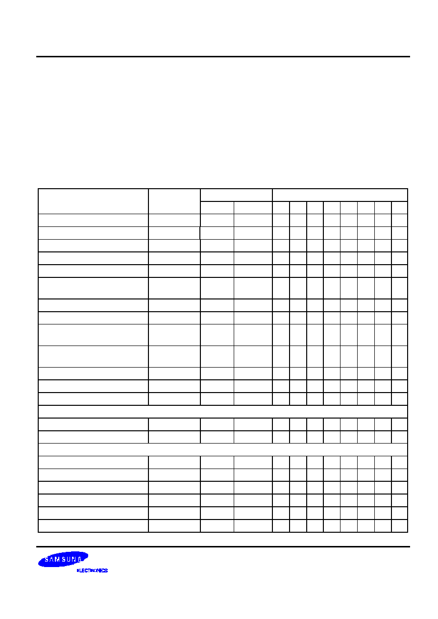
S 3 C 9 6 8 8 / P 9 6 8 8
RESET AND POWER-D O W N
8 -
3
H A R D W A R E R E S E T V A L U E S
T a b l e s 8 -1 t h r o u g h 8 -3 l i s t t h e v a l u e s f o r C P U a n d s y s t e m r e g i s t e r s , p e r i p h e r a l c o n t r o l r e g i s t e r s a n d p e r i p h e r a l d a t a
r e g i s t e r s f o l l o w i n g a r e s e t o p e r a t i o n i n n o r m a l o p e r a t i n g m o d e . T h e f o l l o w i n g n o t a t i o n i s u s e d i n t h e s e t a b l e s t o
r e p r e s e n t s p e c i f i c r e s e t v a l u e s :
A " 1 " o r a " 0 " s h o w s t h e r e s e t b i t v a l u e a s l o g i c o n e o r l o g i c z e r o , r e s p e c t i v e l y .
An 'x' means that the bit value is undefined following a reset.
A d a s h ( '-' ) m e a n s t h a t t h e b it i s e i t h e r n o t u s e d o r n o t m a p p e d .
T a b l e 8 -1 . R e g i s t e r V a l u e s a f t e r a R e s e t
R e g i s t e r N a m e
M n e m o n i c
A d d r e s s
B i t V a l u e s a f t e r R E S E T
D e c
H e x
7
6
5
4
3
2
1
0
G e n e r a l p u r p o s e r e g i s t e r s
≠
0 0 0 ≠ 1 9 1 0 0 H ≠ B F H
x
x
x
x
x
x
x
x
W o r k i n g r e g i s t e r s
R 0 ≠ R 1 5
1 9 2 ≠ 2 0 7 C 0 H ≠ C F H
x
x
x
x
x
x
x
x
T i m e r 0 c o u n t e r
T 0 C N T
2 0 8
D 0 H
0
0
0
0
0
0
0
0
T i m e r 0 d a t a r e g i s t e r
T 0 D A T A
2 0 9
D 1 H
1
1
1
1
1
1
1
1
T i m e r 0 c o n t r o l r e g i s t e r
T 0 C O N
2 1 0
D 2 H
0
0
0
0
0
0
0
0
U S B s e l e c t i o n a n d t r a n s c e i v e r
crossover point control register
U S X C O N
2 1 1
D 3 H
0
0
0
0
0
0
0
0
C l o c k c o n t r o l r e g i s t e r
C L K C O N
2 1 2
D 4 H
0
0
0
0
0
0
0
0
S y s t e m f l a g s r e g i s t e r
F L A G S
2 1 3
D 5 H
0
0
0
0
≠
≠
≠
≠
D + / P S 2 , D -/ P S 2 d a t a r e g i s t e r
( o n l y P S 2 m o d e )
P S 2 D A T A
2 1 4
D 6 H
0
0
0
0
0
0
0
0
P S 2 c o n t r o l a n d i n t e r r u p t
p e n d i n g r e g i s t e r
P S 2 C O N I N T
2 1 4
D 7 H
0
0
0
0
0
0
0
0
Port 0 interrupt control register
P 0 I N T
2 1 6
D 8 H
0
0
0
0
0
0
0
0
S t a c k p o i n t e r
S P
2 1 7
D 9 H
x
x
x
x
x
x
x
x
Port 0 interrupt pending register
P 0 P N D
2 1 8
D A H
0
0
0
0
0
0
0
0
L o c a t i o n D B H i s n o t m a p p e d .
B a s i c t i m e r c o n t r o l r e g i s t e r
B T C O N
2 2 0
D C H
0
0
0
0
0
0
0
0
B a s i c t i m e r c o u n t e r
B T C N T
2 2 1
D D H
0
0
0
0
0
0
0
0
L o c a t i o n D E H i s n o t m a p p e d .
S y s t e m m o d e r e g i s t e r
S Y M
2 2 3
D F H
≠
≠
≠
≠
≠
0
0
0
P o r t 0 d a t a r e g i s t e r
P 0
2 2 4
E 0 H
0
0
0
0
0
0
0
0
P o r t 1 d a t a r e g i s t e r
P 1
2 2 5
E 1 H
0
0
0
0
0
0
0
0
P o r t 2 d a t a r e g i s t e r
P 2
2 2 6
E 2 H
0
0
0
0
0
0
0
0
P o r t 3 d a t a r e g i s t e r
P 3
2 2 7
E 3 H
0
0
0
0
0
0
0
0
P o r t 4 d a t a r e g i s t e r
P 4
2 2 8
E 4 H
0
0
0
0
0
0
0
0
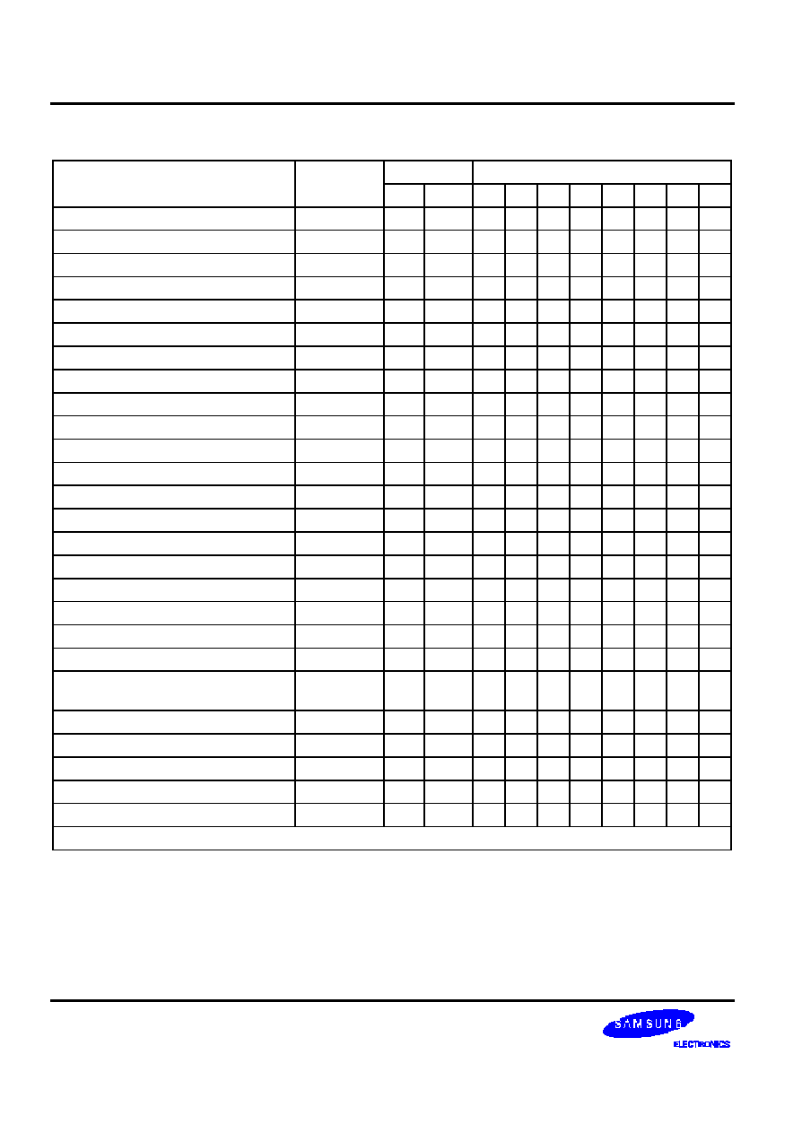
RESET AND POWER-D O W N
S 3 C 9 6 8 8 / P 9 6 8 8
8 -
4
T a b l e 8 -1 . R e g i s t e r V a l u e s a f t e r a R e s e t ( c o n t i n u e d )
B a n k 0 R e g i s t e r N a m e
M n e m o n i c
A d d r e s s
B i t V a l u e s a f t e r a R e s e t
D e c
H e x
7
6
5
4
3
2
1
0
P o r t 3 c o n t r o l r e g i s t e r
P 3 C O N
2 2 9
E 5 H
0
0
0
0
0
0
0
0
P o r t 0 c o n t r o l r e g i s t e r ( h i g h b y t e )
P 0 C O N H
2 3 0
E 6 H
0
0
0
0
0
0
0
0
P o r t 0 c o n t r o l r e g i s t e r ( l o w b y t e )
P 0 C O N L
2 3 1
E 7 H
0
0
0
0
0
0
0
0
P o r t 1 c o n t r o l r e g i s t e r ( h i g h b y t e )
P 1 C O N H
2 3 2
E 8 H
0
0
0
0
0
0
0
0
P o r t 1 c o n t r o l r e g i s t e r ( l o w b y t e )
P 1 C O N L
2 3 3
E 9 H
0
0
0
0
0
0
0
0
Port 2 control register (h i g h b y t e )
P 2 C O N H
2 3 4
E A H
0
0
0
0
0
0
0
0
P o r t 2 c o n t r o l r e g i s t e r ( l o w b y t e )
P 2 C O N L
2 3 5
E B H
0
0
0
0
0
0
0
0
Port 2 interrupt enable register
P 2 I N T
2 3 6
E C H
0
0
0
0
0
0
0
0
Port 2 interrupt pending register
P 2 P N D
2 3 7
E D H
0
0
0
0
0
0
0
0
P o r t 4 c o n t r o l r e g i s t e r
P 4 C O N
2 3 8
E E H
0
0
0
0
0
0
0
0
Port 4 interrupt enable/pending register
P 4 I N T P N D
2 3 9
E F H
0
0
0
0
0
0
0
0
U S B f u n c t i o n a d d r e s s r e g i s t e r
F A D D R
2 4 0
F 0 H
0
0
0
0
0
0
0
0
C o n t r o l e n d p o i n t s t a t u s r e g i s t e r
E P 0 C S R
2 4 1
F 1 H
0
0
0
0
0
0
0
0
Interrupt endpoint s t a t u s r e g i s t e r
E P 1 C S R
2 4 2
F 2 H
0
0
0
0
0
0
0
0
C o n t r o l e n d p o i n t b y t e c o u n t r e g i s t e r
E P 0 B C N T
2 4 3
F 3 H
0
0
0
0
0
0
0
0
C o n t r o l e n d p o i n t F I F O r e g i s t e r
E P 0 F I F O
2 4 4
F 4 H
x
x
x
x
x
x
x
x
Interrupt endpoint FIFO register
E P 1 F I F O
2 4 5
F 5 H
x
x
x
x
x
x
x
x
U S B i n t e r r u p t p e n d i n g r e g i s t e r
U S B P N D
2 4 6
F 6 H
0
0
0
0
0
0
0
0
U S B i n t e r r u p t e n a b l e r e g i s t e r
U S B I N T
2 4 7
F 7 H
0
0
0
0
1
0
1
1
U S B p o w e r m a n a g e m e n t r e g i s t e r
P W R M G R
2 4 8
F 8 H
0
0
0
0
0
0
0
0
Interrupt endpoint 2 control status
r e g i s t e r
E P 2 C S R
2 4 9
F 9 H
0
0
0
0
0
0
0
0
Interrupt endpoint 2 FIFO register
E P 2 F I F O
2 5 0
F A H
x
x
x
x
x
x
x
x
E n d p o i n t m o d e r e g i s t e r
E P M O D E
2 5 1
F B H
0
0
0
0
0
0
0
0
E n d p o i n t 1 b y t e c o u n t
E P 1 B C N T
2 5 2
F C H
0
0
0
0
0
0
0
0
E n d p o i n t 2 b y t e c o u n t
E P 2 B C N T
2 5 3
F D H
0
0
0
0
0
0
0
0
U S B c o n t r o l r e g i s t e r
U S B C O N
2 5 4
F E H
0
0
0
0
1
0
1
1
L o c a t i o n F F H i s n o t m a p p e d
S 3 C 9 6 8 8 / P 9 6 8 8
I/O PORTS
9 -1
9
I/O PORTS
O V E R V I E W
T h e S 3 C 9 6 8 8 / P 9 6 8 8 U S B M o d e h a s f i v e I / O p o r t s ( 0 ≠ 4) with a total of 32 pins.
P S 2 M o d e h a s t w o I / O p o r t s ( D + / P S 2 , D -/ P S 2 ) w i t h a t o t a l o f 3 4 p i n s .
Y o u c a n a c c e s s t h e s e p o r t s d i r e c t l y b y w r i t i n g o r r e a d i n g p o r t d a t a r e g i s t e r a d d r e s s e s .
F o r k e y b o a r d a p p l i c a t i o n s , p o r t s 0 , 1 a n d 2 a r e u s u a l l y c o n f i g u r e d a s k e y b o a r d m a t r i x i n p u t / o u t p u t . P o r t 3 c a n b e
c o n f i g u r e d a s L E D d r i v e . P o r t 4 i s u s e d f o r h o s t c o m m u n i c a t i o n o r f o r c o n t r o l l i n g a m o u s e o r o t h e r e x t e r n a l d e v i c e .
T a b l e 9 -1 . S 3 C 9 6 8 8 / P 9 6 8 8 P o r t C o n f i g u r a t i o n O v e r v i e w
P o r t
F u n c t i o n D e s c r i p t i o n
P r o g r a m m a b i l i t y
0
B i t -p r o g r a m m a b l e I / O p o r t f o r s c h m i t t t r i g g e r input or open-drain output.
Port0 can be individually configured as external interrupt inputs. Pull-u p
r e s i s t o r s a r e a s s i g n a b l e b y s o f t w a r e .
B i t
1
B i t -p r o g r a m m a b l e I / O p o r t f o r s c h m i t t t r i g g e r i n p u t o r o p e n -drain output.
P u l l -u p r e s i s t o r s a r e a s s i g n a b l e b y s o f t w a r e .
B i t
2
B i t -p r o g r a m m a b l e I / O p o r t f o r s c h m i t t t r i g g e r i n p u t o r o p e n -drain output.
Port2 can be individually configured as external interrupt inputs. Pull-u p
r e s i s t o r s a r e a s s i g n a b l e b y s o f t w a r e .
B i t
3
B i t -p r o g r a m m a b l e I / O p o r t f o r s c h m i t t t rigger input, open-d r a i n o r p u s h-pull
o u t p u t . P 3 . 3 c a n b e u s e d t o s y s t e m c l o c k o u t p u t ( C L O ) p i n .
B i t
4
B i t -p r o g r a m m a b l e I / O p o r t f o r s c h m i t t t r i g g e r i n p u t o r o p e n -drain output or
p u s h-pull output. Port4 can be individually configured as external interrupt
i n p u t s . I n o u t p u t m o d e , p u l l -u p r e s i s t o r s a r e a s s i g n a b l e b y s o f t w a r e . B u t i n
i n p u t m o d e , p u l l -up resistors are fixed.
B i t
D + / P S 2
D -/ P S 2
( P S 2 m o d e
O n l y )
B i t -p r o g r a m m a b l e I / O p o r t f o r s c h m i t t t r i g g e r i n p u t o r o p e n -drain output or
p u s h-pull output. This port individually configured as external interrupt
i n p u t s . I n o u t p u t m o d e , p u l l -u p r e s i s t o r s a r e a s s i g n a b l e b y s o f t w a r e . B u t i n
i n p u t m o d e , p u l l -up resistors are fixed.
B i t
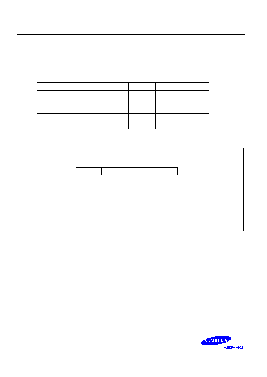
I/O PORTS
S 3 C 9 6 8 8 / P 9 6 8 8
9 -2
P O R T D A T A R E G I S T E R S
Table 9-2 g i v e s y o u a n o v e r v i e w o f t h e p o r t d a t a r e g i s t e r n a m e s , l o c a t i o n s a n d a d d r e s s i n g c h a r a c t e r i s t i c s . D a t a
registers for ports 0≠ 4 h a v e t h e s t r u c t u r e s h o w n i n F i g u r e 9 -1 .
T a b l e 9 -2 . P o r t D a t a R e g i s t e r S u m m a r y
R e g i s t e r N a m e
M n e m o n i c
D e c i m a l
H e x
R / W
P o r t 0 d a t a r e g i s t e r
P 0
2 2 4
E 0 H
R / W
P o r t 1 d a t a r e g i s t e r
P 1
2 2 5
E 1 H
R / W
P o r t 2 d a t a r e g i s t e r
P 2
2 2 6
E 2 H
R / W
P o r t 3 d a t a r e g i s t e r
P 3
2 2 7
E 3 H
R / W
P o r t 4 d a t a r e g i s t e r
P 4
2 2 8
E 4 H
R / W
.7
.6
.5
.4
.3
.2
.1
.0
LSB
MSB
I/O Port n Data Register (n = 0-4)
Pn.0
Pn.1
Pn.2
Pn.4
Pn.3
Pn.5
Pn.6
Pn.7
NOTE:
Because only the four lower-nibble pins of port 3
and port 4 are mapped, data register bits P3.4-P3.7
and P4.4-P4.7 are not used.
NOTE:
Because only the four lower-nibble pins of port 3
and port 4 are mapped, data register bits P3.4-P3.7
and P4.4-P4.7 are not used.
F i g u r e 9 -1 . P o r t D a t a R e g i s t e r F o r m a t
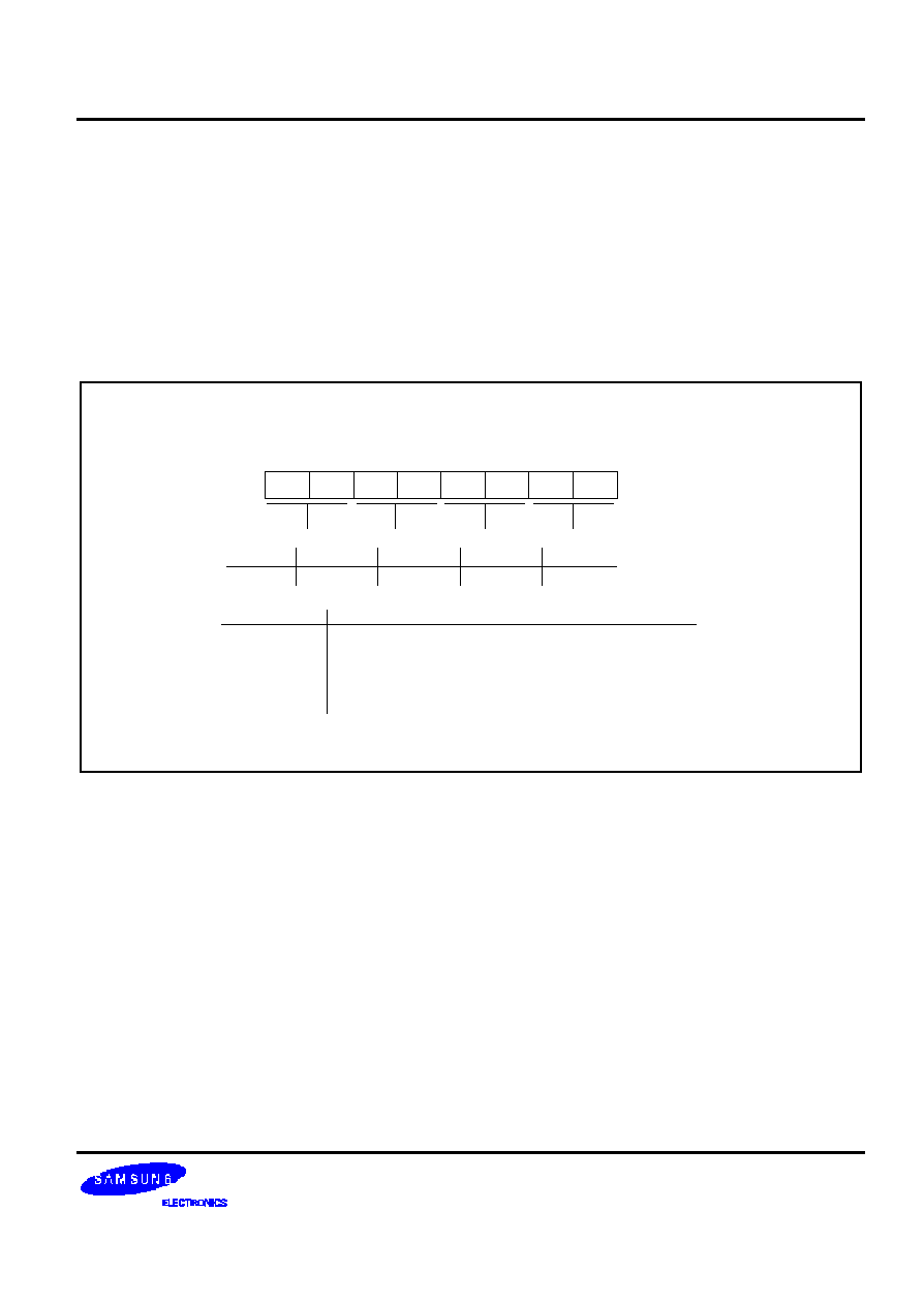
S 3 C 9 6 8 8 / P 9 6 8 8
I/O PORTS
9 -3
P O R T 0 A N D P O R T 1
P o r t s 0 b i t -p r o g r a m m a b l e , g e n e r a l-p u r p o s e , I / O p o r t s . Y o u c a n s e l e c t s c h m i t t t r i g g e r i n p u t m o d e , N -C H o p e n d r a i n
o u t p u t m o d e .
Y o u c a n a c c e s s p o r t s 0 a n d 1 d i r e c t l y b y w r i t i n g o r r e a d i n g t h e c o r r e s p o n d i n g p o r t d a t a r e g i s t e r s -- P 0 ( E 0 H ) a n d P 1
( E 1 H ) . A r e s e t c l e a r s t h e p o r t c o n t r o l r e g i s t e r s P 0 C O N H , P 0 C O N L , P 1 C O N H a n d P 1 C O N L t o ' 0 0 H ' , c o n f i g u r i n g a l l
p o r t 0 a n d p o r t 1 p i n s a s s c h m i t t t r i g g e r i n p u t s .
I n t y p i c a l k e y b o a r d c o n t r o l l e r a p p l i c a t i o n s , t h e s i x t e e n p o r t 0 a n d p o r t 1 p i n s c a n b e u s e d t o c h e c k p r e s s e d k e y f r o m
k e y b o a r d m a t r i x b y g e n e r a t i n g k e y s t r o k e o u t p u t s i g n a l s .
.7
.6
.5
.4
.3
.2
.1
.0
LSB
MSB
Port 0 Control Registers
P0CONH, E6H, R/W, P0CONL, E7H, R/W
P0CONH
P0CONL
P0.7/INT2
P0.3/INT2
P0.6/INT2
P0.2/INT2
P0.5/INT2
P0.1/INT2
P0.4/INT2
P0.0/INT2
7,5,3,1
6,4,2,0
0
0
1
1
0
1
0
1
Schmitt trigger input, rising edge external interrupt mode
Schmitt trigger input, falling edge external interrupt mode
with pull-up
N-CH open drain output mode
N-CH open drain output mode with pull-up
Port Mode Selection
F i g u r e 9 -2 . P o r t 0 C o n t r o l R e g i s t e r s ( P 0 C O N H , P 0 C O N L )
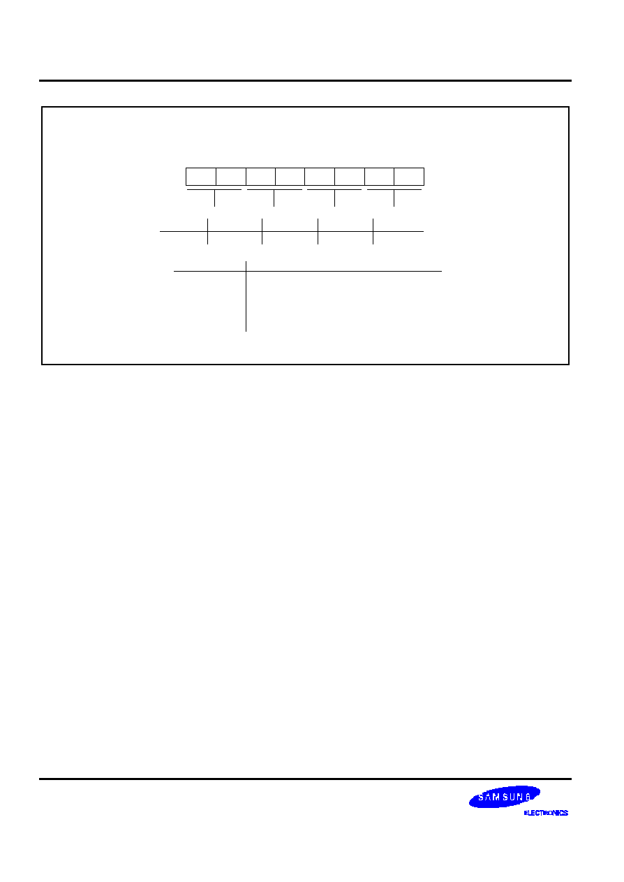
I/O PORTS
S 3 C 9 6 8 8 / P 9 6 8 8
9 -4
.7
.6
.5
.4
.3
.2
.1
.0
LSB
MSB
Port 1 Control Registers
P1CONH, E8H, R/W, P1CONL, E9H, R/W
P1CONH
P1CONL
P1.7
P1.3
P1.6
P1.2
P1.5
P1.1
P1.4
P1.0
7,5,3,1
6,4,2,0
0
0
1
1
0
1
0
1
Schmitt trigger input mode
Schmitt trigger input mode with pull-up
N-CH open-drain output mode
N-CH open-drain output mode with pull-up
Port Mode Selection
F i g u r e 9 -3 . P o r t 1 C o n t r o l R e g i s t e r s ( P 1 C O N H , P 1 C O N L )

S 3 C 9 6 8 8 / P 9 6 8 8
I/O PORTS
9 -5
P O R T 2
P o r t 2 i s a n 8 -bit I/O port with individually configurable pins. It can be used for general I/O (Schmitt trigger input mode
o r p u s h-p u l l o u t p u t m o d e ) . O r , y o u c a n u s e p o r t 2 p i n s a s e x t e r n a l i n t e r r u p t ( I N T 0 ) i n p u t s . I n a d d i t i o n , y o u c a n
configure a pull-u p resistor to individual pins using control register settings. All port 2 pin circuits have noise filters.
I n t y p i c a l k e y b o a r d c o n t r o l l e r a p p l i c a t i o n s , t h e p o r t 2 p i n s a r e p r o g r a m m e d t o r e c e i v e k e y i n p u t d a t a f r o m t h e
k e y b o a r d m a t r i x .
Y o u c a n a d d r e s s p o r t 2 b i t s d i r e c t l y b y w r i t i n g o r r e a d i n g t h e p o r t 2 d a t a r e g i s t e r , P 2 ( E 2 H ) . T h e p o r t 2 h i g h -b y t e a n d
l o w -b y t e c o n t r o l r e g i s t e r s , P 2 C O N H a n d P 2 C O N L , a r e l o c a t e d a t a d d r e s s e s E A H a n d E B H , r e s p e c t i v e l y .
Two additional registers, are used for interrupt control: P 2 I N T ( E C H ) a n d P 2 P N D ( E D H ) . B y s e t t i n g b i t s i n t h e p o r t 2
interrupt enable register P2INT, you can configure specific port 2 pins to generate interrupt requests when rising or
f a l l i n g s i g n a l e d g e s a r e d e t e c t e d . T h e a p p l i c a t i o n p r o g r a m p o l l s t h e p o r t 2 i n t e r r u p t p e n d i n g r e g i s t e r , P 2 P N D , t o
d e t e c t i n t e r r u p t r e q u e s t s . W h e n a n i n t e r r u p t r e q u e s t i s a c k n o w l e d g e d , t h e c o r r e s p o n d i n g p e n d i n g b i t m u s t b e c l e a r e d
by the interrupt service routine.
I n c a s e o f k e y b o a r d a p p l i c a t i o n s , t h e p o r t 2 p i n s c a n b e u s e d t o r e a d k e y v a l u e f r o m k e y m a t r i x .
.7
.6
.5
.4
.3
.2
.1
.0
LSB
MSB
Port 2 Control Registers
P2CONH, EAH, R/W, P2CONL, EBH, R/W
P2CONH
P2CONL
P2.7/INT0
P2.3/INT0
P2.6/INT0
P2.2/INT0
P2.5/INT0
P2.1/INT0
P2.4/INT0
P2.0/INT0
7,5,3,1
6,4,2,0
0
0
1
1
0
1
0
1
Schmitt trigger input, rising edge external interrupt
Schmitt trigger input, falling edge external interrupt
with pull-up
N-CH open-drain
N-CH open-drain with pull-up
Port Mode Selection
F i g u r e 9 -4 . P o r t 2 C o n t r o l R e g i s t e r s ( P 2 C O N H , P 2 C O N L )
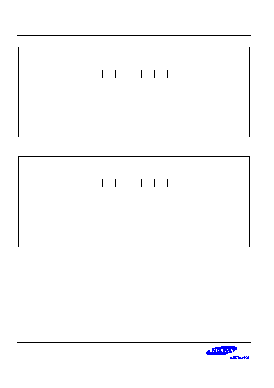
I/O PORTS
S 3 C 9 6 8 8 / P 9 6 8 8
9 -6
.7
.6
.5
.4
.3
.2
.1
.0
LSB
MSB
Port 2 Interrupt Enable Register (P2INT)
ECH, R/W
P2.7/INT0
Port 2 Interrupt Control Settings:
0 = Disable interrupt at P2.n pin
1 = Enable interrupt at P2.n pin
P2.6/INT0
P2.5/INT0
P2.4/INT0
P2.3/INT0
P2.2/INT0
P2.0/INT0
P2.1/INT0
F i g u r e 9 -5 . P o r t 2 I n t e r r u p t E n a b l e R e g i s t e r ( P 2 I N T )
.7
.6
.5
.4
.3
.2
.1
.0
LSB
MSB
Port 2 Interrupt Pending Register (P2PND)
EDH, R/W
P2.7/INT0
Port 2 Interrupt Request Pending Bits:
0 = Not interrupt is pending
1 = Interrupt request is pending
P2.6/INT0
P2.5/INT0
P2.4/INT0
P2.3/INT0
P2.2/INT0
P2.0/INT0
P2.1/INT0
F i g u r e 9 -6 . P o r t 2 I n t e r r u p t P e n d i n g R e g i s t e r ( P 2 P N D )
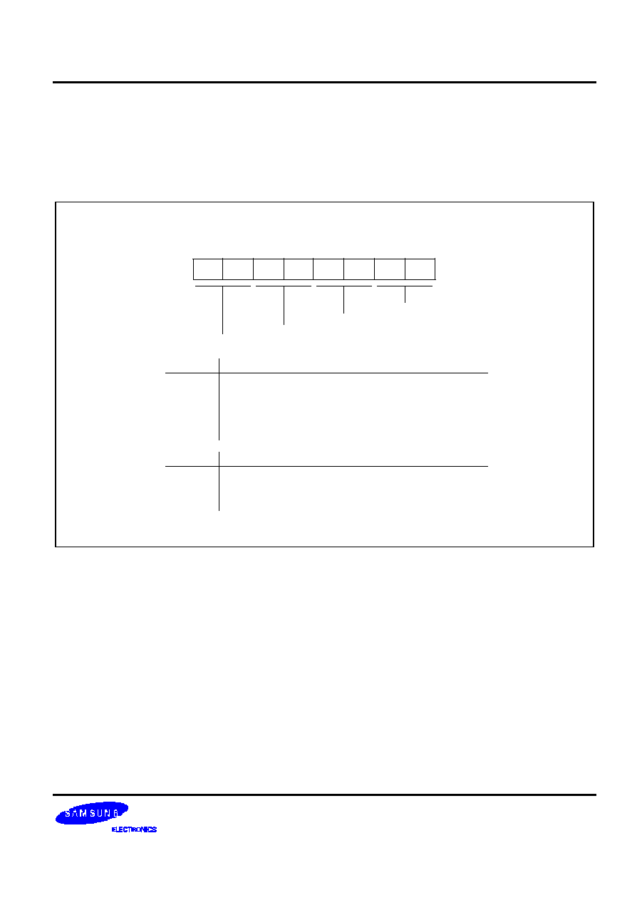
S 3 C 9 6 8 8 / P 9 6 8 8
I/O PORTS
9 -7
P O R T 3
P o r t 3 i s a 4 -bit, bit-configurable, general I/O port. It is designed for high-c u r r e n t f u n c t i o n s s u c h a s L E D d r i v e .
A r e s e t c o n f i g u r e s P 3 . 0 -P 3 . 3 t o s c h m i t t t r i g g e r i n p u t m o d e . U s i n g t h e P 3 C O N r e g i s t e r ( E 5 H ) , y o u c a n a l t e r n a t i v e l y
c o n f i g u r e t h e p o r t 3 p i n s a s n -c h a n n e l , o p e n -d r a i n o u t p u t s . P 3 . 3 c a n b e u s e d t o s y s t e m c l o c k o u t p u t ( C L O ) p o r t .
Port 3 Control Register (P3CON)
E5H, R/W
.7
.6
.5
.4
.3
.2
.1
.0
MSB
LSB
P3.0
P3.1
P3.2
P3.3/CLO
Schmitt trigger input
System Clock Ouput (CLO) mode.
CLO comes from System clock circuit.
Push-pull output
N-CH open drain output
Port Mode Selection (P3.3)
0
1
0
1
Bit 7 Bit 6
0
0
1
1
Schmitt trigger input,
Push-pull output
N-CH open drain output
Port Mode Selection (P3.2-P3.0)
x
0
1
5,3,1 4,2,0
0
1
1
F i g u r e 9 -7 . P o r t 3 C o n t r o l R e g i s t e r ( P 3 C O N )
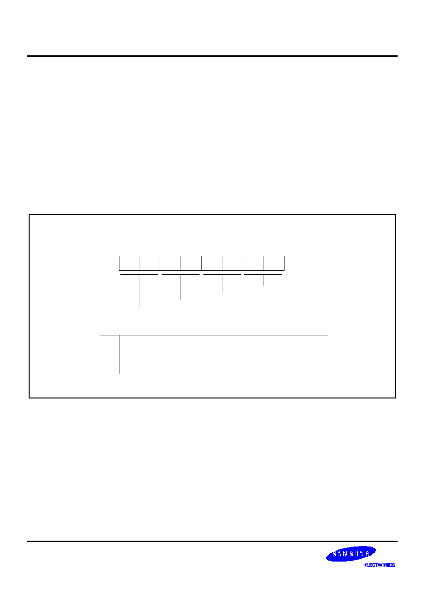
I/O PORTS
S 3 C 9 6 8 8 / P 9 6 8 8
9 -8
P O R T 4
P o r t 4 i s a 4 -bit I/O port with individually configurable pins. It can be used for general I/O (Schmitt trigger, N -C H o p e n
d r a i n o u t p u t m o d e , p u s h-p u l l o u t p u t m o d e ) . O r , y o u c a n u s e p o r t 4 p i n s a s e x t e r n a l i n t e r r u p t ( I N T 1 ) i n p u t s . I n
a d d i t i o n , y o u c a n c o n f i g u r e a p u l l-up resistor to individual pins using control register settings. All port 4 pins have
noise filters.
A r e s e t c o n f i g u r e s P 4 . 0 -P 4 . 3 t o i n p u t m o d e . Y o u a d d r e s s p o r t 4 d i r e c t l y b y w r i t i n g o r r e a d i n g t h e p o r t 4 d a t a r e g i s t e r ,
P 4 ( E 4 H ) . T h e p o r t 4 c o n t r o l r e g i s t e r , P 4 C O N , i s l o c a t e d a t E E H .
A a d d i t i o n a l r e g i s t e r s u s e d f o r i n t e r r u p t c o n t r o l : P 4 I N T P N D ( E F H ) . B y s e t t i n g b i t s i n t h e p o r t 4 i n t e r r u p t e n a b l e a n d
p e n d i n g r e g i s t e r P 4 I N T P N D . 7 -P 4 I N T P N D . 4 , y o u c a n c o n f i g u r e s p e c i f i c p o r t 4 p i n s t o g e n e r a t e i n t e r r u p t r e q u e s t s
w h e n f a l l i n g s i g n a l e d g e s a r e d e t e c t e d . T h e a p p l i c a t i o n p r o g r a m p o l l s t h e i n t e r r u p t p e n d i n g r e g i s t e r , P 4 I N T P N D . 3 -
P 4 I N T P N D . 0 , t o d e t e c t i n t e r r u p t r e q u e s t s . W h e n a n i n t e r r u p t r e q u e s t i s a c k n o w l e d g e d , t h e c o r r e s p o n d i n g p e n d i n g b i t
m u s t b e c l e a r e d b y t h e i n t e r r u p t s e r v i c e r o u t i n e .
Port 4 Control Register (P4CON)
EEH, R/W
.7
.6
.5
.4
.3
.2
.1
.0
MSB
LSB
P4.0/INT1
P4.1/INT1
Schmitt trigger input, falling edge external interrupt with pull-up
N-CH open-drain output with pull-up register
N-CH open-drain output
Push-pull output
P4CON Pin Configuration Settings:
00
01
10
11
P4.3/INT1
P4.2/INT1
F i g u r e 9 -8 . P o r t 4 C o n t r o l R e g i s t e r ( P 4 C O N )
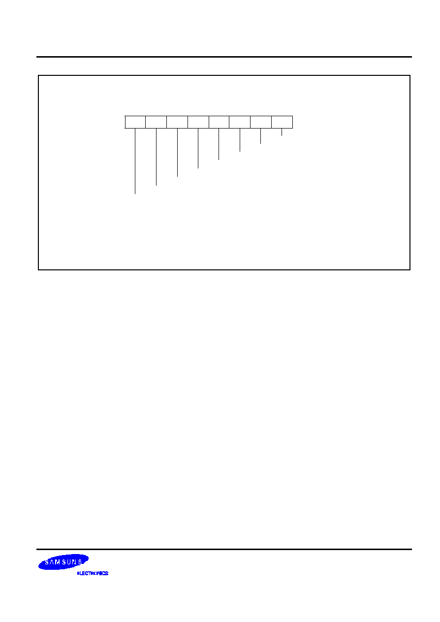
S 3 C 9 6 8 8 / P 9 6 8 8
I/O PORTS
9 -9
.7
.6
.5
.4
.3
.2
.1
.0
LSB
MSB
Port 4 Interrupt Enable and Pending Register (P4INTPND)
EFH, R/W
P4.3/INT1
P4INTPND.7-.4: Port 4 interrupt control settings:
0 = Disable interrupt at P4.n pin
1 = Enable interrupt at P4.n pin
P4.2/INT1
P4.1/INT1
P4.0/INT1
P4.3/INT1
P4.2/INT1
P4.0/INT1
P4.1/INT1
P4INTPND.3-.0: Port 4 interrupt pending bit:
0 = No interrupt request pending
1 = Interrupt request is pending
F i g u r e 9 -9 . P o r t 4 I n t e r r u p t E n a b l e a n d P e n d i n g R e g i s t e r ( P 4 I N T P N D )
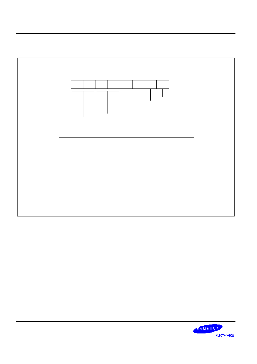
I/O PORTS
S 3 C 9 6 8 8 / P 9 6 8 8
9 -1 0
D + / P S 2 , D -/ P S 2
PS2 Control and Interrupt and Pending Register
D7H, R/W
.7
.6
.5
.4
.3
.2
.1
.0
MSB
LSB
D-/PS2PND
D+/PS2INT
Schmitt trigger input, falling edge external interrupt
Schmitt trigger input, falling edge external interrupt with pull-up
N-CH open-drain output
N-CH open-drain output with pull-up register
PS2CONINT.7-4 Pin Configration Settings: D+/PS2, D-/PS2
00
01
10
11
PS2CONINT.3-2 : Interrupt Control Setting
0 = Disable interrupt
1 = Enable interrupt
D+/PS2
D-/PS2
D-/PS2INT
D+/PS2PND
PS2CONINT.1-0 : Interrupt Pending Bit
0 = No interrupt request pending
1 = Interrupt request pending
NOTE
:
Used only PS2MODE.
F i g u r e 9 -1 0 . P S 2 C o n t r o l a n d I n t e r r u p t a n d P e n d i n g R e g i s t e r ( P S 2 C O N I N T )

S 3 C 9 6 8 8 / P 9 6 8 8
BASIC TIMER AND TIMER 0
1 0 -1
10
B A S I C T I M E R a n d T I M E R 0
M O D U L E O V E R V I E W
T h e S 3 C 9 6 8 8 / P 9 6 8 8 h a s t w o d e f a u l t t i m e r s : a n 8 -b i t b a s i c t i m e r a n d o n e 8 -b i t g e n e r a l-p u r p o s e t i m e r / c o u n t e r . T h e
8 -b i t t i m e r / c o u n t e r i s c a l l e d t i m e r 0 .
B a s i c T i m e r ( B T )
Y o u c a n u s e t h e b a s i c t i m e r ( B T ) i n t w o d i f f e r e n t w a y s :
--
A s a w a t c h d o g t i m e r t o p r o v i d e a n a u t o m a t i c r e s e t m e c h a n i s m i n t h e e v e n t o f a s y s t e m m a l f u n c t i o n .
--
To signal the end of the required oscillation stabilization interval after a reset or a Stop mode release.
T h e f u n c t i o n a l c o m p o n e n t s o f t h e b a s i c t i m e r b l o c k a r e :
--
Clock frequency divider (f
OSC
d i v i d e d b y 4 0 9 6 , 1 0 2 4 , o r 1 2 8 ) w i t h m u l t i p l e x e r
--
8 -b i t b a s i c t i m e r c o u n t e r , B T C N T ( D D H , r e a d -o n l y )
--
B a s i c t i m e r c o n t r o l r e g i s t e r , B T C O N ( D C H , r e a d / w r i t e )
T i m e r 0
T i m e r 0 h a s t w o o p e r a t i n g m o d e s , o n e o f w h i c h y o u s e l e c t b y t h e a p p r o p r i a t e T 0 C O N s e t t i n g :
--
Interval timer mode
--
Overflow mode
T i m e r 0 h a s t h e f o l l o w i n g f u n c t i o n a l c o m p o n e n t s :
--
Clock frequency divider (f
OSC
d i v i d e d b y 4 0 9 6 , 2 5 6 , o r 8 ) w i t h m u l t i p l e x e r
--
8 -bit counter (T0CNT), 8-b i t c o m p a r a t o r , a n d 8 -b i t r e f e r e n c e d a t a r e g i s t e r ( T 0 D A T A )
--
Timer 0 overflow interrupt (T0OVF) and match interrupt (T0INT) generation
--
Timer 0 control re g i s t e r , T 0 C O N
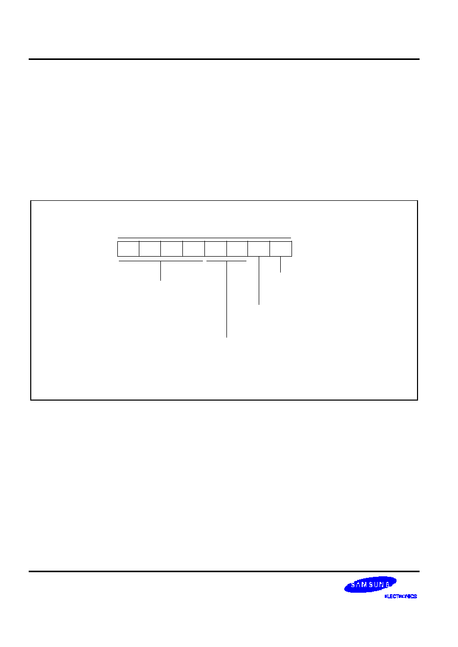
BASIC TIMER AND TIMER 0
S 3 C 9 6 8 8 / P 9 6 8 8
1 0 -2
B A S I C T I M E R C O N T R O L R E G I S T E R ( B T C O N )
T h e b a s i c t i m e r c o n t r o l r e g i s t e r , B T C O N , i s u s e d t o s e l e c t t h e i n p u t c l o c k f r e q u e n c y , t o c l e a r t h e b a s i c t i m e r c o u n t e r
a n d f r e q u e n c y d i v i d e r s , a n d t o e n a b l e o r d i s a b l e t h e w a t c h d o g t i m e r f u n c t i o n .
A r e s e t c l e a r s B T C O N t o ' 0 0 H ' . T h i s e n a b l e s t h e w a t c h d o g f u n c t i o n a n d s e l e c t s a b a s i c t i m e r c l o c k f r e q u e n c y o f
f
OSC
/ 4 0 9 6 . T o d i s a b l e t h e w a t c h d o g f u n c t i o n , y o u m u s t w r i t e t h e s i g n a t u r e c o d e ' 1 0 1 0 B ' t o t h e b a s i c t i m er register
c o n t r o l b i t s B T C O N . 7 -B T C O N . 4 .
T h e 8 -b i t b a s i c t i m e r c o u n t e r , B T C N T , c a n b e c l e a r e d a t a n y t i m e d u r i n g n o r m a l o p e r a t i o n b y w r i t i n g a " 1 " t o
B T C O N . 1 . T o c l e a r t h e f r e q u e n c y d i v i d e r s f o r b o t h t h e b a s i c t i m e r i n p u t c l o c k a n d t h e t i m e r 0 c l o c k , y o u w r i t e a " 1 "
t o B T C O N . 0 .
Basic Timer Control Register (BTCON)
DCH, R/W
.7
.6
.5
.4
.3
.2
.1
.0
MSB
LSB
Basic timer counter clear bit:
0 = No effect
1 = Clear BTCNT
Watchdog timer enable bits:
= Disable watchdog
function
= Enable watchdog
function
1010B
Other value
Basic timer input clock selection bits:
00 = f
OSC
/4096
01 = f
OSC
/1024
10 = f
OSC
/128
11 = Invalid selection
Divider clear bit for basic:
0 = No effect
1 = Clear both dividers
F i g u r e 1 0 -1 . B a s i c T i m e r C o n t r o l R e g i s t e r ( B T C O N )

S 3 C 9 6 8 8 / P 9 6 8 8
BASIC TIMER AND TIMER 0
1 0 -3
B A S I C T I M E R F U N C T I O N D E S C R I P T I O N
W a t c h d o g T i m e r F u n c t i o n
Y o u c a n p r o g r a m t h e b a s i c t i m e r o v e r f l o w s i g n a l t o g e n e r a t e a r e s e t b y s e t t i n g B T C O N . 7 -B T C O N . 4 t o a n y v a l u e o t h e r
t h a n ' 1 0 1 0 B ' ( T h e ' 1 0 1 0 B ' v a l u e d i s a b l e s t h e w a t c h d o g f u n c t i o n ) . A r e s e t c l e a r s B T C O N t o ' 0 0 H ' , a u t o m a t i c a l l y
e n a b l i n g t h e w a t c h d o g t i m e r f u n c t i o n . A r e s e t a l s o s e l e c t s t h e C P U c l o c k ( a s d e t e r m i n e d b y t h e c u r r e n t C L K C O N
r e g i s t e r s e t t i n g ) d i v i d e d b y 4 0 9 6 a s t h e B T c l o c k .
A r e s e t w h e n e v e r a b a s i c t i m e r c o u n t e r o v e r f l o w o c c u r s . D u r i n g n o r m a l o p e r a t i o n , t h e a p p l i c a t i o n p r o g r a m m u s t
p r e v e n t t h e o v e r f l o w , a n d t h e a c c o m p a n y i n g r e s e t o p e r a t i o n , f r o m o c c u r r i n g . T o d o t h i s , t h e B T C N T v a l u e m u s t b e
cleared (by writing a "1" to BTCON.1) at regular intervals.
I f a s y s t e m m a l f u n c t i o n o c c u r s d u e t o c i r c u i t n o i s e o r s o m e o t h e r e r r o r c o n d i t i o n , t h e B T c o u n t e r c l e a r o p e r a t i o n w i l l
not be executed and a basic timer overflow will occur, initiating a reset. In other words, during normal operation, the
basic timer overflow loop (a bit 7 overflow of the 8-b i t b a s i c t i m e r c o u n t e r , B T C N T ) i s a l w a y s b r o k e n b y a B T C N T c l e a r
i n s t r u c t i o n . I f a m a l f u n c t i o n d o e s o c c u r , a r e s e t i s t r i g g e r e d a u t o m a t i c a l l y .
O s c i l l a t i o n S t a b i l i z a t i o n I n t e r v a l T i m e r F u n c t i o n
Y o u c a n a l s o u s e t h e b a s i c t i m e r t o p r o g r a m a s p e c i f i c o s c i l l a t i o n s t a b i l i z a t i o n i n t e r v a l f o l l o w i n g a r e s e t o r w h e n S t o p
m o d e h a s b e e n r e l e a s e d b y a n e x t e r n a l i n t e r r u p t .
I n S t o p m o d e , w h e n e v e r a r e s e t o r a n e x t e r n a l i n t e r r u p t o c c u r s , t h e o s c i l l a t o r s t a r t s . T h e B T C N T v a l u e t h e n s t a r t s
increasing at the rate of f
OSC
/4096 (for reset), or at the rate of the preset clock source (for an external interrupt). When
B T C N T . 4 i s s e t , a s i g n a l i s g e n e r a t e d t o i n d i c a t e t h a t t h e s t a b i l i z a t i o n i n t e r v a l h a s e l a p s e d a n d t o g a t e t h e c l o c k
s i g n a l o f f t o t h e C P U s o t h a t i t c a n r e s u m e n o r m a l o p e r a t i o n .
I n s u m m a r y , t h e f o l l o w i n g e v e n t s o c c u r w h e n S t o p m o d e i s r e l e a s e d :
1 . D u r i n g S t o p m o d e , a p o w e r-o n r e s e t o r a n e x t e r n a l i n t e r r u p t o c c u r s t o t r i g g e r t h e S t o p m o d e r e l e a s e a n d
o s c i l l a t i o n s t a r t s .
2 . If a p o w e r-o n r e s e t o c c u r r e d , t h e b a s i c t i m e r c o u n t e r w i l l i n c r e a s e a t t h e r a t e o f f
OSC
/4096. If an external interrupt
i s u s e d t o r e l e a s e S t o p m o d e , t h e B T C N T v a l u e i n c r e a s e s a t t h e r a t e o f t h e p r e s e t c l o c k s o u r c e .
3 . C l o c k o s c i l l a t i o n s t a b i l i z a t i o n i n t e r v a l b e g i n s a n d c o n t i n u e s u n t i l b i t 4 o f t h e b a s i c t i m e r c o u n t e r i s s e t .
4 . W h e n a B T C N T . 4 i s s e t , n o r m a l C P U o p e r a t i o n r e s u m e s .
F i g u r e s 1 0 -2 a n d 1 0 -3 s h o w s t h e o s c i l l a t i o n s t a b i l i z a t i o n t i m e o n R E S E T a n d S T O P m o d e r e l e a s e
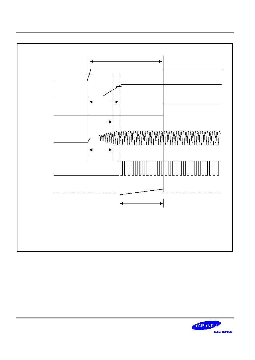
BASIC TIMER AND TIMER 0
S 3 C 9 6 8 8 / P 9 6 8 8
1 0 -4
Oscillation Stabilization
Normal Operating mode
0.5 V
DD
t
WAIT
= (4096x16)/f
OSC
Basic timer increment and
CPU operations are IDLE mode
10000B
00000B
Reset ReleaseVoltage
V
DD
RESET
Internal
Reset
Release
Oscillator
(X
OUT
)
BTCNT
clock
BTCNT
value
0.5 V
DD
Oscillator Stabilization Time
trst RC
~
~
~
NOTE:
During of the oscillator stabilization wait time, t
WAIT
, when it is released
by a Power-on-reset is 4096x16/fosc.
trst RC (R is external resister and C is on chip capacitor)
~
~
~
F i g u r e 1 0 -2 . O s c i l l a t i o n S t a b i l i z a t i o n T i m e o n R E S E T
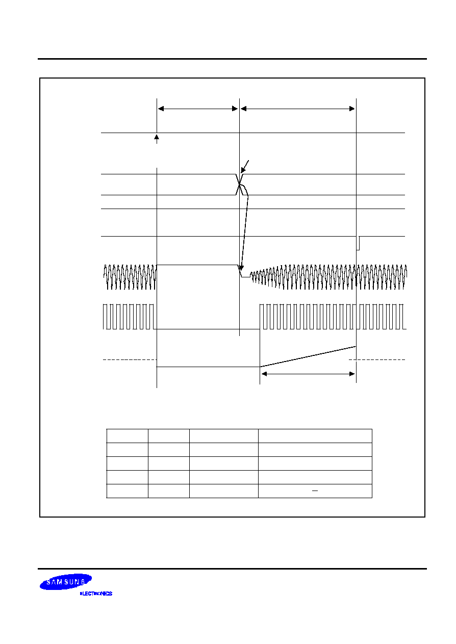
S 3 C 9 6 8 8 / P 9 6 8 8
BASIC TIMER AND TIMER 0
1 0 -5
NOTE:
Duration of the oscillator stabilzation wait time, tWAIT, it is released by an
interrupt is determined by the setting in basic timer control register, BTCON.
V
DD
Oscillation Stabilization Time
RESET
External
Interrupt
Oscillator
(X
OUT
)
BTCNT
clock
BTCNT
Value
t
WAIT
Basic Timer Increment
10000B
STOP
Release
Signal
00000B
Normal
Operating
Mode
Normal
Operating
Mode
STOP Mode
STOP Mode
Release Signal
STOP
Instruction
Execution
BTCON.3
BTCON.2
0
0
1
1
0
1
0
1
t
WAIT
(4096 x 16)/fosc
(1024 x 16)/fosc
(128 x 16)/fosc
Invalid setting
t
WAIT
(When f
OSC
is 6 MHz)
10.92 ms
2.7 ms
0.34 ms
F i g u r e 1 0 -3 . O s c i l l a t i o n S t a b i l i z a t i o n T i m e o n S T O P M o d e R e l e a s e
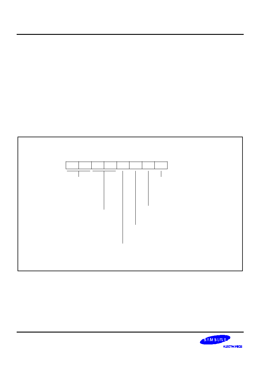
BASIC TIMER AND TIMER 0
S 3 C 9 6 8 8 / P 9 6 8 8
1 0 -6
T I M E R 0 C O N T R O L R E G IS T E R ( T 0 C O N )
T 0 C O N i s l o c a t e d a t a d d r e s s D 2 H , a n d i s r e a d / w r i t e a d d r e s s a b l e .
A r e s e t c l e a r s T 0 C O N t o ' 0 0 H ' . T h i s s e t s t i m e r 0 t o n o r m a l i n t e r v a l m a t c h m o d e , s e l e c t s a n i n p u t c l o c k f r e q u e n c y o f
f
OSC
/ 4 0 9 6 , a n d d i s a b l e s t h e t i m e r 0 o v e r f l o w i n t e r r u p t a n d m a t c h i n t e r r u p t . Y o u c a n c l e a r t h e t i m e r 0 c o u n t e r a t a n y
t i m e d u r i n g n o r m a l o p e r a t i o n b y w r i t i n g a " 1 " t o T 0 C O N . 3 .
T h e t i m e r 0 o v e r f l o w i n t e r r u p t c a n b e e n a b l e d b y w r i t i n g a " 1 " t o T 0 C O N . 2 . W h e n a t i m e r 0 o v e r f l o w i n t e r r u p t o c c u r s
a n d i s s e r v i c e d b y t h e C P U , t h e p e n d i n g c o n d i t i o n m u s t b e c l e a r e d b y s o f t w a r e b y w r i t i n g a " 0 " t o t h e t i m e r 0
interrupt pending bit, T0CON.0.
T o e n a b l e t h e t i m e r 0 m a t c h i n t e r r u p t , y o u m u s t w r i t e T 0 C O N . 1 t o " 1 " . T o d e t e c t a n i n t e r r u p t p e n d i n g c o n d i t i o n , t h e
a p p l i c a t i o n p r o g r a m p o l l s T 0 C O N . 0 . W h e n a " 1 " i s d e t e c t e d , a t i m e r 0 m a t c h / c a p t u r e i n t e r r u p t i s p e n d i n g . W h e n t h e
i n t e r r u p t r e q u e s t h a s b e e n s e r v i c e d , t h e p e n d i n g c o n d i t i o n m u s t b e c l e a r e d b y s o f t w a r e b y w r i t i n g a " 0 " t o t h e t i m e r 0
interrupt pending bit, T0CON.0.
.7
.6
.5
.4
.3
.2
.1
.0
LSB
MSB
Timer 0 Control Register (T0CON)
D2H, R/W
Timer 0 interrupt pending bit:
0 = No interrupt pending
0 = Clear pending bit (when write)
1 = Interrupt is pending (When read)
No effect (When write)
Timer 0 input clock selection bits:
00 = f
OSC
/4096
01 = f
OSC
/256
10 = f
OSC
/8
11 = Invalid selection
Timer 0 overflow interrupt enable bit:
0 = Disable overflow interrupt
1 = Enable overflow interrupt
Timer 0 match interrupt enable bit:
0 = Disable match interrupt
1 = Enable match interrupt
Timer 0 operating mode selection bits:
00 = Interval match mode
01 = Invalid selection
10 = Invalid selection
11 = Overflow mode
Timer 0 counter clear bit:
0 = No effect
1 = Clear the timer 0 counter (when write)
F i g u r e 1 0 -4 . T i m e r 0 C o n t r o l R e g i s t e r ( T 0 C O N )

S 3 C 9 6 8 8 / P 9 6 8 8
BASIC TIMER AND TIMER 0
1 0 -7
T I M E R 0 F U N C T I O N D E S C R I P T I O N
I n t e r v a l M a t c h M o d e
I n i n t e r v a l m a t c h m o d e , a m a t c h s i g n a l i s g e n e r a t e d w h e n t h e c o u n t e r v a l u e i s i d e n t i c a l t o t h e v a l u e w r i t t e n t o t h e T 0
r e f e r e n c e d a t a r e g i s t e r , T 0 D A T A . T h e m a t c h s i g n a l g e n e r a t e s a t i m e r 0 m a t c h i n t e r r u p t a n d t h e n c l e a r s t h e c o u n t e r .
If for example, you write the value '10H' to T0DATA, the counter will increment until it reaches '10H'. At this point, the
T 0 m a t c h i n t e r r u p t i s g e n e r a t e d , t h e c o u n t e r v a l u e i s r e s e t a n d c o u n t i n g r e s u m e s .
O v e r f l o w M o d e
In overflow mode, a overflow signal is generated regardless of the value written to the T0 reference data register when
the counter value is overflowed. The overflow signal generates a timer 0 overflow interrupt and then T0 counter is
c l e a r e d .
Counter
CLK
R
Match
T0INT
T0OVF
Data Bus
8
T0PND
When 8-Bit counter is cleared,
this buffer is open
Data Bus
8
Comparator
T0DATA Buffer
Register
T0DATA
F i g u r e 1 0 -5 . S i m p l i f i e d T i m e r 0 F u n c t i o n D i a g r a m : I n t e r v a l T i m e r M o d e

BASIC TIMER AND TIMER 0
S 3 C 9 6 8 8 / P 9 6 8 8
1 0 -8
Bit 1
RESET or STOP
MUX
DIV
R
XIN
1/4096
1/1024
1/128
Bit 0
DIV
R
2-Bit
SCA
LER
1/4096
1/8
Bits 3, 2
Bits 7, 6
8-Bit Basic Counter
(
BTCNT,
Read-only)
Data Bus
8
When BTCNT. 4 is set after releasing from
RESET or STOP mode, CPU clock start.
Bit 2
OVINT
R
OVF
Bits 7, 6, 5, 4
Write '1010xxxxB' to disable
RESET
8
Data Bus
Overflow
8-Bit Counter
(T0CNT, Read-only)
Bit 3
T0CLR
8
8-Bit Comparator
8
T0DATA Buffer Register
T0DATA
8
Data Bus
When 8-bit counter is cleared,
this buffer is open.
Match
Signal
Match/
Overflow
Bits 5, 4
Bit 1
T0INT
Bit 0
IRQ
Basic Timer Control Register
Timer 0 Control Register
1/256
F i g u r e 1 0 -6 . B a s i c T i m e r a n d T i m e r 0 B l o c k D i a g r a m

S 3 C 9 6 8 8 / P 9 6 8 8
UNIVERSAL SERIAL BUS
1 1 -1
11
U N I V E R S A L S E R I A L B U S
O V E R V I E W
U n i v e r s a l S e r i a l B u s ( U S B ) i s a c o m m u n i c a t i o n a r c h i t e c t u r e t h a t s u p p o r t s d a t a t r a n s f e r b e t w e e n a h o s t c o m p u t e r
a n d a w i d e r a n g e o f P C p e r i p h e r a l s . U S B i s a c t u a l l y a c a b l e b u s i n w h i c h t h e p e r i p h e r a l s s h a r e i t s b a n d w i d t h t h r o u g h
a h o s t s c h e d u l e d t o k e n b a s e d p r o t o c o l .
T h e U S B m o d u l e i n S 3 C 9 6 8 8 / P 9 6 8 8 i s d e s i g n e d t o s e r v e a t a l o w s p e e d t r a n s f e r r a t e ( 1 . 5 M b s ) U S B d e v i c e a s
d e s c r i b e d i n t h e U n i v e r s a l S e r i a l B u s S p e c i f i c a t i o n R e v i s i o n 2 . 0 . S 3 C 9 6 8 8 / P 9 6 8 8 c a n b e b r i e f l y d e s c r i b e a s a
m i c r o c o n t r o l l e r w i t h S A M 8 8 R C R I c o r e w i t h a n o n -c h i p U S B p e r i p h e r a l a s c a n b e s e e n i n f i g u r e 1 1 -1 .
T h e S 3 C 9 6 8 8 / P 9 6 8 8 c o m e s e q u i p p e d w i t h S e r i a l I n t e r f a c e E n g i n e ( S I E ) , w h i c h h a n d l e s t h e c o m m un i c a t i o n p r o t o c o l
o f t h e U S B . T h e S 3 C 9 6 8 8 / P 9 6 8 8 s u p p o r t s t h e f o l l o w i n g c o n t r o l l o g i c : p a c k e t d e c o d i n g / g e n e r a t i o n , C R C
g e n e r a t i o n / c h e c k i n g , N R Z I e n c o d i n g / d e c o d i n g , S y n c d e t e c t i o n , E O P ( e n d o f p a c k e t ) d e t e c t i o n a n d b i t s t u f f i n g .
S 3 C 9 6 8 8 / P 9 6 8 8 s u p p o r t s t w o t y p e s o f d a t a t r a n s f e r s ; c o n t r o l a n d i n t e r r u p t . T h r e e e n d p o i n t s a r e u s e d i n t h i s d e v i c e ;
E n d p o i n t 0 , E n d p o i n t 1 , a n d E n d p o i n t 2 . P l e a s e r e f e r t o t h e U S B s p e c i f i c a t i o n r e v i s i o n 2 . 0 f o r d e t a i l d e s c r i p t i o n o f
U S B .

UNIVERSAL SERIAL BUS
S 3 C 9 6 8 8 / P 9 6 8 8
1 1 -2
D-/PS2
D+/PS2
SAM88RCRI
Core
Transceiver
Voltage
Regulator
SIE
(Serial Interface
Engine)
Endpoint 0 FIFO
Endpoint 1, 2
FIFO
Interface
F i g u r e 1 1 -1 . U S B P e r i p h e r a l I n t e r f a c e

S 3 C 9 6 8 8 / P 9 6 8 8
UNIVERSAL SERIAL BUS
1 1 -3
S e r i a l B u s I n t e r f a c e E n g i n e ( S I E )
The Serial Interface Engine interfaces to the USB serial data and handles, deserialization/serialization of data, NRZI
e n c o d i n g / d e c o d i n g , c l o c k e x t r a c t i o n , C R C g e n e r a t i o n a n d c h e c k i n g , b i t s t u f f i n g a n d o t h e r s p e c i f i c a t i o n s p e r t a i n i n g t o
t h e U S B p r o t o c o l s u c h a s h a n d l i n g i n t e r p a c k e t t i m e o u t a n d P I D d e c o d i n g .
C o n t r o l L o g i c
T h e U S B c o n t r o l l o g i c m a n a g e s d a t a m o v e m e n t s b e t w e e n t h e C P U a n d t h e t r a n s c e i v e r b y m a n i p u l a t i n g t h e
transceiver and the endpoin t r e g i s t e r . T h i s i n c l u d e s b o t h t r a n s m i t a n d r e c e i v e o p e r a t i o n s o n t h e U S B . T h e l o g i c
c o n t a i n s b y t e c o u n t b u f f e r s f o r t r a n s m i t o p e r a t i o n s t h a t l o a d t h e a c t i v e t r a n s m i t e n d p o i n t ' s b y t e c o u n t a n d u s e t h i s t o
d e t e r m i n e t h e n u m b e r o f b y t e s t o t r a n s f e r . T h e s a m e b u f f e r i s u s e d f o r r e c e i v e t r a n s a c t i o n s t o c o u n t t h e n u m b e r o f
b y t e s r e c e i v e d a n d t r a n s f e r t h a t n u m b e r t o t h e r e c e i v e e n d p o i n t ' s b y t e c o u n t r e g i s t e r a t t h e e n d o f t h e t r a n s a c t i o n .
T h e c o n t r o l l o g i c i n S 3 C 9 6 8 8 / P 9 6 8 8 , w h e n t r a n s m i t t i n g , m a n a g e s p a r a l l e l t o s e r i a l c o n v e r s i o n , p a c k e t g e n e r a t i o n ,
CRC generation, NRZI encoding and bit stuffing.
W h e n r e c e i v i n g , t h e c o n t r o l l o g i c i n S 3 C 9 6 8 8 / P 9 6 8 8 h a n d l e s S y n c d e t e c t i o n , p a c k e t d e c o d i n g , E O P ( e n d o f p a c k e t )
d e t e c t i o n , b i t s t u f f i n g , N R Z I d e c o d i n g , C R C c h e c k i n g a n d s e r i a l t o p a r a l l e l c o n v e r s i o n
B u s P r o t o c o l
A l l b u s t r a n s a c t i o n s i n v o l v e t h e t r a n s m i s s i o n o f p a c k e t s . S 3 C 9 6 8 8 / P 9 6 8 8 s u p p o r t s t h r e e p a c k e t t y p e s ; T o k e n , D a t a
a n d H a n d s h a k e . E a c h t r a n s a c t i o n s t a r t s w h e n t h e h o s t c o n t r o l l e r s e n d s a T o k e n P a c k e t t o t h e U S B d e v i c e . T h e
T o k e n p a c k e t s a r e g e n e r a t e d b y t h e U S B h o s t a n d d e c o d e d b y t h e U S B d e v i c e . A T o k e n P a c k e t i n c l u d e s t h e t y p e
d e s c r i p t i o n , d i r e c t i o n o f t h e t r a n s a c t i o n , U S B d e v i c e a d d r e s s a n d t h e e n d p o i n t n u m b e r .
D a t a a n d H a n d s h a k e p a c k e t s a r e b o t h d e c o d e d a n d g e n e r a t e d b y t h e U S B d e v i c e . I n a n y t r a n s a c t i o n , t h e d a t a i s
t r a n s f e r r e d f r o m t h e h o s t t o a d e v i c e o r f r o m a d e v i c e t o t h e h o s t . T h e t r a n s a c t i o n s o u r c e t h e n s e n d s a D a t a P a c k e t
o r i n d i c a t e s t h a t i t h a s n o d a t a t o t r a n s f e r . T h e d e s t i n a t i o n t h e n r e s p o n d s w i t h a H a n d s h a k e P a c k e t i n d i c a t i n g
w h e t h e r t h e t r a n s f e r w a s s u c c e s s f u l .
D a t a T r a n s f e r T y p e s
U S B d a t a t r a n s f e r o c c u r s b e t w e e n t h e h o s t s o f t w a r e a n d a s p e c i f i c e n d p o i n t o n t h e U S B d e v i c e . A n e n d p o i n t
s u p p o r t s a s p e c i f i c t y p e o f d a t a t r a n s f e r . T h e S 3 C 9 6 8 8 / P 9 6 8 8 s u p p o r t s t w o d a t a t r a n s f e r e n d p o i n t s : c o n t r o l a n d
interrupt.
C o n t r o l t r a n s f e r c o n f i g u r e s a n d a s s i g n s a n a d d r e s s t o t h e d e v i c e w h e n d e t e c t e d . C o n t r o l t r a n s f e r a l s o s u p p o r t s
s t a t u s t r a n s a c t i o n , r e t u r n i n g s t a t u s i n f o r m a t i o n f r o m d e v i c e t o h o s t .
Interrupt transfe r r e f e r s t o a s m a l l , s p o n t a n e o u s d a t a t r a n s f e r f r o m U S B d e v i c e t o h o s t .
E n d p o i n t s
C o m m u n i c a t i o n f l o w s b e t w e e n t h e h o s t s o f t w a r e a n d t h e e n d p o i n t s o n t h e U S B d e v i c e . E a c h e n d p o i n t o n a d e v i c e
h a s a n i d e n t i f i e r n u m b e r . I n a d d i t i o n t o t h e e n d p o i n t n u m b e r , e a c h e n d p o i n t s u p p o r t s a s p e c i f i c t r a n s f e r t y p e .
S 3 C 9 6 8 8 / P 9 6 8 8 s u p p o r t s t h r e e e n d p o i n t s : E n d p o i n t 0 s u p p o r t s c o n t r o l t r a n s f e r , a n d E n d p o i n t 1 a n d E n d p o i n t 2
supports interrupt transfer.
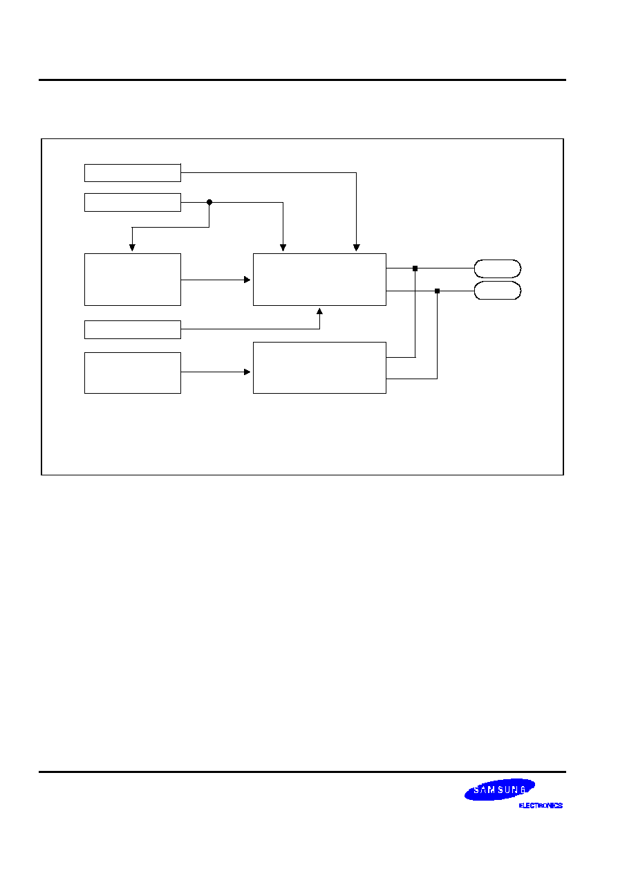
UNIVERSAL SERIAL BUS
S 3 C 9 6 8 8 / P 9 6 8 8
1 1 -4
S T R U C T U R E O F U S B A N D P S / 2 C O M B I N A T I O N A L P O R T
USB Signal Transceiver
(With Pull-up)
PS/2 Signal Transceiver
(With Pull-up)
DM
DP
Voltage Regulator
(3.3 V Generation)
USB Control
PS/2 Control
(P2CONINT)
Pull-up Enable
USB Enable
[A]
[B]
[C]
NOTE:
That block explain USB block can be enabled or disabled with pull-up by s/w.
Voltage regulator also disabled automatically when USB block was disabled.
And PS/2 block can be controlled by software with pull-up.
F i g u r e 1 1 -2 . B l o c k D i a g r a m o f U S B a n d P S / 2 T r a n s c e i v e r
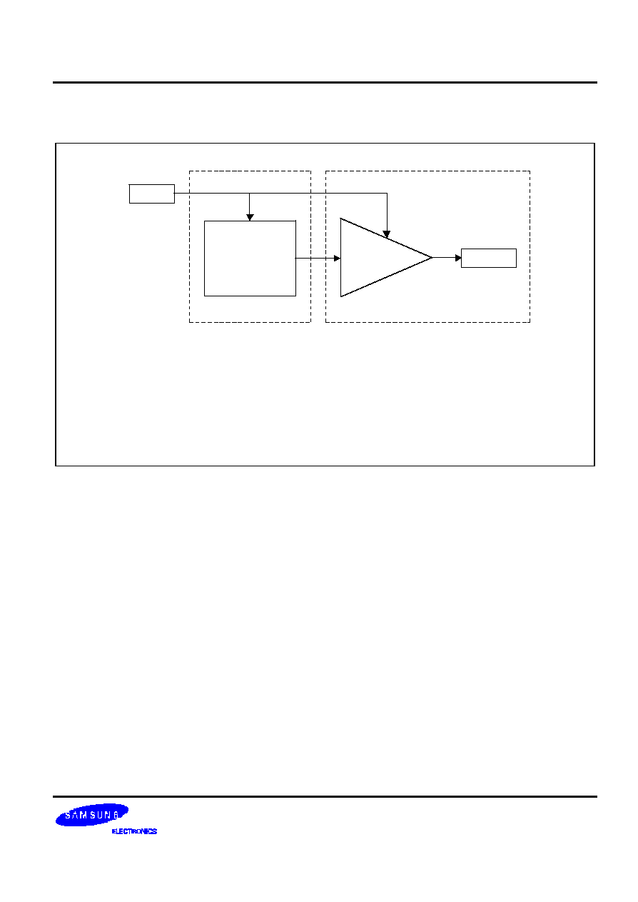
S 3 C 9 6 8 8 / P 9 6 8 8
UNIVERSAL SERIAL BUS
1 1 -5
S T R U C T U R E O F V O L T A G E R E G U L A T O R
Enable
Reference
Voltage
Generator
3.3 V
Current
Amplifier
A
B
NOTE:
This block can give a explanation how it can be controlled automatically.
If the 3.3 voltage regulator is enabled by software, it operates to cover fluctuation of
the line load, sometimes the line is unstable and the driving ability dropped.
As it operates in the normal stage without any peak, power will be supplied with
8 mA, and when the operating. It was designed to cover by 50 mA, the peak current
consumption. It means any kind of load problem will be compensated with the above
design.
F i g u r e 1 1 -3 . B l o c k D i a g r a m o f V o l t a g e R e g u l a t o r

UNIVERSAL SERIAL BUS
S 3 C 9 6 8 8 / P 9 6 8 8
1 1 -6
CTRL
D-
D+
Slope
Control
A
B
V3.3IN
Control
Sinals
Enable
DM
TX/RX
DP
TX/RX
C
D
DM
DP
Pull-up Control
R, 1.5 K
5 %
+
NOTE:
We didn't used the by-pass capacitor on the 3.3 V out, since the 3.3 V regulator and clamp
circuit will give a solution through the feedback.
USB block was designed to cover the line load, the typically designed value is 300 pF (max: 800 pF).
The clamp block operating after it detect the voltage variation
(actually the current fluctuation will be feedback into voltage variation, di/dt to dt/dt variation.
Bias controls the slope.
Control signal means NRZI, EOP, XCON, IN/OUT.
Enable is for the Tx, Rx.
Internal pull-up resistor will be 1.5 k
10 %
+
F i g u r e 1 1 -4 . B l o c k D i a g r a m o f U S B S i g n a l T r a n s c e i v e r
V
DD
DM_DRVP
DM_DRVN
DM
PS/2 Data
Pull-up Enable
V
DD
DP_DRVP
DP_DRVN
DP
PS/2 Clock
Pull-up Enable
NOTE:
It explain the PS2 block.
The pull-up resistor value will be 4.3 k
20 %
This block can be controlled with pull-up resistor and it was designed with totally
different from usb.
+
F i g u r e 1 1 -5 . B l o c k D i a g r a m o f G P I O S i g n a l T r a n s m i t t e r
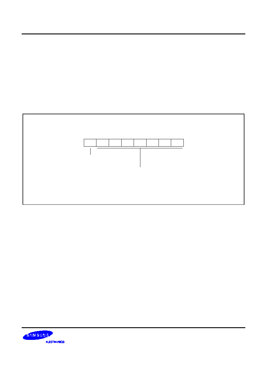
S 3 C 9 6 8 8 / P 9 6 8 8
UNIVERSAL SERIAL BUS
1 1 -7
U S B F U N C T I O N A D D R E S S R E G I S T E R ( F A D D R )
T h i s r e g i s t e r h o l d s t h e U S B a d d r e s s a s s i g n e d b y t h e h o s t c o m p u t e r . F A D D R i s l o c a t e d a t a d d r e s s F 0 H a n d i s
r e a d / w r i t e a d d r e s s a b l e .
B i t 7
This register b i t i s u s e d a s t e s t m o d e o r s p e c i a l p u r p o s e m o d e , s o u s e r s h o u l d s e t z e r o v a l u e ,
B i t 6 ≠ 0 F A D D R :
M C U u p d a t e s t h i s r e g i s t e r o n c e i t d e c o d e s a S E T _ A D D R E S S c o m m a n d . M C U m u s t w r i t e t h i s
r e g i s t e r b e f o r e i t c l e a r s O U T _ P K T _ R D Y ( b i t 0 ) a n d s e t s D A T A _ E N D ( b i t 3 ) i n t h e E P 0 C S R r e g i s t e r . T h e
f u n c t i o n c o n t r o l l e r u s e t h i s r e g i s t e r ' s v a l u e t o d e c o d e U S B T o k e n p a c k e t a d d r e s s . A t r e s e t , i f t h e d e v i c e
is not yet configured the value is reset to 0.
.7
.6
.5
.4
.3
.2
.1
.0
LSB
MSB
USB Function Address Register (FADDR)
F0H, R/W
7-bit programming device address. This register
maintains the USB address assigned by the host.
The function controller uses this register's value to
decode USB token packet address. At reset when
the device is not yet configured the value is reset to 0.
This register bit sets zero value
F i g u r e 1 1 -6 . U S B F u n c t i o n A d d r e s s R e g i s t e r ( F A D D R )

UNIVERSAL SERIAL BUS
S 3 C 9 6 8 8 / P 9 6 8 8
1 1 -8
C O N T R O L E N D P O I N T S T A T U S R E G I S T E R ( E P 0 C S R)
E P 0 C S R r e g i s t e r c o n t r o l s E n d p o i n t 0 ( C o n t r o l E n d p o i n t ) , a n d a l s o h o l d s s t a t u s b i t s f o r E n d p o i n t 0 . E P 0 C S R i s
l o c a t e d a t F 1 H a n d i s r e a d / w r i t e a d d r e s s a b l e .
B i t 7
C L E A R _ S E T U P _ E N D : M C U w r i t e s " 1 " t o t h i s b i t t o c l e a r S E T U P _ E N D b i t ( b i t 4 ) . T h i s b i t i s
a u t o m a t i c a l l y c l e a r e d a f t e r c l e a r i n g S E T U P _ E N D b i t b y S I E . S o r e a d v a l u e w i l l b e a l w a y s " 0 " .
B i t 6
C L E A R _ O U T _ P K T _ R D Y : M C U w r i t e s " 1 " t o t h i s b i t t o c l e a r O U T _ P K T _ R D Y b i t ( b i t 0 ) . T h i s b i t i s
a u t o m a t i c a l l y c l e a r e d a f t e r c l e a r i n g O U T _ P K T _ R D Y b i t b y U S B b l o c k . S o r e a d v a l u e w i l l b e a l w a y s " 0 " .
B i t 5
S E N D _ S T A L L : M C U w r i t e s " 1 " t o t h i s b i t t o s e n d S T A L L p a c k e t t o H o s t , i t m u s t c l e a r O U T _ P K T _ R D Y
( b i t 0 ) a t t h e s a m e t i m e . I f M C U r e c e i v e i n v a l i d c o m m a n d t h e n s h o u l d w r i t e # 6 0 h t o t h i s r e g i s t e r . T h e S I E
i s s u e s a S T A L L h a n d s h a k e t o t h e c u r r e n t c o n t r o l t r a n s f e r ( M e a n s n e x t t r a n s a c t i o n ) . T h i s b i t w i l l b e c l e a r e d
a f t e r s e n d i n g S T A L L h a n d s h a k e .
B i t 4
S E T U P _ E N D : S I E s e t s t h i s b i t , w h e n a c o n t r o l t r a n s f e r e n d s w i t h o u t s e t t i n g D A T A _ E N D b i t ( b i t 3 ) . M C U
c l e a r s t h i s b i t , b y w r i t i n g a " 1 " t o C L E A R _ S E T U P _ E N D b i t ( b i t 7 ) . W h e n S I E s e t s t h i s b i t , a n i n t e r r u p t i s
g e n e r a t e d t o M C U . W h e n s u c h c o n d i t i o n o c c u r s , S I E f l u s h e s t h e F I F O . M C U c a n n o t a c c e s s t o F I F O
u n t i l t h i s b i t c l e a r e d . T h i s f l a g i s a r e a d o n l y b i t s o M C U c a n n o t w r i t e t o t h i s b i t d i r e c t l y .
B i t 3
D A T A _ E N D : M C U s e t s t h i s b i t :
-- A f t e r l o a d i n g t h e l a s t p a c k e t o f d a t a i n t o t h e F I F O , a n d a t t h e s a m e t i m e I N _ P K T _ R D Y b i t s h o u l d b e
s e t .
-- W h i l e i t c l e a r s O U T _ P K T _ R D Y b i t a f t e r u n l o a d i n g t h e l a s t p a c k e t o f d a t a .
-- F o r a z e r o l e n g t h d a t a p h a s e , t h i s b i t s h o u l d b e s e t w h e n i t c l e a r s O U T _ P K T _ R D Y b i t .
B i t 2
S E N T _ S T A L L : S I E s e t s t h i s b i t a f t e r s e n d s t a l l h a n d s h a k e t o h o s t . T h e r e a r e t w o c a s e s w h i c h i s s u e s t a l l
p a c k e t t o h o s t . I f M C U s e t S E N D _ S T A L L b i t , t h e n S I E w i l l s e n d s t a l l t o t h e n e x t t r a n s a c t i o n a n d s e t t h i s
b i t . T h e o t h e r c a s e i s s e n d s t a l l b y S I E a u t o m a t i c a l l y s i n c e p r o t o c o l v i o l a t i o n . A n i n t e r r u p t i s g e n e r a t e d
w h e n t h i s b i t g e t s s e t . T h i s b i t i s a r e a d / w r i t e b i t s o M C U s h o u l d c l e a r s t h i s b i t t o e n d t h e S T A L L
c o n d i t i o n .
B i t 1
I N _ P K T _ R D Y : M C U s e t s t h i s b i t , a f t e r l o a d i n g d a t a i n t o E n d p o i n t 0 F I F O . S I E c l e a r s t h i s b i t , o n c e t h e
p a c k e t h a s b e e n s u c c e s s f u l l y s e n t t o t h e h o s t . A n i n t e r r u p t i s g e n e r a t e d w h e n S I E c l e a r s t h i s b i t s o t h a t
M C U c a n l o a d t h e n e x t p a c k e t . F o r a z e r o l e n g t h d a t a p h a s e , M C U s e t s I N _ P K T _ R D Y b i t w i t h o u t l o a d
d a t a t o F I F O .
B i t 0
O U T _ P K T _ R D Y : SIE sets this bit, if the device receive valid data from host. An interrupt is generated,
w h e n S I E s e t s t h i s b i t . M C U s h o u l d d o w n l o a d d a t a a n d c l e a r s t h i s b i t b y w r i t i n g " 1 " t o
C L E A R _ O U T _ P K T _ R D Y b i t a t t h e e n d o f e x e c u t i o n .
N O T E
W h e n S E T U P _ E N D b i t i s s e t , O U T _ P K T _ R D Y b i t m a y a l s o b e s e t . T h i s h a p p e n s w h e n t h e c u r r e n t t r a n s f e r
h a s t e r m i n a t e d b y n e w s e t u p t r a n s a c t i o n . I n s u c h c a s e , M C U s h o u l d f i r s t c l e a r S E T U P _ E N D b i t , a n d t h e n
start servicing the new control transfer.
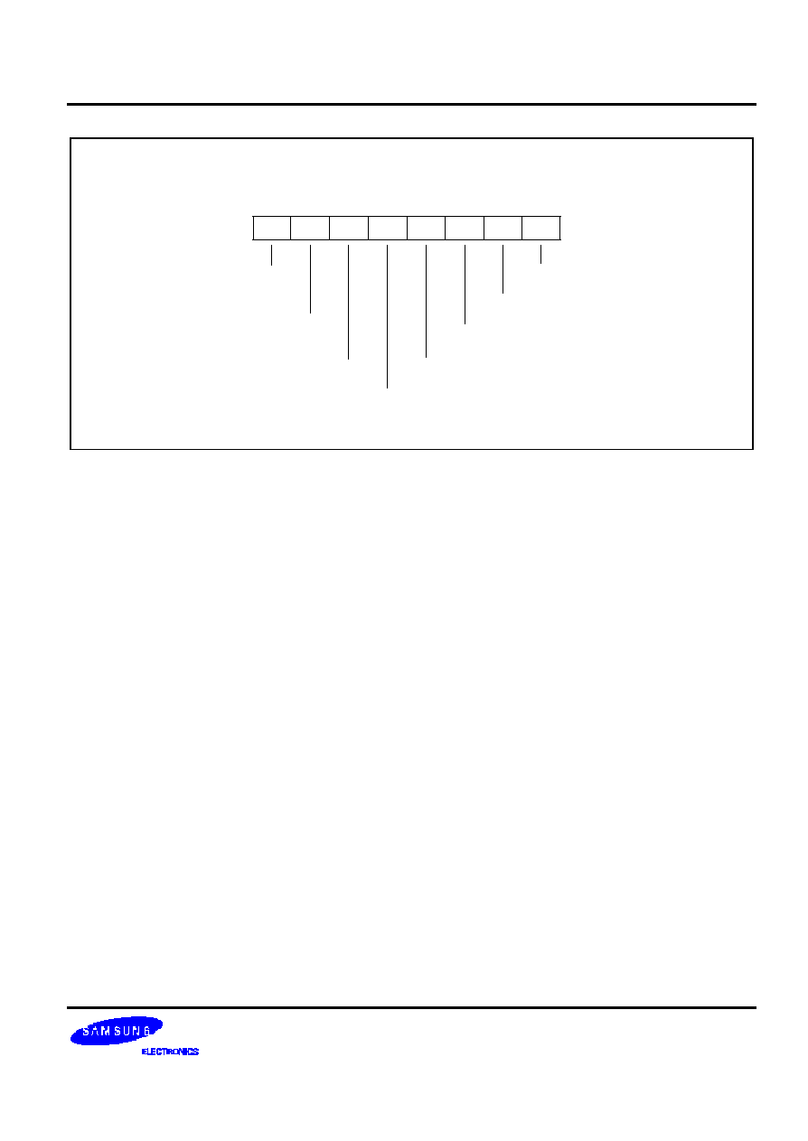
S 3 C 9 6 8 8 / P 9 6 8 8
UNIVERSAL SERIAL BUS
1 1 -9
.7
.6
.5
.4
.3
.2
.1
.0
LSB
MSB
Control Endpoint Status Register (EP0CSR)
F1H, R/W
CLEAR_
SETUP_END
CLEAR_
OUT_PKT_RDY
SEND_STALL
SETUP_END
DATA_END
SENT_STALL
IN_PKT_RDY
OUT_PKT_RDY
F i g u r e 1 1 -7 . C o n t r o l E n d p o i n t S t a t u s R e g i s t e r ( E P 0 C S R )

UNIVERSAL SERIAL BUS
S 3 C 9 6 8 8 / P 9 6 8 8
1 1 -1 0
I N T R R U P T E N D P O I N T S S T A T U S R E G I S T E R ( E P 1 C S R , E P 2 C S R )-- I N M O D E
E P 1 C S R r e g i s t e r c o n t r o l s E n d p o i n t 1 , a n d a l s o h o l d s s t a t u s b i t s f o r E n d p o i n t 1 . E P 1 C S R i s l o c a t e d a t F 2 H a n d i s
r e a d / w r i t e a d d r e s s a b l e . E P 2 C S R r e g i s t e r c o n t r o l s E n d p o i n t 2 , a n d t h e c o n t e n t s i s p e r f e c t l y s a m e t o E P 1 C S R .
E P 2 C S R i s l o c a t e d a t F 9 H a n d i s r e a d / w r i t e a d d r e s s a b l e .
E P 1 C S R a n d E P 2 C S R h a v e t w o m o d e s . T h e s e a r e I N a n d O U T m o d e w h i c h a r e d e c i d e d b y E N D P O I N T _ M O D E
register. The below is IN mode configuration.
B i t 7
C L R _ D A T A _ T O G G L E : M C U w r i t e " 1 " t o t h i s b i t f o r i n i t i a l i z i n g d a t a t o g g l e s e q u e n c e . D a t a t o g g l e
s e q u e n c e c a n b e m o n i t o r e d t h r o u g h W R T _ C N T r e g i s t e r .
B i t 6
M A X P [ 3 ] .
B i t 5
M A X P [ 2 ] .
B i t 4
M A X P [ 1 ] .
B i t 3
M A X P [ 0 ] .
-- S 3 P 9 6 8 8 i s a l o w s p e e d U S B c o n t r o l l e r s o t h e m a x i m u m p a c k e t s i z e i s 8 b y t e s ,
-- T h i s p a r t i s a l i m i t a t i o n o f M A X M U M p a c k e t s i z e s o t h e d e v i c e c a n n o t s e n d m o r e d a t a t h a n t h i s value.
B i t 2
U C _ F I F O _ F L U S H : M C U s e t s t h i s b i t f o r i n i t i a l i z i n g t h e F I F O . M C U c a n n o t c l e a r I N _ P K T _ R D Y s o i f
M C U w a n t t o c l e a r I N _ P K T _ R D Y a f t e r s e t t h e n M C U s h o u l d i s s u e U C _ F I F O _ F L U S H f o r c l e a r i n g
I N _ P K T _ R D Y .
B i t 1
F O R C E _ S T A L L : M C U s e t s t h i s b i t f o r s e n d i n g s t a l l p a c k e t . T h i s f l a g w i l l n o t b e c l e a r e d b y S I E . S o M C U
should clear this flag for stopping stall condition. Device will send stall until this flag is cleared.
B i t 0
I N _ P K T _ R D Y : M C U s e t s t h i s b i t a f t e r l o a d i n g d a t a t o F I F O . S I E w i l l c l e a r t h i s f l a g a f t e r s e n d i n g d a t a t o
h o s t . A n i n t e r r u p t i s g e n e r a t e d w h e n t h i s f l a g i s c l e a r e d . I f M C U i s s u e U C _ F I F O _ F L U S H d u r i n g t h i s f l a g
s e t t h e n t h i s f l a g i s c l e a r e d a n d g e n e r a t e i n t e r r u p t t o M C U . S o M C U w i l l g e t i n t e rrupt directly after setting
U C _ F I F O _ F L U S H f l a g i f t h i s f l a g w a s s e t .

S 3 C 9 6 8 8 / P 9 6 8 8
UNIVERSAL SERIAL BUS
1 1 -1 1
I N T R R U P T E N D P O I N T S S T A T U S R E G I S T E R ( E P 1 C S R , E P 2 C S R )-- O U T M O D E
T h e b e l o w i s O U T m o d e c o n f i g u r a t i o n .
B i t 7
R e s e r v e d .
B i t 6
C L E A R _ O U T _ P K T _ R D Y : M C U w r i t e s " 1 " t o t h i s b i t t o c l e a r O U T _ P K T _ R D Y b i t ( b i t 0 ) . T h i s b i t i s
a u t o m a t i c a l l y c l e a r e d a f t e r c l e a r i n g O U T _ P K T _ R D Y b i t b y S I E . S o r e a d v a l u e w i l l b e a l w a y s " 0 " .
B i t 5
R e s e r v e d .
B i t 4
R e s e r v e d .
B i t 3
S E N T _ S T A L L : T h i s f l a g i s s e t b y S I E a f t e r s e n d i n g s t a l l p a c k e t . A n d t h i s f l a g i s j u s t f o r m o n itoring the
a c t i o n o f S I E s o i t d o e s n o t m e a n a n y o t h e r t h i n g s . T h i s f l a g c a n b e c l e a r e d b y M C U .
B i t 2
U C _ F I F O _ F L U S H : M C U s e t s t h i s b i t f o r i n i t i a l i z i n g t h e F I F O . M C U c a n n o t c l e a r I N _ P K T _ R D Y s o i f
M C U w a n t t o c l e a r I N _ P K T _ R D Y a f t e r s e t t h e n M C U s h o u l d i s s u e U C _ F I F O _ F L U S H f o r c l e a r i n g
I N _ P K T _ R D Y .
B i t 1
F O R C E _ S T A L L : M C U s e t s t h i s b i t f o r s e n d i n g s t a l l p a c k e t . T h i s f l a g w i l l n o t b e c l e a r e d b y S I E . S o M C U
should clear this flag for stopping stall condition. Device will send stall until this flag is cleare d .
B i t 0
O U T _ P K T _ R D Y : SIE sets this bit, if the device receive valid data from host. An interrupt is generated,
w h e n S I E s e t s t h i s b i t . M C U s h o u l d d o w n l o a d d a t a a n d c l e a r s t h i s b i t b y w r i t i n g " 1 " t o
C L E A R _ O U T _ P K T _ R D Y b i t a t t h e e n d o f e x e c u t i o n .

UNIVERSAL SERIAL BUS
S 3 C 9 6 8 8 / P 9 6 8 8
1 1 -1 2
E N D P O I N T 0 W R I T E C O U N T R E G I S T E R ( E P 0 B C N T )
E P 0 B C N T r e g i s t e r c o n t a i n s d a t a c o u n t v a l u e , s o m e m o n i t o r i n g a n d f l o w c o n t r o l f l a g . E P 0 B C N T i s l o c a t e d a t F 3 H a n d
i s r e a d a d d r e s s a b l e .
B i t 7
D A T A _ T O G G L E : This bit is a read only flag. This flag is just for monitoring the d a t a t o g g l e s e q u e n c e .
B i t 6
T O K E N : This flag is for monitoring. If this value is set then it means the last received token packet is
S E T U P t o k e n a n d i f t h e v a l u e i s " 0 " t h e n t h e l a s t r e c e i v e d t o k e n p a c k e t i s O U T o r I N p a c k e t .
B i t 5
O V E R _ 8 :. I f d e v i c e r e c e i v e o v e r 8 b y t e s S E T U P o r O U T t r a n s a c t i o n t h e n t h e d e v i c e d o e s n o t a n s w e r t o
these transaction and set this flag as a error indicator.
B i t 4
E N A B L E :. M C U s e t t h i s b i t f o r d i s a b l i n g e n d p o i n t 0 . D e v i c e d o e s n o t a n s w e r t o a n y t r a f f i c i f a d d r e s s e d t o
e n d p o i n t 0 until this bit is cleared.
B i t 3
E P 0 W R T _ C N T [ 3 ].
B i t 2
E P 0 W R T _ C N T [ 2 ].
B i t 1
E P 0 W R T _ C N T [ 1 ].
B i t 0
E P 0 W R T _ C N T [ 0 ] : S I E s t o r e d a t a c o u n t a f t e r r e c e i v e v a l i d d a t a f r o m h o s t . T h e m a x i m u m v a l u e i s 8 . A n d
i f M C U d o w n l o a d i n g t h e F I F O t h e n t h i s v a l u e a l s o d e c r e a s e d a c c o r d i n g t o r e m a i n d a t a c o u n t .

S 3 C 9 6 8 8 / P 9 6 8 8
UNIVERSAL SERIAL BUS
1 1 -1 3
E N D P O I N T 1 W R I T E C O U N T R E G I S T E R ( E P 1 B C N T )
E P 1 B C N T r e g i s t e r c o n t a i n s d a t a c o u n t v a l u e , s o m e m o n i t o r i n g a n d f l o w c o n t r o l f l a g . E P 1 B C N T i s l o c a t e d a t F C H
a n d i s r e a d / w r i t e a d d r e s s a b l e .
B i t 7
D A T A _ T O G G L E : T h i s b i t i s a r e a d o n ly flag. This flag is just for monitoring the data toggle sequence.
B i t 6
R e s e r v e d .
B i t 5
O V E R _ 8 :. I f d e v i c e r e c e i v e o v e r 8 b y t e s S E T U P o r O U T t r a n s a c t i o n t h e n t h e d e v i c e d o e s n o t a n s w e r t o
these transaction and set this flag as a error indicator.
B i t 4
E N A B L E :. M C U s e t t h i s b i t f o r d i s a b l i n g e n d p o i n t 1 . D e v i c e d o e s n o t a n s w e r t o a n y t r a f f i c i f a d d r e s s e d t o
endpoint 1 until this bit is cleared.
B i t 3
E P 1 W R T _ C N T [ 3 ].
B i t 2
E P 1 W R T _ C N T [ 2 ].
B i t 1
E P 1 W R T _ C N T [ 1 ].
B i t 0
E P 1 W R T _ C N T [ 0 ] : SIE store data count after receive va l i d d a t a f r o m h o s t . T h e m a x i m u m v a l u e i s 8 . A n d
i f M C U d o w n l o a d i n g t h e F I F O t h e n t h i s v a l u e a l s o d e c r e a s e d a c c o r d i n g t o r e m a i n d a t a c o u n t .

UNIVERSAL SERIAL BUS
S 3 C 9 6 8 8 / P 9 6 8 8
1 1 -1 4
E N D P O I N T 2 W R I T E C O U N T R E G I S T E R ( E P 2 B C N T )
E P 2 B C N T r e g i s t e r c o n t a i n s d a t a c o u n t v a l u e , s o m e m o n i t o r i n g a n d f l o w c o n t r o l f l a g . E P 2 B C N T i s l o c a t e d a t F D H
a n d i s r e a d / w r i t e a d d r e s s a b l e .
B i t 7
D A T A _ T O G G L E : This bit is a read only flag. This flag is just for monitoring the data toggle sequence.
B i t 6
R e s e r v e d .
B i t 5
O V E R _ 8 :.If device receive over 8 bytes SETUP or OUT trans a c t i o n t h e n t h e d e v i c e d o e s n o t a n s w e r t o
these transaction and set this flag as a error indicator.
B i t 4
E N A B L E :. M C U s e t t h i s b i t f o r d i s a b l i n g e n d p o i n t 2 . D e v i c e d o e s n o t a n s w e r t o a n y t r a f f i c i f a d d r e s s e d t o
endpoint 1 until this bit is cleared.
B i t 3
E P 1 W R T _ C N T [ 3 ].
B i t 2
E P 1 W R T _ C N T [ 2 ].
B i t 1
E P 1 W R T _ C N T [ 1 ].
B i t 0
E P 1 W R T _ C N T [ 0 ] : S I E s t o r e d a t a c o u n t a f t e r r e c e i v e v a l i d d a t a f r o m h o s t . T h e m a x i m u m v a l u e i s 8 .
A n d i f M C U d o w n l o a d i n g t h e F I F O t h e n t h i s v a l u e a l s o d e c r e a s e d a c c o r d i n g t o r e m a i n d a t a c o u n t .

S 3 C 9 6 8 8 / P 9 6 8 8
UNIVERSAL SERIAL BUS
1 1 -1 5
E N D P O I N T M O D E R E G I S T E R ( E P M O D E )
E P M O D E r e g i s t e r c o n t a i n s t h e f i e l d w h i c h d e f i n e s U S B r e s e t s i g n a l l e n g t h a n d t h e f i e l d w h i c h d e f i n e s t h e d i r e c t i o n o f
e n d p o i n t s . E P M O D E i s l o c a t e d a t F B H a n d i s r e a d / w r i t e a d d r e s s a b l e .
B i t 7
R E S E T _ L E N G T H [ 1 ] .
B i t 6
R E S E T _ L E N G T H [ 0 ] : T h i s f i e l d d e f i n e s t h e l e n g t h o f U S B r e s e t s i g n a l . T h e r e s e t v a l u e i s " 0 0 " . M C U c a n
c o n t r o l U S B r e s e t l e n g t h t h r o u g h t h i s f i e l d . T h e d e f i n i t i o n i s a s b e l o w .
--
" 0 0 " : 2 0 . 9 5 4 u s .
--
" 0 1 " : 1 0 . 4 7 6 u s .
--
" 1 0 " : 5 . 2 3 6 u s .
--
" 1 1 " : 2 . 6 6 4 u s .
B i t 5
R e s e r v e d .
B i t 4
R e s e r v e d .
B i t 3
C H I P _ T E S T _ M O D E : I f t h i s v a l u e i s " 1 " t h e n T e s t m o d e a n d I f t h i s v a l u e i s " 0 " t h e n N o r m a l m o d e . U s e r
m u s t n o t s e t t h i s b i t . T h e R e s e t v a l u e i s " 0 "
B i t 2
O U T P U T _ E N A B L E _ M O D E : I f t h i s v a l u e i s " 1 " t h e n N o r m a l m o d e a n d I f t h i s v a l u e i s " 0 " t h e n E n h a n c e d
m o d e . T h e R e s e t v a l u e i s " 0 " .
B i t 1
E N D P O I N T _ M O D E [ 1 ] : MCU can defines direction of interrupt transfer. If this value is "1" then endpoint 2
a c t a s a O U T i n t e r r u p t e n d p o i n t a n d i f t h i s v a l u e i s " 0 " t h e n e n d p o i n t 2 a c t as a IN interrupt endpoint. The
reset value is "0".
B i t 0
E N D P O I N T _ M O D E [ 0 ] : MCU can defines direction of interrupt transfer. If this value is "1" then endpoint 1
a c t a s a O U T i n t e r r u p t e n d p o i n t a n d i f t h i s v a l u e i s " 0 " t h e n e n d p o i n t 1 a c t a s a I N i n t e r r u p t e n d p o i n t . T h e
reset value is "0".

UNIVERSAL SERIAL BUS
S 3 C 9 6 8 8 / P 9 6 8 8
1 1 -1 6
U S B P O W E R M A N A G E M E N T R E G I S T E R ( P W R M G R )
P W R M G R r e g i s t e r i n t e r a c t s w i t h t h e H o s t ' s p o w e r m a n a g e m e n t s y s t e m t o e x e c u t e s y s t e m p o w e r e v e n t s s u c h a s
S U S P E N D o r R E S U M E . A n d t h i s r e g i s t e r a l s o c o n t a i n s m o n i t o r i n g f i e l d f o r detail control of MCU. This register is
l o c a t e d a t a d d r e s s F 8 H a n d i s r e a d / w r i t e a d d r e s s a b l e .
B i t 7
R e s e r v e d .
B i t 6
R e s e r v e d .
B i t 5
R e s e r v e d .
B i t 4
V P I N _ M O N I T O R : If this value is "1" then DATA - i s o n e a n d I f t h i s v a l u e i s " 0 " t h e n D A T A + i s z e r o .
B i t 3
V M I N _ M O N I T O R : If this value is "1" then DATA - is one and If this value is "0" then DATA - i s o n e .
B i t 2
C L E A R _ S U S P _ C N T : M C U w r i t e " 1 " v a l u e t o t h i s b i t f o r c l e a r i n g s u s p e n d c o u n t e r w h i c h c o u n t 3 m s . A n d
d u r i n g t h i s v a l u e s t a y " 1 " t h e s u s p e n d c o u n t e r d o e s n o t p r o c ee d . T h a t m e a n s t h e U S B c o n t r o l l e r c a n n o t
g o i n t o s u s p e n d s t a t e d u r i n g t h i s v a l u e s t a y s " 1 " .
B i t 1
R e s e r v e d .
B i t 0
S U S P E N D _ S T A T E : S u s p e n d s t a t e i s s e t w h e n t h e M C U s e t s s u s p e n d i n t e r r u p t . T h i s b i t i s c l e a r e d
a u t o m a t i c a l l y w h e n :
--
M C U w r i t e s " 0 " t o S E N D _ R E S U M E b i t t o e n d t h e R E S U M E s i g n a l i n g ( a f t e r S E N D _ R E S U M E i s s e t
for 10ms).
--
M C U r e c e i v e s R E S U M E s i g n a l i n g f r o m t h e H o s t w h i l e i n S U S P E N D m o d e .
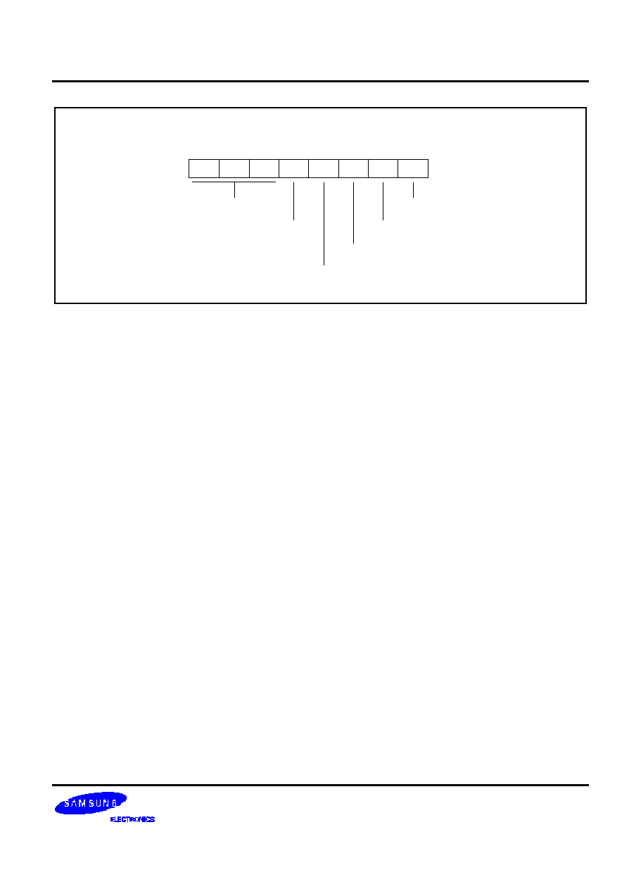
S 3 C 9 6 8 8 / P 9 6 8 8
UNIVERSAL SERIAL BUS
1 1 -1 7
.7
.6
.5
.4
.3
.2
.1
.0
LSB
MSB
USB Power Mangement Register (PWRMGR)
F8H, R/W
SUSPEND_STATE
Reserved
Reserved
CLEAR_SUSP_CNT
VMIN
VPIN
F i g u r e 1 1 -8 . U S B P o w e r M a n a g e m e n t R e g i s t e r ( P W R M G R )

UNIVERSAL SERIAL BUS
S 3 C 9 6 8 8 / P 9 6 8 8
1 1 -1 8
C O N T R O L E N D P O I N T F I F O R E G I S T E R ( E P 0 F I F O )
This register is bi-d i r e c t i o n a l , 8 b y t e d e p t h F I F O u s e d t o t r a n s f e r C o n t r o l E n d p o i n t d a t a . E P 0 F I F O i s l o c a t e d a t
a d d r e s s F 4 H a n d i s r e a d / w r i t e a d d r e s s a b l e .
Initially, the direction of the FIFO, is from the Host to the MCU. After a setup token is received for a control transfer,
t h a t i s , a f t e r M C U u n l o a d t h e s e t u p t o k e n b y t e s , a n d c l e a r s O U T _ P K T _ R D Y , t h e d i r e c t i o n o f F I F O i s c h a n g e d
a u t o m a t i c a l l y f r o m M C U t o t h e H o s t .
I N T E R R U P T E N D P O I N T 1 F I F O R E G I S T E R ( E P 1 F I F O )
E P 1 F I F O i s a n b i-direction 8 -b y t e d e p t h F I F O u s e d t o t r a n s f e r d a t a f r o m t h e M C U t o t h e H o s t o r f r o m t h e H o s t t o t h e
M C U . M C U w r i t e s d a t a t o t h i s r e g i s t e r , a n d w h e n f i n i s h e d s e t I N _ P K T _ R D Y . M e a n w h i l e , w h e n U S B r e c e i v e s v a l i d
d a t a t h r o u g h t h i s r e g i s t e r , i t s e t s O U T _ P K T _ R D Y , a f t e r M C U u n l o a d D a t a b y t e s , a n d c l e a r s O U T _ P K T _ R D Y , T h i s
r e g i s t e r i s l o c a t e d a t a d d r e s s F 5 H .
I N T E R R U P T E N D P O I N T 2 F I F O R E G I S T E R ( E P 2 F I F O )
E P 2 F I F O i s a n b i-direction 8-b y t e d e p t h F I F O u s e d t o t r a n s f e r d a t a f r o m t h e M C U t o t h e H o s t o r f r o m t h e H o s t t o t h e
M C U . M C U w r i t e s d a t a t o t h i s r e g i s t e r , a n d w h e n f i n i s h e d s e t I N _ P K T _ R D Y . M e a n w h i l e , w h e n U S B r e c e i v e s v a l i d
d a t a t h r o u g h t h i s r e g i s t e r , i t s e t s O U T _ P K T _ R D Y , a f t e r M C U u n l o a d D a t a b y t e s , a n d c l e a r s O U T _ P K T _ R D Y , T h i s
r e g i s t e r i s l o c a t e d a t a d d r e s s F A H .
U S B I N T E R R U P T P E N D I N G R E G I S T E R ( U S B P N D )
U S B P N D r e g i s t e r h a s t h e i n t e r r u p t b i t s f o r e n d p o i n t s a n d p o w e r m a n a g e m e n t . This register is cleared once read by MCU.
W h i l e a n y o n e o f t h e b i t s i s s e t , a n i n t e r r u p t i s g e n e r a t e d . U S B P N D i s l o c a t e d a t a d d r e s s F 6 H .
B i t 7 ≠ 6 N o t u s e d
B i t 5
U S B _ R S T _ P N D : T h i s b i t i s s e t , w h e n u s b r e s e t s i g n a l i s r e c e i v e d .
B i t 4
E N D P T 2 _ P N D : T h i s b i t i s s e t , w h e n s u s p e n d s i g n a l i n g i s r e c e i v e d .
B i t 3
R E S U M E _ P N D : W h i l e i n s u s p e n d m o d e , i f r e s u m e s i g n a l i n g i s r e c e i v e d t h i s b i t g e t s s e t .
B i t 2
S U S P E N D _ P N D : T h i s b i t i s s e t , w h e n s u s p e n d s i g n a l i n g i s r e c e i v e d .
B i t 1
E N D P T 1 _ P N D : T h i s b i t i s s e t , w h e n E nd p o i n t 1 n e e d s t o b e s e r v i c e d .
B i t 0
E N D P T 0 _ P N D : T h i s b i t i s s e t , w h e n E n d p o i n t 0 n e e d s t o b e s e r v i c e d . I t i s s e t u n d e r a n y o n e o f t h e
f o l l o w i n g c o n d i t i o n s :
-- O U T _ P K T _ R D Y i s s e t .
-- I N _ P K T _ R D Y g e t s c l e a r e d .
-- S E N T _ S T A L L g e t s s e t .
-- D A T A _ E N D g e t s c l e a r e d .
-- S E T U P _ E N D g e t s s e t .
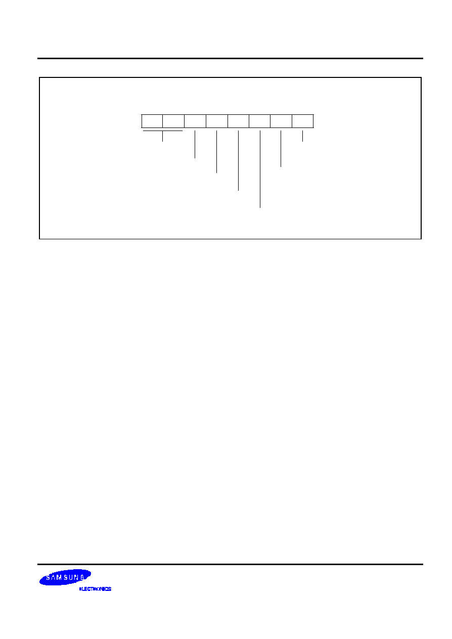
S 3 C 9 6 8 8 / P 9 6 8 8
UNIVERSAL SERIAL BUS
1 1 -1 9
.7
.6
.5
.4
.3
.2
.1
.0
LSB
MSB
USB Interrupt Pending Register (USBPND)
F6H, R/W
SUSPEND_PND
ENDPT1_PND
ENDPT0_PND
Not used
RESUME_PND
USB_RST_PND
ENDPT2_PND
F i g u r e 1 1 -9 . U S B I n t e r r u p t P e n d i n g R e g i s t e r ( U S B P N D )
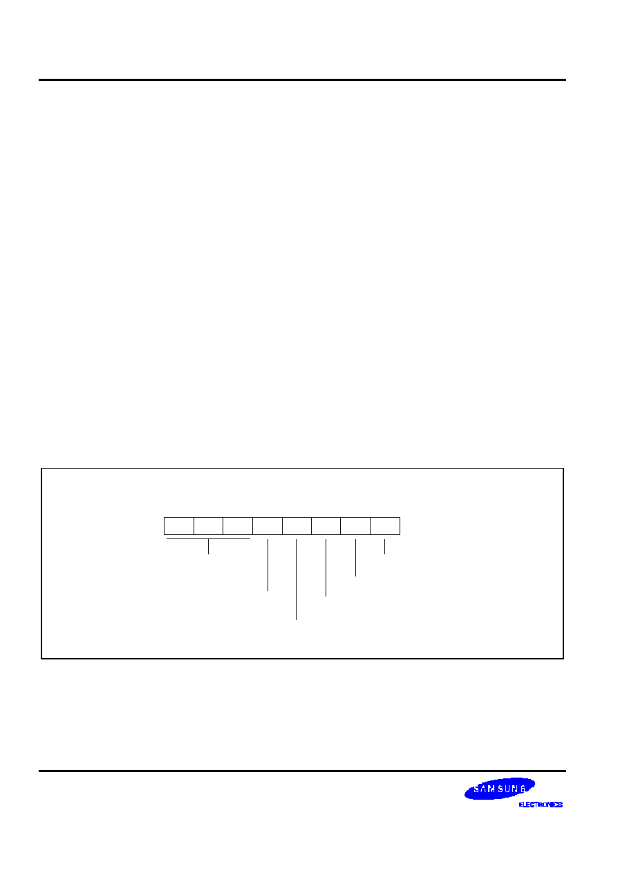
UNIVERSAL SERIAL BUS
S 3 C 9 6 8 8 / P 9 6 8 8
1 1 -2 0
U S B I N T E R R U P T E N A B L E R E G I S T E R ( U S B I N T )
U S B I N T i s l o c a t e d a t a d d r e s s F 7 H a n d i s r e a d / w r i t e a d d r e s s a b l e . T h i s r e g i s t e r s e r v e s a s a n i n t e r r u p t m a s k r e g i s t e r .
If the corresponding bit = 1 then the respective interrupt is enabled.
B y d e f a u l t , a l l i n t e r r u p t s e x c e p t s u s p e n d i n t e r r u p t i s e n a b l e d . I n t e r r u p t e n a b l e s b i t s f o r s u s p e n d a n d r e s u m e i s
combined into a single bit (bit 2).
B i t 7 ≠ 5 N o t u s e d
B i t 4
E N A B L E _ U S B _ R S T _ I N T :
1 : E n a b l e U S B R E S E T I N T E R R U P T ( d e f a u l t )
0 : D i s a b l e U S B R E S E T I N T E R R U P T
B i t 3
E N A B L E _ E N D P T 2 _ I N T :
1 : E n a b l e E N D P O I N T 2 I N T E R R U P T ( d e f a u l t )
0 : D i s a b l e E N D P O I N T 2 I N T E R R U P T
B i t 2
E N A B L E _ S U S P E N D _ R E S U M E _ I N T :
1 : E n a b l e S U S P E N D a n d R E S U M E I N T E R R U P T
0 : D i s a b l e S U S P E N D a n d R E S U M E I N T E R R U P T ( d e f a u l t )
B i t 1
E N A B L E _ E N D P T 1 _ I N T :
1 : E n a b l e E N D P O I N T 1 I N T E R R U P T ( d e f a u l t )
0 : D i s a b l e E N D P O I N T 1 I N T E RR U P T
B i t 0
E N A B L E _ E N D P T 0 _ I N T :
1 : E n a b l e E N D P O I N T 0 I N T E R R U P T ( d e f a u l t )
0 : D i s a b l e E N D P O I N T 0 I N T E R R U P T
.7
.6
.5
.4
.3
.2
.1
.0
LSB
MSB
USB Interrupt Enable Register (USBINT)
F7H, R/W
ENABLE_ENDPT0_INT
Not used
ENABLE_ENDPT1_INT
ENABLE_SUSPEND_RESUME_INT
ENABLE_ENDPT2_INT
ENABLE_USB_RST_INT
F i g u r e 1 1 -1 0 . U S B I n t e r r u p t E n a b l e R e g i s t e r ( U S B I N T )
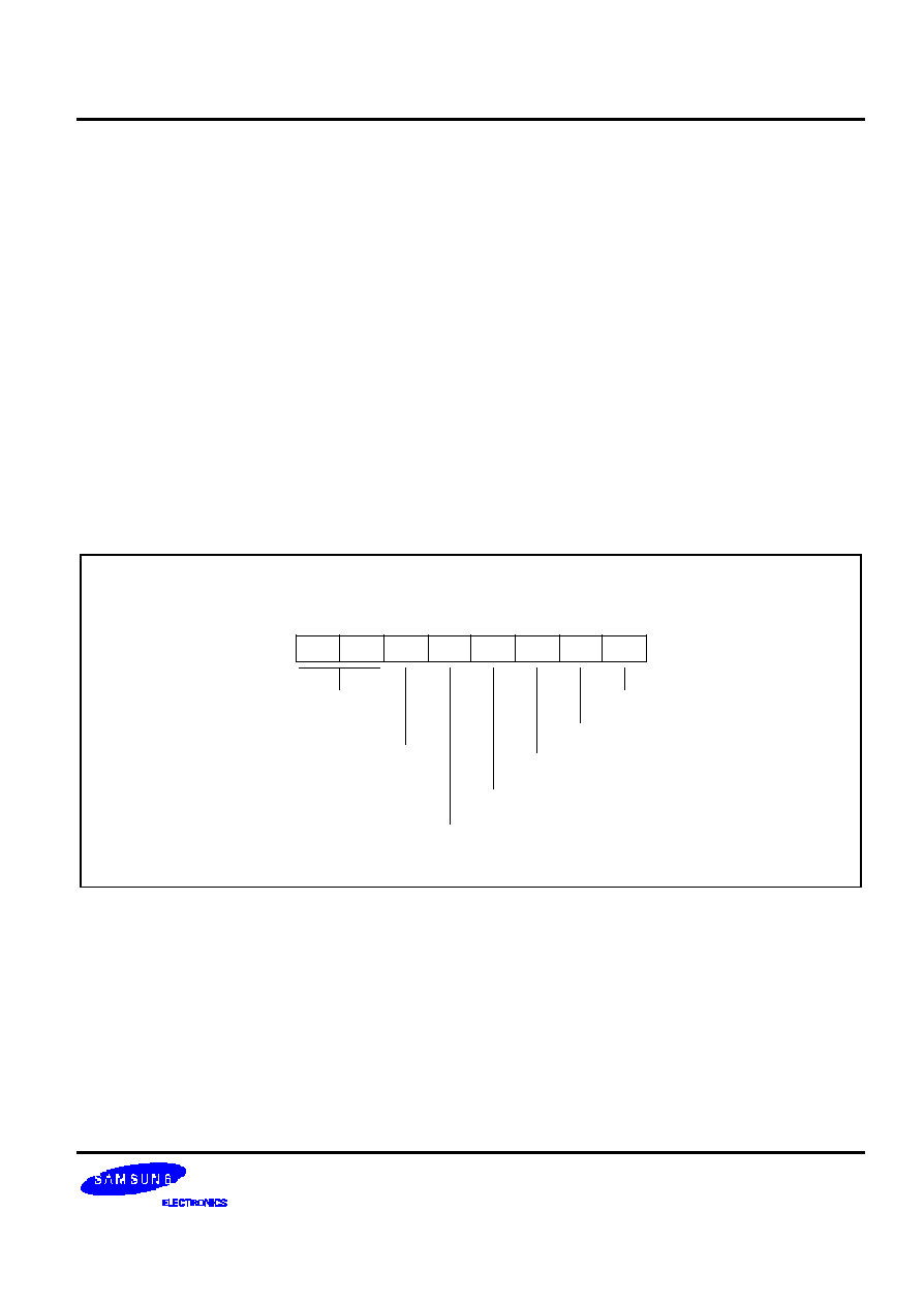
S 3 C 9 6 8 8 / P 9 6 8 8
UNIVERSAL SERIAL BUS
1 1 -2 1
U S B C O N T R O L R E G I S T E R ( U S B C O N )
U S B C O N i s f o r t h e c o n t r o l o f U S B d a t a l i n e a n d t h e c o n t r o l o f r e s e t . T h i s r e g i s t e r i s l o c a t e d a t a d d r e s s F E H a n d i s
r e a d / w r i t e a d d r e s s a b l e .
B i t 5
D P / D M C o n t r o l : W h e n t h i s b i t i s s e t , D P / D M l i n e s c a n b e c o n t r o l l e d b y M C U a s b e l l o w s
B i t 4
D P : On the condition of bit5 set, if this bit is 1, D P l i n e i s t o b e h i g h a n d t h e o t h e r c a s e t h i s b i t i s 0
D P l i n e i s l o w .
B i t 3
D M : O n t h e c o n d i t i o n o f b i t 5 s e t , i f t h i s b i t i s 1 , D M l i n e i s t o b e h i g h a n d t h e o t h e r c a s e t h i s b i t i s 0
D M l i n e i s l o w .
B i t 2
U S B _ R E S E T _ E N : W h e n t h i s b i t i s s e t , i t i s U S B i s m a d e r e s e t , w h i c h t r i g g e r M C U r e s e t
a u t o m a t i c a l l y
B i t 1
M C U _ R E S E T : W h e n t h i s b i t i s s e t , M C U m a k e s U S B r e s e t
B i t 1
U S B _ R S T N : U S B r e s e t s t a t u s b i t
0 : U S B i s n o t r e s e t
1 : U S B i s r e s e t
.7
.6
.5
.4
.3
.2
.1
.0
LSB
MSB
USB Control Register (USBCON)
FEH (Page 0), R/W
USB_RSTN
Reserved
MCU_RESET
USB_RESET_EN
DP/
DM_CONTROL
DP
DM
F i g u r e 1 1 -1 1 . U S B C o n t r o l R e g i s t e r ( U S B C O N )

UNIVERSAL SERIAL BUS
S 3 C 9 6 8 8 / P 9 6 8 8
1 1 -2 2
U S B S I G N A L A N D S I G N A L C R O S S O V E R P O I N T C O N T R O L R E G I S T E R ( U S X CO N )
U S X C O N i s l o c a t e d a t a d d r e s s D 3 H a n d i s r e a d / w r i t e a d d r e s s a b l e . Y o u c a n s e l e c t p r o t o c o l m o d e b e t w e e n U S B P S 2
a n d a d j u s t U S B s i g n a l c r o s s o v e r p o i n t .
B i t 7
U S B / P S 2 m o d e s e l e c t b i t :
0 : P S 2 m o d e ( D e f a u l t )
1 : U S B m o d e ( T h i s b i t i s s e t w h e n t h e D + / P S 2 , D -/ P S 2 p o r t s e t t h e D + , D -)
B i t 6
U S B P u l l -U p C o n t r o l b i t :
0 : P ull-U p D i s a b l e
1 : P u l l -U p E n a b l e
B i t 5
U S B s i g n a l c r o s s o v e r p o i n t c o n t r o l b i t :
E d g e D e l a y
C o n t r o l
B i t 5 , ( 2 )
B i t 4 , ( 1 )
B i t 3 , ( 0 )
D e l a y V a l u e
D e l a y U n i t
R i s i n g
0
0
0
0
E d g e
0
1
1
( a b o u t )
1
0
2
2 . 5 m s e c
1
1
4
Falling
1
0
0
0
E d g e
0
1
1
1
0
2
1
1
4
NOTE:
The value is recommended by chip Vendor.

S 3 C 9 6 8 8 / P 9 6 8 8
LVR (LOW VOLTAGE
RESET)
1 2 -1
12
L V R ( L O W V O L T A G E R E S E T )
O V E R V I E W
T h e S 3 C 9 6 8 8 / P 9 6 8 8 h a v e a L V R ( L o w V o l t a g e R e s e t ) f o r p o w e r o n r e s e t a n d v o l t a g e r e s e t .
Start Up
Reference
Voltage
Generator
Voltage
Divider
Glitch Filter
Comparator
RESET
F i g u r e 1 2 -1 . L V R A r c h i t e c t u r e
--
L o w V o l t a g e R e s e t g e n e r a t e d
RESET
sig n a l.
--
Start Up Circuit: Start up refe rence voltage generator circuit when device is powered.
--
R e f e r e n c e V o l t a g e G e n e r a t o r : S u p p l y V o l t a g e i n d e p e n d e n t r e f e r e n c e v o l t a g e g e n e r a t o r .
--
Voltage Divider: Divide supply voltage by "N"
--
Comparator: Compare reference voltage and divided voltage.
--
G l i t c h F i l t e r : R e m o v e g l i t c h a n d n o i s e s i g n a l .

LVR (LOW VOLTAGE RES ET)
S 3 C 9 6 8 8 / P 9 6 8 8
1 2 -2
Vc (Compare Voltage)
Reference Voltage
Divide Voltage
V
DD
(Supply Voltage)
Normal Operation
Reset Operation
by LVR
NOTES:
1. LVR Operation Voltage Range: 2.3 V-6.0 V
2. LVR Detection Voltage Range: 3.4 V
+ 0.4 V
3. LVR Current Consum ption:
Less then 10 uA (normally 5 uA)
4. LVR Powered Reset Release Time:
more then 500 usec (LVR only, typical)
5. LVR Simulation Conditions (Hspice Simulation)
Temp: 0 - 80
o
C
Process Veriation: Worst to best conditions
Test Voltage: 0.0 V - 7.0 V
Powered Slew Rate: 5 V/1 usec- 5 V/100 msec
F i g u r e 1 2 -2 . L V R C h a r a c t e r i s t i c s
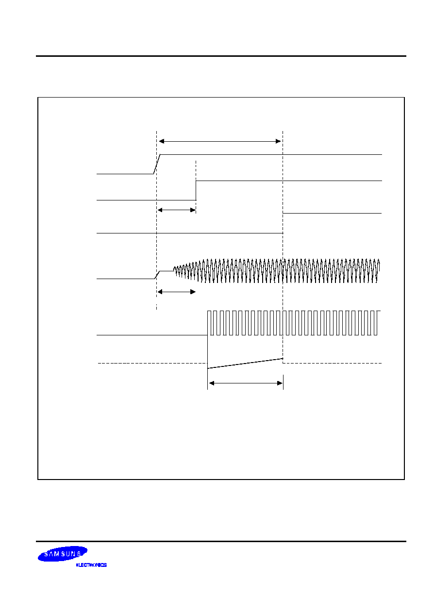
S 3 C 9 6 8 8 / P 9 6 8 8
LVR (LOW VOLTAGE
RESET)
1 2 -3
L V R A N D P O W E R O N
RESET
O P E R A T I O N S
Normal Operating mode
t
WAIT
= (4096x16)/f
OSC
Basic timer increment and
CPU operations are IDLE mode
10000B
00000B
NOTES:
1. T1 = 500 usc (at normal)
2. T2 = T1 + (4096 x 16)/f
OSC
V
DD
LVD
RESET
Release
Internal
RESET
Release
Oscillator
(X
OUT
)
BTCNT
clock
BTCNT
value
Oscillator Stabilization Time
T3
Oscillation Stabilization Time
T2
T1
LVD RESET Release Time
F i g u r e 1 2 -3 . L V R a n d P o w e r O n
RESET
O p e r a t i o n

LVR (LOW VOLTAGE RES ET)
S 3 C 9 6 8 8 / P 9 6 8 8
1 2 -4
N O T E S

S 3 C 9 6 8 8 / P 9 6 8 8
ELECTRICAL DATA
1 3 -1
13
E L E C T R I C A L D A T A
O V E R V I E W
I n t h i s s e c t i o n , t h e f o l l o w i n g S 3 C 9 6 8 8 / P 9 6 8 8 e l e c t r i c a l c h a r a c t e r i s t i c s a r e p r e s e n t e d i n t a b l e s a n d g r a p h s :
--
A b s o l u t e m a x i m u m r a t i n g s
--
D . C . e l e c t r i c a l c h a r a c t e r i s t i c s
--
I n p u t / O u t p u t c a p a c i t a n c e
--
A . C . e l e c t r i c a l c h a r a c t e r i s t i c s
--
I n p u t t i m i n g f o r e x t e r n a l i n t e r r u p t ( P o r t s 0 , 2 , a n d 4 ) D + / P S 2 , D -/ P S 2 : P S 2 M o d e O n l y
--
I n p u t t i m i n g f o r R E S E T
--
O s c i l l a t o r c h a r a c t e r i s t i c s
--
O s c i l l a t i o n s t a b i l i z a t i o n t i m e
--
C l o c k t i m i n g m e a s u r e m e n t p o i n t s a t X
IN
--
D a t a r e t e n t i o n s u p p l y v o l t a g e i n S t o p m o d e
--
S t o p m o d e r e l e a s e t i m i n g w h e n i n i t i a t e d b y a r e s e t
--
S t o p m o d e r e l e a s e t i m i n g w h e n i n i t i a t e d b y a n e x t e r n a l i n t e r r u p t
--
Characteristic curves
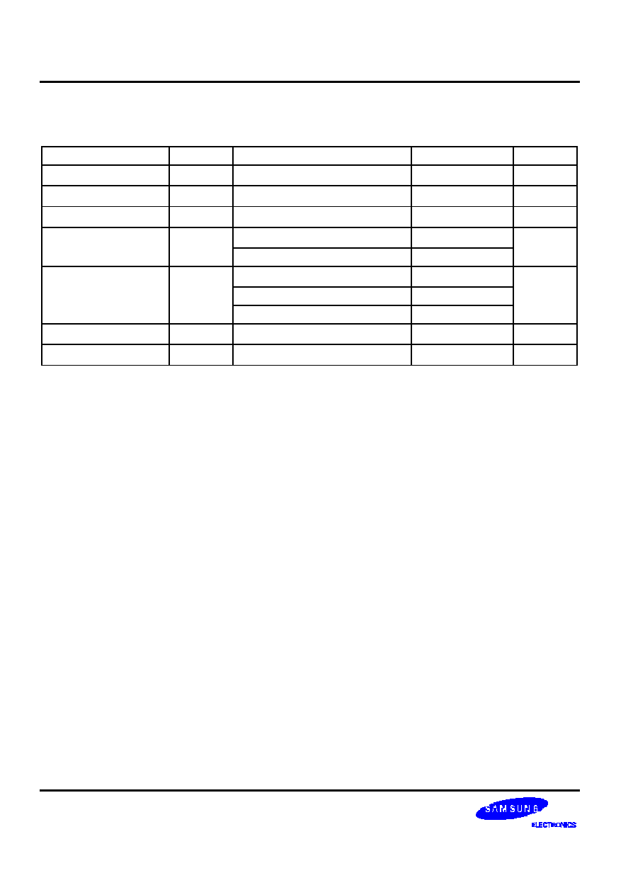
ELECTRICAL DATA
S 3 C9 6 8 8 / P 9 6 8 8
1 3 -2
T a b l e 1 3 -1 . A b s o l u t e M a x i m u m R a t i n g s
(T
A
= 2 5
∞
C )
P a r a m e t e r
S y m b o l
C o n d i t i o n s
R a t i n g
U n i t
S u p p l y V o l t a g e
V
DD
≠
≠ 0 . 3 t o + 6 . 5
V
I n p u t V o l t a g e
V
IN
All input ports
≠ 0 . 3 t o V
DD
+ 0 . 3
V
O u t p u t V o l t a g e
V
O
All output ports
≠ 0 . 3 t o V
DD
+ 0 . 3
V
O u t p u t C u r r e n t H i g h
I
OH
One I/O pin active
≠ 1 8
m A
All I/O pins active
≠ 6 0
O u t p u t C u r r e n t L o w
I
OL
One I/O pin active
+ 3 0
m A
Total pin current for ports 3
+ 1 0 0
Total pin current for ports 0, 1, 2, 4
+ 1 0 0
Operating Temperature
T
A
≠
≠ 4 0 t o + 8 5
∞
C
S t o r a g e T e m p e r a t u r e
T
STG
≠
≠ 6 5 t o + 1 5 0
∞
C
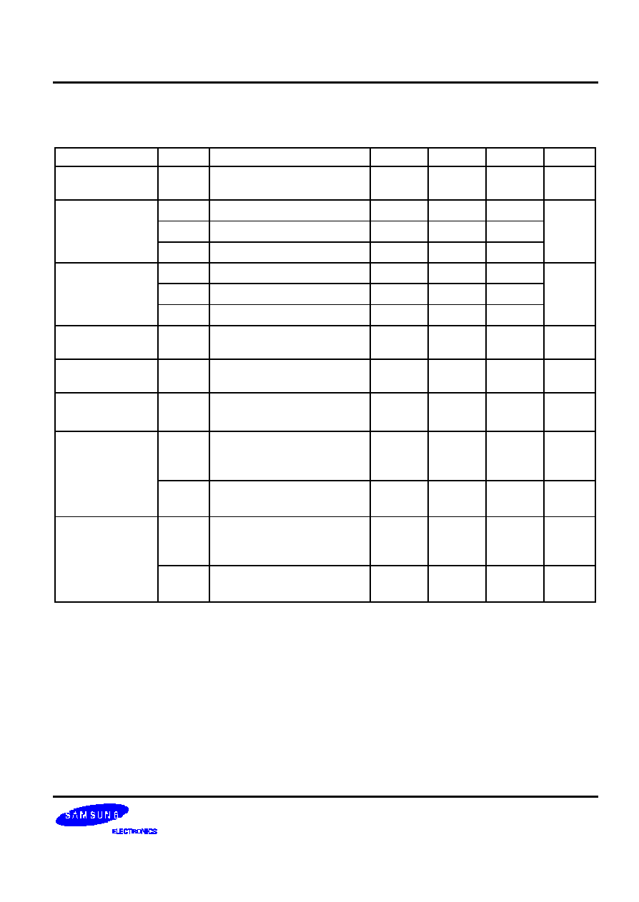
S 3 C 9 6 8 8 / P 9 6 8 8
ELECTRICAL DATA
1 3 -3
T a b l e 1 3 -2 . D . C . E l e c t r i c a l C h a r a c t e r i s t i c s
(T
A
= ≠ 4 0
∞
C t o + 8 5
∞
C , V
DD
= 4 . 0 V t o 5 . 2 5 V )
P a r a m e t e r
S y m b o l
C o n d i t i o n s
M i n
T y p
M a x
U n i t
O p e r a t i n g V o l t a g e
V
DD
f
OSC
= 6 M H z
( i n s t r u c t i o n c l o c k = 1 M H z )
4 . 0
5 . 0
5 . 2 5
V
I n p u t H i g h V o l t a g e
V
IH1
A l l i n p u t p i n s e x c e p t V
IH2
0 . 8 V
DD
≠
V
DD
V
V
IH2
X
IN
V
DD
≠ 0 . 5
V
DD
V
IH3
RESET
0 . 5 V
DD
I n p u t L o w V o l t a g e
V
IL1
A l l i n p u t p i n s e x c e p t V
IL2
≠
≠
0 . 2 V
DD
V
V
IL2
X
IN
0 . 4
V
IL2
RESET
0 . 5 V
DD
O u t p u t H i g h V o l t a g e
V
OH
I
OH
= ≠ 2 0 0
µ
A ; A l l o u t p u t p o r t s
e x c e p t p o r t s 0 , 1 a n d 2 , D + , D ≠
V
DD
≠ 1 . 0
≠
≠
V
O u t p u t L o w V o l t a g e
V
OL
I
OL
= 1 m A
A l l o u t p u t p o r t e x c e p t D + , D ≠
≠
≠
0 . 4
V
O u t p u t L o w C u r r e n t
I
OL
V
OL
= 3 V
P o r t 3 o n l y
8
1 5
2 3
m A
Input High
L e a k a g e C u r r e n t
I
LIH1
(3)
V
IN
= V
DD
A l l i n p u t s e x c e p t I
LIH2
e x c e p t D + , D ≠
≠
≠
3
µ
A
I
LIH2
(3)
V
IN
= V
DD
X
IN,
X
OUT,
RESET
≠
≠
2 0
µ
A
I n p u t L o w
L e a k a g e C u r r e n t
I
LIL1
(3)
V
IN
= 0 V
A l l i n p u t s e x c e p t I
LIL2
e x c e p t D + , D ≠
≠
≠
≠ 3
µ
A
I
LIL2
(3)
V
IN
= 0 V
X
IN,
X
OUT,
RESET
≠
≠
≠ 2 0
µ
A
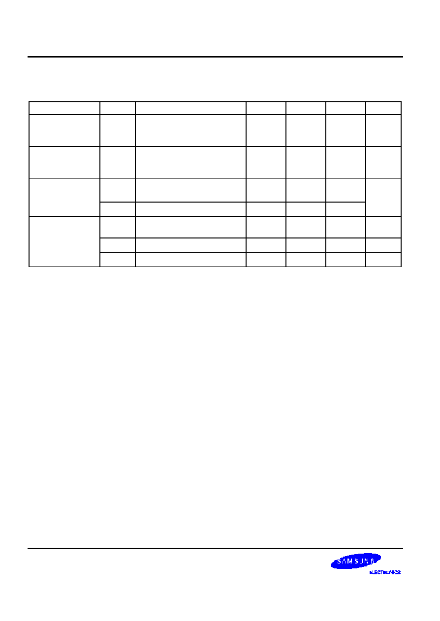
ELECTRICAL DATA
S 3 C9 6 8 8 / P 9 6 8 8
1 3 -4
T a b l e 1 3 -2 . D . C . E l e c t r i c a l C h a r a c t e r i s t i c s ( C o n t i n u e d )
(T
A
= ≠ 4 0
∞
C t o + 8 5
∞
C , V
DD
= 4 . 0 V t o 5 . 2 5 V )
P a r a m e t e r
S y m b o l
C o n d i t i o n s
M i n
T y p
M a x
U n i t
O u t p u t H i g h
L e a k a g e C u r r e n t
I
LOH
(1)
V
OUT
= V
DD
A l l I / O p i n s a n d o u t p u t p i n s
e x c e p t D + , D ≠
≠
≠
3
µ
A
O u t p u t L o w
L e a k a g e C u r r e n t
I
LOL
(1)
V
OUT
= 0 V
A l l I / O p i n s a n d o u t p u t p i n s
e x c e p t D + , D ≠
≠
≠
≠ 3
µ
A
P u l l -u p R e s i s t o r s
R
L1
V
IN
= 0 V
P o r t s 0 , 1 , 2 , 4 . 2 -3 , R e s e t
2 5
5 0
1 0 0
k
R
L2
V
IN
= 0 V ; P 4 . 0 -1
2
≠
5
S u p p l y C u r r e n t
(2)
I
DD1
N o r m a l o p e r a t i o n m o d e
6 M H z C P U c l o c k
≠
5 . 5
1 2
m A
I
DD2
I d l e m o d e ; 6 M H z o s c i l l a t o r
2 . 2
5
m A
I
DD3
S t o p m o d e
6
1 5
µ
A
NOTES
:
1.
Except X
IN
and X
OUT
.
2.
Supply current does not include current drawn through internal pull-up resistors or external output current loads.
3.
When USB Mode Only in 4.2 V to 5.25 V, D+ and D≠ satisfy the USB spec 1.1.
S 3 C 9 6 8 8 / P 9 6 8 8
ELECTRICAL DATA
1 3 -5
T a b l e 1 3 -3 . I n p u t / O u t p u t C a p a c i t a n c e
(T
A
= ≠ 4 0
∞
C t o + 8 5
∞
C , V
DD
=
0 V )
P a r a m e t e r
S y m b o l
C o n d i t i o n s
M i n
T y p
M a x
U n i t
Input
C a p a c i t a n c e
C
IN
f = 1 M H z ; U n m e a s u r e d p i n s
a r e c o n n e c t e d t o V
SS
≠
≠
1 0
p F
O u t p u t
C a p a c i t a n c e
C
OUT
I / O C a p a c i t a n c e
C
IO
T a b l e 1 3 -4 . A . C . E l e c t r i c a l C h a r a c t e r i s t i c s
(T
A
= ≠ 4 0
∞
C t o + 8 5
∞
C , V
DD
= 4 . 0 V t o 5 . 2 5 V )
P a r a m e t e r
S y m b o l
C o n d i t i o n s
M i n
T y p
M a x
U n i t
Interrupt Input
H i g h , L o w W i d t h
t
INTH
, t
INTL
P 0 , P 2 a n d P 4
≠
2 0 0
≠
ns
R E S E T I n p u t L o w
W i d t h
t
RSL
RESET
1 0
≠
≠
µ
s
t
INTH
t
INTL
0.8 V
DD
0.2 V
DD
t
RSL
F i g u r e 1 3 -1 . I n p u t t i m i n g f o r E x t e r n a l I n t e r r u p t ( P o r t s 0 , 2 , a n d 4 )
RESET
t
RSL
0.5 V
DD
F i g u r e 1 3 -2 . I n p u t T i m i n g f o r
RESET
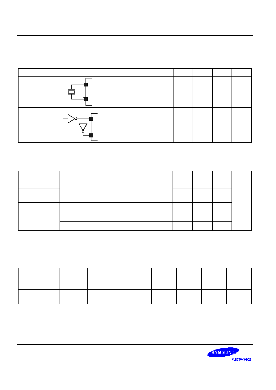
ELECTRICAL DATA
S 3 C9 6 8 8 / P 9 6 8 8
1 3 -6
T a b l e 1 3 -5 . O s c i l l a t o r C h a r a c t e r i s t i c s
(T
A
= ≠ 4 0
∞
C + 8 5
∞
C , V
DD
= 4 . 0 V t o 5 . 2 5 V )
O s c i l l a t o r
C l o c k C i r c u i t
T e s t C o n d i t i o n
M i n
T y p
M a x
U n i t
M a i n c r y s t a l M a i n
c e r a m i c ( f
OSC
)
X
IN
X
OUT
O s c i l l a t i o n f r e q u e n c y
≠
6 . 0
≠
M H z
E x t e r n a l c l o c k
X
IN
X
OUT
O s c i l l a t i o n f r e q u e n c y
≠
6 . 0
≠
T a b l e 1 3 -6 . O s c i l l a t i o n S t a b i l i z a t i o n T i m e
(T
A
= ≠ 4 0
∞
C + 8 5
∞
C , V
DD
= 4 . 0 V t o 5 . 2 5 V )
O s c i l l a t o r
T e s t C o n d i t i o n
M i n
T y p
M a x
U n i t
M a i n C r y s t a l
f
OSC
= 6 . 0 M H z
≠
≠
1 0
m s
M a i n C e r a m i c
( O s c i l l a t i o n s t a b i l i z a t i o n o c c u r s w h e n V
DD
i s e q u a l t o
t h e m i n i m u m o s c i l l a t o r v o l t a g e r a n g e . )
O s c i l l a t o r
S t a b i l i z a t i o n W a i t
T i m e
t
WAIT
s t o p m o d e r e l e a s e t i m e b y a r e s e t
≠
2
16
/ f
OSC
≠
t
WAIT
s t o p m o d e r e l e a s e t i m e b y a n i n t e r r u p t
≠
(note)
≠
NOTE
: The oscillator stabilization wait time, t
WAIT
, is determined by the setting in the basic timer control register, BTCON.
T a b l e 1 3 -7 . D a t a R e t e n t i o n S u p p l y V o l t a g e i n S t o p M o d e
(T
A
= ≠ 4 0
∞
C t o + 8 5
∞
C )
P a r a m e t e r
S y m b o l
C o n d i t i o n s
M i n
T y p
M a x
U n i t
D a t a R e t e n t i o n
S u p p l y V o l t a g e
V
DDDR
S t o p m o d e
2 . 0
≠
6
V
D a t a R e t e n t i o n
S u p p l y C u r r e n t
I
DDDR
S t o p m o d e ; V
DDDR
= 2 . 0 V
≠
≠
3 0 0
µ
A
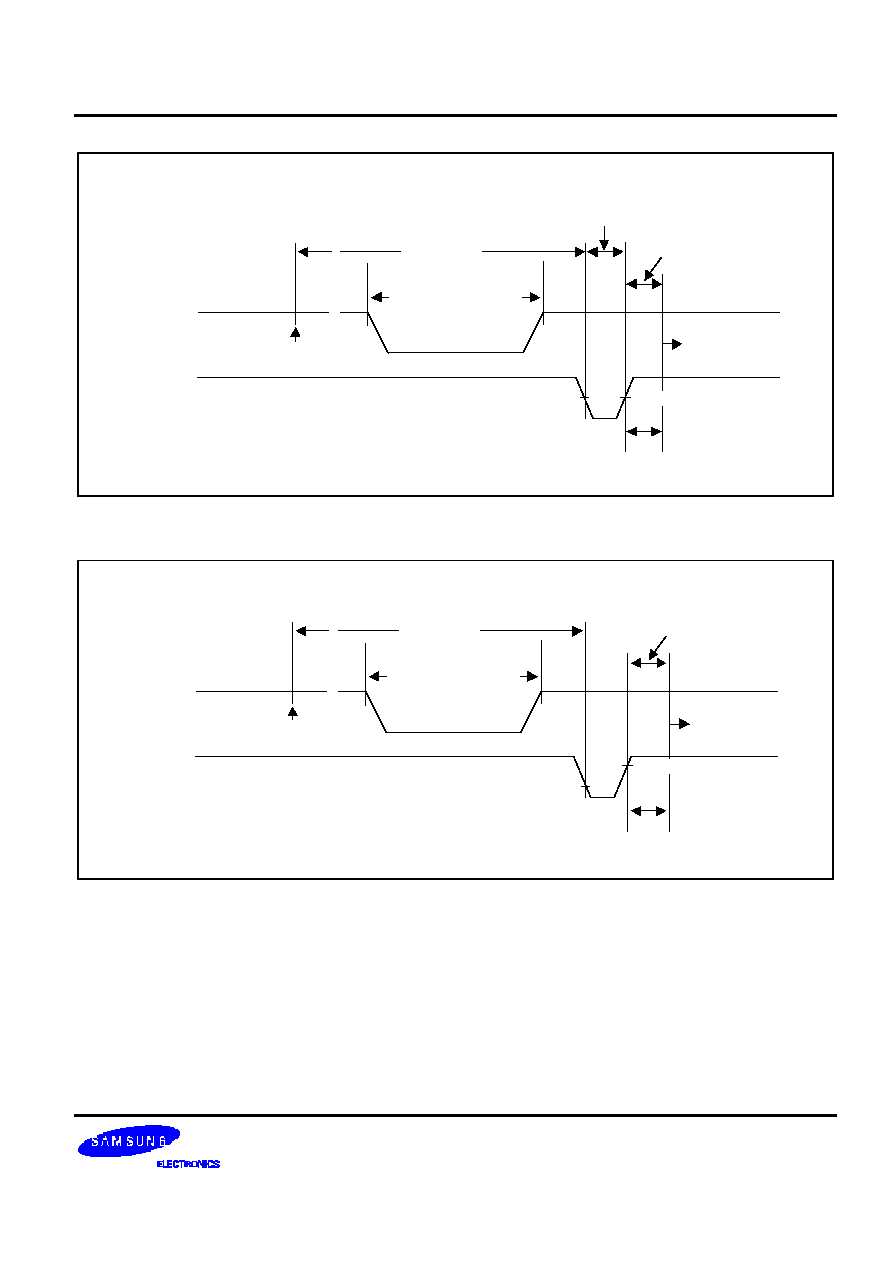
S 3 C 9 6 8 8 / P 9 6 8 8
ELECTRICAL DATA
1 3 -7
Data Retention Mode
~
~ ~
V
DDDR
Execution of
Stop Instrction
V
DD
Normal
Operating
Mode
IDLE Mode
(Basic Timer Active)
~
Stop Mode
t
WAIT
0.5 V
DD
0.5 V
DD
RESET
Internal Reset
Operation
F i g u r e 1 3 -3 . S t o p M o d e R e l e a s e T i m i n g W h e n I n i t i a t e d b y a R e s e t
Data Retention Mode
~
~ ~
V
DDDR
Execution Of
Stop Instrction
V
DD
Normal
Operating
Mode
IDLE Mode
(Basic Timer Active)
~
Stop Mode
t
WAIT
0.8 V
DD
0.2 V
DD
External
Interrupt
F i g u r e 1 3 -4 . S t o p M o d e R e l e a s e T i m i n g W h e n I n i t i a t e d b y a n E x t e r n a l I n t e r r u p t
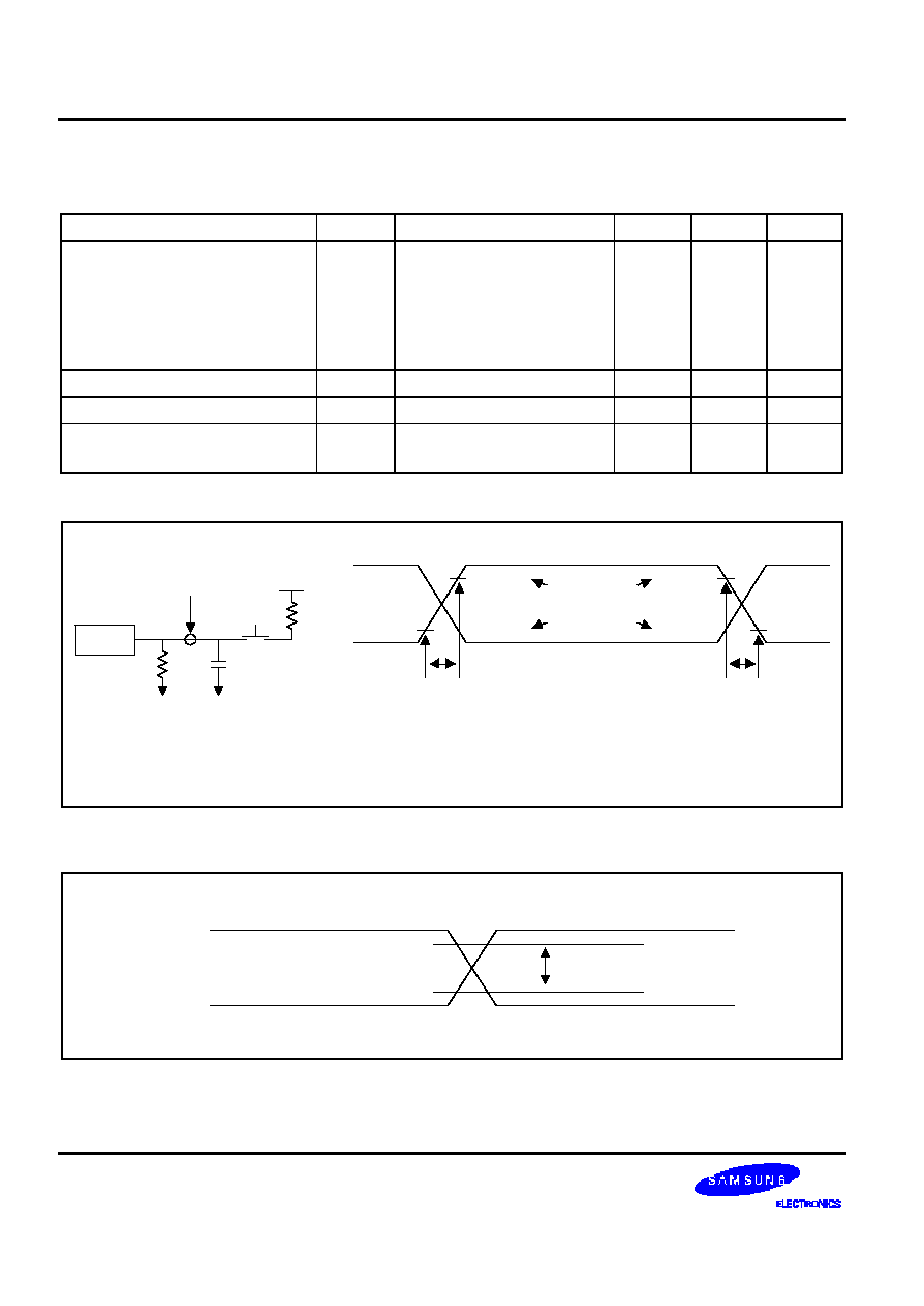
ELECTRICAL DATA
S 3 C9 6 8 8 / P 9 6 8 8
1 3 -8
T a b l e 1 3 -8 . L o w S p e e d U S B E l e c t r i c a l C h a r a c t e r i s t i c s
(T
A
= ≠ 4 0
∞
C t o + 8 5
∞
C , V o l t a g e R e g u l a t o r O u t p u t V
33out
= 2 . 8 V t o 3 . 5 V , t y p 3 , 3 V )
P a r a m e t e r
S y m b o l
C o n d i t i o n s
M i n
M a x
U n i t
Transition Time:
R i s e T i m e
Tr
C L = 5 0 p F
7 5
≠
ns
C L = 3 5 0 p F
≠
3 0 0
F a l l T i m e
Tf
C L = 5 0 p F
7 5
≠
C L = 3 5 0 p F
≠
3 0 0
R i s e / F a l l T i m e M a t c h i n g
Trfm
(Tr/Tf) CL = 50 pF
8 0
1 2 0
%
O u t p u t S i g n a l C r o s s o v e r V o l t a g e
V c r s
C L = 5 0 p F
1 . 3
2 . 0
V
V o l t a g e R e g u l a t o r O u t p u t V o l t a g e
V
33OUT
w i t h V
33OUT
t o G N D 0 . 1
µ
F
c a p a c i t o r
2 . 8
3 . 5
V
R1 = 15 K
R2 = 1.5 K
CL = 50 pF - 350 pF
DM: S/W ON
DP: S/W OFF
D. U. T
Test
Point
S/W
2.8 V
R2
R1
C2
90 %
Measurement
Points
10 %
90 %
10 %
Tr
Tf
F i g u r e 1 3 -5 . U S B D a t a S i g n a l R i s e a n d F a l l T i m e
DM
DP
Vcrs
MAX: 2.0 V
MIN: 1.3 V
3.3 V
0 V
F i g u r e 1 3 -6 . U S B O u t p u t S i g n a l C r o s s o v e r P o i n t V o l t a g e

S 3 C 9 6 8 8 / P 9 6 8 8
ELECTRICAL DATA
1 3 -9
T a b l e 1 3 -9 . L o w S p e e d U S B E l e c t r i c a l C h a r a c t e r i s t i c s
(T
A
= ≠ 4 0
∞
C t o + 8 5
∞
C )
P a r a m e t e r
S y m b o l
C o n d i t i o n s
M i n
T y p
M a x
U n i t
Low level detect voltage
V
LVD
≠
3 . 0 0
3 . 4 0
3 . 8 0
V

ELECTRICAL DATA
S 3 C9 6 8 8 / P 9 6 8 8
1 3 -1 0
N O T E S
S 3 C 9 6 8 8 / P 9 6 8 8
MECHANICAL DATA
1 4 -1
14
M E C H A N I C A L D A T A
O V E R V I E W
T h e S 3 C 9 6 8 8 / P 9 6 8 8 i s a v a i l a b l e i n a 4 2 -p i n S D I P p a c k a g e ( S a m s u n g : 4 2 -SDIP -6 0 0 ) a n d a 4 4 -p i n Q F P p a c k a g e
(44-Q F P -1 0 1 0 B ) . P a c k a g e d i m e n s i o n s a r e s h o w n i n F i g u r e s 1 4 -1 a n d 1 4 -2 .
NOTE :
Dimensions are in millimeters.
39.50 MAX
0.50
± 0.1
1.78
(1.77)
0.51 MIN
3.50
±
0.2
5.08 MAX
42-SDIP-600
0-15
1.00
± 0.1
0.25
+ 0.1
- 0.05
15.24
14.00
0.2
#42
#22
#21
#1
16.30
±
0.5
39.10
0.2
±
3.30
0.3
±
±
F i g u r e 1 4 -1 . 4 2 -P i n S D I P P a c k a g e M e c h a n i c a l D a t a ( 4 2 -S D I P -6 0 0 )

MECHANICAL DATA
S 3 C9 6 8 8 / P 9 6 8 8
1 4 -2
44-QFP-1010B
#44
NOTE
: Dimensions are in millimeters.
10.00
+ 0.2
13.20
+ 0.3
10.00
+
0.2
13.20
+
0.3
#1
0.35
+ 0.10
- 0.05
0.80
(1.00)
0.10 MAX
0.80
+
0.20
0.05 MIN
2.05
+ 0.10
2.30 MAX
0.15
+ 0.10
- 0.05
0-8
F i g u r e 1 4 -2 . 4 4 -P i n Q F P P a c k a g e M e c h a n i c a l D a t a ( 4 4 -Q F P -1 0 1 0 B )

S 3 C 9 6 8 8 / P 9 6 8 8
S 3 P 9 6 8 8 O T P
1 5 -1
15
S3P9688 OTP
O V E R V I E W
T h e S 3 P 9 6 8 8 s i n g l e -c h i p C M O S m i c r o c o n t r o l l e r i s t h e O T P ( O n e T i m e P r o g r a m m a b l e ) v e r s i o n o f t h e S 3 C 9 6 8 8
m i c r o c o n t r o l l e r . I t h a s a n o n -c h i p O T P R O M i n s t e a d o f m a s k e d R O M . T h e E P R O M i s a c c e s s e d b y s e r i a l d a t a
format.
T h e S 3 P 9 6 8 8 i s f u l l y c o m p a t i b l e w i t h t h e S 3 C 9 6 8 8 , b o t h i n f u n c t i o n a n d i n p i n c o n f i g u r a t i o n . B e c a u s e o f i t s s i m p l e
p r o g r a m m i n g r e q u i r e m e n t s , t h e S 3 P 9 6 8 8 i s i d e a l f o r u s e a s a n e v a l u a t i o n c h i p f o r t h e S 3 C 9 6 8 8 .
S3P9688
(42-SDIP)
P3.1
P3.0
INT0/P2.0
INT0/P2.1
INT0/P2.2
INT0/P2.3
INT0/P2.4
INT0/P2.5
SDAT
/INT0/P2.6
SCLK
/INT0/P2.7
V
DD
/V
DD
V
SS
/V
SS
X
OUT
/X
OUT
X
IN
/X
IN
TEST
/TEST
INT1/P4.0
INT1/P4.1
RESET /RESET
INT1/P4.2
INT1/P4.3
P1.7
1
2
3
4
5
6
7
8
9
10
11
12
13
14
15
16
17
18
19
20
21
P3.2
P3.3/CLO
D+/PS2
D-/PS2
3.3V
OUT
NC
P0.0/INT2
P0.1/INT2
P0.2/INT2
P0.3/INT2
P0.4/INT2
P0.5/INT2
P0.6/INT2
P0.7/INT2
P1.0
P1.1
P1.2
P1.3
P1.4
P1.5
P1.6
42
41
40
39
38
37
36
35
34
33
32
31
30
29
28
27
26
25
24
23
22
NOTE:
The TEST pin must be connected to V
SS
(GND) in normal operation mode.
Th pins which used in writing OTP-ROM codes are assigned in bold.
F i g u r e 1 5 -1 . S 3 P 9 6 8 8 P i n A s s i g n m e n t s ( 4 2 -S D I P P a c k a g e )
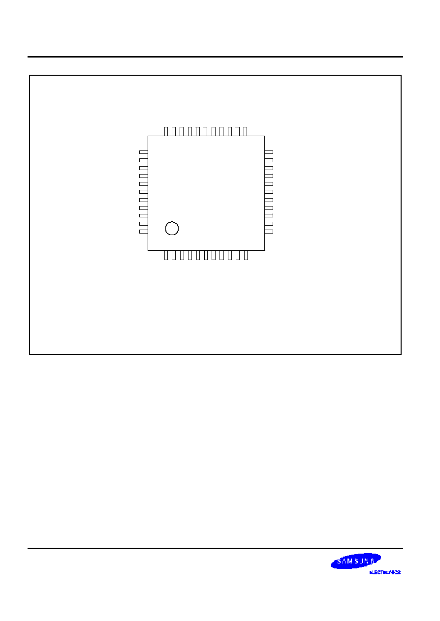
S 3 P 9 6 8 8 O T P
S 3 C 9 6 8 8 / P 9 6 8 8
1 5 -2
INT0/P2.4
INT0/P2.5
SDAT
/INT0/P2.6
SCLK
/INT0/P2.7
V
DD
/V
DD
V
SS
/V
SS
X
OUT
/X
OUT
X
IN
/X
IN
TEST
/TEST
INT1/P4.0 INT1/P4.1
P1.0
P1.1
P1.2
P1.3
P1.4
P1.5
P1.6
P1.7
P4.3/INT1
P4.2/INT1
RESET/RESET
NC NC
NC P0.0/INT2
P0.1/INT2
P0.2/INT2
P0.3/INT2 P0.4/INT2
P0.5/INT2
P0.6/INT2
P0.7/INT2
3.3V
OUT
D- /PS2
D+/PS2
CLO/P3.3
P3.2
P3.1
P3.0
P2.0/INT0
P2.1/INT0
P2.2/INT0
P2.3/INT0
S3P9688
44-QFP
(Top View)
NOTE:
The TEST pin must connect to V
SS
(GND) in the normal operation mode.
The bold is assigned to OTP pin name.
1 2
3 4
5 6 7 8
9 10
11
34
35
36
37
38
39
40
41
42
43
44
33 32
31 30 29
28 27
26 25 24 23
22
21
20
19
18
17
16
15
14
13
12
F i g u r e 1 5 -2 . S 3 P 9 6 8 8 P i n A s s i g n m e n t s ( 4 4 -Q F P P a c k a g e )

S 3 C 9 6 8 8 / P 9 6 8 8
S 3 P 9 6 8 8 O T P
1 5 -3
T a b l e 1 5 -1 . D e s c r i p t i o n s o f P i n s U s e d t o R e a d / W r i t e t h e E P R O M
M a i n C h i p
D u r i n g P r o g r a m m i n g
P i n N a m e
P i n N a m e
P i n N o .
I / O
F u n c t i o n
P 2 . 6
S D A T
9
(3)
I/O
S e r i a l D a t a P i n ( O u t p u t w h e n r e a d i n g , I n p u t w h e n
w r i t i n g ) I n p u t a n d P u s h-p u l l O u t p u t P o r t c a n b e
a s s i g n e d
P 2 . 7
S C L K
1 0
(4)
I/O
S e r i a l C l o c k P i n ( I n p u t O n l y P i n )
T E S T
T E S T
1 5
(9)
I
C h i p I n i t i a l i z a t i o n a n d E P R O M C e l l W r i t i n g P o w e r
S u p p l y P i n ( I n d i c a t e s O T P M o d e E n t e r i n g ) W h e n
w r i t i n g 1 2 . 5 V i s a p p l i e d a n d w h e n r e a d i n g .
RESET
RESET
1 8
(12)
I
0 V : O T P w r i t e a n d t e s t m o d e
5 V : O p e r a t i n g m o d e
V
DD
/ V
SS
V
DD
/ V
SS
1 1
(5)
/ 1 2
(6)
≠
L o g i c P o w e r S u p p l y P i n .
NOTE:
( ) means 44 QFP package.
T a b l e 1 5 -2 . C o m p a r i s o n o f S 3 P 9 6 8 8 a n d S 3 C 9 6 8 8 F e a t u r e s
C h a r a c t e r i s t i c
S 3 P 9 6 8 8
S 3 C 9 6 8 8
P r o g r a m M e m o r y
8 -K b y t e E P R O M
8 -K b y t e m a s k R O M
Operating Voltage (V
DD
)
4 . 0 V t o 5 . 2 5 V
4 . 0 V t o 5 . 2 5 V
O T P P r o g r a m m i n g M o d e
V
DD
= 5 V , V
PP
( R E S E T ) = 1 2 . 5 V
Pin Configuration
4 2 S D I P / 4 4 Q F P
4 2 S D I P / 4 4 Q F P
E P R O M P r o g r a m m a b i l i t y
U s e r P r o g r a m 1 t i m e
P r o g r a m m e d a t t h e f a c t o r y
O P E R A T I N G M O D E C H A R A C T E R I S T I C S
W h e n 1 2 . 5 V i s s u p p l i e d t o t h e V
PP
(
RESET
) p i n o f t h e S 3 P 9 6 8 8 , t h e E P R O M p r o g r a m m i n g m o d e i s e ntered. The
o p e r a t i n g m o d e ( r e a d , w r i t e , o r r e a d p r o t e c t i o n ) i s s e l e c t e d a c c o r d i n g t o t h e i n p u t s i g n a l s t o t h e p i n s l i s t e d i n T a b l e
1 5 -3 b e l o w .
T a b l e 1 5 -3 . O p e r a t i n g M o d e S e l e c t i o n C r i t e r i a
V D D
V p p
( R E S E T )
R E G /
M E M
A d d r e s s
( A 1 5 ≠A 0 )
R / W
M o d e
5 V
5 V
0
0 0 0 0 H
1
E P R O M r e a d
1 2 . 5 V
0
0 0 0 0 H
0
E P R O M p r o g r a m
1 2 . 5 V
0
0 0 0 0 H
1
E P R O M v e r i f y
1 2 . 5 V
1
0 E 3 F H
0
E P R O M r e a d p r o t e c t i o n
NOTE
: "0" means Low level; "1" means High level.

S 3 P 9 6 8 8 O T P
S 3 C 9 6 8 8 / P 9 6 8 8
1 5 -4
PASS
FAIL
NO
FAIL
YES
FAIL
NO
START
Address = First Location
V
DD
= 5V, V
PP
= 12.5V
x = 0
Program One 1ms Pulse
Increment X
x = 10
Verify 1 Byte
Last Address
V
DD
= V
PP
= 5 V
Compare All Byte
Device Passed
Increment Address
Verify Byte
Device Failed
F i g u r e 1 5 -3 . O T P P r o g r a m m i n g A l g o r i t h m

S 3 C 9 6 8 8 / P 9 6 8 8
S 3 P 9 6 8 8 O T P
1 5 -5
T a b l e 1 5 -4 . D . C . E l e c t r i c a l C h a r a c t e r i stics
(T
A
= ≠ 4 0
∞
C t o + 8 5
∞
C , V
DD
= 4 . 0 V t o 5 . 2 5 V )
P a r a m e t e r
S y m b o l
C o n d i t i o n s
M i n
T y p
M a x
U n i t
S u p p l y C u r r e n t
(note)
I
DD1
N o r m a l m o d e ;
6 M H z C P U c l o c k
≠
5 . 5
1 2
m A
I
DD2
I d l e m o d e ;
6 M H z C P U c l o c k
2 . 2
5
I
DD3
S t o p m o d e
6
1 5
µ
A
NOTE
: Supply current does not include current drawn through internal pull-up resistors or external output current loads.

S 3 P 9 6 8 8 O T P
S 3 C 9 6 8 8 / P 9 6 8 8
1 5 -6
N O T E S

S 3 C 9 6 8 8 / P 9 6 8 8
DEVELOPMENT TOOLS
1 6 -1
16
D E V E L O P M E N T T O O L S
O V E R V I E W
S a m s u n g p r o v i d e s a p o w e r f u l a n d e a s y -t o -u s e d e v e l o p m e n t s u p p o r t s y s t e m i n t u r n k e y f o r m . T h e d e v e l o p m e n t
s u p p o r t s y s t e m i s c o n f i g u r e d w i t h a h o s t s y s t e m , d e b u g g i n g t o o l s , a n d s u p p o r t s o f t w a r e . F o r t h e h o s t s y s t e m , a n y
s t a n d a r d c o m p u t e r t h a t o p e r a t e s w i t h M S -D O S a s i t s o p e r a t i n g s y s t e m c a n b e u s e d . O n e t y p e o f d e b u g g i n g t o o l
including hardware and software is provided: the sophisticated and powerful in -c i r c u i t e m u l a t o r , S M D S 2 + , f o r S 3 C 7 ,
S 3 C 9 , S 3 C 8 f a m i l i e s o f m i c r o c o n t r o l l e r s . T h e S M D S 2 + i s a n e w a n d i m p r o v e d v e r s i o n o f S M D S 2 . S a m s u n g a l s o
o f f e r s s u p p o r t s o f t w a r e t h a t i n c l u d e s d e b u g g e r , a s s e m b l e r , a n d a p r o g r a m f o r s e t t i n g o p t i o n s .
S H I N E
S a m s u n g H o s t I n t e r f a c e f o r in -c i r c u i t E m u l a t o r , S H I N E , i s a m u l t i -w i n d o w b a s e d d e b u g g e r f o r S M D S 2 + . S H I N E
provides pull-d o w n a n d p o p -u p m e n u s , m o u s e s u p p o r t , f u n c t i o n / h o t k e y s , a n d c o n t e x t-s e n s i t i v e h y p e r-linked help. It
h a s a n a d v a n c e d , m u l t i p l e -w i n d o w e d u s e r i n t e r f a c e t h a t e m p h a s i z e s e a s e o f u s e . E a c h w i n d o w c a n b e s i z e d , m o v e d ,
s c r o l l e d , h i g h l i g h t e d , a d d e d , o r r e m o v e d c o m p l e t e l y .
S A M A A S S E M B L E R
T h e S a m s u n g A r r a n g e a b l e M i c r o c o n t r o l l e r ( S A M ) A s s e m b l e r , S A M A , i s a u n i v e r s a l a s s e m b l e r , a n d g e n e r a t e s o b j e c t
c o d e i n s t a n d a r d h e x a d e c i m a l f o r m a t . A s s e m b l e d p r o g r a m c o d e i n c l u d e s t h e o b j e c t c o d e t h a t i s u s e d f o r R O M d a t a
a n d r e q u i r e d S M D S p r o g r a m c o n t r o l d a t a . T o a s s e m b l e p r o g r a m s , S A M A r e q u i r e s a s o u r c e f i l e a n d a n a u x i l i a r y
definition (DEF) file with device specific information.
S A S M 8 6
T h e S A S M 8 6 i s a n r e l o c a t a b l e a s s e m b l e r f o r S a m s u n g ' s S 3 C 9 -s e r i e s m i c r o c o n t r o l l e r s . T h e S A S M 8 6 t a k e s a s o u r c e
f i l e c o n t a i n i n g a s s e m b l y l a n g u a g e s t a t e m e n t s a n d t r a n s l a t e s i n t o a c o r r e s p o n d i n g s o u r c e c o d e , o b j e c t c o d e a n d
c o m m e n t s . T h e S A S M 8 6 s u p p o r t s m a c r o s a n d c o n d i t i o n a l a s s e m b l y . I t r u n s o n t h e M S -D O S o p e r a t i n g s y s t e m . I t
p r o d u c e s t h e r e l o c a t a b l e o b j e c t c o d e o n l y , s o t h e u s e r s h o u l d l i n k o b j e c t f i l e . O b j e c t f i l e s c a n b e l i n k e d w i t h o t h e r
o b j e c t f i l e s a n d l o a d e d i n t o m e m o r y .
H E X 2 R O M
H E X 2 R O M f i l e g e n e r a t e s R O M c o d e f r o m H E X f i l e w h i c h h a s b e e n p r o d u c e d b y a s s e m b l e r . R O M c o d e m u s t b e
n e e d e d t o f a b r i c a t e a m i c r o c o n t r o l l e r w h i c h h a s a m a s k R O M . W h e n g e n e r a t i n g t h e R O M c o d e ( . O B J f i l e ) b y
H E X 2 R O M , t h e va l u e " F F " i s f i l l e d i n t o t h e u n u s e d R O M a r e a u p t o t h e m a x i m u m R O M s i z e o f t h e t a r g e t d e v i c e
a u t o m a t i c a l l y .
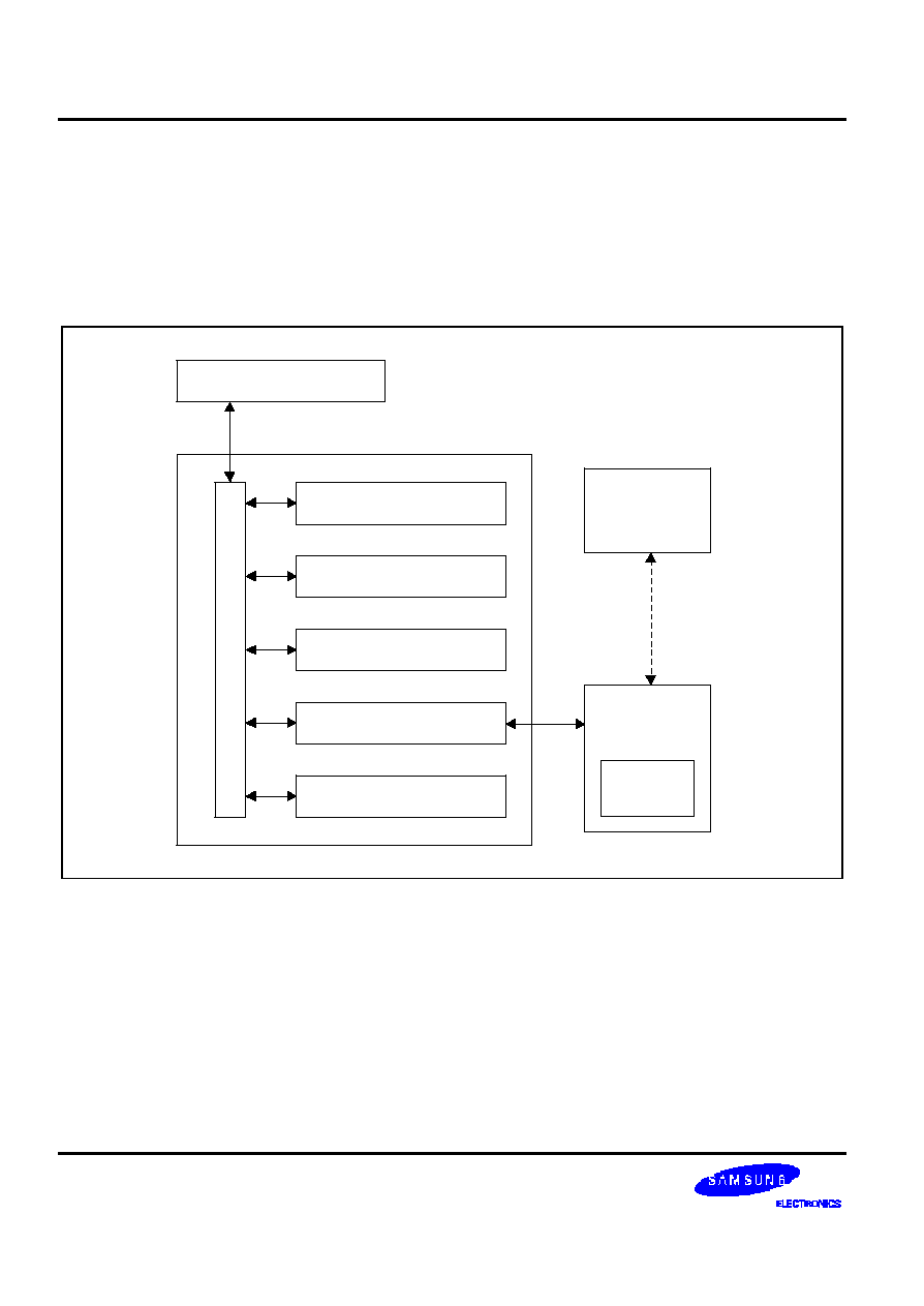
DEVELOPMENT TOOLS
S 3 C 9 6 8 8 / P 9 6 8 8
1 6 -2
T A R G E T B O A R D S
Target boards are available for the test of all S3C9-s e r i e s m i c r o c o n t r o l l e r s . A l l r e q u i r e d t a r g e t s y s t e m c a b l e s a n d
a d a p t e r s a r e i n c l u d e d w i t h t h e d e v i c e-specific target board.
O T P s
O n e t i m e s p r o g r a m m a b l e m i c r o c o n t r o l l e r s ( O T P s ) a r e u n d e r d e v e l o p m e n t f o r S 3 C 9 6 8 8 / P 9 6 8 8 m i c r o c o n t r o l l e r .
BUS
SMDS2+
RS-232C
POD
Probe
Adapter
PROM/OTP Writer Unit
RAM Break/Display Unit
Trace/Timer Unit
SAM4 Base Unit
Power Supply Unit
IBM-PC AT or
Compatible
TB9688
Target
Board
EVA
Chip
Target
Application
System
F i g u r e 1 6 -1 . S M D S P r o d u c t C o n f i g u r a t i o n ( S M D S 2 + )

S 3 C 9 6 8 8 / P 9 6 8 8
DEVELOPMENT TOOLS
1 6 -3
T B 9 6 8 8 T A R G E T B O A R D
T h e T B 9 6 8 8 t a r g e t b o a r d i s u s e d f o r t h e S 3 C 9 6 8 8 / P 9 6 8 8 m i c r o c o n t r o l l e r s . I t i s s u p p o r t e d b y t h e S M D S 2 +
d e v e l o p m e n t s y s t e m s . T h e T B 9 6 8 8 t a r g e t b o a r d c a n a l s o b e u s e d f o r S 3 C 9 6 8 8 / P 9 6 8 8 .
TB9688
GND
V
CC
+
Idle
+
Stop
J101
50-Pin
Connector
50
1
25
26
100-Pin
Connector
25
1
RESET
To User_V
CC
Off
On
U2
EXTTRIG1
EXTTRIG2
CN1
160 QFP
S3E9680
EVA Chip
1
40
SMDS2
SMDS2+
U1
SEL0
SEL1
H
L
H
L
41
80
81
120
121
160
Y2
F i g u r e 1 6 -2 . T B 9 6 8 8 T a r g e t B o a r d C o n f i g u r a t i o n
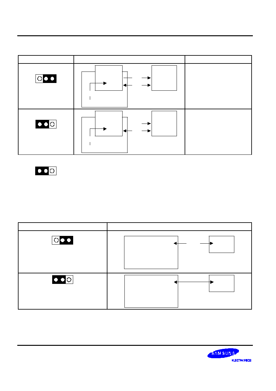
DEVELOPMENT TOOLS
S 3 C 9 6 8 8 / P 9 6 8 8
1 6 -4
T a b l e 1 6 -1 . P o w e r S e l e c t i o n S e t t i n g s f o r T B 9 6 8 8
' T o U s e r _ V c c ' S e t t i n g s
O p e r a t i n g M o d e
C o m m e n t s
To User_V
CC
Off
On
Target
System
SMDS2/SMDS2+
TB9688
V
CC
V
SS
V
CC
T h e S M D S 2 / S M D S 2 + s u p p l i e s
V
CC
to the target board
(evaluation chip) and the target
s y s t e m .
To User_V
CC
Off
On
Target
System
SMDS2+
TB9688
External
V
CC
V
SS
V
CC
T h e S M D S 2 / S M D S 2 + s u p p l i e s
V
CC
o n l y t o t h e t a r g e t b o a r d
(evaluation chip). The target
s y s t e m m u s t h a v e i t s o w n
p o w e r s u p p l y .
NOTE
: The following symbol in the "To User_V
CC
" Setting column indicates the electrical short (off) configuration:
S M D S 2 + S e l e c t i o n ( S A M 8 )
I n o r d e r t o w r i t e d a t a i n t o p r o g r a m m e m o r y t h a t i s a v a i l a b l e i n S M D S 2 + , t h e t a r g e t b o a r d s h o u l d b e s e l e c t e d t o b e f o r
S M D S 2 + t h r o u g h a s w i t c h a s f o l l o w s . O t h e r w i s e , t h e p r o g r a m m e m o r y w r i t i n g f u n c t i o n i s n o t a v a i l a b l e .
T a b l e 1 6 -2 . T h e S M D S 2 + T o o l S e l e c t i o n S e t t i n g
" S W 1 " S e t t i n g
O p e r a t i n g M o d e
S M D S 2
S M D S 2 +
SMDS2+
R/W*
Target
Board
R/W*
S M D S 2
S M D S 2 +
SMDS2+
R/W*
Target
Board
R/W* is not
available

S 3 C 9 6 8 8 / P 9 6 8 8
DEVELOPMENT TOOLS
1 6 -5
T a b l e 1 6 -3 . T h e ' S E L 0 , S E L 1 ' S e l e c t i o n S e t t i n g
' S E L 0 , S E L 1 ' S e t t i n g s
C o m m e n t s
SEL0
SEL1
H
L
H
L
T h i s ' S E L 0 , S E L 1 ' P i n i s n o t U s e d .
( N o C o n n e c t e d )
T a b l e 1 6 -4 . U s i n g S i n g l e H e a d e r P i n s a s t h e I n p u t P a t h f o r E x t e r n a l T r i g g e r S o u r c e s
T a r g e t B o a r d P a r t
C o m m e n t s
CH1
CH2
EXTTRIG2
EXTTRIG1
Connector from
external Trigger
sources of the
application System
Y o u c a n c o n n e c t a n e x t e r n a l t r i g g e r s o u r c e t o o n e o f t h e t w o e x t e r n a l
t r i g g e r c h a n n e l s ( C H 1 o r C H 2 ) f o r t h e S M D S 2 + b r e a k p o i n t a n d t r a c e
f u n c t i o n s .

DEVELOPMENT TOOLS
S 3 C 9 6 8 8 / P 9 6 8 8
1 6 -6
J101
P3.1
P3.0
P2.0/INT0
P2.1/INT0
P2.2/INT0
P2.3/INT0
P2.4/INT0
P2.5/INT0
P2.6/INT0
P2.7/INT0
V
DD
V
SS
X
OUT
X
IN
TEST
P4.0/INT1
P4.1/INT1
RESET
P4.2/INT1
P4.3/INT1
P1.7
P3.2
P3.3/CLO
D+/PS2
D-/PS2
3.3V
OUT
N.C
P0.0/INT2
P0.1/INT2
P0.2/INT2
P0.3/INT2
P0.4/INT2
P0.5/INT2
P0.6/INT2
P0.7/INT2
P1.0
P1.1
P1.2
P1.3
P1.4
P1.5
P1.6
1
2
3
4
5
6
7
8
9
10
11
12
13
14
15
16
17
18
19
20
21
42
41
40
39
38
37
36
35
34
33
32
31
30
29
28
27
26
25
24
23
22
42-Pin Connector
F i g u r e 1 6 -3 . 4 2 P i n C o n n e c t o r f o r T B 9 6 8 8
User System
Target Board
Target System
Part Name: (AP42SD-J)
Order Code: SM6524
50-Pin DIP
Connector
J101
1
50
25
26
J101
1
42
21
22
1
25
50
26
Probe for User
System
F i g u r e 1 6 -4 . S 3 C 9 6 8 8 P r o b e A d a p t e r C a b l e f o r 4 2 -S D I P P a c k a g e