 | –≠–ª–µ–∫—Ç—Ä–æ–Ω–Ω—ã–π –∫–æ–º–ø–æ–Ω–µ–Ω—Ç: S3CI9E0X | –°–∫–∞—á–∞—Ç—å:  PDF PDF  ZIP ZIP |

S3CI9E0X01 FLASH INTERFACE DEVICE
SAMSUNG ELECTRONICS
1
S3CI9E0X01 SPECIFICATION
Version : Ver. 1.0
Date : Jul. 16. 2003
Samsung Electronics Co., LTD
Semiconductor Flash Memory Product Planning & Applications

S3CI9E0X01 FLASH INTERFACE DEVICE
SAMSUNG ELECTRONICS
2
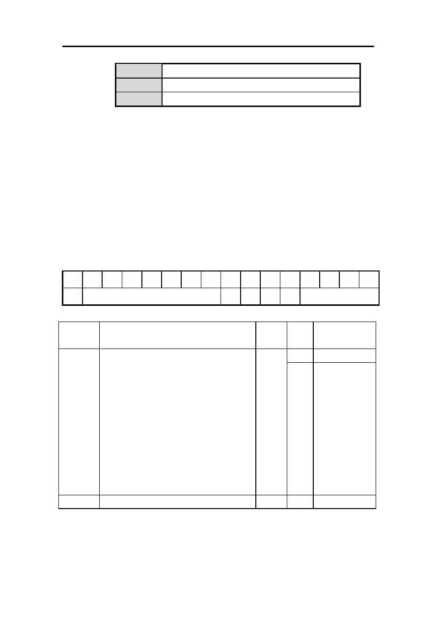
Revision History
Revision
No.
History
Draft
Date
Remark
0.0
Initial Draft
Jan. 24
th
2002
Preliminary
0.1
1.On page 18, BSC is moved from bufferRAM Write
Protection command register to system configuration
register and bufferRAM Write Protection command
register is removed.
2. Host Interface & NAND Flash Interface (page 3)
: 1.8V --> 1.8V / 2.5V / 3.0V
Jan. 25
th
2002
Preliminary
0.2
1. Package information is added.
2. Some description is updated.
3. Controller ID register default value is modified.
(Page 14)
4. Write Protection NAND Flash commands are
changed, and description are updated.(Page 23, 56)
Mar. 13
th
2002
Preliminary
0.3
1. Package pin configuration is changed.(page9)
2. Software algorithm of detecting NAND Flash type is
added. (page 18, 58)
- CE2Ena : 11 bit of system configuration register is
changed from `reserved' to `CE2Ena'.
Apr. 15
th
2002
Preliminary
0.4
1. Minimum latency at sync. Read is changed from
2clocks to 3clocks
2. Technical notes are added
- Write Protection truth table is updated(page 58)
- Write Protection guidance is updated(page 58)
- Internal register reset case is updated(page 61)
- Pin connection guidance between Host and Eagle
(page 61)
- Asynchronous Page Read guidance (page 62)
3. DC/AC parameter is updated(page64~66)
: 1
st
release parameter
4. tASC parameter is removed.
tAES parameter is added
Jun. 21
th
2002
Preliminary

S3CI9E0X01 FLASH INTERFACE DEVICE
SAMSUNG ELECTRONICS
3
4. Package dimension information is updated
(page63~64)
5. Some descriptions are modified & added
0.5
1. Vcc is available on 1.8V and 2.5V part.
2. Pin J2 is changed from NC to DNU.
3. Fig30(State diagram of NAND Flash Write
Protection) is updated.(page 57 )
4. Internal Register reset case table is updated
(page 63)
5. DC parameter is updated for 2.5V part (page 66~67)
6. Erratas and walk-around methods added
(page 73~76)
7. Default value of Interrupt Status Register(1442h) is
changed from 0000h to 8000h, which is not the
silicon revision but definition change.(refer to Internal
Regitster reset case table) (page 22)
9. Controller ID register value is updated from 1002h to
1202h (page 15)
10. AC parameters are updated (page 65~66)
tCES, tIACC are added in Sync. Read.
tVLWL is removed in Async. Write.
tAVA is removed.
tCS is added in Async. Write.
Dec. 11
th
2002
Preliminary
1.0
Spec. is finalized
Jul. 16
th
2003

S3CI9E0X01 FLASH INTERFACE DEVICE
SAMSUNG ELECTRONICS
4
1. Features
!
!
!
!
Architecture
∑
Design Technology : 0.25
µ
m
∑
Voltage Supply
- Main
: 1.8V(1.65V~1.95V) / 2.5V(2.3V~2.7V)
- Host Interface & NAND Flash Interface : 1.8V(1.65V~1.95V) / 2.5V(2.3V~2.7V)
∑
Organization
- Host Interface : 16-bit
- NAND Flash Interface : 8-bit
- Little endian addressing
∑
Internal BufferRAM(4K Bytes)
- BootRAM at booting, Cache-like at normal operation
∑
Integrated ring oscillator providing clock for NAND Flash operations
∑
Voltage detector generating internal reset signal from Vcc
!
!
!
!
Performance
∑
Host Interface type
- Synchronous Random Read
: Clock Frequency : up to 40Mhz @30pF
- Synchronous Burst Read
: Clock Frequency : up to 40MHz @30pF
: Burst Length : 4words/ 8 words/ 16 words/ 32 words/ Continuous Linear Burst(up to
2K words)
- Asynchronous Random Read
- Asynchronous Page Read : 4words
- Asynchronous Random Write
∑
Programmable Read latency
∑
Serial Page Read
- Read Serial pages by Page Count Register(up to 8 times)
∑
Normal ECC mode / Bypass ECC mode is supportable
- Read Operation Case
:Read with ECC - Hidden ECC code generation and comparison and 1bit correction
:Read without ECC - Hidden ECC code generation and comparison and readable of
ECC result
- Program Operation Case
:Program with ECC - Hidden ECC code generation and program it into ECC code

S3CI9E0X01 FLASH INTERFACE DEVICE
SAMSUNG ELECTRONICS
5
position of NAND Flash spare
:Program without ECC ≠ No operation for ECC
∑
Multiple Reset
- Cold Reset / Warm Reset / Hot Reset / NAND Flash Reset
∑
Internal Bootloader supports Booting Solution in system
∑
Data Protection
- Write Protection mode for BufferRAM
: Write protection of Buffer RAM(first 2pages of Buffer RAM)
- Write Protection mode for NAND Flash
: Block based write protection of NAND Flash
- Write protection during power-up
!
!
!
!
Software
∑
Handshaking Feature
- INT pin : Indicates Ready/Busy of The device
- Polling method : Provides a software method of detecting the Ready/Busy status of The
device
∑
Interface Chip ID Read
- Detailed chip information by additional controller ID register
!
!
!
!
Packaging
∑
Package
- 64ball , 6mm X 6mm X max 1.2mmt FBGA
∑
Pin Out
Host Interface
Flash Interface
Power
NC, DNU
Total pin[ea]
35 pins
16 pins
4 pins
9 pins
64 pins

S3CI9E0X01 FLASH INTERFACE DEVICE
SAMSUNG ELECTRONICS
6
2. General Description
The device allows standard NAND-flash chips to interface with The device bus without
performance penalty. This device is 1.8V operation and comprised of about 10,000 gates and
4KB internal BufferRAM. This 4KB BufferRAM is used as BootRAM during cold reset, and is
used as cache RAM after cold reset. The operating clock frequency is up to 40MHz. This
device is X16 interface with Host and X8 interface with NAND Flash. (Notice, in this
specification, address is expressed by the byte order)
Also this device has the speed of 55ns random access time. Actually, it is accessible with
minimum 3clock latency(host-driven clock for synchronous read), but this device adopts the
appropriate wait cycles by programmable read latency. The device interface chip provides the
Serial page read operation by assigning the number of pages to be read in the page counter
register. The device is offered in the single type of package ; 6mmX6mmX max 1.2mmt
64ball FBGA.

S3CI9E0X01 FLASH INTERFACE DEVICE
SAMSUNG ELECTRONICS
7
3. PIN DESCRIPTION
Pin Name
Type
Name and Description
Host Interface
A11~A0
I
Address Inputs
- Inputs for addresses during read operation, which are for addressing
BufferRAM & Register .
INT
O
Interrupt
Notifying Host when a command has completed. CMOS type driver output.
DQ15~DQ0
I/O
Data Inputs/Outputs
- Inputs data during program and commands during all operations, outputs
data during memory array/register read cycles.
Data pins float to high-impedance when the chip is deselected or outputs
are disabled.
CLK
I
Clock
CLK synchronizes the device to the system bus frequency in synchronous
read mode. The first rising edge of CLK in conjunction with nAVD low
latches address input.
nWE
I
Write Enable
nWE controls writes to the bufferRAM and registers. Datas are latched on
the nWE pulse's rising edge
nAVD
I
Address Valid Detect
Indicates valid address presence on address inputs. During asynchronous
read operation, all addresses are transparent during nAVD's low, and during
synchronous read operation, all addresses are latched on CLK's rising edge
while nAVD is held low for one clock cycle.
> Low : for asynchronous mode, indicates valid address ;for burst mode,
causes starting address to be latched on rising edge on CLK
> High : device ignores address inputs
nRP
I
Reset Pin
When low, nRP resets internal operation of Eagle and NAND Flash. nRP
status is don't care during power-up and bootloading.
nCE
I
Chip Enable
nCE-low activates internal control logic, and nCE-high deselects the device,
places it in standby state, and places A/DQ in Hi-Z

S3CI9E0X01 FLASH INTERFACE DEVICE
SAMSUNG ELECTRONICS
8
nOE
I
Output Enable
nOE-low enables the device's output data buffers during a read cycle.
NAND Flash Interface
I/O 0~I/O7
I/O
Flash Input/Output
Multiplexed command/address/data bus
fnCE
O
Flash Chip Enable
fnCE output is NAND Flash selection control. When NAND Flash is in the
Busy state, fnCE high is ignored, and the device does not return to standby
mode.
fnRE
O
Flash Read Enable
fnRE output is the serial data-out control, and when active drives the data
onto the NAND Flash I/O bus
fnWE
O
Flash Write Enable
fnWE output controls writes to the NAND Flash I/O port. Commands,
address and data are latched on the rising edge of the fnWE signal
fCLE
O
Flash Command Latch Enable
fCLE output controls the activating path for commands sent to the command
register of NAND Flash. When active high, commands are latched into the
command register of NAND Flash through the I/O ports on the rising edge of
the fnWE signal
fALE
O
Flash Address Latch Enable
fALE output controls the activating path for address to the internal address
registers of NAND Flash. Addresses are latched on the rising edge of
fnWE with fALE high
fnWP
O
Flash Write Protect
fnWP pin provides inadvertent program/erase protection during power
transitions and is automatically controlled by Eagle. This pin status is
activated to `Low' only during power-up.
fR/nB
I
Flash Ready/Busy
fR/nB input indicates the status of the NAND Flash operation. When low, it
indicates that a program, erase or random read operation of NAND Flash is
in process and returns to high state upon completion. It is an open drain
output and 100K
pull-up resister is internally connected. So, it does not
float to high-z condition when the chip is deselected or when outputs are
disabled
S3CI9E0X01 FLASH INTERFACE DEVICE
SAMSUNG ELECTRONICS
9
Power Supply
Vcc-Core
Power for Eagle Core
This is the power supply for Eagle Core.
Vcc-IO
Power for Eagle I/O(host Interface and NAND Interface)
This is the power supply for Eagle I/O which is
host Interface and also
NAND Interface.
Vss-Core
Ground for Eagle Core
Vss-IO
Ground for Eagle I/O(host Interface and NAND Interface)
etc
DNU.
Do Not Use
Leave it disconnected. These pins are used for testing.
NC
No Connection
Lead is not internally connected.
NOTE : Do not leave power supply( Vcc, Vss) disconnected.
S3CI9E0X01 FLASH INTERFACE DEVICE
SAMSUNG ELECTRONICS
10
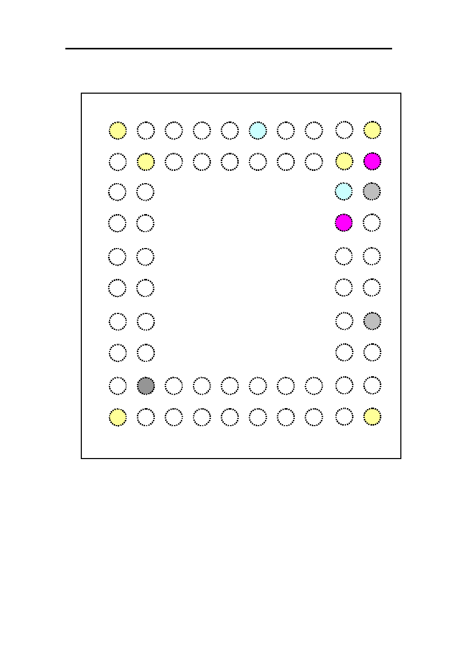
4. PIN CONFIGURATION
Notice: DNU (C10, G10,J2)pins are used as test pin, so please leave these
pins disconnected. DNU pins can be connected with the
limitation that they must be low.
64ball FBGA Eagle Chip
6 mm X 6 mm X max 1.2mmt , Ball Pitch : 0.5 mm
(TOPVIEW, Balls Facing Down)
NC
I/O6
I/O5
I/O2
Vss-IO
I/O0
fnWE
I/O7
nWE
NC
I/O4
I/O3
I/O1
fCLE
fnRE
INT
nRP
nOE
fnRB
NC
NC Vcc-IO
1 2 3 4 5 6 7 8 9 10
A
B
C
D
E
F
G
H
J
K
Vss-Core DNU
DQ15
DQ14
Vcc-Core fnCE1
DQ13
DQ7
A 3
fALE
DQ12
DQ8
A 5
fnWP
DQ10
DQ4
A 9
DNU
DQ9
DQ0
A 10
A 2
DQ6
DNU
DQ5
DQ2
nCE
A 7
A 0
DQ11
fnCE2 A
4
NC
DQ3
flsclk
nAVD A
11
A 8
A 6
DQ1
A 1
NC
S3CI9E0X01 FLASH INTERFACE DEVICE
SAMSUNG ELECTRONICS
11
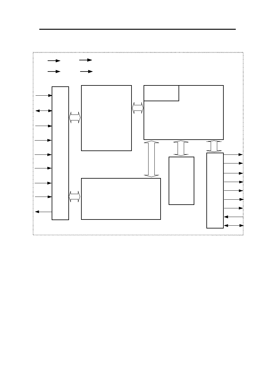
5. BLOCK DIAGRAM For Eagle Interface Chip
-
-
EAGLE flash interface
-
4KB BufferRAM
-
Command and status registers
-
State Machine ( Bootloader is included)
-
Error Correction Logic
-
Standard NAND flash Interface
Note: 1)
At cold reset, bootloader copies bootcode(4K byte size) from NAND Flash to BufferRAM.
and except cold reset host can use BufferRAM like cacheRAM.
VccCore
VssCore
BufferRAM
(4K Bytes)
1)
Internal Registers
(Address/Command/Configuration
/Status Registers)
State Machine
Error
Correction
Logic
St
an
d
a
rd
NA
ND F
l
ash
In
t
e
rf
ace
EA
G
L
E F
l
ash
In
t
e
rf
ace
nWE
nCE
CLK
nOE
nRP
fCLE
nAVD
fALE
fnCE2
fnRE
fnWP
fR/nB
I/O0~I/O7
DQ0~DQ15
Bootloader
fnWE
A0~A11
INT
VccIO
fnCE1
VssIO

S3CI9E0X01 FLASH INTERFACE DEVICE
SAMSUNG ELECTRONICS
12
6. ADDRESS MAP For Eagle Interface Chip
Notice ) Address expression in this specification was used byte order for
customer's convenience. Word order value can be calculated by
1bit-right shift of byte order value.
Address
(byte order)
Size (total 8KB)
Usage
Description
0000h ~ 01FEh
512B
PB0
Main area Buffer 0
0200h ~ 03FEh
512B
PB1
Main area Buffer 1
0400h ~ 05FEh
512B
PB2
Main area Buffer 2
0600h ~ 07FEh
512B
PB3
Main area Buffer 3
0800h ~ 09FEh
512B
PB4
Main area Buffer 4
0A00h ~ 0BFEh
512B
PB5
Main area Buffer 5
0C00h ~ 0DFEh
512B
PB6
Main area Buffer 6
0E00h ~ 0FFEh
512B
4KB
PB7
Main area Buffer 7
1000h ~ 100Eh
16B
SB0
Spare area Buffer 0
1010h ~ 101Eh
16B
SB1
Spare area Buffer 1
1020h ~ 102Eh
16B
SB2
Spare area Buffer 2
1030h ~ 103Eh
16B
SB3
Spare area Buffer 3
1040h ~ 104Eh
16B
SB4
Spare area Buffer 4
1050h ~ 105Eh
16B
SB5
Spare area Buffer 5
1060h ~ 106Eh
16B
SB6
Spare area Buffer 6
1070h ~ 107Eh
16B
128B
SB7
Spare area Buffer 7
1080h ~ 13FEh
896B 896B
Reserved
-
1400h ~ 17FEh
1KB 1KB
Registers
Internal
Registers
1800h ~ 1FFEh
2KB 2KB
Reserved
-
Note : - Data output is 00h while host reads/writes from/to a register bit of reserved
area.

S3CI9E0X01 FLASH INTERFACE DEVICE
SAMSUNG ELECTRONICS
13
∑
Spare area Buffer
- 0x1000 ~ 0x107E : 8 (page counter) x 16 byte(NAND spare area) = 128B
Address
F
E
D
C
B
A
9
8
7
6
5
4
3
2
1
0
1000h(SB0)
LSN(2
nd
) LSN(1
st
)
1002h(SB0)
WC(1
st
) LSN(3
rd
)
1004h(SB0)
BI
WC(2
nd
)
1006h(SB0)
ECC Code for Main area data (2
nd
)
ECC Code for Main area data (1
st
)
1008h(SB0)
ECC Code for Spare area data (1
st
)
ECC Code for Main area data (3
rd
)
100Ah(SB0)
Reserved
ECC Code for Spare area data (2
nd
)
100Ch(SB0)
Reserved Reserved
100Eh(SB0)
Reserved Reserved
1010h~
101Eh(SB1)
1020h~
102Eh(SB2)
1030h~
103Eh(SB3)
1040h~
104Eh(SB4)
1050h~
105Eh(SB5)
1060h~
106Eh(SB6)
1070h~
107Eh(SB7)
SB1 ~ SB7 have same assignment like SB0.
Note:
- LSN : Logical Sector Number
- WC : Wrap Count and each byte has same wrap count information and these are used as
error correction for wrap count itself.
- BI : Bad block Information
> Host can use complete spare area except BI and ECC code area. For example,
Host can write data to `reserved area of Spare area buffer' at program
operation.
> Eagle automatically generates ECC code for both main and spare data during
Eagle's data loading to NAND Flash, but does not update ECC code to spare
buffer.
> When programming/reading spare area, spare area buffer number(SB0~7) is
chosen via Start buffer register as it is.
Equivalent to 1byte of NAND Flash
Equivalent to 1byte of NAND Flash

S3CI9E0X01 FLASH INTERFACE DEVICE
SAMSUNG ELECTRONICS
14
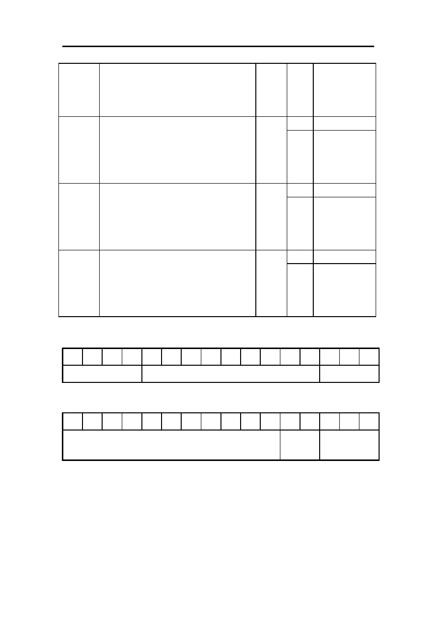
7.Internal Registers for Eagle Interface chip
Address
(byte order)
Name
Host
Access
Description
1400h
Controller
Information
R
Detailed information including device ID is offered
1402h
Block Address
R/W
block address of the flash memory
1404h
Page Address &
Page Count
R/W
8-bit MSB: the Page Address in a block
8-bit LSB: the Page Count which represents the
number of pages to be accessed
1406h
Start Buffer
R/W
Specifies the Buffer Number for the page data transfer
to/from the flash memory
1408h ~
141Eh
Reserved -
1420h
Command R/W
Host control commands and Flash Memory operation
commands
1422h
System
Configuration
R/W
Flash Configuration and Host Interface Configuration
1424h
~143Eh
Reserved -
1440h
Controller Status
R
Controller Status and the result of flash operation
1442h
Interrupt
R/W
Flash Command Completion Interrupt Status
1444h
Reserved -
1446h
ECC Result of
Main area data
R
ECC error position of Main area data error
1448h
ECC Result of
Spare area data
R
ECC error position of Spare area data error
144Ah
NAND Flash
Write Protection
Command
R/W
NAND Flash Write Protection command to make NAND
Flash be secured
144Ch
Unlock Start
Block Address
R/W
Start NAND Flash block address to unlock in Write
Protection mode
144Eh
Unlock End
Block Address
R/W
End NAND Flash block address to unlock in Write
Protection mode
1450h
NAND Flash
R
Current NAND Flash Write Protection status whether

S3CI9E0X01 FLASH INTERFACE DEVICE
SAMSUNG ELECTRONICS
15
Write Protection
Status
unlocked /locked /lock-tighten
1452h~17FEh
Reserved -
Note : - Data output is 00h while host reads/writes from/to a register bit of
reserved area.
7.1. Address Register
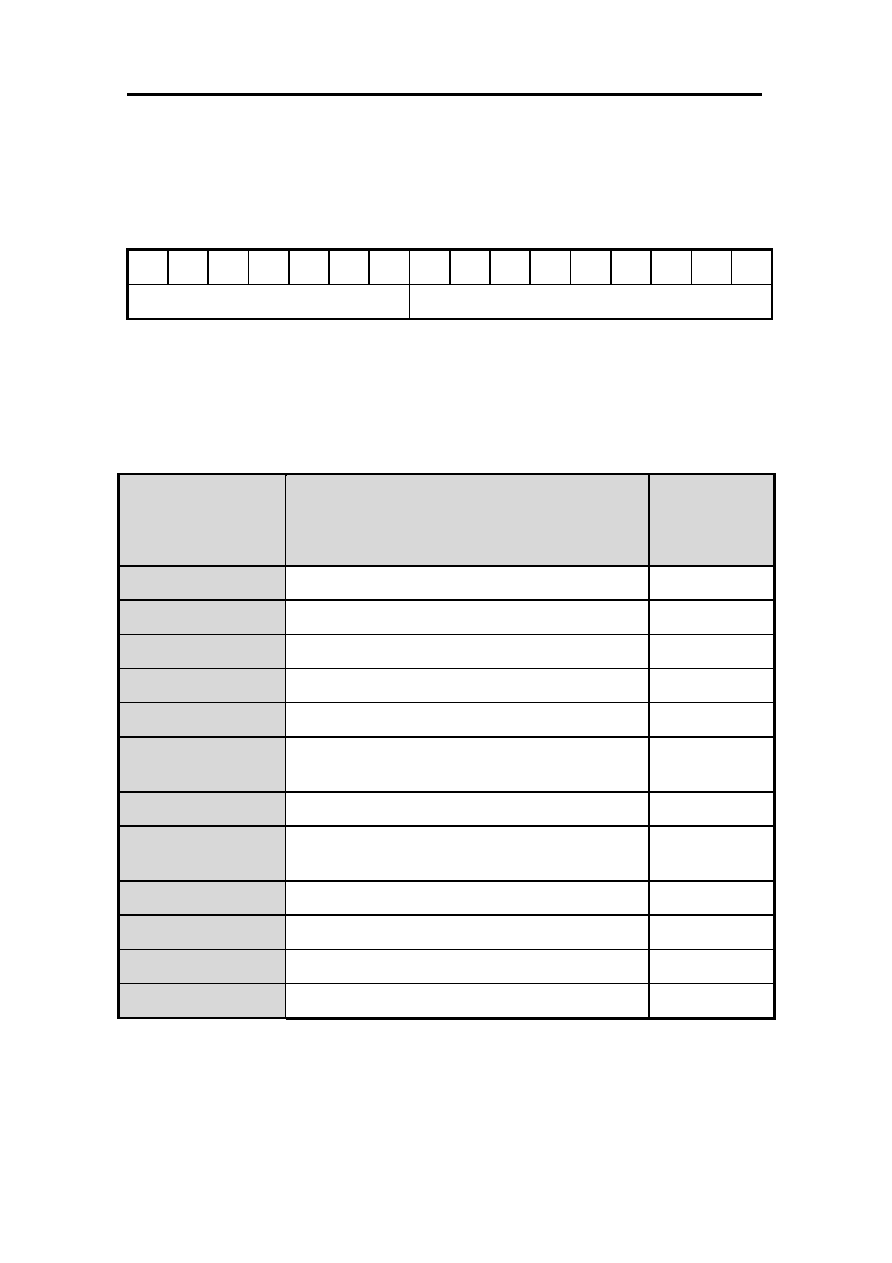
7.1.1. Controller ID Register (R) : 1400h, default = 1202h
15 14
13 12 11 10 9 8 7 6 5 4 3 2 1 0
MANUCODE VERCODE
CHIPID
BUFSIZE
MANUCODE (MANUfacturer CODE): manufacturer identification, 1h for Samsung
Electronics Corp.
VERCODE (VERsion CODE): the version of the chip, which is updated like the following
cases.
- Process change (even if no change in logical interface)
- DC/AC parameter change
- Error correction of existing silicon.
Version
Controller ID reigister value
1.0 1002h
1.1 / 1.2
1202h
CHIPID (CHIP ID): the ID of the chip, which is updated like the following cases.
- Device change
- Changes requiring some SW-change or some completely new
silicon.
BUFSIZE (BUFfer SIZE): the size of internal page buffer.
BUFSIZE
Page Buffer Size in KBytes
0 0 0 0
1
0 0 0 1
2
0 0 1 0
4 (default)
0 0 1 1
6
0 1 0 0
8
0101~1111
Reserved

S3CI9E0X01 FLASH INTERFACE DEVICE
SAMSUNG ELECTRONICS
16
7.1.2. Block Address Register (R/W): 1402h, default = 0000h
15 14
13 12 11 10 9 8 7 6 5 4 3 2 1 0
Reserved BA
BA (Block Address): NAND Flash block address which will be read or programmed or
erased..
NAND Flash
Valid bits
64Mb BA[8:0]
128Mb BA[9:0]
256Mb BA[10:0]
512Mb BA[11:0]
1Gb DDP
BA[12:0]
7.1.3. Address Length Register :
Page Address & Page Counter Register (R/W): 1404h, default = 0000h
15 14
13 12 11 10 9 8 7 6 5 4 3 2 1 0
Reserved PA
Reserved PC
PA (Page Address): NAND Flash start page address in a block for page read or program
operation.
PA(default value) = 00000
PA range : 00000 ~ 11111
PC (Page Count): this field specifies the number of pages to be read. Its maximum count
is 8 pages at 000(default value) value. For a single page access, it should be
programmed as value 001.
However internal RAM buffer reached to 111vaule(max value), it counts up
to 000value to satisfy PC value.
for example) if SB = 110 , PC = 100
then selected bufferRAM are ` 110 ! 111 ! 000 ! 001 `
7.1.4. Start Buffer Register (R/W): 1406h, default = 0000h
15 14
13 12 11 10 9 8 7 6 5 4 3 2 1 0
Reserved SB
SB (Start Buffer) : It is the place where data is placed and specifies the start Buffer
number(0~7
th
) in the internal bufferRAM(0~7
th
) (see Address Map).
S3CI9E0X01 FLASH INTERFACE DEVICE
SAMSUNG ELECTRONICS
17
7.2. Command and System Configuration Registers
7.2.1. Command Register (R/W): 1420h, default = 0000h
15 14 13 12 11 10 9 8
*
7 6 5 4 3 2 1 0
Reserved CMD
* 9
th
bit of CMD determines whether ECC generation or ECC generation bypass.
9
th
bit value: `0' ≠ ECC generation , `1' ≠ bypass ECC generation
And ECC generation is available on Read/Program operation.
The CMD field specifies the operation that the controller will perform.
CMD
Operation
Acceptable
command
during busy
0000h (0 0000 0000)
Read single page
1)
of Flash with ECC correction
F0h , F3h
0100h (1 0000 0000)
Read single page
1)
of Flash without ECC correction
F0h , F3h
0003h (0 0000 0011)
Read single spare area of Flash with ECC correction
F0h , F3h
0103h (1 0000 0011)
Read single spare area of Flash without ECC correction
F0h , F3h
0085h (0 1000 0101)
Program single page
1)
of Flash with ECC generation
F0h , F3h
0185h (1 1000 0101)
Program single page
1)
of Flash without ECC
generation
F0h , F3h
008Ah (0 1000 1010)
Program single spare area
1)
of Flash with ECC generation
F0h , F3h
018Ah (1 1000 1010)
Program single spare area of Flash without ECC
generation
F0h , F3h
0094h (0 1001 0100)
Erase single block of Flash
F0h , F3h
000Ch (0 0000 1100)
Read Flash Memory ID
F0h , F3h
00F0h (0 1111 0000)
Reset Flash Memory
-
00F3h (0 1111 0011)
Reset Controller
2)
-
Note : 1) `Page' means all(528B) of main area(512B) and spare area(16B) in NAND
Flash.

S3CI9E0X01 FLASH INTERFACE DEVICE
SAMSUNG ELECTRONICS
18
Host can read/program by page(main+spare area) unit or by spare area unit.
At read/program by page unit, SB(start buffer) of spare area is same to that
of main area.
2) `Reset Controller'(=Hot reset) command makes the registers default state as
the warm reset(=reset by nRP pin).
> Serial pages read can be performed by setting the PC (Page Counter).
: PC(default) = `0' (8 pages)
: PC value is available up to 8.
"
"
"
"
Command input guide
1. Once previous command is entered, followed next command input cause erroneous
operation. To cancel previous command, resets(nRP ,F3h, F0h) are
recommended.
2. During INT is Low, only resets(nRP, F3h,F0h) are acceptable.
3. Please avoid another resets input during one reset operation.
Previous
command
Next
command
Previous
command
Reset
(nRP,F3h,F0h)
Command
Command
INT
INT return time by reset is max. 5us(at read)
/ 50us(at program) /500us(at erase).
Reset
(nRP,F3h,F0h)

S3CI9E0X01 FLASH INTERFACE DEVICE
SAMSUNG ELECTRONICS
19
7.2.2. System Configuration Register (R/W): 1422h, default = 7051h
> System Configuration Register is not adjusted automatically to NAND Flash
device type(Density , Version).
15 14
13 12 11 10 9 8 7 6 5 4 3 2 1 0
RM
BRL CE2Ena BL
PS BS FBW
BSS
RM (Read Mode): this field specifies the selection between asynchronous read mode and
synchronous read mode
BRL (Burst Read Latency): this field specifies the initial access latency in the burst read
transfer. In 40Mhz, 011(3-cycle) is proper value.
CE2Ena (NAND Flash type): this field specifies NAND Flash type whether 512Mb single
or 512Mb DDP.
RM
Read Mode
0
Asynchronous read (default)
1
Synchronous read
BRL
Latency Cycles
0 0 0
Reserved
0 0 1
Reserved
0 1 0
Reserved
0 1 1
3-cycle (min.)
1 0 0
4-cycle
1 0 1
5-cycle
1 1 0
6-cycle
1 1 1
7-cycle (default)
CE2Ena
NAND Flash type
0
512Mb Single NAND Flash (default)
1
256Mb X 2ea with dual nCE NAND Flash

S3CI9E0X01 FLASH INTERFACE DEVICE
SAMSUNG ELECTRONICS
20
BL (Burst Length): this field specifies the size of burst length during Sync. burst read.
PS (Page Size): this field specifies the size of a page in the flash memory.
PS
Page Size in bytes
0 0
Reserved
0 1
512 (default)
1 0
Reserved
1 1
Reserved
BS (Block Size): this field specifies the size of a block in the flash memory.
BS
Block Size in Kbytes
0 0
8
0 1
16 (default)
1 0
Reserved
1 1
Reserved
FBW (Flash Bus Width): this field specifies the bus width of the flash memory bus.
FBW
Bus Width in bits
0 0
8 (default)
0 1
Reserved
1 0
Reserved
1 1
Reserved
BSS (Buffer Write Protection Set): this field specifies the buffer Write Protection status of
first 2page buffer.
BL
Burst Length
0 0 0
Continuous (default)
0 0 1
4 words
0 1 0
8 words
0 1 1
16 words
1 0 0
32 words
1 0 1~1 1 1
Reserved

S3CI9E0X01 FLASH INTERFACE DEVICE
SAMSUNG ELECTRONICS
21
BSS
Buffer Write Protection Set
0 0
Locked
0 1
Locked (default)
1 0
Unlocked
1 1
Locked
7.3. Status Registers
7.3.1. Controller Status Register (R): 1440h, default = 0000h
15 14
13 12 11 10 9 8 7 6 5 4 3 2 1 0
CB Reserved PR
ERm
ERs
Reserved
CB (Controller Busy): this bit shows the overall internal status of the controller. Set to `1'
when the controller is in its operation and cannot receive any more command. `0' when
the controller is in ready state.
CB
Controller Busy
Status
0
Ready
1
Busy
PR (Program Result): this bit shows the result of Page Program/Block Erase operation for
flash memory.
PR
Program/Erase Result
0
Successful
1
Error in Program/Erase
ERm(ECC Error for Main area data) & ERs (ECC Error for Spare area data)
: ERm and ERs show the number of error in a page as a result of ECC check at the
page read operation.
: ECC algorithm of Eagle can't detect and correct above 2 fault bits per page, interprets
that case as uncorrectable.
ERm, ERs
ECC Status
0 0
No Error
S3CI9E0X01 FLASH INTERFACE DEVICE
SAMSUNG ELECTRONICS
22
0 1
1-bit error(correctable)
1 0
2 bits error (uncorrectable)
1)
1 1
2bits error at serial-pages read(uncorrectable)
2)
NOTE: 1) 3bits or more error detection is not supported
2) At serial-pages Read by the number of PC, ERm and ERs represent
cumulative result of those pages.
For example, if there are 2pages with 2bits error in main/spare area
data, ERm/ERs value is 11.
if there are 2pages with 1bit error in main/spare area data,
ERm/ERs value is 01.
To find where error is, host must check each of serial pages.
7.3.2. Interrupt Status Register (R/W): 1442h, default = 8000h
15 14
13 12 11 10 9 8 7 6 5 4 3 2 1 0
INT Reserved RI
WI
EI
IDI
Reserved
Bit
Address
Bit Name
Default
State
Valid
States
Function
0
Interrupt Off
15
INT (interrupt) :
the master interrupt bit
-Set to '1' of itself when one or more of
RI,WI,EI,IDI is set to `1' ,or boot is done, or
warm reset is released , or hot reset is
released.
-Cleared to '0' when by writing `0' to this bit or
by reset(Cold/Warm/Hot reset).
`0' in this bit means that INT pin is low status.
(This INT bit is directly wired to the INT pin
on the chip, so the pin will go low upon
writing `0' to this bit)
0
1
Interrupt Pending
7
RI (Read Interrupt):
0 0
Interrupt Off
S3CI9E0X01 FLASH INTERFACE DEVICE
SAMSUNG ELECTRONICS
23
-Set to '1' of itself at the completion of
Read Operation
-Cleared to '0' when by writing `0' to this bit or
by reset(Cold/Warm/Hot reset).
1
Interrupt Pending
0
Interrupt Off
6
WI (Write Interrupt):
-Set to '1' of itself at the completion of
Program Operation
-Cleared to '0' when by writing `0' to this bit or
by reset(Cold/Warm/Hot reset).
0
1
Interrupt Pending
0
Interrupt Off
5
EI (Erase Interrupt):
-Set to '1' of itself at the completion of
Erase Operation
-Cleared to '0' when by writing `0' to this bit or
by reset(Cold/Warm/Hot reset).
0
1
Interrupt Pending
0
Interrupt Off
4
IDI (ID Interrupt):
-Set to '1' of itself at the completion of
Read ID Operation
-Cleared to '0' when by writing `0' to this bit or
by reset(Cold/Warm/Hot reset).
0
1
Interrupt Pending
7.3.3. ECC Result of Main area data Register (R) : 1446h, default = 0000h
15 14
13 12 11 10 9 8 7 6 5 4 3 2 1 0
Reserved
ECC Result 1
1)
ECC
Result2
2)
7.3.4. ECC Result of Spare area data Register (R) : 1448h, default = 0000h
15 14
13 12 11 10 9 8 7 6 5 4 3 2 1 0
Reserved
ECC
Result3
3)
ECC Result 2
2)
Note) 1. ECC Result 1 : ECC error position address that selects one of Main area
data (512Bytes).
2. ECC Result 2 : ECC error position address which selects one of eight
I/Os (I/O 0~I/O7).
3. ECC Result 3 : ECC error position address that selects one of Logical Sector
S3CI9E0X01 FLASH INTERFACE DEVICE
SAMSUNG ELECTRONICS
24
Number (3Bytes)
* At serial-page read operation, these ECC result registers have result for last page.
7.3.5. NAND Flash Write Protection Command (R/W) : 144Ah, default = 0002h
15 14 13 12 11 10 9 8
*
7 6 5 4 3 2 1 0
Reserved
Write protection
Command*
Note : *The CMD field specifies the operation which the controller will perform.
NAND Flash
Write Protection
Command
Operation
0004h ( 0000 0100)
Unlock NAND Flash block(s) according to given block address range
0002h ( 0000 0010)
Lock all NAND Flash block(s)
0001h ( 0000 0001)
Lock-tight locked block(s)
7.3.6. Unlock Start Block Address (R/W) : 144Ch, default = 0000h
15 14
13 12 11 10 9 8 7 6 5 4 3 2 1 0
Reserved USBA
USBA (Unlock Start Block Address):
Start NAND Flash block address to unlock in Write
Protection mode, which follows `Unlock block command'.
7.3.7. Unlock End Block Address (R/W) : 144Eh, default = 0000h
15 14
13 12 11 10 9 8 7 6 5 4 3 2 1 0
Reserved UEBA
UEBA (Unlock End Block Address):
End NAND Flash block address to unlock in Write
Protection mode, which follows `Unlock block
command'.
7.3.8. NAND Flash Write Protection Status (R) : 1450h, default = 0002h
15 14
13 12 11 10 9 8 7 6 5 4 3 2 1 0
Reserved
US LS LTS

S3CI9E0X01 FLASH INTERFACE DEVICE
SAMSUNG ELECTRONICS
25
US (Unlocked Status): `1' value of this bit specifies that there is unlocked block in
NAND Flash.
LS (Locked Status): `1' value of this bit specifies that all NAND Flash blocks are in
locked status.
LTS (Lock-tighten Status): `1' value of this bit specifies that `Locked block(s)' is
lock-tighten.
> While anyone of these three bits(US,LS,LTS) is set, the others are internally reset
8. Access Timings for Eagle Interface Chip
Operation
nCE
nOE
nWE
A0~15
DQ
0~15
nRP
FlsCLK
nAVD
Standby
H X X X
High-Z
H X X
Warm Reset
X X X X
High-Z
L X X
Asynchronous Write
L
H
L
Add. In Data In
H
X
Asynchronous Read
L L H
Add.
In
Data
Out
H L
or
Load Initial Burst
Address
L H
or
L
H Add
In X H
or
Burst Read
L L H X
Burst
Dout
H
or
Terminate Burst Read
Cycle
H X H X
High-Z
H X X
Terminate Burst Read
Cycle via nRP
X X X X
High-Z
L X X
Terminate Current Burst
Read Cycle and Start
New Burst Read Cycle
H
H
Add In
High-Z
H
< BUS OPERATION >
X=Don't Care
S3CI9E0X01 FLASH INTERFACE DEVICE
SAMSUNG ELECTRONICS
26
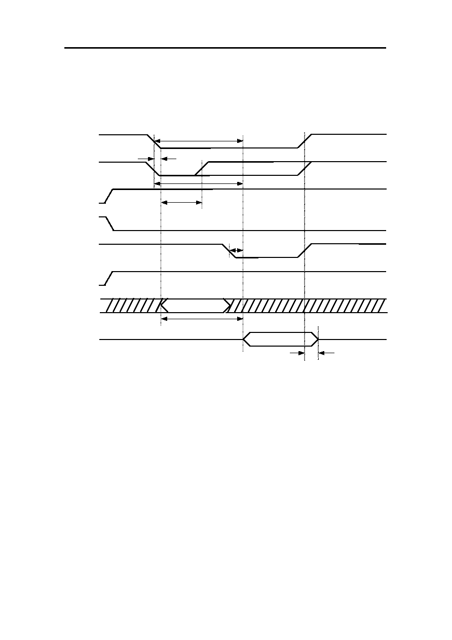
8.1. ASYNCHRONOUS READ OPERATION
HOST
NAND
FLASH
Eagle
Page Write
Block Erase
Page Read
< ACCESS TYPES >
Figure 1. Asynchronous Read Mode
Async. Write
Async. Random Read
Sync. Read
Async. Page Read
nWE
CLK
nRP
nOE
tCE
nCE
Ai
tOE
tACC
DQi
Valid Data
tOH
Valid Address
tAES*
* Please notice, tAES is Address delay from nCE & nAVD's low,
and tAES should not be over 10ns.
tAE
S3CI9E0X01 FLASH INTERFACE DEVICE
SAMSUNG ELECTRONICS
27
8.2. LATCHED ASYNCHRONOUS READ OPERATION
Figure 2. Latched Asynchronous Read Mode
nWE
CLK
nRP
nOE
tCE
nCE
nAVD
Ai
tOE
tACC
DQi
Valid Data
tOH
tASA
Valid Address
tAES*
tAE
S3CI9E0X01 FLASH INTERFACE DEVICE
SAMSUNG ELECTRONICS
28
8.3. ASYNCHRONOUS PAGE READ OPERATION
Figure 3. Asynchronous Page Read Mode
nWE
CLK
nOE
nRP
nCE
tCE
nAVD
Valid Address
tACC
DQi
Data0
Data1 Data2 Data3
Valid
Address
Valid
Address
`L'
tOH
tOE
tAPA
tASA
A
11~2
Valid Address
A
1~0
Valid
Address
tAES* tAE
* Please notice, tAES is Address delay from nCE & nAVD's low,
and tAES should not be over 10ns.
S3CI9E0X01 FLASH INTERFACE DEVICE
SAMSUNG ELECTRONICS
29
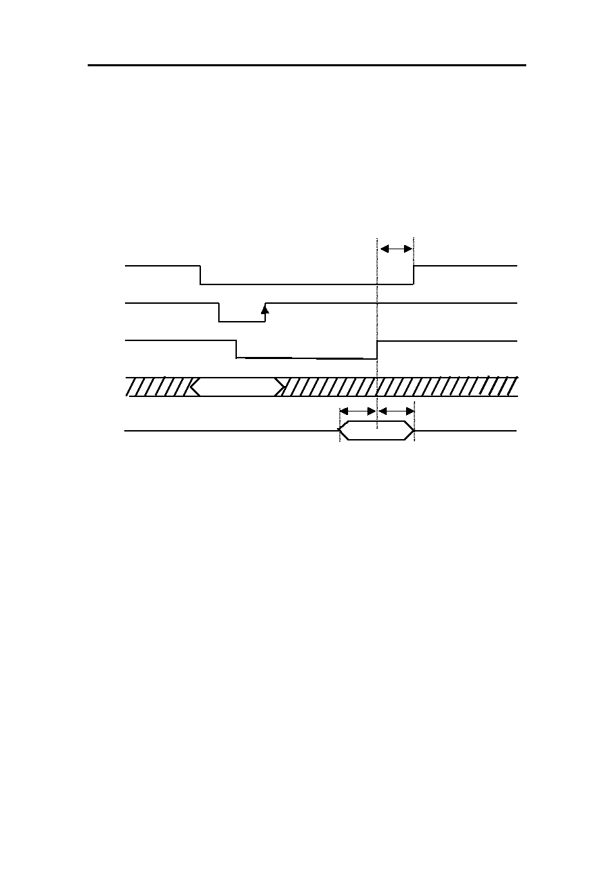
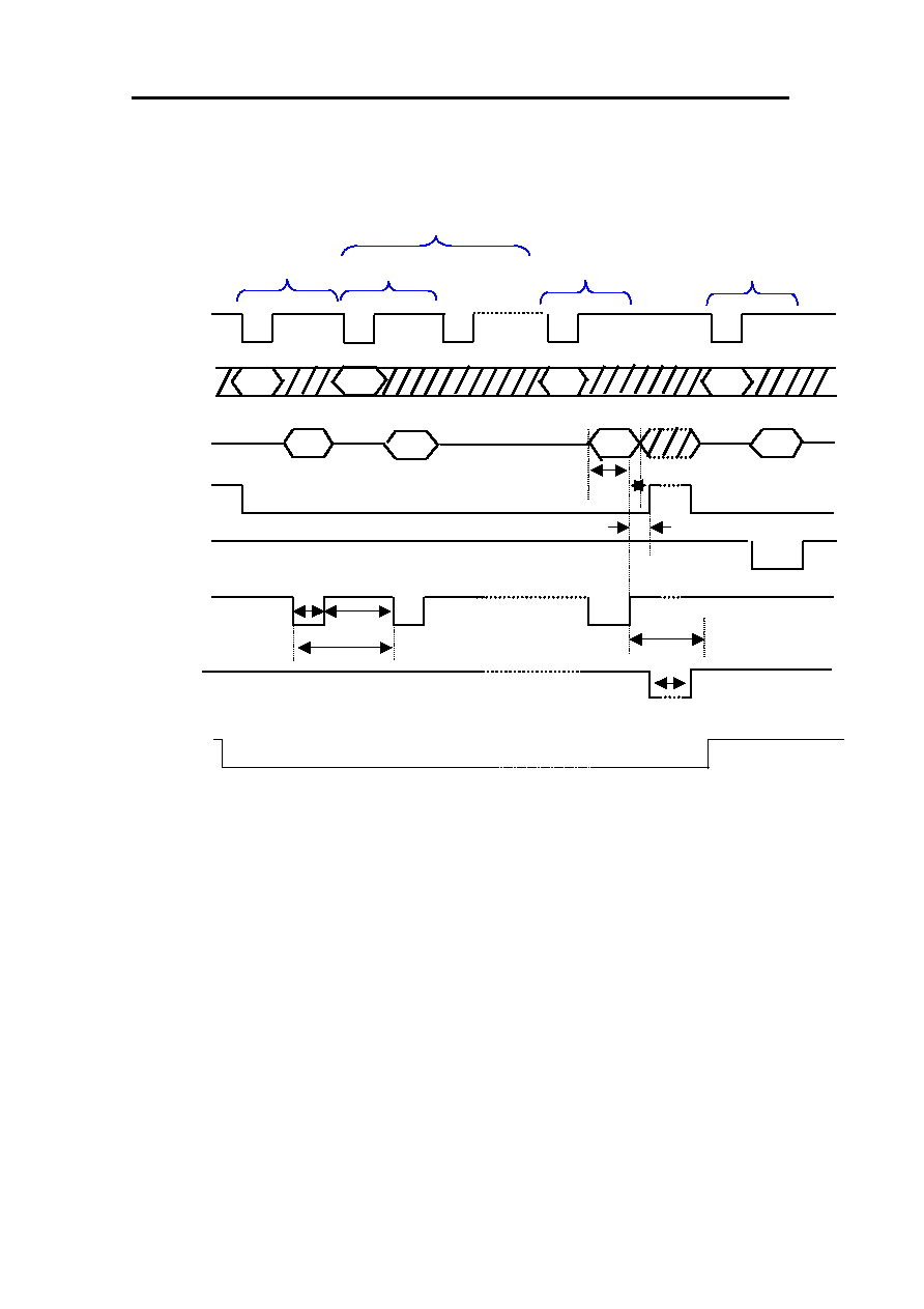
8.4. SYNCHRONOUS BURST READ OPERATION
Figure 4. Synchronous Burst Read Mode
tBACC tBDH
tIACC
tAVDS
tACS tACH
nWE
CLK
nOE
nRP
nCE
tCES
nAVD
INT
Ai
Valid Address
Read latency : 7clock(default), 3clock(min.)
tOH
tOH
DQi
Data
Data
Data
tAVDH

S3CI9E0X01 FLASH INTERFACE DEVICE
SAMSUNG ELECTRONICS
30
8.5. ASYNCHRONOUS WRITE OPERATION
(No nAVD pin case)
Figure 5. Asynchronous Write Mode
INT
nWE
nOE
nRP
nWP
nCE
CLK
tWPL
tWPH
tWC
tCS
tCH
tDS
tDH
Ai
Valid Address
DQi
Valid Data
Valid Address
Valid Data

S3CI9E0X01 FLASH INTERFACE DEVICE
SAMSUNG ELECTRONICS
31
8.6. LATCHED ASYNCHRONOUS WRITE OPERATION
9. Timing Diagram for Eagle Interface Chip
Figure 6. Latched Asynchronous Write Mode
INT
nWE
nOE
nRP
nWP
nCE
nAVD
CLK
tWPL
tAVDP
tWPH
tWC
tCS
tCH
tDS
tDH
Ai
Valid Address
tAAVDS tAAVDH
DQi
Valid Data
Valid Address
Valid Data

S3CI9E0X01 FLASH INTERFACE DEVICE
SAMSUNG ELECTRONICS
32
9.1. ASYNCHRONOUS READ OPERATION
The read cycle is initiated by first applying address to the address bus. The address
latch is transparent while nCE is low. The random access time is measured from a stable
address, falling edge of nCE. The clock should remain "0" during asynchronous access.
Address access time(tACC) is equal to the delay from stable addresses to valid output data.
The chip enable access time(tCE) is the delay from the stable addresses and stable nCE to
valid data at the outputs. The output enable access time(tOE) is the delay from the falling edge
of nOE to valid data at the output. nCE must toggle in asynchronous read operation.
Figure 6. Asynchronous Read Mode
tACC
nOE
tOE
nCE
tCE
Ai
Valid Address
DQi
Valid Data
tAES
tAE

S3CI9E0X01 FLASH INTERFACE DEVICE
SAMSUNG ELECTRONICS
33
9.2. LATHCED ASYNCHRONOUS READ OPERATION
The read cycle is initiated by first applying address to the address bus. The address
latch is transparent while nAVD is low. The random access time is measured from a stable
address, falling edge of nAVD or falling edge of nCE which ever occurs last. The clock should
remain "0" during asynchronous access. Address access time(tACC) is equal to the delay
from stable addresses to valid output data. The chip enable access time(tCE) is the delay from
the stable addresses and stable nCE to valid data at the outputs. The output enable access
time(tOE) is the delay from the falling edge of nOE to valid data at the output. nCE and nAVD
must toggle in asynchronous read operation.
9.3. ASYNCHRONOUS PAGE READ OPERATION
Asynchronous page read mode is the default state and provides a high data transfer
rate for non clocked memory subsystems. The page size is four words, and A
1~0
addresses
one of the four words. The read cycle is initiated by first applying address to the address bus.
The address latch is transparent while nAVD is low. The address is latched by internal address
latch circuit. The random access time is measured from a stable address, falling edge of nAVD
Figure 7. Asynchronous Read Mode
nAVD
tACC
nOE
tOE
nCE
tCE
Ai
Valid Address
DQi
Valid Data
tAES
tAE

S3CI9E0X01 FLASH INTERFACE DEVICE
SAMSUNG ELECTRONICS
34
or falling edge of nCE which ever occurs last. The clock should remain "1" during
asynchronous access. Address access time(tACC) is equal to the delay from stable addresses
to valid output data. The chip enable access time(tCE) is the delay from the stable addresses
and stable nCE to valid data at the outputs. The output enable access time(tOE) is the delay
from the falling edge of nOE to valid data at the output. nCE and nAVD must toggle in
asynchronous read operation.
Figure 8. Asynchronous Page Read Mode
nAVD
nCE
nOE
CLK
tACC
DQi
Data0 Data1
Data
3
`L'
Data2
Valid Address
Valid
Address
Valid
Address
Valid
Address
tOH
tASA
tCE
tAE
tOE
tAPA
A
11~2
A
1~0
Valid Address
tAES
S3CI9E0X01 FLASH INTERFACE DEVICE
SAMSUNG ELECTRONICS
35
9.4. SYNCHRONOUS BURST READ OPERATION
When the device is powered up, it defaults to asynchronous read operation. Burst mode is
selected by System Configuration register bit 15. The burst mode is used to improve the data
transfer between the memory and the system processor. The burst mode is used only for read
operations. Burst length is available on 4words/ 8words/ 16words/ 32words/ Continuous length,
and is set by BL of System configuration register. The Bus Controller in the system will insert
required read latency to meet host random access time. The first access time in the burst is
equal to the random access time. In the burst access, the address is latched at the rising edge
of the clock pulse when nAVD is low. The first data in the burst access is available after the
random access time. The Bus Controller reads data at the first rising edge of the clock after
read latency. There is no conflict between nAVD's low and nOE's low.
The output buffers need to settle before the first data is available. Due to this, the shortest
random access is at least one clock cycles from the rising edge of the clock when nAVD is low.
This is defined as random access without any wait state. As the random access is allowed to
be much longer than one clock cycles, the flash device has to support wait state insertion in
order to synchronize the start of the burst access.
Figure 9. Synchronous Burst Read Mode( 3clock read latency case)
nAVD
nCE
nOE
CLK
Ai
Valid Address
tIACC
tBACC
tBDH
Data0 Data1
Data3
DQi
Data2

S3CI9E0X01 FLASH INTERFACE DEVICE
SAMSUNG ELECTRONICS
36
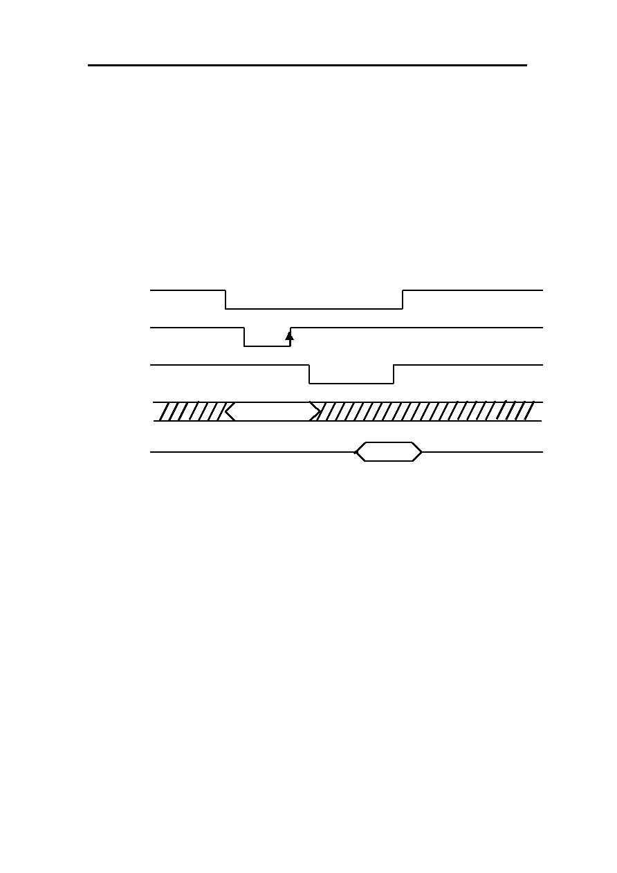
9.5. Programmable Read Latency
The programmable read latency value indicates to the device the number of
additional clock cycles that must elapse after nAVD is driven active before data will be
available.
The number of read latency that should be programmed into the device is directly related to
the clock frequency. Upon Power up, the device defaults to seven cycles. The total number of
the read latency is programmable from zero to seven cycles. A hardware reset will set read
latency to seven cycles after power-up. The minimum read latency for this device is three cycle
assuming 40MHz system clock.
Figure 10. Example of 3clock Read Latency Insertion
Data 0
nAVD
nOE
CLK
tBACC
tIACC
0 1 2 3
Number of clock cycles programmed
Rising edge of the clock cycle following
last read latency triggers next burst data
tBDH
DQi
Valid Address
Ai
Data 1
Data 2
Data 3
Data 4

S3CI9E0X01 FLASH INTERFACE DEVICE
SAMSUNG ELECTRONICS
37
9.6. ASYNCHRONOUS WRITE OPERATION
Write is allowed only in the asynchronous mode. The address is latched at the rising
edge of the nCE signal. The random access time is measured from a stable address, falling
edge of nCE. Write operations are asynchronous. Therefore, CLK is ignored during write
operation. There is no conflict between nCE's low and nOE's low.
Figure 11. Asynchronous Write Mode
nWE
nCE
tDH
tDS
Valid Address
Ai
Valid Data
DQi
S3CI9E0X01 FLASH INTERFACE DEVICE
SAMSUNG ELECTRONICS
38
9.7. LATCHED ASYNCHRONOUS WRITE OPERATION
At Latched Asynchronous Write operation, the address is latched at the rising edge of
the nAVD signal. Because Write operations are asynchronous operation, CLK is ignored
during write operation. There is no conflict between nAVD's low and nOE's low.
Figure 12. Latched Asynchronous Write Mode
nWE
nCE
nAVD
Address Latch
tDH
tDS
Valid Address
Ai
Valid Data
DQi
tCH
S3CI9E0X01 FLASH INTERFACE DEVICE
SAMSUNG ELECTRONICS
39
10. DEVICE OPERATION for Eagle Interface Chip
10.1. Read Controller ID
The device contains a controller ID register, can be read by accessing Controller ID
register(address = 1400h) with synchronous/asynchronous read timing. Figure 12 shows the
`Read controller ID' operation by asynchronous read timing.
nAVD
Address Latch
nOE
nCE
Ai
Address:1400h
Figure 13. Read Controller ID (Lached asynchronous read case)
DQi
ID Data
S3CI9E0X01 FLASH INTERFACE DEVICE
SAMSUNG ELECTRONICS
40
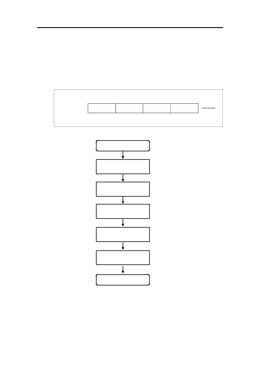
10.2. Read NAND Flash ID
`Read NAND Flash ID' mode is initiated by writing 000Ch command to 1420h register. Before
writing command, host must write the start buffer address which NAND Flash ID will be placed.
As a result of this operation, NAND Flash ID is stored sequentially in LSB(1
st
and 2
nd
word) of
the start buffer ; the maker code(ECh), and the device code (XXh
1)
) , and reserved(2cycle).
Figure 14. Flow Chart of `Read NAND Flash ID' operation
1
st
word
2
nd
word
Maker Code
2)
Device Code
2)
Reserved
Reserved
Start Buffer
Note : 1) Device code is different according to product
( 64Mb ≠ 39h, 128Mb ≠ 33h, 256Mb ≠ 35h )
2) These are Little endian addressing
Wait for INT register
low to high transition
Write Start Buffer Address
to 1406h register
Start
Read NAND Flash
ID from Start Buffer
END
Write Command 000Ch
to 1420h register
Write `0' to `INT' bit
of 1442h

S3CI9E0X01 FLASH INTERFACE DEVICE
SAMSUNG ELECTRONICS
41
10.3. RESET OPERATION
10.3.1 COLD RESET (System Power-up case, Bootcode-loading trigger)
At System Power-up, EAGLE detects it and generates internal power-up reset signal
which triggers Bootcode-loading. Bootcode-loading means that Bootloader in EAGLE copies
designated-sized data(i.e 4K bytes Bootcode) from NAND Flash to BufferRAM(4K bytes).
BufferRAM accesses are O.K, even if INT is still low after bootloading has happened. Reading
and writing from/to registers is O.K as long as there is no NAND command.
10.3.2 WARM RESET(by nRP pin)
Warm Reset means that Host resets Eagle by nRP pin, and then Eagle stops all current
Note: 1) 4K bytes Bootcode copy takes 500us(estimated)
Host must read Bootcode in BufferRAM(4K bytes)
after Bootcode copy completion.
2) INT register goes `Low' to `High' on the condition of `Bootcode-copy done' and
nRP rising edge.
If nRP goes `Low' to `High' before `Bootcode-copy done', INT register goes to
`Low' to `High' as soon as `Bootcode-copy done'
System Power
Internal Power-up
reset signal
EAGLE Operation
Bootcode copy
Sleep
Idle
POR is activated and then Ring Oscillator is activated
nRP
1)
Bootcode-copy done
POR triggering level
Figure 15. Cold Reset Timings
INT
2)
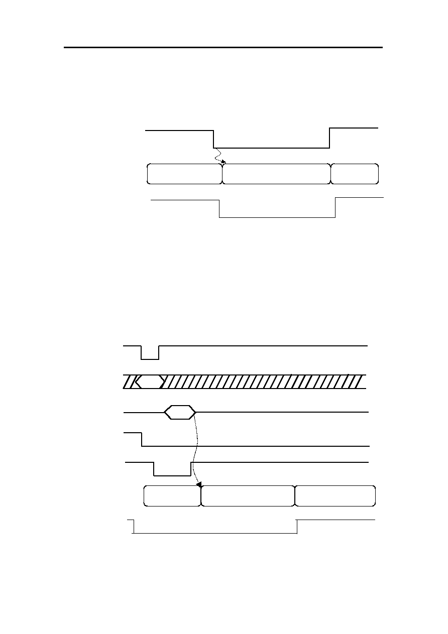
S3CI9E0X01 FLASH INTERFACE DEVICE
SAMSUNG ELECTRONICS
42
operation and executes warm reset operation
1)
, and Eagle resets current NAND Flash operation.
Device will not be reset in case of nRP pulses shorter than 50ns, but device is guaranteed to be
reset in case nRP pulse is longer than 500ns. Warm reset has no effect for contents of
main/spare area buffers
10.3.3 HOT RESET(Eagle Reset Command Input case)
Hot Reset means that host resets Eagle by reset command, and then Eagle stops all
current operation and executes hot reset operation
1)
, and resets current NAND Flash operation.
Hot reset has no effect for contents of main/spare area buffers
nRP
EAGLE Operation
Warm reset operation
Idle
Idle
Initiated by nRP low
INT
EAGLE Operation
Hot reset opreation
1)
Idle
Idle
nAVD
00F3h
nCE
nWE
DQi
Figure 16. Warm Reset Timings
Ai
1420h
INT

S3CI9E0X01 FLASH INTERFACE DEVICE
SAMSUNG ELECTRONICS
43
Note 1) Internal reset operation means that Eagle initializes internal
registers and makes output signals go to default status.
10.3.4 FLASH RESET(FLASH Reset Command Input case)
Host can reset NAND Flash by Flash reset command.
Figure 17. Hot Reset Timings
EAGLE
Operation
Flash reset operation
Idle
Idle
nAVD
nCE
nWE
Flash R/nB
Figure 18. Flash Reset Timings
00F0h
DQi
Ai
1420h
INT

S3CI9E0X01 FLASH INTERFACE DEVICE
SAMSUNG ELECTRONICS
44
10.4. PROGRAM OPERATION ( PROGRAMMING NAND )
Eagle has input/outputs that accept both address and data information. When host
writes data into a NAND flash memory via EAGLE Interface device, firstly, host reads
Controller ID from Controller ID register. Host must drive CLK, nAVD, and nCE to "Low" state
and nOE to "High" state when providing an address to the device, and drive CLK, nWE and
nCE to "Low" state, and nOE to "High" state when writing commands or data. Next, the
program address and data are written, which in turn initiate programming NAND Flash Memory.
Firstly, host writes block address(BA) of NAND to `Block Address Register' and page
address(PA) of NAND to `Page Address Register' also writes NAND program command to
command register in device. Interruption signal is enabled only after NAND flash memory is
programmed according to the NAND Flash program timings. It takes 220us ~ 550us to execute
NAND program procedure. When program operation of NAND is finished, NAND returns status
value and the status is written in status register in device. The host detects the status of the
program operation by monitoring Input/Output pins. In spare area buffer, all sixteen bytes
which are logical sector number area, wrap count, bad block information, ECC code area, and
reserved area are accessible for host. Multi-page program operation is not available, only one-
page program operation is available.

S3CI9E0X01 FLASH INTERFACE DEVICE
SAMSUNG ELECTRONICS
45
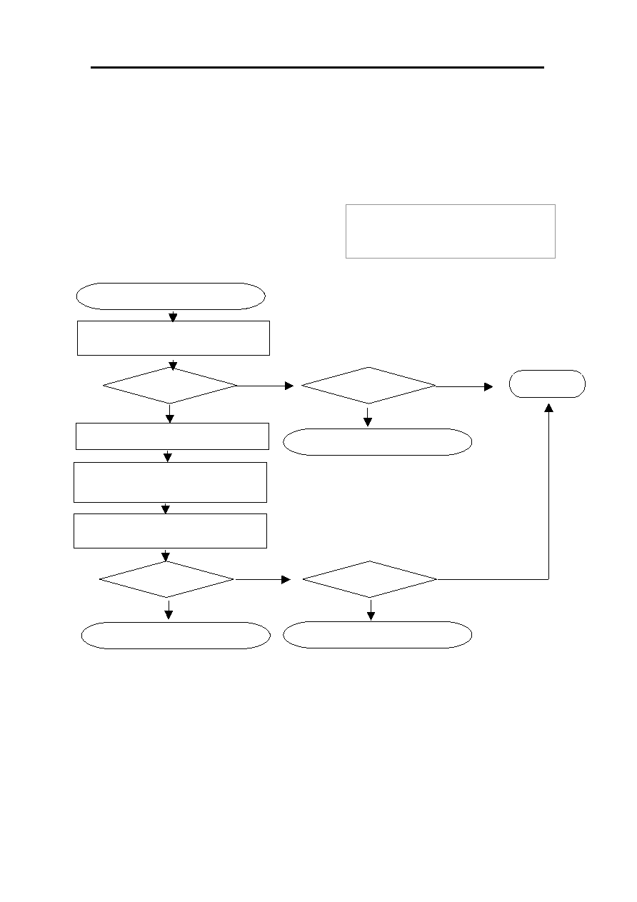
Note 1) refer to Command table
Write Register
Address 1420h
Write Program
command
1)
Wait for INT register
low to high transition
Typ. : 200us
Max. : 550us
Read Controller
Status Register
Write Register
Address 1440h
Program Error
I/O7 = 0 ?
Program
completed
Yes
No
Write Register
Address 1406h
Write Register
Address 1404h
Write Register
Address 1402h
Write `BA'
of Flash
Data Input
Completed?
No
Start
Write `PA' of Flash
Yes
Write `SB'
Write `0' to INT register
of Interrupt register
Write Data
Write Buffer
Column address
S3CI9E0X01 FLASH INTERFACE DEVICE
SAMSUNG ELECTRONICS
46
Figure 19.Flow Chart of Program Operation
Figure 20. Program Operation Timings
Note)
WA : register Address to Write NAND Flash address/command
FA : NAND Flash Address(Block address) to Program
( refer to Address register table)
CMD : Program command ( refer to Command register table)
SRA : Status Register Address ( refer to Status register table)
nCE
nOE
nWE
tDS
tDH
tCH
nAVD
FA
CMD
DQi
Program operation
tWPL
tWPH
Flash
R/nB
SRD
tPROG(typ.) = 220us~500us
FA
1 Word Data Loading
264 Word(=1 page) Data Loading
Command register setting
Status register read
Address register setting
WA
Ai
WA
SRA
WA
INT
tWC

S3CI9E0X01 FLASH INTERFACE DEVICE
SAMSUNG ELECTRONICS
47
10.5. ERASE OPERATION ( ERASING NAND )
Firstly, same ID read operation as programming NAND operation is executed and
then host must drive CLK, nAVD, and nCE to "Low" state and nOE to "High" state when
providing an address to the device, and drive CLK, nWE and nCE to "Low" state, and nOE to
"High" state when writing commands.
Firstly, host writes block address(BA) of NAND to `Block Address Register' and also writes
NAND erase command in command register in device. Interruption signal is enabled only after
NAND flash memory is erased according to the NAND Flash erase timings. It takes 2ms ~ 3ms
to execute NAND erase procedure. When erase operation of NAND is finished, NAND returns
status value and the status is written in status register in device. The host detects the status of
erase operation by monitoring Input/Output pins.
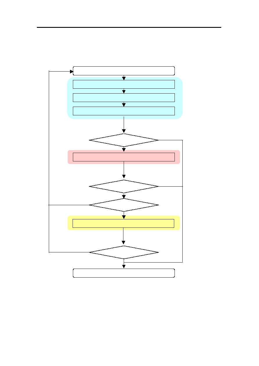
Figure 21. Flow Chart of Erase Operation
Write Register
Address 1420h
Wait for INT register
low to high transition
Typ. : 2ms
Max. : 3ms
Read Controller
Status Register
Write Register
Address 1440h
Erase Error
I/O7 = 0 ?
Erase
completed
Yes
No
Write Register
Address 1402h
Write `BA'
of Flash
Start
Write `0' to INT register
of Interrupt register
Write Erase
Command(0094h)

S3CI9E0X01 FLASH INTERFACE DEVICE
SAMSUNG ELECTRONICS
48
`
Figure 22. Erase Operation Timings
Note)
WA : register Address to Write
NAND Flash
address/command
FA : NAND Flash Address(Block address) to Erase
( refer to Address register table)
CMD : Erase command(94h, refer to Command register table)
SRA : Status Register Address ( refer to Status register table)
nAVD
FA
CMD
nCE
nOE
nWE
tDS
tDH
tCH
Erase operation
tWPL tWPH
Flash
R/nB
SRD
tBERS(typ.) = 2ms~3ms
DQi
WA
WA
SRA
Ai
INT

S3CI9E0X01 FLASH INTERFACE DEVICE
SAMSUNG ELECTRONICS
49
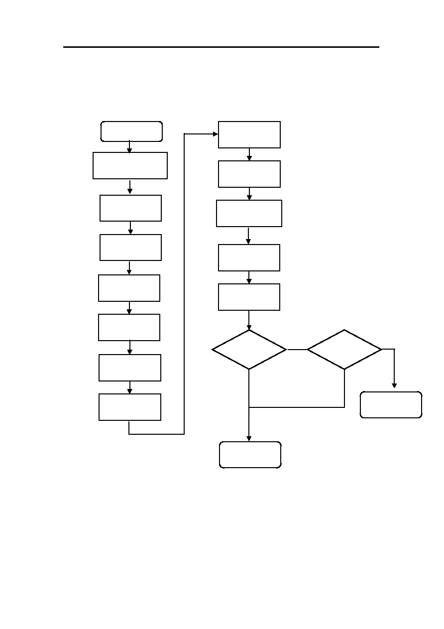
10.6 . READ OPERATION ( READING NAND )
Read operation is just a transferring data from NAND flash memory to interface chip
internal registers. Inputting command sequence procedure is same as the above write or erase
operation in the same condition.
Firstly, host writes block address, page address and page counter value of NAND is assigned in
address register in order and also writes NAND read command in command register in device.
And then initiated NAND flash memory is accessed and transferring data from NAND flash
memory array to the interface chip internal buffers at the assigned address. These data size
increases as multiple of 528 bytes, that is, one page size of NAND flash memory. Interruption
signal is enabled only after NAND flash memory is read according to the NAND Flash read
timings. It takes typically 35 us to execute NAND read procedure while Page Counter is set to
001 which means one page read. If Page Counter is set to above 001 which means multi page
read, read operation from NAND will be executed sequentially as many as assigned in Page
Counter number. When read operation of NAND is finished, NAND returns status value and
the status is written in status register in device. The host detects the status of read operation by
monitoring Input/Output pins. Buffer RAM is dual port ,therefore host can access page in buffer
RAM while state machine is accessing another page in buffer RAM.
S3CI9E0X01 FLASH INTERFACE DEVICE
SAMSUNG ELECTRONICS
50
Figure 23. Flow Chart of Read Operation
Write Register
Address 1420h
Write Read
command
1)
Wait for INT register
low to high transition
Typically `35us' at single page read operation,
and `35us X PC' at multi-read operation.
Read Controller
Status Register
Write Register
Address 1440h
Error exist?
Read
completed
Yes
No
Write Register
Address 1406h
Write Register
Address 1404h
Write Register
Address 1402h
Write `BA'
of Flash
Start
Write `PA' of Flash
& `PC'
Write `SB'
Write `0' to INT register
of Interrupt register
Note 1) refer to Command table
1bit error?
Map Out
Automatically
corrected
Yes
No
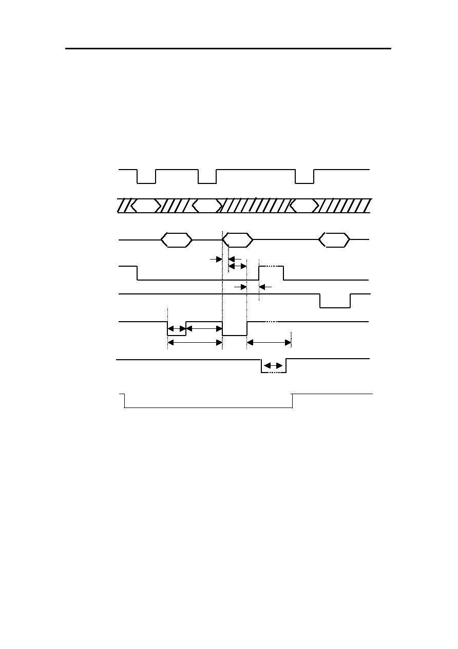
S3CI9E0X01 FLASH INTERFACE DEVICE
SAMSUNG ELECTRONICS
51
Note)
WA : register Address to Write NAND Flash address/command
FA : NAND Flash Address(Block address) to Read
( refer to Address register table)
CMD : Read command( refer to Command register table)
SRA : Status Register Address ( refer to Status register table)
nAVD
nCE
nOE
nWE
tDS
tDH
tCH
Read operation
tWPL tWPH
Flash
R/nB
tR(typ.) = 10us
Figure 24. Read Operation Timings
FA
SRD
DQi
WA
WA
SRA
Ai
CMD
INT

S3CI9E0X01 FLASH INTERFACE DEVICE
SAMSUNG ELECTRONICS
52
10.7. ECC OPERATION
10.7.1 ECC OPERATION CASE
While EAGLE accesses NAND Flash for Program operation, hiddenly generates ECC
code(24bits for Main area data and 10bits for LSN of Spare area data), and while for Read
operation, hiddenly generates ECC code and detects error number and position and corrects
1bit error. Figure 25 shows ECC code assignment of NAND Flash spare area, and this ECC
code is updated by EAGLE automatically. After Read operation, host can know whether there
is error or not by reading `status register'(refer to Controller status register table). Error type
is divided into `no error', `1bit error(correctable)', `above 2bit error(uncorrectable)'.
Since generated ECC code at read/write operation is not updated to internal buffer RAM but is
updated to NAND Flash spare area directly. Host can read generated ECC code only from
NAND Flash spare area.
10.7.2 ECC BYPASS OPERATION CASE
ECC bypass operation is set by 9
th
bit of CMD register. In ECC bypss operation, Eagle
hiddenly generates ECC result which indicates error position(refer to ECC Result table), but
doesn't correct. After Read operation, host can know whether there is error or not by reading
`status register'(refer to Controller status register table). Error type is divided into `no error',
`1bit error(correctable)', `above 2bit error(uncorrectable)'. In 1bit error case, Host can correct
the error by itself after reading ECC Result register.
"
"
"
"
ECC Code / Result readability
Read operation
Program operation
operation
ECC Code
from spare area
buffer
ECC Result
from register
(1446h,1448h)
ECC Code
from spare area
buffer
ECC Result
from register
(1446h,1448h)
ECC operation
Invalid
(Pre-written
ECC code
1)
)
Valid Invalid
(old data
2)
)
-
ECC bypass
Invalid
(Pre-written
ECC code)
Valid Invalid
(old data)
-
Note 1) Pre-written ECC code : ECC code which is previously written to NAND Flash
spare area in program operation.
2) Old data : ECC code is not updated to spare buffer, so ECC code placement of
spare buffer remains old data.
Figure 25. ECC Code/Result readability

S3CI9E0X01 FLASH INTERFACE DEVICE
SAMSUNG ELECTRONICS
53
F E D C B A 9 8 7 6 5 4 3 2 1 0
Reserved 5)
4)
3)
2)
1)
1) Logical Sector Number (LSN)
2) Wrap Counter
:Status flag against sudden power failure during write
3) Bad Block Information
4) ECC code for Main area data(24bits)
5) ECC code for Spare area data(LSB 10bits)
Figure 26. NAND Flash Spare area assignment

S3CI9E0X01 FLASH INTERFACE DEVICE
SAMSUNG ELECTRONICS
54
Figure 27. ECC Operation Guidance
"
"
"
"
ECC operation guidance
1. ECC generation and correction by Eagle
: Program with ECC operation / Read with ECC operation
2. ECC generation by Eagle & correction by Host
: Program with ECC operation / Read without ECC operation
* Host can read ECC result from ECC result register after read operation
in both ECC operation and ECC bypass case.
"
"
"
"
ECC operation example
1) When Eagle read NAND Flash main+spare area data without ECC
--> Eagle place the data read from NAND Flash spare/ECC locations into the buffer
for both main and spare ECC
2) When Eagle read NAND Flash main+spare area data with ECC
--> Eagle doesn't place the data read from NAND Flash spare/ECC locations into the
buffer for both main and spare ECC, but place newly generated main & spare
ECC code of read-data into the buffer for both main and spare ECC.
3) When Eagle read NAND Flash spare area data without ECC
--> Eagle place the data read from NAND Flash spare/ECC locations into the buffer
for both main and spare ECC.
4) When Eagle read NAND Flash spare area data with ECC
--> Eagle doesn't place the data read from NAND Flash spare/ECC locations into
the buffer for both main and spare ECC, but place newly generated spare ECC
code of read-data into the buffer for spare ECC remaining main ECC as
previous data.
S3CI9E0X01 FLASH INTERFACE DEVICE
SAMSUNG ELECTRONICS
55
10.8. WRITE PROTECTION
10.8.1 WRITE PROTECTION for bufferRAM(first 2pages)
Eagle offers software Write Protection feature for first 2pages(main + spare area data) of
bufferRAM, which protects bufferRAM data. This software Write Protection of bufferRAM
feature is used by setting [1:0]bit value of `System configuration register(1422h address)'.
The default state is Locked state; These first 2pages bufferRAM go to locked state after cold
reset or warm reset, and then write is protected.
1
st
page bufferRAM
2
nd
page bufferRAM
3
rd
page bufferRAM
4
th
page bufferRAM
5
th
page bufferRAM
6
th
page bufferRAM
7
th
page bufferRAM
8
th
page bufferRAM
Unlocked
Device in
Cold or Warm
Reset
1)
Locked
System configuration
register[1:0] = 00/01/11
Initial state
System configuration
register[1:0] = 10
Main area
Spare area
Figure28. Write Protection available area in bufferRAM
Figure29. State diagram of bufferRAM Write Protection
Available on
Write Protection
operation
Not available on
Write Protection
operation

S3CI9E0X01 FLASH INTERFACE DEVICE
SAMSUNG ELECTRONICS
56
10.8.2 WRITE PROTECTION for NAND Flash
10.8.2.1 WRITE PROTECTION Modes
Eagle offers both hardware and software Write Protection features for NAND Flash. The
software Write Protection feature is used by executing the Lock block command or Lock-tight
block command, and the hardware Write Protection feature is used by executing cold reset or
warm reset.
10.8.2.2 WRITE PROTECTION Commands
Individual instant secured block protects code and data by allowing any block to be locked or
lock-tighten. This Write Protection scheme offers two levels of protection. The first allows
software-only control of Write Protection(useful for frequently changed data blocks), while the
second requires hardware interaction before locking can be changed(protects infrequently
changed code blocks).
The followings summarizes the locking functionality.
- All blocks power-up in a locked state. Unlock commands can unlock these blocks.
- The Lock-tight command locks blocks and prevents it from being unlocked.
And Lock-tight state can be returned to lock state only when Cold/Warm reset is
executed.
- Writing to Unlock start/end address register during Locked(or Lock-tighten) status
doesn't affect the unlock address , since Eagle has another Unlock address
register internally to prevent this kind of problem.
10.8.2.3 WRITE PROTECTION Status
Eagle's current Write Protection status can be read in NAND Flash Write Protection status
register(1450h). There are three bits - US,LS,LTS - ,which are not cleared by hot reset. These
Write Protection status registers are updated not as Write Protection command is entered but
as other commands are entered.
example1) In default , [2:0] values are 010 -> If host executes unlock block
operation, then [2:0] values are still 010 -> If host executes any
commands except Write Protection commands, then [2:0] values
turn to 110 -> If host executes lock-tight block operation, then [2:0]
values are still 110 -> If host executes any commands except Write
Protection commands, then [2:0] values turn to
101
example2) If host executes lock block operation, then [2:0] values are still
previous status -> If host executes any commands except Write

S3CI9E0X01 FLASH INTERFACE DEVICE
SAMSUNG ELECTRONICS
57
Protection commands, then [2:0] values turn to 010 -> If host
executes lock-tight block operation, then [2:0] values are still 010 ->
If host executes any commands except Write Protection commands,
then [2:0] values turn to 001 -> If cold or warm reset is entered,
then [2:0] values are 010
Figure30. State diagram of NAND Flash Write Protection
Unlock
Lock-
tight
nRP pin : High
&
Start block address+ End block address
+ Unlock block Command
nRP pin : High
&
Lock block Command
nRP pin : High
&
Lock-tight block Command
nRP pin : Rising edge
( This occurs at Cold reset or Warm reset )
Lock
Cold or
Warm
reset
Initial state
nRP pin : High
&
Lock-tight block Command
nRP pin : High
&
Start block address+ End block address
+ Unlock block Command

S3CI9E0X01 FLASH INTERFACE DEVICE
SAMSUNG ELECTRONICS
58
> Command Sequence : Lock block Command(02h)
> All blocks default to locked after initial Cold reset or Warm reset
> Partial block lock is not available ; Lock block operation is
based on all block unit
> Unlocked blocks can be locked by using the Lock block
command and, a lock block's status can be changed to
unlock or lock-tight using the appropriate software commands
> Command Sequence
: Start block address + End block address + Unlock block
Command(04h)
> Unlocked blocks can be programmed or erased
> An unlocked block's status can be changed to the locked or
lock-tighten state using the appropriate software commands
> Only one sequential area can be released to unlock state from
lock state ; Unlocking multi area is not available
> Command Sequence : Lock-tight block Command(01h)
> Lock-tighten blocks offer the user an additional level of write
protection beyond that of a regular lock block. A block that
is lock-tighten cannot have it's state changed by software,
only by nRP's rising edge ; nRP goes Low to High during
Cold/Warm reset. ; Unlocking multi area is not available
> Only locked blocks can be lock-tighten by lock-tight command.
Lock-tighten blocks revert to the locked state at Cold/Warm
reset.
Locked
Start block
address
Lock-tighten
Locked block(s)
Unlocked block(s)
Lock-tighten block(s)
End block
address
Unlocked
S3CI9E0X01 FLASH INTERFACE DEVICE
SAMSUNG ELECTRONICS
59
Note: 1) Refer to `Status register(1440h)'
Figure32. Flowchart of NAND Flash Write Protection
Figure31. Operations of NAND Flash Write Protection
U
U
n
n
l
l
o
o
c
c
k
k
b
b
l
l
o
o
c
c
k
k
s
s
t
t
a
a
t
t
e
e
L
L
o
o
c
c
k
k
b
b
l
l
o
o
c
c
k
k
s
s
t
t
a
a
t
t
e
e
L
L
o
o
c
c
k
k
-
-
t
t
i
i
g
g
h
h
t
t
b
b
l
l
o
o
c
c
k
k
s
s
t
t
a
a
t
t
e
e
Write `Start block address' to address
Write `End block address' to address register
Write `Unlock block command(04h)'
State Change?
Write `Lock-tight block command(01h)'
Write `Lock block command(02h)'
Start
(After Warm or Cold reset)
End
Yes
No
State Change?
Yes
No
State Change?
Yes
No
Change to lock-tighten state?
Yes
No
S3CI9E0X01 FLASH INTERFACE DEVICE
SAMSUNG ELECTRONICS
60
10.8.2.4 WRITE PROTECTION Truth Table
L
LT or LT & UL
1)
L or L & UL
L
Current Status
Current Status
L (all blocks)
UL
L & UL
Current Status
L & UL
LT
LT (all blocks)
Current Status
LT & UL
L & UL
L & UL
Current Status
L & UL
L & LT
LT (all blocks)
Current Status
LT (all blocks)
LT & UL
2)
LT & UL
Current Status
LT & UL
1)
L & UL & LT
UL & LT
Current Status
LT & UL
Note: 1) for example, `LT or LT&UL' status means ` LT(all blocks) status' or `LT(some area) and
UL(the other area).
2) for example, it means that LT and UL commands are consecutively entered regardless of order.
Next status command
L : Locked status, UL : Unlocked status, LT : Lock-tighten status
Current status
Next CMD
(e.g Unlock)
Any Command
except Write
Protection command
NAND Flash Write Protection
Command Register
(
144Ah register)
Current Status
(e.g Lock)
NAND Flash Write Protection
Status Register
(
1450h register)
Next Status
(e.g Unlock)
1450h register(=Eagle's status) is updated
by the next command except write
protection command .
"
"
"
"
Write Protection guidance
1450h register(=Eagle's status) is not
updated at this moment .

S3CI9E0X01 FLASH INTERFACE DEVICE
SAMSUNG ELECTRONICS
61
11. Technical Note
11.1. Ring Oscillator
This device has internal Ring Oscillator for being used as internal clock and for generation
of NAND Flash control signal.
11.2. Voltage Level Detector (POR = Power On Reset)
This device has internal Voltage level detector for initiating cold reset automatically.
0V
1.8V
CMD
INT
Oscillator is active
Bootload operation starts
200us later than POR
level detection.
Bootload operation
S3CI9E0X01 FLASH INTERFACE DEVICE
SAMSUNG ELECTRONICS
62
11.3. NAND Flash type detection algorithm
This algorithm is for detecting NAND Flash type. CE2Ena is the bit 11 of system
configuration register , which specifies NAND Flash type whether 512Mb single
or 512Mb DDP.
Host reads NAND Flash ID
Start
CE2Ena = 0 (default) : 512Mb single
CE2Ena = 1 : 512Mb DDP
Is the device code
256Mb ?
Host sets `CE2Ena' to 1
Host sets the bit 11 of `Block
address register' to 1
1)
Host reads NAND Flash ID
Is it all FFh ?
Yes
Yes
No
Is the device code
512Mb ?
Yes
No
Fail
No
Is the device code
256Mb ?
Yes
No
Note :
1)
The bit 11 data of `Block address register' determines whether to access fnCE2 or not,
for it is a divide factor of 256Mb/512Mb.
Host
needs not to set `CE2Ena' again
.
Host
needs not to set `CE2Ena' again
.
NAND Flash is 256Mb single
NAND Flash is 512Mb single
NAND Flash is 512Mb DDP
(but, this is not considered device)
S3CI9E0X01 FLASH INTERFACE DEVICE
SAMSUNG ELECTRONICS
63
11.4. Internal Register reset case
Internal Register
Default
Value
Cold
Reset
Warm
Reset
Hot
Reset
NAND
Reset
1400h Controller Information
1002h
X
X
X
X
1402h Block Address
0000h
O
O
O
X
1404h Page Address & Page Count
0000h
O
O
O
X
1406h Start Buffer
0000h
O
O
O
X
1420h Command
0000h
O
O
O
X
1422h System Configuration
7051h
O
!
1)
!
2)
X
1440h Controller Status
0000h
O
O
O
X
1422h Interrupt
8000h
!
3)
O O X
1446h ECC result of Main
0000h
O
O
O
X
1448h ECC result of Spare
0000h
O
O
O
X
144Ah NAND Write Protection Command
0002h
O
O
X
X
144Ch Unlock Start Block Address
0000h
O
O
X
X
144Eh Unlock End Block Address
0000h
O
O
X
X
1450h NAND Write Protection Status
0002h
O
O
X
X
O : go to default value, X : not change
Note : 1) CE2Ena bit of System configuration register are not initialized at Warm reset.
2) CE2Ena and BSS bits of System configuration register are not initialized at Hot reset.
3) Interrupt register goes to 8080h at Cold reset.
S3CI9E0X01 FLASH INTERFACE DEVICE
SAMSUNG ELECTRONICS
64
11.5. Pin Connection guidance between Host and Eagle
#
#
#
#
nAVD connected case
#
#
#
#
nAVD disconnected case
nCE
ADD<0>
nAVD
nCE
nAVD
ADD<1>
ADD<2>
ADD<12
ADD<0>
ADD<1>
ADD<2>
ADD<11
ADD<3>
GND or VDD
Host
Eagle
nCE
ADD<0>
nAVD
nCE
ADD<1>
ADD<2>
ADD<12
ADD<0>
ADD<1>
ADD<2>
ADD<11
ADD<3>
GND or VDD
Host
Eagle
> If host uses byte-order typed
address, ADD<0> can be used as
byte/word selection pin.
> If host uses byte-order typed
address, ADD<0> can be used as
byte/word selection pin.
>In nAVD disconnected case,
nAVD can be tied to nCE or GND.
GND
S3CI9E0X01 FLASH INTERFACE DEVICE
SAMSUNG ELECTRONICS
65
11.6. Asynchronous Page Read guidance
Address
CLK
nAVD
nCE
Address
nOE
Invalid data
N
data
N+1
data
N+1
N+2
N+3
N + 4
N+2
data
N+3
data
DQ
tAPA
tCE
tOE
N+4
data
Invalid
address
tAES : tAES should not be over
Address
Example 1
(O.K)
N
X .... X X X 0 0
bit
N+1
X .... X X X 0 1
bit
N+2
X .... X X X 1 0
bit
N+3
X .... X X X 1 1
bit
Example 2
(O.K)
X .... X X X 1 0
bit
X .... X X X 1 1
bit
X .... X X X 0 0
bit
X .... X X X 1 0
bit
Example3
(Not O.K)
X .... X X X 1 1
bit
X .... X X X 1 1
bit
X .... X X X 0 1
bit
X .... X X X 1 0
bit
N+4
X .... X X X 0 1
bit
X .... X X X 1 0
bit
X .... X X X 1 0
bit
There is no problem for there is a
change of one of ADD<0:1>
N+1 address is ignored for there
is no change of ADD<0:1>.
> Eagle's internal address detector latches ADD<0:11> whenever one of
ADD<0:1> changes.
> There is no problem while host sequentially reads data with changing one of
ADD<0:1> and fixing nCE & nOE to Low.
S3CI9E0X01 FLASH INTERFACE DEVICE
SAMSUNG ELECTRONICS
66
12. Electrical Specifications
12-1. Absolute Maximum Ratings
Parameter
Symbol
Rating
Unit
Vcc V
CC
3.6
Voltage on any pin
relative to Vss
All other pins
V
IN
3.6
V
Latch-up current
I
latch
±
200
mA
Storage temperature
T
STG
-65 to 150
O
C
Note: Permanent device damage may occur if ABSOLUTE MAXIMUM RATINGS are exceeded.
Exposure to absolute maximum rating conditions for extended periods may affect
reliability.
12-2. Recommended Operating Ratings
12-2-1. Supply Voltage(Voltage reference to GND)
1.8V Part
2.5V Part
Parameter
Symbol
Min
Typ.
Max
Min
Typ.
Max
Unit
V
CC
1.65 1.8 1.95 2.3 2.5 2.7
Supply
Voltage
V
SS
0 0 0 0 0 0
V
12-2-2. Temperature
Parameter
Symbol
Rating
Unit
Commercial temperature
T
A
(Commercial temp.)
0 to 70
Industrial temperature
T
A
(Industrial temp.)
-25 to 85
O
C

S3CI9E0X01 FLASH INTERFACE DEVICE
SAMSUNG ELECTRONICS
67
12-3. DC Characteristics
1.8V Part
2.5V Part
Parameter
Symbol
Test Condition
Min
Typ
Max
Min
Typ
Max
Unit
Input leakage
current
I
LI
V
IN
= V
SS
to V
CC
V
CC
= V
CC(max)
-7 - 7 -10 - 10
Output leakage
current
I
LO
V
OUT
= V
SS
to V
CC
V
CC
= V
CC(max)
-7 - 7 -10 - 10
Standby current
I
CCS
V
CC
= V
CC(max)
nCE = nRP = V
IH
INT = floating
- 25 40 30 60
uA
Active Async.
Read Current
I
CCR1
V
IN
= V
IH
or V
IL
nCE = V
IL
nOE = V
IH
- 15 20 20 30
Active Sync.
Read Current
I
CCR2
nCE = V
IL
nOE = V
IH
Continuous Burst
CLK = 45Mhz
- 15 20 20 30
Active Program
Current
I
CCW
Program in
Progress
- 15 20 20 30
Active Erase
Current
I
CCE
Erase in Progress
-
15
20
20
30
mA
Input High
voltage
V
IH
-
Vcc-
0.4
-
Vcc+
0.4
1.7 - -
Input Low voltage
V
IL
-
-0.5 - 0.4 - - 0.7
High level output
voltage
V
OH
I
OH
= -100uA
Vcc=Vcc(min)
Vcc-
0.2
- - 1.9 - -
Low level output
voltage
V
OL
I
OL
= 100uA
Vcc=Vcc(min)
- - 0.2 - - 0.5
V
Input capacitance
1)
C
IN
Any input and
Bi -directional buffers
- - 10 - - 10
Output
capacitance
1)
C
OUT
Any output buffers
-
-
10
-
-
10
pF
Note : 1. This value excludes package parasitic

S3CI9E0X01 FLASH INTERFACE DEVICE
SAMSUNG ELECTRONICS
68
12-4. AC Test Condition
Parameter
Value
Input Pulse Levels
0V to Vcc
Input Rise and Fall Times
5ns
Input and Output Timing Levels
Vcc / 2
Output Load
C
L
= 30pF
0V
Vcc
Vcc / 2
Vcc / 2
Input & Output
Test Pint
Input Pulse and Test Point
Device
Under
Test
CL = 30pF
Output Load

S3CI9E0X01 FLASH INTERFACE DEVICE
SAMSUNG ELECTRONICS
69
12-5. AC Characteristics
!
Asynchronous Read AC Parameters
Parameter
Description
Min
Typ
Max
Unit
tCE
Access time from nCE Low
-
-
55
ns
tOE
Output Enable to Output Valid
-
-
23
ns
tACC
Asynchronous Access Time
-
-
55
ns
tAE
Random Access nAVD-Data Valid
-
-
55
ns
tOH
Output hold from nCE or nOE
change, whichever occurs first
0 - -
ns
tAPA
Page address access time
-
- 40
ns
tASA
Address setup to nAVD high
7
- -
ns
tAES
nCE & nAVD setup to Valid Address
-
- 10
ns
tCA
nCE setup to nAVD falling edge
0
-
-
ns
!
Synchronous Read AC Parameters
Parameter
Description
Min
Typ
Max
Unit
tCES
nCE setup time to CLK
5
-
-
ns
tIACC
Initial Access Time @ 40Mhz
-
-
94
ns
tBACC
Burst Access Time
Valid clock to output delay
- - 19
ns
tBDH
Data hold time from next clock cycle
4
-
-
ns
tAVDS
nAVD setup time to CLK
5
-
-
ns
tAVDH
nAVD hold time to CLK
7
-
-
ns
tACS
Address setup time to CLK
5
-
-
ns
tACH
Address hold time to CLK
7
- -
ns
tOH
Output hold from nCE or nOE
change, whichever occurs first
0 - -
ns
tOE
Output Enable to Output Valid
-
-
23
ns
tOES
nOE setup to CLK
2 x tCLK
1)
-
-
ns
tCLKH
FlsCLK high time
10
-
-
ns
tCLKL
FlsCLK low time
10
-
-
ns
tCA
nCE setup to nAVD falling edge
0
-
-
ns

S3CI9E0X01 FLASH INTERFACE DEVICE
SAMSUNG ELECTRONICS
70
Note : 1) tCLK = tCLKH + tCLKL
!
Write AC Parameters
Parameter
Description
Min
Typ
Max
Unit
tAVDP
nAVD Low time
12
-
-
ns
tAAVDS
Asynchronous Address setup time
7
-
-
ns
tAAVDH
Asynchronous Address hold time
7
-
-
ns
tDS
Data Setup Time
5
-
-
ns
tDH
Data Hold Time
4
-
-
ns
tWC
Write Cycle Time
30
-
-
ns
tWPL
Write Pulse Width Low
10
-
-
ns
tWPH
Write Pulse Width High
20
-
-
ns
tCS
nCE setup time
0
-
-
ns
tCH
nCE Hold Time
4
-
-
ns
tAWES
Address setup to nWE Low
5
-
-
ns
tVLWH
nAVD rising edge to nWE rising edge
10
-
-
ns

S3CI9E0X01 FLASH INTERFACE DEVICE
SAMSUNG ELECTRONICS
71
13. Package Dimension
#A1
D
E
A
A2
#A1 Index Mark
(Optional)
f1
f2
e
b
S3CI9E0X01 FLASH INTERFACE DEVICE
SAMSUNG ELECTRONICS
72
Description
Symbol
Unit : mm
Min.
Nom.
Max.
Package Height
A
Ball Height
A2
Ball Diameter
b
Package Body Width
D
Package Body Length
E
Ball Pitch
e
Ball Center to Edge
f1/f2
1.0
1.1
1.2
0.15
0.2
0.25
0.25
0.3
0.35
5.9
6
6.1
5.9
6
6.1
-
0.5
-
-
0.75/0.75
-
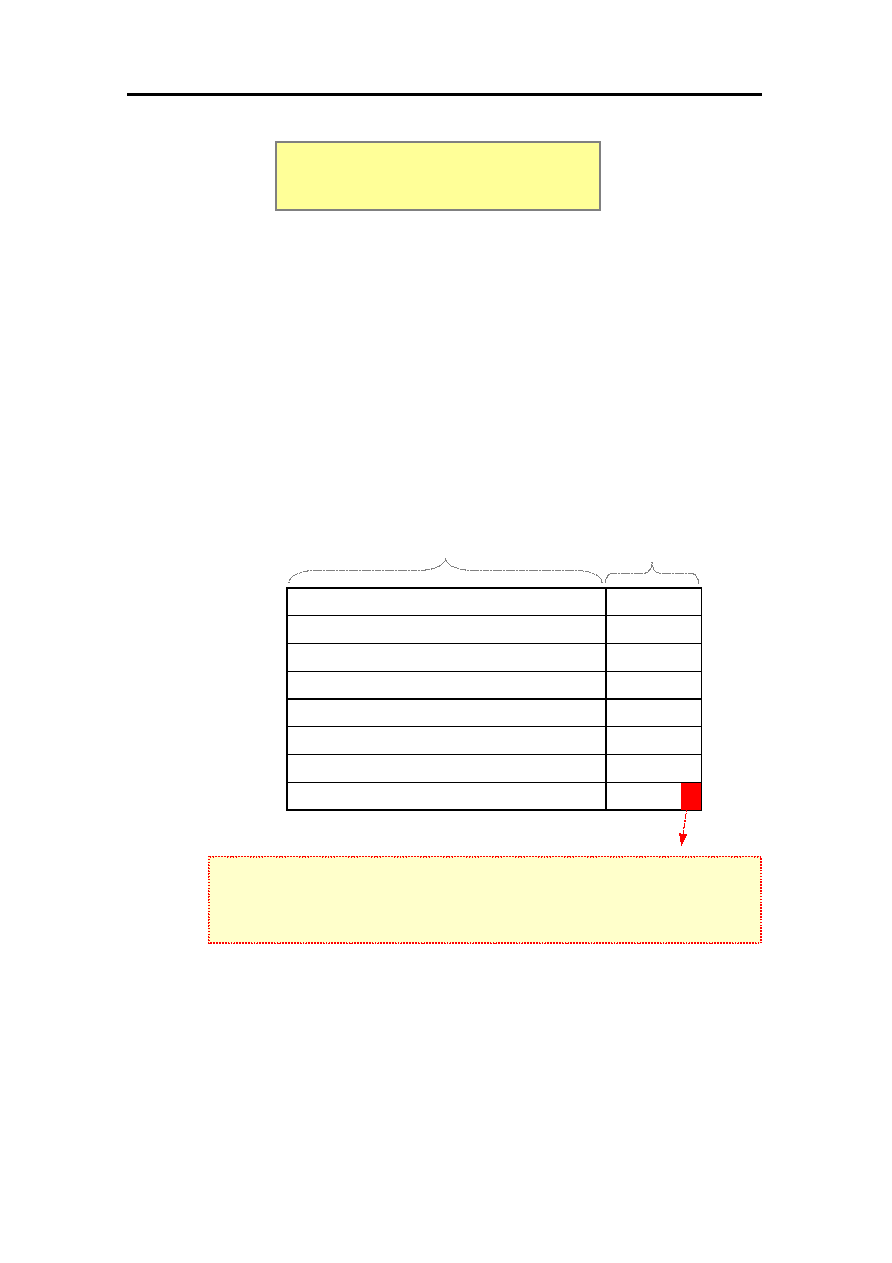
S3CI9E0X01 FLASH INTERFACE DEVICE
SAMSUNG ELECTRONICS
73
1. Synchronous Read Fail in last word of bufferRAM
DESCRIPTION)
Reading last page(8
th
) last word(264
th
) of bufferRAM with synchronous read timing is
not allowed in specification. (refer to figure1)
SHORT-TERM WORKAROUND)
Since current `NAND Flash media driver' never accesses this word, this error will not
affect host's operation anymore.
Main area
Spare area
1
st
page bufferRAM
2
nd
page bufferRAM
3
rd
page bufferRAM
4
th
page bufferRAM
5
th
page bufferRAM
6
th
page bufferRAM
7
th
page bufferRAM
8
th
page bufferRAM
Reading this word with synchronous read timing is not allowed.
Since current `NAND Flash media driver' never accesses this word, this error
will not affect host's operation anymore.
< Synchronous Read fail in BufferRAM >
ERRATA

S3CI9E0X01 FLASH INTERFACE DEVICE
SAMSUNG ELECTRONICS
74
2. ECC fail
2-1. ECC fail at reading data of all erased page
DESCRIPTION)
When data of erased page is read, the ECC result is always reported as ECC
fail.
SHORT-TERM WORKAROUND)
Addition of detection algorithm of erased page in software is required.
The algorithm is to check whether LSN & ECCs(ECC code of LSN) are all
FFh or not. If LSN & ECCs are all FFh, it means that the page is erased
one, then S/W can ignore this ECC fail.
Is ECC Result fail ?
Are LSN & ECCs all
FFh ?
No
Yes
Previous Step
Continue next step
No
It is real ECC fail, continue
next step.
Yes
Ignore this ECC
fail , the page is
erased one.
Additional detection algorithm
< Additional detection algorithm for software walk-around >
LSN
Main area data
WC BI
Reserved
ECCm ECCs
< The Page Assignment of NAND Flash >
Spare area data
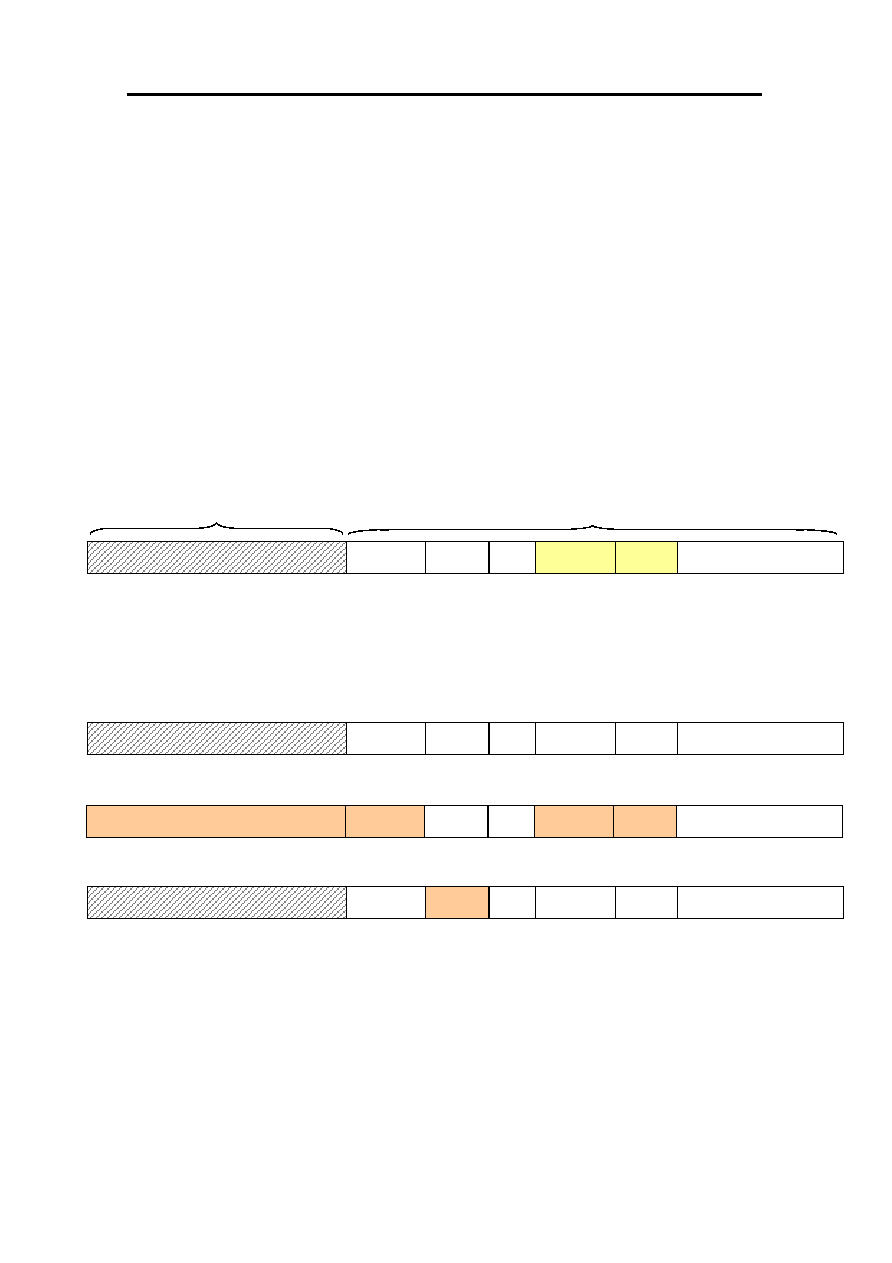
S3CI9E0X01 FLASH INTERFACE DEVICE
SAMSUNG ELECTRONICS
75
2-2. ECC fail at programming spare area data alone
DESCRIPTION)
While only spare area is programmed, ECCm(ECC code of main area) is
reset to 00h.
SHORT-TERM WORKAROUND)]
Avoid partially programming LSN data. The suggested procedure of spare area
program is
; Program Main area data + LSN data at a time, and then program WC
without ECC.
LSN
Main area data
WC BI
Reserved
ECCm ECCs
< The Page Assignment of NAND Flash >
Spare area data
< Suggested program guideline for walk-around >
BI
LSN
BI
Erased(Reserved)
ECCm ECCs
Erased
Main area data
Erased Page
LSN BI
ECCm ECCs
Main area data
Step 1 : Program `Main area data + LSN ` with ECC
Erased Erased
Erased Erased
Erased
Erased(Reserved)
Erased
Step 2 : Program `WC ` without ECC

S3CI9E0X01 FLASH INTERFACE DEVICE
SAMSUNG ELECTRONICS
76
3. Sequential Reset fail
DESCRIPTION)
Sequential reset inputs are prohibited no matter what combination is
between Warm Reset/ Hot Reset/NAND Flash Reset is. Cold reset isn't
concerned with this fail.
For example, 1) Warm Reset ≠ Hot Reset
2) Warm Reset ≠ Warm Reset
3) Hot Reset ≠ Warm Reset
4) Hot Reset ≠ Hot Reset
5) Hot Reset ≠ NAND Flash Reset
6) Etc.
SHORT-TERM WORKAROUND)
If you can't avoid sequential resets case in application, the suggested
walk-around is like the following.
Reset
Reset
NAND
Another operation
between Resets can
break through this
failure.