 | –≠–ª–µ–∫—Ç—Ä–æ–Ω–Ω—ã–π –∫–æ–º–ø–æ–Ω–µ–Ω—Ç: S3F380D | –°–∫–∞—á–∞—Ç—å:  PDF PDF  ZIP ZIP |

S3C380D/F380D
PRODUCT OVERVIEW
1-1
1
PRODUCT OVERVIEW
OVERVIEW
Samsung S3C380D 16/32-bit RISC microcontroller is a cost-effective and high-performance microcontroller
solution for TV applications.
Among the outstanding features of the S3C380D is its CPU core, a 16/32-bit RISC processor (ARM7TDMI)
designed by Advanced RISC Machines, Ltd. The ARM7TDMI core is a low-power, general-purpose
microprocessor macro-cell that was developed for use in application-specific and customer-specific integrated
circuits. Its simple, elegant, and fully static design is particularly suitable for cost-sensitive and power-sensitive
applications.
The S3C380D was developed using the ARM7TDMI core, CMOS standard cell, and a data path compiler. Most
of the on-chip function blocks were designed using an HDL synthesizer. The S3C380D has been fully verified in
the Samsung ASIC test environment.
By providing a complete set of common system peripherals, the S3C380D minimizes overall system costs and
eliminates the need to configure additional components.
The integrated on-chip functions that are described in this document include:
∑
4-Kbyte RAM (3008-byte (1504
◊
16 bits) general register and 1088-byte (544
◊
16 bits) OSD/CCD RAM)
∑
128-Kbyte internal program memory
∑
Two 14-bit PWM modules
∑
Three 16-bit timers
∑
On screen display module
∑
Crystal/Ceramic oscillator or external clock can be used as the clock source
∑
Standby mode support: SLEEP mode
∑
One 8-bit basic timer and 3-bit watchdog timer
∑
Interrupt controller (16 interrupt sources and 2 vectors)
∑
Five 4-bit ADCs
∑
Four programmable I/O ports
∑
42-pin SDIP

PRODUCT OVERVIEW
S3C380D/F380D
1-2
FEATURES
CPU
∑
ARM7T CPU core
Memory
∑
4-Kbyte RAM (3008-byte general purpose register
area + 1088-byte OSD/CCD RAM)
∑
128 Kbyte internal program memory
General I/O
∑
Four I/O ports (25 pins total)
(6 V O/D: 3 pins, 5 V O/D: 4 pins)
Basic timer and watchdog timer
∑
8-bit counter + 3-bit counter
∑
Overflow signal of 8-bit counter makes a basic
timer interrupt and control the oscillation warm-up
time
∑
Overflow signal of 3-bit counter makes a system
reset
Timer/Counters
∑
Three general purpose 16-bit timer/counters with
interval timer modes
Interrupts
∑
16 interrupt sources and 2 vectors
∑
Fast interrupt processing
∑
2 interrupt shadow registers (32 bit
◊
2)
Pulse width modulation (PWM) module
∑
14-bit PWM with 2-channel PWM counter
A/D converter
∑
5-channel: 4-bit conversion resolution (flash ADC)
Remocon receiver
∑
FIFO 8 steps
∑
FIFO interrupt is full (8) step overflow
On screen display (OSD) mode
∑
Analog level OSD
∑
Halftone
∑
64 character colors
∑
16 different character sizes
∑
Graphic OSD
∑
S/W CCD
Oscillator frequency
∑
32,768 Hz external crystal oscillator
∑
1 Hz generation for real time clock
∑
PLL (Phase Lock Loop) controlled oscillators
∑
Maximum 16 MHz CPU clock
Operating temperature Range
∑
- 20
∞
C to + 85
∞
C
Operating Voltage Range
∑
4.5 V to 5.5 V
Package Type
∑
42-pin SDIP

S3C380D/F380D
PRODUCT OVERVIEW
1-3
BLOCK DIAGRAM
INT0-INT3
P0.0-P0.7
P1.0-P1.7
P2.0-P2.7
ARM7TDMI
16-Bit RISC CPU Core
RAM
3008
Byte
ROM
128 Kbyte
Watchdog
Timer
16-Bit
Timer/Counter 2
Ext. Interrupt
IRIN
Remocon
Receive
16-Bit
Timer/Counter 1
16-Bit
Timer/Counter 0
OSD & CCD
System
Control & PLL
V
DD
, V
SS
X
IN
X
OUT
RESET
LPF
Port0
Port1
Port2
P3.0
Port3
PWM0
PWM1
14-Bit
PWM
ADC0-ADC4
4-Bit
ADC
OSD/CCD
RAM
1088 byte
Figure 1-1. S3C380D Block Diagram
PRODUCT OVERVIEW
S3C380D/F380D
1-4
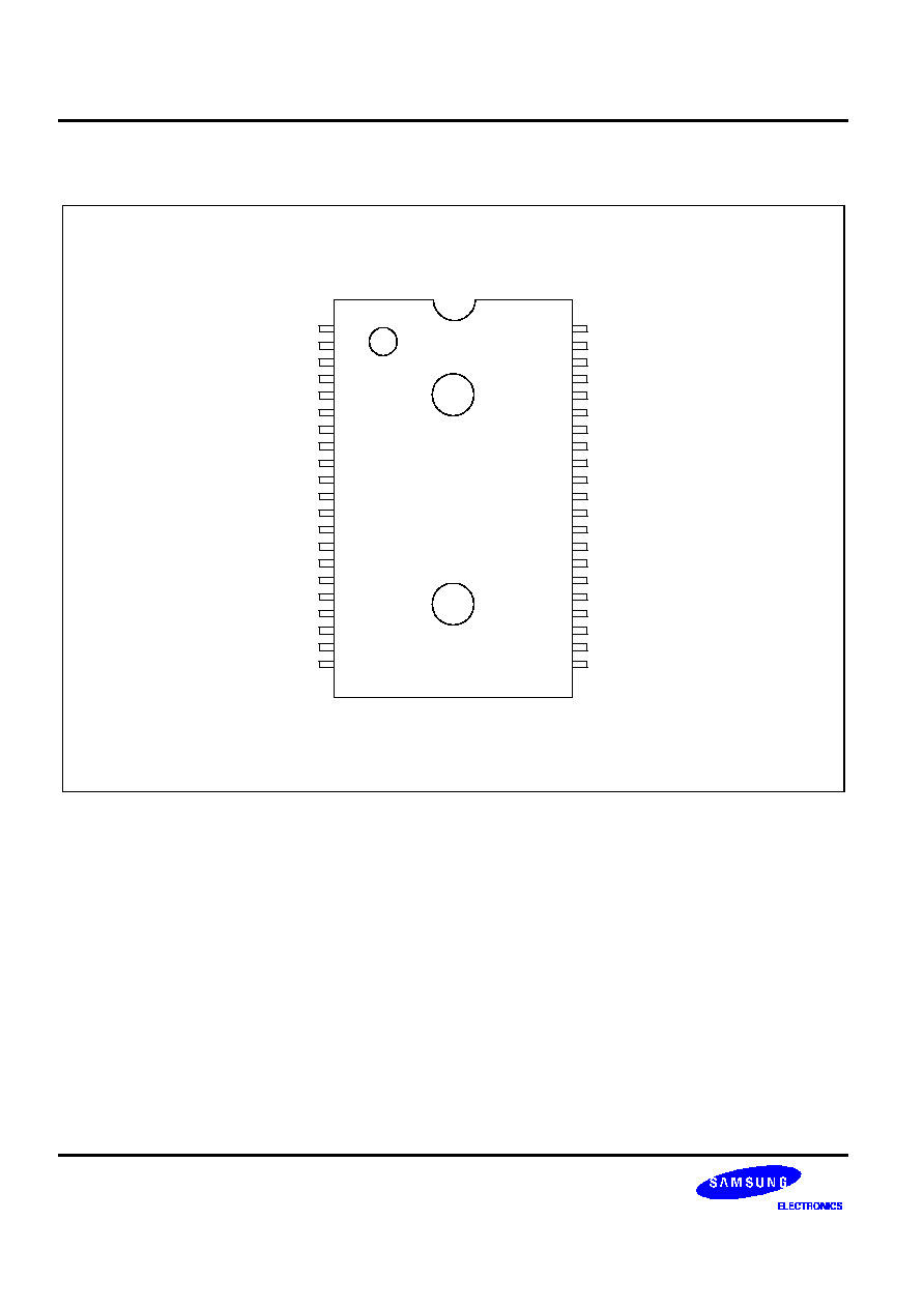
PIN ASSIGNMENTS
P0.0/PWM0
P0.1/PWM1
P0.2
P1.0
P1.1
P1.2
P1.3
P1.4/ADC1
P1.5/ADC2
P1.6/ADC3
P1.7/ADC4
V
DD1
V
SS1
P2.0/INT0
P2.1/INT1
P2.2/INT2
P2.3/INT3
P2.4
P2.5
P2.6
P2.7/OSDHT
S3C380D
(42-SDIP-600)
1
2
3
4
5
6
7
8
9
10
11
12
13
14
15
16
17
18
19
20
21
P0.3
P0.4
P0.5
P0.6
P0.7
V
SS2
V
PP
P3.0
V
DD2
V
SS
X
OUT
V
SS
V
SS3
LPF
CVI IN (ADC0)
V-Sync
H-Sync
Vblank
Vred
Vgreen
Vblue
42
41
40
39
38
37
36
35
34
33
32
31
30
29
28
27
26
25
24
23
22
Figure 1-2. S3C380D Pin Assignments (42-SDIP)

S3C380D/F380D
PRODUCT OVERVIEW
1-5
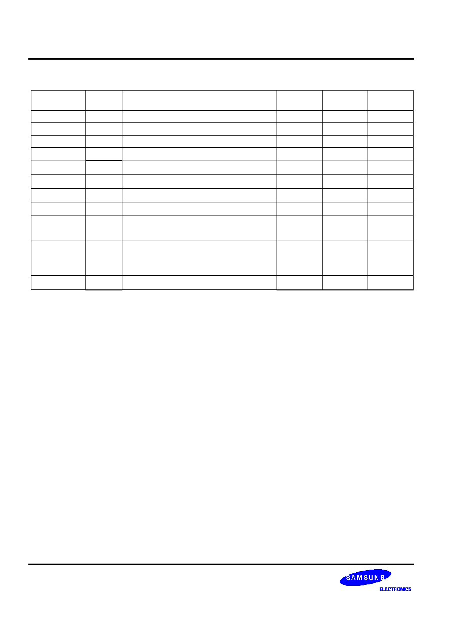
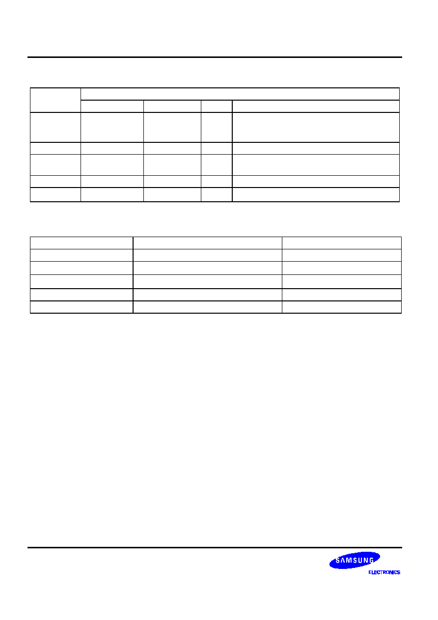
PIN DESCRIPTIONS
Table 1-1. S3C380D Pin Descriptions
Pin Name
Pin
Type
Pin Description
Circuit
Type
Pin
Numbers
Share
Pins
P0.0
I/O
Input mode or push-pull output mode is
software configurable.
P0.0: PWM0 (14-bit PWM Output)
6
1
PWM0
P0.1-P0.2
P0.3
General I/O Port (3-bit), Input or n-channel
open-drain output is software configurable.
Pins can withstand up to 6-volt loads. An
alternative function is supported.
P0.1: PWM1 (14-Bit PWM Output)
3
2-3
42
PWM1
P0.4-P0.7
General I/O Port (4-bit), Input or Output
mode (push-pull or n-channel open drain) is
software configurable.
7
38-41
P1.0-P1.3
I/O
Input/output mode or push-pull output mode
is software configurable.
6
4-7
P1.4-P1.7
General I/O Port (4-bit), configurable for
digital input or n-channel open drain output.
P1.4-P1.7 can withstand up to 5-volt loads.
Multiplexed for alternative use as external
inputs ADC1-ADC4.
4
8-11
ADC1-
ADC4
P2.0-P2.3
I/O
General I/O Port (4-bit), input or push-pull
output mode is software configurable.
Multiplexed for alternative use as external
interrupt inputs INT0-INT3.
2
14-17
INT0-INT3
P2.4-P2.7
I/O
Input mode or push-pull output mode is
software configurable. An alternative
function is supported. P2.7: OSDHT
(Halftone signal output)
6
18-21
OSDHT
P3.0
I/O
Input mode or push-pull output mode is
software configurable.
6
35
PWM0
O
Output pin for 14-bit PWM0 circuit
6
1
P0.0
PWM1
O
Output pin for 14-bit PWM1 circuit
3
2
P0.1
ADC1-4
I
Input for 4-bit resolution flash A/D
Converter
4
8-11
P1.4-7
INT0-INT3
I
External interrupt input pins
2
14-17
P2.0-3
OSDHT
O
Halftone control signal output for OSD
6
21
P2.7
IRIN
I
Remocon signal input
Normal mode: Remocon signal input
OTP Write mode: V
PP
=12.5 V
1
36
≠
CVI IN
I
Video signal input
8
28
ADC0
PRODUCT OVERVIEW
S3C380D/F380D
1-6
Table 1-1. S3C380D Pin Descriptions (Continued)
Pin Name
Pin
Type
Pin Description
Circuit
Type
Pin
Numbers
Share
Pins
RESET
I
System reset input pin
9
33
≠
LPF
≠
PLL filter pin
≠
29
≠
H-SYNC
I
H-sync input for OSD and CCD
1
26
≠
V-SYNC
I
V-sync input for OSD and CCD
1
27
≠
V
blank
O
Video blank signal output for OSD and CCD
5
25
≠
V
red
O
Red signal output for OSD and CCD
5
24
≠
V
green
O
Green signal output for OSD and CCD
5
23
≠
V
blue
O
Blue signal output for OSD and CCD
5
22
≠
ADC0
I
Input for 4-bit resolution flash
A/D Converter (1.5V-2.0V)
8
28
CVI IN
V
DD1
, V
DD2
V
SS1
, V
SS2
V
SS3
≠
Power supply pins
≠
12, 34
13, 37
30
≠
X
IN
, X
OUT
I, O
System clock pins (32,768 Hz)
≠
31,32
≠
S3C380D/F380D
PRODUCT OVERVIEW
1-7
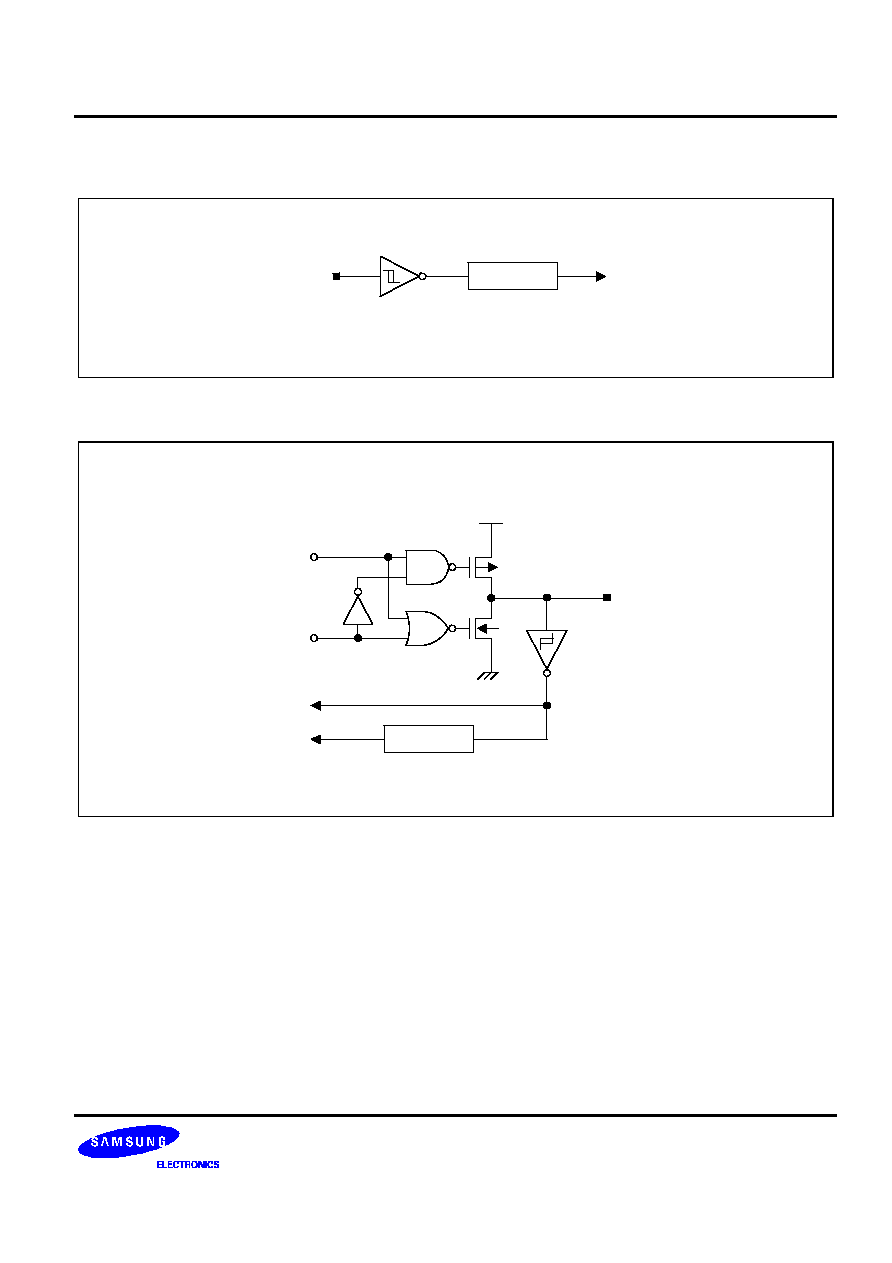
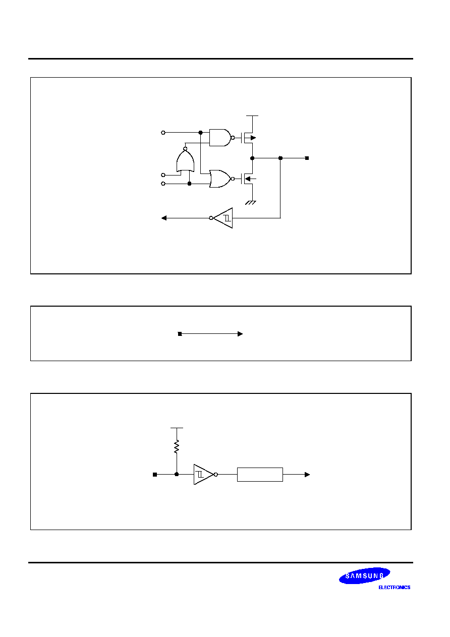
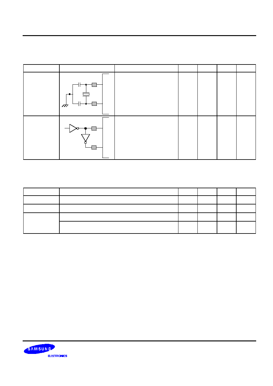
PIN CIRCUITS
In
Noise Filter
Schmitt Trigger Input
Figure 1-3. Pin Circuit Type 1 (H-Sync, V-Sync, IRIN)
V
DD
In/Out
Output
DIsable
Data
Noise Filter
Schmitt
Trigger Input
Input
INT
Figure 1-4. Pin Circuit Type 2 (P2.0-P2.3, INT0-INT3)

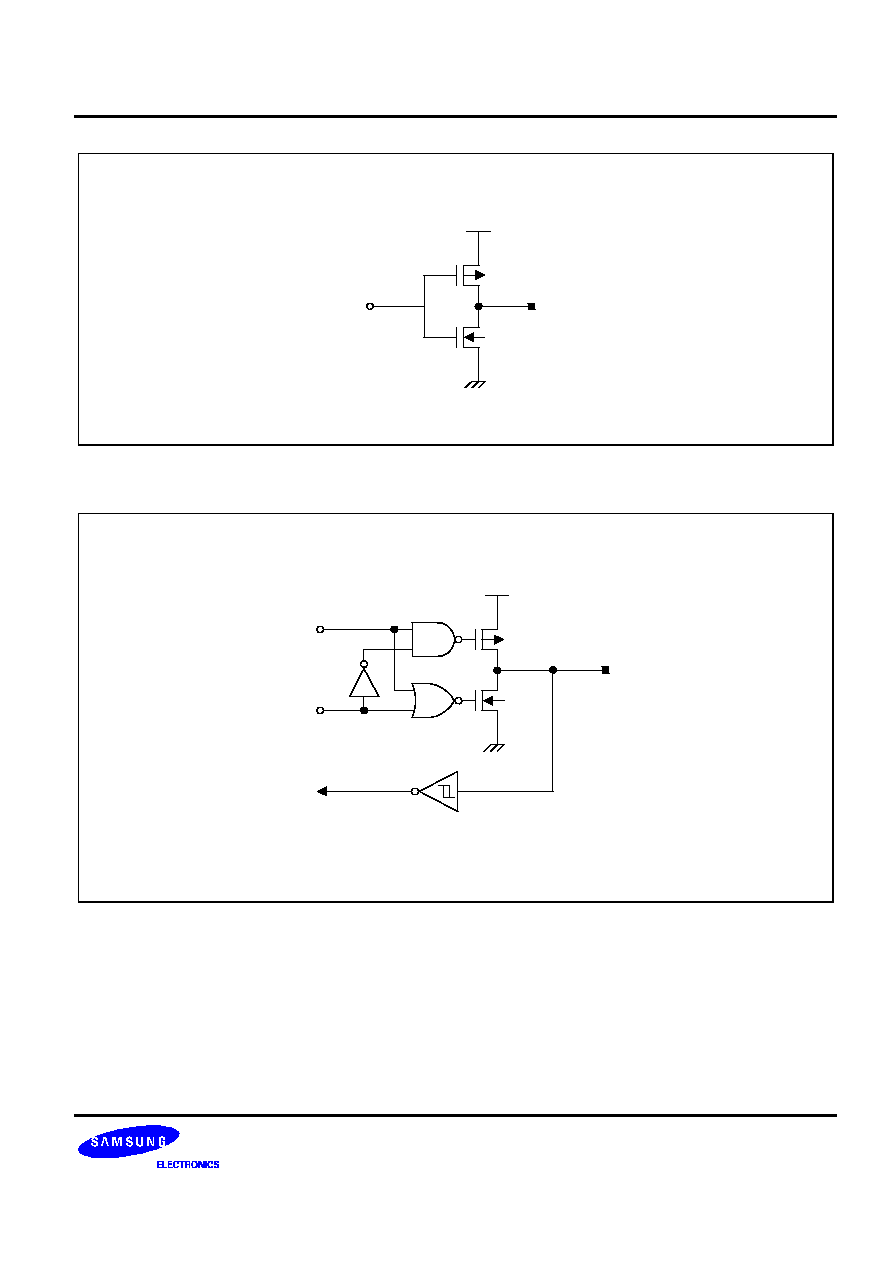
PRODUCT OVERVIEW
S3C380D/F380D
1-8
Schmitt Trigger Input
In/Out
NOTE: Circuit type 3 can withstand up to 6 V loads.
Input
Data
Figure 1-5. Pin Circuit Type 3 (P0.1-P0.3, PWM1)
Schmitt Trigger Input
In/Out
NOTE: Circuit type 4 can withstand up to 5 V loads.
Data
Input
A/D IN
Figure 1-6. Pin Circuit Type 4 (P1.4-P1.7, ADC1-ADC4)
S3C380D/F380D
PRODUCT OVERVIEW
1-9
V
DD
Data
In/Out
Figure 1-7. Pin Circuit Type 5 (V
blue
, V
green
, V
red
, V
blank
)
V
DD
In/Out
Output
DIsable
Data
Input
Schmitt Trigger Input
Figure 1-8. Pin Circuit Type 6 (P0.0, P1.0-P1.3, P2.4-P2.7, P3.0, OSDHT, PWM0)
PRODUCT OVERVIEW
S3C380D/F380D
1-10
V
DD
Data
Open-drain
In/Out
Input
Schmitt Trigger Input
Output DIsable
Figure 1-9. Pin Circuit type 7 (P0.4-P0.7)
A/D Input
In
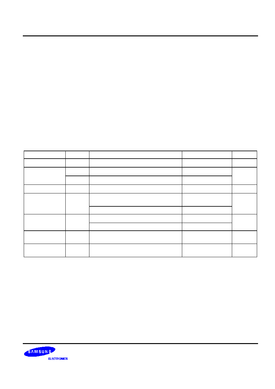
Figure 1-10. Pin Circuit type 8 (CVI IN, ADC0)
Schmitt Trigger Input
In
V
DD
50 K
Noise Filter
Figure 1-11. Pin Circuit type 9 (
RESET
)

S3C380D/F380D
PRODUCT OVERVIEW
1-11
CPU CORE OVERVIEW
The S3C380D CPU core is the ARM7TDMI processor, a general purpose, 32-bit microprocessor developed by
Advanced RISC Machines, Ltd. (ARM). The core's architecture is based on Reduced Instruction Set Computer
(RISC) principles. The RISC architecture makes the instruction set and its related decoding mechanisms simpler
and more efficient than with microprogrammed Complex Instruction Set Computer (CISC) systems. The resulting
benefit is high instruction throughput and impressive real-time interrupt response. Pipelining is also employed so
that all components of the processing and memory systems can operate continuously. The ARM7TDMI has a
32-bit address bus.
An important feature of the ARM7TDMI processor, differentiating it from the ARM7 processor, is a unique
architectural strategy called THUMB. The THUMB strategy is an extension of the basic ARM architecture and
consists of 36 instruction formats. These formats are based on the standard 32-bit ARM instruction set, but have
been re-coded using 16-bit wide opcodes.
Because THUMB instructions are one-half the bit width of normal ARM instructions, they produce very high-
density code. When a THUMB instruction is executed, its 16-bit opcode is decoded by the processor into its
equivalent instruction in the standard ARM instruction set. The ARM core then processes the 16-bit instruction as
it would a normal 32-bit instruction. In other words, the Thumb architecture gives 16-bit systems a way to access
the 32-bit performance of the ARM core without incurring the full overhead of 32-bit processing.
Because the ARM7TDMI core can execute both standard 32-bit ARM instructions and 16-bit Thumb instructions,
it lets you mix routines of Thumb instructions and ARM code in the same address space. In this way, you can
adjust code size and performance, routine by routine, to find the best programming solution for a specific
application.
Instruction
Decoder and
Logic Control
Address Register
Address Register
Register Bank
Write Data Register
Multiplexer
Barrel Shifter
32-Bit ALU
Instruction
Pipeline and
Read Data
Register
Figure 1-12. ARM7TDMI Core Block Diagram

PRODUCT OVERVIEW
S3C380D/F380D
1-12
INSTRUCTION SET
The S3C380D instruction set is divided into two subsets: a standard 32-bit ARM instruction set and a 16-bit
THUMB instruction set.
The 32-bit ARM instruction set is comprised of thirteen basic instruction types which can, in turn, be divided into
four broad classes:
∑
Four types of branch instructions which control program execution flow, instruction privilege levels, and
switching between ARM code and THUMB code.
∑
Three types of data processing instructions which use the on-chip ALU, barrel shifter, and multiplier to
perform high-speed data operations in a bank of 31 registers (all with 32-bit register widths).
∑
Three types of load and store instructions which control data transfer between memory locations and the
registers. One type is optimized for flexible addressing, another for rapid context switching, and the third for
swapping data.
∑
Three types of co-processor instructions which are dedicated to controlling external co-processors. These
instructions extend the off-chip functionality of the instruction set in an open and uniform way.
NOTE
All 32-bit ARM instructions can be executed conditionally.
The 16-bit THUMB instruction set contains 36 instruction formats drawn from the standard 32-bit ARM instruction
set. The THUMB instructions can be divided into four functional groups:
∑
Four branch instructions.
∑
Twelve data processing instructions, which are a subset of the standard ARM data processing instructions.
∑
Eight load and store register instructions.
∑
Four load and store multiple instructions.
NOTE
Each 16-bit THUMB instruction has a corresponding 32-bit ARM instruction with the identical processing
model.
The 32-bit ARM instruction set and the 16-bit THUMB instruction sets are good targets for compilers of many
different high-level languages. When assembly code is required for critical code segments, the ARM
programming technique is straightforward, unlike that of some RISC processors which depend on sophisticated
compiler technology to manage complicated instruction interdependencies.
Pipelining is employed so that all parts of the processor and memory systems can operate continuously.
Typically, while one instruction is being executed, its successor is being decoded, and a third instruction is being
fetched from memory.

S3C380D/F380D
PRODUCT OVERVIEW
1-13
OPERATING STATES
From a programmer's point of view, the ARM7TDMI core is always in one of two operating states. These states,
which can be switched by software or by exception processing, are:
∑
ARM state (when executing 32-bit, word-aligned, ARM instructions), and
∑
THUMB state (when executing 16-bit, half-word aligned THUMB instructions).
OPERATING MODES
The ARM7TDMI core supports seven operating modes:
∑
User mode: the normal program execution state
∑
FIQ (Fast Interrupt Request) mode: for supporting a specific data transfer or channel process
∑
IRQ (Interrupt ReQuest) mode: for general purpose interrupt handling
∑
Supervisor mode: a protected mode for the operating system
∑
Abort mode: entered when a data or instruction pre-fetch is aborted
∑
System mode: a privileged user mode for the operating system
∑
Undefined mode: entered when an undefined instruction is executed
Operating mode changes can be controlled by software, or they can be caused by external interrupts or exception
processing. Most application programs execute in User mode. Privileged modes (that is, all modes other than
User mode) are entered to service interrupts or exceptions, or to access protected resources.

PRODUCT OVERVIEW
S3C380D/F380D
1-14
REGISTERS
The S3C380D CPU core has a total of 37 registers: 31 general-purpose, 32-bit registers, and 6 status registers.
Not all of these registers are always available. Which registers are available to the programmer at any given time
depends on the current processor operating state and mode.
NOTE
When the S3C380D is operating in ARM state, 16 general registers and one or two status registers can
be accessed at any time. In privileged mode, mode-specific banked registers are switched in.
Two register sets, or banks, can also be accessed, depending on the core's current state: the ARM state register
set and the THUMB state register set:
∑
The ARM state register set contains 16 directly accessible registers: R0-R15. All of these registers, except for
R15, are for general-purpose use, and can hold either data or address values. An additional (seventeenth)
register, the CPSR (Current Program Status Register), is used to store status information.
∑
The THUMB state register set is a subset of the ARM state set. You can access eight general registers, R0-
R7, as well as the program counter (PC), a stack pointer register (SP), a link register (LR), and the CPSR.
Each privileged mode has a corresponding banked stack pointer, link register, and saved process status
register (SPSR).
The THUMB state registers are related to the ARM state registers as follows:
∑
THUMB state R0-R7 registers and ARM state R0-R7 registers are identical
∑
THUMB state CPSR and SPSRs and ARM state CPSR and SPSRs are identical
∑
THUMB state SP, LR, and PC map directly to ARM state registers R13, R14, and R15, respectively
In THUMB state, registers R8-R15 are not part of the standard register set. However, you can access them for
assembly language programming and use them for fast temporary storage, if necessary.
S3C380D/F380D
PRODUCT OVERVIEW
1-15
EXCEPTIONS
An exception arises whenever the normal flow of program execution is interrupted. For example, when
processing must be diverted to handle an interrupt from a peripheral. The processor's state just prior to handling
the exception must be preserved so that the program flow can be resumed when the exception routine is
completed. Multiple exceptions may arise simultaneously.
To process exceptions, the S3C380D uses the banked core registers to save the current state. The old PC value
and the CPSR contents are copied into the appropriate R14 (LR) and SPSR register. The PC and mode bits in
the CPSR are forced to a value which corresponds to the type of exception being processed.
The S3C380D core supports seven types of exceptions. Each exception has a fixed priority and a corresponding
privileged processor mode, as shown in Table 1-2.
Table 1-2. S3C380D CPU Exceptions
Exception
Mode on Entry
Priority
Reset
Supervisor mode
1 (Highest)
Data abort
Abort mode
2
FIQ
FIQ mode
3
IRQ
IRQ mode
4
Prefetch abort
Abort mode
5
Undefined instruction
Undefined mode
6 (Lowest)
Software interrupt
Supervisor mode
6 (Lowest)
S3C380D/F380D
ELECTRICAL DATA
17-1
17
ELECTRICAL DATA
OVERVIEW
This chapter describes the S3C380D electrical data. Information is presented according to the following Table of
Contents:
Table 17-1. Absolute Maximum Ratings
(T
A
= 25
∞
C)
Parameter
Symbol
Conditions
Rating
Unit
Supply voltage
V
DD
≠ 0.3 to + 7.0
V
Input voltage
V
I1
P0.1-P0.3, P1.4-P1.7 (open-drain)
≠ 0.3 to + 6
V
V
I2
All ports except V
I1
≠ 0.3 to V
DD
+ 0.3
Output voltage
V
O
All output ports
≠ 0.3 to V
DD
+ 0.3
V
Output current
high
I
OH
One I/O pin active
≠ 10
mA
All I/O pins active
≠ 50
Output current low
I
OL
One I/O pin active
+ 20
mA
Total pin current for ports 0, 1, 2, and 3
+ 100
Operating
temperature
T
A
≠
≠ 20 to + 85
∞
C
Storage
temperature
T
STG
≠
≠ 40 to + 125
∞
C
ELECTRICAL DATA
S3C380D/F380D
17-2
Table 17-2. D.C. Electrical Characteristics
(T
A
= ≠ 20
∞
C to + 85
∞
C, V
DD
= 4.5 V to 5.5 V)
Parameter
Symbol
Conditions
Min
Typ
Max
Unit
Input high
V
IH1
All input pins except V
lH2
0.8 V
DD
≠
V
DD
V
voltage
V
IH2
RESET
0.85 V
DD
Input low voltage
V
IL1
All input pins except V
IL2
≠
≠
0.2 V
DD
V
V
IL2
RESET
0.15 V
DD
Output high
voltage
V
OH1
V
blank
, P2.4, P2.5
I
OH
= ≠ 1 mA
V
DD
≠ 1.0
≠
≠
V
V
OH2
All ports except V
OH1
I
OH
= ≠ 500 uA
V
DD
≠ 0.5
Output low
voltage
V
OL1
P2.4, P2.5
I
OL
= 15 mA
≠
≠
1.0
V
V
OL2
All ports except V
OL1
, V
OL3
I
OL
= 2 mA
0.4
V
OL3
V
blank
I
OL
= 1 mA
0.4
Input high leakage
current
I
LIH1
V
IN
= V
DD
All input pins except I
LIH2
≠
≠
1
uA
I
LIH2
V
IN
= V
DD
X
IN
,
X
OUT
3
20
Input low leakage
current
I
LIL1
V
IN
= 0 V
All input pins except I
LIL2
≠
≠
≠ 1
uA
I
LIL2
V
IN
= 0 V
X
IN
,
X
OUT
≠ 3
≠- 20
Output high
leakage current
I
LOH1
V
OUT
= V
DD
All output pins except I
LOH2
≠
≠
1
uA
I
LOH2
V
OUT
= 6 V
P0.1-P0.3, P1.4-P1.7
(N-channel, open-drain)
10
Output low
leakage current
I
LOL
V
OUT
= 0 V
All output pins
≠
≠
≠ 1
uA
S3C380D/F380D
ELECTRICAL DATA
17-3
Table 17-2. D.C. Electrical Characteristics (Continued)
(T
A
= - 40
∞
C to + 85
∞
C, V
DD
= 4.5 V to 5.5 V)
Parameter
Symbol
Conditions
Min
Typ
Max
Unit
Pull-up resistor
R
P2
V
IN
= 0 V
RESET
only
30
50
70
K
Supply current
I
DD1
V
DD
= 5 V
16 MHz CPU clock
≠
50
100
mA
I
DD2
Sleep mode
0.5
1
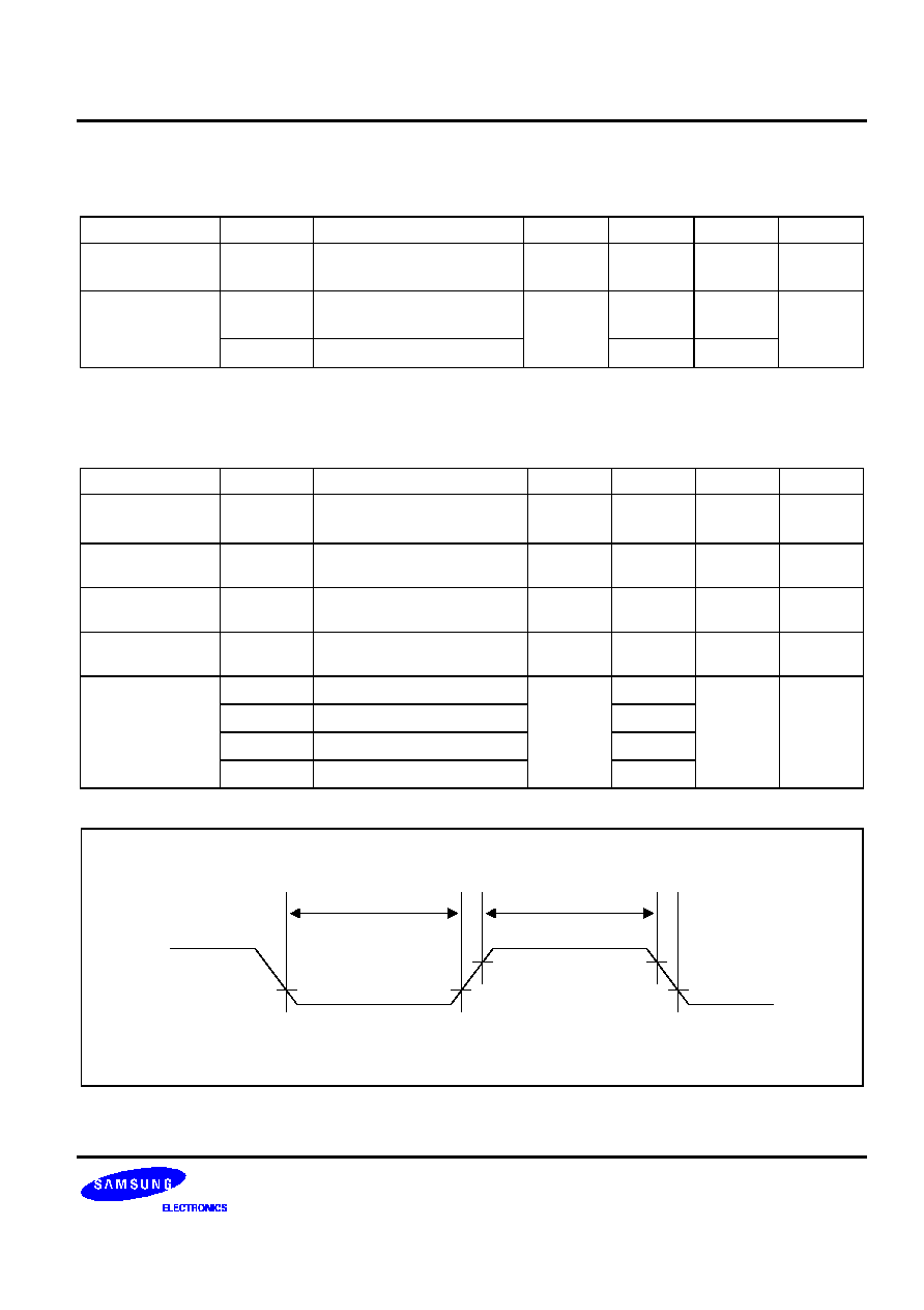
Table 17-3. A.C. Electrical Characteristics
(T
A
= - 40
∞
C to + 85
∞
C, V
DD
= 4.5 V to 5.5 V)
Parameter
Symbol
Conditions
Min
Typ
Max
Unit
Interrupt input
high, low width
t
INTH,
t
INTL
Ports 2.0-2.3
≠
300
≠
ns
RESET
input low
width
t
RSL
Input
≠
1000
≠
ns
V-sync pulse
width
t
VW
≠
4
≠
≠
µ
s
H-sync pulse
width
t
HW
≠
3
≠
≠
µ
s
Noise filter
t
NF1
P2.0-P2.3
≠
300
≠
ns
t
NF4
Glitch filter (oscillator block)
1000
t
NF3
RESET
1000
t
NF2
H-sync, V-sync
300
t
INTL
t
RSL
t
INTH
0.8 V
DD
0.2 V
DD
Figure 17-1. Input Timing measurement points
ELECTRICAL DATA
S3C380D/F380D
17-4
Table 17-4. Input/Output Capacitance
(T
A
= ≠ 40
∞
C to + 85
∞
C, V
DD
=
0 V )
Parameter
Symbol
Conditions
Min
Typ
Max
Unit
Input
capacitance
C
IN
f = 1 MHz; unmeasured pins
are returned to V
SS
≠
≠
10
pF
Output
capacitance
C
OUT
I/O capacitance
C
IO
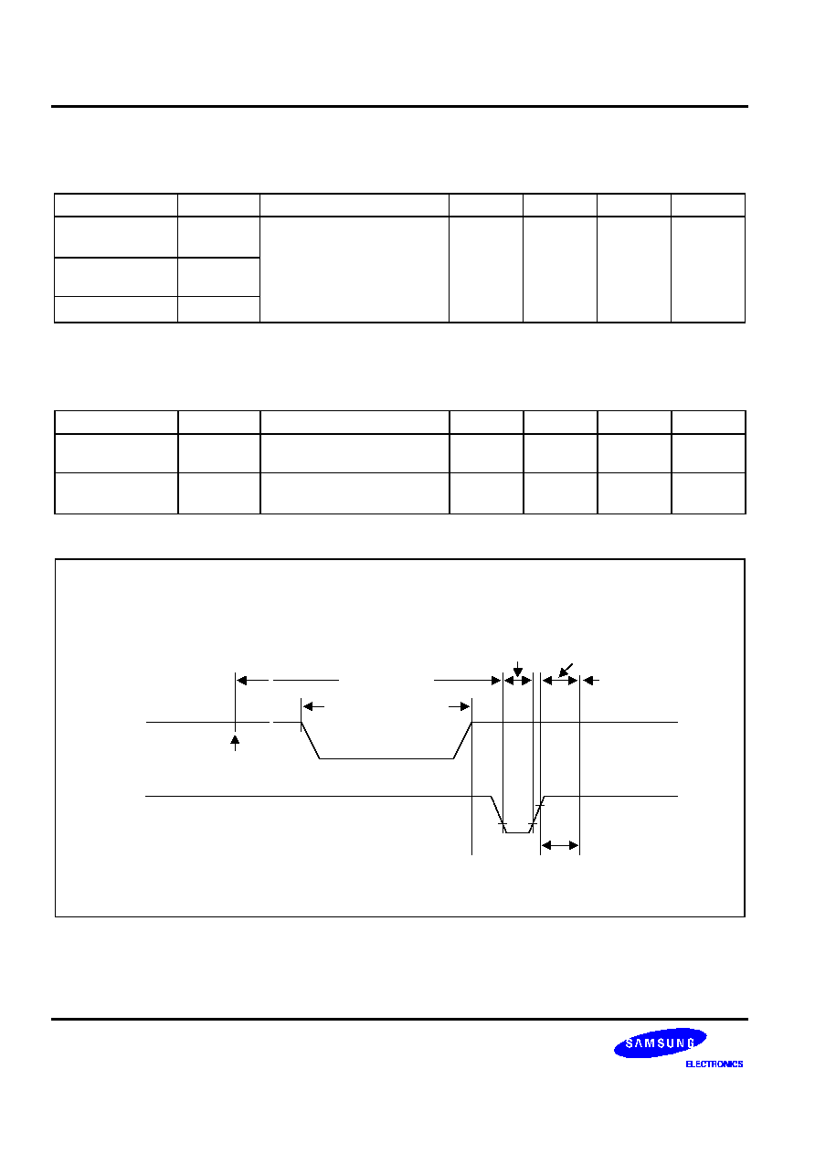
Table 17-5. Data Retention Supply Voltage in Sleep Mode
(T
A
= ≠ 20
∞
C to + 85
∞
C, V
DD
= 4.5 V to 5.5 V)
Parameter
Symbol
Conditions
Min
Typ
Max
Unit
Data retention
supply voltage
V
DDDR
Sleep mode
2
≠
≠
V
Data retention
supply current
I
DDDR
Sleep mode
V
DDDR
= 5.0 V
≠
≠
2
mA
Execution of
Sleep Operation
RESET
Occurs
~ ~
V
DDDR
~ ~
SLEEP Mode
Oscillation
Stabilization
Time
Normal Operting
Mode
Data Retention Mode
t
WAIT
RESET
V
DD
Figure 17-2. Sleep Mode Release Timing When Initiated by
RESET
S3C380D/F380D
ELECTRICAL DATA
17-5
Table 17-6. Oscillator Frequency
(T
A
= ≠ 20
∞
C + 85
∞
C)
Oscillator
Clock Circuit
Test Condition
Min
Typ
Max
Unit
Crystal or
ceramic
S3C380D
X
IN
X
OUT
C1
C2
V
DD
= 4.5 V to 5.5 V
C1 = C2 = 33 pF
recommended
≠
32,768
≠
Hz
External clock
S3C380D
X
IN
X
OUT
V
DD
= 4.5 V to 5.5 V
≠
32,768
≠
Hz
Table 17-7. Oscillator Clock Stabilization Time
(T
A
= ≠ 20
∞
C + 85
∞
C, V
DD
= 4.5 V to 5.5 V)
Oscillator
Test Condition
Min
Typ
Max
Unit
Crystal
X
IN
= 32,768 Hz
≠
≠
20
ms
External clock
X
IN
input high and low level width (t
XH,
t
XL
)
15
≠
125
ns
Oscillator
t
WAIT
when released by a reset, X
IN
= 32,768 Hz
≠
≠
500
ms
stabilization
time
t
WAIT
when released by a interrupt
(note)
≠
≠
4
ms
NOTE: The duration of the oscillator stabilization time, t
WAIT,
when it is released by an interrupt, is determined by the
settings in the basic timer control register, BTCON.

ELECTRICAL DATA
S3C380D/F380D
17-6
Table 17-8. A/D Converter Electrical Characteristics
(T
A
= - 20
∞
C to + 85
∞
C, V
DD
= 4.5 V to 5.5 V (ADC1-ADC4), V
DD
= 5.0 V (ADC0))
Parameter
Symbol
Conditions
Min
Typ
Max
Unit
Resolution
≠
≠
≠
≠
4
Bit
Absolute
accuracy
(1)
≠
CPU clock = 16 MHz ADC0
≠
≠
±
1.0
LSB
ADC1-4
≠
≠
±
0.5
LSB
Conversion
Time
(2)
t
CON
CPU clock = 16 MHz
≠
(3)
≠
ns
Analog input
voltage
V
IAN
≠
ADC1-4
AV
SS
≠
AV
REF
V
ADC0
1.5
≠
2.0
V
Analog input
impedance
R
AN
≠
2
≠
≠
M
Analog output
impedance
R
OAN
CPU clock = 16 MHz
Conversion time = 4 MHz
≠
≠
5
K
CPU clock = 16 MHz
Conversion time =
0.5, 1, and 2 MHz
≠
≠
10
K
NOTES:
1.
Excluding quantization error, absolute accuracy values are within
±
1 LSB (ADC0),
±
0.5 LSB (ADC1-4)
2.
`Conversion time' is the time required from the moment a conversion operation starts until it ends
3.
ADC conversion time is controled by ADCON.9-.8.
S3C380D/F380D
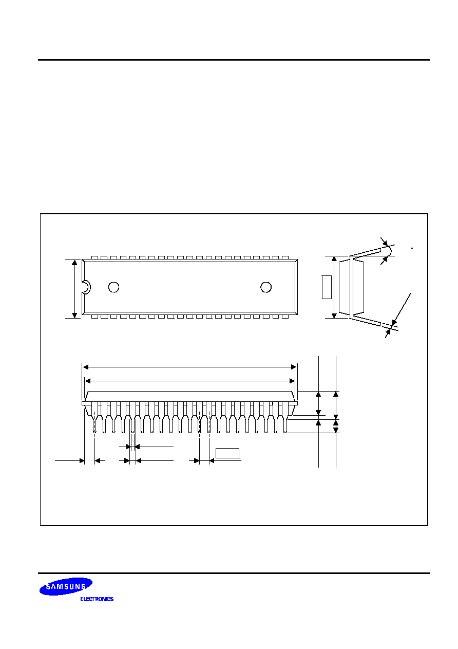
MECHANICAL DATA
18-1
18
MECHANICAL DATA
OVERVIEW
The S3C380D microcontroller is currently available in 42-pin SDIP (42-SDIP-600) package.
NOTE: Dimensions are in millimeters.
39.50 MAX
39.10
±
0.2
0.50
±
0.1
1.778
(1.77)
0.51 MIN
3.30
±
0.3
3.50
±
0.2
5.08 MAX
42-SDIP-600
0-15
1.00
±
0.1
0.25
+ 0.1
- 0.05
15.24
14.00
±
0
.2
#42
#22
#21
#1
Figure 18-1. 42-Pin SDIP Package Dimensions

S3C380D/F380D
S3F380D MTP
19-1
19
S3F380D MTP
OVERVIEW
The S3F380D single-chip CMOS microcontroller is the MTP (Multiple Time Programmable)
version of the
S3C380D microcontroller. It has an on-chip Flash ROM instead of a masked ROM. The flash ROM is accessed
by serial data format.
The S3F380D is fully compatible with the S3C380D, both in function and pin configuration.
P0.0/PWM0
P0.1/PWM1
SCLK/P0.2
SDAT/P1.0
P1.1
P1.2
P1.3
P1.4/ADC1
P1.5/ADC2
P1.6/ADC3
P1.7/ADC4
V
DD
/V
DD1
V
SS
/V
SS1
P2.0/INT0
P2.1/INT1
P2.2/INT2
P2.3/INT3
P2.4
P2.5
P2.6
P2.7/OSDHT
S3F380D
(42-SDIP-600)
1
2
3
4
5
6
7
8
9
10
11
12
13
14
15
16
17
18
19
20
21
P0.3
P0.4
P0.5
P0.6
P0.7
V
SS2
/V
SS
IRIN/V
PP
P3.0
V
DD2
/V
DD
RESET/
RESET
X
OUT
X
IN
V
SS3
/V
SS
LPF
CVI IN (ADC0)
V-sync
H-sync
Vblank
Vred
Vgreen
Vblue
42
41
40
39
38
37
36
35
34
33
32
31
30
29
28
27
26
25
24
23
22
Figure 19-1. S3F380D Pin Assignment (42-SDIP)
S3F380D MTP
S3C380D/F380D
19-2
Table 19-1. Descriptions of Pins Used to Read/Write the Flash ROM (S3F380D)
Main Chip
During Programming
Pin Name
Pin Name
Pin No.
I/O
Function
P1.0 (Pin 4)
SDAT
4
I/O
Serial data pin (output when reading, Input when
writing) Input and push-pull output port can be
assigned
P0.2 (Pin 3)
SCLK
3
I/O
Serial clock pin (Input only pin)
IRIN
V
PP
36
I
0-5 V: operating mode
12.5 V: MTP mode
RESET
RESET
33
I
5 V: operating mode, 0 V: MTP mode
V
DD
/V
SS
V
DD
/V
SS
12/34, 13/30/37
I
Logic power supply pin.
Table 19-2. Comparison of S3F380D and S3C380D Features
Characteristic
S3F380D
S3C380D
Program Memory
128-Kbyte Flash ROM
128-Kbyte mask ROM
Operating Voltage (V
DD
)
4.5 V to 5.5 V
4.5 V to 5.5 V
MTP Programming Mode
V
DD
= 5 V, V
PP
= 12.5 V
≠
Pin Configuration
42 SDIP
42 SDIP
Flash ROM programmability
User program under 100 time
Programmed at the factory