 | –≠–ª–µ–∫—Ç—Ä–æ–Ω–Ω—ã–π –∫–æ–º–ø–æ–Ω–µ–Ω—Ç: S3F441FX | –°–∫–∞—á–∞—Ç—å:  PDF PDF  ZIP ZIP |
Document Outline
- ˛ˇ
- ˛ˇ
- ˛ˇ
- ˛ˇ
- ˛ˇ
- ˛ˇ
- ˛ˇ
- ˛ˇ
- ˛ˇ
- ˛ˇ
- ˛ˇ
- ˛ˇ
- ˛ˇ
- ˛ˇ
- ˛ˇ
- ˛ˇ
- ˛ˇ

22-S3-F441FX-022001
USER'S MANUAL
S3F441FX
32-Bit CMOS
RISC Microprocessor
Revision 2

S3F441FX
32-BIT RISC
MICROPROCESSORS
USER'S MANUAL
Revision 2

ii
S3F441FX RISK MICROPROCESSORS
Important Notice
The information in this publication has been carefully
checked and is believed to be entirely accurate at the
time of publication. Samsung assumes no
responsibility, however, for possible errors or
omissions, or for any consequences resulting from the
use of the information contained herein.
Samsung reserves the right to make changes in its
products or product specifications with the intent to
improve function or design at any time and without
notice and is not required to update this
documentation to reflect such changes.
This publication does not convey to a purchaser of
semiconductor devices described herein any license
under the patent rights of Samsung or others.
Samsung makes no warranty, representation, or
guarantee regarding the suitability of its products for
any particular purpose, nor does Samsung assume
any liability arising out of the application or use of any
product or circuit and specifically disclaims any and
all liability, including without limitation any
consequential or incidental damages.
"Typical" parameters can and do vary in different
applications. All operating parameters, including
"Typicals" must be validated for each customer
application by the customer's technical experts.
Samsung products are not designed, intended, or
authorized for use as components in systems
intended for surgical implant into the body, for other
applications intended to support or sustain life, or for
any other application in which the failure of the
Samsung product could create a situation where
personal injury or death may occur.
Should the Buyer purchase or use a Samsung product
for any such unintended or unauthorized application,
the Buyer shall indemnify and hold Samsung and its
officers, employees, subsidiaries, affiliates, and
distributors harmless against all claims, costs,
damages, expenses, and reasonable attorney fees
arising out of, either directly or indirectly, any claim of
personal injury or death that may be associated with
such unintended or unauthorized use, even if such
claim alleges that Samsung was negligent regarding
the design or manufacture of said product.
S3F441FX RISC Microprocessors
User's Manual, Revision 2
Publication Number: 22-S3-C441FX-022001
© 2001 Samsung Electronics
All rights reserved. No part of this publication may be reproduced, stored in a retrieval system, or transmitted in
any form or by any means, electric or mechanical, by photocopying, recording, or otherwise, without the prior
written consent of Samsung Electronics.
Samsung Electronics' Microprocessor business has been awarded full ISO-
14001 certification (BSI Certificate No. FM24653). All semiconductor products
are designed and manufactured in accordance with the highest quality standards
and objectives.
Samsung Electronics Co., Ltd.
San #24 Nongseo-Ri, Kiheung-Eup
Yongin-City, Kyunggi-Do, Korea
C.P.O. Box #37, Suwon 449-900
TEL: (82)-(031)-209-1907
FAX: (82)-(031)-209-1899
Home-Page URL: Http://www.intl.samsungsemi.com
Printed in the Republic of Korea

S3F441FX RISK MICROPROCESSORS
iii
Preface
The S3F441FX RISC Microprocessor User's Manual is designed specifically for application designers and
programmers who are using S3F441FX RISC Microprocessor for product development.
∑
Section 1, 'Product Overview,' is a high-level introduction to the S3F441FX and includes a features list, block
diagram, pin assignments, signal descriptions, a description of the CPU core, and an overview of special
registers.
∑
Section 2, 'Programmer's Model', describes the important features of the S3F441FX programming
environment.
∑
Section 3, 'Instruction Set', describes the features of the S3F441FX instruction set, which is based on a CPU
core developed by ARM, Ltd.
∑
Section 4, 'I/O Ports', describes the S3F441FX input/output ports and special function registers.
∑
Section 5, 'Basic Timer/Watchdog Timer', describes the basic timer & watch-dog timer, including a interval
mode operation, and special function registers.
∑
Section 6, 'Timer Module 0,1,2,3,4,5 (16-Bit Timers)', describes the Timer modules, including a operation
modes and special function registers.
∑
Section 7, 'UART', describes the UART function blocks, including UART operation, special function registers,
and timing.
∑
Section 8, 'Interrupt Controller', describes the interrupt source and special function registers.
∑
Section 9, 'System Manager', describes the system manager function block which consists of registers that
control bus arbitration and management, as well as external memory access and timing.
∑
Section 10, 'Internal Flash ROM', describes the internal flash ROM function blocks, including the internal
flash ROM operation and special function registers.
∑
Section 11, 'System Control', describes the Power-Down mode and PLL (Phase Locked Loop) function
blocks, including operation modes and special function registers.
∑
Section 12, 'Special Function Registers', describes all the S3F441FX special function registers.
In each of these sections, you will find detailed descriptions of the special registers that are associated with each
function block. These descriptions orient you to the block's features and also serve as a quick reference when
writing application code.
The remaining sections of this manual, sections 13 and 14, present D.C. and A.C. electrical characteristics and
related timing diagrams and mechanical data for 64-pin LQFP package of the S3F441FX.


S3F441FX RISC MICROPROCESSOR
v
Table of Contents
Chapter 1
Product Overview
Introduction..............................................................................................................................................1-1
Features ..................................................................................................................................................1-2
Block Diagram .........................................................................................................................................1-3
Pin Assignments......................................................................................................................................1-4
Signal Descriptions ..................................................................................................................................1-5
I/O Pin Types...........................................................................................................................................1-7
Chapter 2
Programmer's Model
Overview .................................................................................................................................................2-1
Processor Operating States .....................................................................................................................2-1
Switching State........................................................................................................................................2-1
Memory Formats .....................................................................................................................................2-1
Big-Endian Format...................................................................................................................................2-2
Little-Endian Format ................................................................................................................................2-2
Instruction Length ....................................................................................................................................2-2
Operating Modes .....................................................................................................................................2-3
Registers .................................................................................................................................................2-3
The Program Status Registers .................................................................................................................2-7
Exceptions...............................................................................................................................................2-10
Interrupt Latencies ...................................................................................................................................2-15
Reset.......................................................................................................................................................2-15
Chapter 3
Instruction Set
Instruction Set Summay...........................................................................................................................3-1
Format Summary ............................................................................................................................3-1
Instruction Summary .......................................................................................................................3-2
The Condition Field .................................................................................................................................3-4
Branch and Exchange (BX)......................................................................................................................3-5
Instruction Cycle Times ...................................................................................................................3-5
Assembler Syntax ...........................................................................................................................3-5
Using R15 as an Operand ...............................................................................................................3-5
Examples ........................................................................................................................................3-6
Branch and Branch With Link (B, BL) ......................................................................................................3-7
The Link Bit .....................................................................................................................................3-7
Instruction Cycle Times ...................................................................................................................3-7
Assembler Syntax ...........................................................................................................................3-8
Examples ........................................................................................................................................3-8

vi
S3F441FX RISC MICROPROCESSOR
Table of Contents
(Continued)
Chapter 3
Instruction Set
(Continued)
Data Processing.......................................................................................................................................3-9
CPSR Flags ....................................................................................................................................3-11
Shifts...............................................................................................................................................3-12
Immediate Operand Rotates............................................................................................................3-16
Writing to R15 .................................................................................................................................3-16
Using R15 as an Operandy..............................................................................................................3-16
TEQ, Tst, CMP And CMN Opcodes.................................................................................................3-16
Instruction Cycle Times ...................................................................................................................3-16
Assembler Syntax ...........................................................................................................................3-17
Examples ........................................................................................................................................3-17
Psr Transfer (MRS, MSR) ........................................................................................................................3-18
Operand Restrictions .......................................................................................................................3-18
Reserved Bits ..................................................................................................................................3-20
Instruction Cycle Times ...................................................................................................................3-20
Assembly Syntax.............................................................................................................................3-21
Examples ........................................................................................................................................3-21
Multiply and Multiply-Accumulate (MUL, MLA) .........................................................................................3-22
CPSR Flags ....................................................................................................................................3-24
Instruction Cycle Times ...................................................................................................................3-24
Assembler Syntax ...........................................................................................................................3-24
Examples ........................................................................................................................................3-24
Multiply Long and Multiply-Accumulate Long (MULL, MLAL)....................................................................3-25
Operand Restrictions .......................................................................................................................3-26
CPSR Flags ....................................................................................................................................3-26
Instruction Cycle Times ...................................................................................................................3-26
Assembler Syntax ...........................................................................................................................3-27
Examples ........................................................................................................................................3-27
Single Data Transfer (LDR, STR).............................................................................................................3-28
Offsets and Auto-Indexing ...............................................................................................................3-29
Shifted Register Offset ....................................................................................................................3-29
Bytes and Words .............................................................................................................................3-29
Use of R15 ......................................................................................................................................3-31
Restriction on The Use of Base Register .........................................................................................3-31
Data Aborts .....................................................................................................................................3-31
Instruction Cycle Times ...................................................................................................................3-31
Assembler Syntax ...........................................................................................................................3-32
Examples ........................................................................................................................................3-33
Halfword And Signed Data Transfer (LDRH/STRH/LDRSB/LDRSH) ........................................................3-34
Offsets And Auto-Indexing...............................................................................................................3-35
Halfword Load And Stores ...............................................................................................................3-36
Signed Byte And Halfword Loads.....................................................................................................3-36
Endianness And Byte/Halfword Selection ........................................................................................3-36
Use of R15 ......................................................................................................................................3-37
Data Aborts .....................................................................................................................................3-37
Instruction Cycle Times ...................................................................................................................3-37
Assembler Syntax ...........................................................................................................................3-38
Examples ........................................................................................................................................3-39

S3F441FX RISC MICROPROCESSOR
vii
Table of Contents
(Continued)
Chapter 3
Instruction Set
(Continued)
Block Data Transfer (LDM, STM).............................................................................................................3-40
The Register List .............................................................................................................................3-40
Addressing Modes...........................................................................................................................3-41
Address Alignment ..........................................................................................................................3-41
Use of The S Bit ..............................................................................................................................3-43
Use of R15 As The Base .................................................................................................................3-43
Inclusion of The Base in The Register List.......................................................................................3-44
Data Aborts .....................................................................................................................................3-44
Instruction Cycle Times ...................................................................................................................3-44
Assembler Syntax ...........................................................................................................................3-45
Examples ........................................................................................................................................3-46
Single Data Swap (SWP).........................................................................................................................3-47
Bytes and Words .............................................................................................................................3-47
Use of R15 ......................................................................................................................................3-48
Data Aborts .....................................................................................................................................3-48
Instruction Cycle Times ...................................................................................................................3-48
Assembler Syntax ...........................................................................................................................3-48
Examples ........................................................................................................................................3-48
Software Interrupt (SWI) ..........................................................................................................................3-49
Return From The Supervisor ...........................................................................................................3-49
Comment Field................................................................................................................................3-49
Instruction Cycle Times ...................................................................................................................3-49
Assembler Syntax ...........................................................................................................................3-50
Examples ........................................................................................................................................3-50
Coprocessor Data Operations (CDP) .......................................................................................................3-51
Coprocessor Instructions .................................................................................................................3-51
Instruction Cycle Times ...................................................................................................................3-52
Assembler Syntax ...........................................................................................................................3-52
Examples ........................................................................................................................................3-52

viii
S3F441FX RISC MICROPROCESSOR
Table of Contents
(Continued)
Chapter 3
Instruction Set
(Continued)
Coprocessor Data Transfers (LDC, STC) .................................................................................................3-53
The Coprocessor Fields...................................................................................................................3-53
Addressing Modes ...........................................................................................................................3-54
Address Alignment ..........................................................................................................................3-54
Use of R15 ......................................................................................................................................3-54
Data Aborts .....................................................................................................................................3-54
Instruction Cycle Times ...................................................................................................................3-54
Assembler Syntax ...........................................................................................................................3-55
Examples ........................................................................................................................................3-55
Coprocessor Register Transfers (MRC, MCR) .................................................................................3-56
The Coprocessor Fields...................................................................................................................3-56
Transfers to R15..............................................................................................................................3-57
Transfers from R15 .........................................................................................................................3-57
Instruction Cycle Times ...................................................................................................................3-57
Assembler Syntax ...........................................................................................................................3-57
Examples ........................................................................................................................................3-57
Undefined Instruction.......................................................................................................................3-58
Instruction Cycle Times ...................................................................................................................3-58
Assembler Syntax ...........................................................................................................................3-58
Instruction Set Examples .................................................................................................................3-59
Using The Conditional Instructions...................................................................................................3-59
Pseudo-Random Binary Sequence Generator .................................................................................3-61
Multiplication By Constant Using The Barrel Shifter .........................................................................3-61
Loading a Word From an Unknown Alignment.................................................................................3-63
Thumb Instruction Set Format..................................................................................................................3-65
Format Summary ............................................................................................................................3-65
OPCODE Summary ........................................................................................................................3-66

S3F441FX RISC MICROPROCESSOR
ix
Table of Contents
(Continued)
Chapter 3
Instruction Set
(Continued)
Format 1: Move Shifted Register .............................................................................................................3-68
Operation ........................................................................................................................................3-68
Instruction Cycle Times ...................................................................................................................3-69
Examples ........................................................................................................................................3-69
Format 2: Add/Subtract............................................................................................................................3-70
Operation ........................................................................................................................................3-70
Instruction Cycle Times ...................................................................................................................3-71
Examples ........................................................................................................................................3-71
Format 3: Move/Compare/Add/Subtract Immediate .................................................................................3-72
Operations ......................................................................................................................................3-72
Instruction Cycle Times ...................................................................................................................3-73
Examples ........................................................................................................................................3-73
Format 4: Alu Operations.........................................................................................................................3-74
Operation ........................................................................................................................................3-74
Instruction Cycle Times ...................................................................................................................3-75
Examples ........................................................................................................................................3-75
Format 5: Hi-Register Operations/Branch Exchange................................................................................3-76
Operation ........................................................................................................................................3-76
Instruction Cycle Times ...................................................................................................................3-77
The Bx Instruction ...........................................................................................................................3-77
Examples ........................................................................................................................................3-78
Using R15 As An Operand...............................................................................................................3-78
Format 6: Pc-Relative Load .....................................................................................................................3-79
Operation ........................................................................................................................................3-79
Instruction Cycle Times ...................................................................................................................3-80
Examples ........................................................................................................................................3-80
Format 7: Load/Store With Register Offset ..............................................................................................3-81
Operation ........................................................................................................................................3-82
Instruction Cycle Times ...................................................................................................................3-82
Examples ........................................................................................................................................3-82
Format 8: Load/Store Sign-Extended Byte/Halfword ................................................................................3-83
Operation ........................................................................................................................................3-83
Instruction Cycle Times ...................................................................................................................3-84
Examples ........................................................................................................................................3-84
Format 9: Load/Store With Immediate Offset ..........................................................................................3-85
Operation ........................................................................................................................................3-85
Instruction Cycle Times ...................................................................................................................3-86
Examples ........................................................................................................................................3-86
Format 10: Load/Store Halfword ..............................................................................................................3-87
Operation ........................................................................................................................................3-87
Examples ........................................................................................................................................3-88
Format 11: Sp-Relative Load/Store..........................................................................................................3-89
Operation ........................................................................................................................................3-89
Instruction Cycle Times ...................................................................................................................3-89
Examples ........................................................................................................................................3-89

x
S3F441FX RISC MICROPROCESSOR
Table of Contents
(Continued)
Chapter 3
Instruction Set
(Continued)
Format 12: Load Address.........................................................................................................................3-90
Operation ........................................................................................................................................3-90
Instruction Cycle Times ...................................................................................................................3-91
Examples ........................................................................................................................................3-91
Format 13: Add Offset To Stack Pointer ..................................................................................................3-92
Operation ........................................................................................................................................3-92
Instruction Cycle Times ...................................................................................................................3-92
Examples ........................................................................................................................................3-92
Format 14: Push/Pop Registers ...............................................................................................................3-93
Operation ........................................................................................................................................3-93
Instruction Cycle Times ...................................................................................................................3-94
Examples ........................................................................................................................................3-94
Format 15: Multiple Load/Store................................................................................................................3-95
Operation ........................................................................................................................................3-95
Instruction Cycle Times ...................................................................................................................3-95
Examples ........................................................................................................................................3-95
Format 16: Conditional Branch ................................................................................................................3-96
Operation ........................................................................................................................................3-96
Instruction Cycle Times ...................................................................................................................3-97
Examples ........................................................................................................................................3-97
Format 17: Software Interrupt ..................................................................................................................3-98
Operation ........................................................................................................................................3-98
Instruction Cycle Times ...................................................................................................................3-98
Examples ........................................................................................................................................3-98
Format 18: Unconditional Branch.............................................................................................................3-99
Operation ........................................................................................................................................3-99
Examples ........................................................................................................................................3-99
Operation ........................................................................................................................................3-100
Instruction Cycle Times............................................................................................................................3-101
Examples ........................................................................................................................................3-101
Instruction Set Examples .........................................................................................................................3-102
Multiplication By A Constant Using Shifts And Adds ........................................................................3-102
General Purpose Signed Divide.......................................................................................................3-103
Division By A Constant ....................................................................................................................3-105

S3F441FX RISC MICROPROCESSOR
xi
Table of Contents
(Continued)
Chapter 4
Memory Controller
Overview .................................................................................................................................................4-1
Port Data Registers .........................................................................................................................4-2
Port Control Registers Table ...........................................................................................................4-2
Chapter 5
Basic/Watchdog Timer
Overview .................................................................................................................................................5-1
Basic Timer Counter Register..........................................................................................................5-2
External Oscillation Stabilization Time After Stop or Reset..............................................................5-2
Watch Dog Timer Counter...............................................................................................................5-2
Basic Timer Control Register...........................................................................................................5-3
Function Description ................................................................................................................................5-4
Interval Timer Function ...................................................................................................................5-4
Chapter 6
Timer Module 0,1,2,3,4,5 (16-bit Timers)
Overview .................................................................................................................................................6-1
Timer 0,1,2,3,4,5 Control Registers (T0CON,T1CON,T2CON,T3CON,T4CON,T5CON) ..........................6-3
Interval Mode Operation..................................................................................................................6-3
Capture Mode Operation .................................................................................................................6-4
Match & Overflow Mode Operation..................................................................................................6-4
Timer Special Registers...........................................................................................................................6-5
Timer Control Registers...................................................................................................................6-5
Timer Data Registers ......................................................................................................................6-7
Timer Count Registers.....................................................................................................................6-8
Timer Pre-scaler Registers ..............................................................................................................6-9
Chapter 7
UART
Overview .................................................................................................................................................7-1
Infra-Red Mode ...............................................................................................................................7-3
UART Special Registers ..........................................................................................................................7-4
UART Line Control Register ............................................................................................................7-4
UART Control Register....................................................................................................................7-6
UART Status Register .....................................................................................................................7-8
UART Transmit Buffer Register .......................................................................................................7-10
UART Receive Buffer Register........................................................................................................7-11
UART Baud Rate Prescaler Registers .............................................................................................7-12

xii
S3F441FX RISC MICROPROCESSOR
Table of Contents
(Continued)
Chapter 8
Interrupt Controller
Overview .................................................................................................................................................8-1
Interrupt Sources .....................................................................................................................................8-3
Interrupt Controller Special Registers.......................................................................................................8-4
Interrupt Mode Register ...................................................................................................................8-4
Interrupt Pending Register ...............................................................................................................8-5
Interrupt Mask Register ...................................................................................................................8-6
Chapter 9
System Manager
Overview .................................................................................................................................................9-1
System Manager Registers ......................................................................................................................9-2
System Register Address Configuration Register (SYSCFG) ...........................................................9-4
External Memory Control Special Registers .............................................................................................9-5
Memory Control Register 0, 1, 2 ......................................................................................................9-5
Chapter 10
Internal Flash ROM
Overview .................................................................................................................................................10-1
Programming Modes................................................................................................................................10-2
Flash Memory Special Registers..............................................................................................................10-4
Flash Memory Key Registers ...............................................................................................................10-4
Flash Memory Address Register ..........................................................................................................10-4
Flash Memory Data Register ...............................................................................................................10-4
Flash Memory User Programming Control Register .............................................................................10-5
Flash Memory Error Register ...............................................................................................................10-6
Flash Memory Smart Option Bits Read Register ..................................................................................10-7
Flash Memory Protection Option Bits Read Register............................................................................10-7
Data Protection ........................................................................................................................................10-10
Protection Option.................................................................................................................................10-10
Smart Option For LDC Protection / H/W Protection .............................................................................10-12
Flash Memory Map ..................................................................................................................................10-13
Tool Program Mode .................................................................................................................................10-14

S3F441FX RISC MICROPROCESSOR
xiii
Table of Contents
(Concluded)
Chapter 11
System Control
Power-Down Mode ..................................................................................................................................11-1
Global Interrupt Control .......................................................................................................................11-1
PLL .....................................................................................................................................................11-1
Entering The Stop Mode......................................................................................................................11-2
Exiting From The Stop Mode ...............................................................................................................11-2
Idle Mode And Internal Flash ROM......................................................................................................11-2
System Control Register......................................................................................................................11-3
PLL (Phase Locked Loop)....................................................................................................................11-4
PLL Control Register (PLLCON) ..........................................................................................................11-5
PLL Value Selection Guide..................................................................................................................11-5
PLL Value Change Steps.....................................................................................................................11-5
Capacitor for Pll Loop Filter .................................................................................................................11-5
Chapter 12
Special Function Registers
Overview .................................................................................................................................................12-1
S3F441FX Special Registers ...................................................................................................................12-2
Chapter 13
Electrical Data
DC Electrical Characteristics ...................................................................................................................13-1
AC Electrical Characteristics....................................................................................................................13-5
Chapter 14
Mechanical Data
Package Dimensions ...............................................................................................................................14-1


S3F441FX RISC MICROPROCESSOR
xv
List of Figures
Figure
Title
Page
Number
Number
1-1
S3F441FX Block Diagram ......................................................................................1-3
1-2
S3F441FX Pin Assignments (64-LQFP) .................................................................1-4
1-3
IOPUSE (Schmitt Input/Output Pin with Programmable Pull-up Resistor
and Edge Detection)...............................................................................................1-8
1-4
IOPUS (Schmitt Input/Output Pin with Programmable Pull-up Resistor) .................1-8
1-5
IOPD (Input/Output Pin with Programmable Pull-down Resistor) ............................1-9
1-6
IOPU (Input/Output pin with Programmable Pull-up Resistor) .................................1-9
2-1
Big-Endian Addresses of Bytes within Words .........................................................2-2
2-2
Little-Endian Addresses of Bytes within Words .......................................................2-2
2-3
Register Organization in ARM State .......................................................................2-4
2-4
Register Organization in THUMB state ...................................................................2-5
2-5
Mapping of THUMB State Registers onto ARM State Registers..............................2-6
2-6
Program Status Register Format ............................................................................2-7
3-1
ARM Instruction Set Format ...................................................................................3-1
3-2
Branch and Exchange Instructions .........................................................................3-5
3-3
Branch Instructions.................................................................................................3-7
3-4
Data Processing Instructions ..................................................................................3-9
3-5
ARM Shift Operations.............................................................................................3-12
3-6
Logical Shift Left ....................................................................................................3-12
3-7
Logical Shift Right ..................................................................................................3-13
3-8
Arithmetic Shift Right .............................................................................................3-13
3-9
Rotate Right ...........................................................................................................3-14
3-10
Rotate Right Extended ...........................................................................................3-14
3-11
PSR Transfer .........................................................................................................3-19
3-12
Multiply Instructions................................................................................................3-22
3-13
Multiply Long Instructions .......................................................................................3-25
3-14
Single Data Transfer Instructions............................................................................3-28
3-15
Little-Endian Offset Addressing ..............................................................................3-30
3-16
Halfword and Signed Data Transfer with Register Offset ........................................3-34
3-17
Halfword and Signed Data Transfer with Immediate Offset and Auto-Indexing .......3-35
3-18
Block Data Transfer Instructions.............................................................................3-40
3-19
Post-Increment Addressing.....................................................................................3-41
3-20
Pre-Increment Addressing ......................................................................................3-42
3-21
Post-Decrement Addressing ...................................................................................3-42
3-22
Pre-Decrement Addressing.....................................................................................3-43
3-23
Swap Instruction.....................................................................................................3-47
3-24
Software Interrupt Instruction..................................................................................3-49
3-25
Coprocessor Data Operation Instruction .................................................................3-51
3-26
Coprocessor Data Transfer Instructions ..................................................................3-53
3-27
Coprocessor Register Transfer Instructions ............................................................3-56
3-28
Undefined Instruction .............................................................................................3-58
3-29
THUMB Instruction Set Formats .............................................................................3-65

xvi
S3F441FX RISC MICROPROCESSOR
List of Figures
(Continued)
Figure
Title
Page
Number
Number
3-30
Format 1.................................................................................................................3-68
3-31
Format 2.................................................................................................................3-70
3-32
Format 3.................................................................................................................3-72
3-33
Format 4.................................................................................................................3-74
3-34
Format 5.................................................................................................................3-76
3-35
Format 6.................................................................................................................3-79
3-36
Format 7.................................................................................................................3-81
3-37
Format 8.................................................................................................................3-83
3-38
Format 9.................................................................................................................3-85
3-39
Format 10...............................................................................................................3-87
3-40
Format 11...............................................................................................................3-89
3-41
Format 12...............................................................................................................3-90
3-42
Format 13...............................................................................................................3-92
3-43
Format 14...............................................................................................................3-93
3-44
Format 15...............................................................................................................3-95
3-45
Format 16...............................................................................................................3-96
3-46
Format 17...............................................................................................................3-98
3-47
Format 18...............................................................................................................3-99
3-48
Format 19...............................................................................................................3-100
4-1
S3F441FX Memory Map after Reset.......................................................................4-2
4-2
S3F441FX nWAIT(16bit bus width) Work-around Timing Diagram .........................4-5
4-3
S3F441FX nXBREQ/nXBACK Timing Diagram ......................................................4-7
4-4
Memory Interface with 8bit ROM ............................................................................4-8
4-5
Memory Interface with 8bit ROM x 2.......................................................................4-8
4-6
Memory Interface with 8bit ROM x 4.......................................................................4-9
4-7
Memory Interface with 16bit ROM ..........................................................................4-10
4-8
Memory Interface with 16bit SRAM ........................................................................4-10
4-9
Memory Interface with 16bit DRAM ........................................................................4-11
4-10
Memory Interface with 16bit DRAM x 2...................................................................4-11
4-11
Memory Interface with 16bit SDRAM ......................................................................4-12
4-12
S3F441FX nGCS Timing Diagram..........................................................................4-13
4-13
S3F441FX DRAM Timing Diagram .........................................................................4-14
4-14
S3F441FX DRAM Refresh Timing Diagram............................................................4-14
4-15
S3F441FX SDRAM Timing Diagram.......................................................................4-15
5-1
Watchdog Timer Block Diagram .............................................................................5-1

S3F441FX RISC MICROPROCESSOR
xvii
List of Figures
(Continued)
Figure
Title
Page
Number
Number
6-1
16-Bit Timer Block Diagram ...................................................................................6-2
6-2
Interval Mode Example 1 (TnDATA=100, TnPRE=3, UTCLK is a Timer Source)....6-3
6-3
Interval Mode Example 2 (TnDATA=100, TIN is a timer source )............................6-4
6-4
Timer 0,1,2,3,4,5 Control Registers ........................................................................6-6
6-5
Timer Data Registers (TnDATA).............................................................................6-7
6-6
Timer Count Registers (TnCNT) .............................................................................6-8
6-7
Timer Pre-scaler Registers (TnPRE) .....................................................................6-9
7-1
UART Block Diagram .............................................................................................7-2
7-2
Infra-red Mode........................................................................................................7-3
7-3
UART Line Control Register (LCON) ......................................................................7-5
7-4
UART Control Register (UCON) .............................................................................7-7
7-5
UART Status Register (USSR) ...............................................................................7-9
7-6
UART Transmit Buffer Register (TBR)....................................................................7-10
7-7
UART Receive Buffer Register (RBR) ....................................................................7-11
7-8
UART Baud Rate Divisor Registers (UBRDR) ........................................................7-12
8-1
S3F441FX Interrupt Structure.................................................................................8-2
9-1
S3F441FX Default Memory Map of the Normal Mode(In ROM Mode) ....................9-2
9-2
S3F441FX Default Memory Map of External ROM Mode........................................9-3
9-3
System Register Address Configuration Register (SYSCFG)..................................9-4
9-4
An Example of S3F441FX nCSn Timing Diagram ..................................................9-6
10-1
Flash Memory Read/Write Block Diagram..............................................................10-3
10-2
Normal Sector Program Flowchart in a User Program mode
(In the figure: " ... compare end address) ...............................................................10-8
10-3
Option Sector Program Flowchart in a User Program mode ...................................10-8
10-4
Normal Sector Erase Flowchart ..............................................................................10-9
10-5
Option Sector Erase Flowchart ...............................................................................10-9
10-6
Flash Memory Map According to Operating Mode ..................................................10-13
11-1
Clock Circuit Diagram ............................................................................................11-1
11-2
Entering & Wake-up in the STOP Mode .................................................................11-2
11-3
PLL (Phase-Locked Loop) Block Diagram ..............................................................11-4
11-4
Capacitor for PLL Loop Filter..................................................................................11-5
12-1
S3F441FX Default Memory Map of the Normal Mode (In-ROM mode) ...................12-1
12-2
Special Function Register.......................................................................................12-1

xviii
S3F441FX RISC MICROPROCESSOR
List of Figures
(Concluded)
Figure
Title
Page
Number
Number
13-1
Typical Operating Frequency and Voltage Range ( internal flash t
ACC
=1 ) ...............13-3
13-2
Typical Operating Frequency and Voltage Range ( internal flash t
ACC
=2 ) ...............13-3
13-3
EXTCLK and MCLK (Internal Clock) When PLL is not Used. ..................................13-5
13-4
SRAM Read Access Timing without nWAIT
(t
COS
=1, t
ACS
=0, t
COH
=0, t
ACC
=3)...........................................................................13-6
13-5
SRAM Read Access Timing with nWAIT
(t
COS
=1, t
ACS
=0, t
COH
=0, t
ACC
=3, external wait=2) .................................................13-6
13-6
SRAM Write Access Timing without nWAIT
(t
COS
=1, t
ACS
=0, t
COH
=0, t
ACC
=3)...........................................................................13-7
13-7
SRAM Write Access Timing with nWAIT
(t
COS
=1, t
ACS
=0, t
COH
=0, t
ACC
=3, external wait=2) .................................................13-7
13-8
SRAM Read Access Timing with nWAIT
(t
COS
=0, t
ACS
=1, t
COH
=1,t
ACC
=3, external wait=2) ..................................................13-8
13-9
SRAM Read Access Timing with nWAIT
at the Last Cycle of Half-Word/Word Access and Byte Access
(t
COS
=0, t
ACS
=1, t
COH
=0,t
ACC
=3, external wait=2) ..................................................13-8
13-10
SRAM Read Access Timing with nWAIT
During Half-Word/Word Access and Byte Access, except the Last Cycle
(t
COS
=0, t
ACS
=1, t
COH
=0,t
ACC
=3, external wait=2) ..................................................13-9
13-11
nWAIT Data Fetch Timing ......................................................................................13-9
14-1
64-LQFP-1010 Package Dimensions (unit: mm) .....................................................14-1

S3F441FX RISC MICROPROCESSOR
xix
List of Tables
Table
Title
Page
Number
Number
1-1
S3F441FX Signal Descriptions (64-pin LQFP) ........................................................1-5
1-2
S3F441FX I/O Pin Types........................................................................................1-7
2-1
PSR Mode Bit Values.............................................................................................2-9
2-2
Exception Entry/Exit ...............................................................................................2-11
2-3
Exception Vectors ..................................................................................................2-13
3-1
The ARM Instruction Set ........................................................................................3-2
3-2
Condition Code Summary ......................................................................................3-4
3-3
ARM Data Processing Instructions..........................................................................3-11
3-4
Incremental Cycle Times........................................................................................3-16
3-5
Assembler Syntax Descriptions ..............................................................................3-27
3-6
Addressing Mode Names........................................................................................3-45
3-7
THUMB Instruction Set Opcodes............................................................................3-66
3-8
Summary of Format 1 Instructions..........................................................................3-68
3-9
Summary of Format 2 Instructions..........................................................................3-70
3-10
Summary of Format 3 Instructions..........................................................................3-72
3-11
Summary of Format 4 Instructions..........................................................................3-74
3-12
Summary of Format 5 Instructions..........................................................................3-76
3-13
Summary of PC-Relative Load Instruction..............................................................3-79
3-14
Summary of Format 7 Instructions..........................................................................3-82
3-15
Summary of format 8 instructions...........................................................................3-83
3-16
Summary of Format 9 Instructions..........................................................................3-85
3-17
Halfword Data Transfer Instructions........................................................................3-87
3-18
SP-Relative Load/Store Instructions .......................................................................3-89
3-19
Load Address .........................................................................................................3-90
3-20
The ADD SP Instruction .........................................................................................3-92
3-21
PUSH and POP Instructions...................................................................................3-93
3-22
The Multiple Load/Store Instructions.......................................................................3-95
3-23
The Conditional Branch Instructions .......................................................................3-96
3-24
The SWI Instruction................................................................................................3-98
3-25
Summary of Branch Instruction ..............................................................................3-99
3-26
The BL Instruction ..................................................................................................3-101
5-1
Basic Timer Counter Setting (at EXTCLK = 20 MHz)..............................................5-2
5-2
The Delay Time before CPU Time Start (at EXTCLK = 20 MHz) ............................5-2
5-3
Watch Dog Timer Counter Setting (at 20 MHz) ......................................................5-2

xx
S3F441FX RISC MICROPROCESSOR
List of Tables
(Concluded)
Table
Title
Page
Number
Number
8-1
S3F441FX Port Configuration Overview .................................................................8-2
8-2
Port of Group A Control Registers (PCONA,PDATA,PUPA) ...................................8-6
8-3
Port of Group B Control Registers (PCONB,PDATB) ..............................................8-8
8-4
Port of Group C Control Registers (PCONC,PDATC,PUPC)...................................8-9
8-5
Port of Group D Control Registers (PCOND, PDATD, PUPD).................................8-10
8-6
Port of Group E Control Registers (PCONE, PDATE) .............................................8-11
8-7
Port of Group F Control Registers (PCONF, PDATF, PUPF) ..................................8-12
8-8
Port of Group G Control Registers (PCONG, PDATG, PUPG)................................8-13
8-9
External Interrupt Control Register (EXTINT)..........................................................8-15
8-10
D[15:0] Pull-Up Control Register (PUPS) ................................................................8-16
10-1
The Pins Used to Read/Write/Erase the Flash ROM in Tool Program Mode ...........10-14
12-1
S3F441FX Special Registers ..................................................................................12-2
13-1
Absolute Maximum Ratings ....................................................................................13-1
13-2
D.C. Electrical Characteristics ................................................................................13-2
13-3
Typical Quiescent Supply Current on V
DD
@ Normal Mode, Flash Tacc=1 ............13-4
13-4
Typical Quiescent Supply Current on V
DD
@ Normal Mode, Flash Tacc=2 ............13-4
13-5
Typical Quiescent Supply Current on V
DD
@ Idle Mode .........................................13-4
13-6
Timing Constants ...................................................................................................13-10
13-7
AC Electrical Characteristics for Internal Flash ROM ..............................................13-10

S3F441FX RISC MICROPROCESSOR
xxi
List of Instruction Descriptions
Instruction
Full Instruction Name
Page
Mnemonic
Number
Move Shifted ...............................................................................................................................................3-68
Add/Subtract................................................................................................................................................3-70
Move/Compare/Add/Subtract Immediate .....................................................................................................3-72
ALU Operations ...........................................................................................................................................3-74
Hi-Register Operations/Branch Exchange ....................................................................................................3-76
PC-Relative Load ........................................................................................................................................3-79
Load/Store with Register Offset ...................................................................................................................3-81
Load/Store Sign-Extended Byte/Halfword ....................................................................................................3-83
Load/Store With Immediate Offset...............................................................................................................3-85
Load/Store Halfword ....................................................................................................................................3-87
SP-Relative Load/Store ...............................................................................................................................3-89
Load Address...............................................................................................................................................3-90
Add Offset to Stack Pointer..........................................................................................................................3-92
Push/Pop Registers .....................................................................................................................................3-93
Multiple Load/Store......................................................................................................................................3-95
Conditional Branch ......................................................................................................................................3-96
Software Interrupt ........................................................................................................................................3-98
Unconditional Branch...................................................................................................................................3-99
Long Branch With Link.................................................................................................................................3-100

S3F441FX RISC MICROCONTROLLER
PRODUCT OVERVIEW
1-1
1
PRODUCT OVERVIEW
INTRODUCTION
SAMSUNG S3F441FX 16/32-bit RISC micro-controller is a cost-effective and high-performance solution for HDD
and general purpose applications.
An outstanding feature of the S3F441FX is its CPU core, a 16/32-bit RISC processor (ARM7TDMI) designed by
Advanced RISC Machines, Ltd. The ARM7TDMI core is a low-power, general-purpose, microprocessor macro-
cell which was developed for the use in application-specific and customer-specific integrated circuits. Its simple,
elegant, and fully static design is particularly suitable for cost-sensitive and power-sensitive applications.
The S3F441FX has been developed by using the ARM7TDMI core, CMOS standard cell, and data path compiler.
Most of the on-chip function blocks have been designed by using a HDL synthesizer. The S3F441FX has been
fully verified in SAMSUNG ASIC test environment including internal Qualification Assurance Process.
By providing a complete set of common system peripherals, the S3F441FX can minimize the overall system
costs and eliminate the need to configure additional components, externally.
The integrated on-chip functions which are described in this document include:
-- Memory system manager: 3 external memory banks. (If the internal flash ROM is not used for a boot code,
nCS0 will be used for a boot ROM )
-- Built-in 256Kbyte (64K x 32bit) Flash memory
-- 8K-bytes (2K x 32bit) internal SRAM for stack, data memory, and/or code memory
-- One channel UART
-- Six 16-bit internal timers with 8-bit pre-scaler and input Capture function
-- Power down mode: STOP and IDLE modes
-- One 8-bit basic timer and 3-bit watch-dog timer
-- Interrupt controller (Total of 19 interrupt sources including 3 external sources )
-- Sixteen programmable I/O ports
-- On-chip PLL
-- 64-pin LQFP

PRODUCT OVERVIEW
S3F441FX RISC MICROCONTROLLER
1-2
FEATURES
Architecture
∑
Completely integrated micro-controller for
embedded applications, especially HDD
application
∑
Fully 16/32-bit RISC architecture
∑
Efficient and powerful ARM7TDMI CPU core
∑
Cost effective JTAG-based debugging solution
Memory
∑
8-bit external bus support for one ROM bank
and two external memory banks
∑
Programmable memory access times (from 0 to
7 wait cycles)
∑
8-Kbyte SRAM (For stack, data memory, and/or
code memory)
∑
Built-in 256Kbyte Flash memory (For data
and/or code memory )
UART
∑
One UART channel with interrupt-based
operation
∑
Programmable baud rates
∑
Supports asynchronous serial data
transmit/receive operations with 5-bit, 6-bit, 7-
bit, 8-bit frames
16-bit Timers/Counters with Capture Function
(T0, T1, T2, T3, T4 and T5)
∑
Six programmable 16-bit timer/counters
∑
Interval, capture, or match & overflow mode
operations
∑
EXTCLK or TIN (Timer Input Capture Signal)
can be the clock source for the timer.
∑
TIN is shared by all timers.
Basic Timer and Watch-dog Timer
∑
8-bit counter (Basic timer) + 3-bit counter
(Watch-dog timer).
∑
Overflow signal from the 8-bit counter can
generate a basic timer interrupt and can be the
input clock for the 3-bit counter.
∑
Overflow signal from the 3-bit counter resets the
system.
I/O Ports
∑
16 programmable I/O ports ( 7 dedicated I/O
pins only)
∑
Each port pin can be configured individually as
input, output, or functional pin
Interrupts
∑
19 interrupt sources including 3 external
Interrupt sources.
∑
Normal or fast interrupt mode(IRQ, FIQ)
Power down mode
∑
IDLE and STOP modes
∑
Division of system clock to reduce the power
(1/1,1/2, 1/8, 1/16 and 1/1024)
Programmable PLL for System Clock
∑
The on-chip PLL generates the clock for the
MCU up to 40 MHz.
∑
There is an external capacitor for the PLL loop
filter.
Operating Voltage Range
∑
3.0 to 3.6 V
Operating Frequency Range
∑
Up to 40 MHz
Package Type
∑
64-pin LQFP

S3F441FX RISC MICROCONTROLLER
PRODUCT OVERVIEW
1-3
BLOCK DIAGRAM
I/O Port
Controller
System Manager
Sytem Bus Controller
Bus Arbitration
Bus Interface
ROM/SRAM Controller
UART
Timer 0,1,2,3,4,5
Clock Control
(Power Down)
Basic Timer
& WDT
Interrupt
Controller
Bus
Router
Local Bus
ADDRESS/DATA BUS /
CONTROL SIGNALS
CPU
(ARM7TDMI)
8K-byte
SRAM
256 K-byte
Flash ROM
PLL
Figure 1-1. S3F441FX Block Diagram

PRODUCT OVERVIEW
S3F441FX RISC MICROCONTROLLER
1-4
PIN ASSIGNMENTS
S3F441FX
(64-LQFP)
49
50
51
52
53
54
55
56
57
58
59
60
61
62
63
64
33
34
35
36
37
38
39
40
41
42
43
44
45
46
47
48
16
15
14
13
12
11
10
9
8
7
6
5
4
3
2
1
32
31
30
29
28
27
26
25
24
23
22
21
20
19
18
17
V
DD
A0
A1
A2
A3
A4
A5
V
SS
A6
A7
A8
A9
A10
A11
VDD
A12/GPIO8
V
SS
EXTCLK
EINT0
EINT1
EINT2
TIN/GPIO7
GPIO0
V
DD
GPIO1
GPIO2
GPIO3
GPIO4
GPIO5
PLLCAP
GPIO6
TDO
nWE
nOE
nCS0
nCS1
nCS2
nWAIT
V
SS
D7
D6
D5
D4
V
DD
D3
D2
D1
D0
A13/GPIO9
A14/GPIO10
A15/GPIO11
nRESET
A16/GPIO12
A17/GPIO13
MD1
MD0
nTRST
VSS
VDD
TXD/GPIO14
RXD/GPIO15
TDI
TMS
TCK
Figure 1-2. S3F441FX Pin Assignments (64-LQFP)

S3F441FX RISC MICROCONTROLLER
PRODUCT OVERVIEW
1-5
SIGNAL DESCRIPTIONS
Table 1-1. S3F441FX Signal Descriptions (64-pin LQFP)
Signal
Pin #
I/O Pin Type
Description
TDO
64
O
TDO (TAP Controller Data Output) is the serial output for the JTAG
port
TCK
1
IU
TCK (TAP Controller Clock) provides the clock input for the JTAG
logic. A 100K pull-up resistor is connected to the TCK pin internally.
TMS
2
IU
TMS (TAP Controller Mode Select) controls the sequence of the
TAP controller state diagram. A 100K pull-up resistor is connected
to the TMS pin internally.
TDI
3
IU
TDI (TAP Controller Data Input) is the serial input for the JTAG port.
A 100K pull-up resister is connected to the TDI pin internally.
nTRST
8
IU
nTRST(TAP Controller Reset) resets the TAP controller at start.
A 100K pull-up resistor is connected to the nTRST pin internally.
If the debugger(Black ICE) is not used, nTRST pin should be L level
or low active pulse should be applied before running the CPU.
For example, nRESET signal can be tied with the nTRST.
MD[1:0]
10,9
I
00: Normal mode(In-ROM mode). The nCS0 may be used for an
external device. (MDS can be used.)
01: External ROM mode. The nCS0 will be used for boot code
instead of the internal FLASH ROM. (MDS can be used.)
10: Optional MDS mode for ICE. (External ROM mode is selected)
11: Test mode for Internal Flash memory, which is used only a flash
writer equipment.
nRESET
13
IUS
nRESET is the global reset input for the S3F441FX. For a safe
system reset, nRESET should be held at Low level for at least
150us.
A17/GPIO13
11
IOPD
A17: Address line A17
GPIO[13]: Programmable I/O port 13 for push-pull input or output.
A16/GPIO12
12
IOPD
A16: Address line A16
GPIO[12]: Programmable I/O port 12 for push-pull input or output.
A15/GPIO11
14
IOPD
A15: Address line A15
GPIO[11]: Programmable I/O port 11 for push-pull input or output.
A14/GPIO10
15
IOPD
A14: Address line A14
GPIO[10]: Programmable I/O port 10 for push-pull input or output.
A13/GPIO9
16
IOPD
A13: Address line A13
GPIO[9]: Programmable I/O port 9 for push-pull input or output.
A12/GPIO8
17
IOPD
A12: Address line A12
GPIO[8]: Programmable I/O port 8 for push-pull input or output.
A[11:0]
19-24,
26-31
O
Address lines A11-A0

PRODUCT OVERVIEW
S3F441FX RISC MICROCONTROLLER
1-6
Table 1-1. S3F441FX Signal Descriptions (64-pin LQFP) (Continued)
Signal
Pin #
I/O Pin Type
Description
nWE
33
O
nWE (Write Enable) indicates that the current bus cycle is a write
cycle.
nOE
34
O
nOE (Output Enable) indicates that the current bus cycle is a
read cycle.
nWAIT
38
IU
nWAIT requests to prolong a current bus cycle. As long as
nWAIT is L, the current bus cycle cannot be completed.
nCS0
35
O
nCS0 (Chip Select 0) can be activated when the issued address
for memory access is within the address region 0x0-0x3FFFF
and MD[1:0] is configured as an external ROM mode.
nCS1
36
O
nCS1(Chip Select 1) can be activated when the issued address
for memory access is within the address region 0x800000-
0x83FFFF.
nCS2
37
O
nCS2(Chip Select 2) can be activated when the issued address
for memory access is within the address region 0xC00000-
0xC3FFFF.
D[7:0]
40-43,
45-48
IOPD
D[7:0] (Bi-directional Data Bus) inputs data during memory read
and outputs data during memory write.
EXTCLK
50
IS
External clock source. EXTCLK can be fed to the PLL and the
timers
EINT[2:0]
53-51
IOPUSE
External interrupt inputs2-0.
TIN/GPIO7
54
IOPUS
TIN: Timer capture input
GPIO[7]: Programmable I/O port 7 for push-pull input or output.
GPIO[6:0]
63,61-
57,55
IOPU
GPIO[6:0]: Programmable I/O port 6~0 for push-pull input/output.
RXD/GPIO15
4
IOPUS
RXD: Rx data input for the UART
GPIO[15]: Programmable I/O port 15 for push-pull input or
output.
TXD/GPIO14
5
IOPUS
TXD: Tx data output for the UART
GPIO[14]: Programmable I/O port 14 for push-pull input or
output.
PLLCAP
62
A
Loop filter capacitor for the system PLL. ( 700pF )
V
DD
6,18,32,
44,56
-
V
DD
( 3.3 V )
V
SS
7,25,39,
49
-
V
SS

S3F441FX RISC MICROCONTROLLER
PRODUCT OVERVIEW
1-7
I/O PIN TYPES
Table 1-2. S3F441FX I/O Pin Types
I/O TYPE
DESCRIPTIOS
IOPUS
Schmitt-trigger input/output pin with programmable pull-up resistor
IOPUSE
Schmitt-trigger input/output pin with programmable pull-up resistor and edge detection
IOPD
Input/output pin with programmable pull-down resistor
IOPU
Input/output pin with programmable pull-up resistor
O
Output pin
IUS
Schmitt-trigger Input pin with pull-up resistor
I
Input pin
IU
Input pin with pull-up resistor
IS
Schmitt-trigger input pin
A
A pin for analog signal
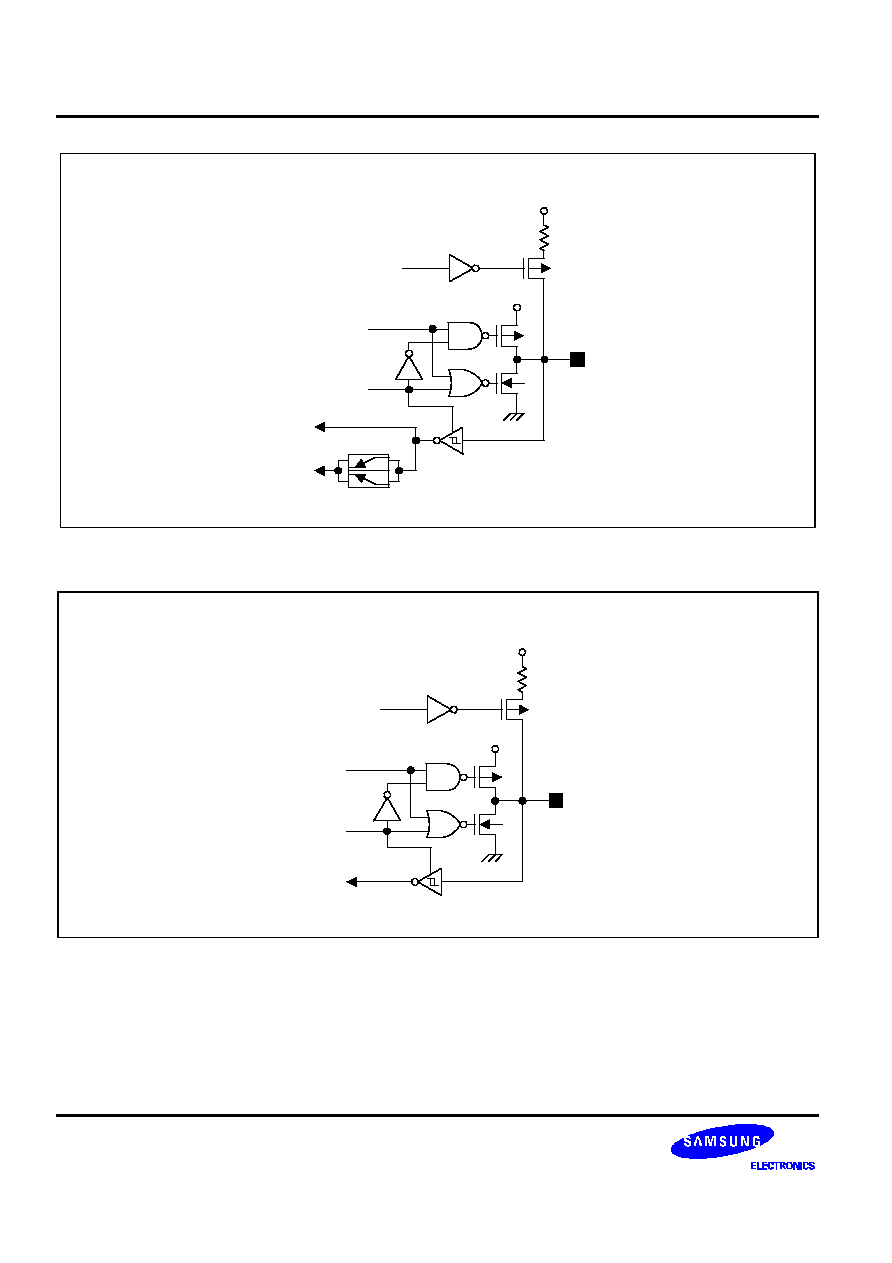
PRODUCT OVERVIEW
S3F441FX RISC MICROCONTROLLER
1-8
Pull-up Resistor
(Typical 50 K
)
V
DD
I/O
V
DD
Output Data
Pull-up Enable
V
SS
Input Data
External
Interrupt Input
Output Enable
Figure 1-3. IOPUSE (Schmitt Input/Output Pin with Programmable Pull-up Resistor and Edge Detection)
Pull-up Resistor
(Typical 50 K
)
V
DD
I/O
V
DD
Output Data
Pull-up Enable
V
SS
Input Data
Output Enable
Figure 1-4. IOPUS (Schmitt Input/Output Pin with Programmable Pull-up Resistor)
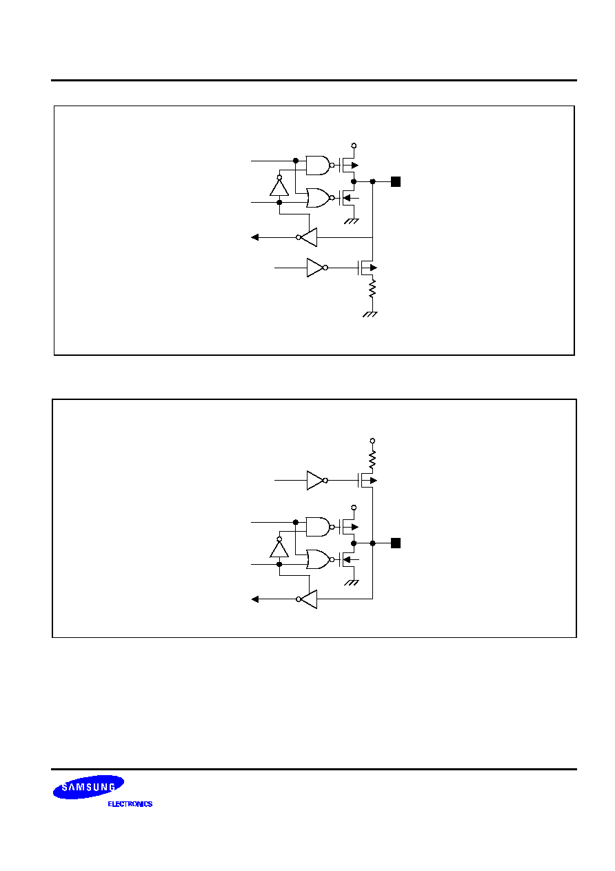
S3F441FX RISC MICROCONTROLLER
PRODUCT OVERVIEW
1-9
Pull-up Resistor
(Typical 50 K
)
V
DD
I/O
Output Data
V
SS
Input Data
Output Enable
Power-down Enable
V
SS
Figure 1-5. IOPD (Input/Output Pin with Programmable Pull-down Resistor)
Pull-up Resistor
(Typical 50 K
)
V
DD
I/O
V
DD
Output Data
Pull-up Enable
V
SS
Input Data
Output Enable
Figure 1-6. IOPU (Input/Output pin with Programmable Pull-up Resistor)

S3F441FX RISC MICROCONTROLLER
PROGRAMMER'S MODEL
2-1
2
PROGRAMMER'S MODEL
OVERVIEW
S3F441FX was developed using the advanced ARM7TDMI core designed by Advanced RISC Machines, Ltd.
PROCESSOR OPERATING STATES
From the programmer's point of view, the ARM7TDMI can be in one of two states:
-- ARM state which executes 32-bit, word-aligned ARM instructions.
-- THUMB state which operates with 16-bit, half-word-aligned THUMB instructions. In this state, the PC uses bit
1 to select between alternate half-words.
NOTE
Transition between these two states does not affect the processor mode or the contents of the registers.
SWITCHING STATE
Entering THUMB State
Entry into THUMB state can be achieved by executing a BX instruction with the state bit (bit 0) set in the operand
register.
Transition to THUMB state will also occur automatically on return from an exception (IRQ, FIQ, UNDEF, ABORT,
SWI etc.), if the exception was entered with the processor in THUMB state.
Entering ARM State
Entry into ARM state happens:
-- On execution of the BX instruction with the state bit clear in the operand register.
-- On the processor taking an exception (IRQ, FIQ, RESET, UNDEF, ABORT, SWI etc.). In this case, the PC is
placed in the exception mode's link register, and execution commences at the exception's vector address.
MEMORY FORMATS
ARM7TDMI views memory as a linear collection of bytes numbered upwards from zero. Bytes 0 to 3 hold the first
stored word, bytes 4 to 7 the second and so on. ARM7TDMI can treat words in memory as being stored either in
Big-Endian or Little-Endian format.
PROGRAMMER'S MODEL
S3F441FX RISC MICROCONTROLLER
2-2
BIG-ENDIAN FORMAT
In Big-Endian format, the most significant byte of a word is stored at the lowest numbered byte and the least
significant byte at the highest numbered byte. Byte 0 of the memory system is therefore connected to data lines
31 through 24.
31
8
4
0
23
9
5
1
10
6
2
11
7
3
8
7
0
4
0
8
Higher Address
Lower Address
Word Address
Most significant byte is at lowest address.
Word is addressed by byte address of most significant byte.
24
15
16
Figure 2-1. Big-Endian Addresses of Bytes within Words
LITTLE-ENDIAN FORMAT
In Little-Endian format, the lowest numbered byte in a word is considered the word's least significant byte, and
the highest numbered byte the most significant. Byte 0 of the memory system is therefore connected to data lines
7 through 0.
31
23
8
7
0
4
0
8
Higher Address
Lower Address
Word Address
Least significant byte is at lowest address.
Word is addressed by byte address of least significant byte.
24
15
16
8
4
0
9
5
1
10
6
2
11
7
3
Figure 2-2. Little-Endian Addresses of Bytes within Words
INSTRUCTION LENGTH
Instructions are either 32 bits long (in ARM state) or 16 bits long (in THUMB state).
Data Types
ARM7TDMI supports byte (8-bit), half-word (16-bit) and word (32-bit) data types. Words must be aligned to four-
byte boundaries and half words to two-byte boundaries.

S3F441FX RISC MICROCONTROLLER
PROGRAMMER'S MODEL
2-3
OPERATING MODES
ARM7TDMI supports seven modes of operation:
-- User (usr): The normal ARM program execution state
-- FIQ (fiq): Designed to support a data transfer or channel process
-- IRQ (irq): Used for general-purpose interrupt handling
-- Supervisor (svc): Protected mode for the operating system
-- Abort mode (abt): Entered after a data or instruction pre-fetch abort
-- System (sys): A privileged user mode for the operating system
-- Undefined (und): Entered when an undefined instruction is executed
Mode changes may be made under software control, or may be brought about by external interrupts or exception
processing. Most application programs will execute in User mode. The non-user modes' known as privileged
modes-are entered in order to service interrupts or exceptions, or to access protected resources.
REGISTERS
ARM7TDMI has a total of 37 registers - 31 general-purpose 32-bit registers and six status registers - but these
cannot all be seen at once. The processor state and operating mode dictate which registers are available to the
programmer.
The ARM State Register Set
In ARM state, 16 general registers and one or two status registers are visible at any one time. In privileged (non-
User) modes, mode-specific banked registers are switched in. Figure 2-3 shows which registers are available in
each mode: the banked registers are marked with a shaded triangle.
The ARM state register set contains 16 directly accessible registers: R0 to R15. All of these except R15 are
general-purpose, and may be used to hold either data or address values. In addition to these, there is a
seventeenth register used to store status information.
Register 14
is used as the subroutine link register. This receives a copy of R15 when a Branch and
Link (BL) instruction is executed. At all other times it may be treated as a general-
purpose register. The corresponding banked registers R14_svc, R14_irq, R14_fiq,
R14_abt and R14_und are similarly used to hold the return values of R15 when
interrupts and exceptions arise, or when Branch and Link instructions are executed
within interrupt or exception routines.
Register 15
holds the Program Counter (PC). In ARM state, bits [1:0] of R15 are zero and bits
[31:2] contain the PC. In THUMB state, bit [0] is zero and bits [31:1] contain the PC.
Register 16
is the CPSR (Current Program Status Register). This contains condition code flags and
the current mode bits.
FIQ mode has seven banked registers mapped to R8-14 (R8_fiq-R14_fiq). In ARM state, many FIQ handlers do
not need to save any registers. User, IRQ, Supervisor, Abort and Undefined each have two banked registers
mapped to R13 and R14, allowing each of these modes to have a private stack pointer and link registers.
PROGRAMMER'S MODEL
S3F441FX RISC MICROCONTROLLER
2-4
R0
R1
R2
R3
R4
R5
R6
R7
R9
R8
R10
R11
R12
R13
R14
R15 (PC)
R0
R1
R2
R3
R4
R5
R6
R7
R9
R8
R10
R11
R12
R13_
svc
R14_
svc
R15 (PC)
R0
R1
R2
R3
R4
R5
R6
R7
R9_
fiq
R10_
fiq
R11_
fiq
R12_
fiq
R13_
fiq
R14_
fiq
R15 (PC)
R8_
fiq
R0
R1
R2
R3
R4
R5
R6
R7
R9
R8
R10
R11
R12
R13_
abt
R14_
abt
R15 (PC)
R0
R1
R2
R3
R4
R5
R6
R7
R9
R8
R10
R11
R12
R13_
irq
R14_
irq
R15 (PC)
R0
R1
R2
R3
R4
R5
R6
R7
R9
R8
R10
R11
R12
R13_
und
R14_
und
R15 (PC)
System & User
FIQ
Supervisor
IRQ
Abort
Undefined
ARM State General Registers and Program Counter
ARM State Program Status Registers
CPSR
CPSR
SPSR_
fiq
CPSR
SPSR_irq
= banked register
CPSR
SPSR_
und
CPSR
SPSR_
abt
CPSR
SPSR_
svc
Figure 2-3. Register Organization in ARM State

S3F441FX RISC MICROCONTROLLER
PROGRAMMER'S MODEL
2-5
The THUMB State Register Set
The THUMB state register set is a subset of the ARM state set. The programmer has direct access to eight
general registers, R0-R7, as well as the Program Counter (PC), a stack pointer register (SP), a link register (LR),
and the CPSR. There are banked Stack Pointers, Link Registers and Saved Process Status Registers (SPSRs)
for each privileged mode. This is shown in Figure 2-4.
R0
R1
R2
R3
R4
R5
R6
R7
LR
SP
PC
System & User
FIQ
Supervisor
IRQ
Abort
Undefined
THUMB State General Registers and Program Counter
THUMB State Program Status Registers
CPSR
CPSR
SPSR_
fiq
CPSR
SPSR_
svc
CPSR
SPSR_
abt
CPSR
SPSR_
irq
CPSR
SPSR_
und
= banked register
LR_
fiq
R0
R1
R2
R3
R4
R5
R6
R7
SP_
fiq
PC
LR_
svc
R0
R1
R2
R3
R4
R5
R6
R7
SP_
svc
PC
LR_
und
R0
R1
R2
R3
R4
R5
R6
R7
SP_
und
PC
LR_
fiq
R0
R1
R2
R3
R4
R5
R6
R7
SP_
fiq
PC
LR_
abt
R0
R1
R2
R3
R4
R5
R6
R7
SP_
abt
PC
Figure 2-4. Register Organization in THUMB state
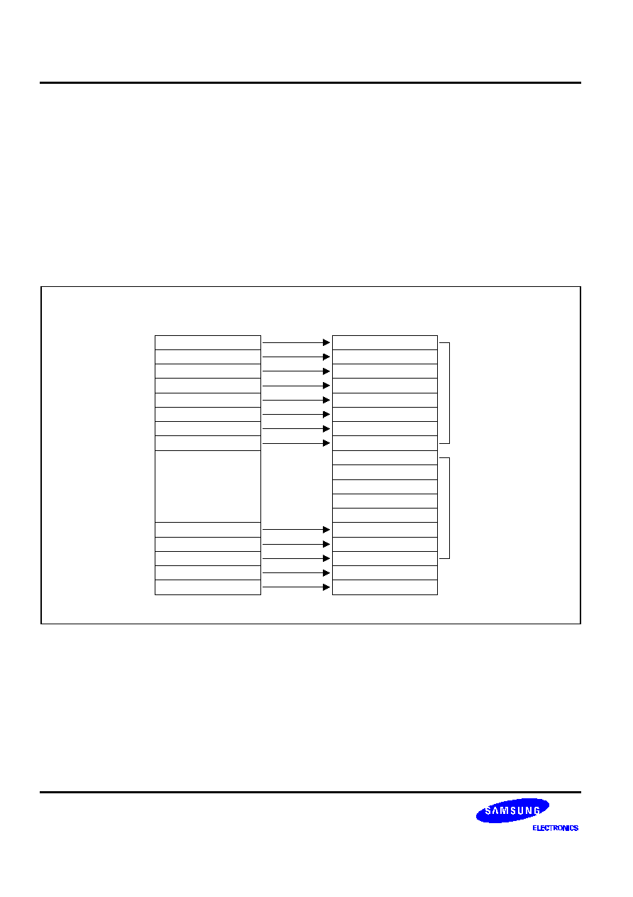
PROGRAMMER'S MODEL
S3F441FX RISC MICROCONTROLLER
2-6
The relationship between ARM and THUMB state registers
The THUMB state registers relate to the ARM state registers in the following way:
-- THUMB state R0-R7 and ARM state R0-R7 are identical
-- THUMB state CPSR and SPSRs and ARM state CPSR and SPSRs are identical
-- THUMB state SP maps onto ARM state R13
-- THUMB state LR maps onto ARM state R14
-- The THUMB state Program Counter maps onto the ARM state Program Counter (R15)
This relationship is shown in Figure 2-5.
R0
R1
R2
R3
R4
R5
R6
R7
Stack Pointer (SP)
Link register (LR)
Program Counter (PC)
CPSR
SPSR
R0
R1
R2
R3
R4
R5
R6
R7
R9
R8
R10
R11
R12
Stack Pointer (R13)
Link register (R14)
Program Counter (R15)
CPSR
SPSR
Lo-registers
Hi-registers
THUMB state
ARM state
Figure 2-5. Mapping of THUMB State Registers onto ARM State Registers

S3F441FX RISC MICROCONTROLLER
PROGRAMMER'S MODEL
2-7
Accessing Hi-Registers in THUMB State
In THUMB state, registers R8-R15 (the Hi registers) are not part of the standard register set. However, the
assembly language programmer has limited access to them, and can use them for fast temporary storage.
A value may be transferred from a register in the range R0-R7 (a Lo register) to a Hi register, and from a Hi
register to a Lo register, using special variants of the MOV instruction. Hi register values can also be compared
against or added to Lo register values with the CMP and ADD instructions. For more information, refer to Figure
3-34.
THE PROGRAM STATUS REGISTERS
The ARM7TDMI contains a Current Program Status Register (CPSR), plus five Saved Program Status Registers
(SPSRs) for use by exception handlers. These register's functions are:
-- Hold information about the most recently performed ALU operation
-- Control the enabling and disabling of interrupts
--
Set the processor operating mode
The arrangement of bits is shown in Figure 2-6.
31
Condition Code Flags
Overflow
N
Z
C
V
I
F
T
M4
M3
M2
M1
M0
30
29
27
28
26
25
24
23
8
7
6
5
4
3
2
1
0
(Reserved)
Control Bits
Carry/Borrow/Extend
Zero
Negative/Less Than
Mode bits
State bit
FIQ disable
IRQ disable
~~
~~
Figure 2-6. Program Status Register Format

PROGRAMMER'S MODEL
S3F441FX RISC MICROCONTROLLER
2-8
The Condition Code Flags
The N, Z, C and V bits are the condition code flags. These may be changed as a result of arithmetic and logical
operations, and may be tested to determine whether an instruction should be executed.
In ARM state, all instructions may be executed conditionally: see Table 3-2 for details.
In THUMB state, only the Branch instruction is capable of conditional execution: see Figure 3-46 for details.
The Control Bits
The bottom 8 bits of a PSR (incorporating I, F, T and M[4:0]) are known collectively as the control bits. These will
be changed when an exception arises. If the processor is operating in a privileged mode, they can also be
manipulated by software.
The T bit
This reflects the operating state. When this bit is set, the processor is executing in
THUMB state, otherwise it is executing in ARM state. This is reflected on the TBIT
external signal.
Note that the software must never change the state of the TBIT in the CPSR. If this
happens, the processor will enter an unpredictable state.
Interrupt disable bits
The I and F bits are the interrupt disable bits. When set, these disable the IRQ and FIQ
interrupts respectively.
The mode bits
The M4, M3, M2, M1 and M0 bits (M[4:0]) are the mode bits. These determine the
processor's operating mode, as shown in Table 2-1. Not all combinations of the mode
bits define a valid processor mode. Only those explicitly described shall be used. The
user should be aware that if any illegal value is programmed into the mode bits, M[4:0],
then the processor will enter an unrecoverable state. If this occurs, reset should be
applied.
Reserved bits
The remaining bits in the PSRs are reserved. When changing a PSR's flag or control
bits, you must ensure that these unused bits are not altered. Also, your program should
not rely on them containing specific values, since in future processors they may read
as one or zero.

S3F441FX RISC MICROCONTROLLER
PROGRAMMER'S MODEL
2-9
Table 2-1. PSR Mode Bit Values
M[4:0]
Mode
Visible THUMB state registers
Visible ARM state registers
10000
User
R7..R0,
LR, SP
PC, CPSR
R14..R0,
PC, CPSR
10001
FIQ
R7..R0,
LR_fiq, SP_fiq
PC, CPSR, SPSR_fiq
R7..R0,
R14_fiq..R8_fiq,
PC, CPSR, SPSR_fiq
10010
IRQ
R7..R0,
LR_irq, SP_irq
PC, CPSR, SPSR_irq
R12..R0,
R14_irq, R13_irq,
PC, CPSR, SPSR_irq
10011
Supervisor
R7..R0,
LR_svc, SP_svc,
PC, CPSR, SPSR_svc
R12..R0,
R14_svc, R13_svc,
PC, CPSR, SPSR_svc
10111
Abort
R7..R0,
LR_abt, SP_abt,
PC, CPSR, SPSR_abt
R12..R0,
R14_abt, R13_abt,
PC, CPSR, SPSR_abt
11011
Undefined
R7..R0
LR_und, SP_und,
PC, CPSR, SPSR_und
R12..R0,
R14_und, R13_und,
PC, CPSR
11111
System
R7..R0,
LR, SP
PC, CPSR
R14..R0,
PC, CPSR
Reserved bits
The remaining bits in the PSR's are reserved. When changing a PSR's flag or control
bits, you must ensure that these unused bits are not altered. Also, your program should
not rely on them containing specific values, since in future processors they may read
as one or zero.

PROGRAMMER'S MODEL
S3F441FX RISC MICROCONTROLLER
2-10
EXCEPTIONS
Exceptions arise whenever the normal flow of a program has to be halted temporarily, for example to service an
interrupt from a peripheral. Before an exception can be handled, the current processor state must be preserved
so that the original program can resume when the handler routine has finished.
It is possible for several exceptions to arise at the same time. If this happens, they are dealt with in a fixed order.
See Exception Priorities on page 2-14.
Action on Entering an Exception
When handling an exception, the ARM7TDMI:
1.
Preserves the address of the next instruction in the appropriate Link Register. If the exception has been
entered from ARM state, then the address of the next instruction is copied into the Link Register (that is,
current PC + 4 or PC + 8 depending on the exception. See Table 2-2 on for details). If the exception has
been entered from THUMB state, then the value written into the Link Register is the current PC offset by a
value such that the program resumes from the correct place on return from the exception. This means that
the exception handler need not determine which state the exception was entered from. For example, in the
case of SWI, MOVS PC, R14_svc will always return to the next instruction regardless of whether the SWI
was executed in ARM or THUMB state.
2.
Copies the CPSR into the appropriate SPSR
3.
Forces the CPSR mode bits to a value which depends on the exception
4.
Forces the PC to fetch the next instruction from the relevant exception vector
It may also set the interrupt disable flags to prevent otherwise unmanageable nesting of exceptions.
If the processor is in THUMB state when an exception occurs, it will automatically switch into ARM state when the
PC is loaded with the exception vector address.
Action on Leaving an Exception
On completion, the exception handler:
1.
Moves the Link Register, minus an offset where appropriate, to the PC. (The offset will vary depending on the
type of exception.)
2.
Copies the SPSR back to the CPSR
3.
Clears the interrupt disable flags, if they were set on entry
NOTE
An explicit switch back to THUMB state is never needed, since restoring the CPSR from the SPSR
automatically sets the T bit to the value it held immediately prior to the exception.

S3F441FX RISC MICROCONTROLLER
PROGRAMMER'S MODEL
2-11
Exception Entry/Exit Summary
Table 2-2 summarizes the PC value preserved in the relevant R14 on exception entry, and the recommended
instruction for exiting the exception handler.
Table 2-2. Exception Entry/Exit
Return Instruction
Previous State
Notes
ARM R14_x
THUMB R14_x
BL
MOV PC, R14
PC + 4
PC + 2
1
SWI
MOVS PC, R14_svc
PC + 4
PC + 2
1
UDEF
MOVS PC, R14_und
PC + 4
PC + 2
1
FIQ
SUBS PC, R14_fiq, #4
PC + 4
PC + 4
2
IRQ
SUBS PC, R14_irq, #4
PC + 4
PC + 4
2
PABT
SUBS PC, R14_abt, #4
PC + 4
PC + 4
1
DABT
SUBS PC, R14_abt, #8
PC + 8
PC + 8
3
RESET
NA
≠
≠
4
NOTES:
1.
Where PC is the address of the BL/SWI/Undefined Instruction fetch which had the prefetch abort.
2.
Where PC is the address of the instruction which did not get executed since the FIQ or IRQ took priority.
3.
Where PC is the address of the Load or Store instruction which generated the data abort.
4.
The value saved in R14_svc upon reset is unpredictable.
FIQ
The FIQ (Fast Interrupt Request) exception is designed to support a data transfer or channel process, and in
ARM state has sufficient private registers to remove the need for register saving (thus minimizing the overhead
of context switching).
FIQ is externally generated by taking the nFIQ input LOW. This input can except either synchronous or
asynchronous transitions, depending on the state of the ISYNC input signal. When ISYNC is LOW, nFIQ and
nIRQ are considered asynchronous, and a cycle delay for synchronization is incurred before the interrupt can
affect the processor flow.
Irrespective of whether the exception was entered from ARM or Thumb state, a FIQ handler should leave the
interrupt by executing
SUBS
PC,R14_fiq,#4
FIQ may be disabled by setting the CPSR's F flag (but note that this is not possible from User mode). If the F flag
is clear, ARM7TDMI checks for a LOW level on the output of the FIQ synchroniser at the end of each instruction.

PROGRAMMER'S MODEL
S3F441FX RISC MICROCONTROLLER
2-12
IRQ
The IRQ (Interrupt Request) exception is a normal interrupt caused by a LOW level on the nIRQ input. IRQ has a
lower priority than FIQ and is masked out when a FIQ sequence is entered. It may be disabled at any time by
setting the I bit in the CPSR, though this can only be done from a privileged (non-User) mode.
Irrespective of whether the exception was entered from ARM or Thumb state, an IRQ handler should return from
the interrupt by executing
SUBS
PC,R14_irq,#4
Abort
An abort indicates that the current memory access cannot be completed. It can be signalled by the external
ABORT input. ARM7TDMI checks for the abort exception during memory access cycles.
There are two types of abort:
--
Prefetch abort: occurs during an instruction prefetch.
-- Data abort: occurs during a data access.
If a prefetch abort occurs, the prefetched instruction is marked as invalid, but the exception will not be taken until
the instruction reaches the head of the pipeline. If the instruction is not executed - for example because a branch
occurs while it is in the pipeline - the abort does not take place.
If a data abort occurs, the action taken depends on the instruction type:
--
Single data transfer instructions (LDR, STR) write back modified base registers: the Abort handler must be
aware of this.
--
The swap instruction (SWP) is aborted as though it had not been executed.
--
Block data transfer instructions (LDM, STM) complete. If write-back is set, the base is updated. If the
instruction would have overwritten the base with data (ie it has the base in the transfer list), the overwriting is
prevented. All register overwriting is prevented after an abort is indicated, which means in particular that R15
(always the last register to be transferred) is preserved in an aborted LDM instruction.
The abort mechanism allows the implementation of a demand paged virtual memory system. In such a system
the processor is allowed to generate arbitrary addresses. When the data at an address is unavailable, the
Memory Management Unit (MMU) signals an abort. The abort handler must then work out the cause of the abort,
make the requested data available, and retry the aborted instruction. The application program needs no
knowledge of the amount of memory available to it, nor is its state in any way affected by the abort.
After fixing the reason for the abort, the handler should execute the following irrespective of the state (ARM or
Thumb):
SUBS
PC,R14_abt,#4
; for a prefetch abort, or
SUBS
PC,R14_abt,#8
; for a data abort
This restores both the PC and the CPSR, and retries the aborted instruction.

S3F441FX RISC MICROCONTROLLER
PROGRAMMER'S MODEL
2-13
Software Interrupt
The software interrupt instruction (SWI) is used for entering Supervisor mode, usually to request a particular
supervisor function. A SWI handler should return by executing the following irrespective of the state (ARM or
Thumb):
MOV
PC,R14_svc
This restores the PC and CPSR, and returns to the instruction following the SWI.
NOTE
nFIQ, nIRQ, ISYNC, LOCK, BIGEND, and ABORT pins exist only in the ARM7TDMI CPU core.
Undefined Instruction
When ARM7TDMI comes across an instruction which it cannot handle, it takes the undefined instruction trap.
This mechanism may be used to extend either the THUMB or ARM instruction set by software emulation.
After emulating the failed instruction, the trap handler should execute the following irrespective of the state (ARM
or Thumb):
MOVS
PC,R14_und
This restores the CPSR and returns to the instruction following the undefined instruction.
Exception Vectors
The following table shows the exception vector addresses.
Table 2-3. Exception Vectors
Address
Exception
Mode in Entry
0x00000000
Reset
Supervisor
0x00000004
Undefined instruction
Undefined
0x00000008
Software Interrupt
Supervisor
0x0000000C
Abort (prefetch)
Abort
0x00000010
Abort (data)
Abort
0x00000014
Reserved
Reserved
0x00000018
IRQ
IRQ
0x0000001C
FIQ
FIQ

PROGRAMMER'S MODEL
S3F441FX RISC MICROCONTROLLER
2-14
Exception Priorities
When multiple exceptions arise at the same time, a fixed priority system determines the order in which they are
handled:
Highest priority:
1.
Reset
2.
Data abort
3.
FIQ
4.
IRQ
5.
Prefetch abort
Lowest priority:
6.
Undefined Instruction, Software interrupt.
Not All Exceptions Can Occur at Once:
Undefined Instruction and Software Interrupt are mutually exclusive, since they each correspond to particular
(non-overlapping) decoding of the current instruction.
If a data abort occurs at the same time as a FIQ, and FIQs are enabled (ie the CPSR's F flag is clear),
ARM7TDMI enters the data abort handler and then immediately proceeds to the FIQ vector. A normal return from
FIQ will cause the data abort handler to resume execution. Placing data abort at a higher priority than FIQ is
necessary to ensure that the transfer error does not escape detection. The time for this exception entry should be
added to worst-case FIQ latency calculations.

S3F441FX RISC MICROCONTROLLER
PROGRAMMER'S MODEL
2-15
INTERRUPT LATENCIES
The worst case latency for FIQ, assuming that it is enabled, consists of the longest time the request can take to
pass through the synchroniser (Tsyncmax if asynchronous), plus the time for the longest instruction to complete
(Tldm, the longest instruction is an LDM which loads all the registers including the PC), plus the time for the data
abort entry (Texc), plus the time for FIQ entry (Tfiq). At the end of this time ARM7TDMI will be executing the
instruction at 0x1C.
Tsyncmax is 3 processor cycles, Tldm is 20 cycles, Texc is 3 cycles, and Tfiq is 2 cycles. The total time is
therefore 28 processor cycles. This is just over 1.4 microseconds in a system which uses a continuous 20 MHz
processor clock. The maximum IRQ latency calculation is similar, but must allow for the fact that FIQ has higher
priority and could delay entry into the IRQ handling routine for an arbitrary length of time. The minimum latency
for FIQ or IRQ consists of the shortest time the request can take through the synchroniser (Tsyncmin) plus Tfiq.
This is 4 processor cycles.
RESET
When the nRESET signal goes LOW, ARM7TDMI abandons the executing instruction and then continues to
fetch instructions from incrementing word addresses.
When nRESET goes HIGH again, ARM7TDMI:
1.
Overwrites R14_svc and SPSR_svc by copying the current values of the PC and CPSR into them. The value
of the saved PC and SPSR is not defined.
2.
Forces M[4:0] to 10011 (Supervisor mode), sets the I and F bits in the CPSR, and clears the CPSR's T bit.
3.
Forces the PC to fetch the next instruction from address 0x00.
4.
Execution resumes in ARM state.
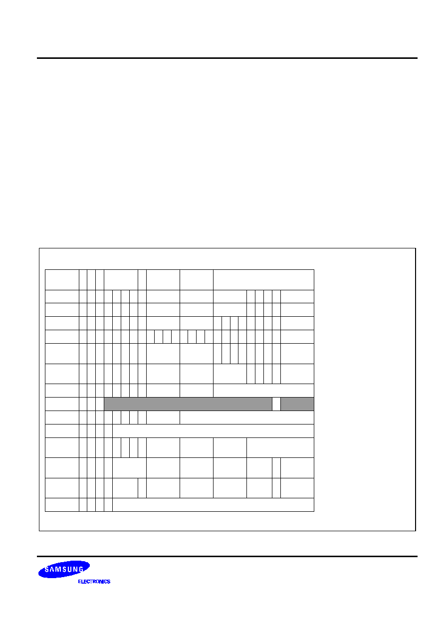
S3F441FX RISC MICROCONTROLLER
ARM INSTRUCTION SET
3-1
3
INSTRUCTION SET
INSTRUCTION SET SUMMAY
This chapter describes the ARM instruction set and the THUMB instruction set in the ARM7TDMI core.
FORMAT SUMMARY
The ARM instruction set formats are shown below.
Cond
Rn
Data Processing/
PSR Transfer
0 0 I
S
Opcode
0 0 0 P U 0 W L
0 0 0 P U 1 W L
0 1 I P U B W L
0 1 I
1 0 0 P U B W L
1
1
1
1
1
1
1
1
1 0
L
1
1 1 0 P U B W L
1 1
1
1
1 1
0
1
1 1
0
1
L
Rd
Rd
Rn
RdHi
RdLo
Rn
Rn
Rn
Rn
Rd
Rd
Rd
Rn
Register List
Rn
CRn
CRn
CRd
Rd
CP Opc
CP
Opc
Operand2
Rs
Rm
Rm
Rm
Rm
Rn
Rn
Rd
Offset
Offset
CRd
Offset
CP#
CP#
CP#
CP
CP
CRm
CRm
Ignored by processor
0
1
Offset
Cond
Cond
Cond
Cond
Cond
Cond
Cond
Cond
Cond
Cond
Cond
Cond
Cond
Cond
0 0 0 0
0
0
A S
A S
U
1
0 0
0
0
0 0 0
0
0 0
1
B
1
0
0
0
1
0 0 0
1
1
1
1
1
1
0
0
0
0
H
H
0
0
0
0
S
S
1
1
1
0
1
1
1
0
0
1
0
0
1
0
0
1
0
0
1
Multiply
Multiply Long
Single Data Swap
Branch and Exchange
Halfword Data Transfer:
register offset
Halfword Data Transfer:
immediate offset
Single Data Transfer
Undefined
Block Data Transfer
Branch
Coprocessor Register Transfer
Coprocessor Data Operation
Coprocessor Data Transfer
Software Interrupt
Offset
27 26 25 24 23 22 21 20 19 18 17 16 15
13
14
12 11 10
31 30 29 28
9 8 7 6 5 4 3 2 1 0
27 26 25 24 23 22 21 20 19 18 17 16 15
13
14
12 11 10
31 30 29 28
9 8 7 6 5 4 3 2 1 0
Figure 3-1. ARM Instruction Set Format

ARM INSTRUCTION SET
S3F441FX RISC MICROCONTROLLER
3-2
NOTE
Some instruction codes are not defined but do not cause the Undefined instruction trap to be taken, for
instance a Multiply instruction with bit 6 changed to a 1. These instructions should not be used, as their
action may change in future ARM implementations.
INSTRUCTION SUMMARY
Table 3-1. The ARM Instruction Set
Mnemonic
Instruction
Action
ADC
Add with carry
Rd: = Rn + Op2 + Carry
ADD
Add
Rd: = Rn + Op2
AND
AND
Rd: = Rn AND Op2
B
Branch
R15: = address
BIC
Bit Clear
Rd: = Rn AND NOT Op2
BL
Branch with Link
R14: = R15, R15: = address
BX
Branch and Exchange
R15: = Rn, T bit: = Rn[0]
CDP
Coprocessor Data Processing
(Coprocessor-specific)
CMN
Compare Negative
CPSR flags: = Rn + Op2
CMP
Compare
CPSR flags: = Rn - Op2
EOR
Exclusive OR
Rd: = (Rn AND NOT Op2)
OR (Op2 AND NOT Rn)
LDC
Load coprocessor from memory
Coprocessor load
LDM
Load multiple registers
Stack manipulation (Pop)
LDR
Load register from memory
Rd: = (address)
MCR
Move CPU register to coprocessor
register
cRn: = rRn {<op>cRm}
MLA
Multiply Accumulate
Rd: = (Rm
◊
Rs) + Rn
MOV
Move register or constant
Rd: = Op2

S3F441FX RISC MICROCONTROLLER
ARM INSTRUCTION SET
3-3
Table 3-1. The ARM Instruction Set (Continued)
Mnemonic
Instruction
Action
MRC
Move from coprocessor register to
CPU register
Rd: = cRn {<op>cRm}
MRS
Move PSR status/flags to register
Rd: = PSR
MSR
Move register to PSR status/flags
PSR: = Rm
MUL
Multiply
Rd: = Rm
◊
Rs
MVN
Move negative register
Rd: = Not Op2
ORR
OR
Rd: = Rn OR Op2
RSB
Reverse Subtract
Rd: = Op2 - Rn
RSC
Reverse Subtract with Carry
Rd: = Op2 - Rn - Not Carry Flag
SBC
Subtract with Carry
Rd: = Rn - Op2 - Not Carry Flag
STC
Store coprocessor register to memory
address: = CRn
STM
Store Multiple
Stack manipulation (Push)
STR
Store register to memory
<address>: = Rd
SUB
Subtract
Rd: = Rn - Op2
SWI
Software Interrupt
OS call
SWP
Swap register with memory
Rd: = [Rn], [Rn] := Rm
TEQ
Test bitwise equality
CPSR flags: = Rn EOR Op2
TST
Test bits
CPSR flags: = Rn AND Op2

ARM INSTRUCTION SET
S3F441FX RISC MICROCONTROLLER
3-4
THE CONDITION FIELD
In ARM state, all instructions are conditionally executed according to the state of the CPSR condition codes and
the instruction's condition field. This field (bits 31:28) determines the circumstances under which an instruction is
to be executed. If the state of the C, N, Z and V flags fulfils the conditions encoded by the field, the instruction is
executed, otherwise it is ignored.
There are sixteen possible conditions, each represented by a two-character suffix that can be appended to the
instruction's mnemonic. For example, a Branch (B in assembly language) becomes BEQ for "Branch if Equal",
which means the Branch will only be taken if the Z flag is set.
In practice, fifteen different conditions may be used: these are listed in Table 3-2. The sixteenth (1111) is
reserved, and must not be used.
In the absence of a suffix, the condition field of most instructions is set to "Always" (sufix AL). This means the
instruction will always be executed regardless of the CPSR condition codes.
Table 3-2. Condition Code Summary
Code
Suffix
Flags
Meaning
0000
EQ
Z set
equal
0001
NE
Z clear
not equal
0010
CS
C set
unsigned higher or same
0011
CC
C clear
unsigned lower
0100
MI
N set
negative
0101
PL
N clear
positive or zero
0110
VS
V set
overflow
0111
VC
V clear
no overflow
1000
HI
C set and Z clear
unsigned higher
1001
LS
C clear or Z set
unsigned lower or same
1010
GE
N equals V
greater or equal
1011
LT
N not equal to V
less than
1100
GT
Z clear AND (N equals V)
greater than
1101
LE
Z set OR (N not equal to V)
less than or equal
1110
AL
(ignored)
always
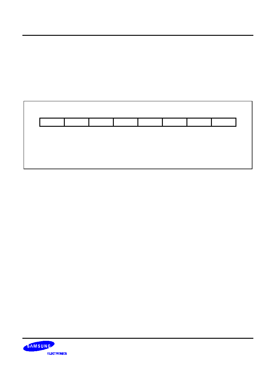
S3F441FX RISC MICROCONTROLLER
ARM INSTRUCTION SET
3-5
BRANCH AND EXCHANGE (BX)
This instruction is only executed if the condition is true. The various conditions are defined in Table 3-2.
This instruction performs a branch by copying the contents of a general register, Rn, into the program counter,
PC. The branch causes a pipeline flush and refill from the address specified by Rn. This instruction also permits
the instruction set to be exchanged. When the instruction is executed, the value of Rn[0] determines whether the
instruction stream will be decoded as ARM or THUMB instructions.
31
24
27
19
15
8 7
0
0
0 0
1
1
0 0
0
1
1 1
1
1
1 1
1
1
1 1
1
0
0 0
1
Cond
Rn
28
16
11
12
23
20
4 3
[3:0] Operand Register
If bit0 of Rn = 1, subsequent instructions decoded as THUMB instructions
If bit0 of Rn =0, subsequent instructions decoded as ARM instructions
[31:28] Condition Field
Figure 3-2. Branch and Exchange Instructions
INSTRUCTION CYCLE TIMES
The BX instruction takes 2S + 1N cycles to execute, where S and N are defined as sequential (S-cycle) and non-
sequencial (N-cycle), respectively.
ASSEMBLER SYNTAX
BX - branch and exchange.
BX {cond} Rn
{
cond}
Two character condition mnemonic. See Table 3-2.
Rn
is an expression evaluating to a valid register number.
USING R15 AS AN OPERAND
If R15 is used as an operand, the behavior is undefined.

ARM INSTRUCTION SET
S3F441FX RISC MICROCONTROLLER
3-6
EXAMPLES
ADR
R0, Into_THUMB + 1
; Generate branch target address
; and set bit 0 high - hence
; arrive in THUMB state.
BX
R0
; Branch and change to THUMB
; state.
CODE16
; Assemble subsequent code as
Into_THUMB
; THUMB instructions
∑
∑
∑
ADR R5, Back_to_ARM
; Generate branch target to word aligned address
; - hence bit 0 is low and so change back to ARM state.
BX R5
; Branch and change back to ARM state.
∑
∑
∑
ALIGN
; Word align
CODE32
; Assemble subsequent code as ARM instructions
Back_to_ARM

S3F441FX RISC MICROCONTROLLER
ARM INSTRUCTION SET
3-7
BRANCH AND BRANCH WITH LINK (B, BL)
The instruction is only executed if the condition is true. The various conditions are defined Table 3-2. The
instruction encoding is shown in Figure 3-3, below.
31
24
27
Cond
Offset
28
23
[24] Link bit
0 = Branch
1 = Branch with link
[31:28] Condition Field
25
101
L
0
Figure 3-3. Branch Instructions
Branch instructions contain a signed 2's complement 24 bit offset. This is shifted left two bits, sign extended to 32
bits, and added to the PC. The instruction can therefore specify a branch of +/- 32Mbytes. The branch offset must
take account of the prefetch operation, which causes the PC to be 2 words (8 bytes) ahead of the current
instruction.
Branches beyond +/- 32Mbytes must use an offset or absolute destination which has been previously loaded into
a register. In this case the PC should be manually saved in R14 if a Branch with Link type operation is required.
THE LINK BIT
Branch with Link (BL) writes the old PC into the link register (R14) of the current bank. The PC value written into
R14 is adjusted to allow for the prefetch, and contains the address of the instruction following the branch and link
instruction. Note that the CPSR is not saved with the PC and R14[1:0] are always cleared.
To return from a routine called by Branch with Link use MOV PC,R14 if the link register is still valid or LDM
Rn!,{..PC} if the link register has been saved onto a stack pointed to by Rn.
INSTRUCTION CYCLE TIMES
Branch and Branch with Link instructions take 2S + 1N incremental cycles, where S and N are defined as
squential (S-cycle) and internal (I-cycle).

ARM INSTRUCTION SET
S3F441FX RISC MICROCONTROLLER
3-8
ASSEMBLER SYNTAX
Items in {} are optional. Items in <> must be present.
B{L}{cond} <expression>
{
L}
Used to request the Branch with Link form of the instruction. If absent, R14 will not be
affected by the instruction.
{
cond}
A two-character mnemonic as shown in Table 3-2. If absent then AL (ALways) will be
used.
<expression>
The destination. The assembler calculates the offset.
EXAMPLES
here
BAL
here
; Assembles to 0xEAFFFFFE (note effect of PC offset).
B
there
; Always condition used as default.
CMP
R1,#0
; Compare R1 with zero and branch to fred
; if R1 was zero, otherwise continue.
BEQ
fred
; Continue to next instruction.
BL
sub+ROM
; Call subroutine at computed address.
ADDS
R1,#1
; Add 1 to register 1, setting CPSR flags
; on the result then call subroutine if
BLCC
sub
; the C flag is clear, which will be the
; case unless R1 held 0xFFFFFFFF.

S3F441FX RISC MICROCONTROLLER
ARM INSTRUCTION SET
3-9
DATA PROCESSING
The data processing instruction is only executed if the condition is true. The conditions are defined in Table 3-2.
The instruction encoding is shown in Figure 3-4.
31
24
27
19
15
Cond
Operand2
28
16
11
12
21
[15:12] Destination register
[19:16] 1st operand register
[20] Set condition codes
0 = Do not affect condition codes
1 = Set condition codes
[24:21] Operation code
0000 = AND-Rd: = Op1 AND Op2
0001 = EOR-Rd: = Op1 EOR Op2
0010 = SUB-Rd: = Op1-Op2
0011 = RSB-Rd: = Op2-Op1
0100 = ADD-Rd: = Op1+Op2
0101 = ADC-Rd: = Op1+Op2+C
0110 = SBC-Rd: = OP1-Op2+C-1
0111 = RSC-Rd: = Op2-Op1+C-1
1000 = TST-set condition codes on Op1 AND Op2
1001 = TEO-set condition codes on OP1 EOR Op2
1010 = CMP-set condition codes on Op1-Op2
1011 = SMN-set condition codes on Op1+Op2
1100 = ORR-Rd: = Op1 OR Op2
1101 = MOV-Rd: =OP2
1110 = BIC-Rd: = Op1 AND NOT Op2
1111 = MVN-Rd: = NOT Op2
[25] Immediate operand
0 = Operand 2 is a register
1 = Operand 2 is an immediate Value
[11:0] Operand 2 Type selection
[31:28] Condition field
26 25
00
I
20
OpCode
S
Rn
Rd
0
Rotate
Shift
Rm
[3:0] 2nd Operand Register
[11:4] Shift applied to Rm
4
11
0
3
8
11
0
7
Imm
[7:0] Unsigned 8 bit immediate value
[11:8] Rotate applied to Imm
Figure 3-4. Data Processing Instructions

ARM INSTRUCTION SET
S3F441FX RISC MICROCONTROLLER
3-10
The instruction produces a result by performing a specified arithmetic or logical operation on one or two
operands. The first operand is always a register (Rn).
The second operand may be a shifted register (Rm) or a rotated 8 bit immediate value (Imm) according to the
value of the I bit in the instruction. The condition codes in the CPSR may be preserved or updated as a result of
this instruction, according to the value of the S bit in the instruction.
Certain operations (TST, TEQ, CMP, CMN) do not write the result to Rd. They are used only to perform tests and
to set the condition codes on the result and always have the S bit set. The instructions and their effects are listed
in Table 3-3.

S3F441FX RISC MICROCONTROLLER
ARM INSTRUCTION SET
3-11
CPSR FLAGS
The data processing operations may be classified as logical or arithmetic. The logical operations (AND, EOR,
TST, TEQ, ORR, MOV, BIC, MVN) perform the logical action on all corresponding bits of the operand or
operands to produce the result. If the S bit is set (and Rd is not R15, see below) the V flag in the CPSR will be
unaffected, the C flag will be set to the carry out from the barrel shifter (or preserved when the shift operation is
LSL #0), the Z flag will be set if and only if the result is all zeros, and the N flag will be set to the logical value of
bit 31 of the result.
Table 3-3. ARM Data Processing Instructions
Assembler Mnemonic
OP Code
Action
AND
0000
Operand1 AND operand2
EOR
0001
Operand1 EOR operand2
SUB
0010
Operand1 - operand2
RSB
0011
Operand2 operand1
ADD
0100
Operand1 + operand2
ADC
0101
Operand1 + operand2 + carry
SBC
0110
Operand1 - operand2 -Not carry flag
RSC
0111
Operand2 - operand1 Not carry flag
TST
1000
As AND, but result is not written
TEQ
1001
As EOR, but result is not written
CMP
1010
As SUB, but result is not written
CMN
1011
As ADD, but result is not written
ORR
1100
Operand1 OR operand2
MOV
1101
Operand2 (operand1 is ignored)
BIC
1110
Operand1 AND NOT operand2 (Bit clear)
MVN
1111
NOT operand2 (operand1 is ignored)
The arithmetic operations (SUB, RSB, ADD, ADC, SBC, RSC, CMP, CMN) treat each operand as a 32 bit integer
(either unsigned or 2's complement signed, the two are equivalent). If the S bit is set (and Rd is not R15) the V
flag in the CPSR will be set if an overflow occurs into bit 31 of the result; this may be ignored if the operands
were considered unsigned, but warns of a possible error if the operands were 2's complement signed. The C flag
will be set to the carry out of bit 31 of the ALU, the Z flag will be set if and only if the result was zero, and the N
flag will be set to the value of bit 31 of the result (indicating a negative result if the operands are considered to be
2's complement signed).
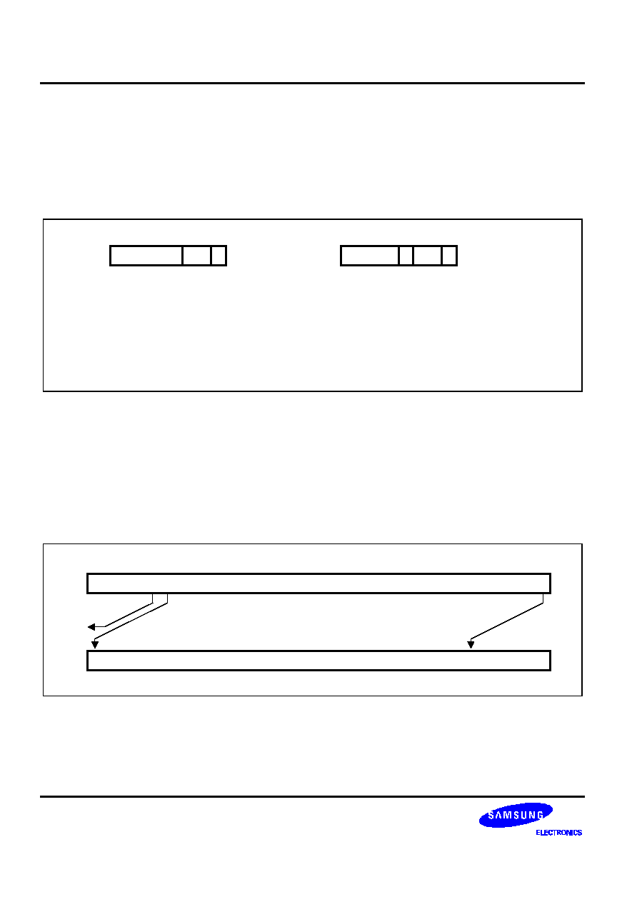
ARM INSTRUCTION SET
S3F441FX RISC MICROCONTROLLER
3-12
SHIFTS
When the second operand is specified to be a shifted register, the operation of the barrel shifter is controlled by
the Shift field in the instruction. This field indicates the type of shift to be performed (logical left or right,
arithmetic right or rotate right). The amount by which the register should be shifted may be contained in an
immediate field in the instruction, or in the least-significant byte of another register (other than R15). The
encoding for the different shift types is shown in Figure 3-5.
0
[6:5] Shift type
00 = logical left
01 = logical right
10 = arithmetic right 11 = rotate right
[11:7] Shift amount
5 bit unsigned integer
[6:5] Shift type
00 = logical left
01 = logical right
10 = arithmetic right 11 = rotate right
[11:8] Shift register
Shift amount specified in the
least-significant byte of Rs
4
5
6
7
11
1
4
5
6
7
11
8
0
RS
Figure 3-5. ARM Shift Operations
Instruction specified shift amount
When the shift amount is specified in the instruction, it is contained in a 5 bit field which may take any value from
0 to 31. A logical shift left (LSL) takes the contents of Rm and moves each bit by the specified amount to a more
significant position. The least significant bits of the result are filled with zeros, and the high bits of Rm which do
not map into the result are discarded, except that the least significant discarded bit becomes the shifter carry
output which may be latched into the C bit of the CPSR when the ALU operation is in the logical class (see
above). For example, the effect of LSL #5 is shown in Figure 3-6.
31
27 26
Contents of Rm
Value of Operand 2
carry out
0
0
0
0
0
0
Figure 3-6. Logical Shift Left
NOTE
LSL #0 is a special case, where the shifter carry out is the old value of the CPSR C flag. The contents of
Rm are used directly as the second operand. A logical shift right (LSR) is similar, but the contents of Rm
are moved to less significant positions in the result. LSR #5 has the effect shown in Figure 3-7.
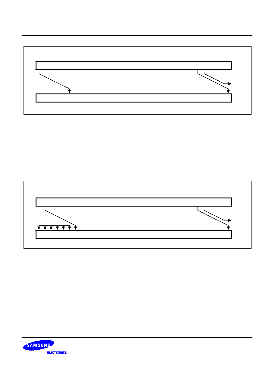
S3F441FX RISC MICROCONTROLLER
ARM INSTRUCTION SET
3-13
31
Contents of Rm
Value of Operand 2
0
carry out
4
5
0
0
0
0
0
Figure 3-7. Logical Shift Right
The form of the shift field which might be expected to correspond to LSR #0 is used to encode LSR #32, which
has a zero result with bit 31 of Rm as the carry output. Logical shift right zero is redundant as it is the same as
logical shift left zero, so the assembler will convert LSR #0 (and ASR #0 and ROR #0) into LSL #0, and allow
LSR #32 to be specified.
An arithmetic shift right (ASR) is similar to logical shift right, except that the high bits are filled with bit 31 of Rm
instead of zeros. This preserves the sign in 2's complement notation. For example, ASR #5 is shown in Figure
3-8.
31
Contents of Rm
Value of Operand 2
0
carry out
4
5
30
Figure 3-8. Arithmetic Shift Right
The form of the shift field which might be expected to give ASR #0 is used to encode ASR #32. Bit 31 of Rm is
again used as the carry output, and each bit of operand 2 is also equal to bit 31 of Rm. The result is therefore all
ones or all zeros, according to the value of bit 31 of Rm.
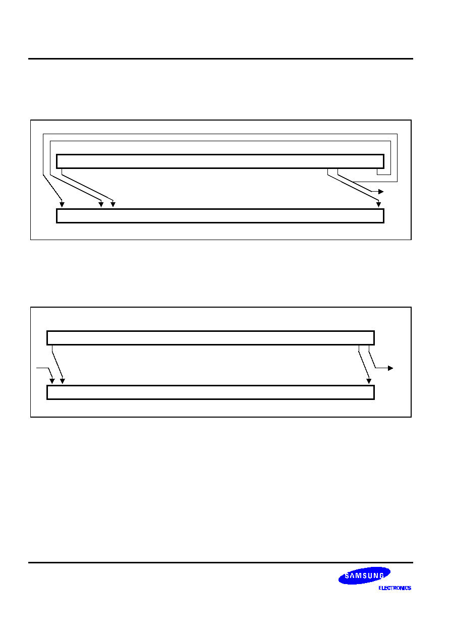
ARM INSTRUCTION SET
S3F441FX RISC MICROCONTROLLER
3-14
Rotate right (ROR) operations reuse the bits which "overshoot" in a logical shift right operation by reintroducing
them at the high end of the result, in place of the zeros used to fill the high end in logical right operations. For
example, ROR #5 is shown in Figure 3-9.
31
Contents of Rm
Value of Operand 2
0
carry out
4
5
Figure 3-9. Rotate Right
The form of the shift field which might be expected to give ROR #0 is used to encode a special function of the
barrel shifter, rotate right extended (RRX). This is a rotate right by one bit position of the 33 bit quantity formed by
appending the CPSR C flag to the most significant end of the contents of Rm as shown in Figure 3-10.
31
Contents of Rm
Value of Operand 2
0
1
carry out
C
in
Figure 3-10. Rotate Right Extended

S3F441FX RISC MICROCONTROLLER
ARM INSTRUCTION SET
3-15
Register specified shift amount
Only the least significant byte of the contents of Rs is used to determine the shift amount. Rs can be any general
register other than R15.
If this byte is zero, the unchanged contents of Rm will be used as the second operand, and the old value of the
CPSR C flag will be passed on as the shifter carry output.
If the byte has a value between 1 and 31, the shifted result will exactly match that of an instruction specified shift
with the same value and shift operation.
If the value in the byte is 32 or more, the result will be a logical extension of the shift described above:
1.
LSL by 32 has result zero, carry out equal to bit 0 of Rm.
2.
LSL by more than 32 has result zero, carry out zero.
3.
LSR by 32 has result zero, carry out equal to bit 31 of Rm.
4.
LSR by more than 32 has result zero, carry out zero.
5.
ASR by 32 or more has result filled with the value of bit 31 of Rm, carry out equal to bit 31 of Rm.
6.
ROR by 32 has result equal to Rm, carry out equal to bit 31 of Rm.
7.
ROR by n where n is greater than 32 will give the same result and carry out as ROR by n-32; therefore
repeatedly subtract 32 from n until the amount is in the range 1 to 32 and see above.
NOTE
The zero in bit 7 of an instruction with a register controlled shift is compulsory; a one in this bit will cause
the instruction to be a multiply or undefined instruction.

ARM INSTRUCTION SET
S3F441FX RISC MICROCONTROLLER
3-16
IMMEDIATE OPERAND ROTATES
The immediate operand rotate field is a 4 bit unsigned integer which specifies a shift operation on the 8 bit
immediate value. This value is zero extended to 32 bits, and then subject to a rotate right by twice the value in
the rotate field. This enables many common constants to be generated, for example all powers of 2.
WRITING TO R15
When Rd is a register other than R15, the condition code flags in the CPSR may be updated from the ALU flags
as described above.
When Rd is R15 and the S flag in the instruction is not set the result of the operation is placed in R15 and the
CPSR is unaffected.
When Rd is R15 and the S flag is set the result of the operation is placed in R15 and the SPSR corresponding to
the current mode is moved to the CPSR. This allows state changes which automatically restore both PC and
CPSR. This form of instruction should not be used in User mode.
USING R15 AS AN OPERAND
If R15 (the PC) is used as an operand in a data processing instruction the register is used directly.
The PC value will be the address of the instruction, plus 8 or 12 bytes due to instruction pre-fetching. If the shift
amount is specified in the instruction, the PC will be 8 bytes ahead. If a register is used to specify the shift
amount the PC will be 12 bytes ahead.
TEQ, TST, CMP AND CMN OPCODES
NOTE
TEQ, TST, CMP and CMN do not write the result of their operation but do set flags in the CPSR. An
assembler should always set the S flag for these instructions even if this is not specified in the
mnemonic.
The TEQP form of the TEQ instruction used in earlier ARM processors must not be used: the PSR transfer
operations should be used instead.
The action of TEQP in the ARM7TDMI is to move SPSR_<mode> to the CPSR if the processor is in a privileged
mode and to do nothing if in User mode.
INSTRUCTION CYCLE TIMES
Data Processing instructions vary in the number of incremental cycles taken as follows:
Table 3-4. Incremental Cycle Times
Processing Type
Cycles
Normal data processing
1S
Data processing with register specified shift
1S + 1I
Data processing with PC written
2S + 1N
Data processing with register specified shift and PC written
2S + 1N +1I
NOTE: S, N and I are as defined sequential (S-cycle), non-sequential (N-cycle), and internal (I-cycle) respectively.

S3F441FX RISC MICROCONTROLLER
ARM INSTRUCTION SET
3-17
ASSEMBLER SYNTAX
∑
∑
MOV,MVN (single operand instructions).
<opcode>{cond}{S} Rd,<Op2>
∑
∑
CMP,CMN,TEQ,TST (instructions which do not produce a result).
<opcode>{cond} Rn,<Op2>
∑
∑
AND,EOR,SUB,RSB,ADD,ADC,SBC,RSC,ORR,BIC
<opcode>{cond}{S} Rd,Rn,<Op2>
where:
<Op2>
Rm{,<shift>} or,<#expression>
{
cond}
A two-character condition mnemonic. See Table 3-2.
{
S}
Set condition codes if S present (implied for CMP, CMN, TEQ, TST).
Rd, Rn and Rm
Expressions evaluating to a register number.
<#expression>
If this is used, the assembler will attempt to generate a shifted immediate 8-bit field to
match the expression. If this is impossible, it will give an error.
<shift>
<Shiftname> <register> or <shiftname> #expression, or RRX (rotate right one bit with
extend).
<shiftname>s
ASL, LSL, LSR, ASR, ROR. (ASL is a synonym for LSL, they assemble to the same
code.)
EXAMPLES
ADDEQ
R2,R4,R5
; If the Z flag is set make R2:=R4+R5
TEQS
R4,#3
; Test R4 for equality with 3.
; (The S is in fact redundant as the
; assembler inserts it automatically.)
SUB
R4,R5,R7,LSR R2
; Logical right shift R7 by the number in
; the bottom byte of R2, subtract result
; from R5, and put the answer into R4.
MOV
PC,R14
; Return from subroutine.
MOVS
PC,R14
; Return from exception and restore CPSR
; from SPSR_mode.

ARM INSTRUCTION SET
S3F441FX RISC MICROCONTROLLER
3-18
PSR TRANSFER (MRS, MSR)
The instruction is only executed if the condition is true. The various conditions are defined in Table 3-2.
The MRS and MSR instructions are formed from a subset of the Data Processing operations and are
implemented using the TEQ, TST, CMN and CMP instructions without the S flag set. The encoding is shown in
Figure 3-11.
These instructions allow access to the CPSR and SPSR registers. The MRS instruction allows the contents of the
CPSR or SPSR_<mode> to be moved to a general register. The MSR instruction allows the contents of a general
register to be moved to the CPSR or SPSR_<mode> register.
The MSR instruction also allows an immediate value or register contents to be transferred to the condition code
flags (N,Z,C and V) of CPSR or SPSR_<mode> without affecting the control bits. In this case, the top four bits of
the specified register contents or 32 bit immediate value are written to the top four bits of the relevant PSR.
OPERAND RESTRICTIONS
∑
∑
In user mode, the control bits of the CPSR are protected from change, so only the condition code flags of the
CPSR can be changed. In other (privileged) modes the entire CPSR can be changed.
∑
∑
Note that the software must never change the state of the T bit in the CPSR. If this happens, the processor
will enter an unpredictable state.
∑
∑
The SPSR register which is accessed depends on the mode at the time of execution. For example, only
SPSR_fiq is accessible when the processor is in FIQ mode.
∑
∑
You must not specify R15 as the source or destination register.
∑
∑
Also, do not attempt to access an SPSR in User mode, since no such register exists.
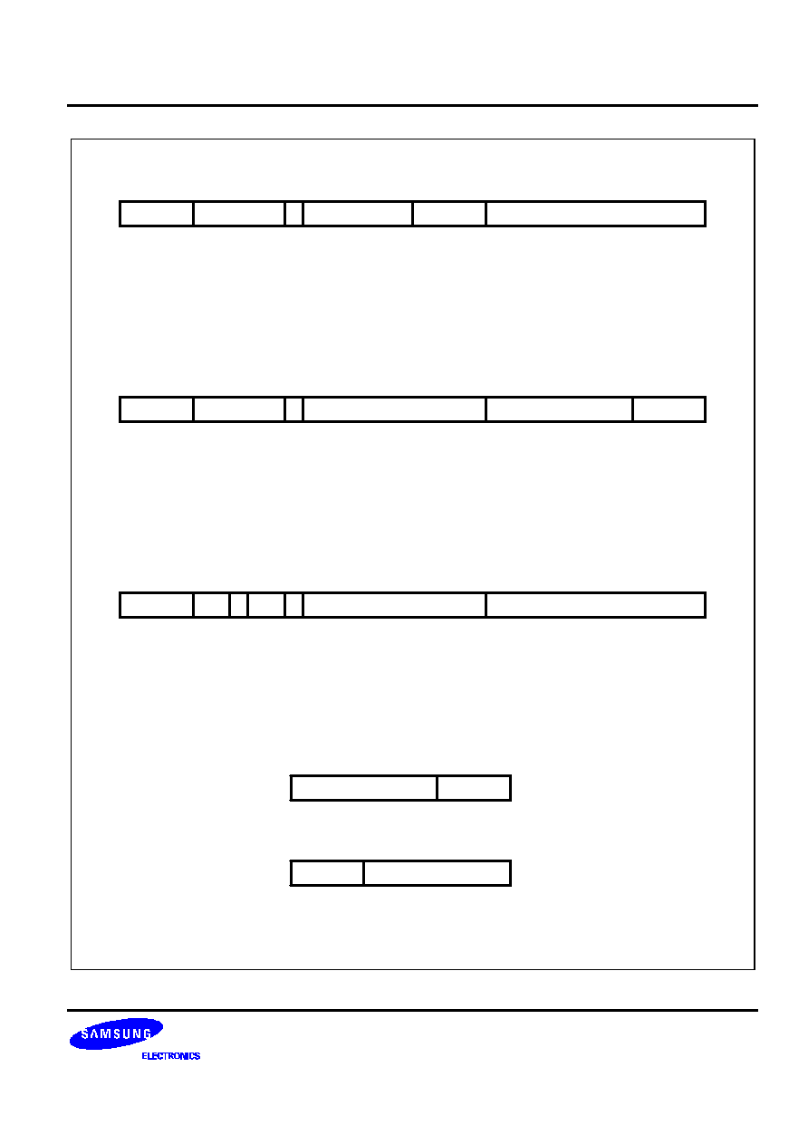
S3F441FX RISC MICROCONTROLLER
ARM INSTRUCTION SET
3-19
MSR (transfer register contents or immediate value to PSR flag bits only)
Cond
Source operand
Pd
101001111
31
22
27
28
11
12
21
23
I
10
00
26 25 24
0
Cond
00000000
00010
Pd
101001111
31
22
27
28
11
12
21
23
Rm
MSR (transfer register contents to PSR)
4 3
0
Cond
000000000000
00010
Rd
Ps
001111
31
22
27
15
28
16
11
12
21
23
MRS (transfer PSR contents to a register)
0
[3:0] Source Register
[22] Destination PSR
0 = CPSR
1 = SPSR_<current mode>
[31:28] Condition Field
[15:12] Destination Register
[22] Source PSR
0 = CPSR
1 = SPSR_<current mode>
[31:28] Condition Field
[3:0] Source Register
[11:4] Source operand is an immediate value
[7:0] Unsigned 8 bit immediate value
[11:8] Rotate applied to Imm
[22] Destination PSR
0 = CPSR
1 = SPSR_<current mode>
[25] Immediate Operand
0 = Source operand is a register
1 = Source operand is a immediate value
[11:0] Source Operand
[31:28] Condition Field
00000000
Rm
11
4 3
0
Rotate
Imm
11
0
8 7
Figure 3-11. PSR Transfer

ARM INSTRUCTION SET
S3F441FX RISC MICROCONTROLLER
3-20
RESERVED BITS
Only twelve bits of the PSR are defined in ARM7TDMI (N,Z,C,V,I,F, T & M[4:0]); the remaining bits are reserved
for use in future versions of the processor. Refer to Figure 2-6 for a full description of the PSR bits.
To ensure the maximum compatibility between ARM7TDMI programs and future processors, the following rules
should be observed:
∑
The reserved bits should be preserved when changing the value in a PSR.
∑
Programs should not rely on specific values from the reserved bits when checking the PSR status, since they
may read as one or zero in future processors.
A read-modify-write strategy should therefore be used when altering the control bits of any PSR register; this
involves transferring the appropriate PSR register to a general register using the MRS instruction, changing only
the relevant bits and then transferring the modified value back to the PSR register using the MSR instruction.
Examples
The following sequence performs a mode change:
MRS
R0,CPSR
; Take a copy of the CPSR.
BIC
R0,R0,#0x1F
; Clear the mode bits.
ORR
R0,R0,#new_mode
; Select new mode
MSR
CPSR,R0
; Write back the modified CPSR.
When the aim is simply to change the condition code flags in a PSR, a value can be written directly to the flag
bits without disturbing the control bits. The following instruction sets the N,Z,C and V flags:
MSR
CPSR_flg,#0xF0000000
; Set all the flags regardless of their previous state
; (does not affect any control bits).
No attempt should be made to write an 8 bit immediate value into the whole PSR since such an operation cannot
preserve the reserved bits.
INSTRUCTION CYCLE TIMES
PSR transfers take 1S incremental cycles, where S is defined as Sequential (S-cycle).

S3F441FX RISC MICROCONTROLLER
ARM INSTRUCTION SET
3-21
ASSEMBLY SYNTAX
∑
∑
MRS - transfer PSR contents to a register
MRS{cond} Rd,<psr>
∑
∑
MSR - transfer register contents to PSR
MSR{cond} <psr>,Rm
∑
∑
MSR - transfer register contents to PSR flag bits only
MSR{cond} <psrf>,Rm
The most significant four bits of the register contents are written to the N,Z,C & V flags respectively.
∑
∑
MSR - transfer immediate value to PSR flag bits only
MSR{cond} <psrf>,<#expression>
The expression should symbolise a 32 bit value of which the most significant four bits are written to the N,Z,C
and V flags respectively.
Key:
{
cond}
Two-character condition mnemonic. See Table 3-2..
Rd and Rm
Expressions evaluating to a register number other than R15
<psr>
CPSR, CPSR_all, SPSR or SPSR_all. (CPSR and CPSR_all are synonyms as are SPSR
and SPSR_all)
<psrf>
CPSR_flg or SPSR_flg
<#expression>
Where this is used, the assembler will attempt to generate a shifted immediate 8-bit field
to match the expression. If this is impossible, it will give an error.
EXAMPLES
In User mode the instructions behave as follows:
MSR
CPSR_all,Rm
; CPSR[31:28]
Rm[31:28]
MSR
CPSR_flg,Rm
; CPSR[31:28]
Rm[31:28]
MSR
CPSR_flg,#0xA0000000
; CPSR[31:28]
0xA (set N,C; clear Z,V)
MRS
Rd,CPSR
; Rd[31:0]
CPSR[31:0]
In privileged modes the instructions behave as follows:
MSR
CPSR_all,Rm
; CPSR[31:0]
Rm[31:0]
MSR
CPSR_flg,Rm
; CPSR[31:28]
Rm[31:28]
MSR
CPSR_flg,#0x50000000
; CPSR[31:28]
0x5 (set Z,V; clear N,C)
MSR
SPSR_all,Rm
; SPSR_<mode>[31:0]
Rm[31:0]
MSR
SPSR_flg,Rm
; SPSR_<mode>[31:28]
Rm[31:28]
MSR
SPSR_flg,#0xC0000000
; SPSR_<mode>[31:28]
0xC (set N,Z; clear C,V)
MRS
Rd,SPSR
; Rd[31:0]
SPSR_<mode>[31:0]

ARM INSTRUCTION SET
S3F441FX RISC MICROCONTROLLER
3-22
MULTIPLY AND MULTIPLY-ACCUMULATE (MUL, MLA)
The instruction is only executed if the condition is true. The various conditions are defined in Table 3-2. The
instruction encoding is shown in Figure 3-12.
The multiply and multiply-accumulate instructions use an 8 bit Booth's algorithm to perform integer multiplication.
31
27
19
15
Cond
28
16
11
12
21 20
S
Rd
Rn
[15:12][11:8][3:0] Operand Registers
[19:16] Destination Register
[20] Set Condition Code
0 = Do not alter condition codes
1 = Set condition codes
[21] Accumulate
0 = Multiply only
1 = Multiply and accumulate
[31:28] Condition Field
22
1 0 0 1
Rs
Rm
A
0
0
0 0 0 0
8 7
4 3
0
Figure 3-12. Multiply Instructions
The multiply form of the instruction gives Rd=Rm
◊
Rs. Rn is ignored, and should be set to zero for compatibility
with possible future upgrades to the instruction set. The multiply-accumulate form gives Rd=Rm
◊
Rs+Rn, which
can save an explicit ADD instruction in some circumstances. Both forms of the instruction work on operands
which may be considered as signed (2's complement) or unsigned integers.
The results of a signed multiply and of an unsigned multiply of 32 bit operands differ only in the upper 32 bits -
the low 32 bits of the signed and unsigned results are identical. As these instructions only produce the low 32 bits
of a multiply, they can be used for both signed and unsigned multiplies.
For example consider the multiplication of the operands:
Operand A
Operand B
Result
0xFFFFFFF6 0x0000001
0xFFFFFF38

S3F441FX RISC MICROCONTROLLER
ARM INSTRUCTION SET
3-23
If the Operands Are Interpreted as Signed
Operand A has the value -10, operand B has the value 20, and the result is -200 which is correctly represented as
0xFFFFFF38.
If the Operands Are Interpreted as Unsigned
Operand A has the value 4294967286, operand B has the value 20 and the result is 85899345720, which is
represented as 0x13FFFFFF38, so the least significant 32 bits are 0xFFFFFF38.
Operand Restrictions
The destination register Rd must not be the same as the operand register Rm. R15 must not be used as an
operand or as the destination register.
All other register combinations will give correct results, and Rd, Rn and Rs may use the same register when
required.

ARM INSTRUCTION SET
S3F441FX RISC MICROCONTROLLER
3-24
CPSR FLAGS
Setting the CPSR flags is optional, and is controlled by the S bit in the instruction. The N (Negative) and Z (Zero)
flags are set correctly on the result (N is made equal to bit 31 of the result, and Z is set if and only if the result is
zero). The C (Carry) flag is set to a meaningless value and the V (oVerflow) flag is unaffected.
INSTRUCTION CYCLE TIMES
MUL takes 1S + mI and MLA 1S + (m+1)I cycles to execute, where S and I are defined as sequential (S-cycle)
and internal (I-cycle), respectively.
m
The number of 8 bit multiplier array cycles is required to complete the multiply, which is
controlled by the value of the multiplier operand specified by Rs. Its possible values are
as follows
1
If bits [32:8] of the multiplier operand are all zero or all one.
2
If bits [32:16] of the multiplier operand are all zero or all one.
3
If bits [32:24] of the multiplier operand are all zero or all one.
4
In all other cases.
ASSEMBLER SYNTAX
MUL{cond}{S} Rd,Rm,Rs
MLA{cond}{S} Rd,Rm,Rs,Rn
{
cond}
Two-character condition mnemonic. See Table 3-2..
{
S}
Set condition codes if S present
Rd, Rm, Rs and Rn
Expressions evaluating to a register number other than R15.
EXAMPLES
MUL
R1,R2,R3
; R1:=R2*R3
MLAEQS
R1,R2,R3,R4
; Conditionally R1:=R2*R3+R4, Setting condition codes.

S3F441FX RISC MICROCONTROLLER
ARM INSTRUCTION SET
3-25
MULTIPLY LONG AND MULTIPLY-ACCUMULATE LONG (MULL, MLAL)
The instruction is only executed if the condition is true. The various conditions are defined in Table 3-2. The
instruction encoding is shown in Figure 3-13.
The multiply long instructions perform integer multiplication on two 32 bit operands and produce 64 bit results.
Signed and unsigned multiplication each with optional accumulate give rise to four variations.
31
27
19
15
Cond
28
16
11
12
21
23
U
20
S
RdHi
RdLo
[11:8][3:0] Operand Registers
[19:16][15:12] Source Destination Registers
[20] Set Condition Code
0 = Do not alter condition codes
1 = Set condition codes
[21] Accumulate
0 = Multiply only
1 = Multiply and accumulate
[22] Unsigned
0 = Unsigned
1 = Signed
[31:28] Condition Field
22
0
0
0 0 1
1 0 0 1
Rs
Rm
A
8 7
4 3
0
Figure 3-13. Multiply Long Instructions
The multiply forms (UMULL and SMULL) take two 32 bit numbers and multiply them to produce a 64 bit result of
the form RdHi,RdLo := Rm * Rs. The lower 32 bits of the 64 bit result are written to RdLo, the upper 32 bits of the
result are written to RdHi.
The multiply-accumulate forms (UMLAL and SMLAL) take two 32 bit numbers, multiply them and add a 64 bit
number to produce a 64 bit result of the form RdHi,RdLo := Rm * Rs + RdHi,RdLo. The lower 32 bits of the 64 bit
number to add is read from RdLo. The upper 32 bits of the 64 bit number to add is read from RdHi. The lower 32
bits of the 64 bit result are written to RdLo. The upper 32 bits of the 64 bit result are written to RdHi.
The UMULL and UMLAL instructions treat all of their operands as unsigned binary numbers and write an
unsigned 64 bit result. The SMULL and SMLAL instructions treat all of their operands as two's-complement
signed numbers and write a two's-complement signed 64 bit result.

ARM INSTRUCTION SET
S3F441FX RISC MICROCONTROLLER
3-26
OPERAND RESTRICTIONS
∑
∑
R15 must not be used as an operand or as a destination register.
∑
∑
RdHi, RdLo, and Rm must all specify different registers.
CPSR FLAGS
Setting the CPSR flags is optional, and is controlled by the S bit in the instruction. The N and Z flags are set
correctly on the result (N is equal to bit 63 of the result, Z is set if and only if all 64 bits of the result are zero).
Both the C and V flags are set to meaningless values.
INSTRUCTION CYCLE TIMES
MULL takes 1S + (m+1)I and MLAL 1S + (m+2)I cycles to execute, where m is the number of 8 bit multiplier
array cycles required to complete the multiply, which is controlled by the value of the multiplier operand specified
by Rs.
Its possible values are as follows:
For Signed INSTRUCTIONS SMULL, SMLAL:
∑
∑
If bits [31:8] of the multiplier operand are all zero or all one.
∑
∑
If bits [31:16] of the multiplier operand are all zero or all one.
∑
∑
If bits [31:24] of the multiplier operand are all zero or all one.
∑
∑
In all other cases.
For Unsigned Instructions UMULL, UMLAL:
∑
∑
If bits [31:8] of the multiplier operand are all zero.
∑
∑
If bits [31:16] of the multiplier operand are all zero.
∑
∑
If bits [31:24] of the multiplier operand are all zero.
∑
∑
In all other cases.
S and I are defined as sequential (S-cycle) and internal (I-cycle), respectively.

S3F441FX RISC MICROCONTROLLER
ARM INSTRUCTION SET
3-27
ASSEMBLER SYNTAX
Table 3-5. Assembler Syntax Descriptions
Mnemonic
Description
Purpose
UMULL{cond}{S} RdLo,RdHi,Rm,Rs
Unsigned Multiply Long
32 x 32 = 64
UMLAL{cond}{S} RdLo,RdHi,Rm,Rs
Unsigned Multiply & Accumulate Long
32 x 32 + 64 = 64
SMULL{cond}{S} RdLo,RdHi,Rm,Rs
Signed Multiply Long
32 x 32 = 64
SMLAL{cond}{S} RdLo,RdHi,Rm,Rs
Signed Multiply & Accumulate Long
32 x 32 + 64 = 64
where:
{
cond}
Two-character condition mnemonic. See Table 3-2.
{S}
Set condition codes if S present
RdLo, RdHi, Rm, Rs
Expressions evaluating to a register number other than R15.
EXAMPLES
UMULL
R1,R4,R2,R3
; R4,R1:=R2*R3
UMLALS
R1,R5,R2,R3
; R5,R1:=R2*R3+R5,R1 also setting condition codes
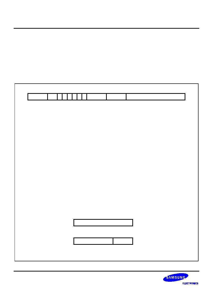
ARM INSTRUCTION SET
S3F441FX RISC MICROCONTROLLER
3-28
SINGLE DATA TRANSFER (LDR, STR)
The instruction is only executed if the condition is true. The various conditions are defined in Table 3-2. The
instruction encoding is shown in Figure 3-14.
The single data transfer instructions are used to load or store single bytes or words of data. The memory address
used in the transfer is calculated by adding an offset to or subtracting an offset from a base register.
The result of this calculation may be written back into the base register if auto-indexing is required.
31
27
19
15
0
Cond
28
16
11
12
21
23
B
20
L
Rn
Rd
22
01
I
P U
Offset
W
26
24
25
[15:12] Source/Destination Registers
[19:16] Base Register
[20] Load/Store Bit
0 = Store to memory
1 = Load from memory
[21] Write-back Bit
0 = No write-back
1 = Write address into base
[22] Byte/Word Bit
0 = Transfer word quantity
1 = Transfer byte quantity
[23] Up/Down Bit
0 = Down: subtract offset from base
1 = Up: add offset to base
[24] Pre/Post Indexing Bit
0 = Post: add offset after transfer
1 = Pre: add offset before transfer
[25] Immediate Offset
0 = Offset is an immediate value
1 = Offset is an register value
[11:0] Offset
Shift
Immediate
[11:0] Unsigned 12-bit immediate offset
11
11
Rm
[3:0] Offset register [11:4] Shift applied to Rm
[31:28] Condition Field
0
4 3
0
Figure 3-14. Single Data Transfer Instructions

S3F441FX RISC MICROCONTROLLER
ARM INSTRUCTION SET
3-29
OFFSETS AND AUTO-INDEXING
The offset from the base may be either a 12 bit unsigned binary immediate value in the instruction, or a second
register (possibly shifted in some way). The offset may be added to (U=1) or subtracted from (U=0) the base
register Rn. The offset modification may be performed either before (pre-indexed, P=1) or after (post-indexed,
P=0) the base is used as the transfer address.
The W bit gives optional auto increment and decrement addressing modes. The modified base value may be
written back into the base (W=1), or the old base value may be kept (W=0). In the case of post-indexed
addressing, the write back bit is redundant and is always set to zero, since the old base value can be retained by
setting the offset to zero. Therefore post-indexed data transfers always write back the modified base. The only
use of the W bit in a post-indexed data transfer is in privileged mode code, where setting the W bit forces non-
privileged mode for the transfer, allowing the operating system to generate a user address in a system where the
memory management hardware makes suitable use of this hardware.
SHIFTED REGISTER OFFSET
The 8 shift control bits are described in the data processing instructions section. However, the register specified
shift amounts are not available in this instruction class. See Figure 3-5.
BYTES AND WORDS
This instruction class may be used to transfer a byte (B=1) or a word (B=0) between an ARM7TDMI register and
memory.
The action of LDR(B) and STR(B) instructions is influenced by the BIGEND control signal of ARM7TDMI core.
The two possible configurations are described below.
Little-Endian Configuration
A byte load (LDRB) expects the data on data bus inputs 7 through 0 if the supplied address is on a word
boundary, on data bus inputs 15 through 8 if it is a word address plus one byte, and so on. The selected byte is
placed in the least significant 8 bits of the destination register, and the remaining bits of the register are filled with
zeros. Please see Figure 2-2.
A byte store (STRB) repeats the least significant 8 bits of the source register four times across data bus outputs
31 through 0. The external memory system should activate the appropriate byte subsystem to store the data.
A word load (LDR) will normally use a word aligned address. However, an address offset from a word boundary
will cause the data to be rotated into the register so that the addressed byte occupies bits 0 to 7. This means that
half-words accessed at offsets 0 and 2 from the word boundary will be correctly loaded into bits 0 through 15 of
the register. Two shift operations are then required to clear or to sign extend the upper 16 bits.
A word store (STR) should generate a word aligned address. The word presented to the data bus is not affected if
the address is not word aligned. That is, bit 31 of the register being stored always appears on data bus output 31.
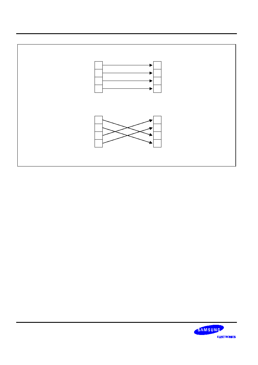
ARM INSTRUCTION SET
S3F441FX RISC MICROCONTROLLER
3-30
LDR from word aligned address
A+3
A
A+2
A+1
memory
24
16
8
0
A
B
C
D
register
24
16
8
0
A
B
C
D
LDR from address offset by 2
A+3
A
A+2
A+1
memory
24
16
8
0
A
B
C
D
register
24
16
8
0
A
B
C
D
Figure 3-15. Little-Endian Offset Addressing
Big-Endian Configuration
A byte load (LDRB) expects the data on data bus inputs 31 through 24 if the supplied address is on a word
boundary, on data bus inputs 23 through 16 if it is a word address plus one byte, and so on. The selected byte is
placed in the least significant 8 bits of the destination register and the remaining bits of the register are filled with
zeros. Please see Figure 2-1.
A byte store (STRB) repeats the least significant 8 bits of the source register four times across data bus outputs
31 through 0. The external memory system should activate the appropriate byte subsystem to store the data.
A word load (LDR) should generate a word aligned address. An address offset of 0 or 2 from a word boundary will
cause the data to be rotated into the register so that the addressed byte occupies bits 31 through 24. This means
that half-words accessed at these offsets will be correctly loaded into bits 16 through 31 of the register. A shift
operation is then required to move (and optionally sign extend) the data into the bottom 16 bits. An address offset
of 1 or 3 from a word boundary will cause the data to be rotated into the register so that the addressed byte
occupies bits 15 through 8.
A word store (STR) should generate a word aligned address. The word presented to the data bus is not affected if
the address is not word aligned. That is, bit 31 of the register being stored always appears on data bus output 31.

S3F441FX RISC MICROCONTROLLER
ARM INSTRUCTION SET
3-31
USE OF R15
Write-back must not be specified if R15 is specified as the base register (Rn). When using R15 as the base
register you must remember it contains an address 8 bytes on from the address of the current instruction.
R15 must not be specified as the register offset (Rm).
When R15 is the source register (Rd) of a register store (STR) instruction, the stored value will be address of the
instruction plus 12.
RESTRICTION ON THE USE OF BASE REGISTER
When configured for late aborts, the following example code is difficult to unwind as the base register, Rn, gets
updated before the abort handler starts. Sometimes it may be impossible to calculate the initial value.
After an abort, the following example code is difficult to unwind as the base register, Rn, gets updated before the
abort handler starts. Sometimes it may be impossible to calculate the initial value.
Example:
LDR
R0,[R1],R1
Therefore a post-indexed LDR or STR where Rm is the same register as Rn should not be used.
DATA ABORTS
A transfer to or from a legal address may cause problems for a memory management system. For instance, in a
system which uses virtual memory the required data may be absent from main memory. The memory manager
can signal a problem by taking the processor ABORT input HIGH whereupon the Data Abort trap will be taken. It
is up to the system software to resolve the cause of the problem, then the instruction can be restarted and the
original program continued.
INSTRUCTION CYCLE TIMES
Normal LDR instructions take 1S + 1N + 1I and LDR PC take 2S + 2N +1I incremental cycles, where S,N and I
are defined as squential (S-cycle), non-sequential (N-cycle), and internal (I-cycle), respectively. STR instructions
take 2N incremental cycles to execute.

ARM INSTRUCTION SET
S3F441FX RISC MICROCONTROLLER
3-32
ASSEMBLER SYNTAX
<LDR|STR>{cond}{B}{T} Rd,<Address>
where:
LDR
Load from memory into a register
STR
Store from a register into memory
{
cond}
Two-character condition mnemonic. See Table 3-2.
{
B}
If B is present then byte transfer, otherwise word transfer
{
T}
If T is present the W bit will be set in a post-indexed instruction, forcing non-privileged
mode for the transfer cycle. T is not allowed when a pre-indexed addressing mode is
specified or implied.
Rd
An expression evaluating to a valid register number.
Rn and Rm
Expressions evaluating to a register number. If Rn is R15 then the assembler will
subtract 8 from
the offset value to allow for ARM7TDMI pipelining. In this case base write-back should
not be specified.
<Address>can be:
1
An expression which generates an address:
The assembler will attempt to generate an instruction using the PC as a base and a
corrected immediate offset to address the location given by evaluating the expression.
This will be a PC relative, pre-indexed address. If the address is out of range, an error
will be generated.
2
A pre-indexed addressing specification:
[Rn]
offset of zero
[Rn,<#expression>]{!}
offset of <expression> bytes
[Rn,{+/-}Rm{,<shift>}]{!}
offset of +/- contents of index register, shifted
by <shift>
3
A post-indexed addressing specification:
[Rn],<#expression>
offset of <expression> bytes
[Rn],{+/-}Rm{,<shift>}
offset of +/- contents of index register, shifted as
by <shift>.
<shift>
General shift operation (see data processing instructions) but you cannot specify the shift
amount by a register.
{
!}
Writes back the base register (set the W bit) if! is present.

S3F441FX RISC MICROCONTROLLER
ARM INSTRUCTION SET
3-33
EXAMPLES
STR
R1,[R2,R4]!
; Store R1 at R2+R4 (both of which are registers)
; and write back address to R2.
STR
R1,[R2],R4
; Store R1 at R2 and write back R2+R4 to R2.
LDR
R1,[R2,#16]
; Load R1 from contents of R2+16, but don't write back.
LDR
R1,[R2,R3,LSL#2]
; Load R1 from contents of R2+R3*4.
LDREQB
R1,[R6,#5]
; Conditionally load byte at R6+5 into
; R1 bits 0 to 7, filling bits 8 to 31 with zeros.
STR
R1,PLACE
; Generate PC relative offset to address PLACE.
PLACE

ARM INSTRUCTION SET
S3F441FX RISC MICROCONTROLLER
3-34
HALFWORD AND SIGNED BYTE DATA TRANSFER (LDRH/STRH/LDRSB/LDRSH)
The instruction is only executed if the condition is true. The various conditions are defined in Table 3-2. The
instruction encoding is shown in Figure 3-16.
These instructions are used to load or store half-words of data and also load sign-extended bytes. The memory
address used in the transfer is calculated by adding an offset to or subtracting an offset from a base register. The
result of this calculation may be written back into the base register if auto-indexing is required.
31
27
19
15
Cond
28
16
11
12
21
23
0
20
L
Rn
Rd
[3:0] Offset Register
[6][5] S H
0 0 = SWP instruction
0 1 = Unsigned halfword
1 1 = Signed byte
1 1 = Signed halfword
[15:12] Source/Destination Register
[19:16] Base Register
[20] Load/Store
0 = Store to memory
1 = Load from memory
[21] Write-back
0 = No write-back
1 = Write address into base
[23] Up/Down
0 = Down: subtract offset from base
1 = Up: add offset to base
[24] Pre/Post Indexing
0 = Post: add/subtract offset after transfer
1 = Pre: add/subtract offset bofore transfer
[31:28] Condition Field
22
000
P U
0000
W
24
25
1
Rm
S H 1
8 7 6
5 4 3
0
Figure 3-16. Half-word and Signed Byte Data Transfer with Register Offset

S3F441FX RISC MICROCONTROLLER
ARM INSTRUCTION SET
3-35
31
27
19
15
Cond
28
16
11
12
21
23
1
20
L
Rn
Rd
[3:0] Immediate Offset (Low Nibble)
[6][5] S H
0 0 = SWP instruction
0 1 = Unsigned halfword
1 1 = Signed byte
1 1 = Signed halfword
[11:8] Immediate Offset (High Nibble)
[15:12] Source/Destination Register
[19:16] Base Register
[20] Load/Store
0 = Store to memory
1 = Load from memory
[21] Write-back
0 = No write-back
1 = Write address into base
[23] Up/Down
0 = Down: subtract offset from base
1 = Up: add offset to base
[24] Pre/Post Indexing
0 = Post: add/subtract offset after transfer
1 = Pre: add/subtract offset bofore transfer
[31:28] Condition Field
22
000
P U
Offset
W
24
25
1
Offset
S H 1
8 7 6
5 4 3
0
Figure 3-17. Half-word and Signed Byte Data Transfer with Immediate Offset and Auto-Indexing
OFFSETS AND AUTO-INDEXING
The offset from the base may be either a 8-bit unsigned binary immediate value in the instruction, or a second
register. The 8-bit offset is formed by concatenating bits 11 to 8 and bits 3 to 0 of the instruction word, such that
bit 11 becomes the MSB and bit 0 becomes the LSB. The offset may be added to (U=1) or subtracted from (U=0)
the base register Rn. The offset modification may be performed either before (pre-indexed, P=1) or after (post-
indexed, P=0) the base register is used as the transfer address.
The W bit gives optional auto-increment and decrement addressing modes. The modified base value may be
written back into the base (W=1), or the old base may be kept (W=0). In the case of post-indexed addressing, the
write back bit is redundant and is always set to zero, since the old base value can be retained if necessary by
setting the offset to zero. Therefore post-indexed data transfers always write back the modified base.
The Write-back bit should not be set high (W=1) when post-indexed addressing is selected.

ARM INSTRUCTION SET
S3F441FX RISC MICROCONTROLLER
3-36
HALF-WORD LOAD AND STORES
Setting S=0 and H=1 may be used to transfer unsigned Half-words between an ARM7TDMI register and memory.
The action of LDRH and STRH instructions is influenced by the BIGEND control signal. The two possible
configurations are described in the section below.
SIGNED BYTE AND HALF-WORD LOADS
The S bit controls the loading of sign-extended data. When S=1 the H bit selects between Bytes (H=0) and Half-
words (H=1). The L bit should not be set low (Store) when Signed (S=1) operations have been selected.
The LDRSB instruction loads the selected Byte into bits 7 to 0 of the destination register and bits 31 to 8 of the
destination register are set to the value of bit 7, the sign bit.
The LDRSH instruction loads the selected Half-word into bits 15 to 0 of the destination register and bits 31 to 16
of the destination register are set to the value of bit 15, the sign bit.
The action of the LDRSB and LDRSH instructions is influenced by the BIGEND control signal. The two possible
configurations are described in the following section.
ENDIANNESS AND BYTE/HALF-WORD SELECTION
Little-Endian Configuration
A signed byte load (LDRSB) expects data on data bus inputs 7 through to 0 if the supplied address is on a word
boundary, on data bus inputs 15 through to 8 if it is a word address plus one byte, and so on. The selected byte is
placed in the bottom 8 bit of the destination register, and the remaining bits of the register are filled with the sign
bit, bit 7 of the byte. Please see Figure 2-2.
A half-word load (LDRSH or LDRH) expects data on data bus inputs 15 through to 0 if the supplied address is on
a word boundary and on data bus inputs 31 through to 16 if it is a half-word boundary, (A[1]=1).The supplied
address should always be on a half-word boundary. If bit 0 of the supplied address is HIGH then the ARM7TDMI
will load an unpredictable value. The selected half-word is placed in the bottom 16 bits of the destination register.
For unsigned half-words (LDRH), the top 16 bits of the register are filled with zeros and for signed half-words
(LDRSH) the top 16 bits are filled with the sign bit, bit 15 of the half-word.
A half-word store (STRH) repeats the bottom 16 bits of the source register twice across the data bus outputs 31
through to 0. The external memory system should activate the appropriate half-word subsystem to store the data.
Note that the address must be half-word aligned, if bit 0 of the address is HIGH this will cause unpredictable
behavior.

S3F441FX RISC MICROCONTROLLER
ARM INSTRUCTION SET
3-37
Big-Endian Configuration
A signed byte load (LDRSB) expects data on data bus inputs 31 through to 24 if the supplied address is on a
word boundary, on data bus inputs 23 through to 16 if it is a word address plus one byte, and so on. The selected
byte is placed in the bottom 8 bit of the destination register, and the remaining bits of the register are filled with
the sign bit, bit 7 of the byte. Please see Figure 2-1.
A half-word load (LDRSH or LDRH) expects data on data bus inputs 31 through to 16 if the supplied address is on
a word boundary and on data bus inputs 15 through to 0 if it is a half-word boundary, (A[1]=1). The supplied
address should always be on a half-word boundary. If bit 0 of the supplied address is HIGH then the ARM7TDMI
will load an unpredictable value. The selected half-word is placed in the bottom 16 bits of the destination register.
For unsigned half-words (LDRH), the top 16 bits of the register are filled with zeros and for signed half-words
(LDRSH) the top 16 bits are filled with the sign bit, bit 15 of the half-word.
A half-word store (STRH) repeats the bottom 16 bits of the source register twice across the data bus outputs 31
through to 0. The external memory system should activate the appropriate half-word subsystem to store the data.
Note that the address must be half-word aligned, if bit 0 of the address is HIGH this will cause unpredictable
behavior.
USE OF R15
Write-back should not be specified if R15 is specified as the base register (Rn). When using R15 as the base
register you must remember it contains an address 8 bytes on from the address of the current instruction.
R15 should not be specified as the register offset (Rm).
When R15 is the source register (Rd) of a Half-word store (STRH) instruction, the stored address will be address
of the instruction plus 12.
DATA ABORTS
A transfer to or from a legal address may cause problems for a memory management system. For instance, in a
system which uses virtual memory the required data may be absent from the main memory. The memory
manager can signal a problem by taking the processor ABORT input HIGH whereupon the Data Abort trap will be
taken. It is up to the system software to resolve the cause of the problem, then the instruction can be restarted
and the original program continued.
INSTRUCTION CYCLE TIMES
Normal LDR(H,SH,SB) instructions take 1S + 1N + 1I. LDR(H,SH,SB) PC take 2S + 2N + 1I incremental cycles.
S,N and I are defined as squential (S-cycle), non-squential (N-cycle), and internal (I-cycle), respectively. STRH
instructions take 2N incremental cycles to execute.

ARM INSTRUCTION SET
S3F441FX RISC MICROCONTROLLER
3-38
ASSEMBLER SYNTAX
<LDR|STR>{cond}<H|SH|SB> Rd,<address>
LDR
Load from memory into a register
STR
Store from a register into memory
{
cond}
Two-character condition mnemonic. See Table 3-2..
H
Transfer half-word quantity
SB
Load sign extended byte (Only valid for LDR)
SH
Load sign extended half-word (Only valid for LDR)
Rd
An expression evaluating to a valid register number.
<address> can be:
1
An expression which generates an address:
The assembler will attempt to generate an instruction using the PC as a base and a
corrected immediate offset to address the location given by evaluating the expression.
This will be a PC relative, pre-indexed address. If the address is out of range, an error
will be generated.
2
A pre-indexed addressing specification:
[Rn]
offset of zero
[Rn,<#expression>]{!}
offset of <expression> bytes
[Rn,{+/-}Rm]{!}
offset of +/- contents of index register
3
A post-indexed addressing specification:
[Rn],<#expression>
offset of <expression> bytes
[Rn],{+/-}Rm
offset of +/- contents of index register.
4
Rn and Rm are expressions evaluating to a register number. If Rn is R15 then the
assembler will subtract 8 from the offset value to allow for ARM7TDMI pipelining. In this
case base write-back should not be specified.
{
!}
Writes back the base register (set the W bit) if ! is present.

S3F441FX RISC MICROCONTROLLER
ARM INSTRUCTION SET
3-39
EXAMPLES
LDRH
R1,[R2,-R3]!
; Load R1 from the contents of the half-word address
; contained in R2-R3 (both of which are registers)
; and write back address to R2
STRH
R3,[R4,#14]
; Store the half-word in R3 at R14+14 but don't write back.
LDRSB
R8,[R2],#-223
; Load R8 with the sign extended contents of the byte
; address contained in R2 and write back R2-223 to R2.
LDRNESH
R11,[R0]
; Conditionally load R11 with the sign extended contents
; of the half-word address contained in R0.
HERE
; Generate PC relative offset to address FRED.
STRH
R5, [PC,#(FRED-HERE-8)]; Store the half-word in R5 at address FRED
FRED

ARM INSTRUCTION SET
S3F441FX RISC MICROCONTROLLER
3-40
BLOCK DATA TRANSFER (LDM, STM)
The instruction is only executed if the condition is true. The various conditions are defined in Table 3-2. The
instruction encoding is shown in Figure 3-18.
Block data transfer instructions are used to load (LDM) or store (STM) any subset of the currently visible
registers. They support all possible stacking modes, maintaining full or empty stacks which can grow up or down
memory, and are very efficient instructions for saving or restoring context, or for moving large blocks of data
around main memory.
THE REGISTER LIST
The instruction can cause the transfer of any registers in the current bank (and non-user mode programs can also
transfer to and from the user bank, see below). The register list is a 16 bit field in the instruction, with each bit
corresponding to a register. A 1 in bit 0 of the register field will cause R0 to be transferred, a 0 will cause it not to
be transferred; similarly bit 1 controls the transfer of R1, and so on.
Any subset of the registers, or all the registers, may be specified. The only restriction is that the register list
should not be empty.
Whenever R15 is stored to memory the stored value is the address of the STM instruction plus 12.
31
27
19
15
Cond
28
16
21
23
S
20
L
Rn
[19:16] Base Register
[20] Load/Store Bit
0 = Store to memory
1 = Load from memory
[21] Write-back Bit
0 = No write-back
1 = Write address into base
[22] PSR & Force User Bit
0 = Do not load PSR or user mode
1 = Load PSR or force user mode
[23] Up/Down Bit
0 = Down: subtract offset from base
1 = Up: add offset to base
[24] Pre/Post Indexing Bit
0 = Post: add offset after transfer
1 = Pre: add offset bofore transfer
[31:28] Condition Field
22
100
P U
W
24
25
Register list
24
0
Figure 3-18. Block Data Transfer Instructions

S3F441FX RISC MICROCONTROLLER
ARM INSTRUCTION SET
3-41
ADDRESSING MODES
The transfer addresses are determined by the contents of the base register (Rn), the pre/post bit (P) and the up/
down bit (U). The registers are transferred in the order lowest to highest, so R15 (if in the list) will always be
transferred last. The lowest register also gets transferred to/from the lowest memory address. By way of
illustration, consider the transfer of R1, R5 and R7 in the case where Rn=0x1000 and write back of the modified
base is required (W=1). Figure 3.19-22 show the sequence of register transfers, the addresses used, and the
value of Rn after the instruction has completed.
In all cases, had write back of the modified base not been required (W=0), Rn would have retained its initial value
of 0x1000 unless it was also in the transfer list of a load multiple register instruction, when it would have been
overwritten with the loaded value.
ADDRESS ALIGNMENT
The address should normally be a word aligned quantity and non-word aligned addresses do not affect the
instruction. However, the bottom 2 bits of the address will appear on A[1:0] and might be interpreted by the
memory system.
1
2
3
4
Rn
R1
R1
R5
R1
R5
R7
Rn
0x100C
0x1000
0x0FF4
0x100C
0x1000
0x0FF4
0x100C
0x1000
0x0FF4
0x100C
0x1000
0x0FF4
Figure 3-19. Post-Increment Addressing
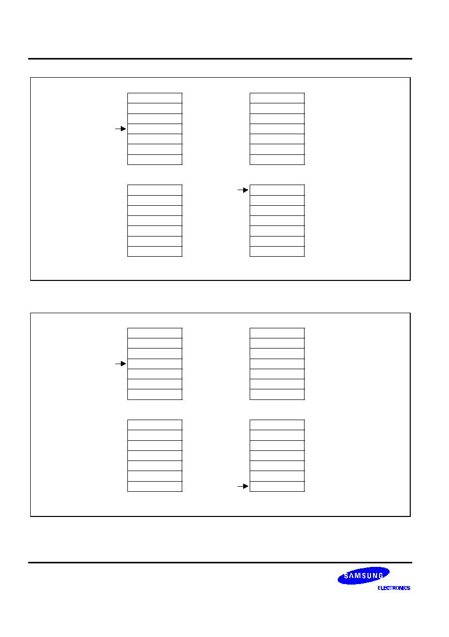
ARM INSTRUCTION SET
S3F441FX RISC MICROCONTROLLER
3-42
Rn
1
R1
R1
2
R5
3
R1
R5
4
R7
Rn
0x100C
0x1000
0x0FF4
0x100C
0x1000
0x0FF4
0x100C
0x1000
0x0FF4
0x100C
0x1000
0x0FF4
Figure 3-20. Pre-Increment Addressing
Rn
1
R1
R1
2
R5
3
R1
R5
4
R7
Rn
0x100C
0x1000
0x0FF4
0x100C
0x1000
0x0FF4
0x100C
0x1000
0x0FF4
0x100C
0x1000
0x0FF4
Figure 3-21. Post-Decrement Addressing

S3F441FX RISC MICROCONTROLLER
ARM INSTRUCTION SET
3-43
Rn
1
R1
R1
2
R5
3
R1
R5
4
R7
Rn
0x100C
0x1000
0x0FF4
0x100C
0x1000
0x0FF4
0x100C
0x1000
0x0FF4
0x100C
0x1000
0x0FF4
Figure 3-22. Pre-Decrement Addressing
USE OF THE S BIT
When the S bit is set in a LDM/STM instruction its meaning depends on whether or not R15 is in the transfer list
and on the type of instruction. The S bit should only be set if the instruction is to execute in a privileged mode.
LDM with R15 in Transfer List and S Bit Set (Mode Changes)
If the instruction is a LDM then SPSR_<mode> is transferred to CPSR at the same time as R15 is loaded.
STM with R15 in Transfer List and S Bit Set (User Bank Transfer)
The registers transferred are taken from the User bank rather than the bank corresponding to the current mode.
This is useful for saving the user state on process switches. Base write-back should not be used when this
mechanism is employed.
R15 not in List and S Bit Set (User Bank Transfer)
For both LDM and STM instructions, the User bank registers are transferred rather than the register bank
corresponding to the current mode. This is useful for saving the user state on process switches. Base write-back
should not be used when this mechanism is employed.
When the instruction is LDM, care must be taken not to read from a banked register during the following cycle
(inserting a dummy instruction such as MOV R0, R0 after the LDM will ensure safety).
USE OF R15 AS THE BASE
R15 should not be used as the base register in any LDM or STM instruction.

ARM INSTRUCTION SET
S3F441FX RISC MICROCONTROLLER
3-44
INCLUSION OF THE BASE IN THE REGISTER LIST
When write-back is specified, the base is written back at the end of the second cycle of the instruction. During a
STM, the first register is written out at the start of the second cycle. A STM which includes storing the base, with
the base as the first register to be stored, will therefore store the unchanged value, whereas with the base second
or later in the transfer order, will store the modified value. A LDM will always overwrite the updated base if the
base is in the list.
DATA ABORTS
Some legal addresses may be unacceptable to a memory management system, and the memory manager can
indicate a problem with an address by taking the ABORT signal HIGH. This can happen on any transfer during a
multiple register load or store, and must be recoverable if ARM7TDMI is to be used in a virtual memory system.
Abort during STM Instructions
If the abort occurs during a store multiple instruction, ARM7TDMI takes little action until the instruction
completes, whereupon it enters the data abort trap. The memory manager is responsible for preventing
erroneous writes to the memory. The only change to the internal state of the processor will be the modification of
the base register if write-back was specified, and this must be reversed by software (and the cause of the abort
resolved) before the instruction may be retried.
Aborts during LDM Instructions
When ARM7TDMI detects a data abort during a load multiple instruction, it modifies the operation of the
instruction to ensure that recovery is possible.
∑
Overwriting of registers stops when the abort happens. The aborting load will not take place but earlier ones
may have overwritten registers. The PC is always the last register to be written and so will always be
preserved.
∑
The base register is restored, to its modified value if write-back was requested. This ensures recoverability in
the case where the base register is also in the transfer list, and may have been overwritten before the abort
occurred.
The data abort trap is taken when the load multiple has completed, and the system software must undo any base
modification (and resolve the cause of the abort) before restarting the instruction.
INSTRUCTION CYCLE TIMES
Normal LDM instructions take nS + 1N + 1I and LDM PC takes (n+1)S + 2N + 1I incremental cycles, where S,N
and I are defined as squential (S-cycle), non-sequential (N-cycle), and internal (I-cycle), respectively. STM
instructions take (n-1)S + 2N incremental cycles to execute, where n is the number of words transferred.

S3F441FX RISC MICROCONTROLLER
ARM INSTRUCTION SET
3-45
ASSEMBLER SYNTAX
<LDM|STM>{cond}<FD|ED|FA|EA|IA|IB|DA|DB> Rn{!},<Rlist>{^}
where:
{
cond}
Two character condition mnemonic. See Table 3-2.
Rn
An expression evaluating to a valid register number
<Rlist>
A list of registers and register ranges enclosed in {} (e.g. {R0,R2-R7,R10}).
{
!}
If present requests write-back (W=1), otherwise W=0.
{
^}
If present set S bit to load the CPSR along with the PC, or force transfer of user bank
when in privileged mode.
Addressing Mode Names
There are different assembler mnemonics for each of the addressing modes, depending on whether the
instruction is being used to support stacks or for other purposes. The equivalence between the names and the
values of the bits in the instruction are shown in the following table 3-6.
Table 3-6. Addressing Mode Names
Name
Stack
Other
L bit
P bit
U bit
Pre-Increment Load
LDMED
LDMIB
1
1
1
Post-Increment Load
LDMFD
LDMIA
1
0
1
Pre-Decrement Load
LDMEA
LDMDB
1
1
0
Post-Decrement Load
LDMFA
LDMDA
1
0
0
Pre-Increment Store
STMFA
STMIB
0
1
1
Post-Increment Store
STMEA
STMIA
0
0
1
Pre-Decrement Store
STMFD
STMDB
0
1
0
Post-Decrement Store
STMED
STMDA
0
0
0
FD, ED, FA, EA define pre/post indexing and the up/down bit by reference to the form of stack required. The F
and E refer to a "full" or "empty" stack, i.e. whether a pre-index has to be done (full) before storing to the stack.
The A and D refer to whether the stack is ascending or descending. If ascending, a STM will go up and LDM
down, if descending, vice-versa.
IA, IB, DA, DB allow control when LDM/STM are not being used for stacks and simply mean Increment After,
Increment Before, Decrement After, Decrement Before.

ARM INSTRUCTION SET
S3F441FX RISC MICROCONTROLLER
3-46
EXAMPLES
LDMFD
SP!,{R0,R1,R2}
; Unstack 3 registers.
STMIA
R0,{R0-R15}
; Save all registers.
LDMFD
SP!,{R15}
; R15
(SP), CPSR unchanged.
LDMFD
SP!,{R15}^
; R15
(SP), CPSR <- SPSR_mode
; (allowed only in privileged modes).
STMFD
R13,{R0-R14}^
; Save user mode regs on stack
; (allowed only in privileged modes).
These instructions may be used to save state on subroutine entry, and restore it efficiently on return to the calling
routine:
STMED
SP!,{R0-R3,R14}
; Save R0 to R3 to use as workspace
; and R14 for returning.
BL
somewhere
; This nested call will overwrite R14
LDMED
SP!,{R0-R3,R15}
; Restore workspace and return.

S3F441FX RISC MICROCONTROLLER
ARM INSTRUCTION SET
3-47
SINGLE DATA SWAP (SWP)
31
19
15
Cond
28
16
11
12
21
23
B
20
00
Rn
Rd
[3:0] Source Register
[15:12] Destination Register
[19:16] Base Register
[22] Byte/Word Bit
0 = Swap word quantity
1 = Swap byte quantity
[31:28] Condition Field
22
00010
0000
Rm
1001
27
8 7
4 3
0
Figure 3-23. Swap Instruction
The instruction is only executed if the condition is true. The various conditions are defined in Table 3-2. The
instruction encoding is shown in Figure 3-23.
The data swap instruction is used to swap a byte or word quantity between a register and external memory. This
instruction is implemented as a memory read followed by a memory write which are "locked" together (the
processor cannot be interrupted until both operations have completed, and the memory manager is warned to
treat them as inseparable). This class of instruction is particularly useful for implementing software semaphores.
The swap address is determined by the contents of the base register (Rn). The processor first reads the contents
of the swap address. Then it writes the contents of the source register (Rm) to the swap address, and stores the
old memory contents in the destination register (Rd). The same register may be specified as both the source and
destination.
The LOCK output goes HIGH for the duration of the read and write operations to signal to the external memory
manager that they are locked together, and should be allowed to complete without interruption. This is important
in multi-processor systems where the swap instruction is the only indivisible instruction which may be used to
implement semaphores; control of the memory must not be removed from a processor while it is performing a
locked operation.
BYTES AND WORDS
This instruction class may be used to swap a byte (B=1) or a word (B=0) between an ARM7TDMI register and
memory. The SWP instruction is implemented as a LDR followed by a STR and the action of these is as
described in the section on single data transfers. In particular, the description of Big and Little Endian
configuration applies to the SWP instruction.

ARM INSTRUCTION SET
S3F441FX RISC MICROCONTROLLER
3-48
USE OF R15
Do not use R15 as an operand (Rd, Rn or Rs) in a SWP instruction.
DATA ABORTS
If the address used for the swap is unacceptable to a memory management system, the memory manager can
flag the problem by driving ABORT HIGH. This can happen on either the read or the write cycle (or both), and in
either case, the Data Abort trap will be taken. It is up to the system software to resolve the cause of the problem,
then the instruction can be restarted and the original program continued.
INSTRUCTION CYCLE TIMES
Swap instructions take 1S + 2N +1I incremental cycles to execute, where S,N and I are defined as squential
(S-cycle), non-sequential, and internal (I-cycle), respectively.
ASSEMBLER SYNTAX
<SWP>{cond}{B} Rd,Rm,[Rn]
{
cond}
Two-character condition mnemonic. See Table 3-2.
{
B}
If B is present then byte transfer, otherwise word transfer
Rd,Rm,Rn
Expressions evaluating to valid register numbers
EXAMPLES
SWP
R0,R1,[R2]
; Load R0 with the word addressed by R2, and
; store R1 at R2.
SWPB
R2,R3,[R4]
; Load R2 with the byte addressed by R4, and
; store bits 0 to 7 of R3 at R4.
SWPEQ
R0,R0,[R1]
; Conditionally swap the contents of the
; word addressed by R1 with R0.

S3F441FX RISC MICROCONTROLLER
ARM INSTRUCTION SET
3-49
SOFTWARE INTERRUPT (SWI)
The instruction is only executed if the condition is true. The various conditions are defined in Table 3-2. The
instruction encoding is shown in Figure 3-24, below.
31
24
27
1111
Cond
Comment Field (Ignored by Processor)
28
23
[31:28] Condition Field
0
Figure 3-24. Software Interrupt Instruction
The software interrupt instruction is used to enter Supervisor mode in a controlled manner. The instruction
causes the software interrupt trap to be taken, which effects the mode change. The PC is then forced to a fixed
value (0x08) and the CPSR is saved in SPSR_svc. If the SWI vector address is suitably protected (by external
memory management hardware) from modification by the user, a fully protected operating system may be
constructed.
RETURN FROM THE SUPERVISOR
The PC is saved in R14_svc upon entering the software interrupt trap, with the PC adjusted to point to the word
after the SWI instruction. MOVS PC,R14_svc will return to the calling program and restore the CPSR.
Note that the link mechanism is not re-entrant, so if the supervisor code wishes to use software interrupts within
itself it must first save a copy of the return address and SPSR.
COMMENT FIELD
The bottom 24 bits of the instruction are ignored by the processor, and may be used to communicate information
to the supervisor code. For instance, the supervisor may look at this field and use it to index into an array of entry
points for routines which perform the various supervisor functions.
INSTRUCTION CYCLE TIMES
Software interrupt instructions take 2S + 1N incremental cycles to execute, where S and N are defined as
sequential (S-cycle) and non-sequential (N-cycle).

ARM INSTRUCTION SET
S3F441FX RISC MICROCONTROLLER
3-50
ASSEMBLER SYNTAX
SWI{cond} <expression>
{
cond}
Two character condition mnemonic, Table 3-2.
<expression>
Evaluated and placed in the comment field (which is ignored by ARM7TDMI).
EXAMPLES
SWI
ReadC
; Get next character from read stream.
SWI
WriteI+"k"
; Output a "k" to the write stream.
SWINE
0
; Conditionally call supervisor with 0 in comment field.
Supervisor code
The previous examples assume that suitable supervisor code exists, for instance:
0x08 B Supervisor
; SWI entry point
EntryTable
; Addresses of supervisor routines
DCD ZeroRtn
DCD ReadCRtn
DCD WriteIRtn
∑
∑
∑
Zero
EQU 0
ReadC
EQU 256
WriteI
EQU 512
Supervisor
; SWI has routine required in bits 8-23 and data (if any) in
; bits 0-7. Assumes R13_svc points to a suitable stack
STMFD
R13,{R0-R2,R14}
; Save work registers and return address.
LDR
R0,[R14,#-4]
; Get SWI instruction.
BIC
R0,R0,#0xFF000000
; Clear top 8 bits.
MOV
R1,R0,LSR#8
; Get routine offset.
ADR
R2,EntryTable
; Get start address of entry table.
LDR
R15,[R2,R1,LSL#2]
; Branch to appropriate routine.
WriteIRtn
; Enter with character in R0 bits 0-7.
∑
∑
∑
LDMFD
R13,{R0-R2,R15}^
; Restore workspace and return,
; restoring processor mode and flags.

S3F441FX RISC MICROCONTROLLER
ARM INSTRUCTION SET
3-51
COPROCESSOR DATA OPERATIONS (CDP)
The instruction is only executed if the condition is true. The various conditions are defined in Table 3-2. The
instruction encoding is shown in Figure 3-25.
This class of instruction is used to tell a coprocessor to perform some internal operation. No result is
communicated back to ARM7TDMI, and it will not wait for the operation to complete. The coprocessor could
contain a queue of such instructions awaiting execution, and their execution can overlap other activity, allowing
the coprocessor and ARM7TDMI to perform independent tasks in parallel.
COPROCESSOR INSTRUCTIONS
The S3F441FX, unlike some other ARM-based processors, does not have an external coprocessor interface. It
does not have a on-chip coprocessor also.
So then all coprocessor instructions will cause the undefined instruction trap to be taken on the S3F441FX. These
coprocessor instructions can be emulated by the undefined trap handler. Even though external coprocessor can
not be connected to the S3F441FX, the coprocessor instructions are still described here in full for completeness.
(Remember that any external coprocessor described in this section is a software emulation.)
31
24
27
19
15
Cond
CRm
28
16
11
12
23
20
[3:0] Coprocessor operand register
[7:5] Coprocessor information
[11:8] Coprocessor number
[15:12] Coprocessor destination register
[19:16] Coprocessor operand register
[23:20] Coprocessor operation code
[31:28] Condition Field
0
Cp
Cp#
CRd
CRn
1110
CP Opc
8 7
5 4 3
0
Figure 3-25. Coprocessor Data Operation Instruction
Only bit 4 and bits 24 to 31 The coprocessor fields are significant to ARM7TDMI. The remaining bits are used by
coprocessors. The above field names are used by convention, and particular coprocessors may redefine the use
of all fields except CP# as appropriate. The CP# field is used to contain an identifying number (in the range 0 to
15) for each coprocessor, and a coprocessor will ignore any instruction which does not contain its number in the
CP# field.
The conventional interpretation of the instruction is that the coprocessor should perform an operation specified in
the CP Opc field (and possibly in the CP field) on the contents of CRn and CRm, and place the result in CRd.

ARM INSTRUCTION SET
S3F441FX RISC MICROCONTROLLER
3-52
INSTRUCTION CYCLE TIMES
Coprocessor data operations take 1S + bI incremental cycles to execute, where b is the number of cycles spent
in the coprocessor busy-wait loop.
S and I are defined as sequential (S-cycle) and internal (I-cycle).
ASSEMBLER SYNTAX
CDP{cond} p#,<expression1>,cd,cn,cm{,<expression2>}
{
cond}
Two character condition mnemonic. See Table 3-2.
p#
The unique number of the required coprocessor
<expression1>
Evaluated to a constant and placed in the CP Opc field
cd, cn and cm
Evaluate to the valid coprocessor register numbers CRd, CRn and CRm respectively
<expression2>
Where present is evaluated to a constant and placed in the CP field
EXAMPLES
CDP
p1,10,c1,c2,c3
; Request coprocessor 1 to do operation 10
; on CR2 and CR3, and put the result in CR1.
CDPEQ
p2,5,c1,c2,c3,2
; If Z flag is set request coprocessor 2 to do operation 5
; (type 2)
; on CR2 and CR3, and put the result in CR1.
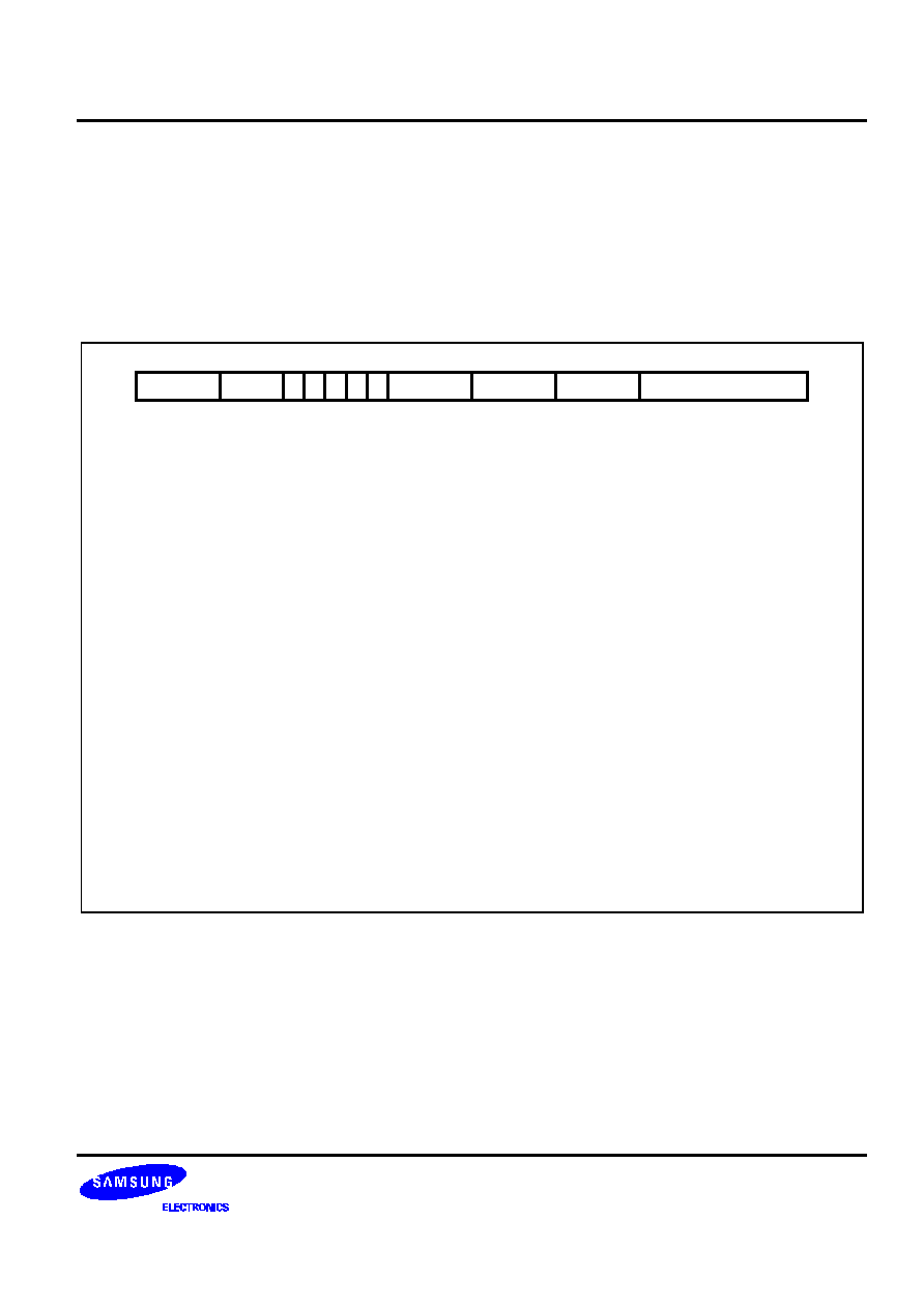
S3F441FX RISC MICROCONTROLLER
ARM INSTRUCTION SET
3-53
COPROCESSOR DATA TRANSFERS (LDC, STC)
The instruction is only executed if the condition is true. The various conditions are defined in Table 3-2. The
instruction encoding is shown in Figure 3-26.
This class of instruction is used to load (LDC) or store (STC) a subset of a coprocessor's registers directly to
memory. ARM7TDMI is responsible for supplying the memory address, and the coprocessor supplies or accepts
the data and controls the number of words transferred.
[7:0] Unsigned 8 Bit Immediate Offset
[11:8] Coprocessor Number
[15:12] Coprocessor Source/Destination Register
[19:16] Base Register
[20] Load/Store Bit
0 = Store to memory
1 = Load from memory
[21] Write-back Bit
0 = No write-back
1 = Write address into base
[22] Transfer Length
[23] Up/Down Bit
0 = Down: subtract offset from base
1 = Up: add offset to base
[24] Pre/Post Indexing Bit
0 = Post: add offset after transfer
1 = Pre: add offset before transfer
[31:28] Condition Field
31
27
19
15
Cond
28
16
11
12
21
23
N
20
L
Rn
CRd
22
110
P U
CP#
W
24
25
Offset
8 7
0
Figure 3-26. Coprocessor Data Transfer Instructions
THE COPROCESSOR FIELDS
The CP# field is used to identify the coprocessor which is required to supply or accept the data, and a
coprocessor will only respond if its number matches the contents of this field.
The CRd field and the N bit contain information for the coprocessor which may be interpreted in different ways by
different coprocessors, but by convention CRd is the register to be transferred (or the first register where more
than one is to be transferred), and the N bit is used to choose one of two transfer length options. For instance
N=0 could select the transfer of a single register, and N=1 could select the transfer of all the registers for context
switching.

ARM INSTRUCTION SET
S3F441FX RISC MICROCONTROLLER
3-54
ADDRESSING MODES
ARM7TDMI is responsible for providing the address used by the memory system for the transfer, and the
addressing modes available are a subset of those used in single data transfer instructions. Note, however, that
the immediate offsets are 8 bits wide and specify word offsets for coprocessor data transfers, whereas they are
12 bits wide and specify byte offsets for single data transfers.
The 8 bit unsigned immediate offset is shifted left 2 bits and either added to (U=1) or subtracted from (U=0) the
base register (Rn); this calculation may be performed either before (P=1) or after (P=0) the base is used as the
transfer address. The modified base value may be overwritten back into the base register (if W=1), or the old
value of the base may be preserved (W=0). Note that post-indexed addressing modes require explicit setting of
the W bit, unlike LDR and STR which always write-back when post-indexed.
The value of the base register, modified by the offset in a pre-indexed instruction, is used as the address for the
transfer of the first word. The second word (if more than one is transferred) will go to or come from an address
one word (4 bytes) higher than the first transfer, and the address will be incremented by one word for each
subsequent transfer.
ADDRESS ALIGNMENT
The base address should normally be a word aligned quantity. The bottom 2 bits of the address will appear on
A[1:0] and might be interpreted by the memory system.
USE OF R15
If Rn is R15, the value used will be the address of the instruction plus 8 bytes. Base write-back to R15 must not
be specified.
DATA ABORTS
If the address is legal but the memory manager generates an abort, the data trap will be taken. The write-back of
the modified base will take place, but all other processor state will be preserved. The coprocessor is partly
responsible for ensuring that the data transfer can be restarted after the cause of the abort has been resolved,
and must ensure that any subsequent actions it undertakes can be repeated when the instruction is retried.
INSTRUCTION CYCLE TIMES
Coprocessor data transfer instructions take (n-1)S + 2N + bI incremental cycles to execute, where:
n
The number of words transferred.
b
The number of cycles spent in the coprocessor busy-wait loop.
S, N and I are defined as squential (S-cycle), non-squential (N-cycle), and internal (I-cycle), respectively.

S3F441FX RISC MICROCONTROLLER
ARM INSTRUCTION SET
3-55
ASSEMBLER SYNTAX
<LDC|STC>{cond}{L} p#,cd,<Address>
LDC
Load from memory to coprocessor
STC
Store from coprocessor to memory
{
L}
When present perform long transfer (N=1), otherwise perform short transfer (N=0)
{
cond}
Two character condition mnemonic. See Table 3-2..
p#
The unique number of the required coprocessor
cd
An expression evaluating to a valid coprocessor register number that is placed in the
CRd field
<Address>
can be:
1
An expression which generates an address:
The assembler will attempt to generate an instruction using the PC as a base and a
corrected immediate offset to address the location given by evaluating the expression.
This will be a PC relative, pre-indexed address. If the address is out of range, an error
will be generated
2
A pre-indexed addressing specification:
[Rn]
offset of zero
[Rn,<#expression>]{!}
offset of <expression> bytes
3
A post-indexed addressing specification:
[Rn],<#expression
offset of <expression> bytes
{!}
write back the base register (set the W bit) if! is present
Rn
is an expression evaluating to a valid
ARM7TDMI register number.
NOTE
If Rn is R15, the assembler will subtract 8 from the offset value to allow for ARM7TDMI pipelining.
EXAMPLES
LDC
p1,c2,table
; Load c2 of coprocessor 1 from address
; table, using a PC relative address.
STCEQL
p2,c3,[R5,#24]!
; Conditionally store c3 of coprocessor 2
; into an address 24 bytes up from R5,
; write this address back to R5, and use
; long transfer option (probably to store multiple words).
NOTE
Although the address offset is expressed in bytes, the instruction offset field is in words. The assembler
will adjust the offset appropriately.
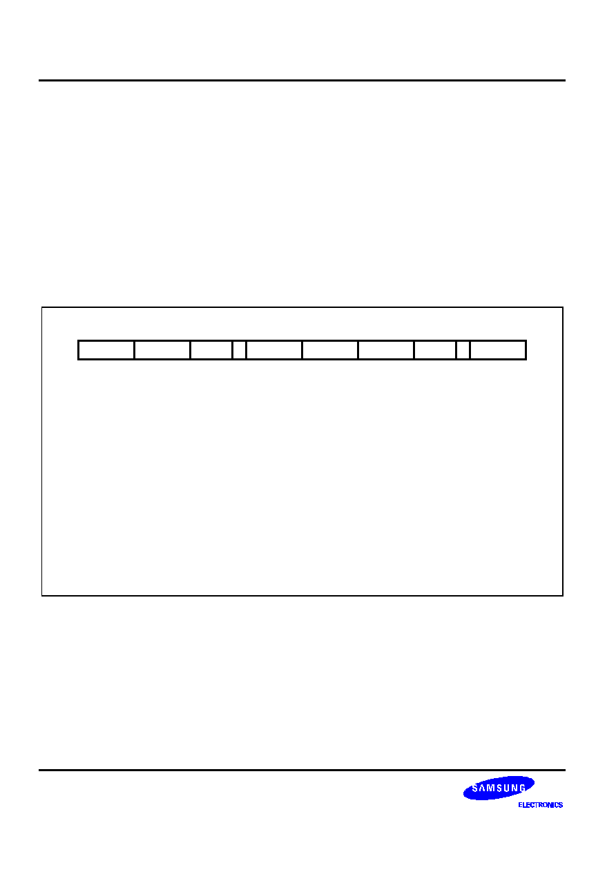
ARM INSTRUCTION SET
S3F441FX RISC MICROCONTROLLER
3-56
COPROCESSOR REGISTER TRANSFERS (MRC, MCR)
The instruction is only executed if the condition is true. The various conditions are defined in Table 3-2. The
instruction encoding is shown in Figure 3-27.
This class of instruction is used to communicate information directly between ARM7TDMI and a coprocessor. An
example of a coprocessor to ARM7TDMI register transfer (MRC) instruction would be a FIX of a floating point
value held in a coprocessor, where the floating point number is converted into a 32 bit integer within the
coprocessor, and the result is then transferred to ARM7TDMI register. A FLOAT of a 32 bit value in ARM7TDMI
register into a floating point value within the coprocessor illustrates the use of ARM7TDMI register to coprocessor
transfer (MCR).
An important use of this instruction is to communicate control information directly from the coprocessor into the
ARM7TDMI CPSR flags. As an example, the result of a comparison of two floating point values within a
coprocessor can be moved to the CPSR to control the subsequent flow of execution.
31
27
19
15
Cond
28
16
11
12
21
23
20
L
CRn
Rd
[3:0] Coprocessor Operand Register
[7:5] Coprocessor Information
[11:8] Coprocessor Number
[15:12] ARM Source/Destination Register
[19:16] Coprocessor Source/Destination Register
[20] Load/Store Bit
0 = Store to coprocessor
1 = Load from coprocessor
[21] Coprocessor Operation Mode
[31:28] Condition Field
1110
CP Opc
CP#
24
CRm
1
CP
8 7
5 4 3
0
Figure 3-27. Coprocessor Register Transfer Instructions
THE COPROCESSOR FIELDS
The CP# field is used, as for all coprocessor instructions, to specify which coprocessor is being called upon.
The CP Opc, CRn, CP and CRm fields are used only by the coprocessor, and the interpretation presented here is
derived from convention only. Other interpretations are allowed where the coprocessor functionality is
incompatible with this one. The conventional interpretation is that the CP Opc and CP fields specify the operation
the coprocessor is required to perform, CRn is the coprocessor register which is the source or destination of the
transferred information, and CRm is a second coprocessor register which may be involved in some way which
depends on the particular operation specified.

S3F441FX RISC MICROCONTROLLER
ARM INSTRUCTION SET
3-57
TRANSFERS TO R15
When a coprocessor register transfer to ARM7TDMI has R15 as the destination, bits 31, 30, 29 and 28 of the
transferred word are copied into the N, Z, C and V flags respectively. The other bits of the transferred word are
ignored, and the PC and other CPSR bits are unaffected by the transfer.
TRANSFERS FROM R15
A coprocessor register transfer from ARM7TDMI with R15 as the source register will store the PC+12.
INSTRUCTION CYCLE TIMES
MRC instructions take 1S + (b+1)I +1C incremental cycles to execute, where S, I and C are defined as sequential
(S-cycle), internal (I-cycle), and coprocessor register transfer (C-cycle), respectively. MCR instructions take 1S +
bI +1C incremental cycles to execute, where b is the number of cycles spent in the coprocessor busy-wait loop.
ASSEMBLER SYNTAX
<MCR|MRC>{cond} p#,<expression1>,Rd,cn,cm{,<expression2>}
MRC
Move from coprocessor to ARM7TDMI register (L=1)
MCR
Move from ARM7TDMI register to coprocessor (L=0)
{
cond}
Two character condition mnemonic. See Table 3-2
p#
The unique number of the required coprocessor
<expression1>
Evaluated to a constant and placed in the CP Opc field
Rd
An expression evaluating to a valid ARM7TDMI register number
cn and cm
Expressions evaluating to the valid coprocessor register numbers CRn and CRm
respectively
<expression2>
Where present is evaluated to a constant and placed in the CP field
EXAMPLES
MRC
p2,5,R3,c5,c6
; Request coprocessor 2 to perform operation 5
; on c5 and c6, and transfer the (single
; 32-bit word) result back to R3.
MCR
p6,0,R4,c5,c6
; Request coprocessor 6 to perform operation 0
; on R4 and place the result in c6.
MRCEQ
p3,9,R3,c5,c6,2
; Conditionally request coprocessor 3 to
; perform operation 9 (type 2) on c5 and
; c6, and transfer the result back to R3.

ARM INSTRUCTION SET
S3F441FX RISC MICROCONTROLLER
3-58
UNDEFINED INSTRUCTION
The instruction is only executed if the condition is true. The various conditions are defined in Table 3-2. The
instruction format is shown in Figure 3-28.
31
27
Cond
28
25 24
011
xxxxxxxxxxxxxxxxxxxx
1
xxxx
5 4 3
0
Figure 3-28. Undefined Instruction
If the condition is true, the undefined instruction trap will be taken.
Note that the undefined instruction mechanism involves offering this instruction to any coprocessors which may
be present, and all coprocessors must refuse to accept it by driving CPA and CPB HIGH.
INSTRUCTION CYCLE TIMES
This instruction takes 2S + 1I + 1N cycles, where S, N and I are defined as squential (S-cycle), non-sequential
(N-cycle), and internal (I-cycle).
ASSEMBLER SYNTAX
The assembler has no mnemonics for generating this instruction. If it is adopted in the future for some specified
use, suitable mnemonics will be added to the assembler. Until such time, this instruction must not be used.

S3F441FX RISC MICROCONTROLLER
ARM INSTRUCTION SET
3-59
INSTRUCTION SET EXAMPLES
The following examples show ways in which the basic ARM7TDMI instructions can combine to give efficient
code. None of these methods saves a great deal of execution time (although they may save some), mostly they
just save code.
USING THE CONDITIONAL INSTRUCTIONS
Using Conditionals for Logical OR
CMP
Rn,#p
; If Rn=p OR Rm=q THEN GOTO Label.
BEQ
Label
CMP
Rm,#q
BEQ
Label
This can be replaced by
CMP
Rn,#p
CMPNE
Rm,#q
; If condition not satisfied try other test.
BEQ
Label
Absolute Value
TEQ
Rn,#0
; Test sign
RSBMI
Rn,Rn,#0
; and 2's complement if necessary.
Multiplication by 4, 5 or 6 (Run Time)
MOV
Rc,Ra,LSL#2
; Multiply by 4,
CMP
Rb,#5
; Test value,
ADDCS
Rc,Rc,Ra
; Complete multiply by 5,
ADDHI
Rc,Rc,Ra
; Complete multiply by 6.
Combining Discrete and Range Tests
TEQ
Rc,#127
; Discrete test,
CMPNE
Rc,# " "-1
; Range test
MOVLS
Rc,# ""
; IF Rc<= "" OR Rc=ASCII(127)
; THEN Rc:= "."

ARM INSTRUCTION SET
S3F441FX RISC MICROCONTROLLER
3-60
Division and Remainder
A number of divide routines for specific applications are provided in source form as part of the ANSI C library
provided with the ARM Cross Development Toolkit, available from your supplier. A short general purpose divide
routine follows.
; Enter with numbers in Ra and Rb.
MOV
Rcnt,#1
; Bit to control the division.
Div1
CMP
Rb,#0x80000000
; Move Rb until greater than Ra.
CMPCC
Rb,Ra
MOVCC
Rb,Rb,ASL#1
MOVCC
Rcnt,Rcnt,ASL#1
BCC
Div1
MOV
Rc,#0
Div2
CMP
Ra,Rb
; Test for possible subtraction.
SUBCS
Ra,Ra,Rb
; Subtract if ok,
ADDCS
Rc,Rc,Rcnt
; Put relevant bit into result
MOVS
Rcnt,Rcnt,LSR#1
; Shift control bit
MOVNE
Rb,Rb,LSR#1
; Halve unless finished.
BNE
Div2
; Divide result in Rc, remainder in Ra.
Overflow Eetection in the ARM7TDMI
1. Overflow in unsigned multiply with a 32-bit result
UMULL
Rd,Rt,Rm,Rn
; 3 to 6 cycles
TEQ
Rt,#0
; +1 cycle and a register
BNE
overflow
2. Overflow in signed multiply with a 32-bit result
SMULL
Rd,Rt,Rm,Rn
; 3 to 6 cycles
TEQ
Rt,Rd ASR#31
; +1 cycle and a register
BNE
overflow
3. Overflow in unsigned multiply accumulate with a 32 bit result
UMLAL
Rd,Rt,Rm,Rn
; 4 to 7 cycles
TEQ
Rt,#0
; +1 cycle and a register
BNE
overflow
4. Overflow in signed multiply accumulate with a 32 bit result
SMLAL
Rd,Rt,Rm,Rn
; 4 to 7 cycles
TEQ
Rt,Rd, ASR#31
; +1 cycle and a register
BNE
overflow

S3F441FX RISC MICROCONTROLLER
ARM INSTRUCTION SET
3-61
5. Overflow in unsigned multiply accumulate with a 64 bit result
UMULL
Rl,Rh,Rm,Rn
; 3 to 6 cycles
ADDS
Rl,Rl,Ra1
; Lower accumulate
ADC
Rh,Rh,Ra2
; Upper accumulate
BCS
overflow
; 1 cycle and 2 registers
6. Overflow in signed multiply accumulate with a 64 bit result
SMULL
Rl,Rh,Rm,Rn
; 3 to 6 cycles
ADDS
Rl,Rl,Ra1
; Lower accumulate
ADC
Rh,Rh,Ra2
; Upper accumulate
BVS
overflow
; 1 cycle and 2 registers
NOTE
Overflow checking is not applicable to unsigned and signed multiplies with a 64-bit result, since overflow
does not occur in such calculations.
PSEUDO-RANDOM BINARY SEQUENCE GENERATOR
It is often necessary to generate (pseudo-) random numbers and the most efficient algorithms are based on shift
generators with exclusive-OR feedback rather like a cyclic redundancy check generator. Unfortunately the
sequence of a 32 bit generator needs more than one feedback tap to be maximal length (i.e. 2^32-1 cycles
before repetition), so this example uses a 33 bit register with taps at bits 33 and 20. The basic algorithm is
newbit:=bit 33 eor bit 20, shift left the 33 bit number and put in newbit at the bottom; this operation is performed
for all the newbits needed (i.e. 32 bits). The entire operation can be done in 5 S cycles:
; Enter with seed in Ra (32 bits),
; Rb (1 bit in Rb lsb), uses Rc.
TST
Rb,Rb,LSR#1
; Top bit into carry
MOVS
Rc,Ra,RRX
; 33 bit rotate right
ADC
Rb,Rb,Rb
; Carry into lsb of Rb
EOR
Rc,Rc,Ra,LSL#12
; (involved!)
EOR
Ra,Rc,Rc,LSR#20
; (similarly involved!) new seed in Ra, Rb as before
MULTIPLICATION BY CONSTANT USING THE BARREL SHIFTER
Multiplication by 2^n (1,2,4,8,16,32..)
MOV
Ra, Rb, LSL #n
Multiplication by 2^n+1 (3,5,9,17..)
ADD
Ra,Ra,Ra,LSL #n
Multiplication by 2^n-1 (3,7,15..)
RSB
Ra,Ra,Ra,LSL #n

ARM INSTRUCTION SET
S3F441FX RISC MICROCONTROLLER
3-62
Multiplication by 6
ADD
Ra,Ra,Ra,LSL #1
; Multiply by 3
MOV
Ra,Ra,LSL#1
; and then by 2
Multiply by 10 and add in extra number
ADD
Ra,Ra,Ra,LSL#2
; Multiply by 5
ADD
Ra,Rc,Ra,LSL#1
; Multiply by 2 and add in next digit
General recursive method for Rb := Ra*C, C a constant:
1. If C even, say C = 2^n*D, D odd:
D=1:
MOV Rb,Ra,LSL #n
D<>1:
{Rb := Ra*D}
MOV
Rb,Rb,LSL #n
2. If C MOD 4 = 1, say C = 2^n*D+1, D odd, n>1:
D=1:
ADD Rb,Ra,Ra,LSL #n
D<>1:
{Rb := Ra*D}
ADD
Rb,Ra,Rb,LSL #n
3. If C MOD 4 = 3, say C = 2^n*D-1, D odd, n>1:
D=1:
RSB Rb,Ra,Ra,LSL #n
D<>1:
{Rb := Ra*D}
RSB
Rb,Ra,Rb,LSL #n
This is not quite optimal, but close. An example of its non-optimality is multiply by 45 which is done by:
RSB
Rb,Ra,Ra,LSL#2
; Multiply by 3
RSB
Rb,Ra,Rb,LSL#2
; Multiply by 4*3-1 = 11
ADD
Rb,Ra,Rb,LSL# 2
; Multiply by 4*11+1 = 45
rather than by:
ADD
Rb,Ra,Ra,LSL#3
; Multiply by 9
ADD
Rb,Rb,Rb,LSL#2
; Multiply by 5*9 = 45

S3F441FX RISC MICROCONTROLLER
ARM INSTRUCTION SET
3-63
LOADING A WORD FROM AN UNKNOWN ALIGNMENT
; Enter with address in Ra (32 bits) uses
; Rb, Rc result in Rd. Note d must be less than c e.g. 0,1
BIC
Rb,Ra,#3
; Get word aligned address
LDMIA
Rb,{Rd,Rc}
; Get 64 bits containing answer
AND
Rb,Ra,#3
; Correction factor in bytes
MOVS
Rb,Rb,LSL#3
; ...now in bits and test if aligned
MOVNE
Rd,Rd,LSR Rb
; Produce bottom of result word (if not aligned)
RSBNE
Rb,Rb,#32
; Get other shift amount
ORRNE
Rd,Rd,Rc,LSL Rb
; Combine two halves to get result

ARM INSTRUCTION SET
S3F441FX RISC MICROCONTROLLER
3-64
NOTES

S3F441FX RISC MICROCONTROLLER
ARM INSTRUCTION SET
3-65
THUMB INSTRUCTION SET FORMAT
The thumb instruction sets are 16-bit versions of ARM instruction sets (32-bit format). The ARM instructions are
reduced to 16-bit versions, Thumb instructions, at the cost of versatile functions of the ARM instruction sets. The
thumb instructions are decompressed to the ARM instructions by the Thumb decompressor inside the
ARM7TDMI core.
As the Thumb instructions are compressed ARM instructions, the Thumb instructions have the 16-bit format
instructions and have some restrictions. The restrictions by 16-bit format is fully notified for using the Thumb
instructions.
FORMAT SUMMARY
The THUMB instruction set formats are shown in the following figure.
Move Shifted register
0
0
0
0
0
0
0
0
0
0
0
0
1
0
0
0
1
0
0
0
0
0
0
1
1
1
1
1
1
1
0
0
0
0
0
1
1
1
1
1
1
1
1
0
L
0
1
1
1
1
1
1
1
1
1
1
1
1
1
1
1
1
0
0
0
0
1
1
1
1
0
0
1
0
0
L
1
0
R
1
1
0
1
0
SP
1
L
L
S
H
0
0
1
B
L
0
1
H
0
1
B
0
0
1
1
1
I
Op
Op
Op
Op
Op
L
0
S
1
Offset5
Rs
Rd
Rn/offset3
Rd
Rs
Rd
Offset8
Rs
Rd/Hd
Rd
H1 H2
Rs/Hs
Rd
Word8
Rd
Rb
Ro
Ro
Rb
Rd
Offset5
Rb
Rd
Rb
Rd
Offset5
Rd
Rd
Word8
Word8
SWord7
Rb
Cond
Rlist
Rlist
Softset8
Value8
Offset11
Offset
Add/subtract
Move/compare/add/
subtract immediate
ALU operations
Hi register operations
/branch exchange
PC-relative load
Load/store with register
offset
Load/store with immediate
offset
Load/store sign-extended
byte/halfword
Load/store halfword
SP-relative load/store
Load address
Add offset to stack pointer
Push/pop register
Multiple load/store
Conditional branch
Software interrupt
Unconditional branch
Long branch with link
15 14 13 12 11 10
9
8
7
6
5
4
2
3
1
0
15 14 13 12 11 10
9
8
7
6
5
4
2
3
1
0
1
2
3
4
5
6
7
8
9
10
11
12
13
14
15
16
17
18
19
Figure 3-29. THUMB Instruction Set Formats

ARM INSTRUCTION SET
S3F441FX RISC MICROCONTROLLER
3-66
OPCODE SUMMARY
The following table summarizes the THUMB instruction set. For further information about a particular instruction
please refer to the sections listed in the right-most column.
Table 3-7. THUMB Instruction Set Opcodes
Mnemonic
Instruction
Lo-Register
Operand
Hi-Register
Operand
Condition
Codes Set
ADC
Add with Carry
Y
≠
Y
ADD
Add
Y
≠
Y
(1)
AND
AND
Y
≠
Y
ASR
Arithmetic Shift Right
Y
≠
Y
B
Unconditional branch
Y
≠
≠
Bxx
Conditional branch
Y
≠
≠
BIC
Bit Clear
Y
≠
Y
BL
Branch and Link
≠
≠
≠
BX
Branch and Exchange
Y
Y
≠
CMN
Compare Negative
Y
≠
Y
CMP
Compare
Y
Y
Y
EOR
EOR
Y
≠
Y
LDMIA
Load multiple
Y
≠
≠
LDR
Load word
Y
≠
≠
LDRB
Load byte
Y
≠
≠
LDRH
Load half-word
Y
≠
≠
LSL
Logical Shift Left
Y
≠
Y
LDSB
Load sign-extended byte
Y
≠
≠
LDSH
Load sign-extended half-word
Y
≠
≠
LSR
Logical Shift Right
Y
≠
Y
MOV
Move register
Y
Y
Y
(2)
MUL
Multiply
Y
≠
Y
MVN
Move Negative register
Y
≠
Y

S3F441FX RISC MICROCONTROLLER
ARM INSTRUCTION SET
3-67
Table 3-7. THUMB Instruction Set Opcodes (Continued)
Mnemonic
Instruction
Lo-Register
Operand
Hi-Register
Operand
Condition
Codes Set
NEG
Negate
Y
≠
Y
ORR
OR
Y
≠
Y
POP
Pop register
Y
≠
≠
PUSH
Push register
Y
≠
≠
ROR
Rotate Right
Y
≠
Y
SBC
Subtract with Carry
Y
≠
Y
STMIA
Store Multiple
Y
≠
≠
STR
Store word
Y
≠
≠
STRB
Store byte
Y
≠
≠
STRH
Store half-word
Y
≠
≠
SWI
Software Interrupt
≠
≠
≠
SUB
Subtract
Y
≠
Y
TST
Test bits
Y
≠
Y
NOTES:
1.
The condition codes are unaffected by the format 5, 12 and 13 versions of this instruction.
2.
The condition codes are unaffected by the format 5 version of this instruction.

ARM INSTRUCTION SET
S3F441FX RISC MICROCONTROLLER
3-68
FORMAT 1: MOVE SHIFTED REGISTER
15
0
0
14
10
[2:0] Destination Register
[5:3] Source Register
[10:6] Immediate Vale
[12:11] Opcode
0 = LSL
1 = LSR
2 = ASR
Offset5
6
5
3
2
Rd
0
0
13
12
11
Op
Rs
Figure 3-30. Format 1
OPERATION
These instructions move a shifted value between Lo registers. The THUMB assembler syntax is shown in
Table 3-8.
NOTE
All instructions in this group set the CPSR condition codes.
Table 3-8. Summary of Format 1 Instructions
OP
THUMB Assembler
ARM Equipment
Action
00
LSL Rd, Rs, #Offset5
MOVS Rd, Rs, LSL #Offset5
Shift Rs left by a 5-bit immediate
value and store the result in Rd.
01
LSR Rd, Rs, #Offset5
MOVS Rd, Rs, LSR #Offset5 Perform logical shift right on Rs by
a 5-bit immediate value and store
the result in Rd.
10
ASR Rd, Rs, #Offset5
MOVS Rd, Rs, ASR
#Offset5
Perform arithmetic shift right on Rs
by a 5-bit immediate value and
store the result in Rd.

S3F441FX RISC MICROCONTROLLER
ARM INSTRUCTION SET
3-69
INSTRUCTION CYCLE TIMES
All instructions in this format have an equivalent ARM instruction as shown in Table 3-8. The instruction cycle
times for the THUMB instruction are identical to that of the equivalent ARM instruction.
EXAMPLES
LSR
R2, R5, #27
; Logical shift right the contents
; of R5 by 27 and store the result in R2.
; Set condition codes on the result.

ARM INSTRUCTION SET
S3F441FX RISC MICROCONTROLLER
3-70
FORMAT 2: ADD/SUBTRACT
15
0
14
10
[2:0] Destination Register
[5:3] Source Register
[8:6] Register/Immediate Vale
[9] Opcode
0 = ADD
1 = SUB
[10] Immediate Flag
0 = Register operand
1 = Immediate oerand
Rn/Offset3
Rd
0
0
13
12
11
Op
Rs
9
8
1
1
1
6
5
3
2
0
Figure 3-31. Format 2
OPERATION
These instructions allow the contents of a Lo register or a 3-bit immediate value to be added to or subtracted
from a Lo register. The THUMB assembler syntax is shown in Table 3-9.
NOTE
All instructions in this group set the CPSR condition codes.
Table 3-9. Summary of Format 2 Instructions
OP
I
THUMB Assembler
ARM Equipment
Action
0
0
ADD Rd, Rs, Rn
ADDS Rd, Rs, Rn
Add contents of Rn to contents of Rs.
Place result in Rd.
0
1
ADD Rd, Rs, #Offset3
ADDS Rd, Rs, #Offset3 Add 3-bit immediate value to contents of
Rs. Place result in Rd.
1
0
SUB Rd, Rs, Rn
SUBS Rd, Rs, Rn
Subtract contents of Rn from contents of
Rs. Place result in Rd.
1
1
SUB Rd, Rs, #Offset3
SUBS Rd, Rs, #Offset3 Subtract 3-bit immediate value from
contents of Rs. Place result in Rd.

S3F441FX RISC MICROCONTROLLER
ARM INSTRUCTION SET
3-71
INSTRUCTION CYCLE TIMES
All instructions in this format have an equivalent ARM instruction as shown in Table 3-9. The instruction cycle
times for the THUMB instruction are identical to that of the equivalent ARM instruction.
EXAMPLES
ADD
R0, R3, R4
; R0 := R3 + R4 and set condition codes on the result.
SUB
R6, R2, #6
; R6 := R2 - 6 and set condition codes.

ARM INSTRUCTION SET
S3F441FX RISC MICROCONTROLLER
3-72
FORMAT 3: MOVE/COMPARE/ADD/SUBTRACT IMMEDIATE
15
0
0
14
10
[7:0] Immediate Vale
[10:8] Source/Destination Register
[12:11] Opcode
0 = MOV
1 = CMP
2 = ADD
3 = SUB
Offset8
Rd
0
0
13
12
11
Op
7
8
Figure 3-32. Format 3
OPERATIONS
The instructions in this group perform operations between a Lo register and an 8-bit immediate value. The
THUMB assembler syntax is shown in Table 3-10.
NOTE
All instructions in this group set the CPSR condition codes.
Table 3-10. Summary of Format 3 Instructions
OP
THUMB Assembler
ARM Equipment
Action
00
MOV Rd, #Offset8
MOVS Rd, #Offset8
Move 8-bit immediate value into Rd.
01
CMP Rd, #Offset8
CMP Rd, #Offset8
Compare contents of Rd with 8-bit
immediate value.
10
ADD Rd, #Offset8
ADDS Rd, Rd, #Offset8
Add 8-bit immediate value to contents of
Rd and place the result in Rd.
11
SUB Rd, #Offset8
SUBS Rd, Rd, #Offset8
Subtract 8-bit immediate value from
contents of Rd and place the result in Rd.

S3F441FX RISC MICROCONTROLLER
ARM INSTRUCTION SET
3-73
INSTRUCTION CYCLE TIMES
All instructions in this format have an equivalent ARM instruction as shown in Table 3-10. The instruction cycle
times for the THUMB instruction are identical to that of the equivalent ARM instruction.
EXAMPLES
MOV
R0, #128
; R0 := 128 and set condition codes
CMP
R2, #62
; Set condition codes on R2 - 62
ADD
R1, #255
; R1 := R1 + 255 and set condition codes
SUB
R6, #145
; R6 := R6 - 145 and set condition codes

ARM INSTRUCTION SET
S3F441FX RISC MICROCONTROLLER
3-74
FORMAT 4: ALU OPERATIONS
15
0
0
14
10
[2:0] Source/Destination Register
[5:3] Source Register 2
[9:6] Opcode
5
6
3
Rd
0
0
13
12
11
Op
Rs
0
0
0
9
2
Figure 3-33. Format 4
OPERATION
The following instructions perform ALU operations on a Lo register pair.
NOTE
All instructions in this group set the CPSR condition codes.
Table 3-11. Summary of Format 4 Instructions
OP
THUMB Assembler
ARM Equipment
Action
0000
AND Rd, Rs
ANDS Rd, Rd, Rs
Rd:= Rd AND Rs
0001
EOR Rd, Rs
EORS Rd, Rd, Rs
Rd:= Rd EOR Rs
0010
LSL Rd, Rs
MOVS Rd, Rd, LSL Rs
Rd := Rd << Rs
0011
LSR Rd, Rs
MOVS Rd, Rd, LSR Rs
Rd := Rd >> Rs
0100
ASR Rd, Rs
MOVS Rd, Rd, ASR Rs
Rd := Rd ASR Rs
0101
ADC Rd, Rs
ADCS Rd, Rd, Rs
Rd := Rd + Rs + C-bit
0110
SBC Rd, Rs
SBCS Rd, Rd, Rs
Rd := Rd - Rs - NOT C-bit
0111
ROR Rd, Rs
MOVS Rd, Rd, ROR Rs
Rd := Rd ROR Rs
1000
TST Rd, Rs
TST Rd, Rs
Set condition codes on Rd AND Rs
1001
NEG Rd, Rs
RSBS Rd, Rs, #0
Rd = - Rs
1010
CMP Rd, Rs
CMP Rd, Rs
Set condition codes on Rd - Rs
1011
CMN Rd, Rs
CMN Rd, Rs
Set condition codes on Rd + Rs
1100
ORR Rd, Rs
ORRS Rd, Rd, Rs
Rd := Rd OR Rs
1101
MUL Rd, Rs
MULS Rd, Rs, Rd
Rd := Rs * Rd
1110
BIC Rd, Rs
BICS Rd, Rd, Rs
Rd := Rd AND NOT Rs
1111
MVN Rd, Rs
MVNS Rd, Rs
Rd := NOT Rs

S3F441FX RISC MICROCONTROLLER
ARM INSTRUCTION SET
3-75
INSTRUCTION CYCLE TIMES
All instructions in this format have an equivalent ARM instruction as shown in Table 3-11. The instruction cycle
times for the THUMB instruction are identical to that of the equivalent ARM instruction.
EXAMPLES
EOR
R3, R4
; R3 := R3 EOR R4 and set condition codes
ROR
R1, R0
; Rotate Right R1 by the value in R0, store
; the result in R1 and set condition codes
NEG
R5, R3
; Subtract the contents of R3 from zero,
; Store the result in R5. Set condition codes ie R5 = - R3
CMP
R2, R6
; Set the condition codes on the result of R2 - R6
MUL
R0, R7
; R0 := R7 * R0 and set condition codes
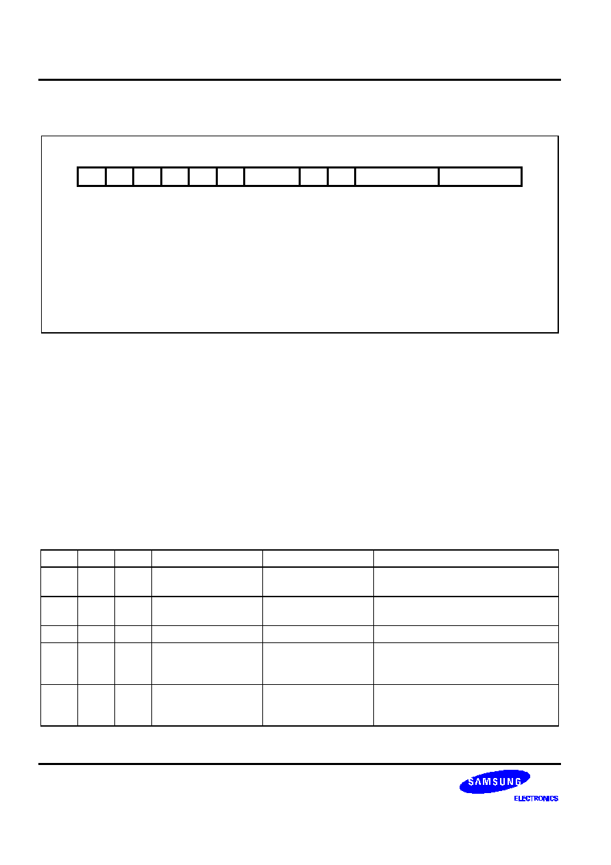
ARM INSTRUCTION SET
S3F441FX RISC MICROCONTROLLER
3-76
FORMAT 5: HI-REGISTER OPERATIONS/BRANCH EXCHANGE
15
0
0
14
10
[2:0] Destination Register
[5:3] Source Register
[6] Hi Operand Flag 2
[7] Hi Operand Flag 1
[9:8] Opcode
6
5
3
2
Rd/Hd
0
0
13
12
11
Op
Rs/Hs
0
0
0
9
8
7
H1
H2
Figure 3-34. Format 5
OPERATION
There are four sets of instructions in this group. The first three allow ADD, CMP and MOV operations to be
performed between Lo and Hi registers, or a pair of Hi registers. The fourth, BX, allows a Branch to be performed
which may also be used to switch processor state. The THUMB assembler syntax is shown in Table 3-12.
NOTE
In this group only CMP (Op = 01) sets the CPSR condition codes.
The action of H1= 0, H2 = 0 for Op = 00 (ADD), Op =01 (CMP) and Op = 10 (MOV) is undefined, and should not
be used.
Table 3-12. Summary of Format 5 Instructions
Op
H1
H2
THUMB assembler
ARM equivalent
Action
00
0
1
ADD Rd, Hs
ADD Rd, Rd, Hs
Add a register in the range 8-15 to a
register in the range 0-7.
00
1
0
ADD Hd, Rs
ADD Hd, Hd, Rs
Add a register in the range 0-7 to a
register in the range 8-15.
00
1
1
ADD Hd, Hs
ADD Hd, Hd, Hs
Add two registers in the range 8-15
01
0
1
CMP Rd, Hs
CMP Rd, Hs
Compare a register in the range 0-7
with a register in the range 8-15. Set
the condition code flags on the result.
01
1
0
CMP Hd, Rs
CMP Hd, Rs
Compare a register in the range 8-15
with a register in the range 0-7. Set
the condition code flags on the result.

S3F441FX RISC MICROCONTROLLER
ARM INSTRUCTION SET
3-77
Table 3-12. Summary of Format 5 Instructions (Continued)
Op
H1
H2
THUMB assembler
ARM equivalent
Action
01
1
1
CMP Hd, Hs
CMP Hd, Hs
Compare two registers in the range
8-15. Set the condition code flags on
the result.
10
0
1
MOV Rd, Hs
MOV Rd, Hs
Move a value from a register in the
range 8-15 to a register in the range 0-
7.
10
1
0
MOV Hd, Rs
MOV Hd, Rs
Move a value from a register in the
range 0-7 to a register in the range
8-15.
10
1
1
MOV Hd, Hs
MOV Hd, Hs
Move a value between two registers in
the range 8-15.
11
0
0
BX Rs
BX Rs
Perform branch (plus optional state
change) to address in a register in the
range 0-7.
11
0
1
BX Hs
BX Hs
Perform branch (plus optional state
change) to address in a register in the
range 8-15.
INSTRUCTION CYCLE TIMES
All instructions in this format have an equivalent ARM instruction as shown in Table 3-12. The instruction cycle
times for the THUMB instruction are identical to that of the equivalent ARM instruction.
THE BX INSTRUCTION
BX performs a Branch to a routine whose start address is specified in a Lo or Hi register.
Bit 0 of the address determines the processor state on entry to the routine:
Bit 0 = 0
Causes the processor to enter ARM state.
Bit 0 = 1
Causes the processor to enter THUMB state.
NOTE
The action of H1 = 1 for this instruction is undefined, and should not be used.

ARM INSTRUCTION SET
S3F441FX RISC MICROCONTROLLER
3-78
EXAMPLES
Hi-Register Operations
ADD
PC, R5
; PC := PC + R5 but don't set the condition codes.
CMP
R4, R12
; Set the condition codes on the result of R4 - R12.
MOV
R15, R14
; Move R14 (LR) into R15 (PC)
; but don't set the condition codes,
; eg. return from subroutine.
Branch and Exchange
; Switch from THUMB to ARM state.
ADR
R1,outofTHUMB
; Load address of outofTHUMB into R1.
MOV
R11,R1
BX
R11
; Transfer the contents of R11 into the PC.
; Bit 0 of R11 determines whether
; ARM or THUMB state is entered, ie. ARM state here.
∑
∑
ALIGN
CODE32
outofTHUMB
; Now processing ARM instructions...
USING R15 AS AN OPERAND
If R15 is used as an operand, the value will be the address of the instruction + 4 with bit 0 cleared. Executing a
BX PC in THUMB state from a non-word aligned address will result in unpredictable execution.

S3F441FX RISC MICROCONTROLLER
ARM INSTRUCTION SET
3-79
FORMAT 6: PC-RELATIVE LOAD
15
0
0
14
10
[7:0] Immediate Value
[10:8] Destination Register
Word 8
0
0
13
12
11
Rd
0
0
8
7
Figure 3-35. Format 6
OPERATION
This instruction loads a word from an address specified as a 10-bit immediate offset from the PC. The THUMB
assembler syntax is shown below.
Table 3-13. Summary of PC-Relative Load Instruction
THUMB assembler
ARM equivalent
Action
LDR Rd, [PC, #Imm]
LDR Rd, [R15, #Imm]
Add unsigned offset (255 words, 1020 bytes) in
Imm to the current value of the PC. Load the
word from the resulting address into Rd.
NOTE: The value specified by #Imm is a full 10-bit address, but must always be word-aligned (ie with bits 1:0 set to 0),
since the assembler places #Imm >> 2 in field Word 8. The value of the PC will be 4 bytes greater than the address
of this instruction, but bit 1 of the PC is forced to 0 to ensure it is word aligned.

ARM INSTRUCTION SET
S3F441FX RISC MICROCONTROLLER
3-80
INSTRUCTION CYCLE TIMES
All instructions in this format have an equivalent ARM instruction. The instruction cycle times for the THUMB
instruction are identical to that of the equivalent ARM instruction.
EXAMPLES
LDR R3,[PC,#844]
; Load into R3 the word found at the
; address formed by adding 844 to PC.
; bit[1] of PC is forced to zero.
; Note that the THUMB opcode will contain
; 211 as the Word8 value.

S3F441FX RISC MICROCONTROLLER
ARM INSTRUCTION SET
3-81
FORMAT 7: LOAD/STORE WITH REGISTER OFFSET
[2:0] Source/Destination Register
[5:3] Base Register
[8:6] Offset Register
[10] Byte/Word Flag
0 = Transfer word quantity
1 = Transfer byte quantity
[11] Load/Store Flag
0 = Store to memory
1 = Load from memory
15
0
0
14
10
6
5
3
2
Rd
1
0
13
12
11
Rb
1
L
B
9
8
Ro
0
Figure 3-36. Format 7

ARM INSTRUCTION SET
S3F441FX RISC MICROCONTROLLER
3-82
OPERATION
These instructions transfer byte or word values between registers and memory. Memory addresses are pre-
indexed using an offset register in the range 0-7. The THUMB assembler syntax is shown in Table 3-14.
Table 3-14. Summary of Format 7 Instructions
L
B
THUMB assembler
ARM equivalent
Action
0
0
STR Rd, [Rb, Ro]
STR Rd, [Rb, Ro]
Pre-indexed word store:
Calculate the target address by adding
together the value in Rb and the value in
Ro. Store the contents of Rd at the
address.
0
1
STRB Rd, [Rb, Ro]
STRB Rd, [Rb, Ro]
Pre-indexed byte store:
Calculate the target address by adding
together the value in Rb and the value in
Ro. Store the byte value in Rd at the
resulting address.
1
0
LDR Rd, [Rb, Ro]
LDR Rd, [Rb, Ro]
Pre-indexed word load:
Calculate the source address by adding
together the value in Rb and the value in
Ro. Load the contents of the address into
Rd.
1
1
LDRB Rd, [Rb, Ro]
LDRB Rd, [Rb, Ro]
Pre-indexed byte load:
Calculate the source address by adding
together the value in Rb and the value in
Ro. Load the byte value at the resulting
address.
INSTRUCTION CYCLE TIMES
All instructions in this format have an equivalent ARM instruction as shown in Table 3-14. The instruction cycle
times for the THUMB instruction are identical to that of the equivalent ARM instruction.
EXAMPLES
STR
R3, [R2,R6]
; Store word in R3 at the address
; formed by adding R6 to R2.
LDRB
R2, [R0,R7]
; Load into R2 the byte found at
; the address formed by adding R7 to R0.

S3F441FX RISC MICROCONTROLLER
ARM INSTRUCTION SET
3-83
FORMAT 8: LOAD/STORE SIGN-EXTENDED BYTE/HALF-WORD
[2:0] Destination Register
[5:3] Base Register
[8:6] Offset Register
[10] Sign-Extended Flag
0 = Operand not sing-extended
1 = Operand sing-extended
[11] H Flag
15
0
0
14
10
6
5
3
2
Rd
1
0
13
12
11
Rb
1
H
S
9
8
Ro
1
Figure 3-37. Format 8
OPERATION
These instructions load optionally sign-extended bytes or half-words, and store half-words. The THUMB
assembler syntax is shown below.
Table 3-15. Summary of format 8 instructions
L
B
THUMB assembler
ARM equivalent
Action
0
0
STRH Rd, [Rb, Ro]
STRH Rd, [Rb, Ro]
Store half-word:
Add Ro to base address in Rb. Store bits
0-15 of Rd at the resulting address.
0
1
LDRH Rd, [Rb, Ro]
LDRH Rd, [Rb, Ro]
Load half-word:
Add Ro to base address in Rb. Load bits
0-15 of Rd from the resulting address,
and set bits 16-31 of Rd to 0.
1
0
LDSB Rd, [Rb, Ro]
LDRSB Rd, [Rb, Ro]
Load sign-extended byte:
Add Ro to base address in Rb. Load bits
0-7 of Rd from the resulting address, and
set bits 8-31 of Rd to bit 7.
1
1
LDSH Rd, [Rb, Ro]
LDRSH Rd, [Rb, Ro]
Load sign-extended half-word:
Add Ro to base address in Rb. Load bits
0-15 of Rd from the resulting address,
and set bits 16-31 of Rd to bit 15.

ARM INSTRUCTION SET
S3F441FX RISC MICROCONTROLLER
3-84
INSTRUCTION CYCLE TIMES
All instructions in this format have an equivalent ARM instruction as shown in Table 3-15. The instruction cycle
times for the THUMB instruction are identical to that of the equivalent ARM instruction.
EXAMPLES
STRH
R4, [R3, R0]
; Store the lower 16 bits of R4 at the
; address formed by adding R0 to R3.
LDSB
R2, [R7, R1]
; Load into R2 the sign extended byte
; found at the address formed by adding R1 to R7.
LDSH
R3, [R4, R2]
; Load into R3 the sign extended half-word
; found at the address formed by adding R2 to R4.

S3F441FX RISC MICROCONTROLLER
ARM INSTRUCTION SET
3-85
FORMAT 9: LOAD/STORE WITH IMMEDIATE OFFSET
[2:0] Source/Destination Register
[5:3] Base Register
[10:6] Offset Register
[11] Load/Store Flag
0 = Store to memory
1 = Load from memory
[12] Byte/Word Flad
0 = Transfer word quantity
1 = Transfer byte quantity
15
0
0
14
10
6
5
3
2
Rd
1
1
13
12
11
Rb
B
L
Offset5
Figure 3-38. Format 9
OPERATION
These instructions transfer byte or word values between registers and memory using an immediate 5 or 7-bit
offset. The THUMB assembler syntax is shown in Table 3-16.
Table 3-16. Summary of Format 9 Instructions
L
B
THUMB assembler
ARM equivalent
Action
0
0
STR Rd, [Rb, #Imm]
STR Rd, [Rb, #Imm]
Calculate the target address by adding
together the value in Rb and Imm. Store
the contents of Rd at the address.
1
0
LDR Rd, [Rb, #Imm]
LDR Rd, [Rb, #Imm]
Calculate the source address by adding
together the value in Rb and Imm. Load
Rd from the address.
0
1
STRB Rd, [Rb, #Imm]
STRB Rd, [Rb, #Imm]
Calculate the target address by adding
together the value in Rb and Imm. Store
the byte value in Rd at the address.
1
1
LDRB Rd, [Rb, #Imm]
LDRB Rd, [Rb, #Imm]
Calculate source address by adding
together the value in Rb and Imm. Load
the byte value at the address into Rd.
NOTE: For word accesses (B = 0), the value specified by #Imm is a full 7-bit address, but must be word-aligned
(ie with bits 1:0 set to 0), since the assembler places #Imm >> 2 in the Offset5 field.

ARM INSTRUCTION SET
S3F441FX RISC MICROCONTROLLER
3-86
INSTRUCTION CYCLE TIMES
All instructions in this format have an equivalent ARM instruction as shown in Table 3-16. The instruction cycle
times for the THUMB instruction are identical to that of the equivalent ARM instruction.
EXAMPLES
LDR
R2, [R5,#116]
; Load into R2 the word found at the
; address formed by adding 116 to R5.
; Note that the THUMB opcode will
; contain 29 as the Offset5 value.
STRB
R1, [R0,#13]
; Store the lower 8 bits of R1 at the
; address formed by adding 13 to R0.
; Note that the THUMB opcode will
; contain 13 as the Offset5 value.
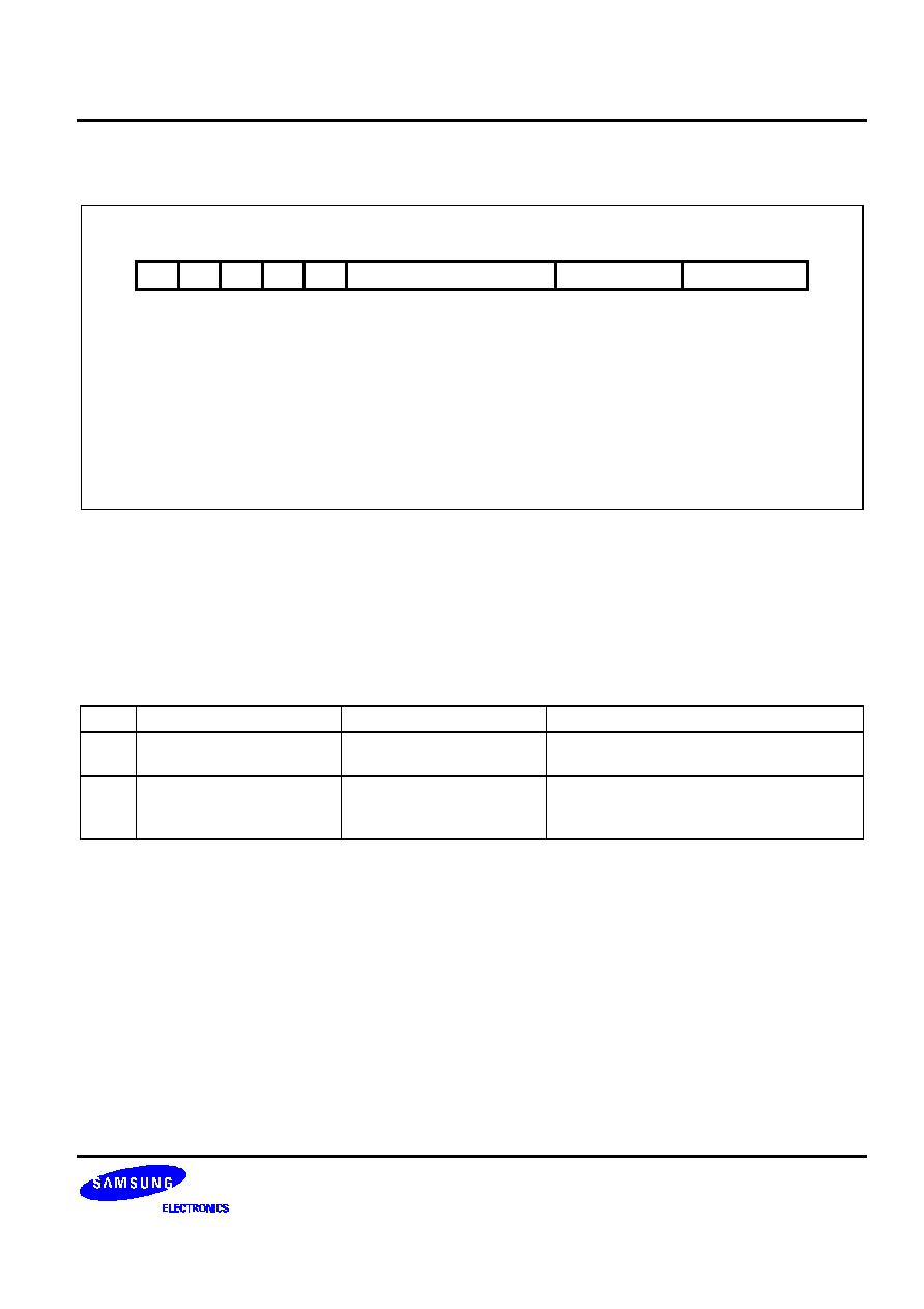
S3F441FX RISC MICROCONTROLLER
ARM INSTRUCTION SET
3-87
FORMAT 10: LOAD/STORE HALF-WORD
[2:0] Source/Destination Register
[5:3] Base Register
[10:6] Immediate Value
[11] Load/Store Flag
0 = Store to memory
1 = Load from memory
15
0
0
14
10
6
5
3
2
Rd
1
0
13
12
11
Rb
0
L
Offset5
Figure 3-39. Format 10
OPERATION
These instructions transfer half-word values between a Lo register and memory. Addresses are pre-indexed,
using a 6-bit immediate value. The THUMB assembler syntax is shown in Table 3-17.
Table 3-17. Half-word Data Transfer Instructions
L
THUMB assembler
ARM equivalent
Action
0
STRH Rd, [Rb, #Imm]
STRH Rd, [Rb, #Imm]
Add #Imm to base address in Rb and store
bits 0 - 15 of Rd at the resulting address.
1
LDRH Rd, [Rb, #Imm]
LDRH Rd, [Rb, #Imm]
Add #Imm to base address in Rb. Load bits
0-15 from the resulting address into Rd and
set bits 16-31 to zero.
NOTE: #Imm is a full 6-bit address but must be half-word-aligned (ie with bit 0 set to 0) since the assembler places
#Imm >> 1 in the Offset5 field.

ARM INSTRUCTION SET
S3F441FX RISC MICROCONTROLLER
3-88
INSTRUCTION CYCLE TIMES
All instructions in this format have an equivalent ARM instruction as shown in Table 3-17. The instruction cycle
times for the THUMB instruction are identical to that of the equivalent ARM instruction.
EXAMPLES
STRH
R6, [R1, #56]
; Store the lower 16 bits of R4 at the address formed by
; adding 56 R1. Note that the THUMB opcode will contain
; 28 as the Offset5 value.
LDRH
R4, [R7, #4]
; Load into R4 the half-word found at the address formed by
; adding 4 to R7. Note that the THUMB opcode will contain
; 2 as the Offset5 value.

S3F441FX RISC MICROCONTROLLER
ARM INSTRUCTION SET
3-89
FORMAT 11: SP-RELATIVE LOAD/STORE
[7:0] Immediate Value
[10:8] Destination Register
[11] Load/Store Bit
0 = Store to memory
1 = Load from memory
15
0
1
14
10
0
0
13
12
11
Word 8
1
L
Rd
7
8
Figure 3-40. Format 11
OPERATION
The instructions in this group perform an SP-relative load or store.The THUMB assembler syntax is shown in the
following table.
Table 3-18. SP-Relative Load/Store Instructions
L
THUMB assembler
ARM equivalent
Action
0
STR Rd, [SP, #Imm]
STR Rd, [R13 #Imm]
Add unsigned offset (255 words, 1020
bytes) in Imm to the current value of the SP
(R7). Store the contents of Rd at the
resulting address.
1
LDR Rd, [SP, #Imm]
LDR Rd, [R13 #Imm]
Add unsigned offset (255 words, 1020
bytes) in Imm to the current value of the SP
(R7). Load the word from the resulting
address into Rd.
NOTE: The offset supplied in #Imm is a full 10-bit address, but must always be word-aligned (ie bits 1:0 set to 0),
since the assembler places #Imm >> 2 in the Word8 field.
INSTRUCTION CYCLE TIMES
All instructions in this format have an equivalent ARM instruction as shown in Table 3-18. The instruction cycle
times for the THUMB instruction are identical to that of the equivalent ARM instruction.
EXAMPLES
STR
R4, [SP,#492]
; Store the contents of R4 at the address
; formed by adding 492 to SP (R13).
; Note that the THUMB opcode will contain
; 123 as the Word8 value.

ARM INSTRUCTION SET
S3F441FX RISC MICROCONTROLLER
3-90
FORMAT 12: LOAD ADDRESS
[7:0] 8-bit Unsigned Constant
[10:8] Destination Register
[11] Source
0 = PC
1 = SP
15
0
1
14
10
0
1
13
12
11
Word 8
0
SP
Rd
7
8
Figure 3-41. Format 12
OPERATION
These instructions calculate an address by adding an 10-bit constant to either the PC or the SP, and load the
resulting address into a register. The THUMB assembler syntax is shown in the following table.
Table 3-19. Load Address
L
THUMB assembler
ARM equivalent
Action
0
ADD Rd, PC, #Imm
ADD Rd, R15, #Imm
Add #Imm to the current value of the
program counter (PC) and load the result
into Rd.
1
ADD Rd, SP, #Imm
ADD Rd, R13, #Imm
Add #Imm to the current value of the stack
pointer (SP) and load the result into Rd.
NOTE: The value specified by #Imm is a full 10-bit value, but this must be word-aligned (ie with bits 1:0 set to 0)
since the assembler places #Imm >> 2 in field Word 8.
Where the PC is used as the source register (SP = 0), bit 1 of the PC is always read as 0. The value of the PC
will be 4 bytes greater than the address of the instruction before bit 1 is forced to 0.
The CPSR condition codes are unaffected by these instructions.

S3F441FX RISC MICROCONTROLLER
ARM INSTRUCTION SET
3-91
INSTRUCTION CYCLE TIMES
All instructions in this format have an equivalent ARM instruction as shown in Table 3-19. The instruction cycle
times for the THUMB instruction are identical to that of the equivalent ARM instruction.
EXAMPLES
ADD
R2, PC, #572
; R2 := PC + 572, but don't set the
; condition codes. bit[1] of PC is forced to zero.
; Note that the THUMB opcode will
; contain 143 as the Word8 value.
ADD
R6, SP, #212
; R6 := SP (R13) + 212, but don't
; set the condition codes.
; Note that the THUMB opcode will
; contain 53 as the Word 8 value.
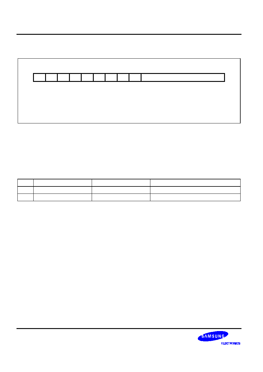
ARM INSTRUCTION SET
S3F441FX RISC MICROCONTROLLER
3-92
FORMAT 13: ADD OFFSET TO STACK POINTER
[6:0] 7-bit Immediate Value
[7] Sign Flag
0 = Offset is positive
1 = Offset is negative
15
0
1
14
10
0
1
13
12
11
SWord 7
1
0
0
7
8
9
6
0
0
S
Figure 3-42. Format 13
OPERATION
This instruction adds a 9-bit signed constant to the stack pointer. The following table shows the THUMB
assembler syntax.
Table 3-20. The ADD SP Instruction
L
THUMB assembler
ARM equivalent
Action
0
ADD SP, #Imm
ADD R13, R13, #Imm
Add #Imm to the stack pointer (SP).
1
ADD SP, # -Imm
SUB R13, R13, #Imm
Add #-Imm to the stack pointer (SP).
NOTE: The offset specified by #Imm can be up to -/+ 508, but must be word-aligned (ie with bits 1:0 set to 0)
since the assembler converts #Imm to an 8-bit sign + magnitude number before placing it in field SWord7.
The condition codes are not set by this instruction.
INSTRUCTION CYCLE TIMES
All instructions in this format have an equivalent ARM instruction as shown in Table 3-20. The instruction cycle
times for the THUMB instruction are identical to that of the equivalent ARM instruction.
EXAMPLES
ADD
SP, #268
; SP (R13) := SP + 268, but don't set the condition codes.
; Note that the THUMB opcode will
; contain 67 as the Word7 value and S=0.
ADD
SP, #-104
; SP (R13) := SP - 104, but don't set the condition codes.
; Note that the THUMB opcode will contain
; 26 as the Word7 value and S=1.

S3F441FX RISC MICROCONTROLLER
ARM INSTRUCTION SET
3-93
FORMAT 14: PUSH/POP REGISTERS
[7:0] Register List
[8] PC/LR Bit
0 = Do not store LR/Load PC
1 = Store LR/Load PC
[11] Load/Store Bit
0 = Store to memory
1 = Load from memory
15
0
1
14
10
0
1
13
12
11
Rlist
1
L
0
7
8
9
1
R
Figure 3-43. Format 14
OPERATION
The instructions in this group allow registers 0-7 and optionally LR to be pushed onto the stack, and registers 0-7
and optionally PC to be popped off the stack. The THUMB assembler syntax is shown in Table 3-21.
NOTE
The stack is always assumed to be Full Descending.
Table 3-21. PUSH and POP Instructions
L
B
THUMB assembler
ARM equivalent
Action
0
0
PUSH { Rlist }
STMDB R13!, { Rlist }
Push the registers specified by Rlist onto
the stack. Update the stack pointer.
0
1
PUSH { Rlist, LR }
STMDB R13!,
{ Rlist, R14 }
Push the Link Register and the registers
specified by Rlist (if any) onto the stack.
Update the stack pointer.
1
0
POP { Rlist }
LDMIA R13!, { Rlist }
Pop values off the stack into the
registers specified by Rlist. Update the
stack pointer.
1
1
POP { Rlist, PC }
LDMIA R13!, {Rlist, R15} Pop values off the stack and load into
the registers specified by Rlist. Pop the
PC off the stack. Update the stack
pointer.

ARM INSTRUCTION SET
S3F441FX RISC MICROCONTROLLER
3-94
INSTRUCTION CYCLE TIMES
All instructions in this format have an equivalent ARM instruction as shown in Table 3-21. The instruction cycle
times for the THUMB instruction are identical to that of the equivalent ARM instruction.
EXAMPLES
PUSH
{R0-R4,LR}
; Store R0,R1,R2,R3,R4 and R14 (LR) at
; the stack pointed to by R13 (SP) and update R13.
; Useful at start of a sub-routine to
; save workspace and return address.
POP
{R2,R6,PC}
; Load R2,R6 and R15 (PC) from the stack
; pointed to by R13 (SP) and update R13.
; Useful to restore workspace and return from sub-routine.

S3F441FX RISC MICROCONTROLLER
ARM INSTRUCTION SET
3-95
FORMAT 15: MULTIPLE LOAD/STORE
[7:0] Register List
[10:8] Base Register
[11] Load/Store Bit
0 = Store to memory
1 = Load from memory
15
0
1
14
10
1
0
13
12
11
Rlist
0
L
7
8
Rb
Figure 3-44. Format 15
OPERATION
These instructions allow multiple loading and storing of Lo registers. The THUMB assembler syntax is shown in
the following table.
Table 3-22. The Multiple Load/Store Instructions
L
THUMB assembler
ARM equivalent
Action
0
STMIA Rb!, { Rlist }
STMIA Rb!, { Rlist }
Store the registers specified by Rlist,
starting at the base address in Rb. Write
back the new base address.
1
LDMIA Rb!, { Rlist }
LDMIA Rb!, { Rlist }
Load the registers specified by Rlist,
starting at the base address in Rb. Write
back the new base address.
INSTRUCTION CYCLE TIMES
All instructions in this format have an equivalent ARM instruction as shown in Table 3-22. The instruction cycle
times for the THUMB instruction are identical to that of the equivalent ARM instruction.
EXAMPLES
STMIA
R0!, {R3-R7}
; Store the contents of registers R3-R7
; starting at the address specified in
; R0, incrementing the addresses for each word.
; Write back the updated value of R0.
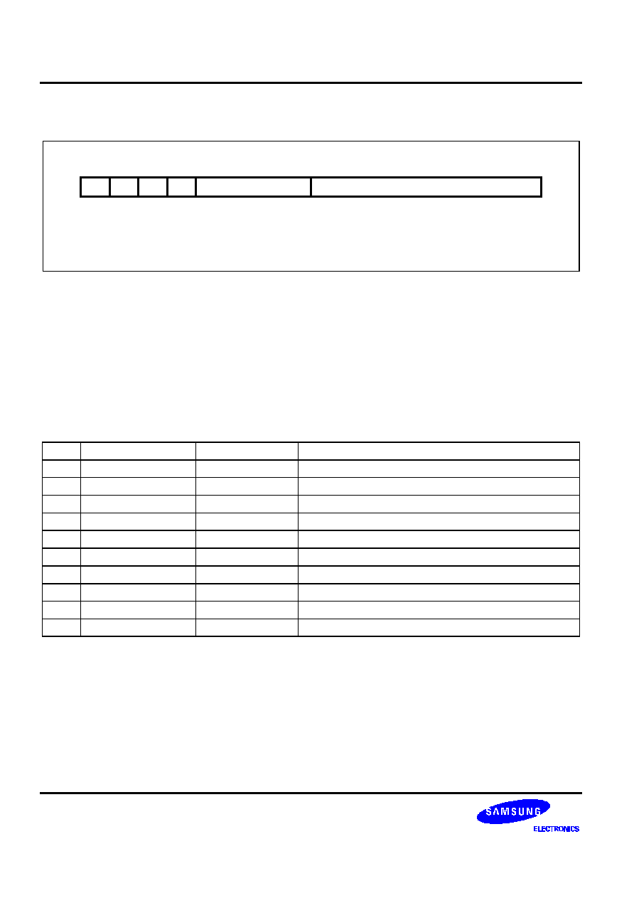
ARM INSTRUCTION SET
S3F441FX RISC MICROCONTROLLER
3-96
FORMAT 16: CONDITIONAL BRANCH
[7:0] 8-bit Signed Immediate
[11:8] Condition
15
0
1
14
1
0
13
12
11
SOffset 8
1
7
8
Cond
Figure 3-45. Format 16
OPERATION
The instructions in this group all perform a conditional Branch depending on the state of the CPSR condition
codes. The branch offset must take account of the prefetch operation, which causes the PC to be 1 word (4
bytes) ahead of the current instruction.
The THUMB assembler syntax is shown in the following table.
Table 3-23. The Conditional Branch Instructions
L
THUMB assembler
ARM equivalent
Action
0000
BEQ label
BEQ label
Branch if Z set (equal)
0001
BNE label
BNE label
Branch if Z clear (not equal)
0010
BCS label
BCS label
Branch if C set (unsigned higher or same)
0011
BCC label
BCC label
Branch if C clear (unsigned lower)
0100
BMI label
BMI label
Branch if N set (negative)
0101
BPL label
BPL label
Branch if N clear (positive or zero)
0110
BVS label
BVS label
Branch if V set (overflow)
0111
BVC label
BVC label
Branch if V clear (no overflow)
1000
BHI label
BHI label
Branch if C set and Z clear (unsigned higher)
1001
BLS label
BLS label
Branch if C clear or Z set (unsigned lower or same)

S3F441FX RISC MICROCONTROLLER
ARM INSTRUCTION SET
3-97
Table 3-23. The Conditional Branch Instructions (Continued)
L
THUMB assembler
ARM equivalent
Action
1001
BLS label
BLS label
Branch if C clear or Z set (unsigned lower or same)
1010
BGE label
BGE label
Branch if N set and V set, or N clear and V clear (greater
or equal)
1011
BLT label
BLT label
Branch if N set and V clear, or N clear and V set (less
than)
1100
BGT label
BGT label
Branch if Z clear, and either N set and V set or N clear
and V clear (greater than)
1101
BLE label
BLE label
Branch if Z set, or N set and V clear, or N clear and V set
(less than or equal)
NOTES:
1.
While label specifies a full 9-bit two's complement address, this must always be half-word-aligned (ie with bit 0 set to 0)
since the assembler actually places label >> 1 in field SOffset8.
2.
Cond = 1110 is undefined, and should not be used.
Cond = 1111 creates the SWI instruction: see .
INSTRUCTION CYCLE TIMES
All instructions in this format have an equivalent ARM instruction as shown in Table 3-23. The instruction cycle
times for the THUMB instruction are identical to that of the equivalent ARM instruction.
EXAMPLES
CMP R0, #45
; Branch to over-if R0 > 45.
BGT over
; Note that the THUMB opcode will contain
∑
; the number of half-words to offset.
∑
over
∑
; Must be half-word aligned.

ARM INSTRUCTION SET
S3F441FX RISC MICROCONTROLLER
3-98
FORMAT 17: SOFTWARE INTERRUPT
[7:0] Comment Field
15
0
1
14
1
0
13
12
11
Value 8
1
7
8
10
9
1
1
1
1
Figure 3-46. Format 17
OPERATION
The SWI instruction performs a software interrupt. On taking the SWI, the processor switches into ARM state and
enters Supervisor (SVC) mode.
The THUMB assembler syntax for this instruction is shown below.
Table 3-24. The SWI Instruction
THUMB assembler
ARM equivalent
Action
SWI Value 8
SWI Value 8
Perform Software Interrupt:
Move the address of the next instruction into LR,
move CPSR to SPSR, load the SWI vector address
(0x8) into the PC. Switch to ARM state and enter
SVC mode.
NOTE: Value8 is used solely by the SWI handler; it is ignored by the processor.
INSTRUCTION CYCLE TIMES
All instructions in this format have an equivalent ARM instruction as shown in Table 3-24. The instruction cycle
times for the THUMB instruction are identical to that of the equivalent ARM instruction.
EXAMPLES
SWI 18
; Take the software interrupt exception.
; Enter Supervisor mode with 18 as the
; requested SWI number.
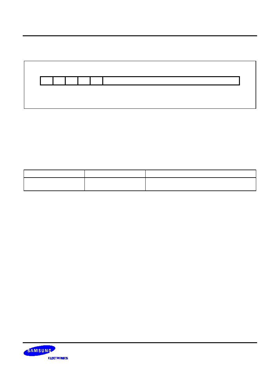
S3F441FX RISC MICROCONTROLLER
ARM INSTRUCTION SET
3-99
FORMAT 18: UNCONDITIONAL BRANCH
[10:0] Immediate Value
15
0
1
14
1
1
13
12
11
Offset11
0
10
0
Figure 3-47. Format 18
OPERATION
This instruction performs a PC-relative Branch. The THUMB assembler syntax is shown below. The branch offset
must take account of the prefetch operation, which causes the PC to be 1 word (4 bytes) ahead of the current
instruction.
Table 3-25. Summary of Branch Instruction
THUMB assembler
ARM equivalent
Action
B label
BAL label (half-word offset)
Branch PC relative +/- Offset11 << 1, where label is
PC +/- 2048 bytes.
NOTE: The address specified by label is a full 12-bit two's complement address,
but must always be half-word aligned (ie bit 0 set to 0), since the assembler places label >> 1 in the Offset11 field.
EXAMPLES
here
B here
; Branch onto itself. Assembles to 0xE7FE.
; (Note effect of PC offset).
B jimmy
; Branch to 'jimmy'.
∑
; Note that the THUMB opcode will contain the number of
∑
∑
; half-words to offset.
jimmy
∑
; Must be half-word aligned.

ARM INSTRUCTION SET
S3F441FX RISC MICROCONTROLLER
3-100
FORMAT 19: LONG BRANCH WITH LINK
[10:0] Long Branch and Link Offset High/Low
[11] Low/High Offset Bit
0 = Offset high
1 = Offset low
15
0
1
14
1
1
13
12
11
Offset
1
10
H
Figure 3-48. Format 19
OPERATION
This format specifies a long branch with link.
The assembler splits the 23-bit two's complement half-word offset specifed by the label into two 11-bit halves,
ignoring bit 0 (which must be 0), and creates two THUMB instructions.
Instruction 1 (H = 0)
In the first instruction the Offset field contains the upper 11 bits of the target address. This is shifted left by 12 bits
and added to the current PC address. The resulting address is placed in LR.
Instruction 2 (H =1)
In the second instruction the Offset field contains an 11-bit representation lower half of the target address. This is
shifted left by 1 bit and added to LR. LR, which now contains the full 23-bit address, is placed in PC, the address
of the instruction following the BL is placed in LR and bit 0 of LR is set.
The branch offset must take account of the prefetch operation, which causes the PC to be 1 word (4 bytes) ahead
of the current instruction

S3F441FX RISC MICROCONTROLLER
ARM INSTRUCTION SET
3-101
INSTRUCTION CYCLE TIMES
This instruction format does not have an equivalent ARM instruction.
Table 3-26. The BL Instruction
L
THUMB assembler
ARM equivalent
Action
0
BL label
none
LR := PC + OffsetHigh << 12
1
temp := next instruction address
PC := LR + OffsetLow << 1
LR := temp | 1
EXAMPLES
BL faraway
; Unconditionally Branch to 'faraway'
next
∑
; and place following instruction
∑
; address, ie "next", in R14,the Link
; register and set bit 0 of LR high.
; Note that the THUMB opcodes will
; contain the number of half-words to offset.
faraway
∑
; Must be Half-word aligned.
∑

ARM INSTRUCTION SET
S3F441FX RISC MICROCONTROLLER
3-102
INSTRUCTION SET EXAMPLES
The following examples show ways in which the THUMB instructions may be used to generate small and efficient
code. Each example also shows the ARM equivalent so these may be compared.
MULTIPLICATION BY A CONSTANT USING SHIFTS AND ADDS
The following shows code to multiply by various constants using 1, 2 or 3 Thumb instructions alongside the ARM
equivalents. For other constants it is generally better to use the built-in MUL instruction rather than using a
sequence of 4 or more instructions.
Thumb
ARM
1. Multiplication by 2^n (1,2,4,8,...)
LSL
Ra, Rb, LSL #n
; MOV Ra, Rb, LSL #n
2. Multiplication by 2^n+1 (3,5,9,17,...)
LSL
Rt, Rb, #n
; ADD Ra, Rb, Rb, LSL #n
ADD
Ra, Rt, Rb
3. Multiplication by 2^n-1 (3,7,15,...)
LSL
Rt, Rb, #n
; RSB Ra, Rb, Rb, LSL #n
SUB
Ra, Rt, Rb
4. Multiplication by -2^n (-2, -4, -8, ...)
LSL
Ra, Rb, #n
; MOV Ra, Rb, LSL #n
MVN
Ra, Ra
; RSB Ra, Ra, #0
5. Multiplication by -2^n-1 (-3, -7, -15, ...)
LSL
Rt, Rb, #n
; SUB Ra, Rb, Rb, LSL #n
SUB
Ra, Rb, Rt
Multiplication by any C = {2^n+1, 2^n-1, -2^n or -2^n-1} * 2^n
Effectively this is any of the multiplications in 2 to 5 followed by a final shift. This allows the following additional
constants to be multiplied. 6, 10, 12, 14, 18, 20, 24, 28, 30, 34, 36, 40, 48, 56, 60, 62 .....
(2..5)
; (2..5)
LSL
Ra, Ra, #n
; MOV Ra, Ra, LSL #n

S3F441FX RISC MICROCONTROLLER
ARM INSTRUCTION SET
3-103
GENERAL PURPOSE SIGNED DIVIDE
This example shows a general purpose signed divide and remainder routine in both Thumb and ARM code.
Thumb code
;signed_divide
; Signed divide of R1 by R0: returns quotient in R0,
; remainder in R1
;Get abs value of R0 into R3
ASR
R2, R0, #31
; Get 0 or -1 in R2 depending on sign of R0
EOR
R0, R2
; EOR with -1 (0
◊
FFFFFFFF) if negative
SUB
R3, R0, R2
; and ADD 1 (SUB -1) to get abs value
;SUB always sets flag so go & report division by 0 if necessary
BEQ
divide_by_zero
;Get abs value of R1 by xoring with 0xFFFFFFFF and adding 1 if negative
ASR
R0, R1, #31
; Get 0 or -1 in R3 depending on sign of R1
EOR
R1, R0
; EOR with -1 (0
◊
FFFFFFFF) if negative
SUB
R1, R0
; and ADD 1 (SUB -1) to get abs value
;Save signs (0 or -1 in R0 & R2) for later use in determining ; sign of quotient & remainder.
PUSH
{R0, R2}
;Justification, shift 1 bit at a time until divisor (R0 value) ; is just <= than dividend (R1 value). To do this shift
dividend ; right by 1 and stop as soon as shifted value becomes >.
LSR
R0, R1, #1
MOV
R2, R3
B
%FT0
just_l
LSL
R2, #1
0
CMP
R2, R0
BLS
just_l
MOV
R0, #0
; Set accumulator to 0
B
%FT0
; Branch into division loop
div_l
LSR
R2, #1
0
CMP
R1, R2
; Test subtract
BCC
%FT0
SUB
R1, R2
; If successful do a real subtract
0
ADC
R0, R0
; Shift result and add 1 if subtract succeeded
CMP
R2, R3
; Terminate when R2 == R3 (ie we have just
BNE
div_l
; tested subtracting the 'ones' value).

ARM INSTRUCTION SET
S3F441FX RISC MICROCONTROLLER
3-104
Now fixup the signs of the quotient (R0) and remainder (R1)
POP
{R2, R3}
; Get dividend/divisor signs back
EOR
R3, R2
; Result sign
EOR
R0, R3
; Negate if result sign = - 1
SUB
R0, R3
EOR
R1, R2
; Negate remainder if dividend sign = - 1
SUB
R1, R2
MOV
pc, lr
ARM Code
signed_divide
; Effectively zero a4 as top bit will be shifted out later
ANDS
a4, a1, #&80000000
RSBMI
a1, a1, #0
EORS
ip, a4, a2, ASR #32
;ip bit 31 = sign of result
;ip bit 30 = sign of a2
RSBCS
a2, a2, #0
;Central part is identical code to udiv (without MOV a4, #0 which comes for free as part of signed entry sequence)
MOVS
a3, a1
BEQ
divide_by_zero
just_l
; Justification stage shifts 1 bit at a time
CMP
a3, a2, LSR #1
MOVLS
a3, a3, LSL #1
; NB: LSL #1 is always OK if LS succeeds
BLO
s_loop
div_l
CMP
a2, a3
ADC
a4, a4, a4
SUBCS
a2, a2, a3
TEQ
a3, a1
MOVNE
a3, a3, LSR #1
BNE
s_loop2
MOV
a1, a4
MOVS
ip, ip, ASL #1
RSBCS
a1, a1, #0
RSBMI
a2, a2, #0
MOV
pc, lr

S3F441FX RISC MICROCONTROLLER
ARM INSTRUCTION SET
3-105
DIVISION BY A CONSTANT
Division by a constant can often be performed by a short fixed sequence of shifts, adds and subtracts.
Here is an example of a divide by 10 routine based on the algorithm in the ARM Cookbook in both Thumb and
ARM code.
Thumb Code
udiv10
; Take argument in a1 returns quotient in a1,
; remainder in a2
MOV
a2, a1
LSR
a3, a1, #2
SUB
a1, a3
LSR
a3, a1, #4
ADD
a1, a3
LSR
a3, a1, #8
ADD
a1, a3
LSR
a3, a1, #16
ADD
a1, a3
LSR
a1, #3
ASL
a3, a1, #2
ADD
a3, a1
ASL
a3, #1
SUB
a2, a3
CMP
a2, #10
BLT
%FT0
ADD
a1, #1
SUB
a2, #10
0
MOV
pc, lr
ARM Code
udiv10
; Take argument in a1 returns quotient in a1,
; remainder in a2
SUB
a2, a1, #10
SUB
a1, a1, a1, lsr #2
ADD
a1, a1, a1, lsr #4
ADD
a1, a1, a1, lsr #8
ADD
a1, a1, a1, lsr #16
MOV
a1, a1, lsr #3
ADD
a3, a1, a1, asl #2
SUBS
a2, a2, a3, asl #1
ADDPL
a1, a1, #1
ADDMI
a2, a2, #10
MOV
pc, lr

ARM INSTRUCTION SET
S3F441FX RISC MICROCONTROLLER
3-106
NOTES

S3F441FX RISC MICROCONTROLLER
I/O PORTS
4-1
4
I/O PORTS
OVERVIEW
S3F441FX has 16 general input/output ports.
-- Seven ports are dedicated to being I/O ports only(GPIO[6:0] )
-- Nine ports are shared with other functional pins (Multiplexed I/O ports :GPIO[15:7] )
-- Three external interrupt input or output pins
Each port can be easily configured by the software to meet various system configuration and design
requirements. The CPU accesses I/O ports by directly writing or reading port register addresses. For this reason,
special I/O instructions are not needed.
Table 4-1. S3F441FX Port Configuration Overview
Port
Configuration Options
Programmability
0
General C-MOS push-pull I/O port with pull-up resistor
Port 0 consists of GPIO[7:0].
GPIO7 is multiplexed with TIN.
Bit programmable
1
General C-MOS push-pull I/O port with pull-up resistor
Port 1 consists of GPIO[15:8].
GPIO[15:8] are multiplexed with RXD,TXD and A[17:12].
Bit programmable
2
External interrupt input or output port
Bit programmable
I/O PORTS
S3F441FX RISC MICROCONTROLLER
4-2
PORT DATA REGISTERS
Table 4-2. Port Data Register Summary
Register Name
Mnemonic
Offset
Reset Value
R/W
Port 0 Data Register
P0
0xb000
xxh
R/W
Port 1 Data Register
P1
0xb001
xxh
R/W
Port 2 Data Register
P2
0xb002
xxh
R/W
PORT CONTROL REGISTERS TABLE
Table 4-3. Port Control Register Summary
Register Name
Mnemonic
ADDR
Reset Value
R/W
Port 0 Control Register
P0CON
0xb010
00h
R/W
Port 0 Pull-up Register
P0PUR
0xb015
ffh
R/W
Port 1 Control Register
P1CON
0xb012
0000h
R/W
Port 1 Pull-up/down Register
P1PUDR
0xb016
ffh
R/W
Port 2 Control Register
P2CON
0xb014
0h
R/W
Port 2 Pull-up Register
P2PUR
0xb017
7h
R/W
Port 2 External Interrupt Control
Register
EINTCON
0xb018
0h
R/W
Port 2 External Interrupt Mode
Register
EINTMOD
0xb01a
00h
R/W

S3F441FX RISC MICROCONTROLLER
I/O PORTS
4-3
Table 4-4. Port 0 Control Register
Name
Bit
Description
P0CON
0
Setting the GPIO[0] bit of Port 0.
0 : C-MOS input mode
1 : C-MOS push-pull output mode
1
Setting the GPIO[1] bit of Port 0.
0 : C-MOS input mode
1 : C-MOS push-pull output mode
2
Setting the GPIO[2] bit of Port 0.
0 : C-MOS input mode
1 : C-MOS push-pull output mode
3
Setting the GPIO[3] bit of Port 0.
0 : C-MOS input mode
1 : C-MOS push-pull output mode
4
Setting the GPIO[4] bit of Port 0.
0 : C-MOS input mode
1 : C-MOS push-pull output mode
5
Setting the GPIO[5] bit of Port 0.
0 : C-MOS input mode
1 : C-MOS push-pull output mode
6
Setting the GPIO[6] bit of Port 0.
0 : C-MOS input mode
1 : C-MOS push-pull output mode
7
Setting the GPIO[7] bit of Port 0.
0 : TIN / C-MOS input mode
1 : C-MOS push-pull output mode
P0PUR
7-0
Setting the GPIO[7:0] pull-up resistor of Port 0.
0 : Disable pull-up resistor
1 : Enable pull-up resistor

I/O PORTS
S3F441FX RISC MICROCONTROLLER
4-4
Table 4-5. Port 1 Control Register
Name
Bit
Description
P1CON
1:0
Setting the GPIO[8] bit of Port 1.
00 : C-MOS input mode
01 : C-MOS push-pull output mode
10 : A12
3:2
Setting the GPIO[9] bit of Port 1.
00 : C-MOS input mode
01 : C-MOS push-pull output mode
10 : A13
5:4
Setting the GPIO[10] bit of Port 1.
00 : C-MOS input mode
01 : C-MOS push-pull output mode
10 : A14
7:6
Setting the GPIO[11] bit of Port 1.
00 : C-MOS input mode
01 : C-MOS push-pull output mode
10 : A15
9:8
Setting the GPIO[12] bit of Port 1.
00 : C-MOS input mode
01 : C-MOS push-pull output mode
10 : A16
11:10
Setting the GPIO[13] bit of Port 1.
00 : C-MOS input mode
01 : C-MOS push-pull output mode
10 : A17
13:12
Setting the GPIO[14] bit of Port 1.
00 : C-MOS input mode
01 : C-MOS push-pull output mode
10 : TXD
15:14
Setting the GPIO[15] bit of Port 1.
00 : RXD / C-MOS input mode
01 : C-MOS push-pull output mode
P1PUDR
5-0
Setting the GPIO[13:8] pull-down resistor of Port 1.
0 : Disable pull-down resistor
1 : Enable pull-down resistor
(When P1 is set as an address line, the pull-down resistor is automatically disabled.)
7-6
Setting the GPIO[15:14] pull-up resistor of Port 1.
0 : Disable pull-up resistor
1 : Enable pull-up resistor

S3F441FX RISC MICROCONTROLLER
I/O PORTS
4-5
Table 4-6. Port2 Control Register
Name
Bit
Description
P2CON
2-0
Setting the EINT[2:0] bit of Port 2.
0 : Input or external interrupt input(EINT2:0)
1 : C-MOS push-pull output mode
P2PUR
2-0
Setting the EINT[2:0] pull-up resistor of Port 2.
0 : Disable pull-up resistor
1 : Enable pull-up resistor
EINTMOD
1,0
Setting the external interrupt mode of EINT0
00 : Falling edge interrupt enable
01 : Rising edge interrupt enable
10 : High level interrupt enable
11 : Low level interrupt enable
3,2
Setting the external interrupt mode of EINT1
00 : Falling edge interrupt enable
01 : Rising edge interrupt enable
10 : High level interrupt enable
11 : Low level interrupt enable
5,4
Setting the external interrupt mode of EINT2
00 : Falling edge interrupt enable
01 : Rising edge interrupt enable
10 : High level interrupt enable
11 : Low level interrupt enable
EINTCON
2-0
Setting the EINT[2:0] interrupt enable
0 : Disable External Interrupt
1 : Enable External Interrupt
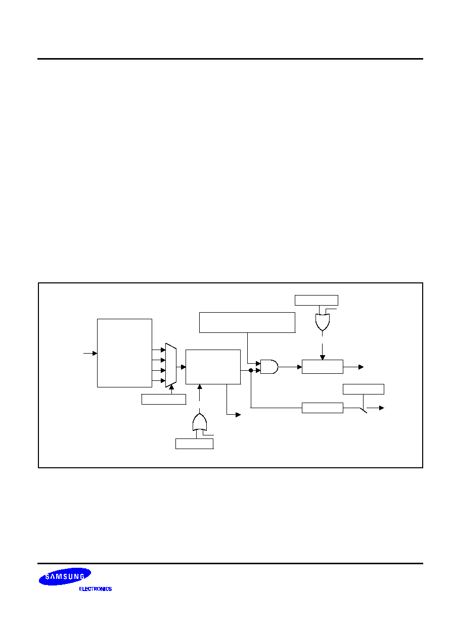
S3F441FX RISC MICROCONTROLLER
BASIC/WATCHDOG TIMER
5-1
5
BASIC/WATCHDOG TIMER
OVERVIEW
The S3F441FX has an internal Basic Timer/Watch-Dog Timer. This timer can be used to resume controller
operation when it has been disturbed due to noise or other kinds of system error or malfunctions. To configure the
Watch-dog timer, the overflow signal from the 8-bit Basic timer should be fed to the clock input of the 3-bit
Watch-dog timer, as shown in figure below. User can enable or disable the Watch-dog by software, i.e., by
controlling the configuration in BTCON register. If the user does not want to configure the Watch-dog timer, the
8-bit Basic timer can be used as a normal interval timer to request interrupt services. It also can signal the end of
the required oscillation interval after a reset or a Stop mode release. For example, the Basic timer can give the
overflow signal to necessary logic blocks after a reset or release from Stop mode. In this case, the overflow
signal from Basic timer may mean that there is a stable clock from an external oscillator circuit.
Clock DIV
Fin/2
9
Fin/2
11
Fin/2
12
Fin/2
13
EXTCLK
8-Bit Basic
Counter
(read only)
3-bit WDT
nRESET
BTCON.3-.2
CPU Start
INTPEND
INTMASK
OVF
BTCON.0
BTINT
WDT Control Register
(write 10100101b to disable)
BTCON.1
RESET
STOP
Clear
RESET,
STOP, IDLE
Clear
Figure 5-1. Watch-dog Timer Block Diagram
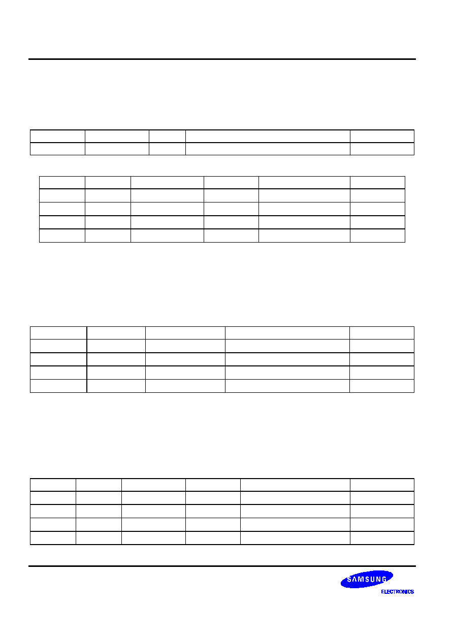
BASIC/WATCHDOG TIMER
S3F441FX RISC MICROCONTROLLER
5-2
BASIC TIMER COUNTER REGISTER
The basic timer counter register, BTCNT(Offset address : 0xa007), is used to specify the time out duration, and is
a free-running 8-bit counter. The table below should be kept as reference for determining the duration of timer.
This is the case when the external clock is 20Mhz.
Register
Offset Address
R/W
Description
Reset Value
BTCNT
0xa007
R
Basic timer count register
00h
Table 5-1. Basic Timer Counter Setting (at EXTCLK = 20 MHz)
BTCON.3
BTCON.2
Clock source
Resolution
Interval Time
Max. interval
0
0
EXTCLK/2
13
409.6
µ
s
2
13
/ EXTCLK
◊
2
8
104.86 ms
0
1
EXTCLK /2
12
204.8
µ
s
2
12
/ EXTCLK
◊
2
8
52.43 ms
1
0
EXTCLK /2
11
102.4
µ
s
2
11
/ EXTCL:K
◊
2
8
26.21 ms
1
1
EXTCLK /2
9
25.6
µ
s
2
9
/ EXTCLK
◊
2
8
6.55 ms
EXTERNAL OSCILLATION STABILIZATION TIME AFTER STOP OR RESET
In Figure 5-1, the CPU Start signal after reset or STOP is activated just after the 8-bit basic timer bit 4 is set to 1.
So, there is delay time before CPU is started after RESET or STOP is released. This delay time may be used for
the oscillation time of an external clock source. This delay time is calculated as in Table 5-2.
Table 5-2. The Delay Time before CPU Time Start (at EXTCLK = 20 MHz)
BTCON.3
BTCON.2
Clock source
WDT Interval
Delay time
0
0
EXTCLK/2
13
2
13
/ EXTCLK
◊
2
4
6.55 ms
0
1
EXTCLK /2
12
2
12
/ EXTCLK
◊
2
4
3.28 ms
1
0
EXTCLK /2
11
2
11
/ EXTCLK
◊
2
4
1.64 ms
1
1
EXTCLK /2
9
2
9
/ EXTCLK
◊
2
4
0.41 ms
WATCH DOG TIMER COUNTER
The watch dog timer counter register, WTCNT, is used to specify the time out duration and is a free-running 3-bit
counter. To enable Watch-dog timer, user should write the data in BTCON[15:8] register except 0xA5, which will
disable the Watch-dog timer. After writing a value in the BTCON[15:8] register the system will reset if there is an
overflow.
Table 5-3. Watch Dog Timer Counter Setting (at EXTCLK = 20 MHz)
BTCON.3
BTCON.2
Clock source
Resolution
WDT Interval
Interval time
0
0
EXTCLK/2
13
409.6
µ
s
2
13
/ EXTCLK
◊
2
8
◊
2
3
838.86 ms
0
1
EXTCLK /2
12
204.8
µ
s
2
12
/ EXTCLK
◊
2
8
◊
2
3
419.43 ms
1
0
EXTCLK /2
11
102.4
µ
s
2
11
/ EXTCLK
◊
2
8
◊
2
3
209.72 ms
1
1
EXTCLK /2
9
25.6
µ
s
2
9
/ EXTCLK
◊
2
8
◊
2
3
52.43 ms

S3F441FX RISC MICROCONTROLLER
BASIC/WATCHDOG TIMER
5-3
BASIC TIMER CONTROL REGISTER
The basic timer control register, BTCON, contains watch-dog counter enable bits, clock input setting bits, and
counter clear bit.
Register
Offset Address
R/W
Description
Reset Value
BTCON
0xa002
R/W
Basic Timer Control register
0000h
The basic timer control register has the following bits:
[0]
WDT Counter clear bit
This bit clears the watch dog counter. When this bit is set, the
Watch-dog counter register will be cleared to zero.(synchronous reset)
And this bit will be cleared automatically.
[1]
Basic Counter clear bit
This bit clears the basic counter. When this bit is set, the Basic timer
counter register will be cleared to all zero.(synchronous reset) And this bit
will be cleared automatically.
[3:2]
Clock source select
These bits select a clock source.
11b = EXTCLK / 2
9
10b = EXTCLK / 2
11
01b = EXTCLK / 2
12
00b = EXTCLK / 2
13
[15:8]
Watch dog timer enable
These bits enable or disable the watch-dog timer counting.
When these bits are {10100101b}, watch dog timer counter is stopped.
The other value enable watch-dog timer counting, and reset the system if
there is an overflow.

BASIC/WATCHDOG TIMER
S3F441FX RISC MICROCONTROLLER
5-4
FUNCTION DESCRIPTION
INTERVAL TIMER FUNCTION
The primary function of a basic timer is to measure the elapsed time intervals. The standard time interval is equal
to 256 basic timer clock pulses.
The content of the 8-bit counter register, BTCNT, increases every time a clock signal corresponding to the
BTCON selected frequency is detected. The BTCNT continues its counting until an overflow occurs, i.e., the
content reaches 255. An overflow set on the BT interrupt pending flag, which signals elapse of the designated
time interval. Then, an interrupt request is generated; BTCNT is cleared to all zero; and the counting continues
from 00H, again.
Watchdog Timer Function
The basic timer can also be used as a "watch-dog" timer to detect an unexpected program sequence, that is, a
system or program operation error due to an external factor. For example, an external noise can create an this
type of error in which the CPU is running an unexpected code sequence, i.e., malfunction of CPU. To recover the
CPU from the unexpected sequence, the watch-dog timer should reset the CPU for malfunctions. But, during
normal sequence, the instruction, which clears the watch-dog timer within a given period, should be executed at
proper points in a program. If an instruction that clears the watch-dog timer is not executed within the specified
period, meaning an overflow of the watch-dog timer, the reset signal should be generated and the system should
be restarted with reset status. An operation of watch-dog timer is as follows:
-- Each time BTCNT overflows, an overflow signal should be sent to the watch-dog timer counter, WDTCNT.
-- If WDTCNT overflows, the system reset should be generated.
A reset signal clears the BTCON as #0000H. This value can enable the watch-dog timer because it is not 0xA5.
During the normal operation, the application program should prevent the overflow. To do this, the WDTCNT
value should be cleared (by writing a "1" to BTCON.0) at regular intervals before the overflow occurs.

S3F441FX RISC MICROCONTROLLER
TIMER MODULE 0,1,2,3,4,5
6-1
6
TIMER MODULE 0,1,2,3,4,5 (16-BIT TIMERS)
OVERVIEW
The S3F441FX has Six 16-bit timers:T0,T1,T2,T3,T4 and T5. The timers T0-T5 can operate in interval mode, in
capture mode, or in match & overflow mode. The clock source for the timers can be UTCLK or TIN. You can
enable or disable the timers by setting the control bits in the corresponding timer mode register.
The timers 0,1,2,3,4, and 5 have three operating modes. The user can select the mode by having the appropriate
TnCON setting:
-- Interval timer mode
-- Capture input mode with a rising or falling edge trigger at the input pin(TIN, which is shared by
timer0/1/2/3/4/5)
-- Match & Overflow mode
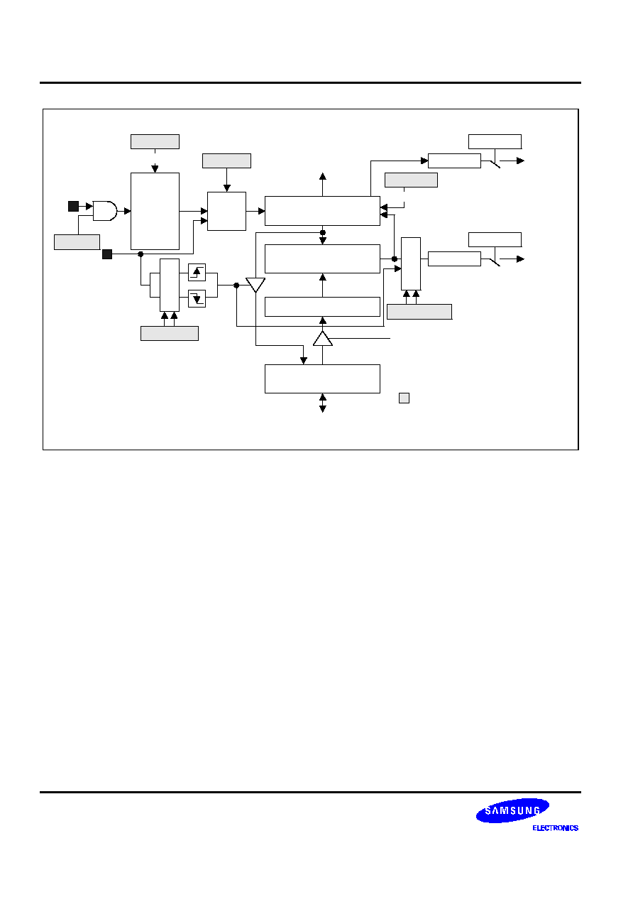
TIMER MODULE 0,1,2,3,4,5
S3F441FX RISC MICROCONTROLLER
6-2
TnCON.6
8-bit
Prescaler
Clear
UTCLK
TnCON.7
MUX
16-bit Up Counter
(TnCNT)
16-bit Comparator
Timer n Buffer Register
Timer n Data Register
(Read/Write)
TnCON.6
INTPND
INTMASK
TnCON.5-.3
TIN
R
Clear
Data Bus
TnOVF
INTPND
INTMASK
TnINT
TnCON.5-.3
Data Bus
Match Signal
TnCLR
TnOVF
Timer n Control Register
where, n = 0, 1, 2, 3, 4 and 5
Match
TnCON.2
Figure 6-1. 16-Bit Timer Block Diagram
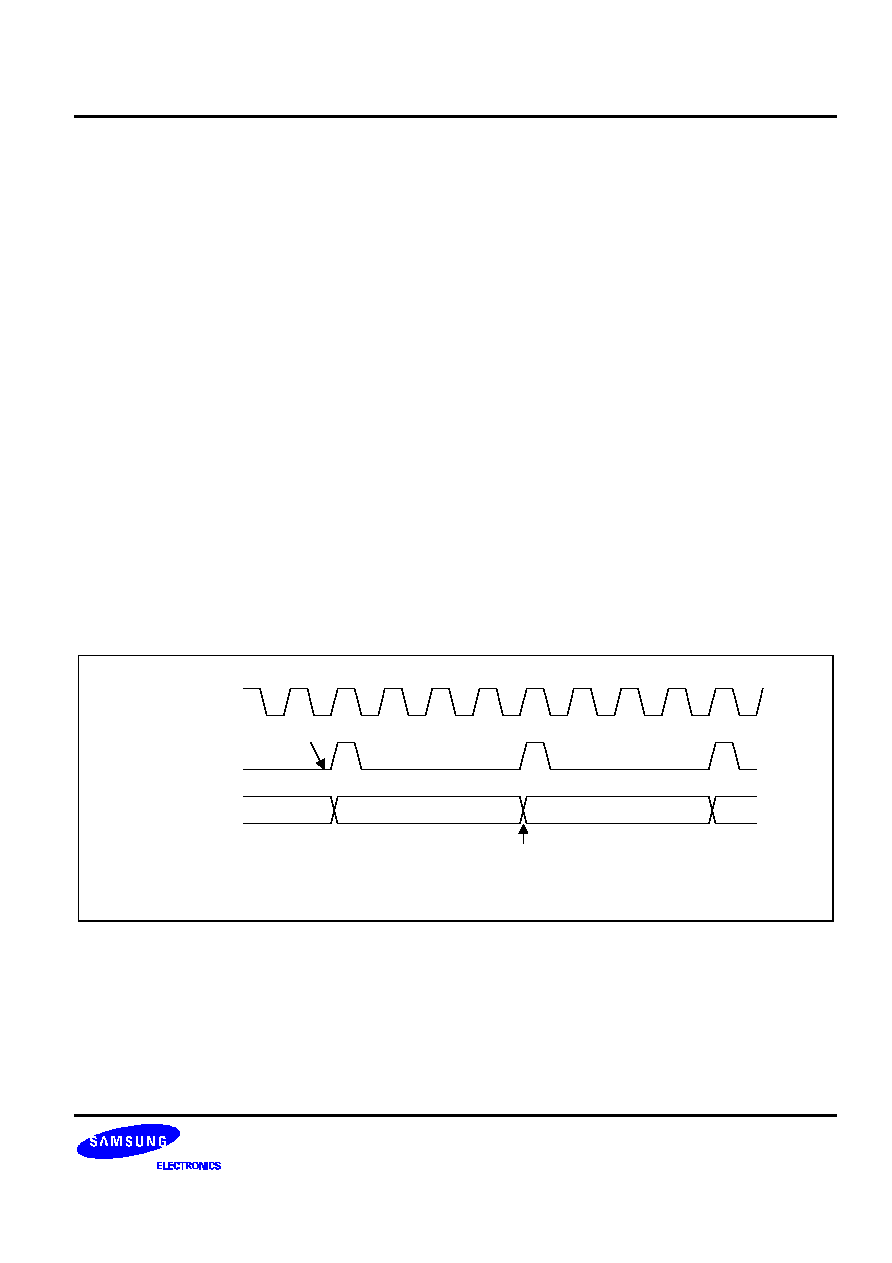
S3F441FX RISC MICROCONTROLLER
TIMER MODULE 0,1,2,3,4,5
6-3
TIMER 0,1,2,3,4,5 CONTROL REGISTERS(T0CON,T1CON,T2CON,T3CON,T4CON,T5CON)
Users should have the configuration on the timer 0,1,2,3,4, and 5 control registers, i.e., TnCON, to determine the
following:
-- Select the timer n operating mode (interval timer mode, match & overflow mode, or capture mode)
-- Select the timer n input clock (UTCLK or TIN)
-- Clear the timer n counter, TnCON[6]
-- Enable/Disable the timer clock, TnCON[7]
The INTMASK register can control whether the interrupt to CPU should be posted or not when the timer n
reaches to the overflow point in the interval timer mode, match & overflow mode, or capture mode. The
INTPEND register can store the interrupt pending bit if the corresponding interrupt is not serviced. After the
service of interrupt, the S/W should clear the pending bit.
During the system reset, TnCON register is cleared to '00H', automatically, which is a default configuration on the
timer. The default configuration is to have the interval timer mode and UTCLK as the timer input clock source.
User can clear the timer n counter at any time during normal operation by writing a "1" to TnCON[6].
INTERVAL MODE OPERATION
In interval timer mode, a match signal is generated when the counter value reaches to the written value in the Tn
reference data register, TnDATA. The match signal can generate a timer n match interrupt (TnINT) and clear the
counter value.
UTCLK
TnCNT clock
TnCNT
TnPRE=3
99
100
0
1
The timer match interrupt will occur.
NOTE:
If the prescaler value is n, the prescaler factor is n + 1.
Figure 6-2. Interval Mode Example 1 (TnDATA=100, TnPRE=3, UTCLK is a Timer Source)

TIMER MODULE 0,1,2,3,4,5
S3F441FX RISC MICROCONTROLLER
6-4
TIN
TnCNT
99
100
0
1
The timer match interrupt will occur
Figure 6-3. Interval Mode Example 2 (TnDATA=100, TIN is a Timer Source )
CAPTURE MODE OPERATION
In capture mode, the timer performs the capturing operation, in which the current timer counter value in TnCNT
register is latched to the timer n data register(TnDATA) in synchronization with an external trigger. For every
external trigger signal, the current timer counter value in TnCNT register is latched to the timer n data
register(TnDATA) and the capture interrupt is generated. By using this feature, the user can measure the time
difference between the external trigger signals. If the TnCNT overflows, the overflow interrupt will be sent to the
CPU core. A valid edge detected at the capture input pin is used as the external trigger. When this overflow
happens, the timer counter starts its counting from 0000H.
MATCH & OVERFLOW MODE OPERATION
In match mode, the match signal is generated when the timer counter value(TnCNT) is identical to the value of
the timer n data register(TnDATA), which was written by S/W. However, the match signal does not clear the
counter and can generate a match interrupt, only. It runs continuously, overflowing at FFFFH, and then continues
the increment from 0000H. When an overflow happens, an overflow interrupt is also generated.
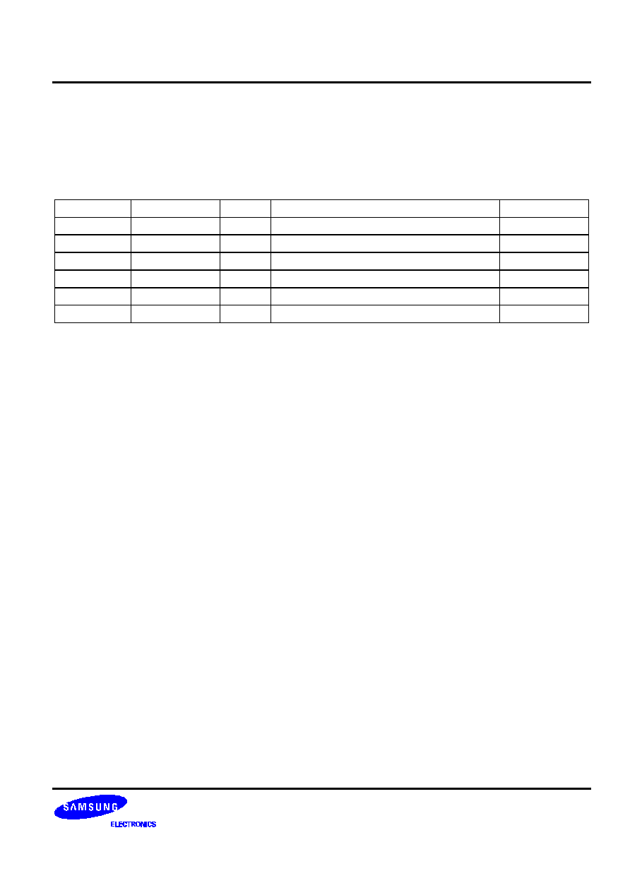
S3F441FX RISC MICROCONTROLLER
TIMER MODULE 0,1,2,3,4,5
6-5
TIMER SPECIAL REGISTERS
TIMER CONTROL REGISTERS
The timer control registers, T0CON, T1CON, T2CON, T3CON, T4CON, and T5CON are used to control the
operations of the six 16-bit timers.
Register
Offset Address
R/W
Description
Reset Value
T0CON
0x9003
R/W
Timer 0 control register
00h
T1CON
0x9013
R/W
Timer 1 control register
00h
T2CON
0x9023
R/W
Timer 2 control register
00h
T3CON
0x9033
R/W
Timer 3 control register
00h
T4CON
0x9043
R/W
Timer 4 control register
00h
T5CON
0x9053
R/W
Timer 5 control register
00h
Three timer mode registers have the following control settings:
[2]
Clock source selection
This bit determines which clock source should be used as a timer input
clock for the corresponding timer. When this bit is 0, UTCLK should be
used as the timer clock source of the corresponding timer. When 1,
TIN should be used.
[5:3]
Timer mode selection
This field determines the operation mode of the corresponding timer to
be used( Interval, match & overflow mode, and capture mode) When
the user sets TnCON[5:3] to 000b, the corresponding timer runs in the
interval mode. When 001b, the corresponding timer runs in the match
& overflow mode. When the user sets TnCON[5:3] to 1xx, the
corresponding timer runs in the capture mode. When 100b, the
corresponding timer runs in the capture and the capturing will happen
at the falling edge of external triggering signal (TIN). When 101b, the
corresponding timer runs in the capture mode with the capturing at the
rising edge of external triggering signal (TIN). When 110b, the
corresponding timer runs in the capture mode with the capturing at
both edges of the external triggering signal(TIN).
[6]
Counter Clear bit
This bit can clear the counter register(TnCNT). When this bit is set the
counter is cleared. Also, this bit is cleared automatically
[7]
Timer clock enable/disable
User can enable or disable the timer clock by setting or clearing this
bit. When TnCON[7] is 1, the divided UTCLK will be asserted to the
16-bit up-counter through the MUX. Otherwise, the divided UTCLK will
not be fed. However, TIN will not be controlled by this bit. Although
TnCON[7] is 0, the TIN will make the counter count.

TIMER MODULE 0,1,2,3,4,5
S3F441FX RISC MICROCONTROLLER
6-6
[1:0] Reserved to 00b
[2] Timer n Input Clock Selection Bits
0 = EXTCLK
1 = TIN
[5:3] Timer n Operation Mode Selection Bits
000 = Interval mode
001 = Match & Overflow mode (Match &OVF INT can occur)
010 = Reserved
011 = Reserved
100 = Capture mode (Capture on falling edge, counter running, OVF can occur)
101 = Capture mode (Capture on rising edge, counter running, OVF can occur)
110 = Capture mode (Capture on rising or falling edge, counter running, OVF can occur)
[6] Timer n Counter
0 = No
1 = Clear the timer n counter (when write)
[7] Timer n input clock enable bit
0 = Disable timer n input clock
1 = Enable timer n input clock
7
6
2
5
4
3
0
1
Figure 6-4. Timer 0,1,2,3,4,5 Control Registers
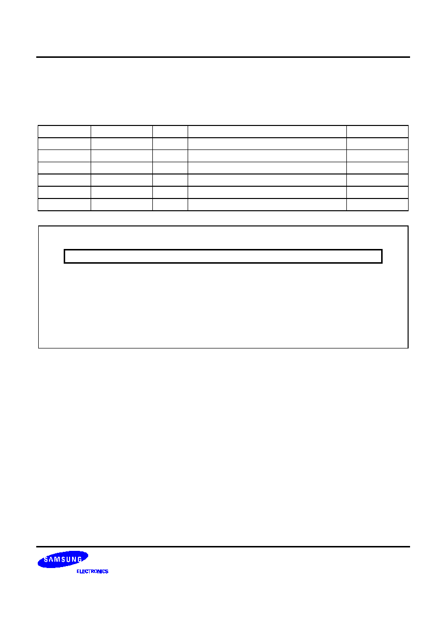
S3F441FX RISC MICROCONTROLLER
TIMER MODULE 0,1,2,3,4,5
6-7
TIMER DATA REGISTERS
The timer data registers, T0DATA, T1DATA, T2DATA, T3DATA, T4DATA and T5DATA, contain values that
specify the time-out duration for each timer. The formula for calculating time-out duration is (Timer data + 1)
cycles. See Figure 6-5 below.
Register
Offset Address
R/W
Description
Reset Value
T0DATA
0x9000
R/W
Timer 0 data register
ffffh
T1DATA
0x9010
R/W
Timer 1 data register
ffffh
T2DATA
0x9020
R/W
Timer 2 data register
ffffh
T3DATA
0x9030
R/W
Timer 3 data register
ffffh
T4DATA
0x9040
R/W
Timer 4 data register
ffffh
T5DATA
0x9050
R/W
Timer 5 data register
ffffh
[15:0] Timer Data Value
This field specifies the time-out period the corresponding
timer. The time-out period is calculated as (Timer data + 1)
cycles. Therefore, a maximum time-out period of 2
16
cycles
is possible (when the timer data value is 0xffff). The minimum
time-out period (2 cycles) is obtained by writing the value
0x0001h to the timer data register field.
15
0
Timer Data
Figure 6-5. Timer Data Registers (TnDATA)

TIMER MODULE 0,1,2,3,4,5
S3F441FX RISC MICROCONTROLLER
6-8
TIMER COUNT REGISTERS
The timer count registers, T0CNT, T1CNT, T2CNT, T3CNT, T4CNT and T5CNT, have values which provides the
count value to the current timers 0,1,2,3,4, and 5 during normal operation, respectively (see Figure 6-6).
Register
Offset Address
R/W
Description
Reset Value
T0CNT
0x9006
R
Timer 0 count register
0000h
T1CNT
0x9016
R
Timer 1 count register
0000h
T2CNT
0x9026
R
Timer 2 count register
0000h
T3CNT
0x9036
R
Timer 3 count register
0000h
T4CNT
0x9046
R
Timer 4 count register
0000h
T5CNT
0x9056
R
Timer 5 count register
0000h
[15:0] Counting Value
This field specifies the time-out period the corresponding timer.
The time-out period is calculated as (Timer data + 1) cycles.
Therefore, a maximum time-out period of 2
16
cycles is possible
(when the timer data value is 0xffff). The minimum time-out period
(2 cycles) is obtained by writing the value 0x0001h to the timer
data register field.
15
0
Counting Data
Figure 6-6. Timer Count Registers (TnCNT)
S3F441FX RISC MICROCONTROLLER
TIMER MODULE 0,1,2,3,4,5
6-9
TIMER PRE-SCALER REGISTERS
The timer pre-scaler registers, T0PRE, T1PRE, T2PRE, T3PRE, T4PRE, and T5PRE, have values which provide
the pre-scaler values (The main clock should be divided by the pre-scaler factor, which is the timer input clock) to
current timers 0/1/2/3/4/5 during normal operation, respectively(see Figure 6-7).
Register
Offset Address
R/W
Description
Reset Value
T0PRE
0x9002
R/W
Timer 0 pre-scaler register
ffh
T1PRE
0x9012
R/W
Timer 1 pre-scaler register
ffh
T2PRE
0x9022
R/W
Timer 2 pre-scaler register
ffh
T3PRE
0x9032
R/W
Timer 3 pre-scaler register
ffh
T4PRE
0x9042
R/W
Timer 4 pre-scaler register
ffh
T5PRE
0x9052
R/W
Timer 5 pre-scaler register
ffh
[7:0] Timer 0,1,2,3,4,5 Prescaler Value
This field cotains the timer 0,1,2,3,4,5 prescaler
value during normal timer operation.
7
0
Prescaler Data
Figure 6-7. Timer Pre-scaler Registers (TnPRE)
A pre-scaler register has an 8-bit pre-scaler value. If the pre-scaler value is n, the prescaler factor is n+1.

S3F441FX RISC MICROCONTROLLER
UART
7-1
7
UART
OVERVIEW
The S3F441FX has an on-chip UART(Universal Asynchronous Receiver/Transmitter) block. The UART can be
operated in the interrupt-based mode
A UART has a programmable baud rate generator with Rx and Tx ports for UART communication, Tx and Rx
shift registers, Tx and Rx buffer registers, Tx and Rx control blocks and control registers. In other words the
UART in S3F441FX supports the programmable baud rate, simultaneous transmit/receive(Full duplex mode), one
or two stop bit insertion, 5-bit, 6-bit, 7-bit, or 8-bit data transmit/receive size, and parity checking capability.
The baud rate generator can generate the suitable bit rate by dividing the MCLK (CPU Clock) or EXTCLK. The bit
rate is fully programmable by S/W with an appropriate clock division factor, the programmable baud generator
can generate UART bit rates 1200, 2400, 4800, 9600, and so on. The transmitter and the receiver block have Tx
and Rx data buffer registers, and a Tx and a Rx shift register, respectively. The transmission data should be
written to the Tx buffer register, then copied to the Tx shift register, and shifted out through the transmit data
pin(Tx). The data to be received should be shifted in through the receive data pin(Rx), and then copied from shift
register to the Rx buffer register whenever one data byte is received. The control unit provides the selection on
UART operation mode and shows the status/interrupt generation of UART during operation.
UART Baud rate = Source clock / ( 16 x ( Divisor Value + 1 ))

UART
S3F441FX RISC MICROCONTROLLER
7-2
Tx Control
Tx. Buffer Reg
Data Bus
Tx. Shift Reg
Rx. Shift Reg
Rx. Buffer Reg
Data Bus
LCON/UCON/USSR
Data Bus
Rx Control
Interrupt
Control
Serial Clock
Generator
Tx
Rx
CK
CK
Baud Rate Generater
16-bit Prescaler
Status
MCLK
UTCLK
UBRDR
Data Bus
LCON.6
Figure 7-1. UART Block Diagram

S3F441FX RISC MICROCONTROLLER
UART
7-3
INFRA-RED MODE
The S3F441FX UART block can support the infra-red (IR)-based transmit and receive (IrDA 1.0), which can be
selected by setting the infra-red-mode bit in the line control register (LCON). The implementation of the mode is
shown in Figure 7-2.
In IrDA mode, the transmitted bit data is slightly different from the normal transmitted bit data. In normal
transmitted bit data, the high value(Logic 1) will be maintained during one bit time if the bit data is 1. Otherwise,
the low value(Logic 0) will be maintained during one bit time if the bit data is 0. In IrDA mode, however, the high
value(Logic 1) will be pulsed with the duty of 3/16 during one bit time if the bit data is 1. Otherwise, the low
value(Logic 0) will be maintained during one bit time if the bit data is 0. Similarly with Tx case of IrDA mode, the
bit data of Rx has same bit shape as Tx. In other words, the receiver should detect the 3/16 pulsed-duty signal
when the bit data is 1. The normal operation of Rx is as same as the that of Tx in terms of bit shaping during one
bit time.
URAT
Block
TxD
RxD
IRS
RE
IR Tx
Encoder
0
1
1
0
IR Rx
Decoder
TxD
RxD
Figure 7-2. Infra-red Mode

UART
S3F441FX RISC MICROCONTROLLER
7-4
UART SPECIAL REGISTERS
UART LINE CONTROL REGISTER
The UART Line control register, LCON, is used to control the UART.
Register
Offset Address
R/W
Description
Reset Value
LCON
0x5003
R/W
UART line control register
00h
[1:0]
Word length (WL)
The two-bit word length value indicates the number of data bits to be
transmitted or received per frame. The options are 5-bit, 6-bit, 7-bit,
and 8-bit.
[2]
Number of stop bits
LCON[2] specifies how many stop bits should be inserted to signal
end-of-frame(EOF). When it is 0, one bit signals the EOF; when it is 1,
two bits signal EOF.
[5:3]
Parity mode (PMD)
The 3-bit parity mode value specifies how the parity generation and
checking should be performed during UART transmit and receive
operations. There are five options (see Figure 7-3).
[6]
Baud rate clock selection
When LCON[6] is 0, the internal system clock (MCLK) is selected as
the baud rate generator clock source. When it is 1, UTCLK is selected
as the baud rate generator clock source
[7]
Infra-Red Mode
This bit determines whether or not to use infra-red mode
0 = Normal Mode operation
1 = Infra-red Tx/Rx mode

S3F441FX RISC MICROCONTROLLER
UART
7-5
[1:0] Word-length Per Frame (WL)
00 = 5-bit
01 = 6-bit
10 = 7-bit
11 = 8-bit
[2] Number of Stop Bits at End of Frame
0 = One stop bit per frame
1 = Two stop bit per frame
[5:3] Parity Mode
0xx = No parity bit in frame
100 = Odd parity
101 = Even parity
110 = Parity forced/checked as 1
111 = Parity forced/checked as 0
[6] Baud Rate Clock Selection
0 = Internal clock source (MCLK)
1 = UTCLK
[7] Infra-Red Mode Selection
0 = Normal mode operation
1 = Infra-red Tx/Rx mode
7
6
2
5
4
3
0
1
PMD
WL
Figure 7-3. UART Line Control Register (LCON)

UART
S3F441FX RISC MICROCONTROLLER
7-6
UART CONTROL REGISTER
The UART control register, UCON, is used to control the single-channel UART.
Register
Offset Address
R/W
Description
Reset Value
UCON
0x5007
R/W
UART control register
00h
[1:0]
Reserved to 01b
These bits enable the UART to generate a receive interrupt.
[2]
Rx status interrupt enable
This bit enables the UART to generate an interrupt if an exception
(break, frame error, parity error, or overrun error) occurs during a
receive operation. When UCON[2] is set to 1, a receive status interrupt
will be generated each time a Rx exception occurs. When UCON[2] is
0, no receive status interrupt will be generated.
[4:3]
Reserved to 01b
These bits enable the UART to generate a transmit interrupt
[5]
Reserved
Unknown value will be read.
[6]
Send break
Setting UCON[6] causes the UART to send a break. The break is
defined as giving the continuous low level signal on the transmit data
output(Tx port) of more than one frame transmission time. When the
transmitter is empty (transmitter empty bit, USSR[7] = 1), the exact
one-frame time can be obtained by using TBR & USSR registers.
When USSR[7] is 1, write dummy data to the transmit buffer
register(TBR). Then poll the USSR[7] value. When it returns to 1,
clear(reset) the send break bit, UCON[6].
[7]
Loopback bit
Setting UCON[7] causes the UART to enter into the loop-back mode.
In loop-back mode, the transmit buffer register (TBR) is internally
connected to the receive buffer register (RBR). This mode is provided
for test purposes only.

S3F441FX RISC MICROCONTROLLER
UART
7-7
[1:0] Reserve interrupt enable
00 = Do not generate a receive interrupt
01 = Generate a receive interrupt
10 = Not used
10 = Not used
[2] Receive status in interrupt enable
0 = Do not generate receive status interrupt
1 = Generate receive status interrupt
[4:3] Transmit interrupt enable
00 = Do not generate a transmit interrupt
01 = Generate a transmit interrupt
10 = Not used
10 = Not used
[5] Reserved (Unknown Value)
[6] Send Break
0 = Do not send break
1 = Send break
[7] Loop break enable
0 = Normal UART operating
1 = Infra-red Tx/Rx mode
7
6
2
5
4
3
0
1
TxM
RxM
Figure 7-4. UART Control Register (UCON)

UART
S3F441FX RISC MICROCONTROLLER
7-8
UART STATUS REGISTER
The UART status register, USSR, is a read-only register that is used to monitor the status of serial I/O operations
in the single-channel UART.
Register
Offset Address
R/W
Description
Reset Value
USSR
0x500b
R
UART status register
c0h
[0]
Overrun error
USSR[0] is automatically set to 1 whenever an overrun error occurs
during a serial data receive operation. If the receive status interrupt
enable bit UCON[2] is 1, a receive status interrupt will be generated if
an overrun error occurs. This bit is automatically cleared to 0
whenever the UART status register (USSR) is read.
[1]
Parity error
USSR[1] is automatically set to 1 whenever a parity error occurs
during a serial data receive operation. If the receive status interrupt
enable bit UCON[2] is 1, a receive status interrupt will be generated if
a parity error occurs. This bit is automatically cleared to 0 whenever
the UART status register (USSR) is read.
[2]
Frame error
USSR[2] is automatically set to 1 whenever a frame error occurs
during a serial data receive operation. If the receive status interrupt
enable bit UCON[2] is 1, a receive status interrupt will be generated if
a frame error occurs. The frame error bit is automatically cleared to 0
whenever the UART status register (USSR) is read.
[3]
Break interrupt
USSR[3] is automatically set to 1 to indicate that a break signal has
been received. If the receive status interrupt enable bit, UCON[2], is 1,
a receive status interrupt will be generated if a break occurs. The
break interrupt bit is automatically cleared to 0 when you read the
UART status register.
[4]
≠
≠
[5]
Receive data ready
USSR[5] is automatically set to 1 whenever the receive data buffer
register (RBR) contains the valid data received over the serial port.
The receive data can then be read from the RBR. When this bit is 0,
the RBR does not contain valid data.
[6]
Tx buffer register empty
USSR[6] is automatically set to 1 when the transmit buffer register
(TBR) does not contain valid data. In this case, the TBR can be written
with the data to be transmitted. When this bit is 0, the TBR contains
valid Tx data that has not yet been copied to the transmit shift register.
In this case, the TBR cannot be written with new Tx data.
[7]
Transmitter empty (T)
USSR[7] is automatically set to 1 when the transmit buffer register has
no valid data to be transmitted and when the Tx shift register is empty.
When the transmitter empty bit is 1, it indicates that it can now disable
the transmitter function block if necessary.

S3F441FX RISC MICROCONTROLLER
UART
7-9
7
6
2
5
4
3
0
1
[0] Overrun Error
0 = No overrun error during receive
1 = Overrun error (Generate receive status interrupt
if UCON[2] is 1.)
[1] Parity Error
0 = No parity error during receive
1 = Parity error (Generate receive status interrupt
if UCON[2] is 1.)
[2] Frame Error
0 = No frame error during receive
1 = Frame error (Generate receive status interrupt
if UCON[2] is 1.)
[3] Break Interrupt
0 = No break receive
1 = Break error (Generate receive status interrupt
if UCON[2] is 1.)
[5] Receive Data Ready
0 = No valid data in the receive buffer register
1 = Valid data present in the receive buffer register
(Issue interrupt)
[6] Transmit Holding Register Empty
0 = Valid data present in transmit holding register
(Issue interrupt)
1 = No valid data in transmit holding register
[7] Transmitter Empty
0 = Transmitter not empty; Tx in progress
1 = Transmitter empty; no data for Tx
x
Figure 7-5. UART Status Register (USSR)

UART
S3F441FX RISC MICROCONTROLLER
7-10
UART TRANSMIT BUFFER REGISTER
The UART transmit holding register, TBR, contains an 8-bit data value to be transmitted over the single-channel
UART.
Register
Offset Address
R/W
Description
Reset Value
TBR
0x500f
W
Serial transmit buffer register
xxh
[7:0]
Transmit data
This field contains the data to be transmitted over the single-channel
UART. When this register is written, the transmit buffer register empty
bit in the status register, USSR[6], should be 1. This prevents
overwriting the transmit data which may already be present in the
TBR. Whenever the TBR is written with a new value, the transmit
register empty bit USSR[6] is automatically cleared to 0.
7
0
[7:0] Transmit Data for UART
This field contains the data to be transmitted over the
serial I/O interface. To avoid overwriting data that has
not yet been transmitted, the transmit holding register
empty bit, USSR[6], should be 1. Writing a value to
this register automatically clears USSR[6] to 0.
Transmit Data
Figure 7-6. UART Transmit Buffer Register (TBR)
NOTE: Tx interrupt will be generated only when the TBR register is empty. So, if the TBR register has been empty and
you enable the UTXD interrupt using INTMASK register, the UTXD interrupt will not be generated. Therefore, to
generate the UTXD interrupt, the first character among the characters to be transmitted should be written into TBR
register.

S3F441FX RISC MICROCONTROLLER
UART
7-11
UART RECEIVE BUFFER REGISTER
The receive buffer register, RBR, contains an 8-bit field for received serial data.
Register
Offset Address
R/W
Description
Reset Value
RBR
0x5013
R
Serial receive buffer register
xxh
[7:0]
Receive data
This field contains the data received over the single-channel UART.
When this register is read, the receive data ready bit in the UART
status register, USSR[5], should be 1. This can prevent the reading of
invalid receive data which may already be present in the RBR.
Whenever the RBR is written with a new value, the receive data ready
bit, USSR[5], is automatically cleared to 0.
7
0
[7:0] Receive Data for UART
This field contains the data received over the serial I/O
interface. To avoid reading invalid data, the receive
data ready bit, USSR[5], should be 1. Reading this
register automatically clears the USSR[5] value to 0.
Receive Data
Figure 7-7. UART Receive Buffer Register (RBR)

UART
S3F441FX RISC MICROCONTROLLER
7-12
UART BAUD RATE PRESCALER REGISTERS
The value stored in the baud rate divisor register, UBRDR, is used to determine the serial Tx/Rx clock rate (baud
rate) as follows:
Baud rate = source_clock / ((Divisor value + 1) x 16)
The source_clock is either MCLK (the internal master clock) or UTCLK(the external UART & Timer clock input)
and it can be determined by setting the serial clock selection bit in the line control register, LCON[6].
Register
Offset Address
R/W
Description
Reset Value
UBRDR
0x5016
R/W
Baud rate divisor register
0000h
15
0
[7:0] Baud-Rate Divisor Vaule
This field contains the baud rate divisor value for
corresponding SIO channel.
Baud rate can be calculated as:
Baud rate = source_clock / ((divisor value + 1) x 16)
Baud-Rate Divisor
NOTE: The value of the baud-rate divisor should be from 0 to (2
16
-1)
Figure 7-8. UART Baud Rate Divisor Registers (UBRDR)

S3F441FX RISC MICROCONTROLLER
INTERRUPT CONTROLLER
8-1
8
INTERRUPT CONTROLLER
OVERVIEW
The S3F441FX interrupt architecture has a total of 19 interrupt sources. Interrupt request can be generated by the
internal functional blocks as well as external pins(External Interrupt Request). The ARM7TDMI core can
recognize two kinds of interrupt: a normal interrupt request (IRQ) and a fast interrupt request (FIQ). Therefore, all
S3F441FX interrupts should be categorized as either IRQ or FIQ. The interrupt sources in S3F441FX can be
serviced, delayed, or not be serviced by the combined configuration on the registers INTMODE, INTPEND, and
INTMASK. In the normal interrupt mode, the interrupt mode(IRQ or FIQ) determine the start address of
corresponding interrupt request. In other words, the start address of interrupt service should be 0x1C or 0x18 if
the mode is FIQ or IRQ. After jumping to 0x1C or 0x18, the S/W should determine the real start address of the
corresponding service address.
-- Interrupt mode register(INTMODE). Defines the interrupt mode, IRQ or FIQ, for each interrupt source.
-- Interrupt pending register(INTPEND). Indicates that an interrupt request is pending. When a pending bit is
set, the interrupt service routine can start whenever the I-flag or F-flag is cleared to 0, which means that the
previous service was finished or ARM7TDMI core is ready to accept other interrupts request during the
service of previous interrupt request. The service routine should clear the corresponding pending bit by
writing 0 when CPU is ready to accept other interrupt requests or when the CPU exits from the
corresponding service routine, at least. Because FIQ interrupt has higher priority than IRQ, the FIQ mode
interrupt can be serviced before the complete service of IRQ mode interrupt.
-- Interrupt mask register(INTMASK). Indicates that the corresponding interrupt request is not allowable if the
corresponding mask bit is 0. If an interrupt mask bit is 1, the interrupt request will be allowable, normally.
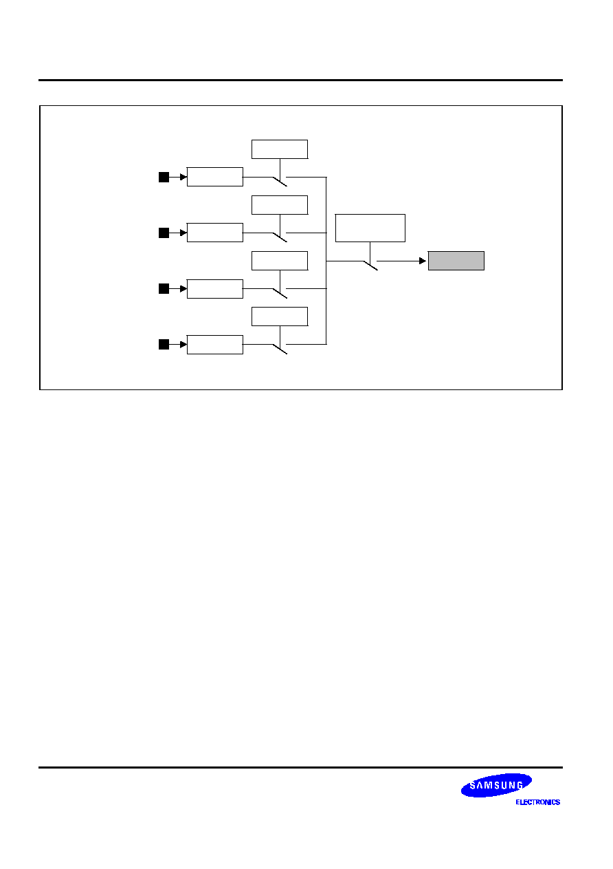
INTERRUPT CONTROLLER
S3F441FX RISC MICROCONTROLLER
8-2
INTPEND
INTMASK
INTPEND
INTMASK
INTPEND
INTMASK
INTPEND
INTMASK
Global Interrupt
Enable
IRQ/FIQ
Source
Source
Source
Source
Figure 8-1. S3F441FX Interrupt Structure

S3F441FX RISC MICROCONTROLLER
INTERRUPT CONTROLLER
8-3
INTERRUPT SOURCES
The 19 interrupt sources in the S3F441FX interrupt structure are described, in brief, as follows:
[18]
[17]
[16]
[15]
[14]
[13]
[12]
[11]
[10]
[9]
[8]
[7]
[6]
[5]
[4]
[3]
[2]
[1]
[0]
EINT2 external interrupt.
EINT1 external interrupt.
EINT0 external interrupt.
Basic Timer Interrupt.
Timer 5 Match/Capture interrupt.
Timer 5 Overflow interrupt.
Timer 4 Match/Capture interrupt.
Timer 4 Overflow interrupt.
Timer 3 Match/Capture interrupt.
Timer 3 Overflow interrupt.
Timer 2 Match/Capture interrupt.
Timer 2 Overflow interrupt.
Timer 1 Match/Capture interrupt.
Timer 1 Overflow interrupt.
Timer 0 Match/Capture interrupt.
Timer 0 Overflow interrupt.
UART error.
UART transmit interrupt.
UART receive interrupt.

INTERRUPT CONTROLLER
S3F441FX RISC MICROCONTROLLER
8-4
INTERRUPT CONTROLLER SPECIAL REGISTERS
INTERRUPT MODE REGISTER
Bits in the interrupt mode register(INTMODE) determine the interrupt mode of the requested interrupt. There are
two kinds of interrupt mode, IRQ and FIQ mode. When the bit is set to 1, the corresponding interrupt service
should be serviced by FIQ(Fast Interrupt Mode) in ARM7TDMI. Otherwise, the corresponding interrupt service
should be serviced by IRQ(Normal Interrupt Request) mode in ARM7TDMI.
Register
Offset Address
R/W
Description
Reset Value
INTMODE
0xc000
R/W
Interrupt mode register
0: IRQ mode
1: FIQ mode
xxx0 0000h
[18]
[17]
[16]
[15]
[14]
[13]
[12]
[11]
[10]
[9]
[8]
[7]
[6]
[5]
[4]
[3]
[2]
[1]
[0]
EINT2 external interrupt.
EINT1 external interrupt.
EINT0 external interrupt.
Basic Timer Interrupt.
Timer 5 Match/Capture interrupt.
Timer 5 Overflow interrupt.
Timer 4 Match/Capture interrupt.
Timer 4 Overflow interrupt.
Timer 3 Match/Capture interrupt.
Timer 3 Overflow interrupt.
Timer 2 Match/Capture interrupt.
Timer 2 Overflow interrupt.
Timer 1 Match/Capture interrupt.
Timer 1 Overflow interrupt.
Timer 0 Match/Capture interrupt.
Timer 0 Overflow interrupt.
UART error.
UART transmit interrupt.
UART receive interrupt.

S3F441FX RISC MICROCONTROLLER
INTERRUPT CONTROLLER
8-5
INTERRUPT PENDING REGISTER
The interrupt pending register (INTPEND) has interrupt pending bits for each interrupt source. When an interrupt
request is generated, the CPU will mask it if the I-flag or F-flag in the process status register (PSR) is set
because of a previous interrupt. When a pending bit is set, the interrupt service routine can start if the I-flag or F-
flag is cleared to 0, which means that the previous service was finished or ARM7TDMI core is ready to
accept other interrupt requests during the service of the previous interrupt request. The service routine should
clear the corresponding pending bit by writing 0 when CPU is ready to accept another interrupt request, or when
the CPU exits from the corresponding service routine, at least. Because FIQ interrupt has higher priority than
IRQ, the FIQ mode interrupt can be serviced before the complete service of IRQ mode interrupt even if the I-bit
in PSR is set to 1. In other words, the FIQ mode interrupt request can't be pending, if the IRQ mode interrupt
service is on processing.
Register
Offset Address
R/W
Description
Reset Value
INTPEND
0xc004
R/W
Interrupt pending register
Read
0: No interrupt has been requested
1: The corresponding interrupt source has
asserted the interrupt request.
Write
0: Clear the corresponding pending bit.
1: Preserve the previous pending bit status.
xxx0 0000h
[18]
[17]
[16]
[15]
[14]
[13]
[12]
[11]
[10]
[9]
[8]
[7]
[6]
[5]
[4]
[3]
[2]
[1]
[0]
EINT2 external interrupt.
EINT1 external interrupt.
EINT0 external interrupt.
Basic Timer Interrupt.
Timer 5 Match/Capture interrupt.
Timer 5 Overflow interrupt.
Timer 4 Match/Capture interrupt.
Timer 4 Overflow interrupt.
Timer 3 Match/Capture interrupt.
Timer 3 Overflow interrupt.
Timer 2 Match/Capture interrupt.
Timer 2 Overflow interrupt.
Timer 1 Match/Capture interrupt.
Timer 1 Overflow interrupt.
Timer 0 Match/Capture interrupt.
Timer 0 Overflow interrupt.
UART error.
UART transmit interrupt.
UART receive interrupt.

INTERRUPT CONTROLLER
S3F441FX RISC MICROCONTROLLER
8-6
INTERRUPT MASK REGISTER
The interrupt mask register (INTMASK) has interrupt mask bits for each interrupt source. Each of the interrupt
mask register (INTMASK) corresponds to an interrupt source. When an interrupt source mask bit is 0, the CPU
does not allow the corresponding interrupt request. If the mask bit is 1, the interrupt is serviced or pending upon
request.
Register
Offset Address
R/W
Description
Reset Value
INTMASK
0xc008
R/W
Interrupt mask register
0: Disable the corresponding interrupt.
1: Enable the corresponding interrupt.
xxx0 0000h
[18]
[17]
[16]
[15]
[14]
[13]
[12]
[11]
[10]
[9]
[8]
[7]
[6]
[5]
[4]
[3]
[2]
[1]
[0]
EINT2 external interrupt.
EINT1 external interrupt.
EINT0 external interrupt.
Basic Timer Interrupt.
Timer 5 Match/Capture interrupt.
Timer 5 Overflow interrupt.
Timer 4 Match/Capture interrupt.
Timer 4 Overflow interrupt.
Timer 3 Match/Capture interrupt.
Timer 3 Overflow interrupt.
Timer 2 Match/Capture interrupt.
Timer 2 Overflow interrupt.
Timer 1 Match/Capture interrupt.
Timer 1 Overflow interrupt.
Timer 0 Match/Capture interrupt.
Timer 0 Overflow interrupt.
UART error.
UART transmit interrupt.
UART receive interrupt.

S3F441FX RISC MICROCONTROLLER
SYSTEM MANAGER
9-1
9
SYSTEM MANAGER
OVERVIEW
The S3F441FX System Manager has the following functions:
-- Supports the big-endian mode. The internal system and the external memory are fixed as big-endian mode.
-- Memory controller for external memory/IO as well as internal memory.
-- Programmable Bank start and Bank end addresses.
-- Programmable access time for memory/IO access.
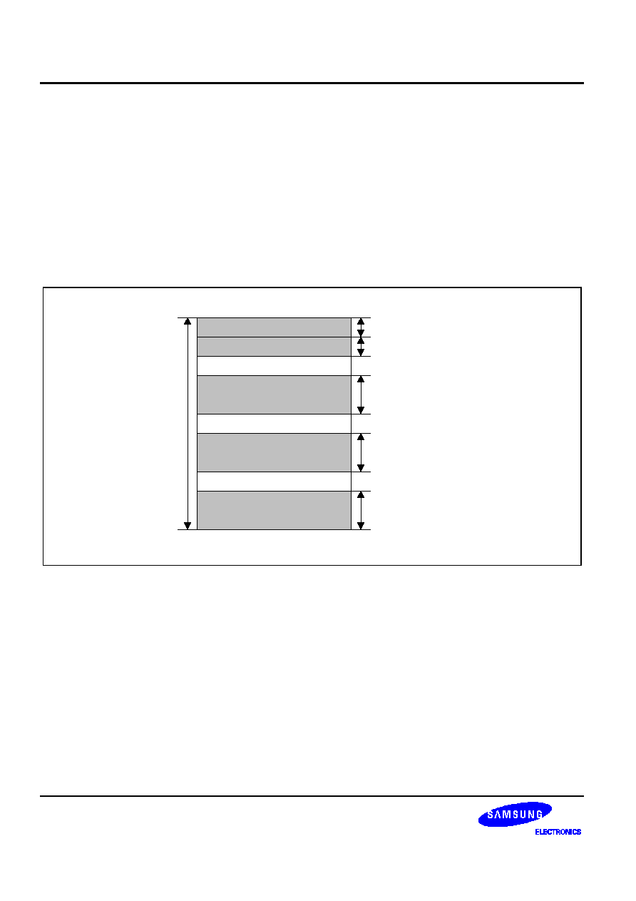
SYSTEM MANAGER
S3F441FX RISC MICROCONTROLLER
9-2
SYSTEM MANAGER REGISTERS
The S3F441FX has the SFRs, Special Function Registers, to keep the system control information of system
manager as well as the configuration on peripherals. Among SFRs, there are SMRs (System Manager Register
files), to configure the external memory maps such SRAM, ROM and etc.
By utilizing the SMR, the user can specify the memory type, access cycles, required control signal timings, and
memory bank location. The SMR provides (or accepts) the control signals and addresses which are needed to
access external devices during normal system operation. Three registers control the memory banks
The S3F441FX provides up to 32Mbytes of address space and each bank provides up to 256Kbytes of memory
space because each bank can have 18 address pins.
0x00000000
0x0003FFFF
0x00800000
0x0083FFFF
0x00C00000
0x00C3FFFF
0x01FF0000
0x01FF2000
0x01FFFFFF
Internal 256KB Flash ROM
CS1 (External memory)
CS2 (External memory)
8KB Internal SRAM
SFR
Figure 9-1. S3F441FX Default Memory Map of the Normal Mode(In ROM Mode)
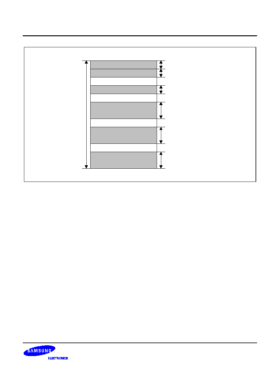
S3F441FX RISC MICROCONTROLLER
SYSTEM MANAGER
9-3
0x00000000
0x0003FFFF
0x00800000
0x0083FFFF
0x00C00000
0x01F3FFFF
0x01FF0000
0x01FF2000
0x01FFFFFF
CS0
(External 256KB Flash ROM)
CS1 (External memory)
CS2 (External memory)
8KB Internal SRAM
SFR
256KB Internal Flash ROM
0x00C3FFFF
0x01F00000
Figure 9-2. S3F441FX Default Memory Map of External ROM Mode
The S3F441FX provides 32-MByte memory space and an internal 25-bit system address bus. You can use any of
the bank area addresses from 000_0000h to 1FF_FFFFh in 1M byte address steps. Each bank can be located
anywhere in the 32-MByte address space.
However, the user should allocate the SFRs to the upper 64-kbyte address areas, 1FF0000h -1FFFFFFh.
The configurable memory allocation in the S3F441FX is very effective in meeting user requirement. By
manipulating the SMRs, the user can easily allocate the memory area anywhere user desires and use the
consecutively connected memory space without changing the H/W.
For example, if the user wants to change the size of memory space from 1Mbytes to 2 Mbytes, the user can
expand the memory space by changing the next pointer of the bank and bank end address.
NOTE: Although the size of each bank may be more than 1M bytes, the physical bank size is max 256Kbytes because the
number of the address pins is 18 in total.
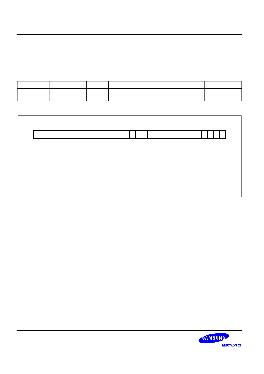
SYSTEM MANAGER
S3F441FX RISC MICROCONTROLLER
9-4
SYSTEM REGISTER ADDRESS CONFIGURATION REGISTER (SYSCFG)
The SMRs (System Manager Registers) have the SYSCFG (System Register Address Configuration Register),
which determines the start address (base point) of SFR (Special Function Register) files. The SYSCFG has the
start address of SFR. Because the reset value of SYSCFG is 1FF1h, the SYSCFG is mapped to the virtual
address 01FF 1000h.
Register
Offset Address
R/W
Description
Reset Value
SYSCFG
0x3000
R/W
Special function register to determine the start
address
0x1FF1
[0] Stall Enable (ST)
When set to 1, Stall operation is enabled
0 = Disable; It is recommended for faster operation.
1 = Enable; Insert an internal wait inside the core logic when non-sequential
memory accesses occur.
[12:4] SYSCFG Address (SFRs Start Address) (READ_ONLY)
These bits are fixed to 1FFH and it means SFRs start address is 1FF0000h
31
15
16
12
Start
0
4
2
3
1
SE
0
0
0
13
14
00
0
Figure 9-3. System Register Address Configuration Register (SYSCFG)

S3F441FX RISC MICROCONTROLLER
SYSTEM MANAGER
9-5
EXTERNAL MEMORY CONTROL SPECIAL REGISTERS
MEMORY CONTROL REGISTER 0, 1, 2
Register
Offset Address
R/W
Description
Reset Value
MEMCON0
0x4000
R/W
Memory control register 0 (nCS0)
0800 3000h
MEMCON1
0x4004
R/W
Memory control register 1 (nCS1)
0c08 3000h
MEMCON2
0x4008
R/W
Memory control register 2 (nCS2)
100c 3000h
[1:0]
Reserved
Reserved to 00b
[4:2]
Tcos
000 = 0 cycles 001 = 1 cycles 010 = 2 cycles
011 = 3 cycles 100 = 4 cycles 101 = 5 cycles
110 = 6 cycles 111 = Not used
[7:5]
Tacs
000 = 0 cycles 001 = 1 cycles 010 = 2 cycles
011 = 3 cycles 100 = 4 cycles 101 = 5 cycles
110 = 6 cycles 111 = Not used
[10:8]
Tcoh
000 = 0 cycles 001 = 1 cycles 010 = 2 cycles
011 = 3 cycles 100 = 4 cycles 101 = 5 cycles
110 = 6 cycles 111 = Not used
[13:11]
Tacc
Memory access time(Tacc)
000 = Disable bank 001 = 2 cycles 010 = 3 cycles
011 = 4 cycles 100 = 5 cycles 101 = 6 cycles
110 = 7 cycles 111 = Not used
If nWAIT is used, Tacc
3
[15:14]
Reserved
Reserved to 00b
[23:16]
Base Address(BA)
Indicates Bank start address. User can configure bank size by 1MB
unit. If bank start address is 0x0100000, the base address(BA) field
value of this bank should be 0x01. The available range is 0-0x1e.
[31:24]
End Address(EA)
Indicates Bank end address. If the end address of the bank is 0x0f3ffff,
the end address(EA) field value of this bank should be 0x10(
(0f3ffffh>>20) +1). The available range is 0x1-0x1f
NOTES:
1.
nCS0 can be used for another external device if the In-ROM mode is selected by MD[1:0]=00b. If the nCS0 area is
overlapped with the internal flash memory, the internal flash ROM will be read by CPU.
2.
nCS0 will be used for boot ROM if the external ROM mode is selected by MD[1:0]=01b.

SYSTEM MANAGER
S3F441FX RISC MICROCONTROLLER
9-6
MCLK
(CPU CLOCK)
ADDR
nCSn
nOE
nWE
tacs
tcos
tacc
tcoh
Figure 9-4. An Example of S3F441FX nCSn Timing Diagram

S3F441FX RISC MICROCONTROLLER
INTERNAL FLASH ROM
10-1
10
INTERNAL FLASH ROM
OVERVIEW
The S3F441FX has an on-chip flash ROM, internally. For writing the data in flash ROM, the user can access the
flash ROM by a program or the external serial interface. Because of the full feature of NOR flash memory, user
can program the data in any address and in any time. The size of embedded flash memory in S3F441FX is 256K-
byte and it has the following features :
-- Tool program mode (Apply V
DD
≠12.5 V externally and the dedicated serial interface)
-- User program mode (Use the internal high voltage generator)
-- Protection mode: hardware protection, read protection and LD protection
The S3F441FX has 6 pins used for Flash ROM writer to read/write/erase the flash memory (V
DD
, V
SS
, RESET,
VPP , SDAT, SCLK), which is the programming by tool program mode. These six pins are multiplexed with other
functional pins. When the S3F441FX is in V
PP
(MD1) = V
DD
≠12.5 V (internal flash ROM test mode) & RESET
(nRESET) = L, these six pins can be used for flash programming in tool program mode.

INTERNAL FLASH ROM
S3F441FX RISC MICROCONTROLLER
10-2
PROGRAMMING MODES
The S3F441FX flash memory control block supports two kinds of program mode:
-- Tool Program Mode
-- User Program Mode
Flash ROM Configuration
The 256KB Flash ROM consists of 512 sectors. Each sector consists of 512 bytes. So, the total size of flash
ROM is 512 x 512 bytes (256KB). User can erase the flash memory a sector unit at a time and write the data into
the flash memory word (4 bytes) unit at a time.
Additionally, there is the option sector, which is different from 256KB memory cell. This optional sector consists
of smart option bits and protection option bits. These bits control the protection features. These bits can be read
only by the FSOREAD/FPOREAD register.
The smart option bits are mapped to the address of 0xe38(4bytes). The protection option bits are also mapped to
the address of 0xe3c (4 bytes).
Address Alignment
To set an address value in FMADDR register, abide by the following rules.
-- Sector Erase
When erasing a sector, the low 9-bit address (FMADDR[8:0]) should be 000000000b because the size of a
sector is 512 bytes.
-- Program
When programming the Flash ROM, the lower 2-bit (FMADDR[1:0]) should be 00b because data should be
written to the Flash ROM by a word unit (4 bytes).
NOTE: In the tool program mode, the low 2-bit address also should be 00b.
User Program Mode
The user program mode for flash memory programming and sector erasing uses the internal high voltage
generator, which is necessary for flash memory programming and sector erasing. In other words, the S3F441FX
has an internal high voltage pumping circuit, therefore, high voltage to V
PP
pin is not needed. Instead of high
voltage, MD1 pins may be tied to V
SS
or V
DD
(in only MDS mode). To program the data into the flash ROM or
sector erase in this mode, several control registers should be used, which will be explained below.
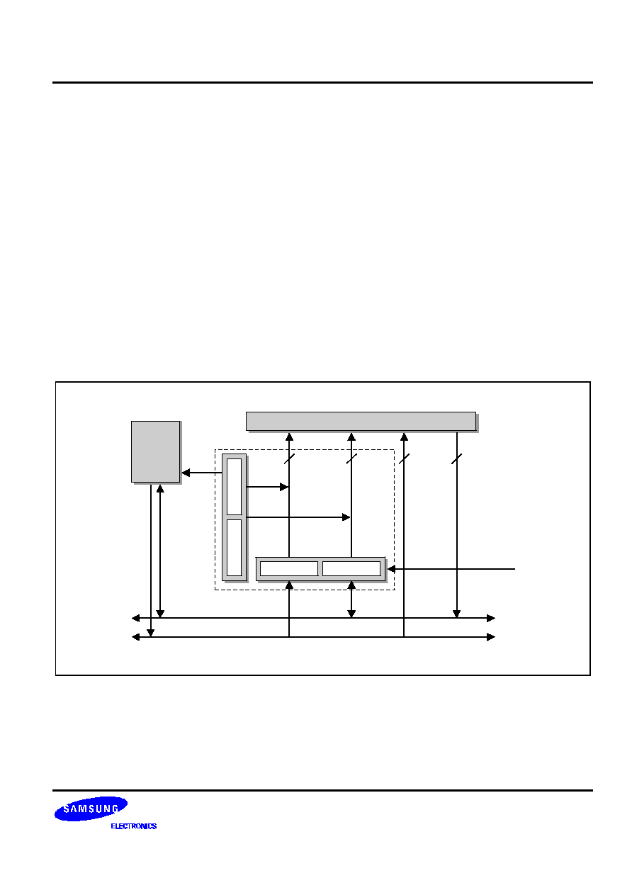
S3F441FX RISC MICROCONTROLLER
INTERNAL FLASH ROM
10-3
The Program Procedure in the User Program Mode
The user should write the data to be written into the data register (FMDATA) and the address into the address
register (FMADDR), respectively. As a next step, the user should write the values (0x5a, 0xa5, 0x5a, 0xa5 in this
order) into key registers 0/1/2/3(FMKEY0-3). Finally, by writing the appropriate data into flash memory control
register(FMUCON), one word data(32-bit) can be written into flash memory at the location of the specified
address and CPU will be held or working by FMACON[7] bit for 30us, which is the minimum programming time
for flash memory.
After the completion of the write operation, all FMKEY registers and the start bit in FMUCON will be cleared. To
perform the next writing operation, FMKEY0-3 registers and FMUCON register should be written again as before.
Sector erase procedure is the same as program procedure except setting the Flash memory data register
(FMDATA). You can enable three protection modes Read Protection, Hardware Protection, LD Protection.
Tool Program Mode
The 6 pins are connected to a tool board and programmed by Serial OTP Tool (SPW). V
DD
≠12.5 V should be
applied to the MD1 (V
PP
) pin. The other modules except the internal flash ROM will be in reset state.
This mode does not support the sector erase. Instead the chip erase is supported. Three protection modes(hard
lock/LD/read protection) can be enabled in this mode.
Address
Flash Cell
CPU
FMKEY0-3
FMUCON
FMDATA
FMADDR
Data
Address
Data
Data Bus
Address
Data
Address Bus
Address
Data
Normal Flash
Memory Interface
Tool Program
Interface
User Program
Interface
Figure 10-1. Flash Memory Read/Write Block Diagram

INTERNAL FLASH ROM
S3F441FX RISC MICROCONTROLLER
10-4
FLASH MEMORY SPECIAL REGISTERS
FLASH MEMORY KEY REGISTERS
To program data into the flash memory by the user programming mode, 4-key registers with 0x5a,0xa5,0x5a and
0xa5 are required to prevent flash data from being destroyed under undesired situations.
Register
Offset
R/W
Description
Access
Reset Value
FMKEY0
0x3010
W
Flash program / erase Key register0
B
00h
FMKEY1
0x3011
W
Flash program / erase Key register1
B
00h
FMKEY2
0x3012
W
Flash program / erase Key register2
B
00h
FMKEY3
0x3013
W
Flash program / erase Key register3
B
00h
NOTE: The FMKEYn register will be cleared automatically just after the completion of erase/program.
FLASH MEMORY ADDRESS REGISTER
Register
Offset
R/W
Description
Access
Reset Value
FMADDR
0x3014
R/W
Flash program / sector erase address
register
W
0000 0000h
NOTE: To program the Option Sector area, set FMADDR to 0x0e38(smart option) or 0x0e3c (protection option) and
FMDATA by the appropriate value and start the write operation.
FLASH MEMORY DATA REGISTER
Register
Offset
R/W
Description
Access
Reset Value
FMDATA
0x3018
R/W
Flash program data register
W
0000 0000h
S3F441FX RISC MICROCONTROLLER
INTERNAL FLASH ROM
10-5
FLASH MEMORY USER PROGRAMMING CONTROL REGISTER
The FMUCON can determine the program/erase operation. In user programming mode, the S3F441FX can
support only sector erase; flash memory should be programmed by a word unit.
Among 4 operating modes, only one operating mode can be selected. Otherwise, the there will be a configuration
error. In this case, clear the error register and start the operation again.
Register
Offset
R/W
Description
Access
Reset Value
FMUCON
0x301f
R/W
Flash memory program/sector erase
control register
B
00h
[0]
Option (protection/smart option) Sector Erase
Enable(OSERS)
0 = Disable
1 = Enable
[1]
Normal Sector Erase Enable (NSERS)
0 = Disable
1 = Enable
[2]
Option (protection/smart option) Sector
Program Enable(OSPGM)
0 = Disable
1 = Enable
[3]
Normal Sector Program Enable (NSPGM)
0 = Disable
1 = Enable
[6:4]
≠
[7]
Operation Start/Stop
0 = Stop
1 = Start
This bit will be cleared automatically just after the
corresponding operation is completed
.
.
The FMACON can control the access cycle for flash memory. This register setting is effective for reading flash
memory.
Register
Offset
R/W
Description
Access
Reset Value
FMACON
0x3027
R/W
Flash memory access control register
B
03h
[1:0]
Flash Memory Access
Cycles
11 = 3 cycles
10 = 2 cycle
01 = 1 cycles 00 = Not used
The internal Flash ROM access time is 50ns. So, the access cycles
will be configured as follows.
@ 20Mhz : 1 cycle
@ 40Mhz : 2 cycles
[6:2]
Reserved
[7]
CPU hold during Flash
operation
0 = CPU working during Flash programming/erasing
In this case, the flash programming/erasing code should not be on the
internal flash ROM. The completion of an operation is checked using
FMUCON register. The advantage is that CPU can perform other tasks
until the completion of an operation.
1 = CPU hold during Flash programming/erasing

INTERNAL FLASH ROM
S3F441FX RISC MICROCONTROLLER
10-6
FLASH MEMORY ERROR REGISTER
If an error occurs during flash memory program / erase, the corresponding bit will be set. Then, user can check
the error type which had occurred.
Register
Offset
R/W
Description
Access
Reset Value
FMERR
0x3023
R/W
Flash memory error register
B
01h
[0]
clear FMKEY / FMUCON
0: clear FMKEY and FMUCON register.
1: no operation.
This bit clears the FMKEYn & FMUCON registers. After the clear
operation, this bit will be restored to 1, automatically.
[6:1]
Reserved
[7]
configuration
error(CFGERR)
0: No error
1: Configuration error occurred.
This bit indicates that the command is invalid in the FMUCON register.
( For example, Program and Erase is active at the same time)
NOTE: To verify the erase/write operation, FMERR[7] will not be used. The completion of data should be verified by
reading the data.

S3F441FX RISC MICROCONTROLLER
INTERNAL FLASH ROM
10-7
FLASH MEMORY SMART OPTION BITS READ REGISTER
Reading the Smart option / Protection option bits is possible only through FSOREAD / FPOREAD registers
because the bits of Smart option / Protection option cannot be read like normal cell.
Register
Offset Address
R/W
Description
Initial Value
(at Fabrication)
FSOREAD
0x3028
R
Smart Option bits read register
MSB xxxx_xxx1 [31:24]
xxxx_xxx1
xxxx_xxx1
LSB xxxx_xxx1b [7:0]
FLASH MEMORY PROTECTION OPTION BITS READ REGISTER
Register
Offset Address
R/W
Description
Initial Value
(at Fabrication)
FPOREAD
0x302C
R
Protection Option bits read register
MSB xxxx_1xxx
xxxx_xx1x
xxxx_xxx1
LSB xxxx_xxxxb
NOTE
If any bit of FMERR register is set, the user must clear the FMERR register and write (erase) the flash
memory again at first.
INTERNAL FLASH ROM
S3F441FX RISC MICROCONTROLLER
10-8
FMADDR 20-bit Address
FMDATA 32-bit Data
Start
FMKEY0-3 0x5a, a5, 5a, a5
FMUCON 0x08
FMUCON 0x88
Program Finish?
Checksum OK?
Finish
Clear FMERR
Increase FMADDR
FMDATA 32-bit Data
No
Yes
Yes
No
; Address set
; Data set
; Key value set whenenver starts
; Mode select & start programming
; Compare end address
; Error during programming
; Next address/data set
Figure 10-2. Normal Sector Program Flowchart in a User Program mode
( In the figure: "....compare end address)
Start
FMKEY0-3 0x5a, a5, 5a, a5
FMUCON 0x04
FMUCON 0x84
FMERR[7] = 0?
FMUCON[7] = 0?
Finish
Clear FMERR
Yes
No
; Option Address set
; Function set
; Set key value
; Mode select & start programming
; Error during programming
; If error, write one word again
FMADDR Smart option: 0x0e38 or
Protection option: 0x0e3C
FMDATA 32-bit Data
Figure 10-3. Option Sector Program Flowchart in a User Program mode

S3F441FX RISC MICROCONTROLLER
INTERNAL FLASH ROM
10-9
Start
FMKEY0-3 0x5a, a5, 5a, a5
FMUCON 0x02
FMUCON 0x82
FMERR[7] = 0?
FMUCON[7]= 0?
Finish
Clear FMERR
Yes
No
; Set key value
; Mode select & start programming
; Error during erasing?
; If error, erase again
FMADDR 20-bit Address
; Set Address to be erased
Figure 10-4. Normal Sector Erase Flowchart
Start
FMKEY0-3 0x5a, a5, 5a, a5
FMUCON 0x01
FMUCON 0x81
FMERR[7] = 0?
FMUCON[7] = 0?
Finish
Clear FMERR
Yes
No
; Set key value
; Mode select & start programming
; Error during erasing?
; If error, erase again
FMADDR 0x0e3X
; Set Address to smart option
Figure 10-5. Option Sector Erase Flowchart

INTERNAL FLASH ROM
S3F441FX RISC MICROCONTROLLER
10-10
DATA PROTECTION
The data programmed in flash memory, need to be protected. In this case, the S3F441FX can support three
kinds of protection mechanism.
-- Hardware protection
-- Read protection
-- LD protection
These protection modes can be enabled by the configuration in the option sector. User can select the tool
program mode or the protection option bit/smart option bit in a user program mode.
The protection option bits (0x0e3c) can be enabled/disabled in terms of hardware protection, read protection, and
LD protection. The smart option bits (0x0e38) can adjust the area of hardware protection and LD protection.
PROTECTION OPTION
Protection Bit table
FMADDR value
FMDATA bit
Description
Initial Value (at Fabrication)
0x0e3c
bit[7:0]
Not used
Undefined
bit[8]
0: Enable the LD protection
1: Disable the LD protection
1
bit[16:9]
Not used
Undefined
bit [17]
0: Enable the hardware protection
1: Disable the hardware protection
1
bit[26:18]
Not used
Undefined
bit [27]
0: Enable the read protection
1: Disable the read protection
1
bit[31:28]
Not used
Undefined
Read Protection bit 27
There are many users who do not want their data to be read by others. Read Protection can give the solution for
this by preventing the flash data from being read serially in the tool program mode. This Read Protection is not
available in the user program mode. When this function is enabled, the reading or and verification of flash data in
the tool program mode will result in all zero read-out. Read Protection can be set and released in user program
mode on the condition of HDP(Hardware Protection) released as follows. The user should write 0x0e3c into the
address and the proper data 0x00ffffff(refer to the above Protection Bit table) into the data register (FMDATA),
respectively. As a next step, the user should write the values (0x5a, 0xa5, 0x5a, 0xa5 in this order) into key
registers 0/1/2/3(FMKEY0-3). Finally, set FMUCON.2(Option Sector Program Enable bit) then set
FMUCON.7(Operation Start bit). Pls refer to figure 10-3(Option Sector Program Flowchart). Meanwhile, in order
to release Read Protection, The user has to erase Option Sector as similar as Read Protection process. Pls refer
to Figure 10-5 (Option Sector Erase Flowchart), which results in initializing all Protection bits and smart option
bits.
On the other way, the user can set Read Protection in tool program mode by executing its functions and release
Read Protection by chip erase, which results in initializing all Protection bits, smart option bits and erasing

S3F441FX RISC MICROCONTROLLER
INTERNAL FLASH ROM
10-11
internal Flash ROM data,
Hardware Protection(hard lock) bit 17
If this function is enabled, the user cannot write or erase the data in a flash memory locked area. Further more
cannot be set or released Protection Option and Smart Option. Hard lock function affects a tool program mode
as well as a user program mode. This protection can be released only by the chip erase execution in the tool
program mode. Refer to smart option about hard lock protection of blocks.
Hardware Protection can be set in user program mode as follows. The user should write 0x0e3c into the address
and the proper data 0xff00ffff(refer to the above Protection Bit table) into the data register (FMDATA),
respectively. As a next step, the user should write the values (0x5a, 0xa5, 0x5a, 0xa5 in this order) into key
registers 0/1/2/3(FMKEY0-3). Finally, set FMUCON.2(Option Sector Program Enable bit) then set
FMUCON.7(Operation Start bit). Pls refer to figure 10-3(Option Sector Program Flowchart).
On the other way, the user can set Read Protection in tool program mode by executing its functions and release
Read Protection by chip erase, which results in initializing all Protection bits, smart option bits and erasing
internal Flash ROM data,
LD Protection bit 8
LD protection can protect the reading of data in flash memory by Load Instruction (all LD-relative Instructions).
When anyone try to read of internal flash data on LD protection enabled, the execution of LDR(load) instruction
results in unknown data read-out. Weather internal flash is mapped to Normal operating mode(In-ROM mode) or
External ROM mode(ROM-less)mode, the LD protection is available. Pls refer to more mapping details Fig10-6.
The user who wants to use LD protection is very careful to avoid Load Instructions in Internal Flash ROM area
locked by LD Protection. It's recommended not to use C-Language for Firmware development, because the
compiler can make undesired Load instructions on assembling C-code.
LD Protection can be set and released in user program mode on the condition of HDP(Hardware Protection)
released as follows. The user should write 0x0e3c into the address and the proper data 0xffff00ff(refer to the
above Protection Bit table) into the data register (FMDATA), respectively. As a next step, the user should write
the values (0x5a, 0xa5, 0x5a, 0xa5 in this order) into key registers 0/1/2/3(FMKEY0-3). Finally, set
FMUCON.2(Option Sector Program Enable bit) then set FMUCON.7(Operation Start bit). Pls refer to figure 10-
3(Option Sector Program Flowchart). Meanwhile, in order to release LD Protection, The user has to erase Option
Sector as similar as Read Protection process. Pls refer to Figure 10-5 (Option Sector Erase Flowchart), which
results in initializing all Protection bits and smart option bits.
On the other way, the user can set RD Protection in tool program mode by executing its functions and release
Read Protection by chip erase, which results in initializing all Protection bits, smart option bits and erasing
internal Flash ROM data,

INTERNAL FLASH ROM
S3F441FX RISC MICROCONTROLLER
10-12
SMART OPTION FOR LD PROTECTION / H/W PROTECTION
In the LD/Hardware protection function, The protection on certain block can be disabled by setting the
corresponding smart option bits. Four bits are allocated in the address of smart option (0x0e38) for this function.
To enable the protection function on a certain block,
-- Configure the smart option bits in advance (refer to Figure 10-3),
-- Configure the LD protection / H/W protection option bits (0x0e3c).
If the smart option bits are not configured and LDP/HDP is enabled (it has no effect LDP/HDP is not enabled), full
256K bytes flash memory will be protected.
FMADDR
value
FMDATA
bit
Description
Reset
Value
0x0e38
Bit [0]
0: H/W protection is disabled at the area of upper 248K bytes
(Only the lower 8K bytes are protected)
1: H/W protection is enabled in all areas if the H/W protection is
enabled.
1
bit[1:7]
not used
undefined
Bit [8]
0: H/W protection is disabled at the area of upper 240K bytes.
(Only the lower 16K bytes are protected)
If the bit[0] is 0, this bit has no effect.
1: H/W protection is enabled in all areas if the H/W protection is
enabled
1
bit[9:15]
not used
undefined
bit [16]
0: LD protection is disabled at the area of upper 248K bytes
(Only the lower 8K bytes are protected)
1: LD protection is enabled in all areas if the LD protection is
enabled.
1
Bit[17:23]
not used
undefined
bit [24]
0: LD protection is disabled at the area of upper 240K bytes.
(Only the lower 16K bytes are protected)
If the bit[24] is 0, this bit has no effect.
1: LD protection is enabled in all areas if the LD protection is
enabled.
1
Bit[25:31]
Not used
undefined
NOTE:
The flash programming tips is as follows; Characteristic of flash memory cell, a bit can be changed from 1 to 0 but not
the vice versa by writing data into flash memory cell. If users do not want to change the certain cell, the user only needs
to write the bit as 1.

S3F441FX RISC MICROCONTROLLER
INTERNAL FLASH ROM
10-13
FLASH MEMORY MAP
The S3F441FX can support two operating modes, the Normal operating mode(In-ROM mode) and the External
ROM(ROM-less) mode.
In the normal operating mode, the program as well as boot program should exist in the internal flash memory. In
the External ROM(ROM-less) mode, the internal flash memory will be mapped to the other addresses as shown
in the below figure.
01FF FFFFh
SFR Area
SRAM Area
01FF 2000h
01FF 0000h
External
Memory Area
Flash Memory Area
0003 FFFFh
0000 0000h
01FF FFFFh
SFR Area
SRAM Area
01FF 2000h
01FF 0000h
External
Memory Area
Flash Memory Area
0000 0000h
8K-byte
256K-byte
01F3 FFFFh
01F0 0000h
8K-byte
256K-byte
Figure 10-6. Flash Memory Map According to Operating Mode
INTERNAL FLASH ROM
S3F441FX RISC MICROCONTROLLER
10-14
TOOL PROGRAM MODE
The tool program mode is the flash memory program mode, which uses an equipment such as a ROM writer. If
the user wants to make a dedicated Flash ROM writer for S3F441FX, please contact us for more detail
document.
Table 10-1. The Pins Used to Read/Write/Erase the Flash ROM in Tool Program Mode
Pin Name
Function Name
Pin No.
I/O
Function
RXD/GPIO15
SDAT
4
I/O
Serial DATA pin.( Output when reading, Input when
writing.) Input & push-pull output port can be assigned
TXD/GPIO14
SCLK
5
I
Serial CLOCK, input only (Write speed: Max 200 kHz,
Read speed : Max 10 MHz)
MD1
VPP
10
I
Flash cell writing power supply pin for tool program
mode. The function of entering flash writing Mode.
When writing V
DD
-12.5V, when reading V
DD
.
NRESET
RESET
13
I
Chip Initialization
VDD/VSS
VDD/VSS
6,7
I
Logic power supply pin for Flash block
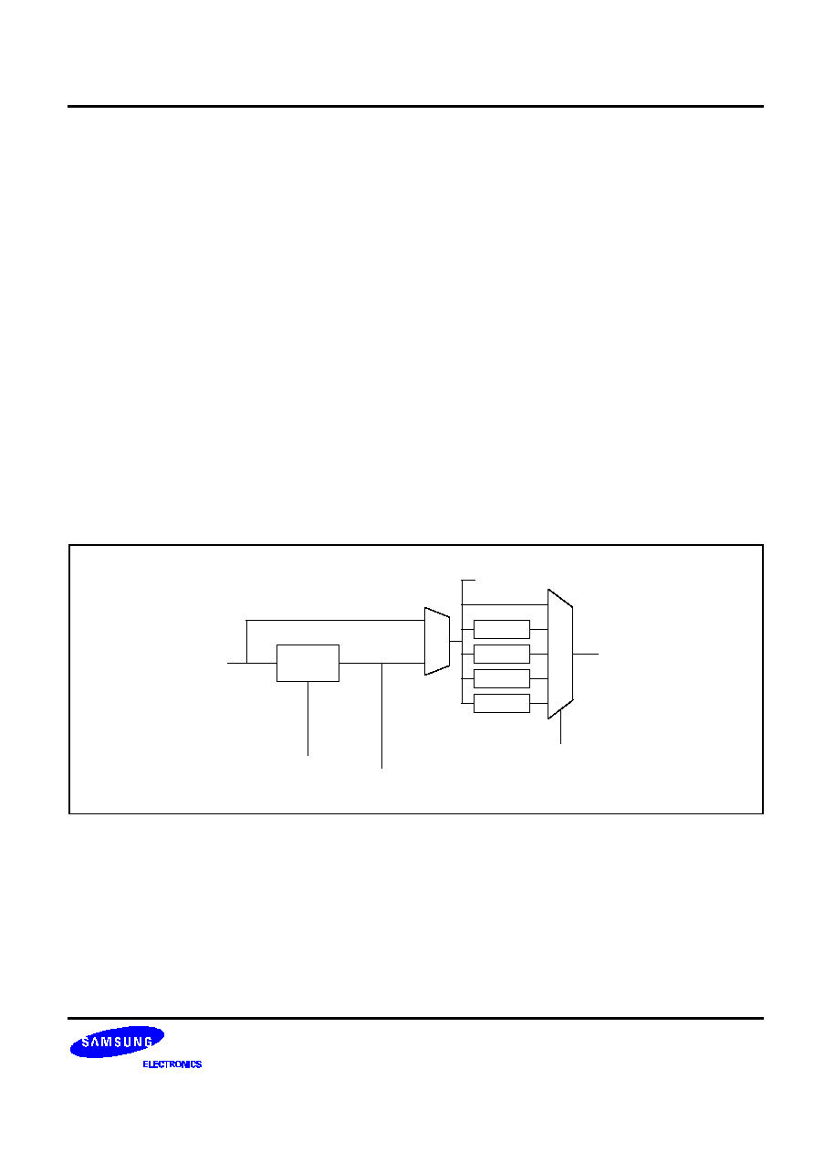
S3F441FX RISC MICROCONTROLLER
SYSTEM CONTROL
11-1
11
SYSTEM CONTROL
POWER-DOWN MODE
In STOP mode, all logic including PLL will be stopped. The external interrupts(EINT0,1,2) can wake up the MCU.
In IDLE mode, the CPU and the internal flash ROM will be stopped. All enabled interrupts can wake up the MCU.
GLOBAL INTERRUPT CONTROL
All interrupt requests can be disabled by global interrupt control bit.
PLL
The MCLK can be programmed by PLL. The PLL can generate MCLK up to 40Mhz.
PLL
EXTCLK
M
U
X
/16
PLL_ON
CLKSRCSEL
CLKDIVSEL
MCLK
Fpllo
Fin
UTCLK (UART & Timer Clock)
/1024
/2
/8
M
U
X
Figure 11-1. Clock Circuit Diagram
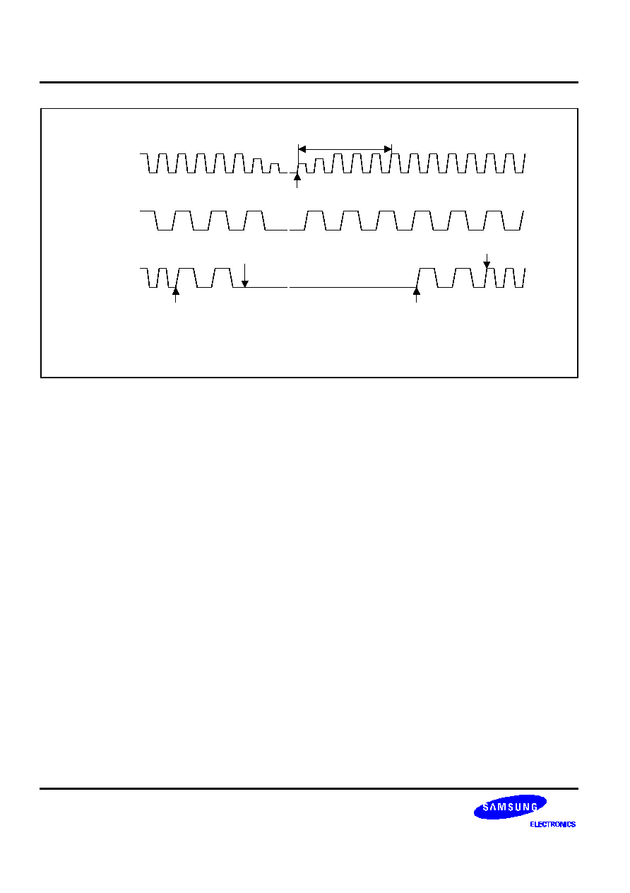
SYSTEM CONTROL
S3F441FX RISC MICROCONTROLLER
11-2
EXTCLK
MCLK
Fpllo
NOTE: The number of the clocks is depicted differently with real condition.
~~
~~
PLL lock time by the basic timer.
Wake-up by EINT[2:0]
~~
STOP mode by SYSCON[0]=1
CLKSRCSEL=EXTCLK
CLKSRCSEL=PLL_output
Locktime is completed.
CPU starts to operate.
Figure 11-2. Entering & Wake-up in the STOP Mode
ENTERING THE STOP MODE
To enter the stop mode, do the following steps.
1.
Set CLKSRCSEL=EXTCLK
2.
Set the SYSCON[0] to enter the STOP mode.
3.
There has to be at least 4 NOP instructions following the instruction to enter the STOP mode
4.
PLL will be turned off automatically.
5.
S3F441FX is in STOP mode now.
EXITING FROM THE STOP MODE
To exit from the stop mode, the following steps should be executed. To configure the STOP exiting condition,
configure EINTMOD,EINTCON,INTMASK and SYSCON[8] registers.
1.
EINT[2:0] will be issued to exit from the STOP mode.
2.
PLL will be turned on and the basic timer will operate to time the PLL lock time. However, the PLL output is
not used for MCLK until CLKSRCSEL = PLL_output is set.
3.
Set CLKSRCSEL = PLL_output to use Fpllo as MCLK.
IDLE MODE AND INTERNAL FLASH ROM
In the IDLE mode, the internal flash ROM will be stopped together. Just after exiting the IDLE mode, the interval
time(32 MCLKs) for start-up time of the internal flash ROM should be available. This 32 MCLK interval is inserted
automatically by H/W logic.

S3F441FX RISC MICROCONTROLLER
SYSTEM CONTROL
11-3
SYSTEM CONTROL REGISTER
The system control register(SYSCON) can be used to control the system operation of chip.
Register
Offset Address
R/W
Description
Reset Value
SYSCON
0xd002
R/W
System Control register
000h
[0]
STOP bit
This bit determines whether the stop mode is enabled or disabled. In
STOP mode, all logic including PLL will be stopped. The external
interrupts(EINT0,1,2) can wake up MCU. This bit will be cleared
automatically.
[1]
IDLE bit
This bit determines whether the idle mode is enabled or disabled. In
IDLE mode, the CPU and the internal flash ROM will be stopped. All
enabled interrupts can wake up MCU. This bit will be cleared
automatically
[2]
UNUSED
[5:3]
CLKDIVSEL
The clock, PLL output or EXTCLK, is divided by 1,2,8,16, or 1024. This
bit determines the divide ratio.
000: 1/16, 001: 1/8, 010: 1/2 011: 1/1 100: 1/1024
[6]
CLKSRCSEL
This bit determines which clock source is used, the EXTCLK or the
PLL output.
0: EXTCLK
1: PLL output
[7]
PLLON
This bit determines whether the PLL is turned on or off.
0: PLL is turned off.
1: PLL is turned on.
[8]
Global Interrupt Control
Global Interrupt Enable bit. This bit can mask all interrupt request.
When 0, all interrupt request will not be acceptable.
0: Disable all interrupt request
1: Enable the interrupt requests, which are enabled on INTMASK.
NOTE: To make CPU enter into STOP/IDLE mode perfectly, there have to be 4 NOP instructions after the activation of the
Stop or Idle mode.

SYSTEM CONTROL
S3F441FX RISC MICROCONTROLLER
11-4
PLL (PHASE LOCKED LOOP)
The PLL within the clock generator is the circuit that synchronizes the output signal with a reference or input
signal in frequency as well as in phase. It is composed of the voltage controlled oscillator to generate the output
frequency, the divider P to divide the reference frequency by p, the divider M to divide the VCO output frequency
by m, the divider S to divide the VCO output frequency by s, the phase detector, charge pump, and loop filter.
The output clock frequency Fout is related to the reference input clock frequency Fin by the following equation:
Fpllo = (m * Fin) / (p * 2
s
)
m = M (the value for divider M)+ 8, p = P(the value for divider P) + 2
The following sections describe the PLL operation that includes the phase detector, charge pump, VCO (Voltage
controlled oscillator), and loop filter.
Phase Detector
The phase detector monitors the phase difference between the Fref (the reference frequency) and Fvco (the
output frequency), and generates a control signal when it detects difference between the two.
Charge Pump
The charge pump converts the phase detector control signal to a charge in voltage across the external filter that
drives the VCO.
Loop Filter
The control signal that the phase detector generates for the charge pump may generate large excursions(ripples)
each time the VCO output is compared to the system clock. To avoid overloading the VCO, a low pass filter
samples and filters the high-frequency components out of the control signal. The filter is typically a single-pole
RC filter consisting of a resistor and capacitor.
A recommended external loop filter capacitance is 700pF.
Voltage Controlled Oscillator (VCO)
The output voltage from the loop filter drives the VCO, causing its oscillation frequency to increase or decrease
as a function of variations in voltage. When the VCO output matches the system clock in frequency and phase,
the phase detector stops sending a control signal to the charge pump, which in turn stabilizes the input voltage to
the loop filter. The VCO frequency then remains constant, and the PLL remains locked onto the system clock.
Divider
P
Fin
M[7:0]
S[1:0]
PWRDN
PFD
Divider
M
P[5:0]
Fvco
PUMP
VCO
Divider
S
Fref
Fpllo
Loop Filter
R
700pF
C
Internal
PLLCAP
External
Figure 11-3. PLL (Phase-Locked Loop) Block Diagram

S3F441FX RISC MICROCONTROLLER
SYSTEM CONTROL
11-5
PLL CONTROL REGISTER (PLLCON)
Fpllo = (m * Fin) / (p * 2
s
)
m = (MDIV + 8), p = (PDIV + 2), s = SDIV
Register
Offset Address
R/W
Description
Reset Value
PLLCON
0xd004
R/W
PLL configuration Register
38080h
PLLCON
Bit
Description
Initial State
MDIV
[19:12]
Main divider control
0x38
PDIV
[9:4]
Pre-divider control
0x08
SDIV
[1:0]
Post divider control
0x0
NOTE: The Fpllo range is 20MHz≠40MHz.
PLL VALUE SELECTION GUIDE
1.
Fpllo * 2
s
has to be less than 170 MHz.
2.
S is as great as possible.
3.
(Fin / p) is recommended to be 1Mhz or above. But, (Fin / p) < 2MHz.
PLL VALUE CHANGE STEPS
If the PLL setting needs to be changed when Fpllo is used as MCLK, the PLL transition noise may be asserted to
CPU core. So, the PLL configuration has to be changed in SLOW mode. Do the following steps to change the
PLL configuration.
1.
Set CLKSRCSEL=EXTCLK
2.
Set PMS value of PLL
3.
Wait for at least 150us.
4.
Set CLKSRCSEL=PLL output
CAPACITOR FOR PLL LOOP FILTER
A 700pF(same or slightly bigger) capacitor is connected between PLLCAP pin and Vss. This capacitor will
operate as a PLL loop filter.
PLLCAP
700pF
Figure 11-4. Capacitor for PLL Loop Filter
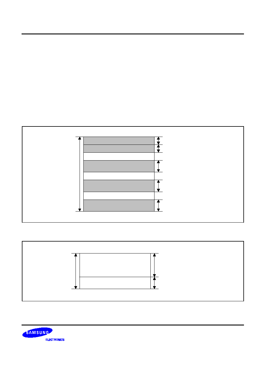
S3F441FX RISC MICROCONTROLLER
SPECIAL FUNCTION REGISTERS
12-1
12
SPECIAL FUNCTION REGISTERS
OVERVIEW
This chapter describes the S3F441FX Special function registers. 64KB SFR block has an 8KB SRAM area for
stack or data memory and special registers to control peripheral blocks.
Internal 256KB Flash ROM
CS1 (External memory)
CS2 (External memory)
8KB Internal SRAM
Special Function Registers
0x00000000
0x0003ffff
0x00800000
0x0083ffff
0x00c00000
0x00C3ffff
0x01ff0000
0x01ff2000
0x01ffffff
Figure 12-1. S3F441FX Default Memory Map of the Normal Mode(In-ROM mode)
SRAM (8KB)
Peripheral Control Registers
0000H (Offset)
1FFFH (Offset)
FFFFH (Offset)
2000H (Offset)
Figure 12-2. Special Function Register

SPECIAL FUNCTION
S3F441FX RISC MICROCONTROLLER
12-2
S3F441FX SPECIAL REGISTERS
Table 12-1. S3F441FX Special Registers
Group
Registers
Offset
R/W
Description
Access
Reset Value
System
SYSCFG
0x3000
R/W
System Configuration register
W
1ff1h
Manager
MEMCON0
0x4000
R/W
Memory Bank 0 control register
W
0800 3000h
MEMCON1
0x4004
R/W
Memory Bank 1 control register
W
0c08 3000h
MEMCON2
0x4008
R/W
Memory Bank 2 control register
W
100c 3000h
Internal
FMKEY0
0x3010
W
Flash program/erase Key register0
B
00h
Flash
FMKEY1
0x3011
W
Flash program/erase Key register1
B
00h
ROM
FMKEY2
0x3012
W
Flash program/erase Key register2
B
00h
FMKEY3
0x3013
W
Flash program/erase Key register3
B
00h
FMADDR
0x3014
R/W Flash user program address register
W
0 0000h
FMDATA
0x3018
R/W
Flash user program data register
W
0000 0000h
FMUCON
0x301f
R/W
Flash program/erase control register
B
00h
FMACON
0x3027
R/W
Flash access cycle control register
B
03h
FMERR
0x3023
R/W
Flash error register
B
01h
FSOREAD
0x3028
R
Smart Option bits read register
W
1b,1b,1b,1b
FPOREAD
0x302C
R
Protection Option bits read register
W
1b,1b,1b
UART
LCON
0x5003
R/W
UART line control register
B
00h
UCON
0x5007
R/W
UART control register
B
00h
USSR
0x500b
R
UART status register
B
c0h
TBR
0x500f
W
UART transmit buffer control register
B
xxh
RBR
0x5013
R
UART receive buffer control register
B
xxh
UBRDR
0x5016
R/W
UART baud rate divisor register
H
0000h
NOTE: B: byte (8-bit), H: half-word (16-bit), W: word (32-bit)

S3F441FX RISC MICROCONTROLLER
SPECIAL FUNCTION REGISTERS
12-3
Table 12-1. S3F441FX Special Registers (Continued)
Group
Registers
Offset
R/W
Description
Access
Reset Value
Timer 0
T0DATA
0x9000
R/W
Timer 0 data register
H
ffffh
T0PRE
0x9002
R/W
Timer 0 prescaler register
B
ffh
T0CON
0x9003
R/W
Timer 0 control register
B
00h
T0CNT
0x9006
R
Timer 0 counter register
H
0000h
Timer 1
T1DATA
0x9010
R/W
Timer 1 data register
H
ffffh
T1PRE
0x9012
R/W
Timer 1 prescaler register
B
ffh
T1CON
0x9013
R/W
Timer 1 control register
B
00h
T1CNT
0x9016
R
Timer 1 counter register
H
0000h
Timer 2
T2DATA
0x9020
R/W
Timer 2 data register
H
ffffh
T2PRE
0x9022
R/W
Timer 2 prescaler register
B
ffh
T2CON
0x9023
R/W
Timer 2 control register
B
00h
T2CNT
0x9026
R
Timer 2 counter register
H
0000h
Timer 3
T3DATA
0x903
0
R/W
Timer 3 data register
H
ffffh
T3PRE
0x9032
R/W
Timer 3 prescaler register
B
ffh
T3CON
0x9033
R/W
Timer 3 control register
B
0000h
T3CNT
0x9036
R/W
Timer 3 counter register
H
00h
Timer 4
T4DATA
0x904
0
R/W
Timer 4 data register
H
ffffh
T4PRE
0x9042
R/W
Timer 4 prescaler register
B
ffh
T4CON
0x9043
R/W
Timer 4 control register
B
00h
T4CNT
0x9046
R/W
Timer 4 counter register
H
0000h
Timer 5
T5DATA
0x905
0
R/W
Timer 5 data register
H
ffffh
T5PRE
0x9052
R/W
Timer 5 prescaler register
B
ffh
T5CON
0x9053
R/W
Timer 5 control register
B
00h
T5CNT
0x9056
R/W
Timer 5 counter register
H
0000h

SPECIAL FUNCTION
S3F441FX RISC MICROCONTROLLER
12-4
Table 12-1. S3F441FX Special Registers (Continued)
Group
Registers
Offset
R/W
Description
Access
Reset Value
BT &
BTCON
0xa002
R/W
Basic timer control register
H/B
0000h
WDT
BTCNT
0xa007
R
Basic timer counter register
B
00h
I/O Port
P0
0xb000
R/W
Port 0 data register
B
xxh
P1
0xb001
R/W
Port 1 data register
B
xxh
P2
0xb002
R/W
Port 2 data register
B
xh
EINTCON
0xb018
R/W
Port 2 external Interrupt Control register
B
0h
EINTMOD
0xb01a
R/W
Port 2 external Interrupt Mode register
B
00h
I/O Port
P0CON
0xb010
R/W
Port 0 control register
B
00h
Control
P1CON
0xb012
R/W
Port 1 control register
H
0000h
Register
P2CON
0xb014
R/W
Port 2 control register
B
0h
I/O Port
P0PUR
0xb015
R/W
Port 0 pull-up resister control register
B
00h
Resistor
P1PUDR
0xb016
R/W
Port 1 pull-up/down resister control.
B
ffh
Control
P2PUR
0xb017
R/W
Port 2 pull-up resister control register
B
ffh
Interrupt
INTMODE
0xc000
R/W
Interrupt Mode register
W
xxx0 0000h
Contro-
INTPEND
0xc004
R/W
Interrupt Pending register
W
xxx0 0000h
ller
INTMASK
0xc008
R/W
Interrupt Mask register
W
xxx0 0000h
System
SYSCON
0xd002
R/W
System Control register
H
000h
Control
PLLCON
0xd004
R/W
System Control register
W
38080h
Internal
SRAM
SRAM
0x0000
≠ 0x1fff
R/W
Internal 8KB SRAM area
B,H,W
xxh

S3F441FX RISC MICROCONTROLLER
ELECTRICAL DATA
13-1
13
ELECTRICAL DATA
DC ELECTRICAL CHARACTERISTICS
Table 13-1. Absolute Maximum Ratings
(T
A
= 25
∞
C)
Parameter
Symbol
Conditions
Rating
Unit
Supply voltage
V
DD
/ V
DDA
≠
- 0.3 to + 3.8
V
Input voltage
V
IN1
All ports except V
IN2
- 0.3 to V
DD
+ 0.3
V
I
IN
DC input current
≠
±
10
mA
Storage
temperature
T
STG
≠
- 40 to + 125
∞
C

ELECTRICAL DATA
S3F441FX RISC MICROCONTROLLER
13-2
Table 13-2. D.C. Electrical Characteristics
(T
A
= 0
∞
C to + 70
∞
C, V
DD
= 3.3
±
0.3V )
Parameter
Symbol
Conditions
Min
Typ
Max
Unit
Operating Voltage
V
DD
Fosc = 40MHz, 64 Pins
3.0
≠
3.6
V
Operating temperature
T
A
0
≠
70
∞
C
High level input voltage 1
V
IH1
nRESET
0.8V
DD
≠
≠
V
High level input voltage 2
V
IH2
Schmitt Pad
2.2
≠
≠
V
High level input voltage 2
V
IH3
MD0, MD1
2.2
≠
≠
V
High level input voltage 4
V
IH4
CMOS pad
2.0
≠
≠
V
High level input voltage 5
V
IH5
EXTCLK
V
DD
-0.3
≠
≠
V
Low level input voltage 1
V
IL1
nRESET
≠
≠
0.2V
DD
V
Low level input voltage 2
V
IL2
Schmitt Pad
≠
≠
0.8
V
Low level input voltage 2
V
IL3
MD0, MD1
≠
≠
0.6
V
Low level input voltage 4
V
IL4
CMOS pad
≠
≠
0.8
V
Low level input voltage 5
V
IL5
EXTCLK
≠
≠
0.4
V
High level input current 1
I
IH1
V
IN
=3.6, no pull-down resistor
-10
≠
10
uA
High level input current 2
I
IH2
V
IN
=3.6, with pull-down resistor
10
≠
90
uA
Low level input current 1
I
IL1
V
IN
=0, no pull-up resistor
-10
≠
10
uA
Low level input current 2
I
IL2
V
IN
=0, with pull-up resistor
-90
≠
-10
uA
High level output voltage 1
V
OH1
V
DD
=3.3V, I
OH
=-8mA
port0,port1, port2,A0-A11,nCS,
nOE,nWE
2.4
≠
≠
V
High level output voltage 2
V
OH2
V
DD
=3.3V,I
OH
=-12mA, D0-D7
2.4
≠
≠
V
Low level output voltage 1
V
OL1
V
DD
=3.3V, I
OH
=8mA
port0, port1, port2, A0-A11,nCS,
nOE,nWE
≠
≠
0.4
V
Low level output voltage 2
V
OL2
V
DD
=3.3V, I
OH
=12mA, D0-D7
≠
≠
0.4
V
Operating current
I
DD1
V
DD
=3.6V, Fosc=40MHz
≠
≠
50
mA
IDLE mode current
I
DD2
V
DD
=3.6V, Fosc=40MHz
≠
≠
10
mA
STOP mode current
I
DD3
V
DD
=3.6V
≠
0.5
1
mA

S3F441FX RISC MICROCONTROLLER
ELECTRICAL DATA
13-3
VDD(V)
70
60
50
40
30
20
10
2.6
2.7
2.8
2.9
3.0
3.1
3.2
3.3
3.5
3.4
3.6
0
MCLK(Mhz)
2.4
2.5
3.7
3.8
Spec. Guaranteed Area
Figure 13-1. Typical Operating Frequency and Voltage Range ( internal flash t
ACC
=1 )
VDD(V)
70
60
50
40
30
20
10
2.6
2.7
2.8
2.9
3.0
3.1
3.2
3.3
3.5
3.4
3.6
0
MCLK(Mhz)
Spec. Guaranteed Area
2.4
2.5
3.7
3.8
Figure 13-2. Typical Operating Frequency and Voltage Range ( internal flash t
ACC
=2 )

ELECTRICAL DATA
S3F441FX RISC MICROCONTROLLER
13-4
Table 13-3. Typical Quiescent Supply Current on V
DD
@NORMAL Mode, Flash Tacc=1
(unit: mA)
VDD \ MCLK
10MHz
20MHz
3.0 V
14
20
3.3 V
17
24
3.6 V
21
28
NOTE: The above current measurement is done in the case that the code is running on internal flash ROM(Tacc=1) &
internal SRAM.
Table 13-4. Typical Quiescent Supply Current on V
DD
@NORMAL Mode, Flash Tacc=2
(unit: mA)
VDD \ MCLK
30MHz
40MHz
3.0 V
21
25
3.3 V
25
29
3.6 V
29
34
NOTE: The above current measurement is done in the case that the code is running on internal flash ROM(Tacc=2) &
internal SRAM.
Table 13-5. Typical Quiescent Supply Current on V
DD
@IDLE Mode
(unit: mA)
VDD \ MCLK
10MHz
20MHz
30MHz
40MHz
3.0 V
1.9
3.0
3.3
4.1
3.3 V
2.2
3.4
3.8
4.8
3.6 V
2.5
3.9
4.3
5.5
NOTES:
1.
The above current measurement is done in the case that the code is on internal flash ROM & internal SRAM.
2. The IDLE mode current
consumption is independent to the internal flash memory Tacc.

S3F441FX RISC MICROCONTROLLER
ELECTRICAL DATA
13-5
AC ELECTRICAL CHARACTERISTICS
EXTCLK
MCLK
(internal clock)
t
MCLKDLY
Figure 13-3. EXTCLK and MCLK (Internal Clock) When PLL is not Used.
NOTE: In the figure 13-1, MCLK is the simulated waveform for the case of not using PLL. Because the MCLK can't be
shown, all the timing diagram should be drawn only for the case that EXTCLK is signaled by an external clock
source without using PLL. Also, all the timing diagram are drawn using the EXTCLK instead of MCLK as a reference
clock because only the EXTCLK can be shown.
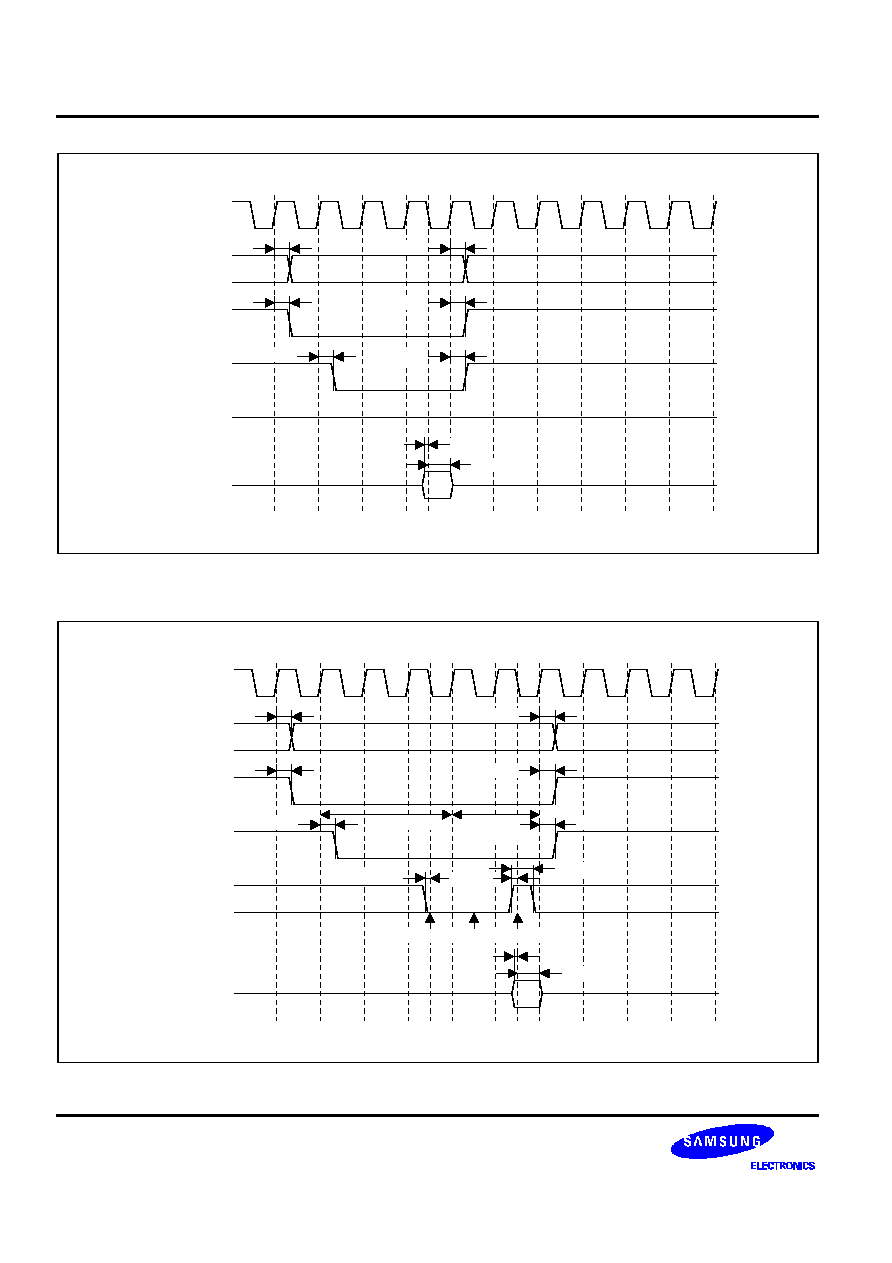
ELECTRICAL DATA
S3F441FX RISC MICROCONTROLLER
13-6
EXTCLK
nCS
ADDR
nOE
nWAIT
DATA(R)
t
ADDR
t
NCS
t
NCS
t
NOE
t
NOE
t
ADDR
'H'
t
DS
t
DH
Figure 13-4. SRAM Read Access Timing without nWAIT ( t
COS
=1,t
ACS
=0,t
COH
=0,t
ACC
=3 )
EXTCLK
nCS
ADDR
nOE
nWAIT
DATA(R)
t
ADDR
t
NCS
t
NCS
t
NOE
t
NOE
t
ADDR
t
DS
t
DH
2 wait
cycle
t
ACC
= 3
t
NWTH
t
NWTS
t
NWTS
nWAIT sampling points
Figure 13-5. SRAM Read Access Timing with nWAIT ( t
COS
=1, t
ACS
=0, t
COH
=0, t
ACC
=3, external wait=2 )
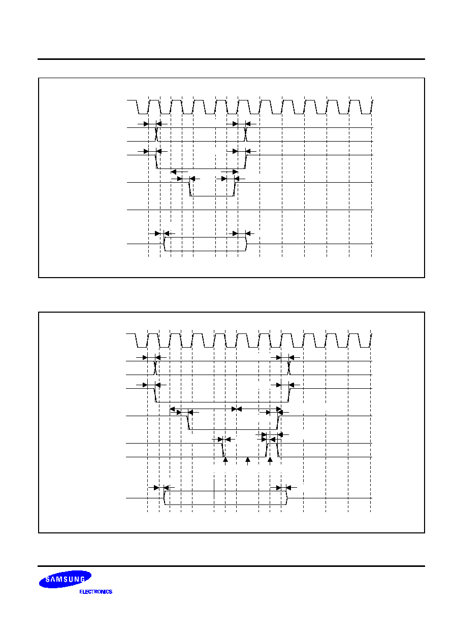
S3F441FX RISC MICROCONTROLLER
ELECTRICAL DATA
13-7
EXTCLK
nCS
ADDR
nWE
nWAIT
DATA(W)
t
ADDR
t
NCS
t
NCS
t
NWE
t
NWE
t
ADDR
'H'
t
WD
t
WD
t
ACC
= 3
Figure 13-6. SRAM Write Access Timing without nWAIT ( t
COS
=1, t
ACS
=0, t
COH
=0, t
ACC
=3 )
EXTCLK
nCS
ADDR
nWE
nWAIT
DATA(W)
t
ADDR
t
NCS
t
NCS
t
NWE
t
NWE
t
ADDR
t
WD
2 wait cycle
t
ACC
= 3
t
NWTH
t
NWTS
t
NWTS
nWAIT sampling points
t
WD
Figure 13-7. SRAM Write Access Timing with nWAIT ( t
COS
=1, t
ACS
=0, t
COH
=0, t
ACC
=3, external wait=2 )
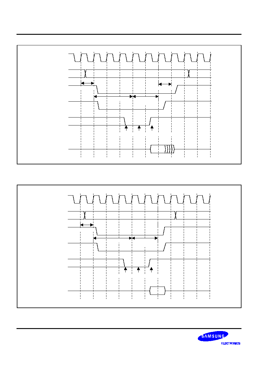
ELECTRICAL DATA
S3F441FX RISC MICROCONTROLLER
13-8
EXTCLK
nCS
ADDR
nOE
nWAIT
DATA(R)
2 wait
cycle
t
ACC
= 3
nWAIT Sampling Points
t
ACS
= 1
t
COH
= 1
Figure 13-8. SRAM Read Access Timing with nWAIT
(t
COS
=0, t
ACS
=1, t
COH
=1, t
ACC
=3, external wait=2)
EXTCLK
nCS
ADDR
nOE
nWAIT
DATA(R)
2 wait
cycle
t
ACC
= 3
nWAIT Sampling Points
t
ACS
= 1
Figure 13-9. SRAM Read Access Timing with nWAIT
at the Last Cycle of Half-Word/Word Access and Byte Access
(t
COS
=0, t
ACS
=1, t
COH
=0, t
ACC
=3, external wait=2)
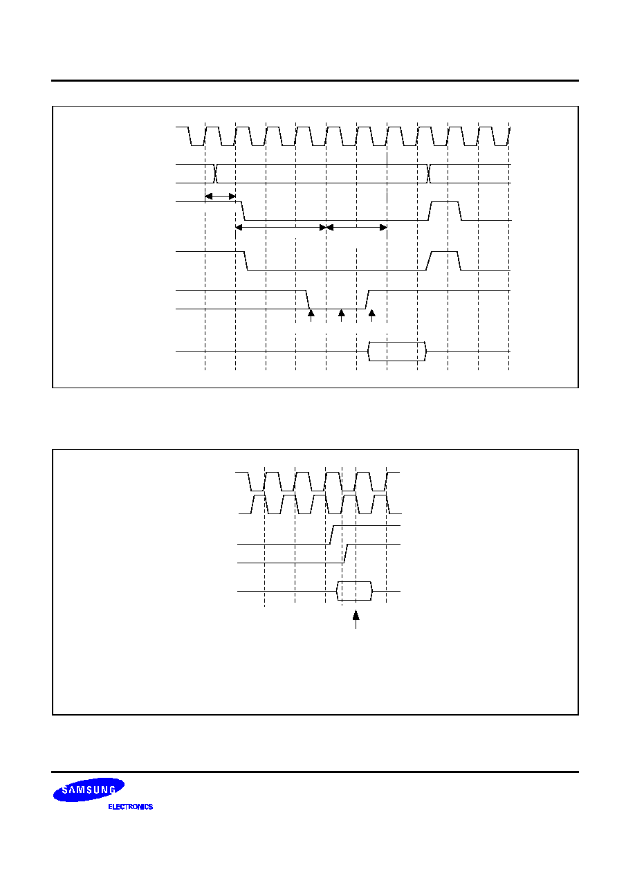
S3F441FX RISC MICROCONTROLLER
ELECTRICAL DATA
13-9
EXTCLK
nCS
ADDR
nOE
nWAIT
2 wait
cycle
t
ACC
= 3
nWAIT Sampling Points
t
ACS
= 1
DATA(R)
Figure 13-10. SRAM Read Access Timing with nWAIT
During Half-Word/Word Access, except the Last Cycle
(t
COS
=0, t
ACS
=1, t
COH
=0, t
ACC
=3, external wait=2)
NOTES:
1. External nWAIT is synchronized at the falling edge of EXTCLK.
That is, CPU recognizes the internal nWAIT as external memory wait signal.
2. Internal CPU fetches the data at the falling edge of internal clock, MCLK.
EXTCLK
nWAIT
DATA(R)
(1)
Internal nWAIT
MCLK
(Internal Clock)
(2)
Data Fetch Time
Figure 13-11. NWAIT Data Fetch Timing
ELECTRICAL DATA
S3F441FX RISC MICROCONTROLLER
13-10
Table 13-6. Timing Constants
(V
DD
= 3.3
±
0.3V, T
A
= 0 to 70
o
C, Operating Frequency = 40 MHz)
Parameter
Symbol
Min
Typ
Max
Unit
EXTCLK input frequency when not using PLL
f
EXTCLK
0
≠
40
MHz
EXTCLK input frequency for PLL
f
PLLIN
4
≠
20
EXTCLK to MCLK delay time
t
MCLKDLY
5
ns
Address delay time
t
ADDR
≠
22
nCS (chip select) delay time
t
NCS
≠
17
nOE (read enable) delay time
t
NOE
≠
17
nWE (write enable) delay time
t
NWE
≠
17
nWAIT sampling setup time
t
NWTS
0
≠
nWAIT sampling hold time
t
NWTH
10
≠
Write data delay time
t
WD
≠
17
Data setup time
t
DS
0
Data hold time
t
DH
10
Table 13-7. AC Electrical Characteristics for Internal Flash ROM
(T
A
= 0
∞
C to + 70
∞
C
, V
DD
= 3.0 V to 3.6V)
Parameter
Symbol
Conditions
Min
Typ
Max
Unit
Programming
time (1)
Ftp
V
DD
= 3.3V
20
30
50
uS
Chip Erasing
Time (2)
Ftp1
≠
10
20
mS
Sector Erasing
time (3)
Ftp2
≠
2
3
mS
Data access time
Ft
RS
≠
40
≠
nS
Number of writing
/ erasing
FNwe
≠
≠
1,000
Times
NOTES:
1.
The programming time is the time during which one word (32-bit) is programmed.
2.
The Chip erasing time is the time during which all 256K-byte block is erased.
3.
The Sector erasing time is the time during which all 512-byte block is erased.
4.
The chip erasing is available in Tool Program Mode only.

S3F441FX RISC MICROCONTROLLER
MECHANICAL DATA
14-1
14
MECHANICAL DATA
PACKAGE DIMENSIONS
64-LQFP-1010-AN
#64
10.00 BSC
12.00 BSC
10.00 BSC
12.00 BSC
#1
0.50 BSC
0.20
+ 0.07
- 0.03
0.45-0.75
1.60 MAX
0.08 MAX
0.09-0.20
0-7
1.40
± 0.05
0.10
± 0.05
0.08 MAX
Figure 14-1. 64-LQFP-1010 Package Dimensions (unit: mm)
(For duplicate copies of this form, and for additional ordering information, please contact your local
Samsung sales representative. Samsung sales offices are listed on the back cover of this book.)
S3F SERIES MASK ROM ORDER FORM
Product description:
Device Number: S3F__________- ___________(write down the ROM code number)
Product Order Form:
Package
Pellet Wafer
Package Type: __________
Package Marking (Check One):
Standard
Custom A
Custom B
(Max 10 chars)
(Max 10 chars each line)
@ : Assembly site code, Y : Last number of assembly year, WW : Week of assembly
@ YWW
Device Name
SEC
Device Name
@ YWW
@ YWW
Delivery Dates and Quantities:
Deliverable
Required Delivery Date
Quantity
Comments
ROM code
≠
Not applicable
See ROM Selection Form
Customer sample
Risk order
See Risk Order Sheet
Please answer the following questions:
+
+
For what kind of product will you be using this order?
New product
Upgrade of an existing product
Replacement of an existing product
Other
If you are replacing an existing product, please indicate the former product name
(
)
+
+
What are the main reasons you decided to use a Samsung microcontroller in your product?
Please check all that apply.
Price
Product quality
Features and functions
Development system
Technical support
Delivery on time
Used same micom before
Quality of documentation
Samsung reputation
Mask Charge (US$ / Won):
____________________________
Customer Information:
Company Name:
___________________ Telephone number
_________________________
Signatures:
________________________
__________________________________
(Person placing the order)
(Technical Manager)


(For duplicate copies of this form, and for additional ordering information, please contact your local
Samsung sales representative. Samsung sales offices are listed on the back cover of this book.)
S3F SERIES
REQUEST FOR PRODUCTION AT CUSTOMER RISK
Customer Information:
Company Name:
________________________________________________________________
Department:
________________________________________________________________
Telephone Number:
__________________________
Fax: _____________________________
Date:
__________________________
Risk Order Information:
Device Number:
S3F________- ________ (write down the ROM code number)
Package:
Number of Pins: ____________
Package Type: _____________________
Intended Application:
________________________________________________________________
Product Model Number:
________________________________________________________________
Customer Risk Order Agreement:
We hereby request SEC to produce the above named product in the quantity stated below. We believe our risk
order product to be in full compliance with all SEC production specifications and, to this extent, agree to assume
responsibility for any and all production risks involved.
Order Quantity and Delivery Schedule:
Risk Order Quantity:
_____________________ PCS
Delivery Schedule:
Delivery Date (s)
Quantity
Comments
Signatures:
_______________________________
_______________________________________
(Person Placing the Risk Order)
(SEC Sales Representative)


(For duplicate copies of this form, and for additional ordering information, please contact your local
Samsung sales representative. Samsung sales offices are listed on the back cover of this book.)
S3F441FX MASK OPTION SELECTION FORM
Device Number:
S3F441FX -__________(write down the ROM code number)
Attachment (Check one):
Diskette
PROM
Customer Checksum:
________________________________________________________________
Company Name:
________________________________________________________________
Signature (Engineer):
________________________________________________________________
Please answer the following questions:
+
+
Application (Product Model ID: _______________________)
Audio
Video
Telecom
LCD Databank
Caller ID
LCD Game
Industrials
Home Appliance
Office Automation
Remocon
Other
Please describe in detail its application
___________________________________________________________________________