Document Outline
- TOC
- 1 Product Overview
- 2 Address Spaces
- 3 Registers
- 4 Memory Map
- 5 Hardware Stack
- 6 Exceptions
- 7 Instruction Set
- 8 Clock Circuit
- 9 Reset and Power-Down
- 10 IO ports
- 11 Basic Timer/Watchdog Timer
- 12 Watch Timer
- 13 16-Bit Timer 0
- 14 16-Bit Timer 1
- 15 8-Bit Timer 2
- 16 8-Bit Timer 3
- 17 Serial IO Interface
- 18 LCD Controller/Driver
- 19 10-Bit ADC
- 20 DA Converter
- 21 Operational Amplifier
- 22 Electrical Data
- 23 Mechanical Data
- 24 S3FK225 Flash MCU
- 25 Development Tools

S3CK225/FK225
CalmRISC 8-Bit CMOS
MICROCONTROLLER
USER'S MANUAL
Revision 1

Important Notice
The information in this publication has been
carefully checked and is believed to be entirely
accurate at the time of publication. Samsung
assumes no responsibility, however, for possible
errors or omissions, or for any consequences
resulting from the use of the information contained
herein.
Samsung reserves the right to make changes in its
products or product specifications with the intent to
improve function or design at any time and without
notice and is not required to update this
documentation to reflect such changes.
This publication does not convey to a purchaser of
semiconductor devices described herein any license
under the patent rights of Samsung or others.
Samsung makes no warranty, representation, or
guarantee regarding the suitability of its products for
any particular purpose, nor does Samsung assume
any liability arising out of the application or use of
any product or circuit and specifically disclaims any
and all liability, including without limitation any
consequential or incidental damages.
"Typical" parameters can and do vary in different
applications. All operating parameters, including
"Typicals" must be validated for each customer
application by the customer's technical experts.
Samsung products are not designed, intended, or
authorized for use as components in systems
intended for surgical implant into the body, for other
applications intended to support or sustain life, or for
any other application in which the failure of the
Samsung product could create a situation where
personal injury or death may occur.
Should the Buyer purchase or use a Samsung
product for any such unintended or unauthorized
application, the Buyer shall indemnify and hold
Samsung and its officers, employees, subsidiaries,
affiliates, and distributors harmless against all
claims, costs, damages, expenses, and reasonable
attorney fees arising out of, either directly or
indirectly, any claim of personal injury or death that
may be associated with such unintended or
unauthorized use, even if such claim alleges that
Samsung was negligent regarding the design or
manufacture of said product.
S3CK225/FK225 8-Bit CMOS Microcontroller
User's Manual, Revision 1
Publication Number: 21-S3-CK225/FK225-032003
� 2003 Samsung Electronics
All rights reserved. No part of this publication may be reproduced, stored in a retrieval system, or transmitted in
any form or by any means, electric or mechanical, by photocopying, recording, or otherwise, without the prior
written consent of Samsung Electronics.
Samsung Electronics' microcontroller business has been awarded full ISO-14001
certification (BVQ1 Certificate No. 9330). All semiconductor products are designed
and manufactured in accordance with the highest quality standards and objectives.
Samsung Electronics Co., Ltd.
San #24 Nongseo-Ri, Giheung- Eup
Yongin-City, Gyeonggi-Do, Korea
C.P.O. Box #37, Suwon 449-900
TEL:
(82)-(331)-209-1907
FAX:
(82)-(331)-209-1889
Home-Page URL:
Http://www.samsungsemi.com/
Printed in the Republic of Korea

S3CK225/FK225 MICROCONTROLLER
iii
Preface
The S3CK225/FK225 Microcontroller User's Manual is designed for application designers and programmers who
are using the S3CK225/FK225 microcontroller for application development. It is organized in two main parts:
Part I
Programming Model
Part II
Hardware Descriptions
Part I contains software-related information to familiarize you with the microcontroller's architecture,
programming model, instruction set, and interrupt structure. It has nine chapters:
Chapter 1
Product Overview
Chapter 2
Address Spaces
Chapter 3
Register
Chapter 4
Memory Map
Chapter 5
Hardware Stack
Chapter 6
Exceptions
Chapter 7
Instruction Set
Chapter 1, "Product Overview," is a high-level introduction to S3CK225/FK225 with general product descriptions,
as well as detailed information about individual pin characteristics and pin circuit types.
Chapter 2, "Address Spaces," describes program and data memory spaces. Chapter 2 also describes ROM code
option.
Chapter 3, "Register," describes the special registers.
Chapter 4, "Memory Map," describes the internal register file.
Chapter 5, "Hardware Stack," describes the S3CK225/FK225 hardware stack structure in detail.
Chapter 6, "Exception," describes the S3CK225/FK225 exception structure in detail.
A basic familiarity with the information in Part I will help you to understand the hardware module descriptions in
Part II. If you are not yet familiar with the S3CK-series microcontroller family and are reading this manual for the
first time, we recommend that you first read Chapters 1�3 carefully. Then, briefly look over the detailed
information in Chapters 4, 5, 6 and 7. Later, you can reference the information in Part I as necessary.
Part II "hardware Descriptions," has detailed information about specific hardware components of the
S3CK225/FK225 microcontroller. Also included in Part II are electrical, mechanical. It has 20 chapters:
Chapter 8
Clock Circuit
Chapter 9
Reset and Power-Down
Chapter 10
I/O Ports
Chapter 11
Basic Timer/Watchdog Timer
Chapter 12
Watch Timer
Chapter 13
16-bit Timer 0
Chapter 14
16-bit Timer 1
Chapter 15
8-bit Timer 2
Chapter 16
8-bit Timer 3
Chapter 17
Serial I/O Interface
Chapter 18
LCD Controller/Driver
Chapter 19
10-bt A/D Converter
Chapter 20
D/A Converter
Chapter 21
Operational Amplifier
Chapter 22
Electrical Data
Chapter 23
Mechanical Data
Chapter 24
S3FK225 Flash MCU
Chapter 25
Development Tools
One order form is included at the back of this manual to facilitate customer order for S3CK225/FK225
microcontrollers: the Flash Factory Writing Order Form.
You can photocopy this form, fill it out, and then forward it to your local Samsung Sales Representative.


S3CK225/FK225 MICROCONTROLLER
v
Table of Contents
Part I -- Programming Model
Chapter 1
Product Overview
Overview ................................................................................................................................................. 1-1
Features .................................................................................................................................................. 1-5
Block Diagram ......................................................................................................................................... 1-7
Pin Assignment........................................................................................................................................ 1-8
Pin Descriptions....................................................................................................................................... 1-9
Pin Circuits .............................................................................................................................................. 1-11
Chapter 2
Address Spaces
Overview ................................................................................................................................................. 2-1
Program Memory (ROM) ......................................................................................................................... 2-1
ROM Code Option (RCOD_OPT) ............................................................................................................ 2-4
Data Memory Organization ...................................................................................................................... 2-6
Chapter 3
Register
Overview ................................................................................................................................................. 3-1
Index Registers: IDH, IDL0 And IDL1............................................................................................... 3-2
Link Registers: ILX, ILH AND ILL..................................................................................................... 3-2
Status Register 0: SR0 .................................................................................................................... 3-3
Status Register 1: SR1 .................................................................................................................... 3-4
Chapter 4
Memory Map
Overview ................................................................................................................................................. 4-1

vi
S3CK225/FK225 MICROCONTROLLER
Table of Contents
(Continued)
Chapter 5
Hardware Stack
Overview ................................................................................................................................................. 5-1
Chapter 6
Exceptions
Overview ................................................................................................................................................. 6-1
Hardware Reset............................................................................................................................... 6-1
IRQ[0] Exception ............................................................................................................................. 6-2
IRQ[1] Exception (Level-Sensitive).................................................................................................. 6-2
Hardware Stack Full Exception ........................................................................................................ 6-2
Break Exception .............................................................................................................................. 6-2
Exceptions (Or Interrupts)................................................................................................................ 6-3
Interrupt Mask Registers.................................................................................................................. 6-5
Interrupt Priority Register................................................................................................................. 6-6
Chapter 7
Instruction Set
Overview ................................................................................................................................................. 7-1
Glossary .......................................................................................................................................... 7-1
Instruction Set Map .................................................................................................................................. 7-2
Quick Reference ...................................................................................................................................... 7-9
Instruction Group Summary ..................................................................................................................... 7-12
ALU Instructions .............................................................................................................................. 7-12
Shift/Rotate Instructions................................................................................................................... 7-16
Load Instructions ............................................................................................................................. 7-18
Branch Instructions .......................................................................................................................... 7-21
Bit Manipulation Instructions ............................................................................................................ 7-25
Miscellaneous Instruction................................................................................................................. 7-26
PSEUDO Instructions ...................................................................................................................... 7-29

S3CK225/FK225 MICROCONTROLLER
vii
Table of Contents
(Continued)
Part II -- Hardware Descriptions
Chapter 8
Clock Circuit
System Clock Circuit ............................................................................................................................... 8-1
Chapter 9
Reset and Power-Down
Overview ................................................................................................................................................. 9-1
Chapter 10
I/O Ports
Port 0....................................................................................................................................................... 10-1
Port 1....................................................................................................................................................... 10-2
Port 2....................................................................................................................................................... 10-3
Port 3....................................................................................................................................................... 10-4
Port 4....................................................................................................................................................... 10-5
Port 5....................................................................................................................................................... 10-6
Port 6....................................................................................................................................................... 10-7
Port 7....................................................................................................................................................... 10-7
Chapter 11
Basic Timer/Watchdog Timer
Overview ................................................................................................................................................. 11-1
Block Diagram................................................................................................................................. 11-2
Chapter 12
Watch Timer
Overview ................................................................................................................................................. 12-1
Watch Timer Circuit Diagram .......................................................................................................... 12-2
Chapter 13
16-Bit Timer 0
Overview......................................................................................................................................... 13-1
Function Description........................................................................................................................ 13-2
Timer 0 Control Register (T0CON) .................................................................................................. 13-3
Block Diagram................................................................................................................................. 13-4

viii
S3CK225/FK225 MICROCONTROLLER
Table of Contents
(Continued)
Chapter 14
16-Bit Timer 1
Overview ................................................................................................................................................. 14-1
Function Description ................................................................................................................................ 14-1
Timer 1 Control Register (T1CON) .................................................................................................. 14-2
Block Diagram ................................................................................................................................. 14-3
Chapter 15
8-Bit Timer 2
Overview ................................................................................................................................................. 15-1
Function Description ........................................................................................................................ 15-2
Timer 2 Control Register (T2CON) .................................................................................................. 15-3
Block Diagram ................................................................................................................................. 15-4
Chapter 16
8-Bit Timer 3
Overview ................................................................................................................................................. 16-1
Timer 3 Pulse Width Calculations .................................................................................................... 16-4
Chapter 17
Serial I/O Interface
Overview ................................................................................................................................................. 17-1
SIO Control Register (SIOCON)............................................................................................................... 17-2
SIO Pre-Scaler Register (SIOPS) ............................................................................................................ 17-2
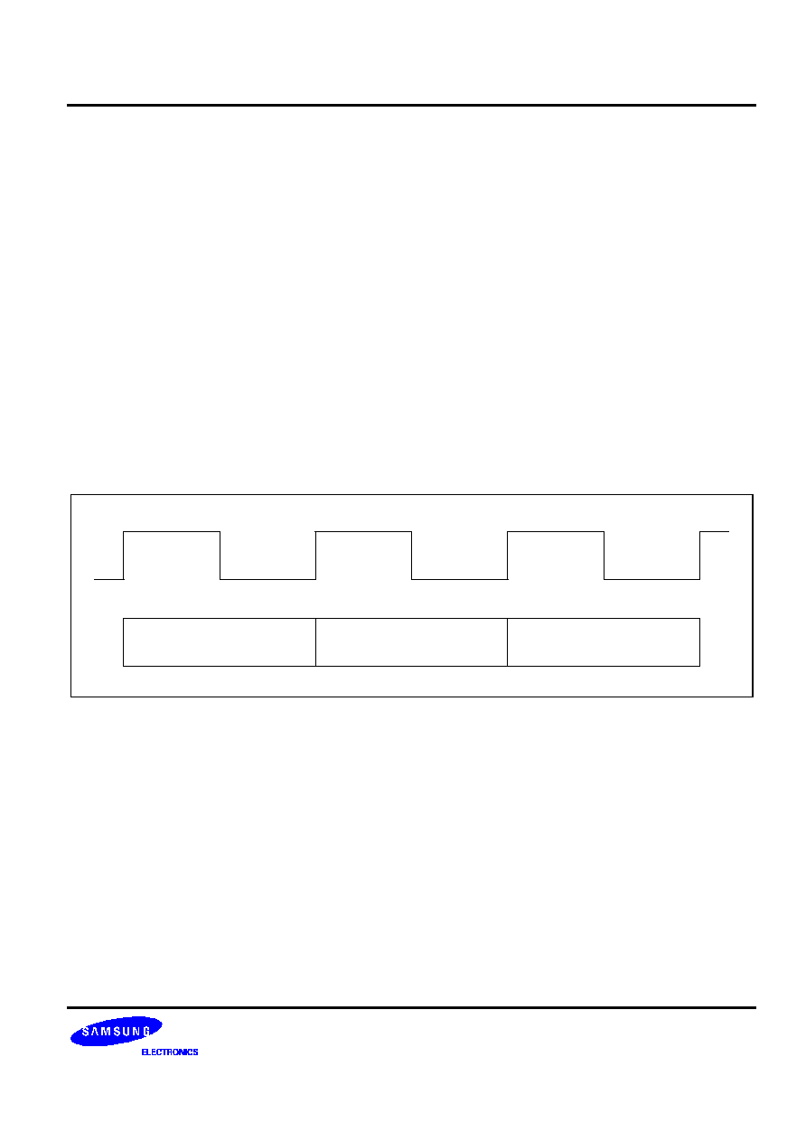
Block Diagram ......................................................................................................................................... 17-3
Serial I/O Timing Diagram ....................................................................................................................... 17-4

S3CK225/FK225 MICROCONTROLLER
ix
Table of Contents
(Continued)
Chapter 18
LCD Controller/Driver
Overview ................................................................................................................................................. 18-1
LCD Circuit Diagram ....................................................................................................................... 18-2
LCD RAM Address Area .................................................................................................................. 18-3
LCD Control Register (LCON, 60H) ................................................................................................. 18-4
LCD Port Control Registers (LPOT1, LPOT2)
.........................................................................................
18-7
LCD Voltage Dividing Resistors....................................................................................................... 18-8
LCD COM/SEG Signals................................................................................................................... 18-9
Chapter 19
10-Bit Analog to Digital Converter
Overview ................................................................................................................................................. 19-1
Function Description ................................................................................................................................ 19-1
Conversion Timing .......................................................................................................................... 19-2
A/D Converter Control Register (ADCON) ....................................................................................... 19-2
Internal Reference Voltage Levels................................................................................................... 19-3
Block Diagram ......................................................................................................................................... 19-3
Chapter 20
D/A Converter
Overview ................................................................................................................................................. 20-1
Function Description........................................................................................................................ 20-1
D/A Converter Data Register (DADATAH/DADATAL) ...................................................................... 20-3
Chapter 21
Operational Amplifier
Overview ................................................................................................................................................. 21-1
OP AMP Control Register (OPCON)................................................................................................ 21-1

x
S3CK225/FK225 MICROCONTROLLER
Table of Contents
(Continued)
Chapter 22
Electrical Data
Overview ................................................................................................................................................. 22-1
Chapter 23
Mechanical Data
Overview ................................................................................................................................................. 23-1
Chapter 24
S3FK225 Flash MCU
Overview ................................................................................................................................................. 24-1
Chapter 25
Development Tools
Overview ................................................................................................................................................. 25-1
CALMSHINE: IDE (Integrated Development Environment) .............................................................. 25-1
Invisible MDS: In-Circuit Emulator ................................................................................................... 25-1
CALMRISC8 C-Compiler: CALM8CC .............................................................................................. 25-1
CALMRISC8 Relocatable Assembler: CALM8ASM.......................................................................... 25-1
CALMRISC8 Linker: CALM8LINK .................................................................................................... 25-1
Emulation Probe Board Configuration ...................................................................................................... 25-2
External Event Input Headers .......................................................................................................... 25-3
Event Match Output Headers........................................................................................................... 25-3
External Break Input Headers .......................................................................................................... 25-3
Power Selection............................................................................................................................... 25-4
Clock Selection................................................................................................................................ 25-4
VREF Selection ............................................................................................................................... 25-5
Use Clock Setting For External Clock Mode .................................................................................... 25-5
Sub Clock Setting ............................................................................................................................ 25-5
JP1, JP2 Pin Assignment ................................................................................................................ 25-6

S3CK225/FK225 MICROCONTROLLER
xi
List of Figures
Figure
Title
Page
Number
Number
1-1
Top Block Diagram............................................................................................................. 1-2
1-2
CalmRISC Pipeline Diagram .............................................................................................. 1-3
1-3
CalmRISC Pipeline Stream Diagram .................................................................................. 1-4
1-4
Block Diagram.................................................................................................................... 1-7
1-5
Pin Assignment (64-QFP)................................................................................................... 1-8
1-6
Pin Circuit Type B (RESET) ............................................................................................... 1-11
1-7
Pin Circuit Type D-3 (P7).................................................................................................... 1-11
1-8
Pin Circuit Type C .............................................................................................................. 1-11
1-9
Pin Circuit Type D-4 (P0)................................................................................................... 1-11
1-10
Pin Circuit Type E-4 (P1).................................................................................................... 1-12
1-11
Pin Circuit Type F-10 (P5) .................................................................................................. 1-12
1-12
Pin Circuit Type H-4 ........................................................................................................... 1-13
1-13
Pin Circuit Type H-14 (P2, P3, P4, P6) ............................................................................... 1-13
2-1
Program Memory Organization........................................................................................... 2-1
2-2
Relative Jump Around Page Boundary ............................................................................... 2-2
2-3
Program Memory Layout .................................................................................................... 2-3
2-4
ROM Code Option (RCOD_OPT) ....................................................................................... 2-5
2-5
Data Memory Map of CalmRISC8 ...................................................................................... 2-6
2-6
Data Memory Map of S3CK225 .......................................................................................... 2-7
3-1
Bank Selection by Setting of GRB Bits and IDB Bit............................................................. 3-3
4-1
Memory Map Area .............................................................................................................. 4-1
5-1
Hardware Stack .................................................................................................................. 5-1
5-2
Even and Odd Bank Selection Example ............................................................................. 5-2
5-3
Stack Operation with PC [19:0]........................................................................................... 5-3
5-4
Stack Operation with Registers........................................................................................... 5-4
5-5
Stack Overflow ................................................................................................................... 5-5
6-1
Interrupt Structure .............................................................................................................. 6-3
6-2
Interrupt Structure .............................................................................................................. 6-4
6-3
Interrupt Mask Register ...................................................................................................... 6-5
6-4
Interrupt Priority Register.................................................................................................... 6-6

xii
S3CK225/FK225 MICROCONTROLLER
List of Figures
(Continued)
Figure
Title
Page
Number
Number
8-1
Main Oscillator Circuit (Crystal or Ceramic Oscillator)......................................................... 8-1
8-2
Main Oscillator Circuit (RC Oscillator)................................................................................. 8-2
8-3
Sub Oscillator Circuit (Crystal or Ceramic Oscillator) .......................................................... 8-2
8-4
System Clock Circuit Diagram ............................................................................................ 8-3
8-5
Power Control Register (PCON) ......................................................................................... 8-4
8-6
Oscillator Control Register (OSCCON) ............................................................................... 8-4
8-7
Main Oscillator Clock Output Functional Block Diagram ..................................................... 8-5
8-8
Main Oscillator Clock Output Control Register (CLOCON) .................................................. 8-5
10-1
Port 0 Control Register (P0CON) ........................................................................................ 10-1
10-2
Port 1 Control Register (P1CON) ........................................................................................ 10-2
10-3
Port 1 Pull-Up Control Register (P1PUR) ............................................................................ 10-2
10-4
Port 2 High-Byte Control Register (P2CONH) ..................................................................... 10-3
10-5
Port 2 Low-Byte Control Register (P2CONL)....................................................................... 10-3
10-6
Port 3 High-Byte Control Register (P3CONH) ..................................................................... 10-4
10-7
Port 3 Low-Byte Control Register (P3CONL)....................................................................... 10-4
10-8
Port 4 High-Byte Control Register (P4CONH) ..................................................................... 10-5
10-9
Port 4 Low-Byte Control Register (P4CONL)....................................................................... 10-5
10-10
Port 5 High-Byte Control Register (P5CONH) ..................................................................... 10-6
10-11
Port 5 Low-Byte Control Register (P5CONL)....................................................................... 10-6
10-12
Port 6 Control Register (P6CON) ........................................................................................ 10-7
10-13
Port 7 Control Register (P7CON) ........................................................................................ 10-7
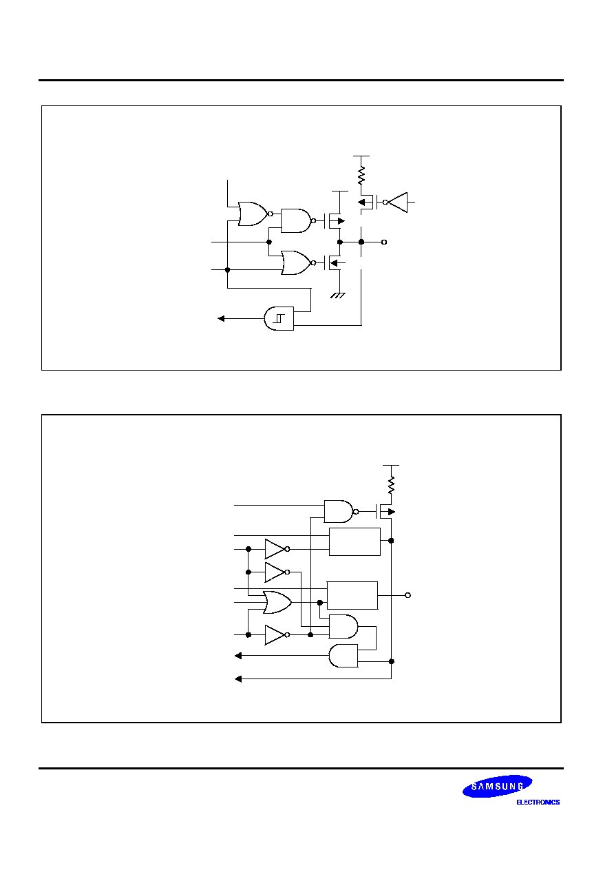
11-1
Watchdog Timer Control Register (WDTCON) ................................................................... 11-1
11-2
Basic Timer & Watchdog Timer Functional Block Diagram ................................................. 11-2
12-1
Watch Timer Circuit Diagram ............................................................................................. 12-2
13-1
Timer 0 Control Register (T0CON) ..................................................................................... 13-3
13-2
Timer 0 Functional Block Diagram...................................................................................... 13-4
13-3
Timer 0 Counter and Data Registers (T0CNTH/L, T0DATAH/L) .......................................... 13-5
14-1
Timer 1 Control Register (T1CON) ..................................................................................... 14-2
14-2
Timer 1 Functional Block Diagram...................................................................................... 14-3
14-3
Timer 1 Counter Register (T1CNTH/L)................................................................................ 14-4
14-4
Timer 1 Data Register (T1DATAH/L) .................................................................................. 14-4
15-1
Timer 2 Control Register (T2CON) ..................................................................................... 15-3
15-2
Timer 2 Functional Block Diagram...................................................................................... 15-4

S3CK225/FK225 MICROCONTROLLER
xiii
List of Figures
(Continued)
Figure
Title
Page
Number
Number
16-1
Timer 3 Functional Block Diagram...................................................................................... 16-2
16-2
Timer 3 Control Register (T3CON) ..................................................................................... 16-3
16-3
Timer 3 Data Registers (T3DATAH/L)................................................................................. 16-3
16-4
Timer 3 Output Flip-Flop Waveforms in Repeat Mode........................................................ 16-5
17-1
Serial I/O Module Control Registers (SIOCON) .................................................................. 17-2
17-2
SIO Pre-scaler Register (SIOPS)........................................................................................ 17-2
17-3
SIO Function Block Diagram .............................................................................................. 17-3
17-4
Serial I/O Timing in Transmit/Receive Mode(Tx at falling, SIOCON.4=0) ........................... 17-4
17-5
Serial I/O Timing in Transmit/Receive Mode(Tx at rising, SIOCON.4=1) ............................ 17-4
18-1
LCD Function Diagram ....................................................................................................... 18-1
18-2
LCD Circuit Diagram .......................................................................................................... 18-2
18-3
LCD Display Data RAM Organization ................................................................................. 18-3
18-4
LCD Port Control Resister1 (LPOT1) .................................................................................. 18-7
18-5
LCD Port Control Resister2 (LPOT2) .................................................................................. 18-7
18-6
Internal Voltage Dividing Resistor Connection .................................................................... 18-8
18-7
Select/No-Select Bias Signals in Static Display Mode......................................................... 18-9
18-8
Select/No-Select Bias Signals in 1/2 Duty, 1/2 Bias Display Mode ...................................... 18-10
18-9
Select/No-Select Bias Signals in 1/3 Duty, 1/3 Bias Display Mode ...................................... 18-10
18-10
LCD Signal and Wave Forms Example in 1/2 Duty, 1/2 Bias Display Mode ........................ 18-11
18-11
LCD Signals and Wave Forms Example in 1/3 Duty, 1/3 Bias Display Mode ...................... 18-12
18-12
LCD Signals and Wave Forms Example in 1/4 Duty, 1/3 Bias Display Mode ...................... 18-13
19-1
A/D Converter Control Register (ADCON) .......................................................................... 19-2
19-2
A/D Converter Data Register (ADDATAH/ADDATAL) ......................................................... 19-3
19-3
A/D Converter Functional Block Diagram ........................................................................... 19-3
19-4
Recommended A/D Converter Circuit for Highest Absolute Accuracy ................................. 19-4
20-1
DAC Circuit Diagram .......................................................................................................... 20-2
20-2
Digital to Analog Converter Control Register (DACON)....................................................... 20-2
20-3
D/A Converter Data Register (DADATAH/DADATAL) ......................................................... 20-3

xiv
S3CK225/FK225 MICROCONTROLLER
List of Figures
(Continued)
Figure
Title
Page
Number
Number
21-1
OP AMP Control Register (OPCON)................................................................................... 21-1
21-2
OP AMP Block Diagram ..................................................................................................... 21-2
22-1
Input Timing for External Interrupts (Port 0) ........................................................................ 22-4
22-2
Input Timing for
RESET ...............................................................................................................
22-4
22-3
Stop Mode Release Timing When Initiated by a
RESET..........................................................
22-5
22-4
Stop Mode Release Timing Initiated by Interrupts ............................................................... 22-6
22-5
Serial Data Transfer Timing................................................................................................ 22-8
22-6
Clock Timing Measurement at X
IN
..............................................................................................
22-10
22-7
Clock Timing Measurement at XT
IN
............................................................................................
22-10
22-8
Operating Voltage Range ................................................................................................... 22-12
23-1
64-Pin QFP Package Dimensions (64-QFP-1420F) ............................................................ 23-1
24-1
S3FK225 Pin Assignments (64-QFP-1420F)....................................................................... 24-2
25-1
Emulation Probe Board Configuration................................................................................. 25-2

S3CK225/FK225 MICROCONTROLLER
xv
List of Tables
Table
Title
Page
Number
Number
1-1
Pin Descriptions ................................................................................................................. 1-9
3-1
General and Special Purpose Registers.............................................................................. 3-1
3-2
Status Register 0 configuration ........................................................................................... 3-3
3-3
Status Register 1: SR1 ....................................................................................................... 3-4
4-1
Registers ............................................................................................................................ 4-2
6-1
Exceptions.......................................................................................................................... 6-1
7-1
Instruction Notation Conventions ........................................................................................ 7-1
7-2
Overall Instruction Set Map ................................................................................................ 7-2
7-3
Instruction Encoding ........................................................................................................... 7-4
7-4
Index Code Information ("idx") ............................................................................................ 7-7
7-5
Index Modification Code Information ("mod")...................................................................... 7-7
7-6
Condition Code Information ("cc")....................................................................................... 7-7
7-7
"ALUop1" Code Information ................................................................................................ 7-8
7-8
"ALUop2" Code Information ................................................................................................ 7-8
7-9
"MODop1" Code Information .............................................................................................. 7-8
12-1
Watch Timer Control Register (WTCON): 8-Bit R/W .......................................................... 12-1
18-1
LCD Control Register (LCON) Organization........................................................................ 18-4
18-2
Relationship of LCON.0 and LMOD.3 Bit Settings .............................................................. 18-4
18-3
LCD Clock Signal (LCDCK) Frame Frequency.................................................................... 18-5
18-4
LCD Mode Control Register (LMOD) Organization, 4CH..................................................... 18-6
18-5
Maximum Number of Display Digits per Duty Cycle............................................................ 18-6
20-1
DADATA Setting to Generate Analog Voltage .................................................................... 20-3

xvi
S3CK225/FK225 MICROCONTROLLER
List of Tables
(Continued)
Table
Title
Page
Number
Number
22-1
Absolute Maximum Ratings ................................................................................................ 22-1
22-2
D.C. Electrical Characteristics ............................................................................................ 22-1
22-3
A.C. Electrical Characteristics............................................................................................. 22-4
22-4
Input/Output Capacitance ................................................................................................... 22-5
22-5
Data Retention Supply Voltage in Stop Mode ..................................................................... 22-5
22-6
A/D Converter Electrical Characteristics ............................................................................. 22-7
22-7
D/A Converter Electrical Characteristics ............................................................................. 22-7
22-8
Synchronous SIO Electrical Characteristics ........................................................................ 22-8
22-9
Main Oscillator Frequency (f
OSC1
) ...................................................................................... 22-9
22-10
Main Oscillator Clock Stabilization Time (T
ST1
) .................................................................. 22-9
22-11
Sub Oscillator Frequency (f
OSC2
)........................................................................................ 22-10
22-12
Sub Oscillator (Crystal) Start up Time (t
ST2
) ....................................................................... 22-11
22-13
OP Amplifier Characteristics............................................................................................... 22-11
24-1
Descriptions of Pins Used to Read/Write the FLASH ROM ................................................. 24-3

S3CK225/FK225 MICROCONTROLLER
xvii
List of Programming Tips
Description
Page
Number
Chapter 6: Exceptions
Interrupt Programming Tip 1 .................................................................................................................... 6-7
Interrupt Programming Tip 2 .................................................................................................................... 6-8
Chapter 16: 8-Bit Timer 3
To generate 38 kHz, 1/3duty signal through P7.2
.............................................................................................
16-6
To generate a one pulse signal through P7.2
....................................................................................................
16-7


S3CK225/FK225 MICROCONTROLLER
xix
List of Instruction Descriptions
Instruction
Full Instruction Name
Page
Mnemonic
Number
ADC
Add with Carry ....................................................................................................... 7-30
ADD
Add ........................................................................................................................ 7-31
AND
Bit-wise AND.......................................................................................................... 7-32
AND SR0
Bit-wise AND with SR0........................................................................................... 7-33
BANK
Bank Selection....................................................................................................... 7-34
BITC
Bit Complement ..................................................................................................... 7-35
BITR
Bit Reset ................................................................................................................ 7-36
BITS
Bit Set.................................................................................................................... 7-37
BITT
Bit Test .................................................................................................................. 7-38
BMC/BMS
TF bit clear/set ....................................................................................................... 7-39
CALL
Conditional subroutine call (Pseudo Instruction) .................................................... 7-40
CALLS
Call Subroutine ...................................................................................................... 7-41
CLD
Load into Coprocessor ........................................................................................... 7-42
CLD
Load from Coprocessor.......................................................................................... 7-43
COM
1's or Bit-wise Complement.................................................................................... 7-44
COM2
2's Complement ..................................................................................................... 7-45
COMC
Bit-wise Complement with Carry ............................................................................ 7-46
COP
Coprocessor........................................................................................................... 7-47
CP
Compare................................................................................................................ 7-48
CPC
Compare with Carry ............................................................................................... 7-49
DEC
Decrement ............................................................................................................. 7-50
DECC
Decrement with Carry ............................................................................................ 7-51
DI
Disable Interrupt (Pseudo Instruction) .................................................................... 7-52
EI
Enable Interrupt (Pseudo Instruction) .................................................................... 7-53
IDLE
Idle Operation (Pseudo Instruction) ....................................................................... 7-54
INC
Increment............................................................................................................... 7-55
INCC
Increment with Carry .............................................................................................. 7-56
IRET
Return from Interrupt Handling............................................................................... 7-57
JNZD
Jump Not Zero with Delay Slot............................................................................... 7-58
JP
Conditional Jump (Pseudo Instruction) .................................................................. 7-59
JR
Conditional Jump Relative ..................................................................................... 7-60
LCALL
Conditional Subroutine Call.................................................................................... 7-61
LD adr:8
Load into Memory .................................................................................................. 7-62

xx
S3CK225/FK225 MICROCONTROLLER
List of Instruction Descriptions
(Continued)
Instruction
Full Instruction Name
Page
Mnemonic
Number
LD @idm
Load into Memory Indexed ..................................................................................... 7-63
LD
Load Register......................................................................................................... 7-64
LD
Load GPR:bankd, GPR:banks................................................................................ 7-65
LD
Load GPR, TBH/TBL.............................................................................................. 7-66
LD
Load TBH/TBL, GPR.............................................................................................. 7-67
LD SPR
Load SPR
.........................................................................................................................
7-68
LD SPR0
Load SPR0 Immediate ........................................................................................... 7-69
LDC
Load Code ............................................................................................................. 7-70
LJP
Conditional Jump ................................................................................................... 7-71
LLNK
Linked Subroutine Call Conditional......................................................................... 7-72
LNK
Linked Subroutine Call (Pseudo Instruction) .......................................................... 7-73
LNKS
Linked Subroutine Call ........................................................................................... 7-74
LRET
Return from Linked Subroutine Call........................................................................ 7-75
NOP
No Operation.......................................................................................................... 7-76
OR
Bit-wise OR ............................................................................................................ 7-77
OR SR0
Bit-wise OR with SR0 ............................................................................................. 7-78
POP
POP ....................................................................................................................... 7-79
POP
POP to Register ..................................................................................................... 7-80
PUSH
Push Register......................................................................................................... 7-81
RET
Return from Subroutine .......................................................................................... 7-82
RL
Rotate Left ............................................................................................................. 7-83
RLC
Rotate Left with Carry ............................................................................................ 7-84
RR
Rotate Right ........................................................................................................... 7-85
RRC
Rotate Right with Carry .......................................................................................... 7-86
SBC
Subtract with Carry................................................................................................. 7-87
SL
Shift Left ................................................................................................................ 7-88
SLA
Shift Left Arithmetic ............................................................................................... 7-89
SR
Shift Right .............................................................................................................. 7-90
SRA
Shift Right Arithmetic ............................................................................................. 7-91
STOP
Stop Operation (Pseudo Instruction) ...................................................................... 7-92
SUB
Subtract ................................................................................................................. 7-93
SWAP
Swap...................................................................................................................... 7-94
SYS
System................................................................................................................... 7-95
TM
Test Multiple Bits.................................................................................................... 7-96
XOR
Exclusive OR ......................................................................................................... 7-97

S3CK225/FK225
PRODUCT OVERVIEW
1-1
1
PRODUCT OVERVIEW
OVERVIEW
The S3CK225/FK225 single-chip CMOS microcontroller is designed for high performance using Samsung's new
8-bit CPU core, CalmRISC.
CalmRISC is an 8-bit low power RISC microcontroller. Its basic architecture follows Harvard style, that is, it has
separate program memory and data memory. Both instruction and data can be fetched simultaneously without
causing a stall, using separate paths for memory access. Represented below is the top block diagram of the
CalmRISC microcontroller.

PRODUCT OVERVIEW
S3CK225/FK225
1-2
BBUS[7:0]
20
Program Memory Address
Generation Unit
PC[19:0]
Hardware
Stack
HS[0]
HS[15]
8
8
R0
R3
R1
R2
ALU
ABUS[7:0]
ALUL
ALUR
PA[19:0]
PD[15:0]
IDL0
IDL1
SR0
SR1
ILH
ILX
ILL
SPR
IDH
DO[7:0]
DI[7:0]
GPR
Data Memory
Address
Generation Unit
DA[15:0]
20
Flag
RBUS
TBH TBL
Figure 1-1. Top Block Diagram
S3CK225/FK225
PRODUCT OVERVIEW
1-3
The CalmRISC building blocks consist of:
-- An 8-bit ALU
-- 16 general purpose registers (GPR)
-- 11 special purpose registers (SPR)
-- 16-level hardware stack
-- Program memory address generation unit
-- Data memory address generation unit
Sixteen GPRs are grouped into four banks (Bank0 to Bank3), and each bank has four 8-bit registers (R0, R1, R2,
and R3). SPRs, designed for special purposes, include status registers, link registers for branch-link instructions,
and data memory index registers. The data memory address generation unit provides the data memory address
(denoted as DA[15:0] in the top block diagram) for a data memory access instruction. Data memory contents are
accessed through DI[7:0] for read operations and DO[7:0] for write operations. The program memory address
generation unit contains a program counter, PC[19:0], and supplies the program memory address through
PA[19:0] and fetches the corresponding instruction through PD[15:0] as the result of the program memory
access. CalmRISC has a 16-level hardware stack for low power stack operations as well as a temporary storage
area.
Instruction Fetch
(IF)
Instruction Decode/
Data Memory Access
(ID/MEM)
Execution/Writeback
(EXE/WB)
Figure 1-2. CalmRISC Pipeline Diagram
CalmRISC has a 3-stage pipeline as described below:
As can be seen in the pipeline scheme, CalmRISC adopts a register-memory instruction set. In other words, data
memory where R is a GPR can be one operand of an ALU instruction as shown below:
The first stage (or cycle) is the Instruction fetch stage (IF for short), where the instruction pointed by the program
counter, PC[19:0] , is read into the Instruction Register (IR for short). The second stage is the Instruction Decode
and Data Memory Access stage (ID/MEM for short), where the fetched instruction (stored in IR) is decoded and
data memory access is performed, if necessary. The final stage is the Execute and Write-back stage (EXE/WB),
where the required ALU operation is executed and the result is written back into the destination registers.
Since CalmRISC instructions are pipelined, the next instruction fetch is not postponed until the current instruction
is completely finished but is performed immediately after completing the current instruction fetch. The pipeline
stream of instructions is illustrated in the following diagram.

PRODUCT OVERVIEW
S3CK225/FK225
1-4
EXE/WB
IF
IF
IF
IF
IF
IF
IF
ID/MEM
ID/MEM
ID/MEM
ID/MEM
ID/MEM
ID/MEM
EXE/WB
EXE/WB
EXE/WB
EXE/WB
EXE/WB
/ 1
/ 2
/ 3
/ 4
/ 6
/ 5
Figure 1-3. CalmRISC Pipeline Stream Diagram
Most CalmRISC instructions are 1-word instructions, while same branch instructions such as long "call" and "jp"
instructions are 2-word instructions. In Figure 1-3, the instruction, I4, is a long branch instruction, and it takes two
clock cycles to fetch the instruction. As indicated in the pipeline stream, the number of clocks per instruction
(CPI) is 1 except for long branches, which take 2 clock cycles per instruction.

S3CK225/FK225
PRODUCT OVERVIEW
1-5
FEATURES
CPU
�
CalmRISC core (8-bit RISC architecture)
Memory
�
ROM: 8K-word (16K-byte)
�
RAM: 384-byte (excluding LCD data RAM)
Stack
�
Size: maximum 16 word-level
48 I/O Pins
�
12 normal I/O pins
�
36 I/O pins sharing with LCD signals
Basic Timer
�
Overflow signal makes a system reset
�
Watchdog function
16-bit Timer/Counter 0
�
Programmable 16-bit timer
�
Interval, capture, PWM mode
�
Match, overflow interrupt
16-bit Timer/Counter 1
�
Programmable 16-bit timer
�
Match interrupt generator
8-bit Timer/Counter 2
�
Programmable 8-bit timer
�
Interval, PWM mode
�
Match, overflow interrupt
8-bit Timer/Counter 3
�
Programmable 8-bit timer
�
Match interrupt/carrier frequency generator
Watch Timer
�
Real-time and interval time measurement
�
Clock generation for LCD
�
Four frequency outputs for buzzer sound
(0.5/1/2/4 kHz at 32.768 kHz)
LCD Controller/Driver
�
32 segments and 4 common terminals
�
Static, 1/2 duty, 1/3 duty, 1/4 duty
�
Internal resistor circuit for LCD bias
8-Bit Serial I/O Interface
�
8-bit transmit/receive mode
�
8-bit receive mode
�
LSB-first/MSB-first transmission selectable
�
Internal/external clock source
A/D Converter
�
Eight analog input channels
�
25
�
s conversion speed at 8 MHz
�
10-bit conversion resolution
�
Operating voltage: 2.7 V to 5.5 V
D/A Converter
�
One analog output channel
�
10-bit conversion resolution (R-2R)
�
Operating voltage: 2.7 V to 5.5 V
Oscillation Sources
�
Crystal, ceramic, RC for main clock
�
Crystal for sub clock
�
Main clock frequency: 0.4�8 MHz
�
Sub clock frequency: 32.768 kHz
�
CPU clock divider circuit
(divided by 1, 2, 4, 8, 16, 32, 64 or 128)

PRODUCT OVERVIEW
S3CK225/FK225
1-6
FEATURES (Continued)
Two Power-Down Modes
�
Idle (only CPU clock stops)
�
Stop (System clock stops)
Interrupts
�
2 Vectors, 13 interrupts
Instruction Execution Times
�
125 ns at 8 MHz (main clock)
�
30.5
�
s at 32.768 kHz (sub clock)
Operating Temperature Range
�
- 25
�
C to 85
�
C
Operating Voltage Range
�
2.0 V to 5.5 V at 2 MHz (2MIPS)
�
2.4 V to 5.5 V at 4 MHz (4MIPS)
�
3.0 V to 5.5 V at 8 MHz (8MIPS)
Two Amplifiers
�
Microphone and filter
Package Type
�
64-pin QFP-1420F

S3CK225/FK225
PRODUCT OVERVIEW
1-7
BLOCK DIAGRAM
RESET
OSC,
Reset
16-Bit Timer/
Counter 0
10-Bit A/D
Converter
P0.0-P0.3/
INT0-INT3
I/O Port 1
X
IN
, XT
IN
16-Bit Timer/
Counter 1
8-Bit Timer/
Counter 2
8-Bit Timer/
Counter 3
I/O Port 0
I/O Port 5
I/O Port 7
T0OUT/T0PWM/P7.1
T0CLK/P7.2
T0CAP/P7.3
T3PWM/P7.2
P1.0/BUZ
P1.1/SO
P1.2/SCK
P1.3/SI
AV
REF
AV
SS
P5.0-P5.7/AD0-AD7/
SEG24-SEG31
P7.0/T2OUT/T2PWM
P7.1/T2CLK/T0OUT/T0PWM
P7.2/T0CLK/T3PWM
P7.3/T0CAP/CLKOUT
DAO
Calm8 RISC CPU
384-byte
Register File
16K-byte
ROM
Basic
Timer
Watch
Timer
X
OUT
, XT
OUT
BUZ/P1.0
P4.0-P4.7/
SEG16-SEG23
T2OUT/T2PWM/P7.0
T2CLK/P7.1
10-Bit D/A
Converter
Serial
I/O Port
P6.0-P6.3/
COM0-COM3
LCD
Driver
I/O Port 2
I/O Port 3
I/O Port 4
I/O Port 6
Two
Amplifiers
I/O Port and Interrupt Control
COM0-COM3/
P6.0-P6.3
SEG0-SEG31/
P2.0-P5.7
SO/P1.1
SCK/P1.2
SI/P1.3
P2.0-P2.7/
SEG0-SEG7
P3.0-P3.7/
SEG8-SEG15
AD0-AD7/P5.0-P5.7
FILIN, MICIN
FILOUT, MICOUT, Vref
Figure 1-4. Block Diagram

PRODUCT OVERVIEW
S3CK225/FK225
1-8
PIN ASSIGNMENT
COM0/P6.0
COM1/P6.1
COM2/P6.2
COM3/P6.3
P7.0/T2OUT/T2PWM
P7.1/T2CLK/T0OUT/T0PWM
P7.2/T0CLK/T3PWM
P7.3/T0CAP/CLKOUT
V
DD
V
SS
X
OUT
X
IN
TEST
XT
IN
XT
OUT
RESET
DAO
FILIN
FILOUT
P2.0/SEG0
P2.1/SEG1
P2.2/SEG2
P2.3/SEG3
P2.4/SEG4
P2.5/SEG5
P2.6/SEG6
P2.7/SEG7
P3.0/SEG8
P3.1/SEG9
P3.2/SEG10
P3.3/SEG11
P3.4/SEG12
VREF
MICIN
MICOUT
P0.0/INT0
P0.1/INT1
P0.2/INT2
P0.3/INT3
P1.0/BUZ
P1.1/SO
P1.2/SCK
P1.3/SI
AVREF
AVSS
P3.5/SEG13
P3.6/SEG14
P3.7/SEG15
P4.0/SEG16
P4.1/SEG17
P4.2/SEG18
P4.3/SEG19
P4.4/SEG20
P4.5/SEG21
P4.6/SEG22
P4.7/SEG23
P5.0/SEG24/AD0
P5.1/SEG25/AD1
P5.2/SEG26/AD2
P5.3/SEG27/AD3
P5.4/SEG28/AD4
P5.5/SEG29/AD5
P5.6/SEG30/AD6
P5.7/SEG31/AD7
S3CK225/FK225
(64-QFP-1420F)
1
2
3
4
5
6
7
8
9
10
11
12
13
14
15
16
17
18
19
51
50
49
48
47
46
45
44
43
42
41
40
39
38
37
36
35
34
33
20
21
22
23
24
25
26
27
28
29
30
31
32
64
63
62
61
60
59
58
57
56
55
54
53
52
Figure 1-5. Pin Assignment (64-QFP)

S3CK225/FK225
PRODUCT OVERVIEW
1-9
PIN DESCRIPTIONS
Table 1-1. Pin Descriptions
Pin
Names
Pin
Type
Pin
Description
Circuit
Type
Pin
Numbers
Share
Pins
P0.0
P0.1
P0.2
P0.3
I/O
I/O port with bit programmable pins;
Schmitt trigger input or output mode
selected by software; software
assignable pull-up resistors.
(with noise filter and interrupt control).
D-4
23
24
25
26
INT0
INT1
INT2
INT3
P1.0
P1.1
P1.2
P1.3
I/O
I/O port with bit programmable pins;
Schmitt trigger input or output mode
selected by software; Open-drain output
mode can be selected by software;
software assignable pull-up resistors.
E-4
27
28
29
30
BUZ
SO
SCK
SI
P2.0-P2.7
I/O
I/O port with bit programmable pins;
Push-pull or open-drain output and input
with software assignable pull-up resistors.
H-14
64-57
SEG0-SEG7
P3.0-P3.7
I/O
Have the same characteristic as port 2
H-14
56-49
SEG8-SEG15
P4.0-P4.7
I/O
Have the same characteristic as port 2
H-14
48-41
SEG16-SEG23
P5.0-P5.7
I/O
I/O port with bit programmable pins;
Normal input or output mode selected by
software; software assignable pull-up
resistors.
F-10
40-33
AD0-AD7/
SEG24-SEG31
P6.0-P6.3
I/O
Have the same characteristic as port 2
H-14
1-4
COM0-COM3
P7.0
P7.1
P7.2
P7.3
I/O
I/O port with bit programmable pins;
Schmitt trigger input or push-pull output
with software assignable pull-up resistors.
D-3
5
6
7
8
T2OUT/T2PWM
T2CLK/T0OUT/T0PWM
T0CLK/T3PWM
T0CAP/CLKOUT
AD0-AD7
I/O
A/D converter analog input channels
F-10
40-33
P5.0-P5.7/
SEG24-SEG31
AV
REF
�
A/D converter reference voltage
�
31
�
AV
SS
�
A/D converter ground
�
32
�
INT0-INT3
I/O
External interrupt input pins
D-4
23-26
P0.0-P0.3
RESET
I
System reset pin
B
16
�
TEST
I
Test signal input
(must be connected to V
SS
)
�
13
�

PRODUCT OVERVIEW
S3CK225/FK225
1-10
Table 1-1. Pin Descriptions (Continued)
Pin
Names
Pin
Type
Pin
Description
Circuit
Type
Pin
Numbers
Share
Pins
V
DD
, V
SS
�
Main power supply and ground
�
9, 10
�
X
OUT
, X
IN
�
Main oscillator pins
�
11, 12
�
XT
OUT
, XT
IN
�
Sub oscillator pins
�
15, 14
�
SO, SCK, SI
I/O
Serial I/O interface clock signal
E-4
28-30
P1.1-P1.3
T3PWM
I/O
Timer 3 PWM output
D-3
7
P7.2
T2OUT/T2PWM
I/O
Timer 2 output and PWM output
D-3
5
P7.0
T2CLK
I/O
Timer 2 external clock input
D-3
6
P7.1
T0CLK
I/O
Timer 0 external clock input
D-3
7
P7.2
T0CAP
I/O
Timer 0 capture input
D-3
8
P7.3
T0OUT/T0PWM
I/O
Timer 0 output and PWM output
D-3
6
P7.1
COM0-COM3
I/O
LCD common signal output
H-14
1-4
P6.0-P6.3
SEG0-SEG7
I/O
LCD segment output
H-14
64-57
P2.0-P2.7
SEG8-SEG15
I/O
LCD segment output
H-14
56-49
P3.0-P3.7
SEG16-SEG23
I/O
LCD segment output
H-14
48-41
P4.0-P4.7
SEG24-SEG31
I/O
LCD segment output
H-14
40-33
P5.0-P5.7/
AD0-AD7
BUZ
I/O
0.5, 1, 2 or 4 kHz frequency output for
buzzer sound with 4.19 MHz main clock
or 32768 Hz sub clock
E-4
27
P1.0
CLKOUT
I/O
Main oscillator clock output
D-3
8
P7.3
DAO
�
DA converter output
�
17
�
FILIN, FILOUT
�
Filter amp input and output
�
18, 19
�
MICIN, MICOUT
�
MIC amp input and output
�
21, 22
�
Vref
�
Reference voltage output for filter amp
and MIC amp
�
20
�

S3CK225/FK225
PRODUCT OVERVIEW
1-11
PIN CIRCUITS
In
V
DD
Figure 1-6. Pin Circuit Type B (
RESET
RESET
)
I/O
Output
Disable
Data
Circuit
Type C
Pull-up
Enable
V
DD
P-Channel
Figure 1-7. Pin Circuit Type D-3 (P7)
P-CH
N-CH
V
DD
Out
Output
Disable
Data
Figure 1-8. Pin Circuit Type C
I/O
Output
Disable
Data
Circuit
Type C
Pull-up
Enable
V
DD
Noise
Filter
Ext. INT
Input
Normal
Figure 1-9. Pin Circuit Type D-4 (P0)
PRODUCT OVERVIEW
S3CK225/FK225
1-12
V
DD
Output
Disable
Data
Pull-up
Resistor
V
DD
I/O
P-CH
N-CH
Open drain
Enable
Figure 1-10. Pin Circuit Type E-4 (P1)
I/O
Output
Disable
Data
Pull-up
Enable
V
DD
ADC
Enable
To ADC
Data
Circuit
Type H-4
SEG
LCD EN
Circuit
Type C
Figure 1-11. Pin Circuit Type F-10 (P5)

S3CK225/FK225
PRODUCT OVERVIEW
1-13
Out
SEG
V
DD
V
LC1
V
LC0
Output
Disable
Figure 1-12. Pin Circuit Type H-4
V
DD
Output
Disable
Data
Pull-up
Enable
V
DD
I/O
P-CH
N-CH
Open Drain
Enable
Circuit
Type H-4
SEG
LCD
Out
Enable
Figure 1-13. Pin Circuit Type H-14 (P2, P3, P4, P6)

PRODUCT OVERVIEW
S3CK225/FK225
1-14
NOTES

S3CK225/FK225
ADDRESS SPACES
2-1
2
ADDRESS SPACES
OVERVIEW
CalmRISC has 20-bit program address lines, PA[19:0], which supports up to 1M words of program memory. The
1M word program memory space is divided into 256 pages and each page is 4K word long as shown in the figure
2-1. The upper 8 bits of the program counter, PC[19:12], points to a specific page and the lower 12 bits, PC[11:0],
specify the offset address of the page.
CalmRISC also has 16-bit data memory address lines, DA[15:0], which supports up to 64K bytes of data memory.
The 64K byte data memory space is divided into 256 pages and each page has 256 bytes. The upper 8 bits of the
data address, DA[15:8], points to a specific page and the lower 8 bits, DA[7:0], specify the offset address of the
page.
PROGRAM MEMORY (ROM)
000H
FFFH
256 page
1 Mword
4 Kword
FFFH
000H
Figure 2-1. Program Memory Organization

ADDRESS SPACES
S3CK225/FK225
2-2
For example, if PC[19:0] = 5F79AH, the page index pointed to by PC is 5FH and the offset in the page is 79AH.
If the current PC[19:0] = 5EFFFH and the instruction pointed to by the current PC, i.e., the instruction at the
address 5EFFFH is not a branch instruction, the next PC becomes 5E000H, not 5F000H. In other words, the
instruction sequence wraps around at the page boundary, unless the instruction at the boundary (in the above
example, at 5EFFFH) is a long branch instruction. The only way to change the program page is by long branches
(LCALL, LLNK, and LJP), where the absolute branch target address is specified. For example, if the current
PC[19:0] = 047ACH (the page index is 04H and the offset is 7ACH) and the instruction pointed to by the current
PC, i.e., the instruction at the address 047ACH, is "LJP A507FH" (jump to the program address A507FH), then
the next PC[19:0] = A507FH, which means that the page and the offset are changed to A5H and 07FH,
respectively. On the other hand, the short branch instructions cannot change the page indices.
Suppose the current PC is 6FFFEH and its instruction is "JR 5H" (jump to the program address PC + 5H). Then
the next instruction address is 6F003H, not 70003H. In other words, the branch target address calculation also
wraps around with respect to a page boundary. This situation is illustrated below:
000H
001H
002H
003H
004H
005H
FFEH
FFFH
Page 6FH
JR 5H
Figure 2-2. Relative Jump Around Page Boundary
Programmers do not have to manually calculate the offset and insert extra instructions for a jump instruction
across page boundaries. The compiler and the assembler for CalmRISC are in charge of producing appropriate
codes for it.

S3CK225/FK225
ADDRESS SPACES
2-3
00000H
FFFFFH
Vector and
Option Area
~
~
~
~
00020H
0001FH
Program Memory Area
(4K words x 256 page = 1 Mword)
8K words
(16K bytes)
NOTE: For S3CK225, total size of program memory area is 8K words (16K bytes).
1FFFH
Figure 2-3. Program Memory Layout
From 00000H to 00004H addresses are used for the vector address of exceptions, and 0001EH, 0001FH are
used for the option only. Aside from these addresses others are reserved in the vector and option area. Program
memory area from the address 00020H to FFFFFH can be used for normal programs.
The Program memory size of S3CK225 is 8K word (16K byte), so from the address 00020H to 1FFFH are the
program memory area.

ADDRESS SPACES
S3CK225/FK225
2-4
ROM CODE OPTION (RCOD_OPT)
Just after power on, the ROM data located at 0001EH and 0001FH is used as the ROM code option.
S3CK225 has ROM code options like the Reset value of Basic timer and Watchdog timer enable.
For example, if you program as below:
RCOD_OPT
1EH, 0x0000
RCOD_OPT
1FH, 0xbfff
fxx/32 is used as Reset value of basic timer (by bit.14, 13, 12)
Watchdog timer is enabled (by bit.11)
If you don't program any values in these option areas, then the default value is "1".
In these cases, the address 0001EH would be the value of "FFFFH".

S3CK225/FK225
ADDRESS SPACES
2-5
ROM_Code Option (RCOD_OPT)
ROM Address: 0001FH
Reset value of basic timer
clock selection bits
(WDTCON.6, .5, .4):
000 = fxx/2
001 = fxx/4
010 = fxx/16
011 = fxx/32
100 = fxx/128
101 = fxx/256
110 = fxx/1024
111 = fxx/2048
Not used
Watchdog timer enable selection bit:
0 = Disable WDT
1 = Enable WDT
.7
.6
.5
.4
.3
.2
.1
.0
MSB
LSB
Not used
.7
.6
.5
.4
.3
.2
.1
.0
MSB
LSB
Not used
.15
.14
.13
.12
.11
.10
.9
.8
MSB
LSB
ROM Address: 0001EH
.15
.14
.13
.12
.11
.10
.9
.8
MSB
LSB
Not used
Not used
Figure 2-4. ROM Code Option (RCOD_OPT)

ADDRESS SPACES
S3CK225/FK225
2-6
DATA MEMORY ORGANIZATION
The total data memory address space is 64K bytes, addressed by DA[15:0], and divided into 256 pages, Each
page consists of 256 bytes as shown below.
00H
FFH
256 page
64K-byte
256-byte
00H
FFH
2 page
Figure 2-5. Data Memory Map of CalmRISC8
The data memory page is indexed by SPR and IDH. In data memory index addressing mode, 16-bit data memory
address is composed of two 8-bit SPRs, IDH[7:0] and IDL0[7:0] (or IDH[7:0] and IDL1[7:0]). IDH[7:0] points to a
page index, and IDL0[7:0] (or IDL1[7:0]) represents the page offset. In data memory direct addressing mode, an
8-bit direct address, adr[7:0], specifies the offset of the page pointed to by IDH[7:0] (See the details for direct
addressing mode in the instruction sections). Unlike the program memory organization, data memory address
does not wrap around. In other words, data memory index addressing with modification performs an addition or a
subtraction operation on the whole 16-bit address of IDH[7:0] and IDL0[7:0] (or IDL1[7:0]) and updates IDH[7:0]
and IDL0[7:0] (or IDL1[7:0]) accordingly. Suppose IDH[7:0] is 0FH and IDL0[7:0] is FCH and the modification on
the index registers, IDH[7:0] and IDL0[7:0], is increment by 5H, then, after the modification (i.e., 0FFCH + 5 =
1001H), IDH[7:0] and IDL0[7:0] become 10H and 01H, respectively.

S3CK225/FK225
ADDRESS SPACES
2-7
The S3CK225 has 400 bytes of data register address from 0080H to 020FH.
The area from 0000H to 007FH is for peripheral control, and LCD RAM area is from 0200H to 020FH.
Data Memory
Control Register
Page 0
80H
FFH
in Byte
7FH
00H
8-bit
Page1
Data Memory
for LCD Display
0FH
00H
Page 2
Figure 2-6. Data Memory Map of S3CK225

ADDRESS SPACES
S3CK225/FK225
2-8
NOTES
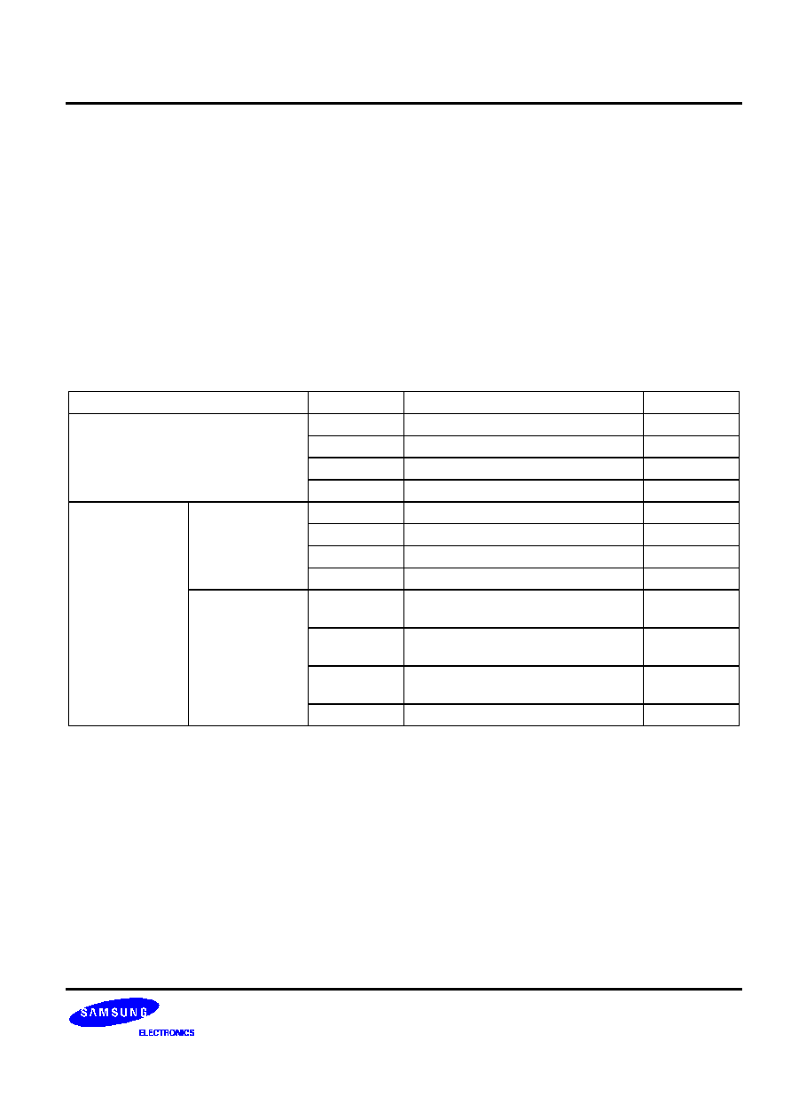
S3CK225/FK225
REGISTERS
3-1
3
REGISTERS
OVERVIEW
The registers of CalmRISC are grouped into 2 parts: general purpose registers and special purpose registers.
Table 3-1. General and Special Purpose Registers
Registers
Mnemonics
Description
Reset Value
General Purpose
R0
General Register 0
Unknown
Registers (GPR)
R1
General Register 1
Unknown
R2
General Register 2
Unknown
R3
General Register 3
Unknown
Special Purpose
Group 0 (SPR0)
IDL0
Lower Byte of Index Register 0
Unknown
Registers (SPR)
IDL1
Lower Byte of Index Register 1
Unknown
IDH
Higher Byte of Index Register
Unknown
SR0
Status Register 0
00H
Group 1 (SPR1)
ILX
Instruction Pointer Link Register for
Extended Byte
Unknown
ILH
Instruction Pointer Link Register for
Higher Byte
Unknown
ILL
Instruction Pointer Link Register for
Lower Byte
Unknown
SR1
Status Register 1
Unknown
GPR
'
s can be used in most instructions such as ALU instructions, stack instructions, load instructions, etc (See
the instruction set sections). From the programming standpoint, they have almost no restriction whatsoever.
CalmRISC has 4 banks of GPR
'
s and each bank has 4 registers, R0, R1, R2, and R3. Hence, 16 GPR
'
s in total
are available. The GPR bank switching can be done by setting an appropriate value in SR0[4:3] (See SR0 for
details). The ALU operations between GPR
'
s from different banks are not allowed.
SPR
'
s are designed for their own dedicated purposes. They have some restrictions in terms of instructions that
can access them. For example, direct ALU operations cannot be performed on SPR
'
s. However, data transfers
between a GPR and an SPR are allowed and stack operations with SPR
'
s are also possible (See the instruction
sections for details).

REGISTERS
S3CK225/FK225
3-2
INDEX REGISTERS: IDH, IDL0 AND IDL1
IDH in concatenation with IDL0 (or IDL1) forms a 16-bit data memory address. Note that CalmRISC
'
s data
memory address space is 64 K byte (addressable by 16-bit addresses). Basically, IDH points to a page index and
IDL0 (or IDL1) corresponds to an offset of the page. Like GPR
'
s, the index registers are 2-way banked. There are
2 banks in total, each of which has its own index registers, IDH, IDL0 and IDL1. The banks of index registers can
be switched by setting an appropriate value in SR0[2] (See SR0 for details). Normally, programmers can reserve
an index register pair, IDH and IDL0 (or IDL1), for software stack operations.
LINK REGISTERS: ILX, ILH AND ILL
The link registers are specially designed for link-and-branch instructions (See LNK and LRET instructions in the
instruction sections for details). When an LNK instruction is executed, the current PC[19:0] is saved into ILX, ILH
and ILL registers, i.e., PC[19:16] into ILX[3:0], PC[15:8] into ILH [7:0], and PC[7:0] into ILL[7:0], respectively.
When an LRET instruction is executed, the return PC value is recovered from ILX, ILH, and ILL, i.e., ILX[3:0] into
PC[19:16], ILH[7:0] into PC[15:8] and ILL[7:0] into PC[7:0], respectively. These registers are used to access
program memory by LDC/LDC+ instructions. When an LDC or LDC+ instruction is executed, the (code) data
residing at the program address specified by ILX:ILH:ILL will be read into TBH:TBL. LDC+ also increments ILL
after accessing the program memory.
There is a special core input pin signal, nP64KW, which is reserved for indicating that the program memory
address space is only 64 K word. By grounding the signal pin to zero, the upper 4 bits of PC, PC[19:16], is
deactivated and therefore the upper 4 bits, PA[19:16], of the program memory address signals from CalmRISC
core are also deactivated. By doing so, power consumption due to manipulating the upper 4 bits of PC can be
totally eliminated (See the core pin description section for details). From the programmer
'
s standpoint, when
nP64KW is tied to the ground level, then PC[19:16] is not saved into ILX for LNK instructions and ILX is not read
back into PC[19:16] for LRET instructions. Therefore, ILX is totally unused in LNK and LRET instructions when
nP64KW = 0.

S3CK225/FK225
REGISTERS
3-3
STATUS REGISTER 0: SR0
SR0 is mainly reserved for system control functions and each bit of SR0 has its own dedicated function.
Table 3-2. Status Register 0 configuration
Flag Name
Bit
Description
eid
0
Data memory page selection in direct addressing
ie
1
Global interrupt enable
idb
2
Index register banking selection
grb[1:0]
4,3
GPR bank selection
exe
5
Stack overflow/underflow exception enable
ie0
6
Interrupt 0 enable
ie1
7
Interrupt 1 enable
SR0[0] (or eid) selects which page index is used in direct addressing. If eid = 0, then page 0 (page index = 0) is
used. Otherwise (eid = 1), IDH of the current index register bank is used for page index. SR0[1] (or ie) is the
global interrupt enable flag. As explained in the interrupt/exception section, CalmRISC has 3 interrupt sources
(non-maskable interrupt, interrupt 0, and interrupt 1) and 1 stack exception. Both interrupt 0 and interrupt 1 are
masked by setting SR0[1] to 0 (i.e., ie = 0). When an interrupt is serviced, the global interrupt enable flag ie is
automatically cleared. The execution of an IRET instruction (return from an interrupt service routine)
automatically sets ie = 1. SR0[2] (or idb) and SR0[4:3] (or grb[1:0]) selects an appropriate bank for index registers
and GPR's, respectively as shown below:
R3
R0
R2
R1
R3
R0
R2
R1
R3
R0
R2
R1
R3
R0
R2
R1
IDH
IDL0
IDL1
IDH
IDL0
IDL1
Bank 0
Bank 1
Bank 2
Bank 3
11
10
01
00
grb [1:0]
0
1
idb
Figure 3-1. Bank Selection by Setting of GRB Bits and IDB Bit
SR0[5] (or exe) enables the stack exception, that is, the stack overflow/underflow exception. If exe = 0, the stack
exception is disabled. The stack exception can be used for program debugging in the software development
stage. SR0[6] (or ie0) and SR0[7] (or ie1) are enabled, by setting them to 1. Even though ie0 or ie1 are enabled,
the interrupts are ignored (not serviced) if the global interrupt enable flag ie is set to 0.

REGISTERS
S3CK225/FK225
3-4
STATUS REGISTER 1: SR1
SR1 is the register for status flags such as ALU execution flag and stack full flag.
Table 3-3. Status Register 1: SR1
Flag Name
Bit
Description
C
0
Carry flag
V
1
Overflow flag
Z
2
Zero flag
N
3
Negative flag
SF
4
Stack Full flag
�
5,6,7
Reserved
SR1[0] (or C) is the carry flag of ALU executions. SR1[1] (or V) is the overflow flag of ALU executions. It is set to
1 if and only if the carry-in into the 8-th bit position of addition/subtraction differs from the carry-out from the 8-th
bit position. SR1[2] (or Z) is the zero flag, which is set to 1 if and only if the ALU result is zero. SR1[3] (or N) is
the negative flag. Basically, the most significant bit (MSB) of ALU results becomes N flag. Note a load instruction
into a GPR is considered an ALU instruction. However, if an ALU instruction touches the overflow flag (V) like
ADD, SUB, CP, etc, N flag is updated as exclusive-OR of V and the MSB of the ALU result. This implies that
even if an ALU operation results in overflow, N flag is still valid. SR1[4] (or SF) is the stack overflow flag. It is set
when the hardware stack is overflowed or under flowed. Programmers can check if the hardware stack has any
abnormalities by the stack exception or testing if SF is set (See the hardware stack section for great details).
NOTE
When an interrupt occurs, SR0 and SR1 are not saved by hardware, so SR0, and SR1 register values
must be saved by software.

S3CK225/FK225
MEMORY MAP
4-1
4
MEMORY MAP
OVERVIEW
To support the control of peripheral hardware, the address for peripheral control registers are memory-mapped to
page 0 of the RAM. Memory mapping lets you use a mnemonic as the operand of an instruction in place of the
specific memory location.
In this section, detailed descriptions of the control registers are presented in an easy-to-read format.
You can use this section as a quick-reference source when writing application programs.
This memory area can be accessed with the whole method of data memory access.
-- If SR0 bit 0 is "0" then the accessed register area is always page 0.
-- If SR0 bit 0 is "1" then the accessed register page is controlled by the proper IDH register's value.
So if you want to access the memory map area, clear the SR0.0 and use the direct addressing mode.
This method is used for most cases.
This control register is divided into five areas. Here, the system control register area is same in every device.
7FH
00H
Control Register
System Control Register Area
Port Data Register Area
Peripheral Control Register (4 x 8)
Peripheral Control Register ( 1x 16 or 2 x 8)
0FH
10H
Port Control Register Area (4 x 8)
1FH
20H
3FH
40H
6FH
70H
Standard exhortative area
Standard area
Figure 4-1. Memory Map Area
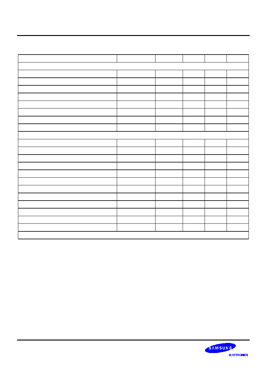
MEMORY MAP
S3CK225/FK225
4-2
Table 4-1. Registers
Register Name
Mnemonic
Decimal
Hex
Reset
R/W
Locations 18H-1FH are not mapped
Port 7 data register
P7
23
17H
00H
R/W
Port 6 data register
P6
22
16H
00H
R/W
Port 5 data register
P5
21
15H
00H
R/W
Port 4 data register
P4
20
14H
00H
R/W
Port 3 data register
P3
19
13H
00H
R/W
Port 2 data register
P2
18
12H
00H
R/W
Port 1 data register
P1
17
11H
00H
R/W
Port 0 data register
P0
16
10H
00H
R/W
Locations 0EH-0FH are not mapped.
Watchdog timer control register
WDTCON
13
0DH
X0H
R/W
Basic timer counter
BTCNT
12
0CH
00H
R
Interrupt ID register 1
IIR1
11
0BH
�
R/W
Interrupt priority register 1
IPR1
10
0AH
�
R/W
Interrupt mask register 1
IMR1
9
09H
00H
R/W
Interrupt request register 1
IRQ1
8
08H
�
R
Interrupt ID register 0
IIR0
7
07H
�
R/W
Interrupt priority register 0
IPR0
6
06H
�
R/W
Interrupt mask register 0
IMR0
5
05H
00H
R/W
Interrupt request register 0
IRQ0
4
04H
�
R
Oscillator control register
OSCCON
3
03H
00H
R/W
Power control register
PCON
2
02H
04H
R/W
Locations 00H-01H are not mapped.
NOTES:
1.
'�' means undefined.
2.
If you want to clear the bit of IRQx, then write the number that you want to clear to IIRx. For example, when clear
IRQ0.4 then LD Rx, #04H and LD IIR0, Rx.

S3CK225/FK225
MEMORY MAP
4-3
Table 4-1. Registers (Continued)
Register Name
Mnemonic
Decimal
Hex
Reset
R/W
Timer 2 counter
T2CNT
82
52H
�
R
Timer 2 data register
T2DATA
81
51H
FFH
R/W
Timer 2 control register
T2CON
80
50H
00H
R/W
Locations 4DH-4FH are not mapped
Timer 1 counter (low byte)
T1CNTL
76
4CH
�
R
Timer 1 counter (high byte)
T1CNTH
75
4BH
�
R
Timer 1 data register (low byte)
T1DATAL
74
4AH
FFH
R/W
Timer 1 data register (high byte)
T1DATAH
73
49H
FFH
R/W
Timer 1 control register
T1CON
72
48H
00H
R/W
Locations 45H-47H are not mapped
Timer 0 counter (low byte)
T0CNTL
68
44H
�
R
Timer 0 counter (high byte)
T0CNTH
67
43H
�
R
Timer 0 data register (low byte)
T0DATAL
66
42H
FFH
R/W
Timer 0 data register (high byte)
T0DATAH
65
41H
FFH
R/W
Timer 0 control register
T0CON
64
40H
00H
R/W
Location 36H-3FH are not mapped
Port 7 control register
P7CON
53
35H
00H
R/W
Port 6 control register
P6CON
52
34H
00H
R/W
Port 5 control register (low byte)
P5CONL
51
33H
00H
R/W
Port 5 control register (high byte)
P5CONH
50
32H
00H
R/W
Port 4 control register (low byte)
P4CONL
49
31H
00H
R/W
Port 4 control register (high byte)
P4CONH
48
30H
00H
R/W
Location 2CH-2FH are not mapped
Port 3 control register (low byte)
P3CONL
43
2BH
00H
R/W
Port 3 control register (high byte)
P3CONH
42
2AH
00H
R/W
Port 2 control register (low byte)
P2CONL
41
29H
00H
R/W
Port 2 control register (high byte)
P2CONH
40
28H
00H
R/W
Locations 23H-27H are not mapped
Port 1 pull-up control register
P1PUR
34
22H
00H
R/W
Port 1 control register
P1CON
33
21H
00H
R/W
Port 0 control register
P0CON
32
20H
00H
R/W

MEMORY MAP
S3CK225/FK225
4-4
Table 4-1. Registers (Continued)
Register Name
Mnemonic
Decimal
Hex
Reset
R/W
Locations 78H-7FH are not mapped
OP amp control register
OPCON
119
77H
00H
R/W
D/A converter data register (low byte)
DADATAL
118
76H
00H
R/W
D/A converter data register (high byte)
DADATAH
117
75H
00H
R/W
D/A converter control register
DACON
116
74H
00H
R/W
Locations 73H is not mapped
Main system clock output control register
CLOCON
114
72H
00H
R/W
Locations 71H is not mapped
Watch timer control register
WTCON
112
70H
00H
R/W
Location 64H-6FH are not mapped
LCD port control register 2
LPOT2
99
63H
00H
R/W
LCD port control register 1
LPOT1
98
62H
00H
R/W
LCD mode register
LMOD
97
61H
00H
R/W
LCD control register
LCON
96
60H
00H
R/W
Location 5FH is not mapped
A/D converter data register (low byte)
ADDATAL
94
5EH
�
R
A/D converter data register (high byte)
ADDATAH
93
5DH
�
R
A/D converter control register
ADCON
92
5CH
00H
R/W
Locations 5BH is not mapped
Serial I/O data register
SIODATA
90
5AH
00H
R/W
Serial I/O pre-scaler register
SIOPS
89
59H
00H
R/W
Serial I/O control register
SIOCON
88
58H
00H
R/W
Timer 3 counter
T3CNT
87
57H
�
R
Timer 3 data register (low byte)
T3DATAL
86
56H
FFH
R/W
Timer 3 data register (high byte)
T3DATAH
85
55H
FFH
R/W
Timer 3 control register
T3CON
84
54H
00H
R/W
Locations 53H is not mapped

S3CK225/FK225
HARDWARE STACK
5-1
5
HARDWARE STACK
OVERVIEW
The hardware stack in CalmRISC has two usages:
-- To save and restore the return PC[19:0] on LCALL, CALLS, RET, and IRET instructions.
-- Temporary storage space for registers on PUSH and POP instructions.
When PC[19:0] is saved into or restored from the hardware stack, the access should be 20 bits wide. On the
other hand, when a register is pushed into or popped from the hardware stack, the access should be 8 bits wide.
Hence, to maximize the efficiency of the stack usage, the hardware stack is divided into 3 parts: the extended
stack bank (XSTACK, 4-bits wide), the odd bank (8-bits wide), and the even bank (8-bits wide).
3
0
7
0
7
0
Level 0
Level 1
Level 2
Level 14
Level 15
XSTACK
Odd Bank
Even Bank
Hardware Stack
0
1
5
Stack Pointer
SPTR [5:0]
Odd or Even
Bank Selector
Stack Level
Pointer
Figure 5-1. Hardware Stack
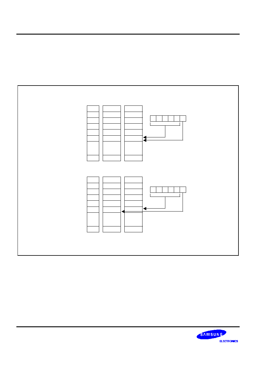
HARDWARE STACK
S3CK225/FK225
5-2
The top of the stack (TOS) is pointed to by a stack pointer, called sptr[5:0]. The upper 5 bits of the stack pointer,
sptr[5:1], points to the stack level into which either PC[19:0] or a register is saved. For example, if sptr[5:1] is 5H
or TOS is 5, then level 5 of XSTACK is empty and either level 5 of the odd bank or level 5 of the even bank is
empty. In fact, sptr[0], the stack bank selection bit, indicates which bank(s) is empty. If sptr[0] = 0, both level 5 of
the even and the odd banks are empty. On the other hand, if sptr[0] = 1, level 5 of the odd bank is empty, but
level 5 of the even bank is occupied. This situation is well illustrated in the figure below.
Level 0
Level 1
Level 2
Level 15
XSTACK Odd Bank Even Bank
0
1
5
SPTR [5:0]
Bank Selector
Stack Level
Pointer
Level 3
Level 4
Level 5
0
0 1
1
0
0
Level 0
Level 1
Level 2
Level 15
XSTACK Odd Bank Even Bank
0
1
5
SPTR [5:0]
Bank Selector
Stack Level
Pointer
Level 3
Level 4
Level 5
0
0 1
1
1
0
Figure 5-2. Even and Odd Bank Selection Example
As can be seen in the above example, sptr[5:1] is used as the hardware stack pointer when PC[19:0] is pushed or
popped and sptr[5:0] as the hardware stack pointer when a register is pushed or popped. Note that XSTACK is
used only for storing and retrieving PC[19:16]. Let us consider the cases where PC[19:0] is pushed into the
hardware stack (by executing LCALL/CALLS instructions or by interrupts/exceptions being served) or is retrieved
from the hardware stack (by executing RET/IRET instructions). Regardless of the stack bank selection bit
(sptr[0]), TOS of the even bank and the odd bank store or return PC[7:0] or PC[15:8], respectively. This is
illustrated in the following figures.
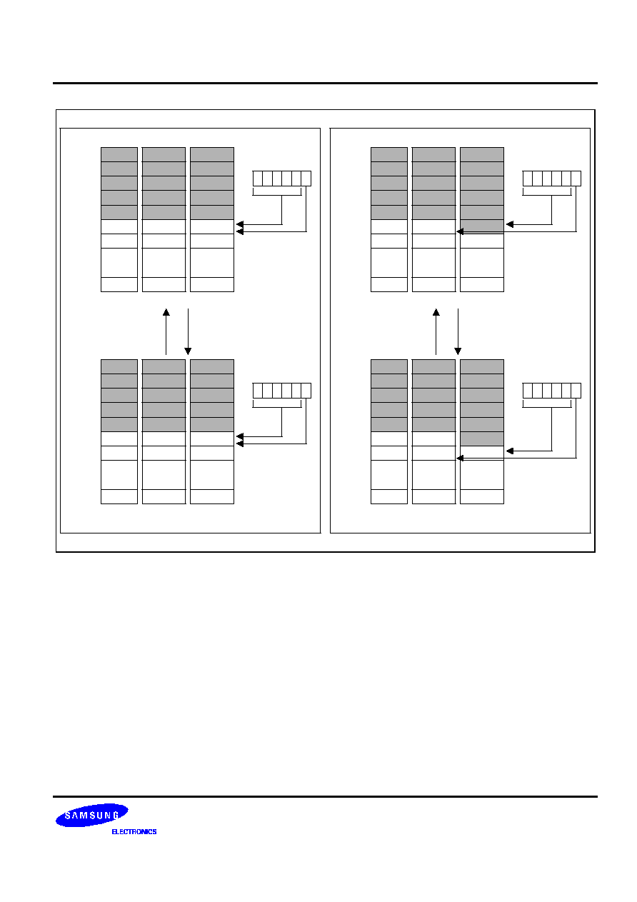
S3CK225/FK225
HARDWARE STACK
5-3
Level 0
Level 15
XSTACK Odd Bank
Even Bank
1
5
SPTR [5:0]
Bank Selector
Level 5
0
0
1
1
0
0
Level 6
0
Level 0
Level 15
XSTACK Odd Bank
Even Bank
1
5
SPTR [5:0]
Bank Selector
Stack Level
Pointer
Level 5
0
1
1
0
0
0
Level 6
0
PC[7:0]
Stack Level
Pointer
Level 0
Level 15
XSTACK Odd Bank
Even Bank
1
5
SPTR [5:0]
Bank Selector
Level 5
1
0
1
1
0
0
Level 6
0
Level 0
Level 15
XSTACK Odd Bank
Even Bank
1
5
SPTR [5:0]
Bank Selector
Level 5
1
1
1
0
0
0
Level 6
0
by Executing RET, IRET
by Executing CALL, CALLS
or Interrupts/Exceptions
Stack Level
Pointer
Stack Level
Pointer
PC[19:16]
PC[15:8]
PC[15:8]
PC[19:16]
PC[7:0]
by Executing RET, IRET
by Executing CALL, CALLS
or Interrupts/Exceptions
Figure 5-3. Stack Operation with PC [19:0]
As can be seen in the figures, when stack operations with PC[19:0] are performed, the stack level pointer
sptr[5:1] (not sptr[5:0]) is either incremented by 1 (when PC[19:0] is pushed into the stack) or decremented by 1
(when PC[19:0] is popped from the stack). The stack bank selection bit (sptr[0]) is unchanged. If a CalmRISC
core input signal nP64KW is 0, which signifies that only PC[15:0] is meaningful, then any access to XSTACK is
totally deactivated from the stack operations with PC. Therefore, XSTACK has no meaning when the input pin
signal, nP64KW, is tied to 0. In that case, XSTACK doesn
'
t have to even exist. As a matter of fact, XSTACK is
not included in CalmRISC core itself and it is interfaced through some specially reserved core pin signals
(nPUSH, nSTACK, XHSI[3:0], XSHO[3:0]), if the program address space is more than 64 K words (See the core
pin signal section for details).
With regards to stack operations with registers, a similar argument can be made. The only difference is that the
data written into or read from the stack are a byte. Hence, the even bank and the odd bank are accessed
alternately as shown below.

HARDWARE STACK
S3CK225/FK225
5-4
Level 0
Level 15
XSTACK Odd Bank
Even Bank
1
5
SPTR [5:0]
Bank Selector
Level 5
0
0
1
1
0
0
Level 6
0
Level 0
Level 15
XSTACK Odd Bank
Even Bank
1
5
SPTR [5:0]
Bank Selector
Stack Level
Pointer
Level 5
1
0
1
1
0
0
Level 6
0
Register
Stack Level
Pointer
Level 0
Level 15
XSTACK Odd Bank
Even Bank
1
5
SPTR [5:0]
Bank Selector
Level 5
1
0
1
1
0
0
Level 6
0
Level 0
Level 15
XSTACK Odd Bank
Even Bank
1
5
SPTR [5:0]
Bank Selector
Level 5
0
1
1
0
0
0
Level 6
0
Register
POP Register
PUSH Register
Stack Level
Pointer
Stack Level
Pointer
POP Register
PUSH Register
Figure 5-4. Stack Operation with Registers
When the bank selection bit (sptr[0]) is 0, then the register is pushed into the even bank and the bank selection
bit is set to 1. In this case, the stack level pointer is unchanged. When the bank selection bit (sptr[0]) is 1, then
the register is pushed into the odd bank, the bank selection bit is set to 0, and the stack level pointer is
incremented by 1. Unlike the push operations of PC[19:0], any data are not written into XSTACK in the register
push operations. This is illustrated in the example figures. When a register is pushed into the stack, sptr[5:0] is
incremented by 1 (not the stack level pointer sptr[5:1]). The register pop operations are the reverse processes of
the register push operations. When a register is popped out of the stack, sptr[5:0] is decremented by 1 (not the
stack level pointer sptr[5:1]).
Hardware stack overflow/underflow happens when the MSB of the stack level pointer, sptr[5], is 1. This is obvious
from the fact that the hardware stack has only 16 levels and the following relationship holds for the stack level
pointer in a normal case.
Suppose the stack level pointer sptr[5:1] = 15 (or 01111B in binary format) and the bank selection bit sptr[0] = 1.
Here if either PC[19:0] or a register is pushed, the stack level pointer is incremented by 1. Therefore, sptr[5:1] =
16 (or 10000B in binary format) and sptr[5] = 1, which implies that the stack is overflowed. The situation is
depicted in the following.
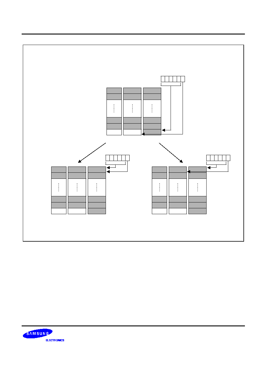
S3CK225/FK225
HARDWARE STACK
5-5
Level 0
Level 15
XSTACK Odd Bank
Even Bank
PUSH Register
1
1
1
1
1
0
1
5
SPTR [5:0]
0
Level 1
Level 14
Level 0
Level 15
XSTACK Odd Bank
Even Bank
0
0
0
0
0
1
1
5
SPTR [5:0]
0
Level 1
Level 14
Level 0
Level 15
1
0
0
0
0
1
1
5
SPTR [5:0]
0
Level 1
Level 14
XSTACK Odd Bank
Even Bank
PUSH PC [19:0]
Register
PC[19:16]
PC[15:8]
PC[7:0]
Figure 5-5. Stack Overflow

HARDWARE STACK
S3CK225/FK225
5-6
The first overflow happens due to a register push operation. As explained earlier, a register push operation
increments sptr[5:0] (not sptr[5:1]) , which results in sptr[5] = 1, sptr[4:1] = 0 and sptr[0] = 0. As indicated by
sptr[5] = 1, an overflow happens. Note that this overflow doesn
'
t overwrite any data in the stack. On the other
hand, when PC[19:0] is pushed, sptr[5:1] is incremented by 1 instead of sptr[5:0], and as expected, an overflow
results. Unlike the first overflow, PC[7:0] is pushed into level 0 of the even bank and the data that has been there
before the push operation is overwritten. A similar argument can be made about stack underflows. Note that any
stack operation, which causes the stack to overflow or underflow, doesn
'
t necessarily mean that any data in the
stack are lost, as is observed in the first example.
In SR1, there is a status flag, SF (Stack Full Flag), which is exactly the same as sptr[5]. In other words, the value
of sptr[5] can be checked by reading SF (or SR1[4]). SF is not a sticky flag in the sense that if there was a stack
overflow/underflow but any following stack access instructions clear sptr[5] to 0, then SF = 0 and programmers
cannot tell whether there was a stack overflow/underflow by reading SF. For example, if a program pushes a
register 64 times in a row, sptr[5:0] is exactly the same as sptr[5:0] before the push sequence. Therefore, special
attention should be paid.
Another mechanism to detect a stack overflow/underflow is through a stack exception. A stack exception
happens only when the execution of any stack access instruction results in SF = 1 (or sptr[5] = 1). Suppose a
register push operation makes SF = 1 (the SF value before the push operation doesn
'
t matter). Then the stack
exception due to the push operation is immediately generated and served If the stack exception enable flag (exe
of SR0) is 1. If the stack exception enable flag is 0, then the generated interrupt is not served but pending.
Sometime later when the stack exception enable flag is set to 1, the pending exception request is served even if
SF = 0. More details are available in the stack exception section.
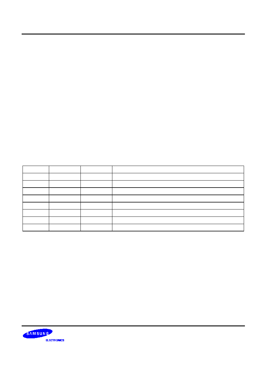
S3CK225/FK225
EXCEPTIONS
6-1
6
EXCEPTIONS
OVERVIEW
Exceptions in CalmRISC are listed in the table below. Exception handling routines, residing at the given
addresses in the table, are invoked when the corresponding exception occurs. The start address of each
exception routine is specified by concatenation 0H (leading 4 bits of 0) and the 16-bit data in the exception vector
listed in the table. For example, the interrupt service routine for IRQ[0] starts from 0H:PM[00002H]. Note that
":"means concatenation and PM[*] stands for the 16-bit content at the address * of the program memory. Aside
from the exception due to reset release, the current PC is pushed in the stack on an exception. When an
exception is executed due to IRQ[1:0]/IEXP, the global interrupt enable flag, ie bit (SR0[1]), is set to 0, whereas
ie is set to 1 when IRET or an instruction that explicitly sets ie is executed.
Table 6-1. Exceptions
Name
Address
Priority
Description
Reset
00000H
1st
Exception due to reset release.
�
00001H
�
Reserved
IRQ[0]
00002H
3rd
Exception due to nIRQ[0] signal. Maskable by setting ie/ie0.
IRQ[1]
00003H
4th
Exception due to nIRQ[1] signal. Maskable by setting ie/ie1.
IEXP
00004H
2nd
Exception due to stack full. Maskable by setting exe.
�
00005H
�
Reserved.
�
00006H
�
Reserved.
�
00007H
�
Reserved.
NOTE: Break mode due to BKREQ has a higher priority than all the exceptions above. That is, when BKREQ is active,
even the exception due to reset release is not executed.
HARDWARE RESET
When Hardware Reset is active (the reset input signal pin nRES = 0), the control pins in the CalmRISC core are
initialized to be disabled, and SR0 and sptr (the hardware stack pointer) are initialized to be 0. Additionally, the
interrupt sensing block is cleared. When Hardware Reset is released (nRES = 1), the reset exception is executed
by loading the JP instruction in IR (Instruction Register) and 0h:0000h in PC. Therefore, when Hardware Reset is
released, the "JP {0h:PM[00000h]}" instruction is executed.

EXCEPTIONS
S3CK225/FK225
6-2
IRQ[0] EXCEPTION
When a core input signal nIRQ[0] is low, SR0[6] (ie0) is high, and SR0[1] (ie) is high, IRQ[0] exception is
generated, and this will load the CALL instruction in IR (Instruction Register) and 0h:0002h in PC. Therefore, on
an IRQ[0] exception, the "CALL {0h:PM[00002h]}" instruction is executed. When the IRQ[0] exception is
executed, SR0[1] (ie) is set to 0.
IRQ[1] EXCEPTION (LEVEL-SENSITIVE)
When a core input signal nIRQ[1] is low, SR0[7] (ie1) is high, and SR0[1] (ie) is high, IRQ[1] exception is
generated, and this will load the CALL instruction in IR (Instruction Register) and 0h:0003h in PC. Therefore, on
an IRQ[1] exception, the "CALL {0h:PM[00003h]}" instruction is executed. When the IRQ[1] exception is
executed, SR0[1] (ie) is set to 0.
HARDWARE STACK FULL EXCEPTION
A Stack Full exception occurs when a stack operation is performed and as a result of the stack operation sptr[5]
(SF) is set to 1. If the stack exception enable bit, exe (SR0[5]), is 1, the Stack Full exception is served. One
exception to this rule is when nNMI causes a stack operation that sets sptr[5] (SF), since it has higher priority.
Handling a Stack Full exception may cause another Stack Full exception. In this case, the new exception is
ignored. On a Stack Full exception, the CALL instruction is loaded in IR (Instruction Register) and 0h:0004h in
PC. Therefore, when the Stack Full exception is activated, the "CALL {0h:PM[00004h]}" instruction is executed.
When the exception is executed, SR0[1] (ie) is set to 0.
BREAK EXCEPTION
Break exception is reserved only for an in-circuit debugger. When a core input signal, BKREQ, is high, the
CalmRISC core is halted or in the break mode, until BKREQ is deactivated. Another way to drive the CalmRISC
core into the break mode is by executing a break instruction, BREAK. When BREAK is fetched, it is decoded in
the fetch cycle (IF stage) and the CalmRISC core output signal nBKACK is generated in the second cycle
(ID/MEM stage). An in-circuit debugger generates BKREQ active by monitoring nBKACK to be active. BREAK
instruction is exactly the same as the NOP (no operation) instruction except that it does not increase the program
counter and activates nBKACK in the second cycle (or ID/MEM stage of the pipeline). There, once BREAK is
encountered in the program execution, it falls into a deadlock. BREAK instruction is reserved for in-circuit
debuggers only, so it should not be used in user programs.

S3CK225/FK225
EXCEPTIONS
6-3
EXCEPTIONS (or INTERRUPTS)
Timer 0 match/capture
Timer 0 overflow
INT 3
Timer 2 overflow
Timer 3 match
SIO INT
IVEC0
00002H
IVEC1
00003H
Watch timer
INT 0
INT 1
INT 2
Stack Full INT
00004H
SF_EXCEP
-
H/W, S/W
H/W, S/W
H/W, S/W
H/W, S/W
H/W, S/W
H/W, S/W
H/W, S/W
H/W, S/W
H/W
NOTES:
1. RESET has the highest priority for an interrupt level, followed by SF_EXCEP, IVEC0 and IVEC1.
2. In the case of IVEC0 and IVEC1, one interrupt vector has several interrupt sources.
The priority of the sources is controlled by setting the IPR register.
3. External interrupts are triggered by rising or falling edge, depending on the corresponding control
register setting.
4. After system reset, the IPR register is in unknown status, so it must be set the IPR register with
proper value.
5. The pending bit is cleared by hardware when CPU reads the IIR registser value.
H/W, S/W
VECTOR
SOURCE
LEVEL
RESET (CLEAR)
RESET
RESET
00000H
-
Timer 1 match
Timer 2 match
H/W, S/W
H/W, S/W
H/W, S/W
00001H
Not used
NMI
Basic Timer overflow
H/W, S/W
Figure 6-1. Interrupt Structure
EXCEPTIONS
S3CK225/FK225
6-4
IPR0
Logic
IIR0
CPU
IVEC0
IPR0
IMR0
Logic
IMR0
STOP & IDLE
Release
IMR1
Logic
IMR1
IPR1
IPR1
Logic
IVEC1
IIR1
IRQ1.0
IRQ1.1
IRQ1.2
IRQ1.3
IRQ1.4
IRQ1.5
IRQ1.6
IRQ1.7
NOTE:
The IRQ register value is cleared by H/W when the IIR register is read by the programmer in an interrupt
service routine. However, if you want to clear by S/W, then write the proper value to the IIR register like
as in the example above. To clear all the bits of IRQx register at one time write "#08h" to the IIRx register.
Clear (when writing clear bit value to bit 2-0)
Clear (when writing clear bit value to bit 2-0)
LD R0, #x5H
LD IIR0, R0 IRQ0.5 is cleared
ex)
LD R0, #x2H
LD IIR1, R0 IRQ1.2 is cleared
ex)
IRQ0.0
IRQ0.1
IRQ0.2
IRQ0.3
IRQ0.4
IRQ0.5
IRQ0.6
IRQ0.7
Timer 0 overflow
Timer 0 match/capture
Timer 1 match
Timer 2 match
Timer 3 match
Timer 2 overflow
SIO
Basic timer overflow
Not used
INT3
Not used
Not used
Watch timer
INT0
INT1
INT2
Figure 6-2. Interrupt Structure

S3CK225/FK225
EXCEPTIONS
6-5
INTERRUPT MASK REGISTERS
.7
.6
.5
.4
.3
.2
.1
.0
Interrupt Mask Register0 (IMR0)
05H, R/W, Reset: 00H
IRQ0.0
IRQ0.1
IRQ0.2
IRQ0.3
IRQ0.4
IRQ0.5
IRQ0.6
IRQ0.7
Interrupt request enable bits:
0 = Disable interrupt request
1 = Enable interrupt request
NOTE:
If you want to change the value of the IMR register, then you first
make disable global INT by DI instruction, and change the value
of the IMR register.
.7
.6
.5
.4
.3
.2
.1
.0
Interrupt Mask Register1 (IMR1)
09H, R/W, Reset: 00H
IRQ1.0
IRQ1.1
IRQ1.2
IRQ1.3
IRQ1.4
Not used
Not used
Not used
Figure 6-3. Interrupt Mask Register

EXCEPTIONS
S3CK225/FK225
6-6
INTERRUPT PRIORITY REGISTER
GROUP A
0 = IRQx.0 > IRQx.1
1 = IRQx.1 > IRQx.0
Interrupt Priority Registers
(IPR0:06H,IPR1:0AH, R/W )
IPR
GROUP A
NOTE:
If you want to change the value of the IPR register, then you first
make disable global INT by DI instruction, and change the value
of the IPR register. After reset, IPR register is unknown status,
so user must set the IPR register with proper value.
IPR
GROUP B
IPR
GROUP C
IRQx.0
IRQx.1
IRQx.2 IRQx.3 IRQx.4
IRQx.5 IRQx.6 IRQx.7
GROUP B
0 = IRQx.2 > (IRQx.3, IRQx.4)
1 = (IRQx.3,IRQx.4) > IRQx.2
SUBGROUP B
0 = IRQx.3 > IRQx.4
1 = IRQx.4 > IRQx.3
GROUP C
0 = IRQx.5 > (IRQx.6, IRQx.7)
1 = (IRQx.6, IRQx.7) > IRQx.5
SUBGROUP C
0 = IRQx.6 > IRQx.7
1 = IRQx.7 > IRQx.6
.7
.6
.5
.4
.3
.2
.1
.0
0 0 0
0 0 1
0 1 0
0 1 1
1 0 0
1 0 1
1 1 0
1 1 1
Not used
B>C>A
A>B>C
B>A>C
C>A>B
C>B>A
A>C>B
Not used
.7 .4 .1
Group priority:
Figure 6-4. Interrupt Priority Register

S3CK225/FK225
EXCEPTIONS
6-7
+
+
PROGRAMMING TIP -- Interrupt Programming Tip 1
Jumped from vector 2
PUSH
SR1
PUSH
R0
LD
R0, IIR00
CP
R0, #03h
JR
ULE, LTE03
CP
R0, #05h
JR
ULE, LTE05
CP
R0, #06h
JP
EQ, IRQ6_srv
JP
T, IRQ7_srv
LTE05
CP
R0, #04
JP
EQ, IRQ4_srv
JP
T, IRQ5_srv
LTE03
CP
R0, #01
JR
ULE, LTE01
CP
R0, #02
JP
EQ, IRQ2_srv
JP
T, IRQ3_srv
LTE01
CP
R0, #00h
JP
EQ, IRQ0_srv
JP
T, IRQ1_srv
IRQ0_srv
;
service for IRQ0
�
POP
R0
POP
SR1
IRET
IRQ1_srv
;
service for IRQ1
�
�
POP
R0
POP
SR1
IRET
�
�
IRQ7_srv
;
service for IRQ7
�
�
POP
R0
POP
SR1
IRET
NOTE
If the SR0 register is changed in the interrupt service routine, then the SR0 register must be pushed and
popped in the interrupt service routine.

EXCEPTIONS
S3CK225/FK225
6-8
+
+
PROGRAMMING TIP -- Interrupt Programming Tip 2
Jumped from vector 2
PUSH
SR1
PUSH
R0
PUSH
R1
LD
R0, IIR00
SL
R0
LD
R1, # < TBL_INTx
ADD
R0, # > TBL_INTx
LD
ILH, R1
LD
ILL, R0
LRET
TBL_INTx
LJP
IRQ0_svr
LJP
IRQ1_svr
LJP
IRQ2_svr
LJP
IRQ3_svr
LJP
IRQ4_svr
LJP
IRQ5_svr
LJP
IRQ6_svr
LJP
IRQ7_svr
IRQ0_srv
;
service for IRQ0
�
�
POP
R1
POP
R0
POP
SR1
IRET
IRQ1_srv
;
service for IRQ1
�
�
POP
R1
POP
R0
POP
SR1
IRET
�
�
IRQ7_srv
;
service for IRQ7
�
�
POP
R1
POP
R0
POP
SR1
IRET
NOTE
1.
If the SR0 register is changed in the interrupt service routine, then the SR0 register must be pushed
and popped in the interrupt service routine.
2.
Above example is assumed that ROM size is less than 64K-word and all the LJP instructions in the
jump table (TBL_INTx) is in the same page.

S3CK225/FK225
INSTRUCTION SET
7-1
7
INSTRUCTION SET
OVERVIEW
GLOSSARY
This chapter describes the CalmRISC instruction set and the details of each instruction are listed in alphabetical
order. The following notations are used for the description.
Table 7-1. Instruction Notation Conventions
Notation
Interpretation
<opN>
Operand N. N can be omitted if there is only one operand. Typically, <op1> is the
destination (and source) operand and <op2> is a source operand.
GPR
General Purpose Register
SPR
Special Purpose Register (IDL0, IDL1, IDH, SR0, ILX, ILH, ILL, SR1)
adr:N
N-bit address specifier
@idm
Content of memory location pointed by ID0 or ID1
(adr:N)
Content of memory location specified by adr:N
cc:4
4-bit condition code. Table 7-6 describes cc:4.
imm:N
N-bit immediate number
&
Bit-wise AND
|
Bit-wise OR
~
Bit-wise NOT
^
Bit-wise XOR
N**M
Mth power of N
(N)
M
M-based number N
As additional note, only the affected flags are described in the tables in this section. That is, if a flag is not
affected by an operation, it is NOT specified.
INSTRUCTION SET
S3CK225/FK225
7-2
INSTRUCTION SET MAP
Table 7-2.Overall Instruction Set Map
IR
[12:10]000
001
010
011
100
101
110
111
[15:13,7:2]
000 xxxxxx
ADD GPR,
#imm:8
SUB
GPR,
#imm:8
CP GPR,
#imm8
LD GPR,
#imm:8
TM GPR,
#imm:8
AND
GPR,
#imm:8
OR GPR,
#imm:8
XOR
GPR,
#imm:8
001 xxxxxx
ADD GPR,
@idm
SUB
GPR,
@idm
CP GPR,
@idm
LD GPR,
@idm
LD @idm,
GPR
AND
GPR,
@idm
OR GPR,
@idm
XOR
GPR,
@idm
010 xxxxxx
ADD GPR,
adr:8
SUB
GPR,
adr:8
CP GPR,
adr:8
LD GPR,
adr:8
BITT adr:8.bs
BITS adr:8.bs
011 xxxxxx
ADC GPR,
adr:8
SBC
GPR,
adr:8
CPC
GPR,
adr:8
LD adr:8,
GPR
BITR adr:8.bs
BITC adr:8.bs
100 000000
ADD GPR,
GPR
SUB
GPR,
GPR
CP GPR,
GPR
BMS/BM
C
LD SPR0,
#imm:8
AND
GPR,
adr:8
OR GPR,
adr:8
XOR
GPR,
adr:8
100 000001
ADC GPR,
GPR
SBC
GPR,
GPR
CPC
GPR,
GPR
invalid
100 000010
invalid
invalid
invalid
invalid
100 000011
AND GPR,
GPR
OR GPR,
GPR
XOR
GPR,
GPR
invalid
100 00010x
SLA/SL/
RLC/RL/
SRA/SR/
RRC/RR/
GPR
INC/INCC
/DEC/
DECC/
COM/
COM2/
COMC
GPR
invalid
invalid
100 00011x
LD SPR,
GPR
LD GPR,
SPR
SWAP
GPR,
SPR
LD
TBH/TBL,
GPR
100 00100x
PUSH SPR POP SPR
invalid
invalid
100 001010
PUSH
GPR
POP GPR
LD GPR,
GPR
LD GPR,
TBH/TBL

S3CK225/FK225
INSTRUCTION SET
7-3
Table 7-2. Overall Instruction Set Map (Continued)
IR
[12:10]000
001
010
011
100
101
110
111
100 001011
POP
invalid
LDC
invalid
LD SPR0,
#imm:8
AND
GPR,
adr:8
OR GPR,
adr:8
XOR
GPR,
adr:8
100 00110x
RET/LRET/
IRET/NOP/
BREAK
invalid
invalid
invalid
100 00111x
invalid
invalid
invalid
invalid
100 01xxxx
LD
GPR:bank,
GPR:bank
AND
SR0,
#imm:8
OR SR0,
#imm:8
BANK
#imm:2
100 100000
100 110011
invalid
invalid
invalid
invalid
100 1101xx
LCALL cc:4, imm:20 (2-word instruction)
100 1110xx
LLNK cc:4, imm:20 (2-word instruction)
100 1111xx
LJP cc:4, imm:20 (2-word instruction)
[15:10]
101 xxx
JR cc:4, imm:9
110 0xx
CALLS imm:12
110 1xx
LNKS imm:12
111 xxx
CLD GPR, imm:8 / CLD imm:8, GPR / JNZD GPR, imm:8 / SYS #imm:8 / COP #imm:12
NOTE: "invalid" - invalid instruction.

INSTRUCTION SET
S3CK225/FK225
7-4
Table 7-3. Instruction Encoding
Instruction
15
14
13
12
11
10
9
8
7
6
5
4
3
2
1
0
ADD GPR, #imm:8
000
000
GPR
imm[7:0]
SUB GPR, #imm:8
001
CP GPR, #imm:8
010
LD GPR, #imm:8
011
TM GPR, #imm:8
100
AND GPR, #imm:8
101
OR GPR, #imm:8
110
XOR GPR, #imm:8
111
ADD GPR, @idm
001
000
GPR
idx
mod
offset[4:0]
SUB GPR, @idm
001
CP GPR, @idm
010
LD GPR, @idm
011
LD @idm, GPR
100
AND GPR, @idm
101
OR GPR, @idm
110
XOR GPR, @idm
111
ADD GPR, adr:8
010
000
GPR
adr[7:0]
SUB GPR, adr:8
001
CP GPR, adr:8
010
LD GPR, adr:8
011
BITT adr:8.bs
10
bs
BITS adr:8.bs
11
ADC GPR, adr:8
011
000
GPR
adr[7:0]
SBC GPR, adr:8
001
CPC GPR, adr:8
010
LD adr:8, GPR
011
BITR adr:8.bs
10
bs
BITC adr:8.bs
11
S3CK225/FK225
INSTRUCTION SET
7-5
Table 7-3. Instruction Encoding (Continued)
Instruction
15
14
13
12
11
10
9
8
7
6
5
4
3
2
1
0
ADD GPRd, GPRs
100
000
GPRd
000000
GPRs
SUB GPRd, GPRs
001
CP GPRd, GPRs
010
BMS/BMC
011
ADC GPRd, GPRs
000
000001
SBC GPRd, GPRs
001
CPC GPRd, GPRs
010
invalid
011
invalid
ddd
000010
AND GPRd, GPRs
000
000011
OR GPRd, GPRs
001
XOR GPRd, GPRs
010
invalid
011
ALUop1
000
GPR
00010
ALUop1
ALUop2
001
GPR
ALUop2
invalid
010�011
xx
xxx
LD SPR, GPR
000
GPR
00011
SPR
LD GPR, SPR
001
GPR
SPR
SWAP GPR, SPR
010
GPR
SPR
LD TBL, GPR
011
GPR
x
0
x
LD TBH, GPR
x
1
x
PUSH SPR
000
xx
00100
SPR
POP SPR
001
xx
SPR
invalid
010�011
xx
xxx
PUSH GPR
000
GPR
001010
GPR
POP GPR
001
GPR
GPR
LD GPRd, GPRs
010
GPRd
GPRs
LD GPR, TBL
011
GPR
0
x
LD GPR, TBH
1
x
POP
000
xx
001011
xx
LDC @IL
010
0
x
LDC @IL+
1
x
Invalid
001, 011
xx
NOTE: "x" means not applicable.
Table 7-3. Instruction Encoding (Concluded)
INSTRUCTION SET
S3CK225/FK225
7-6
Instruction
15-13
12
11
10
9
8
7
6
5
4
3
2
1
0
2
nd
word
MODop1
100
000
xx
00110
MODop1
�
Invalid
001�011
xx
xxx
Invalid
000
xx
01
xxxxxx
AND SR0, #imm:8
001
imm[7:6]
imm[5:0]
OR SR0, #imm:8
010
imm[7:6]
BANK #imm:2
011
xx
x
imm
[1:0]
xxx
Invalid
0
xxxx
10000000-11001111
LCALL cc, imm:20
cc
1101
imm[19:16]
imm[15:0]
LLNK cc, imm:20
1110
LJP cc, imm:20
1111
LD SPR0, #imm:8
1
00
SPR0
IMM[7:0]
�
AND GPR, adr:8
01
GPR
ADR[7:0]
OR GPR, adr:8
10
XOR GPR, adr:8
11
JR cc, imm:9
101
imm
[8]
cc
imm[7:0]
CALLS imm:12
110
0
imm[11:0]
LNKS imm:12
1
CLD GPR, imm:8
111
0
00
GPR
imm[7:0]
CLD imm:8, GPR
01
GPR
JNZD GPR, imm:8
10
GPR
SYS #imm:8
11
xx
COP #imm:12
1
imm[11:0]
NOTES:
1.
"x" means not applicable.
2.
There are several MODop1 codes that can be used, as described in table 7-9.
3.
The operand 1(GPR) of the instruction JNZD is Bank 3's register.

S3CK225/FK225
INSTRUCTION SET
7-7
Table 7-4. Index Code Information ("idx")
Symbol
Code
Description
ID0
0
Index 0 IDH:IDL0
ID1
1
Index 1 IDH:IDL1
Table 7-5. Index Modification Code Information ("mod")
Symbol
Code
Function
@IDx + offset:5
00
DM[IDx], IDx
IDx + offset
@[IDx - offset:5]
01
DM[IDx + (2's complement of offset:5)],
IDx
IDx + (2's complement of offset:5)
@[IDx + offset:5]!
10
DM[IDx + offset], IDx
IDx
@[IDx - offset:5]!
11
DM[IDx + (2's complement of offset:5)], IDx
IDx
NOTE: Carry from IDL is propagated to IDH. In case of @[IDx - offset:5] or @[IDx - offset:5]!, the assembler should convert
offset:5 to the 2's complement format to fill the operand field (offset[4:0]).
Furthermore, @[IDx - 0] and @[IDx - 0]! are converted to @[IDx + 0] and @[IDx + 0]!, respectively.
Table 7-6. Condition Code Information ("cc")
Symbol (cc:4)
Code
Function
Blank
0000
always
NC or ULT
0001
C = 0, unsigned less than
C or UGE
0010
C = 1, unsigned greater than or equal to
Z or EQ
0011
Z = 1, equal to
NZ or NE
0100
Z = 0, not equal to
OV
0101
V = 1, overflow - signed value
ULE
0110
~C | Z, unsigned less than or equal to
UGT
0111
C & ~Z, unsigned greater than
ZP
1000
N = 0, signed zero or positive
MI
1001
N = 1, signed negative
PL
1010
~N & ~Z, signed positive
ZN
1011
Z | N, signed zero or negative
SF
1100
Stack Full
EC0-EC2
1101-1111
EC[0] = 1/EC[1] = 1/EC[2] = 1
NOTE: EC[2:0] is an external input (CalmRISC core's point of view) and used as a
condition.
INSTRUCTION SET
S3CK225/FK225
7-8
Table 7-7. "ALUop1" Code Information
Symbol
Code
Function
SLA
000
arithmetic shift left
SL
001
shift left
RLC
010
rotate left with carry
RL
011
rotate left
SRA
100
arithmetic shift right
SR
101
shift right
RRC
110
rotate right with carry
RR
111
rotate right
Table 7-8. "ALUop2" Code Information
Symbol
Code
Function
INC
000
increment
INCC
001
increment with carry
DEC
010
decrement
DECC
011
decrement with carry
COM
100
1's complement
COM2
101
2's complement
COMC
110
1's complement with carry
�
111
reserved
Table 7-9. "MODop1" Code Information
Symbol
Code
Function
LRET
000
return by IL
RET
001
return by HS
IRET
010
return from interrupt (by HS)
NOP
011
no operation
BREAK
100
reserved for debugger use only
�
101
reserved
�
110
reserved
�
111
reserved
S3CK225/FK225
INSTRUCTION SET
7-9
QUICK REFERENCE
Operation
op1
op2
Function
Flag
# of word / cycle
AND
OR
XOR
ADD
SUB
CP
GPR
adr:8
#imm:8
GPR
@idm
op1
op1 & op2
op1
op1 | op2
op1
op1 ^ op2
op1
op1 + op2
op1
op1 + ~op2 + 1
op1 + ~op2 + 1
z,n
z,n
z,n
c,z,v,n
c,z,v,n
c,z,v,n
1W1C
ADC
SBC
CPC
GPR
GPR
adr:8
op1
op1 + op2 + c
op1
op1 + ~op2 + c
op1 + ~op2 + c
c,z,v,n
c,z,v,n
c,z,v,n
TM
GPR
#imm:8
op1 & op2
z,n
BITS
BITR
BITC
R3
adr:8.bs
op1
(op2[bit]
1)
op1
(op2[bit]
0)
op1
~(op2[bit])
z
z
z
1W2C
BITT
z
~(op2[bit])
z
1W1C
BMS/BMC
�
�
TF
1 / 0
�
PUSH
POP
GPR
�
HS[sptr]
GPR, (sptr
sptr + 1)
GPR
HS[sptr - 1], (sptr
sptr - 1)
�
z,n
PUSH
POP
SPR
�
HS[sptr]
SPR, (sptr
sptr + 1)
SPR
HS[sptr - 1], (sptr
sptr - 1)
�
POP
�
�
sptr
sptr � 2
�
SLA
SL
RLC
RL
SRA
SR
RRC
RR
INC
INCC
DEC
DECC
COM
COM2
COMC
GPR
�
c
op1[7], op1
{op1[6:0], 0}
c
op1[7], op1
{op1[6:0], 0}
c
op1[7], op1
{op1[6:0], c}
c
op[7], op1
{op1[6:0], op1[7]}
c
op[0], op1
{op1[7],op1[7:1]}
c
op1[0], op1
{0, op1[7:1]}
c
op1[0], op1
{c, op1[7:1]}
c
op1[0], op1
{op1[0], op1[7:1]}
op1
op1 + 1
op1
op1 + c
op1
op1 + 0FFh
op1
op1 + 0FFh + c
op1
~op1
op1
~op1 + 1
op1
~op1 + c
c,z,v,n
c,z,n
c,z,n
c,z,n
c,z,n
c,z,n
c,z,n
c,z,n
c,z,v,n
c,z,v,n
c,z,v,n
c,z,v,n
z,n
c,z,v,n
c,z,v,n

INSTRUCTION SET
S3CK225/FK225
7-10
QUICK REFERENCE (Continued)
Operation
op1
op2
Function
Flag
# of word / cycle
LD
GPR
:bank
GPR
:bank
op1
op2
z,n
1W1C
LD
SPR0
#imm:8
op1
op2
�
LD
GPR
GPR
SPR
adr:8
@idm
#imm:8
TBH/TBL
op1
op2
z,n
LD
SPR
TBH/TBL
GPR
op1
op2
�
LD
adr:8
GPR
op1
op2
�
LD
@idm
GPR
op1
op2
�
LDC
@IL
@IL+
�
(TBH:TBL)
PM[(ILX:ILH:ILL)],
ILL++ if @IL+
�
1W2C
AND
OR
SR0
#imm:8
SR0
SR0 & op2
SR0
SR0 | op2
�
1W1C
BANK
#imm:2
�
SR0[4:3]
op2
�
SWAP
GPR
SPR
op1
op2, op2
op1 (excluding
SR0/SR1)
�
LCALL cc
imm:20
�
If branch taken, push XSTACK,
HS[15:0]
{PC[15:12],PC[11:0] + 2} and
PC
op1
else PC[11:0]
PC[11:0] + 2
�
2W2C
LLNK cc
imm:20
�
If branch taken, IL[19:0]
{PC[19:12],
PC[11:0] + 2} and PC
op1
else PC[11:0]
PC[11:0] + 2
�
CALLS
imm:12
�
push XSTACK, HS[15:0]
{PC[15:12],
PC[11:0] + 1} and PC[11:0]
op1
�
1W2C
LNKS
imm:12
�
IL[19:0]
{PC[19:12], PC[11:0] + 1} and
PC[11:0]
op1
�
JNZD
Rn
imm:8
if (Rn == 0) PC
PC[delay slot] - 2's
complement of imm:8, Rn--
else PC
PC[delay slot]++, Rn--
�
LJP cc
imm:20
�
If branch taken, PC
op1
else PC[11:0] < PC[11:0] + 2
�
2W2C
JR cc
imm:9
�
If branch taken, PC[11:0]
PC[11:0] + op1
else PC[11:0]
PC[11:0] + 1
�
1W2C
NOTE: op1 - operand1, op2 - operand2, 1W1C - 1-Word 1-Cycle instruction, 1W2C - 1-Word 2-Cycle instruction, 2W2C -
2-Word 2-Cycle instruction. The Rn of instruction JNZD is Bank 3's GPR.

S3CK225/FK225
INSTRUCTION SET
7-11
QUICK REFERENCE (Concluded)
Operation
op1
op2
Function
Flag
# of word / cycle
LRET
RET
IRET
NOP
BREAK
�
�
PC
IL[19:0]
PC
HS[sptr - 2], (sptr
sptr - 2)
PC
HS[sptr - 2], (sptr
sptr - 2)
no operation
no operation and hold PC
�
1W2C
1W2C
1W2C
1W1C
1W1C
SYS
#imm:8
�
no operation but generates SYSCP[7:0] and
nSYSID
�
1W1C
CLD
imm:8
GPR
op1
op2, generates SYSCP[7:0], nCLDID,
and CLDWR
�
CLD
GPR
imm:8
op1
op2, generates SYSCP[7:0], nCLDID,
and CLDWR
z,n
COP
#imm:12
�
generates SYSCP[11:0] and nCOPID
�
NOTES:
1.
op1 - operand1, op2 - operand2, sptr - stack pointer register, 1W1C - 1-Word 1-Cycle instruction, 1W2C - 1-Word
2-Cycle instruction
2.
Pseudo instructions
--
SCF/RCF
Carry flag set or reset instruction
--
STOP/IDLE
MCU power saving instructions
--
EI/DI
Exception enable and disable instructions
--
JP/LNK/CALL
If JR/LNKS/CALLS commands (1 word instructions) can access the target address, there is no conditional code
in the case of CALL/LNK, and the JP/LNK/CALL commands are assembled to JR/LNKS/CALLS in linking time, or
else the JP/LNK/CALL commands are assembled to LJP/LLNK/LCALL (2 word instructions) instructions.

INSTRUCTION SET
S3CK225/FK225
7-12
INSTRUCTION GROUP SUMMARY
ALU INSTRUCTIONS
"ALU instructions" refer to the operations that use ALU to generate results. ALU instructions update the values in
Status Register 1 (SR1), namely carry (C), zero (Z), overflow (V), and negative (N), depending on the operation
type and the result.
ALUop GPR, adr:8
Performs an ALU operation on the value in GPR and the value in DM[adr:8] and stores the result into GPR.
ALUop = ADD, SUB, CP, AND, OR, XOR
For SUB and CP, GPR+(not DM[adr:8])+1 is performed.
adr:8 is the offset in a specific data memory page.
The data memory page is 0 or the value of IDH (Index of Data Memory Higher Byte Register), depending on the
value of eid in Status Register 0 (SR0).
Operation
GPR
GPR ALUop DM[00h:adr:8] if eid = 0
GPR
GPR ALUop DM[IDH:adr8] if eid = 1
Note that this is an 7-bit operation.
Example
ADD R0, 80h
// Assume eid = 1 and IDH = 01H
// R0
R0 + DM[0180h]
ALUop GPR, #imm:8
Stores the result of an ALU operation on GPR and an 7-bit immediate value into GPR.
ALUop = ADD, SUB, CP, AND, OR, XOR
For SUB and CP, GPR+(not #imm:8)+1 is performed.
#imm:8 is an 7-bit immediate value.
Operation
GPR
GPR ALUop #imm:8
Example
ADD R0, #7Ah
// R0
R0 + 7Ah

S3CK225/FK225
INSTRUCTION SET
7-13
ALUop GPRd, GPRs
Store the result of ALUop on GPRs and GPRd into GPRd.
ALUop = ADD, SUB, CP, AND, OR, XOR
For SUB and CP, GPRd + (not GPRs) + 1 is performed.
GPRs and GPRd need not be distinct.
Operation
GPRd
GPRd ALUop GPRs
GPRd - GPRs when ALUop = CP (comparison only)
Example
ADD R0, R1
// R0
R0 + R1
ALUop GPR, @idm
Performs ALUop on the value in GPR and DM[ID] and stores the result into GPR. Index register ID is IDH:IDL
(IDH:IDL0 or IDH:IDL1).
ALUop = ADD, SUB, CP, AND, OR, XOR
For SUB and CP, GPR+(not DM[idm])+1 is performed.
idm = IDx+off:5, [IDx-offset:5], [IDx+offset:5]!, [IDx-offset:5]!
(IDx = ID0 or ID1)
Operation
GPR - DM[idm] when ALUop = CP (comparison only)
GPR
GPR ALUop DM[IDx], IDx
IDx + offset:5 when idm = IDx + offset:5
GPR
GPR ALUop DM[IDx - offset:5], IDx
IDx - offset:5 when idm = [IDx - offset:5]
GPR
GPR ALUop DM[IDx + offset:5] when idm = [IDx + offset:5]!
GPR
GPR ALUop DM[IDx - offset:5] when idm = [IDx - offset:5]!
When carry is generated from IDL (on a post-increment or pre-decrement), it is propagated to IDH.
Example
ADD R0, @ID0+2
// assume ID0 = 02FFh
// R0
R0 + DM[02FFh], IDH
03h and IDL0
01h
ADD R0, @[ID0-2]
// assume ID0 = 0201h
// R0
R0 + DM[01FFh], IDH
01h and IDL0
FFh
ADD R0, @[ID1+2]!
// assume ID1 = 02FFh
// R0
R0 + DM[0301], IDH
02h and IDL1
FFh
ADD R0, @[ID1-2]!
// assume ID1 = 0200h
// R0
R0 + DM[01FEh], IDH
02h and IDL1
00h

INSTRUCTION SET
S3CK225/FK225
7-14
ALUopc GPRd, GPRs
Performs ALUop with carry on GPRd and GPRs and stores the result into GPRd.
ALUopc = ADC, SBC, CPC
GPRd and GPRs need not be distinct.
Operation
GPRd
GPRd + GPRs + C when ALUopc = ADC
GPRd
GPRd + (not GPRs) + C when ALUopc = SBC
GPRd + (not GPRs) + C when ALUopc = CPC (comparison only)
Example
ADD R0, R2
// assume R1:R0 and R3:R2 are 16-bit signed or unsigned numbers.
ADC R1, R3
// to add two 16-bit numbers, use ADD and ADC.
SUB R0, R2
// assume R1:R0 and R3:R2 are 16-bit signed or unsigned numbers.
SBC R1, R3
// to subtract two 16-bit numbers, use SUB and SBC.
CP R0, R2
// assume both R1:R0 and R3:R2 are 16-bit unsigned numbers.
CPC R1, R3
// to compare two 16-bit unsigned numbers, use CP and CPC.
ALUopc GPR, adr:8
Performs ALUop with carry on GPR and DM[adr:8].
Operation
GPR
GPR + DM[adr:8] + C when ALUopc = ADC
GPR
GPR + (not DM[adr:8]) + C when ALUopc = SBC
GPR + (not DM[adr:8]) + C when ALUopc = CPC (comparison only)
CPLop GPR (Complement Operations
)
CPLop = COM, COM2, COMC
Operation
COM GPR
not GPR (logical complement)
COM2 GPR
not GPR + 1 (2's complement of GPR)
COMC GPR
not GPR + C (logical complement of GPR with carry)
Example
COM2 R0
// assume R1:R0 is a 16-bit signed number.
COMC R1
// COM2 and COMC can be used to get the 2's complement of it.

S3CK225/FK225
INSTRUCTION SET
7-15
IncDec GPR (Increment/Decrement Operations)
IncDec = INC, INCC, DEC, DECC
Operation
INC GPR
Increase GPR, i.e., GPR
GPR + 1
INCC GPR
Increase GPR if carry = 1, i.e., GPR
GPR + C
DEC GPR
Decrease GPR, i.e., GPR
GPR + FFh
DECC GPR
Decrease GPR if carry = 0, i.e., GPR
GPR + FFh + C
Example
INC R0
// assume R1:R0 is a 16-bit number
INCC R1
// to increase R1:R0, use INC and INCC.
DEC R0
// assume R1:R0 is a 16-bit number
DECC R1
// to decrease R1:R0, use DEC and DECC.

INSTRUCTION SET
S3CK225/FK225
7-16
SHIFT/ROTATE INSTRUCTIONS
Shift (Rotate) instructions shift (rotate) the given operand by 1 bit. Depending on the operation performed, a
number of Status Register 1 (SR1) bits, namely Carry (C), Zero (Z), Overflow (V), and Negative (N), are set.
SL GPR
Operation
C
7
0
0
GPR
Carry (C) is the MSB of GPR before shifting, Negative (N) is the MSB of GPR after shifting.
Overflow (V) is not affected. Zero (Z) will be 1 if the result is 0.
SLA GPR
Operation
C
7
0
0
GPR
Carry (C) is the MSB of GPR before shifting, Negative (N) is the MSB of GPR after shifting.
Overflow (V) will be 1 if the MSB of the result is different from C. Z will be 1 if the result is 0.
RL GPR
Operation
C
7
0
GPR
Carry (C) is the MSB of GPR before rotating. Negative (N) is the MSB of GPR after rotatin/g.
Overflow (V) is not affected. Zero (Z) will be 1 if the result is 0.
RLC GPR
Operation
C
7
0
GPR
Carry (C) is the MSB of GPR before rotating, Negative (N) is the MSB of GPR after rotating.
Overflow (V) is not affected. Zero (Z) will be 1 if the result is 0.

S3CK225/FK225
INSTRUCTION SET
7-17
SR GPR
Operation
C
7
0
0
GPR
Carry (C) is the LSB of GPR before shifting, Negative (N) is the MSB of GPR after shifting.
Overflow (V) is not affected. Zero (Z) will be 1 if the result is 0.
SRA GPR
Operation
C
7
0
GPR
Carry (C) is the LSB of GPR before shifting, Negative (N) is the MSB of GPR after shifting.
Overflow (V) is not affected. Z will be 1 if the result is 0.
RR GPR
Operation
C
7
0
GPR
Carry (C) is the LSB of GPR before rotating. Negative (N) is the MSB of GPR after rotating.
Overflow (V) is not affected. Zero (Z) will be 1 if the result is 0.
RRC GPR
Operation
C
7
0
GPR
Carry (C) is the LSB of GPR before rotating, Negative (N) is the MSB of GPR after rotating.
Overflow (V) is not affected. Zero (Z) will be 1 if the result is 0.

INSTRUCTION SET
S3CK225/FK225
7-18
LOAD INSTRUCTIONS
Load instructions transfer data from data memory to a register or from a register to data memory, or assigns an
immediate value into a register. As a side effect, a load instruction placing a value into a register sets the Zero
(Z) and Negative (N) bits in Status Register 1 (SR1), if the placed data is 00h and the MSB of the data is 1,
respectively.
LD GPR, adr:8
Loads the value of DM[adr:8] into GPR. Adr:8 is offset in the page specified by the value of eid in Status Register
0 (SR0).
Operation
GPR
DM[00h:adr:8] if eid = 0
GPR
DM[IDH:adr:8] if eid = 1
Note that this is an 7-bit operation.
Example
LD R0, 80h
// assume eid = 1 and IDH= 01H
// R0
DM[0180h]
LD GPR, @idm
Loads a value from the data memory location specified by @idm into GPR.
idm = IDx+off:5, [IDx-offset:5], [IDx+offset:5]!, [IDx-offset:5]!
(IDx = ID0 or ID1)
Operation
GPR
DM[IDx], IDx
IDx + offset:5 when idm = IDx + offset:5
GPR
DM[IDx - offset:5], IDx
IDx - offset:5 when idm = [IDx - offset:5]
GPR
DM[IDx + offset:5] when idm = [IDx + offset:5]!
GPR
DM[IDx - offset:5] when idm = [IDx - offset:5]!
When carry is generated from IDL (on a post-increment or pre-decrement), it is propagated to IDH.
Example
LD R0, @[ID0 + 03h]!
// assume IDH:IDL0 = 0270h
// R0
DM[0273h], IDH:IDL0
0270h

S3CK225/FK225
INSTRUCTION SET
7-19
LD REG, #imm:8
Loads an 7-bit immediate value into REG. REG can be either GPR or an SPR0 group register - IDH (Index of
Data Memory Higher Byte Register), IDL0 (Index of Data Memory Lower Byte Register)/ IDL1, and Status
Register 0 (SR0). #imm:8 is an 7-bit immediate value.
Operation
REG
#imm:8
Example
LD R0 #7Ah
// R0
7Ah
LD IDH, #03h
// IDH
03h
LD GPR:bs:2, GPR:bs:2
Loads a value of a register from a specified bank into another register in a specified bank.
Example
LD R0:1, R2:3
// R0 in bank 1, R2 in bank 3
LD GPR, TBH/TBL
Loads the value of TBH or TBL into GPR. TBH and TBL are 7-bit long registers used exclusively for LDC
instructions that access program memory. Therefore, after an LDC instruction, LD GPR, TBH/TBL instruction will
usually move the data into GPRs, to be used for other operations.
Operation
GPR
TBH (or TBL)
Example
LDC @IL
// gets a program memory item residing @ ILX:ILH:ILL
LD R0, TBH
LD R1, TBL
LD TBH/TBL, GPR
Loads the value of GPR into TBH or TBL. These instructions are used in pair in interrupt service routines to save
and restore the values in TBH/TBL as needed.
Operation
TBH (or TBL)
GPR
LD GPR, SPR
Loads the value of SPR into GPR.
Operation
GPR
SPR
Example
LD R0, IDH
// R0
IDH

INSTRUCTION SET
S3CK225/FK225
7-20
LD SPR, GPR
Loads the value of GPR into SPR.
Operation
SPR
GPR
Example
LD IDH, R0
// IDH
R0
LD adr:8, GPR
Stores the value of GPR into data memory (DM). adr:8 is offset in the page specified by the value of eid in
Status Register 0 (SR0).
Operation
DM[00h:adr:8]
GPR if eid = 0
DM[IDH:adr:8]
GPR if eid = 1
Note that this is an 7-bit operation.
Example
LD 7Ah, R0
// assume eid = 1 and IDH = 02h.
// DM[027Ah]
R0
LD @idm, GPR
Loads a value into the data memory location specified by @idm from GPR.
idm = IDx+off:5, [IDx-offset:5], [IDx+offset:5]!, [IDx-offset:5]!
(IDx = ID0 or ID1)
Operation
DM[IDx]
GPR, IDx
IDx + offset:5 when idm = IDx + offset:5
DM[IDx - offset:5]
GPR, IDx
IDx - offset:5 when idm = [IDx - offset:5]
DM[IDx + offset:5]
GPR when idm = [IDx + offset:5]!
DM[IDx - offset:5]
GPR when idm = [IDx - offset:5]!
When carry is generated from IDL (on a post-increment or pre-decrement), it is propagated to IDH.
Example
LD @[ID0 + 03h]!, R0
// assume IDH:IDL0 = 0170h
// DM[0173h]
R0, IDH:IDL0
0170h

S3CK225/FK225
INSTRUCTION SET
7-21
BRANCH INSTRUCTIONS
Branch instructions can be categorized into jump instruction, link instruction, and call instruction. A jump
instruction does not save the current PC, whereas a call instruction saves ("pushes") the current PC onto the
stack and a link instruction saves the PC in the link register IL. Status registers are not affected. Each instruction
type has a 2-word format that supports a 20-bit long jump.
JR cc:4, imm:9
imm:9 is a signed number (2's complement), an offset to be added to the current PC to compute the target
(PC[19:12]:(PC[11:0] + imm:9)).
Operation
PC[11:0]
PC[11:0] + imm:9
if branch taken (i.e., cc:4 resolves to be true)
PC[11:0]
PC[11:0] + 1
otherwise
Example
L18411:
// assume current PC = 18411h.
JR Z, 107h
// next PC is 18518 (18411h + 107h) if Zero (Z) bit is set.
LJP cc:4, imm:20
Jumps to the program address specified by imm:20. If program size is less than 64K word, PC[19:16] is not
affected.
Operation
PC[15:0]
imm[15:0] if branch taken and program size is less than 64K word
PC[19:0]
imm[19:0] if branch taken and program size is equal to 64K word or more
PC [11:0]
PC[11:0] + 1 otherwise
Example
L18411:
// assume current PC = 18411h.
LJP Z, 10107h
// next instruction's PC is 10107h If Zero (Z) bit is set
JNZD Rn, imm:8
Jumps to the program address specified by imm:8 if the value of the bank 3 register Rn is not zero. JNZD
performs only backward jumps, with the value of Rn automatically decreased. There is one delay slot following
the JNZD instruction that is always executed, regardless of whether JNZD is taken or not.
Operation
If (Rn == 0) PC
PC[delay slot] (-) 2's complement of imm:8, Rn
Rn - 1
else PC
PC[delay slot] + 1, Rn
Rn - 1.

INSTRUCTION SET
S3CK225/FK225
7-22
Example
LOOP_A:
// start of loop body
�
�
�
JNZD R0, LOOP_A // jump back to LOOP_A if R0 is not zero
ADD R1, #2
// delay slot, always executed (you must use one cycle instruction only)
CALLS imm:12
Saves the current PC on the stack ("pushes" PC) and jumps to the program address specified by imm:12. The
current page number PC[19:12] is not changed. Since this is a 1-word instruction, the return address pushed onto
the stack is (PC + 1). If nP64KW is low when PC is saved, PC[19:16] is not saved in the stack.
Operation
HS[sptr][15:0]
current PC + 1 and sptr
sptr + 2 (push stack)
if nP64KW = 0
HS[sptr][19:0]
current PC + 1 and sptr
sptr + 2 (push stack)
if nP64KW = 1
PC[11:0]
imm:12
Example
L18411:
// assume current PC = 18411h.
CALLS 107h
// call the subroutine at 18107h, with the current PC pushed
// onto the stack (HS
18412h) if nP64KW = 1.
LCALL cc:4, imm:20
Saves the current PC onto the stack (pushes PC) and jumps to the program address specified by imm:20. Since
this is a 2-word instruction, the return address saved in the stack is (PC + 2). If nP64KW, a core input signal is
low when PC is saved, 0000111111PC[19:16] is not saved in the stack and PC[19:16] is not set to imm[19:16].
Operation
HS[sptr][15:0]
current PC + 2 and sptr + 2 (push stack) if branch taken and nP64KW = 0
HS[sptr][19:0]
current PC + 2 and sptr + 2 (push stack) if branch taken and nP64KW = 1
PC[15:0]
imm[15:0] if branch taken and nP64KW = 0
PC[19:0]
imm[19:0] if branch taken and nP64KW = 1
PC[11:0]
PC[11:0] + 2 otherwise
Example
L18411:
// assume current PC = 18411h.
LCALL NZ, 10107h
// call the subroutine at 10107h with the current PC pushed
// onto the stack (HS
18413h)

S3CK225/FK225
INSTRUCTION SET
7-23
LNKS imm:12
Saves the current PC in IL and jumps to the program address specified by imm:12. The current page number
PC[19:12] is not changed. Since this is a 1-word instruction, the return address saved in IL is (PC + 1). If the
program size is less than 64K word when PC is saved, PC[19:16] is not saved in ILX.
Operation
IL[15:0]
current PC + 1
if program size is less than 64K word
IL[19:0]
current PC + 1
if program size is equal to 64K word or more
PC[11:0]
imm:12
Example
L18411:
// assume current PC = 18411h.
LNKS 107h
// call the subroutine at 18107h, with the current PC saved
// in IL (IL[19:0]
18412h) if program size is 64K word or more.
LLNK cc:4, imm:20
Saves the current PC in IL and jumps to the program address specified by imm:20. Since this is a 2-word
instruction, the return address saved in IL is (PC + 2). If the program size is less than 64K word when PC is
saved, PC[19:16] is not saved in ILX.
Operation
IL[15:0]
current PC + 2 if branch taken and program size is less than 64K word
IL[19:0]
current PC + 2 if branch taken and program size is 64K word or more
PC[15:0]
imm[15:0] if branch taken and program size is less than 64K word
PC[19:0]
imm[19:0] if branch taken and program size is 64K word or more
PC[11:0]
PC[11:0] + 2 otherwise
Example
L18411:
// assume current PC = 18411h.
LLNK NZ, 10107h
// call the subroutine at 10107h with the current PC saved
// in IL (IL[19:0]
18413h) if program size is 64K word or more
RET, IRET
Returns from the current subroutine. IRET sets ie (SR0[1]) in addition. If the program size is less than 64K word,
PC[19:16] is not loaded from HS[19:16].
Operation
PC[15:0]
HS[sptr - 2] and sptr
sptr - 2 (pop stack) if program size is less than 64K word
PC[19:0]
HS[sptr - 2] and sptr
sptr - 2 (pop stack) if program size is 64K word or more
Example
RET
// assume sptr = 3h and HS[1] = 18407h.
// the next PC will be 18407h and sptr is set to 1h

INSTRUCTION SET
S3CK225/FK225
7-24
LRET
Returns from the current subroutine, using the link register IL. If the program size is less than 64K word,
PC[19:16] is not loaded from ILX.
Operation
PC[15:0]
IL[15:0]
if program size is less than 64K word
PC[19:0]
IL[19:0]
if program size is 64K word or more
Example
LRET
// assume IL = 18407h.
// the next instruction to execute is at PC = 18407h
// if program size is 64K word or more
JP/LNK/CALL
JP/LNK/CALL instructions are pseudo instructions. If JR/LNKS/CALLS commands (1 word instructions) can
access the target address, there is no conditional code in the case of CALL/LNK and the JP/LNK/CALL
commands are assembled to JR/LNKS/CALLS in linking time or else the JP/LNK/CALL commands are
assembled to LJP/LLNK/LCALL (2 word instructions) instructions.

S3CK225/FK225
INSTRUCTION SET
7-25
BIT MANIPULATION INSTRUCTIONS
BITop adr:8.bs
Performs a bit operation specified by op on the value in the data memory pointed by adr:8 and stores the result
into R3 of current GPR bank or back into memory depending on the value of TF bit.
BITop = BITS, BITR, BITC, BITT
BITS: bit set
BITR: bit reset
BITC: bit complement
BITT: bit test (R3 is not touched in this case)
bs: bit location specifier, 0 - 7.
Operation
R3
DM[00h:adr:8] BITop bs if eid = 0
R3
DM[IDH:adr:8] BITop bs if eid = 1 (no register transfer for BITT)
Set the Zero (Z) bit if the result is 0.
Example
BITS 25h.3
// assume eid = 0. set bit 3 of DM[00h:25h] and store the result in R3.
BITT 25h.3
// check bit 3 of DM[00h:25h] if eid = 0.
BMC/BMS
Clears or sets the TF bit, which is used to determine the destination of BITop instructions. When TF bit is clear,
the result of BITop instructions will be stored into R3 (fixed); if the TF bit is set, the result will be written back to
memory.
Operation
TF
0
(BMC)
TF
1
(BMS)
TM GPR, #imm:8
Performs AND operation on GPR and imm:8 and sets the Zero (Z) and Negative (N) bits. No change in GPR.
Operation
Z, N flag
GPR & #imm:8
BITop GPR.bs
Performs a bit operation on GPR and stores the result in GPR.
Since the equivalent functionality can be achieved using OR GPR, #imm:8, AND GPR, #imm:8, and XOR GPR,
#imm:8, this instruction type doesn't have separate op codes.

INSTRUCTION SET
S3CK225/FK225
7-26
AND SR0, #imm:8/OR SR0, #imm:8
Sets/resets bits in SR0 and stores the result back into SR0.
Operation
SR0
SR0 & #imm:8
SR0
SR0 | #imm:8
BANK #imm:2
Loads SR0[4:3] with #imm[1:0].
Operation
SR0[4:3]
#imm[1:0]
MISCELLANEOUS INSTRUCTION
SWAP GPR, SPR
Swaps the values in GPR and SPR. SR0 and SR1 can NOT be used for this instruction.
No flag is updated, even though the destination is GPR.
Operation
temp
SPR
SPR
GPR
GPR
temp
Example
SWAP R0, IDH
// assume IDH = 00h and R0 = 08h.
// after this, IDH = 08h and R0 = 00h.
PUSH REG
Saves REG in the stack (Pushes REG into stack).
REG = GPR, SPR
Operation
HS[sptr][7:0]
REG and sptr
sptr + 1
Example
PUSH R0
// assume R0 = 08h and sptr = 2h
// then HS[2][7:0]
08h and sptr
3h

S3CK225/FK225
INSTRUCTION SET
7-27
POP REG
Pops stack into REG.
REG = GPR, SPR
Operation
REG
HS[sptr-1][7:0] and sptr
sptr � 1
Example
POP R0
// assume sptr = 3h and HS[2] = 18407h
// R0
07h and sptr
2h
POP
Pops 2 bytes from the stack and discards the popped data.
NOP
Does no work but increase PC by 1.
BREAK
Does nothing and does NOT increment PC. This instruction is for the debugger only. When this instruction is
executed, the processor is locked since PC is not incremented. Therefore, this instruction should not be used
under any mode other than the debug mode.
SYS #imm:8
Does nothing but increase PC by 1 and generates SYSCP[7:0] and nSYSID signals.
CLD GPR, imm:8
GPR
(imm:8) and generates SYSCP[7:0], nCLDID, and nCLDWR signals.
CLD imm:8, GPR
(imm:8)
GPR and generates SYSCP[7:0], nCLDID, and nCLDWR signals.
COP #imm:12
Generates SYSCP[11:0] and nCOPID signals.

INSTRUCTION SET
S3CK225/FK225
7-28
LDC
Loads program memory item into register.
Operation
[TBH:TBL]
PM[ILX:ILH:ILL]
(LDC @IL)
[TBH:TBL]
PM[ILX:ILH:ILL], ILL++
(LDC @IL+)
TBH and TBL are temporary registers to hold the transferred program memory items. These can be accessed
only by LD GPR and TBL/TBH instruction.
Example
LD ILX, R1
// assume R1:R2:R3 has the program address to access
LD ILH, R2
LD ILL, R3
LDC @IL
// get the program data @(ILX:ILH:ILL) into TBH:TBL

S3CK225/FK225
INSTRUCTION SET
7-29
PSEUDO INSTRUCTIONS
EI/DI
Exceptions enable and disable instruction.
Operation
SR0
OR SR0,#00000010b (EI)
SR0
AND SR0,#11111101b (DI)
Exceptions are enabled or disabled through this instruction. If there is an EI instruction, the SR0.1 is set and
reset, when DI instruction.
Example
DI
�
�
�
EI
SCF/RCF
Carry flag set and reset instruction.
Operation
CP R0,R0
(SCF)
AND R0,R0
(RCF)
Carry flag is set or reset through this instruction. If there is an SCF instruction, the SR1.0 is set and reset, when
RCF instruction.
Example
SCF
RCF
STOP/IDLE
MCU power saving instruction.
Operation
SYS #0Ah
(STOP)
SYS #05h
(IDLE)
The STOP instruction stops the both CPU clock and system clock and causes the microcontroller to enter STOP
mode. The IDLE instruction stops the CPU clock while allowing system clock oscillation to continue.
Example
STOP(or IDLE)
NOP
NOP
NOP
�
�
�

INSTRUCTION SET
S3CK225/FK225
7-30
ADC
-- Add with Carry
Format:
ADC <op1>, <op2>
<op1>: GPR
<op2>: adr:8, GPR
Operation:
<op1>
<op1> + <op2> + C
ADC adds the values of <op1> and <op2> and carry (C) and stores the result back into <op1>
Flags:
C: set if carry is generated. Reset if not.
Z: set if result is zero. Reset if not.
V: set if overflow is generated. Reset if not.
.
N: exclusive OR of V and MSB of result.
Example:
ADC
R0, 80h
// If eid = 0, R0
R0 + DM[0080h] + C
// If eid = 1, R0
R0 + DM[IDH:80h] + C
ADC
R0, R1
// R0
R0 + R1 + C
ADD
R0, R2
ADC
R1, R3
In the last two instructions, assuming that register pair R1:R0 and R3:R2 are 16-bit signed or
unsigned numbers. Even if the result of "ADD R0, R2" is not zero, Z flag can be set to `1' if the
result of "ADC R1,R3" is zero. Note that zero (Z) flag do not exactly reflect result of 16-bit
operation. Therefore when programming 16-bit addition, take care of the change of Z flag.

S3CK225/FK225
INSTRUCTION SET
7-31
ADD
-- Add
Format:
ADD <op1>, <op2>
<op1>: GPR
<op2>: adr:8, #imm:8, GPR, @idm
Operation:
<op1>
<op1> + <op2>
ADD adds the values of <op1> and <op2> and stores the result back into <op1>.
Flags:
C: set if carry is generated. Reset if not.
Z: set if result is zero. Reset if not.
V: set if overflow is generated. Reset if not.
.
N: exclusive OR of V and MSB of result.
Example:
Given: IDH:IDL0 = 80FFh, eid = 1
ADD
R0, 80h
// R0
R0 + DM[8080h]
ADD
R0, #12h
// R0
R0 + 12h
ADD
R1, R2
// R1
R1 + R2
ADD
R0, @ID0 + 2
// R0
R0 + DM[80FFh], IDH
81h, IDL0
01h
ADD
R0, @[ID0 � 3]
// R0
R0 + DM[80FCh], IDH
80h, IDL0
FCh
ADD
R0, @[ID0 + 2]!
// R0
R0 + DM[8101h], IDH
80h, IDL0
FFh
ADD
R0, @[ID0 � 2]!
// R0
R0 + DM[80FDh], IDH
80h, IDL0
FFh
In the last two instructions, the value of IDH:IDL0 is not changed. Refer to Table 7-5 for more
detailed explanation about this addressing mode.
idm = IDx+offset:5, [IDx-offset:5], [IDx+offset:5]!, [IDx-offset:5]! (IDx = ID0 or ID1)

INSTRUCTION SET
S3CK225/FK225
7-32
AND
-- Bit-wise AND
Format:
AND <op1>, <op2>
<op1>: GPR
<op2>: adr:8, #imm:8, GPR, @idm
Operation:
<op1>
<op1> & <op2>
AND performs bit-wise AND on the values in <op1> and <op2> and stores the result in <op1>.
Flags:
Z: set if result is zero. Reset if not.
N: set if the MSB of result is 1. Reset if not.
Example:
Given: IDH:IDL0 = 01FFh, eid = 1
AND
R0, 7Ah
// R0
R0 & DM[017Ah]
AND
R1, #40h
// R1
R1 & 40h
AND
R0, R1
// R0
R0 & R1
AND
R1, @ID0 + 3
// R1
R1 & DM[01FFh], IDH:IDL0
0202h
AND
R1, @[ID0 � 5]
// R1
R1 & DM[01FAh], IDH:IDL0
01FAh
AND
R1, @[ID0 + 7]!
// R1
R1 & DM[0206h], IDH:IDL0
01FFh
AND
R1, @[ID0 � 2]!
// R1
R1 & DM[01FDh], IDH:IDL0
01FFh
In the first instruction, if eid bit in SR0 is zero, register R0 has garbage value because data
memory DM[0051h-007Fh] are not mapped in S3CB519/S3FB519. In the last two instructions,
the value of IDH:IDL0 is not changed. Refer to Table 7-5 for more detailed explanation about this
addressing mode.
idm = IDx+offset:5, [IDx-offset:5], [IDx+offset:5]!, [IDx-offset:5]! (IDx = ID0 or ID1)

S3CK225/FK225
INSTRUCTION SET
7-33
AND SR0
-- Bit-wise AND with SR0
Format:
AND SR0, #imm:8
Operation:
SR0
SR0 & imm:8
AND SR0 performs the bit-wise AND operation on the value of SR0 and imm:8 and stores the
result in SR0.
Flags:
�
Example:
Given: SR0 = 11000010b
nIE
EQU ~02h
nIE0
EQU ~40h
nIE1
EQU ~80h
AND SR0, #nIE | nIE0 | nIE1
AND SR0, #11111101b
In the first example, the statement "AND SR0, #nIE|nIE0|nIE1" clear all of bits of the global
interrupt, interrupt 0 and interrupt 1. On the contrary, cleared bits can be set to `1' by instruction
"OR SR0, #imm:8". Refer to instruction OR SR0 for more detailed explanation about enabling bit.
In the second example, the statement "AND SR0, #11111101b" is equal to instruction DI, which
is disabling interrupt globally.

INSTRUCTION SET
S3CK225/FK225
7-34
BANK
-- GPR Bank selection
Format:
BANK #imm:2
Operation:
SR0[4:3]
imm:2
Flags:
�
NOTE:
For explanation of the CalmRISC banked register file and its usage, please refer to chapter 3.
Example:
BANK
#1
// Select register bank 1
LD
R0, #11h
// Bank1's R0
11h
BANK
#2
// Select register bank 2
LD
R1, #22h
// Bank2's R1
22h

S3CK225/FK225
INSTRUCTION SET
7-35
BITC
-- Bit Complement
Format:
BITC adr:8.bs
bs: 3-digit bit specifier
Operation:
R3
((adr:8) ^ (2**bs)) if (TF == 0)
(adr:8)
((adr:8) ^ (2**bs)) if (TF == 1)
BITC complements the specified bit of a value read from memory and stores the result in R3 or
back into memory, depending on the value of TF. TF is set or clear by BMS/BMC instruction.
Flags:
Z: set if result is zero. Reset if not.
NOTE:
Since the destination register R3 is fixed, it is not specified explicitly.
Example:
Given: IDH = 01, DM[0180h] = FFh, eid = 1
BMC
// TF
0
BITC
80h.0
// R3
FEh, DM[0180h] = FFh
BMS
// TF
1
BITC
80h.1
// DM[0180h]
FDh

INSTRUCTION SET
S3CK225/FK225
7-36
BITR
-- Bit Reset
Format:
BITR adr:8.bs
bs: 3-digit bit specifier
Operation:
R3
((adr:8) & ((11111111)
2
- (2**bs))) if (TF == 0)
(adr:8)
((adr:8) & ((11111111)
2
- (2**bs))) if (TF == 1)
BITR resets the specified bit of a value read from memory and stores the result in R3 or back
into memory, depending on the value of TF. TF is set or clear by BMS/BMC instruction.
Flags:
Z: set if result is zero. Reset if not.
NOTE:
Since the destination register R3 is fixed, it is not specified explicitly.
Example:
Given: IDH = 01, DM[0180h] = FFh, eid = 1
BMC
// TF
0
BITR
80h.1
// R3
FDh, DM[0180h] = FFh
BMS
// TF
1
BITR
80h.2
// DM[0180h]
FBh

S3CK225/FK225
INSTRUCTION SET
7-37
BITS
-- Bit Set
Format:
BITS adr:8.bs
bs: 3-digit bit specifier.
Operation:
R3
((adr:8) | (2**bs)) if (TF == 0)
(adr:8)
((adr:8) | (2**bs)) if (TF == 1)
BITS sets the specified bit of a value read from memory and stores the result in R3 or back into
memory, depending on the value of TF. TF is set or clear by BMS/BMC instruction.
Flags:
Z: set if result is zero. Reset if not.
NOTE:
Since the destination register R3 is fixed, it is not specified explicitly.
Example:
Given: IDH = 01, DM[0180h] = F0h, eid = 1
BMC
// TF
0
BITS
80h.1
// R3
0F2h, DM[0180h] = F0h
BMS
// TF
1
BITS
80h.2
// DM[0180h]
F4h

INSTRUCTION SET
S3CK225/FK225
7-38
BITT
-- Bit Test
Format:
BITT adr:8.bs
bs: 3-digit bit specifier.
Operation:
Z
~((adr:8) & (2**bs))
BITT tests the specified bit of a value read from memory.
Flags:
Z: set if result is zero. Reset if not.
Example:
Given: DM[0080h] = F7h, eid = 0
BITT
80h.3
// Z flag is set to `1'
JR
Z, %1
// Jump to label %1 because condition is true.
�
�
�
%1
BITS
80h.3
NOP
�
�
�

S3CK225/FK225
INSTRUCTION SET
7-39
BMC/BMS
� TF bit clear/set
Format:
BMS/BMC
Operation:
BMC/BMS clears (sets) the TF bit.
TF
0 if BMC
TF
1 if BMS
TF is a single bit flag which determines the destination of bit operations, such as BITC, BITR,
and BITS.
Flags:
�
NOTE:
BMC/BMS are the
only instructions that modify the content of the TF bit.
Example:
BMS
// TF
1
BITS
81h.1
BMC
// TF
0
BITR
81h.2
LD
R0, R3

INSTRUCTION SET
S3CK225/FK225
7-40
CALL
-- Conditional Subroutine Call (Pseudo Instruction)
Format:
CALL cc:4, imm:20
CALL imm:12
Operation:
If CALLS can access the target address and there is no conditional code (cc:4), CALL command is
assembled to CALLS (1-word instruction) in linking time, else the CALL is assembled to LCALL (2-word
instruction).
Example:
CALL
C, Wait
// HS[sptr][15:0]
current PC + 2, sptr
sptr + 2
�
// 2-word instruction
�
�
CALL
0088h
// HS[sptr][15:0]
current PC + 1, sptr
sptr + 2
�
// 1-word instruction
�
�
Wait:
NOP
// Address at 0088h
NOP
NOP
NOP
NOP
RET

S3CK225/FK225
INSTRUCTION SET
7-41
CALLS
-- Call Subroutine
Format:
CALLS imm:12
Operation:
HS[sptr][15:0]
current PC + 1, sptr
sptr + 2 if the program size is less than 64K word.
HS[sptr][19:0]
current PC + 1, sptr
sptr + 2 if the program size is equal to or over 64K word.
PC[11:0]
imm:12
CALLS unconditionally calls a subroutine residing at the address specified by imm:12.
Flags:
�
Example:
CALLS
Wait
�
�
�
Wait:
NOP
NOP
NOP
RET
Because this is a 1-word instruction, the saved returning address on stack is (PC + 1).

INSTRUCTION SET
S3CK225/FK225
7-42
CLD
-- Load into Coprocessor
Format:
CLD imm:8, <op>
<op>: GPR
Operation:
(imm:8)
<op>
CLD loads the value of <op> into (imm:8), where imm:8 is used to access the external
coprocessor's address space.
Flags:
�
Example:
AH
EQU
00h
AL
EQU
01h
BH
EQU
02h
BL
EQU
03h
�
�
�
CLD
AH, R0
// A[15:8]
R0
CLD
AL, R1
// A[7:0]
R1
CLD
BH, R2
// B[15:8]
R2
CLD
BL, R3
// B[7:0]
R3
The registers A[15:0] and B[15:0] are Arithmetic Unit (AU) registers of MAC816.
Above instructions generate SYSCP[7:0], nCLDID and CLDWR signals to access MAC816.

S3CK225/FK225
INSTRUCTION SET
7-43
CLD
--
Load from Coprocessor
Format:
CLD <op>, imm:8
<op>: GPR
Operation:
<op>
(imm:8)
CLD loads a value from the coprocessor, whose address is specified by imm:8.
Flags:
Z: set if the loaded value in <op1> is zero. Reset if not.
N: set if the MSB of the loaded value in <op1> is 1. Reset if not.
Example:
AH
EQU
00h
AL
EQU
01h
BH
EQU
02h
BL
EQU
03h
�
�
�
CLD
R0, AH
// R0
A[15:8]
CLD
R1, AL
// R1
A[7:0]
CLD
R2, BH
// R2
B[15:8]
CLD
R3, BL
// R3
B[7:0]
The registers A[15:0] and B[15:0] are Arithmetic Unit (AU) registers of MAC816.
Above instructions generate SYSCP[7:0], nCLDID and CLDWR signals to access MAC816.

INSTRUCTION SET
S3CK225/FK225
7-44
COM
-- 1's or Bit-wise Complement
Format:
COM <op>
<op>: GPR
Operation:
<op>
~<op>
COM takes the bit-wise complement operation on <op> and stores the result in <op>.
Flags:
Z: set if result is zero. Reset if not.
N: set if the MSB of result is 1. Reset if not.
Example:
Given: R1 = 5Ah
COM
R1
// R1
A5h, N flag is set to `1'

S3CK225/FK225
INSTRUCTION SET
7-45
COM2
-- 2's Complement
Format:
COM2 <op>
<op>: GPR
Operation:
<op>
~<op> + 1
COM2 computes the 2's complement of <op> and stores the result in <op>.
Flags:
C: set if carry is generated. Reset if not.
Z: set if result is zero. Reset if not.
V: set if overflow is generated. Reset if not.
N: set if result is negative.
Example:
Given: R0 = 00h, R1 = 5Ah
COM2
R0
// R0
00h, Z and C flags are set to `1'.
COM2
R1
// R1
A6h, N flag is set to `1'.

INSTRUCTION SET
S3CK225/FK225
7-46
COMC
-- Bit-wise Complement with Carry
Format:
COMC <op>
<op>: GPR
Operation:
<op>
~<op> + C
COMC takes the bit-wise complement of <op>, adds carry and stores the result in <op>.
Flags:
C: set if carry is generated. Reset if not.
Z: set if result is zero. Reset if not.
V: set if overflow is generated. Reset if not.
N: set if result is negative. Reset if not.
Example:
If register pair R1:R0 is a 16-bit number, then the 2's complement of R1:R0 can be obtained by
COM2 and COMC as following.
COM2
R0
COMC
R1
Note that Z flag do not exactly reflect result of 16-bit operation. For example, if 16-bit register
pair R1: R0 has value of FF01h, then 2's complement of R1: R0 is made of 00FFh by COM2 and
COMC. At this time, by instruction COMC, zero (Z) flag is set to `1' as if the result of 2's
complement for 16-bit number is zero. Therefore when programming 16-bit comparison, take
care of the change of Z flag.

S3CK225/FK225
INSTRUCTION SET
7-47
COP
-- Coprocessor
Format:
COP #imm:12
Operation:
COP passes imm:12 to the coprocessor by generating SYSCP[11:0] and nCOPID signals.
Flags:
�
Example:
COP
#0D01h
// generate 1 word instruction code(FD01h)
COP
#0234h
// generate 1 word instruction code(F234h)
The above two instructions are equal to statement "ELD A, #1234h" for MAC816 operation. The
microcode of MAC instruction "ELD A, #1234h" is "FD01F234", 2-word instruction. In this, code
`F' indicates `COP' instruction.

INSTRUCTION SET
S3CK225/FK225
7-48
CP
-- Compare
Format:
CP <op1>, <op2>
<op1>: GPR
<op2>: adr:8, #imm:8, GPR, @idm
Operation:
<op1> + ~<op2> + 1
CP compares the values of <op1> and <op2> by subtracting <op2> from <op1>. Contents of
<op1> and <op2> are not changed.
Flags:
C: set if carry is generated. Reset if not.
Z: set if result is zero (i.e., <op1> and <op2> are same). Reset if not.
V: set if overflow is generated. Reset if not.
N: set if result is negative. Reset if not.
Example:
Given: R0 = 73h, R1 = A5h, IDH:IDL0 = 0123h, DM[0123h] = A5, eid = 1
CP
R0, 80h
// C flag is set to `1'
CP
R0, #73h
// Z and C flags are set to `1'
CP
R0, R1
// V flag is set to `1'
CP
R1, @ID0
// Z and C flags are set to `1'
CP
R1, @[ID0 � 5]
CP
R2, @[ID0 + 7]!
CP
R2, @[ID0 � 2]!
In the last two instructions, the value of IDH:IDL0 is not changed. Refer to Table 7-5 for more
detailed explanation about this addressing mode.
idm = IDx+offset:5, [IDx-offset:5], [IDx+offset:5]!, [IDx-offset:5]! (IDx = ID0 or ID1)

S3CK225/FK225
INSTRUCTION SET
7-49
CPC
-- Compare with Carry
Format:
CPC <op1>, <op2>
<op1>: GPR
<op2>: adr:8, GPR
Operation:
<op1>
<op1> + ~<op2> + C
CPC compares <op1> and <op2> by subtracting <op2> from <op1>. Unlike CP, however, CPC
adds (C - 1) to the result. Contents of <op1> and <op2> are not changed.
Flags:
C: set if carry is generated. Reset if not.
Z: set if result is zero. Reset if not.
V: set if overflow is generated. Reset if not.
N: set if result is negative. Reset if not.
Example:
If register pair R1:R0 and R3:R2 are 16-bit signed or unsigned numbers, then use CP and CPC
to compare two 16-bit numbers as follows.
CP
R0, R1
CPC
R2, R3
Because CPC considers C when comparing <op1> and <op2>, CP and CPC can be used in pair
to compare 16-bit operands. But note that zero (Z) flag do not exactly reflect result of 16-bit
operation. Therefore when programming 16-bit comparison, take care of the change of Z flag.

INSTRUCTION SET
S3CK225/FK225
7-50
DEC
-- Decrement
Format:
DEC <op>
<op>: GPR
Operation:
<op>
<op> + 0FFh
DEC decrease the value in <op> by adding 0FFh to <op>.
Flags:
C: set if carry is generated. Reset if not.
Z: set if result is zero. Reset if not.
V: set if overflow is generated. Reset if not.
N: set if result is negative. Reset if not.
Example:
Given: R0 = 80h, R1 = 00h
DEC
R0
// R0
7Fh, C, V and N flags are set to `1'
DEC
R1
// R1
FFh, N flags is set to `1'

S3CK225/FK225
INSTRUCTION SET
7-51
DECC
-- Decrement with Carry
Format:
DECC <op>
<op>: GPR
Operation:
<op>
<op> + 0FFh + C
DECC decrease the value in <op> when carry is not set. When there is a carry, there is no
change in the value of <op>.
Flags:
C: set if carry is generated. Reset if not.
Z: set if result is zero. Reset if not.
V: set if overflow is generated. Reset if not.
N: set if result is negative. Reset if not.
Example:
If register pair R1:R0 is 16-bit signed or unsigned number, then use DEC and DECC to
decrement 16-bit number as follows.
DEC
R0
DECC
R1
Note that zero (Z) flag do not exactly reflect result of 16-bit operation. Therefore when
programming 16-bit decrement, take care of the change of Z flag.

INSTRUCTION SET
S3CK225/FK225
7-52
DI
-- Disable Interrupt (Pseudo Instruction)
Format:
DI
Operation:
Disables interrupt globally. It is same as "AND SR0, #0FDh" .
DI instruction sets bit1 (ie: global interrupt enable) of SR0 register to "0"
Flags:
�
Example:
Given: SR0 = 03h
DI
// SR0
SR0 & 11111101b
DI instruction clears SR0[1] to `0', disabling interrupt processing.

S3CK225/FK225
INSTRUCTION SET
7-53
EI
-- Enable Interrupt (Pseudo Instruction)
Format:
EI
Operation:
Enables interrupt globally. It is same as "OR SR0, #02h" .
EI instruction sets the bit1 (ie: global interrupt enable) of SR0 register to "1"
Flags:
�
Example:
Given: SR0 = 01h
EI
// SR0
SR0 | 00000010b
The statement "EI" sets the SR0[1] to `1', enabling all interrupts.

INSTRUCTION SET
S3CK225/FK225
7-54
IDLE
-- Idle Operation (Pseudo Instruction)
Format:
IDLE
Operation:
The IDLE instruction stops the CPU clock while allowing system clock oscillation to continue.
Idle mode can be released by an interrupt or reset operation.
The IDLE instruction is a pseudo instruction. It is assembled as "SYS #05H", and this generates
the SYSCP[7-0] signals. Then these signals are decoded and the decoded signals
execute the
idle operation.
Flags:
�
NOTE:
The next instruction of IDLE instruction is executed, so please use the NOP instruction after the IDLE
instruction.
Example:
IDLE
NOP
NOP
NOP
�
�
�
The IDLE instruction stops the CPU clock but not the system clock.

S3CK225/FK225
INSTRUCTION SET
7-55
INC
-- Increment
Format:
INC <op>
<op>: GPR
Operation:
<op>
<op> + 1
INC increase the value in <op>.
Flags:
C: set if carry is generated. Reset if not.
Z: set if result is zero. Reset if not.
V: set if overflow is generated. Reset if not.
N: set if result is negative. Reset if not.
Example:
Given: R0 = 7Fh, R1 = FFh
INC
R0
// R0
80h, V flag is set to `1'
INC
R1
// R1
00h, Z and C flags are set to `1'

INSTRUCTION SET
S3CK225/FK225
7-56
INCC
-- Increment with Carry
Format:
INCC <op>
<op>: GPR
Operation:
<op>
<op> + C
INCC increase the value of <op> only if there is carry. When there is no carry, the value of
<op> is not changed.
Flags:
C: set if carry is generated. Reset if not.
Z: set if result is zero. Reset if not.
V: set if overflow is generated. Reset if not.
N: exclusive OR of V and MSB of result.
Example:
If register pair R1:R0 is 16-bit signed or unsigned number, then use INC and INCC to increment
16-bit number as following.
INC
R0
INCC
R1
Assume R1:R0 is 0010h, statement "INC R0" increase R0 by one without carry and statement
"INCC R1" set zero (Z) flag to `1' as if the result of 16-bit increment is zero. Note that zero (Z)
flag do not exactly reflect result of 16-bit operation. Therefore when programming 16-bit
increment, take care of the change of Z flag.

S3CK225/FK225
INSTRUCTION SET
7-57
IRET
-- Return from Interrupt Handling
Format:
IRET
Operation:
PC
HS[sptr - 2], sptr
sptr - 2
IRET pops the return address (after interrupt handling) from the hardware stack and assigns it to
PC. The ie (i.e., SR0[1]) bit is set to allow further interrupt generation.
Flags:
�
NOTE:
The program size (indicated by the nP64KW signal) determines which portion of PC is updated.
When the program size is less than 64K word, only the lower 16 bits of PC are updated
(i.e., PC[15:0]
HS[sptr � 2]).
When the program size is 64K word or more, the action taken is PC[19:0]
HS[sptr - 2].
Example:
SF_EXCEP:
NOP
// Stack full exception service routine
�
�
�
IRET

INSTRUCTION SET
S3CK225/FK225
7-58
JNZD
-- Jump Not Zero with Delay slot
Format:
JNZD <op>, imm:8
<op>: GPR (bank 3's GPR only)
imm:8 is an signed number
Operation:
PC
PC[delay slot] - 2's complement of imm:8
<op>
<op> - 1
JNZD performs a backward PC-relative jump if <op> evaluates to be non-zero. Furthermore,
JNZD decrease the value of <op>. The instruction immediately following JNZD (i.e., in delay slot)
is always executed, and this instruction must be 1 cycle instruction.
Flags:
�
NOTE:
Typically, the delay slot will be filled with an instruction from the loop body. It is noted, however,
that the chosen instruction should be "dead" outside the loop for it executes even when the loop
is exited (i.e., JNZD is not taken).
Example:
Given: IDH = 03h, eid = 1
BANK
#3
LD
R0, #0FFh
// R0 is used to loop counter
LD
R1, #0
%1
LD
IDL0, R0
JNZD
R0, %B1
// If R0 of bank3 is not zero, jump to %1.
LD
@ID0, R1
// Clear register pointed by ID0
�
�
�
This example can be used for RAM clear routine. The last instruction is executed even if the loop
is exited.

S3CK225/FK225
INSTRUCTION SET
7-59
JP
-- Conditional Jump (Pseudo Instruction)
Format:
JP cc:4 imm:20
JP cc:4 imm:9
Operation:
If JR can access the target address, JP command is assembled to JR (1 word instruction) in
linking time, else the JP is assembled to LJP (2 word instruction) instruction.
There are 16 different conditions that can be used, as described in table 7-6.
Example:
%1
LD
R0, #10h
// Assume address of label %1 is 020Dh
�
�
�
JP
Z, %B1
// Address at 0264h
JP
C, %F2
// Address at 0265h
�
�
�
%2
LD
R1, #20h
// Assume address of label %2 is 089Ch
�
�
�
In the above example, the statement "JP Z, %B1" is assembled to JR instruction. Assuming that
current PC is 0264h and condition is true, next PC is made by PC[11:0]
PC[11:0] + offset,
offset value is "64h + A9h" without carry. `A9' means 2's complement of offset value to jump
backward. Therefore next PC is 020Dh. On the other hand, statement "JP C, %F2" is assembled
to LJP instruction because offset address exceeds the range of imm:9.

INSTRUCTION SET
S3CK225/FK225
7-60
JR
-- Conditional Jump Relative
Format:
JR cc:4 imm:9
cc:4: 4-bit condition code
Operation:
PC[11:0]
PC[11:0] + imm:9 if condition is true. imm:9 is a signed number, which is sign-
extended to 12 bits when added to PC.
There are 16 different conditions that can be used, as described in table 7-6.
Flags:
�
NOTE:
Unlike LJP, the target address of JR is PC-relative. In the case of JR, imm:9 is added to PC to
compute the actual jump address, while LJP directly jumps to imm:20, the target.
Example:
JR
Z, %1
// Assume current PC = 1000h
�
�
�
%1
LD
R0, R1
// Address at 10A5h
�
�
�
After the first instruction is executed, next PC has become 10A5h if Z flag bit is set to `1'. The
range of the relative address is from +255 to �256 because imm:9 is signed number.

S3CK225/FK225
INSTRUCTION SET
7-61
LCALL
-- Conditional Subroutine Call
Format:
LCALL cc:4, imm:20
Operation:
HS[sptr][15:0]
current PC + 2, sptr
sptr + 2, PC[15:0]
imm[15:0] if the condition holds
and the program size is less than 64K word.
HS[sptr][19:0]
current PC + 2, sptr
sptr + 2, PC[19:0]
imm:20 if the condition holds and
the program size is equal to or over 64K word.
PC[11:0]
PC[11:0] + 2 otherwise.
LCALL instruction is used to call a subroutine whose starting address is specified by imm:20.
Flags:
�
Example:
LCALL
L1
LCALL
C, L2
Label L1 and L2 can be allocated to the same or other section. Because this is a 2-word
instruction, the saved returning address on stack is (PC + 2).

INSTRUCTION SET
S3CK225/FK225
7-62
LD adr:8
-- Load into Memory
Format:
LD adr:8, <op>
<op>: GPR
Operation:
DM[00h:adr:8]
<op> if eid = 0
DM[IDH:adr:8]
<op> if eid = 1
LD adr:8 loads the value of <op> into a memory location. The memory location is determined by
the eid bit and adr:8.
Flags:
�
Example:
Given: IDH = 01h
LD
80h, R0
If eid bit of SR0 is zero, the statement "LD 80h, R0" load value of R0 into DM[0080h], else eid bit
was set to `1', the statement "LD 80h, R0" load value of R0 into DM[0180h]

S3CK225/FK225
INSTRUCTION SET
7-63
LD @idm
-- Load into Memory Indexed
Format:
LD @idm, <op>
<op>: GPR
Operation:
(@idm)
<op>
LD @idm loads the value of <op> into the memory location determined by @idm. Details of the
@idm format and how the actual address is calculated can be found in chapter 2.
Flags:
�
Example:
Given R0 = 5Ah, IDH:IDL0 = 8023h, eid = 1
LD
@ID0, R0
// DM[8023h]
5Ah
LD
@ID0 + 3, R0
// DM[8023h]
5Ah, IDL0
26h
LD
@[ID0-5], R0
// DM[801Eh]
5Ah, IDL0
1Eh
LD
@[ID0+4]!, R0
// DM[8027h]
5Ah, IDL0
23h
LD
@[ID0-2]!, R0
// DM[8021h]
5Ah, IDL0
23h
In the last two instructions, the value of IDH:IDL0 is not changed. Refer to Table 7-5 for more
detailed explanation about this addressing mode.
idm = IDx+offset:5, [IDx-offset:5], [IDx+offset:5]!, [IDx-offset:5]! (IDx = ID0 or ID1)

INSTRUCTION SET
S3CK225/FK225
7-64
LD
-- Load Register
Format:
LD <op1>, <op2>
<op1>: GPR
<op2>: GPR, SPR, adr:8, @idm, #imm:8
Operation:
<op1>
<op2>
LD loads a value specified by <op2> into the register designated by <op1>.
Flags:
Z: set if result is zero. Reset if not.
N: exclusive OR of V and MSB of result.
Example:
Given: R0 = 5Ah, R1 = AAh, IDH:IDL0 = 8023h, eid = 1
LD
R0, R1
// R0
AAh
LD
R1, IDH
// R1
80h
LD
R2, 80h
// R2
DM[8080h]
LD
R0, #11h
// R0
11h
LD
R0, @ID0+1
// R0
DM[8023h], IDL0
24h
LD
R1, @[ID0-2]
// R1
DM[8021h], IDL0
21h
LD
R2, @[ID0+3]!
// R2
DM[8026h], IDL0
23h
LD
R3, @[ID0-5]!
// R3
DM[801Eh], IDL0
23h
In the last two instructions, the value of IDH:IDL0 is not changed. Refer to Table 7-5 for more
detailed explanation about this addressing mode.
idm = IDx+offset:5, [IDx-offset:5], [IDx+offset:5]!, [IDx-offset:5]! (IDx = ID0 or ID1)

S3CK225/FK225
INSTRUCTION SET
7-65
LD
-- Load GPR:bankd, GPR:banks
Format:
LD <op1>, <op2>
<op1>: GPR: bankd
<op2>: GPR: banks
Operation:
<op1>
<op2>
LD loads a value of a register in a specified bank (banks) into another register in a specified bank
(bankd).
Flags:
Z: set if result is zero. Reset if not.
N: exclusive OR of V and MSB of result.
Example:
LD
R2:1, R0:3
// Bank1's R2
bank3's R0
LD
R0:0, R0:2
// Bank0's R0
bank2's R0

INSTRUCTION SET
S3CK225/FK225
7-66
LD
-- Load GPR, TBH/TBL
Format:
LD <op1>, <op2>
<op1>: GPR
<op2>: TBH/TBL
Operation:
<op1>
<op2>
LD loads a value specified by <op2> into the register designated by <op1>.
Flags:
Z: set if result is zero. Reset if not.
N: exclusive OR of V and MSB of result.
Example:
Given: register pair R1:R0 is 16-bit unsigned data.
LDC
@IL
// TBH:TBL
PM[ILX:ILH:ILL]
LD
R1, TBH
// R1
TBH
LD
R0, TBL
// R0
TBL

S3CK225/FK225
INSTRUCTION SET
7-67
LD
-- Load TBH/TBL, GPR
Format:
LD <op1>, <op2>
<op1>: TBH/TBL
<op2>: GPR
Operation:
<op1>
<op2>
LD loads a value specified by <op2> into the register designated by <op1>.
Flags:
�
Example:
Given: register pair R1:R0 is 16-bit unsigned data.
LD
TBH, R1
// TBH
R1
LD
TBL, R0
// TBL
R0

INSTRUCTION SET
S3CK225/FK225
7-68
LD SPR
-- Load SPR
Format:
LD <op1>, <op2>
<op1>: SPR
<op2>: GPR
Operation:
<op1>
<op2>
LD SPR loads the value of a GPR into an SPR.
Refer to Table 3-1 for more detailed explanation about kind of SPR.
Flags:
�
Example:
Given: register pair R1:R0 = 1020h
LD
ILH, R1
// ILH
10h
LD
ILL, R0
// ILL
20h

S3CK225/FK225
INSTRUCTION SET
7-69
LD SPR0
-- Load SPR0 Immediate
Format:
LD SPR0, #imm:8
Operation:
SPR0
imm:8
LD SPR0 loads an 7-bit immediate value into SPR0.
Flags:
�
Example:
Given: eid = 1, idb = 0 (index register bank 0 selection)
LD
IDH, #80h
// IDH point to page 80h
LD
IDL1, #44h
LD
IDL0, #55h
LD
SR0, #02h
The last instruction set ie (global interrupt enable) bit to `1'.
Special register group 1 (SPR1) registers are not supported in this addressing mode.

INSTRUCTION SET
S3CK225/FK225
7-70
LDC
-- Load Code
Format:
LDC <op1>
<op1>: @IL, @IL+
Operation:
TBH:TBL
PM[ILX:ILH:ILL]
ILL
ILL + 1 (@IL+ only)
LDC loads a data item from program memory and stores it in the TBH:TBL register pair.
@IL+ increase the value of ILL, efficiently implementing table lookup operations.
Flags:
�
Example:
LD
ILX, R1
LD
ILH, R2
LD
ILL, R3
LDC
@IL
// Loads value of PM[ILX:ILH:ILL] into TBH:TBL
LD
R1, TBH
// Move data in TBH:TBL to GPRs for further processing
LD
R0, TBL
The statement "LDC @IL" do not increase, but if you use statement "LDC @IL+", ILL register is
increased by one after instruction execution.

S3CK225/FK225
INSTRUCTION SET
7-71
LJP
-- Conditional Jump
Format:
LJP cc:4, imm:20
cc:4: 4-bit condition code
Operation:
PC[15:0]
imm[15:0] if condition is true and the program size is less than 64K word. If the
program is equal to or larger than 64K word, PC[19:0]
imm[19:0] as long as the condition is
true. There are 16 different conditions that can be used, as described in table 7-6.
Flags:
�
NOTE:
LJP cc:4 imm:20 is a 2-word instruction whose immediate field directly specifies the target
address of the jump.
Example:
LJP
C, %1
// Assume current PC = 0812h
�
�
�
%1
LD
R0, R1
// Address at 10A5h
�
�
�
After the first instruction is executed, LJP directly jumps to address 10A5h if condition is true.

INSTRUCTION SET
S3CK225/FK225
7-72
LLNK
-- Linked Subroutine Call Conditional
Format:
LLNK cc:4, imm:20
cc:4: 4-bit condition code
Operation:
If condition is true, IL[19:0]
{PC[19:12], PC[11:0] + 2}.
Further, when the program is equal to or larger than 64K word, PC[19:0]
imm[19:0] as long as
the condition is true. If the program is smaller than 64K word, PC[15:0]
imm[15:0].
There are 16 different conditions that can be used, as described in table 7-6.
Flags:
�
NOTE:
LLNK is used to conditionally to
call a subroutine with the return address saved in the link register
(IL) without
stack operation.
This is a 2-word instruction.
Example:
LLNK
Z, %1
// Address at 005Ch, ILX:ILH:ILL
00:00:5Eh
NOP
// Address at 005Eh
�
�
�
%1
LD
R0, R1
�
�
�
LRET

S3CK225/FK225
INSTRUCTION SET
7-73
LNK
-- Linked Subroutine Call (Pseudo Instruction)
Format:
LNK cc:4, imm:20
LNK imm:12
Operation:
If LNKS can access the target address and there is no conditional code (cc:4), LNK command is
assembled to LNKS (1 word instruction) in linking time, else the LNK is assembled to LLNK (2
word instruction).
Example:
LNK
Z, Link1
// Equal to "LLNK Z, Link1"
LNK
Link2
// Equal to "LNKS Link2"
NOP
�
�
�
Link2: NOP
�
�
�
LRET
Subroutines
section CODE, ABS 0A00h
Subroutines
Link1: NOP
�
�
�
LRET

INSTRUCTION SET
S3CK225/FK225
7-74
LNKS
-- Linked Subroutine Call
Format:
LNKS imm:12
Operation:
IL[19:0]
{PC[19:12], PC[11:0] + 1} and PC[11:0]
imm:12
LNKS saves the current PC in the link register and jumps to the address specified by imm:12.
Flags:
�
NOTE:
LNKS is used to call a subroutine with the return address saved in the link register (IL) without
stack operation.
Example:
LNKS
Link1
// Address at 005Ch, ILX:ILH:ILL
00:00:5Dh
NOP
// Address at 005Dh
�
�
�
Link1: NOP
�
�
�
LRET

S3CK225/FK225
INSTRUCTION SET
7-75
LRET
-- Return from Linked Subroutine Call
Format:
LRET
Operation:
PC
IL[19:0]
LRET returns from a subroutine by assigning the saved return address in IL to PC.
Flags:
�
Example:
LNK
Link1
Link1: NOP
�
�
�
LRET
; PC[19:0]
ILX:ILH:ILL

INSTRUCTION SET
S3CK225/FK225
7-76
NOP
-- No Operation
Format:
NOP
Operation:
No operation.
When the instruction NOP is executed in a program, no operation occurs. Instead, the instruction
time is delayed by approximately one machine cycle per each NOP instruction encountered.
Flags:
�
Example:
NOP

S3CK225/FK225
INSTRUCTION SET
7-77
OR
-- Bit-wise OR
Format:
OR <op1>, <op2>
<op1>: GPR
<op2>: adr:8, #imm:8, GPR, @idm
Operation:
<op1>
<op1> | <op2>
OR performs the bit-wise OR operation on <op1> and <op2> and stores the result in <op1>.
Flags:
Z: set if result is zero. Reset if not.
N: exclusive OR of V and MSB of result.
Example:
Given: IDH:IDL0 = 031Eh, eid = 1
OR
R0, 80h
// R0
R0 | DM[0380h]
OR
R1, #40h
// Mask bit6 of R1
OR
R1, R0
// R1
R1 | R0
OR
R0, @ID0
// R0
R0 | DM[031Eh], IDL0
1Eh
OR
R1, @[ID0-1]
// R1
R1 | DM[031Dh], IDL0
1Dh
OR
R2, @[ID0+1]!
// R2
R2 | DM[031Fh], IDL0
1Eh
OR
R3, @[ID0-1]!
// R3
R3 | DM[031Dh], IDL0
1Eh
In the last two instructions, the value of IDH:IDL0 is not changed. Refer to Table 7-5 for more
detailed explanation about this addressing mode.
idm = IDx+offset:5, [IDx-offset:5], [IDx+offset:5]!, [IDx-offset:5]! (IDx = ID0 or ID1)

INSTRUCTION SET
S3CK225/FK225
7-78
OR SR0
-- Bit-wise OR with SR0
Format:
OR SR0, #imm:8
Operation:
SR0
SR0 | imm:8
OR SR0 performs the bit-wise OR operation on SR0 and imm:8 and stores the result in SR0.
Flags:
�
Example:
Given: SR0 = 00000000b
EID
EQU 01h
IE
EQU 02h
IDB1
EQU 04h
IE0
EQU 40h
IE1
EQU 80h
OR SR0, #IE | IE0 | IE1
OR SR0, #00000010b
In the first example, the statement "OR SR0, #EID|IE|IE0" set global interrupt(ie), interrupt 0(ie0)
and interrupt 1(ie1) to `1' in SR0. On the contrary, enabled bits can be cleared with instruction
"AND SR0, #imm:8". Refer to instruction AND SR0 for more detailed explanation about disabling
bit.
In the second example, the statement "OR SR0, #00000010b" is equal to instruction EI, which is
enabling interrupt globally.

S3CK225/FK225
INSTRUCTION SET
7-79
POP
-- POP
Format:
POP
Operation:
sptr
sptr � 2
POP decrease sptr by 2. The top two bytes of the hardware stack are therefore invalidated.
Flags:
�
Example:
Given: sptr[5:0] = 001010b
POP
This POP instruction decrease sptr[5:0] by 2. Therefore sptr[5:0] is 001000b.

INSTRUCTION SET
S3CK225/FK225
7-80
POP
-- POP to Register
Format:
POP <op>
<op>: GPR, SPR
Operation:
<op>
HS[sptr - 1], sptr
sptr - 1
POP copies the value on top of the stack to <op> and decrease sptr by 1.
Flags:
Z: set if the value copied to <op> is zero. Reset if not.
N: set if the value copied to <op> is negative. Reset if not.
When <op> is SPR, no flags are affected, including Z and N.
Example:
POP
R0
// R0
HS[sptr-1], sptr
sptr-1
POP
IDH
// IDH
HS[sptr-1], sptr
sptr-1
In the first instruction, value of HS[sptr-1] is loaded to R0 and the second instruction "POP IDH"
load value of HS[sptr-1] to register IDH. Refer to chapter 5 for more detailed explanation about
POP operations for hardware stack.

S3CK225/FK225
INSTRUCTION SET
7-81
PUSH
-- Push Register
Format:
PUSH <op>
<op>: GPR, SPR
Operation:
HS[sptr]
<op>, sptr
sptr + 1
PUSH stores the value of <op> on top of the stack and increase sptr by 1.
Flags:
�
Example:
PUSH
R0
// HS[sptr]
R0, sptr
sptr + 1
PUSH
IDH
// HS[sptr]
IDH, sptr
sptr + 1
In the first instruction, value of register R0 is loaded to HS[sptr-1] and the second instruction
"PUSH IDH" load value of register IDH to HS[sptr-1]. Current HS pointed by stack point sptr[5:0]
be emptied. Refer to chapter 5 for more detailed explanation about PUSH operations for
hardware stack.

INSTRUCTION SET
S3CK225/FK225
7-82
RET
-- Return from Subroutine
Format:
RET
Operation:
PC
HS[sptr - 2], sptr
sptr � 2
RET pops an address on the hardware stack into PC so that control returns to the subroutine call
site.
Flags:
�
Example:
Given: sptr[5:0] = 001010b
CALLS
Wait
// Address at 00120h
�
�
�
Wait:
NOP
// Address at 01000h
NOP
NOP
NOP
NOP
RET
After the first instruction CALLS execution, "PC+1", 0121h is loaded to HS[5] and hardware stack
pointer sptr[5:0] have 001100b and next PC became 01000h. The instruction RET pops value
0121h on the hardware stack HS[sptr-2] and load to PC then stack pointer sptr[[5:0] became
001010b.

S3CK225/FK225
INSTRUCTION SET
7-83
RL
-- Rotate Left
Format:
RL <op>
<op>: GPR
Operation:
C
<op>[7], <op>
{<op>[6:0], <op>[7]}
RL rotates the value of <op> to the left and stores the result back into <op>.
The original MSB of <op> is copied into carry (C).
Flags:
C: set if the MSB of <op> (before rotating) is 1. Reset if not.
Z: set if result is zero. Reset if not.
N: set if the MSB of <op> (after rotating) is 1. Reset if not.
Example:
Given: R0 = 01001010b, R1 = 10100101b
RL
R0
// N flag is set to `1', R0
10010100b
RL
R1
// C flag is set
to `1', R1
01001011b

INSTRUCTION SET
S3CK225/FK225
7-84
RLC
-- Rotate Left with Carry
Format:
RLC <op>
<op>: GPR
Operation:
C
<op>[7], <op>
{<op>[6:0], C}
RLC rotates the value of <op> to the left and stores the result back into <op>.
The original MSB of <op> is copied into carry (C), and the original C bit is copied into <op>[0].
Flags:
C: set if the MSB of <op> (before rotating) is 1. Reset if not.
Z: set if result is zero. Reset if not.
N: set if the MSB of <op> (after rotating) is 1. Reset if not.
Example:
Given: R2 = A5h, if C = 0
RLC
R2
// R2
4Ah, C flag is set to `1'
RL
R0
RLC
R1
In the second example, assuming that register pair R1:R0 is 16-bit number, then RL and RLC are
used for 16-bit rotate left operation. But note that zero (Z) flag do not exactly reflect result of 16-
bit operation. Therefore when programming 16-bit decrement, take care of the change of Z flag.

S3CK225/FK225
INSTRUCTION SET
7-85
RR
-- Rotate Right
Format:
RR <op>
<op>: GPR
Operation:
C
<op>[0], <op>
{<op>[0], <op>[7:1]}
RR rotates the value of <op> to the right and stores the result back into <op>. The original LSB
of <op> is copied into carry (C).
Flags:
C: set if the LSB of <op> (before rotating) is 1. Reset if not.
Z: set if result is zero. Reset if not.
N: set if the MSB of <op> (after rotating) is 1. Reset if not.
Example:
Given: R0 = 01011010b, R1 = 10100101b
RR
R0
// No change of flag, R0
00101101b
RR
R1
// C and N flags are set
to `1', R1
11010010b

INSTRUCTION SET
S3CK225/FK225
7-86
RRC
-- Rotate Right with Carry
Format:
RRC <op>
<op>: GPR
Operation:
C
<op>[0], <op>
{C, <op>[7:1]}
RRC rotates the value of <op> to the right and stores the result back into <op>. The original LSB
of <op> is copied into carry (C), and C is copied to the MSB.
Flags:
C: set if the LSB of <op> (before rotating) is 1. Reset if not.
Z: set if result is zero. Reset if not.
N: set if the MSB of <op> (after rotating) is 1. Reset if not.
Example:
Given: R2 = A5h, if C = 0
RRC
R2
// R2
52h, C flag is set to `1'
RR
R0
RRC
R1
In the second example, assuming that register pair R1:R0 is 16-bit number, then RR and RRC
are used for 16-bit rotate right operation. But note that zero (Z) flag do not exactly reflect result of
16-bit operation. Therefore when programming 16-bit decrement, take care of the change of Z
flag.

S3CK225/FK225
INSTRUCTION SET
7-87
SBC
-- Subtract with Carry
Format:
SBC <op1>, <op2>
<op1>: GPR
<op2>: adr:8, GPR
Operation:
<op1>
<op1> + ~<op2> + C
SBC computes (<op1> - <op2>) when there is carry and (<op1> - <op2> - 1) when there is no
carry.
Flags:
C: set if carry is generated. Reset if not.
Z: set if result is zero. Reset if not.
V: set if overflow is generated.
N: set if result is negative. Reset if not.
Example:
SBC
R0, 80h
// If eid = 0, R0
R0 + ~DM[0080h] + C
// If eid = 1, R0
R0 + ~DM[IDH:80h] + C
SBC
R0, R1
// R0
R0 + ~R1 + C
SUB
R0, R2
SBC
R1, R3
In the last two instructions, assuming that register pair R1:R0 and R3:R2 are 16-bit signed or
unsigned numbers. Even if the result of "ADD R0, R2" is not zero, zero (Z) flag can be set to `1' if
the result of "SBC R1,R3" is zero. Note that zero (Z) flag do not exactly reflect result of 16-bit
operation. Therefore when programming 16-bit addition, take care of the change of Z flag.

INSTRUCTION SET
S3CK225/FK225
7-88
SL
-- Shift Left
Format:
SL <op>
<op>: GPR
Operation:
C
<op>[7], <op>
{<op>[6:0], 0}
SL shifts <op> to the left by 1 bit. The MSB of the original <op> is copied into carry (C).
Flags:
C: set if the MSB of <op> (before shifting) is 1. Reset if not.
Z: set if result is zero. Reset if not.
N: set if the MSB of <op> (after shifting) is 1. Reset if not.
Example:
Given: R0 = 01001010b, R1 = 10100101b
SL
R0
// N flag is set to `1', R0
10010100b
SL
R1
// C flag is set
to `1', R1
01001010b

S3CK225/FK225
INSTRUCTION SET
7-89
SLA
-- Shift Left Arithmetic
Format:
SLA <op>
<op>: GPR
Operation:
C
<op>[7], <op>
{<op>[6:0], 0}
SLA shifts <op> to the left by 1 bit. The MSB of the original <op> is copied into carry (C).
Flags:
C: set if the MSB of <op> (before shifting) is 1. Reset if not.
Z: set if result is zero. Reset if not.
V: set if the MSB of the result is different from C. Reset if not.
N: set if the MSB of <op> (after shifting) is 1. Reset if not.
Example:
Given: R0 = AAh
SLA
R0
// C, V, N flags are set to `1', R0
54h

INSTRUCTION SET
S3CK225/FK225
7-90
SR
-- Shift Right
Format:
SR <op>
<op>: GPR
Operation:
C
<op>[0], <op>
{0, <op>[7:1]}
SR shifts <op> to the right by 1 bit. The LSB of the original <op> (i.e., <op>[0]) is copied into
carry (C).
Flags:
C: set if the LSB of <op> (before shifting) is 1. Reset if not.
Z: set if result is zero. Reset if not.
N: set if the MSB of <op> (after shifting) is 1. Reset if not.
Example:
Given: R0 = 01011010b, R1 = 10100101b
SR
R0
// No change of flags, R0
00101101b
SR
R1
// C flag is set
to `1', R1
01010010b

S3CK225/FK225
INSTRUCTION SET
7-91
SRA
-- Shift Right Arithmetic
Format:
SRA <op>
<op>: GPR
Operation:
C
<op>[0], <op>
{<op>[7], <op>[7:1]}
SRA shifts <op> to the right by 1 bit while keeping the sign of <op>. The LSB of the original <op>
(i.e., <op>[0]) is copied into carry (C).
Flags:
C: set if the LSB of <op> (before shifting) is 1. Reset if not.
Z: set if result is zero. Reset if not.
N: set if the MSB of <op> (after shifting) is 1. Reset if not.
NOTE:
SRA keeps the sign bit or the MSB (<op>[7]) in its original position. If SRA is executed `N' times, N
significant bits will be set, followed by the shifted bits.
Example:
Given: R0 = 10100101b
SRA
R0
// C, N flags are set to `1', R0
11010010b
SRA
R0
// N flag is set to `1', R0
11101001b
SRA
R0
// C, N flags are set to `1', R0
11110100b
SRA
R0
// N flags are set to `1', R0
11111010b

INSTRUCTION SET
S3CK225/FK225
7-92
STOP
-- Stop Operation (pseudo instruction)
Format:
STOP
Operation:
The STOP instruction stops the both the CPU clock and system clock and causes the
microcontroller to enter the STOP mode. In the STOP mode, the contents of the on-chip CPU
registers, peripheral registers, and I/O port control and data register are retained. A reset
operation or external or internal interrupts can release stop mode. The STOP instruction is a
pseudo instruction. It is assembled as "SYS #0Ah", which generates the SYSCP[7-0] signals.
These signals are decoded and stop the operation.
NOTE:
The next instruction of STOP instruction is executed, so please use the NOP instruction after the
STOP instruction.
Example:
STOP
NOP
NOP
NOP
�
�
�
In this example, the NOP instructions provide the necessary timing delay for oscillation
stabilization before the next instruction in the program sequence is executed. Refer to the timing
diagrams of oscillation stabilization, as described in Figure 17-3, 17-4

S3CK225/FK225
INSTRUCTION SET
7-93
SUB
-- Subtract
Format:
SUB <op1>, <op2>
<op1>: GPR
<op2>: adr:8, #imm:8, GPR, @idm
Operation:
<op1>
<op1> + ~<op2> + 1
SUB adds the value of <op1> with the 2's complement of <op2> to perform subtraction on
<op1> and <op2>
Flags:
C: set if carry is generated. Reset if not.
Z: set if result is zero. Reset if not.
V: set if overflow is generated. Reset if not.
N: set if result is negative. Reset if not.
Example:
Given: IDH:IDL0 = 0150h, DM[0143h] = 26h, R0 = 52h, R1 = 14h, eid = 1
SUB
R0, 43h
// R0
R0 + ~DM[0143h] + 1 = 2Ch
SUB
R1, #16h
// R1
FEh, N flag is set to `1'
SUB
R0, R1
// R0
R0 + ~R1 + 1 = 3Eh
SUB
R0, @ID0+1
// R0
R0 + ~DM[0150h] + 1, IDL0
51h
SUB
R0, @[ID0-2]
// R0
R0 + ~DM[014Eh] + 1, IDL0
4Eh
SUB
R0, @[ID0+3]!
// R0
R0 + ~DM[0153h] + 1, IDL0
50h
SUB
R0, @[ID0-2]!
// R0
R0 + ~DM[014Eh] + 1, IDL0
50h
In the last two instructions, the value of IDH:IDL0 is not changed. Refer to Table 7-5 for more detailed
explanation about this addressing mode.
The example in the SBC description shows how SUB and
SBC can be used in pair to subtract a 16-bit number from another.
idm = IDx+offset:5, [IDx-offset:5], [IDx+offset:5]!, [IDx-offset:5]! (IDx = ID0 or ID1)

INSTRUCTION SET
S3CK225/FK225
7-94
SWAP
-- Swap
Format:
SWAP <op1>, <op2>
<op1>: GPR
<op2>: SPR
Operation:
<op1>
<op2>, <op2>
<op1>
SWAP swaps the values of the two operands.
Flags:
�
NOTE:
Among the SPRs, SR0 and SR1 can not be used as <op2>.
Example:
Given: IDH:IDL0 = 8023h, R0 = 56h, R1 = 01h
SWAP
R1, IDH
// R1
80h, IDH
01h
SWAP
R0, IDL0
// R0
23h, IDL0
56h
After execution of instructions, index registers IDH:IDL0 (ID0) have address 0156h.

S3CK225/FK225
INSTRUCTION SET
7-95
SYS
-- System
Format:
SYS #imm:8
Operation:
SYS generates SYSCP[7:0] and nSYSID signals.
Flags:
�
NOTE:
Mainly used for system peripheral interfacing.
Example:
SYS
#0Ah
SYS
#05h
In the first example, statement "SYS #0Ah" is equal to STOP instruction and second example
"SYS #05h" is equal to IDLE instruction. This instruction does nothing but increase PC by one
and generates SYSCP[7:0] and nSYSID signals.

INSTRUCTION SET
S3CK225/FK225
7-96
TM
-- Test Multiple Bits
Format:
TM <op>, #imm:8
<op>: GPR
Operation:
TM performs the bit-wise AND operation on <op> and imm:8 and sets the flags. The content of
<op> is not changed.
Flags:
Z: set if result is zero. Reset if not.
N: set if result is negative. Reset if not.
Example:
Given: R0 = 01001101b
TM
R0, #00100010b
// Z flag is set to `1'

S3CK225/FK225
INSTRUCTION SET
7-97
XOR
-- Exclusive OR
Format:
XOR <op1>, <op2>
<op1>: GPR
<op2>: adr:8, #imm:8, GPR, @idm
Operation:
<op1>
<op1> ^ <op2>
XOR performs the bit-wise exclusive-OR operation on <op1> and <op2> and stores the result in
<op1>.
Flags:
Z: set if result is zero. Reset if not.
N: set if result is negative. Reset if not.
Example:
Given: IDH:IDL0 = 8080h, DM[8043h] = 26h, R0 = 52h, R1 = 14h, eid = 1
XOR
R0, 43h
// R0
74h
XOR
R1, #00101100b
// R1
38h
XOR
R0, R1
// R0
46h
XOR
R0, @ID0
// R0
R0 ^ DM[8080h], IDL0
81h
XOR
R0, @[ID0-2]
// R0
R0 ^ DM[807Eh], IDL0
7Eh
XOR
R0, @[ID0+3]!
// R0
R0 ^ DM[8083h], IDL0
80h
XOR
R0, @[ID0-5]!
// R0
R0 ^ DM[807Bh], IDL0
80h
In the last two instructions, the value of IDH:IDL0 is not changed. Refer to Table 7-5 for more detailed
explanation about this addressing mode.
idm = IDx+offset:5, [IDx-offset:5], [IDx+offset:5]!, [IDx-offset:5]! (IDx = ID0 or ID1)

INSTRUCTION SET
S3CK225/FK225
7-98
NOTES
S3CK225/FK225
CLOCK CIRCUIT
8-1
8
CLOCK CIRCUIT
SYSTEM CLOCK CIRCUIT
The system clock circuit has the following components:
-- External crystal, ceramic resonator, or RC oscillation source (or an external clock source)
-- Oscillator stop and wake-up functions
-- Programmable frequency divider for the CPU clock (f
OSC
divided by 1, 2, 4, 8, 16, 32, 64, 128)
-- System clock control register, PCON
-- Oscillator control register, OSCCON
-- Main oscillator clock output control register, CLOCON
X
IN
X
OUT
C1
C2
S3CK225
Figure 8-1. Main Oscillator Circuit (Crystal or Ceramic Oscillator)

CLOCK CIRCUIT
S3CK225/FK225
8-2
X
IN
X
OUT
S3CK225
Figure 8-2. Main Oscillator Circuit (RC Oscillator)
XT
IN
XT
OUT
C1
C2
S3CK225
Figure 8-3. Sub Oscillator Circuit (Crystal or Ceramic Oscillator)
S3CK225/FK225
CLOCK CIRCUIT
8-3
Basic Timer,
Timer/Counter 0,1,2,3
Watch Timer
LCD Controller
SIO
A/D Converter
D/A Converter
Amplifiers
INT
Stop Release
1/1 - 1/4096
Frequency
Dividing
Circuit
1/1
1/16
1/32
1/64 1/128
1/2
1/4
1/8
Stop Release
INT
Main-System
Oscillator
Circuit
Selector 1
fx
fxt
Sub-System
Oscillator
Circuit
Stop
OSCCON.2
Stop
fxx
Selector 2
Oscillator
Control
Circuit
CPU Stop Signal
by Idle or Stop
CPU
PCON.2 - .0
OSCCON.3
OSCCON.0
Watch Timer
LCD Controller
SYS #05H Idle
SYS #0AH Stop
Figure 8-4. System Clock Circuit Diagram

CLOCK CIRCUIT
S3CK225/FK225
8-4
Power Control Register (PCON)
02H, R/W, Reset: 04H
MSB
LSB
Not used
System clock selection bits:
000 = fxx/128
001 = fxx/64
010 = fxx/32
011 = fxx/16
100 = fxx/8
101 = fxx/4
110 = fxx/2
111 = fxx/1
.7
.6
.5
.4
.3
.2
.1
.0
Figure 8-5. Power Control Register (PCON)
Oscillator Control Register (OSCCON)
03H, R/W, Reset: 00H
MSB
LSB
Not used
Main oscillator control bit:
0 = Main oscillator RUN
1 = Main oscillator STOP
Not used
System clock source selection bit:
0 = Main oscillator select
1 = Sub oscillator select
.7
.6
.5
.4
.3
.2
.1
.0
Sub oscillator control bit:
0 = Sub oscillator RUN
1 = Sub oscillator STOP
Figure 8-6. Oscillator Control Register (OSCCON)

S3CK225/FK225
CLOCK CIRCUIT
8-5
MUX
P7CON.7-.6
P7.3/CLKOUT
CLOCON.0
fx
Figure 8-7. Main Oscillator Clock Output Functional Block Diagram
Main Oscillator Clock Output Control Register (CLOCON)
72H, R/W, Reset: 00H
MSB
LSB
Not used
Main oscillator clock level selection bit:
0 = fx level select
1 = Inverted fx level select
.7
.6
.5
.4
.3
.2
.1
.0
Figure 8-8. Main Oscillator Clock Output Control Register (CLOCON)

CLOCK CIRCUIT
S3CK225/FK225
8-6
NOTES

S3CK225/FK225
RESET AND POWER-DOWN
9-1
9
RESET AND POWER-DOWN
OVERVIEW
During a power-on reset, the voltage at V
DD
goes to High level and the
RESET
pin is forced to Low level. The
RESET
signal is input through a Schmitt trigger circuit where it is then synchronized with the CPU clock. This
procedure brings MCU into a known operating status.
For the time for CPU clock oscillation to stabilize, the
RESET
pin must be held to low level for a minimum time
interval after the power supply comes within tolerance. For the minimum time interval, see the electrical
characteristics.
In summary, the following sequence of events occurs during a reset operation:
-- All interrupts are disabled.
-- The watchdog function (basic timer) is enabled.
-- Ports are set to input mode.
-- Peripheral control and data registers are disabled and reset to their default hardware values.
-- The program counter (PC) is loaded with the program reset address in the ROM, 00000H.
-- When the programmed oscillation stabilization time interval has elapsed, the instruction stored in ROM
location 00000H is fetched and executed.
NOTE
To program the duration of the oscillation stabilization interval, make the appropriate settings to the
watchdog timer control register, WDTCON, before entering STOP mode.

RESET AND POWER-DOWN
S3CK225/FK225
9-2
NOTES

S3CK225/FK225
I/O PORT
10-1
10
I/O PORTS
PORT 0
Port 0 Control Register(P0CON)
20H, R/W, Reset:00H
.7
.6
.5
.4
.3
.2
.1
.0
MSB
LSB
Schmitt trigger input mode; pull-up; interrupt on falling edge
Schmitt trigger input mode; interrupt on rising edge
Schmitt trigger input mode; interrupt on rising or falling edge
Output mode, push-pull
P0CON bit-pair pin configuration settings:
0 0
0 1
1 0
1 1
P0.3/
INT3
P0.2/
INT2
P0.1/
INT1
P0.0/
INT0
Figure 10-1. Port 0 Control Register (P0CON)

I/O PORT
S3CK225/FK225
10-2
PORT 1
Port 1 Control Register (P1CON)
21H, R/W, Reset: 00H
MSB
LSB
P1.1/SO
P1.0/BUZ
.7
.6
.5
.4
.3
.2
.1
.0
P1.3/SI
P1.2/SCK
Input mode (SCK, SI)
Output mode, open-drain
Alternative function (BUZ, SO, SCK)
Output mode, push-pull
P1CON bit-pair pin configuration settings:
0 0
0 1
1 0
1 1
Figure 10-2. Port 1 Control Register (P1CON)
Port 1 Pull-Up Control Register (P1PUR)
22H,R/W, Reset: 00H
.7
.6
.5
.4
.3
.2
.1
.0
MSB
LSB
Disable Pull-Up Resistor
Enable Pull-Up Resistor
P1 pull-up resistor settings:
0
1
P1.1
P1.0
P1.2
P1.3
Not uesd
Figure 10-3. Port 1 Pull-Up Control Register (P1PUR)

S3CK225/FK225
I/O PORT
10-3
PORT 2
Port 2 High-Byte Control Register (P2CONH)
28H, R/W, Reset: 00H
MSB
LSB
Input mode
Input mode, pull-up
Open-drain output mode
Output mode, push-pull
P2CONH bit-pair pin configuration settings:
0 0
0 1
1 0
1 1
P2.7/SEG7
P2.6/SEG6
P2.5/SEG5
P2.4/SEG4
.7
.6
.5
.4
.3
.2
.1
.0
Figure 10-4. Port 2 High-Byte Control Register (P2CONH)
Port 2 Low-Byte Control Register (P2CONL)
29H, R/W, Reset: 00H
MSB
LSB
Input mode
Input mode, pull-up
Open-drain output mode
Output mode, push-pull
P2CONL bit-pair pin configuration settings:
0 0
0 1
1 0
1 1
P2.3/SEG3
P2.2/SEG2
P2.1/SEG1
P2.0/SEG0
.7
.6
.5
.4
.3
.2
.1
.0
Figure 10-5. Port 2 Low-Byte Control Register (P2CONL)
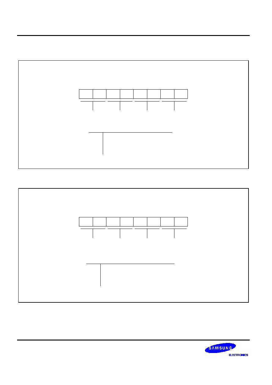
I/O PORT
S3CK225/FK225
10-4
PORT 3
Port 3 High-Byte Control Register (P3CONH)
2AH, R/W, Reset: 00H
MSB
LSB
Input mode
Input mode, pull-up
Open-drain output mode
Output mode, push-pull
P3CONH bit-pair pin configuration settings:
0 0
0 1
1 0
1 1
P3.4/SEG12
.7
.6
.5
.4
.3
.2
.1
.0
P3.7/SEG15
P3.6/SEG14
P3.5/SEG13
Figure 10-6. Port 3 High-Byte Control Register (P3CONH)
Port 3 Low-Byte Control Register (P3CONL)
2BH, R/W, Reset: 00H
MSB
LSB
Input mode
Input mode, pull-up
Open-drain output mode
Output mode, push-pull
P3CONL bit-pair pin configuration settings:
0 0
0 1
1 0
1 1
P3.3/SEG11
P3.2/SEG10
P3.1/SEG9
P3.0/SEG8
.7
.6
.5
.4
.3
.2
.1
.0
Figure 10-7. Port 3 Low-Byte Control Register (P3CONL)
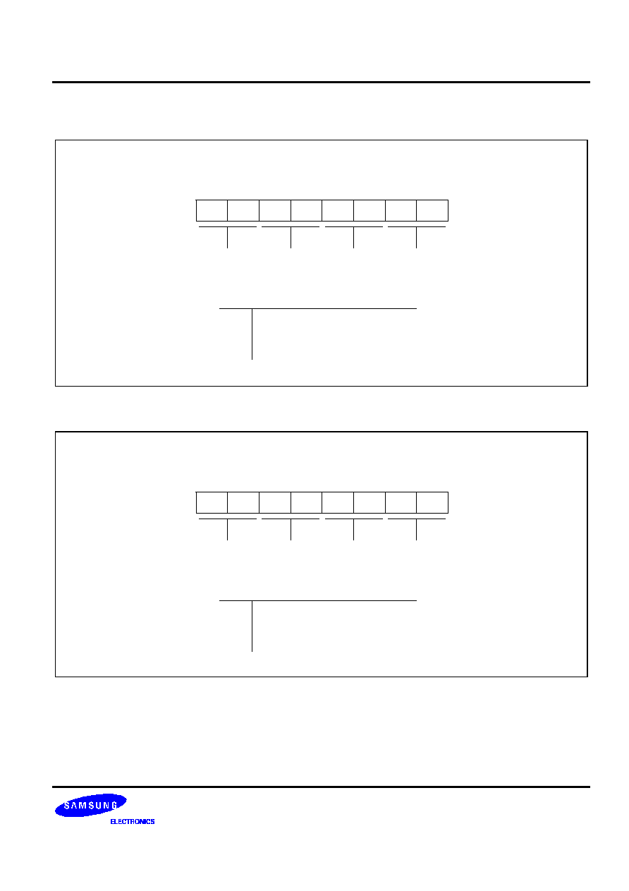
S3CK225/FK225
I/O PORT
10-5
PORT 4
Port 4 High-Byte Control Register (P4CONH)
30H, R/W, Reset: 00H
MSB
LSB
Input mode
Input mode, pull-up
Open-drain output mode
Output mode, push-pull
P4CONH bit-pair pin configuration settings:
0 0
0 1
1 0
1 1
P4.7/SEG23
P4.6/SEG22 P4.5/SEG21
P4.4/SEG20
.7
.6
.5
.4
.3
.2
.1
.0
Figure 10-8. Port 4 High-Byte Control Register (P4CONH)
Port 4 Low-Byte Control Register (P4CONL)
31H, R/W, Reset: 00H
MSB
LSB
Input mode
Input mode, pull-up
Open-drain output mode
Output mode, push-pull
P4CONL bit-pair pin configuration settings:
0 0
0 1
1 0
1 1
P4.3/SEG19
P4.2/SEG18 P4.1/SEG17
P4.0/SEG16
.7
.6
.5
.4
.3
.2
.1
.0
Figure 10-9. Port 4 Low-Byte Control Register (P4CONL)

I/O PORT
S3CK225/FK225
10-6
PORT 5
Port 5 High-Byte Control Register (P5CONH)
32H, R/W, Reset: 00H
MSB
LSB
Input mode
Input mode, pull-up
Alternative function (AD7-AD4)
Output mode, push-pull
P5CONH bit-pair pin configuration settings:
0 0
0 1
1 0
1 1
P5.4/SEG28/
AD4
.7
.6
.5
.4
.3
.2
.1
.0
P5.5/SEG29/
AD5
P5.7/SEG31/
AD7
P5.6/SEG30/
AD6
Figure 10-10. Port 5 High-Byte Control Register (P5CONH)
Port 5 Low-Byte Control Register (P5CONL)
33H, R/W, Reset: 00H
MSB
LSB
Input mode
Input mode, pull-up
Alternative function (AD3-AD0)
Output mode, push-pull
P5CONL bit-pair pin configuration settings:
0 0
0 1
1 0
1 1
P5.3/SEG27/
AD3
P5.2/SEG26/
AD2
P5.1/SEG25/
AD1
P5.0/SEG24/
AD0
.7
.6
.5
.4
.3
.2
.1
.0
Figure 10-11. Port 5 Low-Byte Control Register (P5CONL)
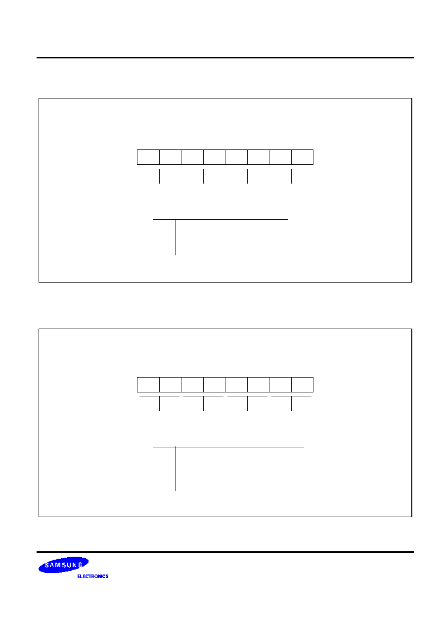
S3CK225/FK225
I/O PORT
10-7
PORT 6
Port 6 Control Register (P6CON)
34H, R/W, Reset: 00H
MSB
LSB
Input mode
Input mode, pull-up
Open-drain output mode
Output mode, push-pull
P6CON bit-pair pin configuration settings:
0 0
0 1
1 0
1 1
P6.0/COM0
.7
.6
.5
.4
.3
.2
.1
.0
P6.3/COM3
P6.2/COM2
P6.1/COM1
Figure 10-12. Port 6 Control Register (P6CON)
PORT 7
Port 7 Control Register (P7CON)
35H, R/W, Reset: 00H
MSB
LSB
Input mode (T0CAP, T0CLK, T2CLK)
Input mode, pull-up (T0CAP)
Alternative function (CLKOUT, T3PWM,
T0OUT/T0PWM, T2OUT/T2PWM)
Output mode, push-pull
P7CON bit-pair pin configuration settings:
0 0
0 1
1 0
1 1
P7.0/T2OUT/
T2PWM
.7
.6
.5
.4
.3
.2
.1
.0
P7.3/T0CAP/
CLKOUT
P7.2/T3PWM/
T0CLK
P7.1/T2CLK/
T0OUT/T0PWM
Figure 10-13. Port 7 Control Register (P7CON)

I/O PORT
S3CK225/FK225
10-8
NOTES

S3CK225/FK225
BASIC TIMER/WATCHDOG TIMER
11-1
11
BASIC TIMER/WATCHDOG TIMER
OVERVIEW
WDTCON controls basic timer clock selection and watchdog timer clear bit.
Basic timer is used in two different ways:
�
As a clock source to watchdog timer to provide an automatic reset mechanism in the event of a system
malfunction (When watchdog function is enabled in ROM code option)
�
To signal the end of the required oscillation stabilization interval after a reset or stop mode release.
The reset value of basic timer clock selection bits is decided by the ROM code option. (see the section on ROM
code option for details). After reset, programmer can select the basic timer input clock using WDTCON.
When watchdog function is enabled by the ROM code option, programmer must set WDTCON.0 periodically
within every 2048
�
basic timer input clock time to prevent system reset.
MSB
LSB
Watchdog Timer Control Register (WDTCON)
0DH, R/W, Reset: X0H
Not used
.7
.6
.5
.4
.3
.2
.1
.0
Basic timer counter clock selection bits:
000 = fxx/2
001 = fxx/4
010 = fxx/16
011 = fxx/32
100 = fxx/128
101 = fxx/256
110 = fxx/1024
111 = fxx/2048
Not used
Watchdog timer clear bit:
0 = don't care
1 = clear watchdog timer counter
Basic timer counter clear bit:
0 = don't care
1 = clear basic timer counter
NOTE:
Under the reset operation, basic timer input clock source is effected
by RCOD_OPT.14-.12. After reset, it can be selected basic timer clock
source by writing appropriate value to WDTCON.6-.4.
Figure 11-1. Watchdog Timer Control Register (WDTCON)

BASIC TIMER/WATCHDOG TIMER
S3CK225/FK225
11-2
BLOCK DIAGRAM
NOTE:
CPU start signal (Bit 5 = 1/fb x 32) (Power down release)
Clear
Reset
3-Bit Watchdog
Timer Counter
STOP
8-Bit Basic Timer
Counter (Read Only)
MUX
MUX
RESET
WDTCON.6, .5, .4
Data Bus
RCOD_OPT .14, .13, .12
Reset or Stop
Data Bus
Clear
BT INT
BT OVF
Bit 5
(NOTE)
RCOD_OPT.11
OVF (System Reset)
WDTCON.0
fb
IDLE
fxx/2
fxx/16
fxx/4
fxx/32
fxx/256
fxx/128
fxx/2048
fxx/1024
IRQ0.7
Figure 11-2. Basic Timer & Watchdog Timer Functional Block Diagram
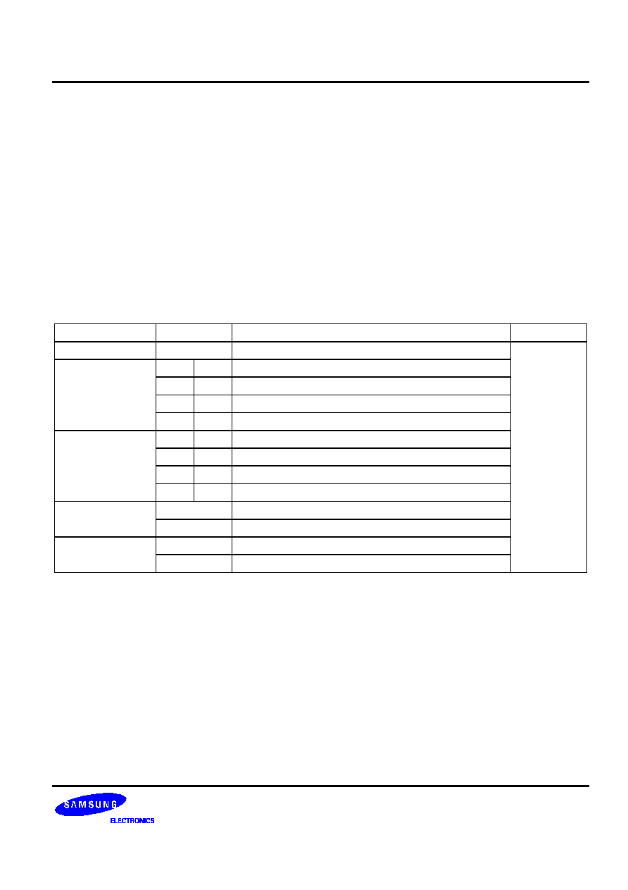
S3CK225/FK225
WATCH TIMER
12-1
12
WATCH
TIMER
OVERVIEW
The source of watch timer is fx/128 (main osc.) or fxt (sub osc.). The interval of watch timer interrupt can be
selected by WTCON.3-2.
Table 12-1. Watch Timer Control Register (WTCON): 8-Bit R/W
Bit Name
Values
Function
Address
WTCON.7 - .6
�
Not used.
70H
WTCON.5-.4
0
0
0.5 kHz buzzer (BUZ) signal output
0
1
1 kHz buzzer (BUZ) signal output
1
0
2 kHz buzzer (BUZ) signal output
1
1
4 kHz buzzer (BUZ) signal output
WTCON.3 - .2
0
0
Set watch timer interrupt to 1 sec.
0
1
Set watch timer interrupt to 0.5 sec.
1
0
Set watch timer interrupt to 0.25 sec.
1
1
Set watch timer interrupt to 3.91 msec.
WTCON.1
0
Select fx/128 as the watch timer clock.
1
Select fxt (sub osc) as the watch timer clock.
WTCON.0
0
Disable watch timer: clear frequency dividing circuits.
1
Enable watch timer.
NOTES:
1.
The main clock frequency (fx) is assumed to be 4.19 MHz.
2.
The watch timer clock frequency (fw) is assumed to be 32.768 kHz.

WATCH TIMER
S3CK225/FK225
12-2
WATCH TIMER CIRCUIT DIAGRAM
Frequency
Dividing
Circuit
fxt
fx = Main clock (4.19 MHz)
fxt = Sub clock (32.768 kHz)
fw = Watch timer clock
WTCON .4-.5
Buzzer Output
Overflow
IRQ1.0
WTCON .1
WTCON .2-.3
fx/128
fw
WTCON .0
Clock
Selector
Selector
Circuit
fw/2
6
(0.5 kHz)
MUX
fw/2
5
(1 kHz)
fw/2
4
(2 kHz)
fw/2
3
(4 kHz)
WT INT
fw/2
7
fw/2
13
fw/2
14
fw/2
15
(1 Hz)
f
LCD
= 512 Hz
fw/2
15
(1 Hz)
Figure 12-1. Watch Timer Circuit Diagram

S3CK225/FK225
16-BIT TIMER 0
13-1
13
16-BIT TIMER 0
OVERVIEW
The 16-bit timer 0 is an 16-bit general-purpose timer/counter. Timer 0 has three operating modes, one of which
you select using the appropriate T0CON setting:
-- Interval timer mode (Toggle output at T0OUT pin)
-- Capture input mode with a rising or falling edge trigger at the T0CAP pin
-- PWM mode (T0PWM)
Timer 0 has the following functional components:
-- Clock frequency divider (fxx divided by 1024, 256, 64, 8 or 1) with multiplexer
-- External clock input pin (T0CLK)
-- 16-bit counter (T0CNTH/L), 16-bit comparator, and 16-bit reference data register (T0DATAH/L)
-- I/O pins for capture input (T0CAP), or PWM or match output (T0PWM, T0OUT)
-- Timer 0 overflow interrupt (IRQ0.1) and match/capture interrupt (IRQ0.0) generation
-- Timer 0 control register, T0CON (40H, read/write)

16-BIT TIMER 0
S3CK225/FK225
13-2
FUNCTION DESCRIPTION
Timer 0 Interrupts (IRQ0.0, IRQ0.1)
The timer 0 module can generate two interrupts, the timer 0 overflow interrupt (T0OVF), and the timer 0
match/capture interrupt (T0INT). T0OVF is interrupt level IRQ0.1. T0INT belongs to interrupt level IRQ0.0.
Interval Timer Function
In interval timer mode, a match signal is generated and T0OUT is toggled when the counter value is identical to
the value written to the T0 reference data register, T0DATAH/L. The match signal generates a timer 0 match
interrupt (T0INT) and clears the counter.
If, for example, you write the value 0010H to T0DATAH/L and 04H to T0CON, the counter will increment until it
reaches 0010H. At this point, the T0 interrupt request is generated, the counter value is reset, and counting
resumes.
Pulse Width Modulation Mode
Pulse width modulation (PWM) mode lets you program the width (duration) of the pulse that is output at the
T0PWM pin. As in interval timer mode, a match signal is generated when the counter value is identical to the
value written to the timer 0 data register. In PWM mode, however, the match signal does not clear the counter
but can generate a match interrupt. The counter runs continuously, overflowing at FFFFH, and then repeat the
incrementing from 0000H. Whenever an overflow is occurred, an overflow (OVF) interrupt can be generated.
Although you can use the match or the overflow interrupt in PWM mode, interrupts are not typically used in
PWM-type applications. Instead, the pulse at the T0PWM pin is held to Low level as long as the reference data
value is less than or equal to (
) the counter value and then pulse is held to High level for as long as the data
value is greater than (>) the counter value. One pulse width is equal to t
CLK
Capture Mode
In capture mode, a signal edge that is detected at the T0CAP pin opens a gate and loads the current counter
value into the T0 data register. You can select rising or falling edges to trigger this operation.
Timer 0 also gives you capture input source, the signal edge at the T0CAP pin. You select the capture input by
setting the value of the timer 0 capture input selection bit in the port 7 control register, P7CON, (35H). When
P7CON.7-6 is 00, the T0CAP input or normal input is selected .When P7CON.7-6 is set to 11, normal output is
selected.
Both kinds of timer 0 interrupts can be used in capture mode, the timer 0 overflow interrupt is generated
whenever a counter overflow occurs, the timer 0 match/capture interrupt is generated whenever the counter
value is loaded into the T0 data register.
By reading the captured data value in T0DATAH/L, and assuming a specific value for the timer 0 clock
frequency, you can calculate the pulse width (duration) of the signal that is being input at the T0CAP pin.

S3CK225/FK225
16-BIT TIMER 0
13-3
TIMER 0 CONTROL REGISTER (T0CON)
You use the timer 0 control register, T0CON, to
-- Select the timer 0 operating mode (interval timer, capture mode, or PWM mode)
-- Select the timer 0 input clock frequency
-- Clear the timer 0 counter, T0CNTH/L
T0CON is located at address 40H, and is read/written addressable.
A reset clears T0CON to `00H'. This sets timer 0 to normal interval timer mode, and selects an input clock
frequency of fxx/1024. To disable the counter operation, please set T0CON.7-.5 to 111B. You can clear the timer
0 counter at any time during normal operation by writing a "1" to T0CON.2.
Timer 0 Control Register (T0CON)
40H, R/W
.7
.6
.5
.4
.3
.2
.1
.0
MSB
LSB
Timer 0 counter clear bit:
0 = No effect
1 = Clear the timer 0 counter (when write)
Timer 0 input clock selection bits:
000 = fxx/1024
010 = fxx/256
100 = fxx/64
110 = fxx/8
001 = fxx/1
011 = External clock (T0CLK) falling edge
101 = External clock (T0CLK) rising edge
111 = Counter stop
Timer 0 operating mode selection bits:
00 = Interval mode
01 = Capture mode (capture on rising edge, counter running, OVF can occur)
10 = Capture mode (capture on falling edge, counter running, OVF can occur)
11 = PWM mode
(OVF & match interrupt can occur)
Not used
Figure 13-1. Timer 0 Control Register (T0CON)

16-BIT TIMER 0
S3CK225/FK225
13-4
BLOCK DIAGRAM
Timer 0 Data H/L
Register
Timer 0 Buffer Reg
16-bit Comparator
16-bit Up-Counter
(Read Only)
Counter Clear Signal or Match
Clear
Match
T0CON.7-5
f
XX
/1024
f
XX
/8
f
XX
/256
f
XX
/64
f
XX
/1
T0OVF
IRQ0.1
OVF
T0CON.2
T0INT
IRQ0.0
T0OUT
T0PWM
T0CON.4-.3
R
M
U
X
V
SS
T0CLK
M
U
X
M
U
X
T0CAP
T0CON.4-.3
Data Bus
8
Data Bus
8
Figure 13-2. Timer 0 Functional Block Diagram

S3CK225/FK225
16-BIT TIMER 0
13-5
Timer 0 Counter High-Byte Register (T0CNTH)
43H, R, Reset Value: 00H
MSB
LSB
MSB
.7
.6
.5
.4
.3
.2
.1
.0
.7
.6
.5
.4
.3
.2
.1
.0
LSB
Timer 0 Counter Low-Byte Register (T0CNTL)
44H, R, Reset Value: 00H
.7
.6
.5
.4
.3
.2
.1
.0
LSB
Timer 0 Data High-Byte Register (T0DATAH)
41H, R/W, Reset Value: FFH
MSB
.7
.6
.5
.4
.3
.2
.1
.0
LSB
Timer 0 Data Low-Byte Register (T0DATAL)
42H, R/W, Reset Value: FFH
MSB
Figure 13-3. Timer 0 Counter and Data Registers (T0CNTH/L, T0DATAH/L)

16-BIT TIMER 0
S3CK225/FK225
13-6
NOTES

S3CK225/FK225
16-BIT TIMER 1
14-1
14
16-BIT TIMER 1
OVERVIEW
The 16-bit timer 1 is an 16-bit general-purpose timer. Timer 1 has the interval timer mode by using the
appropriate T1CON setting.
Timer 1 has the following functional components:
-- Clock frequency divider (fxx divided by 256, 64, 8 or 1) with multiplexer
-- T3OF (from timer 3) is one of the clock frequencies.
-- 16-bit counter (T1CNTH/L), 16-bit comparator, and 16-bit reference data register (T1DATAH/L)
-- Timer 1 interrupt (IRQ0.2) generation
-- Timer 1 control register, T1CON (48H, read/write)
FUNCTION DESCRIPTION
Interval Timer Function
The timer 1 module can generate an interrupt, the timer 1 match interrupt (T1INT). T1INT belongs to interrupt
level IRQ0.2.
In interval timer mode, a match signal is generated when the counter value is identical to the values written to
the T1 reference data registers, T1DATAH/L. The match signal generates a timer 1 match interrupt (T1INT) and
clears the counter.
If, for example, you write the value 0010H to T1DATAH/L and 0CH to T1CON, the counter will increment until it
reaches 10H. At this point, the T1 interrupt request is generated, the counter value is reset, and counting
resumes.

16-BIT TIMER 1
S3CK225/FK225
14-2
TIMER 1 CONTROL REGISTER (T1CON)
You use the timer 1 control register, T1CON, to
-- Enable the timer 1 operating (interval timer)
-- Select the timer 1 input clock frequency
-- Clear the timer 1 counter, T1CNT
T1CON is located, at address 48H, and is read/written addressable.
A reset clears T1CON to "00H". This sets timer 1 to disable interval timer mode, selects the T3OF. You can clear
the timer 1 counter at any time during normal operation by writing a "1" to T1CON.3
Timer 1 Control Register
48H, R/W, RESET; 00H
.7
.6
.5
.4
.3
.2
.1
.0
MSB
LSB
Timer 1 count enable bit:
0 = Disable counting operation
1 = Enable counting operation
Timer 1 counter clear bit:
0 = No affect
1 = Clear the timer 1 counter (when write)
Timer 1 input clock selection bits:
000 = T3OF
010 = fxx/256
100 = fxx/64
110 = fxx/8
xx1 = fxx
Not used
NOTE: For normal operation T1CON.2 bit must be set 1.
Not used
Figure 14-1. Timer 1 Control Register (T1CON)
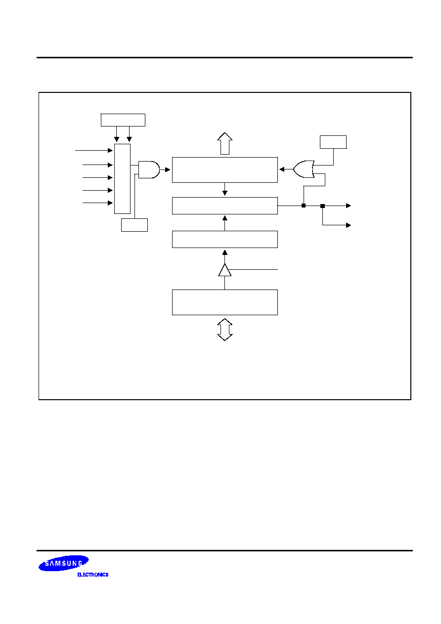
S3CK225/FK225
16-BIT TIMER 1
14-3
BLOCK DIAGRAM
Timer 1 Data H/L Reg
(Read/Write)
Timer 1 Buffer Reg
16-bit Comparator
16-bit up-Counter H/L
(Read Only)
Match
Bit 3
Counter clear (T1CON.3) signal
or match signal
Bits 7, 6, 5
M
U
X
fxx/256
fxx/64
fxx/8
fxx/1
T3OF
Bit 2
Clear
R
Data Bus
8
Data Bus
8
NOTE: T1CON.3 bit is cleared automatically.
IRQ0.2
DA Converter
T1INT
Figure 14-2. Timer 1 Functional Block Diagram

16-BIT TIMER 1
S3CK225/FK225
14-4
Timer 1 Counter High-Byte (T1CNTH)
4BH, R, Reset Value: 00H
.7
.6
.5
.4
.3
.2
.1
.0
MSB
LSB
Timer 1 Counter Low-Byte (T1CNTL)
4CH, R, Reset Value: 00H
.7
.6
.5
.4
.3
.2
.1
.0
MSB
LSB
Figure 14-3. Timer 1 Counter Register (T1CNTH/L)
Timer 1 Data High-Byte Register (T1DATAH)
49H, R/W, Reset Value: FFH
.7
.6
.5
.4
.3
.2
.1
.0
MSB
LSB
Timer 1 Data Low-Byte Register (T1DATAL)
4AH, R/W, Reset Value: FFH
.7
.6
.5
.4
.3
.2
.1
.0
MSB
LSB
Figure 14-4. Timer 1 Data Register (T1DATAH/L)

S3CK225/FK225
8-BIT TIMER 2
15-1
15
8-BIT TIMER 2
OVERVIEW
The 8-bit timer 2 is an 8-bit general-purpose timer/counter. Timer 2 has two operating modes, one of which you
select using the appropriate T2CON setting:
-- Interval timer mode (Toggle output at T2OUT pin)
-- PWM mode (T2PWM)
Timer 2 has the following functional components:
-- Clock frequency divider (fxx divided by 1024, 256, or 64 ) with multiplexer
-- External clock input pin (T2CLK)
-- 8-bit counter (T2CNT), 8-bit comparator, and 8-bit reference data register (T2DATA)
-- I/O pin for PWM/Match output (T2PWM, T2OUT)
-- Timer 2 overflow interrupt (IRQ0.4) and match interrupt (IRQ0.3) generation
-- Timer 2 control register, T2CON (50H, read/write)

8-BIT TIMER 2
S3CK225/FK225
15-2
FUNCTION DESCRIPTION
Timer 2 Interrupts (IRQ0.3 and IRQ0.4)
The timer 2 module can generate two interrupts: the timer 2 overflow interrupt (T2OVF), and the timer 2 match
interrupt (T2INT). T2OVF is interrupt level IRQ0.4. T2INT also belongs to interrupt level IRQ0.3.
Interval Timer Function
In interval timer mode, a match signal is generated and T2OUT is toggled when the counter value is identical to
the value written to the T2 reference data register, T2DATA. The match signal generates a timer 2 match
interrupt (T2INT) and clears the counter.
If, for example, you write the value 10H to T2DATA and 0CH to T2CON, the counter will increment until it
reaches 10H. At this point, the T2 interrupt request is generated, the counter value is reset, and counting
resumes.
Pulse Width Modulation Mode
Pulse width modulation (PWM) mode lets you program the width (duration) of the pulse that is output at the
T2PWM pin. As in interval timer mode, a match signal is generated when the counter value is identical to the
value written to the timer 2 data register. In PWM mode, however, the match signal does not clear the counter.
Instead, it runs continuously, overflowing at FFH, and then continues incrementing from 00H.
Although timer 2 overflow interrupt is occurred, this interrupt is not typically used in PWM-type applications.
Instead, the pulse at the T2PWM pin is held to Low level as long as the reference data value is less than or equal
to (
) the counter value and then the pulse is held to High level for as long as the data value is greater than ( > )
the counter value. One pulse width is equal to t
CLK
� 256 .
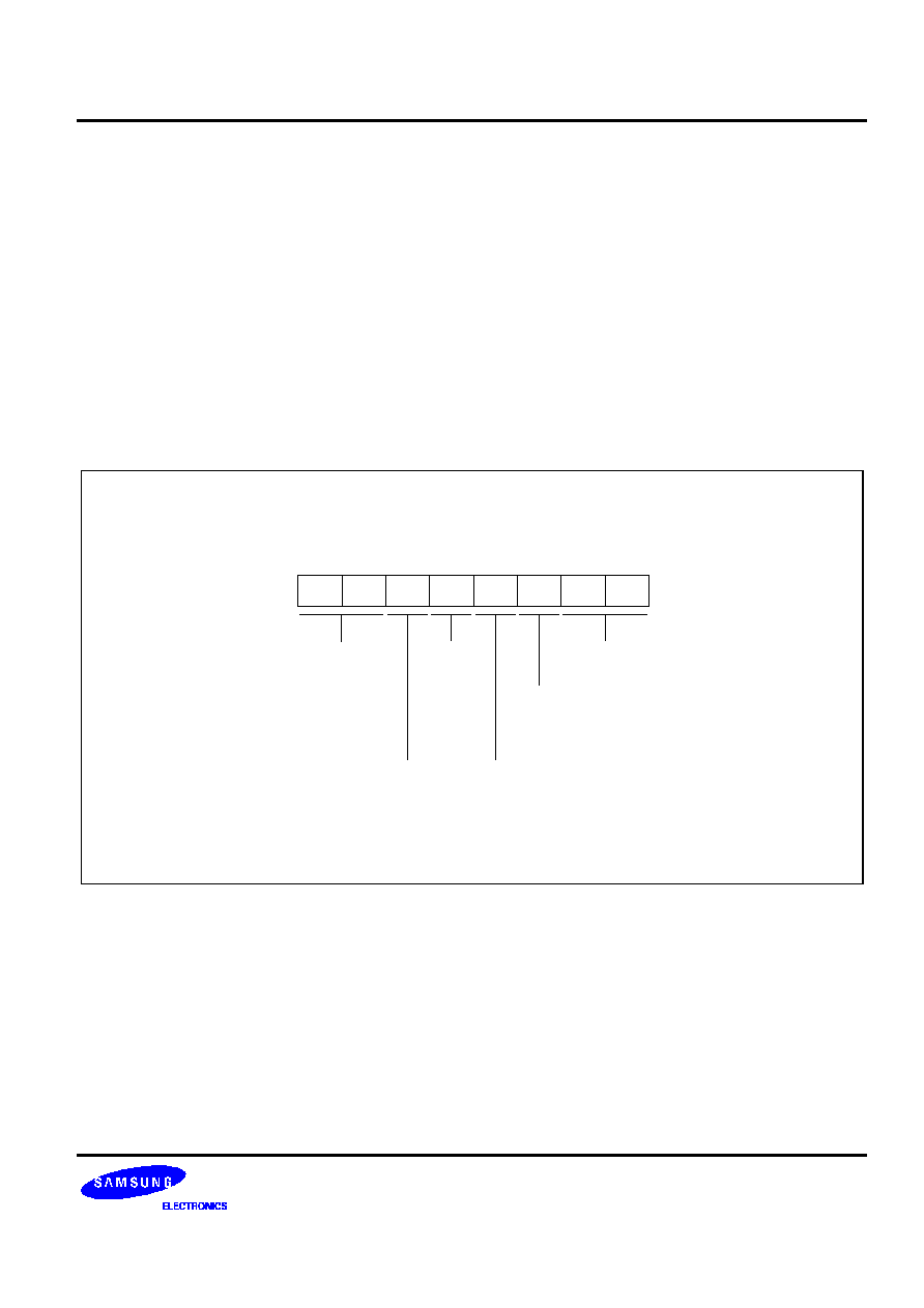
S3CK225/FK225
8-BIT TIMER 2
15-3
TIMER 2 CONTROL REGISTER (T2CON)
You use the timer 2 control register, T2CON, to
-- Select the timer 2 operating mode (interval mode, or PWM mode)
-- Select the timer 2 input clock frequency
-- Clear the timer 2 counter, T2CNT
-- Enable the timer 2 counting operation
T2CON is located in at address 50H, and is read/written addressable.
A reset clears T2CON to '00H'. This sets timer 2 to normal interval timer mode, selects an input clock frequency
of fxx/1024, and disables timer 2 counting operation. You can clear the timer 2 counter at any time during normal
operation by writing a "1" to T2CON.3 or the timer 2 counter is cleared by match signal.
Timer 2 Control Register
50H, R/W, RESET: 00H
.7
.6
.5
.4
.3
.2
.1
.0
MSB
LSB
Timer 2 count enable bit:
0 = Disable counting operation
1 = Enable counting operation
Timer 2 counter clear bit:
0 = No affect
1 = Clear the timer 2 counter (when write)
Timer 2 input clock selection bits:
00 = fxx/1024
01 = fxx/256
10 = fxx/64
11 = External clock (T2CLK)
Timer 2 operating mode selection bits:
0 = Interval mode (T2OUT mode)
1 = PWM mode (OVF interrupt can occur)
Not used
Not used
Figure 15-1. Timer 2 Control Register (T2CON)
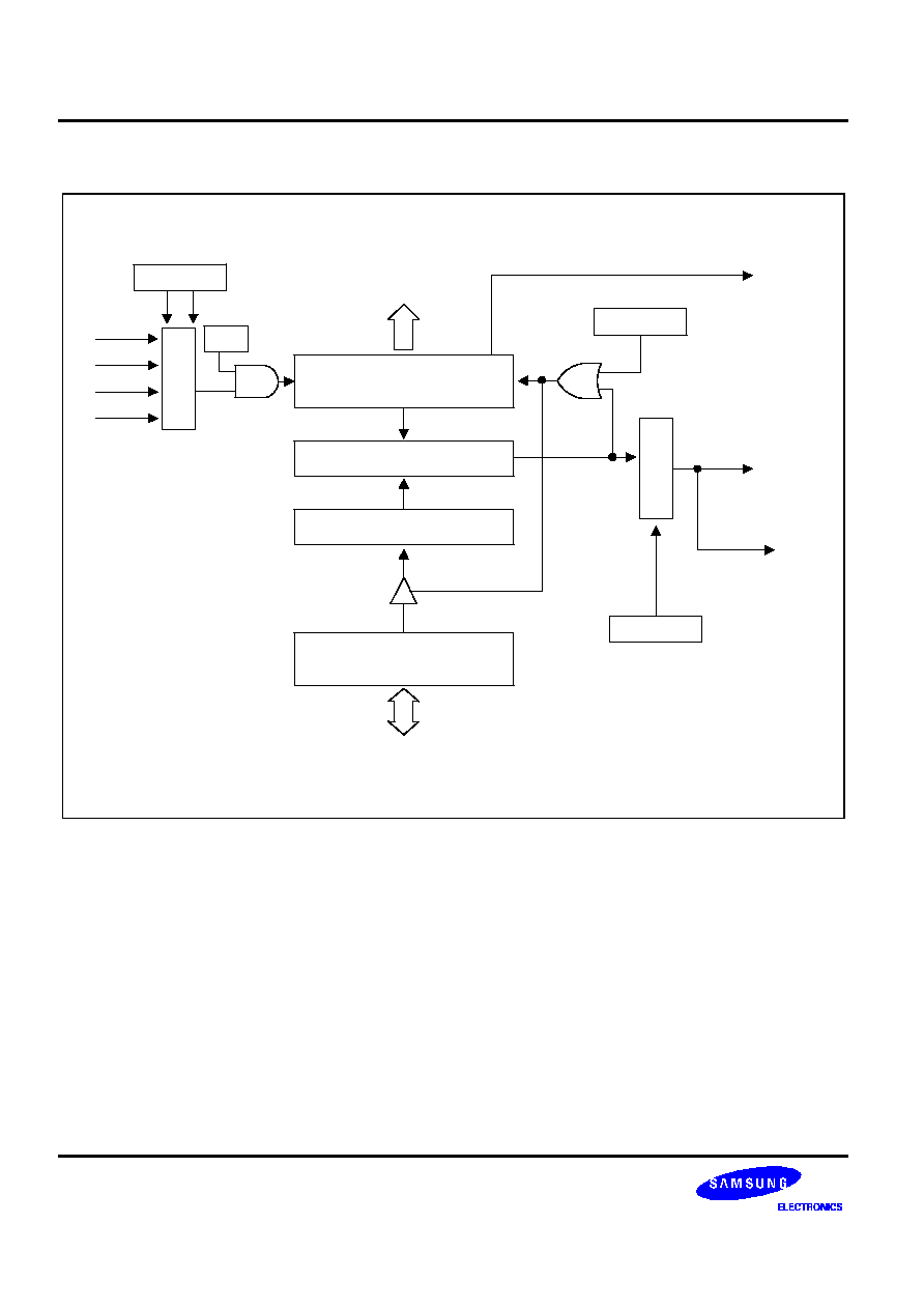
8-BIT TIMER 2
S3CK225/FK225
15-4
BLOCK DIAGRAM
Timer 2 Data Register
(Read/Write)
Timer 2 Buffer Reg
8-bit Comparator
8-bit Up-Counter
(Read Only)
Clear
Match
T2CON.7-.6
f
XX
/1024
f
XX
/256
f
XX
/64
T2CLK
T2CON.3
M
U
X
T2OVF
M
U
X
T2OUT
T2PWM
T2CON.5
Data Bus
8
Data Bus
8
IRQ0.3
IRQ0.4
Bit 2
Figure 15-2. Timer 2 Functional Block Diagram

S3CK225/FK225
8-BIT TIMER 3
16-1
16
8-BIT TIMER 3
OVERVIEW
The S3CK225/FK225 micro-controller has an 8-bit counter called timer 3. Timer 3, which can be used to generate
the carrier frequency of a remote controller signal.
Timer 3 has two functions:
-- As a normal interval timer, generating a timer 3 interrupt at programmed time intervals.
-- To supply a clock source to the 16-bit timer/counter module, timer 1, for generating the timer 1 match
interrupt.

8-BIT TIMER 3
S3CK225/FK225
16-2
8-bit
Down Counter
Timer 3 Data
High Byte Register
MUX
T3CON.0
(T3OF)
To Other Block
(P7.2/T3PWM)
IRQ0.5
(T3INT)
INT.GEN
Repeat Control
Interrupt Control
M
U
X
f
XX
/1
f
XX
/2
f
XX
/4
f
XX
/8
T3CON.6-.7
T3CON.2
Timer 3 Data
Low Byte Register
CLK
T3CON.4-.5
Data Bus
8
NOTE:
The value of the T3DATAL register is loaded into the 8-bit counter when the operation of the timer 3
starts. If a borrow occurs in the counter, the value of the T3DATAH register is loaded into the 8-bit
counter. However, if the next borrow occurs, the value of the T3DATAL register is loaded into the 8-bit
counter.
Figure 16-1. Timer 3 Functional Block Diagram
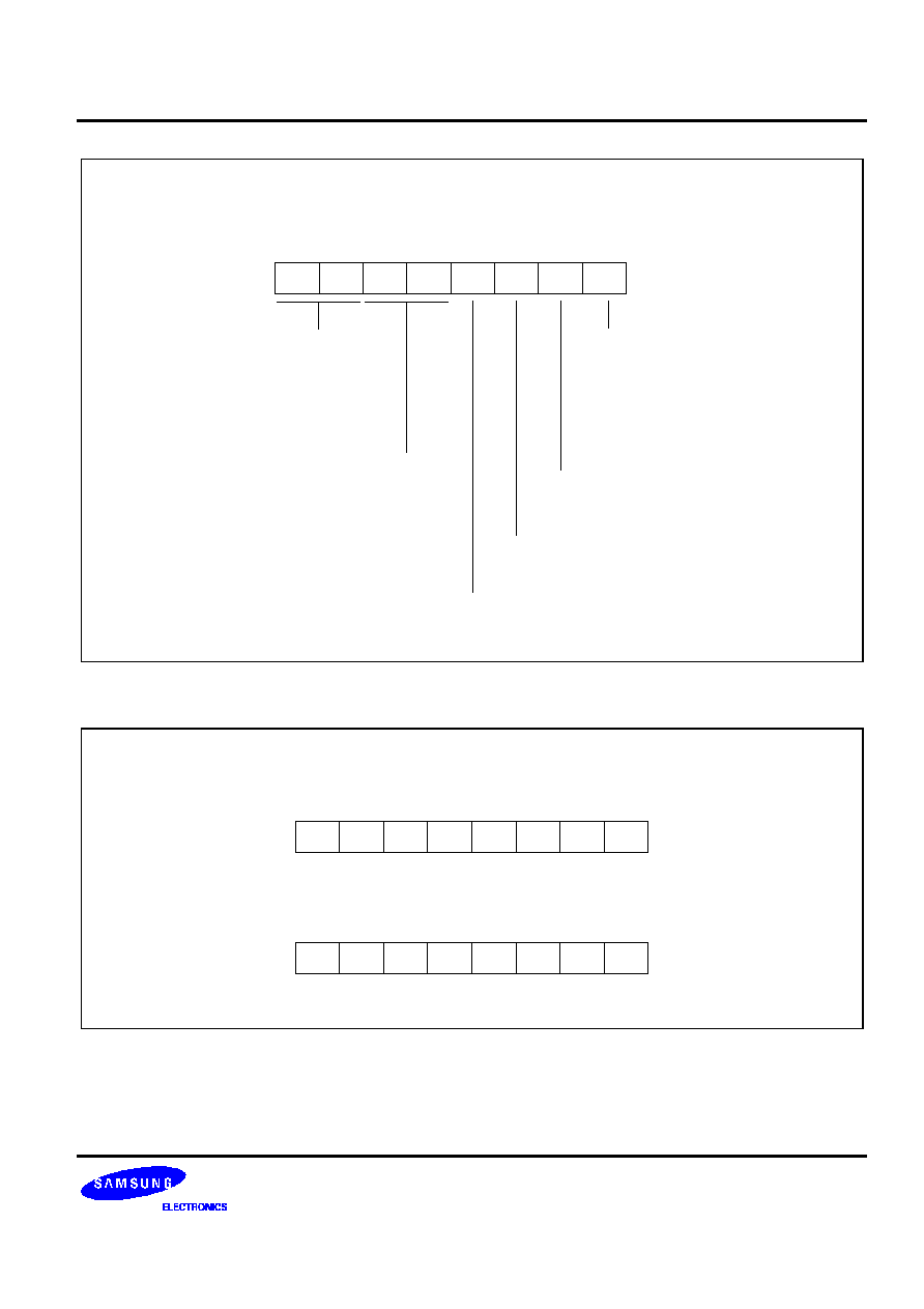
S3CK225/FK225
8-BIT TIMER 3
16-3
Timer 3 Control Register (T3CON)
54H, R/W, Reset: 00H
.7
.6
.5
.4
.3
.2
.1
.0
MSB
LSB
Timer 3 mode selection bit:
0 = One-shot mode
1 = Repeating mode
Timer 3 output flip-flop control bit:
0 = T3OF is low
(T3PWM: low level for low data,
high level for high data)
1 = T3OF is high
(T3PWM: high level for low data,
low level for high data)
Timer 3 start/stop bit:
0 = Stop timer 3
1 = Start timer 3
Not used
Timer 3 input clock selection bits:
00 = fxx
01 = fxx/2
10 = fxx/4
11 = fxx/8
Timer 3 interrupt time selection bits:
00 = Generating after low data is borrowed.
01 = Generating after high data is borrowed.
10 = Generating after low and high data is
borrowed.
11 = Invalid setting
Figure 16-2. Timer 3 Control Register (T3CON)
Timer 3 Data High-Byte Register (T3DATAH)
55H, R/W, Reset Value: FFH
.7
.6
.5
.4
.3
.2
.1
.0
MSB
LSB
Timer 3 Data Low-Byte Register (T3DATAL)
56H, R/W, Reset Value: FFH
.7
.6
.5
.4
.3
.2
.1
.0
MSB
LSB
Figure 16-3. Timer 3 Data Registers (T3DATAH/L)

8-BIT TIMER 3
S3CK225/FK225
16-4
TIMER 3 PULSE WIDTH CALCULATIONS
t
LOW
t
HIGH
t
LOW
To generate the above repeated waveform consisted of low period time, t
LOW
, and high period time, t
HIGH
.
When T3OF = 0,
t
LOW
= (T3DATAL + 2) x 1/fxx, 0H < T3DATAL < 100H, where fxx = The selected clock.
t
HIGH
= (T3DATAH + 2) x 1/fxx, 0H < T3DATAH < 100H, where fxx = The selected clock.
When T3OF = 1,
t
LOW
= (T3DATAH + 2) x 1/fxx, 0H < T3DATAH < 100H, where fxx = The selected clock.
t
HIGH
= (T3DATAL + 2) x 1/fxx, 0H < T3DATAL < 100H, where fxx = The selected clock.
To make t
LOW
= 24 us and t
HIGH
= 15 us. fx = 4 MHz, fxx = 4 MHz/4 = 1 MHz
When T3OF = 0,
t
LOW
= 24 us = (T3DATAL + 2) /fx = (T3DATAL + 2) x 1us, T3DATAL = 22.
t
HIGH
= 15 us = (T3DATAH + 2) /fx = (T3DATAH + 2) x 1us, T3DATAH = 13.
When T3OF = 1,
t
HIGH
= 15 us = (T3DATAL + 2) /fx = (T3DATAL + 2) x 1us, T3DATAL = 13.
t
LOW
= 24 us = (T3DATAH + 2) /fx = (T3DATAH + 2) x 1us, T3DATAH = 22.

S3CK225/FK225
8-BIT TIMER 3
16-5
Timer 3 Clock
0H
T3OF = '0'
T3DATAL = 01-FFH
T3DATAH = 00H
T3OF = '0'
T3DATAL = 00H
T3DATAH = 01-FFH
T3OF = '0'
T3DATAL = 00H
T3DATAH = 00H
T3OF = '1'
T3DATAL = 00H
T3DATAH = 00H
Low
High
Low
High
Timer 3 Clock
T3OF = '1'
T3DATAL = DEH
T3DATAH = 1EH
T3OF = '0'
T3DATAL = DEH
T3DATAH = 1EH
T3OF = '1'
T3DATAL = 7EH
T3DATAH = 7EH
T3OF = '0'
T3DATAL = 7EH
T3DATAH = 7EH
0H
100H
200H
E0H
20H
20H
E0H
80H
80H
80H
80H
Figure 16-4. Timer 3 Output Flip-Flop Waveforms in Repeat Mode

8-BIT TIMER 3
S3CK225/FK225
16-6
F
F
PROGRAMMING TIP -- To generate 38 kHz, 1/3duty signal through P7.2
This example sets Timer 3 to the repeat mode, sets the oscillation frequency as the Timer 3 clock source, and
T3DATAH and T3DATAL to make a 38 kHz,1/3 Duty carrier frequency. The program parameters are:
17.59
�
s
37.9 kHz 1/3 Duty
8.795
�
s
-- Timer 3 is used in repeat mode
-- Oscillation frequency is 4 MHz (0.25
�
s)
-- T3DATAH = 8.795
�
s/0.25
�
s = 35.18, T3DATAL = 17.59
�
s/0.25
�
s = 70.36
-- Set P7.2 to T3PWM mode.
START
DI
�
�
�
LD
R0,#(70-2)
LD
R1,#(35-2)
LD
R2,#00000110B
LD
T3DATAL,R0
; Set 17.5
�
s
LD
T3DATAH,R1
; Set 8.75
�
s
LD
T3CON,R2
; Clock Source
fxx
; Select repeat mode for Timer 3.
; Start Timer 3 operation.
; Set Timer 3 Output flip-flop (T3OF) low.
;
BITR
P7CON.4
; Set P7.2 to T3PWM mode.
BITS
P7CON.5
; This command generates 38 kHz, 1/3 duty pulse signal
through P7.2.
�
�
�

S3CK225/FK225
8-BIT TIMER 3
16-7
F
F
PROGRAMMING TIP -- To generate a one pulse signal through P7.2
This example sets Timer 3 to the one shot mode, sets the oscillation frequency as the Timer 3 clock source, and
T3DATAH and T3DATAL to make a 40
�
s width pulse. The program parameters are:
40
�
s
-- Timer 3 is used in one shot mode
-- Oscillation frequency is 4 MHz (1 clock = 0.25
�
s)
-- T3DATAH = 40
�
s / 0.25
�
s = 160, T3DATAL = 1
-- Set P7.2 to T3PWM mode
START
DI
�
�
�
LD
R0,#(160-2)
LD
R1,#1
LD
R2,#00000001B
LD
T3DATAH,R0
; Set 40
�
s
LD
T3DATAL,R1
; Set any value except 00H
LD
T3CON,R2
; Clock Source
fxx
; Select one shot mode for Timer 3.
; Stop Timer 3 operation.
; Set Timer 3 output flip-flop (T3OF) high
BITR
P7CON.4
; Set P7.2 to T3PWM mode.
BITS
P7CON.5
�
�
Pulse_out:
LD
R0,#00000101B
LD
T3CON,R0
; Start Timer 3 operation
; to make the pulse at this point.
�
; After the instruction is executed, 0.75
�
s is required
�
; before the falling edge of the pulse starts.
�

8-BIT TIMER 3
S3CK225/FK225
16-8
NOTES

S3CK225/FK225
SERIAL I/O INTERFACE
17-1
17
SERIAL I/O INTERFACE
OVERVIEW
The SIO module can transmit or receive 8-bit serial data at a frequency determined by its corresponding control
register settings. To ensure flexible data transmission rates, you can select an internal or external clock source.
Programming Procedure
To program the SIO modules, follow these basic steps:
1.
Configure the I/O pins at port (SO, SCK, SI) by loading the appropriate value to the P1CON register, if
necessary.
2.
Load an 8-bit value to the SIOCON register to properly configure the serial I/O module. In this operation,
SIOCON.2 must be set to "1" to enable the data shifter.
3.
When you transmit data to the serial buffer, write data to SIODATA and set SIOCON.3 to 1, the shift
operation starts.
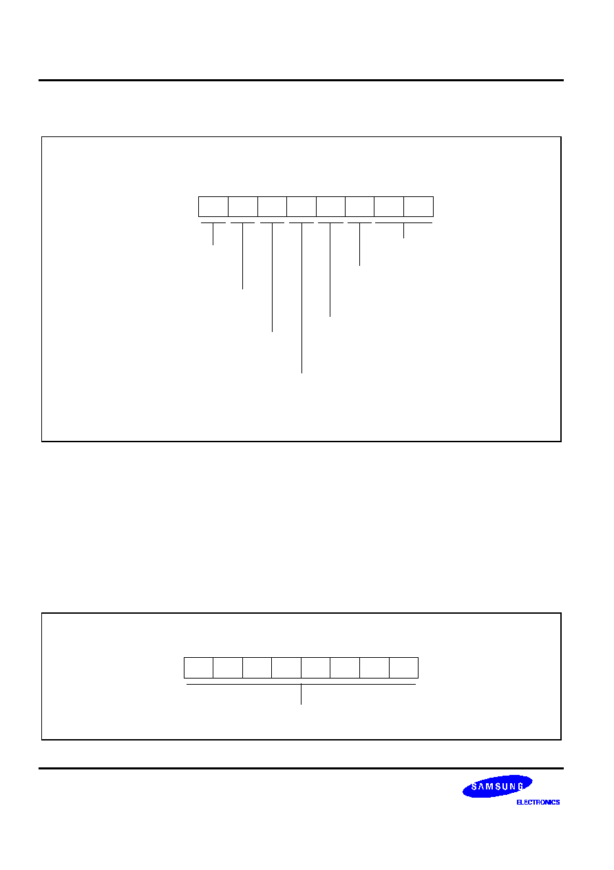
SERIAL I/O INTERFACE
S3CK225/FK225
17-2
SIO CONTROL REGISTER (SIOCON)
LSB
MSB
Serial I/O Module Control Register (SIOCON)
58H, R/W, Reset: 00H
Not used
SIO shift clock select bit:
0 = Internal clock (P.S clock)
1 = External clock (SCK)
Data direction control bit:
0 = MSB-first
1 = LSB-first
SIO counter clear and shift start bit:
0 = No action
1 = Clear 3-bit counter and start shifting
SIO shift operation enable bit:
0 = Disable shifter and clock
1 = Enable shfter and clock
SIO mode selction bit:
0 = Rececive-only mode
1 = Transmit/receive mode
Shift clock edge selction bit:
0 = Tx at falling edge, Rx at rising edge
1 = Tx at rising edge, Rx at falling edge
.7
.6
.5
.4
.3
.2
.1
.0
Figure 17-1. Serial I/O Module Control Registers (SIOCON)
SIO PRE-SCALER REGISTER (SIOPS)
The value stored in the SIO pre-scaler registers, SIOPS, lets you determine the SIO clock rate (baud rate) as
follows:
Baud rate = Input clock( fxx/4)/(Pre-scaler value + 1), or, SCK input clock
where fxx is a selected clock.
LSB
MSB
SIO Pre-scaler Register (SIOPS)
59H,R/W, Reset: 00H
Baud rate = (fxx/4)/(SIOPS + 1)
.7
.6
.5
.4
.3
.2
.1
.0
Figure 17-2. SIO Pre-scaler Register (SIOPS)
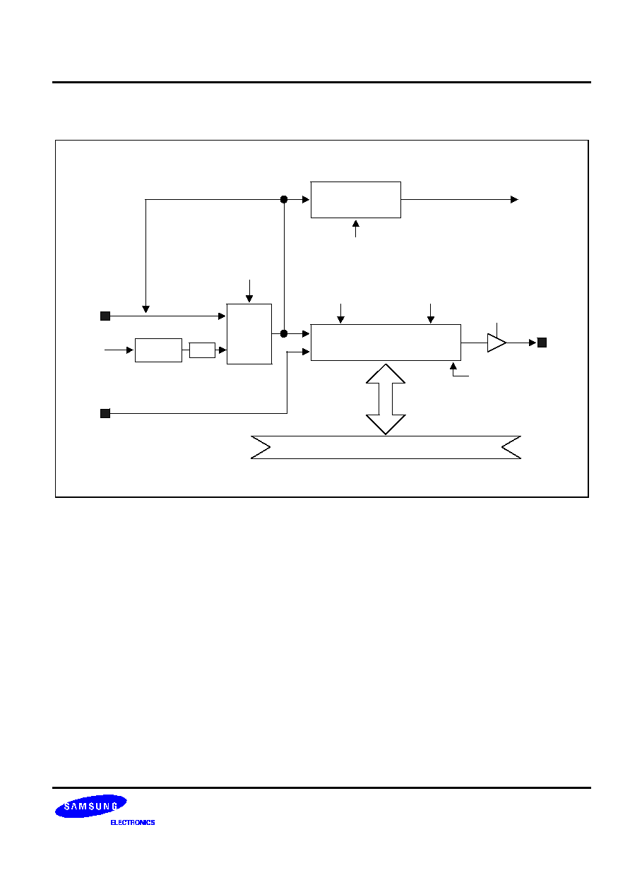
S3CK225/FK225
SERIAL I/O INTERFACE
17-3
BLOCK DIAGRAM
3-Bit Counter
MUX
8-Bit SIO Shift Buffer
(SIODATA)
8-Bit
P.S
1/2
fxx/2
SIOPS
SCK
SIOCON.7
(Shift Clock
Source Select)
Clear
CLK
CLK
SI
SIOCON.3
SIOCON.4
(Edge Select)
SIOCON.5
(Mode Select)
SIOCON.2
(Shift Enable)
SIOCON.6
(LSB/MSB First
Mode Select)
Data Bus
8
SO
IRQ0.6
(SIO INT)
Figure 17-3. SIO Function Block Diagram
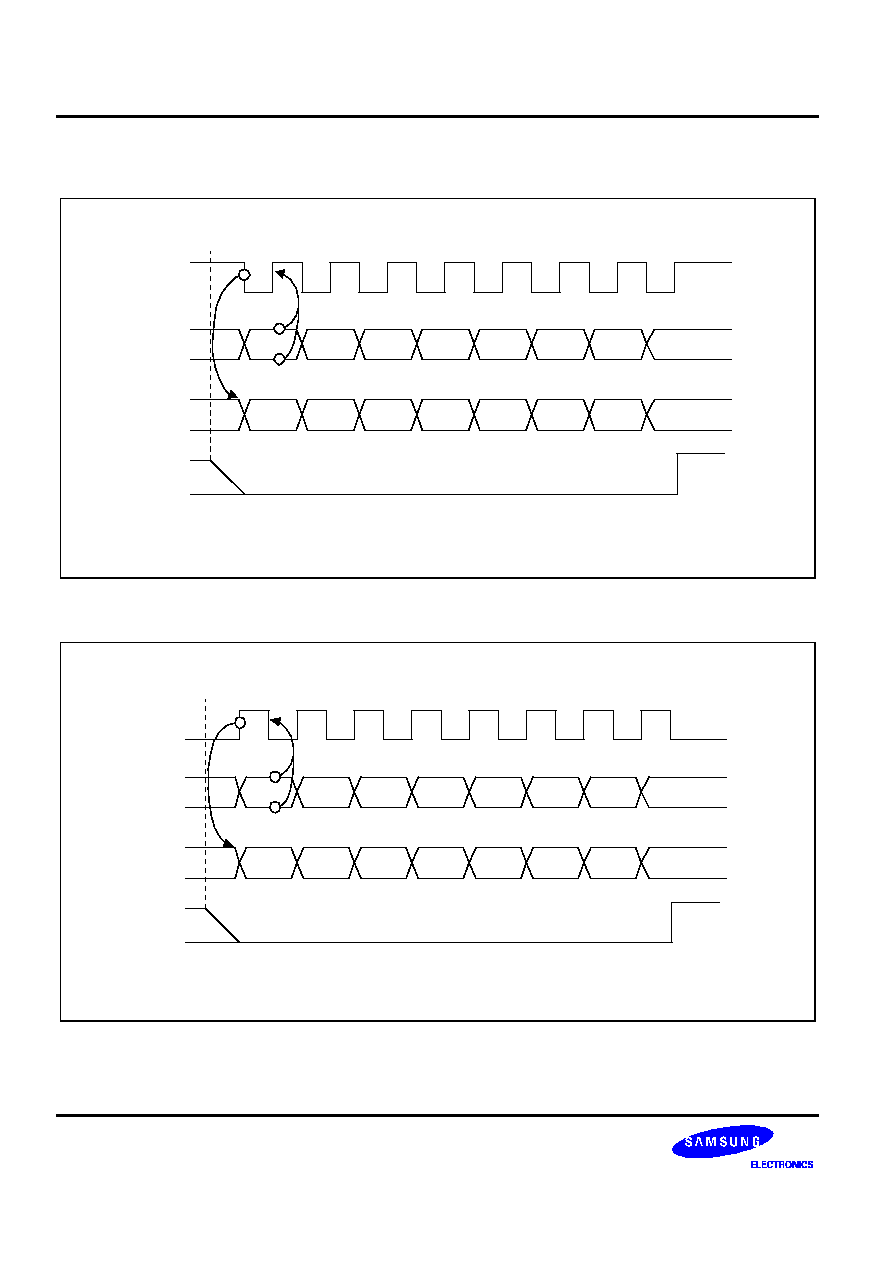
SERIAL I/O INTERFACE
S3CK225/FK225
17-4
SERIAL I/O TIMING DIAGRAM
SO
Transmit
Complete
IRQ0.6
Set SIOCON.3
DO7
DO6
DO5
DO4
DO3
DO2
DO1
DO0
D17
D16
D15
D14
D13
D12
D11
D10
SI
SCK
Figure 17-4. Serial I/O Timing in Transmit/Receive Mode(Tx at falling, SIOCON.4=0)
IRQ0.6
DO7
DO6
DO5
DO4
DO3
DO2
DO1
DO0
D17
D16
D15
D14
D13
D12
D11
D10
SCK
Transmit
Complete
Set SIOCON.3
SI
SO
Figure 17-5. Serial I/O Timing in Transmit/Receive Mode(Tx at rising, SIOCON.4=1)

S3CK225/FK225
LCD CONTROLLER/DRIVER
18-1
18
LCD CONTROLLER/DRIVER
OVERVIEW
The S3CK225/FK225 can directly drive an up-to 128-dots LCD panel. The LCD module has the following
components:
-- LCD controller/driver
-- Display RAM (00H-0FH of Page 2) for storing display data
-- 32 segment output pins (SEG0-SEG31)
-- 4 common output pins (COM0-COM3)
Bit settings in the LCD mode register, LMOD, determine the LCD frame frequency, duty, and bias.
The LCD control register LCON turns the LCD display on and off, and selects the segment pins used for display
output. LCD data stored in the display RAM locations are transferred to the segment signal pins automatically
without program control.
LCD
Controller/
Driver
8
8-Bit Data Bus
4
32
COM0-COM3
SEG0-SEG31
Figure 18-1. LCD Function Diagram
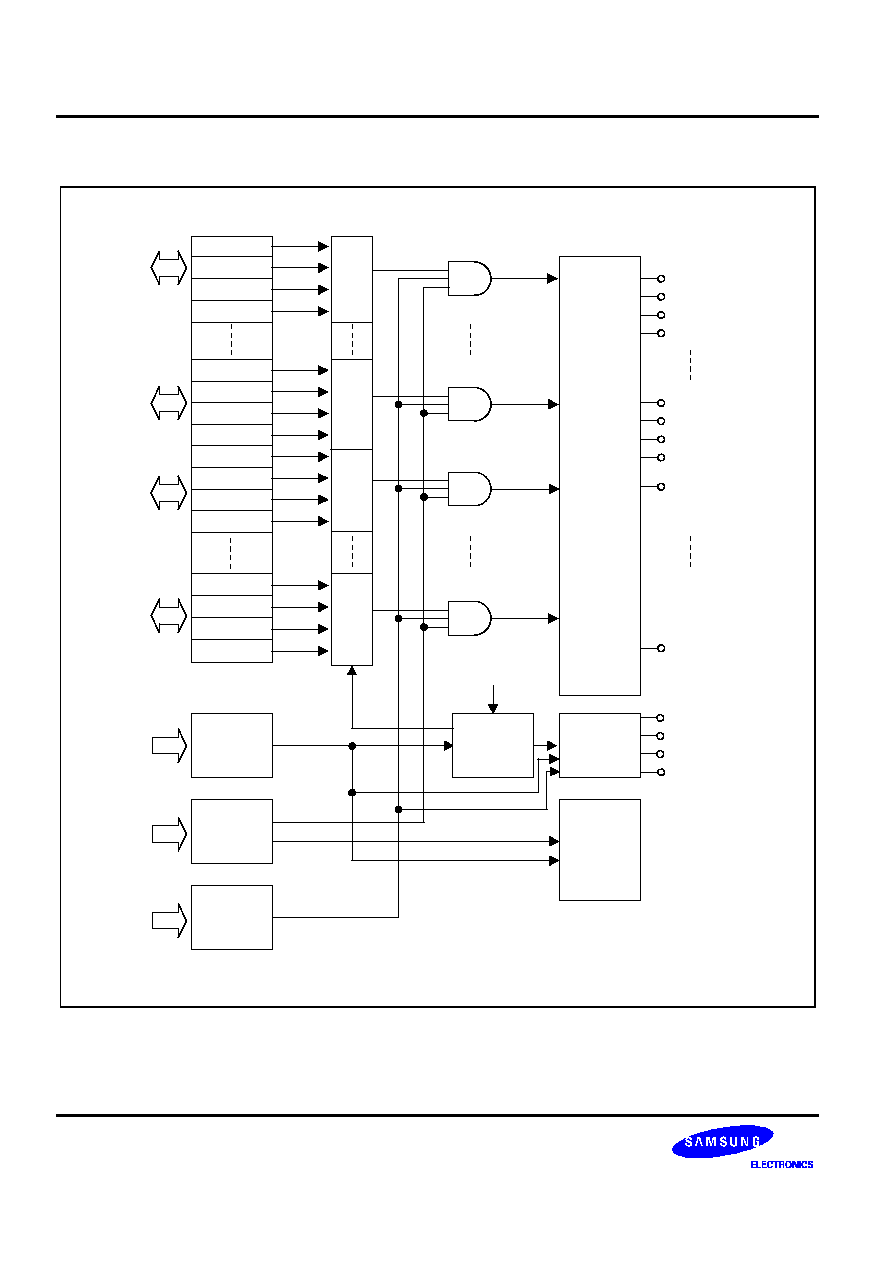
LCD CONTROLLER/DRIVER
S3CK225/FK225
18-2
LCD CIRCUIT DIAGRAM
COM2
COM0
COM3
LMOD
LCON
Timing
Controller
02H.7
02H.6
02H.5
02H.4
00H.3
00H.2
00H.1
00H.0
0FH.4
0FH.5
0FH.6
0FH.7
MUX
MUX
MUX
8
8
8
8
8
f
LCD
COM
Control
COM1
SEG31
SEG30
SEG29
SEG28
SEG0
SEG8
SEG7
SEG6
SEG5
SEG4
Segment
Driver
02H.3
02H.2
02H.1
02H.0
MUX
8
LPOT1,2
8
LCD
Voltage
Control
Figure 18-2. LCD Circuit Diagram

S3CK225/FK225
LCD CONTROLLER/DRIVER
18-3
LCD RAM ADDRESS AREA
RAM addresses 00H-0FH of page 2 are used as LCD data memory. When the bit value of a display segment is
"1", the LCD display is turned on; when the bit value is "0", the display is turned off.
Display RAM data are sent out through segment pins SEG0-SEG31 using a direct memory access (DMA) method
that is synchronized with the f
LCD
signal. RAM addresses in this location that are not used for LCD display can be
allocated to general-purpose use.
203H
bit 7
bit 6
bit 5
bit 3
bit 2
bit 1
bit 0
bit 4
SEG7
SEG6
SEG5
SEG4
SEG3
SEG2
SEG1
SEG0
202H
201H
200H
207H
206H
205H
204H
20BH
20AH
209H
208H
20FH
20EH
20DH
20CH
SEG31
COM3
COM2
COM1
COM0
Figure 18-3. LCD Display Data RAM Organization

LCD CONTROLLER/DRIVER
S3CK225/FK225
18-4
LCD CONTROL REGISTER (LCON, 60H)
Table 18-1. LCD Control Register (LCON) Organization
LCON Bit
Setting
Description
LCON.7
0
P4.7-P4.4 is selected
1
SEG23-SEG20 is selected, P4.7-P4.4 I/O is disabled
LCON.6
0
P4.3-P4.0 is selected
1
SEG19-SEG16 is selected, P4.3-P4.0 I/O is disabled
LCON.5
0
P3.7-P3.4 is selected
1
SEG15-SEG12 is selected, P3.7-P3.4 I/O is disabled
LCON.4
0
P3.3-P3.0 is selected
1
SEG11-SEG8 is selected, P3.3-P3.0 I/O is disabled
LCON.3
0
P2.7-P2.4 is selected
1
SEG7-SEG4 is selected, P2.7-P2.4 I/O is disabled
LCON.2
0
P2.3-P2.0 is selected
1
SEG3-SEG0 is selected, P2.3-P2.0 I/O is disabled
LCON.1
0
Always logic zero
LCON.0
0
LCD output low; turn display off
1
COM and SEG output is in display mode; turn display on
Table 18-2. Relationship of LCON.0 and LMOD.3 Bit Settings
LCON.0
LMOD.3
COM0-COM3
SEG0-SEG31
0
x
Output low; LCD display off
Output low; LCD display off
1
0
LCD display off signal output
1
COM output corresponds to display mode
SEG output corresponds to display mode
NOTE: "x" means don't care.
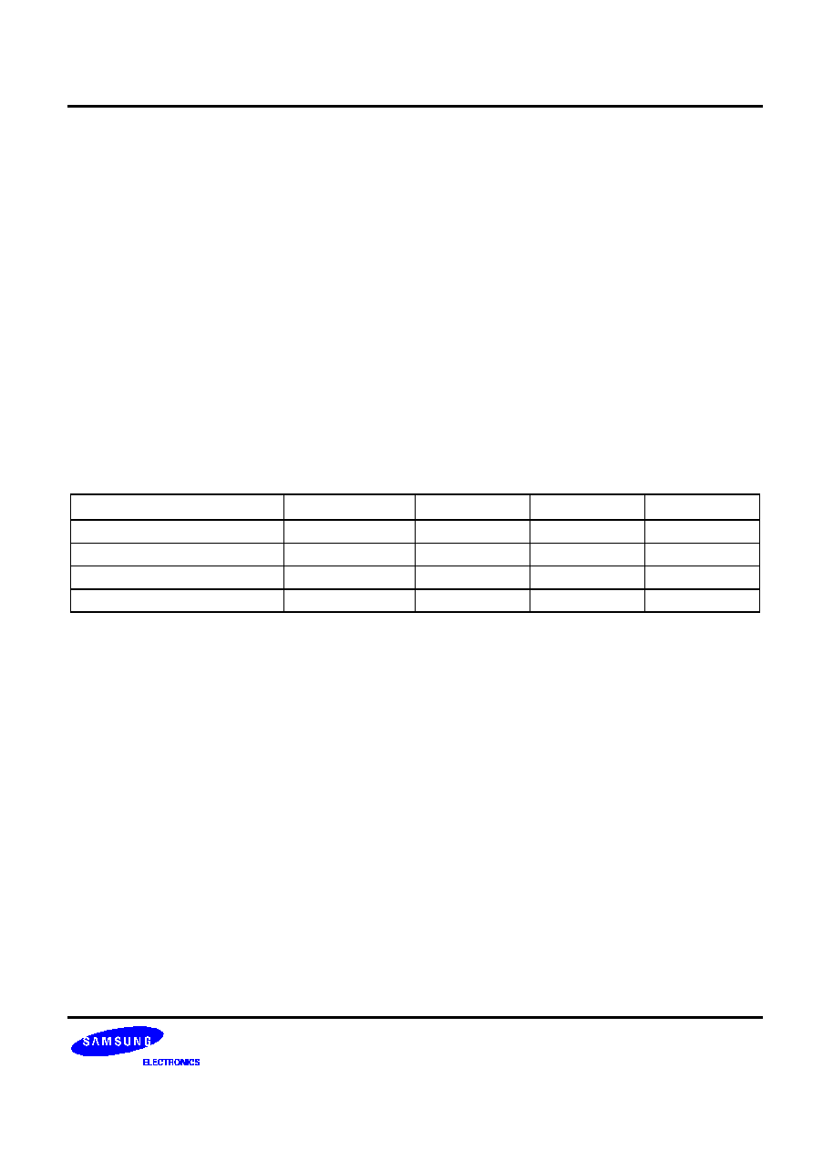
S3CK225/FK225
LCD CONTROLLER/DRIVER
18-5
LCD Mode Register (LMOD)
The LCD mode control register LMOD is mapped to RAM addresses 61H.
LMOD controls these LCD functions:
-- Duty and bias selection (LMOD.3-LMOD.0)
-- LCDCK clock frequency selection (LMOD.5-LMOD.4)
The LCD clock signal, LCDCK, determines the frequency of COM signal scanning of each segment output. This
is also referred to as the 'frame frequency'.
RESET
clears the LMOD and LCON register values to logic zero.
This produces the following LCD control settings:
-- Display is turned off
-- LCDCK frequency is 64 Hz
The LCD display can continue to operate during idle and stop modes if a sub clock is running, sub clock is
selected as watch timer clock, and watch timer is enabled.
Table 18-3. LCD Clock Signal (LCDCK) Frame Frequency
LCDCK Frequency (f
LCD
)
Static
1/2 Duty
1/3 Duty
1/4 Duty
64 Hz
64
32
21
16
128 Hz
128
64
43
32
256 Hz
256
128
85
64
512 Hz
512
256
171
128
NOTE: Because the clock source of LCDCK is from Watch Timer module, Watch Timer must be enabled for LCD display.

LCD CONTROLLER/DRIVER
S3CK225/FK225
18-6
Table 18-4. LCD Mode Control Register (LMOD) Organization, 61H
LMOD.7
Always logic zero.
LMOD.6
Always logic zero.
LMOD.5
LMOD.4
LCD Clock (LCDCK) Frequency
0
0
f
LCD
= 64 Hz (when fw is 32.768 kHz)
0
1
f
LCD
= 128 Hz (when fw is 32.768 kHz)
1
0
f
LCD
= 256 Hz (when fw is 32.768 kHz)
1
1
f
LCD
= 512 Hz (when fw is 32.768 kHz)
LMOD.3
LMOD.2
LMOD.1
LMOD.0
Duty and Bias Selection for LCD Display
0
x
x
x
LCD display off signal output
1
0
0
0
1/4 duty, 1/3 bias
1
0
0
1
1/3 duty, 1/3 bias
1
0
1
1
1/3 duty, 1/2 bias
1
0
1
0
1/2 duty, 1/2 bias
1
1
x
x
Static
NOTE: "x" means don't care.
Table 18-5. Maximum Number of Display Digits per Duty Cycle
LCD Duty
LCD Bias
COM Output Pins
Maximum Seg Display
Static
Static
COM0
32
1/2
1/2
COM0-COM1
32
�
2
1/3
1/2
COM0-COM2
32
�
3
1/3
1/3
COM0-COM2
32
�
3
1/4
1/3
COM0-COM3
32
�
4

S3CK225/FK225
LCD CONTROLLER/DRIVER
18-7
LCD PORT CONTROL REGISTERS (LPOT1, LPOT2)
The LCD port control registers, LPOT1 and LPOT2, is used to control for selecting LCD signal or normal I/O pins.
Following a
RESET
, the LPOT1 and LPOT2 values are cleared to "0".
LSB
MSB
LCD Port Control Register1 (LPOT1)
62H, R/W, Reset: 00H
SEG31/P5.7 selection bit:
0 = Normal I/O pin
1 = SEG pin
SEG30/P5.6 selection bit:
0 = Normal I/O pin
1 = SEG pin
SEG27/P5.3 selection bit:
0 = Normal I/O pin
1 = SEG pin
SEG26/P5.2 selection bit:
0 = Normal I/O pin
1 = SEG pin
SEG29/P5.5 selection bit:
0 = Normal I/O pin
1 = SEG pin
SEG28/P5.4 selection bit:
0 = Normal I/O pin
1 = SEG pin
.7
.6
.5
.4
.3
.2
.1
.0
SEG25/P5.1 selection bit:
0 = Normal I/O pin
1 = SEG pin
SEG24/P5.0 selection bit:
0 = Normal I/O pin
1 = SEG pin
Figure 18-4. LCD Port Control Resister1 (LPOT1)
LSB
MSB
LCD Port Control Register2 (LPOT2)
63H, R/W, Reset: 00H
Always logic zero
COM3/P6.3 selection bit:
0 = Normal I/O pin
1 = COM pin
COM2/P6.2 selection bit:
0 = Normal I/O pin
1 = COM pin
.7
.6
.5
.4
.3
.2
.1
.0
COM1/P6.1 selection bit:
0 = Normal I/O pin
1 = COM pin
COM0/P6.0 selection bit:
0 = Normal I/O pin
1 = COM pin
Figure 18-5. LCD Port Control Resister2 (LPOT2)

LCD CONTROLLER/DRIVER
S3CK225/FK225
18-8
LCD VOLTAGE DIVIDING RESISTORS
Static and 1/3 Bias
1/2 Bias
V
DD
LCON.0
V
LC1
V
LC0
V
LCD
= V
DD
V
SS
R
R
R
V
DD
LCON.0
V
LC1
= V
LC0
V
LCD
= V
DD
V
SS
R
R
R
Figure 18-6. Internal Voltage Dividing Resistor Connection
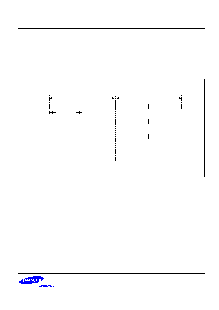
S3CK225/FK225
LCD CONTROLLER/DRIVER
18-9
LCD COM/SEG SIGNALS
The 32 LCD segment signal pins are connected to corresponding display RAM locations at 00H-0FH of page 2.
Bits of the display RAM are synchronized with the common signal output pins COM0, COM1, COM2, and COM3.
When the bit value of a display RAM location is "1", a select signal is sent to the corresponding segment pin.
When the display bit is "0", a 'no-select' signal is sent to the corresponding segment pin. Each bias has select and
no-select signals.
COM-SEG
FR
Select
Non-Select
1 Frame
COM
SEG
V
DD
V
SS
V
DD
V
SS
V
DD
V
SS
-V
DD
Figure 18-7. Select/No-Select Bias Signals in Static Display Mode

LCD CONTROLLER/DRIVER
S3CK225/FK225
18-10
FR
Select
Non-Select
1 Frame
COM
V
DD
V
LC1,0
V
SS
SEG
V
SS
COM-SEG
V
SS
-V
LC1,0
-V
DD
V
DD
V
LC1,0
V
DD
V
LC1,0
Figure 18-8. Select/No-Select Bias Signals in 1/2 Duty, 1/2 Bias Display Mode
-V
DD
V
SS
V
DD
V
SS
V
DD
V
SS
V
DD
COM-SEG
COM
SEG
FR
1 Frame
Non-Select
Select
Figure 18-9. Select/No-Select Bias Signals in 1/3 Duty, 1/3 Bias Display Mode
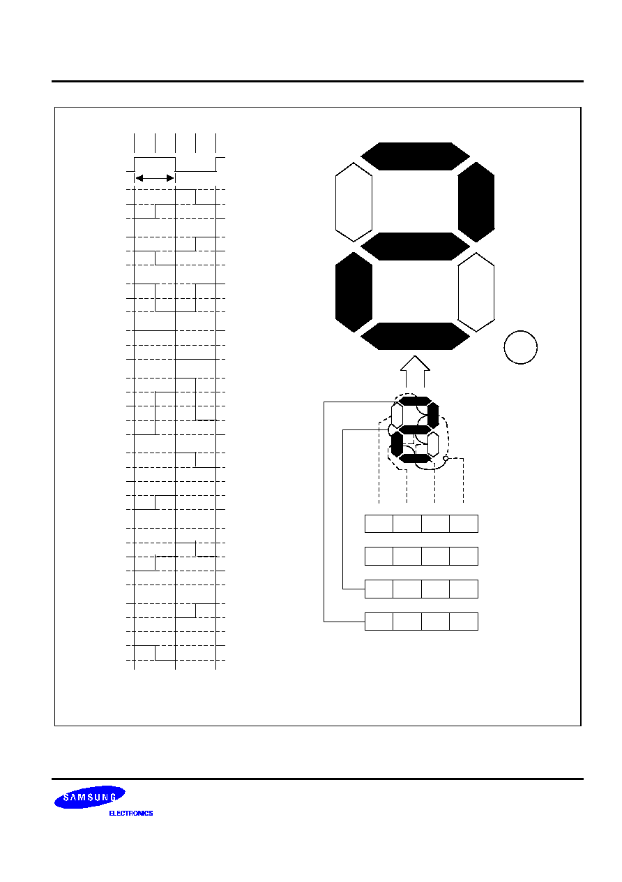
S3CK225/FK225
LCD CONTROLLER/DRIVER
18-11
FR
1 Frame
COM0
COM1
SEG0
SEG1
COM0
-SEG0
COM0
-SEG1
COM1
-SEG0
COM1
-SEG1
0
1
0
1
NOTE:
V
LC1
= V
LC0
SEG1
SEG2
SEG3
SEG0
SEG3.1 x C1
COM0
COM1
SEG2.1 x C1
SEG0.0 x C0
SEG0.1 x C1
SEG1.0 x C0
SEG3.0 x C0
SEG2.1 x C1
SEG2.0 x C0
SEG2.0 x C0
SEG1.1 x C1
V
DD
V
SS
V
LC1,0
V
DD
V
SS
V
LC1,0
V
DD
V
SS
V
LC1,0
V
DD
V
SS
V
LC1,0
V
DD
-V
DD
V
LC1,0
V
SS
-V
LC1,0
V
DD
-V
DD
V
LC1,0
V
SS
-V
LC1,0
V
DD
-V
DD
V
LC1,0
V
SS
-V
LC1,0
V
DD
-V
DD
V
LC1,0
V
SS
-V
LC1,0
X
X
X
X
.0
.1
.2
.3
203H
X
X
X
X
.0
.1
.2
.3
202H
0
1
1
0
.0
.1
.2
.3
201H
1
1
0
1
.0
.1
.2
.3
200H
Figure 18-10. LCD Signal and Wave Forms Example in 1/2 Duty, 1/2 Bias Display Mode

LCD CONTROLLER/DRIVER
S3CK225/FK225
18-12
COM0
COM1
SEG0
SEG1
COM0
-SEG0
COM0
-SEG1
COM1
-SEG0
COM1
-SEG1
COM2
V
LC2
V
SS
V
LC1
V
LC0
V
DD
V
SS
V
LC1
V
LC0
V
DD
V
SS
V
LC1
V
LC0
V
DD
V
SS
V
LC1
V
LC0
V
DD
V
SS
V
LC1
V
LC0
FR
1 Frame
0
1
2
0
1
2
SEG1.6 x C2
SEG2.1 x C1
SEG2.0 x C0
SEG0.0 x C0
SEG2.1 x C1
SEG1.4 x C0
SEG0.2 x C2
SEG2.0 x C0
SEG1.5 x C1
SEG0.1 x C1
COM1
SEG0
SEG1
SEG2
COM2
V
DD
-V
LC1
V
LC1
V
LC0
V
SS
-V
LC0
-V
DD
V
DD
-V
LC1
V
LC1
V
LC0
V
SS
-V
LC0
-V
DD
V
DD
-V
LC1
V
LC1
V
LC0
V
SS
-V
LC0
-V
DD
V
DD
-V
LC1
V
LC1
V
LC0
V
SS
-V
LC0
-V
DD
SEG3
SEG4
SEG5
X
X
X
X
.0
.1
.2
.3
203H
X
X
.4
.5
1
0
0
1
.0
.1
.2
.3
202H
0
0
.4
.5
1
0
1
0
.0
.1
.2
.3
201H
1
1
.4
.5
0
1
1
0
.0
.1
.2
.3
200H
1
1
.4
.5
COM0
Figure 18-11. LCD Signals and Wave Forms Example in 1/3 Duty, 1/3 Bias Display Mode

S3CK225/FK225
LCD CONTROLLER/DRIVER
18-13
1 Frame
0
1
2
3
1
2
V
DD
V
SS
V
LC1
V
LC0
V
DD
V
SS
V
LC1
V
LC0
COM0
COM1
COM3
SEG0
COM0
-SEG0
COM0
-SEG1
COM1
-SEG1
COM2
FR
0
3
V
DD
V
SS
V
LC1
V
LC0
V
DD
V
SS
V
LC1
V
LC0
V
DD
-V
LC1
V
LC1
V
LC0
V
SS
-V
LC0
-V
DD
V
DD
-V
LC1
V
LC1
V
LC0
V
SS
-V
LC0
-V
DD
V
DD
-V
LC1
V
LC1
V
LC0
V
SS
-V
LC0
-V
DD
V
DD
-V
LC1
V
LC1
V
LC0
V
SS
-V
LC0
-V
DD
V
DD
V
SS
V
LC1
V
LC0
V
DD
V
SS
V
LC1
V
LC0
SEG1
COM1
-SEG0
SEG1.7 x C3
SEG2.1 x C1
SEG1.4 x C0
SEG0.0 x C0
SEG0.1 x C1
SEG1.5 x C1
SEG0.3 x C3
SEG2.0 x C0
SEG1.6 x C2
SEG0.2 x C2
COM0
COM1
COM2
SEG2
SEG3
SEG4
SEG5
COM3
SEG0
SEG1
X
X
X
X
.0
.1
.2
.3
203H
X
X
.4
.5
1
0
0
1
.0
.1
.2
.3
202H
0
0
.4
.5
1
0
1
0
.0
.1
.2
.3
201H
1
1
.4
.5
0
1
1
0
.0
.1
.2
.3
200H
1
1
.4
.5
Figure 18-12. LCD Signals and Wave Forms Example in 1/4 Duty, 1/3 Bias Display Mode

LCD CONTROLLER/DRIVER
S3CK225/FK225
18-14
NOTES

S3CK225/FK225
10-BIT A/D CONVERTER
19-1
19
10-BIT ANALOG-TO-DIGITAL CONVERTER
OVERVIEW
The 10-bit A/D converter (ADC) module uses successive approximation logic to convert analog levels entering at
one of the eight input channels to equivalent 10-bit digital values. The analog input level must lie between the
AV
REF
and AV
SS
values. The A/D converter has the following components:
-- Analog comparator with successive approximation logic
-- D/A converter logic (resistor string type)
-- ADC control register (ADCON)
-- Eight multiplexed analog data input pins (AD0-AD7)
-- 10-bit A/D conversion data output register (ADDATAH/ADDATAL)
-- 8-bit digital input port (Alternately, I/O port)
FUNCTION DESCRIPTION
To initiate an analog-to-digital conversion procedure, at first you must set with alternative function for ADC input
enable at port 5, the pin set with alternative function can be used for ADC analog input. And you write the
channel selection data in the A/D converter control register ADCON.4-.6 to select one of the eight analog input
pins (AD0�AD7) and set the conversion start or enable bit, ADCON.0. The read-write ADCON register is located
in address 5CH. The pins which are not used for ADC can be used for normal I/O or SEG signal.
During a normal conversion, ADC logic initially sets the successive approximation register to 800H (the
approximate half-way point of an 10-bit register). This register is then updated automatically during each
conversion step. The successive approximation block performs 10-bit conversions for one input channel at a
time. You can dynamically select different channels by manipulating the channel selection bit value (ADCON.6�
4) in the ADCON register. To start the A/D conversion, you should set the enable bit, ADCON.0. When a
conversion is completed, ADCON.3, the end-of-conversion(EOC) bit is automatically set to 1 and the result is
dumped into the ADDATAH/ADDATAL register where it can be read. The A/D converter then enters an idle state.
Remember to read the contents of ADDATAH/ADDATAL before another conversion starts. Otherwise, the
previous result will be overwritten by the next conversion result.
NOTE
Because the A/D converter has no sample-and-hold circuitry, it is very important that fluctuation in the analog
level at the AD0-AD7 input pins during a conversion procedure be kept to an absolute minimum. Any change in
the input level, perhaps due to noise, will invalidate the result. If the chip enters to STOP or IDLE mode in
conversion process, there will be a leakage current path in A/D block. You must use STOP or IDLE mode after
ADC operation is finished.

10-BIT A/D CONVERTER
S3CK225/FK225
19-2
CONVERSION TIMING
The A/D conversion process requires 4 steps (4 clock edges) to convert each bit and 10 clocks to set-up A/D
conversion. Therefore, total of 50 clocks are required to complete an 10-bit conversion: When fxx/8 is selected
for conversion clock with an 4.5 MHz fxx clock frequency, one clock cycle is 1.78 us. Each bit conversion
requires 4 clocks, the conversion rate is calculated as follows:
4 clocks/bit
�
10-bit + set-up time = 50 clocks, 50 clock
�
1.78 us = 89 us at 0.56 MHz (4.5 MHz/8)
Note that A/D converter needs at least 25
�
s for conversion time.
A/D CONVERTER CONTROL REGISTER (ADCON)
The A/D converter control register, ADCON, is located at address 5CH. It has three functions:
-- Analog input pin selection (bits 4�6)
-- End-of-conversion status detection (bit 3)
-- ADC clock selection (bits 2 and 1)
-- A/D operation start or disable (bit 0 )
After a reset, the start bit is turned off. You can select only one analog input channel at a time. Other analog
input pins (AD0-AD7) can be selected dynamically by manipulating the ADCON.4�.6 bits. And the pins not used
for analog input can be used for normal I/O or SEG function.
Start or disable bit
0 = Disable operation
1 = Start operation
(This bit is cleared automatically
after End-of-Conversion.)
A/D Converter Control Register (ADCON)
5CH, R/W (EOC bit is read-only)
.7
.6
.5
.4
.3
.2
.1
.0
MSB
LSB
End-of-conversion bit
0 = Not complete Conversion
1 = Complete Conversion
Always logic zero
A/D input pin selection bits:
000 = AD0
001 = AD1
010 = AD2
011 = AD3
100 = AD4
101 = AD5
110 = AD6
111 = AD7
Clock Selection bits:
00 = fxx/8
01 = fxx/4
10 = fxx/2
11 = fxx/1
Figure 19-1. A/D Converter Control Register (ADCON)

S3CK225/FK225
10-BIT A/D CONVERTER
19-3
Conversion Data Register ADDATAH/ADDATAL
5DH/5EH, Read Only
.9
.8
.7
.6
.5
.4
.3
.2
MSB
LSB
(ADDATAH)
.1
.0
MSB
LSB
(ADDATAL)
Figure 19-2. A/D Converter Data Register (ADDATAH/ADDATAL)
INTERNAL REFERENCE VOLTAGE LEVELS
In the ADC function block, the analog input voltage level is compared to the reference voltage. The analog input
level must remain within the range AV
SS
to AV
REF
.
Different reference voltage levels are generated internally along the resistor tree during the analog conversion
process for each conversion step. The reference voltage level for the first conversion bit is always 1/2 AV
REF
.
BLOCK DIAGRAM
Input Pins
AD0-AD7
(P5.0-P5.7)
Clock
Selector
Conversion Result
(ADDATAH/ADDATAL,
5DH/5EH)
-
+
To ADCON.3
(EOC Flag)
Successive
Approximation
Logic & Register
AV
REF
AV
SS
Analog
Comparator
10-bit D/A
Converter
M
U
X
ADCON.4-.6
(Select one input pin of the assigned pins)
P5CONH/L
(Assign Pins to ADC Input)
ADCON.0
(AD/C Enable)
ADCON.0
(AD/C Enable)
.
.
.
ADCON.2-.1
Figure 19-3. A/D Converter Functional Block Diagram

10-BIT A/D CONVERTER
S3CK225/FK225
19-4
AV
SS
S3CK225
AD0-AD7
AV
REF
Reference
Voltage Input
(AV
REF
V
DD
)
Analog
Input Pin
V
DD
V
DD
10
�
F
103
101
+
-
C
C
R
NOTE:
The symbol "R" signifies an offset resistor with a value of from 50 to 100
.
Figure 19-4. Recommended A/D Converter Circuit for Highest Absolute Accuracy

S3CK225/FK225
D/A CONVERTER
20-1
20
D/A CONVERTER
OVERVIEW
The 10-bit D/A Converter (DAC) module uses successive approximation logic to convert 10-bit digital values to
equivalent analog levels between V
DD
(1 -
1
1024
) and V
SS.
This D/A Converter consists of R�2R array structure. The D/A Converter has the following components:
-- R�2R array structure
-- Digital-to-analog converter control register (DACON)
-- Digital-to-analog converter data register (DADATAH/DADATAL)
-- Digital-to-analog converter output pin (DAO)
FUNCTION DESCRIPTION
To initiate a digital-to-analog conversion procedure, you should set the digital-to-analog converter enable bit
(DACON.0).
The DACON register is located at the RAM address 74H. You should write the digital value calculated to digital-
to-analog converter data register (DADATAH/DADATAL).
NOTE
If the chip enters to power-down mode, STOP or IDLE, in conversion process, there will be current path
in D/A Converter block. So, It is necessary to cut off the current path before the instruction execution
enters power-down mode.

D/A CONVERTER
S3CK225/FK225
20-2
Data Bus
DACON.1
Timer 1 Match
Signal
.0
.1
.2
.3
.4
.5
.6
.7
DADATA
.8
.0
.1
.2
.3
.4
.5
.6
.7
DAC Buffer
.8
DAO
2R
2R
2R
2R
2R
2R
2R
2R
2R
2R
R
R
R
R
R
R
R
R
DACON.0
10-bit
.9
.9
2R
R
Figure 20-1. DAC Circuit Diagram
Enable/Disable control bit:
0 = Disable D/AC
1 = Enable D/AC
D/A Converter Control Register (DACON)
74H, R/W, Reset: 00H
.7
.6
.5
.4
.3
.2
.1
.0
MSB
LSB
Data latch control bit:
0 = The value of DADATA is always
loaded into the DAC buffer.
1 = The value of DADATA is loaded into
the DAC buffer when the timer 1
match is occurred.
Not used
Figure 20-2. Digital to Analog Converter Control Register (DACON)

S3CK225/FK225
D/A CONVERTER
20-3
D/A CONVERTER DATA REGISTER (DADATAH/DADATAL)
The DAC DATA register, DADATAH/DADATAL is located at the RAM address, 75H�76H. DADATAH/DADATAL
specifies the digital data to generate analog voltage. A
RESET
initializes the DADATAH/DADATAL value to
"00H". The D/A converter output value, V
DAO
, is calculated by the following formula.
V
DAO
= V
DD
�
�
n
1024
(n = 0-1023, DADATAH/DADATAL value)
Table 20-1. DADATA Setting to Generate Analog Voltage
DADATAH.7 DADATAH.6 DADATAH.5 DADATAH.4 DADATAH.3 DADATAH.2 DADATAH.1 DADATAH.0 DADATAL.7 DADATAL.6
VDAO
0
0
0
0
0
0
0
0
0
0
0
1
0
0
0
0
0
0
0
0
0
VDD/2
1
0
1
0
0
0
0
0
0
0
0
VDD/2
2
0
0
1
0
0
0
0
0
0
0
VDD/2
3
0
0
0
1
0
0
0
0
0
0
VDD/2
4
0
0
0
0
1
0
0
0
0
0
VDD/2
5
0
0
0
0
0
1
0
0
0
0
VDD/2
6
0
0
0
0
0
0
1
0
0
0
VDD/2
7
0
0
0
0
0
0
0
1
0
0
VDD/2
8
0
0
0
0
0
0
0
0
1
0
VDD/2
9
0
0
0
0
0
0
0
0
0
1
VDD/2
10
NOTE: These are the values determined by setting just one-bit of DADATA.0-DADATA.9. Other values of DAO can be
obtained with superimposition.

D/A CONVERTER
S3CK225/FK225
20-4
Conversion Data Register (DADATAH/DADATAL)
75H/76H, R/W
.9
.8
.7
.6
.5
.4
.3
.2
MSB
LSB (DADATAH)
.1
-
-
-
-
-
-
MSB
LSB (DADATAL)
These bits should be always "0".
.0
Figure 20-3. D/A Converter Data Register (DADATAH/DADATAL)

S3CK225/FK225
OPERATIONAL AMPLIFIER
21-1
21
OPERATIONAL AMPLIFIER
OVERVIEW
There are two OP AMPs in the S3CK225/FK225. One is for filtering out the noise from input signals, the other is
for amplifying input signals. These amplifiers can be used for another purpose.
The amplifiers consists of the following components:
-- FIL amplifier (FILIN, FILOUT)
-- MIC amplifier (MICIN, MICOUT)
-- OP AMP control register (OPCON)
-- Vref generator
OP AMP CONTROL REGISTER (OPCON)
MIC amplifier control bit:
0 = Disable MIC amplifier
1 = Enable MIC amplifier
OP AMP Control Register (OPCON)
77H, R/W, Reset: 00H
.7
.6
.5
.4
.3
.2
.1
.0
MSB
LSB
FIL amplifier control bit:
0 = Disable FIL amplifier
1 = Enable FIL amplifier
Not used
Figure 21-1. OP AMP Control Register (OPCON)

OPERATIONAL AMPLIFIER
S3CK225/FK225
21-2
Vref
Generator
-
+
-
+
OPCON.0
OPCON.1
FILIN
FILOUT
Vref
MICIN
MICOUT
1 pF
300K
15K
Figure 21-2. OP AMP Block Diagram

S3CK225/FK225
ELECTRICAL DATA
22-1
22
ELECTRICAL DATA
Table 22-1. Absolute Maximum Ratings
(T
A
= 25
�
C)
Parameter
Symbol
Conditions
Rating
Unit
Supply voltage
V
DD
�
�0.3 to + 6.5
V
Input voltage
V
I
�
�0.3 to V
DD
+ 0.3
V
Output voltage
V
O
�
�0.3 to V
DD
+ 0.3
V
Output current high
I
OH
One I/O pin active
�18
mA
All I/O pins active
�60
Output current low
I
OL
One I/O pin active
+ 30
mA
Total pin current for port
+ 100
Operating temperature
T
A
�
�25 to + 85
�
C
Storage temperature
T
STG
�
�65 to + 150
�
C
Table 22-2. D.C. Electrical Characteristics
(T
A
= � 25
�
C to + 85
�
C, V
DD
= 2.0 V to 5.5 V)
Parameter
Symbol
Conditions
Min
Typ
Max
Unit
Operating voltage
V
DD
fx = 8 MHz
3.0
�
5.5
V
fx = 4 MHz
2.4
�
5.5
fx = 2 MHz
2.0
�
5.5
Input high voltage
V
IH1
All input pins except V
IH2
0.8V
DD
�
V
DD
V
V
IH2
X
IN
, XT
IN
V
DD
�
0.1
Input low voltage
V
IL1
All input pins except V
IL2
�
�
0.2V
DD
V
V
IL2
X
IN
, XT
IN
0.1
Output high voltage
V
OH
V
DD
= 4.5 V to 5.5 V;
I
OH
= �1 mA, all output pins
V
DD
�1.0
�
�
V
Output low voltage
V
OL
V
DD
= 4.5 V to 5.5 V;
I
OL
= 10 mA, all output pins
�
�
2.0

ELECTRICAL DATA
S3CK225/FK225
22-2
Table 22-2. D.C. Electrical Characteristics (Continued)
(T
A
= � 25
�
C to + 85
�
C, V
DD
= 2.0 V to 5.5 V)
Parameter
Symbol
Conditions
Min
Typ
Max
Unit
Input high leakage
current
I
LIH1
V
IN
= V
DD
All input pins except I
LIH2
�
�
3
uA
I
LIH2
V
IN
= V
DD
; X
IN
, XT
IN
�
�
20
Input low leakage
current
I
LIL1
V
IN
= 0 V
All input pins except I
LIL2
�
�
�3
I
LIL2
V
IN
= 0 V; X
IN
, XT
IN
,
RESET
�20
Output high
leakage current
I
LOH
V
OUT
= V
DD
All I/O pins and output pins
�
�
3
Output low
leakage current
I
LOL
V
OUT
= 0 V
All I/O pins and output pins
�
�
�3
Oscillator feedback
resistors
R
OSC1
V
DD
= 5.0 V, T
A
= 25
�
C
X
IN
= VDD, X
OUT
= 0 V
400
750
1200
k
R
OSC2
V
DD
= 5.0 V, T
A
= 25
�
C
XT
IN
= VDD, XT
OUT
= 0 V
1500
3000
4500
Pull-up resistor
R
L1
V
IN
= 0 V; V
DD
= 5 V
�
10%
Port 0-7, T
A
= 25
�
C
25
50
100
R
L2
V
IN
= 0 V; V
DD
= 3 V
�
10%
T
A
= 25
�
C,
RESET
only
110
210
310
LCD voltage
dividing resistor
R
LCD
T
A
= 25
�
C
60
100
140
VLC1 output
voltage
V
LC1
T
A
= 25
�
C
V
LCD
= 2.5 V to 5.5 V
2/3V
DD
- 0.2V
2/3V
DD
2/3V
DD
+0.2V
V
VLC0 output
voltage
V
LC0
1/3 bias
1/3V
DD
- 0.2V
1/3V
DD
1/3V
DD
+0.2V
COM output
voltage
deviation
V
DC
V
DD
= V
LC2
= 3V
(VLCD-COMi)
I
O
=
�
15
�
A, (i = 0-3)
�
�
60
�
120
mV
SEG output voltage
deviation
V
DS
V
DD
= V
LC2
= 3V
(VLCD-SEGi)
I
O
=
�
15
�
A, (i = 0-31)
�
�
60
�
120

S3CK225/FK225
ELECTRICAL DATA
22-3
Table 22-2. D.C. Electrical Characteristics (Concluded)
(T
A
= � 25
�
C to + 85
�
C, V
DD
= 2.0 V to 5.5 V)
Parameter
Symbol
Conditions
Min
Typ
Max
Unit
Supply current
(1)
I
DD1
(2)
V
DD
= 5 V
�
10%
8 MHz crystal oscillator
�
5.0
10
mA
2 MHz crystal oscillator
1.5
3
V
DD
= 3 V
�
10%
8 MHz crystal oscillator
3.0
6.0
2 MHz crystal oscillator
1.1
2.0
I
DD2
Idle mode: V
DD
= 5 V
�
10%
8 MHz crystal oscillator
�
1.0
2.0
mA
2 MHz crystal oscillator
0.5
1.0
Idle mode: V
DD
= 3 V
�
10%
8 MHz crystal oscillator
0.5
1.0
2 MHz crystal oscillator
0.3
0.6
I
DD3
Sub operating mode: main-osc stop
V
DD
= 3 V
�
10 %
32768 Hz crystal oscillator
�
20
40
uA
I
DD4
Sub-idle mode; main-osc stop
V
DD
= 3 V
�
10 %
32768 Hz crystal oscillator
�
6
15
I
DD5
Main stop mode; Sub-osc stop.
V
DD
= 5 V
�
10 %, T
A
= 25
�
C
�
1
3
V
DD
= 3 V
�
10 %, T
A
= 25
�
C
0.5
2
NOTES:
1,
Supply current does not include current drawn through internal pull-up resistors or external output current loads.
2.
I
DD1
and I
DD2
includes a power consumption of sub oscillator.
3.
I
DD3
and I
DD4
are the current when the main clock oscillation stop and the sub clock is used, and does not include
LCD voltage dividing resistors.
4. I
DD5
is the current when the main and sub clock oscillation stop.

ELECTRICAL DATA
S3CK225/FK225
22-4
Table 22-3. A.C. Electrical Characteristics
(T
A
= � 25
�
C to + 85
�
C, V
DD
= 2.0 V to 5.5 V)
Parameter
Symbol
Conditions
Min
Typ
Max
Unit
Interrupt input high,
low width
t
INTH
,
t
INTL
P0.0�P0.3
V
DD
= 5 V
�
200
�
ns
RESET
input
low width
t
RSL
V
DD
= 5 V
�
10 %
10
�
�
�
s
t
INTH
t
INTL
0.8 V
DD
0.2 V
DD
Figure 22-1. Input Timing for External Interrupts (Port 0)
RESET
t
RSL
0.2 V
DD
Figure 22-2. Input Timing for
RESET
RESET

S3CK225/FK225
ELECTRICAL DATA
22-5
Table 22-4. Input/Output Capacitance
(T
A
= �25
�
C to + 85
�
C, V
DD
= 0 V)
Parameter
Symbol
Conditions
Min
Typ
Max
Unit
Input capacitance
C
IN
f = 1 MHz; unmeasured pins are
returned to V
SS
.
�
�
10
pF
Output capacitance
C
OUT
I/O capacitance
C
IO
Table 22-5. Data Retention Supply Voltage in Stop Mode
(T
A
= �25
�
C to + 85
�
C)
Parameter
Symbol
Conditions
Min
Typ
Max
Unit
Data retention
supply voltage
V
DDDR
�
2
�
5.5
V
Data retention
supply current
I
DDDR
V
DDDR
= 2 V
�
�
2
uA
Execution of
STOP Instruction
RESET
Occur
~ ~
V
DDDR
~ ~
Stop Mode
Normal
Operating Mode
Data Retention Mode
t
WAIT
RESET
V
DD
NOTE:
t
WAIT
is decided by RCOD_OPT.14-.12 setting. When bit 14, 13, 12 of RCOD_OPT is
"110"b, t
WAIT
is 1024 x 32 x 1/fxx.
Oscillation
Stabilization Time
0.2V
DD
Figure 22-3. Stop Mode Release Timing When Initiated by a
RESET
RESET
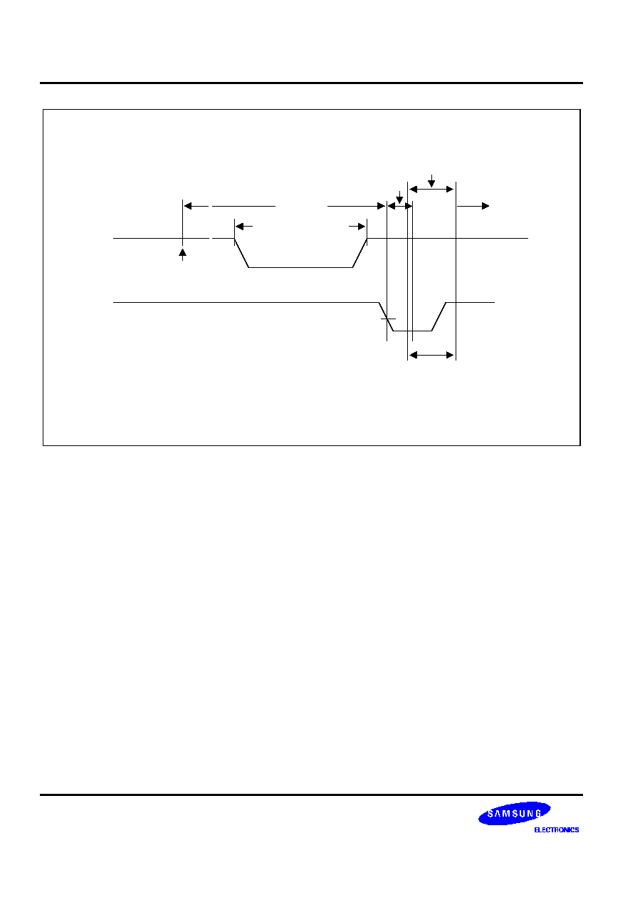
ELECTRICAL DATA
S3CK225/FK225
22-6
Execution of
STOP Instruction
V
DDDR
~ ~
Data Retention
V
DD
Normal
Operating
Mode
~ ~
Stop Mode
OSC Start
up time
t
WAIT
Oscillation
Stabilization Time
0.2 V
DD
INT
NOTE:
t
WAIT
is decided by WDTCON register setting. When bit 6, 5, 4 of WDTCON is "110"b, t
WAIT
is
1024 x 32 x 1/fxx.
Figure 22-4. Stop Mode Release Timing Initiated by Interrupts
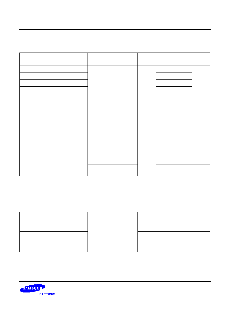
S3CK225/FK225
ELECTRICAL DATA
22-7
Table 22-6. A/D Converter Electrical Characteristics
(T
A
= � 25
�
C to 85
�
C, V
DD
= 2.7 V to 5.5 V, V
SS
= 0 V)
Parameter
Symbol
Conditions
Min
Typ
Max
Unit
Resolution
�
10
�
bit
Total accuracy
V
DD
= 5.12 V
�
�
�
3
LSB
Integral linearity error
ILE
AV
REF
= 5.12 V
�
�
2
Differential linearity error
DLE
AV
SS
= 0 V
�
�
2
Offset error of top
EOT
fxx = 8MHz
�
1
�
3
Offset error of bottom
EOB
f
CON
= fxx/4
�
0.5
�
2
Conversion time
(1)
T
CON
10-bit resolution
50
�
fxx/4, fxx = 8MHz
25
�
�
�
s
Analog input voltage
V
IAN
�
AV
SS
�
AV
REF
V
Analog input impedance
R
AN
�
2
�
�
M
Analog reference
voltage
AV
REF
�
2.5
�
V
DD
V
Analog ground
AV
SS
�
V
SS
�
V
SS
+0.3
Analog input current
I
ADIN
AV
REF
= V
DD
= 5 V
�
�
10
�
A
Analog block current
(2)
I
ADC
AV
REF
= V
DD
= 5 V
�
1
3
mA
AV
REF
= V
DD
= 3 V
0.5
1.5
AV
REF
= V
DD
= 5 V
When power down mode
100
500
nA
NOTES:
1.
'Conversion time' is the period between start and end of conversion operation.
2.
I
ADC
is an operating current during A/D conversion.
Table 22-7. D/A Converter Electrical Characteristics
(T
A
= � 25
�
C to 85
�
C, V
DD
= 2.7 V to 5.5 V, V
SS
= 0 V)
Parameter
Symbol
Conditions
Min
Typ
Max
Unit
Resolution
�
V
DD
= 5.12 V
�
�
10
bits
Absolute accuracy
�
-3
�
3
LSB
Differential linearity error
DLE
-1
�
1
LSB
Setup time
t
SU
�
�
5
�
s
Output resistance
R
O
20
30
40
K

ELECTRICAL DATA
S3CK225/FK225
22-8
Table 22-8. Synchronous SIO Electrical Characteristics
(T
A
= � 25
�
C to + 85
�
C, V
DD
= 2.0 V to 5.5 V, V
SS
= 0 V, fxx = 8 MHz oscillator)
Parameter
Symbol
Conditions
Min
Typ
Max
Unit
SCK Cycle time
T
CYC
�
250
�
�
ns
Serial Clock High Width
T
SCKH
�
75
�
�
Serial Clock Low Width
T
SCKL
�
75
�
�
Serial Output data delay time
T
OD
�
�
�
65
Serial Input data setup time
T
ID
�
50
�
�
Serial Input data Hold time
T
IH
�
125
�
�
Output Data
Input Data
SCK
t
SCKH
t
CYC
t
SCKL
0.8 V
DD
0.2 V
DD
t
OD
t
ID
t
IH
0.8 V
DD
0.2 V
DD
SI
SO
Figure 22-5. Serial Data Transfer Timing
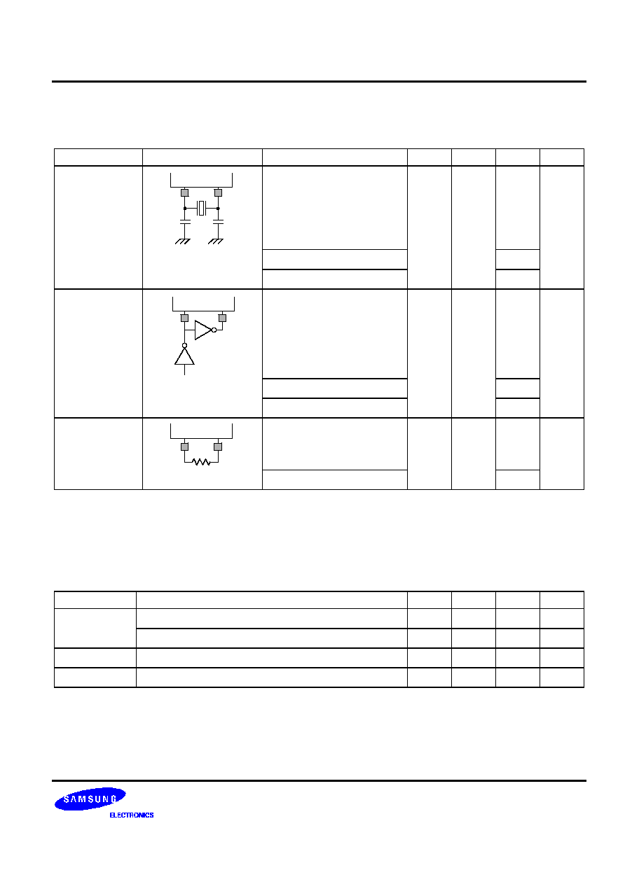
S3CK225/FK225
ELECTRICAL DATA
22-9
Table 22-9. Main Oscillator Frequency (f
OSC
1)
(T
A
= � 25
�
C to + 85
�
C V
DD
= 2.0 V to 5.5 V)
Oscillator
Clock Circuit
Test Condition
Min
Typ
Max
Unit
Crystal/Ceramic
X
IN
C1
C2
X
OUT
V
DD
= 2.0 V � 5.5 V
0.4
�
2.0
MHz
V
DD
= 2.4 V � 5.5 V
4.0
V
DD
= 3.0 V � 5.5 V
8.0
External clock
X
IN
X
OUT
V
DD
= 2.0 V � 5.5 V
0.4
�
2.0
MHz
V
DD
= 2.4 V � 5.5 V
4.0
V
DD
= 3.0 V � 5.5 V
8.0
RC
X
IN
X
OUT
V
DD
= 5 V
0.4
�
1
MHz
V
DD
= 3 V
2
NOTE: Oscillation frequency and Xin input frequency data are for oscillator characteristics only.
Table 22-10. Main Oscillator Clock Stabilization Time (T
ST1
)
(T
A
= � 25
�
C to + 85
�
C, V
DD
= 2.0 V to 5.5 V)
Oscillator
Test Condition
Min
Typ
Max
Unit
Crystal
V
DD
= 4.5 V to 5.5 V
�
�
10
ms
V
DD
= 2.0 V to 5.5 V
�
�
30
ms
Ceramic
V
DD
= 2.0 V to 5.5 V
�
�
4
ms
External clock
X
IN
input high and low level width (t
XH
, t
XL
)
62.5ns
�
125
�
s
�
NOTE: Oscillation stabilization time (T
ST1
) is the time required for the CPU clock to return to its normal oscillation
frequency after a power-on occurs, or when Stop mode is ended by a
RESET
signal.

ELECTRICAL DATA
S3CK225/FK225
22-10
X
IN
t
XH
t
XL
1/fosc1
V
DD
- 0.1 V
0.1 V
Figure 22-6. Clock Timing Measurement at X
IN
Table 22-11. Sub Oscillator Frequency (f
OSC2
)
(T
A
= � 25
�
C to + 85
�
C, V
DD
= 2.0 V to 5.5 V)
Oscillator
Clock Circuit
Test Condition
Min
Typ
Max
Unit
Crystal
XT
IN
C1
C2
XT
OUT
�
32
32.768
35
kHz
External clock
XT
IN
XT
OUT
�
32
�
100
kHz
NOTE: Oscillation frequency and Xtin input frequency data are for oscillator characteristics only.
XT
IN
t
XTH
t
XTL
1/fosc2
V
DD
- 0.1 V
0.1 V
Figure 22-7. Clock Timing Measurement at XT
IN

S3CK225/FK225
ELECTRICAL DATA
22-11
Table 22-12. Sub Oscillator (Crystal) Start up Time (t
ST2
)
(T
A
= � 25
�
C to + 85
�
C, V
DD
= 2.0 V to 5.5 V)
Oscillator
Test Condition
Min
Typ
Max
Unit
Normal drive
V
DD
= 4.5 V to 5.5 V
�
1
2
sec
V
DD
= 2.0 V to 5.5 V
�
�
10
External clock
XT
IN
input high and low level width (t
XTH
, t
XTL
)
5
�
15
�
s
NOTE: Oscillator stabilization time (t
ST2
) is the time required for the oscillator to it's normal oscillation when stop mode is
released by interrupts.
Table 22-13. OP Amplifier Characteristics
(V
DD
= 5 V, T
A
= 25
�
C)
Oscillator
Symbol
Test Condition
Min
Typ
Max
Unit
Input voltage
range
Vina
fin = 1 kHz
�
120
160
mVpp
Total
harmonic
distortion
THD
fin = 100 Hz � 10 kHz
�
�
2
%
Input
impedance
Rin
MICIN input impedance
10
15
20
K
Output
inpedance
Rout
MICIN output impedance
�
5
�
K
NOTE: FILIN and FILOUT are the same as MICIN and MICOUT in characteristics at the same condition.

ELECTRICAL DATA
S3CK225/FK225
22-12
4 MHz
0.4 MHz
1
3
4
Supply Voltage (V)
Minimum instruction time = oscillator frequency
2
f
CPU
8 MHz
2 MHz
5
6
7
2.4
5.5
Figure 22-8. Operating Voltage Range
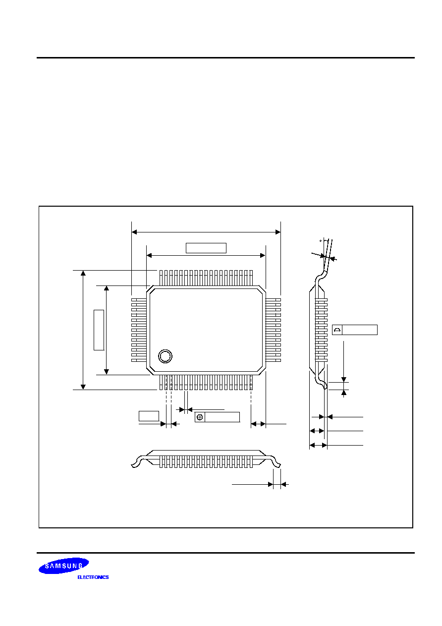
S3CK225/FK225
MECHANICAL DATA
23-1
23
MECHANICAL DATA
OVERVIEW
The S3CK225/FK225 is available in 64-QFP-1420F package.
64-QFP-1420F
#64
20.00
?0.20
23.90
?0.30
14.00
?0.20
17.90
?0.30
#1
1.00
(1.00)
0.40
+ 0.10
- 0.05
NOTE: Dimensions are in millimeters.
0.80
?0.20
0.10 MAX
0.15
+ 0.10
- 0.05
0-8
0.80
?0.20
0.05 MIN
2.65
?0.10
3.00 MAX
0.15 MAX
Figure 23-1. 64-Pin QFP Package Dimensions (64-QFP-1420F)

MECHANICAL DATA
S3CK225/FK225
23-2
NOTES

S3CK225/FK225
S3FK225 FLASH MCU
24-1
24
S3FK225 FLASH MCU
OVERVIEW
The S3FK225 single-chip CMOS microcontroller is the FLASH ROM version of the S3CK225 microcontroller. It
has an on-chip FLASH ROM instead of masked ROM. The FLASH ROM is accessed by serial data formats.
The S3FK225 is fully compatible with S3CK225, both in function and in electrical characteristics. Because of its
simple programming requirements, the S3FK225 is ideal for use as an evaluation for the S3CK225.

S3FK225 FLASH MCU
S3CK225/FK225
24-2
COM0/P6.0
COM1/P6.1
COM2/P6.2
COM3/P6.3
P7.0/T2OUT/T2PWM
P7.1/T2CLK/T0OUT/T0PWM
SDAT/P7.2/T0CLK/T3PWM
SCLK/P7.3/T0CAP/CLKOUT
V
DD
/V
DD
V
SS
/V
SS
X
OUT
X
IN
V
PP
/TEST
XT
IN
XT
OUT
RESET
RESET/RESET
DAO
FILIN
FILOUT
P2.0/SEG0
P2.1/SEG1
P2.2/SEG2
P2.3/SEG3
P2.4/SEG4
P2.5/SEG5
P2.6/SEG6
P2.7/SEG7
P3.0/SEG8
P3.1/SEG9
P3.2/SEG10
P3.3/SEG11
P3.4/SEG12
VREF
MICIN
MICOUT
P0.0/INT0
P0.1/INT1
P0.2/INT2
P0.3/INT3
P1.0/BUZ
P1.1/SO
P1.2/SCK
P1.3/SI
AVREF
AVSS
P3.5/SEG13
P3.6/SEG14
P3.7/SEG15
P4.0/SEG16
P4.1/SEG17
P4.2/SEG18
P4.3/SEG19
P4.4/SEG20
P4.5/SEG21
P4.6/SEG22
P4.7/SEG23
P5.0/SEG24/AD0
P5.1/SEG25/AD1
P5.2/SEG26/AD2
P5.3/SEG27/AD3
P5.4/SEG28/AD4
P5.5/SEG29/AD5
P5.6/SEG30/AD6
P5.7/SEG31/AD7
S3CK225/FK225
(64-QFP-1420F)
1
2
3
4
5
6
7
8
9
10
11
12
13
14
15
16
17
18
19
51
50
49
48
47
46
45
44
43
42
41
40
39
38
37
36
35
34
33
20
21
22
23
24
25
26
27
28
29
30
31
32
64
63
62
61
60
59
58
57
56
55
54
53
52
Figure 24-1. S3FK225 Pin Assignments (64-QFP-1420F)
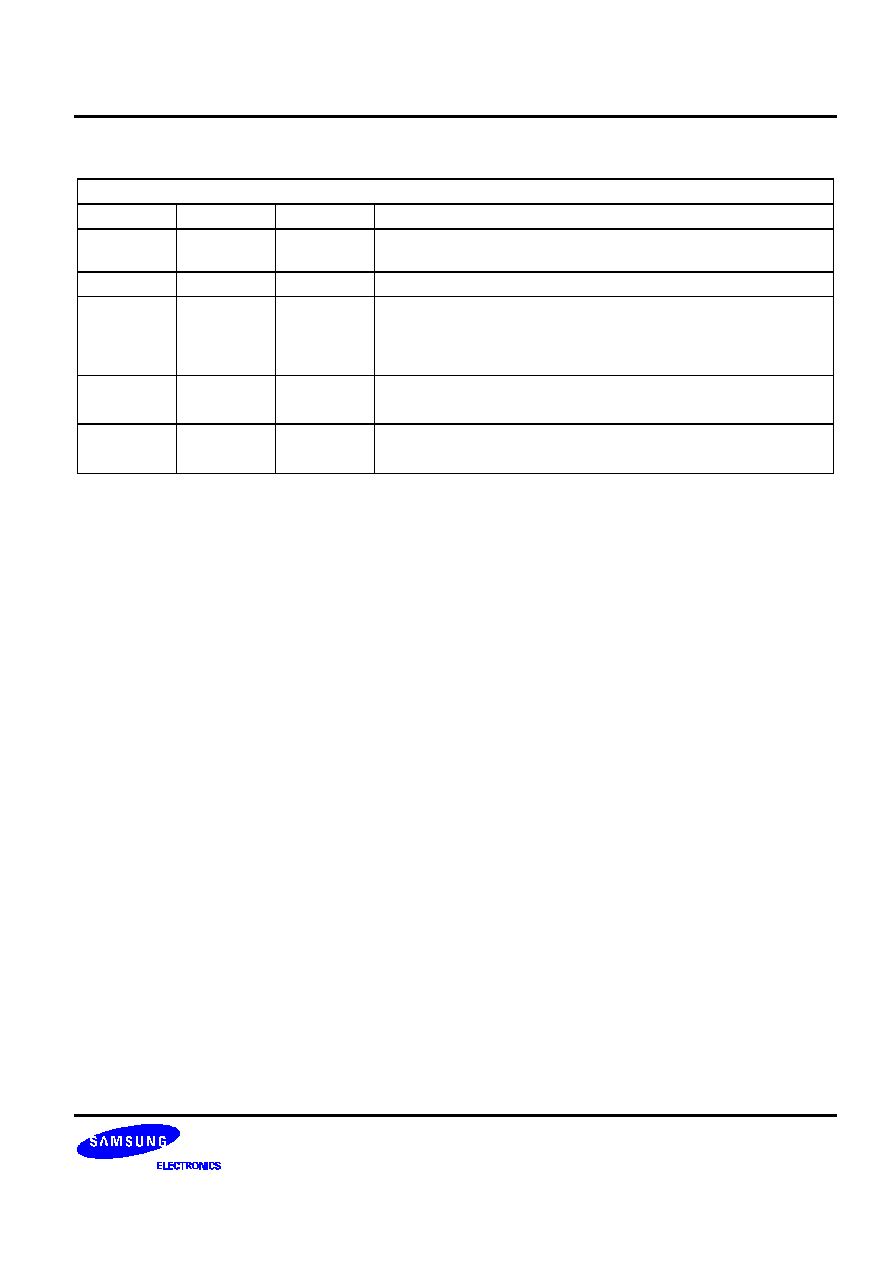
S3CK225/FK225
S3FK225 FLASH MCU
24-3
Table 24-1. Descriptions of Pins Used to Read/Write the FLASH ROM
During Programming
Pin Name
Pin No.
I/O
Function
SDAT (P7.2)
7
I/O
Serial data pin. Output port when reading and input port when
writing. Can be assigned as a Input/push-pull output port.
SCLK (P7.3)
8
I/O
Serial clock pin. Input only pin.
V
PP
(TEST)
13
I
Power supply pin for FLASH ROM cell writing (indicates that
FLASH enters into the writing mode). When 12.5 V is applied,
FLASH is in writing mode and when 5 V is applied, FLASH is in
reading mode. When FLASH is operating, hold GND.
RESET
(RESET)
16
I
Chip initialization
V
DD
/V
SS
(V
DD
/V
SS
)
9/10
I
Logic power supply pin. V
DD
should be tied to
+5 V during programming.
NOTE: Maximum number of writing/erasing for S3FK225 is 100 times.

S3FK225 FLASH MCU
S3CK225/FK225
24-4
NOTES

S3CK225/FK225
DEVELOPMENT TOOLS
25-1
25
DEVELOPMENT TOOLS
OVERVIEW
Samsung provides a powerful and easy-to-use development support system in turnkey form. The development
support system is configured with a host system, debugging tools, and support software. For the host system, any
standard computer that operates with windows95/98/NT as its operating system can be used. One type of
debugging tool including hardware and software is provided: the effective cost and powerful in-circuit emulator,
InvisibleMDS, for CalmRISC8. Samsung also offers support software that includes debugger, Compiler,
Assembler, and a program for setting options.
CALMSHINE: IDE (INTEGRATED DEVELOPMENT ENVIRONMENT)
CalmRISC8 Samsung Host Interface for In-circuit Emulator, CalmSHINE, is a multi window based debugger for
CalmRISC8. CalmSHINE provides pull-down, pop-up and tool-bar menus, mouse support, function/hot keys,
syntax highlight, tool-tip, drag-and-drop and context-sensitive hyper-linked help. It has an advanced, multiple-
windowed user interface that emphasizes ease of use. Each window can be sized, moved, scrolled, highlighted,
added or removed, docked or undocked completely.
INVISIBLE MDS: IN-CIRCUIT EMULATOR
The evaluation chip of CalmRISC8 has a basic debugging utility block. Using this block, evaluation chip directly
interfaces with host through only communication wire. So, InvisibleMDS offers simple and powerful debugging
environment.
CALMRISC8 C-COMPILER: CALM8CC
The CalmRISC8 Compiler offers the standard features of the C language, plus many extensions for MCU
applications, such as interrupt handling in C and data placement controls, designed to take fully advantage of
CalmRISC8 facilities. It conforms to the ANSI specification. It supports standard library of functions applicable to
MCU systems. The standard library also conforms to the ANSI standard. It generates highly size-optimized code
for CalmRISC8 by fully utilizing CalmRISC8 architecture. It is available in a Windows version integrated with the
CalmSHINE.
CALMRISC8 RELOCATABLE ASSEMBLER: CALM8ASM
The CalmRISC8 Assembler is a relocatable assembler for Samsung's CalmRISC8 MCU and its MAC816 and
MAC2424 coprocessors. It translates a source file containing assembly language statements into a relocatable
machine object code file in Samsung format. It runs on WINDOWS95 compatible operating systems. It supports
macros and conditional assembly. It produces the relocatable object code only, so the user should link object
files. Object files can be linked with other object files and loaded into memory.
CALMRISC8 LINKER: CALM8LINK
The CalmRISC8 Linker combines Samsung object format files and library files and generates absolute, machine-
code executable hex programs or binary files for CalmRISC8 MCU and its MAC816 and MAC2424 coprocessors.
It generates the map file, which shows the physical addresses to which each section and symbol is bounded,
start addresses of each section and symbol, and size of them. It runs on WINDOWS95 compatible operating

DEVELOPMENT TOOLS
S3CK225/FK225
25-2
systems.
EMULATION PROBE BOARD CONFIGURATION
S3EK220X
JP4
TAVSS
AVSS
VSS
TAVREF
AVREF
VDD
RESET
U8
10
20
30
9
19
29
10
20
30
9
19
29
U5
POWER
ON
POWER
SELECT
POWER
VDD
OFF
USER
VDD
U14
S1
DC5V 500mA
JP5
E-5V
78R33
10
20
30
9
19
29
1
9
31
19
29
10
32
20
30
JP1
33
39
63
49
59
40
64
50
60
JP2
VDD
VSS
K6A1016C-JCIZ
CON1
EVMAT0
EVMAT3
EXT_BK0
EXT_BK3
XTAL
OSCCLK
U1
CLK_SELECT
JP3
C2
C1
Y1
D3
RUN
D2
POWER
74HC08
U11
EP-K225
12/16/2002
REV 0
U10
U7
BKREQX
JTAG
CON2
SM1409A
U12
30
20
10
40
U19
VDD
E-3V
34
2
Figure 25-1. Emulation Probe Board Configuration
Invisible MDS Connector = 10-pin/normal Pitch (2.54mm) = JTAG
Pin No.
Pin Name
Pin No.
Pin Name
1
V
DD
6
PTD0_TxD
2
PNTRST_NINIT
7
GND
3
PTCK_MCLK
8
UCLK
4
PTMS
9
JTAGSEL
5
PTDI_RxD
10
�
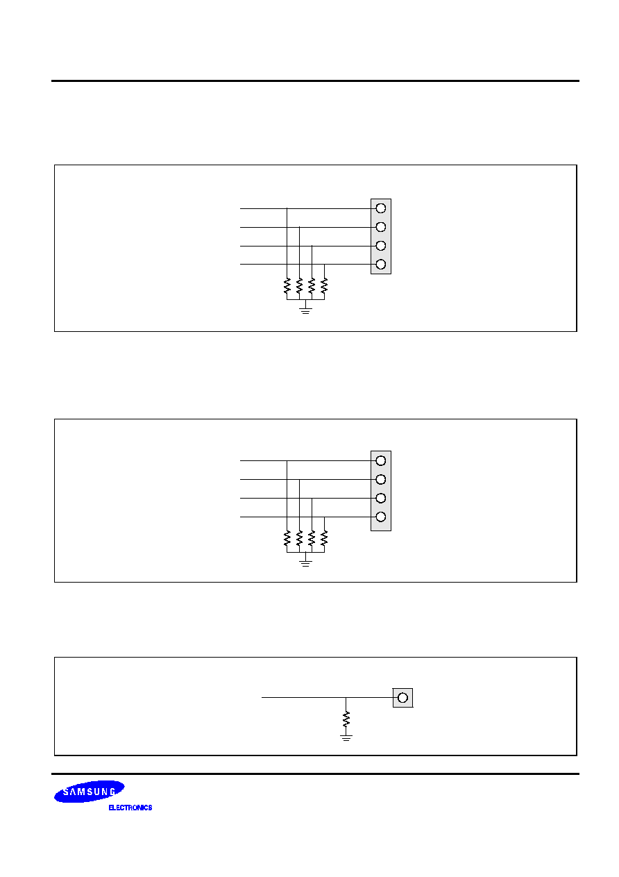
S3CK225/FK225
DEVELOPMENT TOOLS
25-3
EXTERNAL EVENT INPUT HEADERS
These input headers are used to add the break condition to the core status externally when the break using
CalmBreaker occurs in the evaluation chip.
EXT_BK
EXT_BK0
EXT_BK1
EXT_BK2
EXT_BK3
EVACHIP_EXTBK[0]
EVACHIP_EXTBK[1]
EVACHIP_EXTBK[2]
EVACHIP_EXTBK[3]
EVENT MATCH OUTPUT HEADERS
Four event match signals and one combination event signal are occurred by the CalmBreaker in the evaluation
chip. These signals are transmitted through the evaluation chip.
EVMAT
EVMAT0
EVMAT1
EVMAT2
EVMAT3
EVACHIP_EXTBK[0]
EVACHIP_EXTBK[1]
EVACHIP_EXTBK[2]
EVACHIP_EXTBK[3]
EXTERNAL BREAK INPUT HEADERS (U7)
This input pin is used to break during the evaluation chip run.
EVACHIP_BKREQX
BKREQX
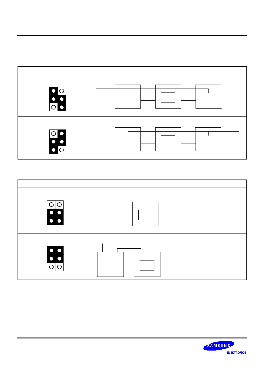
DEVELOPMENT TOOLS
S3CK225/FK225
25-4
POWER SELECTION
U12 State
Description
VDD
POWER
_VDD
OFF
USER
_VDD
POWER
SELECT
Same Power Source from Target System
Target
System
MDS
V
SS
DC
Jack
Power
User
Power
CPU
EP-K225
V
SS
VDD
POWER
_VDD
OFF
USER
_VDD
POWER
SELECT
Same Power Source from DC Jack
DC
Jack
Power
User
Power
Target
System
MDS
V
SS
CPU
EP-K225
V
SS
CLOCK SELECTION
U1 State
Description
XTALI
OSC
CLKSEL
X-TAL
XTALO
OFF
MXIN
MXOUT
OSCCLK
OSC[Y1] is used to clock source for Evaluation chip
CPU
EP-K225
OSC CLK
XMIN
MXOUT
XTALI
OSC
CLKSEL
X-TAL
XTALO
OFF
MXIN
MXOUT
OSCCLK
X-TAL[JP3] is used to clock source for Evaluation chip
CPU
EP-K225
XMIN
MXOUT
JP3
XTALO
XTALI

S3CK225/FK225
DEVELOPMENT TOOLS
25-5
VREF SELECTION
JP4 State
Description
TAVREF
UAVREF
TAVSS
UAVSS
AVREF
AVSS
Same AVREF of EVA chip from TAVREF of Target System.
TAVREF
UAVREF
TAVSS
UAVSS
AVREF
AVSS
Same AVREF of EVA chip from TAVREF of Target System.
USE CLOCK SETTING FOR EXTERNAL CLOCK MODE
Proper crystal and capacitors for main clock should be inserted into pin socket on the IE Board as follows;
C
Y2
X-Tal
C
X
IN
X
OUT
SUB CLOCK SETTING
For sub-clock mode a crystal, 32.768 kHz and capacitors should be inserted into pin socket on the IE Board as
follows;
C
Y1
X-Tal
C
XT
IN
XT
OUT
R
NOTE: The value of resistor is 0 K
.
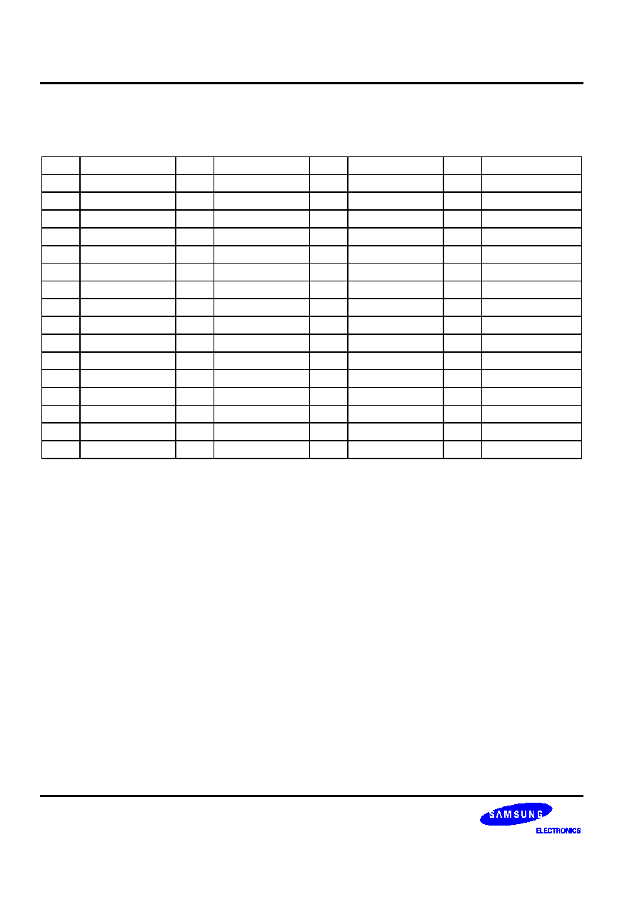
DEVELOPMENT TOOLS
S3CK225/FK225
25-6
JP1, JP2 PIN ASSIGNMENT
JP1, 2 are the signals of IE-K225 and their pin assignment is the same as the pin of S3CK225.
JP1
Function
JP1
Function
JP2
Function
JP2
Function
1
P6.0
2
P6.1
33
P5.7
34
P5.6
3
P6.2
4
P6.3
36
P5.5
36
P5.4
5
P7.0
6
P7.1
37
P5.3
38
P5.2
7
P7.2
8
P7.3
39
P5.1
40
P5.0
9
VDD
10
VSS
41
P4.7
42
P4.6
11
XOUT[NC]
12
XIN[NC]
43
P4.5
44
P4.4
13
TEST
14
XTIN[NC]
45
P4.3
46
P4.2
15
XTOUT[NC]
16
RESET
47
P4.1
48
P4.0
17
DAO
18
FILIN
49
P3.7
50
P3.6
19
FILOUT
20
VREF
51
P3.5
52
P3.4
21
MICIN
22
MICOUT
53
P3.3
54
P3.2
23
P0.0
24
P0.1
55
P3.1
56
P3.0
25
P0.2
26
P0.3
57
P2.7
58
P2.6
27
P1.0
28
P1.1
59
P2.5
60
P2.4
29
P1.2
30
P1.3
61
P2.3
62
P2.2
31
TAVREF
32
TAVSS
63
P2.1
64
P2.0