 | –≠–ª–µ–∫—Ç—Ä–æ–Ω–Ω—ã–π –∫–æ–º–ø–æ–Ω–µ–Ω—Ç: S3P7235 | –°–∫–∞—á–∞—Ç—å:  PDF PDF  ZIP ZIP |

S3C7238/P7238/C7235/P7235
PRODUCT OVERVIEW
1-1
1
PRODUCT OVERVIEW
OVERVIEW
The S3C7238/C7235 single-chip CMOS microcontroller has been designed for high performance using
Samsung's newest 4-bit CPU core, SAM47 (Samsung Arrangeable Microcontrollers).
With features such as LCD direct drive capability, 8-bit timer/counter, and serial I/O, the S3C7238/C7235 offer
an excellent design solution for a wide variety of applications that require LCD functions.
Up to 40 pins of the 80-pin QFP package can be dedicated to I/O. Six vectored interrupts provide fast response
to internal and external events. In addition, the S3C7238/C7235's advanced CMOS technology provides for low
power consumption and a wide operating voltage range.
OTP
The S3C7238/C7235 microcontroller is also available in OTP (One Time Programmable) version,
S3P7238/P7235. S3P7238/P7235 microcontroller has an on-chip 8/16-Kbyte one-time-programmable EPROM
instead of masked ROM. The S3P7238/P7235 is comparable to S3C7238/C7235, both in function and in pin
configuration.

PRODUCT OVERVIEW
S3C7238/P7238/C7235/P7235
1-
2
FEATURES
Memory
≠
512
◊
4-bit RAM
≠
8 K
◊
8-bit ROM (S3C7238/P7238)
≠
16 K
◊
8-bit ROM (S3C7235/P7235)
I/O Pins
≠
Input only: 8 pins
≠
I/O: 24 pins
≠
Output: 8 pins sharing with segment driver
outputs
LCD Controller/Driver
≠
Maximum 16-digit LCD direct drive capability
≠
32 segment, 4 common pins
≠
Display modes: Static, 1/2 duty (1/2 bias),
1/3 duty (1/2 or 1/3 bias), 1/4 duty (1/3 bias)
8-Bit Basic Timer
≠
Programmable interval timer
≠
Watchdog timer
8-Bit Timer/Counter 0
≠
Programmable 8-bit timer
≠
External event counter
≠
Arbitrary clock frequency output
≠
Serial I/O interface clock generator
Watch Timer
≠
Real-time and interval time measurement
≠
Four frequency outputs to BUZ pin
≠
Clock source generation for LCD
8-Bit Serial I/O Interface
≠
8-bit transmit/receive mode
≠
8-bit receive only mode
≠
LSB-first or MSB-first transmission selectable
≠
Internal or external clock source
Bit Sequential Carrier
≠
Support 16-bit serial data transfer in arbitrary
format
Interrupts
≠
Three internal vectored interrupts
≠
Three external vectored interrupts
≠
Two quasi-interrupts
Memory-Mapped I/O Structure
≠
Data memory bank 15
Two Power-Down Modes
≠
Idle mode (only CPU clock stops)
≠
Stop mode (main or sub system oscillation stops)
Oscillation Sources
≠
Crystal, ceramic, or RC for main system clock
≠
Crystal or external oscillator for subsystem clock
≠
Main system clock frequency: 4.19 MHz (typical)
≠
Subsystem clock frequency: 32.768 kHz
≠
CPU clock divider circuit (by 4, 8, or 64)
Instruction Execution Times
≠
0.95, 1.91, 15.3 µs at 4.19 MHz (main)
≠
122 µs at 32.768 kHz (subsystem)
Operating Temperature
≠
≠ 40
∞
C to 85
∞
C
Operating Voltage Range
≠
1.8 V to 5.5 V
Package Type
≠
80-pin QFP
S3C7238/P7238/C7235/P7235
PRODUCT OVERVIEW
1-3
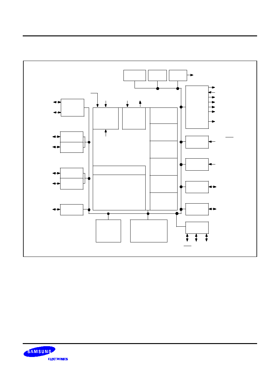
BLOCK DIAGRAM
Interrupt
Control
Block
Instruction
Register
Program
Counter
Program
Status Word
Stack
Pointer
Arithmetic and Logic Unit
Instruction Decoder
Clock
RESET
XIN
XTIN
Internal
Interrupts
INT0, INT1,INT2
P3.0/LCDCK
P3.1/LCDSY
P3.2
P3.3
I/O Port 3
512 x 4-Bit
Data
Memory
8/16-Kbyte
Program
Memory
LCD Drive/
Controller
BIAS
VLC0-VLC2
LCDCK/P3.0
LCDSY/P3.1
COM0-COM3
SEG0-SEG23
P8.0-P8.7/
SEG24-SEG31
P2.3/BUZ
XOUT
XTOUT
P6.0-P6.3/
KS0-KS3
I/O Port 6
P7.0-P7.3/
KS4-KS7
I/O Port 7
P4.0-P4.3
I/O Port 3
P5.0-P5.3
I/O Port 4
8-Bit Timer/
Counter 0
P1.3/TCL0
P2.0/TCLO0
P8.0-P8.7/
SEG24-SEG31
I/O Port 8
P1.0/INT0
P1.1/INT1
P1.2/INT2
P1.3/TCL0
Input Port 1
P2.0/TCLO0
P2.1
P2.2/CLO
P2.3/BUZ
I/O Port 2
Basic
Timer
4-Bit
Accumulator
FLAGS
P0.0/INT4
P0.1/SCK
P0.2/SO
P0.3/SI
I/O Port 0
Serial I/O
Port
P0.2
/SO
P0.3
/SI
P0.1
/SCK
Watch-Dog
Timer
Watch
Timer
Figure 1-1. S3C7238/C7235 Simplified Block Diagram
PRODUCT OVERVIEW
S3C7238/P7238/C7235/P7235
1-
4
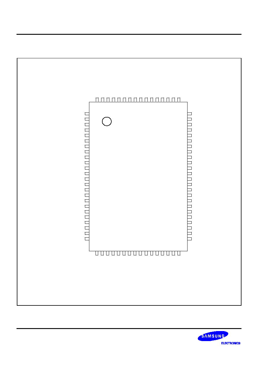
PIN ASSIGNMENTS
SEG19
SEG20
SEG21
SEG22
SEG23
P8.0/SEG24
P8.1/SEG25
P8.2/SEG26
P8.3/SEG27
P8.4/SEG28
P8.5/SEG29
P8.6/SEG30
P8.7/SEG31
P7.3/KS7
P7.2/KS6
P7.1/KS5
P7.0/KS4
P6.3/KS3
P6.2/KS2
P6.1/KS1
P6.0/KS0
P5.3
P5.2
P5.1
64
63
62
61
60
59
58
57
56
55
54
53
52
51
50
49
48
47
46
45
44
43
42
41
80
79
78
77
76
75
74
73
72
71
70
69
68
67
66
65
1
2
3
4
5
6
7
8
9
10
11
12
13
14
15
16
17
18
19
20
21
22
23
24
25
26
27
28
29
30
31
32
33
34
35
36
37
38
39
40
S3C7238
S3C7235
(TOP VIEW)
SEG2
SEG1
SEG0
COM0
COM1
COM2
COM3
BIAS
VLC0
SDAT / VLC1
SCLK / VLC2
VDD / VDD
VSS / VSS
Xout
Xin
TEST / TEST
XTin
XTout
RESET
RESET
/
RESET
P0.0/INT4
P0.1/SCK
P0.2/SO
P0.3/SI
P1.0/INT0
P1.1/INT1
P1.2/INT2
P1.3/TCL0
P2.0/TCLO0
P2.1
P2.2/CLO
P2.3/BUZ
P3.0/LCDCK
P3.1/SCDSY
P3.2
P3.3
P4.0
P4.1
P4.2
P4.3
P5.0
SEG3
SEG4
SEG5
SEG6
SEG7
SEG8
SEG9
SEG10
SEG11
SEG12
SEG13
SEG14
SEG15
SEG16
SEG17
SEG18
Figure 1-2. S3C7238/C7235 80-QFP Pin Assignment Diagram
S3C7238/P7238/C7235/P7235
PRODUCT OVERVIEW
1-5
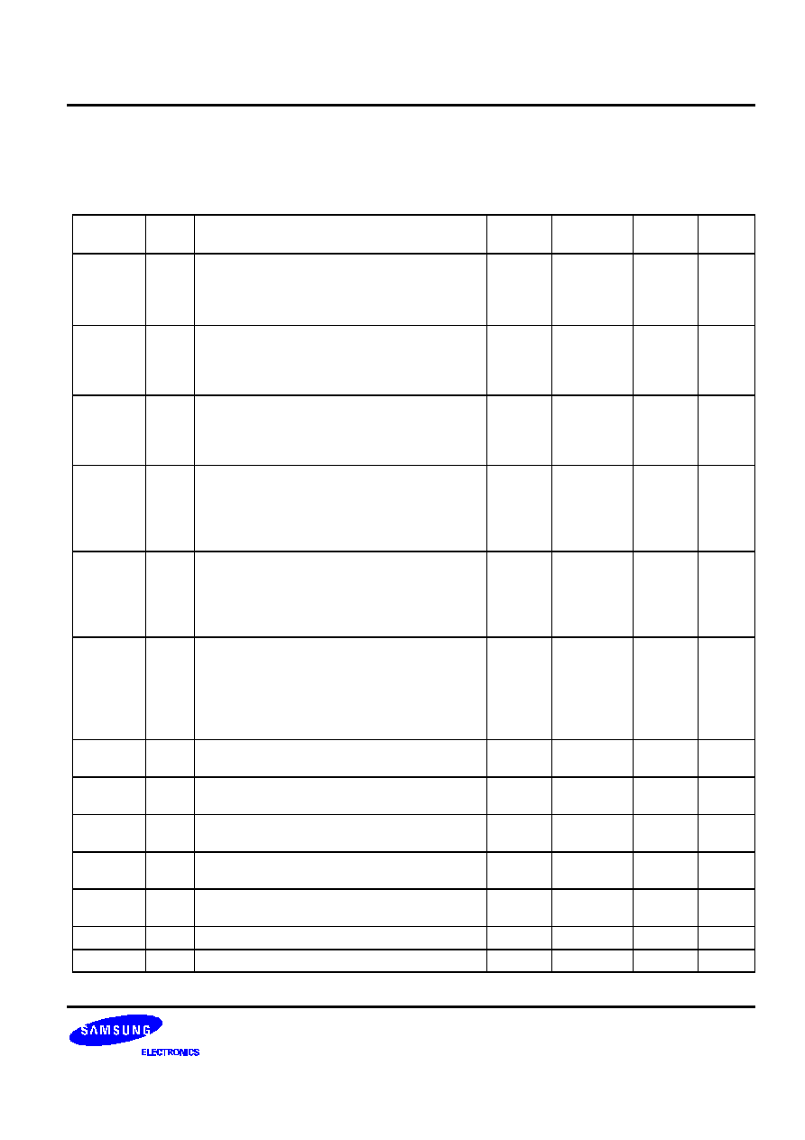
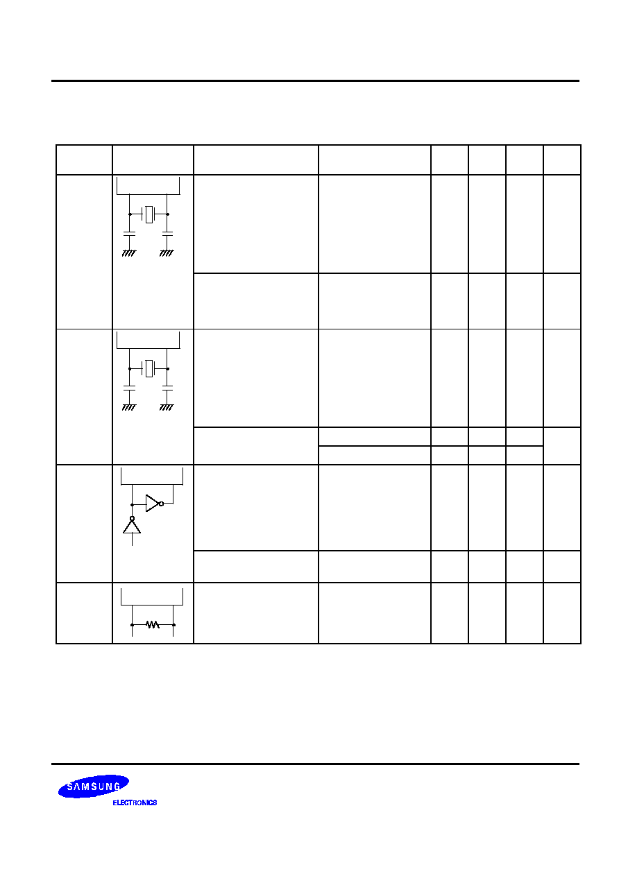
PIN DESCRIPTIONS
Table 1-1. S3C7238/C7235 Pin Descriptions
Pin Name
Pin
Type
Description
Number
Share
Pin
Reset
Value
Circuit
Type
P0.0
P0.1
P0.2
P0.3
I
I/O
I/O
I
4-bit input port.
1-bit and 4-bit read and test are possible.
4-bit pull-up resistors are software assignable.
20
21
22
23
INT4
SCK
SO
SI
Input
A-1
D
*
D
*
A-1
P1.0
P1.1
P1.2
P1.3
I
4-bit input port.
1-bit and 4-bit read and test are possible.
4-bit pull-up resistors are software assignable.
24
25
26
27
INT0
INT1
INT2
TCL0
Input
A-1
P2.0
P2.1
P2.2
P2.3
I/O
4-bit I/O port.
1-bit and 4-bit read/write and test are possible.
4-bit pull-up resistors are software assignable.
28
29
30
31
TCLO0
≠
CLO
BUZ
Input
D
P3.0
P3.1
P3.2
P3.3
I/O
4-bit I/O port.
1-bit and 4-bit read/write and test are possible.
Each individual pin can be specified as input
or output. 4-bit pull-up resistors are software
assignable.
32
33
34
35
LCDCK
LCDSY
Input
D
P4.0≠
P4.3
P5.0≠
P5.3
I/O
4-bit I/O ports. N-channel open-drain output up
to 5 V. 1-, 4-, and 8-bit read/write and test are
possible. Ports 4 and 5 can be paired to
support 8-bit data transfer. 4-bit pull-up
resistors are software assignable.
36≠43
≠
Input
E
P6.0≠
P6.3
P7.0≠
P7.3
I/O
4-bit I/O ports. Port 6 pins are individually
software configurable as input or output. 1-bit
and 4-bit read/write and test are possible. 4-bit
pull-up resistors are software assignable. Ports
6 and 7 can be paired to enable 8-bit data
transfer.
44≠51
KS0≠KS3
KS4≠KS7
Input
D
*
P8.0≠
P8.7
O
Output port for 1-bit data (for use as CMOS
driver only)
59≠52
SEG24≠
SEG31
Output
H-16
SEG0≠
SEG23
O
LCD segment signal output
3≠1,
80≠60
≠
Output
H-15
SEG24≠
SEG31
O
LCD segment signal output
59≠52
P8.0≠P8.7
Output
H-16
COM0≠
COM3
O
LCD common signal output
4≠7
≠
Output
H-15
V
LC0
≠V
LC2
≠
LCD power supply. Voltage dividing resistors
are assignable by mask option
9≠11
SCLK
SDAT
≠
≠
BIAS
≠
LCD power control
8
≠
≠
≠
LCDCK
I/O
LCD clock output for display expansion
32
P3.0
Input
D
PRODUCT OVERVIEW
S3C7238/P7238/C7235/P7235
1-
6
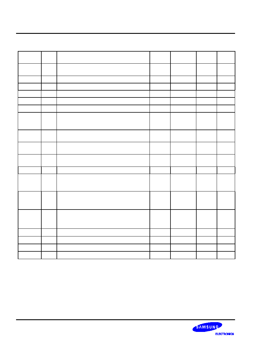
Table 1-1. S3C7238/C7235 Pin Descriptions (Continued)
Pin Name
Pin
Type
Description
Number
Share
Pin
Reset
Value
Circuit
Type
LCDSY
I/O
LCD synchronization clock output for LCD
display expansion
33
P3.1
Input
D
TCL0
I/O
External clock input for timer/counter 0
27
P1.3
Input
A-1
TCLO0
I/O
Timer/counter 0 clock output
28
P2.0
Input
D
SI
I
Serial interface data input
23
P0.3
Input
A-1
SO
I/O
Serial interface data output
22
P0.2
Input
D
*
SCK
I/O
Serial I/O interface clock signal
21
P0.1
Input
D
*
INT0
INT1
I
External interrupts. The triggering edge for
INT0 and INT1 is selectable. Only INT0 is
synchronized with the system clock.
24
25
P1.0
P1.1
Input
A-1
INT2
I
Quasi-interrupt with detection of rising edge
signals.
26
P1.2
Input
A-1
INT4
I
External interrupt input with detection of rising
or falling edge
20
P0.0
Input
A-1
KS0≠KS7
I/O
Quasi-interrupt inputs with falling edge
detection.
44≠51
P6.0≠P7.3
Input
D
*
CLO
I/O
CPU clock output
30
P2.2
Input
D
BUZ
I/O
2, 4, 8 or 16 kHz frequency output for buzzer
sound with 4.19 MHz main system clock or
32.768 kHz subsystem clock.
31
P2.3
Input
D
X
IN,
X
OUT
≠
Crystal, ceramic or RC oscillator pins for main
system clock. (For external clock input, use
X
IN
and input X
IN
`s reverse phase to X
OUT
)
15,14
≠
≠
≠
XT
IN,
XT
OUT
≠
Crystal oscillator pins for subsystem clock.
(For external clock input, use XT
IN
and input
XT
IN
's reverse phase to XT
OUT
)
17,18
≠
≠
≠
V
DD
≠
Main power supply
12
≠
≠
≠
V
SS
≠
Ground
13
≠
≠
≠
RESET
≠
Reset signal
19
≠
Input
B
TEST
≠
Test signal input (must be connected to V
SS
)
16
≠
≠
≠
NOTES:
1.
Pull-up resistors for all I/O ports are automatically disabled if they are configured to output mode.
2.
D
*
Type has a schmitt trigger circuit at input.

S3C7238/P7238/C7235/P7235
PRODUCT OVERVIEW
1-7
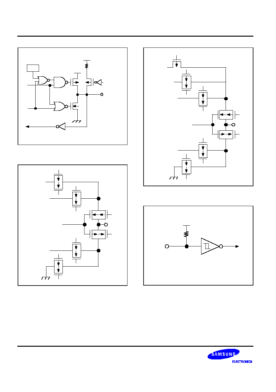
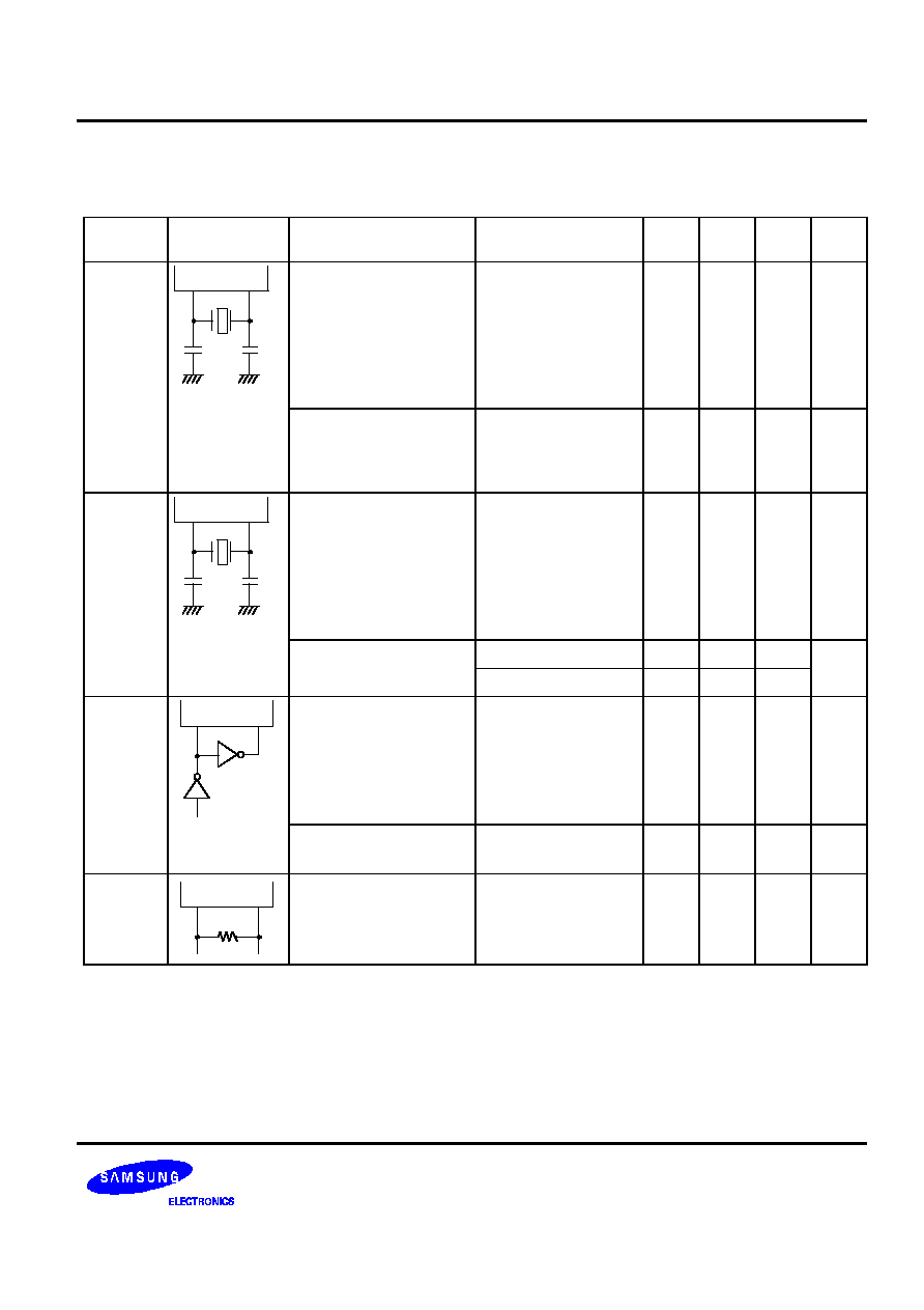
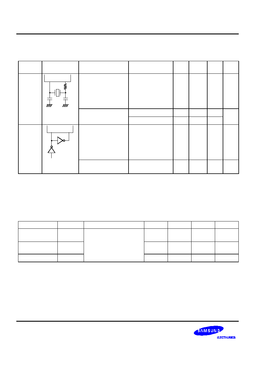
PIN CIRCUIT DIAGRAMS
V
DD
P-CHANNEL
IN
N-CHNNEL
Figure 1-3. Pin Circuit Type A
SCHMITT TRIGGER
V
DD
IN
P-CHANNEL
PULL-UP
RESISTOR
RESISTOR
ENABLE
Figure 1-4. Pin Circuit Type A-1 (P1, P0.0, P0.3)
V
DD
P-CHANNEL
DATA
OUTPUT
DISABLE
N-CHANNEL
OUT
Figure 1-5. Pin Circuit Type C
P-CHANNEL
PULL-UP
RESISTOR
RESISTOR
ENABLE
DATA
OUTPUT
DISABLE
CIRCUIT TYPE A
I/O
V
DD
CIRCUIT
TYPE C
Figure 1-6. Pin Circuit Type D
(P0.1, P0.2, P2, P3, P6, P7)
PRODUCT OVERVIEW
S3C7238/P7238/C7235/P7235
1-
8
DATA
OUTPUT
ENABLE
V
DD
P-CH
RESISTOR
ENABLE
N-CH
PULL-UP
RESISTOR
I/O
CIRCUIT TYPE A
V
DD
PNE
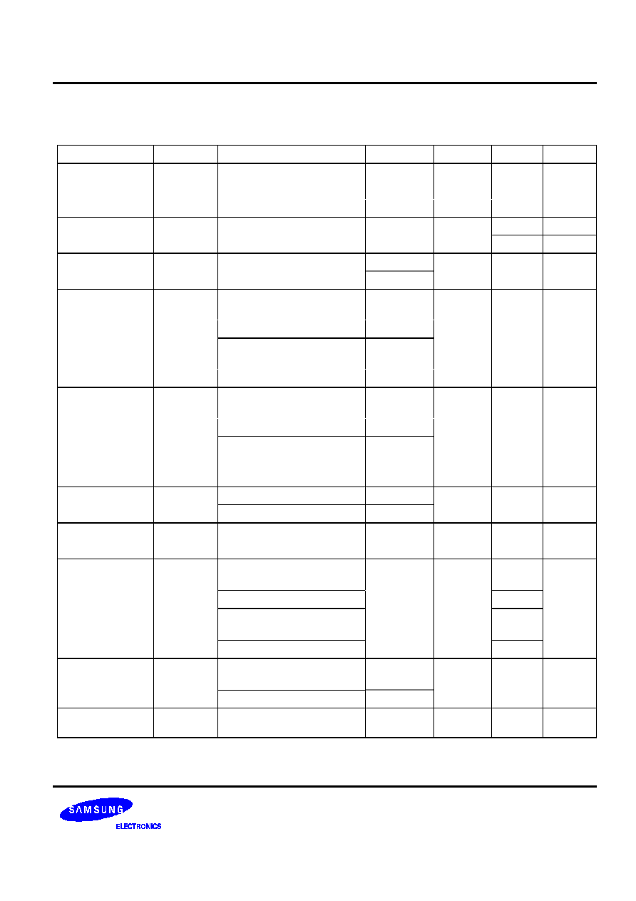
Figure 1-7. Pin Circuit Type E (P4, P5)
V
LC0
V
LC1
LCD SEGMENT/
COMMON DATA
V
LC2
OUT
Figure 1-8. Pin Circuit Type H-15 (SEG/COM)
V
LC0
V
LC1
LCD SEGMENT/
& PORT 8 DATA
V
LC2
V
DD
OUT
Figure 1-9. Pin Circuit Type H-16 (P8)
IN
SCHMITT TRIGGER
V
DD
Figure 1-10. Pin Circuit Type B (
RESET
RESET
)

S3C7238/P7238/C7235/P7235
ELECTRICAL DATA
14-1
14
ELECTRICAL DATA
OVERVIEW
In this section, information on S3C7238/C7235 electrical characteristics is presented as tables and graphics. The
information is arranged in the following order:
Standard Electrical Characteristics
-- Absolute maximum ratings
-- D.C. electrical characteristics
-- Main system clock oscillator characteristics
-- Subsystem clock oscillator characteristics
-- I/O capacitance
-- A.C. electrical characteristics
-- Operating voltage range
Miscellaneous Timing Waveforms
-- A.C timing measurement point
-- Clock timing measurement at X
IN
-- Clock timing measurement at XT
IN
-- TCL timing
-- Input timing for
RESET
-- Input timing for external interrupts
-- Serial data transfer timing
Stop Mode Characteristics and Timing Waveforms
-- RAM data retention supply voltage in stop mode
-- Stop mode release timing when initiated by
RESET
-- Stop mode release timing when initiated by an interrupt request
ELECTRICAL DATA
S3C7238/P7238/C7235/P7235
14-2
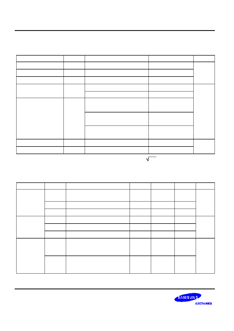
Table 14-1. Absolute Maximum Ratings
(T
A
= 25
∞
C)
Parameter
Symbol
Conditions
Rating
Units
Supply Voltage
V
DD
≠
≠ 0.3 to + 6.5
V
Input Voltage
V
I1
All I/O ports
≠ 0.3 to V
DD
+ 0.3
Output Voltage
V
O
≠
≠ 0.3 to V
DD
+ 0.3
Output Current High
I
OH
One I/O pin active
≠ 15
mA
All I/O ports active
≠ 35
Output Current Low
I
OL
One I/O pin active
+ 30 (Peak value)
+ 15
(note)
Total value for ports 0, 2, 3, and 5
+ 100 (Peak value)
+ 60
(note)
Total value for ports 4, 6, and 7
+ 100
+ 60
(note)
Operating Temperature
T
A
≠
≠ 40 to + 85
∞
C
Storage Temperature
T
stg
≠
≠ 65 to + 150
NOTE
:
The values for Output Current Low (I
OL
) are calculated as Peak Value
◊
Duty .
Table 14-2. D.C. Electrical Characteristics
(T
A
= ≠ 40
∞
C to + 85
∞
C, V
DD
= 1.8 V to 5.5 V)
Parameter
Symbol
Conditions
Min
Typ
Max
Units
Input high
voltage
V
IH1
All input pins except those
specified below for V
IH2
, V
IH3
0.7 V
DD
≠
V
DD
V
V
IH2
Ports 0, 1, 6, 7 and
RESET
0.8 V
DD
≠
V
DD
V
IH3
X
IN
, X
OUT
, XT
IN
and XT
OUT
V
DD
≠ 0.1
≠
V
DD
Input low
V
IL1
Ports 2, 3, 4 and 5
≠
≠
0.3 V
DD
V
voltage
V
IL2
Ports 0, 1, 6, 7 and
RESET
≠
≠
0.2 V
DD
V
IL3
X
IN,
X
OUT
, XT
IN
and XT
OUT
≠
≠
0.1
Output high
voltage
V
OH1
V
DD
= 4.5 V to 5.5 V
Ports 0, 2, 3, 4, 5, 6, 7 and BIAS
I
OH
= ≠ 1 mA
V
DD
≠ 1.0
≠
≠
V
V
OH2
V
DD
= 4.5 V to 5.5 V
Port 8 ONLY
I
OH
= ≠ 100 µA
V
DD
≠ 2.0
≠
≠
S3C7238/P7238/C7235/P7235
ELECTRICAL DATA
14-3
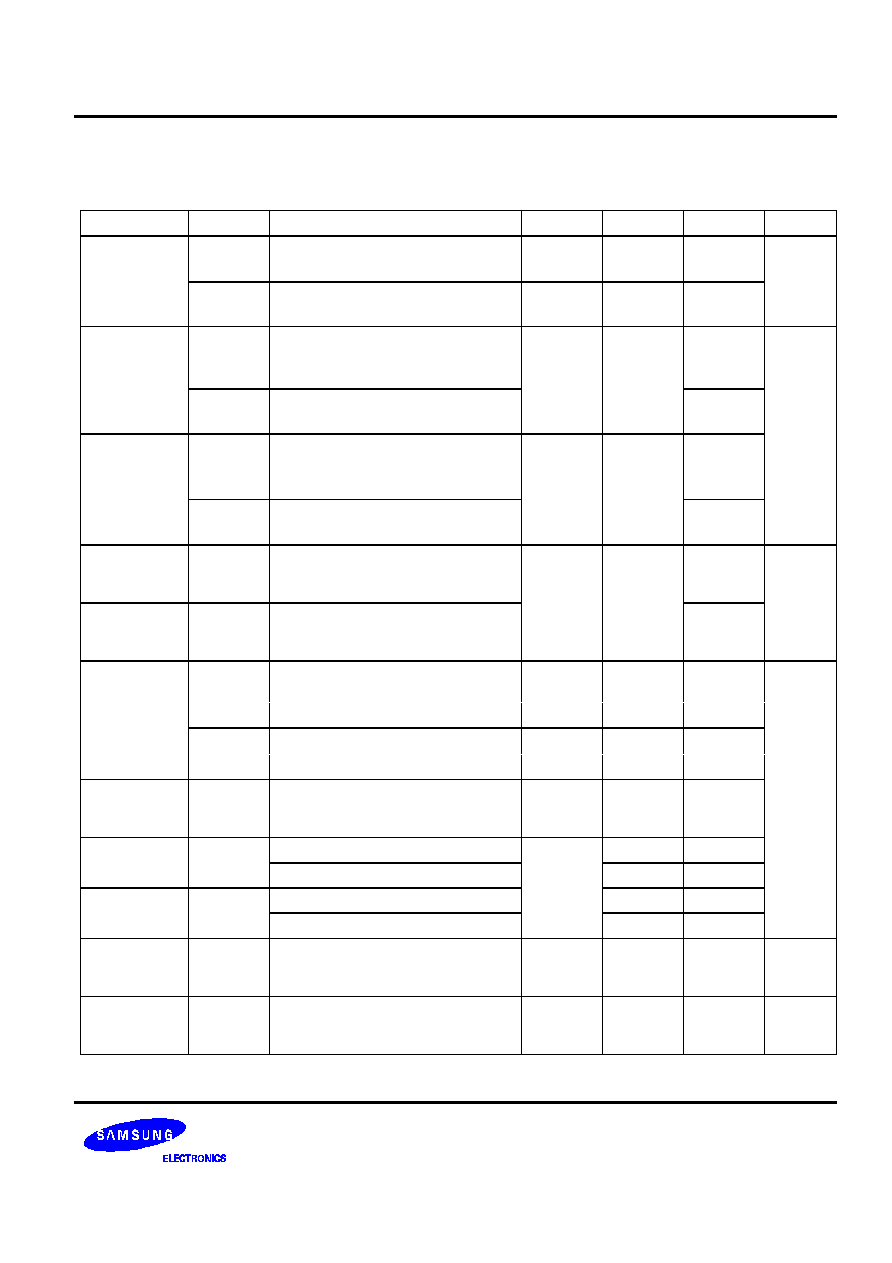
Table 14-2. D.C. Electrical Characteristics (Continued)
(T
A
= ≠ 40
∞
C to + 85
∞
C, V
DD
= 1.8 V to 5.5 V)
Parameter
Symbol
Conditions
Min
Typ
Max
Units
Output low
voltage
V
OL1
V
DD
= 4.5 V to 5.5 V, Ports 0, 2≠7
I
OL
= 15 mA
≠
0.4
2
V
V
OL2
V
DD
= 4.5 V to 5.5 V, Port 8 only
I
OL
= 100 µA
≠
≠
1
Input high
leakage
current
I
LIH1
V
IN
= V
DD
All input pins except those specified
below for I
LIH2
≠
≠
3
µA
I
LIH2
V
IN
= V
DD
X
IN
, X
OUT,
XT
IN and
XT
OUT
≠
≠
20
Input low
leakage
current
I
LIL1
V
IN
= 0 V
All input pins except X
IN
, X
OUT,
XT
IN and
XT
OUT
≠
≠
≠ 3
I
LIL2
V
IN
= 0 V
X
IN
, X
OUT
, XT
IN and
XT
OUT
≠ 20
Output high
leakage
current
I
LOH1
V
OUT
= V
DD
All output pins
≠
≠
3
µA
Output low
leakage
current
I
LOL
V
OUT
= 0 V
All output pins
≠ 3
Pull-up
resistor
R
L1
Ports 0≠7
V
IN
= 0 V; V
DD
= 5 V
25
47
100
K
V
DD
= 3 V
50
95
200
R
L2
V
IN
= 0 V; V
DD
= 5 V,
RESET
100
220
400
V
DD
= 3 V
200
450
800
LCD voltage
dividing
resistor
R
LCD
TA = 25
∞
C
50
93
140
COM output
R
COM
V
DD
= 5 V
≠
3
6
impedance
V
DD
= 3 V
5
15
SEG output
R
SEG
V
DD
= 5 V
3
6
impedance
V
DD
= 3 V
5
15
COM output
voltage
deviation
V
DC
V
DD
= 5 V (V
LC0
≠ COMi)
Io =
±
15uA (I = 0≠3)
≠
±
45
±
90
mV
SEG output
voltage
deviation
V
DS
V
DD
= 5 V (V
LC0
-SEGi)
Io =
±
15
µ
A (I = 0≠31)
≠
Ò
45
Ò
90
mV
ELECTRICAL DATA
S3C7238/P7238/C7235/P7235
14-4
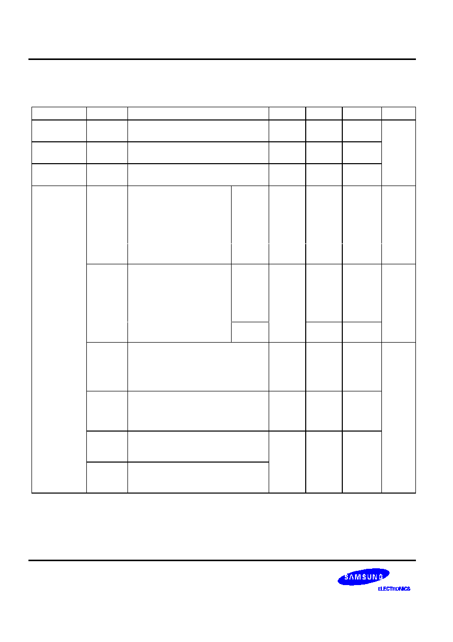
Table 14-2. D.C. Electrical Characteristics (Concluded)
(T
A
= ≠ 40
∞
C to + 85
∞
C, V
DD
= 1.8 V to 5.5 V)
Parameter
Symbol
Conditions
Min
Typ
Max
Units
VLC0 Output
voltage
V
LC0
T
A
= 25
¯
C
0.6 V
DD
≠
0.2
0.6 V
DD
0.6 V
DD
+
0.2
V
VLC1 Output
voltage
V
LC1
T
A
= 25
¯
C
0.4 V
DD
≠ 0.2
0.4 V
DD
0.4 V
DD
+ 0.2
VLC2 Output
voltage
V
LC2
T
A
= 25
¯
C
0.2 V
DD
≠ 0.2
0.2 V
DD
0.2 V
DD
+ 0.2
Supply
Current
(1)
I
DD1
(2)
Main operating:
V
DD
= 5 V
±
10%
CPU = fx/4
SCMOD = 000B
crystal oscillator
C1 = C2 = 22pF
6.0 MHz
4.19 MHz
≠
3.5
2.5
8
5.5
mA
V
DD
= 3 V ± 10%
6.0 MHz
4.19 MHz
1.6
1.2
4
3
I
DD2
(2)
Main Idle mode;
V
DD
= 5 V
±
10%
CPU = fx/4
SCMOD = 000B
crystal oscillator
C1 = C2 = 22pF
6.0 MHz
4.19 MHz
≠
1.0
0.9
2.5
2.0
V
DD
= 3 V ± 10%
6.0 MHz
4.19 MHz
0.5
0.4
1.0
0.8
I
DD3
Sub operating:
V
DD
= 3 V ± 10%
CPU = fxt/4
SCMOD = 1001B
32 kHz crystal oscillator
≠
15
30
µA
I
DD4
Sub Idle mode;
V
DD
= 3 V ± 10%
CPU = fxt/4, SCMOD = 1101B
32 kHz crystal oscillator
≠
6
15
I
DD5
Stop mode;
V
DD
= 5 V ± 10%
CPU = fxt/4, SCMOD = 1101B
≠
0.5
3
I
DD6
(3)
Stop mode;
V
DD
= 5 V ± 10%
CPU = fx/4, SCMOD = 0100B
NOTES:
1.
D.C. electrical values for supply current (I
DD1
to I
DD6
) do not include current drawn through internal pull-up resistors
and through LCD voltage dividing resistors.
2.
Data includes the power consumption for sub-system clock oscillation.
3.
When the system clock mode register, SCMOD, is set to 0100B, the sub-system clock oscillation stops. The
main-system clock oscillation stops by the STOP instruction.
S3C7238/P7238/C7235/P7235
ELECTRICAL DATA
14-5
Table 14-3. Main System Clock Oscillator Characteristics
(T
A
= ≠ 40
∞
C + 85
∞
C, V
DD
= 1.8 V to 5.5 V)
Oscillator
Clock
Configuration
Parameter
Test Condition
Min
Typ
Max
Units
Ceramic
Oscillator
X
IN
X
OUT
C1
C2
Oscillation frequency
(1)
≠
0.4
≠
6.0
MHz
Stabilization time
(2)
Stabilization occurs
when V
DD
is equal to
the minimum oscillator
voltage range.
≠
≠
4
ms
Crystal
Oscillator
C1
C2
X
IN
X
OUT
Oscillation frequency
(1)
≠
0.4
≠
6.0
MHz
Stabilization time
(2)
V
DD
= 4.5 V to 5.5 V
≠
≠
10
ms
V
DD
= 1.8 V to 4.5 V
≠
≠
30
External
Clock
X
IN
X
OUT
X
IN
input frequency
(1)
≠
0.4
≠
6.0
MHz
X
IN
input high and low
level width (t
XH
, t
XL
)
≠
83.3
≠
≠
ns
RC
Oscillator
R
X
IN
X
OUT
Frequency
(1)
V
DD
= 5 V
R = 20 K
, V
DD
= 5 V
R = 38 K
, V
DD
= 3 V
0.4
≠
2.0
1.0
2
MHz
NOTES:
1.
Oscillation frequency and X
IN
input frequency data are for oscillator characteristics only.
2.
Stabilization time is the interval required for oscillator stabilization after a power-on occurs, or when stop mode is
terminated.

ELECTRICAL DATA
S3C7238/P7238/C7235/P7235
14-6
Table 14-4. Subsystem Clock Oscillator Characteristics
(T
A
= ≠ 40
∞
C + 85
∞
C, V
DD
= 1.8 V to 5.5 V)
Oscillator
Clock
Configuration
Parameter
Test Condition
Min
Typ
Max
Units
Crystal
Oscillator
XT
IN
XT
OUT
C1
C2
Oscillation frequency
(1)
≠
32
32.768
35
kHz
Stabilization time
(2)
V
DD
= 4.5 V to 5.5 V
≠
1.0
2
s
V
DD
= 1.8 V to 4.5 V
≠
≠
10
External
Clock
XT
IN
XT
OUT
XT
IN
input frequency
(1)
≠
32
≠
100
kHz
XT
IN
input high and low
level width (t
XTL
, t
XTH
)
≠
5
≠
15
µs
NOTES:
1.
Oscillation frequency and XT
IN
input frequency data are for oscillator characteristics only.
2.
Stabilization time is the interval required for oscillating stabilization after a power-on occurs.
Table 14-5. Input/Output Capacitance
(T
A
= 25
∞
C, V
DD
=
0 V )
Parameter
Symbol
Condition
Min
Typ
Max
Units
Input
capacitance
C
IN
f = 1 MHz; Unmeasured pins
are returned to V
SS
≠
≠
15
pF
Output
capacitance
C
OUT
≠
≠
15
pF
I/O capacitance
C
IO
≠
≠
15
pF
S3C7238/P7238/C7235/P7235
ELECTRICAL DATA
14-7
Table 14-6. A.C. Electrical Characteristics
(T
A
= ≠ 40
∞
C to + 85
∞
C, V
DD
= 1.8 V to 5.5 V)
Parameter
Symbol
Conditions
Min
Typ
Max
Units
Instruction cycle
t
CY
V
DD
= 2.7 V to 5.5 V
0.67
≠
64
µs
time
(1)
V
DD
= 1.8 V to 4.5 V
0.95
≠
64
With subsystem clock (fxt)
114
122
125
TCL0 input
f
TI0
V
DD
= 2.7 V to 5.5 V
0
≠
1.5
MHz
frequency
V
DD
= 1.8 V to 5.5V
1
MHz
TCL0 input high,
t
TIH0
,
t
TIL0
V
DD
= 2.7 V to 5.5 V
0.48
≠
≠
µs
low width
V
DD
= 1.8 V to 5.5 V
1.8
SCK
cycle time
t
KCY
V
DD
= 2.7 V to 5.5 V
External
SCK
source
800
≠
≠
ns
Internal
SCK
source
650
V
DD
= 1.8 V to 5.5 V
External
SCK
source
3200
Internal
SCK
source
3800
SCK
high, low
width
t
KH
, t
KL
V
DD
= 1.8 V to 5.5 V
External
SCK
source
400
≠
≠
ns
Internal
SCK
source
t
KCY
/2 ≠ 50
V
DD
= 1.8 V to 5.5 V
External
SCK
source
1600
Internal
SCK
source
t
KCY
/
2 ≠ 150
SI setup time to
t
SIK
External
SCK
source
100
≠
≠
ns
SCK
high
Internal
SCK
source
150
SI hold time to
t
KSI
External
SCK
source
400
≠
≠
ns
SCK
high
Internal
SCK
source
400
Output delay for
SCK
to SO
t
KSO
V
DD
= 2.7 V to 5.5 V
External
SCK
source
≠
≠
300
ns
Internal
SCK
source
250
V
DD
= 1.8 V to 5.5 V
External
SCK
source
1000
Internal
SCK
source
1000
Interrupt input
t
INTH
,
t
INTL
INT0
(2)
≠
≠
µs
high, low width
INT1, INT2, INT4, KS0≠KS7
10
RESET
Input Low
Width
t
RSL
Input
10
≠
≠
µs
NOTES:
1.
Unless otherwise specified, Instruction Cycle Time condition values assume a main system clock (fx) source.
2.
Minimum value for INT0 is based on a clock of 2t
CY
or 128/fx as assigned by the IMOD0 register setting.
ELECTRICAL DATA
S3C7238/P7238/C7235/P7235
14-8
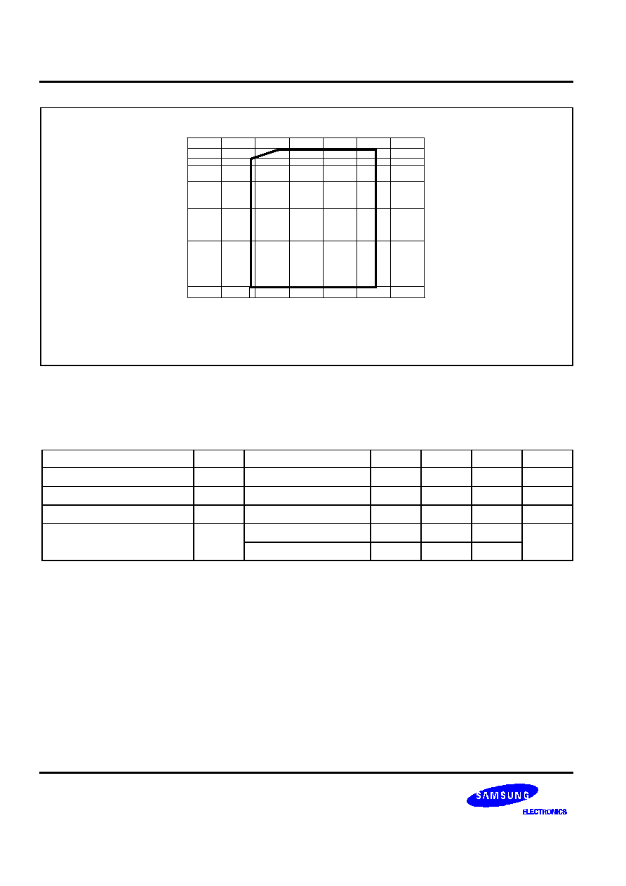
CPU CLOCK = 1/n x oscillator frequency (n = 4, 8, 64)
1
Supply Voltage (V)
250 kHz
500 kHz
750 kHz
1.00 MHz
1.0475 MHz
15.6 kHz
CPU Clock
1.5 MHz
3
4
5
6
7
1.8
Main OSC. Frequency
6 MHz
4.19 MHz
3 MHz
Figure 14-1. Standard Operating Voltage Range
Table 14-7. RAM Data Retention Supply Voltage in Stop Mode
(T
A
= ≠ 40
∞
C to + 85
∞
C)
Parameter
Symbol
Conditions
Min
Typ
Max
Unit
Data retention supply voltage
V
DDDR
Normal operation
1.8
≠
6.5
V
Data retention supply current
I
DDDR
V
DDDR
= 1.8 V
≠
0.1
10
µA
Release signal set time
t
SREL
Normal operation
0
≠
≠
µs
Oscillator stabilization wait
t
WAIT
Released by
RESET
≠
2
17
/fx
≠
ms
time
(1)
Released by interrupt
≠
(2)
≠
NOTES:
1.
During oscillator stabilization wait time, all CPU operations must be stopped to avoid instability during oscillator
start-up.
2.
Use the basic timer mode register (BMOD) interval timer to delay execution of CPU instructions during the wait time.
S3C7238/P7238/C7235/P7235
ELECTRICAL DATA
14-9
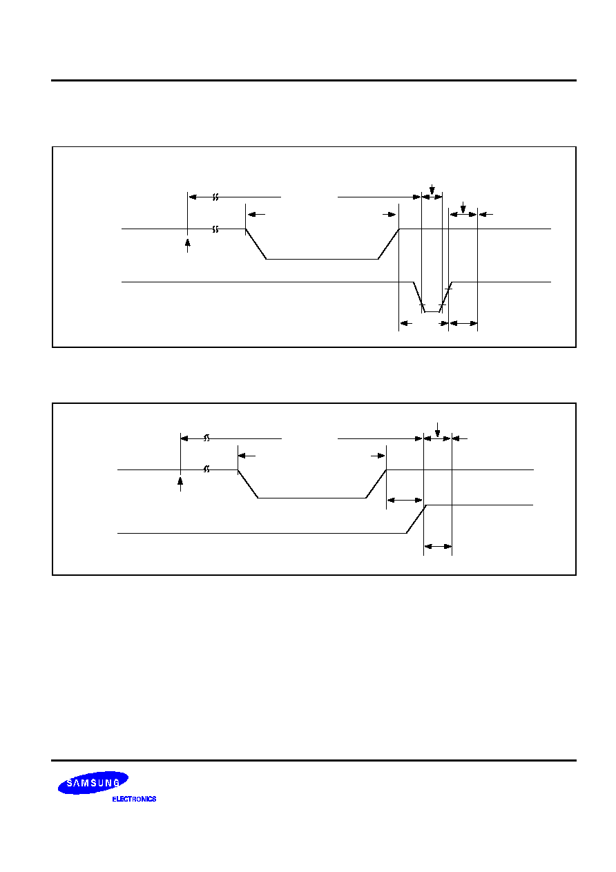
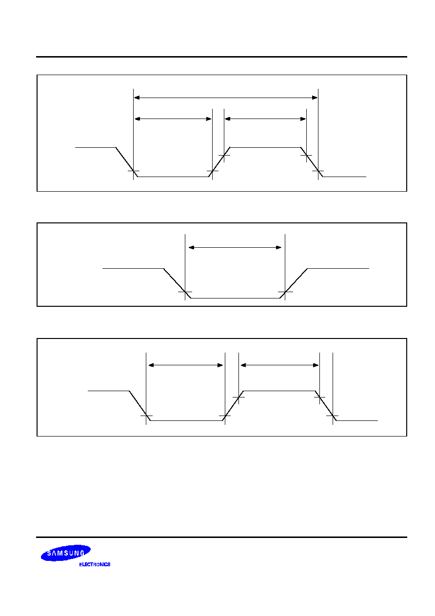
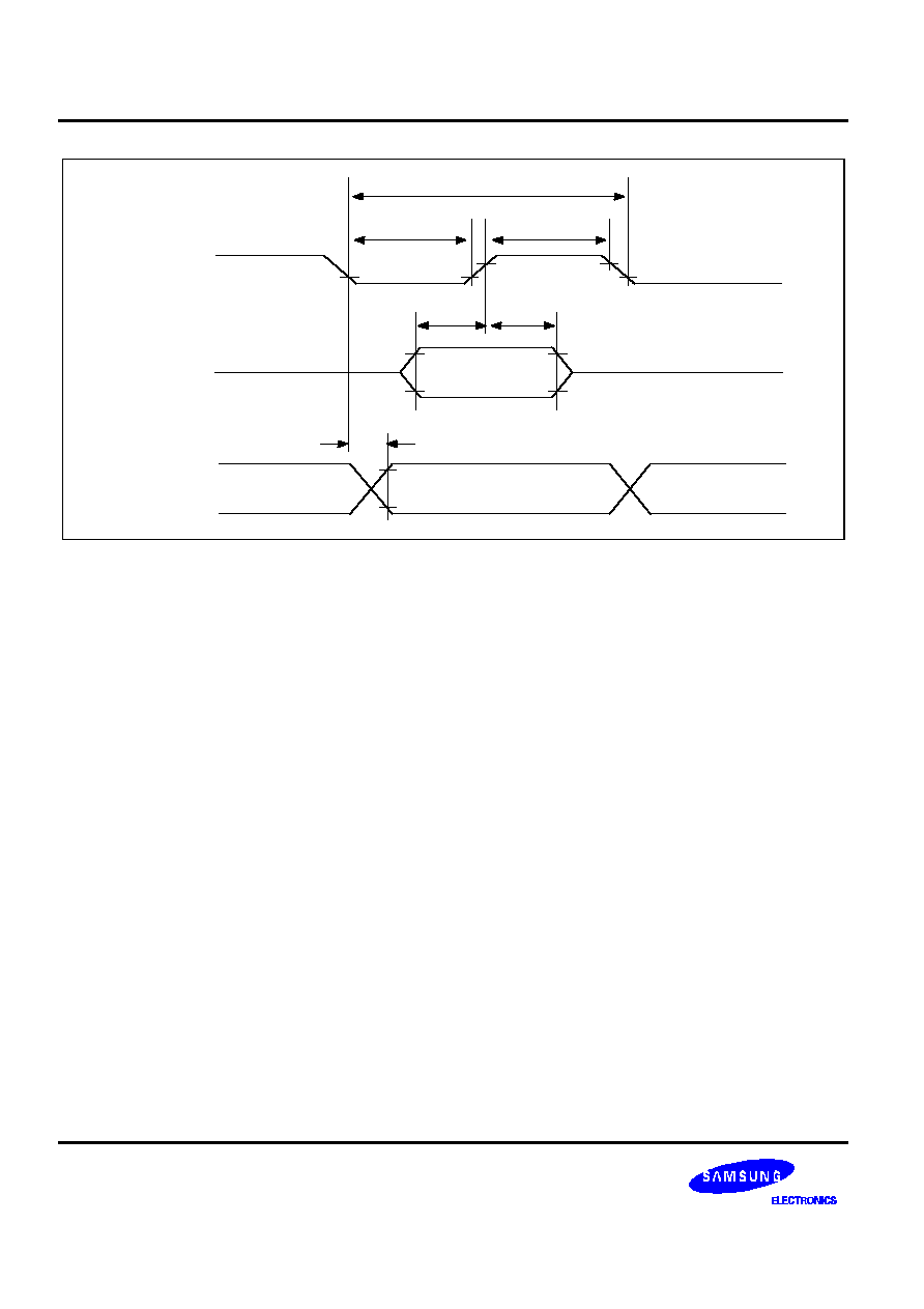
TIMING WAVEFORMS
t
WAIT
V
DD
RESET
EXECUTION OF
STOP INSTRUCTION
V
DDDR
DATA RETENTION MODE
STOP MODE
INTERNAL
RESET
IDLE MODE
OPERATING
MODE
t
SREL
Figure 14-2. Stop Mode Release Timing When Initiated By
RESET
RESET
V
DD
EXECUTION OF
STOP INSTRUCTION
V
DDDR
DATA RETENTION MODE
STOP MODE
t
WAIT
t
SREL
IDLE MODE
NORMAL
OPERATING
MODE
POWER-DOWN MODE TERMINATING SIGNAL
(INTERRUPT REQUEST)
Figure 14-3. Stop Mode Release Timing When Initiated By Interrupt Request

ELECTRICAL DATA
S3C7238/P7238/C7235/P7235
14-10
0.8
V
DD
0.2
V
DD
0.8
V
DD
0.2
V
DD
MEASUREMENT
POINTS
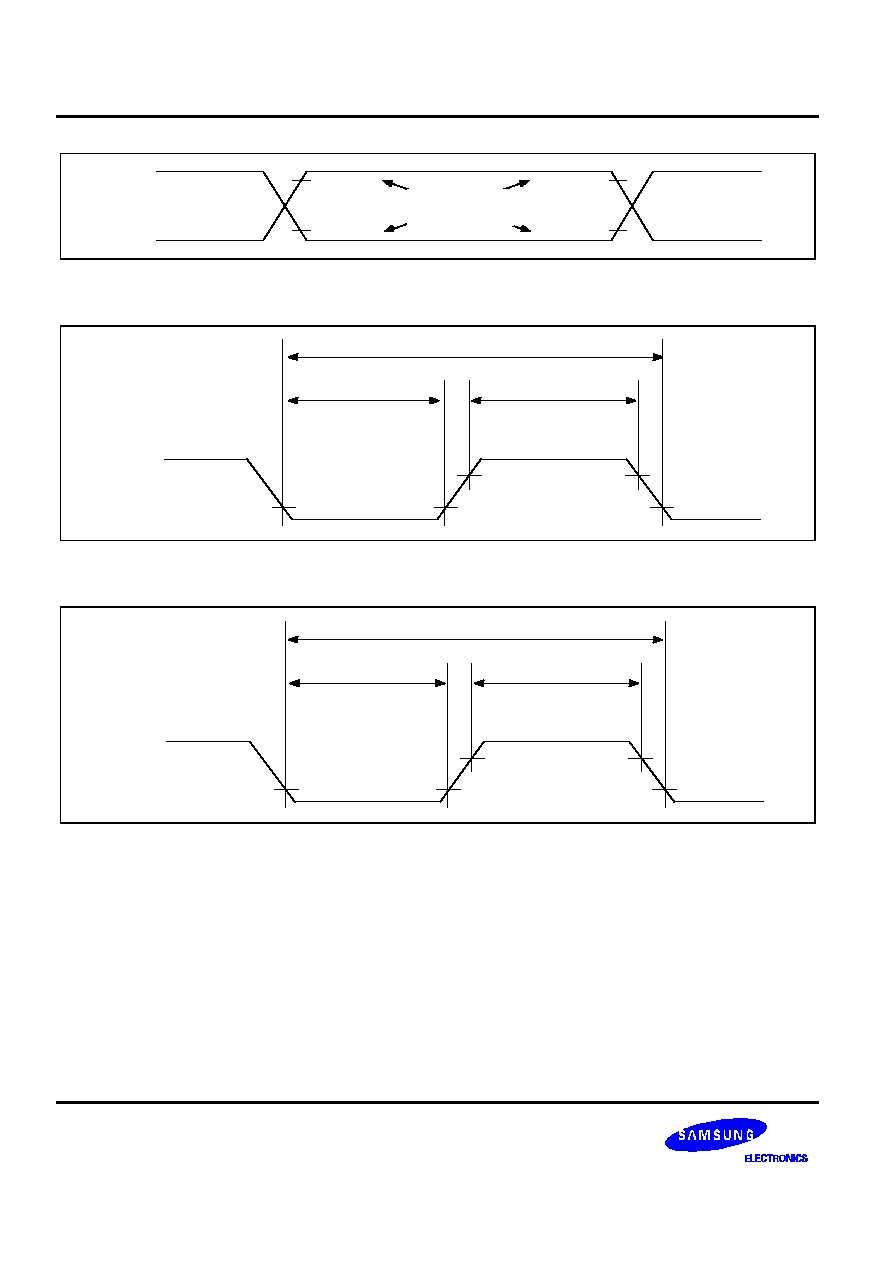
Figure 14-4. A.C. Timing Measurement Points (Except for X
IN
and XT
IN
)
Xin
t
XL
t
XH
x
V
DD
≠ 0.1 V
0.1 V
1/f
Figure 14-5. Clock Timing Measurement at X
IN
XTin
t
XTL
t
XTH
1/f
V
DD
≠ 0.1 V
0.1 V
xt
Figure 14-6. Clock Timing Measurement at XT
IN
S3C7238/P7238/C7235/P7235
ELECTRICAL DATA
14-11
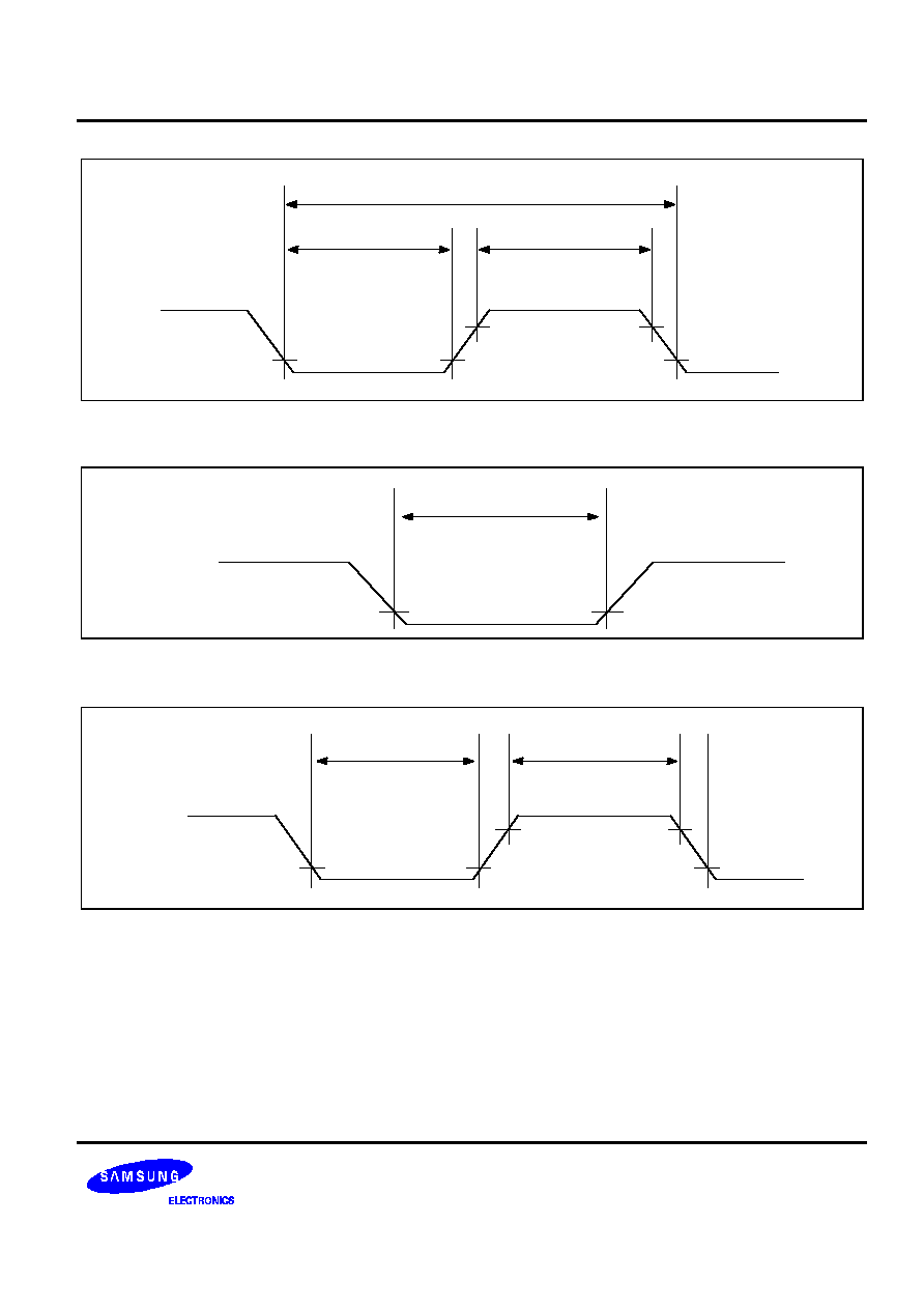
TCL0
t
TIL0
t
TIH0
1/f
0.2 V DD
TI0
0.8 V DD
Figure 14-7. TCL0 Timing
RESET
t
RSL
0.2 V
DD
Figure 14-8. Input Timing for
RESET
RESET
Signal
INT0, 1, 2, 4
KS0 to KS7
t
INTL
t
INTH
0.8 VDD
0.2 VDD
Figure 14-9. Input Timing for External Interrupts and Quasi-Interrupts

ELECTRICAL DATA
S3C7238/P7238/C7235/P7235
14-12
SCK
tKL
tKH
tKCY
0.8 V DD
INPUT DATA
OUTPUT DATA
0.2 V DD
0.8 V DD
0.2 V DD
SI
SO
tKSO
tSIK
tKSI
Figure 14-10. Serial Data Transfer Timing
S3C7238/P7238/C7235/P7235
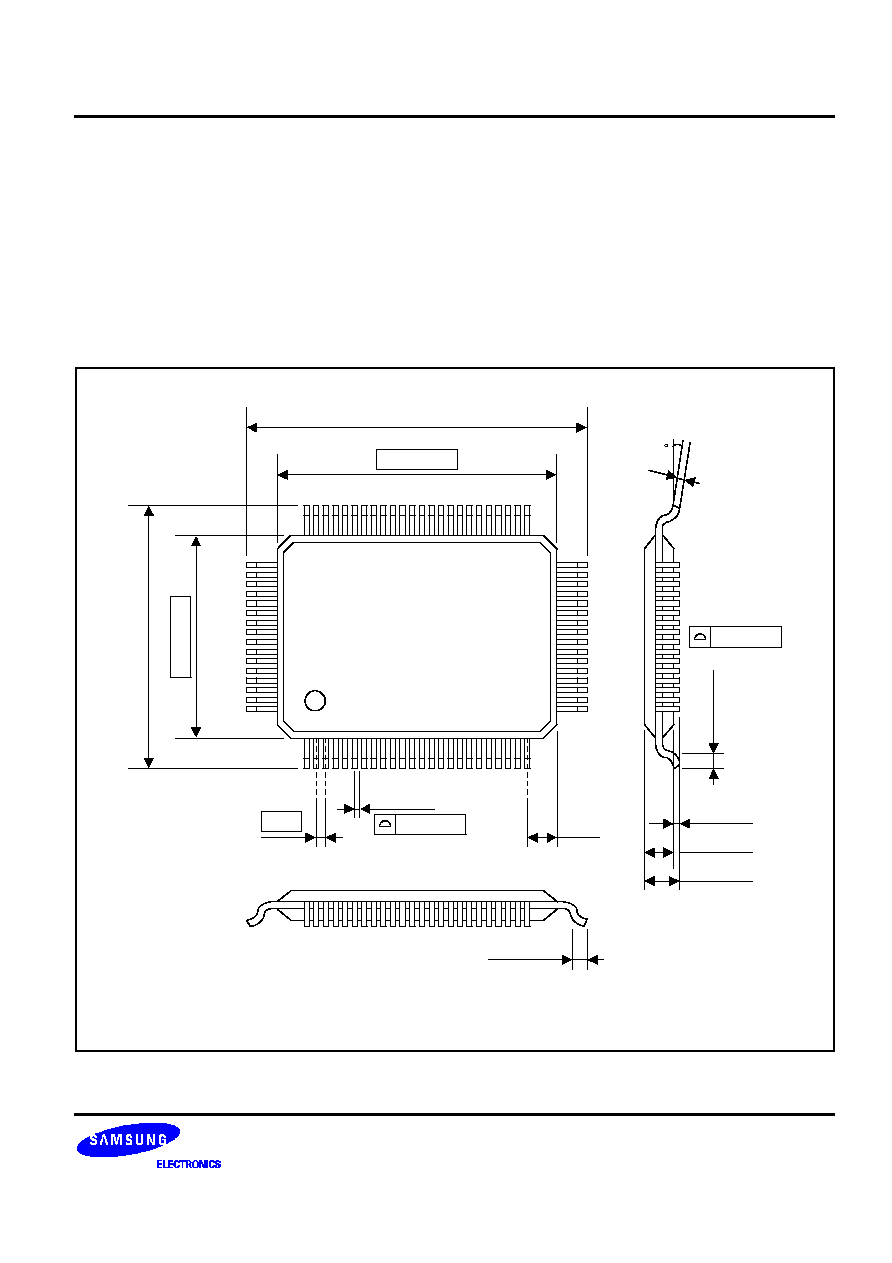
MECHANICAL DATA
15-1
15
MECHANICAL DATA
The S3C7238/C7235 is available in a 80-QFP-1420 package.
80-QFP-1420C
#80
20.00
±
0.20
23.90
±
0.30
14.00
±
0.20
17.90
±
0.30
#1
0.80
0.35
+ 0.10
NOTE: Dimensions are in millimeters.
0.15 MAX
(0.80)
0.15
+ 0.10
- 0.05
0-8
0.10 MAX
0.80
±
0.20
0.05 MIN
2.65
±
0.10
3.00 MAX
0.80
±
0.20
Figure 15-1. 80-QFP-1420C Package Dimensions

S3C7238/P7238/C7235/P7235
S3P7238/P7235 OTP
16-1
16
S3P7238/P7235 OTP
OVERVIEW
The S3P7238/P7235 single-chip CMOS microcontroller is the OTP (One Time Programmable)
version of the
S3C7238/C7235 microcontroller. It has an on-chip EPROM instead of masked ROM. The EPROM is accessed by
a serial data format.
The S3P7238/P7235 is fully compatible with the S3C7238/C7235, both in function and in pin configuration.
Because of its simple programming requirements, the S3P7238/P7235 is ideal for use as an evaluation chip for
the S3C7238/C7235.
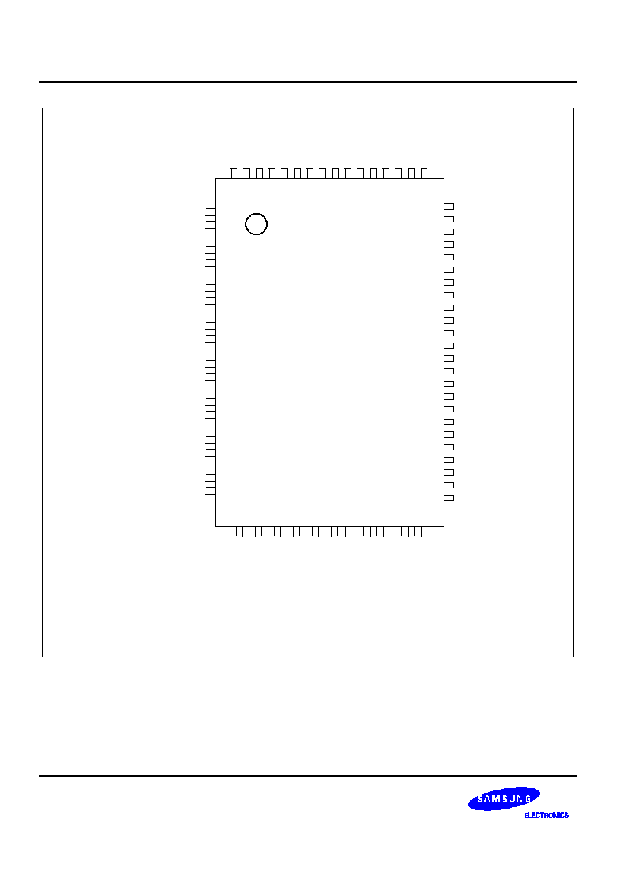
S3P7238/P7235 OTP
S3C7238/P7238/C7235/P7235
16-2
SEG19
SEG20
SEG21
SEG22
SEG23
P8.0/SEG24
P8.1/SEG25
P8.2/SEG26
P8.3/SEG27
P8.4/SEG28
P8.5/SEG29
P8.6/SEG30
P8.7/SEG31
P7.3/KS7
P7.2/KS6
P7.1/KS5
P7.0/KS4
P6.3/KS3
P6.2/KS2
P6.1/KS1
P6.0/KS0
P5.3
P5.2
P5.1
64
63
62
61
60
59
58
57
56
55
54
53
52
51
50
49
48
47
46
45
44
43
42
41
80
79
78
77
76
75
74
73
72
71
70
69
68
67
66
65
1
2
3
4
5
6
7
8
9
10
11
12
13
14
15
16
17
18
19
20
21
22
23
24
25
26
27
28
29
30
31
32
33
34
35
36
37
38
39
40
S3P7238
S3P7235
(TOP VIEW)
SEG2
SEG1
SEG0
COM0
COM1
COM2
COM3
BIAS
VLC0
SDAT / VLC1
SCLK / VLC2
VDD / VDD
VSS / VSS
Xout
Xin
TEST / TEST
XTin
XTout
RESET
RESET
/
RESET
P0.0/INT4
P0.1/SCK
P0.2/SO
P0.3/SI
P1.0/INT0
P1.1/INT1
P1.2/INT2
P1.3/TCL0
P2.0/TCLO0
P2.1
P2.2/CLO
P2.3/BUZ
P3.0/LCDCK
P3.1/SCDSY
P3.2
P3.3
P4.0
P4.1
P4.2
P4.3
P5.0
SEG3
SEG4
SEG5
SEG6
SEG7
SEG8
SEG9
SEG10
SEG11
SEG12
SEG13
SEG14
SEG15
SEG16
SEG17
SEG18
NOTE: The bolds indicate an OTP pin names.
Figure 16-1. S3P7238/P7235 Pin Assignments (80-QFP)
S3C7238/P7238/C7235/P7235
S3P7238/P7235 OTP
16-3
Table 16-1. Pin Descriptions Used to Read/Write the EPROM
Main Chip
During Programming
Pin Name
Pin Name
Pin No.
I/O
Function
V
LC1
SDAT
10
I/O
Serial data pin. Output port when reading and
input port when writing can be assigned as
Input/push-pull output port respectively.
V
LC2
SCLK
11
I/O
Serial clock pin. Input only pin.
TEST
V
PP
(TEST)
16
I
Power supply pin for EPROM cell writing
(indicates that OTP enters into the writing mode).
When 12.5 V is applied, OTP is in writing mode
and when 5 V is applied, OTP is in reading mode.
(Option)
RESET
RESET
19
I
Chip initialization
V
DD
/ V
SS
V
DD
/ V
SS
12/13
I
Logic power supply pin. V
DD
should be tied to +5
V during programming.
Table 16-2. Comparison of S3P7238/P7235 and S3C7238/C7235 Features
Characteristic
S3P7238/P7235
S3C7238/C7235
Program Memory
8 K/16 K-byte EPROM
8 K/16-Kbyte mask ROM
Operating Voltage (V
DD
)
1.8 V to 5.5 V
1.8 V to 5.5 V
OTP Programming Mode
V
DD
= 5 V, V
PP
(TEST) = 12.5 V
≠
Pin Configuration
80 QFP
80 QFP
EPROM Programmability
User Program 1 time
Programmed at the factory
OPERATING MODE CHARACTERISTICS
When 12.5 V is supplied to the Vpp (TEST) pin of the S3P7238/P7235, the EPROM programming mode is
entered. The operating mode (read, write, or read protection) is selected according to the input signals to the pins
listed in Table 16-3 below.
Table 16-3. Operating Mode Selection Criteria
V
DD
Vpp
(TEST)
REG/
MEM
MEM
Address
(A15-A0)
R/
W
W
Mode
5 V
5 V
0
0000H
1
EPROM read
12.5V
0
0000H
0
EPROM program
12.5V
0
0000H
1
EPROM verify
12.5V
1
0E3FH
0
EPROM read protection
NOTE: "0" means low level; "1" means high level.
S3P7238/P7235 OTP
S3C7238/P7238/C7235/P7235
16-4
Table 16-4. Absolute Maximum Ratings
(T
A
= 25
∞
C)
Parameter
Symbol
Conditions
Rating
Units
Supply Voltage
V
DD
≠
≠ 0.3 to + 6.5
V
Input Voltage
V
I1
All I/O ports
≠ 0.3 to V
DD
+ 0.3
Output Voltage
V
O
≠
≠ 0.3 to V
DD
+ 0.3
Output Current High
I
OH
One I/O pin active
≠ 15
mA
All I/O ports active
≠ 35
Output Current Low
I
OL
One I/O pin active
+ 30 (Peak value)
+ 15
(note)
Total value for ports 0, 2, 3, and 5
+ 100 (Peak value)
+ 60
(note)
Total value for ports 4, 6, and 7
+ 100
+ 60
(note)
Operating Temperature
T
A
≠
≠ 40 to + 85
∞
C
Storage Temperature
T
stg
≠
≠ 65 to + 150
NOTE
:
The values for Output Current Low (I
OL
) are calculated as Peak Value
◊
Duty .
Table 16-5. D.C. Electrical Characteristics
(T
A
= ≠ 40
∞
C to + 85
∞
C, V
DD
= 1.8 V to 5.5 V)
Parameter
Symbol
Conditions
Min
Typ
Max
Units
Input high
voltage
V
IH1
All input pins except those
specified below for V
IH2
, V
IH3
0.7 V
DD
≠
V
DD
V
V
IH2
Ports 0, 1, 6, 7 and
RESET
0.8 V
DD
≠
V
DD
V
IH3
X
IN
, X
OUT,
XT
IN
and XT
OUT
V
DD
≠ 0.1
≠
V
DD
Input low
V
IL1
Ports 2, 3, 4 and 5
≠
≠
0.3 V
DD
V
voltage
V
IL2
Ports 0, 1, 6, 7 and
RESET
≠
≠
0.2 V
DD
V
IL3
X
IN,
X
OUT,
XT
IN
and XT
OUT
≠
≠
0.1
Output high
voltage
V
OH1
V
DD
= 4.5 V to 5.5 V
Ports 0, 2, 3, 4, 5, 6, 7 and BIAS
I
OH
= ≠ 1 mA
V
DD
≠ 1.0
≠
≠
V
V
OH2
V
DD
= 4.5 V to 5.5 V
Port 8 ONLY
I
OH
= ≠ 100 µA
V
DD
≠ 2.0
≠
≠
S3C7238/P7238/C7235/P7235
S3P7238/P7235 OTP
16-5
Table 16-5. D.C. Electrical Characteristics (Continued)
(T
A
= ≠ 40
∞
C to + 85
∞
C, V
DD
= 1.8 V to 5.5 V)
Parameter
Symbol
Conditions
Min
Typ
Max
Units
Output low
voltage
V
OL1
V
DD
= 4.5 V to 5.5 V, Ports 0, 2≠7
I
OL
= 15 mA
≠
0.4
2
V
V
OL2
V
DD
= 4.5 V to 5.5 V, Port 8 only
I
OL
= 100 µA
≠
≠
1
Input high
leakage
current
I
LIH1
V
IN
= V
DD
All input pins except those specified
below for I
LIH2
≠
≠
3
µA
I
LIH2
V
IN
= V
DD
X
IN
, X
OUT,
XT
IN and
XT
OUT
≠
≠
20
Input low
leakage
current
I
LIL1
V
IN
= 0 V
All input pins except X
IN
, X
OUT,
XT
IN and
XT
OUT
≠
≠
≠ 3
I
LIL2
V
IN
= 0 V
X
IN
, X
OUT
, XT
IN and
XT
OUT
≠ 20
Output high
leakage
current
I
LOH1
V
OUT
= V
DD
All output pins
≠
≠
3
µA
Output low
leakage
current
I
LOL
V
OUT
= 0 V
All output pins
≠ 3
Pull-up
resistor
R
L1
Ports 0≠7
V
IN
= 0 V; V
DD
= 5 V
25
47
100
K
V
DD
= 3 V
50
95
200
R
L2
V
IN
= 0 V; V
DD
= 5 V,
RESET
100
220
400
V
DD
= 3 V
200
450
800
LCD voltage
dividing
resistor
R
LCD
TA = 25
∞
C
50
93
140
COM output
R
COM
V
DD
= 5 V
≠
3
6
impedance
V
DD
= 3 V
5
15
SEG output
R
SEG
V
DD
= 5 V
3
6
impedance
V
DD
= 3 V
5
15
COM output
voltage
deviation
V
DC
V
DD
= 5 V (V
LC0
≠ COMi)
Io =
±
15uA (I = 0≠3)
≠
±
45
±
90
mV
SEG output
voltage
deviation
V
DS
V
DD
= 5 V (V
LC0
-SEGi)
Io =
±
15
µ
A (I = 0≠31)
≠
Ò
45
Ò
90
mV
S3P7238/P7235 OTP
S3C7238/P7238/C7235/P7235
16-6
Table 16-5. D.C. Electrical Characteristics (Concluded)
(T
A
= ≠ 40
∞
C to + 85
∞
C, V
DD
= 1.8 V to 5.5 V)
Parameter
Symbol
Conditions
Min
Typ
Max
Units
VLC0 Output
voltage
V
LC0
T
A
= 25
¯
C
0.6 V
DD
≠ 0.2
0.6 V
DD
0.6 V
DD
+
0.2
V
VLC1 Output
voltage
V
LC1
T
A
= 25
¯
C
0.4 V
DD
≠ 0.2
0.4 V
DD
0.4 V
DD
+ 0.2
VLC2 Output
voltage
V
LC2
T
A
= 25
¯
C
0.2 V
DD
≠ 0.2
0.2 V
DD
0.2 V
DD
+ 0.2
Supply
Current
(1)
I
DD1
(2)
Main operating:
V
DD
= 5 V
±
10%
CPU = fx/4
SCMOD = 000B
crystal oscillator
C1 = C2 = 22pF
6.0 MHz
4.19 MHz
≠
3.5
2.5
8
5.5
mA
V
DD
= 3 V ± 10%
6.0 MHz
4.19 MHz
1.6
1.2
4
3
I
DD2
(2)
Main Idle mode;
V
DD
= 5 V
±
10%
CPU = fx/4
SCMOD = 000B
crystal oscillator
C1 = C2 = 22pF
6.0 MHz
4.19 MHz
≠
1.0
0.9
2.5
2.0
V
DD
= 3 V ± 10%
6.0 MHz
4.19 MHz
0.5
0.4
1.0
0.8
I
DD3
Sub operating:
V
DD
= 3 V ± 10%
CPU = fxt/4
SCMOD = 1001B
32 kHz crystal oscillator
≠
15
30
µA
I
DD4
Sub Idle mode;
V
DD
= 3 V ± 10%
CPU = fxt/4, SCMOD = 1101B
32 kHz crystal oscillator
≠
6
15
I
DD5
Stop mode;
V
DD
= 5 V ± 10%
CPU = fxt/4, SCMOD = 1101B
≠
0.5
3
I
DD6
(3)
Stop mode;
V
DD
= 5 V ± 10%
CPU = fx/4, SCMOD = 0100B
NOTES:
1.
D.C. electrical values for supply current (I
DD1
to I
DD6
) do not include current drawn through internal pull-up resistors and
through LCD voltage dividing resistors.
2.
Data includes the power consumption for sub-system clock oscillation.
3.
When the system clock mode register, SCMOD, is set to 0100B, the sub-system clock oscillation stops. The
main-system clock oscillation stops by the STOP instruction.
S3C7238/P7238/C7235/P7235
S3P7238/P7235 OTP
16-7
Table 16-6. Main System Clock Oscillator Characteristics
(T
A
= ≠ 40
∞
C + 85
∞
C, V
DD
= 1.8 V to 5.5 V)
Oscillator
Clock
Configuration
Parameter
Test Condition
Min
Typ
Max
Units
Ceramic
Oscillator
X
IN
X
OUT
C1
C2
Oscillation frequency
(1)
≠
0.4
≠
6.0
MHz
Stabilization time
(2)
Stabilization occurs
when V
DD
is equal to
the minimum oscillator
voltage range.
≠
≠
4
ms
Crystal
Oscillator
C1
C2
X
IN
X
OUT
Oscillation frequency
(1)
≠
0.4
≠
6.0
MHz
Stabilization time
(2)
V
DD
= 4.5 V to 5.5 V
≠
≠
10
ms
V
DD
= 1.8 V to 4.5 V
≠
≠
30
External
Clock
X
IN
X
OUT
X
IN
input frequency
(1)
≠
0.4
≠
6.0
MHz
X
IN
input high and low
level width (t
XH
, t
XL
)
≠
83.3
≠
≠
ns
RC
Oscillator
R
X
IN
X
OUT
Frequency
(1)
V
DD
= 5 V
R = 20 K
, V
DD
= 5 V
R = 38 K
, V
DD
= 3 V
0.4
≠
2.0
1.0
2
MHz
NOTES:
1.
Oscillation frequency and X
IN
input frequency data are for oscillator characteristics only.
2.
Stabilization time is the interval required for oscillator stabilization after a power-on occurs, or when stop mode is
terminated.
S3P7238/P7235 OTP
S3C7238/P7238/C7235/P7235
16-8
Table 16-7. Subsystem Clock Oscillator Characteristics
(T
A
= ≠ 40
∞
C + 85
∞
C, V
DD
= 1.8 V to 5.5 V)
Oscillator
Clock
Configuration
Parameter
Test Condition
Min
Typ
Max
Units
Crystal
Oscillator
XT
IN
XT
OUT
C1
C2
Oscillation frequency
(1)
≠
32
32.768
35
kHz
Stabilization time
(2)
V
DD
= 4.5 V to 5.5 V
≠
1.0
2
s
V
DD
= 1.8 V to 4.5 V
≠
≠
10
External
Clock
XT
IN
XT
OUT
XT
IN
input frequency
(1)
≠
32
≠
100
kHz
XT
IN
input high and low
level width (t
XTL
, t
XTH
)
≠
5
≠
15
µs
NOTES:
1.
Oscillation frequency and XT
IN
input frequency data are for oscillator characteristics only.
2.
Stabilization time is the interval required for oscillating stabilization after a power-on occurs.
Table 16-8. Input/Output Capacitance
(T
A
= 25
∞
C, V
DD
=
0 V )
Parameter
Symbol
Condition
Min
Typ
Max
Units
Input
capacitance
C
IN
f = 1 MHz; Unmeasured pins
are returned to V
SS
≠
≠
15
pF
Output
capacitance
C
OUT
≠
≠
15
pF
I/O capacitance
C
IO
≠
≠
15
pF
S3C7238/P7238/C7235/P7235
S3P7238/P7235 OTP
16-9
Table 16-9. A.C. Electrical Characteristics
(T
A
= ≠ 40
∞
C to + 85
∞
C, V
DD
= 1.8 V to 5.5 V)
Parameter
Symbol
Conditions
Min
Typ
Max
Units
Instruction cycle
t
CY
V
DD
= 2.7 V to 5.5 V
0.67
≠
64
µs
time
(1)
V
DD
= 1.8 V to 4.5 V
0.95
≠
64
With subsystem clock (fxt)
114
122
125
TCL0 input
f
TI0
V
DD
= 2.7 V to 5.5 V
0
≠
1.5
MHz
frequency
V
DD
= 1.8 V to 5.5V
1
MHz
TCL0 input high,
t
TIH0
,
t
TIL0
V
DD
= 2.7 V to 5.5 V
0.48
≠
≠
µs
low width
V
DD
= 1.8 V to 5.5 V
1.8
SCK
cycle time
t
KCY
V
DD
= 2.7 V to 5.5 V
External
SCK
source
800
≠
≠
ns
Internal
SCK
source
650
V
DD
= 1.8 V to 5.5 V
External
SCK
source
3200
Internal
SCK
source
3800
SCK
high, low
width
t
KH
, t
KL
V
DD
= 1.8 V to 5.5 V
External
SCK
source
400
≠
≠
ns
Internal
SCK
source
t
KCY
/2 ≠ 50
V
DD
= 1.8 V to 5.5 V
External
SCK
source
1600
Internal
SCK
source
t
KCY
/
2 ≠ 150
SI setup time to
t
SIK
External
SCK
source
100
≠
≠
ns
SCK
high
Internal
SCK
source
150
SI hold time to
t
KSI
External
SCK
source
400
≠
≠
ns
SCK
high
Internal
SCK
source
400
Output delay for
SCK
to SO
t
KSO
V
DD
= 2.7 V to 5.5 V
External
SCK
source
≠
≠
300
ns
Internal
SCK
source
250
V
DD
= 1.8 V to 5.5 V
External
SCK
source
1000
Internal
SCK
source
1000
Interrupt input
t
INTH
,
t
INTL
INT0
(2)
≠
≠
µs
high, low width
INT1, INT2, INT4, KS0≠KS7
10
RESET
Input Low
Width
t
RSL
Input
10
≠
≠
µs
NOTES:
1.
Unless otherwise specified, Instruction Cycle Time condition values assume a main system clock (fx) source.
2.
Minimum value for INT0 is based on a clock of 2t
CY
or 128/fx as assigned by the IMOD0 register setting.

S3P7238/P7235 OTP
S3C7238/P7238/C7235/P7235
16-10
CPU CLOCK = 1/n x oscillator frequency (n = 4, 8, 64)
1
Supply Voltage (V)
250 kHz
500 kHz
750 kHz
1.00 MHz
1.0475 MHz
15.6 kHz
CPU Clock
1.5 MHz
3
4
5
6
7
1.8
Main OSC. Frequency
6 MHz
4.19 MHz
3 MHz
Figure 16-2. Standard Operating Voltage Range
Table 16-10. RAM Data Retention Supply Voltage in Stop Mode
(T
A
= ≠ 40
∞
C to + 85
∞
C)
Parameter
Symbol
Conditions
Min
Typ
Max
Unit
Data retention supply voltage
V
DDDR
Normal operation
1.8
≠
6.5
V
Data retention supply current
I
DDDR
V
DDDR
= 1.8 V
≠
0.1
10
µA
Release signal set time
t
SREL
Normal operation
0
≠
≠
µs
Oscillator stabilization wait
t
WAIT
Released by
RESET
≠
2
17
/fx
≠
ms
time
(1)
Released by interrupt
≠
(2)
≠
NOTES:
1.
During oscillator stabilization wait time, all CPU operations must be stopped to avoid instability during oscillator
start-up.
2.
Use the basic timer mode register (BMOD) interval timer to delay execution of CPU instructions during the wait time.

S3C7238/P7238/C7235/P7235
S3P7238/P7235 OTP
16-11
TIMING WAVEFORMS
t
WAIT
V
DD
RESET
EXECUTION OF
STOP INSTRUCTION
V
DDDR
DATA RETENTION MODE
STOP MODE
INTERNAL
RESET
IDLE MODE
OPERATING
MODE
t
SREL
Figure 16-3. Stop Mode Release Timing When Initiated By
RESET
RESET
V
DD
EXECUTION OF
STOP INSTRUCTION
V
DDDR
DATA RETENTION MODE
STOP MODE
t
WAIT
t
SREL
IDLE MODE
NORMAL
OPERATING
MODE
POWER-DOWN MODE TERMINATING SIGNAL
(INTERRUPT REQUEST)
Figure 16-4. Stop Mode Release Timing When Initiated By Interrupt Request
S3P7238/P7235 OTP
S3C7238/P7238/C7235/P7235
16-12
0.8
V
DD
0.2
V
DD
0.8
V
DD
0.2
V
DD
MEASUREMENT
POINTS
Figure 16-5. A.C. Timing Measurement Points (Except for X
IN
and XT
IN
)
Xin
t
XL
t
XH
x
V
DD
≠ 0.1 V
0.1 V
1/f
Figure 16-6. Clock Timing Measurement at X
IN
XTin
t
XTL
t
XTH
1/f
V
DD
≠ 0.1 V
0.1 V
xt
Figure 16-7. Clock Timing Measurement at XT
IN
S3C7238/P7238/C7235/P7235
S3P7238/P7235 OTP
16-13
TCL0
t
TIL0
t
TIH0
1/f
0.2 V DD
TI0
0.8 V DD
Figure 16-8. TCL0 Timing
RESET
t
RSL
0.2 V
DD
Figure 16-9. Input Timing for
RESET
RESET
Signal
INT0, 1, 2, 4
KS0 to KS7
t
INTL
t
INTH
0.8 VDD
0.2 VDD
Figure 16-10. Input Timing for External Interrupts and Quasi-Interrupts
S3P7238/P7235 OTP
S3C7238/P7238/C7235/P7235
16-14
SCK
tKL
tKH
tKCY
0.8 V DD
INPUT DATA
OUTPUT DATA
0.2 V DD
0.8 V DD
0.2 V DD
SI
SO
tKSO
tSIK
tKSI
Figure 16-11. Serial Data Transfer Timing
S3C7238/P7238/C7235/P7235
S3P7238/P7235 OTP
16-15
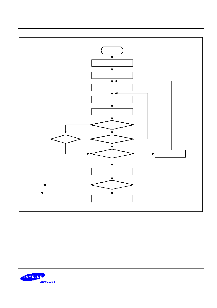
START
Address= First Location
V
DD
=5V, V
PP
=12.5V
x = 0
Program One 1ms Pulse
Increment X
x = 10
Verify 1 Byte
Last Address
V
DD
= V
PP
= 5 V
Compare All Byte
Device Passed
Increment Address
Verify Byte
Device Failed
PASS
FAIL
NO
FAIL
YES
FAIL
NO
Figure 16-12. OTP Programming Algorithm