 | –≠–ª–µ–∫—Ç—Ä–æ–Ω–Ω—ã–π –∫–æ–º–ø–æ–Ω–µ–Ω—Ç: S3P72M7 | –°–∫–∞—á–∞—Ç—å:  PDF PDF  ZIP ZIP |

S3C72M5/C72M7/C72M9/P72M9 (Preliminary Spec)
PRODUCT OVERVIEW
1-1
1
PRODUCT OVERVIEW
OVERVIEW
The S3C72M5/C72M7/C72M9 single-chip CMOS microcontroller has been designed for high performance using
Samsung's newest 4-bit CPU core, SAM47 (Samsung Arrangeable Microcontrollers).
With an up-to-1280-dot LCD direct drive capability, segment expandable circuit, 8-bit and 16-bit timer/counter,
and serial I/O, the S3C72M5/C72M7/C72M9 offers an excellent design solution for a wide variety of applications
which require LCD functions.
Up to 51 pins of the 128-pin QFP package can be dedicated to I/O. Nine vectored interrupts provide fast
response to internal and external events. In addition, the S3C72M5/C72M7/C72M9's advanced CMOS
technology provides for low power consumption and a wide operating voltage range.
OTP
The S3C72M5/C72M7/C72M9 microcontroller is also available in OTP (One Time Programmable) version,
S3P72M9. S3P72M9 microcontroller has an on-chip 32-Kbyte one-time-programmable EPROM instead of
masked ROM. The S3P72M9 is comparable to S3C72M5/C72M7/C72M9, both in function and in pin
configuration except ROM size.

PRODUCT OVERVIEW
S3C72M5/C72M7/C72M9/P72M9 (Preliminary Spec)
1-2
FEATURES SUMMARY
Memory
∑
3,584
◊
4-bit RAM
(Excluding LCD Display
RAM)
∑
16,384/24,576/32,768
◊
8-bit ROM
51 I/O Pins
∑
I/O: 47 pins (32 pins are
configurable as SEG pins)
∑
Input only: 4 pins
LCD Controller/Driver
∑
80 SEG
◊
16 COM, 88 SEG
◊
8 COM Terminals
∑
Internal resistor circuit for
LCD bias
∑
16 Level LCD contrast
control (software)
∑
Segment expandable circuit
∑
All dot can be switched
on/off
8-bit Basic Timer
∑
4 interval timer functions
∑
Watch-dog timer
8-bit Timer/Counter
∑
Programmable 8-bit timer
∑
External event counter
∑
Arbitrary clock frequency
output
∑
External clock signal divider
16-Bit Timer/Counter
∑
Programmable 16-bit timer
∑
External event counter
∑
Arbitrary clock frequency
output
∑
External clock signal divider
∑
Configurable as two 8-bit
Timers
∑
Serial I/O interface clock
generator
Watch Timer
∑
Time interval generation:
0.5 s, 3.9 ms at 32,768 Hz
∑
4 frequency outputs to BUZ
pin
∑
Clock source generation for
LCD
8-bit Serial I/O Interface
∑
8-bit transmit/receive mode
∑
8-bit receive mode
∑
LSB-first or MSB-first
transmission selectable
∑
Internal or external clock
source
Comparator
∑
3 Channel mode: internal
reference (4-bit resolution)
∑
2 Channel mode: external
reference
Interrupts
∑
Five internal vectored
interrupts
∑
Four external vectored
interrupts
∑
Two quasi-interrupts
Bit Sequential Carrier
∑
Supports 16-bit serial data
transfer in arbitrary format
Memory-Mapped I/O Structure
∑
Data memory bank 15
Power-Down Modes
∑
Idle mode (only CPU clock
stops)
∑
Stop mode (main system
clock stops)
∑
Subsystem clock stop mode
Oscillation Sources
∑
Crystal, Ceramic or RC for
main system clock
∑
Crystal oscillator for
subsystem clock
∑
Main system clock
frequency: 0.4≠6 MHz
∑
Subsystem clock frequency:
32.768 kHz
∑
CPU clock divider circuit
(by 4, 8 or 64)
Instruction Execution Times
∑
0.67, 1.33, 10.7 µs at 6 MHz
∑
0.95, 1.91, 15.3 µs at 4.19
MHz
∑
122 µs at 32.768 kHz
Operating Temperature
∑
≠ 40
∞
C to 85
∞
C
Operating Voltage Range
∑
1.8 V to 5.5 V
Package Type
∑
128-pin QFP

S3C72M5/C72M7/C72M9/P72M9 (Preliminary Spec)
PRODUCT OVERVIEW
1-3
FUNCTION OVERVIEW
SAM47 CPU
All KS57-series microcontrollers have the advanced SAM47 CPU core. The SAM47 CPU can directly address up
to 32 K bytes of program memory. The arithmetic logic unit (ALU) performs 4-bit addition, subtraction, logical,
and shift-and-rotate operations in one instruction cycle and most 8-bit arithmetic and logical operations in two
cycles.
CPU REGISTERS
Program Counter
A 15-bit program counter (PC) stores addresses for instruction fetches during program execution. Usually, the PC
is incremented by the number of bytes of the fetched instruction. The one instruction fetch that does not
increment the PC is the 1-byte REF instruction which references instructions stored in a look-up table in the
ROM. Whenever a reset operation or an interrupt occurs, bits PC13 through PC0 are set to the vector address.
Stack Pointer
An 8-bit stack pointer (SP) stores addresses for stack operations. The stack area is located in general-purpose
data memory bank 0. The SP is 8-bit read/writeable and SP bit 0 must always be logical zero.
During an interrupt or a subroutine call, the PC value and the PSW are written to the stack area. When the
service routine has completed, the values referenced by the stack pointer are restored. Then, the next instruction
is executed.
The stack pointer can access the stack despite data memory access enable flag status. Since the reset value of
the stack pointer is not defined in firmware, you use program code to initialize the stack pointer to 00H. This sets
the first register of the stack area to data memory location 0FFH.
PROGRAM MEMORY
In its standard configuration, the 16,384/24,576/32,768
◊
8-bit ROM is divided into four areas:
-- 16-byte area for vector addresses
-- 96-byte instruction reference area
-- 16-byte general-purpose area (0010≠001FH)
-- 16,256/24,448/32,640-byte area for general-purpose program memory
The vector address area is used mostly during reset operations and interrupts. These 16 bytes can alternately be
used as general-purpose ROM.
The REF instruction references 2 x 1-byte or 2-byte instructions stored in reference area locations 0020H≠007FH.
REF can also reference three-byte instructions such as JP or CALL. So that a REF instruction can reference
these instructions, however, the JP or CALL must be shortened to a 2-byte format. To do this, JP or CALL is
written to the reference area with the format TJP or TCALL instead of the normal instruction name. Unused
locations in the REF instruction look-up area can be allocated to general-purpose use.

PRODUCT OVERVIEW
S3C72M5/C72M7/C72M9/P72M9 (Preliminary Spec)
1-4
DATA MEMORY
Overview
The 3,584-bit data memory has five areas:
-- 32
¥
4-bit working register area
-- 224
¥
4 -bit general-purpose area in bank 0 which is also used as the stack area
-- 256
¥
4 -bit general-purpose area in bank 1, bank 2,...
...
, bank 13, respectively
-- 256
¥
5-bit area for LCD data in bank 14
-- 128
¥
4-bit area in bank 15 for memory-mapped I/O addresses
The data memory area is also organized as sixteen memory banks --
bank 0, bank 1, ...
.., and bank 15. You use
the select memory bank instruction (SMB) to select one of the banks as working data memory.
Data stored in RAM locations are 1-, 4-, and 8-bit addressable. After a hardware reset, data memory initialization
values must be defined by program code.
Data Memory Addressing Modes
The enable memory bank (EMB) flag controls the addressing mode for data memory banks 0, 1, ...
.., or 15. When
the EMB flag is logical zero, only locations 00H≠7FH of bank 0 and bank 15 can be accessed. When the EMB
flag is set to logical one, all sixteen data memory banks can be accessed based on the current SMB value.
Working Registers
The RAM's working register area in data memory bank 0 is also divided into four register banks. Each register
bank has eight 4-bit registers. Paired 4-bit registers are 8-bit addressable.
Register A can be used as a 4-bit accumulator and double register EA as an 8-bit extended accumulator; double
registers WX, WL and HL are used as address pointers for indirect addressing.
To limit the possibility of data corruption due to incorrect register addressing, it is advisable to use bank 0 for
main programs and banks 1, 2, and 3 for interrupt service routines.
LCD Data Register Area
Bit values for LCD segment data are stored in data memory bank 14. Register locations that are not used to store
LCD data can be assigned to general-purpose use.
Bit Sequential Carrier
The bit sequential carrier (BSC) is a 16-bit general register that you can manipulate using 1-, 4-, and 8-bit RAM
control instructions.
Using the BSC register, addresses and bit locations can be specified sequentially using 1-bit indirect addressing
instructions. In this way, a program can generate 16-bit data output by moving the bit location sequentially,
incrementing or decrementing the value of the L register. You can also use direct addressing to manipulate data
in the BSC.

S3C72M5/C72M7/C72M9/P72M9 (Preliminary Spec)
PRODUCT OVERVIEW
1-5
CONTROL REGISTERS
Program Status Word
The 8-bit program status word (PSW) controls ALU operations and instruction execution sequencing. It is also
used to restore a program's execution environment when an interrupt has been serviced. Program instructions
can always address the PSW regardless of the current value of data memory access enable flags.
Before an interrupt is processed, the PSW is pushed onto the stack in data memory bank 0. When the routine is
completed, PSW values are restored.
IS1
IS0
EMB
ERB
C
SC2
SC1
SC0
Interrupt status flags (IS1, IS0), the enable memory bank and enable register bank flags (EMB, ERB), and the
carry flag (C) are 1- and 4-bit read/write or 8-bit read-only addressable. Skip condition flags (SC0≠SC2) can be
addressed using 8-bit read instructions only.
Select Bank (SB) Register
Two 4-bit locations called the SB register store address values used to access specific memory and register
banks: the select memory bank register, SMB, and the select register bank register, SRB.
'SMB n' instructions select a data memory bank (0, 1, ...
.., or 15) and store the upper four bits of the 12-bit data
memory address in the SMB register. The 'SRB n' instruction is used to select register bank 0, 1, 2, or 3, and to
store the address data in the SRB.
The instructions 'PUSH SB' and 'POP SB' move SMB and SRB values to and from the stack for interrupts and
subroutines.
CLOCK CIRCUITS
Main system and subsystem oscillation circuits generate the internal clock signals for the CPU and peripheral
hardware. The main system clock can use a Crystal, Ceramic, or RC oscillation source, or an externally-
generated clock signal. The subsystem clock requires either a crystal oscillator or an external clock source.
Bit settings in the 4-bit power control and system clock mode registers select the oscillation source, the CPU
clock, and the clock used during power-down mode. The internal system clock signal (fxx) can be divided inter-
nally to produce four CPU clock frequencies --
fx/4, fx/8, fx/64, or fxt/4.
INTERRUPTS
Interrupt requests may be generated internally by on-chip processes (INTB, INTT0, INTT1, and INTS) or
externally by peripheral devices (INT0, INT1, INT4, and INTK). There are two quasi-interrupts: INT2 and INTW.
INT2 detects rising or falling edges of incoming signals and INTW detects time intervals of 0.5 seconds or 3.91
milliseconds. The following components support interrupt processing:
-- Interrupt enable flags
-- Interrupt request flags
-- Interrupt priority registers
-- Power-down termination circuit

PRODUCT OVERVIEW
S3C72M5/C72M7/C72M9/P72M9 (Preliminary Spec)
1-6
POWER DOWN
To reduce power consumption, there are two power-down modes: idle and stop. The IDLE instruction initiates idle
mode and the STOP instruction initiates stop mode.
In idle mode, only the CPU clock stops while peripherals and the oscillation source continue to operate normally.
Stop mode effects only the main system clock --
a subsystem clock, if used, continues oscillating. In stop mode,
main system clock oscillation stops completely, halting all operations except for a few basic peripheral functions.
RESET
or an interrupt can be used to terminate either idle or stop mode.
RESET
When a
RESET
signal occurs during normal operation or during power-down mode, the CPU enters idle mode
when the reset operation is initiated. When the standard oscillation stabilization interval (31.3 ms at 4.19 MHz)
has elapsed, normal CPU operation resumes.
I/O PORTS
The S3C72M5/C72M7/C72M9 has 13 I/O ports. Pin addresses for all I/O ports are mapped in bank 15 of the
RAM. There are 4 input pins and 47 configurable I/O pins for a total of 51 I/O pins. The contents of I/O port pin
latches can be read, written, or tested at the corresponding address using bit manipulation instructions.
TIMERS and TIMER/COUNTERS
The timer function has four main components: an 8-bit basic interval timer, an 8-bit timer/counter, a 16-bit
timer/counter and a watch timer. The 8-bit basic timer generates interrupt requests at precise intervals, based on
the selected clock frequency and has watch-dog timer function.
The programmable 8-bit and 16-bit timer/counters are used for external event counting, generation of arbitrary
clock frequencies for output, and dividing external clock signals. The 16-bit timer/counter is the source of the
clock signal that is required to drive the serial I/O interface and configurable as two 8-bit timer/counters.
The watch timer has an 8-bit watch timer mode register, a clock selector and a frequency divider circuit. Its
functions include real-time and watch-time measurement, clock generation for the LCD controller and frequency
outputs for buzzer sound.

S3C72M5/C72M7/C72M9/P72M9 (Preliminary Spec)
PRODUCT OVERVIEW
1-7
LCD DRIVER/CONTROLLER
The S3C72M5/C72M7/C72M9 can directly drive an up-to-1,280-dot LCD panel. The LCD function block has the
following components:
-- RAM area for storing display data
-- 80 segment output pins (SEG0≠SEG79)
-- Segment expandable circuit
-- 16 common output pins (COM0≠COM15)
-- 5 operating power supply pins (V
LC1
≠V
LC5
)
-- Sixteen level LCD contrast control circuit (software)
Frame frequency, LCD clock, duty, and segment pins used for display output are controlled by bit settings in the
8-bit mode register, LMOD. You use the 4-bit LCD control register, LCON, to turn the LCD display on and off,
and to control current supplied to the dividing resistors. Segment data are output using a direct memory access
method synchronized with the LCD frame frequency (f
LCD
).
Using the main system clock, the LCD panel operates in idle mode; during stop mode, it is turned off. If a
subsystem clock is used as a clock source, the LCD panel will continue to operate during stop and idle modes.
SERIAL I/O INTERFACE
The serial I/O interface supports the transmission or reception of 8-bit serial data with an external device. The
serial interface has the following functional components:
-- 8-bit mode register
-- Clock selector circuit
-- 8-bit buffer register
-- 3-bit serial clock counter
The serial I/O circuit can be set either to transmit-and-receive or to receive-only mode. MSB-first or LSB-first
transmission is also selectable. The serial interface operates with an internal or an external clock source, or using
the clock signal generated by the 16-bit timer/counter. To modify transmission frequency, the appropriate bits in
the serial I/O mode register (SMOD) must be manipulated.
COMPARATOR
Port 4 can be used as a analog input port for a comparator. The reference voltage for the 3-channel comparator
can be supplied either internally or externally at P4.2. The comparator module has the following components:
-- Comparator
-- Internal reference voltage generator (4-bit resolution)
-- External reference voltage source at P4.2
-- Comparator mode register (CMOD)
-- Comparison result register (CMPREG)
PRODUCT OVERVIEW
S3C72M5/C72M7/C72M9/P72M9 (Preliminary Spec)
1-8
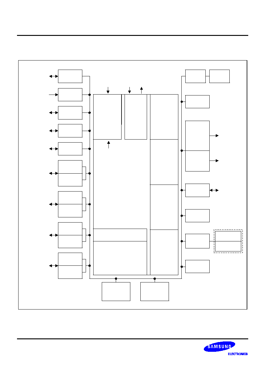
BLOCK DIAGRAM
M/P2.0
LCDFR/P2.1
CL/P3.0/TCLO0
V
LC1
-V
LC5
COM0-COM7
COM8-COM15/
SEG87-SEG80
SEG0-SEG47
SEG48-SEG79/
Port13-Port6
Program
Status Word
Flags
Arithmetic
and
Logic Unit
Instruction Decoder
Internal
Interrupts
Interrupt
Control
Block
Stack
Pointer
Program
Counter
Clock
CIN0/P4.0
CIN1/P4.1
CIN2/P4.2
16/24/32 Kbit
Program
Memory
3,584 x 4-Bit
Data
Memory
SEG79/K4/P6.0
SEG78/K5/P6.1
SEG77/K6/P6.2
SEG76/K7/P6.3
SEG78-SEG72/
P7.0-P7.3
RESET
XT
OUT
XT
IN
X
OUT
X
IN
P0.0/
SCK/
K0
P0.1/SO/K1
P0.2/SI/K2
SEG71-SEG68/
P8.0-P8.3
SEG67-SEG64/
P9.0-P9.3
SCK
/K0/P0.0
SO/K1/P0.1
SI/K2/P0.2
BUZ/K3/P0.3
Basic
Timer
Wachdog
Timer
8-Bit Timer/
Counter1A
8-Bit Timer/
Counter1B
INT0/P1.0
INT1/P1.1
INT2/P1.2
INT4/P1.3
M/P2.0
LCDFR/P2.1
CLO1/P2.2
CLO2/P2.3
TCLO0/CL/P3.0
TCLO1/P3.1
TCL0/P3.2
TCL1/P3.3
SEG63-SEG60/
P10.0-P10.3
SEG59-SEG56/
P11.0-P11.3
SEG55-SEG52/
P12.0-P12.3
SEG51-SEG48/
P13.0-P13.3
I/O Port 3
I/O Port 4
I/O Port 2
Input Port 1
I/O Port 0
I/O Port 7
I/O Port 6
I/O Port 9
I/O Port 8
I/O Port 11
I/O Port 10
I/O Port 13
I/O Port 12
Segment
Expander
8-Bit Timer/
Counter0
16-Bit
Timer/
Counter1
Watch
Timer
LCD
Driver/
Controller
Comparator
Serial I/O
Figure 1-1. S3C72M5/C72M7/C72M9 Simplified Block Diagram
S3C72M5/C72M7/C72M9/P72M9 (Preliminary Spec)
PRODUCT OVERVIEW
1-9
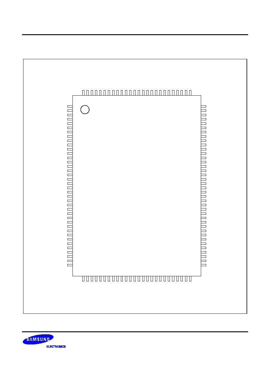
PIN ASSIGNMENTS
SEG20
SEG21
SEG22
SEG23
SEG24
SEG25
SEG26
SEG27
SEG28
SEG29
SEG30
SEG31
SEG32
SEG33
SEG34
SEG35
SEG36
SEG37
SEG38
SEG39
SEG40
SEG41
SEG42
SEG43
SEG44
SEG45
SEG46
SEG47
SEG48/P13.3
SEG49/P13.2
SEG50/P13.1
SEG51/P13.0
SEG52/P12.3
SEG53/P12.2
SEG54/P12.1
SEG55/P12.0
SEG56/P11.3
SEG57/P11.2
COM9/SEG86
COM8/SEG87
COM7
COM6
COM5
COM4
COM3
COM2
COM1
COM0
V
LC5
V
LC4
V
LC3
V
LC2
V
LC1
P0.0/
SCK
/K0
P0.1/SO/K1
P0.2/SI/K2
P0.3/BUZ/K3
V
DD
V
SS
X
OUT
X
IN
TEST
XT
IN
XT
OUT
RESET
P1.0/INT0
P1.1/INT1
P1.2/INT2
P1.3/INT4
P2.0/M
P2.1/LCDFR
P2.2/CLO1
P2.3/CLO2
P3.0/TCLO0/CL
P3.1/TCLO1
P3.2/TCL0
S3C72M5/C72M7/C72M9/P72M9
(128-QFP-1420)
1
2
3
4
5
6
7
8
9
10
11
12
13
14
15
16
17
18
19
20
21
22
23
24
25
26
27
28
29
30
31
32
33
34
35
36
37
38
102
101
100
99
98
97
96
95
94
93
92
91
90
89
88
87
86
85
84
83
82
81
80
79
78
77
76
75
74
73
72
71
70
69
68
67
66
65
128
127
126
125
124
123
122
121
120
119
118
117
116
115
114
113
112
111
110
109
108
107
106
105
104
103
39
40
41
42
43
44
45
46
47
48
49
50
51
52
53
54
55
56
57
58
59
60
61
62
63
64
P3.3/TCL1
P4.0/CIN0
P4.1/CIN1
P4.2/CIN2
SEG79/P6.0/K4
SEG78/P6.1/K5
SEG77//P6.2/K6
SEG76/P6.3/K7
SEG75/P7.0
SEG74/P7.1
SEG73/P7.2
SEG72/P7.3
SEG71/P8.0
SEG70/P8.1
SEG69/P8.2
SEG68/P8.3
SEG67/P9.0
SEG66/P9.1
SEG65/P9.2
SEG64/P9.3
SEG63/P10.0
SEG62/P10.1
SEG61/P10.2
SEG60/P10.3
SEG59/P11.0
SEG58/P11.1
SEG85/COM10
SEG84/COM11
SEG83/COM12
SEG82/COM13
SEG81/COM14
SEG80/COM15
SEG0
SEG1
SEG2
SEG3
SEG4
SEG5
SEG6
SEG7
SEG8
SEG9
SEG10
SEG11
SEG12
SEG13
SEG14
SEG15
SEG16
SEG17
SEG18
SEG19
Figure 1-2. S3C72M5/C72M7/C72M9 128-QFP Pin Assignment

PRODUCT OVERVIEW
S3C72M5/C72M7/C72M9/P72M9 (Preliminary Spec)
1-10
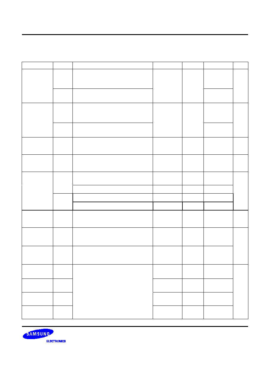
PIN DESCRIPTIONS
Table 1-1. S3C72M5/C72M7/C72M9 Pin Descriptions
Pin Name
Pin Type
Description
Number
Share Pin
P0.0
P0.1
P0.2
P0.3
I/O
4-bit I/O port.
1-bit and 4-bit read/write and test is possible.
4-bit unit pull-up resisters are assignable to input pins
by software and are automatically disabled for output
pins. Each bit pin can be allocated as input or output
(1-bit unit). The N-ch open drain or push-pull output
may be selected by software (1-bit unit).
16
17
18
19
SCK
/K0
SO/K1
SI/K2
BUZ/K3
P1.0
P1.1
P1.2
P1.3
I
4-bit input port.
1-bit and 4-bit read and test is possible.
4-bit unit pull-up resistors are assignable to input pins
by software.
28
29
30
31
INT0
INT1
INT2
INT4
P2.0
P2.1
P2.2
P2.3
I/O
4-bit I/O port. 1-bit and 4-bit read/write and test is
possible. I/O function is same as port 0.
32
33
34
35
M
LCDFR
CLO1
CLO2
P3.0
P3.1
P3.2
P3.3
I/O
4-bit I/O port. 1-bit and 4-bit read/write and test is
possible. I/O function is same as port 0.
36
37
38
39
TCLO0/CL
TCLO1
TCL0
TCL1
P4.0
P4.1
P4.2
I/O
3-bit I/O port. I/O function is same as port 0 except
that port 4 is 3-bit I/O port.
40
41
42
CIN0
CIN1
CIN2
P6.0
P6.1
P6.2
P6.3
P7.0≠P7.3
I/O
4-bit I/O port. 1-, 4-bit and 8-bit read/write and test is
possible. 4-bit unit pull-up resisters are assignable to
input pins by software and are automatically disabled
for output pins. Each bit pin can be allocated as input
or output (1-bit unit). The N-ch open drain or push-
pull output may be selected by software (4-bit unit).
43
44
45
46
47≠50
K4/SEG79
K5/SEG78
K6/SEG77
K7/SEG76
SEG75≠72
P8.0≠P8.3
P9.0≠P9.3
I/O
4-bit I/O port. 1-, 4-bit and 8-bit read/write and test is
possible. I/O function is same as port 6, 7.
51≠54
55≠58
SEG71≠68
SEG67≠64
P10.0≠P10.3
P11.0≠P11.3
I/O
4-bit I/O port. 1-, 4-bit and 8-bit read/write and test is
possible. I/O function is same as port 6, 7.
59≠62
63≠66
SEG63≠60
SEG59≠56
P12.0≠P12.3
P13.0≠P13.3
I/O
4-bit I/O port. 1-, 4-bit and 8-bit read/write and test is
possible. I/O function is same as port 6, 7.
67≠70
71≠74
SEG55≠52
SEG51≠48
SCK
I/O
Serial I/O interface clock signal
16
P0.0
SO
I/O
Serial data output
17
P0.1
SI
I/O
Serial data input
18
P0.2
BUZ
I/O
2, 4, 8, 16 kHz frequency output for buzzer sound
19
P0.3
K0≠K3
K4≠K7
I/O
External interrupts with rising/falling edge detection
16≠19
43≠46
P0.0≠P0.3
P6.0≠P6.3

S3C72M5/C72M7/C72M9/P72M9 (Preliminary Spec)
PRODUCT OVERVIEW
1-11
Table 1-1. S3C72M5/C72M7/C72M9 Pin Descriptions (Continued)
Pin Name
Pin Type
Description
Number
Share Pin
INT0
I
External interrupts with rising/falling edge detection
28
P1.0
INT1
I
External interrupts with rising/falling edge detection
29
P1.1
INT2
I
External quasi-interrupts with rising/falling edge
detection
30
P1.2
INT4
I
External interrupts with rising/falling edge detection
31
P1.3
M
I/O
Alternated signal for SEG driver
32
P2.0
LCDFR
I/O
Synchronous frame signal for SEG driver
33
P2.1
CLO1
I/O
Clock output or operating clock for SEG driver
34
P2.2
CLO2
I/O
Clock output or operating clock for SEG driver
35
P2.3
CL
I/O
Data shift clock for SEG driver
36
P3.0
TCLO0
I/O
Timer/counter0 clock output
36
P3.0
TCLO1
I/O
Timer/counter1 clock output
37
P3.1
TCL0
I/O
External clock input for timer/counter 0
38
P3.2
TCL1
I/O
External clock input for timer/counter 1
39
P3.3
CIN0≠CIN2
I/O
CIN0,1: comparator input only
CIN2: comparator input or external reference input
40, 41
42
P4.0≠P4.1
P4.2
SEG0≠SEG47
O
LCD segment data output
122≠75
≠
SEG48≠SEG79
O
LCD segment data output
74≠43
Port13≠6
SEG80≠SEG87
O
LCD segment data output
2,1,
128≠123
COM15≠8
COM0≠COM7
O
LCD common data output
10≠3
≠
COM8≠COM15
O
LCD common data output
123≠128
1, 2
SEG87≠80
V
LC1
≠V
LC5
≠
LCD power supply. Voltage dividing resistors are
fixed.
15≠11
≠
V
DD
≠
Main power supply
20
≠
V
SS
≠
Ground
21
≠
X
IN
,
X
OUT
≠
Crystal, Ceramic, or RC oscillator signal I/O for main
system clock.
23, 22
≠
XT
IN
,
XT
OUT
≠
Crystal oscillator signal I/O for subsystem clock.
25, 26
≠
TEST
I
Test signal input (must be connected to V
SS
)
24
≠
RESET
I
Reset signal
27
≠
NOTE: Pull-up resistors for all I/O ports are automatically disabled if they are configured to output mode.

PRODUCT OVERVIEW
S3C72M5/C72M7/C72M9/P72M9 (Preliminary Spec)
1-12
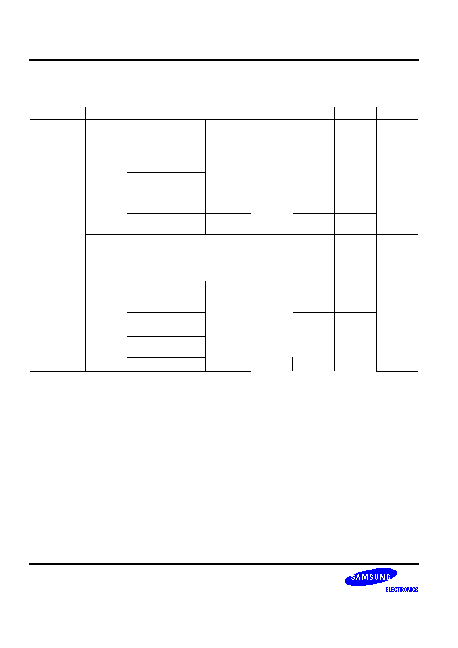
Table 1-2. Overview of S3C72M5/C72M7/C72M9 Pin Data
Pin Names
Share Pins
I/O Type
Reset Value
Circuit Type
P0.0≠P0.3
SCK
, SO, SI, BUZ/K0≠K3
I/O
Input
E-2
P1.0≠P1.3
INT0≠INT2, INT4
I
Input
A-3
P2.0≠P2.3
M, LCDFR, CLO1, CLO2
I/O
Input
E
P3.0≠P3.1
TCLO0/CL, TCLO1
I/O
Input
E
P3.2≠P3.3
TCL0, TCL1
I/O
Input
E-1
P4.0≠P4.2
CIN0≠CIN2
I/O
Input
F-4
P6.0≠P6.3
K4≠K7/SEG79≠SEG76
I/O
Input
H-15
P7.0≠P7.3
SEG75≠SEG72
I/O
Input
H-8
P8.0≠P8.3
SEG71≠SEG68
I/O
Input
H-8
P9.0≠P9.3
SEG67≠SEG64
I/O
Input
H-8
P10.0≠P10.3
SEG63≠SEG60
I/O
Input
H-8
P11.0≠P11.3
SEG59≠SEG56
I/O
Input
H-8
P12.0≠P12.3
SEG55≠SEG52
I/O
Input
H-8
P13.0≠P13.3
SEG51≠SEG48
I/O
Input
H-8
COM0≠COM7
≠
O
Low output
H-4
COM8≠COM15
SEG87≠SEG80
O
Low output
H-6
SEG0≠SEG47
≠
O
Low output
H-5
V
LC1
≠V
LC5
≠
≠
≠
≠
V
DD
≠
≠
≠
≠
V
SS
≠
≠
≠
≠
X
IN
,
X
OUT
≠
≠
≠
≠
XT
IN
,
XT
OUT
≠
≠
≠
≠
RESET
≠
I
≠
B
TEST
≠
I
≠
≠
S3C72M5/C72M7/C72M9/P72M9 (Preliminary Spec)
PRODUCT OVERVIEW
1-13
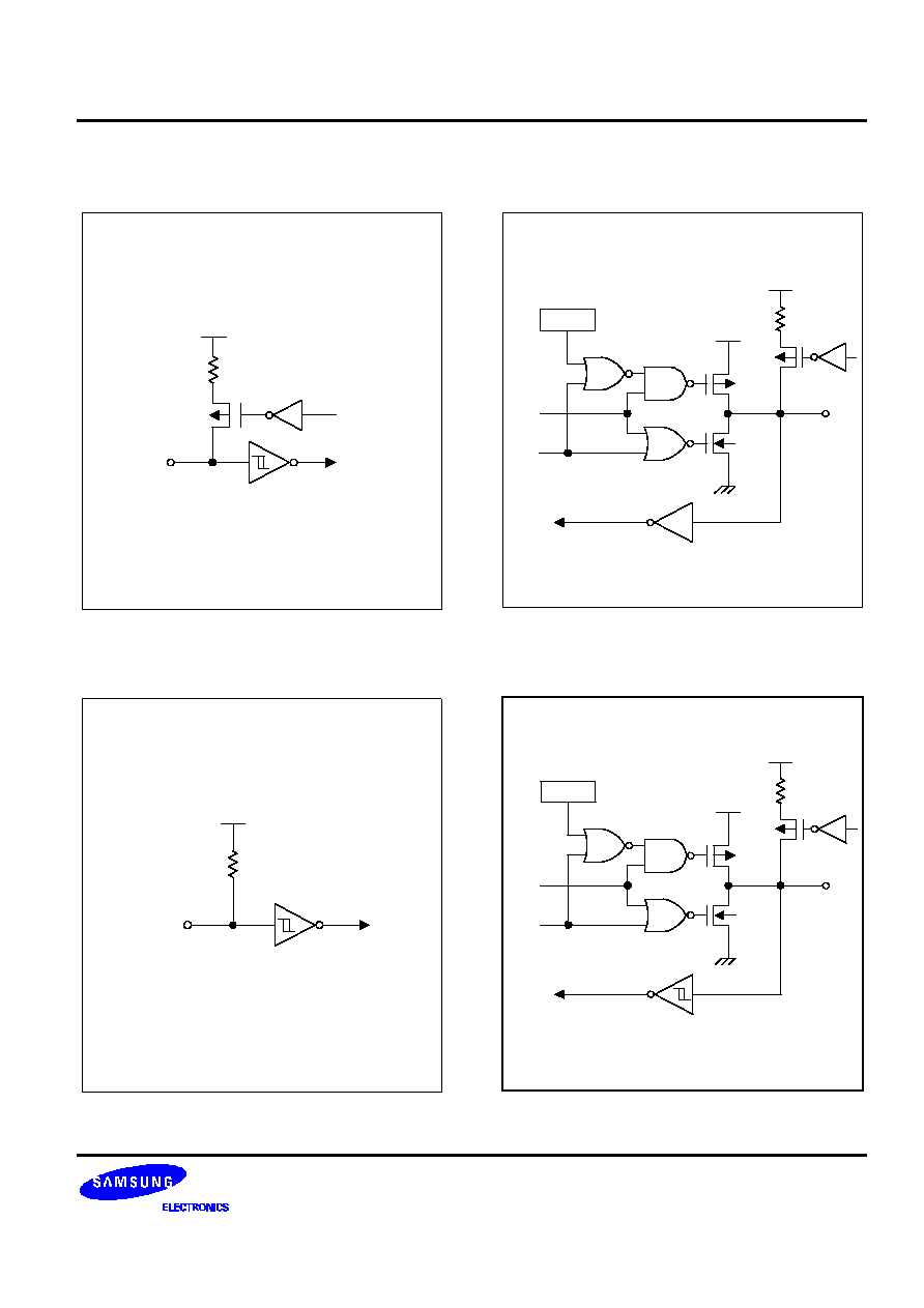
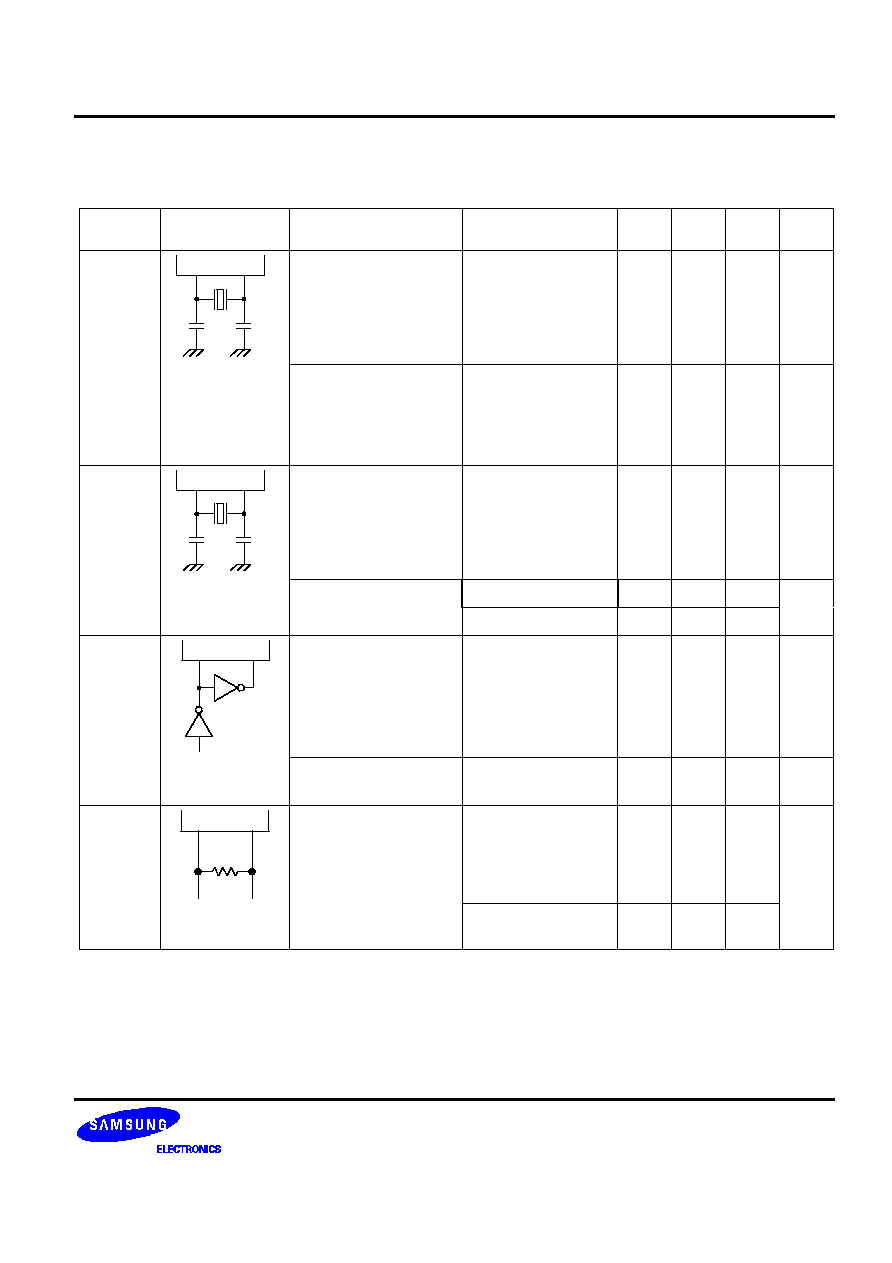
PIN CIRCUIT DIAGRAMS
Schmitt Trigger
Pull-Up
Resistor
V
DD
Resistor
Enable
In
P-Channel
Figure 1-3. Pin Circuit Type A-3
In
Pull-up Resistor
V
DD
Schmitt Trigger
Figure 1-4. Pin Circuit Type B
N-CH
V
DD
Resistor
Enable
V
DD
I/O
PNE
Pull-up
Resistor
P-CH
Output
Disable
Data
Figure 1-5. Pin Circuit Type E
Schmitt Trigger
N-CH
V
DD
Resistor
Enable
V
DD
I/O
PNE
Pull-up
Resistor
P-CH
Output
Disable
Data
Figure 1-6. Pin Circuit Type E-1

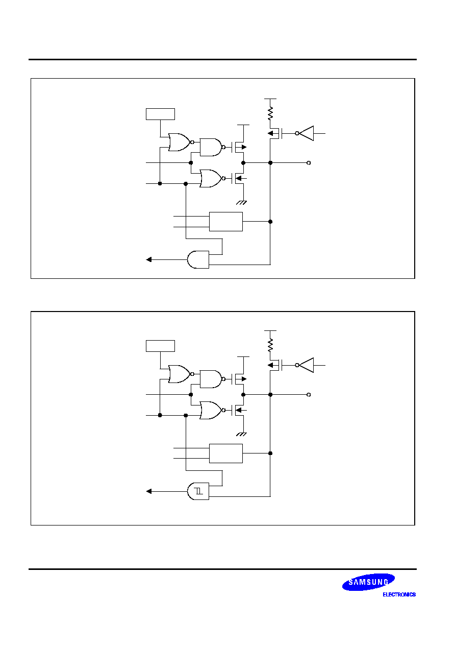
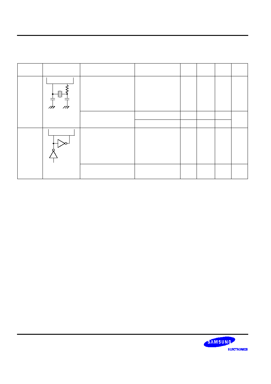
PRODUCT OVERVIEW
S3C72M5/C72M7/C72M9/P72M9 (Preliminary Spec)
1-14
Schmitt Trigger
N-CH
V
DD
Resistor
Enable
V
DD
I/O
PNE
Pull-up
Resistor
P-CH
Output
Disable
Data
Figure 1-7. Pin Circuit Type E-2
N-CH
V
DD
I/O
PNE
P-CH
Output
Disable
Data
Schmitt Trigger
Resistor
Enable
V
DD
Pull-up
Resistor
+
-
EXT-REF
(P4.2 only)
Analog In
Digital In
Comparator
INT-REF
Digital or Analog
Selectable by
Software (P4MOD)
Figure 1-8. Pin Circuit Type F-4

S3C72M5/C72M7/C72M9/P72M9 (Preliminary Spec)
PRODUCT OVERVIEW
1-15
Out
V
LC1
V
LC2
COM
V
SS
V
LC5
Figure 1-9. Pin Circuit Type H-4
Out
V
LC1
V
LC3
SEG
V
SS
V
LC4
Figure 1-10. Pin Circuit Type H-5
Out
SEG/COM
V
LC2
V
LC3
V
LC1
V
LC5
V
LC4
V
SS
Figure 1-11. Pin Circuit Type H-6
Out
V
SS
V
LC4
SEG
V
LC1
V
LC3
Output
Disable
Figure 1-12. Pin Circuit Type H-7
PRODUCT OVERVIEW
S3C72M5/C72M7/C72M9/P72M9 (Preliminary Spec)
1-16
N-Ch
V
DD
Resistor
Enable
V
DD
I/O
Pull-up
Resistor
P-Ch
Data
Circuit
Type H-7
SEG
Output Disable 2
Output Disable 1
PNE
Figure 1-13. Pin Circuit Type H-8
N-Ch
V
DD
Resistor
Enable
V
DD
I/O
Pull-up
Resistor
P-Ch
Data
Circuit
Type H-7
SEG
Output Disable 2
Output Disable 1
PNE
Schmitt Trigger
Figure 1-14. Pin Circuit Type H-15

S3C72M5/C72M7/C72M9/P72M9 (Preliminary Spec)
ELECTRICAL DATA
15-1
15
ELECTRICAL DATA
OVERVIEW
In this section, information on S3C72M5/C72M7/C72M9 electrical characteristics is presented as tables and
graphics. The information is arranged in the following order:
Standard Electrical Characteristics
-- Absolute maximum ratings
-- D.C. electrical characteristics
-- Main system clock oscillator characteristics
-- Subsystem clock oscillator characteristics
-- I/O capacitance
-- Comparator electrical characteristics
-- LCD contrast controller characteristics
-- A.C. electrical characteristics
-- Operating voltage range
Stop Mode Characteristics and Timing Waveforms
-- RAM data retention supply voltage in stop mode
-- Stop mode release timing when initiated by
RESET
-- Stop mode release timing when initiated by an interrupt request
Miscellaneous Timing Waveforms
-- A.C timing measurement points
-- Clock timing measurement at X
IN
-- Clock timing measurement at XT
IN
-- TCL0/TCL1 timing
-- Input timing for
RESET
signal
-- Input timing for external interrupts and quasi-interrupts
-- Serial data transfer timing

ELECTRICAL DATA
S3C72M5/C72M7/C72M9/P72M9 (Preliminary Spec)
15-2
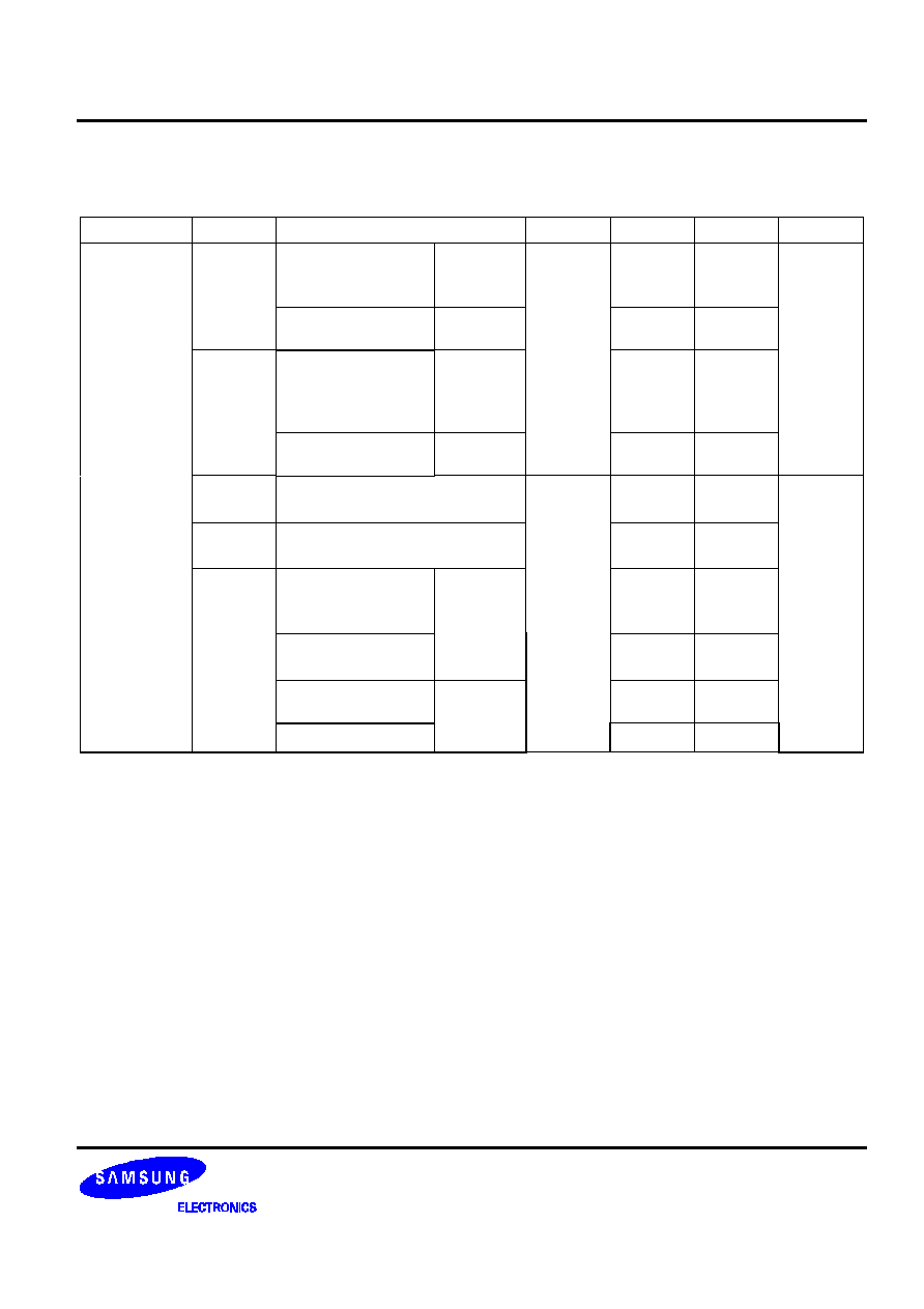
Table 15-1. Absolute Maximum Ratings
(T
A
= 25
∞
C)
Parameter
Symbol
Conditions
Rating
Units
Supply Voltage
V
DD
≠
≠ 0.3 to + 6.5
V
Input Voltage
V
I
All I/O pins active
≠ 0.3 to V
DD
+ 0.3
V
Output Voltage
V
O
≠
≠ 0.3 to V
DD
+ 0.3
V
Output Current High
I
OH
One I/O pin active
≠ 15
mA
All I/O pins active
≠ 35
Output Current Low
I
OL
One I/O pin active
+ 30 (Peak value)
mA
+ 15
(note)
Total for ports 0, 2≠9
+ 100 (Peak value)
+ 60
(note)
Operating Temperature
T
A
≠
≠ 40 to + 85
∞
C
Storage Temperature
T
stg
≠
≠ 65 to + 150
∞
C
NOTE: The values for Output Current Low ( I
OL
) are calculated as Peak Value
◊
Duty .
Table 15-2. D.C. Electrical Characteristics
(T
A
= ≠ 40
∞
C to + 85
∞
C, V
DD
= 1.8 V to 5.5 V)
Parameter
Symbol
Conditions
Min
Typ
Max
Units
Input High
Voltage
V
IH1
All input pins except those
specified below for V
IH2
≠V
IH3
0.7 V
DD
≠
V
DD
V
V
IH2
Ports 0, 1, 4, 6, P3.2, P3.3, and
RESET
0.8 V
DD
V
DD
V
IH3
X
IN
, X
OUT
, XT
IN
, and
XT
OUT
V
DD
≠ 0.1
V
DD
Input Low
Voltage
V
IL1
All input pins except those
specified below for V
IL2
≠V
IL3
≠
≠
0.3 V
DD
V
V
IL2
Ports 0, 1, 4, 6, P3.2, P3.3, and
RESET
0.2 V
DD
V
IL3
X
IN
, X
OUT
, XT
IN
, and
XT
OUT
0.1
Output High
Voltage
V
OH
V
DD
= 4.5 V to 5.5 V
I
OH
= ≠ 1 mA
Ports 0, 2, 3, 4, ports 6≠13
V
DD
≠ 1.0
≠
≠
V
Output Low
Voltage
V
OL
V
DD
= 4.5 V to 5.5 V
I
OL
= 15 mA
Ports 0, 2, 3, 4, ports 6≠13
≠
≠
2.0
V
V
DD
= 1.8 V to 5.5 V
I
OL
= 1.6 mA
0.4
S3C72M5/C72M7/C72M9/P72M9 (Preliminary Spec)
ELECTRICAL DATA
15-3
Table 15-2. D.C. Electrical Characteristics (Continued)
(T
A
= ≠ 40
∞
C to + 85
∞
C, V
DD
= 1.8 V to 5.5 V)
Parameter
Symbol
Conditions
Min
Typ
Max
Units
Input High
Leakage
Current
I
LIH1
V
I
= V
DD
All input pins except those specified
below for I
LIH2
≠
≠
3
µA
I
LIH2
V
I
= V
DD
X
IN
, X
OUT
, XT
IN
, and
XT
OUT
20
Input Low
Leakage
Current
I
LIL1
V
I
= 0 V
All input pins except
RESET
,
X
IN
, X
OUT
, XT
IN
, and
XT
OUT
≠
≠
≠ 3
µA
I
LIL2
V
I
= 0 V
RESET
, X
IN
, X
OUT
, XT
IN
, and
XT
OUT
≠ 20
Output High
Leakage
Current
I
LOH
V
O
= V
DD
All output pins
≠
≠
3
µA
Output Low
Leakage
Current
I
LOL
V
O
= 0 V
All output pins
≠
≠
≠ 3
µA
Pull-Up
Resistor
R
LI
V
I
= 0 V; V
DD
= 5 V
Ports 0≠4, ports 6≠13
25
50
100
k
V
DD
= 3 V
50
100
200
R
L2
V
I
= 0 V; V
DD
= 5 V,
RESET
100
250
400
V
DD
= 3 V
200
500
800
LCD Voltage
Dividing
Resistor
R
LCD
≠
40
60
90
k
|V
LC1
-COM
i
|
Voltage Drop
(i = 0≠15)
V
DC
≠ 15 µA per common pin
≠
≠
120
mV
|V
LC1
-SEGx|
Voltage Drop
(x = 0≠79)
V
DS
≠ 15 µA per segment pin
≠
≠
120
V
LC2
Output
Voltage
V
LC2
V
DD
= 1.8 V to 5.5 V, 1/5 bias
LCD clock = 0 Hz, V
LC1
=
V
DD
0.8 V
DD
≠ 0.2
0.8 V
DD
0.8 V
DD
≠ 0.2
V
V
LC3
Output
Voltage
V
LC3
0.6 V
DD
≠ 0.2
0.6 V
DD
0.6 V
DD
≠ 0.2
V
LC4
Output
Voltage
V
LC4
0.4 V
DD
≠ 0.2
0.4 V
DD
0.4 V
DD
≠ 0.2
V
LC5
Output
Voltage
V
LC5
0.2 V
DD
≠ 0.2
0.2 V
DD
0.2 V
DD
≠ 0.2
ELECTRICAL DATA
S3C72M5/C72M7/C72M9/P72M9 (Preliminary Spec)
15-4
Table 15-2. D.C. Electrical Characteristics (Concluded)
(T
A
= ≠ 40
∞
C to + 85
∞
C, V
DD
= 1.8 V to 5.5 V)
Parameter
Symbol
Conditions
Min
Typ
Max
Units
Supply
Current
(1)
I
DD1
(2)
V
DD
= 5 V
±
10%
Crystal oscillator
C1 = C2 = 22 pF
6.0 MHz
4.19 MHz
≠
3.9
2.9
8.0
5.5
mA
V
DD
= 3 V ± 10%
6.0 MHz
4.19 MHz
1.8
1.3
4.0
3.0
I
DD2
(2)
Idle mode
V
DD
= 5 V
±
10%
Crystal oscillator
C1 = C2 = 22 pF
6.0 MHz
4.19 MHz
1.3
1.2
2.5
1.8
V
DD
= 3 V ± 10%
6.0 MHz
4.19 MHz
0.5
0.44
1.5
1.0
I
DD3
(3)
V
DD
= 3 V ± 10%
32 kHz crystal oscillator
≠
15.3
30
µA
I
DD4
(3)
Idle mode; V
DD
= 3 V ± 10%
32 kHz crystal oscillator
6.4
15
I
DD5
Stop mode;
V
DD
= 5 V ± 10%
SCMOD =
0000B
XT
IN
= 0V
2.5
5
Stop mode;
V
DD
= 3 V ± 10%
0.5
3
V
DD
= 5 V ± 10%
SCMOD =
0100B
0.2
3
V
DD
= 3 V ± 10%
0.1
2
NOTES:
1.
Currents in the following circuits are not included; on-chip pull-up resistors, internal LCD voltage dividing resistors,
output port drive currents.
2.
Data includes power consumption for subsystem clock oscillation.
3.
When the system clock control register, SCMOD, is set to 1001B, main system clock oscillation stops and the
subsystem clock is used.
4.
Every values in this table is measured when the power control register (PCON) is set to "0011B".
S3C72M5/C72M7/C72M9/P72M9 (Preliminary Spec)
ELECTRICAL DATA
15-5
Table 15-3. Main System Clock Oscillator Characteristics
(T
A
= ≠ 40
∞
C + 85
∞
C, V
DD
= 1.8 V to 5.5 V)
Oscillato
r
Clock
Configuration
Parameter
Test Condition
Min
Typ
Max
Units
Ceramic
Oscillator
X
IN
C1
C2
X
OUT
Oscillation frequency
(1)
≠
0.4
≠
6.0
MHz
Stabilization time
(2)
Stabilization occurs
when V
DD
is equal to
the minimum
oscillator voltage
range; V
DD
= 3.0 V.
≠
≠
4
ms
Crystal
Oscillator
X
IN
C1
C2
X
OUT
Oscillation frequency
(1)
≠
0.4
≠
6.0
MHz
Stabilization time
(2)
V
DD
= 2.7 V to 5.5 V
≠
≠
10
ms
V
DD
= 1.8 V to 5.5 V
≠
≠
30
External
Clock
X
IN
X
OUT
X
IN
input frequency
(1)
≠
0.4
≠
6.0
MHz
X
IN
input high and low
level width (t
XH
, t
XL
)
≠
83.3
≠
1250
ns
RC
Oscillator
X
IN
X
OUT
R
Frequency
R = 20 k
,
V
DD
= 5 V
≠
2
≠
MHz
R = 39 k
,
V
DD
= 3 V
≠
1
≠
NOTES:
1.
Oscillation frequency and X
IN i
nput frequency data are for oscillator characteristics only.
2.
Stabilization time is the interval required for oscillating stabilization after a power-on occurs, or when stop mode is
terminated.
ELECTRICAL DATA
S3C72M5/C72M7/C72M9/P72M9 (Preliminary Spec)
15-6
Table 15-4. Subsystem Clock Oscillator Characteristics
(T
A
= ≠ 40
∞
C + 85
∞
C, V
DD
= 1.8 V to 5.5 V)
Oscillator
Clock
Configuration
Parameter
Test Condition
Min
Typ
Max
Units
Crystal
Oscillator
XT
IN
C1
C2
XT
OUT
Oscillation frequency
(1)
≠
32
32.768
35
kHz
Stabilization time
(2)
V
DD
= 2.7 V to 5.5 V
≠
1.0
2
s
V
DD
= 1.8 V to 5.5 V
≠
≠
10
External
Clock
XT
IN
XT
OUT
XT
IN
input frequency
(1)
≠
32
≠
100
kHz
XT
IN
input high and low
level width (t
XTL
, t
XTH
)
≠
5
≠
15
µs
NOTES:
1.
Oscillation frequency and XT
IN
input frequency data are for oscillator characteristics only.
2.
Stabilization time is the interval required for oscillating stabilization after a power-on occurs.

S3C72M5/C72M7/C72M9/P72M9 (Preliminary Spec)
ELECTRICAL DATA
15-7
Table 15-5. Input/Output Capacitance
(T
A
= 25
∞
C, V
DD
=
0 V )
Parameter
Symbol
Condition
Min
Typ
Max
Units
Input
Capacitance
C
IN
f = 1 MHz; Unmeasured
pins are returned to V
SS
≠
≠
15
pF
Output
Capacitance
C
OUT
≠
≠
15
pF
I/O Capacitance
C
IO
≠
≠
15
pF
Table 15-6. Comparator Electrical Characteristics
(T
A
= ≠ 40
∞
C + 85
∞
C, V
DD
= 4.0 V to 5.5 V, V
SS
=
0 V)
Parameter
Symbol
Condition
Min
Typ
Max
Units
Input Voltage Range
≠
≠
0
≠
V
DD
V
Reference Voltage Range
V
REF
≠
0
≠
V
DD
V
Input Voltage
Internal
V
CIN1
≠
≠
≠
±
150
mV
Accuracy
External
V
CIN2
≠
≠
≠
±
150
mV
Input Leakage Current
I
CIN
, I
REF
≠
≠ 3
≠
3
µ
A
Table 15-7. LCD Contrast Controller Characteristics
(T
A
= ≠ 40
∞
C + 85
∞
C, V
DD
= 4.5 V to 5.5 V)
Parameter
Symbol
Condition
Min
Typ
Max
Units
Resolution
≠
≠
≠
≠
4
Bits
Linearity
RLIN
≠
≠
≠
±
1.0
LSB
Max Output Voltage
(LCNST = #8FH)
V
LPP
V
LC1
=V
DD
=5V
4.9
≠
V
LC1
V

ELECTRICAL DATA
S3C72M5/C72M7/C72M9/P72M9 (Preliminary Spec)
15-8
Table 15-8. A.C. Electrical Characteristics
(T
A
= ≠ 40
∞
C to + 85
∞
C, V
DD
= 1.8 V to 5.5 V)
Parameter
Symbol
Conditions
Min
Typ
Max
Units
Instruction Cycle
Time
(note)
t
CY
V
DD
= 2.7 V to 5.5 V
0.67
≠
64
µs
V
DD
= 1.8 V to 5.5 V
0.95
64
TCL0, TCL1 Input
Frequency
f
TI0
,
f
TI1
V
DD
= 2.7 V to 5.5 V
0
≠
1.5
MHz
V
DD
= 1.8 V to 5.5 V
1
TCL0, TCL1 Input
High, Low Width
t
TIH0
,
t
TIL0
t
TIH1
, t
TIL1
V
DD
= 2.7 V to 5.5 V
0.48
≠
≠
µs
V
DD
= 1.8 V to 5.5 V
1.8
SCK
Cycle Time
t
KCY
V
DD
= 2.7 V to 5.5 V; Input
800
≠
≠
ns
Output
650
V
DD
= 1.8 V to 5.5 V; Input
3200
Output
3800
SCK
High, Low
Width
t
KH
, t
KL
V
DD
= 2.7 V to 5.5 V; Input
325
≠
≠
ns
Output
t
KCY
/2 ≠ 50
V
DD
= 1.8 V to 5.5 V; Input
1600
Output
t
KCY
/
2 ≠ 150
SI Setup Time to
SCK
High
t
SIK
V
DD
= 2.7 V to 5.5 V; Input
100
≠
≠
ns
V
DD
= 2.7 V to 5.5 V; Output
150
V
DD
= 1.8 V to 5.5 V; Input
150
V
DD
= 1.8 V to 5.5 V; Output
500
SI Hold Time to
SCK
High
t
KSI
V
DD
= 2.7 V to 5.5 V; Input
400
≠
≠
ns
V
DD
= 2.7 V to 5.5 V; Output
400
V
DD
= 1.8 V to 5.5 V; Input
600
V
DD
= 1.8 V to 5.5 V; Output
500
NOTE: Unless otherwise specified, Instruction Cycle Time condition values assume a main system clock ( fx ) source.
S3C72M5/C72M7/C72M9/P72M9 (Preliminary Spec)
ELECTRICAL DATA
15-9
Table 15-8. A.C. Electrical Characteristics (Continued)
(T
A
= ≠ 40
∞
C to + 85
∞
C, V
DD
= 1.8 V to 5.5 V)
Parameter
Symbol
Conditions
Min
Typ
Max
Units
Output Delay for
SCK
to SO
t
KSO
V
DD
= 2.7 V to 5.5 V; Input
≠
≠
300
ns
V
DD
= 2.7 V to 5.5 V; Output
250
V
DD
= 1.8 V to 5.5 V; Input
1000
V
DD
= 1.8 V to 5.5 V; Output
1000
Interrupt Input
High, Low Width
t
INTH
, t
INTL
INT0, INT1, INT2, INT4,
K0≠K7
10
≠
≠
µs
RESET
Input Low
Width
t
RSL
Input
10
≠
≠
µs
NOTE: Minimum value for INT0 is based on a clock of 2t
CY
or 128 / fx as assigned by the IMOD0 register setting.
1.5 MHz
CPU Clock
1.05 MHz
15.6 kHz
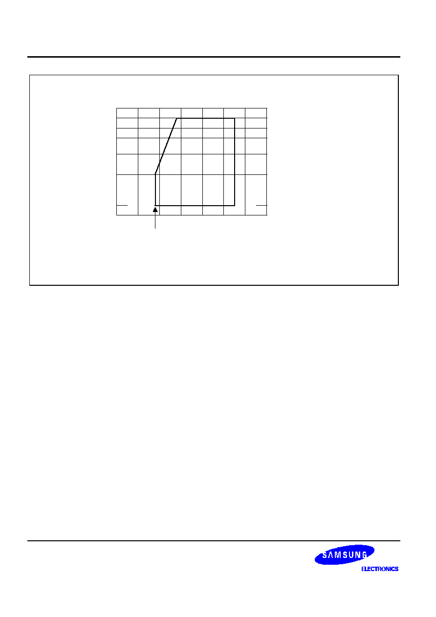
Main Oscillator Frequency
(Divided by 4)
4.2 MHz
6 MHz
1
2
3
4
5
6
7
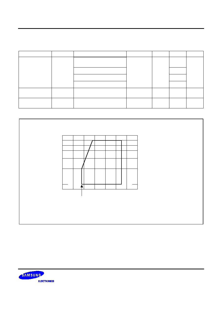
Supply Voltage (V)
CPU clock = 1/n x oscillator frequency (n = 4, 8 or 64)
1.8 V
Figure 15-1. Standard Operating Voltage Range

ELECTRICAL DATA
S3C72M5/C72M7/C72M9/P72M9 (Preliminary Spec)
15-10
Table 15-9. RAM Data Retention Supply Voltage in Stop Mode
(T
A
= ≠ 40
∞
C to + 85
∞
C)
Parameter
Symbol
Conditions
Min
Typ
Max
Unit
Data retention supply voltage
V
DDDR
≠
1.8
≠
5.5
V
Data retention supply current
I
DDDR
V
DDDR
= 1.8 V
≠
0.1
1
µA
Release signal set time
t
SREL
≠
0
≠
≠
µs
Oscillator stabilization wait
time
(1)
t
WAIT
Released by
RESET
≠
2
17
/ fx
≠
ms
Released by interrupt
≠
(2)
≠
NOTES:
1.
During oscillator stabilization wait time, all CPU operations must be stopped to avoid instability during oscillator
start-up.
2.
Use the basic timer mode register (BMOD) interval timer to delay execution of CPU instructions during the wait time.
S3C72M5/C72M7/C72M9/P72M9 (Preliminary Spec)
ELECTRICAL DATA
15-11
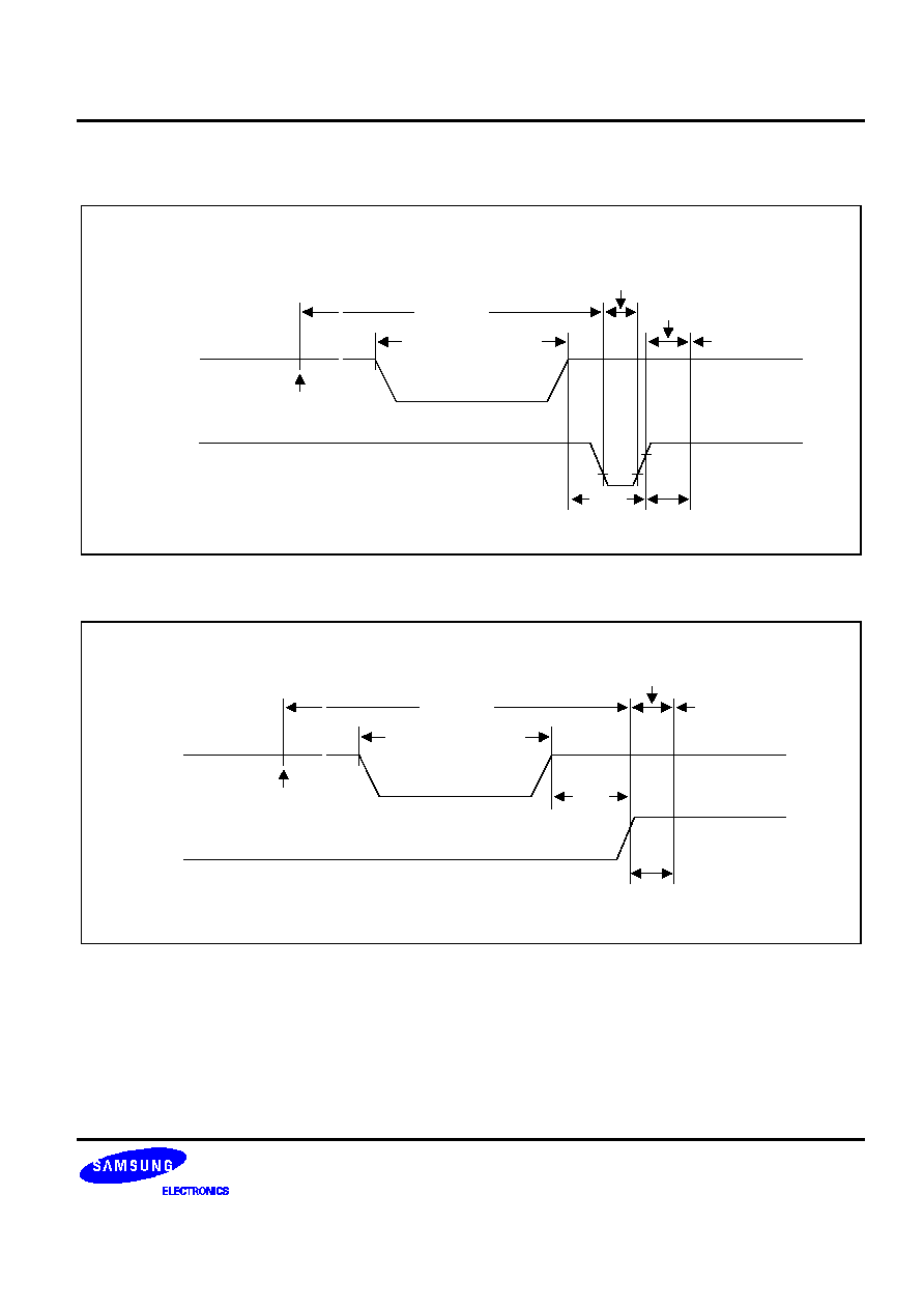
TIMING WAVEFORMS
Execution of
STOP Instrction
Internal
RESET
Operation
~ ~
V
DDDR
~ ~
Stop Mode
Idle Mode
Normal Mode
Data Retention Mode
t
SREL
t
WAIT
RESET
V
DD
Figure 15-2. Stop Mode Release Timing When Initiated By
RESET
Execution of
STOP Instrction
V
DDDR
~ ~
Data Retention Mode
V
DD
Normal Mode
~ ~
Stop Mode
Idle Mode
t
SREL
t
WAIT
Power-down Mode Terminating Signal
(Interrupt Request)
Figure 15-3. Stop Mode Release Timing When Initiated By Interrupt Request
ELECTRICAL DATA
S3C72M5/C72M7/C72M9/P72M9 (Preliminary Spec)
15-12
0.8 V
DD
0.2 V
DD
0.8 V
DD
0.2 V
DD
Measurement
Points
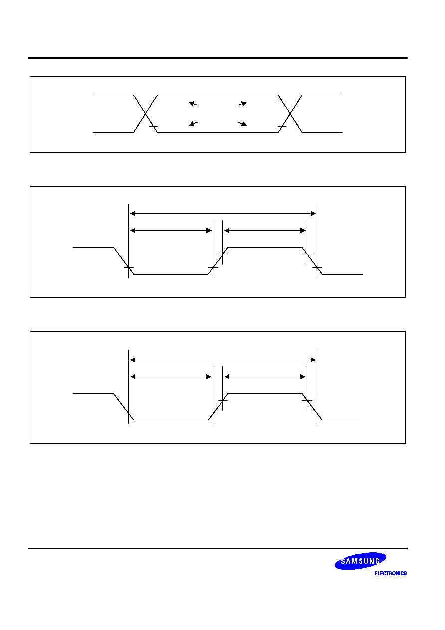
Figure 15-4. A.C. Timing Measurement Points (Except for X
IN
and XT
IN
)
X
IN
t
XH
t
XL
1/fx
V
DD
- 0.1 V
0.1 V
Figure 15-5. Clock Timing Measurement at X
IN
XT
IN
t
XTH
t
XTL
1/fxt
V
DD
- 0.1 V
0.1 V
Figure 15-6. Clock Timing Measurement at XT
IN
S3C72M5/C72M7/C72M9/P72M9 (Preliminary Spec)
ELECTRICAL DATA
15-13
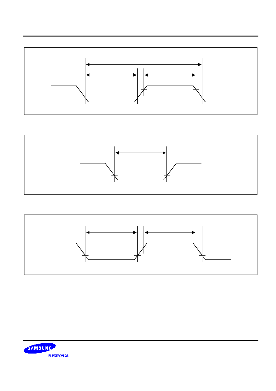
TCL0/TCL1
t
TIH
t
TIL
1/f
TI
0.7 V
DD
0.3 V
DD
Figure 15-7. TCL0/TCL1 Timing
RESET
t
RSL
0.2 V
DD
Figure 15-8. Input Timing for
RESET
Signal
INT0, 1, 2, 4,
K0 to K7
t
INTH
t
INTL
0.8 V
DD
0.2 V
DD
Figure 15-9. Input Timing for External Interrupts and Quasi-Interrupts

ELECTRICAL DATA
S3C72M5/C72M7/C72M9/P72M9 (Preliminary Spec)
15-14
Output Data
Input Data
SCK
t
KH
t
KCY
t
KL
0.8 V
DD
0.2 V
DD
t
KSO
t
SIK
t
KSI
0.8 V
DD
0.2 V
DD
SI
SO
Figure 15-10. Serial Data Transfer Timing
S3C72M5/C72M7/C72M9/P72M9 (Preliminary Spec)
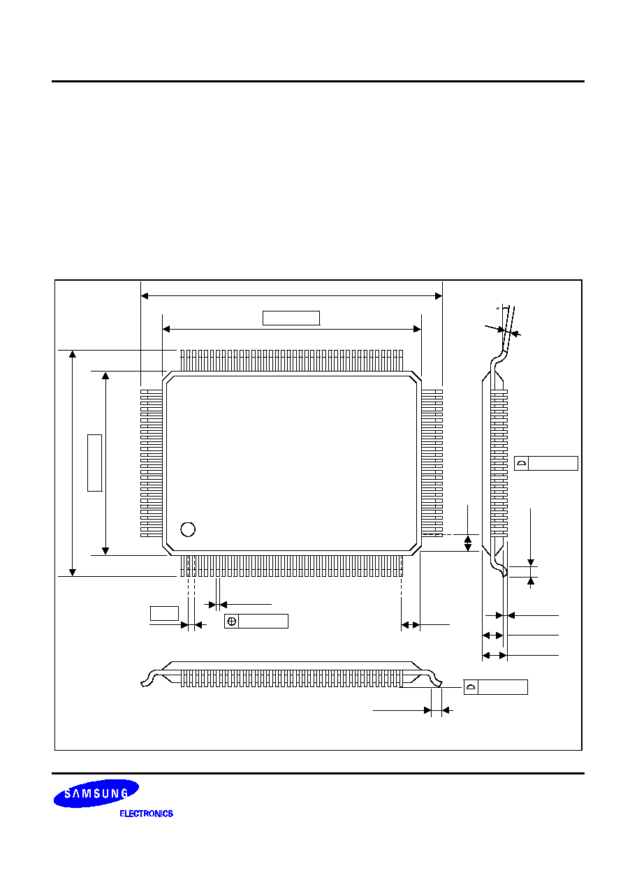
MECHANICAL DATA
16-1
16
MECHANICAL DATA
OVERVIEW
The S3C72M5/C72M7/C72M9/P72M9 microcontroller is currently available in a 128-pin QFP package.
128-QFP-1420
#128
20.00
±
0.20
22.00
±
0.30
14.00
±
0.20
16.00
±
0.30
0.15
+ 0.10
- 0.05
0-8
0.10 MAX
#1
NOTE: Dimensions are in millimeters.
(0.75)
0.50
±
0.20
0.05 MIN
2.10
±
0.10
2.40 MAX
0.50
±
0.20
0.50
0.20
+ 0.10
- 0.05
(0.75)
0.10 MAX
0.10 MAX
Figure 16-1. 128-QFP-1420 Package Dimensions

MECHANICAL DATA
S3C72M5/C72M7/C72M9/P72M9 (Preliminary Spec)
16-2
NOTES

S3C72M5/C72M7/C72M9/P72M9 (Preliminary Spec)
S3P72M9 OTP
17-1
17
S3P72M9 OTP
OVERVIEW
The S3P72M9 single-chip CMOS microcontroller is the OTP (One Time Programmable)
version of the
S3C72M5/C72M7/C72M9 microcontroller. It has an on-chip OTP ROM instead of masked ROM. The EPROM is
accessed by serial data format.
The S3P72M9 is fully compatible with the S3C72M5/C72M7/C72M9, both in function and in pin configuration
except ROM size. Because of its simple programming requirements, the S3P72M9 is ideal for use as an
evaluation chip for the S3C72M5/C72M7/C72M9.

S3P72M9 OTP
S3C72M5/C72M7/C72M9/P72M9 (Preliminary Spec)
17-2
SEG20
SEG21
SEG22
SEG23
SEG24
SEG25
SEG26
SEG27
SEG28
SEG29
SEG30
SEG31
SEG32
SEG33
SEG34
SEG35
SEG36
SEG37
SEG38
SEG39
SEG40
SEG41
SEG42
SEG43
SEG44
SEG45
SEG46
SEG47
SEG48/P13.3
SEG49/P13.2
SEG50/P13.1
SEG51/P13.0
SEG52/P12.3
SEG53/P12.2
SEG54/P12.1
SEG55/P12.0
SEG56/P11.3
SEG57/P11.2
COM9/SEG86
COM8/SEG87
COM7
COM6
COM5
COM4
COM3
COM2
COM1
COM0
V
LC5
V
LC4
V
LC3
V
LC2
V
LC1
P0.0/
SCK
/K0
P0.1/SO/K1
SDAT/P0.2/SI/K2
SCLK/P0.3/BUZ/K3
V
DD
/V
DD
V
SS
/V
SS
X
OUT
X
IN
V
PP
/TEST
XT
IN
XT
OUT
RESET
/RESET
P1.0/INT0
P1.1/INT1
P1.2/INT2
P1.3/INT4
P2.0/M
P2.1/LCDFR
P2.2/CLO1
P2.3/CLO2
P3.0/TCLO0/CL
P3.1/TCLO1
P3.2/TCL0
S3C72M5/C72M7/C72M9/P72M9
(128-QFP-1420)
1
2
3
4
5
6
7
8
9
10
11
12
13
14
15
16
17
18
19
20
21
22
23
24
25
26
27
28
29
30
31
32
33
34
35
36
37
38
102
101
100
99
98
97
96
95
94
93
92
91
90
89
88
87
86
85
84
83
82
81
80
79
78
77
76
75
74
73
72
71
70
69
68
67
66
65
128
127
126
125
124
123
122
121
120
119
118
117
116
115
114
113
112
111
110
109
108
107
106
105
104
103
39
40
41
42
43
44
45
46
47
48
49
50
51
52
53
54
55
56
57
58
59
60
61
62
63
64
P3.3/TCL1
P4.0/CIN0
P4.1/CIN1
P4.2/CIN2
SEG79/P6.0/K4
SEG78/P6.1/K5
SEG77//P6.2/K6
SEG76/P6.3/K7
SEG75/P7.0
SEG74/P7.1
SEG73/P7.2
SEG72/P7.3
SEG71/P8.0
SEG70/P8.1
SEG69/P8.2
SEG68/P8.3
SEG67/P9.0
SEG66/P9.1
SEG65/P9.2
SEG64/P9.3
SEG63/P10.0
SEG62/P10.1
SEG61/P10.2
SEG60/P10.3
SEG59/P11.0
SEG58/P11.1
SEG85/COM10
SEG84/COM11
SEG83/COM12
SEG82/COM13
SEG81/COM14
SEG80/COM15
SEG0
SEG1
SEG2
SEG3
SEG4
SEG5
SEG6
SEG7
SEG8
SEG9
SEG10
SEG11
SEG12
SEG13
SEG14
SEG15
SEG16
SEG17
SEG18
SEG19
NOTE:
The bold indicate an OTP pin name.
Figure 17-1. S3P72M9 Pin Assignments (128-QFP Package)

S3C72M5/C72M7/C72M9/P72M9 (Preliminary Spec)
S3P72M9 OTP
17-3
Table 17-1. Descriptions of Pins Used to Read/Write the EPROM
Main Chip
During Programming
Pin Name
Pin Name
Pin No.
I/O
Function
P0.2
SDAT
18
I/O
Serial data pin. Output port when reading and
input port when writing. Can be assigned as a
Input/push-pull output port.
P0.3
SCLK
19
I/O
Serial clock pin. Input only pin.
TEST
V
PP
(TEST)
24
I
Power supply pin for EPROM cell writing
(indicates that OTP enters into the writing
mode). When 12.5 V is applied, OTP is in
writing mode and when 5 V is applied, OTP is in
reading mode. (Option)
RESET
RESET
27
I
Chip Initialization
V
DD
/V
SS
V
DD
/V
SS
20/21
I
Logic power supply pin. V
DD
should be tied to +5
V during programming.
Table 17-2. Comparison of S3P72M9 and S3C72M5/C72M7/C72M9 Features
Characteristic
S3P72M9
S3C72M5/C72M7/C72M9
Program Memory
32-Kbyte EPROM
16/24/32-Kbyte mask ROM
Operating Voltage (V
DD
)
1.8 V to 5.5 V
1.8 V to 5.5 V
OTP Programming Mode
V
DD
= 5 V, VPP
(TEST) = 12.5V
Pin Configuration
128 QFP
128 QFP
EPROM Programmability
User Program 1 time
Programmed at the factory
OPERATING MODE CHARACTERISTICS
When 12.5 V is supplied to the V
PP
(TEST) pin of the S3P72M9, the EPROM programming mode is entered. The
operating mode (read, write, or read protection) is selected according to the input signals to the pins listed in
Table 17-3 below.
Table 17-3. Operating Mode Selection Criteria
V
DD
V
PP
(TEST)
REG/
MEM
Address
(A15-A0)
R/W
Mode
5 V
5 V
0
0000H
1
EPROM read
12.5 V
0
0000H
0
EPROM program
12.5 V
0
0000H
1
EPROM verify
12.5 V
1
0E3FH
0
EPROM read protection
NOTE: "0" means Low level; "1" means High level.

S3P72M9 OTP
S3C72M5/C72M7/C72M9/P72M9 (Preliminary Spec)
17-4
Start
Address = First Location
V
DD
= 5 V, V
PP
= 12.5 V
x = 0
Program One 1 ms Pulse
Increment X
V
DD
= V
PP
= 5 V
Compare All Byte
Device Passed
Pass
Verify 1 Byte
Last Address
Fail
No
Increment Address
x = 10
No
Yes
Verify Byte
Fail
Fail
Device Faild
Figure 17-2. OTP Programming Algorithm
S3C72M5/C72M7/C72M9/P72M9 (Preliminary Spec)
S3P72M9 OTP
17-5
Table 17-4. D.C. Electrical Characteristics
(T
A
= ≠ 40
∞
C to + 85
∞
C, V
DD
= 1.8 V to 5.5 V)
Parameter
Symbol
Conditions
Min
Typ
Max
Units
Supply
Current
(1)
I
DD1 (2)
V
DD
= 5 V
±
10%
Crystal oscillator
C1 = C2 = 22 pF
6.0 MHz
4.19 MHz
≠
3.9
2.9
8.0
5.5
mA
V
DD
= 3 V ± 10%
6.0 MHz
4.19 MHz
1.8
1.3
4.0
3.0
I
DD2 (2)
Idle mode
V
DD
= 5 V
±
10%
Crystal oscillator
C1 = C2 = 22 pF
6.0 MHz
4.19 MHz
1.3
1.2
2.5
1.8
V
DD
= 3 V ± 10%
6.0 MHz
4.19 MHz
0.5
0.44
1.5
1.0
I
DD3 (3)
V
DD
= 3 V ± 10%
32 kHz crystal oscillator
≠
15.3
30
µA
I
DD4 (3)
Idle mode; V
DD
= 3 V ± 10%
32 kHz crystal oscillator
6.4
15
I
DD5
Stop mode;
V
DD
= 5 V ± 10%
SCMOD =
0000B
XT
IN
= 0V
2.5
5
Stop mode;
V
DD
= 3 V ± 10%
0.5
3
V
DD
= 5 V ± 10%
SCMOD =
0100B
0.2
3
V
DD
= 3 V ± 10%
0.1
2
NOTES:
1.
Currents in the following circuits are not included; on-chip pull-up resistors, internal LCD voltage dividing resistors,
output port drive currents.
2.
Data includes power consumption for subsystem clock oscillation.
3.
When the system clock control register, SCMOD, is set to 1001B, main system clock oscillation stops and the
subsystem clock is used.
4.
Every values in this table is measured when the power control register (PCON) is set to "0011B".
S3P72M9 OTP
S3C72M5/C72M7/C72M9/P72M9 (Preliminary Spec)
17-6
1.5 MHz
CPU Clock
1.05 MHz
15.6 kHz
Main Oscillator Frequency
(Divided by 4)
4.2 MHz
6 MHz
1
2
3
4
5
6
7
Supply Voltage (V)
CPU clock = 1/n x oscillator frequency (n = 4, 8 or 64)
1.8 V
Figure 17-3. Standard Operating Voltage Range