 | –≠–ª–µ–∫—Ç—Ä–æ–Ω–Ω—ã–π –∫–æ–º–ø–æ–Ω–µ–Ω—Ç: S3P7414 | –°–∫–∞—á–∞—Ç—å:  PDF PDF  ZIP ZIP |

S3C7414/P7414/C7424/P7424/C7434/P7434
PRODUCT OVERVIEW
1-1
1
PRODUCT OVERVIEW
OVERVIEW
The S3C7414/C7424/C7434 single-chip CMOS microcontroller has been designed for very high performance
using Samsung's newest 4-bit CPU core, SAM47 (Samsung Arrangeable Microcontroller).
With an A/D converter, LED direct drive pins, an 8-bit serial I/O interface, and an 8-bit timer/counter, the
S3C7414/C7424/C7434 offers you an excellent design solution for a wide variety of home appliance applications
-- electric fans, cookers, boilers, and air conditioners, for example.
Up to 35 pins of the 42-pin SDIP or 44-pin QFP package can be dedicated to I/O. Seven vectored interrupts
provide fast response to internal and external events.
In addition, the S3C7414/C7424/C7434's advanced CMOS technology provides for low power consumption and a
wide operating voltage range.
OTP
The S3C7414/C7424/C7434 microcontroller is also available in OTP (One Time Programmable) version,
S3P7414/P7424/P7434. S3P7414/P7424/P7434 microcontroller has an on-chip 4-Kbyte one-time-programmable
EPROM instead of masked ROM. The S3P7414/P7424/P7434 is comparable to S3C7414/C7424/C7434, in
function, in D.C. electrical characteristics and in pin configuration.
DEVELOPMENT SUPPORT
The Samsung Microcontroller Development System, SMDS, provides you with a complete PC-based develop-
ment environment for S3C7-series microcontrollers that is powerful, reliable, and portable. In addition to its
window-based program development structure, the SMDS toolset includes versatile debugging, trace, instruction
timing, and performance measurement applications.
The Samsung Generalized Assembler (SAMA) has been designed specifically for the SMDS environment and
accepts assembly language sources in a variety of microprocessor formats. SAMA generates industry-standard
hex files that also contain program control data for SMDS compatibility.

PRODUCT OVERVIEW
S3C7414/P7414/C7424/P7424/C7434/P7434
1-2
FEATURES SUMMARY
Memory
∑
256
◊
4-bit RAM
∑
4,096
◊
8-bit ROM
35 I/O Pins
∑
I/O: 31 pins including 8 LED direct drive pins
(S3C7414/C7434)
18 pins including 8 LED direct drive pins
(S3C7424)
∑
Input only: 4 pins
A/D Converter
∑
6-channel with 8-bit resolution
∑
22.89 µs conversion speed at 4.19 MHz
Basic Timer
∑
One 8-bit basic timer
∑
Watchdog timer functions
∑
Four interval clock selection
Timer/Counters
∑
Two 8-bit timer/counter (TC0, TC1)
∑
Programmable 8-bit timer
∑
External event counter
∑
Arbitrary clock frequency output
∑
PWM output mode (TC1)
Watch Timer
∑
One watch timer 8-bit
∑
Time interval generation: 0.5 s, 3.9 ms at
4.19 MHz
∑
Four frequency outputs to BUZ pin
8-bit Serial I/O Interface
∑
8-bit transmit/receive mode
∑
8-bit receive mode
∑
LSB-first or MSB-first transmission selectable
∑
Internal or external clock source
Built-in reset circuit (S3C7434 only)
∑
Built-in power-on reset circuit
Interrupts
∑
Five internal vectored interrupts
(INTB, INTT0, INTT1, INTS, INTAD)
∑
Three external vectored interrupts
(INT0, INT1, INT4)
∑
Two quasi-interrupts (INT2, INTW)
Bit Sequential Carrier
∑
Supports 16-bit serial data transfer in
arbitrary format
Memory-Mapped I/O Structure
∑
Data memory bank 15
Two Power-Down Modes
∑
Idle mode (only CPU clock stops)
∑
Stop mode (system oscillation stops)
Oscillation Sources
∑
Crystal, Ceramic, or RC for system clock
∑
Crystal, Ceramic: 0.4≠6.0 MHz
∑
RC: 4 MHz (typ)
∑
CPU clock divider circuit (by 4, 8, or 64)
Instruction Execution Times
∑
0.95, 1.91, 15.3 µs at 4.19 MHz
∑
0.67, 1.33, 10.7 µs at 6.0 MHz
Operating Temperature
∑
≠ 40
∞
C to 85
∞
C
Operating Voltage Range
∑
1.8 V to 5.5 V (S3C7414/C7424)
∑
2.5 V to 5.5 V (S3C7434)
Package Type
∑
42-pin SDIP, 44-pin QFP (S3C7414/C7434)
30-pin SDIP, 28-pin SOP (S3C7424)
S3C7414/P7414/C7424/P7424/C7434/P7434
PRODUCT OVERVIEW
1-3
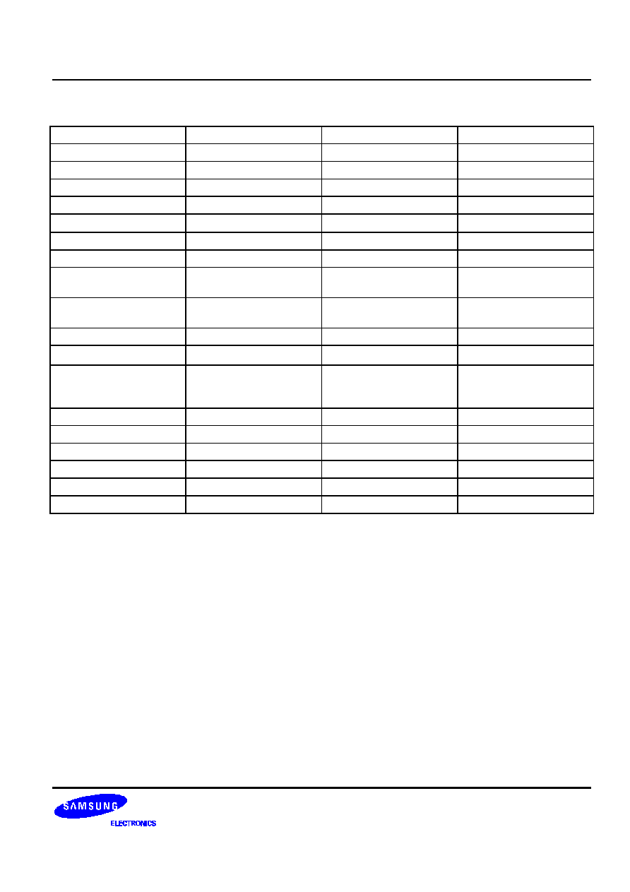
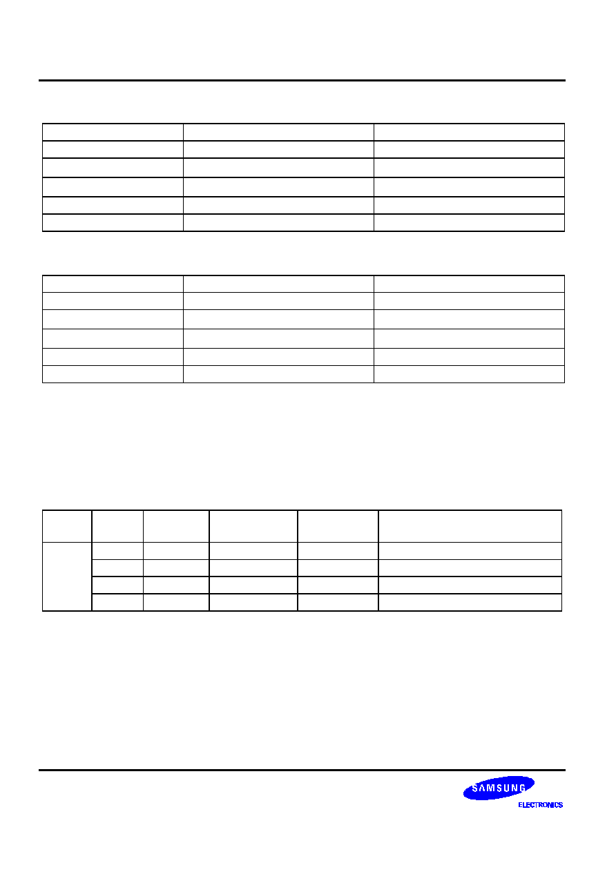
Table 1-1. Comparision Table
Feature
S3C7414
S3C7424
S3C7434
Core
SAM47
SAM47
SAM47
ROM
4 K bytes
Same
Same
RAM
256 nibbles
Same
Same
I/O
35 (4 input only)
21 (3 input only)
35 (4 input only)
POR
(1)
None
None
Built in/ Typ: 2.0 V
SIO
8-bit SIO x 1
Same
Same
Timer0
8-bit timer/counter
Same
Same
Timer1(PWM)
8-bit timer/counter
(8-bit PWM x 1)
Same
Same
Watchdog timer
Watch-dog
4 selectable interval
Same
Same
ADC
8-bit x 6
8-bit x 4
8-bit x 6
AV
SS
None
(2)
Same
Same
Interrupt
External x 3
Internal x 5
Quasi x 2 (KS0≠KS3)
External x 2
Internal x 5
Quasi x 1 ( ≠ )
External x 3
Internal x 5
Quasi x 2 (KS0≠KS3)
Power down
Stop/Idle
Same
Same
Oscillator
Crystal, Ceramic, RC
Same
Same
Operating frequency
0.4≠6 MHz
Same
Same
Operating voltage
1.8≠5.5 V
1.8≠5.5 V
2.5≠5.5 V
OTP/MTP
OTP
Same
Same
Package
42SDIP/44QFP
30SDIP/28SOP
42SDIP/44QFP
NOTES
1.
POR (power on reset)/Typ 2.0 V low voltage detector.
2.
Internal A/D converter ground (bonded to V
SS
internally)
PRODUCT OVERVIEW
S3C7414/P7414/C7424/P7424/C7434/P7434
1-4
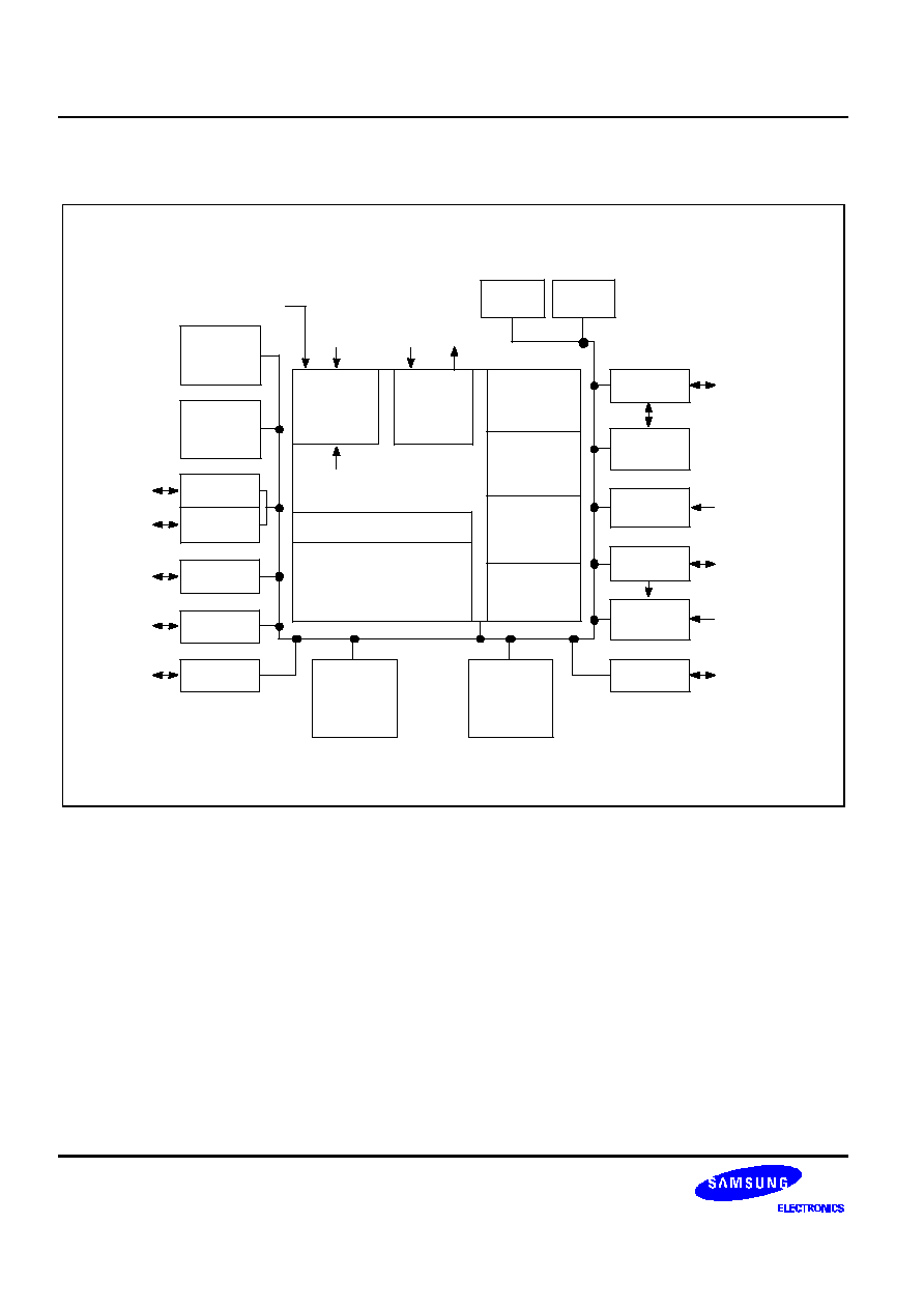
BLOCK DIAGRAM
ARITHMETIC
AND
LOGIC UNIT
INTERRUPT
CONTROL
BLOCK
INSTRUCTION
REGISTER
PROGRAM
COUNTER
PROGRAM
STATUS WORD
256 x 4-BIT
DATA
MEMORY
8-BIT
TIMER/
COUNTER 0
STACK
POINTER
INSTRUCTION DECODER
CLOCK
RESET
X
IN
X
OUT
INTERNAL
INTERRUPTS
4 K BYTE
PROGRAM
MEMORY
INT0, INT1, INT2,INT4
BASIC
TIMER
WATCH
TIMER
P0.0/
SCK
P0.1/SO
P0.2/SI
P0.3/BUZ
P3.0/AD4
P3.1/AD5
P3.2/CLO/TCL1
P3.3/PWM / TCLO1
P4.0-4.3
P5.0-5.3
I/O PORT 4
I/O PORT 5
P6.0/KS0
P6.1/KS1
P6.2/KS2
P6.3/KS3
I/O PORT 6
P7.0-7.3
I/O PORT 7
P8.0/TCL0
P8.1/TCLO0
P8.2
I/O PORT 8
I/O PORT 3
P2.0-P2.3/
AD0-AD3
I/O PORT 2
SERIAL
I/O
I/O PORT 0
I/O PORT 2
P1.0/INT0
P1.1/INT1
P1.2/INT2
P1.3/INT4
INPUT
PORT 1
A/D
CONVERTER
AV
REF
8-BIT
TIMER/
COUNTER 1
Figure 1-1. S3C7414/C7424/C7434Simplified Block Diagram
S3C7414/P7414/C7424/P7424/C7434/P7434
PRODUCT OVERVIEW
1-5
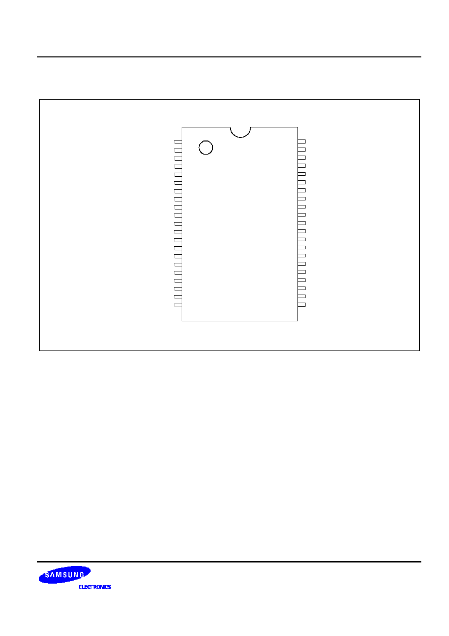
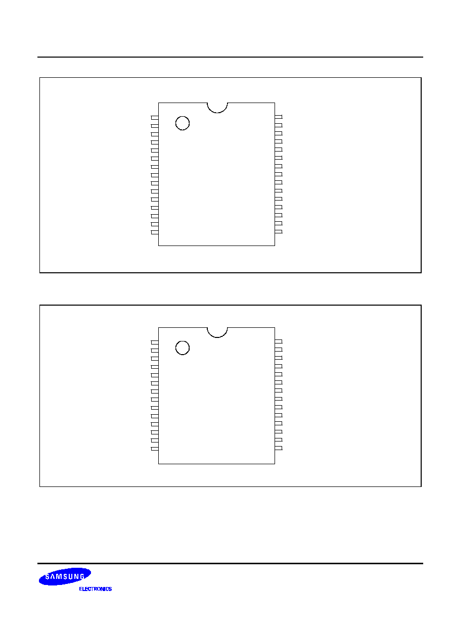
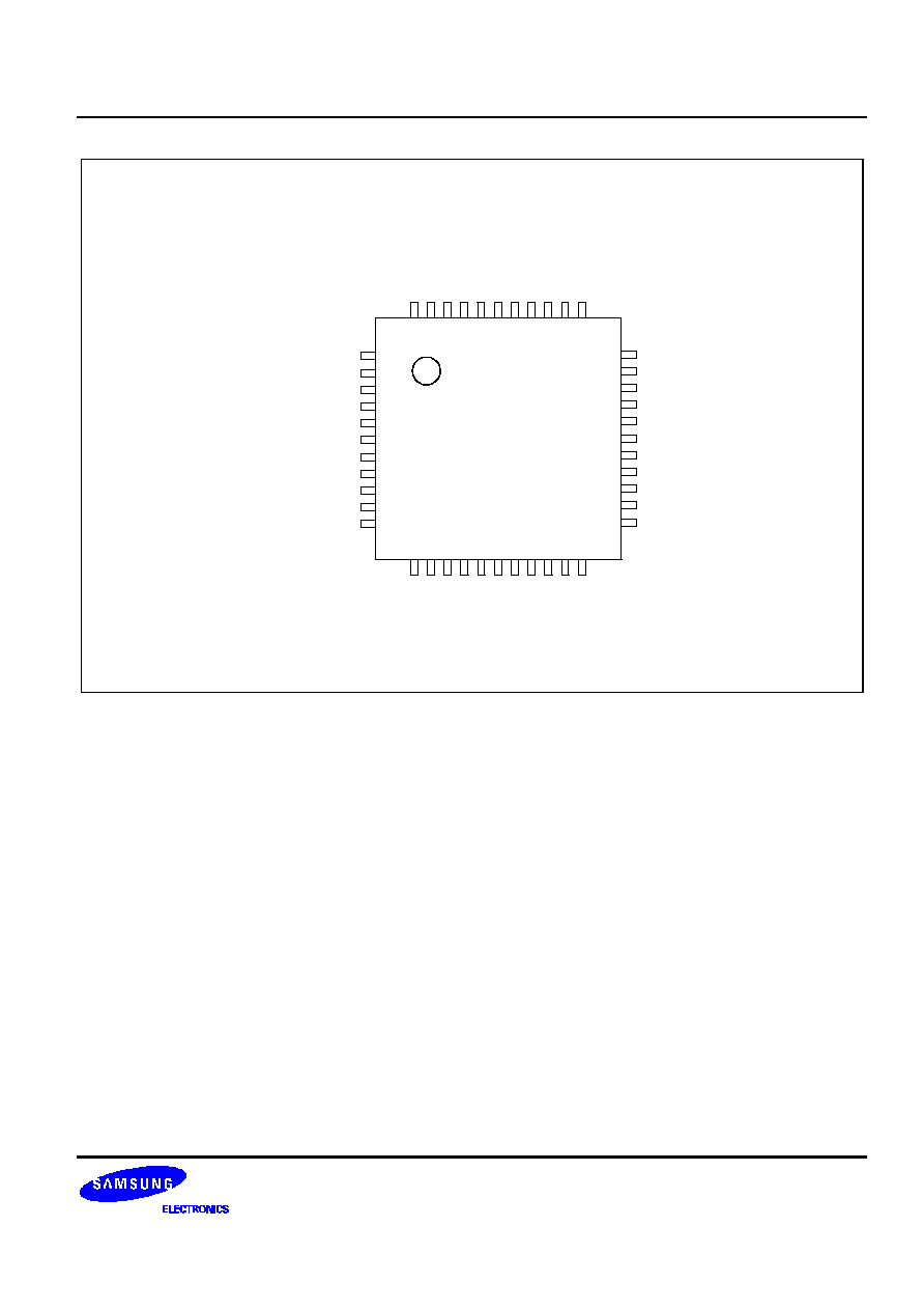
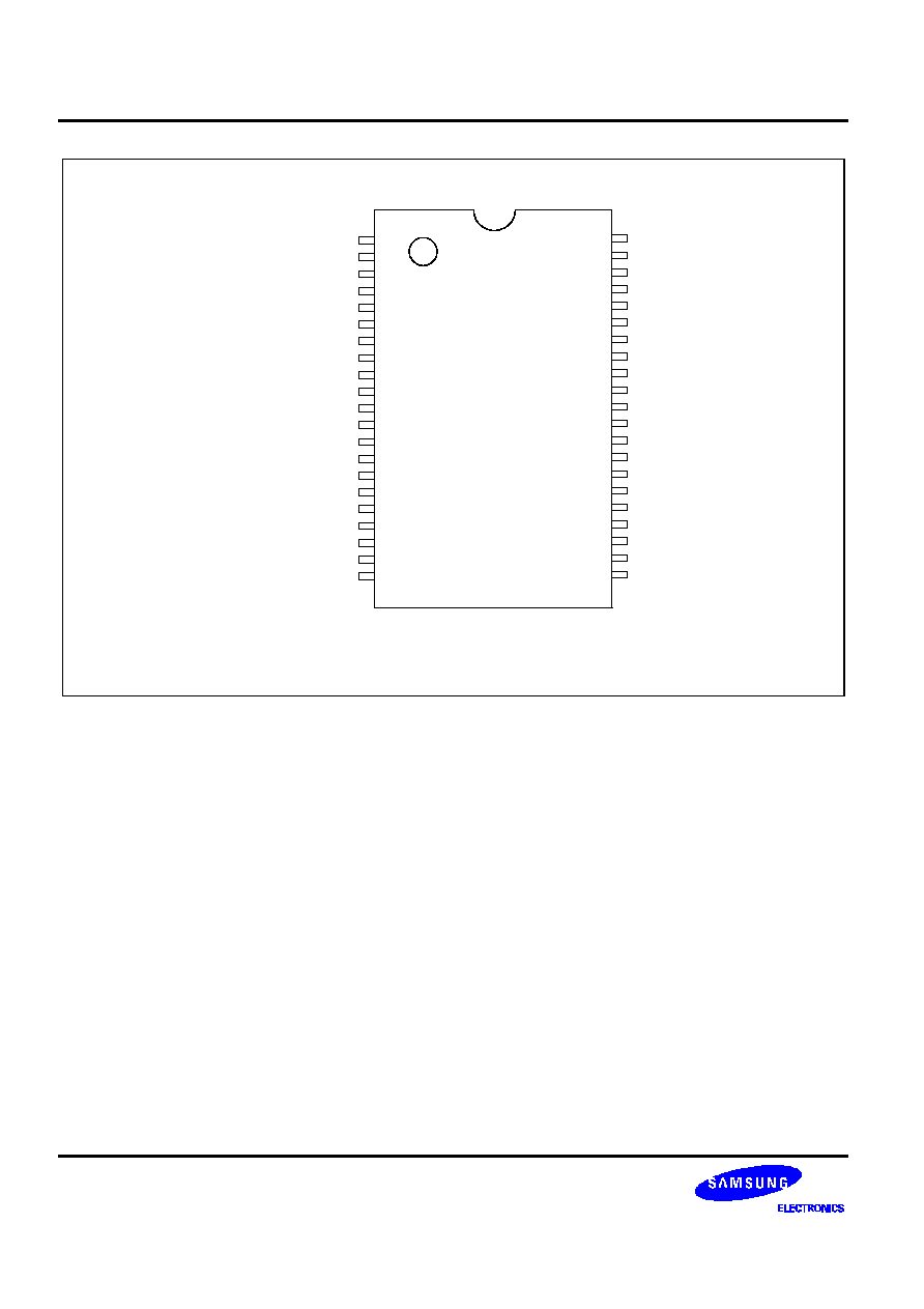
PIN ASSIGNMENTS
S3C7414
(42-SDIP)
P2.0/AD0
P2.1/AD1
P2.2/AD2
P2.3/AD3
P3.0/AD4
P3.1/AD5
AV
REF
P3.2/CLO/TCL1
P3.3/PWM/TCLO1
P4.0
V
DD
V
SS
X
OUT
X
IN
TEST
P4.1
P4.2
RESET
P4.3
P5.0
P5.1
1
2
3
4
5
6
7
8
9
10
11
12
13
14
15
16
17
18
19
20
21
P8.2
P8.1/TCLO0
P8.0/TCL0
P7.3
P7.2
P7.1
P7.0
P6.3/KS3
P6.2/KS2
P6.1/KS1
P6.0/KS0
P1.3/INT4
P1.2/INT2
P1.1/INT1
P1.0/INT0
P0.3/BUZ
P0.2/SI
P0.1/SO
P0.0/
SCK
P5.3
P5.2
42
41
40
39
38
37
36
35
34
33
32
31
30
29
28
27
26
25
24
23
22
Figure 1-2. S3C7414 Pin Assignment (42-SDIP)
PRODUCT OVERVIEW
S3C7414/P7414/C7424/P7424/C7434/P7434
1-6
RESET
P4.3
P5.0
P5.1
P5.2
P5.3
P0.0/
SCK
P0.1/SO
P0.2/SI
P0.3/BUZ
NC
P7.2
P7.1
P7.0
P6.3/KS3
P6.2/KS2
P6.1/KS1
P6.0/KS0
P1.3/INT4
P1.2/INT2
P1.1/INT1
P1.0/INT0
AV
REF
P3.2/CLO/TCL1
P3.3/PWM/TCLO1
P4.0
V
DD
V
SS
X
OUT
X
IN
TEST
P4.1
P4.2
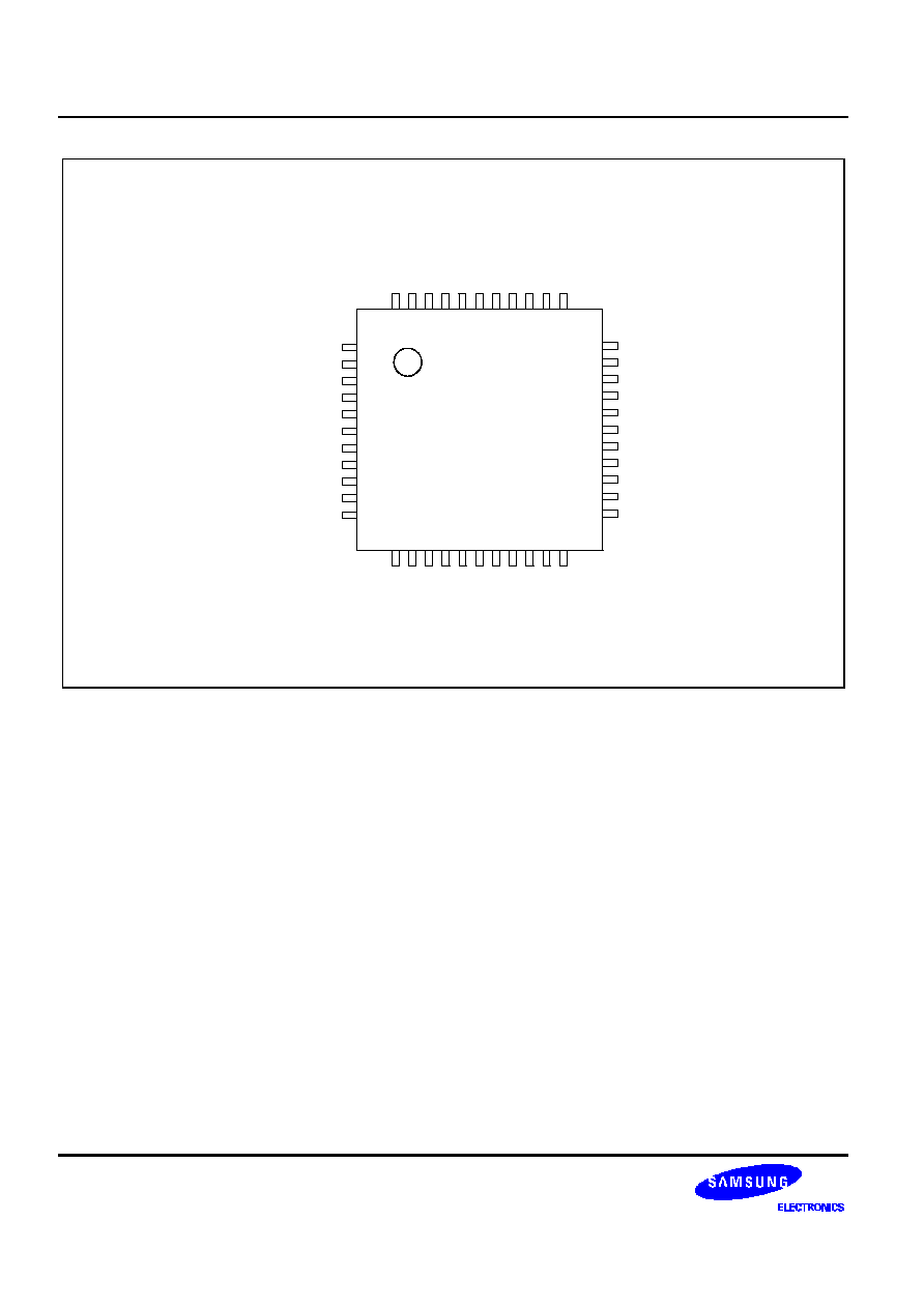
S3C7414
(44-QFP)
1
2
3
4
5
6
7
8
9
10
11
NC
P3.1/AD5
P3.0/AD4
P2.3/AD3
P2.2/AD2
P2.1/AD1
P2.0/AD0
P8.2
P8.1/TCLO0
P8.0/TCL0
P7.3
44
43
42
41
40
39
38
37
36
35
34
33
32
31
30
29
28
27
26
25
24
23
12
13
14
15
16
17
18
19
20
21
22
Figure 1-3. S3C7414 Pin Assignment (44-QFP)
S3C7414/P7414/C7424/P7424/C7434/P7434
PRODUCT OVERVIEW
1-7
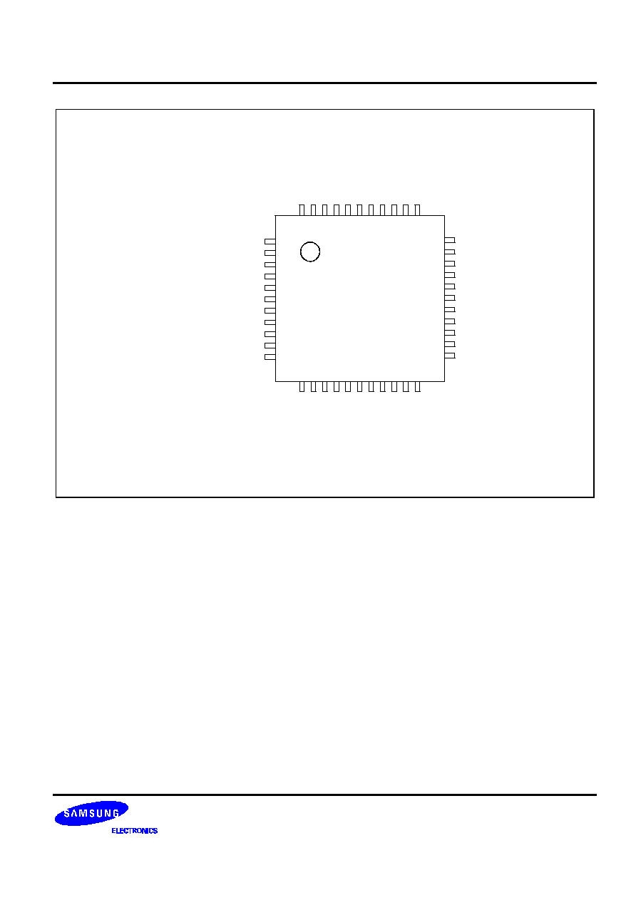
S3C7424
(30-SDIP)
1
2
3
4
5
6
7
8
9
10
11
12
13
14
15
30
29
28
27
26
25
24
23
22
21
20
19
18
17
16
V
SS
X
OUT
X
IN
TEST
P4.1
P4.2
RESET
NC
P4.3
P5.0
P5.1
P5.2
P5.3
P0.0/
SCK
P0.1/SO
V
DD
P4.0
P3.3/PWM/TCLO1
P3.2/CLO/TCL1
AV
REF
NC
P2.3/AD3
P2.2/AD2
P2.1/AD1
P2.0/AD0
P1.2/INT2
P1.1/INT1
P1.0/INT0
P0.3/BUZ
P0.2/SI
Figure 1-4. S3C7424 Pin Assignment (30-SDIP)
S3C7424
(28-SOP)
1
2
3
4
5
6
7
8
9
10
11
12
13
14
28
27
26
25
24
23
22
21
20
19
18
17
16
15
V
SS
X
OUT
X
IN
TEST
P4.1
P4.2
RESET
P4.3
P5.0
P5.1
P5.2
P5.3
P0.0/
SCK
P0.1/SO
V
DD
P4.0
P3.3/PWM/TCLO1
P3.2/CLO/TCL1
AV
REF
P2.3/AD3
P2.2/AD2
P2.1/AD1
P2.0/AD0
P1.2/INT2
P1.1/INT1
P1.0/INT0
P0.3/BUZ
P0.2/SI
Figure 1-5. S3C7424 Pin Assignment (28-SOP)

PRODUCT OVERVIEW
S3C7414/P7414/C7424/P7424/C7434/P7434
1-8
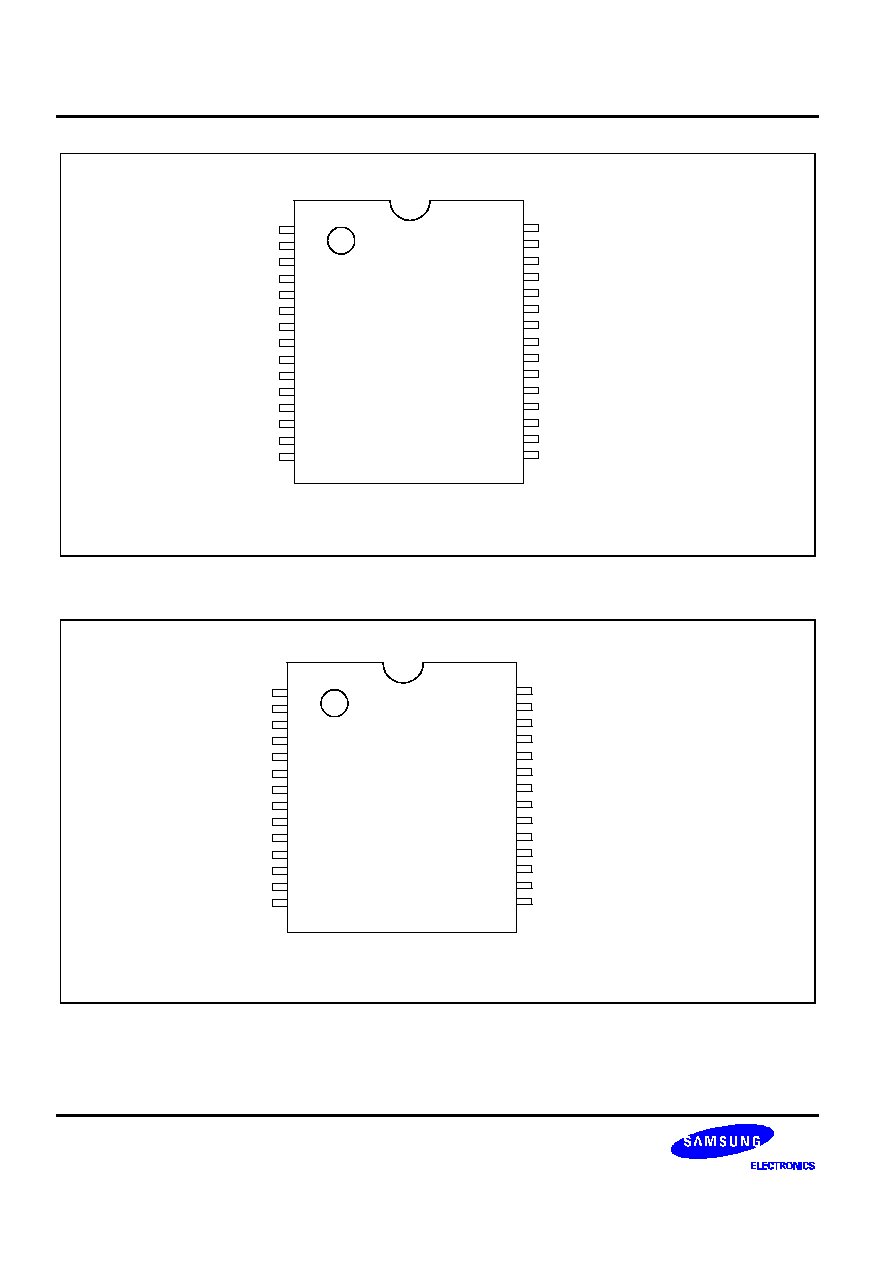
S3C7434
(42-SDIP)
P2.0/AD0
P2.1/AD1
P2.2/AD2
P2.3/AD3
P3.0/AD4
P3.1/AD5
AV
REF
P3.2/CLO/TCL1
P3.3/PWM/TCLO1
P4.0
V
DD
V
SS
X
OUT
X
IN
TEST
P4.1
P4.2
RESET
P4.3
P5.0
P5.1
1
2
3
4
5
6
7
8
9
10
11
12
13
14
15
16
17
18
19
20
21
P8.2
P8.1/TCLO0
P8.0/TCL0
P7.3
P7.2
P7.1
P7.0
P6.3/KS3
P6.2/KS2
P6.1/KS1
P6.0/KS0
P1.3/INT4
P1.2/INT2
P1.1/INT1
P1.0/INT0
P0.3/BUZ
P0.2/SI
P0.1/SO
P0.0/
SCK
P5.3
P5.2
42
41
40
39
38
37
36
35
34
33
32
31
30
29
28
27
26
25
24
23
22
Figure 1-6. S3C7434 Pin Assignment (42-SDIP)
S3C7414/P7414/C7424/P7424/C7434/P7434
PRODUCT OVERVIEW
1-9
RESET
P4.3
P5.0
P5.1
P5.2
P5.3
P0.0/
SCK
P0.1/SO
P0.2/SI
P0.3/BUZ
NC
P7.2
P7.1
P7.0
P6.3/KS3
P6.2/KS2
P6.1/KS1
P6.0/KS0
P1.3/INT4
P1.2/INT2
P1.1/INT1
P1.0/INT0
AV
REF
P3.2/CLO/TCL1
P3.3/PWM/TCLO1
P4.0
V
DD
V
SS
X
OUT
X
IN
TEST
P4.1
P4.2
S3C7434
(44-QFP)
1
2
3
4
5
6
7
8
9
10
11
NC
P3.1/AD5
P3.0/AD4
P2.3/AD3
P2.2/AD2
P2.1/AD1
P2.0/AD0
P8.2
P8.1/TCLO0
P8.0/TCL0
P7.3
44
43
42
41
40
39
38
37
36
35
34
33
32
31
30
29
28
27
26
25
24
23
12
13
14
15
16
17
18
19
20
21
22
Figure 1-7. S3C7434 Pin Assignment (44-QFP)

PRODUCT OVERVIEW
S3C7414/P7414/C7424/P7424/C7434/P7434
1-10
PIN DESCRIPTIONS
Table 1-2. S3C7414/C7434 Pin Descriptions
Pin Name
Pin Type
Description
Number
Share Pin
P0.0
P0.1
P0.2
P0.3
I/O
4-bit I/O port.
1-bit or 4-bit read/write and test is possible.
Individual pins are software configurable as input or
output.
4-bit pull-up resistors are software assignable; pull-up
resistors are automatically disabled for output pins.
24 (18)
25 (19)
26 (20)
27 (21)
SCK
SO
SI
BUZ
P1.0
P1.1
P1.2
P1.3
I
4-bit input port.
1-bit and 4-bit read and test is possible.
3-bit pull-up resistors are individually assignable by
software to pins P1.0, P1.1, and P1.2.
28 (23)
29 (24)
30 (25)
31 (26)
INT0
INT1
INT2
INT4
P2.0
P2.1
P2.2
P2.3
I/O
4-bit I/O port.
N-channel open-drain output.
1-bit or 4-bit write and test is possible.
Individual pins are software configurable as AD input
or output.
4-bit pull-up resistors are software assignable; pull-up
resistors are automatically disabled for output pins.
1 (38)
2 (39)
3 (40)
4 (41)
AD0
AD1
AD2
AD3
P3.0
P3.1
P3.2
P3.3
I/O
Same as Port 0 (P0.0≠P0.3)
5 (42)
6 (43)
8 (2)
9 (3)
AD4
AD5
CLO/TCL1
PWM/TCLO1
P4.0
P4.1
P4.2
P4.3
P5.0≠P5.3
I/O
4-bit I/O ports.
Ports 4 and 5 can be configured individually as n-
channel open-drain or as CMOS push-pull output by
software.
1-bit and 4-bit read/write and test is possible.
Ports 4 and 5 can be paired to enable 8-bit data
transfer.
4-bit pull-up resistors are software assignable; pull-up
resistors are automatically disabled for output pins.
10 (4)
16 (10)
17 (11)
19 (13)
20≠23
(14≠17)
≠
P6.0≠P6.3
P7.0≠P7.3
P8.0
P8.1
P8.2
I/O
Same as Port 0 except port 8 is a 3-bit I/O port
32≠35
(27≠30)
36≠39
(31≠34)
40 (35)
41 (36)
42 (37)
KS0≠KS3
≠
TCL0
TCLO0
≠

S3C7414/P7414/C7424/P7424/C7434/P7434
PRODUCT OVERVIEW
1-11
Table 1-2. S3C7414/C7434 Pin Descriptions (Continued)
Pin Name
Pin Type
Description
Number
Share Pin
SCK
I/O
Serial I/O interface clock signal
24 (18)
P0.0
SO
I/O
Serial data output
25 (19)
P0.1
SI
I/O
Serial data input
26 (20)
P0.2
BUZ
I/O
2 kHz, 4kHz, 8kHz, or 16 kHz frequency output at the
watch timer clock frequency of 32.768 kHz
27 (21)
P0.3
INT0, INT1
I
External interrupts. The triggering edge for INT0 and
INT1 is selectable. Only INT0 is synchronized with the
system clock.
28≠29
(23≠24)
P1.0, P1.1
INT2
I
Quasi-interrupt input with rising edge detection
30 (25)
P1.2
INT4
I
External interrupts with detection of rising and falling
edges
31 (26)
P1.3
AD0≠AD3
AD4≠AD5
I/O
A/D converter analog inputs
1≠4
(38≠41)
5≠6
(42≠43)
P2.0≠P2.3
P3.0≠P3.1
TCL0
I/O
External clock input for timer/counter0
40 (35)
P8.0
TCLO0
I/O
Timer/counter clock output
41 (36)
P8.1
CLO
I/O
Clock output
8 (2)
P3.2
TCL1
I/O
External clock input for timer/counter1
8 (2)
P3.2
PWM
I/O
PWM output
9 (3)
P3.3
TCLO1
I/O
Timer/counter clock output1
9 (3)
P3.3
KS0≠KS3
I/O
Quasi-interrupt input with falling edge detection
32≠35
(27≠30)
P6.0≠P6.3
V
DD
≠
Main power supply
11 (5)
≠
V
SS
≠
Ground
12 (6)
≠
RESET
I
Reset signal
18 (12)
≠
X
IN
, X
out
≠
Crystal, ceramic, or RC oscillator signal for system
clock.
14, 13
(8, 7)
≠
AV
REF
≠
A/D converter analog reference voltage
7 (1)
≠
TEST
I
Test signal input (must be connected to V
SS
)
15 (9)
≠
NC
≠
No connection (no bonding pin)
(22, 44)
≠
NOTE: Parentheses indicate 44-QFP pin number.
PRODUCT OVERVIEW
S3C7414/P7414/C7424/P7424/C7434/P7434
1-12
Table 1-3. S3C7424 Pin Descriptions
Pin Name
Pin Type
Description
Number
Share Pin
P0.0
P0.1
P0.2
P0.3
I/O
4-bit I/O port.
1-bit or 4-bit read/write and test is possible.
Individual pins are software configurable as input or
output.
4-bit pull-up resistors are software assignable; pull-up
resistors are automatically disabled for output pins.
14 (13)
15 (14)
16 (15)
17 (16)
SCK
SO
SI
BUZ
P1.0
P1.1
P1.2
I
4-bit input port.
1-bit and 4-bit read and test is possible.
3-bit pull-up resistors are individually assignable by
software to pins P1.0, P1.1, and P1.2.
18 (17)
19 (18)
20 (19)
INT0
INT1
INT2
P2.0
P2.1
P2.2
P2.3
I/O
4-bit I/O port.
N-channel open-drain output.
1-bit or 4-bit write and test is possible.
Individual pins are software configurable as AD input
or output.
4-bit pull-up resistors are software assignable; pull-up
resistors are automatically disabled for output pins.
21 (20)
22 (21)
23 (22)
24 (23)
AD0
AD1
AD2
AD3
P3.2
P3.3
I/O
Same as Port 0 (P0.0≠P0.3)
27 (25)
28 (26)
CLO/TCL1
PWM/TCLO1
P4.0
P4.1
P4.2
P4.3
P5.0≠P5.3
I/O
4-bit I/O ports.
Ports 4 and 5 can be configured individually as n-
channel open-drain or as CMOS push-pull output by
software.
1-bit and 4-bit read/write and test is possible.
Ports 4 and 5 can be paired to enable 8-bit data
transfer.
4-bit pull-up resistors are software assignable; pull-up
resistors are automatically disabled for output pins.
29 (27)
5 (5)
6 (6)
9 (8)
10≠13
(9≠12)
≠

S3C7414/P7414/C7424/P7424/C7434/P7434
PRODUCT OVERVIEW
1-13
Table 1-3. S3C7424 Pin Descriptions (Continued)
Pin Name
Pin Type
Description
Number
Share Pin
SCK
I/O
Serial I/O interface clock signal
14 (13)
P0.0
SO
I/O
Serial data output
15 (14)
P0.1
SI
I/O
Serial data input
16 (15)
P0.2
BUZ
I/O
2 kHz, 4kHz, 8kHz, or 16 kHz frequency output at the
watch timer clock frequency of 32.768 kHz
17 (16)
P0.3
INT0, INT1
I
External interrupts. The triggering edge for INT0 and
INT1 is selectable. Only INT0 is synchronized with the
system clock.
18, 19
(17, 18)
P1.0, P1.1
INT2
I
Quasi-interrupt input with rising edge detection
20 (19)
P1.2
AD0≠AD3
I/O
A/D converter analog inputs
21≠24
(20≠23)
P2.0≠P2.3
CLO
I/O
Clock output
27 (25)
P3.2
TCL1
I/O
External clock input for timer/counter1
27 (25)
P3.2
PWM
I/O
PWM output
28 (26)
P3.3
TCLO1
I/O
Timer/counter clock output1
28 (26)
P3.3
V
DD
≠
Main power supply
30 (28)
≠
V
SS
≠
Ground
1 (1)
≠
RESET
I
Reset signal
7 (7)
≠
X
IN
, X
OUT
≠
Crystal, ceramic, or RC oscillator signal for system
clock.
3, 2
(3, 2)
≠
AV
REF
≠
Internal A/D converter analog reference voltage
26 (24)
≠
TEST
I
Test signal input (must be connected to V
SS
)
4 (4)
≠
NC
≠
No connection (no bonding pin)
8, 25
≠
NOTE: Parentheses indicate 28-SOP pin number.
PRODUCT OVERVIEW
S3C7414/P7414/C7424/P7424/C7434/P7434
1-14
Table 1-4. Overview of S3C7414/C7424/C7434Pin Data
Pin Names
Share Pins
I/O Type
Reset Value
Circuit Type
P0.0≠P0.3
SCK
, SO, SI, BUZ
I/O
Input
Type D
P1.0
P1.1
P1.2
INT0
(note)
INT1
(note)
INT2
(note)
I
Input
Type A-1
P1.3
INT4
I
Input
Type A
P2.0≠P2.3
AD0≠AD3
I/O
AD input
Type F-3
P3.0
P3.1
P3.2
P3.3
AD4
AD5
CLO/TCL1
TCLO1/PWM
I/O
Input
Type F
Type F
Type D
Type D
P4.0≠P4.3
P5.0≠P5.3
≠
I/O
Input
Type E
P6.0
P6.1
P6.2
P6.3
KS0
(note)
KS1
(note)
KS2
(note)
KS3
(note)
I/O
Input
Type D
P7.0≠P7.3
≠
I/O
Input
Type D
P8.0
P8.1
P8.2
TCL0
(note)
TCLO0
≠
I/O
Input
Type D
V
DD
, V
SS
≠
≠
≠
≠
X
IN
, X
OUT
≠
≠
≠
≠
RESET
≠
I
≠
Type B-2
(note)
AV
REF
≠
≠
≠
≠
TEST
≠
I
≠
≠
NC
≠
≠
≠
≠
NOTE: A noise filter circuit is built-in.
S3C7414/P7414/C7424/P7424/C7434/P7434
PRODUCT OVERVIEW
1-15
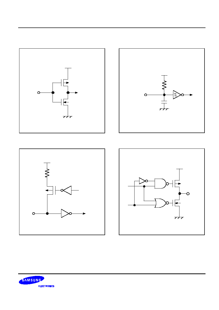
PIN CIRCUIT DIAGRAMS
V
DD
P
-
CHANNEL
IN
N
-
CHANNEL
Figure 1-8. Pin Circuit Type A
PULL-UP
RESISTOR
ENABLE
CIRCUIT TYPE A
IN
V
DD
Figure 1-9. Pin Circuit Type A-1
V
DD
RESET
1M
7pF
Figure 1-10. Pin Circuit Type B-2
DATA
OUTPUT
DISABLE
OUT
V
DD
P
-
CHANNEL
N
-
CHANNEL
Figure 1-11. Pin Circuit Type C
PRODUCT OVERVIEW
KS57C4104/P4104/C4204/P4204 MICROCONTROLLER (Preliminary Spec)
1-16
PULL-UP
RESISTOR
ENABLE
DATA
OUTPUT
DISABLE
CIRCUIT TYPE A
I/O
V
DD
CIRCUIT
TYPE C
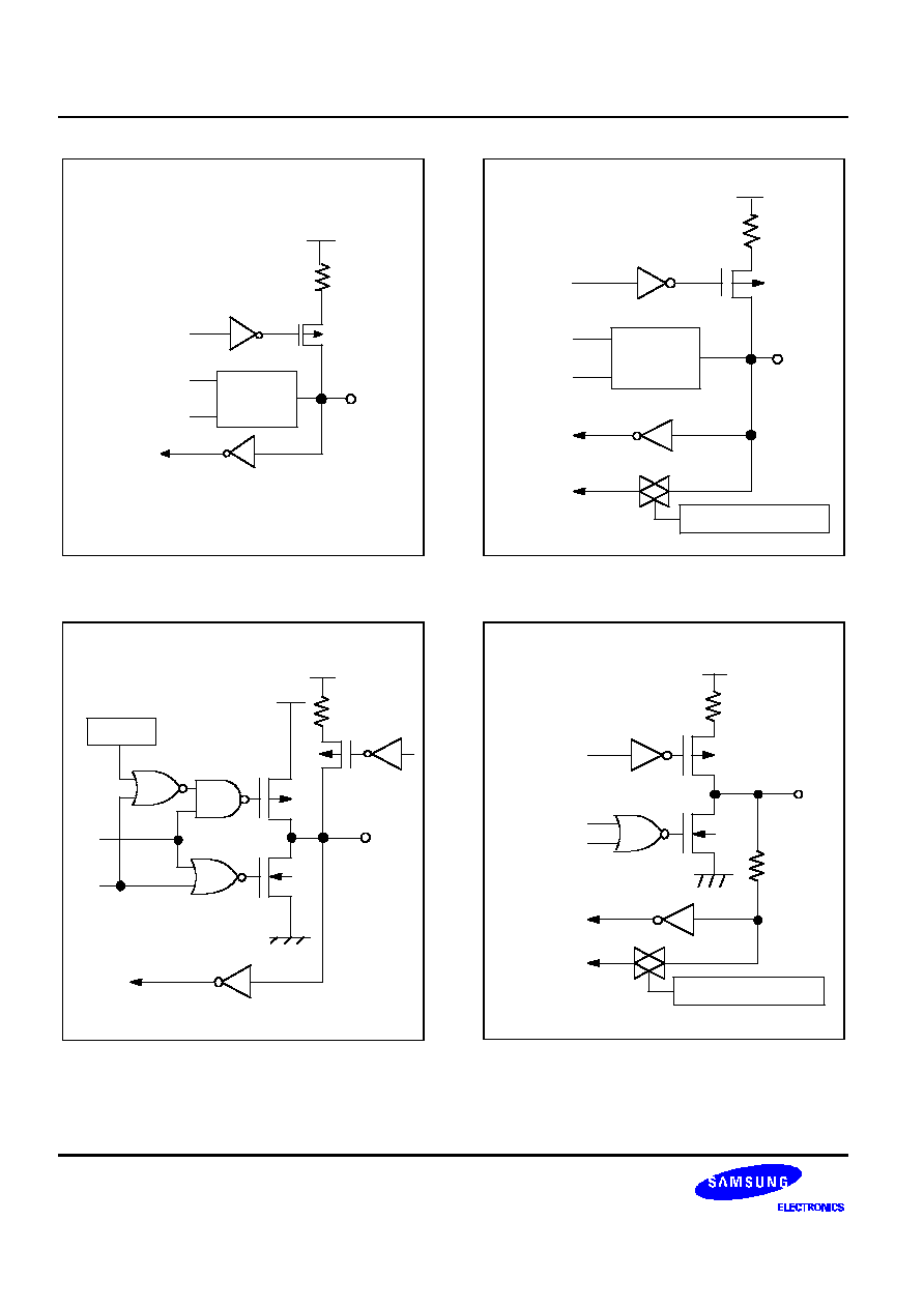
Figure 1-12. Pin Circuit Type D
INPUT
V
DD
DATA
OUTPUT
DISABLE
PNE
PULL-UP
RESISTOR
ENABLE
V
DD
IN/OUT
Figure 1-13. Pin Circuit Type E
IN/OUT
V
DD
CIRCUIT
TYPE C
DATA
DATA
OUTPUT
DISABLE
PULL-UP
RESISTOR
ENABLE
TO ADC
ADC INPUT SELECT
Figure 1-14. Pin Circuit Type F
V
DD
DATA
OUTPUT
DISABLE
IN/OUT
DATA
TO ADC
PULL-UP
RESISTOR
ENABLE
ADC INPUT SELECT
Figure 1-15. Pin Circuit Type F-3

S3C7414/P7414/C7424/P7424/C7434/P7434
ELECTRICAL DATA
14-1
14
ELECTRICAL DATA
OVERVIEW
In this section, information on S3C7414/C7424/C7434 electrical characteristics is presented as tables and
graphics. The information is arranged in the following order:
Standard Electrical Characteristics
-- Absolute maximum ratings
-- D.C. electrical characteristics
-- System clock oscillator characteristics
-- Operating voltage range
-- A.C. electrical characteristics
-- A/D converter electrical characteristics
-- I/O capacitance
Stop Mode Characteristics and Timing Waveforms
-- RAM data retention supply voltage in stop mode
-- Stop mode release timing when initiated by
RESET
-- Stop mode release timing when initiated by an interrupt request
Miscellaneous Timing Waveforms
-- A.C timing measurement points (except for X
IN
)
-- Clock timing measurement at X
IN
-- TCL0/1 timing
-- Input timing for
RESET signal
-- Input timing for external interrupts and quasi-interrupts
-- S3C7434 power-on
RESET
timing
-- Serial data transfer timing

ELECTRICAL DATA
S3C7414/P7414/C7424/P7424/C7434/P7434
14-2
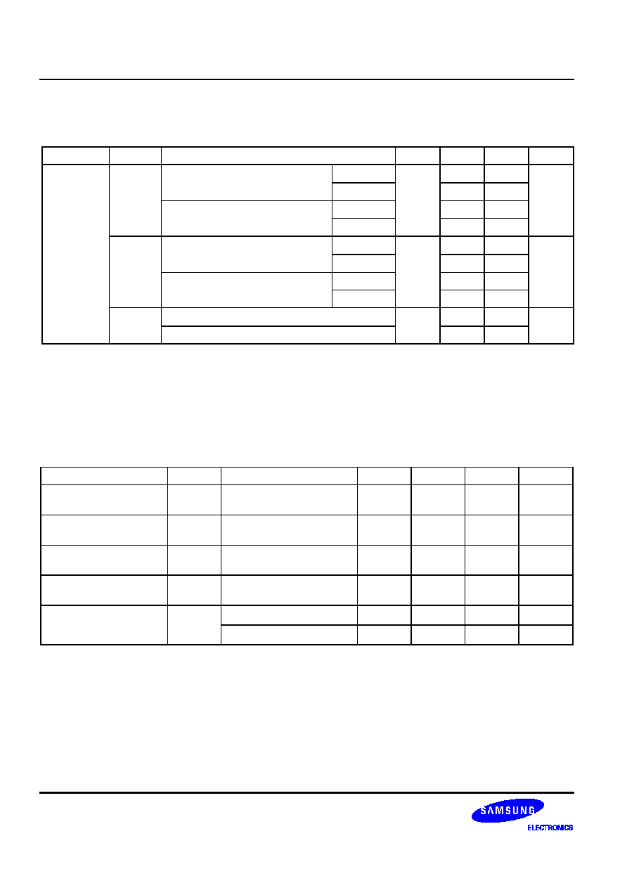
Table 14-1. S3C7414/C7424 Absolute Maximum Ratings
(T
A
= 25
∞
C)
Parameter
Symbol
Conditions
Rating
Units
Supply Voltage
V
DD
≠
≠ 0.3 to + 6.5
V
Input Voltage
V
I
All I/O ports
≠ 0.3 to V
DD
+ 0.3
V
Output Voltage
V
O
≠
≠ 0.3 to V
DD
+ 0.3
V
Output Current High
I
OH
One pin
≠ 15
mA
All output pins
≠ 35
Output Current Low
I
OL
One pin
peak value
(note)
+ 30
mA
rms value
+ 15
All pins
peak value
(note)
+ 100
rms value
+ 60
Operating Temperature
T
A
≠
≠ 40 to + 85
∞
C
Storage Temperature
T
stg
≠
≠ 65 to + 150
∞
C
NOTE: The values for Output Current Low (I
OL
) are calculated as Peak Value
◊
Duty .
S3C7414/P7414/C7424/P7424/C7434/P7434
ELECTRICAL DATA
14-3
Table 14-2. S3C7414/C7424 D.C. Electrical Characteristics
(T
A
= ≠ 40
∞
C to + 85
∞
C, V
DD
= 1.8 V to 5.5 V)
Parameter
Symbol
Conditions
Min
Typ
Max
Units
Input High
Voltage
V
IH1
All input pins except those specified
below for V
IH2
≠V
IH3
0.7 V
DD
≠
V
DD
V
V
IH2
Ports 0, 1, 3, 6 and
RESET
0.8 V
DD
V
DD
V
IH3
X
IN,
X
OUT
V
DD
≠ 0.1
V
DD
Input Low
Voltage
V
IL1
All input pins except those specified
below for V
IL2
≠V
IL3
≠
≠
0.3 V
DD
V
V
IL2
Ports 0, 1, 3, 6 and
RESET
0.2 V
DD
V
IL3
X
IN,
X
OUT
0.1
Output High
Voltage
V
OH
V
DD
= 4.5 V to 5.5 V
I
OH
= ≠ 1 mA
Ports 0, 2≠8
V
DD
≠ 1.0
≠
≠
V
Output Low
Voltage
V
OL
V
DD
= 4.5 V to 5.5 V
I
OL
= 15 mA
Ports 4 and 5 only
≠
0.4
2
V
I
OL
= 4 mA
All output ports except ports 4 and 5
0.2
Input High
Leakage Current
I
LIH1
V
I
= V
DD
All input pins except those specified
below for I
LIH2
≠
≠
3
µA
I
LIH2
V
I
= V
DD
X
IN
and X
OUT
only
20
Input Low
Leakage Current
I
LIL1
V
I
= 0 V
All input pins except X
IN
and X
OUT
,
RESET
≠
≠
≠ 3
µA
I
LIL2
V
I
= 0 V
X
IN
and X
OUT
only
≠ 20
Output High
Leakage Current
I
LOH
V
O
= V
DD
All output pins
≠
≠
3
µA
Output Low
Leakage Current
I
LOL
V
O
= 0 V
All output pins
≠
≠
≠ 3
µA
Pull-up Resistor
R
L1
V
I
= 0 V; V
DD
= 5 V except
RESET
25
50
100
k
V
I
= 0 V; V
DD
= 3 V except
RESET
50
100
200
Pull-up Resistor
R
L2
V
I
= 0 V; V
DD
= 5 V;
RESET
100
250
400
k
V
I
= 0 V; V
DD
= 3 V;
RESET
200
500
800

ELECTRICAL DATA
S3C7414/P7414/C7424/P7424/C7434/P7434
14-4
Table 14-2. S3C7414/C7424 D.C. Electrical Characteristics (Continued)
(T
A
= ≠ 40
∞
C to + 85
∞
C, V
DD
= 1.8 V to 5.5 V)
Parameter
Symbol
Conditions
Min
Typ
Max
Units
Supply
I
DD1
Run mode; V
DD
= 5.0 V
±
10%
6.0MHz
≠
3.0
8.0
mA
Current
(1)
Crystal oscillator; C1=C2=22pF
4.19MHz
2.3
5.5
V
DD
= 3 V
±
10%
6.0MHz
1.4
4.0
4.19MHz
1.1
3.0
I
DD2
Idle mode; V
DD
= 5.0 V
±
10%
6.0MHz
≠
1.1
2.5
mA
Crystal oscillator; C1=C2=22pF
4.19MHz
1.0
1.8
V
DD
= 3 V
±
10%
6.0MHz
0.5
1.5
4.19MHz
0.4
1.0
I
DD3
Stop mode; V
DD
= 5.0 V
±
10%
≠
0.1
5.0
µ
A
Stop mode; V
DD
= 3.0 V
±
10%
0.1
3.0
NOTES:
1.
D.C. electrical values for Supply current (IDD1 to IDD3) do not include current drawn through internal pull-up registers,
output port drive currents and ADC.
2.
The supply current assumes a CPU clock of fx/4.
S3C7414/P7414/C7424/P7424/C7434/P7434
ELECTRICAL DATA
14-5
Table 14-3. S3C7414/C7424 System Clock Oscillator Characteristics
(T
A
= ≠ 40
∞
C to + 85
∞
C, V
DD
= 1.8 V to 5.5 V)
Oscillator
Clock
Configuration
Parameter
Test Condition
Min
Typ
Max
Units
Ceramic
Oscillator
Xin
Xout
C1
C2
Oscillation frequency
(1)
V
DD
= 2.7 V to 5.5 V
0.4
≠
6.0
MHz
V
DD
= 2.0 V to 5.5 V
0.4
≠
4.2
V
DD
= 1.8 V to 5.5 V
0.4
≠
3.0
Stabilization time
(2)
V
DD
= 3.0 V
≠
≠
4
ms
Crystal
Oscillator
Xin
Xout
C1
C2
Oscillation frequency
(1)
V
DD
= 2.7 V to 5.5 V
0.4
≠
6.0
MHz
V
DD
= 2.0 V to 5.5 V
0.4
≠
4.2
V
DD
= 1.8 V to 5.5 V
0.4
≠
3.0
Stabilization time
(2)
V
DD
= 3.0 V
≠
≠
10
ms
External
Clock
Xin
Xout
X
IN
input frequency
(1)
V
DD
= 2.7 V to 5.5 V
0.4
≠
6.0
MHz
V
DD
= 2.0 V to 5.5 V
0.4
≠
4.2
V
DD
= 1.8 V to 5.5 V
0.4
≠
3.0
X
IN
input high and low
level width (t
XH
, t
XL
)
≠
83.3
≠
1250
ns
RC
Oscillator
Xin
Xout
R
Oscillation frequency
limitation
V
DD
= 5 V
R = 8.2 K
≠
4
≠
MHz
NOTES:
1.
Oscillation frequency and X
in
input frequency data are for oscillator characteristics only.
2.
Stabilization time is the interval required for oscillating stabilization after a power-on occurs, or when stop mode is
terminated.
ELECTRICAL DATA
S3C7414/P7414/C7424/P7424/C7434/P7434
14-6
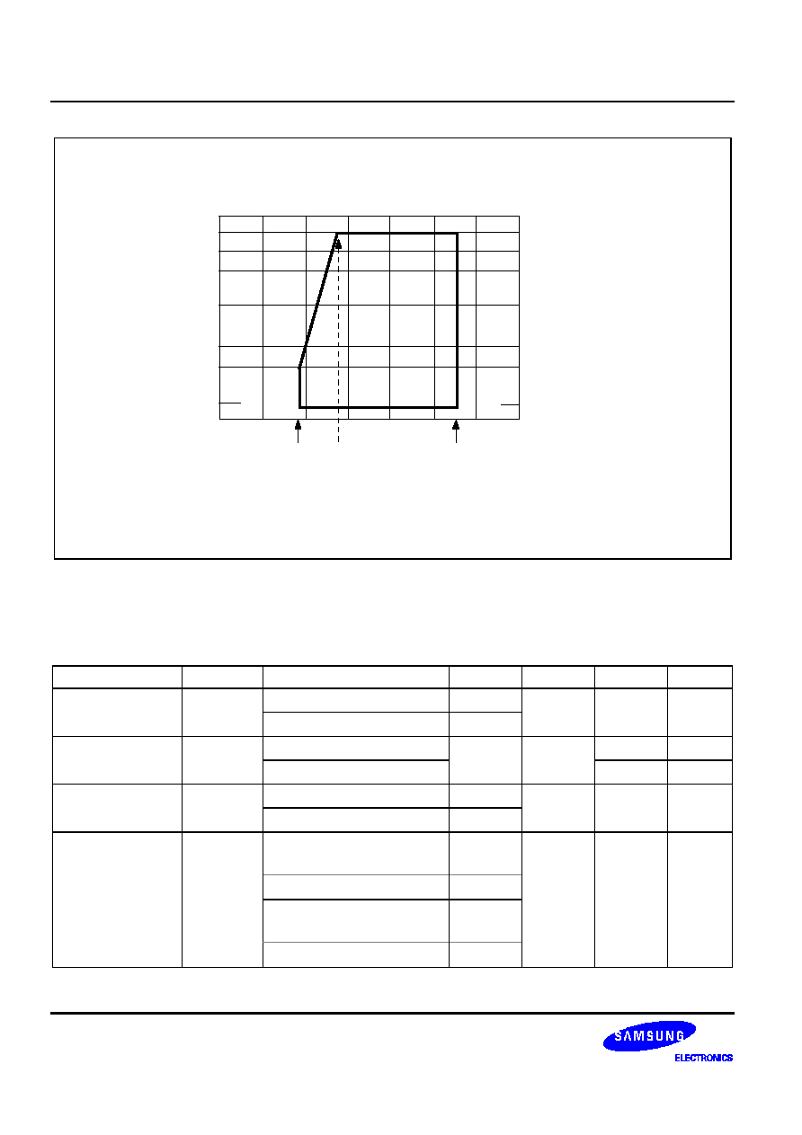
CPU CLOCK = 1/n x oscillator frequency (n = 4, 8 or 64)
SUPPLY VOLTAGE (V)
1.05 MHz
15.6 kHz
CPU CLOCK
1.5 MHz
4.2 MHz
Main Oscillator Frequency
(Divided by 4)
6 MHz
1
2
3
4
5
6
2.7
5.5
0.75 MHz
1.8
3 MHz
Figure 14-1. S3C7414/C7424 Standard Operating Voltage Range
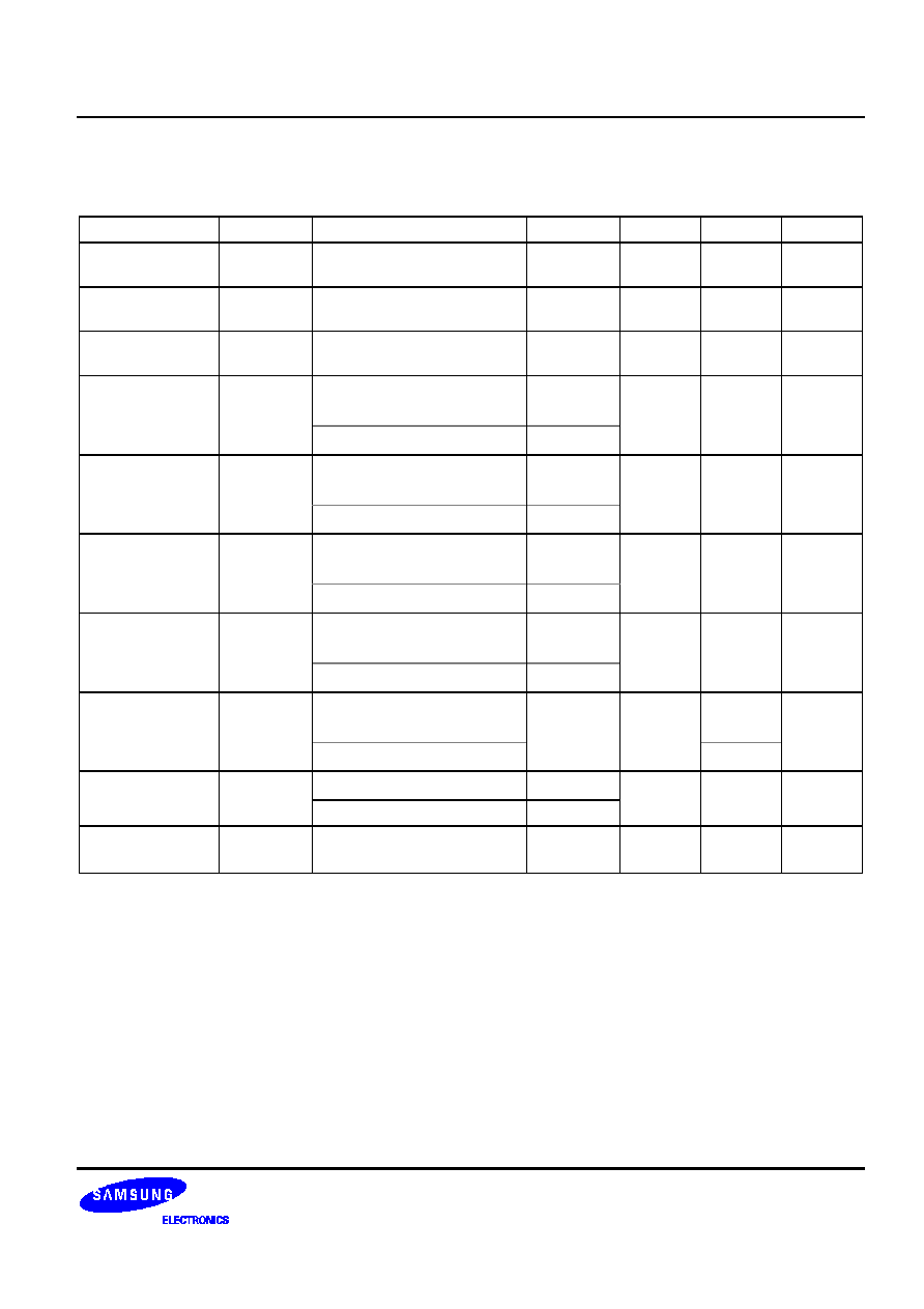
Table 14-4. S3C7414/C7424 A.C. Electrical Characteristics
(T
A
= ≠ 40
∞
C to + 85
∞
C, V
DD
= 1.8 V to 5.5 V)
Parameter
Symbol
Conditions
Min
Typ
Max
Units
Instruction Cycle
t
CY
V
DD
= 2.7 V to 5.5 V
0.67
≠
64
µ
s
Time
V
DD
= 1.8 V to 5.5 V
1.33
TCL0/1 Input
f
TI
V
DD
= 2.7 V to 5.5 V
0
≠
1.5
MHz
Frequency
V
DD
= 1.8 V to 5.5 V
0.75
MHz
TCL0/1 Input High,
t
TIH
,
t
TIL
V
DD
= 2.7 V to 5.5 V
0.48
≠
≠
µ
s
Low Width
V
DD
= 1.8 V to 5.5 V
1.8
SCK
Cycle Time
t
KCY
V
DD
= 2.7 V to 5.5 V
External
SCK
source
800
≠
≠
ns
Internal
SCK
source
670
V
DD
= 1.8 V to 5.5 V
External
SCK
source
3200
Internal
SCK
source
3800
S3C7414/P7414/C7424/P7424/C7434/P7434
ELECTRICAL DATA
14-7
Table 14-4. S3C7414/C7424 A.C. Electrical Characteristics (Continued)
(T
A
= ≠ 40
∞
C to + 85
∞
C, V
DD
= 1.8 V to 5.5 V)
Parameter
Symbol
Conditions
Min
Typ
Max
Units
SCK
High, Low
Width
t
KH
, t
KL
V
DD
= 2.7 V to 5.5 V
External
SCK
source
335
≠
≠
ns
Internal
SCK
source
t
KCY
/2 ≠ 50
V
DD
= 1.8 V to 5.5 V
External
SCK
source
1600
Internal
SCK
source
t
KCY
/
2 ≠ 150
SI Setup Time to
SCK
High
t
SIK
V
DD
= 2.7 V to 5.5 V
External
SCK
source
100
≠
≠
ns
Internal
SCK
source
150
V
DD
= 1.8 V to 5.5 V
External
SCK
source
150
Internal
SCK
source
500
SI Hold Time to
SCK
High
t
KSI
V
DD
= 2.7 V to 5.5 V
External
SCK
source
400
≠
≠
ns
Internal
SCK
source
400
V
DD
= 1.8 V to 5.5 V
External
SCK
source
600
Internal
SCK
source
500
Output Delay for
SCK
to SO
t
KSO
(1)
V
DD
= 2.7 V to 5.5 V
External
SCK
source
≠
≠
300
ns
Internal
SCK
source
250
V
DD
= 1.8 V to 5.5 V
External
SCK
source
1000
Internal
SCK
source
1000
Interrupt Input
High, Low Width
t
INTH
,
t
INTL
INT0
(2)
≠
≠
µ
s
INT1, INT2, INT4, KS0≠KS3
10
RESET
Input
Low Width
t
RSL
Input
10
≠
≠
µ
s
NOTES:
1.
R(1K
) and C (100pF) are the load resistance and load capacitance of the SO output line.
2.
Minimum value for INT0 is based on a clock of 2t
CY
or 128/fx as assigned by the IMOD0 register setting.
ELECTRICAL DATA
S3C7414/P7414/C7424/P7424/C7434/P7434
14-8
Table 14-5. S3C7434 Absolute Maximum Ratings
(T
A
= 25
∞
C)
Parameter
Symbol
Conditions
Rating
Units
Supply Voltage
V
DD
≠
≠ 0.3 to + 6.5
V
Input Voltage
V
I
All I/O ports
≠ 0.3 to V
DD
+ 0.3
V
Output Voltage
V
O
≠
≠ 0.3 to V
DD
+ 0.3
V
Output Current High
I
OH
One pin
≠ 15
mA
All output pins
≠ 35
Output Current Low
I
OL
One pin
peak value
(note)
+ 30
mA
rms value
+ 15
All pins
peak value
(note)
+ 100
rms value
+ 60
Operating Temperature
T
A
≠
≠ 40 to + 85
∞
C
Storage Temperature
T
stg
≠
≠ 65 to + 150
∞
C
NOTE: The values for Output Current Low (I
OL
) are calculated as Peak Value
◊
Duty .
S3C7414/P7414/C7424/P7424/C7434/P7434
ELECTRICAL DATA
14-9
Table 14-6. S3C7434 D.C. Electrical Characteristics
(T
A
= ≠ 40
∞
C to + 85
∞
C, V
DD
= 2.5 V to 5.5 V)
Parameter
Symbol
Conditions
Min
Typ
Max
Units
Input High
Voltage
V
IH1
All input pins except those specified
below for V
IH2
≠V
IH3
0.7 V
DD
≠
V
DD
V
V
IH2
Ports 0, 1, 3, 6 and
RESET
0.8 V
DD
V
DD
V
IH3
X
IN,
X
OUT
V
DD
≠ 0.1
V
DD
Input Low
Voltage
V
IL1
All input pins except those specified
below for V
IL2
≠V
IL3
≠
≠
0.3 V
DD
V
V
IL2
Ports 0, 1, 3, 6 and
RESET
0.2 V
DD
V
IL3
X
IN,
X
OUT
0.1
Output High
Voltage
V
OH
V
DD
= 4.5 V to 5.5 V
I
OH
= ≠ 1 mA
Ports 0, 2≠8
V
DD
≠ 1.0
≠
≠
V
Output Low
Voltage
V
OL
V
DD
= 3.5 V
I
OL
= 15 mA
Ports 4 and 5 only
≠
0.4
2
V
I
OL
= 4 mA
All output ports except ports 4 and 5
0.2
Input High
Leakage Current
I
LIH1
V
I
= V
DD
All input pins except those specified
below for I
LIH2
≠
≠
3
µA
I
LIH2
V
I
= V
DD
X
IN
and X
OUT
only
20
Input Low
Leakage Current
I
LIL1
V
I
= 0 V
All input pins except X
IN
and X
OUT,
RESET
≠
≠
≠ 3
µA
I
LIL2
V
I
= 0 V
X
IN
and X
OUT
only
≠ 20
Output High
Leakage Current
I
LOH
V
O
= V
DD
All output pins
≠
≠
3
µA
Output Low
Leakage Current
I
LOL
V
O
= 0 V
All output pins
≠
≠
≠ 3
µA
Pull-Up Resistor
R
L1
V
I
= 0 V; V
DD
= 5 V except
RESET
25
50
100
k
V
I
= 0 V; V
DD
= 3 V except
RESET
50
100
200
Pull-Up Resistor
R
L2
V
I
= 0 V; V
DD
= 5 V;
RESET
100
250
400
k
V
I
= 0 V; V
DD
= 3 V;
RESET
200
500
800
ELECTRICAL DATA
S3C7414/P7414/C7424/P7424/C7434/P7434
14-10
Table 14-6. S3C7434 D.C. Electrical Characteristics (Continued)
(T
A
= ≠ 40
∞
C to + 85
∞
C, V
DD
= 2.5 V to 5.5 V)
Parameter
Symbol
Conditions
Min
Typ
Max
Units
Supply
I
DD1
Run mode; V
DD
= 5.0 V
±
10%
6.0MHz
≠
3.1
8.0
mA
Current
(1)
Crystal oscillator; C1 = C2 = 22pF
4.19MHz
2.4
5.5
V
DD
= 3 V
±
10%
6.0MHz
1.5
4.0
4.19MHz
1.2
3.0
I
DD2
Idle mode; V
DD
= 5.0 V
±
10%
6.0MHz
≠
1.2
2.5
mA
Crystal oscillator; C1 = C2 = 22pF
4.19MHz
1.1
1.8
V
DD
= 3 V
±
10%
6.0MHz
0.6
1.5
4.19MHz
0.5
1.0
I
DD3
Stop mode; V
DD
= 5.0 V
±
10%
≠
120
200
µ
A
Stop mode; V
DD
= 3.0 V
±
10%
100
150
NOTES:
1.
D.C. electrical values for Supply current (I
DD1
to I
DD3
) do not include current drawn through internal pull-up registers,
output port drive currents and ADC.
2.
The supply current assumes a CPU clock of fx/4.
Table 14-7. S3C7434 Power-On Reset Circuit Characteristics
(T
A
= ≠ 40
∞
C to + 85
∞
C, V
DD
= 2.5 V to 5.5 V)
Parameter
Symbol
Conditions
Min
Typ
Max
Units
Power-On Reset
Voltage High
V
DDH
2.5
5.5
V
Power-On Reset
Voltage Low
V
DDL
0
2.0
2.2
V
Power Supply
Voltage Rise Time
t
r
10
(1)
us
Power Supply
Voltage Off Time
t
off
0.5
s
Power-On Reset Circuit
I
DDPR
V
DD
= 5 V ± 10%
120
200
uA
Cunsumption Current
(2)
V
DD
= 3 V ± 10%
100
150
uA
NOTES:
1.
2
17
/fx (= 31.3 ms at fx = 4.19 MHz)
2.
Current consumed when power-on reset circuit is provided internally.

S3C7414/P7414/C7424/P7424/C7434/P7434
ELECTRICAL DATA
14-11
Table 14-8. S3C7434 System Clock Oscillator Characteristics
(T
A
= ≠ 40
∞
C to + 85
∞
C, V
DD
= 2.5 V to 5.5 V)
Oscillator
Clock
Configuration
Parameter
Test Condition
Min
Typ
Max
Units
Ceramic
Oscillator
Xin
Xout
C1
C2
Oscillation frequency
(1)
V
DD
= 2.7 V to 5.5 V
0.4
≠
6.0
MHz
V
DD
= 2.5 V to 5.5 V
0.4
≠
4.2
Stabilization time
(2)
V
DD
= 3.0 V
≠
≠
4
ms
Crystal
Oscillator
Xin
Xout
C1
C2
Oscillation frequency
(1)
V
DD
= 2.7 V to 5.5 V
0.4
≠
6.0
MHz
V
DD
= 2.5 V to 5.5 V
0.4
≠
4.2
Stabilization time
(2)
V
DD
= 3.0 V
≠
≠
10
ms
External
Clock
Xin
Xout
X
IN
input frequency
(1)
V
DD
= 2.7 V to 5.5 V
0.4
≠
6.0
MHz
V
DD
= 2.5 V to 5.5 V
0.4
≠
4.2
X
IN
input high and low
level width (t
XH
, t
XL
)
≠
83.3
≠
1250
ns
RC
Oscillator
Xin
Xout
R
Oscillation frequency
limitation
V
DD
= 5 V
R = 8.2 K
≠
4
≠
MHz
NOTES:
1.
Oscillation frequency and X
in
input frequency data are for oscillator characteristics only.
2.
Stabilization time is the interval required for oscillating stabilization after a power-on occurs, or when stop mode is
terminated.

ELECTRICAL DATA
S3C7414/P7414/C7424/P7424/C7434/P7434
14-12
CPU CLOCK = 1/n x oscillator frequency (n = 4, 8 or 64)
SUPPLY VOLTAGE (V)
1.05 MHz
15.6 kHz
CPU CLOCK
1.5 MHz
4.2 MHz
Main Oscillator Frequency
(Divided by 4)
6 MHz
1
2
3
4
5
6
2.7
5.5
0.75 MHz
1.8
3 MHz
2.5
Figure 14-2. S3C7434 Standard Operating Voltage Range
S3C7414/P7414/C7424/P7424/C7434/P7434
ELECTRICAL DATA
14-13
Table 14-9. S3C7434 A.C. Electrical Characteristics
(T
A
= ≠ 40
∞
C to + 85
∞
C, V
DD
= 2.5 V to 5.5 V)
Parameter
Symbol
Conditions
Min
Typ
Max
Units
Instruction Cycle
Time
t
CY
V
DD
= 2.7 V to 5.5 V
0.67
≠
64
µs
TCL0/1 Input
Frequency
f
TI0
V
DD
= 2.7 V to 5.5 V
0
≠
1.5
MHz
TCL0/1 Input
High, Low Width
t
TIH0
,
t
TIL0
V
DD
= 2.7 V to 5.5 V
0.48
≠
≠
µs
SCK
Cycle Time
t
KCY
V
DD
= 2.7 V to 5.5 V
External
SCK
source
800
≠
≠
ns
Internal
SCK
source
670
SCK
High, Low
Width
t
KH
, t
KL
V
DD
= 2.7 V to 5.5 V
External
SCK
source
325
≠
≠
ns
Internal
SCK
source
t
KCY
/2 ≠ 50
SI Setup Time to
SCK
High
t
SIK
V
DD
= 2.7 V to 5.5 V
External
SCK
source
100
≠
≠
ns
Internal
SCK
source
150
SI Hold Time to
SCK
High
t
KSI
V
DD
= 2.7 V to 5.5 V
External
SCK
source
400
≠
≠
ns
Internal
SCK
source
400
Output Delay for
SCK
to SO
t
KSO
V
DD
= 2.7 V to 5.5 V
External
SCK
source
≠
≠
300
ns
Internal
SCK
source
250
Interrupt Input
t
INTH
,
INT0
(NOTE)
≠
≠
µs
High, Low Width
t
INTL
INT1, INT2, INT4, KS0≠KS3
10
RESET
Input
Low Width
t
RSL
Input
10
≠
≠
µs
NOTE: Minimum value for INT0 is based on a clock of 2t
CY
or 128/fx as assigned by the IMOD0 register setting.

ELECTRICAL DATA
S3C7414/P7414/C7424/P7424/C7434/P7434
14-14
Table 14-10. A/D Converter Electrical Characteristics
(T
A
= ≠ 10
∞
C to + 70
∞
C, V
DD
= 3.5 V to 5.5 V, V
SS
= AV
SS
= 0 V)
Parameter
Symbol
Condition
Min
Typ
Max
Units
Resolution
≠
≠
8
8
8
bit
Absolute accuracy
(1)
≠
2.5 V < AV
REF
< V
DD
≠
≠
±
1.5
LSB
Conversion time
(2)
t
CON
≠
≠
96/fx
(3)
≠
µs
Analog input voltage
V
IAN
≠
AV
SS
≠
AV
REF
V
Analog input impedance
R
AN
≠
≠
1000
≠
M
NOTES:
1.
Absolute accuracy does not include the quantization error (± 1/2 LSB).
2.
Conversion time is the time required from the moment a conversion operation starts until it ends (EOC = 0).
3.
'fx' is the abbreviation for system clock.
Table 14-11. Input/Output Capacitance
(T
A
= 25
∞
C, V
DD
=
0 V )
Parameter
Symbol
Condition
Min
Typ
Max
Units
Input
Capacitance
C
IN
f = 1 MHz; Unmeasured pins
are returned to V
SS
≠
≠
15
pF
Output
Capacitance
C
OUT
≠
≠
15
pF
I/O Capacitance
C
IO
≠
≠
15
pF
Table 14-12. RAM Data Retention Supply Voltage in Stop Mode
(T
A
= ≠ 40
∞
C to + 85
∞
C)
Parameter
Symbol
Conditions
Min
Typ
Max
Unit
Data retention supply voltage
V
DDDR
≠
1.8
≠
5.5
V
Data retention supply current
I
DDDR
≠
≠
0.1
10
µA
Release signal set time
t
SREL
≠
0
≠
≠
ms
Oscillation stabilization time
(1)
t
WAIT
When released by
RESET
≠
2
17
/fx
≠
ms
When released by
interrupt
≠
(2)
≠
ms
NOTES:
1.
During oscillation stabilization time, CPU operation must be stopped to avoid unstable operation upon oscillation start.
2.
The basic timer causes a delay of 2
17
/fx after a reset.
S3C7414/P7414/C7424/P7424/C7434/P7434
ELECTRICAL DATA
14-15
TIMING WAVEFORMS
t
SREL
t
WAIT
V
DD
RESET
EXECUTION OF
STOP INSTRUCTION
V
DDDR
DATA RETENTION MODE
STOP MODE
INTERNAL RESET
OPERATION
IDLE MODE
OPERATING
MODE
~ ~
~ ~
Figure 14-3. Stop Mode Release Timing When Initiated By
RESET
RESET
V
DD
EXECUTION OF
STOP INSTRUCTION
V
DDDR
DATA RETENTION
STOP MODE
t
WAIT
t
SREL
IDLE MODE
NORMAL
OPERATING
MODE
POWER-DOWN MODE TERMINATING
(INTERRUPT REQUEST)
~ ~
~ ~
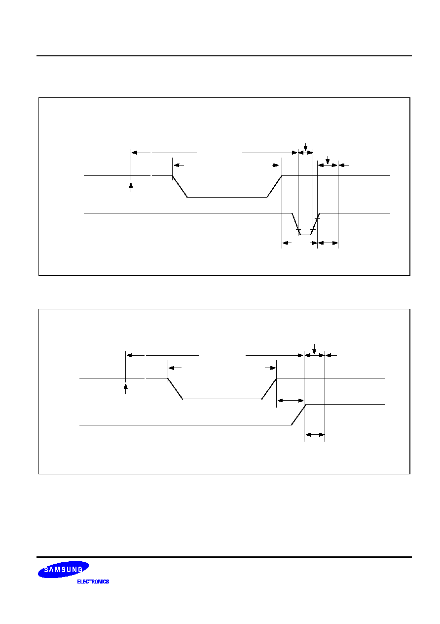
Figure 14-4. Stop Mode Release Timing When Initiated By Interrupt Request
ELECTRICAL DATA
S3C7414/P7414/C7424/P7424/C7434/P7434
14-16
0.8 V
DD
0.2 V
DD
0.8 V
DD
0.2 V
DD
MEASUREMENT
POINTS
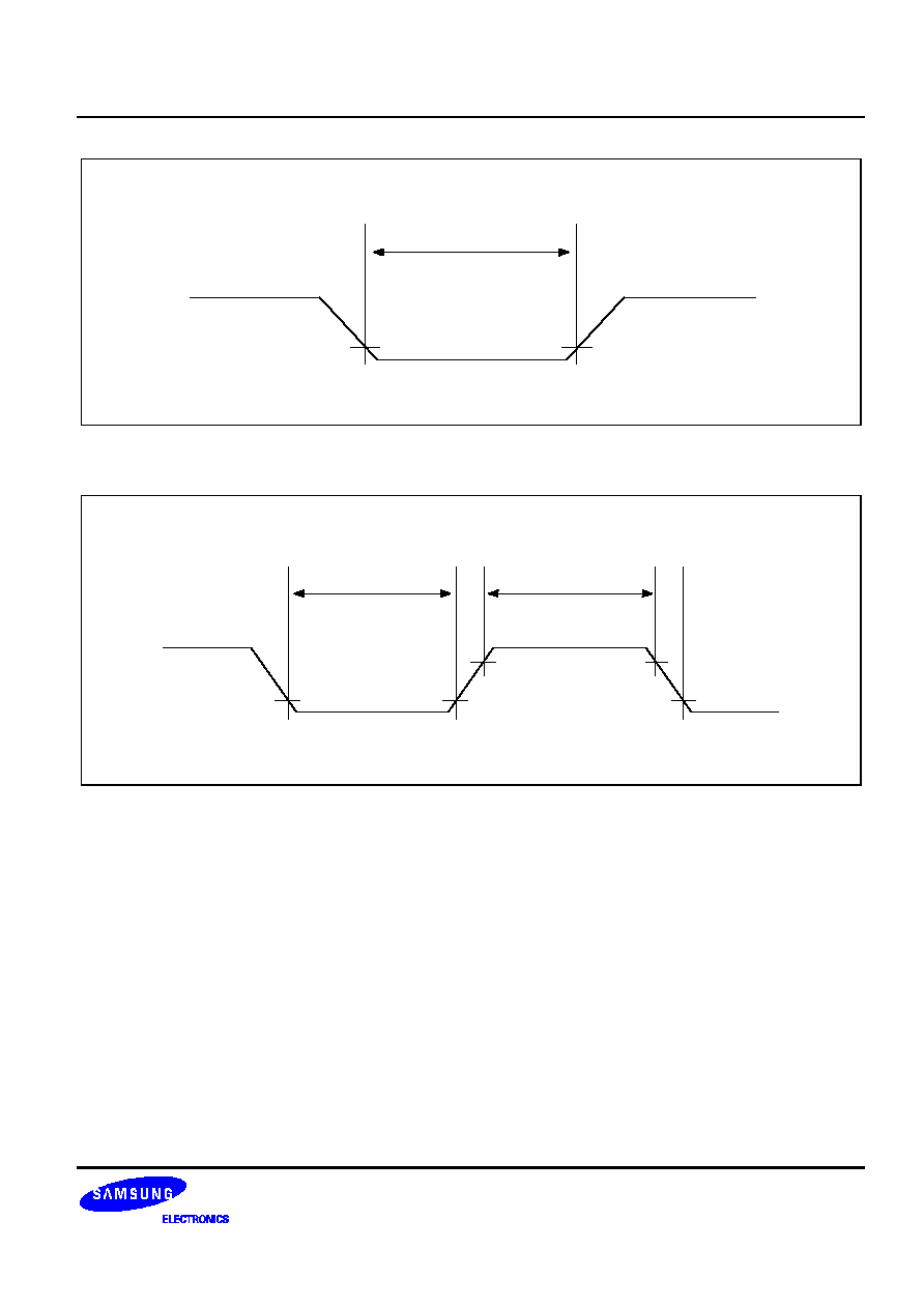
Figure 14-5. A.C. Timing Measurement Points (Except for X
IN
)
X
IN
t
XL
t
XH
1 / f x
V
DD
≠ 0.5 V
0.4 V
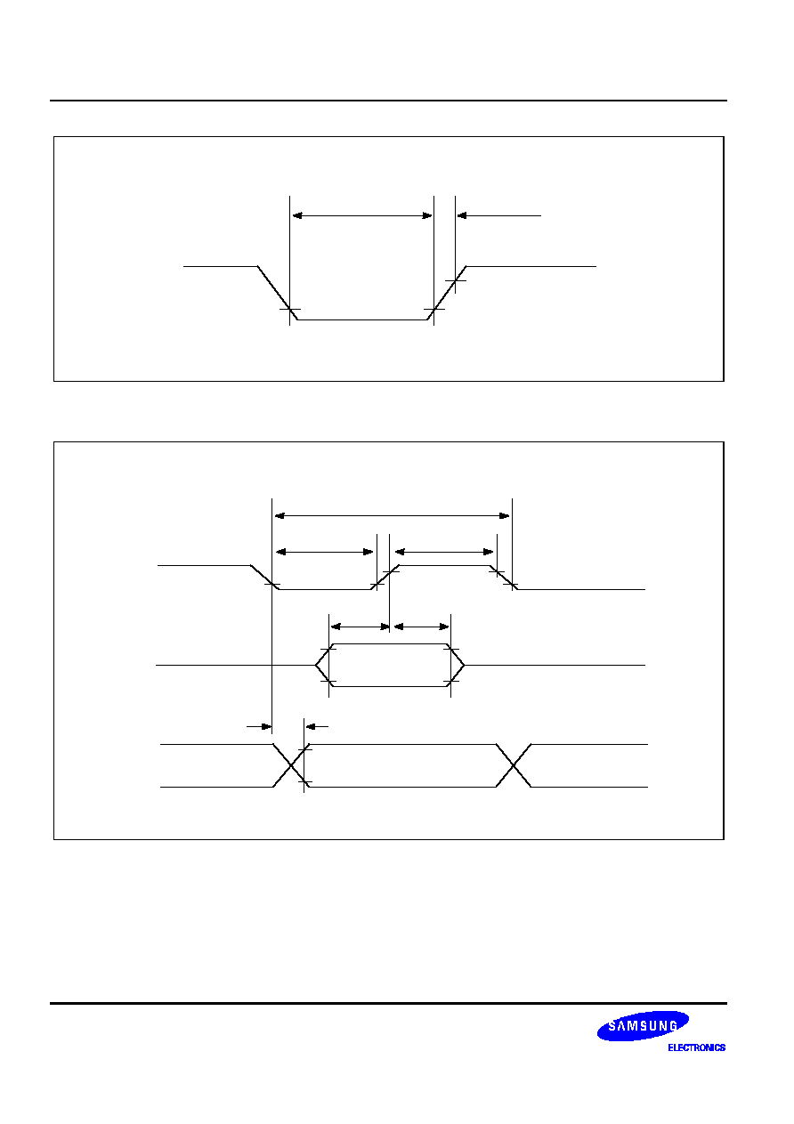
Figure 14-6. Clock Timing Measurement at X
IN
TCL0
t
TIL0
t
TIH0
0.8 V
DD
0.2 V
DD
1 / f TI0
Figure 14-7. TCL0/1 Timing
S3C7414/P7414/C7424/P7424/C7434/P7434
ELECTRICAL DATA
14-17
RESET
0.2 V
DD
t
RSL
Figure 14-8. Input Timing for
RESET
RESET
Signal
INT0, 1, 2, 4
KS0 to KS3
t
INTL
tINTH
0.8 V
DD
0.2 V
DD
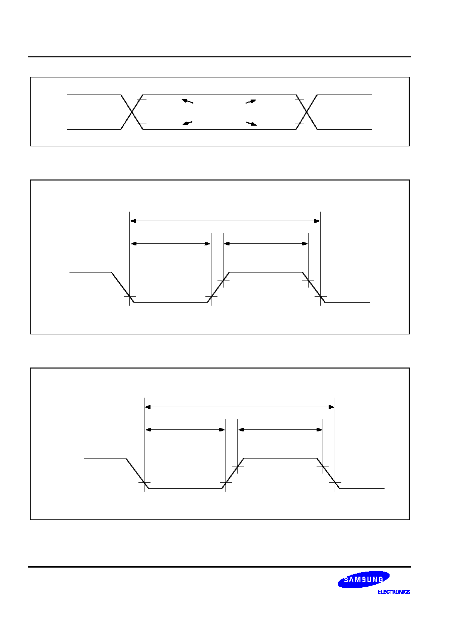
Figure 14-9. Input Timing for External Interrupts and Quasi-Interrupts
ELECTRICAL DATA
S3C7414/P7414/C7424/P7424/C7434/P7434
14-18
V
DD
t
off
t
r
V
DDH
V
DDL
Figure 14-10. S3C7434 Power-On
RESET
RESET
Timing
SCK
tKL
tKH
tKCY
0.8 V
DD
INPUT DATA
OUTPUT DATA
0.2 V
DD
0.8 V
DD
0.2 V
DD
SI
SO
tKSO
tSIK
tKSI
Figure 14-11. Serial Data Transfer Timing
S3C7414/P7414/C7424/P7424/C7434/P7434
MECHANICAL DATA
15-1
15
MECHANICAL DATA
This section contains the following information about the device package:
-- Package dimensions in millimeters
-- Pad diagram
NOTE: Dimensions are in millimeters.
0-15
∞
15.24
0.25
+0.1 ≠ 0.05
0.51MIN
3.30
± 0.3
5.08MAX
1.00
± 0.1
0.50
± 0.1
(1.77)
1.778
3.50
± 0.2
39.10
± 0.2
39.50 MAX
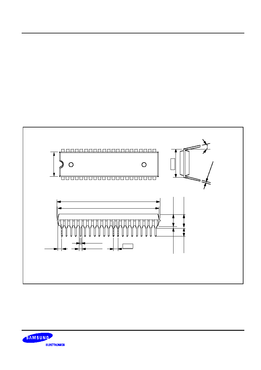
42-SDIP-600
14.00
± 0.2
#1
#21
#42
#22
Figure 15-1. 42-SDIP-600 Package Dimensions

MECHANICAL DATA
S3C7414/P7414/C7424/P7424/C7434/P7434
15-2
NOTE: Dimensions are in millimeters.
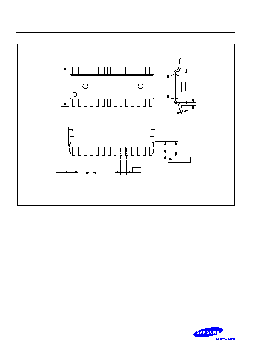
44-QFP-1010
13.20
± 0.3
#44
(1.00)
#1
13.20
± 0.3
10.00
± 0.2
0.35
+0.10
- 0.05
0.10 MAX
0.15
+0.10
- 0.05
0-8∞
0.05 MIN
2.05
± 0.10
2.30 MAX
0.80
±0.20
0.80
10.00
± 0.2
Figure 15-2. 44-QFP-1010 Package Dimensions

S3C7414/P7414/C7424/P7424/C7434/P7434
MECHANICAL DATA
15-3
NOTE: Dimensions are in millimeters.
30-SDIP-400
8.94
± 0.2
#1
#15
#30
#16
0-15
∞
0.25
+0.1 ≠ 0.05
10.16
1.12
± 0.1
0.51MIN
3.81
± 0.2
3.30
± 0.3
5.08MAX
(1.30)
0.56
± 0.1
27.48
± 0.2
27.88 MAX
1.778
Figure 15-3. 30-SDIP-400 Package Dimensions
MECHANICAL DATA
S3C7414/P7414/C7424/P7424/C7434/P7434
15-4
NOTE: Dimensions are in millimeters.
7.70
± 0.2
0-8∞
0.60
± 0.20
9.53
0.15
+0.10
- 0.05
28-SOP-375
10.45
± 0.3
#1
#14
#28
#15
0.10 MAX
0.05MIN
2.15
± 0.2
2.55MAX
17.62
± 0.2
18.02 MAX
(0.56)
0.41
± 0.1
1.27
Figure 15-4. 28-SOP-375 Package Dimensions

S3C7414/P7414/C7424/P7424/C7434/P7434
S3P7414/P7424/P7434 OTP
16-1
16
S3P7414/P7424/P7434 OTP
OVERVIEW
The S3P7414/P7424/P7434 single-chip CMOS microcontroller is the OTP (One Time Programmable)
version of
the S3C7414/C7424/C7434 microcontroller. It has an on-chip OTP ROM instead of masked ROM. Samsung
s
own serial protocol used for OTP program pin information regarding OTP program can be referred OTP pin
description.
The S3P7414/P7424/P7434 is fully compatible with the S3C7414/C7424/C7434, in function, in D.C. electrical
characteristics and in pin configuration. Because of its simple programming requirements, the
S3P7414/P7424/P7434 is ideal for use as an evaluation chip for the S3C7414/C7424/C7434.
S3P7414/P7424/P7434 OTP
S3C7414/P7414/C7424/P7424/C7434/P7434
16-2
S3P7414
(42-SDIP)
P2.0/AD0
P2.1/AD1
P2.2/AD2
P2.3/AD3
P3.0/AD4
P3.1/AD5
AV
REF
P3.2/CLO/TCL1
SDAT/P3.3/PWM/TCLO1
SCLK/P4.0
V
DD
/V
DD
V
SS
/V
SS
X
OUT
X
IN
V
PP
/TEST
P4.1
P4.2
RESET
RESET/RESET
P4.3
P5.0
P5.1
1
2
3
4
5
6
7
8
9
10
11
12
13
14
15
16
17
18
19
20
21
P8.2
P8.1/TCLO0
P8.0/TCL0
P7.3
P7.2
P7.1
P7.0
P6.3/KS3
P6.2/KS2
P6.1/KS1
P6.0/KS0
P1.3/INT4
P1.2/INT2
P1.1/INT1
P1.0/INT0
P0.3/BUZ
P0.2/SI
P0.1/SO
P0.0/
SCK
P5.3
P5.2
42
41
40
39
38
37
36
35
34
33
32
31
30
29
28
27
26
25
24
23
22
NOTE:
The bolds indicate an OTP pin name.
Figure 16-1. S3P7414 Pin Assignments (42-SDIP)
S3C7414/P7414/C7424/P7424/C7434/P7434
S3P7414/P7424/P7434 OTP
16-3
RESET
P4.3
P5.0
P5.1
P5.2
P5.3
P0.0/
SCK
P0.1/SO
P0.2/SI
P0.3/BUZ
NC
P7.2
P7.1
P7.0
P6.3/KS3
P6.2/KS2
P6.1/KS1
P6.0/KS0
P1.3/INT4
P1.2/INT2
P1.1/INT1
P1.0/INT0
AV
REF
P3.2/CLO/TCL1
SDAT/P3.3/PWM/TCLO1
SCLK/P4.0
V
DD
/V
DD
V
SS
/V
SS
X
OUT
X
IN
V
PP
/TEST
P4.1
P4.2
S3P7414
(44-QFP)
1
2
3
4
5
6
7
8
9
10
11
NC
P3.1/AD5
P3.0/AD4
P2.3/AD3
P2.2/AD2
P2.1/AD1
P2.0/AD0
P8.2
P8.1/TCLO0
P8.0/TCL0
P7.3
44
43
42
41
40
39
38
37
36
35
34
33
32
31
30
29
28
27
26
25
24
23
12
13
14
15
16
17
18
19
20
21
22
NOTE:
The bolds indicate an OTP pin name.
Figure 16-2. S3P7414 Pin Assignments (44-QFP)
S3P7414/P7424/P7434 OTP
S3C7414/P7414/C7424/P7424/C7434/P7434
16-4
S3P7424
(30-SDIP)
1
2
3
4
5
6
7
8
9
10
11
12
13
14
15
30
29
28
27
26
25
24
23
22
21
20
19
18
17
16
V
SS
/V
SS
X
OUT
X
IN
V
PP
/TEST
P4.1
P4.2
RESET
RESET/RESET
NC
P4.3
P5.0
P5.1
P5.2
P5.3
P0.0/
SCK
P0.1/SO
V
DD
/V
DD
P4.0/SCLK
P3.3/PWM/TCLO1/SDAT
P3.2/CLO/TCL1
AV
REF
NC
P2.3/AD3
P2.2/AD2
P2.1/AD1
P2.0/AD0
P1.2/INT2
P1.1/INT1
P1.0/INT0
P0.3/BUZ
P0.2/SI
NOTE:
The bolds indicate an OTP pin name.
Figure 16-3. S3P7424 Pin Assignments (30-SDIP)
S3P7424
(28-SOP)
1
2
3
4
5
6
7
8
9
10
11
12
13
14
28
27
26
25
24
23
22
21
20
19
18
17
16
15
V
SS
/V
SS
X
OUT
X
IN
V
PP
/TEST
P4.1
P4.2
RESET
RESET/RESET
P4.3
P5.0
P5.1
P5.2
P5.3
P0.0/
SCK
P0.1/SO
V
DD
/V
DD
P4.0/SCLK
P3.3/PWM/TCLO1/SDAT
P3.2/CLO/TCL1
AV
REF
P2.3/AD3
P2.2/AD2
P2.1/AD1
P2.0/AD0
P1.2/INT2
P1.1/INT1
P1.0/INT0
P0.3/BUZ
P0.2/SI
NOTE:
The bolds indicate an OTP pin name.
Figure 16-4. S3P7424 Pin Assignments (28-SOP)

S3C7414/P7414/C7424/P7424/C7434/P7434
S3P7414/P7424/P7434 OTP
16-5
S3P7434
(42-SDIP)
P2.0/AD0
P2.1/AD1
P2.2/AD2
P2.3/AD3
P3.0/AD4
P3.1/AD5
AV
REF
P3.2/CLO/TCL1
SDAT/P3.3/PWM/TCLO1
SCLK/P4.0
V
DD
/V
DD
V
SS
/V
SS
X
OUT
X
IN
V
PP
/TEST
P4.1
P4.2
RESET
RESET/RESET
P4.3
P5.0
P5.1
1
2
3
4
5
6
7
8
9
10
11
12
13
14
15
16
17
18
19
20
21
P8.2
P8.1/TCLO0
P8.0/TCL0
P7.3
P7.2
P7.1
P7.0
P6.3/KS3
P6.2/KS2
P6.1/KS1
P6.0/KS0
P1.3/INT4
P1.2/INT2
P1.1/INT1
P1.0/INT0
P0.3/BUZ
P0.2/SI
P0.1/SO
P0.0/
SCK
P5.3
P5.2
42
41
40
39
38
37
36
35
34
33
32
31
30
29
28
27
26
25
24
23
22
NOTE:
The bolds indicate an OTP pin name.
Figure 16-5. S3P7434 Pin Assignments (42-SDIP)

S3P7414/P7424/P7434 OTP
S3C7414/P7414/C7424/P7424/C7434/P7434
16-6
RESET
P4.3
P5.0
P5.1
P5.2
P5.3
P0.0/
SCK
P0.1/SO
P0.2/SI
P0.3/BUZ
NC
P7.2
P7.1
P7.0
P6.3/KS3
P6.2/KS2
P6.1/KS1
P6.0/KS0
P1.3/INT4
P1.2/INT2
P1.1/INT1
P1.0/INT0
AV
REF
P3.2/CLO/TCL1
SDAT/P3.3/PWM/TCLO1
SCLK/P4.0
V
DD
/V
DD
V
SS
/V
SS
X
OUT
X
IN
V
PP
/TEST
P4.1
P4.2
S3P7434
(44-QFP)
1
2
3
4
5
6
7
8
9
10
11
NC
P3.1/AD5
P3.0/AD4
P2.3/AD3
P2.2/AD2
P2.1/AD1
P2.0/AD0
P8.2
P8.1/TCLO0
P8.0/TCL0
P7.3
44
43
42
41
40
39
38
37
36
35
34
33
32
31
30
29
28
27
26
25
24
23
12
13
14
15
16
17
18
19
20
21
22
NOTE:
The bolds indicate an OTP pin name.
Figure 16-6. S3P7434 Pin Assignments (44-QFP)
S3C7414/P7414/C7424/P7424/C7434/P7434
S3P7414/P7424/P7434 OTP
16-7
Table 16-1. Pin Descriptions of S3P7414/P7434 Used to Read/Write the EPROM
Main Chip
During Programming
Pin Name
Pin Name
Pin No.
I/O
Function
P3.3
SDAT
9 (3)
I/O
Serial data pin. Output port when reading and input
port when writing. Can be assigned as a Input /
push-pull output port.
P4.0
SCLK
10 (4)
I/O
Serial clock pin. Input only pin.
TEST
V
PP
(TEST)
15 (9)
I
Power supply pin for EPROM cell writing (indicates
that OTP enters into the writing mode). When 12.5
V is applied, OTP is in writing mode and when 5 V
is applied, OTP is in reading mode. (Option)
RESET
RESET
18 (12)
I
Chip initialization
V
DD
/V
SS
V
DD
/V
SS
11/12 (5/6)
I
Logic power supply pin. V
DD
should be tied to +5 V
during programming.
NOTE: Parentheses indicate 44-QFP pin number.
Table 16-2. Pin Descriptions of S3P7424 Used to Read/Write the EPROM
Main Chip
During Programming
Pin Name
Pin Name
Pin No.
I/O
Function
P3.3
SDAT
28 (26)
I/O
Serial data pin. Output port when reading and input
port when writing. Can be assigned as a Input /
push-pull output port.
P4.0
SCLK
29 (27)
I/O
Serial clock pin. Input only pin.
TEST
V
PP
(TEST)
4 (4)
I
Power supply pin for EPROM cell writing (indicates
that OTP enters into the writing mode). When 12.5
V is applied, OTP is in writing mode and when 5 V
is applied, OTP is in reading mode. (Option)
RESET
RESET
7 (7)
I
Chip initialization
V
DD
/V
SS
V
DD
/V
SS
30/1 (28/1)
I
Logic power supply pin. V
DD
should be tied to +5 V
during programming.
NOTE: Parentheses indicate 28-SOP pin number.
S3P7414/P7424/P7434 OTP
S3C7414/P7414/C7424/P7424/C7434/P7434
16-8
Table 16-3. Comparison of S3P7414/P7424 and S3C7414/C7424 Features
Characteristic
S3P7414/P7424
S3C7414/C7424
Program Memory
4 K byte EPROM
4 K byte mask ROM
Operating Voltage (V
DD
)
1.8 V to 5.5 V
1.8 V to 5.5 V
OTP Programming Mode
V
DD
= 5 V, V
PP
(TEST)=12.5V
Pin Configuration
42 SDIP, 44 QFP, 30 SDIP, 28 SOP
42 SDIP, 44 QFP, 30 SDIP, 28 SOP
EPROM Programmability
User Program 1 time
Programmed at the factory
Table 16-4. Comparison of S3P7434 and S3C7434 Features
Characteristic
S3P7434
S3C7434
Program Memory
4 K byte EPROM
4 K byte mask ROM
Operating Voltage (V
DD
)
2.5 V to 5.5 V
2.5 V to 5.5 V
OTP Programming Mode
V
DD
= 5 V, V
PP
(TEST)=12.5V
Pin Configuration
42 SDIP, 44 QFP
42 SDIP, 44 QFP
EPROM Programmability
User Program 1 time
Programmed at the factory
OPERATING MODE CHARACTERISTICS
When 12.5 V is supplied to the V
PP
(TEST) pin of the S3P7414/P7424/P7434, the EPROM programming mode is
entered. The operating mode (read, write, or read protection) is selected according to the input signals to the pins
listed in Table 16-4 below.
Table 16-5. Operating Mode Selection Criteria
V
DD
V
PP
(TEST)
REG/
MEM
Address
(A15-A0)
R/W
Mode
5 V
5 V
0
0000H
1
EPROM read
12.5 V
0
0000H
0
EPROM program
12.5 V
0
0000H
1
EPROM verify
12.5 V
1
0E3FH
0
EPROM read protection
NOTE: "0" means Low level; "1" means High level.
S3C7414/P7414/C7424/P7424/C7434/P7434
S3P7414/P7424/P7434 OTP
16-9
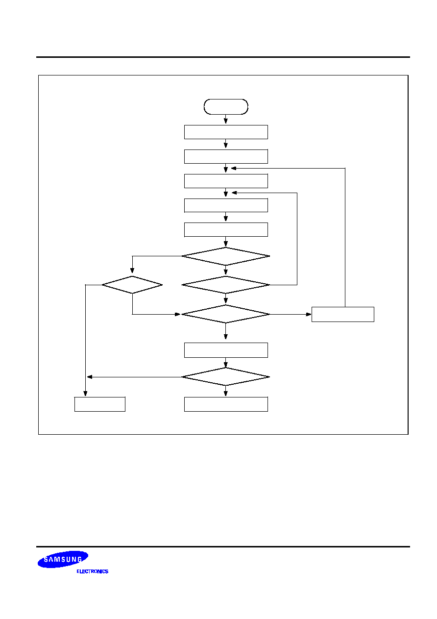
START
Address= First Location
V
DD
=5V, V
PP
=12.5V
x = 0
Program One 1ms Pulse
Increment X
x = 10
Verify 1 Byte
Last Address
V
DD
= V
PP
= 5 V
Compare All Byte
Device Passed
Increment Address
Verify Byte
Device Failed
PASS
FAIL
NO
FAIL
YES
FAIL
NO
Figure 16-7. OTP Programming Algorithm

S3P7414/P7424/P7434 OTP
S3C7414/P7414/C7424/P7424/C7434/P7434
16-10
Table 16-6. S3P7414/P7424 D.C. Electrical Characteristics
(T
A
= ≠ 40
∞
C to + 85
∞
C, V
DD
= 1.8 V to 5.5 V)
Parameter
Symbol
Conditions
Min
Typ
Max
Units
Supply
I
DD1
Run mode; V
DD
= 5.0 V
±
10%
6.0MHz
≠
3.0
8.0
mA
Current
(1)
Crystal oscillator; C1=C2=22pF
4.19MHz
2.3
5.5
V
DD
= 3 V
±
10%
6.0MHz
1.4
4.0
4.19MHz
1.1
3.0
I
DD2
Idle mode; V
DD
= 5.0 V
±
10%
6.0MHz
≠
1.1
2.5
mA
Crystal oscillator; C1=C2=22pF
4.19MHz
1.0
1.8
V
DD
= 3 V
±
10%
6.0MHz
0.5
1.5
4.19MHz
0.4
1.0
I
DD3
Stop mode; V
DD
= 5.0 V
±
10%
≠
0.1
5.0
µ
A
Stop mode; V
DD
= 3.0 V
±
10%
0.1
3.0
NOTES:
1.
D.C. electrical values for Supply current (I
DD1
to I
DD3
) do not include current drawn through internal pull-up registers,
output port drive currents and ADC.
2.
The supply current assumes a CPU clock of fx/4.
CPU CLOCK = 1/n x oscillator frequency (n = 4, 8 or 64)
SUPPLY VOLTAGE (V)
1.05 MHz
15.6 kHz
CPU CLOCK
1.5 MHz
4.2 MHz
Main Oscillator Frequency
(Divided by 4)
6 MHz
1
2
3
4
5
6
2.7
5.5
0.75 MHz
1.8
3 MHz
Figure 16-8. S3P7414/P7424 Standard Operating Voltage Range

S3C7414/P7414/C7424/P7424/C7434/P7434
S3P7414/P7424/P7434 OTP
16-11
Table 16-7. S3P7434 D.C. Electrical Characteristics
(T
A
= ≠ 40
∞
C to + 85
∞
C, V
DD
= 2.5 V to 5.5 V)
Parameter
Symbol
Conditions
Min
Typ
Max
Units
Supply
I
DD1
Run mode; V
DD
= 5.0 V
±
10%
6.0MHz
≠
3.1
8.0
mA
Current
(1)
Crystal oscillator; C1=C2=22pF
4.19MHz
2.4
5.5
V
DD
= 3 V
±
10%
6.0MHz
1.5
4.0
4.19MHz
1.2
3.0
I
DD2
Idle mode; V
DD
= 5.0 V
±
10%
6.0MHz
≠
1.2
2.5
mA
Crystal oscillator; C1=C2=22pF
4.19MHz
1.1
1.8
V
DD
= 3 V
±
10%
6.0MHz
0.6
1.5
4.19MHz
0.5
1.0
I
DD3
Stop mode; V
DD
= 5.0 V
±
10%
≠
120
200
µ
A
Stop mode; V
DD
= 3.0 V
±
10%
100
150
NOTES:
1.
D.C. electrical values for Supply current (IDD1 to IDD3) do not include current drawn through internal pull-up registers,
output port drive currents and ADC.
2.
The supply current assumes a CPU clock of fx/4.
CPU CLOCK = 1/n x oscillator frequency (n = 4, 8 or 64)
SUPPLY VOLTAGE (V)
1.05 MHz
15.6 kHz
CPU CLOCK
1.5 MHz
4.2 MHz
Main Oscillator Frequency
(Divided by 4)
6 MHz
1
2
3
4
5
6
2.5
5.5
Figure 16-9. S3P7434 Standard Operating Voltage Range

S3P7414/P7424/P7434 OTP
S3C7414/P7414/C7424/P7424/C7434/P7434
16-12
NOTES