 | –≠–ª–µ–∫—Ç—Ä–æ–Ω–Ω—ã–π –∫–æ–º–ø–æ–Ω–µ–Ω—Ç: S3P863A | –°–∫–∞—á–∞—Ç—å:  PDF PDF  ZIP ZIP |

S3C8639/C863A/P863A
PRODUCT OVERVIEW
1-1
1
PRODUCT OVERVIEW
SAM8 PRODUCT FAMILY
Samsung's SAM8 family of 8-bit single-chip CMOS microcontrollers offers a fast and efficient CPU with a wide
range of integrated peripherals, in various mask-programmable ROM sizes. Analog its major CPU features are:
-- Efficient register-oriented architecture
-- Selectable CPU clock sources
-- Idle and Stop power-down mode release by interrupt
-- Built-in basic timer with watchdog function
The sophisticated interrupt structure recognizes up to eight interrupt levels. Each level can have one or more
interrupt sources and vectors. Fast interrupt processing (within a minimum of four CPU clocks) can be assigned
to specific interrupt levels.
S3C8639/C863A/P863A MICROCONTROLLERS
S3C8639/C863A/P863A single-chip 8-bit
microcontrollers are based on the powerful SAM8
CPU architecture. The internal register file is logically
expanded to increase the on-chip register space.
S3C8639/C863A/P863A contain 32/48 Kbytes of on-
chip program ROM.
In line with Samsung's modular design approach, the
following peripherals are integrated with the SAM8
core:
-- Four programmable I/O ports (total 27 pins)
-- One 8-bit basic timer for oscillation stabilization
and watchdog functions
-- One 8-bit general-purpose timer/counter with
selectable clock sources
-- One interval timer
-- One 12-bit counter with selectable clock sources,
including Hsync or Csync input
-- PWM block with seven 8-bit PWM circuits
-- Sync processor block (for Vsync and Hsync I/O,
Csync input, and Clamp signal output)
-- DDC Multi-master and slave-only IIC-Bus
-- 4-channel A/D converter (8-bit resolution)
S3C8639/C863A/P863A are a versatile
microcontrollers which are ideal for use in multi-sync
monitors or in general-purpose applications that
require sophisticated timer/counter, PWM, sync
signal processing, A/D converter, and multi-master
IIC-bus support with DDC. They are available in a
42-pin SDIP or a 44-pin QFP package.
OTP
S3C8639/C863A microcontrollers are also available in OTP (One Time Programmable) version named,
S3P863A. S3P863A microcontroller has an on-chip 48-Kbyte one-time-programmable EPROM instead of
masked ROM. S3P863A is comparable to S3C8639/C863A, both in function and pin configuration except its
ROM size.

PRODUCT OVERVIEW
S3C8639/C863A/P863A
1-2
FEATURES
CPU
∑
SAM88RC CPU core
Memory
∑
S3C8639: 32-Kbyte internal program memory
(ROM)
S3C863A: 48-Kbyte internal program memory
(ROM)
∑
S3C8639: 784-byte general-purpose
register area
S3C863A: 1040-byte general-purpose
register area
Instruction Set
∑
78 instructions
∑
IDLE and STOP instructions added for
power-down modes
Instruction Execution Time
∑
Minimum 333 ns (with 12 MHz CPU clock)
Interrupts
∑
Ten interrupt sources/vectors
∑
Eight interrupt level
∑
Fast interrupt feature
General I/O
∑
Four I/O Ports (total 27pins)
8-Bit Basic Timer
∑
Programmable timer for oscillation stabilization
interval control or watchdog timer function
∑
Three selective internal clock frequencies
Timer/Counters
∑
One 8-bit Timer/Counter with several clock
sources (Capture mode)
∑
One 12-bit Counter with H-/C-sync and several
clock sources
∑
One Interval Timer
Low Voltage Reset (LVR)
∑
LVR level is 2.4 V
±
200 mV
Pulse Width Modulator (PWM)
∑
8-bit PWM: 7-CH
(6-bit basic frame with 2-bit extension)
Sync-Processor Block
∑
Vsync-I, Hsync-I, Csync-I input and Vsync-O,
Hsync-O, Clamp-O output pins
∑
Programmable Pseudo sync signal generation
∑
Auto SOG detection
∑
Auto H-/V-sync polarity detection
∑
Composite sync detection
DDC Multi-Master IIC-Bus 1-Ch
∑
Serial Peripheral Interface
∑
Support for Display Data Channel
(DDC1/DDC2B/DDC2Bi/DDC2B+)
Slave Only IIC-Bus 1-Ch
∑
Serial Peripheral Interface
A/D Converter
∑
4-channel; 8-bit resolution
Oscillator Frequency
∑
8 MHz to 12 MHz crystal operation
∑
Internal Max. 12 MHz CPU clock
Operating Temperature Range
∑
≠ 40
∞
C to + 85
∞
C
Operating Voltage Range
∑
3.0 V to 5.5 V
Package Types
∑
42-pin SDIP, 44-pin QFP

S3C8639/C863A/P863A
PRODUCT OVERVIEW
1-3
BLOCK DIAGRAM
Port 0
P0.0-P0.7/INT0-INT2
I/O Port and Interrupt
Control
32/48-
Kbyte
ROM
784/1040-
Byte
Register File
SAM8 CPU
Port 2
Port 1
P1.0-P1.2
P2.0-P2.7
V
DD1
, V
DD2
V
SS1
, V
SS2
TEST
RESET
INT0-INT2
ADC
Port 3
P3.0-P3.7
Slave
Only
IIC-Bus
AD0-AD3
SCL1
SDA1
Main
Osc
8-Bit
PWM
(7-Ch)
Sync-
Processor
X
OUT
X
IN
PWM0
PWM6
8-Bit
Counter
(Timer M0)
TM0CAP
Vsync-I
Hsync-I
Csync-I
Vsync-O
Hsync-O
Clamp-O
12-Bit
Counter
(Timer M1)
Interval
Timer
(Timer M2)
Multi-master IIC-Bus
and DDC1/2B/2Bi/2B+
SCL0
SDA0
* S3C8639
- 32 Kbyte ROM
- 784 Byte RAM
* S3C863A
- 48 Kbyte ROM
- 1040 Byte RAM
Figure 1-1. Block Diagram
PRODUCT OVERVIEW
S3C8639/C863A/P863A
1-4
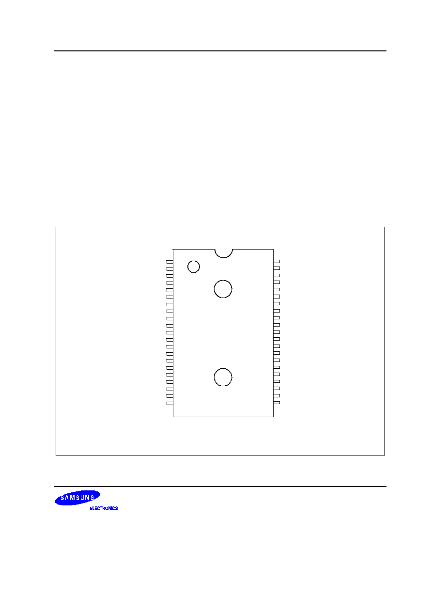
PIN ASSIGNMENTS
P0.0/INT0
P0.1/INT1
P0.2/INT2
P0.3
P0.4/TM0CAP
P0.5
P0.6
P0.7
P1.0/SDA1
P1.1/SCL1
V
DD1
V
SS1
X
OUT
X
IN
TEST (GND)
SDA0
SCL0
RESET
P1.2
P2.0/PWM0
P2.1/PWM1
S3C8639
/C863A
(42-SDIP)
1
2
3
4
5
6
7
8
9
10
11
12
13
14
15
16
17
18
19
20
21
P3.7
P3.6
P3.5
P3.4
P3.3/AD3
P3.2/AD2
P3.1/AD1
P3.0/AD0
V
DD2
V
SS2
P2.7/Csync-I (SOG)
Hsync-I
Vsync-I
Vsync-O
Hsync-O
Clamp-O
P2.6/PWM6
P2.5/PWM5
P2.4/PWM4
P2.3/PWM3
P2.2/PWM2
42
41
40
39
38
37
36
35
34
33
32
31
30
29
28
27
26
25
24
23
22
NOTE: The TEST pin must connect to V
SS
(GND) in the normal operation mode.
Figure 1-2. S3C8639/C863A 42-SDIP Pin Assignment

S3C8639/C863A/P863A
PRODUCT OVERVIEW
1-5
SCL0
RESET
P1.2
P2.0/PWM0
P2.1/PWM1
P2.2/PWM2
N.C.
P2.3/PWM3
P2.4/PWM4
P2.5/PWM5
P2.6/PWM6
P3.2/AD2
P3.1/AD1
P3.0/AD0
V
DD2
V
SS2
P2.7/Csync-I (SOG)
Hsync-I
Vsync-I
Vsync-O
Hsync-O
Clamp-O
P0.4/TM0CAP
P0.3
P0.2/INT2
P0.1/INT1
N.C.
P0.0/INT0
P3.7
P3.6
P3.5
P3.4
P3.3/AD3
P0.5
P0.6
P0.7
P1.0/SDA1
P1.1/SCL1
V
DD1
V
SS1
X
OUT
X
IN
TEST (GND)
SDA0
S3C8639
/C863A
44-QFP
(Top View)
1
2
3
4
5
6
7
8
9
10
11
44
43
42
41
40
39
38
37
36
35
34
33
32
31
30
29
28
27
26
25
24
23
12
13
14
15
16
17
18
19
20
21
22
NOTE: The TEST pin must connect to V
SS
(GND) in the normal operation mode.
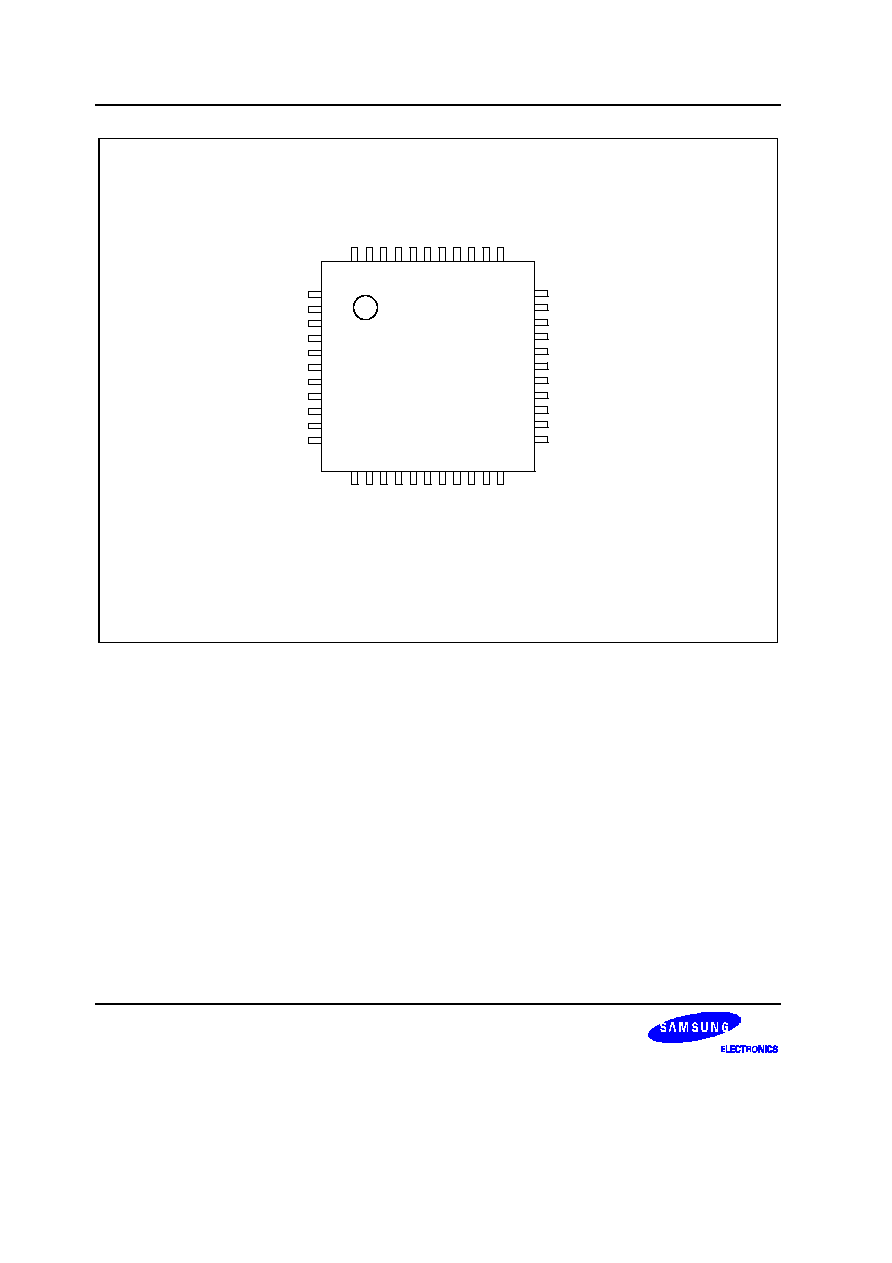
Figure 1-3. S3C8639/C863A 44-QFP Pin Assignment

PRODUCT OVERVIEW
S3C8639/C863A/P863A
1-6
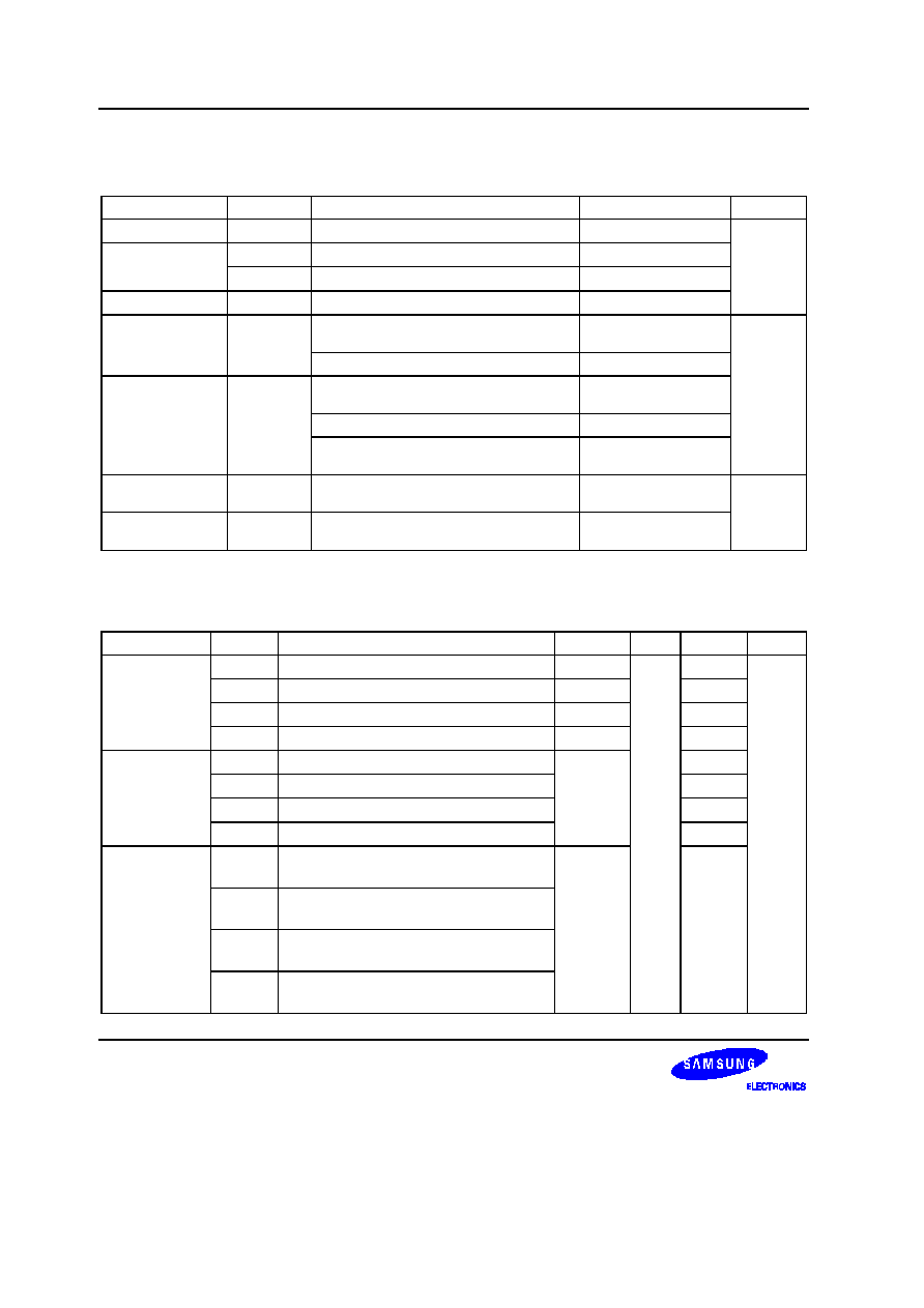
PIN DESCRIPTIONS
Table 1-1. S3C8639/C863A Pin Descriptions
Pin
Names
Pin
Type
Pin
Description
Circuit
Type
SDIP Pin
Numbers
Shared
Functions
P0.0
P0.1
P0.2
P0.3
P0.4
P0.5
P0.6
P0.7
I/O
General-purpose, 8-bit I/O port. Shared
functions include three external interrupt inputs
and I/O for timer M0. Selective configuration of
port 0 pins to input or output mode is
supported.
D-1
D-1
D-1
D-1
D-1
D-1
D-1
D-1
1
2
3
4
5
6
7
8
INT0
INT1
INT2
TM0CAP
P1.0
P1.1
P1.2
I/O
General-purpose, 8-bit I/O port. Selective
configuration is available for port 1 pins to
input, push-pull output, n-channel open-drain
mode, or IIC-bus clock and data I/O.
E-1
E-1
E-1
9
10
19
SDA1
SCL1
P2.0
P2.1
P2.2
P2.3
P2.4
P2.5
P2.6
P2.7
I/O
General-purpose, 8-bit I/O port Selective
configuration of port 2 pins to input or output
mode is supported. The port 2 pin circuits are
designed to push-pull PWM output and Csync
(SOG) signal input.
D-1
D-1
D-1
D-1
E-1
E-1
E-1
D-1
20
21
22
23
24
25
26
32
PWM0
PWM1
PWM2
PWM3
PWM4
PWM5
PWM6
Csync-I
P3.0≠P3.3
P3.4≠P3.7
I/O
General-purpose, 8-bit I/O port Selective
configuration port 3 pins to input or output
mode is supported. Multiplexed for alternative
use as A/D converter inputs AD0≠AD3.
E-1
E
35≠38
39≠42
AD0≠AD3
Hsync-I
Vsync-I
Clamp-O
Hsync-O
Vsync-O
SDA0
SCL0
I
I
O
O
O
I/O
I/O
The pins are sync processor signal I/O and IIC-
bus clock and data I/O.
A-3
A-3
A
A
A
G-3
G-3
31
30
27
28
29
16
17
≠
V
DD1
, V
SS1
,
V
DD2
, V
SS2
≠
Power pins
≠
≠
11, 12
34, 33
≠
X
IN
, X
OUT
≠
System clock I/O pins
≠
14, 13
≠
RESET
I
System
RESET
pin
B
18
≠
TEST
I
Factory test pin input
0 V: Normal operation, 5 V: Factory test mode
≠
15
≠
S3C8639/C863A/P863A
PRODUCT OVERVIEW
1-7
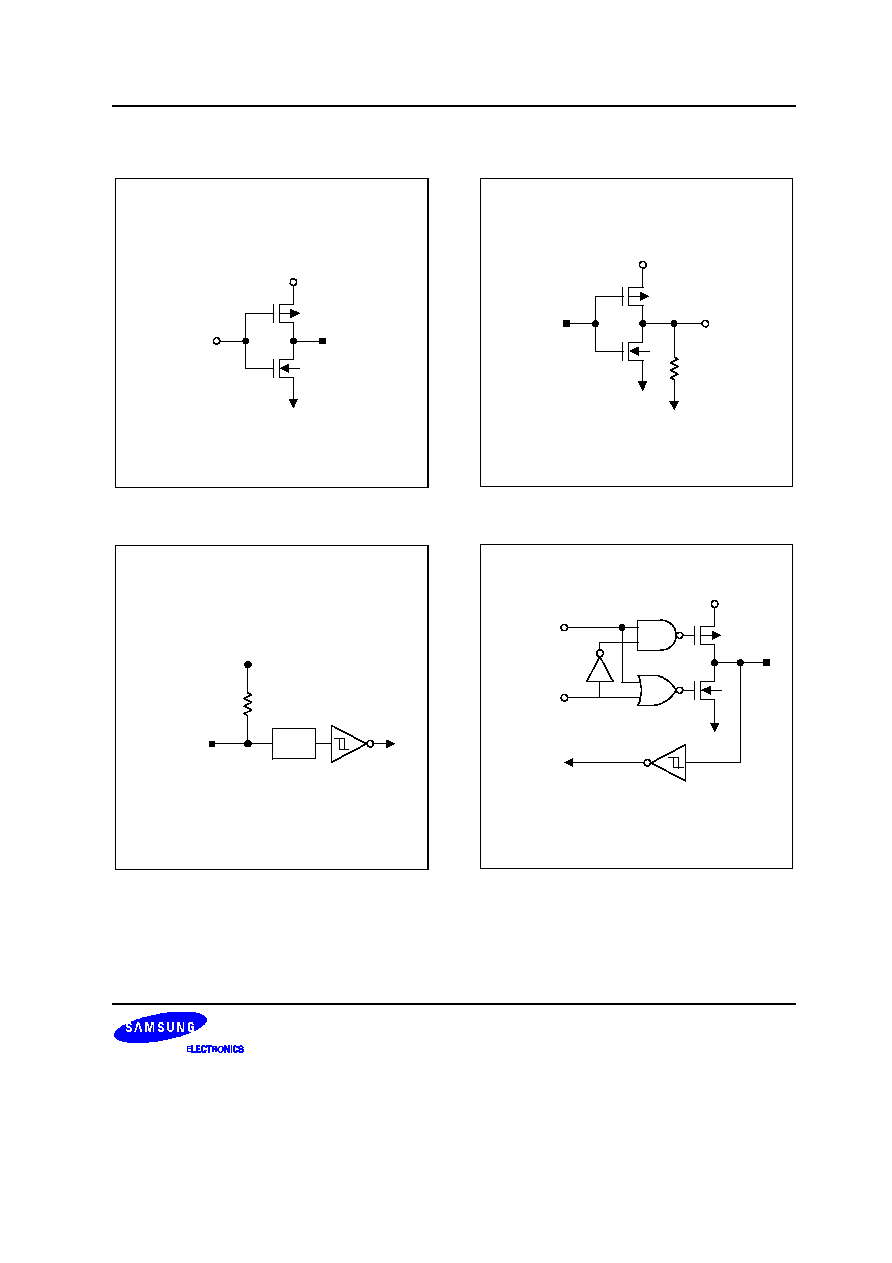
PIN CIRCUITS DIAGRAM
Data
V
SS
Output
V
DD
Figure 1-4. Pin Circuit Type A
RESET
V
DD
280 k
Noise
Filter
Figure 1-6. Pin Circuit Type B (
RESET
)
Input
V
SS
Output
V
SS
300 k
Typical
V
DD
Figure 1-5. Pin Circuit Type A-3
Data or
Other
Function
V
SS
Output
Output
Disable
Digital Input,
TTL Input
NOTE:
The noise filter must be built in the
external interrupts.
V
DD
Figure 1-7. Pin Circuit Type D-1
PRODUCT OVERVIEW
S3C8639/C863A/P863A
1-8
Data
V
SS
Output
Typical
47 k
Pull-up
Enable
V
DD
V
DD
Output
Disable
Open
Drain
Input
Figure 1-8. Pin Circuit Type E
V
SS
Output
Data
Input
Figure 1-10. Pin Circuit Type G-3
Data
V
SS
Output
V
DD
Output
Disable
Open
Drain
Digital Input
or ADC Input
Figure 1-9. Pin Circuit Type E-1

S3C8639/C863A/P863A
ELECTRICAL DATA
19-1
19
ELECTRICAL DATA
OVERVIEW
In this section, S3C8639/C863A electrical characteristics are presented in tables and graphs. The information is
arranged in the following order:
-- Absolute maximum ratings
-- D.C. electrical characteristics
-- Data retention supply voltage in stop mode
-- Stop mode release timing when initiated by a reset
-- I/O capacitance
-- A/D Converter electrical characteristics
-- A.C. electrical characteristics
-- Input timing measurement points for P0.0≠P0.2 and TM0CAP
-- Oscillation characteristics
-- Oscillation stabilization time
-- Clock timing measurement points for X
IN
-- Schmitt trigger characteristics
-- Power-on reset circuit characteristics
ELECTRICAL DATA
S3C8639/C863A/P863A
19-2
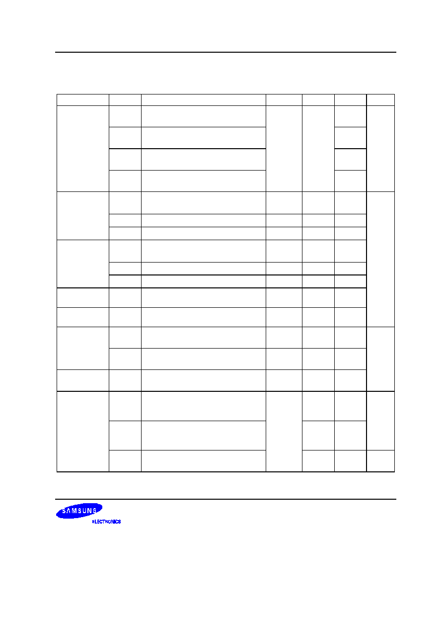
Table 19-1. Absolute Maximum Ratings
(T
A
= 25
∞
C)
Parameter
Symbol
Conditions
Rating
Unit
Supply voltage
V
DD
≠
≠ 0.3 to + 6.5
V
Input voltage
V
I1
Type G-3 (n-channel open drain)
≠ 0.3 to + 7.0
V
I2
All port pins except V
I1
≠ 0.3 to V
DD
+ 0.3
Output voltage
V
O
All output pins
≠ 0.3 to V
DD
+ 0.3
Output current
High
I
OH
One I/O pin active
≠ 10
mA
All I/O pins active
≠ 60
Output current
Low
I
OL
One I/O pin active
+ 30
Total pin current except port 3
+ 100
Sync-processor I/O pins and IIC-bus
clock and data pins
+ 150
Operating
temperature
T
A
≠
≠ 40 to + 85
∞
C
Storage
temperature
T
STG
≠
≠ 65 to + 150
Table 19-2. D.C. Electrical Characteristics
(T
A
= ≠ 40
∞
C to + 85
∞
C, V
DD
= 3.0 V to 5.5 V)
Parameter
Symbol
Conditions
Min
Typ
Max
Unit
Input High
V
IH1
All input pins except V
IH2
, V
IH3
and V
IH4
0.8 V
DD
≠
V
DD
V
voltage
V
IH2
X
IN
V
DD
≠0.5
V
DD
V
IH3
TTL input (Hsync-I, Vsync-I, and Csync-I)
2.0
V
DD
V
IH4
SCL0/SDA0, SCL1/SDA1
0.7V
DD
V
DD
Input Low
V
IL1
All input pins except V
IL2
and V
IL3
≠
0.2 V
DD
voltage
V
IL2
X
IN
0.4
V
IL3
TTL input (Hsync-I, Vsync-I, and Csync-I)
0.8
V
IL4
SCL0/SDA0, SCL1/SDA1
0.3V
DD
Output High
voltage
V
OH1
V
DD
= 5 V
±
10%; I
OH
= ≠ 15 mA;
Port 3.6≠3.7
V
DD
≠ 1.0
≠
V
OH2
V
DD
= 5 V
±
10%; I
OH
= ≠ 4 mA;
Port 1.2, Port 3.0≠3.5
V
OH3
V
DD
= 5 V
±
10%; I
OH
= ≠ 2 mA;
Port 0, 2, Clamp-O, H, and Vsync-O
V
OH4
V
DD
= 5 V
±
10%; I
OH
= ≠ 6 mA;
Port 1.0≠P1.1, SCL0 and SDA0
S3C8639/C863A/P863A
ELECTRICAL DATA
19-3
Table 19-2. D.C. Electrical Characteristics (Continued)
(T
A
= ≠ 40
∞
C to + 85
∞
C, V
DD
= 3.0 V to 5.5 V)
Parameter
Symbol
Conditions
Min
Typ
Max
Unit
Output Low
voltage
V
OL1
V
DD
= 5 V
±
10%; I
OL
= 15 mA
Port 3.6≠3.7
≠
≠
0.4
V
V
OL2
V
DD
= 5 V
±
10%; I
OL
= 4 mA
Port 3.0≠3.5 and Port 1.2
0.4
V
OL3
V
DD
= 5 V
±
10%; I
OL
= 2 mA
Port 0, 2, Clamp-O, H, and Vsync-O
0.4
V
OL4
V
DD
= 5 V
±
10%; I
OL
= 6 mA
Port 1.0≠1.1; SCL0 and SDA0
0.6
Input High
leakage current
I
LIH1
V
IN
= V
DD
All input pins except X
IN
,
X
OUT
≠
≠
3
µA
I
LIH2
V
IN
= V
DD
;
X
OUT
only
≠
≠
20
I
LIH3
V
IN
= V
DD
;
X
IN
only
2.5
6
20
Input Low
leakage current
I
LIL1
V
IN
= 0 V; All input pins except X
IN
,
X
OUT
,
RESET
, HsyncI & VsyncI
≠
≠
≠ 3
I
LIL2
V
IN
= 0 V; X
OUT
only
≠
≠
≠ 20
I
LIL3
V
IN
= 0 V; X
IN
only
≠ 2.5
≠ 6
≠ 20
Output High
leakage current
I
LOH1
V
OUT
= V
DD
≠
≠
3
Output Low
leakage current
I
LOL1
V
OUT
= 0 V
≠
≠
≠ 3
Pull-up resistor
R
U1
V
IN
= 0 V; V
DD
= 5 V
±
10%
Ports 3.7≠3.4
20
47
80
k
R
U2
V
IN
= 0 V; V
DD
= 5 V
±
10%
RESET
only
150
280
480
Pull-down
resistor
R
D
V
IN
= 0 V; V
DD
= 5 V
±
10%
HsyncI & VsyncI
150
300
500
Supply current
(note)
I
DD1
V
DD
= 5 V
±
10%
Operation mode; 12 MHz crystal
C1 = C2 = 22pF
≠
10
20
mA
I
DD2
V
DD
= 5 V
±
10%
Idle mode; 12 MHz crystal
C1 = C2 = 22pF
4
8
I
DD3
V
DD
= 5 V
±
10%
Stop mode
100
150
µA
NOTE: Supply current does not include drawn internal pull-up/pull-down resistors and external loads of output.

ELECTRICAL DATA
S3C8639/C863A/P863A
19-4
Table 19-3. Data Retention Supply Voltage in Stop Mode
(T
A
= ≠ 40
∞
C to + 85
∞
C)
Parameter
Symbol
Conditions
Min
Typ
Max
Unit
Data retention
supply voltage
V
DDDR
Stop mode
2
≠
5.5
V
Data retention
supply current
I
DDDR
Stop mode, V
DDDR
= 2.0 V
≠
≠
5
µA
NOTES:
1.
During the oscillator stabilization wait time (t
WAIT
), all CPU operations must be stopped.
2.
Supply current does not include drawn through internal pull≠up resistors and external output current loads.
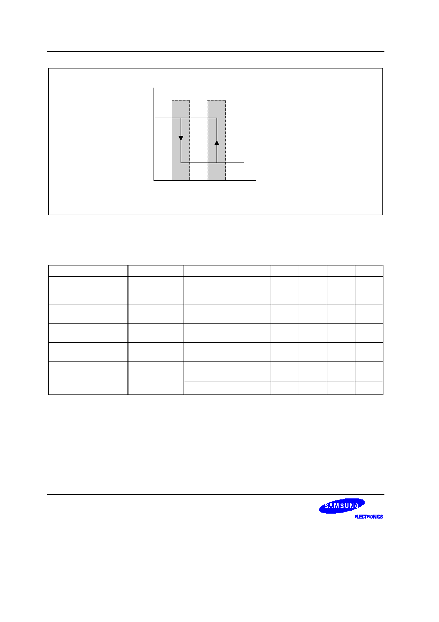
NOTE: t
WAIT
is the same as 4096 x 16 x 1/f
OSC
.
Execution of
STOP Instrction
RESET
occurs
~ ~
V
DDDR
~ ~
Stop Mode
Oscillation
Stabilzation
Time
Data Retention Mode
t
WAIT
RESET
V
DD
Normal
Operating
Mode
Figure 19-1. Stop Mode Release Timing When Initiated by a Reset
Table 19-4. Input/Output Capacitance
(T
A
= ≠40
∞
C to + 85
∞
C, V
DD
=
0 V)
Parameter
Symbol
Conditions
Min
Typ
Max
Unit
Input
capacitance
C
IN
f = 1 MHz; unmeasured pins
are connected to V
SS
≠
≠
10
pF
Output
capacitance
C
OUT
I/O capacitance
C
IO
S3C8639/C863A/P863A
ELECTRICAL DATA
19-5
Table 19-5. A/D Converter Electrical Characteristics
(T
A
= ≠ 40
∞
C to + 85
∞
C, V
DD
= 3.0 V to 5.5 V, V
SS
= 0 V)
Parameter
Symbol
Conditions
Min
Typ
Max
Unit
Resolution
≠
8
≠
bit
Total accuracy
V
DD
= 5 V
Conversion time = 5
µ
s
≠
≠
±
2
LSB
Integral linearity error
ILE
AV
REF
= 5 V
≠
±
1
Differential linearity error
DLE
AV
SS
= 0 V
≠
±
1
Offset error of top
EOT
±
1
±
2
Offset error of bottom
EOB
±
0.5
±
2
Conversion time
(1)
t
CON
8 bit conversion
40 x n/f
OSC
(3)
, n=1,4,8,16
20
≠
170
µ
s
Analog input voltage
V
IAN
≠
AV
SS
≠
AV
REF
V
Analog input impedance
R
AN
≠
2
1000
≠
M
Analog reference voltage
AV
REF
≠
2.5
≠
V
DD
V
Analog ground
AV
SS
≠
V
SS
≠
V
SS
+ 0.3
V
Analog input current
I
ADIN
AV
REF
= V
DD
= 5V
≠
≠
10
µ
A
Analog block Current
(2)
I
ADC
AV
REF
= V
DD
= 5V
≠
1
3
mA
AV
REF
= V
DD
= 3V
0.5
1.5
mA
AV
REF
= V
DD
= 5V
When power down mode
100
500
nA
NOTES:
1.
"Conversion time" is the time required from the moment a conversion operation starts until it ends.
2.
I
ADC
is an operating current during the A/D conversion.
3.
f
OSC
is the main oscillator clock.
ELECTRICAL DATA
S3C8639/C863A/P863A
19-6
Table 19-6. A.C. Electrical Characteristics
(T
A
= ≠ 40
∞
C to + 85
∞
C, V
DD
= 3.0 V to 5.5V)
Parameter
Symbol
Conditions
Min
Typ
Max
Unit
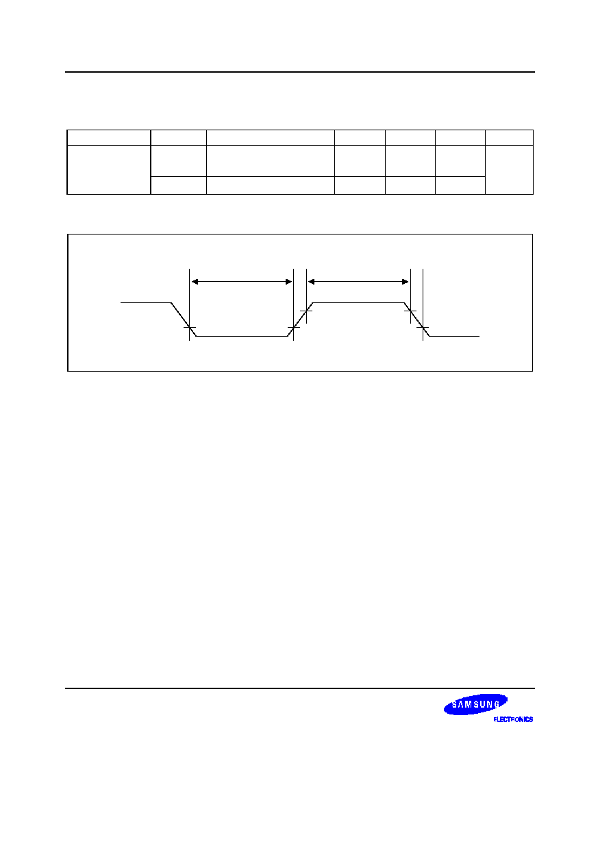
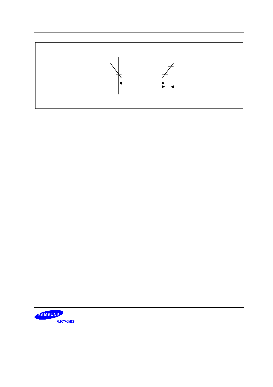
Noise Filter
t
NF1H
t
NF1L
INT0≠2 and TM0CAP (RC
delay)
300
≠
≠
ns
t
NF2
RESET
only (RC delay)
1000
≠
≠
t
NF1H
t
NF1L
0.8 V
DD
0.2 V
DD
t
NF2
Figure 19-2. Input Timing Measurement Points for P0.0≠P0.2 and TM0CAP
S3C8639/C863A/P863A
ELECTRICAL DATA
19-7
Table 19-7. Oscillation Characteristics
(T
A
= ≠ 40
∞
C + 85
∞
C)
Oscillator
Clock Circuit
Conditions
Min
Typ
Max
Unit
Main crystal or
ceramic
C2
C1
X
IN
X
OUT
V
DD
= 3.0 V to 5.5 V
8
≠
12
MHz
External clock
(main)
X
IN
X
OUT
V
DD
= 3.0 V to 5.5 V
8
≠
12
MHz
NOTE: The maximum oscillator frequency is 12 MHz. If you use an oscillator frequency higher than 12 MHz, you cannot
select a non-divided CPU clock using CLKCON settings. That is, you must select one of the divide-by values.
Table 19-8. Oscillation Stabilization Time
(T
A
= ≠ 40
∞
C + 85
∞
C, V
DD
= 3.0 V to 5.5 V)
Oscillator
Test Condition
Min
Typ
Max
Unit
Crystal
V
DD
= 3.0 V to 5.5 V
≠
≠
20
ms
Ceramic
V
DD
= 3.0 V to 5.5V
≠
≠
10
External clock
X
IN
input high and low level width
(t
XH
, t
XL
)
25
≠
500
ns
NOTE: Oscillation stabilization time is the time required for the CPU clock to return to its normal oscillation frequency after a
power-on occurs, or when Stop mode is released.
X
IN
t
XH
t
XL
1/fx
V
DD
- 0.5 V
0.4 V
Figure 19-3. Clock Timing Measurement Points for X
IN
ELECTRICAL DATA
S3C8639/C863A/P863A
19-8
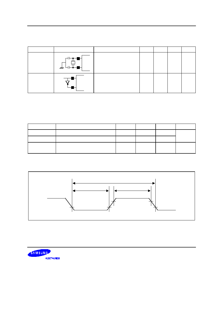
A = 0.2 V
DD
B = 0.4 V
DD
C = 0.6 V
DD
D = 0.8 V
DD
V
DD
V
OUT
V
SS
V
IN
A
B
C
D
Figure 19-4. Schmitt Trigger Characteristics (Normal Port; except TTL Input)
Table 19-9. Power-on Reset Circuit Characteristics
(T
A
= ≠ 40
∞
C to + 85
∞
C, V
DD
= 3.0 V to 5.5 V)
Parameter
Symbol
Conditions
Min
Typ
Max
Unit
Power-on reset release
voltage
V
ODLVD
2.7
≠
5.5
V
Power-on reset detection
voltage
V
LVD
2.2
2.4
2.6
V
Power supply voltage
rise time
t
r
10
≠
(1)
us
Power supply voltage off
time
t
off
10
≠
≠
ms
Power-on reset circuit
consumption current
(2)
I
DDPR
V
DD
= 5 V
±
10%
100
150
µ
A
V
DD
= 3 V
60
100
µ
A
NOTES:
1.
2
16
/f
OSC
(= 5.46 ms at f
OSC
/12MHz)
2.
Current contained when power-on reset circuit is provided internally.
S3C8639/C863A/P863A
ELECTRICAL DATA
19-9
t
off
t
r
V
DDLVD
V
LVD
V
DD
Figure 19-5. Power-on Reset Timing
S3C8639/C863A/P863A
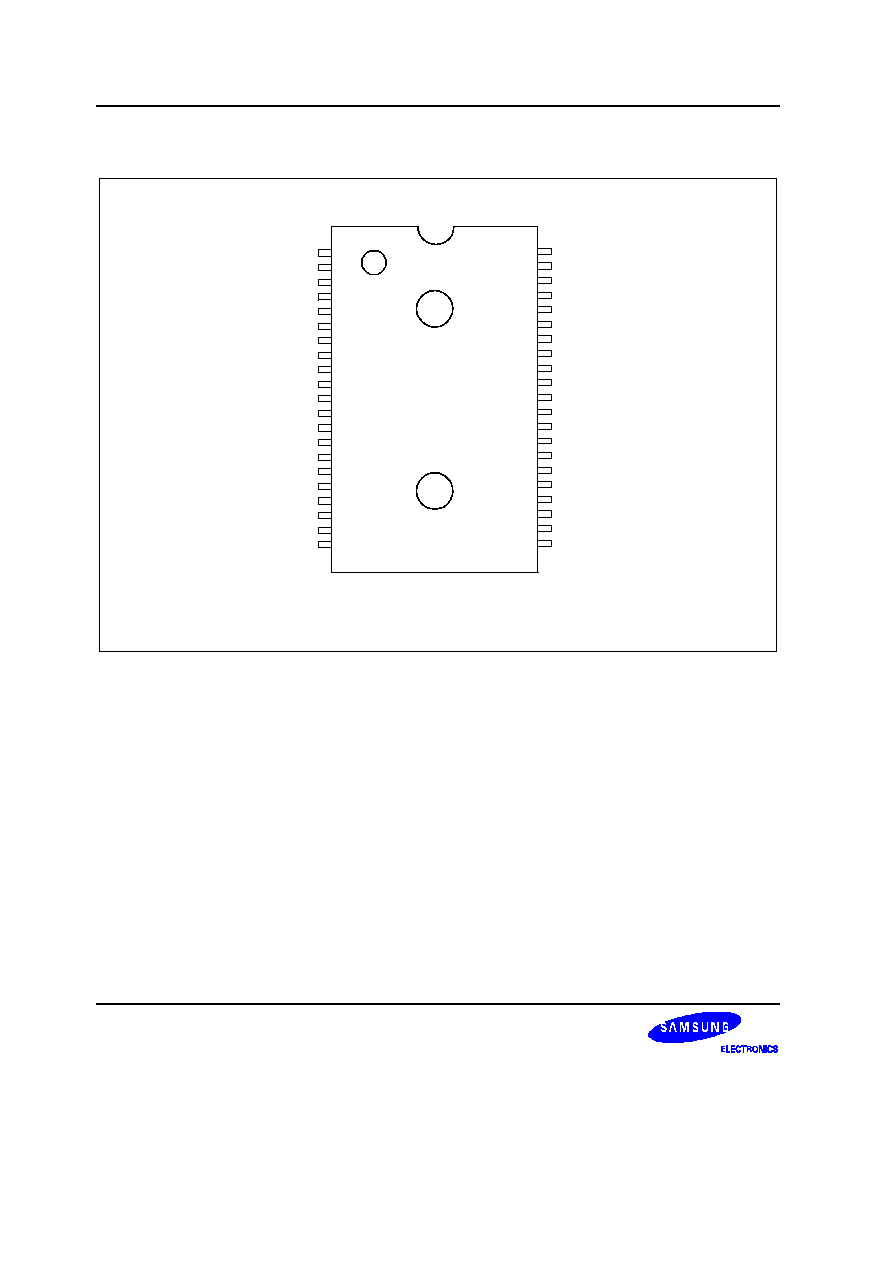
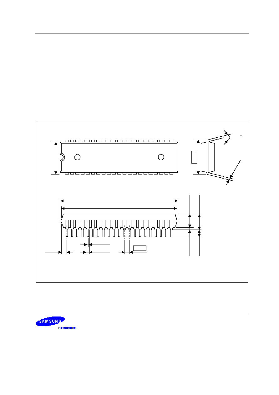
MECHANICAL DATA
20-1
20
MECHANICAL DATA
OVERVIEW
The S3C8639/C863A microcontroller is available in a 42-pin SDIP package (Samsung part number 42-SDIP-
600) and a 44-QFP package (Samsung part number 44-QFP-1010B).
NOTE: Dimensions are in millimeters.
39.50 MAX
39.10
±
0.2
0.50
±
0.1
1.778
(1.77)
0.51 MIN
3.30
±
0.3
3.50
±
0.2
5.08 MAX
42-SDIP-600
0-15
1.00
±
0.1
0.25
+ 0.1
- 0.05
15.24
14.00
±
0
.2
#42
#22
#21
#1
Figure 20-1. 42-Pin SDIP Package Mechanical Data (42-SDIP-600)
MECHANICAL DATA
S3C8639/C863A/P863A
20-2
44-QFP-1010B
#44
NOTE: Dimensions are in millimeters.
10.00
±
0.2
13.20
±
0.3
10.00
±
0.2
13.20
±
0.3
#1
0.35
+ 0.10
- 0.05
0.80
(1.00)
0.10 MAX
0.80
±
0.20
0.05 MIN
2.05
±
0.10
2.30 MAX
0.15
+ 0.10
- 0.05
0-8
Figure 20-2. 44-Pin QFP Package Mechanical Data (44-QFP-1010B)
S3C8639/C863A/P863A
S3P863A OTP
21-1
21
S3P863A OTP
OVERVIEW
The S3P863A single-chip CMOS microcontroller is the OTP (One Time Programmable)
version of the
S3C8639/C863A microcontrollers. It has an on-chip EPROM instead of masked ROM. The EPROM is accessed
by serial data format.
The S3P863A is fully compatible with the S3C8639/C863A, both in function and in pin configuration. Because of
its simple programming requirements, the S3P863A is ideal for use as an evaluation chip for the
S3C8639/C863A.
P0.0/INT0
P0.1/INT1
P0.2/INT2
P0.3
P0.4/TM0CAP
P0.5
P0.6
P0.7
SDAT/P1.0/SDA1
SCLK/P1.1/SCL1
V
DD1
V
SS
X
OUT
X
IN
V
PP
/TEST (GND)
SDA0
SCL0
RESET/RESET
P1.2
P2.0/PWM0
P2.1/PWM1
S3P863A
42-SDIP
(Top View)
1
2
3
4
5
6
7
8
9
10
11
12
13
14
15
16
17
18
19
20
21
P3.7
P3.6
P3.5
P3.4
P3.3/AD3
P3.2/AD2
P3.1/AD1
P3.0/AD0
V
DD2
V
SS2
P2.7/Csync-I (SOG)
Hsync-I
Vsync-I
Vsync-O
Hsync-O
Clamp-O
P2.6/PWM6
P2.5/PWM5
P2.4/PWM4
P2.3/PWM3
P2.2/PWM2
42
41
40
39
38
37
36
35
34
33
32
31
30
29
28
27
26
25
24
23
22
NOTE:
The bolds indicate an OTP pin name.
Figure 21-1. S3P863A Pin Assignments (42-SDIP Package)
S3P863A OTP
S3C8639/C863A/P863A
21-2
P0.5
P0.6
P0.7
SDAT/P1.0/SDA1
SCLK/P1.1/SCL1
V
DD1
V
SS1
X
OUT
X
IN
V
PP
/TEST (GND)
SDA0
S3P863A
44-QFP
(Top View)
1
2
3
4
5
6
7
8
9
10
11
P0.4/TM0CAP
P0.3
P0.2/INT2
P0.1/INT1
N.C.
P0.0/INT0
P3.7
P3.6
P3.5
P3.4
P3.3/AD3
44
43
42
41
40
39
38
37
36
35
34
P3.2/AD2
P3.1/AD1
P3.0/AD0
V
DD2
V
SS2
P2.7/Csync-I (SOG)
Hsync-I
Vsync-I
Vsync-O
Hsync-O
Clamp-O
33
32
31
30
29
28
27
26
25
24
23
SCL0
RESET
/
RESET
P1.2
P2.0/PWM0
P2.1/PWM1
P2.2/PWM2
N.C.
P2.3/PWM3
P2.4/PWM4
P2.5/PWM5
P2.6/PWM6
12
13
14
15
16
17
18
19
20
21
22
NOTE:
The bolds indicate an OTP pin name.
Figure 21-2. S3P863A Pin Assignments (44-QFP Package)
S3C8639/C863A/P863A
S3P863A OTP
21-3
Table 21-1. Descriptions of Pins Used to Read/Write the EPROM
Main Chip
During Programming
Pin Name
Pin Name
Pin No.
I/O
Function
P1.0
SDAT
9 (4)
I/O
Serial data pin. Output port when reading and input
port when writing. Can be assigned as a
Input/push-pull output port.
P1.1
SCLK
10 (5)
I
Serial clock pin. Input only pin.
TEST
V
PP
(TEST)
15 (10)
I
Power supply pin for EPROM cell writing (indicates
that OTP enters into the writing mode). When 12.5
V is applied, OTP is in writing mode and when 5 V
is applied, OTP is in reading mode. (Option)
RESET
RESET
18 (13)
I
Chip Initialization
V
DD1
/V
SS1
V
DD1
/V
SS1
11/12 (6/7)
I
Logic power supply pin. V
DD
should be tied to +5 V
during programming.
NOTE: Parentheses indicate 44-QFP OTP pin number.
Table 21-2. Comparison of S3P863A and S3C8639/C863A Features
Characteristic
S3P863A
S3C8639/C863A
Program Memory
48-Kbyte EPROM
32/48-Kbyte mask ROM
Operating Voltage (V
DD
)
3.0 V to 5.5 V
3.0 V to 5.5V
OTP Programming Mode
V
DD
= 5 V, V
PP
(TEST)=12.5V
Pin Configuration
42SDIP, 44QFP
42SDIP, 44QFP
EPROM Programmability
User Program 1 time
Programmed at the factory
OPERATING MODE CHARACTERISTICS
When 12.5 V is supplied to the V
PP
(TEST) pin of the S3P863A, the EPROM programming mode is entered. The
operating mode (read, write, or read protection) is selected according to the input signals to the pins listed in
Table 21-3 below.
Table 21-3. Operating Mode Selection Criteria
V
DD
V
PP
(TEST)
REG/MEM
Address (A15≠A0)
R/W
Mode
5 V
5 V
0
0000H
1
EPROM read
12.5 V
0
0000H
0
EPROM program
12.5 V
0
0000H
1
EPROM verify
12.5 V
1
0E3FH
0
EPROM read protection
NOTE: "0" means Low level; "1" means High level.

S3P863A OTP
S3C8639/C863A/P863A
21-4
D.C. ELECTRICAL CHARACTERISTICS
Table 21-4. D.C. Electrical Characteristics
(T
A
= ≠ 40
∞
C to + 85
∞
C, V
DD
= 3.0 V to 5.5 V)
Parameter
Symbol
Conditions
Min
Typ
Max
Unit
Input High
leakage current
I
LIH1
V
IN
= V
DD
All input pins except X
IN
,
X
OUT
≠
≠
3
µA
I
LIH2
V
IN
= V
DD
;
X
OUT
only
≠
≠
20
I
LIH3
V
IN
= V
DD
;
X
IN
only
2.5
6
20
Input Low
leakage current
I
LIL1
V
IN
= 0 V; All input pins except X
IN
,
X
OUT
,
RESET
, Hsync-I and Vsync-I
≠
≠
≠ 3
I
LIL2
V
IN
= 0 V; X
OUT
only
≠
≠
≠ 20
I
LIL3
V
IN
= 0 V; X
IN
only
≠ 2.5
≠ 6
≠ 20
Output High
leakage current
I
LOH1
V
OUT
= V
DD
≠
≠
3
Output Low
leakage current
I
LOL1
V
OUT
= 0 V
≠
≠
≠ 3
Pull-up resistor
R
U1
V
IN
= 0 V; V
DD
= 5 V
±
10%
Port 3.7≠3.4
20
47
80
k
R
U2
V
IN
= 0 V; V
DD
= 5 V
±
10%
RESET
only
150
280
480
Pull-down
resistor
R
D
V
IN
= 0 V; V
DD
= 5 V
±
10%
Hsync-I and Vsync-I
150
300
500
Supply current
(note)
I
DD1
V
DD
= 5 V
±
10%
Operation mode; 12 MHz crystal
C1 = C2 = 22pF
≠
10
20
mA
I
DD2
V
DD
= 5 V
±
10%
Idle mode; 12 MHz crystal
C1 = C2 = 22pF
4
8
I
DD3
V
DD
= 5 V
±
10%
Stop mode
100
150
µA
NOTE: Supply current does not include drawn internal pull-up/pull-down resistors and external loads of output.