 | –≠–ª–µ–∫—Ç—Ä–æ–Ω–Ω—ã–π –∫–æ–º–ø–æ–Ω–µ–Ω—Ç: S3P9664 | –°–∫–∞—á–∞—Ç—å:  PDF PDF  ZIP ZIP |

S3C9664/P9664 (Preliminary Spec)
PRODUCT OVERVIEW
1-1
1
PRODUCT OVERVIEW
SAM87RI PRODUCT FAMILY
Samsung's SAM88RCRI family of 8-bit single-chip CMOS microcontrollers offer fast and efficient CPU, a wide
range of integrated peripherals, and support OTP device.
A dual address/data bus architecture and bit- or nibble-configurable I/O ports provide a flexible programming
environment for applications with varied memory and I/O requirements. Timer/counters with selectable operating
modes are included to support real-time operations.
S3C9664 MICROCONTROLLER
The S3C9664 microcontroller with USB function can be used in a wide range of general purpose applications. It
is especially suitable for joystick, game pad controller or mouse and is available in 20-pin DIP, 24-pin SDIP and
20, 24-pin SOP. The S3C9664 single-chip 8-bit microcontroller is fabricated using an advanced CMOS process.
It is built around the powerful SAM88RCRI CPU core.
Stop and Idle power-down modes were implemented to reduce power consumption. To increase on-chip register
space, the size of the internal register file was logically expanded. The S3C9664 has 4 K bytes of program
memory on-chip, and 208 bytes of RAM including 16 bytes of working register. Using the SAM88RCRI design
approach, the following peripherals were integrated with the SAM88RCRI core:
-- Two configurable I/O ports (14 I/O pins on 20 pin package, 18 I/O pins on 24pin package)
-- Analog-to-digital converter with six input channel and 10-bit resolution
-- One 8-bit basic timer for watchdog function
-- One 8 bit timer/counter with three operating modes (Timer 0)
-- One 8 bit timer (Timer 1)
OTP
The S3C9664 microcontroller is also available in OTP (One Time Programmable) version, S3P9664. S3P9664
microcontroller has an on-chip 4 K byte one-time-programmable EPROM instead of masked ROM.
The S3P9664 is compatible to S3C9664, both in function and in pin configuration.

PRODUCT OVERVIEW
S3C9664/P9664 (Preliminary Spec)
1-2
FEATURES
CPU
∑
SAM88RCRI CPU core
Memory
∑
4-K byte internal program memory
∑
208-byte general purpose register area
∑
16 bytes of working register
Instruction Set
∑
41 instructions
∑
IDLE and STOP instructions added for power-
down modes
Instruction Execution Time
∑
0.66
µ
s at 6 MHz f
OSC
Interrupts
∑
28 interrupt sources and one vector (24 pins)
∑
24 interrupt sources and one vector (20 pin)
∑
One interrupt level
General I/O
∑
Three I/O ports (total 18 I/O pins at 24
SOP/SDIP)
∑
Three I/O ports (total 14 I/O pins at 20
SOP/DIP)
Timer/Counter
∑
One 8-bit basic timer for watchdog function
∑
One 8 bit timer/counter with three operating
modes(Match, capture, PWM)
∑
One 8-bit Timer
USB
∑
Compatible to USB low speed (1.5 Mbps) device
1.1 specification.
∑
Serial bus interface engine (SIE)
-- Packet decoding/generation
-- CRC generation and checking
-- NRZI encoding/decoding and bit-stuffing
∑
Two 8-byte receive/transmit USB buffer
A/D Converter
∑
Six analog input pins
∑
10-bit conversion resolution
Low Voltage Reset
∑
Low voltage reset
∑
Power on Reset
Sub Oscillator
∑
Internal RC sub oscillator
∑
Auto interrupt wake-up
Oscillator Frequency
∑
6 MHz crystal/ceramic oscillator
∑
External clock source (6 MHz)
Operating Temperature Range
∑
≠ 40
∞
C to + 85
∞
C
Operating Voltage Range
∑
4.0 V to 5.25 V
Package Types
∑
24-pin SOP/SDIP
∑
20-pin SOP/DIP

S3C9664/P9664 (Preliminary Spec)
PRODUCT OVERVIEW
1-3
BLOCK DIAGRAM
SAM88RCRI CPU
Port I/O and
Interrupt Control
4K ROM
208 Byte
RAM
TEST
RESET
NOTES:
1. 24 SOP/SDIP
2. 20 SOP/DIP
Timer 1
X
IN
X
OUT
OSC
SUB
OSC
Basic
Timer
Timer 0
Port 0
USB
SIE
D+/INT2
D-/INT2
P0.2/INT0
P0.3/INT0
P0.4/INT0
P0.5/INT0
P0.0/INT0/T0
P0.1/INT0
P0.6/INT0
P0.7/INT0
P1.7/INT1
P1.8/INT1
P1.2/INT1/ADC2
P1.3/INT1/ADC3
P1.4/INT1/ADC4
P1.5/INT1/ADC5
P1.0/INT1/ADC0
P1.1/INT1/ADC1
Port 1/
AD
Converter
Figure 1-1. Block Diagram
PRODUCT OVERVIEW
S3C9664/P9664 (Preliminary Spec)
1-4
PIN ASSIGNMENTS
V
SS
X
OUT
X
IN
TEST
P0.0/INT0/T0 (CAP/PWM)
P0.1/INT0
RESET
P0.2/INT0
P0.3/INT0
P0.4/INT0
S3C9664
(20-SOP-300)
(20-DIP-300)
1
2
3
4
5
6
7
8
9
10
V
DD
D-/P2.0/INT2
D+/P2.1/INT2
P1.0/AD0/INT1
P1.1/AD1/INT1
P1.2/AD2/INT1
P1.3/AD3/INT1
P1.4/AD4/INT1
P1.5/AD5/INT1
P0.5/INT0
20
19
18
17
16
15
14
13
12
11
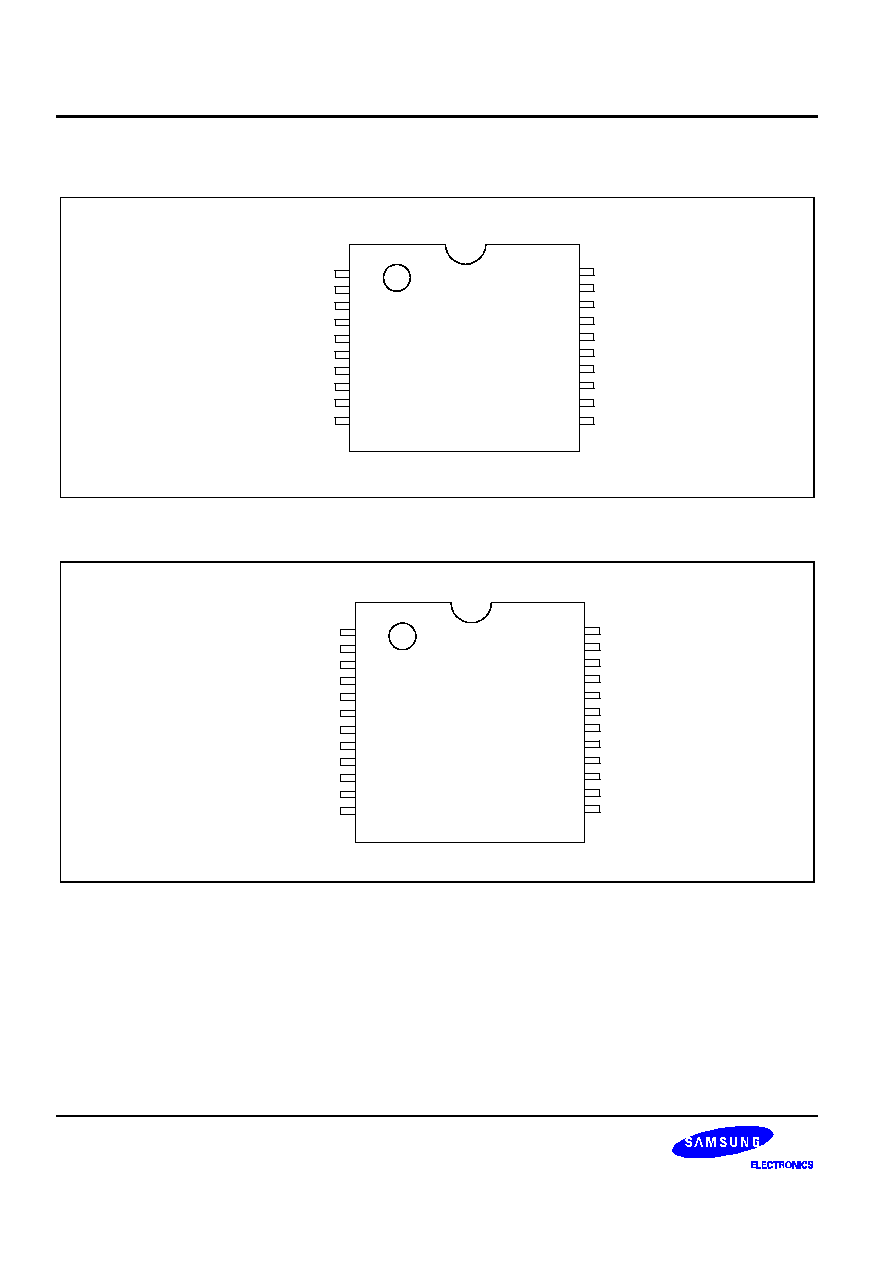
Figure 1-2. Pin Assignment (20 Pin)
V
SS
X
OUT
X
IN
TEST
P0.0/INT0/T0 (CAP/PWM)
P0.1/INT0
RESET
P0.2/INT0
P0.3/INT0
P0.4/INT0
P0.6/INT0
P0.7/INT0
S3C9664
(24-SOP-300)
(24-SDIP-300)
1
2
3
4
5
6
7
8
9
10
11
12
24
23
22
21
20
19
18
17
16
15
14
13
V
DD
D-/P2.0/INT2
D+/P2.1/INT2
P1.0/AD0/INT1
P1.1/AD1/INT1
P1.2/AD2/INT1
P1.3/AD3/INT1
P1.4/AD4/INT1
P1.5/AD5/INT1
P0.5/INT0
P1.6/INT1
P1.7/INT1
Figure 1-3. Pin Assignment (24 Pin)
S3C9664/P9664 (Preliminary Spec)
PRODUCT OVERVIEW
1-5
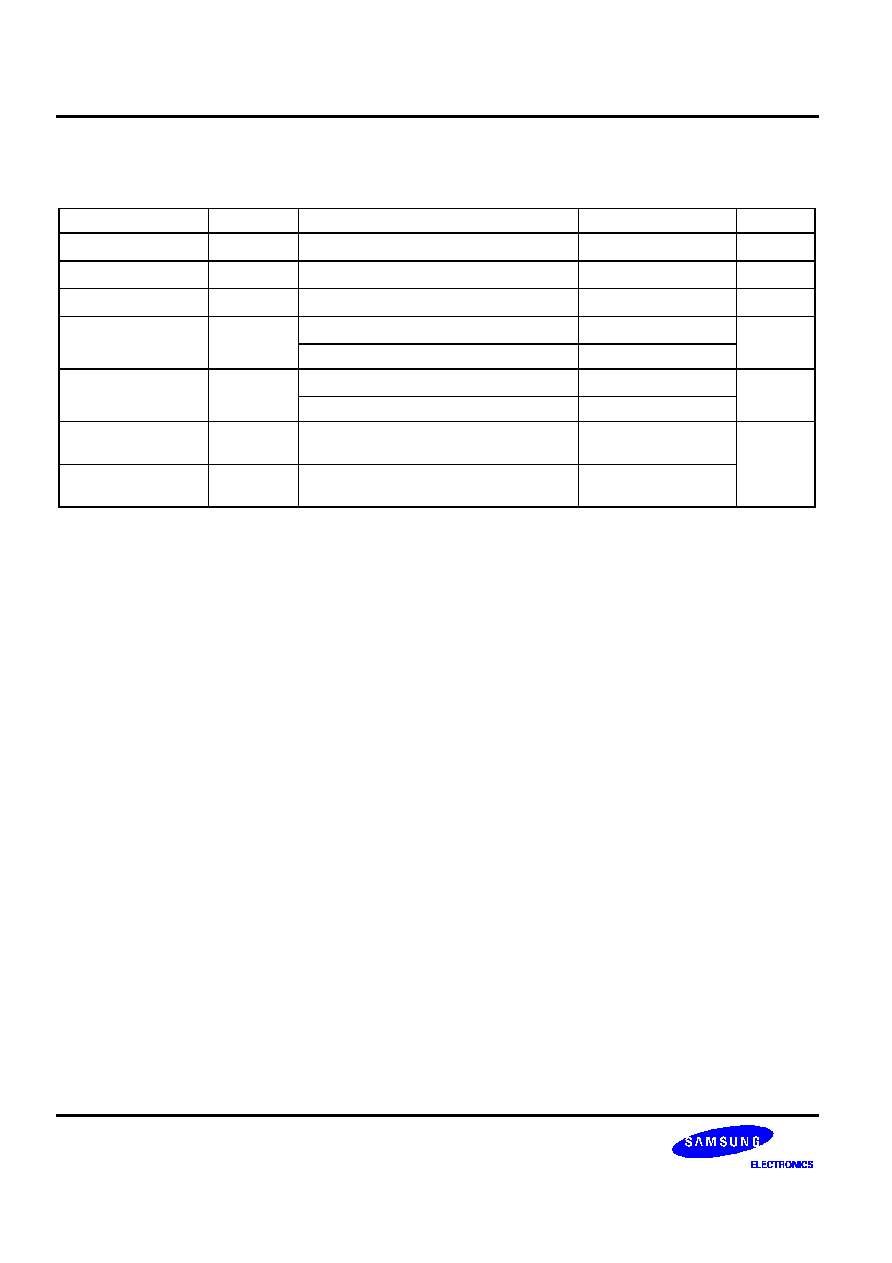
Table 1-1. Pin Descriptions
Pin
Name
In/Out
Pin
Description
Pin
Type
Pin
Numbers
Share
Pins
P0.0≠
P0.7
I/O
Bit-programmable I/O port for Schmitt trigger input ,
push-pull output and N-Ch open drain output.
Pull-up/ pull-down resistors are assignable by
software. Port1 pins can also be used as external
interrupt.
G
5,6,8≠11
(5,6,8≠12,15)
T0, INT0
P1.0-
P1.5
I/O
Bit-programmable I/O port for Schmitt trigger input,
Schmitt trigger input with pull-up and N-Ch open
drain output.
Port1 pins can also be used as A/D converter
Channel.
F
12≠17
(16≠21)
AD0≠5
INT1
P1.6-
P1.7
I/O
Bit-programmable I/O port for Schmitt trigger input ,
Schmitt trigger input with pull-up and N-Ch open
drain output and Push-pull output.
E
(13≠14)
INT1
P2.0/D≠
≠
P2.1/D+
I/O
Bit-programmable I/O port for Schmitt trigger input ,
Schmitt trigger input with pull-up and N-Ch open
drain output and Push-pull output. Port 2 can be
individually configured as external interrupt inputs.
Also it can be configured as an USB ports
E
18≠19
(22≠23)
INT2
X
IN
,
X
OUT
≠
Crystal/ceramic oscillator signal for system clock.
≠
2≠3 (2≠3)
≠
RESET
I
System reset signal input pin.
B
7 (7)
≠
TEST
I
Test signal input pin(for factory use only; muse be
connected to V
SS
)
≠
4 (4)
≠
V
DD
,V
SS
≠
Voltage input pin and ground
≠
1,20 (1,24)
≠
T0
I/O
Timer 0 capture input or PWM output pin
G
6 (6)
P0.0
INT0
I
External interrupt input
G
5,6,8≠11
(5,6,8≠12,15)
P0.0≠P0.7
INT1
I
External interrupt input
F,E
12≠17
(13≠14, 16≠21)
P1.0≠P1.7
INT2
I
External interrupt input
E
18≠19
P2.0≠P2.1
AD0≠
AD5
I
A/D converter input
F
12≠17
(16≠21)
P1.0≠P1.5
NOTE: Pin numbers show in parentheses "( )" are for the 24-pin package
PRODUCT OVERVIEW
S3C9664/P9664 (Preliminary Spec)
1-6
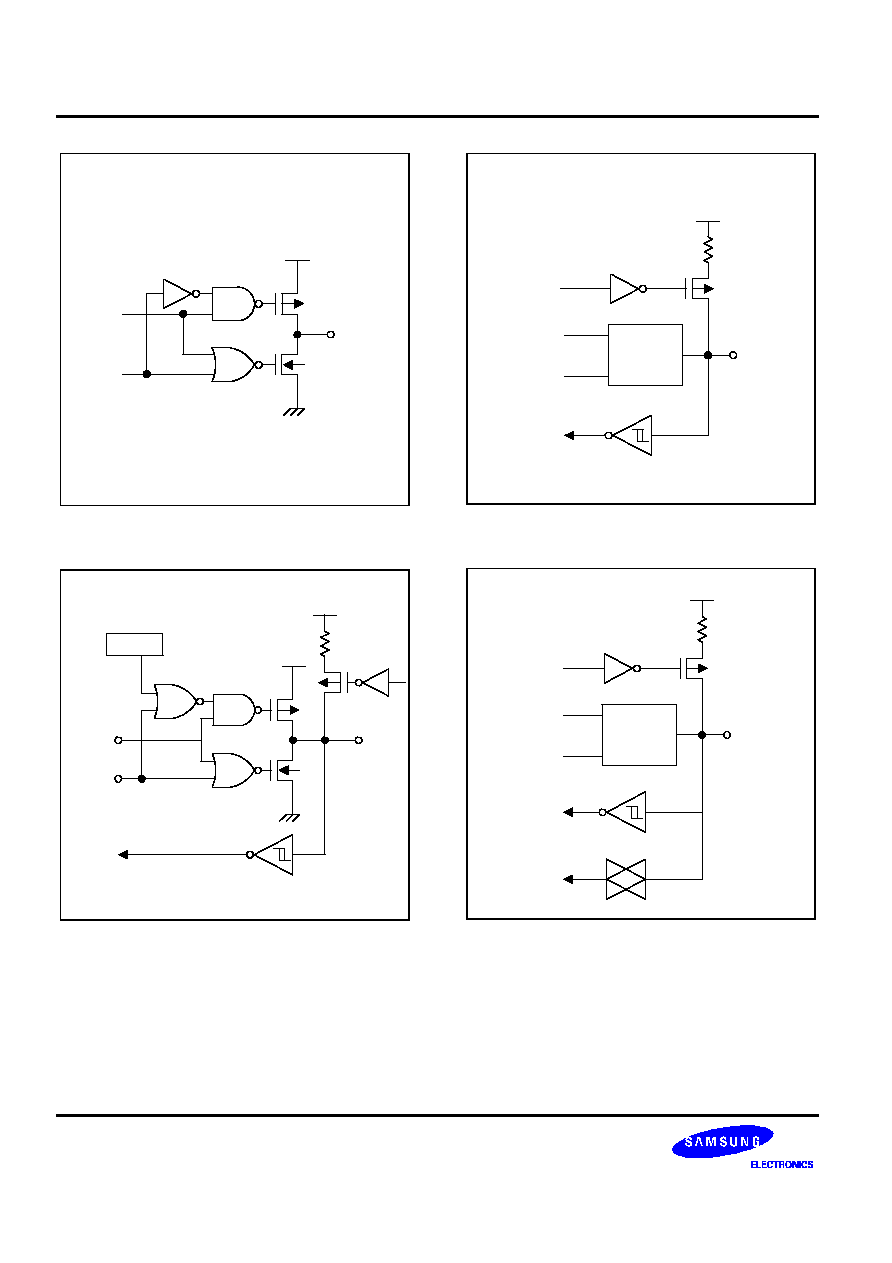
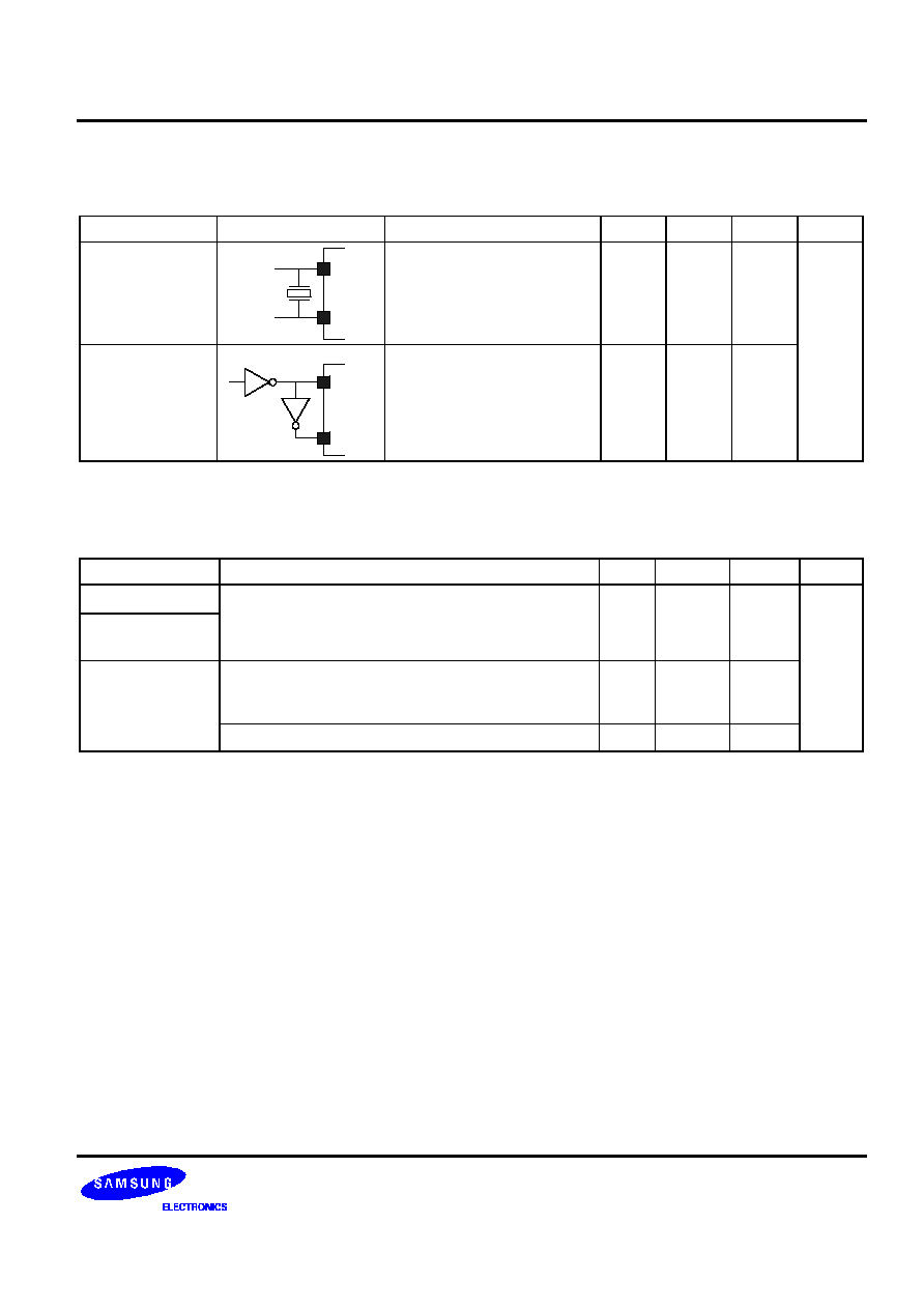
P-Channel
N-Channel
V
DD
Out
Output
DIsable
Data
Figure 1-4. Pin Circuit Type C
V
DD
Pull-up
Enable
V
DD
In/Out
PNE
Output
Disable
Data
47 K
Figure 1-6. Pin Circuit Type E
I/O
Output
DIsable
Data
Circuit
Type C
Pull-up
Enable
V
DD
Data
Figure 1-5. Pin Circuit Type D
Circuit
Type C
V
DD
Output
DIsable
Data
Pull-up
Enable
Data
To ADC
In/Out
47 K
Figure 1-7. Pin Circuit Type F
S3C9664/P9664 (Preliminary Spec)
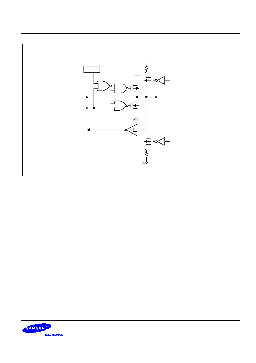
PRODUCT OVERVIEW
1-7
V
DD
V
DD
In/Out
PNE
Output
Disable
Data
Pull-up
Enable
47 K
Pull-down
Enable
47 K
Figure 1-8. Pin Circuit Type G

S3C9664/P9664 (Preliminary Spec)
ELECTRICAL DATA
16-1
16
ELECTRICAL DATA
OVERVIEW
In this section, the following S3C9664 electrical characteristics are presented in tables and graphs:
-- Absolute maximum ratings
-- D.C. electrical characteristics
-- I/O capacitance
-- A.C. electrical characteristics
-- Oscillator characteristics
-- Operating voltage range
-- Oscillation stabilization time
-- Clock timing measurement points at X
IN
-- Data retention supply voltage in Stop mode
-- Stop mode release timing when initiated by a
RESET
-- Stop mode release timing when initiated by an external interrupt
-- Characteristic curves
-- AD Converter Electrical Characteristics
ELECTRICAL DATA
S3C9664/P9664 (Preliminary Spec)
16-2
Table 16-1. Absolute Maximum Ratings
(T
A
= 25
∞
C)
Parameter
Symbol
Conditions
Rating
Unit
Supply voltage
V
DD
≠
≠ 0.3 to + 6.5
V
Input voltage
V
I
All ports
≠ 0.3 to V
DD
+ 0.3
V
Output voltage
V
O
All output ports
≠ 0.3 to V
DD
+ 0.3
V
Output current high
I
OH
One I/O pin active
≠ 18
mA
All I/O pins active
≠ 60
Output current low
I
OL
One I/O pin active
+ 30
mA
Total pin current for ports 0, 1, 2
+ 100
Operating
temperature
T
A
≠
0 to + 85
∞
C
Storage
temperature
T
STG
≠
≠ 60 to + 150

S3C9664/P9664 (Preliminary Spec)
ELECTRICAL DATA
16-3
Table 16-2. D.C. Electrical Characteristics
(T
A
= ≠ 40
∞
C to + 85
∞
C, V
DD
= 4.0 V to 5.25 V)
Parameter
Symbol
Conditions
Min
Typ
Max
Unit
Input highvoltage
V
IH1
All input pins except V
IH2,
D+, D≠
0.8 V
DD
≠
V
DD
V
V
IH2
X
IN
V
DD
≠ 0.5
V
DD
Input low voltage
V
IL1
All input pins except V
IL2,
D+, D≠
≠
≠
0.2 V
DD
V
IL2
X
IN
≠
≠
0.4
Output high voltage
V
OH
V
DD
= 4.0 V ≠ 5.25 V
I
OH
= ≠ 200 mA
All output ports except D+, D≠
V
DD
≠ 1.0
≠
≠
Output low voltage
V
OL
V
DD
= 4.0 V ≠ 5.25 V
I
OL
= 2 mA
All output ports except D+, D≠
≠
≠
0.4
Input high leakage
current
I
LIH1
V
IN
= V
DD
All inputs except I
LIH2
except D+, D≠, X
OUT
≠
≠
3
µA
I
LIH2
V
IN
= V
DD,
X
IN
≠
≠
20
Input low leakage
current
I
LIL1
V
IN
= 0 V
All inputs except I
LIL2
except D+, D≠, X
OUT
≠
≠
≠ 3
I
LIL2
V
IN
= 0 V,
X
IN
≠
≠
≠ 20
Output high leakage
current
I
LOH
V
OUT
= V
DD
All output pins except D+, D≠
≠
≠
3
Output low leakage
current
I
LOL
V
OUT
= 0 V
All output pins except D+, D≠
X
OUT
≠
≠
≠ 3
Pull-up resistors
R
L1
V
IN
= 0 V, V
DD
= 5.0 V,
Port 0, Port 1,Port2
25
50
100
K
R
L2
V
IN
= 0 V, V
DD
= 5.0 V,
RESET only
100
220
400
Pull-down resistors
R
L3
V
IN
= 0 V, V
DD
= 5.0 V,
Port 0
25
50
100
K
Supply current
I
DD1
Normal operation mode,
V
DD
= 5 V
±
10 %,
6 MHz, CPU clock
≠
6.5
15
mA
I
DD2
IDLE mode
V
DD
= 5 V
±
10 %,
6 MHz, CPU clock
≠
4
8
I
DD3
Stop mode, oscillator stop
V
DD
= 5 V
±
10 %,
≠
150
300
µA
NOTES:
1.
Supply current does not include current drawn through internal pull-up resistors or external output current load.
2.
This parameter is guaranteed, but not tested (include D+, D≠).
3.
Only in 4.0 V to 5.25 V, D+ and D≠ satisfy the USB spec 1.1.
ELECTRICAL DATA
S3C9664/P9664 (Preliminary Spec)
16-4
Table 16-3. Input/Output Capacitance
(T
A
= 0
∞
C to + 85
∞
C, V
DD
=
0 V)
Parameter
Symbol
Conditions
Min
Typ
Max
Unit
Input
capacitance
C
IN
f = 1 MHz; unmeasured pins
are connected to V
SS
≠
≠
10
pF
Output
capacitance
C
OUT
I/o capacitance
C
IO
expect X
IN
, X
OUT
XI/XO capacitance
C
XI
, C
XO
X
IN
, X
OUT
33
Table 16-4. A.C. Electrical Characteristics
(T
A
= ≠ 40
∞
C to + 85
∞
C, V
DD
= 4.0 V to 5.25 V)
Parameter
Symbol
Conditions
Min
Typ
Max
Unit
Noise filter
t
NF1H
, t
NF1L
P1 (RC delay)
100
≠
200
ns
0.8 V
DD
0.2 V
DD
t
NF1L
t
NF1H
0.5 V
DD
t
NF2
Figure 16-1. Input Timing for External Interrupts
S3C9664/P9664 (Preliminary Spec)
ELECTRICAL DATA
16-5
Table 16-5. Oscillator Characteristics
(T
A
= 0
∞
C + 85
∞
C)
Oscillator
Clock Circuit
Test Condition
Min
Typ
Max
Unit
Main crystal Main
ceramic
(f
OSC
)
X
IN
X
OUT
Oscillation frequency
V
DD
= 4.0 V ≠ 5.25 V
≠
6.0
≠
MHz
External clock
X
IN
X
OUT
Oscillation frequency
V
DD
= 4.0 V ≠ 5.25 V
≠
6.0
≠
Table 16-6. Oscillation Stabilization Time
(T
A
= 0
∞
C + 85
∞
C, V
DD
= 4.0 V to 5.25 V)
Oscillator
Test Condition
Min
Typ
Max
Unit
Main crystal
V
DD
= 4.0 V to 5.25 V, f
OSC
> 6.0 MHz
≠
≠
10
ms
Main ceramic
(Oscillation stabilization occurs when V
DD
is equal to
the minimum oscillator voltage range.)
Oscillator
stabilization wait
time
t
WAIT
stop mode release time by a reset
≠
2
16
/f
OSC
≠
t
WAIT
stop mode release time by an interrupt
≠
≠
≠
NOTE: The oscillator stabilization wait time, tWAIT, when it is released by an interrupt, is determined by the setting in the
basic timer control register, BTCON.

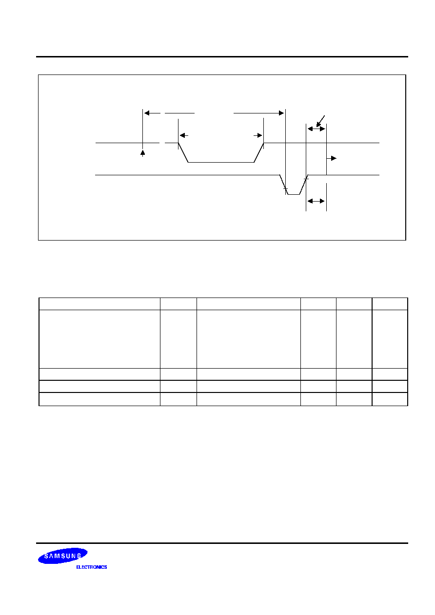
ELECTRICAL DATA
S3C9664/P9664 (Preliminary Spec)
16-6
0.4 V
t
XL
t
XH
X
IN
1/f
OSC
V
DD
- 0.5 V
Figure 16-2. Clock Timing Measurement Points at X
IN
Table 16-7. Data Retention Supply Voltage in Stop Mode
(T
A
= 0
∞
C to + 70
∞
C)
Parameter
Symbol
Conditions
Min
Typ
Max
Unit
Data retention
supply voltage
V
DDDR
Stop mode
2.0
≠
6
V
Data retention
supply current
I
DDDR
Stop mode; V
DDDR
= 2.0 V
≠
≠
5
µA
S3C9664/P9664 (Preliminary Spec)
ELECTRICAL DATA
16-7
Data Retention Mode
~
~ ~
V
DDDR
Execution Of
Stop Instrction
V
DD
Normal
Operating
Mode
IDLE Mode
(Basic Timer Active)
~
Stop Mode
t
WAIT
0.8 V
DD
0.2 V
DD
External
Interrupt
Figure 16-3. Stop Mode Release Timing When Initiated by an External Interrupt
Table 16-8. Low Speed Source Electrical Characteristics (USB)
(T
A
= 0
∞
C to + 85
∞
C, Voltage Regulator Output V
33OUT
= 2.8 V to 3.5 V, typ 3,3 V)
Parameter
Symbol
Conditions
Min
Max
Unit
Transition Time:
Rise Time
Tr
CL = 200 pF
75
≠
ns
CL = 650 pF
≠
300
Fall Time
Tf
CL = 200 pF
75
≠
CL = 650 pF
≠
300
Rise/Fall Time Matching
Trfm
(Tr/Tf) CL = 50 pF
80
125
%
Output Signal Crossover Voltage
Vcrs
CL = 50 pF
1.3
2.0
V
Output Voltage Regulator Built-in
V
33OUT
V
DD
= 4.0≠5.25 V
2.8
3.6
V

ELECTRICAL DATA
S3C9664/P9664 (Preliminary Spec)
16-8
R1 = 15 K
R2 = 1.5 K
CL = 200 pF - 650 pF
DM: S/W ON
DP: S/W OFF
D. U. T
Test
Point
S/W
V
33OUT
R2
R1
C2
90 %
Measurement
Points
10 %
90 %
10 %
Tr
Tf
Figure 16-4. USB Data Signal Rise and Fall Time
DM
DP
V
CRS
MAX: 2.0 V
MIN: 1.3 V
3.3 V
0 V
Figure 16-5. USB Output Signal Crossover Point Voltage
S3C9664/P9664 (Preliminary Spec)
ELECTRICAL DATA
16-9
Table 16-9. A/D Converter Electrical Characteristics
(T
A
= ≠ 40
∞
C to + 85
∞
C, V
DD
= 4.2 V to 5.25 V, V
SS
= 0 V) S3C9664/P9664: 10-bit ADC
Parameter
Symbol
Test Conditions
Min
Typ
Max
Unit
Total accuracy
V
DD
= 5.12 V
CPU clock = 10 MHz
V
DD
= 5.12 V
V
SS
= 0 V
≠
≠
±
3
LSB
Integral linearity
error
ILE
≠
≠
±
2
Differential
linearity error
DLE
≠
≠
±
1
Offset error of
top
EOT
≠
≠ 1
±
3
Offset error of
bottom
EOB
≠
≠ 1
±
2
Conversion
time
(1)
t
CON
fcpu = 10 MHz
≠
50x4/ f
OSC
≠
µ
s
Analog input
voltage
V
IAN
≠
V
SS
≠
V
DD
V
Analog input
impedance
R
AN
≠
2
≠
≠
M
Analog input
current
I
ADIN
V
DD
= 5 V
≠
≠
10
µ
A
ADC block
I
ADC
V
DD
= 5 V
≠
1
3
mA
current
(2)
V
DD
= 5 V
Power down mode
≠
100
500
nA
NOTES:
1.
`Conversion time' is the time required from the moment a conversion operation starts until it ends.
2.
I
ADC
is operating current during A/D conversion.
S3C9664/P9664 (Preliminary Spec)
MECHANICAL DATA
17-1
17
MECHANICAL DATA
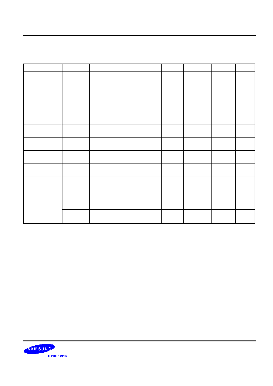
OVERVIEW
This section contains the following information about the device package:
-- Package dimensions in millimeters
-- Pad diagram
NOTE: Dimensions are in millimeters.
26.80 MAX
26.40
± 0.20
(1.77)
20-DIP-300A
6.40
±
0
.20
#20
#1
0.46
±
0.10
1.52
±
0.10
#11
#10
0-15
0.25
+ 0.10- 0.05
7.62
2.54
0.51 MIN
3.30
± 0.30
3.25
±
0.20
5.08 MAX
Figure 17-1. 20-DIP-300A Package Dimensions

MECHANICAL DATA
S3C9664/P9664 (Preliminary Spec)
17-2
NOTE: Dimensions are in millimeters.
20-SOP-300
7.80
±
0
.30
#11
#20
#1
#10
14.10 MAX
13.70
± 0.20
(1.14)
0-8
0.20
+ 0.10
- 0.05
7.62
5.40
±
0.20
0.64
±
0.20
0.05 MIN
1.70
±
0.10
2.00 MAX
0.40
0.10 MAX
+ 0.10
- 0.05
1.27
Figure 17-2. 20-SOP-300 Package Dimensions

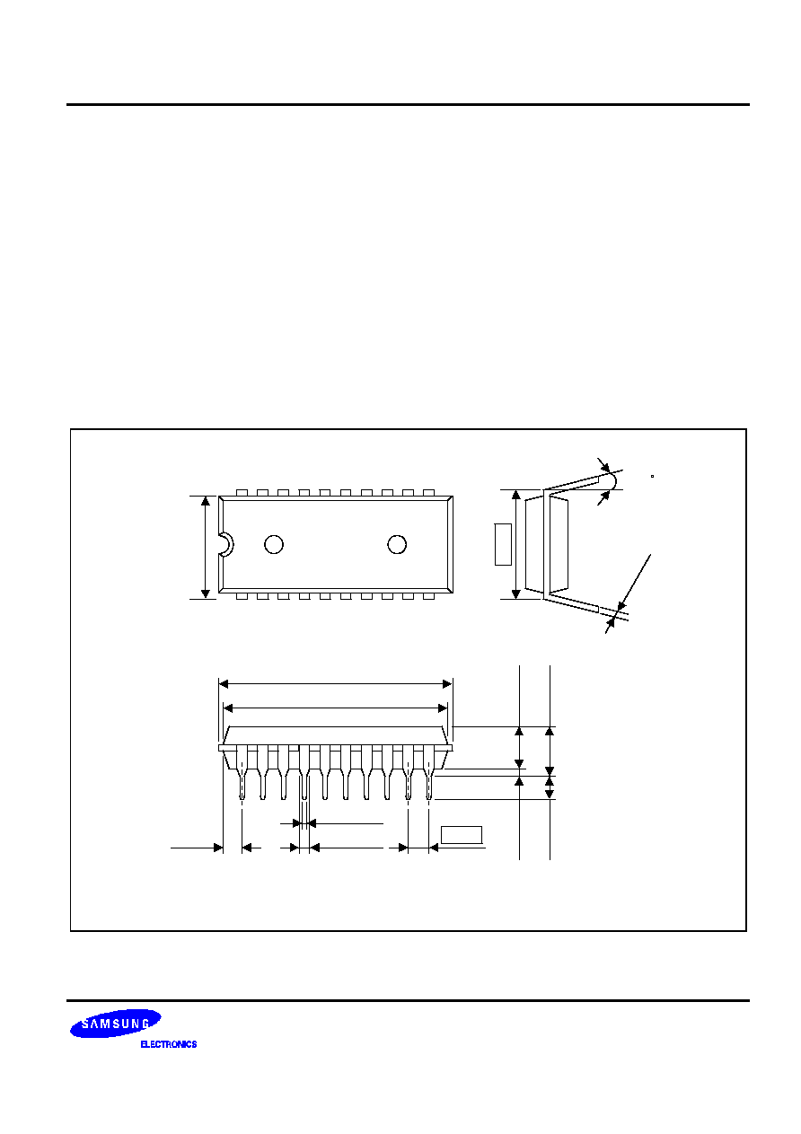
S3C9664/P9664 (Preliminary Spec)
MECHANICAL DATA
17-3
NOTE: Dimensions are in millimeters.
23.35 MAX
22.95
± 0.20
(1.70)
24-SDIP-300
6.40
±
0
.20
#24
#1
0.46 ±
0.10
0.89 ±
0.10
#13
#12
0-15
0.25
+ 0.10- 0.05
7.62
3.25
±
0.20
5.08 MAX
1.778
0.51 MIN
3.30
± 0.30
Figure 17-3. 24-SDIP-300 Package Dimensions

MECHANICAL DATA
S3C9664/P9664 (Preliminary Spec)
17-4
NOTE: Dimensions are in millimeters.
24-SOP-300
7.90
±
0
.30
#13
#24
#1
#12
15.60 MAX
15.20
± 0.20
0-8
0.20
+ 0.10
- 0.05
7.62
5.30
±
0.20
0.60
±
0.20
0.05 MIN
1.75
±
0.10
2.00 MAX
0.45
0.10 MAX
+ 0.10
- 0.05
1.27
Figure 17-4. 24-SOP-300 Package Dimensions
S3C9664/P9664 (Preliminary Spec)
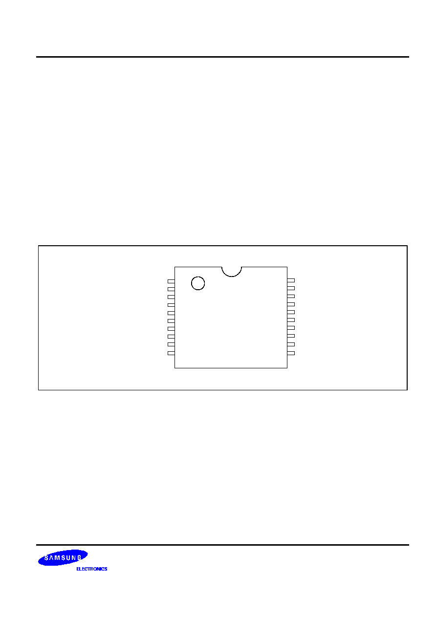
S3P9664 OTP
18-1
18
S3P9664 OTP
OVERVIEW
The S3C9664 single-chip CMOS microcontroller is the OTP (One Time Programmable)
version of the S3C9664
microcontroller. It has an on-chip OTP ROM instead of masked ROM. The EPROM is accessed by serial data
format.
The S3P9664 is fully compatible with the S3C9664, both in function and in pin configuration. Because of its
simple programming requirements, the S3P9664 is ideal for use as an evaluation chip for the S3C9664.
V
SS
/V
SS
X
OUT
X
IN
TEST/TEST
P0.0/INT0/T0 (CAP/PWM)
P0.1/INT0
RESET
RESET/RESET
P0.2/INT0
P0.3/INT0
P0.4/INT0
S3P9664
(20-SOP-300)
(20-DIP-300)
1
2
3
4
5
6
7
8
9
10
V
DD
/V
DD
D-/P2.0/INT2/SCLK
D+/P2.1/INT2/SDAT
P1.0/AD0/INT1
P1.1/AD1/INT1
P1.2/AD2/INT1
P1.3/AD3/INT1
P1.4/AD4/INT1
P1.5/AD5/INT1
P0.5/INT0
20
19
18
17
16
15
14
13
12
11
Figure 18-1. S3P9664 Pin Assignments (20-Pin Package)
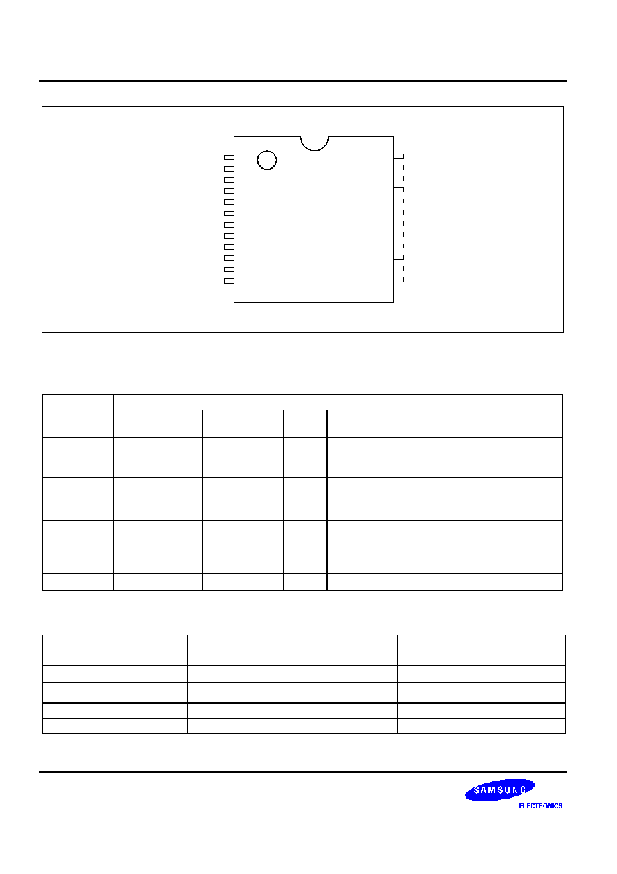
S3P9664 OTP
S3C9664/P9664 (Preliminary Spec)
18-2
V
SS
/V
SS
X
OUT
X
IN
TEST/TEST
P0.0/INT0/T0 (CAP/PWM)
P0.1/INT0
RESET
RESET/RESET
P0.2/INT0
P0.3/INT0
P0.4/INT0
P0.6/INT0
P0.7/INT0
S3P9664
(24-SOP-300)
(24-SDIP-300)
1
2
3
4
5
6
7
8
9
10
11
12
24
23
22
21
20
19
18
17
16
15
14
13
V
DD
/V
DD
D-/P2.0/INT2/SCLK
D+/P2.1/INT2/SDAT
P1.0/AD0/INT1
P1.1/AD1/INT1
P1.2/AD2/INT1
P1.3/AD3/INT1
P1.4/AD4/INT1
P1.5/AD5/INT1
P0.5/INT0
P1.6/INT1
P1.7/INT1
Figure 18-2. S3P9664 Pin Assignments (24-Pin Package)
Table 18-1. Descriptions of Pins Used to Read/Write the EPROM
Main Chip
During Programming
Pin Name
Pin Name
Pin No.
(24 DIP)
I/O
Function
P1.0
SDAT
23
I/O
Serial Data Pin (Output when reading, Input
when writing) Input and Push-pull Output Port
can be assigned
P1.1
SCLK
22
I/O
Serial Clock Pin (Input Only Pin)
TEST
V
PP
(TEST)
5
I
0V : OTP write and test mode
5V : Operating mode
RESET
RESET
8
I
Chip Initialization and EPROM Cell Writing
Power Supply Pin (Indicates OTP Mode
Entering) When writing 12.5V is applied and
when reading.
V
DD
/V
SS
V
DD
/V
SS
24/1
I
Logic Power Supply Pin.
Table 18-2. Comparison of S3P9664 and S3C9664 Features
Characteristic
S3P9664
S3C9664
Program Memory
4 K byte EPROM
4 K byte mask ROM
Operating Voltage (V
DD
)
4.0 V to 5.25 V
4.0 V to 5.25 V
OTP Programming Mode
V
DD
= 5 V, V
PP
(
RESET
) =12.5V
Pin Configuration
20 SOP/20 DIP/24 SOP/24 SDIP
20 SOP/20 DIP/24 SOP/24SDIP
EPROM Programmability
User Program 1 time
Programmed at the factory