 | –≠–ª–µ–∫—Ç—Ä–æ–Ω–Ω—ã–π –∫–æ–º–ø–æ–Ω–µ–Ω—Ç: S5C7332A | –°–∫–∞—á–∞—Ç—å:  PDF PDF  ZIP ZIP |

KS7332
1
INTRODUCTION
PRODUCT SUMMARY
KS7332 is a digital image signal handling IC aimed at improving image contrast and
counter light correction, applicable to CCD-using video camera systems such as
camcorders and surveillance cameras. KS7332 receives the CCD output as digital
data, analyzes the image's luminance distribution, then outputs a signal with
improved dynamic range of luminance and color difference. It also uses a spatial
adaptive filter to remove low intensity noise and output a stable image.
FEATURES
∑
NTSC/PAL, Normal/Hiband, DVC compatible
∑
10-bit A/D input
∑
Digital clamp
∑
WDR expansion using non-linear histogram modification
∑
Look up table (LUT) transform using line memory
∑
S1, S2 signals' HUE component correction by look-up-table transform
∑
Built-in memory for histogram storage
∑
Image analysis with histogram LOG function as reference
∑
Color sensitivity correction
∑
Serial micom interface
∑
Built-in operation for connection with AE
∑
10-bit S1, S2 signal output for DCP I/F
∑
Spatial adaptive noise removal filter for low intensity images
∑
Interpretation of image characteristic through graphic OSD
MANUFACTURING PROCESS AND PACKAGE
Manufacturing process: 0.35 um silicon gate 3 metals 3.3V CMOS (CSP7L)
APPLICATIONS
∑
Camcorder system
∑
Surveillance camera, PC camera
48-LQFP-0707

KS7332
2
PIN DIAGRAM
Figure 1. Pin Diagram
KS7332
T
S
T
O
T
S
T
I
G
N
D
H
D
1
2
N
D
0
S
C
A
N
E
N
H
I
G
H
P
A
L
D
V
C
V
D
D
M
D
S
E
L
1
M
D
S
E
L
0
V
D
V
1
H
D
V
D
D
C
L
K
R
S
T
N
S
M
I
S
C
L
K
S
C
S
N
G
N
D
S
M
0
M
S
B
SO9
SO8
GND
SO7
SO6
SO5
SO4
SO3
SO2
VDD
SO1
SO0
SI9
SI8
VDD
SI7
SI6
SI5
SI4
SI3
SI2
GND
SI1
SI0
37
38
39
40
41
42
43
44
45
46
47
48
24
23
22
21
20
19
18
17
16
15
14
13
3
6
3
5
3
4
3
3
3
2
3
1
3
0
2
9
2
8
2
7
2
6
2
5
1
2
3
4
5
6
7
8
9
1
0
1
1
1
2

KS7332
3
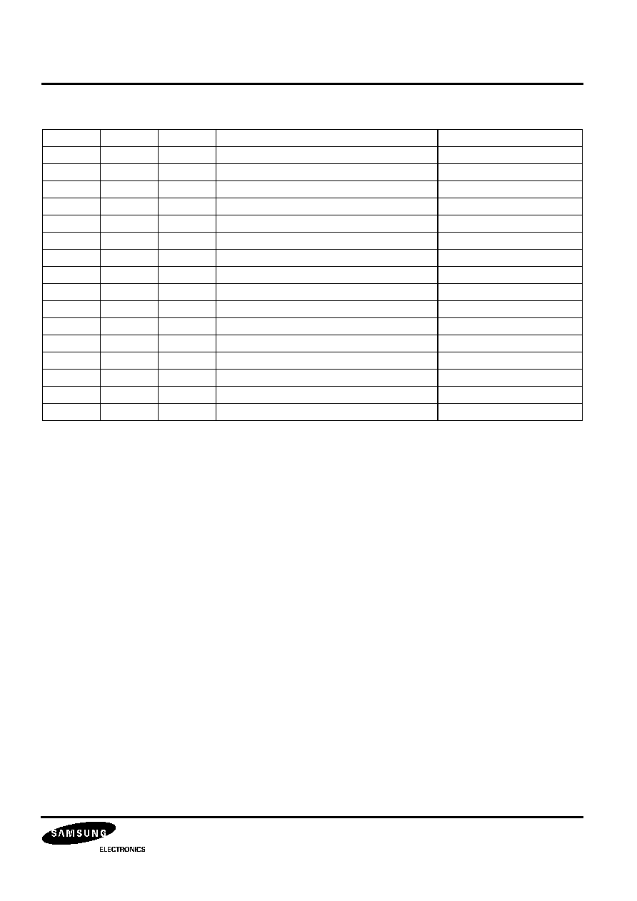
PIN DESCRIPTION
Table 1. Pin Description
No
Name
I/O
Description
Note
1
VD
I
Vertical driving pulse
CCD
2
V1
I
Vertical transfer pulse
3
HD
I
horIzontal driving pulse
4
VDD
P
Power
3.3 V
5
CLK
I
System clock
ADCK (KS7331)
6
RSTN
I
System reset
7
SMI
I
Serial data input from system micom
8
SCLK
I
System micom clock
9
SCSN
I
System micom reset
10
GND
P
Ground
11
SMO
O
Serial data output to system micom
TRI-State out Scsn low ACT.
12
MSB
I
Micom data MSB order
"1" MSB first
"0" LSB first
13
SO0
O
S1S2 data output 0 for DCP
14
SO1
O
S1S2 data output 1 for DCP
15
VDD
P
Power
16
SO2
O
S1S2 data output 2 for DCP
17
SO3
O
S1S2 data output 3 for DCP
18
SO4
O
S1S2 data output 4 for DCP
19
SO5
O
S1S2 data output 5 for DCP
20
SO6
O
S1S2 data output 6 for DCP
21
SO6
O
S1S2 data output 7 for DCP
22
GND
P
Ground
23
SO8
O
S1S2 data output 8 for DCP
24
SO9
O
S1S2 data output 9 for DCP
25
MDSEL0
I
Operation mode selection 0
Normal "0"
26
MDSEL1
I
Operation mode selection 1
Normal "0"
27
VDD
P
Power
28
DVC
I
DVC mode enable signal
DVC "1"
8mm "0"
29
PAL
I
PAL mode enable signal
PAL "1"
NTSC "0"
30
HIGH
I
High mode enable signal
High "1"
Normal "0"
31
SCANEN
I
Scan enable signal
Normal "0"
32
NDO
O
Namd tree output
KS7332
4
33
HD12
O
HD delay output
34
GND
P
Ground
35
TSTI
I
Test input
36
TSTO
O
Test output
37
SI9
I
S1S2 data input 9 from ADC
38
SI8
I
S1S2 data input 8 from ADC
39
VDD
P
Power
40
SI7
I
S1S2 data input 7 from ADC
41
SI6
I
S1S2 data input 6 from ADC
42
SI5
I
S1S2 data input 5 from ADC
43
SI4
I
S1S2 data input 4 from ADC
44
SI3
I
S1S2 data input 3 from ADC
45
SI2
I
S1S2 data input 2 from ADC
46
GND
P
Ground
47
SI1
I
S1S2 data input 1 from ADC
48
SI0
I
S1S2 data input 0 from ADC
Table 1. Pin Description (Continued)
No
Name
I/O
Description
Note

KS7332
5
BLOCK DIAGRAM
Figure 2. Block Diagram
SPSRAM
256
◊
10
LUTB
SPSRAM
1023
◊
10
Preprocess
ALPF
SPSRAM
256
◊
12
Histogram
SPSRAM
LUTA
256
◊
10
Preprocess
Histogram
Lookuptable
Segmentation
SPSRAM
256
◊
10
ALPHA
Chrominance
EXPAND
Luminance
EXPAND
SPSRAM
256
◊
10
GRAPH
GRAPH
MIX
Out
S1/10B
SIG
A/D
TPUT/
S2
BITS
Gnal
AE
MICOM
SYNC_GEN