OSD PROCESSOR FOR MONITOR
S5D2508A01
1
OVERVIEW
The S5D2508A01 is used to display some characters or sym-
bols on a screen of monitor. Basically, the operation is to con-
trol the internal memory on chip and generate the R,G,B signals
for some characters or symbols. The R,G,B signals are syn-
chronized with the horizontal sync. Then the R,G,B signals are
mixed with the main video signal in the Video Amp IC.
The font data for characters or symbols are stored in the inter-
nal ROM. This stored data are accessed and controlled by the
control data from a micro controller. The control data are trans-
mitted through the I
2
C bus. All timing control signals including
the system clock are synchronized with the horizontal sync.
Therefore there is a PLL circuitry on chip.
FEATURES
∑
256 ROM fonts (Each font consists of 12 x 18
dots.)
∑
Full Screen Memory Architecture
∑
Wide range PLL available (15 kHz -- 120 kHz)
∑
Programmable vertical height of character
∑
Programmable vertical and horizontal positioning
∑
Character color selection up to 16 different colors
∑
Programmable background color (Up to 16 colors)
∑
Character blinking, bordering and shadowing
∑
Color blinking
∑
Character scrolling
∑
Fade-in and fade-out
∑
Box drawing
∑
Character sizing up to four times
∑
96 MHz pixel frequency from on-chip PLL
∑
IIC Protocol Data Transmission (Slave Address : BAH)
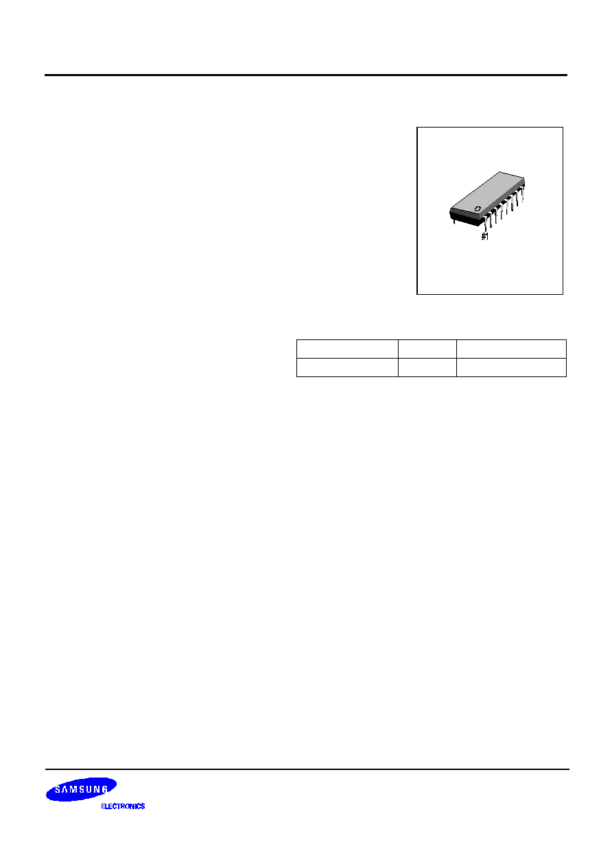
16-DIP-300
ORDERING INFORMATION
Device
Package
Operating Temperature
S5D2508A01-D0B0 16-DIP-300
0
∞
C
-- 70
∞
C

S5D2508A01
OSD PROCESSOR FOR MONITOR
4
PIN DESCRIPTIONS
Table 1. Pin Descriptions
Pin No.
Signal
Active
I/O
Description
1
VSS_A
-
-
Ground (Analog Part)
2
VCO_IN
-
Input
This voltage is generated at the external loop filter and
goes into the input stage of the VCO.
3
VREF1
-
Input
1.26 V DC Voltage from the Bandgap Reference.
Connected to ground through a resistor to make internal
reference current (Typical 36 K
for 27
µ
A)
4
VDD_A
-
-
+5 V Supply Voltage for Analog Part
5
VREF
-
Input
Bandgap Reference Voltage (Typical 1.26 V)
6
HFLB
Low
Input
Horizontal Flyback Signal
7
SDA
-
In/Out
Serial Data (I
2
C)
8
SCL
-
In/Out
Serial Clock (I
2
C)
9
VFLB
Low
Input
Vertical Flyback Signal
10
VSS_D
-
-
Ground for Digital Part
11
FBLK
-
Output
Fast Blank Signal
12
B_OUT
-
Output
Video Signal Output (B)
13
G_OUT
-
Output
Video Signal Output (G)
14
R_OUT
-
Output
Video Signal Output (R)
15
INT
-
Output
Intensity Signal Output
16
VDD_D
-
-
+5 V SUpply Voltage for Dogital Part

OSD PROCESSOR FOR MONITOR
S5D2508A01
5
ABSOLUTE MAXIMUM RATINGS
NOTE: PKG Thermal Resistance : 64.2
∞
C/W
ELECTRICAL CHARACTERISTICS
DC Electrical Characteristics
(Ta = 25
∞
C, VDD = 5 V)
Parameters
Symbol
Value
Unit
Min.
Typ.
Max.
Maximum Supply Voltage
VDD
-
-
7.0
V
Input Voltage
V
I
-
-
7.0
V
Operating Temperature Range
T
OPR
-20
-
70
∞
C
Storage Temperature Range
T
STG
-40
125
∞
C
Power Dissipation
P
D
-
-
1200
mW
Table 2. DC Electrical Characteristics
Parameters (Conditions)
Symbol
Min.
Typ.
Max.
Unit
Supply Voltage
VDD
4.75
5.00
5.25
V
Supply Current
(No load on any output)
I
DD
-
-
25
mA
Input Voltage
V
IH
0.8VDD
-
-
V
V
IL
-
-
VSS + 0.4
V
Output Voltage
(lout = 1mA)
V
OH
0.8VDD
-
-
V
V
OL
-
-
VSS + 0.4
V
Input Leakage Current
I
IL
-10
-
10
µ
A
VCO Input Voltage
V
VCO
2.5
V

