 | –≠–ª–µ–∫—Ç—Ä–æ–Ω–Ω—ã–π –∫–æ–º–ø–æ–Ω–µ–Ω—Ç: S5F325NU | –°–∫–∞—á–∞—Ç—å:  PDF PDF  ZIP ZIP |
1/3 INCH CCD IMAGE SENSOR FOR EIA CAMERA S5F325NU02
1
INTRODUCTION
The S5F325NU02 is an interline transfer CCD area image
sensor developed for EIA 1/3 inch optical format video cameras,
surveillance cameras, object detectors and image pattern
recognizers. High sensitivity is achieved through the on-chip
micro lenses and HAD (Hole Accumulated Diode) photosensors.
This chip features a field integration read out system and an
electronic shutter with variable charge storage time.
FEATURES
∑
High Sensitivity
∑
Optical Size 1/3 inch Format
∑
Low Dark Current
∑
Horizontal Register 5V Drive
∑
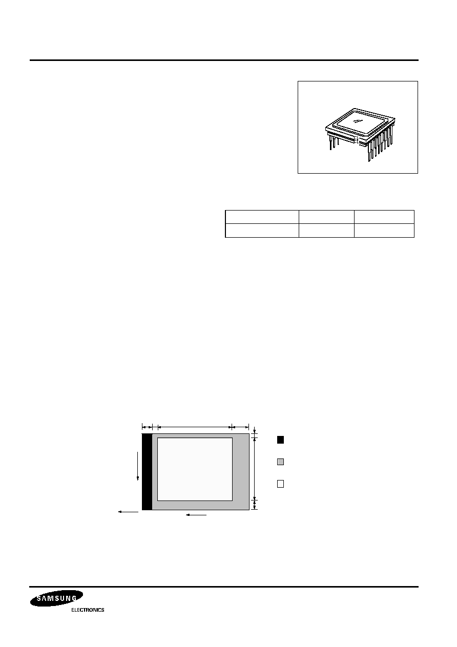
16pin Ceramic DIP Package
∑
Field Integration Read Out System
∑
No DC Bias on Reset Gate
STRUCTURE
∑
Number of Total Pixels:
537(H)
◊
505(V)
∑
Number of Effective Pixels:
510(H)
◊
492(V)
∑
Chip Size:
6.00mm(H)
◊
4.95mm(V)
∑
Unit Pixel Size:
9.60
µ
m(H)
◊
7.50
µ
m(V)
∑
Optical Blacks & Dummies:
Refer to Figure Below
Vertical 1 Line (Even Field Only)
16Pin Cer-DIP
ORDERING INFORMATION
Device
Package
Operating
S5F325NU02-LAB0
16Pin Cer - DIP
-10
∞
C
-
+60
∞
C
16 2
510
25
1
4
9
2
1
2
V
-
C
C
D
OUTPUT
Dummy Pixels
Optical Black Pixels
Effective Pixels
Effective
Imaging
Area
H-CCD
S5F325NU02 1/3 INCH CCD IMAGE SENSOR FOR EIA CAMERA
2
BLOCK DIAGRAM
PIN DESCRIPTION
Figure 1. Block Diagram
Table 1. Pin Description
Pin
Symbol
Description
Pin
Symbol
Description
1
V4
Vertical CCD transfer clock 4
9
V
DD
Output stage drain bias
2
V3
Vertical CCD transfer clock 3
10
GND
Ground
3
V2
Vertical CCD transfer clock 2
11
SUB
Substrate bias
4
V1
Vertical CCD transfer clock 1
12
V
L
Protection circuit bias
5
GND
Ground
13
RS
Charge reset clock
6
V
GG
Output stage gate bias
14
NC
No connection
7
V
SS
Output stage source bias
15
H1
Horizontal CCD transfer clock 1
8
V
OUT
Signal output
16
H2
Horizontal CCD transfer clock 2
8
V
OUT
7
6
5
4
3
2
1
9
10
11
12
13
14
15
16
V
SS
V
GG
GND
V1
V2
V3
V4
V
DD
V
L
GND
NC
H1
H2
RS
SUB
V
e
r
t
i
c
a
l
S
h
i
f
t
R
e
g
i
s
t
e
r
C
C
D
V
e
r
t
i
c
a
l
S
h
i
f
t
R
e
g
i
s
t
e
r
C
C
D
V
e
r
t
i
c
a
l
S
h
i
f
t
R
e
g
i
s
t
e
r
C
C
D
V
e
r
t
i
c
a
l
S
h
i
f
t
R
e
g
i
s
t
e
r
C
C
D
Horizontal Shift Register CCD
(Top View)

1/3 INCH CCD IMAGE SENSOR FOR EIA CAMERA S5F325NU02
3
ABSOLUTE MAXIMUM RATINGS
(1)
NOTES:
1.
The device can be destroyed, if the applied voltage or temperature is higher than the absolute maximum rating voltage
or temperature.
2.
When the clock width is less than 10
µ
sec
and the clock duty factor is less than 0.1%.
Table 2. Absolute Maximum Ratings
Characteristics
Symbols
Min.
Max.
Unit
Substrate voltage
SUB - GND
-0.3
55
V
Supply voltage
V
DD
, V
OUT
, V
SS
- GND
-0.3
18
V
V
DD
, V
OUT
, V
SS
- SUB
-55
10
V
Vertical clock input voltage
V1
,
V2
,
V3
,
V4
- GND
-10
20
V
V1
,
V2
,
V3
,
V4
- V
L
-0.3
30
V
V1
,
V2
,
V3
,
V4
- SUB
-55
10
V
Horizontal clock input voltage
H1
,
H2
- GND
-0.3
10
V
H1
,
H2
- SUB
-55
17
V
Voltage difference between vertical and
horizontal clock input pins
V1
,
V2
,
V3
,
V4
15
V
27
(2)
V
H1
,
H2
17
V
H1
,
H2
-
V4
-17
17
V
Output clock input voltage
RS
, V
GG
- GND
-0.3
15
V
RS
, V
GG
- SUB
-55
10
V
Protection circuit bias voltage
V
L
- SUB
-55
10
V
Operating temperature
T
OP
-10
60
∞
C
Storage temperature
T
STG
-30
80
∞
C
S5F325NU02 1/3 INCH CCD IMAGE SENSOR FOR EIA CAMERA
4
DC CHARACTERISTICS
CLOCK VOLTAGE CONDITIONS
Table 3. DC Characteristics
Item
Symbol
Min.
Typ.
Max.
Unit
Remark
Output stage drain bias
V
DD
14.55
15.0
15.45
V
Output stage gate voltage
V
GG
1.75
2.0
2.25
V
Output stage source voltage
V
SS
Ground through 680
V
±
5%
Substrate voltage adjustment range
V
SUB
7.0
14.5
V
Fluctuation voltage range after substrate
voltage adjusted
V
SUB
-3
3
%
Protection circuit bias voltage
V
L
The lowest vertical clock level
Output stage drain current
I
DD
2.5
mA
Table 4. Clock Voltage Conditions
Item
Symbol
Min.
Typ.
Max.
Unit
Remark
Read-out clock voltage
V
VH1
, V
VH3
14.55
15.0
15.45
V
High level
Vertical transfer clock voltage
V
VM1
~ V
VM4
-0.2
0.0
0.2
V
Middle
V
VL1
~ V
VL4
-9.5
-9.0
-8.5
V
Low
Horizontal transfer clock voltage
V
HH1
, V
HH2
4.75
5.0
5.25
V
High
V
HL1
, V
HL2
-0.2
0.0
0.2
V
Low
Charge reset clock voltage
V
RSH
4.75
5.0
5.25
V
High
V
RSL
-0.2
0.0
0.2
V
Low
Substrate clock voltage
V
SUB
20
23.0
25
V
Shutter
1/3 INCH CCD IMAGE SENSOR FOR EIA CAMERA S5F325NU02
5
DRIVE CLOCK WAVEFORM CONDITIONS
Read Out Clock Waveform
Vertical Transfer Clock Waveform
0V
100%
90%
10%
0%
V
VH 1,
V
VH3
tr
twh
tf
V
V H 1
V
VH
V
V H H
V
VL L
V
VL
V
VL 1
V
VL H
V
V H L
V
V H L
V
V H H
•’ V 1
V
VH
V
VHL
V
VH H
V
V HH
V
VHL
V
VH 4
V
VL
V
VL H
V
VL L
V
V L 4
•’ V 4
V
VH H
V
VHH
V
VH
V
VHL
V
VHL
V
VH2
V
VL
V
VL L
V
VL H
V
VL 2
•’ V 2
V
VL 3
V
VHH
V
VL
V
V HL
V
VH L
V
VH3
V
VH H
V
VH
V
VL H
V
VL L
•’ V 3
V
V H
= ( V
V H 1
+ V
V H 2
)/ 2
V
V L
= (V
V L 3
+ V
V L 4
)/ 2
V
•’
V
= V
V H n
- V
V L n
(n =1~4)
V
V H H
= V
V H
+ 0 . 3 V
V
V H L
= V
V H
- 0 . 3 V
V
V L H
= V
V L
+ 0 . 3 V
V
V L L
= V
V L
- 0 . 3 V