Äîêóìåíòàöèÿ è îïèñàíèÿ www.docs.chipfind.ru
1/4 INCH VGA CMOS IMAGE SENSOR
S5K433CA, S5K433LA
1
S5K433CA, S5K433LA
(1/4" VGA CMOS Image Sensor)
Preliminary Specification
Revision 0.3.1
July 2002
S5K433CA, S5K433LA
1/4" VGA CMOS IMAGE SENSOR
2
DOCUMENT TITLE
1/4" Optical Size 640x480(VGA) 3.3V/2.8V CMOS Image Sensor
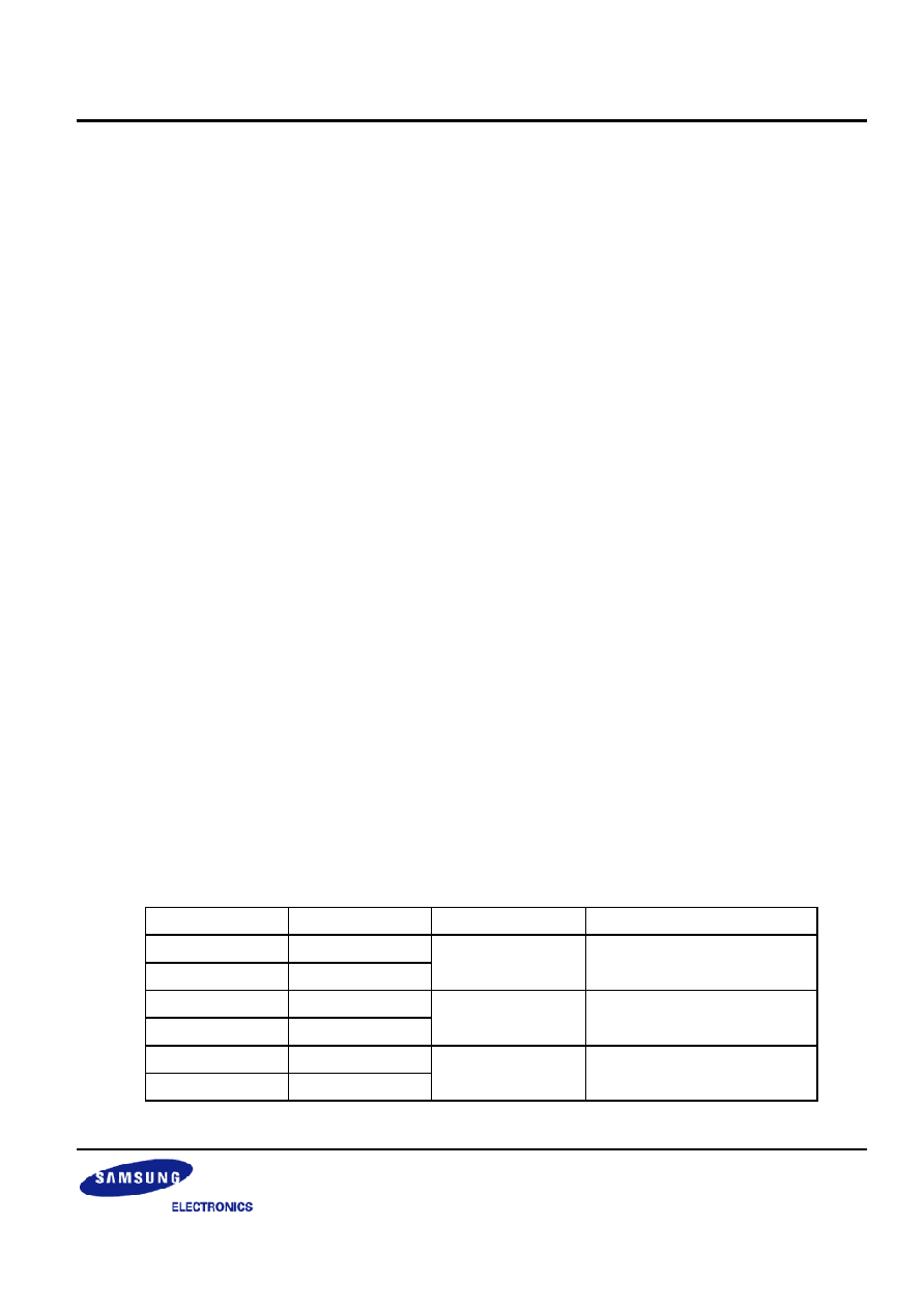
REVISION HISTORY
Revision No.
History
Draft Date
Remark
0.0
Initial Draft
Feb. 16, 2002 Preliminary
0.1
Pin description error corrected (LHOLD polarity).
Feb. 21, 2002 Preliminary
Timing chart added.
0.2
STRB signal polarity error corrected
Apr. 10, 2002 Preliminary
SFCM timing diagram corrected
Operation description added.
0.3
DC timing characteristics specification changed
July 8, 2002
Preliminary
AC timing characteristics specification changed
STRB and LHOLD pins are deleted
0.3.1
Minor description error corrected
July 15, 2002 Preliminary
1/4 INCH VGA CMOS IMAGE SENSOR
S5K433CA, S5K433LA
3
INTRODUCTION
The S5K433CA and S5K433LA are highly integrated single chip CMOS image sensors fabricated by
SAMSUNG 0.35
µ
m CMOS image sensor process technology. It is developed for imaging application to realize
high-efficiency and low-power photo sensor. The sensor has 640 x 480 effective pixels with 1/4 inch optical
format. The sensor has on-chip 10-bit ADC blocks to digitize the pixel output and also on-chip CDS to reduce
Fixed Pattern Noise (FPN) drastically. With its few interface signals and 10-bit raw data directly connected to the
external devices, a camera system can be configured easily. S5K433CA is suitable for a camera system with
standard 3.3V logic operation and S5K433LA is suitable for low power camera module with 2.8V power supply.
FEATURES
--
Process Technology: 0.35
µ
m DPTM CMOS
--
Optical Size: 1/4 inch
--
Unit Pixel: 5.6
µ
m X 5.6
µ
m
--
Effective Resolution: 640X480, VGA
--
Line Progressive Read Out.
--
10-bit Raw Image Data Output
--
Programmable Exposure Time
--
Programmable Gain Control
--
Auto Dark Level Compensation
--
Windowing and Panning
--
Sub-Sampling (2X, 3X, 4X)
--
Standby-Mode for Power Saving
--
Maximum 36 Frame per Second
--
Bad Pixel Replacement
--
Single Power Supply Voltage: 3.3V or 2.8V
--
Package Type: 48-CLCC/PLCC
PRODUCTS
Product Code
Power Supply
Backend Process
Description
S5K433CA01
3.3 V
S5K433LA01
2.8 V
None
Monochrome image sensor
S5K433CA02
3.3 V
S5K433LA02
2.8 V
On-chip micro lens
High sensitivity monochrome
Image sensor
S5K433CA03
3.3 V
S5K433LA03
2.8 V
On-chip color filter
and micro lens
RGB color image sensor
S5K433CA, S5K433LA
1/4" VGA CMOS IMAGE SENSOR
4
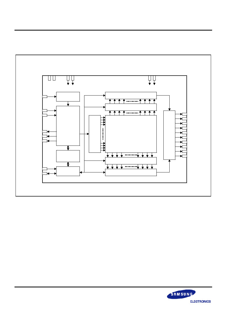
BLOCK DIAGRAM
Figure 1. Block Diagram
Timing
Generator
RSTN
STBYN
MCLK
VSYNC
HSYNC
DCLK
SCL
SDA
Main Clock
Divider
I
2
C Interface
Control
Registers
Active Pixel
Sensor Array
Row
Driver
Even Column CDS
Odd Column CDS
10-bit Column ADC
10-bit Column ADC
VDDD
VSSD
VDDIO
VSSIO
VDDA
VSSA
Post
Processing
DATA9
DATA8
DATA7
DATA6
DATA5
DATA4
DATA3
DATA2
DATA1
DATA0
1/4 INCH VGA CMOS IMAGE SENSOR
S5K433CA, S5K433LA
5
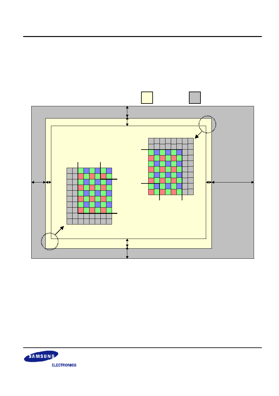
PIXEL ARRAY
(TOP VIEW ON CHIP. DISPLAYED IMAGE WILL BE FLIPPED.)
Figure 2. Pixel Array Configuration
(14,14) read out start point
Active Pixels
Optical
Black Pixels
(0,0)
Default Window of Interest
640X480
10 4
R
B
G
G
8
6
R
B
G
G
R
B
G
G
R
B
G
G
R
B
G
G
R
B
G
G
R
B
G
G
R
B
G
G
R
B
G
G
8
6
30
4
R
B
G
G
R
B
G
G
R
B
G
G
R
B
G
G
R
B
G
G
R
B
G
G
R
B
G
G
R
B
G
G
R
B
G
G
R
B
G
G
R
B
G
G
R
B
G
G
R
B
G
G
R
B
G
G
R
B
G
G