
1/7 INCH CIF CMOS IMAGE SENSOR
S5K711CA, S5K711LA
1
S5K711CA, S5K711LA
(1/7" CIF CMOS Image Sensor)
Preliminary Specification
Revision 0.2
Apr. 2002

S5K711CA, S5K711LA
1/7" CIF CMOS IMAGE SENSOR
2
DOCUMENT TITLE
1/7" Optical Size 352x352(CIF) 3.3V/2.8V CMOS Image Sensor
REVISION HISTORY
Revision No.
History
Draft Date
Remark
0.0
Initial Draft
Feb. 16, 2002 Preliminary
0.1
Pin description error corrected (LHOLD polarity).
Feb. 21, 2002 Preliminary
Timing chart added.
0.2
STRB signal polarity error corrected
Apr. 10, 2002 Preliminary
SFCM timing diagram corrected
Operation description added.
1/7 INCH CIF CMOS IMAGE SENSOR
S5K711CA, S5K711LA
3
INTRODUCTION
The S5K711CA and S5K711LA are highly integrated single chip CMOS image sensors fabricated by
SAMSUNG 0.35
µ
m CMOS image sensor process technology. It is developed for imaging application to realize
high-efficiency and low-power photo sensor. The sensor has 352 x 352 effective pixels with 1/7 inch optical
format. The sensor has on-chip 8-bit ADC blocks to digitize the pixel output and also on-chip CDS to reduce Fixed
Pattern Noise (FPN) drastically. With its few interface signals and 8-bit raw data directly connected to the external
devices, a camera system can be configured easily. S5K711CA is suitable for a camera system with standard 3.3V
logic operation and S5K711LA is suitable for low power camera module with 2.8V power supply.
FEATURES
--
Process Technology: 0.35
µ
m DPTM CMOS
--
Optical Size: 1/7 inch
--
Unit Pixel: 5.6
µ
m X 5.6
µ
m
--
Effective Resolution: 352X352, CIF
--
Line Progressive Read Out.
--
8-bit Raw Image Data Output
--
Programmable Exposure Time
--
Programmable Gain Control
--
Auto Dark Level Compensation
--
Windowing and Panning
--
Sub-Sampling (2X, 3X, 4X)
--
Cotinuous and Single Frame Capture Mode
--
Standby-Mode for Power Saving
--
Maximum 70 Frame per Second
--
Bad Pixel Replacement
--
Single Power Supply Voltage: 3.3V or 2.8V
--
Package Type: 32-CLCC/PLCC
PRODUCTS
Product Code
Power Supply
Backend Process
Description
S5K711CA01
3.3 V
S5K711LA01
2.8 V
None
Monochrome image sensor
S5K711CA02
3.3 V
S5K711LA02
2.8 V
On-chip micro lens
High sensitivity monochrome
Image sensor
S5K711CA03
3.3 V
S5K711LA03
2.8 V
On-chip color filter
and micro lens
RGB color image sensor

S5K711CA, S5K711LA
1/7" CIF CMOS IMAGE SENSOR
4
BLOCK DIAGRAM
Timing
Generator
RSTN
STBYN
MCLK
VSYNC
HSYNC
DCLK
SCL
SDA
STRB
Main Clock
Divider
I
2
C Interface
Control
Registers
Active Pixel
Sensor Array
Row
Driver
Even Column CDS
Odd Column CDS
8-bit Column ADC
8-bit Column ADC
VDDD
VSSD
V
DDA
VSSA
Post
Processing
DATA7
DATA6
DATA5
DATA4
DATA3
DATA2
DATA1
DATA0
LHOLD
1/7 INCH CIF CMOS IMAGE SENSOR
S5K711CA, S5K711LA
5
BLOCK DIAGRAM
(TOP VIEW ON CHIP. DISPLAYED IMAGE WILL BE FLIPPED.)
(14,14) read out start point
Active Pixels
Optical
Black Pixels
(0,0)
Effective Active Pixel
352X352
10 4
R
B
G
G
8
6
R
B
G
G
R
B
G
G
R
B
G
G
R
B
G
G
R
B
G
G
R
B
G
G
R
B
G
G
R
B
G
G
8
6
30
4
R
B
G
G
R
B
G
G
R
B
G
G
R
B
G
G
R
B
G
G
R
B
G
G
R
B
G
G
R
B
G
G
R
B
G
G
R
B
G
G
R
B
G
G
R
B
G
G
R
B
G
G
R
B
G
G
R
B
G
G
S5K711CA, S5K711LA
1/7" CIF CMOS IMAGE SENSOR
6
PIN CONFIGURATION
5
6
7
8
9
10
11
12
13
14
15
16
17
18
19
20
4
3
2
1
32
31
30
29
21
22
23
24
25
26
27
28
DATA7
DATA6
DATA5
DATA4
DATA3
DATA2
DATA1
DATA0
STBYN
VSSA
VDDA
STRB
LHOLD
VDDA
VSSA
TEST2
(NC)
VDDA
VSSA
VSSD
MCLK
SCL
SDA
RSTN
(NC)
VDDA
VSSA
VDDD
DCLK
HSYNC
VSYNC
TEST1
First Readout Pixel

1/7 INCH CIF CMOS IMAGE SENSOR
S5K711CA, S5K711LA
7
MAXIMUM ABSOLUTE LIMIT
Characteristic
Symbol
Value
Unit
Operating voltage
(VDDD, VDDA supply
relative to VSSD, VSSA)
V
DD
-0.3 to 3.8
V
Input voltage
V
IN
-0.3 to V
DD
+0.3 (Max. 3.8)
Operating temperature
T
OPR
-20 to +60
Storage temperature
T
STG
-40 to +125
(1)
∞
C
-40 to +85
(2)
NOTES:
1. The maximum allowed storage temperature for S5K711C(L)X01.
2. The maximum allowed storage temperature for S5K711C(L)X02 and S5K711C(L)X03.
S5K711CA, S5K711LA
1/7" CIF CMOS IMAGE SENSOR
8
ELECTRICAL CHARACTERISTICS
DC Characteristics
(T
A
= -20 to +60
∞
C, C
L
= 15pF)
Characteristics
Symbol
Condition
Min
Typ
Max
Unit
Operating voltage
V
DD
VDDD, VDDA
3.0
3.3
3.6
V
2.55
2.8
3.05
Input voltage
(1)
V
IH
-
0.8V
DD
-
-
V
IL
-
0
-
0.2V
DD
Input leakage
current
(2)
I
IL
V
IN
= V
DD
to V
SS
-10
-
10
µ
A
Input leakage current
with pull-down
(3)
I
ILD
V
IN
= V
DD
10
30
60
High Level Output
V
OH
I
OH
= -1
µ
A
V
DD
-0.05
-
-
V
voltage
(4)
I
OH
= -4mA
2.4
-
-
Low Level Output
V
OL
I
OL
= 1
µ
A
-
-
0.05
voltage
(5)
I
OL
= 4mA
-
-
0.4
High-Z output leakage
current
(6)
I
OZ
V
OUT
= V
DD
-
-
10
µ
A
Supply current
I
STB
STBYN=Low(Active)
All input clocks = Low
-
-
5
µ
A
I
DD
f
MCLK
= 12 MHz
V
DD
= 3.3V
(7)
-
27
-
mA
0 lux illumination
V
DD
= 2.8V
(8)
-
18
-
NOTES:
1. Applied to MCLK, RSTN, STBYN, STRB, SCL, SDA, TEST1, TEST2 pin.
2. MCLK, RSTN, STBYN, STRB, SCL, SDA pin
3. TEST1, TEST2 pin
4. DCLK, HSYNC, VSYNC, DATA0 to DATA7 pin
5. DCLK, HSYNC, VSYNC, DATA0 to DATA7, SCL, SDA pin
6. SDA pin when in High-Z output state
7. S5K711CA
8. S5K711LA
1/7 INCH CIF CMOS IMAGE SENSOR
S5K711CA, S5K711LA
9
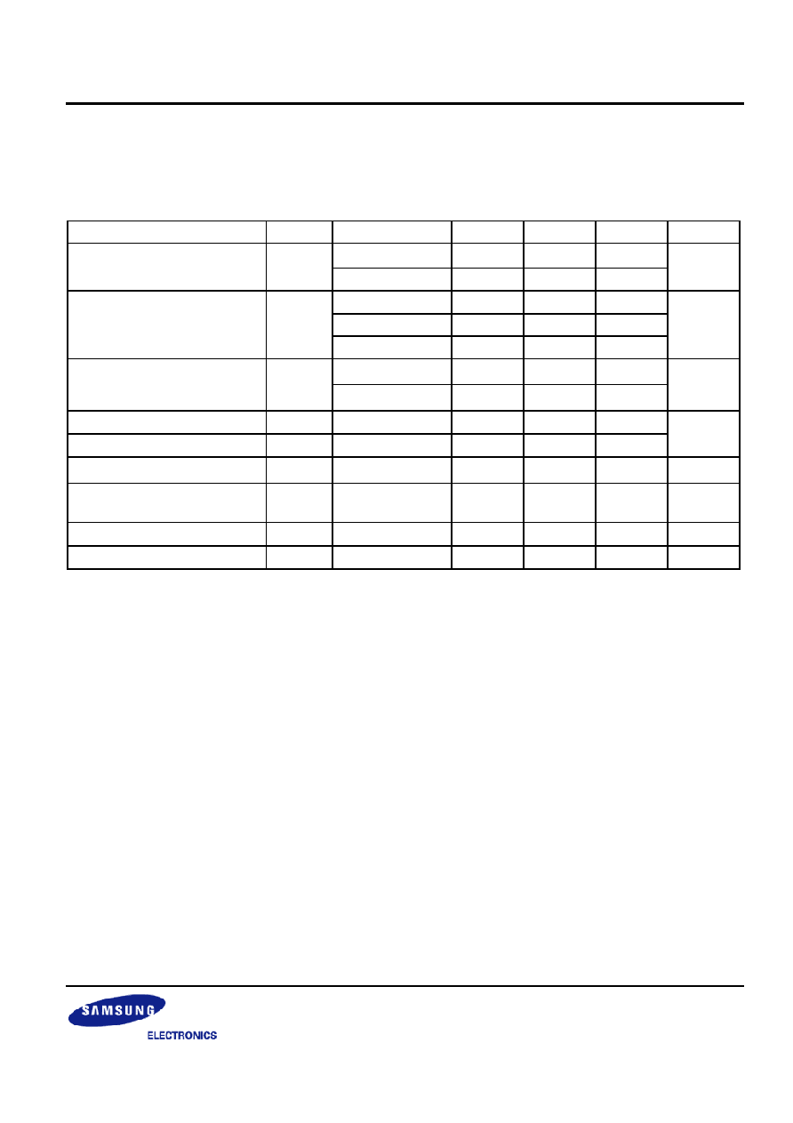
Imaging Characteristics
(Light source with 3200K of color temperature and IR cut filter (CM-500S, 1mm thickness) is used. Electrical
operating conditions follow the recommended typical values. The control registers are set to the default values. T
A
= 25
∞
C if not specified.)
NOTES:
1. Measured minimum output level at 100 lux illumination for exposure time 1/30 sec. 7X7 rank filter is applied for the whole
pixel area to elemiate the values from defective pixels.
2. Measured average output at 25% of saturation level illumination for exposure time 1/30 sec. Green channel output values
are used for color version.
3. Measured average output at zero illumination without any offset compensation for exposure time 1/30 sec.
4. 20 log (saturation level/ dark level rms noise excluding fixed pattern noise). 48dB is limited by 8-bit ADC.
5. 20 log (average output level/rms noise excluding fixed pattern noise) at 25% of saturation level illumination for exposure
time 1/30 sec.
6. Difference between maximum and minimum pixel output levels at zero illumination for exposure time 1/30 sec. 7X7
median filter is applied for the whole pixel area to elemiate the values from defective pixels.
7, Difference between maximum and minimum pixel output levels divided by average output level at 25% of saturation level
illumination for exposure time 1/30 sec. 7X7 median filter is applied for the whole pixel area to elemiate the values from
defective pixels.
8. For the column-averaged pixel output values, maximum relative deviation of values from 7-depth median filtered values for
neighboring 7 columns at 25% of saturation level illumination for exposure time 1/30 sec.
9. For the row-averaged pixel output values, maximum relative deviation of values from 7-depth median filtered values for
neighboring 7 columns at 25% of saturation level illumination for exposure time 1/30 sec.
Characteristic
Symbol
Condition
Min
Typ
Max
Unit
Saturation level
(1)
V
SAT
S5K711CA
950
1000
-
mV
S5K711LA
850
900
-
Sensitivity
(2)
S
S5K711(C,L)X01
-
1500
-
mV/lux sec
S5K711(C,L)X02
-
4000
-
S5K711(C,L)X03
-
1500
-
Dark level
(3)
V
DARK
T
A
= 40
∞
C
-
9
18
mV/sec
T
A
= 60
∞
C
-
50
100
Dynamic range
(4)
DR
-
48
-
dB
Signal to noise ratio
(5)
S/N
-
40
-
Dark signal non-uniformity
(6)
DSNU
T
A
= 60
∞
C
-
-
100
mV/sec
Photo response non-
uniformity
(7)
PRNU
-
4
8
%
Vertical fixed pattern noise
(8)
VFPN
4
8
%
Horizontal fixed pattern noise
(9)
HFPN
4
8
%
S5K711CA, S5K711LA
1/7" CIF CMOS IMAGE SENSOR
10
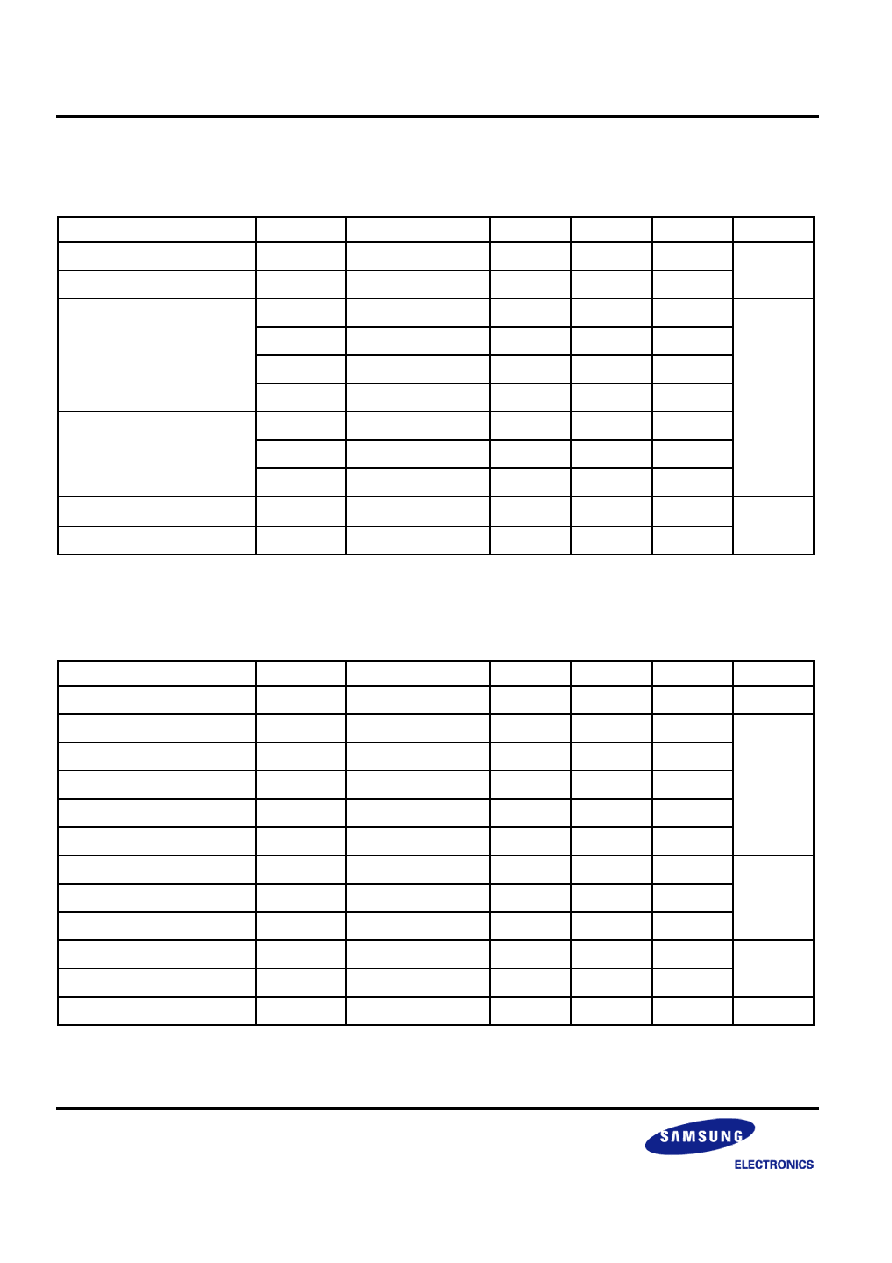
AC Characteristics
(V
DD
= 3.0V to 3.6V for S5K711CA, V
DD
= 2.55V to 3.05V for S5K711LA, Ta = -20 to + 60
∞
C, C
L
= 50pF)
NOTES:
1. The period time of main input clock,
MCLK.
I
2
C Serial Interface Characteristics
Characteristic
Symbol
Condition
Min
Typ
Max
Unit
Main input clock frequency
f
MCLK
Duty = 50%
6
12
30
MHz
Data output clock frequency
f
DCLK
-
2
6
15
Propagation delay time
t
PDMV
VSYNC output
-
-
20
ns
from main input clock
t
PDMH
HSYNC output
-
-
20
t
PDMD
DCLK output
-
-
15
t
PDMO
DATA output
-
-
20
Propagation delay time
t
PDDV
VSYNC output
-
-
10
from data output clock
t
PDDH
HSYNC output
-
-
5
t
PDDO
DATA output
-
-
5
Reset input pulse width
t
WRST
RSTN=low(active)
5
-
-
T
MCLK
(1)
Standby input pulse width
t
WSTB
STBYN=low(active)
4
-
-
Characteristic
Symbol
Condition
Min
Typ
Max
Unit
Clock frequency
f
SCK
-
-
-
400
kHz
Clock high pulse width
t
WH
SCK
800
-
-
ns
Clock low pulse width
t
WL
SCK
1000
-
-
Clock rise/fall time
t
R
/t
F
SCK, SDA
-
-
300
Data set-up time
t
DS
SDA to SCK
300
-
-
Data hold time
t
DH
SDA to SCK
1200
-
-
START condition hold time
t
STH
-
4
T
MCLK
STOP condition setup time
t
STS
-
4
-
-
STOP to new START gap
t
GSS
-
8
-
-
Capacitance for each pin
C
PIN
SCL, SDA
-
-
4
pF
Capacitive bus load
C
BUS
SCL, SDA
-
-
200
Pull-up resistor
R
PU
SCL, SDA to V
DD
1.5
-
10
k
1/7 INCH CIF CMOS IMAGE SENSOR
S5K711CA, S5K711LA
11
PIN DESCRIPTION
Table 1. Pin Description
Pin No
I/O
Name
Function
VDDD (16)
Power Digital power supply
For I/O circuit and logical circuit ( V
DD
±
10% )
VSSD (1)
Power
0V (GND)
VDDA
(3, 14, 23, 26)
Power Analog power supply
For analog circuit ( V
DD
±
10% )
VSSA
(2, 15, 22, 27)
Power
0V (GND)
MCLK (32)
I
Master clock
Master clock pulse input for all timing generators.
RSTN (29)
I
Reset
Initializing all the device registers. (Active low)
STBYN (28)
I
Standby
Activating power saving mode.
( high=normal operation, low=power saving mode )
LHOLD (24)
I
Line hold
Asserting the device to hold line progress for zoomed
image output.
( low= line holding, high= normal operation)
STRB (25)
I
Strobing
Triggering the integration start and stop when single
frame capture mode.
DATA0~DATA7
(5~12)
O
Image data output
8-bit image data outputs. When ADC resolution is
reduced, the unused lower bits are set to 0.
DCLK (17)
O
Data clock
Image data output synchronizing pulse output.
HSYNC (18)
O
Horizontal sync clock
Horizontal synchronizing pulse or data valid signal output.
VSYNC (19)
O
Vertical sync clock
Vertical synchronizing pulse or line valid signal output.
SCL (31)
I
Serial interface clock
I2C serial interface clock input
SDA (30)
I/O
Serial interface data
I2C serial interface data bus
(external pull-up resistor required)
TEST1 (20)
I
Test input 1
Test input signal. Though it can be opened in normal
operation (internally pulled down), it is recommended to
ground the test pins.
TEST2 (21)
I
Test input 2
Test input signal. Though it can be opened in normal
operation (internally pulled down), it is recommended to
ground the test pins.
S5K711CA, S5K711LA
1/7" CIF CMOS IMAGE SENSOR
12
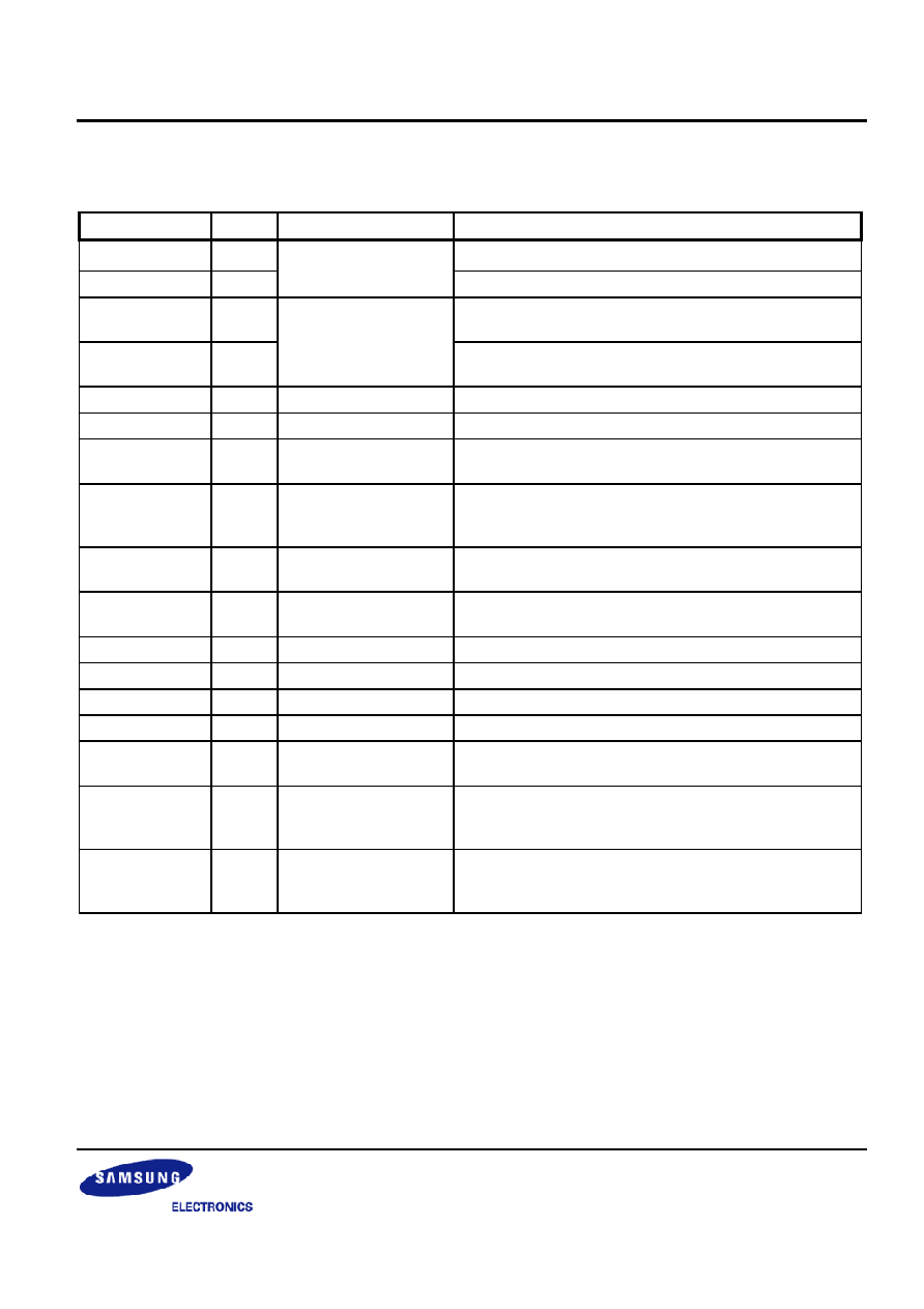
Control Registers
Address
(Hex)
Reset
Value
Bits
Mnemonic
Description
[5]
sckinv
(Factory use only) Column color inversion
[4]
idinv
(Factory use only) Line color inversion
[3]
bprm
Bad pixel replacement mode
0b: disabled (default), 1b: enabled
[2]
dlcm
Dark level compensation mode
0b: manual (default), 1b: auto
[1]
ccsm
Color channel separation mode
0b: not separated (default), 1b: separated
00h
00h
[0]
shutc
Electronic shutter mode
0b: disabled (default), 1b: enabled
[7]
mircv
Vertical mirror control
0b: normal (default), 1b: mirrored
[6]
mirch
Horizontal mirror control
0b: normal (default), 1b: mirrored
[5:4]
mcdiv
Main clock divider
00b: DCLK=MCLK, 01b: DCLK=MCLK
˜
2 (default)
10b: DCLK=MCLK
˜
4, 11b: DCLK=MCLK
˜
8
[3:2]
subsr
Row subsampling mode
00b: disabled (default),
01b: 2X, 10b: 3X, 11b: 4X
01h
10h
[1:0]
subsc
Column subsampling mode
00b: disabled (default),
01b: 2X, 10b: 3X, 11b: 4X
02h
00h
[0]
wrp_high
03h
0Eh
[7:0]
wrp_low
Row start point for window of interest
wrp[8:0] = 14d(default)
04h
00h
[0]
wcp_high
05h
0Eh
[7:0]
wcp_low
Column start point for window of interest
wcp[8:0] = 14d(default)
06h
01h
[0]
wrd_high
07h
20h
[7:0]
wrd_low
Row depth for window of interest
wrd[8:0] = 288d(default)
08h
01h
[1:0]
wcw_high
09h
60h
[7:0]
wcw_low
Column width for window of interest
wcw[9:0] = 352d(default)
0Ah
80h
[7:0]
offsdef
(Factory use only) Analog offset reference
offsdef[7:0] = 128d (default)
1/7 INCH CIF CMOS IMAGE SENSOR
S5K711CA, S5K711LA
13
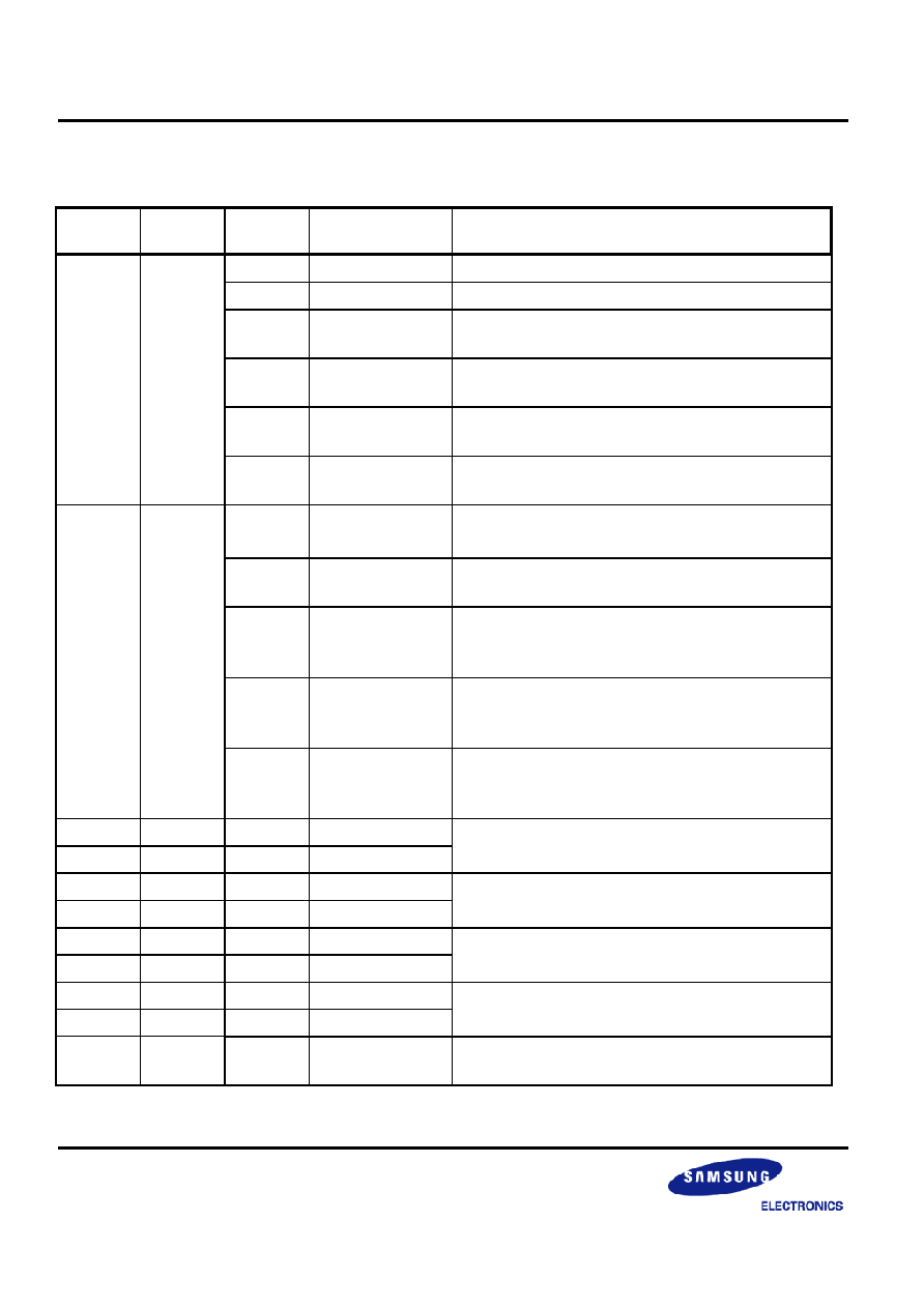
Address
(Hex)
Reset
Value
Bits
Mnemonic
Description
[3]
sfcen
Single frame capture enable
0b: disabled (default), 1b: enabled
0Bh
01h
[2:0]
sint_high
0Ch
8Fh
[7:0]
sint_low
Integration time in single frame capture mode
sint[10:0] = 399d (default)
0Dh
00h
[3:0]
cintr_high
0Eh
C7h
[7:0]
cintr_low
Row-step integration time in continuous frame
capture mode
cintr[11:0] = 199d (default)
0Fh
00h
[4:0]
cintc_high
10h
00h
[7:0]
cintc_low
Column-step integration time in continuous frame
capture mode
cintc[12:0] = 0d (default)
11h
01h
[7:0]
vswd
VSYNC width
vswd[7:0] = 1d (default)
[5]
vspolar
VSYNC polarity
0: active high (default), 1: active low
[4]
vsdisp
VSYNC display mode
0: sync mode (default), 1: data valid mode
12h
00h
[1:0]
vsstrt_high
13h
00h
[7:0]
vsstrt_low
VSYNC start position
vsstrt[9:0] = 0d (default)
14h
00h
[3:0]
vblank_high
15h
6Fh
[7:0]
vblank_low
Vertical blank depth
vblank[11:0] = 111d (default)
16h
20h
[7:0]
hswd
HSYNC width
hswd[7:0] = 32d (default)
[5]
hspolar
HSYNC polarity
0: active high (default), 1: active low
[4]
hsdisp
HSYNC display mode
0: sync mode (default), 1: data valid mode
17h
00h
[1:0]
hsstart_high
18h
00h
[7:0]
hsstart_low
HSYNC start position
hsstrt[9:0] = 0d (default)
19h
00h
[5:0]
hblank_high
1Ah
94h
[7:0]
hblank_low
Horizontal blank depth
hblank[13:0] = 148d (default)
S5K711CA, S5K711LA
1/7" CIF CMOS IMAGE SENSOR
14
Address
(Hex)
Reset
Value
Bits
Mnemonic
Description
[3:0]
sgg1
1
st
sectional global gain
sgg1[3:0] = 7d (default)
1Bh
77h
[7:4]
sgg2
2
nd
sectional global gain
sgg2[3:0] = 7d (default)
[3:0]
sgg3
3
rd
sectional global gain
sgg3[3:0] = 7d (default)
1Ch
77h
[7:4]
sgg4
4
th
sectional global gain
sgg4[3:0] = 7d (default)
1Dh
00h
[6:0]
pgcr
Red channel gain
pgcr[6:0] = 0d (default)
1Eh
00h
[6:0]
pgcg1
Green(Red row) channel gain
or all channel gain (
ccsm=0)
pgcg1[6:0] = 0d (default)
1Fh
00h
[6:0]
pgcg2
Green(Blue row) channel gain
pgcg2[6:0] = 0d (default)
20h
00h
[6:0]
pgcb
Blue channel gain
pgcb[6:0] = 0d (default)
21h
80h
[7:0]
offsr
Red channel analog offset
offsr[7:0] = 128 (default)
22h
80h
[7:0]
offsg1
Green(Red row) channel analog offset
or all channel offset (
ccsm=0)
offsg1[7:0] = 128 (default)
23h
80h
[7:0]
offsg2
Green(Blue row) channel analog offset
offsg2[7:0] = 128 (default)
24h
80h
[7:0]
offsb
Blue channel analog offset
offsb[7:0] = 128 (default)
25h
14h
[6:0]
pthresh
Bad pixel threshold
pthresh[6:0] = 20d (default)
26h
00h
[7:0]
adcoffs
ADC offset
adcoffs[7:0] = 0d (default)
[4]
clipen
(Factory use only) Reset clipping enable
27h
01h
[3:0]
p12stp
(Factory use only) P12 start control
1/7 INCH CIF CMOS IMAGE SENSOR
S5K711CA, S5K711LA
15
Address
(Hex)
Reset
Value
Bits
Mnemonic
Description
[7:5]
stbystrt
(Factory use only) Stand-by start
28h
40h
[4:0]
stbystp
(Factory use only) Stand-by stop
29h
00h
[7:0]
rxstrt
(Factory use only) Reset start control
2Ah
00h
[7:0]
blank
Blank register for general purpose
[3]
vtest
(Factory use only) Vertical function test mode
[2]
htest
(Factory use only) Horizontal function test mode
[1]
i2ctest
(Factory use only) IIC test mode
2Bh
02h
[0]
nandtree
(Factory use only) NAND tree test mode
S5K711CA, S5K711LA
1/7" CIF CMOS IMAGE SENSOR
16
OPERATION DESCRIPTION
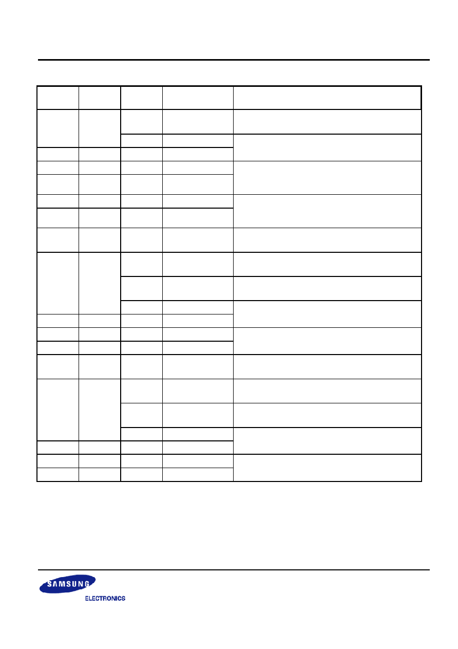
1. Output Data Format
1-1. Main Clock Divider
All the data output and sync signals are synchronized to data clock output (
DCLK). It is generated by dividing the
input main clock (
MCLK). The dividing ratio is 1, 2, 4, and 8 according to main clock dividing control register
(
mcdiv). If ratio of 1 is used, the duty must be within 40% to 60%.
1-2. Synchronous Signal Output
The horizontal sync(
HSYNC) and vertical sync(VSYNC) signals are also available. The sync pulse width, polarity
and position are programmable by control registers (ref. timing chart). When display mode is enabled, the sync
signal outputs indicate that the output data is valid (
hsdisp=1) or the output rows are valid (vsdisp=1).
1-3. Window of Interest Control
Window of Interest (WOI) is defined as the pixel address range to be read out. The WOI can be assigned
anywhere on the pixel array. It is composed of four values: row start pointer(
wrp), column start pointer(wcp), row
depth(
wrd) and column width(wcw). Each value can be programmed by control registers. For convenience of
color signal processing,
wcp is truncated to even numbers so that the starting data of each line is the red and
green column of Bayer pattern. Figure 4 refers to a pictorial representation of the WOI on the displayed pixel
image.
Figure 4. WOI definition.
1-4. Vertical Mirror and Horizontal Mirror Mode Control
The pixel data are read out from left to right in horizontal direction and from top to bottom in vertical direction
normally. By changing the mirror mode, the read-out sequence can be reversed and the resulting image can be
flipped like a mirror image. Pixel data are read out from right to left in horizontal mirror mode and from bottom to
top in vertical mirror mode. The horizontal and the vertical mirror mode can programmed by Horizontal Mirror
Control Register (
mirch) and Vertical Mirror Control Register (mircv).
1-5. Sub-sampling Control
The user can read out the pixel data in sub-sampling rate in both horizontal and vertical direction. Sub-sampling
can be done in four rates : full, 1/2, 1/3 and 1/4. The user controls the sub-sampling using the Sub-sampling
Control Registers,
subsr and subsc. The sub-sampling is performed only in the Bayer space.
Window Of Interest
(
wcp,wrp)
wcw
wrd
0
400
380
0

1/7 INCH CIF CMOS IMAGE SENSOR
S5K711CA, S5K711LA
17
Figure 5. Bayer Space Sub-Sampling Examples
1-6. Line Rate and Frame Rate Control (Virtual Frame)
The line rate and the frame rate can be changeable by varying the size of virtual frame. The virtual frame's width
and depth are controlled by effective WOI and blank depthes. The effective WOI is scaled by the subsampling
factors from WOI set by register values. For CDS and ADC function, the virtual column width must be larger than
256/(2^
mcdiv)+180. The resulting frame time and line time which are inverse of frame rate and line rate are
represented by following equations:
1 frame time = {
wrd / (subsr+1) + vblank } * (1 line time)
1 line time = {
wcw / (subsc+1) + hblank } * (DCLK period)
1-7. Continuous Frame Capture Mode(CFCM) Integration Time Control (Electronic Shutter Control)
In CFCM operation, the integration time is controlled by shutter operation. The shutter operation is done when
shutter control register (
shutc) is set to "1". In shutter operation, the integration time is determined by the Row
Step Integration Time Control Register(
cintr) and Column Step Integration Time Control Register(cintc). The
resulting integration time is expressed as;
Integration Time = (
cintr - 1) * (1 line time) + (cintc +110) * (DCLK period)
where
cintr = 1 to { wrd / (subsr+1) + vblank }, cintc = 0 to { wcw / (subsc+1) + hblank ≠180 }.
1-8. Single Frame Capture Mode(SFCM) Integration Time Control
To capture a still image, SFCM can be set by Single Frame Capture Enable Register(
sfcen). Rolling shutter
mode is implemented. The integration time is controlled by SFCM Integration Time Register (
sint). The light
integration period for each rows progresses with reading rows. The integration time is expressed as :
Integration Time =
sint * (1 line time)
subsr=01b, subsc=01b
R G
G B
R G
G B
R G
G B
R G
G B
R G
G B
R G
G B
R G
G B
R G
G B
R G
G B
R G
G B
R G
G B
R G
G B
R G
G B
R G
G B
R G
G B
R G
G B
R G
G B
R G
G B
R G
G B
R G
G B
R G
G B
R G
G B
R G
G B
R G
G B
R G
G B
R G
G B
R G
G B
R G
G B
R G
G B
R G
G B
R G
G B
R G
G B
R G
G B
R G
G B
R G
G B
R G
G B
R G
G B
R G
G B
R G
G B
R G
G B
R G
G B
R G
G B
R G
G B
R G
G B
R G
G B
R G
G B
R G
G B
R G
G B
R G
G B
R G
G B
R G
G B
R G
G B
R G
G B
R G
G B
R G
G B
R G
G B
R G
G B
R G
G B
R G
G B
R G
G B
R G
G B
R G
G B
R G
G B
R G
G B
subsr=00b, subsc=11b
R G
G B
R G
G B
R G
G B
R G
G B
R G
G B
R G
G B
R G
G B
R G
G B
R G
G B
R G
G B
R G
G B
R G
G B
R G
G B
R G
G B
R G
G B
R G
G B
R G
G B
R G
G B
R G
G B
R G
G B
R G
G B
R G
G B
R G
G B
R G
G B
R G
G B
R G
G B
R G
G B
R G
G B
R G
G B
R G
G B
R G
G B
R G
G B
R G
G B
R G
G B
R G
G B
R G
G B
R G
G B
R G
G B
R G
G B
R G
G B
R G
G B
R G
G B
R G
G B
R G
G B
R G
G B
R G
G B
R G
G B
R G
G B
R G
G B
R G
G B
R G
G B
R G
G B
R G
G B
R G
G B
R G
G B
R G
G B
R G
G B
R G
G B
R G
G B
R G
G B
R G
G B
R G
G B
R G
G B
R G
G B
S5K711CA, S5K711LA
1/7" CIF CMOS IMAGE SENSOR
18
2. Analog to Digital Converter ( ADC)
The image sensor has on-chip ADC. Two-channel column parallel ADC scheme is used for separated color
channel gain and offset control.
2-1. ADC resolution
The ADC resolution is fixed to 8bit.
2-2. Correlated Double Sampling ( CDS )
The analog output signal of each pixel includes some temporal random noise caused by the pixel reset action
and some fixed pattern noise by the in-pixel amplifier offset deviation. To eliminate those noise components, a
correlated double sampling(CDS) circuit is used before converting to digital. The output signal sampled twice, once
for the reset level and once for the actual signal level sampling.
2-3. Programmable Gain and Offset Control
The user can controls the gain of individual color channel by the Programmable Gain Control
Registers (
pgcr, pgcg1, pgcg2, pgcb) and offset by Offset Control Registers (offsr, offsg1,
offsg2, offsb). If the Color Channel Separation Mode is disabled (ccsm=0), pgcg1 and offsg1
change the gains and offsets for all channels. As increasing the gain control register, the ADC
conversion input range decreases and the gain increased as following equation:
Channel Gain = 128 / (128 ≠ Programmable Gain Control Register Value[6:0])
Figure 6. Relative Channel Gain
R G1
G2 B
R G1
G2 B
R G1
G2 B
R G1
G2 B
0
5
10
15
20
25
30
35
40
45
0
16
32
48
64
80
96
112
128
Programmable Gain Control
Channel Gain (dB)
1
2
3
4
5
6
7
8
9
10
0
16
32
48
64
80
96
112
128
Programmable Gain Control
Relative Channel Gain
1/7 INCH CIF CMOS IMAGE SENSOR
S5K711CA, S5K711LA
19
2-4. Quadrisectional Global Gain Control
The user can controls the global gain to change the gain for all color channels by the Global Gain Control
Registers (
sgg1, sgg2, sgg3, sgg4). The global gain control register is composed of four register groups and
each register value decides the gain for each quarter section of output code level.
Global Gain = (
sgg[3:0]+1) / 8
Figure 7. Relative Global Gain
The ADC gain is dependent on
MCLK frequency (not on DCLK frequency). The default global gain is set for
typical
MCLK frequency (12MHz). When the frequency is changed, the global gain should be changed to maintain
the resulting gain over unity for assuring appropriate ADC conversion range.
0
1
2
3
4
5
6
7
8
9
10
11
12
13
14
15
0
1
2
3
4
5
6
7
8
9 10 11 12 13 14 15 16 17 18 19 20 21 22 23 24 25 26 27 28 29 30
MCLK frequency (MHz)
Minimum Glabal Gain
0.0
0.2
0.4
0.6
0.8
1.0
1.2
1.4
1.6
1.8
2.0
0
2
4
6
8
10
12
14
16
Program m able Gain Control
Relative Global Gain
-20
-15
-10
-5
0
5
10
0
2
4
6
8
10
12
14
16
Program m able Gain Control
Glabal Gain (dB)

S5K711CA, S5K711LA
1/7" CIF CMOS IMAGE SENSOR
20
Figure 8. Recommended Minimum Global Gain Control Value
By appropriately programming these four register values, the different output resolution according to the signal
can be achieved and the intra-scene dynamic range can be increased by 16 times. In another application, the
sectional global gain control can be used as a rough gamma correction with four sectional linear approximation
curve as shown in Figure 9.
Figure 9. Quadrisectional Glabal Gain Control
3. Post Processing
3-1. Dark Level Compensation
The dark level of Image sensor is defined as average output level without illumination. It includes pixel ouput
caused by leakage current of the photodiodes and ADC offset. To compensate the dark level, the output level of
optical black(OB) pixels can be a good reference value. When Auto Dark Level Compensation Register (
dlcm) is
set, the image sensor detects the OB pixel level at the start of every frame and anglog-to-digital conversion range
is shifted to compensate the dark level for that frame. So, the resulting output data of that frame will be almost zero
under dark state. If user wants the dark level which is not zero, the ADC Offset Register (
adcoffs) can be used.
The lower 7-bit value represent the offset value in outout code for compensation and the MSB is the sign to define
whether the offset is positive (
adcoffs[7]=0) or negative (adcoffs[7]=1). When not in auto dark level
compensation mode, the
adcoffs[7:0] act as a output code value to subtract the output image data. Please notify
that the all the 8-bit data are used for an offset value without sign bit.
3-2. Bad Pixel Replacement
When the Bad Pixel Replacement Register (
bprm) is enabled, the image sensor check that the image data is
less or greater than horizontally neighboring pixels in same color channel by the preset threshold value (
pthresh).
If satisfied, the output of the pixel is replaced by the averaged value of the neghiboring two pixels. The detectable
defected pixels are rare and the bad pixel replacement action can remove defected image effectively. But it
reduces the line resolution in horizontal direction.
63
0
127
191
255
ADC output code at 8-bit resolution
sgg1=1111b
sgg2=0111b
sgg3=0011b
sgg4=0000b
ADC input signal
sgg1=0111b
sgg2=0111b
sgg3=0111b
sgg4=0111b
sgg1
sgg2
sgg3
sgg4
1/7 INCH CIF CMOS IMAGE SENSOR
S5K711CA, S5K711LA
21
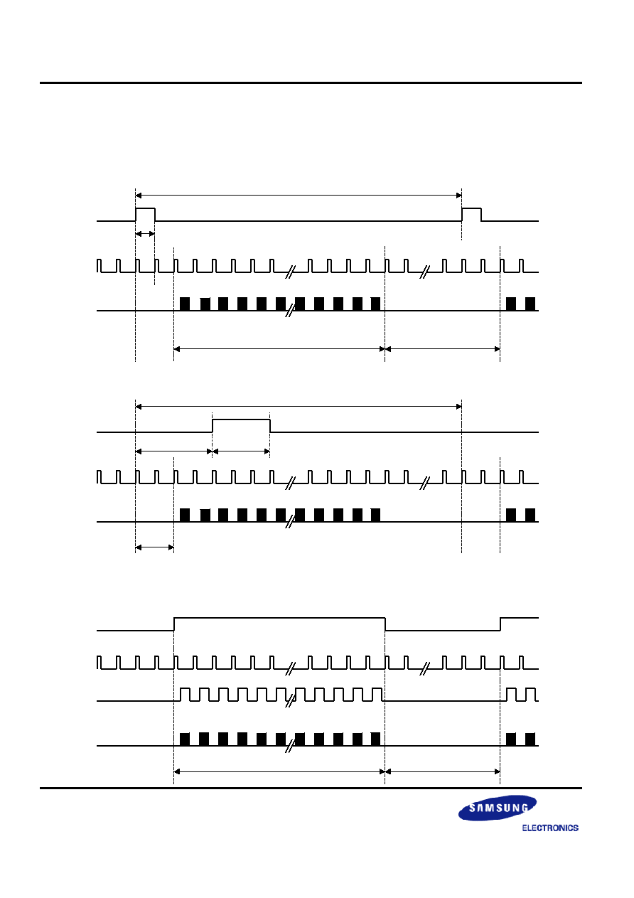
4. I
2
C Serial Interface
The I
2
C is an industry standard serial interface. The I
2
C contains a serial two-wire half duplex interface that
features bi-directional operation, master or slave mode. The general
SDA and SCL are the bi-directional data and
clock pins, respectively. These pins are open-drain type ports and will require a pull-up resistor to VDD. The image
sensor operates in salve mode only and the
SCL is input only. The I
2
C bus interface is composed of following
parts : START signal, 7-bit slave device address (0010001b) transmission followed by a read/write bit, an
acknowledgement signal from the slave, 8-bit data transfer followed by an acknowledgement signal and STOP
signal. The
SDA bus line may only be changed while SCL is low. The data on the SDA bus line is valid on the high-
to-low transition of
SCL.
Figure 10. I
2
C Bus Write Cycle
Figure 11. I
2
C Bus Read Cycle
SDA
Start
D7 D6 D5
SCL
"0" "0" "1" "0" "0" "0" "1"
I
2
C Bus Address
I2C Register Address
Write
Ack
Ack
SDA
SCL
D7 D6 D5 D4 D3 D2 D1 D0
Data to Write
Stop
Ack
D4 D5 D2 D1 D0
SDA
Start
D7 D6 D5
SCL
"0" "0" "1" "0" "0" "0" "1"
I
2
C Bus Address
I2C Register Address
Write
Ack
Ack
Stop
D4 D5 D2 D1 D0
X
SDA
Re-Start
D7 D6 D5
SCL
"0" "0" "1" "0" "0" "0" "1"
I
2
C Bus Address
Data to be Read
Read
Ack
Ack
D4 D5 D2 D1 D0
S5K711CA, S5K711LA
1/7" CIF CMOS IMAGE SENSOR
22
TIMING CHART
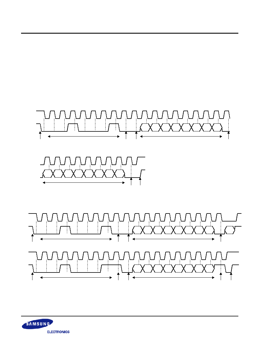
VERTICAL TIMING DIAGRAM
Continuous Frame Capture Mode
( Default Case )
( Delayed Vertical Sync Case)
( Vertical Data Valid Mode Case) vsdisp=1
HSYNC
wrd (288 rows)
1 frame = wrd + vblank (399 rows )
wrp
(14th row)
VSYNC
vswd (1row)
rows
DATA
vblank (111 rows)
HSYNC
1 frame = wrd + vblank
VSYNC
vsstrt
DATA
HSYNC
(hsdisp=0)
wrd
VSYNC
DATA
vblank
2 rows
vswd
2 rows
HSYNC
(hsdisp=1)
1/7 INCH CIF CMOS IMAGE SENSOR
S5K711CA, S5K711LA
23
VERTICAL TIMING DIAGRAM (continued)
Single Frame Capture Mode
HSYNC
VSYNC
DATA
STRB
Integration time for 1st readout row
Normal frame output
Integration time for 2nd readout row
Integration time for 3rd readout row
Integration time for 4th readout row
2 rows
sint X (1 row time)
3 rows
1 row
1 row
1 row
S5K711CA, S5K711LA
1/7" CIF CMOS IMAGE SENSOR
24
HORIZONTAL TIMING DIAGRAM
( Default Case )
( Delayed Horizontal Sync Case )
( Horizontal Data Valid Mode Case ) hsdisp=1
wcw ( 352 columns )
1 row = wcw + hblank ( 500 columns )
hswd
( 32 DCLK)
hblank ( 148 columns )
HSYNC
VSYNC
DATA
DCLK
10 DCLK
wcp
( 14th column)
wcw
1 row = wcw + hblank
hsstrt
HSYNC
VSYNC
DATA
DCLK
hswd
42 DCLK
42 DCLK
wcw
HSYNC
VSYNC
DATA
DCLK
42 DCLK
hblank
1/7 INCH CIF CMOS IMAGE SENSOR
S5K711CA, S5K711LA
25
LINE HOLD MODE TIMING DIAGRAM
HSYNC
DATA
(i)-th row
(i+1)-th row
(i+2)-th row
LHOLD
hblank ≠ 42 DCLK
hblank
42 DCLK
line held
S5K711CA, S5K711LA
1/7" CIF CMOS IMAGE SENSOR
26
PACKAGE DIMENSION
BOTTOM VIEW
SIDE VIEW
TOP VIEW
Center of Image Area
(X=+0.48
±
0.15, Y=0.00
±
0.15
from package center)
Max. Chip Rotation =
±
1.5 degree
Max. Chip Tilt = 0.05mm
0.51
±
0.08
R 0.15
4 Corners
32 1
0.889
±
0.18
7.112
±
0.13
1.016
±
0.08
1.65
±
0.18
0.55
±
0.05
Glass
4
29
32
1
5
12
13
20
28
21
10.668SQ +0.25/-0.13
32pin CLCC