
S5N8944B
G.Lite
ADSL Transceiver for CO and CPE
Preliminary Information
(Revision 2.1)
June 2000
SAMSUNG ELECTRONICS CONFIDENTIAL PROPRIETARY
Copyright © 2000 Samsung Electronics, Inc. All Rights Reserved

2
S5N8944B
G.Lite ADSL Transceiver for CO and CPE
Preliminary Information (Rev.2.1 )
CONFIDENTIAL
Contents
1.
Features............................................................................................................................5
2.
General Description .........................................................................................................5
3.
Logical Symbol Diagram..................................................................................................6
4.
Pin Configuration .............................................................................................................7
5.
Pin Description.................................................................................................................8
6.
Functional Description...................................................................................................11
7.
I/O Timing Description ...................................................................................................13
8.
Electrical Characteristics...............................................................................................17
9.
Package Description ......................................................................................................20

3
S5N8944B
G.Lite ADSL Transceiver for CO and CPE
Preliminary Information (Rev.2.1 )
CONFIDENTIAL
List of Figures
Figure 1: General Block Diagram ...................................................................................... 5
Figure 2: Logical Symbol Diagram of the S5N8944B ......................................................... 6
Figure 3: Pin Configuration of the S5N8944B .................................................................... 7
Figure 4: Functional Block Diagram of the S5N8944B ..................................................... 12
Figure 5: AFE Data I/F Timing Diagram........................................................................... 13
Figure 6: AFE Control I/F Timing Diagram....................................................................... 13
Figure 7: Motorola Read Cycle Timing Diagram .............................................................. 14
Figure 8: Motorola Write Cycle Timing Diagram .............................................................. 14
Figure 9: Intel Read Cycle Timing Diagram ..................................................................... 15
Figure 10: Intel Write Cycle Timing Diagram ................................................................... 15
Figure 11: Non-ATM I/F (Byte Mode) Timing Diagram ..................................................... 16
Figure 12: Non-ATM I/F (Envelope Mode) Timing Diagram ............................................. 16
Figure 13: ATM I/F (UTOPIA-2 Transmit) Timing Diagram............................................... 17
Figure 14: ATM I/F (UTOPIA-2 Receive) Timing Diagram................................................ 17
Figure 15: 160-QFP Package Diagram............................................................................ 20

4
S5N8944B
G.Lite ADSL Transceiver for CO and CPE
Preliminary Information (Rev.2.1 )
CONFIDENTIAL
List of Tables
Table 1: Pin Description of the S5N8944B......................................................................... 8
Table 2: Absolute Maximum Ratings ............................................................................... 18
Table 3: Recommended Operating Conditions ................................................................ 18
Table 4: Power Dissipation.............................................................................................. 18
Table 5: DC Characteristics ............................................................................................ 19
5
S5N8944B
G.Lite ADSL Transceiver for CO and CPE
Preliminary Information (Rev.2.1 )
CONFIDENTIAL
1. Features
∑
Full Compliance with ITU-T G.Lite and G.hs
∑
FDM based DMT Line Coding
∑
Data Rate: Up to 3.5 Mbps for Downstream and 600 kbps for Upstream.
∑
Reach: 5.4 km (18 kft) on 24 AWG and 4 km (13.5kft) on 26 AWG
∑
Rate Adaptive Modem (steps of 32kbps)
∑
Reed-Solomon Forward Error Correction with Interleaver
∑
Frequency and Time Domain Equalizer
∑
Support Fast Retraining Function
∑
Support Network Management Function
∑
Support Power Management Function
∑
Host Interface (Intel/Motorola) and ATM(UTOPIA-2)/non-ATM Interface
∑
0.25
µ
m, 2.5V CMOS Technology
∑
Operating Temperature: -40
∞
C to 85
∞
C
∑
Package Type: 160-QFP
2. General Description
The S5N8944B is a complete ATM-based rate adaptive G.Lite ADSL modem solution with
associated F/W and an Analog Front-End (S5N8943). The S5N8944B provides all the digital
functions such as ATM TC, FEC codec with interleaver/de-interleaver, adaptive QAM codec,
FFT/IFFT, equalizers, digital filters and so on.
There are four interfaces for external communications; UTOPIA-2 interface for direct connection
to ATM systems, serial interface for non-ATM applications, 16-bit ADC/DAC interface, and host
interface for general CPUs like Intel or Motorola.
The same chipset can be used at both sides of the link, Central Office and Customer Premises
Equipment. The S5N8944B uses 17.664MHz Xtal oscillator as a master clock for CO side and
17.664MHz VCXO for CPE.
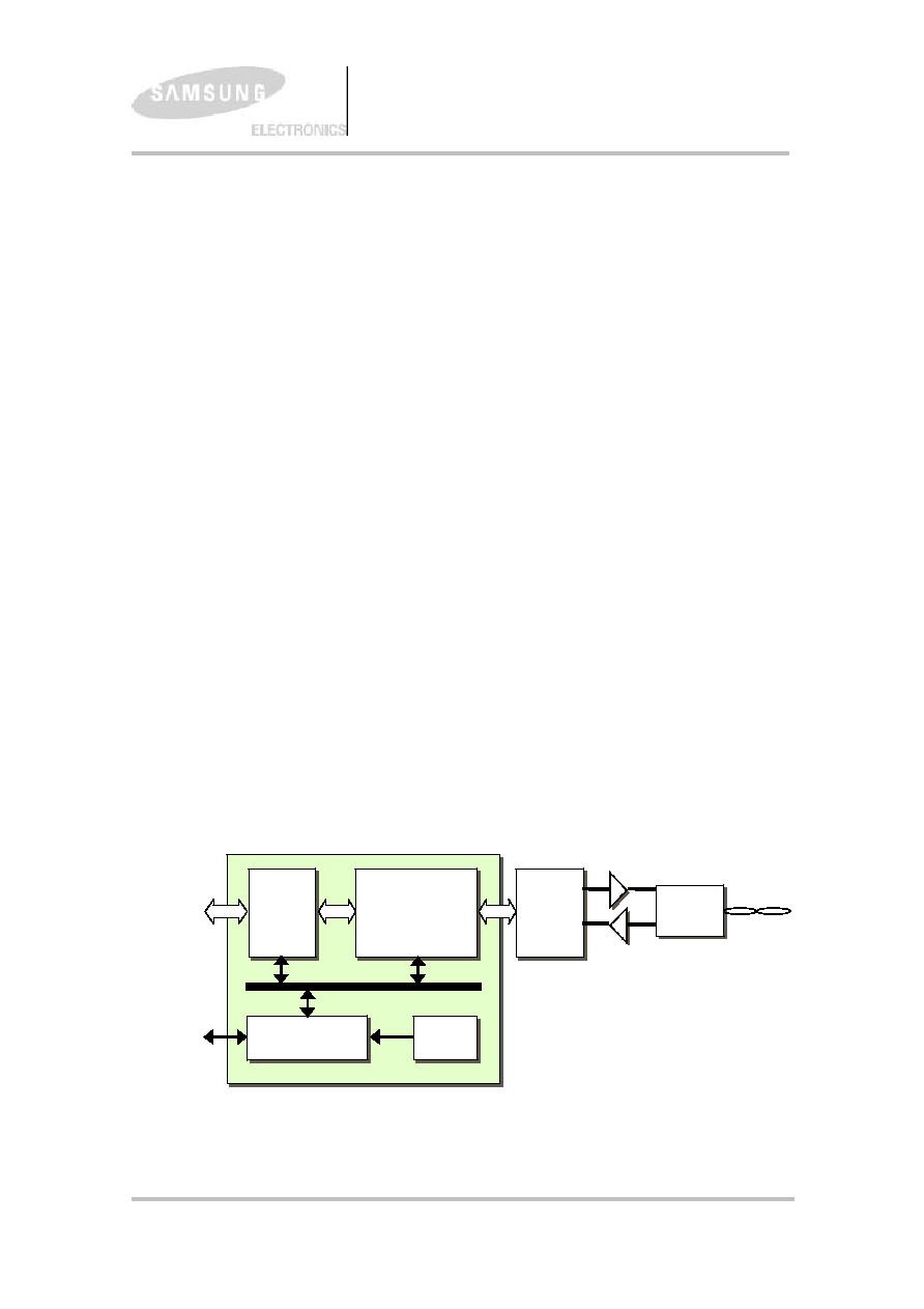
Figure 1: General Block Diagram
Phone
Line
DMT
Processor
Digital
Interface
Analog
Front-
End
Hybrid
Line
Driver
DSP
ROM
ROM
ATM
or
Non-ATM
S5N8944
S5N8943
Host