
CODEC FOR DIGITAL ANSWERING PHONE
S5T8554B03
1
INTRODUCTION
The S5T8554B03 consists of on-chip PCM encoders, decoders (PCM CODECs)
and PCM line filter. This device provides all the functions required to
interface a full-duplex voice telephone circuit, digital answering phone. This
device is designed to perform the transmit encoding and receive decoding as
well as the transmit and receive filtering function in PCM system. Also it is inten-
ded to be used at the analog termination of a PCM line / trunk. This device
provide the Band pass filtering of the analog signals prior to encoding and
after decoding. This combination device performs the encoding and decoding
of voice and call progress tones as well as the signaling and supervision
information.
FEATURES
∑
Complete CODEC and filtering system
∑
Encoding / Decoding : 8 bits
µ
-law PCM
∑
On-chip auto zero, sample and hold,
and precision voltage references
∑
Low power dissipation : 60mW ( operating )
3mW ( standby )
∑
±
5V operation
∑
TTL or CMOS compatible
∑
Automatic power down
ORDERING INFORMATION
PIN CONFIGURATION
Device
Package
Operating Temperature
S5T8554B03-D0B0
16
-
DIP
-
300
0 ~ + 70
∞
C
S5T8554B03-S0B0
16
-
SOP
-
BD300
16
-
DIP
-
300
16
-
SOP
-
BD300
1
2
3
4
5
6
7
8
16
15
14
13
12
11
10
9
V
BB
GNDA
VF
R
O
V
CC
FS
R
D
R
BCLK
R
/CLKSEL
MCLK
R
/PDN
KS8620
VFI
X
I+
VF
X
I-
GS
X
TS
X
FS
X
D
X
BCLK
X
MCLK
X
S5T8554B03
S5T8554B03
CODEC FOR DIGITAL ANSWERING PHONE
2
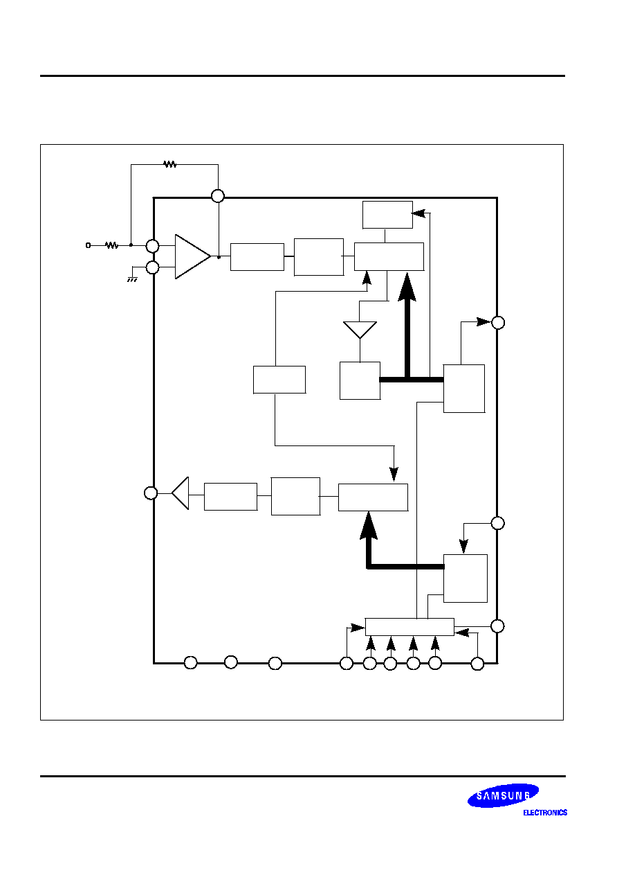
BLOCK DIAGRAM
Figure 1.
Vcc
V
BB
GND
A
MCLKx
MCLK
R
/
PDN
BCLKx
BCLK
R
/
CLKSEL
FS
R
FSx
R1
R2
Analog In
-
+
RC Active
Filter
Switched
Capacitor
B.P.F
16
15
14
3
Auto-zero
logic
Sample & Hold
DAC
A/D
Control
Logic
X
' m
it
register
DE
Receive
register
CLK
Sample & Hold
DAC
Voltage
Reference
RC Active
Filter
Switched
Capacitor
L.P.F
11
comparator
6
Power
Amplifier
Timing and Control
13
9
8
5
12
10
7
4
1
2
Dx
D
R
/TSx
VF
R
O
GSx
VFxI+
VFxI-
CODEC FOR DIGITAL ANSWERING PHONE
S5T8554B03
3
PIN DESCRIPTION
ABSOLUTE MAXIMUM RATINGS ( TA = 25
∞
C )
Pin No
Symbol
Description
1
V
BB
V
BB
=
-
5V
±
5%
2
GNDA
Analog ground
3
VF
R
O
Analog output of the receiver filter
4
V
CC
Vcc = + 5V
±
5%
5
FS
R
Receive frame sync pulse. 8kHz pulse train.
6
D
R
PCM data input
7
BCLK
R
/
CLKSEL
Logic input which selects either 1.536MHz/1.544MHz or 2.048MHz for master clock
in normal operation and BCLKx is used for both TX and RX directions.
Alternately direct clock input available, vary from 64kHz to 2.048MHz.
8
MCLK
R
/
PDN
When MCLK
R
is connected continuously high, the device goes powered down .
Normally connected continuously low, MCLKx is selected for all DAC timing.
Alternately direct 1.536MHz/1.544MHz or 2.048MHz clock input is available.
9
MCLK
X
n
1.536MHz/1.544MHz or 2.048MHz clock input is available
10
BCLK
X
May be vary from 64kHz 2.048MHz,
but BCLKx is externally tied with MCLKx in normal operation.
11
D
X
PCM data output.
12
FS
X
TX frame sync pulse. 8kHz pulse train.
13
TS
X
Changed from high to low during the encoder timeslot. Open drain output.
14
GS
X
Analog output of the TX input amplifier.
Used to set gain through external resistor between pin 14 to pin 15.
15
VF
X
I
-
Inverting input stage of the TX analog signal.
16
VF
X
I+
Non-inverting input stage of the TX analog signal.e
Characteristic
Symbol
Value
Unit
Positive Supply Voltage
Vcc
+7
V
Negative Supply Voltage
V
BB
-
7
V
Voltage at any Analog Input or Output
V
I (A)
Vcc + 0.3 to VBB
-
0.3
V
Voltage at any Digital Input or Output
V
I (D)
Vcc + 0.3 to GNDA
-
0.3
V
Operating Temperature Range
Ta
0 to 70
∞
C
Storage Temperature Range
T
STG
-
65 to +150
∞
C
Lead Temperature Range ( soldering, 10 sec )
T
LEAD
300
∞
C
S5T8554B03
CODEC FOR DIGITAL ANSWERING PHONE
4
ELECTRICAL CHARACTERISTICS
(Unless otherwise specified : Ta = 0
∞
C to 70
∞
C , Vcc = 5V
±
5%, V
BB
=
-
5V
±
5%, GND
A
= 0V )
Characteristic
System
Test Conditions
Min.
Typ.
Max.
Unit
Power Dissipation
Power down Current
I
CC ( down )
No Load
-
0.5
3.0
mA
Power down Current
I
BB ( down )
No Load
-
0.05
1.0
mA
Active Current
I
CC ( A )
No Load
-
6.0
10
mA
Active Current
I
BB ( A )
No Load
-
6.0
10
mA
Digital Interface
Input Low Voltage
V
IL
-
-
-
0.6
V
Input High Voltage
V
IH
-
2.2
-
-
V
Input Low Current
I
IL
GND
A
< V
IN
< V
IL
, all digital input
-
15
-
15
µ
A
Input High Current
I
IH
V
IH
< V
IN
< Vcc
-
15
-
15
µ
A
Output Low Voltage
V
OL
D
X
, I
L
= 3.2 mA
SIG
R
, I
L
= 1.0 mA
/TS
X
, I
L
= 3.2 mA , open drain
-
-
0.4
0.4
0.4
V
V
V
Output High Voltage
V
OH
D
X
, I
H
=
-
3.2mA
SIG
R
, I
H
=
-
1.0mA
2.4
2.4
-
-
V
V
Output Current in High
impedance state ( Tri
-
state )
I
OH (HZ)
D
X
, GND
A
< V
O
< Vcc
8
-
15
-
15
µ
A
Analog Interface with Receiver Filter
Output Resistance
R
O
pin VF
R
O
-
1
3
Load Resistance
R
L
VF
R
O =
±
2.5V
600
-
-
Load Capacitance
C
L
-
-
-
500
pF
Output Capacitance
C
L
-
-
200
-
200
mV
Analog Interface with Transmit input Amp
Input Leakage Current
I
LKG
-
2.5V<V<+2.5V, VF
X
I+ or VF
X
I-
-
200
-
200
nA
Input Resistance
R
I
-
2.5V<V<+2.5V, VF
X
I+ or VF
X
I-
10
-
-
M
Output Resistance
R
O
closed loop , unity gain
-
1
3
Load Resistance
R
L
GSx
10
-
-
k
Load Capacitance
C
L
GSx
-
-
50
pF
Output Dynamic Range
V
OD(TX)
GSx , R
L
< 10k
±
2.8
-
-
V
Voltage Gain
G
V
VF
X
I+ to GSx
5000
-
-
V/V
Unity Gain bandwidth
B W
-
1
2
-
MHz
Offset Voltage
V
IO(TX)
-
-
20
-
20
mV
Common - mode Voltage
V
CM(TX)
CMRR
X
A > 60dB
-
2.5
-
2.5
V
Common mode rejection ratio
CMRR
DC test
55
-
-
dB
Power supply rejection ratio
PSRR
DC test
55
-
-
dB

CODEC FOR DIGITAL ANSWERING PHONE
S5T8554B03
5
TIMING CHARACTERISTICS
(Unless otherwise specified : Ta = 0
∞
C to 70
∞
C, Vcc = 5V
±
5%, V
BB
=
-
5V
±
5%, GND
A
= 0V )
Characteristic
System
Test Conditions
Min.
Typ.
Max.
Unit
Frequency of Master Clock
f
MCK
Depends on the device used and
the BCLK
R
/CLKSEL pin. MCLKx
and MCLK
-
1.536
-
MHz
-
1.544
-
-
2.048
-
Rise time of Bit Clock
t
R(BCK)
t
PB
= 488ns
-
-
50
nS
Fall Time of Bit Clock
t
F(BCK)
t
PB
= 488ns
-
-
50
nS
Hold Time for Bit Clock low to
Frame sync
t
H(LFS)
Long Frame only
0
-
-
nS
Hold Time for Bit Clock High to
Frame sync
t
H(HFS)
Short Frame only
0
-
-
nS
Set-up Time from Frame sync
to Bit Clock low
t
SU(FBCL)
Long Frame only
80
-
-
nS
Delay time from BCLKx High
to data valid
t
D(HDV)
Load = 150pF + 2 LSTTL loads
0
-
180
nS
Delay time to /TSx low
t
D(/TSXL)
Load = 150pF + 2 LSTTL loads
-
-
140
nS
Delay time from BCLKx low to
data output disable
t
D(LDD)
50
-
165
nS
Delay Time to valid data from
FSx or BCLKx
t
D(VD)
CL = 0 pF to 150 pF
Whichever comes later.
20
-
165
nS
Set-up Time from D
R
valid to
BCLK x/
R
low
t
SU(DRBL)
-
50
-
-
nS
Hold time from BCLK x/
R
low
to D
R
invalid
t
H(BLDR)
-
50
-
-
nS
Set-up time from FS x/
R
to
BCLK x/
R
low
t
SU(FBLS)
Short Frame sync pulse (1 or 2 bit
clock periods long ) : note1
50
-
-
nS
Width of master clock High
t
W(MCKH)
MCLKx and MCLK
R
160
-
-
nS
Width of master clock Low
t
W(MCKL)
MCLKx and MCLK
R
160
-
-
nS
Rise Time of Master clock
t
R(MCK)
MCLKx and MCLK
R
-
-
50
nS
Fall Time of Master clock
t
F(MCK)
MCLKx and MCLK
R
-
-
50
nS
Set-up time from BCLKx High
(FSx in Long Frame Sync
mode ) to MCLKx falling edge
t
SU(BHMF)
1
's
t bit clock after the leading
edge of FSx
50
-
-
nS
Period of Bit Clock
t
CK
-
485
488
15.725
nS
Width of Bit clock High
t
W(BCKH)
V
IH
= 2.2V
160
-
-
nS
Width of Bit clock Low
t
W(BCKL)
V
IL
= 0.6V
160
-
-
nS
Hold time from BCLK x/
R
to
FS x/
R
low
t
H(BLFL)
Short Frame sync pulse (1 or 2 bit
clock periods long ) : note1
100
-
-
nS