PLL FREQUENCY SHNTHESIZER FOR PAGER
S5T8808A
1
INTRODUCTION
S5T8808A is a superior low-power-programmable PLL frequency
synthesizer which can be used in a high performance Wide Area
Pager system.
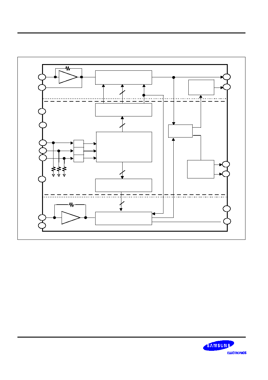
S5T8808A consists of 2 kinds of divider block including a 17bit Shift
register, 16-bit Latch, 14/16-bits Counter, Prescaler, and a phase
detector block including a Phase detector, Lock detector and a
Charge pump.
FEATURES
∑
Maximum operating frequency:
120MHz @ 500mV
P-P
, V
DD1
= 0.95V, V
DD2
= 3.0V
165MHz @ 500mV
P-P
, V
DD1
= 1.0V, V
DD2
= 3.0V
∑
On-chip reference oscillator supports external crystal which oscillates up to 18MHz
∑
Superior supply current:
F
FIN
= 90MHz, I
DD1
= 0.6mA (Typ.) @ V
DD1
= 1.0V, V
DD2
= 3.0V
F
FIN
= 150MHz, I
DD1
= 0.9mA (Typ.) @ V
DD1
= 1.0V, V
DD2
= 3.0V
∑
Operating voltage: V
DD1
= 0.95 ~ 2.0V and V
DD2
= 2.0 ~ 3.3V
∑
Reference frequency counter divider range: 1 / 28 ~ 1 / 65532 (Multiple 4)
But, the Divider range with FRC_High state: 1 / 7 ~ 1 / 16383
∑
RX frequency counter divider range: 1 / 28 ~ 1 / 65535
∑
Package type: 16
-
TSSOP (0.65mm)
ORDERING INFORMATION
+: New Product
Device
Package
Operating Temperature
+S5T8808A01-R0B0
16
-
TSSOP
-
0044
-
25
∞
C to +75
∞
C
16
-
TSSOP
-
0044
( Magnification = 1 : 4 )

S5T8808A
PLL FREQUENCY SHNTHESIZER FOR PAGE
4
PIN DESCRIPTION
Pin No
Symbol
I/O
Description
1
OSCI
I
These input / output pins generate the reference frequency.
In case of OSCI Pin, external reference frequency can be used through the AC
coupling.
2
OSCO
O
3
V
DD2
-
The highest potential supply terminal that can be supplied up to 2.0 ~ 3.3V,
except for V
DD1
.
4
PDA
O
The Output of RX Phase detector terminal for active loop filter
There are 3-kinds of output signal states according to Rx Loop Error;
-
If Fr > Fn (Fr is leading), the output is negative pulse state,
-
If Fr < Fn (Fr is lagging), the output is positive pulse state,
-
If Fr = Fn (the same phase), the output is high impedance state.
5
PDP
O
The Output of RX Phase detector terminal for passive loop filter
There are 3-kinds of output signal states according to Rx Loop Error;
-
If Fr > Fn (Fr is lagging), the output is negative pulse state,
-
If Fr < Fn (Fr is leading), the output is positive pulse state,
-
If Fr = Fn (the same phase), the output is high impedance state.
6
V
SS
-
Ground terminal
7
Fin
I
Input terminal for 16 bit Divider from VCO.
Mostly, VCO output should be input through the AC coupling and the minimum
input level is 500mV
P-P
(in case of 90MHz)
8
V
DD1
-
Voltage supply terminal for Oscillator and Fin block.
This pin can be supplied up to 0.95 ~ 2.0V from V
SS
.
9
NC
-
No Connection
10
LDT
O
Lock detector is also on output of the Phase Detector.
The LOW state of this output shows unlock status, which is the error width
between the Ref. signal and the VCO output signal.
11
CLK
I
These pins are controlled by the
µ
-controller and it also has Schmitt Trigger
architecture.
Internally biased pull-down.
The features of these pins are as follows:
Clock input for 17-bit Shift Register, Serial data input (it include FnFr-on / off and
FRC), and Latch enable input (User selectable EN1 or EN2).
12
DATA
I
13
EN
I
14
Fn
O
Output terminal for divider value of N-counter. To control the output On/Off, the
FnFr bit of the Reference register can be programmed.
When FnFr bit is set to High, this output shows low level.
15
Fr
O
Output terminal of divider value of N-counter. To control the output On/Off, the
FnFr bit of the Reference register can be programmed.
When FnFr bit is set to High, this output shows low level.
16
NC
-
No Connection. Internally biased pull-up.
PLL FREQUENCY SHNTHESIZER FOR PAGER
S5T8808A
5
ABSOLUTE MAXIMUM RATINGS
ELECTRICAL CHARACTERISTICS
(Ta = 25
∞
C, V
DD1
= 1.0V, V
DD2
= 3.0V, unless otherwise specified)
Characteristic
Symbol
Value
Unit
Supply Voltage
V
DD
~ V
DD2
-
0.3 ~ +4.0
V
Input Voltage
V
I
V
SS
-
0.3 ~ V
DD
+ 0.3
V
Power Dissipation
P
D
350
mW
Operating Temperature
T
OPR
-
25 ~ +75
∞
C
Storage Temperature
T
STG
-
40 ~ +125
∞
C
Characteristic
Symbol
Test Conditions
Min.
Typ.
Max.
Unit
Operating voltage
V
DD1
-
0.95
1.0
2.0
V
V
DD2
-
2.0
3.0
3.3
Operating current
I
DD1
F
OSCI
= 12.8MHz
@ 0.3V
P-P
V
DD1
= 1.0V
V
DD2
= 1.0V
F
FIN
= 90MHz
-
0.6
-
mA
I
DD2
F
FIN
= 150MHz
-
0.9
-
Standby current
I
SB
V
DD1
= 0V, V
DD2
= 3.0V
-
-
10
µ
A
Input Voltage
(DATA, CLK, EN, BS)
V
IL
-
-
-
0.3
V
V
IH
-
V
DD3
-0.3
-
-
Input current
(Fin, Xin)
V
IH
V
IH
= V
DD1
-
-
20
µ
A
V
IL
V
IL
= 0V
-
-
20
Input frequency
F
FIN
F
FIN
= 0.5V
P-P
V
DD1
= 0.95V
-
-
120
MHz
V
DD1
= 1.0V
-
-
165
F
OSCI
V
OSCI
= 0.5V
P-P
7
-
18
Output current
(PDA, PDP)
I
OH1
V
OH
= 0.4V
1.0
-
-
mA
I
OL1
V
OL
= V
DD1
- 0.4V
1.0
-
-
Output current
(Fr, Fn, LDT)
I
OH2
V
OH
= 0.4V
0.1
-
-
mA
I
OL2
V
OL
= V
DD1
- 0.4V
0.1
-
-
Setup-time
(DATA-CLK, CLK-EN)
ts
-
2
-
-
µ
S
Hold time
t
H
-
2
-
-
µ
S