PLL FREQUENCY SYNTHESIZER FOR PAGER
S5T8809
1
INTRODUCTION
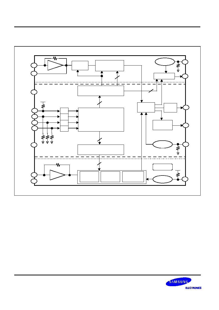
S5T8809 is a superior low-power-programmable PLL frequency
synthesizer which can be used in high performance / Simple
application for a Wide Area Pager system.
S5T8809 consists of 2 kinds of divider block including a 19-bit Shift
register, 16/18-bit Latch, 13/15bits R-counter and 16/18-bit N-
Counter, 32/33 Prescaler, and a phase detector block including a
Phase detector, Lock detector and a Charge pump.
S5T8809 also has a battery saving mode which can control each
register block by serial control data from the
µ
-controller (MICOM)
and it also boosts up signal output for fast locking.
FEATURES
·
Maximum operating frequency: 330MHz @ 300mV
P-P
, V
DD1
= 1.0V, V
DD2
= 3.0V
·
On-chip reference oscillator supports external crystal which oscillates up to 23MHz
·
Superior supply current:
-- F
FIN
= 310MHz, I
DD1
= 0.8mA (Typ.) @ V
DD1
= 1.0V, V
DD2
= 3.0V
·
Operating voltage: V
DD1
= 0.95 to 1.5V and V
DD2
= 2.0 to 3.3V
·
Excellent Divider range:
-- Ref. Divider:
FRC (0): 1 / 40 to 1 / 65528 (Multiple): Default
FRC (1): 1 / 5 to 1 / 32767
-- Rx Divider:
PBC (0): 1 / 1056 to 1 / 65535: Default
PBC (1): 1 / 1056 to 1 / 262143
·
Boost-up signal output for Fast Locking
·
In the Standby mode, VDD1 block can be controlled by BSB Pin status
-- Standby current consumption: 10
µ
A (Max.)
·
Programmable control the output of LD to reduce internal noise
·
Programmable 17 / 19-bit shift register value controlled by PBC
·
Charge pump output circuitry for passive filter
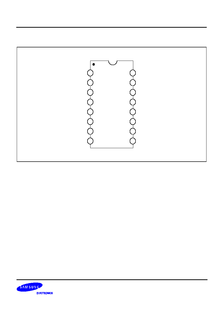
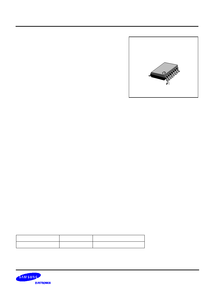
·
Package type: 16
-
TSSOP (0.65mm)
ORDERING INFORMATION
Device
Package
Operating Temperature
S5T8809X01-R0B0
16
-
TSSOP
-
0044
-
25
°
C to +75
°
C
16-TSSOP-0044
( Magnification = 1 : 4 )
S5T8809
PLL FREQUENCY SYNTHESIZER FOR PAGER
4
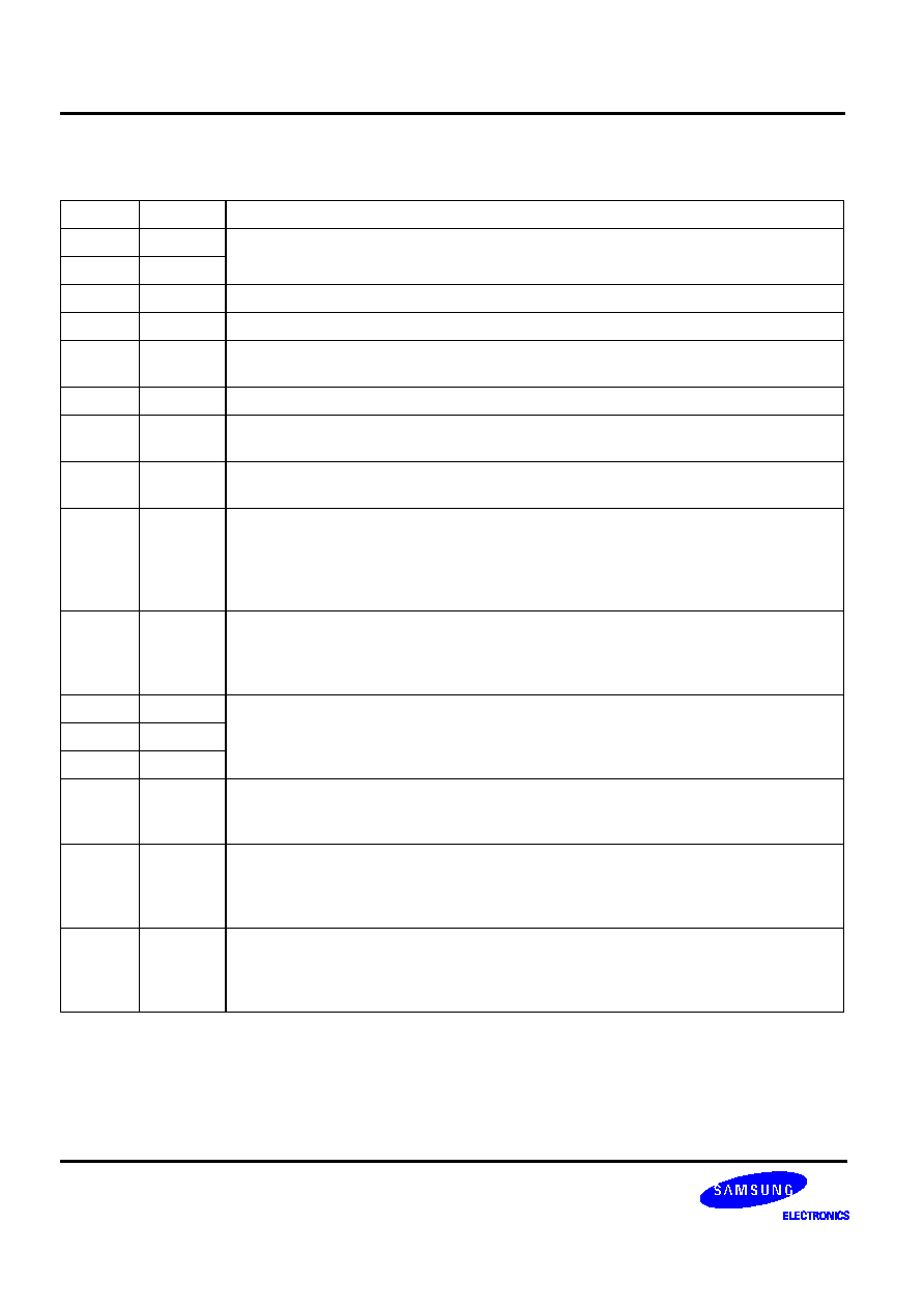
PIN DESCRIPTION
Pin No
Symbol
Description
1
OSCI
These input / output pins generate the reference frequency.
In case of OSCI Pin, external reference frequency can be used through the AC coupling.
2
OSCO
3
V
DD2
The highest potential supply terminal that can be supplied up to 2.0 to 3.3V.
4
FL
Booster signal output for fast locking.
5
PDO
The output of RX phase detector terminal for passive loop filter.
There are 3-kinds of output signal states according to Rx loop error.
6
V
SS
Ground terminal
7
Fin
Input terminal for the frequency from VCO.
Output frequency from VCO was inputted through AC coupling
8
V
DD1
Voltage supply terminal for Oscillator and Fin block.
This pin can be supplied up to 0.95 to 1.5V from V
SS
.
9
PBC
This is an input for programmable bit control which has Schmitt Trigger architecture,
Internally biased pull-up.
High = 16 Bits N-Divider (Default: ND0 to ND15)
Low = 18 Bits N-Divider (ND0 to ND7)
cf) R-divider bits will be changed by the FRC bit of program
10
LD
The output of phase detector can be controlled by R-counter register. When the LDC bit
of R-counter set to Low, the output will be disabled to reduce a noise problem, but if it is
set to High, the output will be enabled to show an lock / unlock status that is the error
width between to Ref. signal and the VCO output signal.
11
CLK
These pins are controlled by the
µ
-controller which has Schmitt Trigger architecture,
Internally biased pull-down. The features of these pins are as follows; Clock input for 17
or 19-bit Shift Register, Serial data input (it include TEST1, FRC and LDC), and Latch
enable input.
12
DATA
13
EN
14
BSB
In the BS mode (set to Low), the VDD1 block will be powered off, but the internal latch
data is still valid because the VDD2 is supplied continuously. This input has Schmitt
Trigger architecture & internally biased pull-up.
15
FLC
This is the input pin for Fast Locking Control (FLC) which has Schmitt Trigger
architecture, Internally biased pull-down.
Low = The Current of PDO Charge pump output is Normal (Default: x1)
High = The Current of PDO Charge pump output is increase (x 1.5)
16
TEST
This is the input pin for TEST which has Schmitt trigger architecture, Internally biased
Pull-down.
Low = All block will be operated as normal state (Default)
High = LD and FL state will be TEST mode
PLL FREQUENCY SYNTHESIZER FOR PAGER
S5T8809
5
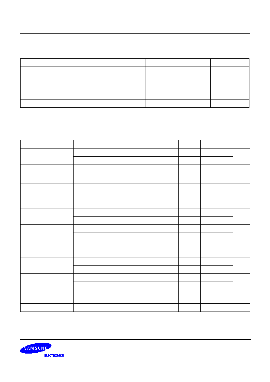
ABSOLUTE MAXIMUM RATINGS
ELECTRICAL CHARACTERISTICS
(Ta = 25
°
C, V
DD1
= 1.0V, V
DD2
= 3.0V, unless otherwise specified)
Characteristic
Symbol
Value
Unit
Supply Voltage
V
DD1
to V
DD2
-
0.3 to +4.0
V
Input Voltage
V
I
V
SS
-
0.3 to V
DD
+ 0.3
V
Power Dissipation
P
D
350
mW
Operating Temperature
T
OPR
-
25 to +75
°
C
Storage Temperature
T
STG
-
40 to +125
°
C
Characteristic
Symbol
Test Conditions
Min.
Typ.
Max.
Unit
Operating voltage
V
DD1
-
0.95
1.0
1.5
V
V
DD2
-
2.0
3.0
3.3
Operating current
IDD
F
OSCI
= 12.8MHz
F
FIN
= 310MHz @ 0.3V
P-P
V
DD1
= 1.0V, V
DD2
= 3.0V, BSB=High
-
0.8
-
mA
Standby current
ISB1
V
DD1
= 0.0V, V
DD2
= 3.0V, BSB=Low
-
0.1
10
µ
A
Input voltage
(DATA, CLK, EN, BS)
V
IL
-
-
-
0.3
V
V
IH
-
V
DD2
-0.3
-
-
Input voltage
(TEST, PBC)
V
IL
-
-
-
0.2
V
V
IH
-
V
SS1
-0.2
-
-
Input current
(Fin, Xin)
I
IH
V
IH
= V
DD1
, BSB = High
-
-
20
µ
A
I
IL
V
IL
= 0V, BSB = High
-
-
20
Input frequency
F
FIN
V
FIN
= 0.3V
P-P
, V
DD1
= 1.0V
40
-
330
MHz
F
OSCI
V
OSCI
= 0.3V
P-P
, V
DD1
= 1.0V
7
12.8
23
Output current
(PDO, FL)
I
OH1
V
OH
= 0.4V
1.0
-
-
mA
I
OL1
V
OL
= V
DD2
- 0.4V
1.0
-
-
Output current
(LD)
I
OH2
V
OH
= 0.4V
0.1
-
-
mA
I
OL2
V
OL
= V
DD2
- 0.4V
0.1
-
-
Setup-time
(DATA-CLK, CLK-EN)
ts
-
2
-
-
µ
S
Hold time
t
H
-
2
-
-
µ
S