 | ÐлекÑÑоннÑй компоненÑ: S6A0069X | СкаÑаÑÑ:  PDF PDF  ZIP ZIP |
þÿ

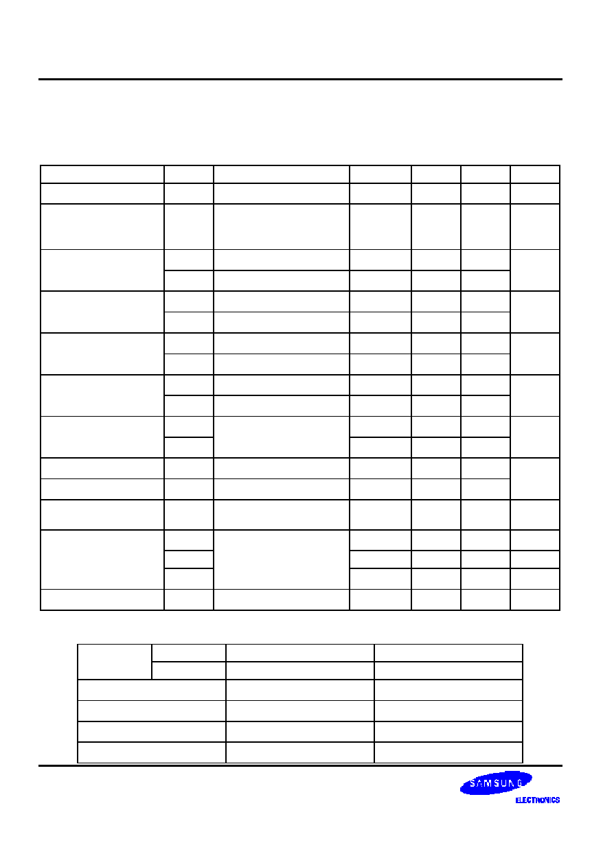
16COM/40SEG DRIVER & CONTROLLER FOR DOT MATRIX LCD
S6A0069
1
INTRODUCTION
S6A0069 is a dot matrix LCD driver & controller LSI which is fabricated by low power CMOS technology. It can
display 1, 2-line with 5 x 8 or 5 x 11 dots format.
FUNCTIONS
--
Character type dot matrix LCD driver & controller.
--
Internal driver: 16 common and 40 segment signal output.
--
Easy interface with 4-bit or 8-bit MPU
--
Display character pattern : 5 x 8 dots format (204 kinds), 5 x 11 dots format (32 kinds)
--
The special character pattern can be programmable by Character Generator RAM directly.
--
A customer character pattern can be programmable by mask option.
--
It can drive a maximum 80 characters by using the S6A0065 or S6A2067 externally.
--
Various instruction functions
--
Automatic power on reset
FEATURES
--
Internal Memory
Character Generator ROM (CGROM): 10,080 bits
(204 characters x 5 x 8 dot) & ( 32 characters x 5 x 11 dot)
Character Generator RAM (CGRAM): 64
×
8 bits (8 characters
×
5
×
8 dot)
Display Data RAM (DDRAM): 80 x 8 bits (80 characters max.)
--
Low Power Operation
Power supply voltage range: 2.7 to 5.5V (V
DD
)
LCD drive voltage range: 3.0 to 13.0V (V
DD
V5)
--
CMOS process
--
Programmable duty cycle: 1/8, 1/11, 1/16
--
Internal oscillator with an external resistor
--
Low power consumption
--
80 QFP or bare chip available

S6A0069
16COM/40SEG DRIVER & CONTROLLER FOR DOT MATRIX LCD
2
Precautions for Light
Light has characteristics to move electrons in the integrated circuitry of semiconductors, therefore may change
the characteristics of semiconductor devices when irradiated with light. Consequently, the users of the packages
which may expose chips to external light such as COB, COG, TCP and COF must consider effective methods to
block out light from reaching the IC on all parts of the surface area, the top, bottom and the sides of the chip.
Follow the precautions below when using the products.
1. Consider and verify the protection of penetrating light to the IC at substrate (board or glass) or product
design stage.
2. Always test and inspect products under the environment with no penetration of light.
16COM/40SEG DRIVER & CONTROLLER FOR DOT MATRIX LCD
S6A0069
3
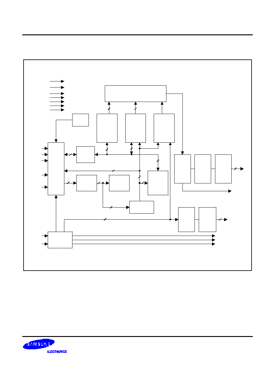
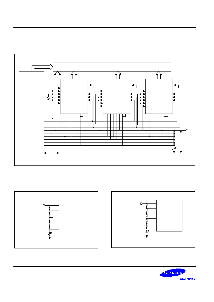
BLOCK DIAGRAM
VDD
GND
V1
V2
V3
V4
V5
Parallel to Serial
Data Conversion Circuit
Busy
Flag
Character
Generator
ROM
(CGROM)
10080 bits
Character
Generator
RAM
(CGRAM)
512 bits
Cursor
& Blink
Controller
5
5
Input/
Output
Buffer
Data
Register
(DR)
Instruction
Register
(IR)
Instruction
Decoder
(ID)
Address
Counter
Display
Data RAM
(DDRAM)
80x8 bits
Timing
Generator
Circuit
16-bit
Shift
Register
Common
Driver
40-bit
Shift
Register
40-bit
Latch
Circuit
Seg-
ment
Driver
R/W
RS
E
DB0-
DB3
DB4-
DB7
OSC1
OSC2
CLK1
CLK2
M
D
S1-S40
C1-C16
8
8
8
7
7
8
7
8
8
7
7
16
16
Figure 1. S6A0069 Block Diagram
S6A0069
16COM/40SEG DRIVER & CONTROLLER FOR DOT MATRIX LCD
4
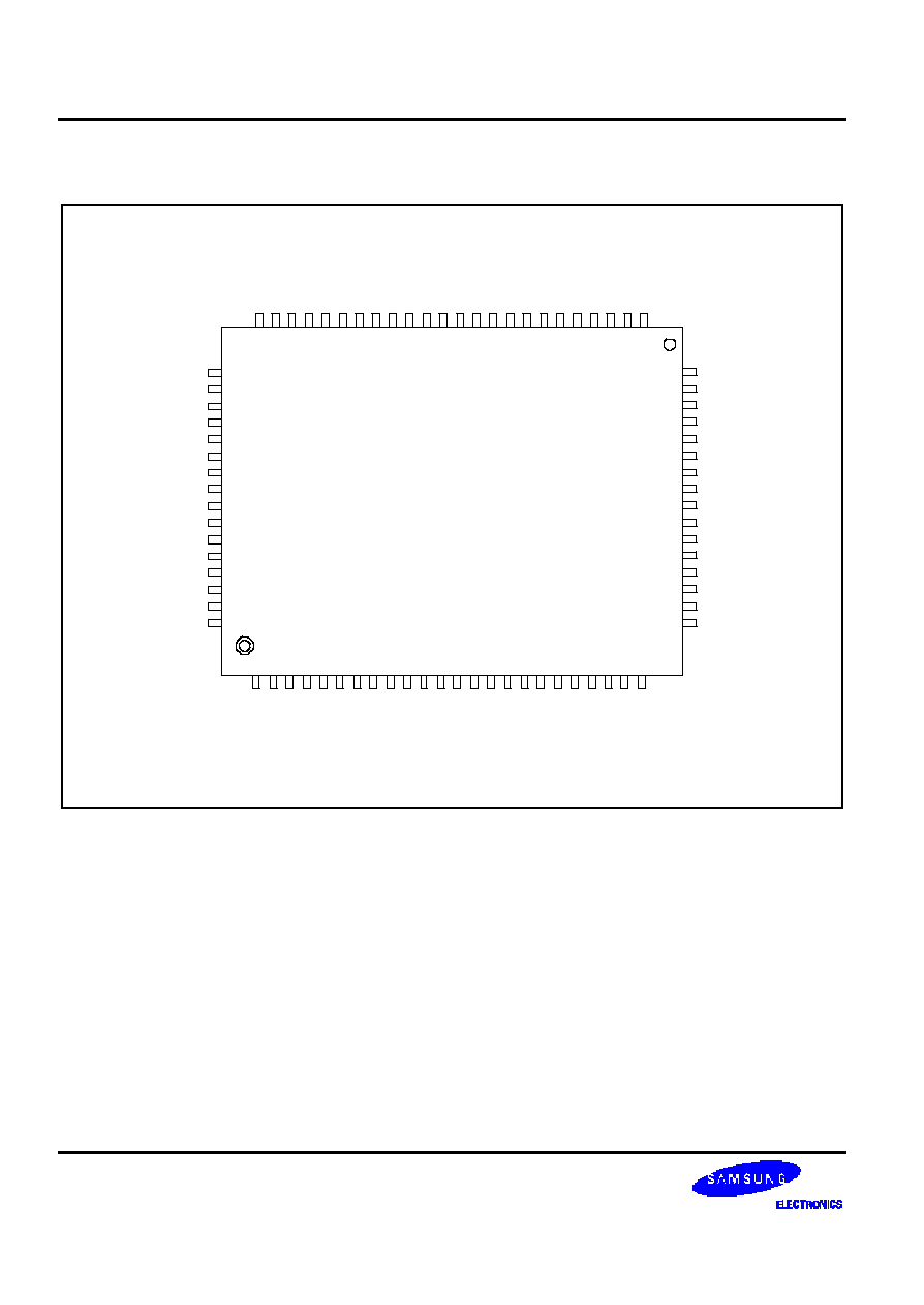
PIN CONFIGURATION
S38
S37
S36
S35
S34
S33
S32
S31
S30
S29
S28
S27
S26
S25
S24
S23
S6A0069
65
66
67
68
69
70
71
72
73
74
75
76
77
78
79
80
S39
S40 C16 C15
C14 C13
C12 C11 C10
C9 C8
C7 C6 C5
C4 C3
C2 C1
DB7 DB6 DB5
DB4 DB3
DB2
64
63 62 61
60 59
58 57 56
55 54
53 52 51
50 49
48 47
46 45 44
43 42
41
1
2 3
4 5 6
7 8
9 10
11 12 13
14 15
16 17 18
19 20
21 22 23
24
S22
S21 S20
S19 S18 S17
S16 S15
S14 S13
S12 S11 S10
S9 S8
S7 S6 S5
S4 S3
S2 S1
GND
OSC1
40
39
38
37
36
35
34
33
32
31
30
29
28
27
26
25
DB1
DB0
E
R/W
RS
D
M
VDD
CLK2
CLK1
V5
V4
V3
V2
V1
OSC2
Figure 2. S6A0069 Pin Configuration
16COM/40SEG DRIVER & CONTROLLER FOR DOT MATRIX LCD
S6A0069
5
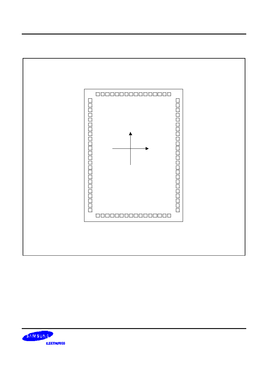
PAD CONFIGURATION
25
26 27
28 29 30
31 32
33 34 35
36 37
38 39
40
80
79 78 77
76 75
74 73 72
71 70
69 68 67
66 65
1
2
3
4
5
6
7
8
9
10
11
12
13
14
15
16
17
18
19
20
21
22
23
24
64
63
62
61
60
59
58
57
56
55
54
53
52
51
50
49
48
47
46
45
44
43
42
41
S6A0069
Chip size: 4060
×
3840
Pad size: 100
×
100
Unit:
µ
m
(0, 0)
X
Y
S22
S21
S20
S19
S18
S17
S16
S15
S14
S13
S12
S11
S10
S9
S8
S7
S6
S5
S4
S3
S2
S1
GND
OSC1
OSC2
V1 V2
V3 V4 V5
CLK1 CLK2
VDD
M D
RS
R/W
E
DB0
DB1
S39
S40
C16
C15
C14
C13
C12
C11
C10
C9
C8
C7
C6
C5
C4
C3
C2
C1
DB7
DB6
DB5
DB4
DB3
DB2
S23 S24
S25 S26 S27
S28 S29
S30 S31 S32
S33 S34
S35 S36
S37 S38
Figure 3. S6A0069 Pad Configuration
S6A0069
16COM/40SEG DRIVER & CONTROLLER FOR DOT MATRIX LCD
6
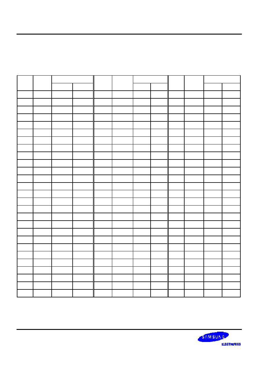
PAD CENTER COORDINATES
Table 1. Pad Center Coordinates
[Unit: um]
PAD
PAD
COORDINATE
PAD
PAD
COORDINATE
PAD
PAD
COORDINATE
NUM.
NAME
X
Y
NUM.
NAME
X
Y
NUM.
NAME
X
Y
1
S22
-1864
1465
28
V3
-670
-1754
55
C9
1864
335
2
S21
-1864
1340
29
V4
-520
-1754
56
C10
1864
460
3
S20
-1864
1215
30
V5
-370
-1754
57
C11
1864
585
4
S19
-1864
1090
31
CLK1
-220
-1754
58
C12
1864
710
5
S18
-1864
965
32
CLK2
-70
-1754
59
C13
1864
835
6
S17
-1864
840
33
VDD
80
-1754
60
C14
1864
960
7
S16
-1864
715
34
M
230
-1754
61
C15
1864
1085
8
S15
-1864
590
35
D
380
-1754
62
C16
1864
1210
9
S14
-1864
465
36
RS
518
-1754
63
S40
1864
1341
10
S13
-1864
340
37
R/W
642
-1754
64
S39
1864
1466
11
S12
-1864
215
38
E
768
-1754
65
S38
886
1754
12
S11
-1864
90
39
DB0
894
-1754
66
S37
760
1754
13
S10
-1864
-35
40
DB1
1018
-1754
67
S36
636
1754
14
S9
-1864
-160
41
DB2
1864
-1488
68
S35
510
1754
15
S8
-1864
-285
42
DB3
1864
-1362
69
S34
386
1754
16
S7
-1864
-410
43
DB4
1864
-1238
70
S33
260
1754
17
S6
-1864
-535
44
DB5
1864
-1112
71
S32
136
1754
18
S5
-1864
-660
45
DB6
1864
-988
72
S31
10
1754
19
S4
-1864
-785
46
DB7
1864
-862
73
S30
-114
1754
20
S3
-1864
-910
47
C1
1864
-665
74
S29
-240
1754
21
S2
-1864
-1034
48
C2
1864
-540
75
S28
-364
1754
22
S1
-1864
-1159
49
C3
1864
-415
76
S27
-490
1754
23
GND
-1864
-1285
50
C4
1864
-290
77
S26
-614
1754
24
OSC1
-1864
-1414
51
C5
1864
-165
78
S25
-740
1754
25
OSC2
-1120
-1754
52
C6
1864
-40
79
S24
-864
1754
26
V1
-970
-1754
53
C7
1864
85
80
S23
-989
1754
27
V2
-820
-1754
54
C8
1864
210
16COM/40SEG DRIVER & CONTROLLER FOR DOT MATRIX LCD
S6A0069
7
PIN DESCRIPTION
Table 2. Pin Description
PIN
No
I/O
NAME
DESCRIPTION
INTERFACE
V
DD
33
Supply
For logical circuit (+3V
±
10%,+5V
±
10%) Power Supply
GND
23
Voltage
0V (GND)
V1 - V5
26- 30
Bias voltage level for LCD driving.
S1 - S40
1-22,
63- 80
O
Segment output
Segment signal output for LCD drive.
LCD
C1 - C16
47-62
O
Common output
Common signal output for LCD drive.
LCD
OSC1
24
I
Oscillator
When use internal oscillator, connect
external Rf resistor. If external clock is
used, connect it to OSC1.
External
Resistor/
Oscillator
OSC2
25
O
Oscillator
OSC1
CLK1
31
O
Extension driver
Latch clock
extension driver latch clock.
Extension
driver
CLK2
32
O
Extension driver
Shift clock
extension driver shift clock.
M
34
O
Alternated signal for
LCD driver output
Outputs the alternating signal to convert
LCD driver waveform to AC.
Extension
driver
D
35
O
Display data
interface
Outputs extension driver data (the 41th
dot's data)
Extension
driver
RS
36
I
Register select
Used as register selection input. When
RS = "High", Data register is selected.
When RS = "Low", Instruction register is
selected.
MPU
R/W
37
I
Read/Write
Used as read/write selection input.
When R/W = "High", read operation.
When R/W = "Low", write operation.
MPU
E
38
I
Read/write enable
Read/write enable signal.
MPU
DB0-
DB3
39-42
O
Data bus 0-7
When 8-bit bus mode, used as low order
bi-directional data bus.
During 4-bit bus mode open these pins.
MPU
DB4-
DB7
43-46
When 8-bit bus mode, used as high order
bi-directional data bus. In case of 4-bit bus
mode, used as both high and low order.
DB7 is used for Busy Flag output.
MPU
S6A0069
16COM/40SEG DRIVER & CONTROLLER FOR DOT MATRIX LCD
8
FUNCTION DESCRIPTION
System Interface
This chip has all two kinds of interface type with MPU : 4-bit bus and 8-bit bus. 4-bit bus and 8-bit bus is selected by
DL bit in the instruction register. During read or write operation, two 8-bit registers are used. one is data register
(DR), the other is instruction register(IR). The data register(DR) is used as temporary data storage place for being
written into or read from DDRAM/CGRAM, target RAM is selected by RAM address setting instruction. Each internal
operation, reading from or writing into RAM, is done automatically. So to speak, after MPU reads DR data, the data
in the next DDRAM/CGRAM address is transferred into DR automatically. Also after MPU writes data to DR, the
data in DR is transferred into DDRAM/CGRAM automatically. The instruction register (IR) is used only to store
instruction code transferred from MPU. MPU cannot use it to read instruction data. To select register, use RS input
pin in 4-bit/8-bit bus mode.
Table 3. Various Kinds of Operations according to RS and R/W Bits
RS
R/W
Operation
L
L
Instruction Write operation (MPU writes Instruction code into IR)
L
H
Read Busy Flag (DB7) and address counter (DB0 - DB6)
H
L
Data Write operation (MPU writes data into DR)
H
H
Data Read operation (MPU reads data from DR)
Busy Flag (BF)
When BF = "High", it indicates that the internal operation is being processed. So during this time the next instruction
cannot be accepted. BF can be read, when RS = Low and R/W = High (Read Instruction Operation), through DB7
port. Before executing the next instruction, be sure that BF is not High.
Address Counter (AC)
Address Counter(AC) stores DDRAM/CGRAM address, transferred from IR. After writing into (reading from)
DDRAM/CGRAM, AC is automatically increased (decreased) by 1. When RS = "Low" and R/W = "High", AC can be
read through DB0 - DB6 ports.
16COM/40SEG DRIVER & CONTROLLER FOR DOT MATRIX LCD
S6A0069
9
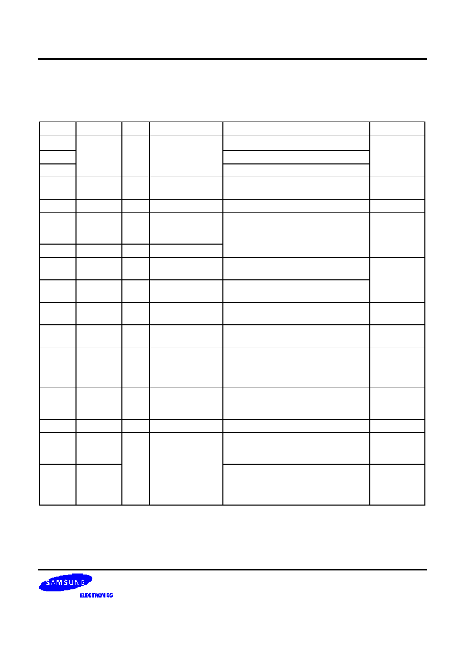
Display Data RAM (DDRAM)
DDRAM stores display data of maximum 80 x 8 bits (80 characters). DDRAM address is set in the address counter
(AC) as a hexadecimal number. (refer to Figure4.)
AC6
AC5
AC4
AC3
AC2
AC1
AC0
LSB
MSB
Figure 4. DDRAM Address
1) 1-line Display
In case of 1 line display, the address range of DDRAM is 00H - 4FH. Extension driver will be used. Figure 5 shows
the example that 40 segment extension driver is added.
Display position
DDRAM Address
00
1
COM1
COM8
01 02 03 04 05 06 07
2
3
4
5
6
7
8
SEG1
S6A0069
SEG40
08
9
09 0A 0B 0C 0D 0E 0F
10 11 12 13 14 15 16
10
17
11 12 13 14 15 16 17
18 19 20 21 22 23 24
SEG1 Extension driver (40 SEG)
SEG40 SEG1 Extension driver (40 SEG)
SEG40
08
1
COM1
COM8
01 02 03 04 05 06 07
2
3
4
5
6
7
8
SEG1
S6A0069
SEG40
10
9
09 0A 0B 0C 0D 0E 0F
10 11 12 13 14 15 16
18
17
11 12 13 14 15 16 17
18 19 20 21 22 23 24
SEG1 Extension driver (40 SEG)
SEG40 SEG1 Extension driver (40 SEG)
SEG40
00
1
COM1
COM8
01 02 03 04 05 06
07
2
3
4
5
6
7
8
SEG1
S6A0069
SEG40
08
9
09 0A 0B 0C 0D 0E
0F
10 11 12 13 14 15 16
10
17
11 12 13 14 15 16
18 19 20 21 22 23 24
SEG1 Extension driver (40 SEG)
SEG40 SEG1 Extension driver (40 SEG)
SEG40
(After Shift Left)
(After Shift Right)
4F
Figure 5. 1-line x 24 Character Display with 40 Segment Extension Driver
S6A0069
16COM/40SEG DRIVER & CONTROLLER FOR DOT MATRIX LCD
10
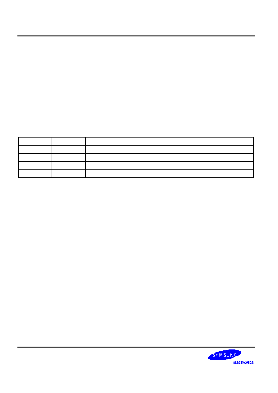
2) 2-line Display
In case of 2 line display, the address range of DDRAM is 00H - 27H, 40H - 67H. Extension driver will be used. Figure
3 shows the example that 40 segment extension driver is added.
Display position
DDRAM Address
00
1
COM1
COM8
01 02 03 04 05 06 07
2
3
4
5
6
7
8
08
9
09 0A 0B 0C 0D 0E 0F
10 11 12 13 14 15 16
10
17
11 12 13 14 15 16 17
18 19 20 21 22 23 24
1
COM1
COM8
01 02 03 04 05 06 07
2
3
4
5
6
7
8
08
9
09 0A 0B 0C 0D 0E 0F
10 11 12 13 14 15 16
10
17
11 12 13 14 15 16 17
18 19 20 21 22 23 24
SEG1
S6A0069
SEG40
SEG1 Extension driver (40 SEG)
SEG40 SEG1 Extension driver (40 SEG)
SEG40
40 41 42 43 44 45 46 47
48 49 4A 4B 4C 4D 4E 4F
50 51 52 53 54 55 56 57
COM9
COM16
SEG1
S6A0069
SEG40
SEG1 Extension driver (40 SEG)
SEG40 SEG1 Extension driver (40 SEG)
SEG40
41 42 43 44 45 46 47 48
49 4A 4B 4C 4D 4E 4F 50
51 52 53 54 55 56 57
COM9
COM16
(After Shift Left)
00
1
COM1
COM8
01 02 03 04 05 06
07
2
3
4
5
6
7
8
08
9
09 0A 0B 0C 0D 0E
0F
10 11 12 13 14 15 16
10
17
11 12 13 14 15 16
18 19 20 21 22 23 24
SEG1
S6A0069
SEG40
SEG1 Extension driver (40 SEG)
SEG40 SEG1 Extension driver (40 SEG)
SEG40
40 41 42 43 44 45 46
47 48 49 4A 4B 4C 4D 4E
4F 50 51 52 53 54 55 56
COM9
COM16
(After Shift Right)
18
58
27
67
Figure 6. 2-line x 24 Character Display with 40 Segment Extension Driver

16COM/40SEG DRIVER & CONTROLLER FOR DOT MATRIX LCD
S6A0069
11
CGROM (Character Generator ROM)
CGROM has a 5 x 8 dots 204 characters pattern and a 5 x 10 dots 32 characters pattern. CGROM has 204
character patterns of 5 x 8 dots, and 32 character patterns of 5 x 11 dots.
CGRAM (Character Generator RAM)
CGRAM has up to 5
×
8 dot, 8 characters. By writing font data to CGRAM, user defined characters can be used.
Timing Generation Circuit
Timing generation circuit generates clock signals for the internal operations.
LCD Driver Circuit
LCD Driver circuit has 16 common and 40 segment signals for LCD driving. Data from CGRAM/CGROM is transferred
to 40 bit segment latch serially, and then it is stored to 40 bit shift latch. When each common is selected by 16 bit
common register, segment data also output through segment driver from 40 bit segment latch.
In case of 1-line display mode, COM1 COM8 have 1/8 duty or COM1 COM11 have 1/11duty, and in 2-line mode,
COM1 COM16 have 1/16 duty ratio.
Cursor/Blink Control Circuit
It controls cursor/blink ON/OFF at cursor position.
Table 4. Relationship between Character Code (DDRAM) and Character Pattern (CGRAM)
S6A0069
16COM/40SEG DRIVER & CONTROLLER FOR DOT MATRIX LCD
12
1
1
1
0
D7 D6 D5 D4 D3 D2 D1 D0 A5 A4 A3 A2 A1 A0 P7 P6 P5 P4 P3 P2 P1 P0
Character Code (DDRAM data)
CGRAM Address
CGRAM Data
Pattern
number
0
0
x
0
0
0
0
0
0
0
0
0
0
0
0
0
0
0
0
0
0
0
1
1
1
1
1
1
1
1
1
1
1
1
.
.
.
.
.
.
.
.
.
.
0
0
0
x
0
1
1
1
0
0
0
0
0
0
0
0
0
0
0
0
0
0
0
1
1
1
1
1
1
1
1
1
1
1
1
x
x
x
0
0
1
1
1
1
1
1
0
1
1
1
1
1
1
1
1
1
0
0
0
0
0
0
0
0
0
0
0
0
0
0
0
0
0
0
0
Pattern 1
x
x
x
0
1
1
0
0
1
1
1
1
1
1
0
1
1
1
1
1
1
1
1
1
0
0
0
0
0
0
0
0
0
0
0
0
0
0
0
0
0
0
0
.
.
.
.
.
.
.
.
.
.
.
.
.
.
.
.
.
.
.
.
Pattern 8
.
.
.
.
.
.
.
.
.
.
.
.
.
.
.
.
.
.
.
.
16COM/40SEG DRIVER & CONTROLLER FOR DOT MATRIX LCD
S6A0069
13
INSTRUCTION DESCRIPTION
OUTLINE
To overcome the speed difference between internal clock of S6A0069 and MPU clock, S6A0069 performs internal
operation by storing control information to IR or DR. The internal operation is determined according to the signal from
MPU, composed of read/write and data bus. Instruction can be divided largely four kinds,
(1) S6A0069 function set instructions (set display methods, set data length, etc.)
(2) Address set instructions to internal RAM
(3) Data transfer instructions with internal RAM
(4) Others
The address of internal RAM is automatically increased or decreased by 1.
NOTE
During internal operation, Busy Flag (DB7) is read High. Busy Flag check must precede the next instruction.
When an MPU program with checking the Busy Flag (DB7) is made, it must be necessary 1/2 fosc for
executing the next instruction by the falling edge of the 'E' signal after the Busy Flag (DB7) goes to "LOW".
CONTENTS
Clear Display
RS
R/W
DB7
DB6
DB5
DB4
DB3
DB2
DB1
DB0
0
0
0
0
0
0
0
0
0
1
Clear all the display data by writing "20H" (space code) to all DDRAM address, and set DDRAM address to "00H"
into AC (address counter). Return cursor to the original status, namely, bring the cursor to the left edge on first line
of the display. Make entry mode increment (I/D = "1").
Return Home
RS
R/W
DB7
DB6
DB5
DB4
DB3
DB2
DB1
DB0
0
0
0
0
0
0
0
0
1
Return Home is cursor return home instruction. Set DDRAM address to "00H" into the address counter. Return
cursor to its original site and return display to its original status, if shifted. Contents of DDRAM does not change.
S6A0069
16COM/40SEG DRIVER & CONTROLLER FOR DOT MATRIX LCD
14
Entry Mode Set
RS
R/W
DB7
DB6
DB5
DB4
DB3
DB2
DB1
DB0
0
0
0
0
0
0
0
1
I/D
SH
Set the moving direction of cursor and display.
I/D : Increment/decrement of DDRAM address (cursor or blink)
When I/D = "High", cursor/blink moves to right and DDRAM address is increased by 1.
When I/D = "Low", cursor/blink moves to left and DDRAM address is decreased by 1.
* CGRAM operates the same as DDRAM, when read from or write to CGRAM.
SH: Shift of entire display
When DDRAM read (CGRAM read/write) operation or SH = "Low", shift of entire display is not performed. If SH =
"High" and DDRAM write operation, shift of entire display is performed according to I/D value (I/D = "1" : shift left, I/D
= "0" : shift right).
Display ON/OFF Control
RS
R/W
DB7
DB6
DB5
DB4
DB3
DB2
DB1
DB0
0
0
0
0
0
0
1
D
C
B
Control display/cursor/blink ON/OFF 1 bit register.
D : Display ON/OFF Control Bit
When D = "High", entire display is turned on.
When D = "Low", display is turned off, but display data is remained in DDRAM.
C : Cursor ON/OFF Control Bit
When C = "High", cursor is turned on.
When C = "Low", cursor is disappeared in current display, but I/D register remains its data.
B : Cursor Blink ON/OFF Control Bit
When B = "High", cursor blink is on, that performs alternate between all the high data and display character at the
cursor position.
When B = "Low", blink is off.
Cursor or Display Shift
RS
R/W
DB7
DB6
DB5
DB4
DB3
DB2
DB1
DB0
0
0
0
0
0
1
S/C
R/L
Shifting of right/left cursor position or display without writing or reading of display data. This instruction is used to
correct or search display data (Refer to table 5). During 2-line mode display, cursor moves to the 2nd line after the
40th digit of the 1st line. Note that display shift is performed simultaneously in all the lines. When displayed data is
shifted repeatedly, each line is shifted individually. When display shift is performed, the contents of the address
counter are not changed.
16COM/40SEG DRIVER & CONTROLLER FOR DOT MATRIX LCD
S6A0069
15
Table 5. Shift Patterns According to S/C and R/L Bits
S/C
R/L
Operation
0
0
Shift cursor to the left, AC is decreased by 1
0
1
Shift cursor to the right, AC is increased by 1
1
0
Shift all the display to the left, cursor moves according to the display
1
1
Shift all the display to the right, cursor moves according to the display
Function Set
RS
R/W
DB7
DB6
DB5
DB4
DB3
DB2
DB1
DB0
0
0
0
0
1
DL
N
F
DL : Interface Data Length Control Bit
When DL = "High", it means 8-bit bus mode with MPU.
When DL = "Low", it means 4-bit bus mode with MPU. So to speak, DL is a signal to select 8-bit or 4-bit bus mode.
When 4-bit bus mode, it needs to transfer 4-bit data by two times.
N : Display Line Number Control Bit
When N = "Low", it means 1-line display mode.
When N = "High", 2-line display mode is set.
F : Display Font Type Control Bit
When F = "Low", it means 5
×
8 dots format display mode
When F = "High", 5
×
11 dots format display mode.
Set CGRAM Address
RS
R/W
DB7
DB6
DB5
DB4
DB3
DB2
DB1
DB0
0
0
0
1
AC5
AC4
AC3
AC2
AC1
AC0
Set CGRAM address to AC. This instruction makes CGRAM data available from MPU.
Set DDRAM Address
RS
R/W
DB7
DB6
DB5
DB4
DB3
DB2
DB1
DB0
0
0
1
AC6
AC5
AC4
AC3
AC2
AC1
AC0
Set DDRAM address to AC. This instruction makes DDRAM data available from MPU. When 1-line display mode (N
= 0), DDRAM address is from "00H" to "4FH". In 2-line display mode (N = 1), DDRAM address in the 1st line is from
"00H" to "27H", and DDRAM address in the 2nd line is from "40H" to "67H".
Read Busy Flag & Address
RS
R/W
DB7
DB6
DB5
DB4
DB3
DB2
DB1
DB0
0
1
BF
AC6
AC5
AC4
AC3
AC2
AC1
AC0
This instruction shows whether S6A0069 is in internal operation or not. If the resultant BF is High, it means the
internal operation is in progress and you have to wait until BF to be Low, and then the next instruction can be
performed. In this instruction you can read also the value of address counter.
S6A0069
16COM/40SEG DRIVER & CONTROLLER FOR DOT MATRIX LCD
16
Write Data to RAM
RS
R/W
DB7
DB6
DB5
DB4
DB3
DB2
DB1
DB0
1
0
D7
D6
D5
D4
D3
D2
D1
D0
Write binary 8-bit data to DDRAM/CGRAM. The selection of RAM from DDRAM, CGRAM, is set by the previous
address set instruction (DDRAM address set, CGRAM address set). RAM set instruction can also determine the AC
direction to RAM. After write operation, the address is automatically increased/decreased by 1, according to the
entry mode.
Read Data from RAM
RS
R/W
DB7
DB6
DB5
DB4
DB3
DB2
DB1
DB0
1
1
D7
D6
D5
D4
D3
D2
D1
D0
Read binary 8-bit data from DDRAM/CGRAM. The selection of RAM is set by the previous address set instruction. If
address set instruction of RAM is not performed before this instruction, the data that read first is invalid, because the
direction of AC is not determined. If you read RAM data several times without RAM address set instruction before
read operation, you can get correct RAM data from the second, but the first data would be incorrect, because there
is no time margin to transfer RAM data. In case of DDRAM read operation, cursor shift instruction plays the same
role as DDRAM address set instruction : it also transfers RAM data to output data register. After read operation
address counter is automatically increased/decreased by 1 according to the entry mode. After CGRAM read
operation, display shift may not be executed correctly.
NOTE
In case of RAM write operation, after this AC is increased/decreased by 1 like reading operation. In this
time, AC indicates the next address position, but you can read only the previous data by read instruction.
16COM/40SEG DRIVER & CONTROLLER FOR DOT MATRIX LCD
S6A0069
17
Table 6. Instruction Table
Instruction
Instruction Code
Description
Execution
RS R/W DB7 DB6 DB5 DB4 DB3 DB2 DB1 DB0
Instruction Code
time(fsoc=270)
Clear Display
0
0
0
0
0
0
0
0
0
1
Write "20H" to DDRAM. and set
DDRAM address to "00H" from
AC.
1.53ms
Return Home
0
0
0
0
0
0
0
0
1
X
Set DDRAM address to "00H"
from AC and return cursor to its
original position if shifted.
The contents of DDRAM are not
changed.
1.53ms
Entry Mode
Set
0
0
0
0
0
0
0
1
I/D
SH Assign cursor moving direction
and make shift of entire display
enable.
39
µ
s
Display
ON/OFF
Control
0
0
0
0
0
0
1
D
C
B
Set display(D), cursor(C), and
blinking of cursor(B) on/off
control bit.
39
µ
s
Cursor or
Display Shift
0
0
0
0
0
1
S/C R/L
X
X
Set cursor moving and display
shift control bit, and the
direction, without changing
DDRAM data.
39
µ
s
Function Set
0
0
0
0
1
DL
N
F
X
X
Set interface data length (DL :
4-bit/8-bit), numbers of display
line (N : 1-line/2-line), display
font type (F : 5 X 8 dots/ 5 X 11
dots)
39
µ
s
Set CGRAM
Address
0
0
0
1
AC5 AC4 AC3 AC2 AC1 AC0 Set CGRAM address in address
counter.
39
µ
s
Set DDRAM
Address
0
0
1
AC6 AC5 AC4 AC3 AC2 AC1 AC0 Set DDRAM address in address
counter.
39
µ
s
Read Busy
Flag and
Address
0
1
BF AC6 AC5 AC4 AC3 AC2 AC1 AC0 Whether during internal
operation or not can be known
by reading BF. The contents of
address counter can also be
read.
0
µ
s
Write Data to
RAM
1
0
D7
D6
D5
D4
D3
D2
D1
D0 Write data into internal RAM
(DDRAM/CGRAM).
43
µ
s
Read Data
from RAM
1
1
D7
D6
D5
D4
D3
D2
D1
D0 Read data from internal RAM
(DDRAM/CGRAM).
43
µ
s
NOTE: When an MPU program with checking the Busy Flag (DB7) is made, it must be necessary 1/2 fosc is necessary for
executing the next instruction by the falling edge of the 'E' signal after the Busy Flag (DB7) goes to "LOW".
S6A0069
16COM/40SEG DRIVER & CONTROLLER FOR DOT MATRIX LCD
18
INTERFACE WITH MPU
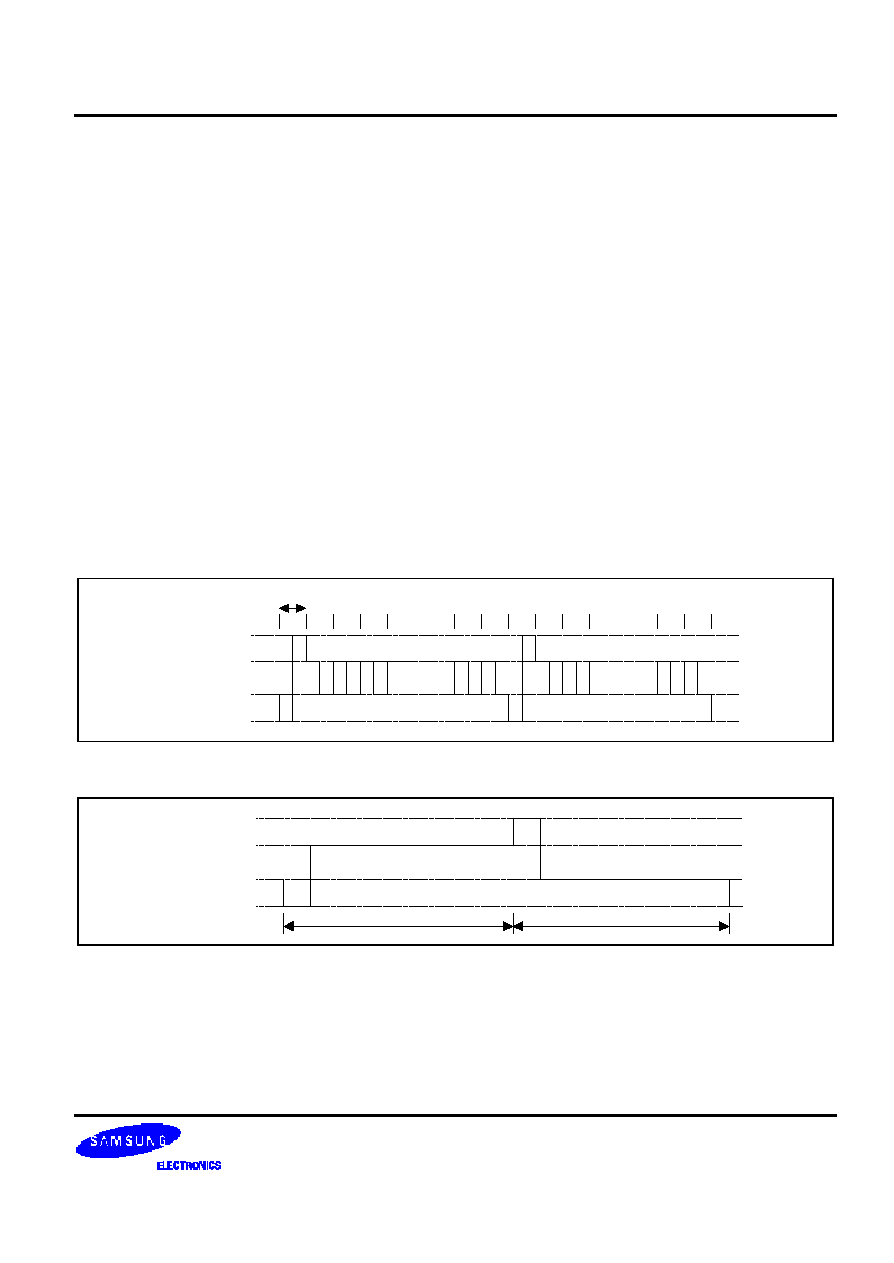
Interface with 8-bit MPU
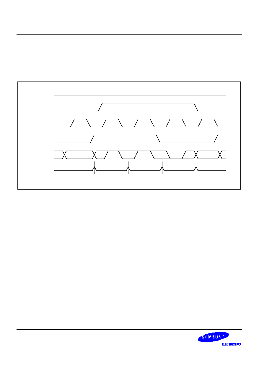
When interfacing data length is 8-bit, transfer is performed at a time through 8 ports, from DB0 to DB7. Example of
timing sequence is shown below.
RS
R/W
E
Internal
signal
DB7
Internal Operation
DATA
Busy
Busy
No
Busy
DATA
Instruction
Busy Flag Check
Instruction
Busy Flag Check
Busy Flag Check
Figure 7. Example of 8-bit Bus Mode Timing Diagram
16COM/40SEG DRIVER & CONTROLLER FOR DOT MATRIX LCD
S6A0069
19
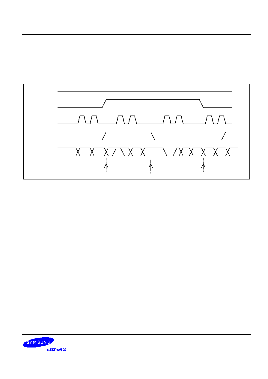
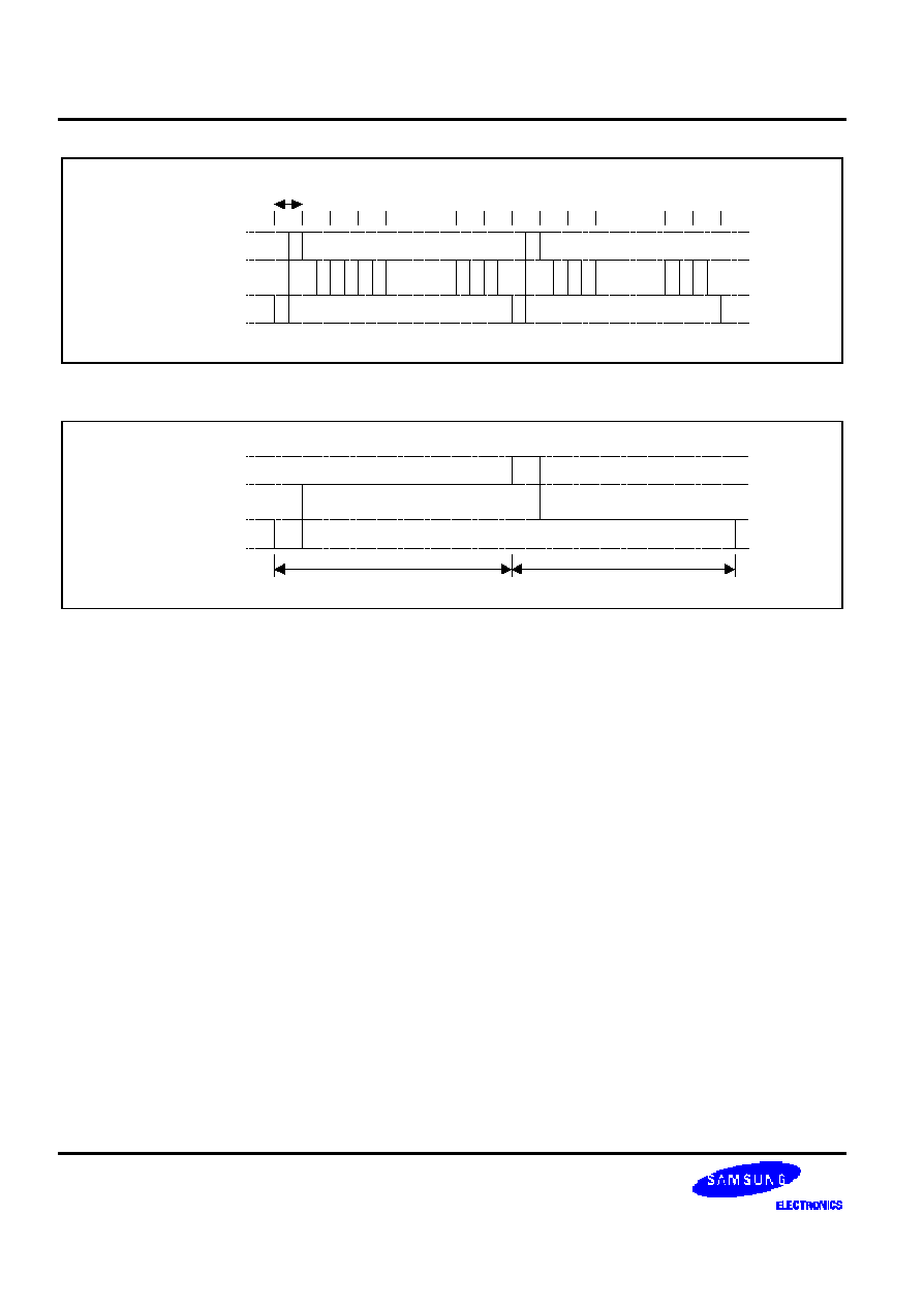
Interface with 4-bit MPU
When interfacing data length is 4-bit, only 4 ports, from DB4 to DB7, are used as data bus. At first higher 4-bit (in
case of 8-bit bus mode, the contents of DB4 - DB7) are transferred, and then lower 4-bit (in case of 8-bit bus mode,
the contents of DB0 - DB3) are transferred. So transfer is performed by two times. Busy Flag outputs "High" after the
second transfer are ended. Example of timing sequence is shown below.
RS
R/W
E
Internal
signal
DB7
Internal Operation
D3
Busy
AC3
No
Busy
Instruction
Busy Flag Check
Instruction
Busy Flag Check
D7
AC3
D7
D3
Figure 8. Example of 4-bit Bus Mode Timing Diagram
S6A0069
16COM/40SEG DRIVER & CONTROLLER FOR DOT MATRIX LCD
20
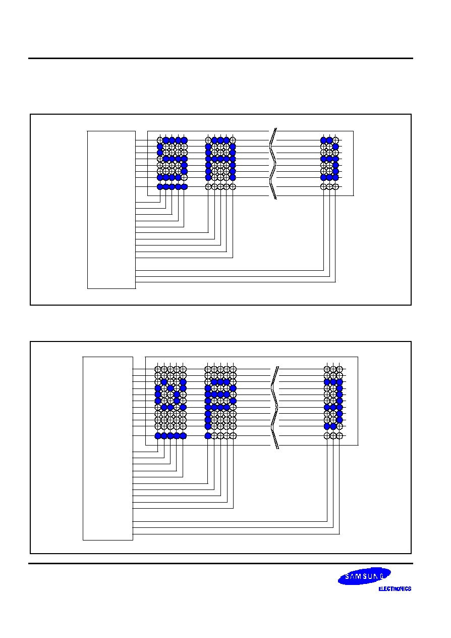
APPLICATION INFORMATION ACCORDING TO LCD PANEL
LCD Panel: 8 Character
×
1-line Character format; 5
×
7 dots + 1-cursor line (1/4 bias, 1/8 duty)
S6A0069
C1
.
.
.
C7
C8
S1
.
.
.
S10
S38
S39
S40
.
.
LCD Panel: 8 Character
×
1-line Character Format; 5
×
10 dots + 1 cursor line (1/4 bias, 1/11 duty)
S6A0069
C1
.
.
.
C10
C11
S1
.
.
.
S10
S38
S39
S40
.
.
16COM/40SEG DRIVER & CONTROLLER FOR DOT MATRIX LCD
S6A0069
21
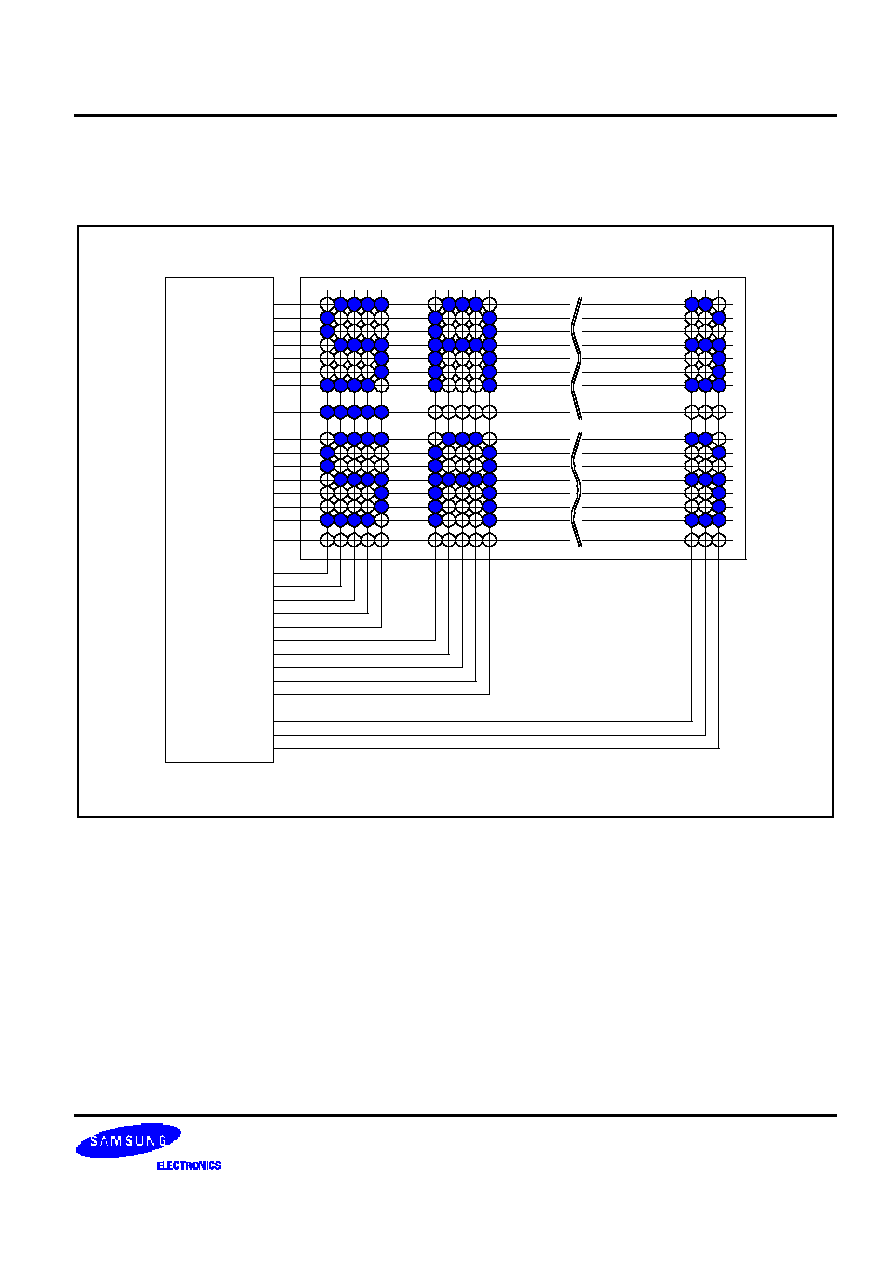
LCD Panel: 8 Character
×
2-line Character Format; 5
×
7 dots + 1cursor line (1/5 bias, 1/16 duty)
S6A0069
C1
.
.
.
C7
C8
S1
.
.
.
S10
S38
S39
S40
.
.
C9
.
.
.
C15
C16
S6A0069
16COM/40SEG DRIVER & CONTROLLER FOR DOT MATRIX LCD
22
LCD Panel: 16 Character ×1-line Character Format; 5×7 dots + 1 cursor line (1/5 bias, 1/16 duty)
S6A0069
C1
.
.
.
C7
C8
S1
.
.
.
S10
S39
S40
.
.
C9
.
.
.
C16
16COM/40SEG DRIVER & CONTROLLER FOR DOT MATRIX LCD
S6A0069
23
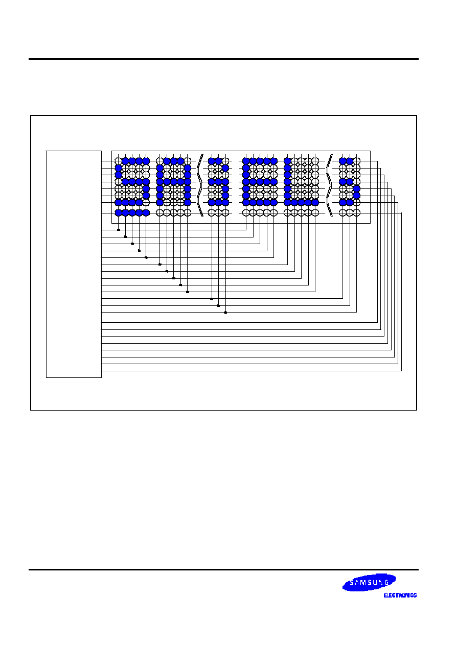
LCD Panel: 4 Character
×
2-line Character Format; 5
×
7 dots + 1 cursor line (1/4 bias, 1/8 duty)
S6A0069
C1
.
.
.
C7
C8
S21
.
.
.
S30
S38
S39
S40
.
.
S20
.
.
.
S19
S18
.
.
S10
S1
S6A0069
16COM/40SEG DRIVER & CONTROLLER FOR DOT MATRIX LCD
24
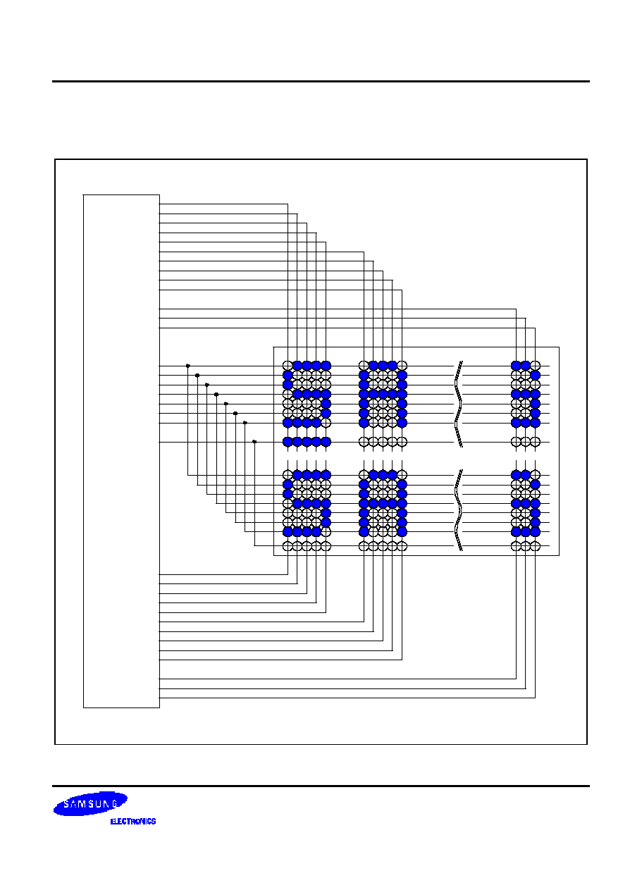
APPLICATION CIRCUIT
Figure 9. S6A0069 Application Circuit
S6A0069
C1-C16
LCD Panel
S1-S40
D
OSC1
OSC2
VSS
M
CLK1
CLK2
VDD
V1
V2
V3
V4
V5
DB0-DB7
SC1-S4C0
DL1
FCS
SHL1
SHL2
VSS
VDD
V6 V5 V4 V3 V2 V1 VEE
DL2
DL1
DR2
CL1
CL2
M
S6A0065
SC1-S4C0
DL1
FCS
SHL1
SHL2
VSS
VDD
V6 V5 V4 V3 V2 V1 VEE
DL2
DL1
DR2
CL1
CL2
M
S6A0065
SC1-S4C0
DL1
FCS
SHL1
SHL2
VSS
VDD
V6 V5 V4 V3 V2 V1 VEE
DL2
DL1
DR2
CL1
CL2
M
S6A0065
V1
V2
V3
V4
V5
GND or
Other voltage
V
LCD
(1/5 bias)
To MPU
VDD
NOTE: When S6A0065 is externally connected to the S6A0069, you can increase the number of display digits up to 80
characters.
BIAS VOLTAGE DIVIDE CIRCUIT
VDD
V1
V2
V3
V4
V5
S6A0069
VDD
R
R
R
R
GND or
Other voltage
Figure 10. 1/4 bias, 1/8 or 1/11 duty
VDD
V1
V2
V3
V4
V5
S6A0069
VDD
R
R
R
R
GND or
Other voltage
R
Figure 11. 1/5 bias, 1/16 duty
16COM/40SEG DRIVER & CONTROLLER FOR DOT MATRIX LCD
S6A0069
25
INITIALIZING
When the power is turned on, S6A0069 is initialized automatically by power on reset circuit. During the initialization,
the following instructions are executed, and BF(Busy Flag) is kept "High"(busy state) to the end of initialization.
(1) Display Clear instruction: Write "20H" to all DDRAM
(2) Set Functions instruction
DL = 1 : 8-bit bus mode
N = 1 : 2-line display mode
F = 0 : 5 X 8 font type
(3) Control Display ON/OFF instruction
D = 0 : Display OFF
C = 0 : Cursor OFF
B = 0 : Blink OFF
(4) Set Entry Mode instruction
I/D = 1 : Increment by 1
SH = 0 : No entire display shift
FRAME FREQUENCY
Programmable Driving Method by the same font mask option: Display waveform A-Type, B-Type
...
...
...
...
8
7
3
2
1
8
7
4
3
2
1
1-line selection period
VDD
V1
V4
V5
COM1
...
Figure 12. 1/8 Duty Cycle (A-Type Waveform)
VDD
V1
V4
V5
COM1
1 Frame
1 Frame
...
Figure 13. 1/8 Duty Cycle (B-Type Waveform)
Line selection period
= 400 clocks
One Frame
= 400 x 8 x 3.7
µ
s = 11850
µ
s = 11.9 ms (1 clock = 3.7
µ
s, fosc = 270kHz)
Frame frequency
= 1/11.9ms = 84.3Hz
S6A0069
16COM/40SEG DRIVER & CONTROLLER FOR DOT MATRIX LCD
26
...
...
...
...
11
10
3
2
1
11
10
4
3
2
1
1-line selection period
VDD
V1
V4
V5
COM1
...
Figure 14. 1/11 Duty Cycle (A-Type Waveform)
VDD
V1
V4
V5
COM1
1 Frame
1 Frame
...
Figure 15. 1/11 Duty Cycle (B-Type Waveform)
Line selection period
= 400 clocks
One Frame
= 400 x 11 x 3.7
µ
s = 16300
µ
s = 16.3ms (1 clock = 3.7
µ
s , fosc = 270kHz)
Frame frequency
= 1/16.3 ms = 61.4 Hz
16COM/40SEG DRIVER & CONTROLLER FOR DOT MATRIX LCD
S6A0069
27
...
...
...
...
16
15
3
2
1
16
15
4
3
2
1
1-line selection period
VDD
V1
V4
V5
COM1
...
Figure 16. 1/16 Duty Cycle (A-Type Waveform)
VDD
V1
V4
V5
COM1
1 Frame
1 Frame
...
Figure 17. 1/16 Duty Cycle (B-Type Waveform)
Line selection period
= 200 clocks
One Frame
= 200 x 16 x 3.7
µ
s = 11850
µ
s = 11.9 ms (1 clock = 3.7
µ
s, fosc = 270kHz)
Frame frequency
= 1/11.9ms = 84.3Hz
S6A0069
16COM/40SEG DRIVER & CONTROLLER FOR DOT MATRIX LCD
28
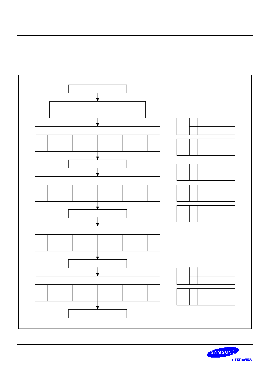
INITIALIZING BY INSTRUCTION
8-bit Interface Mode (Condition: f
OSC
= 270 kHz)
Power On
Wait for more than 30ms after V
DD
rises to 4.5 V.
Wait for more than 40ms after V
DD
rises to 2.7 V.
RS
R/W DB7 DB6 DB5 DB4 DB3 DB2 DB1 DB0
Function Set
0
0
0
0
1
1
N
F
X
X
Wait for more than 39
µ
s
RS
R/W DB7 DB6 DB5 DB4 DB3 DB2 DB1 DB0
Display ON/OFF Control
0
0
0
0
0
0
1
D
C
B
Wait for more than 39
µ
s
RS
R/W DB7 DB6 DB5 DB4 DB3 DB2 DB1 DB0
Display Clear
0
0
0
0
0
0
0
0
0
1
Wait for more than 1.53 ms
RS
R/W DB7 DB6 DB5 DB4 DB3 DB2 DB1 DB0
Entry Mode Set
0
0
0
0
0
0
0
1
I/D
SH
Initialization End
N
0
1
1-line mode
2-line mode
F
0
1
Display off
Display on
D
0
1
Display off
Display on
C
0
1
Cursor off
Cursor on
B
0
1
Blink off
Blink on
I/D
0
1
Decrement mode
Increment mode
SH
0
1
Entire shift off
Entire shift on
16COM/40SEG DRIVER & CONTROLLER FOR DOT MATRIX LCD
S6A0069
29
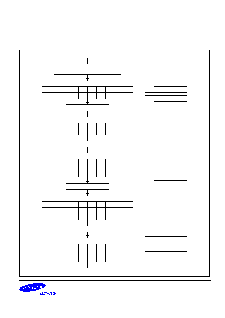
4-bit Interface Mode (Condition: f
OSC
= 270 kHz)
N
0
1
1-line mode
2-line mode
F
0
1
Display off
Display on
D
0
1
Display off
Display on
C
0
1
Cursor off
Cursor on
B
0
1
Blink off
Blink on
I/D
0
1
Decrement mode
Increment mode
SH
0
1
Entire shift off
Entire shift on
0
0
0
0
0
0
0
0
0
1
I/D
SH
DL
0
1
4-bit mode
8-bit mode
Power On
Wait for more than 30ms after V
D D
rises to 4.5V
Wait for more than 40ms after V
D D
rises to 2.7V
Function Set (display mode set)
Wait for more than 39
µ
s
RS
R/W DB7 DB6 DB5 DB4 DB3 DB2 DB1 DB0
Display ON/OFF Control
Wait for more than 39
µ
s
RS
R/W DB7 DB6 DB5 DB4 DB3 DB2 DB1 DB0
Display Clear
Wait for more than 1.53
µ
s
RS
R/W DB7 DB6 DB5 DB4 DB3 DB2 DB1 DB0
Entry Mode Set
Initialization End
0
0
0
0
0
0
x
x
x
x
0
0
1
D
C
B
x
x
x
x
x
x
x
x
x
x
x
x
0
0
0
0
0
0
x
x
x
x
0
0
0
0
0
1
x
x
x
x
Function Set (4-bit mode chage)
Wait for more than 39
µ
s
RS
R/W DB7 DB6 DB5 DB4 DB3 DB2 DB1 DB0
0
0
0
0
1
DL
x
x
x
x
0
0
0
0
1
0
x
x
x
x
0
0
N
F
x
x
x
x
x
x
S6A0069
16COM/40SEG DRIVER & CONTROLLER FOR DOT MATRIX LCD
30
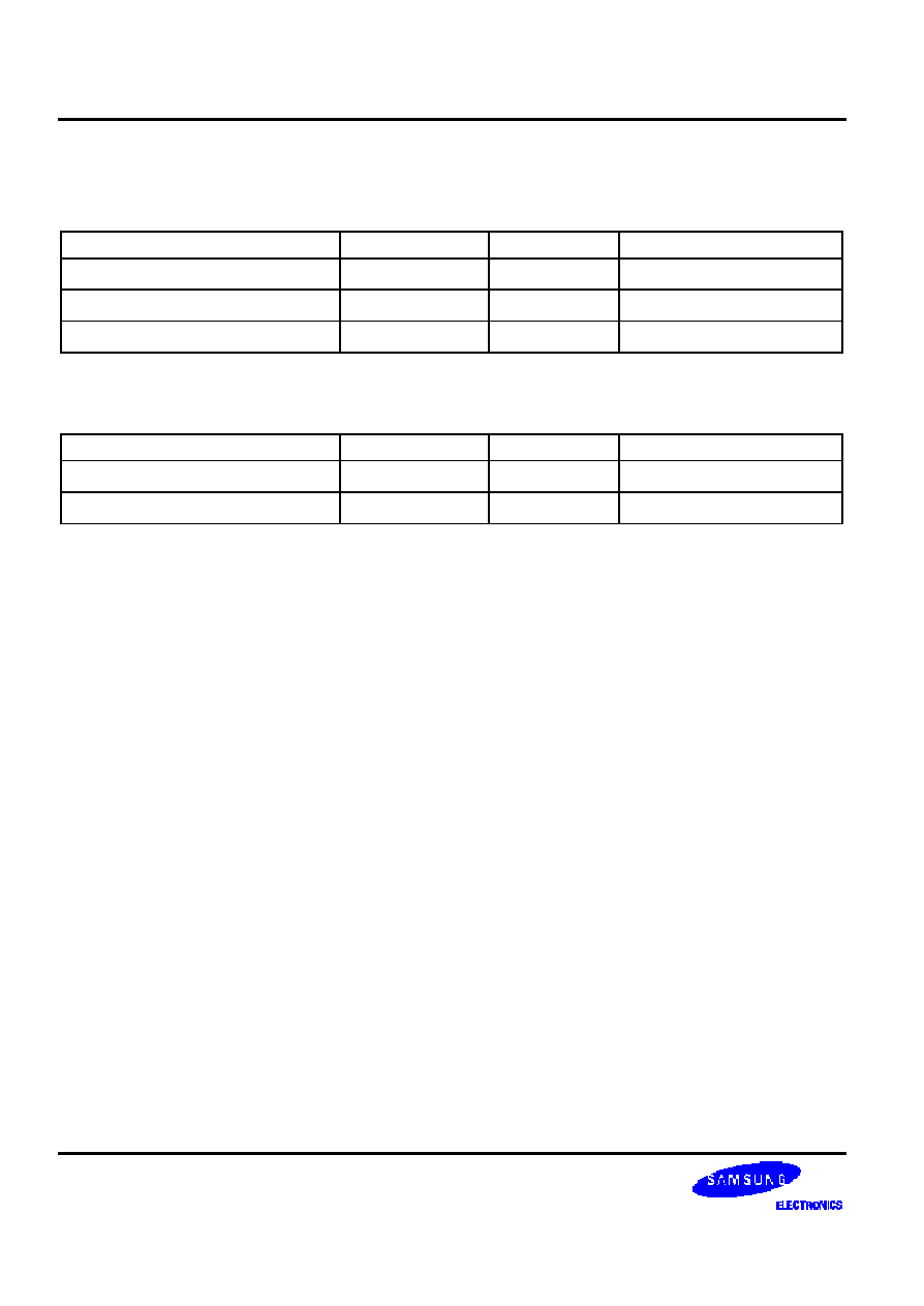
MAXIMUM ABSOLUTE LIMIT
Maximum Absolute Power Ratings
Characteristic
Symbol
Unit
Value
Power Supply Voltage
V
DD
V
-0.3 to +7.0
Operating Voltage
V
LCD
V
V
DD
-15.0 to V
DD
+0.3
Input Voltage
V
IN
V
-0.3 to V
DD
+ 0.3
NOTE: Voltage greater than above may damage the circuit (V
DD
V1
V2
V3
V4
V5)
Temperature Characteristics
Characteristic
Symbol
Unit
Value
Operating Temperature
T
OPR
°
C
-30 to +85
Storage Temperature
T
STG
°
C
-55 to +125
16COM/40SEG DRIVER & CONTROLLER FOR DOT MATRIX LCD
S6A0069
31
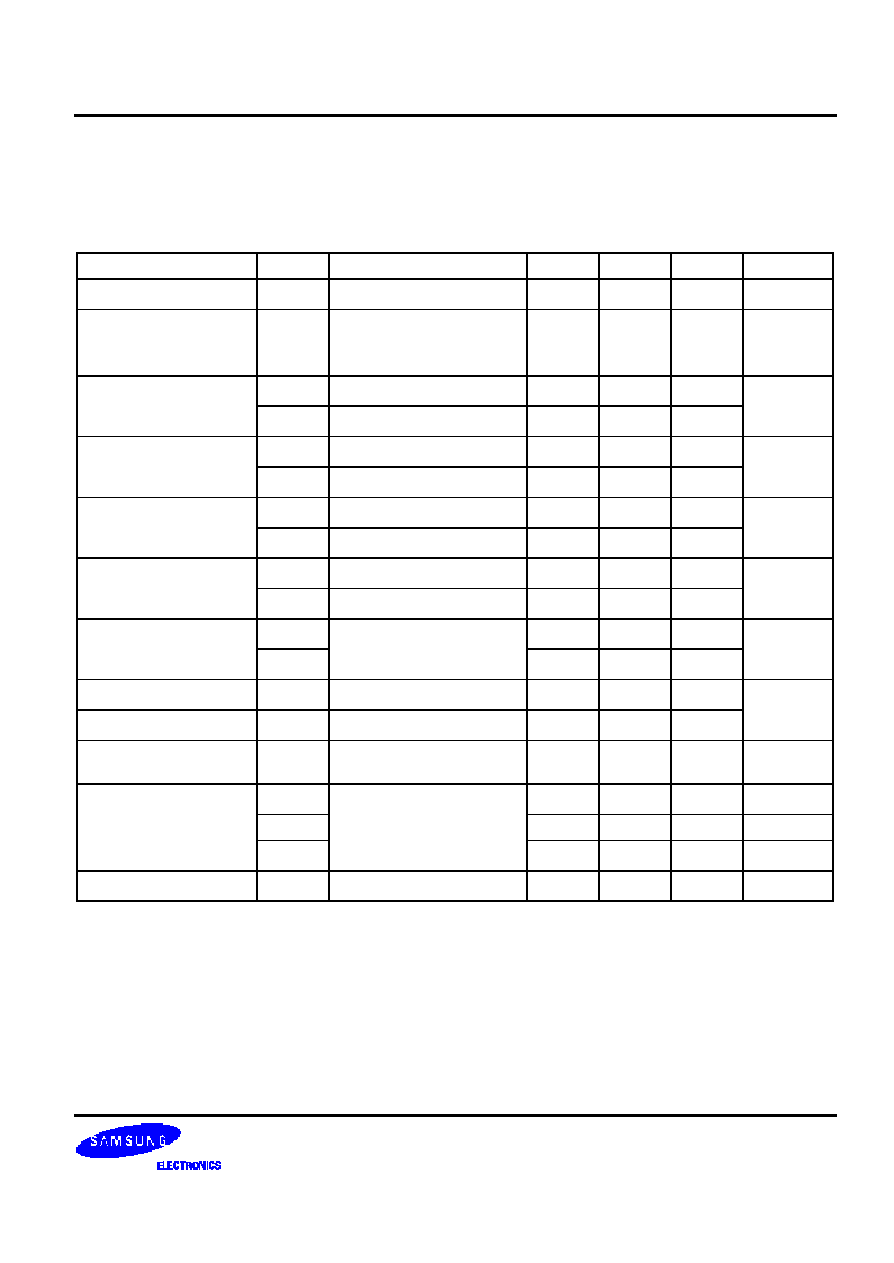
ELECTRICAL CHARACTERISTICS
DC Characteristics
(V
DD
= 4.5V to 5.5V, T
A
= -30 to +85
°
C)
Characteristic
Symbol
Condition
Min
Typ
Max
Unit
Operating Voltage
V
DD
4.5
5.5
V
Operating Current
I
DD
Internal oscillation or
external clock (V
DD
= 5.0V,
fosc = 270kHz)
0.35
0.6
mA
Input Voltage (1)
V
IH1
2.2
V
DD
V
(except OSC1)
V
IL1
-0.3
0.6
Input Voltage (2)
V
IH2
V
DD
-1.0
V
DD
V
(OSC1)
V
IL2
-0.2
1.0
Output Voltage (1)
V
OH1
I
OH
= -0.205mA
2.4
V
(DB0 to DB7)
V
OL1
I
OL
= 1.2mA
-
0.4
Output Voltage (2)
V
OH2
I
O
= -40
µ
A
0.9V
DD
V
(except DB0 to DB7)
V
OL2
I
O
= 40
µ
A
0.1V
DD
Voltage Drop
Vd
COM
I
O
= ±0.1mA
1
V
Vd
SEG
1
Input Leakage Current
I
LKG
V
IN
= 0V to V
DD
-1
1
µ
A
Input Low Current
I
IL
V
IN
= 0V, V
DD
= 5V (pull up)
-50
-125
-250
Internal Clock
(external Rf)
f
OSC1
Rf = 91k
±
2% (V
DD
= 5V)
190
270
350
kHz
External Clock
f
OSC
125
270
350
kHz
duty
45
50
55
%
t
R
, t
F
0.2
µ
A
LCD Driving Voltage
V
LCD
V
DD
-V5 (1/5, 1/4 bias)
3.0
13.0
V
S6A0069
16COM/40SEG DRIVER & CONTROLLER FOR DOT MATRIX LCD
32
DC Characteristics
(V
DD
= 2.7V to 4.5V, T
A
= -30 to +85
°
C)
Characteristic
Symbol
Condition
Min
Typ
Max
Unit
Operating Voltage
V
DD
2.7
4.5
V
Operating Current
I
DD
Internal oscillation or
external clock (V
DD
= 3.0V,
fosc = 270kHz)
0.15
0.3
mA
Input Voltage (1)
V
IH1
0.7 V
DD
V
DD
V
(except OSC1)
V
IL1
-0.3
0.55
Input Voltage (2)
V
IH2
0.7V
DD
V
DD
V
(OSC1)
V
IL2
0.2 V
DD
Output Voltage (1)
V
OH1
I
OH
= -0.1mA
0.75 V
DD
V
(DB0 to DB7)
V
OL1
I
OL
= 0.1mA
0.2 V
DD
Output Voltage (2)
V
OH2
I
O
= -40
µ
A
0.8V
DD
V
(except DB0 to DB7)
V
OL2
I
O
= 40
µ
A
0.2V
DD
Voltage Drop
Vd
COM
I
O
=
±
0.1mA
1
V
Vd
SEG
1
Input Leakage Current
I
LKG
V
IN
= 0V
V
DD
-1
1
µ
A
Input Low Current
I
IL
V
IN
= 0V, V
DD
= 3V (pull up)
-10
-50
-120
Internal Clock
(external Rf)
f
OSC1
Rf = 75k
±
2% (V
DD
= 3V)
190
270
350
kHz
External Clock
f
OSC2
125
270
410
kHz
duty
45
50
55
%
t
R
, t
F
0.2
µ
S
LCD Driving Voltage
V
LCD
V
DD
-V5 (1/5, 1/4 bias)
3.0
13.0
V
NOTE: LCD Driving Voltage
Power
Duty
1/8, 1/11 Duty
1/16 Duty
Bias
1/4 Bias
1/5 Bias
V
DD
V
DD
V
DD
V1
V
DD
- V
LCD
/4
V
DD
- V
LCD
/5
V2
V
DD
- V
LCD
/2
V
DD
- 2V
LCD
/5
V3
V
DD
- V
LCD
/2
V
DD
- 3V
LCD
/5
16COM/40SEG DRIVER & CONTROLLER FOR DOT MATRIX LCD
S6A0069
33
V4
V
DD
- 3V
LCD
/4
V
DD
- 4V
LCD
/5
V5
V
DD
- V
LCD
V
DD
- V
LCD
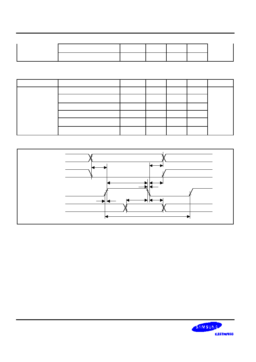
AC Characteristics
(V
DD
= 4.5 to 5.5V, T
A
= -30 to +85
°
C)
Mode
Characteristics
Symbol
Min
Typ
Max
Unit
Write Mode
E Cycle Time
tc
500
ns
(refer to Figure-6)
E Rise/Fall Time
t
R
, t
F
20
E Pulse Width (High, Low)
tw
230
R/W and RS Setup Time
tsu1
40
R/W and RS Hold Time
t
H1
10
Data Setup Time
tsu2
80
Data Hold Time
t
H2
10
Read Mode
E Cycle Time
tc
500
ns
(refer to Figure-7)
E Rise/Fall Time
t
R
, t
F
20
E Pulse Width (High, Low)
tw
230
R/W and RS Setup Time
tsu
40
R/W and RS Hold Time
t
H
10
Data Output Delay Time
tD
120
Data Hold Time
tDH
5
(V
DD
= 2.7 to 4.5V, T
A
= -30 to +85
°
C)
Mode
Characteristic
Symbol
Min
Typ
Max
Unit
Write Mode
E Cycle Time
tc
1000
ns
(refer to Figure-6)
E Rise/Fall Time
t
R
, t
F
25
E Pulse Width (High, Low)
tw
450
R/W and RS Setup Time
tsu1
60
R/W and RS Hold Time
t
H1
20
Data Setup Time
tsu2
195
Data Hold Time
t
H2
10
Read Mode
E Cycle Time
tc
1000
ns
(refer to Figure-7)
E Rise/Fall Time
t
R
, t
F
25
E Pulse Width (High, Low)
tw
450
R/W and RS Setup Time
tsu
60
R/W and RS Hold Time
t
H
20
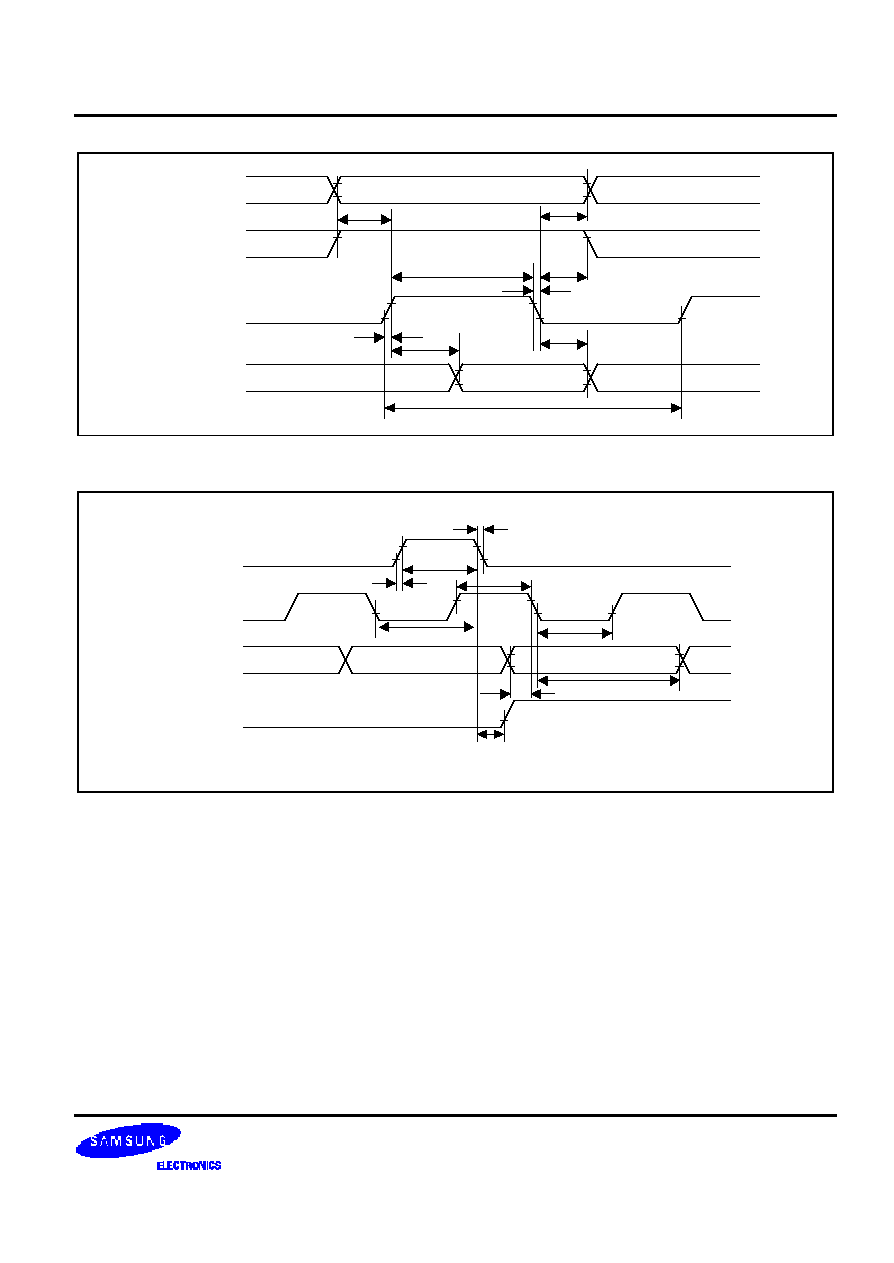
S6A0069
16COM/40SEG DRIVER & CONTROLLER FOR DOT MATRIX LCD
34
Data Output Delay Time
t
D
-
360
Data Hold Time
t
DH
5
(V
DD
= 2.7 to 4.5V, T
A
= -30 to +85
°
C)
Mode
Characteristic
Symbol
Min
Typ
Max
Unit
Interface Mode with Clock Pulse Width (High, Low)
tc
800
ns
Extension Driver
Clock Rise/Fall Time
t
R
, t
F
25
(refer to Figure-8)
Clock Setup Time
tsu1
500
Data Setup Time
tsu2
300
Data Hold Time
t
DH
300
M Delay Time
t
DM
-1000
1000
V
IH1
V
IL1
t
su1
V
IL1
t
h1
V
IL1
t
h1
t
f
t
w
t
h2
V
IH1
V
IL1
t
su2
t
r
V
IH1
V
IL1
Valid Data
V
IH1
V
IL1
t
c
DB0-DB7
E
R/W
RS
V
IL1
Figure 18. Write Mode Timing Diagram
16COM/40SEG DRIVER & CONTROLLER FOR DOT MATRIX LCD
S6A0069
35
V
IH1
V
IL1
t
su
V
IH1
t
h
V
IH1
t
h
t
f
t
w
t
DH
V
IH1
V
IL1
t
r
V
OH1
V
OL1
Valid Data
V
OH1
V
OL1
t
c
DB0-DB7
E
R/W
RS
t
D
V
IL1
Figure 19. Read Mode Timing Diagram
M
D
CLK2
CLK1
V
OH2
t
r
t
w
V
OH2
V
OL2
t
f
V
OH2
V
OL2
V
OH2
t
w
V
OL2
t
w
t
SU2
V
OH2
V
OL2
t
DH
t
DM
V
OL2
t
SU1
Figure 20. Interface Mode with Extension Driver Timing Diagram