34COM/80SEG DRIVER & CONTROLLER FOR DOT MATRIX LCD S6A0074
1
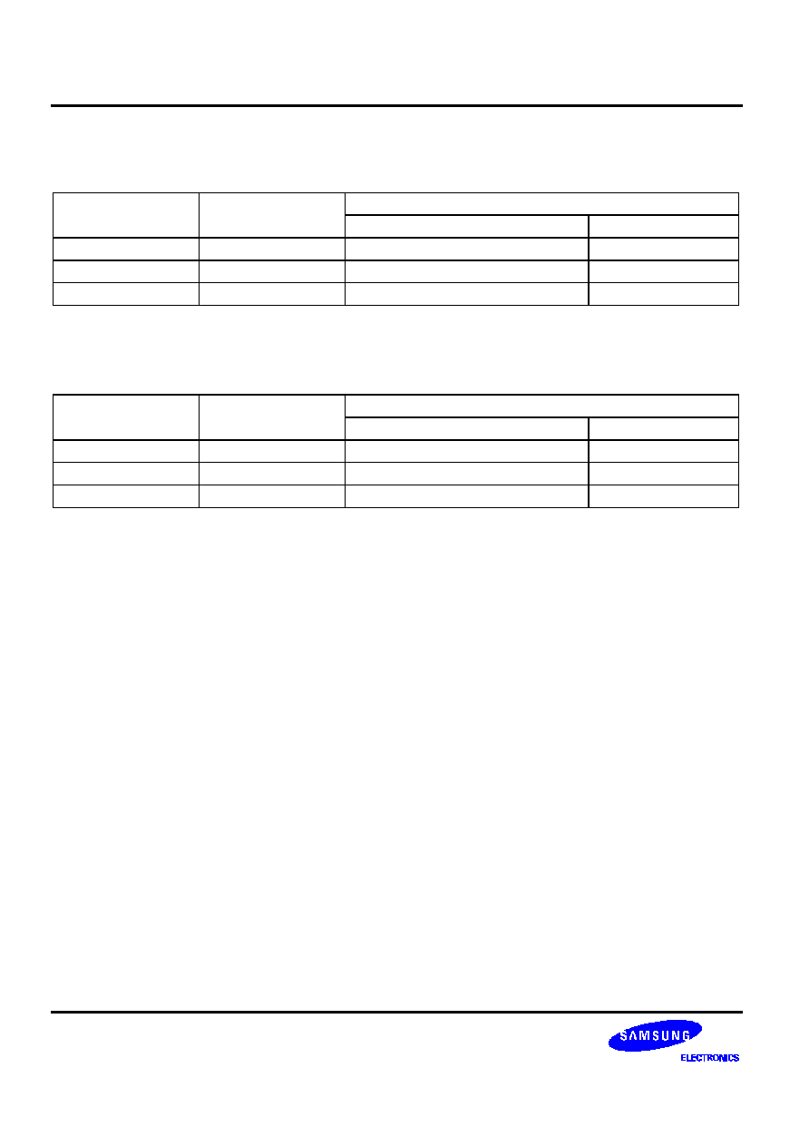
INTRODUCTION
S6A0074 is a dot matrix LCD driver & controller LSI which is fabricated by low power CMOS technology. It can
display 1, 2, or 4 lines with 5 x 8 or 6 x 8 dots format.
FUNCTIONS
∑
Character type dot matrix LCD driver & controller
∑
Internal driver: 34 common and 80 segment signal output
∑
Easy interface with 4-bit or 8-bit MPU
∑
Clock synchronized serial Interface
∑
5 x 8 dots matrix possible
∑
6 x 8 dots matrix possible
∑
Bi-directional shift function
∑
All character reverse display
∑
Display shift per line
∑
Voltage converter for LCD drive voltage: 13V max (2 times/3 times)
∑
Various instruction functions
∑
Automatic power on reset
FEATURES
∑
Internal memory
- Character Generator ROM (CGROM): 9,600 bits (240 characters x 5 x 8 dot)
- Character Generator RAM (CGRAM): 64 x 8 bits (8 characters x 5 x 8 dot)
- Segment Icon RAM (SEGRAM): 16 x 8 bits (96 icons max.)
- Display Data RAM (DDRAM): 80 x 8 bits (80 characters max.)
∑
Low power operation
- Power supply voltage range: 2.7 - 5.5V (V
DD
)
- LCD Drive voltage range: 3.0 - 13.0V (V
DD
- V5)
∑
CMOS process
∑
Programmable duty cycle: 1/17, 1/33
∑
Internal oscillator with an external resistor
∑
Low power consumption
∑
Bare chip available

S6A0074 34COM/80SEG DRIVER & CONTROLLER FOR DOT MATRIX LCD
4
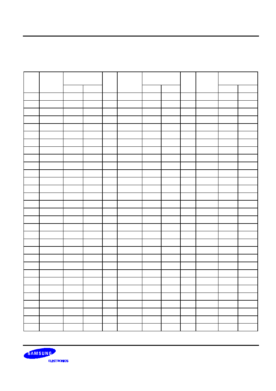
PAD CONFIGURATION
SEG56
SEG57
SEG58
SEG59
SEG60
SEG61
SEG62
SEG63
SEG64
SEG65
SEG66
SEG67
SEG68
SEG69
SEG70
SEG71
SEG72
SEG73
SEG74
SEG75
SEG76
SEG77
SEG78
SEG79
SEG80
COM9
COM10
COM11
COM12
COM13
COM14
COM15
COM16
COM25
COM26
COM27
COM28
COM29
COM30
COM31
COM32
COM33
1
2
3
4
5
6
7
8
9
10
11
12
13
14
15
16
17
18
19
20
21
22
23
24
25
26
27
28
29
30
31
32
33
34
35
36
37
38
39
40
41
42
Chip size: 6450 x 4870
PAD size: 100
◊
100
Unit :
µ
m
X
S6A0074
43
44
45
46
47
48
49
50
51
52
53
54
55
56
57
58
59
60
61
62
63
64
65
66
67
68
69
70
71
V
DD
OSC2
OSC1
RESET
IM
IE
V
SS1
RS/CS
RW/SID
E/SCLK
DB0/SOD
DB1
DB2
DB3
DB4
DB5
DB6
DB7
Vci
C2
C1
V
SS2
V5OUT2
V5OUT3
V5
V4
V3
V2
V1
113
112
111
110
109
108
107
106
105
104
103
102
101
100
99
98
97
96
95
94
93
92
91
90
89
88
87
86
85
84
83
82
81
80
79
78
77
76
75
74
73
72
SEG25
SEG24
SEG23
SEG22
SEG21
SEG20
SEG19
SEG18
SEG17
SEG16
SEG15
SEG14
SEG13
SEG12
SEG11
SEG10
SEG9
SEG8
SEG7
SEG6
SEG5
SEG4
SEG3
SEG2
SEG1
COM0
COM1
COM2
COM3
COM4
COM5
COM6
COM7
COM8
COM17
COM18
COM19
COM20
COM21
COM22
COM23
COM24
143
142
141
140
139
138
137
136
135
134
133
132
131
130
129
128
127
126
125
124
123
122
121
120
119
118
117
116
115
114
SEG55
SEG54
SEG53
SEG52
SEG51
SEG50
SEG49
SEG48
SEG47
SEG46
SEG45
SEG44
SEG43
SEG42
SEG41
SEG40
SEG39
SEG38
SEG37
SEG36
SEG35
SEG34
SEG33
SEG32
SEG31
SEG30
SEG29
SEG28
SEG27
SEG26
(0, 0)
Y