64 CH SEGMENT DRIVER FOR DOT MATRIX LCD
June. 2000.
Ver. 0.0
S6B0108
Contents in this document are subject to change without notice. No part of this document may be reproduced
or transmitted in any form or by any means, electronic or mechanical, for any purpose, without the express
written permission of LCD Driver IC Team.
S6B0108
64CH SEGMENT DRIVER FOR DOT MATRIX LCD
2
INTRODUCTION
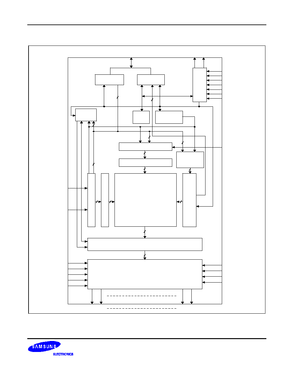
The S6B0108 is a LCD driver LSI with 64 channel output for dot matrix liquid crystal graphic display systems.
This device consists of the display RAM, 64 bit data latch, 64 bit drivers and decoder logic. It has the internal dis-
play RAM for storing the display data transferred from a 8 bit micro controller and generates the dot matrix Iiquid
crystal driving signals corresponding to stored data. The S6B0108 composed of the liquid crystal display system
in combination with the S6B0107 (64 channel common driver).
FEATURES
∑
Dot matrix LCD segment driver with 64 channel output
∑
Input and output signal
- Input: 8 bit parallel display data control signal from MPU divided bias voltage
(V0R, V0L, V2R, V2L, V3R, V3L, V5R, V5L)
- Output: 64 channel for LCD driving.
∑
Display data is stored in display data RAM from MPU.
∑
Interface RAM
- Capacity: 512 bytes (4096 bits)
- RAM bit data: RAM bit data = 1: On
RAM bit data = 0: Off
∑
Applicable LCD duty: 1/32-1/64
∑
LCD driving voltage: 8V-17V (V
DD
-V
EE
)
∑
Power supply voltage: + 5V
±
10%
∑
Interface
Drivers
Common
Segment
Controller
S6B0107
Other S6B0108
MPU
∑
High voltage CMOS process.
∑
Bare chip available

S6B0108
64CH SEGMENT DRIVER FOR DOT MATRIX LCD
4
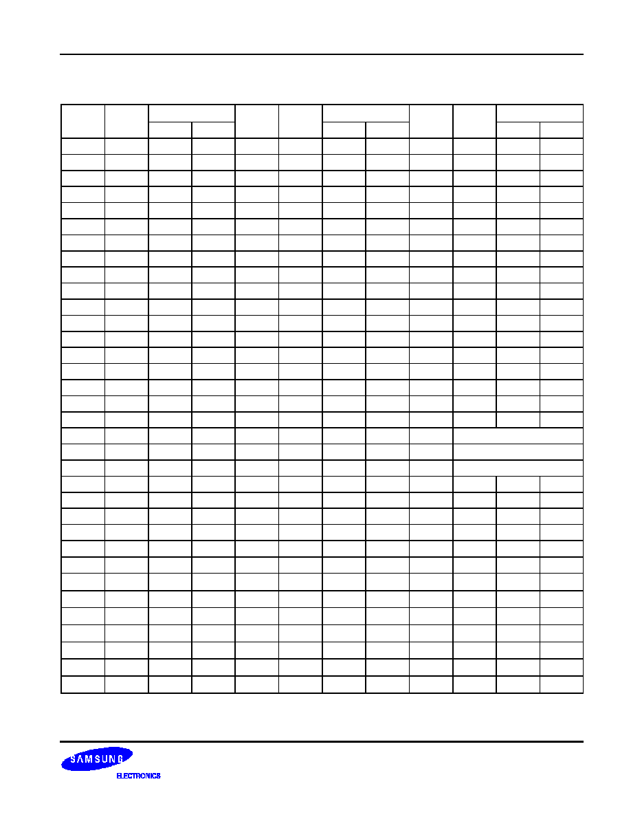
PAD DIAGRAM
3
2
1
100
99
98
97
96
95
94
93
92
91
90
89
88
87
86
85
84
83
82
81
80
79
78
V
DD
M
ADC
FRM
E
CLK1
CLK2
CL
RS
R/W
RSTB
CS1B
CS2B
CS3
NC
NC
NC
DB7
DB6
DB5
DB4
DB3
DB2
DB1
DB0
V
SS
4
5
6
7
8
9
10
11
12
13
14
15
16
17
18
19
20
21
22
23
24
25
26
27
28
29
V3R
V2R
V5R
V0R
V
EE2
S64
S63
S62
S61
S60
S59
S58
S57
S56
S55
S54
S53
S52
S51
S50
S49
S48
S47
S46
S45
S44
Chip size: 4090
◊
4020
PAD size: 100
◊
100
Unit :
µ
m
(0, 0)
X
Y
77
76
75
74
73
72
71
70
69
68
67
66
65
64
63
62
61
60
59
58
57
56
55
54
53
52
V3L
V2L
V5L
V0L
V
EE1
S1
S2
S3
S4
S5
S6
S7
S8
S9
S10
S11
S12
S13
S14
S15
S16
S17
S18
S19
S20
S21
30
31
32
33
34
35
36
37
38
39
40
41
42
43
44
45
46
47
48
49
50
51
S43
S42
S41
S40
S39
S38
S37
S36
S35
S34
S33
S32
S31
S30
S29
S28
S27
S26
S25
S24
S23
S22
There is mark of S6B0108 on the bottom left in the chip.