
S6B0756
65COM / 96 SEG DRIVER & CONTROLLER FOR STN LCD
July. 2002.
Ver. 2.5
Prepared by Jae Ho Park
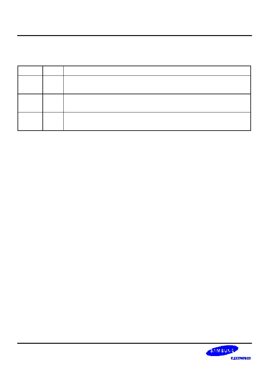
S6B0756 Specification Revision History
Version
Content
Date
Contents in this document are subject to change without notice. No part of this document may be reproduced or
transmitted in any form or by any means, electronic or mechanical, for any purpose, without the express written
permission of LCD Driver IC Team.
65 COM / 96 SEG DRIVER & CONTROLLER FOR STN LCD S6B0756
2
0.0
.Initial version
Dec.2000
0.1
.Reference circuit examples(Page 26) corrected
.Enter Calibration mode instruction deleted
.OTP calibration mode changed
Jan.2001
0.2
.Enter Micro Processor Interface Protocol (Page 9)
Mar.2001
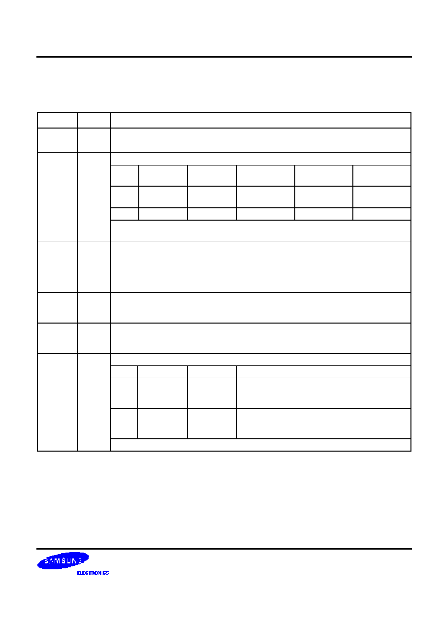
1.0
.Eliminated X5 boost.(Page 1)
.Added VCI range (Page 1)
.Changed Block Diagram for integrated Booster Capacitors(Page 3)
.Added OTPG / OTPD pin(Page 3,5)
.Changed Reference Circuit Examples(Page 27)
.Changed Reset Mode initial operation(Page 29)
.Added Frame Frequency command(Page 30,39)
.Changed Operating Current(Page 54)
Mar.2001
1.1
.Changed block Diagram (Page 3)
.Changed LCD Driver Supply (Page 4)
.Changed System Control (Page 5)
.Changed Voltage Regulator Circuits (Page 24)
.Deleted "In Case of Using External Resisters, Ra and Rb" (Page 26)
.Changed Reference Circuit Examples (Page 27)
.Changed instruction : Read Status ( Page 32)
.Added instructions concerned with OTP : Calibration Mode EN (Page 40)
, OTP Write Enable( Page 41 ), Set OV Register ( Page 45 )
.Added OTP operation (Page 64)
Apr.2001
2.0
.Added instruction concerned with OTP : OTP Mode ON/OFF
.Added OTP operation
.Changed V0 to VOUT
May.2001
2.1
.Pad configuration
.Pad center coordinates
June.2001
2.2
.Changed LCD driving voltage
Dec.2001
2.3
.Fix key coordinates and adjust VSS pin number
Feb.2002
2.4
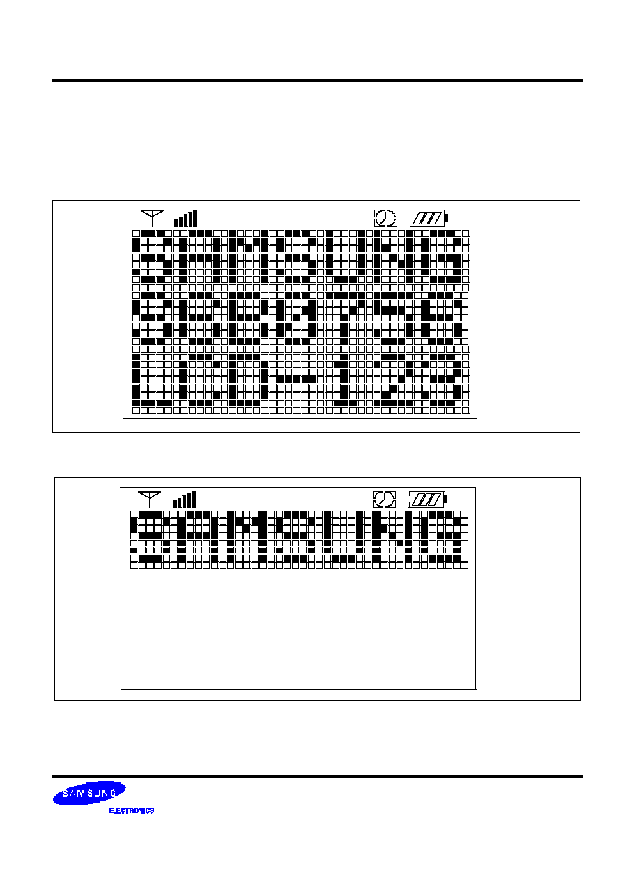
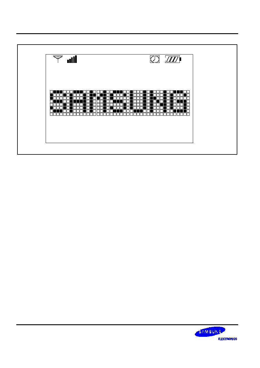
.Added Display Example(Page 42)
May.2002
2.5
.Changed Icon(Page 42) function.
July.2002

S6B0756 65 COM / 96 SEG DRIVER & CONTROLLER FOR STN LCD
3
CONTENTS
INTRODUCTION ............................................................................................................................................ 1
FEATURES .................................................................................................................................................... 1
PAD CONFIGURATION.................................................................................................................................. 3
PIN DESCRIPTION......................................................................................................................................... 7
POWER SUPPLY .................................................................................................................................... 7
LCD DRIVER SUPPLY............................................................................................................................. 7
SYSTEM CONTROL................................................................................................................................ 8
MICROPROCESSOR INTERFACE........................................................................................................... 9
LCD DRIVER OUTPUTS .........................................................................................................................11
FUNCTIONAL DESCRIPTION .......................................................................................................................12
MICROPROCESSOR INTERFACE..........................................................................................................12
DISPLAY DATA RAM (DDRAM) ..............................................................................................................17
LCD DISPLAY CIRCUITS........................................................................................................................20
LCD DRIVER CIRCUIT ...........................................................................................................................22
POWER SUPPLY CIRCUITS...................................................................................................................25
REFERENCE CIRCUIT EXAMPLES .....................................................................................................30
RESET CIRCUIT ....................................................................................................................................32
INSTRUCTION DESCRIPTION ......................................................................................................................33
SPECIFICATIONS .........................................................................................................................................57
ABSOLUTE MAXIMUM RATINGS ...........................................................................................................57
DC CHARACTERISTICS.........................................................................................................................58
AC CHARACTERISTICS .........................................................................................................................61
REFERENCE APPLICATIONS.......................................................................................................................65
MICROPROCESSOR INTERFACE..........................................................................................................65
CONNECTIONS BETWEEN S6B0756 AND LCD PANEL..........................................................................67
OTP CALIBRATION MODE...........................................................................................................................68
SEQUENCE FOR SETTING THE MODIFIED ELECTRONIC VOLUME......................................................68
OTP CELL STRUCTURE ........................................................................................................................69
VOUT CALIBRATION FLOW ...................................................................................................................69
VOLTAGES AND WAVEFORMS FOR OTP PROGRAMMING...................................................................70

S6B0756 65 COM / 96 SEG DRIVER & CONTROLLER FOR STN LCD
1
INTRODUCTION
The S6B0756 is a driver & controller LSI for graphic dot-matrix liquid crystal display systems. It contains 65 common
and 96 segment driver circuits. This chip is connected directly to a microprocessor, accepts serial or 8-bit parallel
display data and stores in an on-chip display data RAM of 65 x 96 bits. It provides a highly flexible display section
due to 1-to-1 correspondence between on-chip display data RAM bits and LCD panel pixels. And it performs display
data RAM read/write operation with no externally operating clock to minimize power consumption. In addition,
because it contains power supply circuits necessary to drive liquid crystal, it is possible to make a display system
with the fewest components.
FEATURES
Driver Output Circuits
-
65 common outputs / 96 segment outputs
Applicable Duty Ratios
Programmable duty ratio
Applicable LCD bias
Maximum display area
1/17 to 1/65
1/4 to 1/9
65
�
96
-
Various partial display
-
Partial window moving & data scrolling
On-chip Display Data RAM
-
Capacity: 65 x 96 = 6,240 bits
-
Bit data "1": a dot of display is illuminated. Bit data "0": a dot of display is not illuminated.
Microprocessor Interface
-
8-bit parallel bi-directional interface with 6800-series or 8080-series.
-
SPI (Serial Peripheral Interface) available. (only write operation)
On-chip Low Power Analog Circuit
-
On-chip oscillator circuit
-
Voltage converter (x2, x3, x4)
-
Voltage regulator (temperature coefficient: -0.05%/
�
C or external input)
-
On-chip electronic contrast control function (64 steps)
-
Voltage follower (LCD bias: 1/4 to 1/9)
-
On-chip bias / boosting capacitor
OTP(One-Time Programmable) method for VOUT calibration
On-chip EPROM(Erasable and Programmable ROM) for setting the offset voltage into LCD panel.
Operating Voltage Range
-
Supply voltage (V
DD
): 1.8 to 3.3 V
-
Voltage for DC/DC Converter (VCI): 2.4 to 4.5 V
-
LCD driving voltage (V
LCD
= VOUT - V
SS
): 4.0 to 12.0 V
Low power Consumption
-
TBD ( Internal power supply on and display OFF)
Package Type
-
COG (Gold bumped chip )
This chip is not designed for resistance to radiation or light.
65 COM / 96 SEG DRIVER & CONTROLLER FOR STN LCD S6B0756
2
BLOCK DIAGRAM
Figure 1. Block Diagram
POWER
SUPPLY
VDD
V1
VSS
VCI
V / C
CIRCUIT
V / R
CIRCUIT
V / F
CIRCUIT
33 COMMON
DRIVER
CIRCUITS
MPU INTERFACE (PARALLEL & SERIAL)
INSTRUCTION DECODER
BUS HOLDER
COLUMN ADDRESS
CIRCUIT
LINE
ADDRES
S
CIRCUIT
PAGE
ADDRESS
CIRCUIT
DISPLAY DATA RAM
65 X 96 = 6,240 Bits
DISPLAY DATA
CONTROL CIRCUIT
DISPLAY
TIMING
GENERATOR
CIRCUIT
COMMON
OUTPUT
CONTROLLER CIRCUIT
DB0
DB1
DB2
DB3
DB4
DB5
DB6(SCLK)
DB7(SID)
RESETB
PS0
RW_WR
E_RD
RS
CS1B
COMS1
COM63
:
COM32
SEG95
SEG94
SEG93
:
:
SEG2
SEG1
SEG0
COM31
:
COM0
COMS
OSCILLATOR
96 SEGMENT
DRIVER CIRCUITS
33 COMMON
DRIVER
CIRCUITS
I/O
BUFFER
STATUS REGISTER
INSTRUCTION REGISTER
INTERNAL
VSS1
VSS2
Test4
Test3
Test2 Test1
OTPG
OTPD
VOUT
PS1
V2
V3
V4
S6B0756 65 COM / 96 SEG DRIVER & CONTROLLER FOR STN LCD
3
PAD CONFIGURATION
Figure 2. S6B0756 Chip Configuration
Table 1. S6B0756 Pad Dimensions
���
�������������������
- - - - - - - - - -
�������������������
���
Y
124
255
123
256
100
279
99
1
S6B0756X
(TOP VIEW)
(0,0)
X
�����������������
- - - - - - - - - - - - - - - - - - - - -
���������������
����
- - - -
����
����
- - - -
����
Item
Pad NO.
Size
Unit
X
Y
Chip Size
-
8780
2300
um
Pad Pitch
1 to 3
80
3 to 97
70
97 to 99
80
100 to 102
80
102 to 120
60
120 to 123
80
124 to 126
80
126 to 253
60
253 to 255
80
256 to 259
80
259 to 277
60
277 to 279
80
Bumped pad Size
(Top)
1,2,98,99
124,125,254,255
60
110
um
3 to 97
50
100
100,101,121,122,123,
256,257,258,278,279
110
60
102 to 120
259 to 277
110
40
126 to 253
40
110
Bumped pad height
All pad
14(Typ.)
65 COM / 96 SEG DRIVER & CONTROLLER FOR STN LCD S6B0756
4
COG Align Key Coordinate ILB Align Key Coordinate
30
�
m 30
�
m 30
�
m
(+4128.00,+1003.00
)
30
�
m 30
�
m 30
�
m
(+3853.05,-888.95)
30
�
m
30
�
m
30
�
m
60
�
m
30
�
m
42
�
m
108
�
m
42
�
m
108
�
m
42
�
m
108
�
m
(-4278.95, +1043.10)
(+4316.90
�
1077.60)
42
�
m
108
�
m
When designing COG pattern, ITO pattern must be prohibited on this area (ILB align key). if ITO pattern is used for
routing over this area, it can be happened pattern-short through bumped pattern on ILB align key
S6B0756 65 COM / 96 SEG DRIVER & CONTROLLER FOR STN LCD
5
PAD CENTER COORDINATES
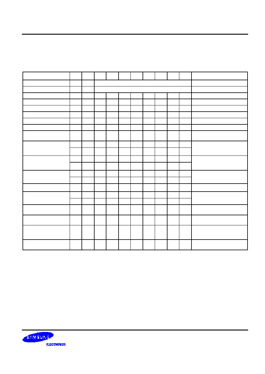
Table 2. Pad Center Coordinates
[Unit:
�
m]
NO
NAME
X
Y
NO
NAME
X
Y
NO
NAME
X
Y
1
DUMMY1
-3585.35
-1035
51
VCI(VCI3)
-65.35
-1035
101
DUMMY6
4243
-577.55
2
DUMMY2
-3505.35
-1035
52
VCI(VCI3)
4.65
-1035
102
COM31
4243
-497.55
3
TEST(PAD-CK) -3425.35
-1035
53
VCI(VCI3)
74.65
-1035
103
COM30
4243
-437.55
4
TEST(TEST_CL) -3355.35
-1035
54
VCI(VCI3)
144.65
-1035
104
COM29
4243
-377.55
5
TEST3
-3285.35
-1035
55
VCI(VCI3)
214.65
-1035
105
COM28
4243
-317.55
6
TEST4
-3215.35
-1035
56
VCI(VCI3)
284.65
-1035
106
COM27
4243
-257.55
7
VSS
-3145.35
-1035
57
VCI(VCI3)
354.65
-1035
107
COM26
4243
-197.55
8
PS0
-3075.35
-1035
58
VSS(VSS0)
424.65
-1035
108
COM25
4243
-137.55
9
VDD1
-3005.35
-1035
59
VSS(VSS1)
494.65
-1035
109
COM24
4243
-77.55
10
PS1
-2935.35
-1035
60
VSS(VSS1)
564.65
-1035
110
COM23
4243
-17.55
11
VSS
-2865.35
-1035
61
VSS(VSS1)
634.65
-1035
111
COM22
4243
42.45
12
CS1B
-2795.35
-1035
62
VSS(VSS1)
704.65
-1035
112
COM21
4243
102.45
13
CS1B
-2725.35
-1035
63
VSS(VSS1)
774.65
-1035
113
COM20
4243
162.45
14
VDD1
-2655.35
-1035
64
VSS(VSS2)
844.65
-1035
114
COM19
4243
222.45
15
RESETB
-2585.35
-1035
65
VSS(VSS2)
914.65
-1035
115
COM18
4243
282.45
16
RS
-2515.35
-1035
66
VSS(VSS2)
984.65
-1035
116
COM17
4243
342.45
17
RS
-2445.35
-1035
67
VSS(VSS2)
1054.65
-1035
117
COM16
4243
402.45
18
RS
-2375.35
-1035
68
VSS(VSS2)
1124.65
-1035
118
COM15
4243
462.45
19
VSS
-2305.35
-1035
69
VSS(VSS2)
1194.65
-1035
119
COM14
4243
522.45
20
RW_WR
-2235.35
-1035
70
VSS(VSS2)
1264.65
-1035
120
COM13
4243
582.45
21
RW_WR
-2165.35
-1035
71
VSS(VSS2)
1334.65
-1035
121
DUMMY7
4243
662.45
22
E_RD
-2095.35
-1035
72
VSS(VSS2)
1404.65
-1035
122
DUMMY8
4243
742.45
23
E_RD
-2025.35
-1035
73
INT(VR)
1474.65
-1035
123
DUMMY9
4243
822.45
24
VDD1
-1955.35
-1035
74
INT(VR)
1544.65
-1035
124
DUMMY10
3969.9
1003
25
DB0
-1885.35
-1035
75
VOUT
1614.65
-1035
125
DUMMY11
3889.9
1003
26
DB1
-1815.35
-1035
76
VOUT
1684.65
-1035
126
COM12
3809.9
1003
27
DB2
-1745.35
-1035
77
VOUT
1754.65
-1035
127
COM11
3749.9
1003
28
DB3
-1675.35
-1035
78
VOUT
1824.65
-1035
128
COM10
3689.9
1003
29
DB4
-1605.35
-1035
79
VOUT
1894.65
-1035
129
COM9
3629.9
1003
30
DB5
-1535.35
-1035
80
VOUT
1964.65
-1035
130
COM8
3569.9
1003
31
DB6
-1465.35
-1035
81
VOUT
2034.65
-1035
131
COM7
3509.9
1003
32
DB6
-1395.35
-1035
82
VOUT
2104.65
-1035
132
COM6
3449.9
1003
33
DB7
-1325.35
-1035
83
V1
2174.65
-1035
133
COM5
3389.9
1003
34
DB7
-1255.35
-1035
84
V1
2244.65
-1035
134
COM4
3329.9
1003
35
VDD(VDD1)
-1185.35
-1035
85
V2
2314.65
-1035
135
COM3
3269.9
1003
36
VDD(VDD1)
-1115.35
-1035
86
V2
2384.65
-1035
136
COM2
3209.9
1003
37
VDD(VDD1)
-1045.35
-1035
87
V3
2454.65
-1035
137
COM1
3149.9
1003
38
VDD(VDD1)
-975.35
-1035
88
V3
2524.65
-1035
138
COM0
3089.9
1003
39
VDD(VDD2)
-905.35
-1035
89
V4
2594.65
-1035
139
COMS
3029.9
1003
40
VDD(VDD2)
-835.35
-1035
90
V4
2664.65
-1035
140
DUMMY12
2969.9
1003
41
VDD(VDD2)
-765.35
-1035
91
OTPG
2734.65
-1035
141
DUMMY13
2909.9
1003
42
VCI(VCI1)
-695.35
-1035
92
OTPG
2804.65
-1035
142
SEG0
2849.9
1003
43
VCI(VCI1)
-625.35
-1035
93
OTPD
2874.65
-1035
143
SEG1
2789.9
1003
44
VCI(VCI1)
-555.35
-1035
94
OTPD
2944.65
-1035
144
SEG2
2729.9
1003
45
VCI(VCI1)
-485.35
-1035
95
DUMMY
3014.65
-1035
145
SEG3
2669.9
1003
46
VCI(VCI2)
-415.35
-1035
96
DUMMY
3084.65
-1035
146
SEG4
2609.9
1003
47
VCI(VCI2)
-345.35
-1035
97
DUMMY
3154.65
-1035
147
SEG5
2549.9
1003
48
VCI(VCI2)
-275.35
-1035
98
DUMMY3
3234.65
-1035
148
SEG6
2489.9
1003
49
VCI(VCI2)
-205.35
-1035
99
DUMMY4
3314.65
-1035
149
SEG7
2429.9
1003
50
VCI(VCI3)
-135.35
-1035
100
DUMMY5
4243
-657.55
150
SEG8
2369.9
1003
65 COM / 96 SEG DRIVER & CONTROLLER FOR STN LCD S6B0756
6
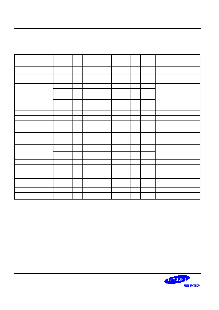
Table 2. Pad Center Coordinates (Continued)
[Unit:
�
m]
NO
NAME
X
Y
NO
NAME
X
Y
NO
NAME
X
Y
151
SEG9
2309.9
1003
201
SEG59
-690.1
1003
251
COM43
-3690.1
1003
152
SEG10
2249.9
1003
202
SEG60
-750.1
1003
252
COM44
-3750.1
1003
153
SEG11
2189.9
1003
203
SEG61
-810.1
1003
253
COM45
-3810.1
1003
154
SEG12
2129.9
1003
204
SEG62
-870.1
1003
254
DUMMY16 -3890.1
1003
155
SEG13
2069.9
1003
205
SEG63
-930.1
1003
255
DUMMY17 -3970.1
1003
156
SEG14
2009.9
1003
206
SEG64
-990.1
1003
256
DUMMY18
-4243
822.45
157
SEG15
1949.9
1003
207
SEG65
-1050.1
1003
257
DUMMY19
-4243
742.45
158
SEG16
1889.9
1003
208
SEG66
-1110.1
1003
258
DUMMY20
-4243
662.45
159
SEG17
1829.9
1003
209
SEG67
-1170.1
1003
259
COM46
-4243
582.45
160
SEG18
1769.9
1003
210
SEG68
-1230.1
1003
260
COM47
-4243
522.45
161
SEG19
1709.9
1003
211
SEG69
-1290.1
1003
261
COM48
-4243
462.45
162
SEG20
1649.9
1003
212
SEG70
-1350.1
1003
262
COM49
-4243
402.45
163
SEG21
1589.9
1003
213
SEG71
-1410.1
1003
263
COM50
-4243
342.45
164
SEG22
1529.9
1003
214
SEG72
-1470.1
1003
264
COM51
-4243
282.45
165
SEG23
1469.9
1003
215
SEG73
-1530.1
1003
265
COM52
-4243
222.45
166
SEG24
1409.9
1003
216
SEG74
-1590.1
1003
266
COM53
-4243
162.45
167
SEG25
1349.9
1003
217
SEG75
-1650.1
1003
267
COM54
-4243
102.45
168
SEG26
1289.9
1003
218
SEG76
-1710.1
1003
268
COM55
-4243
42.45
169
SEG27
1229.9
1003
219
SEG77
-1770.1
1003
269
COM56
-4243
-17.55
170
SEG28
1169.9
1003
220
SEG78
-1830.1
1003
270
COM57
-4243
-77.55
171
SEG29
1109.9
1003
221
SEG79
-1890.1
1003
271
COM58
-4243
-137.55
172
SEG30
1049.9
1003
222
SEG80
-1950.1
1003
272
COM59
-4243
-197.55
173
SEG31
989.9
1003
223
SEG81
-2010.1
1003
273
COM60
-4243
-257.55
174
SEG32
929.9
1003
224
SEG82
-2070.1
1003
274
COM61
-4243
-317.55
175
SEG33
869.9
1003
225
SEG83
-2130.1
1003
275
COM62
-4243
-377.55
176
SEG34
809.9
1003
226
SEG84
-2190.1
1003
276
COM63
-4243
-437.55
177
SEG35
749.9
1003
227
SEG85
-2250.1
1003
277
COMS1
-4243
-497.55
178
SEG36
689.9
1003
228
SEG86
-2310.1
1003
278
DUMMY21
-4243
-577.55
179
SEG37
629.9
1003
229
SEG87
-2370.1
1003
279
DUMMY22
-4243
-657.55
180
SEG38
569.9
1003
230
SEG88
-2430.1
1003
181
SEG39
509.9
1003
231
SEG89
-2490.1
1003
182
SEG40
449.9
1003
232
SEG90
-2550.1
1003
183
SEG41
389.9
1003
233
SEG91
-2610.1
1003
184
SEG42
329.9
1003
234
SEG92
-2670.1
1003
185
SEG43
269.9
1003
235
SEG93
-2730.1
1003
186
SEG44
209.9
1003
236
SEG94
-2790.1
1003
187
SEG45
149.9
1003
237
SEG95
-2850.1
1003
188
SEG46
89.9
1003
238
DUMMY14 -2910.1
1003
189
SEG47
29.9
1003
239
DUMMY15 -2970.1
1003
190
SEG48
-30.1
1003
240
COM32
-3030.1
1003
191
SEG49
-90.1
1003
241
COM33
-3090.1
1003
192
SEG50
-150.1
1003
242
COM34
-3150.1
1003
193
SEG51
-210.1
1003
243
COM35
-3210.1
1003
194
SEG52
-270.1
1003
244
COM36
-3270.1
1003
195
SEG53
-330.1
1003
245
COM37
-3330.1
1003
196
SEG54
-390.1
1003
246
COM38
-3390.1
1003
197
SEG55
-450.1
1003
247
COM39
-3450.1
1003
198
SEG56
-510.1
1003
248
COM40
-3510.1
1003
199
SEG57
-570.1
1003
249
COM41
-3570.1
1003
200
SEG58
-630.1
1003
250
COM42
-3630.1
1003
S6B0756 65 COM / 96 SEG DRIVER & CONTROLLER FOR STN LCD
7
PIN DESCRIPTION
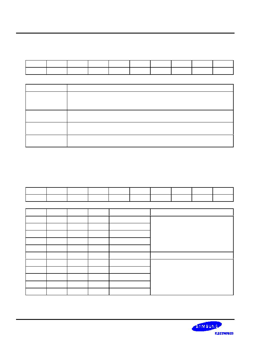
POWER SUPPLY
Table 3. Power Supply Pins
Name
I/O
Description
VDD1
VDD2
Supply
Power supply
VSS0
VSS1
VSS2
Supply
Ground
NOTE: VSS0, VSS1 and VSS2 must be shorted to external wire.
LCD driver supply voltages
These voltages are determined by LCD pixel is impedance, and converted by
operational amplifiers for application.
Voltages should have the following relationship;
VOUT
V1
V2
V3
V4
V
SS
When the internal power circuit is active, these voltages are generated as following table
according to the state of LCD bias.
LCD bias
V1
V2
V3
V4
1/N bias
(N-1) / N x
VOUT
(N-2) / N x VOUT
(2/N) x VOUT
(1/N) x VOUT
VOUT
V1
V2
V3
V4
I/O
NOTE: N = 4 to 9
LCD DRIVER SUPPLY
Table 4. LCD Driver Supply Pins
Name
I/O
Description
VOUT
I/O
Voltage converter input/output pin
Connect this pin to V
SS
through capacitor.
VCI1
VCI2
VCI3
I
Voltage converter input voltage pin and Power supply pins for Analog block
Voltages should have the following relationship: VDD
VCI
VOUT
65 COM / 96 SEG DRIVER & CONTROLLER FOR STN LCD S6B0756
8
SYSTEM CONTROL
Table 5. System Control Pins
Name
I/O
Description
OTPG
I
Gate Voltage for OTP programming
OTPD
I
Drain Voltage for OTP programming
TEST1
to
TEST4
I
Test pins
Don't use these pins.
S6B0756 65 COM / 96 SEG DRIVER & CONTROLLER FOR STN LCD
9
MICROPROCESSOR INTERFACE
Table 6. Microprocessor Interface Pins
Name
I/O
Description
RESETB
I
Reset the input pin
When RESETB is "L", initialization is executed.
Parallel/Serial data input select input
PS0
Interface
Mode
Data/
Instruction
Data
Read / Write
Serial Clock
H
Parallel
RS
DB0 to DB7
E_RD
RW_WR
-
L
Serial
RS or None
SID(DB7)
Write only
SCLK(DB6)
PS0
I
*NOTE: When PS is "L", DB0 to DB5 are high impedance and E_RD and RW_WR
must be fixed to either "H" or "L".
PS1
I
Microprocessor interface select input pin
-
PS0 = "H" , PS1 = "H": 6800-series parallel MPU interface
-
PS0 = "H" , PS1 = "L": 8080-series parallel MPU interface
-
PS0 = "L" , PS1 = "H": 4 Pin-SPI serial MPU interface
-
PS0 = "L" , PS1 = "L": 3 Pin-SPI serial MPU interface
CS1B
I
Chip select input pins
Data/instruction I/O is enabled only when CS1B is "L" . When chip select is non-active, DB0
to DB7 may be high impedance.
RS
I
Register select input pin
-
RS = "H": DB0 to DB7 are display dat a
-
RS = "L": DB0 to DB7 are control data
Read / Write execution control pin
PS1
MPU Type
RW_WR
Description
H
6800-series
RW
Read/Write control input pin
-
RW = "H": read
-
RW = "L": write
L
8080-series
/WR
Write enable clock input pin
The data on DB0 to DB7 are latched at the rising
edge of the /WR signal.
RW_WR
I
65 COM / 96 SEG DRIVER & CONTROLLER FOR STN LCD S6B0756
10
Table 6 (Continued)
Name
I/O
Description
Read / Write execution control pin
PS1
MPU Type
E_RD
Description
H
6800-series
E
Read/Write control input pin
-
RW = "H": When E is "H", DB0 to DB7 are in an
output status.
-
RW = "L": The data on DB0 to DB7 are latched at
the falling edge of the E signal.
L
8080-series
/RD
Read enable clock input pin
When /RD is "L", DB0 to DB7 are in an output status.
E_RD
I
DB0
to
DB7
I/O
8-bit bi-directional data bus that is connected to the standard 8-bit microprocessor data
bus. When the serial interface selected (PS0 = "L");
-
DB0 to DB5: high impedance
-
DB6: serial input clock (SCLK)
-
DB7: serial input data (SID)
When chip select is not active, DB0 to DB7 may be high impedance.
S6B0756 65 COM / 96 SEG DRIVER & CONTROLLER FOR STN LCD
11
LCD DRIVER OUTPUTS
Table 7. LCD Driver Outputs Pins
Name
I/O
Description
LCD segment driver outputs
The display data and the M signal control the output voltage of segment driver.
Segment driver output voltage
Display data
M (Internal)
Normal display
Reverse display
H
H
VOUT
V2
H
L
V
SS
V3
L
H
V2
VOUT
L
L
V3
V
SS
Power save mode
V
SS
V
SS
SEG0
to
SEG95
O
LCD common driver outputs
The internal scanning data and M signal control the output voltage of common driver.
Scan data
M (Internal)
Common driver output voltage
H
H
V
SS
H
L
VOUT
L
H
V1
L
L
V4
Power save mode
V
SS
COM0
to
COM63
O
COMS
(COMS1)
O
Common output for the icons
The output signals of two pins are same. When not used, these pins should be left open.
NOTE:
DUMMY � These pins should be opened (floated).
65 COM / 96 SEG DRIVER & CONTROLLER FOR STN LCD S6B0756
12
FUNCTIONAL DESCRIPTION
MICROPROCESSOR INTERFACE
Chip Select Input
There are CS1B for chip selection. The S6B0756 can interface with an MPU only when CS1B is "L" . Otherwise RS,
E_RD, and RW_WR inputs are disabled and DB0 to DB7 are to be high impedance. And, in case of serial interface,
the internal shift register and the counter are reset.
Parallel / Serial Interface
S6B0756 has four types of interface with an MPU, which are two serial and two parallel interface. This parallel or
serial interface is determined by PS 0 pin as shown in Table 8.
Table 8. Parallel / Serial Interface Mode
PS0
Type
CS1B
PS1
Interface mode
H
6800-series MPU mode
H
Parallel
CS1B
L
8080-series MPU mode
H
4 Pin-SPI MPU mode
L
Serial
CS1B
L
3 Pin-SPI MPU mode
Parallel Interface (PS0 = "H")
The 8-bit bi-directional data bus is used in parallel interface and the type of MPU is selected by PS1 as shown in
Table 9. The type of data transfer is determined by signals at RS, E_RD and RW_WR as shown in Table 10.
Table 9. Microprocessor Selection for Parallel Interface
PS1
CS1B
RS
E_RD
RW_WR
DB0 to DB7
MPU bus
H
CS1B
RS
E
RW
DB0 to DB7
6800-series
L
CS1B
RS
/RD
/WR
DB0 to DB7
8080-series
Table 10. Parallel Data Transfer
Common
6800-series
8080-series
Description
RS
E_RD
(E)
RW_WR
(RW)
E_RD
(/RD)
RW_WR
(/WR)
H
H
H
L
H
Display data read out
H
H
L
H
L
Display data write
L
H
H
L
H
Register status read
L
H
L
H
L
Writes to internal register (instruction)
NOTE: When E_RD pin is always pulled high for 6800-series interface, it can be used CS1B for enable signal. In
this case, interface data is latched at the rising edge of CS1B and the type of data transfer is determined by signals
at RS, RW_WR as in case of 6800-series mode.
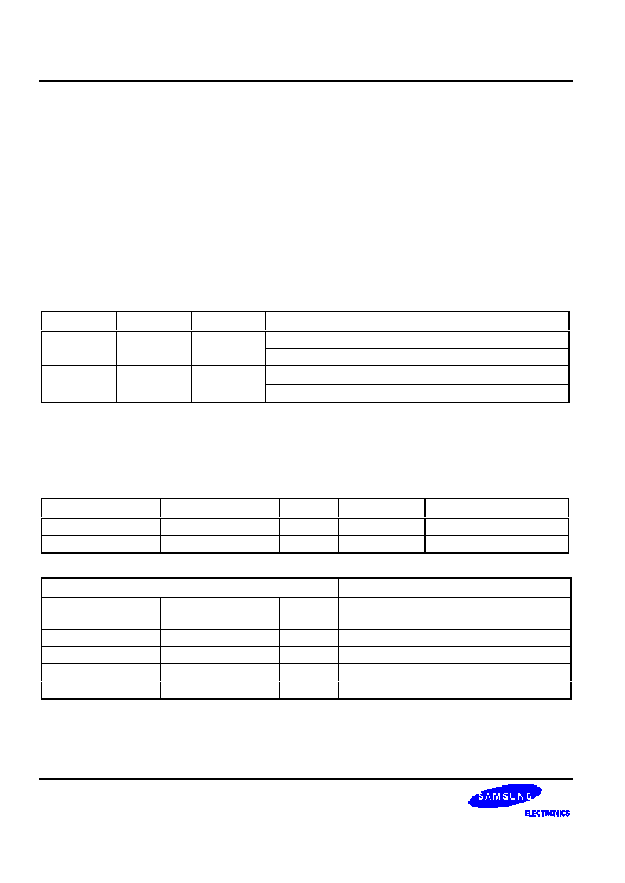
S6B0756 65 COM / 96 SEG DRIVER & CONTROLLER FOR STN LCD
13
CS1B
RS
RW
E
DB
Command Write
Data Write
Status Read
Data Read
Figure 3. 6800-Series MPU Interface protocol (PS="H", MI="H")
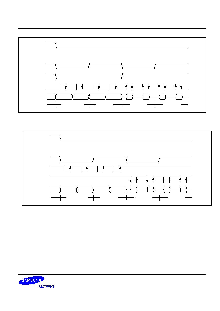
CS1B
RS
/WR
/RD
DB
Command Write
Data Write
Status Read
Data Read
Figure 4 . 8080-Series MPU Interface Protocol (PS="H", MI="L")
65 COM / 96 SEG DRIVER & CONTROLLER FOR STN LCD S6B0756
14
Serial Interface (PS0 = "L")
When the S6B0756 is active(CS1B="L"), serial data (DB7) and serial clock (DB6) inputs are enabled. And not active,
the internal 8-bit shift register and the 3-bit counter are reset. The display data/command indication may be
controlled either via software or the Register Select(RS) Pin, based on the setting of PS1. When the RS pin is used
(PS1 = "H"), data is display data when RS is high, and command data when RS is low. When RS is not used (PS1 =
"L"), the LCD Driver will receive command from MPU by default. If messages on the data pin are data rather than
command, MPU should send Data Direction command(11101000) to control the data direction and then one more
command to define the number of data bytes will be write. After these two continuous commands are send, the
following messages will be data rather than command. Serial data can be read on the rising edge of serial clock
going into DB6 and processed as 8-bit parallel data on the eighth serial clock. And the DDRAM column address
pointer will be increased by one automatically. The next bytes after the display data string is handled as command
data.
Serial Mode
PS0
PS1
CS1B
RS
Serial-mode with RS pin
L
H
CS1B
Used
Serial-mode with software
command
L
L
CS1B
Not used
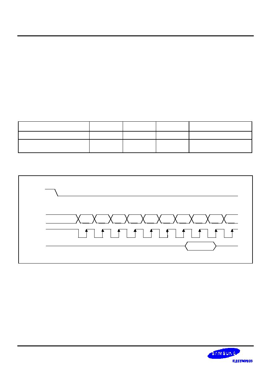
4 Pin-SPI Interface (PS0 = "L" , PS1 = "H")
CS1B
SID
SCLK
RS
DB6
DB7
DB0
DB1
DB2
DB3
DB4
DB5
DB6
DB7
Figure 5. 4 Pin SPI Timing (RS is used)
S6B0756 65 COM / 96 SEG DRIVER & CONTROLLER FOR STN LCD
15
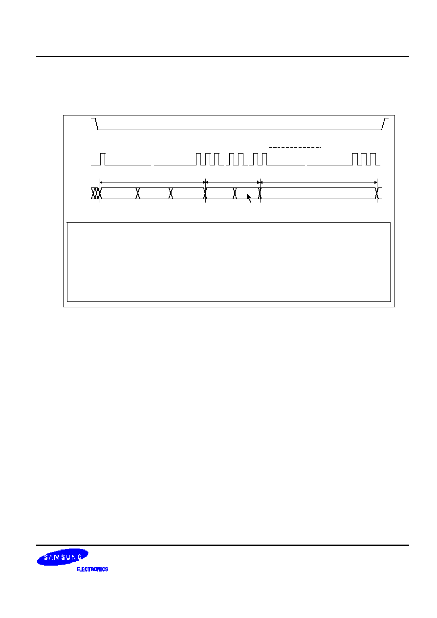
3 Pin-SPI Interface (PS0 = "L" , PS1 = "L")
To write data to the DDRAM, send Data Direction Command in 3-Pin SPI mode. Data is latched at the rising edge of
SCLK. And the DDRAM column address pointer will be increased by one automatically.
Figure 6. 3 Pin SPI Timing (RS is not used)
This command is used in 3-Pin SPI mode only. It will be two continuous commands, the first byte controls the data
direction and informs the LCD driver the second byte will be number of data bytes will be write. After these two
commands sending out, the following messages will be data. If data is stopped in transmitting, it is not valid data.
New data will be transferred serially with most significant bit first.
Notes:
l
In spite of transmission of data, if CS1B will be disable, state terminates abnormally. Next state is
initialized.
l
DDL Register value "0"
�
"1" , "95"
�
"96". (decimal value)
Busy Flag
The Busy Flag indicates whether the S6B0756 is operating or not. When DB7 is "H" in read status operation, this
device is in busy status and will accept only read status instruction. If the cycle time is correct, the microprocessor
needs not to check this flag before each instruction, which improves the MPU performance.
SCLK
CS1B
765 766 767
~~
~~
0
0 1
7 8
~~
15
~~
23
SID
MSB
Data In
Page
LSB
DDC
No. of
DATA
3 Byte (1)
2 Byte (2)
96 Byte
0
(1) Set Page and Column Address.
Set Page Address
: 1 0 1 1 P3 P2 P1 P0
Set Column Address MSB
: 0 0 0 1 0 Y6 Y5 Y4
Set Column Address LSB
: 0 0 0 0 Y3 Y2 Y1 Y0
(2) Set DDC(Data Direction Command) and No. of Data Bytes.
Set Data Direction Command( For SPI mode Only):
0 1 1 0 0 0 0 0
Set No. of Data Bytes(DDL)
: D7 D6 D5 D4 D3D2D1D0
65 COM / 96 SEG DRIVER & CONTROLLER FOR STN LCD S6B0756
16
Data Transfer
The S6B0756 uses bus holder and internal data bus for Data Transfer with the MPU. When writing data from the
MPU to on-chip RAM, data is automatically transferred from the bus holder to the RAM as shown in Figure 7. And
when reading data from on-chip RAM to the MPU, the data for the initial read cycle is stored in the bus holder
(dummy read) and the MPU reads this stored data from bus holder for the next data read cycle as shown in Figure 8.
This means that a dummy read cycle must be inserted between each pair of address sets when a sequence of
address sets is executed. Therefore, the data of the specified address cannot be output with the read display data
instruction right after the address sets, but can be output at the second read of data.
R S
/ W R
DB0 to DB7
N
D(N)
D(N+1)
D(N+2)
D(N+3)
Internal signals
MPU signals
/ W R
BUS HOLDER
C O L U M N A D D R E S S
N
N + 1
N + 2
N + 3
N
D(N)
D(N+1)
D(N+2)
D(N+3)
Figure 7. Write Timing
RS
/WR
/RD
DB0 to DB7
N
MPU signals
Dummy
D(N)
D(N+1)
Internal signals
/WR
/RD
BUS HOLDER
COLUMN ADDRESS
N
D(N)
D(N+1)
D(N+2)
N
N+1
N+2
N+3
D(N+2)
Figure 8. Read Timing
S6B0756 65 COM / 96 SEG DRIVER & CONTROLLER FOR STN LCD
17
DISPLAY DATA RAM (DDRAM)
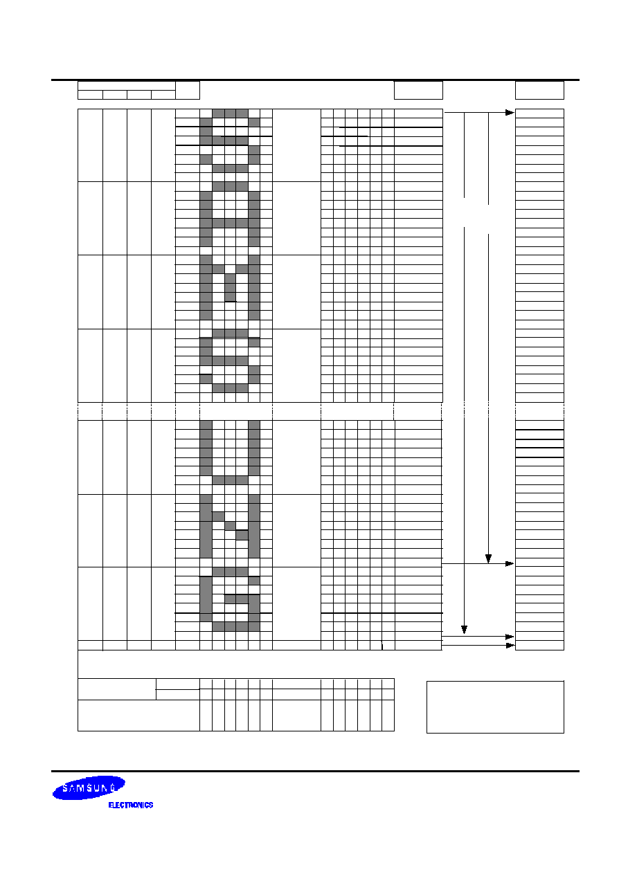
The Display Data RAM stores pixel data for the LCD. It is 65-row by 96-column addressable array. Each pixel can be
selected when the page and column addresses are specified. The 65 rows are divided into 8 pages of 8 lines and the
9th page with a single line (DB0 only). Data is read from or written to the 8 lines of each page directly through DB0 to
DB7. The display data of DB0 to DB7 from the microprocessor correspond to the LCD common lines as shown in
Figure 9. The microprocessor can read from and write to RAM through the I/O buffer. Since the LCD controller
operates independently, data can be written into RAM at the same time as data is being displayed without causing
the LCD flicker.
COM0
- -
COM1
- -
COM2
- -
COM3
- -
COM4
- -
DB0
0
0
1
- -
0
DB1
1
0
0
- -
1
DB2
0
1
1
- -
0
DB3
1
0
1
- -
0
DB4
0
0
0
- -
1
Display Data RAM LCD Display
Figure 9. RAM-to-LCD Data Transfer
Page Address Circuit
This circuit is for providing a Page Address to Display Data RAM shown in Figure 11. It incorporates 4-bit Page
Address register changed by only the "Set Page" instruction. Page Address 8 (DB3 is "H", DB2, DB1 and DB0 is "L")
is a special RAM area for the icons and display data DB0 is only valid.
Line Address Circuit
This circuit assigns DDRAM a Line Address corresponding to the first line (COM0) of the display. Therefore, by
setting line address repeatedly, it is possible to realize the screen scrolling and page switching without changing the
contents of on-chip RAM as shown in Figure 9
. It incorporates 7-bit Line Address register changed by only the initial
display line instruction and 7-bit counter circuit. At the beginning of each LCD frame, the contents of register are
copied to the line counter which is increased by CL signal and generates the Line Address for transferring the 96-
bit RAM data to the display data latch circuit. However, display data of icons are not scrolled because the MPU can
not access Line Address of icons.
65 COM / 96 SEG DRIVER & CONTROLLER FOR STN LCD S6B0756
18
Column Address Circuit
Column address circuit has a 7-bit preset counter that provides column address to the Display Data RAM as shown
in
Figure 11. When set Column Address MSB / LSB instruction is issued, 7-bit [Y6:Y0] is updated. And, since this
address is increased by 1 each a read or write data instruction, microprocessor can access the display data
continuously. And the Column Address counter is independent of page address register.
ADC Select instruction makes it possible to invert the relationship between the column address and the segment
outputs. It is necessary to rewrite the display data on built-in RAM after issuing ADC Select instruction. Refer to the
following Figure 10.
SEG output
SEG
0
SEG
1
SEG
2
SEG
3
... ...
SEG
92
SEG
93
SEG
94
SEG
95
Column address [Y6:Y0]
00H
01H
02H
03H
... ...
5CH
5DH
5EH
5FH
Display data
1
0
1
0
1
1
0
0
LCD panel display
( ADC = 0 )
... ...
LCD panel display
( ADC = 1 )
... ...
Figure 10. The Relationship between the Column Address and the Segment Outputs
Segment Control Circuit
This circuit controls the display data by the Display ON / OFF, reverse display ON / OFF and entire display ON / OFF
instructions without changing the data in the display data RAM.
S6B0756 65 COM / 96 SEG DRIVER & CONTROLLER FOR STN LCD
19
Figure 11. Display Data RAM Map (Initial Line Address = 00H)
Page 0
Page 2
Page 1
Page 3
Page9
Page 8
Line
Address
COM
Output
Page Address
DB3
DB0
DB1
DB2
Data
SEG95
SEG94
SEG1
SEG0
SEG93
SEG92
SEG91
SEG90
SEG2
SEG3
SEG4
SEG5
- - - - -
ADC=1
ADC=0
Column
Address
LCD Output
DB0
DB7
DB6
DB5
DB4
DB3
DB2
DB1
DB0
DB7
DB6
DB5
DB4
DB3
DB2
DB1
DB0
DB7
DB6
DB5
DB4
DB3
DB2
DB1
DB0
DB7
DB6
DB5
DB4
DB3
DB2
DB1
DB0
DB7
DB6
DB5
DB4
DB3
DB2
DB1
DB0
DB7
DB6
DB5
DB4
DB3
DB2
DB1
DB0
DB7
DB6
DB5
DB4
DB3
DB2
DB1
DB0
00H
08H
07H
06H
05H
04H
03H
02H
01H
09H
0AH
0BH
0CH
0DH
0EH
0FH
10H
18H
17H
16H
15H
14H
13H
12H
11H
19H
1AH
1BH
1CH
1DH
1EH
1FH
COM0
COM9
COM8
COM7
COM6
COM5
COM3
COM4
COM2
COM1
COM10
COM19
COM18
COM17
COM16
COM15
COM13
COM14
COM12
COM11
COM20
COM29
COM28
COM27
COM26
COM25
COM23
COM24
COM22
COM21
COM30
COM51
COM50
COM49
COM48
COM47
COM45
COM46
COM44
COM31
COM52
COM61
COM60
COM59
COM58
COM57
COM55
COM56
COM54
COM53
COM62
COM63
COMS
Page 6
Page 5
Page 7
40H
1/57
Duty
1/65
Duty
Initial start line address = 00H
38H
39H
3AH
3BH
3CH
3FH
3EH
3DH
COM43
COM41
COM42
COM40
00
- - - - -
01 02 03 04 05
5A 5B 5C 5D 5E 5F
00
- - - - -
01
02
03
04
05
5A
5B
5C
5D
5E
5F
0
0
0
0
0
0
1
0
0
0
0
1
0
0
1
1
0
1
0
1
0
1
1
0
0
1
1
1
1
0
0
0
initial line
register = 00H
31H
32H
33H
34H
2CH
2BH
2AH
29H
28H
37H
36H
35H
2DH
2FH
30H
27H

65 COM / 96 SEG DRIVER & CONTROLLER FOR STN LCD S6B0756
20
LCD DISPLAY CIRCUITS
Oscillator
This is completely on-chip Oscillator and its frequency is nearly independent of V
DD
. This Oscillator signal is used in
display timing generation circuit.
Display Timing Generator Circuit
This circuit generates some signals to be used for displaying LCD. The display clock, CL(internal), generated by
oscillation clock, generates the clock for the line counter and the signal for the display data latch. The line address of
on-chip RAM is generated in synchronization with the display clock and the display data latch circuit latches the
96-bit display data in synchronization with the display clock. The display data, which is read to the LCD driver, is
completely independent of the access to the display data RAM from the microprocessor. The display clock
generates an LCD AC signal (M) which enables the LCD driver to make a AC drive waveform, and also generates an
internal common timing signal and start signal to the common driver. The frame signal or the line signal changes the
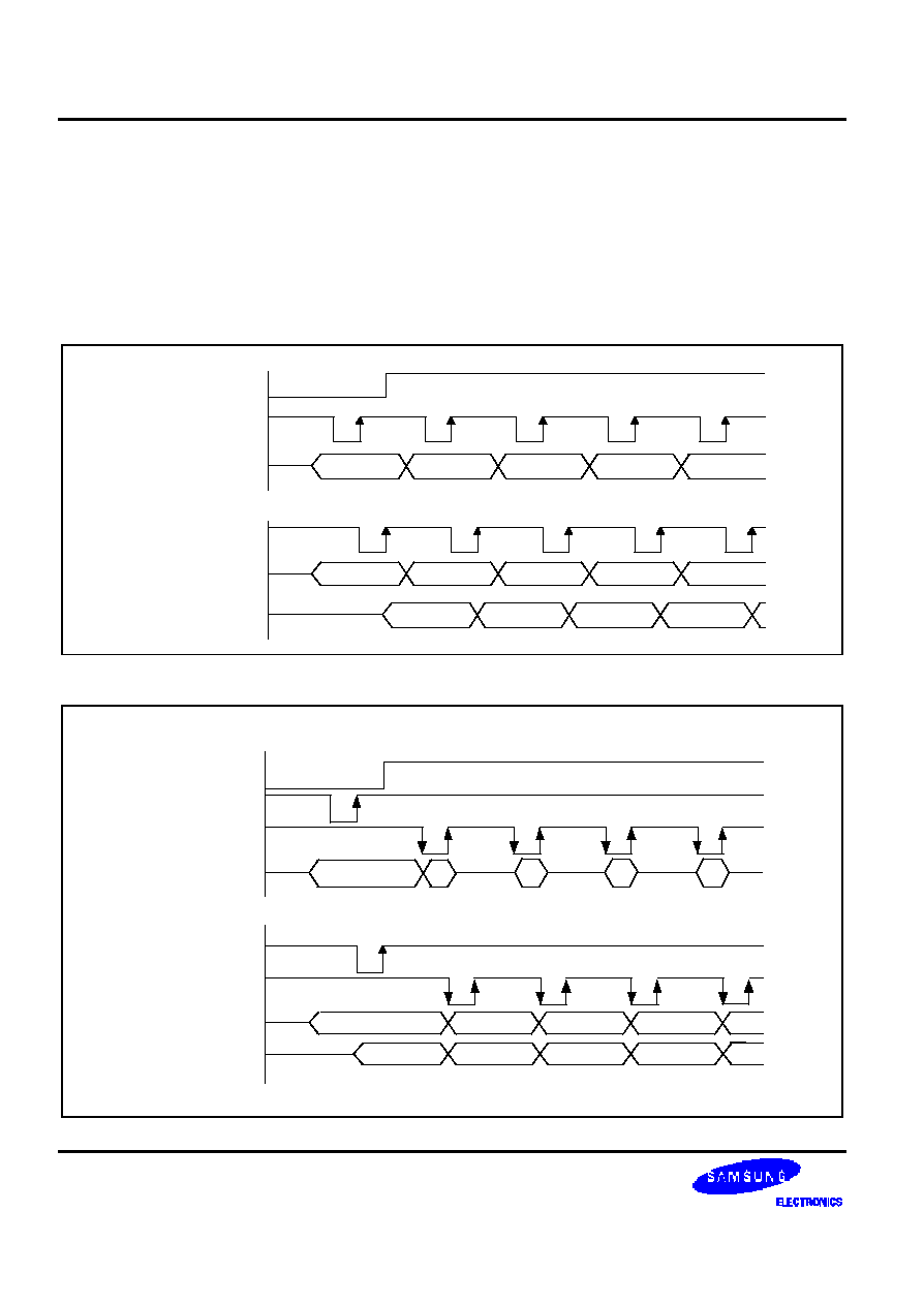
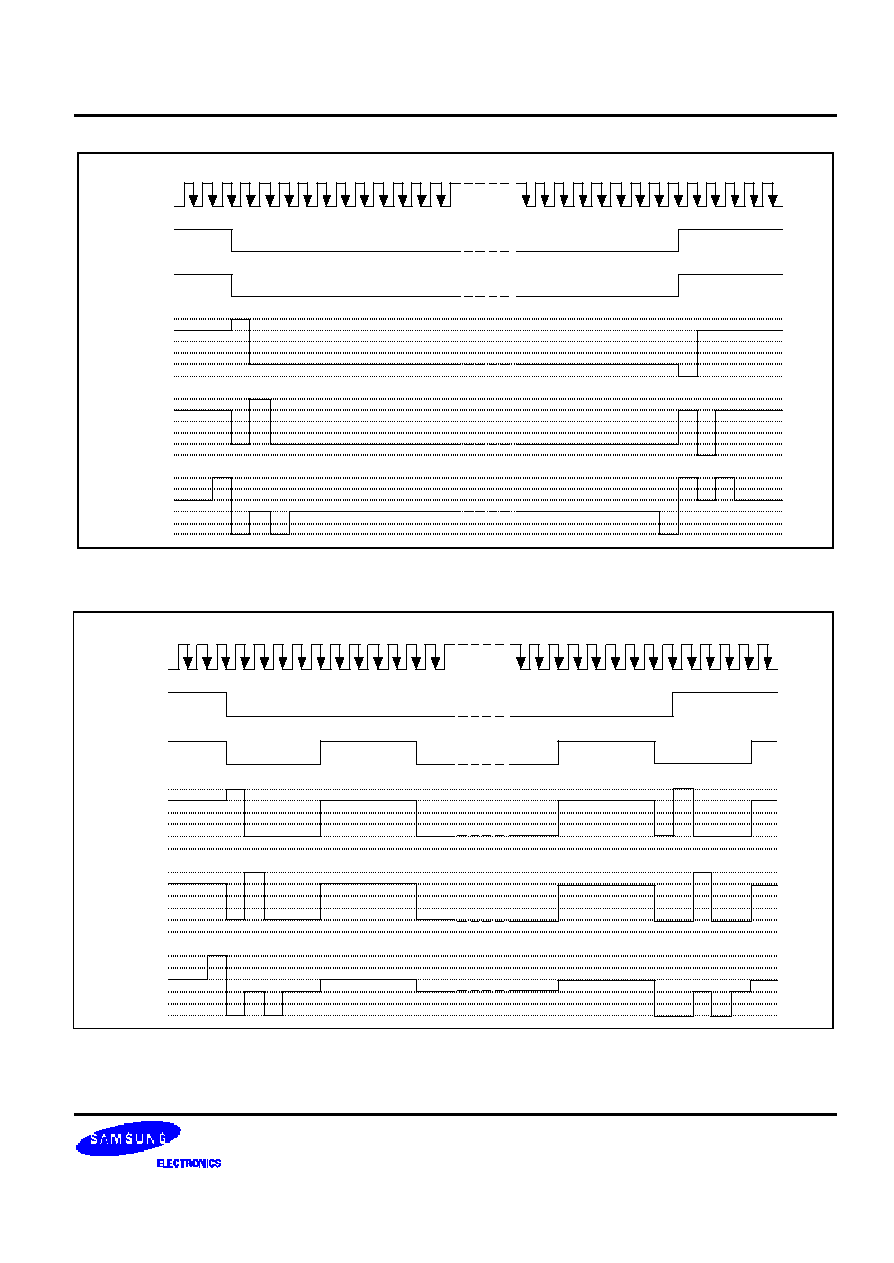
M by setting internal instruction. Driving waveform and internal timing signal are shown in Figure 12.
S6B0756 65 COM / 96 SEG DRIVER & CONTROLLER FOR STN LCD
21
FR(Internal)
M(Internal)
64
65
1
2
3
4
5
6
7
8
9
10
11
12
58
59
60
61
62
63
64
65
1
2
3
4
5
6
CL(Internal)
COM0
V0
V1
V2
V3
V4
VSS
COM1
V0
V1
V2
V3
V4
VSS
V0
V1
V2
V3
V4
VSS
SEG
n
Figure 12. 2-frame AC Driving Waveform (Duty Ratio = 1/65)
COM0
V0
V1
V2
V3
V4
VSS
COM1
V0
V1
V2
V3
V4
VSS
V0
V1
V2
V3
V4
VSS
SEGn
FR(Internal)
M(Internal)
64
65
1
2
3
4
5
6
7
8
9 10
11
12
58
59
60
61
62
63
64
65
1
2
3
4
5
6
CL(Internal)
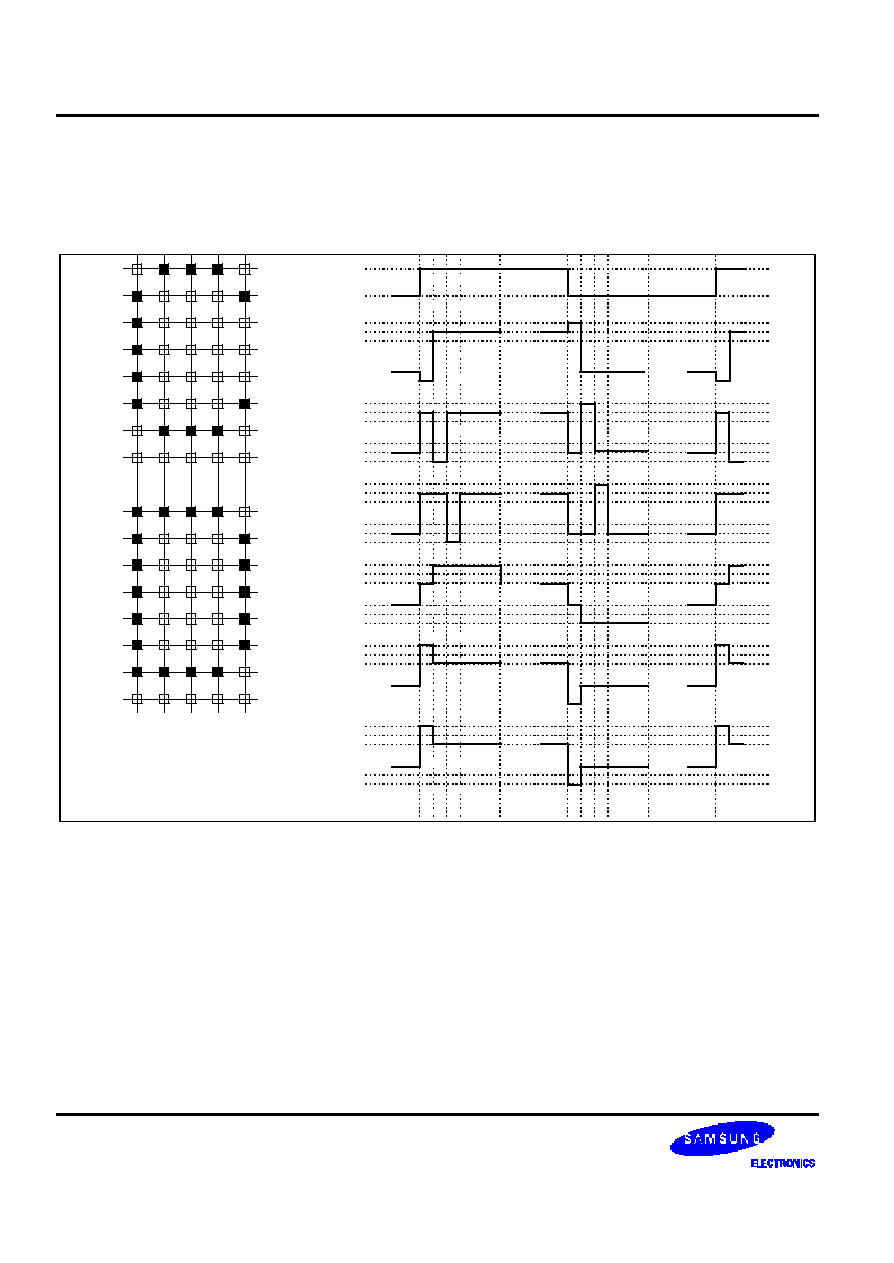
Figure 13. N-line Inversion Driving Waveform (N = 5 , Duty Ratio = 1/65)
65 COM / 96 SEG DRIVER & CONTROLLER FOR STN LCD S6B0756
22
LCD DRIVER CIRCUIT
65-channel common driver and 96-channel segment driver configure this driver circuit. This LCD panel driver
voltage depends on the combination of display data and M(internal) signal.
COM0
COM1
COM2
COM3
COM4
COM5
COM6
COM7
COM8
COM9
COM10
COM11
COM12
COM13
COM14
COM15
S
E
G
4
S
E
G
3
S
E
G
2
S
E
G
1
S
E
G
0
SEG2
SEG1
SEG0
COM2
COM0
COM1
M
V0
V1
V2
V3
V4
VSS
V0
V1
V2
V3
V4
VSS
V0
V1
V2
V3
V4
VSS
V0
V1
V2
V3
V4
VSS
V0
V1
V2
V3
V4
VSS
V0
V1
V2
V3
V4
VSS
VDD
VSS
Figure 14. Segment and Common Timing
S6B0756 65 COM / 96 SEG DRIVER & CONTROLLER FOR STN LCD
23
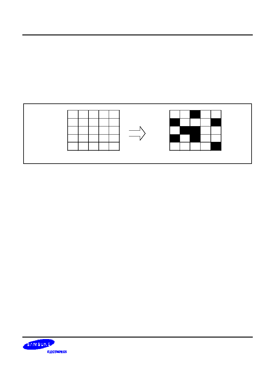
Partial Display on LCD
The S6B0756 realizes the Partial Display function on LCD with low-duty driving for saving power consumption and
showing the various display duty. To show the various display duty on LCD, LCD driving duty and bias are
programmable via the instruction. And, built-in power supply circuits are controlled by the instruction for adjusting
the LCD driving voltages
Figure 15. Reference Example for Partial Display (Display Duty = 25)
-- COMS
-- COM0
-- COM1
-- COM2
-- COM3
-- COM4
-- COM5
-- COM6
-- COM7
-- COM8
-- COM9
-- COM10
-- COM11
-- COM12
-- COM13
-- COM14
-- COM15
-- COM16
-- COM17
-- COM18
-- COM19
-- COM20
-- COM21
-- COM22
-- COM23
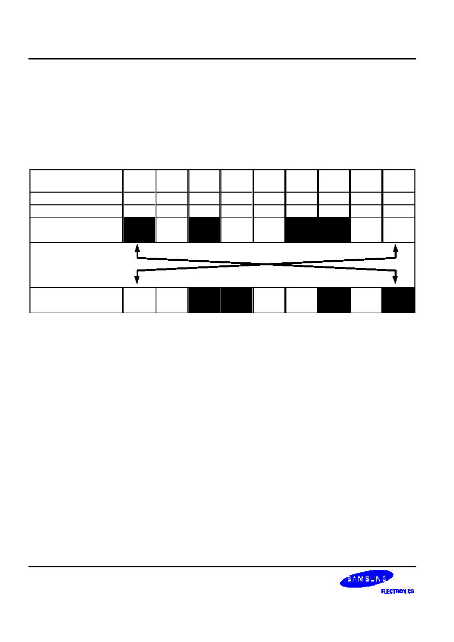
Figure 16. Partial Display (Partial Display Duty = 9, Initial COM0 = 0)
-- COMS
-- COM0
-- COM1
-- COM2
-- COM3
-- COM4
-- COM5
-- COM6
-- COM7
-- COM8
-- COM9
-- COM10
-- COM11
-- COM12
-- COM13
-- COM14
-- COM15
-- COM16
-- COM17
-- COM18
-- COM19
-- COM20
-- COM21
-- COM22
-- COM23
65 COM / 96 SEG DRIVER & CONTROLLER FOR STN LCD S6B0756
24
-- COMS
-- COM0
-- COM1
-- COM2
-- COM3
-- COM4
-- COM5
-- COM6
-- COM7
-- COM8
-- COM9
-- COM10
-- COM11
-- COM12
-- COM13
-- COM14
-- COM15
-- COM16
-- COM17
-- COM18
-- COM19
-- COM20
-- COM21
-- COM22
-- COM23
Figure 17. Moving Display (Partial Display Duty = 9, Initial COM0 = 8)
S6B0756 65 COM / 96 SEG DRIVER & CONTROLLER FOR STN LCD
25
POWER SUPPLY CIRCUITS
The Power Supply circuits generate the voltage levels necessary to drive liquid crystal driver circuits with low-power
consumption and the fewest components. There are voltage converter circuits, voltage regulator circuits, and
voltage follower circuits. They are valid only in master operation and controlled by power control instruction. For
details, refers to "Instruction Description". Table 11 shows the referenced combinations in using Power Supply
circuits.
Table 11. Recommended Power Supply Combinations
User setup
Power
control
(VC VR VF)
V/C
circuits
V/R
circuits
V/F
circuits
VOUT
V1 to V4
Only the internal power
supply circuits are used
1 1 1
ON
ON
ON
Open
Open
Only the voltage regulator
circuits and voltage follower
circuits are used
0 1 1
OFF
ON
ON
*External
input
Open
Only the voltage follower
circuits are used
0 0 1
OFF
OFF
ON
External
input
Open
Only the external power
supply circuits are used
0 0 0
OFF
OFF
OFF
External
input
External
input
* : When only the voltage regulator circuits and voltage follower circuits are used, External VOUT should be the
same voltage to operate LCD panel(VLCD). So, voltage regulator circuit operation doesn't cause any effect.
65 COM / 96 SEG DRIVER & CONTROLLER FOR STN LCD S6B0756
26
Voltage Converter Circuits
These circuits boost up the electric potential between VCI and Vss to 2, 3, 4 times toward positive side and boosted
voltage is outputted from VOUT pin. It is possible to select the lower boosting level in any boosting circuit by "Set
DC-DC Step-up" instruction. When the higher level is selected by instruction, VOUT voltage is not valid.
[C1 = 1.0 to 4.7
�
F]
Vss
VOUT
Vss
VCI
C1
VOUT = 3 x VCI
Vss
VOUT
Vss
VCI
C1
VOUT = 2 x VCI
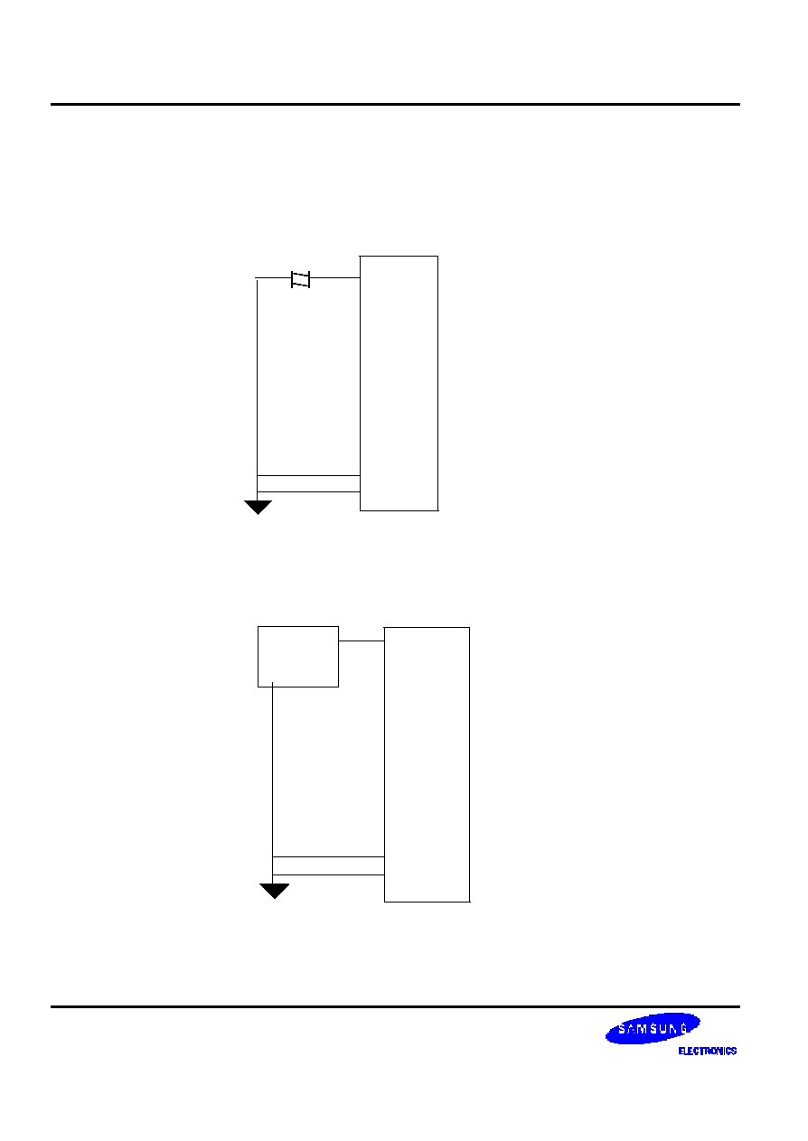
Figure 18. Two Times Boosting Circuit Figure 19. Three Times Boosting Circuit
Vss
VOUT
C1
Vss
VCI
VOUT = 4 x VCI
Figure 20. Four Times Boosting Circuit
S6B0756 65 COM / 96 SEG DRIVER & CONTROLLER FOR STN LCD
27
Voltage Regulator Circuits
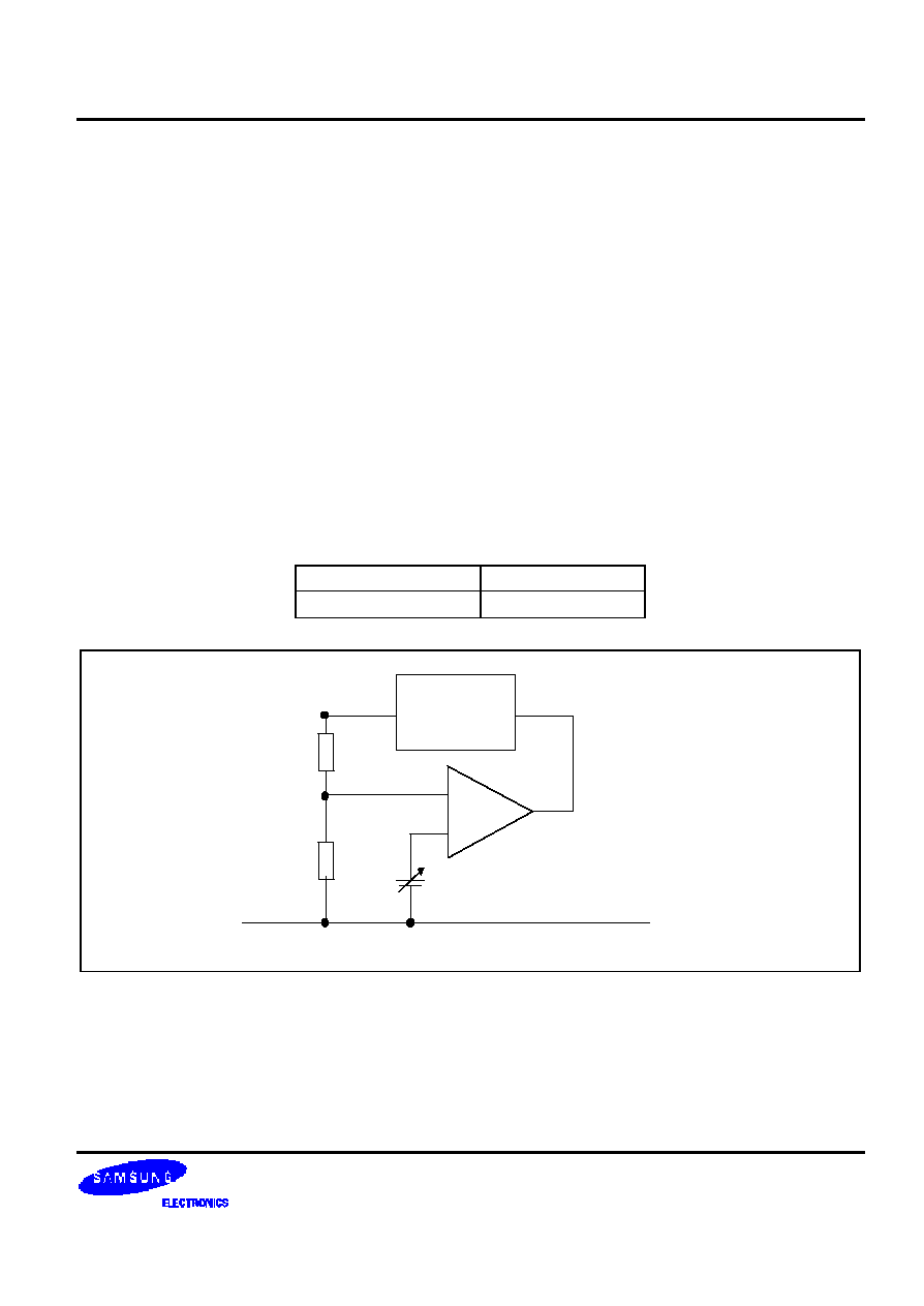
The function of the internal Voltage Regulator circuits is to determine liquid crystal operating voltage, VOUT, by
adjusting resistors, Ra and Rb. Because VOUT is the operating voltage of operational-amplifier circuits shown in
Figure 21, it is necessary to be applied internally.
For the Eq. 1, we determine VOUT by Ra, Rb and V
EV
. The Ra and Rb are connected internally. And V
EV
called the
voltage of electronic volume is determined by Eq. 2, where the parameter
is the value selected by instruction, "Set
Reference Voltage Register", within the range 0 to 63. V
REF
voltage at Ta= 25
�
C is shown in Table 12
(Abbreviated OTP calibration in V
EV
expression (Eq.2), see "OTP calibration mode" section for more information)
Rb
VOUT = (1 +
) x V
EV
[V] ------ (Eq. 1)
Ra
(63 � (
� OV/2)
V
EV
= (1 -
) x V
REF
[V] ------ (Eq. 2)
210
Table 12. . V
REF
Voltage at Ta = 25
�
C
Temp. coefficient
V
REF
[ V ]
-0.05% /
�
C
2.1
Vev (constant voltage source + electronic volume)
+
--
Internal Rb
Internal Ra
VOUT
GND
DCDC
CONVERTER
Figure 21. Internal Voltage Regulator Circuit
65 COM / 96 SEG DRIVER & CONTROLLER FOR STN LCD S6B0756
28
In Case of Using Internal Resistors, Ra and Rb
Resistor Ra is connected internally between VR pin and V
SS
, and Rb is connected between VOUT and VR. We
determine VOUT by two instructions, "Regulator Resistor Select" and "Set Reference Voltage".
Table 13. Internal Rb / Ra Ratio depending on 3-bit Data (R2 R1 R0)
3-bit data settings (R2 R1 R0)
0 0 0
0 0 1
0 1 0
0 1 1
1 0 0
1 0 1
1 1 0
1 1 1
1 + (Rb / Ra)
2.3
3.0
3.7
4.4
5.1
5.8
6.5
7.2
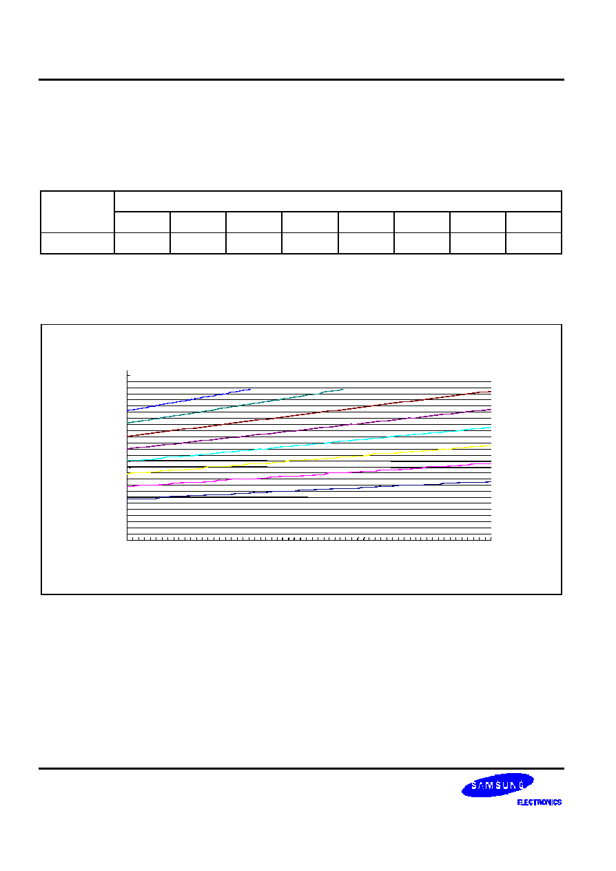
Figure 22 Shows VOUT voltage measured by adjusting internal regulator register ratio (Rb / Ra) and 6-bit electronic
volume registers for each temperature coefficient at Ta = 25
�
C.
0.00
2.00
4.00
6.00
8.00
10.00
12.00
0
8
16
24
32
40
48
56
Electronic volume register (0 to 63)
V0 voltage [V]
(1, 1, 1)
63
63
(1, 1, 0)
(1, 0, 1)
(1, 0 ,0)
(0, 1, 1)
(0, 1, 0)
(0, 0, 1)
(0, 0, 0)
Figure 22. Electronic Volume Level (Temp. Coefficient = -0.05% /
�
C)

S6B0756 65 COM / 96 SEG DRIVER & CONTROLLER FOR STN LCD
29
Voltage Follower Circuits
VLCD voltage (VOUT) is resistively divided into four voltage levels (V1, V2, V3 and V4), and those output
impedance are converted by the Voltage Follower for increasing drive capability. Table 14 shows the relationship
between V1 to V4 level and each duty ratio.
Table 14
LCD bias
V1
V2
V3
V4
Remarks
1/N
(N-1)/N x VOUT (N-2)/N x VOUT
2/N x VOUT
1/N x VOUT
N = 4 to 9
65 COM / 96 SEG DRIVER & CONTROLLER FOR STN LCD S6B0756
30
REFERENCE CIRCUIT EXAMPLES
[
C1
= 1.0 to 4.7 [
�
F] ]
Figure 23. When Using all LCD Power Circuits (V/C: ON, V/R: ON, V/F: ON)
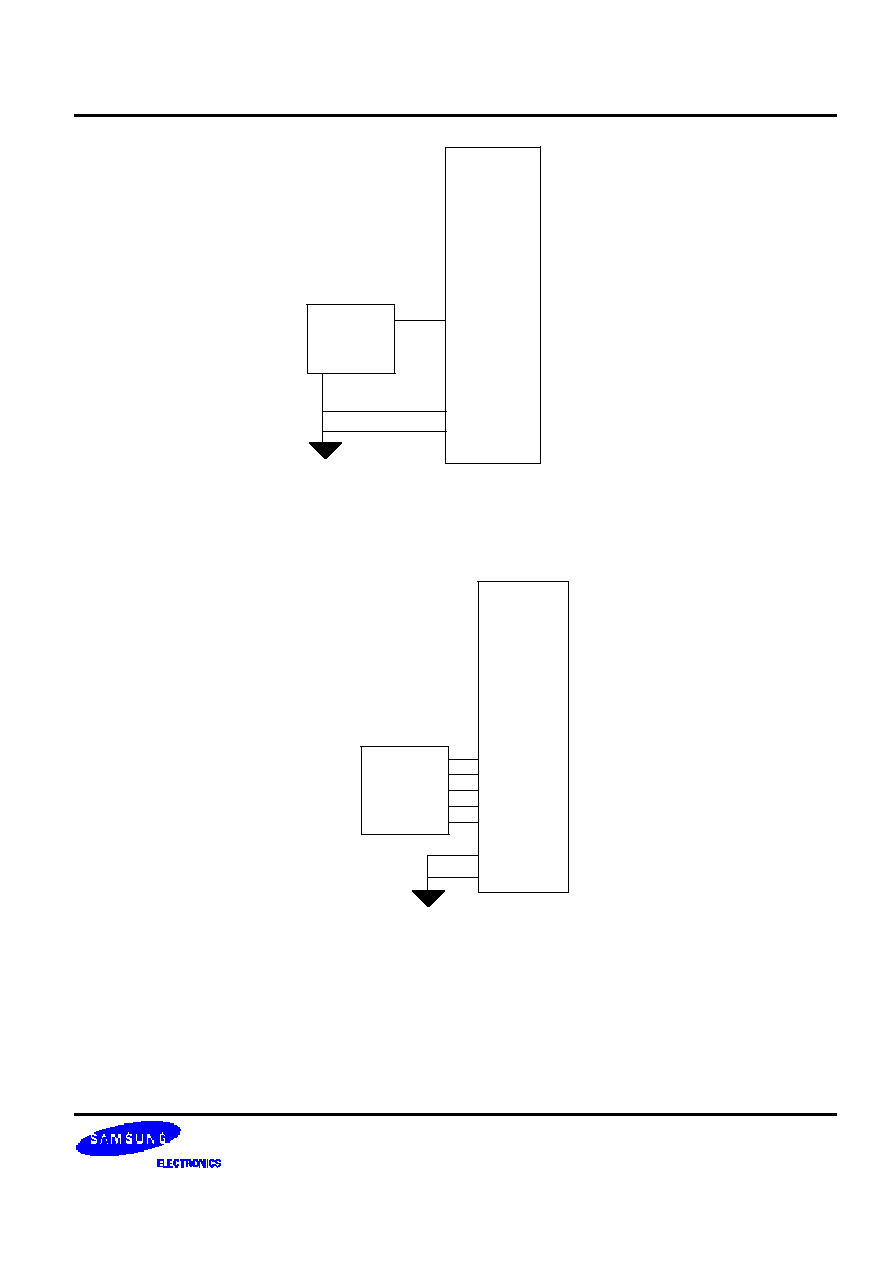
Figure 24. When Using only Voltage Follower Circuit (V/C: OFF, V/R: ON, V/F: ON)
Using internal regulator resistors
VOUT
V 1
V 2
V 3
V 4
V S S
V S S 1
V S S 2
C1
-
+
VOUT
V1
V2
V3
V4
External
Power
Supply
VSS
VSS1
VSS2
S6B0756 65 COM / 96 SEG DRIVER & CONTROLLER FOR STN LCD
31
Figure 25. When Using only Voltage Follower Circuit (V/C: OFF, V/R: OFF, V/F: ON)
Figure 26. When Not Using all LCD Power Circuits (V/C: OFF, V/R: OFF, V/F: OFF)
VOUT
V1
V2
V3
V4
External
Power
Supply
VSS
VSS1
VSS2
VSS
VOUT
V1
V2
V3
V4
VSS1
VSS2
External
Power
Supply

65 COM / 96 SEG DRIVER & CONTROLLER FOR STN LCD S6B0756
32
RESET CIRCUIT
Setting RESETB to
"L" or Reset instruction can initialize internal function.
When RESETB becomes
"L", following procedure is occurred.
Page address: 0
Column address: 0
Modify-read: OFF
Display ON / OFF: OFF
Initial display line: 0 (first)
Initial COM0 register: 0 (COM0)
Partial display duty ratio: 1/64
Icon enable/disable : 0 (disable)
Reverse display ON / OFF: OFF (normal)
n-line inversion register: 0 (disable)
Entire display ON / OFF: OFF (normal)
OTP_Mode ON/OFF : ON (normal)
Power control register (VC, VR, VF) = (0, 0, 0)
DC-DC step up: 2 times converter circuit = (1, 1)
Regulator resistor select register: (R2, R1, R0) = (0, 0, 0)
Reference voltage control register: (EV5, EV4, EV3, EV2, EV1, EVOUT) = (1, 0, 0, 0, 0, 0)
Offset voltage control register (OV4, OV3, OV2, OV1, OVOUT) = (0, 0, 0, 0, 0)
LCD bias ratio: 1/9
SHL select: OFF (normal)
ADC select: OFF (normal)
Oscillator status: OFF
Power save mode: release
Frame Frequency : 75Hz
When RESET instruction is issued, following procedure is occurred.
Page address: 0
Column address: 0
Modify-read: OFF
Initial display line: 0 (First)
Regulator resistor select register: (R2, R1, R0) = (0, 0, 0)
Reference voltage control register (EV5, EV4, EV3, EV2, EV1, EVOUT) = (1, 0, 0, 0, 0, 0)
Other instruction registers : Not Changed
While RESETB is
"L" or reset instruction is executed, no instruction except read status can be accepted. Reset
status appears at DB5. After DB5 becomes
"L", any instruction can be accepted. RESETB must be connected to
the reset pin of the MPU, and initialize the MPU and this LSI at the same time. The initialization by RESETB is
essential before use.
S6B0756 65 COM / 96 SEG DRIVER & CONTROLLER FOR STN LCD
33
INSTRUCTION DESCRIPTION
Table 15. Instruction Table
�
: Don't care
Instruction
RS
RW
DB7
DB6
DB5
DB4
DB3
DB2
DB1
DB0
Description
Read display data
1
1
Read data
Read data from DDRAM
Write display data
1
0
Write data
Write data into DDRAM
Read status
0
1
BUSY
ON
RES
OPRT
0
0
0
0
Read the internal status
Set page address
0
0
1
0
1
1
P3
P2
P1
P0
Set page address
Set column address MSB
0
0
0
0
0
1
0
Y6
Y5
Y4
Set column address MSB
Set column address LSB
0
0
0
0
0
0
Y3
Y2
Y1
Y0
Set column address LSB
Set modify-read
0
0
1
1
1
0
0
0
0
0
Set modify-read mode
Reset modify-read
0
0
1
1
1
0
1
1
1
0
Release modify-read mode
Display ON / OFF
0
0
1
0
1
0
1
1
1
D
D = 0: display OFF
D = 1: display ON
0
0
0
1
0
0
0
0
�
�
Set initial display line
register
0
0
�
S6
S5
S4
S3
S2
S1
S0
2-byte instruction to specify the
initial display line to realize
vertical scrolling
0
0
0
1
0
0
0
1
�
�
Set initial COM0 register
0
0
�
�
C5
C4
C3
C2
C1
C0
2-byte instruction to specify the
initial COM0 to realize window
scrolling
0
0
0
1
0
0
1
0
�
�
Set partial display
duty ratio
0
0
�
D6
D5
D4
D3
D2
D1
D0
2-byte instruction to set partial
display duty ratio
Frame Frequency
0
0
1
1
0
1
1
F2
F1
F0
Programmable Frame
Frequency
0
0
0
1
0
0
1
1
�
�
Set n-line inversion
0
0
�
�
�
N4
N3
N2
N 1
N0
2-byte instruction to set n-line
inversion register
Release n-line inversion
0
0
1
1
1
0
0
1
0
0
Release n-line inversion mode
Reverse display ON / OFF
0
0
1
0
1
0
0
1
1
REV
REV = 0: normal display
REV = 1: reverse display
Icon enable/disable
0
0
1
0
1
0
0
0
1
I
I = 0 : Icon disable
I = 1 : Icon enable
Entire display ON / OFF
0
0
1
0
1
0
0
1
0
EON
EON = 0: normal display
EON = 1: entire display ON
65 COM / 96 SEG DRIVER & CONTROLLER FOR STN LCD S6B0756
34
Table 17. Instruction Table (Continued)
Instruction
RS
RW
DB7
DB6
DB5
DB4
DB3
DB2
DB1
DB0
Description
Power control
0
0
0
0
1
0
1
VC
VR
VF
Control power circuit operation
Select DC-DC step-up
0
0
0
1
1
0
0
1
DC1
DC0
Select the step-up of the
internal voltage converter
Select regulator resistor
0
0
0
0
1
0
0
R2
R1
R0
Select internal resistance ratio
of the regulator resistor
0
0
1
0
0
0
0
0
0
1
Set electronic volume
register
0
0
x
x
EV5
EV4
EV3
EV2
EV1
EV0
2-byte instruction to specify the
electronic volume register
0
0
1
1
1
0
1
0
1
0
Set offset volume register
0
0
x
x
x
OV4
OV3
OV2
OV1
OV0
2-byte instruction to specify the
offset volume register
Select LCD bias
0
0
0
1
0
1
0
B2
B1
B0
Select LCD bias
OTP_Mode ON
0
0
1
1
1
0
1
1
0
OTON
OTP_mode ON/OFF
OTP write enable
0
0
1
1
1
0
1
1
1
1
OTP write enable
SHL select
0
0
1
1
0
0
SHL
�
�
�
COM bi-directional selection
SHL = 0: normal direction
SHL = 1: reverse direction
ADC select
0
0
1
0
1
0
0
0
0
ADC
SEG bi-directional selection
ADC = 0: normal direction
ADC = 1: reverse direction
�
�
1
1
1
0
1
0
0
0
Set Data Direction &
Display Data Length(DDL)
�
�
D7
D6
D5
D4
D3
D2
D1
D0
2-byte Instruction to specify the
number of data bytes(SPI
Mode)
.
Oscillator ON start
0
0
1
0
1
0
1
0
1
1
Start the built-in oscillator
Set power save mode
0
0
1
0
1
0
1
0
0
P
P = 0: standby mode
P = 1: sleep mode
Release power save mode
0
0
1
1
1
0
0
0
0
1
Release power save mode
Reset
0
0
1
1
1
0
0
0
1
0
Initialize the internal functions
NOP
0
0
1
1
1
0
0
0
1
1
No operation
Test instruction
0
0
1
1
1
1
�
�
�
�
Don't use this instruction.
S6B0756 65 COM / 96 SEG DRIVER & CONTROLLER FOR STN LCD
35
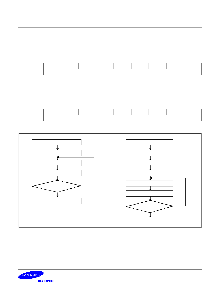
Read Display Data
8-bit data from Display Data RAM specified by the column address and page address can be read by this
instruction. As the column address is incremented by 1 automatically after each this instruction, the
microprocessor can continuously read data from the addressed page. A dummy read is required after loading
an address into the column address register. Display Data cannot be read through the serial interface.
RS
RW
DB7
DB6
DB5
DB4
DB3
DB2
DB1
DB0
1
1
Read data
Write Display Data
8-bit data of display data from the microprocessor can be written to the RAM location specified by the column
address and page address. The column address is incremented by 1 automatically so that the microprocessor
can sequentially write data to the addressed page. During auto-increment, the column address wraps to 0 after
the last column is written.
RS
RW
DB7
DB6
DB5
DB4
DB3
DB2
DB1
DB0
1
0
Write data
Data Write
Set Column Address
Set Page Address
Optional Status
Column = Column +1
No
Yes
Data Write Continue ?
Dummy Data Read
Set Column Address
Set Page Address
Optional Status
Column = Column +1
No
Yes
Data Read Continue ?
Data Read
Column = Column +1
Figure 27. Sequence for Writing Display Data Figure 28. Sequence for Reading Display Data
65 COM / 96 SEG DRIVER & CONTROLLER FOR STN LCD S6B0756
36
Read Status
Indicates the internal status of the S6B0756
RS
RW
DB7
DB6
DB5
DB4
DB3
DB2
DB1
DB0
0
1
BUSY
ON
RES
OPRT
0
0
0
0
Flag
Description
BUSY
The device is busy when internal operation or reset.
Any instruction is rejected until BUSY goes Low.
0: chip is active, 1: chip is being busy.
ON
Indicates display ON / OFF status.
0: display ON, 1: display OFF
RES
Indicates the initialization is in progress by RESETB signal.
0: chip is active, 1: chip is being reset.
OPRT
Indicates OTP status.
0: OTP is programmable, 1: OTP is programmed.
Set Page Address
Sets the Page Address of display data RAM from the microprocessor into the Page Address register. Any RAM
data bit can be accessed when its Page Address and column address are specified. Along with the column
address, the Page Address defines the address of the display RAM to write or read display data. Changing the
Page Address doesn't effect to the display status.
RS
RW
DB7
DB6
DB5
DB4
DB3
DB2
DB1
DB0
0
0
1
0
1
1
P3
P2
P1
P0
P3
P2
P1
P0
Selected page
Description
0
0
0
0
0
0
0
0
1
1
0
0
1
0
2
:
:
:
:
:
0
1
1
1
7
Accessible pages for displaying
dot-matrix display data
1
0
0
0
8
Accessible page for displaying icons
:
:
:
:
:
1
1
0
0
12
1
1
0
1
13
1
1
1
0
14
1
1
1
1
15
Not accessible page.
Do not use these pages.
S6B0756 65 COM / 96 SEG DRIVER & CONTROLLER FOR STN LCD
37
Set Column Address
Sets the Column Address of display RAM from the microprocessor into the column address register. Along with
the Page Address, the column address defines the address of the display RAM to write or read display data.
When the microprocessor reads or writes display data to or from display RAM, Column Addresses are
automatically incremented.
Set Column Address MSB
RS
RW
DB7
DB6
DB5
DB4
DB3
DB2
DB1
DB0
0
0
0
0
0
1
0
Y6
Y5
Y4
Set Column Address LSB
RS
RW
DB7
DB6
DB5
DB4
DB3
DB2
DB1
DB0
0
0
0
0
0
0
Y3
Y2
Y1
Y0
Y6
Y5
Y4
Y3
Y2
Y1
Y0
Selected column address
0
0
0
0
0
0
0
0
0
0
0
0
0
0
1
1
0
0
0
0
0
1
0
2
:
:
:
:
:
:
:
:
:
:
:
:
:
:
:
:
:
:
:
:
:
:
:
:
1
0
1
1
1
0
1
93
1
0
1
1
1
1
0
94
1
0
1
1
1
1
1
95
1
1
x
x
x
x
x
Not used
65 COM / 96 SEG DRIVER & CONTROLLER FOR STN LCD S6B0756
38
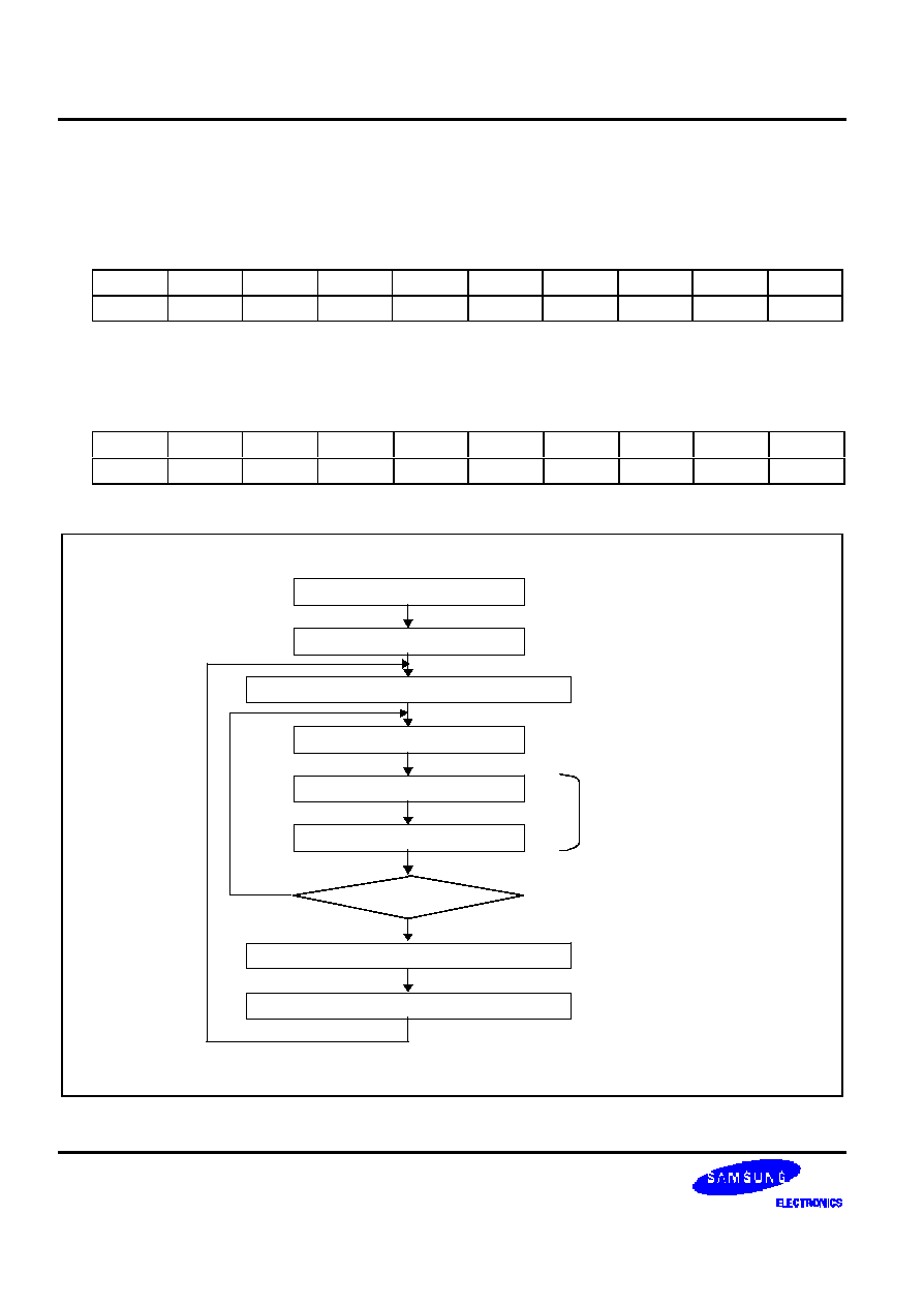
Set Modify-Read
This instruction stops the automatic increment of the column address by the read display data instruction, but
the column address is still increased by the Write display data instruction. And it reduces the load of
microprocessor when the data of a specific area is repeatedly changed during cursor blinking or others. This
mode is canceled by the reset Modify-read instruction.
RS
RW
DB7
DB6
DB5
DB4
DB3
DB2
DB1
DB0
0
0
1
1
1
0
0
0
0
0
Reset Modify-Read
This instruction cancels the Modify-read mode, and makes the column address return to its initial value just
before the set Modify-read instruction is started.
RS
RW
DB7
DB6
DB5
DB4
DB3
DB2
DB1
DB0
0
0
1
1
1
0
1
1
1
0
Set Modify-Read
Reset Modify-Read
Set Page Address
Data Process
No
Yes
Change Complete ?
Set Column Address (N)
Dummy Read
Data Read
Data Write
Return Column Address (N)
Figure 29. Sequence for Cursor Display
S6B0756 65 COM / 96 SEG DRIVER & CONTROLLER FOR STN LCD
39
Display ON / OFF
Turns the display ON or OFF.
This command has priority over Entire Display On/Off and Reverse Display On/Off. Commands are accepted
while the display is off, but the visual state of the display does not change.
RS
RW
DB7
DB6
DB5
DB4
DB3
DB2
DB1
DB0
0
0
1
0
1
0
1
1
1
D
D = 1: display ON
D = 0: display OFF
Set Initial Display Line Register
Sets the line address of display RAM to determine the initial display line using 2-byte instruction. The RAM
display data is displayed at the top row (COM0) of LCD panel.
The 1
st
Instruction
RS
RW
DB7
DB6
DB5
DB4
DB3
DB2
DB1
DB0
0
0
0
1
0
0
0
0
�
�
The 2
nd
Instruction
RS
RW
DB7
DB6
DB5
DB4
DB3
DB2
DB1
DB0
0
0
�
S6
S5
S4
S3
S2
S1
S0
S6
S5
S4
S3
S2
S1
S0
Selected line address
0
0
0
0
0
0
0
0
0
0
0
0
0
0
1
1
:
:
:
:
:
:
:
:
0
1
1
1
1
1
0
62
0
1
1
1
1
1
1
63
1
0
0
0
0
0
0
:
:
:
:
:
:
:
1
1
1
1
1
1
1
No operation
2
nd
Instruction (2-byte Instruction for Register Setting)
Setting Iinitial Display Line End
1
st
Instruction (2-byte Instruction for Mode Setting)
Setting Initial Display Line Start
Figure 30. The Sequence for Setting the Initial Display Line
65 COM / 96 SEG DRIVER & CONTROLLER FOR STN LCD S6B0756
40
Set Initial COM0 Register
Sets the initial row (COM0) of the LCD panel using the 2-byte instruction. By using this instruction, it is possible
to realize the window moving without the change of display data.
The 1
st
Instruction
RS
RW
DB7
DB6
DB5
DB4
DB3
DB2
DB1
DB0
0
0
0
1
0
0
0
1
�
�
The 2
nd
Instruction
RS
RW
DB7
DB6
DB5
DB4
DB3
DB2
DB1
DB0
0
0
�
�
C5
C4
C3
C2
C1
C0
C5
C4
C3
C2
C1
C0
Initial COM0
0
0
0
0
0
0
COM0
0
0
0
0
0
1
COM1
0
0
0
0
1
0
COM2
0
0
0
0
1
1
COM3
:
:
:
:
:
:
:
1
1
1
1
0
0
COM60
1
1
1
1
0
1
COM61
1
1
1
1
1
0
COM62
1
1
1
1
1
1
COM63
2
nd
Instruction (Initial COM0 Setting)
Setting Initial COM0 End
end
1
st
Instruction (Mode Setting)
Setting Initial COM0 Start
Figure 31. Sequence for Setting the Initial COM0
S6B0756 65 COM / 96 SEG DRIVER & CONTROLLER FOR STN LCD
41
Set Partial Display Duty Ratio
When the icon mode is disable, Sets the duty ratio within range of 16 to 64 to realize partial display by using the
2-byte instruction. When the icon mode is enable, Sets the duty ratio within range of 17 to 65 to realize partial
display by using the 2-byte instruction.
The 1
st
Instruction
RS
RW
DB7
DB6
DB5
DB4
DB3
DB2
DB1
DB0
0
0
0
1
0
0
1
0
�
�
The 2
nd
Instruction
RS
RW
DB7
DB6
DB5
DB4
DB3
DB2
DB1
DB0
0
0
�
D6
D5
D4
D3
D2
D1
D0
Icon Enable/Disable Bit = 0
D6
D5
D4
D3
D2
D1
D0
Selected partial duty ratio
0
0
0
0
0
0
0
:
:
:
:
:
:
:
0
0
1
0
0
0
0
No operation
0
0
1
0
0
0
0
1/16
0
0
1
0
0
0
1
1/17
0
0
1
0
0
1
0
1/18
0
0
1
0
0
1
1
1/19
:
:
:
:
:
:
:
:
0
1
1
1
1
0
1
1/61
0
1
1
1
1
1
0
1/62
0
1
1
1
1
1
1
1/63
1
0
0
0
0
0
0
1/64
1
0
0
0
0
1
0
:
:
:
:
:
:
:
1
1
1
1
1
1
1
No operation
2
nd
I
nstruction (Partial Display Duty Setting)
Setting Partial Display End
1
st
Instruction (Mode Setting)
Setting Partial Display Start
Figure 32. Sequence for Setting Partial Display
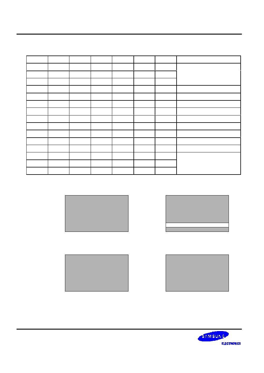
65 COM / 96 SEG DRIVER & CONTROLLER FOR STN LCD S6B0756
42
Icon Enable/Disable Bit = 1
D6
D5
D4
D3
D2
D1
D0
Selected partial duty ratio
0
0
0
0
0
0
0
:
:
:
:
:
:
:
0
0
1
0
0
0
0
No operation
0
0
1
0
0
0
1
1/17
0
0
1
0
0
1
0
1/18
0
0
1
0
0
1
1
1/19
0
0
1
0
1
0
0
1/20
:
:
:
:
:
:
:
:
0
1
1
1
1
1
0
1/62
0
1
1
1
1
1
1
1/63
1
0
0
0
0
0
0
1/64
1
0
0
0
0
0
1
1/65
1
0
0
0
0
1
0
:
:
:
:
:
:
:
1
1
1
1
1
1
1
No operation
Figure 33. Display example When ICON is On or Off
Note : once COMS is used, ICON can be turned off only by using memory data.
COM0
COM63
COMS
COM62
COM1
COM0
COM63
COMS
COM62
COM1
COM0
COM63
COMS
COM62
COM1
COM0
COM63
COMS
COM62
COM1
Partial Duty Ratio = 1/64
ICON ON
ICON ON
ICON OFF
ICON OFF
Partial Duty Ratio = 1/65
Not Available
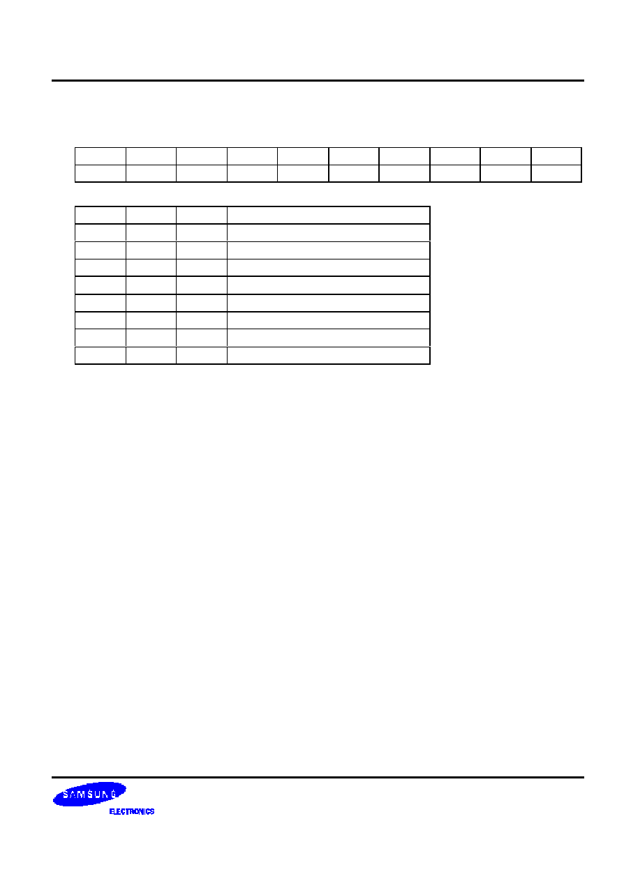
S6B0756 65 COM / 96 SEG DRIVER & CONTROLLER FOR STN LCD
43
Programmable Frame Frequency
Sets the frame frequency to compensate LCD flicking
RS
RW
DB7
DB6
DB5
DB4
DB3
DB2
DB1
DB0
0
0
1
1
0
1
1
F2
F1
F0
F2
F1
F0
Frame Frequency
0
0
0
69Hz
0
0
1
73Hz
0
1
0
75Hz(default Value)
0
1
1
81Hz
1
0
0
85Hz
1
0
1
89Hz
1
1
0
93Hz
1
1
1
97Hz
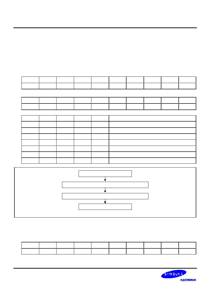
65 COM / 96 SEG DRIVER & CONTROLLER FOR STN LCD S6B0756
44
Set N-line Inversion Register
Sets the inverted line number within range of 3 to 33 to improve the display quality by controlling the phase of
the internal LCD AC signal (Internal M) by using the 2-byte instruction.
The DC-bias problem could be occurred if K is even number. So, we recommend customers to set K to be odd
number. K : D/N
D : The number of display duty ratio (D is selectable by customers)
N : N for N-line inversion (N is selectable by customers).
The 1
st
Instruction
RS
RW
DB7
DB6
DB5
DB4
DB3
DB2
DB1
DB0
0
0
0
1
0
0
1
1
�
�
The 2
nd
Instruction
RS
RW
DB7
DB6
DB5
DB4
DB3
DB2
DB1
DB0
0
0
�
�
�
N4
N3
N2
N1
N0
N4
N3
N2
N1
N0
Selected n-line inversion
0
0
0
0
0
0-line inversion (frame inversion)
0
0
0
0
1
3-line inversion
0
0
0
1
0
4-line inversion
:
:
:
:
:
:
1
1
1
0
1
31-line inversion
1
1
1
1
0
32-line inversion
1
1
1
1
1
33-line inversion
2
nd
Instruction (N-line Inversion Setting)
Setting N-line Inversion End
1
st
Instruction (Mode Setting)
Setting N-line Inversion Start
Figure 34. Sequence for Setting Partial Display
Release N-line Inversion
Returns to the frame inversion condition from the n-line inversion condition.
RS
RW
DB7
DB6
DB5
DB4
DB3
DB2
DB1
DB0
0
0
1
1
1
0
0
1
0
0
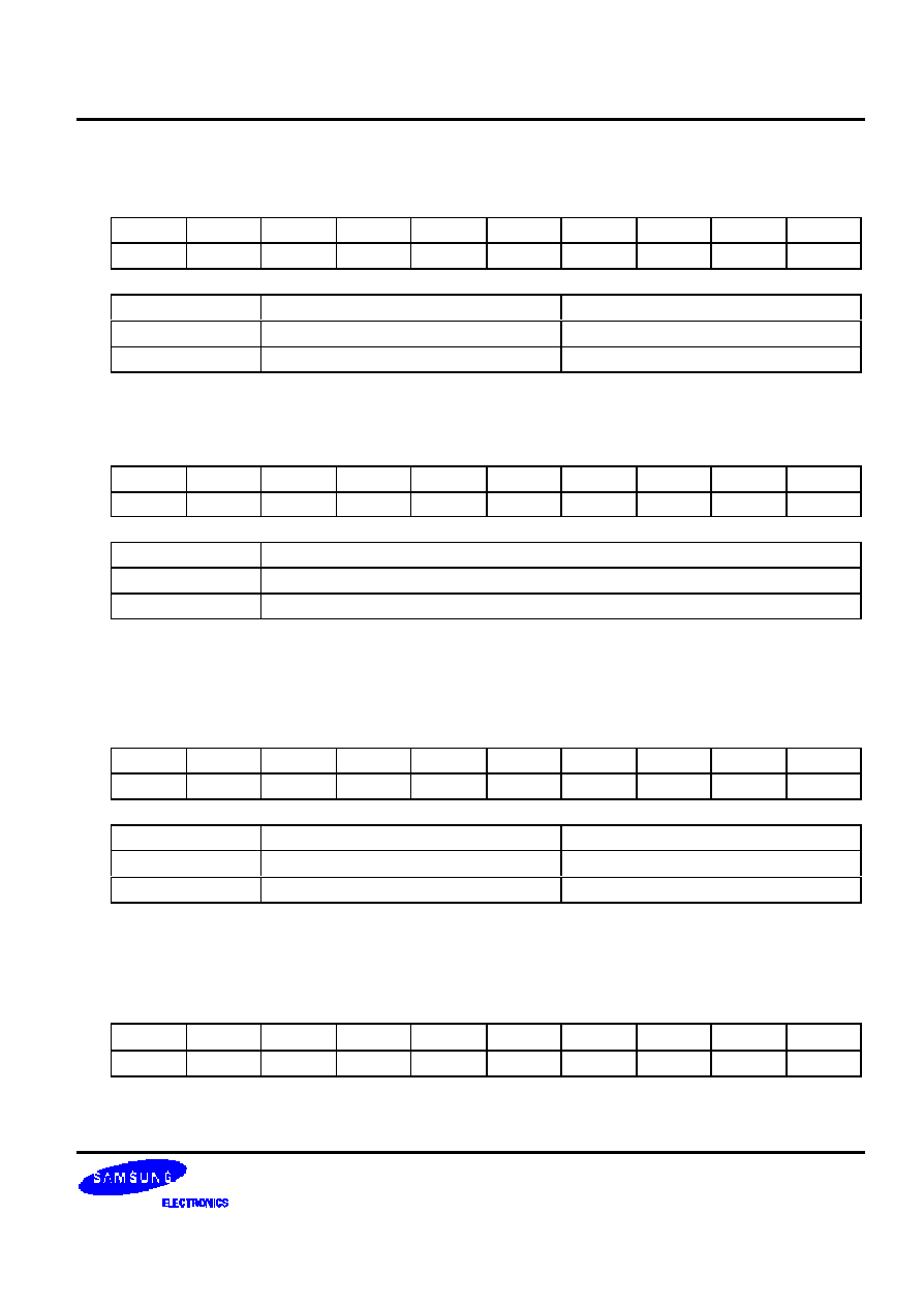
S6B0756 65 COM / 96 SEG DRIVER & CONTROLLER FOR STN LCD
45
Reverse Display ON / OFF
Reverses the display status on LCD panel without rewriting the contents of the display data RAM.
RS
RW
DB7
DB6
DB5
DB4
DB3
DB2
DB1
DB0
0
0
1
0
1
0
0
1
1
REV
REV
RAM bit data = "1"
RAM bit data = "0"
0 (normal)
LCD pixel is illuminated
LCD pixel is not illuminated
1 (reverse)
LCD pixel is not illuminated
LCD pixel is illuminated
Icon enable / Disable
Allows the icon driver circuit to be enabled or disabled, thus changing the duty ratio setting.
RS
RW
DB7
DB6
DB5
DB4
DB3
DB2
DB1
DB0
0
0
1
0
1
0
0
0
1
I
I
Duty Range
0 (disable)
1/16 ~ 1/64
1 (enable)
1/17 ~ 1/65
Entire Display ON / OFF
Forces the whole LCD points to be turned on regardless of the contents of the display data RAM. At this time,
the contents of the display data RAM are held. This instruction has priority over the reverse display ON / OFF
instruction.
RS
RW
DB7
DB6
DB5
DB4
DB3
DB2
DB1
DB0
0
0
1
0
1
0
0
1
0
EON
EON
RAM bit data = "1"
RAM bit data = "0"
0 (normal)
LCD pixel is illuminated
LCD pixel is not illuminated
1 (entire)
LCD pixel is illuminated
LCD pixel is illuminated
OTP_Mode On/Off
Allows module maker to be able to calibrate. Because initial value is On, Mode is changed to Off for calibration.
In OTP_mode_off, offset volume is changable. After calibration, calibration offset volume is stored as OTP
offset volume by OTP Write Enable.
RS
RW
DB7
DB6
DB5
DB4
DB3
DB2
DB1
DB0
0
0
1
1
1
0
1
1
0
OMON
OMON = 1 : OTP_Mode On
OMON = 0 : OTP_Mode Off
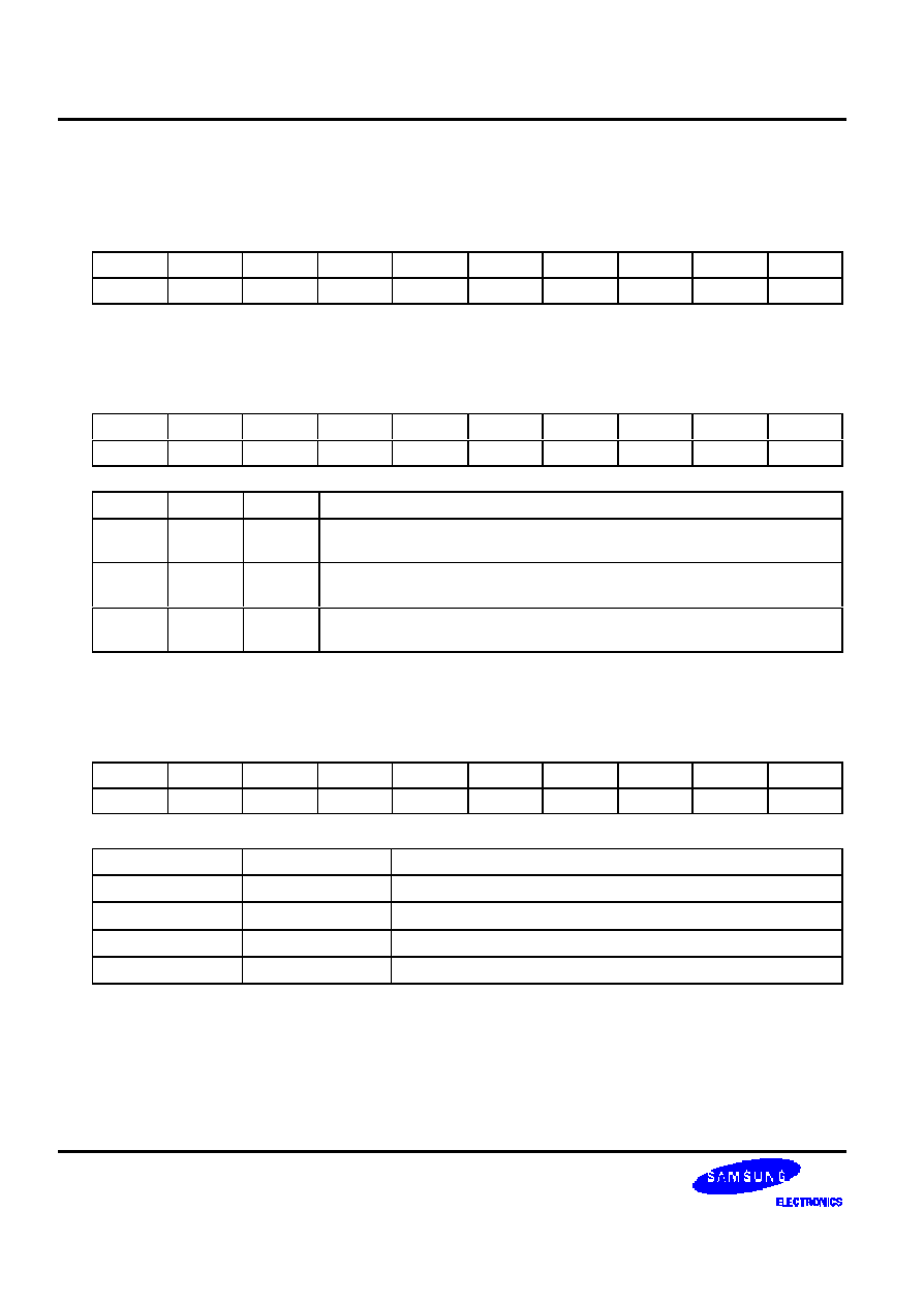
65 COM / 96 SEG DRIVER & CONTROLLER FOR STN LCD S6B0756
46
OTP Write Enable
Allow OTP offset volume, which is determined as suitable value, to be programmed on OTP cell. Once
programmed, an OTP cell can not be reprogrammed.
RS
RW
DB7
DB6
DB5
DB4
DB3
DB2
DB1
DB0
0
0
1
1
1
0
1
1
1
1
Power Control
Selects one of eight power circuit functions by using 3-bit register. An external power supply and part of internal
power supply functions can be used simultaneously.
RS
RW
DB7
DB6
DB5
DB4
DB3
DB2
DB1
DB0
0
0
0
0
1
0
1
VC
VR
VF
VC
VR
VF
Status of internal power supply circuits
0
1
Internal voltage converter circuit is OFF
Internal voltage converter circuit is ON
0
1
Internal voltage regulator circuit is OFF
Internal voltage regulator circuit is ON
0
1
Internal voltage follower circuit is OFF
Internal voltage follower circuit is ON
Select DC-DC Step-up
Selects one of 4 DC-DC step-up to reduce the power consumption by this instruction. It is very useful to realize
the partial display function.
RS
RW
DB7
DB6
DB5
DB4
DB3
DB2
DB1
DB0
0
0
0
1
1
0
0
1
DC1
DC0
DC1
DC0
Selected DC-DC converter circuit
0
0
3 times boosting circuit
0
1
4 times boosting circuit
1
0
Not used
1
1
2 times boosting circuit
S6B0756 65 COM / 96 SEG DRIVER & CONTROLLER FOR STN LCD
47
Regulator Resistor Select
Selects resistance ratio of the internal resistor used in the internal voltage regulator. See voltage regulator section in
power supply circuit. Refer to Table 13.
RS
RW
DB7
DB6
DB5
DB4
DB3
DB2
DB1
DB0
0
0
0
0
1
0
0
R2
R1
R0
R2
R1
R0
[Rb / Ra] ratio
0
0
0
Small
0
0
1
:
:
:
:
:
1
1
0
:
1
1
1
Large
65 COM / 96 SEG DRIVER & CONTROLLER FOR STN LCD S6B0756
48
Set Electronic Volume Register
Consists of 2-byte instruction
The 1
st
instruction sets electronic volume mode, the 2
nd
one updates the contents of electronic volume register.
After second instruction, electronic volume mode is released.
The 1
st
Instruction
RS
RW
DB7
DB6
DB5
DB4
DB3
DB2
DB1
DB0
0
0
1
0
0
0
0
0
0
1
The 2
nd
Instruction
RS
RW
DB7
DB6
DB5
DB4
DB3
DB2
DB1
DB0
0
0
�
�
EV5
EV4
EV3
EV2
EV1
EV0
EV5
EV4
EV3
EV2
EV1
EVOUT
Reference voltage (
)
0
0
0
0
0
0
0
0
0
0
0
0
1
1
:
:
:
:
:
:
:
:
:
:
:
:
:
:
1
1
1
1
1
0
62
1
1
1
1
1
1
63
2
nd
Instruction for Register Setting
Setting Electronic Volume End
1
st
Instruction for Mode Setting
Setting Electronic Volume Start
Figure 35. Sequence for Setting the Electronic Volume
S6B0756 65 COM / 96 SEG DRIVER & CONTROLLER FOR STN LCD
49
Set Offset Volume Register
Consists of 2-byte instruction
The 1
st
instruction sets offset volume mode, the 2
nd
one updates the contents of offset volume register. After
second instruction, offset volume mode is released.
The 1
st
Instruction
RS
RW
DB7
DB6
DB5
DB4
DB3
DB2
DB1
DB0
0
0
1
1
1
0
1
0
1
0
The 2
nd
Instruction
RS
RW
DB7
DB6
DB5
DB4
DB3
DB2
DB1
DB0
0
0
�
�
x
OV4
OV3
OV2
OV1
OV0
EV4
EV3
EV2
EV1
EVOUT
Reference voltage (x)
0
1
1
1
1
15
0
1
1
1
0
14
:
:
:
:
:
:
:
:
:
:
:
:
0
0
0
0
1
1
0
0
0
0
0
0
1
1
1
1
1
-1
1
1
1
1
0
-2
1
1
1
0
1
-3
:
:
:
:
:
:
:
:
:
:
:
:
1
0
0
0
1
-15
1
0
0
0
0
-16
2
nd
Instruction for Register Setting
Setting Offset Volume End
1
st
Instruction for Mode Setting
Setting Offset Volume Start
Figure 36. Sequence for Setting the Offset Volume
65 COM / 96 SEG DRIVER & CONTROLLER FOR STN LCD S6B0756
50
Select LCD Bias
Selects LCD Bias ratio of the voltage required for driving the LCD.
RS
RW
DB7
DB6
DB5
DB4
DB3
DB2
DB1
DB0
0
0
0
1
0
1
0
B2
B1
B0
B2
B1
B0
Selected LCD bias
0
0
0
1/4
0
0
1
1/5
0
1
0
1/6
0
1
1
1/7
1
0
0
1/8
1
0
1
1/9
1
1
0
1/9
1
1
1
1/9
SHL Select
COM output scanning direction is selected by this instruction which determines the LCD driver output status.
RS
RW
DB7
DB6
DB5
DB4
DB3
DB2
DB1
DB0
0
0
1
1
0
0
SHL
�
�
�
SHL = 0: normal direction (COM0
COM63)
SHL = 1: reverse direction (COM63
COM0)
ADC Select
Changes the relationship between RAM column address and segment driver. The direction of segment driver
output pins could be reversed by software. This makes IC layout flexible in LCD module assembly.
RS
RW
DB7
DB6
DB5
DB4
DB3
DB2
DB1
DB0
0
0
1
0
1
0
0
0
0
ADC
ADC = 0: normal direction (SEG0
SEG95)
ADC = 1: reverse direction (SEG95
SEG0)
S6B0756 65 COM / 96 SEG DRIVER & CONTROLLER FOR STN LCD
51
Set Data Direction & Display Data Length (3-Pin SPI Mode)
Consists of two bytes instruction.
This command is used in 3-Pin SPI mode only(PS0 = "L" and PS1 = "L"). It will be two continuous commands,
the first byte control the data direction(write mode only) and inform the LCD driver the second byte will be
number of data bytes will be write. When RS is not used, the Display Data Length instruction is used to indicate
that a specified number of display data bytes are to be transmitted. The next byte after the display data string is
handled as command data.
The 1
st
Instruction: Set Data Direction (Only Write Mode)
RS
RW
DB7
DB6
DB5
DB4
DB3
DB2
DB1
DB0
x
x
1
1
1
0
1
0
0
0
The 2
nd
Instruction: Set Display Data Length (DDL) Register
RS
RW
DB7
DB6
DB5
DB4
DB3
DB2
DB1
DB0
x
x
D7
D6
D5
D4
D3
D2
D1
D0
D7
D6
D5
D4
D3
D2
D1
D0
Display Data
Length
0
0
0
0
0
0
0
0
1
0
0
0
0
0
0
0
1
2
0
0
0
0
0
0
1
0
3
:
:
:
:
:
:
:
:
:
1
1
1
1
1
1
0
1
254
1
1
1
1
1
1
1
0
255
1
1
1
1
1
1
1
1
256
Oscillator ON Start
This instruction enables the built-in oscillator circuit.
RS
RW
DB7
DB6
DB5
DB4
DB3
DB2
DB1
DB0
0
0
1
0
1
0
1
0
1
1
Reset
This instruction resets initial display line, column address, page address, and common output status select to
their initial status, but dose not affect the contents of display data RAM. This instruction cannot initialize the LCD
power supply, which is initialized by the RESETB pin.
RS
RW
DB7
DB6
DB5
DB4
DB3
DB2
DB1
DB0
0
0
1
1
1
0
0
0
1
0
65 COM / 96 SEG DRIVER & CONTROLLER FOR STN LCD S6B0756
52
Power Save
The S6B0756 enters the Power Save status to reduce the power consumption to the static power consumption
value and returns to the normal operation status by the following instructions.
Set Power Save Mode
RS
RW
DB7
DB6
DB5
DB4
DB3
DB2
DB1
DB0
0
0
1
0
1
0
1
0
0
P
P = 0: standby mode
P = 1: sleep mode
Release Power Save Mode
RS
RW
DB7
DB6
DB5
DB4
DB3
DB2
DB1
DB0
0
0
1
1
1
0
0
0
0
1
Release Sleep Mode
Sleep Mode (P=1)
Oscillator Circuits: OFF
LCD Power Supply Circuits: OFF
All COM / SEG Output Level: VSS
Set Power Save Mode
Release Power Save Mode
Figure 37. Power Save Routine
NOP
No Operation Instruction
RS
RW
DB7
DB6
DB5
DB4
DB3
DB2
DB1
DB0
0
0
1
1
1
0
0
0
1
1
Test Instruction
This instruction is for test only. Please do not use it.
RS
RW
DB7
DB6
DB5
DB4
DB3
DB2
DB1
DB0
0
0
1
1
1
1
�
�
�
�
S6B0756 65 COM / 96 SEG DRIVER & CONTROLLER FOR STN LCD
53
Referential Instruction Setup Flow: Initializing with the Built-in Power Supply Circuits
User System Setup by External Pins
Start of Initialization
Power ON (VDD-VSS) Keeping the RESETB Pin = "L"
Waiting for Stabilizing the Power
RESETB Pin = "H"
User Application Setup by Internal Instructions
[Display Duty Select]
[ADC Select]
[SHL Select]
[COM0 Register Select]
User LCD Power Setup by Internal Instructions
[Oscillator ON]
[DC-DC Step-up Register Select]
[Regulator Resistor Select]
[Electronic Volume Register Select]
[LCD Bias Register Select]
[Power Control]
Waiting for Stabilizing the LCD Power Levels
End of Initialization
Figure 38. Initializing with the Built-in Power Supply Circuits
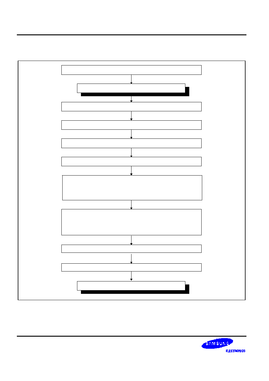
65 COM / 96 SEG DRIVER & CONTROLLER FOR STN LCD S6B0756
54
Referential Instruction Setup Flow: Initializing without the Built-in Power Supply Circuits
User System Setup by External Pins
Start of Initialization
Power ON (VDD-VSS) Keeping the RESETB Pin = "L"
Waiting for Stabilizing the Power
Set Power Save
User Application Setup by Internal Instructions
[Display Duty Select]
[ADC Select]
[SHL Select]
[COM0 Register Select]
User LCD Power Setup by Internal Instructions
[Oscillator ON]
Regulator or Follower Register Select
[Power Control]
Waiting for Stabilizing the LCD Power Levels
End of Initialization
RESETB Pin = "H"
Release Power Save
Figure 39. Initializing without the Built-in Power Supply Circuits
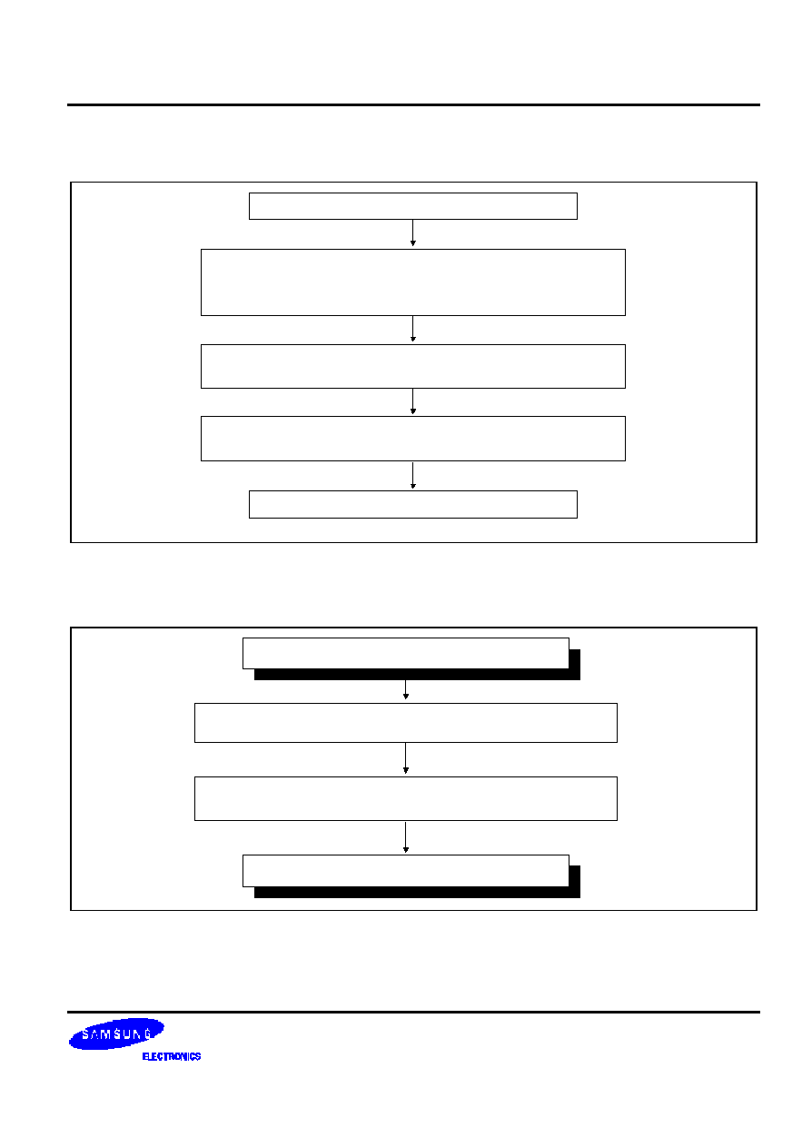
S6B0756 65 COM / 96 SEG DRIVER & CONTROLLER FOR STN LCD
55
Referential Instruction Setup Flow: Data Displaying
End of Initialization
Write Display Data by Instruction
[Display Data Write]
Turn Display ON / OFF Instruction
[Display ON / OFF]
End of Data Display
Display Data RAM Addressing by Instruction
[Initial Display Line]
[Set Page Address]
[Set Column Address]
Figure 40. Data Displaying
Referential Instruction Setup Flow: Power OFF
Optional Status
Power OFF (VDD-VSS)
End of Power OFF
Set Power Save by Instruction
Figure 41. Power OFF
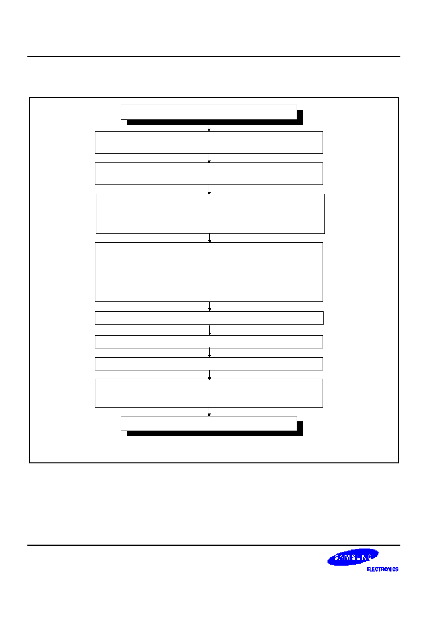
65 COM / 96 SEG DRIVER & CONTROLLER FOR STN LCD S6B0756
56
Referential Instruction Setup Flow: Partial Duty Changing
Start of Partial changing
Set Display OFF by Internal Instruction
[Display ON / OFF]
Set Partial Duty by Internal Instructions
[Partial Display Duty Ratio Select]
[Initial Display Line Register]
[COM0 Register Select]
User LCD Power Setup by Internal Instructions
[DC-DC Step-up Register Select]
[Regulator Resistor Select]
[Electronic Volume Register Select]
[LCD Bias Register Select]
[Power Control]
Waiting for Stabilizing the LCD Power Levels
End of Partial Changing
Release Power Save
Set Standby Mode by Internal Instruction
[Power Save Mode]
Write Display Data & Display ON by Internal Instruction
[Display Data Write]
[Display ON / OFF]
Waiting for Discharging the LCD Power Levels
Figure 42. Partial Duty Changing
NOTE:1. Partial COM0 register setting for COM H/W half: [64 � (user duty) ] / 2
S6B0756 65 COM / 96 SEG DRIVER & CONTROLLER FOR STN LCD
57
SPECIFICATIONS
ABSOLUTE MAXIMUM RATINGS
Table 16. Absolute Maximum Ratings
(V
SS
= 0V)
Parameter
Symbol
Rating
Unit
V
DD
- 0.3 ~ + 4.0
V
V
OUT
- 0.3 ~ + 13.5
V
Supply voltage range
V
1
, V
2
, V
3
, V
4
- 0.3 ~ VOUT
+ 0.3
V
Input voltage range
V
IN
- 0.3 ~ V
DD
+ 0.3
V
Operating temperature range
T
OPR
- 20 ~ + 70
�
C
Storage temperature range
T
STR
- 20 ~ + 70
�
C
NOTES:
1. VDD, VOUT, V1 to V4, VEXT and VCI are based on VSS = 0V.
2. Voltage VOUT
V1
V2
V3
V4
VSS must always be satisfied.
3. If supply voltage exceeds its absolute maximum range, this LSI may be damaged permanently.
It is desirable to use this LSI under electrical characteristic conditions during general operation.
Otherwise, this LSI may malfunction or reduced LSI reliability may result.
65 COM / 96 SEG DRIVER & CONTROLLER FOR STN LCD S6B0756
58
DC CHARACTERISTICS
Table 17. DC Characteristics
(V
SS
= 0V, V
DD
= 1.8~3.3V, Ta=-20~70
�
C)
Item
Symbol
Condition
Min.
Typ.
Max.
Unit
Pin used
Operating voltage (1)
V
DD
1.8
-
3.3
V
VDD *1
Operating voltage (2)
VOUT
4.0
-
12.0
V
VOUT, *2
High
V
IH
0.8V
DD
-
V
DD
Input voltage
Low
V
IL
V
SS
-
0.2V
DD
V
*3
High
V
OH
I
OH
= -0.5mA
0.8V
DD
-
V
DD
Output
voltage
Low
V
OL
I
OL
= 0.5mA
V
SS
-
0.2V
DD
V
*4
Input leakage current
I
IL
V
IN
= V
DD
or V
SS
- 1.0
-
+ 1.0
�
A
*3
Output leakage current
I
OZ
V
IN
= V
DD
or V
SS
- 3.0
-
+ 3.0
�
A
*5
LCD driver ON
resistance
R
ON
Ta = 25
�
C, VOUT =
8V
-
2.0
3.0
k
SEGn
COMn *6
Frame frequency
f
FR
Ta = 25
�
C
65
75
100
Hz
*7
Table 18. DC Characteristics
Item
Symbol
Condition
Min.
Typ.
Max.
Unit
Pin used
Voltage converter
circuit output voltage
V
OUT
�
2 /
�
3 /
�
4
voltage conversion
(no-load )
95
99
-
%
VOUT
Voltage regulator
circuit operating
voltage
V
OUT
4.0
-
12.0
V
VOUT
Voltage follower circuit
operating voltage
V
OUT
4.0
-
12.0
V
VOUT *8
Reference voltage
V
REF
Ta = 25
�
C
2.04
2.10
2.16
V
*9
S6B0756 65 COM / 96 SEG DRIVER & CONTROLLER FOR STN LCD
59
Dynamic Current Consumption (1) when an External Power Supply is used.
Table 19. Dynamic Current 1 (External Power)
(V
DD
= 2.4V, Ta = 25
�
C)
Item
Symbol
Condition
Min
Typ
Max
Unit
Pin used
V
OUT
-V
SS
=9.0V, duty = 1/65
No Load
(Display Off)
-
-
20
�
*10
Dynamic current
consumption (1)
I
DD1
V
OUT
-V
SS
= 9.0V, duty = 1/65
No Load
(Display On , Checker Pattern)
-
-
20
�
*10
Dynamic Current Consumption (2) when The Internal Power Supply is ON
Table 20. . Dynamic Current 2 (Internal Power)
(V
DD
= 2.4V, Ta = 25
�
C)
Item
Symbol
Condition
Min.
Typ.
Max.
Unit
Pin used
VCI=2.75V, x4 boosting,
duty = 1/65, EV=32, RR=3,
No Load
(Display Off)
-
100
150
�
*10
Dynamic current
consumption (2)
I
DD2
VCI=2.75V, x4 boosting,
duty = 1/65, EV=32, RR=3
No Load
(Display On , Checker Pattern)
-
100
150
�
*10
Current Consumption during Power Save Mode
Table 21. Power Save Mode Current
(V
DD
= 2.4V, Ta = 25
�
C)
Item
Symbol
Condition
Min.
Typ.
Max.
Unit
Pin used
Sleep mode
current
I
DDS1
During sleep
-
2
9
�
*10

65 COM / 96 SEG DRIVER & CONTROLLER FOR STN LCD S6B0756
60
Table 22. The Relationship between Oscillation Frequency and Frame Frequency
Duty ratio
Item
f
CL
f
osc
1/N
On-chip oscillator circuit is
used
f
FR x
N
f
FR x
4
x
N
(f
OSC
: oscillation frequency, f
CL
: display clock frequency, f
FR
: frame frequency, N = 17 to 65)
[* Remark Solves]
*1. Though the wide range of operating voltages is guaranteed, a spike voltage change may affect the voltage
assurance during access from the MPU.
*2. In case of external power supply is applied.
*3. CS1B, RS, DB0 to DB7, E_RD, RW_WR, RESETB, PS1, PS0
*4. DB0 to DB7
*5. Applies when the DB0 to DB7 pins are in high impedance.
*6. Resistance value when -0.1[mA] is applied during the ON status of the output pin SEGn or COMn.
RON [k
] =
V[V] / 0.1[mA] (
V : voltage change when -0.1[mA] is applied in the ON status.)
*7. See Table 22 for the relationship between oscillation frequency and frame frequency.
*8. The voltage regulator circuit adjusts V
OUT
within the voltage follower operating voltage range.
*9. On-chip reference voltage source of the voltage regulator circuit to adjust V
OUT
.
*10. Applies to the case where the on-chip oscillation circuit is used and no access is made from the MPU.
The current consumption, when the built-in power supply circuit is ON or OFF.
The current flowing through voltage regulation resistors(Rb and Ra) is not included.
It does not include the current of the LCD panel capacity, wiring capacity, etc.
S6B0756 65 COM / 96 SEG DRIVER & CONTROLLER FOR STN LCD
61
AC CHARACTERISTICS
Read / Write Characteristics (8080-series MP)
t
DH80
t
OD80
t
DS80
t
ACC80
0.9V
DD
0.1V
DD
t
PWLW
, t
PWLR
t
CY80
t
AH80
t
AS80
DB0 to DB7
( Write )
DB0 to DB7
( Read )
/RD, /WR
CS1B
RS
t
PWHW
, t
PWHR
Figure 43. Read / Write Characteristics (8080-series MPU)
Table 23
(V
DD
= 1.8~ 3.3V, Ta = -20 ~ +70
�
C)
Item
Signal
Symbol
Condition
Min.
Max.
Unit
Address setup time
Address hold time
RS
t
AS80
t
AH80
0
0
-
-
ns
System cycle time
t
CY80
500
-
ns
Pulse width low for write
Pulse width high for write
RW_WR
(/WR)
t
PWLW
t
PWHW
120
120
-
-
ns
Pulse width low for read
Pulse width high for read
E_RD
(/RD)
t
PWLR
t
PWHR
240
120
-
-
ns
Data setup time
Data hold time
t
DS80
t
DH80
80
30
-
-
ns
Read access time
Output disable time
DB0
to
DB7
t
ACC80
t
OD80
CL = 100 pF
-
10
280
200
ns
NOTE: *1. The input signal rise time and fall time (tr, tf) is specified at 15 ns or less.
(tr + tf) < (t
CY80
-
t
PWLW
-
t
PWHW
) for write, (tr + tf) < (t
CY80
-
t
PWLR
-
t
PWHR
) for read
65 COM / 96 SEG DRIVER & CONTROLLER FOR STN LCD S6B0756
62
Read / Write Characteristics (6800-series Microprocessor)
t
DH68
t
OD68
t
DS68
t
ACC68
0.1V
DD
0.9V
DD
t
EWHW
, t
EWHR
t
CY68
t
AH68
t
AS68
DB0 to DB7
( Write )
DB0 to DB7
( Read )
E
CS1B
RS, R/W
t
EWLW
, t
EWLR
Figure 44. Read / Write Characteristics (6800-series Microprocessor)
Table 24
(V
DD
= 1.8~ 3.3V, Ta = -20 ~ +70
�
C)
Item
Signal
Symbol
Condition
Min.
Max.
Unit
Address setup time
Address hold time
RS
RW
t
AS68
t
AH68
0
0
-
-
ns
System cycle time
t
CY68
500
-
ns
Enable width high for write
Enable width low for write
E_RD
(E)
t
EWHW
t
EWLW
120
120
-
-
ns
Enable width high for read
Enable width low for read
E_RD
(E)
t
EWHR
t
EWLR
240
120
-
-
ns
Data setup time
Data hold time
t
DS68
t
DH68
30
5
-
-
ns
Read access time
Output disable time
DB0
to
DB7
t
ACC68
t
OD68
C
L
= 100 pF
-
10
60
50
ns
NOTE: *1. The input signal rise time and fall time (tr, tf) is specified at 15 ns or less.
(tr + tf) < (tCY68 - tEWHW - tEWLW ) for write, (tr + tf) < (tCY68 - tEWHR - tEWLR ) for read
S6B0756 65 COM / 96 SEG DRIVER & CONTROLLER FOR STN LCD
63
Serial Interface Characteristics
DB7
( SID )
DB6
( SCLK )
RS
CS1B
t
DHS
t
DSS
t
WHS
0.9V
DD
0.1V
DD
t
WLS
t
CYS
t
AHS
t
ASS
t
CHS
t
CSS
Figure 45
Table 25
(V
DD
= 1.8 V, Ta = -20 ~ +70
�
C)
Item
Signal
Symbol
Condition
Min.
Max.
Unit
Serial clock cycle
SCLK high pulse width
SCLK low pulse width
DB6
(SCLK)
ts
CY
ts
HW
ts
LW
111
60
60
-
-
-
ns
Address setup time
Address hold time
RS
t
ASS
t
AHS
60
60
-
-
ns
Data setup time
Data hold time
DB7
(SID)
T
DSS
t
DHS
60
60
-
-
ns
CS1B setup time
CS1B hold time
CS1B
T
CSS
t
CHS
60
60
-
-
ns
(V
DD
= 2.7V, Ta = -20 ~ +70
�
C)
Item
Signal
Symbol
Condition
Min.
Max.
Unit
Serial clock cycle
SCLK high pulse width
SCLK low pulse width
DB6
(SCLK)
ts
CY
ts
HW
ts
LW
58.8
30
30
-
-
ns
Address setup time
Address hold time
RS
t
ASS
t
AHS
30
30
-
-
ns
Data setup time
Data hold time
DB7
(SID)
T
DSS
t
DHS
30
30
-
-
ns
CS1B setup time
CS1B hold time
CS1B
T
CSS
t
CHS
30
30
-
-
ns
NOTE: *1. The input signal rise time and fall time (tr, tf) is specified at 15 ns or less.
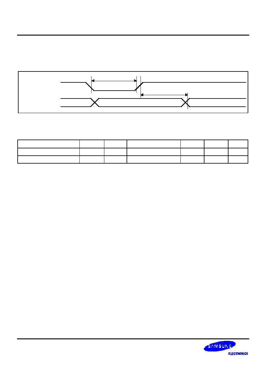
65 COM / 96 SEG DRIVER & CONTROLLER FOR STN LCD S6B0756
64
Reset Input Timing
RESETB
Internal status
t
RW
t
R
Reset complete
During reset
Figure 46
Table 26
(V
DD
= 1.8 ~ 3.3V, Ta = -20 ~ +70
�
C)
Item
Signal
Symbol
Condition
Min.
Max.
Unit
Reset low pulse width
RESETB
t
RW
1000
-
ns
Reset time
-
t
R
-
1000
ns
S6B0756 65 COM / 96 SEG DRIVER & CONTROLLER FOR STN LCD
65
REFERENCE APPLICATIONS
MICROPROCESSOR INTERFACE
In Case of Interfacing with 6800-series (PS0 = "H", PS1 = "H")
6800-series
MPU
CS1B
RS
E_RD
RW_WR
DB0 to DB7
RESETB
PS0
PS1
S6B0756
DB0 to DB7
RESETB
V
DD
V
DD
RW
E
RS
CS1B
Figure 47. Interfacing with 6800-series
In Case of Interfacing with 8080-series (PS0 = "H" , PS1 = "L" )
8080-series
MPU
CS1B
RS
E_RD
RW_WR
DB0 to DB7
RESETB
PS0
PS1
S6B0756
DB0 to DB7
RESETB
V
SS
V
DD
WR
/RD
RS
CS1B
Figure 48. Interfacing with 8080-series
65 COM / 96 SEG DRIVER & CONTROLLER FOR STN LCD S6B0756
66
In Case of Serial Peripheral Interface with RS Pin (PS0 = "L" , PS1 = "H" )
MPU
PS0
PS1
S6B0756
V
DD
V
SS
DB0 to DB5
OPEN
CS1B
CS1B
RS
RS
RESETB
RESETB
DB6(SCLK)
SCLK
DB7(SID)
SID
Figure 49. Serial Interface
In Case of Serial Peripheral Interface with software command (PS0 = "L" , PS1 = "L" )
MPU
PS0
PS1
S6B0756
V
SS
V
SS
DB0 to DB5
OPEN
CS1B
CS1B
RS
Vss/Vdd
RESETB
RESETB
DB6(SCLK)
SCLK
DB7(SID)
SID
Figure 50. Serial Interface
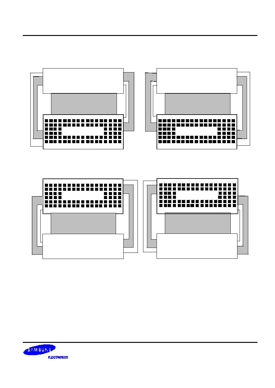
S6B0756 65 COM / 96 SEG DRIVER & CONTROLLER FOR STN LCD
67
CONNECTIONS BETWEEN S6B0756 AND LCD PANEL
Single Chip Configurations (1/65 Duty)
COM31
:
COM0
COMS
COMS1
COM63
:
COM32
SEG95 ........... SEG0
S6B0756
(Bottom View)
COM31
:
COM0
COMS
COMS1
COM63
:
COM32
SEG0 ......... SEG95
S6B0756
(Top View)
�
�
64
�
96 pixels
�
�
64
�
96 pixels
Figure 51. SHL = 0, ADC = 1 Figure 52. SHL = 0, ADC = 0
�
�
COMS
COM0
:
COM31
COM32
:
COM63
COMS1
SEG95 ........... SEG0
S6B0756
(Top View)
�
�
64
�
96 pixels
COM32
:
COM63
COMS1
COMS
COM0
:
COM31
SEG0 .......... SEG95
S6B0756
(Bottom View)
64
�
96 pixels
Figure 53. SHL = 1, ADC = 0 Figure 54. SHL = 1, ADC = 1
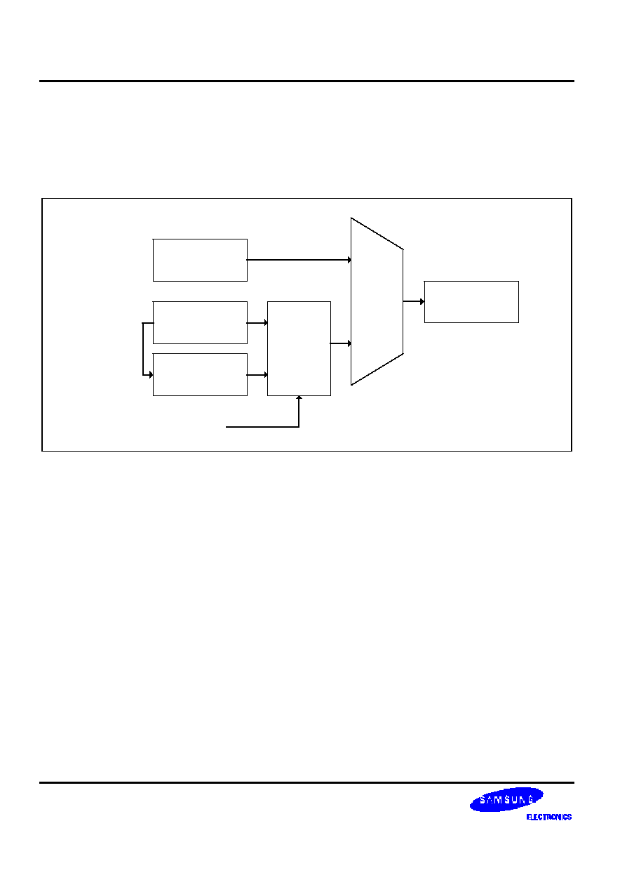
65 COM / 96 SEG DRIVER & CONTROLLER FOR STN LCD S6B0756
68
OTP CALIBRATION MODE
SEQUENCE FOR SETTING THE MODIFIED ELECTRONIC VOLUME
- Next figure is a Block Diagram of Sequence for Setting the Modified Electronic Volume.
OTP calibration
5bit offset
(OTP_OV)
INST calibration
5bit offset
(INST_OV)
MUX
Electronic volume
6bit level
(EV)
ADDER
0
1
OTP_MODE
ON/OFF
Modified EV
7bit level
(MEV)
OTP
Writing
Process
Figure 55. Sequence for Setting the Modified Electronic Volume
Initially, OTP cell is not programmed and has 5'b00000 value. When the external reset is applied, OTP_mode is On.
MEV is EV + OTP_OV. Since OTP_OV is 5'b00000, MEV is EV. For VOUT calibration The instruction
"OTP_mode_off" is executed, and then MEV is EV + OV and user can adjust MEV value using the instruction "Set
offset volume register". When MEV overflows or underflows, MEV will be saturated. Repeat this step until end of the
calibration. If VOUT calibration is suitable, OTP_writing process is executed, and then OTP cell is programmed and
OTP_OV is programmed with OV. Finally, VOUT calibration process is finished. Again, when the external reset is
applied, OTP_mode is ON. MEV is EV + OTP_OV. Accordingly MEV is the EV which has always the offset with
OTP_OV value. But if programmed OTP_OV is unlike, the instruction "OTP_mode off" can be executed and then
MEV will be EV + OV. Accordingly OV can be adjusted with instructions although OTP cell is programmed.
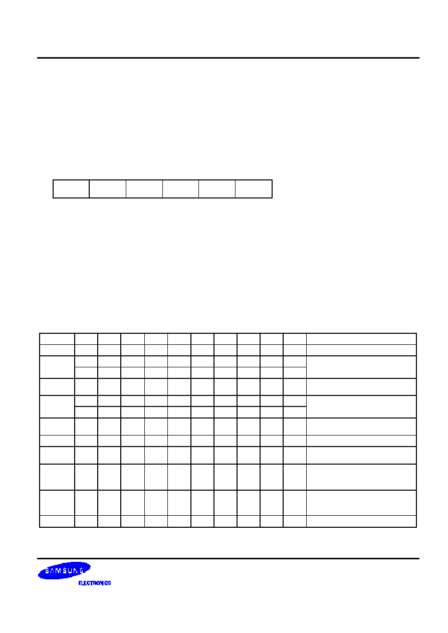
S6B0756 65 COM / 96 SEG DRIVER & CONTROLLER FOR STN LCD
69
EPROM CELL STRUCTURE
OTP(One Time Programmable) has been implemented on the S6B0756. The EPROM stores the offset volume for
VOUT calibration after the device has been assembled and calibrated on a LCD module. For OTP programming,
OTPD pin and OTPG pin are used. Those pins should be made available on the module glass
The OTP block of the S6B0756 consists of 6 bits. 1 bit is used for OTP mode protection bit(OPRT), and 5 bits are
used for VOUT calibration(OV4~OV0).
EPROM
block
MSB
LSB
OPRT
OV4
OV3
OV2
OV1
OV0
Description -.
OPRT : The Offset Volume(OV) can be written to EPROM only when OPRT bit = `0'
OV4~OV0 : The OV is used for calibrating the VOUT voltage as an offset to the
EV register value.
VOUT CALIBRATION FLOW
VOUT may be calibrated with OTP in the following order.(ex : EX = 32, OV=-3)
STEP
RS
RW
DB7 DB6 DB5 DB4 DB3 DB2 DB1 DB0
Description
1.
Apply external reset
0
0
1
0
0
0
0
0
0
1
2
0
0
x
x
1
0
0
0
0
0
Set electronic volume by using
instruction(EV = 32)
3
0
0
1
1
1
0
1
1
0
0
OTP_mode_off by using the
instruction
0
0
1
1
1
0
1
0
1
0
4.
0
0
x
x
x
1
1
1
0
1
Set offset volume by using the
instruction(OV = -3)
5.
Repeat STEP 4. Until the end
of the calibration
6.
0
0
1
0
1
0
1
0
0
1
Set power save mode(P=1)
7.
0
0
1
1
1
0
1
1
1
1
OTP write Enable
( Only when OPRT = 0 )
8.
Apply programming voltages
for OTP programming
(OTPG, OTPD)
9.
Cut off programming voltages
for OTP
programming(OTPG,OTPD)
10.
Apply external reset
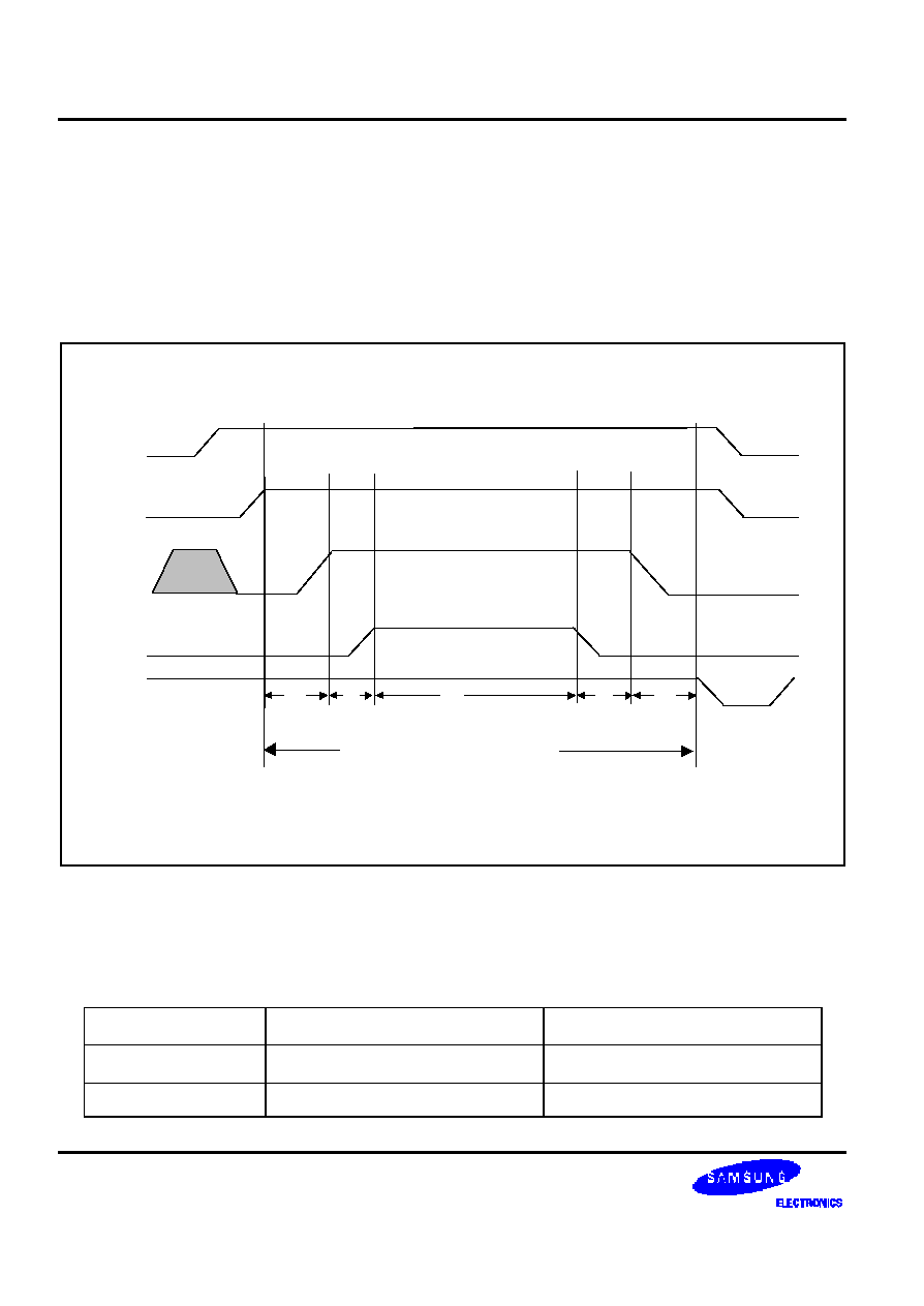
65 COM / 96 SEG DRIVER & CONTROLLER FOR STN LCD S6B0756
70
After the external reset, the calibrated data are automatically transferred to the 5-bit reference voltage control
register.
*Step 6,7,8,9,10 is OTP_WRITING PROCESS.
*OTP_WRITING PROCESS is available when OPRT is zero (if OPRT = 1, OTP cell is not programmed).
VOLTAGES AND WAVEFORMS FOR OTP PROGRAMMING
Power
Save ON
OTP
WRITE
ENABLE
OTPG
OTPD
RESETB
10V*
12.5V *
OTP WRITE MODE
t1
t2
t3
t4
t5
Figure 56. Voltages and waveforms for OTP programming( OTP_Writing Process)
* Note : Voltages for OTPG and OTPD may be changed.
Specific timings(t1~t5)
Timing
Min
Max
t1,t2, t4, t5
100uS
-
t3
100mS
-