Contents in this document are subject to change without notice. No part of this document may
be reproduced or transmitted in any form or by any means, electronic or mechanical, for any
purpose, without the express written permission of LCD Driver IC Team.
Precautions for Light
Light has characteristics to move electrons in the integrated circuitry of semiconductors,
therefore may change the characteristics of semiconductor devices when irradiated with light.
Consequently, the users of the packages which may expose chips to external light such as
COB, COG, TCP and COF must consider effective methods to block out light from reaching
the IC on all parts of the surface area, the top, bottom and the sides of the chip. Follow the
precautions below when using the products.
1. Consider and verify the protection of penetrating light to the IC at substrate (board or
glass) or product design stage.
2. Always test and inspect products under the environment with no penetration of light.
S6B1713
65 COM / 132 SEG DRIVER & CONTROLLER FOR STN LCD
March .2002
Ver. 4.2
65 COM / 132 SEG DRIVER & CONTROLLER FOR STN LCD S6B1713
2
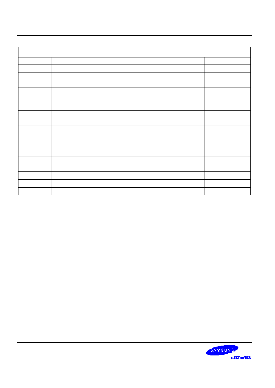
S6B1713 Specification Revision History
Version
Content
Date
2.0
Neglect the more past version than version 2.0
Nov.1998
2.1
f
OSC
= 16kHz (Typ.)
22kHz (Typ.): For removing flicker phenomenon
Temperature coefficient (when TEMPS = L): -0.0%/
∞
C
-0.05%/
∞
C
Nov.1998
3.0
Modified some syntax errors
Voltage regulator reference voltage [V
REF
]: TBD
2.0
Modified voltage regulator block of "Functional Description"
Nov.1998
3.1
V
LCD
absolute maximum rating: 15.0V
17.0V
Power consumption: 100
µ
A
80
µ
A
3.2
Oscillator frequency (1): 19 (Min.)
17 (Min.), 25 (Max.)
27 (Max.)
Oscillator frequency (2): 22 (Min.)
20 (Min.), 28 (Max.)
30 (Max.)
3.3
Modified Y-axis values of "Pad Center Coordinates"
Modified the contents of "Referential Instruction Setup Flow"
3.4
Word-processor version change
Apr.1999
3.5
Modified error: pad No.113 (COMS) Y Coordinate: -1210
-1140 (after)
Oct.1999
4.0
Change VDD Range : 2.4V to 5.5V
2.4V to 3.6V
Jan.2000
4.1
Added detail information for several items
Mar.2001
4.2
Change VDD Range : 2.4V to 3.6V
2.4V to 5.5V
Mar.2002

S6B1713
65 COM / 132 SEG DRIVER & CONTROLLER FOR STN LCD
3
CONTENTS
INTRODUCTION ............................................................................................................................................ 1
FEATURES .................................................................................................................................................... 1
BLOCK DIAGRAM ......................................................................................................................................... 3
PAD CONFIGURATION ................................................................................................................................. 4
PAD CENTER COORDINATES ...................................................................................................................... 5
PIN DESCRIPTION ........................................................................................................................................ 8
POWER SUPPLY .................................................................................................................................... 8
LCD DRIVER SUPPLY ............................................................................................................................ 8
SYSTEM CONTROL................................................................................................................................ 9
MICROPROCESSOR INTERFACE .........................................................................................................11
LCD DRIVER OUTPUTS .........................................................................................................................13
FUNCTIONAL DESCRIPTION .......................................................................................................................14
MICROPROCESSOR INTERFACE .........................................................................................................14
DISPLAY DATA RAM (DDRAM) ..............................................................................................................18
LCD DISPLAY CIRCUITS .......................................................................................................................21
LCD DRIVER CIRCUIT ...........................................................................................................................23
POWER SUPPLY CIRCUITS ..................................................................................................................24
REFERECE CIRCUIT EXAMPLES ..........................................................................................................31
RESET CIRCUIT ....................................................................................................................................33
INSTRUCTION DESCRIPTION ......................................................................................................................34
SPECIFICATIONS .........................................................................................................................................48
ABSOLUTE MAXIMUM RATINGS ...........................................................................................................48
DC CHARACTERISTICS ........................................................................................................................49
REFERENCE DATA ...............................................................................................................................52
AC CHARACTERISTICS .........................................................................................................................54
REFERENCE APPLICATIONS ......................................................................................................................60
MICROPROCESSOR INTERFACE .........................................................................................................60
CONNECTIONS BETWEEN S6B1713 AND LCD PANE L .........................................................................61
TCP PIN LAYOUT (SAMPLE)..................................................................................................................66


S6B1713
65 COM / 132 SEG DRIVER & CONTROLLER FOR STN LCD
1
INTRODUCTION
The S6B1713 is a driver & controller LSI for graphic dot-matrix liquid crystal display systems. It contains 65
commons and 132 segments driver circuits. This chip is connected directly to a microprocessor, accepts serial or
8-bit parallel display data and stores in an on-chip Display Data RAM of 65 x 132 bits. It provides a high-flexible
display section due to 1-to-1 correspondence between on-chip display data RAM bits and LCD panel pixels. And it
performs display data RAM read/write operation with no externally operating clock to minimize power consumption.
In addition, because it contains power supply circuits necessary to drive liquid crystal, it is possible to make a display
system with the fewest components.
FEATURES
Driver Output Circuits
-
65 common outputs / 132 segment outputs
On-chip Display Data RAM
-
Capacity: 65 x 132 = 8,580 bits
Applicable Duty Ratios
Duty ratio
Applicable LCD bias
Maximum display area
1/65
1/7 or 1/9
65
◊
132
1/49
1/6 or 1/8
49
◊
132
1/33
1/5 or 1/6
33
◊
132
Microprocessor Interface
-
8-bit parallel bi-directional interface with 6800-series or 8080-series
-
Serial interface (only write operation) available
Function Set
-
Various instructions sets
-
H/W, S/W reset capable
Built-in Analog Circuit
-
On-chip oscillator circuit
-
Voltage converter (x2, x3, x4, x5)
-
Voltage regulator (temperature coefficient: -0.05%/
∞
C, -0.2%/
∞
C)
-
Voltage follower
-
Electronic contrast control function (64 steps)
Operating Voltage Range
-
Supply voltage2 (V
DD
): 2.4 to 5.5 V
-
LCD driving voltage (V
LCD
= V0 - V
SS
): 4.0 to 15.0 V
Low Power Consumption
-
70
µ
Typ. (V
DD
= 3V, x4 boosting, V0 = 11V, internal power supply ON)
-
10
µ
Max. (during power save [standby] mode)
Package Type
-
Gold bumped chip or TCP