
128 RGB Segment & 129 Common Driver For 4,096 Color STN LCD
Sep. 06. 2002.
Ver. 1.3
Contents in this document are subject to change without notice. No part of this document may be
reproduced or transmitted in any form or by any means, electronic or mechanical, for any purpose,
without the express written permission of LCD Driver IC Team
S6B33A2
S6B33A2 PRELIMINARY VER 1.3 128 RGB SEGMENT & 129 COMMON DRIVER FOR 4,096 COLOR STN LCD
2
S6B33A2 Specification Revision History
Version
Content
Date
0.0
Original
Oct. 2001
0.1
1. Page11
-
Added & Changed Test Pin
2. Page24
-
Deleted "Data Bus Mode Set" Instruction
-
Deleted "Driving Current Mode & Bias Set" Instruction
-
Deleted "Row Vector Mode Set" Instruction
-
Added "DDRAM Burst Mode On/Off" Instruction
3. Page25
-
Deleted "Data Bus Mode Set" description
4. Page26
-
Reduced bus bandwidth of DIV(1) and DIV(2)
5. Page28
-
Deleted "Driving Current Mode and Bias Set" description
6. Page33
-
Deleted "Row Vector Mode Set" description
-
Added "DDRAM Burst Mode On/Off" description
7. Page37
-
Deleted "MDI" bit in "Entry Mode Set" parameters
8. Page49
- Modified the register list and parameters according to modification
Nov. 2001
0.2
-
Page2
-
Deleted C24+, C24- pin in block diagram
2.Page 9
-
Deleted C24+, C24- pin in pin description
3.Page12
- Deleted "REG_ENB" pin
- Deleted "TEST2", "TEST3" pin
4.Page23
- Delete "REG_ENB" pin on figure20
5.Page25
-
Added "Red, Green and Blue Palette Set" instruction.
6.Page 28
-
Changed DCDC clock division ratio
7.Page 35
-
Added "GSM" bit for gray scale selection at "Gray Scale Mode Set"
instruction
-
Page 37
-
Added "Red, Green and Blue Palette Set" description
-
Page38
-
Added "HL" bit at "Entry Mode Set" instruction
-
Page 50
-
Modified the register list and parameters according to modification
11.Page 54
-
Changed Oscillator frequency tolerance and range
12.Page41,43,44,55,56
- The duty of partial mode1 is changed from 1/69 to 1/66
Dec. 2001
S6B33A2 PRELIMINARY VER 1.3 128 RGB SEGMENT & 129 COMMON DRIVER FOR 4,096 COLOR STN LCD
3
S6B33A2 Specification Revision History
Version
Content
Date
0.3
-
Page4~9
-
Added key coordinates, pad dimension, configuration and coordinates
2. Page59
-
Added "the limitation of usage of analog circuit" in detail
3
.
Page65~66
-
Added system application diagram
Jan. 2002
0.4
1. Page3
-
Deleted CK Pin
2. Page10
-
Modified pin description
3. Page16
- Collected the code of X,Y address
4. Page 50
- Described write/read data which is accessed by MCU I/F in 256 color mode
Jan. 2002
0.5
1. Page5
- Deleted *note about ILB, TOM align key
Jan.2002
0.6
-
Page26, 50
- Added display format select command(60H/61H)
2. Page27
-
Added "DIV2" bit at "Oscillation Mode Set" instruction
3. Page66
- Add maximum rating voltage of capacitors
Mar.2002
0.7
-
Page 26,35,36
- Delete Burst mode on/off instruction
2. Page 59,60
� Add MPU 68/80 Parallel I/F AC Timing
May.2002
0.8
1. Page 65
- Add shot-key diode at application circuit
May.2002
0.9
1. Page 26, 35, 51
- Add ROW Vector Mode Set Command
May.2002
1.0
1. Page 65
- Add Values of Schottky barrier diode.
Jun.2002
1.1
1. Page 30
- Corrected Miss-typing.
Jul.2002
1.2
1. Page 53~61
- Filled TBD items
Jul.2002
1.3
1. Page 18
- Delete "Block NO" on figure15.
2. Page 59-60
- Delete a word of "25
�
C" from condition item on table17.
3. Page 54
-
Add DC Spec of DC2IN, VIN2 and VIN45
4. Page 55
- Add Current Measure data
Sep.2002

S6B33A2 PRELIMINARY VER 1.3 128 RGB SEGMENT & 129 COMMON DRIVER FOR 4,096 COLOR STN LCD
4
CONTENTS
INTRODUCTION ............................................................................................................................................ 1
FEATURES .................................................................................................................................................... 1
PAD CONFIGURATION ................................................................................................................................. 4
PIN CONFIGURATION................................................................................................................................... 6
PAD CENTER COORDINATES ...................................................................................................................... 7
FUNCTIONAL DESCRIPTION .......................................................................................................................13
MPU INTERFACE ..................................................................................................................................13
DISPLAY DATA RAM .............................................................................................................................16
INSTRUCTION PARAMETE R .................................................................................................................49
SPECIFICATIONS .........................................................................................................................................52
ABSOLUTE MAXIMUM RATINGS ...........................................................................................................52
OPERATING VOLTAGE .........................................................................................................................52
DC CHARACTERISTICS (1) ...................................................................................................................53
DC CHARACTERISTICS (2) ...................................................................................................................54
DC CHARACTERISTICS (3) ...................................................................................................................55
DC CHARACTERISTICS (4) ...................................................................................................................56
DC CHARACTERISTICS (5) ...................................................................................................................57
AC CHARACTERISTICS .........................................................................................................................58

S6B33A2 PRELIMINARY VER 1.3 128 RGB SEGMENT & 129 COMMON DRIVER FOR 4,096 COLOR STN LCD
1
INTRODUCTION
S6B33A2 is a mid-display-size-compatible driver for liquid crystal dot matrix gray-scale graphic systems. With on-
chip RC oscillator circuit, the display-timing signal is generated without being sent from MPU. Also, it is capable of
using 8bit/16bit data bus alternatively and operating with 68/80-series MPU in asynchronous. Due to the internal bit-
map display RAM of 128
�
128
�
12-bit, S6B33A2 is capable of operating max. 128 RGB x 128 dot LCD panels in
low-power consumption. Being the segment RGB 3-output, one pixel is 12-bit data and S6B33A2 can display 4,096
color.
FEATURES
Driver Output
-
129 COM X 128 RGB SEG
Gray Scale Function
-
4,096 color display of R: 16 gray scale, G: 16 gray scale, B: 16 gray scale
-
256 color display of R: 8 gray scale, G: 8 gray scale, B: 4 gray scale
On-chip Display Data RAM
-
Capacity: 128 x 128 x 12 = 196,608 bits
Display Mode
-
Normal display mode: Entire duty displaying
-
Partial display mode: Partial displaying
-
Standby mode: Internal display clocks off
-
Area scroll mode: Particular area scrolling
Microprocessor Interface
-
8-bit/16 bit parallel bi-directional interface with 6800-series or 8080-series
-
3/4 Pin SPI (only write operation)
On-chip Low Power Analog Circuit
-
On-chip RC oscillator (Internal cap. & external resistor), external clock available
-
Voltage converter
-
Voltage regulator
-
Voltage follower
-
On-chip electronic contrast control (256 steps)
-
Bias ratio: 1/6
Operating Voltage Range
-
VDD
:
1.8 to 3.3 [V] (without Internal Regulator), 2.4 to 3.3 [V] (With internal Regulator)
-
VIN1: 2.4 to 3.6 [V]
-
Display operating voltage(V1): 2.0 to 3.3 V
-
LCD Operating Voltage Range : 20 V
Low Power Consumption
- 650 uA Typ.
Package Type
- COG

S6B33A2 PRELIMINARY VER 1.3 128 RGB SEGMENT & 129 COMMON DRIVER FOR 4,096 COLOR STN LCD
2
Output Pad Pitch
- 38um Min.
S6B33A2 PRELIMINARY VER 1.3 128 RGB SEGMENT & 129 COMMON DRIVER FOR 4,096 COLOR STN LCD
3
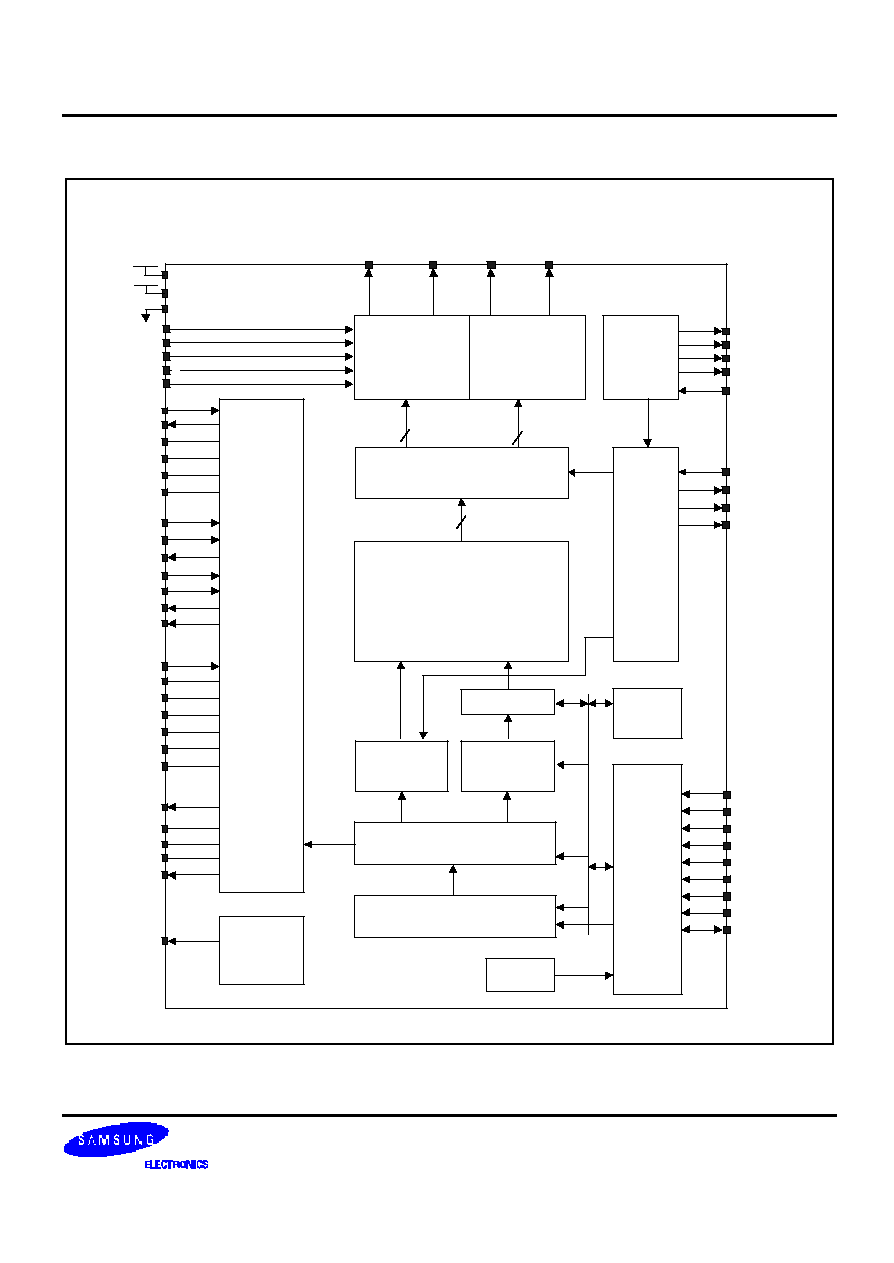
BLOCK DIAGRAM
COM
Driving Circuit
LCD
System
Control
Circuit
Bus
Holder
MPU INTERFACE
CS2
/CS1
DB<15:0>
Display data RAM
128 X 1536
MPU System
Control Circuit
Instruction Decoder
SEG
Driving Circuit
Y - Address
Control
Circuit
I/O Buffer
X - Address
Control
Circuit
Status
Oscillator
Circuit
Voltage
Converter/
Voltage
Regulator/
Voltage
Follower
PS
/RST
-VR
+VR
V1
REG_OUT
Power
Regulator
Circuit
Decoder Circuit
1536
384
129
PM
FR
CL
VSS
VEE
VCC
VIN2
VIN45
VOUT45
C11+
C11-
C12-
C12+
VIN1
V1T
C21+
C22-
C22+
C21-
C23+
C23-
C31+
C31-
INTRS
VDD
VDD1
V0
VMOUT
V1OUT
OSC5
SEGA0
SEGB0 - - -
SEGC0
COM0 - - - COM128
SEGA127
SEGB127
SEGC127
DC3IN
DC2OUT
DC2IN
MPU[1:0]
/WR
D/I
/RD
CDIR
VM
OSC2
OSC1
OSC4
OSC3
Figure 1. Block Diagram
S6B33A2 PRELIMINARY VER 1.3 128 RGB SEGMENT & 129 COMMON DRIVER FOR 4,096 COLOR STN LCD
4
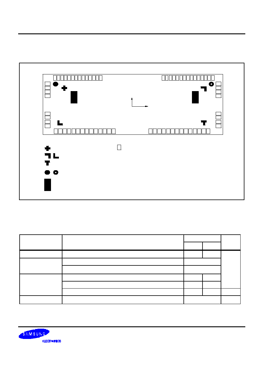
PAD CONFIGURATION
.......................
..
............
.
X
Y
(0,0) S6B33A2
652
1
177
230
178
229
704
653
: Bump Key
: ILB Align Key
: COG Align Key
: COF Align Key
: TOM
PAD
Figure 2. S6B33A2 Chip Pad Configuration
Table 1. S6B33A2 Pad Dimensions
Size
Item
Pad No.
X
Y
Unit
Chip size
-
16670
2430
1 ~ 177
90
Pad pitch
178 to 229, 230 to 652, 653 to 704
38
1 ~ 177
70
70
178 to 229, , 653 to 704
170
23
�
m
Bumped
pad size
230 to 652
23
170
Bumped pad height
All Pad
17
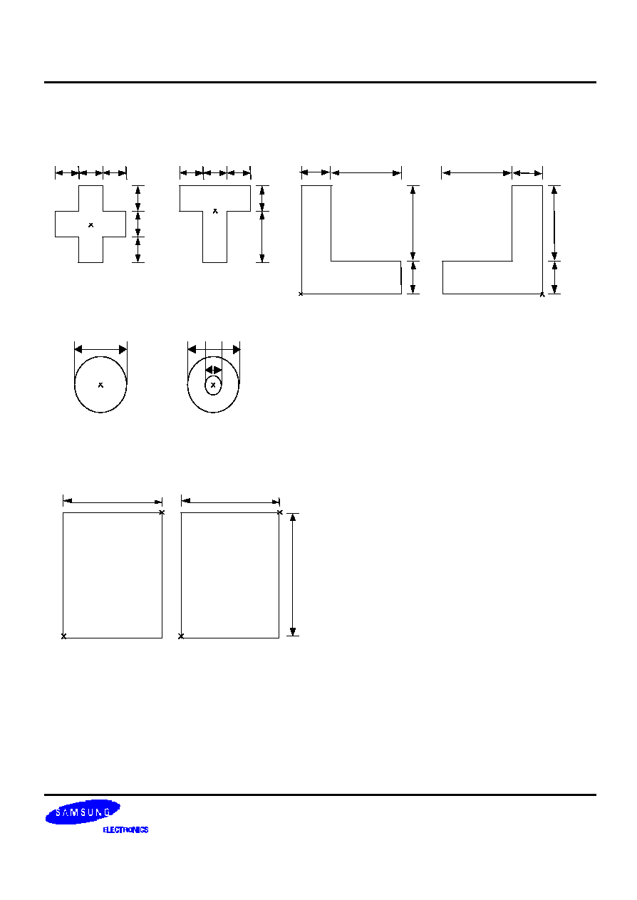
S6B33A2 PRELIMINARY VER 1.3 128 RGB SEGMENT & 129 COMMON DRIVER FOR 4,096 COLOR STN LCD
5
Figure 3. Bump, COG Align Key Coordinate Figure 4. ILB Align Key Coordinate
30
�
m 30
�
m 30
�
m
30
�
m 30
�
m 30
�
m
30
�
m
30
�
m
30
�
m
60
�
m
30
�
m
42
�
m
108
�
m
42
�
m
108
�
m
42
�
m
108
�
m
42
�
m
108
�
m
(-7374,740)
(7495,-725)
(-7500,-785)
(7340,665)
50
�
m
50
�
m
20
�
m
(-7975,820)
(7975,820)
Figure 5. COF Align Key Coordinate
220um
(-7005, -35)
(-6785, 545)
58
0um
220um
(6900, -35)
(7120, 545)
Left
Right
Figure 6. TOM Coordinate
S6B33A2 PRELIMINARY VER 1.3 128 RGB SEGMENT & 129 COMMON DRIVER FOR 4,096 COLOR STN LCD
6
PIN CONFIGURATION
COM0
COM1
COM2
COM45
COM46
COM47
:
:
:
:
:
:
:
:
:
:
:
:
SEGC0
SEGB0
SEGA0
SEGC1
SEGB1
SEGA1
SEGC2
SEGB2
SEGA2
:
:
:
:
:
:
:
:
:
:
:
:
:
:
:
:
:
:
:
:
:
:
:
SEGC125
SEGB125
SEGA125
SEGC126
SEGB126
SEGA126
SEGC127
SEGB127
SEGA127
S6B33A2 (Top View)
C21M
C21P
DC2IN
DC2OUT
VMIN
VMOUT
V1T
V1OUT
V1IN
C12M
C12P
C11M
C11P
VOUT45
VIN45
VIN2
VIN1
VDD
REG_OUT
VDD1
OSC1
DB15
DB14
DB13
DB12
DB11
DB10
DB9
DB8
DB7
DB6
DB5
DB4
DB3
DB2
DB1
OSC2
OSC3
OSC4
OSC5
INTRS
VSS
DB0
RDB
WRB
RS
RSTB
PM
FR
CL
TEST0
TEST1
TEST2
CS2
CS1B
CDIR
MPU0
MPU1
PS
VOIN
C22M
C22P
C23M
C23P
C24M
C24P
C31M
VEE
VRN
VCC
C31P
VOIN
COM63
COM64
COM65
108
COM109
COM110
:
:
:
:
:
:
:
:
:
:
:
:
:
:
:
COM48
COM49
COM50
COM60
COM61
COM62
:
:
:
COM128
COM127
COM126
COM113
COM112
COM111
:
:
:
TEST3
TEST4
VRP
Figure 7. S6B33A2 Chip Pin Configuration
S6B33A2 PRELIMINARY VER 1.3 128 RGB SEGMENT & 129 COMMON DRIVER FOR 4,096 COLOR STN LCD
7
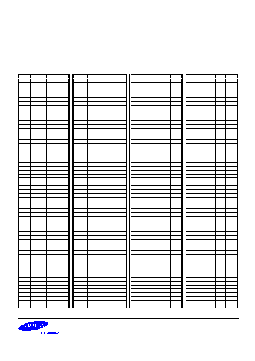
PAD CENTER COORDINATES
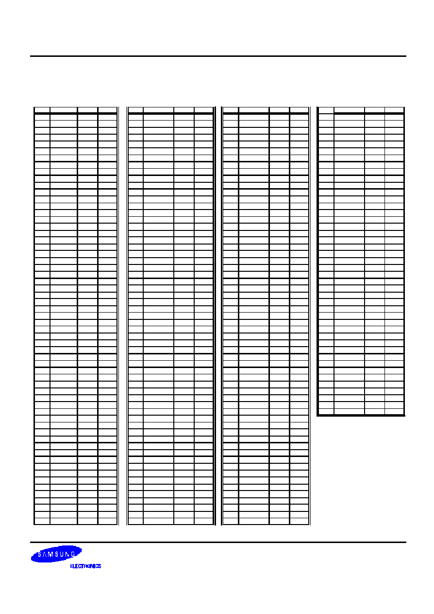
Table 2. Pad Center Coordinates
[Unit:
�
m]
NO
N A M E
X
Y
NO
N A M E
X
Y
NO
N A M E
X
Y
NO
N A M E
X
Y
1
D U M M Y
- 7 9 2 0
- 1 1 0 0
6 1
V S S
- 2 5 2 0
- 1 1 0 0
1 2 1
V 1 O U T
2 8 8 0
- 1 1 0 0
1 8 1
C O M < 1 >
8 1 6 5
- 9 5 5
2
D U M M Y
- 7 8 3 0
- 1 1 0 0
6 2
V S S
- 2 4 3 0
- 1 1 0 0
1 2 2
V 1 O U T
2 9 7 0
- 1 1 0 0
1 8 2
C O M < 2 >
8 1 6 5
- 9 1 7
3
V0IN
- 7 7 4 0
- 1 1 0 0
6 3
V S S
- 2 3 4 0
- 1 1 0 0
1 2 3
V 1 T
3 0 6 0
- 1 1 0 0
1 8 3
C O M < 3 >
8 1 6 5
- 8 7 9
4
V0IN
- 7 6 5 0
- 1 1 0 0
6 4
V D D
- 2 2 5 0
- 1 1 0 0
1 2 4
V M O U T
3 1 5 0
- 1 1 0 0
1 8 4
C O M < 4 >
8 1 6 5
- 8 4 1
5
V S S
- 7 5 6 0
- 1 1 0 0
6 5
I N T R S
- 2 1 6 0
- 1 1 0 0
1 2 5
V M O U T
3 2 4 0
- 1 1 0 0
1 8 5
C O M < 5 >
8 1 6 5
- 8 0 3
6
P S
- 7 4 7 0
- 1 1 0 0
6 6
O S C 5
- 2 0 7 0
- 1 1 0 0
1 2 6
V M O U T
3 3 3 0
- 1 1 0 0
1 8 6
C O M < 6 >
8 1 6 5
- 7 6 5
7
V D D
- 7 3 8 0
- 1 1 0 0
6 7
V S S
- 1 9 8 0
- 1 1 0 0
1 2 7
V M I N
3 4 2 0
- 1 1 0 0
1 8 7
C O M < 7 >
8 1 6 5
- 7 2 7
8
M P U < 1 >
- 7 2 9 0
- 1 1 0 0
6 8
O S C 4
- 1 8 9 0
- 1 1 0 0
1 2 8
V M I N
3 5 1 0
- 1 1 0 0
1 8 8
C O M < 8 >
8 1 6 5
- 6 8 9
9
V S S
- 7 2 0 0
- 1 1 0 0
6 9
O S C 3
- 1 8 0 0
- 1 1 0 0
1 2 9
V M I N
3 6 0 0
- 1 1 0 0
1 8 9
C O M < 9 >
8 1 6 5
- 6 5 1
1 0
M P U < 0 >
- 7 1 1 0
- 1 1 0 0
7 0
O S C 2
- 1 7 1 0
- 1 1 0 0
1 3 0
D C 2 O U T
3 6 9 0
- 1 1 0 0
1 9 0
C O M < 1 0 >
8 1 6 5
- 6 1 3
1 1
V D D
- 7 0 2 0
- 1 1 0 0
7 1
O S C 1
- 1 6 2 0
- 1 1 0 0
1 3 1
D C 2 O U T
3 7 8 0
- 1 1 0 0
1 9 1
C O M < 1 1 >
8 1 6 5
- 5 7 5
1 2
CDIR
- 6 9 3 0
- 1 1 0 0
7 2
V D D 1
- 1 5 3 0
- 1 1 0 0
1 3 2
DC2IN
3 8 7 0
- 1 1 0 0
1 9 2
C O M < 1 2 >
8 1 6 5
- 5 3 7
1 3
V S S
- 6 8 4 0
- 1 1 0 0
7 3
V D D 1
- 1 4 4 0
- 1 1 0 0
1 3 3
DC2IN
3 9 6 0
- 1 1 0 0
1 9 3
C O M < 1 3 >
8 1 6 5
- 4 9 9
1 4
C S 1 B
- 6 7 5 0
- 1 1 0 0
7 4
V D D 1
- 1 3 5 0
- 1 1 0 0
1 3 4
C 2 1 P
4 0 5 0
- 1 1 0 0
1 9 4
C O M < 1 4 >
8 1 6 5
- 4 6 1
1 5
C S 2
- 6 6 6 0
- 1 1 0 0
7 5
V D D 1
- 1 2 6 0
- 1 1 0 0
1 3 5
C 2 1 P
4 1 4 0
- 1 1 0 0
1 9 5
C O M < 1 5 >
8 1 6 5
- 4 2 3
1 6
T E S T < 4 >
- 6 5 7 0
- 1 1 0 0
7 6
V D D 1
- 1 1 7 0
- 1 1 0 0
1 3 6
C 2 1 P
4 2 3 0
- 1 1 0 0
1 9 6
C O M < 1 6 >
8 1 6 5
- 3 8 5
1 7
T E S T < 3 >
- 6 4 8 0
- 1 1 0 0
7 7
V D D 1
- 1 0 8 0
- 1 1 0 0
1 3 7
C 2 1 M
4 3 2 0
- 1 1 0 0
1 9 7
C O M < 1 7 >
8 1 6 5
- 3 4 7
1 8
T E S T < 2 >
- 6 3 9 0
- 1 1 0 0
7 8
R E G _ O U T
- 9 9 0
- 1 1 0 0
1 3 8
C 2 1 M
4 4 1 0
- 1 1 0 0
1 9 8
C O M < 1 8 >
8 1 6 5
- 3 0 9
1 9
T E S T < 1 >
- 6 3 0 0
- 1 1 0 0
7 9
R E G _ O U T
- 9 0 0
- 1 1 0 0
1 3 9
C 2 1 M
4 5 0 0
- 1 1 0 0
1 9 9
C O M < 1 9 >
8 1 6 5
- 2 7 1
2 0
T E S T < 0 >
- 6 2 1 0
- 1 1 0 0
8 0
R E G _ O U T
- 8 1 0
- 1 1 0 0
1 4 0
C 2 2 P
4 5 9 0
- 1 1 0 0
2 0 0
C O M < 2 0 >
8 1 6 5
- 2 3 3
2 1
V D D
- 6 1 2 0
- 1 1 0 0
8 1
V D D
- 7 2 0
- 1 1 0 0
1 4 1
C 2 2 P
4 6 8 0
- 1 1 0 0
2 0 1
C O M < 2 1 >
8 1 6 5
- 1 9 5
2 2
C L
- 6 0 3 0
- 1 1 0 0
8 2
V D D
- 6 3 0
- 1 1 0 0
1 4 2
C 2 2 P
4 7 7 0
- 1 1 0 0
2 0 2
C O M < 2 2 >
8 1 6 5
- 1 5 7
2 3
FR
- 5 9 4 0
- 1 1 0 0
8 3
V D D
- 5 4 0
- 1 1 0 0
1 4 3
C 2 2 M
4 8 6 0
- 1 1 0 0
2 0 3
C O M < 2 3 >
8 1 6 5
- 1 1 9
2 4
P M
- 5 8 5 0
- 1 1 0 0
8 4
V D D
- 4 5 0
- 1 1 0 0
1 4 4
C 2 2 M
4 9 5 0
- 1 1 0 0
2 0 4
C O M < 2 4 >
8 1 6 5
- 8 1
2 5
RSTB
- 5 7 6 0
- 1 1 0 0
8 5
V D D
- 3 6 0
- 1 1 0 0
1 4 5
C 2 2 M
5 0 4 0
- 1 1 0 0
2 0 5
C O M < 2 5 >
8 1 6 5
- 4 3
2 6
R S
- 5 6 7 0
- 1 1 0 0
8 6
V D D
- 2 7 0
- 1 1 0 0
1 4 6
C 2 3 P
5 1 3 0
- 1 1 0 0
2 0 6
C O M < 2 6 >
8 1 6 5
- 5
2 7
V S S
- 5 5 8 0
- 1 1 0 0
8 7
V D D
- 1 8 0
- 1 1 0 0
1 4 7
C 2 3 P
5 2 2 0
- 1 1 0 0
2 0 7
C O M < 2 7 >
8 1 6 5
3 3
2 8
W R B
- 5 4 9 0
- 1 1 0 0
8 8
V I N 1
- 9 0
- 1 1 0 0
1 4 8
C 2 3 P
5 3 1 0
- 1 1 0 0
2 0 8
C O M < 2 8 >
8 1 6 5
7 1
2 9
R D B
- 5 4 0 0
- 1 1 0 0
8 9
V I N 1
0
- 1 1 0 0
1 4 9
C 2 3 M
5 4 0 0
- 1 1 0 0
2 0 9
C O M < 2 9 >
8 1 6 5
1 0 9
3 0
V D D
- 5 3 1 0
- 1 1 0 0
9 0
V I N 1
9 0
- 1 1 0 0
1 5 0
C 2 3 M
5 4 9 0
- 1 1 0 0
2 1 0
C O M < 3 0 >
8 1 6 5
1 4 7
3 1
D B < 0 >
- 5 2 2 0
- 1 1 0 0
9 1
V I N 1
1 8 0
- 1 1 0 0
1 5 1
C 2 3 M
5 5 8 0
- 1 1 0 0
2 1 1
C O M < 3 1 >
8 1 6 5
1 8 5
3 2
D B < 1 >
- 5 1 3 0
- 1 1 0 0
9 2
V I N 1
2 7 0
- 1 1 0 0
1 5 2
V R N
5 6 7 0
- 1 1 0 0
2 1 2
C O M < 3 2 >
8 1 6 5
2 2 3
3 3
D B < 2 >
- 5 0 4 0
- 1 1 0 0
9 3
V I N 1
3 6 0
- 1 1 0 0
1 5 3
V R N
5 7 6 0
- 1 1 0 0
2 1 3
C O M < 3 3 >
8 1 6 5
2 6 1
3 4
D B < 3 >
- 4 9 5 0
- 1 1 0 0
9 4
V I N 1
4 5 0
- 1 1 0 0
1 5 4
V R N
5 8 5 0
- 1 1 0 0
2 1 4
C O M < 3 4 >
8 1 6 5
2 9 9
3 5
D B < 4 >
- 4 8 6 0
- 1 1 0 0
9 5
V I N 1
5 4 0
- 1 1 0 0
1 5 5
V E E
5 9 4 0
- 1 1 0 0
2 1 5
C O M < 3 5 >
8 1 6 5
3 3 7
3 6
D B < 5 >
- 4 7 7 0
- 1 1 0 0
9 6
V I N 1
6 3 0
- 1 1 0 0
1 5 6
V E E
6 0 3 0
- 1 1 0 0
2 1 6
C O M < 3 6 >
8 1 6 5
3 7 5
3 7
D B < 6 >
- 4 6 8 0
- 1 1 0 0
9 7
V I N 1
7 2 0
- 1 1 0 0
1 5 7
V E E
6 1 2 0
- 1 1 0 0
2 1 7
C O M < 3 7 >
8 1 6 5
4 1 3
3 8
D B < 7 >
- 4 5 9 0
- 1 1 0 0
9 8
V I N 1
8 1 0
- 1 1 0 0
1 5 8
V E E
6 2 1 0
- 1 1 0 0
2 1 8
C O M < 3 8 >
8 1 6 5
4 5 1
3 9
D B < 8 >
- 4 5 0 0
- 1 1 0 0
9 9
V I N 2
9 0 0
- 1 1 0 0
1 5 9
D U M M Y
6 3 0 0
- 1 1 0 0
2 1 9
C O M < 3 9 >
8 1 6 5
4 8 9
4 0
D B < 9 >
- 4 4 1 0
- 1 1 0 0
1 0 0
V I N 2
9 9 0
- 1 1 0 0
1 6 0
C 3 1 M
6 3 9 0
- 1 1 0 0
2 2 0
C O M < 4 0 >
8 1 6 5
5 2 7
4 1
D B < 1 0 >
- 4 3 2 0
- 1 1 0 0
1 0 1
V I N 2
1 0 8 0
- 1 1 0 0
1 6 1
C 3 1 M
6 4 8 0
- 1 1 0 0
2 2 1
C O M < 4 1 >
8 1 6 5
5 6 5
4 2
D B < 1 1 >
- 4 2 3 0
- 1 1 0 0
1 0 2
V I N 2
1 1 7 0
- 1 1 0 0
1 6 2
C 3 1 M
6 5 7 0
- 1 1 0 0
2 2 2
C O M < 4 2 >
8 1 6 5
6 0 3
4 3
D B < 1 2 >
- 4 1 4 0
- 1 1 0 0
1 0 3
VIN45
1 2 6 0
- 1 1 0 0
1 6 3
D U M M Y
6 6 6 0
- 1 1 0 0
2 2 3
C O M < 4 3 >
8 1 6 5
6 4 1
4 4
D B < 1 3 >
- 4 0 5 0
- 1 1 0 0
1 0 4
VIN45
1 3 5 0
- 1 1 0 0
1 6 4
C 3 1 P
6 7 5 0
- 1 1 0 0
2 2 4
C O M < 4 4 >
8 1 6 5
6 7 9
4 5
D B < 1 4 >
- 3 9 6 0
- 1 1 0 0
1 0 5
V O U T 4 5
1 4 4 0
- 1 1 0 0
1 6 5
C 3 1 P
6 8 4 0
- 1 1 0 0
2 2 5
C O M < 4 5 >
8 1 6 5
7 1 7
4 6
D B < 1 5 >
- 3 8 7 0
- 1 1 0 0
1 0 6
V O U T 4 5
1 5 3 0
- 1 1 0 0
1 6 6
C 3 1 P
6 9 3 0
- 1 1 0 0
2 2 6
C O M < 4 6 >
8 1 6 5
7 5 5
4 7
V S S
- 3 7 8 0
- 1 1 0 0
1 0 7
C 1 1 P
1 6 2 0
- 1 1 0 0
1 6 7
D U M M Y
7 0 2 0
- 1 1 0 0
2 2 7
C O M < 4 7 >
8 1 6 5
7 9 3
4 8
V S S
- 3 6 9 0
- 1 1 0 0
1 0 8
C 1 1 P
1 7 1 0
- 1 1 0 0
1 6 8
V R P
7 1 1 0
- 1 1 0 0
2 2 8
D U M M Y
8 1 6 5
8 3 1
4 9
V S S
- 3 6 0 0
- 1 1 0 0
1 0 9
C 1 1 P
1 8 0 0
- 1 1 0 0
1 6 9
V R P
7 2 0 0
- 1 1 0 0
2 2 9
D U M M Y
8 1 6 5
8 6 9
5 0
V S S
- 3 5 1 0
- 1 1 0 0
1 1 0
C 1 1 M
1 8 9 0
- 1 1 0 0
1 7 0
V C C
7 2 9 0
- 1 1 0 0
2 3 0
D U M M Y
8 0 1 8
1 0 4 5
5 1
V S S
- 3 4 2 0
- 1 1 0 0
1 1 1
C 1 1 M
1 9 8 0
- 1 1 0 0
1 7 1
V C C
7 3 8 0
- 1 1 0 0
2 3 1
D U M M Y
7 9 8 0
1 0 4 5
5 2
V S S
- 3 3 3 0
- 1 1 0 0
1 1 2
C 1 1 M
2 0 7 0
- 1 1 0 0
1 7 2
D U M M Y
7 4 7 0
- 1 1 0 0
2 3 2
C O M < 4 8 >
7 9 4 2
1 0 4 5
5 3
V S S
- 3 2 4 0
- 1 1 0 0
1 1 3
C 1 2 P
2 1 6 0
- 1 1 0 0
1 7 3
V S S
7 5 6 0
- 1 1 0 0
2 3 3
C O M < 4 9 >
7 9 0 4
1 0 4 5
5 4
V S S
- 3 1 5 0
- 1 1 0 0
1 1 4
C 1 2 P
2 2 5 0
- 1 1 0 0
1 7 4
V0IN
7 6 5 0
- 1 1 0 0
2 3 4
C O M < 5 0 >
7 8 6 6
1 0 4 5
5 5
V S S
- 3 0 6 0
- 1 1 0 0
1 1 5
C 1 2 P
2 3 4 0
- 1 1 0 0
1 7 5
V0IN
7 7 4 0
- 1 1 0 0
2 3 5
C O M < 5 1 >
7 8 2 8
1 0 4 5
5 6
V S S
- 2 9 7 0
- 1 1 0 0
1 1 6
C 1 2 M
2 4 3 0
- 1 1 0 0
1 7 6
D U M M Y
7 8 3 0
- 1 1 0 0
2 3 6
C O M < 5 2 >
7 7 9 0
1 0 4 5
5 7
V S S
- 2 8 8 0
- 1 1 0 0
1 1 7
C 1 2 M
2 5 2 0
- 1 1 0 0
1 7 7
D U M M Y
7 9 2 0
- 1 1 0 0
2 3 7
C O M < 5 3 >
7 7 5 2
1 0 4 5
5 8
V S S
- 2 7 9 0
- 1 1 0 0
1 1 8
C 1 2 M
2 6 1 0
- 1 1 0 0
1 7 8
D U M M Y
8 1 6 5
- 1 0 6 9
2 3 8
C O M < 5 4 >
7 7 1 4
1 0 4 5
5 9
V S S
- 2 7 0 0
- 1 1 0 0
1 1 9
V1IN
2 7 0 0
- 1 1 0 0
1 7 9
D U M M Y
8 1 6 5
- 1 0 3 1
2 3 9
C O M < 5 5 >
7 6 7 6
1 0 4 5
6 0
V S S
- 2 6 1 0
- 1 1 0 0
1 2 0
V1IN
2 7 9 0
- 1 1 0 0
1 8 0
C O M < 0 >
8 1 6 5
- 9 9 3
2 4 0
C O M < 5 6 >
7 6 3 8
1 0 4 5
S6B33A2 PRELIMINARY VER 1.3 128 RGB SEGMENT & 129 COMMON DRIVER FOR 4,096 COLOR STN LCD
8
Table 2. Pad Center Coordinates (Continued)
[Unit:
�
m]
NO
NAME
X
Y
NO
NAME
X
Y
NO
NAME
X
Y
NO
NAME
X
Y
241 COM<57>
7600
1045
301 SEGA<17>
5320
1045
361 SEGA<37>
3040
1045
421 SEGA<57>
760
1045
242 COM<58>
7562
1045
302 SEGC<18>
5282
1045
362 SEGC<38>
3002
1045
422 SEGC<58>
722
1045
243 COM<59>
7524
1045
303 SEGB<18>
5244
1045
363 SEGB<38>
2964
1045
423 SEGB<58>
684
1045
244 COM<60>
7486
1045
304 SEGA<18>
5206
1045
364 SEGA<38>
2926
1045
424 SEGA<58>
646
1045
245 COM<61>
7448
1045
305 SEGC<19>
5168
1045
365 SEGC<39>
2888
1045
425 SEGC<59>
608
1045
246 COM<62>
7410
1045
306 SEGB<19>
5130
1045
366 SEGB<39>
2850
1045
426 SEGB<59>
570
1045
247 DUMMY
7372
1045
307 SEGA<19>
5092
1045
367 SEGA<39>
2812
1045
427 SEGA<59>
532
1045
248 SEGC<0>
7334
1045
308 SEGC<20>
5054
1045
368 SEGC<40>
2774
1045
428 SEGC<60>
494
1045
249 SEGB<0>
7296
1045
309 SEGB<20>
5016
1045
369 SEGB<40>
2736
1045
429 SEGB<60>
456
1045
250 SEGA<0>
7258
1045
310 SEGA<20>
4978
1045
370 SEGA<40>
2698
1045
430 SEGA<60>
418
1045
251 SEGC<1>
7220
1045
311 SEGC<21>
4940
1045
371 SEGC<41>
2660
1045
431 SEGC<61>
380
1045
252 SEGB<1>
7182
1045
312 SEGB<21>
4902
1045
372 SEGB<41>
2622
1045
432 SEGB<61>
342
1045
253 SEGA<1>
7144
1045
313 SEGA<21>
4864
1045
373 SEGA<41>
2584
1045
433 SEGA<61>
304
1045
254 SEGC<2>
7106
1045
314 SEGC<22>
4826
1045
374 SEGC<42>
2546
1045
434 SEGC<62>
266
1045
255 SEGB<2>
7068
1045
315 SEGB<22>
4788
1045
375 SEGB<42>
2508
1045
435 SEGB<62>
228
1045
256 SEGA<2>
7030
1045
316 SEGA<22>
4750
1045
376 SEGA<42>
2470
1045
436 SEGA<62>
190
1045
257 SEGC<3>
6992
1045
317 SEGC<23>
4712
1045
377 SEGC<43>
2432
1045
437 SEGC<63>
152
1045
258 SEGB<3>
6954
1045
318 SEGB<23>
4674
1045
378 SEGB<43>
2394
1045
438 SEGB<63>
114
1045
259 SEGA<3>
6916
1045
319 SEGA<23>
4636
1045
379 SEGA<43>
2356
1045
439 SEGA<63>
76
1045
260 SEGC<4>
6878
1045
320 SEGC<24>
4598
1045
380 SEGC<44>
2318
1045
440 SEGC<64>
38
1045
261 SEGB<4>
6840
1045
321 SEGB<24>
4560
1045
381 SEGB<44>
2280
1045
441 SEGB<64>
0
1045
262 SEGA<4>
6802
1045
322 SEGA<24>
4522
1045
382 SEGA<44>
2242
1045
442 SEGA<64>
-38
1045
263 SEGC<5>
6764
1045
323 SEGC<25>
4484
1045
383 SEGC<45>
2204
1045
443 SEGC<65>
-76
1045
264 SEGB<5>
6726
1045
324 SEGB<25>
4446
1045
384 SEGB<45>
2166
1045
444 SEGB<65>
-114
1045
265 SEGA<5>
6688
1045
325 SEGA<25>
4408
1045
385 SEGA<45>
2128
1045
445 SEGA<65>
-152
1045
266 SEGC<6>
6650
1045
326 SEGC<26>
4370
1045
386 SEGC<46>
2090
1045
446 SEGC<66>
-190
1045
267 SEGB<6>
6612
1045
327 SEGB<26>
4332
1045
387 SEGB<46>
2052
1045
447 SEGB<66>
-228
1045
268 SEGA<6>
6574
1045
328 SEGA<26>
4294
1045
388 SEGA<46>
2014
1045
448 SEGA<66>
-266
1045
269 SEGC<7>
6536
1045
329 SEGC<27>
4256
1045
389 SEGC<47>
1976
1045
449 SEGC<67>
-304
1045
270 SEGB<7>
6498
1045
330 SEGB<27>
4218
1045
390 SEGB<47>
1938
1045
450 SEGB<67>
-342
1045
271 SEGA<7>
6460
1045
331 SEGA<27>
4180
1045
391 SEGA<47>
1900
1045
451 SEGA<67>
-380
1045
272 SEGC<8>
6422
1045
332 SEGC<28>
4142
1045
392 SEGC<48>
1862
1045
452 SEGC<68>
-418
1045
273 SEGB<8>
6384
1045
333 SEGB<28>
4104
1045
393 SEGB<48>
1824
1045
453 SEGB<68>
-456
1045
274 SEGA<8>
6346
1045
334 SEGA<28>
4066
1045
394 SEGA<48>
1786
1045
454 SEGA<68>
-494
1045
275 SEGC<9>
6308
1045
335 SEGC<29>
4028
1045
395 SEGC<49>
1748
1045
455 SEGC<69>
-532
1045
276 SEGB<9>
6270
1045
336 SEGB<29>
3990
1045
396 SEGB<49>
1710
1045
456 SEGB<69>
-570
1045
277 SEGA<9>
6232
1045
337 SEGA<29>
3952
1045
397 SEGA<49>
1672
1045
457 SEGA<69>
-608
1045
278 SEGC<10>
6194
1045
338 SEGC<30>
3914
1045
398 SEGC<50>
1634
1045
458 SEGC<70>
-646
1045
279 SEGB<10>
6156
1045
339 SEGB<30>
3876
1045
399 SEGB<50>
1596
1045
459 SEGB<70>
-684
1045
280 SEGA<10>
6118
1045
340 SEGA<30>
3838
1045
400 SEGA<50>
1558
1045
460 SEGA<70>
-722
1045
281 SEGC<11>
6080
1045
341 SEGC<31>
3800
1045
401 SEGC<51>
1520
1045
461 SEGC<71>
-760
1045
282 SEGB<11>
6042
1045
342 SEGB<31>
3762
1045
402 SEGB<51>
1482
1045
462 SEGB<71>
-798
1045
283 SEGA<11>
6004
1045
343 SEGA<31>
3724
1045
403 SEGA<51>
1444
1045
463 SEGA<71>
-836
1045
284 SEGC<12>
5966
1045
344 SEGC<32>
3686
1045
404 SEGC<52>
1406
1045
464 SEGC<72>
-874
1045
285 SEGB<12>
5928
1045
345 SEGB<32>
3648
1045
405 SEGB<52>
1368
1045
465 SEGB<72>
-912
1045
286 SEGA<12>
5890
1045
346 SEGA<32>
3610
1045
406 SEGA<52>
1330
1045
466 SEGA<72>
-950
1045
287 SEGC<13>
5852
1045
347 SEGC<33>
3572
1045
407 SEGC<53>
1292
1045
467 SEGC<73>
-988
1045
288 SEGB<13>
5814
1045
348 SEGB<33>
3534
1045
408 SEGB<53>
1254
1045
468 SEGB<73>
-1026
1045
289 SEGA<13>
5776
1045
349 SEGA<33>
3496
1045
409 SEGA<53>
1216
1045
469 SEGA<73>
-1064
1045
290 SEGC<14>
5738
1045
350 SEGC<34>
3458
1045
410 SEGC<54>
1178
1045
470 SEGC<74>
-1102
1045
291 SEGB<14>
5700
1045
351 SEGB<34>
3420
1045
411 SEGB<54>
1140
1045
471 SEGB<74>
-1140
1045
292 SEGA<14>
5662
1045
352 SEGA<34>
3382
1045
412 SEGA<54>
1102
1045
472 SEGA<74>
-1178
1045
293 SEGC<15>
5624
1045
353 SEGC<35>
3344
1045
413 SEGC<55>
1064
1045
473 SEGC<75>
-1216
1045
294 SEGB<15>
5586
1045
354 SEGB<35>
3306
1045
414 SEGB<55>
1026
1045
474 SEGB<75>
-1254
1045
295 SEGA<15>
5548
1045
355 SEGA<35>
3268
1045
415 SEGA<55>
988
1045
475 SEGA<75>
-1292
1045
296 SEGC<16>
5510
1045
356 SEGC<36>
3230
1045
416 SEGC<56>
950
1045
476 SEGC<76>
-1330
1045
297 SEGB<16>
5472
1045
357 SEGB<36>
3192
1045
417 SEGB<56>
912
1045
477 SEGB<76>
-1368
1045
298 SEGA<16>
5434
1045
358 SEGA<36>
3154
1045
418 SEGA<56>
874
1045
478 SEGA<76>
-1406
1045
299 SEGC<17>
5396
1045
359 SEGC<37>
3116
1045
419 SEGC<57>
836
1045
479 SEGC<77>
-1444
1045
300 SEGB<17>
5358
1045
360 SEGB<37>
3078
1045
420 SEGB<57>
798
1045
480 SEGB<77>
-1482
1045
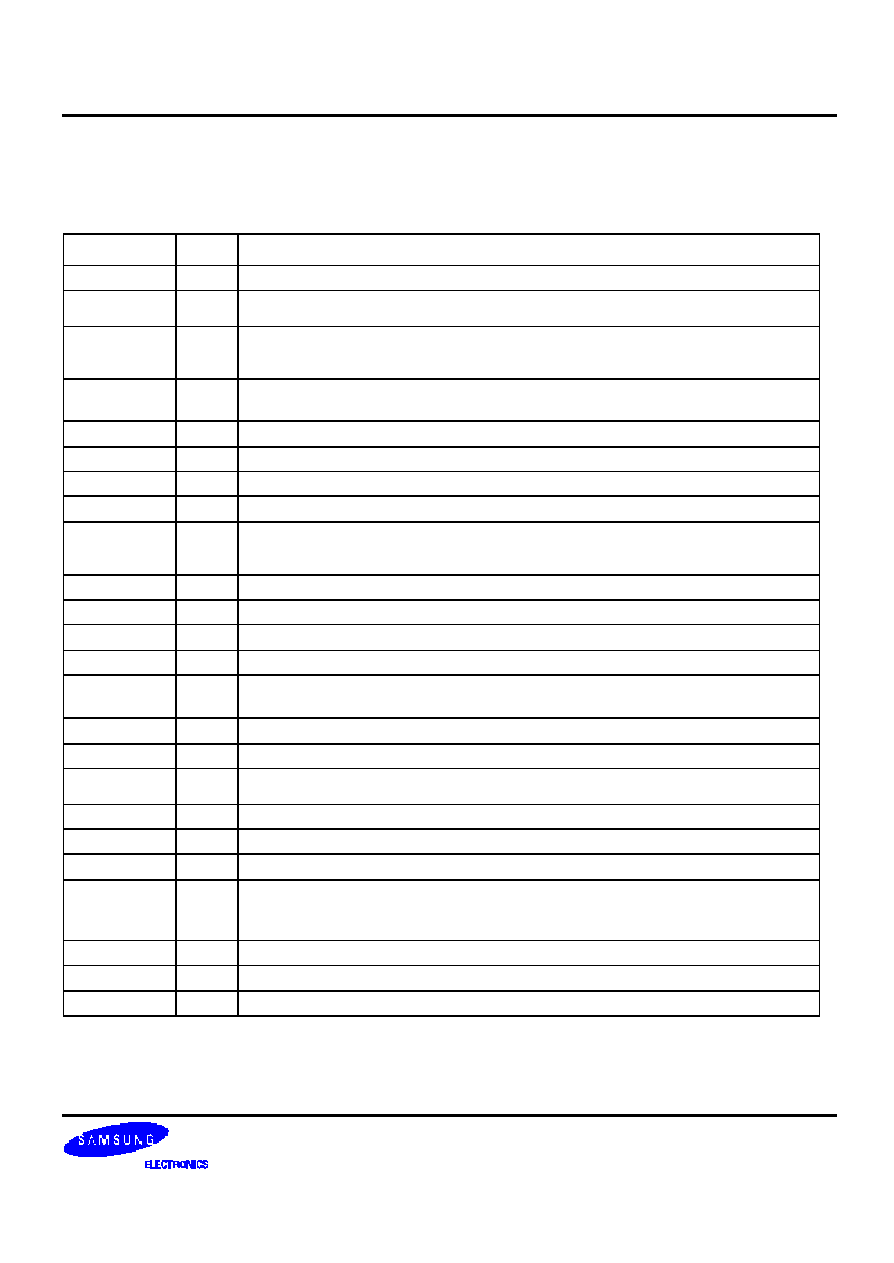
S6B33A2 PRELIMINARY VER 1.3 128 RGB SEGMENT & 129 COMMON DRIVER FOR 4,096 COLOR STN LCD
9
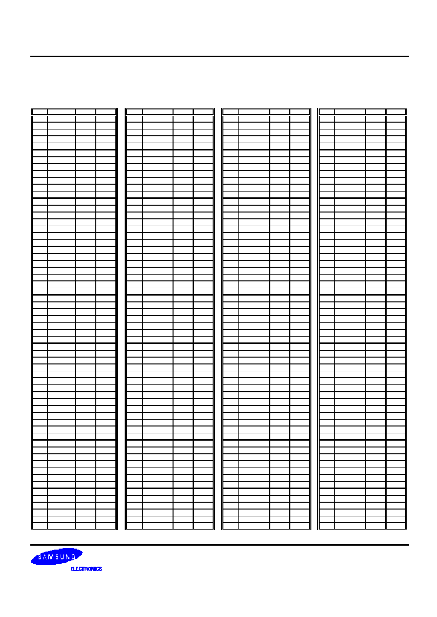
Table 2. Pad Center Coordinates (Continued)
[Unit:
�
m]
NO
NAME
X
Y
NO
NAME
X
Y
NO
NAME
X
Y
NO
NAME
X
Y
481 SEGA<77>
-1520
1045
541 SEGA<97>
-3800
1045
601 SEGA<117>
-6080
1045
661 COM<104>
-8165
565
482 SEGC<78>
-1558
1045
542 SEGC<98>
-3838
1045
602 SEGC<118>
-6118
1045
662 COM<103>
-8165
527
483 SEGB<78>
-1596
1045
543 SEGB<98>
-3876
1045
603 SEGB<118>
-6156
1045
663 COM<102>
-8165
489
484 SEGA<78>
-1634
1045
544 SEGA<98>
-3914
1045
604 SEGA<118>
-6194
1045
664 COM<101>
-8165
451
485 SEGC<79>
-1672
1045
545 SEGC<99>
-3952
1045
605 SEGC<119>
-6232
1045
665 COM<100>
-8165
413
486 SEGB<79>
-1710
1045
546 SEGB<99>
-3990
1045
606 SEGB<119>
-6270
1045
666 COM<99>
-8165
375
487 SEGA<79>
-1748
1045
547 SEGA<99>
-4028
1045
607 SEGA<119>
-6308
1045
667 COM<98>
-8165
337
488 SEGC<80>
-1786
1045
548 SEGC<100>
-4066
1045
608 SEGC<120>
-6346
1045
668 COM<97>
-8165
299
489 SEGB<80>
-1824
1045
549 SEGB<100>
-4104
1045
609 SEGB<120>
-6384
1045
669 COM<96>
-8165
261
490 SEGA<80>
-1862
1045
550 SEGA<100>
-4142
1045
610 SEGA<120>
-6422
1045
670 COM<95>
-8165
223
491 SEGC<81>
-1900
1045
551 SEGC<101>
-4180
1045
611 SEGC<121>
-6460
1045
671 COM<94>
-8165
185
492 SEGB<81>
-1938
1045
552 SEGB<101>
-4218
1045
612 SEGB<121>
-6498
1045
672 COM<93>
-8165
147
493 SEGA<81>
-1976
1045
553 SEGA<101>
-4256
1045
613 SEGA<121>
-6536
1045
673 COM<92>
-8165
109
494 SEGC<82>
-2014
1045
554 SEGC<102>
-4294
1045
614 SEGC<122>
-6574
1045
674 COM<91>
-8165
71
495 SEGB<82>
-2052
1045
555 SEGB<102>
-4332
1045
615 SEGB<122>
-6612
1045
675 COM<90>
-8165
33
496 SEGA<82>
-2090
1045
556 SEGA<102>
-4370
1045
616 SEGA<122>
-6650
1045
676 COM<89>
-8165
-5
497 SEGC<83>
-2128
1045
557 SEGC<103>
-4408
1045
617 SEGC<123>
-6688
1045
677 COM<88>
-8165
-43
498 SEGB<83>
-2166
1045
558 SEGB<103>
-4446
1045
618 SEGB<123>
-6726
1045
678 COM<87>
-8165
-81
499 SEGA<83>
-2204
1045
559 SEGA<103>
-4484
1045
619 SEGA<123>
-6764
1045
679 COM<86>
-8165
-119
500 SEGC<84>
-2242
1045
560 SEGC<104>
-4522
1045
620 SEGC<124>
-6802
1045
680 COM<85>
-8165
-157
501 SEGB<84>
-2280
1045
561 SEGB<104>
-4560
1045
621 SEGB<124>
-6840
1045
681 COM<84>
-8165
-195
502 SEGA<84>
-2318
1045
562 SEGA<104>
-4598
1045
622 SEGA<124>
-6878
1045
682 COM<83>
-8165
-233
503 SEGC<85>
-2356
1045
563 SEGC<105>
-4636
1045
623 SEGC<125>
-6916
1045
683 COM<82>
-8165
-271
504 SEGB<85>
-2394
1045
564 SEGB<105>
-4674
1045
624 SEGB<125>
-6954
1045
684 COM<81>
-8165
-309
505 SEGA<85>
-2432
1045
565 SEGA<105>
-4712
1045
625 SEGA<125>
-6992
1045
685 COM<80>
-8165
-347
506 SEGC<86>
-2470
1045
566 SEGC<106>
-4750
1045
626 SEGC<126>
-7030
1045
686 COM<79>
-8165
-385
507 SEGB<86>
-2508
1045
567 SEGB<106>
-4788
1045
627 SEGB<126>
-7068
1045
687 COM<78>
-8165
-423
508 SEGA<86>
-2546
1045
568 SEGA<106>
-4826
1045
628 SEGA<126>
-7106
1045
688 COM<77>
-8165
-461
509 SEGC<87>
-2584
1045
569 SEGC<107>
-4864
1045
629 SEGC<127>
-7144
1045
689 COM<76>
-8165
-499
510 SEGB<87>
-2622
1045
570 SEGB<107>
-4902
1045
630 SEGB<127>
-7182
1045
690 COM<75>
-8165
-537
511 SEGA<87>
-2660
1045
571 SEGA<107>
-4940
1045
631 SEGA<127>
-7220
1045
691 COM<74>
-8165
-575
512 SEGC<88>
-2698
1045
572 SEGC<108>
-4978
1045
632 DUMMY
-7258
1045
692 COM<73>
-8165
-613
513 SEGB<88>
-2736
1045
573 SEGB<108>
-5016
1045
633 COM<128>
-7296
1045
693 COM<72>
-8165
-651
514 SEGA<88>
-2774
1045
574 SEGA<108>
-5054
1045
634 COM<127>
-7334
1045
694 COM<71>
-8165
-689
515 SEGC<89>
-2812
1045
575 SEGC<109>
-5092
1045
635 COM<126>
-7372
1045
695 COM<70>
-8165
-727
516 SEGB<89>
-2850
1045
576 SEGB<109>
-5130
1045
636 COM<125>
-7410
1045
696 COM<69>
-8165
-765
517 SEGA<89>
-2888
1045
577 SEGA<109>
-5168
1045
637 COM<124>
-7448
1045
697 COM<68>
-8165
-803
518 SEGC<90>
-2926
1045
578 SEGC<110>
-5206
1045
638 COM<123>
-7486
1045
698 COM<67>
-8165
-841
519 SEGB<90>
-2964
1045
579 SEGB<110>
-5244
1045
639 COM<122>
-7524
1045
699 COM<66>
-8165
-879
520 SEGA<90>
-3002
1045
580 SEGA<110>
-5282
1045
640 COM<121>
-7562
1045
700 COM<65>
-8165
-917
521 SEGC<91>
-3040
1045
581 SEGC<111>
-5320
1045
641 COM<120>
-7600
1045
701 COM<64>
-8165
-955
522 SEGB<91>
-3078
1045
582 SEGB<111>
-5358
1045
642 COM<119>
-7638
1045
702 COM<63>
-8165
-993
523 SEGA<91>
-3116
1045
583 SEGA<111>
-5396
1045
643 COM<118>
-7676
1045
703 DUMMY
-8165
-1031
524 SEGC<92>
-3154
1045
584 SEGC<112>
-5434
1045
644 COM<117>
-7714
1045
704 DUMMY
-8165
-1069
525 SEGB<92>
-3192
1045
585 SEGB<112>
-5472
1045
645 COM<116>
-7752
1045
526 SEGA<92>
-3230
1045
586 SEGA<112>
-5510
1045
646 COM<115>
-7790
1045
527 SEGC<93>
-3268
1045
587 SEGC<113>
-5548
1045
647 COM<114>
-7828
1045
528 SEGB<93>
-3306
1045
588 SEGB<113>
-5586
1045
648 COM<113>
-7866
1045
529 SEGA<93>
-3344
1045
589 SEGA<113>
-5624
1045
649 COM<112>
-7904
1045
530 SEGC<94>
-3382
1045
590 SEGC<114>
-5662
1045
650 COM<111>
-7942
1045
531 SEGB<94>
-3420
1045
591 SEGB<114>
-5700
1045
651 DUMMY
-7980
1045
532 SEGA<94>
-3458
1045
592 SEGA<114>
-5738
1045
652 DUMMY
-8018
1045
533 SEGC<95>
-3496
1045
593 SEGC<115>
-5776
1045
653 DUMMY
-8165
869
534 SEGB<95>
-3534
1045
594 SEGB<115>
-5814
1045
654 DUMMY
-8165
831
535 SEGA<95>
-3572
1045
595 SEGA<115>
-5852
1045
655 COM<110>
-8165
793
536 SEGC<96>
-3610
1045
596 SEGC<116>
-5890
1045
656 COM<109>
-8165
755
537 SEGB<96>
-3648
1045
597 SEGB<116>
-5928
1045
657 COM<108>
-8165
717
538 SEGA<96>
-3686
1045
598 SEGA<116>
-5966
1045
658 COM<107>
-8165
679
539 SEGC<97>
-3724
1045
599 SEGC<117>
-6004
1045
659 COM<106>
-8165
641
540 SEGB<97>
-3762
1045
600 SEGB<117>
-6042
1045
660 COM<105>
-8165
603
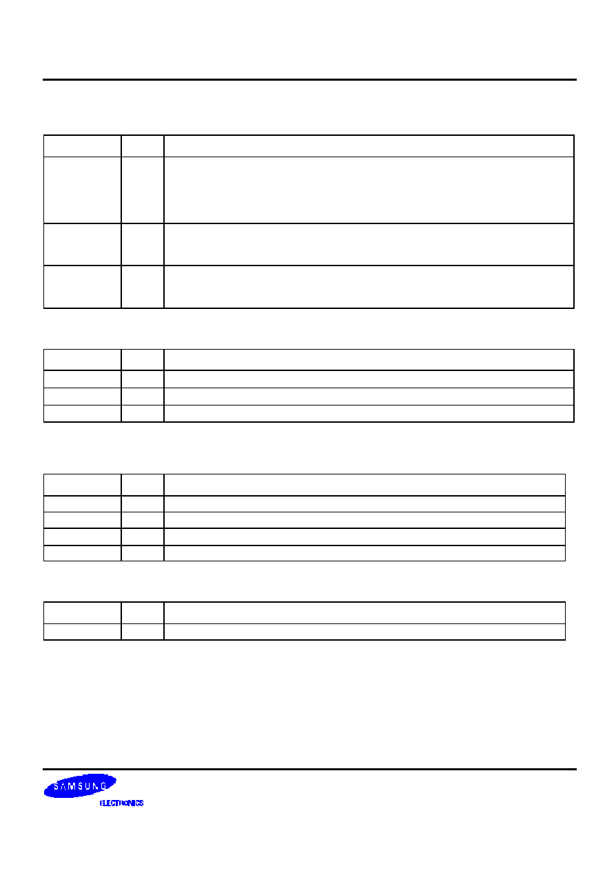
S6B33A2 PRELIMINARY VER 1.3 128 RGB SEGMENT & 129 COMMON DRIVER FOR 4,096 COLOR STN LCD
10
PIN DESCRIPTION
Table 3. Power Supply Pins
Name
I/O
Description
VDD
Supply Power supply(Logic)
VDD3R
Supply Internal regulator power supply
This pin is connected to VDD.
VDD1
Supply
Regulated power supply input pin for internal digital and DDRAM block.
This pin is connected to REG_OUT outside the chip with stabilization capacitor.
When the internal regulator is not used, VDD1 should be tied to VDD directly.
VSS,VSSA
VSSB,VSSO
GND Ground
VCC
I
LCD common high selected driving voltage input pin
V1IN
I
LCD segment high selected driving voltage input pin
VMIN
I
LCD common/segment non-selected driving voltage input pin
V0IN
I
LCD segment low selected driving voltage input pin
VEE,VEES
I
LCD common low selected driving voltage input pin
The relationship between VCC, V1, VM, V0 and VEE:
VCC > V1 > VM > V0(=VSS) > VEE (V1 � VM = VM � V0, VCC �VM = VM � VEE)
VIN1,VIN1A
I
Power supply for 1'st booster circuit and VM amp
VIN2
I
Power supply for 2'nd booster circuit
VOUT45
O
1'st booster output pin
VIN45
I
Power supply for V1. Connect to VOUT45 or VIN1
C11+ C11-
C12+ C12-
O
External capacitor connection pins used for 1'st booster circuit
V1OUT
O
LCD segment high driving voltage output pin
V1T
I
Thermistor resistor connection pin
INTRS
I
External resister select pin for temperature compensation circuit
� INTRS = L : External resistor mode, INTRS = H : Internal resistor mode
VMOUT
O
LCD common/segment non-selected driving voltage output pin
DC2OUT
O
Power output pin for 2'nd booster input
DC2IN
I
Power supply for 2'nd booster. Connect to DC2OUT pin
C21+ C21-
C22+ C22-
C23+ C23-
O
External capacitor connection pins used for 2'nd booster circuit
-VR
O
LCD common low selected driving voltage output pin
C31+ C31-
O
External capacitor connection pins used for 3'rd booster circuit
+VR
O
LCD common high selected driving voltage output pin

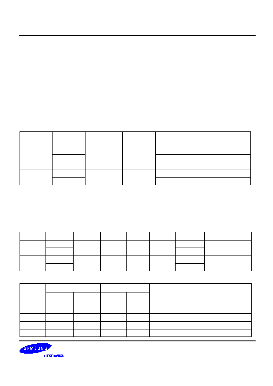
S6B33A2 PRELIMINARY VER 1.3 128 RGB SEGMENT & 129 COMMON DRIVER FOR 4,096 COLOR STN LCD
11
Table 4. MPU Interface Pins
Name
I/O
Description
/RST
I
Reset input pin.
When /RST is "L", initialization is executed.
MPU interface select pin
PS
MPU[1]
MPU[0]
Description
H
L
L
8080-series 8bit interface
H
L
H
8080-series 16bit interface
H
H
L
6800-series 8bit interface
H
H
H
6800-series 16bit interface
L
L
X
3 pin SPI(Write only)
PS
MPU[1:0]
I
L
H
X
4 pin SPI(Write only)
/CS1
CS2
I
Chip select input pins
Data / instruction I/O is enabled only when /CS1 is "L" and CS2 is "H". When chip
select is non-active, DB0 to DB15 may be high impedance.
D/I
I
Data / Instruction select input pin
-
D/I = "H": DB0 to DB15 are display data
-
D/I = "L": DB0 to DB7 are instruction data
Read / Write execution control pin
PS
MPU
MPU Type
/WR
Description
H
H
6800-series
R/W
Read/Write control input pin
-
R/W = "H": read
-
R/W = "L": write
/WR
(R/W)
I
H
L
8080-series
/WR
Write enable clock input pin
The data on DB0 to DB15 are latched at the
rising edge of the /WR signal.
Read / Write execution control pin
MPU[1]
MPU type
/RD
Description
H
6800-
series
E
Read / Write control input pin
-
R/W = "H": When E is "H", DB0 to DB15
are in an output status.
-
R/W = "L": The data on DB0 to DB15 are
latched at the falling edge of the E signal.
/RD
(E)
I
L
8080-
series
/RD
Read enable clock input pin
When /RD is "L", DB0 to DB15 are in an output
status.
DB[15:8]
DB[7]/SDI
DB[6]/SCL
DB[5:0]
I/O
-DB[15:0]: 16-bit bi-directional data bus.
-SDI: Serial data input pin. The data is latched at the rising edge of SCL.
-SCL: Serial clock input pin.
CDIR
I
Common direction select pin.
S6B33A2 PRELIMINARY VER 1.3 128 RGB SEGMENT & 129 COMMON DRIVER FOR 4,096 COLOR STN LCD
12
Table 5. Oscillator and Power Regulator Pins
Name
I/O
Description
OSC1
OSC2
OSC3
OSC4
O
CR oscillator output pin
When the internal CR oscillator is used, connect to OSC1, OSC3 through a resistor.
OSC1 � OSC2: Using in normal display mode, partial display mode 0
OSC3 � OSC4: Using in partial display mode 1
When an external oscillator is used, OSC1 pin is connected to VDD or VSS.
OSC5
I
External clock input pin
When an external input is used, it is input to this pin. But the internal oscillator is used,
this pin is connected to VDD or VSS.
REG_OUT
O
Internal voltage regulator output pin
The regulator output port from this pin is used as a power supplier for an internal digital
block via VDD1 pins.
Table 6. Timing signal Pins for monitoring
Name
I/O
Description
CL
O
Shift clock output pin
PM
O
Field delimiter output pin
FR
O
Liquid crystal alternating current output pin
Table 7. LCD driver output pins
Name
I/O
Description
SEGA0 to 127
O
LCD driving segment output (Red or Blue)
SEGB0 to 127
O
LCD driving segment output (Green)
SEGC0 to127
O
LCD driving segment output (Blue or Red)
COM0 to 128
O
LCD common outputs
Table 8. Test pins
Name
I/O
Description
TEST [4:0]
I
Don't use these pins. IC maker's test pins. Fix "High" in normal mode.
S6B33A2 PRELIMINARY VER 1.3 128 RGB SEGMENT & 129 COMMON DRIVER FOR 4,096 COLOR STN LCD
13
FUNCTIONAL DESCRIPTION
MPU INTERFACE
Chip Select Input
There are /CS1 and CS2 pins for chip selection. The S6B33A2 can interface with an MPU only when /CS1 is "L" and
CS2 is "H". When these pins are set to any other combination, D/I, /RD, and /WR inputs are disabled and DB0 to
DB15 are to be high impedance. And, in case of serial interface, the internal shift register and the counter are reset.
Parallel/Serial Interface
The S6B33A2 has four types of interface with an MPU, which are two serial and two parallel interfaces. This parallel
or serial interface is determined by PS pin as shown in Table9
.
Table 9. Parallel / Serial Interface Mode.
PS
MPU[1]
/CS1
CS2
MPU bus type
L
8080-Series MPU
H
H
/CS1
CS2
6800-Series MPU
L
3�Pin SPI
L
H
/CS1
CS2
4-Pin SPI
Parallel Interface (PS="H")
The 8-bit/16-bit bi-directional data bus is used in parallel interface. The type of MPU is selected by MPU[1] and the
mode of data-bus is controlled by MPU[0] as shown in below. In accessing internal registers (D/I = "L"), only DB[7:0]
are valid.
Table 10. Microprocessor Selection for Parallel Int erface
MPU[1]
MPU[0]
/CS1
CS2
/RD
/WR
Data Bus
MPU bus type
L
DB[7:0]
L
H
/CS1
CS2
E
R/W
DB[15:0]
8080-series MPU
L
DB[7:0]
H
H
/CS1
CS2
/RD
/WR
DB[15:0]
6800-series MPU
Table 11. Parallel Data Transfer
6800-series
8080-series
D/I
/RD
/WR
/RD
/WR
Description
H
H
H
L
H
Read display data
H
H
L
H
L
Write display data
L
H
H
L
H
Read out internal status register
L
H
L
H
L
Write instruction data
S6B33A2 PRELIMINARY VER 1.3 128 RGB SEGMENT & 129 COMMON DRIVER FOR 4,096 COLOR STN LCD
14
/CS1
CS2
D/I
R/W
E
DB
Command Write
Data Write
Status Read
Data Read
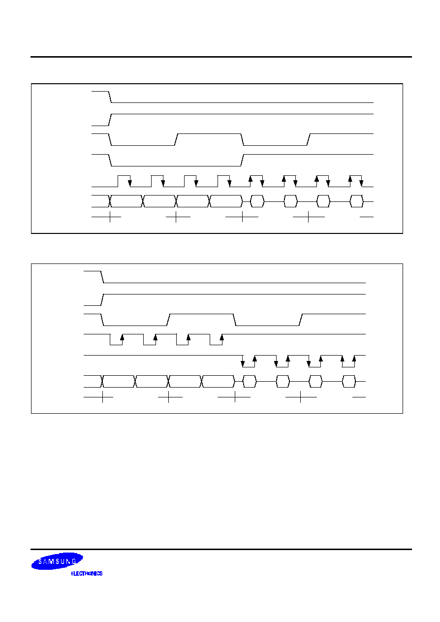
Figure 8. 6800-Series MPU Interface protocol (MPU[1]="H")
/CS1
CS2
D/I
/WR
/RD
DB
Command Write
Data Write
Status Read
Data Read
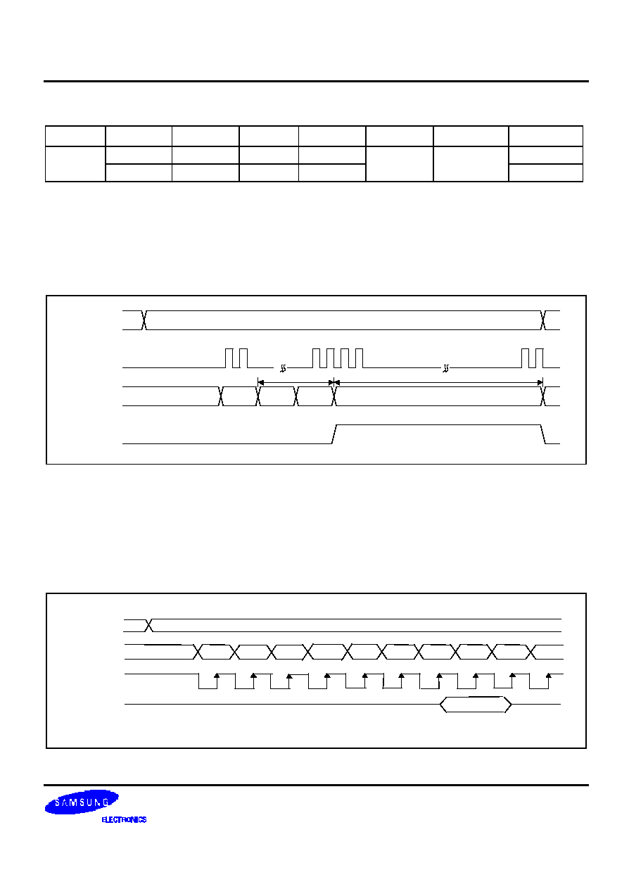
Figure 9. 8080-Series MPU Interface Protocol (MPU[1]="L")
Serial Interface(PS="L")
Communication with the microprocessor occurs via a clock-synchronized serial peripheral interface when PS is low.
When using the serial interface, read operations are not allowed. When the chip select inputs are valid (/CS1 = "L" &
CS2 = "H"), the serial data is sent most significant bit first on the rising edge of a serial clock going into DB6 and
processed as 8 bit parallel data on the eighth clock. Since the clock signal is easy to be affected by the external
noise caused by the line length, the operation check on the actual machine is recommended. And Invalid, the
internal shift register and the counter are reset.
The serial interface type is selected by setting PS as shown in Table12.
S6B33A2 PRELIMINARY VER 1.3 128 RGB SEGMENT & 129 COMMON DRIVER FOR 4,096 COLOR STN LCD
15
Table 12. Microprocessor Selection for Serial Interface
PS
MPU[1]
/CS1
CS2
D/I
Serial Data
Serial Clock
SPI Mode
L
/CS1
CS2
D/I
3-Pin
L
H
/CS1
CS2
S/W
DB[7]
DB[6]
4-Pin
3-Pin SPI Interface (PS = "L" & MPU[1] = "L")
In 3-Pin SPI Interface mode, the pre-defined instruction called Display Data Length is used to indicate whether serial
data input is display or instruction data instead of D/I pin. The data is handled as instruction data until the Display
Data Length instruction is issued. This Display Data Length instruction consists of three bytes instruction. The first
byte instruction enables the next two instructions to be valid, and the data of the next two bytes indicate that a
specified number of display data bytes(1 to 65536) are to be transmitted. For details, refer the Figure 8.
Chip Select
SCL(DB6)
SDI(DB7)
Internal D/I
/CS1 = L, CS2 = H
1
24
00000000
00001001
2
23
1 2
80
79
9 bytes display data
DDL_SET
DDL_L = 9
User's display data (Initial 50688 bytes)
9 bytes
2 bytes
11111100
DDL_H = 0
(Initial : 80h,00h)
= 32,768
Figure 10. 3-Pin SPI Timing (D/I is not used)
4-Pin Serial Interface (PS="L" & MPU[1]="H")
In 4-pin SPI interface mode, D/I pin is used for indicating whether serial data input is display or instruction data.
Data is display data when D/I is high and instruction data when D/I is low.
Serial data can be read on the rising edge of serial clock going into DB6 and processed as 8-bit parallel data on the
eighth serial clock.
l
Chip Select
SID(DB7)
SCL(DB6)
D/I
DB0
DB1
DB4
DB6
DB7
DB3
/CS1=L, CS2=H
DB5
DB2
DB7
DB7
Figure 11. 4-Pin Serial Interface Timing
S6B33A2 PRELIMINARY VER 1.3 128 RGB SEGMENT & 129 COMMON DRIVER FOR 4,096 COLOR STN LCD
16
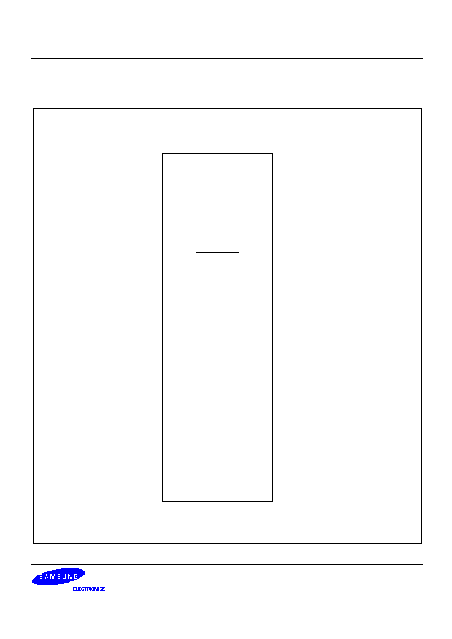
DISPLAY DATA RAM
The on-chip display data RAM of S6B33A2 is a static RAM that is stored the data for the display. It is a 1,536x 128
structure. It is controlled by 2 addresses, X and Y. And, RAM area selection and automatic address count up
functions are accomplished by the internal instructions.
DDRAM Address Area Selection
A part of DDRAM address area of S6B33A2 can be accessed by X and Y address area settings. After setting RAM
area, the addresses become the start address.
X-address
area
Y-address
area
Figure 12. DDRAM Address Area
Table 13. X address Control
DB7
DB6
DB5
DB4
DB3
DB2
DB1
DB0
Code
0
0
1
0
0
0
1
0
P1
0
X start address set(Initial Status = 00H)
P2
X end address set(Initial Status = 7FH)
Table 14. Y address Control
DB7
DB6
DB5
DB4
DB3
DB2
DB1
DB0
Code
0
0
1
1
0
0
1
1
P1
0
Y start address set (Initial status = 00H)
P2
0
Y end address set (Initial status =7FH)
S6B33A2 PRELIMINARY VER 1.3 128 RGB SEGMENT & 129 COMMON DRIVER FOR 4,096 COLOR STN LCD
17
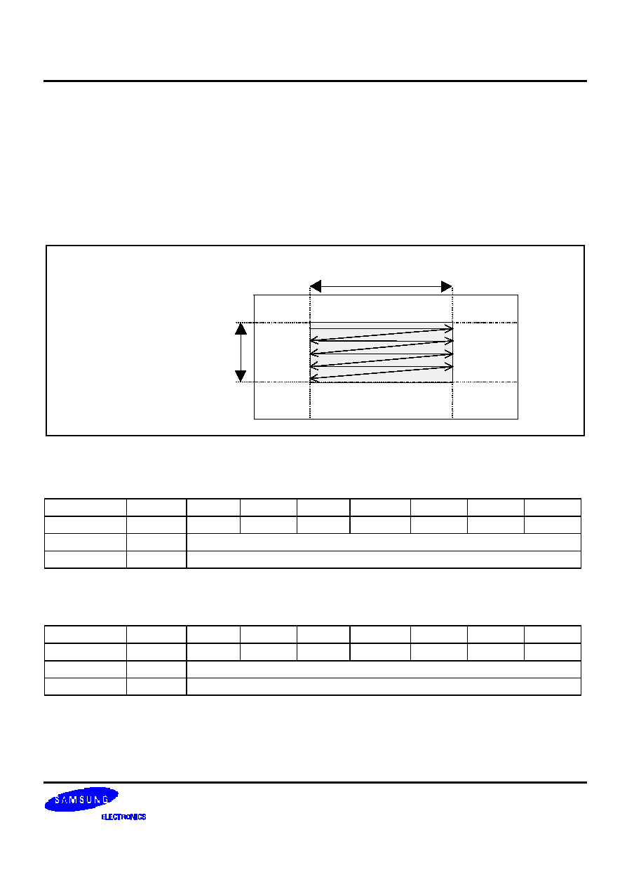
RAM Addressing Count up
By selecting the X address and Y address area by the internal instructions, the address counts up from its start
address to end address after data access operation. When one address is equal to the end address, it returns to the
start address. At this time, the other address is increased by 1.
Y address count mode (Y address = 00h to7Fh, X address = 00h to 7Fh, 16 bit access mode)
Y-address
0
1
2
3
4
5
6
7
8
00
01
02
03
04
05
07
08
06
X-address
00h
01h
02h
03h
7Fh
128
256
16256
127
7Fh
255
383
511
16383
384
Figure 13. Y address count mode
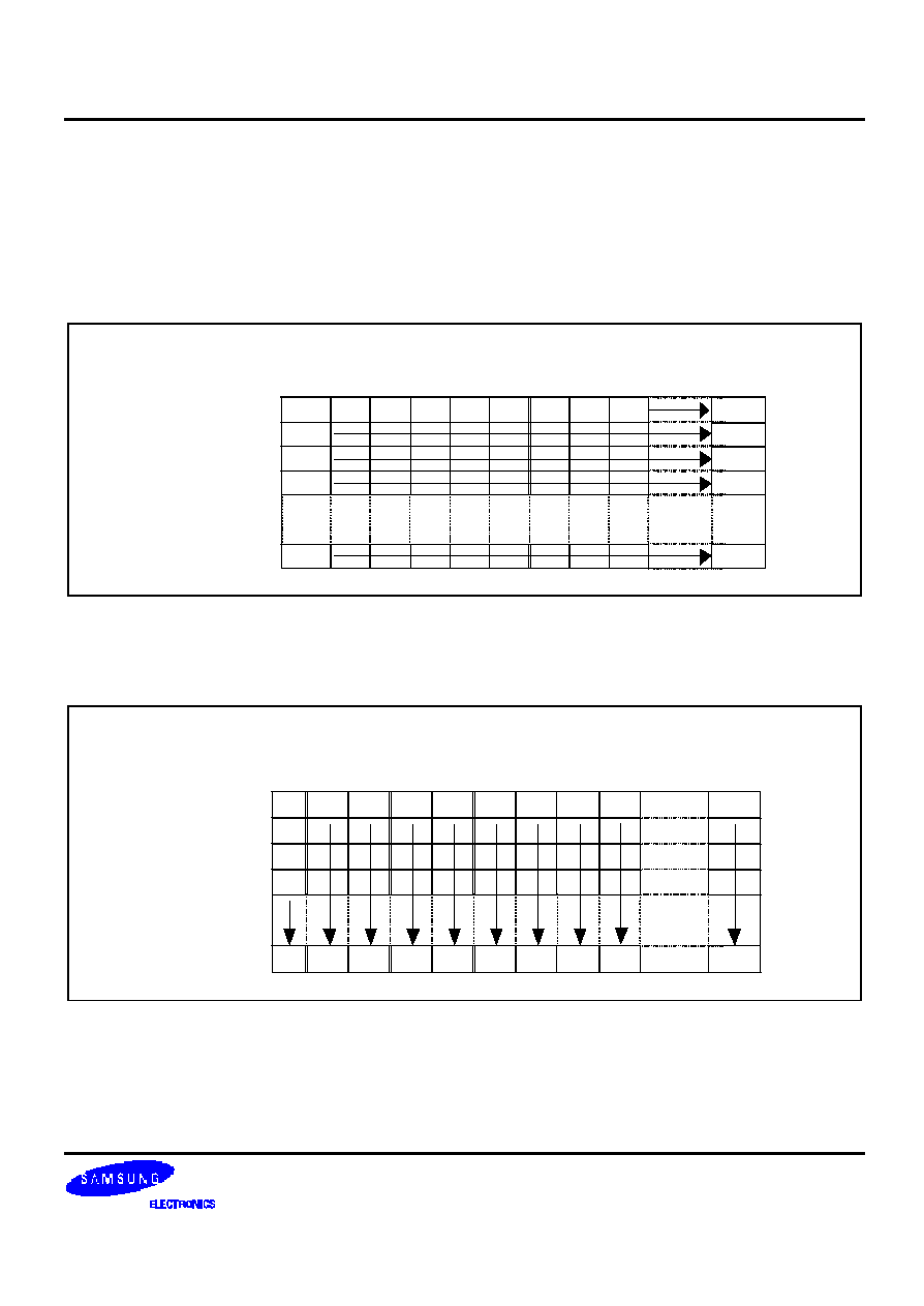
X address count mode (Y address =00h to 7Fh, X address = 00h to 7Fh, 16 bit access mode)
Y-address
0
128 256 384 512 640 768 896 1024
16256
00h 01h 02h 03h 04h 05h
7Fh
07h 08h
06h
X-address
00h
01h
02h
03h
7Fh
1
2
3
127 255 383 511 639 767 895 1023 1151
16383
Figure 14. X address count mode
S6B33A2 PRELIMINARY VER 1.3 128 RGB SEGMENT & 129 COMMON DRIVER FOR 4,096 COLOR STN LCD
18
XA
Address
YA Address
00H
01H
02H
03H
04H
05H
06H
07H
08H
09H
0AH
0BH
0CH
0DH
0EH
0FH
00H 01H 02H 03H 04H 05H 06H 07H
79H 7AH 7BH 7CH 7DH 7EH 7FH
08H - - - - - - -
- - - - - - -
- - - - - - -
- - - - - - -
- - - - - - -
- - - - - - -
- - - - - - -
- - - - - - -
- - - - - - -
- - - - - - -
- - - - - - -
- - - - - - -
- - - - - - -
- - - - - - -
- - - - - - -
- - - - - - -
- - - - - - -
70H
71H
72H
73H
74H
75H
76H
77H
78H
79H
7AH
7BH
7CH
7DH
7EH
7FH
- - - - - - -
- - - - - - -
- - - - - - -
- - - - - - -
- - - - - - -
- - - - - - -
- - - - - - -
- - - - - - -
- - - - - - -
- - - - - - -
- - - - - - -
- - - - - - -
- - - - - - -
- - - - - - -
- - - - - - -
- - - - - - -
- - - - -
- - - - -
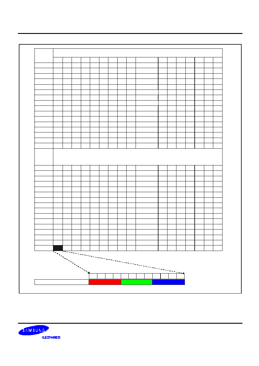
Red
Green
Blue
4K color
D7 D6 D5 D4 D3 D2 D1 D0
D11 D10 D9 D8
Figure 15. Display Data RAM Map

S6B33A2 PRELIMINARY VER 1.3 128 RGB SEGMENT & 129 COMMON DRIVER FOR 4,096 COLOR STN LCD
19
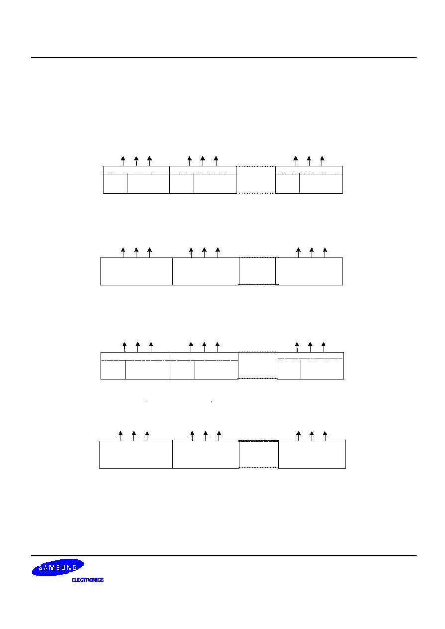
Partial Display Mode
The S6B33A2 realizes the partial display function with low duty driving for saving power consumption and showing
the various display duties. It is set as display start/end line number.
Area Scroll Function
The S6B33A2 realizes the specific area scroll function. (1/128 duty case).
0
15
115
127
Fixed area
Scroll area
Display area
LCD Panel
Fixed 15 lines
100 Lines
14
Fixed 18 lines
0
115
127
14
Example of Scrolling down
Example of Scrolling up
15
Figure 16. Area scroll examples (duty = 1/128, center scroll mode)
S6B33A2 PRELIMINARY VER 1.3 128 RGB SEGMENT & 129 COMMON DRIVER FOR 4,096 COLOR STN LCD
20
Y = 126
Y = 0
Y = 127
SEGA0
SEGB0
SEGC0
SEGA1
SEGB1
SEGC1
SEGA127
SEGB127
SEGC127
(D11~D0)
(D11~D0)
(D11~D0)
Display Direction
SDIR
The direction of segment display is selected by SDIR which is a bit in internal register.
Figure 17. 8-bit data bus mode when SDIR = "0"
Figure 18. 16-bit data bus mode when SDIR = "0"
Figure 19. 8-bit data bus mode when SDIR = "1"
Figure 20. 16-bit data bus mode when SDIR = "1"
x = 0
Y = 1
Y = 127
Y = 0
SEGA0
SEGB0
SEGC0
SEGA1
SEGB1
SEGC1
SEGA127
SEGB127
9
SEGC127
(D7~D0)
(D3~D0)
(D3~D0)
(D7~D0)
(D7~D0)
(D3~D0)
1st
2nd
Y = 1
Y = 127
Y = 0
SEGA0
SEGB0
SEGC0
SEGA1
SEGB1
SEGC1
SEGA127
SEGB127
SEGC127
(D11~D0)
(D11~D0)
(D11~D0)
x = 0
Y = 126
Y = 0
Y = 127
SEGA0
SEGB0
SEGC0
SEGA1
SEGB1
SEGC1
SEGA127
SEGB127
SEGC127
x = 0
x = 0
1st
2nd
(D3~D0)
(D7~D0)
(D3~D0)
(D7~D0)
(D3~D0)
(D7~D0)
1st
2nd
1st
2nd
1st
2nd
1st
2nd
S6B33A2 PRELIMINARY VER 1.3 128 RGB SEGMENT & 129 COMMON DRIVER FOR 4,096 COLOR STN LCD
21
CDIR
The direction of common scanning is selected by CDIR pin.
COM 0
Line number 0
Display Area
128Display Lines
<CDIR=0>
COM 128
Line number 127
COM 0
Display Area
<CDIR=1>
COM 128
Line number 0
COM 127
COM 1
Line number 127
Driver
SEG128RGB
COM128
COM 62
COM 0
COM63
S6B33A2 PRELIMINARY VER 1.3 128 RGB SEGMENT & 129 COMMON DRIVER FOR 4,096 COLOR STN LCD
22
SEGAi
SEGBi
SEGCi
RED
GREEN
BLUE
Color
SWP = 0
D11 ~ D8
D7 ~ D4
D3 ~ D0
Assigned Bit
BLUE
GREEN
RED
Color
SWP = 1
D3~ D0
D7 ~ D4
D11 ~ D8
Assigned Bit
Figure 21. The relationship between SEG outputs and RGB color
SWP=1
* i = 0 to 127
Gray Scale control
R3
R2
R1
R0
G3
G2
G1
G0
B3
B2
B1
B0
RAM
DATA
D0
D1
D2
D3
D4
D5
D6
D7
D8
D9
D10 D11
MPU I/F
DATA[11:0]
SEGAi
SEGBi
SEGCi
Gray Scale control
Gray Scale control
SWP=0
* i = 0 to 127
SEGAi
SEGBi
SEGCi
D0
D1
D2
D3
D4
D5
D6
D7
D8
D9
D10
D11
R3
R2
R1
R0
G3
G2
G1
G0
B3
B2
B1
B0
RAM
DATA
MPU I/F
Gray Scale control
Gray Scale control
Gray Scale control
DATA[11:0]
S6B33A2 PRELIMINARY VER 1.3 128 RGB SEGMENT & 129 COMMON DRIVER FOR 4,096 COLOR STN LCD
23
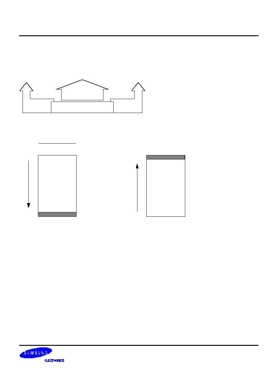
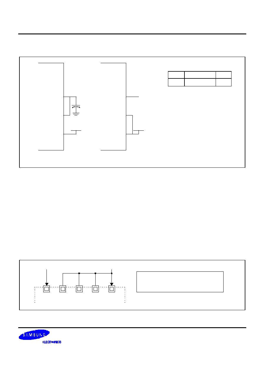
On-Chip Regulator Configuration
REG_OUT
VDD1
VDD
C1
VDD
REG_OUT
VDD1
VDD
Floating
VDD
Value of external Capacitance
Item
Value
Unit
C1
1.0 to 4.7
�
F
VDD: 2.4 ~ 3.3V
VDD: 1.7 ~ 3.3V
Figure 22. Regulator Application
Oscillator Circuit
When internal oscillator is used(EXT=0), the selection of oscillator resistor is determined by display mode.
-
Normal display mode/ Partial display mode 0 : resistor1 between OSC1 and OSC2
-
Partial display mode 1 : resistor2 between OSC3 and OSC4
-
When external clock is used (EXT=1), clock frequency should be adjusted to display mode which is selected
.
Example of external oscillator application
OSC4
OSC2
OSC3
OSC5
Ext.
OSC1
VSS
Figure 23. External oscillator application
When external clock mode (EXT = "H")
is used, it is not possible to use the
partial mode1
S6B33A2 PRELIMINARY VER 1.3 128 RGB SEGMENT & 129 COMMON DRIVER FOR 4,096 COLOR STN LCD
24
Example of internal oscillator application
OSC4
OSC2
OSC3
R1
OSC5
VSS/VDD
OSC1
OSC4
OSC2
OSC3
OSC5
OSC1
VSS/VDD
R2
R1
When partial display mode 1 is not used. When partial display mode 1 is used.
Figure 24. Internal oscillator application
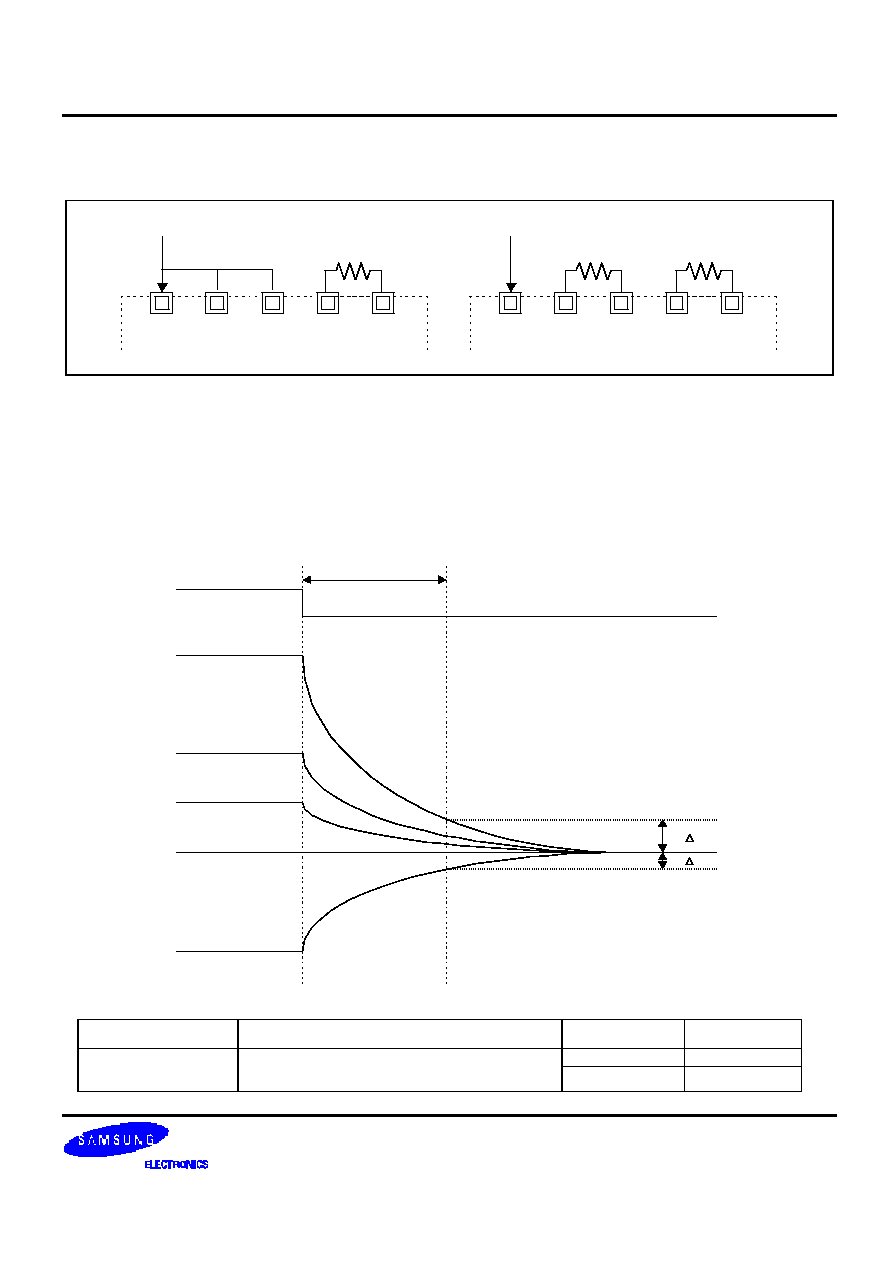
Discharge Circuit
Driving voltage level discharge time at stand by ON.
The relation between voltage level and discharge time from when "Stand By ON" command is inputted.
LEVEL
CONDITION
T[ms]
V+,
V-[mV]
100
< 50
+VR,V1,VM,-VR
+VR=10.5V, V1=3.0V, VM=1.5V, -VR=-7.5V
at T=0
300
< 20
Internal STB signal
VM
VSS
-VR
V1
+VR
T[ms]
V+[mV]
V-[mV]
S6B33A2 PRELIMINARY VER 1.3 128 RGB SEGMENT & 129 COMMON DRIVER FOR 4,096 COLOR STN LCD
25
INSTRUCTION DESCRIPTION
Table 15. Instruction Table
Instruction Name
D/I /WR /RD DB15
~ DB8 DB7
DB6
DB5 DB4
DB3
DB2 DB1 DB0 Hex. Parameter
Non Operation
0
0
1
*
0
0
0
0
0
0
0
0
00
-
Oscillation Mode Set
0
0
1
*
0
0
0
0
0
0
1
0
02
1Byte
Driver Output Mode Set
0
0
1
*
0
0
0
1
0
0
0
0
10
1Byte
DC-DC Select
0
0
1
*
0
0
1
0
0
0
0
0
20
1Byte
DCDC Clock Division Set
0
0
1
*
0
0
1
0
0
1
0
0
24
1Byte
DCDC and AMP ON/OFF set
0
0
1
*
0
0
1
0
0
1
1
0
26
1Byte
Temperature Compensation Set
0
0
1
*
0
0
1
0
1
0
0
0
28
1Byte
Contrast Control(1)
0
0
1
*
0
0
1
0
1
0
1
0
2A
1Byte
Contrast Control(2)
0
0
1
*
0
0
1
0
1
0
1
1
2B
1Byte
Standby Mode OFF
0
0
1
*
0
0
1
0
1
1
0
0
2C
-
Standby Mode ON
0
0
1
*
0
0
1
0
1
1
0
1
2D
-
Addressing Mode Set
0
0
1
*
0
0
1
1
0
0
0
0
30
1Byte
ROW Vector Mode Set
0
0
1
*
0
0
1
1
0
0
1
0
32
1Byte
N-line Inversion Set
0
0
1
*
0
0
1
1
0
1
0
0
34
1Byte
Red palette Set
0
0
1
*
0
0
1
1
1
0
0
0
38
8Byte
Green palette Set
0
0
1
*
0
0
1
1
1
0
1
0
3A
8Byte
Blue palette Set
0
0
1
*
0
0
1
1
1
1
0
0
3C
4Byte
Entry Mode Set
0
0
1
*
0
1
0
0
0
0
0
0
40
1Byte
X-address Area Set
0
0
1
*
0
1
0
0
0
0
1
0
42
2Byte
Y-address Area Set
0
0
1
*
0
1
0
0
0
0
1
1
43
2Byte
Display OFF
0
0
1
*
0
1
0
1
0
0
0
0
50
-
Display ON
0
0
1
*
0
1
0
1
0
0
0
1
51
-
Specified Display Pattern Set
0
0
1
*
0
1
0
1
0
0
1
1
53
1Byte
Partial Display Mode Set
0
0
1
*
0
1
0
1
0
1
0
1
55
1Byte
Partial Display Start Line Set
0
0
1
*
0
1
0
1
0
1
1
0
56
1Byte
Partial Display End Line Set
0
0
1
*
0
1
0
1
0
1
1
1
57
1Byte
Area Scroll Mode Set
0
0
1
*
0
1
0
1
1
0
0
1
59
4Byte
Scroll Start Line Set
0
0
1
*
0
1
0
1
1
0
1
0
5A
1Byte
Display Format Select(Mode0)
0
0
1
*
0
1
1
0
1
1
1
0
60
-
Display Format Select(Mode1)
0
0
1
*
0
1
1
0
1
1
1
1
61
-
Set Display Data Length
X
X
X
*
1
1
1
1
1
1
0
0
FC
2Byte
Display Data Write
1
0
1
Display Data Write
-
-
Display Data Read
1
1
0
Display Data Read
-
-
Status Read
0
1
0
Status Data Read
-
-
Test Mode0
0
0
1
*
1
1
1
1
1
1
1
1
FF
-
Test Mode1
0
0
1
*
1
1
1
1
1
1
1
0
FE
-
*: Don't care
Parameter: The number of parameter bytes that follows instruction data.
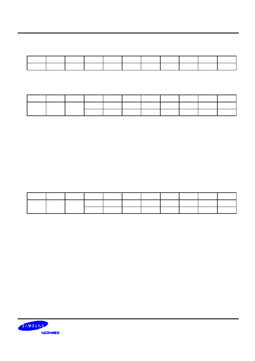
S6B33A2 PRELIMINARY VER 1.3 128 RGB SEGMENT & 129 COMMON DRIVER FOR 4,096 COLOR STN LCD
26
Non Operation (00H)
This instruction is Non operation.
D/I
/WR
/RD
DB7
DB6
DB5
DB4
DB3
DB2
DB1
DB0
0
0
1
0
0
0
0
0
0
0
0
Oscillation Mode Set (02H)
Setting internal function mode.
D/I
/WR
/RD
DB7
DB6
DB5
DB4
DB3
DB2
DB1
DB0
0
0
0
0
0
0
1
0
0
0
1
0
0
0
0
0
DIV2
EXT
OSC
DIV2: Display clock selecting
DIV2 = 0: Display clock = OSC clock (Initial status)
DIV2= 1: Display clock = OSC/2 clock
EXT: External clock selecting
EXT = 0: Internal clock mode (Initial status)
EXT = 1: External clock mode
OSC: Internal oscillator ON/OFF
OSC = 0: Internal oscillator OFF(Initial status)
OSC = 1: Internal oscillator ON
Driver Output Mode Set(10H)
This instruction sets the display direction.
D/I
/WR
/RD
DB7
DB6
DB5
DB4
DB3
DB2
DB1
DB0
0
0
0
1
0
0
0
0
0
0
1
0
0
0
0
0
0
SDIR
SWP
SDIR: Segment direction
This bit is for controlling the direction of segment driver.
SDIR = 0 (Initial status)
SWP: Swap segment output SEGAi and SEGCi
This bit is for swapping the output of segment driver.
SWP = 0 (Initial status)
S6B33A2 PRELIMINARY VER 1.3 128 RGB SEGMENT & 129 COMMON DRIVER FOR 4,096 COLOR STN LCD
27
DC-DC Select (20H)
Selects DC-DC step-up of the common driver in normal and partial mode
D/I
/WR
/RD
DB7
DB6
DB5
DB4
DB3
DB2
DB1
DB0
0
0
1
0
0
0
0
0
0
0
1
0
0
0
0
0
0
DC(2)
DC(1)
DC(1) : 1'st DC-DC booster boosting step select for V1 generation in normal mode and partial mode 0.
DC(2) : 1'st DC-DC booster boosting step select for V1 generation in partial mode 1.
DC(2) : In partial mode 1
DC(1) : In normal mode, partial mode 0
DB1
DC-DC step up
DB0
DC-DC step up
0
X1.0
0
X1.0
1
X1.5
1
X1.5
S6B33A2 PRELIMINARY VER 1.3 128 RGB SEGMENT & 129 COMMON DRIVER FOR 4,096 COLOR STN LCD
28
DC-DC Select and power supply for V1 Op-Amp.
Even if VIN45 is connected to VOUT45 or VIN1, a setup by software must be able to be performed.
Power supply for V1 Op.Amp. is decided by Hardware setting and Software setting.
The example of usage is shown below.
Hardware setting : VIN45 connected to (1) VIN1 (when 1'st boosting is not used)
(2) VOUT45 (when 1'st boosting is used)
Software setting : DC-DC Select(20H) - DC(1), DC(2)
Set value "00" Power supply for V1 Op.Amp. uses VIN1 directly.
Set value "01" or "10" Power supply for V1 Op.Amp. uses VOUT45.
1st
Booster
Circuit
Reference
voltage
generator
&
Temperature
Compensation
Control Circuit
VIN1
V1
+
C11-
C11+
C12-
C12+
VOUT45
VIN45
-
R1
EV_256
R1
Software Setting
Hardware Setting
V1 generation circuit
Figure28. Example : Hardware Setting
Software Setting
: VIN45 connected to VOUT45
: Power supply for V1 Op.Amp. uses VIN1 ( not VOUT45).
VSS
S6B33A2 PRELIMINARY VER 1.3 128 RGB SEGMENT & 129 COMMON DRIVER FOR 4,096 COLOR STN LCD
29
DCDC Clock Division (24H)
This instruction sets the internal booster clock frequency.
D/I
/WR
/RD
DB7
DB6
DB5
DB4
DB3
DB2
DB1
DB0
0
0
1
0
0
1
0
0
0
0
1
0
0
DIV(2)
0
0
DIV(1)
DIV(1) : DC-DC Charge Pump Division Ratio in Normal Mode Display and Partial Display Mode0
- DIV(1) = 10 (Initial status)
DIV(2) : Division Ratio in Partial Display Mode1
- DIV(2) = 10 (Initial status)
DB5
DB4 DIV(2)
DB1
DB0
DIV(1)
0
0
fPCK = fOSC/2x
0
0
fPCK = fOSC/2x
0
1
fPCK = fOSC/4x
0
1
fPCK = fOSC/4x
1
0
fPCK = fOSC/6x
1
0
fPCK = fOSC/6x
1
1
fPCK = fOSC/8x
1
1
fPCK = fOSC/8x
Note: fOSC = ( ROUNDUP (Duty/3) + dummy) x 4 x 4 x frame frequency
DC/DC and AMP ON/OFF Set (26H)
This instruction set up the DC/DC and Op-amp in common start up setting.
D/I
/WR
/RD
DB7
DB6
DB5
DB4
DB3
DB2
DB1
DB0
0
0
1
0
0
1
1
0
0
0
1
0
0
0
0
AMP
DCDC3 DCDC2 DCDC1
AMP : Built-in OP-AMP ON/OFF.
- AMP=0 :OP-AMP OFF(Initial status)
- AMP=1 :OP-AMP ON
DCDC1: Built-in 1
st
Booster ON/OFF (Initial status)
- DCDC1= 0: 1
st
Booster OFF (Initial status)
- DCDC1= 1: 1
st
Booster ON
DCDC2: Built-in 1
st
Booster ON/OFF (Initial status)
- DCDC2= 0: 2
nd
Booster OFF (Initial status)
- DCDC2= 1: 2
nd
Booster ON
DCDC3: Built-in 1
st
Booster ON/OFF (Initial status)
- DCDC3= 0: 3
rd
Booster OFF (Initial status)
- DCDC3= 1: 3
rd
Booster ON
S6B33A2 PRELIMINARY VER 1.3 128 RGB SEGMENT & 129 COMMON DRIVER FOR 4,096 COLOR STN LCD
30
Temperature Compensation Set (28H)
This Instruction sets up the driving voltage slope for temperature compensation.
D/I
/WR
/RD
DB7
DB6
DB5
DB4
DB3
DB2
DB1
DB0
0
0
1
0
1
0
0
0
0
0
1
0
0
0
0
0
0
TCS
TCS: Temperature compensation slope set
-
TCS = 00 : 0.00%/degC
-
TCS = 01 : -0.05%/degC
-
TCS = 10 : -0.10%/degC
-
TCS = 11 : -0.15%degC
00: 0.00 %/degC
Driving
voltage
01: -0.05 %/degC
10: -0.10 %/degC
11: -0.15 %/degC
Temperature
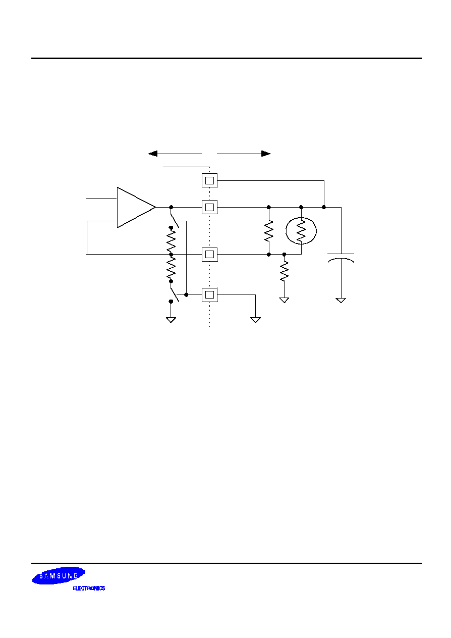
S6B33A2 PRELIMINARY VER 1.3 128 RGB SEGMENT & 129 COMMON DRIVER FOR 4,096 COLOR STN LCD
31
Temperature Compensation
If external temperature compensation is needed, circuit diagram is described as below.
To use temperature compensation, two resistors and one thermistor are needed.
External
Chip
Internal
V1-i
+
-
V1-o
V1-t
INTRS
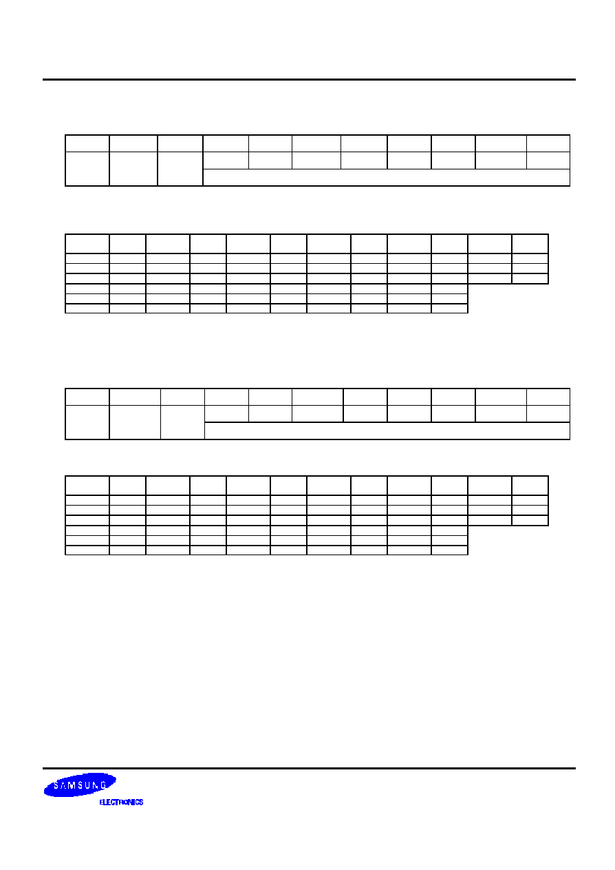
S6B33A2 PRELIMINARY VER 1.3 128 RGB SEGMENT & 129 COMMON DRIVER FOR 4,096 COLOR STN LCD
32
Contrast Control (1) (2AH)
This instruction updates the contrast control value in normal display mode and partial display mode 0.
D/I
/WR
/RD
DB7
DB6
DB5
DB4
DB3
DB2
DB1
DB0
0
0
1
0
1
0
1
0
0
0
1
Contrast control value (0 to 255)
The relation between V1 voltage (typ.) and Contrast(1) set value ( 3bit step case)
Contrast(1)
(HEX)
V1[V] Contrast(1)
(HEX)
V1[V] Contrast(1)
(HEX)
V1[V] Contrast(1)
(HEX)
V1[V] Contrast(1)
(HEX)
V1[V] Contrast(1)
(HEX)
V1[V]
00h
2.000
30h
2.244
60h
2.488
90h
2.731
C0h
2.975
F0h
3.219
08h
2.041
38h
2.284
68h
2.528
98h
2.772
C8h
3.016
F8h
3.259
10h
2.081
40h
2.325
70h
2.569
A0h
2.813
D0h
3.056
FFh
3.300
18h
2.122
48h
2.366
78h
2.609
A8h
2.853
D8h
3.097
20h
2.163
50h
2.406
80h
2.650
B0h
2.894
E0h
3.138
28h
2.203
58h
2.447
88h
2.691
B8h
2.934
E8h
3.178
Contrast Control (2) (2BH)
This instruction updates the contrast control value in partial display mode 1.
D/I
/WR
/RD
DB7
DB6
DB5
DB4
DB3
DB2
DB1
DB0
0
0
0
1
0
0
0
1
0
0
1
Contrast control value (0 to 255)
The relation between V1 voltage (typ.) and Contrast(2) set value ( 3bit step case)
Contrast(1)
(HEX)
V1[V] Contrast(1)
(HEX)
V1[V] Contrast(1)
(HEX)
V1[V] Contrast(1)
(HEX)
V1[V] Contrast(1)
(HEX)
V1[V] Contrast(1)
(HEX)
V1[V]
00h
2.000
30h
2.244
60h
2.488
90h
2.731
C0h
2.975
F0h
3.219
08h
2.041
38h
2.284
68h
2.528
98h
2.772
C8h
3.016
F8h
3.259
10h
2.081
40h
2.325
70h
2.569
A0h
2.813
D0h
3.056
FFh
3.300
18h
2.122
48h
2.366
78h
2.609
A8h
2.853
D8h
3.097
20h
2.163
50h
2.406
80h
2.650
B0h
2.894
E0h
3.138
28h
2.203
58h
2.447
88h
2.691
B8h
2.934
E8h
3.178

S6B33A2 PRELIMINARY VER 1.3 128 RGB SEGMENT & 129 COMMON DRIVER FOR 4,096 COLOR STN LCD
33
Standby Mode OFF (2CH)
This instruction releases the standby mode.
D/I
/WR
/RD
DB7
DB6
DB5
DB4
DB3
DB2
DB1
DB0
0
0
1
0
0
1
0
1
1
0
0
The internal statuses during standby off are as following:
-
All common and segment output: refer to following
-
Oscillator circuit: On (EXT = 0, OSC=1),OFF (others)
-
Displaying clocks (FR, PM, CL, CK): In operation
Function and Pin condition at standby OFF
Function/Pin
Condition
DC/DC
booster(1'st,2'nd,3'rd)
ON(Operate)
COM outputs
+VR /VM / VSS /�VR
SEG outputs
V1 /VSS
Standby Mode ON (2DH)
This instruction enters the standby mode to reduce the power consumption to the static power consumption
value (Initial status). The following instructions, standby off and display on, cause returning to the normal
operation status.
D/I
/WR
/RD
DB7
DB6
DB5
DB4
DB3
DB2
DB1
DB0
0
0
1
0
0
1
0
1
1
0
1
The internal statuses during standby on are as following:
-
All common and segment output: refer to following table
-
Oscillator circuit: OFF
-
Displaying clocks (FR, PM, CL, CK) are held.
Function and Pin condition at standby ON
Function/Pin
Condition
DC/DC
booster(1'st,2'nd,3'rd)
OFF
SEG and COM outputs
VSS
LCD driving power output condition at Standby ON.
Level
Condition
+VR
VSS
V1
VSS
VM
VSS
-VR
VSS
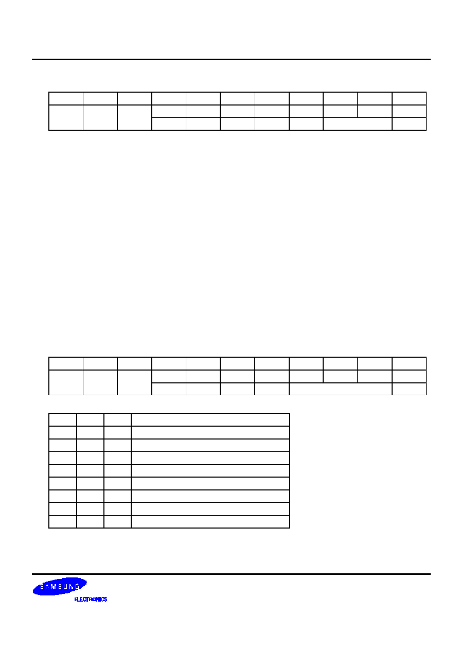
S6B33A2 PRELIMINARY VER 1.3 128 RGB SEGMENT & 129 COMMON DRIVER FOR 4,096 COLOR STN LCD
34
Addressing Mode Set (30H)
D/I
/WR
/RD
DB7
DB6
DB5
DB4
DB3
DB2
DB1
DB0
0
0
1
1
0
0
0
0
0
0
1
0
0
GSM
DSG
SGF
SGP
SGM
GSM: Gray Scale Mode
0 : 4,096 Color mode(Initial status)
1 : 256 Color mode
1. 8 bit mode : DB[7:0] :RRRGGGBB
2.16bit mode: DB[15:0] :RRRGGGBBRRRGGGBB
3. 3bits of R and G, 2bits of B are expanded to 4 bit internally by red, green and blue palette set
instruction
DSG : Duty Adjust Setting
0 : Dummy subgroup is one subgroup (Initial status)
1 : Dummy subgroup is none
SGF : SG Frame Inversion mode setting
0: SG Frame inversion OFF (Initial status)
1: SG Frame inversion ON
SGM : SG inversion mode setting
0: SG inversion OFF (Initial status)
1: SG inversion ON
SGP : SG Phase mode setting
00 : Same phase in all pixels
01 : Different phase by 1pixel-unit
10 : Different phase by 2pixel-unit
11 : Different phase by 4pixel-unit
Row Vector Mode Set (32H)
Setting ROW function.
D/I
WRB
RDB
DB7
DB6
DB5
DB4
DB3
DB2
DB1
DB0
0
0
1
1
0
0
1
0
0
0
1
0
0
0
0
INC
VEC
INC: Row Vector Increment Mode. This Parameter set up Row vector increment period
DB3
DB2
DB1
Row Vector Increment Period
0
0
0
Every subgroup
0
0
1
Every 2subgroup
0
1
0
Every 4subgroup
0
1
1
Every 8subgroup
1
0
0
Every 16subgroup
1
0
1
Every 16subgroup
1
1
0
Every 16subgroup
1
1
1
Every subframe
VEC: ROW Vector Sequence Mode
- 0: R1->R2->R3->R4 -> R1..... (initial status)
- 1: R1->R3->R2->R4 -> R1.....
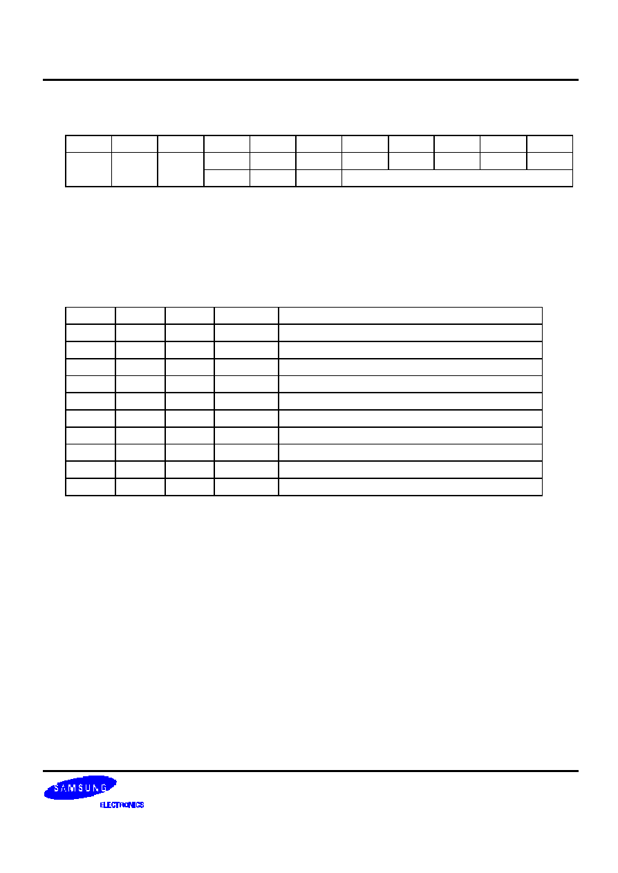
S6B33A2 PRELIMINARY VER 1.3 128 RGB SEGMENT & 129 COMMON DRIVER FOR 4,096 COLOR STN LCD
35
N-block inversion Set (34H)
This instruction set up N block inversion for AC driving.
D/I
/WR
/RD
DB7
DB6
DB5
DB4
DB3
DB2
DB1
DB0
0
0
0
1
1
1
1
1
0
0
1
FIM
FIP
0
N-block inversion
FIM: Forcing Inversion Mode
FIM = 0: Forcing Inversion OFF (Initial status)
FIM = 1: Forcing Inversion ON
FIP: Forcing Inversion Period
FIP = 0: Forcing Inversion Period is one frame
FIP = 1: Forcing Inversion Period is two frames
N-block Inversion : This parameter indicates the basic period of polarity inversion.
The whole period of polarity inversion is decided by FIM, FIP and this parameter.
DB7
DB6
DB5
DB4 � DB0
Polarity Inversion Period
X
x
x
0
every frame
0
x
x
1
every 1 block
:
:
:
:
:
0
x
x
31
every 31 blocks
1
0
x
1
every 1 block and every frame
:
:
:
:
:
1
0
x
31
every 31 blocks and every frame
1
1
x
1
every 1 block and every 2 frames
:
:
:
:
:
1
1
x
31
every 31 blcks and every 2 frames

S6B33A2 PRELIMINARY VER 1.3 128 RGB SEGMENT & 129 COMMON DRIVER FOR 4,096 COLOR STN LCD
36
Red palette Set (38H)
Setting red gray scale data for 256 Color mode.
D/I
/WR
/RD
DB7
DB6
DB5
DB4
DB3
DB2
DB1
DB0
0
0
1
1
1
0
0
0
0
0
0
0
RAM data "000" to GS data
0
0
0
0
RAM data "001" to GS data
0
0
0
0
RAM data "010" to GS data
0
0
0
0
RAM data "011" to GS data
0
0
0
0
RAM data "100" to GS data
0
0
0
0
RAM data "101" to GS data
0
0
0
0
RAM data "110" to GS data
0
0
1
0
0
0
0
RAM data "111" to GS data
Green palette Set (3AH)
Setting green gray scale data for 256 Color mode.
D/I
/WR
/RD
DB7
DB6
DB5
DB4
DB3
DB2
DB1
DB0
0
0
1
1
1
0
1
0
0
0
0
0
RAM data "000" to GS data
0
0
0
0
RAM data "001" to GS data
0
0
0
0
RAM data "010" to GS data
0
0
0
0
RAM data "011" to GS data
0
0
0
0
RAM data "100" to GS data
0
0
0
0
RAM data "101" to GS data
0
0
0
0
RAM data "110" to GS data
0
0
1
0
0
0
0
RAM data "111" to GS data
Blue palette Set (3CH)
Setting blue gray scale data for 256 Color mode.
D/I
/WR
/RD
DB7
DB6
DB5
DB4
DB3
DB2
DB1
DB0
0
0
1
1
1
1
0
0
0
0
0
0
RAM data "000" to GS data
0
0
0
0
RAM data "001" to GS data
0
0
0
0
RAM data "010" to GS data
0
0
1
0
0
0
0
RAM data "011" to GS data
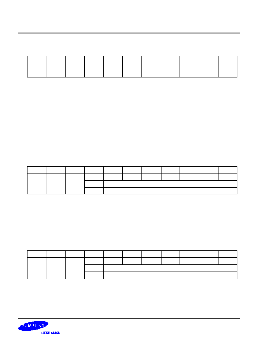
S6B33A2 PRELIMINARY VER 1.3 128 RGB SEGMENT & 129 COMMON DRIVER FOR 4,096 COLOR STN LCD
37
Entry Mode Set (40H)
Setting internal function mode.
D/I
/WR
/RD
DB7
DB6
DB5
DB4
DB3
DB2
DB1
DB0
0
1
0
0
0
0
0
0
0
0
1
0
0
0
0
0
HL
X/Y
RMW
HL: Exchange higher and lower byte only for "Display Data Write/Read" in 256 color & 16-bit data bus .
HL = 0 : Exchange status(initial status)
HL = 1 : Not exchange status
X/Y: Memory address counter mode setting
X/Y = 0: Y address counter mode (Initial status)
X/Y = 1: X address counter mode (Don't use in 256 color & 16bit data bus mode)
RMW: Read modify write mode ON/OFF select
RMW = 0: Read modify write OFF (Initial status)
RMW = 1: Read modify write ON. When this mode is on, X(Y) address of on-chip display RAM is increment
not in reading display data but in writing display data.
X Address Area Set (42H)
This instruction and parameter set up the X address areas of the on-chip display data RAM.
D/I
/WR
/RD
DB7
DB6
DB5
DB4
DB3
DB2
DB1
DB0
0
1
0
0
0
0
1
0
0
X start address set (Initial Status = 00H)
0
0
1
0
X end address set (Initial Status = 7FH)
The current X address of the on-chip display data RAM is the X start address by setting this instruction. In X
address count mode (X/Y = "H"), the X address is increased from X start address to X end address. When X
address is equal to the X end address, the Y address is increased by 1 and the X address returns to X start
address. The X start and X end addresses must be set as a pair and X start address must be less than X end
address.
Address Area Set (43H)
This instruction and parameter set up the Y address areas of the on-chip display data RAM
.
D/I
/WR
/RD
DB7
DB6
DB5
DB4
DB3
DB2
DB1
DB0
0
1
0
0
0
0
1
1
0
Y start address set (Initial Status = 00H)
0
0
1
0
Y end address set (Initial Status = 7FH)
The current Y address of the on-chip display data RAM is the Y start address by setting this instruction. In
Y address count mode (X/Y = "L"), the Y address is increased from Y start address to Y end address. When
Y address is equal to the Y end address, the X address is increased by 1 and the Y address returns to Y start
address. The Y start and Y end address must be set as a pair and Y start address must be less than Y end
address.
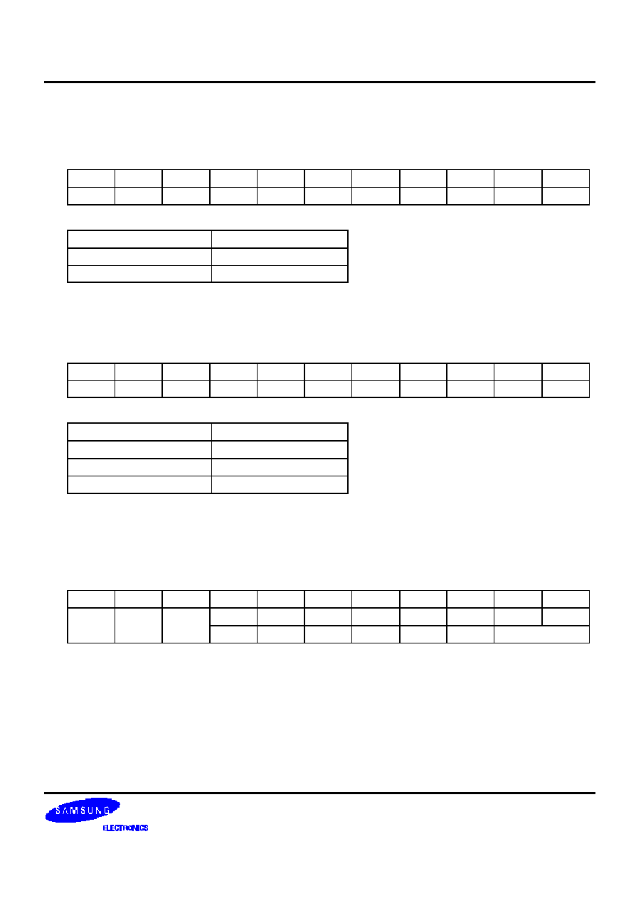
S6B33A2 PRELIMINARY VER 1.3 128 RGB SEGMENT & 129 COMMON DRIVER FOR 4,096 COLOR STN LCD
38
Display OFF (50H)
Turn the display OFF(Initial status).
When display is off, all segment and common output are VSS level.
D/I
/WR
/RD
DB7
DB6
DB5
DB4
DB3
DB2
DB1
DB0
0
0
1
0
1
0
1
0
0
0
0
Function and Pin condition at Display OFF
Function/Pin
Condition
DC/DC booster(1
st
,2
nd
,3
rd
)
ON(Operate)
SEG and COM outputs
VSS
Display ON (51H)
Turns the display ON.
In case of being standby mode, this instruction does not work. This instruction is executed after standby mode
off.
D/I
/WR
/RD
DB7
DB6
DB5
DB4
DB3
DB2
DB1
DB0
0
0
1
0
1
0
1
0
0
0
1
Function and Pin condition at Display ON
Function/Pin
Condition
DC/DC booster(1
st
,2
nd
,3
rd
)
ON(Operate)
COM outputs
+VR /VM /-VR
SEG outputs
V1 /VSS
Specified Display Pattern Set (53H)
This instruction sets the specified display pattern.
D/I
/WR
/RD
DB7
DB6
DB5
DB4
DB3
DB2
DB1
DB0
0
1
0
1
0
0
1
1
0
0
1
0
0
0
0
0
0
SDP
SDP : Specified Display Pattern set
- SDP = 00 : Normal display
- SDP = 01 : Reverse display : Display data reversing mode setting without the contents of the display
RAM
-
SDP = 10 : Whole display pattern becomes OFF regardless of the RAM data.
-
SDP = 11 : Whole display pattern becomes ON regardless of the RAM data.
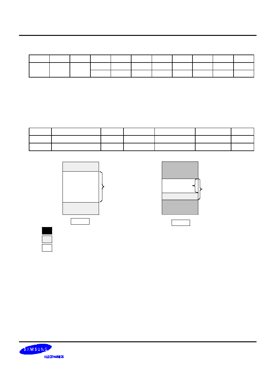
S6B33A2 PRELIMINARY VER 1.3 128 RGB SEGMENT & 129 COMMON DRIVER FOR 4,096 COLOR STN LCD
39
Partial Display Mode Set (55H)
D/I
/WR
/RD
DB7
DB6
DB5
DB4
DB3
DB2
DB1
DB0
0
1
0
1
0
1
0
1
0
0
1
0
0
0
0
0
0
PDM
PT
PT: Partial Display ON/OFF
-
PT = 0: Partial display OFF = Normal mode (Initial status)
-
PT = 1: Partial display ON
PDM: Partial Display mode set
-
PDM = 0: Partial mode 0 : Duty ratio is same as Normal display mode(initial status)
-
PDM = 1: Partial mode 1 : Duty ratio is changed from Normal display mode(66 duty fixed)
Applied parameter in PDM0 and PDM1 are summarized as below
PDM
Contrast
Duty
Bias
DC-DC Select
OSC
PCK
0
Contrast control(1)
Normal
Bias(1)
DC-DC(1),DC(1)
OSC1-OSC2
DIV(1)
1
Contrast control(1)
1/66
Bias(2)
DC-DC(1),DC(2)
OSC3-OSC4
DIV(2)
Operation in Partial Display Mode 0 (PDM=0)
On scanning except partial display area
-SEG output select V0 or V1 level depend on "FR" value. Refer to 44
-All of COM output is fixed VM level.
On scanning partial display area
-It is equal to be in normal mode
Operation in Partial Display Mode 1 (PDM=1)
Display area is from partial start line to partial end line.
(COM driver output is fixed VM except display area, only max66 line output COM signal.
On scanning except partial display area
-SEG output select V0 or V1 level depend on "FR" value. Refer to Page44
-All of COM output is fixed VM level.
On scanning partial display area
-It is equal to be in normal mode
Display
Area
Partial Start Line
Partial End Line
N line
PDM 0
Partial Start Line
M line
Max. 66 line
PDM 1
No display Area : No COM Scanning field (COM = Vm fixed)
Except Partial Display Area : COM Timing is existing, but COM = Vm fixed
Partial Display Area : Real display field
Partial End Line
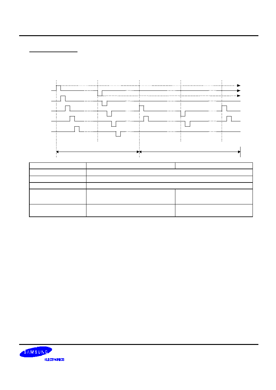
S6B33A2 PRELIMINARY VER 1.3 128 RGB SEGMENT & 129 COMMON DRIVER FOR 4,096 COLOR STN LCD
40
Partial Display Mode0
Item
Partial Display Area
Out of Partial Display Area
Duty
Same as normal display mode
Contrast
Same as normal display mode ( Contrast(1) setting )
Oscillator
Same as normal display mode ( OSC1 � OSC2 )
SEG Output level
Same as normal mode (V1,V0)
Depends on Internal "FR" signal
See page 44
COM Output level
Same as normal mode
(+VR,VM,-VR)
VM fixed
<COM0-2>
In case of COM 6 to COM11 Partial display
<COM3-5>
<COM6-8>
<COM9-11>
<COM12-14>
Normal Display Mode
Partial Display Mode 0
+VR
VM
-VR
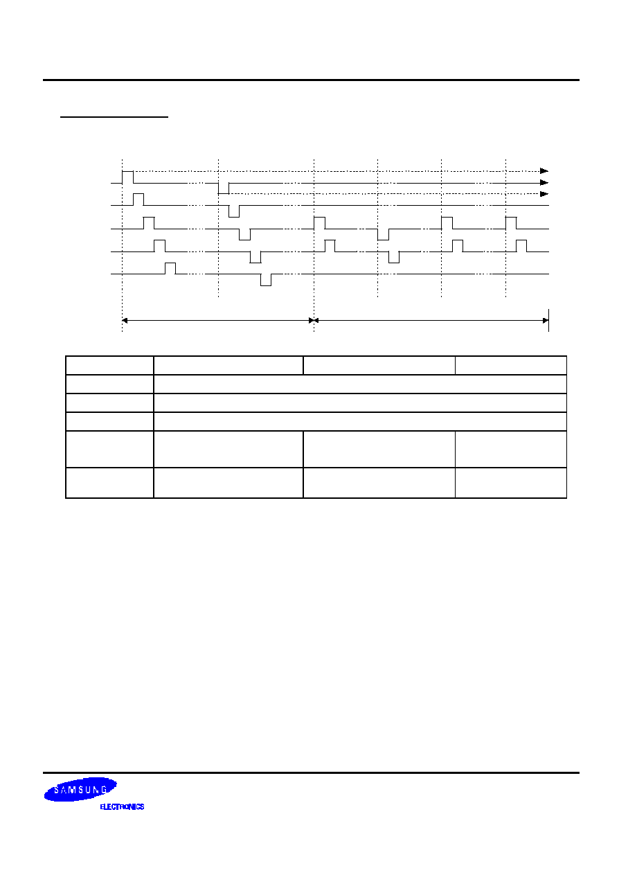
S6B33A2 PRELIMINARY VER 1.3 128 RGB SEGMENT & 129 COMMON DRIVER FOR 4,096 COLOR STN LCD
41
Partial display mode1
Item
Partial Display Area
Out of Partial Display Area
Out of Display Area
Duty
1/66duty
Contrast
Contrast(2) setting
Oscillator
( OSC3 � OSC4 ) setting value
SEG Output
level
Same as normal mode
(V1,V0)
Depends on "FR" signal
See page 44
-
COM Output
level
Same as normal mode
(+VR, VM, -VR)
VM fixed
VM fixed
<COM0-2>
In case of COM 6 to COM11 Partial display
<COM3-5>
<COM6-8>
<COM9-11>
<COM12-14>
Normal Display Mode
Partial Display Mode 1
+VR
VM
-VR
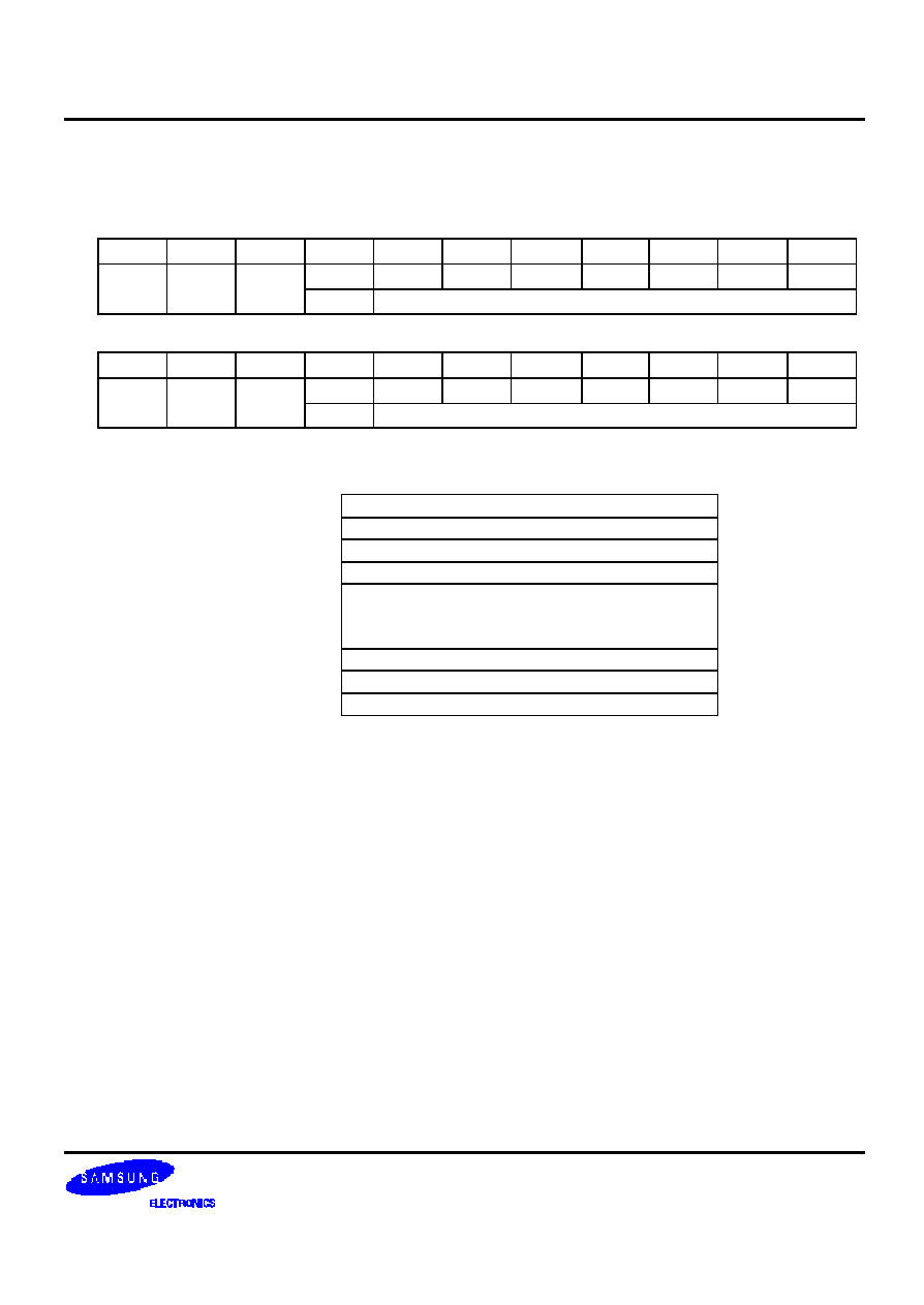
S6B33A2 PRELIMINARY VER 1.3 128 RGB SEGMENT & 129 COMMON DRIVER FOR 4,096 COLOR STN LCD
42
Partial Display Start Line Set (56H), Partial Display End Line Set(57H)
These 2 instructions set the partial display area and it is possible to display a part.
Partial Display Start Line Set (56H)
D/I
/WR
/RD
DB7
DB6
DB5
DB4
DB3
DB2
DB1
DB0
0
1
0
1
0
1
1
0
0
0
1
0
Partial start line
Partial Display End Line Set (57H)
D/I
/WR
/RD
DB7
DB6
DB5
DB4
DB3
DB2
DB1
DB0
0
1
0
1
0
1
1
1
0
0
1
0
Partial end line
Parameter set appoints display line number. At PDM 0, Parameter Size is able to be in a number of Display
lines. But that is not able to be over max 66 line at PDM 1. Partial end line must set bigger number than Partial
start line.
line 0
line 1
COM 0
COM 1
line 2
line 3
COM 2
COM 3
line 126
line 127
COM 126
line 128
COM 127
COM 128
:
:
:
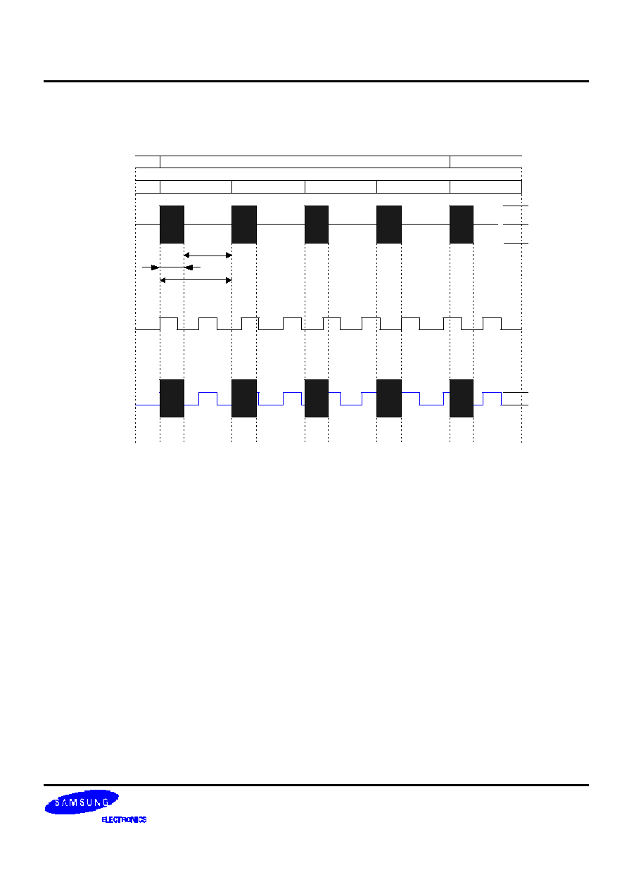
S6B33A2 PRELIMINARY VER 1.3 128 RGB SEGMENT & 129 COMMON DRIVER FOR 4,096 COLOR STN LCD
43
Example of Segment Voltage in non-display area
COM
Partial
Display
VM
Subframe
+VR
VM
-VR
V1
V0
Addressing Duty
Display
Off
internal
polarity
counter
(FR)
V0
V1
V0
V1
V0
V1
V1
V0
V1
V0
VM
VM
VM
0
1
2
0
3
N
N+1
SEG
Frame
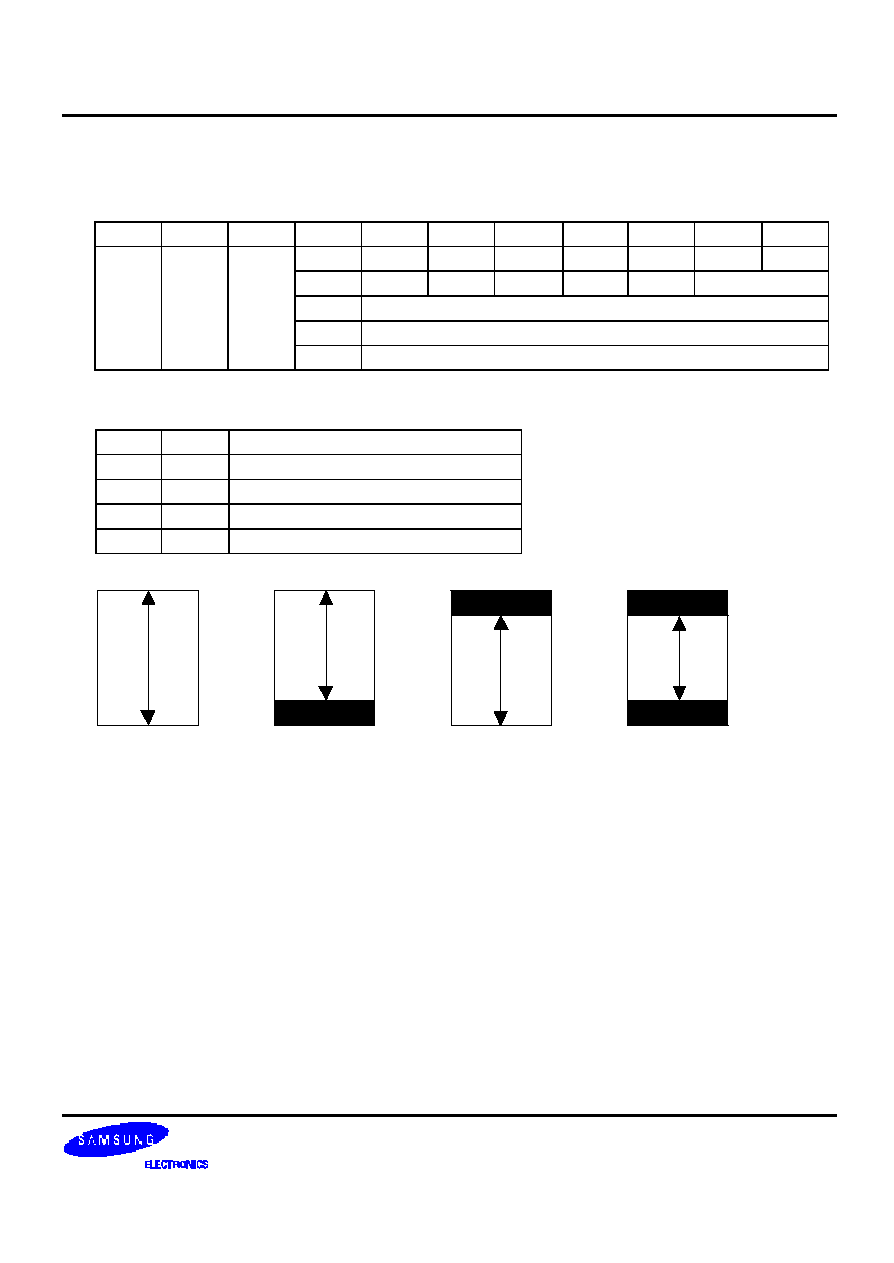
S6B33A2 PRELIMINARY VER 1.3 128 RGB SEGMENT & 129 COMMON DRIVER FOR 4,096 COLOR STN LCD
44
Area scroll Set (59H)
This instruction sets up area scroll field (start line, end line, Lower fixed line number), and it is possible to make
screen to display as partial scroll field.
D/I
/WR
/RD
DB7
DB6
DB5
DB4
DB3
DB2
DB1
DB0
0
1
0
1
1
0
0
1
0
0
0
0
0
0
SCM
0
Scroll area start line
0
Scroll area end line
0
0
1
0
Lower fixed number
Note: In lower and center scroll mode, scroll area end line must be smaller than duty - lower fixed number.
SCM: Scroll mode setting
DB1
DB0
Mode
0
0
Entire display(Initial status)
0
1
Upper scroll display
1
0
Lower scroll display
1
1
Center scroll display
Entire Display
Upper Display
Lower Display
Center Display
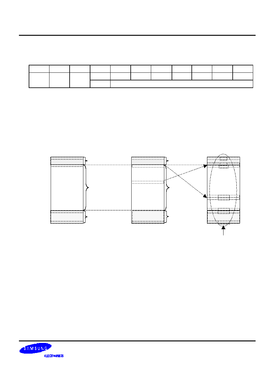
S6B33A2 PRELIMINARY VER 1.3 128 RGB SEGMENT & 129 COMMON DRIVER FOR 4,096 COLOR STN LCD
45
Scroll Start Line Set (5AH)
This instruction and parameter set up scroll start line. On this instruction, scroll start line becomes the first of
area scroll field. Scroll operation is occurred every issue of this instruction.
D/I
/WR
/RD
DB7
DB6
DB5
DB4
DB3
DB2
DB1
DB0
0
1
0
1
1
0
1
0
0
0
1
0
Scroll start line
<Example>
-SCM : 2'b11 (Center display mode)
-Scroll area start line : 6
-Scroll area end line : 119
-Lower fixed number : 8
-Scroll start line : 40
Upper
fIx
<DUTY BLOCK>
<RAM BLOCK>
COM6
COM127
COM0
Scroll
area
Upper
fix
Scroll
display
Lower
fix
<DISPLAY>
Xadr=6
Xadr=0
Xadr=120
Xadr=127
RAM Address.
COM120
COM0
COM6
COM120
Lower
fix
Addr0
Addr5
Addr40
Addr120
Addr127
Addr119
Addr6
Addr39
Xadr=40
COM127
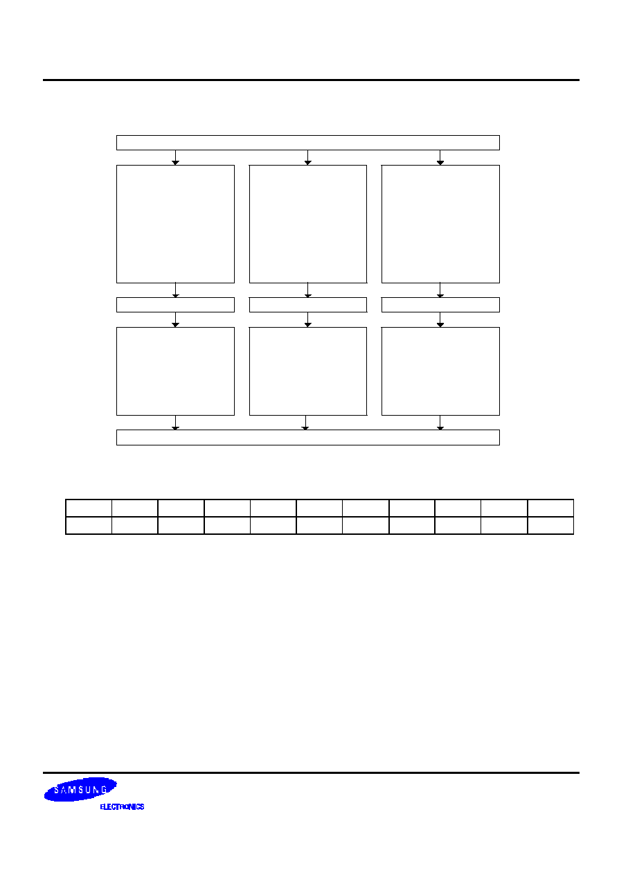
S6B33A2 PRELIMINARY VER 1.3 128 RGB SEGMENT & 129 COMMON DRIVER FOR 4,096 COLOR STN LCD
46
Data Format Select (60H/61H)
D/I
WRB
RDB
DB7
DB6
DB5
DB4
DB3
DB2
DB1
DB0
0
0
1
0
1
1
0
0
0
0
DFS
DFS: 4,096 Color Mode Data Format Select
- 0 : 4,096 Color Data Format A (Initial Status)
8 bit mode :
DB[7:0] : XXXXRRRR (1'st write)
DB[7:0] : GGGGBBBB(2'nd write)
16 bit mode :
DB[15:0] :XXXXRRRRGGGGBBBB (12 bit)
- 1 : 4,096 Color Data Format B
8 bit mode :
DB[7:0] : RRRRGGGG(1'st write)
DB[7:0] : BBBBRRRR (2'nd write)
DB[7:0] : GGGGBBBB(3'rd write)
16 bit mode :
DB[15:0] :RRRRGGGGBBBBXXXX (12 bit)
Normal Mode
Normal Mode
Partial Mode 0
Scroll Mode
Scroll/Partial Mode 0
Set partial start line
Set partial end line
Set partial mode 0
Set scroll mode
Set scroll area start line
Set scroll area end line
Set lower fixed line no.
Set scroll start line
Set scroll mode
Set scroll area start line
Set scroll area end line
Set lower fixed line
Set scroll start line
Set partial start line
Set partial end line
Set partial mode 0
Release partial mode
Set scroll mode
Set scroll area start line
Set scroll area end line
Set lower fixed line no.
Set scroll start line
Set scroll mode
Set scroll area start line
Set scroll area end line
Set lower fixed line no.
Set scroll start line
Release partial mode
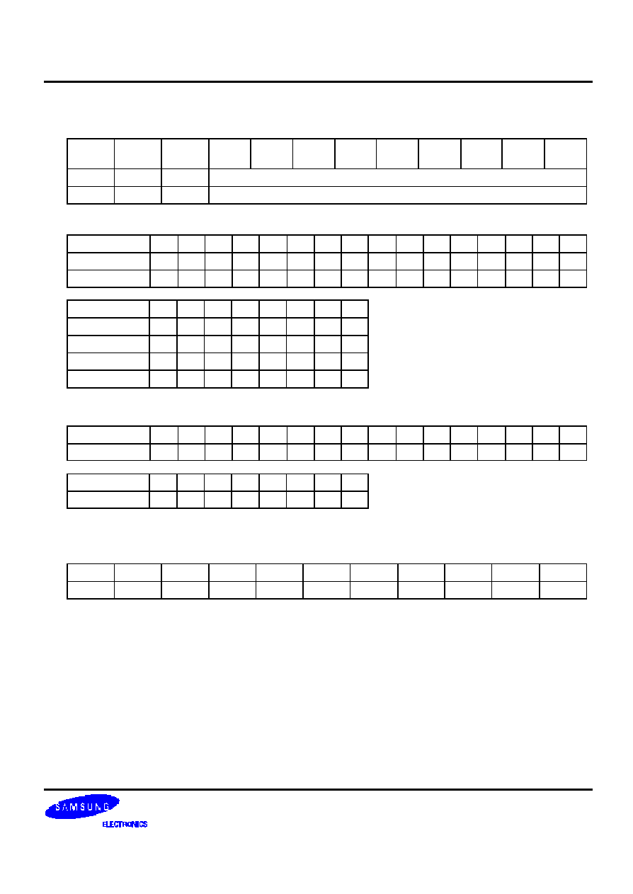
S6B33A2 PRELIMINARY VER 1.3 128 RGB SEGMENT & 129 COMMON DRIVER FOR 4,096 COLOR STN LCD
47
Display Data Write/Read
D/I
/WR
/RD
DB15
~ DB8
DB7
DB6
DB5
DB4
DB3
DB2
DB1
DB0
1
0
1
Display RAM write in data
1
1
0
Display RAM read out data
1. 4,096 Color mode
(1) 16bit access mode
15 14 13
12 11 10
9
8
7
6
5
4
3
2
1
0
1
st
cycle
X
X
X
X
R3 R2 R1 R0 G3 G2 G1 G0 B3 B2 B1 B0
2
nd
cycle
X
X
X
X
R3 R2 R1 R0 G3 G2 G1 G0 B3 B2 B1 B0
(2) 8bit access mode
7
6
5
4
3
2
1
0
1
st
cycle
X
X
X
X
R3 R2 R1 R0
2
nd
cycle
G3 G2 G1 G0 B3 B2 B1 B0
3
rd
cycle
X
X
X
X
R3 R2 R1 R0
4
th
cycle
G3 G2 G1 G0 B3 B2 B1 B0
2. 256 color mode
(1) 16bit access mode
15 14 13
12 11 10
9
8
7
6
5
4
3
2
1
0
1
st
cycle
R2 R1 R0 G2 G1 G0 B1 B0 R2 R1 R0 G2 G1 G0 B1 B0
(3) 8bit access mode
7
6
5
4
3
2
1
0
1
st
cycle
R2 R1 R0 G2 G1 G0 B1 B0
Status Read
D/I
/WR
/RD
DB7
DB6
DB5
DB4
DB3
DB2
DB1
DB0
0
1
0
BSY
X/Y
0
PDM
PT
STB
REV
DP
This instruction indicates the internal status of the S6B33A2.
DP: ( 0 : Display OFF Status, 1 : Display ON Status )
REV: ( 0 : Display Image Non-Reversing, 1 : Display Image Reversing )
STB: ( 0 : Standby Mode OFF Status, 1 : Standby Mode ON Status )
PT: ( 0 : Partial Display Mode OFF Status, 1 : Partial Display Mode ON Status )
PDM: ( 0 : Partial Display Mode 0, 1 : Partial Display Mode 1 )
X/Y: ( 0 : Y-address Count Mode, 1 : X-address Count Mode )
BSY: ( 0 : No Busy, 1 : Busy )
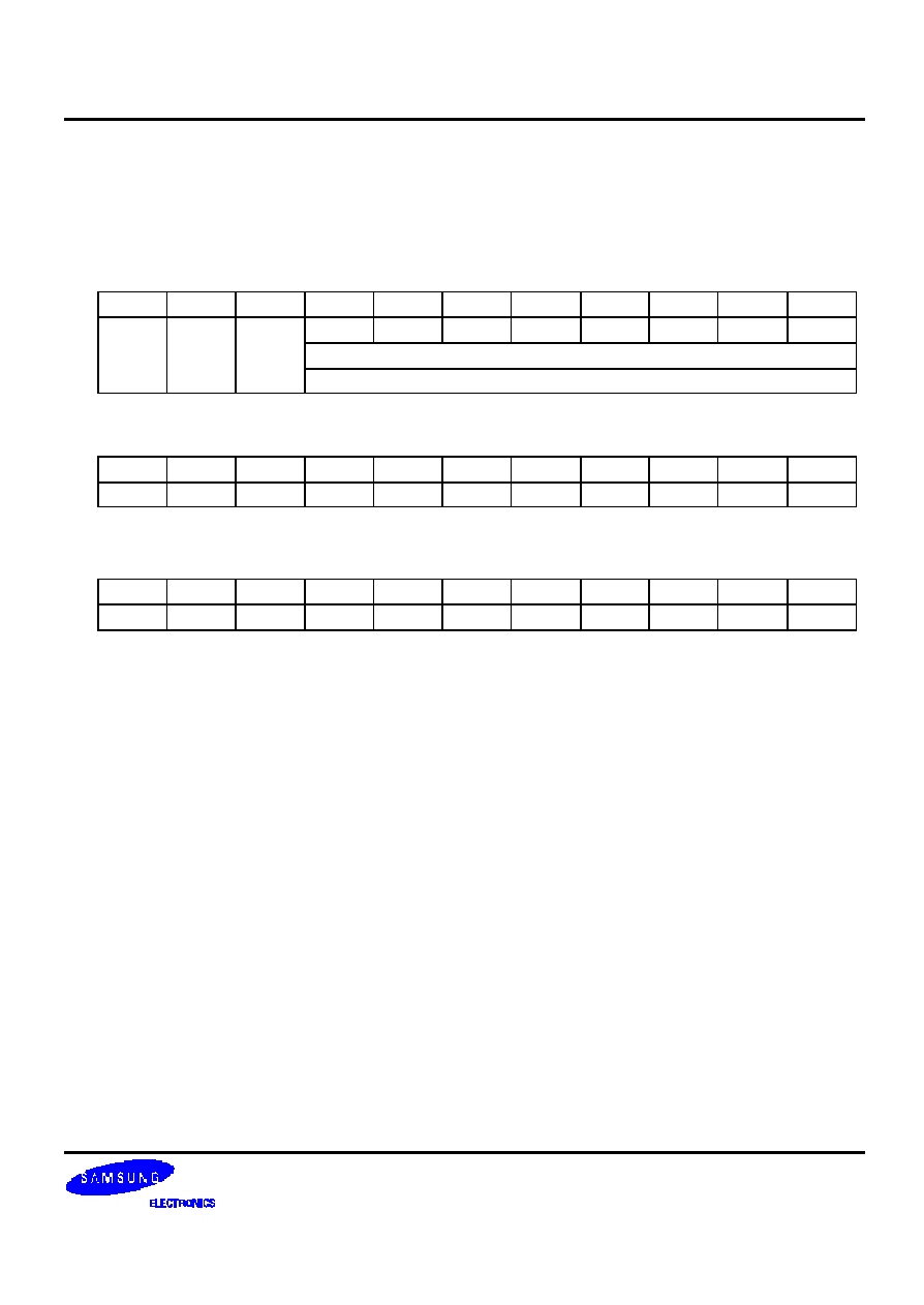
S6B33A2 PRELIMINARY VER 1.3 128 RGB SEGMENT & 129 COMMON DRIVER FOR 4,096 COLOR STN LCD
48
Set Display Data Length
This Instruction is only used in 3-pin SPI MPU interface mode(PS="L", MPU[1]="L"). It consists of two
continuous commands, the first byte control the data direction(write mode only) and inform the LCD driver the
second and third bytes will be number of data bytes will be write. When DI is not used, the Display Data Length
instruction is used to indicate that a specified number of display data bytes are to be transmitted.
The next byte after the display data string is handled as command data.
D/I
/WR
/RD
DB7
DB6
DB5
DB4
DB3
DB2
DB1
DB0
1
1
1
1
1
1
0
0
Number of display data upper 8bits (DDL_H)
0
0
1
Number of display data lower 8bits (DDL_L)
Test Mode1 (FFH)
This Instruction is for testing IC. User is not permitted to access. If access ,have to reset.
D/I
/WR
/RD
DB7
DB6
DB5
DB4
DB3
DB2
DB1
DB0
0
0
1
1
1
1
1
1
1
1
1
Test Mode2 (FEH)
This Instruction is for testing IC. User is not permitted to access. If access ,have to reset.
D/I
/WR
/RD
DB7
DB6
DB5
DB4
DB3
DB2
DB1
DB0
0
0
1
1
1
1
1
1
1
1
0
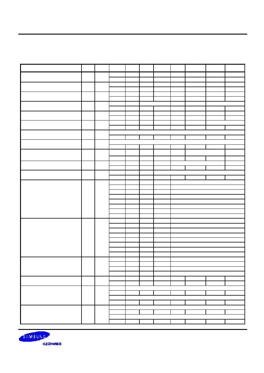
S6B33A2 PRELIMINARY VER 1.3 128 RGB SEGMENT & 129 COMMON DRIVER FOR 4,096 COLOR STN LCD
49
INSTRUCTION PARAMETER
Table 16. Instruction Parameter
Instruction
Hex Para.
DB7
DB6
DB5
DB4
DB3
DB2
DB1
DB0
0
0
0
0
0
0
EXT
OSC
Oscillation Mode Set
02H
1
*
*
*
*
*
*
0
0
0
0
0
0
0
0
SDIR
SWP
Driver Output Mode Set
10H
1
*
*
*
*
*
*
0
0
0
0
0
0
0
0
DC(2)
DC(1)
DC-DC Set
20H
1
0
0
0
0
0
0
0
0
0
0
DIV(2)
0
0
DIV(1)
PCK Generation Mode Set
24H
1
*
*
1
0
*
*
1
0
0
0
0
0
AMP
DCDC3 DCDC2 DCDC1
DCDC and AMP ON/OFF Set
26H
1
*
*
*
*
0
0
0
0
0
0
0
0
0
0
TCS
Temperature Compensation Set 28H
1
*
*
*
*
*
*
0
0
Contrast control value in normal and partial display mode0(0 to 255)
Contrast Control (1)
2AH
1
0
0
0
0
0
0
0
0
Contrast control value in partial display mode 1(0 to 255)
Contrast Control(2)
2BH
1
0
0
0
0
0
0
0
0
0
0
GSM
DSG
SGF
SGP
SGM
Addressing Mode Set
30H
1
*
*
0
0
0
0
0
0
0
0
0
0
INC
VEC
ROW Vector Mode Set
32H
1
*
*
*
*
0
0
0
0
FIM
FIP
0
N-block Inversion
N-line Inversion Set
34H
1
0
0
*
0
0
0
0
0
0
0
0
0
RAM data "000" to GS data
0
0
0
0
RAM data "001" to GS data
0
0
0
0
RAM data "010" to GS data
0
0
0
0
RAM data "011" to GS data
0
0
0
0
RAM data "100" to GS data
0
0
0
0
RAM data "101" to GS data
0
0
0
0
RAM data "110" to GS data
Red palette Set
38H
8
0
0
0
0
RAM data "111" to GS data
0
0
0
0
RAM data "000" to GS data
0
0
0
0
RAM data "001" to GS data
0
0
0
0
RAM data "010" to GS data
0
0
0
0
RAM data "011" to GS data
0
0
0
0
RAM data "100" to GS data
0
0
0
0
RAM data "101" to GS data
0
0
0
0
RAM data "110" to GS data
Green palette Set
3AH
8
0
0
0
0
RAM data "111" to GS data
0
0
0
0
RAM data "000" to GS data
0
0
0
0
RAM data "001" to GS data
0
0
0
0
RAM data "010" to GS data
Blue palette Set
3CH
4
0
0
0
0
RAM data "011" to GS data
0
0
0
0
0
HL
X/Y
RMW
Entry Mode Set
40H
1
*
*
*
*
*
0
0
0
0
X Start address set
*
0
0
0
0
0
0
0
0
X end address set
X-address Area Set
42H
2
*
1
1
1
1
1
1
1
0
Y start address set
*
0
0
0
0
0
0
0
0
Y end address set
Y-address Area Set
43H
2
*
1
1
1
1
1
1
1
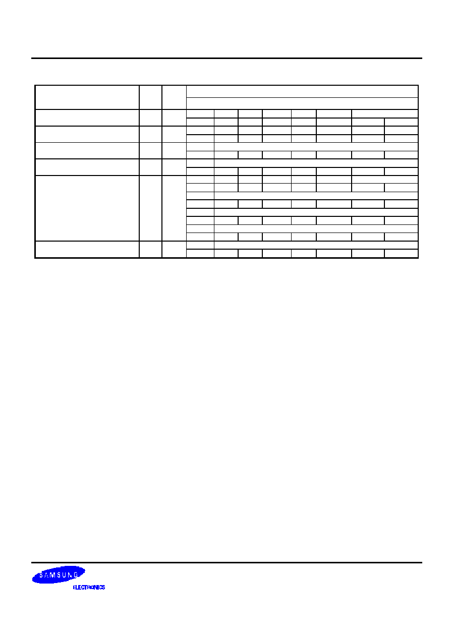
S6B33A2 PRELIMINARY VER 1.3 128 RGB SEGMENT & 129 COMMON DRIVER FOR 4,096 COLOR STN LCD
50
Number of display data upper word
Set Display Data Length
FCH
2
Number of display data lower word
0
0
0
0
0
0
SDP
Specified Display Pattern Set
53H
1
*
*
*
*
*
*
0
0
0
0
0
0
0
0
PDM
PT
Partial Display Mode Set
55H
1
*
*
*
*
*
*
0
0
0
Partial start line
Partial Display Start Line Set
56H
1
*
0
0
0
0
0
0
0
0
Partial end line
Partial Display End Line Set
57H
1
*
0
0
0
0
0
0
0
0
0
0
0
0
0
SCM
*
*
*
*
*
*
0
0
0
Scroll area start line
*
0
0
0
0
0
0
0
0
Scroll area end line
*
1
1
1
1
1
1
0
Lower Fixed number
Area Scroll Mode Set
59H
4
*
0
0
0
0
0
0
0
0
Scroll start line
Scroll Start Line Set
5AH
1
*
0
0
0
0
0
0
0

S6B33A2 PRELIMINARY VER 1.3 128 RGB SEGMENT & 129 COMMON DRIVER FOR 4,096 COLOR STN LCD
51
Reset Operation
When /RST becomes "L", following procedure is occurred.
- X address: 0
- Y address: 0
- Display OFF
- Read Modify Write Mode OFF
- Function Mode Set
OSC = 0: Oscillator OFF
EXT = 0: Internal Oscillator Mode
REV = 0: Reversing mode OFF
X/Y = 0: Y-address Count Mode
HL = 0
Standby Mode ON
- PCK Generation mode Set
DIV(1) = 10: fPCK = fOSC/6x
DIV(2) = 10: fPCK = fOSC/6x
- DC-DC Select
DC(1) = 0: X1 step-up
DC(2) = 0: X1 step-up
- DC/DC and AMP ON/OFF Set
AMP =0: Built-in OP-AMP OFF
DCDC1 =0: Built-in 1
st
booster OFF
DCDC2 =0: Built-in 2
nd
booster OFF
DCDC3 =0: Built-in 3
rd
booster OFF
- N-block inversion
FIM =0: Forcing Inversion OFF
FIP =0: Forcing Inversion Period in one frame
N-block inversion = 00H: frame inversion
- Partial Display Mode
PT = 0: Partial Display Mode OFF
PDM = 0: Partial Mode 0
- Partial Display Area Set
Partial start line = 00H
Partial end line = 00H
-Area Scroll Set
Mode = 00H : Entire Display Scroll Mode
Area Start Line: 00H
Area End Line: 7FH
Lower Fixed Line Number: 00H
- Scroll Start Line Set
Scroll Start Line: 00H
- Addressing Mode Set
GSM =0: 4,096 color mode
DSG = 0: Mode 0
SGF = 0: SG Frame Inversion OFF
SGM = 0: SG Reverse Mode OFF
SGP=00:Same phase in all pixel
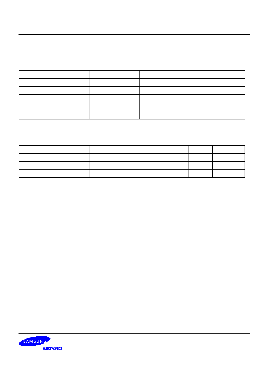
S6B33A2 PRELIMINARY VER 1.3 128 RGB SEGMENT & 129 COMMON DRIVER FOR 4,096 COLOR STN LCD
52
SPECIFICATIONS
ABSOLUTE MAXIMUM RATINGS
Item
Symbol
Rating
Unit
Supply Voltage range
VDD
-0.3 to +4.0
V
LCD Supply Voltage range
|
VCC � VEE|
20
V
Input Voltage range
Vin
- 0.3 to VDD +0.3
V
Operating Temperature range
T
OPR
-30 to +70
�
C
Storage Temperature range
T
STR
-55 to +150
�
C
OPERATING VOLTAGE
Item
Symbol
Min.
Typ.
Max.
Unit
Supply Voltage (1)
VDD
1.8
-
3.3
V
Supply Voltage (2)
2Vr
-
-
20
V
Supply Voltage (3)
VIN
2.4
3.0
3.6
V
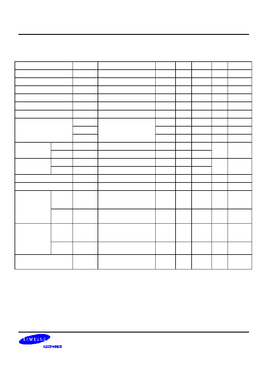
S6B33A2 PRELIMINARY VER 1.3 128 RGB SEGMENT & 129 COMMON DRIVER FOR 4,096 COLOR STN LCD
53
DC CHARACTERISTICS (1)
(Vss
= 0V, V
DD
= 1.8 to 3.3V, Ta = -30 to 70
�
C)
Item
Symbol
Condition
Min
Typ
Max
Unit Remarks
Operating voltage
VDD
1.8
-
3.3
V
VDD
Operating voltage
VIN1
2.4
-
3.6
V
VCI
Operating voltage
DC2IN
1.66
-
2.75
V
DC2IN
Operating voltage
VIN2
2.4
-
5.4
V
VIN2
Operating voltage
VIN45
2.4
-
5.4
V
VIN45
Operating voltage
2Vr
2Vr
= |(+VR)- (-VR)|
4.0
-
20
V
+VR, -VR
VM
1.0
1.65
V
VM
VCC
7.0
11.55
V
VCC
Driving voltage input range
VEE
External power supply
mode
-8.25
-5.0
V
VEE
High
V
IH
0.8VDD
-
VDD
Input voltage
Low
V
IL
VSS
-
0.2VDD
V
High
V
OH
I
OH
= 0.5mA
0.8VDD
-
VDD
Output voltage
Low
V
OL
I
OL
= 0.5mA
VSS
-
0.2VDD
V
Input leakage current
I
IL
VIN = VDD or VSS
-1.0
-
+1.0
�
A
Output leakage current
I
OZ
VIN = VDD or VSS
-3.0
-
+3.0
�
A
Normal
or
Partial 0
F
OSC1
R1=? (fFR=80Hz target),
DSG=0, 128 display lines
50.688 56.32 61.952
kHz OSC1
- OSC2
Oscillator
Frequency
Tolerance
Partial 1
F
OSC2
R1=? (fFR=80Hz target),
DSG=0, 66 display lines
26.496 29.44 32.384
kHz OSC3
- OSC4
Normal
or
Partial 0
F
OSC1
(*1)
35.200
70.400
kHz OSC1
- OSC2
Oscillator
Frequency
Range
Partial 1
F
OSC2
(*2)
18.400
36.800
kHz OSC3
- OSC4
Driving voltage input range
V1
VM
2.0
1.0
-
3.3
1.65
V
(*1) Minimum oscillator frequency range is defined at fFR=50Hz and display line number=128
Maximum oscillator frequency range is defined at fFR=100Hz and display line number=128
(*2) Minimum oscillator frequency range is defined at fFR=50Hz and display line number=66
Maximum oscillator frequency range is defined at fFR=100Hz and display line number=66
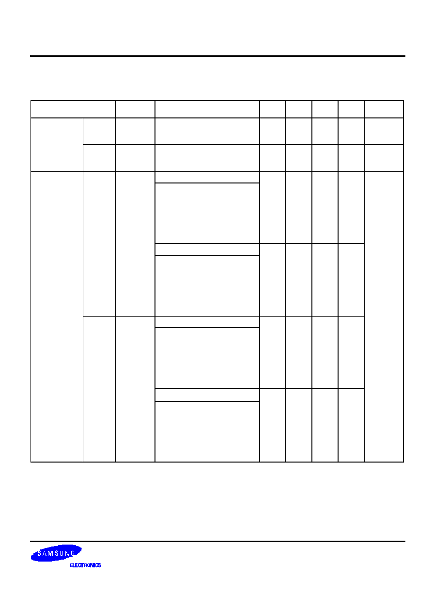
S6B33A2 PRELIMINARY VER 1.3 128 RGB SEGMENT & 129 COMMON DRIVER FOR 4,096 COLOR STN LCD
54
DC CHARACTERISTICS (2)
(Vss
= 0V, V
DD
= 1.8 to 3.3V, VIN1=2.4 to 3.6V, Ta = -30 to 70
�
C)
Item
Symbol
Condition
Min
Typ
Max
Unit Remarks
SEG
R
ON-Seg
V1=3.3 V, VM=1.65V, V0=0V,
Ta = 25
�
C, Iload=100uA
-
1.5
3.0
k
SEGn
Driver output
resistance
COM
R
ON-Com
VCC=12 V, VM=1.5V,
VEE=-9.0V,
Ta = 25
�
C, Iload=100uA
-
1.0
1.5
k
COMn
VDD=3V
VIN1=3.0V, V1=3.3V,
Bias(1)=1/6, DC(1)=x1.5,
Ta=25
�
C, Display line=128
DSG=0 (1dummy)
f
OSC
1=49.3kHz (fFR=70Hz)
Low current mode, No load,
No access, All white pattern
-
400
-
�
VDD=1.8V
Normal
Mode
IDD1
VIN1=3.0V, V1=3.3V,
Bias(1)=1/6, DC(1)=x1.5,
Ta=25
�
C, Display line=128
DSG=0 (1dummy)
f
OSC
1=49.3kHz (fFR=70Hz)
Low current mode, No load,
No access, All white pattern
-
270
-
�
VDD=3V
VIN1=3.0V, V1=3.3V,
Bias(2)=1/6, DC(2)=x1.5,
Ta=25
�
C, Display line=66
DSG=0 (1dummy)
f
OSC
1=25.8kHz (fFR=70Hz)
Low current mode, No load,
No access, All white pattern
-
240
-
�
VDD=1.8V
Current
consumption
Partial1
Mode
IDD2
VIN1=3.0V, V1=3.3V,
Bias(2)=1/6, DC(2)=x1.5,
Ta=25
�
C, Display line=66
DSG=0 (1dummy)
f
OSC
1=25.8kHz (fFR=70Hz)
Low current mode, No load,
No access, All white pattern
-
180
-
�
VDD
* : "IDD1 and IDD2" are determined from lowest power consumption for dc-dc converter.
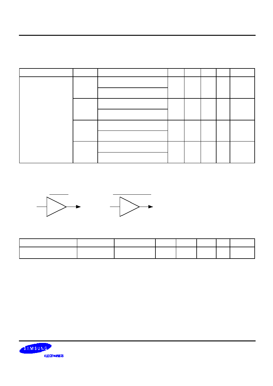
S6B33A2 PRELIMINARY VER 1.3 128 RGB SEGMENT & 129 COMMON DRIVER FOR 4,096 COLOR STN LCD
55
DC CHARACTERISTICS (3)
(Vss
= 0V, V
DD
= 1.8 to 3.3V, VIN1=2.4 to 3.6V, Ta = -30 to 70
�
C)
Item
Symbol
Condition
Min
Typ
Max Unit Remarks
Low current mode
Isource = 80uA
(+VR)
High current mode
Isource = 150 or 250uA
-
-
100
mV
+VR
Low current mode
Isource = 250uA
(V1)
High current mode
Isource = 500 or 1000uA
-
-
20
mV
V1
Low current mode
Isource,sink = 250uA
(VM)
High current mode
Isource,sink = 500 or 1000uA
-
-
20
mV
VM
Low current mode
Isink = 80uA
Voltage shift range(*1)
(-VR)
High current mode
Isink = 150 or 250uA
-
-
100
mV
-VR
(*1) Voltage shift means output voltage deference between output current = Iload and no-load.
Refer to the following figure. (in case of source current mode)
Item
Symbol
Condition
Min
Typ
Max
Unit Remarks
Tolerance of Bias ratio
(+VR)_0
(-VR)_0(*1)
No load
-100
-
+100
mV +VR
-VR
(*1) Tolerance of bias ratio definition
(+VR)_0 = ((+VR) - VM ) � VM *6
(-VR)_0 = ( VM - (-VR)) � VM *6
No-load
Vx
Vx
Vy
Vy
I=0
I=ILoad
Vshift = |Vx-Vy|
Current = I Load
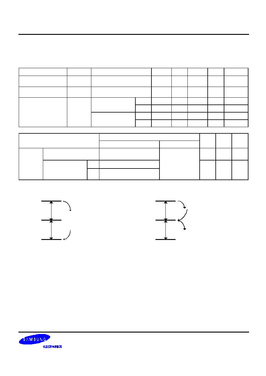
S6B33A2 PRELIMINARY VER 1.3 128 RGB SEGMENT & 129 COMMON DRIVER FOR 4,096 COLOR STN LCD
56
DC CHARACTERISTICS (4)
(Vss
= 0V, V
DD
= 1.8 to 3.3V, VIN1=2.4 to 3.6V, Ta = -30 to 70
�
C)
Item
Symbol
Condition
Min
Typ
Max
Unit
Remarks
Temperature
compensation
Vt
VDD=VIN1=V1=3.0V,
-20 to 70
�
C
-0.02
-
+0.02
%/
�
C
V1
Tolerance of Contrast
step of V1
Vstep
2.539
5.078
7.617
mV
V1
V1
3.25
3.3
3.35
V
V1
Contrast set = FFh
VM
1.60
1.65
1.70
V
VM
V1
1.95
2.00
2.05
V
V1
Voltage range
V1
VM
Contrast set = 00h
VM
0.95
1.00
1.05
V
VM
Condition
Item
Load current
Voltage range
Max
Unit
Ref
||+VR-VM| -|VM -(-VR)||
I Load = +100uA (+VR)
I Load = -100uA (-VR)
100
mV
Fig.1
A
I Load = +100uA ( V1, VM )
Offset
Voltage
||V1-VM| -|VM-V0||
B
I Load = +100uA (+VR)
I Load = -100uA (-VR)
+VR=7.0~11.55 V
V1=2.0~3.3V
VM=1.0~1.65V
-VR=-8.25~-5 V
50
mV
Fig.2
+VR
Fig. 1: Offset voltage definition (+VR,VM,-VR)
Vx
|Vx-Vy| < 100mV
VM
-VR
Vy
+100uA
-100uA
V1
Va
|Va-Vb| < 50mV
VM
V0
Vb
+100uA (both Case A and B)
-100uA (Case B)
+100uA (Case A)
Fig. 2: Offset voltage definition (V1,VM,V0)
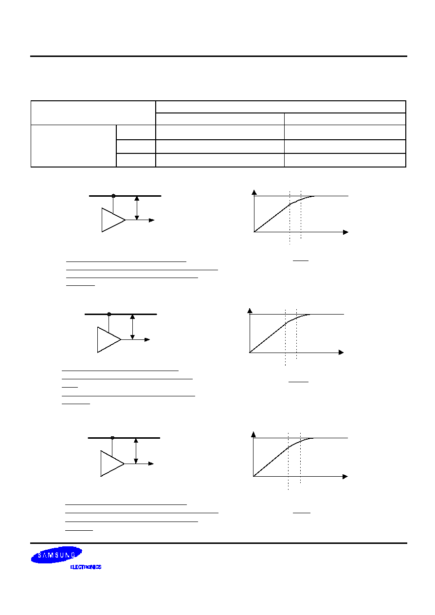
S6B33A2 PRELIMINARY VER 1.3 128 RGB SEGMENT & 129 COMMON DRIVER FOR 4,096 COLOR STN LCD
57
DC CHARACTERISTICS (5)
(Vss
= 0V, V
DD
= 1.8 to 3.3V, VIN1=2.4 to 3.6V, Ta = -30 to 70
�
C)
Range
Item
Min
Max (DC(1) and DC(2) = X1.5)
V1OUT
2.0 V
3.3 V(*1)
VMOUT
1.0 V
1.65 V(*2)
Voltage Level
DC2OUT
1.67 V
2.75 V(*3)
If V1OUT input voltage is set over VIN45,
V1OUT output voltage must be clipped near VIN45.
In this case, V1OUT output level must not be
unstable. Refer to Fig.1
V1OUT
VIN45
V > 0.3 V (External VIN45)
V
(*1) This definition is shown as below
VIN45
V1OUT
Output
VIN45
VIN45 -
V
Fig. 1
V1OUT
Input
V > 0.5 V (VIN45 = VOUT45)
If VMOUT input voltage is set over VIN1,
VMOUT output voltage must be clipped near
VIN1.
In this case, VMOUT output level must not be
unstable. Refer to Fig.2
VMOUT
VIN1
V > 0.3 V
V
(*2) This definition is shown as below
VIN1
VMOUT
Output
VIN1
VIN1 -
V
Fig. 2
VMOUT
Input
If DC2OUT input voltage is set over VIN2,
DC2OUT output voltage must be clipped near VIN2.
In this case, VMOUT output level must not be
unstable. Refer to Fig.3
DC2OUT
VIN2
V > 0.3 V (External VIN2)
V
(*3) This definition is shown as below
VIN2
DC2OUT
Output
VIN2
VIN2 -
V
DC2OUT
Input
V > 0.5 V (VIN2 = VOUT45)
Fig.3
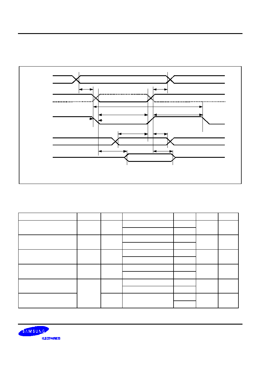
S6B33A2 PRELIMINARY VER 1.3 128 RGB SEGMENT & 129 COMMON DRIVER FOR 4,096 COLOR STN LCD
58
AC CHARACTERISTICS
Read / Write Characteristics (8080-series MPU)
DB0 to DB7
(Write)
DB0 to DB7
(Read)
t
DH80
t
OD80
t
DS80
t
ACC80
0.9V
DD
0.1V
DD
t
PW L80(R)
, t
PWL80(W)
t
CY80
t
AH80
t
AS80
/RD, /WR
/CS1
(CS2)
D/I
t
PWH80(R)
, t
PW H80(W)
** t
PWL80(W)
and t
PWL80(R)
is specified in the overlapped period when CS1B is low (CS2 is high)
and /WR(/RD) is low.
Figure 27. Parallel Interface (8080-series MPU) Timing Diagram
Table 17. AC Characteristics (8080-series Parallel Mode)
(VDD
= 1.8 to 3.3V, Ta = -30 to +70
�
C)
Item
Signal
Symbol
Condition
Min.
Max.
Unit
1.8V/3.3V
0
Address setup time
Address hold time
D/I
t
AS80
t
AH80
1.8V/3.3V
0
-
-
ns
1.8V
470
System cycle time
t
CY80
3.3V
180
-
ns
1.8V
160
Pulse width low for write
Pulse width High for write
/WR
(/WR)
t
PWLW
t
PWHW
3.3V
70
-
-
ns
1.8V
160
Pulse width low for read
Pulse width high for read
/RD
(/RD)
t
PWLR
t
PWHR
3.3V
70
-
-
ns
1.8V/3.3V
70/35
Data setup time
Data hold time
t
DS80
t
DH80
1.8V/3.3V
15/10
-
-
ns
170/90
Read access time
Output disable time
DB0
to
DB15
t
ACC80
t
OD80
1.8V/3.3V
C
L
= 100 pF
-
-
ns
NOTE: *1. The input signal rise time and fall time (tr, tf) is specified at 10 ns or less.
(tr + tf) < (t
CY80
- t
PWLW
- t
PWHW
) for write, (tr + tf) < (t
CY80
- t
PWLR
- t
PWHR
) for read
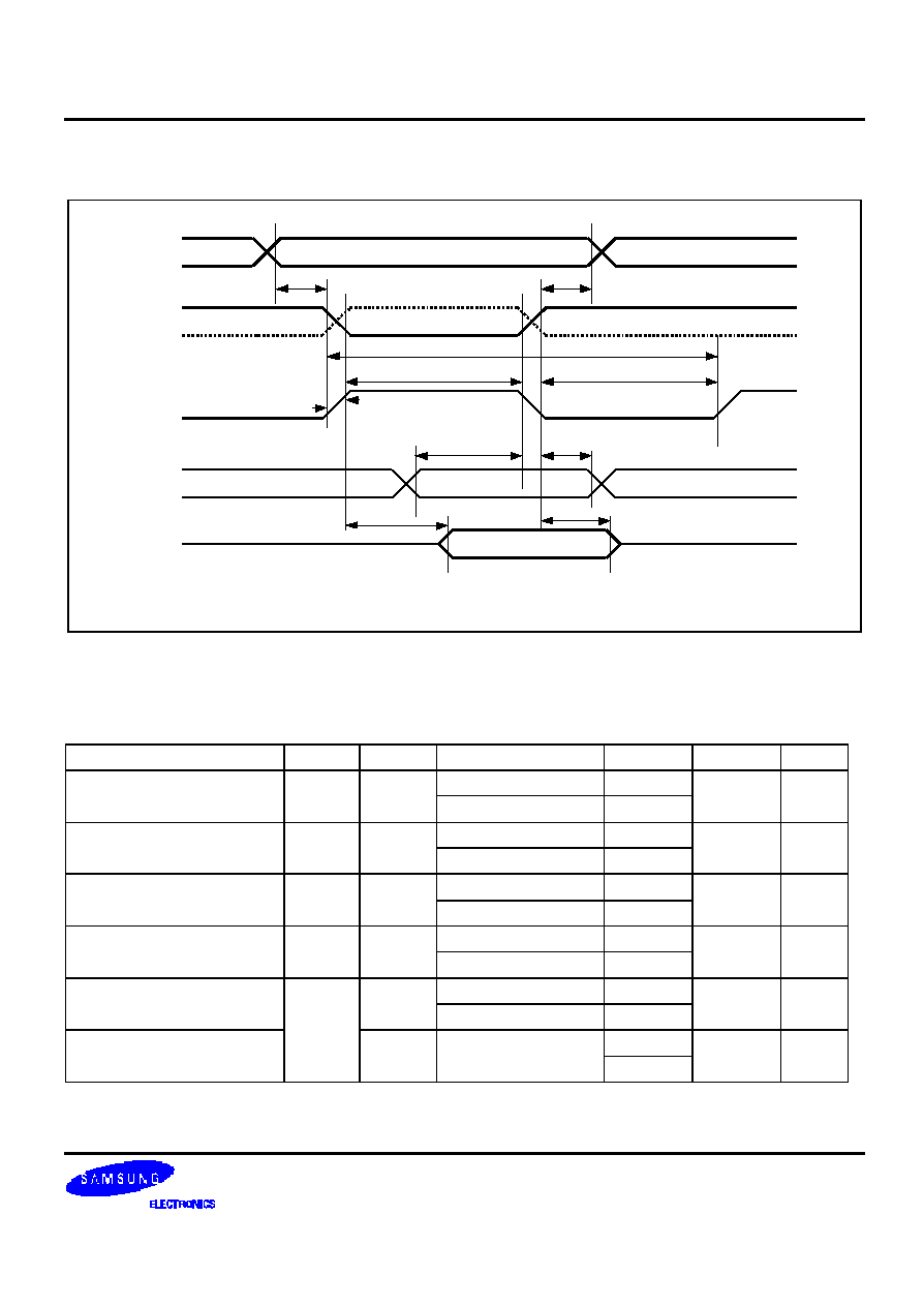
S6B33A2 PRELIMINARY VER 1.3 128 RGB SEGMENT & 129 COMMON DRIVER FOR 4,096 COLOR STN LCD
59
Read / Write Characteristics (6800-series Microprocessor)
t
DH68
t
OD68
t
DS68
t
ACC68
0.9V
DD
0.1V
DD
t
EW H68(R)
, t
EWH68(W)
t
CY68
t
AH68
t
AS68
DB0 to DB7
(Write)
E
/CS1
(CS2)
D/I,R/W
DB0 to DB7
(Read)
t
EWL68(R)
, t
EWL68(W)
** t
EWH68(W)
and t
EWH68(R)
is specified in the overlapped period when /CS1 is low (CS2 is high)
and E is high.
Figure 28. Parallel Interface (6800-series MPU) Timing Diagram
Table 18. AC Characteristics (6800-series Parallel Mode)
(V
DD
= 1.8 to 3.3V, Ta = -30 to +70
�
C)
Item
Signal
Symbol
Condition
Min.
Max.
Unit
1.8V/3.3V
0
Address setup time
Address hold time
D/I
R/W
t
AS68
t
AH68
1.8V/3.3V
0
-
-
ns
1.8V
470
System cycle time
t
CY68
3.3V
180
-
-
ns
1.8V
160
Enable width high for write
Enable width low for write
/RD
(E)
t
EWHW
t
EWLW
3.3V
70
-
-
ns
1.8V
160
Enable width high for read
Enable width low for read
/RD
(E)
t
EWHR
t
EWLR
3.3V
70
-
-
ns
1.8V/3.3V
70/35
Data setup time
Data hold time
t
DS68
t
DH68
1.8V/3.3V
15/10
-
-
ns
170/90
Read access time
Output disable time
DB0
to
DB15
T
ACC68
t
OD68
1.8V/3.3V
C
L
= 100 pF
-
-
-
ns
NOTE: *1. The input signal rise time and fall time (tr, tf) is specified at 10 ns or less.
(tr + tf) < (t
CY68
- t
EWHW
- t
EWLW
) for write, (tr + tf) < (t
CY68
- t
EWHR
- t
EWLR
) for read
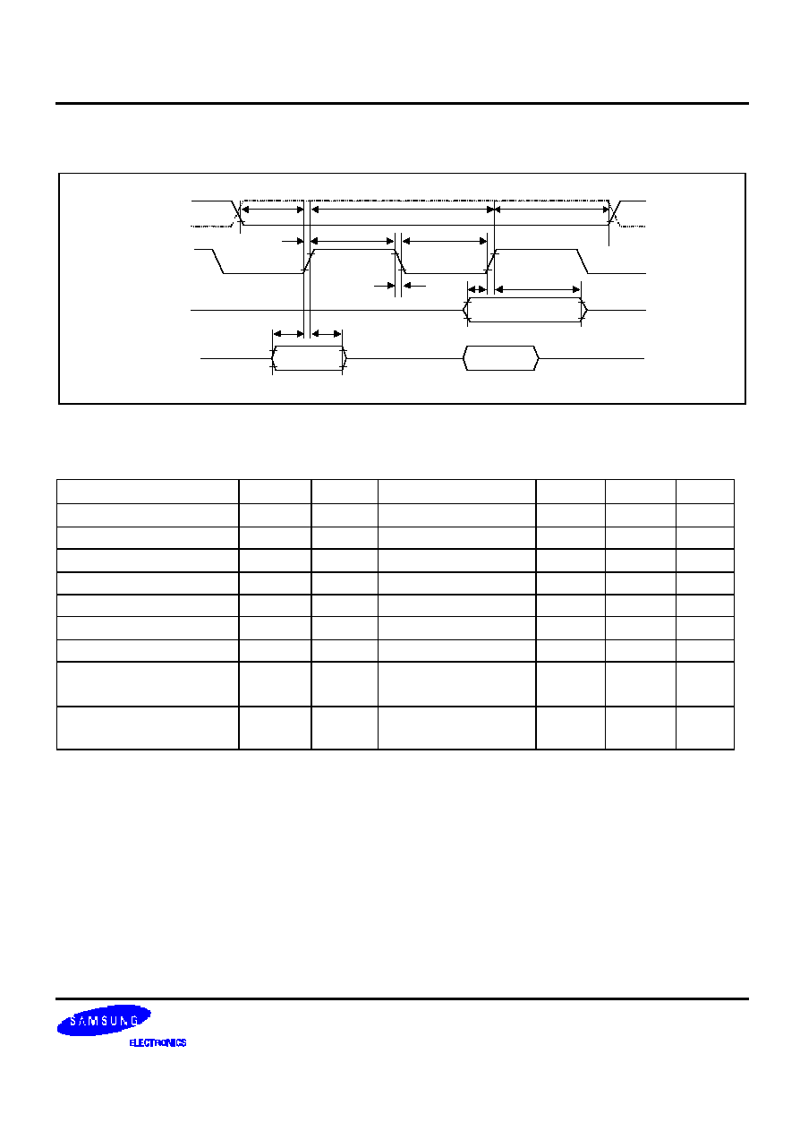
S6B33A2 PRELIMINARY VER 1.3 128 RGB SEGMENT & 129 COMMON DRIVER FOR 4,096 COLOR STN LCD
60
Serial Data Interface Timing
/CS1
SDI
D/I
SCL
t
CSH
t
SDH
t
SAH
t
SCYC
t
CSS
t
SDS
t
SAS
t
SLW
t
SHW
t
f
0.1V
DD
0.1V
DD
t
r
0.9V
DD
0.1V
DD
0.9V
DD
0.1V
DD
(CS2)
Table 19. Serial Data Interface Timing
(V
DD
= 1.8 to 3.3V, Ta = -30 to +70
�
C)
Item
Signal
Symbol
Condition
Min.
Max.
Unit
SCL Cycle Time
SCL
t
CSC
50
us
SCL High Pulse Width
SCL
t
SHW
20
ns
SCL Low Pulse Width
SCL
t
SLW
20
ns
SDI Setup time
SDI
t
SDS
20
ns
SDI Hold time
SDI
t
SDH
20
ns
D/I Setup time
D/I
t
SAS
20
ns
D/I Hold time
D/I
t
SAH
20
ns
Chip Select Setup time
/CS1
(CS2)
t
CSS
20
ns
Chip Select Hold time
/CS1
(CS2)
t
CHS
20
ns
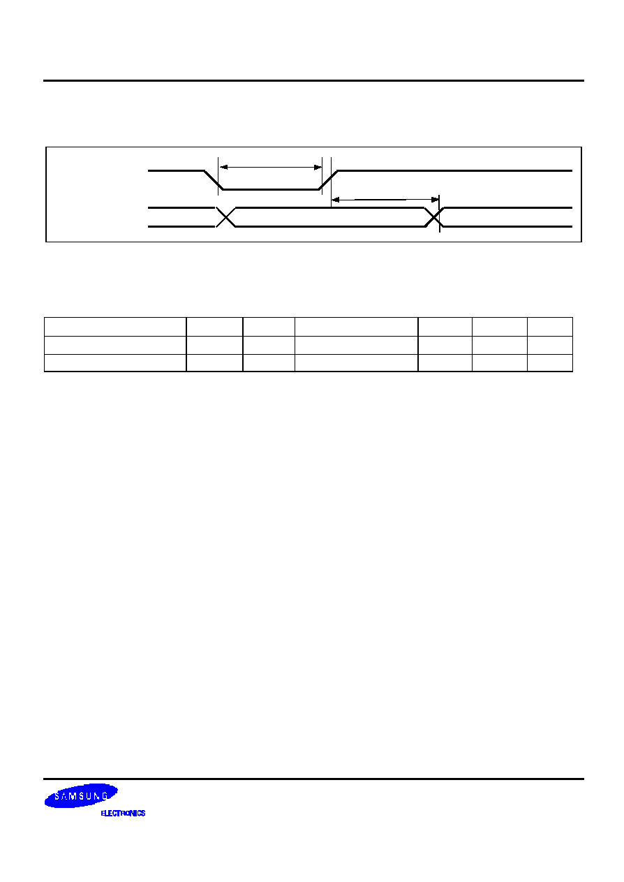
S6B33A2 PRELIMINARY VER 1.3 128 RGB SEGMENT & 129 COMMON DRIVER FOR 4,096 COLOR STN LCD
61
Reset Input Timing
/RST
Internal status
t
RW
t
R
Reset complete
During reset
Figure 29. Reset Input Timing Diagram
Table 20. AC Characteristics (Reset mode)
(V
DD
= 1.8 to 3.3V, Ta = -30 to +70
�
C)
Item
Signal
Symbol
Condition
Min.
Max.
Unit
Reset low pulse width
/RST
t
RW
1000
-
ns
Reset time
-
t
R
-
1000
ns
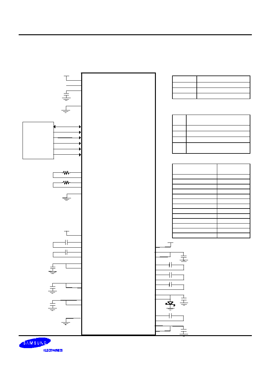
S6B33A2 PRELIMINARY VER 1.3 128 RGB SEGMENT & 129 COMMON DRIVER FOR 4,096 COLOR STN LCD
62
SYSTEM APPLICATION DIAGRAM
Internal Power Mode
External Components
Name
Device
R1,R2
Resistors
C1,C2,C3
Capacitors
D1
Schottky barrier diode
Values of external Capacitors and D1
Item
Capacitance
C1
1.0 to 4.7
�
F
C2
1.0 to 2.2
�
F
C3
1.0 to 2.2
�
F
D1 Vforward = Max. 0.3V at 1mA
Vreverse = Min. 15V
Maximum rating voltage of capacitors
Item
Maximum
rating voltage
REG_OUT to VSS
3V
VOUT45 to VSS
8V
C11P to C11M
6V
C12P to C12M
6V
VMOUT to VSS
3V
DC2OUT to VSS
5V
V1OUT to VSS
6V
C21P to C21M
5V
C22P to C22M
10V
C23P to C23M
13V
VSS to VRN
13V
C31P to C31M
17V
VRP to VSS
18V
S6B33A2
OSC1
OSC2
OSC3
OSC4
R1
R2
OSC5
/WR
/RD
DB15DB0
D/I
/CS1
/WR
/RD
DB15 to DB0
MPU
CS2
D/I
/CS1
CS2
C11P
C11M
C12P
C12M
C2
C2
VOUT45
VIN45
C3
VIN1
VIN1
VDD
VDD1
REG_OUT
VDD or REG_OUT
C1
C21P
C21M
C22P
C22M
C2
C2
C23M
C2
VRN
VEE
C3
VIN2
VIN2
DC2OUT
DC2IN
C3
V1OUT
V1IN
C3
VMOUT
VMIN
C3
C31P
C31M
C2
VRP
VCC
C3
C23P
V0IN
VSS
S6B33A2 PRELIMINARY VER 1.3 128 RGB SEGMENT & 129 COMMON DRIVER FOR 4,096 COLOR STN LCD
63
External Power Mode
S6B33A2
00
OSC1
OSC2
OSC3
OSC4
R1
R2
OSC5
/WR
/RD
DB15 to DB0
D/I
/CS1
/WR
/RD
DB15 to DB0
MPU
CS2
D/I
/CS1
CS2
C11P
C11M
C12P
C12M
VDD
VDD1
REG_OUT
VDD or REG_OUT
C
VOUT45
VIN45
VIN1
VIN1
C21P
C21M
C22P
C22M
C23P
C23M
VRN
VEE
VIN2
VIN2
DC2OUT
DC2IN
V1OUT
V1IN
VMOUT
VMIN
C31P
C31M
VRP
VCC
V1IN
VMIN
VEE
VCC
V0IN
VSS