132 RGB SOURCE & 176 GATE DRIVER WITH INTERNAL RAM FOR 65K COLORS TFT-LCD
S6D0110
Preliminary
2
S6D0110 Specification Revision History
Version
Content
Author
Date
0.0
Original
G. H. Jung
March 16 , 2002
0.1
Modified descriptions for operating voltage. (page 4)
Modified figure for pad configuration. (page 6)
Added descriptions for IM2-0 pin mode setting. (page 10)
Added descriptions for /RD pin. (page 10)
Modified table for register selection. (page 12)
Added table for GRAM address. (page 17-18)
Modified table for Instruction. (page 20)
Modified descriptions for R00h. (page 22)
Added descriptions for SM bit in R01h. (page 23)
Modified descriptions for BT2-0 bits in R03h. (page 26)
Modified descriptions for CAD bit in R04h. (page 28)
Modified descriptions for VDV4-0 bits in R0Eh. (page 30)
Added descriptions for R08h, R09h. (page 36)
Modified figure for window address setting range. (page 41)
Modified table for GRAM data and grayscale level. (page 43)
Modified figure for voltage regulation function. (page 47)
Added descriptions and table for system interface.(page 48)
Modified figure for high-speed RAM write in window address
range. (page 56)
Added descriptions and figure for gate driver scan mode setting.
(page 69)
Modified figure for setup procedure of 8color display mode.(page
83)
Modified figure for instruction setup flow. (page 85-86)
Modified figure for interlaced drive. (page 89)
Modified descriptions for restriction on the 1
st
/2
nd
screen driving
position register setting. (page 93)
M. S. Song
April 1 , 2002
0.2
Modified descriptions for introduction. (page 3)
Modified descriptions for Features. (page 4)
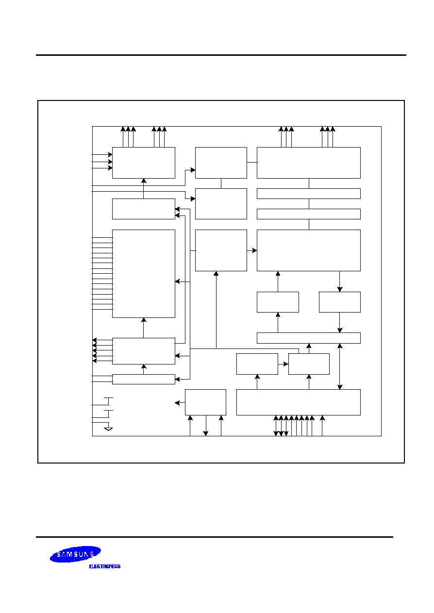
Modified figure for block diagram. (page 5)
Modified figure for pad configuration. (page 6)
Added table for pad dimension. (page 7)
Added figure for align key configuration and its coordinate. (page
8-9)
Added table for pad center coordinates. (page 10-13)
Modified and Added descriptions for pin description. (page 14-18)
Modified descriptions for power supply circuit. (page 21)
Modified figure for voltage setting. (page 22)
Added figure for application circuit. (page 102)
M. S. Song
April 12 , 2002
0.3
Modified table for pad dimension. (page 7)
Added table for blanking period setting. (page 43)
Modified descriptions for reset function. (page 53)
M. S. Song
April 30 , 2002
0.4
Modified descriptions for VC2-0 and VRL3-0 bit. (page 36)
Added descriptions and table contents for BGR bit. (page 39-40)
M. S. Song
July 9, 2002

S6D0110 132 RGB SOURCE & 176 GATE DRIVER WITH INTERNAL RAM FOR 65K COLORS TFT-LCD
Preliminary
3
INTRODUCTION
The S6D0110 is 1-chip solution for TFT-LCD panel: source driver with built-in memory, gate driver, power IC are
integrated on one chip. This IC can display to a maximum of 132-RGB x 176-dot graphics on 65k-color TFT panel.
The S6D0110 also supports bit-operation functions, 8/16-bit high-speed bus interface, and high-speed RAM-write
functions enable efficient data transfer and high-speed rewriting of data to the internal GRAM.
The moving picture area can be specified in internal GRAM by window function. The specified window area can be
updated selectively so that moving picture is able to displayed simultaneously independent of still picture area.
The S6D0110 has various functions for reducing the power consumption of a LCD system: It operates at low voltage
(minimum 1.8V) and the IC has an internal GRAM to store 132-RGB x 176-dot 65k-color image. In addition, it has
the internal booster that generates the LCD driving voltage, breeder resistance and the voltage follower circuit for
LCD driver.
This LSI is suitable for any medium-sized or small portable mobile solution requiring long-term driving capabilities,
such as digital cellular phones supporting a web browser, bi-directional pagers, and small PDAs.

132 RGB SOURCE & 176 GATE DRIVER WITH INTERNAL RAM FOR 65K COLORS TFT-LCD
S6D0110
Preliminary
4
FEATURES
132-RGB x 176-dot TFT-LCD display controller/driver IC for 65,536 colors (396ch-source driver/176ch-gate
driver)
16-/8-bit high-speed bus interface and serial peripheral interface (SPI)
High-speed burst-RAM write function
Writing to a window-RAM address area by using a window-address function
Bit-operation functions for graphic processing
-
Write-data mask functions in bit units
-
Logical operation in pixel unit and conditional write function
Various color-display control functions
-
65,536 colors can be displayed at the same time (gamma adjust included)
-
Vertical scroll display function in raster-row units
Internal RAM capacity: 132 x 16 x 176 = 371,712 bits
Low-power operation supports:
-
Power-save functions such as the standby mode and sleep mode
-
Partial LCD drive of two screens in any position
-
Maximum 12-times step-up circuit for liquid crystal drive voltage
-
Voltage followers to decrease direct current flow in the LCD drive breeder-resistors
-
Equalizing function for the switching performance of step-up circuits and operational amplifiers
N-raster row inversion drive (Reverse the polarity of driving voltage in every selected raster row is
possible)
Internal oscillation and hardware reset
Structure for TFT-display retention volume (Cst/Cadd structure)
Alternating functions for TFT-display counter-electrode power supply
-
N-line alternating drive of Vcom (Vgoff is also available for N-line alternating drive for Cadd)
Internal power supply circuit
-
Step-up circuit: five to nine times, positive-polarity inversion
-
Adjustment of Vcom(Vgoff) amplitude: internal 22-level digital potentiometer
Operating voltage
�
Applying voltage
-
VDD to VSS = 1.8 to 2.5 V (non-regulating)
(logic voltage range � non-regulated)
VDD3 to VSS = 2.3 to 3.3 V (regulating)
(logic voltage range � regulated)
-
Vci to VSS = 2.5 to 3.3 V
(internal reference power-supply voltage)
-
Vci1 to VSS = 1.7 to 2.75 V (2.5 x 0.68 ~ 2.75)
(power supply for step-up circuits)
�
Generating voltage
-
For the source driver: AVDD to VSS = 3.5 to 5.5V (power supply for liquid crystal output circuits)
GVDD to VSS = 3.0 to 5.0V (reference power supply for grayscale voltages)
-
For the gate driver: VGH to VGL = 14 to 30 V, VGH to VSS = +7.0 to +20 V,
VgoffL = (VGL+0.5) to �7.5V, VgoffH = ~ to -1.5V
-
For the TFT-display counter electrode: Vcom amplitude(max) = 6V, VcomH to VSS(max) = GVDD
VcomL to VSS(max) = 1.0 V to -Vci + 0.5 V